Datasheet EPC901 - Neumüller Elektronik
36
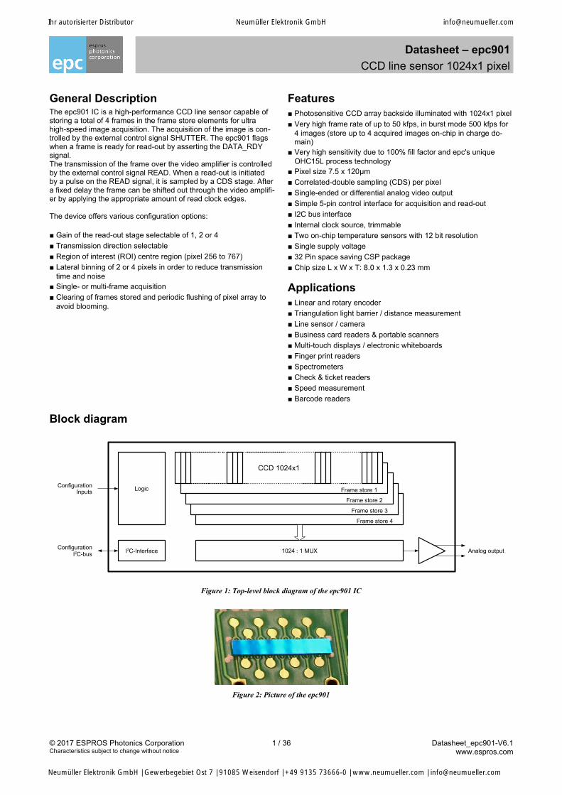
Datasheet – epc901 CCD line sensor 1024x1 pixel General Description The epc901 IC is a high-performance CCD line sensor capable of storing a total of 4 frames in the frame store elements for ultra high-speed image acquisition. The acquisition of the image is con- trolled by the external control signal SHUTTER. The epc901 flags when a frame is ready for read-out by asserting the DATA_RDY signal. The transmission of the frame over the video amplifier is controlled by the external control signal READ. When a read-out is initiated by a pulse on the READ signal, it is sampled by a CDS stage. After a fixed delay the frame can be shifted out through the video amplifi- er by applying the appropriate amount of read clock edges. The device offers various configuration options: ■ Gain of the read-out stage selectable of 1, 2 or 4 ■ Transmission direction selectable ■ Region of interest (ROI) centre region (pixel 256 to 767) ■ Lateral binning of 2 or 4 pixels in order to reduce transmission time and noise ■ Single- or multi-frame acquisition ■ Clearing of frames stored and periodic flushing of pixel array to avoid blooming. Features ■ Photosensitive CCD array backside illuminated with 1024x1 pixel ■ Very high frame rate of up to 50 kfps, in burst mode 500 kfps for 4 images (store up to 4 acquired images on-chip in charge do- main) ■ Very high sensitivity due to 100% fill factor and epc's unique OHC15L process technology ■ Pixel size 7.5 x 120μm ■ Correlated-double sampling (CDS) per pixel ■ Single-ended or differential analog video output ■ Simple 5-pin control interface for acquisition and read-out ■ I2C bus interface ■ Internal clock source, trimmable ■ Two on-chip temperature sensors with 12 bit resolution ■ Single supply voltage ■ 32 Pin space saving CSP package ■ Chip size L x W x T: 8.0 x 1.3 x 0.23 mm Applications ■ Linear and rotary encoder ■ Triangulation light barrier / distance measurement ■ Line sensor / camera ■ Business card readers & portable scanners ■ Multi-touch displays / electronic whiteboards ■ Finger print readers ■ Spectrometers ■ Check & ticket readers ■ Speed measurement ■ Barcode readers Block diagram CCD 1024x1 Frame store 4 Frame store 2 Frame store 3 1024 : 1 MUX Logic I 2 C-Interface Analog output Configuration Inputs Configuration I 2 C-bus Frame store 1 Figure 1: Top-level block diagram of the epc901 IC Figure 2: Picture of the epc901 © 2017 ESPROS Photonics Corporation Characteristics subject to change without notice 1 / 36 Datasheet_epc901-V6.1 www.espros.com Ihr autorisierter Distributor Neumüller Elektronik GmbH [email protected] Neumüller Elektronik GmbH | Gewerbegebiet Ost 7 | 91085 Weisendorf | +49 9135 73666-0 | www.neumueller.com | [email protected]
-
Upload
khangminh22 -
Category
Documents
-
view
3 -
download
0
Transcript of Datasheet EPC901 - Neumüller Elektronik
Datasheet – epc901
CCD line sensor 1024x1 pixel
General DescriptionThe epc901 IC is a high-performance CCD line sensor capable of storing a total of 4 frames in the frame store elements for ultra high-speed image acquisition. The acquisition of the image is con-trolled by the external control signal SHUTTER. The epc901 flags when a frame is ready for read-out by asserting the DATA_RDY signal.The transmission of the frame over the video amplifier is controlled by the external control signal READ. When a read-out is initiated by a pulse on the READ signal, it is sampled by a CDS stage. Aftera fixed delay the frame can be shifted out through the video amplifi-er by applying the appropriate amount of read clock edges.
The device offers various configuration options:
■ Gain of the read-out stage selectable of 1, 2 or 4
■ Transmission direction selectable
■ Region of interest (ROI) centre region (pixel 256 to 767)
■ Lateral binning of 2 or 4 pixels in order to reduce transmissiontime and noise
■ Single- or multi-frame acquisition
■ Clearing of frames stored and periodic flushing of pixel array toavoid blooming.
Features■ Photosensitive CCD array backside illuminated with 1024x1 pixel
■ Very high frame rate of up to 50 kfps, in burst mode 500 kfps for4 images (store up to 4 acquired images on-chip in charge do-main)
■ Very high sensitivity due to 100% fill factor and epc's uniqueOHC15L process technology
■ Pixel size 7.5 x 120μm
■ Correlated-double sampling (CDS) per pixel
■ Single-ended or differential analog video output
■ Simple 5-pin control interface for acquisition and read-out
■ I2C bus interface
■ Internal clock source, trimmable
■ Two on-chip temperature sensors with 12 bit resolution
■ Single supply voltage
■ 32 Pin space saving CSP package
■ Chip size L x W x T: 8.0 x 1.3 x 0.23 mm
Applications■ Linear and rotary encoder
■ Triangulation light barrier / distance measurement
■ Line sensor / camera
■ Business card readers & portable scanners
■ Multi-touch displays / electronic whiteboards
■ Finger print readers
■ Spectrometers
■ Check & ticket readers
■ Speed measurement
■ Barcode readers
Block diagram
CCD 1024x1
Frame store 4
Frame store 2
Frame store 3
1024 : 1 MUX
Logic
I2C-Interface Analog output
ConfigurationInputs
ConfigurationI2C-bus
Frame store 1
Figure 1: Top-level block diagram of the epc901 IC
Figure 2: Picture of the epc901
© 2017 ESPROS Photonics CorporationCharacteristics subject to change without notice
1 / 36 Datasheet_epc901-V6.1www.espros.com
Ihr autorisierter Distributor Neumüller Elektronik GmbH [email protected]
Neumüller Elektronik GmbH | Gewerbegebiet Ost 7 | 91085 Weisendorf | +49 9135 73666-0 | www.neumueller.com | [email protected]

Table of Contents
1. Block diagram.....................................................................................................................................................32. Pin-out................................................................................................................................................................42.1. Pin assignment....................................................................................................................................................................................42.2. Pin table...............................................................................................................................................................................................42.3. Power domain separation and ESD protection...................................................................................................................................53. Electrical, optical and timing characteristics............................................................................................................63.1. Recommended operating conditions...................................................................................................................................................63.2. System characteristics.........................................................................................................................................................................63.3. Electrical characteristics......................................................................................................................................................................63.4. Temperature sensor characteristics....................................................................................................................................................73.5. Timing parameters...............................................................................................................................................................................83.6. Absolute maximum ratings..................................................................................................................................................................83.7. Optical characteristics..........................................................................................................................................................................93.7.1. Typical spectral range and quantum efficiency (QE).....................................................................................................................103.8. Frequency response..........................................................................................................................................................................104. Chip configuration.............................................................................................................................................114.1. Configuration pin description.............................................................................................................................................................114.2. Dynamic change of the configuration pins........................................................................................................................................124.3. Charge pump on/off through DATA_RDY strap pin..........................................................................................................................124.4. Frequency response setting..............................................................................................................................................................125. Imager operation................................................................................................................................................135.1. General remarks................................................................................................................................................................................135.2. Image acquisition...............................................................................................................................................................................135.3. Multi frame acquisition.......................................................................................................................................................................145.4. Image readout....................................................................................................................................................................................145.5. Readout configuration........................................................................................................................................................................155.6. Periodic flushing................................................................................................................................................................................155.7. Clearing the CCD pixel field and the CCD frame store with CLR_DATA..........................................................................................156. Temperature sensor...........................................................................................................................................167. Power-down mode.............................................................................................................................................168. Chip reset.........................................................................................................................................................169. Measuring the internal oscillator clock frequency...................................................................................................1610. I2C interface....................................................................................................................................................1710.1. I2C communication..........................................................................................................................................................................1710.1.1. Device addressing........................................................................................................................................................................1710.1.2. Single-byte write...........................................................................................................................................................................1710.1.3. Multi-byte write..............................................................................................................................................................................1710.1.4. Single-byte read............................................................................................................................................................................1810.1.5. Multi-byte read..............................................................................................................................................................................1810.1.6. Software reset...............................................................................................................................................................................1810.1.7. Re-sampling the device address..................................................................................................................................................1810.2. Setup latency...................................................................................................................................................................................1810.3. I2C register description....................................................................................................................................................................1910.4. I2C bus timing..................................................................................................................................................................................2611. Application information.....................................................................................................................................2711.1. Circuit for differential mode..............................................................................................................................................................2711.2. Circuit for single ended mode..........................................................................................................................................................2811.3. External components.......................................................................................................................................................................2811.4. Low noise operation.........................................................................................................................................................................2811.4.1. Charge pump noise......................................................................................................................................................................2811.4.2. Video amplifier noise....................................................................................................................................................................2812. Power consumption considerations....................................................................................................................2912.1. General considerations....................................................................................................................................................................2912.2. Low power operation with external 3V and 5V supply....................................................................................................................2913. Layout and packaging information......................................................................................................................3013.1. Mechanical dimensions...................................................................................................................................................................3013.2. Location of the photosensitive area.................................................................................................................................................3013.3. Layout recommendations................................................................................................................................................................3113.3.1. Electrical.......................................................................................................................................................................................3113.3.2. PCB design and SMD manufacturing process considerations....................................................................................................3214. Tape & Reel Information....................................................................................................................................3314.1. Soldering and IC handling...............................................................................................................................................................3315. Self-test mode by fill-and-spill............................................................................................................................3415.1. Fill-and-spill procedure....................................................................................................................................................................3415.2. Important notes to fill-and-spill.........................................................................................................................................................3416. Ordering Information........................................................................................................................................3517. Note to various chip releases.............................................................................................................................3518. IMPORTANT NOTICE........................................................................................................................................36
© 2017 ESPROS Photonics CorporationCharacteristics subject to change without notice
2 / 36 Datasheet_epc901-V6.1www.espros.com
Ihr autorisierter Distributor Neumüller Elektronik GmbH [email protected]
Neumüller Elektronik GmbH | Gewerbegebiet Ost 7 | 91085 Weisendorf | +49 9135 73666-0 | www.neumueller.com | [email protected]
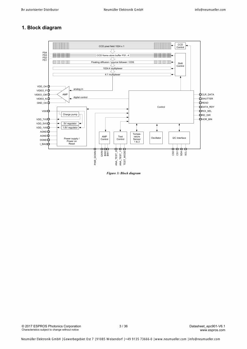
1. Block diagram
Tempe-rature
Sensor1 & 2
Oscillator I2C Interface
Control
TestControlPower supply /
Power onReset
VDD_1V8
AGND
AGND
DGND
AN
A_T
ES
T_
1
CS
0
CS
1
SD
A
SC
L
AN
A_
TE
ST
_0
CCD pixel field 1024 x 1CCD
Control
ShiftControl
CCD frame store buffer FS1..4
Floating diffusion / source follower / CDS
1024:4 multiplexer
4:1 multiplexer
AMPP
WR
_D
OW
N
VDD_OA
VIDEO_P
VIDEO_CM
VIDEO_N
GND_OA
VDD
VDD_7V0
VDD_5V0
CLR_DATA
SHUTTER
READ
DATA_RDY
ROI_SEL
RD_DIR
HOR_BIN
TE
ST
_M
OD
E
analog in
digital control
AMPControl
BW
1
GA
IN
I_BIAS
FS4FS3FS2FS1
Charge pump
5V regulator
1.8V regulator
BW
0
Figure 3: Block diagram
© 2017 ESPROS Photonics CorporationCharacteristics subject to change without notice
3 / 36 Datasheet_epc901-V6.1www.espros.com
Ihr autorisierter Distributor Neumüller Elektronik GmbH [email protected]
Neumüller Elektronik GmbH | Gewerbegebiet Ost 7 | 91085 Weisendorf | +49 9135 73666-0 | www.neumueller.com | [email protected]

2. Pin-out
2.1. Pin assignment
epc901
32
1 2 3 4 5 6 7 8 9 10 11 12 13 14 15 16
31 30 29 28 27 26 25 24 23 22 21 20 19 18 17
Figure 4: Pin-out of epc901 with view to the photo-sensitive side (top-view)
2.2. Pin tablePin no. Pin name Pin type Default [V] Description
Digital pins
2 PWR_DOWN DI 0 Power-down mode enable
3 CLR_DATA DI 0 Clear internal data memory controller
5 CLR_PIX DI 0 Rising edge resets pixels and its controller
6 SHUTTER DI 0 Exposure active when SHUTTER set
12 READ DI 0 Read-out control and read clock
4 DATA_RDY DOFlag when data on video interface is ready. Used as a strap pin to turn on/off the charge pump
13 SDA DIOD VDD I2C serial data (open drain)
14 SCL DIOD VDD I2C serial clock (open drain)
15 ROI_SEL DI 0 Region of interest selection
17 CS1 TER VDD/2 I2C chip select 1
19 CS0 TER VDD/2 I2C chip select 0
21 GAIN TER VDD/2 Select gain of read-out path
22 BW0 TER VDD/2 LSB of bandwidth of video amplifier
23 BW1 TER VDD/2 MSB of bandwidth of video amplifier
24 RD_DIR DI 0 Read-out direction
25 HOR_BIN TER VDD/2 Horizontal binning selection
30 TEST_MODE DI 0 Chip test
Analog pins
8 VIDEO_N AO Negative terminal of video output
9 VIDEO_P AO Positive terminal of video output
11 VIDEO_CM AI VDD/2 or 0 Voltage to set video output common-mode
27 I_BIAS AI Bias current
28 ANA_TEST_1 AIO 0 Analog test in-/output 1
29 ANA_TEST_0 AIO 0 Analog test in-/output 0
Supply pins
26 VDD Supply Positive chip supply voltage
10 VDD_OA Supply Positive supply of video amplifier
32 VDD_1V8 AO / Supply Decoupling of digital partition
18 VDD_5V0 AO / Supply Decoupling of CCD bias voltage, input is supplied externally (refer to 12.2.)
20 VDD_7V0 AO / Supply Decoupling of charge pump
16 AGND Supply Analog ground
1 AGND Supply Analog ground
7 GND_OA Supply Video amplifier ground
31 DGND Supply Digital ground
Definitions:
■ DI: Digital input pin, with an internal pull-down resistor of approx. 100-250kΩ
■ DO: Digital output pin
■ DIOD: General purpose bidirectional digital pin with open-drain output, requires external pull-up resistor
■ AO: Analog output
■ AI: Analog input
■ AIO: Analog input and output
■ TER: Ternary input pin, with a pull-down and an equal pull-up resistor of approx. 100-250kΩ which tie the pin to the VDD/2 state.
© 2017 ESPROS Photonics CorporationCharacteristics subject to change without notice
4 / 36 Datasheet_epc901-V6.1www.espros.com
Ihr autorisierter Distributor Neumüller Elektronik GmbH [email protected]
Neumüller Elektronik GmbH | Gewerbegebiet Ost 7 | 91085 Weisendorf | +49 9135 73666-0 | www.neumueller.com | [email protected]
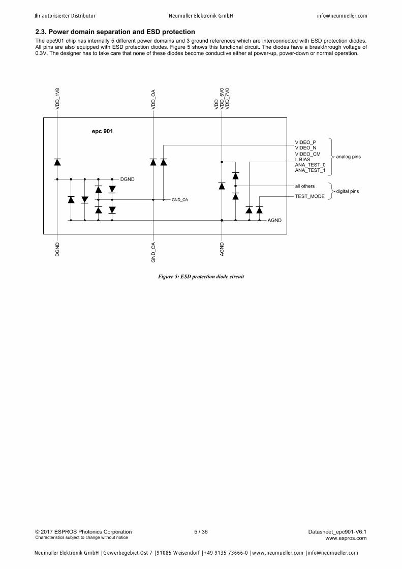
2.3. Power domain separation and ESD protectionThe epc901 chip has internally 5 different power domains and 3 ground references which are interconnected with ESD protection diodes.All pins are also equipped with ESD protection diodes. Figure 5 shows this functional circuit. The diodes have a breakthrough voltage of0.3V. The designer has to take care that none of these diodes become conductive either at power-up, power-down or normal operation.
DGND
AGND
GND_OA
VIDEO_PVIDEO_N
VD
D_
OA
GN
D_
OA
VD
D_
1V
8D
GN
D
AG
ND
VD
DV
DD
_5
V0
VD
D_
7V
0
VIDEO_CMI_BIASANA_TEST_0ANA_TEST_1
TEST_MODE
all others
epc 901
analog pins
digital pins
Figure 5: ESD protection diode circuit
© 2017 ESPROS Photonics CorporationCharacteristics subject to change without notice
5 / 36 Datasheet_epc901-V6.1www.espros.com
Ihr autorisierter Distributor Neumüller Elektronik GmbH [email protected]
Neumüller Elektronik GmbH | Gewerbegebiet Ost 7 | 91085 Weisendorf | +49 9135 73666-0 | www.neumueller.com | [email protected]
3. Electrical, optical and timing characteristics(TA = 25°C, VDD = 3.0V unless otherwise noted)
3.1. Recommended operating conditions
Parameter Description Min Typ Max Unit
VDD Nominal Nominal supply voltage on VDD and VDD_OA 2.70 3.00 3.45 V
Supply voltage on VDD and VDD_OA with Read Clock of max. 1 MHz.
2.45
PSRR Power supply rejection ratio VDD and VDD_OA. Differential 13 dB
Single ended 9 dB
TJ Junction temperature range -40 85 °C
Rth J-A Thermal resistance junction - ambient 65 K/W
3.2. System characteristics
Parameter Description Min Typ Max Unit
RVIDEO Frame rate on video output 1 50k fps
B3dB,VIDEO 3dB-bandwidth of video output @ CLVIDEO = 40pF 10 11 MHz
BI2C I2C transmission rate 400 kbit/s
3.3. Electrical characteristics
Parameter Description Min Typ Max Unit
IDD
+IDD_OA
1 Total current consumption on pins VDD and VDD_OA(refer to section 12.)
Differential mode, full video bandwidth, 50kfps 2, Charge pump: ONTemperature sensors: ON
Idle mode (READ = L) 26 39 mA
Peak, during read-out 48 72 mA
Differential mode,full video bandwidth, 50kfps 2,external VDD5V0 supply 3
Charge pump: OFFTemperature sensors: OFF
Idle mode (READ = L) 10 15 mA
Peak, during read-out 16 24 mA
Differential mode, low video bandwidth, 1kfps 4, external VDD5V0 supply 3
Charge pump: OFFTemperature sensors: OFF
Idle mode (READ = L) 6.0 9.0 mA
Peak, during read-out 6.0 9.0 mA
Single-ended mode, low video bandwidth, 1kfps 4
Charge pump: ONTemperature sensors: ON
Idle mode (READ = L) 21 30 mA
Peak, during read-out 40 60 mA
Single-ended mode, low video bandwidth, 1kfps 4, external VDD5V0 supply 3
Charge pump: OFF Temperature sensors: OFF
Idle mode (READ = L) 5.0 10.0 mA
Peak during read-out 5.0 10.0 mA
Power-Save mode (POWR_DOWN = H, shutter still working),external VDD5V0 supply 3
Charge pump: OFFTemperature sensors: OFF
1.3 2 mA
In-rush current at power-up during approximately 5msCharge pump: ON
60 90 mA
In-rush current at power-up during approximately 2ms,external VDD5V0 supply 3
Charge pump: OFF
50 75 mA
IDD_5V
Current consumption on pin VDD_5V0 3,Differential/single-ended mode, full video bandwidth, 50kfps 2
external VDD5V0 supply 3)Charge pump: OFF
1.2 2.5 mA
VDIL Low voltage level on binary digital inputs 5 (Level L) 0.2*VDD V
VDIH High voltage level on binary digital inputs 5 (Level H) 0.5*VDD V
VDOL, VTERIL Low voltage level on binary and ternary digital outputs (Level L) 0.2*VDD V
© 2017 ESPROS Photonics CorporationCharacteristics subject to change without notice
6 / 36 Datasheet_epc901-V6.1www.espros.com
Ihr autorisierter Distributor Neumüller Elektronik GmbH [email protected]
Neumüller Elektronik GmbH | Gewerbegebiet Ost 7 | 91085 Weisendorf | +49 9135 73666-0 | www.neumueller.com | [email protected]
Parameter Description Min Typ Max Unit
VDOH, VTERIH High voltage level on binary and ternary digital outputs (Level H) 0.8*VDD V
VTERIM Centre voltage level on ternary digital inputs (Level M) 0.4*VDD 0.6*VDD V
IDI Sink current at digital inputs 10 μA
RDI
Internal pull-down resistor 100 250 kΩ
RTER
Internal voltage dividing resistors which force the input to VDD/2 100 250 kΩ
IDO Sink / source current at digital outputs 3 mA
VVDD1V8 Internally generated voltage on pin VDD1V8 1.62 1.8 1.98 V
VVDD5V0 Internally generated voltage on pin VDD5V0 4.5 5.0 5.5 V
VDD7V0 Internally generated voltage on pin VDD7V0 6.0 6.5 7.0 V
VVIDEO_P,N Voltage range at output of video amplifier (@ gain 1) 0.25 VDD-0.25 V
VCM_SE Voltage at VIDEO_CM to select single-ended mode 0.4 V
VCM_D Common-mode voltage in differential mode, set on pinVIDEO_CM. Note: For VCM_D>1V, differential mode is detected au-tomatically by default. For VCM_D<1V, differential mode has to be enabled by setting bit AMP_OVR in register FORCE_ANA_CTRL_SIGS (see section 10.3.)
0.5 VDD
/2 VDD
/2+0.1 V
RIN,CM Input resistance of VIDEO_CM 100 kΩ
CMRRCM Common-mode rejection ratio on VIDEO_CM (f ≥ 100 kHz)
100kHz … 50MHz 17 dB
100kHz … 10Mhz 24 dB
VOFF,VIDEO,CM Common-mode offset of video amplifier output ±50 mV
VOFF,VIDEO,SIG Signal offset of video amplifier output ±100 mV
CLVIDEO Load capacitance on video output single ended 5 100 pF
differential 5 25 pF
RINT,VIDEO Output resistance of the video amplifiersingle ended 32 100 Ω
differential 11 100 Ω
RLVIDEO Load resistance on video output 3 kΩ
Notes:1 The current values change after the first Read Pulse after boot-up. The values here are after this first Read Pulse.2 Video amplifier BW = HIGH_BW, VIDEO_GBW_SEL_REG = 0x3.3 VDD5V0 has only to be supplied externally in case the charge pump is configured to be off. See section 12.2.4 Video amplifier BW = LOW_BW, VIDEO_GBW_SEL_REG = 0x0.5 I2C pins SCL and SDA are according to I2C standards
3.4. Temperature sensor characteristics
Parameter Description Min Typ Max Unit
TTEMP Temperature measurement range -40 +85 ºC
OFFSETTEMP Temperature sensor offset -10.1·103 LSB
GAINTEMP
Temperature sensor gain.The typical measured temperature value of e.g. the left tempera-ture sensor can be calculated from the value of the sensor output registers TEMP_SENS_L_MSB and TEMP_SENS_L_LSB as fol-lows:
TTEMP_L=TEMP_L [12: 0] − OFFSETTEMP
GAINTEMP
[ºK]
Note: Values for OFFSETTEMP and GAINTEMP are rough. For abso-lute measurements or precise relative measurements, calibration is required.
24 48 96 LSB/ºK
PTS Resolution of the temperature sensors 13 bits
NTEMP Noise 2 4 LSB
LINTEMP Linearity of temperature sensors over the full temperature range ±2 ±4 ºK
fTEMP Update rate of the temperature sensors (configurable) 0.1 10 Hz
© 2017 ESPROS Photonics CorporationCharacteristics subject to change without notice
7 / 36 Datasheet_epc901-V6.1www.espros.com
Ihr autorisierter Distributor Neumüller Elektronik GmbH [email protected]
Neumüller Elektronik GmbH | Gewerbegebiet Ost 7 | 91085 Weisendorf | +49 9135 73666-0 | www.neumueller.com | [email protected]
3.5. Timing parameters
Parameter Description Min Typ Max Unit
TSTARTUP Start-up time after applying external supply/supplies (includes ramp-up of charge pump)
10 ms
TCP_UP Charge pump power-up time: time from changing the bit CP_PD from 1 to 0 until chip is operational (internal VDD5V)
5 ms
TWAKE_UP Wake-up time from Power-Save mode 7 12 µs
fOSC
Oscillator clock frequency at nominal trim value (OSC_TRIM_REG at default value)
room temperature 22.4 36 48 MHz
-20°C < TA < 65°C 18 36 58 MHz
fOSC_MAX_TRIM
Frequency of oscillator clock that can be achieved through trim-ming 3 at room temperature.
32 MHz
TSU,CONF Setup time of configuration pins with respect to rising edge of read pulse
50 ns
TH,CONF Hold time of configuration pins with respect to rising edge of read pulse
3 Oscillatorclock cycles
TSHUTTER Pulse width of SHUTTER signal 5 Oscillatorclock cycles
TFLUSH Flush period 1 30 32 Oscillatorclock cycles
TSHIFT Shift period 1 24 26 Oscillatorclock cycles
TRD_PULSE Pulse width of Read Pulse 3 Oscillatorclock cycles
TCDS CDS operation 37 Oscillatorclock cycles
TSTORE Duration how long a frame may be stored in the frame-store 10 ms
TRD_CLK Period of the read clock 18.5 10'000 ns
fREAD READ clock rate (the inverse of TRD_CLK) 2 0.1 54 MHz
D READ clock duty cycle @ fREAD
max 45 50 55 %
TH,VIDEO Period during which the output of the video amplifier is held sta-ble after the last read clock edge
50 µs
TPERIOD,FLUSH Periodicity of the periodic flush operation 4 100 ms
TPULSE,CLR_DATA Pulse width on CLR_DATA 3 Oscillatorclock cycles
BI2C I2C transmission rate 400 kbit/s
Notes:1 By measuring the frequency of the internal clock oscillator (see section 9.), the duration of the internal flush and shift periods can be cal-culated exactly.2 To achieve the maximum clock frequency, the duty cycle of the read clock has to be 50% with a maximal tolerance of ±5%.3 The internal oscillator must not be trimmed to a frequency higher than 50MHz.4 Refer to section 5.6. for more details.
3.6. Absolute maximum ratings
Description Conditions
Power supply voltage (VDD) -0.3V to +5V
Voltage to any Pin -0.3 to VDD +0.3V
Storage Temperature Range (TS) -40°C to +85°C
Relative humidity 0 to 95% non-condensing
ESD rating all pins except VDD7V0 vs. VDD1V8: HBM class 2 ( 2kV to <4kV, JEDEC)Pin VDD7V0 vs. VDD1V8: HBM class 1B (500V to <1kV, JEDEC)Note: Pin VDD7V0 is in the final circuit loaded with 2.2µF low ESR capacitor.
© 2017 ESPROS Photonics CorporationCharacteristics subject to change without notice
8 / 36 Datasheet_epc901-V6.1www.espros.com
Ihr autorisierter Distributor Neumüller Elektronik GmbH [email protected]
Neumüller Elektronik GmbH | Gewerbegebiet Ost 7 | 91085 Weisendorf | +49 9135 73666-0 | www.neumueller.com | [email protected]
3.7. Optical characteristics(Gain 1, video bandwidth 1MHz, differential mode)
Parameter Description Min Typ Max Unit
WPIX Width of pixels 7.5 μm
HPIX Height of pixels 120 μm
NPIX Number of pixels 1024
NFS Number of frames stored on-chip (including the pixel array) 4
FF Optical fill factor in pixel array 100 %
CG Conversion gain (standard version) 3 5 8 μV/e-
Optical sensitivity (λ = 630 nm, gain = 1) 71 V/(Lux*s)
QE Quantum efficiency (λ = 630 nm) 90 %
FW 4 Full-well capacity per frame 400 ke-
NREAD_D Read noise, differential mode, optimal settings 1 700 1000 µVrms
NREAD_SE Read noise, single ended mode, optimal settings 1 500 700 µVrms
LIN Linearity2 Differential mode 1.0 2.0 %
Single-ended mode 2.0 4.0 %
ILAG Image lag @ max. Vpp and @ 400ke-
Single-frame acquisition (see section 5.2) 0.2 %
Multi-frame acquisition (see section 5.3) 0.3 0.5 %
δVDARK,PIX Output voltage drift due to dark current in pixel area 1.0 10.0 V/s
δVDARK,FS Output voltage drift due to dark current in frame store area 0.3 0.6 V/s
ΘDARK Thermal drift of dark current Doubles approx. every 8°K
PRNU3 Photo response non-uniformity (@ 0.5*FW4) 2 6 %
DSNU3 Dark pixel non-uniformity @ TEXP = 100 µs ±0.3 % FW
MFW Irradiance to generate FW electrons per pixel in 1 ns (λ = 630 nm)
155 mW/mm2
Surface reflectivity (@ 550 to 860 nm, 90° incident angle) 2 %
Surface reflectivity (@ 550 to 860 nm, 60° incident angle) 4 %
Pixel cross-talk (@ 630nm, 90° incident angle) 20 %
Cross-talk width @ 1σ 4 µm
Table 1: Optical specification
Notes:1 Charge pump off, temp sensor off, video amplifier BW=LOW_BW, VIDEO_GBW_SEL_REG=0x0 (minimum video amplifier bias current,
Read Clock 1MHz).2 The linearity is defined as the maximum deviation of the pixel responses between 10% and 80% FW4 from the straight line between 10%
and 80% FW4. Pixels with high dark current excluded.3 Valid for Pixel 3 .. 1020. 4 FW corresponds to 2V swing at the output in differential mode.
© 2017 ESPROS Photonics CorporationCharacteristics subject to change without notice
9 / 36 Datasheet_epc901-V6.1www.espros.com
Ihr autorisierter Distributor Neumüller Elektronik GmbH [email protected]
Neumüller Elektronik GmbH | Gewerbegebiet Ost 7 | 91085 Weisendorf | +49 9135 73666-0 | www.neumueller.com | [email protected]
3.7.1. Typical spectral range and quantum efficiency (QE)
The following diagrams show the quantum efficiency as a function of wavelength. The curve is a measurement where the chip has a wide-range anti-reflection coating which is optimized at 650 nm.
Figure 6: Quantum efficiency as a function of wavelength
3.8. Frequency responseThe signal amplitude at the output of the video amplifier is a function of the optical modulation and the read-out clock frequency. Theoptical modulation is defined as follows:
Shadow
epc901side view
Light source (parallel light)
Light
Grid
Pixel 0 Pixel 1023
Pixel no.0 1023
Amplifieroutput
Test setup
Measurement output
0.128mm
0.128mm
Out
put v
olta
ge
sw
ing
The amplitude at the video amplifier output as a function of the Read Clock frequency is as follows (temperature sensor off, differentialmode):
Read Clockfrequency
Mode BW (video am-plifier band-
width setting)
VIDEO_GBW_SEL_
REG
GAIN Min. useful signal swing
SNR typ.(charge pump off)
SNR typ.(charge pump on)
Usefulpixel
range 1
min typ min typ
1MHz Differential LOW_BW 0x0 1 2.0Vpp 66dB 70dB 65dB 67dB 3..1020
10MHz Differential HIGH_BW 0x3 1 1.5Vpp 55dB 58dB 53dB 55dB 3..1020
54MHz Differential HIGH_BW 0x3 1 0.5Vpp 46dB 49dB 44dB 46dB 3..1020
54MHz Differential HIGH_BW 0x3 2 0.75Vpp 46dB 49dB 42dB 46dB 3..1020
54MHz Differential HIGH_BW 0x3 4 1.25Vpp 46dB 49dB 42dB 46dB 3..1020
1MHz Single-ended LOW_BW 0x0 1 1.6Vpp 67dB 70dB N/A N/A 3..1020
Table 2: Useful video amplifier signal swing and SNR for different settings
Note:1 For the ROI_SEL=H, the read-out region as defined in Table 5 is the useful pixel range
© 2017 ESPROS Photonics CorporationCharacteristics subject to change without notice
10 / 36 Datasheet_epc901-V6.1www.espros.com
300 400 500 600 700 800 900 1000 1100 1200
0
10
20
30
40
50
60
70
80
90
100
Wavelength [nm]
QE
[%]
Ihr autorisierter Distributor Neumüller Elektronik GmbH [email protected]
Neumüller Elektronik GmbH | Gewerbegebiet Ost 7 | 91085 Weisendorf | +49 9135 73666-0 | www.neumueller.com | [email protected]

4. Chip configurationThe epc901 IC can be configured either by the configuration pins or through I2C commands. At power-up or software reset, the status ofthe configuration pins are read and used to operate the chip. The configuration can later on be changed with I2C commands (refer to Table9). Make sure that the bit RD_CONF_CTRL is set properly.
4.1. Configuration pin description
Pin Name Low (GND) High-Z High (VDD) Comments
RD_DIR Pixel 0 .. 1023 Pixel 1023 .. 0
ROI_SEL Pixel 0 .. 1023 Pixel 256 .. 767 Readout region of the pixel array
Gain 2 1 4 Multiplier for the conversion gain
HOR_BIN 2 pixel 1 pixel 4 pixel
Defines horizontal binning. Binning here means averaging over 2 or 4 pix-els in the voltage domain (not charge domain!) e.g. for HOR_BIN=H, pix-els 0..3, 4..7, 8..11 etc. are averaged as follows
VBINNING_BY_4[ i]=V [ i]+V [ i+1]+V [ i+2]+V [ i+3]
4, i = 0, 3, 7, .., 1020
Binning can be used to reduce the read-out time by the binning factor.
Note: Binning 2 (HOR_BIN = 0) is not applicable for single-ended mode.
VIDEO_CM Single ended Differential n/a Refer also to section 11.1. Circuit for differential mode
DATA_RDYCharge pump
onN/A
Charge pumpoff
Refer to section 4.3.
BW0 X Max. video bandwidth (referred to as 16MHz, see section 4.4. Frequency response setting)BW1 X
BW0 X High video bandwidth(referred to as 8MHz)BW1 X
BW0 X Low video bandwidth(referred to as 4MHz)BW1 X
BW0 X Min. video bandwidth(referred to as 1MHz, see section 4.4. Frequency response setting)BW1 X
Table 3: Configuration pin description
Notes:
• The shaded values are recommended for typical and easy to use applications.
• The bandwidth of the video amplifier (configured through BW and VIDEO_GBW_SEL_REG) affects the current consumption ofthe chip and the noise at the output. The lower the bandwidth the lower the noise and the lower the current consumption. Thus, itis a good concept to keep the bandwidth as low as possible.
• The configuration pins are read into the registers ACQ_TX_CONF_EFF and BW_VIDEO_CONF_EFF (and become effective)upon reset (i.e. power-up or software reset). In case RD_CONF_CTRL is left at default setting 0 (see Table 9), the configurationpins except VIDEO_CM and DATA_RDY are also read upon the rising edge of READ (refer to section 5.4.).
• The re-sampled values of the configuration pins take effect immediately if the configuration is controlled by the configurationpins.
• The configuration set by the configuration pins can be overwritten by writing to the registers ACQ_TX_CONF and/or BW_VIDEO_CONF through I2C (see section 10.). The overwrite functionality has to be enabled by setting RD_CONF_CTRL=1 (see Table 9).
• The CS0 and CS1 pin configuration are described in section 10.1.1. Device addressing.
© 2017 ESPROS Photonics CorporationCharacteristics subject to change without notice
11 / 36 Datasheet_epc901-V6.1www.espros.com
Ihr autorisierter Distributor Neumüller Elektronik GmbH [email protected]
Neumüller Elektronik GmbH | Gewerbegebiet Ost 7 | 91085 Weisendorf | +49 9135 73666-0 | www.neumueller.com | [email protected]
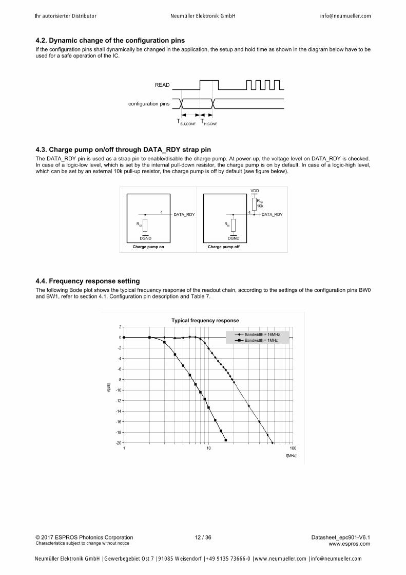
4.2. Dynamic change of the configuration pinsIf the configuration pins shall dynamically be changed in the application, the setup and hold time as shown in the diagram below have to beused for a safe operation of the IC.
READ
configuration pins
TSU,CONF
TH,CONF
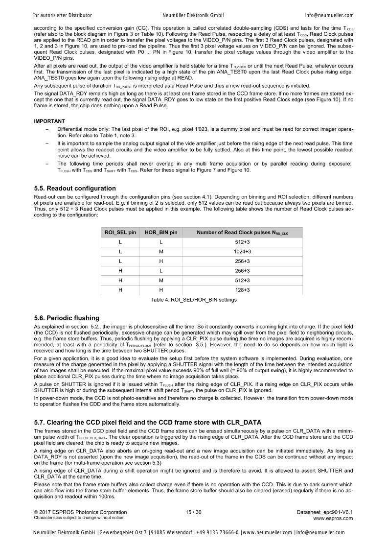
4.3. Charge pump on/off through DATA_RDY strap pinThe DATA_RDY pin is used as a strap pin to enable/disable the charge pump. At power-up, the voltage level on DATA_RDY is checked.In case of a logic-low level, which is set by the internal pull-down resistor, the charge pump is on by default. In case of a logic-high level,which can be set by an external 10k pull-up resistor, the charge pump is off by default (see figure below).
DATA_RDY
DGND
VDD
RDI
RPU
10k
DATA_RDY
DGND
RDI
4 4
Charge pump on Charge pump off
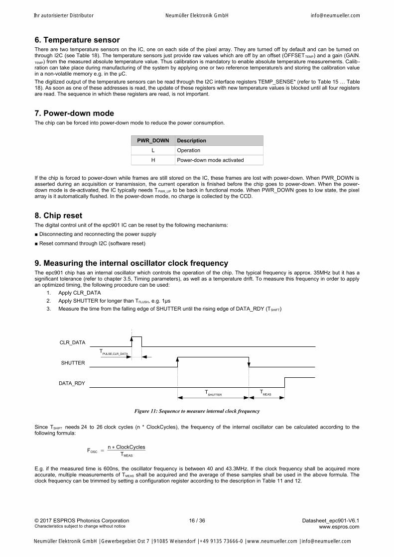
4.4. Frequency response settingThe following Bode plot shows the typical frequency response of the readout chain, according to the settings of the configuration pins BW0and BW1, refer to section 4.1. Configuration pin description and Table 7.
1 10 100-20
-18
-16
-14
-12
-10
-8
-6
-4
-2
0
2
Typical frequency response
Bandwidth = 16MHz
Bandwidth = 1MHz
f[MHz]
A[d
B]
© 2017 ESPROS Photonics CorporationCharacteristics subject to change without notice
12 / 36 Datasheet_epc901-V6.1www.espros.com
Ihr autorisierter Distributor Neumüller Elektronik GmbH [email protected]
Neumüller Elektronik GmbH | Gewerbegebiet Ost 7 | 91085 Weisendorf | +49 9135 73666-0 | www.neumueller.com | [email protected]

5. Imager operation
5.1. General remarksThe epc901 line imager chip is based on a backside illumination technology (BSI). The image is taken from the backside of the chip,whereas the electrical circuits and the pins are on the frontside. Thus, the chip must be flip-chip mounted to the PCB in order to expose thebackside to the incoming light.
It is not possible with BSI to shield the photosensitive area with an integrated, electrically controlled shutter when there no light shall bedetected. In other words, the pixel CCD is continuously photo-sensitive and collects charge generated by the detected photons (unwantedexposure). Thus, the CCD must be flushed or erased by the unwanted charge before an image can be acquired.
READ Pulse - The pulse applied to pin READ_CLK to initiate the read-out of a frame.READ Clock - The clock applied to pin READ_CLK to read out the frame (after the Read Pulse).
5.2. Image acquisitionAfter the exposure time defined by the user, the charge collected in the CCD has to be shifted into an area which is not photo-sensitive.This area is called frame store. The shift process samples the charge collected by the CCD in the frame store. The following diagramshows this operation.
SHUTTER
CCD operation
TFLUSH
TSHIFT
exposure time
DATA_RDY
automaticCCD flush
automaticshift to framestore (FIFO)
exposure toacquire an
image
(unwanted)exposure
(unwanted)exposure
TFLUSH
flush CCD
CLR_PIX
TPULSE_CLR_PIX
Figure 7: Image acquisition timing
The acquisition of a frame is controlled by a pulse on pin SHUTTER (see Figure 7). The rising edge of a pulse on SHUTTER triggers theinternal flush operation to erase the CCD from any unwanted electrons prior to the exposure. The exposure starts automatically after theflush operation is completed. The CCD collects electrons thereafter as long as the SHUTTER pin is high. Upon the falling edge ofSHUTTER, the charge collected in the CCD pixel field is automatically shifted to the CCD frame store which is a photo-insensitive area(see (1) in Figure 8). As soon as the frame is ready for read-out, the signal DATA_RDY goes high. The image is ready to be readout asdescribed in section 5.4..
CC
D p
ixel
fie
ldF
S1
FS
2F
S3
FS
4
SHUTTER
fram
e
fram
e
CD
S
READ_CLK
read
-out
don
e
fram
e
TCDS
fram
e
TSHIFT
CC
D fr
am
e s
tore
(1)
(2)
(3)
DATA_RDY
Figure 8: Illustrative example of single-frame acquisition and read-out
© 2017 ESPROS Photonics CorporationCharacteristics subject to change without notice
13 / 36 Datasheet_epc901-V6.1www.espros.com
Ihr autorisierter Distributor Neumüller Elektronik GmbH [email protected]
Neumüller Elektronik GmbH | Gewerbegebiet Ost 7 | 91085 Weisendorf | +49 9135 73666-0 | www.neumueller.com | [email protected]

It is to note that the CCD continues to be photo-sensitive during the shift operation i.e. for a time TSHIFT
after the falling edge of SHUTTER.
5.3. Multi frame acquisitionUp to 4 images can be acquired and stored in the CCD frame store in a fast sequence without intermediate read-out. The CCD frame storeis organized in 4 CCD frame store elements (FS1-FS4), thereby each CCD frame store element can store one frame/image. The firstcaptured image initially occupies 3 frame store elements as for a single-frame acquisition (see section 5.2 and Figure 8). epc901 automati-cally detects a multi-frame acquisition when detecting the second SHUTTER signal without prior read-out. Upon the second shutter thefirst image is shifted to a single frame store element (see (2) in Figure 9). The frames are shifted from the CCD pixel field to and throughthe CCD frame store in a FIFO-manner i.e. the first captured image is the first one read out. The read-out is described in more detail insection 5.4. As soon as 4 frames have been captured without prior read-out, at least one read-out has to be issued prior the next shutter inorder to make FS1 available again. Excessive shutter pulses are ignored.
FS
1C
CD
pix
el f
ield
FS
2F
S3
FS
4
SHUTTER
1st fr
ame
CD
S
READ_CLK
read
-ou
tdo
ne
1st fr
ame
1st fr
ame
2nd fr
ame
2nd fr
ame
3rd fr
ame
2nd fr
ame
TSHIFT
1st fr
ame
TCDS
TSHIFT
TSHIFT
3rd fr
ame
CC
D f
ram
e st
ore
TCDS
TCDS
2nd fr
ame
2nd fr
ame
3rd fr
ame
3rd fr
ame
3rd fr
ame
(1)
(2)
(3)
(4)
DATA_RDY
Figure 9: Illustrative example of multi-frame acquisition and read-out
5.4. Image readoutAfter one or more images have been captured, the first image (FIFO) can be read out through the video interface on the pins VIDEO_Pand VIDEO_N. The read-out is controlled by the READ pin. The following timing diagram shows its usage:
READ
VIDEO_P/N
TRD_PULSE
TRD_CLK
TH,VIDEOT
CDS
NRD_CLK
* TRD_CLK
Pre-loading ofinternal pipe-line
DATA_RDY
ANA_TEST0
1 2 3P0
P1
P2
P3
PN
READY goes low when the readout ofthe last stored frame begins
(rising edge indicates readout of the last pixel in a frame)
Figure 10: Image readout timing of one frame
The first pulse of a read sequence applied to pin READ is a Read Pulse and must have a duration of TRD_PULSE. Upon a Read Pulse, the lastframe in the CCD frame store is sampled pixel-wise onto a capacitor array thereby the pixel charges are converted into pixel voltages
© 2017 ESPROS Photonics CorporationCharacteristics subject to change without notice
14 / 36 Datasheet_epc901-V6.1www.espros.com
Ihr autorisierter Distributor Neumüller Elektronik GmbH [email protected]
Neumüller Elektronik GmbH | Gewerbegebiet Ost 7 | 91085 Weisendorf | +49 9135 73666-0 | www.neumueller.com | [email protected]
according to the specified conversion gain (CG). This operation is called correlated double-sampling (CDS) and lasts for the time T CDS
(refer also to the block diagram in Figure 3 or Table 10). Following the Read Pulse, respecting a delay of at least TCDS, Read Clock pulsesare applied to the READ pin in order to transfer the pixel voltages to the VIDEO_P/N pins. The first 3 Read Clock pulses, designated with1, 2 and 3 in Figure 10, are used to pre-load the pipeline. Thus the first 3 pixel voltage values on VIDEO_P/N can be ignored. The subse-quent Read Clock pulses, designated with P0 ... PN in Figure 10, transfer the pixel voltage values through the video amplifier to theVIDEO_P/N pins.
After all pixels are read out, the output of the video amplifier is held stable for a time T H,VIDEO or until the next Read Pulse, whatever occursfirst. The transmission of the last pixel is indicated by a high state of the pin ANA_TEST0 upon the last Read Clock pulse rising edge.ANA_TEST0 goes low again upon the following rising edge at READ.
Any subsequent pulse of duration TRD_PULSE is interpreted as a Read Pulse and thus a new read-out sequence is initiated.
The signal DATA_RDY remains high as long as there is at least one frame stored in the CCD frame store. If no more frames are stored ex -cept the one that is currently read out, the signal DATA_RDY goes to low state on the first positive Read Clock edge (see Figure 10). If noframe is stored, the chip does nothing upon a Read Pulse.
IMPORTANT
– Differential mode only: The last pixel of the ROI, e.g. pixel 1'023, is a dummy pixel and must be read for correct imager opera-tion. Refer also to Table 1, note 3.
– It is important to sample the analog output signal of the vide amplifier just before the rising edge of the next read pulse. This timepoint allows the readout circuits and the video amplifier to be fully settled. Also at this time point, the lowest possible readoutnoise can be achieved.
– The following time periods shall never overlap in any multi frame acquisition or by parallel reading during exposure:TFLUSH with TCDS and TSHIFT with TCDS. Refer for these signal to Figure 7 and Figure 10.
5.5. Readout configurationRead-out can be configured through the configuration pins (see section 4.1). Depending on binning and ROI selection, different numbersof pixels are available for read-out. E.g. if binning of 2 is selected, only 512 values can be read out because always two pixels are binned.Thus, only 512 + 3 Read Clock pulses must be applied in this example. The following table shows the number of Read Clock pulses ac -cording to the configuration:
ROI_SEL pin HOR_BIN pin Number of Read Clock pulses NRD_CLK
L L 512+3
L M 1024+3
L H 256+3
H L 256+3
H M 512+3
H H 128+3
Table 4: ROI_SEL/HOR_BIN settings
5.6. Periodic flushingAs explained in section 5.2., the imager is photosensitive all the time. So it constantly converts incoming light into charge. If the pixel field(the CCD) is not flushed periodically, excessive charge can be generated which may spill over from the pixel field to neighboring circuits,e.g. the frame store buffers. Thus, periodic flushing by applying a CLR_PIX pulse during the time no images are acquired is highly recom-mended, at least with a periodicity of TPERIOD,FLUSH (refer to section 3.5.). However, the need to do so depends on how much light isreceived and how long is the time between two SHUTTER pulses.
For a given application, it is a good idea to evaluate the setup first before the system software is implemented. During evaluation, onemeasure of the charge generated in the pixel by applying a SHUTTER signal with the length of the time between the intended acquisitionof two images shall be executed. If the maximal pixel value exceeds 90% of full well (= 90% of output swing), it is highly recommended toplace additional CLR_PIX pulses during the time where no image acquisition takes place.
A pulse on SHUTTER is ignored if it is issued within TFLUSH after the rising edge of CLR_PIX. If a rising edge on CLR_PIX occurs whileSHUTTER is high or during the subsequent internal shift period TSHIFT, the pulse on CLR_PIX is ignored.
In power-down mode, the CCD is not photo-sensitive and therefore no charge is collected. However, the transition from power-down modeto operation flushes the CDD and the frame store automatically.
5.7. Clearing the CCD pixel field and the CCD frame store with CLR_DATAThe frames stored in the CCD pixel field and the CCD frame store can be erased simultaneously by a pulse on CLR_DATA with a minim-um pulse width of TPULSE,CLR_DATA. The clear operation is triggered by the rising edge of CLR_DATA. After the CCD frame store and the CCDpixel field are cleared, the chip is ready to acquire new images.
A rising edge on CLR_DATA also aborts an on-going read-out and a new image acquisition can be initiated immediately. As long asDATA_RDY is not asserted (upon the new image acquisition), the read-out of the frame in the CDS can be continued without any impacton the frame (for multi-frame operation see section 5.3)
A rising edge of CLR_DATA during a shift operation might be ignored and is therefore to avoid. It is allowed to assert SHUTTER andCLR_DATA at the same time.
Please note that the frame store buffers also collect charge even if there is no operation with the CCD. This is due to dark current whichcan also flow into the frame store buffer elements. Thus, the frame store buffer should also be cleared (erased) regularly if there is no ac -quisition and readout within 100ms.
© 2017 ESPROS Photonics CorporationCharacteristics subject to change without notice
15 / 36 Datasheet_epc901-V6.1www.espros.com
Ihr autorisierter Distributor Neumüller Elektronik GmbH [email protected]
Neumüller Elektronik GmbH | Gewerbegebiet Ost 7 | 91085 Weisendorf | +49 9135 73666-0 | www.neumueller.com | [email protected]
6. Temperature sensorThere are two temperature sensors on the IC, one on each side of the pixel array. They are turned off by default and can be turned onthrough I2C (see Table 18). The temperature sensors just provide raw values which are off by an offset (OFFSETTEMP) and a gain (GAIN-
TEMP) from the measured absolute temperature value. Thus calibration is mandatory to enable absolute temperature measurements. Calib -ration can take place during manufacturing of the system by applying one or two reference temperature/s and storing the calibration valuein a non-volatile memory e.g. in the µC.
The digitized output of the temperature sensors can be read through the I2C interface registers TEMP_SENSE* (refer to Table 15 … Table18). As soon as one of these addresses is read, the update of these registers with new temperature values is blocked until all four registersare read. The sequence in which these registers are read, is not important.
7. Power-down modeThe chip can be forced into power-down mode to reduce the power consumption.
PWR_DOWN Description
L Operation
H Power-down mode activated
If the chip is forced to power-down while frames are still stored on the IC, these frames are lost with power-down. When PWR_DOWN isasserted during an acquisition or transmission, the current operation is finished before the chip goes to power-down. When the power-down mode is de-activated, the IC typically needs TPWR_UP to be back in functional mode. When PWR_DOWN goes to low state, the pixelarray is it automatically flushed. In the power-down mode, no charge is collected by the CCD.
8. Chip resetThe digital control unit of the epc901 IC can be reset by the following mechanisms:
■ Disconnecting and reconnecting the power supply
■ Reset command through I2C (software reset)
9. Measuring the internal oscillator clock frequencyThe epc901 chip has an internal oscillator which controls the operation of the chip. The typical frequency is approx. 35MHz but it has asignificant tolerance (refer to chapter 3.5, Timing parameters), as well as a temperature drift. To measure this frequency in order to applyan optimized timing, the following procedure can be used:
1. Apply CLR_DATA
2. Apply SHUTTER for longer than TFLUSH, e.g. 1µs
3. Measure the time from the falling edge of SHUTTER until the rising edge of DATA_RDY (TSHIFT)
SHUTTER
TSHUTTER
TMEAS
DATA_RDY
CLR_DATA
TPULSE,CLR_DATA
Figure 11: Sequence to measure internal clock frequency
Since TSHIFT needs 24 to 26 clock cycles (n * ClockCycles), the frequency of the internal oscillator can be calculated according to thefollowing formula:
FOSC = n∗ ClockCyclesTMEAS
E.g. if the measured time is 600ns, the oscillator frequency is between 40 and 43.3MHz. If the clock frequency shall be acquired moreaccurate, multiple measurements of TMEAS shall be acquired and the average of these samples shall be used in the above formula. Theclock frequency can be trimmed by setting a configuration register according to the description in Table 11 and 12.
© 2017 ESPROS Photonics CorporationCharacteristics subject to change without notice
16 / 36 Datasheet_epc901-V6.1www.espros.com
Ihr autorisierter Distributor Neumüller Elektronik GmbH [email protected]
Neumüller Elektronik GmbH | Gewerbegebiet Ost 7 | 91085 Weisendorf | +49 9135 73666-0 | www.neumueller.com | [email protected]

10. I2C interfaceThe epc901 supports the following functions by using the I2C interface:
■ Fast I2C (400 kBit/s)
■ 7-bit addressing
■ Slave (epc901 is always the slave)
■ Supported functions are software reset, read, write, read the device address
Clock stretching and other uses of I2C bus are not supported. The register list which can be accessed by the I2C interface are listed insection 10.3. All registers can be accessed directly except the test mode registers.
10.1. I2C communication
10.1.1. Device addressing
The MSBs of the device address are fixed to '001' internally, the LSBs A3 to A0 can be set by the two ternary input pins CS0 and CS1.
CS0
L M H
CS1
L 0000 0001 0011
M 0100 0101 0111
H 1100 1101 1111
The LSB of the device addressing is used to select the communication direction:
0 0 1 A3
A2
A1
A0 0
Write access
The bus protocol in the following sections uses the following notation:
Symbol Function
S START
P STOP
A ACK
N NACK
Shaded Master
Unshaded Slave (epc901
10.1.2. Single-byte write
P
Device address
AS 0 0 1 0 Register address A Data A
10.1.3. Multi-byte write
During a multi-byte write operation the master transmits the device address and the address of the first register to be written. All subse -quent bytes until STOP are interpreted as write data packets.
Register addressS PA Write data 0 A Write data 1 A Write data n AA0 0 1 0
Device address
Registers reside in a non-consecutive address space. Writing to a unused address will fail silently (no error feedback).
© 2017 ESPROS Photonics CorporationCharacteristics subject to change without notice
17 / 36 Datasheet_epc901-V6.1www.espros.com
Ihr autorisierter Distributor Neumüller Elektronik GmbH [email protected]
Neumüller Elektronik GmbH | Gewerbegebiet Ost 7 | 91085 Weisendorf | +49 9135 73666-0 | www.neumueller.com | [email protected]

10.1.4. Single-byte read
During a single-byte read, only one register is read. After the device address is transmitted, the master has to transmit the register ad -dress. After addressing the epc901 IC with a read-command, it transmits the read data. The access is terminated with a NACK and aSTOP by the master.
PAS 0 0 1 1 Read data NAS 0 0 1 0 Register address A
Device address Device address
10.1.5. Multi-byte read
During a multi-byte read operation the master transmits the device address and the address of the first register to be read. Afterwards, theepc901 is addressed with a read command. It then transmits data bytes until the master applies NACK and a STOP.
S PRead data 0 A Read data 1 A Read data n NA0 0 1 1Register addressS AA0 0 1 0
Device address Device address
Registers reside in a non-consecutive address space. Reading to a unused address will return no useful data.
10.1.6. Software reset
PAS 0 0 A0 0 0 0 0 0 0 0 0 0 0 1 1 0
A software reset has the same effect like a power-up reset. E.g. the chip uses the configuration as given by the configuration pins. Also, alltrimming parameters are reset to the initial values.
10.1.7. Re-sampling the device address
PAS 0 0 A0 0 0 0 0 0 0 0 0 0 0 1 0 0
By applying this command, the pins CS0 and CS1 are read and updated in the internal address register.
10.2. Setup latencyThe new register value becomes active with the falling edge of the last bit transmitted.
© 2017 ESPROS Photonics CorporationCharacteristics subject to change without notice
18 / 36 Datasheet_epc901-V6.1www.espros.com
Ihr autorisierter Distributor Neumüller Elektronik GmbH [email protected]
Neumüller Elektronik GmbH | Gewerbegebiet Ost 7 | 91085 Weisendorf | +49 9135 73666-0 | www.neumueller.com | [email protected]
10.3. I2C register description
Address Register name Ref. Description
Configuration
0x00 ACQ_TX_CONF_I2C Table 6 Acquisition and transmission configuration
Use this register to overwrite the values set by the corresponding configuration pins (see Table 2 or Table 3). Make sure RD_CONF_CTRL is set to 1. In this caseACQ_TX_CONF_I2C is copied to ACQ_TX_CONF_EFF at the rising edge of Read Pulse.
0x01 BW_VIDEO_CONF_IC2 Table 7 Bandwidth control of the video amplifier
Use this register address to overwrite the values set by the corresponding configu-ration pins (see Table 2 or Table 3). Make sure RD_CONF_CTRL is set to 1. In this case BW_VIDEO_CONF_IC2 is copied to BW_VIDEO_CONF_EFF at the ris-ing edge of Read Pulse.
0x02 MISC_CONF Table 8 Miscellaneous configuration
0x03 ACQ_TX_CONF_EFF Table 6 Acquisition and transmission configuration (effective register)The values for this register are read in from the configuration pins as long as RD_CONF_CTRL is set to 0Do not write to this register through I2C, use ACQ_TX_CONF_I2C instead.
0x04 BW_VIDEO_CONF_EFF Table 7 Bandwidth control of the video amplifier (effective register)The values for this register are read in from the configuration pins as long as RD_CONF_CTRL is set to 0Do not write to this register through I2C, use BW_VIDEO_CONF_IC2 instead.
Trimming
0x90 OSC_TRIM_REG Table 11 Oscillator trimming
0x91 …0x93
reserved n/a
0x94 VIDEO_GBW_SEL_REG Table 13 Tuning of the gain-bandwidth product of video amp
Temperature sensors
0xA0 TEMP_SENS_L_LSB Table 15 Least-significant byte of left sensor's raw temperature value
0xA1 TEMP_SENS_L_MSB Table 16 Most-significant byte of left sensor's raw temperature value
0xA2 TEMP_SENS_R_LSB Table 17 Least-significant byte of right sensor's raw temperature value
0xA3 TEMP_SENS_R_MSB Table 18 Most-significant byte of right sensor's raw temperature value
0xA4 TEMP_SENS_CONF Table 19 Configure behavior of temperature sensor
Error indicators (read-only)
0xB0 I2C_ERROR_IND Table 22 Error indicator of the I2C interface
Analog test mode registers (see also section 15.)
0xD0 ANA_TEST_MODE_EN_0 n/a Enable register for analog test mode
0xD1 ANA_TEST_MODE_EN_1 n/a Enable register for analog test mode
0xD2 ANA_TEST_CTRL n/a Test mode control register
0xD3 ANA_TEST_CONF n/a Configuration for the analog test modes
0xD4 ANA_TEST_MUX_0_SEL n/a Selection register for MUX on pin ANA_TEST_0
0xD5 ANA_TEST_MUX_1_SEL n/a Selection register for MUX on pin ANA_TEST_1
0xD6 FORCE_ANA_CTRL_SIGS Table 23 Force power-down of charge pump and pixel bias voltage regulator
0xD7 OSC_TRIM_RANGE_REG Table 10 Oscillator trimming - set oscillator trim range (available from chip revision number 0x14 i.e. epc901_020)
Debug read-only registers
0xF0 …0xFE
reserved n/a
0xFF CHIP_REV_NO_REG Table 25 Identifier register for chip revision number
Table 5: Register map accessible by the I2C interface
In the tables below, the operations defined are:
R Read
W Write
WP Writeable with protection
C Automatic synchronous clear operation after read access
© 2017 ESPROS Photonics CorporationCharacteristics subject to change without notice
19 / 36 Datasheet_epc901-V6.1www.espros.com
Ihr autorisierter Distributor Neumüller Elektronik GmbH [email protected]
Neumüller Elektronik GmbH | Gewerbegebiet Ost 7 | 91085 Weisendorf | +49 9135 73666-0 | www.neumueller.com | [email protected]
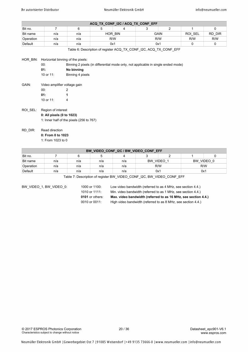
ACQ_TX_CONF_I2C / ACQ_TX_CONF_EFF
Bit no. 7 6 5 4 3 2 1 0
Bit name n/a n/a HOR_BIN GAIN ROI_SEL RD_DIR
Operation n/a n/a R/W R/W R/W R/W
Default n/a n/a 0x1 0x1 0 0
Table 6: Description of register ACQ_TX_CONF_I2C, ACQ_TX_CONF_EFF
HOR_BIN: Horizontal binning of the pixels:
00: Binning 2 pixels (in differential mode only, not applicable in single ended mode)
01: No binning
10 or 11: Binning 4 pixels
GAIN: Video amplifier voltage gain
00: 2
01: 1
10 or 11: 4
ROI_SEL: Region of interest
0: All pixels (0 to 1023)
1: Inner half of the pixels (256 to 767)
RD_DIR: Read direction
0: From 0 to 1023
1: From 1023 to 0
BW_VIDEO_CONF_I2C / BW_VIDEO_CONF_EFF
Bit no. 7 6 5 4 3 2 1 0
Bit name n/a n/a n/a n/a BW_VIDEO_1 BW_VIDEO_0
Operation n/a n/a n/a n/a R/W R/W
Default n/a n/a n/a n/a 0x1 0x1
Table 7: Description of register BW_VIDEO_CONF_I2C, BW_VIDEO_CONF_EFF
BW_VIDEO_1, BW_VIDEO_0: 1000 or 1100: Low video bandwidth (referred to as 4 MHz, see section 4.4.)
1010 or 1111: Min. video bandwidth (referred to as 1 MHz, see section 4.4.)
0101 or others: Max. video bandwidth (referred to as 16 MHz, see section 4.4.)
0010 or 0011: High video bandwidth (referred to as 8 MHz, see section 4.4.)
© 2017 ESPROS Photonics CorporationCharacteristics subject to change without notice
20 / 36 Datasheet_epc901-V6.1www.espros.com
Ihr autorisierter Distributor Neumüller Elektronik GmbH [email protected]
Neumüller Elektronik GmbH | Gewerbegebiet Ost 7 | 91085 Weisendorf | +49 9135 73666-0 | www.neumueller.com | [email protected]
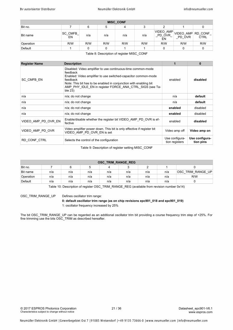
MISC_CONF
Bit no. 7 6 5 4 3 2 1 0
Bit nameSC_CMFB_
ENn/a n/a n/a n/a
VIDEO_AMP_PD_OVR_
EN
VIDEO_AMP_PD_OVR
RD_CONF_CTRL
Operation R/W R/W R/W R/W R/W R/W R/W R/W
Default 1 0 0 1 1 0 0 0
Table 8: Description of register MISC_CONF
Register Name Description 1 0
SC_CMFB_EN
Disabled: Video amplifier to use continuous-time common-mode feedbackEnabled: Video amplifier to use switched-capacitor common-mode feedbackNote: This bit has to be enabled in conjunction with enabling bit AMP_PHY_IDLE_EN in register FORCE_ANA_CTRL_SIGS (see Ta-ble 23)
enabled disabled
n/a n/a; do not change n/a default
n/a n/a; do not change n/a default
n/a n/a; do not change enabled disabled
n/a n/a; do not change enabled disabled
VIDEO_AMP_PD_OVR_ENEnable/disable whether the register bit VIDEO_AMP_PD_OVR is ef-fective
enabled disabled
VIDEO_AMP_PD_OVRVideo amplifier power down. This bit is only effective if register bit VIDEO_AMP_PD_OVR_EN is set
Video amp off Video amp on
RD_CONF_CTRL Selects the control of the configurationUse configura-tion registers
Use configura-tion pins
Table 9: Description of register setting MISC_CONF
OSC_TRIM_RANGE_REG
Bit no. 7 6 5 4 3 2 1 0
Bit name n/a n/a n/a n/a n/a n/a n/a OSC_TRIM_RANGE_UP
Operation n/a n/a n/a n/a n/a n/a n/a R/W
Default n/a n/a n/a n/a n/a n/a n/a 0
Table 10: Description of register OSC_TRIM_RANGE_REG (available from revision number 0x14)
OSC_TRIM_RANGE_UP Defines oscillator trim range:
0: default oscillator trim range (as on chip revisions epc901_018 and epc901_019)
1: oscillator frequency increased by 25%
The bit OSC_TRIM_RANGE_UP can be regarded as an additional oscillator trim bit providing a course frequency trim step of +25%. Forfine trimming use the bits OSC_TRIM as described hereafter.
© 2017 ESPROS Photonics CorporationCharacteristics subject to change without notice
21 / 36 Datasheet_epc901-V6.1www.espros.com
Ihr autorisierter Distributor Neumüller Elektronik GmbH [email protected]
Neumüller Elektronik GmbH | Gewerbegebiet Ost 7 | 91085 Weisendorf | +49 9135 73666-0 | www.neumueller.com | [email protected]
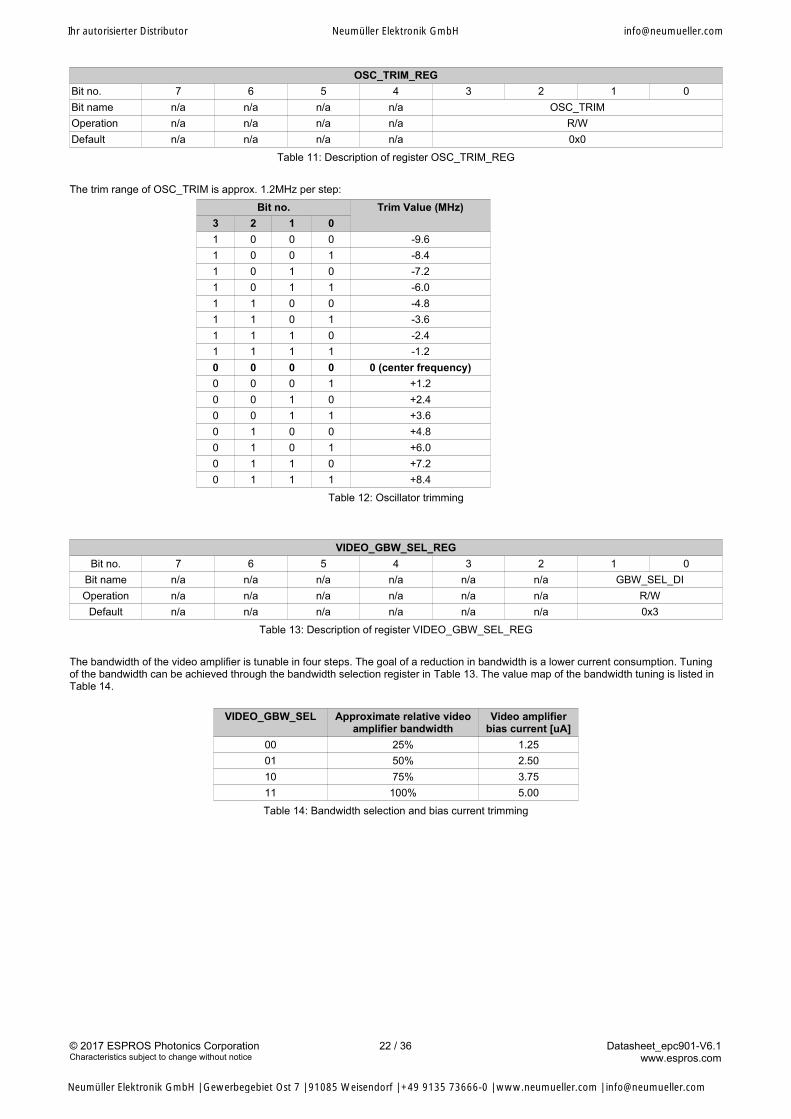
OSC_TRIM_REG
Bit no. 7 6 5 4 3 2 1 0
Bit name n/a n/a n/a n/a OSC_TRIM
Operation n/a n/a n/a n/a R/W
Default n/a n/a n/a n/a 0x0
Table 11: Description of register OSC_TRIM_REG
The trim range of OSC_TRIM is approx. 1.2MHz per step:
Bit no. Trim Value (MHz)
3 2 1 0
1 0 0 0 -9.6
1 0 0 1 -8.4
1 0 1 0 -7.2
1 0 1 1 -6.0
1 1 0 0 -4.8
1 1 0 1 -3.6
1 1 1 0 -2.4
1 1 1 1 -1.2
0 0 0 0 0 (center frequency)
0 0 0 1 +1.2
0 0 1 0 +2.4
0 0 1 1 +3.6
0 1 0 0 +4.8
0 1 0 1 +6.0
0 1 1 0 +7.2
0 1 1 1 +8.4
Table 12: Oscillator trimming
VIDEO_GBW_SEL_REG
Bit no. 7 6 5 4 3 2 1 0
Bit name n/a n/a n/a n/a n/a n/a GBW_SEL_DI
Operation n/a n/a n/a n/a n/a n/a R/W
Default n/a n/a n/a n/a n/a n/a 0x3
Table 13: Description of register VIDEO_GBW_SEL_REG
The bandwidth of the video amplifier is tunable in four steps. The goal of a reduction in bandwidth is a lower current consumption. Tuningof the bandwidth can be achieved through the bandwidth selection register in Table 13. The value map of the bandwidth tuning is listed inTable 14.
VIDEO_GBW_SEL Approximate relative videoamplifier bandwidth
Video amplifierbias current [uA]
00 25% 1.25
01 50% 2.50
10 75% 3.75
11 100% 5.00
Table 14: Bandwidth selection and bias current trimming
© 2017 ESPROS Photonics CorporationCharacteristics subject to change without notice
22 / 36 Datasheet_epc901-V6.1www.espros.com
Ihr autorisierter Distributor Neumüller Elektronik GmbH [email protected]
Neumüller Elektronik GmbH | Gewerbegebiet Ost 7 | 91085 Weisendorf | +49 9135 73666-0 | www.neumueller.com | [email protected]
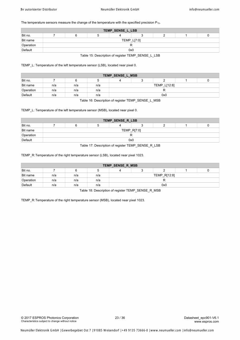
The temperature sensors measure the change of the temperature with the specified precision PTS.
TEMP_SENSE_L_LSB
Bit no. 7 6 5 4 3 2 1 0
Bit name TEMP_L[7:0]
Operation R
Default 0x0
Table 15: Description of register TEMP_SENSE_L_LSB
TEMP_L: Temperature of the left temperature sensor (LSB), located near pixel 0.
TEMP_SENSE_L_MSB
Bit no. 7 6 5 4 3 2 1 0
Bit name n/a n/a n/a TEMP_L[12:8]
Operation n/a n/a n/a R
Default n/a n/a n/a 0x0
Table 16: Description of register TEMP_SENSE_L_MSB
TEMP_L: Temperature of the left temperature sensor (MSB), located near pixel 0.
TEMP_SENSE_R_LSB
Bit no. 7 6 5 4 3 2 1 0
Bit name TEMP_R[7:0]
Operation R
Default 0x0
Table 17: Description of register TEMP_SENSE_R_LSB
TEMP_R:Temperature of the right temperature sensor (LSB), located near pixel 1023.
TEMP_SENSE_R_MSB
Bit no. 7 6 5 4 3 2 1 0
Bit name n/a n/a n/a TEMP_R[12:8]
Operation n/a n/a n/a R
Default n/a n/a n/a 0x0
Table 18: Description of register TEMP_SENSE_R_MSB
TEMP_R:Temperature of the right temperature sensor (MSB), located near pixel 1023.
© 2017 ESPROS Photonics CorporationCharacteristics subject to change without notice
23 / 36 Datasheet_epc901-V6.1www.espros.com
Ihr autorisierter Distributor Neumüller Elektronik GmbH [email protected]
Neumüller Elektronik GmbH | Gewerbegebiet Ost 7 | 91085 Weisendorf | +49 9135 73666-0 | www.neumueller.com | [email protected]

TEMP_SENS_CONF
Bit no. 7 6 5 4 3 2 1 0
Bit name n/a n/a MEAS_RATE_CONF ENABLE_R ENABLE_L PD_CONF_R PD_CONF_L
Operation n/a n/a R/W R/W R/W R/W R/W
Default for versions < -031Default from version -031 1
n/an/a
n/an/a
0x00x0
10 1
10 1
01 1
01 1
Table 19: Description of register TEMP_SENS_CONF
Note:1 The temperature sensors are turned off by default
Register Name Description 1 0
MEAS_RATE_CONF
Configure the measurement rate of the temperature sensors:
00: 10 measurements per second01: 1 measurement per second10: 1 measurement every 10 seconds
Note: A change of the measurement rate becomes effective only af-ter the temperature sensor has been disabled and enabled again.
ENABLE_R
See Table 21ENABLE_L
PD_CONF_R
PD_CONF_L
Table 20: Description of register setting TEMP_SENS_CONF
ENABLE_R ENABLE_L PD_CONF_R PD_CONF_L Description Comment
0 0 1 1 Both sensors offDefault setting fromversion 031
1 1 0 0 Both sensors onDefault setting up to version 023
1 0 0 1 Only right sensor on
0 1 1 0 Only left sensor on
Table 21: Enable/disable temperature sensors
I2C_ERROR_IND
Bit no. 7 6 5 4 3 2 1 0
Bit name n/a n/a n/a n/a n/a n/a n/a I2C_ERR
Operation n/a n/a n/a n/a n/a n/a n/a R/C
Default n/a n/a n/a n/a n/a n/a n/a 0
Table 22: Description of register I2C_ERROR_IND
I2C_ERR Read/clear bit is set when the configuration controller fails to service a register read (or write) operation in due time.When this happens, the affected read operation may return wrong data, and the affected write operation may beignored.
© 2017 ESPROS Photonics CorporationCharacteristics subject to change without notice
24 / 36 Datasheet_epc901-V6.1www.espros.com
Ihr autorisierter Distributor Neumüller Elektronik GmbH [email protected]
Neumüller Elektronik GmbH | Gewerbegebiet Ost 7 | 91085 Weisendorf | +49 9135 73666-0 | www.neumueller.com | [email protected]
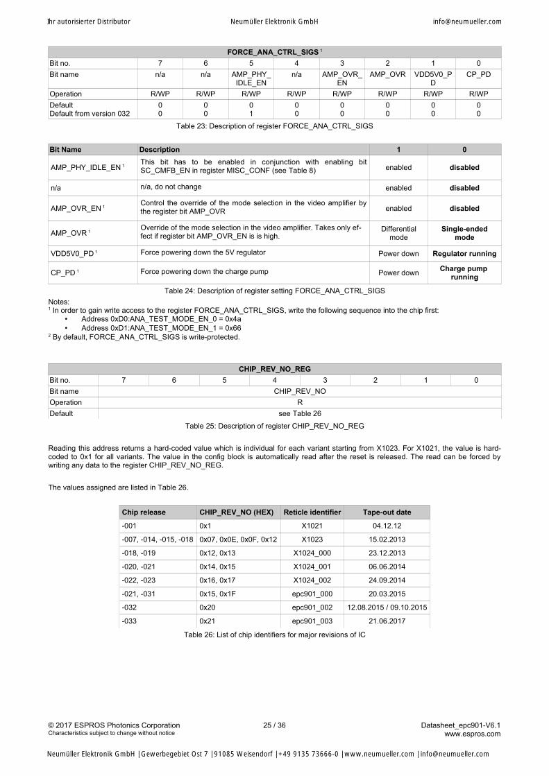
FORCE_ANA_CTRL_SIGS 1
Bit no. 7 6 5 4 3 2 1 0
Bit name n/a n/a AMP_PHY_IDLE_EN
n/a AMP_OVR_EN
AMP_OVR VDD5V0_PD
CP_PD
Operation R/WP R/WP R/WP R/WP R/WP R/WP R/WP R/WP
DefaultDefault from version 032
00
00
01
00
00
00
00
00
Table 23: Description of register FORCE_ANA_CTRL_SIGS
Bit Name Description 1 0
AMP_PHY_IDLE_EN 1This bit has to be enabled in conjunction with enabling bitSC_CMFB_EN in register MISC_CONF (see Table 8) enabled disabled
n/a n/a, do not change enabled disabled
AMP_OVR_EN 1Control the override of the mode selection in the video amplifier bythe register bit AMP_OVR enabled disabled
AMP_OVR 1Override of the mode selection in the video amplifier. Takes only ef-fect if register bit AMP_OVR_EN is is high.
Differentialmode
Single-endedmode
VDD5V0_PD 1 Force powering down the 5V regulator Power down Regulator running
CP_PD 1 Force powering down the charge pump Power downCharge pump
running
Table 24: Description of register setting FORCE_ANA_CTRL_SIGS
Notes:1 In order to gain write access to the register FORCE_ANA_CTRL_SIGS, write the following sequence into the chip first:
• Address 0xD0:ANA_TEST_MODE_EN_0 = 0x4a• Address 0xD1:ANA_TEST_MODE_EN_1 = 0x66
2 By default, FORCE_ANA_CTRL_SIGS is write-protected.
CHIP_REV_NO_REG
Bit no. 7 6 5 4 3 2 1 0
Bit name CHIP_REV_NO
Operation R
Default see Table 26
Table 25: Description of register CHIP_REV_NO_REG
Reading this address returns a hard-coded value which is individual for each variant starting from X1023. For X1021, the value is hard-coded to 0x1 for all variants. The value in the config block is automatically read after the reset is released. The read can be forced bywriting any data to the register CHIP_REV_NO_REG.
The values assigned are listed in Table 26.
Chip release CHIP_REV_NO (HEX) Reticle identifier Tape-out date
-001 0x1 X1021 04.12.12
-007, -014, -015, -018 0x07, 0x0E, 0x0F, 0x12 X1023 15.02.2013
-018, -019 0x12, 0x13 X1024_000 23.12.2013
-020, -021 0x14, 0x15 X1024_001 06.06.2014
-022, -023 0x16, 0x17 X1024_002 24.09.2014
-021, -031 0x15, 0x1F epc901_000 20.03.2015
-032 0x20 epc901_002 12.08.2015 / 09.10.2015
-033 0x21 epc901_003 21.06.2017
Table 26: List of chip identifiers for major revisions of IC
© 2017 ESPROS Photonics CorporationCharacteristics subject to change without notice
25 / 36 Datasheet_epc901-V6.1www.espros.com
Ihr autorisierter Distributor Neumüller Elektronik GmbH [email protected]
Neumüller Elektronik GmbH | Gewerbegebiet Ost 7 | 91085 Weisendorf | +49 9135 73666-0 | www.neumueller.com | [email protected]

10.4. I2C bus timing
SDA
SCLK
ACKMSB LSB
Change of data allowed
START condition STOP condition
Data stable
START condition
Acknowledgment
SDA
SCL
ACKMSB LSB
tSTA
tSU
tH
tSCLL
tSCLH
tSDAF
tSDAR
tSTO
tSTOSTA
tSCLR
tSCLF
Figure 12: I2C bus timing, top: Basic communication sequence, bottom: Timing parameters
Symbol Parameter Min. Max. Units
fSCL I2C data rate 400 kbit/s
tSCLL SCL clock low time 1.3 µs
tSCLH SCL clock high time 0.6 µs
tSU SDA setup time 100 ns
tH SDA hold time 0 ns
tSDAR
tSCLR
SDA and SCL rise time 300 ns
tSDAF
tSCLF
SDA and SCL fall time 300 ns
tSTA Start condition hold time 0.6 µs
tSTO Stop condition setup time 0.6 µs
tSTOSTA Stop to start condition time (bus free) 1.3 µs
Cb Capacitive load for each bus line 400 pF
tSP Pulse width of the spikes that are suppressed by the analog filter 50 ns
Table 27: I2C bus timing: Timing parameters (FM+)
© 2017 ESPROS Photonics CorporationCharacteristics subject to change without notice
26 / 36 Datasheet_epc901-V6.1www.espros.com
Ihr autorisierter Distributor Neumüller Elektronik GmbH [email protected]
Neumüller Elektronik GmbH | Gewerbegebiet Ost 7 | 91085 Weisendorf | +49 9135 73666-0 | www.neumueller.com | [email protected]
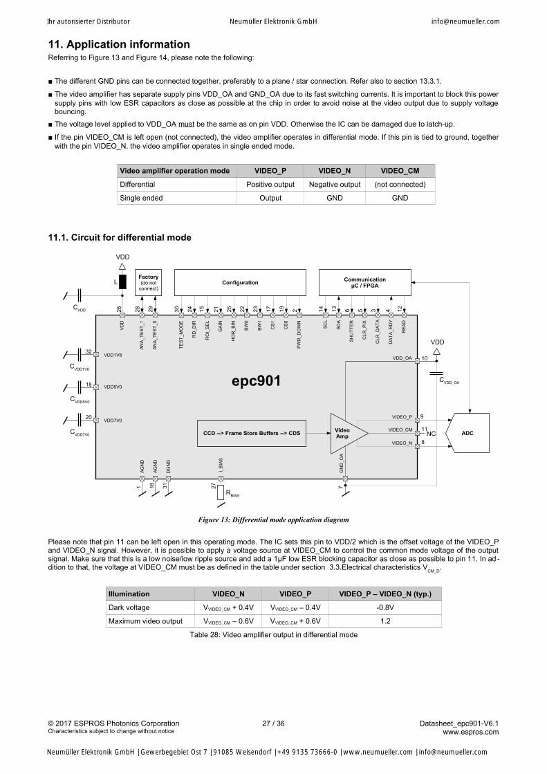
11. Application informationReferring to Figure 13 and Figure 14, please note the following:
■ The different GND pins can be connected together, preferably to a plane / star connection. Refer also to section 13.3.1.
■ The video amplifier has separate supply pins VDD_OA and GND_OA due to its fast switching currents. It is important to block this powersupply pins with low ESR capacitors as close as possible at the chip in order to avoid noise at the video output due to supply voltagebouncing.
■ The voltage level applied to VDD_OA must be the same as on pin VDD. Otherwise the IC can be damaged due to latch-up.
■ If the pin VIDEO_CM is left open (not connected), the video amplifier operates in differential mode. If this pin is tied to ground, togetherwith the pin VIDEO_N, the video amplifier operates in single ended mode.
Video amplifier operation mode VIDEO_P VIDEO_N VIDEO_CM
Differential Positive output Negative output (not connected)
Single ended Output GND GND
11.1. Circuit for differential mode
epc901
I_B
IAS
RBIAS
VDD1V8
VDD7V0
VDD_OA
VIDEO_P
VIDEO_N
BW
0
BW
1
PW
R_
DO
WN
HO
R_
BIN
GA
IN
RD
_D
IR
RO
I_S
EL
RE
AD
DA
TA
_RD
Y
CL
R_
PIX
SH
UT
TE
R
SC
L
SD
A
CS
1
CS
0
AN
A_
TE
ST
_0
TE
ST
_M
OD
E
VD
D
CVDD7V0
CVDD1V8
VDDCL
R_
DA
TA
AN
A_
TE
ST
_1
VDD
CVDD
CommunicationμC / FPGA
ADC
26
ConfigurationFactory(do not
connect)
28 29 30 24 15 21 25 22 23 17 19 2 14 13 6 5 3 4 12
72731161
32
20
8
10
CCD --> Frame Store Buffers --> CDS NC
9
VDD5V0
CVDD5V0
18
VIDEO_CM 11
GN
D_
OA
VideoAmp
CVDD_OA
DG
ND
AG
ND
AG
ND
L
Figure 13: Differential mode application diagram
Please note that pin 11 can be left open in this operating mode. The IC sets this pin to VDD/2 which is the offset voltage of the VIDEO_Pand VIDEO_N signal. However, it is possible to apply a voltage source at VIDEO_CM to control the common mode voltage of the outputsignal. Make sure that this is a low noise/low ripple source and add a 1µF low ESR blocking capacitor as close as possible to pin 11. In ad -dition to that, the voltage at VIDEO_CM must be as defined in the table under section 3.3.Electrical characteristics V
CM_D.
Illumination VIDEO_N VIDEO_P VIDEO_P – VIDEO_N (typ.)
Dark voltage VVIDEO_CM + 0.4V VVIDEO_CM – 0.4V -0.8V
Maximum video output VVIDEO_CM – 0.6V VVIDEO_CM + 0.6V 1.2
Table 28: Video amplifier output in differential mode
© 2017 ESPROS Photonics CorporationCharacteristics subject to change without notice
27 / 36 Datasheet_epc901-V6.1www.espros.com
Ihr autorisierter Distributor Neumüller Elektronik GmbH [email protected]
Neumüller Elektronik GmbH | Gewerbegebiet Ost 7 | 91085 Weisendorf | +49 9135 73666-0 | www.neumueller.com | [email protected]

11.2. Circuit for single ended mode
epc901I_
BIA
S
RBIAS
VDD1V8
VDD7V0
VDD_OA
VIDEO_P
VIDEO_N
BW
0
BW
1
PW
R_
DO
WN
HO
R_
BIN
GA
IN
RD
_D
IR
RO
I_S
EL
RE
AD
DA
TA
_RD
Y
CLR
_P
IX
SH
UT
TE
R
SC
L
SD
A
CS
1
CS
0
AN
A_
TE
ST
_0
TE
ST
_M
OD
E
VD
D
CVDD7V0
CVDD1V8
VDDCLR
_D
AT
A
AN
A_
TE
ST
_1
VDD
CVDD
CommunicationμC / FPGA
ADC
26
ConfigurationFactory(do not
connect)
28 29 30 24 15 21 25 22 23 17 19 2 14 13 6 5 3 4 12
72731161
32
20
8
10
CCD --> Frame Store Buffers --> CDS
9
VDD5V0
CVDD5V0
18
VIDEO_CM 11
GN
D_
OA
VideoAmp
CVDD_OA
DG
ND
AG
ND
AG
ND
L
Pins 8 and 11:Can be left notconnected.Refer to the notebelow.
Figure 14: Single ended mode application diagram
If VIDEO_N and VIDEO_CM are tied to GND at power-up or RESET, single-ended mode is selected. The output signal is available atVIDEO_P.
Note:Are the pins VIDEO_N and VIDEO_CM not connected, the epc901 is after power-up or RESET in differential mode. In this case, single-en-ded mode can be selected via I2C register setting FORCE_ANA_CTRL_SIGS, bit AMP_OVR (see Table 23 and Table 24).
Illumination VIDEO_P (typ.)
Dark voltage 0.4V
Maximum video output 2.0V
Table 29: Video amplifier output in single-ended mode
11.3. External componentsThe external components in Figure 13 and Figure 14 shall be as follows:
Parameter Description Value Units Tolerance Comments
RBIAS External resistor defining the bias current 56k kΩ ±1% Temperature coefficient max. ±100ppm/K
CVDD1V8 Decoupling capacitor for VDD1V8 1.0 μF ±20% low ESR
CVDD5V0, CVDD7V0 Decoupling capacitors for VDD5V0, VDD7V0 2.2 μF ±20% low ESR
CVDD, CVDD_OA Decoupling capacitors for VDD, VDD_OA 1.0 μF ±20% low ESR
L Decoupling inductor 600 Ω e.g. Taiyo Yuden BK1005HR601-T
11.4. Low noise operation
11.4.1. Charge pump noise
The internal charge pump generates considerable noise, especially in single-ended mode. The noise performance can be optimized byturning off the charge pump and supplying the chip with an external 5V supply. Refer to section 12.2..
11.4.2. Video amplifier noise
Another noise source is the video amplifier which can be used in two different modes. Single ended mode is the lower noise operationmode. Thus, use the chip in single ended mode for low noise applications.
© 2017 ESPROS Photonics CorporationCharacteristics subject to change without notice
28 / 36 Datasheet_epc901-V6.1www.espros.com
Ihr autorisierter Distributor Neumüller Elektronik GmbH [email protected]
Neumüller Elektronik GmbH | Gewerbegebiet Ost 7 | 91085 Weisendorf | +49 9135 73666-0 | www.neumueller.com | [email protected]
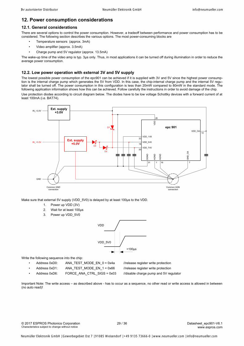
12. Power consumption considerations
12.1. General considerationsThere are several options to control the power consumption. However, a tradeoff between performance and power consumption has to beconsidered. The following section describes the various options. The most power-consuming blocks are
• Temperature sensors (approx. 3mA)
• Video amplifier (approx. 3.5mA)
• Charge pump and 5V regulator (approx. 13.5mA)
The wake-up time of the video amp is typ. 3µs only. Thus, in most applications it can be turned off during illumination in order to reduce theaverage power consumption.
12.2. Low power operation with external 3V and 5V supplyThe lowest possible power consumption of the epc901 can be achieved if it is supplied with 3V and 5V since the highest power consump-tion is the internal charge pump which generates the 5V from VDD. In this case, the chip-internal charge pump and the internal 5V regu-lator shall be turned off. The power consumption in this configuration is less than 20mW compared to 80mW in the standard mode. Thefollowing application information shows how this can be achieved. Follow carefully the instructions in order to avoid damage of the chip.
Use protection diodes according to circuit diagram below. The diodes have to be low voltage Schottky devices with a forward current of atleast 100mA (i.e. BAT74).
Make sure that external 5V supply (VDD_5V0) is delayed by at least 100µs to the VDD.
1. Power up VDD (3V)
2. Wait for at least 100µs
3. Power up VDD_5V0
>100µs
VDD
VDD_5V0
Write the following sequence into the chip:
• Address 0xD0: ANA_TEST_MODE_EN_0 = 0x4a //release register write protection
• Address 0xD1: ANA_TEST_MODE_EN_1 = 0x66 //release register write protection
• Address 0xD6: FORCE_ANA_CTRL_SIGS = 0x03 //disable charge pump and 5V regulator
Important Note: The write access – as described above - has to occur as a sequence, no other read or write access is allowed in between(no auto read)!
© 2017 ESPROS Photonics CorporationCharacteristics subject to change without notice
29 / 36 Datasheet_epc901-V6.1www.espros.com
Ext. supply+5.0V
DG
ND
AG
ND
AG
ND
GN
D_O
A
VD
D
VDD_1V8
VDD_5V0
VDD_7V0
VDD_OA
32
18
20
1 1631 7
26
10
epc 901
IN_+5.0V
GND
Common AGNconnection
Common GNDconnection
Ext. supply+3.0V
IN_+3.0V
D1
D3
D2
Ihr autorisierter Distributor Neumüller Elektronik GmbH [email protected]
Neumüller Elektronik GmbH | Gewerbegebiet Ost 7 | 91085 Weisendorf | +49 9135 73666-0 | www.neumueller.com | [email protected]
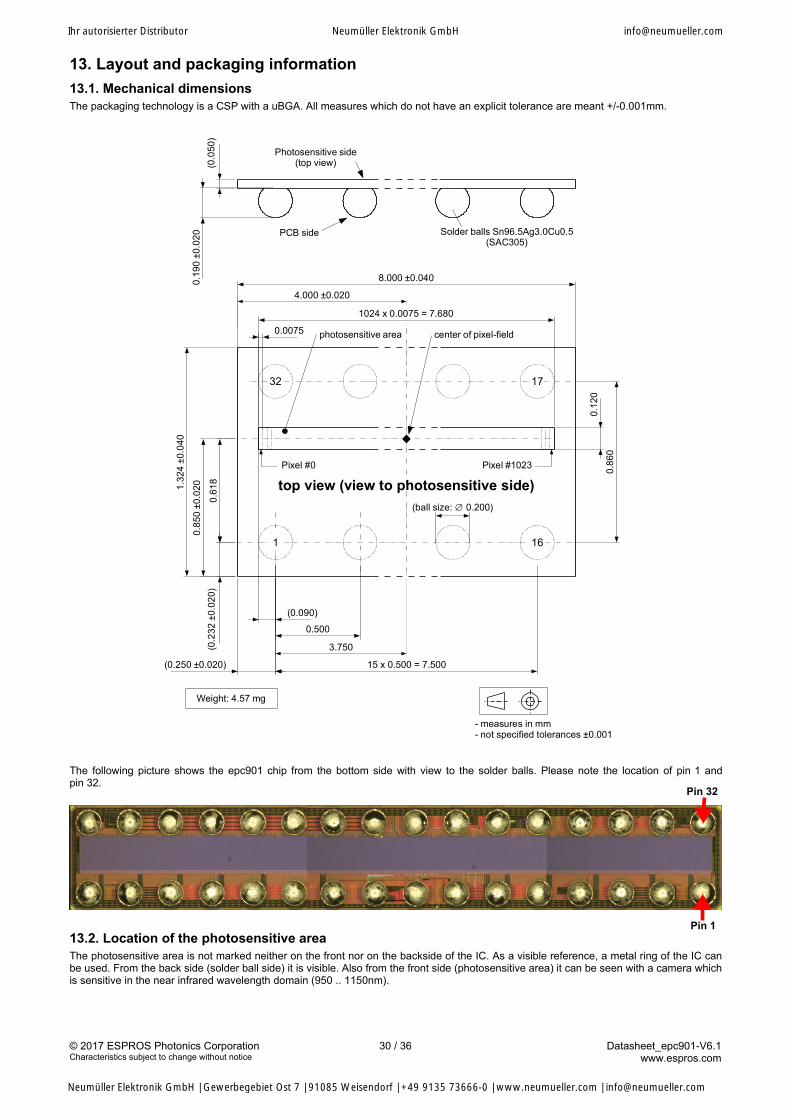
13. Layout and packaging information
13.1. Mechanical dimensionsThe packaging technology is a CSP with a uBGA. All measures which do not have an explicit tolerance are meant +/-0.001mm.
1.32
4 ±0
.040
0.0075
top view (view to photosensitive side)
1 16
(ball size: 0.200)
(0.2
32 ±
0.02
0)
8.000 ±0.0400.19
0 ±0
.020
(0.0
50)
PCB side
Photosensitive side(top view)
Solder balls Sn96.5Ag3.0Cu0.5(SAC305)
Pixel #0 Pixel #1023
(0.250 ±0.020)
0.500
15 x 0.500 = 7.500
photosensitive area
4.000 ±0.020
1024 x 0.0075 = 7.680
center of pixel-field
0.85
0 ±0
.020
0.12
0
32 17
0.86
0
- measures in mm- not specified tolerances ±0.001
0.61
8
3.750
(0.090)
Weight: 4.57 mg
The following picture shows the epc901 chip from the bottom side with view to the solder balls. Please note the location of pin 1 andpin 32.
13.2. Location of the photosensitive areaThe photosensitive area is not marked neither on the front nor on the backside of the IC. As a visible reference, a metal ring of the IC canbe used. From the back side (solder ball side) it is visible. Also from the front side (photosensitive area) it can be seen with a camera whichis sensitive in the near infrared wavelength domain (950 .. 1150nm).
© 2017 ESPROS Photonics CorporationCharacteristics subject to change without notice
30 / 36 Datasheet_epc901-V6.1www.espros.com
Pin 1
Pin 32
Ihr autorisierter Distributor Neumüller Elektronik GmbH [email protected]
Neumüller Elektronik GmbH | Gewerbegebiet Ost 7 | 91085 Weisendorf | +49 9135 73666-0 | www.neumueller.com | [email protected]
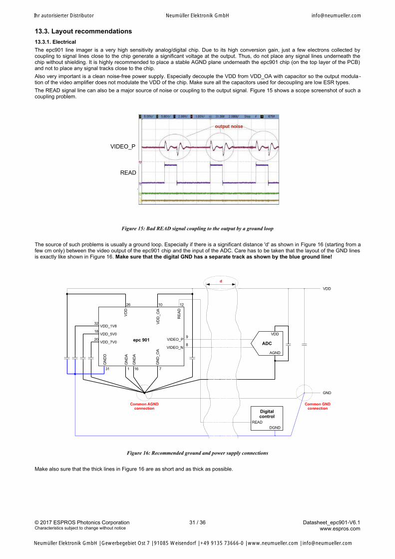
13.3. Layout recommendations
13.3.1. Electrical
The epc901 line imager is a very high sensitivity analog/digital chip. Due to its high conversion gain, just a few electrons collected bycoupling to signal lines close to the chip generate a significant voltage at the output. Thus, do not place any signal lines underneath thechip without shielding. It is highly recommended to place a stable AGND plane underneath the epc901 chip (on the top layer of the PCB)and not to place any signal tracks close to the chip.
Also very important is a clean noise-free power supply. Especially decouple the VDD from VDD_OA with capacitor so the output modula -tion of the video amplifier does not modulate the VDD of the chip. Make sure all the capacitors used for decoupling are low ESR types.
The READ signal line can also be a major source of noise or coupling to the output signal. Figure 15 shows a scope screenshot of such acoupling problem.
VIDEO_P
READ
Figure 15: Bad READ signal coupling to the output by a ground loop
The source of such problems is usually a ground loop. Especially if there is a significant distance 'd' as shown in Figure 16 (starting from afew cm only) between the video output of the epc901 chip and the input of the ADC. Care has to be taken that the layout of the GND linesis exactly like shown in Figure 16. Make sure that the digital GND has a separate track as shown by the blue ground line!
Digitalcontrol
VIDEO_N
VIDEO_P
GN
DD
GN
DA
GN
DA
GN
D_O
A
RE
AD
VD
D
VDD_1V8
VDD_5V0
VDD_7V0
VD
D_
OA
32
18
20
1 1631 7
26 12
9
8 ADC
AGND
VDD
epc 901
DGND
READ
GND
VDD
d
Common AGNDconnection
Common GNDconnection
10
Figure 16: Recommended ground and power supply connections
Make also sure that the thick lines in Figure 16 are as short and as thick as possible.
© 2017 ESPROS Photonics CorporationCharacteristics subject to change without notice
31 / 36 Datasheet_epc901-V6.1www.espros.com
Ihr autorisierter Distributor Neumüller Elektronik GmbH [email protected]
Neumüller Elektronik GmbH | Gewerbegebiet Ost 7 | 91085 Weisendorf | +49 9135 73666-0 | www.neumueller.com | [email protected]
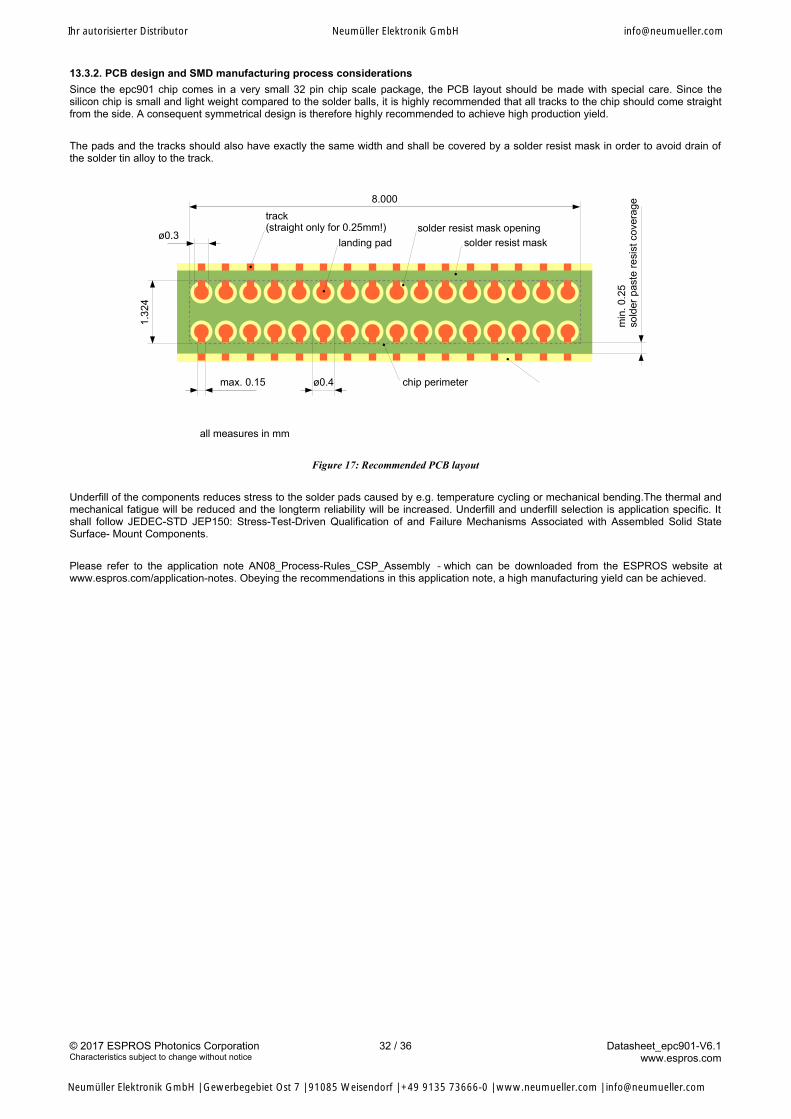
13.3.2. PCB design and SMD manufacturing process considerations
Since the epc901 chip comes in a very small 32 pin chip scale package, the PCB layout should be made with special care. Since thesilicon chip is small and light weight compared to the solder balls, it is highly recommended that all tracks to the chip should come straightfrom the side. A consequent symmetrical design is therefore highly recommended to achieve high production yield.
The pads and the tracks should also have exactly the same width and shall be covered by a solder resist mask in order to avoid drain ofthe solder tin alloy to the track.
1.3
24
8.000
ø0.4
min
. 0.2
5so
lder
pas
te r
esi
st c
over
age
solder resist mask
solder resist mask openingtrack(straight only for 0.25mm!)
landing padø0.3
max. 0.15 chip perimeter
all measures in mm
Figure 17: Recommended PCB layout
Underfill of the components reduces stress to the solder pads caused by e.g. temperature cycling or mechanical bending.The thermal andmechanical fatigue will be reduced and the longterm reliability will be increased. Underfill and underfill selection is application specific. Itshall follow JEDEC-STD JEP150: Stress-Test-Driven Qualification of and Failure Mechanisms Associated with Assembled Solid StateSurface- Mount Components.
Please refer to the application note AN08_Process-Rules_CSP_Assembly - which can be downloaded from the ESPROS website atwww.espros.com/application-notes. Obeying the recommendations in this application note, a high manufacturing yield can be achieved.
© 2017 ESPROS Photonics CorporationCharacteristics subject to change without notice
32 / 36 Datasheet_epc901-V6.1www.espros.com
Ihr autorisierter Distributor Neumüller Elektronik GmbH [email protected]
Neumüller Elektronik GmbH | Gewerbegebiet Ost 7 | 91085 Weisendorf | +49 9135 73666-0 | www.neumueller.com | [email protected]
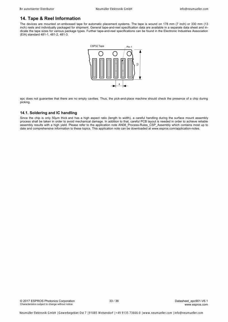
14. Tape & Reel InformationThe devices are mounted on embossed tape for automatic placement systems. The tape is wound on 178 mm (7 inch) or 330 mm (13inch) reels and individually packaged for shipment. General tape-and-reel specification data are available in a separate data sheet and in-dicate the tape sizes for various package types. Further tape-and-reel specifications can be found in the Electronic Industries Association(EIA) standard 481-1, 481-2, 481-3.
Pin 1
12
4
CSP32 Tape
Pin 1
8
Pin 1
12
8
4
CSP6 Tape QFN16 Tapeepc does not guarantee that there are no empty cavities. Thus, the pick-and-place machine should check the presence of a chip duringpicking.
14.1. Soldering and IC handlingSince the chip is only 50μm thick and has a high aspect ratio (length to width), a careful handling during the surface mount assemblyprocess shall be taken in order to avoid mechanical damage. In addition to that, careful PCB layout is needed in order to achieve reliableassembly results with a high yield. Please refer to the application note AN08_Process-Rules_CSP_Assembly which contains most up todate and comprehensive information to these topics. This application note can be downloaded at www.espros.com/application-notes.
© 2017 ESPROS Photonics CorporationCharacteristics subject to change without notice
33 / 36 Datasheet_epc901-V6.1www.espros.com
Ihr autorisierter Distributor Neumüller Elektronik GmbH [email protected]
Neumüller Elektronik GmbH | Gewerbegebiet Ost 7 | 91085 Weisendorf | +49 9135 73666-0 | www.neumueller.com | [email protected]
15. Self-test mode by fill-and-spillThe CCD and the readout chain functionality of the epc901 chip can be tested without optical stimulation. This function is useful in a facto-ry test of the final product or in safety applications. The concept is to inject electrically stimulated charge into the pixel instead of photongenerated charge by the as-called fill-and-spill circuitry.
The basic behavior of the IC by the fill-and-spill circuitry is exactly the same as when the IC is illuminated. I.e. also when fill-and-spill isused, the acquisition is controlled by SHUTTER, the internal flush and shift operation are similar and the signal DATA_RDY is asserted atthe end of the internal shift operation.
If the CCD is stimulated by the fill-and-spill, the on-chip test controller coordinates the operation of the fill-and-spill and the CCD.
15.1. Fill-and-spill procedure1. Put the chip in differential readout mode.
2. Force the chip into test mode by applying the following voltages:
TEST_MODE = VDD ROI_SEL = 0V or VDD RD_DIR = 0V or VDD
3. Access the test mode configuration registers by the following two write operations. The two accesses must occur as a sequence, noother read or write access is allowed in between them in order to enable writing to the test registers. Once enabled, the write accessremains available until the next time the IC is reset.ANA_TEST_MODE_EN_0 (Addr 0xD0): 0x4A ANA_TEST_MODE_EN_1 (Addr 0xD1): 0x66
4. Configure IC into fill-and-spill test mode by the following write access ANA_TEST_CTRL (Addr 0xD2): 0x02
5. Setup test pins ANA_TEST_* ANA_TEST_MUX_0_SEL (Addr 0xD4): 0x20 ANA_TEST_MUX_1_SEL (Addr 0xD5): 0x21
6. Select the pattern of pixels to be stimulated by writing to register ANA_TEST_CONF (see Table 30):
Bit select Stimulation
7 not used
6 all odd pixels
5 pixels 2, 6, 10 etc.
4 pixels 4, 12, 20 etc.
3 pixels 0, 8, 16 etc.
2:0 Set these bits to 0x1
Table 30: Bit select description of register ANA_TEST_CONF (Addr 0xD3) in fill-and-spill test mode
7. Apply to the test pins ANA_TEST_* the following voltages (typical values) ANA_TEST_0 = 1 VDC ANA_TEST_1 (VIDEO_P – VIDEO_N):
- 3.0 VDC for Vout of approx. -0.3V- 3.6 VDC for Vout of approx. +0.5V
The Vout values may deviate from production lot to lot. Therefore, it could be necessary to adjust the input voltages ANA_TEST_* ac-cordingly.
8. Wait for 10 µs
9. Acquire a frame by using a 20µs SHUTTER signal.
10. Read-out the frame as described in section 5.4. See item 7 above for Vout values.
11. Disconnect external voltage sources from pads ANA_TEST_*.
12. Configure test mode registers to their initial values ANA_TEST_MUX_0_SEL (Addr 0xD4): 0x00 ANA_TEST_MUX_1_SEL (Addr 0xD5): 0x01 ANA_TEST_CTRL (Addr 0xD2): 0x0 ANA_TEST_CONF (Addr 0xD3): 0x0
13. Leave test mode by applying the following voltages:
TEST_MODE = 0VROI_SEL → application dependentRD_DIR → application dependent
15.2. Important notes to fill-and-spill
■ In test mode the IC can behave in an unexpected way if the procedure described above is not strictly followed.
■ The pins ANA_TEST* are bi-directional. By default, they are outputs, i.e. the two voltages VIN and VDC may only be forced externallywhen the IC is in fill-and-spill test mode. Otherwise, the chip can get damaged!
© 2017 ESPROS Photonics CorporationCharacteristics subject to change without notice
34 / 36 Datasheet_epc901-V6.1www.espros.com
Ihr autorisierter Distributor Neumüller Elektronik GmbH [email protected]
Neumüller Elektronik GmbH | Gewerbegebiet Ost 7 | 91085 Weisendorf | +49 9135 73666-0 | www.neumueller.com | [email protected]

16. Ordering InformationPart Number Part Name Package RoHS
compliancePackaging
Method
P100 360 epc901-CSP32-032 1 CSP32 Yes Reel
P100 401 epc901-CSP32-033 1 CSP32 Yes Reel
P100 208 epc901 Evaluation Board V2 PCB 70.00 x 65.00 mm Yes Anti static bag
P100 209 epc901 Chip Carrier Board V2 PCB 36.00 x 42.75 mm Yes Anti static bag
Table 31: Ordering information
Note:1 P100 360 will be / is replaced by P100 401. There is no difference in specification nor in design. Devices are exchangeable. The differ-
ent versions represent different manufacturing lines.
17. Note to various chip releasesNo open pending items. Use former versions of the Datasheet epc901 for older releases.
© 2017 ESPROS Photonics CorporationCharacteristics subject to change without notice
35 / 36 Datasheet_epc901-V6.1www.espros.com
Ihr autorisierter Distributor Neumüller Elektronik GmbH [email protected]
Neumüller Elektronik GmbH | Gewerbegebiet Ost 7 | 91085 Weisendorf | +49 9135 73666-0 | www.neumueller.com | [email protected]

18. IMPORTANT NOTICEESPROS Photonics AG and its subsidiaries (epc) reserve the right to make corrections, modifications, enhancements, improvements, andother changes to its products and services at any time and to discontinue any product or service without notice. Customers should obtainthe latest relevant information before placing orders and should verify that such information is current and complete. All products are soldsubject to epc’s terms and conditions of sale supplied at the time of order acknowledgment.
epc warrants performance of its hardware products to the specifications applicable at the time of sale in accordance with epc’s standardwarranty. Testing and other quality control techniques are used to the extent epc deems necessary to support this warranty. Except wheremandated by government requirements, testing of all parameters of each product is not necessarily performed.
epc assumes no liability for applications assistance or customer product design. Customers are responsible for their products and applica-tions using epc components. To minimize the risks associated with customer products and applications, customers should provide ade -quate design and operating safeguards.
epc does not warrant or represent that any license, either express or implied, is granted under any epc patent right, copyright, mask workright, or other epc intellectual property right relating to any combination, machine, or process in which epc products or services are used.Information published by epc regarding third-party products or services does not constitute a license from epc to use such products or ser -vices or a warranty or endorsement thereof. Use of such information may require a license from a third party under the patents or other in-tellectual property of the third party, or a license from epc under the patents or other intellectual property of epc.
Resale of epc products or services with statements different from or beyond the parameters stated by epc for that product or service voidsall express and any implied warranties for the associated epc product or service. epc is not responsible or liable for any such statements.
epc products are not authorized for use in safety-critical applications (such as life support) where a failure of the epc product would reason-ably be expected to cause severe personal injury or death, unless officers of the parties have executed an agreement specifically gov ern-ing such use. Buyers represent that they have all necessary expertise in the safety and regulatory ramifications of their applications, andacknowledge and agree that they are solely responsible for all legal, regulatory and safety-related requirements concerning their productsand any use of epc products in such safety-critical applications, notwithstanding any applications-related information or support that maybe provided by epc. Further, Buyers must fully indemnify epc and its representatives against any damages arising out of the use of epcproducts in such safety-critical applications.
epc products are neither designed nor intended for use in military/aerospace applications or environments unless the epc products arespecifically designated by epc as military-grade. Only products designated by epc as military-grade meet military specifications. Buyers ac-knowledge and agree that any such use of epc products which epc has not designated as military-grade is solely at the Buyer's risk, andthat they are solely responsible for compliance with all legal and regulatory requirements in connection with such use.
epc products are neither designed nor intended for use in automotive applications or environments unless the specific epc products aredesignated by epc as compliant with ISO/TS 16949 requirements. Buyers acknowledge and agree that, if they use any non-designatedproducts in automotive applications, epc will not be responsible for any failure to meet such requirements.
© 2017 ESPROS Photonics CorporationCharacteristics subject to change without notice
36 / 36 Datasheet_epc901-V6.1www.espros.com
Ihr autorisierter Distributor Neumüller Elektronik GmbH [email protected]
Neumüller Elektronik GmbH | Gewerbegebiet Ost 7 | 91085 Weisendorf | +49 9135 73666-0 | www.neumueller.com | [email protected]