810001-21 Datasheet - Renesas
20
1 ©2016 Integrated Device Technology, Inc Revision B March 3, 2016 General Description The 810001-21 is a PLL based synchronous clock generator that is optimized for digital video clock jitter attenuation and frequency translation. The device contains two internal frequency multiplication stages that are cascaded in series. The first stage is a VCXO PLL that is optimized to provide reference clock jitter attenuation, and to support the complex PLL multiplication ratios needed for video rate conversion. The second stage is a FemtoClock™ frequency multiplier that provides the low jitter, high frequency video output clock. Preset multiplication ratios are selected from internal lookup tables using device input selection pins. The multiplication ratios are optimized to support most common video rates used in professional video system applications. The VCXO requires the use of an external, inexpensive pullable crystal. Two crystal connections are provided (pin selectable) so that both 60 and 59.94 base frame rates can be supported. The VCXO requires external passive loop filter components which are used to set the PLL loop bandwidth and damping characteristics. Features • Jitter attenuation and frequency translation of video clock signals • Supports SMPTE 292M, ITU-R Rec. 601/656 and MPEG-transport clocks • Support of High-Definition (HD) and Standard-Definition (SD) pixel rates • Dual VCXO-PLL supports both 60 and 59.94Hz base frame rates in one device • Supports both 1000/1001 and 1001/1000 rate conversions • Dual PLL mode for high-frequency clock generation (36MHz to 148.5MHz) • VCXO-PLL mode for low-frequency clock generation (27MHz and 26.973MHz) • One LVCMOS/LVTTL clock output • Two selectable LVCMOS/LVTTL clock inputs • LVCMOS/LVTTL compatible control signals • RMS phase jitter @148.3516MHz, (12kHz - 20MHz): 1.089ps (typical) • 3.3V supply voltage • 0°C to 70°C ambient operating temperature • Available in lead-free (RoHS 6) packages Supported Input Frequencies Supported Output Frequencies f VCXO = 27MHz f VCXO = 26.973MHz 27.0000MHz 26.9730MHz 27.0270MHz 27.0000MHz 74.1758MHz 74.1016MHz 74.3243MHz 74.2499MHz 74.2500MHz 74.1758MHz 27.0270MHz 27.0000MHz 26.9730MHz 26.9461MHz 74.1758MHz 74.1016kHz 45.0000kHz 44.9550kHz 33.7500kHz 33.7163kHz 15.6250kHz 15.6094kHz 15.7343kHz 15.7185kHz 28.1250kHz 28.0969kHz f VCXO = 27MHz f VCXO = 26.973MHz 148.5000MHz 148.3515MHz 74.2500MHz 74.1758MHz 49.5000MHz 49.4505MHz 33.0000MHz 32.9670MHz 162.0000MHz 161.8380MHz 81.0000MHz 80.9190MHz 54.0000MHz 53.9460MHz 36.0000MHz 35.9640MHz 27.0000MHz 26.9730MHz 810001-21 Data Sheet FemtoClock™ Dual VCXO Video PLL
-
Upload
khangminh22 -
Category
Documents
-
view
0 -
download
0
Transcript of 810001-21 Datasheet - Renesas

1©2016 Integrated Device Technology, Inc Revision B March 3, 2016
General Description
The 810001-21 is a PLL based synchronous clock generator that is optimized for digital video clock jitter attenuation and frequency translation. The device contains two internal frequency multiplication stages that are cascaded in series. The first stage is a VCXO PLL that is optimized to provide reference clock jitter attenuation, and to support the complex PLL multiplication ratios needed for video rate conversion. The second stage is a FemtoClock™ frequency multiplier that provides the low jitter, high frequency video output clock.
Preset multiplication ratios are selected from internal lookup tables using device input selection pins. The multiplication ratios are optimized to support most common video rates used in professional video system applications. The VCXO requires the use of an external, inexpensive pullable crystal. Two crystal connections are provided (pin selectable) so that both 60 and 59.94 base frame rates can be supported. The VCXO requires external passive loop filter components which are used to set the PLL loop bandwidth and damping characteristics.
Features
• Jitter attenuation and frequency translation of video clock signals
• Supports SMPTE 292M, ITU-R Rec. 601/656 and MPEG-transport clocks
• Support of High-Definition (HD) and Standard-Definition (SD) pixel rates
• Dual VCXO-PLL supports both 60 and 59.94Hz base frame rates in one device
• Supports both 1000/1001 and 1001/1000 rate conversions
• Dual PLL mode for high-frequency clock generation (36MHz to 148.5MHz)
• VCXO-PLL mode for low-frequency clock generation (27MHz and 26.973MHz)
• One LVCMOS/LVTTL clock output
• Two selectable LVCMOS/LVTTL clock inputs
• LVCMOS/LVTTL compatible control signals
• RMS phase jitter @148.3516MHz, (12kHz - 20MHz): 1.089ps (typical)
• 3.3V supply voltage
• 0°C to 70°C ambient operating temperature
• Available in lead-free (RoHS 6) packages
Supported Input Frequencies Supported Output Frequencies
fVCXO = 27MHz fVCXO = 26.973MHz
27.0000MHz 26.9730MHz
27.0270MHz 27.0000MHz
74.1758MHz 74.1016MHz
74.3243MHz 74.2499MHz
74.2500MHz 74.1758MHz
27.0270MHz 27.0000MHz
26.9730MHz 26.9461MHz
74.1758MHz 74.1016kHz
45.0000kHz 44.9550kHz
33.7500kHz 33.7163kHz
15.6250kHz 15.6094kHz
15.7343kHz 15.7185kHz
28.1250kHz 28.0969kHz
fVCXO = 27MHz fVCXO = 26.973MHz
148.5000MHz 148.3515MHz
74.2500MHz 74.1758MHz
49.5000MHz 49.4505MHz
33.0000MHz 32.9670MHz
162.0000MHz 161.8380MHz
81.0000MHz 80.9190MHz
54.0000MHz 53.9460MHz
36.0000MHz 35.9640MHz
27.0000MHz 26.9730MHz
810001-21Data Sheet
FemtoClock™ Dual VCXO Video PLL

2©2016 Integrated Device Technology, Inc Revision B March 3, 2016
810001-21 Data Sheet
Block Diagram
Pin Assignment
ChargePump
VCXO
V3:V0
PhaseDetector
Q
OutputDivider
00 = 4 (default)01 = 810 = 1211 = 18
VCXO Feedback Divider(M Value from Table)
VCXO InputPre-Divider
(P Valuefrom Table)
VCXO Jitter Attenuation PLL
XTA
L_I
N0
XTA
L_O
UT
0
XTA
L_I
N1
XTA
L_O
UT
1
LF
1
LF
0
ISE
T
LoopFilter
VCXODividerTable
OE
XTA
L_S
EL
0 1
MF
MR Master Reset
0
1
CLK0
CLK1
CLK_SEL
N1:N0
4
2
11
101011
01
011011
00
2nBP1:nBP0
FemtoClockFrequency Multiplier
0= x22 (default)1= x24
Pulldown
Pulldown
Pulldown
Pulldown
Pulldown
Pulldown
Pulldown
Pullup
Pul
ldow
n
Pullup
9 10 11 12 13 14 15 16
32 31 30 29 28 27 26 25
1
2
3
4
5
6
7
8
24
23
22
21
20
19
18
17
LF1
LF0
ISET
VDD
nBP0
GND
CLK_SEL
CLK1
N0
N1
nBP1
OE
GND
Q
VDDO
VDDA
CLK
0
V0
VD
D
MR
MF V1
V2
V3
XT
AL_
IN0
XT
AL_
OU
T0
GN
D
XT
AL_
IN1
XT
AL_
OU
T1
XT
AL_
SE
L
VD
D
VD
DX
810001-2132 Lead VFQFN
5mm x 5mm x 0.925mmpackage body
K PackageTop View

3©2016 Integrated Device Technology, Inc Revision B March 3, 2016
810001-21 Data Sheet
Table 1. Pin Descriptions
NOTE: Pullup and Pulldown refer to internal input resistors. See Table 2, Pin Characteristics, for typical values.
Table 2. Pin Characteristics
Number Name Type Description
1, 2 LF1, LF0Analog
Input/OutputLoop filter connection node pins.
3 ISETAnalog
Input/OutputCharge pump current setting pin.
4, 11, 25 VDD Power Core supply pins.
5, 22nBP0,nBP1
Input Pullup PLL Bypass control pins. See block diagram.
6, 20, 29 GND Power Power supply ground.
7 CLK_SEL Input PulldownInput clock select. When HIGH selects CLK1. When LOW, selects CLK0. LVCMOS / LVTTL interface levels.
8, 9 CLK1, CLK0 Input Pulldown Single-ended clock inputs. LVCMOS/LVTTL interface levels.
10, 14,15, 16
V0, V1,V2, V3
Input Pulldown VCXO PLL divider selection pins. LVCMOS/LVTTL interface levels.
12 MR Input PulldownActive HIGH Master Reset. When logic HIGH, the internal dividers are reset causing the output to go low. When logic LOW, the internal dividers and the output is enabled. LVCMOS/LVTTL interface levels.
13 MF Input Pulldown FemtoClock multiplication factor select pin. LVCMOS/LVTTL interface levels.
17 VDDA Power Analog supply pin.
18 VDDO Power Output supply pin.
19 Q Output Single-ended VCXO PLL clock output. LVCMOS/LVTTL interface levels.
21 OE Input PullupOutput enable. When logic LOW, the clock output is in high-impedance. When logic HIGH, the output is enabled. LVCMOS/LVTTL interface levels.
23, 24 N1, N0 Input Pulldown FemtoClock output divide select pins. LVCMOS/LVTTL interface levels.
26 XTAL_SEL Input PulldownCrystal select. When HIGH, selects XTAL1. When LOW, selects XTAL0. LVCMOS/LVTTL interface levels.
27,28
XTAL_OUT1,XTAL_IN1
Input Crystal oscillator interface. XTAL_IN1 is the input. XTAL_OUT1 is the output.
30,31
XTAL_OUT0,XTAL_IN0
Input Crystal oscillator interface. XTAL_IN0 is the input. XTAL_OUT0 is the output.
32 VDDX Power Power supply pin for VCXO charge pump.
Symbol Parameter Test Conditions Minimum Typical Maximum Units
CIN Input Capacitance 4 pF
CPDPower Dissipation Capacitance (per output)
VDD = VDDO = 3.465V 8.5 pF
RPULLUP Input Pullup Resistor 51 k
RPULLDOWN Input Pulldown Resistor 51 k
ROUT Output Impedance 22.5

4©2016 Integrated Device Technology, Inc Revision B March 3, 2016
810001-21 Data Sheet
Function TablesTable 3A. VCXO PLL Pre- and Feedback Divider Function Table
Input VCXO PLL Configuration
V3 V2 V1 V0 Pre-Divider P Feedback- Divider M
0 (default) 0 (default) 0 (default) 0 (default) 1000 1000
0 0 0 1 1001 1000
0 0 1 0 11000 4004
0 0 1 1 11011 4000
0 1 0 0 11000 4000
0 1 0 1 4004 4004
0 1 1 0 4004 4000
0 1 1 1 1000 1001
1 0 0 0 250 91
1 0 0 1 253 92
1 0 1 0 92 92
1 0 1 1 1 600
1 1 0 0 1 800
1 1 0 1 1 1728
1 1 1 0 1 1716
1 1 1 1 1 960

5©2016 Integrated Device Technology, Inc Revision B March 3, 2016
810001-21 Data Sheet
Table 3B. Input Frequency Table
Table 3C. Output Frequency Table (dual PLL Mode)
NOTE: Use the VCXO-PLL mode to achieve output Frequencies of 27MHz or 26.973MHz. See Table 3H.
Input Crystal Frequency (fVCXO)
V3 V2 V1 V0 27MHz 26.973MHz
0 (default) 0 (default) 0 (default) 0 (default) 27.0000MHz 26.9730MHz
0 0 0 1 27.0270MHz 27.0000MHz
0 0 1 0 74.1758MHz 74.1016MHz
0 0 1 1 74.3243MHz 74.2499MHz
0 1 0 0 74.2500MHz 74.1758MHz
0 1 0 1 27.0000MHz 26.9730MHz
0 1 1 0 27.0270MHz 27.0000MHz
0 1 1 1 26.9730MHz 26.9461MHz
1 0 0 0 74.1758MHz 74.1016MHz
1 0 0 1 74.2500MHz 74.1758MHz
1 0 1 0 27.0000MHz 26.9730MHz
1 0 1 1 45.0000kHz 44.9550kHz
1 1 0 0 33.7500kHz 33.7163kHz
1 1 0 1 15.6250kHz 15.6094kHz
1 1 1 0 15.7343kHz 15.7185kHz
1 1 1 1 28.1250kHz 28.0969kHz
fVCXO
FemtoClock Look-up Table
Output Frequency fQ (MHz)MF N1 N0
27MHz
0 0 0 148.5000
0 0 1 74.2500
0 1 0 49.5000
0 1 1 33.0000
1 0 0 162.0000
1 0 1 81.0000
1 1 0 54.0000
1 1 1 36.0000
26.973MHz
0 0 0 148.3515
0 0 1 74.1758
0 1 0 49.4505
0 1 1 32.9670
1 0 0 161.8380
1 0 1 80.9190
1 1 0 53.9460
1 1 1 35.9640

6©2016 Integrated Device Technology, Inc Revision B March 3, 2016
810001-21 Data Sheet
Table 3D. CLK_SEL Function Table
Table 3E. MR Master Reset Function Table
Table 3F. FemtoCLock PLL Feedback Divider Function Table
Table 3G. PLL Output Divider Function Table
Table 3H. PLL BYPASS Logic Function Table
Input
OperationCLK_SEL
0 (default) Selects CLK0 as PLL reference input.
1 Selects CLK1 as PLL reference input.
Input
OperationMR
0 (default) Normal operation, internal dividers and the output Q are enabled.
1 Internal dividers are reset. Q output is in logic low state (with OE = 1).
Input
OperationMF
0 (default) Selects MF = 22. The 2nd stage PLL (FemtoClock. multiplies the output frequency of the VCXO-PLL by 22.
1 Selects MF = 24. The 2nd stage PLL (FemtoClock. multiplies the output frequency of the VCXO-PLL by 24.
Input
OperationN1 N0
0 (default) 0 (default) Output divider N = 4.
0 1 Output divider N = 8.
1 0 Output divider N = 12.
1 1 Output divider N = 18.
Input
OperationnBP1 nBP0
0 0VCXO-PLL mode: The input reference frequency is divided by the pre-divider P and is multiplied by the VCXO-PLL. fOUT = (fREF ÷ P) * M.
0 1Test mode: The input reference frequency is divided by the pre-divider P and the output divider N and bypasses both PLLs. fOUT = fREF ÷ (P * N).
1 0FemtoClock Mode: The input reference frequency is divided by the pre-divider P multiplied by the 2nd PLL (FemtoClock, MF). The 1st PLL (VCXO-PLL, M) is bypassed. This mode does not support jitter attenuatiion. fOUT = (fREF ÷ P) * MF ÷ N.
1 (default) 1 (default)Dual PLL Mode: both PLLs are cascaded for jitter attenuation and frequency multiplication.fOUT = (fREF ÷ P) * M * MF ÷ N.

7©2016 Integrated Device Technology, Inc Revision B March 3, 2016
810001-21 Data Sheet
Absolute Maximum RatingsNOTE: Stresses beyond those listed under Absolute Maximum Ratings may cause permanent damage to the device. These ratings are stress specifications only. Functional operation of product at these conditions or any conditions beyond those listed in the DC Characteristics or AC Characteristics is not implied. Exposure to absolute maximum rating conditions for extended periods may affect product reliability.
DC Electrical CharacteristicsTable 4A. Power Supply DC Characteristics, VDD = VDDO = VDDX = 3.3V ± 5%, TA = 0°C to 70°C
Item Rating
Supply Voltage, VDD 4.6V
Inputs, VIXTAL_INOther Inputs
0V to VDD-0.5V to VDD + 0.5V
Outputs, VO -0.5V to VDDO + 0.5V
Package Thermal Impedance, JA 37C/W (0 mps)
Storage Temperature, TSTG -65C to 150C
Symbol Parameter Test Conditions Minimum Typical Maximum Units
VDD Core Supply Voltage 3.135 3.3 3.465 V
VDDA Analog Supply Voltage VDD – 0.15 3.3 VDD V
VDDO Output Supply Voltage 3.135 3.3 3.465 V
VDDX Charge Pump Supply Voltage VDD – 0.04 3.3 3.465 V
IDD Power Supply Current 290 mA
IDDA Analog Supply Current 15 mA
IDDO Output Supply Current No Load 4 mA
IDDX Charge Pump Supply Current 4 mA

8©2016 Integrated Device Technology, Inc Revision B March 3, 2016
810001-21 Data Sheet
Table 4B. LVCMOS/LVTTL DC Characteristics, VDD = VDDO = VDDX = 3.3V ± 5%, TA = 0°C to 70°C
AC Electrical CharacteristicsTable 5. AC Characteristics, VDD = VDDO = VDDX = 3.3V ± 5%, TA = 0°C to 70°C
NOTE: Electrical parameters are guaranteed over the specified ambient operating temperature range, which is established when the device is mounted in a test socket with maintained transverse airflow greater than 500 lfpm. The device will meet specifications after thermal equilibrium has been reached under these conditions.See Parameter Measurement Information Section.NOTE 1: Refer to the Phase Noise Plot.NOTE 2: Lock Time measured from power-up to stable output frequency.
Symbol Parameter Test Conditions Minimum Typical Maximum Units
VIH Input High Voltage 2.0 VDD + 0.3 V
VIL Input Low Voltage -0.3 0.8 V
IIHInputHigh Current
CLK[0:1], CLK_SEL, P[1:0], V[3:0], N[1:0], MR, MF, XTAL_SEL
VDD = VIN = 3.465V 150 µA
OE, nBP0, nBP1 VDD = VIN = 3.465V 5 µA
IILInputLow Current
CLK[0:1], CLK_SEL, P[1:0], V[3:0], N[1:0], MR, MF, XTAL_SEL
VDD = 3.465V, VIN = 0V -5 µA
OE, nBP0, nBP1 VDD = 3.465, VIN = 0V -150 µA
VOH Output High Voltage IOH = -24mA 2.6 V
VOL Output Low Voltage IOL = 24mA 0.5 V
Symbol Parameter Test Conditions Minimum Typical Maximum Units
fOUT Output FrequencynBP0, nBP1 = 00 14 35 MHz
nBP1 = 1 31 175 MHz
tjit(Ø)RMS Phase Jitter, (Random), NOTE 1
148.3516MHz,Integration Range: 12kHz – 20MHz
1.089 ps
tR / tF Output Rise/Fall Time 20% to 80% 250 750 ps
odc Output Duty Cycle 48 52 %
tLOCKVCXO & FemtoClock PLL Lock Time; NOTE 2
M = 92, Bandwidth = 475Hz 100 ms
M = 4004, Bandwidth = 6Hz 25 s

9©2016 Integrated Device Technology, Inc Revision B March 3, 2016
810001-21 Data Sheet
Typical Phase Noise at 148.3516MHz
148.3516484MHzRMS Phase Jitter (Random)
12kHz to 20MHz = 1.089ps (typical)
Noi
se P
ower
dBc
Hz
Offset Frequency (Hz)
10Hz 100Hz 1kHz 10kHz 100kHz 1MHz 30MHZ

10©2016 Integrated Device Technology, Inc Revision B March 3, 2016
810001-21 Data Sheet
Parameter Measurement Information
3.3V Output Load AC Test Circuit
Output Duty Cycle/Pulse Width/Period
Output Rise/Fall Time
Phase Jitter
LVCMOS
GND
Measurement Point
1.65V±5%
-1.65±5%
VDD,VDDO, VDDX
1.65V±5%
VDDA
tPERIOD
tPW
tPERIOD
odc =
VDDO
2
x 100%
tPW
Q
20%
80% 80%
20%
tR tF
Q

11©2016 Integrated Device Technology, Inc Revision B March 3, 2016
810001-21 Data Sheet
Applications Information
Recommendations for Unused Input Pins
Inputs:
CLK Inputs
For applications not requiring the use of a clock input, it can be left floating. Though not required, but for additional protection, a 1k resistor can be tied from the CLK input to ground.
LVCMOS Control Pins
All control pins have internal pullups or pulldowns; additional resistance is not required but can be added for additional protection. A 1k resistor can be used.
Power Supply Filtering Technique
As in any high speed analog circuitry, the power supply pins are vulnerable to random noise. To achieve optimum jitter perform ance, power supply isolation is required. The 810001-21 provides separate power supplies to isolate any high switching noise from the outputs to the internal PLL. VDD, VDDA, VDDO and VDDX should be individually connected to the power supply plane through vias, and 0.01µF bypass capacitors should be used for each pin. Figure 1 illustrates this for a generic VDD pin and also shows that VDDA requires that an additional 10 resistor along with a 10F bypass capacitor be connected to the VDDA pin.
Figure 1. Power Supply Filtering
VDD
VDDX
VDDA
3.3V
10Ω
10Ω
10µF.01µF
.01µF
10µF.01µF

12©2016 Integrated Device Technology, Inc Revision B March 3, 2016
810001-21 Data Sheet
VFQFN EPAD Thermal Release Path
In order to maximize both the removal of heat from the package and the electrical performance, a land pattern must be incorporated on the Printed Circuit Board (PCB) within the footprint of the package corresponding to the exposed metal pad or exposed heat slug on the package, as shown in Figure 2. The solderable area on the PCB, as defined by the solder mask, should be at least the same size/shape as the exposed pad/slug area on the package to maximize the thermal/electrical performance. Sufficient clearance should be designed on the PCB between the outer edges of the land pattern and the inner edges of pad pattern for the leads to avoid any shorts.
While the land pattern on the PCB provides a means of heat transfer and electrical grounding from the package to the board through a solder joint, thermal vias are necessary to effectively conduct from the surface of the PCB to the ground plane(s). The land pattern must be connected to ground through these vias. The vias act as “heat pipes”. The number of vias (i.e. “heat pipes”) are application specific and dependent upon the package power dissipation as well as
electrical conductivity requirements. Thus, thermal and electrical analysis and/or testing are recommended to determine the minimum number needed. Maximum thermal and electrical performance is achieved when an array of vias is incorporated in the land pattern. It is recommended to use as many vias connected to ground as possible. It is also recommended that the via diameter should be 12 to 13mils (0.30 to 0.33mm) with 1oz copper via barrel plating. This is desirable to avoid any solder wicking inside the via during the soldering process which may result in voids in solder between the exposed pad/slug and the thermal land. Precautions should be taken to eliminate any solder voids between the exposed heat slug and the land pattern. Note: These recommendations are to be used as a guideline only. For further information, please refer to the Application Note on the Surface Mount Assembly of Amkor’s Thermally/Electrically Enhance Leadframe Base Package, Amkor Technology.
Figure 2. P.C. Assembly for Exposed Pad Thermal Release Path – Side View (drawing not to scale)
SOLDERSOLDER PINPIN EXPOSED HEAT SLUG
PIN PAD PIN PADGROUND PLANE LAND PATTERN (GROUND PAD)THERMAL VIA

13©2016 Integrated Device Technology, Inc Revision B March 3, 2016
810001-21 Data Sheet
Schematic Example
Figure 3 shows an example of the 810001-21 application schematic. In this example, the device is operated at VDD = VDDX = VDDO = VDDA= 3.3V. The decoupling capacitors should be located as close as possible to the power pin. The input is driven by a 3.3V 17 LVCMOS driver. An optional 3-pole filter can also be used for additional spur reduction. It is recommended that the loop filter
components be laid out for the 3-pole option. This will also allow the 2-pole filter to be used. For the LVCMOS output, a termination example is shown in this schematic. For more termination approaches, please refer to the LVCMOS Termination Application Note.
Figure 3. 810001-21 Schematic Example
U1
810001-21 Schematic
LF11
LF02
ISET3
VDD4
nBP05
GND6
CLK_SEL7
CLK18
CL
K0
9
V0
10
VD
D1
1
MR
12
MF
13
V1
14
V2
15
V3
16
VDDA17VDDO18Q19GND20OE21nBP122N123N024
32V
DD
X31
XT
AL
_IN
030
XT
AL
_OU
T0
29G
ND
28X
TA
L_I
N1
27X
TA
L_O
UT
126
XT
AL_
SE
LV
DD
25
12pF
12pF
C8
.01uF
X1
VDD
Set LogicInput to '0'
To LogicInputpins
Logic Control Input Examples
To LogicInputpins
Set LogicInput to '1'
RU2Not Install
RU11K
RD21K
RD1Not Install
VDDVDD
MR Control
VDDA
X2
Pin25
R6
TBD
Cp2TBD
Cp1TBD
Rs1TBD
Cs1TBD
LF1
3-pole loop filter example -(optional)
LF0
VDD
Q1
Driv er_LVCMOS
Q2
Driv er_LVCMOS
Rs150K
R1
33
R2
33Pin18Pin11Pin4
Rset 2.21K
TL2
Zo = 50
TL1
Zo = 50
C5.01uF
VDD
2-pole loop filter
C10
.01uF
C9
10uF
R310
VDD
C1spare
C2spare
C3 spare
C4 spare
Cs
.22uF
Cp.001uF
C6
.01uF
VDDX
C12
.01uF
C11
10uF
R410
C7
.01uF
VDD
VDDX
VDD
VDDA
VDD
R5
33 TL3
Zo = 50
Receiv er
14©2016 Integrated Device Technology, Inc Revision B March 3, 2016
810001-21 Data Sheet
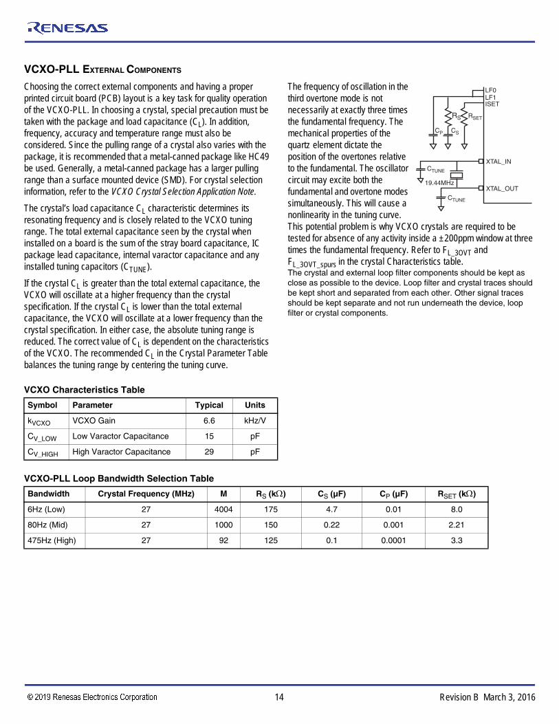
VCXO-PLL EXTERNAL COMPONENTS
Choosing the correct external components and having a proper printed circuit board (PCB) layout is a key task for quality operation of the VCXO-PLL. In choosing a crystal, special precaution must be taken with the package and load capacitance (CL). In addition, frequency, accuracy and temperature range must also be considered. Since the pulling range of a crystal also varies with the package, it is recommended that a metal-canned package like HC49 be used. Generally, a metal-canned package has a larger pulling range than a surface mounted device (SMD). For crystal selection information, refer to the VCXO Crystal Selection Application Note.
The crystal’s load capacitance CL characteristic determines its resonating frequency and is closely related to the VCXO tuning range. The total external capacitance seen by the crystal when installed on a board is the sum of the stray board capacitance, IC package lead capacitance, internal varactor capacitance and any installed tuning capacitors (CTUNE).
If the crystal CL is greater than the total external capacitance, the VCXO will oscillate at a higher frequency than the crystal specification. If the crystal CL is lower than the total external capacitance, the VCXO will oscillate at a lower frequency than the crystal specification. In either case, the absolute tuning range is reduced. The correct value of CL is dependent on the characteristics of the VCXO. The recommended CL in the Crystal Parameter Table balances the tuning range by centering the tuning curve.
The frequency of oscillation in the third overtone mode is not necessarily at exactly three times the fundamental frequency. The mechanical properties of the quartz element dictate the position of the overtones relative to the fundamental. The oscillator circuit may excite both the fundamental and overtone modes simultaneously. This will cause a nonlinearity in the tuning curve. This potential problem is why VCXO crystals are required to be tested for absence of any activity inside a ±200ppm window at three times the fundamental frequency. Refer to FL_3OVT and FL_3OVT_spurs in the crystal Characteristics table.The crystal and external loop filter components should be kept as close as possible to the device. Loop filter and crystal traces should be kept short and separated from each other. Other signal traces should be kept separate and not run underneath the device, loop filter or crystal components.
VCXO Characteristics Table
VCXO-PLL Loop Bandwidth Selection Table
LF0LF1ISET
XTAL_IN
XTAL_OUT
RS
CSCP
RSET
CTUNE
CTUNE
19.44MHz
Symbol Parameter Typical Units
kVCXO VCXO Gain 6.6 kHz/V
CV_LOW Low Varactor Capacitance 15 pF
CV_HIGH High Varactor Capacitance 29 pF
Bandwidth Crystal Frequency (MHz) M RS (k) CS (µF) CP (µF) RSET (k)
6Hz (Low) 27 4004 175 4.7 0.01 8.0
80Hz (Mid) 27 1000 150 0.22 0.001 2.21
475Hz (High) 27 92 125 0.1 0.0001 3.3

15©2016 Integrated Device Technology, Inc Revision B March 3, 2016
810001-21 Data Sheet
Crystal Characteristics
Reliability Information
Table 6. JA vs. Air Flow Table for a 32 Lead VFQFN
Transistor CountThe transistor count for 810001-21 is: 9365
Symbol Parameter Test Conditions Minimum Typical Maximum Units
Mode of Oscillation Fundamental
fN Frequency27 MHz
26.973 MHz
fT Frequency Tolerance ±20 ppm
fS Frequency Stability ±20 ppm
Operating Temperature Range 0 70 0C
CL Load Capacitance 12 pF
CO Shunt Capacitance 4 pF
CO / C1 Pullability Ratio 220 240
FL_3OVT 3RD Overtone FL 200 ppm
FL_3OVT_spurs 3RD Overtone FL Spurs 200 ppm
ESR Equivalent Series Resistance 20
Drive Level 1 mW
Aging @ 25 0C ±3 per year ppm
JA vs. Air Flow
Meters per Second 0 1 2.5
Multi-Layer PCB, JEDEC Standard Test Boards 37.0°C/W 32.4°C/W 29°C/W

16©2016 Integrated Device Technology, Inc Revision B March 3, 2016
810001-21 Data Sheet
Package Outline and Package DimensionsPackage Outline - K Suffix for 32 Lead VFQFN
Table 7. Package Dimensions
Reference Document: JEDEC Publication 95, MO-220
NOTE: The following package mechanical drawing is a generic drawing that applies to any pin count VFQFN package. This drawing is not intended to convey the actual pin count or pin layout of this device. The pin count and pinout are shown on the front page. The package dimensions are in Table 7.
Top View
Index Area
D
Chamfer 4x0.6 x 0.6 maxOPTIONAL
AnvilSingula tion
A
0. 08 CC
A3A1
Seating Plane
E2 E2 2
L
(N -1)x e (Ref.)
(Ref.)N & N Even
N
eD2 2
D2
(Ref.)N & N Odd
1
2
e2
(Ty p.)If N & N are Even
(N -1)x e (Re f.)
b
Thermal Base
N
OR
AnvilSingulation
N-1NCHAMFER
12
N-1
12
NRADIUS
44
Bottom View w/Type C IDBottom View w/Type A ID
There are 2 methods of indicating pin 1 corner at the back of the VFQFN package:1. Type A: Chamfer on the paddle (near pin 1)2. Type C: Mouse bite on the paddle (near pin 1)
JEDEC Variation: VHHD-2/-4All Dimensions in Millimeters
Symbol Minimum Nominal MaximumN 32A 0.80 1.00
A1 0 0.05
A3 0.25 Ref.b 0.18 0.25 0.30
ND & NE 8
D & E 5.00 BasicD2 & E2 3.0 3.3
e 0.50 Basic
L 0.30 0.40 0.50

17©2016 Integrated Device Technology, Inc Revision B March 3, 2016
810001-21 Data Sheet
Ordering InformationTable 8. Ordering Information
Part/Order Number Marking Package Shipping Packaging Temperature810001DK-21LF ICS0001D21L “Lead-Free” 32 Lead VFQFN Tray 0C to 70C810001DK-21LFT ICS0001D21L “Lead-Free” 32 Lead VFQFN Tape & Reel 0C to 70C

18©2016 Integrated Device Technology, Inc Revision B March 3, 2016
810001-21 Data Sheet
Revision History Sheet
Rev Table Page Description of Change Date
B
T4B 810
14
15
16
LVCMOS DC Characteristics Table - corrected typo in VIH row from 3V min. to 2V min.Parameter Measurement Information - updated 3.3V Load AC Test Circuit Diagram.
Replaced 4th paragraph in VCXO-PLL External Components section.
Crystal Characteristics Table - added 3rd Overtone specs.
Updated VFQFN Package Outline.Updated datasheet Header/Footer.
4/13/10
BT8 17 Ordering Information - Removed leaded devices.
Updated data sheet format4/23/15
BT8 17 Ordering Information - Deleted LF note below table. Removed quantity from tape and reel.
Updated data sheet header and footer.3/3/16

DISCLAIMER Integrated Device Technology, Inc. (IDT) reserves the right to modify the products and/or specifications described herein at any time, without notice, at IDT's sole discretion. Performance specificationsand operating parameters of the described products are determined in an independent state and are not guaranteed to perform the same way when installed in customer products. The information contained hereinis provided without representation or warranty of any kind, whether express or implied, including, but not limited to, the suitability of IDT's products for any particular purpose, an implied warranty of merchantability,or non-infringement of the intellectual property rights of others. This document is presented only as a guide and does not convey any license under intellectual property rights of IDT or any third parties.
IDT's products are not intended for use in applications involving extreme environmental conditions or in life support systems or similar devices where the failure or malfunction of an IDT product can be reasonablyexpected to significantly affect the health or safety of users. Anyone using an IDT product in such a manner does so at their own risk, absent an express, written agreement by IDT.
Integrated Device Technology, IDT and the IDT logo are trademarks or registered trademarks of IDT and its subsidiaries in the United States and other countries. Other trademarks used herein are the property ofIDT or their respective third party owners.
For datasheet type definitions and a glossary of common terms, visit www.idt.com/go/glossary.
Copyright ©2016 Integrated Device Technology, Inc. All rights reserved.
Tech Supportwww.idt.com/go/support
Sales1-800-345-7015 or 408-284-8200 Fax: 408-284-2775www.IDT.com/go/sales
Corporate Headquarters6024 Silver Creek Valley Road San Jose, CA 95138 USAwww.IDT.com
810001-21 Data Sheet

Corporate HeadquartersTOYOSU FORESIA, 3-2-24 Toyosu,Koto-ku, Tokyo 135-0061, Japanwww.renesas.com
Contact InformationFor further information on a product, technology, the most up-to-date version of a document, or your nearest sales office, please visit:www.renesas.com/contact/
TrademarksRenesas and the Renesas logo are trademarks of Renesas Electronics Corporation. All trademarks and registered trademarks are the property of their respective owners.
IMPORTANT NOTICE AND DISCLAIMER
RENESAS ELECTRONICS CORPORATION AND ITS SUBSIDIARIES (“RENESAS”) PROVIDES TECHNICAL SPECIFICATIONS AND RELIABILITY DATA (INCLUDING DATASHEETS), DESIGN RESOURCES (INCLUDING REFERENCE DESIGNS), APPLICATION OR OTHER DESIGN ADVICE, WEB TOOLS, SAFETY INFORMATION, AND OTHER RESOURCES “AS IS” AND WITH ALL FAULTS, AND DISCLAIMS ALL WARRANTIES, EXPRESS OR IMPLIED, INCLUDING, WITHOUT LIMITATION, ANY IMPLIED WARRANTIES OF MERCHANTABILITY, FITNESS FOR A PARTICULAR PURPOSE, OR NON-INFRINGEMENT OF THIRD PARTY INTELLECTUAL PROPERTY RIGHTS.
These resources are intended for developers skilled in the art designing with Renesas products. You are solely responsible for (1) selecting the appropriate products for your application, (2) designing, validating, and testing your application, and (3) ensuring your application meets applicable standards, and any other safety, security, or other requirements. These resources are subject to change without notice. Renesas grants you permission to use these resources only for development of an application that uses Renesas products. Other reproduction or use of these resources is strictly prohibited. No license is granted to any other Renesas intellectual property or to any third party intellectual property. Renesas disclaims responsibility for, and you will fully indemnify Renesas and its representatives against, any claims, damages, costs, losses, or liabilities arising out of your use of these resources. Renesas' products are provided only subject to Renesas' Terms and Conditions of Sale or other applicable terms agreed to in writing. No use of any Renesas resources expands or otherwise alters any applicable warranties or warranty disclaimers for these products.
(Rev.1.0 Mar 2020)
© 2020 Renesas Electronics Corporation. All rights reserved.