ISL267452 Datasheet - Renesas
16
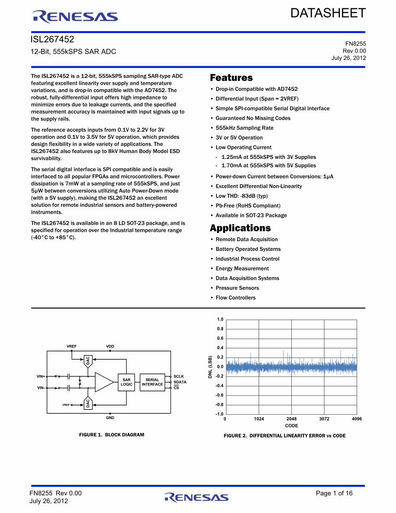
FN8255 Rev 0.00 Page 1 of 16 July 26, 2012 FN8255 Rev 0.00 July 26, 2012 ISL267452 12-Bit, 555kSPS SAR ADC DATASHEET The ISL267452 is a 12-bit, 555kSPS sampling SAR-type ADC featuring excellent linearity over supply and temperature variations, and is drop-in compatible with the AD7452. The robust, fully-differential input offers high impedance to minimize errors due to leakage currents, and the specified measurement accuracy is maintained with input signals up to the supply rails. The reference accepts inputs from 0.1V to 2.2V for 3V operation and 0.1V to 3.5V for 5V operation, which provides design flexibility in a wide variety of applications. The ISL267452 also features up to 8kV Human Body Model ESD survivability. The serial digital interface is SPI compatible and is easily interfaced to all popular FPGAs and microcontrollers. Power dissipation is 7mW at a sampling rate of 555kSPS, and just 5μW between conversions utilizing Auto Power-Down mode (with a 5V supply), making the ISL267452 an excellent solution for remote industrial sensors and battery-powered instruments. The ISL267452 is available in an 8 LD SOT-23 package, and is specified for operation over the Industrial temperature range (-40°C to +85°C). Features • Drop-in Compatible with AD7452 • Differential Input (Span = 2VREF) • Simple SPI-compatible Serial Digital Interface • Guaranteed No Missing Codes • 555kHz Sampling Rate • 3V or 5V Operation • Low Operating Current - 1.25mA at 555kSPS with 3V Supplies - 1.70mA at 555kSPS with 5V Supplies • Power-down Current between Conversions: 1μA • Excellent Differential Non-Linearity • Low THD: -83dB (typ) • Pb-Free (RoHS Compliant) • Available in SOT-23 Package Applications • Remote Data Acquisition • Battery Operated Systems • Industrial Process Control • Energy Measurement • Data Acquisition Systems • Pressure Sensors • Flow Controllers FIGURE 1. BLOCK DIAGRAM FIGURE 2. DIFFERENTIAL LINEARITY ERROR vs CODE SERIAL INTERFACE VDD VREF GND VIN+ VIN– SCLK SDATA CS DAC DAC SAR LOGIC VREF -1.0 -0.8 -0.6 -0.4 -0.2 0.0 0.2 0.4 0.6 0.8 1.0 0 1024 2048 3072 4096 CODE DNL (LSB)
-
Upload
khangminh22 -
Category
Documents
-
view
1 -
download
0
Transcript of ISL267452 Datasheet - Renesas
FN8255Rev 0.00
July 26, 2012
ISL26745212-Bit, 555kSPS SAR ADC
DATASHEET
The ISL267452 is a 12-bit, 555kSPS sampling SAR-type ADC featuring excellent linearity over supply and temperature variations, and is drop-in compatible with the AD7452. The robust, fully-differential input offers high impedance to minimize errors due to leakage currents, and the specified measurement accuracy is maintained with input signals up to the supply rails.
The reference accepts inputs from 0.1V to 2.2V for 3V operation and 0.1V to 3.5V for 5V operation, which provides design flexibility in a wide variety of applications. The ISL267452 also features up to 8kV Human Body Model ESD survivability.
The serial digital interface is SPI compatible and is easily interfaced to all popular FPGAs and microcontrollers. Power dissipation is 7mW at a sampling rate of 555kSPS, and just 5µW between conversions utilizing Auto Power-Down mode (with a 5V supply), making the ISL267452 an excellent solution for remote industrial sensors and battery-powered instruments.
The ISL267452 is available in an 8 LD SOT-23 package, and is specified for operation over the Industrial temperature range (-40°C to +85°C).
Features• Drop-in Compatible with AD7452
• Differential Input (Span = 2VREF)
• Simple SPI-compatible Serial Digital Interface
• Guaranteed No Missing Codes
• 555kHz Sampling Rate
• 3V or 5V Operation
• Low Operating Current
- 1.25mA at 555kSPS with 3V Supplies
- 1.70mA at 555kSPS with 5V Supplies
• Power-down Current between Conversions: 1µA
• Excellent Differential Non-Linearity
• Low THD: -83dB (typ)
• Pb-Free (RoHS Compliant)
• Available in SOT-23 Package
Applications• Remote Data Acquisition
• Battery Operated Systems
• Industrial Process Control
• Energy Measurement
• Data Acquisition Systems
• Pressure Sensors
• Flow Controllers
FIGURE 1. BLOCK DIAGRAM FIGURE 2. DIFFERENTIAL LINEARITY ERROR vs CODE
SERIAL INTERFACE
VDDVREF
GND
VIN+
VIN–
SCLK
SDATA
CS
DA
CD
AC
SARLOGIC
VREF
-1.0
-0.8
-0.6
-0.4
-0.2
0.0
0.2
0.4
0.6
0.8
1.0
0 1024 2048 3072 4096
CODE
DN
L (
LS
B)
FN8255 Rev 0.00 Page 1 of 16July 26, 2012
ISL267452
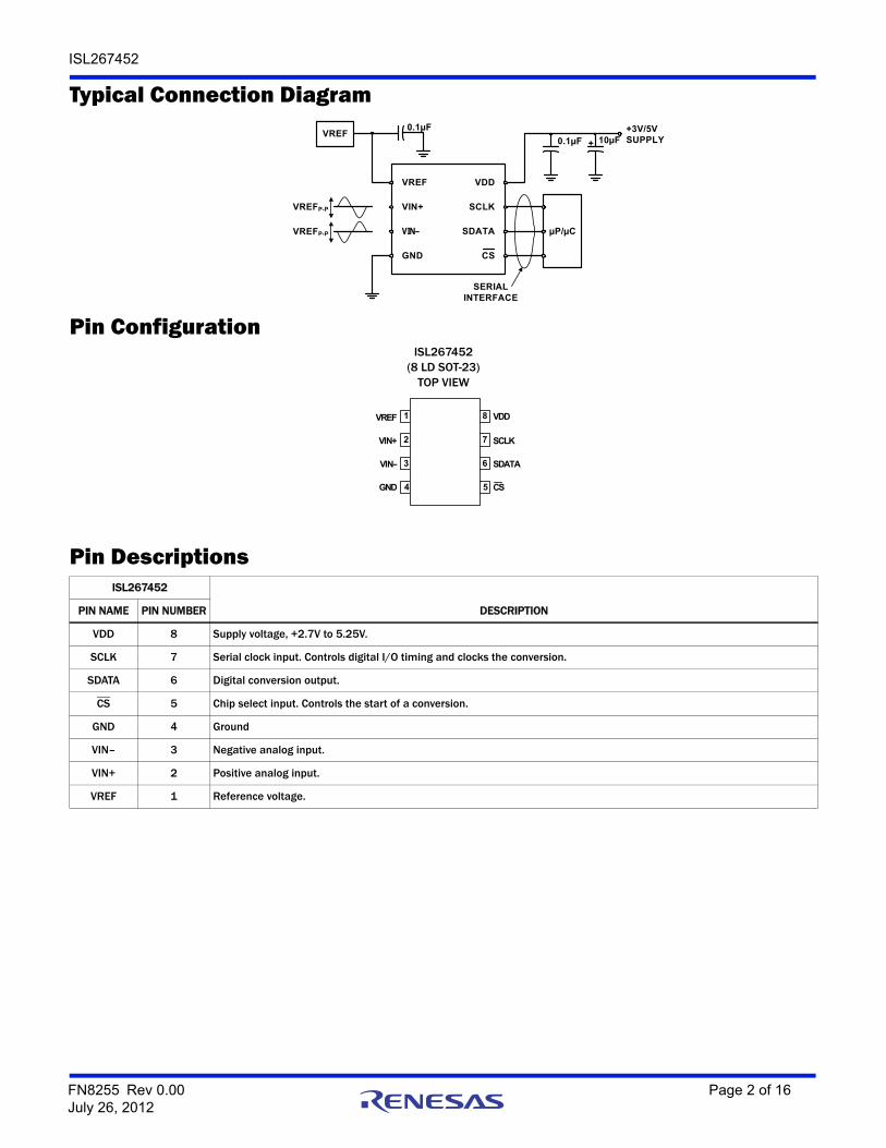
Typical Connection Diagram
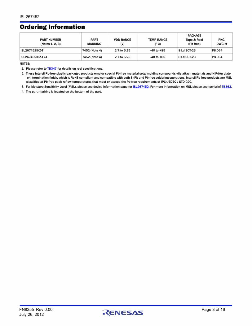
Pin ConfigurationISL267452
(8 LD SOT-23)TOP VIEW
VREF
VIN+
VIN–
GND
VDD
SCLK
SDATA
CS
VREFP-P
+
+3V/5V SUPPLY
µP/µC
VREF
SERIAL INTERFACE
10µF0.1µF
VREFP-P
0.1µF
VREF 8
7
6
5
1
2
3
4
VIN+
VIN–
GND
VDD
SCLK
SDATA
CS
Pin DescriptionsISL267452
DESCRIPTIONPIN NAME PIN NUMBER
VDD 8 Supply voltage, +2.7V to 5.25V.
SCLK 7 Serial clock input. Controls digital I/O timing and clocks the conversion.
SDATA 6 Digital conversion output.
CS 5 Chip select input. Controls the start of a conversion.
GND 4 Ground
VIN– 3 Negative analog input.
VIN+ 2 Positive analog input.
VREF 1 Reference voltage.
FN8255 Rev 0.00 Page 2 of 16July 26, 2012
ISL267452
Ordering Information
PART NUMBER(Notes 1, 2, 3)
PART MARKING
VDD RANGE(V)
TEMP RANGE(°C)
PACKAGETape & Reel
(Pb-free)PKG.
DWG. #
ISL267452IHZ-T 7452 (Note 4) 2.7 to 5.25 -40 to +85 8 Ld SOT-23 P8.064
ISL267452IHZ-T7A 7452 (Note 4) 2.7 to 5.25 -40 to +85 8 Ld SOT-23 P8.064
NOTES:
1. Please refer to TB347 for details on reel specifications.
2. These Intersil Pb-free plastic packaged products employ special Pb-free material sets; molding compounds/die attach materials and NiPdAu plate -e4 termination finish, which is RoHS compliant and compatible with both SnPb and Pb-free soldering operations. Intersil Pb-free products are MSL classified at Pb-free peak reflow temperatures that meet or exceed the Pb-free requirements of IPC/JEDEC J STD-020.
3. For Moisture Sensitivity Level (MSL), please see device information page for ISL267452. For more information on MSL please see techbrief TB363.
4. The part marking is located on the bottom of the part.
FN8255 Rev 0.00 Page 3 of 16July 26, 2012
ISL267452
Table of ContentsPin Configuration. . . . . . . . . . . . . . . . . . . . . . . . . . . . . . . . . . . . . . . . . . . . . . . . . . . . . . . . . . . . . . . . . . . . . . . . . . . . . . . . . . . . . . . . . . . . 2
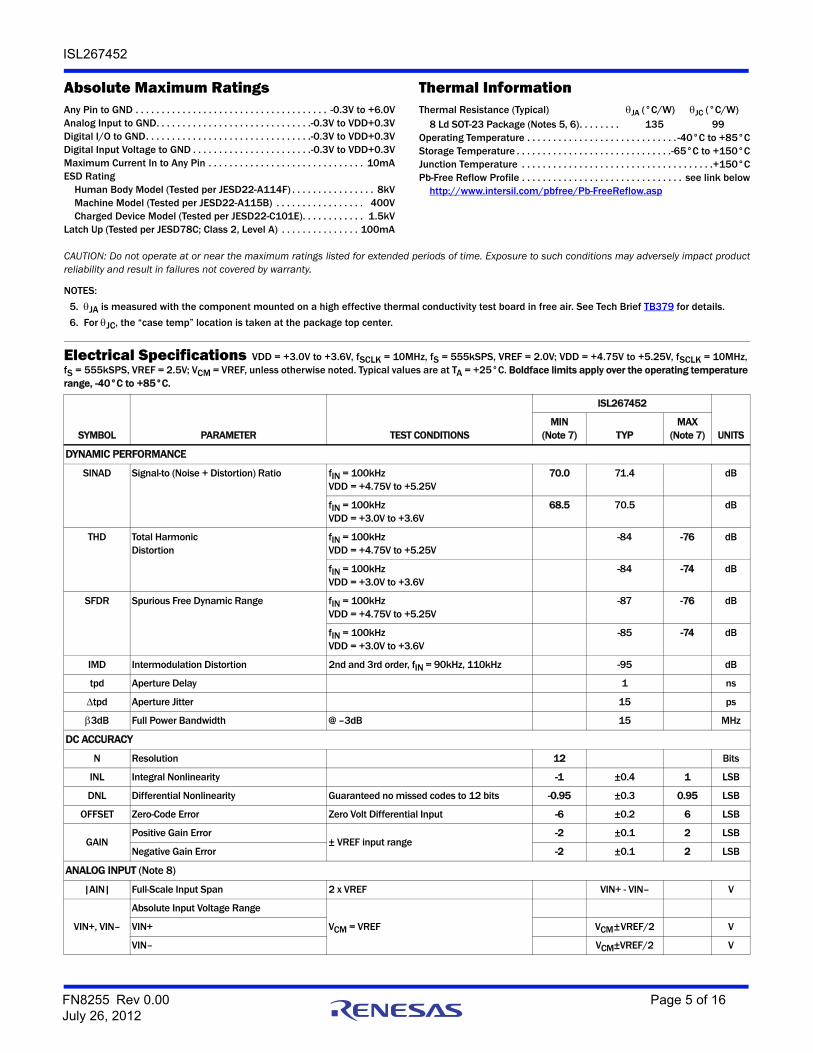
Absolute Maximum Ratings . . . . . . . . . . . . . . . . . . . . . . . . . . . . . . . . . . . . . . . . . . . . . . . . . . . . . . . . . . . . . . . . . . . . . . . . . . . . . . . . . . . 5
Thermal Information . . . . . . . . . . . . . . . . . . . . . . . . . . . . . . . . . . . . . . . . . . . . . . . . . . . . . . . . . . . . . . . . . . . . . . . . . . . . . . . . . . . . . . . . . 5
Electrical Specifications . . . . . . . . . . . . . . . . . . . . . . . . . . . . . . . . . . . . . . . . . . . . . . . . . . . . . . . . . . . . . . . . . . . . . . . . . . . . . . . . . . . . . 5
Timing Specifications . . . . . . . . . . . . . . . . . . . . . . . . . . . . . . . . . . . . . . . . . . . . . . . . . . . . . . . . . . . . . . . . . . . . . . . . . . . . . . . . . . . . . . . . 7
Typical Performance Characteristics . . . . . . . . . . . . . . . . . . . . . . . . . . . . . . . . . . . . . . . . . . . . . . . . . . . . . . . . . . . . . . . . . . . . . . . . . . . 8
Functional Description . . . . . . . . . . . . . . . . . . . . . . . . . . . . . . . . . . . . . . . . . . . . . . . . . . . . . . . . . . . . . . . . . . . . . . . . . . . . . . . . . . . . . . 10
ADC Transfer Function . . . . . . . . . . . . . . . . . . . . . . . . . . . . . . . . . . . . . . . . . . . . . . . . . . . . . . . . . . . . . . . . . . . . . . . . . . . . . . . . . . . . . . . . . . . 10Analog Input . . . . . . . . . . . . . . . . . . . . . . . . . . . . . . . . . . . . . . . . . . . . . . . . . . . . . . . . . . . . . . . . . . . . . . . . . . . . . . . . . . . . . . . . . . . . . . . . . . . 11Voltage Reference Input . . . . . . . . . . . . . . . . . . . . . . . . . . . . . . . . . . . . . . . . . . . . . . . . . . . . . . . . . . . . . . . . . . . . . . . . . . . . . . . . . . . . . . . . . . . . . . . . . . .11Converter Operation . . . . . . . . . . . . . . . . . . . . . . . . . . . . . . . . . . . . . . . . . . . . . . . . . . . . . . . . . . . . . . . . . . . . . . . . . . . . . . . . . . . . . . . . . . . . . 12Power-On Reset . . . . . . . . . . . . . . . . . . . . . . . . . . . . . . . . . . . . . . . . . . . . . . . . . . . . . . . . . . . . . . . . . . . . . . . . . . . . . . . . . . . . . . . . . . . . . . . . . 13Acquisition Time . . . . . . . . . . . . . . . . . . . . . . . . . . . . . . . . . . . . . . . . . . . . . . . . . . . . . . . . . . . . . . . . . . . . . . . . . . . . . . . . . . . . . . . . . . . . . . . . 13Short Cycling . . . . . . . . . . . . . . . . . . . . . . . . . . . . . . . . . . . . . . . . . . . . . . . . . . . . . . . . . . . . . . . . . . . . . . . . . . . . . . . . . . . . . . . . . . . . . . . . . . . 13
Application Hints . . . . . . . . . . . . . . . . . . . . . . . . . . . . . . . . . . . . . . . . . . . . . . . . . . . . . . . . . . . . . . . . . . . . . . . . . . . . . . . . . . . . . . . . . . . 13
Grounding and Layout . . . . . . . . . . . . . . . . . . . . . . . . . . . . . . . . . . . . . . . . . . . . . . . . . . . . . . . . . . . . . . . . . . . . . . . . . . . . . . . . . . . . . . . . . . . . 13
Terminology . . . . . . . . . . . . . . . . . . . . . . . . . . . . . . . . . . . . . . . . . . . . . . . . . . . . . . . . . . . . . . . . . . . . . . . . . . . . . . . . . . . . . . . . . . . . . . . 14
Signal-to-(Noise + Distortion) Ratio (SINAD) . . . . . . . . . . . . . . . . . . . . . . . . . . . . . . . . . . . . . . . . . . . . . . . . . . . . . . . . . . . . . . . . . . . . . . . . . 14Total Harmonic Distortion. . . . . . . . . . . . . . . . . . . . . . . . . . . . . . . . . . . . . . . . . . . . . . . . . . . . . . . . . . . . . . . . . . . . . . . . . . . . . . . . . . . . . . . . . 14Peak Harmonic or Spurious Noise (SFDR) . . . . . . . . . . . . . . . . . . . . . . . . . . . . . . . . . . . . . . . . . . . . . . . . . . . . . . . . . . . . . . . . . . . . . . . . . . . 14Intermodulation Distortion . . . . . . . . . . . . . . . . . . . . . . . . . . . . . . . . . . . . . . . . . . . . . . . . . . . . . . . . . . . . . . . . . . . . . . . . . . . . . . . . . . . . . . . . 14Aperture Delay . . . . . . . . . . . . . . . . . . . . . . . . . . . . . . . . . . . . . . . . . . . . . . . . . . . . . . . . . . . . . . . . . . . . . . . . . . . . . . . . . . . . . . . . . . . . . . . . . . 14Aperture Jitter. . . . . . . . . . . . . . . . . . . . . . . . . . . . . . . . . . . . . . . . . . . . . . . . . . . . . . . . . . . . . . . . . . . . . . . . . . . . . . . . . . . . . . . . . . . . . . . . . . . 14Full Power Bandwidth . . . . . . . . . . . . . . . . . . . . . . . . . . . . . . . . . . . . . . . . . . . . . . . . . . . . . . . . . . . . . . . . . . . . . . . . . . . . . . . . . . . . . . . . . . . . 14Common-Mode Rejection Ratio (CMRR) . . . . . . . . . . . . . . . . . . . . . . . . . . . . . . . . . . . . . . . . . . . . . . . . . . . . . . . . . . . . . . . . . . . . . . . . . . . . 14Integral Nonlinearity (INL). . . . . . . . . . . . . . . . . . . . . . . . . . . . . . . . . . . . . . . . . . . . . . . . . . . . . . . . . . . . . . . . . . . . . . . . . . . . . . . . . . . . . . . . . 14Differential Nonlinearity (DNL) . . . . . . . . . . . . . . . . . . . . . . . . . . . . . . . . . . . . . . . . . . . . . . . . . . . . . . . . . . . . . . . . . . . . . . . . . . . . . . . . . . . . . 14Zero-Code Error . . . . . . . . . . . . . . . . . . . . . . . . . . . . . . . . . . . . . . . . . . . . . . . . . . . . . . . . . . . . . . . . . . . . . . . . . . . . . . . . . . . . . . . . . . . . . . . . . 14Positive Gain Error . . . . . . . . . . . . . . . . . . . . . . . . . . . . . . . . . . . . . . . . . . . . . . . . . . . . . . . . . . . . . . . . . . . . . . . . . . . . . . . . . . . . . . . . . . . . . . . 14Negative Gain Error . . . . . . . . . . . . . . . . . . . . . . . . . . . . . . . . . . . . . . . . . . . . . . . . . . . . . . . . . . . . . . . . . . . . . . . . . . . . . . . . . . . . . . . . . . . . . . 14Track and Hold Acquisition Time . . . . . . . . . . . . . . . . . . . . . . . . . . . . . . . . . . . . . . . . . . . . . . . . . . . . . . . . . . . . . . . . . . . . . . . . . . . . . . . . . . . 14Power Supply Rejection Ratio (PSRR) . . . . . . . . . . . . . . . . . . . . . . . . . . . . . . . . . . . . . . . . . . . . . . . . . . . . . . . . . . . . . . . . . . . . . . . . . . . . . . 14
Revision History. . . . . . . . . . . . . . . . . . . . . . . . . . . . . . . . . . . . . . . . . . . . . . . . . . . . . . . . . . . . . . . . . . . . . . . . . . . . . . . . . . . . . . . . . . . . 15
Products . . . . . . . . . . . . . . . . . . . . . . . . . . . . . . . . . . . . . . . . . . . . . . . . . . . . . . . . . . . . . . . . . . . . . . . . . . . . . . . . . . . . . . . . . . . . . . . . . . 15
P8.064 . . . . . . . . . . . . . . . . . . . . . . . . . . . . . . . . . . . . . . . . . . . . . . . . . . . . . . . . . . . . . . . . . . . . . . . . . . . . . . . . . . . . . . . . . . . . . . . . . . . . 16
FN8255 Rev 0.00 Page 4 of 16July 26, 2012
ISL267452
Absolute Maximum Ratings Thermal InformationAny Pin to GND . . . . . . . . . . . . . . . . . . . . . . . . . . . . . . . . . . . . . -0.3V to +6.0VAnalog Input to GND. . . . . . . . . . . . . . . . . . . . . . . . . . . . . .-0.3V to VDD+0.3VDigital I/O to GND. . . . . . . . . . . . . . . . . . . . . . . . . . . . . . . .-0.3V to VDD+0.3VDigital Input Voltage to GND . . . . . . . . . . . . . . . . . . . . . . .-0.3V to VDD+0.3VMaximum Current In to Any Pin . . . . . . . . . . . . . . . . . . . . . . . . . . . . . . 10mAESD Rating
Human Body Model (Tested per JESD22-A114F) . . . . . . . . . . . . . . . . 8kVMachine Model (Tested per JESD22-A115B) . . . . . . . . . . . . . . . . . 400VCharged Device Model (Tested per JESD22-C101E). . . . . . . . . . . . 1.5kV
Latch Up (Tested per JESD78C; Class 2, Level A) . . . . . . . . . . . . . . . 100mA
Thermal Resistance (Typical) JA (°C/W) JC (°C/W)8 Ld SOT-23 Package (Notes 5, 6). . . . . . . . 135 99
Operating Temperature . . . . . . . . . . . . . . . . . . . . . . . . . . . . . -40°C to +85°CStorage Temperature . . . . . . . . . . . . . . . . . . . . . . . . . . . . . .-65°C to +150°CJunction Temperature . . . . . . . . . . . . . . . . . . . . . . . . . . . . . . . . . . . . .+150°CPb-Free Reflow Profile . . . . . . . . . . . . . . . . . . . . . . . . . . . . . . . see link below
http://www.intersil.com/pbfree/Pb-FreeReflow.asp
CAUTION: Do not operate at or near the maximum ratings listed for extended periods of time. Exposure to such conditions may adversely impact productreliability and result in failures not covered by warranty.
NOTES:
5. JA is measured with the component mounted on a high effective thermal conductivity test board in free air. See Tech Brief TB379 for details.
6. For JC, the “case temp” location is taken at the package top center.
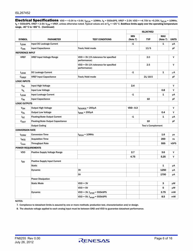
Electrical Specifications VDD = +3.0V to +3.6V, fSCLK = 10MHz, fS = 555kSPS, VREF = 2.0V; VDD = +4.75V to +5.25V, fSCLK = 10MHz, fS = 555kSPS, VREF = 2.5V; VCM = VREF, unless otherwise noted. Typical values are at TA = +25°C. Boldface limits apply over the operating temperature range, -40°C to +85°C.
SYMBOL PARAMETER TEST CONDITIONS
ISL267452
UNITSMIN
(Note 7) TYP MAX
(Note 7)
DYNAMIC PERFORMANCE
SINAD Signal-to (Noise + Distortion) Ratio fIN = 100kHzVDD = +4.75V to +5.25V
70.0 71.4 dB
fIN = 100kHzVDD = +3.0V to +3.6V
68.5 70.5 dB
THD Total HarmonicDistortion
fIN = 100kHzVDD = +4.75V to +5.25V
-84 -76 dB
fIN = 100kHzVDD = +3.0V to +3.6V
-84 -74 dB
SFDR Spurious Free Dynamic Range fIN = 100kHzVDD = +4.75V to +5.25V
-87 -76 dB
fIN = 100kHzVDD = +3.0V to +3.6V
-85 -74 dB
IMD Intermodulation Distortion 2nd and 3rd order, fIN = 90kHz, 110kHz -95 dB
tpd Aperture Delay 1 ns
tpd Aperture Jitter 15 ps
3dB Full Power Bandwidth @ –3dB 15 MHz
DC ACCURACY
N Resolution 12 Bits
INL Integral Nonlinearity -1 ±0.4 1 LSB
DNL Differential Nonlinearity Guaranteed no missed codes to 12 bits -0.95 ±0.3 0.95 LSB
OFFSET Zero-Code Error Zero Volt Differential Input -6 ±0.2 6 LSB
GAINPositive Gain Error
± VREF input range-2 ±0.1 2 LSB
Negative Gain Error -2 ±0.1 2 LSB
ANALOG INPUT (Note 8)
|AIN| Full-Scale Input Span 2 x VREF VIN+ - VIN– V
VIN+, VIN–
Absolute Input Voltage Range
VCM = VREFVIN+ VCM±VREF/2 V
VIN– VCM±VREF/2 V
FN8255 Rev 0.00 Page 5 of 16July 26, 2012
ISL267452
ILEAK Input DC Leakage Current -1 1 µA
CVIN Input Capacitance Track/Hold mode 13/5 pF
REFERENCE INPUT
VREF VREF Input Voltage Range VDD = 3V (1% tolerance for specified performance)
2.0 V
VDD = 5V (1% tolerance for specified performance)
2.5 V
ILEAK DC Leakage Current -1 1 A
CVREF VREF Input Capacitance Track/Hold mode 21/18.5 pF
LOGIC INPUTS
VIH Input High Voltage 2.4 V
VIL Input Low Voltage 0.8 V
ILEAK Input Leakage Current -1 1 µA
CIN Input Capacitance 10 pF
LOGIC OUTPUTS
VOH Output High Voltage ISOURCE = 200µA VDD - 0.3 V
VOL Output Low Voltage ISINK = 200µA 0.4 V
IOZ Floating-State Output Current -1 1 µA
COUT Floating-State Output Capacitance 10 pF
Output Coding Two’s Complement
CONVERSION RATE
tCONV Conversion Time fSCLK = 10MHz 1.6 µs
tACQ Acquisition Time 200 ns
fmax Throughput Rate 555 kSPS
POWER REQUIREMENTS
VDD Positive Supply Voltage Range 2.7 3.6 V
4.75 5.25 V
IDD Positive Supply Input Current
Static 1 µA
Dynamic 3V 1250 µA
5V 1700 µA
Power Dissipation
Static Mode VDD = 3V 3 µW
VDD = 5V 5 µW
Dynamic VDD = 3V, fsmpl = 555kSPS 3.75 mW
VDD = 5V, fsmpl = 555kSPS 8.5 mW
NOTES:
7. Compliance to datasheet limits is assured by one or more methods: production test, characterization and/or design.
8. The absolute voltage applied to each analog input must be between GND and VDD to guarantee datasheet performance.
Electrical Specifications VDD = +3.0V to +3.6V, fSCLK = 10MHz, fS = 555kSPS, VREF = 2.0V; VDD = +4.75V to +5.25V, fSCLK = 10MHz, fS = 555kSPS, VREF = 2.5V; VCM = VREF, unless otherwise noted. Typical values are at TA = +25°C. Boldface limits apply over the operating temperature range, -40°C to +85°C. (Continued)
SYMBOL PARAMETER TEST CONDITIONS
ISL267452
UNITSMIN
(Note 7) TYP MAX
(Note 7)
FN8255 Rev 0.00 Page 6 of 16July 26, 2012
ISL267452
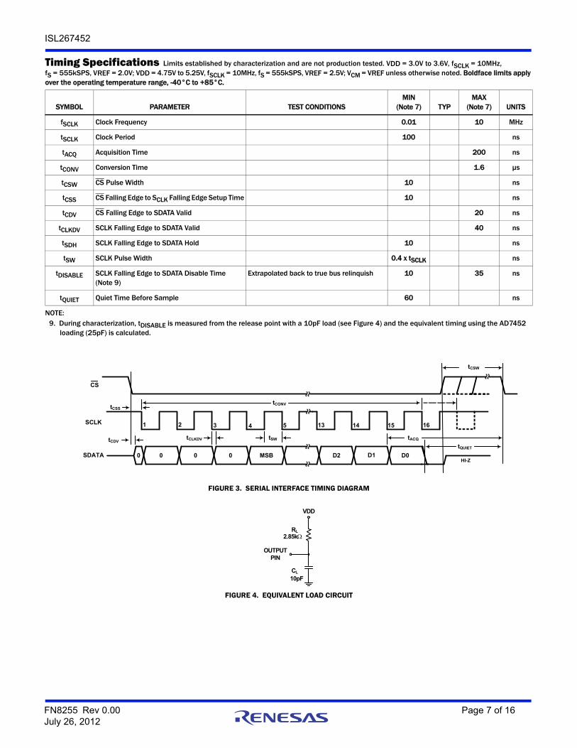
Timing Specifications Limits established by characterization and are not production tested. VDD = 3.0V to 3.6V, fSCLK = 10MHz, fS = 555kSPS, VREF = 2.0V; VDD = 4.75V to 5.25V, fSCLK = 10MHz, fS = 555kSPS, VREF = 2.5V; VCM = VREF unless otherwise noted. Boldface limits apply over the operating temperature range, -40°C to +85°C.
SYMBOL PARAMETER TEST CONDITIONSMIN
(Note 7) TYP MAX
(Note 7) UNITS
fSCLK Clock Frequency 0.01 10 MHz
tSCLK Clock Period 100 ns
tACQ Acquisition Time 200 ns
tCONV Conversion Time 1.6 µs
tCSW CS Pulse Width 10 ns
tCSS CS Falling Edge to SCLK Falling Edge Setup Time 10 ns
tCDV CS Falling Edge to SDATA Valid 20 ns
tCLKDV SCLK Falling Edge to SDATA Valid 40 ns
tSDH SCLK Falling Edge to SDATA Hold 10 ns
tSW SCLK Pulse Width 0.4 x tSCLK ns
tDISABLE SCLK Falling Edge to SDATA Disable Time
(Note 9)Extrapolated back to true bus relinquish 10 35 ns
tQUIET Quiet Time Before Sample 60 ns
NOTE:9. During characterization, tDISABLE is measured from the release point with a 10pF load (see Figure 4) and the equivalent timing using the AD7452
loading (25pF) is calculated.
FIGURE 3. SERIAL INTERFACE TIMING DIAGRAM
SCLK
SDATA
1 2 3 4 5 161514
tCSW
tCDV
tCSStCONV
13
0 0 0 0 MSB D0D1D2
tQUIET
tSWtCLKDV
CS
HI-Z
tACQ
FIGURE 4. EQUIVALENT LOAD CIRCUIT
OUTPUT PIN
CL
10pF
VDD
2.85kRL
FN8255 Rev 0.00 Page 7 of 16July 26, 2012
ISL267452
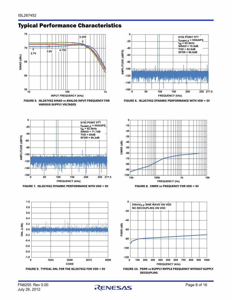
Typical Performance Characteristics
FIGURE 5. ISL267452 SINAD vs ANALOG INPUT FREQUENCY FOR VARIOUS SUPPLY VOLTAGES
FIGURE 6. ISL267452 DYNAMIC PERFORMANCE WITH VDD = 3V
FIGURE 7. ISL267452 DYNAMIC PERFORMANCE WITH VDD = 5V FIGURE 8. CMRR vs FREQUENCY FOR VDD = 5V
FIGURE 9. TYPICAL DNL FOR THE ISL267452 FOR VDD = 5V FIGURE 10. PSRR vs SUPPLY RIPPLE FREQUENCY WITHOUT SUPPLY DECOUPLING
55
60
65
70
75
10 100 1k
INPUT FREQUENCY (kHz)
SIN
AD
(d
Bc
) 2.7V3.6V 4.75V
5.25V
-160
-140
-120
-100
-80
-60
-40
-20
0
0 50 100 150 200 250
FREQUENCY (kHz)
AM
PL
ITU
DE
(d
BF
S)
277.5
8192 POINT FFTfSAMPLE = 555kSPSfIN = 92.5kHzSINAD = 70.9dBTHD = 82.9dBSFDR = 86.6dB
-160
-140
-120
-100
-80
-60
-40
-20
0
0 50 100 150 200 250
FREQUENCY (kHz)
AM
PL
ITU
DE
(d
BF
S)
277.5
8192 POINT FFTfSAMPLE = 555kSPSfIN = 92.5kHzSINAD = 71.7dBTHD = 85dBSFDR = 86.2dB
-100
-90
-80
-70
-60
-50
-40
-30
-20
-10
0
10k 100k 1k 10k
FREQUENCY (Hz)
CM
RR
(d
B)
-1.0
-0.8
-0.6
-0.4
-0.2
0.0
0.2
0.4
0.6
0.8
1.0
0 1024 2048 3072 4096
CODE
DN
L (
LS
B)
-120
-100
-80
-60
-40
-20
0
0 100 200 300 400 500 600 700 800 900 1000
FREQUENCY (kHz)
250mVP-P SINE WAVE ON VDDNO DECOUPLING ON VDD
PS
RR
(d
B)
FN8255 Rev 0.00 Page 8 of 16July 26, 2012
ISL267452
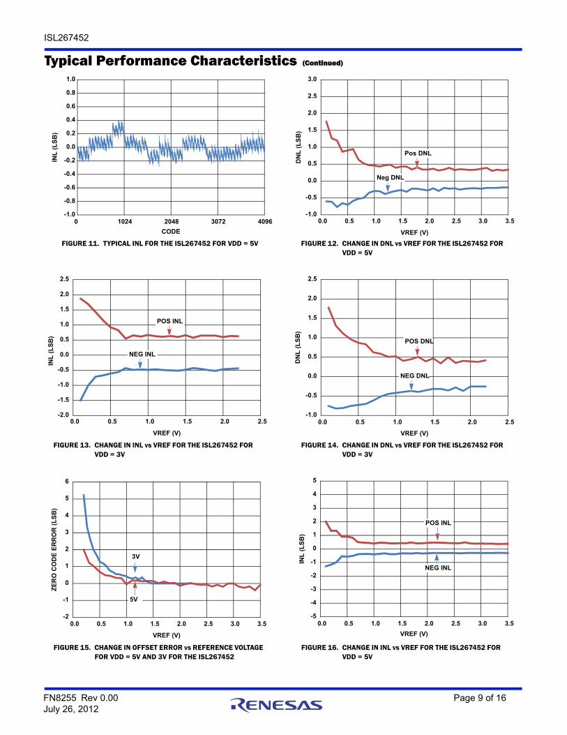
FIGURE 11. TYPICAL INL FOR THE ISL267452 FOR VDD = 5V FIGURE 12. CHANGE IN DNL vs VREF FOR THE ISL267452 FOR VDD = 5V
FIGURE 13. CHANGE IN INL vs VREF FOR THE ISL267452 FOR VDD = 3V
FIGURE 14. CHANGE IN DNL vs VREF FOR THE ISL267452 FOR VDD = 3V
FIGURE 15. CHANGE IN OFFSET ERROR vs REFERENCE VOLTAGE FOR VDD = 5V AND 3V FOR THE ISL267452
FIGURE 16. CHANGE IN INL vs VREF FOR THE ISL267452 FOR VDD = 5V
Typical Performance Characteristics (Continued)
-1.0
-0.8
-0.6
-0.4
-0.2
0.0
0.2
0.4
0.6
0.8
1.0
0 1024 2048 3072 4096
CODE
INL
(L
SB
)
-1.0
-0.5
0.0
0.5
1.0
1.5
2.0
2.5
3.0
0.0 0.5 1.0 1.5 2.0 2.5 3.0 3.5
VREF (V)
DN
L (
LS
B)
Neg DNL
Pos DNL
-2.0
-1.5
-1.0
-0.5
0.0
0.5
1.0
1.5
2.0
2.5
0.0 0.5 1.0 1.5 2.0 2.5
INL
(L
SB
)
VREF (V)
NEG INL
POS INL
-1.0
-0.5
0.0
0.5
1.0
1.5
2.0
2.5
0.0 0.5 1.0 1.5 2.0 2.5
VREF (V)
DN
L (
LS
B)
NEG DNL
POS DNL
-2
-1
0
1
2
3
4
5
6
0.0 0.5 1.0 1.5 2.0 2.5 3.0 3.5
ZE
RO
CO
DE
ER
RO
R (
LS
B)
VREF (V)
3V
5V
-5
-4
-3
-2
-1
0
1
2
3
4
5
0.0 0.5 1.0 1.5 2.0 2.5 3.0 3.5
INL
(L
SB
)
VREF (V)
NEG INL
POS INL
FN8255 Rev 0.00 Page 9 of 16July 26, 2012
ISL267452
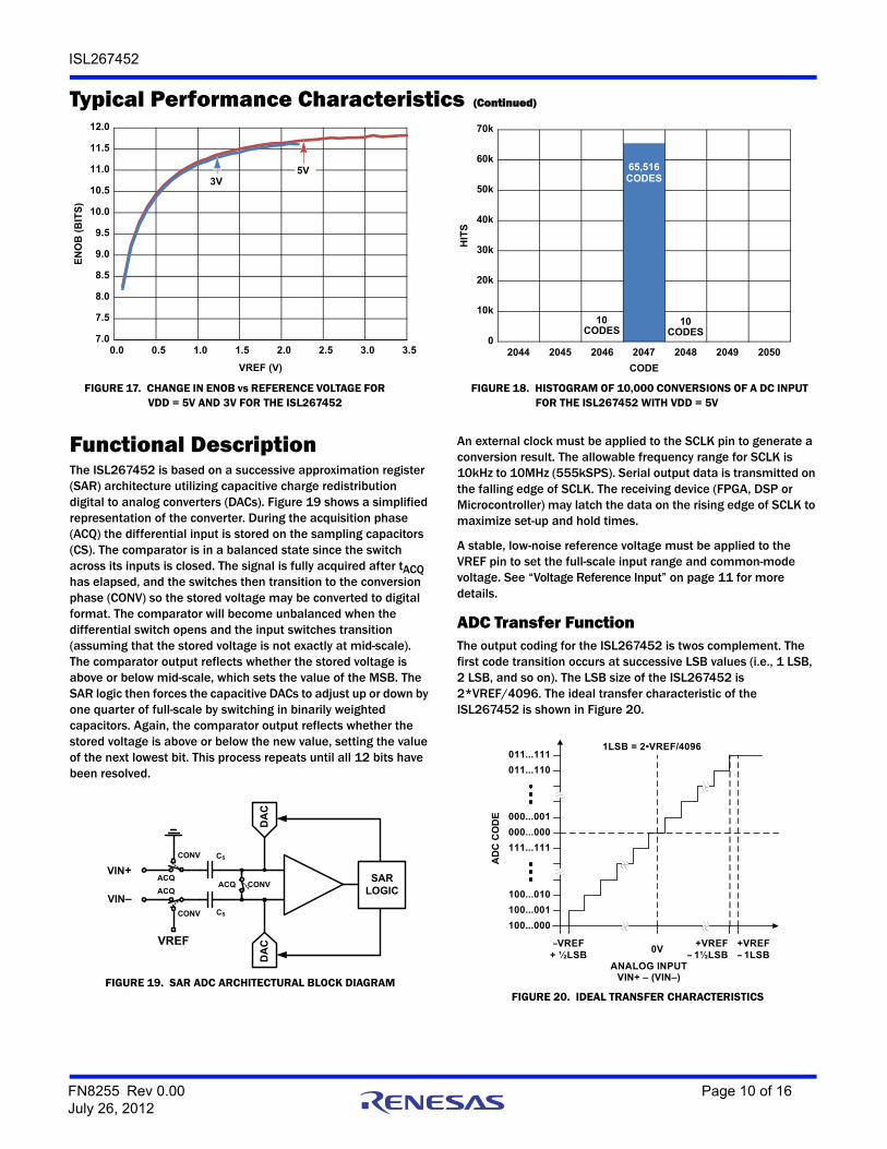
Functional DescriptionThe ISL267452 is based on a successive approximation register (SAR) architecture utilizing capacitive charge redistribution digital to analog converters (DACs). Figure 19 shows a simplified representation of the converter. During the acquisition phase (ACQ) the differential input is stored on the sampling capacitors (CS). The comparator is in a balanced state since the switch across its inputs is closed. The signal is fully acquired after tACQ has elapsed, and the switches then transition to the conversion phase (CONV) so the stored voltage may be converted to digital format. The comparator will become unbalanced when the differential switch opens and the input switches transition (assuming that the stored voltage is not exactly at mid-scale). The comparator output reflects whether the stored voltage is above or below mid-scale, which sets the value of the MSB. The SAR logic then forces the capacitive DACs to adjust up or down by one quarter of full-scale by switching in binarily weighted capacitors. Again, the comparator output reflects whether the stored voltage is above or below the new value, setting the value of the next lowest bit. This process repeats until all 12 bits have been resolved.
An external clock must be applied to the SCLK pin to generate a conversion result. The allowable frequency range for SCLK is 10kHz to 10MHz (555kSPS). Serial output data is transmitted on the falling edge of SCLK. The receiving device (FPGA, DSP or Microcontroller) may latch the data on the rising edge of SCLK to maximize set-up and hold times.
A stable, low-noise reference voltage must be applied to the VREF pin to set the full-scale input range and common-mode voltage. See “Voltage Reference Input” on page 11 for more details.
ADC Transfer FunctionThe output coding for the ISL267452 is twos complement. The first code transition occurs at successive LSB values (i.e., 1 LSB, 2 LSB, and so on). The LSB size of the ISL267452 is 2*VREF/4096. The ideal transfer characteristic of the ISL267452 is shown in Figure 20.
FIGURE 17. CHANGE IN ENOB vs REFERENCE VOLTAGE FOR VDD = 5V AND 3V FOR THE ISL267452
FIGURE 18. HISTOGRAM OF 10,000 CONVERSIONS OF A DC INPUT FOR THE ISL267452 WITH VDD = 5V
Typical Performance Characteristics (Continued)
7.0
7.5
8.0
8.5
9.0
9.5
10.0
10.5
11.0
11.5
12.0
0.0 0.5 1.0 1.5 2.0 2.5 3.0 3.5
EN
OB
(B
ITS
)
VREF (V)
5V 3V
0
10k
20k
30k
40k
50k
60k
70k
2044 2045 2046 2047 2048 2049 2050
CODE
65,516CODES
10CODES
10CODES
HIT
S
FIGURE 19. SAR ADC ARCHITECTURAL BLOCK DIAGRAM
VIN+
VIN–
VREF
ACQCONV
ACQACQ
CONV
CONV
DA
CD
AC
SARLOGIC
CS
CS
FIGURE 20. IDEAL TRANSFER CHARACTERISTICS
1LSB = 2•VREF/4096
100...000
100...001
100...010
111...111
000...000
000...001
011...110
011...111
AD
C C
OD
E
ANALOG INPUTVIN+ – (VIN–)
–VREF+ ½LSB
+VREF– 1½LSB
0V+VREF– 1LSB
FN8255 Rev 0.00 Page 10 of 16July 26, 2012
ISL267452
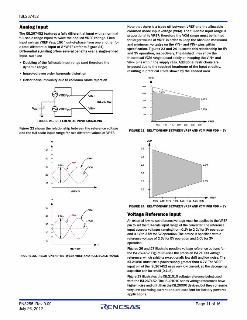
Analog InputThe ISL267452 features a fully differential input with a nominal full-scale range equal to twice the applied VREF voltage. Each input swings VREF VP-P, 180° out-of-phase from one another for a total differential input of 2*VREF (refer to Figure 21). Differential signaling offers several benefits over a single-ended input, such as:
• Doubling of the full-scale input range (and therefore the dynamic range)
• Improved even order harmonic distortion
• Better noise immunity due to common mode rejection
Figure 22 shows the relationship between the reference voltage and the full-scale input range for two different values of VREF.
Note that there is a trade-off between VREF and the allowable common mode input voltage (VCM). The full-scale input range is proportional to VREF; therefore the VCM range must be limited for larger values of VREF in order to keep the absolute maximum and minimum voltages on the VIN+ and VIN– pins within specification. Figures 23 and 24 illustrate this relationship for 5V and 3V operation, respectively. The dashed lines show the theoretical VCM range based solely on keeping the VIN+ and VIN– pins within the supply rails. Additional restrictions are imposed due to the required headroom of the input circuitry, resulting in practical limits shown by the shaded area.
Voltage Reference InputAn external low-noise reference voltage must be applied to the VREF pin to set the full-scale input range of the converter. The reference input accepts voltages ranging from 0.1V to 2.2V for 3V operation and 0.1V to 3.5V for 5V operation. The device is specified with a reference voltage of 2.5V for 5V operation and 2.0V for 3V operation.
Figures 26 and 27 illustrate possible voltage reference options for the ISL267452. Figure 26 uses the precision ISL21090 voltage reference, which exhibits exceptionally low drift and low noise. The ISL21090 must use a power supply greater than 4.7V. The VREF input pin of the ISL267452 uses very low current, so the decoupling capacitor can be small (0.1µF).
Figure 27 illustrates the ISL21010 voltage reference being used with the ISL267452. The ISL21010 series voltage references have higher noise and drift than the ISL26090 devices, but they consume very low operating current and are excellent for battery-powered applications.
FIGURE 21. DIFFERENTIAL INPUT SIGNALING
FIGURE 22. RELATIONSHIP BETWEEN VREF AND FULL-SCALE RANGE
ISL267452
VCM
VREFP-P
VREFP-P
VIN+
VIN–
3.0
5.0
2.0
1.0
4.0
VIN+
VIN–
VCM2.0VP-P
VREF = 2V
3.0
5.0
2.0
1.0
4.0 VIN+
VIN–
VCM
2.5VP-P
VREF = 2.5V
t
V
t
V
FIGURE 23. RELATIONSHIP BETWEEN VREF AND VCM FOR VDD = 5V
FIGURE 24. RELATIONSHIP BETWEEN VREF AND VCM FOR VDD = 3V
3.0
5.0
2.0
1.0
4.0
VREF
VCM
0.5 1.0 1.5 2.0 2.5 3.0 3.5
3.25V
1.75V
4.25V
1.5
2.0
1.0
0.5
VREF
VCM
0.25 0.50 0.75 1.00
2.5
2.001.25 1.50 1.75
2.5
1.0V
2.0V
FN8255 Rev 0.00 Page 11 of 16July 26, 2012
ISL267452
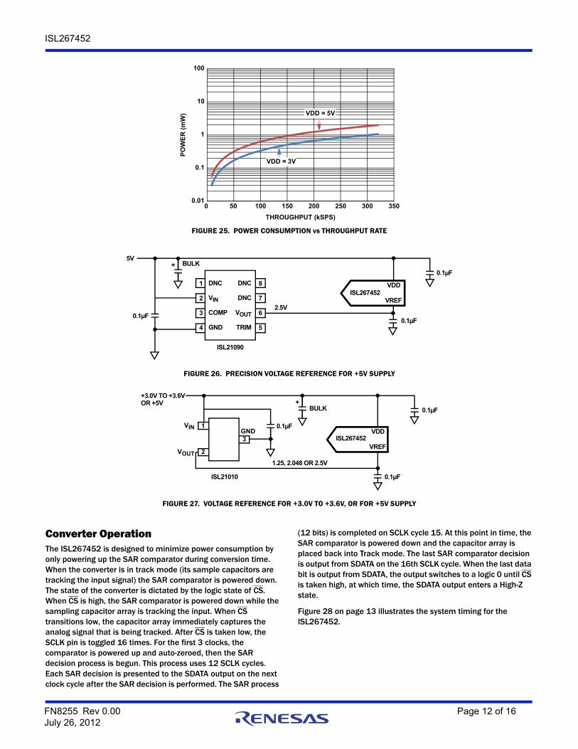
Converter OperationThe ISL267452 is designed to minimize power consumption by only powering up the SAR comparator during conversion time. When the converter is in track mode (its sample capacitors are tracking the input signal) the SAR comparator is powered down. The state of the converter is dictated by the logic state of CS. When CS is high, the SAR comparator is powered down while the sampling capacitor array is tracking the input. When CS transitions low, the capacitor array immediately captures the analog signal that is being tracked. After CS is taken low, the SCLK pin is toggled 16 times. For the first 3 clocks, the comparator is powered up and auto-zeroed, then the SAR decision process is begun. This process uses 12 SCLK cycles. Each SAR decision is presented to the SDATA output on the next clock cycle after the SAR decision is performed. The SAR process
(12 bits) is completed on SCLK cycle 15. At this point in time, the SAR comparator is powered down and the capacitor array is placed back into Track mode. The last SAR comparator decision is output from SDATA on the 16th SCLK cycle. When the last data bit is output from SDATA, the output switches to a logic 0 until CS is taken high, at which time, the SDATA output enters a High-Z state.
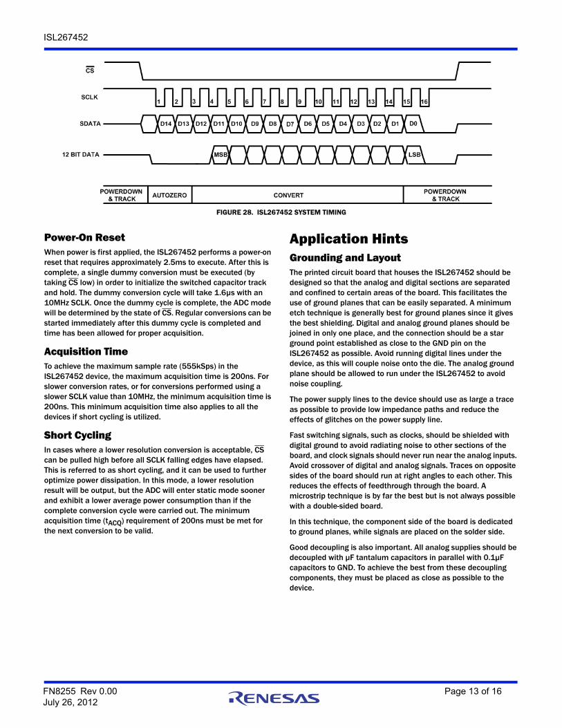
Figure 28 on page 13 illustrates the system timing for the ISL267452.
FIGURE 25. POWER CONSUMPTION vs THROUGHPUT RATE
0.01
0.1
1
10
100
0 50 100 150 200 250 300 350
THROUGHPUT (kSPS)
PO
WE
R (
mW
)
VDD = 3V
VDD = 5V
FIGURE 26. PRECISION VOLTAGE REFERENCE FOR +5V SUPPLY
1
2
3
4
8
7
6
5
DNC
VIN
COMP
GND
DNC
DNC
VOUT
TRIM
0.1µF
VDD
0.1µF
2.5VVREF
0.1µF
BULK+5V
ISL21090
ISL267452
FIGURE 27. VOLTAGE REFERENCE FOR +3.0V TO +3.6V, OR FOR +5V SUPPLY
VDD
0.1µF
VREF
0.1µFBULK+
+3.0V TO +3.6V
ISL21010
GNDVIN
VOUT
1
2
3
0.1µF
1.25, 2.048 OR 2.5V
OR +5V
ISL267452
FN8255 Rev 0.00 Page 12 of 16July 26, 2012
ISL267452
Power-On ResetWhen power is first applied, the ISL267452 performs a power-on reset that requires approximately 2.5ms to execute. After this is complete, a single dummy conversion must be executed (by taking CS low) in order to initialize the switched capacitor track and hold. The dummy conversion cycle will take 1.6µs with an 10MHz SCLK. Once the dummy cycle is complete, the ADC mode will be determined by the state of CS. Regular conversions can be started immediately after this dummy cycle is completed and time has been allowed for proper acquisition.
Acquisition Time To achieve the maximum sample rate (555kSps) in the ISL267452 device, the maximum acquisition time is 200ns. For slower conversion rates, or for conversions performed using a slower SCLK value than 10MHz, the minimum acquisition time is 200ns. This minimum acquisition time also applies to all the devices if short cycling is utilized.
Short CyclingIn cases where a lower resolution conversion is acceptable, CS can be pulled high before all SCLK falling edges have elapsed. This is referred to as short cycling, and it can be used to further optimize power dissipation. In this mode, a lower resolution result will be output, but the ADC will enter static mode sooner and exhibit a lower average power consumption than if the complete conversion cycle were carried out. The minimum acquisition time (tACQ) requirement of 200ns must be met for the next conversion to be valid.
Application HintsGrounding and LayoutThe printed circuit board that houses the ISL267452 should be designed so that the analog and digital sections are separated and confined to certain areas of the board. This facilitates the use of ground planes that can be easily separated. A minimum etch technique is generally best for ground planes since it gives the best shielding. Digital and analog ground planes should be joined in only one place, and the connection should be a star ground point established as close to the GND pin on the ISL267452 as possible. Avoid running digital lines under the device, as this will couple noise onto the die. The analog ground plane should be allowed to run under the ISL267452 to avoid noise coupling.
The power supply lines to the device should use as large a trace as possible to provide low impedance paths and reduce the effects of glitches on the power supply line.
Fast switching signals, such as clocks, should be shielded with digital ground to avoid radiating noise to other sections of the board, and clock signals should never run near the analog inputs. Avoid crossover of digital and analog signals. Traces on opposite sides of the board should run at right angles to each other. This reduces the effects of feedthrough through the board. A microstrip technique is by far the best but is not always possible with a double-sided board.
In this technique, the component side of the board is dedicated to ground planes, while signals are placed on the solder side.
Good decoupling is also important. All analog supplies should be decoupled with μF tantalum capacitors in parallel with 0.1μF capacitors to GND. To achieve the best from these decoupling components, they must be placed as close as possible to the device.
FIGURE 28. ISL267452 SYSTEM TIMING
FN8255 Rev 0.00 Page 13 of 16July 26, 2012
ISL267452
TerminologySignal-to-(Noise + Distortion) Ratio (SINAD)This is the measured ratio of signal-to-(noise + distortion) at the output of the ADC. The signal is the rms amplitude of the fundamental. Noise is the sum of all nonfundamental signals up to half the sampling frequency (fs/2), excluding DC. The ratio is dependent on the number of quantization levels in the digitization process; the more levels, the smaller the quantization noise. The theoretical signal-to-(noise + distortion) ratio for an ideal N-bit converter with a sine wave input is given by Equation 1:
Thus, for a 12-bit converter, this is 74dB.
Total Harmonic DistortionTotal harmonic distortion (THD) is the ratio of the rms sum of harmonics to the fundamental. For the ISL267452, it is defined as Equation 2:
where V1 is the rms amplitude of the fundamental and V2, V3, V4, V5, and V6 are the rms amplitudes of the second to the sixth harmonics.
Peak Harmonic or Spurious Noise (SFDR)Peak harmonic or spurious noise is defined as the ratio of the rms value of the next largest component in the ADC output spectrum (up to fS/2 and excluding DC) to the rms value of the fundamental (also referred to as Spurious Free Dynamic Range (SFDR)). Normally, the value of this specification is determined by the largest harmonic in the spectrum, but for ADCs where the harmonics are buried in the noise floor, it will be a noise peak.
Intermodulation DistortionWith inputs consisting of sine waves at two frequencies, fa and fb, any active device with nonlinearities will create distortion products at sum and difference frequencies of mfa ± nfb where m and n = 0, 1, 2 or 3. Intermodulation distortion terms are those for which neither m nor n are equal to zero. For example, the second order terms include (fa + fb) and (fa – fb), while the third order terms include (2fa + fb), (2fa – fb), (fa + 2fb), and (fa –2fb).
The ISL267452 is tested using the CCIF standard, where two input frequencies near the top end of the input bandwidth are used. In this case, the second order terms are usually distanced in frequency from the original sine waves, while the third order terms are usually at a frequency close to the input frequencies. As a result, the second and third order terms are specified separately. The calculation of the intermodulation distortion is as per the THD specification, where it is the ratio of the rms sum of the individual distortion products to the rms amplitude of the sum of the fundamentals expressed in dBs.
Aperture DelayThis is the amount of time from the leading edge of the sampling clock until the ADC actually takes the sample.
Aperture JitterThis is the sample-to-sample variation in the effective point in time at which the actual sample is taken.
Full Power BandwidthThe full power bandwidth of an ADC is that input frequency at which the amplitude of the reconstructed fundamental is reduced by 3dB for a full-scale input.
Common-Mode Rejection Ratio (CMRR)The common-mode rejection ratio is defined as the ratio of the power in the ADC output at full-scale frequency, f, to the power of a 250mVP-P sine wave applied to the common-mode voltage of VIN+ and VIN– of frequency fs:
Pf is the power at the frequency f in the ADC output; Pfs is the power at frequency fs in the ADC output.
Integral Nonlinearity (INL)This is the maximum deviation from a straight line passing through the endpoints of the ADC transfer function.
Differential Nonlinearity (DNL)This is the difference between the measured and the ideal 1 LSB change between any two adjacent codes in the ADC.
Zero-Code ErrorThis is the deviation of the midscale code transition (111...111 to 000...000) from the ideal VIN+ – VIN– (i.e., 0 LSB).
Positive Gain ErrorThis is the deviation of the last code transition (011...110 to 011...111) from the ideal VIN+ – VIN– (i.e., +REF – 1 LSB), after the zero code error has been adjusted out.
Negative Gain ErrorThis is the deviation of the first code transition (100...000 to 100...001) from the ideal VIN+ – VIN– (i.e., – REF + 1 LSB), after the zero code error has been adjusted out.
Track and Hold Acquisition TimeThe track and hold acquisition time is the minimum time required for the track and hold amplifier to remain in track mode for its output to reach and settle to within 0.5 LSB of the applied input signal.
Power Supply Rejection Ratio (PSRR)The power supply rejection ratio is defined as the ratio of the power in the ADC output at full-scale frequency, f, to ADC VDD supply of frequency fS. The frequency of this input varies from 1kHz to 1MHz.
Pf is the power at frequency f in the ADC output; Pfs is the power at frequency fs in the ADC output.
Signal-to-(Noise + Distortion) 6.02 N 1.76+ dB= (EQ. 1)
(EQ. 2)THD dB 20V2
2 V3 2 V4
2 V5 2 V6
2+ + + +
V1 2
------------------------------------------------------------------------log=
(EQ. 3)CMRR dB 10 Pfl Pfs log=
(EQ. 4)PSRR dB 10 Pf Pfs log=
FN8255 Rev 0.00 Page 14 of 16July 26, 2012
ISL267452
Intersil products are manufactured, assembled and tested utilizing ISO9001 quality systems as notedin the quality certifications found at www.intersil.com/en/support/qualandreliability.html
Intersil products are sold by description only. Intersil may modify the circuit design and/or specifications of products at any time without notice, provided that such modification does not, in Intersil's sole judgment, affect the form, fit or function of the product. Accordingly, the reader is cautioned to verify that datasheets are current before placing orders. Information furnished by Intersil is believed to be accurate and reliable. However, no responsibility is assumed by Intersil or its subsidiaries for its use; nor for any infringements of patents or other rights of third parties which may result from its use. No license is granted by implication or otherwise under any patent or patent rights of Intersil or its subsidiaries.
For information regarding Intersil Corporation and its products, see www.intersil.com
For additional products, see www.intersil.com/en/products.html
© Copyright Intersil Americas LLC 2012. All Rights Reserved.All trademarks and registered trademarks are the property of their respective owners.
ProductsIntersil Corporation is a leader in the design and manufacture of high-performance analog semiconductors. The Company's products address some of the industry's fastest growing markets, such as, flat panel displays, cell phones, handheld products, and notebooks. Intersil's product families address power management and analog signal processing functions. Go to www.intersil.com/products for a complete list of Intersil product families.
For a complete listing of Applications, Related Documentation and Related Parts, please see the respective device information page on intersil.com: ISL267452
To report errors or suggestions for this datasheet, please go to: www.intersil.com/askourstaff
FITs are available from our website at: http://rel.intersil.com/reports/search.php
Revision HistoryThe revision history provided is for informational purposes only and is believed to be accurate, but not warranted. Please go to web to make sure you have the latest revision.
DATE REVISION CHANGE
July 26, 2012 FN8255.0 Initial Release.
FN8255 Rev 0.00 Page 15 of 16July 26, 2012
ISL267452
FN8255 Rev 0.00 Page 16 of 16July 26, 2012
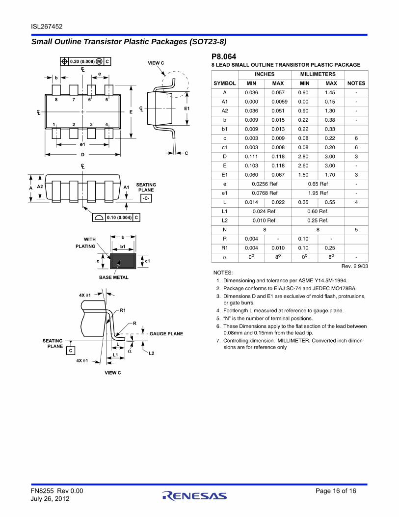
Small Outline Transistor Plastic Packages (SOT23-8)
D
e1
E
CLe
b
CL
A2A A1
CL
0.20 (0.008) M
0.10 (0.004) C
C
-C-
SEATINGPLANE
1 2 3 4
568 7
E1CL
C
VIEW C
VIEW C
L
R1
R
4X 1
4X 1
GAUGE PLANE
L1
SEATING
L2C
PLANE
c
BASE METAL
WITH
c1
b1PLATING
b
P8.0648 LEAD SMALL OUTLINE TRANSISTOR PLASTIC PACKAGE
SYMBOL
INCHES MILLIMETERS
NOTESMIN MAX MIN MAX
A 0.036 0.057 0.90 1.45 -
A1 0.000 0.0059 0.00 0.15 -
A2 0.036 0.051 0.90 1.30 -
b 0.009 0.015 0.22 0.38 -
b1 0.009 0.013 0.22 0.33
c 0.003 0.009 0.08 0.22 6
c1 0.003 0.008 0.08 0.20 6
D 0.111 0.118 2.80 3.00 3
E 0.103 0.118 2.60 3.00 -
E1 0.060 0.067 1.50 1.70 3
e 0.0256 Ref 0.65 Ref -
e1 0.0768 Ref 1.95 Ref -
L 0.014 0.022 0.35 0.55 4
L1 0.024 Ref. 0.60 Ref.
L2 0.010 Ref. 0.25 Ref.
N 8 8 5
R 0.004 - 0.10 -
R1 0.004 0.010 0.10 0.25
0o 8o 0o 8o -
Rev. 2 9/03NOTES:
1. Dimensioning and tolerance per ASME Y14.5M-1994.
2. Package conforms to EIAJ SC-74 and JEDEC MO178BA.
3. Dimensions D and E1 are exclusive of mold flash, protrusions, or gate burrs.
4. Footlength L measured at reference to gauge plane.
5. “N” is the number of terminal positions.
6. These Dimensions apply to the flat section of the lead between 0.08mm and 0.15mm from the lead tip.
7. Controlling dimension: MILLIMETER. Converted inch dimen-sions are for reference only