
PHOTOCOUPLERS AN - Renesas
52
To our customers, Old Company Name in Catalogs and Other Documents On April 1 st , 2010, NEC Electronics Corporation merged with Renesas Technology Corporation, and Renesas Electronics Corporation took over all the business of both companies. Therefore, although the old company name remains in this document, it is a valid Renesas Electronics document. We appreciate your understanding. Renesas Electronics website: http://www.renesas.com April 1 st , 2010 Renesas Electronics Corporation Issued by: Renesas Electronics Corporation (http://www.renesas.com) Send any inquiries to http://www.renesas.com/inquiry.
-
Upload
khangminh22 -
Category
Documents
-
view
3 -
download
0
Transcript of PHOTOCOUPLERS AN - Renesas

To our customers,
Old Company Name in Catalogs and Other Documents
On April 1st, 2010, NEC Electronics Corporation merged with Renesas Technology
Corporation, and Renesas Electronics Corporation took over all the business of both companies. Therefore, although the old company name remains in this document, it is a valid Renesas Electronics document. We appreciate your understanding.
Renesas Electronics website: http://www.renesas.com
April 1st, 2010 Renesas Electronics Corporation
Issued by: Renesas Electronics Corporation (http://www.renesas.com)
Send any inquiries to http://www.renesas.com/inquiry.

Notice 1. All information included in this document is current as of the date this document is issued. Such information, however, is
subject to change without any prior notice. Before purchasing or using any Renesas Electronics products listed herein, please confirm the latest product information with a Renesas Electronics sales office. Also, please pay regular and careful attention to additional and different information to be disclosed by Renesas Electronics such as that disclosed through our website.
2. Renesas Electronics does not assume any liability for infringement of patents, copyrights, or other intellectual property rights of third parties by or arising from the use of Renesas Electronics products or technical information described in this document. No license, express, implied or otherwise, is granted hereby under any patents, copyrights or other intellectual property rights of Renesas Electronics or others.
3. You should not alter, modify, copy, or otherwise misappropriate any Renesas Electronics product, whether in whole or in part. 4. Descriptions of circuits, software and other related information in this document are provided only to illustrate the operation of
semiconductor products and application examples. You are fully responsible for the incorporation of these circuits, software, and information in the design of your equipment. Renesas Electronics assumes no responsibility for any losses incurred by you or third parties arising from the use of these circuits, software, or information.
5. When exporting the products or technology described in this document, you should comply with the applicable export control laws and regulations and follow the procedures required by such laws and regulations. You should not use Renesas Electronics products or the technology described in this document for any purpose relating to military applications or use by the military, including but not limited to the development of weapons of mass destruction. Renesas Electronics products and technology may not be used for or incorporated into any products or systems whose manufacture, use, or sale is prohibited under any applicable domestic or foreign laws or regulations.
6. Renesas Electronics has used reasonable care in preparing the information included in this document, but Renesas Electronics does not warrant that such information is error free. Renesas Electronics assumes no liability whatsoever for any damages incurred by you resulting from errors in or omissions from the information included herein.
7. Renesas Electronics products are classified according to the following three quality grades: “Standard”, “High Quality”, and “Specific”. The recommended applications for each Renesas Electronics product depends on the product’s quality grade, as indicated below. You must check the quality grade of each Renesas Electronics product before using it in a particular application. You may not use any Renesas Electronics product for any application categorized as “Specific” without the prior written consent of Renesas Electronics. Further, you may not use any Renesas Electronics product for any application for which it is not intended without the prior written consent of Renesas Electronics. Renesas Electronics shall not be in any way liable for any damages or losses incurred by you or third parties arising from the use of any Renesas Electronics product for an application categorized as “Specific” or for which the product is not intended where you have failed to obtain the prior written consent of Renesas Electronics. The quality grade of each Renesas Electronics product is “Standard” unless otherwise expressly specified in a Renesas Electronics data sheets or data books, etc.
“Standard”: Computers; office equipment; communications equipment; test and measurement equipment; audio and visual equipment; home electronic appliances; machine tools; personal electronic equipment; and industrial robots.
“High Quality”: Transportation equipment (automobiles, trains, ships, etc.); traffic control systems; anti-disaster systems; anti-crime systems; safety equipment; and medical equipment not specifically designed for life support.
“Specific”: Aircraft; aerospace equipment; submersible repeaters; nuclear reactor control systems; medical equipment or systems for life support (e.g. artificial life support devices or systems), surgical implantations, or healthcare intervention (e.g. excision, etc.), and any other applications or purposes that pose a direct threat to human life.
8. You should use the Renesas Electronics products described in this document within the range specified by Renesas Electronics, especially with respect to the maximum rating, operating supply voltage range, movement power voltage range, heat radiation characteristics, installation and other product characteristics. Renesas Electronics shall have no liability for malfunctions or damages arising out of the use of Renesas Electronics products beyond such specified ranges.
9. Although Renesas Electronics endeavors to improve the quality and reliability of its products, semiconductor products have specific characteristics such as the occurrence of failure at a certain rate and malfunctions under certain use conditions. Further, Renesas Electronics products are not subject to radiation resistance design. Please be sure to implement safety measures to guard them against the possibility of physical injury, and injury or damage caused by fire in the event of the failure of a Renesas Electronics product, such as safety design for hardware and software including but not limited to redundancy, fire control and malfunction prevention, appropriate treatment for aging degradation or any other appropriate measures. Because the evaluation of microcomputer software alone is very difficult, please evaluate the safety of the final products or system manufactured by you.
10. Please contact a Renesas Electronics sales office for details as to environmental matters such as the environmental compatibility of each Renesas Electronics product. Please use Renesas Electronics products in compliance with all applicable laws and regulations that regulate the inclusion or use of controlled substances, including without limitation, the EU RoHS Directive. Renesas Electronics assumes no liability for damages or losses occurring as a result of your noncompliance with applicable laws and regulations.
11. This document may not be reproduced or duplicated, in any form, in whole or in part, without prior written consent of Renesas Electronics.
12. Please contact a Renesas Electronics sales office if you have any questions regarding the information contained in this document or Renesas Electronics products, or if you have any other inquiries.
(Note 1) “Renesas Electronics” as used in this document means Renesas Electronics Corporation and also includes its majority-owned subsidiaries.
(Note 2) “Renesas Electronics product(s)” means any product developed or manufactured by or for Renesas Electronics.

Application Note
1997©
PHOTOCOUPLERS
Printed in Japan
Document No. P12602EJ1V0AN00 (1st edition)Date Published May 1997 N

[MEMO]

CAUTION
Within this device there exists GaAs (Gallium Arsenide) material which is a
harmful substance if ingested. Please do not under any circumstances break the
hermetic seal.
The application circuits and their parameters are for reference only and are not intended for use in actual design-ins.
No part of this document may be copied or reproduced in any form or by any means without the prior writtenconsent of NEC Corporation. NEC Corporation assumes no responsibility for any errors which may appear inthis document.NEC Corporation does not assume any liability for infringement of patents, copyrights or other intellectualproperty rights of third parties by or arising from use of a device described herein or any other liability arisingfrom use of such device. No license, either express, implied or otherwise, is granted under any patents,copyrights or other intellectual property rights of NEC Corporation or of others.
M4A 96. 10

[MEMO]

- i -
CONTENTS
1. GENERAL ...................................................................................................................... ................... 1
2. FEATURES, PACKAGE DIMENSIONS AND STRUCTURE ........................................................... 1
2.1 Features .................................................................................................................... ................ 1
2.2 Package Dimensions.......................................................................................................... ..... 6
2.3 Structure ................................................................................................................... ................ 11
3. CHARACTERISTICS VALUE AND MEASURING CHARACTERISTICS VALUE .......................... 12
3.1 Characteristics Value ....................................................................................................... ....... 12
3.2 Measuring Characteristics Value ........................................................................................... 13
4. MAIN CHARACTERISTICS......................................................................................................... ..... 16
4.1 Current Transfer Ratio (CTR)................................................................................................ .. 16
4.1.1 CTR vs. I F Characteristics (I F: Forward current flowing through the LED) .......................... 16
4.1.2 CTR vs. TA Characteristics (T A: Ambient temperature).......................................................... 21
4.1.3 Long Term CTR Degradation ................................................................................................. ... 26
4.2 Response Characteristics.................................................................................................... ... 28
5. APPLICATIONS................................................................................................................. ............... 36
5.1 Power Supply Example ........................................................................................................ ... 36
5.2 Telephone Example ........................................................................................................... ...... 37
5.3 PC Card/Modem/Facsimile Example...................................................................................... 38
5.4 Programmable Controller Example........................................................................................ 39
5.5 Solid State Relay Example................................................................................................... ... 40
5.6 Inverter Conditioner Example................................................................................................ . 41
5.7 Computer and Peripheral Equipment Example .................................................................... 42
6. CONCLUSION ................................................................................................................... ............... 43

- ii -
[MEMO]

1
1. GENERAL
Recently, photocouplers have been supplanting relays and pulse transformers for complete noise elimination,
level conversion, and high-potential isolation. Microprocessor systems are requiring more and more photocouplers
on the limited area of PC boards for I/O interface and other purposes. For these requirements, NEC has
manufactured photocouplers having 4 pins (for one channel) to 16 pins (for four channels).
The photocouplers are divided into PS25xx, PS26xx, PS27xx and PS86xx according to their functions. (“L” suffix
designates lead bending type for surface mount applications.)
This manual describes features, structures, and basic characteristics of the photocouplers.
2. FEATURES, PACKAGE DIMENSIONS AND STRUCTURE
2.1 FeaturesThe major feature of photocouplers is very high isolation voltage between input and output.
In addition to high isolation voltage, the photocouplers boast high heat resistance and high humidity resistance.
Table 1 to Table 5 list the major features of the NEC PS25xx, PS26xx, PS27xx, PS28xx and PS86xx photocouplers.

2
Table 1. Features of PS25xx Series
Features
Product name *1
Isolation
voltage
(Vr.m.s.)
Input and output functionsCTR
(%)
VCEO
(V) MIN.
Response
tr, tf
(Ps) TYP.
PS2501-1, -2, -4
PS2501L-1, -2, -4
5 k DC input Single Tr. output 80 to 600 80 3, 5
PS2502-1, -2, -4
PS2502L-1, -2, -4
DC input Darlington Tr. output 200 to 40 100, 100
PS2503-1, -2, -4
PS2503L-1, -2, -4
Low current, DC input Single Tr.
output
100 to 400 40 20, 30
(RL = 10 k:)
PS2505-1, -2, -4
PS2505L-1, -2, -4
AC input Single Tr. output 80 to 600 80 3, 5
PS2506-1, -2, -4
PS2506L-1, -2, -4
AC input Darlington Tr. output 200 to 40 100, 100
PS2521-1, -2, -4
PS2521L-1, -2, -4
Large forward, DC input Single
Tr. output
20 to 80 80 3, 5
PS2525-1, -2, -4
PS2525L-1, -2, -4
Large forward, AC input Single
Tr. output
20 to 80 80 3, 5
PS2532-1, -2, -4*2
PS2532L-1, -2, -4*2
5 k
3.75 k*4
DC input Darlington Tr. High
VCEO
1500 to 6500 300 3, 5
PS2533-1, -2, -4*2
PS2533L-1, -2, -4*2
DC input Darlington Tr. High
VCEO
1500 to 6500 350 100, 100
PS2561-1, -2, -4*3
PS2561L-1, -2, -4*3
DC input Single Tr. output 80 to 400 80 3, 5
PS2562-1, -2, -4*3
PS2562L-1, -2, -4*3
DC input Darlington Tr. output 200 to 40 100, 100
PS2565-1, -2, -4*3
PS2565L-1, -2, -4*3
AC input Single Tr. output 80 to 400 80 3, 5
PS2566-1, -2, -4*3
PS2566L-1, -2, -4*3
AC input Darlington Tr. output 200 to 40 100, 100
PS2581L1-1, L2-1 5 k DC input Single Tr. output 80 to 400 80 3, 5
*1. “L” suffix designates lead bending type for surface mount applications.
*2. VDE0884 Approved
*3. Safety standard type (VDE0884, BSI, SEMKO, NEMKO, DEMKO, FIMKO)
*4. VDE0884 speck product (option)

3
Table 2. Features of PS26xx Series
Features
Product name *1
Isolation
voltage
(Vr.m.s.)
Input and output functionsCTR
(%)
VCEO
(V) MIN.
Response
tr, tf
(Ps) TYP.
PS2601, PS2601L*2
PS2602, PS2602L*2
5 k DC input Single Tr. output 80 to 600 80 3, 5
PS2603, PS2603L*2
PS2604, PS2604L
DC input Darlington Tr. output 2000 to 40 100, 100
PS2605, PS2605L*2
PS2606, PS2606L
AC input Single Tr. output 80 to 600 80 3, 5
PS2607, PS2607L*2
PS2608, PS2608L
AC input Darlington Tr. output 200 to 40 100, 100
PS2621, PS2621L*2
PS2622, PS2622L
Large forward, DC input Single
Tr. output
20 to 80 80 3, 5
PS2625, PS2625L*2
PS2626, PS2626L
Large forward, DC input Single
Tr. output
20 to 80 80 3, 5
PS2631, PS2631L*2 DC input Single Tr. output High
VCEO
20 to 80 200 3, 5
PS2633, PS2633L*2
PS2634, PS2634L
DC input Darlington Tr. output
High VCEO
1000 to 1500 300 3, 5
PS2651, PS2651L2*2, 3
PS2652, PS2652L2
DC input Single Tr. output 80 to 400 80 3, 5
PS2653, PS2653L2*2, 3
PS2654, PS2654L
DC input Darlington Tr. output 2000 to 40 100, 100
*1. “L” suffix designates lead bending type for surface mount applications.
*2. With base pin type
*3. Safety standard type (VDE0884, BSI, SEMKO, NEMKO, DEMKO, FIMKO)

4
Table 3. Features of PS27xx Series
Features
Product name
Isolation
voltage
(Vr.m.s.)
Input and output functionsCTR
(%)
VCEO
(V) MIN.
Response
tr, tf
(Ps) TYP.
PS2701-1, -2, -4*1 3.75 k DC input Single Tr. output 50 to 300 40 3, 5
PS2702-1, -2, -4*1 DC input Darlington Tr. output 200 to 40 100, 100
PS2703-1, -2, -4*1 Low current, DC input Single Tr.
output
50 to 400 120 3, 5
PS2705-1, -2, -4*1 AC input Single Tr. output 50 to 300 40 3, 5
PS2706-1, -2, -4*1 AC input Darlington Tr. output 200 to 40 100, 100
PS2707-1, -2, -4*1 Low current, DC input Single Tr.
output
50 to 400 80 3, 5
PS2732-1, -2, -4*1 2.5 k DC input Darlington Tr. High
VCEO
1500 to 300 3, 5
PS2733-1, -2, -4*1 DC input Darlington Tr. High
VCEO
1500 to 350 100, 100
*1. VDE0884 Approved
Table 4. Features of PS28xx Series
Features
Product name
Isolation
voltage
(Vr.m.s.)
Input and output functionsCTR
(%)
VCEO
(V) MIN.
Response
tr, tf
(Ps) TYP.
PS2801-1, -4 2.5 k DC input Single Tr. output 80 to 300 80 3, 5
PS2802-1, -4 DC input Darlington Tr. output 200 to 40 100, 100
PS2805-1, -4 AC input Single Tr. output 50 to 300 80 3, 5
PS2806-1, -4 AC input Darlington Tr. output 200 to 40 100, 100

5
Table 5. Features of PS86xx Series
Features
Product name
Isolation
voltage
(Vr.m.s.)
Input and output functionsCTR
(%)
VCEO
(V) MIN.
Response
tPHL, tPLH
(Ps) MAX.
PS8601*1
PS8601L*1
5 k DC input
Photo diode + Tr. output
15 to 35 0.8, 0.8
PS8602*2
PS8602L*2
Dc input
Photo diode + Tr. output
15 to 35 0.8, 0.8
*1. With base pin type
*2. High CMR r2 kV/Ps
6
4.6 ± 0.35
7.62
6.5
1.25 ±0.15 0.5 ± 0.1 M0.25
4.55
MA
X.
0 to 15°
2.8
MIN
.
3.8
MA
X.
0.65
2.54
4.6 ± 0.35
6.5
4.25
MA
X.
2.8
MIN
. 3.8
MA
X.
0.35
1.25 ± 0.15 0.5 ± 0.12.54
10.16
0.25 M
7.62
0 to 15˚
20.3 MAX.
7.62
6.5
1.25 ±0.15 0.5 ± 0.1 M0.25
4.55
MA
X.
0 to 15°
2.8
MIN
.
3.8
MA
X.
0.65
2.54
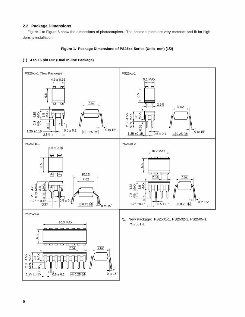
2.2 Package DimensionsFigure 1 to Figure 5 show the dimensions of photocouplers. The photocouplers are very compact and fit for high-
density installation.
Figure 1. Package Dimensions of PS25xx Series (Unit: mm) (1/2)
(1) 4 to 16 pin DIP (Dual In-line Package)
*1. New Package: PS2501-1, PS2502-1, PS2505-1,PS2561-1
5.1 MAX.
2.547.62
6.5
1.25 ±0.15 0.5 ± 0.1 M0.25
4.55
MA
X.
0 to 15°2.
8M
IN.
3.8
MA
X.
0.65
10.2 MAX.
2.54 7.62
6.5
1.25 ±0.15 0.5 ± 0.1 M0.25
4.55
MA
X.
0 to 15°
2.8
MIN
.
3.8
MA
X.
0.65
PS25xx-1PS25xx-1 (New Package)*1
PS25xx-2PS2581L1
PS25xx-4

7
Figure 1. Package Dimensions of PS25xx Series (Unit: mm) (2/2)
(2) 4 to 16 pin Lead Bending type (Gull-wing)
20.3 MAX.
1.25 ± 0.15 M0.25
3.8
MA
X.
2.54
7.62
6.5
9.6 ± 0.4 0.9 ± 0.25
0.05
to 0
.2
5.1 MAX.
2.54
7.62
1.25 ± 0.15 M0.25
3.8
MA
X.
6.5
9.6 ± 0.40.9 ± 0.25
0.05
to 0
.2
4.6 ± 0.35
6.5
1.25 ± 0.15 M0.252.54
3.8
MA
X.
7.62
9.6 ± 0.40.9 ± 0.25
0.05
to 0
.2
4.6 ± 0.35
6.5
3.8
MA
X.
1.25 ± 0.15
2.54
10.16
0.25 M
7.62
0.05
to 0
.2
0.9 ± 0.2512 MAX.
10.2 MAX.
2.54
7.62
1.25 ± 0.15 M0.25
3.8
MA
X.
6.5
9.6 ± 0.40.9 ± 0.25
0.05
to 0
.2
PS25xxL-1PS250xL-1
PS25xxL-2PS2581L2
PS25xxL-4

8
6.5
1.34 ± 0.1
0.5 ± 0.1 M0.25
4.55
MA
X.
2.8
MIN
.3.
8M
AX
.0.
65
2.54 2.54 MAX.
10.16 MAX.
6 4
1 3
7.62
0 to 15°
1.34 ± 0.1 M0.25
3.8
MA
X.
2.54 2.54 MAX.
10.16 MAX.
6 4
1 3
7.62
6.5
9.6 ± 0.40.9 ± 0.25
0.05
to 0
.210.16
0 to 15°
7.626.5
1.34 ± 0.1
0.5 ± 0.1 M0.25
4.25
MA
X.
2.8
MIN
.3.
8M
AX
.0.
35
2.54 2.54 MAX.
10.16 MAX.
6 5 4
1 2 3
2.54 1.27 MAX.
1.34 ± 0.1
1
10.16 MAX.
4.25
MA
X.
3.8
MA
X.
10.167.62
3
6 4
6.5
0.05
to 0
.2
11.8 ±0.4
0.9 ± 0.25M0.25
Figure 2. Package Dimensions of PS26xx Series (Unit: mm)
(1) 6 pin DIP (Dual In-line Package)
(2) 6 pin Lead Bending type (Gull-wing)
PS265xPS26xx
PS26xxL PS265xL2

9
7.0±0.3
4.4
0.5±0.3
1.30.
15+
0.10
–0.0
5
M0.25
2.54
2.0
2.3
MA
X.
1.2 MAX.
1 8
16 9
19.46 MAX.
0.4+0.10–0.05
0.1±
0.1
9.3 MAX.
8
7.0±0.3
4.4
0.15
+0.
10–0
.05
2.54 1.2 MAX.
2.0
2.3
MA
X. 1.3
5
1 4
0.5±0.3
M0.250.4+0.10–0.05
0.1±
0.1
Figure 3. Package Dimensions of PS27xx Series (Unit: mm)
4 to 16 pin SOP (Lead Pitch: 2.54 mm)
4.5 MAX.
4
7.0±0.3
4.40.
15+
0.10
–0.0
5
2.54 1.2 MAX.
2.0
2.3
MA
X. 1.3
3
1 2
0.5±0.3
M0.250.4+0.10–0.05
0.1±
0.1
PS27xx-2PS27xx-1
PS27xx-4

10
Figure 4. Package Dimensions of PS28xx Series (Unit: mm)
4 to 16 pin SOP (Lead Pitch: 1.27 mm)
Figure 5. Package Dimensions of PS86xx Series (Unit: mm)
(1) 8 pin DIP (Dual In-line Package) (2) 8 pin Lead Bending type (Gull-wing)
0.4 ± 0.1 M0.12
2.7 MAX.
34
21
7.0 ± 0.3
4.4
0.5 ± 0.3
0.15
+0.
10–0
.05
1.270.63 MAX.
0.1
± 0
.1
2.0
2.3
MA
X. 1.3
6.5
1.34 ± 0.1
0.5 ± 0.1
4.55
MA
X.
2.8
MIN
.3.
8M
AX
.
2.541.27 MAX.
10.16 MAX.
8
7.62
0 to 15°
0.65
5
1 4
M0.25
PS28xx-4PS28xx-1
PS86xx PS86xxL
7.0 ± 0.3
4.4
0.5 ± 0.3
1.3
0.15
+0.
10–0
.05
M0.12
1.27
2.0
2.3
MA
X.
0.63 MAX.
1 8
16 9
10.3 MAX.
0.1
± 0
.1
0.40+0.10–0.05
1.34 ± 0.1 M0.25
3.8
MA
X.
2.54 1.27 MAX.
10.16 MAX.
17.62
6.5
9.6 ± 0.4 0.9 ± 0.25
0.05
to 0
.2
4
8 5

11
2.3 StructureFigure 6 shows the internal perspective view of a photocoupler. In a light-tight epoxy resin housing, a light-
sensitive element (phototransistor or photo Darlington transistor) with light-transmittable epoxy resin medium
between them. A light signal emitted by the LED is transferred to the photosensitive transistor via the internal resin
medium.
Both the housing resin and the internal resin have the same expansion coefficient. Namely, the photocoupler
elements are molded epoxy resin.
The high isolation voltage is obtained by the long adjacent area of the inner and outer resins and identical
expansion coefficient of the inner and outer resins.
Figure 6. Internal Perspective View of Photocoupler
12
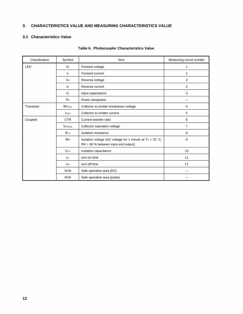
3. CHARACTERISTICS VALUE AND MEASURING CHARACTERISTICS VALUE
3.1 Characteristics Value
Table 6. Photocoupler Characteristics Value
Classification Symbol Item Measuring circuit number
LED VF Forward voltage 1
IF Forward current 1
VR Reverse voltage 2
IR Reverse current 2
Ct Input capacitance 3
PD Power dissipation
Transistor BVCEO Collector to emitter breakdown voltage 4
ICEO Collector to emitter current 5
Coupled CTR Current transfer ratio 6
VCE(sat) Collector saturation voltage 7
RI-O Isolation resistance 8
BV Isolation voltage (AC voltage for 1 minute at TA = 25 qC,
RH = 60 % between input and output).
9
CI-O Isolation capacitance 10
ton turn-on time 11
toff turn-off time 11
SOA Safe operation area (DC)
SOA Safe operation area (pulse)

13
IF
VFV
(Control input side)
3.2 Measuring Characteristics Value
Table 7. Measuring Photocoupler Characteristics Value (1/3)
Measuring
circuit
number
Characteristic value Measuring method and conditions Measuring circuit
1 Forward voltage (VF) Let a required current flow across control input
terminals and measure the voltage.
IF 10 (mA)
2 Reverse current (IR) Apply a voltage across control input terminals in a
direction opposite to normal and measure the
current.
VR 5 (V)
3 Input capacitance (Ct) Connect an LCR meter to control input terminals
and measure the electrostatic capacitance.
V 0 (V), f 1 (MHz)
4 Collector to emitter
breakdown voltage
(BVCEO)
Step up a voltage slowly across switching
terminals and measure the voltage at which a
required current begins flowing.
IL = 1 mA, IB = 0
5 Collector to emitter
current (ICEO)
Apply a required voltage across switching
terminals and measure the current.
VCEO Rated voltage (V)
IR
VR = 5 V
A
LCR meter, etc.
A
V
A
V
Semiconductormultimeter, etc.
Semiconductormultimeter, etc.
ICEO
A

14
Table 7. Measuring Photocoupler Characteristics Value (2/3)
Measuring
circuit
number
Characteristic value Measuring method and conditions Measuring circuit
6 Current transfer ratio
(CTR)
Measuring procedure: Apply the regulated
collector/emitter voltage (VCE) to the output pin of
the specimen photocoupler. Adjust the variable
power supply on the output side to measure the
collector current (ICE) when the forward current (IF)
becomes the regulated value. Produce the
Current Transfer Ratio (CTR) by the following
formula.
Current Transfer Ratio (CTR) =
Measuring conditions which should be regulated.
(1) Collector/emitter voltage (VCE)
(2) Forward current (IF)
(3) Ambient Temperature (TA)
7 Collector saturation
voltage (VCE(sat))
Measuring procedure: Flow the regulated forward
current (IF) between the input pins of the
specimen photocoupler. Adjust the variable
power supply on the output side to flow the
regulated collector current (ICE) to the outside.
Then measure the voltage between the output
pins (collector/emitter saturation voltage (VCE(sat)).
Measuring conditions which should be regulated.
(1) Forward current (IF)
(2) Collector current (ICE)
(3) Ambient Temperature (TA)
8 Isolation resistance
(RI-O)
Connect an Isolation resistance meter between
control input terminals and switching terminals,
apply a required voltage, and measure the
resistance.
VI-O 1 (kV)
Isolationresistancemeter
AVI-O
RI-O = VI-O
II-O
AA
V
RS2RS1
AA
V
RS2RS1
Collector current (A)
Forward current (A) u 100

15
Oscilloscope
VCC
RL
V1 V2
Table 7. Measuring Photocoupler Characteristics Value (3/3)
Measuring
circuit
number
Characteristic value Measuring method and conditions Measuring circuit
9 Isolation voltage (BV) AC voltage for 1 minute at TA = 25 qC,
RH = 60 % between input terminals and output
terminals.
10 Isolation capacitance
(CI-O)
Connect an LCR meter between control input
terminals and output terminals and measure the
electrostatic capacitance.
V 0 (V), f 1 (MHz)
11 turn-on time (ton)
turn-off time (toff)
Apply a rectangular wave voltage, to cause a
required current to flow across control input
terminals, and connect a load across output
terminals that satisfies a required current and
voltage. Measure the waveforms for the voltages
across control input terminals and across
switching terminals, using a time measuring
instrument like an oscilloscope, as shown at the
right.
IF 10 (mA)
RL
(to be defined)
VCC
V1
V2
td
tr tf10 %
90 %
50 %
ton toff
ts
½¾¿
ADielectricstrengthmeasuringmeter
II-O < 0.5 mA
A
V
LCR meter

16
4. MAIN CHARACTERISTICS
4.1 Current Transfer Ratio (CTR)The current transfer ratio (CTR) of a photocoupler is the ratio of the value of output current IC to the value of input
forward current IF (IC/IF u 100 %). The CTR is a parameter equivalent to the DC current amplification factor hFE of a
transistor.
The CTR is one of the most significant characteristics of photocouplers as well as isolation voltage. In circuit
designing, CTR must be considered first of all because the CTR.
1 is dependent upon forward current IF flowing through the LED.
2 is affected by ambient temperature, and
3 varies as time goes by.
4.1.1 CTR vs. IF Characteristics (I F: Forward current flowing through the LED)
The current transfer ratio (CTR) depends upon the magnitude of a forward current (IF). When IF goes lower or
higher than a proper magnitude, the CTR becomes smaller. Figure 7 to Figure 11 show the CTR vs. IF
characteristics.
Note that rate changes of CTRs are very different at low IF magnitude (approx. 5 mA), middle IF magnitude
(approx. 5 mA), and high IF magnitude (approx. 20 mA). Namely, the CTR depends heavily upon the magnitude of
forward current IF in lower and higher current ranges.

17
Figure 7. CTR vs. I F Characteristics of PS25xx Series
(1) PS2501, PS2505, PS2561, PS2565, PS2581 (2) PS2502, PS2506, PS2562, PS2566
450
400
350
300
250
200
150
100
50
00.05 0.1 0.5 1 5 10 50
CURRENT TRANSFER RATIO (CTR) vs.FORWARD CURRENT
VCE = 5 V
CT
R -
Cur
rent
Tra
nsfe
r R
atio
- %
IF - Forward Current - mA
(3) PS2503 (4) PS2521, PS2525
5
400
300
200
100
00.3 0.5 1 10 100
CURRENT TRANSFER RATIO (CTR) vs.FORWARD CURRENT
50
CTR
- C
urre
nt T
rans
fer R
atio
- %
IF - Forward Current - mA
VCE = 5 V
(5) PS2532, PS2533
CURRENT TRANSFER RATIO (CTR) vs.FORWARD CURRENT
5000
CT
R –
Cur
rent
Tra
nsfe
r R
atio
– %
0
VCE = 2 V
IF – Forward Current – mA0.1
4000
3000
2000
1000
0.5 1 5 10 20
CURRENT TRANSFER RATIO (CTR) vs.FORWARD CURRENT
8000
CT
R –
Cur
rent
Tra
nsfe
r R
atio
– %
0
1000
2000
3000
4000
5000
6000
7000VCE = 2 V
IF – Forward Current – mA0.1 0.5 1 5 10 30
CURRENT TRANSFER RATIO (CTR) vs.FORWARD CURRENT
IF – Forward Current – mA
CT
R –
Cur
rent
Tra
nsfe
r R
atio
– %
00.1
50
100
150
200
250
0.5 1 5 10 50 100
VCE = 3 V

18
Figure 8. CTR vs. I F Characteristics of PS26xx Series
(1) PS2601, PS2602, PS2605, PS2606, PS2651, PS2652 (2) PS2603, PS2604, PS2607, PS2608, PS2653, PS2654
0.5 10 500
IF – Forward Current – mA
0.50.1
CURRENT TRANSFER RATIO (CTR) vs.FORWARD CURRENT
CT
R –
Cur
rent
Tra
nsfe
r R
atio
– %
VCE = 5 V400
300
200
100
0
50
100
150
200
0.03 1 5
(3) PS2621, PS2622, PS2625, PS2626 (4) PS2631
50
00.1 0.5 1 5 10 50 100
250
200
150
100
CURRENT TRANSFER RATIO (CTR) vs.FORWARD CURRENT
IF – Forward Current – mA
CT
R –
Cur
rent
Tra
nsfe
r R
atio
– %
VCE = 3 V
(5) PS2633, PS2634
5 000
4 000
3 000
2 000
1 000
0
VCE = 2 V
IF – Forward Current – mA
CT
R –
Cur
rent
Tra
nsfe
r R
atio
– %
CURRENT TRANSFER RATIO (CTR) vs.FORWARD CURRENT
0.1 0.5 1 5 10 20
5 100.05 10.1
1000
2000
4000
5000
0
3000
50
VCE = 2 V
CURRENT TRANSFER RATIO (CTR) vs.FORWARD CURRENT
CT
R –
Cur
rent
Tra
nsfe
r R
atio
– %
IF – Forward Current – mA
240220200180160140120100
80604020
VCE = 5 V
0.1 10 1000.5 50
IF – Forward Current – mA
CURRENT TRANSFER RATIO (CTR) vs. FORWARD CURRENT
CT
R –
Cu
rre
nt
Tra
nsf
er
Ra
tio –
%
1 5

19
VCE = 2 V
CURRENT TRANSFER RATIO (CTR) vs. FORWARD CURRENT
8 000
7 000
6 000
5 000
4 000
3 000
2 000
1 000
00.1
CT
R -
Cur
rent
Tra
nsfe
r R
atio
- %
IF - Forward Current - mA
10.5 105 30
Figure 9. CTR vs. I F Characteristics of PS27xx Series
(1) PS2701, PS2705 (2) PS2702, PS2706C
TR
– C
urre
nt T
rans
fer
Rat
io –
%
CURRENT TRANSFER RATIO (CTR) vs.FORWARD CURRENT
200
IF – Forward Current – mA
0.5
100
5 100.1 1
50
150
300
50
VCE = 5 V
250
0.05
(3) PS2703, PS2707 (4) PS2732, PS2733
CT
R –
Cur
rent
Tra
nsfe
r R
atio
– %
CURRENT TRANSFER RATIO (CTR) vs.FORWARD CURRENT
300
IF – Forward Current – mA
150
50
500
250
5 10
200
VCE = 5 V
0.1 0.2
100
0.5 1 2 20
Figure 10. CTR vs. I F Characteristics of PS28xx Series
(1) PS2801, PS2805 (2) PS2802, PS2806
IF - Forward Current - mA
0.02
CT
R -
Cur
rent
Tra
nsfe
r R
atio
- %
100
CURRENT TRANSFER RATIO (CTR) vs.FORWARD CURRENT
100
200
0.1
VCE = 5 Vn = 3
10
50
150
250
300
CT
R –
Cur
rent
Tra
nsfe
r R
atio
– %
CURRENT TRANSFER RATIO (CTR) vs.FORWARD CURRENT
9000
IF – Forward Current – mA
500.05 1
6000
7000
8000
10
5000
2000
3000
4000
1000
00.1
VCE = 2 V
CT
R –
Cur
rent
Tra
nsfe
r R
atio
– %
CURRENT TRANSFER RATIO (CTR) vs.FORWARD CURRENT
5 000
0.5
IF – Forward Current – mA
1 000
200
5
2 000
3 000
4 000
0.1 1 10
VCE = 2 V

20
Figure 11. CTR vs. I F Characteristics of PS86xx Series
PS8601, PS8602
IF - Forward Current - mA
CT
R -
Cur
rent
Tra
nsfe
r R
aito
- %
CURRENT TRANSFER RATIO (CTR) vs.FORWARD CURRENT
50
40
30
20
10
00.1 0.5 1 5 10 50 100
VCC = 4.5 VVO = 0.4 VTA = 25 ˚C

21
4.1.2 CTR vs. T A Characteristics (T A: Ambient temperature)
The CTR-Temperature characteristic is greatly affected by the total characteristics of light-emission efficiency of
the LED and hFE of the phototransistor as the light-emission efficiency has a negative temperature coefficient and hFE
has a positive temperature coefficient. See Figure 12.
Figure 12. CTR vs. T A Characteristics
hFE o
f pho
totr
ansi
stor
CT
R
Ligh
t-em
issi
onef
ficie
ncy
of L
ED
TA TA TA
Figure 13 to Figure 17 show CTR vs. TA characteristics under various conditions.

22
Figure 13. CTR vs. T A Characteristics of PS25xx Series
(1) PS2501, PS2505, PS2561, PS2565, PS2581 (2) PS2502, PS2506, PS2562, PS2566
1.2
–50
NORMALIZED OUTPUT CURRENT vs.AMBIENT TEMPERATURE
1.0
0.8
0.6
0.4
0.2
0–25 0 25 50 75 100
Normalized to 1.0at TA = 25 °CIF = 5 mA, VCE = 5 V
TA - Ambient Temperature - °C
CT
R -
Nor
mal
ized
Out
put C
urre
nt∆
(3) PS2503 (4) PS2521, PS2525
–30
NORMALIZED OUTPUT CURRENT vs.AMBIENT TEMPERATURE
1.0
0.8
0.6
0.4
0.2
00 25 50 75 100
Normalized to 1.0at TA = 25 °CIF = 1 mA, VCE = 5 V
1.2
1.4
CTR
- N
orm
aliz
ed O
utpu
t Cur
rent
TA - Ambient Temperature - C
(5) PS2532, PS2533
TA – Ambient Temperature – °C
NORMALIZED OUTPUT CURRENT vs.AMBIENT TEMPERATURE
25
CT
R –
Nor
mal
ized
Out
put C
urre
nt 1.2
1.0
0.8
0.6
0.4
0.2
–50 0–25 50 75 100
∆
Normalized to 1.0at TA = 25 ˚CIF = 1 mA, VCE = 2 V
0
TA – Ambient Temperature – °C
NORMALIZED OUTPUT vs.AMBIENT TEMPERATURE
1.4
25
CT
R –
Nor
mal
ized
Out
put C
urre
nt
1.2
1.0
0.8
0.6
0.4
0.2
–50 0–25 50 75 100
Normalized to 1.0at TA = 25 oCIF = 1 mAVCE = 2 V
NORMALIZED OUTPUT CURRENT vs.AMBIENT TEMPERATURE
TA – Ambient Temperature – °C
CT
R –
Nor
mal
ized
Out
put C
urre
nt
0–55
0.2
0.4
0.6
0.8
1.0
1.2
1.4
–25 0 25 50 75 100
Normalized to 1.0at TA = 25 °CIF = 100 mA, VCE = 3 V

23
Figure 14. CTR vs. T A Characteristics of PS26xx Series
(1) PS2601, PS2602, PS2605, PS2606, PS2651, PS2652 (2) PS2603, PS2604, PS2607, PS2608, PS2653, PS2654
NORMALIZED OUTPUT CURRENT vs.AMBIENT TEMPERATURE
25 50 75 100–55
TA – Ambient Temperature – ˚C
0.2
0.6
1.0
1.2
∆CT
R –
Nor
mal
ized
Out
put C
urrr
ent
Normalized to 1.0at TA = 25 ˚CIF = 5 mA, VCE = 5 V
0–250
0.4
0.8
(3) PS2621, PS2622, PS2625, PS2626 (4) PS2631
NORMALIZED OUTPUT CURRENT vs.AMBIENT TEMPERATURE
–55
TA – Ambient Temperature – ˚C
∆CT
R –
Nor
mal
ized
Out
put C
urre
nt
Normalized to 1.0at TA = 25 ˚CIF = 100 mA, VCE = 3 V
0–25 0 25 50 75 100
0.2
0.4
0.6
0.8
1.0
1.2
1.4
(5) PS2633, PS2634
1.2
1.0
0.8
0.6
0.4
0.2
0–50 –25 0 25 50 75 100
Normalized to 1.0at TA = 25 ˚CIF = 1 mA, VCE = 2 V
TA – Ambient Temperature – ˚C
∆CT
R –
Nor
mal
ized
Out
put C
urre
nt
NORMALIZED OUTPUT CURRENT vs.AMBIENT TEMPERATURE
NORMALIZED OUTPUT CURRENT vs.AMBIENT TEMPERATURE
25 50 75 100–55
TA – Ambient Temperature – ˚C
0.2
0.6
1.0
1.2
∆CT
R –
Nor
mal
ized
Out
put C
urre
nt
Normalized to 1.0at TA = 25 ˚CIF = 1 mA, VCE = 2 V
0–250
0.4
0.8
NORMALIZED OUTPUT CURRENT vs.AMBIENT TEMPERATURE
1.6
1.4
1.2
1.0
0.8
0.6
0.4
0.2
–50 –25 0 25 50 75 100
Normalized to 1.0at TA = 25 ˚CIF = 5 mAVCE = 5 V
TA – Ambient Temperature – ˚C
∆CT
R –
Nor
mal
ized
Out
put C
urre
nt

24
NORMALIZED OUTPUT vs.AMBIENT TEMPERATURE
1.4
1.2
1.0
0.8
0.6
0.4
0.2
–50 –25 0 25 50 75 100
Normalized to 1.0at TA = 25 ˚CIF = 1 mAVCE = 2 V
CT
R -
Nor
mal
ized
Out
put C
urre
nt
TA - Ambient Temperature - ˚C
∆
Figure 15. CTR vs. T A Characteristics of PS27xx Series
(1) PS2701, PS2705 (2) PS2702, PS2706
CT
R –
Nor
mal
ized
Out
put C
urre
nt
1.2
1000
0.2
–25 0 50 75
0.6
1.0
–55
0.4
0.8
25
Normalized to 1.0at TA = 25 °CIF = 5 mA, VCE = 5 V
NORMALIZED OUTPUT CURRENT vs.AMBIENT TEMPERATURE
TA – Ambient Temperature – °C
(3) PS2703, PS2707 (4) PS2732, PS2733
CT
R –
Nor
mal
ized
Out
put C
urre
nt
NORMALIZED OUTPUT CURRENT vs.AMBIENT TEMPERATURE
1.2
TA – Ambient Temperature – °C
1000
0.2
–25 0 50 75
0.6
1.0
–55
0.4
0.8
25
Normalized to 1.0at TA = 25 °CIF = 5 mA, VCE = 5 V
Figure 16. CTR vs. T A Characteristics of PS28xx Series
(1) PS2801, PS2805 (2) PS2802, PS2806
TA - Ambient Temperature - ˚C
CT
R -
Nor
mal
ized
Out
put C
urre
nt
–500
0.6
0 100
NORMALIZED OUTPUT CURRENT vs.AMBIENT TEMPERATURE
1.2
Normalized to 1.0at TA = 25 °CIF = 5 mA, VCE = 5 V
–25 25 50 75
0.2
0.4
1.0
0.8
∆
CT
R –
Nor
mal
ized
Out
put C
urre
nt
NORMALIZED OUTPUT CURRENT vs.AMBIENT TEMPERATURE
TA – Ambient Temperature – °C
0.6
1000
1.2
–25 50
0.8
1.0
0
Normalized to 1.0at TA = 25 °CIF = 1 mA, VCE = 2 V
0.4
0.2
–55 25 75
CT
R –
Nor
mal
ized
Out
put C
urre
nt
NORMALIZED OUTPUT CURRENT vs.AMBIENT TEMPERATURE
TA – Ambient Temperature – °C
0.6
0.2
100–50 –25 25
0.8
1.2
0 75
1.0
0.4
50
Normalized to 1.0at TA = 25 °CIF = 1 mA, VCE = 2V
0

25
Figure 17. CTR vs. T A Characteristics of PS86xx Series
PS8601, PS8602 C
TR
-N
orm
aliz
ed O
utpu
t Cur
rent
TA - Ambient Temperature - ˚C
NORMALIZED OUTPUT CURRENT vs.AMBIENT TEMPERATURE
Normalized to at TA = 25 ˚CVCC = 4.5 VVO = 0.4 VIF = 16 mA
–75 –50 –20 0 25 50 75 100 125
2.0
1.8
1.6
1.4
1.2
1.0
0.8
0.6
0.4
0.2
0.0
∆

26
4.1.3 Long Term CTR Degradation
The current transfer ratio (CTR) of a photocoupler is determined by the light-emission efficiency of the LED
(emitting infrared light), efficiency of light transmission between the LED and the phototransistor, light sensitivity of
the phototransistor, and hFE of the transistor.
The change of a CTR over time is mainly caused by the reduction of the light-emission efficiency of the LED.
Generally, the CTR is reduced to a greater extent as the forward current (IF) increases or as the operating
temperature increase. Figure 18 respectively shows estimated changes of CTRs of PS25xx, PS26xx, PS27xx,
PS28xx and PS86xx photocouplers over time.
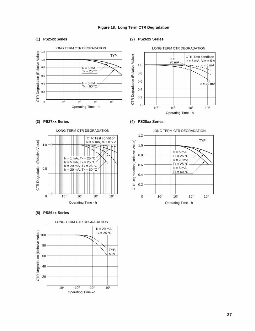
27
LONG TERM CTR DEGRADATION
Operating Time - h
0
0.2
1.0
102
0.6
103 104 105
CT
R D
egra
datio
n (R
elat
ive
Val
ue)
0.8
0.4
CTR Test conditionIF = 5 mA, VCE = 5 V
IF = 5 mA
IF = 40 mA
IF = 20 mA
Figure 18. Long Term CTR Degradation
(1) PS25xx Series (2) PS26xx Series
1.0
0.8
0.6
0.4
0.2
0 105
LONG TERM CTR DEGRADATION
IF = 5 mATA = 25 °C
IF = 5 mATA = 60 °C
104103102
1.2
TYP.
Operating Time - h
CT
R D
egra
datio
n (R
elat
ive
Val
ue)
(3) PS27xx Series (4) PS28xx Series
CT
R D
egra
datio
n (R
elat
ive
Val
ue)
LONG TERM CTR DEGRADATION
1.0
Operating Time - h
0.5
0 102 103 104 105
IF = 1 mA, TA = 25 °CIF = 5 mA, TA = 25 °CIF = 20 mA, TA = 25 °CIF = 20 mA, TA = 60 °C
CTR Test conditionIF = 5 mA, VCE = 5 V
(5) PS86xx Series
100
80
60
40
20
102
Operating Time –h
IF = 20 mATA = 25 °C
TYP.MIN.
103 104 105
CT
R D
egra
datio
n (R
elat
ive
Val
ue)
LONG TERM CTR DEGRADATION
LONG TERM CTR DEGRADATION
Operating Time - h
0.6
1.2C
TR
Deg
rada
tion
(Rel
ativ
e V
alue
)
0 102
1.0
TYP.
0.8
0.2
0.4
103 104 105
IF = 5 mATA = 25 °CIF = 20 mATA = 25 °CIF = 5 mATA = 60 °C

28
4.2 Response CharacteristicsThe response characteristics of photocouplers are the same as those of phototransistors. The fall time tf is
expressed by
tfv RL hFE CCB
RL : Load resistance
hFE : Amplification factor
CCB : Collector-base capacitance
If RL is too high, tf becomes too high to be fit for high-speed signal transmission. Select the proper load resistance
for the desired signal rate. Similarly, the collector current must fully satisfy the minimum value of the CTR, CTR vs.
TA characteristics, and CTR vs. time characteristics. Otherwise, the phototransistor will operate unsaturated, causing
lower response characteristics and malfunction.
Figure 19. Test Circuit for Response-time
Pulse input
Monitor(input)
PW = 100 sDuty cycle = 1/10
µ IF
51 Ω RL
VO (Output)
VCC
tontoff
90 %
10 %
ts
tftr
td
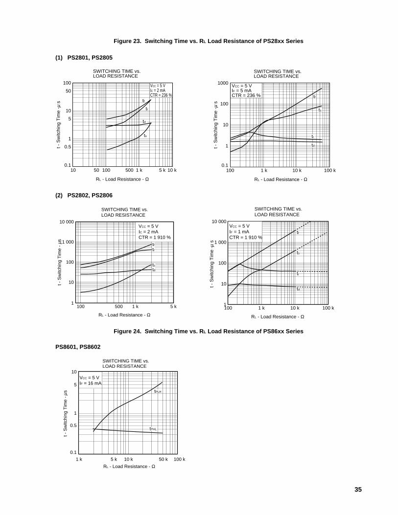
Figure 20 to Figure 24 show the response time vs. the load resistance which show four CTR parameters.
29
SWITCHING TIME vs.LOAD RESISTANCE
RL – Load Resistance – Ω
t – S
witc
hing
Tim
e –
s
150
µ
5
10
50
100
100 500 1 k 2 k
toff
ton
trtf
VCC = 10 VIC = 2 mA
500
50
t – S
witc
hing
Tim
e –
sµ
RL – Load Resistance – Ω1 k300
10
100
1000
5000
10000
5 k 10 k 50 k
VCC = 5 VIF = 1 mACTR = 2280 %
td
tr
ts
tf
SWITCHING TIME vs. LOAD RESISTANCE
Figure 20. Switching Time vs. R L Load Resistance of PS25xx Series (1/2)
(1) PS2501, PS2505, PS2561, PS2565, PS2581
1 000
SWITCHING TIME vs. LOAD RESISTANCE
100
10
1100 k50 k10 k5k1 k500100
IF = 5 mAVCC = 5 VTA = 25 °CCTR 290 %
ts
td
tr
tf
t - S
witc
hing
Tim
e -
sµ
RL - Load Resistance - Ω
(2) PS2502, PS2506, PS2562, PS2566
SWITCHING TIME vs.LOAD RESISTANCE
1000
500
100
50
10
5
2
t – S
witc
hing
Tim
e –
sµ
RL – Load Resistance – Ω10050 500 1 k 5 k
VCC = 5 VIC = 2 mACTR = 2280 %
tftr
td
ts
(3) PS2503 (4) PS2521, PS2525
50
SWITCHING TIME vs. LOAD RESISTANCE
10
1
0.110 k5 k1 k5001005010
IC = 2 mAVCC = 10 VTA = 25 °CCTR 290 %
tftr
td
ts
t - S
witc
hing
Tim
e -
s
RL - Load Resistance - Ω
µ
50
SWITCHING TIME vs.LOAD RESISTANCE
10
1
10 k5 k1 k500100
tf
tr
td
100 k50 k
0.5
5
ts
IF = 1 mA, VCC = 5 VSample : CTR 209 %at IF = 1 mA
0.1
µt -
Sw
itchi
ng T
ime
- s
RL - Load Resistance - Ω

30
Figure 20. Switching Time vs. R L Load Resistance of PS25xx Series (2/2)
(5) PS2532, PS2533
SWITCHING TIME vs.LOAD RESISTANCE
300
t – S
witc
hing
Tim
e –
sµ
RL – Load Resistance – Ω20
VCC = 10 V, IC = 10 mAPulse Width = 5 msDuty Cycle = 1/2
100
50
10
1
5
50 100 500 1 k 2 k
tr
td
tf
ts

31
Figure 21. Switching Time vs. R L Load Resistance of PS26xx Series (1/2)
(1) PS2601, PS2602, PS2605, PS2606, PS2651, PS2652
SWITCHING TIME vs.LOAD RESISTANCE
500 1 k 5 k 10 k
RL – Load Resistance – Ω
1
5
50
100
t – S
witc
hing
Tim
e –
s
100
0.5
10
µ
VCC = 10 VIC = 2 mATA = 25 ˚CSampleCTR = 290 %
tr
ts
tstd
(2) PS2603, PS2604, PS2607, PS2608, PS2653, PS2654 (3) PS2621, PS2622, PS2625, PS2626
SWITCHING TIME vs.LOAD RESISTANCE
RL – Load Resistance – Ω
t – S
witc
hing
Tim
e –
s
VCC = 10 VIC = 2 mA
50 100 500 1 k 2 k10
2000
1000
500
100
50
ton
toff
tf
tr
µ
SWITCHING TIME vs.LOAD RESISTANCE
1 k 5 k 10 k 50 k100
RL – Load Resistance – Ω
5
10
500
1000
t – S
witc
hing
Tim
e –
s
500
100
µ
IF = 5 mA, VCC = 5 VTA = 25 ˚CSampleCTR = 290 %
ts
tr
tf
50
td
SWITCHING TIME vs.LOAD RESISTANCE
RL – Load Resistance – Ω
t – S
witc
hing
Tim
e –
s
VCC = 10 VIC = 2 mA
50 100 500 1 k 2 k
100
ton
toff
tf
tr
µ
50
10
5
1

32
Figure 21. Switching Time vs. R L Load Resistance of PS26xx Series (2/2)
(4) PS2631 (5) PS2633, PS2634
tf
ts
td
tr
IF = 10 mAVCC = 5 V
SWITCHING TIME vs.LOAD RESISTANCE
RL – Load Resistance – Ω
1 k 5 k 10 k 50 k100 k
1000
100
10
1
t – S
witc
hing
Tim
e –
s
µ
300
100
50
10
5
120 50 100 500 1 k 2 k
ts
tf
td
trVCC = 10 V, IC = 10 mAPulse Width = 5 msDuty Cycle = 1/2
RL – Load Resistance – Ωt –
Sw
itchi
ng T
ime
– sµ
SWITCHING TIME vs.LOAD RESISTANCE

33
SWITCHING TIME vs.LOAD RESISTANCE
1000
RL – Load Resistance – Ω
100k
0.51
500 1 k 5 k 50 k
10
100
100
5
50
500
td
IF = 5 mAVCC = 5 VTA = 25 °CCTR = 90 %
10 k
t – S
witc
hing
Tim
e –
sµ
tr
ts
tf
Figure 22. Switching Time vs. R L Load Resistance of PS27xx Series (1/2)
(1) PS2701, PS2705
SWITCHING TIME vs.LOAD RESISTANCE
RL – Load Resistance – Ω
10
2 k
100
100
50
500
VCC = 5 VIC = 2 mA
5
50
ton
t – S
witc
hing
Tim
e –
sµ
toff
td
ts
1 k
0.5
1
(2) PS2702, PS2706
t – S
witc
hing
Tim
e –
s
SWITCHING TIME vs.LOAD RESISTANCE
1 000
RL – Load Resistance – Ω
5 k2
100 500
100
50
500
50
10
5
1 k
VCC = 5 VIC = 2 mACTR = 2 200 %
µ tr
tftd
ts
(3) PS2703, PS2707
SWITCHING TIME vs.LOAD RESISTANCE
RL – Load Resistance – Ω
1
10 k
100
100
10
1 k
VCE = 10 VIC = 2 mA
0.110
td
ts
tr
tf
t – S
witc
hing
Tim
e –
sµ
SWITCHING TIME vs.LOAD RESISTANCE
1000
RL – Load Resistance – Ω
100 k
0.51
500 1 k 5 k 50 k
10
100
100
5
50
500IF = 5 mAVCC = 5 VTA = 25 °CCTR = 100 %
10 k
ts
tdtr
tf
t – S
witc
hing
Tim
e –
sµt –
Sw
itchi
ng T
ime
– s
5 000
RL – Load Resistance – Ω
100 k0.5
1 k 10 k
100
1 000
100
10
VCC = 5 VIF = 1 mATA = 25 °CCTR = 2 200 %
1
µ
SWITCHING TIME vs.LOAD RESISTANCE
tr
tf
td
ts

34
Figure 22. Switching Time vs. R L Load Resistance of PS27xx Series (2/2)
(4) PS2732, PS2733
t – S
witc
hing
Tim
e –
s
SWITCHING TIME vs. LOAD RESISTANCE
300
100
RL – Load Resistance – Ω
2 k20
100
50
10
5
1
µ
50 1 k500
tr
td
tf
ts
VCC = 10 V, IC = 10 mAPulse Width = 5 msDuty Cycle = 1/2
35
Figure 23. Switching Time vs. R L Load Resistance of PS28xx Series
(1) PS2801, PS2805
RL - Load Resistance - Ω
0.110 50
SWITCHING TIME vs.LOAD RESISTANCE
100
50
t - S
witc
hing
Tim
e -
sµ
100 500 1 k 5 k 10 k
10
5
1
0.5
tf
ts
tr
td
VCC = 5 VIC = 2 mACTR = 236 %
(2) PS2802, PS2806
10 000
1 000
100
10
1
SWITCHING TIME vs.LOAD RESISTANCE
t - S
witc
hing
Tim
e -
s
RL - Load Resistance - Ω
100 500 1 k 5 k
trtf
tdts
µ
VCC = 5 VIC = 2 mACTR = 1 910 %
Figure 24. Switching Time vs. R L Load Resistance of PS86xx Series
PS8601, PS8602
tf
ts
tr
td
100 1 k 10 k 100 k0.1
1
10
100
1000
t - S
witc
hing
Tim
e -
sµ
SWITCHING TIME vs.LOAD RESISTANCE
VCC = 5 VIF = 5 mACTR = 236 %
RL - Load Resistance - Ω
RL - Load Resistance - Ω
t - S
witc
hing
Tim
e -
s
SWITCHING TIME vs. LOAD RESISTANCE
VCC = 5 VIF = 16 mA
10
5
1
0.5
0.1
1 k 5 k 10 k 50 k 100 k
tPLH
tPHL
µ
tf
ts
tr
td
SWITCHING TIME vs.LOAD RESISTANCE
t - S
witc
hing
Tim
e -
s
RL - Load Resistance - Ω
VCC = 5 VIF = 1 mACTR = 1 910 %
100 1 k 10 k 100 k
10 000
1 000
100
10
1
µ

36
5. APPLICATIONS
5.1 Power Supply Example
ZAC Input
Input Rectifier
Power MOS FET
VaristorNV( )270D( )
Thyristor5P4M-6M
+
+
Control IC PC1099µ
PhotocouplerPS2501-1
Error Amplifier PC1093µ
MicroComputer
Peak Hold IC
VCR Power Supply
Nicd Battery+
Output Rectifier
Power SW(Relay or Power MOS FET)
Recommended devices
Part number Function
PS2501-1
PS2561-1
PS2581L1-1
PS2581L2-1
PS2701-1
PS2703-1
PS2801-1
PS8601
PS8602
Feedback circuit

37
5.2 Telephone Example
LINE
Bell Ringing Signal(75 Vr.m.s., 16 Hz) PS2501, PS2505
PS2701, PS2705PS2703, PS2707PS2801, PS2805etc.
Bell Ringing Detect
VCC
VCC
Line Observe
Dial PulseGenerator
Dialer Circuit
IN
OUT
CPU
OCMOS FETPS7141-1C
Speech Circuit
PS2532, PS2533PS2732, PS2733
PS2521PS2525
Recommended devices
Part number Function
PS2501-1, PS2505-1
PS2701-1, PS2703-1
PS2705-1, PS2707-1
PS2801-1, PS2805-1
Bell ringing detector
PS2521-1, PS2525-1
PS2621, PS2622
PS2625, PS2626
Line observer
PS2532-1, PS2533-1
PS2633, PS2634
PS2732-1, PS2733-1
Dial pulse generator

38
5.3 PC Card/Modem/Facsimile Example
Ring
TIP
Telecom.Network
ModulatorDemodulator
Loopcurrentdetector
Ring signaldetector
line“ON” “OFF”
line“ON” “OFF”
Dialpulse Hook
Switch
Switching Device: Signal circuit On/OffPS7141/42-1A/2A
Pulse Generator
CPU (NCU controller)
PS2505-1/2Isolator b/w Signal Circuit and CPU:Control signal transfer to CPU w/o Noise
Recommended devices
Part number Function
PS2501-1, PS2505-1
PS2701-1, PS2703-1
PS2705-1, PS2707-1
PS2801-1, PS2805-1
Bell ringing detector
PS2521-1, PS2525-1
PS2621, PS2625
PS2622, PS2626
Line observer

39
5.4 Programmable Controller Example
PD4050µ
PS2801 - 4
COM
Recommended devices
Part number Function
PS2501-1, -2, -4, PS2502-1, -2, -4
PS2505-1, -2, -4, PS2506-1, -2, -4
PS2701-1, -2, -4, PS2702-1, -2, -4
PS2703-1, -2, -4, PS2705-1, -2, -4
PS2706-1, -2, -4, PS2707-1, -2, -4
PS2801-1, -4, PS2802-1, -4
PS2805-1, -4
Input side isolation
PS2501-1, -2, -4, PS2502-1, -2, -4
PS2701-1, -2, -4, PS2702-1, -2, -4
PS2703-1, -2, -4
PS2801-1, -4, PS2802-1, -4
Output side isolation

40
5.5 Solid State Relay Example
AC 100 V
Load
Recommended devices
Part number Function
PS2501-1
PS2601
PS2602
PS2701-1
PS2703-1
Tr. trigger circuit

41
5.6 Inverter Conditioner Example
M
MMMM M
fan
mot
or
heat
er
ACse
rg o
fab
sorb
er
motor
Photocoupler
indoor-outdoorcommunication
M
PS8602-6pcs
INVERTER CIRCUIT
sens
or o
f ove
r cu
rren
t
steping motor fan motor
8/16 bitmicrocomputer
8/16 bitmicrocomputer
valve valve
PS2501
left right up down
steping motor
left right
volta
ge r
ectif
ucat
ion
circ
uit
Indoor UnitOutdoor Unit
Recommended devices
Part number Function
PS2501-1
PS2505-1
PS2701-1
PS2703-1
PS2705-1
PS2706-1
Interface indoor and outdoor units
PS8602 Inverter circuit drives
PS2501-1 IPM Controls

42
5.7 Computer and Peripheral Equipment Example
CPU Peripharal equipment
Recommended devices
Part number Function
PS2501-1
PS2601
PS8601
PS8602
Noise protection

43
6. CONCLUSION
Demand for photocouplers featuring higher insulation and noise elimination is steadily increasing. At the same
time, various problems (change of characteristics by ambient temperature and time elapse) will occur in their circuit
design. We hope this manual will be helpful in solving such problems.

44
[MEMO]