Digital Dice - AN-CM-292 - Renesas
11
Application Note Digital Dice AN-CM-292 Abstract This application note describes how to design a true random number generator from 1 to 6 with a 7-segment 1-digit LED display. The device is designed to replace commonly used dice. This application note comes complete with design files which can be found in the References section.
-
Upload
khangminh22 -
Category
Documents
-
view
3 -
download
0
Transcript of Digital Dice - AN-CM-292 - Renesas

Application Note
Digital Dice
AN-CM-292
Abstract
This application note describes how to design a true random number generator from 1 to 6 with a 7-segment 1-digit LED display. The device is designed to replace commonly used dice. This application note comes complete with design files which can be found in the References section.

AN-CM-292
Digital Dice
Application Note Revision 1.0 04-Feb-2020
CFR0014 2 of 10 © 2022 Renesas Electronics Corporation
Contents
Abstract ................................................................................................................................................ 1
Contents ............................................................................................................................................... 2
Figures .................................................................................................................................................. 2
Tables ................................................................................................................................................... 2
1 Terms and Definitions ................................................................................................................... 3
2 References ..................................................................................................................................... 3
3 Introduction .................................................................................................................................... 4
4 Device Architecture ....................................................................................................................... 4
4.1 Entropy Generator ................................................................................................................. 4
4.2 Linear Feedback Shift Register ............................................................................................. 5
4.3 Binary to 7-Segment Decoder ............................................................................................... 5
4.4 Control Unit ........................................................................................................................... 6
4.5 Macrocell Settings ................................................................................................................. 7
5 Conclusions ................................................................................................................................... 9
Revision History ................................................................................................................................ 10
Figures
Figure 1: Digital Dice Schematic Diagram ............................................................................................. 4 Figure 2: GreenPAK6 Designer Project ................................................................................................ 4 Figure 3: Entropy Generator .................................................................................................................. 5 Figure 4: LFSR ...................................................................................................................................... 5 Figure 5: Binary to 7 Segment Decoder ................................................................................................ 6 Figure 6: Control Unit ............................................................................................................................ 6
Tables
Table 1. LUT Settings ............................................................................................................................ 7 Table 2: DFF Settings ............................................................................................................................ 7 Table 3: CNT/DLY Settings ................................................................................................................... 7 Table 4: FILTER Settings ...................................................................................................................... 8 Table 5: P DLY Settings ........................................................................................................................ 8 Table 6: OSC Settings ........................................................................................................................... 8 Table 7: PIN Settings ............................................................................................................................. 8

AN-CM-292
Digital Dice
Application Note Revision 1.0 04-Feb-2020
CFR0014 3 of 10 © 2022 Renesas Electronics Corporation
1 Terms and Definitions
DFF D-type Flip Flop
LED Light-emitting diode
LFSR Linear feedback shift register
LUT Lookup table
2 References
For related documents and software, please visit:
https://www.dialog-semiconductor.com/products/greenpak.
Download our free GreenPAK™ Designer software [1] to open the .gp files [2] and view the proposed circuit design. Use the GreenPAK development tools [3] to freeze the design into your own customized IC in a matter of minutes. Find out more in complete library of application notes [4] featuring design examples as well as explanations of features and blocks within the GreenPAK IC.
[1] GreenPAK Designer Software, Software Download, and User Guide
[2] AN-CM-292 Digital Dice.gp, GreenPAK Design File
[3] GreenPAK Development Tools, GreenPAK Development Tools Webpage
[4] GreenPAK Application Notes, GreenPAK Application Notes Webpage
[5] SLG46826V, Datasheet
[6] AN-1200 True Random Number Generator Hardware Author: Nazar Sliunchenko
AN-CM-292
Digital Dice
Application Note Revision 1.0 04-Feb-2020
CFR0014 4 of 10 © 2022 Renesas Electronics Corporation
3 Introduction
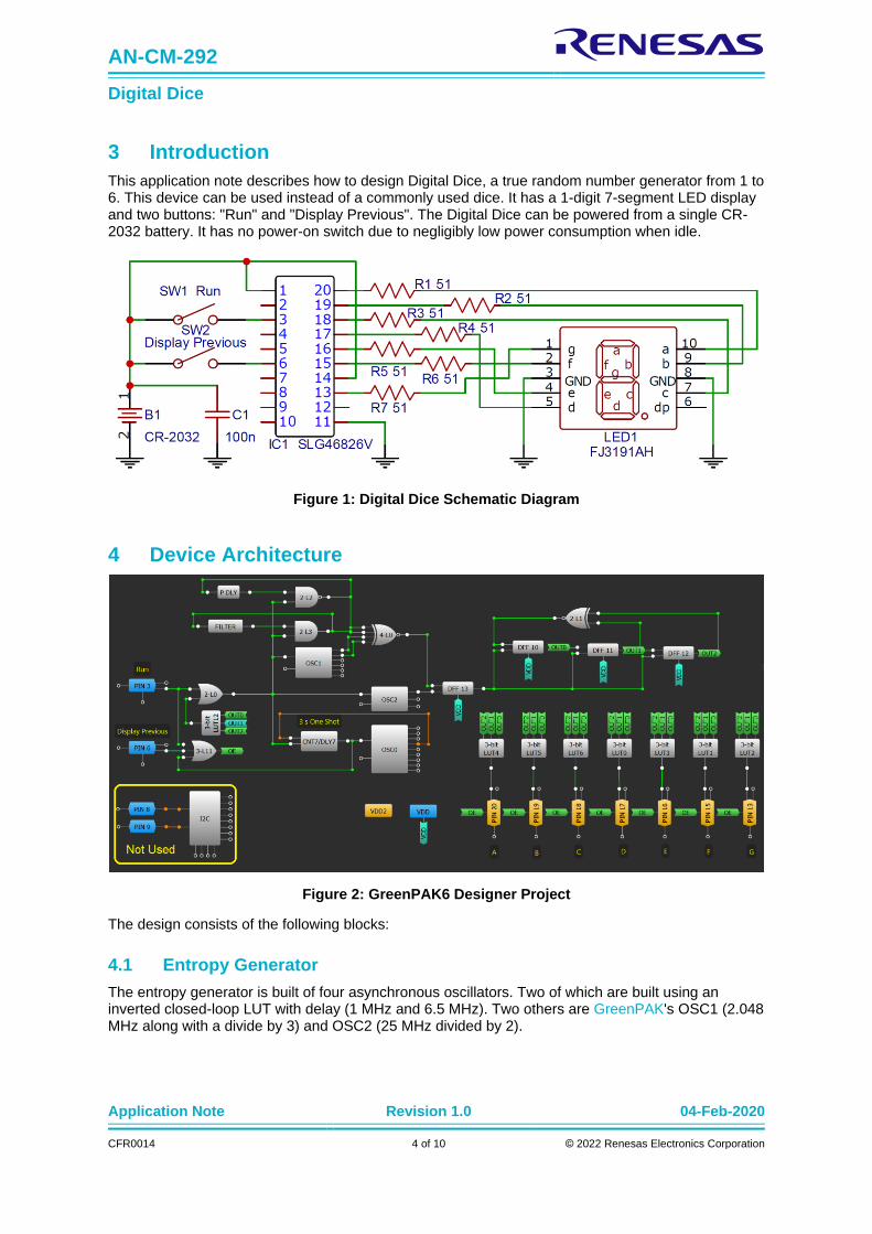
This application note describes how to design Digital Dice, a true random number generator from 1 to 6. This device can be used instead of a commonly used dice. It has a 1-digit 7-segment LED display and two buttons: "Run" and "Display Previous". The Digital Dice can be powered from a single CR-2032 battery. It has no power-on switch due to negligibly low power consumption when idle.
Figure 1: Digital Dice Schematic Diagram
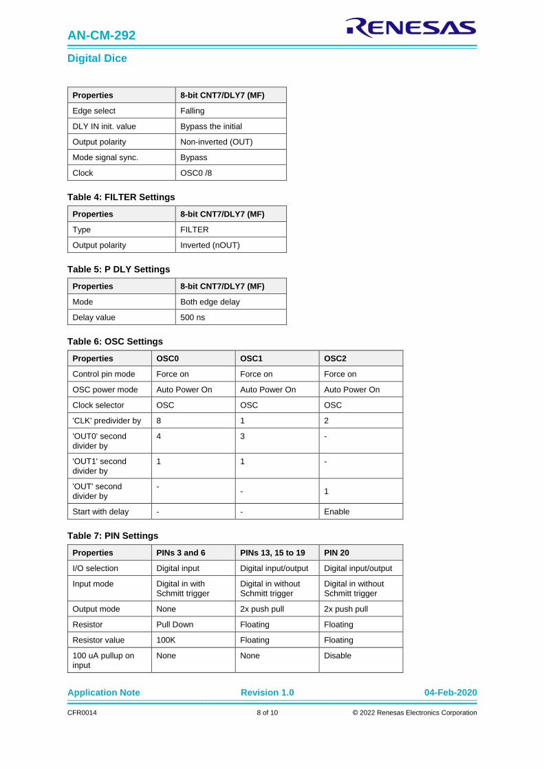
4 Device Architecture
Figure 2: GreenPAK6 Designer Project
The design consists of the following blocks:
4.1 Entropy Generator
The entropy generator is built of four asynchronous oscillators. Two of which are built using an inverted closed-loop LUT with delay (1 MHz and 6.5 MHz). Two others are GreenPAK's OSC1 (2.048 MHz along with a divide by 3) and OSC2 (25 MHz divided by 2).

AN-CM-292
Digital Dice
Application Note Revision 1.0 04-Feb-2020
CFR0014 5 of 10 © 2022 Renesas Electronics Corporation
Inputting a few asynchronous clock signals to XNOR gate is enough to get an unpredictable signal on its output (noise or entropy). But the macrocells within the SLG46826V allow making even more complicated solutions. Using one more oscillator and DFF we get a completely random signal.
Figure 3: Entropy Generator
4.2 Linear Feedback Shift Register
The 3-bit LFSR is built using three DFFs and one XNOR gate. This block with each input clock generates a 3-bit pseudo-random number. Here, instead of a clock pulse, the noise signal goes into the LFSR's input, generating a true random 3-bit number.
Figure 4: LFSR
4.3 Binary to 7-Segment Decoder
In order to convert the 3-bit random number generated by the LSFR, the Binary to 7-segment decoder is used, see Figure 3. The decoder is built of 3-bit LUTs.

AN-CM-292
Digital Dice
Application Note Revision 1.0 04-Feb-2020
CFR0014 6 of 10 © 2022 Renesas Electronics Corporation
Figure 5: Binary to 7 Segment Decoder
4.4 Control Unit
The control unit is a part of the device designed to start it and stop after the 3-second period. Two pins are configured as inputs and two buttons must be connected from VDD to those pins. While the button "Run" is pressed, the device continuously generates random numbers. Right after the button is released, the generation stops and LFSR latches its outputs. The decoder subsequently drives a 7-segment display. After a 3 second period, the Digital Dice goes idle. The device is still powered on, but because all oscillations have been turned off, the current consumption is extremely low. This allows the device to "remember" the last generated random number. If the button "Display Previous" is pressed, the last generated random number will be displayed until the button is released. Because Digital Dice is designed to replace usual dice, the 3-bit LUT12 is used to restart it when "0" or "7" occurs. This ensures the device will generate a random number in the range of 1 to 6.
Figure 6: Control Unit

AN-CM-292
Digital Dice
Application Note Revision 1.0 04-Feb-2020
CFR0014 7 of 10 © 2022 Renesas Electronics Corporation
4.5 Macrocell Settings
For each macrocell, settings refer to the tables below.
Table 1. LUT Settings
IN3
IN2
IN1
IN0
2-b
it L
UT
0 O
UT
2-b
it L
UT
1 O
UT
2-b
it L
UT
2 O
UT
2-b
it L
UT
3 O
UT
3-b
it L
UT
0 O
UT
3-b
it L
UT
1 O
UT
3-b
it L
UT
2 O
UT
3-b
it L
UT
3 O
UT
3-b
it L
UT
4 O
UT
3-b
it L
UT
5 O
UT
3-b
it L
UT
6 O
UT
3-b
it L
UT
11 O
UT
3-b
it L
UT
12 O
UT
4-b
it L
UT
0 O
UT
0 0 0 0 0 1 1 0 0 0 0 0 0 0 0 0 1 1
0 0 0 1 1 0 1 0 0 0 0 0 0 1 1 1 0 0
0 0 1 0 1 0 1 0 1 0 1 1 1 1 0 1 0 0
0 0 1 1 1 1 0 1 1 0 1 0 1 1 1 1 0 1
0 1 0 0 - - - - 0 1 1 0 0 1 1 1 0 0
0 1 0 1 - - - - 1 1 1 0 1 0 1 1 0 1
0 1 1 0 - - - - 1 1 1 1 1 0 1 1 0 1
0 1 1 1 - - - - 0 0 0 0 0 0 0 1 1 0
1 0 0 0 - - - - - - - - - - - - - 0
1 0 0 1 - - - - - - - - - - - - - 1
1 0 1 0 - - - - - - - - - - - - - 1
1 0 1 1 - - - - - - - - - - - - - 0
1 1 0 0 - - - - - - - - - - - - - 1
1 1 0 1 - - - - - - - - - - - - - 0
1 1 1 0 - - - - - - - - - - - - - 0
1 1 1 1 - - - - - - - - - - - - - 1
Table 2: DFF Settings
Properties DFFs 10, 11, 12, 13
Multi-function mode DFF/LATCH
Mode DFF
nSET/nRESET option nRESET
Initial polarity Low
Q output polarity Non-Inverted (Q)
Table 3: CNT/DLY Settings
Properties 8-bit CNT7/DLY7 (MF)
Multi-function mode CNT/DLY
Mode One shot
Counter data 95
AN-CM-292
Digital Dice
Application Note Revision 1.0 04-Feb-2020
CFR0014 8 of 10 © 2022 Renesas Electronics Corporation
Properties 8-bit CNT7/DLY7 (MF)
Edge select Falling
DLY IN init. value Bypass the initial
Output polarity Non-inverted (OUT)
Mode signal sync. Bypass
Clock OSC0 /8
Table 4: FILTER Settings
Properties 8-bit CNT7/DLY7 (MF)
Type FILTER
Output polarity Inverted (nOUT)
Table 5: P DLY Settings
Properties 8-bit CNT7/DLY7 (MF)
Mode Both edge delay
Delay value 500 ns
Table 6: OSC Settings
Properties OSC0 OSC1 OSC2
Control pin mode Force on Force on Force on
OSC power mode Auto Power On Auto Power On Auto Power On
Clock selector OSC OSC OSC
'CLK' predivider by 8 1 2
'OUT0' second
divider by 4 3 -
'OUT1' second
divider by 1 1 -
'OUT' second
divider by -
- 1
Start with delay - - Enable
Table 7: PIN Settings
Properties PINs 3 and 6 PINs 13, 15 to 19 PIN 20
I/O selection Digital input Digital input/output Digital input/output
Input mode Digital in with
Schmitt trigger
Digital in without
Schmitt trigger
Digital in without
Schmitt trigger
Output mode None 2x push pull 2x push pull
Resistor Pull Down Floating Floating
Resistor value 100K Floating Floating
100 uA pullup on
input None None Disable

AN-CM-292
Digital Dice
Application Note Revision 1.0 04-Feb-2020
CFR0014 9 of 10 © 2022 Renesas Electronics Corporation
5 Conclusions
The Digital Dice can be used as a replacement of usual dice in casinos or when playing any other games where dice are needed. It has an entropy generator that is constantly generating 3-bit random numbers while the button "Run" is pressed. It stops and displays the result only when the button is released, so the human factor also affects the generated random number. Four asynchronous oscillators together with human button push variability make the device completely and desirably unpredictable.

AN-CM-292
Digital Dice
Application Note Revision 1.0 04-Feb-2020
CFR0014 10 of 10 © 2022 Renesas Electronics Corporation
Revision History
Revision Date Description
1.0 04-Feb-2020 Initial Version

Corporate HeadquartersTOYOSU FORESIA, 3-2-24 Toyosu,Koto-ku, Tokyo 135-0061, Japanwww.renesas.com
Contact InformationFor further information on a product, technology, the most up-to-date version of a document, or your nearest sales office, please visit:www.renesas.com/contact/
TrademarksRenesas and the Renesas logo are trademarks of Renesas Electronics Corporation. All trademarks and registered trademarks are the property of their respective owners.
IMPORTANT NOTICE AND DISCLAIMER
RENESAS ELECTRONICS CORPORATION AND ITS SUBSIDIARIES (“RENESAS”) PROVIDES TECHNICAL SPECIFICATIONS AND RELIABILITY DATA (INCLUDING DATASHEETS), DESIGN RESOURCES (INCLUDING REFERENCE DESIGNS), APPLICATION OR OTHER DESIGN ADVICE, WEB TOOLS, SAFETY INFORMATION, AND OTHER RESOURCES “AS IS” AND WITH ALL FAULTS, AND DISCLAIMS ALL WARRANTIES, EXPRESS OR IMPLIED, INCLUDING, WITHOUT LIMITATION, ANY IMPLIED WARRANTIES OF MERCHANTABILITY, FITNESS FOR A PARTICULAR PURPOSE, OR NON-INFRINGEMENT OF THIRD PARTY INTELLECTUAL PROPERTY RIGHTS.
These resources are intended for developers skilled in the art designing with Renesas products. You are solely responsible for (1) selecting the appropriate products for your application, (2) designing, validating, and testing your application, and (3) ensuring your application meets applicable standards, and any other safety, security, or other requirements. These resources are subject to change without notice. Renesas grants you permission to use these resources only for development of an application that uses Renesas products. Other reproduction or use of these resources is strictly prohibited. No license is granted to any other Renesas intellectual property or to any third party intellectual property. Renesas disclaims responsibility for, and you will fully indemnify Renesas and its representatives against, any claims, damages, costs, losses, or liabilities arising out of your use of these resources. Renesas' products are provided only subject to Renesas' Terms and Conditions of Sale or other applicable terms agreed to in writing. No use of any Renesas resources expands or otherwise alters any applicable warranties or warranty disclaimers for these products.
(Rev.1.0 Mar 2020)
© 2021 Renesas Electronics Corporation. All rights reserved.