SH7705 Group Hardware Manual - Renesas
741
To our customers, Old Company Name in Catalogs and Other Documents On April 1 st , 2010, NEC Electronics Corporation merged with Renesas Technology Corporation, and Renesas Electronics Corporation took over all the business of both companies. Therefore, although the old company name remains in this document, it is a valid Renesas Electronics document. We appreciate your understanding. Renesas Electronics website: http://www.renesas.com April 1 st , 2010 Renesas Electronics Corporation Issued by: Renesas Electronics Corporation (http://www.renesas.com ) Send any inquiries to http://www.renesas.com/inquiry .
-
Upload
khangminh22 -
Category
Documents
-
view
0 -
download
0
Transcript of SH7705 Group Hardware Manual - Renesas

To our customers,
Old Company Name in Catalogs and Other Documents
On April 1st, 2010, NEC Electronics Corporation merged with Renesas Technology
Corporation, and Renesas Electronics Corporation took over all the business of both companies. Therefore, although the old company name remains in this document, it is a valid Renesas Electronics document. We appreciate your understanding.
Renesas Electronics website: http://www.renesas.com
April 1st, 2010 Renesas Electronics Corporation
Issued by: Renesas Electronics Corporation (http://www.renesas.com)
Send any inquiries to http://www.renesas.com/inquiry.

Notice 1. All information included in this document is current as of the date this document is issued. Such information, however, is
subject to change without any prior notice. Before purchasing or using any Renesas Electronics products listed herein, please confirm the latest product information with a Renesas Electronics sales office. Also, please pay regular and careful attention to additional and different information to be disclosed by Renesas Electronics such as that disclosed through our website.
2. Renesas Electronics does not assume any liability for infringement of patents, copyrights, or other intellectual property rights of third parties by or arising from the use of Renesas Electronics products or technical information described in this document. No license, express, implied or otherwise, is granted hereby under any patents, copyrights or other intellectual property rights of Renesas Electronics or others.
3. You should not alter, modify, copy, or otherwise misappropriate any Renesas Electronics product, whether in whole or in part. 4. Descriptions of circuits, software and other related information in this document are provided only to illustrate the operation of
semiconductor products and application examples. You are fully responsible for the incorporation of these circuits, software, and information in the design of your equipment. Renesas Electronics assumes no responsibility for any losses incurred by you or third parties arising from the use of these circuits, software, or information.
5. When exporting the products or technology described in this document, you should comply with the applicable export control laws and regulations and follow the procedures required by such laws and regulations. You should not use Renesas Electronics products or the technology described in this document for any purpose relating to military applications or use by the military, including but not limited to the development of weapons of mass destruction. Renesas Electronics products and technology may not be used for or incorporated into any products or systems whose manufacture, use, or sale is prohibited under any applicable domestic or foreign laws or regulations.
6. Renesas Electronics has used reasonable care in preparing the information included in this document, but Renesas Electronics does not warrant that such information is error free. Renesas Electronics assumes no liability whatsoever for any damages incurred by you resulting from errors in or omissions from the information included herein.
7. Renesas Electronics products are classified according to the following three quality grades: “Standard”, “High Quality”, and “Specific”. The recommended applications for each Renesas Electronics product depends on the product’s quality grade, as indicated below. You must check the quality grade of each Renesas Electronics product before using it in a particular application. You may not use any Renesas Electronics product for any application categorized as “Specific” without the prior written consent of Renesas Electronics. Further, you may not use any Renesas Electronics product for any application for which it is not intended without the prior written consent of Renesas Electronics. Renesas Electronics shall not be in any way liable for any damages or losses incurred by you or third parties arising from the use of any Renesas Electronics product for an application categorized as “Specific” or for which the product is not intended where you have failed to obtain the prior written consent of Renesas Electronics. The quality grade of each Renesas Electronics product is “Standard” unless otherwise expressly specified in a Renesas Electronics data sheets or data books, etc.
“Standard”: Computers; office equipment; communications equipment; test and measurement equipment; audio and visual equipment; home electronic appliances; machine tools; personal electronic equipment; and industrial robots.
“High Quality”: Transportation equipment (automobiles, trains, ships, etc.); traffic control systems; anti-disaster systems; anti-crime systems; safety equipment; and medical equipment not specifically designed for life support.
“Specific”: Aircraft; aerospace equipment; submersible repeaters; nuclear reactor control systems; medical equipment or systems for life support (e.g. artificial life support devices or systems), surgical implantations, or healthcare intervention (e.g. excision, etc.), and any other applications or purposes that pose a direct threat to human life.
8. You should use the Renesas Electronics products described in this document within the range specified by Renesas Electronics, especially with respect to the maximum rating, operating supply voltage range, movement power voltage range, heat radiation characteristics, installation and other product characteristics. Renesas Electronics shall have no liability for malfunctions or damages arising out of the use of Renesas Electronics products beyond such specified ranges.
9. Although Renesas Electronics endeavors to improve the quality and reliability of its products, semiconductor products have specific characteristics such as the occurrence of failure at a certain rate and malfunctions under certain use conditions. Further, Renesas Electronics products are not subject to radiation resistance design. Please be sure to implement safety measures to guard them against the possibility of physical injury, and injury or damage caused by fire in the event of the failure of a Renesas Electronics product, such as safety design for hardware and software including but not limited to redundancy, fire control and malfunction prevention, appropriate treatment for aging degradation or any other appropriate measures. Because the evaluation of microcomputer software alone is very difficult, please evaluate the safety of the final products or system manufactured by you.
10. Please contact a Renesas Electronics sales office for details as to environmental matters such as the environmental compatibility of each Renesas Electronics product. Please use Renesas Electronics products in compliance with all applicable laws and regulations that regulate the inclusion or use of controlled substances, including without limitation, the EU RoHS Directive. Renesas Electronics assumes no liability for damages or losses occurring as a result of your noncompliance with applicable laws and regulations.
11. This document may not be reproduced or duplicated, in any form, in whole or in part, without prior written consent of Renesas Electronics.
12. Please contact a Renesas Electronics sales office if you have any questions regarding the information contained in this document or Renesas Electronics products, or if you have any other inquiries.
(Note 1) “Renesas Electronics” as used in this document means Renesas Electronics Corporation and also includes its majority-owned subsidiaries.
(Note 2) “Renesas Electronics product(s)” means any product developed or manufactured by or for Renesas Electronics.

32
User’s M
anual
SH7705 GroupHardware Manual
Renesas 32-Bit RISC MicrocomputerSuperHTM RISC engine Family/SH7700 Series
Rev.2.00 2003.09
Unknown
The revision list can be viewed directly by clicking the title page. The revision list summarizes the locations of revisions and additions. Details should always be checked by referring to the relevant text.


Renesas 32-Bit RISC MicrocomputerSuperH RISC engine Family/SH7700 Series
SH7705 Group
Hardware Manual
REJ09B0082-0200O

Rev. 2.00, 09/03, page iv of xlvi
Cautions
Keep safety first in your circuit designs!1. Renesas Technology Corp. puts the maximum effort into making semiconductor products
better and more reliable, but there is always the possibility that trouble may occur with them.Trouble with semiconductors may lead to personal injury, fire or property damage.Remember to give due consideration to safety when making your circuit designs, withappropriate measures such as (i) placement of substitutive, auxiliary circuits, (ii) use ofnonflammable material or (iii) prevention against any malfunction or mishap.
Notes regarding these materials1. These materials are intended as a reference to assist our customers in the selection of the
Renesas Technology Corp. product best suited to the customer's application; they do notconvey any license under any intellectual property rights, or any other rights, belonging toRenesas Technology Corp. or a third party.
2. Renesas Technology Corp. assumes no responsibility for any damage, or infringement of anythird-party's rights, originating in the use of any product data, diagrams, charts, programs,algorithms, or circuit application examples contained in these materials.
3. All information contained in these materials, including product data, diagrams, charts,programs and algorithms represents information on products at the time of publication of thesematerials, and are subject to change by Renesas Technology Corp. without notice due toproduct improvements or other reasons. It is therefore recommended that customers contactRenesas Technology Corp. or an authorized Renesas Technology Corp. product distributor forthe latest product information before purchasing a product listed herein.The information described here may contain technical inaccuracies or typographical errors.Renesas Technology Corp. assumes no responsibility for any damage, liability, or other lossrising from these inaccuracies or errors.Please also pay attention to information published by Renesas Technology Corp. by variousmeans, including the Renesas Technology Corp. Semiconductor home page(http://www.renesas.com).
4. When using any or all of the information contained in these materials, including product data,diagrams, charts, programs, and algorithms, please be sure to evaluate all information as a totalsystem before making a final decision on the applicability of the information and products.Renesas Technology Corp. assumes no responsibility for any damage, liability or other lossresulting from the information contained herein.
5. Renesas Technology Corp. semiconductors are not designed or manufactured for use in adevice or system that is used under circumstances in which human life is potentially at stake.Please contact Renesas Technology Corp. or an authorized Renesas Technology Corp. productdistributor when considering the use of a product contained herein for any specific purposes,such as apparatus or systems for transportation, vehicular, medical, aerospace, nuclear, orundersea repeater use.
6. The prior written approval of Renesas Technology Corp. is necessary to reprint or reproduce inwhole or in part these materials.
7. If these products or technologies are subject to the Japanese export control restrictions, theymust be exported under a license from the Japanese government and cannot be imported into acountry other than the approved destination.Any diversion or reexport contrary to the export control laws and regulations of Japan and/orthe country of destination is prohibited.
8. Please contact Renesas Technology Corp. for further details on these materials or the productscontained therein.

Rev. 2.00, 09/03, page v of xlvi
General Precautions on Handling of Product
1. Treatment of NC Pins
Note: Do not connect anything to the NC pins.The NC (not connected) pins are either not connected to any of the internal circuitry or areused as test pins or to reduce noise. If something is connected to the NC pins, theoperation of the LSI is not guaranteed.
2. Treatment of Unused Input Pins
Note: Fix all unused input pins to high or low level.Generally, the input pins of CMOS products are high-impedance input pins. If unused pinsare in their open states, intermediate levels are induced by noise in the vicinity, a pass-through current flows internally, and a malfunction may occur.
3. Processing before Initialization
Note: When power is first supplied, the product’s state is undefined.The states of internal circuits are undefined until full power is supplied throughout thechip and a low level is input on the reset pin. During the period where the states areundefined, the register settings and the output state of each pin are also undefined. Designyour system so that it does not malfunction because of processing while it is in thisundefined state. For those products which have a reset function, reset the LSI immediatelyafter the power supply has been turned on.
4. Prohibition of Access to Undefined or Reserved Addresses
Note: Access to undefined or reserved addresses is prohibited.The undefined or reserved addresses may be used to expand functions, or test registersmay have been be allocated to these addresses. Do not access these registers; the system’soperation is not guaranteed if they are accessed.

Rev. 2.00, 09/03, page vi of xlvi
Configuration of This Manual
This manual comprises the following items:
1. General Precautions on Handling of Product
2. Configuration of This Manual
3. Preface
4. Contents
5. Overview
6. Description of Functional Modules
• CPU and System-Control Modules
• On-Chip Peripheral Modules
The configuration of the functional description of each module differs according to themodule. However, the generic style includes the following items:
i) Feature
ii) Input/Output Pin
iii) Register Description
iv) Operation
v) Usage Note
When designing an application system that includes this LSI, take notes into account. Eachsection includes notes in relation to the descriptions given, and usage notes are given, as required,as the final part of each section.
7. List of Registers
8. Electrical Characteristics
9. Appendix
10. Index

Rev. 2.00, 09/03, page vii of xlvi
Preface
The SH7705 single-chip RISC (Reduced Instruction Set Computer) microprocessor includes aRenesas Technology original RISC CPU as its core, and the peripheral functions required toconfigure a system.
Target users: This manual was written for users who will be using the SH7705 Micro-ComputerUnit (MCU) in the design of application systems. Users of this manual are expectedto understand the fundamentals of electrical circuits, logical circuits, andmicrocomputers.
Objective: This manual was written to explain the hardware functions and electricalcharacteristics of the SH7705 MCU to the above users.Refer to the SH-3/SH-3E/SH3-DSP Programming Manual for a detailed descriptionof the instruction set.
Notes on reading this manual:
• Product names
The following products are covered in this manual.
Product Classifications and Abbreviations
Basic Classification Product Code
SH7705 HD6417705
• In order to understand the overall functions of the chip
Read the manual according to the contents. This manual can be roughly categorized into partson the CPU, system control functions, peripheral functions and electrical characteristics.
• In order to understand the details of the CPU's functions
Read the SH-3/SH-3E/SH3-DSP Programming Manual.

Rev. 2.00, 09/03, page viii of xlvi
Rules: Register name: The following notation is used for cases when the same or asimilar function, e.g. serial communication, is implementedon more than one channel:XXX_N (XXX is the register name and N is the channelnumber)
Bit order: The MSB (most significant bit) is on the left and the LSB(least significant bit) is on the right.
Number notation: Binary is B'xxxx, hexadecimal is H'xxxx, decimal is xxxx
Signal notation: An overbar is added to a low-active signal: xxxx
Related Manuals: The latest versions of all related manuals are available from our web site.Please ensure you have the latest versions of all documents you require.http://www.renesas.com/eng/
SH7705 manuals:
Manual Title ADE No.
SH7705 Hardware Manual This manual
SH-3/SH-3E/SH3-DSP Programming Manual ADE-602-096
Users manuals for development tools:
Manual Title ADE No.
SH Series C/C++ Compiler, Assembler, Optimizing Linkage Editor User'sManual
ADE-702-246
SH Series Simulator/Debugger (for Windows) User's Manual ADE-702-186
SH Series Simulator/Debugger (for UNIX) User's Manual ADE-702-203
Embedded Workshop User's Manual ADE-702-201
SH Series Embedded Workshop, Debugging Interface Tutorial ADE-702-230

Rev. 2.00, 09/03, page ix of xlvi
Abbreviations
ADC Analog to Digital Converter
ALU Arithmetic Logic Unit
ASE Adaptive System Evaluator
ASID Address Space Identifier
AUD Advanced User Debugger
BCD Binary Coded Decimal
bps bit per second
BSC Bus State Controller
CCN Cache Memory Controller
CMT Compare Match Timer
CPG Clock Pulse Generator
CPU Central Processing Unit
DMAC Direct Memory Access Controller
etu Elementary Time Unit
FIFO First-In First-Out
Hi-Z High Impedance
UDI User Debugging Interface
INTC Interrupt Controller
IrDA Infrared Data Association
JTAG Joint Test Action Group
LQFP Low Profile QFP
LRU Least Recently Used
LSB Least Significant Bit
MMU Memory Management Unit
MPX Multiplex
MSB Most Significant Bit
PC Program Counter
PFC Pin Function Controller
PLL Phase Locked Loop
PWM Pulse Width Modulation
RAM Random Access Memory
RISC Reduced Instruction Set Computer
ROM Read Only Memory
RTC Realtime Clock
SCIF Serial Communication Interface with FIFO

Rev. 2.00, 09/03, page x of xlvi
SDRAM Synchronous DRAM
TAP Test Access Port
T.B.D To Be Determined
TLB Translation Lookaside Buffer
TMU Timer Unit
TPU Timer Pulse Unit
UART Universal Asynchronous Receiver/Transmitter
UBC User Break Controller
USB Universal Serial Bus
WDT Watchdog Timer

Main Revisions and Additions in this Edition
Item Page Revisions (See Manual for Details)
1.1 SH7705 Features
Table 1.1 SH7705Features
4 Features of USB function module (USB) amended
• Conforms to USB 2.0 full-speed specification
Note *6, *7 added13, 15,16 Pin No.
1.3 Pin Assignment
Table 1.2 Pin Functions
FP-208C
TBP-208A Pin Name I/O Description
139 G15 TDI*7/PTG0 I / I/O Test data input (UDI) /input/output port G
140 G14 TCK*7/PTG1 I / I/O Test clock (UDI) / input/outputport G
141 F17 TMS*7/PTG2 I / I/O Test mode select (UDI) /input/output port G
142 F16 TRST*1 *7/PTG3 I / I/O Test reset (UDI) / input/outputport G
143 F15 TDO/PTF5 O / I/O Test data output (UDI) /input/output port F
144 F14 ASEBRKAK/PTF6
O / I/O ASE break acknowledge(UDI) / input/output port F
145 E17 ASEMD0*2 *7/PTF7
I / I/O ASE mode (UDI) / input/outputport F
195 C6 RESETP*6 I Power-on reset request
Notes: 6. Pull-up MOS connected.
7. The pull-up MOS turns on if the pin function controller(PFC) is used to select other functions (UDI).
4.4.1 Address Array
Address-Array Write(Associative Operation)
105 Description amended
⋅⋅⋅⋅⋅ This operation is used to invalidate the addressspecification for a cache.
4.4.3 Usage Examples
Invalidating a Specific Entry
107 Description largely revised
Invalidating an AddressSpecification
108 Description added
5.2.5 Exception SourceAcceptance Timing andPriority
Table 5.1 Exception EventVectors
117 Note *3 amended
Note: 3. If an interrupt is accepted, the exception eventregister (EXPEVT) is not changed. ⋅⋅⋅⋅⋅
Rev. 2.00, 09/03, page xi of xlvi

Item Page Revisions (See Manual for Details)
6.1 Features
Figure 6.1 Block Diagramof INTC
126 CMT deleted
DMAC
SCIF
ADC
USB
TMU
6
DMAC : Direct memory access controllerSCIF : Serial communication interface (with FIFO)ADC : A/D converterUSB : USB interface
TMU : Timer pulse unitTPU : 16-bit timer pulse unit
Input/output
control
(Interrupt request)
Legend:
IRQ5−IRQ0
16PINT15−PINT0
NMI
6.4.6 Interrupt ExceptionHandling and Priority
Table 6.4 InterruptException Handling Sourcesand Priority (IRQ Mode)
140 IPR (bit numbers) amended for interrupt source TMU2
IPRA (7 to 4)
7.4.2 CSn Space BusControl Register (CSnBCR)(n = 0, 2, 3, 4, 5A, 5B, 6A,6B)
160 Bits 14 to 12 description added
Note: SDRAM can be specified only in area 2 and area 3. IfSDRAM is connected to only one area, SDRAM should bespecified for area 3. In this case area 2 should be specifiedas normal space.
161 Note 5 added
Note: 5. The SDRAM bank active mode can only be usedfor the CS3 space. (Refer to the explanation of the BACTVbit in the SDRAM control register.)
177 Bits 31 to 18 description amended7.4.5 Refresh TimerControl/Status Register(RTCSR) Bit
BitName
InitialValue R/W Description
31 to 8 0 R Reserved
179 Bits 31 to 18 description amended
BitBitName
InitialValue R/W Description
7.4.6 Refresh TimerCounter (RTCNT)
31 to 8 0 R Reserved
Rev. 2.00, 09/03, page xii of xlvi

Item Page Revisions (See Manual for Details)
7.13 Others
Reset
237 In standby, sleep, and manual reset, control registers of thebus state controller are not initialized. At manual reset, thecurrent bus cycle being executed is completed and then theaccess wait state is entered. Since the RTCNT continuescounting up during manual reset signal assertion, a refreshrequest occurs to initiate the refresh cycle.
Note that arbitration requests using BREQ are not acceptedduring manual reset signal assertion.
8.3.4 DMA ChannelControl Registers (CHCR)
244 Bits 15, 14 description amended
00: Fixed destination address(setting prohibited in 16-byte transfer)
245 Bits 13, 12 description amended
00: Fixed source address(setting prohibited in 16-byte transfer)
8.4.3 Channel Priority
Round-Robin Mode
258 ⋅⋅⋅⋅⋅ The priority of round-robin mode is CH0 > CH1 > CH2 >CH3 immediately after a reset.
When the round-robin mode is specified, cycle-steal modeand burst mode should not be mixed among the bus modesfor multiple channels.
8.4.4 DMA Transfer Types
Address Modes
Figure 8.6 Example ofDMA Transfer Timing inDual Mode (Source:Ordinary Memory,Destination: OrdinaryMemory)
262 Figure amended
CKIO
A25 to A0
D31 to D0
WEn
RD
DACKn
(Active-Low)
CSn
Transfer source address
Transfer destination address
Data read cycle Data write cycle
(1st cycle) (2nd cycle)
Bus Mode and channelPriority Order
266 Description largely revised
8.5 Precautions 270 Newly added
Rev. 2.00, 09/03, page xiii of xlvi

Item Page Revisions (See Manual for Details)
9.1 Features
Figure 9.1 Block Diagramof Clock Pulse Generator
272 Figure amended
Peripheral bus
Bus interface
10.2.2 Watchdog TimerControl/Status Register(WTCSR)
289 Note added
Note: If manual reset is selected using the RSTS bit, afrequency division ratio of 1/16, 1/32, 1/64, 1/256, 1/1,024,or 1/4,096 is selected using bits CKS2 to CKS0, and awatchdog timer counter overflow occurs, resulting in amanual reset, the LSI will generate two manual resets insuccession. This will not affect its operation but will causechange in the state of the STATUS pin.
11.6.1 Transition toModule Standby Function
301 Description amended
This function can be used to reduce the power consumptionin the normal mode and sleep mode.
427 Table amended
InterruptSource Description DMAC Activation
16.5 SCIF InterruptSources and DMAC
Table 16.4 SCIF InterruptSources ERI Interrupt initiated by receive error flag
(ER) or break flag (BRK)Not possible
RXI Interrupt initiated by receive FIFO datafull flag (RDF) or receive data ready(DR)
Possible*1
TXI Interrupt initiated by transmit FIFO dataempty flag (TDFE) or transmit data stopflag (TSF)
Possible*2
18.1 Features 437 Description amended
• The UDC (USB device controller) conforming to USB2.0and transceiver process USB protocol automatically.
19.2.7 Port F ControlRegister (PFCR)
489 Note *2 added to Bits 15 and 14
Note 2. Pull-up MOS on.
19.2.9 Port G ControlRegister (PGCR)
491 Note *2 added to Bits 7 to 0
Note 2. Pull-up MOS on.
Rev. 2.00, 09/03, page xiv of xlvi

Item Page Revisions (See Manual for Details)
22.2.10 Execution TimesBreak Register (BETR)
552 Note addedNote: If the channel B brake condition set to during instruction fetch cycles and any of the
instructions below perform breaks, BETR is not decremented when the first break occurs.
The decremented values are listed below.
RTE
DMULS.L Rm,Rn
DMULU.L Rm,Rn
MAC.L @Rm+,@Rn+
MAC.W @Rm+,@Rn+
MUL.L Rm,Rn
AND.B #imm,@(R0,GBR)
OR.B #imm,@(R0,GBR)
TAS.B @Rn
TST.B #imm,@(R0,GBR)
XOR.B #imm,@(R0,GBR)
LDC Rm,SR
LDC Rm,GBR
LDC Rm,VBR
LDC Rm,SSR
LDC Rm,SPC
LDC Rm,R0_BANK
LDC Rm,R1_BANK
LDC Rm,R2_BANK
LDC Rm,R3_BANK
LDC Rm,R4_BANK
LDC Rm,R5_BANK
LDC Rm,R6_BANK
LDC Rm,R7_BANK
4
2
2
2
2
3
3
3
3
3
3
4
4
4
4
4
4
4
4
4
4
4
4
4
Instruction
Value
Decremented
LDC.L @Rm+,SR
LDC.L @Rm+,GBR
LDC.L @Rm+,VBR
LDC.L @Rm+,SSR
LDC.L @Rm+,SPC
LDC.L @Rm+,R0_BANK
LDC.L @Rm+,R1_BANK
LDC.L @Rm+,R2_BANK
LDC.L @Rm+,R3_BANK
LDC.L @Rm+,R4_BANK
LDC.L @Rm+,R5_BANK
LDC.L @Rm+,R6_BANK
LDC.L @Rm+,R7_BANK
LDC.L @Rn+,MOD
LDC.L @Rn+,RS
LDC.L @Rn+,RE
LDC Rn,MOD
LDC Rn,RS
LDC Rn,RE
BSR label
BSRF Rm
JSR @Rm
6
4
4
4
4
4
4
4
4
4
4
4
4
4
4
4
4
4
4
2
2
2
Instruction
Value
Decremented
23.2 Input/Output Pins 569 Note * added
Note: * The pull-up MOS turns on if the pin functioncontroller (PFC) is used to select other functions (UDI).
23.3.3 Boundary ScanRegister (SDBSR)
570 Description amended
SDBSR is a 385-bit shift register, located on the PAD, forcontrolling the input/output pins of this LSI.
23.5.2 Points for Attention 582 Item 7 added under “23.5.2 Points for Attention”
7. The CKIO cock should operate during boundary scan.The MD[2:0] pin should be set to the clock mode usedduring normal operation, and EXTAL and CKIO should beset within the frequency range specified in the Clock PulseGenerator (CPG) section.
As during normal operation, the boundary scan test shouldbe performed after allowing sufficient settling time for thecrystal oscillator, PLL1, and PLL2.
24.1 Register Addresses(by functional module, inorder of the correspondingsection numbers)
592 Access size of EP1 data register and EP2 data registeramended to 8/32
Rev. 2.00, 09/03, page xv of xlvi

Item Page Revisions (See Manual for Details)
25.3.1 Clock Timing
Figure 25.5 Power-OnOscillation Settling Time
633 Figure amended
VCC mintRESPW tRESPStOSC1
VCC
RESETP
TRST
CKIO,
internal clock
Stable oscillation
25.3.2 Control SignalTiming
Table 25.6 Control SignalTiming
636 Conditions amended
(Conditions: VCCQ = VCC-RTC = VCC-USB = 3.0 to 3.6 V,VCC = VCC-PLL1 = VCC-PLL2 = 1.4 to 1.6 V, AVCC = 3.0 to3.6 V, VSSQ = VSS = VSS-RTC = VSS-USB = VSS-PLL1 = VSS-PLL2 = AVSS = 0 V, Ta = –20 to 75°C, Clock mode0/1/2/4/5/6/7)
Note *1 amended
Note: 1.RESETP, RESETM, NMI, and IRQ5 to IRQ0 areasynchronous. ⋅⋅⋅⋅⋅⋅
Figure 25.15 Pin DriveTiming at Standby
638 Figure amended
CKIO
tSTD
STATUS 0
STATUS 1
Normal mode Normal modeStandby mode
25.3.4 Basic Timing
Figure 25.16 Basic BusCycle (No Wait)
640 Note *2 addedtAHtWEDtWED
tWDH1
tWDH4
tWDD1
WEn*2
D31 to D0
Write
Notes: 1. DACKn is a waveform when active-low is specified.
2. Output timing is the same when reading byte-selection SRAM.
Figure 25.17 Basic BusCycle (One Software Wait)
641 Note *2 addedtWEDtWED tAH
tWDH1
tWDH4
tWDD1
WEn*2
D31 to D0
Notes: 1. DACKn is a waveform when active-low is specified.
2. Output timing is the same when reading byte-selection SRAM.
Write
Rev. 2.00, 09/03, page xvi of xlvi

Item Page Revisions (See Manual for Details)
25.3.4 Basic Timing
Figure 25.18 Basic BusCycle (One External Wait)
642 Note *2 addedtAH
tWED tWED
tWDH1tWDD1
WEn*2
D31 to D0
Write
Notes: 1. DACKn is a waveform when active-low is specified.
2. Output timing is the same when reading byte-selection SRAM.
Figure 25.19 Basic BusCycle (One Software Wait,External Wait Enabled(WM Bit = 0), No Idle CycleSetting)
643 Note *2 addedtWED tWED tWEDtAH tWED tAH
tWDD1 tWDH1 tWDH1tWDD1
D15 to D0
WEn*2
Write
Notes: 1. DACKn is a waveform when active-low is specified.
2. Output timing is the same when reading byte-selection SRAM.
25.3.11 SCIF ModuleSignal Timing
Table 25.13 SCIF ModuleSignal Timing
671 Item amended
Transmission data delay time (clock synchronization)
RTS delay time (clock synchronization)
679 Note *11 added
ResetPower-DownStates
A. I/O Port States in EachProcessing State
Table A.1 I/O Port Statesin Each Processing State
Category Pin
Power-onReset
ManualReset
SoftwareStandby Sleep
BusMastershipReleased I/O
Handlingof UnusedPins
Systemcontrol
RESETP I*11 I*11 I*11 I*11 I*11 I Must beused
RESETM I I I I I I Pull-up
Rev. 2.00, 09/03, page xvii of xlvi

Item Page Revisions (See Manual for Details)
Note *13 added682,684
ResetPower-DownStates
A. I/O Port States in EachProcessing State
Table A.1 I/O Port Statesin Each Processing State
Category Pin
Power-onReset
ManualReset
SoftwareStandby Sleep
BusMastershipReleased I/O
Handlingof UnusedPins
Port NF/PTD[5] I I Z I I I/I Pull-up
PTE[7] V P K P P IO Open
NF/PTJ[7] L O O O O O/O Open
NF/PTJ[6:0]
H*13 O O O O O/O Open
Note: 13. The values of PTJ6, PTJ1, and PTJ0 differ duringpower-on reset and after the power-on reset state isreleased. They conform to the port J data register valueafter being switched to port status by the pin functioncontroller (PFC).
After Power-On Reset ReleaseDuring Power-OnReset PTD5/NF = 1 PTD5/NF = 0
PTJ6/NF 1 0 1
PTJ1/NF 1 1 0
PTJ0/NF 1 0 1
Rev. 2.00, 09/03, page xviii of xlvi

Rev. 2.00, 09/03, page xix of xlvi
Contents
Section 1 Overview ....................................................................................... 11.1 SH7705 Features.......................................................................................................... 11.2 Block Diagram............................................................................................................. 61.3 Pin Assignment............................................................................................................ 71.4 Pin Functions............................................................................................................... 17
Section 2 CPU............................................................................................... 252.1 Processing States and Processing Modes....................................................................... 25
2.1.1 Processing States ............................................................................................. 252.1.2 Processing Modes............................................................................................ 26
2.2 Memory Map ............................................................................................................... 272.2.1 Logical Address Space..................................................................................... 272.2.2 External Memory Space................................................................................... 28
2.3 Register Descriptions ................................................................................................... 292.3.1 General Registers ............................................................................................ 322.3.2 System Registers ............................................................................................. 332.3.3 Program Counter ............................................................................................. 342.3.4 Control Registers............................................................................................. 35
2.4 Data Formats ............................................................................................................... 372.4.1 Register Data Format....................................................................................... 372.4.2 Memory Data Formats..................................................................................... 38
2.5 Features of CPU Core Instructions ............................................................................... 402.5.1 Instruction Execution Method .......................................................................... 402.5.2 CPU Instruction Addressing Modes ................................................................. 422.5.3 CPU Instruction Formats ................................................................................. 45
2.6 Instruction Set.............................................................................................................. 482.6.1 CPU Instruction Set Based on Functions .......................................................... 482.6.2 Operation Code Map ....................................................................................... 62
Section 3 Memory Management Unit (MMU) ............................................... 653.1 Role of MMU .............................................................................................................. 65
3.1.1 MMU of This LSI............................................................................................ 673.2 Register Descriptions ................................................................................................... 72
3.2.1 Page Table Entry Register High (PTEH) .......................................................... 723.2.2 Page Table Entry Register Low (PTEL) ........................................................... 733.2.3 Translation Table Base Register (TTB) ............................................................ 733.2.4 MMU Control Register (MMUCR) .................................................................. 73
3.3 TLB Functions............................................................................................................. 753.3.1 Configuration of the TLB ................................................................................ 75
Rev. 2.00, 09/03, page xx of xlvi
3.3.2 TLB Indexing.................................................................................................. 773.3.3 TLB Address Comparison ............................................................................... 783.3.4 Page Management Information ........................................................................ 80
3.4 MMU Functions .......................................................................................................... 813.4.1 MMU Hardware Management ......................................................................... 813.4.2 MMU Software Management .......................................................................... 813.4.3 MMU Instruction (LDTLB)............................................................................. 823.4.4 Avoiding Synonym Problems .......................................................................... 83
3.5 MMU Exceptions ........................................................................................................ 853.5.1 TLB Miss Exception ....................................................................................... 853.5.2 TLB Protection Violation Exception ................................................................ 863.5.3 TLB Invalid Exception .................................................................................... 873.5.4 Initial Page Write Exception ............................................................................ 88
3.6 Memory-Mapped TLB................................................................................................. 903.6.1 Address Array ................................................................................................. 903.6.2 Data Array ...................................................................................................... 903.6.3 Usage Examples.............................................................................................. 92
3.7 Usage Note .................................................................................................................. 92
Section 4 Cache..............................................................................................934.1 Features....................................................................................................................... 93
4.1.1 Cache Structure............................................................................................... 934.2 Register Descriptions................................................................................................... 95
4.2.1 Cache Control Register 1 (CCR1).................................................................... 964.2.2 Cache Control Register 2 (CCR2).................................................................... 974.2.3 Cache Control Register 3 (CCR3).................................................................... 100
4.3 Operation .................................................................................................................... 1014.3.1 Searching the Cache ........................................................................................ 1014.3.2 Read Access.................................................................................................... 1024.3.3 Prefetch Operation .......................................................................................... 1024.3.4 Write Access ................................................................................................... 1024.3.5 Write-Back Buffer........................................................................................... 1034.3.6 Coherency of Cache and External Memory ...................................................... 103
4.4 Memory-Mapped Cache............................................................................................... 1044.4.1 Address Array ................................................................................................. 1044.4.2 Data Array ...................................................................................................... 1054.4.3 Usage Examples.............................................................................................. 107
4.5 Usage Note .................................................................................................................. 108
Section 5 Exception Handling ........................................................................1095.1 Register Descriptions................................................................................................... 109
5.1.1 TRAPA Exception Register (TRA).................................................................. 1105.1.2 Exception Event Register (EXPEVT) .............................................................. 111

Rev. 2.00, 09/03, page xxi of xlvi
5.1.3 Interrupt Event Register (INTEVT).................................................................. 1115.1.4 Interrupt Event Register 2 (INTEVT2)............................................................. 1125.1.5 Exception Address Register (TEA) .................................................................. 112
5.2 Exception Handling Function ....................................................................................... 1135.2.1 Exception Handling Flow ................................................................................ 1135.2.2 Exception Vector Addresses ............................................................................ 1145.2.3 Exception Codes.............................................................................................. 1145.2.4 Exception Request and BL Bit (Multiple Exception Prevention)....................... 1145.2.5 Exception Source Acceptance Timing and Priority........................................... 115
5.3 Individual Exception Operations .................................................................................. 1185.3.1 Resets.............................................................................................................. 1185.3.2 General Exceptions.......................................................................................... 1185.3.3 General Exceptions (MMU Exceptions) ........................................................... 121
5.4 Usage Notes................................................................................................................. 124
Section 6 Interrupt Controller (INTC)............................................................ 1256.1 Features ....................................................................................................................... 1256.2 Input/Output Pins......................................................................................................... 1276.3 Register Descriptions ................................................................................................... 127
6.3.1 Interrupt Priority Level Setting Registers A to H (IPRA to IPRH)..................... 1286.3.2 Interrupt Control Register 0 (ICR0).................................................................. 1296.3.3 Interrupt Control Register 1 (ICR1).................................................................. 1306.3.4 Interrupt Control Register 2 (ICR2).................................................................. 1326.3.5 PINT Interrupt Enable Register (PINTER) ....................................................... 1326.3.6 Interrupt Request Register 0 (IRR0) ................................................................. 1336.3.7 Interrupt Request Register 1 (IRR1) ................................................................. 1346.3.8 Interrupt Request Register 2 (IRR2) ................................................................. 135
6.4 Interrupt Sources.......................................................................................................... 1366.4.1 NMI Interrupt.................................................................................................. 1366.4.2 IRQ Interrupts ................................................................................................. 1366.4.3 IRL Interrupts.................................................................................................. 1376.4.4 PINT Interrupt................................................................................................. 1386.4.5 On-Chip Peripheral Module Interrupts ............................................................. 1386.4.6 Interrupt Exception Handling and Priority........................................................ 139
6.5 Operation..................................................................................................................... 1446.5.1 Interrupt Sequence........................................................................................... 1446.5.2 Multiple Interrupts........................................................................................... 147
6.6 Usage Note .................................................................................................................. 147
Section 7 Bus State Controller (BSC) ............................................................ 1497.1 Overview..................................................................................................................... 149
7.1.1 Features........................................................................................................... 1497.1.2 Block Diagram ................................................................................................ 150

Rev. 2.00, 09/03, page xxii of xlvi
7.2 Pin Configuration ........................................................................................................ 1517.3 Area Overview............................................................................................................. 152
7.3.1 Address Map................................................................................................... 1527.3.2 Memory Bus Width ......................................................................................... 1547.3.3 Shadow Space ................................................................................................. 155
7.4 Register Descriptions................................................................................................... 1557.4.1 Common Control Register (CMNCR).............................................................. 1567.4.2 CSn Space Bus Control Register (CSnBCR) (n = 0, 2, 3, 4, 5A, 5B, 6A, 6B).... 1587.4.3 CSn Space Wait Control Register (CSnWCR) (n = 0, 2, 3, 4, 5A, 5B, 6A, 6B) . 1617.4.4 SDRAM Control Register (SDCR) .................................................................. 1747.4.5 Refresh Timer Control/Status Register (RTCSR) ............................................. 1777.4.6 Refresh Timer Counter (RTCNT) .................................................................... 1797.4.7 Refresh Time Constant Register (RTCOR) ...................................................... 1797.4.8 Reset Wait Counter (RWTCNT)...................................................................... 180
7.5 Endian/Access Size and Data Alignment ...................................................................... 1807.6 Normal Space Interface................................................................................................ 187
7.6.1 Basic Timing................................................................................................... 1877.6.2 Access Wait Control........................................................................................ 1927.6.3 CSn Assert Period Expansion .......................................................................... 194
7.7 Address/Data Multiplex I/O Interface........................................................................... 1957.8 SDRAM Interface........................................................................................................ 198
7.8.1 SDRAM Direct Connection ............................................................................. 1987.8.2 Address Multiplexing ...................................................................................... 2007.8.3 Burst Read ...................................................................................................... 2127.8.4 Single Read..................................................................................................... 2147.8.5 Burst Write ..................................................................................................... 2157.8.6 Single Write .................................................................................................... 2177.8.7 Bank Active .................................................................................................... 2187.8.8 Refreshing....................................................................................................... 2257.8.9 Low-Frequency Mode ..................................................................................... 2287.8.10 Power-On Sequence ........................................................................................ 229
7.9 Burst ROM Interface.................................................................................................... 2317.10 Byte-Selection SRAM Interface ................................................................................... 2337.11 Wait between Access Cycles ........................................................................................ 2357.12 Bus Arbitration ............................................................................................................ 2357.13 Others.......................................................................................................................... 237
Section 8 Direct Memory Access Controller (DMAC)....................................2398.1 Features....................................................................................................................... 2398.2 Input/Output Pins......................................................................................................... 2418.3 Register Descriptions................................................................................................... 241
8.3.1 DMA Source Address Registers (SAR)............................................................ 2428.3.2 DMA Destination Address Registers (DAR) .................................................... 242

Rev. 2.00, 09/03, page xxiii of xlvi
8.3.3 DMA Transfer Count Registers (DMATCR).................................................... 2438.3.4 DMA Channel Control Registers (CHCR)........................................................ 2438.3.5 DMA Operation Register (DMAOR) ............................................................... 2488.3.6 DMA Extended Resource Selectors 0, 1 (DMARS0, DMARS1)....................... 250
8.4 Operation..................................................................................................................... 2528.4.1 Transfer Flow.................................................................................................. 2528.4.2 DMA Transfer Requests .................................................................................. 2548.4.3 Channel Priority .............................................................................................. 2578.4.4 DMA Transfer Types....................................................................................... 2608.4.5 Number of Bus Cycle States and DREQ Pin Sampling Timing ......................... 267
8.5 Precautions .................................................................................................................. 2708.5.1 Precautions when Mixing Cycle-Steal Mode Channels and Burst Mode
Channels ......................................................................................................... 270
Section 9 Clock Pulse Generator (CPG)......................................................... 2719.1 Features ....................................................................................................................... 2719.2 Input/Output Pins......................................................................................................... 2749.3 Clock Operating Modes................................................................................................ 2759.4 Register Descriptions ................................................................................................... 279
9.4.1 Frequency Control Register (FRQCR).............................................................. 2799.4.2 USB Clock Frequency Control Register (UCLKCR) ........................................ 2819.4.3 Usage Notes .................................................................................................... 281
9.5 Changing Frequency .................................................................................................... 2829.5.1 Changing Multiplication Rate .......................................................................... 2829.5.2 Changing Division Ratio.................................................................................. 2829.5.3 Modification of Clock Operating Mode............................................................ 282
9.6 Usage Notes................................................................................................................. 283
Section 10 Watchdog Timer (WDT) .............................................................. 28510.1 Features ....................................................................................................................... 28510.2 Register Descriptions ................................................................................................... 286
10.2.1 Watchdog Timer Counter (WTCNT)................................................................ 28610.2.2 Watchdog Timer Control/Status Register (WTCSR)......................................... 28710.2.3 Notes on Register Access................................................................................. 289
10.3 Operation..................................................................................................................... 29010.3.1 Canceling Software Standbys........................................................................... 29010.3.2 Changing Frequency........................................................................................ 29110.3.3 Using Watchdog Timer Mode.......................................................................... 29110.3.4 Using Interval Timer Mode.............................................................................. 291
Section 11 Power-Down Modes..................................................................... 29311.1 Features ....................................................................................................................... 29311.2 Input/Output Pins......................................................................................................... 295

Rev. 2.00, 09/03, page xxiv of xlvi
11.3 Register Descriptions................................................................................................... 29511.3.1 Standby Control Register (STBCR) ................................................................. 29611.3.2 Standby Control Register 2 (STBCR2)............................................................. 29711.3.3 Standby Control Register 3 (STBCR3)............................................................. 298
11.4 Sleep Mode.................................................................................................................. 29911.4.1 Transition to Sleep Mode................................................................................. 29911.4.2 Canceling Sleep Mode..................................................................................... 299
11.5 Software Standby Mode............................................................................................... 30011.5.1 Transition to Software Standby Mode .............................................................. 30011.5.2 Canceling Software Standby Mode .................................................................. 300
11.6 Module Standby Function ............................................................................................ 30111.6.1 Transition to Module Standby Function ........................................................... 30111.6.2 Canceling Module Standby Function ............................................................... 302
11.7 Hardware Standby Mode.............................................................................................. 30211.7.1 Transition to Hardware Standby Mode............................................................. 30211.7.2 Canceling Hardware Standby Mode................................................................. 302
11.8 Timing of STATUS Pin Changes ................................................................................. 303
Section 12 Timer Unit (TMU)........................................................................30912.1 Features....................................................................................................................... 30912.2 Input/Output Pin .......................................................................................................... 31112.3 Register Descriptions................................................................................................... 311
12.3.1 Timer Start Register (TSTR)............................................................................ 31212.3.2 Timer Control Registers (TCR)........................................................................ 31312.3.3 Timer Constant Registers (TCOR) ................................................................... 31712.3.4 Timer Counters (TCNT).................................................................................. 31712.3.5 Input Capture Register_2 (TCPR_2) ................................................................ 317
12.4 Operation .................................................................................................................... 31812.4.1 Counter Operation ........................................................................................... 31812.4.2 Input Capture Function.................................................................................... 320
12.5 Interrupts..................................................................................................................... 32112.5.1 Status Flag Set Timing .................................................................................... 32112.5.2 Status Flag Clear Timing ................................................................................. 32112.5.3 Interrupt Sources and Priorities........................................................................ 322
12.6 Usage Notes................................................................................................................. 32212.6.1 Writing to Registers ........................................................................................ 32212.6.2 Reading Registers............................................................................................ 322
Section 13 Compare Match Timer (CMT) ......................................................32313.1 Features....................................................................................................................... 32313.2 Register Descriptions................................................................................................... 324
13.2.1 Compare Match Timer Start Register (CMSTR)............................................... 32413.2.2 Compare Match Timer Control/Status Register (CMCSR)................................ 325

Rev. 2.00, 09/03, page xxv of xlvi
13.2.3 Compare Match Counter (CMCNT)................................................................. 32613.2.4 Compare Match Constant Register (CMCOR).................................................. 326
13.3 Operation..................................................................................................................... 32613.3.1 Period Count Operation ................................................................................... 32613.3.2 CMCNT Count Timing.................................................................................... 32713.3.3 Compare Match Flag Set Timing ..................................................................... 327
Section 14 16-Bit Timer Pulse Unit (TPU) .................................................... 32914.1 Features ....................................................................................................................... 32914.2 Input/Output Pins......................................................................................................... 33214.3 Register Descriptions ................................................................................................... 332
14.3.1 Timer Control Registers (TCR)........................................................................ 33414.3.2 Timer Mode Registers (TMDR)....................................................................... 33714.3.3 Timer I/O Control Registers (TIOR) ................................................................ 33814.3.4 Timer Interrupt Enable Registers (TIER).......................................................... 33914.3.5 Timer Status Registers (TSR)........................................................................... 34014.3.6 Timer Counters (TCNT) .................................................................................. 34114.3.7 Timer General Registers (TGR) ....................................................................... 34114.3.8 Timer Start Register (TSTR)............................................................................ 341
14.4 Operation..................................................................................................................... 34214.4.1 Overview......................................................................................................... 34214.4.2 Basic Functions ............................................................................................... 34314.4.3 Buffer Operation ............................................................................................. 34614.4.4 PWM Modes ................................................................................................... 348
Section 15 Realtime Clock (RTC).................................................................. 35115.1 Features ....................................................................................................................... 35115.2 Input/Output Pins......................................................................................................... 35315.3 Register Descriptions ................................................................................................... 353
15.3.1 64-Hz Counter (R64CNT) ............................................................................... 35415.3.2 Second Counter (RSECCNT)........................................................................... 35415.3.3 Minute Counter (RMINCNT) .......................................................................... 35515.3.4 Hour Counter (RHRCNT)................................................................................ 35515.3.5 Day of Week Counter (RWKCNT) .................................................................. 35615.3.6 Date Counter (RDAYCNT) ............................................................................. 35715.3.7 Month Counter (RMONCNT).......................................................................... 35715.3.8 Year Counter (RYRCNT) ................................................................................ 35815.3.9 Second Alarm Register (RSECAR).................................................................. 35815.3.10 Minute Alarm Register (RMINAR).................................................................. 35915.3.11 Hour Alarm Register (RHRAR) ....................................................................... 36015.3.12 Day of Week Alarm Register (RWKAR).......................................................... 36115.3.13 Date Alarm Register (RDAYAR)..................................................................... 36215.3.14 Month Alarm Register (RMONAR) ................................................................. 363

Rev. 2.00, 09/03, page xxvi of xlvi
15.3.15 Year Alarm Register (RYRAR) ....................................................................... 36415.3.16 RTC Control Register 1 (RCR1) ...................................................................... 36515.3.17 RTC Control Register 2 (RCR2) ...................................................................... 36615.3.18 RTC Control Register 3 (RCR3) ...................................................................... 368
15.4 Operation .................................................................................................................... 36915.4.1 Initial Settings of Registers after Power-On ..................................................... 36915.4.2 Setting Time.................................................................................................... 36915.4.3 Reading the Time ............................................................................................ 37015.4.4 Alarm Function ............................................................................................... 37115.4.5 Crystal Oscillator Circuit ................................................................................. 372
15.5 Notes for Usage ........................................................................................................... 37315.5.1 Register Writing during RTC Count ................................................................ 37315.5.2 Use of Realtime Clock (RTC) Periodic Interrupts............................................. 37315.5.3 Standby Mode after Register Setting................................................................ 373
Section 16 Serial Communication Interface with FIFO (SCIF) .......................37516.1 Features....................................................................................................................... 37516.2 Input/Output Pins......................................................................................................... 37816.3 Register Descriptions................................................................................................... 379
16.3.1 Receive Shift Register (SCRSR) ...................................................................... 38016.3.2 Receive FIFO Data Register (SCFRDR) .......................................................... 38016.3.3 Transmit Shift Register (SCTSR)..................................................................... 38016.3.4 Transmit FIFO Data Register (SCFTDR) ......................................................... 38116.3.5 Serial Mode Register (SCSMR) ....................................................................... 38116.3.6 Serial Control Register (SCSCR) ..................................................................... 38516.3.7 FIFO Error Count Register (SCFER) ............................................................... 38916.3.8 Serial Status Register (SCSSR)........................................................................ 39016.3.9 Bit Rate Register (SCBRR).............................................................................. 39516.3.10 FIFO Control Register (SCFCR)...................................................................... 39816.3.11 FIFO Data Count Register (SCFDR)................................................................ 40116.3.12 Transmit Data Stop Register (SCTDSR) .......................................................... 401
16.4 Operation .................................................................................................................... 40216.4.1 Overview ........................................................................................................ 40216.4.2 Asynchronous Mode........................................................................................ 40216.4.3 Serial Operation in Asynchronous Mode.......................................................... 40416.4.4 Clock Synchronous Mode................................................................................ 41516.4.5 Serial Operation in Clock Synchronous Mode.................................................. 416
16.5 SCIF Interrupt Sources and DMAC.............................................................................. 42616.6 Notes on Usage............................................................................................................ 428
Section 17 Infrared Data Association Module (IrDA).....................................43117.1 Features....................................................................................................................... 43117.2 Input/Output Pins......................................................................................................... 432

Rev. 2.00, 09/03, page xxvii of xlvi
17.3 Register Description..................................................................................................... 43217.3.1 IrDA Mode Register (SCSMR_Ir).................................................................... 432
17.4 Operation..................................................................................................................... 43417.4.1 Overview......................................................................................................... 43417.4.2 Transmitting.................................................................................................... 43417.4.3 Receiving ........................................................................................................ 43517.4.4 Data Format Specification ............................................................................... 435
Section 18 USB Function Module.................................................................. 43718.1 Features ....................................................................................................................... 43718.2 Input/Output Pins......................................................................................................... 43918.3 Register Descriptions ................................................................................................... 440
18.3.1 Interrupt Flag Register 0 (IFR0)....................................................................... 44118.3.2 Interrupt Flag Register 1 (IFR1)....................................................................... 44218.3.3 Interrupt Select Register 0 (ISR0) .................................................................... 44318.3.4 Interrupt Select Register 1 (ISR1) .................................................................... 44318.3.5 Interrupt Enable Register 0 (IER0)................................................................... 44418.3.6 Interrupt Enable Register 1 (IER1)................................................................... 44418.3.7 EP0i Data Register (EPDR0i) .......................................................................... 44518.3.8 EP0o Data Register (EPDR0o)......................................................................... 44518.3.9 EP0s Data Register (EPDR0s) ......................................................................... 44518.3.10 EP1 Data Register (EPDR1) ............................................................................ 44618.3.11 EP2 Data Register (EPDR2) ............................................................................ 44618.3.12 EP3 Data Register (EPDR3) ............................................................................ 44618.3.13 EP0o Receive Data Size Register (EPSZ0o)..................................................... 44718.3.14 EP1 Receive Data Size Register (EPSZ1)......................................................... 44718.3.15 Trigger Register (TRG) ................................................................................... 44818.3.16 Data Status Register (DASTS) ......................................................................... 44918.3.17 FIFO Clear Register (FCLR)............................................................................ 44918.3.18 DMA Transfer Setting Register (DMAR)......................................................... 45018.3.19 Endpoint Stall Register (EPSTL) ..................................................................... 45318.3.20 Transceiver Control Register (XVERCR)......................................................... 453
18.4 Operation..................................................................................................................... 45418.4.1 Cable Connection ............................................................................................ 45418.4.2 Cable Disconnection........................................................................................ 45518.4.3 Control Transfer .............................................................................................. 45518.4.4 EP1 Bulk-Out Transfer (Dual FIFOs)............................................................... 46118.4.5 EP2 Bulk-In Transfer (Dual FIFOs) ................................................................. 46218.4.6 EP3 Interrupt-In Transfer................................................................................. 463
18.5 Processing of USB Standard Commands and Class/Vendor Commands ........................ 46418.5.1 Processing of Commands Transmitted by Control Transfer .............................. 464
18.6 Stall Operations ........................................................................................................... 46518.6.1 Overview......................................................................................................... 465

Rev. 2.00, 09/03, page xxviii of xlvi
18.6.2 Forcible Stall by Application ........................................................................... 46518.6.3 Automatic Stall by USB Function Module ....................................................... 467
18.7 DMA Transfer ............................................................................................................. 46818.7.1 Overview ........................................................................................................ 46818.7.2 DMA Transfer for Endpoint 1.......................................................................... 46818.7.3 DMA Transfer for Endpoint 2.......................................................................... 469
18.8 Example of USB External Circuitry.............................................................................. 47018.9 Usage Notes................................................................................................................. 473
18.9.1 Receiving Setup Data ...................................................................................... 47318.9.2 Clearing the FIFO ........................................................................................... 47318.9.3 Overreading and Overwriting the Data Registers.............................................. 47318.9.4 Assigning Interrupt Sources to EP0.................................................................. 47418.9.5 Clearing the FIFO when DMA Transfer Is Enabled.......................................... 47418.9.6 Notes on TR Interrupt...................................................................................... 474
Section 19 Pin Function Controller.................................................................47519.1 Overview..................................................................................................................... 47519.2 Register Descriptions................................................................................................... 479
19.2.1 Port A Control Register (PACR)...................................................................... 48019.2.2 Port B Control Register (PBCR) ...................................................................... 48119.2.3 Port C Control Register (PCCR) ...................................................................... 48319.2.4 Port D Control Register (PDCR)...................................................................... 48519.2.5 Port E Control Register (PECR)....................................................................... 48719.2.6 Port E Control Register 2 (PECR2).................................................................. 48819.2.7 Port F Control Register (PFCR) ....................................................................... 48919.2.8 Port F Control Register 2 (PFCR2) .................................................................. 49019.2.9 Port G Control Register (PGCR)...................................................................... 49119.2.10 Port H Control Register (PHCR)...................................................................... 49319.2.11 Port J Control Register (PJCR) ........................................................................ 49419.2.12 Port K Control Register (PKCR)...................................................................... 49619.2.13 Port L Control Register (PLCR)....................................................................... 49819.2.14 Port M Control Register (PMCR)..................................................................... 49919.2.15 Port N Control Register (PNCR)...................................................................... 50019.2.16 Port N Control Register 2 (PNCR2) ................................................................. 50219.2.17 Port SC Control Register (SCPCR) .................................................................. 503
Section 20 I/O Ports .......................................................................................50720.1 Port A.......................................................................................................................... 507
20.1.1 Register Description ........................................................................................ 50720.1.2 Port A Data Register (PADR) .......................................................................... 508
20.2 Port B.......................................................................................................................... 50820.2.1 Register Description ........................................................................................ 50920.2.2 Port B Data Register (PBDR)........................................................................... 509

Rev. 2.00, 09/03, page xxix of xlvi
20.3 Port C .......................................................................................................................... 51020.3.1 Register Description ........................................................................................ 51020.3.2 Port C Data Register (PCDR)........................................................................... 510
20.4 Port D.......................................................................................................................... 51120.4.1 Register Description ........................................................................................ 51120.4.2 Port D Data Register (PDDR) .......................................................................... 511
20.5 Port E .......................................................................................................................... 51320.5.1 Register Description ........................................................................................ 51320.5.2 Port E Data Register (PEDR) ........................................................................... 513
20.6 Port F .......................................................................................................................... 51420.6.1 Register Description ........................................................................................ 51420.6.2 Port F Data Register (PFDR) ........................................................................... 514
20.7 Port G.......................................................................................................................... 51520.7.1 Register Description ........................................................................................ 51520.7.2 Port G Data Register (PGDR) .......................................................................... 516
20.8 Port H.......................................................................................................................... 51620.8.1 Register Description ........................................................................................ 51720.8.2 Port H Data Register (PHDR) .......................................................................... 517
20.9 Port J ........................................................................................................................... 51820.9.1 Register Description ........................................................................................ 51820.9.2 Port J Data Register (PJDR)............................................................................. 518
20.10 Port K.......................................................................................................................... 51920.10.1 Register Description ........................................................................................ 51920.10.2 Port K Data Register (PKDR) .......................................................................... 519
20.11 Port L .......................................................................................................................... 52020.11.1 Register Description ........................................................................................ 52020.11.2 Port L Data Register (PLDR) ........................................................................... 521
20.12 Port M ......................................................................................................................... 52120.12.1 Register Description ........................................................................................ 52220.12.2 Port M Data Register (PMDR) ......................................................................... 522
20.13 Port N.......................................................................................................................... 52320.13.1 Register Description ........................................................................................ 52320.13.2 Port N Data Register (PNDR) .......................................................................... 523
20.14 SC Port ........................................................................................................................ 52420.14.1 Register Description ........................................................................................ 52520.14.2 Port SC Data Register (SCPDR) ...................................................................... 525
Section 21 A/D Converter.............................................................................. 52721.1 Features ....................................................................................................................... 52721.2 Input/Output Pins......................................................................................................... 52921.3 Register Descriptions ................................................................................................... 529
21.3.1 A/D Data Registers A to D (ADDRA to ADDRD) ........................................... 53021.3.2 A/D Control/Status Registers (ADCSR)........................................................... 530

Rev. 2.00, 09/03, page xxx of xlvi
21.4 Operation .................................................................................................................... 53321.4.1 Single Mode.................................................................................................... 53321.4.2 Multi Mode ..................................................................................................... 53321.4.3 Scan Mode ...................................................................................................... 53421.4.4 Input Sampling and A/D Conversion Time....................................................... 534
21.5 Interrupts and DMAC Transfer Request ....................................................................... 53621.6 Definitions of A/D Conversion Accuracy ..................................................................... 53621.7 Usage Notes................................................................................................................. 538
21.7.1 Allowable Signal-Source Impedance................................................................ 53821.7.2 Influence to Absolute Accuracy....................................................................... 53821.7.3 Setting Analog Input Voltage........................................................................... 53821.7.4 Notes on Board Design.................................................................................... 53921.7.5 Notes on Countermeasures to Noise................................................................. 539
Section 22 User Break Controller ...................................................................54122.1 Features....................................................................................................................... 54122.2 Register Descriptions................................................................................................... 543
22.2.1 Break Address Register A (BARA).................................................................. 54322.2.2 Break Address Mask Register A (BAMRA) ..................................................... 54422.2.3 Break Bus Cycle Register A (BBRA)............................................................... 54422.2.4 Break Address Register B (BARB) .................................................................. 54522.2.5 Break Address Mask Register B (BAMRB) ..................................................... 54622.2.6 Break Data Register B (BDRB) ....................................................................... 54622.2.7 Break Data Mask Register B (BDMRB)........................................................... 54722.2.8 Break Bus Cycle Register B (BBRB) ............................................................... 54722.2.9 Break Control Register (BRCR)....................................................................... 54922.2.10 Execution Times Break Register (BETR)......................................................... 55222.2.11 Branch Source Register (BRSR) ...................................................................... 55322.2.12 Branch Destination Register (BRDR)............................................................... 55422.2.13 Break ASID Register A (BASRA) ................................................................... 55422.2.14 Break ASID Register B (BASRB).................................................................... 555
22.3 Operation .................................................................................................................... 55522.3.1 Flow of the User Break Operation.................................................................... 55522.3.2 Break on Instruction Fetch Cycle ..................................................................... 55722.3.3 Break on Data Access Cycle ............................................................................ 55822.3.4 Sequential Break ............................................................................................. 55922.3.5 Value of Saved Program Counter..................................................................... 55922.3.6 PC Trace ......................................................................................................... 56122.3.7 Usage Examples.............................................................................................. 56222.3.8 Notes............................................................................................................... 566
Section 23 User Debugging Interface (UDI)...................................................56723.1 Features....................................................................................................................... 567

Rev. 2.00, 09/03, page xxxi of xlvi
23.2 Input/Output Pins......................................................................................................... 56823.3 Register Descriptions ................................................................................................... 569
23.3.1 Bypass Register (SDBPR)................................................................................ 56923.3.2 Instruction Register (SDIR) ............................................................................. 56923.3.3 Boundary Scan Register (SDBSR) ................................................................... 57023.3.4 ID Register (SDID).......................................................................................... 577
23.4 Operation..................................................................................................................... 57823.4.1 TAP Controller................................................................................................ 57823.4.2 Reset Configuration......................................................................................... 57923.4.3 TDO Output Timing ........................................................................................ 57923.4.4 UDI Reset ....................................................................................................... 58023.4.5 UDI Interrupt .................................................................................................. 580
23.5 Boundary Scan............................................................................................................. 58123.5.1 Supported Instructions ..................................................................................... 58123.5.2 Points for Attention ......................................................................................... 582
23.6 Usage Notes................................................................................................................. 58323.7 Advanced User Debugger (AUD)................................................................................. 583
Section 24 List of Registers ........................................................................... 58524.1 Register Addresses
(by functional module, in order of the corresponding section numbers) ......................... 58624.2 Register Bits ................................................................................................................ 59524.3 Register States in Each Operating Mode....................................................................... 614
Section 25 Electrical Characteristics .............................................................. 62325.1 Absolute Maximum Ratings......................................................................................... 62325.2 DC Characteristics ....................................................................................................... 62525.3 AC Characteristics ....................................................................................................... 630
25.3.1 Clock Timing .................................................................................................. 63125.3.2 Control Signal Timing ..................................................................................... 63625.3.3 AC Bus Timing ............................................................................................... 63825.3.4 Basic Timing................................................................................................... 64025.3.5 Burst ROM Timing ......................................................................................... 64525.3.6 Synchronous DRAM Timing ........................................................................... 64625.3.7 DMAC Signal Timing ..................................................................................... 66825.3.8 TMU Signal Timing ........................................................................................ 66925.3.9 RTC Signal Timing ......................................................................................... 67025.3.10 16-Bit Timer Pulse Unit (TPU) Signal Timing ................................................. 67025.3.11 SCIF Module Signal Timing............................................................................ 67125.3.12 USB Module Signal Timing............................................................................. 67225.3.13 USB Transceiver Timing ................................................................................. 67325.3.14 Port Input/Output Timing ................................................................................ 67425.3.15 UDI Related Pin Timing .................................................................................. 675

Rev. 2.00, 09/03, page xxxii of xlvi
25.3.16 AC Characteristics Measurement Conditions ................................................... 67725.4 A/D Converter Characteristics...................................................................................... 678
Appendix .....................................................................................................679A. I/O Port States in Each Processing State ....................................................................... 679B. Package Dimensions .................................................................................................... 685
Index .....................................................................................................687

Rev. 2.00, 09/03, page xxxiii of xlvi
Figures
Section 1 OverviewFigure 1.1 Block Diagram of SH7705 ........................................................................................6Figure 1.2 Pin Assignment (FP-208C) .......................................................................................7Figure 1.3 Pin Assignment (TBP-208A).....................................................................................8
Section 2 CPUFigure 2.1 Processing State Transitions....................................................................................26Figure 2.2 Logical Address to External Memory Space Mapping .............................................29Figure 2.3 Register Configuration in Each Processing Mode ....................................................31Figure 2.4 General Registers....................................................................................................33Figure 2.5 System Registers and Program Counter ...................................................................34Figure 2.6 Control Register Configuration ...............................................................................37Figure 2.7 Data Format on Memory (Big Endian Mode)...........................................................38Figure 2.8 Data Format on Memory (Little Endian Mode)........................................................39
Section 3 Memory Management Unit (MMU)Figure 3.1 MMU Functions .....................................................................................................66Figure 3.2 Virtual Address Space (MMUCR.AT = 1)...............................................................68Figure 3.3 Virtual Address Space (MMUCR.AT = 0)...............................................................69Figure 3.4 P4 Area ..................................................................................................................69Figure 3.5 External Memory Space..........................................................................................70Figure 3.6 Overall Configuration of the TLB ...........................................................................75Figure 3.7 Virtual Address and TLB Structure .........................................................................76Figure 3.8 TLB Indexing (IX = 1)............................................................................................77Figure 3.9 TLB Indexing (IX = 0)............................................................................................78Figure 3.10 Objects of Address Comparison ............................................................................79Figure 3.11 Operation of LDTLB Instruction ...........................................................................82Figure 3.12 Synonym Problem (32-kbyte Cache) .....................................................................84Figure 3.13 MMU Exception Generation Flowchart .................................................................89Figure 3.14 Specifying Address and Data for Memory-Mapped TLB Access............................91
Section 4 CacheFigure 4.1 Cache Structure (32-kbyte Mode)............................................................................94Figure 4.2 Cache Search Scheme ........................................................................................... 101Figure 4.3 Write-Back Buffer Configuration .......................................................................... 103Figure 4.4 Specifying Address and Data for Memory-Mapped Cache Access
(32-kbyte Mode).................................................................................................... 106
Section 5 Exception HandlingFigure 5.1 Register Bit Configuration .................................................................................... 110
Section 6 Interrupt Controller (INTC)Figure 6.1 Block Diagram of INTC........................................................................................ 126

Rev. 2.00, 09/03, page xxxiv of xlvi
Figure 6.2 Example of IRL Interrupt Connection ................................................................... 137Figure 6.3 Interrupt Operation Flowchart............................................................................... 146
Section 7 Bus State Controller (BSC)Figure 7.1 BSC Functional Block Diagram ............................................................................ 150Figure 7.2 Address Space ...................................................................................................... 154Figure 7.3 Continuous Access for Normal Space (No Wait, WM Bit in CSnWCR = 1,
16-Bit Bus Width, Longword Access, No Wait State between Cycles) ................... 188Figure 7.4 Continuous Access for Normal Space (No Wait, One Wait State between Cycles) . 189Figure 7.5 Example of 32-Bit Data-Width SRAM Connection ............................................... 190Figure 7.6 Example of 16-Bit Data-Width SRAM Connection ............................................... 191Figure 7.7 Example of 8-Bit Data-Width SRAM Connection ................................................. 191Figure 7.8 Wait Timing for Normal Space Access (Software Wait Only)................................ 192Figure 7.9 Wait State Timing for Normal Space Access
(Wait State Insertion byWAIT Signal) .................................................................. 193Figure 7.10 CSn Assert Period Expansion.............................................................................. 194Figure 7.11 Access Timing for MPX Space (Address Cycle No Wait, Data Cycle No Wait) ... 195Figure 7.12 Access Timing for MPX Space (Address Cycle Wait 1, Data Cycle No Wait)...... 196Figure 7.13 Access Timing for MPX Space (Address Cycle Access Wait 1,
Data Cycle Wait 1, External Wait 1) ................................................................... 197Figure 7.14 Example of 64-MBit Synchronous DRAM Connection (32-Bit Data Bus)............ 199Figure 7.15 Example of 64-MBit Synchronous DRAM (16-Bit Data Bus) .............................. 200Figure 7.16 Synchronous DRAM Burst Read Wait Specification Timing (Auto Precharge) .... 213Figure 7.17 Basic Timing for Single Read (Auto Precharge) .................................................. 214Figure 7.18 Basic Timing for Synchronous DRAM Burst Write (Auto Precharge).................. 216Figure 7.19 Basic Timing for Single Write (Auto Precharge) ................................................. 217Figure 7.20 Burst Read Timing (No Auto Precharge)............................................................. 219Figure 7.21 Burst Read Timing (Bank Active, Same Row Address) ....................................... 220Figure 7.22 Burst Read Timing (Bank Active, Different Row Addresses)............................... 221Figure 7.23 Single Write Timing (No Auto Precharge)........................................................... 222Figure 7.24 Single Write Timing (Bank Active, Same Row Address) ..................................... 223Figure 7.25 Single Write Timing (Bank Active, Different Row Addresses)............................. 224Figure 7.26 Auto-Refresh Timing.......................................................................................... 226Figure 7.27 Self-Refresh Timing ........................................................................................... 227Figure 7.28 Low-Frequency Mode Access Timing................................................................. 228Figure 7.29 Synchronous DRAM Mode Write Timing (Based on JEDEC) ............................. 231Figure 7.30 Burst ROM Access (Bus Width 8 Bits, Access Size 32 Bits (Number of Burst 4),
Access Wait for the 1st Time 2, Access Wait for 2nd Time and after 1)............... 232Figure 7.31 Byte-Selection SRAM Basic Access Timing ....................................................... 233Figure 7.32 Example of Connection with 32-Bit Data-Width Byte-Selection SRAM .............. 234Figure 7.33 Example of Connection with 16-Bit Data-Width Byte-Selection SRAM .............. 234Figure 7.34 Bus Arbitration ................................................................................................... 237

Rev. 2.00, 09/03, page xxxv of xlvi
Section 8 Direct Memory Access Controller (DMAC)Figure 8.1 Block Diagram of DMAC ..................................................................................... 240Figure 8.2 DMAC Transfer Flowchart ................................................................................... 253Figure 8.3 Round-Robin Mode .............................................................................................. 258Figure 8.4 Channel Priority in Round-Robin Mode ................................................................ 259Figure 8.5 Data Flow of Dual Address Mode ......................................................................... 261Figure 8.6 Example of DMA Transfer Timing in Dual Mode
(Source: Ordinary Memory, Destination: Ordinary Memory).................................. 262Figure 8.7 Data Flow in Single Address Mode ....................................................................... 263Figure 8.8 Example of DMA Transfer Timing in Single Address Mode.................................. 263Figure 8.9 DMA Transfer Example in Cycle-Steal Normal Mode
(Dual Address, DREQ Low Level Detection)......................................................... 264Figure 8.10 Example of DMA Transfer in Cycle Steal Intermittent Mode
(Dual Address, DREQ Low Level Detection)....................................................... 265Figure 8.11 DMA Transfer Example in Burst Mode
(Dual Address, DREQ Low Level Detection)....................................................... 265Figure 8.12 Bus State when Multiple Channels are Operating................................................. 267Figure 8.13 Example of DREQ Input Detection in Cycle Steal Mode Edge Detection ............. 267Figure 8.14 Example of DREQ Input Detection in Cycle Steal Mode Level Detection ............ 268Figure 8.15 Example of DREQ Input Detection in Burst Mode Edge Detection ...................... 268Figure 8.16 Example of DREQ Input Detection in Burst Mode Level Detection ..................... 269Figure 8.17 Example of DMA Transfer End Signal (in Cycle Steal Level Detection) .............. 269Figure 8.18 BSC Ordinary Memory Access
(No Wait, Idle Cycle 1, Longword Access to 16-Bit Device) ................................ 270
Section 9 Clock Pulse Generator (CPG)Figure 9.1 Block Diagram of Clock Pulse Generator .............................................................. 272Figure 9.2 Points for Attention when Using Crystal Resonator ............................................... 283Figure 9.3 Points for Attention when Using PLL Oscillator Circuit ........................................ 284
Section 10 Watchdog Timer (WDT)Figure 10.1 Block Diagram of WDT ...................................................................................... 286Figure 10.2 Writing to WTCNT and WTCSR ........................................................................ 290
Section 11 Power-Down ModesFigure 11.1 Canceling Standby Mode with STBY Bit in STBCR............................................ 301Figure 11.2 Power-On Reset STATUS Output ....................................................................... 303Figure 11.3 Manual Reset STATUS Output ........................................................................... 303Figure 11.4 Canceling Software Standby by Interrupt STATUS Output.................................. 304Figure 11.5 Canceling Software Standby by Power-On Reset STATUS Output ...................... 304Figure 11.6 Canceling Software Standby by Manual Reset STATUS Output .......................... 305Figure 11.7 Canceling Sleep by Interrupt STATUS Output .................................................... 305Figure 11.8 Canceling Sleep by Power-On Reset STATUS Output......................................... 306Figure 11.9 Canceling Sleep by Manual Reset STATUS Output............................................. 306

Rev. 2.00, 09/03, page xxxvi of xlvi
Figure 11.10 Hardware Standby Mode (When CA Goes Low in Normal Operation)............... 307Figure 11.11 Hardware Standby Mode Timing (When CA Goes Low during
WDT Operation while Standby Mode Is Canceled) ............................................ 307
Section 12 Timer Unit (TMU)Figure 12.1 TMU Block Diagram .......................................................................................... 310Figure 12.2 Setting Count Operation...................................................................................... 318Figure 12.3 Auto-Reload Count Operation............................................................................. 319Figure 12.4 Count Timing when Internal Clock Is Operating.................................................. 319Figure 12.5 Count Timing when External Clock Is Operating (Both Edges Detected) ............. 320Figure 12.6 Operation Timing when Using Input Capture Function
(Using TCLK Rising Edge) ................................................................................. 320Figure 12.7 UNF Set Timing ................................................................................................. 321Figure 12.8 Status Flag Clear Timing .................................................................................... 321
Section 13 Compare Match Timer (CMT)Figure 13.1 CMT Block Diagram .......................................................................................... 323Figure 13.2 Counter Operation .............................................................................................. 326Figure 13.3 Count Timing ..................................................................................................... 327Figure 13.4 CMF Set Timing................................................................................................. 327
Section 14 16-Bit Timer Pulse Unit (TPU)Figure 14.1 Block Diagram of TPU ....................................................................................... 331Figure 14.2 Example of Counter Operation Setting Procedure................................................ 343Figure 14.3 Free-Running Counter Operation ........................................................................ 344Figure 14.4 Periodic Counter Operation................................................................................. 344Figure 14.5 Example of Setting Procedure for Waveform Output by Compare Match ............. 345Figure 14.6 Example of 0 Output/1 Output Operation ............................................................ 345Figure 14.7 Example of Toggle Output Operation.................................................................. 346Figure 14.8 Compare Match Buffer Operation ....................................................................... 346Figure 14.9 Example of Buffer Operation Setting Procedure .................................................. 347Figure 14.10 Example of Buffer Operation ............................................................................ 348Figure 14.11 Example of PWM Mode Setting Procedure ....................................................... 349Figure 14.12 Example of PWM Mode Operation (1).............................................................. 350Figure 14.13 Examples of PWM Mode Operation (2) ............................................................ 350
Section 15 Realtime Clock (RTC)Figure 15.1 RTC Block Diagram ........................................................................................... 352Figure 15.2 Setting Time....................................................................................................... 369Figure 15.3 Reading the Time................................................................................................ 370Figure 15.4 Using the Alarm Function ................................................................................... 371Figure 15.5 Example of Crystal Oscillator Circuit Connection ............................................... 372Figure 15.6 Using Periodic Interrupt Function ....................................................................... 373
Section 16 Serial Communication Interface with FIFO (SCIF)Figure 16.1 Block Diagram of SCIF ...................................................................................... 377

Rev. 2.00, 09/03, page xxxvii of xlvi
Figure 16.2 Sample SCIF Initialization Flowchart .................................................................. 406Figure 16.3 Sample Serial Transmission Flowchart ................................................................ 407Figure 16.4 Example of Transmit Operation
(Example with 8-Bit Data, Parity, One Stop Bit) .................................................. 409Figure 16.5 Example of Transmit Data Stop Function ............................................................ 409Figure 16.6 Transmit Data Stop Function Flowchart .............................................................. 410Figure 16.7 Sample Serial Reception Flowchart (1)................................................................ 411Figure 16.8 Sample Serial Reception Flowchart (2)................................................................ 412Figure 16.9 Example of SCIF Receive Operation
(Example with 8-Bit Data, Parity, One Stop Bit) .................................................. 414Figure 16.10 CTS Control Operation ..................................................................................... 414Figure 16.11 RTS Control Operation ..................................................................................... 415Figure 16.12 Data Format in Clock Synchronous Communication .......................................... 416Figure 16.13 Sample SCIF Initialization Flowchart (1) (Transmission)................................... 418Figure 16.13 Sample SCIF Initialization Flowchart (2) (Reception)........................................ 419Figure 16.13 Sample SCIF Initialization Flowchart (3)
(Simultaneous Transmission and Reception) ...................................................... 420Figure 16.14 Sample Serial Transmission Flowchart (1)
(First Transmission after Initialization) .............................................................. 421Figure 16.14 Sample Serial Transmission Flowchart (2)
(Second and Subsequent Transmission) ............................................................. 421Figure 16.15 Sample Serial Reception Flowchart (1) (First Reception after Initialization)....... 422Figure 16.15 Sample Serial Reception Flowchart (2) (Second and Subsequent Reception) ...... 423Figure 16.16 Sample Simultaneous Serial Transmission and Reception Flowchart (1)
(First Transfer after Initialization)...................................................................... 424Figure 16.16 Sample Simultaneous Serial Transmission and Reception Flowchart (2)
(Second and Subsequent Transfer) ..................................................................... 425
Section 17 Infrared Data Association Module (IrDA)Figure 17.1 Block Diagram of IrDA....................................................................................... 431Figure 17.2 Transmit/Receive Operation................................................................................ 435
Section 18 USB Function ModuleFigure 18.1 Block Diagram of USB ....................................................................................... 438Figure 18.2 Cable Connection Operation ............................................................................... 454Figure 18.3 Cable Disconnection Operation ........................................................................... 455Figure 18.4 Transfer Stages in Control Transfer ..................................................................... 455Figure 18.5 Setup Stage Operation......................................................................................... 456Figure 18.6 Data Stage (Control-In) Operation....................................................................... 457Figure 18.7 Data Stage (Control-Out) Operation .................................................................... 458Figure 18.8 Status Stage (Control-In) Operation..................................................................... 459Figure 18.9 Status Stage (Control-Out) Operation .................................................................. 460Figure 18.10 EP1 Bulk-Out Transfer Operation ..................................................................... 461Figure 18.11 EP2 Bulk-In Transfer Operation ........................................................................ 462

Rev. 2.00, 09/03, page xxxviii of xlvi
Figure 18.12 Operation of EP3 Interrupt-In Transfer .............................................................. 463Figure 18.13 Forcible Stall by Application............................................................................. 466Figure 18.14 Automatic Stall by USB Function Module......................................................... 467Figure 18.15 RDFN Bit Operation for EP1 ............................................................................ 468Figure 18.16 PKTE Bit Operation for EP2............................................................................. 469Figure 18.17 Example of USB Function Module External Circuitry (Internal Transceiver) ..... 471Figure 18.18 Example of USB Function Module External Circuitry (External Transceiver) .... 472Figure 18.19 TR Interrupt Flag Set Timing ............................................................................ 474
Section 20 I/O PortsFigure 20.1 Port A................................................................................................................. 507Figure 20.2 Port B................................................................................................................. 508Figure 20.3 Port C................................................................................................................. 510Figure 20.4 Port D................................................................................................................. 511Figure 20.5 Port E ................................................................................................................. 513Figure 20.6 Port F ................................................................................................................. 514Figure 20.7 Port G................................................................................................................. 515Figure 20.8 Port H................................................................................................................. 516Figure 20.9 Port J.................................................................................................................. 518Figure 20.10 Port K............................................................................................................... 519Figure 20.11 Port L ............................................................................................................... 520Figure 20.12 Port M .............................................................................................................. 521Figure 20.13 Port N............................................................................................................... 523Figure 20.14 SC Port............................................................................................................. 524
Section 21 A/D ConverterFigure 21.1 Block Diagram of A/D Converter........................................................................ 528Figure 21.2 A/D Conversion Timing...................................................................................... 535Figure 21.3 Definitions of A/D Conversion Accuracy ........................................................... 537Figure 21.4 Definitions of A/D Conversion Accuracy ............................................................ 537Figure 21.5 Analog Input Circuit Example............................................................................. 538Figure 21.6 Example of Analog Input Protection Circuit ........................................................ 539Figure 21.7 Analog Input Pin Equivalent Circuit.................................................................... 540
Section 22 User Break ControllerFigure 22.1 Block Diagram of User Break Controller............................................................. 542
Section 23 User Debugging Interface (UDI)Figure 23.1 Block Diagram of UDI........................................................................................ 567Figure 23.2 TAP Controller State Transitions ........................................................................ 578Figure 23.3 UDI Data Transfer Timing.................................................................................. 580Figure 23.4 UDI Reset........................................................................................................... 580
Section 25 Electrical CharacteristicsFigure 25.1 Power On/Off Sequence...................................................................................... 624Figure 25.2 EXTAL Clock Input Timing ............................................................................... 632
Rev. 2.00, 09/03, page xxxix of xlvi
Figure 25.3 CKIO Clock Input Timing .................................................................................. 632Figure 25.4 CKIO Clock Output Timing ................................................................................ 632Figure 25.5 Power-On Oscillation Settling Time.................................................................... 633Figure 25.6 Oscillation Settling Time at Standby Return (Return by Reset) ............................ 633Figure 25.7 Oscillation Settling Time at Standby Return (Return by NMI) ............................. 633Figure 25.8 Oscillation Settling Time at Standby Return
(Return by IRQ5 to IRQ0, PINT15 to PINT0, and IRL3 to IRL0)......................... 634Figure 25.9 PLL Synchronization Settling Time by Reset or NMI .......................................... 634Figure 25.10 PLL Synchronization Settling Time by IRQ/IRL, PINT Interrupts ..................... 635Figure 25.11 PLL Synchronization Settling Time when Frequency Multiplication
Ratio Modified ................................................................................................. 635Figure 25.12 Reset Input Timing ........................................................................................... 637Figure 25.13 Interrupt Signal Input Timing ............................................................................ 637Figure 25.14 Bus Release Timing .......................................................................................... 637Figure 25.15 Pin Drive Timing at Standby ............................................................................. 638Figure 25.16 Basic Bus Cycle (No Wait) ............................................................................... 640Figure 25.17 Basic Bus Cycle (One Software Wait) ............................................................... 641Figure 25.18 Basic Bus Cycle (One External Wait) ................................................................ 642Figure 25.19 Basic Bus Cycle (One Software Wait, External Wait Enabled (WM Bit = 0),
No Idle Cycle Setting) ...................................................................................... 643Figure 25.20 Address/Data Multiplex I/O Bus Cycle
(Three Address Cycles, One Software Wait, One External Wait) ........................ 644Figure 25.21 Burst ROM Read Cycle
(One Access Wait, One External Wait, One Burst Wait, Two Bursts) ................. 645Figure 25.22 Synchronous DRAM Single Read Bus Cycle
(Auto Precharge, CAS Latency = 2, TRCD = 1 Cycle, TRP = 1 Cycle) ............... 646Figure 25.23 Synchronous DRAM Single Read Bus Cycle
(Auto Precharge, CAS Latency = 2, TRCD = 2 Cycle, TRP = 2 Cycle) ............... 647Figure 25.24 Synchronous DRAM Burst Read Bus Cycle (Single Read × 4),
(Auto Precharge, CAS Latency = 2, TRCD = 1 Cycle, TRP = 2 Cycle) ............... 648Figure 25.25 Synchronous DRAM Burst Read Bus Cycle (Single Read × 4),
(Auto Precharge, CAS Latency = 2, TRCD = 2 Cycle, TRP = 1 Cycle) ............... 649Figure 25.26 Synchronous DRAM Single Write Bus Cycle
(Auto Precharge, TRWL = 2 Cycle) ................................................................... 650Figure 25.27 Synchronous DRAM Single Write Bus Cycle
(Auto Precharge, TRCD = 3 Cycle, TRWL = 2 Cycle) ....................................... 651Figure 25.28 Synchronous DRAM Burst Write Bus Cycle (Single Write × 4),
(Auto Precharge, TRCD = 1 Cycle, TRWL = 2 Cycle) ....................................... 652Figure 25.29 Synchronous DRAM Burst Write Bus Cycle (Single Write × 4),
(Auto Precharge, TRCD = 2 Cycle, TRWL = 2 Cycle) ....................................... 653Figure 25.30 Synchronous DRAM Burst Read Bus Cycle (Single Read × 4)
(Bank Active Mode: ACTV + READ Commands, CAS Latency = 2,TRCD = 1 Cycle).............................................................................................. 654

Rev. 2.00, 09/03, page xl of xlvi
Figure 25.31 Synchronous DRAM Burst Read Bus Cycle (Single Read × 4)(Bank Active Mode: READ Command, Same Row Address,CAS Latency = 2, TRCD = 1 Cycle) ................................................................. 655
Figure 25.32 Synchronous DRAM Burst Read Bus Cycle (Single Read × 4)(Bank Active Mode: PRE + ACTV + READ Commands,Different Row Address, CAS Latency = 2, TRCD = 1 Cycle)............................ 656
Figure 25.33 Synchronous DRAM Burst Write Bus Cycle (Single Write × 4)(Bank Active Mode: ACTV + WRITE Commands, TRCD = 1 Cycle,TRWL = 1 Cycle)............................................................................................. 657
Figure 25.34 Synchronous DRAM Burst Write Bus Cycle (Single Write × 4)(Bank Active Mode: WRITE Command, Same Row Address,TRCD = 1 Cycle, TRWL = 1 Cycle) ................................................................. 658
Figure 25.35 Synchronous DRAM Burst Write Bus Cycle (Single Write × 4)(Bank Active Mode: PRE + ACTV + WRITE Commands,Different Row Address, TRCD = 1 Cycle, TRWL = 1 Cycle)............................ 659
Figure 25.36 Synchronous DRAM Auto-Refresh Timing (TRP = 2 Cycle) ............................. 660Figure 25.37 Synchronous DRAM Self-Refresh Timing (TRP = 2 Cycle) .............................. 661Figure 25.38 Synchronous DRAM Mode Register Write Timing (TRP = 2 Cycle).................. 662Figure 25.39 Access Timing in Low-Frequency Mode (Auto Precharge) ................................ 664Figure 25.40 Synchronous DRAM Auto-Refresh Timing
(TRP = 2 Cycle, Low-Frequency Mode) ............................................................ 665Figure 25.41 Synchronous DRAM Self-Refresh Timing
(TRP = 2 Cycle, Low-Frequency Mode) ............................................................ 666Figure 25.42 Synchronous DRAM Mode Register Write Timing
(TRP = 2 Cycle, Low-Frequency Mode) ............................................................ 667Figure 25.43 DREQ Input Timing ......................................................................................... 668Figure 25.44 DACK, TEND Output Timing .......................................................................... 668Figure 25.45 TCLK Input Timing.......................................................................................... 669Figure 25.46 TCLK Clock Input Timing................................................................................ 669Figure 25.47 Oscillation Settling Time when RTC Crystal Oscillator Is Turned On ................ 670Figure 25.48 TPU Output Timing .......................................................................................... 670Figure 25.49 SCK Input Clock Timing .................................................................................. 671Figure 25.50 SCIF Input/Output Timing in Clock Synchronous Mode.................................... 672Figure 25.51 USB Clock Timing ........................................................................................... 672Figure 25.52 Oscillation Settling Time when USB Crystal Oscillator Is Turned On ................ 673Figure 25.53 I/O Port Timing ................................................................................................ 674Figure 25.54 TCK Input Timing ............................................................................................ 675Figure 25.55 TRST Input Timing (Reset Hold) ...................................................................... 676Figure 25.56 UDI Data Transfer Timing ................................................................................ 676Figure 25.57 ASEMD0 Input Timing..................................................................................... 676Figure 25.58 Output Load Circuit .......................................................................................... 677

Rev. 2.00, 09/03, page xli of xlvi
AppendixFigure B.1 Package Dimensions (FP-208C) ........................................................................... 685Figure B.2 Package Dimensions (TBP-208A) ........................................................................ 686

Rev. 2.00, 09/03, page xlii of xlvi
Tables
Section 1 OverviewTable 1.1 SH7705 Features...................................................................................................... 2Table 1.2 Pin Functions ........................................................................................................... 9Table 1.3 Pin Functions ......................................................................................................... 17
Section 2 CPUTable 2.1 Logical Address Space ........................................................................................... 28Table 2.2 Register Initial Values ............................................................................................ 30Table 2.3 Addressing Modes and Effective Addresses for CPU Instructions ........................... 42Table 2.4 CPU Instruction Formats........................................................................................ 45Table 2.5 CPU Instruction Types ........................................................................................... 48Table 2.6 Data Transfer Instructions ...................................................................................... 52Table 2.7 Arithmetic Operation Instructions........................................................................... 54Table 2.8 Logic Operation Instructions .................................................................................. 56Table 2.9 Shift Instructions.................................................................................................... 57Table 2.10 Branch Instructions ............................................................................................ 58Table 2.11 System Control Instructions................................................................................ 59Table 2.12 Operation Code Map .......................................................................................... 62
Section 3 Memory Management Unit (MMU)Table 3.1 Access States Designated by D, C, and PR Bits....................................................... 80
Section 4 CacheTable 4.1 Number of Entries and Size/Way in Each Cache Size ............................................. 93Table 4.2 LRU and Way Replacement (when Cache Locking Mechanism Is Disabled)........... 95Table 4.3 Way Replacement when a PREF Instruction Misses the Cache................................ 99Table 4.4 Way Replacement when Instructions other than
the PREF Instruction Miss the Cache...................................................................... 99Table 4.5 LRU and Way Replacement (when W2LOCK = 1 and W3LOCK = 0).................... 99Table 4.6 LRU and Way Replacement (when W2LOCK = 0 and W3LOCK = 1).................... 99Table 4.7 LRU and Way Replacement (when W2LOCK = 1 and W3LOCK = 1).................. 100Table 4.8 Address Format Based on Size of Cache to be Assigned to Memory...................... 106
Section 5 Exception HandlingTable 5.1 Exception Event Vectors ...................................................................................... 116
Section 6 Interrupt Controller (INTC)Table 6.1 Pin Configuration................................................................................................. 127Table 6.2 Interrupt Sources and IPRA to IPRH..................................................................... 128Table 6.3 IRL3 to IRL0 Pins and Interrupt Levels ................................................................ 138Table 6.4 Interrupt Exception Handling Sources and Priority (IRQ Mode)............................ 140

Rev. 2.00, 09/03, page xliii of xlvi
Section 7 Bus State Controller (BSC)Table 7.1 Pin Configuration ................................................................................................. 151Table 7.2 Physical Address Space Map ................................................................................ 152Table 7.3 Correspondence between External Pins (MD3 and MD4) and Memory Size .......... 154Table 7.4 32-Bit External Device/Big Endian Access and Data Alignment............................ 181Table 7.5 16-Bit External Device/Big Endian Access and Data Alignment............................ 182Table 7.6 8-Bit External Device/Big Endian Access and Data Alignment ............................. 183Table 7.7 32-Bit External Device/Little Endian Access and Data Alignment......................... 184Table 7.8 16-Bit External Device/Little Endian Access and Data Alignment......................... 185Table 7.9 8-Bit External Device/Little Endian Access and Data Alignment........................... 186Table 7.10 Relationship between A2/3BSZ[1:0], A2/3ROW[1:0],
and Address Multiplex Output (1)-1.................................................................. 201Table 7.11 Relationship between A2/3BSZ[1:0], A2/3ROW[1:0],
and Address Multiplex Output (2)-1.................................................................. 203Table 7.12 Relationship between A2/3BSZ[1:0], A2/3ROW[1:0],
and Address Multiplex Output (3)..................................................................... 205Table 7.13 Relationship between A2/3BSZ[1:0], A2/3ROW[1:0],
and Address Multiplex Output (4)-1.................................................................. 206Table 7.14 Relationship between A2/3BSZ[1:0], A2/3ROW[1:0],
and Address Multiplex Output (5)-1.................................................................. 208Table 7.15 Relationship between A2/3BSZ[1:0], A2/3ROW[1:0],
and Address Multiplex Output (6)-1.................................................................. 210Table 7.16 Relationship between Access Size and Number of Bursts .................................. 212Table 7.17 Access Address in SDRAM Mode Register Write ............................................. 229Table 7.18 Relationship between Bus Width, Access Size, and Number of Bursts............... 232
Section 8 Direct Memory Access Controller (DMAC)Table 8.1 Pin Configuration ................................................................................................. 241Table 8.2 Transfer Request Sources ..................................................................................... 251Table 8.3 Selecting External Request Modes with RS Bits.................................................... 254Table 8.4 Selecting External Request Detection with DL, DS Bits ........................................ 255Table 8.5 Selecting External Request Detection with DO Bit................................................ 255Table 8.6 Selecting On-Chip Peripheral Module Request Modes with RS3 to RS0 Bits......... 256Table 8.7 Selecting On-Chip Peripheral Module Request Modes with RS3 to RS0 Bits......... 256Table 8.8 Supported DMA Transfers.................................................................................... 260Table 8.9 Relationship of Request Modes and Bus Modes by DMA Transfer Category......... 266
Section 9 Clock Pulse Generator (CPG)Table 9.1 Clock Pulse Generator Pins and Functions ............................................................ 274Table 9.2 Clock Operating Modes........................................................................................ 275Table 9.3 Possible Combination of Clock Modes and FRQCR Values .................................. 276
Section 11 Power-Down ModesTable 11.1 States of Power-Down Modes ........................................................................... 294

Rev. 2.00, 09/03, page xliv of xlvi
Table 11.2 Pin Configuration ............................................................................................. 295
Section 12 Timer Unit (TMU)Table 12.1 Pin Configuration ............................................................................................. 311Table 12.2 TMU Interrupt Sources..................................................................................... 322
Section 14 16-Bit Timer Pulse Unit (TPU)Table 14.1 TPU Functions ................................................................................................. 330Table 14.2 Pin Configuration ............................................................................................. 332Table 14.3 TPU Clock Sources .......................................................................................... 335Table 14.4 TPSC2 to TPSC0 (1) ........................................................................................ 335Table 14.4 TPSC2 to TPSC0 (2) ........................................................................................ 335Table 14.4 TPSC2 to TPSC0 (3) ........................................................................................ 336Table 14.4 TPSC2 to TPSC0 (4) ........................................................................................ 336Table 14.5 IOA2 to IOA0 .................................................................................................. 338Table 14.6 Register Combinations in Buffer Operation....................................................... 346
Section 15 Realtime Clock (RTC)Table 15.1 Pin Configuration ............................................................................................. 353Table 15.2 Recommended Oscillator Circuit Constants (Recommended Values)................. 372
Section 16 Serial Communication Interface with FIFO (SCIF)Table 16.1 Pin Configuration ............................................................................................. 378Table 16.2 SCSMR Settings for Serial Transfer Format Selection....................................... 403Table 16.3 Serial Transfer Formats .................................................................................... 404Table 16.4 SCIF Interrupt Sources ..................................................................................... 427
Section 17 Infrared Data Association Module (IrDA)Table 17.1 Pin Configuration ............................................................................................. 432
Section 18 USB Function ModuleTable 18.1 Pin Configuration ............................................................................................. 439Table 18.2 Command Decoding on Application Side.......................................................... 464
Section 19 Pin Function ControllerTable 19.1 Multiplex Pins.................................................................................................. 475
Section 20 I/O PortsTable 20.1 Port A Data Register (PADR) Read/Write Operations ....................................... 508Table 20.2 Port B Data Register (PBDR) Read/Write Operations ....................................... 509Table 20.3 Port C Data Register (PCDR) Read/Write Operations ....................................... 511Table 20.4 Port D Data Register (PDDR) Read/Write Operations ....................................... 512Table 20.5 Port E Data Register (PEDR) Read/Write Operations........................................ 514Table 20.6 Port F Data Register (PFDR) Read/Write Operations ........................................ 515Table 20.7 Port G Data Register (PGDR) Read/Write Operations ....................................... 516Table 20.8 Port H Data Register (PHDR) Read/Write Operations ....................................... 517Table 20.9 Port J Data Register (PJDR) Read/Write Operations.......................................... 519

Rev. 2.00, 09/03, page xlv of xlvi
Table 20.10 Port K Data Register (PKDR) Read/Write Operations ....................................... 520Table 20.11 Port L Data Register (PLDR) Read/Write Operation ......................................... 521Table 20.12 Port M Data Register (PMDR) Read/Write Operations...................................... 522Table 20.13 Port N Data Register (PNDR) Read/Write Operations ....................................... 524Table 20.14 SC Port Data Register (SCPDR) Read/Write Operations ................................... 525
Section 21 A/D ConverterTable 21.1 Pin Configuration ............................................................................................. 529Table 21.2 Analog Input Channels and A/D Data Registers ................................................ 530Table 21.3 A/D Conversion Time (Single Mode)................................................................ 535Table 21.4 A/D Conversion Time (Multi Mode and Scan Mode) ........................................ 535Table 21.5 A/D Converter Interrupt Source ........................................................................ 536Table 21.6 Analog Input Pin Ratings.................................................................................. 540
Section 22 User Break ControllerTable 22.1 Data Access Cycle Addresses and Operand Size Comparison Conditions .......... 558
Section 23 User Debugging Interface (UDI)Table 23.1 Pin Configuration ............................................................................................. 568Table 23.2 UDI Commands ............................................................................................... 570Table 23.3 SH7705 Pins and Boundary Scan Register Bits ................................................. 571Table 23.4 Reset Configuration.......................................................................................... 579
Section 25 Electrical CharacteristicsTable 25.1 Absolute Maximum Ratings ............................................................................. 623Table 25.2 DC Characteristics (1) [Common Items] ........................................................... 625Table 25.2 DC Characteristics (2-a) [Excluding USB-Related Pins].................................... 627Table 25.2 DC Characteristics (2-b) [USB-Related Pins*] .................................................. 628Table 25.2 DC Characteristics (2-c) [USB Transceiver-Related Pins*1] .............................. 629Table 25.3 Permitted Output Current Values ...................................................................... 629Table 25.4 Maximum Operating Frequencies ..................................................................... 630Table 25.5 Clock Timing ................................................................................................... 631Table 25.6 Control Signal Timing ...................................................................................... 636Table 25.7 Bus Timing (1) ................................................................................................. 638Table 25.8 Bus Timing (2) ................................................................................................. 663Table 25.9 DMAC Signal Timing ...................................................................................... 668Table 25.10 TMU Signal Timing ......................................................................................... 669Table 25.11 RTC Signal Timing .......................................................................................... 670Table 25.12 16-Bit Timer Pulse Unit (TPU) Signal Timing .................................................. 670Table 25.13 SCIF Module Signal Timing............................................................................. 671Table 25.14 USB Module Clock Timing .............................................................................. 672Table 25.15 USB Transceiver Timing .................................................................................. 673Table 25.16 Port Input/Output Timing ................................................................................. 674Table 25.17 UDI Related Pin Timing ................................................................................... 675Table 25.18 A/D Converter Characteristics .......................................................................... 678

Rev. 2.00, 09/03, page xlvi of xlvi
AppendixTable A.1 I/O Port States in Each Processing State............................................................ 679

Rev. 2.00, 09/03, page 1 of 690
Section 1 Overview
1.1 SH7705 Features
This LSI is a microprocessor that integrates a 32-bit RISC-type SuperH architecture CPU as itscore, together with 32-kbyte cache memory as well as peripheral functions required for systemconfiguration such as an interrupt controller.
High-speed data transfers can be formed by an on-chip direct memory access controller (DMAC),and an external memory access support function enables direct connection to different kinds ofmemory. This LSI also includes powerful peripheral functions that are essential to systemconfiguration, such as USB (Function) functionality and a serial interface with a large FIFO.
A powerful built-in power-management function keeps power consumption low, even duringhigh-speed operation. This LSI is ideal for use in electronic devices such as those for applicationsthat require both high speeds and low power consumption.
The features of this LSI are listed in table 1.1.

Rev. 2.00, 09/03, page 2 of 690
Table 1.1 SH7705 Features
Item Features
CPU • Original Renesas SuperH architecture
• Compatible with SH-1, SH-2 and SH-3 at object code level
• 32-bit internal data bus
• General-registers
Sixteen 32-bit general registers (eight 32-bit shadow registers)
Five 32-bit control registers
Four 32-bit system registers
• RISC-type instruction set
Instruction length: 16-bit fixed length and improved code efficiency
Load/store architecture
Delayed branch instructions
Instruction set based on C language
• Instruction execution time: one instruction/cycle for basic instructions
• Logical address space: 4 Gbytes
• Five-stage pipeline
Memorymanagementunit (MMU)
• 4 Gbytes of address space, 256 address space identifiers (ASID: 8 bits)
• Page unit sharing
• Supports multiple page sizes: 1 kbyte or 4 kbytes
• 128-entry, 4-way set associative TLB
• Supports software selection of replacement method and random-replacement algorithms
• Contents of TLB are directly accessible by address mapping
Cache memory • 32-kbyte cache, mixture of instructions and data
• 512 entries, 4-way set associative, 16-byte block length
• Write-back, write-through, LRU replacement algorithm
• 1-stage write-back buffer
Interruptcontroller (INTC)
• Seven external interrupt pins (NMI, IRQ5 to IRQ0)
• On-chip peripheral interrupt: Priority level is independently selected for each
module

Rev. 2.00, 09/03, page 3 of 690
Item Features
Bus statecontroller (BSC)
• Physical address space is divided into eight areas: area 0, areas 2 to 4;each a maximum of 64 Mbytes, and areas 5A, 5B, 6A, 6B; each a maximumof 32 Mbytes
• The following features are settable for each area
Bus size (8, 16, or 32 bits). The supported bus size differs for each area.
Number of access wait cycles (Numbers of wait-state cycles during readingand writing are independently selectable for some areas.)
Setting of idle wait cycles (for the same area or different area)
Specifying the memory type to be connected to each area enables directconnection to SRAM, byte selection SRAM, SDRAM, and burst ROM. Someareas support address/data multiplex I/O (MPX).
Outputs chip select signal (CS0, CS2 to CS4, CS5A/B, CS6A/B) forcorresponding area (Programs are used to select the CS assert/negatetiming.)
• SDRAM refresh function
Supports auto-refresh and self-refresh modes
• SDRAM burst access function
Different SDRAM can be connected to area 2 or area 3 (size/latency)
• Usable as either big or little endian machine
Direct memoryaccess controller(DMAC)
• Four channels. Two of these channels support external requests.
• Burst mode and cycle steal mode
• Outputs transfer end signal in channel with DREQ (one channel)
• Supports intermittent mode (supports 16 or 64 cycles)
Clock pulsegenerator (CPG)
• Clock mode: Input clock can be selected from external input (EXTAL or
CKIO) or crystal resonator
• Three types of clocks generated
CPU clock: max. 133.34 MHz/100 MHz
Bus clock: max. 66.67 MHz
Peripheral clock: max. 33.34 MHz
• Seven types of clock mode (selection of multiplication ratio of PLL1 and
PLL2, and selection external clock or crystal resonator)
Watchdog timer(WDT)
• One-channel watchdog timer
Power-downmode
• Supports power-down mode
Sleep mode
Software standby mode and hardware standby mode
Module standby mode

Rev. 2.00, 09/03, page 4 of 690
Item Features
Timer unit (TMU) • Three-channel auto-reload-type 32-bit timer
• Input capture function (only channel 2)
• Five types of counter input clocks can be selected (Pφ/4, Pφ/16, Pφ/64,Pφ/256, TCLK input)
Compare matchtimer (CMT)
• 16-bit counter
• Four types of clocks can be selected (Pφ/4, Pφ/8, Pφ/16, Pφ/64)
16-bit timer pulseunit (TPU)
• Four PWM output (TO0, TO1, TO2, and TO3)
• Supports PWM function
Realtime clock(RTC)
• Clock and calendar functions (BCD format)
• 30-second adjust function
• Alarm/periodic/carry interrupt
• Automatic leap year adjustment
Serialcommunicationinterface(SCIF_0, SCIF_2)
• Clock synchronous/asynchronous mode
• 64-byte transmit/receive FIFOs
• High-speed UART
• UART supports FIFO stop and FIFO trigger
• Supports RTS/CTS
• Supports IrDA 1.0 (only channel 0)
USB functionmodule (USB)
• Conforms to USB 2.0 full-speed specification
• Supports modes with an on-chip and external USB transceiver
• Supports control transfer (endpoint 0), bulk transfer (endpoint 1, 2), andinterrupt transfer (endpoint 3)
• The USB standard commands are supported, and class and bender
commands are handled by firmware
• On-chip FIFO buffer for endpoints (128 bytes/endpoint 1, 2)
• Module input clock: 48 MHz
I/O port • Bitwise selection of input/output for input/output port
A/D converter • 10 bits ± 4 LSB, four channels
• Input range: 0 to AVcc (max. 3.6 V)
User breakcontroller (UBC)
• Address, data value, access type, and data size are available for setting asbreak conditions
• Supports the sequential break function
• Two break channels

Rev. 2.00, 09/03, page 5 of 690
Item Features
User debugginginterface (UDI)
• Supports the E10A emulator
• JTAG-standard pin assignment
• Real-time branch trace (AUD)
Power-supplyvoltage
• I/O: 3.3 ± 0.3 V, internal: 1.5 ± 0.1 V
Power Supply Voltage
ProductName I/O
On-chipModules
OperatingFrequency Product Code Package
133 MHz HD6417705F133
100 MHz HD6417705F100
208-pinplasticLQFP (FP-208C)
133 MHz HD6417705BP133
SH7705 3.3 ± 0.3 V 1.5 ± 0.1 V
100 MHz HD6417705BP100
208-pinTFBGA(TBP-208A)
Product lineup
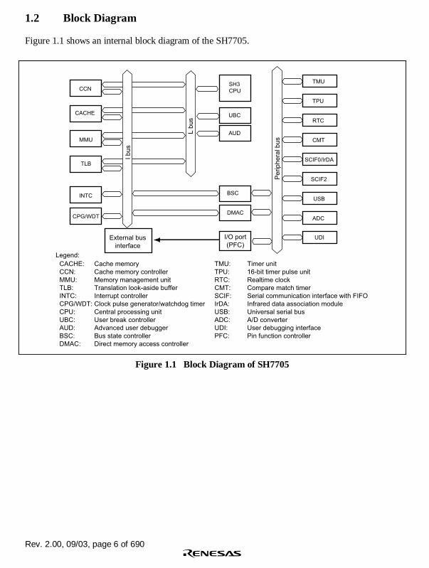
Rev. 2.00, 09/03, page 6 of 690
1.2 Block Diagram
Figure 1.1 shows an internal block diagram of the SH7705.
SH3CPU
TMU
TPU
RTC
CMT
SCIF0/IrDA
SCIF2
USB
ADC
UDI
UBC
AUD
BSC
DMAC
CCN
CACHE
MMU
TLB
INTC
CPG/WDT
Legend:
CACHE:
CCN:
MMU:
TLB:
INTC:
CPG/WDT:
CPU:
UBC:
AUD:
BSC:
DMAC:
Cache memory
Cache memory controller
Memory management unit
Translation look-aside buffer
Interrupt controller
Clock pulse generator/watchdog timer
Central processing unit
User break controller
Advanced user debugger
Bus state controller
Direct memory access controller
Timer unit
16-bit timer pulse unit
Realtime clock
Compare match timer
Serial communication interface with FIFO
Infrared data association module
Universal serial bus
A/D converter
User debugging interface
Pin function controller
TMU:
TPU:
RTC:
CMT:
SCIF:
IrDA:
USB:
ADC:
UDI:
PFC:
I/O port
(PFC)External bus
interface
I bus
L b
us
Periphera
l bus
Figure 1.1 Block Diagram of SH7705

Rev. 2.00, 09/03, page 7 of 690
1.3 Pin Assignment
1 2 3 4 5 6 7 8 9 10
11
12
13
14
15
16
17
18
19
20
21
22
23
24
25
26
27
28
29
30
31
32
33
34
35
36
37
38
39
40
41
42
43
44
45
46
47
48
49
50
51
52
VS
SQ
VC
C-U
SB
D+
D-
VS
S-U
SB
VC
C-R
TC
XTA
L2
EX
TA
L2
VS
S-R
TC
VB
US
/PT
M6
MD
6D
31/P
TB
7/P
INT
15
D30/P
TB
6/P
INT
14
D29/P
TB
5/P
INT
13
D28/P
TB
4/P
INT
12
D27/P
TB
3/P
INT
11
VS
SQ
D26/P
TB
2/P
INT
10
VC
CQ
D25/P
TB
1/P
INT
9D
24/P
TB
0/P
INT
8D
23/P
TA
7/P
INT
7D
22/P
TA
6/P
INT
6D
21/P
TA
5/P
INT
5D
20/P
TA
4/P
INT
4V
SS
D19/P
TA
3/P
INT
3V
CC
D18/P
TA
2/P
INT
2D
17/P
TA
1/P
INT
1D
16/P
TA
0/P
INT
0V
SSQ
D15
VC
CQ
D14
D13
D12
D11
D10
D9
D8
D7
D6
VS
SQ
D5
VC
CQ
D4
D3
D2
D1
D0
VS
SQ
156
155
154
153
152
151
150
149
148
147
146
145
144
143
142
141
140
139
138
137
136
135
134
133
132
131
130
129
128
127
126
125
124
123
122
121
120
11
911
811
711
611
511
411
311
2111
11
0109
108
107
106
105
VS
SQ
EX
TA
LX
TA
LM
D5
VC
C-P
LL2
VS
S-P
LL2
VS
S-P
LL1
VC
C-P
LL1
MD
2M
D1
MD
0ASEMD0
/PT
F7
ASEBRKAK
/PT
F6
TD
O/P
TF
5TRST
/PT
G3
TM
S/P
TG
2T
CK
/PT
G1
TD
I/P
TG
0V
CC
QP
TM
3P
TM
2P
TM
1P
TM
0V
SSQ
VC
CN
F*/P
TM
4V
SS
NF
*/P
TJ7
NF
*/P
TJ6
NF
*/P
TJ5
NF
*/P
TJ4
NF
*/P
TJ3
NF
*/P
TJ2
NF
*/P
TJ1
NF
*/P
TJ0
AU
DA
TA
3/P
TF
3/T
O3
AU
DA
TA
2/P
TF
2/T
O2
AU
DA
TA
1/P
TF
1/T
O1
AU
DA
TA
0/P
TF
0/T
O0
AU
DS
YN
C/P
TF
4T
EN
D0/P
TE
3D
AC
K1/P
TE
1D
AC
K0/P
TE
0V
CC
QWAIT
/PT
G7
VS
SQ
BREQ
/PT
G6
BACK
/PT
G5
PT
D5/N
F*
CK
E/P
TD
4CASU
/PT
D3
VS
SQ
INDEX
104103102101100
9998979695949392919089888786858483828180797877767574737271706968676665646362616059585756555453
CASL/PTD2RASU/PTD1RASL/PTD0CS6B/PTD7CS6A/PTC7CS5B/PTD6CS5A/PTC6CS4/PTC5CS3/PTC4CS2/PTC3CS0RD/WRWE3/DQMUU/AH/PTC2WE2/DQMUL/PTC1WE1/DQMLUVCCQWE0/DQMLLVSSQRDBS/PTC0A25/PTK7A24/PTK6A23/PTK5A22/PTK4VCCA21/PTK3VSSA20/PTK2A19/PTK1A18 A17 A16 A15 VCCQ A14 VSSQ A13 A12 A11 A10 A9 A8 A7 A6 A5 VCCQ A4 VSSQ A3 A2 A1 A0/PTK0
157158159160161162163164165166167168169170171172173174175176177178179180181182183184185186187188189190191192193194195196197198199200201202203204205206207208
STATUS0/PTE4/RTS0STATUS1/PTE5/CTS0
VSSQCKIOVCCQ
PTN0/SUSPNDPTN1/TXENL
PTN2/XVDATA PTN3/TXDMNS PTN4/TXDPLS
PTN5/DMNS PTN6/DPLS
PTN7 TCLK/PTE6
PTE7TxD0/SCPT0/IrTX
SCK0/SCPT1TxD2/SCPT2SCK2/SCPT3RTS2/SCPT4
RxD0/SCPT0/IrRXVCCQ
RxD2/SCPT2VSSQ
CTS2/SCPT5VSS
RESETMVCC
IRQ0/IRL0/PTH0IRQ1/IRL1/PTH1IRQ2/IRL2/PTH2IRQ3/IRL3/PTH3
IRQ4/PTH4IRQ5/PTE2
AUDCK/PTG4NMI
DREQ0/PTH5DREQ1/PTH6
RESETPCA
MD3MD4AVSS
AN0/PTL0AN1/PTL1AN2/PTL2AN3/PTL3
AVCCVSSQ
EXTAL_USBXTAL_USB
VCCQ
SH7705FP-208C(Top view)
Note: * The initial functions of NF (No Function) pins are not assigned after power-on reset. Specifies the functions with Pin Function Controller (PFC).
Figure 1.2 Pin Assignment (FP-208C)

Rev. 2.00, 09/03, page 8 of 690
17
16
15
14
13
12
11
10
9
8
7
6
5
4
3
2
1
17
16
15
14
13
12
11
10
9
8
7
6
5
4
3
2
1
A B C D E F G H J K L M N P R T U
A B C D E F G H J K L M N P R T U
SH7705
TBP-208A
(Top view)
INDEX MARK
Note: The terminal area surrounded by the dotted line is the perspective view.
Figure 1.3 Pin Assignment (TBP-208A)

Rev. 2.00, 09/03, page 9 of 690
Table 1.2 Pin Functions
Pin No.
FP-208C
TBP-208A Pin Name I/O Description
1 A1 VssQ I/O power supply (0 V)
2 B1 Vcc-USB USB power supply (3.3 V)
3 C3 D+ I/O USB data line
4 C2 D- I/O USB data line
5 C1 Vss-USB USB power supply (0 V)
6 D3 Vcc-RTC*5 RTC power supply (3.3 V)*5
7 D2 XTAL2 O Crystal oscillator pin for on-chip RTC
8 D1 EXTAL2 I Crystal oscillator pin for on-chip RTC
9 E4 Vss-RTC*5 RTC power supply (0 V)*5
10 E3 VBUS/PTM6 I / I/O USB power supply detection / input/output port M
11 E2 MD6 I connect to I/O power supply (0V)
12 E1 D31/PTB7/PINT15 I/O / I/O / I Data bus / input/output port B / PINT interrupt
13 F4 D30/PTB6/PINT14 I/O / I/O / I Data bus / input/output port B / PINT interrupt
14 F3 D29/PTB5/PINT13 I/O / I/O / I Data bus / input/output port B / PINT interrupt
15 F2 D28/PTB4/PINT12 I/O / I/O / I Data bus / input/output port B / PINT interrupt
16 F1 D27/PTB3/PINT11 I/O / I/O / I Data bus / input/output port B / PINT interrupt
17 G4 VssQ I/O power supply (0 V)
18 G3 D26/PTB2/PINT10 I/O / I/O / I Data bus / input/output port B / PINT interrupt
19 G2 VccQ I/O power supply (3.3 V)
20 G1 D25/PTB1/PINT9 I/O / I/O / I Data bus / input/output port B / PINT interrupt
21 H4 D24/PTB0/PINT8 I/O / I/O / I Data bus / input/output port B / PINT interrupt
22 H3 D23/PTA7/PINT7 I/O / I/O / I Data bus / input/output port A / PINT interrupt
23 H2 D22/PTA6/PINT6 I/O / I/O / I Data bus / input/output port A / PINT interrupt
24 H1 D21/PTA5/PINT5 I/O / I/O / I Data bus / input/output port A / PINT interrupt
25 J4 D20/PTA4/PINT4 I/O / I/O / I Data bus / input/output port A / PINT interrupt
26 J2 Vss Internal power supply (0 V)
27 J1 D19/PTA3/PINT3 I/O / I/O / I Data bus / input/output port A / PINT interrupt
28 J3 Vcc Internal power supply (1.5 V)
29 K1 D18/PTA2/PINT2 I/O / I/O / I Data bus / input/output port A / PINT interrupt
30 K2 D17/PTA1/PINT1 I/O / I/O / I Data bus / input/output port A / PINT interrupt
31 K3 D16/PTA0/PINT0 I/O / I/O / I Data bus / input/output port A / PINT interrupt

Rev. 2.00, 09/03, page 10 of 690
Pin No.
FP-208C
TBP-208A Pin Name I/O Description
32 K4 VssQ I/O power supply (0 V)
33 L1 D15 I/O Data bus
34 L2 VccQ I/O power supply (3.3 V)
35 L3 D14 I/O Data bus
36 L4 D13 I/O Data bus
37 M1 D12 I/O Data bus
38 M2 D11 I/O Data bus
39 M3 D10 I/O Data bus
40 M4 D9 I/O Data bus
41 N1 D8 I/O Data bus
42 N2 D7 I/O Data bus
43 N3 D6 I/O Data bus
44 N4 VssQ I/O power supply (0 V)
45 P1 D5 I/O Data bus
46 P2 VccQ I/O power supply (3.3 V)
47 P3 D4 I/O Data bus
48 R1 D3 I/O Data bus
49 R2 D2 I/O Data bus
50 P4 D1 I/O Data bus
51 T1 D0 I/O Data bus
52 T2 VssQ I/O power supply (0 V)
53 U1 A0/PTK0 O / I/O Address bus / input/output port K
54 U2 A1 O Address bus
55 R3 A2 O Address bus
56 T3 A3 O Address bus
57 U3 VssQ I/O power supply (0 V)
58 R4 A4 O Address bus
59 T4 VccQ I/O power supply (3.3 V)
60 U4 A5 O Address bus
61 P5 A6 O Address bus
62 R5 A7 O Address bus
63 T5 A8 O Address bus

Rev. 2.00, 09/03, page 11 of 690
Pin No.
FP-208C
TBP-208A Pin Name I/O Description
64 U5 A9 O Address bus
65 P6 A10 O Address bus
66 R6 A11 O Address bus
67 T6 A12 O Address bus
68 U6 A13 O Address bus
69 P7 VssQ I/O power supply (0 V)
70 R7 A14 O Address bus
71 T7 VccQ I/O power supply (3.3 V)
72 U7 A15 O Address bus
73 P8 A16 O Address bus
74 R8 A17 O Address bus
75 T8 A18 O Address bus
76 U8 A19/PTK1 O / I/O Address bus / input/output port K
77 P9 A20/PTK2 O / I/O Address bus / input/output port K
78 T9 Vss Internal power supply (0 V)
79 U9 A21/PTK3 O / I/O Address bus / input/output port K
80 R9 Vcc Internal power supply (1.5 V)
81 U10 A22/PTK4 O / I/O Address bus / input/output port K
82 T10 A23/PTK5 O / I/O Address bus / input/output port K
83 R10 A24/PTK6 O / I/O Address bus / input/output port K
84 P10 A25/PTK7 O / I/O Address bus / input/output port K
85 U11 BS/PTC0 O / I/O Bus cycle start signal / input/output port C
86 T11 RD O Read strobe
87 R11 VssQ I/O power supply (0 V)
88 P11 WE0/DQMLL O / O D7 to D0 select signal / DQM (SDRAM)
89 U12 VccQ I/O power supply (3.3 V)
90 T12 WE1/DQMLU O / O D15 to D8 select signal / DQM (SDRAM)
91 R12 WE2/DQMUL/PTC1 O / O / I/O D23 to D16 select signal / DQM (SDRAM) /input/output port C
92 P12 WE3/DQMUU/AH/PTC2
O / O / O /I/O
D31 to D24 select signal / DQM (SDRAM) /address hold / input/output port C
93 U13 RD/WR O Read/write
94 T13 CS0 O Chip select 0

Rev. 2.00, 09/03, page 12 of 690
Pin No.
FP-208C
TBP-208A Pin Name I/O Description
95 R13 CS2/PTC3 O / I/O Chip select 2 / input/output port C
96 P13 CS3/PTC4 O / I/O Chip select 3 / input/output port C
97 U14 CS4/PTC5 O / I/O Chip select 4 / input/output port C
98 T14 CS5A*3/PTC6 O / I/O Chip select 5A / input/output port C
99 R14 CS5B*3/PTD6 O / I/O Chip select 5B / input/output port D
100 U15 CS6A*3/PTC7 O / I/O Chip select 6A / input/output port C
101 T15 CS6B*3/PTD7 O / I/O Chip select 6B / input/output port D
102 P14 RASL/PTD0 O / I/O Lower 32 Mbytes address RAS (SDRAM) /input/output port D
103 U16 RASU*3/PTD1 O / I/O Upper 32 Mbytes address RAS (SDRAM) /input/output port D
104 T16 CASL/PTD2 O / I/O Lower 32 Mbytes address CAS (SDRAM) /input/output port D
105 U17 VssQ I/O power supply (0 V)
106 T17 CASU*3/PTD3 O / I/O Upper 32 Mbytes address CAS (SDRAM) /input/output port D
107 R15 CKE/PTD4 O / I/O CK enable (SDRAM) / input/output port D
108 R16 PTD5/NF*4 I Input port D / NF*4
109 R17 BACK/PTG5 O / I/O Bus acknowledge / input/output port G
110 P15 BREQ/PTG6 I / I/O Bus request / input/output port G
111 P16 VssQ I/O power supply (0 V)
112 P17 WAIT/PTG7 I / I/O Hardware wait request / input/output port G
113 N14 VccQ I/O power supply (3.3 V)
114 N15 DACK0/PTE0 O / I/O DMA acknowledge 0 / input/output port E
115 N16 DACK1/PTE1 O / I/O DMA acknowledge 1 / input/output port E
116 N17 TEND0/PTE3 O / I/O DMA transfer end notification / input/outputport E
117 M14 AUDSYNC/PTF4 O / I/O AUD synchronous / input/output port F
118 M15 AUDATA0/PTF0/TO0 O / I/O / O AUD data output / input/output port F / timeroutput
119 M16 AUDATA1/PTF1/TO1 O / I/O / O AUD data output / input/output port F / timeroutput
120 M17 AUDATA2/PTF2/TO2 O / I/O / O AUD data output / input/output port F / timeroutput

Rev. 2.00, 09/03, page 13 of 690
Pin No.
FP-208C
TBP-208A Pin Name I/O Description
121 L14 AUDATA3/PTF3/TO3 O / I/O / O AUD data output / input/output port F / timeroutput
122 L15 NF*4/PTJ0 O NF*4 /output port J
123 L16 NF*4/PTJ1 O NF*4 /output port J
124 L17 NF*4/PTJ2 O NF*4 /output port J
125 K14 NF*4/PTJ3 O NF*4 /output port J
126 K15 NF*4/PTJ4 O NF*4 /output port J
127 K16 NF*4/PTJ5 O NF*4 /output port J
128 K17 NF*4/PTJ6 O NF*4 /output port J
129 J14 NF*4/PTJ7 O NF*4 /output port J
130 J16 Vss Internal power supply (0 V)
131 J17 NF*4/PTM4 I NF*4 / input port M
132 J15 Vcc Internal power supply (1.5 V)
133 H17 VssQ I/O power supply (0 V)
134 H16 PTM0 I/O Input/output port M
135 H15 PTM1 I/O Input/output port M
136 H14 PTM2 I/O Input/output port M
137 G17 PTM3 I/O Input/output port M
138 G16 VccQ I/O power supply (3.3 V)
139 G15 TDI*7/PTG0 I / I/O Test data input (UDI) / input/output port G
140 G14 TCK*7/PTG1 I / I/O Test clock (UDI) / input/output port G
141 F17 TMS*7/PTG2 I / I/O Test mode select (UDI) / input/output port G
142 F16 TRST*1 *7/PTG3 I / I/O Test reset (UDI) / input/output port G
143 F15 TDO/PTF5 O / I/O Test data output (UDI) / input/output port F
144 F14 ASEBRKAK/PTF6 O / I/O ASE break acknowledge (UDI) / input/outputport F
145 E17 ASEMD0*2 *7/PTF7 I / I/O ASE mode (UDI) / input/output port F
146 E16 MD0 I Clock mode setting
147 E15 MD1 I Clock mode setting
148 E14 MD2 I Clock mode setting
149 D17 Vcc-PLL1 PLL1 power supply (1.5 V)
150 D16 Vss-PLL1 PLL1 power supply (0 V)

Rev. 2.00, 09/03, page 14 of 690
Pin No.
FP-208C
TBP-208A Pin Name I/O Description
151 D15 Vss-PLL2 PLL2 power supply (0 V)
152 C17 Vcc-PLL2 PLL2 power supply (1.5 V)
153 C16 MD5 I Endian setting
154 D14 XTAL O Crystal oscillator pin
155 B17 EXTAL I External clock / crystal oscillator pin
156 B16 VssQ I/O power supply (0 V)
157 A17 STATUS0/PTE4/RTS0
O / I/O / O Processor status / input/output port E / SCIF0transmit request
158 A16 STATUS1/PTE5/CTS0
O / I/O / I Processor status / input/output port E / SCIF0transmit clear
159 C15 VssQ I/O power supply (0 V)
160 B15 CKIO I/O System clock input/output
161 A15 VccQ I/O power supply (3.3 V)
162 C14 PTN0/SUSPND I/O / O input/output port N / USB suspend
163 B14 PTN1/TXENL I/O / O input/output port N / USB output enable
164 A14 PTN2/XVDATA I/O / I input/output port N / USB differential receiveinput
165 D13 PTN3/TXDMNS I/O / O input/output port N / USB D– transmit output
166 C13 PTN4/TXDPLS I/O / O input/output port N / USB D+ transmit output
167 B13 PTN5/DMNS I/O / I input/output port N / D– input from USBreceiver
168 A13 PTN6/DPLS I/O / I input/output port N / D+ input from USBreceiver
169 D12 PTN7 I/O input/output port N
170 C12 TCLK/PTE6 I / I/O TMU clock input / input/output port E
171 B12 PTE7 I/O Input/output port E
172 A12 TxD0/SCPT0/IrTX O / O / O SCIF0 transmit data / SC port / IrDA TX port
173 D11 SCK0/SCPT1 I/O / I/O SCIF0 clock / SC port
174 C11 TxD2/SCPT2 O / O SCIF2 transmit data / SC port
175 B11 SCK2/SCPT3 I/O / I/O SCIF2 clock / SC port
176 A11 RTS2/SCPT4 O / I/O SCIF2 transmit request / SC port
177 D10 RxD0/SCPT0/IrRX I / I / I SCIF0 receive data / SC port / IrDA RX port
178 C10 VccQ I/O power supply (3.3 V)
179 B10 RxD2/SCPT2 I / I SCIF2 receive data / SC port
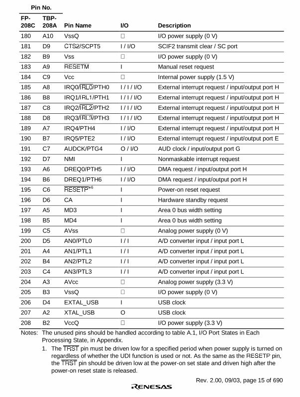
Rev. 2.00, 09/03, page 15 of 690
Pin No.
FP-208C
TBP-208A Pin Name I/O Description
180 A10 VssQ I/O power supply (0 V)
181 D9 CTS2/SCPT5 I / I/O SCIF2 transmit clear / SC port
182 B9 Vss I/O power supply (0 V)
183 A9 RESETM I Manual reset request
184 C9 Vcc Internal power supply (1.5 V)
185 A8 IRQ0/IRL0/PTH0 I / I / I/O External interrupt request / input/output port H
186 B8 IRQ1/IRL1/PTH1 I / I / I/O External interrupt request / input/output port H
187 C8 IRQ2/IRL2/PTH2 I / I / I/O External interrupt request / input/output port H
188 D8 IRQ3/IRL3/PTH3 I / I / I/O External interrupt request / input/output port H
189 A7 IRQ4/PTH4 I / I/O External interrupt request / input/output port H
190 B7 IRQ5/PTE2 I / I/O External interrupt request / input/output port E
191 C7 AUDCK/PTG4 O / I/O AUD clock / input/output port G
192 D7 NMI I Nonmaskable interrupt request
193 A6 DREQ0/PTH5 I / I/O DMA request / input/output port H
194 B6 DREQ1/PTH6 I / I/O DMA request / input/output port H
195 C6 RESETP*6 I Power-on reset request
196 D6 CA I Hardware standby request
197 A5 MD3 I Area 0 bus width setting
198 B5 MD4 I Area 0 bus width setting
199 C5 AVss Analog power supply (0 V)
200 D5 AN0/PTL0 I / I A/D converter input / input port L
201 A4 AN1/PTL1 I / I A/D converter input / input port L
202 B4 AN2/PTL2 I / I A/D converter input / input port L
203 C4 AN3/PTL3 I / I A/D converter input / input port L
204 A3 AVcc Analog power supply (3.3 V)
205 B3 VssQ I/O power supply (0 V)
206 D4 EXTAL_USB I USB clock
207 A2 XTAL_USB O USB clock
208 B2 VccQ I/O power supply (3.3 V)
Notes: The unused pins should be handled according to table A.1, I/O Port States in EachProcessing State, in Appendix.1. The TRST pin must be driven low for a specified period when power supply is turned on
regardless of whether the UDI function is used or not. As the same as the RESETP pin,the TRST pin should be driven low at the power-on set state and driven high after thepower-on reset state is released.

Rev. 2.00, 09/03, page 16 of 690
2. The input level of the ASEMD0 pin must be high if the E10A emulator is not used. Fordetails, refer to section 23.4.2, Reset Configuration.
3. These pins are initialized to the general input port setting in which the pull-up MOS is offat a power-on reset. When these pins are connected to memory and so on, their levelsmust be fixed externally.
4. The initial functions of NF (No Function) pins are not assigned after power-on reset.Specifies the functions with Pin Function Controller (PFC).
5. In hardware standby mode, supply power to all power supply pins including the RTCpower supply pins.
6. Pull-up MOS connected.7. The pull-up MOS turns on if the pin function controller (PFC) is used to select other
functions (UDI).

Rev. 2.00, 09/03, page 17 of 690
1.4 Pin Functions
Table 1.3 lists the pin functions.
Table 1.3 Pin Functions
Classification Symbol I/O Name Function
Vcc Power supply Power supply for the internalmodules and ports for the system.Connect all Vcc pins to the systempower supply. There will be nooperation if any pins are open.
Vss Ground Ground pin. Connect all Vss pins tothe system power supply (0 V).There will be no operation if anypins are open.
VccQ Power supply Power supply for I/O pins. Connectall VccQ pins to the system powersupply. There will be no operationif any pins are open.
Power supply
VssQ Ground Ground pin. Connect all VssQ pinsto the system power supply (0 V).There will be no operation if anypins are open.
Vcc-PLL1 PLL1 powersupply
Power supply for the on-chip PLL1oscillator.
Vss-PLL1 PLL1 ground Ground pin for the on-chip PLL1oscillator.
Vcc-PLL2 PLL2 powersupply
Power supply for the on-chip PLL2oscillator.
Vss-PLL2 PLL2 ground Ground pin for the on-chip PLL2oscillator.
EXTAL I External clock For connection to a crystalresonator. An external clock signalmay also be input to the EXTALpin.
XTAL O Crystal For connection to a crystalresonator.
Clock
CKIO I/O System clock Supplies the system clock toexternal devices.

Rev. 2.00, 09/03, page 18 of 690
Classification Symbol I/O Name Function
Operating modecontrol
MD6 to MD0 I Mode set Sets the operating mode. Do notchange values on these pinsduring operation.
MD2 to MD0 set the clock mode,MD3 and MD4 set the bus-widthmode of area 0 and MD5 sets theendian. MD6 pin should beconnected to VssQ.
RESETP I Power-on reset When low, the system enters thepower-on reset state.
RESETM I Manual reset When low, the system enters themanual reset state.
STATUS1,STATUS0
O Status output Indicates the operating state.
BREQ I Bus request Low when an external devicerequests the release of the busmastership.
BACK O Bus requestacknowledge
Indicates that the bus mastershiphas been released to an externaldevice. Reception of the BACKsignal informs the device whichhas output the BREQ signal that ithas acquired the bus.
System control
CA I Chip active High in normal operation, and lowin hardware standby mode.
NMI I Non-maskableinterrupt
Non-maskable interrupt requestpin. Fix to high level when not inuse.
IRQ5 to IRQ0 I Interruptrequests 5 to 0
Maskable interrupt request pin.
Selectable as level input or edgeinput. The rising edge or fallingedge is selectable as the detectionedge. The low level or high level isselectable as the detection level.
IRL3 to IRL0 I Interruptrequests 3 to 0
Maskable interrupt request pin.
Input a coded interrupt level.
Interrupts
PINT15 toPINT0
I Interruptrequests 15 to 0
PINT interrupt request pin.
Address bus A25 to A0 O Address bus Outputs addresses.
Data bus D31 to D0 I/O Data bus 32-bit bidirectional data bus.

Rev. 2.00, 09/03, page 19 of 690
Classification Symbol I/O Name Function
CS0,CS2 to CS4,CS5A, CS5B,CS6A, CS6B,
O Chip select 0,2 to 4, 5A, 5B,6A, 6B
Chip-select signal for externalmemory or devices.
RD O Read Indicates reading of data fromexternal devices.
RD/WR O Read/write Read/write signal.
BS O Bus start Bus-cycle start.
WE3 O Highest-bytewrite
Indicates that bits 31 to 24 of thedata in the external memory ordevice are being written.
WE2 O Second-highest-byte write
Indicates that bits 23 to 16 of thedata in the external memory ordevice are being written.
WE1 O Second-lowest-byte write
Indicates that bits 15 to 8 of thedata in the external memory ordevice are being written.
WE0 O Lowest-bytewrite
Indicates that bits 7 to 0 of the datain the external memory or deviceare being written.
CKE O CK enable Clock enable. (SDRAM)
DQMUU O DQ mask UU Selects D31 to D24. (SDRAM)
DQMUL O DQ mask UL Selects D23 to D16. (SDRAM)
DQMLU O DQ mask LU Selects D15 to D8. (SDRAM)
DQMLL O DQ mask LL Selects D7 to D0. (SDRAM)
RASU O Row address U Specifies a row address. (SDRAM)
RASL O Row address L Specifies a row address. (SDRAM)
CASU O Column addressU
Specifies a column address.(SDRAM)
CASL O Column addressL
Specifies a column address.(SDRAM)
AH O Address hold Address hold signal.
Bus control
WAIT I Wait Inserts a wait cycle into the buscycles during access to theexternal space.

Rev. 2.00, 09/03, page 20 of 690
Classification Symbol I/O Name Function
DREQ0,DREQ1
I DMA-transferrequest
Input pin for external requests forDMA transfer.
DACK0,DACK1
O DMA-transferstrobe
Output strobe to external I/O, inresponse to external requests forDMA transfer.
Direct memoryaccess controller(DMAC)
TEND0 O DMA-transferend
Transfer end output for DMACchannel 0.
Timer unit (TMU) TCLK I Clock input External clock input pin/inputcapture control input pin.
16-bit timer pulseunit (TPU)
TO3 to TO0 O Timer output Output compare/PWM output pin.
TxD0, TxD2 O Transmit data Transmit data pin.
RxD0, RxD2 I Receive data Receive data pin.
SCK0, SCK2 I/O Serial clock Clock input/output pin.
RTS0, RTS2 O Transmitrequest
Modem control pin.
Serialcommunicationinterface withFIFO(SCIF0, SCIF2)
CTS0, CTS2 I Transmit enable Modem control pin.
IrTX O IrDA TX port IrDA transmit data output.IrDA
IrRX I IrDA RX port IrDA receive data input.
EXTAL2 I RTC clock RTC crystal oscillator pin. (32.768kHz)
XTAL2 O RTC clock RTC crystal oscillator pin. (32.768kHz)
Vcc-RTC RTC powersupply
Power supply pin for the RTC.
Realtime clock(RTC)
Vss-RTC RTC ground Ground pin for the RTC.
AN3 to AN0 I Analog input pin Analog input pin.
AVcc A/D analogpower supply
Power supply for the A/Dconverter. When the A/D converteris not in use, connect this pin to theport power supply (VccQ).
A/D converter(ADC)
AVss A/D analogground
Ground pin for the A/D converter.Connect this pin to the systempower supply (Vss).

Rev. 2.00, 09/03, page 21 of 690
Classification Symbol I/O Name Function
EXTAL_USB I USB clock USB clock input pin. (48-MHzinput)
XTAL_USB O USB clock USB clock pin.
XVDATA I Data input Receive data input pin from thedifferential receiver.
VBUS I USB powersupply detection
USB-cable connection-monitor pin.
TXDPLS O D+ output D+ transmit output pin for thedriver.
TXDMNS O D− output D− transmit output pin for thedriver.
DPLS I D+ input D+ signal input pin from thereceiver to the driver.
DMNS I D− input D− signal input pin from thereceiver to the driver.
TXENL O Output enable Output enable pin for the driver.
SUSPND O Suspend Suspend-state output pin for thetransceiver.
Vcc-USB USB analogpower supply
USB power supply pin. When theUSB is not in use, connect this pinto the port power supply (VccQ).
Vss-USB USB analogground
USB ground pin. Connect this pinto the system power supply (Vss).
D− I/O D− I/O On-chip USB transceiver D−.
USB
D+ I/O D+ I/O On-chip USB transceiver D+.

Rev. 2.00, 09/03, page 22 of 690
Classification Symbol I/O Name Function
PTA7 to PTA0 I/O Generalpurpose port
8-bit general-purpose I/O port pins.
PTB7 to PTB0 I/O Generalpurpose port
8-bit general-purpose I/O port pins.
PTC7 to PTC0 I/O Generalpurpose port
8-bit general-purpose I/O port pins.
PTD7 to PTD0 I/O Generalpurpose port
8-bit general-purpose I/O port pins.
PTE7 to PTE0 I/O Generalpurpose port
8-bit general-purpose I/O port pins.
PTF7 to PTF0 I/O Generalpurpose port
8-bit general-purpose I/O port pins.
PTG7 to PTG0 I/O Generalpurpose port
8-bit general-purpose I/O port pins.
PTH6 to PTH0 I/O Generalpurpose port
7-bit general-purpose I/O port pins.
PTJ7 to PTJ0 O Generalpurpose port
8-bit general-purpose output portpins.
PTK7 to PTK0 I/O Generalpurpose port
8-bit general-purpose I/O port pins.
PTL3 to PTL0 I Generalpurpose port
4-bit general-purpose input portpins.
PTM6, PTM4 toPTM0
I/O Generalpurpose port
6-bit general-purpose I/O port pins.
PTN7 to PTN0 I/O Generalpurpose port
8-bit general-purpose I/O port pins.
I/O port
SCPT5 toSCPT0
I/O Serial port 6-bit serial port pins.

Rev. 2.00, 09/03, page 23 of 690
Classification Symbol I/O Name Function
TCK I Test clock Test-clock input pin.
TMS I Test modeselect
Inputs the test-mode select signal.
TDI I Test data input Serial input pin for instructions anddata.
TDO O Test dataoutput
Serial output pin for instructionsand data.
User debugginginterface(UDI)
TRST I Test reset Initial-signal input pin.
AUDATA3 toAUDATA0
O AUD data Destination-address output pin inbranch-trace mode.
AUDCK O AUD clock Synchronous clock output pin inbranch-trace mode.
Advanced userdebugger(AUD)
AUDSYNC O AUDsynchronoussignal
Data start-position acknowledge-signal output pin in branch-tracemode.
ASEBRKAK O Break modeacknowledge
Indicates that the E10A emulatorhas entered its break mode.
For the connection with the E10A,see the SH7705 E10A EmulatorUser’s Manual (tentative title).
E10A interface
ASEMD0 I ASE mode Sets ASE mode.

Rev. 2.00, 09/03, page 24 of 690

Rev. 2.00, 09/03, page 25 of 690
Section 2 CPU
2.1 Processing States and Processing Modes
2.1.1 Processing States
This LSI supports four types of processing states: a reset state, an exception handling state, aprogram execution state, and a low-power consumption state, according to the CPU processingstates.
Reset State: In the reset state, the CPU is reset. The LSI supports two types of resets: power-onreset and manual reset. For details on resets, refer to section 5, Exception Handling.
In power-on reset, the registers and internal statuses of all LSI on-chip modules are initialized. Inmanual reset, the register contents of a part of the LSI on-chip modules, such as the bus statecontroller (BSC), are retained. For details, refer to section 24, List of Registers. The CPU internalstatuses and registers are initialized both in power-on reset and manual reset. After initialization,the program branches to address H'A0000000 to pass control to the reset processing program to beexecuted.
Exception Handling State: In the exception handling state, the CPU processing flow is changedtemporarily by a general exception or interrupt exception processing. The program counter (PC)and status register (SR) are saved in the save program counter (SPC) and save status register(SSR), respectively. The program branches to an address obtained by adding a vector offset to thevector base register (VBR) and passes control to the exception processing program defined by theuser to be executed. For details on reset, refer to section 5, Exception Handling.
Program Execution State: The CPU executes programs sequentially.
Low-Power Consumption State: The CPU stops operation to reduce power consumption. Thelow-power consumption state can be entered by executing the SLEEP instruction. For details onthe low-power consumption state, refer to section 11, Power-Down Modes.
Figure 2.1 shows a status transition diagram.
CPUS3D0S_000020020300

Rev. 2.00, 09/03, page 26 of 690
2.1.2 Processing Modes
This LSI supports two processing modes: user mode and privileged mode. These processingmodes can be determined by the processing mode bit (MD) of the status register (SR). If the MDbit is cleared to 0, the user mode is selected. If the MD bit is set to 1, the privileged mode isselected. The CPU enters the privileged mode by a transition to reset state or exception handlingstate. In the privileged mode, any registers and resources in address spaces can be accessed.
Clearing the MD bit of the SR to 0 puts the CPU in the user mode. In the user mode, some of theregisters, including SR, and some of the address spaces cannot be accessed by the user programand system control instructions cannot be executed. This function effectively protects the systemresources from the user program. To change the processing mode from user to privileged mode, atransition to exception handling state is required.*
Note: * To call a service routine used in privileged mode from user mode, the LSI supports anunconditional trap instruction (TRAPA). When a transition from user mode toprivileged mode occurs, the contents of the SR and PC are saved. A program executionin user mode can be resumed by restoring the contents of the SR and PC. To returnfrom an exception processing program, the LSI supports an RTE instruction.
(From any states)
Power-on reset
Manual reset
Reset state Program execution state
Low-power
consumption stateException handling state
An exception is accepted
Exception handling
routine starts
Reset processing
routine starts
An exception
is accepted
Multiple
exceptions
SLEEP instruction
Figure 2.1 Processing State Transitions

Rev. 2.00, 09/03, page 27 of 690
2.2 Memory Map
2.2.1 Logical Address Space
The LSI supports 32-bit logical addresses and accesses system resources using the 4-Gbytes oflogical address space. User programs and data are accessed from the logical address space. Thelogical address space is divided into several areas as shown in table 2.1.
P0/U0 Area: This area is called the P0 area when the CPU is in privileged mode and the U0 areawhen in user mode. For the P0 and U0 areas, access using the cache is enabled. The P0 and U0areas are handled as address translatable areas.
If the cache is enabled, access to the P0 or U0 area is cached. If a P0 or U0 address is specifiedwhile the address translation unit is enabled, the P0 or U0 address is translated into a physicaladdress based on translation information defined by the user.
If the CPU is in user mode, only the U0 area can be accessed. If P1, P2, P3, or P4 is accessed inuser mode, a transition to an address error exception occurs.
P1 Area: The P1 area is defined as a cacheable but non-address translatable area. Normally,programs executed at high speed in privileged mode, such as exception processing handlers, whichare at the core of the operating system (S), are assigned to the P1 area.
P2 Area: The P2 area is defined as a non-cacheable but non-address translatable area. A resetprocessing program to be called from the reset state is described at the start address (H'A0000000)of the P2 area. Normally, programs such as system initialization routines and OS initiationprograms are assigned to the P2 area. To access a part of an on-chip module control register, itscorresponding program should be assigned to the P2 area.
P3 Area: The P3 area is defined as a cacheable and address translatable area. This area is used ifan address translation is required for a privileged program.
P4 Area: The P4 area is defined as a control area which is non-cacheable and non-addresstranslatable. This area can be accessed only in privileged mode. A part of this LSI's on-chipmodule control register is assigned to this area.

Rev. 2.00, 09/03, page 28 of 690
Table 2.1 Logical Address Space
AddressRange Name Mode Description
H’00000000 toH’7FFFFFFF
P0/U0 Privileged/user mode 2-Gbyte physical space, cacheable, addresstranslatable
In user mode, only this address space canbe accessed.
H’80000000 toH’9FFFFFFF
P1 Privileged mode 0.5-Gbyte physical space, cacheable
H’A0000000 toH’BFFFFFFF
P2 Privileged mode 0.5-Gbyte physical space, non-cacheable
H’C0000000 toH’DFFFFFFF
P3 Privileged mode 0.5-Gbyte physical space, cacheable,address translatable
H’E0000000 toH’FFFFFFFF
P4 Privileged mode 0.5-Gbyte control space, non-cacheable
2.2.2 External Memory Space
The LSI uses 29 bits of the 32-bit logical address to access external memory. In this case, 0.5-Gbyte of external memory space can be accessed. The external memory space is managed in areaunits. Different types of memory can be connected to each area, as shown in figure 2.2. Fordetails, please refer to section 7, Bus State Controller (BSC). In addition, area 1 in the externalmemory space is used as an on-chip I/O space where most of this LSI's on-chip module controlregisters are mapped. *1
Normally, the upper three bits of the 32-bit logical address are masked and the lower 29 bits areused for external memory addresses.*2 For example, address H'00000100 in the P0 area, addressH'80000100 in the P1 area, address H'A0000100 in the P2 area, and address H'C0000100 in the P3area of the logical address space are mapped into address H'00000100 of area 0 in the externalmemory space. The P4 area in the logical address space is not mapped into the external memoryaddress. If an address in the P4 area is accessed, an external memory cannot be accessed.
Notes: 1. To access an on-chip module control register mapped into area 1 in the externalmemory space, access the address from the P2 area which is not cached in the logicaladdress space.
2. If the address translation unit is enabled, arbitrary mapping in page units can bespecified. For details, refer to section 3, Memory Management Unit (MMU).

Rev. 2.00, 09/03, page 29 of 690
P0 area
Privileged mode User mode
External memory space
Area 0
Area 1
Area 2
Area 3
Area 4
Area 5
Area 6
Area 7
H'0000 0000 H'0000 0000
H'8000 0000
H'FFFF FFFF
H'8000 0000
H'A000 0000
H'C000 0000
H'E000 0000
H'FFFF FFFF
U0 area
Address error
P1 area
P2 area
P3 area
P4 area
Figure 2.2 Logical Address to External Memory Space Mapping
2.3 Register Descriptions
This LSI provides thirty-three 32-bit registers: 24 general registers, five control registers, threesystem registers, and one program counter.
General Registers: This LSI incorporates 24 general registers: R0_BANK0 to R7_BANK0,R0_BANK1 to R7_BANK1 and R8 to R15. R0 to R7 are banked. The process mode and theregister bank (RB) bit in the status register (SR) define which set of banked registers (R0_BANK0to R7_BANK0 or R0_BANK1 to R7_BANK1) are accessed as general registers.
System Registers: This LSI incorporates the multiply and accumulate registers (MACH/MACL)and procedure register (PR) as system registers. These registers can be accessed regardless of theprocessing mode.
Program Counter: The program counter stores the value obtained by adding 4 to the currentinstruction address.
Control Registers: This LSI incorporates the status register (SR), global base register (GBR),save status register (SSR), save program counter (SPC), and vector base register (VBR) as controlregister. Only the GBR can be accessed in user mode. Control registers other than the GBR can beaccessed only in privileged mode.

Rev. 2.00, 09/03, page 30 of 690
Table 2.2 shows the register values after reset. Figure 2.3 shows the register configurations in eachprocess mode.
Table 2.2 Register Initial Values
Register Type Registers Initial Values
General registers R0_BANK0 to R7_BANK0,
R0_BANK1 to R7_BANK1,
R8 to R15
Undefined
System registers MACH, MACL, PR Undefined
Program counter PC H’A0000000
SR MD bit = 1, RB bit = 1, BL bit = 1, I3 to I0bits = H’F (1111), reserved bits = all 0, otherbits = undefined
GBR, SSR, SPC Undefined
Control registers
VBR H’00000000
Note:* Initialized by a power-on or manual reset.

Rev. 2.00, 09/03, page 31 of 690
31
R0_BANK0*1 *2
R1_BANK0*2
R2_BANK0*2
R3_BANK0*2
R4_BANK0*2
R5_BANK0*2
R6_BANK0*2
R7_BANK0*2
R8
R9
R10
R11
R12
R13
R14
R15
SR
GBR
MACH
MACL
PR
PC
0 31
R0_BANK1*1 *3
R1_BANK1*3
R2_BANK1*3
R3_BANK1*3
R4_BANK1*3
R5_BANK1*3
R6_BANK1*3
R7_BANK1*3
R0_BANK0*1 *4
R1_BANK0*4
R2_BANK0*4
R3_BANK0*4
R4_BANK0*4
R5_BANK0*4
R6_BANK0*4
R7_BANK0*4
R8
R9
R10
R11
R12
R13
R14
R15
SR
SSR
GBR
MACH
MACL
VBR
PR
PC
SPC
0 31
R0_BANK0*1 *4
R1_BANK0*4
R2_BANK0*4
R3_BANK0*4
R4_BANK0*4
R5_BANK0*4
R6_BANK0*4
R7_BANK0*4
R0_BANK1*1 *3
R1_BANK1*3
R2_BANK1*3
R3_BANK1*3
R4_BANK1*3
R5_BANK1*3
R6_BANK1*3
R7_BANK1*3
R8
R9
R10
R11
R12
R13
R14
R15
SR
SSR
GBR
MACH
MACL
VBR
PR
PC
SPC
0
(a) User mode register
configuration(b) Privileged mode register
configuration (RB = 1)
(c) Privileged mode register
configuration (RB = 0)
Notes: 1. The R0 register is used as an index register in indexed register indirect addressing mode
and indexed GBR indirect addressing mode.
2. Bank register
3. Bank register
Accessed as a general register when the RB bit is set to 1 in the SR register.
Accessed only by LDC/STC instructions when the RB bit is cleared to 0.
4. Bank register
Accessed as a general register when the RB bit is cleared to 0 in the SR register.
Accessed only by LDC/STC instructions when the RB bit is set to 1.
Figure 2.3 Register Configuration in Each Processing Mode

Rev. 2.00, 09/03, page 32 of 690
2.3.1 General Registers
There are twenty-four 32-bit general registers: R0_BANK0 to R7_BANK0, R0_BANK1 toR7_BANK1, and R8 to R15. R0 to R7 are banked. The process mode and the register bank (RB)bit in the status register (SR) define which set of banked registers (R0_BANK0 to R7_BANK0 orR0_BANK1 to R7_BANK1) are accessed as general registers. R0 to R7 registers in the selectedbank are accessed as R0 to R7. R0 to R7 in the non-selected bank is accessed as R0_BANK toR7_BANK by the control register load instruction (LDC) and control register store instruction(STC).
In user mode, bank 0 is selected regardless of he RB bit value. Sixteen registers: R0_BANK0 toR7_BANK0 and R8 to R15 are accessed as general registers R0 to R15. The R0_BANK1 toR7_BANK1 registers in bank 1 cannot be accessed.
In privileged mode that is entered by a transition to exception handling state, the RB bit is set to 1to select bank 1. In privileged mode, sixteen registers: R0_BANK1 to R7_BANK1 and R8 to R15are accessed as general registers R0 to R15. A bank is switched automatically when an exceptionhandling state is entered, registers R0 to R7 need not be saved by the exception handling routine.The R0_BANK0 to R7_BANK0 registers in bank 0 can be accessed as R0_BANK to R7_BANKby the LDC and STC instructions.
In privileged mode, bank 0 can also be used as general registers by clearing the RB bit to 0. In thiscase, sixteen registers: R0_BANK0 to R7_BANK0 and R8 to R15 are accessed as generalregisters R0 to R15. The R0_BANK1 to R7_BANK1 registers in bank 1 can be accessed asR0_BANK to R7_BANK by the LDC and STC instructions.
The general registers R0 to R15 are used as equivalent registers for almost all instructions. Insome instructions, the R0 register is automatically used or only the R0 register can be used assource or destination registers.
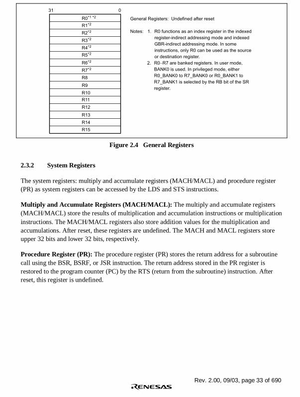
Rev. 2.00, 09/03, page 33 of 690
31
R0*1 *2
R1*2
R2*2
R3*2
R4*2
R5*2
R6*2
R7*2
R8
R9
R10
R11
R12
R13
R14
R15
0
General Registers: Undefined after reset
Notes: 1. R0 functions as an index register in the indexed
register-indirect addressing mode and indexed
GBR-indirect addressing mode. In some
instructions, only R0 can be used as the source
or destination register.
2. R0−R7 are banked registers. In user mode,
BANK0 is used. In privileged mode, either
R0_BANK0 to R7_BANK0 or R0_BANK1 to
R7_BANK1 is selected by the RB bit of the SR
register.
Figure 2.4 General Registers
2.3.2 System Registers
The system registers: multiply and accumulate registers (MACH/MACL) and procedure register(PR) as system registers can be accessed by the LDS and STS instructions.
Multiply and Accumulate Registers (MACH/MACL): The multiply and accumulate registers(MACH/MACL) store the results of multiplication and accumulation instructions or multiplicationinstructions. The MACH/MACL registers also store addition values for the multiplication andaccumulations. After reset, these registers are undefined. The MACH and MACL registers storeupper 32 bits and lower 32 bits, respectively.
Procedure Register (PR): The procedure register (PR) stores the return address for a subroutinecall using the BSR, BSRF, or JSR instruction. The return address stored in the PR register isrestored to the program counter (PC) by the RTS (return from the subroutine) instruction. Afterreset, this register is undefined.

Rev. 2.00, 09/03, page 34 of 690
2.3.3 Program Counter
The program counter (PC) stores the value obtained by adding 4 to the current instruction address.There is no instruction to read the PC directly. Before an exception handling state is entered, thePC is saved in the save program counter (SPC). Before a subroutine call is executed, the PC issaved in the procedure register (PR). In addition, the PC can be used for PC relative addressingmode.
Figure 2.5 shows the system register and program counter configurations.
MACH
MACL
31 0
PR
31 0
PC
31 0
Multiply and accumulate high and low registers (MACH/MACL)
Procedure register (PR)
Program counter (PC)
Figure 2.5 System Registers and Program Counter

Rev. 2.00, 09/03, page 35 of 690
2.3.4 Control Registers
The control registers (SR, GBR, SSR, SPC, and VBR) can be accessed by the LDC or STCinstruction in privileged mode. The GBR register can be accessed in the user mode.
The control registers are described below.
Status Register (SR): The status register (SR) indicates the system status as shown below. TheSR register can be accessed only in privileged mode.
Bit Bit NameInitialValue R/W Description
31 0 R Reserved
This bit is always read as 0. The write value should always be0.
30 MD 1 R/W Processing Mode
Indicates the CPU processing mode.
0: User mode
1: Privileged mode
The MD bit is set to 1 in reset or exception handling state.
29 RB 1 R/W Register Bank
The general registers R0 to R7 are banked registers. The RBbit selects a bank used in the privileged mode.
0: Selects bank 0 registers. In this case, R0_BANK0 toR7_BANK0 and R8 to R15 are used as general registers.R0_BANK1 to R7_BANK1 can be accessed by the LDC orSTR instruction.
1: Selects bank 1 registers. In this case, R0_BANK1 toR7_BANK1 and R8 to R15 are used as general registers.R0_BANK0 to R7_BANK0 can be accessed by the LDC orSTR instruction.
The RB bit is set to 1 in reset or exception handling state.
28 BL 1 R/W Block
Specifies whether an exception, interrupt, or user break isenabled or not.
0: Enables an exception, interrupt, or user break.
1: Disables an exception, interrupt, or user break.
The BL bit is set to 1 in reset or exception handling state.
27 to 10 0 R Reserved
These bits are always read as 0. The write value shouldalways be 0.

Rev. 2.00, 09/03, page 36 of 690
Bit Bit NameInitialValue R/W Description
9
8
M
Q
R/W
R/W
M Bit
Q Bit
These bits are used by the DIV0S, DIV0U, and DIV1instructions. These bits can be changed even in user mode byusing the DIV0S, DIV0U, and DIV1 instructions. These bitsare undefined at reset. These bits do not change in anexception handling state.
7 to 4 I3 to I0 1 R/W Interrupt Mask
Indicates the interrupt mask level. These bits do not changeeven if an interrupt occurs. At reset, these bits are initializedto B’1111. These bits are not affected in an exceptionhandling state.
3, 2 0 R Reserved
These bits are always read as 0. The write value shouldalways be 0.
1 S R/W Saturation Mode
Specifies the saturation mode for multiply instructions ormultiply and accumulate instructions. This bit can be specifiedby the SETS and CLRS instructions in user mode.
At reset, this bit is undefined. This bit is not affected in anexception handling state.
0 T R/W T Bit
Indicates true or false for compare instructions or carry orborrow occurrence for an operation instruction with carry orborrow. This bit can be specified by the SETT and CLRTinstructions in user mode.
At reset, this bit is undefined. This bit is not affected in anexception handling state.
Note: The M, Q, S, and T bits can be set/cleared by the user mode specific instructions. Other bitscan be read or written in privileged mode.
Save Status Register (SSR): The save status register (SSR) can be accessed only in privilegedmode. Before entering the exception, the contents of the SR register is stored in the SSR register.At reset, the SSR initial value is undefined.
Save Program Counter (SPC): The save program counter (SPC) can be accessed only inprivileged mode. Before entering the exception, the contents of the PC are stored in the SPC. Atreset, the SPC initial value is undefined.
Global Base Register (GBR): The global base register (GBR) is referenced as a base register inGBR indirect addressing mode. At reset, the GBR initial value is undefined.

Rev. 2.00, 09/03, page 37 of 690
Vector Base Register (VBR): The global base register (GBR) can be accessed only in privilegedmode. If a transition from reset state to exception handling state occurs, this register is referencedas a base address. For details, refer to section 5, Exception Handling. At reset, the VBR isinitialized as H'00000000.
Figure 2.6 shows the control register configuration.
31 0
31
SPC
SSR
0
Save status register (SSR)
Save program counter (SPC)
31 0
31
VBR
GBR
0
Global base register (GBR)
Vector base register (VBR)
31 0
0 MD RB BL 0
Status register (SR)
TS00I0I1I2I3QM0
Figure 2.6 Control Register Configuration
2.4 Data Formats
2.4.1 Register Data Format
Register operands are always longwords (32 bits). When the memory operand is only a byte (8bits) or a word (16 bits), it is sign-extended into a longword when loaded into a register.
31 0
Longword

Rev. 2.00, 09/03, page 38 of 690
2.4.2 Memory Data Formats
Memory data formats are classified into byte, word, and longword. Memory can be accessed inbyte, word, and longword. When the memory operand is only a byte (8 bits) or a word (16 bits), itis sign-extended into a longword when loaded into a register.
An address error will occur if word data starting from an address other than 2n or longword datastarting from an address other than 4n is accessed. In such cases, the data accessed cannot beguaranteed.
When a word or longword operand is accessed, the byte positions on the memory corresponding tothe word or longword data on the register is determined to the specified endian mode (big endianor little endian).
Figure 2.7 shows a byte correspondence in big endian mode. In big endian mode, the MSB byte inthe register corresponds to the lowest address in the memory, and the LSB the in the registercorresponds to the highest address. For example, if the contents of the general register R0 is storedat an address indicated by the general register R1 in longword, the MSB byte of the R0 is stored atthe address indicated by the R1 and the LSB byte of the R1 register is stored at the addressindicated by the (R1 +3).
The on-chip device registers assigned to memory are accessed in big endian mode. Note that theavailable access size (byte, word, or long word) differs in each register.
Note: The CPU instruction codes of this LSI must be stored in word units. In big endian mode,the instruction code must be stored from upper byte to lower byte in this order from theword boundary of the memory.
31
@(R1+0) @(R1+1) @(R1+2) @(R1+3) @(R1+0) @(R1+1) @(R1+2) @(R1+3) @(R1+0) @(R1+1) @(R1+2) @(R1+3)
[7:0] [15:8] [7:0] [31:24] [23:16] [15:8] [7:0]
[31:24] [23:16] [15:8] [7:0][7:0][7:0]
(a) Byte access
Example: MOV.B R0, @R1(R1 = Address 4n)
(b) Word access
Example: MOV.W R0, @R1 (R1 = Address 4n)
(c) Longword access
Example: MOV.L R0, @R1(R1 = Address 4n)
Byte position in R0
Byte position in memory
23 15 7 0
[15:8]
Figure 2.7 Data Format on Memory (Big Endian Mode)

Rev. 2.00, 09/03, page 39 of 690
The little endian mode can also be specified as data format. Either big-endian or little-endian modecan be selected according to the MD5 pin at reset. When MD5 is low at reset, the processoroperates in big-endian mode. When MD5 is high at reset, the processor operates in little-endianmode. The endian mode cannot be modified dynamically.
In little endian mode, the MSB byte in the register corresponds to the highest address in thememory, and the LSB the in the register corresponds to the lowest address (figure 2.8). Forexample, if the contents of the general register R0 is stored at an address indicated by the generalregister R1 in longword, the MSB byte of the R0 is stored at the address indicated by the (R1+3)and the LSB byte of the R1 register is stored at the address indicated by the R1.
If the little endian mode is selected, the on-chip device registers assigned to memory are accessedin big endian mode. Note that the available access size (byte, word, or long word) differs in eachregister.
Note: The CPU instruction codes of this LSI must be stored in word units. In little endian mode,the instruction code must be stored from lower byte to upper byte in this order from theword boundary of the memory.
31
@(R1+3) @(R1+2) @(R1+1) @(R1+0) @(R1+3) @(R1+2) @(R1+1) @(R1+0) @(R1+3) @(R1+2) @(R1+1) @(R1+0)
[7:0] [15:8] [7:0] [31:24] [23:16] [15:8] [7:0]
[31:24] [23:16] [15:8] [7:0][15:8] [7:0][7:0]
(a) Byte access
Example: MOV.B R0, @R1 (R1 = Address 4n)
(b) Word access
Example: MOV.W R0, @R1 (R1 = Address 4n)
(c) Longword access
Example: MOV.L R0, @R1 (R1 = Address 4n)
Byte position in R0
Byte position in memory
23 15 7 0
Figure 2.8 Data Format on Memory (Little Endian Mode)

Rev. 2.00, 09/03, page 40 of 690
2.5 Features of CPU Core Instructions
2.5.1 Instruction Execution Method
Instruction Length: All instructions have a fixed length of 16 bits and are executed in thesequential pipeline. In the sequential pipeline, almost all instructions can be executed in one cycle.All data items are handles in longword (32 bits). Memory can be accessed in byte, word, orlongword. In this case, Memory byte or word data is sign-extended and operated on as longworddata. Immediate data is sign-extended to longword size for arithmetic operations (MOV, ADD,and CMP/EQ instructions) or zero-extended to longword size for logical operations (TST, AND,OR, and XOR instructions).
Load/Store Architecture: Basic operations are executed between registers. In operationsinvolving memory, data is first loaded into a register (load/store architecture). However, bitmanipulation instructions such as AND are executed directly on memory.
Delayed Branching: Unconditional branch instructions are executed as delayed branches. With adelayed branch instruction, the branch is made after execution of the instruction (called the slotinstruction) immediately following the delayed branch instruction. This minimizes disruption ofthe pipeline when a branch is made.
This LSI supports two types of conditional branch instructions: delayed branch instruction ornormal branch instruction.
Example: BRA TARGET
ADD R1, R0 ; ADD is executed before branching to the TARGET
T Bit: The result of a comparison is indicated by the T bit in the status register (SR), and aconditional branch is performed according to whether the result is True or False. Processing speedhas been improved by keeping the number of instructions that modify the T bit to a minimum.
Example: ADD #1, R0 ; The T bit cannot be modified by the ADD instruction
CMP/EQ #0, R0 ; The T bit is set to 1 if R0 is 0.
BT Target ; Branch to TARGET if the T bit is set to 1 (R0=0).
Rev. 2.00, 09/03, page 41 of 690
Literal Constant: Byte literal constant is placed inside the instruction code as immediate data.Since the instruction length is fixed to 16 bits, word and longword literal constant is not placedinside the instruction code, but in a table in memory. The table in memory is referenced with aMOV instruction using PC-relative addressing mode with displacement.
Example: MOV.W @(disp, PC)
Absolute Addresses: When data is referenced by absolute address, the absolute address value isplaced in a table in memory beforehand as well as word or longword literal constant. Using themethod whereby immediate data is loaded when an instruction is executed, this value istransferred to a register and the data is referenced using register indirect addressing mode.
16-Bit/32-Bit Displacement: When data is referenced with a 16- or 32-bit displacement, thedisplacement value is placed in a table in memory beforehand. Using the method whereby word orlongword immediate data is loaded when an instruction is executed, this value is transferred to aregister and the data is referenced using indexed register indirect addressing mode.

Rev. 2.00, 09/03, page 42 of 690
2.5.2 CPU Instruction Addressing Modes
The following table shows addressing modes and effective address calculation methods forinstructions executed by the CPU core.
Table 2.3 Addressing Modes and Effective Addresses for CPU Instructions
AddressingMode
InstructionFormat Effective Address Calculation Method
CalculationFormula
Registerdirect
Rn Effective address is register Rn.
(Operand is register Rn contents.)
—
Registerindirect
@Rn Effective address is register Rn contents.
Rn Rn
Rn
Registerindirect withpost-increment
@Rn+ Effective address is register Rn contents. Aconstant is added to Rn after instructionexecution: 1 for a byte operand, 2 for a wordoperand, 4 for a longword operand.
Rn Rn
1/2/4
+
Rn + 1/2/4
Rn
After instructionexecution
Byte: Rn + 1 → Rn
Word: Rn + 2 → Rn
Longword: Rn + 4 →Rn
Registerindirect withpre-decrement
@–Rn Effective address is register Rn contents,decremented by a constant beforehand: 1 for abyte operand, 2 for a word operand, 4 for alongword operand.
Rn
Rn - 1/2/4
1/2/4
-
Rn - 1/2/4
Byte: Rn – 1 → Rn
Word: Rn – 2 → Rn
Longword: Rn – 4 →Rn
(Instruction executedwith Rn aftercalculation)
Registerindirect withdisplacement
@(disp:4,Rn)
Effective address is register Rn contents with4-bit displacement disp added. After disp iszero-extended, it is multiplied by 1 (byte), 2(word), or 4 (longword), according to theoperand size.
Rn
Rn
+ disp × 1/2/4
1/2/4
+disp
(zero-extended)
×
Byte: Rn + disp
Word: Rn + disp ×2
Longword: Rn +disp × 4

Rev. 2.00, 09/03, page 43 of 690
AddressingMode
InstructionFormat Effective Address Calculation Method
CalculationFormula
Indexedregister indirect
@(R0, Rn) Effective address is sum of register Rn and R0contents.
+
Rn
R0
Rn + R0
Rn + R0
GBR indirectwithdisplacement
@(disp:8,GBR)
Effective address is register GBR contents with8-bit displacement disp added. After disp iszero-extended, it is multiplied by 1 (byte), 2(word), or 4 (longword), according to theoperand size.
GBR
GBR
+ disp × 1/2/4
1/2/4
+disp
(Zero-extended)
×
Byte: GBR + disp
Word: GBR + disp× 2
Longword: GBR +disp × 4
Indexed GBRindirect
@(R0,GBR)
Effective address is sum of register GBR andR0 contents.
GBR
GBR + R0
R0
+
GBR + R0
PC-relative withdisplacement
@(disp:8,PC)
Effective address is PC with 8-bit displacementdisp added. After disp is zero-extended, it ismultiplied by 2 (word) or 4 (longword), accordingto the operand size. With a longword operand,the lower 2 bits of PC are masked.
PC
PC + disp × 2
or
PC &
H'FFFFFFFC
+ disp × 4
H'FFFFFFFC+
&
×
2/4
disp
(zero-extended)
*
*: With longword operand
Word: PC + disp × 2
Longword:PC&H'FFFFFFFC+ disp × 4

Rev. 2.00, 09/03, page 44 of 690
AddressingMode
InstructionFormat Effective Address Calculation Method
CalculationFormula
PC-relative disp:8 Effective address is PC with 8-bit displacementdisp added after being sign-extended andmultiplied by 2.
PC
×
2
disp
(sign-extended)
+ PC + disp × 2
PC + disp × 2
disp:12 Effective address is PC with 12-bit displacementdisp added after being sign-extended andmultiplied by 2
PC
×
2
disp
(sign-extended)
+ PC + disp × 2
PC + disp × 2
Rn Effective address is sum of PC and Rn.
PC
PC + Rn
Rn
+
PC + Rn
#imm:8 8-bit immediate data imm of TST, AND, OR,or XOR instruction is zero-extended.
—
#imm:8 8-bit immediate data imm of MOV, ADD, orCMP/EQ instruction is sign-extended.
—
Immediate
#imm:8 8-bit immediate data imm of TRAPA instructionis zero-extended and multiplied by 4.
—
Note: For addressing modes with displacement (disp) as shown below, the assembler descriptionin this manual indicates the value before it is scaled (x 1, x2, or x4) according to theoperand size to clarify the LSI operation. For details on assembler description, refer to thedescription rules in each assembler.
@ (disp:4, Rn) ; Register indirect with displacement
@ (disp:8, Rn) ; GBR indirect with displacement@ (disp:8, PC) ; PC relative with displacementdisp:8, disp ; PC relative

Rev. 2.00, 09/03, page 45 of 690
2.5.3 CPU Instruction Formats
Table 2.4 shows the instruction formats, and the meaning of the source and destination operands,for instructions executed by the CPU core. The meaning of the operands depends on theinstruction code. The following symbols are used in the table.
xxxx: Instruction code
mmmm: Source register
nnnn: Destination register
iiii: Immediate data
dddd: Displacement
Table 2.4 CPU Instruction Formats
Instruction FormatSourceOperand
DestinationOperand Sample Instruction
0 type
xxxx xxxx xxxx xxxx
15 0
— — NOP
n type
xxxx nnnn xxxx xxxx
15 0
— nnnn: registerdirect
MOVT Rn
Control register orsystem register
nnnn: registerdirect
STS MACH,Rn
Control register orsystem register
nnnn: pre-decrement registerindirect
STC.L SR,@-Rn
m type
xxxx mmmm xxxx xxxx
15 0
mmmm: registerdirect
Control register orsystem register
LDC Rm,SR
mmmm: post-increment registerindirect
Control register orsystem register
LDC.L @Rm+,SR
mmmm: registerindirect
— JMP @Rm
PC-relative usingRm
— BRAF Rm

Rev. 2.00, 09/03, page 46 of 690
Instruction FormatSourceOperand
DestinationOperand Sample Instruction
nm type
xxxx nnnn mmmm xxxx
15 0
mmmm: registerdirect
nnnn: registerdirect
ADD Rm,Rn
mmmm: registerindirect
nnnn: registerindirect
MOV.L Rm,@Rn
mmmm: post-increment registerindirect (multiply-and-accumulateoperation)
nnnn: * post-increment registerindirect (multiply-and-accumulateoperation)
MACH, MACL MAC.W @Rm+,@Rn+
mmmm: post-increment registerindirect
nnnn: registerdirect
MOV.L @Rm+,Rn
mmmm: registerdirect
nnnn: pre-decrement registerindirect
MOV.L Rm,@-Rn
mmmm: registerdirect
nnnn: indexedregister indirect
MOV.L Rm,@(R0,Rn)
md type
xxxx xxxx mmmm dddd
15 0
mmmmdddd:register indirectwith displacement
R0 (register direct) MOV.B @(disp,Rm),R0
nd4 type
xxxx xxxx nnnn dddd
15 0
R0 (register direct) nnnndddd:register indirectwith displacement
MOV.B R0,@(disp,Rn)
nmd type
xxxx nnnn mmmm dddd
15 0
mmmm: registerdirect
nnnndddd:register indirectwith displacement
MOV.L Rm,@(disp,Rn)
mmmmdddd:register indirectwith displacement
nnnn: registerdirect
MOV.L @(disp,Rm),Rn

Rev. 2.00, 09/03, page 47 of 690
Instruction FormatSourceOperand
DestinationOperand Sample Instruction
d type
xxxx xxxx dddd dddd
15 0
dddddddd: GBRindirect withdisplacement
R0 (register direct) MOV.L @(disp,GBR),R0
R0 (register direct) dddddddd: GBRindirect withdisplacement
MOV.L R0,@(disp,GBR)
dddddddd:PC-relative withdisplacement
R0 (register direct) MOVA @(disp,PC),R0
dddddddd:PC-relative
— BF label
d12 type
xxxx dddd dddd dddd
15 0
dddddddddddd:PC-relative
— BRA label(label=disp+PC)
nd8 type
xxxx nnnn dddd dddd
15 0
dddddddd: PC-relative withdisplacement
nnnn: registerdirect
MOV.L @(disp,PC),Rn
i type
xxxx xxxx i i i i i i i i
15 0
iiiiiiii: immediate Indexed GBRindirect
AND.B #imm,@(R0,GBR)
iiiiiiii: immediate R0 (register direct) AND #imm,R0
iiiiiiii: immediate — TRAPA #imm
ni type
xxxx nnnn i i i i i i i i
15 0
iiiiiiii: immediate nnnn: registerdirect
ADD #imm,Rn
Note: * In multiply-and-accumulate instructions, nnnn is the source register.

Rev. 2.00, 09/03, page 48 of 690
2.6 Instruction Set
2.6.1 CPU Instruction Set Based on Functions
The CPU instruction set consists of 68 basic instruction types divided into six functional groups,as shown in table 2.5. Tables 2.6 to 2.11 show the instruction notation, machine code, executiontime, and function.
Table 2.5 CPU Instruction Types
TypeKinds ofInstruction Op Code Function
Number ofInstructions
MOV Data transfer
Immediate data transfer
Peripheral module data transfer
Structure data transfer
39
MOVA Effective address transfer
MOVT T bit transfer
SWAP Upper/lower swap
Data transferinstructions
5
XTRCT Extraction of middle of linked registers
21 ADD Binary addition 33
ADDC Binary addition with carry
ADDV Binary addition with overflow check
CMP/cond Comparison
DIV1 Division
DIV0S Signed division initialization
DIV0U Unsigned division initialization
DMULS Signed double-precision multiplication
DMULU Unsigned double-precision multiplication
DT Decrement and test
EXTS Sign extension
EXTU Zero extension
MAC Multiply-and-accumulate, double-precision multiply-and-accumulate
Arithmeticoperationinstructions
MUL Double-precision multiplication(32 × 32 bits)

Rev. 2.00, 09/03, page 49 of 690
TypeKinds ofInstruction Op Code Function
Number ofInstructions
21 MULS Signed multiplication (16 × 16 bits) 33
MULU Unsigned multiplication (16 × 16 bits)
NEG Sign inversion
NEGC Sign inversion with borrow
SUB Binary subtraction
SUBC Binary subtraction with carry
Arithmeticoperationinstructions
SUBV Binary subtraction with underflow
6 AND Logical AND 14
NOT Bit inversion
OR Logical OR
TAS Memory test and bit setting
TST Logical AND and T bit setting
Logicoperationinstructions
XOR Exclusive logical OR
12 ROTL 1-bit left shift 16
ROTR 1-bit right shift
ROTCL 1-bit left shift with T bit
ROTCR 1-bit right shift with T bit
SHAL Arithmetic 1-bit left shift
SHAR Arithmetic 1-bit right shift
SHLL Logical 1-bit left shift
SHLLn Logical n-bit left shift
SHLR Logical 1-bit right shift
SHLRn Logical n-bit right shift
SHAD Arithmetic dynamic shift
Shiftinstructions
SHLD Logical dynamic shift

Rev. 2.00, 09/03, page 50 of 690
TypeKinds ofInstruction Op Code Function
Number ofInstructions
9 BF Conditional branch, delayed conditionalbranch (T = 0)
11
BT Conditional branch, delayed conditionalbranch (T = 1)
BRA Unconditional branch
BRAF Unconditional branch
BSR Branch to subroutine procedure
BSRF Branch to subroutine procedure
JMP Unconditional branch
JSR Branch to subroutine procedure
Branchinstructions
RTS Return from subroutine procedure
15 CLRT T bit clear 75
CLRMAC MAC register clear
CLRS S bit clear
LDC Load into control register
LDS Load into system register
LDTLB PTEH/PTEL load into TLB
NOP No operation
PREF Data prefetch to cache
RTE Return from exception handling
SETS S bit setting
SETT T bit setting
SLEEP Transition to power-down mode
STC Store from control register
STS Store from system register
Systemcontrolinstructions
TRAPA Trap exception handling
Total: 68 188

Rev. 2.00, 09/03, page 51 of 690
The instruction code, operation, and number of execution states of the CPU instructions are shownin the following tables, classified by instruction type, using the format shown below.
Instruction Instruction Code Operation PrivilegeExecutionStates T Bit
Indicated by mnemonic.
Explanation of Symbols
OP.Sz SRC, DESTOP: Operation codeSz: SizeSRC: SourceDEST: Destination
Rm: Source register
Rn: Destination register
imm: Immediate data
disp: Displacement
Indicated in MSB ↔LSB order.
Explanation of Symbols
mmmm: Source register
nnnn: Destination register0000: R00001: R1.........
1111: R15
iiii: Immediate data
dddd: Displacement*2
Indicates summary ofoperation.
Explanation of Symbols
→, ←: Transfer direction
(xx): Memory operand
M/Q/T: Flag bits in SR
&: Logical AND of each bit
|: Logical OR of each bit
^: Exclusive logical OR ofeach bit
~: Logical NOT of each bit
<<n: n-bit left shift
>>n: n-bit right shift
Indicates aprivilegedinstruction.
Value whenno waitstates areinserted*1
Value of Tbit afterinstruction isexecuted
Explanationof Symbols
—: Nochange
Notes: 1. The table shows the minimum number of execution states. In practice, the number ofinstruction execution states will be increased in cases such as the following:a. When there is a conflict between an instruction fetch and a data accessb. When the destination register of a load instruction (memory → register) is also
used by the following instruction2. Scaled (x1, x2, or x4) according to the instruction operand size, etc.

Rev. 2.00, 09/03, page 52 of 690
Table 2.6 Data Transfer Instructions
Instruction Instruction Code OperationPrivilegedMode Cycles T Bit
MOV #imm,Rn 1110nnnniiiiiiii Imm → Sign extension → Rn – 1 –
MOV.W @(disp,PC),Rn 1001nnnndddddddd (disp x 2+PC)→Sign extension→ Rn
– 1 –
MOV.L @(disp,PC),Rn 1101nnnndddddddd (disp x 4+PC)→Rn – 1 –
MOV Rm,Rn 0110nnnnmmmm0011 Rm→Rn – 1 –
MOV.B Rm,@Rn 0010nnnnmmmm0000 Rm→(Rn) – 1 –
MOV.W Rm,@Rn 0010nnnnmmmm0001 Rm→(Rn) – 1 –
MOV.L Rm,@Rn 0010nnnnmmmm0010 Rm→(Rn) – 1 –
MOV.B @Rm,Rn 0110nnnnmmmm0000 (Rm)→Sign extension→Rn – 1 –
MOV.W @Rm,Rn 0110nnnnmmmm0001 (Rm)→Sign extension→Rn – 1 –
MOV.L @Rm,Rn 0110nnnnmmmm0010 (Rm)→Rn – 1 –
MOV.B Rm,@–Rn 0010nnnnmmmm0100 Rn–1→Rn, Rm→(Rn) – 1 –
MOV.W Rm,@–Rn 0010nnnnmmmm0101 Rn–2→Rn, Rm→(Rn) – 1 –
MOV.L Rm,@–Rn 0010nnnnmmmm0110 Rn–4→Rn, Rm→(Rn) – 1 –
MOV.B @Rm+,Rn 0110nnnnmmmm0100 (Rm)→Sign extension→Rn,Rm+1→Rm
– 1 –
MOV.W @Rm+,Rn 0110nnnnmmmm0101 (Rm)→Sign extension→Rn,Rm+2→Rm
– 1 –
MOV.L @Rm+,Rn 0110nnnnmmmm0110 (Rm)→Rn, Rm+4→Rm – 1 –
MOV.B R0,@(disp,Rn) 10000000nnnndddd R0→(disp+Rn) – 1 –
MOV.W R0,@(disp,Rn) 10000001nnnndddd R0→(disp x 2+Rn) – 1 –
MOV.L Rm,@(disp,Rn) 0001nnnnmmmmdddd Rm→(disp x 4+Rn) – 1 –
MOV.B @(disp,Rm),R0 10000100mmmmdddd (disp+Rm)→Sign extension→R0 – 1 –
MOV.W @(disp,Rm),R0 10000101mmmmdddd (disp x 2+Rm)→Signextension→R0
– 1 –
MOV.L @(disp,Rm),Rn 0101nnnnmmmmdddd (disp x 4+Rm)→Rn – 1 –
MOV.B Rm,@(R0,Rn) 0000nnnnmmmm0100 Rm→(R0+Rn) – 1 –
MOV.W Rm,@(R0,Rn) 0000nnnnmmmm0101 Rm→(R0+Rn) – 1 –
MOV.L Rm,@(R0,Rn) 0000nnnnmmmm0110 Rm→(R0+Rn) – 1 –

Rev. 2.00, 09/03, page 53 of 690
Instruction Instruction Code OperationPrivilegedMode Cycles T Bit
MOV.B @(R0,Rm),Rn 0000nnnnmmmm1100 (R0+Rm)→Sign extension→Rn – 1 –
MOV.W @(R0,Rm),Rn 0000nnnnmmmm1101 (R0+Rm)→Sign extension→Rn – 1 –
MOV.L @(R0,Rm),Rn 0000nnnnmmmm1110 (R0+Rm)→Rn – 1 –
MOV.B R0,@(disp,GBR) 11000000dddddddd R0→(disp+GBR) – 1 –
MOV.W R0,@(disp,GBR) 11000001dddddddd R0→(disp x 2+GBR) – 1 –
MOV.L R0,@(disp,GBR) 11000010dddddddd R0→(disp x 4+GBR) – 1 –
MOV.B @(disp,GBR),R0 11000100dddddddd (disp+GBR)→Signextension→R0
– 1 –
MOV.W @(disp,GBR),R0 11000101dddddddd (disp x 2+GBR)→Signextension→R0
– 1 –
MOV.L @(disp,GBR),R0 11000110dddddddd (disp x 4+GBR)→R0 – 1 –
MOVA @(disp,PC),R0 11000111dddddddd disp x 4+PC→R0 – 1 –
MOVT Rn 0000nnnn00101001 T→Rn – 1 –
SWAP.B Rm,Rn 0110nnnnmmmm1000 Rm→Swap lowest twobytes→Rn
– 1 –
SWAP.W Rm,Rn 0110nnnnmmmm1001 Rm→Swap two consecutivewords→Rn
– 1 –
XTRCT Rm,Rn 0010nnnnmmmm1101 Rm: Middle 32 bits of Rn →Rn – 1 –

Rev. 2.00, 09/03, page 54 of 690
Table 2.7 Arithmetic Operation Instructions
Instruction Instruction Code OperationPrivilegedMode Cycles T Bit
ADD Rm,Rn 0011nnnnmmmm1100 Rn+Rm→Rn – 1 –
ADD #imm,Rn 0111nnnniiiiiiii Rn+imm→Rn – 1 –
ADDC Rm,Rn 0011nnnnmmmm1110 Rn+Rm+T→Rn, Carry→T – 1 Carry
ADDV Rm,Rn 0011nnnnmmmm1111 Rn+Rm→Rn, Overflow→T – 1 Overflow
CMP/EQ #imm,R0 10001000iiiiiiii If R0 = imm, 1 → T – 1 Comparison
result
CMP/EQ Rm,Rn 0011nnnnmmmm0000 If Rn = Rm, 1 → T – 1 Comparison
result
CMP/HS Rm,Rn 0011nnnnmmmm0010 If Rn ≥ Rm with unsigned data, 1→ T
– 1 Comparison
result
CMP/GE Rm,Rn 0011nnnnmmmm0011 If Rn ≥ Rm with signed data, 1 →T
– 1 Comparison
result
CMP/HI Rm,Rn 0011nnnnmmmm0110 If Rn > Rm with unsigned data, 1→ T
– 1 Comparison
result
CMP/GT Rm,Rn 0011nnnnmmmm0111 If Rn > Rm with signed data, 1 →T
– 1 Comparison
result
CMP/PL Rn 0100nnnn00010101 If Rn ≥ 0, 1 → T – 1 Comparison
result
CMP/PZ Rn 0100nnnn00010001 If Rn > 0, 1 → T – 1 Comparison
result
CMP/STR Rm,Rn 0010nnnnmmmm1100 If Rn and Rm have an equivalentbyte, 1 → T
– 1 Comparison
result
DIV1 Rm,Rn 0011nnnnmmmm0100 Single-step division (Rn/Rm) – 1 Calculation
result
DIV0S Rm,Rn 0010nnnnmmmm0111 MSB of Rn → Q, MSB of Rm →M, M ^ Q → T
– 1 Calculation
result
DIV0U 0000000000011001 0 → M/Q/T – 1 0
DMULS.L Rm,Rn 0011nnnnmmmm1101 Signed operation of Rn × Rm → MACH, MACL 32 × 32 → 64 bits
– 2 (to5)*
–
DMULU.L Rm,Rn 0011nnnnmmmm0101 Unsigned operation of Rn × Rm→ MACH, MACL 32 × 32 → 64bits
– 2 (to5)*
–
DT Rn 0100nnnn00010000 Rn – 1 → Rn, if Rn = 0, 1 → T,else 0 → T
– 1 Comparison
result

Rev. 2.00, 09/03, page 55 of 690
Instruction Instruction Code OperationPrivilegedMode Cycles T Bit
EXTS.B Rm,Rn 0110nnnnmmmm1110 A byte in Rm is sign-extended →Rn
– 1 –
EXTS.W Rm,Rn 0110nnnnmmmm1111 A word in Rm is sign-extended→ Rn
– 1 –
EXTU.B Rm,Rn 0110nnnnmmmm1100 A byte in Rm is zero-extended →Rn
– 1 –
EXTU.W Rm,Rn 0110nnnnmmmm1101 A word in Rm is zero-extended→ Rn
– 1 –
MAC.L @Rm+,@Rn+
0000nnnnmmmm1111 Signed operation of (Rn) × (Rm)+ MAC → MAC,Rn + 4 → Rn,Rm + 4 → Rm,32 × 32 + 64 → 64 bits
– 2 (to 5)* –
MAC.W @Rm+,@Rn+
0100nnnnmmmm1111 Signed operation of (Rn) × (Rm)+ MAC → MAC,Rn + 2 → Rn,Rm + 2 → Rm,16 × 16 + 64 → 64 bits
– 2 (to 5)* –
MUL.L Rm,Rn 0000nnnnmmmm0111 Rn × Rm → MACL,32 × 32 → 32 bits
– 2 (to 5)* –
MULS.W Rm,Rn 0010nnnnmmmm1111 Signed operation of Rn × Rm →MACL,16 × 16 → 32 bits
– 1(to 3)* –
MULU.W Rm,Rn 0010nnnnmmmm1110 Unsigned operation of Rn × Rm→ MACL,16 × 16 → 32 bits
– 1(to 3)* –
NEG Rm,Rn 0110nnnnmmmm1011 0–Rm→Rn – 1 –
NEGC Rm,Rn 0110nnnnmmmm1010 0–Rm–T→Rn, Borrow→T – 1 Borrow
SUB Rm,Rn 0011nnnnmmmm1000 Rn–Rm→Rn – 1 –
SUBC Rm,Rn 0011nnnnmmmm1010 Rn–Rm–T→Rn, Borrow →T – 1 Borrow
SUBV Rm,Rn 0011nnnnmmmm1011 Rn–Rm→Rn, Underflow→T – 1 Underflow
Note: * The number of execution cycles indicated within the parentheses ( ) are required whenthe operation result is read from the MACH/MACL register immediately after theinstruction.

Rev. 2.00, 09/03, page 56 of 690
Table 2.8 Logic Operation Instructions
InstructionInstructionCode Operation
PrivilegedMode Cycles T Bit
AND Rm,Rn 0010nnnnmmmm1001Rn & Rm → Rn – 1 –
AND #imm,R0 11001001iiiiiiii R0 & imm → R0 – 1 –
AND.B #imm,@(R0,GBR)
11001101iiiiiiii (R0+GBR) & imm → (R0+GBR) – 3 –
NOT Rm,Rn 0110nnnnmmmm0111~Rm → Rn – 1 –
OR Rm,Rn 0010nnnnmmmm1011Rn Rm → Rn – 1 –
OR #imm,R0 11001011iiiiiiii R0 imm → R0 – 1 –
OR.B #imm,@(R0,GBR)
11001111iiiiiiii (R0+GBR) imm → (R0+GBR) – 3 –
TAS.B @Rn 0100nnnn00011011 If (Rn) is 0, 1 → T; 1 → MSB of(Rn)
– 4 Testresult
TST Rm,Rn 0010nnnnmmmm1000Rn & Rm; if the result is 0, 1 → T – 1 Testresult
TST #imm,R0 11001000iiiiiiii R0 & imm; if the result is 0, 1 → T – 1 Testresult
TST.B #imm,@(R0,GBR)
11001100iiiiiiii (R0 + GBR) & imm; if the result is0, 1 → T
– 3 Testresult
XOR Rm,Rn 0010nnnnmmmm1010Rn ^ Rm → Rn – 1 –
XOR #imm,R0 11001010iiiiiiii R0 ^ imm → R0 – 1 –
XOR.B #imm,@(R0,GBR)
11001110iiiiiiii (R0+GBR) ^ imm → (R0+GBR) – 3 –

Rev. 2.00, 09/03, page 57 of 690
Table 2.9 Shift Instructions
Instruction Instruction Code OperationPrivilegedMode Cycles T Bit
ROTL Rn 0100nnnn00000100 T←Rn←MSB – 1 MSB
ROTR Rn 0100nnnn00000101 LSB→Rn→T – 1 LSB
ROTCL Rn 0100nnnn00100100 T←Rn←T – 1 MSB
ROTCR Rn 0100nnnn00100101 T→Rn→T – 1 LSB
SHAD Rm, Rn 0100nnnnmmmm1100 Rn ≥ 0: Rn << Rm → RnRn < 0: Rn >> Rm → [MSB →Rn]
– 1 –
SHAL Rn 0100nnnn00100000 T←Rn←0 – 1 MSB
SHAR Rn 0100nnnn00100001 MSB→Rn→T – 1 LSB
SHLD Rm, Rn 0100nnnnmmmm1101 Rn ≥ 0: Rn << Rm → RnRn < 0: Rn >> Rm → [0 → Rn]
– 1 –
SHLL Rn 0100nnnn00000000 T←Rn←0 – 1 MSB
SHLR Rn 0100nnnn00000001 0→Rn→T – 1 LSB
SHLL2 Rn 0100nnnn00001000 Rn<<2 → Rn – 1 –
SHLR2 Rn 0100nnnn00001001 Rn>>2 → Rn – 1 –
SHLL8 Rn 0100nnnn00011000 Rn<<8 → Rn – 1 –
SHLR8 Rn 0100nnnn00011001 Rn>>8 → Rn – 1 –
SHLL16 Rn 0100nnnn00101000 Rn<<16 → Rn – 1 –
SHLR16 Rn 0100nnnn00101001 Rn>>16 → Rn – 1 –

Rev. 2.00, 09/03, page 58 of 690
Table 2.10 Branch Instructions
Instruction Instruction Code OperationPrivilegedMode Cycles T Bit
BF disp 10001011dddddddd If T = 0, disp × 2 + PC → PC;if T = 1, nop
– 3/1* –
BF/S disp 10001111dddddddd Delayed branch,if T = 0, disp × 2 + PC → PC;if T = 1, nop
– 2/1* –
BT disp 10001001dddddddd If T = 1, disp × 2 + PC → PC;if T = 0, nop
– 3/1* –
BT/S disp 10001101dddddddd Delayed branch,if T = 1, disp × 2 + PC → PC;if T = 0, nop
– 2/1* –
BRA disp 1010dddddddddddd Delayed branch, disp × 2 + PC →PC
– 2 –
BRAF Rm 0000mmmm00100011 Delayed branch,Rm + PC → PC – 2 –
BSR disp 1011dddddddddddd Delayed branch, PC → PR, disp× 2 + PC → PC
– 2 –
BSRF Rm 0000mmmm00000011 Delayed branch, PC → PR, Rm +PC → PC
– 2 –
JMP @Rm 0100mmmm00101011 Delayed branch, Rm → PC – 2 –
JSR @Rm 0100mmmm00001011 Delayed branch, PC → PR, Rm→ PC
– 2 –
RTS 0000000000001011 Delayed branch, PR → PC – 2 –
Note: * One state when the branch is not executed.

Rev. 2.00, 09/03, page 59 of 690
Table 2.11 System Control Instructions
Instruction Instruction Code OperationPrivilegedMode Cycles T Bit
CLRMAC
0000000000101000 0→MACH,MACL – 1 –
CLRS 0000000001001000 0→S – 1 –
CLRT 0000000000001000 0→T – 1 0
LDC Rm,SR 0100mmmm00001110 Rm→SR √ 6 LSB
LDC Rm,GBR 0100mmmm00011110 Rm→GBR – 4 –
LDC Rm,VBR 0100mmmm00101110 Rm→VBR √ 4 –
LDC Rm,SSR 0100mmmm00111110 Rm→SSR √ 4 –
LDC Rm,SPC 0100mmmm01001110 Rm→SPC √ 4 –
LDC Rm,R0_BANK 0100mmmm10001110 Rm→R0_BANK √ 4 –
LDC Rm,R1_BANK 0100mmmm10011110 Rm→R1_BANK √ 4 –
LDC Rm,R2_BANK 0100mmmm10101110 Rm→R2_BANK √ 4 –
LDC Rm,R3_BANK 0100mmmm10111110 Rm→R3_BANK √ 4 –
LDC Rm,R4_BANK 0100mmmm11001110 Rm→R4_BANK √ 4 –
LDC Rm,R5_BANK 0100mmmm11011110 Rm→R5_BANK √ 4 –
LDC Rm,R6_BANK 0100mmmm11101110 Rm→R6_BANK √ 4 –
LDC Rm,R7_BANK 0100mmmm11111110 Rm→R7_BANK √ 4 –
LDC.L @Rm+,SR 0100mmmm00000111 (Rm)→SR, Rm+4→Rm √ 8 LSB
LDC.L @Rm+,GBR 0100mmmm00010111 (Rm)→GBR, Rm+4→Rm – 4 –
LDC.L @Rm+,VBR 0100mmmm00100111 (Rm)→VBR, Rm+4→Rm √ 4 –
LDC.L @Rm+,SSR 0100mmmm00110111 (Rm)→SSR, Rm+4→Rm √ 4 –
LDC.L @Rm+,SPC 0100mmmm01000111 (Rm)→SPC, Rm+4→Rm √ 4 –
LDC.L @Rm+,R0_BANK
0100mmmm10000111 (Rm)→R0_BANK, Rm+4→Rm √ 4 –
LDC.L @Rm+,R1_BANK
0100mmmm10010111 (Rm)→R1_BANK, Rm+4→Rm √ 4 –
LDC.L @Rm+,R2_BANK
0100mmmm10100111 (Rm)→R2_BANK, Rm+4→Rm √ 4 –
LDC.L @Rm+,R3_BANK
0100mmmm10110111 (Rm)→R3_BANK, Rm+4→Rm √ 4 –
LDC.L @Rm+,R4_BANK
0100mmmm11000111 (Rm)→R4_BANK, Rm+4→Rm √ 4 –
LDC.L @Rm+,R5_BANK
0100mmmm11010111 (Rm)→R5_BANK, Rm+4→Rm √ 4 –

Rev. 2.00, 09/03, page 60 of 690
Instruction Instruction Code OperationPrivilegedMode Cycles T Bit
LDC.L @Rm+,R6_BANK
0100mmmm11100111 (Rm)→R6_BANK, Rm+4→Rm √ 4 –
LDC.L @Rm+,R7_BANK
0100mmmm11110111 (Rm)→R7_BANK, Rm+4→Rm √ 4 –
LDS Rm,MACH 0100mmmm00001010 Rm→MACH – 1 –
LDS Rm,MACL 0100mmmm00011010 Rm→MACL – 1 –
LDS Rm,PR 0100mmmm00101010 Rm→PR – 1 –
LDS.L @Rm+,MACH 0100mmmm00000110 (Rm)→MACH, Rm+4→Rm – 1 –
LDS.L @Rm+,MACL 0100mmmm00010110 (Rm)→MACL, Rm+4→Rm – 1 –
LDS.L @Rm+,PR 0100mmmm00100110 (Rm)→PR, Rm+4→Rm – 1 –
LDTLB 0000000000111000 PTEH/PTEL→TLB √ 1 –
NOP 0000000000001001 No operation – 1 –
PREF @Rm 0000mmmm10000011 (Rm) → cache – 1 –
RTE 0000000000101011 Delayed branch, SSR → SR,SPC → PC
√ 5 –
SETS 0000000001011000 1→S – 1 –
SETT 0000000000011000 1→T – 1 1
SLEEP 0000000000011011 Sleep √ 4*1 –
STC SR,Rn 0000nnnn00000010 SR→Rn √ 1 –
STC GBR,Rn 0000nnnn00010010 GBR→Rn – 1 –
STC VBR,Rn 0000nnnn00100010 VBR→Rn √ 1 –
STC SSR, Rn 0000nnnn00110010 SSR→Rn √ 1 –
STC SPC,Rn 0000nnnn01000010 SPC→Rn √ 1 –
STC R0_BANK,Rn 0000nnnn10000010 R0_BANK→Rn √ 1 –
STC R1_BANK,Rn 0000nnnn10010010 R1_BANK→Rn √ 1 –
STC R2_BANK,Rn 0000nnnn10100010 R2_BANK→Rn √ 1 –
STC R3_BANK,Rn 0000nnnn10110010 R3_BANK→Rn √ 1 –
STC R4_BANK,Rn 0000nnnn11000010 R4_BANK→Rn √ 1 –
STC R5_BANK,Rn 0000nnnn11010010 R5_BANK→Rn √ 1 –
STC R6_BANK,Rn 0000nnnn11100010 R6_BANK→Rn √ 1 –
STC R7_BANK,Rn 0000nnnn11110010 R7_BANK→Rn √ 1 –
STC.L SR,@–Rn 0100nnnn00000011 Rn–4→Rn, SR→(Rn) √ 1 –
STC.L GBR,@–Rn 0100nnnn00010011 Rn–4→Rn, GBR→(Rn) – 1 –
STC.L VBR,@–Rn 0100nnnn00100011 Rn–4→Rn, VBR→(Rn) √ 1 –

Rev. 2.00, 09/03, page 61 of 690
InstructionInstructionCode Operation
PrivilegedMode Cycles T Bit
STC.L SSR,@–Rn 0100nnnn00110011 Rn–4→Rn, SSR→(Rn) √ 1 –
STC.L SPC,@–Rn 0100nnnn01000011 Rn–4→Rn, SPC→(Rn) √ 1 –
STC.L R0_BANK,@–Rn 0100nnnn10000011 Rn–4→Rn, R0_BANK→(Rn) √ 1 –
STC.L R1_BANK,@–Rn 0100nnnn10010011 Rn–4→Rn, R1_BANK→(Rn) √ 1 –
STC.L R2_BANK,@–Rn 0100nnnn10100011 Rn–4→Rn, R2_BANK→(Rn) √ 1 –
STC.L R3_BANK,@–Rn 0100nnnn10110011 Rn–4→Rn, R3_BANK→(Rn) √ 1 –
STC.L R4_BANK,@–Rn 0100nnnn11000011 Rn–4→Rn, R4_BANK→(Rn) √ 1 –
STC.L R5_BANK,@–Rn 0100nnnn11010011 Rn–4→Rn, R5_BANK→(Rn) √ 1 –
STC.L R6_BANK,@–Rn 0100nnnn11100011 Rn–4→Rn, R6_BANK→(Rn) √ 1 –
STC.L R7_BANK,@–Rn 0100nnnn11110011 Rn–4→Rn, R7_BANK→(Rn) √ 1 –
STS MACH,Rn 0000nnnn00001010 MACH→Rn – 1 –
STS MACL,Rn 0000nnnn00011010 MACL→Rn – 1 –
STS PR,Rn 0000nnnn00101010 PR→Rn – 1 –
STS.L MACH,@–Rn 0100nnnn00000010 Rn–4→Rn, MACH→(Rn) – 1 –
STS.L MACL,@–Rn 0100nnnn00010010 Rn–4→Rn, MACL→(Rn) – 1 –
STS.L PR,@–Rn 0100nnnn00100010 Rn–4→Rn, PR→(Rn) – 1 –
TRAPA #imm 11000011iiiiiiii Unconditional trap exceptionoccurs*2
– 8 –
Notes: The table shows the minimum number of clocks required for execution. In practice, thenumber of execution cycles will be increased in the following conditions.
a. If there is a conflict between an instruction fetch and a data accessb. If the destination register of a load instruction (memory → register) is also
used by the following instruction.For addressing modes with displacement (disp) as shown below, the assembler descriptionin this manual indicates the value before it is scaled (x 1, x2, or x4) according to theoperand size to clarify the LSI operation. For details on assembler description, refer to thedescription rules in each assembler.
@ (disp:4, Rn) ; Register indirect with displacement@ (disp:8, Rn) ; GBR indirect with displacement
@ (disp:8, PC) ; PC relative with displacementdisp:8, disp ; PC relative
1. Number of states before the chip enters the sleep state.2. For details, refer to section 5, Exception Handling.

Rev. 2.00, 09/03, page 62 of 690
2.6.2 Operation Code Map
Table 2.12 shows the operation code map.
Table 2.12 Operation Code Map
Instruction Code Fx: 0000 Fx: 0001 Fx: 0010 Fx: 0011 to 1111
MSB LSB MD: 00 MD: 01 MD: 10 MD: 11
0000 Rn Fx 0000
0000 Rn Fx 0001
0000 Rn 00MD 0010 STC SR, Rn
0000 Rn 01MD 0010 STC SPC, Rn
STC GBR, Rn STC VBR, Rn STC SSR, Rn
0000 Rn 10MD 0010 STC R0_BANK, Rn STC R1_BANK, Rn STC R2_BANK, Rn STC R3_BANK, Rn
0000 Rn 11MD 0010 STC R4_BANK, Rn STC R6_BANK, Rn STC R7_BANK, Rn
0000 Rm 00MD 0011 BSRF Rm
0000 Rm 10MD 0011 PREF @Rm
STC R5_BANK, Rn
BRAF Rm
0000 Rn Rm 01MD MOV.B Rm, @(R0, Rn) MOV.W Rm, @(R0,
Rn)
MOV.L Rm,@(R0,
Rn)
MUL.L Rm, Rn
0000 0000 00MD 1000 CLRT SETT
0000 0000 01MD 1000 CLRS SETS
0000 0000 Fx 1001
0000 0000 Fx 1010
NOP DIV0U
CLRMAC
0000 0000 Fx 1011
0000 Rn Fx 1000
RTE
0000 Rn Fx 1001
RTS SLEEP
MOVT Rn
0000 Rn Fx 1010
0000 Rn Fx 1011
STS MACH, Rn STS MACL, Rn STS PR, Rn
LDTLB
0000 Rn Rm 11MD MOV. B @(R0, Rm),
Rn
MOV.W @(R0, Rm),
Rn
MOV.L @(R0, Rm), Rn MAC.L @Rm+,@Rn+
0001 Rn Rm disp MOV.L Rm, @(disp:4, Rn)
0010 Rn Rm 00MD MOV.B Rm, @Rn MOV.W Rm, @Rn MOV.L Rm, @Rn
0010 Rn Rm 01MD MOV.B Rm, @–Rn MOV.W Rm, @–Rn MOV.L Rm, @–Rn DIV0S Rm, Rn
0010 Rn Rm 10MD TST Rm, Rn AND Rm, Rn XOR Rm, Rn OR Rm, Rn
0010 Rn Rm 11MD CMP/STR Rm, Rn MULU.W Rm, Rn MULSW Rm, Rn
0011 Rn Rm 00MD CMP/EQ Rm, Rn
XTRCT Rm, Rn
CMP/HS Rm, Rn CMP/GE Rm, Rn

Rev. 2.00, 09/03, page 63 of 690
Instruction Code Fx: 0000 Fx: 0001 Fx: 0010 Fx: 0011 to 1111
MSB LSB MD: 00 MD: 01 MD: 10 MD: 11
0011 Rn Rm 01MD DIV1 Rm, Rn CMP/HI Rm, Rn CMP/GT Rm, Rn
0011 Rn Rm 10MD SUB Rm, Rn
DMULU.L Rm,Rn
SUBC Rm, Rn SUBV Rm, Rn
0011 Rn Rm 11MD ADD Rm, Rn DMULS.L Rm,Rn ADDC Rm, Rn
0100 Rn Fx 0000 SHLL Rn DT Rn SHAL Rn
0100 Rn Fx 0001 SHLR Rn CMP/PZ Rn SHAR Rn
0100 Rn Fx 0010 STS.L MACH, @–Rn STS.L MACL, @–
Rn
STS.L PR, @–
Rn
ADDV Rm, Rn
0100 Rn 00MD 0011 STC.L SR, @–Rn
0100 Rn 01MD 0011 STC.L SPC, @–Rn
STC.L GBR, @–Rn STC.L VBR, @–Rn STC.L SSR, @–Rn
0100 Rn 10MD 0011 STC.L
R0_BANK, @–Rn
STC.L
R1_BANK, @–Rn
STC.L
R2_BANK, @–Rn
STC.L
R3_BANK, @–Rn
0100 Rn 11MD 0011 STC.L
R4_BANK, @–Rn
STC.L
R6_BANK, @–Rn
0100 Rn Fx 0100 ROTL Rn
STC.L
R5_BANK, @–Rn
ROTCL Rn
0100 Rn Fx 0101 ROTR Rn CMP/PL Rn ROTCR Rn
0100 Rm Fx 0110 LDS.L
@Rm+, MACH
LDS.L @Rm+, MACL LDS.L @Rm+, PR
STC.L
R7_BANK, @–Rn
0100 Rm 00MD 0111 LDC.L @Rm+, SR
0100 Rm 01MD 0111 LDC.L @Rm+,
SPC
LDC.L @Rm+, GBR LDC.L @Rm+, VBR LDC.L @Rm+, SSR
0100 Rm 10MD 0111 LDC.L
@Rm+, R0_BANK
LDC.L
@Rm+, R1_BANK
LDC.L
@Rm+, R2_BANK
LDC.L
@Rm+, R3_BANK
0100 Rm 11MD 0111 LDC.L
@Rm+, R4_BANK
LDC.L
@Rm+, R5_BANK
LDC.L
@Rm+, R6_BANK
0100 Rn Fx 1000 SHLL2 Rn SHLL8 Rn SHLL16 Rn
0100 Rn Fx 1001 SHLR2 Rn SHLR8 Rn SHLR16 Rn
0100 Rm Fx 1010 LDS Rm,
MACH
LDS Rm,
MACL
LDS Rm, PR
0100 Rm/Rn
Fx 1011 JSR @Rm TAS.B @Rn JMP @Rm
LDC.L
@Rm+, R7_BANK

Rev. 2.00, 09/03, page 64 of 690
Instruction Code Fx: 0000 Fx: 0001 Fx: 0010 Fx: 0011 to 1111
MSB LSB MD: 00 MD: 01 MD: 10 MD: 11
0100 Rn Rm 1100 SHAD Rm, Rn
0100 Rn Rm 1101 SHLD Rm, Rn
0100 Rm 00MD 1110 LDC Rm, SR
0100 Rm 01MD 1110 LDC Rm, SPC
LDC Rm, GBR LDC Rm, VBR LDC Rm, SSR
0100 Rm 10MD 1110 LDC Rm, R0_BANK LDC Rm, R1_BANK LDC Rm, R2_BANK LDC Rm, R3_BANK
0100 Rm 11MD 1110 LDC Rm, R4_BANK LDC Rm, R5_BANK LDC Rm, R6_BANK LDC Rm, R7_BANK
0100 Rn Rm 1111 MAC.W Rm+, Rn+
0101 Rn Rm disp MOV.L (disp:4, Rm), Rn
0110 Rn Rm 00MD MOV.B @Rm, Rn MOV.W @Rm, Rn MOV.L @Rm, Rn MOV Rm, Rn
0110 Rn Rm 01MD MOV.B @Rm+, Rn MOV.W @Rm+, RnMOV.L @Rm+, Rn NOT Rm, Rn
0110 Rn Rm 10MD SWAP.B Rm, Rn SWAP.W Rm, Rn NEGC Rm, Rn NEG Rm, Rn
0110 Rn Rm 11MD EXTU.B Rm, Rn EXTU.W Rm, Rn EXTS.B Rm, Rn EXTS.W Rm, Rn
0111 Rn imm ADD # imm : 8, Rn
1000 00MD Rn disp MOV. B
R0, @(disp: 4, Rn)
MOV. W
R0, @(disp: 4, Rn)
1000 01MD Rm disp MOV.B
@(disp:4, Rm), R0
MOV.W
@(disp: 4, Rm), R0
1000 10MD imm/disp BT disp: 8 BF disp: 8
1000 11MD imm/disp
CMP/EQ #imm:8,
R0BT/S disp: 8 BF/S disp: 8
1001 Rn disp MOV.W (disp : 8, PC), Rn
1010 disp BRA disp: 12
1011 disp BSR disp: 12
1100 00MD imm/disp MOV.B
R0, @(disp: 8, GBR)
MOV.W
R0, @(disp: 8, GBR)
MOV.L
R0, @(disp: 8, GBR)
TRAPA #imm: 8
1100 01MD disp MOV.B
@(disp: 8, GBR), R0
MOV.W
@(disp: 8, GBR), R0
MOV.L
@(disp: 8, GBR), R0
MOVA
@(disp: 8, PC), R0
1100 10MD imm TST #imm: 8, R0 AND #imm: 8, R0 XOR #imm: 8, R0 OR #imm: 8, R0
1100 11MD imm TST.B
#imm: 8, @(R0, GBR)
AND.B
#imm: 8, @(R0, GBR)
XOR.B
#imm: 8, @(R0, GBR)
OR.B
#imm: 8, @(R0, GBR)
1101 Rn disp MOV.L @(disp: 8, PC), Rn
1110 Rn imm MOV #imm:8, Rn
1111 ************
Note: For details, refer to the SH-3/SH-3H/SH3-DSP Programming Manual.

Rev. 2.00, 09/03, page 65 of 690
Section 3 Memory Management Unit (MMU)
This LSI has an on-chip memory management unit (MMU) that supports a virtual memory system.The on-chip translation look-aside buffer (TLB) caches information for user-created addresstranslation tables located in external memory. It enables high-speed translation of virtual addressesinto physical addresses. Address translation uses the paging system and supports two page sizes (1kbyte or 4 kbytes). The access rights to virtual address space can be set for each of the privilegedand user modes to provide memory protection.
3.1 Role of MMU
The MMU is a feature designed to make efficient use of physical memory. As shown in figure 3.1,if a process is smaller in size than the physical memory, the entire process can be mapped ontophysical memory. However, if the process increases in size to the extent that it no longer fits intophysical memory, it becomes necessary to partition the process and to map those parts requiringexecution onto memory as occasion demands (figure 3.1 (1)). Having the process itself considerthis mapping onto physical memory would impose a large burden on the process. To lighten thisburden, the idea of virtual memory was born as a means of performing en bloc mapping ontophysical memory (figure 3.1 (2)). In a virtual memory system, substantially more virtual memorythan physical memory is provided, and the process is mapped onto this virtual memory. Thus aprocess only has to consider operation in virtual memory. Mapping from virtual memory tophysical memory is handled by the MMU. The MMU is normally controlled by the operatingsystem, switching physical memory to allow the virtual memory required by a process to bemapped onto physical memory in a smooth fashion. Switching of physical memory is performedvia secondary storage, etc.
The virtual memory system that came into being in this way is particularly effective in a time-sharing system (TSS) in which a number of processes are running simultaneously (figure 3.1 (3)).If processes running in a TSS had to take mapping onto virtual memory into consideration whilerunning, it would not be possible to increase efficiency. Virtual memory is thus used to reduce thisload on the individual processes and so improve efficiency (figure 3.1 (4)). In the virtual memorysystem, virtual memory is allocated to each process. The task of the MMU is to perform efficientmapping of these virtual memory areas onto physical memory. It also has a memory protectionfeature that prevents one process from inadvertently accessing another process’s physical memory.
When address translation from virtual memory to physical memory is performed using the MMU,it may occur that the relevant translation information is not recorded in the MMU, with the resultthat one process may inadvertently access the virtual memory allocated to another process. In thiscase, the MMU will generate an exception, change the physical memory mapping, and record thenew address translation information.
Although the functions of the MMU could also be implemented by software alone, the need fortranslation to be performed by software each time a process accesses physical memory would
MMUS300S_000020020300

Rev. 2.00, 09/03, page 66 of 690
result in poor efficiency. For this reason, a buffer for address translation (translation look-asidebuffer: TLB) is provided in hardware to hold frequently used address translation information. TheTLB can be described as a cache for storing address translation information. Unlike cachememory, however, if address translation fails, that is, if an exception is generated, switching ofaddress translation information is normally performed by software. This makes it possible formemory management to be performed flexibly by software.
The MMU has two methods of mapping from virtual memory to physical memory: a pagingmethod using fixed-length address translation, and a segment method using variable-lengthaddress translation. With the paging method, the unit of translation is a fixed-size address space(usually of 1 to 64 kbytes) called a page.
In the following text, the address space in virtual memory is referred to as virtual address space,and address space in physical memory as physical memory space.
Process 1
Physicalmemory
Physicalmemory
Process 1 MMUPhysicalmemory
Process 1
Process 3
Process 2
Process 1 Process 1
Process 2
Process 3
Virtualmemory
MMU
(1) (2)
(3) (4)
Physicalmemory
Physicalmemory
Virtualmemory
Figure 3.1 MMU Functions

Rev. 2.00, 09/03, page 67 of 690
3.1.1 MMU of This LSI
Virtual Address Space: This LSI supports a 32-bit virtual address space that enables access to a4-Gbyte address space. As shown in figures 3.2 and 3.3, the virtual address space is divided intoseveral areas. In privileged mode, a 4-Gbyte space comprising areas P0 to P4 is accessible. In usermode, a 2-Gbyte space of U0 area is accessible. Access to any area excluding the U0 area in usermode will result in an address error.
If the MMU is enabled by setting the AT bit of the MMUCR register to 1, P0, P3, and U0 areascan be used as any physical address area in 1- or 4-kbyte page units. By using an 8-bit addressspace identifier, P0, P2, and U0 areas can be increased to up to 256 areas. Mapping from virtualaddress to 29-bit physical address can be achieved by the TLB.
1. P0, P3, and U0 Areas
The P0, P3, and U0 areas can be address translated by the TLB and can be accessed throughthe cache. If the MMU is enabled, these areas can be mapped to any physical address space in1- or 4-kbyte page units via the TLB. If the CE bit in the cache control register (CCR1) is setto 1 and if the corresponding cache enable bit (C bit) of the TLB entry is set to 1, access via thecache is enabled. If the MMU is disabled, replacing the upper three bits of an address in theseareas with 0s creates the address in the corresponding physical address space. If the CE bit ofthe CCR1 register is set to 1, access via the cache is enabled. When the cache is used, eitherthe copy-back or write-through mode is selected for write access via the WT bit in CCR1.
If these areas are mapped to the on-chip module control register area in area 1 in the physicaladdress space via the TLB, the C bit of the corresponding page must be cleared to 0.
2. P1 Area
The P1 area can be accessed via the cache and cannot be address-translated by the TLB.Whether the MMU is enabled or not, replacing the upper three bits of an address in these areaswith 0s creates the address in the corresponding physical address space. Use of the cache isdetermined by the CE bit in the cache control register (CCR1). When the cache is used, eitherthe copy-back or write-through mode is selected for write access by the CB bit in the CCR1register.
3. P2 Area
The P2 area cannot be accessed via the cache and cannot be address-translated by the TLB.Whether the MMU is enabled or not, replacing the upper three bits of an address in this areawith 0s creates the address in the corresponding physical address space.
4. P4 Area
The P4 area is mapped to the on-chip module control register of this LSI. This area cannot beaccessed via the cache and cannot be address-translated by the TLB. Figure 3.4 shows theconfiguration of the P4 area.

Rev. 2.00, 09/03, page 68 of 690
H'8000 0000
H'A000 0000
H'C000 0000
H'E000 0000
H'FFFF FFFF
Area P0cacheable
address translation possible
Area U0cacheable
address translation possible
Area P1cacheable
address translation not possible
Area P2non-cacheable
address translation not possible
Area P3cacheable
address translation possible
Area P4non-cacheable
address translation not possible
Address error
H'0000 0000
H'8000 0000
H'FFFF FFFF
H'0000 0000
Privileged mode User mode
Area 0
Area 1
Area 2
Area 3
Area 4
Area 5
Area 7
Area 6
External addressspace
256256
Figure 3.2 Virtual Address Space (MMUCR.AT = 1)

Rev. 2.00, 09/03, page 69 of 690
H'8000 0000
H'A000 0000
H'C000 0000
H'E000 0000
H'FFFF FFFF
Area P0
cacheable
Area U0
cacheable
Area P1
cacheable
Area P2
non-cacheable
Area P3
cacheable
Area P4
non-cacheable
Address error
H'0000 0000
H'8000 0000
H'FFFF FFFF
H'0000 0000
Privileged mode User mode
Area 0
Area 1
Area 2
Area 3
Area 4
Area 5
Area 7
Area 6
External address space
Figure 3.3 Virtual Address Space (MMUCR.AT = 0)
H'F000 0000
H'F100 0000
H'F200 0000
H'F300 0000
H'F400 0000
H'FFFF FFFF
H'FC00 0000
Reserved area
Reserved area
Cache address array
Cache data array
TLB address array
TLB data array
H'E000 0000
Control register area
Figure 3.4 P4 Area

Rev. 2.00, 09/03, page 70 of 690
The area from H'F000 0000 to H'F0FF FFFF is for direct access to the cache address array. Formore information, see section 4.4, Memory-Mapped Cache.
The area from H'F100 0000 to H'F1FF FFFF is for direct access to the cache data array. For moreinformation, see section 4.4, Memory-Mapped Cache.
The area from H'F200 0000 to H'F2FF FFFF is for direct access to the TLB address array. Formore information, see section 3.6, Memory-Mapped TLB.
The area from H'F300 0000 to H'F3FF FFFF is for direct access to the TLB data array. For moreinformation, see section 3.6, Memory-Mapped TLB.
The area from H'FC00 0000 to H'FFFF FFFF is reserved for the on-chip module control registers.For more information, see section 24, List of Registers.
Physical Address Space: This LSI supports a 29-bit physical address space. As shown in figure3.5, the physical address space is divided into eight areas. Area 1 is mapped to the on-chip modulecontrol register area. Area 7 is reserved.
For details on physical address space, refer to section 7, Bus State Controller (BSC).
H'0400 0000
H'0800 0000
H'0C00 0000
H'1000 0000
H'1400 0000
H'1C00 0000
H'1FFF FFFF
H'1800 0000
Area 0
Area 1(On-Chip modulecontrol register)
Area 2
Area 3
Area 4
Area 5
Area 6
Area 7(Reserved Area)
H'0000 0000
Figure 3.5 External Memory Space

Rev. 2.00, 09/03, page 71 of 690
Address Transition: When the MMU is enabled, the virtual address space is divided into unitscalled pages. Physical addresses are translated in page units. Address translation tables in externalmemory hold information such as the physical address that corresponds to the virtual address andmemory protection codes. When an access to area P1 or P2 occurs, there is no TLB access and thephysical address is defined uniquely by hardware. If it belongs to area P0, P3 or U0, the TLB issearched by virtual address and, if that virtual address is registered in the TLB, the access hits theTLB. The corresponding physical address and the page control information are read from the TLBand the physical address is determined.
If the virtual address is not registered in the TLB, a TLB miss exception occurs and processingwill shift to the TLB miss handler. In the TLB miss handler, the TLB address translation table inexternal memory is searched and the corresponding physical address and the page controlinformation are registered in the TLB. After returning from the handler, the instruction that causedthe TLB miss is re-executed. When the MMU is enabled, address translation information thatresults in a physical address space of H'20000000 to H'FFFFFFFF should not be registered in theTLB.
When the MMU is disabled, masking the upper three bits of the virtual address to 0s creates theaddress in the corresponding physical address space. Since this LSI supports 29-bit address spaceas physical address space, the upper three bits of the virtual address are ignored as shadow areas.For details, refer to section 7, Bus State Controller (BSC). For example, address H'00001000 inthe P0 area, address H'80001000 in the P1 area, address H'A0001000 in the P2 area, and addressH'C0001000 in the P3 area are all mapped to the same physical memory. If these addresses areaccessed while the cache is enabled, the upper three bits are always cleared to 0 to guarantee thecontinuity of addresses stored in the address array of the cache.
Single Virtual Memory Mode and Multiple Virtual Memory Mode: There are two virtualmemory modes: single virtual memory mode and multiple virtual memory mode. In single virtualmemory mode, multiple processes run in parallel using the virtual address space exclusively andthe physical address corresponding to a given virtual address is specified uniquely. In multiplevirtual memory mode, multiple processes run in parallel sharing the virtual address space, so agiven virtual address may be translated into different physical addresses depending on the process.By the value set to the MMU control register (MMUCR), either single or multiple virtual mode isselected.
In terms of operation, the only difference between single virtual memory mode and multiplevirtual memory mode is in the TLB address comparison method (see section 3.3.3, TLB AddressComparison).
Address Space Identifier (ASID): In multiple virtual memory mode, the address space identifier(ASID) is used to differentiate between processes running in parallel and sharing virtual addressspace. The ASID is eight bits in length and can be set by software setting of the ASID of thecurrently running process in page table entry register high (PTEH) within the MMU. When theprocess is switched using the ASID, the TLB does not have to be purged.

Rev. 2.00, 09/03, page 72 of 690
In single virtual memory mode, the ASID is used to provide memory protection for processesrunning simultaneously and using the virtual address space exclusively (see section 3.3.3, TLBAddress Comparison).
3.2 Register Descriptions
There are four registers for MMU processing. These are all on-chip module control registers, sothey are located in address space area P4 and can only be accessed from privileged mode byspecifying the address.
The MMU has the following registers. Refer to section 24, List of Registers, for the addresses andaccess size for these registers.
• Page table entry register high (PTEH)
• Page table entry register low (PTEL)
• Translation table base register (TTB)
• MMU control register (MMUCR)
3.2.1 Page Table Entry Register High (PTEH)
The page table entry register high (PTEH) register residing at address H'FFFFFFF0, whichconsists of a virtual page number (VPN) and ASID. The VPN set is the VPN of the virtual addressat which the exception is generated in case of an MMU exception or address error exception.When the page size is 4 kbytes, the VPN is the upper 20 bits of the virtual address, but in this casethe upper 22 bits of the virtual address are set. The VPN can also be modified by software. As theASID, software sets the number of the currently executing process. The VPN and ASID arerecorded in the TLB by the LDTLB instruction.
A program that modifies the ASID in PTEH should be allocated in the P1 or P2 areas.
BitBitName
InitialValue R/W Description
31 to 10 VPN R/W Number of Virtual Page
9, 8 0 R Reserved
These bits are always read as 0. The write valueshould always be 0.
7 to 0 ASID R/W Address Space Identifier

Rev. 2.00, 09/03, page 73 of 690
3.2.2 Page Table Entry Register Low (PTEL)
The page table entry register low (PTEL) register residing at address H'FFFFFFF4, and used tostore the physical page number and page management information to be recorded in the TLB bythe LDTLB instruction. The contents of this register are only modified in response to a softwarecommand.
BitBitName
InitialValue R/W Description
31 to 29 0 R Reserved
These bits are always read as 0. The write valueshould always be 0.
28 to 10 PPN R/W Number of Physical Page
9
8
7
6, 5
4
3
2
1
0
V
PR
SZ
C
D
SH
0
0
0
R
R/W
R
R/W
R/W
R/W
R/W
R/W
R
Page Management Information
For more details, see section 3.3, TLB Functions
3.2.3 Translation Table Base Register (TTB)
The translation table base register (TTB) residing at address H'FFFFFFF8, which points to thebase address of the current page table. The hardware does not set any value in TTB automatically.TTB is available to software for general purposes. The initial value is undefined.
3.2.4 MMU Control Register (MMUCR)
The MMU control register (MMUCR) residing at address H'FFFFFFE0, which makes the MMUsettings described in figure 3.3. Any program that modifies MMUCR should reside in the P1 or P2area.

Rev. 2.00, 09/03, page 74 of 690
BitBitName
InitialValue R/W Description
31 to 9 0 R Reserved
These bits are always read as 0. The write valueshould always be 0.
8 SV R/W Single Virtual Memory Mode
0: Multiple virtual memory mode1: Single virtual memory mode
7, 6 0 R Reserved
These bits are always read as 0. The write valueshould always be 0.
5, 4 RC 0 R/W Random Counter
A 2-bit random counter that is automatically updatedby hardware according to the following rules in theevent of an MMU exception.When a TLB miss exception occurs, all of TLB entryways corresponding to the virtual address at whichthe exception occurred are checked. If all ways arevalid, 1 is added to RC; if there is one or more invalidway, they are set by priority from way 0, in the orderway 0, way 1, way 2, and way 3. In the event of anMMU exception other than a TLB miss exception, theway which caused the exception is set in RC.
3 0 R Reserved
These bits are always read as 0. The write valueshould always be 0.
2 TF 0 R/W TLB Flush
Write 1 to flush the TLB (clear all valid bits of the TLBto 0). When they are read, 0 is always returned.
1 IX 0 R/W Index Mode
0: VPN bits 16 to 12 are used as the TLB indexnumber.
1: The value obtained by EX-ORing ASID bits 4 to 0in PTEH and VPN bits 16 to 12 is used as the TLBindex number.
0 AT 0 R/W Address Translation
Enables/disables the MMU.
0: MMU disabled
1: MMU enabled

Rev. 2.00, 09/03, page 75 of 690
3.3 TLB Functions
3.3.1 Configuration of the TLB
The TLB caches address translation table information located in the external memory. The addresstranslation table stores the logical page number and the corresponding physical number, theaddress space identifier, and the control information for the page, which is the unit of addresstranslation. Figure 3.6 shows the overall TLB configuration. The TLB is 4-way set associativewith 128 entries. There are 32 entries for each way. Figure 3.7 shows the configuration of virtualaddresses and TLB entries.
Entry 1
Address array Data array
Entry 0
Entry 1
Entry 31
Ways 0 to 3Ways 0 to 3
VPN(11-10)VPN(31-17) ASID(7-0) V Entry 0
Entry 31
PPN(28-10) PR(1-0) SZ C D SH
Figure 3.6 Overall Configuration of the TLB

Rev. 2.00, 09/03, page 76 of 690
31 9
VPN
Virtual address (1-kbyte page)
Virtual address (4-kbyte page)
TLB entry
Offset
VPN
VPN (31-17) VPN (11-0) ASID V PR SZ SHPPN C D
Offset
010
31 11 0
(15) (2) (2)(8) (1) (19) (1) (1) (1) (1)
12
Legend:
VPN: Virtual page number
Upper 22 bits of virtual address for a 1-kbyte page, or upper 20 bits of virtual address for a 4-kbyte
page. Since VPN bits 16 to 12 are used as the index number, they are not stored in the TLB entry.
Attention must be paid to the synonym problem (see section 3.4.4, Avoiding Synonym Problems).
ASID: Address space identifier
Indicates the process that can access a virtual page. In single virtual memory mode and user mode, or
in multiple virtual memory mode, if the SH bit is 0, the address is compared with the ASID in PTEH
when address comparison is performed.
SH: Share status bit
0: Page not shared between processes
1: Page shared between processes
SZ: Page-size bit
0: 1-kbyte page
1: 4-kbyte page
V: Valid bit
Indicates whether entry is valid.
0: Invalid
1: Valid
Cleared to 0 by a power-on reset. Not affected by a manual reset.
PPN: Physical page number
Upper 22 bits of physical address. PPN bits 11 to10 are not used in case of a 4-kbyte page.
PR: Protection key field
2-bit field encoded to define the access rights to the page.
00: Reading only is possible in privileged mode.
01: Reading/writing is possible in privileged mode.
10: Reading only is possible in privileged/user mode.
11: Reading/writing is possible in privileged/user mode.
C: Cacheable bit
Indicates whether the page is cacheable.
0: Non-cacheable
1: Cacheable
D: Dirty bit
Indicates whether the page has been written to.
0: Not written to
1: Written to
Figure 3.7 Virtual Address and TLB Structure

Rev. 2.00, 09/03, page 77 of 690
3.3.2 TLB Indexing
The TLB uses a 4-way set associative scheme, so entries must be selected by index. VPN bits 16to 12 are used as the index number regardless of the page size. The index number can be generatedin two different ways depending on the setting of the IX bit in MMUCR.
1. When IX = 0, VPN bits 16 to 12 alone are used as the index number
2. When IX = 1, VPN bits 16 to 12 are EX-ORed with ASID bits 4 to 0 to generate a 5-bit indexnumber
The first method is used to prevent lowered TLB efficiency that results when multiple processesrun simultaneously in the same virtual address space (multiple virtual memory) and a specificentry is selected by indexing of each process. In single virtual memory mode (MMUCR.SV = 1),IX bit should be set to 0. Figures 3.8 and 3.9 show the indexing schemes.
31 16 111217 0 31 0
PTEH registerVirtual address
VPN 0 ASID
710
Index
ASID(4-0)Exclusive-OR
Ways 0 to 3
VPN(31-17) VPN(11-10) ASID(7-0) V0
31
Address array Data array
PPN(28-10) PR(1-0) SZ C D SH
Figure 3.8 TLB Indexing (IX = 1)

Rev. 2.00, 09/03, page 78 of 690
31 16 111217 0
Virtual address
Index
Ways 0 to 3
VPN(31-17) VPN(11-10) ASID(7-0) V0
31
Address array Data array
PPN(28-10) PR(1-0) SZ C D SH
Figure 3.9 TLB Indexing (IX = 0)
3.3.3 TLB Address Comparison
The results of address comparison determine whether a specific virtual page number is registeredin the TLB. The virtual page number of the virtual address that accesses external memory iscompared to the virtual page number of the indexed TLB entry. The ASID within the PTEH iscompared to the ASID of the indexed TLB entry. All four ways are searched simultaneously. If thecompared values match, and the indexed TLB entry is valid (V bit = 1), the hit is registered.
It is necessary to have software ensure that TLB hits do not occur simultaneously in more than oneway, as hardware operation is not guaranteed if this occurs. An example of setting which causesTLB hits to occur simultaneously in more than one way is described below. It is necessary toensure that this kind of setting is not made by software.
1. If there are two identical TLB entries with the same VPN and a setting is made such that aTLB hit is made only by a process with ASID = H'FF when one is in the shared state (SH = 1)and the other in the non-shared state (SH = 0), then if the ASID in PTEH is set to H'FF, there isa possibility of simultaneous TLB hits in both these ways.
2. If several entries which have different ASID with the same VPN are registered in single virtualmemory mode, there is the possibility of simultaneous TLB hits in more than one way whenaccessing the corresponding page in privileged mode. Several entries with the same VPN mustnot be registered in single virtual memory mode.
3. There is the possibility of simultaneous TLB hits in more than one way. These hits may occurdepending on the contents of ASID in PTEH when a page to which SH is set 1 is registered inthe TLB in index mode (MMUCR.IX = 1). Therefore a page to which SH is set 1 must not beregistered in index mode. When memory is shared by several processings, different pages mustbe registered in each ASID.

Rev. 2.00, 09/03, page 79 of 690
The object compared varies depending on the page management information (SZ, SH) in the TLBentry. It also varies depending on whether the system supports multiple virtual memory or singlevirtual memory.
The page-size information determines whether VPN (11 to 10) is compared. VPN (11 to 10) iscompared for 1-kbyte pages (SZ = 0) but not for 4-kbyte pages (SZ = 1).
The sharing information (SH) determines whether the PTEH. ASID and the ASID in the TLBentry are compared. ASIDs are compared when there is no sharing between processes (SH = 0) butnot when there is sharing (SH = 1).
When single virtual memory is supported (MMUCR.SV = 1) and privileged mode is engaged(SR.MD = 1), all process resources can be accessed. This means that ASIDs are not comparedwhen single virtual memory is supported and privileged mode is engaged. The objects of addresscomparison are shown in figure 3.10.
SH = 1 or
(SR.MD = 1 and
MMUCR.SV = 1)?
SZ = 0? SZ = 0?
No
No (4 kbytes)
Yes
Yes (1 kbyte)
No (4 kbytes)
Yes (1 kbyte)
Bits compared:
VPN 31 to 17
VPN 11 to 10
Bits compared:
VPN 31 to 17
Bits compared:
VPN 31 to 17
VPN 11 to 10
ASID 7 to 0
Bits compared:
VPN 31 to 17
ASID 7 to 0
Figure 3.10 Objects of Address Comparison

Rev. 2.00, 09/03, page 80 of 690
3.3.4 Page Management Information
In addition to the SH and SZ bits, the page management information of TLB entries also includesD, C, and PR bits.
The D bit of a TLB entry indicates whether the page is dirty (i.e., has been written to). If the D bitis 0, an attempt to write to the page results in an initial page write exception. For physical pageswapping between secondary memory and main memory, for example, pages are controlled so thata dirty page is paged out of main memory only after that page is written back to secondarymemory. To record that there has been a write to a given page in the address translation table inmemory, an initial page write exception is used.
The C bit in the entry indicates whether the referenced page resides in a cacheable or non-cacheable area of memory. When the on-chip module control registers in area 1 are mapped, setthe C bit to 0. The PR field specifies the access rights for the page in privileged and user modesand is used to protect memory. Attempts at non-permitted accesses result in TLB protectionviolation exceptions.
Access states designated by the D, C, and PR bits are shown in table 3.1.
Table 3.1 Access States Designated by D, C, and PR Bits
Privileged Mode User Mode
Reading Writing Reading Writing
D bit 0 Permitted Initial page writeexception
Permitted Initial page writeexception
1 Permitted Permitted Permitted Permitted
C bit 0 Permitted(no caching)
Permitted(no caching)
Permitted(no caching)
Permitted(no caching)
1 Permitted(with caching)
Permitted(with caching)
Permitted(with caching)
Permitted(with caching)
PR bit 00 Permitted TLB protectionviolation exception
TLB protectionviolationexception
TLB protectionviolation exception
01 Permitted Permitted TLB protectionviolationexception
TLB protectionviolation exception
10 Permitted TLB protectionviolation exception
Permitted TLB protectionviolation exception
11 Permitted Permitted Permitted Permitted

Rev. 2.00, 09/03, page 81 of 690
3.4 MMU Functions
3.4.1 MMU Hardware Management
There are two kinds of MMU hardware management as follows.
1. The MMU decodes the virtual address accessed by a process and performs address translationby controlling the TLB in accordance with the MMUCR settings.
2. In address translation, the MMU receives page management information from the TLB, anddetermines the MMU exception and whether the cache is to be accessed (using the C bit). Fordetails of the determination method and the hardware processing, see section 3.5, MMUExceptions.
3.4.2 MMU Software Management
There are three kinds of MMU software management, as follows.
1. MMU register setting
MMUCR setting, in particular, should be performed in areas P1 and P2 for which addresstranslation is not performed. Also, since SV and IX bit changes constitute address translationsystem changes, in this case, TLB flushing should be performed by simultaneously writing 1 tothe TF bit also. Since MMU exceptions are not generated in the MMU disabled state with theAT bit cleared to 0, use in the disabled state must be avoided with software that does not usethe MMU.
2. TLB entry recording, deletion, and reading
TLB entry recording can be done in two ways by using the LDTLB instruction, or by writingdirectly to the memory-mapped TLB. For TLB entry deletion and reading, the memoryallocation TLB can be accessed. See section 3.4.3, MMU Instruction (LDTLB), for details ofthe LDTLB instruction, and section 3.6, Memory-Mapped TLB, for details of the memory-mapped TLB.
3. MMU exception processing
When an MMU exception is generated, it is handled on the basis of information set from thehardware side. See section 3.5, MMU Exceptions, for details.
When single virtual memory mode is used, it is possible to create a state in which physicalmemory access is enabled in the privileged mode only by clearing the share status bit (SH) to 0 tospecify recording of all TLB entries. This strengthens inter-process memory protection, andenables special access levels to be created in the privileged mode only.
Recording a 1- or 4- kbyte page TLB entry may result in a synonym problem. See section 3.4.4,Avoiding Synonym Problems.

Rev. 2.00, 09/03, page 82 of 690
3.4.3 MMU Instruction (LDTLB)
The load TLB instruction (LDTLB) is used to record TLB entries. When the IX bit in MMUCR is0, the LDTLB instruction changes the TLB entry in the way specified by the RC bit in MMUCRto the value specified by PTEH and PTEL, using VPN bits 16 to 12 specified in PTEH as theindex number. When the IX bit in MMUCR is 1, the EX-OR of VPN bits 16 to 12 specified inPTEH and ASID bits 4 to 0 in PTEH are used as the index number.
Figure 3.11 shows the case where the IX bit in MMUCR is 0.
When an MMU exception occurs, the virtual page number of the virtual address that caused theexception is set in PTEH by hardware. The way is set in the RC bit of MMUCR for each exceptionaccording to the rules (see section 3.2.4, MMU Control Registers). Consequently, if the LDTLBinstruction is issued after setting only PTEL in the MMU exception processing routine, TLB entryrecording is possible. Any TLB entry can be updated by software rewriting of PTEH and the RCbits in MMUCR.
As the LDTLB instruction changes address translation information, there is a risk of destroyingaddress translation information if this instruction is issued in the P0, U0, or P3 area. Make sure,therefore, that this instruction is issued in the P1 or P2 area. Also, an instruction associated with anaccess to the P0, U0, or P3 area (such as the RTE instruction) should be issued at least twoinstructions after the LDTLB instruction.
VPN(31-17) VPN(11-10) ASID(7-0) V
VPN 0 ASID VPN
0 SV 0 0 RC 0 TF IX AT
PPN0 0 V 0 PR SZ C D SH 0
Write
PPN(28-10) PR(1-0) SZ C D SH
Write
Data arrayAddress array
Way selection
Ways 0 to 3
31 9 0MMUCR
Index
31 17 12 10 8 0PTEH register
31 29 28 10 0PTEL register
0
31
0 0
Figure 3.11 Operation of LDTLB Instruction

Rev. 2.00, 09/03, page 83 of 690
3.4.4 Avoiding Synonym Problems
When a 1- or 4-kbyte page is recorded in a TLB entry, a synonym problem may arise. If a numberof virtual addresses are mapped onto a single physical address, the same physical address data willbe recorded in a number of cache entries, and it will not be possible to guarantee data congruity.The reason that this problem occurs is explained below with reference to figure 3.12.
The relationship between bit n of the virtual address and cache size is shown in the followingtable. Note that no synonym problems occur in 4-kbyte page when the cache size is 16 kbytes.
Cache Size Bit n in Virtual Address
16 kbytes 11
32 kbytes 12
To achieve high-speed operation of this LSI’s cache, an index number is created using virtualaddress bits 12 to 4. When a 1-kbyte page is used, virtual address bits 12 to 10 is subject to addresstranslation and when a 4-kbyte page is used, a virtual address bit 12 is subject to addresstranslation. Therefore, the physical address bits 12 to 10 may not be the same as the virtual addressbits 12 to 10.
For example, assume that, with 1-kbyte page TLB entries, TLB entries for which the followingtranslation has been performed are recorded in two TLBs:
Virtual address 1 H'00000000 → physical address H'00000C00
Virtual address 2 H'00000C00 → physical address H'00000C00
Virtual address 1 is recorded in cache entry H'000, and virtual address 2 in cache entry H'0C0.Since two virtual addresses are recorded in different cache entries despite the fact that the physicaladdresses are the same, memory inconsistency will occur as soon as a write is performed to eithervirtual address.
Consequently, the following restrictions apply to the recording of address translation informationin TLB entries.
1. When address translation information whereby a number of 1-kbyte page TLB entries aretranslated into the same physical address is recorded in the TLB, ensure that the VPN bits 12 to10 are the same.
2. When address translation information whereby a number of 4-kbyte page TLB entries aretranslated into the same physical address is recorded in the TLB, ensure that the VPN bit 12 isthe same.
3. Do not use the same physical addresses for address translation information of different pagesizes.

Rev. 2.00, 09/03, page 84 of 690
The above restrictions apply only when performing accesses using the cache.
Note: When multiple items of address translation information use the same physical memory toprovide for future SuperH RISC engine family expansion, ensure that the VPN bits 20 to10 are the same.
• When using a 4-kbyte page
Virtual address
31
VPN
0
1213 11 10
Offset
Physical address
28
PPN
0
Offset
Virtual address 12 to 4
Physical address 28 to 10
Cache
• When using a 1-kbyte page
Virtual address
31
VPN
010111213
Offset
Physical address
28
PPN
010111213
Offset
Virtual address 12 to 4
Physical address 28 to 10
Cache
1213 11 10
Figure 3.12 Synonym Problem (32-kbyte Cache)

Rev. 2.00, 09/03, page 85 of 690
3.5 MMU Exceptions
When the address translation unit of the MMU is enabled, occurrence of the MMU exception ischecked following the CPU address error check. There are four MMU exceptions: TLB miss, TLBprotection violation, TLB invalid, and initial page write, and these MMU exceptions are checkedin this order.
3.5.1 TLB Miss Exception
A TLB miss results when the virtual address and the address array of the selected TLB entry arecompared and no match is found. TLB miss exception processing includes both hardware andsoftware operations.
Hardware Operations: In a TLB miss, this hardware executes a set of prescribed operations, asfollows:
1. The VPN field of the virtual address causing the exception is written to the PTEH register.
2. The virtual address causing the exception is written to the TEA register.
3. Either exception code H'040 for a load access, or H'060 for a store access, is written to theEXPEVT register.
4. The PC value indicating the address of the instruction in which the exception occurred iswritten to the save program counter (SPC). If the exception occurred in a delay slot, the PCvalue indicating the address of the related delayed branch instruction is written to the SPC.
5. The contents of the status register (SR) at the time of the exception are written to the savestatus register (SSR).
6. The mode (MD) bit in SR is set to 1 to place the privileged mode.
7. The block (BL) bit in SR is set to 1 to mask any further exception requests.
8. The register bank (RB) bit in SR is set to 1.
9. The RC field in the MMU control register (MMUCR) is incremented by 1 when all entriesindexed are valid. When some entries indexed are invalid, the smallest way number of them isset in RC.
10. Execution branches to the address obtained by adding the value of the VBR contents andH'00000400 to invoke the user-written TLB miss exception handler.
Software (TLB Miss Handler) Operations: The software searches the page tables in externalmemory and allocates the required page table entry. Upon retrieving the required page table entry,software must execute the following operations:
1. Write the value of the physical page number (PPN) field and the protection key (PR), page size(SZ), cacheable (C), dirty (D), share status (SH), and valid (V) bits of the page table entryrecorded in the address translation table in the external memory into the PTEL register.

Rev. 2.00, 09/03, page 86 of 690
2. If using software for way selection for entry replacement, write the desired value to the RCfield in MMUCR.
3. Issue the LDTLB instruction to load the contents of PTEH and PTEL into the TLB.
4. Issue the return from exception handler (RTE) instruction to terminate the handler routine andreturn to the instruction stream.
3.5.2 TLB Protection Violation Exception
A TLB protection violation exception results when the virtual address and the address array of theselected TLB entry are compared and a valid entry is found to match, but the type of access is notpermitted by the access rights specified in the PR field. TLB protection violation exceptionprocessing includes both hardware and software operations.
Hardware Operations: In a TLB protection violation exception, this hardware executes a set ofprescribed operations, as follows:
1. The VPN field of the virtual address causing the exception is written to the PTEH register.
2. The virtual address causing the exception is written to the TEA register.
3. Either exception code H'0A0 for a load access, or H'0C0 for a store access, is written to theEXPEVT register.
4. The PC value indicating the address of the instruction in which the exception occurred iswritten into SPC (if the exception occurred in a delay slot, the PC value indicating the addressof the related delayed branch instruction is written into SPC).
5. The contents of SR at the time of the exception are written to SSR.
6. The MD bit in SR is set to 1 to place the privileged mode.
7. The BL bit in SR is set to 1 to mask any further exception requests.
8. The RB bit in SR is set to 1.
9. The way that generated the exception is set in the RC field in MMUCR.
10. Execution branches to the address obtained by adding the value of the VBR contents andH'00000100 to invoke the TLB protection violation exception handler.
Software (TLB Protection Violation Handler) Operations: Software resolves the TLBprotection violation and issues the RTE (return from exception handler) instruction to terminatethe handler and return to the instruction stream. Issue the RTE instruction after issuing twoinstructions from the LDTLB instruction.

Rev. 2.00, 09/03, page 87 of 690
3.5.3 TLB Invalid Exception
A TLB invalid exception results when the virtual address is compared to a selected TLB entryaddress array and a match is found but the entry is not valid (the V bit is 0). TLB invalid exceptionprocessing includes both hardware and software operations.
Hardware Operations: In a TLB invalid exception, this hardware executes a set of prescribedoperations, as follows:
1. The VPN number of the virtual address causing the exception is written to the PTEH register.
2. The virtual address causing the exception is written to the TEA register.
3. Either exception code H'040 for a load access, or H'060 for a store access, is written to theEXPEVT register.
4. The PC value indicating the address of the instruction in which the exception occurred iswritten to the SPC. If the exception occurred in a delay slot, the PC value indicating theaddress of the delayed branch instruction is written to the SPC.
5. The contents of SR at the time of the exception are written into SSR.
6. The mode (MD) bit in SR is set to 1 to place the privileged mode.
7. The block (BL) bit in SR is set to 1 to mask any further exception requests.
8. The RB bit in SR is set to 1.
9. The way number causing the exception is written to RC in MMUCR.
10. Execution branches to the address obtained by adding the value of the VBR contents andH'00000100, and the TLB protection violation exception handler starts.
Software (TLB Invalid Exception Handler) Operations: The software searches the page tablesin external memory and assigns the required page table entry. Upon retrieving the required pagetable entry, software must execute the following operations:
1. Write the values of the physical page number (PPN) field and the values of the protection key(PR), page size (SZ), cacheable (C), dirty (D), share status (SH), and valid (V) bits of the pagetable entry recorded in the external memory to the PTEL register.
2. If using software for way selection for entry replacement, write the desired value to the RCfield in MMUCR.
3. Issue the LDTLB instruction to load the contents of PTEH and PTEL into the TLB.
4. Issue the RTE instruction to terminate the handler and return to the instruction stream. TheRTE instruction should be issued after two LDTLB instructions.

Rev. 2.00, 09/03, page 88 of 690
3.5.4 Initial Page Write Exception
An initial page write exception results in a write access when the virtual address and the addressarray of the selected TLB entry are compared and a valid entry with the appropriate access rightsis found to match, but the D (dirty) bit of the entry is 0 (the page has not been written to). Initialpage write exception processing includes both hardware and software operations.
Hardware Operations: In an initial page write exception, this hardware executes a set ofprescribed operations, as follows:
1. The VPN field of the virtual address causing the exception is written to the PTEH register.
2. The virtual address causing the exception is written to the TEA register.
3. Exception code H'080 is written to the EXPEVT register.
4. The PC value indicating the address of the instruction in which the exception occurred iswritten to the SPC. If the exception occurred in a delay slot, the PC value indicating theaddress of the related delayed branch instruction is written to the SPC.
5. The contents of SR at the time of the exception are written to SSR.
6. The MD bit in SR is set to 1 to place the privileged mode.
7. The BL bit in SR is set to 1 to mask any further exception requests.
8. The RB bit in SR is set to 1.
9. The way that caused the exception is set in the RC field in MMUCR.
10. Execution branches to the address obtained by adding the value of the VBR contents andH'00000100 to invoke the user-written initial page write exception handler.
Software (Initial Page Write Handler) Operations: The software must execute the followingoperations:
1. Retrieve the required page table entry from external memory.
2. Set the D bit of the page table entry in the external memory to 1.
3. Write the value of the PPN field and the PR, SZ, C, D, SH, and V bits of the page table entryin the external memory to the PTEL register.
4. If using software for way selection for entry replacement, write the desired value to the RCfield in MMUCR.
5. Issue the LDTLB instruction to load the contents of PTEH and PTEL into the TLB.
6. Issue the RTE instruction to terminate the handler and return to the instruction stream. TheRTE instruction must be issued after two LDTLB instructions.

Rev. 2.00, 09/03, page 89 of 690
Start
SH = 0 and(MMUCR.SV = 0 or
SR.MD = 0)?
VPNs
and ASIDs
match?
V=1?
User or
privileged?
D=1?
C=1?
Memory
access
Cache
access
Initial page writeexception
TLB protection
violation exception
PR?
TLB protection
violation exception
R/W? R/W?R/W?R/W?
PR?
TLB invalid
exceptionTLB miss
exception
CPU address
error
VPNs match?No
No
No
No (Non-cacheable) Yes (Cacheable)
Yes
Yes
Yes
Yes
Yes
No
Address error?Yes
No
No
User mode Privileged mode
01/11 00/1000/01 10 11
W W W W
RR R R
Figure 3.13 MMU Exception Generation Flowchart

Rev. 2.00, 09/03, page 90 of 690
3.6 Memory-Mapped TLB
In order for TLB operations to be managed by software, TLB contents can be read or written to inthe privileged mode using the MOV instruction. The TLB is assigned to the P4 area in the virtualaddress space. The TLB address array (VPN, V bit, and ASID) is assigned to H'F2000000 toH'F2FFFFFF, and the data array (PPN, PR, SZ, C, D, and SH bits) to H'F3000000 toH'F3FFFFFF. The V bit in the address array can also be accessed from the data array. Onlylongword access is possible for both the address array and the data array. However, the instructiondata cannot be fetched from both arrays.
3.6.1 Address Array
The address array is assigned to H'F2000000 to H'F2FFFFFF. To access an address array, the 32-bit address field (for read/write operations) and 32-bit data field (for write operations) must bespecified. The address field specifies information for selecting the entry to be accessed; the datafield specifies the VPN, V bit and ASID to be written to the address array (figure 3.14 (1)).
In the address field, specify the entry address for selecting the entry (bits 16 to 12), W for selectingthe way (bits 9 to 8) and H'F2 to indicate address array access (bits 31 to 24). The IX bit inMMUCR indicates whether an EX-OR is taken of the entry address and ASID.
The following two operations can be used on the address array:
1. Address array read
VPN, V, and ASID are read from the TLB entry corresponding to the entry address and wayset in the address field.
2. TLB address array write
The data specified in the data field are written to the TLB entry corresponding to the entryaddress and way set in the address field.
3.6.2 Data Array
The data array is assigned to H'F3000000 to H'F3FFFFFF. To access a data array, the 32-bitaddress field (for read/write operations), and 32-bit data field (for write operations) must bespecified. The address section specifies information for selecting the entry to be accessed; the datasection specifies the longword data to be written to the data array (figure 3.14 (2)).
In the address section, specify the entry address for selecting the entry (bits 16 to 12), W forselecting the way (bits 9 to 8), and H'F3 to indicate data array access (bits 31 to 24). The IX bit inMMUCR indicates whether an EX-OR is taken of the entry address and ASID.
Both reading and writing use the longword of the data array specified by the entry address andway number. The access size of the data array is fixed at longword.

Rev. 2.00, 09/03, page 91 of 690
1 1 1 1 0 0 1 0
9
VPN: Virtual page number
V: Valid bit
W: Way (00: Way 0, 01: Way 1, 10: Way 2, 11: Way 3)
ASID: Address space identifier
*: Don't care bit
Address field
Data field
Address field
Data field
Address field
Data field
31 24 23 17 16 12 1110 9 8 7 0
31 17 16 12 1110 9 8 7 0
31 24 23 17 16 12 11
11
10 9 8 7 0
31 17 16 12 10 9 8 7 0
31 24 23
29 28
17 16 12 1110 9 8 7 012
31 10 8 7 0
6
6 5 4 3 2 1
0 0 0
VPN
1 1 1 1 0 0 1 0
1 1 1 1 0 0 1 1
(1) TLB address array access
• Read access
• Write access
(2) TLB data array access
• Read/write access
6
* . . . . . . . . . . . . * VPN W 0* * * . . . . . . . . . *
VPN 0 . . . . . . . 0 VPN 0 V ASID
* . . . . . . . . . . . . * VPN
* . . . . . . .
*
W 0 * . . . . . . . . . ***
VPN V* ASID
* . . . . . . . . . . . . * VPN W * . . . . . . . . . . . ***
PPN X V X PR SZ C D SH X
PPN: Physical page number
PR: Protection key field
C: Cacheable bit
SH: Share status bit
VPN: Virtual page number
X: 0 for read, don't care bit for write
W: Way (00: Way 0, 01: Way 1, 10: Way 2, 11: Way 3)
V: Valid bit
SZ: Page-size bit
D: Dirty bit
*: Don't care bit
00
12
00
12
00
Figure 3.14 Specifying Address and Data for Memory-Mapped TLB Access

Rev. 2.00, 09/03, page 92 of 690
3.6.3 Usage Examples
Invalidating Specific Entries: Specific TLB entries can be invalidated by writing 0 to the entry’sV bit. R0 specifies the write data and R1 specifies the address.
; R0=H'1547 381C R1=H'F201 3000
; MMUCR.IX=0
; the V bit of way 0 of the entry selected by the VPN(16–12)=B'1 0011
; index is cleared to0,achieving invalidation.
MOV.L R0,@R1
Reading the Data of a Specific Entry: This example reads the data section of a specific TLBentry. The bit order indicated in the data field in figure 3.14 (2) is read. R0 specifies the addressand the data section of a selected entry is read to R1.
; R0=H'F300 4300 VPN(16-12)=B'00100 Way 3
; MOV.L @R0,R1
3.7 Usage Note
The following operations should be performed in the P1 or P2 areas. In addition, when the P0, P3,or U0 areas are accessed consecutively (this access includes instruction fetching), the instructioncode should be placed at least two instructions after the instruction that executes the followingoperations.
1. Modification of SR.MD or SR.BL
2. Execution of the LDTLB instruction
3. Write to the memory-mapped TLB
4. Modification of MMUCR
5. Modification of PTEH.ASID

Rev. 2.00, 09/03, page 93 of 690
Section 4 Cache
4.1 Features
• Capacity: 16 or 32 kbytes
• Structure: Instructions/data mixed, 4-way set associative
• Locking: Way 2 and way 3 are lockable
• Line size: 16 bytes
• Number of entries: 256 entries/way in 16-kbyte mode or 512 entries/way in 32-kbyte mode
• Write system: Write-back/write-through is selectable for spaces P0, P1, P3, and U0
Group 1 (P0, P3, and U0 areas)
Group 2 (P1 area)
• Replacement method: Least-recently used (LRU) algorithm
Note: After power-on reset or manual reset, initialized as 16-kbyte mode (256 entries/way).
4.1.1 Cache Structure
The cache mixes instructions and data and uses a 4-way set associative system. It is composed offour ways (banks), and each of which is divided into an address section and a data section. Notethat the following sections will be described for the 32-kbyte mode as an example. For other cachesize modes, change the number of entries and size/way according to table 4.1. Each of the addressand data sections is divided into 512 entries. The entry data is called a line. Each line consists of16 bytes (4 bytes × 4). The data capacity per way is 8 kbytes (16 bytes × 512 entries) in the cacheas a whole (4 ways). The cache capacity is 32 kbytes as a whole. Figure 4.1 shows the cachestructure.
Table 4.1 Number of Entries and Size/Way in Each Cache Size
Cache Size Number of Entries Size/Way
16 kbytes 256 4 kbytes
32 kbytes 512 8 kbytes
CACH000S_000020020300

Rev. 2.00, 09/03, page 94 of 690
24 (1 + 1 + 22) bits 128 (32 × 4) bits 6 bits
LW0 to LW3: Longword data 0−3
Entry 0
Entry 1
Entry 511
0
1
511
0
1
511
V U Tag address LW0 LW1 LW2 LW3
Address array (ways 0−3) Data array (ways 0−3) LRU
.
.
.
.
.
.
.
.
.
.
.
.
.
.
.
.
.
.
Figure 4.1 Cache Structure (32-kbyte Mode)
Address Array: The V bit indicates whether the entry data is valid. When the V bit is 1, data isvalid; when 0, data is not valid. The U bit indicates whether the entry has been written to in write-back mode. When the U bit is 1, the entry has been written to; when 0, it has not. The tag addressholds the physical address used in the external memory access. It is composed of 22 bits (addressbits 31 to 10) used for comparison during cache searches.
In this LSI, the top three of 32 physical address bits are used as shadow bits (see section 7, BusState Controller (BSC)), and therefore the top three bits of the tag address are cleared to 0.
The V and U bits are initialized to 0 by a power-on reset, but are not initialized by a manual reset.The tag address is not initialized by either a power-on or manual reset.
Data Array: Holds a 16-byte instruction or data. Entries are registered in the cache in line units(16 bytes). The data array is not initialized by a power-on or manual reset.
LRU: With the 4-way set associative system, up to four instructions or data with the same entryaddress can be registered in the cache. When an entry is registered, LRU shows which of the fourways it is recorded in. There are six LRU bits, controlled by hardware. A least-recently-used(LRU) algorithm is used to select the way.
Six LRU bits indicate the way to be replaced, when a cache miss occurs. Table 4.2 shows therelationship between the LRU bits and the way to be replaced when the cache locking mechanismis disabled. (For the relationship when the cache locking mechanism is enabled, refer to section4.2.2, Cache Control Register 2.) If a bit pattern other than those listed in table 4.2 is set in theLRU bits by software, the cache will not function correctly. When modifying the LRU bits bysoftware, set one of the patterns listed in table 4.2.
The LRU bits are initialized to 000000 by a power-on reset, but are not initialized by a manualreset.

Rev. 2.00, 09/03, page 95 of 690
Table 4.2 LRU and Way Replacement (when Cache Locking Mechanism Is Disabled)
LRU (Bits 5 to 0) Way to be Replaced
000000, 000100, 010100, 100000, 110000, 110100 3
000001, 000011, 001011, 100001, 101001, 101011 2
000110, 000111, 001111, 010110, 011110, 011111 1
111000, 111001, 111011, 111100, 111110, 111111 0
4.2 Register Descriptions
The cache has the following registers. For details on register addresses and register states duringeach process, refer to section 24, List of Registers.
• Cache control register 1 (CCR1)
• Cache control register 2 (CCR2)
• Cache control register 3 (CCR3)

Rev. 2.00, 09/03, page 96 of 690
4.2.1 Cache Control Register 1 (CCR1)
The cache is enabled or disabled using the CE bit in CCR1. CCR1 also has a CF bit (whichinvalidates all cache entries), and WT and CB bits (which select either write-through mode orwrite-back mode). Programs that change the contents of the CCR1 register should be placed inaddress space that is not cached.
BitBitName
InitialValue R/W Description
31 to 4 — 0 R Reserved
These bits are always read as 0. The write valueshould always be 0.
3 CF 0 R/W Cache Flush
Writing 1 flushes all cache entries (clears the V, U,and LRU bits of all cache entries to 0). This bit isalways read as 0. Write-back to external memory isnot performed when the cache is flushed.
2 CB 0 R/W Write-Back
Indicates the cache’s operating mode for space P1.
0: Write-through mode
1: Write-back mode
1 WT 0 R/W Write-Through
Indicates the cache’s operating mode for spaces P0,U0, and P3.
0: Write-back mode
1: Write-through mode
0 CE 0 R/W Cache Enable
Indicates whether the cache function is used.
0: The cache function is not used.
1: The cache function is used.

Rev. 2.00, 09/03, page 97 of 690
4.2.2 Cache Control Register 2 (CCR2)
The CCR2 register controls the cache locking mechanism in cache lock mode only. The CPUenters the cache lock mode when the lock enable bit (bit 16) in the cache control register 2 (CCR2)is set to 1. The cache locking mechanism is disabled in non-cache lock mode (DSP bit = 0).
When a prefetch instruction (PREF@Rn) is issued in cache lock mode and a cache miss occurs,the line of data pointed to by Rn will be loaded into the cache, according to the setting of bits 9and 8 (W3LOAD, W3LOCK) and bits 1 and 0 (W2LOAD, W2LOCK in CCR2).
Table 4.3 shows the relationship between the settings of bits and the way that is to be replacedwhen the cache is missed by a prefetch instruction.
On the other hand, when the cache is hit by a prefetch instruction, new data is not loaded into thecache and the valid entry is held. For example, a prefetch instruction is issued while bitsW3LOAD and W3LOCK are set to 1 and the line of data to which Rn points is already in way 0,the cache is hit and new data is not loaded into way 3.
In cache lock mode, bits W3LOCK and W2LOCK restrict the way that is to be replaced, wheninstructions other than the prefetch instruction are issued. Table 4.4 shows the relationshipbetween the settings of bits in CCR2 and the way that is to be replaced when the cache is missedby instructions other than the prefetch instruction.
Programs that change the contents of the CCR2 register should be placed in address space that isnot cached.

Rev. 2.00, 09/03, page 98 of 690
BitBitName
InitialValue R/W Description
31 to 17 — 0 R Reserved
These bits are always read as 0. The write valueshould always be 0.
16 LE 0 R/W Lock Enable (LE)
Controls cache lock mode.
0: Does not enter cache lock mode.
1: Enters cache lock mode.
15 to 10 — 0 R Reserved
These bits are always read as 0. The write valueshould always be 0.
9
8
W3LOAD
W3LOCK
0
0
R/W
R/W
Way 3 Load (W3LOAD)
Way 3 Lock (W3LOCK)
When the cache is missed by a prefetch instructionwhile in cache lock mode and when bits W3LOADand W3LOCK in CCR2 are set to 1, the data isalways loaded into way 3. Under any other condition,the prefetched data is loaded into the way to whichLRU points.
7 to 2 — 0 R Reserved
These bits are always read as 0. The write valueshould always be 0.
1
0
W2LOAD
W2LOCK
0
0
R/W
R/W
Way 2 Load (W2LOAD)
Way 2 Lock (W2LOCK)
When the cache is missed by a prefetch instructionwhile in cache lock mode and when bits W2LOADand W2LOCK in CCR2 are set to 1, the data isalways loaded into way 2. Under any other condition,the prefetched data is loaded into the way to whichLRU points.
Note: W2LOAD and W3LOAD should not be set to 1 at the same time.

Rev. 2.00, 09/03, page 99 of 690
Table 4.3 Way Replacement when a PREF Instruction Misses the Cache
DSP Bit W3LOAD W3LOCK W2LOAD W2LOCK Way to be Replaced
0 * * * * Determined by LRU (table 4.2)
1 * 0 * 0 Determined by LRU (table 4.2)
1 * 0 0 1 Determined by LRU (table 4.5)
1 0 1 * 0 Determined by LRU (table 4.6)
1 0 1 0 1 Determined by LRU (table 4.7)
1 0 * 1 1 Way 2
1 1 1 0 * Way 3
Notes: * Don’t care
W3LOAD and W2LOAD should not be set to 1 at the same time.
Table 4.4 Way Replacement when Instructions other than the PREF Instruction Miss theCache
DSP Bit W3LOAD W3LOCK W2LOAD W2LOCK Way to be Replaced
0 * * * * Determined by LRU (table 4.2)
1 * 0 * 0 Determined by LRU (table 4.2)
1 * 0 * 1 Determined by LRU (table 4.5)
1 * 1 * 0 Determined by LRU (table 4.6)
1 * 1 * 1 Determined by LRU (table 4.7)
Notes: * Don’t careW3LOAD and W2LOAD should not be set to 1 at the same time.
Table 4.5 LRU and Way Replacement (when W2LOCK = 1 and W3LOCK = 0)
LRU (Bits 5 to 0) Way to be Replaced
000000, 000001, 000100, 010100, 100000, 100001, 110000, 110100 3
000011, 000110, 000111, 001011, 001111, 010110, 011110, 011111 1
101001, 101011, 111000, 111001, 111011, 111100, 111110, 111111 0
Table 4.6 LRU and Way Replacement (when W2LOCK = 0 and W3LOCK = 1)
LRU (Bits 5 to 0) Way to be Replaced
000000, 000001, 000011, 001011, 100000, 100001, 101001, 101011 2
000100, 000110, 000111, 001111, 010100, 010110, 011110, 011111 1
110000, 110100, 111000, 111001, 111011, 111100, 111110, 111111 0

Rev. 2.00, 09/03, page 100 of 690
Table 4.7 LRU and Way Replacement (when W2LOCK = 1 and W3LOCK = 1)
LRU (Bits 5 to 0) Way to be Replaced
000000, 000001, 000011, 000100, 000110, 000111, 001011, 001111,010100, 010110, 011110, 011111
1
100000, 100001, 101001, 101011, 110000, 110100, 111000, 111001,111011, 111100, 111110, 111111
0
4.2.3 Cache Control Register 3 (CCR3)
The CCR3 register controls the cache size to be used. The cache size must be specified accordingto the LSI to be selected. If the specified cache size exceeds the size of cache incorporated in theLSI, correct operation cannot be guaranteed. Note that programs that change the contents of theCCR3 register should be placed in un-cached address space. In addition, note that all cache entriesmust be invalidated by setting the CF bit of the CCR1 to 1 before accessing the cache after theCCR3 is modified.
BitBitName
InitialValue R/W Description
31 to 24 — 0 R Reserved
These bits are always read as 0. The write valueshould always be 0.
23 to 16 CSIZE7 toCSIZE0
H'01 R/W Cache Size
Specify the cache size as shown below.
0000 0001: 16-kbyte cache
0000 0010: 32-kbyte cache
Settings other than above are prohibited.
15 to 0 — 0 R Reserved
These bits are always read as 0. The write valueshould always be 0.

Rev. 2.00, 09/03, page 101 of 690
4.3 Operation
4.3.1 Searching the Cache
If the cache is enabled (the CE bit in CCR1 = 1), whenever instructions or data in spaces P0, P1,P3, and U0 are accessed the cache will be searched to see if the desired instruction or data is in thecache. Figure 4.2 illustrates the method by which the cache is searched. The cache is a physicalcache and holds physical addresses in its address section. The following will be described for the32-kbyte mode as an example.
Entries are selected using bits 12 to 4 of the address (virtual) of the access to memory and the tagaddress of that entry is read. The virtual address (bits 31 to 10) of the access to memory and thephysical address (tag address) read from the address array are compared. The address comparisonuses all four ways. When the comparison shows a match and the selected entry is valid (V = 1), acache hit occurs. When the comparison does not show a match or the selected entry is not valid (V= 0), a cache miss occurs. Figure 4.2 shows a hit on way 1.
0
1
511
V U Tag address LW0 LW1 LW2 LW3
Ways 0 to 3 Ways 0 to 3
31 13 12 4 3 2 1 0
Virtual address
CMP0 CMP1 CMP2 CMP3
Physical address
CMP0: Comparison circuit 0
CMP1: Comparison circuit 1
CMP2: Comparison circuit 2
CMP3: Comparison circuit 3
Hit signal 1
Entry selection Longword (LW) selection
MMU
Figure 4.2 Cache Search Scheme

Rev. 2.00, 09/03, page 102 of 690
4.3.2 Read Access
Read Hit: In a read access, instructions and data are transferred from the cache to the CPU. TheLRU is updated to indicate that the hit way is the most recently hit way.
Read Miss: An external bus cycle starts and the entry is updated. The way to be replaced is shownin table 4.3. Entries are updated in 16-byte units. When the desired instruction or data that causedthe miss is loaded from external memory to the cache, the instruction or data is transferred to theCPU in parallel with being loaded to the cache. When it is loaded to the cache, the U bit is clearedto 0 and the V bit is set to 1 to indicate that the hit way is the most recently hit way. When the Ubit for the entry which is to be replaced by entry updating in write-back mode is 1, the cache-update cycle starts after the entry is transferred to the write-back buffer. After the cache completesits update cycle, the write-back buffer writes the entry back to the memory. Transfer is in 16-byteunits.
4.3.3 Prefetch Operation
Prefetch Hit: The LRU is updated to indicate that the hit way is the most recently hit way. Theother contents of the cache are not changed. Instructions and data are not transferred from thecache to the CPU.
Prefetch Miss: Instructions and data are not transferred from the cache to the CPU. The way thatis to be replaced is shown in table 4.2. The other operations are the same as those for a read miss.
4.3.4 Write Access
Write Hit: In a write access in write-back mode, the data is written to the cache and no externalmemory write cycle is issued. The U bit of the entry that has been written to is set to 1, and theLRU is updated to indicate that the hit way is the most recently hit way. In write-through mode,the data is written to the cache and an external memory write cycle is issued. The U bit of theentry that has been written to is not updated, and the LRU is updated to indicate that the hit way isthe most recently hit way.
Write Miss: In write-back mode, an external write cycle starts when a write miss occurs, and theentry is updated. The way to be replaced is shown in table 4.3. When the U bit of the entry whichis to be replaced by entry updating is 1, the cache-update cycle starts after the entry has beentransferred to the write-back buffer. Data is written to the cache and the U bit and the V bit are setto 1. The LRU is updated to indicate that the replaced way is the most recently updated way. Afterthe cache has completed its update cycle, the write-back buffer writes the entry back to thememory. Transfer is in 16-byte units. In write-through mode, no write to cache occurs in a writemiss; the write is only to the external memory.

Rev. 2.00, 09/03, page 103 of 690
4.3.5 Write-Back Buffer
When the U bit of the entry to be replaced in write-back mode is 1, the entry must be written backto the external memory. To increase performance, the entry to be replaced is first transferred to thewrite-back buffer and fetching of new entries to the cache takes priority over writing back to theexternal memory. After the fetching of new entries to the cache completes, the write-back bufferwrites the entry back to the external memory. During the write-back cycles, the cache can beaccessed. The write-back buffer can hold one line of cache data (16 bytes) and its physicaladdress. Figure 4.3 shows the configuration of the write-back buffer.
Longword 0 Longword 1 Longword 2 Longword 3PA (31 to 4)
PA (31 to 4):
Longword 0 to 3:
Physical address written to external memory
One line of cache data to be written to external
memory
Figure 4.3 Write-Back Buffer Configuration
4.3.6 Coherency of Cache and External Memory
Use software to ensure coherency between the cache and the external memory. When memoryshared by this LSI and another device is placed in an address space to which caching applies, usethe memory-mapped cache to make the data invalid and written back, as required. Memory that isshared by this LSI’s CPU and DMAC should also be handled in this way.

Rev. 2.00, 09/03, page 104 of 690
4.4 Memory-Mapped Cache
To allow software management of the cache, cache contents can be read and written by means ofMOV instructions in privileged mode. The cache is mapped onto the P4 area in virtual addressspace. The address array is mapped onto addresses H'F0000000 to H'F0FFFFFF, and the dataarray onto addresses H'F1000000 to H'F1FFFFFF. Only longword can be used as the access sizefor the address array and data array, and instruction fetches cannot be performed.
4.4.1 Address Array
The address array is mapped onto H'F0000000 to H'F0FFFFFF. To access an address array, the32-bit address field (for read/write accesses) and 32-bit data field (for write accesses) must bespecified. The address field specifies information for selecting the entry to be accessed; the datafield specifies the tag address, V bit, U bit, and LRU bits to be written to the address array.
In the address field, specify the entry address for selecting the entry, W for selecting the way, Afor enabling or disabling the associative operation, and H'F0 for indicating address array access.As for W, 00 indicates way 0, 01 indicates way 1, 10 indicates way 2, and 11 indicates way 3).
In the data field, specify the tag address, LRU bits, U bit, and V bit. Figure 4.4 shows the addressand data formats in 32-kbyte mode. The following three operations are available in the addressarray.
Address-Array Read: Read the tag address, LRU bits, U bit, and V bit for the entry thatcorresponds to the entry address and way specified by the address field of the read instruction. Inreading, the associative operation is not performed, regardless of whether the associative bit (Abit) specified in the address is 1 or 0.
Address-Array Write (non-Associative Operation): Write the tag address, LRU bits, U bit, andV bit, specified by the data field of the write instruction, to the entry that corresponds to the entryaddress and way as specified by the address field of the write instruction. Ensure that theassociative bit (A bit) in the address field is set to 0. When writing to a cache line for which the Ubit = 1 and the V bit =1, write the contents of the cache line back to memory, then write the tagaddress, LRU bits, U bit, and V bit specified by the data field of the write instruction. Alwaysclear the uppermost 3 bits (bits 31 to 29) of the tag address to 0. When 0 is written to the V bit, 0must also be written to the U bit for that entry.
Address-Array Write (Associative Operation): When writing with the associative bit (A bit) ofthe address = 1, the addresses in the four ways for the entry specified by the address field of thewrite instruction are compared with the tag address that is specified by the data field of the writeinstruction. If the MMU is enabled in this case, a logical address specified by data is translatedinto a physical address via the TLB before comparison. Write the U bit and the V bit specified bythe data field of the write instruction to the entry of the way that has a hit. However, the tag

Rev. 2.00, 09/03, page 105 of 690
address and LRU bits remain unchanged. When there is no way that receives a hit, nothing iswritten and there is no operation. This operation is used to invalidate the address specification fora cache. When the U bit of the entry that has received a hit is 1 at this point, writing back shouldbe performed. However, when 0 is written to the V bit, 0 must also be written to the U bit of thatentry.
4.4.2 Data Array
The data array is mapped onto H'F1000000 to H'F1FFFFFF. To access a data array, the 32-bitaddress field (for read/write accesses) and 32-bit data field (for write accesses) must be specified.The address field specifies information for selecting the entry to be accessed; the data fieldspecifies the longword data to be written to the data array.
In the address field, specify the entry address for selecting the entry, L for indicating the longwordposition within the (16-byte) line, W for selecting the way, and H'F1 for indicating data arrayaccess. As for L, 00 indicates longword 0, 01 indicates longword 1, 10 indicates longword 2, and11 indicates longword 3. As for W, 00 indicates way 0, 01 indicates way 1, 10 indicates way 2,and 11 indicates way 3).
Since access size of the data array is fixed at longword, bits 1 and 0 of the address field should beset to 00.
Figure 4.4 shows the address and data formats in 32-kbyte mode. For other cache size modes,change the entry address and w as shown in table 4.8.
The following two operations on the data array are available. The information in the address arrayis not affected by these operations.
Data-Array Read: Read the data specified by L of the address filed, from the entry thatcorresponds to the entry address and the way that is specified by the address filed.
Data-Array Write: Write the longword data specified by the data filed, to the position specifiedby L of the address field, in the entry that corresponds to the entry address and the way specifiedby the address field.
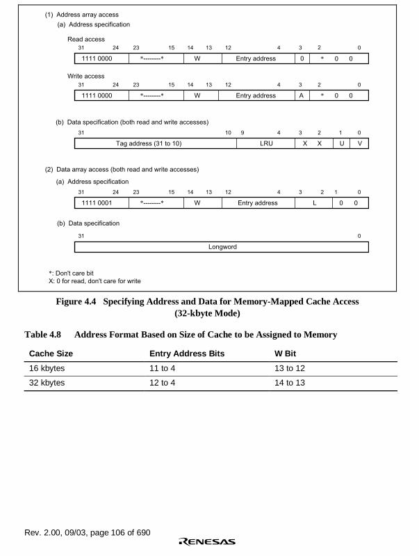
Rev. 2.00, 09/03, page 106 of 690
(1) Address array access
(a) Address specification
Read access
Write access
(b) Data specification (both read and write accesses)
(2) Data array access (both read and write accesses)
(a) Address specification
31 24 23 15 14 13 12 4 3 0
1111 0000 *--------* W Entry address
31 24 23 15 14 13 12 4 3 0
1111 0000 *--------* W Entry address
2
A
31 10 4 3 0
LRU
2
X X
9
Tag address (31 to 10) U V
1
31 24 23 15 14 13 12 4 3 0
1111 0001 *--------* W Entry address
12
L
(b) Data specification
31 0
Longword
*: Don't care bit
X: 0 for read, don't care for write
0 * 0 0
* 0 0
2
0 0
Figure 4.4 Specifying Address and Data for Memory-Mapped Cache Access(32-kbyte Mode)
Table 4.8 Address Format Based on Size of Cache to be Assigned to Memory
Cache Size Entry Address Bits W Bit
16 kbytes 11 to 4 13 to 12
32 kbytes 12 to 4 14 to 13

Rev. 2.00, 09/03, page 107 of 690
4.4.3 Usage Examples
Invalidating a Specific Entry: A specific cache entry can be invalidated by accessing theallocated memory cache and writing a 0 to the entry’s U and V bits. The A bit is cleared to 0, andan address is specified for the entry address and the way. If the U bit of the way of the entry inquestion was set to 1, the entry is written back and the V and U bits specified by the write data arewritten to.
In the following example, the write data is specified in R0 and the address is specified in R1 (32-kbyte mode).
; R0 = H'0000 0000 LRU = H'000, U = 0, V = 0
; R1 = H'F000 2080; Way = 1, Entry = B'000001000, A = 0
;
MOV.L R0, @R1
To invalidate all entries and ways, write 0 to the following addresses.
32-kbyte mode (2,048 writes)Addresses
F000 0000
F000 0010
F000 0020
:
F000 7FF0
16-kbyte mode (1,024 writes)Addresses
F000 0000
F000 0010
F000 0020
:
F000 3FF0
The above operation should be performed using a non-cacheable area.

Rev. 2.00, 09/03, page 108 of 690
Invalidating an Address Specification: An address specification can be invalidated by accessingthe memory allocation cache and writing a 0 to the entry’s V bit. When the A bit is 1, the tagaddress specified by the write data is compared to the tag address within the cache selected by theentry address. If the tag addresses match, and if the U bit of the entry is set to 1, the entry iswritten back and data is written to the specified the V and U bits. If no match is found, nooperation is carried out.
In the following example, the write data is specified in R0 and the address is specified in R1 (32-kbyte mode).
; R0=H'01100010; Tag address=B'0000 0001 0001 0000 0000 00, U=0, V=0
; R1=H'F0000088; address array access, entry=B'00001000, A=1
;
MOV.L R0,@R1
In the following example, an address (32-bit) to be purged is specified in R0.
MOV.L #H'00001FF0, R1 ; 32-kbyte mode, H'00000FF0 in the 16-kbyte mode.
AND R0, R1 ; The entry address is fetched.
MOV.L #H'00000008, R2 ;
OR R1, R2 ; The start is set to H'F0 and the A bit to 1.
MOV.L #H'1FFFFC00, R3 ;
AND R0, R3 ; The tag address is fetched. U = V = 0.
MOV.L R3, @R2 ; Associative purge.
The above operation should be performed using a non-cacheable area.
Reading the Data of a Specific Entry: To read the data field of a specific entry is enabled by thememory-mapped cache access. The longword indicated in the data field of the data array in figure4.4 is read into the register. In the example shown below, R0 specifies the address and R1 showswhat is read (32-kbyte mode).
; R0=H'F100 004C; data array access, entry=B'00000100; Way = 0, longword address = 3
;
MOV.L @R0,R1 ; Longword 3 is read.
4.5 Usage Note
Do note execute the PREF instruction for the area that cannot be accessed using the cache (P2 andP4 areas).

Rev. 2.00, 09/03, page 109 of 690
Section 5 Exception Handling
Exception handling is separate from normal program processing, and is performed by a routineseparate from the normal program. For example, if an attempt is made to execute an undefinedinstruction code or an instruction protected by the CPU processing mode, a control function maybe required to return to the source program by executing the appropriate operation or to report anabnormality and carry out end processing. In addition, a function to control processing requestedby LSI on-chip modules or an LSI external module to the CPU may also be required.
Transferring control to a user-defined exception processing routine and executing the process tosupport the above functions are called exception handling. This LSI has two types of exceptions:general exceptions and interrupts. The user can execute the required processing by assigningexception handling routines corresponding to the required exception processing and then return tothe source program.
A reset input can terminate the normal program execution and pass control to the reset vector afterregister initialization. This reset operation can also be regarded as an exception handling. Thissection describes an overview of the exception handling operation. Here, general exceptions andinterrupts are referred to as exception handling. For interrupts, this section describes only theprocess executed for interrupt requests. For details on how to generate an interrupt request, refer tosection 6, Interrupt Controller (INTC).
5.1 Register Descriptions
There are five registers for exception handling. A register with an undefined initial value should beinitialized by the software. Refer to section 24, List of Registers, for the addresses and access sizesof these registers.
• TRAPA exception register (TRA)
• Exception event register (EXPEVT)
• Interrupt event register (INTEVT)
• Interrupt event register 2 (INTEVT2)
• Exception address register (TEA)

Rev. 2.00, 09/03, page 110 of 690
Figure 5.1 shows the bit configuration of each register.
31
TRA
EXPEVT
INTEVT
INTEVT2
TRA
EXPEVT
INTEVT
INTEVT2
TEA TEA
10 9 2 1 0
31 12 11 0
00
0
0
0
31 12 11 0
31 12 11 0
31 0
Figure 5.1 Register Bit Configuration
5.1.1 TRAPA Exception Register (TRA)
TRA is assigned to address H'FFFFFFD0 and consists of the 8-bit immediate data (imm) of theTRAPA instruction. TRA is automatically specified by the hardware when the TRAPA instructionis executed. Only bits 9 to 2 of the TRA can be re-written using the software.
Bit Bit Name Initial Value R/W Description
31 to 10 R Reserved
These bits are always read as 0. The write valueshould always be 0.
9 to 2 TRA R/W 8-bit Immediate Data
1, 0 R Reserved
These bits are always read as 0. The write valueshould always be 0.

Rev. 2.00, 09/03, page 111 of 690
5.1.2 Exception Event Register (EXPEVT)
EXPEVT is assigned to address H'FFFFFFD4 and consists of a 12-bit exception code. Exceptioncodes to be specified in EXPEVT are those for resets and general exceptions. These exceptioncodes are automatically specified the hardware when an exception occurs. Only bits 11 to 0 ofEXPEVT can be re-written using the software.
Bit Bit Name Initial Value R/W Description
31 to 12 0 R Reserved
These bits are always read as 0. The write valueshould always be 0.
11 to 0 EXPEVT * R/W 12-bit Exception Code
Note: * Initialized to H'000 at power-on reset and H'020 at manual reset.
5.1.3 Interrupt Event Register (INTEVT)
INTEVT is assigned to address H'FFFFFFD8 and consists of a 12-bit exception code. Exceptioncodes to be specified in INTEVT are those for interrupt requests. These exception codes areautomatically specified by the hardware when an exception occurs. Only bits 11 to 0 of INTEVTcan be re-written using the software.
Bit Bit Name Initial Value R/W Description
31 to 12 0 R Reserved
These bits are always read as 0. The write valueshould always be 0.
11 to 0 INTEVT R/W 12-bit Exception Code

Rev. 2.00, 09/03, page 112 of 690
5.1.4 Interrupt Event Register 2 (INTEVT2)
INTEVT2 is assigned to address H'A4000000 and consists of a 12-bit exception code. Exceptioncodes to be specified in INTEVT2 are those for interrupt requests. These exception codes areautomatically specified by the hardware when an exception occurs. INTEVT2 cannot be modifiedusing the software.
Bit Bit Name Initial Value R/W Description
31 to 12 0 R Reserved
These bits are always read as 0. The write valueshould always be 0.
11 to 0 INTEVT2 R 12-bit Exception Code
5.1.5 Exception Address Register (TEA)
TEA is assigned to address H'FFFFFFFC and stores the logical address for an exceptionoccurrence when an exception related to memory accesses occurs. TEA can be modified using thesoftware.
Bit Bit Name Initial Value R/W Description
31 to 0 TEA R/W Logical address for exception occurrence

Rev. 2.00, 09/03, page 113 of 690
5.2 Exception Handling Function
5.2.1 Exception Handling Flow
In exception handling, the contents of the program counter (PC) and status register (SR) are savedin the saved program counter (SPC) and saved status register (SSR), respectively, and execution ofthe exception handler is invoked from a vector address. The return from exception handler (RTE)instruction is issued by the exception handler routine on completion of the routine, restoring thecontents of PC and SR to return to the processor state at the point of interruption and the addresswhere the exception occurred.
A basic exception handling sequence consists of the following operations. If an exception occursand the CPU accepts it, operations 1 to 8 are executed.
1. The address of the instruction to be returned to after exception handling is saved to SPC.
2. The contents of SR is saved in SSR.
3. The block (BL) bit in SR is set to 1, masking any subsequent exceptions.
4. The mode (MD) bit in SR is set to 1 to place the privileged mode.
5. The register bank (RB) bit in SR is set to 1.
6. An exception code identifying the exception event is written to bits 11 to 0 of the exceptionevent (EXPEVT) or interrupt event (INTEVT or INTEVT2) register.
7. If a TRAPA instruction is executed, an 8-bit immediate data specified by the TRAPAinstruction is set to TRA. For an exception related to memory accesses, the logic addresswhere the exception occurred is written to TEA.*1
8. Instruction execution jumps to the designated exception vector address to invoke the handlerroutine.
The above operations from 1 to 8 are executed in sequence. During these operations, no otherexceptions may be accepted unless multiple exception acceptance is enabled.
In an exception handling routine for a general exception, the appropriate exception handling mustbe executed based on an exception source determined by the EXPEVP. In an interrupt exceptionhandling routine, the appropriate exception handling must be executed based on an exceptionsource determined by the INTEVT or INTEVT2. After the exception handling routine has beencompleted, program execution can be resumed by executing an RTE instruction. The RTEinstruction causes the following operations to be executed.
1. The contents of the SSR are restored into the SR to return to the processing state in effectbefore the exception handling took place.
2. A delay slot instruction of the RTE instruction is executed.*2
3. Control is passed to the address stored in the SPC.

Rev. 2.00, 09/03, page 114 of 690
The above operations from 1 to 3 are executed in sequence. During these operations, no otherexceptions may be accepted. By changing the SPT and SSR before executing the RTE instruction,a status different from that in effect before the exception handling can also be specified.
Notes: 1. The MMU registers are also modified if an MMU exception occurs.
2. For details on the CPU processing mode in which RTE delay slot instructions areexecuted, please refer to section 5.4, Usage Notes.
5.2.2 Exception Vector Addresses
A vector address for general exceptions is determined by adding a vector offset to a vector baseaddress. The vector offset for general exceptions other than the TLB error exception isH'00000100. The vector offset for interrupts is H'00000600. The vector base address is loaded intothe vector base register (VBR) using the software. The vector base address should reside in the P1or P2 fixed physical address space.
5.2.3 Exception Codes
The exception codes are written to bits 11 to 0 of the EXPEVT register (for reset or generalexceptions) or the INTEVT2 register (for interrupt requests) to identify each specific exceptionevent. See section 6, Interrupt Controller (INTC), for details of the exception codes for interruptrequests. Table 5.1 lists exception codes for resets and general exceptions.
5.2.4 Exception Request and BL Bit (Multiple Exception Prevention)
The BL bit in SR is set to 1 when a reset or exception is accepted. While the BL bit is set to 1,acceptance of general exceptions is restricted as described below, making it possible to effectivelyprevent multiple exceptions from being accepted.
If the BL bit is set to 1, an interrupt request is not accepted and is retained. The interrupt request isaccepted when the BL bit is cleared to 0. If the CPU is in low power consumption mode, aninterrupt is accepted even if the BL bit is set to 1 and the CPU returns from the low powerconsumption mode.
A DMA error is not accepted and is retained if the BL bit is set to 1 and accepted when the BL bitis cleared to 0. User break requests generated while the BL bit is set are ignored and are notretained. Accordingly, user breaks are not accepted even if the BL bit is cleared to 0.
If a general exception other than a DMA address error or user break occurs while the BL bit is setto 1, the CPU enters a state similar to that in effect immediately after a reset, and passes control tothe reset vector (H'A0000000) (multiple exception). In this case, unlike a normal reset, modulesother than the CPU are not initialized, the contents of EXPEVT, SPC, and SSR are undefined, andthis status is not detected by an external device.

Rev. 2.00, 09/03, page 115 of 690
To enable acceptance of multiple exceptions, the contents of SPC and SSR must be saved whilethe BL bit is set to 1 after an exception has been accepted, and then the BL bit must be cleared to0. Before restoring the SPC and SSR, the BL bit must be set to 1.
5.2.5 Exception Source Acceptance Timing and Priority
Exception Request of Instruction Synchronous Type and Instruction Asynchronous Type:Resets and interrupts are requested asynchronously regardless of the program flow. In generalexceptions, a DMA address error and a user break under the specific condition are also requestedasynchronously. The user cannot expect on which instruction an exception is requested. Forgeneral exceptions other than a DMA address error and a user break under a specific condition,each general exception corresponds to a specific instruction.
Re-Execution Type and Processing-Completion Type Exceptions: All exceptions are classifiedinto two types: a re-execution type and a processing-completion type. If a re-execution typeexception is accepted, the current instruction executed when the exception is accepted isterminated and the instruction address is saved to the SPC. After returning from the exceptionprocessing, program execution resumes from the instruction where the exception was accepted. Ina processing-completion type exception, the current instruction executed when the exception isaccepted is completed, the next instruction address is saved to the SPC, and then the exceptionprocessing is executed.
During a delayed branch instruction and delay slot, the following operations are executed. A re-execution type exception detected in a delay slot is accepted before executing the delayed branchinstruction. A processing-completion type exception detected in a delayed branch instruction or adelay slot is accepted when the delayed branch instruction has been executed. In this case, theacceptance of delayed branch instruction or a delay slot precedes the execution of the branchdestination instruction. In the above description, a delay slot indicates an instruction following anunconditional delayed branch instruction or an instruction following a conditional delayed branchinstruction whose branch condition is satisfied. If a branch does not occur in a conditional delayedbranch, the normal processing is executed.
Acceptance Priority and Test Priority: Acceptance priorities are determined for all exceptionrequests. The priority of resets, general exceptions, and interrupts are determined in this order: areset is always accepted regardless of the CPU status. Interrupts are accepted only when resets orgeneral exceptions are not requested.
If multiple general exceptions occur simultaneously in the same instruction, the priority isdetermined as follows.
1. A processing-completion type exception generated at the previous instruction*
2. A user break before instruction execution (re-execution type)
3. An exception related to an instruction fetch (CPU address error and MMU related exceptions:re-execution type)

Rev. 2.00, 09/03, page 116 of 690
4. An exception caused by an instruction decode (General illegal instruction exceptions and slotillegal instruction exceptions: re-execution type, unconditional trap: processing-completiontype)
5. An exception related to data access (CPU address error and MMU related exceptions: re-execution type)
6. Unconditional trap (processing-completion type)
7. A user break other than one before instruction execution (processing-completion type)
8. DMA address error (processing-completion type)
Note:* If a processing-completion type exception is accepted at an instruction, exceptionprocessing starts before the next instruction is executed. This exception processingexecuted before an exception generated at the next instruction is detected.
Only one exception is accepted at a time. Accepting multiple exceptions sequentially results in allexception requests being processed.
Table 5.1 Exception Event Vectors
ExceptionType
CurrentInstruction Exception Event Priority*1
ExceptionOrder
Processat BL=1
VectorCode
VectorOffset
Power-on reset 1 1 Reset H'A00 —Reset Aborted
Manual reset 1 2 Reset H'020 —
User break(before instructionexecution)
2 0 Ignored H'1E0 H'00000100
CPU address error (instructionaccess)
2 1 Reset H'0E0 H'00000100
TLB miss *4
(instruction access)2 1-1 Reset H'040 H'00000400
TLB invalid *4 (instructionaccess)
2 1-2 Reset H'040 H'00000100
TLB protection violation *4
(instruction access)2 1-3 Reset H'0A0 H'00000100
Illegal general instructionexception
2 2 Reset H'180 H'00000100
Illegal slotinstruction exception
2 2 Reset H'1A0 H'00000100
CPU address error(data access)
2 3 Reset H'0E0/H'100
H'00000100
Generalexceptionevents
Re-executed
TLB miss *4
(data access)2 3-1 Reset H'040/
H'060H'00000400

Rev. 2.00, 09/03, page 117 of 690
ExceptionType
CurrentInstruction Exception Event Priority*1
ExceptionOrder
Processat BL=1
VectorCode
VectorOffset
TLB invalid *4 (data access) 2 3-2 Reset H'040/H'060
H'00000100
TLB protection violation *4
(data access)2 3-3 Reset H'0A0/
H'0C0H'00000100
Re-executed
Initial page write *4
(data access)2 3-4 Reset H'080 H'00000100
Unconditional trap (TRAPAinstruction)
2 4 Reset H'160 H'00000100
Generalexceptionevents
Completed
User breakpoint (Afterinstruction execution, address)
2 5 Ignored H'1E0 H'00000100
User breakpoint(Data break, I-BUS break)
2 5 Ignored H'1E0 H'00000100Generalinterruptrequests
Completed
DMA address error 2 6 Retained H'5C0 H'00000100
Interruptrequests
Completed Interrupt requests 3 —*2 Retained —*3 H'00000600
Notes: 1. Priorities are indicated from high to low, 1 being the highest and 3 the lowest.A reset has the highest priority. An interrupt is accepted only when general exceptionsare not requested.
2. For details on priorities in multiple interrupt sources, refer to section 6, InterruptController (INTC).
3. If an interrupt is accepted, the exception event register (EXPEVT) is not changed. Theinterrupt source code is specified in interrupt source register 2 (EXPEVT2). For details,refer to section 6, Interrupt Controller (INTC).
4. These exception codes are valid when the MMU is used.

Rev. 2.00, 09/03, page 118 of 690
5.3 Individual Exception Operations
This section describes the conditions for specific exception handling and the processor operationsfor resets and general exceptions. For interrupts, refer to section 6, Interrupt Controller (INTC).
5.3.1 Resets
Power-On Reset:
• Conditions
Power-on reset is request
• Operations
Set EXPEVT to H'000, initialize the CPU and on-chip peripheral modules, and branch to thereset vector H'A0000000. For details, refer to the register descriptions in the relevant sections.
Manual Reset:
• Conditions
Manual reset is request
• Operations
Set EXPEVT to H'020, initialize the CPU and on-chip peripheral modules, and branch to thereset vector H'A0000000. For details, refer to the register descriptions in the relevant sections.
5.3.2 General Exceptions
CPU Address Error:
• Conditions
Instruction is fetched from odd address (4n + 1, 4n + 3)
Word data is accessed from addresses other than word boundaries (4n + 1, 4n + 3)
Longword is accessed from addresses other than longword boundaries (4n + 1, 4n + 2,4n + 3)
The area ranging from H'80000000 to H'FFFFFFFF in logical space is accessed in usermode
• Types
Instruction synchronous, re-execution type
• Save address
Instruction fetch: An instruction address to be fetched when an exception occurred
Data access: An instruction address where an exception occurs (a delayed branch instructionaddress if an instruction is assigned to a delay slot)

Rev. 2.00, 09/03, page 119 of 690
• Exception code
An exception occurred during read: H'0E0
An exception occurred during write: H'1E0
• Remarks
The logical address (32 bits) that caused the exception is set in TEA.
Illegal General Instruction Exception:
• Conditions
When undefined code not in a delay slot is decoded
Delayed branch instructions: JMP, JSR, BRA, BRAF, BSR, BSRF, RTS, RTE, BT/S, BF/S
Note: For details on undefined code, refer to section 2.6.2, Operation Code Map. When anundefined code other than H'F000 to H'FFFF is decoded, operation cannot be guaranteed.
When a privileged instruction not in a delay slot is decoded in user mode
Privileged instructions: LDC, STC, RTE, LDTLB, SLEEP; instructions that access GBRwith LDC/STC are not privileged instructions.
• Types
Instruction synchronous, re-execution type
• Save address
An instruction address where an exception occurs
• Exception code
H'180
• Remarks
None
Illegal Slot Instruction:
• Conditions
When undefined code in a delay slot is decoded
Delayed branch instructions: JMP, JSR, BRA, BRAF, BSR, BSRF, RTS, RTE, BT/S, BF/S
When a privileged instruction in a delay slot is decoded in user mode
Privileged instructions: LDC, STC, RTE, LDTLB, SLEEP; instructions that access GBRwith LDC/STC are not privileged instructions.
When an instruction that rewrites PC in a delay slot is decoded
Instructions that rewrite PC: JMP, JSR, BRA, BRAF, BSR, BSRF, RTS, RTE, BT, BF,BT/S, BF/S, TRAPA, LDC Rm, SR, LDC.L @Rm+, SR
• Types
Instruction synchronous, re-execution type

Rev. 2.00, 09/03, page 120 of 690
• Save address
A delayed branch instruction address
• Exception code
H'1A0
• Remarks
None
Unconditional Trap:
• Conditions
TRAPA instruction executed
• Types
Instruction synchronous, processing-completion type
• Save address
An address of an instruction following TRAPA
• Exception code
H'160
• Remarks
The exception is a processing-completion type, so PC of the instruction after the TRAPAinstruction is saved to SPC. The 8-bit immediate value in the TRAPA instruction is quadrupledand set in TRA[9:2].
User Break Point Trap:
• Conditions
When a break condition set in the user break controller is satisfied
• Types
Break (L bus) before instruction execution: Instruction synchronous, re-execution type
Operand break (L bus): Instruction synchronous, processing-completion type
Data break (L bus): Instruction asynchronous, processing-completion type
I bus break: Instruction asynchronous, processing-completion type
• Save address
Re-execution type: An address of the instruction where a break occurs (a delayed branchinstruction address if an instruction is assigned to a delay slot)
Processing-completion type: An address of the instruction following the instruction where abreak occurs (a delayed branch instruction address if an instruction is assigned to a delay slot)
• Exception code
H'1E0

Rev. 2.00, 09/03, page 121 of 690
• Remarks
For details on user break controller, refer to section 22, User Break Controller (UBC).
DMA Address Error:
• Conditions
Word data accessed from addresses other than word boundaries (4n + 1, 4n + 3)
Longword accessed from addresses other than longword boundaries (4n + 1, 4n + 2, 4n +3)
• Types
Instruction asynchronous, processing-completion type
• Save address
An address of the instruction following the instruction where a break occurs (a delayed branchinstruction destination address if an instruction is assigned to a delay slot)
• Exception code
H'5C0
• Remarks
An exception occurs when a DMA transfer is executed while an illegal instruction addressdescribed above is specified in the DMAC. Since the DMA transfer is performedasynchronously with the CPU instruction operation, an exception is also requestedasynchronously with the instruction execution. For details on DMAC, refer to section 8, DirectMemory Access Controller (DMAC).
5.3.3 General Exceptions (MMU Exceptions)
When the address translation unit of the memory management unit (MMU) is valid, MMUexceptions are checked after a CPU address error has been checked. Four types of MMUexceptions are defined: TLP error exception, TLP invalid exception, TLB protection exception,and initial page write exception. These exceptions are checked in this order.
A vector offset for a TLB error exception is defined as H'00000400 to simplify exception sourcedetermination. For details on MMU exception operations, refer to section 3, Memory ManagementUnit (MMU).
TLB Miss Exception:
• Conditions
Comparison of TLB addresses shows no address match.
• Types
Instruction synchronous, re-execution type

Rev. 2.00, 09/03, page 122 of 690
• Save address
Instruction fetch: An instruction address to be fetched when an exception occurred
Data access: An instruction address where an exception occurs (a delayed branch instructionaddress if an instruction is assigned to a delay slot)
• Exception code
An exception occurred during read: H'040
An exception occurred during write: H'060
• Remarks
The logical address (32 bits) that caused the exception is set in TEA and the MMU registersare updated. The vector address of the TLB miss exception is VBR + H'0400. To speed upTLB miss processing, the offset differs from other exceptions.
TLB Invalid Exception:
• Conditions
Comparison of TLB addresses shows address match but V = 0.
• Types
Instruction synchronous, re-execution type
• Save address
Instruction fetch: An instruction address to be fetched when an exception occurred
Data access: An instruction address where an exception occurs (a delayed branch instructionaddress if an instruction is assigned to a delay slot)
• Exception code
An exception occurred during read: H'040
An exception occurred during write: H'060
• Remarks
The logical address (32 bits) that caused the exception is set in TEA and the MMU registersare updated.
TLB Protection Exception:
• Conditions
When a hit access violates the TLB protection information (PR bits)
• Types
Instruction synchronous, re-execution type
• Save address
Instruction fetch: An instruction address to be fetched when an exception occurred
Data access: An instruction address where an exception occurs (a delayed branch instructionaddress if an instruction is assigned to a delay slot)

Rev. 2.00, 09/03, page 123 of 690
• Exception code
An exception occurred during read: H'0A0
An exception occurred during write: H'0C0
• Remarks
The logical address (32 bits) that caused the exception is set in TEA and the MMU registersare updated.
Initial Page Write Exception:
• Conditions
A hit occurred to the TLB for a store access, but D = 0.
• Types
Instruction synchronous, re-execution type
• Save address
Instruction fetch: An instruction address to be fetched when an exception occurred
Data access: An instruction address where an exception occurs (a delayed branch instructionaddress if an instruction is assigned to a delay slot)
• Exception code
H'080
• Remarks
The logical address (32 bits) that caused the exception is set in TEA and the MMU registersare updated.

Rev. 2.00, 09/03, page 124 of 690
5.4 Usage Notes
1. An instruction assigned at a delay slot of the RTE instruction is executed after the contents ofthe SSR is restored into the SR. An acceptance of an exception related to instruction access isdetermined according to the SR before restore. An acceptance of other exceptions isdetermined by the SR after restore, processing mode, and BL bit value. A processing-completion type exception is accepted before an instruction at the RTE branch destinationaddress is executed. However, note that the correct operation cannot be guaranteed if a re-execution type exception occurs.
2. In an instruction assigned at a delay slot of the RTE instruction, a user break cannot beaccepted.
3. If the MD and BL bits of the SR register are changed by the LDC instruction, an exception isaccepted according to the changed SR value from the next instruction.* A processing-completion type exception is accepted before the next instruction is executed. An interruptand DMA address error in re-execution type exceptions are accepted before the nextinstruction is executed.
Note:* If an LDC instruction is executed for the SR, the following instructions are re-fetched andan instruction fetch exception is accepted according to the modified SR value.

Rev. 2.00, 09/03, page 125 of 690
Section 6 Interrupt Controller (INTC)
The interrupt controller (INTC) ascertains the priority of interrupt sources and controls interruptrequests to the CPU. The INTC registers set the order of priority of each interrupt, allowing theuser to process interrupt requests according to the user-set priority.
6.1 Features
• 16 levels of interrupt priority can be set
By setting the interrupt priority registers, the priorities of on-chip peripheral modules, and IRQinterrupts can be selected from 16 levels for individual request sources.
• NMI noise canceller function
An NMI input-level bit indicates the NMI pin state. By reading this bit in the interruptexception service routine, the pin state can be checked, enabling it to be used as a noisecanceller.
• IRQ interrupts can be set
Detection of low level, high level, rising edge, or falling edge

Rev. 2.00, 09/03, page 126 of 690
Figure 6.1 shows a block diagram of the INTC.
DMAC
SCIF
ADC
USB
TMU
TPU
WDT
UDI
REF
RTC
6
DMAC : Direct memory access controllerSCIF : Serial communication interface (with FIFO)ADC : A/D converterUSB : USB interfaceTMU : Timer pulse unitTPU : 16-bit timer pulse unit
WDT : Watchdog timerUDI : User debugging interfaceRTC : Realtime clockREF : Refresh request in bus state controllerICR : Interrupt control registerIPR : Interrupt priority level setting registerIRR : Interrupt request registerPINTER : PINT interrupt enable registerSR : Status register
Input/output
control
Priority
identifier
Com-
parator
Interrupt
request
SR
CPU
Bus
interface
Inte
rna
l b
us
INTC
I3 I2 I1 I0
(Interrupt request)
ICR
IRR
Legend:
PINTER
IRQ5−IRQ0
16PINT15−PINT0
NMI
IPR
Figure 6.1 Block Diagram of INTC

Rev. 2.00, 09/03, page 127 of 690
6.2 Input/Output Pins
Table 6.1 shows the INTC pin configuration.
Table 6.1 Pin Configuration
Name Abbreviation I/O Description
Nonmaskable interrupt input pin NMI Input Input of interrupt request signal, notmaskable by the interrupt mask bitsin SR
Interrupt input pins IRQ5 to IRQ0,IRL3 to IRL0
Input Input of interrupt request signals
Port interrupt input pins PINT15 toPINT0
Input Input of port interrupt signals
Note: IRL3 to IRL0 are multiplexed with IRQ3 to IRQ0; they cannot be used together with IRQ3 toIRQ0 at the same time.
6.3 Register Descriptions
The INTC has the following registers. For details on register addresses and register states duringeach processing, refer to section 24, List of Registers.
• Interrupt control register 0 (ICR0)
• Interrupt control register 1 (ICR1)
• Interrupt control register 2 (ICR2)
• PINT interrupt enable register (PINTER)
• Interrupt priority level setting register A (IPRA)
• Interrupt priority level setting register B (IPRB)
• Interrupt priority level setting register C (IPRC)
• Interrupt priority level setting register D (IPRD)
• Interrupt priority level setting register E (IPRE)
• Interrupt priority level setting register F (IPRF)
• Interrupt priority level setting register G (IPRG)
• Interrupt priority level setting register H (IPRH)
• Interrupt request register 0 (IRR0)
• Interrupt request register 1 (IRR1)
• Interrupt request register 2 (IRR2)

Rev. 2.00, 09/03, page 128 of 690
6.3.1 Interrupt Priority Level Setting Registers A to H (IPRA to IPRH)
IPRA to IPRH are 16-bit readable/writable registers in which priority levels from 0 to 15 are setfor on-chip peripheral module, and IRQ and PINT interrupts.
Bit Bit Name Initial Value R/W Description
15 to 0 IPR15 toIPR0
0 R/W These bits set the priority level for each interruptsource in 4-bit units. For details, see table 6.2.
Table 6.2 Interrupt Sources and IPRA to IPRH
Register Bits 15 to 12 Bits 11 to 8 Bits 7 to 4 Bits 3 to 0
IPRA TMU0 TMU1 TMU2 RTC
IPRB WDT REF Reserved* Reserved*
IPRC IRQ3 IRQ2 IRQ1 IRQ0
IPRD PINT0 to PINT7 PINT8 to PINT15 IRQ5 IRQ4
IPRE DMAC SCIF0 SCIF2 ADC
IPRF Reserved* Reserved* USB Reserved*
IPRG TPU0 TPU1 Reserved* Reserved*
IPRH TPU2 TPU3 Reserved* Reserved*
Note: *Always read as 0. The write value should always be 0.
As shown in table 6.2, on-chip peripheral module, or IRQ or PINT interrupts are assigned to four4-bit groups in each register. These 4-bit groups (bits 15 to 12, bits 11 to 8, bits 7 to 4, and bits 3to 0) are set with values from H'0 (0000) to H'F (1111). Setting H'0 means priority level 0(masking is requested); H'F means priority level 15 (the highest level).

Rev. 2.00, 09/03, page 129 of 690
6.3.2 Interrupt Control Register 0 (ICR0)
ICR0 is a register that sets the input signal detection mode of external interrupt input pin NMI, andindicates the input signal level at the NMI pin.
Bit Bit Name Initial Value R/W Description
15 NMIL 0/1* R NMI Input Level
Sets the level of the signal input at the NMI pin.This bit can be read from to determine the NMIpin level. This bit cannot be modified.
0: NMI input level is low
1: NMI input level is high
14 to 9 0 R Reserved
These bits are always read as 0. The write valueshould always be 0.
8 NMIE 0 R/W NMI Edge Select
Selects whether the falling or rising edge of theinterrupt request signal at the NMI pin isdetected.
0: Interrupt request is detected on falling edge ofNMI input
1: Interrupt request is detected on rising edge ofNMI input
7 to 0 0 R Reserved
These bits are always read as 0. The write valueshould always be 0.
Note: *When NMI input is high, 0 when NMI input is low.

Rev. 2.00, 09/03, page 130 of 690
6.3.3 Interrupt Control Register 1 (ICR1)
ICR1 is a 16-bit register that specifies the detection mode for external interrupt input pins IRQ0 toIRQ5 individually: rising edge, falling edge, high level, or low level.
Bit Bit Name Initial Value R/W Description
15 MAI 0 R/W Mask All Interrupts
When set to 1, masks all interrupt requests whena low level is being input to the NMI pin. MasksNMI interrupts in standby mode.
0: All interrupt requests are not masked when alow level is being input to the NMI pin
1: All interrupt requests are masked when a lowlevel is being input to the NMI pin
14 IRQLVL 1 R/W Interrupt Request Level Detect
Selects whether the IRQ3 to IRQ0 pins areenabled or disabled to be used as fourindependent interrupt pins. This bit does notaffect the IRQ4 and IRQ5 pins.
0: Used as four independent interrupt requestpins IRQ3 to IRQ0
1: Used as encoded 15-level interrupt pins asIRL3 to IRL0
13 BLMSK 0 R/W BL Bit Mask
Specifies whether NMI interrupts are maskedwhen the BL bit of the SR register is 1.
0: NMI interrupts are masked when the BL bit is 1
1: NMI interrupts are accepted regardless of theBL bit setting
12 0 R Reserved
This bit is always read as 0. The write valueshould always be 0.

Rev. 2.00, 09/03, page 131 of 690
Bit Bit Name Initial Value R/W Description
IRQn Sense Select
Select whether the interrupt signals to the IRQ5to IRQ0 pins are detected at the falling edge, atthe rising edge, at low level, or at high level.
Bit 2n+1 Bit 2n
IRQn1S IRQn0S
0 0 An interrupt request isdetected at IRQn inputfalling edge
0 1 An interrupt request isdetected at IRQn inputrising edge
1 0 An interrupt request isdetected at IRQn inputlow level
1 1 An interrupt request isdetected at IRQn inputhigh level
11 to 0 IRQ51S toIRQ00S
0 R/W
[Legend] n = 0 to 5

Rev. 2.00, 09/03, page 132 of 690
6.3.4 Interrupt Control Register 2 (ICR2)
ICR2 is a 16-bit register that specifies the detection mode for external interrupt input pins PINT15to PINT0.
Bit Bit Name Initial Value R/W Description
15 to 0 PINT15S toPINT0S
0 R/W PINT15 to PINT0 Sense Select
Select whether interrupt request signals toPINT15 to PINT0 are detected at low levels orhigh levels.
PINTnS
0: Interrupt requests are detected at low levelinput to the PINT pins
1: Interrupt requests are detected at high levelinput to the PINT pins
[Legend] n = 0 to 15
6.3.5 PINT Interrupt Enable Register (PINTER)
PINTER is a 16-bit register that enables interrupt requests input to external interrupt input pinsPINT0 to PINT15.
When all or some of these pins, PINT0 to PINT15 are not used as an interrupt input, a bitcorresponding to a pin unused as an interrupt request should be cleared to 0.
Bit Bit Name Initial Value R/W Description
15 to 0 PINT15E toPINT0E
0 R/W PINT15 to PINT0 Interrupt Enable
Select whether the interrupt requests input to thePINT15 to PINT0 pins is enabled.
PINTnE
0: Disables PINT input interrupt requests
1: Enables PINT input interrupt requests
[Legend] n = 0 to 15

Rev. 2.00, 09/03, page 133 of 690
6.3.6 Interrupt Request Register 0 (IRR0)
IRR0 is an 8-bit register that indicates interrupt requests from external input pins IRQ0 to IRQ5and PINT0 to PINT15.
Bit Bit Name Initial Value R/W Description
7 PINT0R 0 R PINT0 to PINT7 Interrupt Request
Indicates whether interrupt requests are input toPINT0 to PINT7 pins.
0: Interrupt requests are not input to PINT0 toPINT7 pins
1: Interrupt requests are input to PINT0 to PINT7pins
6 PINT1R 0 R PINT8 to PINT15 Interrupt Request
Indicates whether interrupt requests are input toPINT8 to PINT15 pins.
0: Interrupt requests are not input to PINT8 toPINT15 pins
1: Interrupt requests are input to PINT8 toPINT15 pins
5 to 0 IRQ5R toIRQ0R
0 R/W IRQn Interrupt RequestIndicates whether there is interrupt request inputto the IRQn pin. When edge-detection mode isset for IRQn, an interrupt request is cleared bywriting 0 to the IRQnR bit after reading IRQnR =1.When level-detection mode is set for IRQn, thesebits indicate whether an interrupt request is input.The interrupt request is set/cleared by only 1/0input to the IRQn pin.
IRQnR
0: No interrupt request input to IRQn pin
1: Interrupt request input to IRQn pin
[Legend] n = 0 to 5

Rev. 2.00, 09/03, page 134 of 690
6.3.7 Interrupt Request Register 1 (IRR1)
IRR1 is an 8-bit register that indicates whether DMAC or SCIF0 interrupt requests are generated.
BitBitName
InitialValue R/W Description
7 TXI0R 0 R TXI0 Interrupt Request
Indicates whether a TXI0 (SCIF0) interrupt request is generated.
0: A TXI0 interrupt request is not generated
1: A TXI0 interrupt request is generated
6 0 R Reserved
This bit is always read as 0.
5 RXI0R 0 R RXI0 Interrupt Request
Indicates whether an RXI0 (SCIF0) interrupt request isgenerated.
0: An RXI0 interrupt request is not generated
1: An RXI0 interrupt request is generated
4 ERI0R 0 R ERI0 Interrupt Request
Indicates whether an ERI0 (SCIF0) interrupt request isgenerated.
0: An ERI0 interrupt request is not generated
1: An ERI0 interrupt request is generated
3 DEI3R 0 R DEI3 Interrupt Request
Indicates whether a DEI3 (DMAC) interrupt request is generated.
0: A DEI3 interrupt request is not generated
1: A DEI3 interrupt request is generated
2 DEI2R 0 R DEI2 Interrupt Request
Indicates whether a DEI2 (DMAC) interrupt request is generated.
0: A DEI2 interrupt request is not generated
1: A DEI2 interrupt request is generated
1 DEI1R 0 R DEI1 Interrupt Request
Indicates whether a DEI1 (DMAC) interrupt request is generated.
0: A DEI1 interrupt request is not generated
1: A DEI1 interrupt request is generated

Rev. 2.00, 09/03, page 135 of 690
BitBitName
InitialValue R/W Description
0 DEI0R 0 R DEI0 Interrupt Request
Indicates whether a DEI0 (DMAC) interrupt request is generated.
0: A DEI0 interrupt request is not generated
1: A DEI0 interrupt request is generated
6.3.8 Interrupt Request Register 2 (IRR2)
IRR2 is an 8-bit register that indicates whether SCIF2 or ADC interrupt requests are generated.
BitBitName
InitialValue R/W Description
7 to 5 0 R Reserved
These bits are always read as 0.
4 ADIR 0 R ADI Interrupt Request
Indicates whether an ADI (ADC) interrupt request is generated.
0: An ADI interrupt request is not generated
1: An ADI interrupt request is generated
3 TXI2R 0 R TXI2 Interrupt Request
Indicates whether a TXI2 (SCIF2) interrupt request is generated.
0: A TXI2 interrupt request is not generated
1: A TXI2 interrupt request is generated
2 0 R Reserved
This bit is always read as 0.
1 RXI2R 0 R RXI2 Interrupt Request
Indicates whether an RXI2 (SCIF2) interrupt request isgenerated.
0: An RXI2 interrupt request is not generated
1: An RXI2 interrupt request is generated
0 ERI2R 0 R ERI2 Interrupt Request
Indicates whether an ERI2 (SCIF2) interrupt request isgenerated.
0: An ERI2 interrupt request is not generated
1: An ERI2 interrupt request is generated

Rev. 2.00, 09/03, page 136 of 690
6.4 Interrupt Sources
There are five types of interrupt sources: NMI, IRQ, IRL, PINT, and on-chip peripheral modules.Each interrupt has a priority level (0 to 16), with 1 the lowest and 16 the highest. Priority level 0masks an interrupt, so the interrupt request is ignored.
6.4.1 NMI Interrupt
The NMI interrupt has the highest priority level of 16. When the BLMSK bit in the interruptcontrol register 1 (ICR1) is 1 or the BL bit in the status register (SR) is 0, NMI interrupt isaccepted. NMI interrupt is edge-detected. In sleep or standby mode, the interrupt is acceptedregardless of the BL setting. The NMI edge select bit (NMIE) in the interrupt control register 0(ICR0) is used to select either rising or falling edge detection.
When using edge-input detection for NMI interrupt, a pulse width of at least two Pφcycles(peripheral clock) is necessary. NMI interrupt exception handling does not affect the interruptmask level bits (I3 to I0) in the status register (SR). When the MAI bit in ICR1 is 1, NMI interruptis not accepted.
It is possible to wake the chip up from sleep mode or standby mode with an NMI interrupt.
6.4.2 IRQ Interrupts
IRQ interrupts are input by level or edge from pins IRQ0 to IRQ5. The priority level can be set byinterrupt priority registers C and D (IPRC and IPRD) in a range from 0 to 15.
When using edge-sensing for IRQ interrupts, clear the interrupt source by having software read 1from the corresponding bit in IRR0, then write 0 to the bit.
When ICR1 is rewritten, IRQ interrupts may be mistakenly detected, depending on the IRQ pinstates. To prevent this, rewrite the register while interrupts are masked, then release the mask afterclearing the illegal interrupt by writing 0 to interrupt request register 0 (IRR0).
Edge input interrupt detection requires input of a pulse width of more than two cycles on a P clockbasis.
When using level-sensing for IRQ interrupts, the pin levels must be retained until the CPUsamples the pins. Therefore, the interrupt source must be cleared by the interrupt handler.
The interrupt mask bits (I3 to I0) in the status register (SR) are not affected by IRQ interrupthandling. IRQ interrupts can wake the chip up from the standby state when the relevant interruptlevel is higher than I3 to I0 in SR (but only when the RTC is used, the clock for the RTC is used towake the chip up from the standby state).
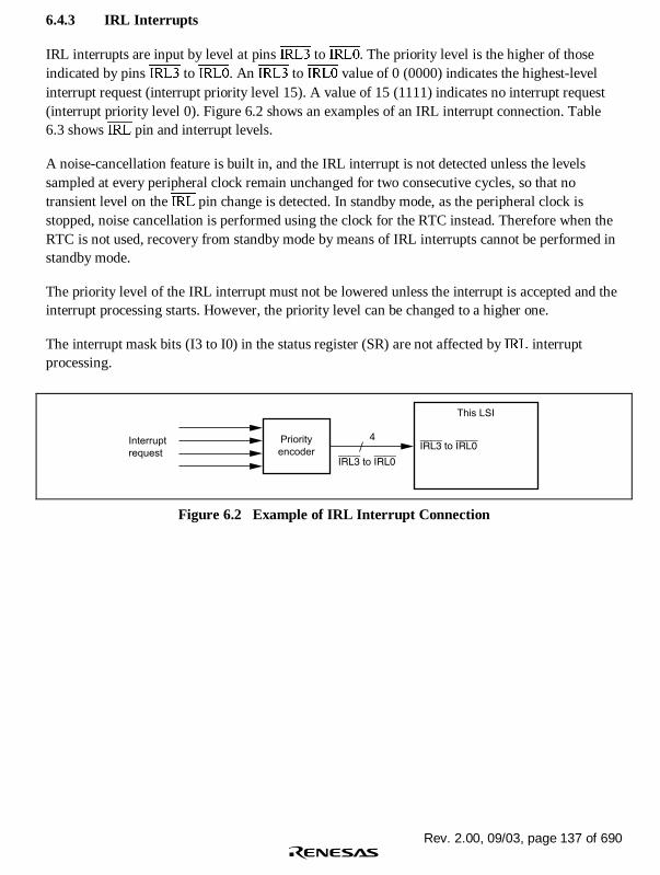
Rev. 2.00, 09/03, page 137 of 690
6.4.3 IRL Interrupts
IRL interrupts are input by level at pins IRL3 to IRL0. The priority level is the higher of thoseindicated by pins IRL3 to IRL0. An IRL3 to IRL0 value of 0 (0000) indicates the highest-levelinterrupt request (interrupt priority level 15). A value of 15 (1111) indicates no interrupt request(interrupt priority level 0). Figure 6.2 shows an examples of an IRL interrupt connection. Table6.3 shows IRL pin and interrupt levels.
A noise-cancellation feature is built in, and the IRL interrupt is not detected unless the levelssampled at every peripheral clock remain unchanged for two consecutive cycles, so that notransient level on the IRL pin change is detected. In standby mode, as the peripheral clock isstopped, noise cancellation is performed using the clock for the RTC instead. Therefore when theRTC is not used, recovery from standby mode by means of IRL interrupts cannot be performed instandby mode.
The priority level of the IRL interrupt must not be lowered unless the interrupt is accepted and theinterrupt processing starts. However, the priority level can be changed to a higher one.
The interrupt mask bits (I3 to I0) in the status register (SR) are not affected by IRL interruptprocessing.
Interrupt
request
Priority
encoderIRL3 to IRL0
4
This LSI
IRL3 to IRL0
Figure 6.2 Example of IRL Interrupt Connection

Rev. 2.00, 09/03, page 138 of 690
Table 6.3 IRL3 to IRL0 Pins and Interrupt Levels
IRL3 IRL2 IRL1 IRL0 Interrupt Priority Level Interrupt Request
0 0 0 0 15 Level 15 interrupt request
0 0 0 1 14 Level 14 interrupt request
0 0 1 0 13 Level 13 interrupt request
0 0 1 1 12 Level 12 interrupt request
0 1 0 0 11 Level 11 interrupt request
0 1 0 1 10 Level 10 interrupt request
0 1 1 0 9 Level 9 interrupt request
0 1 1 1 8 Level 8 interrupt request
1 0 0 0 7 Level 7 interrupt request
1 0 0 1 6 Level 6 interrupt request
1 0 1 0 5 Level 5 interrupt request
1 0 1 1 4 Level 4 interrupt request
1 1 0 0 3 Level 3 interrupt request
1 1 0 1 2 Level 2 interrupt request
1 1 1 0 1 Level 1 interrupt request
1 1 1 1 0 No interrupt request
6.4.4 PINT Interrupt
PINT interrupts are input from pins PINT0 to PINT15 with a level. The priority level can be set bythe interrupt priority level setting register D (IPRD) in a range from levels 0 to 15, in the unit ofPINT0 to PINT7 or PINT8 to PINT15. The PINT interrupt level should be held until the interruptis accepted and interrupt handling is started.
The interrupt mask bits (I3 to I0) in the status register (SR) are not affected by PINT interruptprocessing. PINT interrupts can wake the chip up from the standby state when the relevantinterrupt level is higher than I3 to I0 in SR (but only when the RTC is used, the clock for the RTCis used to wake the chip up from the standby state).
6.4.5 On-Chip Peripheral Module Interrupts
On-chip peripheral module interrupts are generated by the following 10 modules:
• Direct memory access controller (DMAC)
• Serial communication interfaces (SCIF0 and SCIF2)
• A/D converter (ADC)

Rev. 2.00, 09/03, page 139 of 690
• USB interface (USB)
• Timer unit (TMU)
• 16-bit timer pulse unit (TPU)
• Watchdog timer (WDT)
• Bus state controller (BSC)
• User-debugging interface (UDI)
• Realtime clock (RTC)
Not every interrupt source is assigned a different interrupt vector. Sources are reflected in theinterrupt event registers (INTEVT and INTEVT2). It is easy to identify sources by using the valueof INTEVT or INTEVT2 as a branch offset.
A priority level (from 0 to 15) can be set for each module except UDI by writing to the interruptpriority level setting registers A to H (IPRA to IPRH). The priority level of the UDI interrupt is 15(fixed).
The interrupt mask bits (I3 to I0) in the status register are not affected by on-chip peripheralmodule interrupt handling.
6.4.6 Interrupt Exception Handling and Priority
There are five types of interrupt sources: NMI, IRQ, IRL, PINT, and on-chip peripheral modules.The priority of each interrupt source is set within priority levels 0 to 16; level 16 is the highest andlevel 1 is the lowest. When the priority is set to level 0, that interrupt is masked and the interruptrequest is ignored.
Tables 6.4 and 6.5 list the codes for the interrupt source and the interrupt event registers (INTEVTand INTEVT2) and the order of interrupt priority.
Each interrupt source is assigned a unique code by INTEVT and INTEVT2. The start address ofthe interrupt service routine is common for each interrupt source. This is why, for instance, thevalue of INTEVT2 is used as an offset at the start of the interrupt service routine and branched toin order to identify the interrupt source.
IRQ and PINT interrupts, and on-chip peripheral module interrupt priorities can be set freelybetween 0 and 15 for each module by setting the interrupt priority level setting registers. A resetassigns priority level 0 to IRQ, PINT, and on-chip peripheral module interrupts.
If the same priority level is assigned to two or more interrupt sources and interrupts from thosesources occur simultaneously, their priority order is the default priority order indicated at the rightin tables 6.4 and 6.5.

Rev. 2.00, 09/03, page 140 of 690
Table 6.4 Interrupt Exception Handling Sources and Priority (IRQ Mode)
Interrupt Source Interrupt Code*1
InterruptPriority(Initial Value)
IPR(Bit Numbers)
Prioritywithin IPRSetting Unit
DefaultPriority
NMI H'1C0*2 16 High
UDI H'5E0*2 15
IRQ0 H'600*3 0 to 15 (0) IPRC (3 to 0)
IRQ1 H'620*3 0 to 15 (0) IPRC (7 to 4)
IRQ2 H'640*3 0 to 15 (0) IPRC (11 to 8)
IRQ3 H'660*3 0 to 15 (0) IPRC (15 to 12)
IRQ4 H'680*3 0 to 15 (0) IPRD (3 to 0)
IRQ
IRQ5 H'6A0*3 0 to 15 (0) IPRD (7 to 4)
PINT0 toPINT7
H'700*3 0 to 15 (0) IPRD (15 to 12) PINT
PINT8 toPINT15
H'720*3 0 to 15 (0) IPRD (11 to 8)
DEI0 H'800*3 High
DEI1 H'820*3
DEI2 H'840*3
DMAC
DEI3 H'860*3
0 to 15 (0) IPRE (15 to 12)
Low
ERI0 H'880*3 0 to 15 (0) IPRE (11 to 8) High
RXI0 H'8A0*3
SCIF0
TXI0 H'8E0*3 Low
ERI2 H'900*3 High
RXI2 H'920*3
SCIF2
TXI2 H'960*3
0 to 15 (0) IPRE (7 to 4)
Low
ADC ADI H'980*3 0 to 15 (0) IPRE (3 to 0) —
USI0 H'A20*3 HighUSB
USI1 H'A40*3
0 to 15 (0) IPRF (7 to 4)
Low
TPU0 TPI0 H'C00*3 0 to 15 (0) IPRG (15 to 12) —
TPU1 TPI1 H'C20*3 0 to 15 (0) IPRG (11 to 8) —
TPU2 TPI2 H'C80*3 0 to 15 (0) IPRH (15 to 12) —
TPU3 TPI3 H'CA0*3 0 to 15 (0) IPRH (11 to 8) — Low

Rev. 2.00, 09/03, page 141 of 690
Interrupt Source Interrupt Code*1
InterruptPriority(Initial Value)
IPR(Bit Numbers)
Prioritywithin IPRSetting Unit
DefaultPriority
TMU0 TUNI0 H'400*2 0 to 15 (0) IPRA (15 to 12) — High
TMU1 TUNI1 H'420*2 0 to 15 (0) IPRA (11 to 8) —
TUNI2 H'440*2 HighTMU2
TICPI2 H'460*2
0 to 15 (0) IPRA (7 to 4)
Low
ATI H'480*2 High
PRI H'4A0*2
RTC
CUI H'4C0*2
0 to 15 (0) IPRA (3 to 0)
Low
WDT ITI H'560*2 0 to 15 (0) IPRB (15 to 12) —
REF RCMI H'580*2 0 to 15 (0) IPRB (11 to 8) — Low
Notes: 1. The INTEVT2 code.2. The same code as INTEVT2 is set in INTEVT.3. The code indicating an interrupt level (H'200 to H'3C0 shown in table 6.6) is set in
INTEVT.
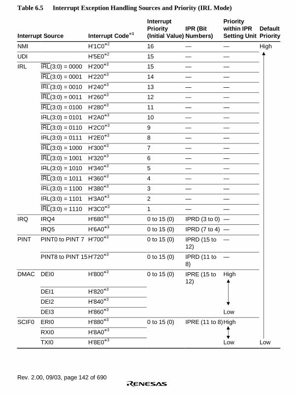
Rev. 2.00, 09/03, page 142 of 690
Table 6.5 Interrupt Exception Handling Sources and Priority (IRL Mode)
Interrupt Source Interrupt Code*1
InterruptPriority(Initial Value)
IPR (BitNumbers)
Prioritywithin IPRSetting Unit
DefaultPriority
NMI H'1C0*2 16 — — High
UDI H'5E0*2 15 — —
IRL IRL(3:0) = 0000 H'200*3 15 — —
IRL(3:0) = 0001 H'220*3 14 — —
IRL(3:0) = 0010 H'240*3 13 — —
IRL(3:0) = 0011 H'260*3 12 — —
IRL(3:0) = 0100 H'280*3 11 — —
IRL(3:0) = 0101 H'2A0*3 10 — —
IRL(3:0) = 0110 H'2C0*3 9 — —
IRL(3:0) = 0111 H'2E0*3 8 — —
IRL(3:0) = 1000 H'300*3 7 — —
IRL(3:0) = 1001 H'320*3 6 — —
IRL(3:0) = 1010 H'340*3 5 — —
IRL(3:0) = 1011 H'360*3 4 — —
IRL(3:0) = 1100 H'380*3 3 — —
IRL(3:0) = 1101 H'3A0*3 2 — —
IRL(3:0) = 1110 H'3C0*3 1 — —
IRQ IRQ4 H'680*3 0 to 15 (0) IPRD (3 to 0) —
IRQ5 H'6A0*3 0 to 15 (0) IPRD (7 to 4) —
PINT PINT0 to PINT 7 H'700*3 0 to 15 (0) IPRD (15 to12)
—
PINT8 to PINT 15H'720*3 0 to 15 (0) IPRD (11 to8)
—
DMAC DEI0 H'800*3 0 to 15 (0) IPRE (15 to12)
High
DEI1 H'820*3
DEI2 H'840*3
DEI3 H'860*3 Low
SCIF0 ERI0 H'880*3 0 to 15 (0) IPRE (11 to 8)High
RXI0 H'8A0*3
TXI0 H'8E0*3 Low Low

Rev. 2.00, 09/03, page 143 of 690
Interrupt Source Interrupt Code*1
InterruptPriority(Initial Value)
IPR (BitNumbers)
Prioritywithin IPRSetting Unit
DefaultPriority
SCIF2 ERI2 H'900*3 0 to 15 (0) IPRE (7 to 4) High High
RXI2 H'920*3
TXI2 H'960*3 Low
ADC ADI H'980*3 0 to 15 (0) IPRE (3 to 0) —
USB USI0 H'A20*3 0 to 15 (0) IPRF (7 to 4) High
USI1 H'A40*3 Low
TPU0 TPI0 H'C00*3 0 to 15 (0) IPRG (15 to12)
—
TPU1 TPI1 H'C20*3 0 to 15 (0) IPRG (11 to8)
—
TPU2 TPI2 H'C80*3 0 to 15 (0) IPRH (15 to12)
—
TPU3 TPI3 H'CA0*3 0 to 15 (0) IPRH (11 to8)
—
TMU0 TUNI0 H'400*2 0 to 15 (0) IPRA (15 to12)
—
TMU1 TUNI1 H'420*2 0 to 15 (0) IPRA (11 to 8)—
TMU2 TUNI2 H'440*2 0 to 15 (0) IPRA (7 to 4) High
TICPI2 H'460*2 Low
RTC ATI H'480*2 0 to 15 (0) IPRA (3 to 0) High
PRI H'4A0*2
CUI H'4C0*2 Low
WDT ITI H'560*2 0 to 15 (0) IPRB (15 to12)
—
REF RCMI H'580*2 0 to 15 (0) IPRB (11 to 8)— Low
Notes: 1. The INTEVT2 code.2. The same code as INTEVT2 is set in INTEVT.3. The code indicating an interrupt level (H'200 to H'3C0 shown in table 6.6) is set in
INTEVT.

Rev. 2.00, 09/03, page 144 of 690
Table 6.6 Interrupt Level and INTEVT Code
Interrupt level INTEVT Code
15 H'200
14 H'220
13 H'240
12 H'260
11 H'280
10 H'2A0
9 H'2C0
8 H'2E0
7 H'300
6 H'320
5 H'340
4 H'360
3 H'380
2 H'3A0
1 H'3C0
6.5 Operation
6.5.1 Interrupt Sequence
The sequence of interrupt operations is described below. Figure 6.3 is a flowchart of theoperations.
1. The interrupt request sources send interrupt request signals to the interrupt controller.
2. The interrupt controller selects the highest-priority interrupt from the interrupt requests sent,following the priority levels set in the interrupt priority level setting registers A to H (IPRA toIPRH). Lower priority interrupts are held pending. If two of these interrupts have the samepriority level or if multiple interrupts occur within a single module, the interrupt with thehighest priority is selected, according to tables 6.4 and 6.5.
3. The priority level of the interrupt selected by the interrupt controller is compared with theinterrupt mask bits (I3 to I0) in the status register (SR) of the CPU. If the request priority levelis higher than the level in bits I3 to I0, the interrupt controller accepts the interrupt and sendsan interrupt request signal to the CPU.
4. Detection timing: The INTC operates, and notifies the CPU of interrupt requests, insynchronization with the peripheral clock (Pφ). The CPU receives an interrupt at a break ininstructions.

Rev. 2.00, 09/03, page 145 of 690
5. The interrupt source code is set in the interrupt event registers (INTEVT and INTEVT2).
6. The status register (SR) and program counter (PC) are saved to SSR and SPC, respectively.
7. The block bit (BL), mode bit (MD), and register bank bit (RB) in SR are set to 1.
8. The CPU jumps to the start address of the interrupt handler (the sum of the value set in thevector base register (VBR) and H'00000600). This jump is not a delayed branch. The interrupthandler may branch with INTEVT or INTEVT2 value as its offset in order to identify theinterrupt source. This enables it to branch to the handling routine for the individual interruptsource.
Notes: 1. The interrupt mask bits (I3 to I0) in the status register (SR) are not changed byacceptance of an interrupt in this LSI.
2. The interrupt source flag should be cleared in the interrupt handler. To ensure that aninterrupt request that should have been cleared is not inadvertently accepted again, readthe interrupt source flag after it has been cleared, and then execute an RTE instruction.

Rev. 2.00, 09/03, page 146 of 690
Yes
Yes
Yes
Yes
Yes
Yes
Yes
Yes
Yes
Yes
Yes
Yes
Yes
NoNo
No
No
No
No
No
No
No
No
No
No
No
Programexecution state
Interruptgenerated?
ICR1.MAI = 1?
ICR1.BLMSK = 1?
NMI?
NMI = low?
SR.BL=0or sleep mode or software
standby mode?
NMI?
Level 15interrupt?
I3-I0 level14 or lower?
Level 14interrupt?
I3-I0 level13 or lower?
Level 1interrupt?
I3-I0level 0?
Set interrupt source inINTEVT and INTEVT2
Save SR to SSR;save PC to SPC
Set BL/MD/RBbits in SR to 1
Branch to exceptionhandler
I3-I0: Interrupt mask bits in status register (SR)
Figure 6.3 Interrupt Operation Flowchart

Rev. 2.00, 09/03, page 147 of 690
6.5.2 Multiple Interrupts
When handling multiple interrupts, an interrupt handler should include the following procedures:
1. Branch to a specific interrupt handler corresponding to a code set in INTEVT or INTEVT2.The code in INTEVT or INTEVT2 can be used as an offset for branching to the specifichandler.
2. Clear the interrupt source in each specific handler.
3. Save SSR and SPC to memory.
4. Clear the BL bit in SR, and set the accepted interrupt level in the interrupt mask bits in SR.
5. Handle the interrupt.
6. Execute the RTE instruction.
When these procedures are followed in order, an interrupt of higher priority than the one beinghandled can be accepted after clearing BL in step 4. Figure 6.3 shows a sample interrupt operationflowchart.
6.6 Usage Note
The interrupt accept timing in this LSI is not acknowledged externally. Thus, keep the followingnote in mind when designing the system.
• Level interrupt
The level interrupt request should be held until the CPU accepts it. The level interrupt requestneeds to be cleared (released) within the specific interrupt handler. If the level interrupt requestis not held, the operation may branch to the interrupt handling routine when the value inINTEVT/2 becomes H'000.
When the standby state is cancelled, if the level interrupt request is not held, the operation willgo back to the standby state again in the middle of WDT counting. When canceling thestandby state again in such a condition by asserting the level interrupt request, the settling timefor the PLL or crystal oscillator is not secured enough and the operation may not recover fromthe standby state correctly.
• Interrupt flag update
When an interrupt is acceptable and the generation of an interrupt request is enabled, updatingor clearing the interrupt flag may branch the operation to the interrupt handling routine whenthe value in INTEVT2 becomes H'000.

Rev. 2.00, 09/03, page 148 of 690
BSCS311A_000020020100 Rev. 2.00, 09/03, page 149 of 690
Section 7 Bus State Controller (BSC)
7.1 Overview
The bus state controller (BSC) outputs control signals for various types of memory that isconnected to the external address space and external devices. BSC functions enable this LSI toconnect directly with SRAM, SDRAM, and other memory storage devices, and external devices.
7.1.1 Features
The BSC has the following features:
• Physical address space is divided into eight areas
A maximum 32 or 64 Mbytes for each of the eight areas, CS0, CS2 to CS4, CS5A, CS5B,CS6A and CS6B, totally 384 Mbytes.
Can specify the normal space interface, byte-selection SRAM interface, burst ROM,address/data multiplex I/O (MPX), or SDRAM for each address space.
Can select the data bus width (8, 16, or 32 bits) for each address space.
Controls the insertion of the wait state for each address space.
Controls the insertion of the wait state for each read access and write access.
Can set the independent idling cycle in the continuous access for five cases: read-write (insame space/different space), read-read (in same space/different space), the first cycle is awrite access.
• Normal space interface
Supports the interface that can directly connect to the SRAM.
• Burst ROM interface
High-speed access to the ROM, such as flash memory, that has the page mode function.
• Address/data multiplex I/O (MPX) interface
Can directly connect to a peripheral LSI that needs an address/data multiplexing.
• SDRAM interface
Can set the SDRAM up to 2 areas.
Multiplex output for row address/column address.
Efficient access by single read/single write.
High-speed access by the bank-active mode.
Supports an auto-refresh and self-refresh.

Rev. 2.00, 09/03, page 150 of 690
• Bus arbitration
Shares all of the resources with other CPU and outputs the bus enable after receiving thebus request from external devices.
7.1.2 Block Diagram
BSC functional block diagram is shown in figure 7.1.
Output
signal drive
controller
Wait between
access cycles
controller
Wait
controller
Memory
controller
Refresh
controller
Address/data
controller
Area
controller
CMNCR
CSnBCR*
CSnWCR*
SDCR
RTCSR
RTCNT
RTCOR
Comparator
CS0, CS2, CS3, CS4,
CS5A, CS5B, CS6A, CS6B
BS, RD, RD/WR, WE3 to WE0,
RASU, RASL, CASU, CASL,
AH, CKE, DQMUU, DQMUL,
DQMLU, DQMLL
WAIT
A25 to 0
D31 to 0
Internal
address bus
Internal
data bus
Note: * CSnBCR, CSnWCR : n = 0, 2, 3, 4, 5A, 5B, 6A, 6B
Legend:
CSnBCR : Area n bus control register
CSnWCR : Area n wait control register
SDCR : SDRAM control register
RTCSR : Refresh timer control/status register
RTCNT : Refresh timer counter
RTCOR : Refresh timer constant register
BSC
Figure 7.1 BSC Functional Block Diagram

Rev. 2.00, 09/03, page 151 of 690
7.2 Pin Configuration
Table 7.1 Pin Configuration
Name I/O Function
A25 to A0 O Address bus
D31 to D0 I/O Data bus
BS O Bus cycle start
Asserted when a normal space, byte-selection SRAM, burst ROM, oraddress/data multiplex I/O is accessed. Asserted by the same timingas CAS in SDRAM access.
CS0, CS2 to CS4,CS5A, CS5B, CS6A,CS6B
O Chip select
RD/WR O Read/write
Connects to WE pins when SDRAM or byte-selection SRAM isconnected.
RD O Read
WE3,
DQMUU
O Indicates that D31 to D24 are being written to when a normal spaceis set.
Selects D31 to D24 when a byte-selection SRAM space is set.
Selects D31 to D24 when an SDRAM space is set.
WE2,
DQMUL
O Indicates that D23 to D16 are being written to when a normal spaceis set.
Selects D23 to D16 when a byte-selection SRAM space is set.
Selects D23 to D16 when an SDRAM space is set.
WE1,
DQMLU
O Indicates that D15 to D8 are being written to when a normal spaceand address/data multiplex I/O space are set.
Selects D15 to D8 when a byte-selection SRAM space is set.
Selects D15 to D8 when an SDRAM space is set.
WE0,
DQMLL
O Indicates that D7 to D0 are being written to when a normal spaceand address/data multiplex I/O space are set.
Selects D7 to D0 when a byte-selection SRAM space is set.
Selects D7 to D0 when an SDRAM space is set.
RASU
RASL
O Connects to RAS pin when SDRAM is connected.
CASU
CASL
O Connects to CAS pin when SDRAM is connected.

Rev. 2.00, 09/03, page 152 of 690
Name I/O Function
CKE O Connects to CKE pin when SDRAM is connected.
AH O Holds the address in address/data multiplex I/O mode.
WAIT I External wait input
BREQ I Bus request input
BACK O Bus acknowledge output
MD3, MD4 I Area 0 bus width (8/16/32 bits)
MD5 I Specifies endian
0: Big endian
1: Little endian
7.3 Area Overview
In the architecture of this LSI, both logical spaces and physical spaces have 32-bit address spaces.The cache access method is shown by the upper 3 bits. For details see section 4, Cache. Theremaining 29 bits are used for division of the space into eight areas. The BSC performs control forthis 29-bit space.
As listed in table 7.2, this LSI can be connected directly to eight areas of memory, and it outputschip select signals (CS0, CS2 to CS4, CS5A, CS5B, CS6A, and CS6B) for each of them. CS0 isasserted during area 0 access; CS5B is asserted during area 5B access. When an SDRAM isconnected to area 2 or area 3, RASU, RASL, CASU, CASL, DQMUU, DQMUL, DQMLU, andDQMLL are asserted.
7.3.1 Address Map
The external address space has a capacity of 384 Mbytes and is used by dividing 8 partial spaces.The kind of memory to be connected and the data bus width are specified in each partial space.The address map for the external address space is listed below.
Table 7.2 Physical Address Space Map
AreaMemory to beConnected Physical Address Capacity
AccessSize
H'00000000 to H'03FFFFFF 64 Mbytes 8, 16, 32*2Area 0 Normal memory*1,Burst ROM H'00000000 to H'03FFFFFF
+H'20000000×n +H'20000000×nShadow (n: 1 to 6)

Rev. 2.00, 09/03, page 153 of 690
AreaMemory to beConnected Physical Address Capacity
AccessSize
H'04000000 to H'07FFFFFFArea 1 Internal I/O register*7
H'04000000 to H'07FFFFFF+H'20000000×n +H'20000000×n
(n:1 to 6)
H'08000000 to H'0BFFFFFF 64 Mbytes 8, 16, 32*3, *5Area 2 Normal memory*1,Synchronous DRAM H'08000000 to H'0BFFFFFF
+H'20000000×n +H'20000000×nShadow (n:1 to 6)
H'0C000000 to H'0FFFFFFF 64 Mbytes 8, 16, 32*3, *5Area 3 Normal memory*1,Synchronous DRAM H'0C000000 to H'0FFFFFFF
+H'20000000×n +H'20000000×nShadow (n: 1 to 6)
H'10000000 to H'13FFFFFF 64 Mbytes 8, 16, 32*3Area 4 Normal memory*1,Burst ROM,Byte-selection SRAM
H'10000000 to H'13FFFFFF+H'20000000×n +H'20000000×n
Shadow (n: 1 to 6)
H'14000000 to H'15FFFFFF 32 Mbytes 8, 16, 32*3Area 5A Normal memory*1
H'14000000 to H'15FFFFFF+H'20000000×n +H'20000000×n
Shadow (n: 1 to 6)
H'16000000 to H'17FFFFFF 32 Mbytes 8, 16*3, *4Area 5B Normal memory*1,Address/data multiplexI/O (MPX), Byte-selection SRAM
H'16000000 to H'17FFFFFF+H'20000000×n +H'20000000×n
Shadow (n: 1 to 6)
H'18000000 to H'19FFFFFF 32 Mbytes 8, 16*3Area 6A Normal memory*1
H'18000000 to H'19FFFFFF+H'20000000×n +H'20000000×n
Shadow (n: 1 to 6)
H'1A000000 to H'1BFFFFFF 32 Mbytes 8, 16*3Area 6B Normal memory*1
H'1A000000 to H'1BFFFFFF+H'20000000×n +H'20000000×n
Shadow (n: 1 to 6)
Area 7*6 Reserved area H'1C000000 to H'1FFFFFFF+H'20000000×n +H'20000000×n
(n: 0 to 7)
Notes: 1. Memory that has an interface such as SRAM or ROM.2. Memory bus width is specified by an external pin.3. Memory bus width is specified by a register.4. With the address/data multiplex I/O (MPX) interface, the bus width must be 16 bits.5. With the SDRAM, the bus width must be 16 bits or 32 bits.6. Do not access the reserved area. If the reserved area is accessed, the operation cannot
be guaranteed.7. When the addresses of the on-chip module control registers (internal I/O registers) in
area 1 are not translated by the MMU, set the top three bits of the logical addresses to101 to allocate in the P2 space.

Rev. 2.00, 09/03, page 154 of 690
Area 0 (CS0)H'00000000
H'20000000
H'40000000
H'60000000
H'80000000
H'A0000000
H'C0000000
H'E0000000
Internal I/O
Area 2 (CS2)
Area 3 (CS3)
Area 4 (CS4)
Area 5A (CS5A)
Area 6A (CS6A)
H'00000000
H'04000000
H'08000000
H'0C000000
H'10000000
H'14000000
H'18000000
Reserved area
Physical address space
Logical address space
Note: For logical address spaces P0 and P3, when the memory management unit (MMU) is on, it can
optionally generate a physical address for the logical address. This figure can be applied when
MMU is off and when the MMU is on and each physical address for the logical address is equal
except for higher three bits. When translating a logical address to a physical address, refer to
table 7.2.
P0
P1
P2
P3
P4
Area 5B (CS5B)
Area 6B (CS6B)
H'16000000
H'1A000000
H'1BFFFFFF
Figure 7.2 Address Space
7.3.2 Memory Bus Width
The memory bus width in this LSI can be set for each area. In area 0, external pins can be used toselect byte (8 bits), word (16 bits), or longword (32 bits) on power-on reset. The correspondencebetween the external pins (MD3, MD4) and memory size is listed in the table below.
Table 7.3 Correspondence between External Pins (MD3 and MD4) and Memory Size
MD4 MD3 Memory Size
0 Setting prohibited0
1 8 bits
0 16 bits1
1 32 bits
For areas other than area 0, byte, word, and longword may be chosen for the bus width usingCSnBCR that can be set in each area. The bus width that can be set differs according to aconnected interface. For more details, see the CSn Bus Control Register.

Rev. 2.00, 09/03, page 155 of 690
When port A or B is used, set the bus width of all areas to 8-bit or 16-bit.
For details see section 7.4.2, CSn Space Bus Control Register (CSnBCR).
7.3.3 Shadow Space
Areas 0, 2 to 4, 5A, 5B, 6A, and 6B are decoded by physical addresses A28 to A26, whichcorrespond to areas 000 to 110. Address bits 31 to 29 are ignored. This means that the range ofarea 0 addresses, for example, is H'00000000 to H'03FFFFFF, and its corresponding shadow spaceis the address space obtained by adding to it H'20000000 × n (n = 1 to 6) in areas P1 to P3.
The address range for area 7 is H'1C000000 to H'1FFFFFFF. The address space H'1C000000 +H'20000000 × n to H'1FFFFFFF + H'20000000 × n (n = 0 to 7) corresponding to the area 7shadow space is reserved, so do not use it.
Area P4 (H'E0000000 to H'EFFFFFFF) is the I/O area where on-chip registers are allocated. Thisarea has no shadow space.
7.4 Register Descriptions
The BSC has the following registers. Refer to section 24, List of Registers for the details of theaddresses of these registers and the state of registers in each operating mode.
Do not access spaces other than CS0 until the termination of the setting the memory interface.
• Common control register (CMNCR)
• Bus control register for CS0 space (CS0BCR)
• Bus control register for CS2 space (CS2BCR)
• Bus control register for CS3 space (CS3BCR)
• Bus control register for CS4 space (CS4BCR)
• Bus control register for CS5A space (CS5ABCR)
• Bus control register for CS5B space (CS5BBCR)
• Bus control register for CS6A space (CS6ABCR)
• Bus control register for CS6B space (CS6BBCR)
• Wait control register for CS0 space (CS0WCR)
• Wait control register for CS2 space (CS2WCR)
• Wait control register for CS3 space (CS3WCR)
• Wait control register for CS4 space (CS4WCR)
• Wait control register for CS5A space (CS5AWCR)
• Wait control register for CS5B space (CS5BWCR)
• Wait control register for CS6A space (CS6AWCR)

Rev. 2.00, 09/03, page 156 of 690
• Wait control register for CS6B space (CS6BWCR)
• SDRAM control register (SDCR)
• Refresh timer control/status register (RTCSR)*1
• Refresh timer counter (RTCNT)*1
• Refresh time constant register (RTCOR)*1
• SDRAM mode register for CS2 space (SDMR2)*2
• SDRAM mode register for CS3 space (SDMR3)*2
Notes: 1. This register only accepts 32-bit writing to prevent incorrect writing. In this case, theupper 16 bits of the data must be H'A55A, otherwise writing cannot be performed.When reading, the upper 16 bits are read as H'0000.
2. The contents of this register are stored in SDRAM. When this register space isaccessed, the corresponding register in SDRAM is written to. For details, refer tosection 7.8.10, Power-On Sequence.
7.4.1 Common Control Register (CMNCR)
CMNCR is a 32-bit register that controls the common items for each area. Do not access externalmemory other than area 0 until the CMNCR register initialization is complete.
BitBitName
InitialValue R/W Description
31 to 8 0 R Reserved
These bits are always read as 0. The write value shouldalways be 0.
7
6
DMAIW1
DMAIW0
0
0
R/W
R/W
Wait states between access cycles when DMA single addresstransfer is performed.
Specify the number of idle cycles to be inserted after anaccess to an external device with DACK when DMA singleaddress transfer is performed. The method of inserting idlecycles depends on the contents of DMAIWA.
00: No idle cycle inserted
01: 1 idle cycle inserted
10: 2 idle cycles inserted
11: 4 idle cycled inserted

Rev. 2.00, 09/03, page 157 of 690
BitBitName
InitialValue R/W Description
5 DMAIWA 0 R/W Method of inserting wait states between access cycles whenDMA single address transfer is performed.
Specifies the method of inserting the idle cycles specified bythe DMAIW1 and DMAIW0 bits. Clearing this bit will make thisLSI insert the idle cycles when another device, which includesthis LSI, drives the data bus after an external device withDACK drove it. Setting this bit will make this LSI insert the idlecycles even when the continuous accesses to an externaldevice with DACK are performed.
4 1 R Reserved
This bit is always read as 1. The write value should always be1.
3 ENDIAN 0/1* R Endian Flag
Samples the external pin for specifying endian on power-onreset (MD5). All address spaces are defined by this bit. This isa read-only bit.
0: The external pin for specifying endian (MD5) was low levelon power-on reset. This LSI is being operated as bigendian.
1: The external pin for specifying endian (MD5) was high levelon power-on reset. This LSI is being operated as littleendian.
2 0 R Reserved
This bit is always read as 0. The write value should always be0.
1 HIZMEM 0 R/W High-Z Memory Control
Specifies the pin state in software standby mode for A25 toA0, BS, CS, RD/WR, WE, and RD.
0: High impedance in software standby mode.
1: Driven in software standby mode
0 HIZCNT 0 R/W High-Z Control
Specifies the state in software standby mode and busreleased for RASU, RASL, CASU, and CASL.
0: High impedance in software standby mode and busreleased for RASU, RASL, CASU, and CASL.
1: Driven in standby mode and bus released for RASU,RASL, CASU, and CASL.
Note: * The external pin for specifying endian (MD5) is sampled on power-on reset.When big endian is specified, this bit is read as 0 and when little endian is specified,this bit is read as 1.

Rev. 2.00, 09/03, page 158 of 690
7.4.2 CSn Space Bus Control Register (CSnBCR) (n = 0, 2, 3, 4, 5A, 5B, 6A, 6B)
CSnBCR is a 32-bit readable/writable register that specifies the function of each area, the numberof idle cycles between bus cycles, and the bus-width.
Do not access external memory other than area 0 until CSnBCR register initialization iscompleted.
BitBitName
InitialValue R/W Description
31, 30 0 R Reserved
These bits are always read as 0. The write value shouldalways be 0.
29
28
IWW1
IWW0
1
1
R/W
R/W
Idle Cycles between Write-read Cycles and Write-write Cycles
These bits specify the number of idle cycles to be insertedafter the access to a memory that is connected to the space.The target access cycles are the write-read cycle and write-write cycle.
00: No idle cycle inserted
01: 1 idle cycle inserted
10: 2 idle cycles inserted
11: 4 idle cycles inserted
27 0 R Reserved
This bit is always read as 0. The write value should always be0.
26
25
IWRWD1
IWRWD2
1
1
R/W
R/W
Idle Cycles for Another Space Read-write
Specify the number of idle cycles to be inserted after theaccess to a memory that is connected to the space. Thetarget access cycle is a read-write one in which continuousaccesses switch between different spaces.
00: Setting prohibited
01: 2 idle cycles inserted
10: 3 idle cycles inserted
11: 5 idle cycles inserted

Rev. 2.00, 09/03, page 159 of 690
BitBitName
InitialValue R/W Description
24 0 R Reserved
This bit is always read as 0. The write value should always be0.
23
22
IWRWS1
IWRWS0
1
1
R/W
R/W
Idle Cycles for Read-write in the Same Space
Specify the number of idle cycles to be inserted after theaccess to a memory that is connected to the space. Thetarget cycle is a read-write cycle of which continuousaccesses are for the same space.
00: Setting prohibited.
01: 2 idle cycles inserted
10: 3 idle cycles inserted
11: 5 idle cycles inserted
21 0 R Reserved
This bit is always read as 0. The write value should always be0.
20
19
IWRRD1
IWRRD0
1
1
R/W
R/W
Idle Cycles for Read-read in Another Space
Specify the number of idle cycles to be inserted after theaccess to a memory that is connected to the space. Thetarget cycle is a read-read cycle of which continuousaccesses switch between different space.
00: 1 idle cycle inserted
01: 2 idle cycles inserted
10: 3 idle cycles inserted
11: 5 idle cycles inserted
18 0 R Reserved
This bit is always read as 0. The write value should always be0.
17
16
IWRRS1
IWRRS0
1
1
R/W
R/W
Idle Cycles for Read-read in the Same Space
Specify the number of idle cycles to be inserted after theaccess to a memory that is connected to the space. Thetarget cycle is a read-read cycle of which continuousaccesses are for the same space.
00: No idle cycle inserted
01: 1 idle cycle inserted
10: 2 idle cycles inserted
11: 4 idle cycles inserted

Rev. 2.00, 09/03, page 160 of 690
BitBitName
InitialValue R/W Description
15 0 R Reserved
This bit is always read as 0. The write value should always be0.
14
13
12
TYPE2
TYPE1
TYPE0
0
0
0
R/W
R/W
R/W
Memory Type
Specify the type of memory connected to a space.
000: Normal space
001: Burst ROM
010: Address/data multiplex I/O (MPX)
011: Byte-selection SRAM
100: SDRAM
101: Setting prohibited
110: Setting prohibited
111: Setting prohibited
Note: SDRAM can be specified only in area 2 and area 3. IfSDRAM is connected to only one area, SDRAMshould be specified for area 3. In this case area 2should be specified as normal space. Burst ROM canbe specified only in area 0 and area 4. Address/datamultiplex I/O (MPX) can be specified only in area 5B.Byte-selection SRAM can be specified only in area 4and area 5B.
11 0 R Reserved
This bit is always read as 0. The write value should always be0.
10
9
BSZ1
BSZ0
1
1
R/W
R/W
Data Bus Size
Specify the data bus sizes of spaces.
The data bus sizes of areas 2, 3, 4 and 5A are shown below.
00: Setting prohibited.
01: 8-bit size
10: 16-bit size
11: 32-bit size
The data bus sizes of areas 5B, 6A, and 6B are shown below.
00: Setting prohibited.
01: 8-bit size
10: 16-bit size
11: Setting Prohibited

Rev. 2.00, 09/03, page 161 of 690
BitBitName
InitialValue R/W Description
8 to 0 0 R Reserved
These bits are always read as 0. The write value shouldalways be 0.
Notes: 1. When the CS5B space is specified as address/data multiplex I/O (MPX), specify thebus size to 16 bits.
2. The data bus size of the CS0 space is specified by an external input pin. The value ofBSZ[1:0] bits in CS0BCR are invalid.
3. When both the CS2 and CS3 spaces are specified as the SDRAM space, specify thesame bus size for the CS2 and CS3 spaces.
4. When the CS2 or CS3 space is specified as the SDRAM space, specify the bus width to16 bits or 32 bits.
5. The SDRAM bank active mode can only be used for the CS3 space. (Refer to theexplanation of the BACTV bit in the SDRAM control register.)
6. The initial values of the bus size assignment for areas 5B, 6A, and 6B after power-onreset is specified to prohibited setting. Therefore, specify the 8- or 16-bit size beforeaccessing these areas.
7. When port A or B is used, specify the bus size of all areas to 8 bits or 16 bits.
When the memory type is specified to an area other than the areas that can be specified, theoperation of this LSI is not guaranteed.
7.4.3 CSn Space Wait Control Register (CSnWCR) (n = 0, 2, 3, 4, 5A, 5B, 6A, 6B)
CSnWCR is a 32-bit readable/writable register that specifies various wait cycles for memoryaccesses. The bit configuration of this register varies as shown below according to the memorytype (TYPE 2, TYPE 1, or TYPE 0) specified by the CSn space bus control register (CSnBCR).Specify the CSnWCR register before accessing the target area. Specify CSnBCR register first,then specify the CSnWCR register.

Rev. 2.00, 09/03, page 162 of 690
1. Normal Space, Byte-Selection SRAM, Address/Data Multiplex I/O (MPX)
CS0WCR, CS6AWCR, CS6BWCR
Bit Bit NameInitialValue R/W Description
31 to 13 0 R Reserved
These bits are always read as 0. The write value shouldalways be 0.
12
11
SW1
SW0
0
0
R/W
R/W
Number of Delay Cycles from Address, CSn Assertion to RD,WEn AssertionSpecify the number of delay cycles from address and CSnassertion to RD and WEn assertion.
00: 0.5 cycles
01: 1.5 cycles
10: 2.5 cycles
11: 3.5 cycles
10
9
8
7
WR3
WR2
WR1
WR0
1
0
1
0
R/W
R/W
R/W
R/W
Number of Access Wait Cycles
Specify the number of cycles that are necessary for read/writeaccess.
0000: 0 cycle
0001: 1 cycle
0010: 2 cycles
0011: 3 cycles
0100: 4 cycles
0101: 5 cycles
0110: 6 cycles
0111: 8 cycles
1000: 10 cycles
1001: 12 cycles
1010: 14 cycles
1011: 18 cycles
1100: 24 cycles
1101: Setting prohibited
1110: Setting prohibited
1111: Setting prohibited

Rev. 2.00, 09/03, page 163 of 690
Bit Bit NameInitialValue R/W Description
6 WM 0 R/W External Wait Mask Specification
Specifies whether or not the external wait input is valid. Thespecification by this bit is valid even when the number ofaccess wait cycle is 0.
0: External wait is valid
1: External wait is ignored
5 to 2 0 R Reserved
These bits are always read as 0. The write value shouldalways be 0.
1
0
HW1
HW0
0
0
R/W
R/W
Delay Cycles from RD, WEn negation to Address, CSnnegation
Specify the number of delay cycles from RD and WEn
negation to address and CSn negation.
00: 0.5 cycles
01: 1.5 cycles
10: 2.5 cycles
11: 3.5 cycles

Rev. 2.00, 09/03, page 164 of 690
CS2WCR, CS3WCR
BitBitName
InitialValue R/W Description
31 to 11 0 R Reserved
These bits are always read as 0. The write value shouldalways be 0.
10
9
8
7
WR3
WR2
WR1
WR0
1
0
1
0
R/W
R/W
R/W
R/W
Number of Access Wait Cycles
Specify the number of cycles that are necessary for read/writeaccess.
0000: 0 cycle
0001: 1 cycle
0010: 2 cycles
0011: 3 cycles
0100: 4 cycles
0101: 5 cycles
0110: 6 cycles
0111: 8 cycles
1000: 10 cycles
1001: 12 cycles
1010: 14 cycles
1011: 18 cycles
1100: 24 cycles
1101: Setting prohibited
1110: Setting prohibited
1111: Setting prohibited
6 WM 0 R/W External Wait Mask Specification
Specify whether or not the external wait input is valid. Thespecification by this bit is valid even when the number ofaccess wait cycle is 0.
0: External wait is valid
1: External wait is ignored
5 to 0 0 R Reserved
These bits are always read as 0. The write value shouldalways be 0.

Rev. 2.00, 09/03, page 165 of 690
CS4WCR, CS5AWCR
BitBitName
InitialValue R/W Description
31 to 19 0 R Reserved
These bits are always read as 0. The write value shouldalways be 0.
18
17
16
WW2
WW1
WW0
0
0
0
R/W
R/W
R/W
Number of Write Access Wait Cycles
Specify the number of cycles that are necessary for writeaccess.
000: The same cycles as WR3 to WR0 setting (read accesswait)
001: 0 cycle
010: 1 cycles
011: 2 cycles
100: 3 cycles
101: 4 cycles
110: 5 cycles
111: 6 cycles
15 to 13 0 R Reserved
These bits are always read as 0. The write value shouldalways be 0.
12
11
SW1
SW0
0
0
R/W
R/W
Number of Delay Cycles from Address, CSn Assertion to RD,WEn Assertion
Specify the number of delay cycles from address and CSnassertion to RD and WEn assertion.
00: 0.5 cycles
01: 1.5 cycles
10: 2.5 cycles
11: 3.5 cycles

Rev. 2.00, 09/03, page 166 of 690
BitBitName
InitialValue R/W Description
10
9
8
7
WR3
WR2
WR1
WR0
1
0
1
0
R/W
R/W
R/W
R/W
Number of Access Wait Cycles
Specify the number of cycles that are necessary for read/writeaccess.
0000: 0 cycle
0001: 1 cycle
0010: 2 cycles
0011: 3 cycles
0100: 4 cycles
0101: 5 cycles
0110: 6 cycles
0111: 8 cycles
1000: 10 cycles
1001: 12 cycles
1010: 14 cycles
1011: 18 cycles
1100: 24 cycles
1101: Setting prohibited
1110: Setting prohibited
1111: Setting prohibited
6 WM 0 R/W External Wait Mask Specification
Specifies whether or not the external wait input is valid. Thespecification by this bit is valid even when the number ofaccess wait cycle is 0.
0: External wait is valid
1: External wait is ignored
5 to 2 0 R Reserved
These bits are always read as 0. The write value shouldalways be 0.
1
0
HW1
HW0
0
0
R/W
R/W
Delay Cycles from RD, WEn negation to Address, CSnnegation
Specify the number of delay cycles from RD and WEnnegation to address and CSn negation.
00: 0.5 cycles
01: 1.5 cycles
10: 2.5 cycles
11: 3.5 cycles

Rev. 2.00, 09/03, page 167 of 690
CS5BWCR
BitBitName
InitialValue R/W Description
31 to 21 0 R Reserved
These bits are always read as 0. The write value shouldalways be 0.
20 MPXW 0 R/W MPX Interface Address Wait
Specifies the wait to be inserted between address cycles foraddress/data multiplex I/O. This specification is valid onlywhen area 5B is specified to address/data multiplex I/O.
0: No wait
1: 1 cycle wait inserted
19 0 R Reserved
This bit is always read as 0. The write value should always be0.
18
17
16
WW2
WW1
WW0
0
0
0
R/W
R/W
R/W
Number of Write Access Wait Cycles
Specify the number of cycles that are necessary for writeaccess.
000: The same cycles as WR3 to WR0 setting (read accesswait)
001: 0 cycle
010: 1 cycles
011: 2 cycles
100: 3 cycles
101: 4 cycles
110: 5 cycles
111: 6 cycles
15 to 13 0 R Reserved
These bits are always read as 0. The write value shouldalways be 0.
12
11
SW1
SW0
0
0
R/W
R/W
Number of Delay Cycles from Address, CSn Assertion to RD,WEn Assertion
Specify the number of delay cycles from address and CSnassertion to RD and WEn assertion.
00: 0.5 cycles
01: 1.5 cycles
10: 2.5 cycles
11: 3.5 cycles
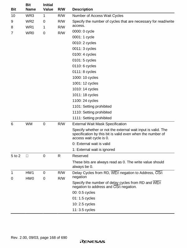
Rev. 2.00, 09/03, page 168 of 690
BitBitName
InitialValue R/W Description
10
9
8
7
WR3
WR2
WR1
WR0
1
0
1
0
R/W
R/W
R/W
R/W
Number of Access Wait Cycles
Specify the number of cycles that are necessary for read/writeaccess.
0000: 0 cycle
0001: 1 cycle
0010: 2 cycles
0011: 3 cycles
0100: 4 cycles
0101: 5 cycles
0110: 6 cycles
0111: 8 cycles
1000: 10 cycles
1001: 12 cycles
1010: 14 cycles
1011: 18 cycles
1100: 24 cycles
1101: Setting prohibited
1110: Setting prohibited
1111: Setting prohibited
6 WM 0 R/W External Wait Mask Specification
Specify whether or not the external wait input is valid. Thespecification by this bit is valid even when the number ofaccess wait cycle is 0.
0: External wait is valid
1: External wait is ignored
5 to 2 0 R Reserved
These bits are always read as 0. The write value shouldalways be 0.
1
0
HW1
HW0
0
0
R/W
R/W
Delay Cycles from RD, WEn negation to Address, CSnnegation
Specify the number of delay cycles from RD and WEnnegation to address and CSn negation.
00: 0.5 cycles
01: 1.5 cycles
10: 2.5 cycles
11: 3.5 cycles

Rev. 2.00, 09/03, page 169 of 690
2. Burst ROM
CS0WCR
BitBitName
InitialValue R/W Description
31 to 18 0 R Reserved
These bits are always read as 0. The write value shouldalways be 0.
17
16
BW1
BW0
0
0
R/W
R/W
Number of Burst Wait Cycles
Specify the number of wait cycles to be inserted between thesecond or later access cycles in burst access.
00: 0 cycle
01: 1 cycle
10: 2 cycles
11: 3 cycles
15 to 11 0 R Reserved
These bits are always read as 0. The write value shouldalways be 0.
10
9
8
7
W3
W2
W1
W0
1
0
1
0
R/W
R/W
R/W
R/W
Number of Access Wait Cycles
Specify the number of wait cycles to be inserted in the firstread/write access cycle.
0000: 0 cycle
0001: 1 cycle
0010: 2 cycles
0011: 3 cycles
0100: 4 cycles
0101: 5 cycles
0110: 6 cycles
0111: 8 cycles
1000: 10 cycles
1001: 12 cycles
1010: 14 cycles
1011: 18 cycles
1100: 24 cycles
1101: Setting prohibited
1110: Setting prohibited
1111: Setting prohibited

Rev. 2.00, 09/03, page 170 of 690
BitBitName
InitialValue R/W Description
6 WM 0 R/W External Wait Mask Specification
Specify whether or not the external wait input is valid. Thespecification by this bit is valid even when the number ofaccess wait cycle is 0.
0: External wait is valid
1: External wait is ignored
5 to 0 0 R Reserved
These bits are always read as 0. The write value shouldalways be 0.
CS4WCR
BitBitName
InitialValue R/W Description
31 to 18 0 R Reserved
These bits are always read as 0. The write value shouldalways be 0.
17
16
BW1
BW0
0
0
R/W
R/W
Number of Burst Wait Cycles
Specify the number of wait cycles to be inserted between thesecond or later access cycles in burst access.
00: 0 cycle
01: 1 cycle
10: 2 cycles
11: 3 cycles
15 to 13 0 R Reserved
These bits are always read as 0. The write value shouldalways be 0.
12
11
SW1
SW0
0
0
R/W
R/W
Number of Delay Cycles from Address, CSn Assertion to RD,WEn Assertion
Specify the number of delay cycles from address and CSnassertion to RD and WEn assertion.
00: 0.5 cycles
01: 1.5 cycles
10: 2.5 cycles
11: 3.5 cycles

Rev. 2.00, 09/03, page 171 of 690
BitBitName
InitialValue R/W Description
10
9
8
7
W3
W2
W1
W0
1
0
1
0
R/W
R/W
R/W
R/W
Number of Access Wait Cycles
Specify the number of wait cycles to be inserted in the firstread/write access cycle.
0000: 0 cycle
0001: 1 cycle
0010: 2 cycles
0011: 3 cycles
0100: 4 cycles
0101: 5 cycles
0110: 6 cycles
0111: 8 cycles
1000: 10 cycles
1001: 12 cycles
1010: 14 cycles
1011: 18 cycles
1100: 24 cycles
1101: Setting prohibited
1110: Setting prohibited
1111: Setting prohibited
6 WM 0 R/W External Wait Mask Specification
Specifies whether or not the external wait input is valid. Thespecification by this bit is valid even when the number ofaccess wait cycle is 0.
0: External wait is valid
1: External wait is ignored
5 to 2 0 R Reserved
These bits are always read as 0. The write value shouldalways be 0.
1
0
HW1
HW0
0
0
R/W
R/W
Delay Cycles from RD, WEn negation to Address, CSnnegation
Specify the number of delay cycles from RD and WEnnegation to address and CSn negation.
00: 0.5 cycles
01: 1.5 cycles
10: 2.5 cycles
11: 3.5 cycles

Rev. 2.00, 09/03, page 172 of 690
3. SDRAM*
CS2WCR
BitBitName
InitialValue R/W Description
31 to 11 0 R Reserved
These bits are always read as 0. The write value shouldalways be 0.
10 1 R Reserved
This bit is always read as 1. The write value should always be1.
9 0 R Reserved
This bit is always read as 0. The write value should always be0.
8
7
A2CL1
A2CL0
1
0
R/W
R/W
CAS Latency for Area 2
Specify the CAS latency for area 2.
00: Setting prohibited.
01: 2 cycles
10: 3 cycles
11: Setting prohibited
6 to 0 0 R Reserved
These bits are always read as 0. The write value shouldalways be 0.

Rev. 2.00, 09/03, page 173 of 690
CS3WCR
BitBitName
InitialValue R/W Description
31 to 15 0 R Reserved
These bits are always read as 0. The write value shouldalways be 0.
14
13
TRP1
TRP0
0
0
R/W
R/W
Number of Cycles from Auto-precharge/PRE Command toACTV Command
Specify the number of minimum cycles from the start of auto-precharge or issuing of PRE command to the issuing of ACTVcommand for the same bank. The setting for areas 2 and 3 iscommon.
00: 1 cycle
01: 2 cycles
10: 3 cycles
11: 4 cycles
12 0 R Reserved
This bit is always read as 0. The write value should always be0.
11
10
TRCD1
TRCD0
0
1
R/W
R/W
Number of Cycles from ACTV Command toREAD(A)/WRIT(A) Command
Specify the number of minimum cycles from issuing ACTVcommand to issuing READ(A)/WRIT(A) command. Thesetting for areas 2 and 3 is common.
00: 1 cycle
01: 2 cycles
10: 3 cycles
11: 4 cycles
9 0 R Reserved
This bit is always read as 0. The write value should always be0.
8
7
A3CL1
A3CL0
1
0
R/W
R/W
CAS Latency for Area 3
Specify the CAS latency for area 3.
00: Setting prohibited.
01: 2 cycles
10: 3 cycles
11: Setting prohibited

Rev. 2.00, 09/03, page 174 of 690
BitBitName
InitialValue R/W Description
6, 5 0 R Reserved
These bits are always read as 0. The write value shouldalways be 0.
4
3
TRWL1
TRWL0
0
0
R/W
R/W
Number of Cycles from WRITA/WRIT Command to Auto-precharge/PRE Command
Specifies the number of cycles from issuing WRITA/WRITcommand to the start of auto-precharge or to issuing PREcommand. The setting for areas 2 and 3 is common.
00: 0 cycle
01: 1 cycle
10: 2 cycles
11: Setting prohibited
2 0 R Reserved
This bit is always read as 0. The write value should always be0.
1
0
TRC1
TRC0
0
0
R/W
R/W
Number of Cycles from REF Command/Self-refresh Releaseto ACTV Command
Specify the number of cycles from issuing the REF commandor releasing self-refresh to issuing the ACTV command. Thesetting for areas 2 and 3 is common.
00: 3 cycles
01: 4 cycles
10: 6 cycles
11: 9 cycles
Note: * Specify area 3 as SDRAM when only one area is connected with SDRAM. In this case,specify area 2 as normal space.
7.4.4 SDRAM Control Register (SDCR)
SDCR specifies the method to refresh and access SDRAM, and the types of SDRAMs to beconnected.
The bits other than RFSH and RMODE should be written in the initialization after a power-onreset and should not be modified after the initialization. When modifying these bits RFSH andRMODE, do not change the values of other bits and write the previous values. Do not access area2 or 3 until the SDCR register setting is complete when using synchronous DRAM.

Rev. 2.00, 09/03, page 175 of 690
BitBitName
InitialValue R/W Description
31 to 21 0 R Reserved
These bits are always read as 0. The write value shouldalways be 0.
20
19
A2ROW1
A2ROW0
0
0
R/W
R/W
Number of Bits of Row Address for Area 2
Specifies the number of bits of row address for area 2.
00: 11 bits
01: 12 bits
10: 13 bits
11: Setting prohibited
18 0 R Reserved
This bit is always read as 0. The write value should always be0.
17
16
A2COL1
A2COL0
0
0
R/W
R/W
Number of Bits of Column Address for Area 2
Specifies the number of bits of column address for area 2.
00: 8 bits
01: 9 bits
10: 10 bits
11: Setting prohibited
15 to 13 0 R Reserved
These bits are always read as 0. The write value shouldalways be 0.
12 SLOW 0 R/W Low-Frequency Mode
Specifies the output timing of command, address, and writedata for SDRAM and the latch timing of read data fromSDRAM. Setting this bit makes the hold time for command,address, write and read data extended. This mode is suitablefor SDRAM with low-frequency clock.
0: Command, address, and write data for SDRAM is output atthe rising edge of CKIO. Read data from SDRAM islatched at the rising edge of CKIO.
1: Command, address, and write data for SDRAM is output atthe falling edge of CKIO. Read data from SDRAM islatched at the falling edge of CKIO.

Rev. 2.00, 09/03, page 176 of 690
BitBitName
InitialValue R/W Description
11 RFSH 0 R/W Refresh Control
Specifies whether or not the refresh operation of the SDRAMis performed.
0: No refresh
1: Refresh
10 RMODE 0 R/W Refresh Control
Specifies whether to perform auto-refresh or self-refreshwhen the RFSH bit is 1. When the RFSH bit is 1 and this bit is1, self-refresh starts immediately. When the RFSH bit is 1 andthis bit is 0, auto-refresh starts according to the contents thatare set in registers RTCSR, RTCNT, and RTCOR.
0: Auto-refresh is performed
1: Self-refresh is performed
9 0 R Reserved
This bit is always read as 0. The write value should always be0.
8 BACTV 0 R/W Bank Active Mode
Specifies to access whether in auto-precharge mode (usingREADA and WRITA commands) or in bank active mode(using READ and WRIT commands).
0: Auto-precharge mode (using READA and WRITAcommands)
1: Bank active mode (using READ and WRIT commands)
Note: Bank active mode can be used only when either theupper or lower bits of the CS3 space are used. Whenboth the CS2 and CS3 spaces are set to SDRAM,specify the auto-precharge mode.
7 to 5 0 R Reserved
These bits are always read as 0. The write value shouldalways be 0.
4
3
A3ROW1
A3ROW0
0
0
R/W
R/W
Number of Bits of Row Address for Area 3
Specifies the number of bits of the row address for area 3.
00: 11 bits
01: 12 bits
10: 13 bits
11: Setting prohibited

Rev. 2.00, 09/03, page 177 of 690
BitBitName
InitialValue R/W Description
2 0 R Reserved
This bit is always read as 0. The write value should always be0.
1
0
A3COL1
A3COL0
0
0
R/W
R/W
Number of Bits of Column Address for Area 3
Specifies the number of bits of the column address for area 3.
00: 8 bits
01: 9 bits
10: 10 bits
11: Setting prohibited
7.4.5 Refresh Timer Control/Status Register (RTCSR)
RTCSR specifies various items about refresh for SDRAM.
This register only accepts 32-bit writing to prevent incorrect writing. In this case, the upper 16 bitsof the data must be H'A55A, otherwise writing cannot be performed. When reading, the upper 16bits are read as H'0000.
RTCSR
BitBitName
InitialValue R/W Description
31 to 8 0 R Reserved
7 CMF 0 R/W Compare Match Flag
0: Clearing condition When 0 is written in CMF after readingout RTCSR during CMF = 1.
1: Setting condition When the condition RTCNT = RTCOR issatisfied.
6 CMIE 0 R/W CMF Interrupt Enable
0: CMF interrupt request is disabled.
1: CMF interrupt request is enabled.

Rev. 2.00, 09/03, page 178 of 690
BitBitName
InitialValue R/W Description
5
4
3
CKS2
CKS1
CKS0
0
0
0
R/W
R/W
R/W
Clock Select
Select the clock input to count-up the refresh timer counter(RTCNT).
000: Stop the counting-up
001: Bφ/4
010: Bφ/16
011: Bφ/64
100: Bφ/256
101: Bφ/1024
110: Bφ/2048
111: Bφ/4096
2
1
0
RRC2
RRC1
RRC0
0
0
0
R/W
R/W
R/W
Refresh Count
Specify the number of continuous refresh cycles, when therefresh request occurs after the coincidence of the values ofthe refresh timer counter (RTCNT) and the refresh timeconstant register (RTCOR). These bits can make the periodof occurrence of refresh long.
000: Once
001: Twice
010: 4 times
011: 6 times
100: 8 times
101: Setting prohibited.
110: Setting prohibited.
111: Setting prohibited.

Rev. 2.00, 09/03, page 179 of 690
7.4.6 Refresh Timer Counter (RTCNT)
RTCNT is an 8-bit counter that counts up using the clock selected by bits CKS2 to CKS0 inRTCSR.
This register only accepts 32-bit writing to prevent incorrect writing. In this case, the upper 16 bitsof the data must be H'A55A, otherwise writing cannot be performed. When reading, the upper 16bits are read as H'0000.
When RTCNT matches RTCOR, RTCNT is cleared to 0. The value in RTCNT returns to 0 aftercounting up to 255.
BitBitName
InitialValue R/W Description
31 to 8 0 R Reserved
7 to 0 0 R/W 8-Bit Counter
7.4.7 Refresh Time Constant Register (RTCOR)
RTCOR is an 8-bit register. When RTCOR matches RTCNT, the CMF bit in RTCSR is set to 1and RTCNT is cleared to 0.
This register only accepts 32-bit writing to prevent incorrect writing. In this case, the upper 16 bitsof the data must be H'A55A, otherwise writing cannot be performed. When reading, the upper 16bits are read as H'0000.
When the RFSH bit in SDCR is 1, a memory refresh request is issued by this matching signal.This request is maintained until the refresh operation is performed. If the request is not processedwhen the next matching occurs, the previous request is ignored.
When the CMIE bit in RTCSR is 1, an interrupt request is issued by this matching signal. Thisrequest signal is output until the CMF bit in RTCSR is cleared. Clearing the CMF bit only affectsthe interrupt and does not affect the refresh request. Accordingly, the refresh requests and intervaltimer interrupts can be used together. For example, the number of refresh requests can be countedby using interrupts while the refresh is performed.

Rev. 2.00, 09/03, page 180 of 690
BitBitName
InitialValue R/W Description
31 to 8 0 R Reserved
These bits are always read as 0. The write value shouldalways be 0.
7 to 0 0 R/W Maximum Counter Value (eight bits)
7.4.8 Reset Wait Counter (RWTCNT)
RWTCNT is a 16-bit register. The lower seven bits of this register (bits 6 to 0) are valid as acounter and the upper nine bits (bits 15 to 7) are reserved. This counter starts to count-up bysynchronizing the CKIO after a power-on reset is released. This counter stops when the valuereaches to H'007F. The access to an external bus has to wait when the counter is operating. Thiscounter is provided to minimize the time from releasing a reset for flash memory to the firstaccess. This counter cannot be read or written into.
7.5 Endian/Access Size and Data Alignment
This LSI supports big endian, in which the 0 address is the most significant byte (MSByte) in thebyte data and little endian, in which the 0 address is the least significant byte (LSByte) in the bytedata. Endian is specified on power-on reset by the external pin (MD5). When MD5 pin is lowlevel on power-on reset, the endian will become big endian and when MD5 pin is high level onpower-on reset, the endian will become little endian. Three data bus widths are available fornormal memory (byte, word, and longword). Word and longword are available for SDRAM. Databus width for address/data multiplex I/O (MPX) should be 16 bits. Data alignment is performed inaccordance with the data bus width of the device and endian. This also means that when longworddata is read from a byte-width device, the read operation must be done four times. In this LSI, dataalignment and conversion of data length is performed automatically between the respectiveinterfaces.
Tables 7.4 to 7.9 show the relationship between endian, device data width, and access unit.

Rev. 2.00, 09/03, page 181 of 690
Table 7.4 32-Bit External Device/Big Endian Access and Data Alignment
Data Bus Strobe Signals
OperationD31 toD24
D23 toD16
D15 toD8
D7 to D0 WE3,DQMUU
WE2,DQMUL
WE1,DQMLU
WE0,DQMLL
Byte accessat 0
Data 7 toData 0
Assert
Byte accessat 1
Data 7 toData 0
Assert
Byte accessat 2
Data 7 toData 0
Assert
Byte accessat 3
Data 7 toData 0
Assert
Word accessat 0
Data 15 toData 8
Data 7 toData 0
Assert Assert
Word accessat 2
Data 15to Data 8
Data 7 toData 0
Assert Assert
Longwordaccess at 0
Data 31 toData 24
Data 23 toData 16
Data 15to Data 8
Data 7 toData 0
Assert Assert Assert Assert

Rev. 2.00, 09/03, page 182 of 690
Table 7.5 16-Bit External Device/Big Endian Access and Data Alignment
Data Bus Strobe Signals
OperationD31 toD24
D23 toD16
D15 toD8
D7 to D0 WE3,DQMUU
WE2,DQMUL
WE1,DQMLU
WE0,DQMLL
Byte access at 0 Data 7 toData 0
Assert
Byte access at 1 Data 7 toData 0
Assert
Byte access at 2 Data 7 toData 0
Assert
Byte access at 3 Data 7 toData 0
Assert
Word access at 0 Data 15to Data 8
Data 7 toData 0
Assert Assert
Word access at 2 Data 15to Data 8
Data 7 toData 0
Assert Assert
1sttime at 0
Data 31to Data24
Data 23to Data16
Assert AssertLongwordaccessat 0
2ndtime at 2
Data 15to Data 8
Data 7 toData 0
Assert Assert

Rev. 2.00, 09/03, page 183 of 690
Table 7.6 8-Bit External Device/Big Endian Access and Data Alignment
Data Bus Strobe Signals
OperationD31 toD24
D23 toD16
D15 toD8
D7 to D0 WE3,DQMUU
WE2,DQMUL
WE1,DQMLU
WE0,DQMLL
Byte access at 0 Data 7 toData 0
Assert
Byte access at 1 Data 7 toData 0
Assert
Byte access at 2 Data 7 toData 0
Assert
Byte access at 3 Data 7 toData 0
Assert
Wordaccess at 0
1st timeat 0
Data 15to Data 8
Assert
2nd timeat 1
Data 7 toData 0
Assert
Wordaccess at 2
1st timeat 2
Data 15to Data 8
Assert
2nd timeat 3
Data 7 toData 0
Assert
Longwordaccess at 0
1st timeat 0
Data 31to Data24
Assert
2nd timeat 1
Data 23to Data16
Assert
3rd timeat 2
Data 15to Data 8
Assert
4th timeat 3
Data 7 toData 0
Assert

Rev. 2.00, 09/03, page 184 of 690
Table 7.7 32-Bit External Device/Little Endian Access and Data Alignment
Data Bus Strobe Signals
OperationD31 toD24
D23 toD16
D15 toD8
D7 to D0 WE3,DQMUU
WE2,DQMUL
WE1,DQMLU
WE0,DQMLL
Byte accessat 0
Data 7 toData 0
Assert
Byte accessat 1
Data 7 toData 0
Assert
Byte accessat 2
Data 7 toData 0
Assert
Byte accessat 3
Data 7 toData 0
Assert
Word accessat 0
Data 15to Data 8
Data 7 toData 0
Assert Assert
Word accessat 2
Data 15 toData 8
Data 7 toData 0
Assert Assert
Longwordaccess at 0
Data 31 toData 24
Data 23 toData 16
Data 15to Data 8
Data 7 toData 0
Assert Assert Assert Assert

Rev. 2.00, 09/03, page 185 of 690
Table 7.8 16-Bit External Device/Little Endian Access and Data Alignment
Data Bus Strobe Signals
OperationD31 toD24
D23 toD16
D15 toD8
D7 to D0 WE3,DQMUU
WE2,DQMUL
WE1,DQMLU
WE0,DQMLL
Byte access at 0 Data 7 toData 0
Assert
Byte access at 1 Data 7 toData 0
Assert
Byte access at 2 Data 7 toData 0
Assert
Byte access at 3 Data7 toData 0
Assert
Word access at 0 Data 15to Data 8
Data 7 toData 0
Assert Assert
Word access at 2 Data 15to Data 8
Data 7 toData 0
Assert Assert
1sttime at 0
Data 15to Data 8
Data 7 toData 0
Assert AssertLongwordaccessat 0 2nd
time at 1 Data 31
to Data24
Data 23to Data16
Assert Assert
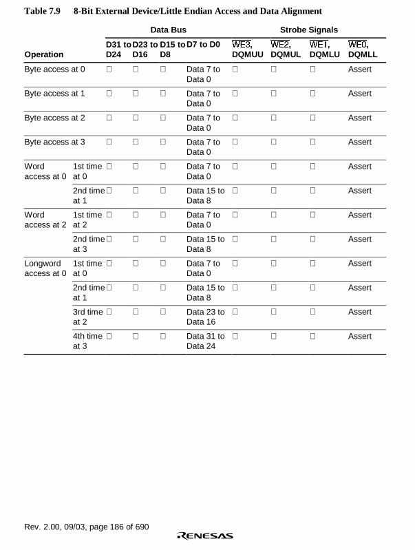
Rev. 2.00, 09/03, page 186 of 690
Table 7.9 8-Bit External Device/Little Endian Access and Data Alignment
Data Bus Strobe Signals
OperationD31 toD24
D23 toD16
D15 toD8
D7 to D0 WE3,DQMUU
WE2,DQMUL
WE1,DQMLU
WE0,DQMLL
Byte access at 0 Data 7 toData 0
Assert
Byte access at 1 Data 7 toData 0
Assert
Byte access at 2 Data 7 toData 0
Assert
Byte access at 3 Data 7 toData 0
Assert
Wordaccess at 0
1st timeat 0
Data 7 toData 0
Assert
2nd timeat 1
Data 15 toData 8
Assert
Wordaccess at 2
1st timeat 2
Data 7 toData 0
Assert
2nd timeat 3
Data 15 toData 8
Assert
Longwordaccess at 0
1st timeat 0
Data 7 toData 0
Assert
2nd timeat 1
Data 15 toData 8
Assert
3rd timeat 2
Data 23 toData 16
Assert
4th timeat 3
Data 31 toData 24
Assert

Rev. 2.00, 09/03, page 187 of 690
7.6 Normal Space Interface
7.6.1 Basic Timing
For access to a normal space, this LSI uses strobe signal output in consideration of the fact thatmainly static RAM will be directly connected. When using SRAM with a byte-selection pin, seesection 7.10, Byte-Selection SRAM Interface. Figures 7.3 and 7.4 show the basic timings ofnormal space accesses. A no-wait normal access is completed in two cycles. The BS signal isasserted for one cycle to indicate the start of a bus cycle.
There is no access size specification when reading. The correct access start address is output in theleast significant bit of the address, but since there is no access size specification, 32 bits are alwaysread in case of a 32-bit device, and 16 bits in case of a 16-bit device. When writing, only the WEnsignal for the byte to be written is asserted.
Read/write for cache fill or writeback follows the selected bus width and transfers a total of 16bytes continuously. The bus is not released during this transfer. For cache misses that occur duringbyte or word operand accesses or branching to odd word boundaries, the fill is always performedby longword accesses on the chip-external interface. Write-through-area write access and non-cacheable read/write access are based on the actual address size.
It is necessary to output the read out data by using RD when a buffer is established in the data bus.The RD/WR signal is in a read state (high output) when an access is not performed. Therefore,care must be taken about the collision of output in controlling the external data buffer.
When the WM bit in CSnWCR is cleared to 0, a Tnop cycle is inserted to evaluate an externalwait. When the WM bit in CSnWCR is set to 1, an external wait is ignored and no Tnop cycle isinserted.

Rev. 2.00, 09/03, page 188 of 690
CKIO
A25 to A0
RD/WR
Data
DACK
CS
T1 T2 T1 T2
RD
WEn
BS
Data
Read
Write
Figure 7.3 Continuous Access for Normal Space (No Wait, WM Bit in CSnWCR = 1,16-Bit Bus Width, Longword Access, No Wait State between Cycles)

Rev. 2.00, 09/03, page 189 of 690
CKIO
A25 to A0
RD
Data
WEn
Data
DACKn
WAIT
CSn
T1 T2 Taw T1 T2
Read
Write
Figure 7.4 Continuous Access for Normal Space(No Wait, One Wait State between Cycles)

Rev. 2.00, 09/03, page 190 of 690
Figures 7.5 to 7.7 show examples of connection to 32-bit, 16-bit, and 8-bit data-width SRAM,respectively.
A16
A0CS
OE
I/O7
I/O0WE
A18
A2CSn
RD
D31
D24WE3
D23
D16WE2
D15
D8WE1
D7
D0WE0
This LSI128k × 8-bit
SRAM
A16
A0CS
OE
I/O7
I/O0WE
A16
A0CS
OE
I/O7
I/O0WE
A16
A0CS
OE
I/O7
I/O0WE
Figure 7.5 Example of 32-Bit Data-Width SRAM Connection

Rev. 2.00, 09/03, page 191 of 690
A16
A0CS
OE
I/O7
I/O0WE
A17
A1CSn
RD
D15
D8WE1
D7
D0WE0
This LSI128k × 8-bit
SRAM
A16
A0CS
OE
I/O7
I/O0WE
Figure 7.6 Example of 16-Bit Data-Width SRAM Connection
A16
A0
CS
OE
I/O7
I/O0
WE
A16
A0
CSn
RD
D7
D0
WE0
This LSI128k × 8-bit
SRAM
Figure 7.7 Example of 8-Bit Data-Width SRAM Connection

Rev. 2.00, 09/03, page 192 of 690
7.6.2 Access Wait Control
Wait cycle insertion on a normal space access can be controlled by the settings of bits WR3 toWR0 in CSnWCR. It is possible for areas 4, 5A, and 5B to insert wait cycles independently inread access and in write access. The areas other than 4, 5A, and 5B have common access wait forread cycle and write cycle. The specified number of Tw cycles is inserted as wait cycles in anormal space access shown in figure 7.8.
T1
CKIO
A25 to A0
CSn
RD/WR
RD
Data
WEn
Data
BS
Tw
Read
Write
T2
DACKn*
Note: * The waveform for DACKn is when active low is specified.
Figure 7.8 Wait Timing for Normal Space Access (Software Wait Only)

Rev. 2.00, 09/03, page 193 of 690
When the WM bit in CSnWCR is cleared to 0, the external wait input WAIT signal is alsosampled. WAIT pin sampling is shown in figure 7.9. A 2-cycle wait is specified as a softwarewait. The WAIT signal is sampled on the falling edge of CKIO at the transition from the T1 or Twcycle to the T2 cycle.
T1
CKIO
A25 to A0
CSn
RD/WR
RD
Data
WEn
Data
WAIT
Tw Tw Twx T2
Read
Write
BS
Wait states insertedby WAIT signal
DACKn*
Note: * The waveform for DACKn is when active low is specified.
Figure 7.9 Wait State Timing for Normal Space Access(Wait State Insertion by WAIT Signal)

Rev. 2.00, 09/03, page 194 of 690
7.6.3 CSn Assert Period Expansion
The number of cycles from CSn assertion to RD, WEn assertion can be specified by setting bitsSW1 and SW0 in CSnWCR. The number of cycles from RD, WEn negation to CSn negation canbe specified by setting bits HW1 and HW0. Therefore, a flexible interface to an external devicecan be obtained. Figure 7.10 shows an example. A Th cycle and a Tf cycle are added before andafter an ordinary cycle, respectively. In these cycles, RD and WEn are not asserted, while othersignals are asserted. The data output is prolonged to the Tf cycle, and this prolongation is usefulfor devices with slow writing operations.
T1
CKIO
A25 to A0
CSn
RD/WR
RD
Data
WEn
Data
BS
Th
Read
Write
T2
DACKn*
Tf
Note: * The waveform for DACKn is when active low is specified.
Figure 7.10 CSn Assert Period Expansion

Rev. 2.00, 09/03, page 195 of 690
7.7 Address/Data Multiplex I/O Interface
The address/data multiplex (MPX) I/O interface can be selected by setting bits TYPE2 to TYPE0to 010 in CS5BBCR. Do not set this value to the bits in CSnBCR other than those in area 5B,otherwise the operation of the LSI is not guaranteed. Access timing for the MPX space is shownbelow. In the MPX space, CS5B, AH, RD, and WEn signals control the accessing. The basicaccess for the MPX space consists of 2 cycles of address output followed by an access to a normalspace.
The address output is performed from cycle Ta2 to cycle Ta3. Because cycle Ta1 has a high-impedance state, collisions of addresses and data can be avoided without inserting idle cycles,even in continuous accesses. Address output is increased to 3 cycles by setting the MPXW bit to 1in CS5BWCR. The RD/WR signal is output at the same time as the CSn signal; it is high in theread cycle and low in the write cycle.
The data cycle is the same as that in a normal space access.
Timing charts are shown in figures 7.11, 7.12, and 7.13.
T1
CKIO
A25 to A16
CS5B
RD/WR
RD
D15 to D0
WEn
D15 to D0
BS
Read
Write
T2
DACKn*
Ta1 Ta2 Ta3
AH
Address
Address Data
Data
Note: * The waveform for DACKn is when active low is specified.
Figure 7.11 Access Timing for MPX Space(Address Cycle No Wait, Data Cycle No Wait)

Rev. 2.00, 09/03, page 196 of 690
T1
CKIO
A25 to A16
CS5B
RD/WR
RD
D15 to D0
WEn
D15 to D0
BS
Read
Write
T2
DACKn*
Ta1 Ta2 Ta3
AH
Address
Address Data
Data
Tadw
Note: * The waveform for DACKn is when active low is specified.
Figure 7.12 Access Timing for MPX Space(Address Cycle Wait 1, Data Cycle No Wait)
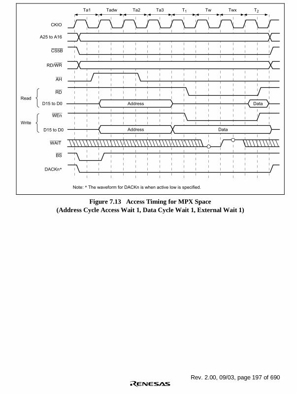
Rev. 2.00, 09/03, page 197 of 690
T1
CKIO
A25 to A16
CS5B
RD/WR
RD
D15 to D0
WEn
D15 to D0
BS
Read
Write
T2
DACKn*
Ta1 Ta2 Ta3
AH
Address
Address Data
Data
Tadw Tw Twx
WAIT
Note: * The waveform for DACKn is when active low is specified.
Figure 7.13 Access Timing for MPX Space(Address Cycle Access Wait 1, Data Cycle Wait 1, External Wait 1)

Rev. 2.00, 09/03, page 198 of 690
7.8 SDRAM Interface
7.8.1 SDRAM Direct Connection
Since synchronous DRAM can be selected by the CS signal, physical space areas 2 and 3 can beconnected using RAS and other control signals in common. If the TYPE[2:0] bits in CSnBCR (n =2 or 3) are set to 100, the synchronous DRAM interface can be selected. Do not set this value toCSnBCR unless n = 2 or 3, otherwise the operation of this LSI is not guaranteed.
The SDRAM that can be connected to this LSI is a product that has 11/12/13 bits of row address,8/9/10 bits of column address, 4 or less banks, and uses the A10 pin for setting precharge mode inread and write command cycles. The control signals for direct connection of SDRAM are RASU,RASL, CASU, CASL, RD/WR, DQMUU, DQMUL, DQMLU, DQMLL, CKE, CS2, and CS3.All the signals other than CS2 and CS3 are common to all areas, and signals other than CKE arevalid when CS2 or CS3 is asserted. SDRAM can be connected to up to 2 spaces. The data buswidth of the area that is connected to SDRAM can be set to 32 or 16 bits.
Burst read/single write (burst length 1) and burst read/burst write (burst length 1) are supported asthe SDRAM operating mode.
Commands for SDRAM can be specified by RASU, RASL, CASU, CASL, RD/WR, and specificaddress signals. These commands are shown below.
• NOP
• Auto-refresh (REF)
• Self-refresh (SELF)
• All banks pre-charge (PALL)
• Specified bank pre-charge (PRE)
• Bank active (ACTV)
• Read (READ)
• Read with pre-charge (READA)
• Write (WRIT)
• Write with pre-charge (WRITA)
• Write mode register (MRS)
The byte to be accessed is specified by DQMUU, DQMUL, DQMLU, and DQMLL. For therelationship between DQMxx and the byte to be accessed, refer to section 7.5, Endian/Access Sizeand Data Alignment.
Figures 7.14 and 7.15 show examples of the connection of SDRAM with the LSI.

Rev. 2.00, 09/03, page 199 of 690
This LSI
A15
A14
A13
A2
CKIO
CKE
CSn
RASx
CASx
RD/WR
D31
D16
DQMUU
DQMUL
D15
D0
DQMLU
DQMLL
64M synchronous DRAM
(1M × 16-bit × 4-bank)
A13
A12
A11
A0
CLK
CKE
CS
RAS
CAS
WE
DQ15
DQ0
DQMU
DQML
A13
A12
A11
A0
CLK
CKE
CS
RAS
CAS
WE
DQ15
DQ0
DQMU
DQML
Note: x is U or L
Figure 7.14 Example of 64-MBit Synchronous DRAM Connection (32-Bit Data Bus)

Rev. 2.00, 09/03, page 200 of 690
This LSI
64M synchronous DRAM
(1M × 16-bit × 4-bank)
A14
A13
A12
A1
CKIO
CKE
CSn
RASx
CASx
RD/WR
D15
D0
DQMLU
DQMLL
A13
A12
A11
A0
CLK
CKE
CS
RAS
CAS
WE
DQ15
DQ0
DQMU
DQML
Note: x is U or L
Figure 7.15 Example of 64-MBit Synchronous DRAM (16-Bit Data Bus)
7.8.2 Address Multiplexing
An address multiplexing is specified so that SDRAM can be connected without externalmultiplexing circuitry according to the setting of bits BSZ[1:0] in CSnBCR, AxROW[1:0] andAxCOL[1:0] in SDCR. Tables 7.10 to 7.15 show the relationship between the settings of bitsBSZ[1:0], AxROW[1:0], and AxCOL[1:0] and the bits output at the address pins. Do not specifythose bits in the manner other than this table, otherwise the operation of this LSI is not guaranteed.A25 to A18 are not multiplexed and the original values of address are always output at these pins.
When the data bus width is 16 bits (BSZ[1:0] = 10), A0 of SDRAM specifies a word address.Therefore, connect this A0 pin of SDRAM to the A1 pin of the LSI; the A1 pin of SDRAM to theA2 pin of the LSI, and so on. When the data bus width is 32 bits (BSZ[1:0] = 11), the A0 pin ofSDRAM specifies a longword address. Therefore, connect this A0 pin of SDRAM to the A2 pin ofthe LSI; the A1 pin of SDRAM to the A3 pin of the LSI, and so on.

Rev. 2.00, 09/03, page 201 of 690
Table 7.10 Relationship between A2/3BSZ[1:0], A2/3ROW[1:0], and Address MultiplexOutput (1)-1
Setting
A2/3 BSZ[1:0] A2/3 ROW[1:0] A2/3 COL[1:0]
11 (32 bits) 00 (11 bits) 00 (8 bits)
Output Pin ofThis LSI
Row AddressOutput Cycle
Column AddressOutput Cycle
Synchronous DRAMPin Function
A17 A25 A17
A16 A24 A16
A15 A23 A15
Unused
A14 A22*2 A22*2 A12 (BA1)
A13 A21*2 A21*2 A11 (BA0)
Specifies bank
A12 A20 L/H*1 A10/AP Specifiesaddress/precharge
A11 A19 A11 A9
A10 A18 A10 A8
A9 A17 A9 A7
A8 A16 A8 A6
A7 A15 A7 A5
A6 A14 A6 A4
A5 A13 A5 A3
A4 A12 A4 A2
A3 A11 A3 A1
A2 A10 A2 A0
Address
A1 A9 A1
A0 A8 A0
Unused
Example of connected memory
64-Mbit product (512 kwords x 32 bits x 4 banks, column 8 bits product): 1 device
16-Mbit product (512 kwords x 16 bits x 2 banks, column 8 bits product): 2 devices
Notes: 1. L/H is a bit used in the command specification; it is fixed at L or H according to theaccess mode.
2. Bank address specification

Rev. 2.00, 09/03, page 202 of 690
Table 7.10 Relationship between A2/3BSZ[1:0], A2/3ROW[1:0], and Address MultiplexOutput (1)-2
Setting
A2/3 BSZ[1:0] A2/3 ROW[1:0] A2/3 COL[1:0]
11 (32 bits) 01 (12 bits) 00 (8 bits)
Output Pin ofThis LSI
Row AddressOutput Cycle
Column AddressOutput Cycle
Synchronous DRAMPin Function
A17 A25 A17
A16 A24 A16
Unused
A15 A23*2 A23*2 A13 (BA1)
A14 A22*2 A22*2 A12 (BA0)
Specifies bank
A13 A21 A13 A11 Address
A12 A20 L/H*1 A10/AP Specifiesaddress/precharge
A11 A19 A11 A9
A10 A18 A10 A8
A9 A17 A9 A7
A8 A16 A8 A6
A7 A15 A7 A5
A6 A14 A6 A4
A5 A13 A5 A3
A4 A12 A4 A2
A3 A11 A3 A1
A2 A10 A2 A0
Address
A1 A9 A1
A0 A8 A0
Unused
Example of connected memory
128-Mbit product (1 Mword x 32 bits x 4 banks, column 8 bits product): 1 device
64-Mbit product (1 Mword x 16 bits x 4 banks, column 8 bits product): 2 devices
Notes: 1. L/H is a bit used in the command specification; it is fixed at L or H according to theaccess mode.
2. Bank address specification

Rev. 2.00, 09/03, page 203 of 690
Table 7.11 Relationship between A2/3BSZ[1:0], A2/3ROW[1:0], and Address MultiplexOutput (2)-1
Setting
A2/3 BSZ[1:0] A2/3 ROW[1:0] A2/3 COL[1:0]
11 (32 bits) 01 (12 bits) 01 (9 bits)
Output Pin ofThis LSI
Row AddressOutput Cycle
Column AddressOutput Cycle
Synchronous DRAMPin Function
A17 A26 A17
A16 A25 A16
Unused
A15 A24*2 A24*2 A13 (BA1)
A14 A23*2 A23*2 A12 (BA0)
Specifies bank
A13 A22 A13 A11 Address
A12 A21 L/H*1 A10/AP Specifiesaddress/precharge
A11 A20 A11 A9
A10 A19 A10 A8
A9 A18 A9 A7
A8 A17 A8 A6
A7 A16 A7 A5
A6 A15 A6 A4
A5 A14 A5 A3
A4 A13 A4 A2
A3 A12 A3 A1
A2 A11 A2 A0
Address
A1 A10 A1
A0 A9 A0
Unused
Example of connected memory
256-Mbit product (2 Mwords x 32 bits x 4 banks, column 9 bits product): 1 device
128-Mbit product (2 Mwords x 16 bits x 4 banks, column 9 bits product): 2 devices
Notes: 1. L/H is a bit used in the command specification; it is fixed at L or H according to theaccess mode.
2. Bank address specification

Rev. 2.00, 09/03, page 204 of 690
Table 7.11 Relationship between A2/3BSZ[1:0], A2/3ROW[1:0], and Address MultiplexOutput (2)-2
Setting
A2/3 BSZ[1:0] A2/3 ROW[1:0] A2/3 COL[1:0]
11 (32 bits) 01 (12 bits) 10 (10 bits)
Output Pin ofThis LSI
Row AddressOutput Cycle
Column AddressOutput Cycle
Synchronous DRAMPin Function
A17 A27 A17
A16 A26 A16
Unused
A15 A25*2 A25*2*3 A13 (BA1)
A14 A24*2 A24*2 A12 (BA0)
Specifies bank
A13 A23 A13 A11 Address
A12 A22 L/H*1 A10/AP Specifiesaddress/precharge
A11 A21 A11 A9
A10 A20 A10 A8
A9 A19 A9 A7
A8 A18 A8 A6
A7 A17 A7 A5
A6 A16 A6 A4
A5 A15 A5 A3
A4 A14 A4 A2
A3 A13 A3 A1
A2 A12 A2 A0
Address
A1 A11 A1
A0 A10 A0
Unused
Example of connected memory
512-Mbit product (4 Mwords x 32 bits x 4 banks, column 10 bits product): 1 device
256-Mbit product (4 Mwords x 16 bits x 4 banks, column 10 bits product): 2 devices
Notes: 1. L/H is a bit used in the command specification; it is fixed at L or H according to theaccess mode.
2. Bank address specification3. Only the RASL pin is asserted because the A25 pin specified the bank address. RASU
is not asserted.

Rev. 2.00, 09/03, page 205 of 690
Table 7.12 Relationship between A2/3BSZ[1:0], A2/3ROW[1:0], and Address MultiplexOutput (3)
Setting
A2/3 BSZ[1:0] A2/3 ROW[1:0] A2/3 COL[1:0]
11 (32 bits) 10 (13 bits) 01 (9 bits)
Output Pin ofThis LSI
Row AddressOutput Cycle
Column AddressOutput Cycle
Synchronous DRAMPin Function
A17 A26 A17 Unused
A16 A25*2*3 A25*2*3 A14 (BA1)
A15 A24*2 A24*2 A13 (BA0)
Specifies bank
A14 A23 A14 A12
A13 A22 A13 A11
Address
A12 A21 L/H*1 A10/AP Specifiesaddress/precharge
A11 A20 A11 A9
A10 A19 A10 A8
A9 A18 A9 A7
A8 A17 A8 A6
A7 A16 A7 A5
A6 A15 A6 A4
A5 A14 A5 A3
A4 A13 A4 A2
A3 A12 A3 A1
A2 A11 A2 A0
Address
A1 A10 A1
A0 A9 A0
Unused
Example of connected memory
512-Mbit product (4 Mwords x 32 bits x 4 banks, column 9 bits product): 1 device
256-Mbit product (4 Mwords x 16 bits x 4 banks, column 9 bits product): 2 devices
Notes: 1. L/H is a bit used in the command specification; it is fixed at L or H according to theaccess mode.
2. Bank address specification3. Only the RASL pin is asserted because the A25 pin specified the bank address.
RASU is not asserted.

Rev. 2.00, 09/03, page 206 of 690
Table 7.13 Relationship between A2/3BSZ[1:0], A2/3ROW[1:0], and Address MultiplexOutput (4)-1
Setting
A2/3 BSZ[1:0] A2/3 ROW[1:0] A2/3 COL[1:0]
10 (16 bits) 00 (11 bits) 00 (8 bits)
Output Pin ofThis LSI
Row AddressOutput Cycle
Column AddressOutput Cycle
Synchronous DRAMPin Function
A17 A25 A17
A16 A24 A16
A15 A23 A15
A14 A22 A14
Unused
A13 A21*2 A21*2 A12 (BA1)
A12 A20*2 A20*2 A11 (BA0)
Specifies bank
A11 A19 L/H*1 A10/AP Specifiesaddress/precharge
A10 A18 A10 A9
A9 A17 A9 A8
A8 A16 A8 A7
A7 A15 A7 A6
A6 A14 A6 A5
A5 A13 A5 A4
A4 A12 A4 A3
A3 A11 A3 A2
A2 A10 A2 A1
A1 A9 A1 A0
Address
A0 A8 A0 Unused
Example of connected memory
16-Mbit product (512 kwords x 16 bits x 2 banks, column 8 bits product): 1 device
Notes: 1. L/H is a bit used in the command specification; it is fixed at L or H according to theaccess mode.
2. Bank address specification

Rev. 2.00, 09/03, page 207 of 690
Table 7.13 Relationship between A2/3BSZ[1:0], A2/3ROW[1:0], and Address MultiplexOutput (4)-2
Setting
A2/3 BSZ[1:0] A2/3 ROW[1:0] A2/3 COL[1:0]
10 (16 bits) 01 (12 bits) 00 (8 bits)
Output Pin ofThis LSI
Row AddressOutput Cycle
Column AddressOutput Cycle
Synchronous DRAMPin Function
A17 A25 A17
A16 A24 A16
A15 A23 A15
Unused
A14 A22*2 A22*2 A13 (BA1)
A13 A21*2 A21*2 A12 (BA0)
A12 A20 A12 A11
Specifies bank
Address
A11 A19 L/H*1 A10/AP Specifiesaddress/precharge
A10 A18 A10 A9
A9 A17 A9 A8
A8 A16 A8 A7
A7 A15 A7 A6
A6 A14 A6 A5
A5 A13 A5 A4
A4 A12 A4 A3
A3 A11 A3 A2
A2 A10 A2 A1
A1 A9 A1 A0
Address
A0 A8 A0 Unused
Example of connected memory
64-Mbit product (1 Mword x 16 bits x 4 banks, column 8 bits product): 1 device
Notes: 1. L/H is a bit used in the command specification; it is fixed at L or H according to theaccess mode.
2. Bank address specification

Rev. 2.00, 09/03, page 208 of 690
Table 7.14 Relationship between A2/3BSZ[1:0], A2/3ROW[1:0], and Address MultiplexOutput (5)-1
Setting
A2/3 BSZ[1:0] A2/3 ROW[1:0] A2/3 COL[1:0]
10 (16 bits) 01 (12 bits) 01 (9 bits)
Output Pin ofThis LSI
Row AddressOutput Cycle
Column AddressOutput Cycle
Synchronous DRAMPin Function
A17 A26 A17
A16 A25 A16
A15 A24 A15
Unused
A14 A23*2 A23*2 A13 (BA1)
A13 A22*2 A22*2 A12 (BA0)
Specifies bank
A12 A21 A12 A11 Address
A11 A20 L/H*1 A10/AP Specifiesaddress/precharge
A10 A19 A10 A9
A9 A18 A9 A8
A8 A17 A8 A7
A7 A16 A7 A6
A6 A15 A6 A5
A5 A14 A5 A4
A4 A13 A4 A3
A3 A12 A3 A2
A2 A11 A2 A1
A1 A10 A1 A0
Address
A0 A9 A0 Unused
Example of connected memory
128-Mbit product (2 Mwords x 16 bits x 4 banks, column 9 bits product): 1 device
Notes: 1. L/H is a bit used in the command specification; it is fixed at L or H according to theaccess mode.
2. Bank address specification

Rev. 2.00, 09/03, page 209 of 690
Table 7.14 Relationship between A2/3BSZ[1:0], A2/3ROW[1:0], and Address MultiplexOutput (5)-2
Setting
A2/3 BSZ[1:0] A2/3 ROW[1:0] A2/3 COL[1:0]
10 (16 bits) 01 (12 bits) 10 (10 bits)
Output Pin ofThis LSI
Row AddressOutput Cycle
Column AddressOutput Cycle
Synchronous DRAMPin Function
A17 A27 A17
A16 A26 A16
A15 A25 A15
Unused
A14 A24*2 A24*2 A13 (BA1)
A13 A23*2 A23*2 A12 (BA0)
Specifies bank
A12 A22 A12 A11 Address
A11 A21 L/H*1 A10/AP Specifiesaddress/precharge
A10 A20 A10 A9
A9 A19 A9 A8
A8 A18 A8 A7
A7 A17 A7 A6
A6 A16 A6 A5
A5 A15 A5 A4
A4 A14 A4 A3
A3 A13 A3 A2
A2 A12 A2 A1
A1 A11 A1 A0
Address
A0 A10 A0 Unused
Example of connected memory
256-Mbit product (4 Mwords x 16 bits x 4 banks, column 10 bits product): 1 device
Notes: 1. L/H is a bit used in the command specification; it is fixed at L or H according to theaccess mode.
2. Bank address specification

Rev. 2.00, 09/03, page 210 of 690
Table 7.15 Relationship between A2/3BSZ[1:0], A2/3ROW[1:0], and Address MultiplexOutput (6)-1
Setting
A2/3 BSZ[1:0] A2/3 ROW[1:0] A2/3 COL[1:0]
10 (16 bits) 10 (13 bits) 01 (9 bits)
Output Pin ofThis LSI
Row AddressOutput Cycle
Column AddressOutput Cycle
Synchronous DRAMPin Function
A17 A26 A17
A16 A25 A16
Unused
A15 A24*2 A24*2 A14 (BA1)
A14 A23*2 A23*2 A13 (BA0)
Specifies bank
A13 A22 A13 A12
A12 A21 A12 A11
Address
A11 A20 L/H*1 A10/AP Specifiesaddress/precharge
A10 A19 A10 A9
A9 A18 A9 A8
A8 A17 A8 A7
A7 A16 A7 A6
A6 A15 A6 A5
A5 A14 A5 A4
A4 A13 A4 A3
A3 A12 A3 A2
A2 A11 A2 A1
A1 A10 A1
Address
A0 A9 A0
A0
Unused
Example of connected memory
256-Mbit product (4 Mwords x 16 bits x 4 banks, column 9 bits product): 1 device
Notes: 1. L/H is a bit used in the command specification; it is fixed at L or H according to theaccess mode.
2. Bank address specification

Rev. 2.00, 09/03, page 211 of 690
Table 7.15 Relationship between A2/3BSZ[1:0], A2/3ROW[1:0], and Address MultiplexOutput (6)-2
Setting
A2/3 BSZ[1:0] A2/3 ROW[1:0] A2/3 COL[1:0]
10 (16 bits) 10 (13 bits) 10 (10 bits)
Output Pin ofThis LSI
Row AddressOutput Cycle
Column AddressOutput Cycle
Synchronous DRAMPin Function
A17 A27 A17
A16 A26 A16
Unused
A15 A25*2*3 A25*2*3 A14 (BA1)
A14 A24*2 A24*2 A13 (BA0)
Specifies bank
A13 A23 A13 A12
A12 A22 A12 A11
Address
A11 A21 L/H*1 A10/AP Specifiesaddress/precharge
A10 A20 A10 A9
A9 A19 A9 A8
A8 A18 A8 A7
A7 A17 A7 A6
A6 A16 A6 A5
A5 A15 A5 A4
A4 A14 A4 A3
A3 A13 A3 A2
A2 A12 A2 A1
A1 A11 A1 A0
Address
A0 A10 A0 Unused
Example of connected memory
512-Mbit product (8 Mwords x 16 bits x 4 banks, column 10 bits product): 1 device
Notes: 1. L/H is a bit used in the command specification; it is fixed at L or H according to theaccess mode.
2. Bank address specification3. Only the RASL pin is asserted because the A25 pin specified the bank address. RASU
is not asserted.
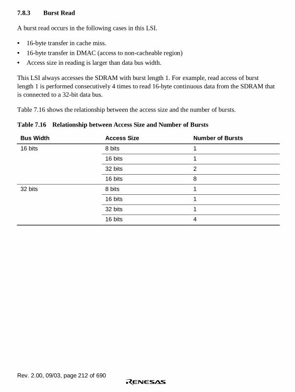
Rev. 2.00, 09/03, page 212 of 690
7.8.3 Burst Read
A burst read occurs in the following cases in this LSI.
• 16-byte transfer in cache miss.
• 16-byte transfer in DMAC (access to non-cacheable region)
• Access size in reading is larger than data bus width.
This LSI always accesses the SDRAM with burst length 1. For example, read access of burstlength 1 is performed consecutively 4 times to read 16-byte continuous data from the SDRAM thatis connected to a 32-bit data bus.
Table 7.16 shows the relationship between the access size and the number of bursts.
Table 7.16 Relationship between Access Size and Number of Bursts
Bus Width Access Size Number of Bursts
8 bits 1
16 bits 1
32 bits 2
16 bits
16 bits 8
8 bits 1
16 bits 1
32 bits 1
32 bits
16 bits 4

Rev. 2.00, 09/03, page 213 of 690
Figure 7.16 shows a timing chart in burst read. In burst read, an ACTV command is output in theTr cycle, the READ command is issued in the Tc1, Tc2, and Tc3 cycles, the READA command isissued in the Tc4 cycle, and the read data is received at the rising edge of the external clock(CKIO) in the Td1 to Td4 cycles. The Tap cycle is used to wait for the completion of an auto-precharge induced by the READ command in the SDRAM. In the Tap cycle, a new commandwill not be issued to the same bank. However, access to another CS space or another bank in thesame SDRAM space is enabled. The number of Tap cycles is specified by the TRP[1:0] bits ofthe CS3WCR register.
Tc4
CKIO
A25 to A0
CSn
RD/WR
RASU/L
DQMxx*2
D31 to D0
BS
Tap
DACKn*3
Tr Tc2 Tc3Tc1Td4
TdeTd2 Td3Td1
A12/A11*1
CASU/L
Notes: 1. Address pin to be connected to the A10 pin of SDRAM.
2. xx is UU, UL, LU, or LL.
3. The waveform for DACKn is when active low is specified.
TrwTw
Figure 7.16 Synchronous DRAM Burst Read Wait Specification Timing(Auto Precharge)

Rev. 2.00, 09/03, page 214 of 690
7.8.4 Single Read
A read access ends in one cycle when data exists in non-cacheable region and the data bus width islarger than or equal to access size. As the burst length is set to 1 in synchronous DRAM burstread/single write mode, only the required data is output. Consequently, no unnecessary bus cyclesare generated even when a cache-through area is accessed.
Figure 7.17 shows the basic timing chart for single read.
CKIO
A25 to A0
CSn
RD/WR
RASU/L
DQMxx*2
D31 to D0
BS
Tap
DACKn*3
Tr Tc1 TdeTd1Tw
A12/A11*1
CASU/L
Notes: 1. Address pin to be connected to the A10 pin of SDRAM.
2. xx is UU, UL, LU, or LL
3. The waveform for DACKn is when active low is specified.
Figure 7.17 Basic Timing for Single Read (Auto Precharge)

Rev. 2.00, 09/03, page 215 of 690
7.8.5 Burst Write
A burst write occurs in the following cases in this LSI.
• Copyback of the cache
• 16-byte transfer in DMAC (access to non-cacheable region)
• Access size in writing is larger than data bus width.
This LSI always accesses SDRAM with burst length 1. For example, write access of burst length 1is performed continuously 4 times to write 16-byte continuous data to the SDRAM that isconnected to a 32-bit data bus.
The relationship between the access size and the number of bursts is shown in table 7.16.
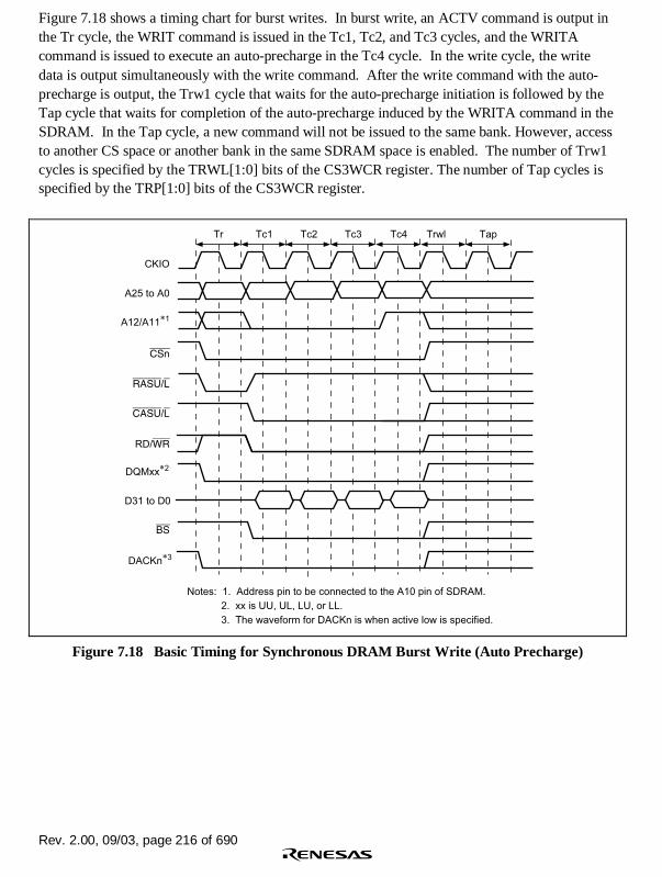
Rev. 2.00, 09/03, page 216 of 690
Figure 7.18 shows a timing chart for burst writes. In burst write, an ACTV command is output inthe Tr cycle, the WRIT command is issued in the Tc1, Tc2, and Tc3 cycles, and the WRITAcommand is issued to execute an auto-precharge in the Tc4 cycle. In the write cycle, the writedata is output simultaneously with the write command. After the write command with the auto-precharge is output, the Trw1 cycle that waits for the auto-precharge initiation is followed by theTap cycle that waits for completion of the auto-precharge induced by the WRITA command in theSDRAM. In the Tap cycle, a new command will not be issued to the same bank. However, accessto another CS space or another bank in the same SDRAM space is enabled. The number of Trw1cycles is specified by the TRWL[1:0] bits of the CS3WCR register. The number of Tap cycles isspecified by the TRP[1:0] bits of the CS3WCR register.
Tc4
CKIO
A25 to A0
CSn
RD/WR
RASU/L
DQMxx*2
D31 to D0
BS
Tap
DACKn*3
Tr Tc2 Tc3Tc1 Trwl
A12/A11*1
CASU/L
Notes: 1. Address pin to be connected to the A10 pin of SDRAM.
2. xx is UU, UL, LU, or LL.
3. The waveform for DACKn is when active low is specified.
Figure 7.18 Basic Timing for Synchronous DRAM Burst Write (Auto Precharge)

Rev. 2.00, 09/03, page 217 of 690
7.8.6 Single Write
A write access ends in one cycle when data is written in non-cacheable region and the data buswidth is larger than or equal to access size. This is called single write. Figure 7.19 shows the basictiming chart for single write.
CKIO
A25 to A0
CSn
RD/WR
RASU/L
DQMxx*2
D31 to D0
BS
Tap
DACKn*3
Tr Tc1 Trwl
A12/A11*1
CASU/L
Notes: 1. Address pin to be connected to the A10 pin of SDRAM.
2. xx is UU, UL, LU, or LL.
3. The waveform for DACKn is when active low is specified.
Figure 7.19 Basic Timing for Single Write (Auto Precharge)

Rev. 2.00, 09/03, page 218 of 690
7.8.7 Bank Active
The synchronous DRAM bank function is used to support high-speed accesses to the same rowaddress. When the BACTV bit in SDCR is 1, accesses are performed using commands (READ,WRIT) without auto-precharge. This function is called bank-active function. This function is validonly for either the upper or lower bits of area 3. When area 3 is set to bank-active mode, area 2should be set to normal space or byte-selection SRAM. When areas 2 and 3 are both set toSDRAM or both the upper and lower bits of area 3 are connected to SDRAM, auto pre-chargemode must be set. In this case, precharging is not performed when the access ends. Whenaccessing the same row address in the same bank, it is possible to issue the READ or WRITcommand immediately, without issuing an ACTV command. As synchronous DRAM is internallydivided into several banks, it is possible to activate one row address in each bank. If the nextaccess is to a different row address, a PRE command is first issued to precharge the relevant bank,then when precharging is completed, the access is performed by issuing an ACTV commandfollowed by a READ or WRIT command. If this is followed by an access to a different rowaddress, the access time will be longer because of the precharging performed after the accessrequest is issued.
In a write, when auto-precharge is performed, a command cannot be issued for a period of Trwl +Tpc cycles after issuance of the WRITA command. When bank active mode is used, READ orWRIT commands can be issued successively if the row address is the same. The number of cyclescan thus be reduced by Trwl + Tpc cycles for each write.
There is a limit on tRAS, the time for placing each bank in the active state. If there is no guaranteethat there will not be a cache hit and another row address will be accessed within the period inwhich this value is maintained by program execution, it is necessary to set auto-refresh and set therefresh cycle to no more than the maximum value of tRAS.
A burst read cycle without auto-precharge is shown in figure 7.20, a burst read cycle for the samerow address in figure 7.21, and a burst read cycle for different row addresses in figure 7.22.Similarly, a burst write cycle without auto-precharge is shown in figure 7.23, a single write cyclefor the same row address in figure 7.24, and a single write cycle for different row addresses infigure 7.25.
When bank active mode is set, if only accesses to the respective banks in the area 3 space areconsidered, as long as accesses to the same row address continue, the operation starts with thecycle in figure 7.20 or 7.23, followed by repetition of the cycle in figure 7.21 or 7.24. An access toa different area during this time has no effect. If there is an access to a different row address in thebank active state, after this is detected the bus cycle in figure 7.22 or 7.25 is executed instead ofthat in figure 7.21 or 7.24. In bank active mode, too, all banks become inactive after a refreshcycle or after the bus is released as the result of bus arbitration.

Rev. 2.00, 09/03, page 219 of 690
Tc4
CKIO
A25 to A0
CSn
RD/WR
RASU/L
DQMxx*2
D31 to D0
BS
DACKn*3
Tr Tc2 Tc3Tc1Td4Td2 Td3Td1Tw
Tde
A12/A11*1
CASU/L
Notes: 1. Address pin to be connected to the A10 pin of SDRAM.
2. xx is UU, UL, LU, or LL.
3. The waveform for DACKn is when active low is specified.
Figure 7.20 Burst Read Timing (No Auto Precharge)

Rev. 2.00, 09/03, page 220 of 690
Tc4Tc2 Tc3Tc1Td4
TdeTd2 Td3Td1Tw
CKIO
A25 to A0
CSn
RD/WR
RASU/L
DQMxx*2
D31 to D0
BS
DACKn*3
A12/A11*1
CASU/L
Notes: 1. Address pin to be connected to the A10 pin of SDRAM.
2. xx is UU, UL, LU, or LL.
3. The waveform for DACKn is when active low is specified.
Figure 7.21 Burst Read Timing (Bank Active, Same Row Address)

Rev. 2.00, 09/03, page 221 of 690
Tc4TpwTp Tc2 Tc3Tc1Td4Td2 Td3Td1Tw
TdeTr
CKIO
A25 to A0
CSn
RD/WR
RASU/L
DQMxx*2
D31 to D0
BS
DACKn*3
A12/A11*1
CASU/L
Notes: 1. Address pin to be connected to the A10 pin of SDRAM.
2. xx is UU, UL, LU, or LL.
3. The waveform for DACKn is when active low is specified.
Figure 7.22 Burst Read Timing (Bank Active, Different Row Addresses)

Rev. 2.00, 09/03, page 222 of 690
Tr Tc1
CKIO
A25 to A0
CSn
RD/WR
RASU/L
DQMxx*2
D31 to D0
BS
DACKn*3
A12/A11*1
CASU/L
Notes: 1. Address pin to be connected to the A10 pin of SDRAM.
2. xx is UU, UL, LU, or LL.
3. The waveform for DACKn is when active low is specified.
Figure 7.23 Single Write Timing (No Auto Precharge)

Rev. 2.00, 09/03, page 223 of 690
Tnop Tc1
CKIO
A25 to A0
CSn
RD/WR
RASU/L
DQMxx*2
D31 to D0
BS
DACKn*3
A12/A11*1
CASU/L
Notes: 1. Address pin to be connected to the A10 pin of SDRAM.
2. xx is UU, UL, LU, or LL.
3. The waveform for DACKn is when active low is specified.
Figure 7.24 Single Write Timing (Bank Active, Same Row Address)

Rev. 2.00, 09/03, page 224 of 690
TpwTp Tc1Tr
CKIO
A25 to A0
CSn
RD/WR
RASU/L
DQMxx*2
D31 to D0
BS
DACKn*3
A12/A11*1
CASU/L
Notes: 1. Address pin to be connected to the A10 pin of SDRAM.
2. xx is UU, UL, LU, or LL.
3. The waveform for DACKn is when active low is specified.
Figure 7.25 Single Write Timing (Bank Active, Different Row Addresses)

Rev. 2.00, 09/03, page 225 of 690
7.8.8 Refreshing
This LSI has a function for controlling synchronous DRAM refreshing. Auto-refreshing can beperformed by clearing the RMODE bit to 0 and setting the RFSH bit to 1 in SDCR. A continuousrefreshing can be performed by setting the RRC[2:0] bits in RTCSR. If synchronous DRAM is notaccessed for a long period, self-refresh mode, in which the power consumption for data retentionis low, can be activated by setting both the RMODE bit and the RFSH bit to 1.
1. Auto-refreshing
Refreshing is performed for the number of times specified by bits RRC[2:0] in RTCSR atintervals determined by the input clock selected by bits CKS[2:0] in RTCSR, and the value setin RTCOR. The value of these bits should be set so as to satisfy the refresh interval stipulationfor the synchronous DRAM used. First make the settings for RTCOR, RTCNT, and theRMODE and RFSH bits in SDCR, then make bits CKS[2:0] and RRC[2:0] settings in RTCSR.When the clock is selected by bits CKS[2:0], RTCNT starts counting up from the value at thattime. The RTCNT value is constantly compared with the RTCOR value, and if the two valuesare the same, a refresh request is generated and auto-refresh is performed for the number oftimes specified by bits RRC[2:0]. At the same time, RTCNT is cleared to zero and the count-up is restarted. Figure 7.26 shows the auto-refresh cycle timing.
After starting, the auto refreshing, PALL command is issued in the Tp cycle to make all thebanks to pre-charged state from active state when some bank is being pre-charged. Then REFcommand is issued in the Trr cycle after inserting idle cycles of which number is specified bythe TRP[1:0] bits in CSnWCR. A new command is not issued for the duration of the numberof cycles specified by the TRC[1:0] bits in CSnWCR after the Trr cycle. The TRC[1:0] bitsmust be set so as to satisfy the SDRAM refreshing cycle time stipulation (tRC). A NOP cycle isinserted between the Tp cycle and Trr cycle when the setting value of the TRP[1:0] bits inCSnWCR is longer than or equal to 2 cycles.

Rev. 2.00, 09/03, page 226 of 690
TpwTp Trr Trc Trc Trc
Hi-Z
CKIO
A25 to A0
CSn
RD/WR
RASU/L
DQMxx*2
D31 to D0
BS
DACKn*3
A12/A11*1
CASU/L
Notes: 1. Address pin to be connected to the A10 pin of SDRAM.
2. xx is UU, UL, LU, or LL.
3. The waveform for DACKn is when active low is specified.
Figure 7.26 Auto-Refresh Timing
2. Self-refreshing
Self-refresh mode in which the refresh timing and refresh addresses are generated within thesynchronous DRAM. Self-refreshing is activated by setting both the RMODE bit and theRFSH bit in SDCR to 1. After starting the self-refreshing, PALL command is issued in Tpcycle after the completion of the pre-charging bank. A SELF command is then issued afterinserting idle cycles of which number is specified by the TRP[1:0] bits in CSnWSR.Synchronous DRAM cannot be accessed while in the self-refresh state. Self-refresh mode iscleared by clearing the RMODE bit to 0. After self-refresh mode has been cleared, commandissuance is disabled for the number of cycles specified by the TRC[1:0] bits in CSnWCR. Self-refresh timing is shown in figure 7.27. Settings must be made so that self-refresh clearing anddata retention are performed correctly, and auto-refreshing is performed at the correctintervals. When self-refreshing is activated from the state in which auto-refreshing is set, auto-refreshing is restarted if the RFSH bit is set to 1 and the RMODE bit is cleared to 0 when self-refresh mode is cleared. If the transition from clearing of self-refresh mode to the start of auto-refreshing takes time, this time should be taken into consideration when setting the initial valueof RTCNT. Making the RTCNT value 1 less than the RTCOR value will enable refreshing tobe started immediately.

Rev. 2.00, 09/03, page 227 of 690
After self-refreshing has been set, the self-refresh state continues even if the chip standby stateis entered using the LSI standby function, and is maintained even after recovery from standbymode other than through a power-on reset. In case of a power-on reset, the bus statecontroller’s registers are initialized, and therefore the self-refresh state is cleared.
TpwTp Trr Trc Trc Trc
Hi-Z
Trc Trc
CKIO
CKE
A25 to A0
CSn
RD/WR
RASU/L
DQMxx*2
D31 to D0
BS
DACKn*3
A12/A11*1
CASU/L
Notes: 1. Address pin to be connected to the A10 pin of SDRAM.
2. xx is UU, UL, LU, or LL.
3. The waveform for DACKn is when active low is specified.
Figure 7.27 Self-Refresh Timing
3. Relationship between refresh requests and bus cycle
If a refresh request is generated during a bus cycle, refresh waits for the bus cycle to becompleted. If a refresh request is generated while the bus is released by the bus arbitrationfunction, refresh waits for the bus mastership to be obtained.
If a new refresh request is generated while refresh is waiting, the first refresh request iscanceled. To perform refresh correctly, the bus cycle and the bus-owned period must be shorterthan the refresh interval.
If a bus request is issued during self-refreshing, the bus is not released until the refresh iscompleted.

Rev. 2.00, 09/03, page 228 of 690
7.8.9 Low-Frequency Mode
When the SLOW bit in SDCR is set to 1, output of commands, addresses, and write data, andfetch of read data are performed at a timing suitable for operating SDRAM at a low frequency.
Figure 7.28 shows the access timing in low-frequency mode. In this mode, commands, addresses,and write data are output in synchronization with the falling edge of CKIO, which is half a cycledelayed than the normal timing. Read data is fetched at the rising edge of CKIO, which is half acycle faster than the normal timing. This timing allows the hold time of commands, addresses,write data, and read data to be extended.
If SDRAM is operated at a high frequency with the SLOW bit set to 1, the setup time ofcommands, addresses, write data, and read data are not guaranteed. Take the operating frequencyand timing design into consideration when making the SLOW bit setting.
CKIO
A25 to A0
CSn
RD/WR
D31 to D0
BS
Tc1
DACKn*3
Tr Td1Tw
A12/A11*1
Tde Tap Tr Tc1 Tnop Trwl Tap
CKE
RASU/L
DQMxx*2
CASU/L
Notes: 1. Address pin to be connected to the A10 pin of SDRAM.
2. xx is UU, UL, LU, or LL.
3. The waveform for DACKn is when active low is specified.
Figure 7.28 Low-Frequency Mode Access Timing

Rev. 2.00, 09/03, page 229 of 690
7.8.10 Power-On Sequence
In order to use synchronous DRAM, mode setting must first be performed after powering on. Toperform synchronous DRAM initialization correctly, the bus state controller registers must first beset, followed by a write to the synchronous DRAM mode register. In synchronous DRAM moderegister setting, the address signal value at that time is latched by a combination of the CSn, RAS,CAS, and RD/WR signals. If the value to be set is X, the bus state controller provides for value Xto be written to the synchronous DRAM mode register by performing a write to addressH'A4FD4000 + X for area 2 synchronous DRAM, and to address H'A4FD5000 + X for area 3synchronous DRAM. In this operation the data is ignored, but the mode write is performed as aword-size access. To set burst read/single write, CAS latency 2 to 3, wrap type = sequential, andburst length 1 supported by the LSI, arbitrary data is written in a word-size access to the addressesshown in table 7.17. In this time 0 is output at the external address pins of A12 or later.
Table 7.17 Access Address in SDRAM Mode Register Write
(1) Setting for Area 2 (SDMR2)
Burst read/single write (burst length 1):
Data Bus Width CAS Latency Access Address External Address Pin
16 bits 2 H'A4FD4440 H'0000440
3 H'A4FD4460 H'0000460
32 bits 2 H'A4FD4880 H'0000880
3 H'A4FD48C0 H'00008C0
Burst read/burst write (burst length 1):
Data Bus Width CAS Latency Access Address External Address Pin
16 bits 2 H'A4FD4040 H'0000040
3 H'A4FD4060 H'0000060
32 bits 2 H'A4FD4080 H'0000080
3 H'A4FD40C0 H'00000C0

Rev. 2.00, 09/03, page 230 of 690
(2) Setting for Area 3 (SDMR3)
Burst read/single write (burst length 1):
Data Bus Width CAS Latency Access Address External Address Pin
16 bits 2 H'A4FD5440 H'0000440
3 H'A4FD5460 H'0000460
32 bits 2 H'A4FD5880 H'0000880
3 H'A4FD58C0 H'00008C0
Burst read/burst write (burst length 1):
Data Bus Width CAS Latency Access Address External Address Pin
16 bits 2 H'A4FD5040 H'0000040
3 H'A4FD5060 H'0000060
32 bits 2 H'A4FD5080 H'0000080
3 H'A4FD50C0 H'00000C0
Mode register setting timing is shown in figure 7.29. A PALL command (all bank pre-chargecommand) is firstly issued. A REF command (auto refresh command) is then issued 8 times. AnMRS command (mode register write command) is finally issued. Idle cycles, of which number isspecified by the TRP[1:0] bits in CSnWCR, are inserted between the PALL and the first REF. Idlecycles, of which number is specified by the TRC[1:0] bits in CSnWCR, are inserted between REFand REF, and between the 8th REF and MRS. Idle cycles, of which number is one or more, areinserted between the MRS and a command to be issued next.
It is necessary to keep idle time of certain cycles for SDRAM before issuing PALL command afterpower-on. Refer the manual of the SDRAM for the idle time to be needed. When the pulse widthof the reset signal is longer then the idle time, mode register setting can be started immediatelyafter the reset, but care should be taken when the pulse width of the reset signal is shorter than theidle time.

Rev. 2.00, 09/03, page 231 of 690
TpwTp Trr Trc Trc Tmw
Hi-Z
TnopTrc Trr Trc
REF REF MRSPALL
Notes: 1. Address pin to be connected to the A10 pin of SDRAM.
2. xx is UU, UL, LU, or LL.
3. The waveform for DACKn is when active low is specified.
CKIO
A25 to A0
CSn
RD/WR
RASU/L
DQMxx*2
D31 to D0
BS
DACKn*3
A12/A11*1
CASU/L
Figure 7.29 Synchronous DRAM Mode Write Timing (Based on JEDEC)
7.9 Burst ROM Interface
The burst ROM interface is provided to access ROM that has the page mode function, such asflash memory, in high speed. Basically the access to the ROM is performed in the same way as fornormal space. When the first cycle is terminated, however, negation of the RD signal is notexecuted. The accesses after the 2nd access are performed by exchanging only the address. In theaccesses after the 2nd access, the address is changed at the falling edge of CKIO.
The number of wait cycles specified by the W[3:0] bits in CSnWCR are inserted for the firstaccess cycle. The number of wait cycles specified by the BW[1:0] bits in CSnWCR are insertedfor the second and subsequent access cycles.
In the access to the burst ROM, the BS signal is asserted only to the first access cycle. An externalwait input is valid only to the first access cycle. In the single access or write access that do notperform the burst operation in the burst ROM interface, access timing is same as a normal space.Table 7.18 lists a relationship between bus width, access size, and the number of bursts. Figure7.30 shows a timing chart.

Rev. 2.00, 09/03, page 232 of 690
Table 7.18 Relationship between Bus Width, Access Size, and Number of Bursts
Bus Width Access Size Number of Bursts
8 bits 8 bits 1
16 bits 2
32 bits 4
16 bytes 16
16 bits 8 bits 1
16 bits 1
32 bits 2
16 bytes 8
CKIO
Address
RD
Data
DACK
WAIT
CS
T1 Tw Tw TB2 Twb TB2 Twb TB2 Twb T2
RD/WR
BS
Figure 7.30 Burst ROM Access (Bus Width 8 Bits, Access Size 32 Bits (Number of Burst 4),Access Wait for the 1st Time 2, Access Wait for 2nd Time and after 1)

Rev. 2.00, 09/03, page 233 of 690
7.10 Byte-Selection SRAM Interface
The byte-selection SRAM interface is for outputting the byte-selection signal (WEn) in both readand write bus cycles. This interface has 16-bit data pins and accesses SRAM that has an upperbyte-selection pin and a lower byte-selection pin, such as UB and LB. The write access timing isthe same as that for the normal space interface. The read access timing differs from that for thenormal space interface in the WEn timing, and a byte-selection signal is output from the WEn pin.The basic access timing is shown in figure 7.31.
Note that in a write cycle, data is written in accordance with the byte-selection pin (WEn) timing.Check the data sheet of the memory to be used for the actual timing.
CKIO
A25 to A0
CSn
WEn
RD/WR
RD
RD
D31 to D0
D31 to D0
RD/WR
BS
DACKn*
T1 T2
HighWrite
Read
Note: * The waveform for DACKn is when active low is specified.
Figure 7.31 Byte-Selection SRAM Basic Access Timing

Rev. 2.00, 09/03, page 234 of 690
A15
A0
CS
OE
WE
I/O15
I/O0
UB
LB
A17
A2
CSn
RD
RD/WR
D31
D16
D15
D0
A15
A0
CS
OE
WE
I/O15
I/O0
UB
LB
This LSI
64k × 16-bit
SRAM
.
.
.
.
.
.
.
.
.
.
.
.
.
.
.
.
.
.
.
.
.
WE3
WE2
WE1
WE2
Figure 7.32 Example of Connection with 32-Bit Data-Width Byte-Selection SRAM
This LSI
A16
A1
CSn
RD
RD/WR
D15
D0
WE1
WE0
A15
A0
CS
OE
WE
I/O 15
I/O 0
UB
LB
64k × 16-bit
SRAM
Figure 7.33 Example of Connection with 16-Bit Data-Width Byte-Selection SRAM

Rev. 2.00, 09/03, page 235 of 690
7.11 Wait between Access Cycles
As the operating frequency of LSIs becomes higher, the off-operation of the data buffer oftencollides with the next data access when the read operation from devices with slow access speed iscompleted. As a result of these collisions, the reliability of the device is low and malfunctions mayoccur. A function that avoids data collisions by inserting wait cycles between continuous accesscycles has been newly added.
The number of wait cycles between access cycles can be set by bits IWW[1:0], IWRWD[1:0],IWRWS[1:0], IWRRD[1:0], and IWRRS[1:0] in CSnBCR, and bits DMAIW[1:0] and DMAIWAin CMNCR. The conditions for setting the wait cycles between access cycles (idle cycles) areshown below.
1. Continuous accesses are write-read or write-write
2. Continuous accesses are read-write for different spaces
3. Continuous accesses are read-write for the same space
4. Continuous accesses are read-read for different spaces
5. Continuous accesses are read-read for the same space
6. Data output from an external device caused by DMA single transfer is followed by data outputfrom another device that includes this LSI (DMAIWA = 0)
7. Data output from an external device caused by DMA single transfer is followed by any type ofaccess (DMAIWA = 1)
7.12 Bus Arbitration
This LSI supports bus arbitration. This LSI has bus mastership in the normal state and releases busmastership after receiving a bus request from another device.
To prevent device malfunction while the bus mastership is transferred between master and slave,the LSI negates all of the bus control signals before bus release. When the bus mastership isreceived, all of the bus control signals are first negated and then driven appropriately. In this case,output buffer conflicts can be prevented because the master and slave drive the same signals withthe same values. In addition, to prevent noise while the bus control signal is in the high-impedancestate, pull-up resistors must be connected to these control signals.
Bus mastership is transferred at the boundary of bus cycles. Namely, bus mastership is releasedimmediately after receiving a bus request when a bus cycle is not being performed. The release ofbus mastership is delayed until the bus cycle is complete when a bus cycle is in progress. Evenwhen from outside the LSI it looks like a bus cycle is not being performed, a bus cycle may beperforming internally, started by inserting wait cycles between access cycles. Therefore, it cannotbe immediately determined whether or not bus mastership has been released by looking at the CSnsignal or other bus control signals. The states that do not allow bus mastership release are shownbelow.

Rev. 2.00, 09/03, page 236 of 690
1. 16-byte transition because of a cache miss
2. During copyback operation for the cache
3. Between the read and write cycles of a TAS instruction
4. Multiple bus cycles generated when data bus width is smaller than the access size (Forexample, between bus cycles when longword access is made to memory with a data bus widthof 8 bits.)
5. 16-byte transfer by the DMAC
If self-refresh mode is specified for the SDRAM, the master device cannot release the bus. If themaster clock stops because a transition is underway to standby mode or the frequency is changed,or if this LSI is being reset, the master device cannot release the bus. To prevent the slave fromissuing bus requests in such a case, the slave must be put into the sleep state so that no slaveaccess cycles are generated.
The refresh request and bus request are accepted during the DMA burst transfer.
Bus mastership is maintained until a new bus request is received. Bus mastership is releasedimmediately after the completion of the bus cycle in progress when an external bus request(BREQ) is asserted (low level) and a bus acknowledge signal (BACK) is asserted (low level). Bususe is resumed when a negation (high level) of BREQ, which shows that the slave has released thebus, has been received.
SDRAM issues all bank pre-charge commands (PALLs) when active banks exist and releases thebus after completion of a PALL command.
The bus release sequence is as follows. The address bus and data bus are placed in a high-impedance state synchronized with the rising edge of CKIO. The bus mastership enable signal isasserted 0.5 cycles after the above timing, synchronized with the falling edge of CKIO. Buscontrol signals (BS, CSn, RASU, RASL, CASU, CASL, DQMxx, WEn, RD, and RD/WR) aremade to the high-impedance states at the subsequent rising edge of CKIO. Bus request signals aresampled at the falling edge of CKIO. The sequence for re-claiming bus mastership from a slave isdescribed below. After detecting the negation of BREQ at the falling edge of CKIO, the busenable signal is negated at the subsequent falling edge of the clock. The address and data signalsare driven at the subsequent rising edge of CKIO. Figure 7.34 shows the bus arbitration timing.

Rev. 2.00, 09/03, page 237 of 690
CKIO
A25 to A0
CSnOther bus
control signals
Data
BREQ
BACK
Figure 7.34 Bus Arbitration
In an original slave device designed by the user, multiple bus accesses are generated continuouslyto reduce the overhead caused by bus arbitration. In this case, to execute SDRAM refreshcorrectly, the slave device must be designed to release the bus mastership within the refreshinterval time.
The bus release by the BREQ and BACK signal handshaking requires some overhead. If the slavehas many tasks, multiple bus cycles should be executed in a bus mastership acquisition. Reducingthe cycles required for master to slave bus mastership transitions streamlines the system design.
7.13 Others
Reset: The bus state controller (BSC) can be initialized completely only at power-on reset. Atpower-on reset, all signals are negated and output buffers are turned off regardless of the bus cyclestate. All control registers are initialized.
In standby, sleep, and manual reset, control registers of the bus state controller are not initialized.At manual reset, the current bus cycle being executed is completed and then the access wait stateis entered. Since the RTCNT continues counting up during manual reset signal assertion, a refreshrequest occurs to initiate the refresh cycle.
Note that arbitration requests using BREQ are not accepted during manual reset signal assertion.
On-Chip Peripheral Module Access: To access an on-chip module register, two or moreperipheral module clock (Pφ) cycles are required. Care must be taken in system design.

Rev. 2.00, 09/03, page 238 of 690

DMAS311B_000020020100 Rev. 2.00, 09/03, page 239 of 690
Section 8 Direct Memory Access Controller (DMAC)
This LSI includes the direct memory access controller (DMAC). The DMAC can be used in placeof the CPU to perform high-speed transfers between external devices with DACK (transfer requestacknowledge signal), external memory, memory-mapped external devices, and on-chip peripheralmodules.
8.1 Features
• Four channels (two channels can receive an external request)
• 4-Gbyte physical address space
• Data transfer unit: Byte, word (2 bytes), longword (4 bytes), and 16 bytes (longword × 4)
• Maximum transfer count: 16777216 transfers
• Address mode: Dual address mode or single address mode can be selected.
• Transfer requests: External request, on-chip peripheral module request, or auto request can beselected.
The following modules can issue an on-chip peripheral module request.
SCIF0, SCIF2, CMT, USB, and A/D converter
• Bus modes: Cycle steal mode (normal mode and intermittent mode 16/64) or burst mode canbe selected.
• Selectable channel priority levels:
The channel priority levels are selectable between fixed mode and round-robin mode.
• Interrupt request: An interrupt request can be generated to the CPU after transfers end.
• External request detection: Low-/high-level or rising/falling edge detection of DREQ input canbe selected.
• Transfer request acknowledge signal: Active levels for DACK can be set independently.
• Transfer end signal: Active level for TEND can be set. TEND is output at the same timing asDACK in the last DMA transfer. (Only channel 0)

Rev. 2.00, 09/03, page 240 of 690
Figure 8.1 shows the block diagram of the DMAC.
On-chip
peripheral module
Pe
rip
he
ral b
us
Inte
rna
l b
us
External
ROM
DREQ0, DREQ1
DEIn
DACK0, DACK1
TEND0
External
RAM
External I/O
(memory
mapped)
External I/O
(with
acknowledge-
ment)
Bus
interface
Bus state
controller
Request
priority
control
Start-up
control
Register
control
Transfer count
control
SAR_n
DAR_n
DMATCR_n
CHCR_n
DMAOR
DMARS0−1
[Legend]
DMAOR: DMA operation register
SARn: DMA source address register
DARn: DMA destination address register
DMATCRn: DMA transfer count register
CHCRn: DMA channel control register
DMARS0/1: DMA extension resource selector
DEIn: DMA transfer-end interrupt request to the CPU
n : 0, 1, 2, 3
DMAC module
SCIF0, SCIF2
CMT, USBA/D converter
Figure 8.1 Block Diagram of DMAC

Rev. 2.00, 09/03, page 241 of 690
8.2 Input/Output Pins
The external pins for the DMAC are described below.
Table 8.1 lists the configuration of the pins that are connected to external bus. The DMAC haspins for 2 channels (channels 0 and 1) for external bus use. Channel 0 has the DMA transfer endsignal.
Table 8.1 Pin Configuration
Channel Name Symbol I/O Function
0 DMA transfer request DREQ0 I DMA transfer request input fromexternal device to channel 0
DMA transfer requestacknowledge
DACK0 O DMA transfer request acknowledgeoutput from channel 0 to external device
DMA transfer end TEND0 O Transfer end output in channel 0
1 DMA transfer request DREQ1 I DMA transfer request input fromexternal device to channel 1
DMA transfer requestacknowledge
DACK1 O DMA transfer request acknowledgeoutput from channel 1 to external device
8.3 Register Descriptions
The DMAC has the following registers. See section 24, List of Registers, for the addresses ofthese registers and the states of them in each processing state. The SAR for channel 0 is expressedsuch as SAR_0.
1. Channel 0
• DMA source address register_0 (SAR_0)
• DMA destination address register_0 (DAR_0)
• DMA transfer count register_0 (DMATCR_0)
• DMA channel control register_0 (CHCR_0)
2. Channel 1
• DMA source address register_1 (SAR_1)
• DMA destination address register_1 (DAR_1)
• DMA transfer count register_1 (DMATCR_1)
• DMA channel control register _1 (CHCR_1)

Rev. 2.00, 09/03, page 242 of 690
3. Channel 2
• DMA source address register_2 (SAR_2)
• DMA destination address register_2 (DAR_2)
• DMA transfer count register_2 (DMATCR_2)
• DMA channel control register_2 (CHCR_2)
4. Channel 3
• DMA source address register_3 (SAR_3)
• DMA destination address register_3 (DAR_3)
• DMA transfer count register_3 (DMATCR_3)
• DMA channel control register_3 (CHCR_3)
5. Common
• DMA operation register (DMAOR)
• DMA extended resource selector 0 (DMARS0)
• DMA extended resource selector 1 (DMARS1)
8.3.1 DMA Source Address Registers (SAR)
SAR are 32-bit readable/writable registers that specify the source address of a DMA transfer.During a DMA transfer, these registers indicate the next source address. When the data of anexternal device with DACK is transferred in single address mode, SAR is ignored.
To transfer data in 16 bits or in 32 bits, specify the address with 16-bit or 32-bit address boundary.When transferring data in 16-byte units, a 16-byte boundary must be set for the source addressvalue. The initial value is undefined. The SAR retains the current value in software standby ormodule standby mode.
8.3.2 DMA Destination Address Registers (DAR)
DAR are 32-bit readable/writable registers that specify the destination address of a DMA transfer.During a DMA transfer, these registers indicate the next destination address. When the data of anexternal device with DACK is transferred in single address mode, DAR is ignored.
To transfer data in 16 bits or in 32 bits, specify the address with 16-bit or 32-bit address boundary.When transferring data in 16-byte units, a 16-byte boundary must be set for the source addressvalue. The initial value is undefined. The DAR retains the current value in software standby ormodule standby mode.

Rev. 2.00, 09/03, page 243 of 690
8.3.3 DMA Transfer Count Registers (DMATCR)
DMATCR are 32-bit readable/writable registers that specify the DMA transfer count. The numberof transfers is 1 when the setting is H'00000001, 16,777,215 when H'00FFFFFF is set, and16,777,216 (the maximum) when H'00000000 is set. During a DMA transfer, these registersindicate the remaining transfer count.
The upper 8 bits of DMATCR are always read as 0. The write value should always be 0. Totransfer data in 16 bytes, one 16-byte transfer (128 bits) counts one. The initial value is undefined.The DMATCR retains the current value in software standby or module standby mode.
8.3.4 DMA Channel Control Registers (CHCR)
CHCR are 32-bit readable/writable registers that control the DMA transfer mode.
BitBitName
InitialValue R/W Descriptions
31 to 24 0 R Reserved
These bits are always read as 0. The write value should alwaysbe 0.
23 DO 0 R/W DMA Overrun
Selects whether DREQ is detected by overrun 0 or by overrun1. This bit is valid only in CHCR_0 and CHCR_1. This bit isalways read as 0 in CHCR_2 and CHCR_3. The write valueshould always be 0.
0: Detects DREQ by overrun 0
1: Detects DREQ by overrun 1
22 TL 0 R/W Transfer End Level
Selects whether the TEND signal output is high active or lowactive. This bit is valid only in CHCR_0. There are no TENDpins in CHCR_1 to CHCR_3. Therefore this setting is invalid.This bit is always read as 0. The write value should always be0.
0: Low-active output of TEND
1: High-active output of TEND
21 to 18 0 R Reserved
These bits are always read as 0. The write value should alwaysbe 0.

Rev. 2.00, 09/03, page 244 of 690
BitBitName
InitialValue R/W Descriptions
17 AM 0 R/W Acknowledge Mode
Selects whether DACK is output in data read cycle or in datawrite cycle in dual address mode.
In single address mode, DACK is always output regardless ofthe specification by this bit.
This bit is valid only in CHCR_0 and CHCR_1. This bit isalways read as 0 in CHCR_2 and CHCR_3. The write valueshould always be 0.
0: DACK output in read cycle (Dual address mode)
1: DACK output in write cycle (Dual address mode)
16 AL 0 R/W Acknowledge Level
Specifies the DACK signal output is high active or low active.
This bit is valid only in CHCR_0 and CHCR_1. This bit isalways read as 0 in CHCR_2 and CHCR_3. The write valueshould always be 0.
0: Low-active output of DACK
1: High-active output of DACK
15
14
DM1
DM0
0
0
R/W
R/W
Destination Address Mode
Specify whether the DMA destination address is incremented,decremented, or left fixed. (In single address mode, the DM1and DM0 bits are ignored when data is transferred to anexternal device with DACK.)
00: Fixed destination address(setting prohibited in 16-byte transfer)
01: Destination address is incremented (+1 in byte-sizetransfer, +2 in word-size transfer, +4 in longword-sizetransfer, +16 in 16-byte transfer)
10: Destination address is decremented (–1 in byte-sizetransfer, –2 in word-size transfer, –4 in longword-sizetransfer, setting prohibited in 16-byte transfer)
11: Setting prohibited

Rev. 2.00, 09/03, page 245 of 690
BitBitName
InitialValue R/W Descriptions
13
12
SM1
SM0
0
0
R/W
R/W
Source Address Mode
Specifies whether the DMA source address is incremented,decremented, or left fixed. (In single address mode, the SM1and SM0 bits are ignored when data is transferred from anexternal device with DACK.)
00: Fixed source address(setting prohibited in 16-byte transfer)
01: Source address is incremented (+1 in byte-size transfer, +2in word-size transfer, +4 in longword-size transfer, +16 in16-byte transfer)
10: Source address is decremented (–1 in byte-size transfer, –2in word-size transfer, –4 in longword-size transfer, settingprohibited in 16-byte transfer)
11: Setting prohibited
11
10
9
8
RS3
RS2
RS1
RS0
0
0
0
0
R/W
R/W
R/W
R/W
Resource Select
Specifies which transfer requests will be sent to the DMAC. Thechanging of transfer request source should be done in the statethat the DMA enable bit (DE) is set to 0.
0000: External request, dual address mode
0001: Setting prohibited
0010: External request/single address mode
External address space → external device with DACK
0011: External request/single address mode
External device with DACK → external address space
0100: Auto request
0101: Setting prohibited
0110: Setting prohibited
0111: Setting prohibited
1000: DMA extended resource selector specification
1001: Setting prohibited
1010: Setting prohibited
1011: Setting prohibited
1100: Setting prohibited
1101: Setting prohibited
1110: Peripheral module request, A/D converter
1111: Peripheral module request, CMT
Note: External request specification is valid only in CHCR_0and CHCR_1. None of the external request specificationcan be set in channels CHCR_2 and CHCR_3.

Rev. 2.00, 09/03, page 246 of 690
BitBitName
InitialValue R/W Descriptions
7
6
DL
DS
0
0
R/W
R/W
DREQ Level and DREQ Edge Select
Select the detection method of the DREQ pin input and thedetection level.
These bits are valid only in CHCR_0 and CHCR_1. These bitsare always read as 0 in CHCR_2 and CHCR_3. The write valueshould always be 0.
In channels 0 and 1, also, if the transfer request source isspecified as an on-chip peripheral module or if an auto-requestis specified, these bits are invalid.
00: DREQ detected in low level
01: DREQ detected at falling edge
10: DREQ detected in high level
11: DREQ detected at rising edge
5 TB 0 R/W Transfer Bus Mode
Specifies the bus mode when DMA transfers data.
0: Cycle steal mode
1: Burst mode
4
3
TS1
TS0
0
0
R/W
R/W
Transfer Size
Specify the size of data to be transferred.
Select the size of data to be transferred when the source ordestination is an on-chip peripheral module register of whichtransfer size is specified.
00: Byte size
01: Word size (two bytes)
10: Longword size (four bytes)
11: 16-byte unit (four longword transfers)
2 IE 0 R/W Interrupt Enable
Specifies whether or not an interrupt request is generated to theCPU at the end of the DMA transfer. Setting this bit to 1generates an interrupt request (DEI) to the CPU when the TEbit is set to 1.
0: Interrupt request disabled
1: Interrupt request enabled

Rev. 2.00, 09/03, page 247 of 690
BitBitName
InitialValue R/W Descriptions
1 TE 0 R/(W)* Transfer End Flag
Indicates that the DMA transfer ends. The TE bit is set to 1when data transfer ends when DMATCR becomes to 0.
The TE bit is not set to 1 in the following cases.
• DMA transfer ends due to an NMI interrupt or DMA addresserror before DMATCR becomes to 0.
• DMA transfer is ended by clearing the DE bit and the DME
bit in the DMA operation register (DMAOR).
This bit can only be cleared by writing 0 after reading 1. Even ifthe DE bit is set to 1 while this bit is set to 1, transfer is notenabled.
0: During the DMA transfer or DMA transfer has been aborted
[Clearing conditions]
• Writing 0 after reading TE = 1
• Power-on reset
• Manual reset
1: Data transfer ends by the specified count (DMATCR = 0)
0 DE 0 R/W DMA Enable
Enables or disables the DMA transfer. In auto request mode,DMA transfer starts by setting the DE bit and DME bit inDMAOR to 1. In this time, all of the bits TE, NMIF in DMAOR,and AE must be 0. In an external request or peripheral modulerequest, DMA transfer starts if DMA transfer request isgenerated by the devices or peripheral modules after settingthe bits DE and DME to 1. In this case, however, all of the bitsTE, NMIF, and AE must be 0 an in the case of auto requestmode. Clearing the DE bit to 0 can terminate the DMA transfer.
0: DMA transfer disabled
1: DMA transfer enabled
Note: * Only 0 can be written for clearing the flags.

Rev. 2.00, 09/03, page 248 of 690
8.3.5 DMA Operation Register (DMAOR)
DMAOR is a 16-bit readable/writable register that specifies the priority level of channels at theDMA transfer. This register shows the DMA transfer status.
BitBitName
InitialValue R/W Description
15, 14 0 R Reserved
These bits are always read as 0. The write value shouldalways be 0.
13
12
CMS1
CMS0
0
0
R/W
R/W
Cycle Steal Mode Select
Select either normal mode or intermittent mode in cycle stealmode.
It is necessary that all channels' bus modes are set to cyclesteal mode to make valid intermittent mode.
00: Normal mode
01: Setting prohibited
10: Intermittent mode 16
Executes one DMA transfer in each of 16 clocks of anexternal bus clock.
11: Intermittent mode 64
Executes one DMA transfer in each of 64 clocks of anexternal bus clock.
11, 10 0 R Reserved
These bits are always read as 0. The write value shouldalways be 0.
9
8
PR1
PR0
0
0
R/W
R/W
Priority Mode
Select the priority level between channels when there aretransfer requests for multiple channels simultaneously.
00: CH0 > CH1 > CH2 > CH3
01: CH0 > CH2 > CH3 > CH1
10: Setting prohibited
11: Round-robin mode
7 to 3 0 R Reserved
These bits are always read as 0. The write value shouldalways be 0.

Rev. 2.00, 09/03, page 249 of 690
BitBitName
InitialValue R/W Description
2 AE 0 R/(W)* Address Error Flag
Indicates that an address error occurred by the DMAC. If thisbit is set, DMA transfer is not enabled even if the DE bit inCHCR and the DME bit in DMAOR are set to 1. This bit canonly be cleared by writing 0 after reading 1.
0: No DMAC address error
[Clearing conditions]
• Writing 0 after reading AE = 1
• Power-on reset
• Manual reset
1: DMAC address error. DMA transfer disabled.
[Setting condition]
DMAC address error occurrence
1 NMIF 0 R/(W)* NMI Flag
Indicates that an NMI interrupt occurred. If this bit is set, DMAtransfer is not enabled even if the DE bit in CHCR and theDME bit in DMAOR are set to 1. This bit can only be clearedby writing 0 after reading 1.
When the NMI is input, the DMA transfer in progress can bedone in one transfer unit. When the DMAC is not in operation,the NMIF bit is set to 1 even if the NMI interrupt was input.
0: No NMI interrupt
[Clearing conditions]
• Writing 0 after reading NMIF = 1
• Power-on reset
• Manual reset
1: NMI input. DMA transfer disabled.
[Setting condition]
NMI interrupt occurrence
0 DME 0 R/W DMA Master Enable
Enables or disables DMA transfers on all channels. If theDME bit and the DE bit in CHCR are set to 1, DMA transfersare enabled. In this time, all of the bits TE in CHCR, NMIF inDMAOR, and AE must be 0. If this bit is cleared duringtransfer, transfers in all the channels can be terminated.
0: Disable DMA transfers on all channels
1: Enable DMA transfers on all channels
Note: *Only 0 can be written for clearing the flags.

Rev. 2.00, 09/03, page 250 of 690
8.3.6 DMA Extended Resource Selectors 0, 1 (DMARS0, DMARS1)
DMARS is a 16-bit readable/writable register that specifies the DMA transfer request sourcesfrom peripheral modules in each channel. DMARS0 specifies for channels 0 and 1, DMARS1 forchannels 2 and 3. This register can set the transfer request of SCIF0, SCIF2, and USB.
When MID/RID other than the values listed in table 8.2 is set, the operation of this LSI is notguaranteed. The transfer request from DMARS is valid only when the resource select bits (RS3 toRS0) has been set to B'1000 for CHCR_0 to CHCR_3. Otherwise, even if DMARS has been set,transfer request source is not accepted.
• DMARS0
BitBitName
InitialValue R/W Description
15
14
13
12
11
10
C1MID5
C1MID4
C1MID3
C1MID2
C1MID1
C1MID0
0
0
0
0
0
0
R/W
R/W
R/W
R/W
R/W
R/W
Transfer request source module ID5 to ID0 for DMA channel1 (MID)
See table 8.2.
9
8
C1RID1
C1RID0
0
0
R/W
R/W
Transfer request resource register ID1 to ID0 for DMAchannel 1 (RID)
See table 8.2.
7
6
5
4
3
2
C0MID5
C0MID4
C0MID3
C0MID2
C0MID1
C0MID0
0
0
0
0
0
0
R/W
R/W
R/W
R/W
R/W
R/W
Transfer request source module ID5 to ID0 for DMA channel0 (MID)
See table 8.2
1
0
C0RID1
C0RID0
0
0
R/W
R/W
Transfer request resource register ID1 to ID0 for DMAchannel 0 (RID)
See table 8.2.

Rev. 2.00, 09/03, page 251 of 690
• DMARS1
BitBitName
InitialValue R/W Description
15 to 10 C3MID5 toC3MID0
0 R/W Transfer request resource module ID5 to ID0 for DMAchannel 3 (MID)
See table 8.2.
9
8
C3RID1
C3RID0
0
0
R/W
R/W
Transfer request resource register ID1 and ID0 for DMAchannel 3 (RID)
See table 8.2.
7 to 2 C2MID5 toC2MID0
0 R/W Transfer request resource module ID5 to ID0 for DMAchannel 2 (MID)
See table 8.2.
1
0
C2RID1
C2RID0
0
0
R/W
R/W
Transfer request resource register ID1 and ID0 for DMAchannel 2 (RID)
See table 8.2.
Table 8.2 Transfer Request Sources
PeripheralModule
Setting Value for OneChannel (MID + RID) MID RID Function
H'21 B'01 TransmitSCIF0
H'22
B'001000
B'10 Receive
H'29 B'01 TransmitSCIF2
H'2A
B'001010
B'10 Receive
H'73 B'11 TransmitUSB
H'70
B'011100
B'00 Receive

Rev. 2.00, 09/03, page 252 of 690
8.4 Operation
When there is a DMA transfer request, the DMAC starts the transfer according to thepredetermined channel priority order; when the transfer end conditions are satisfied, it ends thetransfer. Transfers can be requested in three modes: auto request, external request, and on-chipperipheral module request. In bus mode, burst mode or cycle steal mode can be selected.
8.4.1 Transfer Flow
After the DMA source address registers (SAR), DMA destination address registers (DAR), DMAtransfer count registers (DMATCR), DMA channel control registers (CHCR), DMA operationregister (DMAOR), and DMA extended resource selector (DMARS) are set, the DMAC transfersdata according to the following procedure:
1. Checks to see if transfer is enabled (DE = 1, DME = 1, TE = 0, AE = 0, NMIF = 0)
2. When a transfer request is generated and transfer is enabled, the DMAC transfers 1 transferunit of data (depending on the TS0 and TS1 settings). For an auto request, the transfer beginsautomatically when the DE bit and DME bit are set to 1. The DMATCR value will bedecremented for each transfer. The actual transfer flows vary by address mode and bus mode.
3. When the specified number of transfer have been completed (when DMATCR reaches 0), thetransfer ends normally. If the IE bit in CHCR is set to 1 at this time, a DEI interrupt is sent tothe CPU.
4. When an address error or an NMI interrupt is generated, the transfer is aborted. Transfers arealso aborted when the DE bit in CHCR or the DME bit in DMAOR are cleared to 0.

Rev. 2.00, 09/03, page 253 of 690
Figure 8.2 is a flowchart of this procedure.
Normal end
NMIF = 1
or AE = 1 or DE = 0
or DME = 0?
Bus mode,
transfer request mode,
DREQ detection method
Initial settings
(SAR, DAR, DMATCR, CHCR, DMAOR, DMARS)
Transfer (1 transfer unit);
DMATCR − 1 → DMATCR, SAR and DAR
updated
DEI interrupt request (when IE = 1)
TE = 1
No
Yes
No
Yes
No
Yes
Yes
No
Yes
No
*3
*2
Start
Transfer aborted
DMATCR = 0?
Transfer request
occurs?*1
DE, DME = 1 and
NMIF, AE, TE = 0?
NMIF = 1
or AE = 1 or DE = 0
or DME = 0?
Transfer end
Notes: 1. In auto-request mode, transfer begins when NMIF, AE, and TE bits are 0 and the DE and DME
bits are set to 1.
2. DREQ = level detection in burst mode (external request), or cycle-steal mode.
3. DREQ = edge detection in burst mode (external request), or auto-request mode in burst mode.
Figure 8.2 DMAC Transfer Flowchart

Rev. 2.00, 09/03, page 254 of 690
8.4.2 DMA Transfer Requests
DMA transfer requests are basically generated in either the data transfer source or destination, butthey can also be generated by external devices and on-chip peripheral modules that are neither thesource nor the destination. Transfers can be requested in three modes: auto request, externalrequest, and on-chip peripheral module request. The request mode is selected in the RS3 to RS0bits in the DMA channel control register (CHCR), and DMARS0 and DMARS1.
Auto-Request Mode: When there is no transfer request signal from an external source, as in amemory-to-memory transfer or a transfer between memory and an on-chip peripheral moduleunable to request a transfer, auto-request mode allows the DMAC to automatically generate atransfer request signal internally. When the DE bit in CHCR and the DME bit in DMAOR are setto 1, the transfer begins so long as the AE and NMIF bits in DMAOR are 0.
External Request Mode: In this mode a transfer is performed at the request signals (DREQ0 andDREQ1) of an external device. This mode is valid only in channels 0 and 1. Choose one of themodes shown in table 8.3 according to the application system. When this mode is selected, if theDMA transfer is enabled (DE = 1, DME = 1, TE = 0, AE = 0, NMIF = 0), a transfer is performedupon a request at the DREQ input.
Table 8.3 Selecting External Request Modes with RS Bits
RS3 RS2 RS1 RS0 Address Mode Source Destination
0 0 0 0 Dual addressmode
Any Any
1 0 Single addressmode
External memory,memory-mappedexternal device
External device withDACK
1 External device withDACK
External memory,memory-mappedexternal device
Choose to detect DREQ by either the edge or level of the signal input with the DL bit and DS bitof CHCR_0 and CHCR_1 as shown in table 8.4. The source of the transfer request does not haveto be the data transfer source or destination.

Rev. 2.00, 09/03, page 255 of 690
Table 8.4 Selecting External Request Detection with DL, DS Bits
CHCR_0 or CHCR_1
DL DS Detection of External Request
0 Low level detection0
1 Falling edge detection
0 High level detection1
1 Rising edge detection
When DREQ is accepted, the DREQ pin becomes request accept disabled state. After issuingacknowledge signal DACK for the accepted DREQ, the DREQ pin again becomes request acceptenabled state.
When DREQ is used for level detection, there are the following two cases depending on the timingto detect the next DREQ after outputting DACK. A case wherein transfer is aborted after the samenumber of transfers has been performed as requests (overrun 0) and wherein another transfer isaborted after transfers have been performed for (the number of requests plus 1) times (overrun 1).The DO bit in CHCR selects overrun 0 or overrun 1.
Table 8.5 Selecting External Request Detection with DO Bit
CHCR_0 or CHCR_1
DO External Request
0 Overrun 0
1 Overrun 1

Rev. 2.00, 09/03, page 256 of 690
On-Chip Peripheral Module Request Mode: In this mode a transfer is performed at the transferrequest signal of an on-chip peripheral module. Transfer request signals comprise the transmit dataempty transfer request and receive data full transfer request from the SCIF0 and SCIF2 set byDMARS0/1, the compare-match timer transfer request from the CMT, and transfer requests fromthe USB.
When this mode is selected, if the DMA transfer is enabled (DE = 1, DME = 1, TE = 0, AE = 0,NMIF = 0), a transfer is performed upon the input of a transfer request signal.
When a transmit data empty transfer request of the SCIF is set as the transfer request, the transferdestination must be the SCIF’s transmit data register. Likewise, when receive data full transferrequest of the SCIF is set as the transfer request, the transfer source must be the SCIF’s receivedata register. These conditions also apply to the USB. Any address can be specified for data sourceand destination, when transfer request is generated by the CMT.
Table 8.6 Selecting On-Chip Peripheral Module Request Modes with RS3 to RS0 Bits
RS3 RS2 RS1 RS0
DMA TransferRequestSource
DMA TransferRequest Signal Source Destination
BusMode
1 1 1 0 ADC AD-conversion end request ADDR Any Cyclesteal
1 1 1 1 CMT Compare-match transferrequest
Any Any Burst/cyclesteal
Table 8.7 Selecting On-Chip Peripheral Module Request Modes with RS3 to RS0 Bits
CHCR DMARS
RS[3:0] MID RID
DMA TransferRequestSource
DMA TransferRequest Signal Source Destination
BusMode
01 SCIF0transmitter
TXI0(transmit FIFO data empty)
Any SCFTDR_0 Cyclesteal
001000
10 SCIF0receiver
RXI0(receive FIFO data full)
SCFRDR_0 Any Cyclesteal
01 SCIF2transmitter
TXI2(transmit FIFO data empty)
Any SCFTDR_2 Cyclesteal
001010
10 SCIF2receiver
RXI2(receive FIFO data full)
SCFRDR_2 Any Cyclesteal
11 USBtransmitter
EP2 FIFO empty transferrequest
Any EPDR2 Cyclesteal
1000
011100
00 USBreceiver
EP1 FIFO full transferrequest
EPDR1 Any Cyclesteal

Rev. 2.00, 09/03, page 257 of 690
8.4.3 Channel Priority
When the DMAC receives simultaneous transfer requests on two or more channels, it selects achannel according to a predetermined priority order. Two modes (fixed mode and round-robinmode) are selected by bits PR1 and PR0 in the DMA operation register (DMAOR).
Fixed Mode: In these modes, the priority levels among the channels remain fixed. There are twokinds of fixed modes as follows:
CH0 > CH1 > CH2 > CH3CH0 > CH2 > CH3 > CH1
These are selected by the PR1 and the PR0 bits in the DMA operation register (DMAOR).

Rev. 2.00, 09/03, page 258 of 690
Round-Robin Mode: Each time one byte, word, longword, or 16-byte is transferred on onechannel, the priority order is rotated. The channel on which the transfer was just finished rotates tothe bottom of the priority order. The round-robin mode operation is shown in figure 8.3. Thepriority of round-robin mode is CH0 > CH1 > CH2 > CH3 immediately after a reset.
When the round-robin mode is specified, cycle-steal mode and burst mode should not be mixedamong the bus modes for multiple channels.
CH 1 > CH2 > CH3 > CH0
CH0 > CH1 > CH2 > CH3
CH2 > CH3 > CH0 > CH1
CH0 > CH1 > CH2 > CH3
CH2 > CH3 > CH0 > CH1
CH0 > CH1 > CH2 > CH3
CH0 > CH1 > CH2 > CH3
CH3 > CH0 > CH1 > CH2
CH0 > CH1 > CH2 > CH3
(1) When channel 0 transfers
Initial priority order
Initial priority order
Initial priority order
Initial priority order
Priority order
after transfer
Priority order does not change
Channel 2 becomes bottom
priority.
The priority of channels 0 and 1,
which were higher than channel 2,
are also shifted. If immediately
after there is a request to transfer
channel 1 only, channel 1 becomes
bottom priority and the priority of
channels 3 and 0, which were
higher than channel 1, are also
shifted.
Channel 1 becomes bottom
priority.
The priority of channel 0, which
was higher than channel 1, is also
shifted.
Channel 0 becomes bottom
priority
Priority order
after transfer
Priority order
after transfer
Priority order
after transfer
Post-transfer priority order
when there is an
immediate transfer
request to channel 1 only
(2) When channel 1 transfers
(3) When channel 2 transfers
(4) When channel 3 transfers
Figure 8.3 Round-Robin Mode

Rev. 2.00, 09/03, page 259 of 690
Figure 8.4 shows how the priority order changes when channel 0 and channel 3 transfers arerequested simultaneously and a channel 1 transfer is requested during the channel 0 transfer. TheDMAC operates as follows:
1. Transfer requests are generated simultaneously to channels 0 and 3.
2. Channel 0 has a higher priority, so the channel 0 transfer begins first (channel 3 waits fortransfer).
3. A channel 1 transfer request occurs during the channel 0 transfer (channels 1 and 3 are bothwaiting)
4. When the channel 0 transfer ends, channel 0 becomes lowest priority.
5. At this point, channel 1 has a higher priority than channel 3, so the channel 1 transfer begins(channel 3 waits for transfer).
6. When the channel 1 transfer ends, channel 1 becomes lowest priority.
7. The channel 3 transfer begins.
8. When the channel 3 transfer ends, channels 3 and 2 shift downward in priority so that channel3 becomes the lowest priority.
Transfer request Waiting channel(s) DMAC operation Channel priority
(1) Channels 0 and 3
(3) Channel 1
0 > 1 > 2 > 3(2) Channel 0 transfer
start
(4) Channel 0 transfer
ends
(5) Channel 1 transfer
starts
(6) Channel 1 transfer
ends
(7) Channel 3 transfer
starts
(8) Channel 3 transfer
ends
1 > 2 > 3 > 0
2 > 3 > 0 > 1
0 > 1 > 2 > 3
Priority order
changes
Priority order
changes
Priority order
changes
None
3
3
1,3
Figure 8.4 Channel Priority in Round-Robin Mode

Rev. 2.00, 09/03, page 260 of 690
8.4.4 DMA Transfer Types
DMA transfer has two types; single address mode transfer and dual address mode transfer. Theydepend on the number of bus cycles of access to source and destination. A data transfer timingdepends on the bus mode, which has cycle steal mode and burst mode. The DMAC supports thetransfers shown in table 8.8.
Table 8.8 Supported DMA Transfers
Destination
Source
ExternalDevice withDACK
ExternalMemory
Memory-MappedExternal Device
On-Chip PeripheralModule
External device with DACK Not available Dual, single Dual, single Not available
External memory Dual, single Dual Dual Dual
Memory-mapped externaldevice
Dual, single Dual Dual Dual
On-chip peripheral module Notavailable
Dual Dual Dual
Notes: 1. Dual: Dual address mode2. Single: Single address mode3. A 16-byte transfer is available only for the registers to which longword-size access is
enabled in the on-chip peripheral modules.

Rev. 2.00, 09/03, page 261 of 690
Address Modes
• Dual Address Mode
In dual address mode, both the transfer source and destination are accessed by an address. Thesource and destination can be located externally or internally.
DMA transfer requires two bus cycles because data is read from the transfer source in a dataread cycle and written to the transfer destination in a data write cycle. At this time, transferdata is temporarily stored in the DMAC. In the transfer between external memories as shownin figure 8.5, data is read to the DMAC from one external memory in a data read cycle, andthen that data is written to the other external memory in a write cycle.
Data buffer
Ad
dre
ss b
us
Da
ta b
us
Ad
dre
ss b
us
Da
ta b
us
Memory
Transfer source
module
Transfer destination
module
Memory
Transfer source
module
Transfer destination
module
SAR
DAR
Data buffer
SAR
DAR
The SAR value is an address, data is read from the transfer source module,
and the data is temporarily stored in the DMAC.
The DAR value is an address and the value stored in the data buffer in the
DMAC is written to the transfer destination module.
DMAC
DMAC
First bus cycle
Second bus cycle
Figure 8.5 Data Flow of Dual Address Mode
Auto request, external request, and on-chip peripheral module request are available for thetransfer request. DACK can be output in read cycle or write cycle in dual address mode.Channel control register (CHCR) can specify whether the DACK is output in read cycle orwrite cycle.
Figure 8.6 shows an example of DMA transfer timing in dual address mode.

Rev. 2.00, 09/03, page 262 of 690
CKIO
A25 to A0
Note: In transfer between external memories, with DACK output in the read cycle,
DACK output timing is the same as that of CSn.
D31 to D0
WEn
RD
DACKn
(Active-Low)
CSn
Transfer source address
Transfer destination address
Data read cycle Data write cycle
(1st cycle) (2nd cycle)
Figure 8.6 Example of DMA Transfer Timing in Dual Mode(Source: Ordinary Memory, Destination: Ordinary Memory)
• Single Address Mode
In single address mode, either the transfer source or transfer destination peripheral device isaccessed (selected) by means of the DACK signal, and the other device is accessed by address.In this mode, the DMAC performs one DMA transfer in one bus cycle, accessing one of theexternal devices by outputting the DACK transfer request acknowledge signal to it, and at thesame time outputting an address to the other device involved in the transfer. For example, inthe case of transfer between external memory and an external device with DACK shown infigure 8.7, when the external device outputs data to the data bus, that data is written to theexternal memory in the same bus cycle.

Rev. 2.00, 09/03, page 263 of 690
DMAC
This LSI
DACK
DREQ
External address bus External data bus
External
memory
External device
with DACK
Data flow
Figure 8.7 Data Flow in Single Address Mode
Two kinds of transfer are possible in single address mode: (1) transfer between an externaldevice with DACK and a memory-mapped external device, and (2) transfer between anexternal device with DACK and external memory. In both cases, only the external requestsignal (DREQ) is used for transfer requests.
Figures 8.8 shows example of DMA transfer timing in single address mode.
Address output to external memory space
Select signal to external memory space
Select signal to external memory space
Data output from external device with DACK
DACK signal (active-low) to external device with DACK
Write strobe signal to external memory space
Address output to external memory space
Data output from external memory space
DACK signal (active-low) to external device with DACK
Read strobe signal to external memory space
(a) External device with DACK → external memory space (ordinary memory)
(b) External memory space (ordinary memory) → external device with DACK
CKIO
A25 to A0
D31 to D0
DACKn
CSn
WE
CKIO
A25 to A0
D31 to D0
DACKn
CSn
RD
Figure 8.8 Example of DMA Transfer Timing in Single Address Mode

Rev. 2.00, 09/03, page 264 of 690
Bus Modes: There are two bus modes: cycle steal and burst. Select the mode in the TB bits ofchannel control register (CHCR).
a. Cycle-Steal Mode
• Normal mode
In the normal mode of cycle-steal, the bus right is given to another bus master after a one-transfer-unit (byte, word, long-word, or 16 bytes unit) DMA transfer. When another transferrequest occurs, the bus rights are obtained from the other bus master and a transfer isperformed for one transfer unit. When that transfer ends, the bus right is passed to the otherbus master. This is repeated until the transfer end conditions are satisfied.
In cycle-steal mode, transfer areas are not affected regardless of settings of the transfer requestsource, transfer source, and transfer destination. Figure 8.9 shows an example of DMA transfertiming in cycle steal mode. Transfer conditions shown in the figure are:
Dual address mode
DREQ low level detection
CPU CPU CPU DMAC DMAC CPU DMAC DMAC CPU
DREQ
Bus cycle
Bus right returned to CPU once
Read/Write Read/Write
Figure 8.9 DMA Transfer Example in Cycle-Steal Normal Mode(Dual Address, DREQ Low Level Detection)
• Intermittent Mode 16 and Intermittent Mode 64
In intermittent mode of cycle steal, DMAC returns the bus right to other bus master whenevera unit of transfer (byte, word, longword, or 16 bytes) is complete. If the next transfer requestoccurs after that, DMAC gets the bus right from other bus master after waiting for 16 or 64clocks in Bφcount. DMAC then transfers data of one unit and returns the bus right to other busmaster. These operations are repeated until the transfer end condition is satisfied. It is thuspossible to make lower the ratio of bus occupation by DMA transfer than the normal mode ofcycle steal.
When DMAC gets again the bus right, DMA transfer can be postponed in case of entryupdating due to cache miss.
This intermittent mode can be used for all transfer section; transfer requester, source, anddestination. The bus modes, however, must be cycle steal mode in all channels.

Rev. 2.00, 09/03, page 265 of 690
Figure 8.10 shows an example of DMA transfer timing in cycle steal intermittent mode.Transfer conditions shown in the figure are:
Dual address mode
DREQ low level detection
DREQ
CPU CPUBus cycle CPU
More than 16 or 64 Bφ
(change by the CPU's condition of using bus)
DMAC DMAC CPU CPU DMAC DMAC CPU
Read/Write Read/Write
Figure 8.10 Example of DMA Transfer in Cycle Steal Intermittent Mode(Dual Address, DREQ Low Level Detection)
b. Burst Mode
Once the bus right is obtained, the transfer is performed continuously until the transfer endcondition is satisfied. In external request mode with low level detection of the DREQ pin,however, when the DREQ pin is driven high, the bus passes to the other bus master after theDMAC transfer request that has already been accepted ends, even if the transfer end conditionshave not been satisfied.
Burst mode cannot be used for other than the CMT when the on-chip peripheral module is thetransfer request source. Figure 8.11 shows DMA transfer timing in burst mode.
CPU CPU CPU DMAC DMAC DMAC DMACDMAC DMAC CPU
DREQ
Bus cycle
Read Read ReadWrite Write Write
Figure 8.11 DMA Transfer Example in Burst Mode(Dual Address, DREQ Low Level Detection)

Rev. 2.00, 09/03, page 266 of 690
Relationship between Request Modes and Bus Modes by DMA Transfer Category: Table 8.9shows the relationship between request modes and bus modes by DMA transfer category.
Table 8.9 Relationship of Request Modes and Bus Modes by DMA Transfer Category
AddressMode Transfer Category
RequestMode
BusMode
TransferSize (bits)
UsableChannels
Dual External device with DACK and externalmemory
External B/C 8/16/32/128 0, 1
External device with DACK and memory-mapped external device
External B/C 8/16/32/128 0, 1
External memory and external memory All*1 B/C 8/16/32/128 0 to 3*5
External memory and memory-mappedexternal device
All*1 B/C 8/16/32/128 0 to 3*5
Memory-mapped external device andmemory-mapped external device
All*1 B/C 8/16/32/128 0 to 3*5
External memory and on-chip peripheralmodule
All*2 B/C*3 8/16/32/128*4 0 to 3*5
Memory-mapped external device andon-chip peripheral module
All*2 B/C*3 8/16/32/128*4 0 to 3*5
On-chip peripheral module and on-chipperipheral module
All*2 B/C*3 8/16/32/128*4 0 to 3*5
Single External device with DACK and externalmemory
External B/C 8/16/32 0, 1
External device with DACK and memory-mapped external device
External B/C 8/16/32 0, 1
B: Burst, C: Cycle stealNotes: 1. External requests, auto requests, and on-chip peripheral module requests are all
available. In the case of on-chip peripheral module requests, however, the CMT is onlyavailable.
2. External requests, auto requests, and on-chip peripheral module requests are allavailable. However, with the exception of the CMT, the module must be designated asthe transfer request source or the transfer destination.
3. Only cycle steal except for the CMT as the transfer source.4. Access size permitted for the on-chip peripheral module register functioning as the
transfer source or transfer destination.5. If the transfer request is an external request, channels 0 and 1 are only available.
Bus Mode and Channel Priority Order: If, when the priority is set to fixed mode (CH0 > CH1)and channel 1 is transferring in burst mode, a transfer request to channel 0, which has higherpriority, is generated, the transfer on channel 0 will begin immediately.
At this time, if channel 0 is set to burst mode, the transfer on channel 1 will resume when thechannel 0 transfer has completely finished.

Rev. 2.00, 09/03, page 267 of 690
On the other hand, if channel 0 is operating in cycle-steal mode, channel 1 will begin operatingagain after channel 0 completes the transfer of one transfer unit, and without the internal bus beingreleased. Transfer will then alternate between the two channels in the order channel 0, channel 1,channel 0, channel 1, and so on. In other words, the CPU cycles following cycle-steal modetransfer are replaced by bust mode transfer. Figure 8.12 shows an example of this. If multiplechannels are competing to execute burst mode transfers, the channel with the highest priorityperforms the burst mode transfer first.
When DMA transfers are performed using multiple channels, the bus is not released to another busmaster until all of the competing burst mode transfers have completed.
CPU DMA CH1 DMA CH1 DMA CH0 DMA CH1 DMA CH0 DMA CH1 DMA CH1 CPU
CH0 CH1 CH0
Cycle-steal mode between
DMAC CH0 and CH1
DMAC CH1
burst mode
CPUCPU
Priority: CH0 > CH1
CH0: Cycle-steal mode
CH1: Burst mode
DMAC CH1
burst mode
Figure 8.12 Bus State when Multiple Channels are Operating
Cycle-steal mode channels and burst mode channels should not be mixed in round-robin mode.Doing so runs the risk that priority changes may not be made properly, although the individualchannel transfer operations will be performed correctly.
8.4.5 Number of Bus Cycle States and DREQ Pin Sampling Timing
Number of Bus Cycle States: When the DMAC is the bus master, the number of bus cycle statesis controlled by the bus state controller (BSC) in the same way as when the CPU is the bus master.For details, see section 7, Bus State Controller (BSC).
DREQ Pin Sampling Timing:
CKIO
Bus cycle
DREQ
(Rising)
DACK
(Active-high)
CPU CPU
Acceptance start
2nd acceptance1st acceptance
CPU DMAC
Non sensitive period
Figure 8.13 Example of DREQ Input Detection in Cycle Steal Mode Edge Detection

Rev. 2.00, 09/03, page 268 of 690
CKIO
Bus cycle
Bus cycle
DREQ
(Overrun 0 at high level)
DACK
(Active-high)
CPU CPUCPU DMAC
CKIO
DREQ
(Overrun 1 at high level)
DACK
(Active-high)
CPU CPUCPU DMAC
Non sensitive period
1st acceptance 2nd acceptance
Acceptance
start
Acceptance
start
1st acceptance 2nd acceptance
Non sensitive period
Figure 8.14 Example of DREQ Input Detection in Cycle Steal Mode Level Detection
CKIO
Bus cycle
DREQ
(Rising)
DACK
(Active-high)
CPU CPU DMAC DMAC
Non sensitive period
Busrst acceptance
Figure 8.15 Example of DREQ Input Detection in Burst Mode Edge Detection

Rev. 2.00, 09/03, page 269 of 690
CKIO
Bus cycle
Bus cycle
DREQ
(Overrun 0 at
high level)
DACK
(Active-high)
CPU
1st acceptance
CPU DMAC
CKIO
DREQ
(Overrun 1 at
high level)
DACK
(Active-high)
CPU CPU DMAC DMAC
2nd acceptance
Acceptance
start
Acceptance
start
Acceptance
start
Non sensitive
Non sensitive
1st acceptance 2nd acceptance3rd acceptance
Figure 8.16 Example of DREQ Input Detection in Burst Mode Level Detection
CKIO
Bus cycle
DACK
DREQ
TEND
CPU CPUCPUDMAC
Last DMA transfer
DMAC
Figure 8.17 Example of DMA Transfer End Signal (in Cycle Steal Level Detection)

Rev. 2.00, 09/03, page 270 of 690
CKIO
Address
Data
RD
DACKn
WAIT
CSn
T1 T2 Taw T1 T2
TEND0
Note: TEND0 is asserted during the last transfer unit of
DMA transfer. When the transfer unit is divided into
several bus cycles and CS is negated between bus
cycles, TEND0 is also divided.
Figure 8.18 BSC Ordinary Memory Access(No Wait, Idle Cycle 1, Longword Access to 16-Bit Device)
8.5 Precautions
8.5.1 Precautions when Mixing Cycle-Steal Mode Channels and Burst Mode Channels
Transfer mode settings should not fulfill conditions (1) and (2) below at the same time.
(1) DMA transfer takes place using multiple channels, some of which operate in the burst modeand some in the cycle-steal mode.
(2) A channel that uses the burst mode is set to dual address mode and DACK is output using thewrite cycle.

CPGS312B_000020020100 Rev. 2.00, 09/03, page 271 of 690
Section 9 Clock Pulse Generator (CPG)
This LSI has a clock pulse generator (CPG) that generates an internal clock (Iφ), a peripheral clock(Pφ), and a bus clock (Bφ). The CPG consists of oscillators, PLL circuits, and divider circuits.
9.1 Features
• Seven clock modes
Selection of seven clock modes depending on the frequency ranges and crystal oscillation orexternal clock input.
• Three clocks generated independently
An internal clock for the CPU and cache (Iφ); a peripheral clock (Pφ) for the peripheralmodules; a bus clock (Bφ = CKIO) for the external bus interface.
• Frequency change function
Internal and peripheral clock frequencies can be changed independently using the phase-lockedloop (PLL) circuit and divider circuit within the CPG. Frequencies are changed by softwareusing the frequency control register (FRQCR) settings.
• Power-down mode control
The clock can be stopped for sleep mode and software standby mode and specific modules canbe stopped using the module standby function.
A block diagram of the CPG is shown in figure 9.1.

Rev. 2.00, 09/03, page 272 of 690
XTAL_USB
EXTAL_USB
CKIO
PLL circuit 1
(×1, 2, 3, 4)
CrystalOscillator
PLL circuit 2
(×1, 2, 4)
×1
×1/2
×1/3
×1/4
CPG oscillator circuit unit
Internal clock
(Iφ)
Peripheral bus
Bus interface
FRQCR:
STBCR:
STBCR2:
STBCR3:
UCLKCR:
Frequency control register
Standby control register
Standby control register 2
Standby control register 3
USB clock control register
Peripheral clock
(Pφ)
Bus clock
(Bφ = CKIO)
XTAL
EXTAL
MD2
MD1
MD0
FRQCR UCLKCR STBCR STBCR2 STBCR3
CPG control unit
USB clock
Clock frequency
control circuitStandby control circuit
Divider 1
CrystalOscillator
Figure 9.1 Block Diagram of Clock Pulse Generator

Rev. 2.00, 09/03, page 273 of 690
The clock pulse generator blocks function as follows:
1. PLL Circuit 1
PLL circuit 1 doubles, triples, quadruples, or leaves unchanged the input clock frequency fromthe CKIO pin or PLL circuit 2. The multiplication rate is set by the frequency control register.When this is done, the phase of the rising edge of the internal clock is controlled so that it willsynchronize with the phase of the rising edge of the CKIO pin.
2. PLL Circuit 2
PLL circuit 2 leaves unchanged, doubles, or quadruples the input clock frequency coming fromthe crystal oscillator or EXTAL pin. The multiplication ratio is fixed by the clock-operatingmode. The clock-operating mode is set by pins MD0, MD1, and MD2. For more details onclock operating modes, refer to table 9.2.
3. Crystal Oscillator
This oscillator circuit is used when a crystal resonator is connected to the XTAL and EXTALpins. This crystal oscillator operates according to the clock operating mode setting.
4. Divider 1
Divider 1 generates a clock at the operating frequency used by the internal or peripheral clock.The operating frequency can be 1, 1/2, 1/3, or 1/4 times the output frequency of PLL circuit 1,as long as it stays at or above the clock frequency of the CKIO pin. The division ratio is set inthe frequency control register.
5. Clock Frequency Control Circuit
The clock frequency control circuit controls the clock frequency using the MD0, MD1, andMD2 pins and the frequency control register.
6. Standby Control Circuit
The standby control circuit controls the state of the on-chip oscillator and other modules duringclock switching and software/standby modes.
7. Frequency Control Register
The frequency control register has control bits assigned for the following functions: clockoutput/non-output from the CKIO pin, the frequency multiplication ratio of PLL circuit 1, andthe frequency division ratio of the internal clock and the peripheral clock.
8. Standby Control Register
The standby control register has bits for controlling the power-down modes. See section 11,Power-Down Modes, for more information.
9. USB Clock Control Register
The source clock generating the USB clock is set in the USB clock control register.
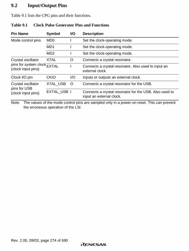
Rev. 2.00, 09/03, page 274 of 690
9.2 Input/Output Pins
Table 9.1 lists the CPG pins and their functions.
Table 9.1 Clock Pulse Generator Pins and Functions
Pin Name Symbol I/O Description
MD0 I Set the clock-operating mode.
MD1 I Set the clock-operating mode.
Mode control pins
MD2 I Set the clock-operating mode.
XTAL O Connects a crystal resonator.Crystal oscillatorpins for system clock(clock input pins)
EXTAL I Connects a crystal resonator. Also used to input anexternal clock.
Clock I/O pin CKIO I/O Inputs or outputs an external clock.
XTAL_USB O Connects a crystal resonator for the USB.Crystal oscillatorpins for USB(clock input pins) EXTAL_USB I Connects a crystal resonator for the USB. Also used to
input an external clock.
Note: The values of the mode control pins are sampled only in a power-on reset. This can preventthe erroneous operation of the LSI.

Rev. 2.00, 09/03, page 275 of 690
9.3 Clock Operating Modes
Table 9.2 shows the relationship between the mode control pins (MD2 to MD0) combinations andthe clock operating modes. Table 9.3 shows the usable frequency ranges in the clock operatingmodes and the frequency range of the input clock.
Table 9.2 Clock Operating Modes
Pin Values Clock I/O
Mode MD2 MD1 MD0 Source OutputPLL2On/Off
PLL1On/Off
CKIOFrequency
0 0 0 0 EXTAL CKIO ON (× 1) ON (× 1, 2, 3, 4) (EXTAL)
1 0 0 1 EXTAL CKIO ON (× 4) ON (× 1, 2, 3, 4) (EXTAL) × 4
2 0 1 0 Crystalresonator
CKIO ON (× 4) ON (× 1, 2, 3, 4) (Crystal) × 4
4 1 0 0 Crystalresonator
CKIO ON (× 1) ON (× 1, 2, 3, 4) (Crystal)
5 1 0 1 EXTAL CKIO ON (× 2) ON (× 1, 2, 3, 4) (EXTAL) × 2
6 1 1 0 Crystalresonator
CKIO ON (× 2) ON (× 1, 2, 3, 4) (Crystal) × 2
7 1 1 1 CKIO OFF ON (× 1, 2, 3, 4) (CKIO)
Mode 0: An external clock is input from the EXTAL pin and executes waveform shaping by PLLcircuit 2 before being supplied inside this LSI.
Mode 1: An external clock is input from the EXTAL pin and its frequency is multiplied by 4 byPLL circuit 2 before being supplied inside this LSI, allowing a low-frequency external clock to beused.
Mode 2: The on-chip crystal oscillator operates, with the oscillation frequency being multiplied by4 by PLL circuit 2 before being supplied inside this LSI, allowing a low-frequency external clockto be used.
Mode 4: The on-chip crystal oscillator operates and executes waveform shaping by PLL circuit 2before being supplied inside this LSI.
Mode 5: An external clock is input from the EXTAL pin and its frequency is multiplied by 2 byPLL circuit 2 before being supplied inside this LSI, allowing a low-frequency external clock to beused.
Mode 6: The on-chip crystal oscillator operates, with the oscillation frequency being multiplied by2 by PLL circuit 2 before being supplied inside this LSI, allowing a low crystal frequency to beused.

Rev. 2.00, 09/03, page 276 of 690
Mode 7: In this mode, the CKIO pin is an input, an external clock is input to this pin, and executeswaveform shaping, and also frequency multiplication according to the setting, by PLL circuit 1before being supplied to this LSI. As PLL circuit 1 compensates for fluctuations in the CKIO pinload, this mode is suitable for connection of synchronous DRAM.
Table 9.3 Possible Combination of Clock Modes and FRQCR Values
ClockMode FRQCR*1 PLL1 PLL2
Clock Rate*2
(I:B:P)
Input Clock/CrystalResonator FrequencyRange CKIO Frequency Range
H'1000 ON (× 1) ON (× 1) 1:1:1 20.00 MHz to 33.34 MHz 20.00 MHz to 33.34 MHz
H'1001 ON (× 1) ON (× 1) 1:1:1/2 20.00 MHz to 66.67 MHz 20.00 MHz to 66.67 MHz
H'1003 ON (× 1) ON (× 1) 1:1:1/4 20.00 MHz to 66.67 MHz 20.00 MHz to 66.67 MHz
H'1101 ON (× 2) ON (× 1) 2:1:1 20.00 MHz to 33.34 MHz 20.00 MHz to 33.34 MHz
H'1103 ON (× 2) ON (× 1) 2:1:1/2 20.00 MHz to 66.67 MHz 20.00 MHz to 66.67 MHz
H'1111 ON (× 2) ON (× 1) 1:1:1 20.00 MHz to 33.34 MHz 20.00 MHz to 33.34 MHz
H'1113 ON (× 2) ON (× 1) 1:1:1/2 20.00 MHz to 66.67 MHz 20.00 MHz to 66.67 MHz
H'1202 ON (× 3) ON (× 1) 3:1:1 26.70 MHz to 33.34 MHz 26.70 MHz to 33.34 MHz
H'1222 ON (× 3) ON (× 1) 1:1:1 26.70 MHz to 33.34 MHz 26.70 MHz to 33.34 MHz
H'1303 ON (× 4) ON (× 1) 4:1:1 20.00 MHz to 33.34 MHz 20.00 MHz to 33.34 MHz
H'1313 ON (× 4) ON (× 1) 2:1:1 20.00 MHz to 33.34 MHz 20.00 MHz to 33.34 MHz
0
H'1333 ON (× 4) ON (× 1) 1:1:1 20.00 MHz to 33.34 MHz 20.00 MHz to 33.34 MHz
H'1001 ON (× 1) ON (× 4) 4:4:2 10.00 MHz to 16.67 MHz 40.00 MHz to 66.67 MHz
H'1003 ON (× 1) ON (× 4) 4:4:1 10.00 MHz to 16.67 MHz 40.00 MHz to 66.67 MHz
H'1103 ON (× 2) ON (× 4) 8:4:2 10.00 MHz to 16.67 MHz 40.00 MHz to 66.67 MHz
1, 2
H'1113 ON (× 2) ON (× 4) 4:4:2 10.00 MHz to 16.67 MHz 40.00 MHz to 66.67 MHz
H'1000 ON (× 1) ON (× 1) 1:1:1 20.00 MHz to 33.34 MHz 20.00 MHz to 33.34 MHz
H'1001 ON (× 1) ON (× 1) 1:1:1/2 20.00 MHz to 33.34 MHz 20.00 MHz to 33.34 MHz
H'1003 ON (× 1) ON (× 1) 1:1:1/4 20.00 MHz to 33.34 MHz 20.00 MHz to 33.34 MHz
H'1101 ON (× 2) ON (× 1) 2:1:1 20.00 MHz to 33.34 MHz 20.00 MHz to 33.34 MHz
H'1103 ON (× 2) ON (× 1) 2:1:1/2 20.00 MHz to 33.34 MHz 20.00 MHz to 33.34 MHz
H'1111 ON (× 2) ON (× 1) 1:1:1 20.00 MHz to 33.34 MHz 20.00 MHz to 33.34 MHz
H'1113 ON (× 2) ON (× 1) 1:1:1/2 20.00 MHz to 33.34 MHz 20.00 MHz to 33.34 MHz
H'1202 ON (× 3) ON (× 1) 3:1:1 26.70 MHz to 33.34 MHz 26.70 MHz to 33.34 MHz
H'1222 ON (× 3) ON (× 1) 1:1:1 26.70 MHz to 33.34 MHz 26.70 MHz to 33.34 MHz
H'1303 ON (× 4) ON (× 1) 4:1:1 20.00 MHz to 33.34 MHz 20.00 MHz to 33.34 MHz
H'1313 ON (× 4) ON (× 1) 2:1:1 20.00 MHz to 33.34 MHz 20.00 MHz to 33.34 MHz
4
H'1333 ON (× 4) ON (× 1) 1:1:1 20.00 MHz to 33.34 MHz 20.00 MHz to 33.34 MHz

Rev. 2.00, 09/03, page 277 of 690
ClockMode FRQCR*1 PLL1 PLL2
Clock Rate*2
(I:B:P)
Input Clock / CrystalResonator FrequencyRange CKIO Frequency Range
H'1000 ON (× 1) ON (× 2) 2:2:2 10.00 MHz to 16.67 MHz 20.00 MHz to 33.34 MHz
H'1001 ON (× 1) ON (× 2) 2:2:1 10.00 MHz to 33.34 MHz 20.00 MHz to 66.67 MHz
H'1003 ON (× 1) ON (× 2) 2:2:1/2 10.00 MHz to 33.34 MHz 20.00 MHz to 66.67 MHz
H'1101 ON (× 2) ON (× 2) 4:2:2 10.00 MHz to 16.67 MHz 20.00 MHz to 33.33 MHz
H'1103 ON (× 2) ON (× 2) 4:2:1 10.00 MHz to 33.34 MHz 20.00 MHz to 66.67 MHz
H'1111 ON (× 2) ON (× 2) 2:2:2 10.00 MHz to 16.67 MHz 20.00 MHz to 33.34 MHz
H'1113 ON (× 2) ON (× 2) 2:2:1 10.00 MHz to 33.34 MHz 20.00 MHz to 66.67 MHz
H'1202 ON (× 3) ON (× 2) 6:2:2 10.00 MHz to 16.67 MHz 20.00 MHz to 33.34 MHz
H'1222 ON (× 3) ON (× 2) 2:2:2 10.00 MHz to 16.67 MHz 20.00 MHz to 33.34 MHz
H'1303 ON (× 4) ON (× 2) 8:2:2 10.00 MHz to 16.67 MHz 20.00 MHz to 33.33 MHz
H'1313 ON (× 4) ON (× 2) 4:2:2 10.00 MHz to 16.67 MHz 20.00 MHz to 33.33 MHz
5
H'1333 ON (× 4) ON (× 2) 2:2:2 10.00 MHz to 16.67 MHz 20.00 MHz to 33.34 MHz
H'1000 ON (× 1) ON (× 2) 2:2:2 10.00 MHz to 16.67 MHz 20.00 MHz to 33.34 MHz
H'1001 ON (× 1) ON (× 2) 2:2:1 10.00 MHz to 33.34 MHz 20.00 MHz to 66.67 MHz
H'1003 ON (× 1) ON (× 2) 2:2:1/2 10.00 MHz to 33.34 MHz 20.00 MHz to 66.67 MHz
H'1101 ON (× 2) ON (× 2) 4:2:2 10.00 MHz to 16.67 MHz 20.00 MHz to 33.33 MHz
H'1103 ON (× 2) ON (× 2) 4:2:1 10.00 MHz to 33.34 MHz 20.00 MHz to 66.67 MHz
H'1111 ON (× 2) ON (× 2) 2:2:2 10.00 MHz to 16.67 MHz 20.00 MHz to 33.34 MHz
H'1113 ON (× 2) ON (× 2) 2:2:1 10.00 MHz to 33.34 MHz 20.00 MHz to 66.67 MHz
H'1202 ON (× 3) ON (× 2) 6:2:2 10.00 MHz to 16.67 MHz 20.00 MHz to 33.34 MHz
H'1222 ON (× 3) ON (× 2) 2:2:2 10.00 MHz to 16.67 MHz 20.00 MHz to 33.34 MHz
H'1303 ON (× 4) ON (× 2) 8:2:2 10.00 MHz to 16.67 MHz 20.00 MHz to 33.33 MHz
H'1313 ON (× 4) ON (× 2) 4:2:2 10.00 MHz to 16.67 MHz 20.00 MHz to 33.33 MHz
6
H'1333 ON (× 4) ON (× 2) 2:2:2 10.00 MHz to 16.67 MHz 20.00 MHz to 33.34 MHz

Rev. 2.00, 09/03, page 278 of 690
ClockMode FRQCR*1 PLL1 PLL2
Clock Rate*2
(I:B:P)
Input Clock / CrystalResonator FrequencyRange CKIO Frequency Range
H'1000 ON (× 1) OFF 1:1:1 20.00 MHz to 33.34 MHz 20.00 MHz to 33.34 MHz
H'1001 ON (× 1) OFF 1:1:1/2 20.00 MHz to 66.67 MHz 20.00 MHz to 66.67 MHz
H'1003 ON (× 1) OFF 1:1:1/4 20.00 MHz to 66.67 MHz 20.00 MHz to 66.67 MHz
H'1101 ON (× 2) OFF 2:1:1 20.00 MHz to 33.34 MHz 20.00 MHz to 33.34 MHz
H'1103 ON (× 2) OFF 2:1:1/2 20.00 MHz to 66.67 MHz 20.00 MHz to 66.67 MHz
H'1111 ON (× 2) OFF 1:1:1 20.00 MHz to 33.34 MHz 20.00 MHz to 33.34 MHz
H'1113 ON (× 2) OFF 1:1:1/2 20.00 MHz to 66.67 MHz 20.00 MHz to 66.67 MHz
H'1202 ON (× 3) OFF 3:1:1 26.70 MHz to 33.34 MHz 26.70 MHz to 33.34 MHz
H'1222 ON (× 3) OFF 1:1:1 26.70 MHz to 33.34 MHz 26.70 MHz to 33.34 MHz
H'1303 ON (× 4) OFF 4:1:1 20.00 MHz to 33.34 MHz 20.00 MHz to 33.34 MHz
H'1313 ON (× 4) OFF 2:1:1 20.00 MHz to 33.34 MHz 20.00 MHz to 33.34 MHz
7
H'1333 ON (× 4) OFF 1:1:1 20.00 MHz to 33.34 MHz 20.00 MHz to 33.34 MHz
Notes: 1. This LSI cannot operate in an FRQCR value other than that listed in table 9.3.2. Taking input clock frequency ratio as 1.
Cautions:
1. The input to divider 1 is the output of the PLL circuit 1.
2. The frequency of the internal clock (Iφ) is:
• The product of the frequency of the CKIO pin, the frequency multiplication ratio of PLLcircuit 1, and the division ratio of divider 1.
• Do not set the internal clock frequency lower than the CKIO pin frequency.
3. The frequency of the peripheral clock (Pφ) is:
• The product of the frequency of the CKIO pin, the frequency multiplication ratio of PLLcircuit 1, and the division ratio of divider 1.
• The peripheral clock frequency should not be set higher than the frequency of the CKIOpin, higher than 33.34 MHz, or lower than 13 MHz when the USB is used.
4. ×1, ×2, ×3, or ×4 can be used as the multiplication ratio of PLL circuit 1. ×1, ×1/2, ×1/3, or×1/4 can be selected as the division ratios of divider 1. Set the rate in the frequency controlregister.
5. The output frequency of PLL circuit 1 is the product of the CKIO frequency and themultiplication ratio of PLL circuit 1. Use the output frequency under 133.34 MHz.

Rev. 2.00, 09/03, page 279 of 690
9.4 Register Descriptions
The CPG has the following registers. Refer to section 24, List of Registers, for the addresses of theregisters and the state of each register in each processor state.
• Frequency control register (FRQCR)
• USB clock control register (UCLKCR)
9.4.1 Frequency Control Register (FRQCR)
The frequency control register (FRQCR) is a 16-bit readable/writable register used to specifywhether a clock is output from the CKIO pin, the on/off state of PLL circuit 1, PLL standby, thefrequency multiplication ratio of PLL circuit 1, and the frequency division ratio of the internalclock and the peripheral clock. Only word access can be used on FRQCR. As for the combinationof the clock rate, refer to table 9.3. The combinations listed in table 9.3 should only be set onFRQCR.
BitBitName
InitialValue R/W Description
15 to 13 0 R Reserved
These bits are always read as 0. The write valueshould always be 0.
12 CKOEN 1 R/W Clock Output Enable
Specifies to output a clock from the CKIO pin or to fixthe CKIO pin low when software standby is canceled(after an interrupt before STATUS1 becomes low andSTATUS0 becomes low). The CKIO pin is fixed lowduring STATUS1 = low and STATUS0 = high, whenthe CKOEN bit is cleared to 0. Therefore, themalfunction of an external circuit because of anunstable CKIO clock in releasing software standbymode can be prevented.
In clock operating mode 7, the CKIO pin is in the inputstate regardless of this bit.
0: Fixes the CKIO pin low in software standby mode.
1: Outputs a clock from the CKIO pin.
11, 10 0 R Reserved
These bits are always read as 0. The write valueshould always be 0.

Rev. 2.00, 09/03, page 280 of 690
BitBitName
InitialValue R/W Description
9
8
STC1
STC0
0
0
R/W
R/W
Frequency Multiplication Ratio
00: × 1 time
01: × 2 times
10: × 3 times
11: × 4 times
7, 6 0 R Reserved
These bits are always read as 0. The write valueshould always be 0.
5
4
IFC1
IFC0
0
0
R/W
R/W
Internal Clock Frequency Division Ratio
Specify the frequency division ratio of the internalclock with respect to the output frequency of PLLcircuit 1.
00: × 1 time
01: × 1/2 time
10: × 1/3 time
11: × 1/4 time
3, 2 0 R Reserved
These bits are always read as 0. The write valueshould always be 0.
1
0
PFC1
PFC0
1
1
R/W
R/W
Peripheral Clock Frequency Division Ratio
Specify the frequency division ratio of the peripheralclock with respect to the output frequency of PLLcircuit 1.
00: × 1 time
01: × 1/2 time
10: × 1/3 time
11: × 1/4 time

Rev. 2.00, 09/03, page 281 of 690
9.4.2 USB Clock Frequency Control Register (UCLKCR)
UCLKCR is an 8-bit readable/writable register.
Word-size access is used to write to this register. This writing should be performed with H'A5 inthe upper byte and the write data in the lower byte.
BitBitName
InitialValue R/W Description
7
6
USSCS1
USSCS0
1
1
R/W
R/W
Source Clock Selection Bit
These bits select the source clock.
00: Clock stopped
01: Setting prohibited
10: Setting prohibited
11: External input clock
5 USBEN 1 R/W USB On-chip Oscillator Enable
This bit controls the operation of the USB on-chiposcillator.
0: USB on-chip oscillator stopped
1: USB on-chip oscillator operates
4 to 0 0 R Reserved
These bits are always read as 0. The write valueshould always be 0.
9.4.3 Usage Notes
Note the following when using the USB. If these are used incorrectly, the correct clocks may notbe generated, causing faulty operation of the USB.
1. UCLKCR is used only for generation of the USB clocks. When the USB is not used, it isrecommended that UCLKCR be cleared to H'00 to halt the clock.
2. Halt the USB before changing the values of UCLKCR. Halt the USB by stopping the clocksupply using the USB module stop bits in STBCR3.
3. UCLKCR is initialized only by a power-on reset. In a manual reset, they retain their current setvalues.
4. Use the USB module with Pφ> 13 MHz. Otherwise, the operation of this LSI is notguaranteed.

Rev. 2.00, 09/03, page 282 of 690
9.5 Changing Frequency
The frequency of the internal clock and peripheral clock can be changed either by changing themultiplication rate of PLL circuit 1 or by changing the division rates of divider 1. All of these arecontrolled by software through the frequency control register. The methods are described below.
9.5.1 Changing Multiplication Rate
A PLL settling time is required when the multiplication rate of PLL circuit 1 is changed. The on-chip WDT counts the settling time.
1. In the initial state, the multiplication rate of PLL circuit 1 is 1.2. Set a value that will become the specified oscillation settling time in the WDT and stop the
WDT. The following must be set:WTCSR.TME = 0: WDT stopsWTCSR.CKS[2:0]: Division ratio of WDT count clockWTCNT: Initial counter value
3. Set the desired value in the STC[1:0] bits. The division ratio can also be set in the IFC[1:0] bitsand PFC[1:0] bits.
4. The processor pauses internally and the WDT starts incrementing. The internal and peripheralclocks both stop and the WDT is supplied with the clock. The clock will continue to be outputat the CKIO pin.
5. Supply of the clock that has been set begins at WDT count overflow, and the processor beginsoperating again. The WDT stops after it overflows.
9.5.2 Changing Division Ratio
The WDT will not count unless the multiplication rate is changed simultaneously.
1. In the initial state, IFC[1:0] = 00 and PFC[1:0] = 11.
2. Set the IFC[1:0], PFC[1:0] bits to the new division ratio. The values that can be set are limitedby the clock mode and the multiplication rate of PLL circuit 1. Note that if the wrong value isset, the processor will malfunction.
3. The clock is immediately supplied at the new division ratio.
9.5.3 Modification of Clock Operating Mode
The values of the mode control pins (MD2 to MD0) that define a clock-operating mode arereflected at power-on reset.

Rev. 2.00, 09/03, page 283 of 690
9.6 Usage Notes
When Using an External Crystal Resonator: Place the crystal resonator, capacitors CL1 andCL2, and damping resistance R as close as possible to the EXTAL and XTAL pins. To preventinduction from interfering with correct oscillation, use a common grounding point for thecapacitors connected to the resonator, and do not locate a wiring pattern near these components.
Note: The values for CL1, CL2, and damping resistance
should be determined after consultation with the
crystal resonator manufacturer.
XTALEXTAL
This LSI
CL2
R
CL1
Avoid crossing signal lines
Figure 9.2 Points for Attention when Using Crystal Resonator
Decoupling Capacitors: As far as possible, insert a laminated ceramic capacitor of 0.1 to 1 µF asa passive capacitor for each VSS/VSSQ and VCC/VCCQ pair. Mount the passive capacitors as closeas possible to the chip’s power supply pins, and use components with a frequency characteristicsuitable for the chip’s operating frequency, as well as a suitable capacitance value.
Digital system VSS/VSSQ and VCC/VCCQ pairs: 2-5, 17-19, 26-28, 32-34, 44-46, 57-59, 69-71, 78-80, 87-89, 111-113, 130-132, 133-138, 159-161, 178-180, 182-184, 199-204
On-chip oscillator VSS/VSSQ and VCC/VCCQ pairs: 6-9, 149-150, 151-152, 205-208
When Using a PLL Oscillator Circuit: Keep the wiring from the PLL VCC and PLL VSS
connection pattern to the power supply pins short, and make the pattern width wide, to minimizethe inductance value.
In clock mode 7, connect the EXTAL pin to VCCQ (3.3-V power) with pull-up resistor, and leavethe XTAL pin open.

Rev. 2.00, 09/03, page 284 of 690
VCC -PLL2
VCC -PLL1
VCC
VSS
VSS -PLL2
VSS -PLL1
Avoid crossingsignal lines
Power supply
Figure 9.3 Points for Attention when Using PLL Oscillator Circuit
Notes on Wiring Power Supply Pins: To avoid crossing signal lines, wire VCC−PLL1,VCC−PLL2, VSS−PLL1, and VSS−PLL2 as three patterns from the power supply source on theboard so that they are independent of digital VCC and VSS.

WDTS311A_000020020100 Rev. 2.00, 09/03, page 285 of 690
Section 10 Watchdog Timer (WDT)
This LSI includes the watchdog timer (WDT) and can be reset by the overflow of the counterwhen the value of the counter has not been updated because of an erroneous system operation.
The WDT is a single-channel timer that uses a peripheral clock as an input and counts the clocksettling time when clearing software standby mode and temporary standbys, such as frequencychanges. It can also be used as a conventional watchdog timer or an interval timer.
10.1 Features
• Can be used to ensure the clock settling time
Use the WDT to clear software standby mode and the temporary standbys which occur whenthe clock frequency is changed.
• Can switch between watchdog timer mode and interval timer mode.
• Generates internal resets in watchdog timer mode
Internal resets occur after counter overflow.
Power-on reset and manual reset are available.
• Interrupt generation in interval timer mode
An interval timer interrupt is generated when the counter overflows.
• Choice of eight counter input clocks
Eight clocks (×1 to ×1/4096) that are obtained by dividing the peripheral clock can be selected.

Rev. 2.00, 09/03, page 286 of 690
Figures 10.1 shows a block diagram of the WDT.
WTCSR
Standby
control
Bus interface
WTCNT
Divider
Clock selector
Clock
Standby
mode
Peripheral
clock
Standby
cancellation
Reset
control
Clock selection
WDT
Overflow
Internal
reset
request
Interrupt
control
Interrupt
request
WTCSR:
WTCNT:
Legend
Watchdog timer control/status register
Watchdog timer counter
Figure 10.1 Block Diagram of WDT
10.2 Register Descriptions
The WDT has the following two registers. Refer to section 24, List of Registers for the details ofthe addresses of these registers and the state of registers in each operating mode.
• Watchdog timer counter (WTCNT)
• Watchdog timer control/status register (WTCSR)
10.2.1 Watchdog Timer Counter (WTCNT)
The watchdog timer counter (WTCNT) is an 8-bit readable/writable register that increments on theselected clock. When an overflow occurs, it generates a reset in watchdog timer mode and aninterrupt in interval timer mode. The WTCNT counter is not initialized by an internal reset due tothe WDT overflow. The WTCNT counter is initialized to H'00 only by a power-on reset using theRESETP pin.
Use a word access to write to the WTCNT counter, with H'5A in the upper byte. Use a byte accessto read WTCNT.

Rev. 2.00, 09/03, page 287 of 690
Note: WTCNT differs from other registers in that it is more difficult to write to. See section10.2.3, Notes on Register Access, for details.
10.2.2 Watchdog Timer Control/Status Register (WTCSR)
The watchdog timer control/status register (WTCSR) is an 8-bit readable/writable registercomposed of bits to select the clock used for the count, overflow flags, and enable bits.
WTCSR holds its value in an internal reset due to the WDT overflow. WTCSR is initialized toH'00 only by a power-on reset using the RESETP pin.
When used to count the clock settling time for canceling a software standby, it retains its valueafter counter overflow. Use a word access to write to the WTCSR counter, with H'A5 in the upperbyte. Use a byte access to read WTCSR.
Note: WTCSR differs from other registers in that it is more difficult to write to. See section10.2.3, Notes on Register Access, for details.

Rev. 2.00, 09/03, page 288 of 690
BitBitName
InitialValue R/W Description
7 TME 0 R/W Timer Enable
Starts and stops timer operation. Clear this bit to 0when using the WDT in software standby mode orwhen changing the clock frequency.
0: Timer disabled: Count-up stops and WTCNT valueis retained
1: Timer enabled
6 WT/IT 0 R/W Timer Mode Select
Selects whether to use the WDT as a watchdog timeror an interval timer.
0: Use as interval timer
1: Use as watchdog timer
Note: If WT/IT is modified when the WDT is running,the up-count may not be performed correctly.
5 RSTS 0 R/W Reset Select
Selects the type of reset when WTCNT overflows inwatchdog timer mode. In interval timer mode, thissetting is ignored.
0: Power-on reset
1: Manual reset
4 WOVF 0 R/W Watchdog Timer Overflow
Indicates that WTCNT has overflowed in watchdogtimer mode. This bit is not set in interval timer mode.
0: No overflow
1: WTCNT has overflowed in watchdog timer mode
3 IOVF 0 R/W Interval Timer Overflow
Indicates that WTCNT has overflowed in interval timermode. This bit is not set in watchdog timer mode.
0: No overflow
1: WTCNT has overflowed in interval timer mode

Rev. 2.00, 09/03, page 289 of 690
BitBitName
InitialValue R/W Description
2
1
0
CKS2
CKS1
CKS0
0
0
0
R/W
R/W
R/W
Clock Select 2 to 0
These bits select the clock to be used for the WTCNTcount from the eight types obtainable by dividing theperipheral clock. The overflow period that is showninside the parenthesis in the table is the value whenthe peripheral clock (Pφ) is 15 MHz.
000 Pφ (17 µs)
001 Pφ/4 (68 µs)
010 Pφ/16 (273 µs)
011 Pφ/32 (546 µs)
100 Pφ/64 (1.09 ms)
101 Pφ/256 (4.36 ms)
110 Pφ/1024 (17.48 ms)
111 Pφ/4096 (69.91 ms)
Note: If bits CKS2 to CKS0 are modified when theWDT is running, the up-count may not beperformed correctly. Ensure that these bits aremodified only when the WDT is not running.
Note: If manual reset is selected using the RSTS bit, a frequency division ratio of 1/16, 1/32, 1/64,1/256, 1/1,024, or 1/4,096 is selected using bits CKS2 to CKS0, and a watchdog timercounter overflow occurs, resulting in a manual reset, the LSI will generate two manualresets in succession. This will not affect its operation but will cause change in the state ofthe STATUS pin.
10.2.3 Notes on Register Access
The watchdog timer counter (WTCNT) and watchdog timer control/status register (WTCSR) aremore difficult to write to than other registers. The procedure for writing to these registers is givenbelow.
• These registers must be written by a word transfer instruction. They cannot be written by abyte or longword transfer instruction.
When writing to WTCNT, set the upper byte to H'5A and transfer the lower byte as the write data,as shown in figure 10.2. When writing to WTCSR, set the upper byte to H'A5 and transfer thelower byte as the write data. This transfer procedure writes the lower byte data to WTCNT orWTCSR.

Rev. 2.00, 09/03, page 290 of 690
15 8 7 0
H'5A Write data
WTCNT write
15 8 7 0
H'A5 Write data
WTCSR write
Figure 10.2 Writing to WTCNT and WTCSR
10.3 Operation
10.3.1 Canceling Software Standbys
The WDT is used to cancel software standby mode with an interrupt such as an NMI. Theprocedure when using an NMI interrupt is described below. (The WDT does not run when resetsare used for canceling, so keep the RESETP or RESETM pin low until the clock stabilizes.)
1. Before transitioning to software standby mode, always clear the TME bit in WTCSR to 0.When the TME bit is 1, an erroneous reset or interval timer interrupt may be generated whenthe count overflows.
2. Set the type of count clock used in the CKS2 to CKS0 bits in WTCSR and the initial values forthe counter in the WTCNT counter. These values should ensure that the time till countoverflow is longer than the clock oscillation settling time.
3. Move to software standby mode by executing a SLEEP instruction, after that clock stops.
4. The WDT starts counting by detecting the edge change of the NMI signal.
5. When the WDT count overflows, the CPG starts supplying the clock and the processorresumes operation. The WOVF flag in WTCSR is not set.
6. Since the WDT continues counting from H'00, clear the STBY bit in the STBCR register to 0in the interrupt processing program and this will stop the WDT. When the STBY bit remains 1,the LSI again enters the software standby mode when the WDT has counted up to H'80. Thissoftware standby mode can be canceled by power-on resets.

Rev. 2.00, 09/03, page 291 of 690
10.3.2 Changing Frequency
To change the frequency used by the PLL, use the WDT. When changing the frequency only byswitching the divider, do not use the WDT.
1. Before changing the frequency, always clear the TME bit in WTCSR to 0. When the TME bitis 1, an erroneous reset or interval timer interrupt may be generated when the count overflows.
2. Set the type of count clock used in the CKS2 to CKS0 bits of WTCSR and the initial values forthe counter in the WTCNT counter. These values should ensure that the time till countoverflow is longer than the clock oscillation settling time. The divided clock set by CKS2 toCKS0 bits in WTCSR will be used for the base clock of Pφafter the frequency is changed.
3. When the frequency control register (FRQCR) is written, the processor stops temporarily. TheWDT starts counting.
4. When the WDT count overflows, the CPG resumes supplying the clock and the processorresumes operation. The WOVF flag in WTCSR is not set.
5. The counter stops at the values H'00.
6. Before changing WTCNT after the execution of the frequency change instruction, alwaysconfirm that the value of WTCNT is H'00 by reading WTCNT.
10.3.3 Using Watchdog Timer Mode
1. Set the WT/IT bit in WTCSR to 1, set the reset type in the RSTS bit, set the type of countclock in the CKS2 to CKS0 bits, and set the initial value of the counter in the WTCNT counter.
2. Set the TME bit in WTCSR to 1 to start the count in watchdog timer mode.
3. While operating in watchdog timer mode, rewrite the counter periodically to H'00 to preventthe counter from overflowing.
4. When the counter overflows, the WDT sets the WOVF flag in WTCSR to 1 and generates thereset signal specified by the RSTS bit. The counter then resumes counting.
10.3.4 Using Interval Timer Mode
When operating in interval timer mode, interval timer interrupts are generated at every overflow ofthe counter. This enables interrupts to be generated at set periods.
1. Clear the WT/IT bit in WTCSR to 0, set the type of count clock in the CKS2 to CKS0 bits, andset the initial value of the counter in the WTCNT counter.
2. Set the TME bit in WTCSR to 1 to start the count in interval timer mode.
3. When the counter overflows, the WDT sets the IOVF flag in WTCSR to 1 and an intervaltimer interrupt request is sent to the INTC. The counter then resumes counting.

Rev. 2.00, 09/03, page 292 of 690

LPWS300A_000020011000 Rev. 2.00, 09/03, page 293 of 690
Section 11 Power-Down Modes
This LSI has four types of the power-down modes: sleep mode, software standby mode, modulestandby function, and hardware standby mode.
11.1 Features
This LSI has the following power-down modes and function:
1. Sleep mode
2. Software standby mode
3. Module standby function (Cache, TLB, UBC, DMAC, UDI, and on-chip peripheral module)
4. Hardware standby mode
Table 11.1 shows the transition conditions for entering the modes from the program executionstate, as well as the CPU and peripheral module states in each mode and the procedures forcanceling each mode.

Rev. 2.00, 09/03, page 294 of 690
Table 11.1 States of Power-Down Modes
State
ModeTransitionConditions CPG CPU
CPURegister
On-ChipPeripheralModules Pins
ExternalMemory
CancelingCondition
Sleep mode Execute SLEEPinstruction withSTBY bit clearedto 0 in STBCR
Run Halt Held Run *3 Refresh 1. Interrupt
2. Reset
Softwarestandbymode
Execute SLEEPinstruction withSTBY bit set to 1in STBCR
Halt Halt Held Halt*1 *3 Self-refresh
1. Interrupt
2. Reset
Modulestandbyfunction
Set MSTP bit ofSTBCR, STBCR2,and STBCR3 to 1
Run Run Held Specifiedmodulehalts
*2 Refresh 1. Clear MSTPbit to 0
2. Power-onreset
Hardwarestandbymode
Drive CA pin low Halt Halt Held Halt*1 *4 Power-on reset
Notes: 1. The RTC still runs if the START bit in RCR2 is set to 1 (see section 15, Realtime Clock(RTC)).
2. Depends on the on-chip peripheral module.3. Refer to table A.1, in Appendix.4. Hi-Z except EXTAL, XTAL, EXTAL2, XTAL2, EXTAL_USB, XTAL_USB, STATUS1, and
STATUS0.

Rev. 2.00, 09/03, page 295 of 690
11.2 Input/Output Pins
Table 11.2 lists the pins used for the power-down modes.
Table 11.2 Pin Configuration
Pin Name Symbol I/O Description
Processing state STATUS1,STATUS0
O Operating state of the processor.
HH: Reset
HL: Sleep mode
LH: Standby mode
LL: Normal operation
Note: H means high level, and L means low level.
Power-on reset RESETP I Reset input signal. Power-on reset occurs at low-level.
Manual reset RESETM I Reset input signal. Manual reset occurs at low-level.
Hardware standby CA I Normal operation at high-level and hardware standbymode is entered at low-level.
11.3 Register Descriptions
There are following five registers used for the power-down modes. Refer to section 24, List ofRegisters, for the details of the addresses of these registers and the state of registers in eachoperating mode.
• Standby control register (STBCR)
• Standby control register 2 (STBCR2)
• Standby control register 3 (STBCR3)

Rev. 2.00, 09/03, page 296 of 690
11.3.1 Standby Control Register (STBCR)
STBCR is an 8-bit readable/writable register that specifies the state of the power-down mode.
Bit Bit Name Initial Value R/W Description
7 STBY 0 R/W Standby
Specifies transition to software standby mode.
0: Executing SLEEP instruction puts chip into sleepmode
1: Executing SLEEP instruction puts chip intosoftware standby mode
6, 5 0 R Reserved
These bits are always read as 0. The write valueshould always be 0.
4 STBXTL 0 R/W Standby Crystal
Specifies stop/start of the crystal oscillator instandby mode.
0: Crystal oscillator stops in standby mode.
1: Crystal oscillator continues operation in standbymode.
3 0 R Reserved
This bit is always read as 0. The write value shouldalways be 0.
2 MSTP2 0 R/W Module Stop 2
Specifies halting the clock supply to the TMU whenthe MSTP2 bit has been set to 1.
0: TMU runs
1: Clock supply to TMU halted
1 MSTP1 0 R/W Module Stop 1
Specifies halting the clock supply to the RTC whenthe MSTP1 bit has been set to 1.
0: RTC runs
1: Clock supply to RTC halted
0 0 R Reserved
This bit is always read as 0. The write value shouldalways be 0.

Rev. 2.00, 09/03, page 297 of 690
11.3.2 Standby Control Register 2 (STBCR2)
STBCR2 is an 8-bit readable/writable register that controls the operation of modules in the power-down mode.
Bit Bit Name Initial Value R/W Description
7 MSTP10 0 R/W Module Stop Bit 10
When the MSTP10 bit is set to 1, the clock supply tothe UDI is halted.
0: UDI runs
1: Clock supply to UDI is halted
6 MSTP9 0 R/W Module Stop Bit 9
When the MSTP9 bit is set to 1, the clock supply tothe UBC is halted.
0: UBC runs
1: Clock supply to UBC is halted
5 MSTP8 0 R/W Module Stop Bit 8
When the MSTP8 bit is set to 1, the clock supply tothe DMAC is halted.
0: DMAC runs
1: Clock supply to DMAC is halted
4 0 R Reserved
This bit is always read as 0. The write value shouldalways be 0.
3 MSTP6 0 R/W Module Stop Bit 6
When the MSTP6 bit is set to 1, the clock supply tothe TLB is halted.
0: TLB runs
1: Clock supply to TLB is halted
2 MSTP5 0 R/W Module Stop Bit 5
When the MSTP5 bit is set to 1, the clock supply tocache memory is halted.
0: Cache memory runs
1: Clock supply to cache memory is halted
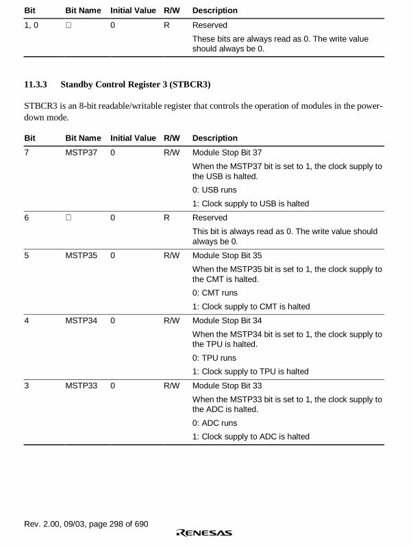
Rev. 2.00, 09/03, page 298 of 690
Bit Bit Name Initial Value R/W Description
1, 0 0 R Reserved
These bits are always read as 0. The write valueshould always be 0.
11.3.3 Standby Control Register 3 (STBCR3)
STBCR3 is an 8-bit readable/writable register that controls the operation of modules in the power-down mode.
Bit Bit Name Initial Value R/W Description
7 MSTP37 0 R/W Module Stop Bit 37
When the MSTP37 bit is set to 1, the clock supply tothe USB is halted.
0: USB runs
1: Clock supply to USB is halted
6 0 R Reserved
This bit is always read as 0. The write value shouldalways be 0.
5 MSTP35 0 R/W Module Stop Bit 35
When the MSTP35 bit is set to 1, the clock supply tothe CMT is halted.
0: CMT runs
1: Clock supply to CMT is halted
4 MSTP34 0 R/W Module Stop Bit 34
When the MSTP34 bit is set to 1, the clock supply tothe TPU is halted.
0: TPU runs
1: Clock supply to TPU is halted
3 MSTP33 0 R/W Module Stop Bit 33
When the MSTP33 bit is set to 1, the clock supply tothe ADC is halted.
0: ADC runs
1: Clock supply to ADC is halted

Rev. 2.00, 09/03, page 299 of 690
Bit Bit Name Initial Value R/W Description
2 MSTP32 0 R/W Module Stop Bit 32
When the MSTP32 bit is set to 1, the clock supply tothe IrDA is halted.
0: IrDA runs
1: Clock supply to IrDA is halted
1 MSTP31 0 R/W Module Stop Bit 31
When the MSTP31 bit is set to 1, the clock supply tothe SCIF2 is halted.
0: SCIF2 runs
1: Clock supply to SCIF2 is halted
0 MSTP30 0 R/W Module Stop Bit 30
When the MSTP30 bit is set to 1, the clock supply tothe SCIF0 is halted.
0: SCIF0 runs
1: Clock supply to SCIF0 is halted
11.4 Sleep Mode
11.4.1 Transition to Sleep Mode
Executing the SLEEP instruction when the STBY bit in STBCR is 0 causes a transition from theprogram execution state to sleep mode. Although the CPU halts immediately after executing theSLEEP instruction, the contents of its internal registers remain unchanged. The on-chip peripheralmodules continue to run in sleep mode and the clock continues to be output to the CKIO pin.
In sleep mode, the STATUS1 pin is set high and the STATUS0 pin low.
11.4.2 Canceling Sleep Mode
Sleep mode is canceled by an interrupt (NMI, IRQ, IRL, PINT, and on-chip peripheral module) orreset. Interrupts are accepted in sleep mode even when the BL bit in SR is 1. If necessary, saveSPC and SSR to the stack before executing the SLEEP instruction.
Canceling with an Interrupt: When an NMI, IRQ, IRL, PINT, or on-chip peripheral moduleinterrupt occurs, sleep mode is canceled and interrupt exception processing is executed. A codeindicating the interrupt source is set in INTEVT and INTEVT2.
Canceling with a Reset: Sleep mode is canceled by a power-on reset or a manual reset.

Rev. 2.00, 09/03, page 300 of 690
11.5 Software Standby Mode
11.5.1 Transition to Software Standby Mode
The LSI switches from a program execution state to software standby mode by executing theSLEEP instruction when the STBY bit is 1 in STBCR. In software standby mode, not only theCPU but also the clock and on-chip peripheral modules halt. The clock output from the CKIO pinalso halts.
The contents of the CPU and cache registers remain unchanged. Some registers of on-chipperipheral modules are, however, initialized. For more details on the states of on-chip peripheralmodules registers in software standby mode, refer to section 24.3, Register States in EachOperating Mode.
The procedure for moving to software standby mode is as follows:
1. Clear the TME bit in the WDT’s timer control register (WTCSR) to 0 to stop the WDT.
2. Clear the WDT’s timer counter (WTCNT) to 0 and set the CKS2 to CKS0 bits in WTCSR toappropriate values to secure the specified oscillation settling time.
3. After the STBY bit in STBCR is set to 1, a SLEEP instruction is executed.
4. Software standby mode is entered and the clocks within the LSI are halted. The STATUS1 pinoutput goes low and the STATUS0 pin output goes high.
11.5.2 Canceling Software Standby Mode
Software standby mode is canceled by an interrupt (NMI, IRQ, IRL, PINT, or RTC) or a reset.
Canceling with an Interrupt: The on-chip WDT can be used for hot starts. When the chip detectsan NMI, IRQ*1, IRL*1, PINT*1, or RTC*1 interrupt, the clock will be supplied to the entire chipand software standby mode canceled after the time set in the WDT’s timer control/status registerhas elapsed. The STATUS1 and STATUS0 pins both go low. Interrupt exception handling thenbegins and a code indicating the interrupt source is set in INTEVT and INTEVT2. After branchingto the interrupt handling routine occurs, clear the STBY bit in STBCR. WTCNT stopsautomatically. If the STBY bit is not cleared, WTCNT continues operation and transits to softwarestandby mode*2 when it reaches H'80. This function prevents data from being broken in case of avoltage rise when the power supply is unstable. At this time, a manual reset is not accepted untilthe STBY bit is cleared to 0.
Interrupts are accepted in software standby mode even when the BL bit in SR is 1. If necessary,save SPC and SSR to the stack before executing the SLEEP instruction.
Immediately after an interrupt is detected, the phase of the clock output of the CKIO pin may beunstable, until software standby mode is cancelled.

Rev. 2.00, 09/03, page 301 of 690
Notes: 1. Only when the RTC is being used can standby mode be canceled using IRQ, IRL,PINT, or RTC.
2. Use a power-on reset to cancel software standby mode.
WTCNT value
H'FF
H'80
Time
Interrupt
request
WDT overflow and branch to
interrupt handling routine
Crystal oscillator settling
time and PLL synchronization
time
Clear the STBY bit in STBCR before
WTCNT reaches H'80. When the
STBY bit in STBCR is cleared, WTCNT
halts automatically.
Figure 11.1 Canceling Standby Mode with STBY Bit in STBCR
Canceling with a Reset: Software standby mode is canceled by a reset (power-on or manual).Keep the RESETP or RESETM pins low until the clock oscillation settles. The internal clock willcontinue to be output to the CKIO pin.
11.6 Module Standby Function
11.6.1 Transition to Module Standby Function
Setting the standby control register MSTP bits to 1 halts the supply of clocks to the correspondingon-chip peripheral modules. This function can be used to reduce the power consumption in thenormal mode and sleep mode. Before making a transition to module standby state, be sure todisable the relevant module.
In module standby state, the functions of the external pins of the on-chip peripheral moduleschange depending on the on-chip peripheral module and port settings. With a few exceptions, allregisters hold their values prior to halt.

Rev. 2.00, 09/03, page 302 of 690
11.6.2 Canceling Module Standby Function
The module standby function can be canceled by clearing the MSTP bits to 0 or by a power-onreset.
When canceling the module standby function by clearing the corresponding MSTP bit, be sure toread the relevant MSTP bit to confirm that it has been cleared to 0.
11.7 Hardware Standby Mode
11.7.1 Transition to Hardware Standby Mode
The LSI enters hardware standby mode by driving the CA pin low. In hardware standby mode, asthe same as software standby mode entered by executing the SLEEP instruction, all modules haltexcept ones operated by the RTC clock. Even in hardware standby mode, supply power to allpower supply pins including the RTC power supply pins.
As differing from software standby mode, an interrupt or manual reset cannot be accepted inhardware standby mode.
When the CA pin is driven low, the LSI enters hardware standby mode in the following proceduredepending on the state of CPG.
During Software Standby Mode: The LSI enters the hardware standby state with the clockhalted. An interrupt or manual reset cannot be accepted.
During WDT Operation for Canceling Software Standby Mode by an Interrupt: The CPUrestarts the operation after software standby mode is canceled. Then, the LSI enters hardwarestandby mode.
During Sleep Mode: The CPU restarts the operation after sleep mode is canceled. Then, the LSIenters hardware standby mode.
In hardware standby mode, the CA pin must be held low.
11.7.2 Canceling Hardware Standby Mode
The hardware standby function can be canceled only by the power-on reset.
When the CA pin is driven high while the RESETP pin is low, the clock starts oscillating. Makesure to hold the RESETP pin low until the oscillation stabilizes. Then, drive the RESETP pin highto start the power-on resetting by the CPU.
The operation is not guaranteed when an interrupt or manual reset is input.

Rev. 2.00, 09/03, page 303 of 690
11.8 Timing of STATUS Pin Changes
The timing of the STATUS0 and STATUS1 pin changes is shown in figures 11.2 to 11.9.
In Case of A Reset:
a. Power-on reset
CKIO
RESETP
STATUS Normal*2 Normal*2Reset*1
PLL settling
time
0 to 5 Bcyc*30 to 30 Bcyc*3
Notes: 1. Reset: HH (STATUS1 high, STATUS0 high)
2. Normal: LL (STATUS1 low, STATUS0 low)
3. Bcyc: Bus clock cycle
Figure 11.2 Power-On Reset STATUS Output
b. Manual reset
CKIO
RESETM
STATUS Normal*3 Normal*3Reset*2
0 Bcyc or more*1,4 0 to 30 Bcyc*4
During manual reset, STATUS becomes HH (reset) and the internal
reset begins after waiting for the executing bus cycle to end.
Reset: HH (STATUS1 high, STATUS0 high)
Normal: LL (STATUS1 low, STATUS0 low)
Bcyc: Bus clock cycle
Notes: 1.
2.
3.
4.
Figure 11.3 Manual Reset STATUS Output

Rev. 2.00, 09/03, page 304 of 690
In Case of Canceling Software Standby:
a. Canceling software standby by interrupt
CKIO
STATUS Normal*2 Normal*2
WDT count
Oscillation stops
Standby*1
Interrupt request WDT overflow
Notes: 1. Standby: LH (STATUS1 low, STATUS0 high)
2. Normal: LL (STATUS1 low, STATUS0 low)
Figure 11.4 Canceling Software Standby by Interrupt STATUS Output
b. Canceling software standby by power-on reset
CKIO
STATUS Normal*5 Normal*5
Oscillation stops
Standby*4*2
0 to 10 Bcyc*6 0 to 30 Bcyc*6
Reset
Reset*3
RESETP *1
1. When software standby mode is cleared with a power-on reset, the WDT does
not count. Keep RESETP low during the PLL’s oscillation settling time.
2. Undefined
3. Reset: HH (STATUS1 high, STATUS0 high)
4. Standby: LH (STATUS1 low, STATUS0 high)
5. Normal: LL (STATUS1 low, STATUS0 low)
6. Bcyc: Bus clock cycle
Notes:
Figure 11.5 Canceling Software Standby by Power-On Reset STATUS Output
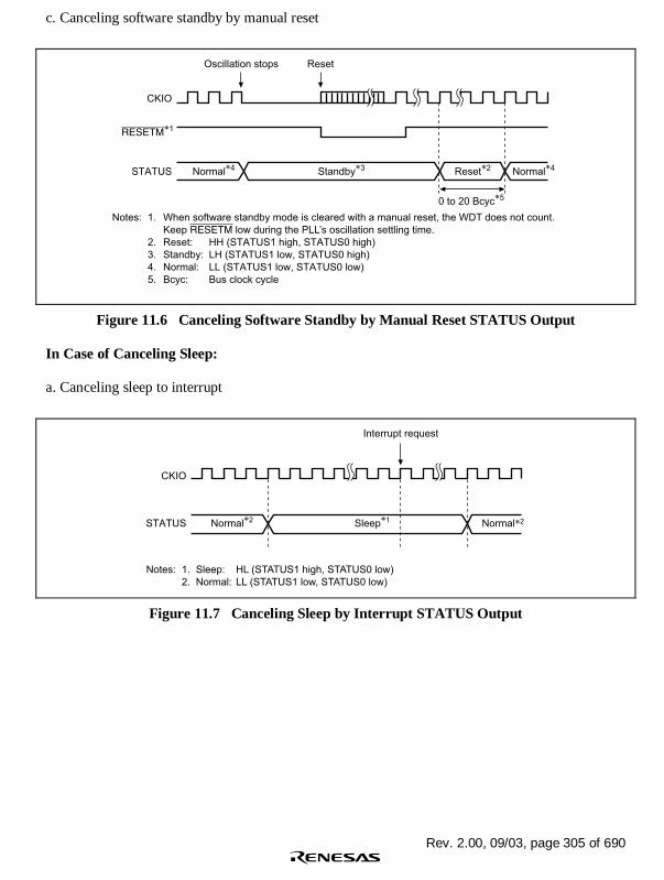
Rev. 2.00, 09/03, page 305 of 690
c. Canceling software standby by manual reset
CKIO
STATUS Normal*4 Normal*4
Oscillation stops
Standby*3 Reset*2
0 to 20 Bcyc*5
Reset
RESETM*1
Notes: 1. When software standby mode is cleared with a manual reset, the WDT does not count.
Keep RESETM low during the PLL’s oscillation settling time.
2. Reset: HH (STATUS1 high, STATUS0 high)
3. Standby: LH (STATUS1 low, STATUS0 high)
4. Normal: LL (STATUS1 low, STATUS0 low)
5. Bcyc: Bus clock cycle
Figure 11.6 Canceling Software Standby by Manual Reset STATUS Output
In Case of Canceling Sleep:
a. Canceling sleep to interrupt
CKIO
STATUS Normal*2 Normal*2Sleep*1
Interrupt request
Notes: 1. Sleep: HL (STATUS1 high, STATUS0 low)
2. Normal: LL (STATUS1 low, STATUS0 low)
Figure 11.7 Canceling Sleep by Interrupt STATUS Output

Rev. 2.00, 09/03, page 306 of 690
b. Canceling sleep by power-on reset
CKIO
STATUS Normal*5 Normal*5Sleep*4
0 to 10 Bcyc*6 0 to 30 Bcyc*6
Reset
Reset*3*2
RESETP*1
1. When the PLL1's multiplication ratio is changed by a power-on reset,
keep RESETP low during the PLL's oscillation settling time.
2. Undefined
3. Reset: HH (STATUS1 high, STATUS0 high)
4. Sleep: HL (STATUS1 high, STATUS0 low)
5. Normal: LL (STATUS1 low, STATUS0 low)
6. Bcyc: Bus clock cycle
Notes:
Figure 11.8 Canceling Sleep by Power-On Reset STATUS Output
c. Canceling sleep by manual reset
CKIO
0 to 80 Bcyc*5 0 to 30 Bcyc*5
Reset
STATUS Normal*4Normal*4Sleep*3 Reset*2
RESETM*1
Notes: 1. Keep RESETM low until STATUS becomes reset.
2. Reset: HH (STATUS1 high, STATUS0 high)
3. Sleep: HL (STATUS1 high, STATUS0 low)
4. Normal: LL (STATUS1 low, STATUS0 low)
5. Bcyc: Bus clock cycle
Figure 11.9 Canceling Sleep by Manual Reset STATUS Output
In Case of Hardware Standby:
Figures 11.10 and 11.11 show examples of pin timing in hardware standby mode.
The CA pin is sampled using EXTAL2 (32.768 kHz), and a hardware standby request is onlydetected when the pin is low for two consecutive clock cycles.
The CA pin must be held low while the chip is in hardware standby mode.
Clock oscillation starts when the CA pin is driven high after the RESETP pin is driven low.

Rev. 2.00, 09/03, page 307 of 690
a. Normal operation to hardware standby
Normal*3 Normal*3STATUS
CA
CKIO
Standby*2 Reset*1
RESETP
Undefined
2 Rcyc or more*5 0−10Bcyc*4 0−30Bcyc
Notes: 1. Reset: HH (STATUS1 high, STATUS0 high)
2. Standby: LH (STATUS1 low, STATUS0 high)
3. Normal: LL (STATUS1 low, STATUS0 low)
4. Bcyc: Bus clock cycle
5. Rcyc: EXTAL2 (32.768 kHz) cycle
Figure 11.10 Hardware Standby Mode(When CA Goes Low in Normal Operation)
b. Canceling software standby (during WDT operation) to hardware standby
Normal*3STATUS
CA
CKIO
Standby*2 Reset*1
RESETP
Undefined
2 Rcyc or more*5
0−10 Bcyc*4
Standby
WDT operation
Notes: 1. Reset: HH (STATUS1 high, STATUS0 high)
2. Standby: LH (STATUS1 low, STATUS0 high)
3. Normal: LL (STATUS1 low, STATUS0 low)
4. Bcyc: Bus clock cycle
5. Rcyc: EXTAL2 (32.768 kHz) cycle
Figure 11.11 Hardware Standby Mode Timing(When CA Goes Low during WDT Operation while Standby Mode Is Canceled)

Rev. 2.00, 09/03, page 308 of 690

TIMTMU2A_000020020100 Rev. 2.00, 09/03, page 309 of 690
Section 12 Timer Unit (TMU)
This LSI includes a three-channel 32-bit timer unit (TMU).
12.1 Features
• Each channel is provided with an auto-reload 32-bit down counter
• All channels are provided with 32-bit constant registers and 32-bit down counters for an auto-reload function that can be read or written to at any time
• All channels generate interrupt requests when the 32-bit down counter underflows(H'00000000 → H'FFFFFFFF)
• Only channel 2 is provided with an input capture function
• Allows selection among five counter input clocks: External clock (TCLK), Pφ/4, Pφ/16, Pφ/64,and Pφ/256

Rev. 2.00, 09/03, page 310 of 690
Figure 12.1 shows a block diagram of the TMU.
Prescaler
TSTR
TCR_0
TCNT_0
Module
bus
Inte
rnal bus
TCOR_0
TCR_1
TCNT_1
TCOR_1
Counter
controller
TCLK
Pφ
TUNI0
Bus interface
Ch. 0
Interrupt
controller
Interrupt
controller
Interrupt
controller
Counter
controller
Counter
controller
TUNI1
TUNI2
TICPI2
TCR_2
TCPR_2
TCNT_2
TCOR_2
TMU
Ch. 1
Ch. 2
Clock
controller
TSTR:
TCR_n:
Timer start register TCNT_n:
TCOR_n:
TCPR_2:
32-bit timer counter
32-bit timer constant register
32-bit input capture register
Timer control register(n: 0, 1, 2)
Legend:
Figure 12.1 TMU Block Diagram

Rev. 2.00, 09/03, page 311 of 690
12.2 Input/Output Pin
Table 12.1 shows the pin configuration of the TMU.
Table 12.1 Pin Configuration
Name Abbreviation I/O Description
Clock input TCLK I External clock input pin/input capture control input pin
12.3 Register Descriptions
The TMU has the following registers. Refer to section 24, List of Registers, for more details of theaddresses of these registers and state of these registers in each processing state. For the registername for each channel, TCOR for channel 0 is noted as TCOR_0.
1. Common
• Timer start register (TSTR)
2. Channel 0
• Timer constant register_0 (TCOR_0)
• Timer counter_0 (TCNT_0)
• Timer control register_0 (TCR_0)
3. Channel 1
• Timer constant register_1 (TCOR_1)
• Timer counter_1 (TCNT_1)
• Timer control register_1 (TCR_1)
4. Channel 2
• Timer constant register_2 (TCOR_2)
• Timer counter_2 (TCNT_2)
• Timer control register_2 (TCR_2)
• Input capture register_2 (TCPR_2)

Rev. 2.00, 09/03, page 312 of 690
12.3.1 Timer Start Register (TSTR)
TSTR is an 8-bit readable/writable register that selects whether to run or halt the timer counters(TCNT).
TSTR is initialized by satisfying the initialization conditions shown in section 24, List ofRegisters, changing the multiplication ratio of PLL1, or setting the MSTP2 bit in STBCR to 1.
Bit Bit Name Initial Value R/W Description
7 to 3 0 R Reserved
These bits are always read as 0. The write value shouldalways be 0.
2 STR2 0 R/W Counter Start 2
Selects whether to run or halt timer counter 2(TCNT_2).
0: TCNT_2 count halted
1: TCNT_2 counts
1 STR1 0 R/W Counter Start 1
Selects whether to run or halt timer counter 1(TCNT_1).
0: TCNT_1 count halted
1: TCNT_1 counts
0 STR0 0 R/W Counter Start 0
Selects whether to run or halt timer counter 0(TCNT_0).
0: TCNT_0 count halted
1: TCNT_0 counts

Rev. 2.00, 09/03, page 313 of 690
12.3.2 Timer Control Registers (TCR)
TCR are 16-bit readable/writable registers that control the timer counters (TCNT) and interrupts.
TCR control the issuance of interrupts when the flag indicating timer counter (TCNT) underflowhas been set to 1, and also carry out counter clock selection. When the external clock has beenselected, they also select its edge.
Only TCR_2 controls the input capture function and the issuance of interrupts during inputcapture.
TCR_0 and TCR_1:
Bit Bit Name Initial Value R/W Description
15 to 9 0 R Reserved
These bits are always read as 0. The write value shouldalways be 0.
8 UNF 0 R/(W)* Underflow Flag
Status flag that indicates occurrence of a TCNTunderflow.
0: TCNT has not underflowed
[Clearing condition]
0 is written to UNF
1: TCNT has underflowed
[Setting condition]
TCNT underflows
7, 6 0 R Reserved
These bits are always read as 0. The write value shouldalways be 0.
5 UNIE 0 R/W Underflow Interrupt Control
Controls enabling of interrupt generation when thestatus flag (UNF) indicating TCNT underflow has beenset to 1.
0: Interrupt due to UNF (TUNI) is disabled
1: Interrupt due to UNF (TUNI) is enabled

Rev. 2.00, 09/03, page 314 of 690
Bit Bit Name Initial Value R/W Description
4
3
CKEG1
CKEG0
0
0
R/W
R/W
Clock Edge
Select an input edge of the external clock when theexternal clock is selected.
00: Count on rising edge
01: Count on falling edge
1X: Count on both rising and falling edges
Note: X: Don’t care
2
1
0
TPSC2
TPSC1
TPSC0
0
0
0
R/W
R/W
R/W
Timer Prescaler
Select the TCNT count clock.
000: Count on Pφ/4
001: Count on Pφ/16
010: Count on Pφ/64
011: Count on Pφ/256
100: Setting prohibited
101: Count on TCLK pin input
110: Setting prohibited
111: Setting prohibited
Note: *Only 0 can be written for clearing the flags. If 1 is written to this bit, the prior value isretained.

Rev. 2.00, 09/03, page 315 of 690
TCR_2:
Bit Bit Name Initial Value R/W Description
15 to 10 0 R Reserved
These bits are always read as 0. The write valueshould always be 0.
9 ICPF 0 R/(W)* Input Capture Interrupt Flag
A function of channel 2 only: the flag is set wheninput capture is requested via the TCLK pin.
0: No input capture request has been issued.
[Clearing condition]
0 is written to ICPF
1: Input capture has been requested via the TCLKpin.
[Setting condition]
When an input capture is requested via the TCLKpin
8 UNF 0 R/(W)* Underflow Flag
Status flag that indicates occurrence of a TCNT_2underflow.
0: TCNT_2 has not underflowed
[Clearing condition]
0 is written to UNF
1: TCNT_2 has underflowed
[Setting condition]
TCNT_2 underflows

Rev. 2.00, 09/03, page 316 of 690
Bit Bit Name Initial Value R/W Description
7
6
ICPE1
ICPE0
0
0
R/W
R/W
Input Capture Control
A function of channel 2 only: determines whetherthe input capture function can be used, and whenused, whether or not to enable interrupts.
Use the CKEG1 and CKEG0 bits to designateuse of either the rising or falling edge of the TCLKpin to set the value of TCNT_2 in TCPR_2.
00: Input capture function is not used.
01: Setting prohibited
10: Input capture function is used. Interrupt due toICPF (TICPI2) are not enabled.
11: Input capture function is used. Interrupt due toICPF (TICPI2) are enabled.
5 UNIE 0 R/W Underflow Interrupt Control
Controls enabling of interrupt generation whenthe status flag (UNF) indicating TCNT_2underflow has been set to 1.
0: Interrupt due to UNF (TUNI2) is not enabled.
1: Interrupt due to UNF (TUNI2) is enabled.
4
3
CKEG1
CKEG0
0
0
R/W
R/W
Clock Edge
Select an input edge of the external clock whenthe external clock is selected, or when the inputcapture function is used.
00: Count/capture register set on rising edge
01: Count/capture register set on falling edge
1X: Count/capture register set on both rising andfalling edge
Note: X: Don’t care.

Rev. 2.00, 09/03, page 317 of 690
Bit Bit Name Initial Value R/W Description
2
1
0
TPSC2
TPSC1
TPSC0
0
0
0
R/W
R/W
R/W
Timer Prescaler
Select the TCNT_2 count clock.
000: Count on Pφ/4
001: Count on Pφ/16
010: Count on Pφ/64
011: Count on Pφ/256
100: Setting prohibited
101: Count on TCLK pin input
110: Setting prohibited
111: Setting prohibited
Note: *Only 0 can be written for clearing the flags. If 1 is written to this bit, the prior value isretained.
12.3.3 Timer Constant Registers (TCOR)
TCOR set the value to be set in TCNT when TCNT underflows.
TCOR are 32-bit readable/writable registers. Their initial value is H'FFFFFFFF.
12.3.4 Timer Counters (TCNT)
TCNT counts down upon input of a clock. The clock input is selected using the TPSC2 to TPSC0bits in the timer control register (TCR).
When a TCNT countdown results in an underflow (H'00000000 → H'FFFFFFFF), the underflowflag (UNF) in the timer control register (TCR) of the relevant channel is set. The TCOR value issimultaneously set in TCNT itself and the countdown continues from that value.
Initial value of TCNT is H'FFFFFFFF.
12.3.5 Input Capture Register_2 (TCPR_2)
TCPR_2 is a read-only 32-bit register used for the input capture function built only into timer 2.The TCPR_2 setting conditions due to the TCLK pin are controlled by the input capture functionbits (ICPE1/ICPE0 and CKEG1/CKEG0) in TCR_2. When a TCPR_2 setting indication due to theTCLK pin occurs, the value of TCNT_2 is copied into TCPR_2.
Initial value of TCPR_2 is undefined.

Rev. 2.00, 09/03, page 318 of 690
12.4 Operation
Each of the three channels has a 32-bit timer counter (TCNT) and a 32-bit timer constant register(TCOR). The TCNT counts down. The auto-reload function enables synchronized counting andcounting by external events. Channel 2 has an input capture function.
12.4.1 Counter Operation
When the STR0 to STR2 bits in the timer start register (TSTR) are set to 1, the correspondingtimer counter (TCNT) starts counting. When a TCNT underflows, the UNF flag of thecorresponding timer control register (TCR) is set. At this time, if the UNIE bit in TCR is 1, aninterrupt request is sent to the CPU. Also at this time, the value is copied from TCOR to TCNTand the down-count operation is continued.
Count Operation Setting Procedure: An example of the procedure for setting the countoperation is shown in figure 12.2.
Select operation
Select counter
clock
Set underflow
interrupt generation
Set timer constant
register
Initialize timer
counter
Start counting
(1)
(2)
(4)
(5)
(6)
Set input capture
interrupt generation
When using input
capture function
(3)
Note: When an interrupt has been generated, clear the flag in the interrupt handler that caused it.
If interrupts are enabled without clearing the flag, another interrupt will be generated.
Select the counter clock with the TPSC0-TPSC2
bits in the timer control register. If the external
clock is selected, select its edge with the CKEG1
and CKEG0 bits in the timer control register.
Use the UNIE bit in the timer control register to set
whether to generate an interrupt when timer
counter underflows.
When using the input capture function, set the
ICPE bits in the timer control register, including
the choice of whether or not to use the interrupt
function (channel 2 only).
Set a value in the timer constant register
(the cycle is the set value plus 1).
Set the initial value in the timer counter.
Set the STR bit in the timer start register to 1 to
start operation.
(1)
(2)
(3)
(4)
(5)
(6)
Figure 12.2 Setting Count Operation

Rev. 2.00, 09/03, page 319 of 690
Auto-Reload Count Operation: Figure 12.3 shows the TCNT auto-reload operation.
TCNT value
TCOR
H'00000000
STR0−STR2
UNF
TCOR value set to
TCNT during underflow
Time
Figure 12.3 Auto-Reload Count Operation
TCNT Count Timing:
1. Internal Clock Operation: Set the TPSC2 to TPSC0 bits in TCR to select whether one of thefour internal clocks created by dividing the peripheral module clock is used (Pφ/4, Pφ/16,Pφ/64, Pφ/256). Figure 12.4 shows the timing.
Pφ
Internal
clock
Timer counter
input clock
TCNT N + 1 N N − 1
Figure 12.4 Count Timing when Internal Clock Is Operating

Rev. 2.00, 09/03, page 320 of 690
2. External Clock Operation: Set the TPSC2 to TPSC0 bits in TCR to select the external clock(TCLK) as the timer clock. Use the CKEG1 and CKEG0 bits in TCR to select the detectionedge. Rise, fall or both may be selected. The pulse width of the external clock must be at least2 peripheral module clock cycles (Pφ) for single edges or 3 peripheral module clock cycles(Pφ) for both edges. A shorter pulse width will result in incorrect operation. Figure 12.5 showsthe timing for both-edge detection.
Pφ
Externalclock input
(TCLK)
TCNT
input clock
TCNT N + 1 N N − 1
Figure 12.5 Count Timing when External Clock Is Operating (Both Edges Detected)
12.4.2 Input Capture Function
Channel 2 has an input capture function. When using the input capture function, set the timeroperation clock to internal clock with the TPSC2 to TPSC0 bits in TCR_2. Also, specifies use ofthe input capture function and whether to generate interrupts on using it with the ICPE1 to ICPE0bits in TCR_2, and specifies the use of either the rising or falling edge of the TCLK pin to set theTCNT_2 value into TCPR_2 with the CKEG1 to CKEG0 bits in TCR_2. The input capturefunction cannot be used in standby mode.
Figure 12.6 shows the timing at the rising edge of the TCLK pin input.
TCNT_2 value
TCOR_2
H'00000000
TCLK
TCPR_2 Set TCNT_2 value
TICPI2
TCOR_2 value set to
TCNT_2 during underflow
Time
Figure 12.6 Operation Timing when Using Input Capture Function(Using TCLK Rising Edge)

Rev. 2.00, 09/03, page 321 of 690
12.5 Interrupts
There are two sources of TMU interrupts: underflow interrupts (TUNI) and interrupts when usingthe input capture function (TICPI2).
12.5.1 Status Flag Set Timing
The UNF bit is set to 1 when the TCNT underflows. Figure 12.7 shows the timing.
Pφ
TCNT
Underflow
signal
UNF
TUNI
TCOR valueH'00000000
Figure 12.7 UNF Set Timing
12.5.2 Status Flag Clear Timing
The status flag can be cleared by writing 0 from the CPU. Figure 12.8 shows the timing.
Pφ
Peripheral address bus
UNF, ICPF
TCR address
T1 T2
TCR write cycle
T3
Figure 12.8 Status Flag Clear Timing

Rev. 2.00, 09/03, page 322 of 690
12.5.3 Interrupt Sources and Priorities
The TMU generates underflow interrupts for each channel. When the interrupt request flag andinterrupt enable bit are both set to 1, the relevant interrupt is requested. Codes are set in theinterrupt event register (INTEVT and INTEVT2) for these interrupts and interrupt processing mustbe executed according to the codes.
The relative priorities of channels can be changed using the interrupt controller. For details, seesection 5, Exception Handling, and section 6, Interrupt Controller (INTC).
Table 12.2 lists TMU interrupt sources.
Table 12.2 TMU Interrupt Sources
Channel Interrupt Source Description Priority
0 TUNI0 Underflow interrupt 0 High
1 TUNI1 Underflow interrupt 1
TUNI2 Underflow interrupt 2
2
TICPI2 Input capture interrupt 2 Low
12.6 Usage Notes
12.6.1 Writing to Registers
Synchronization processing is not performed for timer counting during register writes. Whenwriting to registers, always clear the appropriate start bits for the channel (STR2 to STR0) in thetimer start register (TSTR) to halt timer counting.
12.6.2 Reading Registers
Synchronization processing is performed for timer counting during register reads. When timercounting and register read processing are performed simultaneously, the register value beforeTCNT counting down is read.

TIMCMT2A_000020020100 Rev. 2.00, 09/03, page 323 of 690
Section 13 Compare Match Timer (CMT)
The DMAC has an on-chip compare match timer (CMT) to generate a DMA transfer request. TheCMT has 16-bit counter.
Figure 13.1 shows a CMT block diagram.
13.1 Features
• Four types of counter input clock can be selected.
One of four internal clocks (Pφ/4, Pφ/8, Pφ/16, Pφ/64) can be selected.
• Generates a DMA transfer request when compare match occurs. (The CPU interrupt is notsupported.)
• When the CMT is not used, the operation can be halted by stopping the clock supply to theCMT so that the power consumption can be reduced.
Internal bus
Bus
interface
Control circuit Clock selection
CM
ST
R
CM
CS
R
CM
CO
R
Co
mp
ara
tor
CM
CN
T
Module bus
CMT
Pφ/4 Pφ/8 Pφ/16 Pφ/64
CMSTR:
CMCSR:
CMCOR:
CMCNT:
Compare match timer start register
Compare match timer control/status register
Compare match constant register
Compare match counter
[Legend]
Figure 13.1 CMT Block Diagram

Rev. 2.00, 09/03, page 324 of 690
13.2 Register Descriptions
The CMT has the following registers. Refer to section 24, List of Registers, for more detail of theaddresses and access size.
• Compare match timer start register (CMSTR)
• Compare match timer control/status register (CMCSR)
• Compare match counter (CMCNT)
• Compare match constant register (CMCOR)
13.2.1 Compare Match Timer Start Register (CMSTR)
CMSTR is a 16-bit register that selects whether to operate or halt the counter (CMCNT).
Bit Bit Name Initial Value R/W Description
15 to 1 — 0 R Reserved
These bits are always read as 0. The write valueshould always be 0.
0 STR 0 R/W Count Start
Selects whether to operate or halt the comparematch counter.
0: CMCNT count operation halted
1: CMCNT count operation

Rev. 2.00, 09/03, page 325 of 690
13.2.2 Compare Match Timer Control/Status Register (CMCSR)
CMCSR is a 16-bit register that indicates the occurrence of compare matches, and sets theenable/disable of DMA transfer requests and the clock used for incrementation.
Bit Bit Name Initial Value R/W Description
15 to 8 — 0 R Reserved
These bits are always read as 0. The write valueshould always be 0.
7 CMF 0 R/(W)* Compare Match Flag
Indicates whether CMCNT and CMCOR valueshave matched or not.
0: CMCNT and CMCOR values have not matched
[Clearing condition]
Write 0 to CMF after reading CMF = 1
1: CMCNT and CMCOR values have matched
6, 5 — 0 R Reserved
These bits are always read as 0. The write valueshould always be 0.
4 CMR 0 R/W Compare Match Request
0: Disables a DMA transfer request
1: Enables a DMA transfer request
3, 2 — 0 R Reserved
These bits are always read as 0. The write valueshould always be 0.
1
0
CKS1
CKS0
0
0
R/W
R/W
Clock Select
Select the clock input to CMCNT from among thefour internal clocks obtained by dividing theperipheral clock (Pφ). When the STR bit inCMSTR is set to 1, CMCNT begins incrementingwith the clock selected by the CKS1 and CKS0bits.
00: P φ/4
01: P φ/8
10: P φ/16
11: P φ/64
Note: *Only 0 can be written for clearing the flags.

Rev. 2.00, 09/03, page 326 of 690
13.2.3 Compare Match Counter (CMCNT)
CMCNT is a 16-bit register used as an up-counter.
When an internal clock is selected with the CKS1 and CKS0 bits in CMCSR and the STR bit inCMSTR is set to 1, CMCNT begins incrementing with the selected clock. When the CMCNTvalue matches that of CMCOR, CMCNT is cleared to H'0000 and the CMF flag in CMCSR is setto 1.
The initial value of CMCNT is H'0000.
13.2.4 Compare Match Constant Register (CMCOR)
CMCOR is a 16-bit register that sets the compare match period with CMCNT.
The initial value of CMCOR is H'FFFF.
13.3 Operation
13.3.1 Period Count Operation
When an internal clock is selected with the CKS1 and CKS0 bits in CMCSR and the STR bit inCMSTR is set to 1, CMCNT begins incrementing with the selected clock. When the CMCNTvalue matches that of CMCOR, CMCNT is cleared to H'0000 and the CMF flag in CMCSR is setto 1. CMCNT begins counting up again from H'0000.
Figure 13.2 shows the compare match counter operation.
Counter cleared by
CMCOR compare match
CMCNT value
CMCOR
H'0000Time
Figure 13.2 Counter Operation

Rev. 2.00, 09/03, page 327 of 690
13.3.2 CMCNT Count Timing
One of four clocks (Pφ/4, Pφ/8, Pφ/16, Pφ/64) obtained by dividing the peripheral clock (Pφ) canbe selected by the CKS1 and CKS0 bits in CMCSR. Figure 13.3 shows the timing.
N+1
Internal clock
CMCNT input
clock
CMCNT N-1 N
Pφ
Figure 13.3 Count Timing
13.3.3 Compare Match Flag Set Timing
The CMF bit in CMCSR is set to 1 by the compare match signal generated when CMCOR andCMCNT match. The compare match signal is generated upon the final state of the match (timingat which the CMCNT matching count value is updated to H'0000). Consequently, after CMCORand CMCNT match, a compare match signal will not be generated until a CMCNT clock is input.Figure 13.4 shows the CMF bit set timing.
CMCOR
CMCNT
input clock
Compare
match signal
CMF
CMI
CMCNT N
N
0
Pφ
Figure 13.4 CMF Set Timing

Rev. 2.00, 09/03, page 328 of 690

TIMTPU8A_000020020100 Rev. 2.00, 09/03, page 329 of 690
Section 14 16-Bit Timer Pulse Unit (TPU)
This LSI has an on-chip 16-bit timer pulse unit (TPU) that comprises four 16-bit timer channels.
14.1 Features
• Maximum 4-pulse output
A total of 16 timer general registers (TGRA to TGRD × 4 ch.) are provided (four each forchannels). TGRA can be set as an output compare register.
TGRB, TGRC, and TGRD for each channel can also be used as timer counter clearingregisters. TGRC and TGRD can also be used as buffer registers.
• Selection of four counter input clocks for channels 0 to 3
• The following operations can be set for each channel:
Waveform output at compare match: Selection of 0, 1, or toggle output
Counter clear operation: Counter clearing possible by compare match
PWM mode: Any PWM output duty cycle can be set
Maximum of 4-phase PWM output possible
• Buffer operation settable for each channel
Automatic rewriting of output compare register possible
• An interrupt request for each channel
Compare match and overflow interrupt requests can be enabled or disabled for each sourceindependently

Rev. 2.00, 09/03, page 330 of 690
Table 14.1 lists the functions of the TPU.
Table 14.1 TPU Functions
Item Channel 0 Channel 1 Channel 2 Channel 3
Count clock Pφ/1Pφ/4Pφ/16Pφ/64
Pφ/1Pφ/4Pφ/16Pφ/64
Pφ/1Pφ/4Pφ/16Pφ/64
Pφ/1Pφ/4Pφ/16Pφ/64
General registers TGR0ATGR0B
TGR1ATGR1B
TGR2ATGR2B
TGR3ATGR3B
General registers/buffer registers
TGR0CTGR0D
TGR1CTGR1D
TGR2CTGR2D
TGR3CTGR3D
Output pins TO0 TO1 TO2 TO3
Counter clearfunction
TGR comparematch
TGR comparematch
TGR comparematch
TGR comparematch
0 output
1 output
Comparematchoutput
Toggleoutput
PWM mode
Buffer operation
Interrupt sources 5 sources
• Compare
match
• Overflow
5 sources
• Compare
match
• Overflow
5 sources
• Compare
match
• Overflow
5 sources
• Compare
match
• Overflow
Legend: Possible
—: Not possible

Rev. 2.00, 09/03, page 331 of 690
DividerClock
selection
Edge
selection
Comparator
Buffer
Counter
up
Output
control
Channel 0
Channel 2
Channel 1 Same as channel 0
Channel 3 Same as channel 2
clear
TGRA
Pφ
TO0
TO2
TO1
TO3
Pφ/1
Pφ/4
Pφ/16
Pφ/64
TGRB
TGRC
TGRD
Se
lecto
r
Clock
selection
Edge
selection
Comparator
Buffer
Counter
up Output
control
clear
TGRA
TGRB
TGRC
TGRD
Se
lecto
r
Figure 14.1 Block Diagram of TPU

Rev. 2.00, 09/03, page 332 of 690
14.2 Input/Output Pins
Table 14.2 shows the pin configuration of the TPU.
Table 14.2 Pin Configuration
Channel Name Symbol I/O Function
0 Output comparematch 0
TO0 O TGR0A output compare output/PWM outputpin
1 Output comparematch 1
TO1 O TGR1A output compare output/PWM outputpin
2 Output comparematch 2
TO2 O TGR2A output compare output/PWM outputpin
3 Output comparematch 3
TO3 O TGR3A output compare output/PWM outputpin
14.3 Register Descriptions
The TPU has the following registers. Refer to section 24, List of Registers, for more details of theaddresses of these registers and state of these registers in each processing state. For the registername for each channel, TCR for channel 0 is noted as TCR_0.
1. Channel 0
• Timer control register_0 (TCR_0)
• Timer mode register_0 (TMDR_0)
• Timer I/O control register_0 (TIOR_0)
• Timer interrupt enable register_0 (TIER_0)
• Timer status register_0 (TSR_0)
• Timer counter_0 (TCNT_0)
• Timer general register A_0 (TGRA_0)
• Timer general register B_0 (TGRB_0)
• Timer general register C_0 (TGRC_0)
• Timer general register D_0 (TGRD_0)
2. Channel 1
• Timer control register_1 (TCR_1)
• Timer mode register_1 (TMDR_1)
• Timer I/O control register_1 (TIOR_1)
• Timer interrupt enable register_1 (TIER_1)
• Timer status register_1 (TSR_1)

Rev. 2.00, 09/03, page 333 of 690
• Timer counter_1 (TCNT_1)
• Timer general register A_1 (TGRA_1)
• Timer general register B_1 (TGRB_1)
• Timer general register C_1 (TGRC_1)
• Timer general register D_1 (TGRD_1)
3. Channel 2
• Timer control register_2 (TCR_2)
• Timer mode register_2 (TMDR_2)
• Timer I/O control register_2 (TIOR_2)
• Timer interrupt enable register_2 (TIER_2)
• Timer status register 2 (TSR_2)
• Timer counter_2 (TCNT_2)
• Timer general register A_2 (TGRA_2)
• Timer general register B_2 (TGRB_2)
• Timer general register C_2 (TGRC_2)
• Timer general register D_2 (TGRD_2)
4. Channel 3
• Timer control register_3 (TCR_3)
• Timer mode register_3 (TMDR_3)
• Timer I/O control register_3 (TIOR_3)
• Timer interrupt enable register_3 (TIER_3)
• Timer status register_3 (TSR_3)
• Timer counter_3 (TCNT_3)
• Timer general register A_3 (TGRA_3)
• Timer general register B_3 (TGRB_3)
• Timer general register C_3 (TGRC_3)
• Timer general register D_3 (TGRD_3)
5. Common
• Timer start register (TSTR)

Rev. 2.00, 09/03, page 334 of 690
14.3.1 Timer Control Registers (TCR)
TCR are 16-bit registers that control the TCNT channels.
TCR register settings should be made only when TCNT operation is stopped.
Bit Bit NameInitialValue R/W Description
15 to 8 0 R Reserved
These bits are always read as 0 and cannot be modified.
7
6
5
CCLR2
CCLR1
CCLR0
0
0
0
R/W
R/W
R/W
Counter Clear
Select the TCNT clearing source.
000: TCNT clearing disabled
001: TCNT cleared by TGRA compare match
010: TCNT cleared by TGRB compare match
011: Setting prohibited
100: TCNT clearing disabled
101: TCNT cleared by TGRC compare match
110: TCNT cleared by TGRD compare match
111: Setting prohibited
4
3
CKEG1
CKEG0
0
0
R/W
R/W
Clock Edge
Select the input clock edge. When the internal clock iscounted using both edges, the input clock period is halved(e.g. Pφ/4 both edges = Pφ/2 rising edge).
00: Count at rising edge
01: Count at falling edge
1X: Count at both edges*
[Legend] X: Don’t careNote: * Internal-clock edge selection is valid when the input
clock is Pφ/4 or slower. If the input clock is Pφ/1, thisoperation is not performed.
2
1
0
TPSC2
TPSC1
TPSC0
0
0
0
R/W
R/W
R/W
Timer Prescaler
Select the TCNT count clock. The clock source can beselected independently for each channel. Table 14.3 showsthe clock sources that can be set for each channel. For moreinformation on count clock selection, see table 14.4.

Rev. 2.00, 09/03, page 335 of 690
Table 14.3 TPU Clock Sources
Internal Clock
Channel Pφφφφ/1 Pφφφφ/4 Pφφφφ/16 Pφφφφ/64
0
1
2
3
[Legend]
: Setting
Blank: No setting
Table 14.4 TPSC2 to TPSC0 (1)
ChannelBit 2TPSC2
Bit 1TPSC1
Bit 0TPSC0 Description
0 0 0 0 Internal clock: counts on Pφ/1
1 Internal clock: counts on Pφ/4
1 0 Internal clock: counts on Pφ/16
1 Internal clock: counts on Pφ/64
1 X X Setting prohibited
Note: X: Don’t care
Table 14.4 TPSC2 to TPSC0 (2)
ChannelBit 2TPSC2
Bit 1TPSC1
Bit 0TPSC0 Description
1 0 0 0 Internal clock: counts on Pφ/1
1 Internal clock: counts on Pφ/4
1 0 Internal clock: counts on Pφ/16
1 Internal clock: counts on Pφ/64
1 X X Setting prohibited
Note: X: Don’t care

Rev. 2.00, 09/03, page 336 of 690
Table 14.4 TPSC2 to TPSC0 (3)
ChannelBit 2TPSC2
Bit 1TPSC1
Bit 0TPSC0 Description
2 0 0 0 Internal clock: counts on Pφ/1
1 Internal clock: counts on Pφ/4
1 0 Internal clock: counts on Pφ/16
1 Internal clock: counts on Pφ/64
1 X X Setting prohibited
Note: X: Don’t care
Table 14.4 TPSC2 to TPSC0 (4)
ChannelBit 2TPSC2
Bit 1TPSC1
Bit 0TPSC0 Description
3 0 0 0 Internal clock: counts on Pφ/1
1 Internal clock: counts on Pφ/4
1 0 Internal clock: counts on Pφ/16
1 Internal clock: counts on Pφ/64
1 X X Setting prohibited
Note: X: Don’t care

Rev. 2.00, 09/03, page 337 of 690
14.3.2 Timer Mode Registers (TMDR)
TMDR are 16-bit readable/writable registers that are used to set the operating mode for eachchannel.
TMDR register settings should be made only when TCNT operation is stopped.
Bit Bit NameInitialValue R/W Description
15 to 7 0 R ReservedThese bits are always read as 0 and cannot be modified.
6 BFWT 0 R/W Buffer Write TimingSpecifies TGRA and TGRB update timing when TGRC andTGRD are used as a compare match buffer. When TGRCand TGRD are not used as a compare match buffer register,this bit is ignored.
0: TGRA and TGRB are rewritten at compare match of eachregister.
1: TGRA and TGRB are rewritten in counter clearing.
5 BFB 0 R/W Buffer Operation BSpecifies whether TGRB is to operate in the normal way, orTGRB and TGRD are to be used together for bufferoperation.
0: TGRB operates normally
1: TGRB and TGRD used together for buffer operation
4 BFA 0 R/W Buffer Operation ASpecifies whether TGRA is to operate in the normal way, orTGRA and TGRC are to be used together for bufferoperation.
0: TGRA operates normally
1: TGRA and TGRC used together for buffer operation
3 0 R ReservedThis bit is always read as 0 and cannot be modified.
2
1
0
MD2
MD1
MD0
0
0
0
R/W
R/W
R/W
Timer Operating ModeSet the timer-operating mode.
000: Normal operation
001: Setting prohibited
010: PWM mode
011: Setting prohibited
1XX: Setting prohibited
Note: X: Don’t care

Rev. 2.00, 09/03, page 338 of 690
14.3.3 Timer I/O Control Registers (TIOR)
TIOR are 16-bit registers that control the TO pin.
TIOR register settings should be made only when TCNT operation is stopped.
Care is required since TIOR is affected by the TMDR setting.
Bit Bit NameInitialValue R/W Description
15 to 3 0 R Reserved
These bits are always read as 0 and cannot be modified.
2
1
0
IOA2
IOA1
IOA0
0
0
0
R/W
R/W
R/W
I/O Control
Bits IOA2 to IOA0 specify the functions of TGRA and the TOpin. For details, refer to table 14.5.
Table 14.5 IOA2 to IOA0
Bit 2 Bit 1 Bit 0
Channel IOA2 IOA1 IOA0 Description
0 Always 0 output0
1 0 output at TGRA compare match*
0 1 output at TGRA compare match
0
1
1
Initial output is 0output for TO pin
Toggle output at TGRA compare match*
0 Always 1 output0
1 0 output at TGRA compare match
0 1 output at TGRA compare match*
0 to 3
1
1
1
Initial output is 1output for TO pin
Toggle output at TGRA compare match*
Note: *This setting is invalid in PWM mode.

Rev. 2.00, 09/03, page 339 of 690
14.3.4 Timer Interrupt Enable Registers (TIER)
TIER are 16-bit registers that control enabling or disabling of interrupt requests for each channel.
Bit Bit NameInitialValue R/W Description
15 to 5 0 R Reserved
These bits are always read as 0 and cannot be modified.
4 TCIEV 0 R/W Overflow Interrupt Enable
Enables or disables interrupt requests by the TCFV bit whenthe TCFV bit in TSR is set to 1 (TCNT overflow).
0: Interrupt requests by TCFV disabled
1: Interrupt requests by TCFV enabled
3 TGIED 0 R/W TGR Interrupt Enable D
Enables or disables interrupt requests by the TGFD bit whenthe TGFD bit in TSR is set to 1 (TCNT and TGRD comparematch).
0: Interrupt requests by TGFD disabled
1: Interrupt requests by TGFD enabled
2 TGIEC 0 R/W TGR Interrupt Enable C
Enables or disables interrupt requests by the TGFC bit whenthe TGFC bit in TSR is set to 1 (TCNT and TGRC comparematch).
0: Interrupt requests by TGFC disabled
1: Interrupt requests by TGFC enabled
1 TGIEB 0 R/W TGR Interrupt Enable B
Enables or disables interrupt requests by the TGFB bit whenthe TGFB bit in TSR is set to 1 (TCNT and TGRB comparematch).
0: Interrupt requests by TGFB disabled
1: Interrupt requests by TGFB enabled
0 TGIEA 0 R/W TGR Interrupt Enable A
Enables or disables interrupt requests by the TGFA bit whenthe TGFA bit in TSR is set to 1 (TCNT and TGRA comparematch).
0: Interrupt requests by TGFA disabled
1: Interrupt requests by TGFA enabled

Rev. 2.00, 09/03, page 340 of 690
14.3.5 Timer Status Registers (TSR)
TSR are 16-bit registers that indicate the status of each channel.
Bit Bit NameInitialValue R/W Description
15 to 5 0 R Reserved
These bits are always read as 0 and cannot be modified.
4 TCFV 0 R/(W)* Overflow Flag
Status flag that indicates that TCNT overflow has occurred.
[Clearing condition]
When 0 is written to TCFV after reading TCFV = 1
[Setting condition]
When the TCNT value overflows (changes from H'FFFF toH'0000)
3 TGFD 0 R/(W)* Output Compare Flag D
Status flag that indicates the occurrence of TGRD comparematch.
[Clearing condition]
When 0 is written to TGFD after reading TGFD = 1
[Setting condition]
When TCNT = TGRD
2 TGFC 0 R/(W)* Output Compare Flag C
Status flag that indicates the occurrence of TGRC comparematch.
[Clearing condition]
When 0 is written to TGFC after reading TGFC = 1
[Setting condition]
When TCNT = TGRC
1 TGFB 0 R/(W)* Output Compare Flag B
Status flag that indicates the occurrence of TGRB comparematch.
[Clearing condition]
When 0 is written to TGFB after reading TGFB = 1
[Setting condition]
When TCNT = TGRB

Rev. 2.00, 09/03, page 341 of 690
Bit Bit NameInitialValue R/W Description
0 TGFA 0 R/(W)* Output Compare Flag A
Status flag that indicates the occurrence of TGRA comparematch.
[Clearing condition]
When 0 is written to TGFA after reading TGFA = 1
[Setting condition]
When TCNT = TGRA
Note: *Only 0 can be written for clearing the flags.
14.3.6 Timer Counters (TCNT)
TCNT are 16-bit counters.
The initial value of TCNT is H'0000.
14.3.7 Timer General Registers (TGR)
TGR are 16-bit registers.
TGRC and TGRD can also be designated for operation as buffer registers*. The initial value ofTGR is H'FFFF.
Note: *TGR buffer register combinations are TGRA—TGRC and TGRB—TGRD.
14.3.8 Timer Start Register (TSTR)
TSTR is a 16-bit readable/writable register that selects TCNT operation/stoppage for channels 0 to3.
Bit Bit NameInitialValue R/W Description
15 to 4 0 R Reserved
These bits are always read as 0 and cannot be modified.
3
2
1
0
CST3
CST2
CST1
CST0
0
0
0
0
R/W
R/W
R/W
R/W
Counter Start
Select operation or stoppage for TCNT.
0: TCNTn count operation is stopped
1: TCNTn performs count operation
[Legend] n = 3 to 0

Rev. 2.00, 09/03, page 342 of 690
14.4 Operation
14.4.1 Overview
Operation in each mode is outlined below.
Normal Operation: Each channel has a TCNT and TGR register. TCNT performs up-counting,and is also capable of free-running operation and periodic counting.
Buffer Operation: When a compare match occurs, the value in the buffer register for the relevantchannel is transferred to TGR. For update timing from a buffer register, rewriting on comparematch occurrence or on counter clearing can be selected.
PWM Mode: In this mode, a PWM waveform is output. The output level can be set by means ofTIOR. A PWM waveform with a duty cycle of between 0% and 100% can be output, according tothe setting of each TGR register.

Rev. 2.00, 09/03, page 343 of 690
14.4.2 Basic Functions
Counter Operation: When one of bits CST0 to CST3 is set to 1 in TSTR, the TCNT counter forthe corresponding channel starts counting. TCNT can operate as a free-running counter, periodiccounter, and so on.
• Example of count operation setting procedure
Figure 14.2 shows an example of the count operation setting procedure.
Select counter clock
Operation selection
Select counter clearing source
Periodic counter
Set period
Start count
<Periodic counter>
[1]
[2]
[4]
[3]
[6]
Free-running counter
Start count
<Free-running counter>
[6]
Set external pin function [5]
[1]
[2]
[3]
[4]
[5]
[6]
Select output compare register
Select the counter clock
with bits TPSC2 to
TPSC0 in TCR. At the
same time, select the
input clock edge with bits
CKEG1 and CKEG0 in
TCR.
For periodic counter
operation, select the
TGRA to be used as the
TCNT clearing source
with bits CCLR2 to
CCLR0 in TCR.
Designate the output
compare register by
means of TIOR.
Set the periodic counter
cycle in the TGRA.
Set the external pin
function in pin function
controller (PFC).
Set the CST bit in TSTR
to 1 to start the count
operation.
Set external pin function [5]
Figure 14.2 Example of Counter Operation Setting Procedure

Rev. 2.00, 09/03, page 344 of 690
• Free-running count operation and periodic count operation
Immediately after a reset, the TPU’s TCNT counters are all designated as free-runningcounters. When the relevant bit in TSTR is set to 1 the corresponding TCNT counter starts up-count operation as a free-running counter. When TCNT overflows (from H'FFFF to H'0000),the TCFV bit in TSR is set to 1. After overflow, TCNT starts counting up again from H'0000.
Figure 14.3 illustrates free-running counter operation.
TCNT value
H'FFFF
H'0000
CST bit
TCFV
Time
Figure 14.3 Free-Running Counter Operation
When compare match is selected as the TCNT clearing source, the TCNT counter for the relevantchannel performs periodic count operation. The TGR register for setting the period is designatedas an output compare register, and counter clearing by compare match is selected by means of bitsCCLR2 to CCLR0 in TCR. After the settings have been made, TCNT starts up-count operation asa periodic counter when the corresponding bit in TSTR is set to 1. When the count value matchesthe value in TGR, the TGF bit in TSR is set to 1 and TCNT is cleared to H'0000.
After a compare match, TCNT starts counting up again from H'0000.
Figure 14.4 illustrates periodic counter operation.
TCNT value
TGRA
H'0000
CST bit
TGFA
Time
Counter cleared by TGRA
compare match
Flag cleared by software
Figure 14.4 Periodic Counter Operation

Rev. 2.00, 09/03, page 345 of 690
Waveform Output by Compare Match: The TPU can perform 0, 1, or toggle output from thecorresponding output pin (TO pin) using TGRA compare match.
• Example of setting procedure for waveform output by compare match
Figure 14.5 shows an example of the setting procedure for waveform output by compare match
Select waveform output mode
Output selection
Set output timing
Start count
<Waveform output>
[1]
[2]
Set external pin function [3]
[4]
[1] Select initial value 0 output or 1 output, and
compare match output value 0 output, 1 output,
or toggle output, by means of TIOR. The set
initial value is output at the TO pin until the first
compare match occurs.
[2] Set the timing for compare match generation in
TGRA.
[3] Set the external pin function in pin function
controller (PFC).
[4] Set the CST bit in TSTR to 1 to start the count
operation.
Figure 14.5 Example of Setting Procedure for Waveform Output by Compare Match
• Examples of waveform output operation
Figure 14.6 shows an example of 0 output/1 output.
In this example TCNT has been designated as a free-running counter, and settings have beenmade so that 1 is output by compare match A, and 0 is output by compare match B. When theset level and the pin level coincide, the pin level does not change.
TCNT value
H'FFFF
H'0000
TO pin (1 output)
TO pin (0 output)
Time
TGRA
No change
No change
No change
No change
Figure 14.6 Example of 0 Output/1 Output Operation

Rev. 2.00, 09/03, page 346 of 690
Figure 14.7 shows an example of toggle output.
In this example TCNT has been designated as a periodic counter (with counter clearing performedby compare match B), and settings have been made so that output is toggled by compare match A.
TCNT value
H'FFFF
H'0000
TO pin
Time
TGRB
TGRA
Toggle output
Counter cleared by TGRB compare match
Figure 14.7 Example of Toggle Output Operation
14.4.3 Buffer Operation
Buffer operation, enables TGRC and TGRD to be used as buffer registers.
Table 14.6 shows the register combinations used in buffer operation.
Table 14.6 Register Combinations in Buffer Operation
Timer General Register Buffer Register
TGRA TGRC
TGRB TGRD
When a compare match occurs, the value in the buffer register for the corresponding channel istransferred to the timer general register. For update timing from a buffer register, rewriting oncompare match occurrence or on counter cleaning can be selected.
This operation is illustrated in figure 14.8.
Buffer register Timer general
registerTCNTComparator
Compare match signalCounter clearing signal
BFWT bit
Figure 14.8 Compare Match Buffer Operation

Rev. 2.00, 09/03, page 347 of 690
Example of Buffer Operation Setting Procedure: Figure 14.9 shows an example of the bufferoperation setting procedure.
Set buffer operation
Buffer operation
Set rewriting timing
Start count
<Buffer operation>
[1]
[2]
Set external pin function [3]
[4]
[1] Designate TGR for buffer operation with bits
BFA and BFB in TMDR.
[2] Set rewriting timing from the buffer register with
bit BFWT in TMDR.
[3] Set the external pin function in pin function
controller (PFC).
[4] Set the CST bit in TSTR to 1 to start the count
operation.
Figure 14.9 Example of Buffer Operation Setting Procedure
Example of Buffer Operation
Figure 14.10 shows an operation example in which PWM mode has been designated for channel 0,and buffer operation has been designated for TGRA and TGRC. The settings used in this exampleare TCNT clearing by compare match B, 1 output at compare match A, and 0 output at counterclearing. Rewriting timing from the buffer register is set at counter clearing.
As buffer operation has been set, when compare match A occurs the output changes. Whencounter clearing occurs by TGRB, the output changes and the value in buffer register TGRC issimultaneously transferred to timer general register TGRA. This operation is repeated each timecompare match A occurs.
For details of PWM modes, see section 14.4.4, PWM Modes.
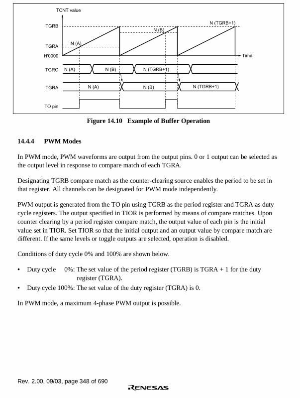
Rev. 2.00, 09/03, page 348 of 690
TCNT value
TGRB
H'0000
TGRC
Time
TGRA
N (A) N (TGRB+1)
TO pin
N (A)
N (B)
N (TGRB+1)
N (TGRB+1)
N (B)
TGRA N (B)N (A)
Figure 14.10 Example of Buffer Operation
14.4.4 PWM Modes
In PWM mode, PWM waveforms are output from the output pins. 0 or 1 output can be selected asthe output level in response to compare match of each TGRA.
Designating TGRB compare match as the counter-clearing source enables the period to be set inthat register. All channels can be designated for PWM mode independently.
PWM output is generated from the TO pin using TGRB as the period register and TGRA as dutycycle registers. The output specified in TIOR is performed by means of compare matches. Uponcounter clearing by a period register compare match, the output value of each pin is the initialvalue set in TIOR. Set TIOR so that the initial output and an output value by compare match aredifferent. If the same levels or toggle outputs are selected, operation is disabled.
Conditions of duty cycle 0% and 100% are shown below.
• Duty cycle 0%: The set value of the period register (TGRB) is TGRA + 1 for the dutyregister (TGRA).
• Duty cycle 100%: The set value of the duty register (TGRA) is 0.
In PWM mode, a maximum 4-phase PWM output is possible.

Rev. 2.00, 09/03, page 349 of 690
Example of PWM Mode Setting Procedure: Figure 14.11 shows an example of the PWM modesetting procedure.
Select counter clock
PWM mode
Select counter clearing source
Select waveform output level
<PWM mode>
[1]
[2]
[3]
Set period [4]
Set PWM mode [5]
Set external pin function [6]
Start count [7]
[1] Select the counter clock with bits TPSC2 to
TPSC0 in TCR. At the same time, select the
input clock edge with bits CKEG1 and CKEG0 in
TCR.
[2] Use bits CCLR2 to CCLR0 in TCR to select the
TGRB to be used as the TCNT clearing source.
[3] Use TIOR to select the initial value and
output value.
[4] Set the period in TGRB, and set the duty in
TGRA.
[5] Select the PWM mode with bits MD2 to MD0 in
TMDR.
[6] Set the external pin function in pin function
controller (PFC).
[7] Set the CST bit in TSTR to 1 to start the count
operation.
Figure 14.11 Example of PWM Mode Setting Procedure

Rev. 2.00, 09/03, page 350 of 690
Examples of PWM Mode Operation: Figure 14.12 shows an example of PWM mode operation.
In this example, TGRB compare match is set as the TCNT clearing source, 0 is set as the initialoutput value of the TO pin by TGRA, and 1 is set as the output value by TGRA compare match.
In this case, the value set in TGRB is used as the period, and the value set in TGRA as the duty.
TCNT value
TGRB
H'0000
TO
Time
TGRA
Counter cleared by
TGRB compare match
Figure 14.12 Example of PWM Mode Operation (1)
Figure 14.13 shows examples of PWM waveform output with 0% duty and 100% duty in PWMmode.
TCNT
TGRA=1
TGRA=2
TGRA=3
↑ Rewrite timing for TGRA
Period: TGRB=2
02 1 2 0
TGRA=0
Figure 14.13 Examples of PWM Mode Operation (2)

RTCS320A_000020020100 Rev. 2.00, 09/03, page 351 of 690
Section 15 Realtime Clock (RTC)
This LSI has a realtime clock (RTC) with its own 32.768 kHz crystal oscillator. A block diagramof the RTC is shown in figure 15.1.
15.1 Features
The RTC has the following features:
• Clock and calendar functions (BCD format): seconds, minutes, hours, date, day of the week,month, and year
• 1-Hz to 64-Hz timer (binary format)
• Start/stop function
• 30-second adjust function
• Alarm interrupt: frame comparison of seconds, minutes, hours, date, day of the week, month,and year can be used as conditions for the alarm interrupt
• Periodic interrupts: the interrupt cycle may be 1/256 second, 1/64 second, 1/16 second, 1/4second, 1/2 second, 1 second, or 2 seconds
• Carry interrupt: a carry interrupt indicates when a carry occurs during a counter read
• Automatic leap year adjustment

Rev. 2.00, 09/03, page 352 of 690
Module
bus
RTC
Periphera
l bus
Interrupt
control
circuit
Prescaler
(÷ 2)
Bus
interface
Carry
detection
circuit
ATI
PRI
CUI
R64CNT
Reset
RSECCNT
RMINCNT
RHRCNT
RWKCNT
16.384 kHz
RDAYCNT
RMONCNT
RYRCNT
Comparator
RSECAR
RMINAR
RHRAR
RWKAR
RDAYAR
RCR1
RCR2
RCR3
30-second
ADJEXTAL2
32.768 kHz
128 Hz
XTAL2
Externally
connected
circuit
Oscillator
circuit
Prescaler
(÷ 128)
RYRAR
RMONAR
R64CNT:
RSECCNT:
RMINCNT:
RHRCNT:
RWKCNT:
RDAYCNT:
RMONCNT:
RYRCNT:
RSECAR:
64-Hz counter
Second counter
Minute counter
Hour counter
Day of the week counter
Date counter
Month counter
Year counter
Second alarm register
RHRAR:
RMINAR:
RWKAR:
RDAYAR:
RMONAR:
RYRAR:
RCR1:
RCR2:
RCR3:
Minute alarm register
Hour alarm register
Day of the week alarm register
Date alarm register
Month alarm register
Year alarm register
RTC control register 1
RTC control register 2
RTC control register 3
Legend:
Figure 15.1 RTC Block Diagram

Rev. 2.00, 09/03, page 353 of 690
15.2 Input/Output Pins
Table 15.1 shows the RTC pin configuration.
Table 15.1 Pin Configuration
Pin Abbreviation I/O Function
Crystal oscillator for RTC EXTAL2 I Connects crystal to RTC oscillator*
Crystal oscillator for RTC XTAL2 O Connects crystal to RTC oscillator*
Power-supply for RTC VCC-RTC — Power-supply pin for RTC
GND for RTC VSS-RTC — GND pin for RTC
Note: *Pull up (VccQ (3.3 V power)) EXTAL2 and leave XTAL2 open, when the RTC is not used.
15.3 Register Descriptions
The RTC has the following registers. Refer to section 24, List of Registers, for more detail of theaddress and access size.
• 64-Hz counter (R64CNT)
• Second counter (RSECCNT)
• Minute counter (RMINCNT)
• Hour counter (RHRCNT)
• Day of week counter (RWKCNT)
• Date counter (RDAYCNT)
• Month counter (RMONCNT)
• Year counter (RYRCNT)
• Second alarm register (RSECAR)
• Minute alarm register (RMINAR)
• Hour alarm register (RHRAR)
• Day of week alarm register (RWKAR)
• Date alarm register (RDAYAR)
• Month alarm register (RMONAR)
• Year alarm register (RYRAR)
• RTC control register 1 (RCR1)
• RTC control register 2 (RCR2)
• RTC control register 3 (RCR3)

Rev. 2.00, 09/03, page 354 of 690
15.3.1 64-Hz Counter (R64CNT)
The 64-Hz counter (R64CNT) is an 8-bit read-only register that indicates the state of the dividercircuit between 64 Hz and 1 Hz.
R64CNT is reset to H'00 by setting the RESET bit in RCR2 or the ADJ bit in RCR2 to 1.
R64CNT is not initialized by a power-on reset or manual reset, or in standby mode.
Bit Bit Name Initial Value R/W Description
7 0 R Reserved
This bit is always read as 0.
6 to 0 R 64-Hz Counter
Each bit (bits 6 to 0) indicates the state of theRTC divider circuit between 64 Hz and 1 Hz.
Bit Frequency
6: 1 Hz
5: 2 Hz
4: 4 Hz
3: 8 Hz
2: 16 Hz
1: 32 Hz
0: 64 Hz
15.3.2 Second Counter (RSECCNT)
The second counter (RSECCNT) is an 8-bit readable/writable register used for setting/counting inthe BCD-coded second section. The count operation is performed by a carry for each second of the64-Hz counter.
The range of second that can be set is 00 to 59 (decimal). Errant operation will result if any othervalue is set. Carry out write processing after stopping the count operation with the START bit inRCR2.
RSECCNT is not initialized by a power-on reset or manual reset, or in standby mode.

Rev. 2.00, 09/03, page 355 of 690
Bit Bit Name Initial Value R/W Description
7 0 R Reserved
This bit is always read as 0. The write valueshould always be 0.
6 to 4 R/W 10-unit of the second counter in the BCD-code.The range that can be set is 0 to 5 (decimal).
3 to 0 R/W 1-unit of the second counter in the BCD-code.The range that can be set is 0 to 9 (decimal).
15.3.3 Minute Counter (RMINCNT)
The minute counter (RMINCNT) is an 8-bit readable/writable register used for setting/counting inthe BCD-coded minute section. The count operation is performed by a carry for each minute of thesecond counter.
The range of minute that can be set is 00 to 59 (decimal). Errant operation will result if any othervalue is set. Carry out write processing after stopping the count operation with the START bit inRCR2.
RMINCNT is not initialized by a power-on reset or manual reset, or in standby mode.
Bit Bit Name Initial Value R/W Description
7 0 R Reserved
This bit is always read as 0. The write valueshould always be 0.
6 to 4 R/W 10-unit of the minute counter in the BCD-code.The range that can be set is 0 to 5 (decimal).
3 to 0 R/W 1-unit of the minute counter in the BCD-code.The range that can be set is 0 to 9 (decimal).
15.3.4 Hour Counter (RHRCNT)
The hour counter (RHRCNT) is an 8-bit readable/writable register used for setting/counting in theBCD-coded hour section. The count operation is performed by a carry for each 1 hour of theminute counter.
The range of hour that can be set is 00 to 23 (decimal). Errant operation will result if any othervalue is set. Carry out write processing after stopping the count operation with the START bit inRCR2.
RHRCNT is not initialized by a power-on reset or manual reset, or in standby mode.

Rev. 2.00, 09/03, page 356 of 690
Bit Bit Name Initial Value R/W Description
7, 6 0 R Reserved
These bits are always read as 0. The write valueshould always be 0.
5, 4 R/W 10-unit of the hour counter in the BCD-code.The range that can be set is 0 to 2 (decimal).
3 to 0 R/W 1-unit of the hour counter in the BCD-code.The range that can be set is 0 to 9 (decimal).
15.3.5 Day of Week Counter (RWKCNT)
The day of week counter (RWKCNT) is an 8-bit readable/writable register used forsetting/counting in the day of week section. The count operation is performed by a carry for eachday of the date counter.
The range for day of the week that can be set is 0 to 6 (decimal). Errant operation will result if anyother value is set. Carry out write processing after stopping the count operation with the STARTbit in RCR2.
RWKCNT is not initialized by a power-on reset or manual reset, or in standby mode.
Bit Bit Name Initial Value R/W Description
7 to 3 0 R Reserved
These bits are always read as 0. The write valueshould always be 0.
2 to 0 R/W Counter for the day of week in the BCD-code.The range that can be set is 0 to 6 (decimal).
Code Day of Week
0: Sunday
1: Monday
2: Tuesday
3: Wednesday
4: Thursday
5: Friday
6: Saturday

Rev. 2.00, 09/03, page 357 of 690
15.3.6 Date Counter (RDAYCNT)
The date counter (RDAYCNT) is an 8-bit readable/writable register used for setting/counting inthe BCD-coded date section. The count operation is performed by a carry for each day of the hourcounter.
The range of date that can be set changes within 01 to 31 (decimal) with some months and in leapyears. Please confirm the correct setting. Errant operation will result if any other value is set.Carry out write processing after stopping the count operation with the START bit in RCR2.
RDAYCNT is not initialized by a power-on reset or manual reset, or in standby mode.
Bit Bit Name Initial Value R/W Description
7, 6 0 R Reserved
These bits are always read as 0. The write valueshould always be 0.
5, 4 R/W 10-unit of the date counter in the BCD-code.The range that can be set is 0 to 3 (decimal).
3 to 0 R/W 1-unit of the date counter in the BCD-code.The range that can be set is 0 to 9 (decimal).
15.3.7 Month Counter (RMONCNT)
The month counter (RMONCNT) is an 8-bit readable/writable register used for setting/counting inthe BCD-coded month section. The count operation is performed by a carry for each month of thedate counter.
The range of month that can be set is 01 to 12 (decimal). Errant operation will result if any othervalue is set. Carry out write processing after stopping the count operation with the START bit inRCR2.
RMONCNT is not initialized by a power-on reset or manual reset, or in standby mode.
Bit Bit Name Initial Value R/W Description
7 to 5 0 R Reserved
These bits are always read as 0. The write valueshould always be 0.
4 R/W 10-unit of the month counter in the BCD-code.The range that can be set is 0 to 1 (decimal).
3 to 0 R/W 1-unit of the month counter in the BCD-code.The range that can be set is 0 to 9 (decimal).

Rev. 2.00, 09/03, page 358 of 690
15.3.8 Year Counter (RYRCNT)
The year counter (RYRCNT) is a 16-bit readable/writable register used for setting/counting in theBCD-coded year section. The four digits of the western calendar year are counted. The countoperation is performed by a carry for each year of the month counter.
The range for year that can be set is 0000 to 9999 (decimal). Errant operation will result if anyother value is set. Carry out write processing after stopping the count operation with the STARTbit in RCR2 or using a carry flag.
RYRCNT is not initialized by a power-on reset or manual reset, or in standby mode.
Leap years are recognized by dividing the year counter value by 4 and obtaining a fractional resultof 0. The year counter value 0000 is recognized as a leap year.
Bit Bit Name Initial Value R/W Description
15 to 12 R/W 1000-unit of the year counter in the BCD-code.The range that can be set is 0 to 9 (decimal).
11 to 8 R/W 100-unit of the year counter in the BCD-code.The range that can be set is 0 to 9 (decimal).
7 to 4 R/W 10-unit of the year counter in the BCD-code.The range that can be set is 0 to 9 (decimal).
3 to 0 R/W 1-unit of the year counter in the BCD-code.The range that can be set is 0 to 9 (decimal).
15.3.9 Second Alarm Register (RSECAR)
The second alarm register (RSECAR) is an 8-bit readable/writable register, and an alarm registercorresponding to the second counter RSECCNT. When the ENB bit is set to 1, a comparison withthe RSECCNT value is performed. For alarm registers RSECAR, RMINAR, RHRAR, RWKAR,RDAYAR, and RMONAR, a comparison with the corresponding counter value is performed forthose whose ENB bit is set to 1, and for RCR3, a comparison is performed when the YAEN bit isset to 1. If all of those match, an RTC alarm interrupt is generated.
The range of second alarm that can be set is 00 to 59 (decimal). Errant operation will result if anyother value is set.
The ENB bit in RSECAR is initialized to 0 by a power-on reset, and it is not initialized by manualreset and standby mode. The remaining RSECAR fields are not initialized by a power-on reset ormanual reset, or in standby mode.

Rev. 2.00, 09/03, page 359 of 690
Bit Bit Name Initial Value R/W Description
7 ENB 0 R/W Second Alarm Enable
Specifies whether to compare RSECCNT withRSECAR to generate a second alarm.
0: Not compared
1: Compared
6 to 4 R/W 10-unit of second alarm setting in the BCD-code.The range that can be set is 0 to 5 (decimal).
3 to 0 R/W 1-unit of second alarm setting in the BCD-code.The range that can be set is 0 to 9 (decimal).
15.3.10 Minute Alarm Register (RMINAR)
The minute alarm register (RMINAR) is an 8-bit readable/writable register, and an alarm registercorresponding to the minute counter RMINCNT. When the ENB bit is set to 1, a comparison withthe RMINCNT value is performed. For alarm registers RSECAR, RMINAR, RHRAR, RWKAR,RDAYAR, and RMONAR, a comparison with the corresponding counter value is performed forthose whose ENB bit is set to 1, and for RCR3, a comparison is performed when the YAEN bit isset to 1. If all of those match, an RTC alarm interrupt is generated.
The range of minute alarm that can be set is 00 to 59 (decimal). Errant operation will result if anyother value is set.
The ENB bit in RMINAR is initialized by a power-on reset, and it is not initialized by manualreset and standby mode. The remaining RMINAR fields are not initialized by a power-on reset ormanual reset, or in standby mode.
Bit Bit Name Initial Value R/W Description
7 ENB 0 R/W Minute Alarm Enable
Specifies whether to compare RMINCNT withRMINAR to generate a second alarm.
0: Not compared
1: Compared
6 to 4 R/W 10-unit of minute alarm setting in the BCD-code.The range that can be set is 0 to 5 (decimal).
3 to 0 R/W 1-unit of minute alarm setting in the BCD-code.The range that can be set is 0 to 9 (decimal).

Rev. 2.00, 09/03, page 360 of 690
15.3.11 Hour Alarm Register (RHRAR)
The hour alarm register (RHRAR) is an 8-bit readable/writable register, and an alarm registercorresponding to the hour counter RHRCNT. When the ENB bit is set to 1, a comparison with theRHRCNT value is performed. For alarm registers RSECAR, RMINAR, RHRAR, RWKAR,RDAYAR, and RMONAR, a comparison with the corresponding counter value is performed forthose whose ENB bit is set to 1, and for RCR3, a comparison is performed when the YAEN bit isset to 1. If all of those match, an RTC alarm interrupt is generated.
The range of hour alarm that can be set is 00 to 23 (decimal). Errant operation will result if anyother value is set.
The ENB bit in RHRAR is initialized by a power-on reset, and it is not initialized by manual resetand standby mode. The remaining RHRAR fields are not initialized by a power-on reset or manualreset, or in standby mode.
Bit Bit Name Initial Value R/W Description
7 ENB 0 R/W Hour Alarm Enable
Specifies whether to compare RHRCNT withRHRAR to generate a second alarm.
0: Not compared
1: Compared
6 0 R Reserved
This bit is always read as 0. The write valueshould always be 0.
5, 4 R/W 10-unit of hour alarm setting in the BCD-code.The range that can be set is 0 to 2 (decimal).
3 to 0 R/W 1-unit of hour alarm setting in the BCD-code.The range that can be set is 0 to 9 (decimal).

Rev. 2.00, 09/03, page 361 of 690
15.3.12 Day of Week Alarm Register (RWKAR)
The day of week alarm register (RWKAR) is an 8-bit readable/writable register, and an alarmregister corresponding to the day of week counter RWKCNT. When the ENB bit is set to 1, acomparison with the RWKCNT value is performed. For alarm registers RSECAR, RMINAR,RHRAR, RWKAR, RDAYAR, and RMONAR, a comparison with the corresponding countervalue is performed for those whose ENB bit is set to 1, and for RCR3, a comparison is performedwhen the YAEN bit is set to 1. If all of those match, an RTC alarm interrupt is generated.
The range of day of the week alarm that can be set is 0 to 6 (decimal). Errant operation will resultif any other value is set.
The ENB bit in RWKAR is initialized by a power-on reset, and it is not initialized by manual resetand standby mode. The remaining RWKAR fields are not initialized by a power-on reset ormanual reset, or in standby mode.
Bit Bit Name Initial Value R/W Description
7 ENB 0 R/W Day of Week Alarm Enable
Specifies whether to compare RWKCNT withRWKAR to generate a second alarm.
0: Not compared
1: Compared
6 to 3 0 R Reserved
These bits are always read as 0. The write valueshould always be 0.
2 to 0 R/W Day of Week Alarm Code
The range that can be set is 0 to 6 (decimal).
Code Day of the Week
0: Sunday
1: Monday
2: Tuesday
3: Wednesday
4: Thursday
5: Friday
6: Saturday

Rev. 2.00, 09/03, page 362 of 690
15.3.13 Date Alarm Register (RDAYAR)
The date alarm register (RDAYAR) is an 8-bit readable/writable register, and an alarm registercorresponding to the date counter RDAYCNT. When the ENB bit is set to 1, a comparison withthe RDAYCNT value is performed. For alarm registers RSECAR, RMINAR, RHRAR, RWKAR,RDAYAR, and RMONAR, a comparison with the corresponding counter value is performed forthose whose ENB bit is set to 1, and for RCR3, a comparison is performed when the YAEN bit isset to 1. If all of those match, an RTC alarm interrupt is generated.
The range of date alarm that can be set is 01 to 31 (decimal). Errant operation will result if anyother value is set. The RDAYCNT range that can be set changes with some months and in leapyears. Please confirm the correct setting.
The ENB bit in RDAYAR is initialized by a power-on reset, and it is not initialized by manualreset and standby mode. The remaining RDAYAR fields are not initialized by a power-on reset ormanual reset, or in standby mode.
Bit Bit Name Initial Value R/W Description
7 ENB 0 R/W Date Alarm Enable
Specifies whether to compare RDAYCNT withRDAYAR to generate a second alarm.
0: Not compared
1: Compared
6 0 R Reserved
This bit is always read as 0. The write valueshould always be 0.
5, 4 R/W 10-unit of date alarm setting in the BCD-code.The range that can be set is 0 to 3 (decimal).
3 to 0 R/W 1-unit of date alarm setting in the BCD-code.The range that can be set is 0 to 9 (decimal).

Rev. 2.00, 09/03, page 363 of 690
15.3.14 Month Alarm Register (RMONAR)
The month alarm register (RMONAR) is an 8-bit readable/writable register, and an alarm registercorresponding to the month counter RMONCNT. When the ENB bit is set to 1, a comparison withthe RMONCNT value is performed. For alarm registers RSECAR, RMINAR, RHRAR, RWKAR,RDAYAR, and RMONAR, a comparison with the corresponding counter value is performed forthose whose ENB bit is set to 1, and for RCR3, a comparison is performed when the YAEN bit isset to 1. If all of those match, an RTC alarm interrupt is generated.
The range of month alarm that can be set is 01 to 12 (decimal). Errant operation will result if anyother value is set.
The ENB bit in RMONAR is initialized by a power-on reset, and it is not initialized by manualreset and standby mode. The remaining RMONAR fields are not initialized by a power-on reset ormanual reset, or in standby mode.
Bit Bit Name Initial Value R/W Description
7 ENB 0 R/W Month Alarm Enable
Specifies whether to compare RMONCNT withRMONAR to generate a second alarm.
0: Not compared
1: Compared
6, 5 0 R Reserved
These bits are always read as 0. The write valueshould always be 0.
4 R/W 10-unit of month alarm setting in the BCD-code.The range that can be set is 0 to 1 (decimal).
3 to 0 R/W 1-unit of month alarm setting in the BCD-code.The range that can be set is 0 to 9 (decimal).

Rev. 2.00, 09/03, page 364 of 690
15.3.15 Year Alarm Register (RYRAR)
The year alarm register (RYRAR) is a 16-bit readable/writable register, and an alarm registercorresponding to the year counter RYRCNT. When the YAEN bit in RCR3 is set to 1, acomparison with the RYRCNT value is performed. For alarm registers RSECAR, RMINAR,RHRAR, RWKAR, RDAYAR, and RMONAR, a comparison with the corresponding countervalue is performed for those whose ENB bit is set to 1, and for RCR3, a comparison is performedwhen the YAEN bit is set to 1. If all of those match, an RTC alarm interrupt is generated.
The range of year alarm that can be set is 0000 to 9999 (decimal). Errant operation will result ifany other value is set.
The RYRAR contents are not initialized by a power-on reset or manual reset, or in standby mode.
Bit Bit Name Initial Value R/W Description
15 to 12 R/W 1000-unit of year alarm setting in the BCD-code.The range that can be set is 0 to 9 (decimal).
11 to 8 R/W 100-unit of year alarm setting in the BCD-code.The range that can be set is 0 to 9 (decimal).
7 to 4 R/W 10-unit of year alarm setting in the BCD-code.The range that can be set is 0 to 9 (decimal).
3 to 0 R/W 1-unit of year alarm setting in the BCD-code.The range that can be set is 0 to 9 (decimal).

Rev. 2.00, 09/03, page 365 of 690
15.3.16 RTC Control Register 1 (RCR1)
The RTC control register 1 (RCR1) is an 8-bit readable/writable register that affects carry flagsand alarm flags. It also selects whether to generate interrupts for each flag. Because flags aresometimes set after an operand read, do not use this register in read-modify-write processing.
RCR1 is initialized to H'00 by a power-on reset or a manual reset. In a reset, all bits are initializedto 0 except for the CF flag, which is undefined. When using the CF flag, it must be initializedbeforehand. This register is not initialized in standby mode.
Bit Bit Name Initial Value R/W Description
7 CF Undefined R/W Carry Flag
Status flag that indicates that a carry hasoccurred. CF is set to 1 when R64CNT orRSECCNT is read during a carry occurrence byR64CNT or RSECCNT. A count register valueread at this time cannot be guaranteed; anotherread is required.
0: No carry by R64CNT or RSECCNT.[Clearing condition] When 0 is written to CF
1: [Setting condition] When R64CNT orRSECCNT is read during a carry occurrence byR64CNT or RSECCNT, or 1 is written to CF
6, 5 — 0 R Reserved
These bits are always read as 0. The write valueshould always be 0.
4 CIE 0 R/W Carry Interrupt Enable Flag
When the carry flag (CF) is set to 1, the CIE bitenables interrupts.
0: A carry interrupt is not generated when the CFflag is set to 1
1: A carry interrupt is generated when the CF flagis set to 1
3 AIE 0 R/W Alarm Interrupt Enable Flag
When the alarm flag (AF) is set to 1, the AIE bitenables interrupts.
0: An alarm interrupt is not generated when theAF flag is set to 1
1: An alarm interrupt is generated when the AFflag is set to 1

Rev. 2.00, 09/03, page 366 of 690
Bit Bit Name Initial Value R/W Description
2, 1 — 0 R Reserved
These bits are always read as 0. The write valueshould always be 0.
0 AF 0 R/W Alarm Flag
The AF flag is set to 1 when the alarm time set inan alarm register (only registers with ENB bit ofthe corresponding alarm registers and YAEN bitin RCR3 set to 1) matches the clock and calendartime. This flag is cleared to 0 when 0 is written,but holds the previous value when 1 is written.
0: Clock/calendar and alarm register have notmatched.[Clearing condition] When 0 is written to AF
1: [Setting condition] Clock/calendar and alarmregister have matched (only registers that ENBbit and YAEN bit is 1)
15.3.17 RTC Control Register 2 (RCR2)
The RTC control register 2 (RCR2) is an 8-bit readable/writable register for periodic interruptcontrol, 30-second adjustment ADJ, divider circuit RESET, and RTC count start/stop control. It isinitialized to H'09 by a power-on reset. It is initialized except for RTCEN and START by amanual reset. It is not initialized in standby mode, and retains its contents.
Bit Bit Name Initial Value R/W Description
7 PEF 0 R/W Periodic Interrupt Flag
Indicates interrupt generation with the perioddesignated by the PES2 to PES0 bits. When setto 1, PEF generates periodic interrupts.
0: Interrupts not generated with the perioddesignated by the PES bits.[Clearing condition] When 0 is written to PEF
1: [Setting condition] When interrupts aregenerated with the period designated by thePES bits or 1 is written to PEF

Rev. 2.00, 09/03, page 367 of 690
Bit Bit Name Initial Value R/W Description
654
PES2PES1PES0
000
R/WR/WR/W
Periodic Interrupt Interval
These bits specify the periodic interrupt interval.
000: No periodic interrupts generated
001: Periodic interrupt generated every 1/256second
010: Periodic interrupt generated every 1/64second
011: Periodic interrupt generated every 1/16second
100: Periodic interrupt generated every 1/4second
101: Periodic interrupt generated every 1/2second
110: Periodic interrupt generated every 1 second
111: Periodic interrupt generated every 2 seconds
3 RTCEN 1 R/W Controls the operation of the crystal oscillator forthe RTC.
0: Halts the crystal oscillator for the RTC.
1: Runs the crystal oscillator for the RTC.
2 ADJ 0 R/W 30 Second Adjustment
When 1 is written to the ADJ bit, times of 29seconds or less will be rounded to 00 secondsand 30 seconds or more to 1 minute. The dividercircuit will be simultaneously reset. This bit isalways read as 0.
0: Runs normally.
1: 30-second adjustment.
1 RESET 0 R/W Reset
When 1 is written, initializes the divider circuit(RTC prescaler and R64CNT). This bit is alwaysread as 0.
0: Runs normally.
1: Divider circuit is reset.

Rev. 2.00, 09/03, page 368 of 690
Bit Bit Name Initial Value R/W Description
0 START 1 R/W Start Bit
Halts and restarts the counter (clock).
0: Second/minute/hour/day/week/month/yearcounter halts.*
1: Second/minute/hour/day/week/month/yearcounter runs normally.*
Note: *The 64-Hz counter always runs unlessstopped with the RTCEN bit.
15.3.18 RTC Control Register 3 (RCR3)
The RTC control register 3 (RCR3) is an 8-bit readable/writable register that controls thecomparison between the BCD-coded year section counter RYRCNT of the RTC and the yearalarm register RYRAR.
Bit Bit Name Initial Value R/W Description
7 YAEN 0 R/W Year Alarm Enable
When this bit is set to 1, the year alarm register(RYRAR) is compared with the year counter(RYRCNT). For alarm registers RSECAR,RMINAR, RHRAR, RWKAR, RDAYAR, andRMONAR, a comparison with the correspondingcounter value is performed for those whose ENBbit is set to 1, and for RCR3, a comparison isperformed when this bit is set to 1. If all of thosematch, an RTC alarm interrupt is generated.
6 to 0 — 0 R Reserved
These bits are always read as 0. The write valueshould always be 0.

Rev. 2.00, 09/03, page 369 of 690
15.4 Operation
15.4.1 Initial Settings of Registers after Power-On
All the registers should be set after the power is turned on.
15.4.2 Setting Time
Figure 15.2 shows how to set the time when the clock is stopped.
Write 1 to RESET and 0 to
START in the RCR2 register
Order is irrelevant
Write 1 to START in the
RCR2 register
Set seconds, minutes,hour, day, day of the
week, month and year
Stop clock,
reset divider circuit
Start clock
Figure 15.2 Setting Time
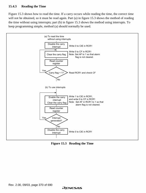
Rev. 2.00, 09/03, page 370 of 690
15.4.3 Reading the Time
Figure 15.3 shows how to read the time. If a carry occurs while reading the time, the correct timewill not be obtained, so it must be read again. Part (a) in figure 15.3 shows the method of readingthe time without using interrupts; part (b) in figure 15.3 shows the method using interrupts. Tokeep programming simple, method (a) should normally be used.
Write 0 to CF in RCR1
Note: Set AF to 1 so that alarm
flag is not cleared.
Read RCR1 and check CF
Write 0 to CIE in RCR1
Carry flag = 1?
No
Yes
Clear the carry flag
Disable the carry
interrupt
Read counterregister
Write 1 to CIE in RCR1,
and write 0 to CF in RCR1
Note: Set AF in RCR1 to 1 so that
alarm flag is not cleared.
Interrupt
generated?
No
Yes
Enable the carry
interrupt
Clear the carry flag
Disable the carry
interrupt
Read counter
register
To read the time
without using interrupts
(b) To use interrupts
(a)
Write 0 to CIE in RCR1
Figure 15.3 Reading the Time

Rev. 2.00, 09/03, page 371 of 690
15.4.4 Alarm Function
Figure 15.4 shows how to use the alarm function.
Alarms can be generated using seconds, minutes, hours, day of the week, date, month, year, or anycombination of these. Set the ENB or YAEN bit for the register on which the alarm is placed to 1,and then set the alarm time in the lower bits. Clear the ENB or YAEN bit for the register on whichthe alarm is not placed to 0.
When the clock and alarm times match, 1 is set in the AF bit in RCR1. Alarm detection can bechecked by reading this bit, but normally it is done by interrupt. If 1 is placed in the AIE bit inRCR1, an interrupt is generated when an alarm occurs.
Disable interrupt to prevent erroneous
interruption.(AIE bit in RCR1 is cleared)
Then write 1.
Clock running
Set alarm time
Cancel alarm interrupt
Always clear, since the flag may have been
set while the alarm time was being set.
(Write 0 to AF of RCR1 to clear it. )
Clear alarm flag
Monitor alarm time
(wait for interrupt or
check alarm flag)
Figure 15.4 Using the Alarm Function
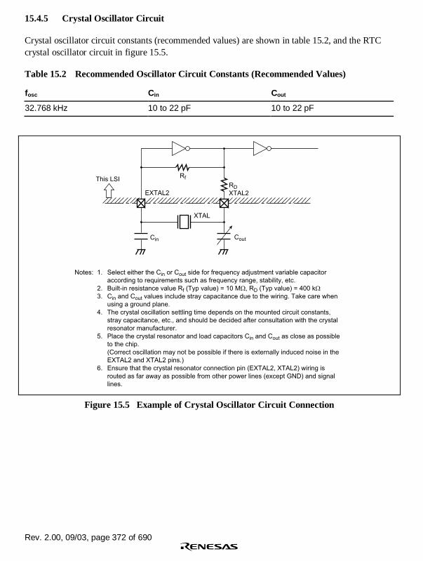
Rev. 2.00, 09/03, page 372 of 690
15.4.5 Crystal Oscillator Circuit
Crystal oscillator circuit constants (recommended values) are shown in table 15.2, and the RTCcrystal oscillator circuit in figure 15.5.
Table 15.2 Recommended Oscillator Circuit Constants (Recommended Values)
fosc Cin Cout
32.768 kHz 10 to 22 pF 10 to 22 pF
This LSI
EXTAL2 XTAL2
XTAL
Cin Cout
Rf
RD
Notes: 1. Select either the Cin or Cout side for frequency adjustment variable capacitor
according to requirements such as frequency range, stability, etc.
2. Built-in resistance value Rf (Typ value) = 10 MΩ, RD (Typ value) = 400 kΩ
3. Cin and Cout values include stray capacitance due to the wiring. Take care when
using a ground plane.
4. The crystal oscillation settling time depends on the mounted circuit constants,
stray capacitance, etc., and should be decided after consultation with the crystal
resonator manufacturer.
5. Place the crystal resonator and load capacitors Cin and Cout as close as possible
to the chip.
(Correct oscillation may not be possible if there is externally induced noise in the
EXTAL2 and XTAL2 pins.)
6. Ensure that the crystal resonator connection pin (EXTAL2, XTAL2) wiring is
routed as far away as possible from other power lines (except GND) and signal
lines.
Figure 15.5 Example of Crystal Oscillator Circuit Connection

Rev. 2.00, 09/03, page 373 of 690
15.5 Notes for Usage
15.5.1 Register Writing during RTC Count
The following RTC registers cannot be written to during an RTC count (while the START bit inRCR2 = 1).
RSECCNT, RMINCNT, RHRCNT, RDAYCNT, RWKCNT, RMONCNT, RYRCNT
The RTC count must be halted before writing to any of the above registers.
15.5.2 Use of Realtime Clock (RTC) Periodic Interrupts
The method of using the periodic interrupt function is shown in figure 15.6.
A periodic interrupt can be generated periodically at the interval set by the periodic interruptinterval bits (PES0 to PES2) in RCR2. When the time set by the PES0 to PES2 bits has elapsed,the PEF bit is set to 1.
The PEF is cleared to 0 upon periodic interrupt generation when the periodic interrupt interval bits(PES0 to PES2) is set. Periodic interrupt generation can be confirmed by reading this bit, butnormally the interrupt function is used.
Set PES0 to PES2,
and clear PEF to 0,
in RCR2
Clear PEF to 0
Set PES, clear PEF
Elapse of time set by PES
Clear PEF
Figure 15.6 Using Periodic Interrupt Function
15.5.3 Standby Mode after Register Setting
If the standby mode is entered after the RTC registers are set, the time cannot be countedcorrectly. After setting the registers, wait for 2 RTC clock cycles or longer before the standbymode is entered.

Rev. 2.00, 09/03, page 374 of 690

SCIS3C2B_000020020100 Rev. 2.00, 09/03, page 375 of 690
Section 16 Serial Communication Interface with FIFO(SCIF)
This LSI has a two-channel serial communication interface with on-chip FIFO buffers (SerialCommunication Interface with FIFO: SCIF). The SCIF can perform asynchronous and clocksynchronous serial communication.
64-stage FIFO registers are provided for both transmission and reception, enabling fast, efficient,and continuous communication.
16.1 Features
• Asynchronous mode
Serial data communication is executed using an asynchronous system in whichsynchronization is achieved character by character. Serial data communication can be carriedout with standard asynchronous communication chips such as a Universal AsynchronousReceiver/Transmitter (UART) or Asynchronous Communication Interface Adapter (ACIA).
There is a choice of eight serial data communication formats.
Data length: 7 or 8 bits
Stop bit length: 1 or 2 bits
Parity: Even/odd/none
LSB-first transfer
Receive error detection: Parity, framing, and overrun errors
Break detection: If a framing error is followed by at least one frame at the space “0” (low)level, a break is detected.
• Clock synchronous mode
Serial data communication is synchronized with a clock. Serial data communication can becarried out with other chips that have a synchronous communication function.
Data length: 8 bits
LSB-first transfer
• Full-duplex communication capability
The transmitter and receiver are independent units, enabling transmission and reception to beperformed simultaneously.
The transmitter and receiver both have a 64-stage FIFO buffer structure, enabling fast andcontinuous serial data transmission and reception.
• On-chip baud rate generator allows any bit rate to be selected.
• Choice of serial clock source: internal clock from baud rate generator or external clock fromSCK pin.
• Six interrupt sources in asynchronous mode

Rev. 2.00, 09/03, page 376 of 690
There are six interrupt sources transmit-data-stop, transmit-FIFO-data-empty, receive-FIFO-data-full, receive-error (framing/parity error), break-receive, and receive-data-ready interrupts.
• Two interrupt sources in clock synchronous mode
There are two interrupt sources transmit-FIFO-data-empty and receive-FIFO-data-fullinterrupts.
• The DMA controller (DMAC) can be activated to execute a data transfer in the event of atransmit-FIFO-data-empty, transmit-data-stop, or receive-FIFO-data-full interrupt. The DMACrequests of transmit-FIFO-data-empty and transmit-data-stop interrupts are the same.
• On-chip modem control functions (CTS and RTS)
• On-chip transmit-data-stop functions (only in asynchronous mode)
• When not in use, the SCIF can be stopped by halting its clock supply to reduce powerconsumption.
• The amount of data in the transmit/receive FIFO registers and the number of receive errors inthe receive data in the receive FIFO register can be ascertained.

Rev. 2.00, 09/03, page 377 of 690
Figure 16.1 shows a block diagram of the SCIF.
SCIF4
Module data bus
SCFRDR
(64-stage)
RxD
TxD
CTS
RTS
SCK
SCFTDR
(64-stage)
SCTSRSCRSR
SCFDR
SCFCR
SCFER
SCSSR
SCSCR
SCSMR
SCTDSR
SCBRR
Transmission/
reception control
Baud rate
generator
Clock
Parity
generation
Parity check
External clock
Pφ
Pφ/4
Pφ/16
Pφ/64
SCIF
Bus inte
rface
Peripheral
bus
SCRSR: Receive shift register
SCFRDR: Receive FIFO data register
SCTSR: Transmit shift register
SCFTDR: Transmit FIFO data register
SCSMR: Serial mode register
SCSCR: Serial control register
SCFER: FIFO error count register
SCSSR: Serial status register
SCBRR: Bit rate register
SCFCR: FIFO control register
SCFDR: FIFO data count register
SCTDSR: Transit data stop register
SCIF
interrupt
Note:
Figure 16.1 Block Diagram of SCIF

Rev. 2.00, 09/03, page 378 of 690
16.2 Input/Output Pins
Table 16.1 shows the SCIF pin configuration.
Table 16.1 Pin Configuration
Channel Pin Name Abbreviation*1 I/O Function
0 Serial clock SCK0 SCK Input/output Clock input/output
Receive data RxD0 RxD*2 Input Receive data input
Transmit data TxD0 TxD*2 Output Transmit data output
Modem control CTS0 CTS Input Transmission possible
Modem control RTS0 RTS Output Transmit request
2 Serial clock SCK2 SCK Input/output Clock input/output
Receive data RxD2 RxD*2 Input Receive data input
Transmit data TxD2 TxD*2 Output Transmit data output
Modem control CTS2 CTS Input Transmission possible
Modem control RTS2 RTS Output Transmit request
Notes: 1. The pins are collectively called SCK, RxD, TxD, CTS, and RTS without channel numberin the following descriptions.
2. These pins are made to function as serial pins by setting SCIF operation with the TEand RE bits in SCSCR.

Rev. 2.00, 09/03, page 379 of 690
16.3 Register Descriptions
The SCIF has the following internal registers. For details on register addresses and register statesin each processing state, refer to section 24, List of Registers.
1. Channel 0
• Serial mode register 0 (SCSMR_0)
• Bit rate register 0 (SCBRR_0)
• Serial control register 0 (SCSCR_0)
• Transmit data stop register 0 (SCTDSR_0)
• FIFO error count register 0 (SCFER_0)
• Serial status register 0 (SCSSR_0)
• FIFO control register 0 (SCFCR_0)
• FIFO data count register 0 (SCFDR_0)
• Transmit FIFO data register 0 (SCFTDR_0)
• Receive FIFO data register 0 (SCFRDR_0)
2. Channel 2
• Serial mode register 2 (SCSMR_2)
• Bit rate register 2 (SCBRR_2)
• Serial control register 2 (SCSCR_2)
• Transmit data stop register 2 (SCTDSR_2)
• FIFO error count register 2 (SCFER_2)
• Serial status register 2 (SCSSR_2)
• FIFO control register 2 (SCFCR_2)
• FIFO data count register 2 (SCFDR_2)
• Transmit FIFO data register 2 (SCFTDR_2)
• Receive FIFO data register 2 (SCFRDR_2)

Rev. 2.00, 09/03, page 380 of 690
16.3.1 Receive Shift Register (SCRSR)
SCRSR is the register used to receive serial data.
The SCIF sets serial data input from the RxD pin in SCRSR in the order received, starting with theLSB (bit 0), and converts it to parallel data. When one byte of data has been received, it istransferred to the receive FIFO data register, SCFRDR, automatically.
SCRSR cannot be directly read or written to by the CPU.
16.3.2 Receive FIFO Data Register (SCFRDR)
SCFRDR is a 64-stage 8-bit FIFO register that stores received serial data.
When the SCIF has received one byte of serial data, it transfers the received data from SCRSR toSCFRDR where it is stored, and completes the receive operation. SCRSR is then enabled forreception, and consecutive receive operations can be performed until the receive FIFO dataregister is full (64 data bytes).
SCFRDR is a read-only register, and cannot be written to by the CPU.
If a read is performed when there is no receive data in the receive FIFO data register, an undefinedvalue will be returned. When the receive FIFO data register is full of receive data, subsequentserial data is lost.
Bit Bit Name Initial Value R/W Description
7 to 0 SCFRD7 toSCFRD0
Undefined R Serial Receive Data FIFO
16.3.3 Transmit Shift Register (SCTSR)
SCTSR is the register used to transmit serial data.
To perform serial data transmission, the SCIF first transfers transmit data from SCFTDR toSCTSR, then sends the data sequentially to the TxD pin starting with the LSB (bit 0).
When transmission of one byte is completed, the next transmit data is transferred from SCFTDRto SCTSR, and transmission is started automatically.
SCTSR cannot be directly read or written to by the CPU.

Rev. 2.00, 09/03, page 381 of 690
16.3.4 Transmit FIFO Data Register (SCFTDR)
SCFTDR is an 8-bit 64-stage FIFO data register that stores data for serial transmission.
If SCTSR is empty when transmit data is written to SCFTDR, the SCIF transfers the transmit datawritten in SCFTDR to SCTSR and starts serial transmission.
SCFTDR is a write-only register, and cannot be read by the CPU.
The next data cannot be written when SCFTDR is filled with 64 bytes of transmit data. Datawritten in this case is ignored.
Bit Bit Name Initial Value R/W Description
7 to 0 SCFTD7 toSCFTD0
Undefined W Serial Transmit Data FIFO
16.3.5 Serial Mode Register (SCSMR)
SCSMR is a 16-bit readable/writable register used to set the SCIF’s serial transfer format andselect the baud rate generator clock source and the sampling rate.

Rev. 2.00, 09/03, page 382 of 690
BitBitName
InitialValue R/W Description
15 to 11 0 R Reserved
These bits are always read as 0. The write value shouldalways be 0.
10
9
8
SRC2
SRC1
SRC0
0
0
0
R/W
R/W
R/W
Sampling Control
Select the sampling rate in asynchronous mode. Thissetting is valid only in asynchronous mode.
000: Sampling rate 1/16
001: Sampling rate 1/5
010: Sampling rate 1/11
011: Sampling rate 1/13
100: Sampling rate 1/29
101: Setting prohibited
110: Setting prohibited
111: Setting prohibited
7 C/A 0 R/W Communication Mode
Selects whether the SCI operates in the asynchronousor clock synchronous mode.
0: Asynchronous mode
1: Clock synchronous mode
6 CHR 0 R/W Character Length
Selects seven or eight bits as the data length.
This setting is only valid in asynchronous mode. Inclock synchronous mode, the data length is alwayseight bits, regardless of the CHR setting.
0: 8-bit data
1: 7-bit data*
Note: *When the 7-bit data is selected, the MSB bit (bit7) in the transmit FIFO data register (SCFTDR)is not transmitted.

Rev. 2.00, 09/03, page 383 of 690
BitBitName
InitialValue R/W Description
5 PE 0 R/W Parity Enable
Selects whether or not parity bit addition is performed intransmission, and parity bit checking in reception.
This setting is only valid in asynchronous mode. Insynchronous mode, parity bit addition and checking isnot performed, regardless of the PE setting.
0: Parity bit addition and checking disabled
1: Parity bit addition and checking enabled*
Note: *When the PE bit is set to 1, the parity (even orodd) specified by the O/E bit is added totransmit data before transmission. In reception,the parity bit is checked for the parity (even orodd) specified by the O/E bit.
4 O/E 0 R/W Parity Mode
Selects either even or odd parity for use in parityaddition and checking. The O/E bit setting is only validwhen the PE bit is set to 1, enabling parity bit additionand checking. The O/E bit setting is invalid when parityaddition and checking is disabled in asynchronous andclock synchronous mode.
0: Even parity*1
1: Odd parity*2
Notes: 1. When even parity is set, parity bit addition isperformed in transmission so that the totalnumber of 1-bits in the transmit characterplus the parity bit is even. In reception, acheck is performed to see if the totalnumber of 1-bits in the receive characterplus the parity bit is even.
2. When odd parity is set, parity bit addition isperformed in transmission so that the totalnumber of 1-bits in the transmit characterplus the parity bit is odd. In reception, acheck is performed to see if the totalnumber of 1-bits in the receive characterplus the parity bit is odd.

Rev. 2.00, 09/03, page 384 of 690
BitBitName
InitialValue R/W Description
3 STOP 0 R/W Stop Bit Length
Selects one or two bits as the stop bit length. Inreception, only the first stop bit is checked, regardlessof the STOP bit setting. If the second stop bit is 1, it istreated as a stop bit; if it is 0, it is treated as the start bitof the next transmit character.
This setting is only valid in asynchronous mode. Inclock synchronous mode, this setting is invalid sincestop bits are not added.
0: One stop bit*1
1: Two stop bits*2
Notes: 1. In transmission, a single 1-bit (stop bit) isadded to the end of a transmit characterbefore it is sent.
2. In transmission, two 1-bits (stop bits) areadded to the end of a transmit characterbefore it is sent.
2 0 R Reserved
This bit is always read as 0. The write value shouldalways be 0.
10
CKS1CKS0
00
R/WR/W
Clock Select
Select the clock source for the on-chip baud rategenerator.
00: Pφ
01: Pφ/4
10: Pφ/16
11: Pφ/64
Note: When the clock synchronous mode is selected (C/A bit = 1), the bits other than CKS1 andCKS0 bits are all fixed to 0.

Rev. 2.00, 09/03, page 385 of 690
16.3.6 Serial Control Register (SCSCR)
SCSCR is a 16-bit readable/writable register that enables or disables the SCIF transfer operationsand interrupt requests, and selects the serial clock source.
BitBitName
InitialValue R/W Description
15 to 12 0 R Reserved
These bits are always read as 0. The write value shouldalways be 0.
11 TSIE 0 R/W Transmit Data Stop Interrupt Enable
Enables or disables generation of a transmit-data-stopinterrupt when the TSE bit in SCFCR is enabled and theTSF flag in SCSSR is set to 1.
0: Transmit-data-stop interrupt disabled*
1: Transmit-data-stop interrupt enabled
Note: *The interrupt request is cleared by clearing theTSF flag to 0 after reading 1 from it or clearingthe TSIE bit to 0.
10 ERIE 0 R/W Receive Error Interrupt Enable
Enables or disables generation of a receive-error(framing or parity error) interrupt when the ER flag inSCSSR is set to 1.
0: Receive-error interrupt disabled*
1: Receive-error interrupt enabled
Note: *The interrupt request is cleared by clearing theER flag to 0 after reading 1 from it or clearing theERIE bit to 0.

Rev. 2.00, 09/03, page 386 of 690
BitBitName
InitialValue R/W Description
9 BRIE 0 R/W Break Interrupt Enable
Enables or disables generation of a break-receiveinterrupt when the BRK flag in SCSSR is set to 1.
0: Break-receive interrupt disabled*
1: Break-receive interrupt enabled
Note: *The interrupt request is cleared by clearing theBRK flag to 0 after reading 1 from it or clearingthe BRIE bit to 0.
8 DRIE 0 R/W Receive Data Ready Interrupt Enable
Enables or disables generation of a receive-data-readyinterrupt when the DR flag in SCSSR is set to 1.
0: Receive-data-ready interrupt disabled*
1: Receive-data-ready interrupt enabled
Note: *The interrupt request is cleared by clearing theDR flag to 0 after reading 1 from it or clearing theDRIE bit to 0.
7 TIE 0 R/W Transmit Interrupt Enable
Enables or disables generation of a transmit-FIFO-data-empty interrupt request when the TDFE flag in SCSSR isset to 1.
0: Transmit-FIFO-data-empty interrupt requestdisabled*
1: Transmit-FIFO-data-empty interrupt request enabled
Note: *The interrupt request is cleared by writingtransmit data exceeding the transmit trigger setnumber to SCFTDR, reading 1 from the TDFEflag, then clearing it to 0, or clearing the TIE bit to0.
6 RIE 0 R/W Receive Interrupt Enable
Enables or disables generation of a receive-FIFO-data-full interrupt request when the RDF flag in SCSSR is setto 1.
0: Receive-FIFO-data-full interrupt request disabled*
1: Receive-FIFO-data-full interrupt request enabled
Note: *The interrupt requests is cleared by reading 1from the RDF flag, then clearing the flag to 0, orclearing the RIE bit to 0.

Rev. 2.00, 09/03, page 387 of 690
BitBitName
InitialValue R/W Description
5 TE 0 R/W Transmit Enable
Enables or disables the start of serial transmission bythe SCIF.
0: Transmission disabled
1: Transmission enabled*
Note: *The serial mode register (SCSMR) and FIFOcontrol register (SCFCR) settings must be made,the transmit format decided, and the transmitFIFO reset, before the TE bit is set to 1.
4 RE 0 R/W Receive Enable
Enables or disables the start of serial reception by theSCIF.
0: Reception disabled*1
1: Reception enabled*2
Notes: 1. Clearing the RE bit to 0 does not affect theDR, ER, BRK, RDF, FER, PER, and ORERflags, which retain their state.
2. The serial mode register (SCSMR) and FIFOcontrol register (SCFCR) settings must bemade, the receive format decided, and thereceive FIFO reset, before the RE bit is set to1.
3, 2 0 R Reserved
These bits are always read as 0. The write value shouldalways be 0.

Rev. 2.00, 09/03, page 388 of 690
BitBitName
InitialValue R/W Description
1
0
CKE1
CKE0
0
0
R/W
R/W
Clock Enable
Select the SCIF clock source. The CKE1 and CKE0 bitsmust be set before determining the SCIF operating modewith SCSMR.
00: Internal clock/SCK pin functions as input pin (inputsignal ignored)
01: Internal clock/SCK pin functions as serial clockoutput*1
10: External clock/SCK pin functions as clock input*2
11: External clock/SCK pin functions as clock input*2
When data is sampled by the on-chip baud rategenerator, set bits CKE1 and CKE0 to B'00 (internalclock/SCK pin functions as input pin (input signalignored)).
When using the SCK pin as a port, set bits CKE1 andCKE0 to B’00.
Notes: 1. In synchronous mode, a clock with afrequency equal to the bit rate is output.
2. In asynchronous mode, a clock with asampling rate should be input. For example,when the sampling rate is 1/16, a clock with afrequency of 8 times the bit rate should beinput. When an external clock is not input, setbits CKE1 and CKE0 to B'00 or B'01.

Rev. 2.00, 09/03, page 389 of 690
16.3.7 FIFO Error Count Register (SCFER)
SCFER is a 16-bit read-only register that indicates the number of receive errors (framing or parityerror).
BitBitName
InitialValue R/W Description
15, 14 0 R Reserved
These bits are always read as 0. The write value shouldalways be 0.
13 to 8 PER5toPER0
0 R Parity Error Count
Indicates the number of data, in which parity errors aregenerated, in receive data stored in the receive FIFOdata register (SCFRDR) in asynchronous mode.
After setting the ER bit in SCSSR, the value of bits 13to 8 indicates the number of parity error generated data.
When all 64 bytes of receive data in SCFRDR haveparity errors, the PER5 to PER0 bits indicate 0.
7, 6 0 R Reserved
These bits are always read as 0. The write value shouldalways be 0.
5 to 0 FER5toFER0
0 R Framing Error Count
Indicates the number of data, in which framing errorsare generated, in receive data stored in the receiveFIFO data register (SCFRDR) in asynchronous mode.
After setting the ER bit in SCSSR, the value of bits 5 to0 indicates the number of framing error generated data.
When all 64 bytes of receive data in SCFRDR haveframing errors, the FER5 to FER0 bits indicate 0.

Rev. 2.00, 09/03, page 390 of 690
16.3.8 Serial Status Register (SCSSR)
SCSSR is a 16-bit readable/writable register that indicates the SCIF status.
However, 1 cannot be written to the ORER, TSF, ER, TDFE, BRK, RDF, and DR flags. Also notethat in order to clear these flags to 0, they must be read as 1 beforehand. The TEND, FER, andPER flags are read-only flags and cannot be modified.
BitBitName
InitialValue R/W Description
15 to 10 0 R Reserved
These bits are always read as 0. The write valueshould always be 0.
9 ORER 0 R/(W)* Overrun Error
Indicates that an overrun error occurred duringreception.
This bit is only valid in asynchronous mode.
0: Reception in progress, or reception has endedsuccessfully*1
[Clearing conditions]
• Power-on reset or manual reset
• When 0 is written to ORER after reading ORER =
1
1: An overrun error occurred during reception*2
[Setting condition]
When serial reception is completed while receiveFIFO is full
Notes: 1. The ORER flag is not affected and retainsits previous state when the RE bit inSCSCR is cleared to 0.
2. The receive data prior to the overrun erroris retained in SCFRDR, and the datareceived subsequently is lost. Serialreception cannot be continued while theORER flag is set to 1.
Rev. 2.00, 09/03, page 391 of 690
BitBitName
InitialValue R/W Description
8 TSF 0 R/(W)* Transmit Data Stop
Indicates that the number of transmit data matches thevalue of SCTDSR.
0: Number of transmit data does not match the value ofSCTDSR
[Clearing conditions]
• Power-on reset or manual reset
• When 0 is written to TSF after reading TSF = 1
1: Number of transmit data matches the value of SCTDSR
7 ER 0 R/(W)* Receive Error
Indicates that a framing error or parity error occurred duringreception in asynchronous mode.*1
0: No framing error or parity error occurred during reception
[Clearing conditions]
• Power-on reset or manual reset
• When 0 is written to ER after reading ER = 1
1: A framing error or parity error occurred during reception
[Setting conditions]
• When the SCIF checks whether the stop bit at the endof the receive data is 1 when reception ends, and thestop bit is 0*2
• When, in reception, the number of 1-bits in the receive
data plus the parity bit does not match the parity setting(even or odd) specified by the O/E bit in SCSMR
Notes: 1. The ER flag is not affected and retains itsprevious state when the RE bit in SCSCR iscleared to 0. When a receive error occurs, thereceive data is still transferred to SCFRDR, andreception continues.The FER and PER bits in SCSSR can be usedto determine whether there is a receive error inthe data read from SCFRDR.
2. When the stop length is two bits, only the firststop bit is checked for a value of 1; the secondstop bit is not checked.

Rev. 2.00, 09/03, page 392 of 690
BitBitName
InitialValue R/W Description
6 TEND 1 R Transmit End
Indicates that there is no valid data in SCFTDR when thelast bit of the transmit character is sent, and transmissionhas been ended.
0: Transmission is in progress
[Clearing condition]
When data is written to SCFTDR
1: Transmission has been ended
[Setting condition]
When there is no transmit data in SCFTDR on transmissionof a 1-byte serial transmit character
5 TDFE 1 R/(W)* Transmit FIFO Data Empty
Indicates that data has been transferred from SCFTDR toSCTSR, the number of data bytes in SCFTDR has fallen toor below the transmit trigger data number set by bitsTTRG1 and TTRG0 in the FIFO control register (SCFCR),and new transmit data can be written to SCFTDR.
0: A number of transmit data bytes exceeding the transmittrigger set number have been written to SCFTDR
[Clearing condition]
When transmit data exceeding the transmit trigger setnumber is written to SCFTDR, and 0 is written to TDFEafter reading TDFE = 1
1: The number of transmit data bytes in SCFTDR does notexceed the transmit trigger set number
[Setting conditions]
• Power-on reset or manual reset
• When the number of SCFTDR transmit data bytes fallsto or below the transmit trigger set number as the resultof a transmit operation*1
Note: 1. As SCFTDR is a 64-byte FIFO register, themaximum number of bytes that can be writtenwhen TDFE = 1 is 64 – (transmit trigger setnumber). Data written in excess of this will beignored. The number of data bytes in SCFTDR isindicated by SCFDR.

Rev. 2.00, 09/03, page 393 of 690
BitBitName
InitialValue R/W Description
4 BRK 0 R/(W)* Break Detect
Indicates that a receive data break signal has beendetected in asynchronous mode.
0: A break signal has not been received
[Clearing conditions]
• Power-on reset or manual reset• When 0 is written to BRK after reading BRK = 1
1: A break signal has been received*1
[Setting condition]
When data with a framing error is received, followed by thespace 0 level (low level) for at least one frame length
Note: 1. When a break is detected, the receive data(H'00) following detection is not transferred toSCFRDR. When the break ends and the receivesignal returns to mark 1, receive data transfer isresumed.
3 FER 0 R Framing Error
Indicates a framing error in the data read from SCFRDR inasynchronous mode.
0: There is no framing error in the receive data read fromSCFRDR
[Clearing conditions]
• Power-on reset or manual reset• When there is no framing error in SCFRDR read data
1: There is a framing error in the receive data read fromSCFRDR
[Setting condition]
When there is a framing error in SCFRDR read data

Rev. 2.00, 09/03, page 394 of 690
BitBitName
InitialValue R/W Description
2 PER 0 R Parity Error
Indicates a parity error in the data read from SCFRDR inasynchronous mode.
0: There is no parity error in the receive data read fromSCFRDR
[Clearing conditions]
• Power-on reset or manual reset• When there is no parity error in SCFRDR read data
1: There is a parity error in the receive data read fromSCFRDR
[Setting condition]
When there is a parity error in SCFRDR read data
1 RDF 0 R/(W)* Receive FIFO Data Full
Indicates that the received data has been transferred fromSCRSR to SCFRDR, and the number of receive data bytesin SCFRDR is equal to or greater than the receive triggernumber set by bits RTRG1 and RTRG0 in the FIFO controlregister (SCFCR).
0: The number of receive data bytes in SCFRDR is lessthan the receive trigger set number
[Clearing conditions]
• Power-on reset or manual reset
• When SCFRDR is read until the number of receive databytes in SCFRDR falls below the receive trigger set
number, and 0 is written to RDF after reading RDF = 1
1: The number of receive data bytes in SCFRDR is equal toor greater than the receive trigger set number
[Setting condition]
When SCFRDR contains at least the receive trigger setnumber of receive data bytes*1
Note: 1. SCFRDR is a 64-byte FIFO register. When RDF =1, at least the receive trigger set number of databytes can be read. If data is read when SCFRDRis empty, an undefined value will be returned. Thenumber of receive data bytes in SCFRDR isindicated by the lower bits of SCFDR.

Rev. 2.00, 09/03, page 395 of 690
BitBitName
InitialValue R/W Description
0 DR 0 R/(W)* Receive Data Ready
Indicates that there are fewer than the receive triggerset number of data bytes in SCFRDR and no furtherdata will arrive in asynchronous mode.
0: Reception is in progress or has ended successfullyand there is no receive data left in SCFRDR
[Clearing conditions]
• Power-on reset or manual reset
• When all the receive data in SCFRDR has been
read, and 0 is written to DR after reading DR = 1
1: No further receive data has arrived
[Setting condition]
When SCFRDR contains fewer than the receive triggerset number of receive data bytes and no further datawill arrive.* 1
Note: 1. The DR bit is set 15 etu after the last data isreceived at a sampling rate of 1/16 regardlessof the setting of the sampling control bits inSCSMR.etu: Elementary time unit (time for transfer ofone bit)
Note: *Only 0 can be written for clearing the flags.
16.3.9 Bit Rate Register (SCBRR)
SCBRR is an 8-bit readable/writable register that sets the serial transfer bit rate in accordance withthe baud rate generator operating clock selected by bits CKS1 and CKS0 in SCSMR.
BitBitName
InitialValue R/W Description
7 to 0 SCBR7toSCBR0
H'FF R/W Bit Rate Setting
The SCBRR setting is found from the following equation.

Rev. 2.00, 09/03, page 396 of 690
Asynchronous Mode:
1. When sampling rate is 1/16
N =Pφ
32 × 22n-1 × B× 106 - 1
2. When sampling rate is 1/5
N =Pφ
10 × 22n-1 × B× 106 - 1
3. When sampling rate is 1/11
N =Pφ
22 × 22n-1 × B× 106 - 1
4. When sampling rate is 1/13
N =Pφ
26 × 22n-1 × B× 106 - 1
5. When sampling rate is 1/29
N =Pφ
58 × 22n-1 × B× 106 - 1
Clock Synchronous Mode:
N =Pφ
4 × 22n-1 × B× 106 - 1
Where B: Bit rate (bits/s)N: SCBRR setting for baud rate generator
Asynchronous mode: 0 ≤ N ≤ 255Clock synchronous mode: 1 ≤ N ≤ 255
Pφ: Peripheral module operating frequency (MHz)n: Baud rate generator input clock (n = 0 to 3)
(See the table below for the relation between n and the clock.)
SCSMR Setting
n Clock CKS1 CKS0
0 Pφ 0 0
1 Pφ/4 0 1
2 Pφ/16 1 0
3 Pφ/64 1 1

Rev. 2.00, 09/03, page 397 of 690
The bit rate error in asynchronous mode is found from the following equation:
1. When sampling rate is 1/16
Error (%) =Pφ × 106
(1+N) × B × 32 × 22n-1 - 1 × 100
2. When sampling rate is 1/5
Error (%) =Pφ × 106
(1+N) × B × 10 × 22n-1 - 1 × 100
3. When sampling rate is 1/11
Error (%) =Pφ × 106
(1+N) × B × 22 × 22n-1 - 1 × 100
4. When sampling rate is 1/13
Error (%) =Pφ × 106
(1+N) × B × 26 × 22n-1 - 1 × 100
5. When sampling rate is 1/27
Error (%) =Pφ × 106
(1+N) × B × 58 × 22n-1 - 1 × 100

Rev. 2.00, 09/03, page 398 of 690
16.3.10 FIFO Control Register (SCFCR)
SCFCR is a 16-bit readable/writable register that resets the data count and sets the trigger datanumber for the transmit and receive FIFO registers, and also contains a loopback test enable bit.
BitBitName
InitialValue R/W Description
15 TSE 0 R/W Transmit Data Stop Enable
Enables or disables the transmit data stop function.
This function is enabled only in asynchronous mode.Since this function is not supported in clock synchronousmode, clear this bit to 0 in clock synchronous mode.
0: Transmit data stop function disabled
1: Transmit data stop function enabled
14 TCRST 0 R/W Transmit Count Reset
Clears the transmit count to 0. This bit is valid only whenthe transmit data stop function is used.
0: Transmit count reset disabled*
1: Transmit count reset enabled (clearing to 0)
Note:* The transmit count is reset (clearing to 0) isperformed in power-on reset or manual reset.
13 to 11 0 R Reserved
These bits are always read as 0. The write value shouldalways be 0.
1098
RSTRG2RSTRG1RSTRG0
000
R/WR/WR/W
RTS Output Active Trigger
The RTS signal goes high when the number of receivedata bytes in SCFRDR is equal to or greater than thetrigger set number shown in below.
000: 63
001: 1
010: 8
011: 16
100: 32
101: 48
110: 54
111: 60

Rev. 2.00, 09/03, page 399 of 690
BitBitName
InitialValue R/W Description
76
RTRG1RTRG0
00
R/WR/W
Receive FIFO Data Number Trigger
Set the number of receive data bytes that sets the receivedata full (RDF) flag in the serial status register (SCSSR).
The RDF flag is set when the number of receive data bytesin SCFRDR is equal to or greater than the trigger setnumber shown in below.
00: 1
01: 16
10: 32
11: 48
54
TTRG1TTRG0
00
R/WR/W
Transmit FIFO Data Number Trigger
Set the number of remaining transmit data bytes that setsthe transmit FIFO data register empty (TDFE) flag in theserial status register (SCSSR).
The TDFE flag is set when, as the result of a transmitoperation, the number of transmit data bytes in the transmitFIFO data register (SCFTDR) falls to or below the triggerset number shown in below.
00: 32 (32)
01: 16 (48)
10: 2 (62)
11: 0 (64)
Note: The values in parentheses are the number of emptybytes in SCFTDR when the flag is set.
3 MCE 0 R/W Modem Control Enable
Enables modem control signals CTS and RTS.
This setting is only valid in asynchronous mode.
0: Modem signal disabled*
1: Modem signal enabled
Note: *CTS is fixed at active 0 regardless of the inputvalue, and RTS is also fixed at 0.

Rev. 2.00, 09/03, page 400 of 690
BitBitName
InitialValue R/W Description
2 TFRST 0 R/W Transmit FIFO Data Register Reset
Invalidates the transmit data in the transmit FIFO dataregister and resets it to the empty state.
0: Reset operation disabled*
1: Reset operation enabled
Note:* A reset operation is performed in the event of apower-on reset or manual reset.
1 RFRST 0 R/W Receive FIFO Data Register Reset
Invalidates the receive data in the receive FIFO dataregister and resets it to the empty state.
0: Reset operation disabled*
1: Reset operation enabled
Note:* A reset operation is performed in the event of apower-on reset or manual reset.
0 LOOP 0 R/W Loopback Test
Internally connects the transmit output pin (TxD) andreceive input pin (RxD), and RTS pin and CTS pin, enablingloopback testing.
0: Loopback test disabled
1: Loopback test enabled

Rev. 2.00, 09/03, page 401 of 690
16.3.11 FIFO Data Count Register (SCFDR)
SCFDR is a 16-bit read-only register that indicates the number of data bytes stored in the transmitFIFO data register (SCFTDR) and receive FIFO data register (SCFRDR).
Bits 14 to 8 show the number of transmit data bytes in SCFTDR, and bits 6 to 0 show the numberof receive data bytes in SCFRDR.
BitBitName
InitialValue R/W Description
15 0 R Reserved
This bit is always read as 0. The write value shouldalways be 0.
14 to 8 T6 toT0
0 R These bits show the number of untransmitted databytes in SCFTDR.
A value of H'00 means that there is no transmit data,and a value of H'40 means that SCFTDR is full oftransmit data.
7 0 R Reserved
This bit is always read as 0. The write value shouldalways be 0.
6 to 0 R6 toR0
0 R These bits show the number of receive data bytes inSCFRDR.
A value of H'00 means that there is no receive data,and a value of H'40 means that SCFRDR is full ofreceive data.
16.3.12 Transmit Data Stop Register (SCTDSR)
SCTDSR is an 8-bit readable/writable register that sets the number of transmit data bytes.SCTDSR is valid only when the TSE bit in the FIFO control register (SCFCR) is enabled.Transmit operation is stopped when the number of data bytes set in SCTDSR is transmitted. Thesetting value should be H'00 (one byte) to H'FF (256 bytes). This function is only enabled inasynchronous mode.
SCTDSR is initialized to H'FF.

Rev. 2.00, 09/03, page 402 of 690
16.4 Operation
16.4.1 Overview
The SCIF can carry out serial communication in asynchronous mode, in which synchronization isachieved character by character, and in clock synchronous mode, in which synchronization isachieved with clock pulses.
64-stage FIFO buffers are provided for both transmission and reception, reducing the CPUoverhead and enabling fast, continuous communication to be performed.
16.4.2 Asynchronous Mode
The transfer format is selected using the serial mode register (SCSMR), as shown in table 16.2.The SCIF clock source is determined by the CKE1 and CKE0 bits in the serial control register(SCSCR).
• Data length: Choice of seven or eight bits
• Choice of parity addition and addition of one or two stop bits (the combination of theseparameters determines the transfer format and character length)
• Detection of framing errors, parity errors, overrun errors, receive-FIFO-data-full state, receive-data-ready state, and breaks, during reception
• Indication of the number of data bytes stored in the transmit and receive FIFO registers
• Choice of internal or external clock as the SCIF clock source
When internal clock is selected: the SCIF operates on the baud rate generator clock.
When external clock is selected: A clock must be input according to the sampling rate. Forexample, when the sampling rate is 1/16, a clock with a frequency of 8 times the bit ratemust be input (the on-chip baud rate generator is not used.)

Rev. 2.00, 09/03, page 403 of 690
Table 16.2 SCSMR Settings for Serial Transfer Format Selection
SCSMR Settings SCIF Transfer Format
Bit 6:CHR
Bit 5:PE
Bit 3:STOP Mode
DataLength
MultiprocessorBit
ParityBit
Stop BitLength
0 0 0 Asynchronous mode 8-bit data None No 1 bit
1 2 bits
1 0 Yes 1 bit
1 2 bits
1 0 0 7-bit data No 1 bit
1 2 bits
1 0 Yes 1 bit
1 2 bits

Rev. 2.00, 09/03, page 404 of 690
16.4.3 Serial Operation in Asynchronous Mode
1. Data Transfer Format
Table 16.3 shows the transfer formats that can be used in asynchronous mode. Any of eighttransfer formats can be selected according to the SCSMR settings.
Table 16.3 Serial Transfer Formats
SCSMR Settings Serial Transfer Format and Frame Length
CHR PE STOP 1 2 3 4 5 6 7 8 9 10 11 12
0 0 0 S 8-bit data STOP
1 S 8-bit data STOP STOP
1 0 S 8-bit data P STOP
1 S 8-bit data P STOP STOP
1 0 0 S 7-bit data STOP
1 S 7-bit data STOP STOP
1 0 S 7-bit data P STOP
1 S 7-bit data P STOP STOP
S: Start bitSTOP: Stop bitP: Parity bit

Rev. 2.00, 09/03, page 405 of 690
2. Clock
Either an internal clock generated by the on-chip baud rate generator or an external clock input atthe SCK pin can be selected as the serial clock for the SCIF, according to the setting of the CKE1and CKE0 bits in SCSCR.
When an external clock is input at the SCK pin, a clock must be input according to the samplingrate. For example, when the sampling rate is 1/16, a clock with a frequency of 8 times the bit ratemust be input.
3. Data Transfer Operations
a. SCIF Initialization
Before transmitting and receiving data, it is necessary to clear the TE and RE bits in SCSCR to 0,then initialize the SCIF as described below.
When the transfer format, etc., is changed, the TE and RE bits must be cleared to 0 before makingthe change using the following procedure. When the TE bit is cleared to 0, the transmit shiftregister (SCTSR) is initialized. Note that clearing the TE and RE bits to 0 does not change thecontents of SCSSR, SCFTDR, or SCFRDR. The TE bit should be cleared to 0 after all transmitdata has been sent and the TEND bit in SCSSR has been set to 1. Clearing to 0 can also beperformed during transmission, but the data being transmitted will go to the high-impedance stateafter the clearance. Before setting TE to 1 again to start transmission, the TFRST bit in SCFCRshould first be set to 1 to reset SCFTDR.
When an external clock is used, the clock should not be stopped during operation, includinginitialization, since operation will be unreliable in this case.

Rev. 2.00, 09/03, page 406 of 690
Figure 16.2 shows a sample SCIF initialization flowchart.
Clear TE and RE bits
in SCSCR to 0
Set TFRST and RFRST bits
in SCFCR to 1
Clear the C/A bit in SCSMR to 0, and
set the transmit/receive format
Set RTRG1−0 and
TTRG1−0 bits in SCFCR.
Clear TFRST and
RFRST bits to 0
Set TE and RE bits in SCSCR
to 1, and set RIE and TIE bits
Set value in SCBRR
Set CKE1 and CKE0 bits
in SCSCR to B'00
(leaving TE and RE bits
cleared to 0)
[1] Set the clock selection in SCSCR.
Be sure to clear bits RIE, TIE, TE, and RE to 0.
[2] Set the transmit and receive format in SCSMR.
[3] Write a value corresponding to the bit rate into
SCBRR. (Not necessary if an external clock is
used.)
[4] Wait at least one bit interval, then set the TE bit
and RE bits in SCSCR to 1. Also set the RIE
and TIE bits.
Setting the TE and RE bits enables the TxD
and RxD pins to be used. When transmitting,
the TxD pin will go to the mark state; when
receiving, the RxD pin will go to the idle state.
Initialization
End
1-bit interval elapsed?No
Wait
Yes
[3]
[4]
[2]
[1]
Figure 16.2 Sample SCIF Initialization Flowchart

Rev. 2.00, 09/03, page 407 of 690
b. Serial Data Transmission
Figure 16.3 shows a sample flowchart for serial transmission.
Use the following procedure for serial data transmission after enabling the SCIF for transmission.
Read TDFE bit in SCSSR
Read TEND bit in SCSSR
Set SCPDR and SCPCR
Clear TE bit in SCSCR to 0
Write (64) − transmit trigger
set number) bytes of transmit
data to SCFTDR, read 1 from
TDFE bit in SCSSR, then clear to 0
[1] SCIF status check and transmit data write:
Read the serial status register (SCSSR) and
check that the TDFE flag is set to 1, then write
transmit data to SCFTDR, read 1 from the TDFE
flag, then clear the flag to 0.
The number of data bytes that can be written is
64 − (transmit trigger set number).
[2] Serial transmission continuation procedure:
To continue serial transmission, read 1 from the
TDFE flag to confirm that writing is possible, then
write data to SCFTDR, and then clear the TDFE
bit to 0.
[3] Break output at the end of serial transmission:
To output a break in serial transmission, set the
port SC data register (SCPDR) and port SC
control register (SCPCR), then clear the TE bit in
SCSCR to 0.
In steps 1 and 2, it is possible to ascertain the
number of data bytes that can be written from the
number of transmit data bytes in SCFTDR
indicated by the upper 8 bits of SCFDR.
Start of transmission
End of transmission
TDFE = 1?No
Yes
All data transmitted?No
Yes
TEND = 1?No
Yes
Break output?No
Yes
[1]
[2]
[3]
Figure 16.3 Sample Serial Transmission Flowchart

Rev. 2.00, 09/03, page 408 of 690
In serial transmission, the SCIF operates as described below.
1. When data is written into SCFTDR, the SCIF transfers the data from SCFTDR to SCTSR andstarts transmitting. Confirm that the TDFE flag in the serial status register (SCSSR) is set to 1before writing transmit data to SCFTDR. The number of data bytes that can be written is atleast 64 – (transmit trigger set number).
2. When data is transferred from SCFTDR to SCTSR and transmission is started, consecutivetransmit operations are performed until there is no transmit data left in SCFTDR. When thenumber of transmit data bytes in SCFTDR falls to or below the transmit trigger number set inthe FIFO control register (SCFCR), the TDFE flag is set. If the TIE bit in SCSCR is set to 1 atthis time, a transmit-FIFO-data-empty interrupt (TXI) request is generated.
When the transmit data stop function is used and the number of data bytes set in the transmitdata stop register (SCTDSR) is matched, transmit operation is stopped, and the TSF flag in theserial status register (SCSSR) is set. If the TSIE bit in the serial control register (SCSCR) is setto 1, a transmit-data-stop-interrupt (TDI) request is generated. The vectors of transmit-FIFO-data-empty and transmit-data-stop interrupts are the same.
The serial transmit data is sent from the TxD pin in the following order.
a. Start bit: One 0-bit is output.
b. Transmit data: 8-bit or 7-bit data is output in LSB-first order.
c. Parity bit: One parity bit (even or odd parity) is output.
d. A format in which a parity bit is not output can also be selected.
e. Stop bit(s): One or two 1-bits (stop bits) are output.
f. Mark state: 1 is output continuously until the start bit that starts the next transmission issent.
3. The SCIF checks the SCFTDR transmit data at the timing for sending the stop bit. If data ispresent, the data is transferred from SCFTDR to SCTSR, the stop bit is sent, and then serialtransmission of the next frame is started.
If there is no transmit data, the TEND flag in SCSSR is set to 1, the stop bit is sent, and thenthe line goes to the mark state in which 1 is output.

Rev. 2.00, 09/03, page 409 of 690
Figure 16.4 shows an example of the operation for transmission in asynchronous mode.
0 1
1 1
0/1 0 1
TDFE
TEND
Parity bit
Parity bit
Serial
data
Start bit
Startbit Data Data
Stopbit
Stopbit
Idle state
(mark state)
TXI interrupt
request
Data written to SCFTDR
and TDFE flag read as
1 and then cleared to 0
by TXI interrupt handler
One frame
D0 D1 D7 D0 D1 D7 0/1
TXI interrupt
request
Figure 16.4 Example of Transmit Operation(Example with 8-Bit Data, Parity, One Stop Bit)
• Transmit Data Stop Function
When a value in the SCTDSR register is matched with the number of transmit data bytes, thisfunction stops the transmit operation. Interrupts can be generated and the DMAC can be activatedby setting the TSIE bit (interrupt enable bit).
Figure 16.5 shows an example of operation for the transmit data stop function.
TSF flag
0 D0 D1 D6 D7 0/1 0 D0 D1 D6 D7 0/1
StartbitTransmit data
TxD
Paritybit
Stopbit
Startbit
Figure 16.5 Example of Transmit Data Stop Function

Rev. 2.00, 09/03, page 410 of 690
Figure 16.6 shows a flowchart for the transmit data stop function.
Start of transmission
End of transmission
No
Set transmit data stopnumber in SCTDSR
Set TSE and TSIE bitsin SCFCR to 1
Read TSF bit in SCSSR; if it is 1, clear to 0 after reading1 from TSF bit
Yes
TSF = 1 ?
[1] Set the transmit data stop number in SCTDSR, then set the TSE bit in SCFCR to 1.When an interrupt is enabled, also set the TSIE bit to 1.
[2] If the TSF bit in SCSSR is set to 1, clear it to 0 after reading 1. When transmit data is written to SCFTDR in this state, transmit operation is started.
[3] If the TSF bit is set to 1 (transmit data stop number is matched with transmit data number), transmit operation is stopped. If the TSIE bit is set to 1, an interrupt is generated.
Serial transmission continuation procedure:Set the TCRST bit in SCFCR to 1, clear transmit count, and clear the TCRST bit to 0. Then follow steps 1, 2, and 3.
[1]
[2]
[3]
Figure 16.6 Transmit Data Stop Function Flowchart

Rev. 2.00, 09/03, page 411 of 690
c. Serial Data Reception
Figures 16.7 and 16.8 show sample flowcharts for serial reception.
Use the following procedure for serial data reception after enabling the SCIF for reception.
Read DR, ER, and BRK flags in SCSSR
Read RDF flag in SCSSR
Read receive data from SCFRDR,
and clear RDF flag in SCSSR to 0
Clear RE bit in SCSCR to 0
[1] Receive error handling and break detection:
Read the DR, ER, and BRK flags in SCSSR to
identify any error, perform the appropriate error
handling, then clear the DR, ER, and BRK flags to 0.
In the case of a framing error, a break can also be
detected by reading the value of the RxD pin.
[2] SCIF status check and receive data read:
Read SCSSR and check that RDF = 1, then read the
receive data in SCFRDR, read 1 from the RDF flag,
and then clear the RDF flag to 0. The transition of the
RDF flag from 0 to 1 can also be identified by an RXI
interrupt.
[3] Serial reception continuation procedure:
To continue serial reception, read at least the receive
trigger set number of data bytes from SCFRDR, read
1 from the RDF flag, and then clear the RDF flag to
0. The number of receive data bytes in SCFRDR can
be ascertained by reading the lower bits of SCFDR.
Start of reception
End of reception
DR V ER V BRK = 1?Yes
No
RDF = 1?No
Yes
All data received?No
Yes
Error handling
[3]
[2]
[1]
Figure 16.7 Sample Serial Reception Flowchart (1)

Rev. 2.00, 09/03, page 412 of 690
Receive error handling
Break handling
Read receive data in SCFRDR
Clear DR, ER, and BRK flags
in SCSSR to 0
[1] Whether a framing error or parity error has
occurred in the receive data read from
SCFRDR can be ascertained from the FER
and PER bits in SCSSR.
[2] When a break signal is received, receive data
is not transferred to SCFRDR while the BRK
flag is set. However, note that the last data in
SCFRDR is H'00 and the break data in which
a framing error occurred is stored.
Error handling
End
ER = 1?No
Yes
BRK = 1?No
Yes
DR = 1?No
Yes
[1]
[2]
Figure 16.8 Sample Serial Reception Flowchart (2)

Rev. 2.00, 09/03, page 413 of 690
In serial reception, the SCIF operates as described below.
1. The SCIF monitors the communication line, and if 0 of a start bit is detected, performs internalsynchronization and starts reception.
2. The received data is stored in SCRSR in LSB-to-MSB order.
3. The parity bit and stop bit are received.
After receiving these bits, the SCIF carries out the following checks.
a. Stop bit check: the SCIF checks whether the stop bit is 1. If there are two stop bits, only thefirst is checked.
b. The SCIF checks whether receive data can be transferred from the receive shift register(SCRSR) to SCFRDR.
c. Break check: the SCIF checks that the BRK flag is 0, indicating that the break state is notset.
If all the above checks are passed, the receive data is stored in SCFRDR.
Note: Reception continues when a receive error (a framing error or parity error) occurs.
4. If the RIE bit in SCSCR is set to 1 when the RDF flag changes to 1, a receive-FIFO-data-fullinterrupt (RXI) request is generated.If the ERIE bit in SCSCR is set to 1 when the ER flag changes to 1, a receive-error interrupt(ERI) request is generated.If the BRIE bit in SCSCR is set to 1 when the BRK flag changes to 1, a break receptioninterrupt (BRI) request is generated.If the DRIE bit in SCSCR is set to 1 when the DR flag changes to 1, a receive-data-readyinterrupt (DRI) request is generated.The vectors of receive-FIFO-data-full and receive-data-ready interrupts are the same. Thevectors of receive-error and break reception interrupts are the same.

Rev. 2.00, 09/03, page 414 of 690
Figure 16.9 shows an example of the operation for reception in asynchronous mode.
RDF
FER
ERI interrupt request
generated by receive
errorOne frame
Data read and RDF flag
read as 1 then cleared
to 0 by RXI interrupt
handler
RXI interrupt
request
0 1
1 1
0/1 0 1
Parity
bit
Parity
bit
Serial
data
Start
bit
Start
bitData Data
Stop
bit
Stop
bit
Idle state
(mark state)D0 D1 D7 D0 D1 D7 0/1
Figure 16.9 Example of SCIF Receive Operation(Example with 8-Bit Data, Parity, One Stop Bit)
• Modem Function
When using a modem function, transmission can be stopped and started again according to theCTS input value. When the CTS is set to 1 during transmission, the data enters a mark state aftertransmitting one frame. When CTS is set to 0, the next transmit data is output starting with a startbit.
Figure 16.10 shows an example of operation for the CTS control.
CTS
Transmission stopswhen CTS goes high
Transmission starts againwhen CTS goes low
0 D0 D1 D6 D7 0/1 0 D0 D1 D6 D7 0/1
Startbit
Transmit dataTxD
Paritybit
Stopbit
Startbit
Figure 16.10 CTS Control Operation

Rev. 2.00, 09/03, page 415 of 690
When using a modem function and the receive FIFO (SCFRDR) is at least the number of the RTSoutput trigger, the RTS signal goes high.
Figure 16.11 shows an example of operation for the RTS control.
RTS
RTS goes high when receive data is
at least number of RTS output trigger
0 D0 D1 D6 D7 0/1
Startbit
Transmit dataTxD
Paritybit
Stopbit
RTS goes low when receive data is
less than number of RTS output trigger
Figure 16.11 RTS Control Operation
16.4.4 Clock Synchronous Mode
64-stage FIFO buffers are provided for both transmission and reception, reducing the CPUoverhead and enabling fast, continuous communication to be performed.
The operating clock source is selected using the serial mode register (SCSMR). The SCIF clocksource is determined by the CKE1 and CKE0 bits in the serial control register (SCSCR).
• Transmit/receive format: Fixed 8-bit data
• Indication of the number of data bytes stored in the transmit and receive FIFO registers
• Internal clock or external clock used as the SCIF clock source
When the internal clock is selected:The SCIF operates on the baud rate generator clock and outputs a serial clock from SCK pin.
When the external clock is selected:The SCIF operates on the external clock input through the SCK pin.

Rev. 2.00, 09/03, page 416 of 690
16.4.5 Serial Operation in Clock Synchronous Mode
Don't careDon't care
* *
LSB MSB
Note: * High except in continuous transmission/reception
Serial data
Serial clock
Bit 0 Bit 1 Bit 2 Bit 3 Bit 4 Bit 5 Bit 6 Bit 7
One unit of transfer data (character or frame)
Figure 16.12 Data Format in Clock Synchronous Communication
In clock synchronous serial communication, data on the communication line is output from afalling edge of the serial clock to the next falling edge. Data is guaranteed valid at the rising edgeof the serial clock.
In serial communication, each character is output starting with the LSB and ending with the MSB.After the MSB is output, the communication line remains in the state of the MSB.
In clock synchronous mode, the SCIF receives data in synchronization with the rising edge of theserial clock.
1. Data Transfer Format
A fixed 8-bit data format is used. No parity or multiprocessor bits are added.
2. Clock
An internal clock generated by the on-chip baud rate generator or an external clock input throughthe SCK pin can be selected as the serial clock for the SCIF, according to the setting of the CKE1and CKE0 bits in SCSCR.
Eight serial clock pulses are output in the transfer of one character, and when notransmission/reception is performed, the clock is fixed high. However, when the operation mode isreception only, the synchronous clock output continues while the RE bit is set to 1. To fix theclock high every time one character is transferred, write to the transmit FIFO data register(SCFTDR) the same number of dummy data bytes as the data bytes to be received and set the TEand RE bits to 1 at the same time to transmit the dummy data. When the specified number of databytes are transmitted, the clock is fixed high.
3. Data Transfer Operations
a. SCIF Initialization:
Before transmitting and receiving data, it is necessary to clear the TE and RE bits in SCSCR to 0,then initialize the SCIF as described below.

Rev. 2.00, 09/03, page 417 of 690
When the clock source, etc., is changed, the TE and RE bits must be cleared to 0 before makingthe change using the following procedure. When the TE bit is cleared to 0, the transmit shiftregister (SCTSR) is initialized. Note that clearing the TE and RE bits to 0 does not change thecontents of SCSSR, SCFTDR, or SCFRDR. The TE bit should be cleared to 0 after all transmitdata has been sent and the TEND bit in SCSSR has been set to 1. The TE bit should not be clearedto 0 during transmission; if attempted, the TxD pin will go to the high-impedance state. Beforesetting TE to 1 again to start transmission, the TFRST bit in SCFCR should first be set to 1 to resetSCFTDR.

Rev. 2.00, 09/03, page 418 of 690
Figure 16.13 shows sample SCIF initialization flowcharts.
No
Yes
Wait
End
1-bit interval elapsed?
Set transmit trigger number in TTRG1and TTRG0 in SCFCR, write transmitdata exceeding transmit trigger settingnumber, and clear TDFE flag to 0 after
reading 1 from it
Initialization
Clear TE and RE bits in SCSCR to 0
Set TFRST bit in SCFCR to 1
Set CKE1 and CKE0 bits in SCSCR(leaving TE and RE bits cleared to 0)
Set C/A bit in SCSMR to 1Set CKS1 and CKS0 bits
Set value in SCBRR
Clear TFRST bit to 0
[1] Be sure to set the TFRST bit in SCFCR to 1, to reset the FIFOs.
[2] Set the clock selection in SCSCR. Be sure to clear bits RIE, TIE, TE, and RE to 0.
[3] Set the clock source selection in SCSMR.
[4] Write a value corresponding to the bit rate into SCBRR.
[5] Clear the TFRST bit in SCFCR to 0.
[6] Set the transmit trigger number, write transmit data exceeding the transmit trigger setting number, and clear the TDFE flag to 0 after reading it.
[7] Wait one bit interval.
[1]
[2]
[3]
[4]
[5]
[6]
[7]
Figure 16.13 Sample SCIF Initialization Flowchart (1) (Transmission)

Rev. 2.00, 09/03, page 419 of 690
No
Yes
Wait
[1] Be sure to set the RFRST bit in SCFCR to 1, to reset the FIFOs.
[2] Set the clock selection in SCSCR. Be sure to clear bits RIE, TIE, TE, and RE to 0.
[3] Set the clock source selection in SCSMR.
[4] Write a value corresponding to the bit rate into SCBRR.
[5] Clear the RFRST bit in SCFCR to 0.
[6] Wait one bit interval.
Initialization
Clear TE and RE bits in SCSCR to 0
Set RFRST bit in SCFCR to 1
Set CKE1 and CKE0 bits in SCSCR(leaving TE and RE bits cleared to 0)
Set C/A bit in SCSMR to 1Set CKS1 and CKS0 bits
Set value in SCBRR
Clear RFRST bit in SCFCR to 0
1-bit interval elapsed?
End
[1]
[2]
[3]
[4]
[5]
[6]
Figure 16.13 Sample SCIF Initialization Flowchart (2) (Reception)

Rev. 2.00, 09/03, page 420 of 690
No
Yes
Wait
[1] Be sure to set the TFRST bit in SCFCR to 1, to reset the FIFOs.
[2] Set the clock selection in SCSCR. Be sure to clear bits RIE, TIE, TE, and RE to 0.
[3] Set the clock source selection in SCSMR.
[4] Write a value corresponding to the bit rate into SCBRR.
[5] Clear the TFRST and RFRST bits in SCFCR to 0.
[6] Set the transmit trigger number, write transmit data exceeding the transmit trigger setting number, and clear the TDFE flag to 0 after reading it.
[7] Wait one bit interval.
Initialization
Clear TE and RE bits in SCSCR to 0
Set TFRST and RFRST bits inSCFCR to 1
Set CKE1 and CKE0 bits in SCSCR(leaving TE and RE bits cleared to 0)
Set C/A bit in SCSMR to 1Set CKS1 and CKS0 bits
Set value in SCBRR
Clear TFRST and RFRST bits to 0
Set transmit trigger number in TTRG1and TTRG0 in SCFCR, write transmit
data exceeding transmit triggersetting number, and clear TDFEflag to 0 after reading 1 from it
1-bit interval elapsed?
End
[1]
[2]
[3]
[4]
[5]
[6]
[7]
Figure 16.13 Sample SCIF Initialization Flowchart (3)(Simultaneous Transmission and Reception)

Rev. 2.00, 09/03, page 421 of 690
b. Serial Data Transmission:
Figure 16.14 shows sample flowcharts for serial transmission.
No
Yes
[1] Write the remaining transmit data to SCFTDR.
[2] Transmission is started when the TE bit in SCSCR is set to 1.
[3] After the end of transmission, clear the TE bit to 0.
Start of transmission
Write remaining transmit data to SCFTDR
Set TE bit in SCSCRWhen using transmit FIFO data interrupt,
set TIE bit to 1
TEND =1?
Clear TE bit in SCSCR to 0
End of transmission
[1]
[2]
[3]
Figure 16.14 Sample Serial Transmission Flowchart (1)(First Transmission after Initialization)
No
Yes
No
Wait
Yes
[1] Set the transmit trigger number in SCFCR.
[2] Write transmit data to SCFTDR, and clear the TDFE flag to 0 after reading 1 from it.
[3] Wait for one bit interval.
[4] Transmission is started when the TE bit in SCSCR is set to 1.
[5] After the end of transmission, clear the TE bit to 0.
Start of transmission
Set transmit trigger number in TTRG1and TTRG0 in SCFCR
Write transmit data exceeding transmittrigger setting number, and clear
TDFE flag to 0 after reading 1 from it
1-bit interval elapsed?
Set TE bit in SCSCRWhen using transmit FIFO data
interrupt, set TIE bit to 1
TEND =1?
Clear TE bit in SCSCR to 0
End of transmission
[1]
[2]
[3]
[4]
[5]
Figure 16.14 Sample Serial Transmission Flowchart (2)(Second and Subsequent Transmission)

Rev. 2.00, 09/03, page 422 of 690
c. Serial Data Reception
Figure 16.15 shows sample flowcharts for serial reception.
No
Yes
[1] Set the receive trigger number in SCFCR.
[2] Reception is started when the RE bit in SCSCR is set to 1.
[3] Read receive data while the RDF bit is 1.
[4] After the end of reception, clear the RE bit to 0.
Start of reception
Set receive trigger number in RTRG1and RTRG0 in SCFCR
Set RE bit in SCSCRWhen using receive FIFO data interrupt,
set RIE bit to 1
RDF =1?
Read receive trigger number of receivedata bytes from SCFRDR
Clear RE bit in SCSCR to 0
End of reception
[1]
[2]
[3]
[4]
Figure 16.15 Sample Serial Reception Flowchart (1)(First Reception after Initialization)

Rev. 2.00, 09/03, page 423 of 690
No
Yes
No
Wait
Yes
[1] Set the receive trigger number in SCFCR.
[2] Reset the receive FIFO.
[3] Wait for one bit interval.
[4] Reception is started when the RE bit in SCSCR is set to 1.
[5] Read receive data while the RDF bit is 1.
[6] After the end of reception, clear the RE bit to 0.
Start of reception
Set receive trigger number in RTRG1and RTRG0 in SCFCR
Set RFRST bit in SCFCR to 1
Clear RFRST bit in SCFCR to 0
1-bit interval elapsed?
Set RE bit in SCSCRWhen using receive FIFO data interrupt,
set RIE bit to 1
RDF =1?
Read receive trigger number of receivedata bytes from SCFRDR
Clear RE bit in SCSCR to 0
End of reception
[1]
[2]
[3]
[4]
[5]
[6]
Figure 16.15 Sample Serial Reception Flowchart (2)(Second and Subsequent Reception)
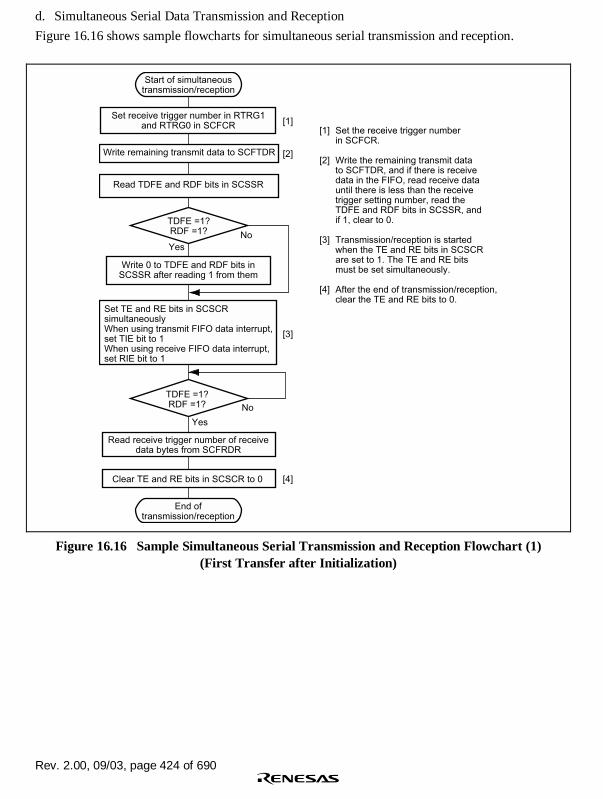
Rev. 2.00, 09/03, page 424 of 690
d. Simultaneous Serial Data Transmission and Reception
Figure 16.16 shows sample flowcharts for simultaneous serial transmission and reception.
No
Yes
No
Yes
[1] Set the receive trigger number in SCFCR.
[2] Write the remaining transmit data to SCFTDR, and if there is receive data in the FIFO, read receive data until there is less than the receive trigger setting number, read the TDFE and RDF bits in SCSSR, and if 1, clear to 0.
[3] Transmission/reception is started when the TE and RE bits in SCSCR are set to 1. The TE and RE bits must be set simultaneously.
[4] After the end of transmission/reception, clear the TE and RE bits to 0.
Start of simultaneoustransmission/reception
Set receive trigger number in RTRG1and RTRG0 in SCFCR
Write remaining transmit data to SCFTDR
Read TDFE and RDF bits in SCSSR
TDFE =1?RDF =1?
Write 0 to TDFE and RDF bits inSCSSR after reading 1 from them
Set TE and RE bits in SCSCRsimultaneouslyWhen using transmit FIFO data interrupt,set TIE bit to 1When using receive FIFO data interrupt,set RIE bit to 1
TDFE =1?RDF =1?
Read receive trigger number of receivedata bytes from SCFRDR
Clear TE and RE bits in SCSCR to 0
End oftransmission/reception
[2]
[1]
[3]
[4]
Figure 16.16 Sample Simultaneous Serial Transmission and Reception Flowchart (1)(First Transfer after Initialization)

Rev. 2.00, 09/03, page 425 of 690
No
Yes
Yes
No
Yes
No
Wait
[1] Set the receive trigger number and transmit trigger number in SCFCR.
[2] Reset the receive FIFO and transmit FIFO.
[3] Write transmit data to SCFTDR, and if there is receive data in the FIFO, read receive data until there is less than the receive trigger setting number, read the TDFE and RDF bits in SCSSR, and if 1, clear to 0.
[4] Wait for one bit interval.
[5] Transmission/reception is started when the TE and RE bits in SCSCR are set to 1. The TE and RE bits must be set simultaneously.
[6] After the end of transmission/reception, clear the TE and RE bits to 0.
Start of simultaneoustransmission/reception
Set receive trigger number in RTRG1and RTRG0 in SCFCR, and set transmit
trigger number in TTRG1 and TTRG0
Set TFRST and RFRST bits inSCFCR to 1
Clear TFRST and RFRST bits inSCFCR to 0
Write transmit data to SCFTDR
Read TDFE and RDF bits in SCSSR
TDFE =1?RDF =1?
Write 0 to TDFE and RDF bits inSCSSR after reading 1 from them
1-bit interval elapsed?
Set TE and RE bits in SCSCRsimultaneouslyWhen using transmit FIFO datainterrupt, set TIE bit to 1When using receive FIFO datainterrupt, set RIE bit to 1
TDFE =1?RDF =1?
Read receive trigger number ofreceive data bytes from SCFRDR
End oftransmission/reception
Clear TE and RE bits in SCSCR to 0
[1]
[2]
[3]
[4]
[5]
[6]
Figure 16.16 Sample Simultaneous Serial Transmission and Reception Flowchart (2)(Second and Subsequent Transfer)

Rev. 2.00, 09/03, page 426 of 690
16.5 SCIF Interrupt Sources and DMAC
The SCIF supports six interrupts in asynchronous mode—transmit-FIFO-data-empty (TXI),transmit-data-stop (TDI), receive-error (ERI), receive-FIFO-data-full (RXI), break-receive (BRI),and receive-data-ready (DRI). The vectors of transmit-data-stop and transmit-FIFO-data-emptyinterrupts are the same. The vectors of receive-error and break-receive interrupts are the same. Thevectors of receive-FIFO-data-full and receive-data-ready interrupts are the same.
In clock synchronous mode, the SCIF supports two interrupts—transmit-FIFO-data-empty (TXI)and receive-FIFO-data-full (RXI).
Table 16.4 shows the interrupt sources. The interrupt sources can be enabled or disabled by meansof the TIE, RIE, ERIE, BRIE, DRIE, and TSIE bits in SCSCR.
When the TDFE flag in SCSSR is set to 1, a TXI interrupt request is generated. When the TSFflag in SCSSR is set to 1, a TDI interrupt request is generated. The DMAC can be activated anddata transfer performed on generation of TXI and TDI interrupt requests. The DMAC requests ofTXI and TDI are assigned to the same vector.
When the RDF flag in SCSSR is set to 1, an RXI interrupt request is generated. The DMAC canbe activated and data transfer performed on generation of an RXI interrupt request.
When using the DMAC for transmission/reception, set and enable the DMAC before making SCIFsettings. See section 8, Direct Memory Access Controller (DMAC), for details of the DMACsetting procedure.
When the ER flag in SCSSR is set to 1, an ERI interrupt request is generated. When the BRK flagin SCSSR is set to 1, a BRI interrupt request is generated. When the DR flag in SCSSR is set to 1,a DRI interrupt request is generated. When the TSF flag in SCSSR is set to 1, a TDI interruptrequest is generated.
The vectors of TXI and TDI, ERI and BRI, and RXI and DRI are the same.
The DMAC activation and interrupts cannot be generated simultaneously by the same source. Thefollowing procedure should be used for the DMAC activation.
1. Set the interrupt enable bits (TIE and RIE) corresponding to the generated source to 1.
2. Mask the corresponding interrupt requests by using the interrupt mask register of the interruptcontroller.

Rev. 2.00, 09/03, page 427 of 690
Table 16.4 SCIF Interrupt Sources
Interrupt Source Description DMAC Activation
ERI Interrupt initiated by receive error flag (ER) or breakflag (BRK)
Not possible
RXI Interrupt initiated by receive FIFO data full flag (RDF)or receive data ready (DR)
Possible*1
TXI Interrupt initiated by transmit FIFO dataempty flag (TDFE) or transmit data stop flag (TSF)
Possible*2
Notes: 1. The DMAC can be activated only by a receive-FIFO-data-full interrupt request.2. The DMAC can be activated by a transmit-FIFO-data-empty (TDFE) or transmit-data-
stop (TSF) interrupt request. When the DMAC is activated by the TSF interrupt, it iscleared by either of two cases listed below.(1) The TSF flag is read by the CPU.(2) The transmit FIFO is full.
See section 5, Exception Handling, for priorities and the relationship with non-SCIF interrupts.

Rev. 2.00, 09/03, page 428 of 690
16.6 Notes on Usage
Note the following when using the SCIF.
a. SCFTDR Writing and the TDFE Flag:
The TDFE flag in the serial status register (SCSSR) is set when the number of transmit data byteswritten in the transmit FIFO data register (SCFTDR) has fallen to or below the transmit triggernumber set by bits TTRG1 and TTRG0 in the FIFO control register (SCFCR). After TDFE is set,transmit data up to the number of empty bytes in SCFTDR can be written, allowing efficientcontinuous transmission.
However, if the number of data bytes written in SCFTDR is equal to or less than the transmittrigger number, the TDFE flag will be set to 1 again after being read as 1 and cleared to 0. TDFEclearing should therefore be carried out when SCFTDR contains more than the transmit triggernumber of transmit data bytes.
The number of transmit data bytes in SCFTDR can be found from the 14 to 8 bits of the FIFO datacount register (SCFDR).
b. SCFRDR Reading and the RDF Flag:
The RDF flag in the serial status register (SCSSR) is set when the number of receive data bytes inthe receive FIFO data register (SCFRDR) has become equal to or greater than the receive triggernumber set by bits RTRG1 and RTRG0 in the FIFO control register (SCFCR). After RDF is set,receive data equivalent to the trigger number can be read from SCFRDR, allowing efficientcontinuous reception.
However, if the number of data bytes in SCFRDR is still equal to or greater than the triggernumber after a read, the RDF flag will be set to 1 again if it is cleared to 0. RDF should thereforebe cleared to 0 after being read as 1 after all receive data has been read.
The number of receive data bytes in SCFRDR can be found from the 6 to 0 bits of the FIFO datacount register (SCFDR).
c. Break Detection and Processing:
Break signals can be detected by reading the RxD pin directly when a framing error (FER) isdetected. In the break state the input from the RxD pin consists of all 0s, so the FER flag is set andthe parity error flag (PER) may also be set.
Although the SCIF stops transferring receive data to SCFRDR after receiving a break, the receiveoperation continues.

Rev. 2.00, 09/03, page 429 of 690
d. Receive Data Sampling Timing and Receive Margin:
As an example, when the sampling rate is 1/16, the SCIF operates on a base clock with afrequency of 8 times the transfer rate.
In reception, the SCIF synchronizes internally with the fall of the start bit, which it samples on thebase clock. Receive data is latched at the rising edge of the fourth base clock pulse.
The receive margin can therefore be expressed as shown in equation (1).
M = 0.5 − 1
2N
D − 0.5
N− (L − 0.5)F − (1 + F) × 100% .......................... (1)
M: Receive margin (%)N: Ratio of clock frequency to bit rate (N = 16)D: Clock duty cycle (D = 0 to 1.0)L: Frame length (L = 9 to 12)F: Absolute deviation of clock frequency
From equation (1), if F = 0 and D = 0.5, the receive margin is 46.875%, as given by equation (2).
When D = 0.5 and F = 0:
M = (0.5 – 1/(2 × 16)) × 100% = 46.875% ........................................... (2)
This is a theoretical value. A reasonable margin to allow in system designs is 20% to 30%.

Rev. 2.00, 09/03, page 430 of 690

IFIRDA0A_000020020100 Rev. 2.00, 09/03, page 431 of 690
Section 17 Infrared Data Association Module (IrDA)
This LSI has an on-chip Infrared Data Association (IrDA) interface that is based on the IrDA 1.0system and can perform infrared communication.
The IrDA is an optional module used for modulation and demodulation of signals for the SCIFmodule, and it must always be used together with the SCIF module.
17.1 Features
• Conforms to the IrDA 1.0 system
• Asynchronous serial communication
Data length: 8 bits
Stop bit length: 1 bit
Parity bit: None
• On-chip 64-stage FIFO buffers for both transmit and receive operations
• On-chip baud rate generator with selectable bit rates
• Guard functions to protect the receiver during transmission
• Clock supply halted to reduce power consumption when not using the IrDA interface
Figure 17.1 shows a block diagram of the IrDA.
SCIF
TxD
Transfer clock
RxD
Switching IrDA/SCIF
IrDA
IrTx
IrRx
Modulation unit
Demodulation unit
Legend
SCIF: Serial communication interface with FIFO
Figure 17.1 Block Diagram of IrDA

Rev. 2.00, 09/03, page 432 of 690
17.2 Input/Output Pins
Table 17.1 shows the IrDA pin configuration.
Table 17.1 Pin Configuration
Pin Name Signal Name I/O Function
Receive data pin IrRx Input Receive data input
Transmit data pin IrTx Output Transmit data output
Note: Clock input from the serial clock pin cannot be set in IrDA mode.
17.3 Register Description
The IrDA has the following internal registers. For details on register addresses and register statesin each processing state, refer to section 24, List of Registers.
• IrDA mode register (SCSMR_Ir)
17.3.1 IrDA Mode Register (SCSMR_Ir)
SCSMR_Ir is a 16-bit register that selects IrDA or SCIF mode and selects the IrDA output pulsewidth.
This module operates as IrDA when the IRMOD bit is set to 1. When the IRMOD bit is cleared to0, this module can also operate as an SCIF.

Rev. 2.00, 09/03, page 433 of 690
Bit Bit Name Initial Value R/W Description
15 to 8 0 R Reserved
These bits are always read as 0. The writevalue should always be 0.
7 IRMOD 0 R/W IrDA Mode
Selects whether this module operates as anIrDA serial communication interface or as anSCIF.
0: Operates as an SCIF
1: Operates as an IrDA
6 to 3 ICK3 to ICK0 0 R/W Output Pulse Division Ratio
Specifies the ratio for dividing the peripheralclock (Pφ) to generate the IRCLK clock pulseto be used for IrDA. IRCLK is obtained asfollows:
IRCLK = 1/(2N + 2) × Pφ
N = Value set by ICK3 to ICK0
2 PSEL 0 R/W Output Pulse Width Select
PSEL selects an IrDA output pulse width thatis 3/16 of the bit length for 115 kbps or 3/16 ofthe bit length for the selected baud rate.
0: Pulse width is 3/16 of the bit length
1: Pulse width is 3/16 of 115 kbps bit length forthe baud rate selected by ICK3 to ICK0
1, 0 0 R Reserved
These bits are always read as 0. The writevalue should always be 0.
Example:
Pφ clock: 14.7456 MHz
IRCLK: 921.6 kHz (fixed)
N: Setting of ICK3 to ICK0 (0 ≤ N ≤ 15)
– 1 ≥ 7 N ≥ Pφ
2×IRCLK
Accordingly, N is 7.

Rev. 2.00, 09/03, page 434 of 690
17.4 Operation
The IrDA module can perform infrared communication conforming to IrDA 1.0 by connectinginfrared transmit/receive units. The serial communication interface unit includes a buffer in thetransmit unit and the receive unit, allowing CPU overhead to be reduced and continuous high-speed communication to be performed.
17.4.1 Overview
The IrDA module modifies IrTx/IrRx transmit/receive data waveforms to satisfy the IrDA 1.0specification for infrared communication.
In the IrDA 1.0 specification, communication is first performed at a speed of 9600 bps, and thecommunication speed is changed. However, the communication rate cannot be automaticallychanged in this module, so the communication speed should be confirmed, and the appropriatespeed set for this module by software.
17.4.2 Transmitting
The waveforms of a serial output signal (UART frame) from the SCIF are modified and the signalis converted into the IR frame serial output signal by the IrDA module, as shown in figure 17.2.
When serial data is 0, a pulse of 3/16 the IR frame bit width is generated and output. When serialdata is 1, no pulse is output.

Rev. 2.00, 09/03, page 435 of 690
17.4.3 Receiving
Received 3/16 IR frame bit-width pulses are demodulated and converted to a UART frame, asshown in figure 17.2.
Demodulation to 0 is performed for pulse output, and demodulation to 1 is performed for no pulseoutput.
0 1 0 1 0 0 1 1 0 1
0 1 0 1 0 0 1 1 0 1
UART frame
Start bit
IR frame
Start bit
Bit cycle 3/16-bit cycle
pulse width
UART frame
Data
IR frame
Data
Receive
Transmit
Stop bit
Stop bit
Figure 17.2 Transmit/Receive Operation
17.4.4 Data Format Specification
The data format of UART frames used for IrDA communication must be specified by the SCIF0registers. The UART frame has eight data bits, no parity bit, and one stop bit.
IrDA communication is performed in asynchronous mode, and this mode must also be specifiedby the SCIF0 registers. The sampling rate must be set to 1/16.
The internal clock must be selected for the SCIF0 operation clock and the SCK0 pin must bespecified for the synchronizing clock output pin.
The IrDA communication rate is the same as the SCIF0 bit rate, which is specified by the SCIF0registers.
For details on SCIF0 registers, refer to section 16, Serial Communication Interface with FIFO(SCIF).

Rev. 2.00, 09/03, page 436 of 690

IFUSB40A_000020020100 Rev. 2.00, 09/03, page 437 of 690
Section 18 USB Function Module
This LSI incorporates a USB function module (USB).
18.1 Features
• The UDC (USB device controller) conforming to USB2.0 and transceiver process USBprotocol automatically.
Automatic processing of USB standard commands for endpoint 0 (some commands andclass/vendor commands require decoding and processing by firmware)
• Transfer speed: Full-speed
• Endpoint configuration:
EndpointName Abbreviation Transfer Type
MaximumPacket Size
FIFO BufferCapacity (Byte) DMA Transfer
Endpoint 0 EP0s Setup 8 8 —
EP0i Control-in 8 8 —
EP0o Control-out 8 8 —
Endpoint 1 EP1 Bulk-out 64 128 Possible
Endpoint 2 EP2 Bulk-in 64 128 Possible
Endpoint 3 EP3 Interrupt 8 8 —
Configuration 1 Interface 0 Alternate Setting 0 Endpoint 1
Endpoint 2
Endpoint 3
• Interrupt requests: Generates various interrupt signals necessary for USBtransmission/reception
• Clock: External input (48 MHz) (Refer to section 9.4.1, Frequency Control Register (FRQCR),and section 9.4.2, USB Clock Frequency Control Register (UCLKCR))
• Power-down mode
Power consumption can be reduced by stopping UDC internal clock when USB cable isdisconnected
Automatic transition to/recovery from suspend state
• Can be connected to a Philips PDIUSBP11 Series transceiver or compatible product in internaltransceiver bypass mode (the XVEROFF bit in XVERCR is set to 1)
When using a compatible product, carry out evaluation and investigation with themanufacturer supplying the transceiver beforehand.
• Power mode: Self-powered

Rev. 2.00, 09/03, page 438 of 690
Figure 18.1 shows the block diagram of the USB.
Peripheral bus
Interrupt requests
DMA transfer requestsStatus and
control registers
FIFO
UDC
Transceiver
USB function module
D+
D-
Clock (48 MHz)
UDC: USB device controller
Legend:
Figure 18.1 Block Diagram of USB

Rev. 2.00, 09/03, page 439 of 690
18.2 Input/Output Pins
Table 18.1 shows the USB pin configuration.
Table 18.1 Pin Configuration
Pin Name I/O FunctionXVEROFFCondition
XVDATA Input Input pin for receive data from differential receiver 1
DPLS Input Input pin to driver for D+ signal from receiver 1
DMNS Input Input pin to driver for D– signal from receiver 1
TXDPLS Output D+ transmit output pin to driver 1
TXDMNS Output D- transmit output pin to driver 1
TXENL Output Driver output enable pin 1
VBUS Input USB cable connection monitor pin 1 or 0
SUSPND Output Transceiver suspend state output pin 1
EXTAL_USB Input USB clock input pin (external clock input/crystalresonator connect)
XTAL_USB Output USB clock pin (crystal resonator connect)
D+ I/O USB internal transceiver D+
D- I/O USB internal transceiver D–
Vcc-USB Input Power supply for USB
Vss-USB Input Ground for USB
Note: The USB can be connected to a Philips PDIUSBP11 Series transceiver or compatibleproduct in internal transceiver bypass mode (the XVEROFF bit in XVERCR is set to 1).When using a compatible product, carry out evaluation and investigation with themanufacturer supplying the transceiver beforehand.

Rev. 2.00, 09/03, page 440 of 690
18.3 Register Descriptions
The USB has following registers. For the information on the addresses of these registers and thestate of the register in each processing condition, see section 24, List of Registers.
• Interrupt flag register 0 (IFR0)
• Interrupt flag register 1 (IFR1)
• Interrupt select register 0 (ISR0)
• Interrupt select register 1 (ISR1)
• Interrupt enable register 0 (IER0)
• Interrupt enable register 1 (IER1)
• EP0i data register (EPDR0i)
• EP0o data register (EPDR0o)
• EP0s data register (EPDR0s)
• EP1 data register (EPDR1)
• EP2 data register (EPDR2)
• EP3 data register (EPDR3)
• EP0o receive data size register (EPSZ0o)
• EP1 receive data size register (EPSZ1)
• Trigger register (TRG)
• Data status register (DASTS)
• FIFO clear register (FCLR)
• DMA transfer setting register (DMAR)
• Endpoint stall register (EPSTL)
• Transceiver control register (XVERCR)

Rev. 2.00, 09/03, page 441 of 690
18.3.1 Interrupt Flag Register 0 (IFR0)
IFR0, together with interrupt flag register 1 (IFR1), indicates interrupt status information requiredby the application. When an interrupt source is generated, the corresponding bit is set to 1 and aninterrupt request is sent to the CPU according to the combination with interrupt enable register 0(IER0). Clearing is performed by writing 0 to the bit to be cleared, and 1 to the other bits.However, EP1FULL and EP2EMPTY are status bits, and cannot be cleared.
Bit Bit NameInitialValue R/W Description
7 BRST 0 R/W Bus Reset
This bit is set to 1 when a bus reset signal is detected onthe USB bus.
6 EP1FULL 0 R EP1 FIFO Full
This bit is set when endpoint 1 receives one packet ofdata successfully from the host, and holds a value of 1 aslong as there is valid data in the FIFO buffer.
This is a status bit, and cannot be cleared.
5 EP2TR 0 R/W EP2 Transfer Request
This bit is set if there is no valid transmit data in the FIFObuffer when an IN token for endpoint 2 is received fromthe host. A NACK handshake is returned to the host untildata is written to the FIFO buffer and packet transmissionis enabled.
4 EP2EMPTY 1 R EP2 FIFO Empty
This bit is set when at least one of the dual endpoint 2transmit FIFO buffers is ready for transmit data to bewritten.
This is a status bit, and cannot be cleared.
3 SETUPTS 0 R/W Setup Command Receive Complete
This bit is set to 1 when endpoint 0 receives successfullya setup command requiring decoding on the applicationside, and returns an ACK handshake to the host.
2 EP0oTS 0 R/W EP0o Receive Complete
This bit is set to 1 when endpoint 0 receives data from thehost successfully, stores the data in the FIFO buffer, andreturns an ACK handshake to the host.

Rev. 2.00, 09/03, page 442 of 690
Bit Bit NameInitialValue R/W Description
1 EP0iTR 0 R/W EP0i Transfer Request
This bit is set if there is no valid transmit data in the FIFObuffer when an IN token for endpoint 0 is received fromthe host. A NACK handshake is returned to the host untildata is written to the FIFO buffer and packet transmissionis enabled.
0 EP0iTS 0 R/W EP0i Transmit Complete
This bit is set when data is transmitted to the host fromendpoint 0 and an ACK handshake is returned.
18.3.2 Interrupt Flag Register 1 (IFR1)
IFR1, together with interrupt flag register 0 (IFR0), indicates interrupt status information requiredby the application. When an interrupt source is generated, the corresponding bit is set to 1 and aninterrupt request is sent to the CPU according to the combination with interrupt enable register 1(IER1). Clearing is performed by writing 0 to the bit to be cleared, and 1 to the other bits.
Bit Bit NameInitialValue R/W Description
7 to 4 0 R Reserved
These bits are always read as 0. The write value shouldalways be 0.
3 VBUSMN 0 R This is a status bit which monitors the state of the VBUSpin. This bit reflects the state of the VBUS pin.
2 EP3TR 0 R/W EP3 Transfer Request
This bit is set if there is no valid transmit data in the FIFObuffer when an IN token for endpoint 3 is received fromthe host. A NACK handshake is returned to the host untildata is written to the FIFO buffer and packet transmissionis enabled.
1 EP3TS 0 R/W EP3 Transmit Complete
This bit is set when data is transmitted to the host fromendpoint 3 and an ACK handshake is returned.
0 VBUS 0 R/W USB Disconnection Detection
When the function is connected to the USB bus ordisconnected from it, this bit is set to 1. The VBUS pin ofthis module is used for detecting connection ordisconnection.

Rev. 2.00, 09/03, page 443 of 690
18.3.3 Interrupt Select Register 0 (ISR0)
ISR0 selects the vector numbers of the interrupt requests indicated in interrupt flag register 0(IFR0). If the USB issues an interrupt request to the INTC when a bit in ISR0 is cleared to 0, theinterrupt corresponding to the bit will be USI0 (USB interrupt 0). If the USB issues an interruptrequest to the INTC when a bit in ISR0 is set to 1, the corresponding interrupt will be USI1 (USBinterrupt 1). If interrupts occur simultaneously, USI0 has priority by default.
Bit Bit Name Initial Value R/W Description
7 BRST 0 R/W Bus Reset
6 EP1FULL 0 R/W EP1 FIFO Full
5 EP2TR 0 R/W EP2 Transfer Request
4 EP2EMPTY 0 R/W EP2 FIFO Empty
3 SETUPTS 0 R/W Setup Command Receive Complete
2 EP0oTS 0 R/W EP0o Receive Complete
1 EP0iTR 0 R/W EP0i Transfer Request
0 EP0iTS 0 R/W EP0i Transmit Complete
18.3.4 Interrupt Select Register 1 (ISR1)
ISR1 selects the vector numbers of the interrupt requests indicated in interrupt flag register 1(IFR1). If the USB issues an interrupt request to the INTC when a bit in ISR1 is cleared to 0, theinterrupt corresponding to the bit will be USI0 (USB interrupt 0). If the USB issues an interruptrequest to the INTC when a bit in ISR1 is set to 1, the corresponding interrupt will be USI1 (USBinterrupt 1). If interrupts occur simultaneously, USI0 has priority by default.
Bit Bit Name Initial Value R/W Description
7 to 3 0 R Reserved
These bits are always read as 0. The write valueshould always be 0.
2 EP3TR 1 R/W EP3 Transfer Request
1 EP3TS 1 R/W EP3 Transmit Complete
0 VBUS 1 R/W USB Bus Connect

Rev. 2.00, 09/03, page 444 of 690
18.3.5 Interrupt Enable Register 0 (IER0)
IER0 enables the interrupt requests of interrupt flag register 0 (IFR0). When an interrupt flag is setto 1 while the corresponding bit of each interrupt is set to 1, an interrupt request is sent to theCPU. The interrupt vector number is determined by the contents of interrupt select register 0(ISR0).
Bit Bit Name Initial Value R/W Description
7 BRST 0 R/W Bus Reset
6 EP1FULL 0 R/W EP1 FIFO Full
5 EP2TR 0 R/W EP2 Transfer Request
4 EP2EMPTY 1 R/W EP2 FIFO Empty
3 SETUPTS 0 R/W Setup Command Receive Complete
2 EP0oTS 0 R/W EP0o Receive Complete
1 EP0iTR 0 R/W EP0i Transfer Request
0 EP0iTS 0 R/W EP0i Transmit Complete
18.3.6 Interrupt Enable Register 1 (IER1)
IER1 enables the interrupt requests of interrupt flag register 1 (IFR1). When an interrupt flag is setto 1 while the corresponding bit of each interrupt is set to 1, an interrupt request is sent to theCPU. The interrupt vector number is determined by the contents of interrupt select register 1(ISR1).
Bit Bit Name Initial Value R/W Description
7 to 3 0 R Reserved
These bits are always read as 0. The write valueshould always be 0.
2 EP3TR 0 R/W EP3 Transfer Request
1 EP3TS 0 R/W EP3 Transmit Complete
0 VBUS 0 R/W USB Bus Connect

Rev. 2.00, 09/03, page 445 of 690
18.3.7 EP0i Data Register (EPDR0i)
EPDR0i is an 8-byte transmit FIFO buffer for endpoint 0. EPDR0i holds one packet of transmitdata for control-in. Transmit data is fixed by writing one packet of data and setting EP0iPKTE inthe trigger register. When an ACK handshake is returned from the host after the data has beentransmitted, EP0iTS in interrupt flag register 0 is set. This FIFO buffer can be initialized by meansof EP0iCLR in the FCLR register.
Bit Bit Name Initial Value R/W Description
7 to 0 D7 to D0 Undefined W Data register for control-in transfer
18.3.8 EP0o Data Register (EPDR0o)
EPDR0o is an 8-byte receive FIFO buffer for endpoint 0. EPDR0o holds endpoint 0 receive dataother than setup commands. When data is received successfully, EP0oTS in interrupt flag register0 is set, and the number of receive bytes is indicated in the EP0o receive data size register. Afterthe data has been read, setting EP0oRDFN in the trigger register enables the next packet to bereceived. This FIFO buffer can be initialized by means of BP0oCLR in the FCLR register.
Bit Bit Name Initial Value R/W Description
7 to 0 D7 to D0 Undefined R Data register for control-out transfer
18.3.9 EP0s Data Register (EPDR0s)
EPDR0s is an 8-byte FIFO buffer specifically for receiving endpoint 0 setup commands. Only thesetup command to be processed by the application is received. When command data is receivedsuccessfully, the SETUPTS bit in interrupt flag register 0 is set.
As a latest setup command must be received in high priority, if data is left in this buffer, it will beoverwritten with new data. If reception of the next command is started while the current commandis being read, command reception has priority, the read by the application is forcibly stopped, andthe read data is invalid.
Bit Bit Name Initial Value R/W Description
7 to 0 D7 to D0 Undefined R Data register for storing the setup command atthe control-out transfer

Rev. 2.00, 09/03, page 446 of 690
18.3.10 EP1 Data Register (EPDR1)
EPDR1 is a 128-byte receive FIFO buffer for endpoint 1. EPDR1 has a dual-buffer configuration,and has a capacity of twice the maximum packet size. When one packet of data is receivedsuccessfully, EP1FULL in interrupt flag register 0 is set, and the number of receive bytes isindicated in the EP1 receive data size register. After the data has been read, the buffer that wasread is enabled to receive data again by writing 1 to the EP1RDFN bit in the trigger register. Thereceive data in this FIFO buffer can be transferred by DMA. This FIFO buffer can be initialized bymeans of EP1CLR in the FCLR register.
Bit Bit Name Initial Value R/W Description
7 to 0 D7 to D0 Undefined R Data register for endpoint 1 transfer
18.3.11 EP2 Data Register (EPDR2)
EPDR2 is a 128-byte transmit FIFO buffer for endpoint 2. EPDR2 has a dual-buffer configuration,and has a capacity of twice the maximum packet size. When transmit data is written to this FIFObuffer and EP2PKTE in the trigger register is set, one packet of transmit data is fixed, and thedual-FIFO buffer is switched over. The transmit data for this FIFO buffer can be transferred byDMA. This FIFO buffer can be initialized by means of EP2CLR in the FCLR register.
Bit Bit Name Initial Value R/W Description
7 to 0 D7 to D0 Undefined W Data register for endpoint 2 transfer
18.3.12 EP3 Data Register (EPDR3)
EPDR3 is an 8-byte transmit FIFO buffer for endpoint 3. EPDR3 holds one packet of transmit datafor the interrupt transfer of endpoint 3. Transmit data is fixed by writing one packet of data andsetting EP3PKTE in the trigger register. When an ACK handshake is returned from the host afterone packet of data has been transmitted successfully, EP3TS in interrupt flag register 0 is set. ThisFIFO buffer can be initialized by means of EP3CLR in the FCLR register.
Bit Bit Name Initial Value R/W Description
7 to 0 D7 to D0 Undefined R Data register for endpoint 3 transfer

Rev. 2.00, 09/03, page 447 of 690
18.3.13 EP0o Receive Data Size Register (EPSZ0o)
EPSZ0o indicates the number of bytes received at endpoint 0 from the host.
Bit Bit Name Initial Value R/W Description
7 to 0 — 0 R Number of receive data for endpoint 0
18.3.14 EP1 Receive Data Size Register (EPSZ1)
EPSZ1 is a receive data size resister for endpoint 1. EPSZ1 indicates the number of bytes receivedfrom the host. The FIFO for endpoint 1 has a dual-buffer configuration. The size of the receiveddata indicated by this register is the size of the currently selected side (can be read by CPU).
Bit Bit Name Initial Value R/W Description
7 to 0 — 0 R Number of received bytes for endpoint 1

Rev. 2.00, 09/03, page 448 of 690
18.3.15 Trigger Register (TRG)
TRG generates one-shot triggers to control the transfer sequence for each endpoint.
Bit Bit Name Initial Value R/W Description
7 Undefined Reserved
The write value should always be 0.
6 EP3PKTE Undefined W EP3 Packet Enable
After one packet of data has been written to theendpoint 3 transmit FIFO buffer, the transmit data isfixed by writing 1 to this bit.
5 EP1RDFN Undefined W EP1 Read Complete
Write 1 to this bit after one packet of data has beenread from the endpoint 1 FIFO buffer. The endpoint1 receive FIFO buffer has a dual-bufferconfiguration. Writing 1 to this bit initializes the FIFOthat was read, enabling the next packet to bereceived.
4 EP2PKTE Undefined W EP2 Packet Enable
After one packet of data has been written to theendpoint 2 transmit FIFO buffer, the transmit data isfixed by writing 1 to this bit.
3 Undefined Reserved
The write value should always be 0.
2 EP0sRDFN Undefined W EP0s Read Complete
Write 1 to this bit after data for the EP0s commandFIFO has been read. Writing 1 to this bit enablestransfer of data in the following data stage. A NACKhandshake is returned in response to transferrequests from the host in the data stage until 1 iswritten to this bit.
1 EP0oRDFN Undefined W EP0o Read Complete
Writing 1 to this bit after one packet of data hasbeen read from the endpoint 0 transmit FIFO bufferinitializes the FIFO buffer, enabling the next packetto be received.
0 EP0iPKTE Undefined W EP0i Packet Enable
After one packet of data has been written to theendpoint 0 transmit FIFO buffer, the transmit data isfixed by writing 1 to this bit.

Rev. 2.00, 09/03, page 449 of 690
18.3.16 Data Status Register (DASTS)
DASTS indicates whether the transmit FIFO buffers contain valid data. A bit is set when data iswritten to the corresponding FIFO buffer and the packet enable state is set, and cleared when alldata has been transmitted to the host.
Bit Bit Name Initial Value R/W Description
7, 6 0 R Reserved
This bit is always read as 0.
5 EP3DE 0 R EP3 Data Present
This bit is set when the endpoint 3 FIFO buffercontains valid data.
4 EP2DE 0 R EP2 Data Present
This bit is set when the endpoint 2 FIFO buffercontains valid data.
3 to 1 0 R Reserved
This bit is always read as 0.
0 EP0iDE 0 R EP0i Data Present
This bit is set when the endpoint 0 FIFO buffercontains valid data.
18.3.17 FIFO Clear Register (FCLR)
FCLR is a register to initialize the FIFO buffers for each endpoint. Writing 1 to a bit clears all thedata in the corresponding FIFO buffer. Note that the corresponding interrupt flag is not cleared.Do not clear a FIFO buffer during transfer.
Bit Bit Name Initial Value R/W Description
7 Undefined Reserved
The write value should always be 0.
6 EP3CLR Undefined W EP3 Clear
Writing 1 to this bit initializes the endpoint 3 transmitFIFO buffer.
5 EP1CLR Undefined W EP1 Clear
Writing 1 to this bit initializes both sides of theendpoint 1 receive FIFO buffer.

Rev. 2.00, 09/03, page 450 of 690
Bit Bit Name Initial Value R/W Description
4 EP2CLR Undefined W EP2 Clear
Writing 1 to this bit initializes both sides of theendpoint 2 transmit FIFO buffer.
3, 2 Undefined Reserved
The write value should always be 0.
1 EP0oCLR Undefined W EP0o Clear
Writing 1 to this bit initializes the endpoint 0 receiveFIFO buffer.
0 EP0iCLR Undefined W EP0i Clear
Writing 1 to this bit initializes the endpoint 0 transmitFIFO buffer.
18.3.18 DMA Transfer Setting Register (DMAR)
DMA transfer can be carried out between the endpoint 1 and 2 data registers and memory bymeans of the on-chip direct memory access controller (DMA). Dual address transfer is performedin bytes. To start DMA transfer, DMAC settings must be made in addition to the settings in thisregister.
Bit Bit Name Initial Value R/W Description
7 to 2 0 R Reserved
These bits are always read as 0. The write value shouldalways be 0.

Rev. 2.00, 09/03, page 451 of 690
Bit Bit Name Initial Value R/W Description
1 EP2DMAE 0 R/W Endpoint 2 DMA Transfer Enable
When this bit is set, DMA transfer is enabled frommemory to the endpoint 2 transmit FIFO buffer. If there isat least one byte of space in the FIFO buffer, a transferrequest is asserted for the DMAC. In DMA transfer, when64 bytes are written to the FIFO buffer the EP2 packetenable bit is set automatically, allowing 64 bytes of datato be transferred, and if there is still space in the other ofthe two FIFOs, a transfer request is asserted for theDMAC again. However, if the size of the data packet tobe transmitted is less than 64 bytes, the EP2 packetenable bit is not set automatically, and so should be setby the CPU with a DMA transfer end interrupt.
As EP2-related interrupt requests to the CPU are notautomatically masked, interrupt requests should bemasked as necessary in the interrupt enable register.
• Operating procedure
1. Write of 1 to the EP2 DMAE bit in DMAR
2. Transfer count setting in the DMAC
3. DMAC activation
4. DMA transfer
5. DMA transfer end interrupt generated
Refer to section 18.7.3, DMA Transfer for Endpoint 2.

Rev. 2.00, 09/03, page 452 of 690
Bit Bit Name Initial Value R/W Description
0 EP1DMAE 0 R/W Endpoint 1 DMA Transfer Enable
When this bit is set, DMA transfer is enabled from theendpoint 1 receive FIFO buffer to memory. If there is atleast one byte of receive data in the FIFO buffer, atransfer request is asserted for the DMAC. In DMAtransfer, when all the received data is read, EP1 is readautomatically and the completion trigger operates.
EP1-related interrupt requests to the CPU are notautomatically masked.
• Operating procedure:
1. Write of 1 to the EP1 DMAE bit in DMAR
2. Transfer count setting in the DMAC
3. DMAC activation
4. DMA transfer
5. DMA transfer end interrupt generated
Refer to section 18.7.2, DMA Transfer for Endpoint 1.

Rev. 2.00, 09/03, page 453 of 690
18.3.19 Endpoint Stall Register (EPSTL)
The bits in EPSTL are used to forcibly stall the endpoints on the application side. While a bit is setto 1, the corresponding endpoint returns a stall handshake to the host. The stall bit for endpoint 0 iscleared automatically on reception of 8-byte command data for which decoding is performed bythe function and the EP0 STL bit is cleared. When the SETUPTS flag in the IFR0 register is set to1, writing 1 to the EP0 STL bit is ignored. For detailed operation, see section 18.6, StallOperations.
Bit Bit Name Initial Value R/W Description
7 to 4 0 R Reserved
These bits are always read as 0. The write valueshould always be 0.
3 EP3STL 0 R/W EP3 Stall
When this bit is set to 1, endpoint 3 is placed in thestall state.
2 EP2STL 0 R/W EP2 Stall
When this bit is set to 1, endpoint 2 is placed in thestall state.
1 EP1STL 0 R/W EP1 Stall
When this bit is set to 1, endpoint 1 is placed in thestall state.
0 EP0STL 0 R/W EP0 Stall
When this bit is set to 1, endpoint 0 is placed in thestall state.
18.3.20 Transceiver Control Register (XVERCR)
The Transceiver Control Register sets either the internal transceiver or external transceiver for use.
Bit Bit Name Initial Value R/W Description
7 to 1 0 R Reserved
These bits are always read as 0. The write valueshould always be 0.
0 XVEROFF 0 R/W Transceiver Control
1: The internal transceiver function is stopped and adigital signal for the external transceiver is outputfrom the port.
0: The internal transceiver is operated.

Rev. 2.00, 09/03, page 454 of 690
18.4 Operation
18.4.1 Cable Connection
Cable disconnected
VBUS pin = 0 V
UDC core reset
USB cable connection
IFR1.VBUS = 1
USB bus connection interrupt
UDC core reset release
Bus reset reception
IFR0.BRST = 1
Bus reset interrupt
Wait for setup command
reception complete interrupt
USB function Application
General output port
D+ pull-up enabled?
USB module interrupt
setting
As soon as preparations are
completed, enable D+ pull-up
in general output port
Clear VBUS flag
(IFR1.VBUS)
Firmware preparations for
start of USB communication
Clear bus reset flag
(IFR0.BRST)
Clear FIFOs(EP0, EP1, EP2, EP3)
Yes
No
Initial
settings
Wait for setup command
reception complete interrupt
Interrupt request
Interrupt request
Figure 18.2 Cable Connection Operation
The above flowchart shows the operation in the case of in section 18.8, Example of USB ExternalCircuitry.
In applications that do not require USB cable connection to be detected, processing by the USBbus connection interrupt is not necessary. Preparations should be made with the bus-resetinterrupt.

Rev. 2.00, 09/03, page 455 of 690
18.4.2 Cable Disconnection
USB function Application
Cable connected
VBUS pin = 1
USB cable disconnection
VBUS pin = 0
UDC core reset
End
Figure 18.3 Cable Disconnection Operation
The above flowchart shows the operation in section 18.8, Example of USB External Circuitry.
18.4.3 Control Transfer
Control transfer consists of three stages: setup, data (not always included), and status (figure 18.4).The data stage comprises a number of bus transactions. Operation flowcharts for each stage areshown below.
Control-in
Setup stage Data stage Status stage
Control-out
No data
SETUP(0)
DATA0
SETUP(0)
DATA0
SETUP(0)
DATA0
IN(1)
DATA1
OUT(1)
DATA1
IN(0)
DATA0
OUT(0)
. . .
. . .
DATA0
IN(0/1)
DATA0/1
OUT(0/1)
DATA0/1
OUT(1)
DATA1
IN(1)
DATA1
IN(1)
DATA1
Figure 18.4 Transfer Stages in Control Transfer

Rev. 2.00, 09/03, page 456 of 690
1. Setup Stage
USB function Application
SETUP token reception
Receive 8-byte command
data in EP0s
To data stage
Set setup command
reception complete flag
(IFR0.SETUP TS = 1)
Automatic
processing by
this module
Clear SETUP TS flag
(IFR0.SETUP TS = 0)
Clear EP0i FIFO (CLR.EP0iCLR = 1)
Clear EP0o FIFO (CLR.EP0oCLR = 1)
Read 8-byte data from EP0s
Decode command data
Determine data stage direction*1
Write 1 to EP0s read complete bit
(TRG.EP0s RDFN = 1)
To control-in
data stage
To control-out
data stage
Command
to be processed by
application?
Interrupt request
Yes
No
Notes: 1. In the setup stage, the application analyzes command data from the host requiring processing by
the application, and determines the subsequent processing (for example, data stage direction, etc.).
2. When the transfer direction is control-out, the EP0i transfer request interrupt required in the status
stage should be enabled here. When the transfer direction is control-in, this interrupt is not required
and should be disabled.
*2
Figure 18.5 Setup Stage Operation

Rev. 2.00, 09/03, page 457 of 690
2. Data Stage (Control-In)
USB function Application
IN token reception
Data transmission to host
Set EP0i transmission
complete flag
(IFR0.EP0i TS = 1)
From setup stage
Write data to EP0i
data register (EPDR0i)
Write 1 to EP0i packet
enable bit
(TRG.EP0i PKTE = 1)
Clear EP0i transmission
complete flag
(IFR0.EP0i TS = 0)
Write 1 to EP0i packet
enable bit
(TRG.EP0i PKTE = 1)
Write data to EP0i
data register (EPDR0i)
1 written
to TRG.EP0s
RDFN?
Valid data
in EP0i FIFO?
NACK
NACK
No
No
Yes
Yes
ACK
Interrupt request
Figure 18.6 Data Stage (Control-In) Operation
The application first analyzes command data from the host in the setup stage, and determines thesubsequent data stage direction. If the result of command data analysis is that the data stage is in-transfer, one packet of data to be sent to the host is written to the FIFO. If there is more data to besent, this data is written to the FIFO after the data written first has been sent to the host (EP0iTSbit in IFR0 = 1).
The end of the data stage is identified when the host transmits an OUT token and the status stageis entered.
Note: If the size of the data transmitted by the function is smaller than the data size requested bythe host, the function indicates the end of the data stage by returning to the host a packetshorter than the maximum packet size. If the size of the data transmitted by the function isan integral multiple of the maximum packet size, the function indicates the end of the datastage by transmitting a zero-length packet.

Rev. 2.00, 09/03, page 458 of 690
3. Data Stage (Control-Out)
USB function Application
OUT token reception
Data reception from host
OUT token reception
Set EP0o reception
complete flag
(IFR0.EP0o TS = 1)
Clear EP0o reception
complete flag
(IFR0.EP0o TS = 0)
Read data from EP0o
receive data size register
(EPSZ0o)
Write 1 to EP0o read
complete bit
(TRG.EP0o RDFN = 1)
Read data from EP0o
data register (EPDR0o)
1 written
to TRG.EP0s
RDFN?
1 written
to TRG.EP0o
RDFN?
NACK
NACK
ACK
No
Yes
No
Yes
Interrupt request
Figure 18.7 Data Stage (Control-Out) Operation
The application first analyzes command data from the host in the setup stage, and determines thesubsequent data stage direction. If the result of command data analysis is that the data stage is out-transfer, the application waits for data from the host, and after data is received (EP0oTS bit inIFR0 = 1), reads data from the FIFO. Next, the application writes 1 to the EP0o read complete bit,empties the receive FIFO, and waits for reception of the next data.
The end of the data stage is identified when the host transmits an IN token and the status stage isentered.

Rev. 2.00, 09/03, page 459 of 690
4. Status Stage (Control-In)
USB function Application
OUT token reception
0-byte reception from host
End of control transfer
Set EP0o reception
complete flag
(IFR0.EP0o TS = 1)
Clear EP0o reception
complete flag
(IFR0.EP0o TS = 0)
Write 1 to EP0o read
complete bit
(TRG.EP0o RDFN = 1)
End of control transfer
ACK
Interrupt request
Figure 18.8 Status Stage (Control-In) Operation
The control-in status stage starts with an OUT token from the host. The application receives 0-bytedata from the host, and ends control transfer.

Rev. 2.00, 09/03, page 460 of 690
5. Status Stage (Control-Out)
USB function Application
IN token reception
0-byte transmission to host
End of control transfer
Set EP0i transmission
complete flag
(IFR0.EP0i TS = 1)
Clear EP0i transfer
request flag
(IFR0.EP0i TR = 0)
Write 1 to EP0i packet
enable bit
(TRG.EP0i PKTE = 1)
Clear EP0i transmission
complete flag
(IFR0.EP0i TS = 0)
End of control transfer
Valid data
in EP0i FIFO?
ACK
Yes
No
NACK
Interrupt request
Interrupt request
Figure 18.9 Status Stage (Control-Out) Operation
The control-out status stage starts with an IN token from the host. When an IN-token is received atthe start of the status stage, there is not yet any data in the EP0i FIFO, and so an EP0i transferrequest interrupt is generated. The application recognizes from this interrupt that the status stagehas started. Next, in order to transmit 0-byte data to the host, 1 is written to the EP0i packet enablebit but no data is written to the EP0i FIFO. As a result, the next IN token causes 0-byte data to betransmitted to the host, and control transfer ends.
After the application has finished all processing relating to the data stage, 1 should be written tothe EP0i packet enable bit.

Rev. 2.00, 09/03, page 461 of 690
18.4.4 EP1 Bulk-Out Transfer (Dual FIFOs)
USB function Application
OUT token reception
Data reception from host
Set EP1 FIFO full status
(IFR0.EP1 FULL = 1)
Clear EP1 FIFO full status
(IFR0.EP1 FULL = 0)
Read EP1 receive data
size register (EPSZ1)
Read data from EP1
data register (EPDR1)
Write 1 to EP1 read
complete bit
(TRG.EP1 RDFN = 1)
Space
in EP1 FIFO?No
Yes
Both
EP1 FIFOs empty?No
Yes
NACK
ACK
Interrupt request
Interrupt request
Figure 18.10 EP1 Bulk-Out Transfer Operation
EP1 has two 64-byte FIFOs, but the user can receive data and read receive data without beingaware of this dual-FIFO configuration.
When one FIFO is full after reception is completed, the EP1FULL bit in IFR0 is set. After the firstreceive operation into one of the FIFOs when both FIFOs are empty, the other FIFO is empty, andso the next packet can be received immediately. When both FIFOs are full, NACK is returned tothe host automatically. When reading of the receive data is completed following data reception, 1is written to the EP1RDFN bit in TRG. This operation empties the FIFO that has just been read,and makes it ready to receive the next packet.

Rev. 2.00, 09/03, page 462 of 690
18.4.5 EP2 Bulk-In Transfer (Dual FIFOs)
USB function Application
IN token reception
Data transmission to host
Clear EP2 transfer
request flag
(IFR0.EP2 TR = 0)
Enable EP2 FIFO
empty interrupt
(IER0.EP2 EMPTY = 1)
IER0.EP2 EMPTY
interrupt
Write one packet of data
to EP2 data register
(EPDR2)
Write 1 to EP2 packet
enable bit
(TRG.EP2 PKTE = 1)
Set EP2
empty status
(IFR0.EP2
EMPTY = 1)
Valid data
in EP2 FIFO?NACK
ACK
Interrupt request
Yes
No
Clear EP2 empty status
(IFR0.EP2 EMPTY = 0)
Space
in EP2 FIFO?
No
Yes
Interrupt
request
Figure 18.11 EP2 Bulk-In Transfer Operation
EP2 has two 64-byte FIFOs, but the user can transmit data and write transmit data without beingaware of this dual-FIFO configuration. However, one data write is performed for one FIFO. Forexample, even if both FIFOs are empty, it is not possible to perform EP2PKTE at one time afterconsecutively writing 128 bytes of data. EP2PKTE must be performed for each 64-byte write.
When performing bulk-in transfer, as there is no valid data in the FIFOs on reception of the firstIN token, an EP2TR bit interrupt in IFR0 is requested. With this interrupt, 1 is written to theEP2EMPTY bit in IER0, and the EP2 FIFO empty interrupt is enabled. At first, both EP2 FIFOsare empty, and so an EP2 FIFO empty interrupt is generated immediately.
The data to be transmitted is written to the data register using this interrupt. After the first transmitdata write for one FIFO, the other FIFO is empty, and so the next transmit data can be written tothe other FIFO immediately. When both FIFOs are full, EP2 EMPTY is cleared to 0. If at least oneFIFO is empty, the EP2EMPTY bit in IFR0 is set to 1. When ACK is returned from the host after
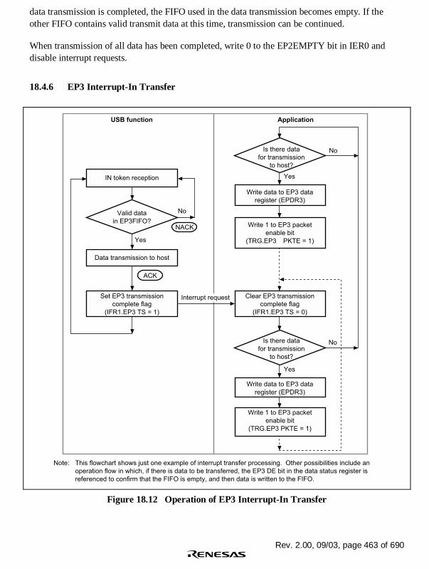
Rev. 2.00, 09/03, page 463 of 690
data transmission is completed, the FIFO used in the data transmission becomes empty. If theother FIFO contains valid transmit data at this time, transmission can be continued.
When transmission of all data has been completed, write 0 to the EP2EMPTY bit in IER0 anddisable interrupt requests.
18.4.6 EP3 Interrupt-In Transfer
USB function Application
IN token reception
Data transmission to host
Set EP3 transmission
complete flag
(IFR1.EP3 TS = 1)
Write data to EP3 data
register (EPDR3)
Write 1 to EP3 packet
enable bit
(TRG.EP3 PKTE = 1)
Clear EP3 transmission
complete flag
(IFR1.EP3 TS = 0)
Write data to EP3 data
register (EPDR3)
Write 1 to EP3 packet
enable bit
(TRG.EP3 PKTE = 1)
Valid data
in EP3FIFO?
Is there data
for transmission
to host?
Is there data
for transmission
to host?
No
Yes
No
Yes
No
Yes
NACK
ACK
Note: This flowchart shows just one example of interrupt transfer processing. Other possibilities include an
operation flow in which, if there is data to be transferred, the EP3 DE bit in the data status register is
referenced to confirm that the FIFO is empty, and then data is written to the FIFO.
Interrupt request
Figure 18.12 Operation of EP3 Interrupt-In Transfer

Rev. 2.00, 09/03, page 464 of 690
18.5 Processing of USB Standard Commands and Class/VendorCommands
18.5.1 Processing of Commands Transmitted by Control Transfer
A command transmitted from the host by control transfer may require decoding and execution ofcommand processing on the application side. Whether command decoding is required on theapplication side is indicated in table 18.2 below.
Table 18.2 Command Decoding on Application Side
Decoding not Necessary on Application Side Decoding Necessary on Application Side
Clear Feature
Get Configuration
Get Interface
Get Status
Set Address
Set Configuration
Set Feature
Set Interface
Get Descriptor
Class/Vendor command
Set Descriptor
Sync Frame
If decoding is not necessary on the application side, command decoding and data stage and statusstage processing are performed automatically. No processing is necessary by the user. An interruptis not generated in this case.
If decoding is necessary on the application side, this module stores the command in the EP0sFIFO. After reception is completed successfully, the IFR0/SETUP TS flag is set and an interruptrequest is generated. In the interrupt routine, eight bytes of data must be read from the EP0s dataregister (EPDR0s) and decoded by firmware. The necessary data stage and status stage processingshould then be carried out according to the result of the decoding operation.

Rev. 2.00, 09/03, page 465 of 690
18.6 Stall Operations
18.6.1 Overview
This section describes stall operations in this module. There are two cases in which the USBfunction module stall function is used:
• When the application forcibly stalls an endpoint for some reason
• When a stall is performed automatically within the USB function module due to a USBspecification violation
The USB function module has internal status bits that hold the status (stall or non-stall) of eachendpoint. When a transaction is sent from the host, the module references these internal status bitsand determines whether to return a stall to the host. These bits cannot be cleared by theapplication; they must be cleared with a Clear Feature command from the host.
18.6.2 Forcible Stall by Application
The application uses the EPSTL register to issue a stall request for the USB function module.When the application wishes to stall a specific endpoint, it sets the corresponding bit in EPSTL (1-1 in figure 18.13). The internal status bits are not changed at this time. When a transaction is sentfrom the host for the endpoint for which the EPSTL bit was set, the USB function modulereferences the internal status bit, and if this is not set, references the corresponding bit in EPSTL(1-2 in figure 18.13). If the corresponding bit in EPSTL is set, the USB function module sets theinternal status bit and returns a stall handshake to the host (1-3 in figure 18.13). If thecorresponding bit in EPSTL is not set, the internal status bit is not changed and the transaction isaccepted.
Once an internal status bit is set, it remains set until cleared by a Clear Feature command from thehost, without regard to the EPSTL register. Even after a bit is cleared by the Clear Featurecommand (3-1 in figure 18.13), the USB function module continues to return a stall handshakewhile the bit in EPSTL is set, since the internal status bit is set each time a transaction is executedfor the corresponding endpoint (1-2 in figure 18.13). To clear a stall, therefore, it is necessary forthe corresponding bit in EPSTL to be cleared by the application, and also for the internal status bitto be cleared with a Clear Feature command (2-1, 2-2, and 2-3 in figure 18.13).

Rev. 2.00, 09/03, page 466 of 690
(1) Transition from normal operation to stall (1-1)
Transaction request
USB
Reference(1-2)
STALL handshakeStall
To (2-1) or (3-1)
Normal status restored
(1-3)
(2) When Clear Feature is sent after EPSTL is cleared (2-1)
STALL handshake
Transaction request
(2-2)
Clear Feature command
Clear Feature command
(2-3)
(3) When Clear Feature is sent before EPSTL is cleared to 0 (3-1)
1. 1 written to EPSTL by application
1. IN/OUT token received from host
2. EPSTL referenced
1. Transmission of STALL handshake
1. Internal status bit cleared to 0
1. Internal status bit cleared to 0
2. EPSTL not changed
1. 1 set in EPSTL2. Internal status bit
set to 13. Transmission of
STALL handshake
1. EPSTL cleared to 0 by application
2. IN/OUT token received from host
3. Internal status bit already set to 1
4. EPSTL not referenced
5. Internal status bit not changed
To (1-2)
Internal status bit0
EPSTL0 → 1
Internal status bit0
EPSTL
1
Internal status bit
0 → 1
EPSTL
1
Internal status bit
1
EPSTL1 → 0
Internal status bit
1
EPSTL
0
Internal status bit
1 → 0
EPSTL
0
Internal status bit
1 → 0
EPSTL
1
Figure 18.13 Forcible Stall by Application

Rev. 2.00, 09/03, page 467 of 690
18.6.3 Automatic Stall by USB Function Module
When a stall setting is made with the Set Feature command, or in the event of a USB specificationviolation, the USB function module automatically sets the internal status bit for the relevantendpoint without regard to the EPSTL register, and returns a stall handshake (1-1 in figure 18.14).
Once an internal status bit is set, it remains set until cleared by a Clear Feature command from thehost, without regard to the EPSTL register. After a bit is cleared by the Clear Feature command,EPSTL is referenced (3-1 in figure 18.14). The USB function module continues to return a stallhandshake while the internal status bit is set, since the internal status bit is set even if a transactionis executed for the corresponding endpoint (2-1 and 2-2 in figure 18.14). To clear a stall, therefore,the internal status bit must be cleared with a Clear Feature command (3-1 in figure 18.14). If setby the application, EPSTL should also be cleared (2-1 in figure 18.14).
(1) Transition from normal operation to stall (1-1)
(2) When transaction is performed when internal status bit is set, and Clear Feature is sent (2-1)
STALL handshake
Transaction request
STALL handshake
(2-2)
Clear Feature command
(3) When Clear Feature is sent before transaction is performed (3-1)
1. In case of USB specification violation, etc., USB function module stalls endpoint automatically
1. Transmission of STALL handshake
1. Internal status bit cleared to 0
2. EPSTL not changed
1. EPSTL cleared to 0 by application
2. IN/OUT token received from host
3. Internal status bit already set to 1
4. EPSTL not referenced
5. Internal status bit not changed
Normal status restored
Internal status bit0 → 1
EPSTL0
Internal status bit1
EPSTL0
Internal status bit1
EPSTL
0
Internal status bit1 → 0
EPSTL
0
Stall status maintained
To (2-1) or (3-1)
Figure 18.14 Automatic Stall by USB Function Module

Rev. 2.00, 09/03, page 468 of 690
18.7 DMA Transfer
18.7.1 Overview
DMA transfer can be performed for endpoints 1 and 2 in this module. Note that word or longworddata cannot be transferred.
When endpoint 1 holds at least one byte of valid receive data, a DMA request for endpoint 1 isgenerated. When endpoint 2 holds no valid data, a DMA request for endpoint 2 is generated.
If the DMA transfer is enabled by setting the EP1DMAE bit to 1 in the DMA transfer settingregister, zero-length data reception at endpoint 1 is ignored. When the DMA transfer is enabled,the RDFN bit for EP1 and PKTE bit for EP2 do not need to be set to 1 in TRG (note that thePKTE bit must be set to 1 when the transfer data is less than the maximum number of bytes).When all the data received at EP1 is read, the FIFO automatically enters the EMPTY state. Whenthe maximum number of bytes (64 bytes) are written to the EP2 FIFO, the FIFO automaticallyenters the FULL state, and the data in the FIFO can be transmitted (see figures 18.15 and 18.16).
18.7.2 DMA Transfer for Endpoint 1
When the data received at EP1 is transferred by the DMAC, the USB function moduleautomatically performs the same processing as writing 1 to the RDFN bit in TRG if the currentlyselected FIFO becomes empty. Accordingly, in DMA transfer, do not write 1 to the RDFN bit inTRG. If the user writes 1 to the RDFN bit in DMA transfer, correct operation cannot beguaranteed.
Figure 18.15 shows an example of receiving 150 bytes of data from the host. In this case, internalprocessing which is the same as writing 1 to the RDFN bit in TRG is automatically performedthree times. This internal processing is performed when the currently selected data FIFO becomesempty. Accordingly, this processing is automatically performed both when 64-byte data is sentand when data less than 64 bytes is sent.
RDFN
(Automatically
performed)
RDFN
(Automatically
performed)
RDFN
(Automatically
performed)
64 bytes 64 bytes 22 bytes
Figure 18.15 RDFN Bit Operation for EP1

Rev. 2.00, 09/03, page 469 of 690
18.7.3 DMA Transfer for Endpoint 2
When the transmit data at EP2 is transferred by the DMAC, the USB function moduleautomatically performs the same processing as writing 1 to the PKTE bit in TRG if the currentlyselected FIFO (64 bytes) becomes full. Accordingly, to transfer data of a multiple of 64 bytes, theuser need not write 1 to the PKTE bit. To transfer data of less than 64 bytes, the user must write 1to the PKTE bit using the DMA transfer end interrupt of the on-chip DMAC. If the user writes 1 tothe PKTE bit when the maximum number of bytes (64 bytes) are transferred, correct operationcannot be guaranteed.
Figure 18.16 shows an example for transmitting 150 bytes of data to the host. In this case, internalprocessing which is the same as writing 1 to the PKTE bit in TRG is automatically performedtwice. This internal processing is performed when the currently selected data FIFO becomes full.Accordingly, this processing is automatically performed only when 64-byte data is sent.
When the last 22 bytes are sent, the internal processing for writing 1 to the PKTE bit is notperformed, and the user must write 1 to the PKTE bit by software. In this case, the application hasno more data to transfer but the USB function module continues to output DMA requests for EP2as long as the FIFO has an empty space. When all data has been transferred, write 0 to theEP2DMAE bit in DMAR to cancel DMA requests for EP2.
PKTE
(Automatically
performed)
PKTE
(Automatically
performed)
PKTE is
not performed
Execute by DMA transfer
end interrupt (user)
64 bytes 64 bytes 22 bytes
Figure 18.16 PKTE Bit Operation for EP2

Rev. 2.00, 09/03, page 470 of 690
18.8 Example of USB External Circuitry
1. USB Transceiver
A USB transceiver IC (such as a PDIUSBP11) should be connected externally when nointernal transceiver is used. The USB transceiver manufacturer should be consulted concerningthe recommended circuit from the USB transceiver to the USB connector, etc.
2. D+ Pull-Up Control
In a system where it is wished to disable USB host/hub connection notification (D+ pull-up)(during high-priority processing or initialization processing, for example), D+ pull-up shouldbe controlled using a general output port. However, if a USB cable is already connected to thehost/hub and D+ pull-up is prohibited, D+ and D– will both go low (both of D+ and D– pulleddown on the host/hub side) and the USB module will mistakenly identify this as reception of aUSB bus reset from the host. Therefore, the D+ pull-up control signal and VBUS pin inputsignal should be controlled using a general output port and the USB cable VBUS (ANDcircuit) as shown in figure 18.17. (The UDC core in this LSI maintains the powered state whenthe VBUS pin is low, regardless of the D+/D– state.)
3. Detection of USB Cable Connection/Disconnection
As USB states, etc., are managed by hardware in this module, a VBUS signal that recognizesconnection/disconnection is necessary. The power supply signal (VBUS) in the USB cable isused for this purpose. However, if the cable is connected to the USB host/hub when thefunction (system installing this LSI) power is off, a voltage (5 V) will be applied from the USBhost/hub. Therefore, an IC (such as an HD74LV1G08A or 2G08A) that allows voltageapplication when the system power is off should be connected externally.

Rev. 2.00, 09/03, page 471 of 690
VBUS
EXTAL_USB
VBUS
GND
D+D+
D-D-
5V
3V
General output port,
etc.
This LSI
USB module
48 MHz
IC allowing voltageapplication when system(LSI) power is off
IC allowing voltageapplication when system(LSI) power is off
USBconnector
USBcable
Note: Operation is not guaranteed with this sample circuit.
If external surge and ESD noise countermeasures are required for the system,
a protective diode or the noise canceler should be used for this purpose.
Figure 18.17 Example of USB Function Module External Circuitry(Internal Transceiver)

Rev. 2.00, 09/03, page 472 of 690
VBUS
VBUS
TXENLTXDMNSTXDPLS
XVDATA
DPLS
GND
DMNS
SUSPND
+-
SUSPND
PDIUSBP11 etc
VM
VP
RCV
OE
SPEED
VMOVPO
D+
D-
5V
3V
General output port,
etc.
USB module
IC allowing voltageapplication when system(LSI) power is off
IC allowing voltageapplication when system(LSI) power is off
USBconnector
USBcable
Note: Operation is not guaranteed with this sample circuit.
If external surge and ESD noise countermeasures are required for the system,
a protective diode or the noise canceler should be used for this purpose.
This LSI
EXTAL_USB
48 MHz
Figure 18.18 Example of USB Function Module External Circuitry(External Transceiver)

Rev. 2.00, 09/03, page 473 of 690
18.9 Usage Notes
18.9.1 Receiving Setup Data
Note the following for EPDR0s that receives 8-byte setup data:
1. As a latest setup command must be received in high priority, the write from the USB bus takespriority over the read from the CPU. If the next setup command reception is started while theCPU is reading data after the data is received, the read from the CPU is forcibly terminated.Therefore, the data read after reception is started becomes invalid.
2. EPDR0s must always be read in 8-byte units. If the read is terminated at a midpoint, the datareceived at the next setup cannot be read correctly.
18.9.2 Clearing the FIFO
If a USB cable is disconnected during data transfer, the data being received or transmitted mayremain in the FIFO. When disconnecting a USB cable, clear the FIFO.
While a FIFO is transferring data, it must not be cleared.
18.9.3 Overreading and Overwriting the Data Registers
Note the following when reading or writing to a data register of this module.
(1) Receive data registers
The receive data registers must not be read exceeding the valid amount of receive data, that is, thenumber of bytes indicated by the receive data size register. Even for EPDR1 which has doubleFIFO buffers, the maximum data to be read at one time is 64 bytes. After the data is read from thecurrent valid FIFO buffer, be sure to write 1 to EP1RDFN in TRG, which switches the validbuffer, updates the receive data size to the new number of bytes, and enables the next data to bereceived.
(2) Transmit data registers
The transmit data registers must not be written to exceeding the maximum packet size. Even forEPDR2 which has double FIFO buffers, write data within the maximum packet size at one time.After the data is written, write 1 to PKTE in TRG to switch the valid buffer and enable the nextdata to be written. Data must not be continuously written to the two FIFO buffers.

Rev. 2.00, 09/03, page 474 of 690
18.9.4 Assigning Interrupt Sources to EP0
The EP0-related interrupt sources indicated by the interrupt source bits (bits 0 to 3) in IFR0 mustbe assigned to the same interrupt signal with ISR0. The other interrupt sources have no limitations.
18.9.5 Clearing the FIFO when DMA Transfer Is Enabled
The endpoint 1 data register (EPDR1) cannot be cleared when DMA transfer for endpoint 1 isenabled (EP1 DMAE in DMAR = 1). Cancel DMA transfer before clearing the register.
18.9.6 Notes on TR Interrupt
Note the following when using the transfer request interrupt (TR interrupt) for IN transfer to EP0i,EP2, or EP3.
The TR interrupt flag is set if the FIFO for the target EP has no data when the IN token is sentfrom the USB host. However, at the timing shown in figure 18.19, multiple TR interrupts occursuccessively. Take appropriate measures against malfunction in such a case.
Note: This module determines whether to return NAK if the FIFO of the target EP has no datawhen receiving the IN token, but the TR interrupt flag is set only after a NAK handshakeis sent. If the next IN token is sent before PKTE of TRG is written to, the TR interrupt flagis set again.
CPU
Host IN token IN token IN token
Sets TR flag
(Sets the flag again)
Sets TR flag
Determines whetherto return NAK Transmits data
TR interrupt routine
Clear
TR flag
Writes
transmit data
TRG.
PKTE
TR interrupt routine
USBNAK
Determines whetherto return NAK
NAKACK
Figure 18.19 TR Interrupt Flag Set Timing

Rev. 2.00, 09/03, page 475 of 690
Section 19 Pin Function Controller
19.1 Overview
The pin function controller (PFC) consists of registers to select the pin functions and I/Odirections of multiplex pins. Pin functions and I/O directions can be individually selected for everypin regardless of the LSI operating mode. Table 19.1 lists the multiplex pins of this LSI.
Table 19.1 Multiplex Pins
Port Port Function (Related Module) Other Functions (Related Module)
A PTA7 input/output (port)/PINT7 input (INTC) D23 input/output (BSC)
A PTA6 input/output (port)/PINT6 input (INTC) D22 input/output (BSC)
A PTA5 input/output (port)/PINT5 input (INTC) D21 input/output (BSC)
A PTA4 input/output (port)/PINT4 input (INTC) D20 input/output (BSC)
A PTA3 input/output (port)/PINT3 input (INTC) D19 input/output (BSC)
A PTA2 input/output (port)/PINT2 input (INTC) D18 input/output (BSC)
A PTA1 input/output (port)/PINT1 input (INTC) D17 input/output (BSC)
A PTA0 input/output (port)/PINT0 input (INTC) D16 input/output (BSC)
B PTB7 input/output (port)/PINT15 input (INTC) D31 input/output (BSC)
B PTB6 input/output (port)/PINT14 input (INTC) D30 input/output (BSC)
B PTB5 input/output (port)/PINT13 input (INTC) D29 input/output (BSC)
B PTB4 input/output (port)/PINT12 input (INTC) D28 input/output (BSC)
B PTB3 input/output (port)/PINT11 input (INTC) D27 input/output (BSC)
B PTB2 input/output (port)/PINT10 input (INTC) D26 input/output (BSC)
B PTB1 input/output (port)/PINT9 input (INTC) D25 input/output (BSC)
B PTB0 input/output (port)/PINT8 input (INTC) D24 input/output (BSC)
C PTC7 input/output (port) CS6A output (BSC)
C PTC6 input/output (port) CS5A output (BSC)
C PTC5 input/output (port) CS4 output (BSC)
C PTC4 input/output (port) CS3 output (BSC)
C PTC3 input/output (port) CS2 output (BSC)
C PTC2 input/output (port) WE3 output (BSC)/DQMUU output (BSC)/AH output (BSC)
C PTC1 input/output (port) WE2 output (BSC)/DQMUL output (BSC)
C PTC0 input/output (port) BS output (BSC)

Rev. 2.00, 09/03, page 476 of 690
Port Port Function (Related Module) Other Functions (Related Module)
D PTD7 input/output (port) CS6B output (BSC)
D PTD6 input/output (port) CS5B output (BSC)
D PTD5 input (port) NF*1
D PTD4 input/output (port) CKE output (BSC)
D PTD3 input/output (port) CASU output (BSC)
D PTD2 input/output (port) CASL output (BSC)
D PTD1 input/output (port) RASU output (BSC)
D PTD0 input/output (port) RASL output (BSC)
E PTE7 input/output (port)
E PTE6 input/output (port) TCLK input (TMU)
E PTE5 input/output (port) STATUS1 output (CPG)/CTS0 input (SCIF0)
E PTE4 input/output (port) STATUS0 output (CPG)/RTS0 output (SCIF0)
E PTE3 input/output (port) TEND0 output (DMAC)
E PTE2 input/output (port) IRQ5 input (INTC)
E PTE1 input/output (port) DACK1 output (DMAC)
E PTE0 input/output (port) DACK0 output (DMAC)
F PTF7 input/output (port) ASEMD0 input
F PTF6 input/output (port) ASEBRKAK output
F PTF5 input/output (port) TDO output (UDI)
F PTF4 input/output (port) AUDSYNC output (AUD)
F PTF3 input/output (port) AUDATA3 output (AUD)/TO3 output (TPU)
F PTF2 input/output (port) AUDATA2 output (AUD)/TO2 output (TPU)
F PTF1 input/output (port) AUDATA1 output (AUD)/TO1 output (TPU)
F PTF0 input/output (port) AUDATA0 output (AUD)/TO0 output (TPU)
G PTG7 input/output (port) WAIT input (BSC)
G PTG6 input/output (port) BREQ input (BSC)
G PTG5 input/output (port) BACK output (BSC)
G PTG4 input/output (port) AUDCK output (AUD)
G PTG3 input/output (port) TRST input (UDI)
G PTG2 input/output (port) TMS input (UDI)
G PTG1 input/output (port) TCK input (UDI)
G PTG0 input/output (port) TDI input (UDI)

Rev. 2.00, 09/03, page 477 of 690
Port Port Function (Related Module) Other Functions (Related Module)
H PTH6 input/output (port) DREQ1 input (DMAC)
H PTH5 input/output (port) DREQ0 input (DMAC)
H PTH4 input/output (port) IRQ4 input (INTC)
H PTH3 input/output (port) IRQ3 input (INTC)/IRL3 input (INTC)
H PTH2 input/output (port) IRQ2 input (INTC)/IRL2 input (INTC)
H PTH1 input/output (port) IRQ1 input (INTC)/IRL1 input (INTC)
H PTH0 input/output (port) IRQ0 input (INTC)/IRL0 input (INTC)
J PTJ7 output (port) NF*1
J PTJ6 output (port) NF*1
J PTJ5 output (port) NF*1
J PTJ4 output (port) NF*1
J PTJ3 output (port) NF*1
J PTJ2 output (port) NF*1
J PTJ1 output (port) NF*1
J PTJ0 output (port) NF*1
K PTK7 input/output (port) A25 output (BSC)
K PTK6 input/output (port) A24 output (BSC)
K PTK5 input/output (port) A23 output (BSC)
K PTK4 input/output (port) A22 output (BSC)
K PTK3 input/output (port) A21 output (BSC)
K PTK2 input/output (port) A20 output (BSC)
K PTK1 input/output (port) A19 output (BSC)
K PTK0 input/output (port) A0 output (BSC)
L PTL3 input (port) AN3 input (ADC)
L PTL2 input (port) AN2 input (ADC)
L PTL1 input (port) AN1 input (ADC)
L PTL0 input (port) AN0 input (ADC)
M PTM6 input/output (port) VBUS input (USB)
M PTM4 input (port) NF*1
M PTM3 input/output (port)
M PTM2 input/output (port)
M PTM1 input/output (port)
M PTM0 input/output (port)

Rev. 2.00, 09/03, page 478 of 690
Port Port Function (Related Module) Other Functions (Related Module)
N PTN7 input/output (port)
N PTN6 input/output (port) DPLS input (USB)
N PTN5 input/output (port) DMNS input (USB)
N PTN4 input/output (port) TXDPLS output (USB)
N PTN3 input/output (port) TXDMNS output (USB)
N PTN2 input/output (port) XVDATA input (USB)
N PTN1 input/output (port) TXENL output (USB)
N PTN0 input/output (port) SUSPND output (USB)
SCPT SCPT5 input/output (port) CTS2 input (SCIF2)
SCPT SCPT4 input/output (port) RTS2 output (SCIF2)
SCPT SCPT3 input/output (port) SCK2 input/output (SCIF2)
SCPT SCPT2 input (port)*2 RXD2 input (SCIF2)
SCPT SCPT2 output (port)*2 TXD2 output (SCIF2)
SCPT SCPT1 input/output (port) SCK0 input/output (SCIF0)
SCPT SCPT0 input (port)*2 RXD0 input (SCIF0)/IrRX input (IrDA)
SCPT SCPT0 output (port)*2 TXD0 output (SCIF0)/IrTX output (IrDA)
Notes: 1. The initial functions of NF (No Function) pins are not assigned after power-on reset.Specifies the functions with Pin Function Controller (PFC).PTD5 and PTM4 must be pulled up.PTJ[7:0] must be open except for the pins specified as port output pins.The values of PTJ6, PTJ1, and PTJ0 differ during power-on reset and after the power-on reset state is released. They conform to the port J data register value after beingswitched to port status by the pin function controller (PFC).
After Power-On Reset Release
During Power-On Reset PTD5/NF = 1 PTD5/NF = 0
PTJ6/NF 1 0 1
PTJ1/NF 1 1 0
PTJ0/NF 1 0 1
2. SCPT0 and SCPT2 each have two separate pins for input and output, however, acommon data register is accessed.
In table 19.1, pin functions in the shaded column can be used immediately after a power-on reset.

Rev. 2.00, 09/03, page 479 of 690
19.2 Register Descriptions
The PFC has the following registers. For details on register addresses and access sizes, see section24, List of Registers.
• Port A control register (PACR)
• Port B control register (PBCR)
• Port C control register (PCCR)
• Port D control register (PDCR)
• Port E control register (PECR)
• Port E control register 2 (PECR2)
• Port F control register (PFCR)
• Port F control register 2 (PFCR2)
• Port G control register (PGCR)
• Port H control register (PHCR)
• Port J control register (PJCR)
• Port K control register (PKCR)
• Port L control register (PLCR)
• Port M control register (PMCR)
• Port N control register (PNCR)
• Port N control register 2 (PNCR2)
• Port SC control register (SCPCR)
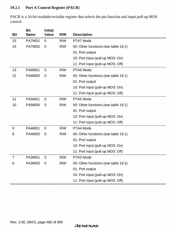
Rev. 2.00, 09/03, page 480 of 690
19.2.1 Port A Control Register (PACR)
PACR is a 16-bit readable/writable register that selects the pin function and input pull-up MOScontrol.
BitBitName
InitialValue R/W Description
15
14
PA7MD1
PA7MD0
0
0
R/W
R/W
PTA7 Mode
00: Other functions (see table 19.1)
01: Port output
10: Port input (pull-up MOS: On)
11: Port input (pull-up MOS: Off)
13
12
PA6MD1
PA6MD0
0
0
R/W
R/W
PTA6 Mode
00: Other functions (see table 19.1)
01: Port output
10: Port input (pull-up MOS: On)
11: Port input (pull-up MOS: Off)
11
10
PA5MD1
PA5MD0
0
0
R/W
R/W
PTA5 Mode
00: Other functions (see table 19.1)
01: Port output
10: Port input (pull-up MOS: On)
11: Port input (pull-up MOS: Off)
9
8
PA4MD1
PA4MD0
0
0
R/W
R/W
PTA4 Mode
00: Other functions (see table 19.1)
01: Port output
10: Port input (pull-up MOS: On)
11: Port input (pull-up MOS: Off)
7
6
PA3MD1
PA3MD0
0
0
R/W
R/W
PTA3 Mode
00: Other functions (see table 19.1)
01: Port output
10: Port input (pull-up MOS: On)
11: Port input (pull-up MOS: Off)

Rev. 2.00, 09/03, page 481 of 690
BitBitName
InitialValue R/W Description
5
4
PA2MD1
PA2MD0
0
0
R/W
R/W
PTA2 Mode
00: Other functions (see table 19.1)
01: Port output
10: Port input (pull-up MOS: On)
11: Port input (pull-up MOS: Off)
3
2
PA1MD1
PA1MD0
0
0
R/W
R/W
PTA1 Mode
00: Other functions (see table 19.1)
01: Port output
10: Port input (pull-up MOS: On)
11: Port input (pull-up MOS: Off)
1
0
PA0MD1
PA0MD0
0
0
R/W
R/W
PTA0 Mode
00: Other functions (see table 19.1)
01: Port output
10: Port input (pull-up MOS: On)
11: Port input (pull-up MOS: Off)
19.2.2 Port B Control Register (PBCR)
PBCR is a 16-bit readable/writable register that selects the pin function and input pull-up MOScontrol.
BitBitName
InitialValue R/W Description
15
14
PB7MD1
PB7MD0
0
0
R/W
R/W
PTB7 Mode
00: Other functions (see table 19.1)
01: Port output
10: Port input (pull-up MOS: On)
11: Port input (pull-up MOS: Off)
13
12
PB6MD1
PB6MD0
0
0
R/W
R/W
PTB6 Mode
00: Other functions (see table 19.1)
01: Port output
10: Port input (pull-up MOS: On)
11: Port input (pull-up MOS: Off)

Rev. 2.00, 09/03, page 482 of 690
BitBitName
InitialValue R/W Description
11
10
PB5MD1
PB5MD0
0
0
R/W
R/W
PTB5 Mode
00: Other functions (see table 19.1)
01: Port output
10: Port input (pull-up MOS: On)
11: Port input (pull-up MOS: Off)
9
8
PB4MD1
PB4MD0
0
0
R/W
R/W
PTB4 Mode
00: Other functions (see table 19.1)
01: Port output
10: Port input (pull-up MOS: On)
11: Port input (pull-up MOS: Off)
7
6
PB3MD1
PB3MD0
0
0
R/W
R/W
PTB3 Mode
00: Other functions (see table 19.1)
01: Port output
10: Port input (pull-up MOS: On)
11: Port input (pull-up MOS: Off)
5
4
PB2MD1
PB2MD0
0
0
R/W
R/W
PTB2 Mode
00: Other functions (see table 19.1)
01: Port output
10: Port input (pull-up MOS: On)
11: Port input (pull-up MOS: Off)
3
2
PB1MD1
PB1MD0
0
0
R/W
R/W
PTB1 Mode
00: Other functions (see table 19.1)
01: Port output
10: Port input (pull-up MOS: On)
11: Port input (pull-up MOS: Off)
1
0
PB0MD1
PB0MD0
0
0
R/W
R/W
PTB0 Mode
00: Other functions (see table 19.1)
01: Port output
10: Port input (pull-up MOS: On)
11: Port input (pull-up MOS: Off)

Rev. 2.00, 09/03, page 483 of 690
19.2.3 Port C Control Register (PCCR)
PCCR is a 16-bit readable/writable register that selects the pin function and input pull-up MOScontrol.
BitBitName
InitialValue R/W Description
15
14
PC7MD1
PC7MD0
1
1
R/W
R/W
PTC7 Mode
00: Other functions (see table 19.1)
01: Port output
10: Port input (pull-up MOS: On)
11: Port input (pull-up MOS: Off)
13
12
PC6MD1
PC6MD0
1
1
R/W
R/W
PTC6 Mode
00: Other functions (see table 19.1)
01: Port output
10: Port input (pull-up MOS: On)
11: Port input (pull-up MOS: Off)
11
10
PC5MD1
PC5MD0
0
0
R/W
R/W
PTC5 Mode
00: Other functions (see table 19.1)
01: Port output
10: Port input (pull-up MOS: On)
11: Port input (pull-up MOS: Off)
9
8
PC4MD1
PC4MD0
0
0
R/W
R/W
PTC4 Mode
00: Other functions (see table 19.1)
01: Port output
10: Port input (pull-up MOS: On)
11: Port input (pull-up MOS: Off)
7
6
PC3MD1
PC3MD0
0
0
R/W
R/W
PTC3 Mode
00: Other functions (see table 19.1)
01: Port output
10: Port input (pull-up MOS: On)
11: Port input (pull-up MOS: Off)

Rev. 2.00, 09/03, page 484 of 690
BitBitName
InitialValue R/W Description
5
4
PC2MD1
PC2MD0
0
0
R/W
R/W
PTC2 Mode
00: Other functions (see table 19.1)
01: Port output
10: Port input (pull-up MOS: On)
11: Port input (pull-up MOS: Off)
3
2
PC1MD1
PC1MD0
0
0
R/W
R/W
PTC1 Mode
00: Other functions (see table 19.1)
01: Port output
10: Port input (pull-up MOS: On)
11: Port input (pull-up MOS: Off)
1
0
PC0MD1
PC0MD0
0
0
R/W
R/W
PTC0 Mode
00: Other functions (see table 19.1)
01: Port output
10: Port input (pull-up MOS: On)
11: Port input (pull-up MOS: Off)

Rev. 2.00, 09/03, page 485 of 690
19.2.4 Port D Control Register (PDCR)
PDCR is a 16-bit readable/writable register that selects the pin function and input pull-up MOScontrol.
BitBitName
InitialValue R/W Description
15
14
PD7MD1
PD7MD0
1
1
R/W
R/W
PTD7 Mode
00: Other functions (see table 19.1)
01: Port output
10: Port input (pull-up MOS: On)
11: Port input (pull-up MOS: Off)
13
12
PD6MD1
PD6MD0
1
1
R/W
R/W
PTD6 Mode
00: Other functions (see table 19.1)
01: Port output
10: Port input (pull-up MOS: On)
11: Port input (pull-up MOS: Off)
11
10
PD5MD1
PD5MD0
0
0
R/W
R/W
PTD5 Mode
00: NF
01: Setting prohibited
10: Port input (pull-up MOS: On)
11: Port input (pull-up MOS: Off)
9
8
PD4MD1
PD4MD0
0
0
R/W
R/W
PTD4 Mode
00: Other functions (see table 19.1)
01: Port output
10: Port input (pull-up MOS: On)
11: Port input (pull-up MOS: Off)
7
6
PD3MD1
PD3MD0
1
1
R/W
R/W
PTD3 Mode
00: Other functions (see table 19.1)
01: Port output
10: Port input (pull-up MOS: On)
11: Port input (pull-up MOS: Off)

Rev. 2.00, 09/03, page 486 of 690
BitBitName
InitialValue R/W Description
5
4
PD2MD1
PD2MD0
0
0
R/W
R/W
PTD2 Mode
00: Other functions (see table 19.1)
01: Port output
10: Port input (pull-up MOS: On)
11: Port input (pull-up MOS: Off)
3
2
PD1MD1
PD1MD0
1
1
R/W
R/W
PTD1 Mode
00: Other functions (see table 19.1)
01: Port output
10: Port input (pull-up MOS: On)
11: Port input (pull-up MOS: Off)
1
0
PD0MD1
PD0MD0
0
0
R/W
R/W
PTD0 Mode
00: Other functions (see table 19.1)
01: Port output
10: Port input (pull-up MOS: On)
11: Port input (pull-up MOS: Off)

Rev. 2.00, 09/03, page 487 of 690
19.2.5 Port E Control Register (PECR)
PECR is a 16-bit readable/writable register that selects the pin function and input pull-up MOScontrol.
BitBitName
InitialValue R/W Description
15
14
PE7MD1
PE7MD0
1
0
R/W
R/W
PTE7 Mode
00: Setting prohibited
01: Port output
10: Port input (pull-up MOS: On)
11: Port input (pull-up MOS: Off)
13
12
PE6MD1
PE6MD0
1
0
R/W
R/W
PTE6 Mode
00: Other functions (see table 19.1)
01: Port output
10: Port input (pull-up MOS: On)
11: Port input (pull-up MOS: Off)
11
10
PE5MD1
PE5MD0
0
0
R/W
R/W
PTE5 Mode
00: Other functions (see table 19.1)
01: Port output
10: Port input (pull-up MOS: On)
11: Port input (pull-up MOS: Off)
9
8
PE4MD1
PE4MD0
0
0
R/W
R/W
PTE4 Mode
00: Other functions (see table 19.1)
01: Port output
10: Port input (pull-up MOS: On)
11: Port input (pull-up MOS: Off)
7
6
PE3MD1
PE3MD0
1
0
R/W
R/W
PTE3 Mode
00: Other functions (see table 19.1)
01: Port output
10: Port input (pull-up MOS: On)
11: Port input (pull-up MOS: Off)
5
4
PE2MD1
PE2MD0
1
1
R/W
R/W
PTE2 Mode
00: Other functions (see table 19.1)
01: Port output
10: Port input (pull-up MOS: On)
11: Port input (pull-up MOS: Off)

Rev. 2.00, 09/03, page 488 of 690
BitBitName
InitialValue R/W Description
3
2
PE1MD1
PE1MD0
1
0
R/W
R/W
PTE1 Mode
00: Other functions (see table 19.1)
01: Port output
10: Port input (pull-up MOS: On)
11: Port input (pull-up MOS: Off)
1
0
PE0MD1
PE0MD0
1
0
R/W
R/W
PTE0 Mode
00: Other functions (see table 19.1)
01: Port output
10: Port input (pull-up MOS: On)
11: Port input (pull-up MOS: Off)
19.2.6 Port E Control Register 2 (PECR2)
PECR2 is an 8-bit readable/writable register that selects the pin function.
BitBit Name Initial
Value R/W Description
7, 6 — 0 R Reserved
These bits are always read as 0. The write value shouldalways be 0.
5 PE5MD2 0 R/W PE5 Mode 2
This bit is valid when the PE5MD[1:0] bits in PECR are setto B’00 (other functions).
0: STATUS1 (CPG)
1: CTS0 (SCIF0)
4 PE4MD2 0 R/W PE4 Mode 2
This bit is valid when the PE4MD[1:0] bits in PECR are setto B’00 (other functions).
0: STATUS0 (CPG)
1: RTS0 (SCIF0)
3 to 0 — 0 R Reserved
These bits are always read as 0. The write value shouldalways be 0.

Rev. 2.00, 09/03, page 489 of 690
19.2.7 Port F Control Register (PFCR)
PFCR is a 16-bit readable/writable register that selects the pin function and input pull-up MOScontrol.
BitBitName
InitialValue R/W Description
15
14
PF7MD1
PF7MD0
0
0
R/W
R/W
PTF7 Mode
00: Other functions*2 (see table 19.1)
01: Port output
10: Port input (pull-up MOS: On)
11: Port input (pull-up MOS: Off)
13
12
PF6MD1
PF6MD0
1*1
0
R/W
R/W
PTF6 Mode
00: Other functions (see table 19.1)
01: Port output
10: Port input (pull-up MOS: On)
11: Port input (pull-up MOS: Off)
11
10
PF5MD1
PF5MD0
0
0
R/W
R/W
PTF5 Mode
00: Other functions (see table 19.1)
01: Port output
10: Port input (pull-up MOS: On)
11: Port input (pull-up MOS: Off)
9
8
PF4MD1
PF4MD0
1*1
0
R/W
R/W
PTF4 Mode
00: Other functions (see table 19.1)
01: Port output
10: Port input (pull-up MOS: On)
11: Port input (pull-up MOS: Off)
7
6
PF3MD1
PF3MD0
1*1
0
R/W
R/W
PTF3 Mode
00: Other functions (see table 19.1)
01: Port output
10: Port input (pull-up MOS: On)
11: Port input (pull-up MOS: Off)
5
4
PF2MD1
PF2MD0
1*1
0
R/W
R/W
PTF2 Mode
00: Other functions (see table 19.1)
01: Port output
10: Port input (pull-up MOS: On)
11: Port input (pull-up MOS: Off)

Rev. 2.00, 09/03, page 490 of 690
BitBitName
InitialValue R/W Description
3
2
PF1MD1
PF1MD0
1*1
0
R/W
R/W
PTF1 Mode
00: Other functions (see table 19.1)
01: Port output
10: Port input (pull-up MOS: On)
11: Port input (pull-up MOS: Off)
1
0
PF0MD1
PF0MD0
1*1
0
R/W
R/W
PTF0 Mode
00: Other functions (see table 19.1)
01: Port output
10: Port input (pull-up MOS: On)
11: Port input (pull-up MOS: Off)
Notes: 1. Indicates the initial value when ASEMD0 = 1. When ASEMD0 = 0, the relevant bitbecomes 0, and other functions is selected.
2. Pull-up MOS on.
19.2.8 Port F Control Register 2 (PFCR2)
PFCR2 is an 8-bit readable/writable register that selects the pin function.
BitBitName
InitialValue R/W Description
7 to 4 — 0 R Reserved
These bits are always read as 0. The write value shouldalways be 0.
3 PF3MD2 0 R/W PTF3 Mode 2
This bit is valid when the PF3MD[1:0] bits in PFCR are setto B'00 (other functions).
0: AUDATA3 (AUD)
1: TO3 (TPU)
2 PF2MD2 0 R/W PTF2 Mode 2
This bit is valid when the PF2MD[1:0] bits in PFCR are setto B'00 (other functions).
0: AUDATA2 (AUD)
1: TO2 (TPU)

Rev. 2.00, 09/03, page 491 of 690
BitBitName
InitialValue R/W Description
1 PF1MD2 0 R/W PTF1 Mode 2
This bit is valid when the PF1MD[1:0] bits in PFCR are set toB'00 (other functions).
0: AUDATA1 (AUD)
1: TO1 (TPU)
0 PF0MD2 0 R/W PTF0 Mode 2
This bit is valid when the PF0MD[1:0] bits in PFCR are set toB'00 (other functions).
0: AUDATA0 (AUD)
1: TO0 (TPU)
19.2.9 Port G Control Register (PGCR)
PGCR is a 16-bit readable/writable register that selects the pin function and input pull-up MOScontrol.
BitBitName
InitialValue R/W Description
15
14
PG7MD1
PG7MD0
0
0
R/W
R/W
PTG7 Mode
00: Other functions (see table 19.1)
01: Port output
10: Port input (pull-up MOS: On)
11: Port input (pull-up MOS: Off)
13
12
PG6MD1
PG6MD0
0
0
R/W
R/W
PTG6 Mode
00: Other functions (see table 19.1)
01: Port output
10: Port input (pull-up MOS: On)
11: Port input (pull-up MOS: Off)
11
10
PG5MD1
PG5MD0
0
0
R/W
R/W
PTG5 Mode
00: Other functions (see table 19.1)
01: Port output
10: Port input (pull-up MOS: On)
11: Port input (pull-up MOS: Off)

Rev. 2.00, 09/03, page 492 of 690
BitBitName
InitialValue R/W Description
9
8
PG4MD1
PG4MD0
1*1
0
R/W
R/W
PTG4 Mode
00: Other functions (see table 19.1)
01: Port output
10: Port input (pull-up MOS: On)
11: Port input (pull-up MOS: Off)
7
6
PG3MD1
PG3MD0
0
0
R/W
R/W
PTG3 Mode
00: Other functions*2 (see table 19.1)
01: Port output
10: Port input (pull-up MOS: On)
11: Port input (pull-up MOS: Off)
5
4
PG2MD1
PG2MD0
0
0
R/W
R/W
PTG2 Mode
00: Other functions*2 (see table 19.1)
01: Port output
10: Port input (pull-up MOS: On)
11: Port input (pull-up MOS: Off)
3
2
PG1MD1
PG1MD0
0
0
R/W
R/W
PTG1 Mode
00: Other functions*2 (see table 19.1)
01: Port output
10: Port input (pull-up MOS: On)
11: Port input (pull-up MOS: Off)
1
0
PG0MD1
PG0MD0
0
0
R/W
R/W
PTG0 Mode
00: Other functions*2 (see table 19.1)
01: Port output
10: Port input (pull-up MOS: On)
11: Port input (pull-up MOS: Off)
Notes: 1. Indicates the initial value when ASEMD0 = 1. When ASEMD0 = 0, the relevant bitbecomes 0, and other functions is selected.
2. Pull-up MOS on.

Rev. 2.00, 09/03, page 493 of 690
19.2.10 Port H Control Register (PHCR)
PHCR is a 16-bit readable/writable register that selects the pin function and input pull-up MOScontrol.
BitBitName
InitialValue R/W Description
15, 14 — 0 R Reserved
These bits are always read as 0. The write value shouldalways be 0.
13
12
PH6MD1
PH6MD0
1
1
R/W
R/W
PTH6 Mode
00: Other functions (see table 19.1)
01: Port output
10: Port input (pull-up MOS: On)
11: Port input (pull-up MOS: Off)
11
10
PH5MD1
PH5MD0
1
1
R/W
R/W
PTH5 Mode
00: Other functions (see table 19.1)
01: Port output
10: Port input (pull-up MOS: On)
11: Port input (pull-up MOS: Off)
9
8
PH4MD1
PH4MD0
0
0
R/W
R/W
PTH4 Mode
00: Other functions (see table 19.1)
01: Port output
10: Port input (pull-up MOS: On)
11: Port input (pull-up MOS: Off)
7
6
PH3MD1
PH3MD0
0
0
R/W
R/W
PTH3 Mode
00: Other functions (see table 19.1)
01: Port output
10: Port input (pull-up MOS: On)
11: Port input (pull-up MOS: Off)
5
4
PH2MD1
PH2MD0
0
0
R/W
R/W
PTH2 Mode
00: Other functions (see table 19.1)
01: Port output
10: Port input (pull-up MOS: On)
11: Port input (pull-up MOS: Off)

Rev. 2.00, 09/03, page 494 of 690
BitBitName
InitialValue R/W Description
3
2
PH1MD1
PH1MD0
0
0
R/W
R/W
PTH1 Mode
00: Other functions (see table 19.1)
01: Port output
10: Port input (pull-up MOS: On)
11: Port input (pull-up MOS: Off)
1
0
PH0MD1
PH0MD0
0
0
R/W
R/W
PTH0 Mode
00: Other functions (see table 19.1)
01: Port output
10: Port input (pull-up MOS: On)
11: Port input (pull-up MOS: Off)
19.2.11 Port J Control Register (PJCR)
PJCR is a 16-bit readable/writable register that selects the pin function.
BitBitName
InitialValue R/W Description
15
14
PJ7MD1
PJ7MD0
0
0
R/W
R/W
PTJ7 Mode
00: NF
01: Port output
10: Setting prohibited
11: Setting prohibited
13
12
PJ6MD1
PJ6MD0
0
0
R/W
R/W
PTJ6 Mode
00: NF
01: Port output
10: Setting prohibited
11: Setting prohibited
11
10
PJ5MD1
PJ5MD0
0
0
R/W
R/W
PTJ5 Mode
00: NF
01: Port output
10: Setting prohibited
11: Setting prohibited

Rev. 2.00, 09/03, page 495 of 690
BitBitName
InitialValue R/W Description
9
8
PJ4MD1
PJ4MD0
0
0
R/W
R/W
PTJ4 Mode
00: NF
01: Port output
10: Setting prohibited
11: Setting prohibited
7
6
PJ3MD1
PJ3MD0
0
0
R/W
R/W
PTJ3 Mode
00: NF
01: Port output
10: Setting prohibited
11: Setting prohibited
5
4
PJ2MD1
PJ2MD0
0
0
R/W
R/W
PTJ2 Mode
00: NF
01: Port output
10: Setting prohibited
11: Setting prohibited
3
2
PJ1MD1
PJ1MD0
0
0
R/W
R/W
PTJ1 Mode
00: NF
01: Port output
10: Setting prohibited
11: Setting prohibited
1
0
PJ0MD1
PJ0MD0
0
0
R/W
R/W
PTJ0 Mode
00: NF
01: Port output
10: Setting prohibited
11: Setting prohibited

Rev. 2.00, 09/03, page 496 of 690
19.2.12 Port K Control Register (PKCR)
PKCR is a 16-bit readable/writable register that selects the pin function and input pull-up MOScontrol.
BitBitName
InitialValue R/W Description
15
14
PK7MD1
PK7MD0
0
0
R/W
R/W
PTK7 Mode
00: Other functions (see table 19.1)
01: Port output
10: Port input (pull-up MOS: On)
11: Port input (pull-up MOS: Off)
13
12
PK6MD1
PK6MD0
0
0
R/W
R/W
PTK6 Mode
00: Other functions (see table 19.1)
01: Port output
10: Port input (pull-up MOS: On)
11: Port input (pull-up MOS: Off)
11
10
PK5MD1
PK5MD0
0
0
R/W
R/W
PTK5 Mode
00: Other functions (see table 19.1)
01: Port output
10: Port input (pull-up MOS: On)
11: Port input (pull-up MOS: Off)
9
8
PK4MD1
PK4MD0
0
0
R/W
R/W
PTK4 Mode
00: Other functions (see table 19.1)
01: Port output
10: Port input (pull-up MOS: On)
11: Port input (pull-up MOS: Off)
7
6
PK3MD1
PK3MD0
0
0
R/W
R/W
PTK3 Mode
00: Other functions (see table 19.1)
01: Port output
10: Port input (pull-up MOS: On)
11: Port input (pull-up MOS: Off)
5
4
PK2MD1
PK2MD0
0
0
R/W
R/W
PTK2 Mode
00: Other functions (see table 19.1)
01: Port output
10: Port input (pull-up MOS: On)
11: Port input (pull-up MOS: Off)

Rev. 2.00, 09/03, page 497 of 690
BitBitName
InitialValue R/W Description
3
2
PK1MD1
PK1MD0
0
0
R/W
R/W
PTK1 Mode
00: Other functions (see table 19.1)
01: Port output
10: Port input (pull-up MOS: On)
11: Port input (pull-up MOS: Off)
1
0
PK0MD1
PK0MD0
0
0
R/W
R/W
PTK0 Mode
00: Other functions (see table 19.1)
01: Port output
10: Port input (pull-up MOS: On)
11: Port input (pull-up MOS: Off)

Rev. 2.00, 09/03, page 498 of 690
19.2.13 Port L Control Register (PLCR)
PLCR is a 16-bit readable/writable register that selects the pin function.
BitBitName
InitialValue R/W Description
15 to 8 — 0 R Reserved
These bits are always read as 0. The write value shouldalways be 0.
7
6
PL3MD1
PL3MD0
0
0
R/W
R/W
PTL3 Mode
00: Other functions (see table 19.1)
01: Setting prohibited
10: Setting prohibited
11: Port input (pull-up MOS: Off)
5
4
PL2MD1
PL2MD0
0
0
R/W
R/W
PTL2 Mode
00: Other functions (see table 19.1)
01: Setting prohibited
10: Setting prohibited
11: Port input (pull-up MOS: Off)
3
2
PL1MD1
PL1MD0
0
0
R/W
R/W
PTL1 Mode
00: Other functions (see table 19.1)
01: Setting prohibited
10: Setting prohibited
11: Port input (pull-up MOS: Off)
1
0
PL0MD1
PL0MD0
0
0
R/W
R/W
PTL0 Mode
00: Other functions (see table 19.1)
01: Setting prohibited
10: Setting prohibited
11: Port input (pull-up MOS: Off)

Rev. 2.00, 09/03, page 499 of 690
19.2.14 Port M Control Register (PMCR)
PMCR is a 16-bit readable/writable register that selects the pin function and input pull-up MOScontrol.
BitBitName
InitialValue R/W Description
15, 14 — 0 R Reserved
These bits are always read as 0. The write value shouldalways be 0.
13
12
PM6MD1
PM6MD0
1
0
R/W
R/W
PTM6 Mode
00: Other functions (see table 19.1)
01: Port output
10: Port input (pull-up MOS: On)
11: Port input (pull-up MOS: Off)
11, 10 — 0 R Reserved
These bits are always read as 0. The write value shouldalways be 0.
9
8
PM4MD1
PM4MD0
0
0
R/W
R/W
PTM4 Mode
00: NF
01: Setting prohibited
10: Port input (pull-up MOS: On)
11: Port input (pull-up MOS: Off)
7
6
PM3MD1
PM3MD0
1
0
R/W
R/W
PTM3 Mode
00: Setting prohibited
01: Port output
10: Port input (pull-up MOS: On)
11: Port input (pull-up MOS: Off)
5
4
PM2MD1
PM2MD0
1
0
R/W
R/W
PTM2 Mode
00: Setting prohibited
01: Port output
10: Port input (pull-up MOS: On)
11: Port input (pull-up MOS: Off)

Rev. 2.00, 09/03, page 500 of 690
BitBitName
InitialValue R/W Description
3
2
PM1MD1
PM1MD0
1
0
R/W
R/W
PTM1 Mode
00: Setting prohibited
01: Port output
10: Port input (pull-up MOS: On)
11: Port input (pull-up MOS: Off)
1
0
PM0MD1
PM0MD0
1
0
R/W
R/W
PTM0 Mode
00: Setting prohibited
01: Port output
10: Port input (pull-up MOS: On)
11: Port input (pull-up MOS: Off)
19.2.15 Port N Control Register (PNCR)
PNCR is a 16-bit readable/writable register that selects the pin function and input pull-up MOScontrol.
BitBitName
InitialValue R/W Description
15
14
PN7MD1
PN7MD0
1
0
R/W
R/W
PTN7 Mode
00: Setting prohibited
01: Port output
10: Port input (pull-up MOS: On)
11: Port input (pull-up MOS: Off)
13
12
PN6MD1
PN6MD0
1
0
R/W
R/W
PTN6 Mode
00: Other functions (see table 19.1)
01: Port output
10: Port input (pull-up MOS: On)
11: Port input (pull-up MOS: Off)
11
10
PN5MD1
PN5MD0
1
0
R/W
R/W
PTN5 Mode
00: Other functions (see table 19.1)
01: Port output
10: Port input (pull-up MOS: On)
11: Port input (pull-up MOS: Off)

Rev. 2.00, 09/03, page 501 of 690
BitBitName
InitialValue R/W Description
9
8
PN4MD1
PN4MD0
1
0
R/W
R/W
PTN4 Mode
00: Other functions (see table 19.1)
01: Port output
10: Port input (pull-up MOS: On)
11: Port input (pull-up MOS: Off)
7
6
PN3MD1
PN3MD0
1
0
R/W
R/W
PTN3 Mode
00: Other functions (see table 19.1)
01: Port output
10: Port input (pull-up MOS: On)
11: Port input (pull-up MOS: Off)
5
4
PN2MD1
PN2MD0
1
0
R/W
R/W
PTN2 Mode
00: Other functions (see table 19.1)
01: Port output
10: Port input (pull-up MOS: On)
11: Port input (pull-up MOS: Off)
3
2
PN1MD1
PN1MD0
1
0
R/W
R/W
PTN1 Mode
00: Other functions (see table 19.1)
01: Port output
10: Port input (pull-up MOS: On)
11: Port input (pull-up MOS: Off)
1
0
PN0MD1
PN0MD0
1
0
R/W
R/W
PTN0 Mode
00: Other functions (see table 19.1)
01: Port output
10: Port input (pull-up MOS: On)
11: Port input (pull-up MOS: Off)
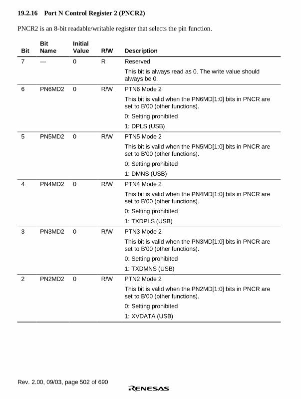
Rev. 2.00, 09/03, page 502 of 690
19.2.16 Port N Control Register 2 (PNCR2)
PNCR2 is an 8-bit readable/writable register that selects the pin function.
BitBitName
InitialValue R/W Description
7 — 0 R Reserved
This bit is always read as 0. The write value shouldalways be 0.
6 PN6MD2 0 R/W PTN6 Mode 2
This bit is valid when the PN6MD[1:0] bits in PNCR areset to B'00 (other functions).
0: Setting prohibited
1: DPLS (USB)
5 PN5MD2 0 R/W PTN5 Mode 2
This bit is valid when the PN5MD[1:0] bits in PNCR areset to B'00 (other functions).
0: Setting prohibited
1: DMNS (USB)
4 PN4MD2 0 R/W PTN4 Mode 2
This bit is valid when the PN4MD[1:0] bits in PNCR areset to B'00 (other functions).
0: Setting prohibited
1: TXDPLS (USB)
3 PN3MD2 0 R/W PTN3 Mode 2
This bit is valid when the PN3MD[1:0] bits in PNCR areset to B'00 (other functions).
0: Setting prohibited
1: TXDMNS (USB)
2 PN2MD2 0 R/W PTN2 Mode 2
This bit is valid when the PN2MD[1:0] bits in PNCR areset to B'00 (other functions).
0: Setting prohibited
1: XVDATA (USB)

Rev. 2.00, 09/03, page 503 of 690
BitBitName
InitialValue R/W Description
1 PN1MD2 0 R/W PTN1 Mode 2
This bit is valid when the PN1MD[1:0] bits in PNCR areset to B'00 (other functions).
0: Setting prohibited
1: TXENL (USB)
0 PN0MD2 0 R/W PTN0 Mode 2
This bit is valid when the PN0MD[1:0] bits in PNCR areset to B'00 (other functions).
0: Setting prohibited
1: SUSPND (USB)
19.2.17 Port SC Control Register (SCPCR)
SCPCR is a 16-bit readable/writable register that selects the pin function and input pull-up MOScontrol. The settings of SCPCR become valid only when transmission/reception operation isdisabled by the settings of SCSCR in the on-chip serial communication interface (SCIF).
When the TE bit in SCSCR_0 or SCSCR_2 of the SCIF is set to 1, the output status of “otherfunctions: TxD0 or TxD2” has priority for the setting of SCPCR.
Similarly, when the RE bit in SCSCR_0 or SCSCR_2 is set to 1, the input status of “otherfunctions: RxD0 or RxD2” has priority for the setting of SCPCR.
BitBitName
InitialValue R/W Description
15 to 12 — 0 R Reserved
These bits are always read as 0. The write value shouldalways be 0.
11
10
SCP5MD1
SCP5MD0
0
0
R/W
R/W
SCPT5 Mode
00: Other functions (see table 19.1)
01: Port output
10: Port input (pull-up MOS: On)
11: Port input (pull-up MOS: Off)

Rev. 2.00, 09/03, page 504 of 690
BitBitName
InitialValue R/W Description
9
8
SCP4MD1
SCP4MD0
0
0
R/W
R/W
SCPT4 Mode
00: Other functions (see table 19.1)
01: Port output
10: Port input (pull-up MOS: On)
11: Port input (pull-up MOS: Off)
7
6
SCP3MD1
SCP3MD0
0
0
R/W
R/W
SCPT3 Mode
00: Other functions (see table 19.1)
01: Port output
10: Port input (pull-up MOS: On)
11: Port input (pull-up MOS: Off)
5
4
SCP2MD1
SCP2MD0
0
0
R/W
R/W
SCPT2 Mode
These bits select pin function and input pull-up MOScontrol.
When TE = 0 and RE = 0 in SCSCR_2, operation is asfollows:
00: Other functions (see table 19.1)
01: Port output
10: Port input (pull-up MOS: On)
11: Port input (pull-up MOS: Off)
When TE = 1 in SCSCR_2, the SCPT2/TxD2 pin functionsas TxD2.
When RE = 1 in SCSCR_2, the SCPT2/RxD2 pinfunctions as RxD2.
Note: Since two pins (TxD2 and RxD2) are used to accessone bit (SCPT2), there is no combination ofsimultaneous input/output of SCPT2.
When port input is set (when bit SCP2MD1 is set to 1), theTxD2 pin enters an output state when the TE bit inSCSCR_2 is set to 1, whereas it enters high-impedancestate when the TE bit is cleared to 0.

Rev. 2.00, 09/03, page 505 of 690
BitBitName
InitialValue R/W Description
3
2
SCP1MD1
SCP1MD0
0
0
R/W
R/W
SCPT1 Mode
These bits select pin function and input pull-up MOScontrol.
00: Other functions (see table 19.1)
01: Port output
10: Port input (pull-up MOS: On)
11: Port input (pull-up MOS: Off)
1
0
SCP0MD1
SCP0MD0
0
0
R/W
R/W
SCPT0 Mode
These bits select pin function and input pull-up MOScontrol.
When TE = 0 and RE = 0 in SCSCR_0, operation is asfollows:
00: Other functions (see table 19.1)
01: Port output
10: Port input (pull-up MOS: On)
11: Port input (pull-up MOS: Off)
When TE = 1 in SCSCR_0, the SCPT0/TxD0 pinfunctions as TxD0.
When RE = 1 in SCSCR_0, the SCPT0/RxD0 pinfunctions as RxD0.
Note: Since two pins (TxD0 and RxD0) are used toaccess one bit (SCPT0), there is no combination ofsimultaneous input/output of SCPT0.
When port input is set (when bit SCP0MD1 is set to 1),the TxD0 pin enters an output state when the TE bit inSCSCR_0 is set to 1, whereas it enters high-impedancestate when the TE bit is cleared to 0.

Rev. 2.00, 09/03, page 506 of 690

Rev. 2.00, 09/03, page 507 of 690
Section 20 I/O Ports
This LSI has fourteen I/O ports (ports A to H, J to N, and SC). All port pins are multiplexed withother pin functions (the pin function controller (PFC) handles the selection of pin functions andpull-up MOS control). Each port has a data register which stores data for the pins.
20.1 Port A
Port A is an 8-bit input/output port with the pin configuration shown in figure 20.1. Each pin hasan input pull-up MOS, which is controlled by the port A control register (PACR) in the PFC.
Port A
PTA7 (input/output)/D23 (input/output)/PINT7 (input)
PTA6 (input/output)/D22 (input/output)/PINT6 (input)
PTA5 (input/output)/D21 (input/output)/PINT5 (input)
PTA4 (input/output)/D20 (input/output)/PINT4 (input)
PTA3 (input/output)/D19 (input/output)/PINT3 (input)
PTA2 (input/output)/D18 (input/output)/PINT2 (input)
PTA1 (input/output)/D17 (input/output)/PINT1 (input)
PTA0 (input/output)/D16 (input/output)/PINT0 (input)
Figure 20.1 Port A
20.1.1 Register Description
Port A has the following register. For details on the register address and access size, see section24, List of Registers.
• Port A data register (PADR)

Rev. 2.00, 09/03, page 508 of 690
20.1.2 Port A Data Register (PADR)
PADR is an 8-bit readable/writable register that stores data for pins PTA7 to PTA0. Bits PA7DTto PA0DT correspond to pins PTA7 to PTA0. When the pin function is general output port, if theport is read, the value of the corresponding PADR bit is returned directly. When the function isgeneral input port, if the port is read the corresponding pin level is read.
BitBitName
InitialValue R/W Description
7 to 0 PA7DTtoPA0DT
0 R/W Table 20.1 shows the function of PADR.
Table 20.1 Port A Data Register (PADR) Read/Write Operations
PACR State
PAnMD1 PAnMD0 Pin State Read Write
0 0 Other function PADR value Data can be written to PADR but no effect onpin state.
1 Output PADR value Written data is output from the pin.
1 0 Input (Pull-upMOS on)
Pin state Data can be written to PADR but no effect onpin state.
1 Input (Pull-upMOS off)
Pin state Data can be written to PADR but no effect onpin state.
Note: n = 0 to 7
20.2 Port B
Port B is an 8-bit input/output port with the pin configuration shown in figure 20.2. Each pin hasan input pull-up MOS, which is controlled by the port B control register (PBCR) in the PFC.
Port B
PTB7 (input/output)/D31 (input/output)/PINT15 (input)
PTB6 (input/output)/D30 (input/output)/PINT14 (input)
PTB5 (input/output)/D29 (input/output)/PINT13 (input)
PTB4 (input/output)/D28 (input/output)/PINT12 (input)
PTB3 (input/output)/D27 (input/output)/PINT11 (input)
PTB2 (input/output)/D26 (input/output)/PINT10 (input)
PTB1 (input/output)/D25 (input/output)/PINT9 (input)
PTB0 (input/output)/D24 (input/output)/PINT8 (input)
Figure 20.2 Port B

Rev. 2.00, 09/03, page 509 of 690
20.2.1 Register Description
Port B has the following register. For details on the register address and access size, see section24, List of Registers.
• Port B data register (PBDR)
20.2.2 Port B Data Register (PBDR)
PBDR is an 8-bit readable/writable register that stores data for pins PTB7 to PTB0. Bits PB7DT toPB0DT correspond to pins PTB7 to PTB0. When the pin function is general output port, if the portis read the value of the corresponding PBDR bit is returned directly. When the function is generalinput port, if the port is read, the corresponding pin level is read.
BitBitName
InitialValue R/W Description
7 to 0 PB7DTtoPB0DT
0 R/W Table 20.2 shows the function of PBDR.
Table 20.2 Port B Data Register (PBDR) Read/Write Operations
PBCR State
PBnMD1 PBnMD0 Pin State Read Write
0 0 Other function PBDR value Data can be written to PBDR but no effect onpin state.
1 Output PBDR value Written data is output from the pin.
1 0 Input (Pull-upMOS on)
Pin state Data can be written to PBDR but no effect onpin state.
1 Input (Pull-upMOS off)
Pin state Data can be written to PBDR but no effect onpin state.
Note: n = 0 to 7

Rev. 2.00, 09/03, page 510 of 690
20.3 Port C
Port C is an 8-bit input/output port with the pin configuration shown in figure 20.3. Each pin hasan input pull-up MOS, which is controlled by the port C control register (PCCR) in the PFC.
Port C
PTC7 (input/output)/CS6A (output)
PTC6 (input/output)/CS5A (output)
PTC5 (input/output)/CS4 (output)
PTC4 (input/output)/CS3 (output)
PTC3 (input/output)/CS2 (output)
PTC2 (input/output)/WE3 (output)/DQMUU (output)/AH (output)
PTC1 (input/output)/WE2 (output)/DQMUL (output)
PTC0 (input/output)/BS (output)
Figure 20.3 Port C
20.3.1 Register Description
Port C has the following register. For details on the register address and access size, see section24, List of Registers.
• Port C data register (PCDR)
20.3.2 Port C Data Register (PCDR)
PCDR is an 8-bit readable/writable register that stores data for pins PTC7 to PTC0. Bits PC7DT toPC0DT correspond to pins PTC7 to PTC0. When the pin function is general output port, if the portis read, the value of the corresponding PCDR bit is returned directly. When the function is generalinput port, if the port is read, the corresponding pin level is read.
BitBitName
InitialValue R/W Description
7 to 0 PC7DTtoPC0DT
0 R/W Table 20.3 shows the function of PCDR.

Rev. 2.00, 09/03, page 511 of 690
Table 20.3 Port C Data Register (PCDR) Read/Write Operations
PCCR State
PCnMD1 PCnMD0 Pin State Read Write
0 0 Other function PCDR value Data can be written to PCDR but no effect onpin state.
1 Output PCDR value Written data is output from the pin.
1 0 Input (Pull-upMOS on)
Pin state Data can be written to PCDR but no effect onpin state.
1 Input (Pull-upMOS off)
Pin state Data can be written to PCDR but no effect onpin state.
Note: n = 0 to 7
20.4 Port D
Port D is an 8-bit input/output port with the pin configuration shown in figure 20.4. Each pin hasan input pull-up MOS, which is controlled by the port D control register (PDCR) in the PFC.
Port D
PTD7 (input/output)/CS6B (output)
PTD6 (input/output)/CS5B (output)
PTD5 (input) /NF (input)
PTD4 (input/output)/CKE (output)
PTD3 (input/output)/CASU (output)
PTD2 (input/output)/CASL (output)
PTD1 (input/output)/RASU (output)
PTD0 (input/output)/RASL (output)
Figure 20.4 Port D
20.4.1 Register Description
Port D has the following register. For details on the register address and access size, see section24, List of Registers.
• Port D data register (PDDR)
20.4.2 Port D Data Register (PDDR)
PDDR is an 8-bit readable/writable register that stores data for pins PTD7 to PTD0. Bits PD7DTto PD0DT correspond to pins PTD7 to PTD0. When the pin function is general output port, if theport is read, the value of the corresponding PDDR bit is returned directly. When the function isgeneral input port, if the port is read, the corresponding pin level is read.

Rev. 2.00, 09/03, page 512 of 690
BitBitName
InitialValue R/W Description
7 to0
PD7DTtoPD0DT
0 R/W Table 20.4 shows the function of PDDR.
Table 20.4 Port D Data Register (PDDR) Read/Write Operations
PDCR State
PDnMD1 PDnMD0 Pin State Read Write
0 0 Other function PDDR value Data can be written to PDDR but no effecton pin state.
1 Output PDDR value Written data is output from the pin.
1 0 Input (Pull-upMOS on)
Pin state Data can be written to PDDR but no effecton pin state.
1 Input (Pull-upMOS off)
Pin state Data can be written to PDDR but no effecton pin state.
Note: n = 0 to 4, 6, and 7
PDCR State
PD5MD1 PD5MD0 Pin State Read Write
0 0 NF PDDR value Data can be written to PDDR but no effecton pin state.
1 SettingProhibited
1 0 Input (Pull-upMOS on)
Pin state Data can be written to PDDR but no effecton pin state.
1 Input (Pull-upMOS off)
Pin state Data can be written to PDDR but no effecton pin state.

Rev. 2.00, 09/03, page 513 of 690
20.5 Port E
Port E is an 8-bit input/output port with the pin configuration shown in figure 20.5. Each pin hasan input pull-up MOS, which is controlled by the port E control register (PECR) in the PFC.
Port E
PTE7 (input/output)
PTE6 (input/output)/TCLK (input)
PTE5 (input/output)/STATUS1 (output)/CTS0 (input)
PTE4 (input/output)/STATUS0 (output)/RTS0 (output)
PTE3 (input/output)/TEND0 (output)
PTE2 (input/output)/IRQ5 (input)
PTE1 (input/output)/DACK1 (output)
PTE0 (input/output)/DACK0 (output)
Figure 20.5 Port E
20.5.1 Register Description
Port E has the following register. For details on the register address and access size, see section24, List of Registers.
• Port E data register (PEDR)
20.5.2 Port E Data Register (PEDR)
PEDR is an 8-bit readable/writable register that stores data for pins PTE7 to PTE0. Bits PE7DT toPE0DT correspond to pins PTE7 to PTE0. When the pin function is general output port, if the portis read, the value of the corresponding PEDR bit is returned directly. When the function is generalinput port, if the port is read the corresponding pin level is read.
BitBitName
InitialValue R/W Description
7 to 0 PE7DTtoPE0DT
0 R/W Table 20.5 shows the function of PEDR.

Rev. 2.00, 09/03, page 514 of 690
Table 20.5 Port E Data Register (PEDR) Read/Write Operations
PECR State
PEnMD1 PEnMD0 Pin State Read Write
0 0 Other function PEDR value Data can be written to PEDR but no effect onpin state.
1 Output PEDR value Written data is output from the pin.
1 0 Input (Pull-upMOS on)
Pin state Data can be written to PEDR but no effect onpin state.
1 Input (Pull-upMOS off)
Pin state Data can be written to PEDR but no effect onpin state.
Note: n = 0 to 7
20.6 Port F
Port F is an 8-bit input port with the pin configuration shown in figure 20.6. Each pin has an inputpull-up MOS, which is controlled by the port F control register (PFCR) in the PFC.
Port F
PTF7 (input/output)/ASEMD0 (input)
PTF6 (input/output)/ASEBRKAK (output)
PTF5 (input/output)/TDO (output)
PTF4 (input/output)/AUDSYNC (output)
PTF3 (input/output)/AUDATA3 (output)/TO3 (output)
PTF2 (input/output)/AUDATA2 (output)/TO2 (output)
PTF1 (input/output)/AUDATA1 (output)/TO1 (output)
PTF0 (input/output)/AUDATA0 (output)/TO0 (output)
Figure 20.6 Port F
20.6.1 Register Description
Port F has the following register. For details on the register address and access size, see section 24,List of Registers.
• Port F data register (PFDR)
20.6.2 Port F Data Register (PFDR)
PFDR is an 8-bit readable/writable register that stores data for pins PTF7 to PTF0. Bits PF7DT toPF0DT correspond to pins PTF7 to PTF0. When the pin function is general output port, if the portis read, the value of the corresponding PFDR bit is returned directly. When the function is generalinput port, if the port is read the corresponding pin level is read.

Rev. 2.00, 09/03, page 515 of 690
BitBitName
InitialValue R/W Description
7 to0
PF7DTtoPF0DT
0 R/W Table 20.6 shows the function of PFDR.
Table 20.6 Port F Data Register (PFDR) Read/Write Operations
PFCR State
PFnMD1 PFnMD0 Pin State Read Write
0 0 Other function PFDR value Data can be written to PFDR but no effect onpin state.
1 Output PFDR value Written data is output from the pin.
1 0 Input (Pull-upMOS on)
Pin state Data can be written to PFDR but no effect onpin state.
1 Input (Pull-upMOS off)
Pin state Data can be written to PFDR but no effect onpin state.
Note: n = 0 to 7
20.7 Port G
Port G is an 8-bit input port with the pin configuration shown in figure 20.7. Each pin has an inputpull-up MOS, which is controlled by the port G control register (PGCR) in the PFC.
Port G
PTG5 (input/output)/BACK (output)
PTG4 (input/output)/AUDCK (output)
PTG3 (input/output)/TRST (input)
PTG2 (input/output)/TMS (input)
PTG1 (input/output)/TCK (input)
PTG0 (input/output)/TDI (input)
PTG7 (input/output)/WAIT (input)
PTG6 (input/output)/BREQ (input)
Figure 20.7 Port G
20.7.1 Register Description
Port G has the following register. For details on the register address and access size, see section24, List of Registers.
• Port G data register (PGDR)

Rev. 2.00, 09/03, page 516 of 690
20.7.2 Port G Data Register (PGDR)
PGDR is an 8-bit readable/writable register that stores data for pins PTG7 to PTG0. Bits PG7DTto PG0DT correspond to pins PTG7 to PTG0. When the pin function is general output port, if theport is read, the value of the corresponding PGDR bit is returned directly. When the function isgeneral input port, if the port is read the corresponding pin level is read.
BitBitName
InitialValue R/W Description
7 to0
PG7DTtoPG0DT
0 R/W Table 20.7 shows the function of PGDR.
Table 20.7 Port G Data Register (PGDR) Read/Write Operations
PGCR State
PGnMD1 PGnMD0 Pin State Read Write
0 0 Other function PGDR value Data can be written to PGDR but no effect onpin state.
1 Output PGDR value Written data is output from the pin.
1 0 Input (Pull-upMOS on)
Pin state Data can be written to PGDR but no effect onpin state.
1 Input (Pull-upMOS off)
Pin state Data can be written to PGDR but no effect onpin state.
Note: n = 0 to 7
20.8 Port H
Port H is a 7-bit input/output port with the pin configuration shown in figure 20.8. Each pin has aninput pull-up MOS, which is controlled by the port H control register (PHCR) in the PFC.
Port H
PTH6 (input/output)/DREQ1 (input)
PTH5 (input/output)/DREQ0 (input)
PTH4 (input/output)/IRQ4 (input)
PTH3 (input/output)/IRQ3 (input)/IRL3 (input)
PTH2 (input/output)/IRQ2 (input)/IRL2 (input)
PTH1 (input/output)/IRQ1 (input)/IRL1 (input)
PTH0 (input/output)/IRQ0 (input)/IRL0 (input)
Figure 20.8 Port H

Rev. 2.00, 09/03, page 517 of 690
20.8.1 Register Description
Port H has the following register. For details on the register address and access size, see section24, List of Registers.
• Port H data register (PHDR)
20.8.2 Port H Data Register (PHDR)
PHDR is an 8-bit readable/writable register that stores data for pins PTH6 to PTH0. Bits PH6DTto PH0DT correspond to pins PTH6 to PTH0. When the pin function is general output port, if theport is read, the value of the corresponding PHDR bit is returned directly. When the function isgeneral input port, if the port is read, the corresponding pin level is read.
BitBitName
InitialValue R/W Description
7 — 0 R ReservedThis bit is always read as 0. The write value shouldalways be 0.
6 to0
PH6DTtoPH0DT
0 R/W Table 20.8 shows the function of PHDR.
Table 20.8 Port H Data Register (PHDR) Read/Write Operations
PHCR State
PHnMD1 PHnMD0 Pin State Read Write
0 0 Other function PHDR value Data can be written to PHDR but no effecton pin state.
1 Output PHDR value Written data is output from the pin.
1 0 Input (Pull-upMOS on)
Pin state Data can be written to PHDR but no effecton pin state.
1 Input (Pull-upMOS off)
Pin state Data can be written to PHDR but no effecton pin state.
Note: n = 0 to 6
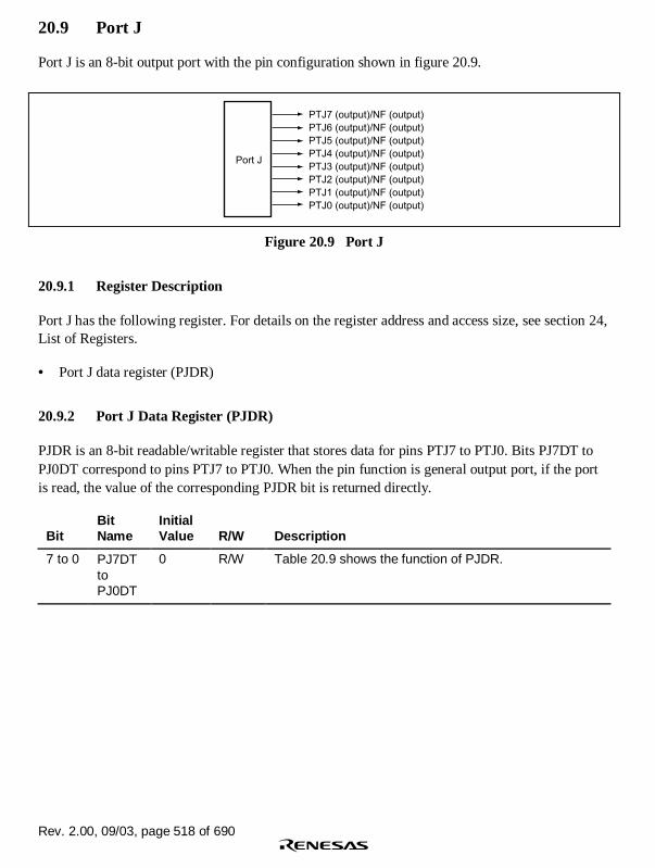
Rev. 2.00, 09/03, page 518 of 690
20.9 Port J
Port J is an 8-bit output port with the pin configuration shown in figure 20.9.
Port J
PTJ7 (output)/NF (output)
PTJ6 (output)/NF (output)
PTJ5 (output)/NF (output)
PTJ4 (output)/NF (output)
PTJ3 (output)/NF (output)
PTJ2 (output)/NF (output)
PTJ1 (output)/NF (output)
PTJ0 (output)/NF (output)
Figure 20.9 Port J
20.9.1 Register Description
Port J has the following register. For details on the register address and access size, see section 24,List of Registers.
• Port J data register (PJDR)
20.9.2 Port J Data Register (PJDR)
PJDR is an 8-bit readable/writable register that stores data for pins PTJ7 to PTJ0. Bits PJ7DT toPJ0DT correspond to pins PTJ7 to PTJ0. When the pin function is general output port, if the portis read, the value of the corresponding PJDR bit is returned directly.
BitBitName
InitialValue R/W Description
7 to 0 PJ7DTtoPJ0DT
0 R/W Table 20.9 shows the function of PJDR.

Rev. 2.00, 09/03, page 519 of 690
Table 20.9 Port J Data Register (PJDR) Read/Write Operations
PJCR State
PJnMD1 PJnMD0 Pin State Read Write
0 0 NF PJDR value Data can be written to PJDR but no effect onpin state.
1 Output PJDR value Written data is output from the pin.
1 0 SettingProhibited
1 SettingProhibited
Note: n = 0 to 7
20.10 Port K
Port K is an 8-bit input/output port with the pin configuration shown in figure 20.10. Each pin hasan input pull-up MOS, which is controlled by the port K control register (PKCR) in the PFC.
Port K
PTK7 (input/output)/A25 (output)
PTK6 (input/output)/A24 (output)
PTK5 (input/output)/A23 (output)
PTK4 (input/output)/A22 (output)
PTK3 (input/output)/A21 (output)
PTK2 (input/output)/A20 (output)
PTK1 (input/output)/A19 (output)
PTK0 (input/output)/A0 (output)
Figure 20.10 Port K
20.10.1 Register Description
Port K has the following register. For details on the register address and access size, see section24, List of Registers.
• Port K data register (PKDR)
20.10.2 Port K Data Register (PKDR)
PKDR is an 8-bit readable/writable register that stores data for pins PTK7 to PTK0. Bits PK7DTto PK0DT correspond to pins PTK7 to PTK0. When the pin function is general output port, if theport is read, the value of the corresponding PKDR bit is returned directly. When the function isgeneral input port, if the port is read, the corresponding pin level is read.

Rev. 2.00, 09/03, page 520 of 690
BitBitName
InitialValue R/W Description
7 to 0 PK7DTtoPK0DT
0 R/W Table 20.10 shows the function of PKDR.
Table 20.10 Port K Data Register (PKDR) Read/Write Operations
PKCR State
PKnMD1 PKnMD0 Pin State Read Write
0 0 Other function PKDR value Data can be written to PKDR but no effecton pin state.
1 Output PKDR value Written data is output from the pin.
1 0 Input (Pull-upMOS on)
Pin state Data can be written to PKDR but no effecton pin state.
1 Input (Pull-upMOS off)
Pin state Data can be written to PKDR but no effecton pin state.
Note: n = 0 to 7
20.11 Port L
Port L is a 4-bit input port with the pin configuration shown in figure 20.11.
Port L
PTL3 (input)/AN3 (input)
PTL2 (input)/AN2 (input)
PTL1 (input)/AN1 (input)
PTL0 (input)/AN0 (input)
Figure 20.11 Port L
20.11.1 Register Description
Port L has the following register. For details on the register address and access size, see section24, List of Registers.
• Port L data register (PLDR)

Rev. 2.00, 09/03, page 521 of 690
20.11.2 Port L Data Register (PLDR)
PLDR is an 8-bit read-only register that stores data for pins PTL3 to PTL0. Bits PL3DT to PL0DTcorrespond to pins PTL3 to PTL0. If the port is read, the corresponding pin level is read.
BitBitName
InitialValue R/W Description
7 to 4 — 0 R Reserved
These bits are always read as 0.
3 to 0 PL3DTtoPL0DT
0 R Table 20.11 shows the function of PLDR.
Table 20.11 Port L Data Register (PLDR) Read/Write Operation
PLCR State
PLnMD1 PLnMD0 Pin State Read Write
0 0 Other function Read as 0 Invalid (no effect on pin state)
1 Settingprohibited
— —
0 Settingprohibited
— —1
1 Input (Pull-upMOS off)
Pin state Invalid (no effect on pin state)
Note: n = 0 to 3
20.12 Port M
Port M is a 6-bit input/output port with the pin configuration shown in figure 20.12. Each pin hasan input pull-up MOS, which is controlled by the port M control register (PMCR) in the PFC.
Port M
PTM6 (input/output)/VBUS (input)
PTM4 (input)/NF (input)
PTM3 (input/output)
PTM2 (input/output)
PTM1 (input/output)
PTM0 (input/output)
Figure 20.12 Port M

Rev. 2.00, 09/03, page 522 of 690
20.12.1 Register Description
Port M has the following register. For details on the register address and access size, see section24, List of Registers.
• Port M data register (PMDR)
20.12.2 Port M Data Register (PMDR)
PMDR is an 8-bit readable/writable register that stores data for pins PTM6 and PTM4 to PTM0.Bits PM6DT and PM4DT to PM0DT correspond to pins PTM6 and PTM4 to PTM0. When the pinfunction is general output port, if the port is read, the value of the corresponding PMDR bit isreturned directly. When the function is general input port, if the port is read, the corresponding pinlevel is read.
BitBitName
InitialValue R/W Description
7 — 0 R ReservedThis bit is always read as 0. The write value shouldalways be 0.
6 PM6DT 0 R/W Table 20.12 shows the function of PMDR.
5 — 0 R ReservedThis bit is always read as 0. The write value shouldalways be 0.
4 to 0 PM4DTtoPM0DT
0 R/W Table 20.12 shows the function of PMDR.
Table 20.12 Port M Data Register (PMDR) Read/Write Operations
PMCR State
PMnMD1 PMnMD0 Pin State Read Write
0 0 Other function PMDR value Data can be written to PMDR but no effecton pin state.
1 Output PMDR value Written data is output from the pin.
1 0 Input (Pull-upMOS on)
Pin state Data can be written to PMDR but no effecton pin state.
1 Input (Pull-upMOS off)
Pin state Data can be written to PMDR but no effecton pin state.
Note: n = 0 to 3 and 6

Rev. 2.00, 09/03, page 523 of 690
PMCR State
PM4MD1 PM4MD0 Pin State Read Write
0 0 NF PMDR value Data can be written to PMDR but no effecton pin state.
1 SettingProhibited
PMDR value Written data is output from the pin.
1 0 Input (Pull-upMOS on)
Pin state Data can be written to PMDR but no effecton pin state.
1 Input (Pull-upMOS off)
Pin state Data can be written to PMDR but no effecton pin state.
20.13 Port N
Port N is an 8-bit input/output port with the pin configuration shown in figure 20.13. Each pin hasan input pull-up MOS, which is controlled by the port N control register (PNCR) in the PFC.
Port N
PTN7 (input/output)
PTN6 (input/output)/DPLS (input)
PTN5 (input/output)/DMNS (input)
PTN4 (input/output)/TXDPLS (output)
PTN3 (input/output)/TXDMNS (output)
PTN2 (input/output)/XVDATA (input)
PTN1 (input/output)/TXENL (output)
PTN0 (input/output)/SUSPND (output)
Figure 20.13 Port N
20.13.1 Register Description
Port N has the following register. For details on the register address and access size, see section24, List of Registers.
• Port N data register (PNDR)
20.13.2 Port N Data Register (PNDR)
PNDR is an 8-bit readable/writable register that stores data for pins PTN7 to PTN0. Bits PN7DTto PN0DT correspond to pins PTN7 to PTN0. When the pin function is general output port, if theport is read, the value of the corresponding PNDR bit is returned directly. When the function isgeneral input port, if the port is read, the corresponding pin level is read.

Rev. 2.00, 09/03, page 524 of 690
BitBitName
InitialValue R/W Description
7 to 0 PN7DTtoPN0DT
0 R/W Table 20.13 shows the function of PNDR.
Table 20.13 Port N Data Register (PNDR) Read/Write Operations
PNCR State
PNnMD1 PNnMD0 Pin State Read Write
0 0 Other function PNDR value Data can be written to PNDR but no effecton pin state.
1 Output PNDR value Written data is output from the pin.
1 0 Input (Pull-upMOS on)
Pin state Data can be written to PNDR but no effecton pin state.
1 Input (Pull-upMOS off)
Pin state Data can be written to PNDR but no effecton pin state.
Note: n = 0 to 7
20.14 SC Port
The SC port is an 8-bit input/output port with the pin configuration shown in figure 20.14. Eachpin has an input pull-up MOS, which is controlled by the SC port control register (SCPCR) in thePFC.
SC
Port
SCPT5 (input/output)/CTS2 (input)
SCPT4 (input/output)/RTS2 (output)
SCPT3 (input/output)/SCK2 (input/output)
SCPT2 (input)*/RxD2 (input)
SCPT2 (output)*/TxD2 (output)
SCPT1 (input/output)/SCK0 (input/output)
SCPT0 (input)*/RxD0 (input)/IrRX (input)
SCPT0 (output)*/TxD0 (output)/IrTX (output)
Note: * SCPT0 and SCPT2 each have two separate pins for input
and output, however, a common data register is accessed.
Figure 20.14 SC Port
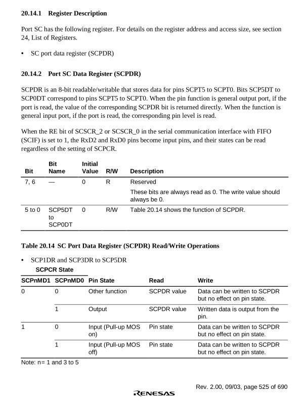
Rev. 2.00, 09/03, page 525 of 690
20.14.1 Register Description
Port SC has the following register. For details on the register address and access size, see section24, List of Registers.
• SC port data register (SCPDR)
20.14.2 Port SC Data Register (SCPDR)
SCPDR is an 8-bit readable/writable that stores data for pins SCPT5 to SCPT0. Bits SCP5DT toSCP0DT correspond to pins SCPT5 to SCPT0. When the pin function is general output port, if theport is read, the value of the corresponding SCPDR bit is returned directly. When the function isgeneral input port, if the port is read, the corresponding pin level is read.
When the RE bit of SCSCR_2 or SCSCR_0 in the serial communication interface with FIFO(SCIF) is set to 1, the RxD2 and RxD0 pins become input pins, and their states can be readregardless of the setting of SCPCR.
BitBitName
InitialValue R/W Description
7, 6 — 0 R Reserved
These bits are always read as 0. The write value shouldalways be 0.
5 to 0 SCP5DTtoSCP0DT
0 R/W Table 20.14 shows the function of SCPDR.
Table 20.14 SC Port Data Register (SCPDR) Read/Write Operations
• SCP1DR and SCP3DR to SCP5DR
SCPCR State
SCPnMD1 SCPnMD0 Pin State Read Write
0 0 Other function SCPDR value Data can be written to SCPDRbut no effect on pin state.
1 Output SCPDR value Written data is output from thepin.
1 0 Input (Pull-up MOSon)
Pin state Data can be written to SCPDRbut no effect on pin state.
1 Input (Pull-up MOSoff)
Pin state Data can be written to SCPDRbut no effect on pin state.
Note: n= 1 and 3 to 5

Rev. 2.00, 09/03, page 526 of 690
• SCP0DR and SCP2DR
SCPCR State
SCPnMD1 SCPnMD0 Pin State Read Write
0 0 Other function Prohibited Prohibited
1 TxD: Output
RxD: Input (cannot beread)
SCPDR value Written data is output on TxD pin.
1 0 TxD: Output highimpedance
RxD: Input (Pull-upMOS on)
RxD pin state Data can be written to SCPDR butno effect on pin state.
1 TxD: Output highimpedance
RxD: Input (Pull-upMOS off)
RxD pin state Data can be written to SCPDR butno effect on pin state.
Note: n= 0 and 2The operations are not guaranteed when read and write operations are prohibited.

ADCMS60A_000020020100 Rev. 2.00, 09/03, page 527 of 690
Section 21 A/D Converter
This LSI includes a 10-bit successive-approximation A/D converter allowing selection of up tofour analog input channels.
21.1 Features
• 10-bit resolution
• Four input channels
• Minimum conversion time: 8.5 µs per channel (Pφ= 33 MHz operation)
• Three conversion modes
Single mode: A/D conversion on one channel
Multi mode: A/D conversion on one to four channels
Scan mode: Continuous A/D conversion on one to four channels
• Four 16-bit data registers
A/D conversion results are transferred for storage into 16-bit data registers correspondingto the channels.
• Sample-and-hold function
• Interrupt source
At the end of A/D conversion, an A/D conversion end interrupt (ADI) can be requested.
• Module standby mode can be set

Rev. 2.00, 09/03, page 528 of 690
Figure 21.1 shows a block diagram of the A/D converter.
10-bit
D/A AD
DR
A
AD
DR
B
AD
DR
D
Bus inte
rface
Peripheral data bus
Analog
multi-
plexer
Control circuit
Successiv
e a
ppro
xi-
mation r
egis
ter
+
−
Comparator
Sample-and-hold circuit
ADI
interrupt
signal
AVSS
AN0
AN1
AN2
AN3
Pφ/8
Pφ/16
AD
CS
R
Pφ/4
AVCC
ADCSR: A/D control/status register
ADDRA: A/D data register A
ADDRB: A/D data register B
ADDRC: A/D data register C
ADDRD: A/D data register D
Legend
Internal
data bus
AD
DR
C
Figure 21.1 Block Diagram of A/D Converter

Rev. 2.00, 09/03, page 529 of 690
21.2 Input/Output Pins
Table 21.1 summarizes the A/D converter’s pins. The AVCC and AVSS pins are the power supplyfor the analog circuits in the A/D converter. The AVCC pin also functions as the A/D conversionreference voltage pin.
Table 21.1 Pin Configuration
Pin Name AbbreviationInput/Output Function
Analog power supply AVcc Input Analog power supply and reference voltage forA/D conversion
Analog ground AVss Input Analog ground and reference voltage for A/Dconversion
Analog input 0 AN0 Input Analog input 0
Analog input 1 AN1 Input Analog input 1
Analog input 2 AN2 Input Analog input 2
Analog input 3 AN3 Input Analog input 3
21.3 Register Descriptions
The A/D converter has the following registers. For more information on addresses of registers andregister states in the processing, see section 24, List of Registers.
• A/D data register A (ADDRA)
• A/D data register B (ADDRB)
• A/D data register C (ADDRC)
• A/D data register D (ADDRD)
• A/D control/status register (ADCSR)

Rev. 2.00, 09/03, page 530 of 690
21.3.1 A/D Data Registers A to D (ADDRA to ADDRD)
The four A/D data registers (ADDRA to ADDRD) are 16-bit read-only registers that store theresults of A/D conversion. Table 21.2 indicates the pairings of analog input channels and A/D dataregisters that store the results of A/D conversion.
An A/D conversion produces 10-bit data, which is transferred for storage into bits 15 to 6 in theA/D data register corresponding to the selected channel. Bits 5 to 0 of an A/D data register arereserved bits that are always read as 0.
The A/D data registers are initialized to H'0000.
Table 21.2 Analog Input Channels and A/D Data Registers
Analog Input Channel A/D Data Register that Store Results of A/D Conversion
AN0 ADDRA
AN1 ADDRB
AN2 ADDRC
AN3 ADDRD
21.3.2 A/D Control/Status Registers (ADCSR)
ADCSR is a 16-bit readable/writable register that selects the mode and controls the A/D converter.
BitBitName
InitialValue R/W Description
15 ADF 0 R/(W)* A/D End Flag
Indicates the end of A/D conversion.
[Setting conditions]
Single mode: A/D conversion ends
Multi mode: A/D conversion ends cycling through theselected channels
Scan mode: A/D conversion ends cycling through theselected channels
[Clearing conditions]
(1) Reading ADF while ADF = 1, then writing 0 to ADF
(2) DMAC is activated by ADI interrupt and ADDR isread
Note: *Clear this bit by writing 0. Writing 1 is ignored.

Rev. 2.00, 09/03, page 531 of 690
BitBitName
InitialValue R/W Description
14 ADIE 0 R/W A/D Interrupt Enable
Enables or disables the interrupt (ADI) requested by ADF.Set the ADIE bit while the ADST bit is 0.
0: Interrupt (ADI) requested by ADF is disabled
1: Interrupt (ADI) requested by ADF is enabled
13 ADST 0 R/W A/D Start
Starts or stops A/D conversion. The ADST bit remains set to1 during A/D conversion.
0: A/D conversion is stopped.
1: Single mode:A/D conversion starts; ADST is automatically cleared to 0when conversion ends on selected channels.Multi mode:A/D conversion starts; when conversion is completedcycling through the selected channels, ADST isautomatically cleared.Scan mode:A/D conversion starts and continues, A/D conversion iscontinuously performed until ADST is cleared to 0 bysoftware, by a reset, or by a transition to standby mode.
12 DMASL 0 R/W DMAC Select
Selects an interrupt due to ADF or activation of the DMAC.Set the DMASL bit while the ADST bit is 0.
0: An interrupt by ADF is selected.
1: Activation of the DMAC by ADF is selected.
11 to 8 — 0 R Reserved
These bits are always read as 0. The write value shouldalways be 0.

Rev. 2.00, 09/03, page 532 of 690
BitBitName
InitialValue R/W Description
76
CKS1CKS0
01
R/WR/W
Clock Select
Selects the A/D conversion time. Clear the ADST bit to 0before changing the conversion time.
00: Conversion time = 151 states (maximum) at Pφ/4
01: Conversion time = 285 states (maximum) at Pφ/8
10: Conversion time = 545 states (maximum) at Pφ/16
11: Setting prohibited
Note: If the minimum conversion time is not satisfied,lack of accuracy or abnormal operation mayoccur.
54
MULTI1MULTI0
00
R/WR/W
Mode Select
Selects single mode, multi mode, or scan mode.
00: Single mode
01: Setting prohibited
10: Multi mode
11: Scan mode
32
——
00
RR
Reserved
These bits are always read as 0. The write value shouldalways be 0.
10
CH1CH0
00
R/WR/W
Channel Select
These bits and the MULTI bit select the analog inputchannels. Clear the ADST bit to 0 before changing thechannel selection.
Single mode Multi mode or scan mode
00: AN0 AN0
01: AN1 AN0, AN1
10: AN2 AN0 to AN2
11: AN3 AN0 to AN3

Rev. 2.00, 09/03, page 533 of 690
21.4 Operation
The A/D converter operates by successive approximations with 10-bit resolution. It has threeoperating modes: single mode, multi mode, and scan mode. To avoid malfunction, switchoperating modes while the ADST bit of ADCSR is 0. Changing operating modes and channels andsetting the ADST bit can be performed simultaneously.
21.4.1 Single Mode
Single mode should be selected when only one A/D conversion on one channel is required.
1. A/D conversion of the selected channel starts when the ADST bit of ADCSR is set to 1 bysoftware.
2. When conversion ends, the conversion results are transmitted to the A/D data register thatcorresponds to the channel.
3. When conversion ends, the ADF bit of ADCSR is set to 1. If the ADIE bit is also set to 1, anADI interrupt is requested at this time.
4. The ADST bit holds 1 during A/D conversion. When A/D conversion is completed, the ADSTbit is cleared to 0 and the A/D converter becomes idle. When the ADST bit is cleared to 0during A/D conversion, the conversion is halted and the A/D converter becomes idle.To clear the ADF flag to 0, first read ADF, then write 0 to ADF.
21.4.2 Multi Mode
Multi mode should be selected when performing A/D conversions on one or more channels.
1. When the ADST bit is set to 1 by software, A/D conversion starts with the smaller number ofthe analog input channel in the group (for instance, AN0, and AN1 to AN3).
2. When conversion of each channel ends, the conversion results are transmitted to the A/D dataregister that corresponds to the channel.
3. When conversion of all selected channels ends, the ADF bit of ADCSR is set to 1. If theADIE bit is also set to 1, an ADI interrupt is requested at this time.
4. When A/D conversion is completed, the ADST bit is cleared to 0 and the A/D converterbecomes idle. When the ADST bit is cleared to 0 during A/D conversion, the conversion ishalted and the A/D converter becomes idle.To clear the ADF flag to 0, first read ADF, then write 0 to ADF.

Rev. 2.00, 09/03, page 534 of 690
21.4.3 Scan Mode
Scan mode should be selected when performing A/D conversions of analog inputs on one or morespecified channels. Scan mode is useful for monitoring analog inputs.
1. When the ADST bit is set to 1 by software, A/D conversion starts with the smaller number ofthe analog input channel in the group (for instance, AN0, and AN1 to AN3).
2. When conversion of each channel ends, the conversion results are transmitted to the A/D dataregister that corresponds to the channel.
3. When conversion of all selected channels ends, the ADF bit of ADCSR is set to 1. If theADIE bit is also set to 1, an ADI interrupt is requested at this time. A/D conversion then startswith the smaller number of the analog input channel.
4. The ADST bit is not automatically cleared to 0. When the ADST bit is set to 1, steps 2 and 3above are repeated. When the ADST bit is cleared to 0, the conversion is halted and the A/Dconverter becomes idle.To clear the ADF flag to 0, first read ADF, then write 0 to ADF.
21.4.4 Input Sampling and A/D Conversion Time
The A/D converter has a built-in sample-and-hold circuit. The A/D converter samples the analoginput at an A/D conversion start delay time tD after the ADST bit is set to 1, then starts conversion.Figure 21.2 shows the A/D conversion timing. Table 21.3 indicates the A/D conversion time.
As indicated in figure 21.2, the A/D conversion time (tCONV) includes tD and the input samplingtime (tSPL). The length of tD varies depending on the timing of the write access to ADCSR. Thetotal conversion time therefore varies within the ranges indicated in table 21.3.
In multi mode and scan mode, the values given in table 21.3 apply to the first conversion. In thesecond and subsequent conversions, the values given in table 21.4 apply to the first conversion.

Rev. 2.00, 09/03, page 535 of 690
Pφ
ADF
A/D conversion time (tCONV)
A/D conversion start delay time (tD) Analog input sampling time (t
SPL)
Write cycle A/D
synchronization time
Address
Internal
write signal
Write timing of ADST
Analog input
sampling signal
A/D converter Idle time Sample and hold A/D conversion executed
A/D conversion ended
Figure 21.2 A/D Conversion Timing
Table 21.3 A/D Conversion Time (Single Mode)
CKS1 = 1,CKS0 = 0
CKS1 = 0,CKS0 = 1
CKS1 = 0,CKS0 = 0
Symbol Min Typ Max Min Typ Max Min Typ Max
A/D conversion startdelay
tD 18 — 21 10 — 13 6 — 9
Input sampling time tSPL — 129 — — 65 — — 33 —
A/D conversion time tCONV 535 — 545 275 — 285 141 — 151
Note: Values in the table are numbers of states for Pφ.
Table 21.4 A/D Conversion Time (Multi Mode and Scan Mode)
CKS1 CKS0 Conversion Time (cycles)
0 0 128 (fixed)
0 1 256 (fixed)
1 0 512 (fixed)
1 1 Unused

Rev. 2.00, 09/03, page 536 of 690
21.5 Interrupts and DMAC Transfer Request
The A/D converter generates an interrupt (ADI) at the end of A/D conversion. The ADI interruptrequest is enabled when ADF in ADCSR is set to 1and the ADIE bit in ADCSR is set to 1 afterA/D conversion. The ADI interrupt can activate the direct memory access controller (DMAC) bysetting the ADIE and DMASL bits to 1. Continuous conversion without loads of software isenabled by reading data that has been converted by the ADI interrupt with DMAC.
When activating DMAC by ADI, the ADF bit in ADCSR is automatically cleared to 0 at DMACdata transfer.
Table 21.5 A/D Converter Interrupt Source
Name Interrupt source Interrupt flag DMAC activation
ADI A/D conversion end ADF Yes
21.6 Definitions of A/D Conversion Accuracy
The following shows the definitions of A/D conversion accuracy. In the figure, the 10 bits of theA/D converter have been simplified to 3 bits.
• ResolutionDigital output code number of the A/D converter
• Quantization errorIntrinsic error of the A/D converter and is expressed as 1/2 LSB (figure 21.3)
• Offset errorDeviation between analog input voltage and ideal A/D conversion characteristics when thedigital output value changes from the minimum (zero voltage) 0000000000 (H'00; 000 infigure 21.3) to 0000000001 (H'01; 001 in figure 21.3) (figure 21.4)
• Full-scale errorDeviation between analog input voltage and ideal A/D conversion characteristics when thedigital output value changes from the 1111111110 (H'3EF; 110 in figure 21.3) to the maximum1111111111 (H'3FF; 111 in figure 21.3) (figure 21.4).
• Nonlinearity errorDeviation between analog input voltage and ideal A/D conversion characteristics between zerovoltage and full-scale voltage (figure 21.4). Note that it does not include offset, full-scale, orquantization error.
• Absolute accuracyDeviation between analog and digital input values. Note that it includes offset, full-scale,quantization, or nonlinearity error.

Rev. 2.00, 09/03, page 537 of 690
111
110
101
100
011
010
001
0000 1/8 2/8 3/8 4/8 5/8 6/8 7/8 FS
Analog input
voltage
Quantization
error
Ideal A/D
conversion
characteristic
Digital output
Figure 21.3 Definitions of A/D Conversion Accuracy
Nonlinearity
error
Ideal A/D
conversion
characteristic
Actual A/D
conversion
characteristic
Full-scale errorDigital output
Analog input
voltageOffset error
FS
Figure 21.4 Definitions of A/D Conversion Accuracy

Rev. 2.00, 09/03, page 538 of 690
21.7 Usage Notes
21.7.1 Allowable Signal-Source Impedance
For the analog input design of this LSI, conversion accuracy is guaranteed for an input signal withsignal-source impedance of 5 kΩ or less. The specification is for charging input capacitance of thesample and hold circuit of the A/D converter within sampling time. When the output impedance ofthe sensor exceeds 5 kΩ, conversion accuracy is not guaranteed due to insufficient charging. Iflarge external capacitance is set at conversion in single mode, signal-source impedance is ignoredsince input load is only internal input resistance of 3 kΩ. However, an analog signal with largedifferential coefficient (5 mV/µs or greater) cannot be followed up because of a low-pass filter(figure 21.5). When converting high-speed analog signals or converting in scan mode, insert alow-impedance buffer.
21.7.2 Influence to Absolute Accuracy
By adding capacitance, absolute accuracy may be degraded if noise is on GND because there iscoupling with GND. Therefore, connect electrically stable GND such as AVcc to prevent absoluteaccuracy from being degraded.
A filter circuit must not interfere with digital signals, or must not be an antenna on a mountingboard.
20 pFCin =15 pF
3 kΩto 5 kΩ
Output impedance of sensor
Sensor input
This LSI
Lowpass
filter
(C = 0.1µF)
Equivalent circuit
of A/D converter
Figure 21.5 Analog Input Circuit Example
21.7.3 Setting Analog Input Voltage
Operating the chip in excess of the following voltage range may result in damage to chipreliability.
• Analog Input Voltage Range: During A/D conversion, the voltages (VANn) input to the analoginput pins ANn should be in the range AVSS ≤ VANn ≤ AVCC (n = 0 to 3).

Rev. 2.00, 09/03, page 539 of 690
• Relationships of AVCC, AVSS and VCCQ, VSSQ: AVCC = VCCQ ± 0.2 V and AVSS = VSSQ. Evenwhen the A/D converter is not used, do not open AVCC and AVSS.
21.7.4 Notes on Board Design
In designing a board, separate digital circuits and analog circuits. Do not intersect or locate closelysignal lines of a digital circuit and an analog circuit. An analog circuit may malfunction due toinduction, thus affecting A/D conversion values. Separate analog input pins (AN0 to AN3) and theanalog power voltage (AVcc) from digital circuits with analog ground (AVss). Connect analogground (AVss) to one point of stable ground (Vss) on the board.
21.7.5 Notes on Countermeasures to Noise
Connect a protective circuit between AVcc and AVss, as shown in figure 21.6, to prevent damageof analog input pins (AN0 to AN3) due to abnormal voltage such as excessive serge. Connect abypass capacitor that is connected to AVcc and a capacitor for a filter that is connected to AN0 toAN3 to AVss.
When a capacitor for a filter is connected, input currents of AN0 to AN3 are averaged, maycausing errors. If A/D conversion is frequently performed in scan mode, voltages of analog inputpins cause errors when a current that is charged/discharged for capacitance of a sample & holdcircuit in the A/D converter is higher than a current that is input through input impedance (Rin).Therefore, determine a circuit constant carefully.
0.01 µF10 µF
AVCC
AN0 to AN3
AVSS
This LSI
*1
100 Ω
0.1 µF
Notes: 1. Values are for reference.
Rin*2
2. Rin is input impedance.
Figure 21.6 Example of Analog Input Protection Circuit
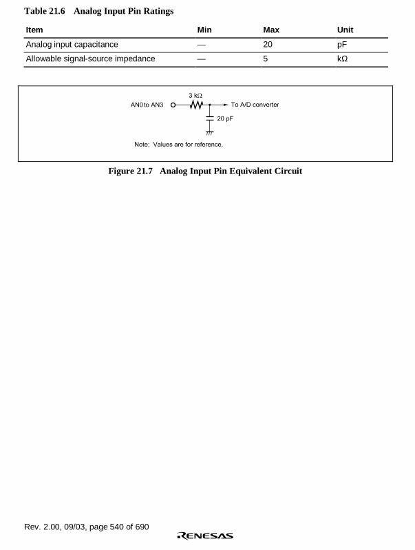
Rev. 2.00, 09/03, page 540 of 690
Table 21.6 Analog Input Pin Ratings
Item Min Max Unit
Analog input capacitance — 20 pF
Allowable signal-source impedance — 5 kΩ
20 pF
AN0 to AN3
3 kΩ
To A/D converter
Note: Values are for reference.
Figure 21.7 Analog Input Pin Equivalent Circuit
UBCS311A_000020020100 Rev. 2.00, 09/03, page 541 of 690
Section 22 User Break Controller
The user break controller (UBC) provides functions that simplify program debugging. Thesefunctions make it easy to design an effective self-monitoring debugger, enabling the chip to debugprograms without using an in-circuit emulator. Break conditions that can be set in the UBC areinstruction fetch or data read/write access, data size, data contents, address value, and stop timingin the case of instruction fetch.
22.1 Features
The UBC has the following features:
• The following break comparison conditions can be set.
Number of break channels: two channels (channels A and B)User break can be requested as either the independent or sequential condition on channels Aand B (sequential break setting: channel A and then channel B match with break conditions,but not in the same bus cycle).
Address (Compares 40 bits configured of the ASID and addresses 32 bits: the ASID can beselected either all-bit comparison or all-bit mask. Comparison bits for the address aremaskable in 1-bit units; user can mask addresses at lower 12 bits (4 k page), lower 10 bits(1 k page), or any size of page, etc.)
One of the two address buses (L bus address (LAB) and I bus address (IAB)) can beselected.
Data (only on channel B, 32-bit maskable)
One of the two data buses (L bus data (LDB) and I bus data (IDB)) can be selected.
Bus cycle: Instruction fetch or data access
Read/write
Operand size: Byte, word, or longword
• User break is generated upon satisfying break conditions. A user-designed user-breakcondition exception processing routine can be run.
• In an instruction fetch cycle, it can be selected that a break is set before or after an instructionis executed.
• Maximum repeat times for the break condition (only for channel B): 212 – 1 times.
• Eight pairs of branch source/destination buffers.

Rev. 2.00, 09/03, page 542 of 690
Figure 22.1 shows a block diagram of the UBC.
BBRA
BARA
BAMRA
CPU state signals
IAB LAB MDB
Accesscomparator
Channel A
Accesscomparator
Addresscomparator
Datacomparator
PC trace
CONTROL
Channel B
BBRB
BETR
BASRA
BASRB
BARB
BAMRB
BBRB
BDMRB
BRSR
BRDR
BRCR
User break request
UBC Location CCN Location
LDB/IDB
[Legend]BBRA: Break bus cycle register ABARA: Break address register ABAMRA: Break address mask register ABASRA: Break ASID register ABBRB: Break bus cycle register BBARB: Break address register BBAMRB: Break address mask register B
BASRB: Break ASID register BBDRB: Break data register BBDMRB: Break data mask register BBETR: Break execution times registerBRSR: Branch source registerBRDR: Branch destination registerBRCR: Break control register
Access Control
ASIDcomparator
ASIDcomparator
ASID
Addresscomparator
Figure 22.1 Block Diagram of User Break Controller

Rev. 2.00, 09/03, page 543 of 690
22.2 Register Descriptions
The user break controller has the following registers. For details on register addresses and accesssizes, refer to section 24, List of Registers.
• Break address register A (BARA)
• Break address mask register A (BAMRA)
• Break bus cycle register A (BBRA)
• Break address register B (BARB)
• Break address mask register B (BAMRB)
• Break bus cycle register B (BBRB)
• Break data register B (BDRB)
• Break data mask register B (BDMRB)
• Break control register (BRCR)
• Execution times break register (BETR)
• Branch source register (BRSR)
• Branch destination register (BRDR)
• Break ASID register A (BASRA)
• Break ASID register B (BASRB)
22.2.1 Break Address Register A (BARA)
BARA is a 32-bit readable/writable register. BARA specifies the address used as a break conditionin channel A.
BitBitName
InitialValue R/W Description
31 to 0 BAA31 toBAA0
0 R/W Break Address A
Store the address on the LAB or IAB specifying breakconditions of channel A.

Rev. 2.00, 09/03, page 544 of 690
22.2.2 Break Address Mask Register A (BAMRA)
BAMRA is a 32-bit readable/writable register. BAMRA specifies bits masked in the break addressspecified by BARA.
BitBitName
InitialValue R/W Description
31 to 0 BAMA31 toBAMA0
0 R/W Break Address Mask A
Specify bits masked in the channel A break addressbits specified by BARA (BAA31 to BAA0).
0: Break address bit BAAn of channel A is included inthe break condition
1: Break address bit BAAn of channel A is maskedand is not included in the break condition
Note: n = 31 to 0
22.2.3 Break Bus Cycle Register A (BBRA)
BBRA is a 16-bit readable/writable register, which specifies (1) L bus cycle or I bus cycle, (2)instruction fetch or data access, (3) read or write, and (4) operand size in the break conditions ofchannel A.
BitBitName
InitialValue R/W Description
15 to 8 0 R ReservedThese bits are always read as 0. The write value shouldalways be 0.
76
CDA1CDA0
00
R/WR/W
L Bus Cycle/I Bus Cycle Select A
Select the L bus cycle or I bus cycle as the bus cycle of thechannel A break condition.
00: Condition comparison is not performed
01: The break condition is the L bus cycle
10: The break condition is the I bus cycle
11: The break condition is the L bus cycle

Rev. 2.00, 09/03, page 545 of 690
BitBitName
InitialValue R/W Description
54
IDA1IDA0
00
R/WR/W
Instruction Fetch/Data Access Select A
Select the instruction fetch cycle or data access cycle asthe bus cycle of the channel A break condition.
00: Condition comparison is not performed
01: The break condition is the instruction fetch cycle
10: The break condition is the data access cycle
11: The break condition is the instruction fetch cycle or dataaccess cycle
32
RWA1RWA0
00
R/WR/W
Read/Write Select A
Select the read cycle or write cycle as the bus cycle of thechannel A break condition.
00: Condition comparison is not performed
01: The break condition is the read cycle
10: The break condition is the write cycle
11: The break condition is the read cycle or write cycle
10
SZA1SZA0
00
R/WR/W
Operand Size Select A
Select the operand size of the bus cycle for the channel Abreak condition.
00: The break condition does not include operand size
01: The break condition is byte access
10: The break condition is word access
11: The break condition is longword access
22.2.4 Break Address Register B (BARB)
BARB is a 32-bit readable/writable register. BARB specifies the address used as a break conditionin channel B.
BitBitName
InitialValue R/W Description
31 to 0 BAB31toBAB0
0 R/W Break Address B
Stores an address which specifies a break condition inchannel B.BARB specifies the break address on LAB or IAB.

Rev. 2.00, 09/03, page 546 of 690
22.2.5 Break Address Mask Register B (BAMRB)
BAMRB is a 32-bit readable/writable register. BAMRB specifies bits masked in the break addressspecified by BARB.
BitBitName
InitialValue R/W Description
31 to 0 BAMB31toBAMB0
0 R/W Break Address Mask B
Specifies bits masked in the break address of channel Bspecified by BARB (BAB31 to BAB0).
0: Break address BABn of channel B is included in thebreak condition
1: Break address BABn of channel B is masked and isnot included in the break condition
Note: n = 31 to 0
22.2.6 Break Data Register B (BDRB)
BDRB is a 32-bit readable/writable register.
BitBitName
InitialValue R/W Description
31 to 0 BDB31 toBDB0
0 R/W Break Data Bit B
Stores data which specifies a break condition in channelB.
BDRB specifies the break data on LDB or IDB.
Notes: 1. Specify an operand size when including the value of the data bus in the break condition.2. When the byte size is selected as a break condition, the same byte data must be set in
bits 15 to 8 and 7 to 0 in BDRB as the break data.

Rev. 2.00, 09/03, page 547 of 690
22.2.7 Break Data Mask Register B (BDMRB)
BDMRB is a 32-bit readable/writable register. BDMRB specifies bits masked in the break dataspecified by BDRB.
BitBitName
InitialValue R/W Description
31 to 0 BDMB31 toBDMB0
0 R/W Break Data Mask B
Specifies bits masked in the break data of channel Bspecified by BDRB (BDB31 to BDB0).
0: Break data BDBn of channel B is included in thebreak condition
1: Break data BDBn of channel B is masked and is notincluded in the break condition
Note: n = 31 to 0
Notes: 1. Specify an operand size when including the value of the data bus in the break condition.2. When the byte size is selected as a break condition, the same byte data must be set in
bits 15 to 8 and 7 to 0 in BDRB as the break mask data in BDMRB.
22.2.8 Break Bus Cycle Register B (BBRB)
BBRB is a 16-bit readable/writable register, which specifies (1) L bus cycle or I bus cycle, (2)instruction fetch or data access, (3) read or write, and (4) operand size in the break conditions ofchannel B.
BitBitName
InitialValue R/W Description
15 to 8 0 R ReservedThese bits are always read as 0. The write value shouldalways be 0.

Rev. 2.00, 09/03, page 548 of 690
BitBitName
InitialValue R/W Description
76
CDB1CDB0
00
R/WR/W
L Bus Cycle/I Bus Cycle Select BSelect the L bus cycle or I bus cycle as the bus cycle of thechannel B break condition.
00: Condition comparison is not performed
01: The break condition is the L bus cycle
10: The break condition is the I bus cycle
11: The break condition is the L bus cycle
54
IDB1IDB0
00
R/WR/W
Instruction Fetch/Data Access Select BSelect the instruction fetch cycle or data access cycle asthe bus cycle of the channel B break condition.
00: Condition comparison is not performed
01: The break condition is the instruction fetch cycle
10: The break condition is the data access cycle
11: The break condition is the instruction fetch cycle or dataaccess cycle
32
RWB1RWB0
00
R/WR/W
Read/Write Select BSelect the read cycle or write cycle as the bus cycle of thechannel B break condition.
00: Condition comparison is not performed
01: The break condition is the read cycle
10: The break condition is the write cycle
11: The break condition is the read cycle or write cycle
10
SZB1SZB0
00
R/WR/W
Operand Size Select BSelect the operand size of the bus cycle for the channel Bbreak condition.
00: The break condition does not include operand size
01: The break condition is byte access
10: The break condition is word access
11: The break condition is longword access

Rev. 2.00, 09/03, page 549 of 690
22.2.9 Break Control Register (BRCR)
BRCR sets the following conditions:
1. Specifies whether channels A and B are used in two independent channel conditions or underthe sequential condition.
2. Specifies whether a break is set before or after instruction execution.
3. Specifies whether to include the number of execution times on channel B in comparisonconditions.
4. Specifies whether to include data bus on channel B in comparison conditions.
5. Enables PC trace.
6. Enables ASID check.
BRCR is a 32-bit readable/writable register that has break conditions match flags and bits forsetting a variety of break conditions.
BitBitName
InitialValue R/W Description
31 to 22 0 R Reserved
These bits are always read as 0. The write value shouldalways be 0.
21 BASMA 0 R/W Break ASID Mask A
Specifies whether bits in channel A break ASID7 toASID0 (BASA7 to BASA0) which are set in BASRA aremasked or not.
0: All BASRA bits are included in the break conditionsand the ASID is checked
1: All BASRA bits are not included in the break conditionsand the ASID is not checked
20 BASMB 0 R/W Break ASID Mask B
Specifies whether bits in channel B break ASID7 toASID0 (BASB7 to BASB0) which are set in BASRB aremasked or not.
0: All BASRB bits are included in the break conditionsand the ASID is checked
1: All BASRB bits are not included in the break conditionsand the ASID is not checked
19 to 16 0 R Reserved
These bits are always read as 0. The write value shouldalways be 0.

Rev. 2.00, 09/03, page 550 of 690
BitBitName
InitialValue R/W Description
15 SCMFCA 0 R/W L Bus Cycle Condition Match Flag AWhen the L bus cycle condition in the break conditions setfor channel A is satisfied, this flag is set to 1. In order toclear this flag, write 0 into this bit.
0: The L bus cycle condition for channel A does not match
1: The L bus cycle condition for channel A matches
14 SCMFCB 0 R/W L Bus Cycle Condition Match Flag BWhen the L bus cycle condition in the break conditions setfor channel B is satisfied, this flag is set to 1. In order toclear this flag, write 0 into this bit.
0: The L bus cycle condition for channel B does not match
1: The L bus cycle condition for channel B matches
13 SCMFDA 0 R/W I Bus Cycle Condition Match Flag AWhen the I bus cycle condition in the break conditions set forchannel A is satisfied, this flag is set to 1. In order to clearthis flag, write 0 into this bit.
0: The I bus cycle condition for channel A does not match
1: The I bus cycle condition for channel A matches
12 SCMFDB 0 R/W I Bus Cycle Condition Match Flag BWhen the I bus cycle condition in the break conditions set forchannel B is satisfied, this flag is set to 1. In order to clearthis flag, write 0 into this bit.
0: The I bus cycle condition for channel B does not match
1: The I bus cycle condition for channel B matches
11 PCTE 0 R/W PC Trace Enable
0: Disables PC trace
1: Enables PC trace
10 PCBA 0 R/W PC Break Select ASelects the break timing of the instruction fetch cycle forchannel A as before or after instruction execution.
0: PC break of channel A is set before instruction execution
1: PC break of channel A is set after instruction execution

Rev. 2.00, 09/03, page 551 of 690
BitBitName
InitialValue R/W Description
9, 8 0 R ReservedThese bits are always read as 0. The write value shouldalways be 0.
7 DBEB 0 R/W Data Break Enable BSelects whether or not the data bus condition is included inthe break condition of channel B.
0: No data bus condition is included in the condition of channelB
1: The data bus condition is included in the condition ofchannel B
6 PCBB 0 R/W PC Break Select BSelects the break timing of the instruction fetch cycle forchannel B as before or after instruction execution.
0: PC break of channel B is set before instruction execution
1: PC break of channel B is set after instruction execution
5, 4 0 R ReservedThese bits are always read as 0. The write value shouldalways be 0.
3 SEQ 0 R/W Sequence Condition SelectSelects two conditions of channels A and B as independent orsequential conditions.
0: Channels A and B are compared under independentconditions
1: Channels A and B are compared under sequentialconditions (channel A, then channel B)
2, 1 0 R ReservedThese bits are always read as 0. The write value shouldalways be 0.
0 ETBE 0 R/W Number of Execution Times Break EnableEnables the execution-times break condition only on channelB. If this bit is 1 (break enable), a user break is issued whenthe number of satisfied break conditions matches with thenumber of execution times that is specified by BETR.
0: The execution-times break condition is disabled on channelB
1: The execution-times break condition is enabled on channelB

Rev. 2.00, 09/03, page 552 of 690
22.2.10 Execution Times Break Register (BETR)
BETR is a 16-bit readable/writable register. When the execution-times break condition of channelB is enabled, this register specifies the number of execution times to make the break. Themaximum number is 212 – 1 times. When a break condition is satisfied, it decrements the BETRvalue. A break is issued when the break condition is satisfied after BETR becomes H'0001.
BitBitName
InitialValue R/W Description
15 to12
0 R Reserved
These bits are always read as 0. The write value shouldalways be 0.
11 to 0 BET11 toBET0
0 R/W Number of Execution Times
Note: If the channel B brake condition set to during instruction fetch cycles and any of theinstructions below perform breaks, BETR is not decremented when the first break occurs.The decremented values are listed below.
InstructionValueDecremented Instruction
ValueDecremented
RTE 4 LDC.L @Rm+,SR 6
DMULS.L Rm,Rn 2 LDC.L @Rm+,GBR 4
DMULU.L Rm,Rn 2 LDC.L @Rm+,VBR 4
MAC.L @Rm+,@Rn+ 2 LDC.L @Rm+,SSR 4
MAC.W @Rm+,@Rn+ 2 LDC.L @Rm+,SPC 4
MUL.L Rm,Rn 3 LDC.L @Rm+,R0_BANK 4
AND.B #imm,@(R0,GBR) 3 LDC.L @Rm+,R1_BANK 4
OR.B #imm,@(R0,GBR) 3 LDC.L @Rm+,R2_BANK 4
TAS.B @Rn 3 LDC.L @Rm+,R3_BANK 4
TST.B #imm,@(R0,GBR) 3 LDC.L @Rm+,R4_BANK 4
XOR.B #imm,@(R0,GBR) 3 LDC.L @Rm+,R5_BANK 4
LDC Rm,SR 4 LDC.L @Rm+,R6_BANK 4
LDC Rm,GBR 4 LDC.L @Rm+,R7_BANK 4
LDC Rm,VBR 4 LDC.L @Rn+,MOD 4
LDC Rm,SSR 4 LDC.L @Rn+,RS 4
LDC Rm,SPC 4 LDC.L @Rn+,RE 4
LDC Rm,R0_BANK 4 LDC Rn,MOD 4
LDC Rm,R1_BANK 4 LDC Rn,RS 4
LDC Rm,R2_BANK 4 LDC Rn,RE 4
LDC Rm,R3_BANK 4 BSR label 2
LDC Rm,R4_BANK 4 BSRF Rm 2
LDC Rm,R5_BANK 4 JSR @Rm 2
LDC Rm,R6_BANK 4
LDC Rm,R7_BANK 4

Rev. 2.00, 09/03, page 553 of 690
22.2.11 Branch Source Register (BRSR)
BRSR is a 32-bit read-only register. BRSR stores bits 27 to 0 in the address of the branch sourceinstruction. BRSR has the flag bit that is set to 1 when a branch occurs. This flag bit is cleared to 0when BRSR is read, the setting to enable PC trace is made, or BRSR is initialized by a power-onreset. Other bits are not initialized by a power-on reset. The eight BRSR registers have a queuestructure and a stored register is shifted at every branch.
BitBitName
InitialValue R/W Description
31 SVF 0 R BRSR Valid Flag
Indicates whether the branch source address is stored.When a branch source address is fetched, this flag isset to 1. This flag is cleared to 0 by reading from BRSR.
0: The value of BRSR register is invalid
1: The value of BRSR register is valid
30 to 28 0 R Reserved
These bits are always read as 0.
27 to 0 BSA27to BSA0
Undefined R Branch Source Address
Store bits 27 to 0 of the branch source address.

Rev. 2.00, 09/03, page 554 of 690
22.2.12 Branch Destination Register (BRDR)
BRDR is a 32-bit read-only register. BRDR stores bits 27 to 0 in the address of the branchdestination instruction. BRDR has the flag bit that is set to 1 when a branch occurs. This flag bit iscleared to 0 when BRDR is read, the setting to enable PC trace is made, or BRDR is initialized bya power-on reset. Other bits are not initialized by a power-on reset. The eight BRDR registers havea queue structure and a stored register is shifted at every branch.
BitBitName
InitialValue R/W Description
31 DVF 0 R BRDR Valid Flag
Indicates whether a branch destination address isstored. When a branch destination address isfetched, this flag is set to 1. This flag is cleared to 0by reading BRDR.
0: The value of BRDR register is invalid
1: The value of BRDR register is valid
30 to28
0 R Reserved
These bits are always read as 0.
27 to 0 BDA27 toBDA0
Undefined R Branch Destination Address
Store bits 27 to 0 of the branch destination address.
22.2.13 Break ASID Register A (BASRA)
BASRA is an 8-bit readable/writable register that specifies ASID which becomes the breakcondition for channel A. BASRA is in CCN.
BitBitName
InitialValue R/W Description
7 to 0 BASA7toBASA0
R/W Break ASID A
Store ASID (bits 7 to 0) which is the break conditionfor channel A.
Rev. 2.00, 09/03, page 555 of 690
22.2.14 Break ASID Register B (BASRB)
BASRB is an 8-bit readable/writable register that specifies ASID which becomes the breakcondition for channel B. BASRB is in CCN.
BitBitName
InitialValue R/W Description
7 to 0 BASB7toBASB0
R/W Break ASID B
Store ASID (bits 7 to 0) which is the break condition forchannel B.
22.3 Operation
22.3.1 Flow of the User Break Operation
The flow from setting of break conditions to user break exception processing is described below:
1. The break addresses and corresponding ASID are set in the break address registers (BARA andBARB) and break ASID registers (BASRA and BASRB in CNN). The masked addresses areset in the break address mask registers (BAMRA and BAMRB). The break data is set in thebreak data register (BDRB). The masked data is set in the break data mask register (BDMRB).The bus break conditions are set in the break bus cycle registers (BBRA and BBRB). Threegroups of BBRA and BBRB (L bus cycle/I bus cycle select, instruction fetch/data accessselect, and read/write select) are each set. No user break will be generated if even one of thesegroups is set with 00. The respective conditions are set in the bits of the break control register(BRCR). Make sure to set all registers related to breaks before setting BBRA/BBRB.
2. When the break conditions are satisfied, the UBC sends a user break request to the CPU andsets the L bus condition match flag (SCMFCA or SCMFCB) and the I bus condition matchflag (SCMFDA or SCMFDB) for the appropriate channel.
3. The appropriate condition match flags (SCMFCA, SCMFDA, SCMFCB, and SCMFDB) canbe used to check if the set conditions match or not. The matching of the conditions sets flags,but they are not reset. 0 must first be written to them before they can be used again.
4. There is a chance that the data access break and its following instruction fetch break occuraround the same time. There will be only one break request to the CPU, but these two breakchannel match flags could be both set.

Rev. 2.00, 09/03, page 556 of 690
5. When selecting the I bus as the break condition, note the following:
Several bus masters, including the CPU and DMAC, are connected to the I bus. The UBCmonitors bus cycles generated by all bus masters, and determines the condition match.
Physical addresses are used for the I bus. Set a physical address in break address registers(BARA and BARB). The bus cycles for logical addresses issued on the L bus by the CPUare converted to physical addresses before being output to the I bus. (If the addresstranslation function is enabled, address translation by the MMU is carried out.)
For data access cycles issued on the L bus by the CPU, if their logical addresses are not tobe cached, they are issued with the data size specified on the L bus and their addresses arenot rounded.
For instruction fetch cycles issued on the L bus by the CPU, even though their logicaladdresses are not to be cached, they are issued in longwords and their addresses arerounded to match longword boundaries.
If a logical address issued on the L bus by the CPU is an address to be cached and a cachemiss occurs, its bus cycle is issued as a cache fill cycle on the I bus. In this case, it is issuedin longwords and its address is rounded to match longword boundaries. However note thatcache fill is not performed for a write miss in write through mode. In this case, the buscycle is issued with the data size specified on the L bus and its address is not rounded. Inwrite back mode, a write back cycle may be issued in addition to a read fill cycle. It is alongword bus cycle whose address is rounded to match longword boundaries.
I bus cycles (including read fill cycles) resulting from instruction fetches on the L bus bythe CPU are defined as instruction fetch cycles on the I bus, while other bus cycles aredefined as data access cycles.
The DMAC only issues data access cycles for I bus cycles.
If a break condition is specified for the I bus, even when the condition matches in an I buscycle resulting from an instruction executed by the CPU, at which instruction the break isto be accepted cannot be clearly defined.
6. While the block bit (BL) in the CPU status register (SR) is set to 1, no breaks can be accepted.However, condition determination will be carried out, and if the condition matches, thecorresponding condition match flag is set to 1.

Rev. 2.00, 09/03, page 557 of 690
22.3.2 Break on Instruction Fetch Cycle
1. When L bus/instruction fetch/read/word or longword is set in the break bus cycle register(BBRA or BBRB), the break condition becomes the L bus instruction fetch cycle. Whether itbreaks before or after the execution of the instruction can then be selected with the PCBA orPCBB bit of the break control register (BRCR) for the appropriate channel. If an instructionfetch cycle is set as a break condition, clear LSB in the break address register (BARA orBARB) to 0. A break cannot be generated as long as this bit is set to 1.
2. An instruction set for a break before execution breaks when it is confirmed that the instructionhas been fetched and will be executed. This means this feature cannot be used on instructionsfetched by overrun (instructions fetched at a branch or during an interrupt transition, but not tobe executed). When this kind of break is set for the delay slot of a delayed branch instruction,the break is generated prior to execution of the delayed branch instruction.
Note: If a branch does not occur at a delayed conditional branch instruction, the subsequentinstruction is not recognized as a delay slot.
3. When the condition is specified to be occurred after execution, the instruction set with thebreak condition is executed and then the break is generated prior to the execution of the nextinstruction. As with pre-execution breaks, this cannot be used with overrun fetch instructions.When this kind of break is set for a delayed branch instruction and its delay slot, a break is notgenerated until the first instruction at the branch destination.
4. When an instruction fetch cycle is set for channel B, the break data register B (BDRB) isignored. Therefore, break data cannot be set for the break of the instruction fetch cycle.
5. If the I bus is set for a break of an instruction fetch cycle, the condition is determined for theinstruction fetch cycles on the I bus. For details, see 5 in section 22.3.1, Flow of the UserBreak Operation.

Rev. 2.00, 09/03, page 558 of 690
22.3.3 Break on Data Access Cycle
1. If the L bus is specified as a break condition for data access break, condition comparison isperformed for the logical addresses (and data) accessed by the executed instructions, and abreak occurs if the condition is satisfied. If the I bus is specified as a break condition, conditioncomparison is performed for the physical addresses (and data) of the data access cycles that areissued on the I bus by all bus masters including the CPU, and a break occurs if the condition issatisfied. For details on the CPU bus cycles issued on the I bus, see 5 in section 22.3.1, Flow ofthe User Break Operation.
2. The relationship between the data access cycle address and the comparison condition for eachoperand size is listed in table 22.1.
Table 22.1 Data Access Cycle Addresses and Operand Size Comparison Conditions
Access Size Address Compared
Longword Compares break address register bits 31 to 2 to address bus bits 31 to 2
Word Compares break address register bits 31 to 1 to address bus bits 31 to 1
Byte Compares break address register bits 31 to 0 to address bus bits 31 to 0
This means that when address H'00001003 is set in the break address register (BARA orBARB), for example, the bus cycle in which the break condition is satisfied is as follows(where other conditions are met).
Longword access at H'00001000
Word access at H'00001002
Byte access at H'00001003
3. When the data value is included in the break conditions on channel B:
When the data value is included in the break conditions, either longword, word, or byte isspecified as the operand size of the break bus cycle register B (BBRB). When data values areincluded in break conditions, a break is generated when the address conditions and dataconditions both match. To specify byte data for this case, set the same data in two bytes at bits15 to 8 and bits 7 to 0 of the break data register B (BDRB) and break data mask register B(BDMRB). When word or byte is set, bits 31 to 16 of BDRB and BDMRB are ignored.
4. Access by a PREF instruction is handled as read access in longword units without access data.Therefore, if including the value of the data bus when a PREF instruction is specified as abreak condition, a break will not occur.
5. If the L bus is selected, a break occurs on ending execution of the instruction that matches thebreak condition, and immediately before the next instruction is executed. However, when datais also specified as the break condition, the break may occur on ending execution of theinstruction following the instruction that matches the break condition. If the I bus is selected,the instruction at which the break will occur cannot be determined. When this kind of break

Rev. 2.00, 09/03, page 559 of 690
occurs at a delayed branch instruction or its delay slot, the break may not actually take placeuntil the first instruction at the branch destination.
22.3.4 Sequential Break
1. By setting the SEQ bit in BRCR to 1, the sequential break is issued when a channel B breakcondition matches after a channel A break condition matches. A user break is not generatedeven if a channel B break condition matches before a channel A break condition matches.When channels A and B conditions match at the same time, the sequential break is not issued.To clear the channel A condition match when a channel A condition match has occurred but achannel B condition match has not yet occurred in a sequential break specification, clear theSEQ bit in BRCR to 0.
2. In sequential break specification, the L or I bus can be selected and the execution times breakcondition can be also specified. For example, when the execution times break condition isspecified, the break condition is satisfied when a channel B condition matches with BETR =H'0001 after a channel A condition has matched.
22.3.5 Value of Saved Program Counter
When a break occurs, the address of the instruction from where execution is to be resumed issaved in the SPC, and the exception handling state is entered. If the L bus is specified as a breakcondition, the instruction at which the break should occur can be clearly determined (except forwhen data is included in the break condition). If the I bus is specified as a break condition, theinstruction at which the break should occur cannot be clearly determined.

Rev. 2.00, 09/03, page 560 of 690
1. When instruction fetch (before instruction execution) is specified as a break condition:
The address of the instruction that matched the break condition is saved in the SPC. Theinstruction that matched the condition is not executed, and the break occurs before it. Howeverwhen a delay slot instruction matches the condition, the address of the delayed branchinstruction is saved in the SPC.
2. When instruction fetch (after instruction execution) is specified as a break condition:
The address of the instruction following the instruction that matched the break condition issaved in the SPC. The instruction that matches the condition is executed, and the break occursbefore the next instruction is executed. However when a delayed branch instruction or delayslot matches the condition, these instructions are executed, and the branch destination addressis saved in the SPC.
3. When data access (address only) is specified as a break condition:
The address of the instruction immediately after the instruction that matched the breakcondition is saved in the SPC. The instruction that matches the condition is executed, and thebreak occurs before the next instruction is executed. However when a delay slot instructionmatches the condition, the branch destination address is saved in the SPC.
4. When data access (address + data) is specified as a break condition:
When a data value is added to the break conditions, the address of an instruction that is withintwo instructions of the instruction that matched the break condition is saved in the SPC. Atwhich instruction the break occurs cannot be determined accurately.
When a delay slot instruction matches the condition, the branch destination address is saved inthe SPC. If the instruction following the instruction that matches the break condition is abranch instruction, the break may occur after the branch instruction or delay slot has finished.In this case, the branch destination address is saved in the SPC.

Rev. 2.00, 09/03, page 561 of 690
22.3.6 PC Trace
1. Setting PCTE in BRCR to 1 enables PC traces. When branch (branch instruction, and interruptexception) is generated, the branch source address and branch destination address are stored inBRSR and BRDR, respectively.
2. The values stored in BRSR and BRDR are as given below due to the kind of branch.
If a branch occurs due to a branch instruction, the address of the branch instruction is savedin BRSR and the address of the branch destination instruction is saved in BRDR.
If a branch occurs due to an interrupt or exception, the value saved in SPC due to exceptionoccurrence is saved in BRSR and the start address of the exception handling routine issaved in BRDR.
3. BRSR and BRDR have eight pairs of queue structures. The top of queues is read first when theaddress stored in the PC trace register is read. BRSR and BRDR share the read pointer. ReadBRSR and BRDR in order, the queue only shifts after BRDR is read. After switching thePCTE bit (in BRCR) off and on, the values in the queues are invalid.

Rev. 2.00, 09/03, page 562 of 690
22.3.7 Usage Examples
Break Condition Specified for an L Bus Instruction Fetch Cycle
1. Register specifications
BARA = H'00000404, BAMRA = H'00000000, BBRA = H'0054, BARB = H'00008010,BAMRB = H'00000006, BBRB = H'0054, BDRB = H'00000000, BDMRB = H'00000000,BRCR = H'00300400
Specified conditions: Channel A/channel B independent mode
• Channel A
Address: H'00000404, Address mask: H'00000000
Bus cycle: L bus/instruction fetch (after instruction execution)/read (operand sizeis not included in the condition)
The ASID check is not included.
• Channel B
Address: H'00008010, Address mask: H'00000006
Data: H'00000000, Data mask: H'00000000
Bus cycle: L bus/instruction fetch (before instruction execution)/read (operand sizeis not included in the condition)
The ASID check is not included.
A user break occurs after an instruction of address H'00000404 is executed or beforeinstructions of addresses H'00008010 to H'00008016 are executed.
2. Register specifications
BARA = H'00037226, BAMRA = H'00000000, BBRA = H'0056, BARB = H'0003722E,BAMRB = H'00000000, BBRB = H'0056, BDRB = H'00000000, BDMRB = H'00000000,BRCR = H'00000008, BASRA = H'80, BASRB = H'70
Specified conditions: Channel A/channel B sequential mode
• Channel A
Address: H'00037226, Address mask: H'00000000, ASID = H'80
Bus cycle: L bus/instruction fetch (before instruction execution)/read/word
• Channel B
Address: H'0003722E, Address mask: H'00000000, ASID = H'70
Data: H'00000000, Data mask: H'00000000
Bus cycle: L bus/instruction fetch (before instruction execution)/read/word
After an instruction with ASID = H'80 and address H'00037226 is executed, a user breakoccurs before an instruction with ASID = H'70 and address H'0003722E is executed.
Rev. 2.00, 09/03, page 563 of 690
3. Register specifications
BARA = H'00027128, BAMRA = H'00000000, BBRA = H'005A, BARB = H'00031415,BAMRB = H'00000000, BBRB = H'0054, BDRB = H'00000000, BDMRB = H'00000000,BRCR = H'00300000
Specified conditions: Channel A/channel B independent mode
• Channel A
Address: H'00027128, Address mask: H'00000000
Bus cycle: L bus/instruction fetch (before instruction execution)/write/word
The ASID check is not included.
• Channel B
Address: H'00031415, Address mask: H'00000000
Data: H'00000000, Data mask: H'00000000
The ASID check is not included.
Bus cycle: L bus/instruction fetch (before instruction execution)/read (operand sizeis not included in the condition)
On channel A, no user break occurs since instruction fetch is not a write cycle. On channelB, no user break occurs since instruction fetch is performed for an even address.
4. Register specifications
BARA = H'00037226, BAMRA = H'00000000, BBRA = H'005A, BARB = H'0003722E,BAMRB = H'00000000, BBRB = H'0056, BDRB = H'00000000, BDMRB = H'00000000,BRCR = H'00000008, BASRA = H'80, BASRB = H'70
Specified conditions: Channel A/channel B sequential mode
• Channel A
Address: H'00037226, Address mask: H'00000000, ASID = H'80
Bus cycle: L bus/instruction fetch (before instruction execution)/write/word
• Channel B
Address: H'0003722E, Address mask: H'00000000, ASID = H'70
Data: H'00000000, Data mask: H'00000000
Bus cycle: L bus/instruction fetch (before instruction execution)/read/word
Since instruction fetch is not a write cycle on channel A, a sequential condition does notmatch. Therefore, no user break occurs.

Rev. 2.00, 09/03, page 564 of 690
5. Register specifications
BARA = H'00000500, BAMRA = H'00000000, BBRA = H'0057, BARB = H'00001000,BAMRB = H'00000000, BBRB = H'0057, BDRB = H'00000000, BDMRB = H'00000000,BRCR = H'00300001, BETR = H'0005
Specified conditions: Channel A/channel B independent mode
• Channel A
Address: H'00000500, Address mask: H'00000000
Bus cycle: L bus/instruction fetch (before instruction execution)/read/longword
The ASID check is not included.
• Channel B
Address: H'00001000, Address mask: H'00000000
Data: H'00000000, Data mask: H'00000000
Bus cycle: L bus/instruction fetch (before instruction execution)/read/longword
The number of execution-times break enable (5 times)
The ASID check is not included.
On channel A, a user break occurs before an instruction of address H'00000500 is executed.On channel B, a user break occurs after the instruction of address H'00001000 are executedfour times and before the fifth time.
6. Register specifications
BARA = H'00008404, BAMRA = H'00000FFF, BBRA = H'0054, BARB = H'00008010,BAMRB = H'00000006, BBRB = H'0054, BDRB = H'00000000, BDMRB = H'00000000,BRCR = H'00000400, BASRA = H'80, BASRB = H'70
Specified conditions: Channel A/channel B independent mode
• Channel A
Address: H'00008404, Address mask: H'00000FFF, ASID = H'80
Bus cycle: L bus/instruction fetch (after instruction execution)/read (operand sizeis not included in the condition)
• Channel B
Address: H'00008010, Address mask: H'00000006, ASID = H'70
Data: H'00000000, Data mask: H'00000000
Bus cycle: L bus/instruction fetch (before instruction execution)/read (operand sizeis not included in the condition)
A user break occurs after an instruction with ASID = H'80 and addresses H'00008000 toH'00008FFE is executed or before an instruction with ASID = H'70 and addressesH'00008010 to H'00008016 are executed.

Rev. 2.00, 09/03, page 565 of 690
Break Condition Specified for an L Bus Data Access Cycle
Register specifications:
BARA = H'00123456, BAMRA = H'00000000, BBRA = H'0064, BARB = H'000ABCDE,BAMRB = H'000000FF, BBRB = H'006A, BDRB = H'0000A512, BDMRB = H'00000000,BRCR = H'00000080, BASRA = H'80, BASRB = H'70
Specified conditions: Channel A/channel B independent mode
• Channel A
Address: H'00123456, Address mask: H'00000000, ASID = H'80
Bus cycle: L bus/data access/read (operand size is not included in the condition)
• Channel B
Address: H'000ABCDE, Address mask: H'000000FF, ASID = H'70
Data: H'0000A512, Data mask: H'00000000
Bus cycle: L bus/data access/write/word
On channel A, a user break occurs with longword read from ASID = H'80 and addressH'00123454, word read from address H'00123456, or byte read from address H'00123456.On channel B, a user break occurs when word H'A512 is written in ASID = H'70 andaddresses H'000ABC00 to H'000ABCFE.
Break Condition Specified for an I Bus Data Access Cycle
Register specifications:
BARA = H'00314156, BAMRA = H'00000000, BBRA = H'0094, BARB = H'00055555,BAMRB = H'00000000, BBRB = H'00A9, BDRB = H'00007878, BDMRB = H'00000F0F,BRCR = H'00000080, BASRA = H'80, BASRB = H'70
Specified conditions: Channel A/channel B independent mode
• Channel A
Address: H'00314156, Address mask: H'00000000, ASID = H'80
Bus cycle: I bus/instruction fetch/read (operand size is not included in thecondition)
• Channel B
Address: H'00055555, Address mask: H'00000000, ASID = H'70
Data: H'00000078, Data mask: H'0000000F
Bus cycle: I bus/data access/write/byte
On channel A, a user break occurs when instruction fetch is performed for ASID = H'80and address H'00314156 in the memory space.
On channel B, a user break occurs when byte data H'7* is written in address H'00055555with ASID = H'70 on the I bus.

Rev. 2.00, 09/03, page 566 of 690
22.3.8 Notes
1. The CPU can read from or write to the UBC registers via the I bus. Accordingly, during theperiod from executing an instruction to rewrite the UBC register till the new value is actuallyrewritten, the desired break may not occur. In order to know the timing when the UBC registeris changed, read from the last written register. Instructions after then are valid for the newlywritten register value.
2. UBC cannot monitor access to the L bus and I bus in the same channel.
3. Note on specification of sequential break:
A condition match occurs when a B-channel match occurs in a bus cycle after an A-channelmatch occurs in another bus cycle in sequential break setting. Therefore, no break occurs evenif a bus cycle, in which an A-channel match and a channel B match occur simultaneously, isset.
4. When a user break and another exception occur at the same instruction, which has higherpriority is determined according to the priority levels defined in table 5.1 in section 5,Exception Handling. If an exception with higher priority occurs, the user break is notgenerated.
Pre-execution break has the highest priority.
When a post-execution break or data access break occurs simultaneously with a re-execution-type exception (including pre-execution break) that has higher priority, the re-execution-type exception is accepted, and the condition match flag is not set (see theexception in the following note). The break will occur and the condition match flag will beset only after the exception source of the re-execution-type exception has been cleared bythe exception handling routine and re-execution of the same instruction has ended.
When a post-execution break or data access break occurs simultaneously with acompletion-type exception (TRAPA) that has higher priority, though a break does notoccur, the condition match flag is set.
5. Note the following exception for the above note.
If a post-execution break or data access break is satisfied by an instruction that generates aCPU address error (or TLB related exception) by data access, the CPU address error (or TLBrelated exception) is given priority to the break. Note that the UBC condition match flag is setin this case.
6. Note the following when a break occurs in a delay slot.
If a pre-execution break is set at the delay slot instruction of the RTE instruction, the breakdoes not occur until the branch destination of the RTE instruction.
7. User breaks are disabled during USB module standby mode. Do not read from or write to theUBC registers during USB module standby mode; the values are not guaranteed.

Rev. 2.00, 09/03, page 567 of 690
Section 23 User Debugging Interface (UDI)
This LSI incorporates a user debugging interface (UDI) and advanced user debugger (AUD) for aboundary scan function and emulator support.
This section describes the UDI. The AUD is a function exclusively for use by an emulator. Referto the User’s Manual for the relevant emulator for details of the AUD.
23.1 Features
The UDI (User Debugging Interface) is a serial I/O interface which supports with JTAG (JointTest Action Group, IEEE Standard 1149.1 and IEEE Standard Test Access Port and Boundary-Scan Architecture) specifications.
The UDI in this LSI supports a boundary scan mode, and is also used for emulator connection.
When using an emulator, UDI functions should not be used. Refer to the emulator manual for themethod of connecting the emulator.
Figure 23.1 shows a block diagram of the UDI.
SDIR
SDID
TCK
TDO
TDI
TMS
SDBPR
MUX
SD
BS
R
Sh
ift
reg
iste
r
TAP controller DecoderLocal
bus
TRST
Figure 23.1 Block Diagram of UDI

Rev. 2.00, 09/03, page 568 of 690
23.2 Input/Output Pins
Table 23.1 shows the pin configuration of the UDI.
Table 23.1 Pin Configuration
Pin Name Input/Output Description
TCK* Input Serial Data Input/Output Clock Pin
Data is serially supplied to the UDI from the data input pin(TDI), and output from the data output pin (TDO), insynchronization with this clock.
TMS* Input Mode Select Input Pin
The state of the TAP control circuit is determined by changingthis signal in synchronization with TCK. The protocol issupported to the JTAG standard (IEEE Std.1149.1).
TRST* Input Reset Input Pin
Input is accepted asynchronously with respect to TCK, andwhen low, the UDI is reset. TRST must be held low for aconstant period when power is turned on regardless of usingthe UDI function. As the same as the RESETP pin, the TRSTpin should be driven low at the power-on reset state and drivenhigh after the power-on reset state is released. This is differentfrom the JTAG standard.See section 23.4.2, Reset Configuration, for more information.
TDI* Input Serial Data Input Pin
Data transfer to the UDI is executed by changing this signal insynchronization with TCK.
TDO Output Serial Data Output Pin
Data read from the UDI is executed by reading this pin insynchronization with TCK. The data output timing depends onthe command type set in the SDIR. See section 23.3.2,Instruction Register (SDIR), for more information.
ASEMD0* Input ASE Mode Select Pin
If a low level is input at the ASEMD0 pin while the RESETP pinis asserted, ASE mode is entered; if a high level is input, normalmode is entered. In ASE mode, dedicated emulator functioncan be used. The input level at the ASEMD0 pin should be heldfor at least one cycle after RESETP negation. See section23.4.2, Reset Configuration, for more information.

Rev. 2.00, 09/03, page 569 of 690
Pin Name Input/Output Description
ASEBRKAK
AUDSYNCAUDATA3 to 0AUDCK
Output Dedicated emulator pin
Note: *The pull-up MOS turns on if the pin function controller (PFC) is used to select otherfunctions (UDI).
23.3 Register Descriptions
The UDI has the following registers. For details on register addresses and register states in eachprocessing state, see section 24, List of Registers.
• Bypass register (SDBPR)
• Instruction register (SDIR)
• Boundary scan register (SDBSR)
• ID register (SDID)
23.3.1 Bypass Register (SDBPR)
SDBPR is a 1-bit register that cannot be accessed by the CPU. When SDIR is set to the bypassmode, SDBPR is connected between UDI pins TDI and TDO. The initial value is undefined butSDBPR is initialized when the TAP enters the Capture-DR state.
23.3.2 Instruction Register (SDIR)
SDIR is a 16-bit read-only register. The register is in JTAG IDCODE in its initial state. It isinitialized by TRST assertion or in the TAP test-logic-reset state, and can be written to by the UDIirrespective of the CPU mode. Operation is not guaranteed if a reserved command is set in thisregister.

Rev. 2.00, 09/03, page 570 of 690
BitBitName
InitialValue R/W Description
15 to 13 TI7 to TI5 1 R
12 TI4 0 R
11 to 8 TI3 to TI0 1 R
Test Instruction 7 to 0
The UDI instruction is transferred to SDIR by aserial input from TDI.For commands, see table 23.2.
7 to 2 1 R ReservedThese bits are always read as 1.
1 0 R ReservedThis bit is always read as 0.
0 1 R ReservedThis bit is always read as 1.
Table 23.2 UDI Commands
Bits 15 to 8
TI7 TI6 TI5 TI4 TI3 TI2 TI1 TI0 Description
0 0 0 0 — — — — JTAG EXTEST
0 0 1 0 — — — — JTAG CLAMP
0 0 1 1 — — — — JTAG HIGHZ
0 1 0 0 — — — — JTAG SAMPLE/PRELOAD
0 1 1 0 — — — — UDI reset negate
0 1 1 1 — — — — UDI reset assert
1 0 1 — — — — — UDI interrupt
1 1 1 0 — — — — JTAG IDCODE (Initial value)
1 1 1 1 — — — — JTAG BYPASS
Other than the above Reserved
23.3.3 Boundary Scan Register (SDBSR)
SDBSR is a 385-bit shift register, located on the PAD, for controlling the input/output pins of thisLSI. The initial value is undefined. SDBSR cannot be accessed by the CPU.
Using the EXTEST, SAMPLE/PRELOAD, CLAMP, and HIGHZ commands, a boundary scantest which supports the JTAG standard can be carried out. Table 23.3 shows the correspondencebetween this LSI’s pins and boundary scan register bits.

Rev. 2.00, 09/03, page 571 of 690
Table 23.3 SH7705 Pins and Boundary Scan Register Bits
Bit Pin Name I/O Bit Pin Name I/O
from TDI 353 D2 IN
384 VBUS/PTM6 IN 352 D1 IN
383 MD6 IN 351 D0 IN
382 D31/PTB7/PINT15 IN 350 VBUS/PTM6 OUT
381 D30/PTB6/PINT14 IN 349 D31/PTB7/PINT15 OUT
380 D29/PTB5/PINT13 IN 348 D30/PTB6/PINT14 OUT
379 D28/PTB4/PINT12 IN 347 D29/PTB5/PINT13 OUT
378 D27/PTB3/PINT11 IN 346 D28/PTB4/PINT12 OUT
377 D26/PTB2/PINT10 IN 345 D27/PTB3/PINT11 OUT
376 D25/PTB1/PINT9 IN 344 D26/PTB2/PINT10 OUT
375 D24/PTB0/PINT8 IN 343 D25/PTB1/PINT9 OUT
374 D23/PTA7/PINT7 IN 342 D24/PTB0/PINT8 OUT
373 D22/PTA6/PINT6 IN 341 D23/PTA7/PINT7 OUT
372 D21/PTA5/PINT5 IN 340 D22/PTA6/PINT6 OUT
371 D20/PTA4/PINT4 IN 339 D21/PTA5/PINT5 OUT
370 D19/PTA3/PINT3 IN 338 D20/PTA4/PINT4 OUT
369 D18/PTA2/PINT2 IN 337 D19/PTA3/PINT3 OUT
368 D17/PTA1/PINT1 IN 336 D18/PTA2/PINT2 OUT
367 D16/PTA0/PINT0 IN 335 D17/PTA1/PINT1 OUT
366 D15 IN 334 D16/PTA0/PINT0 OUT
365 D14 IN 333 D15 OUT
364 D13 IN 332 D14 OUT
363 D12 IN 331 D13 OUT
362 D11 IN 330 D12 OUT
361 D10 IN 329 D11 OUT
360 D9 IN 328 D10 OUT
359 D8 IN 327 D9 OUT
358 D7 IN 326 D8 OUT
357 D6 IN 325 D7 OUT
356 D5 IN 324 D6 OUT
355 D4 IN 323 D5 OUT
354 D3 IN 322 D4 OUT

Rev. 2.00, 09/03, page 572 of 690
Bit Pin Name I/O Bit Pin Name I/O
321 D3 OUT 288 D3 Control
320 D2 OUT 287 D2 Control
319 D1 OUT 286 D1 Control
318 D0 OUT 285 D0 Control
317 VBUS/PTM6 Control 284 A0/PTK0 IN
316 D31/PTB7/PINT15 Control 283 A19/PTK1 IN
315 D30/PTB6/PINT14 Control 282 A20/PTK2 IN
314 D29/PTB5/PINT13 Control 281 A21/PTK3 IN
313 D28/PTB4/PINT12 Control 280 A22/PTK4 IN
312 D27/PTB3/PINT11 Control 279 A23/PTK5 IN
311 D26/PTB2/PINT10 Control 278 A24/PTK6 IN
310 D25/PTB1/PINT9 Control 277 A25/PTK7 IN
309 D24/PTB0/PINT8 Control 276 BS/PTC0 IN
308 D23/PTA7/PINT7 Control 275 WE2/DQMUL/PTC1 IN
307 D22/PTA6/PINT6 Control 274 WE3/DQMUU/AH/PTC2 IN
306 D21/PTA5/PINT5 Control 273 CS2/PTC3 IN
305 D20/PTA4/PINT4 Control 272 CS3/PTC4 IN
304 D19/PTA3/PINT3 Control 271 CS4/PTC5 IN
303 D18/PTA2/PINT2 Control 270 CS5A/PTC6 IN
302 D17/PTA1/PINT1 Control 269 CS5B/PTD6 IN
301 D16/PTA0/PINT0 Control 268 CS6A/PTC7 IN
300 D15 Control 267 CS6B/PTD7 IN
299 D14 Control 266 RASL/PTD0 IN
298 D13 Control 265 RASU/PTD1 IN
297 D12 Control 264 CASL/PTD2 IN
296 D11 Control 263 A0/PTK0 OUT
295 D10 Control 262 A1 OUT
294 D9 Control 261 A2 OUT
293 D8 Control 260 A3 OUT
292 D7 Control 259 A4 OUT
291 D6 Control 258 A5 OUT
290 D5 Control 257 A6 OUT
289 D4 Control 256 A7 OUT

Rev. 2.00, 09/03, page 573 of 690
Bit Pin Name I/O Bit Pin Name I/O
255 A8 OUT 222 RASL/PTD0 OUT
254 A9 OUT 221 RASU/PTD1 OUT
253 A10 OUT 220 CASL/PTD2 OUT
252 A11 OUT 219 A0/PTK0 Control
251 A12 OUT 218 A1 Control
250 A13 OUT 217 A2 Control
249 A14 OUT 216 A3 Control
248 A15 OUT 215 A4 Control
247 A16 OUT 214 A5 Control
246 A17 OUT 213 A6 Control
245 A18 OUT 212 A7 Control
244 A19/PTK1 OUT 211 A8 Control
243 A20/PTK2 OUT 210 A9 Control
242 A21/PTK3 OUT 209 A10 Control
241 A22/PTK4 OUT 208 A11 Control
240 A23/PTK5 OUT 207 A12 Control
239 A24/PTK6 OUT 206 A13 Control
238 A25/PTK7 OUT 205 A14 Control
237 BS/PTC0 OUT 204 A15 Control
236 RD OUT 203 A16 Control
235 WE0/DQMLL OUT 202 A17 Control
234 WE1/DQMLU OUT 201 A18 Control
233 WE2/DQMUL/PTC1 OUT 200 A19/PTK1 Control
232 WE3/DQMUU/AH/PTC2 OUT 199 A20/PTK2 Control
231 RD/WR OUT 198 A21/PTK3 Control
230 CS0 OUT 197 A22/PTK4 Control
229 CS2/PTC3 OUT 196 A23/PTK5 Control
228 CS3/PTC4 OUT 195 A24/PTK6 Control
227 CS4/PTC5 OUT 194 A25/PTK7 Control
226 CS5A/PTC6 OUT 193 BS/PTC0 Control
225 CS5B/PTD6 OUT 192 RD Control
224 CS6A/PTC7 OUT 191 WE0/DQMLL Control
223 CS6B/PTD7 OUT 190 WE1/DQMLU Control

Rev. 2.00, 09/03, page 574 of 690
Bit Pin Name I/O Bit Pin Name I/O
189 WE2/DQMUL/PTC1 Control 156 NF/PTJ5 IN
188 WE3/DQMUU/AH/PTC2 Control 155 NF/PTJ6 IN
187 RD/WR Control 154 NF/PTJ7 IN
186 CS0 Control 153 NF/PTM4 IN
185 CS2/PTC3 Control 152 PTM0 IN
184 CS3/PTC4 Control 151 PTM1 IN
183 CS4/PTC5 Control 150 PTM2 IN
182 CS5A/PTC6 Control 149 PTM3 IN
181 CS5B/PTD6 Control 148 ASEBRKAK/PTF6 IN
180 CS6A/PTC7 Control 147 MD0 IN
179 CS6B/PTD7 Control 146 MD1 IN
178 RASL/PTD0 Control 145 MD2 IN
177 RASU/PTD1 Control 144 MD5 IN
176 CASL/PTD2 Control 143 CASU/PTD3 OUT
175 CASU/PTD3 IN 142 CKE/PTD4 OUT
174 CKE/PTD4 IN 141 PTD5/NF OUT
173 PTD5/NF IN 140 BACK/PTG5 OUT
172 BACK/PTG5 IN 139 BREQ/PTG6 OUT
171 BREQ/PTG6 IN 138 WAIT/PTG7 OUT
170 WAIT/PTG7 IN 137 DACK0/PTE0 OUT
169 DACK0/PTE0 IN 136 DACK1/PTE1 OUT
168 DACK1/PTE1 IN 135 TEND0/PTE3 OUT
167 TEND0/PTE3 IN 134 AUDSYNC/PTF4 OUT
166 AUDSYNC/PTF4 IN 133 AUDATA0/PTF0/TO0 OUT
165 AUDATA0/PTF0/TO0 IN 132 AUDATA1/PTF1/TO1 OUT
164 AUDATA1/PTF1/TO1 IN 131 AUDATA2/PTF2/TO2 OUT
163 AUDATA2/PTF2/TO2 IN 130 AUDATA3/PTF3/TO3 OUT
162 AUDATA3/PTF3/TO3 IN 129 NF/PTJ0 OUT
161 NF/PTJ0 IN 128 NF/PTJ1 OUT
160 NF/PTJ1 IN 127 NF/PTJ2 OUT
159 NF/PTJ2 IN 126 NF/PTJ3 OUT
158 NF/PTJ3 IN 125 NF/PTJ4 OUT
157 NF/PTJ4 IN 124 NF/PTJ5 OUT

Rev. 2.00, 09/03, page 575 of 690
Bit Pin Name I/O Bit Pin Name I/O
123 NF/PTJ6 OUT 90 PTM2 Control
122 NF/PTJ7 OUT 89 PTM3 Control
121 NF/PTM4 OUT 88 ASEBRKAK/PTF6 Control
120 PTM0 OUT 87 STATUS0/PTE4/RTS0 IN
119 PTM1 OUT 86 STATUS1/PTE5/CTS0 IN
118 PTM2 OUT 85 PTN0/SUSPND IN
117 PTM3 OUT 84 PTN1/TXENL IN
116 ASEBRKAK/PTF6 OUT 83 PTN2/XVDATA IN
115 CASU/PTD3 Control 82 PTN3/TXDMNS IN
114 CKE/PTD4 Control 81 PTN4/TXDPLS IN
113 PTD5/NF Control 80 PTN5/DMNS IN
112 BACK/PTG5 Control 79 PTN6/DPLS IN
111 BREQ/PTG6 Control 78 PTN7 IN
110 WAIT/PTG7 Control 77 TCLK/PTE6 IN
109 DACK0/PTE0 Control 76 PTE7 IN
108 DACK1/PTE1 Control 75 SCK0/SCPT1 IN
107 TEND0/PTE3 Control 74 SCK2/SCPT3 IN
106 AUDSYNC/PTF4 Control 73 RTS2/SCPT4 IN
105 AUDATA0/PTF0/TO0 Control 72 RXD0/SCPT0/IrRX IN
104 AUDATA1/PTF1/TO1 Control 71 RXD2/SCPT2 IN
103 AUDATA2/PTF2/TO2 Control 70 CTS2/SCPT5 IN
102 AUDATA3/PTF3/TO3 Control 69 IRQ0/IRL0/PTH0 IN
101 NF/PTJ0 Control 68 IRQ1/IRL1/PTH1 IN
100 NAF/PTJ1 Control 67 IRQ2/IRL2/PTH2 IN
99 NF/PTJ2 Control 66 IRQ3/IRL3/PTH3 IN
98 NF/PTJ3 Control 65 IRQ4/PTH4 IN
97 NF/PTJ4 Control 64 IRQ5/PTE2 IN
96 NF/PTJ5 Control 63 AUDCK/PTG4 IN
95 NF/PTJ6 Control 62 NMI IN
94 NF/PTJ7 Control 61 DREQ0/PTH5 IN
93 NF/PTM4 Control 60 DREQ1/PTH6 IN
92 PTM0 Control 59 MD3 IN
91 PTM1 Control 58 MD4 IN

Rev. 2.00, 09/03, page 576 of 690
Bit Pin Name I/O Bit Pin Name I/O
57 AN0/PTL0 IN 27 DREQ1/PTH6 OUT
56 AN1/PTL1 IN 26 STATUS0/PTE4/RTS0 Control
55 AN2/PTL2 IN 25 STATUS1/PTE5/CTS0 Control
54 AN3/PTL3 IN 24 PTN0/SUSPND Control
53 STATUS0/PTE4/RTS0 OUT 23 PTN1/TXENL Control
52 STATUS1/PTE5/CTS0 OUT 22 PTN2/XVDATA Control
51 PTN0/SUSPND OUT 21 PTN3/TXDMNS Control
50 PTN1/TXENL OUT 20 PTN4/TXDPLS Control
49 PTN2/XVDATA OUT 19 PTN5/DMNS Control
48 PTN3/TXDMNS OUT 18 PTN6/DPLS Control
47 PTN4/TXDPLS OUT 17 PTN7 Control
46 PTN5/DMNS OUT 16 TCLK/PTE6 Control
45 PTN6/DPLS OUT 15 PTE7 Control
44 PTN7 OUT 14 TXD0/SCPT0/IrTX Control
43 TCLK/PTE6 OUT 13 SCK0/SCPT1 Control
42 PTE7 OUT 12 TxD2/SCPT2 Control
41 TXD0/SCPT0/IrTX OUT 11 SCK2/SCPT3 Control
40 SCK0/SCPT1 OUT 10 RTS2/SCPT4 Control
39 TXD2/SCPT2 OUT 9 CTS2/SCPT5 Control
38 SCK2/SCPT3 OUT 8 IRQ0/IRL0/PTH0 Control
37 RTS2/SCPT4 OUT 7 IRQ1/IRL1/PTH1 Control
36 CTS2/SCPT5 OUT 6 IRQ2/IRL2/PTH2 Control
35 IRQ0/IRL0/PTH0 OUT 5 IRQ3/IRL3/PTH3 Control
34 IRQ1/IRL1/PTH1 OUT 4 IRQ4/PTH4 Control
33 IRQ2/IRL2/PTH2 OUT 3 IRQ5/PTE2 Control
32 IRQ3/IRL3/PTH3 OUT 2 AUDCK/PTG4 Control
31 IRQ4/PTH4 OUT 1 DREQ0/PTH5 Control
30 IRQ5/PTE2 OUT 0 DREQ1/PTH6 Control
29 AUDCK/PTG4 OUT
28 DREQ0/PTH5 OUTto TDO
Note: Control is an active-low signal.
When Control is driven low, the corresponding pin is driven by the value of OUT.
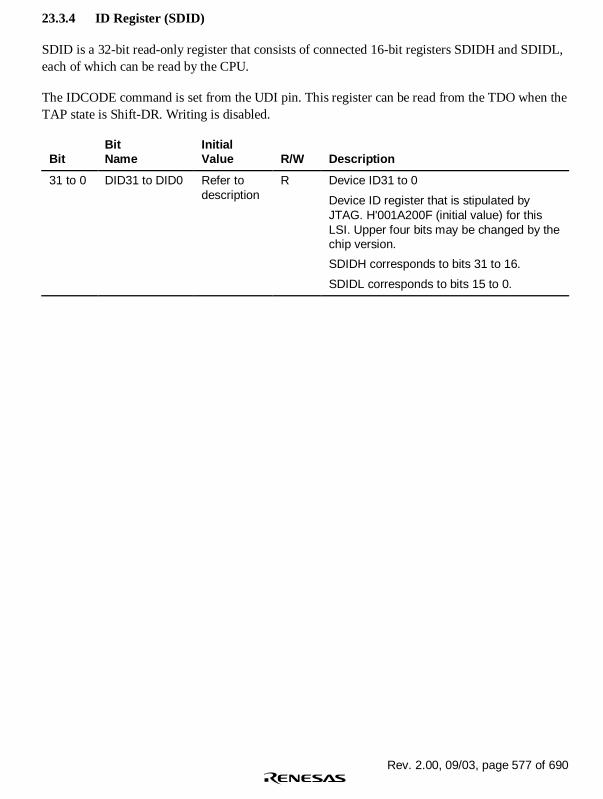
Rev. 2.00, 09/03, page 577 of 690
23.3.4 ID Register (SDID)
SDID is a 32-bit read-only register that consists of connected 16-bit registers SDIDH and SDIDL,each of which can be read by the CPU.
The IDCODE command is set from the UDI pin. This register can be read from the TDO when theTAP state is Shift-DR. Writing is disabled.
BitBitName
InitialValue R/W Description
31 to 0 DID31 to DID0 Refer todescription
R Device ID31 to 0
Device ID register that is stipulated byJTAG. H'001A200F (initial value) for thisLSI. Upper four bits may be changed by thechip version.
SDIDH corresponds to bits 31 to 16.
SDIDL corresponds to bits 15 to 0.

Rev. 2.00, 09/03, page 578 of 690
23.4 Operation
23.4.1 TAP Controller
Figure 23.2 shows the internal states of the TAP controller. State transitions basically conform tothe JTAG standard.
Test-logic-reset
Capture-DR
Shift-DR
Exit1-DR
Pause-DR
Exit2-DR
Update-DR
Select-DR-scanRun-test/idle
1
0
0
0
01 1
1
1
0
0
1
0
1
1
1 0
Capture-IR
Shift-IR
Exit1-IR
Pause-IR
Exit2-IR
Update-IR
Select-IR-scan
0
0
1
0
0
1
1
0
1
1
1 0
0
Figure 23.2 TAP Controller State Transitions
Note: The transition condition is the TMS value at the rising edge of TCK. The TDI value issampled at the rising edge of TCK; shifting occurs at the falling edge of TCK. For detailson change timing of the TDO value, see section 23.4.3, TDO Output Timing. The TDO isat high impedance, except with shift-DR and shift-IR states. During the change to TRST =0, there is a transition to test-logic-reset asynchronously with TCK.

Rev. 2.00, 09/03, page 579 of 690
23.4.2 Reset Configuration
Table 23.4 Reset Configuration
ASEMD0*1RESETP TRST Chip State
H L L Normal reset and UDI reset*4
H Normal reset*4
H L UDI reset only
H Normal operation
L L L Reset hold*2
H In ASE user mode*3: Normal reset
In ASE break mode*3: RESETP assert ismasked
H L UDI reset only
H Normal operation
Notes: 1. Performs normal mode and ASE mode settingsASEMD0 = H, normal modeASEMD0 = L, ASE mode
2. In ASE mode, reset hold is enabled by driving the RESETP and TRST pins low for aconstant cycle. In this state, the CPU does not start up, even if RESETP is driven high.When TRST is driven high, UDI operation is enabled, but the CPU does not start up.The reset hold state is canceled by the following:• Another RESETP assert (power-on reset)• TRST reassert
3. ASE mode is classified into two modes; ASE break mode to execute the firm programof an emulator and ASE user mode to execute the user program.
4. Make sure the TRST pin is low when the power is turned on.
23.4.3 TDO Output Timing
The timing of data output from the TDO is switched by the command type set in the SDIR. Thetiming changes at the TCK falling edge when JTAG commands (EXTEST, CLAMP, HIGHZ,SAMPLE/PRELOAD, IDCODE, and BYPASS) are set. This is a timing of the JTAG standard.When the UDI commands (UDI reset negate, UDI reset assert, and UDI interrupt) are set, TDO isoutput at the TCK rising edge earlier than the JTAG standard by a half cycle.

Rev. 2.00, 09/03, page 580 of 690
TDO(when the UDI command is set)
TCK
TDO(when the boundary scan command is set)
tTDO
tTDO
Figure 23.3 UDI Data Transfer Timing
23.4.4 UDI Reset
An UDI reset is executed by setting an UDI reset assert command in SDIR. An UDI reset is of thesame kind as a power-on reset. An UDI reset is released by inputting an UDI reset negatecommand. The required time between the UDI reset assert command and UDI reset negatecommand is the same as time for keeping the RESETP pin low to apply a power-on reset.
UDI reset assert UDI reset negateSDIR
Chip internal reset
CPU state Branch to H'A0000000
Figure 23.4 UDI Reset
23.4.5 UDI Interrupt
The UDI interrupt function generates an interrupt by setting a command from the UDI in theSDIR. An UDI interrupt is a general exception/interrupt operation, resulting in a branch to anaddress based on the VBR value plus offset, and with return by the RTE instruction. This interruptrequest has a fixed priority level of 15.
UDI interrupts are accepted in sleep mode, but not in standby mode.

Rev. 2.00, 09/03, page 581 of 690
23.5 Boundary Scan
A command can be set in SDIR by the UDI to place the UDI pins in boundary scan modestipulated by JTAG.
23.5.1 Supported Instructions
This LSI supports the three essential instructions defined in the JTAG standard (BYPASS,SAMPLE/PRELOAD, and EXTEST) and three option instructions (IDCODE, CLAMP, andHIGHZ).
1. BYPASS:
The BYPASS instruction is an essential standard instruction that operates the bypass register.This instruction shortens the shift path to speed up serial data transfer involving other chips onthe printed circuit board. While this instruction is executing, the test circuit has no effect on thesystem circuits. The upper four bits of the instruction code are 1111.
2. SAMPLE/PRELOAD:
The SAMPLE/PRELOAD instruction inputs values from this LSI's internal circuitry to theboundary scan register, outputs values from the scan path, and loads data onto the scan path.When this instruction is executing, this LSI's input pin signals are transmitted directly to theinternal circuitry, and internal circuit values are directly output externally from the output pins.This LSI's system circuits are not affected by execution of this instruction. The upper four bitsof the instruction code are 0100.
In a SAMPLE operation, a snapshot of a value to be transferred from an input pin to theinternal circuitry, or a value to be transferred from the internal circuitry to an output pin, islatched into the boundary scan register and read from the scan path. Snapshot latching isperformed in synchronization with the rise of TCK in the Capture-DR state. Snapshot latchingdoes not affect normal operation of this LSI.
In a PRELOAD operation, an initial value is set in the parallel output latch of the boundaryscan register from the scan path prior to the EXTEST instruction. Without a PRELOADoperation, when the EXTEST instruction was executed an undefined value would be outputfrom the output pin until completion of the initial scan sequence (transfer to the output latch)(with the EXTEST instruction, the parallel output latch value is constantly output to the outputpin).

Rev. 2.00, 09/03, page 582 of 690
3. EXTEST:
This instruction is provided to test external circuitry when this LSI is mounted on a printedcircuit board. When this instruction is executed, output pins are used to output test data(previously set by the SAMPLE/PRELOAD instruction) from the boundary scan register to theprinted circuit board, and input pins are used to latch test results into the boundary scanregister from the printed circuit board. If testing is carried out by using the EXTESTinstruction N times, the Nth test data is scanned-in when test data (N-1) is scanned out.
Data loaded into the output pin boundary scan register in the Capture-DR state is not used forexternal circuit testing (it is replaced by a shift operation).
The upper four bits of the instruction code are 0000.
4. IDCODE:
A command can be set in SDIR by the UDI pins to place the UDI pins in the IDCODE modestipulated by JTAG. When the UDI is initialized (TRST is asserted or TAP is in the Test-Logic-Reset state), the IDCODE mode is entered.
5. CLAMP, HIGHZ:
A command can be set in SDIR by the UDI pins to place the UDI pins in the CLAMP orHIGHZ mode stipulated by JTAG.
23.5.2 Points for Attention
1. Boundary scan mode does not cover clock-related signals (EXTAL, EXTAL2, XTAL,XTAL2, EXTAL_USB, XTAL_USB, and CKIO).
2. Boundary scan mode does not cover reset-related signals (RESETP, RESETM, and CA).
3. Boundary scan mode does not cover UDI-related signals (TCK, TDI, TDO, TMS, and TRST).
4. Fix the RESETP pin low during boundary scan.
5. Fix the CA pin high during boundary scan.
6. Fix the ASEMD0 pin high during boundary scan.
7. The CKIO cock should operate during boundary scan. The MD[2:0] pin should be set to theclock mode used during normal operation, and EXTAL and CKIO should be set within thefrequency range specified in the Clock Pulse Generator (CPG) section.
As during normal operation, the boundary scan test should be performed after allowingsufficient settling time for the crystal oscillator, PLL1, and PLL2.

Rev. 2.00, 09/03, page 583 of 690
23.6 Usage Notes
1. An UDI command, once set, will not be modified as long as another command is not re-issuedfrom the UDI. If the same command is given continuously, the command must be set after acommand (BYPASS, etc.) that does not affect chip operations is once set.
2. Because chip operations are suspended in standby mode, UDI commands are not accepted. Tokeep the TAP state constant before and after standby mode, TCK must be high during standbymode transition.
3. The UDI is used for emulator connection. Therefore, UDI functions cannot be used when usingan emulator.
23.7 Advanced User Debugger (AUD)
The AUD is a function only for an emulator. For details on the AUD, refer to each emulator’sUser’s Manual.

Rev. 2.00, 09/03, page 584 of 690

Rev. 2.00, 09/03, page 585 of 690
Section 24 List of Registers
This section gives information on the on-chip I/O registers and is configured as describedbelow.
1. Register Addresses (by functional module, in order of the corresponding section numbers)
• Descriptions by functional module, in order of the corresponding section numbersEntries that consist of lines are for separation of the functional modules.
• Access to reserved addresses which are not described in this list is prohibited.
• When registers consist of 16 or 32 bits, the addresses of the MSBs are given, on thepresumption of a big-endian system.
2. Register Bits
• Bit configurations of the registers are described in the same order as the Register Addresses(by functional module, in order of the corresponding section numbers).
• Reserved bits are indicated by in the bit name.
• No entry in the bit-name column indicates that the whole register is allocated as a counter orfor holding data.
• When registers consist of 16 or 32 bits, bits are described from the MSB side.The order in which bytes are described is on the presumption of a big-endian system.
3. Register States in Each Operating Mode
• Register states are described in the same order as the Register Addresses (by functionalmodule, in order of the corresponding section numbers).
• For the initial state of each bit, refer to the description of the register in the correspondingsection.
• The register states described are for the basic operating modes. If there is a specific reset foran on-chip module, refer to the section on that on-chip module.

Rev. 2.00, 09/03, page 586 of 690
24.1 Register Addresses(by functional module, in order of the corresponding sectionnumbers)
Entries under Access size indicates numbers of bits.
Note: Access to undefined or reserved addresses is prohibited. Since operation or continuedoperation is not guaranteed when these registers are accessed, do not attempt suchaccess.
Register Name AbbreviationNumberof Bits Address Module
AccessSize
MMU control register MMUCR 32 H'FFFF FFE0 MMU 32
Page table entry register high PTEH 32 H'FFFF FFF0 32
Page table entry register low PTEL 32 H'FFFF FFF4 32
Translation table base register TTB 32 H'FFFF FFF8 32
Cache control register 1 CCR1 32 H'FFFF FFEC Cache 32
Cache control register 2 CCR2 32 H'A400 00B0 32
Cache control register 3 CCR3 32 H'A400 00B4 32
Interrupt event register 2 INTEVT2 32 H'A400 0000 32
TRAPA exception register TRA 32 H'FFFF FFD0
Exceptionhandling 32
Exception event register EXPEVT 32 H'FFFF FFD4 32
Interrupt event register INTEVT 32 H'FFFF FFD8 32
TLB exception address register TEA 32 H'FFFF FFFC 32
Interrupt priority level setting register A IPRA 16 H'FFFF FEE2 INTC 16
Interrupt priority level setting register B IPRB 16 H'FFFF FEE4 16
Interrupt priority level setting register C IPRC 16 H'A400 0016 16
Interrupt priority level setting register D IPRD 16 H'A400 0018 16
Interrupt priority level setting register E IPRE 16 H'A400 001A 16
Interrupt priority level setting register F IPRF 16 H'A408 0000 16
Interrupt priority level setting register G IPRG 16 H'A408 0002 16
Interrupt priority level setting register H IPRH 16 H'A408 0004 16
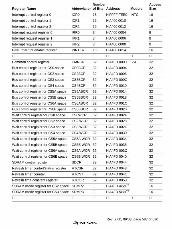
Rev. 2.00, 09/03, page 587 of 690
Register Name AbbreviationNumberof Bits Address Module
AccessSize
Interrupt control register 0 ICR0 16 H'FFFF FEE0 INTC 16
Interrupt control register 1 ICR1 16 H'A400 0010 16
Interrupt control register 2 ICR2 16 H'A400 0012 16
Interrupt request register 0 IRR0 8 H'A400 0004 8
Interrupt request register 1 IRR1 8 H'A400 0006 8
Interrupt request register 2 IRR2 8 H'A400 0008 8
PINT interrupt enable register PINTER 16 H'A400 0014 16
Common control register CMNCR 32 H'A4FD 0000 BSC 32
Bus control register for CS0 space CS0BCR 32 H'A4FD 0004 32
Bus control register for CS2 space CS2BCR 32 H'A4FD 0008 32
Bus control register for CS3 space CS3BCR 32 H'A4FD 000C 32
Bus control register for CS4 space CS4BCR 32 H'A4FD 0010 32
Bus control register for CS5A space CS5ABCR 32 H'A4FD 0014 32
Bus control register for CS5B space CS5BBCR 32 H'A4FD 0018 32
Bus control register for CS6A space CS6ABCR 32 H'A4FD 001C 32
Bus control register for CS6B space CS6BBCR 32 H'A4FD 0020 32
Wait control register for CS0 space CS0WCR 32 H'A4FD 0024 32
Wait control register for CS2 space CS2 WCR 32 H'A4FD 0028 32
Wait control register for CS3 space CS3 WCR 32 H'A4FD 002C 32
Wait control register for CS4 space CS4 WCR 32 H'A4FD 0030 32
Wait control register for CS5A space CS5A WCR 32 H'A4FD 0034 32
Wait control register for CS5B space CS5B WCR 32 H'A4FD 0038 32
Wait control register for CS6A space CS6A WCR 32 H'A4FD 003C 32
Wait control register for CS6B space CS6B WCR 32 H'A4FD 0040 32
SDRAM control register SDCR 32 H'A4FD 0044 32
Refresh timer control/status register RTCSR 32 H'A4FD 0048 32
Refresh timer counter RTCNT 32 H'A4FD 004C 32
Refresh time constant register RTCOR 32 H'A4FD 0050 32
SDRAM mode register for CS2 space SDMR2 H'A4FD 4xxx*2 16
SDRAM mode register for CS3 space SDMR3 H'A4FD 5xxx*2 16

Rev. 2.00, 09/03, page 588 of 690
Register Name AbbreviationNumberof Bits Address Module
AccessSize
DMA source address register_0 SAR_0 32 H'A400 0020 DMAC 16/32
DMA destination address register_0 DAR_0 32 H'A400 0024 16/32
DMA transfer count register_0 DMATCR_0 32 H'A400 0028 16/32
DMA channel control register_0 CHCR_0 32 H'A400 002C 8/16/32
DMA source address register_1 SAR_1 32 H'A400 0030 16/32
DMA destination address register_1 DAR_1 32 H'A400 0034 16/32
DMA transfer count register_1 DMATCR_1 32 H'A400 0038 16/32
DMA channel control register_1 CHCR_1 32 H'A400 003C 8/16/32
DMA source address register_2 SAR_2 32 H'A400 0040 16/32
DMA destination address register_2 DAR_2 32 H'A400 0044 16/32
DMA transfer count register_2 DMATCR_2 32 H'A400 0048 16/32
DMA channel control register_2 CHCR_2 32 H'A400 004C 8/16/32
DMA source address register_3 SAR_3 32 H'A400 0050 16/32
DMA destination address register_3 DAR_3 32 H'A400 0054 16/32
DMA transfer count register_3 DMATCR_3 32 H'A400 0058 16/32
DMA channel control register_3 CHCR_3 32 H'A400 005C 8/16/32
DMA operation register DMAOR 16 H'A400 0060 8/16
DMA extended resource selector 0 DMARS0 16 H'A409 0000 16
DMA extended resource selector 1 DMARS1 16 H'A409 0004 16
USB clock control register UCLKCR 8 H'A40A 0008 CPG 8/16*1
Frequency control register FRQCR 16 H'FFFF FF80 16
Watchdog timer counter WTCNT 8 H'FFFF FF84 WDT 8/16*1
Watchdog timer control/status register WTCSR 8 H'FFFF FF86 8/16*1
Standby control register STBCR 8 H'FFFF FF82 8
Standby control register 2 STBCR2 8 H'FFFF FF88 8
Standby control register 3 STBCR3 8 H'A40A 0000
Power-downmodes
8

Rev. 2.00, 09/03, page 589 of 690
Register Name AbbreviationNumberof Bits Address Module
AccessSize
Timer start register TSTR 8 H'FFFF FE92 TMU 8
Timer constant register_0 TCOR_0 32 H'FFFF FE94 32
Timer counter_0 TCNT_0 32 H'FFFF FE98 32
Timer control register_0 TCR_0 16 H'FFFF FE9C 16
Timer constant register_1 TCOR_1 32 H'FFFF FEA0 32
Timer counter_1 TCNT_1 32 H'FFFF FEA4 32
Timer control register_1 TCR_1 16 H'FFFF FEA8 16
Timer constant register_2 TCOR_2 32 H'FFFF FEAC 32
Timer counter_2 TCNT_2 32 H'FFFF FEB0 32
Timer control register_2 TCR_2 16 H'FFFF FEB4 16
Input capture register_2 TCPR_2 32 H'FFFF FEB8 32
Compare match timer start register CMSTR 16 H'A400 0070 CMT 16
Compare match timer control/statusregister
CMCSR 16 H'A400 0074 16
Compare match timer counter CMCNT 16 H'A400 0078 16
Compare match timer constant register CMCOR 16 H'A400 007C 16
Timer start register TSTR 16 H'A449 0000 TPU 16
Timer control register_0 TCR_0 16 H'A449 0010 16
Timer mode register_0 TMDR_0 16 H'A449 0014 16
Timer I/O control register_0 TIOR_0 16 H'A449 0018 16
Timer interrupt enable register_0 TIER_0 16 H'A449 001C 16
Timer status register_0 TSR_0 16 H'A449 0020 16
Timer counter_0 TCNT_0 16 H'A449 0024 16
Timer general register A_0 TGRA_0 16 H'A449 0028 16
Timer general register B_0 TGRB_0 16 H'A449 002C 16
Timer general register C_0 TGRC_0 16 H'A449 0030 16
Timer general register D_0 TGRD_0 16 H'A449 0034 16
Timer control register_1 TCR_1 16 H'A449 0050 16
Timer mode register_1 TMDR_1 16 H'A449 0054 16
Timer I/O control register_1 TIOR_1 16 H'A449 0058 16

Rev. 2.00, 09/03, page 590 of 690
Register Name AbbreviationNumberof Bits Address Module
AccessSize
Timer interrupt enable register_1 TIER_1 16 H'A449 005C TPU 16
Timer status register_1 TSR_1 16 H'A449 0060 16
Timer counter_1 TCNT_1 16 H'A449 0064 16
Timer general register A_1 TGRA_1 16 H'A449 0068 16
Timer general register B_1 TGRB_1 16 H'A449 006C 16
Timer general register C_1 TGRC_1 16 H'A449 0070 16
Timer general register D_1 TGRD_1 16 H'A449 0074 16
Timer control register_2 TCR_2 16 H'A449 0090 16
Timer mode register_2 TMDR_2 16 H'A449 0094 16
Timer I/O control register_2 TIOR_2 16 H'A449 0098 16
Timer interrupt enable register_2 TIER_2 16 H'A449 009C 16
Timer status register_2 TSR_2 16 H'A449 00A0 16
Timer counter_2 TCNT_2 16 H'A449 00A4 16
Timer general register A_2 TGRA_2 16 H'A449 00A8 16
Timer general register B_2 TGRB_2 16 H'A449 00AC 16
Timer general register C_2 TGRC_2 16 H'A449 00B0 16
Timer general register D_2 TGRD_2 16 H'A449 00B4 16
Timer control register_3 TCR_3 16 H'A449 00D0 16
Timer mode register_3 TMDR_3 16 H'A449 00D4 16
Timer I/O control register_3 TIOR_3 16 H'A449 00D8 16
Timer interrupt enable register_3 TIER_3 16 H'A449 00DC 16
Timer status register_3 TSR_3 16 H'A449 00E0 16
Timer counter_3 TCNT_3 16 H'A449 00E4 16
Timer general register A_3 TGRA_3 16 H'A449 00E8 16
Timer general register B_3 TGRB_3 16 H'A449 00EC 16
Timer general register C_3 TGRC_3 16 H'A449 00F0 16
Timer general register D_3 TGRD_3 16 H'A449 00F4 16

Rev. 2.00, 09/03, page 591 of 690
Register Name AbbreviationNumberof Bits Address Module
AccessSize
64-Hz counter R64CNT 8 H'FFFF FEC0 RTC 8
Second counter RSECCNT 8 H'FFFF FEC2 8
Minute counter RMINCNT 8 H'FFFF FEC4 8
Hour counter RHRCNT 8 H'FFFF FEC6 8
Day of week counter RWKCNT 8 H'FFFF FEC8 8
Date counter RDAYCNT 8 H'FFFF FECA 8
Month counter RMONCNT 8 H'FFFF FECC 8
Year counter RYRCNT 16 H'FFFF FECE 16
Second alarm register RSECAR 8 H'FFFF FED0 8
Minute alarm register RMINAR 8 H'FFFF FED2 8
Hour alarm register RHRAR 8 H'FFFF FED4 8
Day of week alarm register RWKAR 8 H'FFFF FED6 8
Date alarm register RDAYAR 8 H'FFFF FED8 8
Month alarm register RMONAR 8 H'FFFF FEDA 8
RTC control register 1 RCR1 8 H'FFFF FEDC 8
RTC control register 2 RCR2 8 H'FFFF FEDE 8
Year alarm register RYRAR 16 H'A413 FEE0 16
RTC control register 3 RCR3 8 H'A413 FEE4 8
Serial mode register_0 SCSMR_0 16 H'A440 0000 SCIF_0 16
Bit rate register_0 SCBRR_0 8 H'A440 0004 (Channel 0) 8
Serial control register_0 SCSCR_0 16 H'A440 0008 16
Transmit data stop register_0 SCTDSR_0 8 H'A440 000C 8
FIFO error count register_0 SCFER_0 16 H'A440 0010 16
Serial status register_0 SCSSR_0 16 H'A440 0014 16
FIFO control register_0 SCFCR_0 16 H'A440 0018 16
FIFO data count register_0 SCFDR_0 16 H'A440 001C 16
Transmit FIFO data register_0 SCFTDR_0 8 H'A440 0020 8
Receive FIFO data register_0 SCFRDR_0 8 H'A440 0024 8

Rev. 2.00, 09/03, page 592 of 690
Register Name AbbreviationNumberof Bits Address Module
AccessSize
Serial mode register_2 SCSMR_2 16 H'A441 0000 SCIF_2 16
Bit rate register_2 SCBRR_2 8 H'A441 0004 (Channel 2) 8
Serial control register_2 SCSCR_2 16 H'A441 0008 16
Transmit data stop register_2 SCTDSR_2 8 H'A441 000C 8
FIFO error count register_2 SCFER_2 16 H'A441 0010 16
Serial status register_2 SCSSR_2 16 H'A441 0014 16
FIFO control register_2 SCFCR_2 16 H'A441 0018 16
FIFO data count register_2 SCFDR_2 16 H'A441 001C 16
Transmit FIFO data register_2 SCFTDR_2 8 H'A441 0020 8
Receive FIFO data register_2 SCFRDR_2 8 H'A441 0024 8
IrDA mode register SCSMR_Ir 16 H'A44A 0000 IrDA 16
EP0i data register EPDR0i 8B H'A448 0000 USB 8
EP0o data register EPDR0o 8B H'A448 0004 8
EP0s data register EPDR0s 8B H'A448 0008 8
EP1 data register EPDR1 128B H'A448 000C 8/32
EP2 data register EPDR2 128B H'A448 0010 8/32
EP3 data register EPDR3 8B H'A448 0014 8
Interrupt flag register 0 IFR0 8 H'A448 0018 8
Interrupt flag register 1 IFR1 8 H'A448 001C 8
Trigger register TRG 8 H'A448 0020 8
FIFO clear register FCLR 8 H'A448 0024 8
EP0o receive data size register EPSZ0o 8 H'A448 0028 8
Data status register DASTS 8 H'A448 002C 8
Endpoint stall register EPSTL 8 H'A448 0030 8
Interrupt enable register 0 IER0 8 H'A448 0034 8
Interrupt enable register 1 IER1 8 H'A448 0038 8
EP1 receive data size register EPSZ1 8 H'A448 003C 8
DMA transfer setting register DMAR 8 H'A448 0040 8
Interrupt select register 0 ISR0 8 H'A448 0044 8
Interrupt select register 1 ISR1 8 H'A448 0048 8
Transceiver control register XVERCR 8 H'A448 0060 8

Rev. 2.00, 09/03, page 593 of 690
Register Name AbbreviationNumberof Bits Address Module
AccessSize
Port A control register PACR 16 H'A400 0100 PFC 16
Port B control register PBCR 16 H'A400 0102 16
Port C control register PCCR 16 H'A400 0104 16
Port D control register PDCR 16 H'A400 0106 16
Port E control register PECR 16 H'A400 0108 16
Port E control register 2 PECR2 8 H'A405 0148 8
Port F control register PFCR 16 H'A400 010A 16
Port F control register 2 PFCR2 8 H'A405 014A 8
Port G control register PGCR 16 H'A400 010C 16
Port H control register PHCR 16 H'A400 010E 16
Port J control register PJCR 16 H'A400 0110 16
Port K control register PKCR 16 H'A400 0112 16
Port L control register PLCR 16 H'A400 0114 16
Port SC control register SCPCR 16 H'A400 0116 16
Port M control register PMCR 16 H'A400 0118 16
Port N control register PNCR 16 H'A400 011A 16
Port N control register 2 PNCR2 8 H'A405 015A 8
Port A data register PADR 8 H'A400 0120 Port 8
Port B data register PBDR 8 H'A400 0122 8
Port C data register PCDR 8 H'A400 0124 8
Port D data register PDDR 8 H'A400 0126 8
Port E data register PEDR 8 H'A400 0128 8
Port F data register PFDR 8 H'A400 012A 8
Port G data register PGDR 8 H'A400 012C 8
Port H data register PHDR 8 H'A400 012E 8
Port J data register PJDR 8 H'A400 0130 8
Port K data register PKDR 8 H'A405 0132 8
Port L data register PLDR 8 H'A400 0134 8
SC port data register SCPDR 8 H'A400 0136 8
Port M data register PMDR 8 H'A400 0138 8
Port N data register PNDR 8 H'A400 013A 8

Rev. 2.00, 09/03, page 594 of 690
Register Name AbbreviationNumberof Bits Address Module
AccessSize
A/D data register A ADDRA 16 H'A400 0080 ADC 16
A/D data register B ADDRB 16 H'A400 0082 16
A/D data register C ADDRC 16 H'A400 0084 16
A/D data register D ADDRD 16 H'A400 0086 16
A/D control/status register ADCSR 16 H'A400 0088 16
Break data register B BDRB 32 H'FFFF FF90 UBC 32
Break data mask register B BDMRB 32 H'FFFF FF94 32
Break control register BRCR 32 H'FFFF FF98 32
Execution count break register BETR 16 H'FFFF FF9C 16
Break address register B BARB 32 H'FFFF FFA0 32
Break address mask register B BAMRB 32 H'FFFF FFA4 32
Break bus cycle register B BBRB 16 H'FFFF FFA8 16
Branch source register BRSR 32 H'FFFF FFAC 32
Break address register A BARA 32 H'FFFF FFB0 32
Break address mask register A BAMRA 32 H'FFFF FFB4 32
Break bus cycle register A BBRA 16 H'FFFF FFB8 16
Branch destination register BRDR 32 H'FFFF FFBC 32
Break ASID register A BASRA 8 H'FFFF FFE4 8
Break ASID register B BASRB 8 H'FFFF FFE8 8
Instruction register SDIR 16 H'A400 0200 UDI 16
ID register SDID/SDIDH 16 H'A400 0214 16
ID register SDIDL 16 H'A400 0216 16
Notes: 1. 8 bits when reading and 16 bits when writing.2. The value of xxx depends on the setting value because of access control for the
SDRAM mode register.

Rev. 2.00, 09/03, page 595 of 690
24.2 Register Bits
Register addresses and bit names of the on-chip peripheral modules are described below.
Each line covers eight bits, and 16-bit and 32-bit registers are shown as 2 or 4 lines,respectively.
RegisterAbbreviation
Bit 31/23/15/7
Bit 30/22/14/6
Bit 29/21/13/5
Bit 28/20/12/4
Bit 27/19/11/3
Bit 26/18/10/2
Bit 25/17/9/1
Bit 24/16/8/0 Module
MMUCR MMU
SV
RC1 RC0 TF IX AT
PTEH VPN VPN VPN VPN VPN VPN VPN VPN
VPN VPN VPN VPN VPN VPN VPN VPN
VPN VPN VPN VPN VPN VPN
ASID7 ASID6 ASID5 ASID4 ASID3 ASID2 ASID1 ASID0
PTEL PPN PPN PPN PPN PPN
PPN PPN PPN PPN PPN PPN PPN PPN
PPN PPN PPN PPN PPN PPN V
PR1 PR0 SZ C D SH
TTB

Rev. 2.00, 09/03, page 596 of 690
RegisterAbbreviation
Bit 31/23/15/7
Bit 30/22/14/6
Bit 29/21/13/5
Bit 28/20/12/4
Bit 27/19/11/3
Bit 26/18/10/2
Bit 25/17/9/1
Bit 24/16/8/0 Module
CCR1 Cache
CF CB WT CE
CCR2
LE
W3LOADW3LOCK
W2LOADW2LOCK
CCR3
CSIZE7 CSIZE6 CSIZE5 CSIZE4 CSIZE3 CSIZE2 CSIZE1 CSIZE0
INTEVT2
Exceptionhanding
TRA
imm imm
imm imm imm imm imm imm
EXPEVT
INTEVT

Rev. 2.00, 09/03, page 597 of 690
RegisterAbbreviation
Bit 31/23/15/7
Bit 30/22/14/6
Bit 29/21/13/5
Bit 28/20/12/4
Bit 27/19/11/3
Bit 26/18/10/2
Bit 25/17/9/1
Bit 24/16/8/0 Module
TEA Exceptionhanding
IPRA IPR15 IPR14 IPR13 IPR12 IPR11 IPR10 IPR9 IPR8 INTC
IPR7 IPR6 IPR5 IPR4 IPR3 IPR2 IPR1 IPR0
IPRB IPR15 IPR14 IPR13 IPR12 IPR11 IPR10 IPR9 IPR8
IPR7 IPR6 IPR5 IPR4 IPR3 IPR2 IPR1 IPR0
IPRC IPR15 IPR14 IPR13 IPR12 IPR11 IPR10 IPR9 IPR8
IPR7 IPR6 IPR5 IPR4 IPR3 IPR2 IPR1 IPR0
IPRD IPR15 IPR14 IPR13 IPR12 IPR11 IPR10 IPR9 IPR8
IPR7 IPR6 IPR5 IPR4 IPR3 IPR2 IPR1 IPR0
IPRE IPR15 IPR14 IPR13 IPR12 IPR11 IPR10 IPR9 IPR8
IPR7 IPR6 IPR5 IPR4 IPR3 IPR2 IPR1 IPR0
IPRF IPR15 IPR14 IPR13 IPR12 IPR11 IPR10 IPR9 IPR8
IPR7 IPR6 IPR5 IPR4 IPR3 IPR2 IPR1 IPR0
IPRG IPR15 IPR14 IPR13 IPR12 IPR11 IPR10 IPR9 IPR8
IPR7 IPR6 IPR5 IPR4 IPR3 IPR2 IPR1 IPR0
IPRH IPR15 IPR14 IPR13 IPR12 IPR11 IPR10 IPR9 IPR8
IPR7 IPR6 IPR5 IPR4 IPR3 IPR2 IPR1 IPR0
ICR0 NMIL NMIE
ICR1 MAI IRQLVL BLMSK IRQ51S IRQ50S IRQ41S IRQ40S
IRQ31S IRQ30S IRQ21S IRQ20S IRQ11S IRQ10S IRQ01S IRQ00S
ICR2 PINT15S PINT14S PINT13S PINT12S PINT11S PINT10S PINT9S PINT8S
PINT7S PINT6S PINT5S PINT4S PINT3S PINT2S PINT1S PINT0S
IRR0 PINT0R PINT1R IRQ5R IRQ4R IRQ3R IRQ2R IRQ1R IRQ0R
IRR1 TXI0R RXI0R ERI0R DEI3R DEI2R DEI1R DEI0R
IRR2 ADIR TXI2R RXI2R ERI2R
PINTER PINT15E PINT14E PINT13E PINT12E PINT11E PINT10E PINT9E PINT8E
PINT7E PINT6E PINT5E PINT4E PINT3E PINT2E PINT1E PINT0E

Rev. 2.00, 09/03, page 598 of 690
RegisterAbbreviation
Bit 31/23/15/7
Bit 30/22/14/6
Bit 29/21/13/5
Bit 28/20/12/4
Bit 27/19/11/3
Bit 26/18/10/2
Bit 25/17/9/1
Bit 24/16/8/0 Module
CMNCR BSC
DMAIW1 DMAIW0 DMAIWA ENDIAN HIZMEM HIZCNT
CS0BCR IWW1 IWW0 IWRWD1 IWRWD0
IWRWS1 IWRWS0 IWRRD1 IWRRD0 IWRRS1 IWRRS0
TYPE2 TYPE1 TYPE0 BSZ1 BSZ0
CS2BCR IWW1 IWW0 IWRWD1 IWRWD0
IWRWS1 IWRWS0 IWRRD1 IWRRD0 IWRRS1 IWRRS0
TYPE2 TYPE1 TYPE0 BSZ1 BSZ0
CS3BCR IWW1 IWW0 IWRWD1 IWRWD0
IWRWS1 IWRWS0 IWRRD1 IWRRD0 IWRRS1 IWRRS0
TYPE2 TYPE1 TYPE0 BSZ1 BSZ0
CS4BCR IWW1 IWW0 IWRWD1 IWRWD0
IWRWS1 IWRWS0 IWRRD1 IWRRD0 IWRRS1 IWRRS0
TYPE2 TYPE1 TYPE0 BSZ1 BSZ0
CS5ABCR IWW1 IWW0 IWRWD1 IWRWD0
IWRWS1 IWRWS0 IWRRD1 IWRRD0 IWRRS1 IWRRS0
TYPE2 TYPE1 TYPE0 BSZ1 BSZ0
CS5BBCR IWW1 IWW0 IWRWD1 IWRWD0
IWRWS1 IWRWS0 IWRRD1 IWRRD0 IWRRS1 IWRRS0
TYPE2 TYPE1 TYPE0 BSZ1 BSZ0
CS6ABCR IWW1 IWW0 IWRWD1 IWRWD0
IWRWS1 IWRWS0 IWRRD1 IWRRD0 IWRRS1 IWRRS0
TYPE2 TYPE1 TYPE0 BSZ1 BSZ0

Rev. 2.00, 09/03, page 599 of 690
RegisterAbbreviation
Bit 31/23/15/7
Bit 30/22/14/6
Bit 29/21/13/5
Bit 28/20/12/4
Bit 27/19/11/3
Bit 26/18/10/2
Bit 25/17/9/1
Bit 24/16/8/0 Module
CS6BBCR IWW1 IWW0 IWRWD1 IWRWD0 BSC
IWRWS1 IWRWS0 IWRRD1 IWRRD0 IWRRS1 IWRRS0
TYPE2 TYPE1 TYPE0 BSZ1 BSZ0
SW1 SW0 WR3 WR2 WR1
CS0WCR(except burstROM)
WR0 WM HW1 HW0
BW1 BW0
W3 W2 W1
CS0WCR(burst ROM)
W0 WM
WR3 WR2 WR1
CS2 WCR(exceptSDRAM)
WR0 WM
A2CL1
CS2 WCR(SDRAM)
A2CL0
WR3 WR2 WR1
CS3 WCR(exceptSDRAM)
WR0 WM
TRP1 TRP0 TRCD1 TRCD0 A3CL1
CS3 WCR(SDRAM)
A3CL0 TRWL1 TRWL0 TRC1 TRC0
WW2 WW1 WW0
SW1 SW0 WR3 WR2 WR1
CS4 WCR(except burstROM)
WR0 WM HW1 HW0
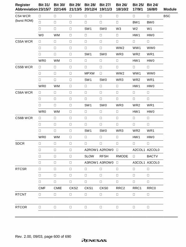
Rev. 2.00, 09/03, page 600 of 690
RegisterAbbreviation
Bit 31/23/15/7
Bit 30/22/14/6
Bit 29/21/13/5
Bit 28/20/12/4
Bit 27/19/11/3
Bit 26/18/10/2
Bit 25/17/9/1
Bit 24/16/8/0 Module
BSC
BW1 BW0
SW1 SW0 W3 W2 W1
CS4 WCR(burst ROM)
W0 WM HW1 HW0
CS5A WCR
WW2 WW1 WW0
SW1 SW0 WR3 WR2 WR1
WR0 WM HW1 HW0
CS5B WCR
MPXW WW2 WW1 WW0
SW1 SW0 WR3 WR2 WR1
WR0 WM HW1 HW0
CS6A WCR
SW1 SW0 WR3 WR2 WR1
WR0 WM HW1 HW0
CS6B WCR
SW1 SW0 WR3 WR2 WR1
WR0 WM HW1 HW0
SDCR
A2ROW1 A2ROW0 A2COL1 A2COL0
SLOW RFSH RMODE BACTV
A3ROW1 A3ROW0 A3COL1 A3COL0
RTCSR
CMF CMIE CKS2 CKS1 CKS0 RRC2 RRC1 RRC0
RTCNT
RTCOR

Rev. 2.00, 09/03, page 601 of 690
RegisterAbbreviation
Bit 31/23/15/7
Bit 30/22/14/6
Bit 29/21/13/5
Bit 28/20/12/4
Bit 27/19/11/3
Bit 26/18/10/2
Bit 25/17/9/1
Bit 24/16/8/0 Module
SDMR2 BSC
SDMR3
SAR_0 DMAC
DAR_0
DMATCR_0
CHCR_0
DO TL AM AL
DM1 DM0 SM1 SM0 RS3 RS2 RS1 RS0
DL DS TB TS1 TS0 IE TE DE
SAR_1
DAR_1
DMATCR_1
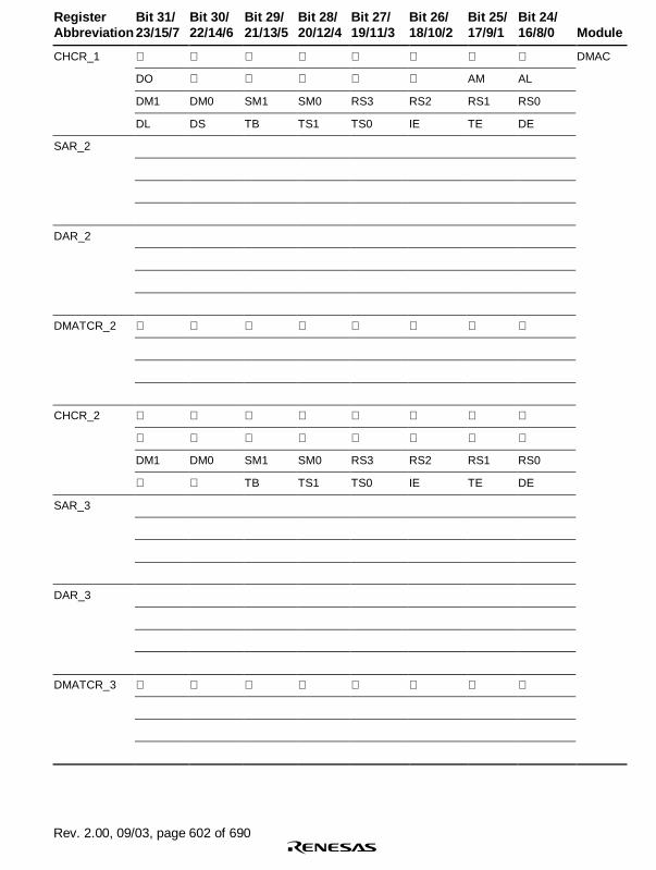
Rev. 2.00, 09/03, page 602 of 690
RegisterAbbreviation
Bit 31/23/15/7
Bit 30/22/14/6
Bit 29/21/13/5
Bit 28/20/12/4
Bit 27/19/11/3
Bit 26/18/10/2
Bit 25/17/9/1
Bit 24/16/8/0 Module
CHCR_1 DMAC
DO AM AL
DM1 DM0 SM1 SM0 RS3 RS2 RS1 RS0
DL DS TB TS1 TS0 IE TE DE
SAR_2
DAR_2
DMATCR_2
CHCR_2
DM1 DM0 SM1 SM0 RS3 RS2 RS1 RS0
TB TS1 TS0 IE TE DE
SAR_3
DAR_3
DMATCR_3

Rev. 2.00, 09/03, page 603 of 690
RegisterAbbreviation
Bit 31/23/15/7
Bit 30/22/14/6
Bit 29/21/13/5
Bit 28/20/12/4
Bit 27/19/11/3
Bit 26/18/10/2
Bit 25/17/9/1
Bit 24/16/8/0 Module
CHCR_3 DMAC
DM1 DM0 SM1 SM0 RS3 RS2 RS1 RS0
TB TS1 TS0 IE TE DE
DMAOR CMS1 CMS0 PR1 PR0
AE NMIF DME
DMARS0 C1MID5 C1MID4 C1MID3 C1MID2 C1MID1 C1MID0 C1RID1 C1RID0
C0MID5 C0MID4 C0MID3 C0MID2 C0MID1 C0MID0 C0RID1 C0RID0
DMARS1 C3MID5 C3MID4 C3MID3 C3MID2 C3MID1 C3MID0 C3RID1 C3RID0
C2MID5 C2MID4 C2MID3 C2MID2 C2MID1 C2MID0 C2RID1 C2RID0
UCLKCR USSCS1 USSCS0 USBEN CPG
FRQCR CKOEN STC1 STC0
IFC1 IFC0 PFC1 PFC0
WTCNT
WTCSR TME WT/IT RSTS WOVF IOVF CKS2 CKS1 CKS0
WDT
STBCR STBY STBXTL MSTP2 MSTP1
STBCR2 MSTP10 MSTP9 MSTP8 MSTP6 MSTP5
STBCR3 MSTP37 MSTP35 MSTP34 MSTP33 MSTP32 MSTP31 MSTP30
Power-downmodes
TSTR STR2 STR1 STR0 TMU
TCOR_0
TCNT_0
UNFTCR_0
UNIE CKEG1 CKEG0 TPSC2 TPSC1 TPSC0

Rev. 2.00, 09/03, page 604 of 690
RegisterAbbreviation
Bit 31/23/15/7
Bit 30/22/14/6
Bit 29/21/13/5
Bit 28/20/12/4
Bit 27/19/11/3
Bit 26/18/10/2
Bit 25/17/9/1
Bit 24/16/8/0 Module
TCOR_1 TMU
TCNT_1
TCR_1 UNF
UNIE CKEG1 CKEG0 TPSC2 TPSC1 TPSC0
TCOR_2
TCNT_2
TCR_2 ICPF UNF
ICPE1 ICPE0 UNIE CKEG1 CKEG0 TPSC2 TPSC1 TPSC0
TCPR_2
CMSTR CMT
STR
CMCSR
CMF CMR CKS1 CKS0
CMCNT
CMCOR

Rev. 2.00, 09/03, page 605 of 690
RegisterAbbreviation
Bit 31/23/15/7
Bit 30/22/14/6
Bit 29/21/13/5
Bit 28/20/12/4
Bit 27/19/11/3
Bit 26/18/10/2
Bit 25/17/9/1
Bit 24/16/8/0 Module
TSTR TPU
CST3 CST2 CST1 CST0
TCR_0
CCLR2 CCLR1 CCLR0 CKEG1 CKEG0 TPSC2 TPSC1 TPSC0
TMDR_0
BFWT BFB BFA MD2 MD1 MD0
TIOR_0
IOA2 IOA1 IOA0
TIER_0
TCIEV TGIED TGIEC TGIEB TGIEA
TSR_0
TCFV TGFD TGFC TGFB TGFA
TCNT_0
TGRA_0
TGRB_0
TGRC_0
TGRD_0
TCR_1
CCLR2 CCLR1 CCLR0 CKEG1 CKEG0 TPSC2 TPSC1 TPSC0
TMDR_1
BFWT BFB BFA MD2 MD1 MD0
TIOR_1
IOA2 IOA1 IOA0
TIER_1
TCIEV TGIED TGIEC TGIEB TGIEA
TSR_1
TCFV TGFD TGFC TGFB TGFA

Rev. 2.00, 09/03, page 606 of 690
RegisterAbbreviation
Bit 31/23/15/7
Bit 30/22/14/6
Bit 29/21/13/5
Bit 28/20/12/4
Bit 27/19/11/3
Bit 26/18/10/2
Bit 25/17/9/1
Bit 24/16/8/0 Module
TCNT_1 TPU
TGRA_1
TGRB_1
TGRC_1
TGRD_1
TCR_2
CCLR2 CCLR1 CCLR0 CKEG1 CKEG0 TPSC2 TPSC1 TPSC0
TMDR_2
BFWT BFB BFA MD2 MD1 MD0
TIOR_2
IOA2 IOA1 IOA0
TIER_2
TCIEV TGIED TGIEC TGIEB TGIEA
TSR_2
TCFV TGFD TGFC TGFB TGFA
TCNT_2
TGRA_2
TGRB_2
TGRC_2
TGRD_2
TCR_3
CCLR2 CCLR1 CCLR0 CKEG1 CKEG0 TPSC2 TPSC1 TPSC0

Rev. 2.00, 09/03, page 607 of 690
RegisterAbbreviation
Bit 31/23/15/7
Bit 30/22/14/6
Bit 29/21/13/5
Bit 28/20/12/4
Bit 27/19/11/3
Bit 26/18/10/2
Bit 25/17/9/1
Bit 24/16/8/0 Module
TMDR_3 TPU
BFWT BFB BFA MD2 MD1 MD0
TIOR_3
IOA2 IOA1 IOA0
TIER_3
TCIEV TGIED TGIEC TGIEB TGIEA
TSR_3
TCFV TGFD TGFC TGFB TGFA
TCNT_3
TGRA_3
TGRB_3
TGRC_3
TGRD_3
R64CNT 1Hz 2Hz 4Hz 8Hz 16Hz 32Hz 64Hz RTC
RSECCNT
RMINCNT
RHRCNT
RWKCNT
RDAYCNT
RMONCNT
RYRCNT
RSECAR ENB
RMINAR ENB
RHRAR ENB
RWKAR ENB
RDAYAR ENB
RMONAR ENB

Rev. 2.00, 09/03, page 608 of 690
RegisterAbbreviation
Bit 31/23/15/7
Bit 30/22/14/6
Bit 29/21/13/5
Bit 28/20/12/4
Bit 27/19/11/3
Bit 26/18/10/2
Bit 25/17/9/1
Bit 24/16/8/0 Module
RCR1 CF CIE AIE AF RTC
RCR2 PEF PES2 PES1 PES0 RTCEN ADJ RESET START
RYRAR
RCR3 YAEN
SCSMR_0 SRC2 SRC1 SRC0 SCIF_0
C/A CHR PE O/E STOP CKS1 CKS0
SCBRR_0 SCBRD7 SCBRD6 SCBRD5 SCBRD4 SCBRD3 SCBRD2 SCBRD1 SCBRD0
SCSCR_0 TSIE ERIE BRIE DRIE
TIE RIE TE RE CKE1 CKE0
SCTDSR_0
SCFER_0 PER5 PER4 PER3 PER2 PER1 PER0
FER5 FER4 FER3 FER2 FER1 FER0
SCSSR_0 ORER TSF
ER TEND TDFE BRK FER PER RDF DR
SCFCR_0 TSE TCRST RSTRG2 RSTRG1 RSTRG0
RTRG1 RTRG0 TTRG1 TTRG0 MCE TFRST RFRST LOOP
SCFDR_0 T6 T5 T4 T3 T2 T1 T0
R6 R5 R4 R3 R2 R1 R0
SCFTDR_0 SCFTD7 SCFTD6 SCFTD5 SCFTD4 SCFTD3 SCFTD2 SCFTD1 SCFTD0
SCFRDR_0 SCFRD7 SCFRD6 SCFRD5 SCFRD4 SCFRD3 SCFRD2 SCFRD1 SCFRD0
SCSMR_2 SRC2 SRC1 SRC0 SCIF_2
C/A CHR PE O/E STOP CKS1 CKS0
SCBRR_2 SCBRD7 SCBRD6 SCBRD5 SCBRD4 SCBRD3 SCBRD2 SCBRD1 SCBRD0
SCSCR_2 TSIE ERIE BRIE DRIE
TIE RIE TE RE CKE1 CKE0
SCTDSR_2
SCFER_2 PER5 PER4 PER3 PER2 PER1 PER0
FER5 FER4 FER3 FER2 FER1 FER0
SCSSR_2 ORER TSF
ER TEND TDFE BRK FER PER RDF DR
SCFCR_2 TSE TCRST RSTRG2 RSTRG1 RSTRG0
RTRG1 RTRG0 TTRG1 TTRG0 MCE TFRST RFRST LOOP

Rev. 2.00, 09/03, page 609 of 690
RegisterAbbreviation
Bit 31/23/15/7
Bit 30/22/14/6
Bit 29/21/13/5
Bit 28/20/12/4
Bit 27/19/11/3
Bit 26/18/10/2
Bit 25/17/9/1
Bit 24/16/8/0 Module
SCFDR_2 T6 T5 T4 T3 T2 T1 T0 SCIF_2
R6 R5 R4 R3 R2 R1 R0
SCFTDR_2 SCFTD7 SCFTD6 SCFTD5 SCFTD4 SCFTD3 SCFTD2 SCFTD1 SCFTD0
SCFRDR_2 SCFRD7 SCFRD6 SCFRD5 SCFRD4 SCFRD3 SCFRD2 SCFRD1 SCFRD0
SCSMR_Ir IrDA
IRMOD ICK3 ICK2 ICK1 ICK0 PSEL
EPDR0i D7 D6 D5 D4 D3 D2 D1 D0 USB
EPDR0o D7 D6 D5 D4 D3 D2 D1 D0
EPDR0s D7 D6 D5 D4 D3 D2 D1 D0
EPDR1 D7 D6 D5 D4 D3 D2 D1 D0
EPDR2 D7 D6 D5 D4 D3 D2 D1 D0
EPDR3 D7 D6 D5 D4 D3 D2 D1 D0
IFR0 BRST EP1FULL EP2TR EP2EMPTY SETUPTS EP0oTS EP0iTR EP0iTS
IFR1 VBUSMN EP3TR EP3TS VBUS
TRG EP3PKTE EP1RDFN EP2PKTE EP0sRDFN EP0oRDFN EP0iPKTE
FCLR EP3CLR EP1CLR EP2CLR EP0oCLR EP0iCLR
EPSZ0o D7 D6 D5 D4 D3 D2 D1 D0
DASTS EP3DE EP2DE EP0iDE
EPSTL EP3STL EP2STL EP1STL EP0STL
IER0 BRST EP1FULL EP2TR EP2EMPTY SETUPTS EP0oTS EP0iTR EP0iTS
IER1 EP3TR EP3TS VBUS
EPSZ1 D7 D6 D5 D4 D3 D2 D1 D0
DMAR EP2DMAE EP1DMAE
ISR0 BRST EP1FULL EP2TR EP2EMPTY SETUPTS EP0oTS EP0iTR EP0iTS
ISR1 EP3TR EP3TS VBUS
XVERCR XVEROFF
PACR PA7MD1 PA7MD0 PA6MD1 PA6MD0 PA5MD1 PA5MD0 PA4MD1 PA4MD0 PFC
PA3MD1 PA3MD0 PA2MD1 PA2MD0 PA1MD1 PA1MD0 PA0MD1 PA0MD0
PBCR PB7MD1 PB7MD0 PB6MD1 PB6MD0 PB5MD1 PB5MD0 PB4MD1 PB4MD0
PB3MD1 PB3MD0 PB2MD1 PB2MD0 PB1MD1 PB1MD0 PB0MD1 PB0MD0
PCCR PC7MD1 PC7MD0 PC6MD1 PC6MD0 PC5MD1 PC5MD0 PC4MD1 PC4MD0
PC3MD1 PC3MD0 PC2MD1 PC2MD0 PC1MD1 PC1MD0 PC0MD1 PC0MD0

Rev. 2.00, 09/03, page 610 of 690
RegisterAbbreviation
Bit 31/23/15/7
Bit 30/22/14/6
Bit 29/21/13/5
Bit 28/20/12/4
Bit 27/19/11/3
Bit 26/18/10/2
Bit 25/17/9/1
Bit 24/16/8/0 Module
PDCR PD7MD1 PD7MD0 PD6MD1 PD6MD0 PD5MD1 PD5MD0 PD4MD1 PD4MD0 PFC
PD3MD1 PD3MD0 PD2MD1 PD2MD0 PD1MD1 PD1MD0 PD0MD1 PD0MD0
PECR PE7MD1 PE7MD0 PE6MD1 PE6MD0 PE5MD1 PE5MD0 PE4MD1 PE4MD0
PE3MD1 PE3MD0 PE2MD1 PE2MD0 PE1MD1 PE1MD0 PE0MD1 PE0MD0
PECR2 PE6MD2 PE5MD2 PE4MD2
PFCR PF7MD1 PF7MD0 PF6MD1 PF6MD0 PF5MD1 PF5MD0 PF4MD1 PF4MD0
PF3MD1 PF3MD0 PF2MD1 PF2MD0 PF1MD1 PF1MD0 PF0MD1 PF0MD0
PFCR2 PF3MD2 PF2MD2 PF1MD2 PF0MD2
PGCR PG7MD1 PG7MD0 PG6MD1 PG6MD0 PG5MD1 PG5MD0 PG4MD1 PG4MD0
PG3MD1 PG3MD0 PG2MD1 PG2MD0 PG1MD1 PG1MD0 PG0MD1 PG0MD0
PHCR PH6MD1 PH6MD0 PH5MD1 PH5MD0 PH4MD1 PH4MD0
PH3MD1 PH3MD0 PH2MD1 PH2MD0 PH1MD1 PH1MD0 PH0MD1 PH0MD0
PJCR PJ7MD1 PJ7MD0 PJ6MD1 PJ6MD0 PJ5MD1 PJ5MD0 PJ4MD1 PJ4MD0
PJ3MD1 PJ3MD0 PJ2MD1 PJ2MD0 PJ1MD1 PJ1MD0 PJ0MD1 PJ0MD0
PKCR PK7MD1 PK7MD0 PK6MD1 PK6MD0 PK5MD1 PK5MD0 PK4MD1 PK4MD0
PK3MD1 PK3MD0 PK2MD1 PK2MD0 PK1MD1 PK1MD0 PK0MD1 PK0MD0
PLCR
PL3MD1 PL3MD0 PL2MD1 PL2MD0 PL1MD1 PL1MD0 PL0MD1 PL0MD0
SCPCR SCP5MD1 SCP5MD0 SCP4MD1 SCP4MD0
SCP3MD1 SCP3MD0 SCP2MD1 SCP2MD0 SCP1MD1 SCP1MD0 SCP0MD1 SCP0MD0
PMCR PM6MD1 PM6MD0 PM4MD1 PM4MD0
PM3MD1 PM3MD0 PM2MD1 PM2MD0 PM1MD1 PM1MD0 PM0MD1 PM0MD0
PNCR PN7MD1 PN7MD0 PN6MD1 PN6MD0 PN5MD1 PN5MD0 PN4MD1 PN4MD0
PN3MD1 PN3MD0 PN2MD1 PN2MD0 PN1MD1 PN1MD0 PN0MD1 PN0MD0
PNCR2 PN6MD2 PN5MD2 PN4MD2 PN3MD2 PN2MD2 PN1MD2 PN0MD2
PADR PA7DT PA6DT PA5DT PA4DT PA3DT PA2DT PA1DT PA0DT Port
PBDR PB7DT PB6DT PB5DT PB4DT PB3DT PB2DT PB1DT PB0DT
PCDR PC7DT PC6DT PC5DT PC4DT PC3DT PC2DT PC1DT PC0DT
PDDR PD7DT PD6DT PD5DT PD4DT PD3DT PD2DT PD1DT PD0DT
PEDR PE7DT PE6DT PE5DT PE4DT PE3DT PE2DT PE1DT PE0DT
PFDR PF7DT PF6DT PF5DT PF4DT PF3DT PF2DT PF1DT PF0DT
PGDR PG7DT PG6DT PG5DT PG4DT PG3DT PG2DT PG1DT PG0DT

Rev. 2.00, 09/03, page 611 of 690
RegisterAbbreviation
Bit 31/23/15/7
Bit 30/22/14/6
Bit 29/21/13/5
Bit 28/20/12/4
Bit 27/19/11/3
Bit 26/18/10/2
Bit 25/17/9/1
Bit 24/16/8/0 Module
PHDR PH6DT PH5DT PH4DT PH3DT PH2DT PH1DT PH0DT Port
PJDR PJ7DT PJ6DT PJ5DT PJ4DT PJ3DT PJ2DT PJ1DT PJ0DT
PKDR PK7DT PK6DT PK5DT PK4DT PK3DT PK2DT PK1DT PK0DT
PLDR PL3DT PL2DT PL1DT PL0DT
SCPDR SCP 5DT SCP 4DT SCP 3DT SCP 2DT SCP 1DT SCP 0DT
PMDR PM6DT PM4DT PM3DT PM2DT PM1DT PM0DT
PNDR PN7DT PN6DT PN5DT PN4DT PN3DT PN2DT PN1DT PN0DT
ADDRA ADC
ADDRB
ADDRC
ADDRD
ADCSR ADF ADIE ADST DMASL
CKS1 CKS0 MULTI1 MULTI0 CH1 CH0
BDRB BDB31 BDB30 BDB29 BDB28 BDB27 BDB26 BDB25 BDB24 UBC
BDB23 BDB22 BDB21 BDB20 BDB19 BDB18 BDB17 BDB16
BDB15 BDB14 BDB13 BDB12 BDB11 BDB10 BDB9 BDB8
BDB7 BDB6 BDB5 BDB4 BDB3 BDB2 BDB1 BDB0
BDMRB BDMB31 BDMB30 BDMB29 BDMB28 BDMB27 BDMB26 BDMB25 BDMB24
BDMB23 BDMB22 BDMB21 BDMB20 BDMB19 BDMB18 BDMB17 BDMB16
BDMB15 BDMB14 BDMB13 BDMB12 BDMB11 BDMB10 BDMB9 BDMB8
BDMB7 BDMB6 BDMB5 BDMB4 BDMB3 BDMB2 BDMB1 BDMB0
BRCR
BASMA BASMB
SCMFCA SCMFCB SCMFDA SCMFDB PCTE PCBA
DBEB PCBB SEQ ETBE
BETR BET11 BET10 BET9 BET8
BET7 BET6 BET5 BET4 BET3 BET2 BET1 BET0

Rev. 2.00, 09/03, page 612 of 690
RegisterAbbreviation
Bit 31/23/15/7
Bit 30/22/14/6
Bit 29/21/13/5
Bit 28/20/12/4
Bit 27/19/11/3
Bit 26/18/10/2
Bit 25/17/9/1
Bit 24/16/8/0 Module
BARB BAB31 BAB30 BAB29 BAB28 BAB27 BAB26 BAB25 BAB24 UBC
BAB23 BAB22 BAB21 BAB20 BAB19 BAB18 BAB17 BAB16
BAB15 BAB14 BAB13 BAB12 BAB11 BAB10 BAB9 BAB8
BAB7 BAB6 BAB5 BAB4 BAB3 BAB2 BAB1 BAB0
BAMRB BAMB31 BAMB30 BAMB29 BAMB28 BAMB27 BAMB26 BAMB25 BAMB24
BAMB23 BAMB22 BAMB21 BAMB20 BAMB19 BAMB18 BAMB17 BAMB16
BAMB15 BAMB14 BAMB13 BAMB12 BAMB11 BAMB10 BAMB9 BAMB8
BAMB7 BAMB6 BAMB5 BAMB4 BAMB3 BAMB2 BAMB1 BAMB0
BBRB
CDB1 CDB0 IDB1 IDB0 RWB1 RWB0 SZB1 SZB0
BRSR SVF BSA27 BSA26 BSA25 BSA24
BSA23 BSA22 BSA21 BSA20 BSA19 BSA18 BSA17 BSA16
BSA15 BSA14 BSA13 BSA12 BSA11 BSA10 BSA9 BSA8
BSA7 BSA6 BSA5 BSA4 BSA3 BSA2 BSA1 BSA0
BARA BAA31 BAA30 BAA29 BAA28 BAA27 BAA26 BAA25 BAA24
BAA23 BAA22 BAA21 BAA20 BAA19 BAA18 BAA17 BAA16
BAA15 BAA14 BAA13 BAA12 BAA11 BAA10 BAA9 BAA8
BAA7 BAA6 BAA5 BAA4 BAA3 BAA2 BAA1 BAA0
BAMRA BAMA31 BAMA30 BAMA29 BAMA28 BAMA27 BAMA26 BAMA25 BAMA24
BAMA23 BAMA22 BAMA21 BAMA20 BAMA19 BAMA18 BAMA17 BAMA16
BAMA15 BAMA14 BAMA13 BAMA12 BAMA11 BAMA10 BAMA9 BAMA8
BAMA7 BAMA6 BAMA5 BAMA4 BAMA3 BAMA2 BAMA1 BAMA0
BBRA
CDA1 CDA0 IDA1 IDA0 RWA1 RWA0 SZA1 SZA0
BRDR DVF BDA27 BDA26 BDA25 BDA24
BDA23 BDA22 BDA21 BDA20 BDA19 BDA18 BDA17 BDA16
BDA15 BDA14 BDA13 BDA12 BDA11 BDA10 BDA9 BDA8
BDA7 BDA6 BDA5 BDA4 BDA3 BDA2 BDA1 BDA0
BASRA BASA7 BASA6 BASA5 BASA4 BASA3 BASA2 BASA1 BASA0
BASRB BASB7 BASB6 BASB5 BASB4 BASB3 BASB2 BASB1 BASB0

Rev. 2.00, 09/03, page 613 of 690
RegisterAbbreviation
Bit 31/23/15/7
Bit 30/22/14/6
Bit 29/21/13/5
Bit 28/20/12/4
Bit 27/19/11/3
Bit 26/18/10/2
Bit 25/17/9/1
Bit 24/16/8/0 Module
TI7 TI6 TI5 TI4 TI3 TI2 TI1 TI0SDIR
UDI
DID31 DID30 DID29 DID28 DID27 DID26 DID25 DID24SDID/SDIDH
DID23 DID22 DID21 DID20 DID19 DID18 DID17 DID16
DID15 DID14 DID13 DID12 DID11 DID10 DID9 DID8SDIDL
DID7 DID6 DID5 DID4 DID3 DID2 DID1 DID0

Rev. 2.00, 09/03, page 614 of 690
24.3 Register States in Each Operating Mode
RegisterAbbreviation
Power-OnReset
ManualReset
SoftwareStandby
ModuleStandby Sleep Module
MMUCR Initialized*6 Initialized*6 Retained Retained Retained MMU
PTEH Undefined Undefined Retained Retained Retained
PTEL Undefined Undefined Retained Retained Retained
TTB Undefined Undefined Retained Retained Retained
CCR1 Initialized Initialized Retained Retained Retained Cache
CCR2 Initialized Initialized Retained Retained Retained
CCR3 Initialized Initialized Retained Retained Retained
INTEVT2 Undefined Undefined Retained Retained Retained
TRA Undefined Undefined Retained Retained Retained
Exceptionhandling
EXPEVT Initialized*7 Initialized*7 Retained Retained Retained
INTEVT Undefined Undefined Retained Retained Retained
TEA Undefined Undefined Retained Retained Retained
IPRA Initialized Initialized Retained Retained Retained INTC
IPRB Initialized Initialized Retained Retained Retained
IPRC Initialized Initialized Retained Retained Retained
IPRD Initialized Initialized Retained Retained Retained
IPRE Initialized Initialized Retained Retained Retained
IPRF Initialized Initialized Retained Retained Retained
IPRG Initialized Initialized Retained Retained Retained
IPRH Initialized Initialized Retained Retained Retained
ICR0 Initialized*8 Initialized*8 Retained Retained Retained
ICR1 Initialized Initialized Retained Retained Retained
ICR2 Initialized Initialized Retained Retained Retained
IRR0 Initialized Initialized Retained Retained Retained
IRR1 Initialized Initialized Retained Retained Retained
IRR2 Initialized Initialized Retained Retained Retained
PINTER Initialized Initialized Retained Retained Retained
CMNCR Initialized*9 Retained Retained Retained Retained BSC
CS0BCR Initialized Retained Retained Retained Retained
CS2BCR Initialized Retained Retained Retained Retained
CS3BCR Initialized Retained Retained Retained Retained
CS4BCR Initialized Retained Retained Retained Retained

Rev. 2.00, 09/03, page 615 of 690
RegisterAbbreviation
Power-OnReset
ManualReset
SoftwareStandby
ModuleStandby Sleep Module
CS5ABCR Initialized Retained Retained Retained Retained BSC
CS5BBCR Initialized Retained Retained Retained Retained
CS6ABCR Initialized Retained Retained Retained Retained
CS6BBCR Initialized Retained Retained Retained Retained
CS0WCR Initialized Retained Retained Retained Retained
CS2 WCR Initialized Retained Retained Retained Retained
CS3 WCR Initialized Retained Retained Retained Retained
CS4 WCR Initialized Retained Retained Retained Retained
CS5A WCR Initialized Re4ained Retained Retained Retained
CS5B WCR Initialized Retained Retained Retained Retained
CS6A WCR Initialized Retained Retained Retained Retained
CS6B WCR Initialized Retained Retained Retained Retained
SDCR Initialized Retained Retained Retained Retained
RTCSR Initialized Retained Retained Retained Retained
RTCNT Initialized Retained Retained Retained Retained
RTCOR Initialized Retained Retained Retained Retained
SDMR2
SDMR3
SAR_0 Undefined Undefined Retained Retained Retained DMAC
DAR_0 Undefined Undefined Retained Retained Retained
DMATCR_0 Undefined Undefined Retained Retained Retained
CHCR_0 Initialized Initialized Retained Retained Retained
SAR_1 Undefined Undefined Retained Retained Retained
DAR_1 Undefined Undefined Retained Retained Retained
DMATCR_1 Undefined Undefined Retained Retained Retained
CHCR_1 Initialized Initialized Retained Retained Retained
SAR_2 Undefined Undefined Retained Retained Retained
DAR_2 Undefined Undefined Retained Retained Retained
DMATCR_2 Undefined Undefined Retained Retained Retained
CHCR_2 Initialized Initialized Retained Retained Retained
SAR_3 Undefined Undefined Retained Retained Retained
DAR_3 Undefined Undefined Retained Retained Retained

Rev. 2.00, 09/03, page 616 of 690
RegisterAbbreviation
Power-OnReset
ManualReset
SoftwareStandby
ModuleStandby Sleep Module
DMATCR_3 Undefined Undefined Retained Retained Retained DMAC
CHCR_3 Initialized Initialized Retained Retained Retained
DMAOR Initialized Initialized Retained Retained Retained
DMARS0 Initialized Initialized Retained Retained Retained
DMARS1 Initialized Initialized Retained Retained Retained
UCLKCR Initialized Retained Retained Retained Retained CPG
FRQCR Initialized*5 Retained Retained Retained Retained
WTCNT Initialized*5 Retained Retained Retained Retained WDT
WTCSR Initialized*5 Retained Retained Retained Retained
STBCR Initialized Retained Retained Retained Retained
STBCR2 Initialized Retained Retained Retained Retained
STBCR3 Initialized Retained Retained Retained Retained
Power-downmodes
TSTR Initialized Initialized Initialized Initialized Retained TMU
TCOR_0 Initialized Initialized Retained Retained Retained
TCNT_0 Initialized Initialized Retained Retained Retained
TCR_0 Initialized Initialized Retained Retained Retained
TCOR_1 Initialized Initialized Retained Retained Retained
TCNT_1 Initialized Initialized Retained Retained Retained
TCR_1 Initialized Initialized Retained Retained Retained
TCOR_2 Initialized Initialized Retained Retained Retained
TCNT_2 Initialized Initialized Retained Retained Retained
TCR_2 Initialized Initialized Retained Retained Retained
TCPR_2 Undefined Undefined Retained Retained Retained
CMSTR Initialized Initialized Retained Retained Retained CMT
CMCSR Initialized Initialized Retained Retained Retained
CMCNT Initialized Initialized Retained Retained Retained
CMCOR Initialized Initialized Retained Retained Retained

Rev. 2.00, 09/03, page 617 of 690
RegisterAbbreviation
Power-OnReset
ManualReset
SoftwareStandby
ModuleStandby Sleep Module
TSTR Initialized Initialized Retained Retained Retained TPU
TCR_0 Initialized Initialized Retained Retained Retained
TMDR_0 Initialized Initialized Retained Retained Retained
TIOR_0 Initialized Initialized Retained Retained Retained
TIER_0 Initialized Initialized Retained Retained Retained
TSR_0 Initialized Initialized Retained Retained Retained
TCNT_0 Initialized Initialized Retained Retained Retained
TGRA_0 Initialized Initialized Retained Retained Retained
TGRB_0 Initialized Initialized Retained Retained Retained
TGRC_0 Initialized Initialized Retained Retained Retained
TGRD_0 Initialized Initialized Retained Retained Retained
TCR_1 Initialized Initialized Retained Retained Retained
TMDR_1 Initialized Initialized Retained Retained Retained
TIOR_1 Initialized Initialized Retained Retained Retained
TIER_1 Initialized Initialized Retained Retained Retained
TSR_1 Initialized Initialized Retained Retained Retained
TCNT_1 Initialized Initialized Retained Retained Retained
TGRA_1 Initialized Initialized Retained Retained Retained
TGRB_1 Initialized Initialized Retained Retained Retained
TGRC_1 Initialized Initialized Retained Retained Retained
TGRD_1 Initialized Initialized Retained Retained Retained
TCR_2 Initialized Initialized Retained Retained Retained
TMDR_2 Initialized Initialized Retained Retained Retained
TIOR_2 Initialized Initialized Retained Retained Retained
TIER_2 Initialized Initialized Retained Retained Retained
TSR_2 Initialized Initialized Retained Retained Retained
TCNT_2 Initialized Initialized Retained Retained Retained
TGRA_2 Initialized Initialized Retained Retained Retained
TGRB_2 Initialized Initialized Retained Retained Retained
TGRC_2 Initialized Initialized Retained Retained Retained
TGRD_2 Initialized Initialized Retained Retained Retained

Rev. 2.00, 09/03, page 618 of 690
RegisterAbbreviation
Power-OnReset
ManualReset
SoftwareStandby
ModuleStandby Sleep Module
TCR_3 Initialized Initialized Retained Retained Retained TPU
TMDR_3 Initialized Initialized Retained Retained Retained
TIOR_3 Initialized Initialized Retained Retained Retained
TIER_3 Initialized Initialized Retained Retained Retained
TSR_3 Initialized Initialized Retained Retained Retained
TCNT_3 Initialized Initialized Retained Retained Retained
TGRA_3 Initialized Initialized Retained Retained Retained
TGRB_3 Initialized Initialized Retained Retained Retained
TGRC_3 Initialized Initialized Retained Retained Retained
TGRD_3 Initialized Initialized Retained Retained Retained
R64CNT Operationcontinued
Operationcontinued
Operationcontinued
Retained Operationcontinued
RTC
RSECCNT Operationcontinued
Operationcontinued
Operationcontinued
Retained Operationcontinued
RMINCNT Operationcontinued
Operationcontinued
Operationcontinued
Retained Operationcontinued
RHRCNT Operationcontinued
Operationcontinued
Operationcontinued
Retained Operationcontinued
RWKCNT Operationcontinued
Operationcontinued
Operationcontinued
Retained Operationcontinued
RDAYCNT Operationcontinued
Operationcontinued
Operationcontinued
Retained Operationcontinued
RMONCNT Operationcontinued
Operationcontinued
Operationcontinued
Retained Operationcontinued
RYRCNT Operationcontinued
Operationcontinued
Operationcontinued
Retained Operationcontinued
RSECAR Retained*1 Retained Retained Retained Retained
RMINAR Retained*1 Retained Retained Retained Retained
RHRAR Retained*1 Retained Retained Retained Retained
RWKAR Retained*1 Retained Retained Retained Retained
RDAYAR Retained*1 Retained Retained Retained Retained
RMONAR Retained*1 Retained Retained Retained Retained
RCR1 Initialized*2 Initialized*2 Retained Retained Retained
RCR2 Initialized*10 Initialized*10 Retained Retained Retained
RYRAR Retained Retained Retained Retained Retained
RCR3 Initialized Retained Retained Retained Retained

Rev. 2.00, 09/03, page 619 of 690
RegisterAbbreviation
Power-OnReset
ManualReset
SoftwareStandby
ModuleStandby Sleep Module
SCSMR_0 Initialized Initialized Retained Retained Retained SCIF_0
SCBRR_0 Initialized Initialized Retained Retained Retained
SCSCR_0 Initialized Initialized Retained Retained Retained
SCTDSR_0 Initialized Initialized Retained Retained Retained
SCFER_0 Initialized Initialized Retained Retained Retained
SCSSR_0 Initialized Initialized Retained Retained Retained
SCFCR_0 Initialized Initialized Retained Retained Retained
SCFDR_0 Initialized Initialized Retained Retained Retained
SCFTDR_0 Undefined Undefined Retained Retained Retained
SCFRDR_0 Undefined Undefined Retained Retained Retained
SCSMR_2 Initialized Initialized Retained Retained Retained SCIF_2
SCBRR_2 Initialized Initialized Retained Retained Retained
SCSCR_2 Initialized Initialized Retained Retained Retained
SCTDSR_2 Initialized Initialized Retained Retained Retained
SCFER_2 Initialized Initialized Retained Retained Retained
SCSSR_2 Initialized Initialized Retained Retained Retained
SCFCR_2 Initialized Initialized Retained Retained Retained
SCFDR_2 Initialized Initialized Retained Retained Retained
SCFTDR_2 Undefined Undefined Retained Retained Retained
SCFRDR_2 Undefined Undefined Retained Retained Retained
SCSMR_Ir Initialized Initialized Retained Retained Retained IrDA
EPDR0i Undefined Undefined Retained Retained Retained USB
EPDR0o Undefined Undefined Retained Retained Retained
EPDR0s Undefined Undefined Retained Retained Retained
EPDR1 Undefined Undefined Retained Retained Retained
EPDR2 Undefined Undefined Retained Retained Retained
EPDR3 Undefined Undefined Retained Retained Retained
IFR0 Initialized Initialized Retained Retained Retained
IFR1 Initialized Initialized Retained Retained Retained
TRG Undefined Undefined Retained Retained Retained
FCLR Undefined Undefined Retained Retained Retained
EPSZ0o Initialized Initialized Retained Retained Retained
DASTS Initialized Initialized Retained Retained Retained

Rev. 2.00, 09/03, page 620 of 690
RegisterAbbreviation
Power-OnReset
ManualReset
SoftwareStandby
ModuleStandby Sleep Module
EPSTL Initialized Initialized Retained Retained Retained USB
IER0 Initialized Initialized Retained Retained Retained
IER1 Initialized Initialized Retained Retained Retained
EPSZ1 Initialized Initialized Retained Retained Retained
DMAR Initialized Initialized Retained Retained Retained
ISR0 Initialized Initialized Retained Retained Retained
ISR1 Initialized Initialized Retained Retained Retained
XVERCR Initialized Initialized Retained Retained Retained
PACR Initialized Retained Retained Retained Retained PFC
PBCR Initialized Retained Retained Retained Retained
PCCR Initialized Retained Retained Retained Retained
PDCR Initialized Retained Retained Retained Retained
PECR Initialized Retained Retained Retained Retained
PECR2 Initialized Retained Retained Retained Retained
PFCR Initialized Retained Retained Retained Retained
PFCR2 Initialized Retained Retained Retained Retained
PGCR Initialized Retained Retained Retained Retained
PHCR Initialized Retained Retained Retained Retained
PJCR Initialized Retained Retained Retained Retained
PKCR Initialized Retained Retained Retained Retained
PLCR Initialized Retained Retained Retained Retained
SCPCR Initialized Retained Retained Retained Retained
PMCR Initialized Retained Retained Retained Retained
PNCR Initialized Retained Retained Retained Retained
PNCR2 Initialized Retained Retained Retained Retained
PADR Initialized Retained Retained Retained Retained Port
PBDR Initialized Retained Retained Retained Retained
PCDR Initialized Retained Retained Retained Retained
PDDR Initialized Retained Retained Retained Retained
PEDR Initialized Retained Retained Retained Retained
PFDR Initialized Retained Retained Retained Retained
PGDR Initialized Retained Retained Retained Retained

Rev. 2.00, 09/03, page 621 of 690
RegisterAbbreviation
Power-OnReset
ManualReset
SoftwareStandby
ModuleStandby Sleep Module
PHDR Initialized Retained Retained Retained Retained Port
PJDR Initialized Retained Retained Retained Retained
PKDR Initialized Retained Retained Retained Retained
PLDR Initialized Retained Retained Retained Retained
SCPDR Initialized Retained Retained Retained Retained
PMDR Initialized Retained Retained Retained Retained
PNDR Initialized Retained Retained Retained Retained
ADDRA Initialized Initialized Initialized Initialized Retained ADC
ADDRB Initialized Initialized Initialized Initialized Retained
ADDRC Initialized Initialized Initialized Initialized Retained
ADDRD Initialized Initialized Initialized Initialized Retained
ADCSR Initialized Initialized Initialized Initialized Retained
BDRB Initialized Retained Retained Retained Retained UBC
BDMRB Initialized Retained Retained Retained Retained
BRCR Initialized Retained Retained Retained Retained
BETR Initialized Retained Retained Retained Retained
BARB Initialized Retained Retained Retained Retained
BAMRB Initialized Retained Retained Retained Retained
BBRB Initialized Retained Retained Retained Retained
BRSR Initialized*3 Retained Retained Retained Retained
BARA Initialized Retained Retained Retained Retained
BAMRA Initialized Retained Retained Retained Retained
BBRA Initialized Retained Retained Retained Retained
BRDR Initialized*3 Retained Retained Retained Retained
BASRA Undefined Retained Retained Retained Retained
BASRB Undefined Retained Retained Retained Retained
SDIR Retained Retained Retained Retained Retained UDI
SDID/SDIDH*4
SDIDL*4
Notes: 1. The ENB bit is initialized. Other bits are retained.2. The CF bit is undefined.3. Although the flag is initialized, other bits are not initialized (except the reserved
bits).4. Values of these resisters are fixed.5. These registers are not initialized by a power-on reset caused by the WDT.

Rev. 2.00, 09/03, page 622 of 690
6. The SV bit is undefined.7. EXPEVT[11:0] = H'000 at a power-on reset and EXPEVT[11:0] = H'020 at a
manual reset.8. The NMIL bit = 1 when the NMI input is high, and the NMIL bit = 0 when the NMI
input is low.9. The ENDIAN bit indicates the MD5 pin input sampled at a power-on reset.10. At a power-on reset, this register is initialized to H'09. At a manual reset, bits other
than the RTCEN and START bits are initialized.

Rev. 2.00, 09/03, page 623 of 690
Section 25 Electrical Characteristics
25.1 Absolute Maximum Ratings
Table 25.1 shows the absolute maximum ratings.
Table 25.1 Absolute Maximum Ratings
Item Symbol Rating Unit
Power supply voltage (I/O) VCCQVCC-RTC
–0.3 to 4.2 V
Power supply voltage (internal) VCC
VCC-PLL1VCC-PLL2
–0.3 to 2.1 V
Input voltage (except port L) Vin –0.3 to VCCQ + 0.3 V
Input voltage (port L) Vin –0.3 to AVCC + 0.3 V
Analog power supply voltage (AD) AVCC –0.3 to 4.2 V
Analog input voltage (AD) VAN –0.3 to AVCC + 0.3 V
Analog power supply voltage (USB) VCC-USB –0.3 to 4.2 V
Analog input voltage (USB) VIN –0.3 to (VCC-USB) + 0.3 V
Operating temperature Topr –20 to 75 °C
Storage temperature Tstg –55 to 125 °C
Caution:
• Operating the chip in excess of the absolute maximum rating may result in permanent damage.
• Order of turning on 1.5 V power (Vcc, Vcc-PLL1, Vcc-PLL2) and 3.3 V power (VccQ, Vcc-RTC, AVcc, Vcc-USB):
1. The 3.3 V power and the 1.5 V power should be turned on simultaneously or the 3.3 Vpower should be tuned on first. When the 3.3 V is turned on first, turn on the 1.5 V powerwithin 1 ms. It is recommended that this interval will be as short as possible.
2. Until voltage is applied to all power supplies and a low level is input at the RESETP pin,internal circuits remain unsettled, and so pin states are also undefined. The system designmust ensure that these undefined states do not cause erroneous system operation.
3. When the power is turned on, make sure that the voltage of the 1.5 V power is lower thanthat of the 3.3 V power.

Rev. 2.00, 09/03, page 624 of 690
• Power-off order
1. In the reverse order of powering-on, first turn off the 1.5 V power, then turn off the 3.3 Vpower within 1 ms. It is recommended that this interval will be as short as possible.
2. Pin states are undefined while only the 1.5 V power is off. The system design must ensurethat these undefined states do not cause erroneous system operation.
3. When the power is turned off, make sure that the voltage of the 1.5 V power is lower thanthat of the 3.3 V power.
Waveforms and recommended times at power on/off are shown in figure 25.1.
tpwu
VccQ: 3.3 V power
VccQ (min) voltage
VccQ (min)
attain timeVcc (min)
attain time
Vcc: 1.5 V power
Vcc (min) voltage
Vcc/2 level voltage
Normal operation termStates undefined
termOperation stopped
Clock oscillation started
Oscillation settling time
Cancel the power-on reset and
go to normal operation
tuncGND
tpwd
Figure 25.1 Power On/Off Sequence
Recommended Power On/Off Times
Item SymbolMax. PermittedValue Unit
VccQ to Vcc power-on time interval tpwu 1 ms
VccQ to Vcc power-off time interval tpwd 1 ms
State undefined term tunc 10 ms
The recommended times shown above do not require strict settings.
The state undefined term indicates that pins are at the power rising stage. The pin state is stabilizedat VccQ (min) attain time. However, a power-on reset (RESETP) is accepted successfully onlyafter VccQ (min) attain time and clock oscillation settling time. Set the state undefined term lessthan 10 ms.

Rev. 2.00, 09/03, page 625 of 690
25.2 DC Characteristics
Tables 25.2 and 25.3 list DC characteristics.
Table 25.2 DC Characteristics (1) [Common Items]
(Condition: Ta = –20 to 75°C)
Item Symbol Min Typ Max UnitMeasurementConditions
VCCQ,VCC-RTC
3.0 3.3 3.6 VPower supply voltage
VCC,VCC-PLL1VCC-PLL2
1.4 1.5 1.6
— 133 200 VCC = 1.5 V
Iφ= 133 MHz
ICC
— 105 150 VCC = 1.5 V
Iφ= 100 MHz
Normaloperation
ICCQ — 20 40
mA
VCCQ = 3.3 V
Bφ= 33 MHz
ICC — 25 40 mAIn sleep mode*
ICCQ — 10 20
Bφ= 33 MHz
ICC — 150 500 µA
ICCQ — 10 30
Ta = 25°C (RTCon)
VCCQ = 3.3 V
VCC = 1.5 V
ICC — 150 500 µA
Currentconsumption
In standbymode
ICCQ — 10 30
Ta = 25°C (RTCoff)
VCCQ = 3.3 V
VCC = 1.5 V
Input leakcurrent
All input pins | Iin | — — 1.0 µA Vin = 0.5 toVCCQ – 0.5 V
Three-stateleak current
I/O, all outputpins (offcondition)
| ITSI | — — 1.0 µA Vin = 0.5 toVCCQ – 0.5 V
Pull-upresistance
Port pin Rpull 30 60 120 kΩ

Rev. 2.00, 09/03, page 626 of 690
Item Symbol Min Typ Max UnitMeasurementConditions
Pincapacitance
All pins otherthan the USBtransceiver pins(D+, D-) andPTM3 to PTM0
C — — 10 pF
USBtransceiver pins(D+, D–) andPTM3 to PTM0
CAN — — 20 pF
Analog power-supplyvoltage (AD)
AVCC 3.0 3.3 3.6 V
Analog power-supplyvoltage (USB)
VCC-USB 3.0 3.3 3.6 V
Analogpower-supplycurrent (AD)
During A/Dconversion
AICC — 0.8 2 mA
Idle — 0.01 5.0 µA
Note: *No external bus cycles except refresh cycles.

Rev. 2.00, 09/03, page 627 of 690
Table 25.2 DC Characteristics (2-a) [Excluding USB-Related Pins]
(Condition: Ta = –20 to 75°C)
Item Symbol Min Typ Max UnitMeasurementConditions
Input highvoltage
RESETP,RESETM, NMIIRQ5 to IRQ0,PINT15 toPINT0, RXD0,MD6 to MD0,ASEMD0,TRST, EXTAL,CKIO, CA
VIH VCCQ × 0.9 — VCCQ + 0.3
EXTAL2 — — — When this pinis notconnected tothe crystalresonator, thispin should beconnected tothe VCCQ pin(pulled up).
Port L 2.0 — AVCC + 0.3
Other inputpins
2.0 — VCCQ + 0.3
V
Input lowvoltage
RESETP,RESETM, NMIIRQ5 to IRQ0,PINT15 toPINT0, RXD0,MD6 to MD0,ASEMD0,TRST, EXTAL,CKIO, CA
VIL –0.3 — VCCQ × 0.1
EXTAL2 — — — When this pinis notconnected tothe crystalresonator, thispin should beconnected tothe VCCQ pin(pulled up).
Port L –0.3 — AVCC × 0.2
V

Rev. 2.00, 09/03, page 628 of 690
Item Symbol Min Typ Max UnitMeasurementConditions
Input lowvoltage
Other inputpins
VIL –0.3 — VCCQ × 0.2 V
Output highvoltage
All output pins VOH 2.4 — — VCCQ = 3.0 V,IOH = –200 µA
2.0 — —
V
VCCQ = 3.0 V,IOH = –2 mA
Output lowvoltage
All output pins VOL — — 0.55 V VCCQ = 3.6 V,IOL = 1.6 mA
Notes: 1. Even when the RTC is not used, power must be supplied between VCC-RTC and VSS-RTC.
2. AVCC must satisfy the condition: VCCQ – 0.2 V ≤ AVCC ≤ VCCQ + 0.2 V. Do not leave theAVCC and AVSS pins open if the A/D converter is not used; connect AVCC to VCCQ, andAVSS to VSSQ.
3. Current consumption values are for VIHmin = VCCQ – 0.5 V and VILmax = 0.5 V with alloutput pins unloaded.
Table 25.2 DC Characteristics (2-b) [USB-Related Pins*]
(Condition: Ta = –20 to 75°C)
Item Symbol Min Typ Max UnitMeasurementConditions
Power supply voltage VCCQ 3.0 3.3 3.6 V
Input high voltage VIH 2.0 — VCCQ + 0.3 V
Input low voltage VIL –0.3 — VCCQ × 0.2 V
Input high voltage(EXTAL_USB)
VIH
(EXTAL_USB)VCCQ – 0.3— VCCQ + 0.3 V
Input low voltage(EXTAL_USB)
VIL
(EXTAL_USB)–0.3 — VCCQ × 0.2 V
Output high voltage VOH 2.4 — — V VCCQ = 3.0 V,IOH = –200 µA
2.0 — — VCCQ = 3.0 V,IOH = –2 mA
Output low voltage VOL — — 0.55 V VCCQ = 3.6 V,IOL = 1.6 mA
Note: *XVDATA, DPLS, DMNS, TXDPLS, TXDMNS, TXENL, VBUS, SUSPND, and EXTAL_USBpins

Rev. 2.00, 09/03, page 629 of 690
Table 25.2 DC Characteristics (2-c) [USB Transceiver-Related Pins*1]
(Condition: Ta = –20 to 75°C)
Item Symbol Min Typ Max UnitMeasurementConditions
Power supply voltage*2 VCC-USB 3.0 3.3 3.6 V
Differential input sensitivity VDI 0.2 — — V (DP)–(DM)
Differential common moderange
VCM 0.8 — 2.5 V
Single ended receiverthreshold voltage
VSE 0.8 — 2.0 V
Output high voltage VOH 2.8 — VCC-USB V
Output low voltage VOL — — 0.3 V
Tri-state leak current ILO –10 — 10 µA 0V<VIN<3.3V
Notes: 1. D+ and D– pins2. VCC-USB must satisfy the condition: VCCQ ≤ VCC-USB. Even when the USB is not used,
power must be supplied between VCC-USB and VSS-USB.
Table 25.3 Permitted Output Current Values
(Conditions: VCCQ = VCC-RTC = VCC-USB = 3.0 to 3.6 V, VCC = VCC-PLL1 = VCC-PLL2 = 1.4 to1.6 V, AVCC = 3.0 to 3.6 V, VSSQ = VSS = VSS-RTC = VSS-USB = VSS-PLL1 = VSS-PLL2 =
AVSS = 0 V, Ta = –20 to 75°C)
Item Symbol Min Typ Max Unit
Output low-level permissible current (per pin) IOL — — 2.0 mA
Output low-level permissible current (total) ∑ IOL — — 120 mA
Output high-level permissible current (per pin) –IOH — — 2.0 mA
Output high-level permissible current (total) ∑ (–IOH) — — 40 mA
Caution: To ensure LSI reliability, do not exceed the value for output current given in table 25.3.

Rev. 2.00, 09/03, page 630 of 690
25.3 AC Characteristics
In general, inputting for this LSI should be clock synchronous. Keep the setup and hold times foreach input signal unless otherwise specified.
Table 25.4 Maximum Operating Frequencies
(Conditions: VCCQ = VCC-RTC = VCC-USB = 3.0 to 3.6 V, VCC = VCC-PLL1 = VCC-PLL2 = 1.4 to1.6 V, AVCC = 3.0 to 3.6 V, VSSQ = VSS = VSS-RTC = VSS-USB = VSS-PLL1 = VSS-PLL2 =
AVSS = 0 V, Ta = –20 to 75°C)
Item Symbol Min Typ Max Unit Remarks
133.34 133-MHzproduct
CPU, cache (Iφ) f 20 —
100
MHz
100-MHzproduct
External bus (Bφ) 20 — 66.67
Operatingfrequency
Peripheral module (Pφ) 5 — 33.34

Rev. 2.00, 09/03, page 631 of 690
25.3.1 Clock Timing
Table 25.5 Clock Timing
(Condition: VCCQ = VCC-RTC = VCC-USB = 3.0 to 3.6 V, VCC = VCC-PLL1 = VCC-PLL2 = 1.4 to 1.6 V,AVCC = 3.0 to 3.6 V, VSSQ = VSS = VSS-RTC = VSS-USB = VSS-PLL1 = VSS-PLL2 = AVSS =
0 V, Ta = –20 to 75°C, Maximum External Bus Operating Frequency: 66.67 MHz)
Item Symbol Min Max Unit Figure
EXTAL clock input frequency fEX 10 66.67 MHz 25.2
EXTAL clock input cycle time tEXcyc 15 100 ns
EXTAL clock input low pulse width tEXL 1.5 — ns
EXTAL clock input high pulse width tEXH 1.5 — ns
EXTAL clock input rise time tEXr — 6 ns
EXTAL clock input fall time tEXf — 6 ns
CKIO clock input frequency fCKI 20 66.67 MHz 25.3
CKIO clock input cycle time tCKICYC 15 50 ns
CKIO clock input low pulse width tCKIL 3 — ns
CKIO clock input high pulse width tCKIH 3 — ns
CKIO clock input rise time tCKIR — 4 ns
CKIO clock input fall time tCKIF — 4 ns
CKIO clock output frequency tOP 20 66.67 MHz 25.4
CKIO clock output cycle time tcyc 15 50 ns
CKIO clock output low pulse width tCKOL 3 — ns
CKIO clock output high pulse width tCKOH 3 — ns
CKIO clock output rise time tCKOr — 5 ns
CKIO clock output fall time tCKOf — 5 ns
Power-on oscillation settling time tOSC1 10 — ms 25.5
RESETP setup time tRESPS 20 — ns 25.5
RESETP assert time tRESPW 20 — tcyc 25.5, 25.6
RESETM assert time tRESMW 20 — tcyc 25.6
Standby return oscillation settling time 1 tOSC2 10 — ms 25.6
Standby return oscillation settling time 2 tOSC3 10 — ms 25.7
Standby return oscillation settling time 3 tOSC4 11 — ms 25.8

Rev. 2.00, 09/03, page 632 of 690
Item Symbol Min Max Unit Figure
PLL synchronization settling time 1 tPLL1 100 — µs 25.9, 25.10
PLL synchronization settling time 2 tPLL2 100 — µs 25.11
Interrupt determination time(RTC used and standby mode)
tIRLSTB 100 — µs 25.10
tEXH
tEXf tEXr
tEXL
tEXcyc
VIH VIHVIH
1/2 VCCQ 1/2 VCCQVIL VIL
EXTAL*
(input)
Note: * The clock input from the EXTAL pin.
Figure 25.2 EXTAL Clock Input Timing
tCKIH
tCKIF tCKIR
tCKIL
tCKICYC
VIH1/2 VCCQ 1/2 VCCQVIH
VIL
VIH
VIL
CKIO
(input)
Figure 25.3 CKIO Clock Input Timing
tCKOH
tCKOf tCKOr
tCKOL
tcyc
VOH1/2 VCCQ 1/2 VCCQVOH VOH
VOL VOL
CKIO
(output)
Figure 25.4 CKIO Clock Output Timing

Rev. 2.00, 09/03, page 633 of 690
VCC mintRESPW tRESPStOSC1
VCC
RESETP
TRST
CKIO,
internal clock
Stable oscillation
Note: Oscillation settling time when built-in oscillator is used
Figure 25.5 Power-On Oscillation Settling Time
CKIO,
internal
clock
Stable oscillationStandby
tOSC2
tRESPW
tRESMW
RESETP
RESETM
Note: Oscillation settling time when built-in oscillator is used
Figure 25.6 Oscillation Settling Time at Standby Return (Return by Reset)
CKIO,
internal
clock
Stable oscillationStandby
tOSC3
NMI
Note: Oscillation settling time when built-in oscillator is used
Figure 25.7 Oscillation Settling Time at Standby Return (Return by NMI)

Rev. 2.00, 09/03, page 634 of 690
CKIO,
internal
clock
Stable oscillationStandby
tOSC4
IRL3 to IRL0
IRQ5 to IRQ0
PINT15 to PINT0
Note: Oscillation settling time when built-in oscillator is used in oscillation stop mode
Figure 25.8 Oscillation Settling Time at Standby Return(Return by IRQ5 to IRQ0, PINT15 to PINT0, and IRL3 to IRL0)
EXTAL input,CKIO input
Stable input clock
Reset or NMI interrupt request
Stable input clock
Normal NormalStandby
PLL output, CKIO output
Internal clock
STATUS 0STATUS 1
PLL synchronization
Note: PLL oscillation settling time when clock is input from EXTAL pin
tPLL1PLL synchronization
Figure 25.9 PLL Synchronization Settling Time by Reset or NMI

Rev. 2.00, 09/03, page 635 of 690
EXTAL inputor CKIO input
Stable input clock
PINT15 to PINT0,IRQ5 to IRQ0/IRL3 to IRL0 interrupt request
Stable input clock
Normal Normal
PLL output,CKIO output
Internal clock
STATUS 0STATUS 1
Note: PLL oscillation settling time when clock is input from EXTAL pin or CKIO pin in oscillation continuous mode.
tPLL1 PLL synchronization
Standby
PLL synchronization tIRLSTB
Figure 25.10 PLL Synchronization Settling Time by IRQ/IRL, PINT Interrupts
EXTAL input*1
(CKIO input)
CKIO output*2
(PLL output)
Internal clock
Multiplication ratio modified
tPLL2
Notes: 1. CKIO input in clock mode 7
2. PLL output except in clock mode 7
Figure 25.11 PLL Synchronization Settling Time when Frequency MultiplicationRatio Modified
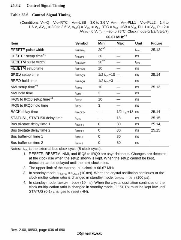
Rev. 2.00, 09/03, page 636 of 690
25.3.2 Control Signal Timing
Table 25.6 Control Signal Timing
(Conditions: VCCQ = VCC-RTC = VCC-USB = 3.0 to 3.6 V, VCC = VCC-PLL1 = VCC-PLL2 = 1.4 to1.6 V, AVCC = 3.0 to 3.6 V, VSSQ = VSS = VSS-RTC = VSS-USB = VSS-PLL1 = VSS-PLL2 =
AVSS = 0 V, Ta = –20 to 75°C, Clock mode 0/1/2/4/5/6/7)
66.67 MHz*2
Item Symbol Min Max Unit Figure
RESETP pulse width tRESPW 20*3 — tcyc 25.12
RESETP setup time*1 tRESPS 20 — ns
RESETM pulse width tRESMW 20*4 — tcyc
RESETM setup time tRESMS 10 — ns
BREQ setup time tBREQS 1/2 tcyc+10 — ns 25.14
BREQ hold time tBREQH 1/2 tcyc+3 — ns
NMI setup time*1 tNMIS 10 — ns 25.13
NMI hold time tNMIH 3 — ns
IRQ5 to IRQ0 setup time*1 tIRQS 10 — ns
IRQ5 to IRQ0 hold time tIRQH 3 — ns
BACK delay time tBACKD — 1/2 tcyc+13 ns 25.14
STATUS1, STATUS0 delay time tSTD — 18 ns 25.15
Bus tri-state delay time 1 tBOFF1 0 30 ns 25.14,
Bus tri-state delay time 2 tBOFF2 0 30 ns 25.15
Bus buffer-on time 1 tBON1 0 30 ns
Bus buffer-on time 2 tBON2 0 30 ns
Notes: tcyc is the external bus clock cycle (B clock cycle).1. RESETP, RESETM, NMI, and IRQ5 to IRQ0 are asynchronous. Changes are detected
at the clock rise when the setup shown is kept. When the setup cannot be kept,detection can be delayed until the next clock rises.
2. The upper limit of the external bus clock is 66.67 MHz.3. In standby mode, tRESPW = tOSC2 (10 ms). When the crystal oscillation continues or the
clock multiplication ratio is changed in standby mode, tRESPW = tPLL1 (100 µs).4. In standby mode, tRESMW = tOSC2 (10 ms). When the crystal oscillation continues or the
clock multiplication ratio is changed in standby mode, RESETMmust be kept low untilSTATUS (0-1) changes to reset (HH).

Rev. 2.00, 09/03, page 637 of 690
CKIO
tRESPStRESMS
tRESPStRESMS
RESETP
RESETM
tRESPW
tRESMW
Figure 25.12 Reset Input Timing
CKIO
NMI
tNMIH tNMIS
VIH
VIL
IRQ5 to IRQ0
tIRQH tIRQS
VIH
VIL
Figure 25.13 Interrupt Signal Input Timing
CKIO
BREQ
BACK
A25 to A0,
D31 to D0
RD, RD/WR,
RASU/L,
CASU/L,
CSn, WEn,
BS, CKE
BREQHt BREQSt
BACKDt BACKDt
BREQHt BREQSt
BON1tBOFF1t
BOFF2t BON2t
Figure 25.14 Bus Release Timing

Rev. 2.00, 09/03, page 638 of 690
CKIO
tBOFF2
tBOFF1
tSTD
tBON2
tBON1
STATUS 0
STATUS 1
A25 to A0,
D31 to D0
RD, RD/WR,
RASU/L, CASU/L,
CSn, WEn, BS,
CKE
Normal mode Normal modeStandby mode
Figure 25.15 Pin Drive Timing at Standby
25.3.3 AC Bus Timing
Table 25.7 Bus Timing (1)
(Conditions: VCCQ = VCC-RTC = VCC-USB = 3.0 to 3.6 V, VCC = VCC-PLL1 = VCC-PLL2 = 1.4 to1.6 V, AVCC = 3.0 to 3.6 V, VSSQ = VSS = VSS-RTC = VSS-USB = VSS-PLL1 = VSS-PLL2 =
AVSS = 0 V, Ta = –20 to 75°C, Clock mode 0/1/2/4/5/6/7)
66.67 MHz
Item Symbol Min Max Unit Figure
Address delay time 1 tAD1 1 12 ns 25.16 to 25.38
Address delay time 2 tAD2 — 1/2 tcyc+12 ns 25.21
Address setup time tAS 0 — ns 25.16 to 25.19
Address hold time tAH 0 — ns 25.16 to 25.19
BS delay time tBSD — 10 ns 25.16 to 25.35
CS delay time 1 tCSD1 1 10 ns 25.16 to 25.38
Read/write delay time 1 tRWD1 1 10 ns 25.16 to 25.38
Read strobe delay time tRSD — 1/2 tcyc+10 ns 25.16 to 25.21
Read data setup time 1 tRDS1 1/2 tcyc+6 — ns 25.16 to 25.20
Read data setup time 2 tRDS2 6 — ns 25.22 to 25.25, 25.30 to 25.32
Read data setup time 3 tRDS3 1/2 tcyc+6 — ns 25.21
Read data hold time 1 tRDH1 0 — ns 25.16 to 25.20
Read data hold time 2 tRDH2 2 — ns 25.22 to 25.25, 25.30 to 25.32
Read data hold time 3 tRDH3 0 — ns 25.21

Rev. 2.00, 09/03, page 639 of 690
66.67 MHz
Item Symbol Min Max Unit Figure
Write enable delay time tWED — 1/2 tcyc+10 ns 25.16 to 25.21
Write data delay time 1 tWDD1 — 12 ns 25.16 to 25.20
Write data delay time 2 tWDD2 — 12 ns 25.26 to 25.29, 25.33 to 25.35
Write data hold time 1 tWDH1 1 — ns 25.16 to 25.20
Write data hold time 2 tWDH2 1 — ns 25.26 to 25.29, 25.33 to 25.35
Write data hold time 4 tWDH4 0 — ns 25.16 to 25.19
WAIT setup time tWTS 1/2 tcyc+6 — ns 25.17 to 25.21
WAIT hold time tWTH 1/2 tcyc+2 — ns 25.17 to 25.21
RAS delay time 1 tRASD1 1 10 ns 25.22 to 25.38
CAS delay time 1 tCASD1 1 10 ns 25.22 to 25.38
DQM
delay time 1 tDQMD1 1 10 ns 25.22 to 25.35
CKE delay time 1 tCKED1 1 10 ns 25.37
AH delay time tAHD 1/2 tcyc 1/2 tcyc+10 ns 25.20
Multiplex address delaytime
tMAD — 12 ns 25.20
Multiplex address holdtime
tMAH 0 — ns 25.20
DACK delay time tDACD — 10 ns 25.16 to 25.35

Rev. 2.00, 09/03, page 640 of 690
25.3.4 Basic Timing
T1
tAD1 tAD1
tAS
tCSD1 tCSD1
T2
tRWD1 tRWD1
tRSD tRSD tAH
tAH
tRDH1
tRDS1
tWEDtWED
tBSD tBSD
tDACD tDACD
tWDH1
tWDH4
tWDD1
CKIO
A25 to A0
CSn
RD/WR
RD
D31 to D0
WEn*2
BS
DACKn*1
D31 to D0
Read
Write
Notes: 1. DACKn is a waveform when active-low is specified.
2. Output timing is the same when reading byte-selection SRAM.
Figure 25.16 Basic Bus Cycle (No Wait)

Rev. 2.00, 09/03, page 641 of 690
T1
tAD1 tAD1
tAS
tCSD1 tCSD1
Tw T2
tRWD1 tRWD1
tRSDtRSD
tRDH1
tRDS1
tWEDtWED tAH
tAH
tBSD tBSD
tWTH
tWTS
tDACD tDACD
tWDH1
tWDH4
tWDD1
CKIO
A25 to A0
CSn
RD/WR
RD
D31 to D0
WEn*2
BS
WAIT
DACKn*1
D31 to D0
Notes: 1. DACKn is a waveform when active-low is specified.
2. Output timing is the same when reading byte-selection SRAM.
Read
Write
Figure 25.17 Basic Bus Cycle (One Software Wait)

Rev. 2.00, 09/03, page 642 of 690
T1
tAD1 tAD1
tAS
tCSD1tCSD1
TwX T2
tRWD1 tRWD1
tRSD tRSD tAH
tAH
tRDH1
tRDS1
tWED tWED
tBSDtBSD
tWTH tWTH
tWTS tWTS
tDACDtDACD
tWDH1
tWDH4
tWDD1
CKIO
A25 to A0
CSn
RD/WR
RD
D31 to D0
WEn*2
BS
WAIT
DACKn*1
D31 to D0
Read
Write
Notes: 1. DACKn is a waveform when active-low is specified.
2. Output timing is the same when reading byte-selection SRAM.
Figure 25.18 Basic Bus Cycle (One External Wait)

Rev. 2.00, 09/03, page 643 of 690
tAD1 tAD1
T1
tRWD1
tRSD
tWED tWED tWED
tRDS1 tRDS1
tRDH1 tRDH1
tAS
tRSD tRSDtAHtRSD
tAH tWED tAH
tAH
tCSD1
tWDD1 tWDH1
tWDH4
tWDH1
tWDH4
tWDD1
tBSD tBSD
tDACD tDACD tDACDtDACD
tBSD tBSD
tRWD1 tRWD1 tRWD1
tCSD1 tCSD1tCSD1
tAS
tAD1 tAD1
Tw T2 Tnop T1 Tw T2 Tnop
DACKn*1
A25 to A0
D15 to D0
CSn
RD/WR
RD
WAIT
D15 to D0
WEn*2
BS
CKIO
tWTH
tWTS
tWTH
tWTS
Read
Write
Notes: 1. DACKn is a waveform when active-low is specified.
2. Output timing is the same when reading byte-selection SRAM.
Figure 25.19 Basic Bus Cycle (One Software Wait, External Wait Enabled(WM Bit = 0), No Idle Cycle Setting)

Rev. 2.00, 09/03, page 644 of 690
tWDD1
Ta1 Ta2 Ta3 T1 Tw Tw T2
tAD1
tCSD1
tAD1
tRWD1 tRWD1
tCSD1
tRSD tRSD
tRDH1
tRDS1
tWED tWED
Data
Data
tBSD tBSD
tWTH
tWTS
tAHDtAHD
tWTH
tWTS
tDACD tDACD
Address
tWDH1tMAHtMAD
CKIO
A25 to A0
CSn
RD/WR
RD
AH
D15 to D0
WE0/1
BS
WAIT
DACKn*
D15 to D0
Address
tMAHtMADRead
Write
Note: * DACKn is a waveform when active-low is specified.
Figure 25.20 Address/Data Multiplex I/O Bus Cycle(Three Address Cycles, One Software Wait, One External Wait)

Rev. 2.00, 09/03, page 645 of 690
25.3.5 Burst ROM Timing
T1 Tw Twx T2B Twb T2B
tAD1
tCSD1
tAD2 tAD2
tRWD1 tRWD1
tCSD1
tRSD tRSD
tWEDtWED
tBSD tBSD
tWTH
tWTS
tWTH
tWTS
tDACD tDACD
tRDS3
tRDH3
tRDS3
tRDH3
CKIO
A25 to A0
CSn
RD/WR
RD
WEn
BS
WAIT
DACKn
D31 to D0
Notes: 1. tRDH3 is specified by earlier one of change of A25 to A0 or the RD rising edge.
2. DACKn is a waveform when active-low is specified.
Figure 25.21 Burst ROM Read Cycle (One Access Wait, One External Wait,One Burst Wait, Two Bursts)

Rev. 2.00, 09/03, page 646 of 690
25.3.6 Synchronous DRAM Timing
Tc1Tr Tcw Td1 Tde
tAD1 tAD1
tCSD1
tAD1
tRWD1 tRWD1
tCSD1
tAD1 tAD1tAD1
tRDH2tRDS2
CKIO
A25 to A0
CSn
RD/WR
A12/A11*1
D31 to D0
tRASD1 tRASD1
RASU/L
Row address
Read A command
Column address
tCASD1 tCASD1
CASU/L
tBSD tBSD
(High)
BS
CKE
tDQMD1 tDQMD1
DQMxx
tDACD tDACD
DACKn*2
Notes: 1. Address pin to be connected to A10 of SDRAM.
2. DACKn is a waveform when active-low is specified.
Figure 25.22 Synchronous DRAM Single Read Bus Cycle(Auto Precharge, CAS Latency ==== 2, TRCD ==== 1 Cycle, TRP ==== 1 Cycle)

Rev. 2.00, 09/03, page 647 of 690
TrwTr Tc1 Tcw Td1 Tde Tap
tAD1 tAD1
tCSD1
tAD1
tRWD1 tRWD1
tCSD1
tAD1 tAD1tAD1
tRDH2tRDS2
CKIO
A25 to A0
CSn
RD/WR
A12/A11*1
D31 to D0
tRASD1 tRASD1
RASU/L
Row address
Read A command
Column address
tCASD1 tCASD1
CASU/L
tBSD tBSD
(High)
BS
CKE
tDQMD1 tDQMD1
DQMxx
tDACD tDACD
DACKn*2
Notes: 1. Address pin to be connected to A10 of SDRAM.
2. DACKn is a waveform when active-low is specified.
Figure 25.23 Synchronous DRAM Single Read Bus Cycle(Auto Precharge, CAS Latency ==== 2, TRCD ==== 2 Cycle, TRP ==== 2 Cycle)

Rev. 2.00, 09/03, page 648 of 690
Tc1 Tc2Td1 Td2 Td3 Td4
Tr Tc3 Tc4 Tde
tAD1
tCSD1
tAD1tAD1tAD1tAD1tAD1
tAD1tAD1tAD1tAD1
tRWD1 tRWD1
tCSD1
CKIO
A25 to A0
CSn
RD/WR
A12/A11*1
D31 to D0
tRASD1 tRASD1
RASU/L
Rowaddress
Read AcommandRead command
Columnaddress (1 to 4)
tCASD1 tCASD1
CASU/L
tBSD tBSD
(High)
BS
CKE
tDQMD1 tDQMD1
DQMxx
tDACD tDACD
DACKn*2
tRDH2tRDS2 tRDH2tRDS2
Notes: 1. Address pin to be connected to A10 of SDRAM.
2. DACKn is a waveform when active-low is specified.
Figure 25.24 Synchronous DRAM Burst Read Bus Cycle (Single Read ×××× 4),(Auto Precharge, CAS Latency ==== 2, TRCD ==== 1 Cycle, TRP ==== 2 Cycle)

Rev. 2.00, 09/03, page 649 of 690
Tc1 Tc2Td1 Td2 Td3 Td4
Tr Trw Tc3 Tc4 Tde
tCSD1 tCSD1
tAD1 tAD1 tAD1 tAD1
tAD1 tAD1 tAD1 tAD1 tAD1 tAD1
tRWD1 tRWD1
CKIO
A25 to A0
CSn
RD/WR
A12/A11*1
D31 to D0
tRASD1 tRASD1
RASU/L
Row address
Read Acommand
Read command
Columnaddress (1 to 4)
tCASD1 tCASD1
CASU/L
tBSD tBSD
(High)
BS
CKE
tDQMD1 tDQMD1
DQMxx
tDACD tDACD
DACKn*2
tRDH2tRDS2 tRDH2tRDS2
Notes: 1. Address pin to be connected to A10 of SDRAM.
2. DACKn is a waveform when active-low is specified.
Figure 25.25 Synchronous DRAM Burst Read Bus Cycle (Single Read ×××× 4),(Auto Precharge, CAS Latency ==== 2, TRCD ==== 2 Cycle, TRP ==== 1 Cycle)

Rev. 2.00, 09/03, page 650 of 690
TrwlTr Tc1
tCSD1 tCSD1
tRWD1 tRWD1 tRWD1
tAD1 tAD1 tAD1
tAD1 tAD1 tAD1
CKIO
A25 to A0
CSn
RD/WR
A12/A11*1
D31 to D0
tRASD1 tRASD1
RASU/L
Row address
Write Acommand
Columnaddress
tCASD1 tCASD1
CASU/L
tBSD tBSD
(High)
BS
CKE
tDQMD1 tDQMD1
DQMxx
tDACD tDACD
DACKn*2
tWDD2 tWDH2
Notes: 1. Address pin to be connected to A10 of SDRAM.
2. DACKn is a waveform when active-low is specified.
Figure 25.26 Synchronous DRAM Single Write Bus Cycle(Auto Precharge, TRWL = 2 Cycle)

Rev. 2.00, 09/03, page 651 of 690
Trw Tc1 Trwl Tr Trw
tCSD1 tCSD1
tCASD1tCASD1
tAD1
tAD1
tAD1
tAD1
tAD1
tAD1
tRWD1
CKIO
A25 to A0
CSn
RD/WR
A12/A11*1
D31 to D0
tRASD1
RASU/L
Row address
Write Acommand
Columnaddress
CASU/L
tBSD tBSD
(High)
BS
CKE
tDQMD1
tRWD1tRWD1
tRASD1 tRASD1
tDQMD1
DQMxx
tDACD tDACD
DACKn*2
tWDH2tWDD2
Notes: 1. Address pin to be connected to A10 of SDRAM.
2. DACKn is a waveform when active-low is specified.
Figure 25.27 Synchronous DRAM Single Write Bus Cycle(Auto Precharge, TRCD ==== 3 Cycle, TRWL = 2 Cycle)

Rev. 2.00, 09/03, page 652 of 690
Tc2 Tc3 Tc4 TrwlTr Tc1
tCSD1 tCSD1
tAD1 tAD1 tAD1 tAD1 tAD1 tAD1
tAD1tAD1tAD1tAD1
tRWD1 tRWD1 tRWD1
CKIO
A25 to A0
CSn
RD/WR
A12/A11*1
D31 to D0
tRASD1 tRASD1
RASU/L
Row address
Write AcommandWrite command
Columnaddress (1-4)
tCASD1 tCASD1
CASU/L
tBSD tBSD
(High)
BS
CKE
tDQMD1 tDQMD1
DQMxx
tDACD tDACD
DACKn*2
tWDH2 tWDH2tWDD2 tWDD2
tRASD1
Notes: 1. Address pin to be connected to A10 of SDRAM.
2. DACKn is a waveform when active-low is specified.
Figure 25.28 Synchronous DRAM Burst Write Bus Cycle (Single Write ×××× 4),(Auto Precharge, TRCD ==== 1 Cycle, TRWL = 2 Cycle)

Rev. 2.00, 09/03, page 653 of 690
Tc2 Tc3 Tc4 TrwlTr Tc1Trw
tCSD1 tCSD1
tAD1 tAD1 tAD1 tAD1 tAD1 tAD1
tAD1tAD1tAD1tAD1
tRWD1 tRWD1 tRWD1
CKIO
A25 to A0
CSn
RD/WR
A12/A11*1
D31 to D0
tRASD1 tRASD1
RASU/L
Row address
Write Acommand
Write command
Columnaddress
(1-4)
tCASD1 tCASD1
CASU/L
tBSD tBSD
(High)
BS
CKE
tDQMD1 tDQMD1
DQMxx
tDACD tDACD
DACKn*2
tWDH2 tWDH2tWDD2 tWDD2
tRASD1
Notes: 1. Address pin to be connected to A10 of SDRAM.
2. DACKn is a waveform when active-low is specified.
Figure 25.29 Synchronous DRAM Burst Write Bus Cycle (Single Write ×××× 4),(Auto Precharge, TRCD ==== 2 Cycle, TRWL = 2 Cycle)
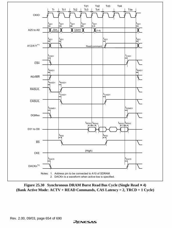
Rev. 2.00, 09/03, page 654 of 690
Tc3 Tc4 TdeTr Tc2
Td1 Td2 Td3 Td4
Tc1
tCSD1 tCSD1
tAD1
tAD1 tAD1 tAD1
tAD1tAD1tAD1tAD1tAD1
tRWD1 tRWD1
CKIO
A25 to A0
CSn
RD/WR
A12/A11*1
D31 to D0
tRASD1 tRASD1
RASU/L
Rowaddress
Read command
Columnaddress (1-4)
tCASD1 tCASD1
CASU/L
tBSD tBSD
(High)
BS
CKE
tDQMD1 tDQMD1
DQMxx
tDACD tDACD
DACKn*2
tRDH2tRDS2tRDH2tRDS2
tAD1
Notes: 1. Address pin to be connected to A10 of SDRAM.
2. DACKn is a waveform when active-low is specified.
Figure 25.30 Synchronous DRAM Burst Read Bus Cycle (Single Read ×××× 4)(Bank Active Mode: ACTV + READ Commands, CAS Latency = 2, TRCD = 1 Cycle)

Rev. 2.00, 09/03, page 655 of 690
Tc2 Tc4 TdeTc1 Tc3
Td1 Td2 Td3 Td4
tCSD1tCSD1tCSD1
tAD1
tAD1 tAD1
tAD1 tAD1
tRWD1 tRWD1
CKIO
A25 to A0
CSn
RD/WR
A12/A11*1
D31 to D0
tRASD1 tRASD1
RASU/L
Read command
Columnaddress (1-4)
tCASD1 tCASD1
CASU/L
tBSD tBSD
(High)
BS
CKE
tDQMD1 tDQMD1
DQMxx
tDACD tDACD
DACKn*2
tRDH2tRDS2 tRDH2tRDS2
tAD1
tDQMD1
tDACD
tBSD
tCASD1
Notes: 1. Address pin to be connected to A10 of SDRAM.
2. DACKn is a waveform when active-low is specified.
Figure 25.31 Synchronous DRAM Burst Read Bus Cycle (Single Read ×××× 4)(Bank Active Mode: READ Command, Same Row Address,
CAS Latency = 2, TRCD = 1 Cycle)

Rev. 2.00, 09/03, page 656 of 690
Tc3 Tc4 TdeTc2
Td1 Td2 Td3 Td4
Tc1TrTpwTp
tCSD1 tCSD1
tAD1
tAD1 tAD1 tAD1 tAD1
tAD1 tAD1 tAD1 tAD1 tAD1
tRWD1 tRWD1 tRWD1
CKIO
A25 to A0
CSn
RD/WR
A12/A11*1
D31 to D0
tRASD1 tRASD1 tRASD1 tRASD1
RASU/L
Read command
ColumnaddressRow address (1-4)
tCASD1 tCASD1
CASU/L
tBSD tBSD
(High)
BS
CKE
tDQMD1 tDQMD1
DQMxx
tDACD tDACD
DACKn*2
tRDH2tRDS2 tRDH2tRDS2
tCSD1
tRASD1
tCASD1
tDQMD1
tBSD
tDACD
Notes: 1. Address pin to be connected to A10 of SDRAM.
2. DACKn is a waveform when active-low is specified.
Figure 25.32 Synchronous DRAM Burst Read Bus Cycle (Single Read ×××× 4)(Bank Active Mode: PRE + ACTV + READ Commands,
Different Row Address, CAS Latency = 2, TRCD = 1 Cycle)

Rev. 2.00, 09/03, page 657 of 690
Tc2 Tc3 Tc4Tr Tc1
tCSD1 tCSD1
tAD1 tAD1
tAD1 tAD1 tAD1
tAD1 tAD1 tAD1 tAD1
tRWD1
CKIO
A25 to A0
CSn
RD/WR
A12/A11*1
D31 to D0
tRASD1
tRWD1 tRWD1
tRASD1
RASU/L
Row address
Write command
Columnaddress (1-4)
tCASD1 tCASD1
CASU/L
tBSD tBSD
(High)
BS
CKE
tDQMD1 tDQMD1
DQMxx
tDACD tDACD
DACKn*2
tWDH2 tWDH2tWDD2 tWDD2
tRASD1
Notes: 1. Address pin to be connected to A10 of SDRAM.
2. DACKn is a waveform when active-low is specified.
Figure 25.33 Synchronous DRAM Burst Write Bus Cycle (Single Write ×××× 4)(Bank Active Mode: ACTV + WRITE Commands, TRCD = 1 Cycle, TRWL = 1 Cycle)

Rev. 2.00, 09/03, page 658 of 690
Tc2 Tc3 Tc4Tnop Tc1
tCSD1 tCSD1
tAD1 tAD1 tAD1 tAD1 tAD1
tAD1tAD1tAD1
tRWD1 tRWD1 tRWD1
CKIO
A25 to A0
CSn
RD/WR
A12/A11*1
D31 to D0
RASU/L
Write command
Columnaddress (1-4)
tCASD1 tCASD1
CASU/L
tBSD tBSD
(High)
BS
CKE
tDQMD1 tDQMD1
DQMxx
tDACD tDACD
DACKn*2
tWDH2 tWDH2tWDD2 tWDD2
tRASD1
Notes: 1. Address pin to be connected to A10 of SDRAM.
2. DACKn is a waveform when active-low is specified.
Figure 25.34 Synchronous DRAM Burst Write Bus Cycle (Single Write ×××× 4)(Bank Active Mode: WRITE Command, Same Row Address,
TRCD = 1 Cycle, TRWL = 1 Cycle)

Rev. 2.00, 09/03, page 659 of 690
Tc2 Tc3 Tc4TrTpwTp Tc1
tCSD1 tCSD1
tAD1
tAD1
tAD1 tAD1 tAD1 tAD1 tAD1
tAD1 tAD1tAD1
tRWD1 tRWD1 tRWD1 tRWD1
tRASD1 tRASD1 tRASD1 tRASD1
CKIO
A25 to A0
CSn
RD/WR
A12/A11*1
D31 to D0
RASU/L
Write command
Row address (1-4)Columnaddress
tCASD1 tCASD1
CASU/L
tBSD tBSD
(High)
BS
CKE
tDQMD1 tDQMD1
DQMxx
tDACD tDACD
DACKn*2
tWDH2tWDD2 tWDH2tWDD2
tRASD1
Notes: 1. Address pin to be connected to A10 of SDRAM.
2. DACKn is a waveform when active-low is specified.
Figure 25.35 Synchronous DRAM Burst Write Bus Cycle (Single Write ×××× 4)(Bank Active Mode: PRE + ACTV + WRITE Commands,
Different Row Address, TRCD = 1 Cycle, TRWL = 1 Cycle)

Rev. 2.00, 09/03, page 660 of 690
Trc TrcTrrTpwTp Trc
tCSD1 tCSD1 tCSD1 tCSD1
tAD1 tAD1
tAD1 tAD1
tRWD1 tRWD1 tRWD1
tRASD1 tRASD1 tRASD1 tRASD1
CKIO
A25 to A0
CSn
RD/WR
A12/A11*1
D31 to D0
RASU/L
tCASD1 tCASD1
CASU/L
(High)
(Hi-Z)
BS
CKE
DQMxx
DACKn*2
Notes: 1. Address pin to be connected to A10 of SDRAM.
2. DACKn is a waveform when active-low is specified.
Figure 25.36 Synchronous DRAM Auto-Refresh Timing (TRP = 2 Cycle)

Rev. 2.00, 09/03, page 661 of 690
Trc Trc Trc TrcTrrTpwTp Trc
tCSD1 tCSD1 tCSD1 tCSD1
tAD1
tAD1
tAD1
tAD1
tRWD1 tRWD1 tRWD1
tRASD1 tRASD1 tRASD1 tRASD1
CKIO
A25 to A0
CSn
RD/WR
A12/A11*1
D31 to D0
RASU/L
tCASD1 tCASD1
CASU/L
(Hi-Z)
BS
CKE
DQMxx
DACKn*2
tCKED1 tCKED1
Notes: 1. Address pin to be connected to A10 of SDRAM.
2. DACKn is a waveform when active-low is specified.
Figure 25.37 Synchronous DRAM Self-Refresh Timing (TRP = 2 Cycle)

Rev. 2.00, 09/03, page 662 of 690
Trc Trc Trc Tmw TdeTrrTrrTpwTp Trc
tCSD1 tCSD1 tCSD1 tCSD1 tCSD1 tCSD1 tCSD1 tCSD1
tAD1 tAD1 tAD1
tAD1tAD1
PALL REF REF MRS
tRWD1 tRWD1 tRWD1 tRWD1tRWD1
tRASD1 tRASD1 tRASD1 tRASD1 tRASD1 tRASD1 tRASD1tRASD1
CKIO
A25 to A0
CSn
RD/WR
A12/A11*1
D31 to D0
RASU/L
tCASD1 tCASD1 tCASD1 tCASD1 tCASD1 tCASD1
CASU/L
(Hi-Z)
BS
CKE
DQMxx
DACKn*2
Notes: 1. Address pin to be connected to A10 of SDRAM.
2. DACKn is a waveform when active-low is specified.
Figure 25.38 Synchronous DRAM Mode Register Write Timing (TRP = 2 Cycle)

Rev. 2.00, 09/03, page 663 of 690
Table 25.8 Bus Timing (2)
(Conditions: VCCQ = VCC-RTC = VCC-USB = 3.0 to 3.6 V, VCC = VCC-PLL1 = VCC-PLL2 = 1.4 to1.6 V, AVCC = 3.0 to 3.6 V, VSSQ = VSS = VSS-RTC = VSS-USB = VSS-PLL1 = VSS-PLL2 =
AVSS = 0 V, Ta = –20 to 75°C, Clock mode 0/1/2/4/5/6/7)
Item Symbol Min Max Unit Figure
Address delay time 3 tAD3 1/2 tcyc 1/2 tcyc+12 ns 25.39 to 25.42
CS delay time 2 tCSD2 1/2 tcyc 1/2 tcyc+10 ns 25.39 to 25.42
Read/write delay time 2 tRWD2 1/2 tcyc 1/2 tcyc+10 ns 25.39 to 25.42
Read data setup time 4 tRDS4 1/2 tcyc+6 — ns 25.39
Read data hold time 4 tRDH4 0 — ns 25.39
Write data delay time 3 tWDD3 — 1/2 tcyc+12 ns 25.39
Write data hold time 3 tWDH3 1/2 tcyc — ns 25.39
RAS delay time 2 tRASD2 1/2 tcyc 1/2 tcyc+10 ns 25.39 to 25.42
CAS delay time 2 tCASD2 1/2 tcyc 1/2 tcyc+10 ns 25.39 to 25.42
DQM delay time 2 tDQMD2 1/2 tcyc 1/2 tcyc+10 ns 25.39
CKE delay time 2 tCKED2 1/2 tcyc 1/2 tcyc+10 ns 25.41

Rev. 2.00, 09/03, page 664 of 690
Tr Td1 Tde Tap Trwl TapTnopTc1 Tr Tc1
tAD3tAD3tAD3tAD3tAD3tAD3
tAD3tAD3 tAD3 tAD3 tAD3
tCSD2tCSD2tCSD2tCSD2
tRWD2tRWD2tRWD2
CKIO
A25 to A0
CSn
RD/WR
A12/A11*1
D31 to D0
tRASD2tRASD2tRASD2tRASD2
RASU/L
tCASD2tCASD2tCASD2
tCASD2
CASU/L
tBSDtBSDtBSD
tRDS4tRDH4
tBSD
BS
CKE
tDQMD2tDQMD2 tDQMD2 tDQMD2
DQMxx
tDACDtDACDtDACDtDACD
DACKn*2
tWDH3tWDD3
Tw
(High)
Notes: 1. Address pin to be connected to A10 of SDRAM.
2. DACKn is a waveform when active-low is specified.
Figure 25.39 Access Timing in Low-Frequency Mode (Auto Precharge)

Rev. 2.00, 09/03, page 665 of 690
Trc TrcTrrTpwTp Trc
tCSD2 tCSD2 tCSD2 tCSD2
tAD3 tAD3
tAD3 tAD3
tRWD2 tRWD2 tRWD2
tRASD2 tRASD2 tRASD2 tRASD2
CKIO
A25 to A0
CSn
RD/WR
A12/A11*1
D31 to D0
RASU/L
tCASD2 tCASD2
CASU/L
(High)
(Hi-Z)
BS
CKE
DQMxx
DACKn*2
Notes: 1. Address pin to be connected to A10 of SDRAM.
2. DACKn is a waveform when active-low is specified.
Figure 25.40 Synchronous DRAM Auto-Refresh Timing(TRP = 2 Cycle, Low-Frequency Mode)

Rev. 2.00, 09/03, page 666 of 690
Trc Trc Trc TrcTrrTpwTp Trc
tCSD2 tCSD2 tCSD2 tCSD2
tAD3
tAD3
tAD3
tAD3
tRWD2tRWD2 tRWD2
tRASD2 tRASD2 tRASD2 tRASD2
CKIO
A25 to A0
CSn
RD/WR
A12/A11*1
D31 to D0
RASU/L
tCASD2 tCASD2
CASU/L
(Hi-Z)
BS
CKE
DQMxx
DACKn*2
tCKED2 tCKED2
Notes: 1. Address pin to be connected to A10 of SDRAM.
2. DACKn is a waveform when active-low is specified.
Figure 25.41 Synchronous DRAM Self-Refresh Timing(TRP = 2 Cycle, Low-Frequency Mode)

Rev. 2.00, 09/03, page 667 of 690
Trc Trc Trc Tmw TdeTrrTrrTpwTp Trc
tCSD2 tCSD2 tCSD2 tCSD2 tCSD2 tCSD2tCSD2 tCSD2
tAD3 tAD3 tAD3
tAD3tAD3
PALL REF REF MRS
tRWD2tRWD2 tRWD2 tRWD2
tRWD2
tRASD2 tRASD2 tRASD2 tRASD2 tRASD2 tRASD2 tRASD2tRASD2
CKIO
A25 to A0
CSn
RD/WR
A12/A11*1
D31 to D0
RASU/L
tCASD2 tCASD2tCASD2 tCASD2 tCASD2 tCASD2
CASU/L
(Hi-Z)
BS
CKE
DQMxx
DACKn*2
Notes: 1. Address pin to be connected to A10 of SDRAM.
2. DACKn is a waveform when active-low is specified.
Figure 25.42 Synchronous DRAM Mode Register Write Timing(TRP = 2 Cycle, Low-Frequency Mode)

Rev. 2.00, 09/03, page 668 of 690
25.3.7 DMAC Signal Timing
Table 25.9 DMAC Signal Timing
(Conditions: VCCQ = VCC-RTC = VCC-USB = 3.0 to 3.6 V, VCC = VCC-PLL1 = VCC-PLL2 = 1.4 to1.6 V, AVCC = 3.0 to 3.6 V, VSSQ = VSS = VSS-RTC = VSS-USB = VSS-PLL1 = VSS-PLL2 =
AVSS = 0 V, Ta = –20 to 75°C)
Module Item Symbol Min Max Unit Figure
DMAC DREQ setup time tDRQS 10 — ns 25.43
DREQ hold time tDRQH 3 —
DACK, TEND delay time tDACD — 10 25.44
tDRQS tDRQH
CKIO
DREQn
Figure 25.43 DREQ Input Timing
CKIO
TEND0
DACKn
tDACD tDACD
Figure 25.44 DACK, TEND Output Timing

Rev. 2.00, 09/03, page 669 of 690
25.3.8 TMU Signal Timing
Table 25.10 TMU Signal Timing
(Conditions: VCCQ = VCC-RTC = VCC-USB = 3.0 to 3.6 V, VCC = VCC-PLL1 = VCC-PLL2 = 1.4 to1.6 V, AVCC = 3.0 to 3.6 V, VSSQ = VSS = VSS-RTC = VSS-USB = VSS-PLL1 = VSS-PLL2 =
AVSS = 0 V, Ta = –20 to 75°C)
Module Item Symbol Min Max Unit Figure
B:P clock ratio = 1:1 15 —
B:P clock ratio = 2:1 tcyc+15 —
TMU Timer inputsetup time
B:P clock ratio = 4:1
tTCLKS
3 × tcyc+15 —
ns 25.45
Timer clock input setup time tTCKS 15 — 25.46
Timer clockpulse width
Edge specification tTCKWH/L 2.0 — tpcyc*
Both edgespecification
tTCKWH/L 3.0 —
Note: * tpcyc indicates a peripheral clock (Pφ) cycle.
tTCLKS
CKIO
TCLK
(input)
Figure 25.45 TCLK Input Timing
tTCKStTCKS
tTCKWHtTCKWL
CKIO
TCLK
(input)
Figure 25.46 TCLK Clock Input Timing

Rev. 2.00, 09/03, page 670 of 690
25.3.9 RTC Signal Timing
Table 25.11 RTC Signal Timing
(Conditions: VCCQ = VCC-RTC = VCC-USB = 3.0 to 3.6 V, VCC = VCC-PLL1 = VCC-PLL2 = 1.4 to1.6 V, AVCC = 3.0 to 3.6 V, VSSQ = VSS = VSS-RTC = VSS-USB = VSS-PLL1 = VSS-PLL2 =
AVSS = 0 V, Ta = –20 to 75°C)
Module Item Symbol Min Max Unit Figure
RTC Oscillation settling time tROSC 3 — s 25.47
VCC
VCCmintROSC
RTC crystal
oscillator
Stable oscillation
Figure 25.47 Oscillation Settling Time when RTC Crystal Oscillator Is Turned On
25.3.10 16-Bit Timer Pulse Unit (TPU) Signal Timing
Table 25.12 16-Bit Timer Pulse Unit (TPU) Signal Timing
(Conditions: VCCQ = VCC-RTC = VCC-USB = 3.0 to 3.6 V, VCC = VCC-PLL1 = VCC-PLL2 = 1.4 to1.6 V, AVCC = 3.0 to 3.6 V, VSSQ = VSS = VSS-RTC = VSS-USB = VSS-PLL1 = VSS-PLL2 =
AVSS = 0 V, Ta = –20 to 75°C)
Item Symbol Min Max Unit Figure
Timer output delay time tTOD — 15 ns 25.48
CKIO
TO0, TO1
tTOD
TO2, TO3
Figure 25.48 TPU Output Timing

Rev. 2.00, 09/03, page 671 of 690
25.3.11 SCIF Module Signal Timing
Table 25.13 SCIF Module Signal Timing
(Conditions: VCCQ = VCC-RTC = VCC-USB = 3.0 to 3.6 V, VCC = VCC-PLL1 = VCC-PLL2 = 1.4 to1.6 V, AVCC = 3.0 to 3.6 V, VSSQ = VSS = VSS-RTC = VSS-USB = VSS-PLL1 = VSS-PLL2 =
AVSS = 0 V, Ta = –20 to 75°C)
Module Item Symbol Min Max Unit Figure
Clocksynchronization
12 —SCIF0,SCIF2
Input clockcycle
Asynchroniza-tion
tScyc
4 —
tpcyc 25.4925.50
Input clock rise time tSCKr — 1.5 25.49
Input clock fall time tSCKf — 1.5
Input clock pulse width tSCKW 0.4 0.6 tscyc
Transmission data delay time(clock synchronization)
tTXD — 3 tpcyc* + 50 ns 25.50
Receive data setup time(clock synchronization)
tRXS 2 tpcyc* —
Receive data hold time(clock synchronization)
tRXH 2 tpcyc* —
RTS delay time(clock synchronization)
tRTSD — 100
CTS setup time(clock synchronization)
tCTSS 100 —
CTS hold time(clock synchronization)
tCTSH 100 —
Note: * tpcyc indicates a peripheral clock (Pφ) cycle.
tSCKW tSCKr tSCKf
tScyc
SCK
Figure 25.49 SCK Input Clock Timing

Rev. 2.00, 09/03, page 672 of 690
tScyc
tTXD
tRXHtRXS
tRTSD
tCTSHtCTSS
SCK
RTS
CTS
TxD
(data trans-
mission)
RxD
(data
reception)
Figure 25.50 SCIF Input/Output Timing in Clock Synchronous Mode
25.3.12 USB Module Signal Timing
Table 25.14 USB Module Clock Timing
(Conditions: VCCQ = VCC-RTC = VCC-USB = 3.0 to 3.6 V, VCC = VCC-PLL1 = VCC-PLL2 = 1.4 to1.6 V, AVCC = 3.0 to 3.6 V, VSSQ = VSS = VSS-RTC = VSS-USB = VSS-PLL1 = VSS-PLL2 =
AVSS = 0 V, Ta = –20 to 75°C)
Item Symbol Min Max Unit Figure
Frequency (48 MHz)* tFREQ 47.9 48.1 MHz 25.51
Clock rise time* tR48 — 4 ns
Clock fall time* tF48 — 4 ns
Duty (tHIGH/tLOW)* tDUTY 90 110 %
Oscillation settling time tUOSC 10 — ms 25.52
Note: *When the USB is operated by supplying a clock to the EXTAL_USB pin from off-chip, thesupplied clock must satisfy the above clock specifications.
tHIGH tLOW
tFREQ
10%
tR48 tF48
90%EXTAL_USB
Figure 25.51 USB Clock Timing

Rev. 2.00, 09/03, page 673 of 690
VCC VCCmintUOSC
USB crystal
oscillator
State oscillation
Figure 25.52 Oscillation Settling Time when USB Crystal Oscillator Is Turned On
25.3.13 USB Transceiver Timing
Table 25.15 USB Transceiver Timing
(Conditions: VCCQ = VCC-RTC = VCC-USB = 3.0 to 3.6 V, VCC = VCC-PLL1 = VCC-PLL2 = 1.4 to1.6 V, AVCC = 3.0 to 3.6 V, VSSQ = VSS = VSS-RTC = VSS-USB = VSS-PLL1 = VSS-PLL2 =
AVS = 0 V, Ta = –20 to 75°C)
Item Symbol Min Typ Max UnitMeasurementCondition
Rising time tr 4 — 20 ns CL = 50pF
Falling time tf 4 — 20 ns CL = 50pF
Rising/falling time ratio tr / tf 90 — 110 %
Output signal crossovervoltage
VCRS 1.3 — 2.0 V CL = 50pF
Note: This transceiver complies with the full-speed specifications.
tr, tf
90%
10%Crossover voltage
DP
DM
Measured
element
Vcc-USB
DP
DM
Vcc
VSS
RS = 33Ω RL = 15kΩ
RL = 15kΩ
CL
CL
RL = 1.5kΩ
RS = 33Ω
1. tr and tf are judged by the time taken for the
transitions between 10% and 90% amplitude.
2. The electrostatic capacitance, CL, includes the
floating capacitance of the wiring connection
and the input capacitance of the probe.
Measurement circuit

Rev. 2.00, 09/03, page 674 of 690
25.3.14 Port Input/Output Timing
Table 25.16 Port Input/Output Timing
(Conditions: VCCQ = VCC-RTC = VCC-USB = 3.0 to 3.6 V, VCC = VCC-PLL1 = VCC-PLL2 = 1.4 to1.6 V, AVCC = 3.0 to 3.6 V, VSSQ = VSS = VSS-RTC = VSS-USB = VSS-PLL1 = VSS-PLL2 =
AVSS = 0 V, Ta = –20 to 75°C)
Module Item Symbol Min Max Unit Figure
Output data delay time tPORTD — 17
B:P clock ratio = 1:1 15 —
B:P clock ratio = 2:1 tcyc+15 —
Input datasetup time
B:P clock ratio = 4:1
tPORTS
3 × tcyc+15 —
Port
Input data hold time tPORTH 8 —
ns 25.53
tPORTS
CKIO
tPORTH
tPORTD
Ports 7 to 0
(read)
Ports 7 to 0
(write)
Figure 25.53 I/O Port Timing

Rev. 2.00, 09/03, page 675 of 690
25.3.15 UDI Related Pin Timing
Table 25.17 UDI Related Pin Timing
(Conditions: VCCQ = VCC-RTC = VCC-USB = 3.0 to 3.6 V, VCC = VCC-PLL1 = VCC-PLL2 = 1.4 to1.6 V, AVCC = 3.0 to 3.6 V, VSSQ = VSS = VSS-RTC = VSS-USB = VSS-PLL1 = VSS-PLL2 =
AVSS = 0 V, Ta = –20 to 75°C)
Item Symbol Min Max Unit Figure
TCK cycle time tTCKcyc 50 — ns 25.54,25.56
TCK high-pulse width tTCKH 12 — ns 25.54
TCK low-pulse width tTCKL 12 — ns
TCK rise/fall time tTCKf — 4 ns
TRST setup time tTRSTS 12 — ns 25.55
TRST hold time tTRSTH 50 — tcyc
TDI setup time tTDIS 10 — ns 25.56
TDI hold time tTDIH 10 — ns
TMS setup time tTMSS 10 — ns
TMS hold time tTMSH 10 — ns
TDO delay time tTDOD — 15 ns
ASEMD0 setup time tASEMD0S 12 — ns 25.57
ASEMD0 hold time tASEMD0H 12 — ns
tTCKH
tTCKf tTCKf
tTCKL
tTCKcyc
VIH VIHVIH
1/2 VCCQ 1/2 VCCQVIL VIL
Figure 25.54 TCK Input Timing

Rev. 2.00, 09/03, page 676 of 690
tTRSTS tTRSTH
TRST
RESETP
Figure 25.55 TRST Input Timing (Reset Hold)
tTMSS tTMSH
tTDOD
tTCKcyc
tTDIHtTDIS
TCK
TDI
TMS
TDO
Figure 25.56 UDI Data Transfer Timing
tASEMD0HtASEMD0S
RESETP
ASEMD0
Figure 25.57 ASEMD0 Input Timing

Rev. 2.00, 09/03, page 677 of 690
25.3.16 AC Characteristics Measurement Conditions
• I/O signal reference level: VCCQ/2 (VCCQ = 3.0 to 3.6 V, VCC = 1.4 to 1.6 V)
• Input pulse level: VSSQ to 3.0 V (where RESETP, RESETM, ASEMD0, NMI, IRQ5 to IRQ0,CKIO, and MD6 to MD0 are within VSSQ to VCCQ)
• Input rise and fall times: 1 ns
IOL
IOH
CL VREF
LSI output pin Reference voltage
Notes: CL is the total value that includes the capacitance of measurement
instruments, etc., and is set as follows for each pin.
30 pF: CKIO, RASU/L, CASU/L, CS0, CS2 to CS6B, BACK
50 pF: All other pins
IOL =1.6 mA, IOH = –200µA
1.
2.
V
Figure 25.58 Output Load Circuit

Rev. 2.00, 09/03, page 678 of 690
25.4 A/D Converter Characteristics
Table 25.18 lists the A/D converter characteristics.
Table 25.18 A/D Converter Characteristics
(Conditions: VCCQ = VCC-RTC = VCC-USB = 3.0 to 3.6 V, VCC = VCC-PLL1 = VCC-PLL2 = 1.4 to1.6 V, AVCC = 3.0 to 3.6 V, VSSQ = VSS = VSS-RTC = VSS-USB = VSS-PLL1 = VSS-PLL2 =
AVSS = 0 V, Ta = –20 to 75°C)
Item Min Typ Max Unit
Resolution 10 10 10 bits
Conversion time 8.5 — — µs
Analog input capacitance — — 20 pF
Permissible signal-source impedance(single-source)
— — 5 kΩ
Nonlinearity error — — ±3.0 LSB
Offset error — — ±2.0 LSB
Full-scale error — — ±2.0 LSB
Quantization error — — ±0.5 LSB
Absolute accuracy — — ±4.0 LSB

Rev. 2.00, 09/03, page 679 of 690
Appendix
A. I/O Port States in Each Processing State
Table A.1 I/O Port States in Each Processing State
Reset Power-Down States
Category PinPower-onReset
ManualReset
SoftwareStandby Sleep
BusMastershipReleased I/O
Handling ofUnused Pins
Clock EXTAL I I I I I I Pull-up
XTAL O O O O O O Open
EXTAL2 I I I I I I Pull-up
XTAL2 O O O O O O Open
CKIO I O*1 I O*1 I O*1 I O*1 I O*1 I O Open
RESETP I*11 I*11 I*11 I*11 I*11 I Must be usedSystemcontrol
RESETM I I I I I I Pull-up
BREQ/PTG[6] Z i P*2 i K*3 I P*2 I I/IO Pull-up
BACK/PTG[5] O O P*2 O K*3 O P*2 L P*2 O/IO Open
MD6 I i Z i i I Pull-down
MD[2:0] I i i i i I Must be used
MD[5:3] I i Z i i I Must be used
CA I I I I I I Pull-up
STATUS0/PTE[4]/RTS0
H H P*2 Z*6 H K*3 Z*6 L P*2 O L P*2 O O/IO/O
Open
STATUS1/PTE[5]/CTS0
H H P*2 Z*6 L K*3 Z*7 H P*2 I L P*2 I O/IO/I
Open
Interrupt IRQ[3:0]/IRL[3:0]/PTH[3:0]
Z I P*2 I K*3 I P*2 I P*2 I/I/IO Pull-up
IRQ4/PTH[4] Z I P*2 I K*3 I P*2 I P*2 I/IO Pull-up
IRQ5/PTE[2] Z I P*2 I K*3 I P*2 I P*2 I/IO Pull-up
NMI I I I I I I Pull-up
Address A[25:19,0]/PTK[7:0]
O O P*2 ZO*8K*3 O P*2 Z P*2 O/IO Open
A[18:1] O O ZO*8 O Z O Open

Rev. 2.00, 09/03, page 680 of 690
Reset Power-Down States
Category PinPower-onReset
ManualReset
SoftwareStandby Sleep
BusMastershipReleased I/O
Handling ofUnused Pins
Data D[15:0] Z Z Z IO Z IO Pull-up
D[23:16]/PTA[7:0]/PINT[7:0]
Z Z P*2 Z P*2 IO P*2 Z P*2 IO/IO/I
Pull-up
D[31:24]/PTB[7:0]/PINT[15:8]
Z Z P*2 Z P*2 IO P*2 Z P*2 IO/IO/I
Pull-up
CS0 H O ZH*6 O Z O OpenBuscontrol
CS2/PTC[3] H O P*2 ZH*6 K*3 O P*2 Z P*2 O/IO Open
CS3/PTC[4] H O P*2 ZH*6 K*3 O P*2 Z P*2 O/IO Open
CS4/PTC[5] H O P*2 ZH*6 K*3 O P*2 Z P*2 O/IO Open
CS5A/PTC[6] Z O P*2 ZH*6 K*3 O P*2 Z P*2 O/IO Pull-up
CS5B/PTD[6] Z O P*2 ZH*6 K*3 O P*2 Z P*2 O/IO Pull-up
CS6A/PTC[7] Z O P*2 ZH*6 K*3 O P*2 Z P*2 O/IO Pull-up
CS6B/PTD[7] Z O P*2 ZH*6 K*3 O P*2 Z P*2 O/IO Pull-up
BS/PTC[0] H O P*2 ZH*6 K*3 O P*2 Z P*2 O/IO Open
RASL/PTD[0] H O P*2 ZH*6 K*3 O P*2 ZH*6 P*2 O/IO Open
RASU/PTD[1] Z O P*2 ZH*6 K*3 O P*2 ZH*6 P*2 O/IO Pull-up
CASL/PTD[2] H O P*2 ZH*6 K*3 O P*2 ZH*6 P*2 O/IO Open
CASU/PTD[3] Z O P*2 ZH*6 K*3 O P*2 ZH*6 P*2 O/IO Pull-up
WE0/DQMLL H O ZH*6 O Z O/O Open
WE1/DQMLU H O ZH*6 O Z O/O Open
WE2/DQMUL/PTC[1]
H O P*2 ZH*6 K*3 O P*2 Z P*2 O/O/IO
Open
WE3/DQMUU/AH/PTC[2]
H O P*2 ZH*6 K*3 O P*2 Z P*2 O/O/O/IO
Open
RD/WR H O ZH*6 O Z O Open
RD H O ZH*6 O Z O Open
CKE/PTD[4] H O P*2 OK*3 O P*2 OP*2 O/IO Open
WAIT/PTG[7] I I P*2 I K*3 I P*2 I P*2 I/IO Pull-up

Rev. 2.00, 09/03, page 681 of 690
Reset Power-Down States
Category PinPower-onReset
ManualReset
SoftwareStandby Sleep
BusMastershipReleased I/O
Handling ofUnused Pins
DMAC DREQ0/PTH[5]
Z Z P*2 Z K*3 I P*2 I P*2 I/IO Pull-up
DACK0/PTE[0]
V O P*2 Z K*3 O P*2 O P*2 O/IO Open
TEND0/PTE[3]
V O P*2 Z K*3 O P*2 O P*2 O/IO Open
DREQ1/PTH[6]
Z Z P*2 Z K*3 I P*2 I P*2 I/IO Pull-up
DACK1/PTE[1]
V O P*2 Z K*3 O P*2 O P*2 O/IO Open
Timer TCLK/PTE[6] V I P*2 Z K*3 I P*2 I P*2 I/IO Open
SCIF RxD0/SCPT[0]/IrRX
Z Z I*4 Z I I I/I/I Pull-up
TxD0/SCPT[0]/IrTX
Z Z O*5 Z O*5 O O O/O/O
Open
SCK0/SCPT[1]
Z Z P*2 Z K*3 IO P*2 IO P*2 IO/IO Pull-up
RxD2/SCPT[2]
Z Z I*4 Z I I I/I Pull-up
TxD2/SCPT[2]
Z Z O*5 Z O*5 O O O/O Open
SCK2/SCPT[3]
Z Z P*2 Z K*3 IO P*2 IO P*2 IO/IO Pull-up
RTS2/SCPT[4]
V Z P*2 Z K*3 O P O P O/IO Open
CTS2/SCPT[5]
Z Z P*2 Z K*3 I P*2 I P*2 I/IO Pull-up
Analog AN[3:0]/PTL[3:0]
i Z I*4 i I I I/I Open
USB VBUS/PTM[6]
V I P*2 Z K*2 I P*2 I P*2 I/IO Open
SUSPND/PTN[0]
V O P*2 O K*3 O P*2 O P*2 O/IO Open
TXENL/PTN[1]
V O P*2 O K*3 O P*2 O P*2 O/IO Open
XVDATA/PTN[2]
V I P*2 V K*3 I P*2 I P*2 I/IO Open

Rev. 2.00, 09/03, page 682 of 690
Reset Power-Down States
Category PinPower-onReset
ManualReset
SoftwareStandby Sleep
BusMastershipReleased I/O
Handling ofUnused Pins
USB TXDMNS/PTN[3]
V O P*2 O K*3 O P*2 O P*2 O/IO Open
TXDPLS/PTN[4]
V O P*2 O K*3 O P*2 O P*2 O/IO Open
DMNS/PTN[5]
V I P*2 V K*3 I P*2 I P*2 I/IO Open
DPLS/PTN[6] V I P*2 V K*3 I P*2 I P*2 I/IO Open
EXTAL_USB I I i I I I Pull-up
XTAL_USB O O O O O O Open
D+ Z IO*9 Z IO*9 IO*9 IO Open
D- Z IO*9 Z IO*9 IO*9 IO Open
Port NF/PTD[5] I I Z I I I/I Pull-up
PTE[7] V P K P P IO Open
NF/PTJ[7] L O O O O O/O Open
NF/PTJ[6:0] H*13 O O O O O/O Open
NF/PTM[4] I I Z I I I/I Pull-up
PTM[3:0] V P K P P IO Open
PTN[7] V P K P P IO Open
AUDSYNC/PTF[4]
V/V*10 O P*2 O K*3 O P*2 O P*2 O/IO Open
AUDATA[3:0]/PTF[3:0]/TO[3:0]
V/V*10 O P*2 Z*8 O K*3 Z*8 O P*2 O P*2 O/IO/O
Open
Advanceduserdebugger
AUDCK/PTG[4]
O/V*10 O P*2 O K*3 O P*2 O P*2 O/IO Open
TDI/PTG[0] I*11 I*11 P*2 i*11 K*3 I*11 P*2 I*11 P*2 I/IO Open
TCK/PTG[1] I*11 I*11 P*2 i*11 K*3 I*11 P*2 I*11 P*2 I/IO Open
TMS/PTG[2] I*11 I*11 P*2 i*11 K*3 I*11 P*2 I*11 P*2 I/IO Open
Userdebugg-inginterface
TRST/PTG[3] I*11 I*11 P*2 i*11 K*3 I*11 P*2 I*11 P*2 I/IO Must be used
TDO/PTF[5] OZ O P*2 Z K*3 O P*2 O P*2 O/IO Open
ASEBRKAK/PTF[6]
V/V*10 O P*2 O K*3 O P*2 O P*2 O/IO Open
ASEMD0/PTF[7]
I*11 I*11 P*2 V K*3 I*11 P*2 I*11 P*2 I/IO Must be used

Rev. 2.00, 09/03, page 683 of 690
Reset Power-Down States
Category PinPower-onReset
ManualReset
SoftwareStandby Sleep
BusMastershipReleased I/O
Handling ofUnused Pins
Vcc_USB VccQ
Vss_USB VssQ
Powersupplyvoltage
Vcc-RTC VccQ
Vss-RTC VssQ
AVcc VccQ
AVss VssQ
VccQ VccQ
VssQ VssQ
Vcc-PLL1 Vcc*12
Vss-PLL1 Vss*12
Vcc-PLL2 Vcc*12
Vss-PLL2 Vss*12
Vcc Vcc
Vss Vss
Legend:I : Input statei : Input state (however, input is fixed by the internal logic.)O : Output state (high or low, undefined)L : Low-level outputH : High-level output
Z : High impedance (input/output buffer off)V : Input/output buffer off, pull-up onK : The high-level output or low-level output/input becomes high impedance.P : Input or output depending on the register settings.Notes:
1. Depends on clock mode.
2. The state is P when the port function is used.3. The state is K when the port function is used.4. The state is I when the port function is used.5. The state is O when the port function is used.6. The state is Z or H depending on the register settings.7. The state is Z or L depending on the register settings.
8. The state is Z or O depending on the register settings.9. The state is i when the USB is not used.10. The initial value (power-on reset) changes depending on the input level of the
ASEMD0 pin. First, this list shows the value when the ASEMD0 pin is 0, then thevalue when the ASEMD0 pin is 1.

Rev. 2.00, 09/03, page 684 of 690
11. Pull-up MOS open12. To avoid the power friction, Vcc-PLL1, Vcc-PLL2, and Vss-PLL1, Vss-PLL2, and
other digital Vcc, Vss should be arranged in three independent patterns from theboard power-supply source.
13. The values of PTJ6, PTJ1, and PTJ0 differ during power-on reset and after thepower-on reset state is released. They conform to the port J data register value afterbeing switched to port status by the pin function controller (PFC).
After Power-On Reset Release
During Power-On Reset PTD5/NF = 1 PTD5/NF = 0
PTJ6/NF 1 0 1
PTJ1/NF 1 1 0
PTJ0/NF 1 0 1
Connect the pull-up pins shown in table A.1 to 3.3 V power through the pull-up resistor.

Rev. 2.00, 09/03, page 685 of 690
B. Package Dimensions
Figures B.1 and B.2 show the package dimensions.
Package Code
JEDEC
JEITA
Mass (reference value)
FP-208C
Conforms
2.7 g*Dimension including the plating thickness
Base material dimension
30.0 ± 0.2
30
.0 ±
0.2
0.5
1.7
0 M
ax
0° − 8°*0
.17
± 0
.05
156 105
104
521
157
208 53
*0.22 ± 0.050.08 M
0.08
1.4
0
0.5 ± 0.1
1.0
28
0.1
0 ±
0.0
5
1.25
0.20 ± 0.04
0.1
5 ±
0.0
4
Unit: mm
Figure B.1 Package Dimensions (FP-208C)

Rev. 2.00, 09/03, page 686 of 690
0.6
50
.80
0.80
12.00
12
.00
0.154 ×
0.2 CC
0.10 C
0.65
0.3
1 ±
0.0
5
1.2
0M
ax
BA
DC
FE
HG
KJ
ML
PN
TR
U
17 1516
1314
1112
910
78
56
34
120.20 C A
0.2
0C
B
B
Cφ0.08 A B
208 × φ0.40 ± 0.05
M
A
Unit: mm
Package Code
JEDEC
JEITA
Mass (reference value)
TBP-208A
0.26 g
Figure B.2 Package Dimensions (TBP-208A)

Rev. 2.00, 09/03, page 687 of 690
Index
16-bit timer pulse unit ........................... 32916-Bit/32-Bit Displacement ..................... 41
A/D conversion time ............................. 534A/D converter ....................................... 527Absolute Addresses ................................. 41Access wait control ............................... 192Address multiplexing ............................ 200Address Space Identifier.......................... 71Address Transition .................................. 71Address-Array Read .............................. 104Address-Array Write(Associative Operation)......................... 104Address-Array Write(non-Associative Operation).................. 104Advanced user debugger ....................... 583Alarm function...................................... 371Asynchronous Mode.............................. 402Auto-Reload count operation ................. 319Auto-Request mode............................... 254
Big endian....................................... 38, 180Boundary scan mode ............................. 581Buffer operation .................................... 346Bulk-in transfer ..................................... 462Bulk-out transfer ................................... 461Burst mode............................................ 265Burst read ............................................. 212Burst ROM interface ............................. 231Bus arbitration ...................................... 235Bus clock (Bφ) ...................................... 271Bus State Controller .............................. 149Byte-selection SRAM interface ............. 233
Clock Pulse Generator ........................... 271Clock synchronous mode....................... 396Compare match counter operation ......... 326Compare match timer ............................ 323Control Registers .................................... 29Control transfer ..................................... 455
Crystal resonator ................................... 273Cycle-Steal mode .................................. 264
Data stage ............................................. 457Data-Array Read ................................... 105Data-Array Write................................... 105Delayed Branching..................................40Direct memory access controller ............ 239Dual Address mode ............................... 261
Emulator ............................................... 567Exception handling................................ 109Exception Handling State ........................25External request mode ........................... 265
Fixed mode ........................................... 257Free-running count ................................ 344
General Registers ....................................29Global Base Register (GBR) ...................36
User debugging interface ....................... 567
I/O ports................................................ 507Infrared data association (IrDA)............. 431Input capture function............................ 320Instruction Length ...................................40Internal clock (Iφ).................................. 271Interrupt Controller................................ 125Interrupt sources.................................... 136Interrupt-in transfer ............................... 463Interval timer mode ............................... 291IrDA interface ....................................... 431IRL Interrupts........................................ 137IRQ Interrupts ....................................... 136
JTAG .................................................... 567
Literal Constant.......................................41Little endian .................................... 39, 180

Rev. 2.00, 09/03, page 688 of 690
Load/Store Architecture .......................... 40Low-frequency mode ............................ 228Low-Power Consumption State ............... 25
MMU...................................................... 65Module Standby Function ..................... 301Multi mode ........................................... 533Multiple interrupts ................................ 147Multiple Virtual Memory Mode............... 71Multiply and Accumulate Registers ......... 33
NMI interrupt........................................ 136
On-Chip peripheral module interrupts.... 138On-Chip peripheral module request modes............................................................. 256
P0/U0 Area............................................. 27P1 Area................................................... 27P2 Area................................................... 27P3 Area................................................... 27P4 Area................................................... 27Peripheral clock (Pφ)............................. 271Physical Address Space........................... 70Pin function controller........................... 475PINT interrupt....................................... 138Power-Down modes .............................. 293Priority.................................................. 137Procedure Register .................................. 33Processing Modes ................................... 26Program Counter..................................... 29PWM mode........................................... 348
Realtime clock ...................................... 351Receive margin ..................................... 429Refreshing ............................................ 225Register
ADCSR.......................530, 594, 611, 621ADDR.........................530, 594, 611, 621BAMRA .....................544, 594, 612, 621BAMRB......................546, 594, 612, 621BARA.........................543, 594, 612, 621BARB.........................545, 594, 612, 621
BASRA...................... 554, 594, 612, 621BASRB...................... 555, 594, 612, 621BBRA ........................ 544, 594, 612, 621BBRB ........................ 547, 594, 612, 621BDMRB..................... 547, 594, 611, 621BDRB ........................ 546, 594, 611, 621BETR......................... 552, 594, 611, 621BRCR ........................ 549, 594, 611, 621BRDR ........................ 554, 594, 612, 621BRSR......................... 553, 594, 612, 621CCR1................................. 586, 596, 614CCR2................................. 586, 596, 614CCR3................................. 586, 596, 614CHCR ........................ 243, 588, 601, 615CMCNT..................... 326, 589, 604, 616CMCOR..................... 326, 589, 604, 616CMCSR ..................... 325, 589, 604, 616CMNCR..................... 156, 587, 598, 614CMSTR...................... 324, 589, 604, 616CS0BCR ............................ 587, 598, 614CS0WCR ........................... 587, 599, 615CSnBCR ........................................... 158CSnWCR .......................................... 161DAR .......................... 242, 588, 601, 615DASTS ...................... 449, 592, 609, 619DMAOR .................... 248, 588, 603, 616DMAR....................... 450, 592, 609, 620DMARS..................... 250, 588, 603, 616DMATCR .................. 243, 588, 601, 615EPDR0i...................... 445, 592, 609, 619EPDR0o..................... 445, 592, 609, 619EPDR0s ..................... 445, 592, 609, 619EPDR1....................... 446, 592, 609, 619EPDR2....................... 446, 592, 609, 619EPDR3....................... 446, 592, 609, 619EPSTL ....................... 453, 592, 609, 620EPSZ0o...................... 447, 592, 609, 619EPSZ1........................ 447, 592, 609, 620EXPEVT............................ 586, 596, 614FCLR......................... 449, 592, 609, 619FRQCR...................... 279, 588, 603, 616ICR0 ...................110, 129, 587, 597, 614ICR1 .......................... 130, 587, 597, 614

Rev. 2.00, 09/03, page 689 of 690
ICR2 .......................... 132, 587, 597, 614IER0 .......................... 444, 592, 609, 620IER1 .......................... 444, 592, 609, 620IFR0........................... 441, 592, 609, 619IFR1........................... 442, 592, 609, 619INTEVT............................. 586, 596, 614INTEVT2........................... 586, 596, 614IPR............................. 128, 586, 597, 614IRR0 .......................... 133, 587, 597, 614IRR1 .......................... 134, 587, 597, 614IRR2 .......................... 135, 587, 597, 614ISR0........................... 443, 592, 609, 620ISR1........................... 443, 592, 609, 620MMUCR............................ 586, 595, 614PACR......................... 480, 593, 609, 620PADR ........................ 508, 593, 610, 620PBCR......................... 481, 593, 609, 620PBDR......................... 509, 593, 610, 620PCCR......................... 483, 593, 609, 620PCDR......................... 510, 593, 610, 620PDCR......................... 485, 593, 610, 620PDDR ........................ 511, 593, 610, 620PECR......................... 487, 593, 610, 620PECR2....................... 488, 593, 610, 620PEDR......................... 513, 593, 610, 620PFCR ......................... 489, 593, 610, 620PFCR2 ....................... 490, 593, 610, 620PFDR......................... 514, 593, 610, 620PGCR......................... 491, 593, 610, 620PGDR ........................ 516, 593, 610, 620PHCR......................... 493, 593, 610, 620PHDR ........................ 517, 593, 611, 621PINTER..................... 132, 587, 597, 614PJCR.......................... 494, 593, 610, 620PJDR.......................... 518, 593, 611, 621PKCR......................... 496, 593, 610, 620PKDR ........................ 519, 593, 611, 621PLCR......................... 498, 593, 610, 620PLDR......................... 521, 593, 611, 621PMCR........................ 499, 593, 610, 620PMDR........................ 522, 593, 611, 621PNCR......................... 500, 593, 610, 620PNCR2....................... 502, 593, 610, 620
PNDR......................... 523, 593, 611, 621PTEH.................................586, 595, 614PTEL .................................586, 595, 614R64CNT..................... 354, 591, 607, 618RCR1 ......................... 365, 591, 608, 618RCR2 ......................... 366, 591, 608, 618RCR3 ......................... 368, 591, 608, 618RDAYAR................... 362, 591, 607, 618RDAYCNT ................ 357, 591, 607, 618RHRAR...................... 360, 591, 607, 618RHRCNT ................... 355, 591, 607, 618RMINAR ................... 359, 591, 607, 618RMINCNT ................. 355, 591, 607, 618RMONAR.................. 363, 591, 607, 618RMONCNT................ 357, 591, 607, 618RSECAR.................... 358, 591, 607, 618RSECCNT ................. 354, 591, 607, 618RTCNT ...................... 179, 587, 600, 615RTCOR...................... 179, 587, 600, 615RTCSR....................... 177, 587, 600, 615RWKAR..................... 361, 591, 607, 618RWKCNT .................. 356, 591, 607, 618RYRAR...................... 364, 591, 608, 618RYRCNT ................... 358, 591, 607, 618SAR ........................... 242, 588, 601, 615SCBRR ...................... 395, 591, 608, 619SCFCR....................... 398, 591, 608, 619SCFDR....................... 401, 591, 608, 619SCFER....................... 389, 591, 608, 619SCFRDR.................... 380, 591, 608, 619SCFTDR .................... 381, 591, 608, 619SCPCR....................... 503, 593, 610, 620SCPDR....................... 525, 593, 611, 621SCRSR.............................................. 380SCSCR....................... 385, 591, 608, 619SCSMR (SCIF) .......... 381, 591, 608, 619SCSMR_Ir (IrDA)...... 432, 592, 609, 619SCSSR ....................... 390, 591, 608, 619SCTDSR .................... 401, 591, 608, 619SCTSR.............................................. 380SDBPR.............................................. 569SDBSR.............................................. 570SDCR......................... 174, 587, 600, 615

Rev. 2.00, 09/03, page 690 of 690
SDID ................................................ 577SDID/SDIDH..................... 594, 613, 621SDIDL ............................... 594, 613, 621SDIR...........................569, 594, 613, 621SDMR2.......................229, 587, 601, 615SDMR3.......................230, 587, 601, 615STBCR .......................296, 588, 603, 616STBCR2 .....................297, 588, 603, 616STBCR3 .....................298, 588, 603, 616TCNT (TMU) .............317, 589, 603, 616TCNT (TPU)...............341, 589, 605, 617TCOR.........................317, 589, 603, 616TCPR..........................317, 589, 604, 616TCR (TMU)................313, 589, 603, 616TCR (TPU) .................334, 589, 605, 617TEA................................... 586, 597, 614TGR............................341, 589, 605, 617TIER...........................339, 589, 605, 617TIOR ..........................338, 589, 605, 617TMDR ........................337, 589, 605, 617TRA................................... 586, 596, 614TRG............................448, 592, 609, 619TSR ............................340, 589, 605, 617TSTR (TMU) ..............312, 589, 603, 616TSTR (TPU) ...............341, 589, 605, 617TTB................................... 586, 595, 614UCLKCR....................281, 588, 603, 616WTCNT......................286, 588, 603, 616WTCSR ......................287, 588, 603, 616XVERCR....................453, 592, 609, 620
Reset State .............................................. 25Round-Robin mode............................... 258RTC crystal oscillator circuit................. 372
Save Program Counter (SPC) .................. 36
Save Status Register (SSR)...................... 36Scan mode ............................................ 534SDRAM interface.................................. 198Sequential break.................................... 559Serial communication interface with FIFO............................................................. 375Setup stage............................................ 456Shadow space........................................ 155Signal-Source impedance ...................... 538Single Address mode............................. 262Single mode .......................................... 533Single Virtual Memory Mode .................. 71Sleep mode ........................................... 299Software standby mode.......................... 300Stall operations ..................................... 465Status Register (SR) ................................ 35Status stage ........................................... 459Synonym problem ................................... 83System Registers ..................................... 29
T Bit ....................................................... 40TAP controller ...................................... 578Timer Unit ............................................ 309TRAPA Exception Register ................... 110
USB function module............................ 437USB standard commands....................... 464User break controller ............................. 541User break exception processing............ 555
Vector Base Register (VBR)................... 37Virtual Address Space ............................. 67
Watchdog timer..................................... 285Watchdog timer mode ........................... 291

SH7705 Group Hardware Manual
Publication Date: 1st Edition, November 2002Rev.2.00, September 19, 2003
Published by: Sales Strategic Planning Div.Renesas Technology Corp.
Edited by: Technical Documentation & Information DepartmentRenesas Kodaira Semiconductor Co., Ltd.
©2002, 2003 Renesas Technology Corp. All rights reserved. Printed in Japan.

Colophon 1.0
Sales Strategic Planning Div. Nippon Bldg., 2-6-2, Ohte-machi, Chiyoda-ku, Tokyo 100-0004, Japan
http://www.renesas.com
Renesas Technology America, Inc.
450 Holger Way, San Jose, CA 95134-1368, U.S.ATel: <1> (408) 382-7500 Fax: <1> (408) 382-7501
Renesas Technology Europe Limited.
Dukes Meadow, Millboard Road, Bourne End, Buckinghamshire, SL8 5FH, United KingdomTel: <44> (1628) 585 100, Fax: <44> (1628) 585 900
Renesas Technology Europe GmbH
Dornacher Str. 3, D-85622 Feldkirchen, GermanyTel: <49> (89) 380 70 0, Fax: <49> (89) 929 30 11 Renesas Technology Hong Kong Ltd.
7/F., North Tower, World Finance Centre, Harbour City, Canton Road, Hong Kong Tel: <852> 2265-6688, Fax: <852> 2375-6836 Renesas Technology Taiwan Co., Ltd.
FL 10, #99, Fu-Hsing N. Rd., Taipei, TaiwanTel: <886> (2) 2715-2888, Fax: <886> (2) 2713-2999
Renesas Technology (Shanghai) Co., Ltd.
26/F., Ruijin Building, No.205 Maoming Road (S), Shanghai 200020, ChinaTel: <86> (21) 6472-1001, Fax: <86> (21) 6415-2952
Renesas Technology Singapore Pte. Ltd.
1, Harbour Front Avenue, #06-10, Keppel Bay Tower, Singapore 098632 Tel: <65> 6213-0200, Fax: <65> 6278-8001
RENESAS SALES OFFICES

1753, Shimonumabe, Nakahara-ku, Kawasaki-shi, Kanagawa 211-8668 Japan
SH7705 Group
REJ09B0082-0200O
Hardware Manual