VersaClock LP App Note for SB_NB_EB - Renesas
15
APPLICATION NOTE VERSACLOCK ® LP APPLICATION NOTE FOR SMARTBOOKS, NETBOOKS, & E-BOOK READERS IDT® VERSACLOCK ® LP APPLICATION NOTE FOR SMARTBOOKS, NETBOOKS, & E-BOOK READERS 1 REV A 050311 Introduction Some of the growing application areas of the VersaClock ® LP device are in Smartbooks, Netbooks and E-Book Readers. There are several discrete crystals and oscillators used in these systems that can potentially be replaced with a single clock synthesizer and buffer IC. This can lead to savings in power, board space and cost. This application note provides schematic and layout guidelines that should be considered while designing in the VersaClock ® LP device in the above mentioned applications. It also provides an insight into the external clocking requirements of popular processors used in these systems. External Clocking Needs of Popular Processors The external clocking needs of 4 popular Netbook, Smartbook and E-book Reader processors are illustrated below. Samsung 6410
-
Upload
khangminh22 -
Category
Documents
-
view
2 -
download
0
Transcript of VersaClock LP App Note for SB_NB_EB - Renesas

APPLICATION NOTE
VERSACLOCK®LP APPLICATION NOTE FOR SMARTBOOKS, NETBOOKS, &E-BOOK READERS
IDT® VERSACLOCK®LP APPLICATION NOTE FOR SMARTBOOKS, NETBOOKS, & E-BOOK READERS 1 REV A 050311
Introduction
Some of the growing application areas of the VersaClock®LP device are in Smartbooks, Netbooks and E-Book Readers. There are several discrete crystals and oscillators used in these systems that can potentially be replaced with a single clock synthesizer and buffer IC. This can lead to savings in power, board space and cost. This application note provides schematic and layout guidelines that should be considered while designing in the VersaClock®LP device in the above mentioned applications. It also provides an insight into the external clocking requirements of popular processors used in these systems.
External Clocking Needs of Popular Processors
The external clocking needs of 4 popular Netbook, Smartbook and E-book Reader processors are illustrated below.
Samsung 6410
VERSACLOCK®LP APPLICATION NOTE FOR SMARTBOOKS, NETBOOKS, & E-BOOK READERS APPLICATION NOTE
IDT® VERSACLOCK®LP APPLICATION NOTE FOR SMARTBOOKS, NETBOOKS, & E-BOOK READERS 2 REV A 050311
Samsung 2416
Nvidia T20
VERSACLOCK®LP APPLICATION NOTE FOR SMARTBOOKS, NETBOOKS, & E-BOOK READERS APPLICATION NOTE
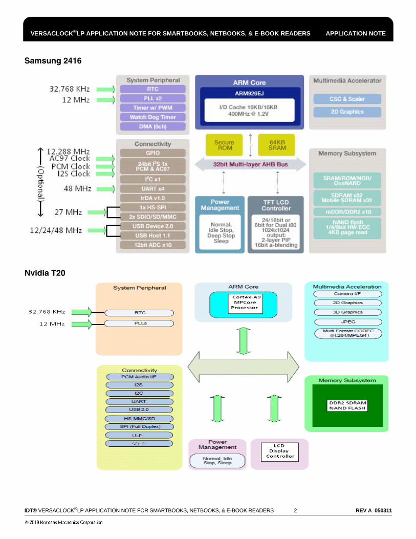
IDT® VERSACLOCK®LP APPLICATION NOTE FOR SMARTBOOKS, NETBOOKS, & E-BOOK READERS 3 REV A 050311
TI OMAP3530
Other than the frequency requirements of the processor, Smartbook, Netbook and E-book Readers may require additional frequencies for the applications listed below.
• LAN (25 MHz typical)• Bluetooth/Wi-Fi (19.2 MHz / 26 MHz typical)• GPS (16.368 MHz / 16.369 MHz/ 26 MHz typical)• Low Power 32.768 kHz clock for PMIC, Bluetooth/Wi-Fi, Keyboard and Embedded Controller
The table in the following page lists the typical input and output frequency requirements in systems using the processors listed above. It also lists the optimal PLL divider and loop filter settings that would need to be set on the VersaClock LP device in order to synthesize the required output frequencies.
VERSACLOCK®LP APPLICATION NOTE FOR SMARTBOOKS, NETBOOKS, & E-BOOK READERS APPLICATION NOTE
IDT® VERSACLOCK®LP APPLICATION NOTE FOR SMARTBOOKS, NETBOOKS, & E-BOOK READERS 4 REV A 050311
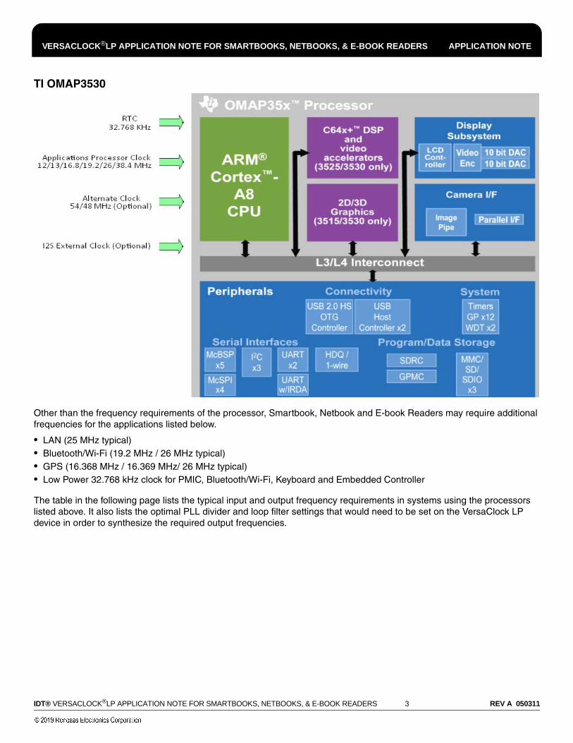
Typical VersaClock LP Configurations

VERSACLOCK®LP APPLICATION NOTE FOR SMARTBOOKS, NETBOOKS, & E-BOOK READERS APPLICATION NOTE
IDT® VERSACLOCK®LP APPLICATION NOTE FOR SMARTBOOKS, NETBOOKS, & E-BOOK READERS 5 REV A 050311
Input Crystal/Clock Selection
The following items need to be considered while selecting the reference crystal/clock source for the VersaClock LP device.
Frequency Accuracy
Different standards impose different requirements for the overall frequency accuracy of the reference clock. Some popular standards with their reference clock frequency accuracy requirements are summarized in the table below.
In general, the frequency tolerance of the VersaClock LP device input clock/crystal should be selected such that the output clocks meet the overall frequency accuracy requirement for all target devices in the system.
Output Clock Phase Noise
The phase noise of the synthesized output clock from the VersaClock LP device depends on the operating bandwidth of the internal PLLs. It is often crucial for the bandwidth of these PLLs to be set optimally in order to keep the phase noise of the synthesized outputs low. The bandwidth of a PLL is often limited by the phase detector rate. Bluetooth, Wi-Fi and GPS ICs are particularly sensitive to the phase noise of the reference clock to their chipset. An ideal scenario would be to generate buffered copies of the VersaClock LP device reference clock and route them directly to these ICs, assuming they require similar reference clock frequencies. More often that not, these ICs are designed to work with multiple reference clock frequencies and finding a common operating frequency is often possible.
Select versions of the VersaClock LP device have a unity gain buffer that preserves the waveshape of the input reference clock and contributes negligible additive phase noise. Other frequencies could then be synthesized from this reference clock. USB and Ethernet Phy standards specify a maximum tolerable RMS filtered phase jitter specification for their reference clocks. Audio Codecs are sensitive to reference clock carrier to noise ratio in addition to phase noise. LCD controllers are sensitive to long term jitter on the reference clock while application processors are sensitive to short term cycle-cycle jitter. In general, for PLL synthesized output clocks, the higher the PLL phase detector rate, the higher is the permissible closed loop bandwidth of the PLL and lower is the overall phase noise and accumulated jitter. If possible, for phase noise critical applications, select an input frequency that will yield the highest phase detector frequency for the PLL.
Standard Frequency Accuracy Across Operating Temperature
Bluetooth +/- 20 ppm
802.11a +/- 20 ppm
802.11b/g +/- 25 ppm
GPS +/- 0.5 ppm
10/100 Ethernet +/- 100 ppm
USB +/- 500 ppm

VERSACLOCK®LP APPLICATION NOTE FOR SMARTBOOKS, NETBOOKS, & E-BOOK READERS APPLICATION NOTE
IDT® VERSACLOCK®LP APPLICATION NOTE FOR SMARTBOOKS, NETBOOKS, & E-BOOK READERS 6 REV A 050311
Crystal Specifications
The following are typical specifications when selecting a crystal to be used as input source to the VersaClock LP device:
MHz Crystal
kHz Crystal
Frequency 8 MHz – 30 MHz
Tolerance over Temperature ±5 PPM – ±50 PPM
Operating Mode Fundamental (AT Cut)
Load Capacitance 20pF
ESR 50 ohms (max)
Operating Temperature 0 to 70°C
Power dissipation 1 mWatt (max)
Package SMD Low Profile
Recommended Crystal Manufacturers
Manufacturer Web URL
Abracon http://www.abracon.com/
PDI http://www.pdixtal.com/
Hosonic http://www.hosonic.com/
Pletronics http://www.pletronics.com/
Fox http://www.foxonline.com/
Frequency 32.758 kHz
Tolerance over Temperature 20 PPM (+/- .002%)
Operating Mode Fundamental
Load Capacitance 6.0-8.0pF
ESR 65K ohms (max)
Operating Temperature 0 to 70°C
Power dissipation 0.1 µWatt (max)
Package SMT (7 x 1.5 x 1.4 mm)
Recommended Crystal Manufacturers
Manufacturer Web URL
Epson Toyocom http://www.epsontoyocom.co.jp/english/
Citizen http://www.citizencrystal.com/khz.htm
Ecliptek http://www.ecliptek.com/
ECS http://www.ecsxtal.com/
Fox http://www.foxonline.com/

VERSACLOCK®LP APPLICATION NOTE FOR SMARTBOOKS, NETBOOKS, & E-BOOK READERS APPLICATION NOTE
IDT® VERSACLOCK®LP APPLICATION NOTE FOR SMARTBOOKS, NETBOOKS, & E-BOOK READERS 7 REV A 050311
Recommended Schematic for IDT5P49EE502
CLK
OU
TR
4
SMBus ADDRESS
C12
1u
F
1 2
TDK
MMZ1608R301A 300
0603 0.20
500
CLK
OU
TR
0
C10
2.2p
FN
O-P
OP
1 2
C3
.1u
F
1 2
XT
AL
_R_
X2
OTHER WISE USE 0 OHM RESISTOR.
Ceratech
HB-1T1608-601 600
0603 0.50
200
0.4
Inte
gra
ted
Dev
ice
Tec
hno
log
y
A
11
Mo
nda
y, A
ugu
st 0
2, 2
010
IDT5
V4
9EE
502
FIL
TE
R
Sa
n Jo
se,
CA
Siz
eD
ocu
me
nt N
um
ber
Re
v
Da
te:
She
et
of
C4
1u
F1 2
DRIVE POWER TO 50 uW IF NECESSARY.
VD
DO
3P
3
muRata
BLM18BD601SN1_PB 600
0603 0.65
200
C9
.1u
F
1 2
USE RESISTOR TO REDUCE XTAL
muRata
BLM18AG601SN1 600
0603 0.50
200
VD
D1
P8
R4
2K
12
XTA
L_X
2
Manufacture Part Number Z@100MHz PkgSz DC res. Current(Ma)
C5
.1u
F
1 2
AssocCmpTch CBG0805-600-50 600
0805 0.30
600
C1
12
.2p
FN
O-P
OP
1 2
C2
1uF
1 2
C8
10u
F
1 2
STEWARD
HZ0805E601R 600
0805 0.30
600
AV
DD
1P8A
XT
AL
_X
1
CLK
OU
TR
3
CLK
OU
TR
1
R1
331
2
TDK
MMZ2012S601A 600
0805 0.30
600
FB1
SIG
NA
L_B
EA
D
12
U1
5V49
EE
502
6 7 19 8 18 2 1 14 17 5 12
15
11
10
4 16
3 9 13
20
21
VD
DA
VD
DX
AV
DD
VD
DO
1V
DD
O2
XIN
XO
UT
SC
LKS
DA
SE
L0S
EL1
OU
T0
OU
T1
OU
T2
OU
T3
OU
T4
GN
DG
ND
GN
DTP
AD
TPA
D
muRata
BLM21A601R 600
0805 0.30
500
VD
DO
3P3
C6
.1u
F
1 2
application dependent.
CLK
OU
TR
2
AV
DD
1P8B
AV
DD
1P8B
R3
1.0
12
Crystal frequency is
R2
1.0
12
with VDDO = 3.3 VOLTS.
C1
10u
F
1 2
AV
DD
1P
8
VD
D3
P3
FB2
SIG
NA
L_B
EA
D
12
Manufacture Part Number Z@100MHz PkgSz DC res. Current(Ma)
Series resistor for CLKOUTRx
C7
.1uF
1 2
AV
DD
1P8A
Y1
19.
2M_
20p
F
12
= D3h Read
= D2h Write
R5
1.0
12
NOTE:FERRITE BEADS =
AV
DD
1P8

VERSACLOCK®LP APPLICATION NOTE FOR SMARTBOOKS, NETBOOKS, & E-BOOK READERS APPLICATION NOTE
IDT® VERSACLOCK®LP APPLICATION NOTE FOR SMARTBOOKS, NETBOOKS, & E-BOOK READERS 8 REV A 050311
Recommended Schematic for IDT5P49EE602
Manufacture Part Number Z@100MHz PkgSz DC res. Current(Ma)
CL
KR
_3
2K
0
PW
R_D
WN
#
C2
.1uF
1 2
V1
P2_
AO
N_
SC
C5
.1uF
1 2
AssocCmpTch CBG0805-600-50 600 0805 0.30 600
application dependent.
CLK
_24M
+V
3.3
_S
U_
US
B_
HU
B
CL
KR
_3
2K
1
R7
33
12
+V
3.3
S
AV
DD
1P8
AV
DD
1P8B
SM
B_S
DA
T
STEWARD HZ0805E601R 600 0805 0.30 600
Crystal frequency is
C1
42.
2pF
NO
-PO
P
1 2
VD
DO
3P
3
XTA
L_X
1
R3
1.0
12
XTA
L3
2_X
1
= D3h Read
FB
3
SIG
NA
L_B
EA
DN
O-P
OP
12
R1
1.0
12
CL
KR
_2
4M
+V3.
3_
SU
_US
B_
HU
B
AV
DD
1P8A
= D2h Write
XT
AL
32_
X2
Y2
32.
768K
Hz
_8.0
pF
12
C9
2.2
pF
NO
-PO
P
1 2
SMBus ADDRESS
XTA
L3
2_X
2
C12
10uF
1 2
+V
3.3
A
C3
1uF
1 2
OTHER WISE USE 0 OHM RESISTOR.
AV
DD
1P8
TDK MMZ2012S601A 600 0805 0.30 600
C8
.1u
F
1 2
ST
AN
DB
Y
CLK
_32K
1
AV
DD
1P8B
DRIVE POWER TO 50 uW IF NECESSARY.
XT
AL
32_
X1
+V
3.3
_S
U_
US
B_H
UB
muRata BLM21A601R 600 0805 0.30 500
R9
33
12
R4
0
12
C4
.1uF
1 2
USE RESISTOR TO REDUCE XTAL
XTA
L_R
_X
2
R2
1.0
12
C13
2.2p
FN
O-P
OP
1 2
Y1
14.3
18
M_2
0pF
12
CLK
_25M
SM
B_S
CLK
C1
11
uF
1 2
0.3
Inte
gra
ted
Dev
ice
Tech
nolo
gy
A
11
Mon
day,
Aug
ust 0
2, 2
010
AN
25 ID
T5P
49E
E60
2 F
ILT
ER
Sa
n J
ose,
CA
Siz
eD
ocu
me
nt N
um
ber
Rev
Dat
e:S
heet
of
+V
1p
3_A
ON
_S
C
AV
DD
1P8A
Manufacture Part Number Z@100MHz PkgSz DC res. Current(Ma)
CLK
14M
NOTE:FERRITE BEADS =
C7
10
uF
1 2
VD
D1
P8
R6
33
12
TDK MMZ1608R301A 300 0603 0.20 500
R8
33
12
VD
DO
3P
3
CL
KR
_2
5M
FB
2
SIG
NA
L_B
EA
D
12
V1
P2
_A
ON
_S
C
U1
5P49
EE
60
2
14 21 7 9 4 10 16 6 7 23 24 17 20 3 12
15 11 2 1 19 18 8 13 22 25 26 27 28
AV
DD
AV
DD
VD
DX
VD
D
VD
DO
1V
DD
O2
VD
DO
3
X1
32K
X2
32K
XIN
XO
UT
SC
LK
SD
AT
SE
L0
SE
L1
OU
T0
OU
T1
OU
T2
OU
T3
OU
T4
A
OU
T4
B
GN
DG
ND
GN
DTP
AD
TPA
DTP
AD
TPA
D
Ceratech HB-1T1608-601 600 0603 0.50 200
R5
33
12
CLK
_32K
0
FB1
SIG
NA
L_B
EA
D
12
CL
KR
_1
4M
C1
1uF
1 2
muRata BLM18BD601SN1_PB 600 0603 0.65 200
C1
02
.2pF
NO
-PO
P
1 2
XT
AL
_X
2
muRata BLM18AG601SN1 600 0603 0.50 200
C1
6.1
uF
1 2
C15
.1u
F
1 2

VERSACLOCK®LP APPLICATION NOTE FOR SMARTBOOKS, NETBOOKS, & E-BOOK READERS APPLICATION NOTE
IDT® VERSACLOCK®LP APPLICATION NOTE FOR SMARTBOOKS, NETBOOKS, & E-BOOK READERS 9 REV A 050311
Recommended Schematic for IDT5P49EE802
C1
5.1
uF
1 2
0.3
Inte
gra
ted
Dev
ice
Tech
nolo
gy
A
11
Mo
nda
y, A
ugus
t 02
, 20
10
IDT
5P49
EE
802
FIL
TE
R
Sa
n Jo
se,
CA
Siz
eD
ocu
me
nt N
um
ber
Re
v
Da
te:
She
etof
CL
KR
_1
2.2
88M
USE RESISTOR TO REDUCE XTAL
XT
AL3
2_
X2
C12
2.2
pFN
O-P
OP
1 2
FB1
SIG
NA
L_B
EA
D
12
SM
B_
SD
AT
CLK
_25
M0
C1
01
uF
1 2
R4
0
12
C6
10u
F
1 2
C5
.1uF
1 2
+V1P
8_C
PU
CLK
_25
M1
C9
2.2
pFN
O-P
OP
1 2
AV
DD
1P8
B
VD
DO
3P
3R
733
12
CLK
_48
M
R1
233
12
NOTE:FERRITE BEADS =
XT
AL
32_X
1
U1
5P
49E
E8
02
16 17 24 8 11 25 5 12 19 6 7 27 28 20 23 4 14
18 15 13 3 2 1 22 21 9 10 26 29 30 31 32
AV
DD
AV
DD
AV
DD
VD
DX
VD
DV
DD
VD
DO
1V
DD
O2
VD
DO
3
X13
2KX
232K
XIN
/RE
FX
OU
T
SC
LKS
DA
TS
EL0
SE
L1
OU
T0
OU
T1
OU
T2
OU
T3
OU
T4
OU
T5
OU
T6A
OU
T6B
GN
DG
ND
GN
D EP
EP
EP
EP
VD
D1P
8
PW
R_D
WN
#
VD
DO
3P
3
R1
133
12
TDK
MMZ1608R301A
300
0603 0.20
500
C8
2.2
pFN
O-P
OP
1 2
Ceratech
HB-1T1608-601
600
0603 0.50
200
CL
KR
_2
5M
1
application dependent.
AV
DD
1P8
A
V1
P8
_CP
U
+V
3.3
S
V1
P8
_CP
U
muRata
BLM18BD601SN1_PB 600
0603 0.65
200
Y1
32.
76
8KH
z_8.
0pF
12
Crystal frequency is
CLK
_32
K1
muRata
BLM18AG601SN1 600
0603 0.50
200
CL
KR
_4
8M C
7.1
uF
1 2
C1
32
.2pF
NO
-PO
P1 2
= D3h Read
FB3
SIG
NA
L_B
EA
DN
O-P
OP
12
R6
33
12
CL
KR
_2
5M
0
Manufacture Part Number
Z@100MHz PkgSz DC res. Current(Ma)
CLK
_32
K0
R3
1.0
12
XT
AL
_X2
AV
DD
1P8
= D2h Write
+V3
.3_S
U_U
SB
_HU
B
AV
DD
1P8
CLK
12M
R8
33
12
AssocCmpTch CBG0805-600-50 600
0805 0.30
600
Y2
24.
000
M_
20
pF
12
CL
KR
_3
2K
0
C11
10uF
1 2
SMBus ADDRESS
CL
KR
_3
2K
1
R9
33
12
+V
3.3
A
XT
AL
32_X
2
STEWARD
HZ0805E601R
600
0805 0.30
600
ST
AN
DB
Y
C7
.1u
F
1 2
TDK
MMZ2012S601A
600
0805 0.30
600
C2
.1uF
1 2
AV
DD
1P
8A
C7
.1u
F
1 2
+V3
.3_S
U_U
SB
_HU
B
CL
KR
_1
2M
muRata
BLM21A601R
600
0805 0.30
500
CLK
_24
M
SM
B_
SC
LK
R1
033
12
R1
1.0
12
R5
33
12
R2
1.0
12
C7
.1u
F
1 2
CLK
_12
.28
8M
XT
AL
_R_
X2
C1
4.1
uF
1 2
AV
DD
1P
8B
C3
1uF
1 2
XT
AL3
2_
X1
OTHER WISE USE 0 OHM RESISTOR.
XTA
L_X
1
C1
1uF
1 2
Manufacture Part Number
Z@100MHz PkgSz DC res. Current(Ma)
FB2
SIG
NA
L_B
EA
D
12
CL
KR
_2
4M
+V3.
3_
SU
_US
B_
HU
B
DRIVE POWER TO 50 uW IF NECESSARY.
C4
.1uF
1 2

VERSACLOCK®LP APPLICATION NOTE FOR SMARTBOOKS, NETBOOKS, & E-BOOK READERS APPLICATION NOTE
IDT® VERSACLOCK®LP APPLICATION NOTE FOR SMARTBOOKS, NETBOOKS, & E-BOOK READERS 10 REV A 050311
PCB Layout Guidelines
Clocking ICs with regular output transitions can be demanding on voltage and current distribution components such as power supplies, power buses and power planes. The power bus inductance often prevents the rapid energy transfer needed to keep up with the quick output transitions and fast rise/fall times. 0.1µF bypass capacitors placed right next to the VDD pins of the device (as recommended on the schematic) can greatly improve this situation by delivering the required energy in time. Care should be taken while selecting these capacitors.
Bypass Capacitor Selection and Placement
1) Choose a surface mount bypass capacitor (preferably ceramic X5R type) that has a low ESR, low ESL and low impedance at the frequency of interest.
2) Package sizes have an impact on the ESL of the capacitor as well. Choose a small package size '0402' for the bypass capacitor in order to keep the parasitic inductance as low as possible.
3) The length of the trace (if any) from the device power pin to the bypass capacitors should be kept as short as possible to keep the impedance of the bypass path low. The other end of the bypass capacitor is connected to a via going directly to the ground plane. The length of the trace (if any) from the capacitor to the via should be kept as short as possible.
The clock chip may also inject noise into the system power supply and vice versa. A low pass filter formed by a combination of a ferrite bead and capacitor (as recommended on the schematic) is often used to block power supply noise.
Low Pass Filter Component Selection and Placement
1) The Ferrite bead selected should have a maximum DC resistance between 0.4-0.8 ohms with a current rating of at least 200mA.
2) The Ferrite bead should have an impedance of 300 ohms or more at 100 MHz. Try to use a ferrite bead in '0603' package to reduce parasitics.
3) The Ferrite bead should not have a long inductive tail extending to low frequencies. Use the ferrite beads suggested on the schematic for reference.
4) The capacitor to ground should be placed right next to the ferrite bead in order to be effective. This capacitor delivers the power required for low frequency load surges.
5) Choose a 10µF MLCC capacitor for this purpose with low ESR and ESL.
Additionally, the Analog and Digital VDDs need to be isolated for optimal performance. Use an inexpensive resistor and capacitor as recommended on the schematic for this isolation. It is recommended to connect the VersaClock LP device VDDOs (Output Voltages) to the I/O power supply of the chipset that is receiving the clock synthesized from the output that the VDDO voltage controls. In order to minimize signal reflections, connect a 33 ohm series resistor on the outputs.

VERSACLOCK®LP APPLICATION NOTE FOR SMARTBOOKS, NETBOOKS, & E-BOOK READERS APPLICATION NOTE
IDT® VERSACLOCK®LP APPLICATION NOTE FOR SMARTBOOKS, NETBOOKS, & E-BOOK READERS 11 REV A 050311
PCB Stack-up
PCB stack-up can impact the EMC performance of a product greatly. An ideal stack-up can be very effective in reducing the radiation from the loops on the PCB (differential mode emissions) as well as cables connected to the board (common-mode emissions). The five most critical objectives when selecting an ideal PCB stack-up are
1) Signal layers should always run adjacent to a power plane.
2) Signal layers should be tightly coupled to their reference planes.
3) Power and Ground planes should be closely coupled.
4) Critical signals should be routed on buried layers located between planes. The planes will then act as a shield andconstrain the radiation.
5) Having multiple ground planes will lower the ground impedance of the board and reduce common mode radiation.
An 8-layer board can be used to satisfy all the above objectives. The preferred stack-up for an 8-layer board is shown below:
The above stack-up has a tightly coupled center power-ground plane for controlling common mode emissions. Critical signals can be routed on signal layers 3 or 6 and be effectively shielded by the planes. 'H' indicates horizontal routing for signals on Layers 1 and 6 while 'V' indicates vertical routing for signals on Layers 3 and 8. Orthogonal routing will help to minimize capacitive coupling between the signals on different layers. This configuration has the added advantage that orthogonal signals always reference the same plane. Typical layer spacing for a 0.060" thick board is 0.006"/0.006"/0.015"/0.006"/0.015"/0.006"/0.006.
SIGNAL (H)
GND
SIGNAL (V)
SIGNAL (H)
GND
SIGNAL (V)
GND
VDD
VERSACLOCK®LP APPLICATION NOTE FOR SMARTBOOKS, NETBOOKS, & E-BOOK READERS APPLICATION NOTE
IDT® VERSACLOCK®LP APPLICATION NOTE FOR SMARTBOOKS, NETBOOKS, & E-BOOK READERS 12 REV A 050311
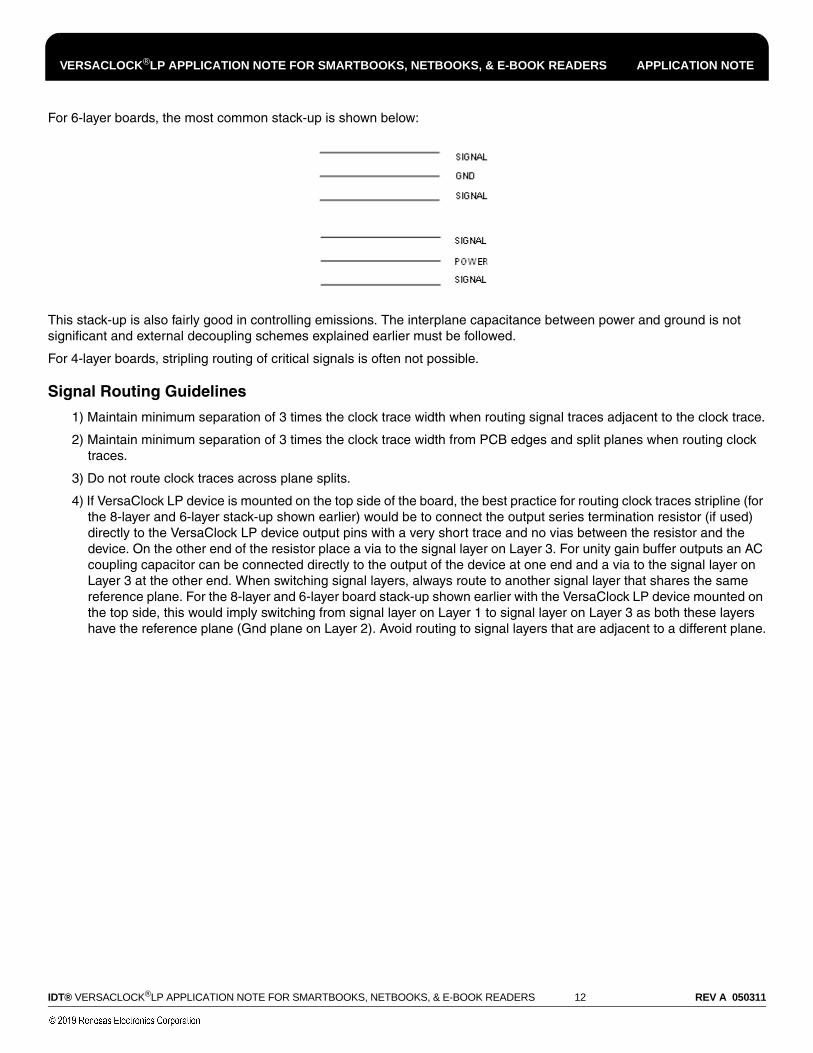
For 6-layer boards, the most common stack-up is shown below:
This stack-up is also fairly good in controlling emissions. The interplane capacitance between power and ground is not significant and external decoupling schemes explained earlier must be followed.
For 4-layer boards, stripling routing of critical signals is often not possible.
Signal Routing Guidelines
1) Maintain minimum separation of 3 times the clock trace width when routing signal traces adjacent to the clock trace.
2) Maintain minimum separation of 3 times the clock trace width from PCB edges and split planes when routing clocktraces.
3) Do not route clock traces across plane splits.
4) If VersaClock LP device is mounted on the top side of the board, the best practice for routing clock traces stripline (forthe 8-layer and 6-layer stack-up shown earlier) would be to connect the output series termination resistor (if used)directly to the VersaClock LP device output pins with a very short trace and no vias between the resistor and thedevice. On the other end of the resistor place a via to the signal layer on Layer 3. For unity gain buffer outputs an ACcoupling capacitor can be connected directly to the output of the device at one end and a via to the signal layer onLayer 3 at the other end. When switching signal layers, always route to another signal layer that shares the samereference plane. For the 8-layer and 6-layer board stack-up shown earlier with the VersaClock LP device mounted onthe top side, this would imply switching from signal layer on Layer 1 to signal layer on Layer 3 as both these layershave the reference plane (Gnd plane on Layer 2). Avoid routing to signal layers that are adjacent to a different plane.

VERSACLOCK®LP APPLICATION NOTE FOR SMARTBOOKS, NETBOOKS, & E-BOOK READERS APPLICATION NOTE
IDT® VERSACLOCK®LP APPLICATION NOTE FOR SMARTBOOKS, NETBOOKS, & E-BOOK READERS 13 REV A 050311
Errata
The following is the errata list for the VersaClock LP device (at the time this document was created):
• The rms crystal drive current for the MHz oscillator on the VersaClock LP device is around 3.7mA. This results in a powerdissipation of around 343µW for a crystal with a typical series resistance of 25ohms. We recommend using a SMD lowprofile crystal with a power dissipation specification of 500µW or higher with this device.
• The internal load capacitance on XIN and XOUT is fixed to 32pF. This leads to an effective internal load capacitance of16pF. Factoring in the input pad capacitance, the effective internal capacitance increases to around 18pF. We recommendusing a MHz crystal with load capacitance rating of 20pF (accounting for PCB stray capacitance) with this device.
• We recommend using a 32.768 kHz crystal (if required) with 8pF load capacitance rating. The internal load capacitors onX132K and X232K need to be unbalanced to achieve 50% Duty Cycle on the output.
• The output impedance for outputs powered by VDDO = 1.8V is around 80 ohms. Running traces > 1 inch on a systemboard for outputs power by VDDO = 1.8V is not recommended from a signal integrity standpoint.
• The 32.768 kHz oscillator has a typical operating current of 35µA and the power down current of the VersaClock LPdevice is around 10µA.
• GPS and wireless module performance cannot be guaranteed with the synthesized clocks from VersaClock LP device.
• Please consult IDT if your jitter requirements are not met on any one of the VersaClock LP device output clocks whenprogrammed with the software generated configuration file.

© 2011 Integrated Device Technology, Inc. All rights reserved. Product specifications subject to change without notice. IDT and the IDT logo are trademarks of Integrated DeviceTechnology, Inc. Accelerated Thinking is a service mark of Integrated Device Technology, Inc. All other brands, product names and marks are or may be trademarks or registeredtrademarks used to identify products or services of their respective owners. Printed in USA
Corporate HeadquartersIntegrated Device Technology, Inc.
www.idt.com
For Sales800-345-7015
408-284-8200
Fax: 408-284-2775
For Tech Supportwww.idt.com/go/clockhelp
Innovate with IDT and accelerate your future networks. Contact:
www.IDT.com
VERSACLOCK®LP APPLICATION NOTE FOR SMARTBOOKS, NETBOOKS, & E-BOOK READERS APPLICATION NOTE

Corporate HeadquartersTOYOSU FORESIA, 3-2-24 Toyosu,Koto-ku, Tokyo 135-0061, Japanwww.renesas.com
Contact InformationFor further information on a product, technology, the most up-to-date version of a document, or your nearest sales office, please visit:www.renesas.com/contact/
TrademarksRenesas and the Renesas logo are trademarks of Renesas Electronics Corporation. All trademarks and registered trademarks are the property of their respective owners.
IMPORTANT NOTICE AND DISCLAIMER
RENESAS ELECTRONICS CORPORATION AND ITS SUBSIDIARIES (“RENESAS”) PROVIDES TECHNICAL SPECIFICATIONS AND RELIABILITY DATA (INCLUDING DATASHEETS), DESIGN RESOURCES (INCLUDING REFERENCE DESIGNS), APPLICATION OR OTHER DESIGN ADVICE, WEB TOOLS, SAFETY INFORMATION, AND OTHER RESOURCES “AS IS” AND WITH ALL FAULTS, AND DISCLAIMS ALL WARRANTIES, EXPRESS OR IMPLIED, INCLUDING, WITHOUT LIMITATION, ANY IMPLIED WARRANTIES OF MERCHANTABILITY, FITNESS FOR A PARTICULAR PURPOSE, OR NON-INFRINGEMENT OF THIRD PARTY INTELLECTUAL PROPERTY RIGHTS.
These resources are intended for developers skilled in the art designing with Renesas products. You are solely responsible for (1) selecting the appropriate products for your application, (2) designing, validating, and testing your application, and (3) ensuring your application meets applicable standards, and any other safety, security, or other requirements. These resources are subject to change without notice. Renesas grants you permission to use these resources only for development of an application that uses Renesas products. Other reproduction or use of these resources is strictly prohibited. No license is granted to any other Renesas intellectual property or to any third party intellectual property. Renesas disclaims responsibility for, and you will fully indemnify Renesas and its representatives against, any claims, damages, costs, losses, or liabilities arising out of your use of these resources. Renesas' products are provided only subject to Renesas' Terms and Conditions of Sale or other applicable terms agreed to in writing. No use of any Renesas resources expands or otherwise alters any applicable warranties or warranty disclaimers for these products.
(Rev.1.0 Mar 2020)
© 2020 Renesas Electronics Corporation. All rights reserved.