R2J20653ANP Datasheet - Renesas
18
REJ03G1849-0200 Rev.2.00 Dec 21, 2009 Page 1 of 15 Preliminary R2J20653ANP Integrated Driver – MOS FET (DrMOS) REJ03G1849-0200 Rev.2.00 Dec 21, 2009 Description The R2J20653ANP multi-chip module incorporates a high-side MOS FET, low-side MOS FET, and MOS-FET driver in a single QFN package. The on and off timing of the power MOS FET is optimized by the built-in driver, making this device suitable for large-current buck converters. The chip also incorporates a high-side bootstrap switch, eliminating the need for an external SBD for this purpose. Features • Compliant with Intel 6 × 6 DrMOS specification • Built-in power MOS FET suitable for Notebook, Desktop, Server application • Low-side MOS FET with built-in SBD for lower loss and reduced ringing • Built-in driver circuit which matches the power MOS FET • Built-in tri-state input function which can support a number of PWM controllers • High-frequency operation (above 1 MHz) possible • VIN operating-voltage range: 27 V max • Large average output current (Max. 35 A) • Achieve low power dissipation • Controllable driver: Remote on/off • Low-side MOS FET disabled function for DCM operation • Double thermal protection: Thermal warning & Thermal shutdown • Built-in bootstrapping switch • Small package: QFN40 (6 mm × 6 mm × 0.95 mm) • Terminal Pb-free/Halogen-free Outline (Bottom view) Low-side MOS Pad High-side MOS Pad Driver Pad 40 1 10 30 21 11 31 20 Integrated Driver-MOS FET (DrMOS) QFN40 package 6 mm × 6 mm VIN GH BOOT VCIN DISBL# LSDBL# CGND VDRV GL PGND THWN PWM MOS FET Driver VSWH
-
Upload
khangminh22 -
Category
Documents
-
view
1 -
download
0
Transcript of R2J20653ANP Datasheet - Renesas
REJ03G1849-0200 Rev.2.00 Dec 21, 2009 Page 1 of 15
Preliminary
R2J20653ANP Integrated Driver – MOS FET (DrMOS)
REJ03G1849-0200 Rev.2.00
Dec 21, 2009
Description The R2J20653ANP multi-chip module incorporates a high-side MOS FET, low-side MOS FET, and MOS-FET driver in a single QFN package. The on and off timing of the power MOS FET is optimized by the built-in driver, making this device suitable for large-current buck converters. The chip also incorporates a high-side bootstrap switch, eliminating the need for an external SBD for this purpose.
Features • Compliant with Intel 6 × 6 DrMOS specification • Built-in power MOS FET suitable for Notebook, Desktop, Server application • Low-side MOS FET with built-in SBD for lower loss and reduced ringing • Built-in driver circuit which matches the power MOS FET • Built-in tri-state input function which can support a number of PWM controllers • High-frequency operation (above 1 MHz) possible • VIN operating-voltage range: 27 V max • Large average output current (Max. 35 A) • Achieve low power dissipation • Controllable driver: Remote on/off • Low-side MOS FET disabled function for DCM operation • Double thermal protection: Thermal warning & Thermal shutdown • Built-in bootstrapping switch • Small package: QFN40 (6 mm × 6 mm × 0.95 mm) • Terminal Pb-free/Halogen-free
Outline
(Bottom view)
Low-side MOS Pad
High-side
MOS Pad
Driver
Pad
40
1 10
30 21
11
31 20
Integrated Driver-MOS FET (DrMOS)QFN40 package 6 mm × 6 mm
VINGHBOOTVCIN
DISBL#
LSDBL#
CGND VDRV GL PGND
THWN
PWM
MOS FET Driver VSWH
R2J20653ANP Preliminary
REJ03G1849-0200 Rev.2.00 Dec 21, 2009 Page 2 of 15
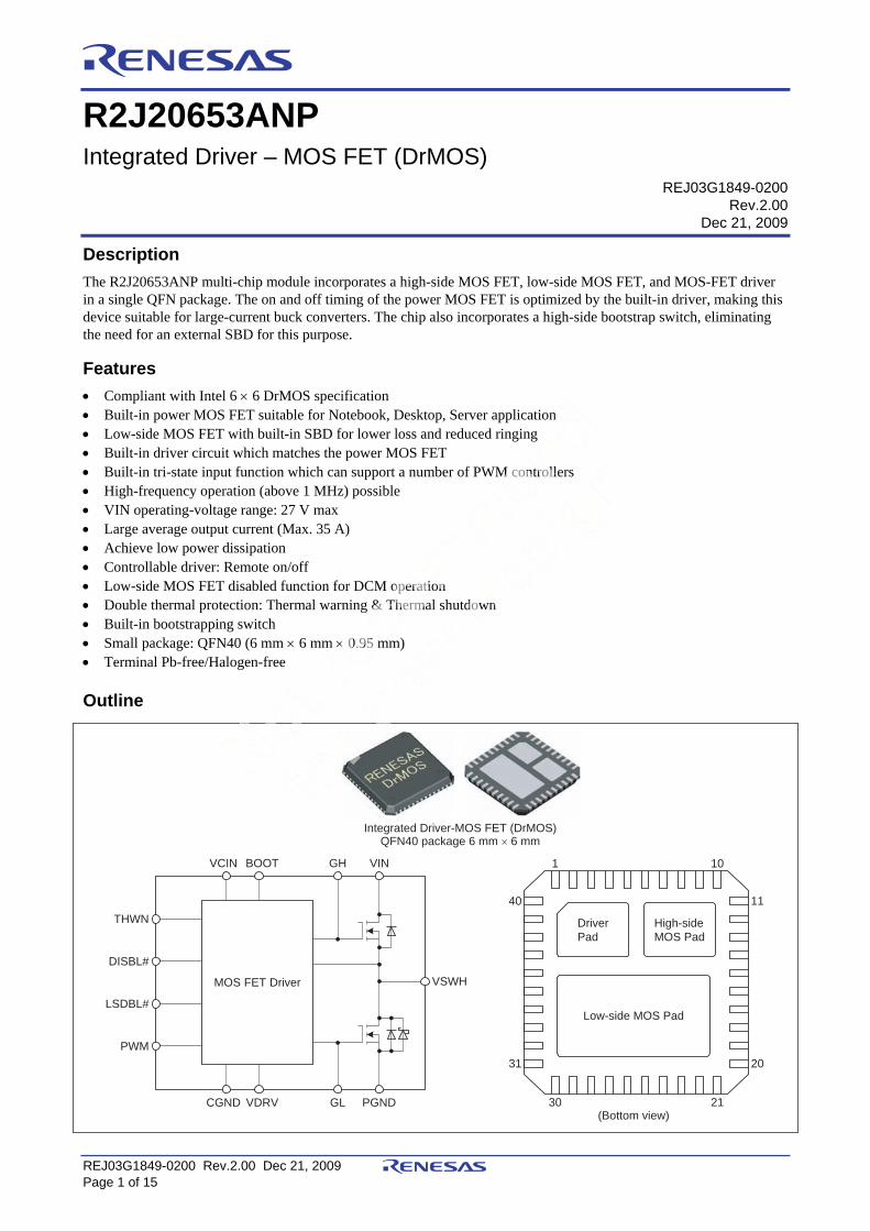
Block Diagram
Driver Chip
PGND
25 k
150 k
Overlap
Protection.
& Logic
VIN
VSWH
Boot
SW
High Side
MOS FET
Low Side
MOS FET
THWN
VCIN
VCIN
VDRV
THDN
CGND
CGND
20 μA
UVL
Level Shifter
2 μA
Input Logic
(TTL Level)
(3 state in)
THWN
DISBL#
LSDBL#
PWM
VCIN VDRV BOOT GH
GLCGND
Notes: 1. Truth table for the DISBL# pin. 2. Truth table for the LSDBL# pin. DISBL# Input Driver Chip Status
"L" Shutdown (GL, GH = "L") "Open" Shutdown (GL, GH = "L") "H" Enable (GL, GH = "Active")
LSDBL# Input GL Status "L" "L" "Open" "Active" "H" "Active"
3. Output signal from the UVL block 4. Output signal from the THWN block
"H"
"L"
UVL output
Logic LevelVCIN
VHVL
For active
For shutdown
"H"
"L"
Thermal Warning
Logic Level
TIC(°C)
TwarnHTwarnL
Thermal
WarningNormal
operating
5. Truth table for the THDN block Driver IC Temp. Driver Chip Status
< 150°C (< 135°C on cancellation)
Enable (GL, GH = "Active")
> 150°C Shutdown (GL, GH = "L")
R2J20653ANP Preliminary
REJ03G1849-0200 Rev.2.00 Dec 21, 2009 Page 3 of 15
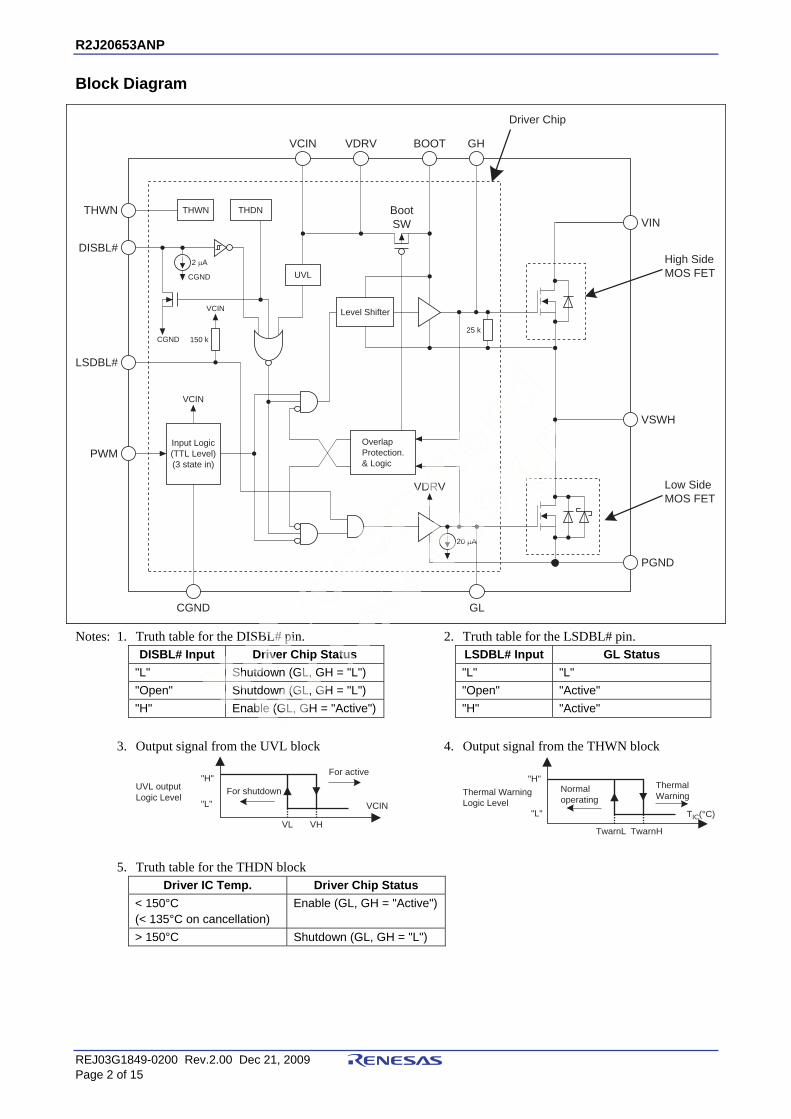
Pin Arrangement
(Top view)
VSWH
VIN PWM
DISBL#
THWN
CGND
GL
VSWH
VSWH
VSWH
VSWH
VIN
VIN
VIN
VSWH
PGND
PGND
PGND
PGND
PGND VSWH
VIN CGND
21 22 23 24 25 26 27 28 29 30
10 9 8 7 6 5 4 3 2 1
20
11
12
13
14
15
16
17
18
19
31
40
39
38
37
36
35
34
33
32
PG
ND
PG
ND
PG
ND
PG
ND
PG
ND
PG
ND
PG
ND
PG
ND
VS
WH
VS
WH
VIN
VIN
VIN
VS
WH
GH
CG
ND
BO
OT
VD
RV
VC
IN
LS
DB
L#
Note: All die-pads (three pads in total) should be soldered to PCB.
Pin Description Pin Name Pin No. Description Remarks LSDBL# 1 Low-side gate disable When asserted "L" signal, Low-side gate disableVCIN 2 Control input voltage (+5 V input) Driver Vcc input VDRV 3 Gate supply voltage (+5 V input) 5 V gate drive BOOT 4 Bootstrap voltage pin To be supplied +5 V through internal switch CGND 5, 37, Pad Control signal ground Should be connected to PGND externally GH 6 High-side gate signal Pin for monitor VIN 8 to 14, Pad Input voltage VSWH 7, 15, 29 to 35, Pad Phase output/Switch output PGND 16 to 28 Power ground GL 36 Low-side gate signal Pin for monitor THWN 38 Thermal warning Thermal warning when over 115°C DISBL# 39 Signal disable Disabled when DISBL# is "L"
This pin is pulled low when internal IC over the thermal shutdown level, 150°C.
PWM 40 PWM drive logic input 5 V logic input
R2J20653ANP Preliminary
REJ03G1849-0200 Rev.2.00 Dec 21, 2009 Page 4 of 15
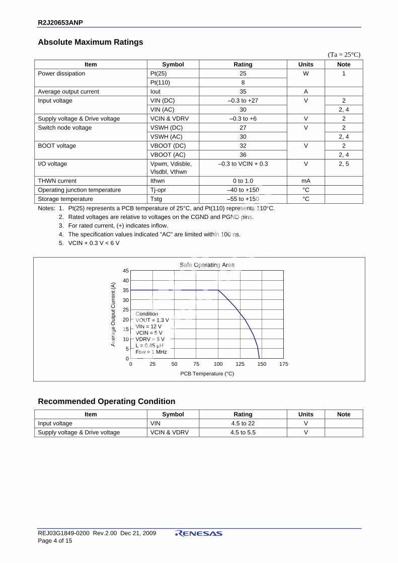
Absolute Maximum Ratings (Ta = 25°C)
Item Symbol Rating Units Note Pt(25) 25 Power dissipation Pt(110) 8
W 1
Average output current Iout 35 A VIN (DC) –0.3 to +27 2 Input voltage VIN (AC) 30
V 2, 4
Supply voltage & Drive voltage VCIN & VDRV –0.3 to +6 V 2 VSWH (DC) 27 2 Switch node voltage VSWH (AC) 30
V 2, 4
VBOOT (DC) 32 2 BOOT voltage VBOOT (AC) 36
V 2, 4
I/O voltage Vpwm, Vdisble, Vlsdbl, Vthwn
–0.3 to VCIN + 0.3 V 2, 5
THWN current Ithwn 0 to 1.0 mA Operating junction temperature Tj-opr –40 to +150 °C Storage temperature Tstg –55 to +150 °C Notes: 1. Pt(25) represents a PCB temperature of 25°C, and Pt(110) represents 110°C. 2. Rated voltages are relative to voltages on the CGND and PGND pins. 3. For rated current, (+) indicates inflow. 4. The specification values indicated "AC" are limited within 100 ns. 5. VCIN + 0.3 V < 6 V
0
5
10
15
20
25
30
35
40
45
0 25 50 75 100 125 150 175
Condition
VOUT = 1.3 V
VIN = 12 V
VCIN = 5 V
VDRV = 5 V
L = 0.45 μH
Fsw = 1 MHz
Ave
rag
e O
utp
ut C
urr
en
t (A
)
PCB Temperature (°C)
Safe Operating Area
Recommended Operating Condition Item Symbol Rating Units Note
Input voltage VIN 4.5 to 22 V Supply voltage & Drive voltage VCIN & VDRV 4.5 to 5.5 V
R2J20653ANP Preliminary
REJ03G1849-0200 Rev.2.00 Dec 21, 2009 Page 5 of 15
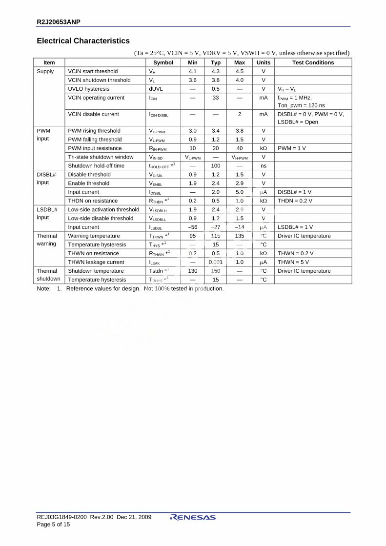
Electrical Characteristics (Ta = 25°C, VCIN = 5 V, VDRV = 5 V, VSWH = 0 V, unless otherwise specified)
Item Symbol Min Typ Max Units Test Conditions VCIN start threshold VH 4.1 4.3 4.5 V VCIN shutdown threshold VL 3.6 3.8 4.0 V UVLO hysteresis dUVL — 0.5 — V VH – VL VCIN operating current ICIN — 33 — mA fPWM = 1 MHz,
Ton_pwm = 120 ns
Supply
VCIN disable current ICIN-DISBL — — 2 mA DISBL# = 0 V, PWM = 0 V, LSDBL# = Open
PWM rising threshold VH-PWM 3.0 3.4 3.8 V PWM falling threshold VL-PWM 0.9 1.2 1.5 V PWM input resistance RIN-PWM 10 20 40 kΩ PWM = 1 V Tri-state shutdown window VIN-SD VL-PWM — VH-PWM V
PWM input
Shutdown hold-off time tHOLD-OFF *1 — 100 — ns Disable threshold VDISBL 0.9 1.2 1.5 V Enable threshold VENBL 1.9 2.4 2.9 V Input current IDISBL — 2.0 5.0 μA DISBL# = 1 V
DISBL# input
THDN on resistance RTHDN *1 0.2 0.5 1.0 kΩ THDN = 0.2 V Low-side activation threshold VLSDBLH 1.9 2.4 2.9 V Low-side disable threshold VLSDBLL 0.9 1.2 1.5 V
LSDBL# input
Input current ILSDBL –56 –27 –14 μA LSDBL# = 1 V Warning temperature TTHWN *1 95 115 135 °C Driver IC temperature Temperature hysteresis THYS *1 — 15 — °C THWN on resistance RTHWN *1 0.2 0.5 1.0 kΩ THWN = 0.2 V
Thermal warning
THWN leakage current ILEAK — 0.001 1.0 μA THWN = 5 V Shutdown temperature Tstdn *1 130 150 — °C Driver IC temperature Thermal
shutdown Temperature hysteresis TDHYS *1 — 15 — °C Note: 1. Reference values for design. Not 100% tested in production.
R2J20653ANP Preliminary
REJ03G1849-0200 Rev.2.00 Dec 21, 2009 Page 6 of 15
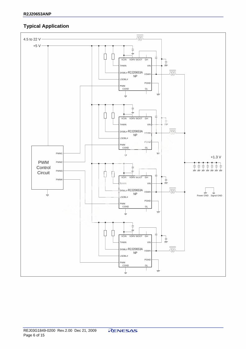
Typical Application
VCIN
CGND GL
VIN
BOOT
4.5 to 22 V
+5 V
+1.3 V
GHVDRV
R2J20653A
NP
PGND
THWN
DISBL#
LSDBL#
PWM1
PWM
VSWH
VCIN
CGND GL
VIN
BOOT GHVDRV
R2J20653A
NP
PGND
THWN
DISBL#
LSDBL#
PWM2
PWM
VSWH
VCIN
CGND GL
VIN
BOOT GHVDRV
R2J20653A
NP
PGND
THWN
DISBL#
LSDBL#
PWM
VSWH
VCIN
CGND GL
VIN
BOOT GHVDRV
PWM
Control
Circuit
R2J20653A
NP
PGND
THWN
DISBL#
LSDBL#
PWM
VSWH
PWM3
PWM4
Power GND Signal GND
R2J20653ANP Preliminary
REJ03G1849-0200 Rev.2.00 Dec 21, 2009 Page 7 of 15
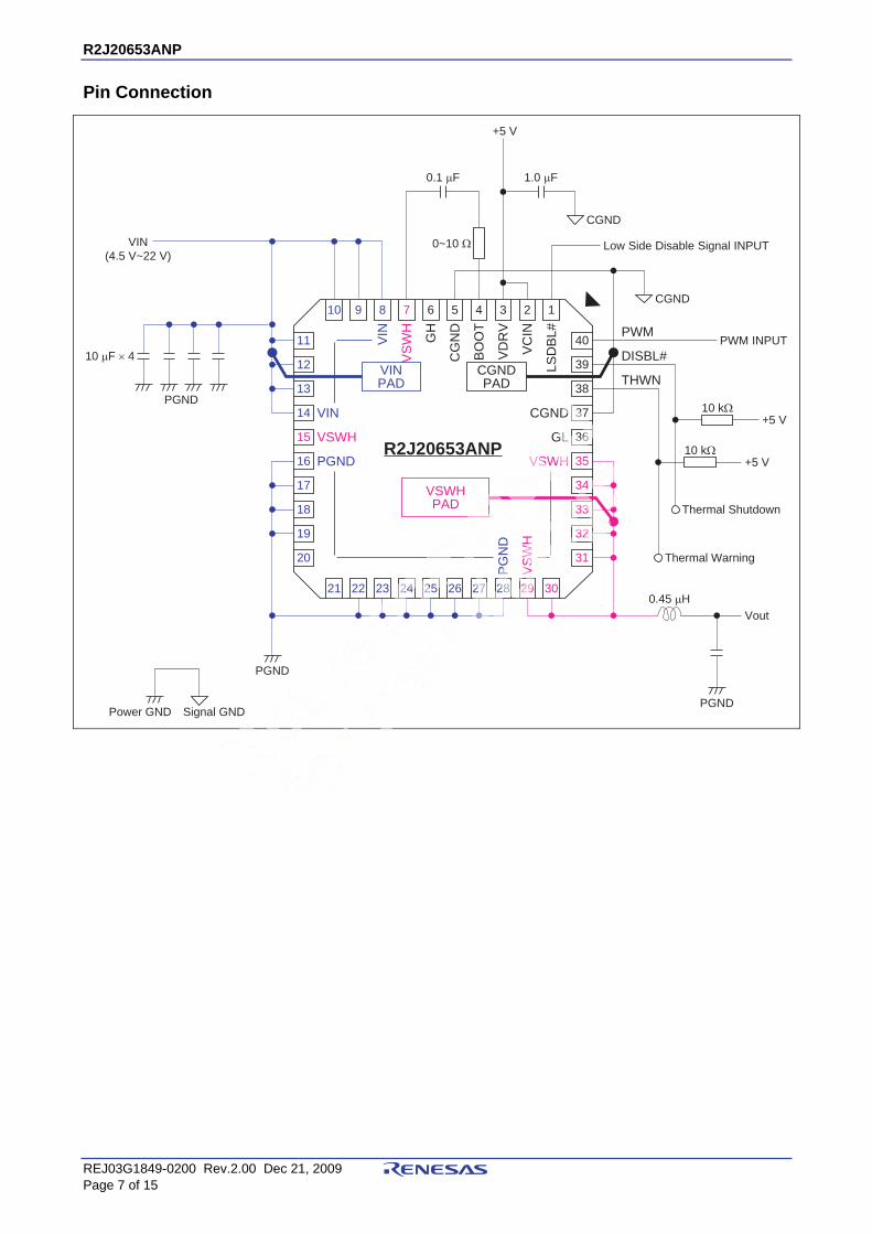
Pin Connection
+5 V
0.1 μF
0.45 μH
VIN
(4.5 V~22 V)
PGND
PGNDPower GND Signal GND
R2J20653ANP
CGNDPAD
21 22 23 24 25 26 27 28 29 30
10 9 8 7 6 5 4 3 2 1
20
11
12
13
14
15
16
17
18
19
31
40
39
38
37
36
35
34
33
32
PWM
DISBL#
THWN
CGND
VSWH
VIN
VSWH GL
PGND
PG
ND
VS
WH
VIN
VS
WH
GH
CG
ND
BO
OT
VD
RV
VC
IN
LS
DB
L#
Low Side Disable Signal INPUT
VINPAD
PGND
1.0 μF
CGND
CGND
10 μF × 4
+5 V
Thermal Shutdown
PWM INPUT
VSWHPAD
0~10 Ω
10 kΩ
+5 V10 kΩ
Vout
Thermal Warning
R2J20653ANP Preliminary
REJ03G1849-0200 Rev.2.00 Dec 21, 2009 Page 8 of 15
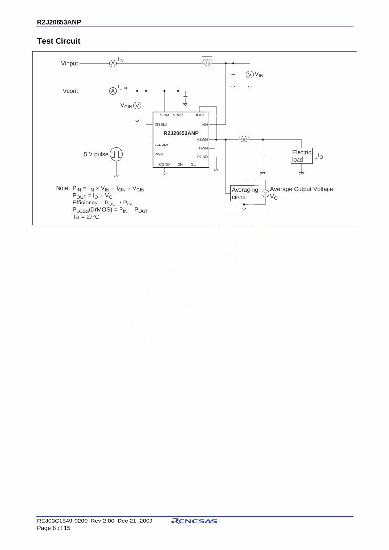
Test Circuit
VCIN
VIN
VSWH
BOOT
GL
R2J20653ANP
PGND
GH
THWN
Vcont
Vinput
CGND
DISBL#
LSDBL#
PWM5 V pulse
Note: PIN = IIN × VIN + ICIN × VCIN
POUT = IO × VO
Efficiency = POUT / PIN
PLOSS(DrMOS) = PIN – POUT
Ta = 27°C
Average Output Voltage
VOV
V
VCIN
VIN
ICIN
V
IIN
A
A
IOElectric
load
Averaging
circuit
VDRV
R2J20653ANP Preliminary
REJ03G1849-0200 Rev.2.00 Dec 21, 2009 Page 9 of 15
Typical Data
Power Loss vs. Output Current
Output Current (A)
Output Voltage (V)
Po
we
r L
oss
(W
)
No
rma
lize
d P
ow
er
Lo
ss
@ V
IN =
12
V
Input Voltage (V)
Power Loss vs. Input Voltage
Power Loss vs. Switching Frequency
No
rma
lize
d P
ow
er
Lo
ss
@ V
OU
T =
1.3
V
Switching Frequency (kHz)
No
rma
lize
d P
ow
er
Lo
ss
@ f
PW
M =
60
0 k
Hz
Power Loss vs. Output Voltage
0
1
2
3
4
5
6
7
8
9
0 5 10 15 20 25 30 35 4 6 8 10 2012 14 2216 180.8
0.9
1.0
1.1
1.2
1.3
1.4
1.5
0.8
0.9
1.0
1.1
1.2
1.3
1.4
1.5
0.8
0.9
1.0
1.1
1.2
1.3
1.4
1.5
0.8 1.2 1.6 2.0 2.4 2.8 3.2 3.6 4.0 4.4 250 500 750 1000 1250
VIN = 12 V
VCIN = 5 V
VOUT = 1.3 V
fPWM = 600 kHz
L = 0.45 μH
VIN = 12 V
VCIN = 5 V
fPWM = 600 kHz
L = 0.45 μH
IOUT = 25 A
VIN = 12 V
VCIN = 5 V
VOUT = 1.3 V
L = 0.45 μH
IOUT = 25 A
VCIN = 5 V
VOUT = 1.3 V
fPWM = 600 kHz
L = 0.45 μH
IOUT = 25 A
R2J20653ANP Preliminary
REJ03G1849-0200 Rev.2.00 Dec 21, 2009 Page 10 of 15
Power Loss vs. Output Inductance
Output Inductance (μH)
No
rma
lize
d P
ow
er
Lo
ss
@ L
= 0
.45
μH
No
rma
lize
d P
ow
er
Lo
ss
@ V
CIN
= 5
V
Power Loss vs. VCIN
0.1 0.2 0.3 0.4 0.5 0.6 0.7 0.8 0.9 1.0
VCIN (V)
4.5 5.0 5.5 6.0
VIN = 12 V
VCIN = 5 V
VOUT = 1.3 V
fPWM = 600 kHz
IOUT = 25 A
VIN = 12 V
VCIN = 5 V
VOUT = 1.3 V
L = 0.45 μH
IOUT = 0 A
Switching Frequency (kHz)
Average ICIN vs. Switching Frequency
Ave
rag
e IC
IN (
mA
)
0
10
30
40
20
50
250 500 750 1000 1250
0.8
0.9
1.0
1.1
1.2
1.3
1.4
1.5
0.8
0.9
1.0
1.1
1.2
1.3
1.4
1.5VIN = 12 V
VOUT = 1.3 V
fPWM = 600 kHz
L = 0.45 μH
IOUT = 25 A
R2J20653ANP Preliminary
REJ03G1849-0200 Rev.2.00 Dec 21, 2009 Page 11 of 15
Description of Operation The DrMOS multi-chip module incorporates a high-side MOS FET, low-side MOS FET, and MOS-FET driver in a single QFN package. Since the parasitic inductance between each chip is extremely small, the module is highly suitable for use in buck converters to be operated at high frequencies. The control timing between the high-side MOS FET, low-side MOS FET, and driver is optimized so that high efficiency can be obtained at low output-voltage.
VCIN & DISBL#
The VCIN pin is connected to the UVL (under-voltage lockout) module, so that the driver is disabled as long as VCIN is 4.3 V or less. On cancellation of UVL, the driver remains enabled until the UVL input is driven to 3.8 V or less. The signal on pin DISBL# also enables or disables the circuit.
Voltages from –0.3 V to VCIN can be applied to the DISBL# pin, so on/off control by a logic IC or the use of a resistor, etc., to pull the DISBL# line up to VCIN are both possible.
VCIN DISBL# Driver State L ∗ Disable (GL, GH = L) H L Disable (GL, GH = L) H H Active H Open Disable (GL, GH = L)
The pulled-down MOS FET, which is turned on when internal IC temperature becomes over thermal shutdown level, is connected to the DISBL# pin. The detailed function is described in THDN section.
PWM & LSDBL#
The PWM pin is the signal input pin for the driver chip. The input-voltage range is –0.3 V to (VCIN + 0.3 V). When the PWM input is high, the gate of the high-side MOS FET (GH) is high and the gate of the low-side MOS FET (GL) is low.
PWM GH GL L L H H H L
The LSDBL# pin is the low-side gate disable pin for "Discontinuous Conduction Mode (DCM)" when LSDBL# is low.
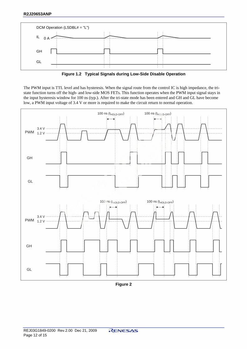
Figure 1 shows the typical high-side and low-side gate switching and inductor current (IL) during Continuous Conduction Mode (CCM) and low-side gate disabled when asserting low-side disable signal.
This pin is internally pulled up to VCIN with 150 kΩ resistor.
When low-side disable function is not used, keep this pin open or pulled up to VCIN.
CCM Operation (LSDBL# = "H" or Open mode)
IL
GH
GL
Figure 1.1 Typical Signals during CCM
R2J20653ANP Preliminary
REJ03G1849-0200 Rev.2.00 Dec 21, 2009 Page 12 of 15
DCM Operation (LSDBL# = "L")
GL
IL
GH
0 A
Figure 1.2 Typical Signals during Low-Side Disable Operation
The PWM input is TTL level and has hysteresis. When the signal route from the control IC is high impedance, the tri-state function turns off the high- and low-side MOS FETs. This function operates when the PWM input signal stays in the input hysteresis window for 100 ns (typ.). After the tri-state mode has been entered and GH and GL have become low, a PWM input voltage of 3.4 V or more is required to make the circuit return to normal operation.
3.4 V
1.2 V
3.4 V
1.2 V
100 ns (tHOLD-OFF)
100 ns (tHOLD-OFF)
100 ns (tHOLD-OFF)
100 ns (tHOLD-OFF)
PWM
GH
GH
GL
GL
PWM
Figure 2
R2J20653ANP Preliminary
REJ03G1849-0200 Rev.2.00 Dec 21, 2009 Page 13 of 15
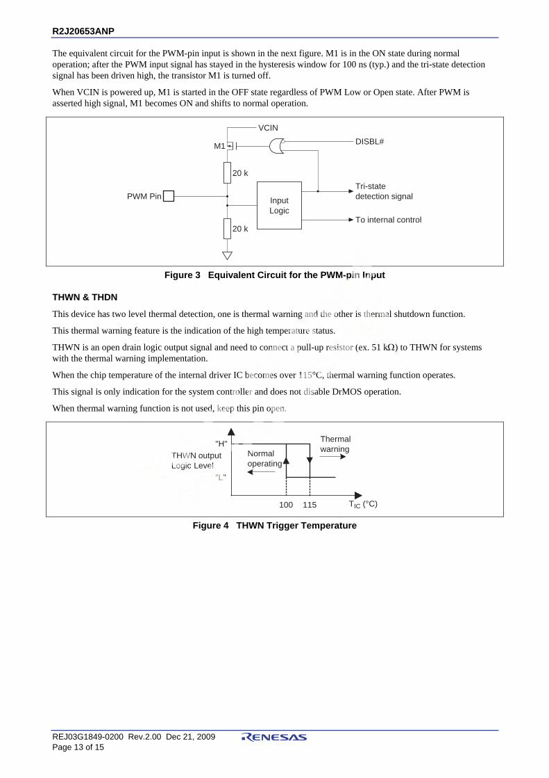
The equivalent circuit for the PWM-pin input is shown in the next figure. M1 is in the ON state during normal operation; after the PWM input signal has stayed in the hysteresis window for 100 ns (typ.) and the tri-state detection signal has been driven high, the transistor M1 is turned off.
When VCIN is powered up, M1 is started in the OFF state regardless of PWM Low or Open state. After PWM is asserted high signal, M1 becomes ON and shifts to normal operation.
VCIN
DISBL#
20 k
To internal control
Tri-state
detection signal
20 k
Input
Logic
M1
PWM Pin
Figure 3 Equivalent Circuit for the PWM-pin Input
THWN & THDN
This device has two level thermal detection, one is thermal warning and the other is thermal shutdown function.
This thermal warning feature is the indication of the high temperature status.
THWN is an open drain logic output signal and need to connect a pull-up resistor (ex. 51 kΩ) to THWN for systems with the thermal warning implementation.
When the chip temperature of the internal driver IC becomes over 115°C, thermal warning function operates.
This signal is only indication for the system controller and does not disable DrMOS operation.
When thermal warning function is not used, keep this pin open.
TIC (°C)115100
Thermal
warningNormal
operatingTHWN output
Logic Level
"L"
"H"
Figure 4 THWN Trigger Temperature
R2J20653ANP Preliminary
REJ03G1849-0200 Rev.2.00 Dec 21, 2009 Page 14 of 15
THDN is an internal thermal shutdown signal when driver IC becomes over 150°C.
This function makes high-side MOS FET and low-side MOS FET turn off for the device protection from abnormal high temperature situation and at the same time DISBL# pin is pulled low internally to give notice to the system controller.
Figure 5 shows the example of two types of DISBL# connection with the system controller signal.
Driver IC Temp. Driver Chip Status < 150°C (< 135°C on cancellation)
Enable (GL, GH = "Active")
> 150°C Shutdown (GL, GH = "L")
Figure 5.1 THDN Signal to the System Controller Figure 5.2 ON/OFF Signal from the System Controller
2 μA
10 k
5 V
DISBL#
Thermal
Shutdown
Detection
To Internal
Logic
To shutdown signal
2 μA
DISBL#
Thermal
Shutdown
Detection
To Internal
Logic
ON/OFF signal
10 k
MOS FETs
The MOS FETs incorporated in R2J20653ANP are highly suitable for synchronous-rectification buck conversion. For the high-side MOS FET, the drain is connected to the VIN pin and the source is connected to the VSWH pin. For the low-side MOS FET, the drain is connected to the VSWH pin and the source is connected to the PGND pin.
R2J20653ANP Preliminary
REJ03G1849-0200 Rev.2.00 Dec 21, 2009 Page 15 of 15
Package Dimensions
Dimension in MillimetersReference
Symbol
P-HVQFN40-p-0606-0.50 ——PVQN0040KC-A
MASS[Typ.]RENESAS CodeJEITA Package Code Previous Code
5.95 6.00 6.05
5.95 6.00 6.05
D
Min Nom Max
E
e
0.87 0.89 0.91A2
— — 0.20
0.865 0.91 0.95
f
A
0.005 0.02 0.04A1
0.17 0.22 0.27
0.16 0.20 0.24
b
b1
— 0.50 —
0.40 0.50 0.60
— — 0.05
Lp
x
— — 0.05y
— — 0.20
— — 0.20
y1
t
6.15 6.20 6.25HD
6.15 6.20 6.25
— 0.75 —
HE
ZD
— 0.75 —ZE
0.06 0.10 0.14
0.17 0.20 0.23
L1
c1
0.17 0.22 0.27c2
L1
c2
Lp
A2
A1
A
HE
/2E
/2
EHE
t S AB
bx S AB
eZD
f S AB
X 4X 4
ZE
2-A section
HD/2 D /2
D
HD
4-C0.50
20°20°
4-(0.139)
1.9
5
1.95
1.9
5
1.95
y S
1pin
40
1pin
40
C0.3
INDEX
0.20.7
2.2
2.05
0.2
2.2
0.2
2.2
2.2
2.0
5
CAV No.Die No.
B
S
y1 S
0.6
9
A
B
Ordering Information Part Name Quantity Shipping Container
R2J20653ANP#G3 2500 pcs Taping Reel
Notes:1. This document is provided for reference purposes only so that Renesas customers may select the appropriate Renesas products for their use. Renesas neither makes warranties or representations with respect to the accuracy or completeness of the information contained in this document nor grants any license to any intellectual property rights or any other rights of Renesas or any third party with respect to the information in this document. 2. Renesas shall have no liability for damages or infringement of any intellectual property or other rights arising out of the use of any information in this document, including, but not limited to, product data, diagrams, charts, programs, algorithms, and application circuit examples.3. You should not use the products or the technology described in this document for the purpose of military applications such as the development of weapons of mass destruction or for the purpose of any other military use. When exporting the products or technology described herein, you should follow the applicable export control laws and regulations, and procedures required by such laws and regulations.4. All information included in this document such as product data, diagrams, charts, programs, algorithms, and application circuit examples, is current as of the date this document is issued. Such information, however, is subject to change without any prior notice. Before purchasing or using any Renesas products listed in this document, please confirm the latest product information with a Renesas sales office. Also, please pay regular and careful attention to additional and different information to be disclosed by Renesas such as that disclosed through our website. (http://www.renesas.com )5. Renesas has used reasonable care in compiling the information included in this document, but Renesas assumes no liability whatsoever for any damages incurred as a result of errors or omissions in the information included in this document.6. When using or otherwise relying on the information in this document, you should evaluate the information in light of the total system before deciding about the applicability of such information to the intended application. Renesas makes no representations, warranties or guaranties regarding the suitability of its products for any particular application and specifically disclaims any liability arising out of the application and use of the information in this document or Renesas products. 7. With the exception of products specified by Renesas as suitable for automobile applications, Renesas products are not designed, manufactured or tested for applications or otherwise in systems the failure or malfunction of which may cause a direct threat to human life or create a risk of human injury or which require especially high quality and reliability such as safety systems, or equipment or systems for transportation and traffic, healthcare, combustion control, aerospace and aeronautics, nuclear power, or undersea communication transmission. If you are considering the use of our products for such purposes, please contact a Renesas sales office beforehand. Renesas shall have no liability for damages arising out of the uses set forth above.8. Notwithstanding the preceding paragraph, you should not use Renesas products for the purposes listed below: (1) artificial life support devices or systems (2) surgical implantations (3) healthcare intervention (e.g., excision, administration of medication, etc.) (4) any other purposes that pose a direct threat to human life Renesas shall have no liability for damages arising out of the uses set forth in the above and purchasers who elect to use Renesas products in any of the foregoing applications shall indemnify and hold harmless Renesas Technology Corp., its affiliated companies and their officers, directors, and employees against any and all damages arising out of such applications. 9. You should use the products described herein within the range specified by Renesas, especially with respect to the maximum rating, operating supply voltage range, movement power voltage range, heat radiation characteristics, installation and other product characteristics. Renesas shall have no liability for malfunctions or damages arising out of the use of Renesas products beyond such specified ranges.10. Although Renesas endeavors to improve the quality and reliability of its products, IC products have specific characteristics such as the occurrence of failure at a certain rate and malfunctions under certain use conditions. Please be sure to implement safety measures to guard against the possibility of physical injury, and injury or damage caused by fire in the event of the failure of a Renesas product, such as safety design for hardware and software including but not limited to redundancy, fire control and malfunction prevention, appropriate treatment for aging degradation or any other applicable measures. Among others, since the evaluation of microcomputer software alone is very difficult, please evaluate the safety of the final products or system manufactured by you. 11. In case Renesas products listed in this document are detached from the products to which the Renesas products are attached or affixed, the risk of accident such as swallowing by infants and small children is very high. You should implement safety measures so that Renesas products may not be easily detached from your products. Renesas shall have no liability for damages arising out of such detachment.12. This document may not be reproduced or duplicated, in any form, in whole or in part, without prior written approval from Renesas. 13. Please contact a Renesas sales office if you have any questions regarding the information contained in this document, Renesas semiconductor products, or if you have any other inquiries.
Sales Strategic Planning Div. Nippon Bldg., 2-6-2, Ohte-machi, Chiyoda-ku, Tokyo 100-0004, Japan
http://www.renesas.comRefer to "http://www.renesas.com/en/network" for the latest and detailed information.
Renesas Technology America, Inc.450 Holger Way, San Jose, CA 95134-1368, U.S.ATel: <1> (408) 382-7500, Fax: <1> (408) 382-7501 Renesas Technology Europe LimitedDukes Meadow, Millboard Road, Bourne End, Buckinghamshire, SL8 5FH, U.K.Tel: <44> (1628) 585-100, Fax: <44> (1628) 585-900
Renesas Technology (Shanghai) Co., Ltd.Unit 204, 205, AZIACenter, No.1233 Lujiazui Ring Rd, Pudong District, Shanghai, China 200120Tel: <86> (21) 5877-1818, Fax: <86> (21) 6887-7858/7898 Renesas Technology Hong Kong Ltd.7th Floor, North Tower, World Finance Centre, Harbour City, Canton Road, Tsimshatsui, Kowloon, Hong Kong Tel: <852> 2265-6688, Fax: <852> 2377-3473
Renesas Technology Taiwan Co., Ltd.10th Floor, No.99, Fushing North Road, Taipei, TaiwanTel: <886> (2) 2715-2888, Fax: <886> (2) 3518-3399 Renesas Technology Singapore Pte. Ltd.1 Harbour Front Avenue, #06-10, Keppel Bay Tower, Singapore 098632 Tel: <65> 6213-0200, Fax: <65> 6278-8001
Renesas Technology Korea Co., Ltd.Kukje Center Bldg. 18th Fl., 191, 2-ka, Hangang-ro, Yongsan-ku, Seoul 140-702, KoreaTel: <82> (2) 796-3115, Fax: <82> (2) 796-2145 Renesas Technology Malaysia Sdn. BhdUnit 906, Block B, Menara Amcorp, Amcorp Trade Centre, No.18, Jln Persiaran Barat, 46050 Petaling Jaya, Selangor Darul Ehsan, MalaysiaTel: <603> 7955-9390, Fax: <603> 7955-9510
RENESAS SALES OFFICES
© 2009. Renesas Technology Corp., All rights reserved. Printed in Japan.
Colophon .7.2
To our customers,
Old Company Name in Catalogs and Other Documents
On April 1st, 2010, NEC Electronics Corporation merged with Renesas Technology
Corporation, and Renesas Electronics Corporation took over all the business of both companies. Therefore, although the old company name remains in this document, it is a valid Renesas Electronics document. We appreciate your understanding.
Renesas Electronics website: http://www.renesas.com
April 1st, 2010 Renesas Electronics Corporation
Issued by: Renesas Electronics Corporation (http://www.renesas.com)
Send any inquiries to http://www.renesas.com/inquiry.
Notice 1. All information included in this document is current as of the date this document is issued. Such information, however, is
subject to change without any prior notice. Before purchasing or using any Renesas Electronics products listed herein, please confirm the latest product information with a Renesas Electronics sales office. Also, please pay regular and careful attention to additional and different information to be disclosed by Renesas Electronics such as that disclosed through our website.
2. Renesas Electronics does not assume any liability for infringement of patents, copyrights, or other intellectual property rights of third parties by or arising from the use of Renesas Electronics products or technical information described in this document. No license, express, implied or otherwise, is granted hereby under any patents, copyrights or other intellectual property rights of Renesas Electronics or others.
3. You should not alter, modify, copy, or otherwise misappropriate any Renesas Electronics product, whether in whole or in part. 4. Descriptions of circuits, software and other related information in this document are provided only to illustrate the operation of
semiconductor products and application examples. You are fully responsible for the incorporation of these circuits, software, and information in the design of your equipment. Renesas Electronics assumes no responsibility for any losses incurred by you or third parties arising from the use of these circuits, software, or information.
5. When exporting the products or technology described in this document, you should comply with the applicable export control laws and regulations and follow the procedures required by such laws and regulations. You should not use Renesas Electronics products or the technology described in this document for any purpose relating to military applications or use by the military, including but not limited to the development of weapons of mass destruction. Renesas Electronics products and technology may not be used for or incorporated into any products or systems whose manufacture, use, or sale is prohibited under any applicable domestic or foreign laws or regulations.
6. Renesas Electronics has used reasonable care in preparing the information included in this document, but Renesas Electronics does not warrant that such information is error free. Renesas Electronics assumes no liability whatsoever for any damages incurred by you resulting from errors in or omissions from the information included herein.
7. Renesas Electronics products are classified according to the following three quality grades: “Standard”, “High Quality”, and “Specific”. The recommended applications for each Renesas Electronics product depends on the product’s quality grade, as indicated below. You must check the quality grade of each Renesas Electronics product before using it in a particular application. You may not use any Renesas Electronics product for any application categorized as “Specific” without the prior written consent of Renesas Electronics. Further, you may not use any Renesas Electronics product for any application for which it is not intended without the prior written consent of Renesas Electronics. Renesas Electronics shall not be in any way liable for any damages or losses incurred by you or third parties arising from the use of any Renesas Electronics product for an application categorized as “Specific” or for which the product is not intended where you have failed to obtain the prior written consent of Renesas Electronics. The quality grade of each Renesas Electronics product is “Standard” unless otherwise expressly specified in a Renesas Electronics data sheets or data books, etc.
“Standard”: Computers; office equipment; communications equipment; test and measurement equipment; audio and visual equipment; home electronic appliances; machine tools; personal electronic equipment; and industrial robots.
“High Quality”: Transportation equipment (automobiles, trains, ships, etc.); traffic control systems; anti-disaster systems; anti-crime systems; safety equipment; and medical equipment not specifically designed for life support.
“Specific”: Aircraft; aerospace equipment; submersible repeaters; nuclear reactor control systems; medical equipment or systems for life support (e.g. artificial life support devices or systems), surgical implantations, or healthcare intervention (e.g. excision, etc.), and any other applications or purposes that pose a direct threat to human life.
8. You should use the Renesas Electronics products described in this document within the range specified by Renesas Electronics, especially with respect to the maximum rating, operating supply voltage range, movement power voltage range, heat radiation characteristics, installation and other product characteristics. Renesas Electronics shall have no liability for malfunctions or damages arising out of the use of Renesas Electronics products beyond such specified ranges.
9. Although Renesas Electronics endeavors to improve the quality and reliability of its products, semiconductor products have specific characteristics such as the occurrence of failure at a certain rate and malfunctions under certain use conditions. Further, Renesas Electronics products are not subject to radiation resistance design. Please be sure to implement safety measures to guard them against the possibility of physical injury, and injury or damage caused by fire in the event of the failure of a Renesas Electronics product, such as safety design for hardware and software including but not limited to redundancy, fire control and malfunction prevention, appropriate treatment for aging degradation or any other appropriate measures. Because the evaluation of microcomputer software alone is very difficult, please evaluate the safety of the final products or system manufactured by you.
10. Please contact a Renesas Electronics sales office for details as to environmental matters such as the environmental compatibility of each Renesas Electronics product. Please use Renesas Electronics products in compliance with all applicable laws and regulations that regulate the inclusion or use of controlled substances, including without limitation, the EU RoHS Directive. Renesas Electronics assumes no liability for damages or losses occurring as a result of your noncompliance with applicable laws and regulations.
11. This document may not be reproduced or duplicated, in any form, in whole or in part, without prior written consent of Renesas Electronics.
12. Please contact a Renesas Electronics sales office if you have any questions regarding the information contained in this document or Renesas Electronics products, or if you have any other inquiries.
(Note 1) “Renesas Electronics” as used in this document means Renesas Electronics Corporation and also includes its majority-owned subsidiaries.
(Note 2) “Renesas Electronics product(s)” means any product developed or manufactured by or for Renesas Electronics.