F0562 Datasheet | Renesas
36
Sampling IF Receiver 2300MHz to 2700MHz F0562 Datasheet FlatNoise TM , Zero-Distortion TM , SIF Rx 1 February 9, 2022 DESCRIPTION This document describes the specifications for the F0562 2300MHz to 2700MHz dual path Sampling IF (SIF) Receiver used in Multi-mode, Multi-carrier BaseStation Receivers. Refer to the Part # Matrix below describing the frequency coverage of the complete series. This series is offered with high side or low side LO injection options for all UTRA bands and offers significantly better Noise and Distortion performance than currently available solutions. IF frequencies from 60MHz to 450MHz are supported. The F0562 SIF provides 29dB gain and offers 47dB gain adjustment in 1dB steps designed to operate with a single 5V supply. Nominally, the device offers +44 dBm Output IP3 using 480mA of ICC. Alternately one can configure the device in low current (LC) mode to reduce power consumption to < 2 Watts. This device is packaged in a 10 x 10 mm 68-pin Thin QFN with 50 ohm single-ended RF input and 200 ohm differential IF output impedances for ease of integration into the receiver lineup. The 200 ohm differential IF output can easily be matched to 100 ohms differential per the application drawing. COMPETITIVE ADVANTAGE Renesas’ Zero-Distortion TM mixer in combination with interstage filtering and Renesas’ proprietary FlatNoise TM DVGA improves system SNR to the point where the external SAW filter can be eliminated. Both IP3O & NF are kept virtually flat while gain is backed off, enhancing SNR significantly under high level interferer conditions, and greatly benefiting 2G/3G/4G Multi-Carrier IF sampling receivers. In addition, total power consumption is reduced by 35% compared to conventional solutions. No external SAW is needed Reduced Power Consumption by 35% NF and OIP3 virtually flat for first 13dB gain reduction The fast-settling, parallel mode gain step of 1.0dB coupled with the excellent differential non-linearity allow for SNR to be maximized further by targeting the minimum necessary gain in small, accurate increments. The matched output does not require a terminating resistor, thus the gain and distortion performance are preserved when driving Bandpass Anti-Alias filters. FEATURES • Dual Path for Diversity Systems • Combines FlatNoise TM and Zero-Distortion technologies • 29dB Total Power Gain • Ultra linear +44dBm IP3O • Low NF: 9.9dB at GMAX • 50 Ω input impedance • Matched 100Ω differential output impedance • Ultra high +19.8dBm P1dBo • Independent path standby mode • Constant LO impedance in STBY mode • 47dB gain control range • 6-bit parallel control • 1dB Gain Steps • 60MHz – 450MHz IF frequency range • Excellent 2 nd Harmonic Rejection • ICC = 390mA LC Mode • 10 x 10 mm 68-pin VFQFPN package DEVICE BLOCK DIAGRAM PART# MATRIX Part# RF freq range UTRA bands IF freq range Typ. Gain Injection F0502 698 - 915 5,6,8,12,13,14,17 18,19,20 60 – 250 29 High Side F0552 1710 - 2050 1,2,3,4,9,10,23, 25,33,34,35,36, 37,39 60 – 450 29 Low & High Side F0562 2300 – 2700 7,38,40,41 60 – 450 29 Low & High Side RFIN_A RF VCO RFIN_B Bias Control Decode Logic IFOUT_A+ IFOUT_A- IFOUT_B+ IFOUT_B- 6 2 6 2 GAIN_A[0:5] GAIN_B[0:5] TDD (STBY) LC_Mode Iset
-
Upload
khangminh22 -
Category
Documents
-
view
4 -
download
0
Transcript of F0562 Datasheet | Renesas

Sampling IF Receiver 2300MHz to 2700MHz
F0562 Datasheet
FlatNoiseTM, Zero-DistortionTM, SIF Rx 1 February 9, 2022
DESCRIPTION This document describes the specifications for the F0562 2300MHz to 2700MHz dual path Sampling IF (SIF) Receiver used in Multi-mode, Multi-carrier BaseStation Receivers. Refer to the Part # Matrix below describing the frequency coverage of the complete series. This series is offered with high side or low side LO injection options for all UTRA bands and offers significantly better Noise and Distortion performance than currently available solutions. IF frequencies from 60MHz to 450MHz are supported.
The F0562 SIF provides 29dB gain and offers 47dB gain adjustment in 1dB steps designed to operate with a single 5V supply. Nominally, the device offers +44 dBm Output IP3 using 480mA of ICC. Alternately one can configure the device in low current (LC) mode to reduce power consumption to < 2 Watts.
This device is packaged in a 10 x 10 mm 68-pin Thin QFN with 50 ohm single-ended RF input and 200 ohm differential IF output impedances for ease of integration into the receiver lineup. The 200 ohm differential IF output can easily be matched to 100 ohms differential per the application drawing.
COMPETITIVE ADVANTAGE Renesas’ Zero-DistortionTM mixer in combination with interstage filtering and Renesas’ proprietary FlatNoiseTM
DVGA improves system SNR to the point where the external SAW filter can be eliminated. Both IP3O & NF are kept virtually flat while gain is backed off, enhancing SNR significantly under high level interferer conditions, and greatly benefiting 2G/3G/4G Multi-Carrier IF sampling receivers. In addition, total power consumption is reduced by 35% compared to conventional solutions.
No external SAW is needed Reduced Power Consumption by 35% NF and OIP3 virtually flat for first 13dB gain
reduction The fast-settling, parallel mode gain step of 1.0dB coupled with the excellent differential non-linearity allow for SNR to be maximized further by targeting the minimum necessary gain in small, accurate increments. The matched output does not require a terminating resistor, thus the gain and distortion performance are preserved when driving Bandpass Anti-Alias filters.
FEATURES • Dual Path for Diversity Systems • Combines FlatNoiseTM and Zero-Distortion
technologies • 29dB Total Power Gain • Ultra linear +44dBm IP3O • Low NF: 9.9dB at GMAX • 50 Ω input impedance • Matched 100Ω differential output impedance • Ultra high +19.8dBm P1dBo • Independent path standby mode • Constant LO impedance in STBY mode • 47dB gain control range • 6-bit parallel control • 1dB Gain Steps • 60MHz – 450MHz IF frequency range • Excellent 2nd Harmonic Rejection • ICC = 390mA LC Mode • 10 x 10 mm 68-pin VFQFPN package
DEVICE BLOCK DIAGRAM
PART# MATRIX
Part# RF freq range
UTRA bands IF freq range
Typ. Gain
Injection
F0502 698 - 915 5,6,8,12,13,14,1718,19,20 60 – 250 29 High Side
F0552 1710 - 2050 1,2,3,4,9,10,23, 25,33,34,35,36,
37,39 60 – 450 29 Low &
High Side
F0562 2300 – 2700 7,38,40,41 60 – 450 29 Low & High Side
RFIN_A
RF VCO
RFIN_B
BiasControl
DecodeLogic
IFOUT_A+
IFOUT_A-
IFOUT_B+
IFOUT_B-
62
6
2
GAIN_A[0:5]
GAIN_B[0:5]TDD (STBY)
LC_ModeIset

Sampling IF Receiver 2300MHz to 2700MHz
F0562 Datasheet
FlatNoiseTM, Zero-DistortionTM, SIF Rx 2 February 9, 2022
Contents Absolute Maximum Ratings ............................................................................................................................................3 Truth Table – Channel A and B .......................................................................................................................................4 F0562 Recommended Operating Conditions ..................................................................................................................5 F0562 Specification ........................................................................................................................................................6 Typical Operating Conditions (184 MHz IF Center) ........................................................................................................9
TOCs [Max Gain, STD Mode, IF = 184MHz] Gain, OIP3, OIP2 (-1-) ........................................................................10 TOCs [Max Gain, STD Mode, IF = 184MHz] 2x2, L-I, DC Current (-2-) ....................................................................11 TOCs [Swept Gain, STD Mode, IF = 184MHz, LS Injection] Gain, OIP3, IIP3 (-3-) ..................................................12 TOCs [Swept Gain, STD Mode, IF = 184MHz, LS Injection] OIP2, IIP2, 2x2 (-4-) ....................................................13 TOCs [Swept Gain, STD Mode, IF = 184MHz, LS Injection] 3x3, L-I, R-I (-5-) .........................................................14 TOCs [Swept Gain, LC Mode, IF = 184MHz, LS Injection] Gain, OIP3, IIP3 (-6-) ....................................................15 TOCs [Swept Gain, LC Mode, IF = 184MHz, LS Injection] OIP2, Chan Iso, 2x2 (-7-) ..............................................16 TOCs [Swept Gain, LC Mode, IF = 184MHz, LS Injection] 3x3, L-I, DC Current, R-I (-8-) ........................................17
Typical Operating Conditions [276MHz IF Center] ........................................................................................................18 TOCs [Swept Gain, STD Mode, IF = 276MHz, LS Injection] Gain, OIP3, OIP2 (-9-) ................................................19 TOCs [swept Gain, STD Mode, IF = 276MHz, LS Injection] 2x2, 3x3, Current, R-I, ISO (-10-) ................................20 TOCs Return Loss [STD Mode] (-11-) ......................................................................................................................21 TOCs Noise Figure, Gain Accuracy, P1dB [STD Mode] (-12-) .................................................................................22 TOCs M x N Spurs [IF = 276 MHz, LO = 2.2586 GHz, TCASE = 25C] (-13-) ...........................................................23 TOCs Histograms [N= 4584, TCASE = 25C] (-14-) ......................................................................................................24
Package Outline Drawings ............................................................................................................................................25 F0562 Pinout: ................................................................................................................................................................25 F0562 Pin Description Table .........................................................................................................................................26 F0562 Digital Pin Voltage and Resistance Values ........................................................................................................28 EVKIT and Typical Application Schematic: ...................................................................................................................30 EVkit Picture .................................................................................................................................................................32 F0562 BOM 1 and 2 ......................................................................................................................................................33 Top Markings ................................................................................................................................................................34 Ordering Information .....................................................................................................................................................34 Revision History ............................................................................................................................................................34

Sampling IF Receiver 2300MHz to 2700MHz
F0562 Datasheet
FlatNoiseTM, Zero-DistortionTM, SIF Rx 3 February 9, 2022
ABSOLUTE MAXIMUM RATINGS
VCC to GND -0.3V to +5.5V A[5:0], B[5:0], TDD_A, TDD_B (STBY), LCMode -0.3V to (VCC + 0.25V) MX_IFA+, MX_IFA-, MX_IFB+, MX_IFB- -0.3V to (VCC + 0.25V) IFOUT_A+, IFOUT_A-, IFOUT_B+, IFOUT_B- 1V to (Vcc + 0.3V) LO1_ADJ +1V to +3V LO2_ADJ +2.1V to +4V MX_IF_BiasA, MX_IF_BiasB -0.3V to +0.3V LO_IN, RFIN_A, RFIN_B -0.3V to +0.3V RF Input Power (RFIN_A, RFIN_B) +20dBm ISET_A, ISET_B to GND -0.3V to +2.2V Continuous Power Dissipation 2.5W θJA (Junction – Ambient) +25°C/W θJC (Junction – Case) The Case is defined as the exposed paddle +3°C/W Operating Temperature Range (Case Temperature) TC = -40°C to +105°C Maximum Junction Temperature 150°C Storage Temperature Range -65°C to +150°C Lead Temperature (soldering, 10s) +260°C
Stresses above those listed above may cause permanent damage to the device. Functional operation of the device at these or any other conditions above those indicated in the operational section of this specification is not implied. Exposure to absolute maximum rating conditions for extended periods may affect device reliability.

Sampling IF Receiver 2300MHz to 2700MHz
F0562 Datasheet
FlatNoiseTM, Zero-DistortionTM, SIF Rx 4 February 9, 2022
TRUTH TABLE – CHANNEL A AND B
Gain Set Target
Gain CodeWord
Code Name
Gain Set Target
Gain CodeWord
Code Name
Gain Set Target
Gain CodeWord
Code Name
27 000000 G27 5 010110 G5 -17 101100 G-17
26 000001 G26 4 010111 G4 -18 101101 G-18
25 000010 G25 3 011000 G3 -19 101110 G-19
24 000011 G24 2 011001 G2 -20 101111 G-20
23 000100 G23 1 011010 G1 -20 110000 G-20
22 000101 G22 0 011011 G0 -20 110001 G-20
21 000110 G21 -1 011100 G-1 -20 110010 G-20
20 000111 G20 -2 011101 G-2 -20 110011 G-20
19 001000 G19 -3 011110 G-3 -20 110100 G-20
18 001001 G18 -4 011111 G-4 -20 110101 G-20
17 001010 G17 -5 100000 G-5 -20 110110 G-20
16 001011 G16 -6 100001 G-6 -20 110111 G-20
15 001100 G15 -7 100010 G-7 -20 111000 G-20
14 001101 G14 -8 100011 G-8 -20 111001 G-20
13 001110 G13 -9 100100 G-9 -20 111010 G-20
12 001111 G12 -10 100101 G-10 -20 111011 G-20
11 010000 G11 -11 100110 G-11 -20 111100 G-20
10 010001 G10 -12 100111 G-12 -20 111101 G-20
9 010010 G9 -13 101000 G-13 -20 111110 G-20
8 010011 G8 -14 101001 G-14 -20 111111 G-20
7 010100 G7 -15 101010 G-15
6 010101 G6 -16 101011 G-16

Sampling IF Receiver 2300MHz to 2700MHz
F0562 Datasheet
FlatNoiseTM, Zero-DistortionTM, SIF Rx 5 February 9, 2022
F0562 RECOMMENDED OPERATING CONDITIONS Parameter Comment Symbol Min Typ Max Units Supply Voltage(s) All VCC pins VCC 4.75 5.25 V LO Power PLO -3 +3 dBm Operating Temperature Range Case Temperature TCASE -40 +105 °C
RF Freq Range FRF 2300 2700
MHz LO Freq Range FLO 1900 2800
IF Range FIF 60 450

Sampling IF Receiver 2300MHz to 2700MHz
F0562 Datasheet
FlatNoiseTM, Zero-DistortionTM, SIF Rx 6 February 9, 2022
F0562 SPECIFICATION IDTF0562 Typical Application Circuit, when operated as a Sampling IF Receiver, VCC = +5.00V, TC = +25°C, FRF = 2500MHz, FIF = 184MHz, FLO = 2316MHz, PLO = 0 dBm, Max gain output power = +3dBm per tone unless otherwise stated, TDD = LOW. EVkit IF transformer losses are de-embedded unless otherwise noted.
Parameter Comment Symbol Min Typ Max Units
Logic Input High For all control pins VIH 1.07 V
Logic Input Low For all control pins VIL 0.68 V
Logic Current For all control pins IIH, IIL -150 10 μA
Supply Current Total VCC, STD Mode ISTD 480 540 mA
Supply Current Total VCC, LC Mode ILC 390 435 mA
Supply Current Standby Mode STBY = VIH Total Both Channels
ISTBY 27.5 37 mA
Gain STD Mode Conversion Power Gain GSTDMAX 271 29 31 dB
Gain LC Mode Conversion Power Gain GLC 26.9 28.9 30.9 dB
Gain control range GRANGE 47 dB Gain STD mode min gain setting Maximum attenuation GSTDMIN -18 dB
Step size GSTEP 1 dB
Differential Gain Error Between any two adjacent 1dB steps DNL 0.1 0.22 dB
Integral Gain Error Error vs. line (G27 Ref) INL 0.2 0.8 dB
Phase Error Maximum phase change between GMAX and any state down to G-14
IPE 2.2 4 degree
NF STD Mode Noise Figure (@ +25C) NFSTD 9.9 10.9 dB NF STD Mode 10dB reduced gain NFSTD_G-10 9.9 10.9 dB
NF LC Mode Noise Figure (@ +25C) NFLC 9.6 10.6 dB NF LC Mode 10dB reduced gain NFLC_G-10 9.6 10.6 dB
NF w/Blocker +100 MHz offset blocker PIN = +4 dBm 28dB gain reduced
NFBLK 17.6 19 dB

Sampling IF Receiver 2300MHz to 2700MHz
F0562 Datasheet
FlatNoiseTM, Zero-DistortionTM, SIF Rx 7 February 9, 2022
F0562 SPECIFICATION (CONTINUED) IDTF0562 Typical Application Circuit, when operated as a Sampling IF Receiver, VCC = +5.00V, TC = +25°C, FRF = 2500MHz, FIF = 184MHz, FLO = 2316MHz, PLO = 0 dBm, Max gain output power = +3dBm per tone unless otherwise stated, TDD = LOW. EVkit IF transformer losses are de-embedded unless otherwise noted.
Parameter Comment Symbol Min Typ Max Units
Turn-on time Gate STBY from VIH to VIL Time for IF Signal to settle to
within 0.1 dB of final value TSETTL 0.17 0.20 µsec
Attenuator adjustment settling time
Any two Adjacent 1dB Steps +/-0.10 dB Pout settling T1dB 17.5 25 nsec
Output IP3 Max Gain, STDMODE
Set GMAX, 800 KHz Tone Separation IP3O1 40 44 dBm
Output IP3 10dB reduced gain, STDMODE
From GMAX to GMAX-10, Pout = +1dBm per tone 800 KHz Tone Separation
IP3O2 40 44 dBm
Output IP3 10dB reduced gain, STDMODE
From GMAX to GMAX-10, Pout = +1dBm per tone 800 KHz Tone Separation -40C ≤ Tcase ≤ +105C IF = 138MHz, LO = 2362MHz IF = 184MHz, LO = 2316MHz IF = 276MHz3, LO = 2224MHz
IP3O3 43 dBm
Output IP3 Max Gain, LCMODE
Set GMAX, 800 KHz Tone Separation IP3O4 40 44 dBm
Input IP3 22dB reduced gain, STDMODE
Set GMAX-22dB, Pin = -5dBm per tone 800 KHz Tone Separation
IP3ISTD 26.5 31 dBm
Input IP3 22dB reduced gain, LCMODE
Set GMAX-22dB, Pin = -15dBm per tone 800 KHz Tone Separation
IP3ILC 25 dBm
1 dB Compression Max Gain, STDMODE Output referred P1dBO1 17 19.8 dBm
1 dB Compression 30dB reduced gain, STDMODE
Input referred Set GMAX-30dB P1dBI1 8.2 9.2 dBm
1 dB Compression Max Gain, LCMODE Output referred P1dBO2 17 19.8 dBm
1 dB Compression 30dB reduced gain, LCMODE
Input referred Set GMAX-30dB P1dBI2 6.5 7 dBm
2RF – 2LO rejection Max Gain, STDMODE
Frequency = FRF - ½ FIF PRF = -27dBm 2x21 -79 -69 dBc
2RF – 2LO rejection 17dB reduced gain, STDMODE
Frequency = FRF - ½ FIF PRF = -10dBm 2x22 -67 -60 dBc

Sampling IF Receiver 2300MHz to 2700MHz
F0562 Datasheet
FlatNoiseTM, Zero-DistortionTM, SIF Rx 8 February 9, 2022
F0562 SPECIFICATION (CONTINUED) IDTF0562 Typical Application Circuit, when operated as a Sampling IF Receiver, VCC = +5.00V, TC = +25°C, FRF = 2500 MHz, FIF = 184MHz, FLO = 2316MHz, PLO = 0 dBm, Max gain output power = +3dBm per tone unless otherwise stated, TDD = LOW.) EVkit IF transformer losses are de-embedded unless otherwise noted.
SPECIFICATION NOTES: 1 – Items in min/max columns in bold italics are confirmed by Test using BOM1 components supporting 4:1 output impedance transformation to 50 ohms. 2 – All other Items in min/max columns are confirmed by Design Characterization using BOM2 components supporting 2:1 output impedance transformation to 100 ohms. 3 – Matching network changed for 276MHz IF per BOM table values.
Parameter Comment Symbol Min Typ Max Units 2RF – 2LO rejection Max Gain, LCMODE
Frequency = FRF - ½ FIF PRF = -27dBm 2x23 -76 -66 dBc
2RF – 2LO rejection 17dB reduced gain, LCMODE
Frequency = FRF - ½ FIF PRF = -10dBm 2x24 -69 -60 dBc
2nd Harmonic Max Gain, STDMODE PRF = -27 dBm HD21 -80 -70 dBc
2nd Harmonic Max Gain, LCMODE PRF = -27 dBm HD23 -76 -66 dBc
3rd Harmonic Max Gain, STDMODE PRF = -27 dBm HD31 -93 -80 dBc
3rd Harmonic Max Gain, LCMODE PRF = -27 dBm HD33 -93 -80 dBc
Channel Isolation Max Gain, STDMODE
IF_B Pout vs. IF_A w/ RF_A input ISOC_STD 41 44.5 dB
Channel Isolation Max Gain, LCMODE
IF_B Pout vs. IF_A w/ RF_A input ISOC_LC 41 44.5 dB
LO to IF leakage Max Gain, STDMODE ISOLI-1 -45 -39 dBm
LO to IF leakage Max Gain, LCMODE ISOLI-3 -47 -40 dBm
RF to IF leakage Max Gain, STDMODE PRF = -27 dBm ISORI-1 -83 -73 dBc
RF to IF leakage Max Gain, LCMODE PRF = -27 dBm ISORI-2 -83 -73 dBc
LO to RF leakage ISOLR -37 dBm
RFIN Impedance Single Ended ZRFIN 50
Ω LO Port Impedance Single Ended ZLO 50
IF Output Impedance Differential ZIF 200

Sampling IF Receiver 2300MHz to 2700MHz
F0562 Datasheet
FlatNoiseTM, Zero-DistortionTM, SIF Rx 9 February 9, 2022
TYPICAL OPERATING CONDITIONS (184 MHZ IF CENTER)
Unless otherwise noted, the following conditions apply:
• Applications circuit for 100ohm differential load with 184MHz +/- 40MHz BW into 2:1 Transformer. See schematic Below
• Pout ~ +1dBm • Measurement on Channel A • PIN from -27dBm to -3dBm per Tone (Gain Setting Adjusted to yield Pout ~ +1dBm) • Tone Spacing = 800kHz • Device configured in Standard Mode with Low Side Injection • TCASE = 25C, VCC = 5.00V, LO Power = 0dBm • RF Frequency: 2.6GHz • IF Frequency: 184MHz • IF Transformer Losses are de-embedded • Input RF trace Losses are de-embedded
Vcc
C25/C13 = 3.0 pF
L9/L12 = 30 nH
L10/L11 = 30 nH
C27/C12 = 20 pF
C24/C9 = 20 pF
L8/L4 = 150 nH
L7/L3 = 150 nH
10 nF
10 nF
0.6 pF
100 ohm
55
56
IFOUT-
IFOUT+
Vcc
2:1 Transformer
184 MHz Output Match 200Ω to 100Ω
Sampling IF Receiver 2300MHz to 2700MHz
F0562 Datasheet
FlatNoiseTM, Zero-DistortionTM, SIF Rx 10 February 9, 2022
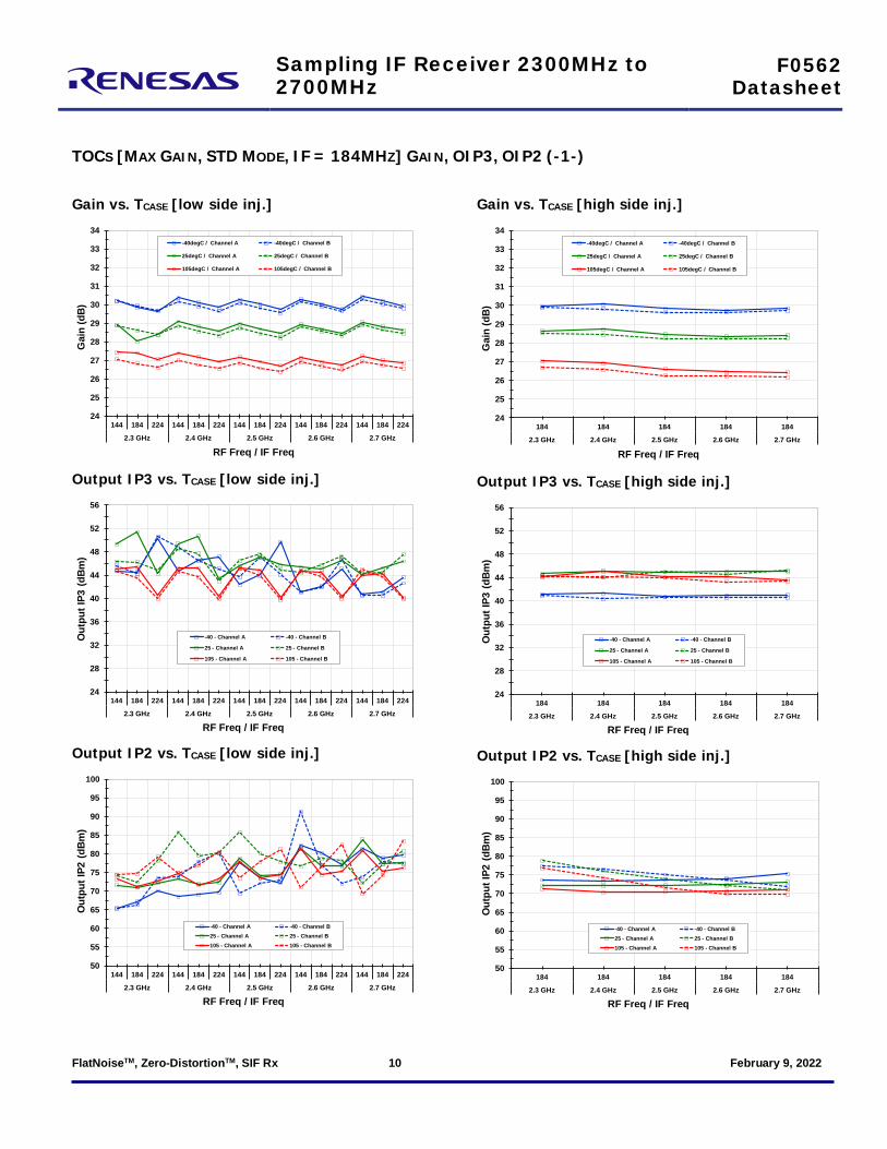
TOCS [MAX GAIN, STD MODE, IF = 184MHZ] GAIN, OIP3, OIP2 (-1-)
Gain vs. TCASE [low side inj.]
Output IP3 vs. TCASE [low side inj.]
Output IP2 vs. TCASE [low side inj.]
Gain vs. TCASE [high side inj.]
Output IP3 vs. TCASE [high side inj.]
Output IP2 vs. TCASE [high side inj.]
24
25
26
27
28
29
30
31
32
33
34
144 184 224 144 184 224 144 184 224 144 184 224 144 184 224
2.3 GHz 2.4 GHz 2.5 GHz 2.6 GHz 2.7 GHz
-40degC / Channel A -40degC / Channel B
25degC / Channel A 25degC / Channel B
105degC / Channel A 105degC / Channel B
Gai
n (d
B)
RF Freq / IF Freq
24
28
32
36
40
44
48
52
56
144 184 224 144 184 224 144 184 224 144 184 224 144 184 224
2.3 GHz 2.4 GHz 2.5 GHz 2.6 GHz 2.7 GHz
-40 - Channel A -40 - Channel B
25 - Channel A 25 - Channel B
105 - Channel A 105 - Channel B
Out
putI
P3 (d
Bm)
RF Freq / IF Freq
50
55
60
65
70
75
80
85
90
95
100
144 184 224 144 184 224 144 184 224 144 184 224 144 184 224
2.3 GHz 2.4 GHz 2.5 GHz 2.6 GHz 2.7 GHz
-40 - Channel A -40 - Channel B25 - Channel A 25 - Channel B105 - Channel A 105 - Channel B
RF Freq / IF Freq
Out
put I
P2 (d
Bm)
24
25
26
27
28
29
30
31
32
33
34
184 184 184 184 184
2.3 GHz 2.4 GHz 2.5 GHz 2.6 GHz 2.7 GHz
-40degC / Channel A -40degC / Channel B
25degC / Channel A 25degC / Channel B
105degC / Channel A 105degC / Channel B
Gai
n (d
B)
RF Freq / IF Freq
24
28
32
36
40
44
48
52
56
184 184 184 184 184
2.3 GHz 2.4 GHz 2.5 GHz 2.6 GHz 2.7 GHz
-40 - Channel A -40 - Channel B
25 - Channel A 25 - Channel B
105 - Channel A 105 - Channel B
Out
putI
P3 (d
Bm)
RF Freq / IF Freq
50
55
60
65
70
75
80
85
90
95
100
184 184 184 184 184
2.3 GHz 2.4 GHz 2.5 GHz 2.6 GHz 2.7 GHz
-40 - Channel A -40 - Channel B25 - Channel A 25 - Channel B105 - Channel A 105 - Channel B
RF Freq / IF Freq
Out
put I
P2 (d
Bm)

Sampling IF Receiver 2300MHz to 2700MHz
F0562 Datasheet
FlatNoiseTM, Zero-DistortionTM, SIF Rx 11 February 9, 2022
TOCS [MAX GAIN, STD MODE, IF = 184MHZ] 2X2, L-I, DC CURRENT (-2-)
2 X 2 vs. TCASE [low side inj.]
LO to IF Leakage [low side inj.]
Total Current Drain [low side inj.]
2 x 2 vs. TCASE [high side inj.]
LO to IF Leakage [high side inj.]
Total Current Drain [high side inj.]
-100
-90
-80
-70
-60
-50
-40
-30
-20
144 184 224 144 184 224 144 184 224 144 184 224 144 184 224
2.3 GHz 2.4 GHz 2.5 GHz 2.6 GHz 2.7 GHz
-40 - Channel A -40 - Channel B
25 - Channel A 25 - Channel B
105 - Channel A 105 - Channel B
2X2
Rej
ectio
n (d
Bc)
RF Freq / IF Freq
-65
-60
-55
-50
-45
-40
-35
-30
-25
144 184 224 144 184 224 144 184 224 144 184 224 144 184 224
2.3 GHz 2.4 GHz 2.5 GHz 2.6 GHz 2.7 GHz
-40 degC - Channel A -40 degC - Channel B
25 degC - Channel A 25 degC - Channel B
105 degC - Channel A 105 degC - Channel B
LO to
IF L
eaka
ge (
dBm
)
RF Freq / IF Freq
0.42
0.44
0.46
0.48
0.50
0.52
144 184 224 144 184 224 144 184 224 144 184 224 144 184 224
2.3 GHz 2.4 GHz 2.5 GHz 2.6 GHz 2.7 GHz
-40 degC 25 degC 105 degC
RF Freq / IF Freq
Tota
l IC
C(A
mps
)
RF Freq / IF Freq
Tota
l IC
C(A
mps
)
-100
-90
-80
-70
-60
-50
-40
-30
-20
184 184 184 184 184
2.3 GHz 2.4 GHz 2.5 GHz 2.6 GHz 2.7 GHz
-40 - Channel A -40 - Channel B
25 - Channel A 25 - Channel B
105 - Channel A 105 - Channel B
2X2
Rej
ectio
n (d
Bc)
RF Freq / IF Freq
-65
-60
-55
-50
-45
-40
-35
-30
-25
184 184 184 184 184
2.3 GHz 2.4 GHz 2.5 GHz 2.6 GHz 2.7 GHz
-40 degC - Channel A -40 degC - Channel B
25 degC - Channel A 25 degC - Channel B
105 degC - Channel A 105 degC - Channel B
LO to
IF L
eaka
ge (
dBm
)
RF Freq / IF Freq
0.42
0.44
0.46
0.48
0.50
0.52
184 184 184 184 184
2.3 GHz 2.4 GHz 2.5 GHz 2.6 GHz 2.7 GHz
-40 degC 25 degC 105 degC
RF Freq / IF Freq
Tota
l IC
C(A
mps
)
RF Freq / IF Freq
Tota
l IC
C(A
mps
)

Sampling IF Receiver 2300MHz to 2700MHz
F0562 Datasheet
FlatNoiseTM, Zero-DistortionTM, SIF Rx 12 February 9, 2022
TOCS [SWEPT GAIN, STD MODE, IF = 184MHZ, LS INJECTION] GAIN, OIP3, IIP3 (-3-)
Gain [2.4 GHz]
Output IP3 [2.4 GHz]
Input IP3 [2.4 GHz]
Gain [2.6 GHz]
Output IP3 [2.6 GHz]
Input IP3 [2.6 GHz]
2
6
10
14
18
22
26
30
3579111315171921232527
Gai
n (d
B)
Gain Setting (dB) / PIN (dBm/Tone)
-40C / ChA -40C / ChB
+25C / ChA +25C / ChB
+105C / ChA +105C / ChB
-27 -25 -23 -21 -19 -17 -15 -13 -11 -9 -7 -5 -3
15
20
25
30
35
40
45
50
55
3579111315171921232527
Out
put I
P3 (d
Bm)
Gain Setting (dB) / PIN (dBm/Tone)
-40C / ChA -40C / ChB
+25C / ChA +25C / ChB
+105C / ChA +105C / ChB
-27 -25 -23 -21 -19 -17 -15 -13 -11 -9 -7 -5 -3
5
10
15
20
25
30
35
40
3579111315171921232527
Inpu
t IP3
(dBm
)
Gain Setting (dB) / PIN (dBm/Tone)
-40C / ChA -40C / ChB
+25C / ChA +25C / ChB
+105C / ChA +105C / ChB
-27 -25 -23 -21 -19 -17 -15 -13 -11 -9 -7 -5 -3

Sampling IF Receiver 2300MHz to 2700MHz
F0562 Datasheet
FlatNoiseTM, Zero-DistortionTM, SIF Rx 13 February 9, 2022
TOCS [SWEPT GAIN, STD MODE, IF = 184MHZ, LS INJECTION] OIP2, IIP2, 2X2 (-4-)
Output IP2 [2.4 GHz]
Input IP2 [2.4 GHz]
2x2 Rejection [2.4 GHz]
Output IP2 [2.6 GHz]
Input IP2 [2.6 GHz]
2x2 Rejection [2.6 GHz]
0
10
20
30
40
50
60
70
80
90
3579111315171921232527
Out
put I
P2 (d
Bm)
Gain Setting (dB) / PIN (dBm/Tone)
-40C / ChA -40C / ChB
+25C / ChA +25C / ChB
+105C / ChA +105C / ChB
-27 -25 -23 -21 -19 -17 -15 -13 -11 -9 -7 -5 -3
0
10
20
30
40
50
60
70
80
90
3579111315171921232527
Inpu
t IP2
(dBm
)
Gain Setting (dB) / PIN (dBm/Tone)
-40C / ChA -40C / ChB
+25C / ChA +25C / ChB
+105C / ChA +105C / ChB
-27 -25 -23 -21 -19 -17 -15 -13 -11 -9 -7 -5 -3
-100
-90
-80
-70
-60
-50
-40
-30
-20
3579111315171921232527
2 X
2 R
ejec
tion
(dBc
)
Gain Setting (dB) / Pin (dBm)
-40C / ChA -40C / ChB
+25C / ChA +25C / ChB
+105C / ChA +105C / ChB
-27 -25 -23 -21 -19 -17 -15 -13 -11 -9 -7 -5 -3
0
10
20
30
40
50
60
70
80
90
3579111315171921232527
Out
put I
P2 (d
Bm)
Gain Setting (dB) / PIN (dBm/Tone)
-40C / ChA -40C / ChB
+25C / ChA +25C / ChB
+105C / ChA +105C / ChB
-27 -25 -23 -21 -19 -17 -15 -13 -11 -9 -7 -5 -3
0
10
20
30
40
50
60
70
80
90
3579111315171921232527
Inpu
t IP2
(dBm
)
Gain Setting (dB) / PIN (dBm/Tone)
-40C / ChA -40C / ChB
+25C / ChA +25C / ChB
+105C / ChA +105C / ChB
-27 -25 -23 -21 -19 -17 -15 -13 -11 -9 -7 -5 -3
-100
-90
-80
-70
-60
-50
-40
-30
-20
3579111315171921232527
2 X
2 R
ejec
tion
(dBc
)
Gain Setting (dB) / PIN (dBm/Tone)
-40C / ChA -40C / ChB
+25C / ChA +25C / ChB
+105C / ChA +105C / ChB
-27 -25 -23 -21 -19 -17 -15 -13 -11 -9 -7 -5 -3

Sampling IF Receiver 2300MHz to 2700MHz
F0562 Datasheet
FlatNoiseTM, Zero-DistortionTM, SIF Rx 14 February 9, 2022
TOCS [SWEPT GAIN, STD MODE, IF = 184MHZ, LS INJECTION] 3X3, L-I, R-I (-5-)
3x3 Rejection [2.4 GHz]
LO to IF Leakage [low side inj, 2.6 GHz]
RF to IF Leakage [2.4 GHz]
3x3 Rejection [2.6 GHz]
LO to IF Leakage [high side inj., 2.6 GHz]
RF to IF Leakage [2.6 GHz]
-100
-90
-80
-70
-60
-50
-40
-30
-20
3579111315171921232527
3 X
3 R
ejec
tion
(dBc
)
Gain Setting (dB) / PIN (dBm/Tone)
-40C / ChA -40C / ChB
+25C / ChA +25C / ChB
+105C / ChA +105C / ChB
-27 -25 -23 -21 -19 -17 -15 -13 -11 -9 -7 -5 -3
-75-70-65-60-55-50-45-40-35-30-25-20
3579111315171921232527
LO to
IF L
eaka
ge (
dBm
)
Gain Setting (dB) / PIN (dBm/Tone)
-40C / ChA -40C / ChB
+25C / ChA +25C / ChB
+105C / ChA +105C / ChB
-27 -25 -23 -21 -19 -17 -15 -13 -11 -9 -7 -5 -3
-100-95-90-85-80-75-70-65-60-55-50-45-40
3579111315171921232527
RF
to IF
Lea
kage
(dB
m)
Gain Setting (dB) / PIN (dBm/Tone)
-40C / ChA -40C / ChB
+25C / ChA +25C / ChB
+105C / ChA +105C / ChB
-27 -25 -23 -21 -19 -17 -15 -13 -11 -9 -7 -5 -3
Sampling IF Receiver 2300MHz to 2700MHz
F0562 Datasheet
FlatNoiseTM, Zero-DistortionTM, SIF Rx 15 February 9, 2022
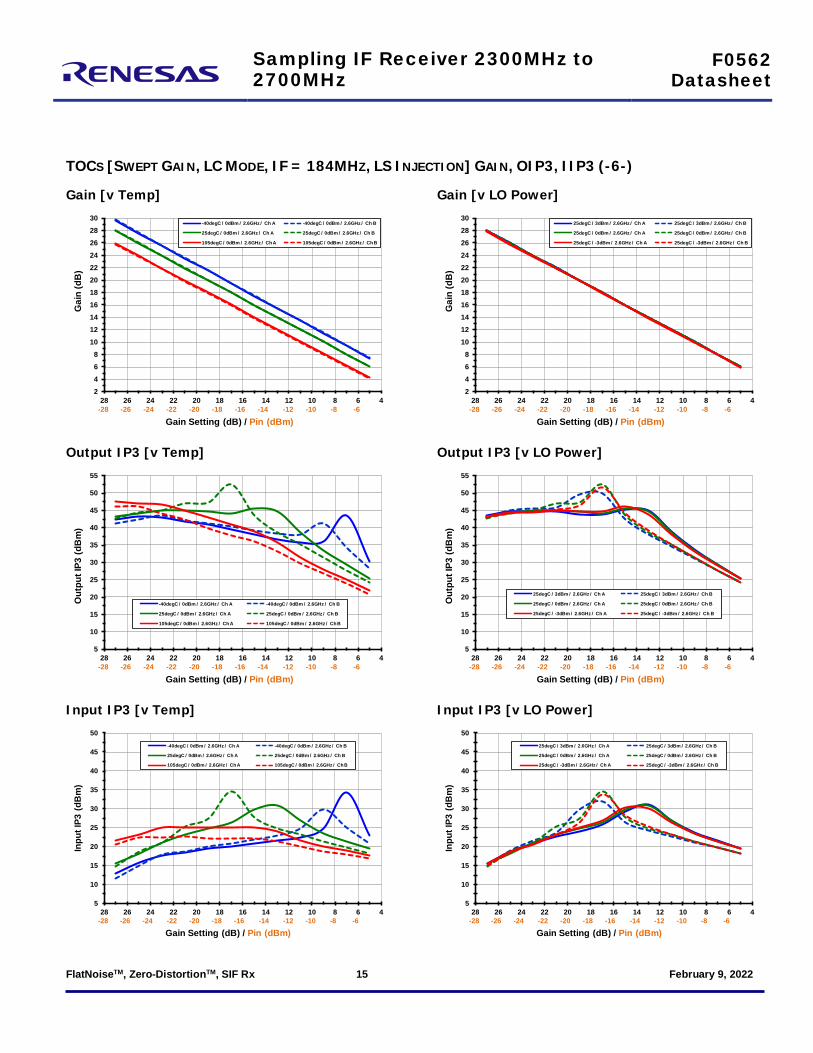
TOCS [SWEPT GAIN, LC MODE, IF = 184MHZ, LS INJECTION] GAIN, OIP3, IIP3 (-6-) Gain [v Temp]
Output IP3 [v Temp]
Input IP3 [v Temp]
Gain [v LO Power]
Output IP3 [v LO Power]
Input IP3 [v LO Power]
2468
1012141618202224262830
46810121416182022242628
Gai
n (d
B)
Gain Setting (dB) / Pin (dBm)
-40degC / 0dBm / 2.6GHz / Ch A -40degC / 0dBm / 2.6GHz / Ch B
25degC / 0dBm / 2.6GHz / Ch A 25degC / 0dBm / 2.6GHz / Ch B
105degC / 0dBm / 2.6GHz / Ch A 105degC / 0dBm / 2.6GHz / Ch B
-28 -26 -24 -22 -20 -18 -16 -14 -12 -10 -8 -6
5
10
15
20
25
30
35
40
45
50
55
46810121416182022242628
Out
put I
P3 (d
Bm
)
Gain Setting (dB) / Pin (dBm)
-40degC / 0dBm / 2.6GHz / Ch A -40degC / 0dBm / 2.6GHz / Ch B
25degC / 0dBm / 2.6GHz / Ch A 25degC / 0dBm / 2.6GHz / Ch B
105degC / 0dBm / 2.6GHz / Ch A 105degC / 0dBm / 2.6GHz / Ch B
-28 -26 -24 -22 -20 -18 -16 -14 -12 -10 -8 -6
5
10
15
20
25
30
35
40
45
50
46810121416182022242628
Inpu
t IP3
(dB
m)
Gain Setting (dB) / Pin (dBm)
-40degC / 0dBm / 2.6GHz / Ch A -40degC / 0dBm / 2.6GHz / Ch B
25degC / 0dBm / 2.6GHz / Ch A 25degC / 0dBm / 2.6GHz / Ch B
105degC / 0dBm / 2.6GHz / Ch A 105degC / 0dBm / 2.6GHz / Ch B
-28 -26 -24 -22 -20 -18 -16 -14 -12 -10 -8 -6
2468
1012141618202224262830
46810121416182022242628
Gai
n (d
B)
Gain Setting (dB) / Pin (dBm)
25degC / 3dBm / 2.6GHz / Ch A 25degC / 3dBm / 2.6GHz / Ch B
25degC / 0dBm / 2.6GHz / Ch A 25degC / 0dBm / 2.6GHz / Ch B
25degC / -3dBm / 2.6GHz / Ch A 25degC / -3dBm / 2.6GHz / Ch B
-28 -26 -24 -22 -20 -18 -16 -14 -12 -10 -8 -6
5
10
15
20
25
30
35
40
45
50
55
46810121416182022242628
Out
put I
P3 (d
Bm
)
Gain Setting (dB) / Pin (dBm)
25degC / 3dBm / 2.6GHz / Ch A 25degC / 3dBm / 2.6GHz / Ch B
25degC / 0dBm / 2.6GHz / Ch A 25degC / 0dBm / 2.6GHz / Ch B
25degC / -3dBm / 2.6GHz / Ch A 25degC / -3dBm / 2.6GHz / Ch B
-28 -26 -24 -22 -20 -18 -16 -14 -12 -10 -8 -6
5
10
15
20
25
30
35
40
45
50
46810121416182022242628
Inpu
t IP3
(dB
m)
Gain Setting (dB) / Pin (dBm)
25degC / 3dBm / 2.6GHz / Ch A 25degC / 3dBm / 2.6GHz / Ch B
25degC / 0dBm / 2.6GHz / Ch A 25degC / 0dBm / 2.6GHz / Ch B
25degC / -3dBm / 2.6GHz / Ch A 25degC / -3dBm / 2.6GHz / Ch B
-28 -26 -24 -22 -20 -18 -16 -14 -12 -10 -8 -6
Sampling IF Receiver 2300MHz to 2700MHz
F0562 Datasheet
FlatNoiseTM, Zero-DistortionTM, SIF Rx 16 February 9, 2022
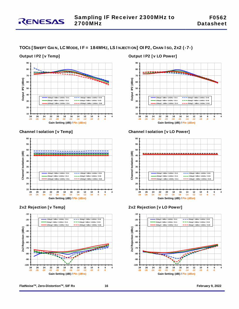
TOCS [SWEPT GAIN, LC MODE, IF = 184MHZ, LS INJECTION] OIP2, CHAN ISO, 2X2 (-7-)
Output IP2 [v Temp]
Channel Isolation [v Temp]
2x2 Rejection [v Temp]
Output IP2 [v LO Power]
Channel Isolation [v LO Power]
2x2 Rejection [v LO Power]
10
20
30
40
50
60
70
80
90
46810121416182022242628
Out
put
IP2
(dB
m)
Gain Setting (dB) / Pin (dBm)
-40degC / 0dBm / 2.6GHz / Ch A -40degC / 0dBm / 2.6GHz / Ch B
25degC / 0dBm / 2.6GHz / Ch A 25degC / 0dBm / 2.6GHz / Ch B
105degC / 0dBm / 2.6GHz / Ch A 105degC / 0dBm / 2.6GHz / Ch B
-28 -26 -24 -22 -20 -18 -16 -14 -12 -10 -8 -6
15
20
25
30
35
40
45
50
55
60
46810121416182022242628
Cha
nnel
Isol
atio
n (d
B)
Gain Setting (dB) / Pin (dBm)
-40degC / 0dBm / 2.6GHz / Ch A -40degC / 0dBm / 2.6GHz / Ch B
25degC / 0dBm / 2.6GHz / Ch A 25degC / 0dBm / 2.6GHz / Ch B
105degC / 0dBm / 2.6GHz / Ch A 105degC / 0dBm / 2.6GHz / Ch B
-28 -26 -24 -22 -20 -18 -16 -14 -12 -10 -8 -6
-100
-90
-80
-70
-60
-50
-40
-30
-20
-10
46810121416182022242628
2x2
Rej
ectio
n (d
Bc)
Gain Setting (dB) / Pin (dBm)
-40degC / 0dBm / 2.6GHz / Ch A -40degC / 0dBm / 2.6GHz / Ch B
25degC / 0dBm / 2.6GHz / Ch A 25degC / 0dBm / 2.6GHz / Ch B
105degC / 0dBm / 2.6GHz / Ch A 105degC / 0dBm / 2.6GHz / Ch B
-28 -26 -24 -22 -20 -18 -16 -14 -12 -10 -8 -6
10
20
30
40
50
60
70
80
90
46810121416182022242628
Out
put
IP2
(dB
m)
Gain Setting (dB) / Pin (dBm)
25degC / 3dBm / 2.6GHz / Ch A 25degC / 3dBm / 2.6GHz / Ch B
25degC / 0dBm / 2.6GHz / Ch A 25degC / 0dBm / 2.6GHz / Ch B
25degC / -3dBm / 2.6GHz / Ch A 25degC / -3dBm / 2.6GHz / Ch B
-28 -26 -24 -22 -20 -18 -16 -14 -12 -10 -8 -6
15
20
25
30
35
40
45
50
55
60
46810121416182022242628
Cha
nnel
Isol
atio
n (d
B)
Gain Setting (dB) / Pin (dBm)
25degC / 3dBm / 2.6GHz / Ch A 25degC / 3dBm / 2.6GHz / Ch B
25degC / 0dBm / 2.6GHz / Ch A 25degC / 0dBm / 2.6GHz / Ch B
25degC / -3dBm / 2.6GHz / Ch A 25degC / -3dBm / 2.6GHz / Ch B
-28 -26 -24 -22 -20 -18 -16 -14 -12 -10 -8 -6
-100
-90
-80
-70
-60
-50
-40
-30
-20
-10
46810121416182022242628
2x2
Rej
ectio
n (d
Bc)
Gain Setting (dB) / Pin (dBm)
25degC / 3dBm / 2.6GHz / Ch A 25degC / 3dBm / 2.6GHz / Ch B
25degC / 0dBm / 2.6GHz / Ch A 25degC / 0dBm / 2.6GHz / Ch B
25degC / -3dBm / 2.6GHz / Ch A 25degC / -3dBm / 2.6GHz / Ch B
-28 -26 -24 -22 -20 -18 -16 -14 -12 -10 -8 -6
Sampling IF Receiver 2300MHz to 2700MHz
F0562 Datasheet
FlatNoiseTM, Zero-DistortionTM, SIF Rx 17 February 9, 2022
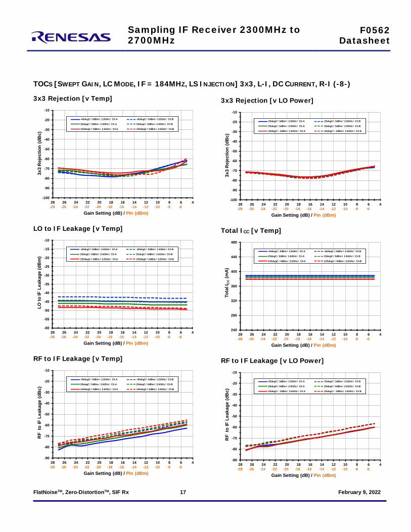
TOCS [SWEPT GAIN, LC MODE, IF = 184MHZ, LS INJECTION] 3X3, L-I, DC CURRENT, R-I (-8-)
3x3 Rejection [v Temp]
LO to IF Leakage [v Temp]
RF to IF Leakage [v Temp]
3x3 Rejection [v LO Power]
Total ICC [v Temp]
RF to IF Leakage [v LO Power]
-100
-90
-80
-70
-60
-50
-40
-30
-20
-10
46810121416182022242628
3x3
Rej
ectio
n (d
Bc)
Gain Setting (dB) / Pin (dBm)
-40degC / 0dBm / 2.6GHz / Ch A -40degC / 0dBm / 2.6GHz / Ch B
25degC / 0dBm / 2.6GHz / Ch A 25degC / 0dBm / 2.6GHz / Ch B
105degC / 0dBm / 2.6GHz / Ch A 105degC / 0dBm / 2.6GHz / Ch B
-28 -26 -24 -22 -20 -18 -16 -14 -12 -10 -8 -6
-60
-55
-50
-45
-40
-35
-30
-25
-20
-15
-10
46810121416182022242628
LO to
IF L
eaka
ge (d
Bm
)
Gain Setting (dB) / Pin (dBm)
-40degC / 0dBm / 2.6GHz / Ch A -40degC / 0dBm / 2.6GHz / Ch B
25degC / 0dBm / 2.6GHz / Ch A 25degC / 0dBm / 2.6GHz / Ch B
105degC / 0dBm / 2.6GHz / Ch A 105degC / 0dBm / 2.6GHz / Ch B
-28 -26 -24 -22 -20 -18 -16 -14 -12 -10 -8 -6
-90
-80
-70
-60
-50
-40
-30
-20
-10
46810121416182022242628
RF
to IF
Lea
kage
(dB
c)
Gain Setting (dB) / Pin (dBm)
-40degC / 0dBm / 2.6GHz / Ch A -40degC / 0dBm / 2.6GHz / Ch B
25degC / 0dBm / 2.6GHz / Ch A 25degC / 0dBm / 2.6GHz / Ch B
105degC / 0dBm / 2.6GHz / Ch A 105degC / 0dBm / 2.6GHz / Ch B
-28 -26 -24 -22 -20 -18 -16 -14 -12 -10 -8 -6
-100
-90
-80
-70
-60
-50
-40
-30
-20
-10
46810121416182022242628
3x3
Rej
ectio
n (d
Bc)
Gain Setting (dB) / Pin (dBm)
25degC / 3dBm / 2.6GHz / Ch A 25degC / 3dBm / 2.6GHz / Ch B
25degC / 0dBm / 2.6GHz / Ch A 25degC / 0dBm / 2.6GHz / Ch B
25degC / -3dBm / 2.6GHz / Ch A 25degC / -3dBm / 2.6GHz / Ch B
-28 -26 -24 -22 -20 -18 -16 -14 -12 -10 -8 -6
240
280
320
360
400
440
480
46810121416182022242628
Tota
l IC
C(m
A)
Gain Setting (dB) / Pin (dBm)
-40degC / 0dBm / 2.6GHz / Ch A -40degC / 0dBm / 2.6GHz / Ch B
25degC / 0dBm / 2.6GHz / Ch A 25degC / 0dBm / 2.6GHz / Ch B
105degC / 0dBm / 2.6GHz / Ch A 105degC / 0dBm / 2.6GHz / Ch B
-28 -26 -24 -22 -20 -18 -16 -14 -12 -10 -8 -6
-90
-80
-70
-60
-50
-40
-30
-20
-10
46810121416182022242628
RF
to IF
Lea
kage
(dB
c)
Gain Setting (dB) / Pin (dBm)
25degC / 3dBm / 2.6GHz / Ch A 25degC / 3dBm / 2.6GHz / Ch B
25degC / 0dBm / 2.6GHz / Ch A 25degC / 0dBm / 2.6GHz / Ch B
25degC / -3dBm / 2.6GHz / Ch A 25degC / -3dBm / 2.6GHz / Ch B
-28 -26 -24 -22 -20 -18 -16 -14 -12 -10 -8 -6

Sampling IF Receiver 2300MHz to 2700MHz
F0562 Datasheet
FlatNoiseTM, Zero-DistortionTM, SIF Rx 18 February 9, 2022
TYPICAL OPERATING CONDITIONS [276MHZ IF CENTER]
Unless otherwise noted, the following conditions apply:
• Applications circuit for 100ohm differential load with 276MHz +/- 40 MHzBW into 2:1 Transformer. See schematic Below
• Pout ~ +1dBm (for Gain Setting > 5dB) • Measurement on Channel A • PIN from -27dBm to -6dBm per Tone (Gain Setting Adjusted to yield Pout ~ +1dBm) • Tone Spacing = 800kHz • Device configured in Standard Mode with Low Side Injection • TCASE = 25°C, VCC = 5.00V, LO Power = 0dBm • RF Frequency: 2.4GHz, 2.6GHz • IF Frequency: 276MHz • IF Transformer Losses are de-embedded • Input RF trace Losses are de-embedded
Vcc
C25/C13 = 1.2 pF
L9/L12 = 24 nH
L10/L11 = 24 nH
C27/C12 = 8 pF
C24/C9 = 8 pF
L8/L4 = 82 nH
L7/L3 =82 nH
10 nF
10 nF
0.6 pF
100 ohm
55
56
IFOUT-
IFOUT+
Vcc
2:1 Transformer
276 MHz Output Match 200Ω to 100Ω

Sampling IF Receiver 2300MHz to 2700MHz
F0562 Datasheet
FlatNoiseTM, Zero-DistortionTM, SIF Rx 19 February 9, 2022
TOCS [SWEPT GAIN, STD MODE, IF = 276MHZ, LS INJECTION] GAIN, OIP3, OIP2 (-9-)
Gain [2.4 GHz]
Output IP3 [2.4 GHz]
Output IP2 [2.4 GHz]
Gain [2.6 GHz]
Output IP3 [2.6 GHz]
Output IP2 [2.6 GHz]
-22
-18
-14
-10
-6
-2
2
6
10
14
18
22
26
30
-20-16-12-8-40481216202428
Gai
n (d
B)
Gain Setting (dB) / Pin (dBm)
25degC / 3dBm / 2.4GHz / Ch A 25degC / 3dBm / 2.4GHz / Ch B
25degC / 0dBm / 2.4GHz / Ch A 25degC / 0dBm / 2.4GHz / Ch B
25degC / -3dBm / 2.4GHz / Ch A 25degC / -3dBm / 2.4GHz / Ch B
-28 -24 -20 -16 -12 -8 -6 -6 -6 -6 -6 -6 -6
5
10
15
20
25
30
35
40
45
50
55
-20-16-12-8-40481216202428
Out
put I
P3 (d
Bm
)
Gain Setting (dB) / Pin (dBm)
25degC / 3dBm / 2.4GHz / Ch A 25degC / 3dBm / 2.4GHz / Ch B
25degC / 0dBm / 2.4GHz / Ch A 25degC / 0dBm / 2.4GHz / Ch B
25degC / -3dBm / 2.4GHz / Ch A 25degC / -3dBm / 2.4GHz / Ch B
-28 -24 -20 -16 -12 -8 -6 -6 -6 -6 -6 -6 -6
10
20
30
40
50
60
70
80
90
100
110
-20-16-12-8-40481216202428
Out
put I
P2 (d
Bm
)
Gain Setting (dB) / Pin (dBm)
25degC / 3dBm / 2.4GHz / Ch A 25degC / 3dBm / 2.4GHz / Ch B
25degC / 0dBm / 2.4GHz / Ch A 25degC / 0dBm / 2.4GHz / Ch B
25degC / -3dBm / 2.4GHz / Ch A 25degC / -3dBm / 2.4GHz / Ch B
-28 -24 -20 -16 -12 -8 -6 -6 -6 -6 -6 -6 -6
-22
-18
-14
-10
-6
-2
2
6
10
14
18
22
26
30
-20-16-12-8-40481216202428
Gai
n (d
B)
Gain Setting (dB) / Pin (dBm)
-40degC / 0dBm / 2.6GHz / Ch A -40degC / 0dBm / 2.6GHz / Ch B
25degC / 0dBm / 2.6GHz / Ch A 25degC / 0dBm / 2.6GHz / Ch B
105degC / 0dBm / 2.6GHz / Ch A 105degC / 0dBm / 2.6GHz / Ch B
-28 -24 -20 -16 -12 -8 -6 -6 -6 -6 -6 -6 -6
5
10
15
20
25
30
35
40
45
50
55
-20-16-12-8-40481216202428
Out
put I
P3 (d
Bm
)
Gain Setting (dB) / Pin (dBm)
-40degC / 0dBm / 2.6GHz / Ch A -40degC / 0dBm / 2.6GHz / Ch B
25degC / 0dBm / 2.6GHz / Ch A 25degC / 0dBm / 2.6GHz / Ch B
105degC / 0dBm / 2.6GHz / Ch A 105degC / 0dBm / 2.6GHz / Ch B
-28 -24 -20 -16 -12 -8 -6 -6 -6 -6 -6 -6 -6
10
20
30
40
50
60
70
80
90
100
110
-20-16-12-8-40481216202428
Out
put I
P2 (d
Bm
)
Gain Setting (dB) / Pin (dBm)
-40degC / 0dBm / 2.6GHz / Ch A -40degC / 0dBm / 2.6GHz / Ch B
25degC / 0dBm / 2.6GHz / Ch A 25degC / 0dBm / 2.6GHz / Ch B
105degC / 0dBm / 2.6GHz / Ch A 105degC / 0dBm / 2.6GHz / Ch B
-28 -24 -20 -16 -12 -8 -6 -6 -6 -6 -6 -6 -6

Sampling IF Receiver 2300MHz to 2700MHz
F0562 Datasheet
FlatNoiseTM, Zero-DistortionTM, SIF Rx 20 February 9, 2022
TOCS [SWEPT GAIN, STD MODE, IF = 276MHZ, LS INJECTION] 2X2, 3X3, CURRENT, R-I, ISO (-10-)
2x2 Rejection [2.4 GHz]
3x3 Rejection [2.6 GHz]
RF to IF Leakage [2.6 GHz]
2x2 Rejection [2.6 GHz]
Total ICC [2.6 GHz]
Channel Isolation [2.6 GHz]
-100
-90
-80
-70
-60
-50
-40
-30
-20
-10
-20-16-12-8-40481216202428
2 x
2 R
ejec
tion
(dB
c)
Gain Setting (dB) / Pin (dBm)
25degC / 3dBm / 2.4GHz / Ch A 25degC / 3dBm / 2.4GHz / Ch B
25degC / 0dBm / 2.4GHz / Ch A 25degC / 0dBm / 2.4GHz / Ch B
25degC / -3dBm / 2.4GHz / Ch A 25degC / -3dBm / 2.4GHz / Ch B
-28 -24 -20 -16 -12 -8 -6 -6 -6 -6 -6 -6 -6
-100
-90
-80
-70
-60
-50
-40
-30
-20
-10
-20-16-12-8-40481216202428
3 x
3 R
ejec
tion
(dB
c)
Gain Setting (dB) / Pin (dBm)
25degC / 3dBm / 2.6GHz / Ch A 25degC / 3dBm / 2.6GHz / Ch B
25degC / 0dBm / 2.6GHz / Ch A 25degC / 0dBm / 2.6GHz / Ch B
25degC / -3dBm / 2.6GHz / Ch A 25degC / -3dBm / 2.6GHz / Ch B
-28 -24 -20 -16 -12 -8 -6 -6 -6 -6 -6 -6 -6
-90
-80
-70
-60
-50
-40
-30
-20
-10
-20-16-12-8-40481216202428
RF
to IF
Lea
kage
(dB
c)
Gain Setting (dB) / Pin (dBm)
-40degC / 0dBm / 2.6GHz / Ch A -40degC / 0dBm / 2.6GHz / Ch B
25degC / 0dBm / 2.6GHz / Ch A 25degC / 0dBm / 2.6GHz / Ch B
105degC / 0dBm / 2.6GHz / Ch A 105degC / 0dBm / 2.6GHz / Ch B
-28 -24 -20 -16 -12 -8 -6 -6 -6 -6 -6 -6 -6
-100
-90
-80
-70
-60
-50
-40
-30
-20
-10
-20-16-12-8-40481216202428
2 x
2 R
ejec
tion
(dB
c)
Gain Setting (dB) / Pin (dBm)
-40degC / 0dBm / 2.6GHz / Ch A -40degC / 0dBm / 2.6GHz / Ch B
25degC / 0dBm / 2.6GHz / Ch A 25degC / 0dBm / 2.6GHz / Ch B
105degC / 0dBm / 2.6GHz / Ch A 105degC / 0dBm / 2.6GHz / Ch B
-28 -24 -20 -16 -12 -8 -6 -6 -6 -6 -6 -6 -6
320
360
400
440
480
520
560
-20-16-12-8-40481216202428
Tota
l IC
C(m
A)
Gain Setting (dB) / Pin (dBm)
-40degC / 0dBm / 2.6GHz / Ch A 25degC / 0dBm / 2.6GHz / Ch A
105degC / 0dBm / 2.6GHz / Ch A
-28 -24 -20 -16 -12 -8 -6 -6 -6 -6 -6 -6 -6
10
15
20
25
30
35
40
45
50
55
60
-20-16-12-8-40481216202428
Cha
nnel
Isol
atio
n (d
B)
Gain Setting (dB) / Pin (dBm)
-40degC / 0dBm / 2.6GHz / Ch A -40degC / 0dBm / 2.6GHz / Ch B
25degC / 0dBm / 2.6GHz / Ch A 25degC / 0dBm / 2.6GHz / Ch B
105degC / 0dBm / 2.6GHz / Ch A 105degC / 0dBm / 2.6GHz / Ch B
-28 -24 -20 -16 -12 -8 -6 -6 -6 -6 -6 -6 -6

Sampling IF Receiver 2300MHz to 2700MHz
F0562 Datasheet
FlatNoiseTM, Zero-DistortionTM, SIF Rx 21 February 9, 2022
TOCS RETURN LOSS [STD MODE] (-11-) IF_A Output Return Loss 184MHz match
IF_A Output Return Loss 276MHz match
RF Port Return Loss
IF_B Output Return Loss 184MHz match
IF_B Output Return Loss 276MHz match
LO Port Return Loss
-35
-30
-25
-20
-15
-10
-5
0
84 104 124 144 164 184 204 224 244 264 284
Ret
urn
Loss
(dB)
IF Frequency (MHz)
G-20 G10
G15 G17
G20 G23
G25 G27
-35
-30
-25
-20
-15
-10
-5
0
176 196 216 236 256 276 296 316 336 356 376
Ret
urn
Loss
(dB)
IF Frequency (MHz)
G-20 G10
G15 G17
G20 G23
G25 G27
-30
-25
-20
-15
-10
-5
0
2.1 2.2 2.3 2.4 2.5 2.6 2.7 2.8 2.9
Ret
urn
Loss
(dB)
RF Frequency (GHz)
ChA / LO=2.2GHz ChA / LO=2.6GHz
ChB / LO=2.2GHz ChB / LO=2.6GHz
-35
-30
-25
-20
-15
-10
-5
0
84 104 124 144 164 184 204 224 244 264 284
Ret
urn
Loss
(dB)
IF Frequency (MHz)
G-20 G10
G15 G17
G20 G23
G25 G27
-35
-30
-25
-20
-15
-10
-5
0
176 196 216 236 256 276 296 316 336 356 376
Ret
urn
Loss
(dB)
IF Frequency (MHz)
G-20 G10
G15 G17
G20 G23
G25 G27
-30
-25
-20
-15
-10
-5
0
1.7 1.9 2.1 2.3 2.5 2.7 2.9 3.1
Ret
urn
Loss
(dB)
LO Frequency (GHz)
LO
Sampling IF Receiver 2300MHz to 2700MHz
F0562 Datasheet
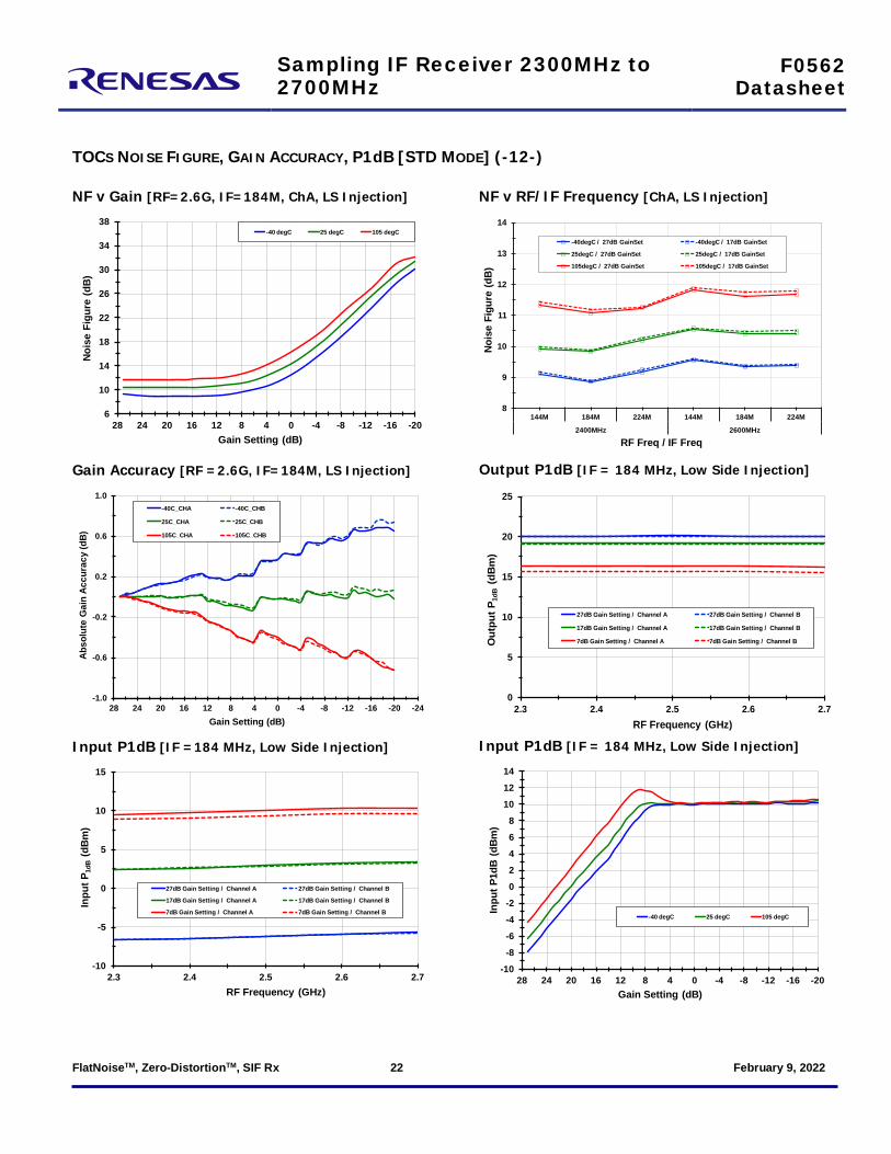
FlatNoiseTM, Zero-DistortionTM, SIF Rx 22 February 9, 2022
TOCS NOISE FIGURE, GAIN ACCURACY, P1dB [STD MODE] (-12-) NF v Gain [RF=2.6G, IF=184M, ChA, LS Injection]
Gain Accuracy [RF =2.6G, IF=184M, LS Injection]
Input P1dB [IF =184 MHz, Low Side Injection]
NF v RF/IF Frequency [ChA, LS Injection]
Output P1dB [IF = 184 MHz, Low Side Injection]
Input P1dB [IF = 184 MHz, Low Side Injection]
6
10
14
18
22
26
30
34
38
-20-16-12-8-40481216202428
Nois
e Fi
gure
(dB)
Gain Setting (dB)
-40 degC 25 degC 105 degC
-1.0
-0.6
-0.2
0.2
0.6
1.0
-24-20-16-12-8-40481216202428
Abso
lute
Gai
n Ac
cura
cy (d
B)
Gain Setting (dB)
-40C_CHA -40C_CHB
25C_CHA 25C_CHB
105C_CHA 105C_CHB
-10
-5
0
5
10
15
2.3 2.4 2.5 2.6 2.7
Inpu
t P1d
B(d
Bm)
RF Frequency (GHz)
27dB Gain Setting / Channel A 27dB Gain Setting / Channel B
17dB Gain Setting / Channel A 17dB Gain Setting / Channel B
7dB Gain Setting / Channel A 7dB Gain Setting / Channel B
8
9
10
11
12
13
14
144M 184M 224M 144M 184M 224M
2400MHz 2600MHz
-40degC / 27dB GainSet -40degC / 17dB GainSet
25degC / 27dB GainSet 25degC / 17dB GainSet
105degC / 27dB GainSet 105degC / 17dB GainSet
Nois
eFi
gure
(dB)
RF Freq / IF Freq
0
5
10
15
20
25
2.3 2.4 2.5 2.6 2.7
Out
put P
1dB
(dB
m)
RF Frequency (GHz)
27dB Gain Setting / Channel A 27dB Gain Setting / Channel B
17dB Gain Setting / Channel A 17dB Gain Setting / Channel B
7dB Gain Setting / Channel A 7dB Gain Setting / Channel B
-10-8-6-4-202468
101214
-20-16-12-8-40481216202428
Inpu
t P1d
B (d
Bm)
Gain Setting (dB)
-40 degC 25 degC 105 degC

Sampling IF Receiver 2300MHz to 2700MHz
F0562 Datasheet
FlatNoiseTM, Zero-DistortionTM, SIF Rx 23 February 9, 2022
TOCS M X N SPURS [IF = 276 MHZ, LO = 2.2586 GHZ, TCASE = 25C] (-13-) Spur Rejection [ChA, Spur PIN = -5 dBm]
Spur Rejection [ChA, Spur PIN = 0 dBm]
Transformer TC2-7T Loss vs. Temperature
Spur Rejection [ChB, Spur PIN = -5 dBm]
Spur Rejection [ChB, Spur PIN = 0 dBm]
-3 3 -2 2 -3 3 -1 -2-3 32 1 -2 2 -1 1 -1 11 -1 1 -1 2 -2 1 23 -3-2 -1 3 -3 2 -2 3 -3
-1000
1000
3000
5000
7000
9000
11000
-120
-110
-100
-90
-80
-70
-60
-50
-40
-30
-20
-10
0
0.6 1.1 1.6 2.1 2.6 3.1 3.6 4.1 4.6 5.1 5.6 6.1 6.6 7.1
Spur
Rej
ectio
n (d
Bc)
Spur Frequency (GHz)
Spur Rejection (dBc)
M x RF
N x LO
FundamentalImage
Sig GenOut of Range
0.00
0.25
0.50
0.75
1.00
1.25
1.50
0.05 0.10 0.15 0.20 0.25 0.30 0.35 0.40 0.45 0.50
-40 25 100
IF Frequency (GHz)
TC2
Loss
(dB)
-3 3 -2 2 -3 3 -1 -2-3 32 1 -2 2 -1 1 -1 11 -1 1 -1 2 -2 1 23 -3-2 -1 3 -3 2 -2 3 -3
-1000
1000
3000
5000
7000
9000
11000
-120
-110
-100
-90
-80
-70
-60
-50
-40
-30
-20
-10
0
0.6 1.1 1.6 2.1 2.6 3.1 3.6 4.1 4.6 5.1 5.6 6.1 6.6 7.1
Spur
Rej
ectio
n (d
Bc)
Spur Frequency (GHz)
Spur Rejection (dBc)
M x RF
N x LO
FundamentalImage
Sig GenOut of Range

Sampling IF Receiver 2300MHz to 2700MHz
F0562 Datasheet
FlatNoiseTM, Zero-DistortionTM, SIF Rx 24 February 9, 2022
TOCS HISTOGRAMS [N= 4584, TCASE = 25C] (-14-) Gain [RF = 2500M, LO = 2316M, GMAX]
Output IP3 [RF = 2500M, LO = 2316M, G17]
ATTN Accuracy2 [RF = 2500M, LO = 2316, ChA]
Output IP3 [RF = 2500M, LO = 2316M, GMAX]
ATTN Accuracy1 [RF = 2500M, LO = 2316, ChA]
Total ICC [LO = 2316M, VCC = 5.00 V]
0%
5%
10%
15%
20%
25%
30%
35%
40%
Perc
ent
Gain Bin (dB)
ChA ChB
0%
5%
10%
15%
20%
25%
Perc
ent
Output IP3 Bin (dBm)
ChA ChBGain Setting = 17 dB (10 dB Reduced from Max Gain)
0%
5%
10%
15%
20%
25%
30%
Perc
ent
Attenuation Accuracy Bin (dB)
32 dB 47 dB
0%
5%
10%
15%
20%
25%
Perc
ent
Output IP3 Bin (dBm)
ChA ChB
0%
10%
20%
30%
40%
50%
60%
70%Pe
rcen
t
Attenuation Accuracy Bin (dB)
8 dB 16 dB
0%
5%
10%
15%
20%
25%
30%
35%
Perc
ent
Total Current Draw Bin (mA)
STD mode
LC mode
Sampling IF Receiver 2300MHz to 2700MHz
F0562 Datasheet
FlatNoiseTM, Zero-DistortionTM, SIF Rx 25 February 9, 2022
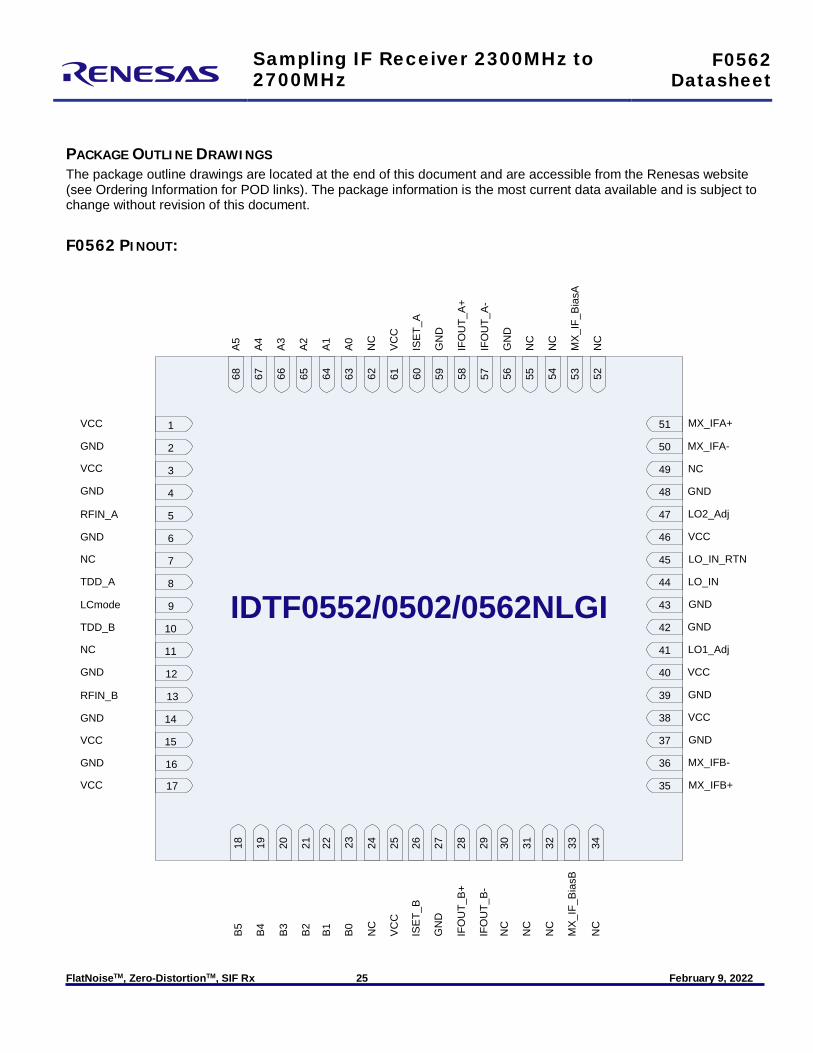
PACKAGE OUTLINE DRAWINGS The package outline drawings are located at the end of this document and are accessible from the Renesas website (see Ordering Information for POD links). The package information is the most current data available and is subject to change without revision of this document. F0562 PINOUT:
IDTF0552/0502/0562NLGI
1
2
3
4
5
6
7
8
9
10
11
12
13
14
15
16
17
18 19 20 21 22 23 24 25 26 27 28 29 30 31 32 33 34
35
36
37
38
39
40
41
42
43
44
45
46
47
48
49
50
51
5253545556575859606162636465666768B5 B4 B3 B2 B1 B0 N
C
VCC
ISET
_B
GN
D
IFO
UT_
B+
IFO
UT_
B-
NC
NC
NC
MX_
IF_B
iasB
NC
MX_IFB+
MX_IFB-
GND
VCC
GND
VCC
LO1_Adj
GND
GND
LO_IN
LO_IN_RTN
VCC
LO2_Adj
GND
NC
MX_IFA-
MX_IFA+
NC
MX_
IF_B
iasA
NC
NC
GN
D
IFO
UT_
A-
IFO
UT_
A+
GN
D
ISET
_A
VCC
NC
A0A1A2A3A4A5
VCC
GND
VCC
GND
RFIN_A
GND
NC
TDD_A
LCmode
TDD_B
NC
GND
RFIN_B
GND
VCC
GND
VCC

Sampling IF Receiver 2300MHz to 2700MHz
F0562 Datasheet
FlatNoiseTM, Zero-DistortionTM, SIF Rx 26 February 9, 2022
F0562 PIN DESCRIPTION TABLE Pin Name Function
1, 3, 15, 17, 25, 38, 40, 46, 61
VCC Power Supply. Bypass to GND with capacitors shown in the Typical Application Circuit as close as possible to pin.
2, 4, 6, 12, 14, 16, 27, 37, 39, 42, 43, 48, 56, 59
GND Ground these pins.
5 RFIN_A Main Channel RF Input. Internally matched to 50Ω. DO NOT apply DC to these pins
7, 11, 24, 30, 31, 32, 34, 49, 52, 54, 55, 62
NC No Connection. Not internally connected. OK to connect to VCC, OK to connect to GND
8 TDD_A Standby control for Channel A. Includes an internal pull-up resistor so leave as NC for Standby mode. Set this pin to low or GND for normal operation.
9 LCmode Low_Current Mode. Includes an internal pull-up resistor so leave as NC for LC mode. Set this pin to low or GND for STD mode.
10 TDD_B Standby control for Channel B. Includes an internal pull-up resistor so leave as NC for Standby mode. Set this pin to low or GND for normal operation.
13 RFIN_B Diversity Channel RF Input. Internally matched to 50Ω
18 B5 Parallel Gain Control Input - MSB
19 B4 Parallel Gain Control Input
20 B3 Parallel Gain Control Input
21 B2 Parallel Gain Control Input
22 B1 Parallel Gain Control Input
23 B0 Parallel Gain Control Input – LSB (1 dB step)
26 ISET_B ChB VGA Icc set: Recommended resistor value = 3.83K
28 IFOUT_B+ Channel B Differential Output +. Pull up to Vcc through an inductor
29 IFOUT_B- Channel B Differential Output -. Pull up to Vcc through an inductor
33 MX_IF_BiasB Connect the specified resistor for either Standard mode (41ohm) or LC mode (62ohm) from this pin to ground to set the bias for the Diversity IF amplifier. This is NOT a current set resistor.
35 MX_IFB+ Diversity Mixer Differential IF (+) Output. Connect a pullup inductor from this pin to VCC.
36 MX_IFB- Diversity Mixer Differential IF (-) Output. Connect a pullup inductor from this pin to VCC.

Sampling IF Receiver 2300MHz to 2700MHz
F0562 Datasheet
FlatNoiseTM, Zero-DistortionTM, SIF Rx 27 February 9, 2022
F0562 PIN DESCRIPTION TABLE (CONTINUED)
41 LO1_ADJ Connect the specified resistor for either Standard mode (220ohm) or LC mode (240ohm) from this pin to ground to set the LO common buffer Icc.
44 LO_IN Local Oscillator Input. Connect the LO to this port through the recommended coupling capacitor.
45 LO_IN_RTN Transformer ground return. Ground this pin.
47 LO2_ADJ Connect the specified resistor for either Standard mode (1.3K) or LC mode (2.15K) from this pin to ground to set the LO drive buffers Icc.
50 MX_IFA- Diversity Mixer Differential IF (-) Output. Connect a pullup inductor from this pin to VCC.
51 MX_IFA+ Diversity Mixer Differential IF (+) Output. Connect a pullup inductor from this pin to VCC.
53 MX_IF_BiasA Connect the specified resistor for either Standard mode (41ohm) or LC mode (62ohm) from this pin to ground to set the bias for the Diversity IF amplifier. This is NOT a current set resistor.
57 IFOUT_A- Channel A Differential Output -. Pull up to Vcc through an inductor
58 IFOUT_A+ Channel A Differential Output +. Pull up to Vcc through an inductor
60 ISET_A ChA VGA Icc set: Recommended resistor value = 3.83K 63 A0 Parallel Gain Control Input – LSB (1dB step)
64 A1 Parallel Gain Control Input
65 A2 Parallel Gain Control Input
66 A3 Parallel Gain Control Input
67 A4 Parallel Gain Control Input
68 A5 Parallel Gain Control Input - MSB
— EP
Exposed Pad. Internally connected to GND. Solder this exposed pad to a PCB pad that uses multiple ground vias to provide heat transfer out of the device into the PCB ground planes. These multiple via grounds are also required to achieve the noted RF performance.

Sampling IF Receiver 2300MHz to 2700MHz
F0562 Datasheet
FlatNoiseTM, Zero-DistortionTM, SIF Rx 28 February 9, 2022
F0562 DIGITAL PIN VOLTAGE AND RESISTANCE VALUES The following table provides open-circuit DC voltage and resistance values referenced to ground for each of the control pins listed.
Pin Name DC Voltage (volts) Resistance (ohms)
8 TDD_A 5 50k
9 LC_MODE 5 50k
10 TDD_B 5 50k
18 – 23 B0-B5 5 50k
63 - 68 A0-A5 5 50k
Sampling IF Receiver 2300MHz to 2700MHz
F0562 Datasheet
FlatNoiseTM, Zero-DistortionTM, SIF Rx 29 February 9, 2022
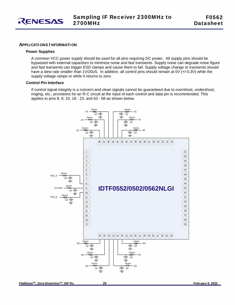
APPLICATIONS INFORMATION Power Supplies
A common VCC power supply should be used for all pins requiring DC power. All supply pins should be bypassed with external capacitors to minimize noise and fast transients. Supply noise can degrade noise figure and fast transients can trigger ESD clamps and cause them to fail. Supply voltage change or transients should have a slew rate smaller than 1V/20uS. In addition, all control pins should remain at 0V (+/-0.3V) while the supply voltage ramps or while it returns to zero.
Control Pin Interface If control signal integrity is a concern and clean signals cannot be guaranteed due to overshoot, undershoot, ringing, etc., provisions for an R-C circuit at the input of each control and data pin is recommended. This applies to pins 8, 9, 10, 18 - 23, and 63 - 68 as shown below.
IDTF0552/0502/0562NLGI8
9
10
11
12
13
14
15
16
17
18 19 20 21 22 23 24 25 26 27 28 29 30 31 32 33 34
35
36
37
38
39
40
41
42
43
44
45
46
47
48
49
50
51
5253545556575859606162636465666768
B5
B4
B3 B2
B1
B0
TDD_A
LCmode
TDD_B
5Kohm
2pf
5Kohm
2pf
5Kohm
2pf
5Kohm
2pf
5Kohm
2pf
5Kohm
2pf
1
2
3
4
5
6
7
5Kohm
2pf
5Kohm
2pf
5Kohm
2pf
A3
A5
A2
A45Kohm
2pf
5Kohm
2pf
5Kohm
2pf
5Kohm
2pf
5Kohm
2pf5Kohm
2pfA1
A0
Sampling IF Receiver 2300MHz to 2700MHz
F0562 Datasheet
FlatNoiseTM, Zero-DistortionTM, SIF Rx 30 February 9, 2022
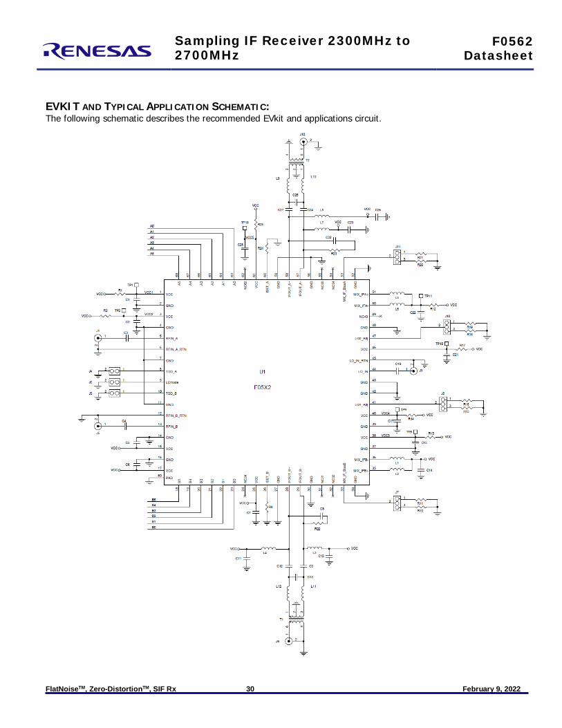
EVKIT AND TYPICAL APPLICATION SCHEMATIC: The following schematic describes the recommended EVkit and applications circuit.

Sampling IF Receiver 2300MHz to 2700MHz
F0562 Datasheet
FlatNoiseTM, Zero-DistortionTM, SIF Rx 31 February 9, 2022
SCHEMATIC CONTINUED FROM PREVIOUS PAGE

Sampling IF Receiver 2300MHz to 2700MHz
F0562 Datasheet
FlatNoiseTM, Zero-DistortionTM, SIF Rx 32 February 9, 2022
EVKIT PICTURE
LEAVE OPEN FOR LC MODE, SHORT FOR STD MODE
INSTALL JUMPER INOUTER POSITION FOR CHANNEL A STD MODEINNER POSITION FOR CHANNEL A LC MODE
SHORT FOR CHANNEL A NORMAL OPERATIONLEAVE OPEN CHANNEL A STBY MODE
SHORT FOR CHANNEL B NORMAL OPERATIONLEAVE OPEN CHANNEL B STBY MODE
INSTALL JUMPER INOUTER POSITION FOR STD MODEINNER POSITION FOR LC MODE
INSTALL JUMPER INOUTER POSITION FOR CHANNEL B STD MODEINNER POSITION FOR CHANNEL B LC MODE
Sampling IF Receiver 2300MHz to 2700MHz
F0562 Datasheet
FlatNoiseTM, Zero-DistortionTM, SIF Rx 33 February 9, 2022
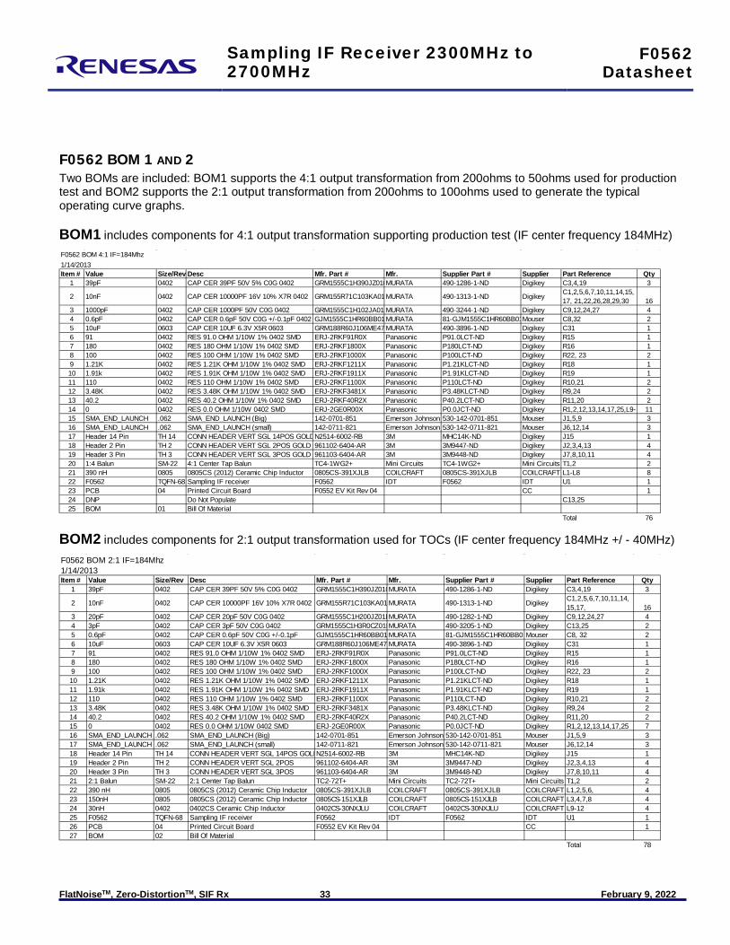
F0562 BOM 1 AND 2 Two BOMs are included: BOM1 supports the 4:1 output transformation from 200ohms to 50ohms used for production test and BOM2 supports the 2:1 output transformation from 200ohms to 100ohms used to generate the typical operating curve graphs. BOM1 includes components for 4:1 output transformation supporting production test (IF center frequency 184MHz)
BOM2 includes components for 2:1 output transformation used for TOCs (IF center frequency 184MHz +/ - 40MHz)
F0562 BOM 4:1 IF=184Mhz
Item # Value Size/Rev Desc Mfr. Part # Mfr. Supplier Part # Supplier Part Reference Qty1 39pF 0402 CAP CER 39PF 50V 5% C0G 0402 GRM1555C1H390JZ010MURATA 490-1286-1-ND Digikey C3,4,19 3
2 10nF 0402 CAP CER 10000PF 16V 10% X7R 0402 GRM155R71C103KA01MURATA 490-1313-1-ND Digikey C1,2,5,6,7,10,11,14,15,17, 21,22,26,28,29,30 16
3 1000pF 0402 CAP CER 1000PF 50V C0G 0402 GRM1555C1H102JA01 MURATA 490-3244-1-ND Digikey C9,12,24,27 44 0.6pF 0402 CAP CER 0.6pF 50V C0G +/-0.1pF 0402 GJM1555C1HR60BB01MURATA 81-GJM1555C1HR60BB01Mouser C8,32 25 10uF 0603 CAP CER 10UF 6.3V X5R 0603 GRM188R60J106ME47 MURATA 490-3896-1-ND Digikey C31 16 91 0402 RES 91.0 OHM 1/10W 1% 0402 SMD ERJ-2RKF91R0X Panasonic P91.0LCT-ND Digikey R15 17 180 0402 RES 180 OHM 1/10W 1% 0402 SMD ERJ-2RKF1800X Panasonic P180LCT-ND Digikey R16 18 100 0402 RES 100 OHM 1/10W 1% 0402 SMD ERJ-2RKF1000X Panasonic P100LCT-ND Digikey R22, 23 29 1.21K 0402 RES 1.21K OHM 1/10W 1% 0402 SMD ERJ-2RKF1211X Panasonic P1.21KLCT-ND Digikey R18 110 1.91k 0402 RES 1.91K OHM 1/10W 1% 0402 SMD ERJ-2RKF1911X Panasonic P1.91KLCT-ND Digikey R19 111 110 0402 RES 110 OHM 1/10W 1% 0402 SMD ERJ-2RKF1100X Panasonic P110LCT-ND Digikey R10,21 212 3.48K 0402 RES 3.48K OHM 1/10W 1% 0402 SMD ERJ-2RKF3481X Panasonic P3.48KLCT-ND Digikey R9,24 213 40.2 0402 RES 40.2 OHM 1/10W 1% 0402 SMD ERJ-2RKF40R2X Panasonic P40.2LCT-ND Digikey R11,20 214 0 0402 RES 0.0 OHM 1/10W 0402 SMD ERJ-2GE0R00X Panasonic P0.0JCT-ND Digikey R1,2,12,13,14,17,25,L9- 1115 SMA_END_LAUNCH .062 SMA_END_LAUNCH (Big) 142-0701-851 Emerson Johnson 530-142-0701-851 Mouser J1,5,9 316 SMA_END_LAUNCH .062 SMA_END_LAUNCH (small) 142-0711-821 Emerson Johnson 530-142-0711-821 Mouser J6,12,14 317 Header 14 Pin TH 14 CONN HEADER VERT SGL 14POS GOLDN2514-6002-RB 3M MHC14K-ND Digikey J15 118 Header 2 Pin TH 2 CONN HEADER VERT SGL 2POS GOLD 961102-6404-AR 3M 3M9447-ND Digikey J2,3,4,13 419 Header 3 Pin TH 3 CONN HEADER VERT SGL 3POS GOLD 961103-6404-AR 3M 3M9448-ND Digikey J7,8,10,11 420 1:4 Balun SM-22 4:1 Center Tap Balun TC4-1WG2+ Mini Circuits TC4-1WG2+ Mini Circuits T1,2 221 390 nH 0805 0805CS (2012) Ceramic Chip Inductor 0805CS-391XJLB COILCRAFT 0805CS-391XJLB COILCRAFT L1-L8 822 F0562 TQFN-68 Sampling IF receiver F0562 IDT F0562 IDT U1 123 PCB 04 Printed Circuit Board F0552 EV Kit Rev 04 CC 124 DNP Do Not Populate C13,2525 BOM 01 Bill Of Material
Total 76
1/14/2013
F0562 BOM 2:1 IF=184Mhz
Item # Value Size/Rev Desc Mfr. Part # Mfr. Supplier Part # Supplier Part Reference Qty1 39pF 0402 CAP CER 39PF 50V 5% C0G 0402 GRM1555C1H390JZ010MURATA 490-1286-1-ND Digikey C3,4,19 3
2 10nF 0402 CAP CER 10000PF 16V 10% X7R 0402 GRM155R71C103KA01 MURATA 490-1313-1-ND Digikey C1,2,5,6,7,10,11,14,15,17, 16
3 20pF 0402 CAP CER 20pF 50V C0G 0402 GRM1555C1H200JZ01DMURATA 490-1282-1-ND Digikey C9,12,24,27 44 3pF 0402 CAP CER 3pF 50V C0G 0402 GRM1555C1H3R0CZ01DMURATA 490-3205-1-ND Digikey C13,25 25 0.6pF 0402 CAP CER 0.6pF 50V C0G +/-0.1pF GJM1555C1HR60BB01 MURATA 81-GJM1555C1HR60BB01Mouser C8, 32 26 10uF 0603 CAP CER 10UF 6.3V X5R 0603 GRM188R60J106ME47 MURATA 490-3896-1-ND Digikey C31 17 91 0402 RES 91.0 OHM 1/10W 1% 0402 SMD ERJ-2RKF91R0X Panasonic P91.0LCT-ND Digikey R15 18 180 0402 RES 180 OHM 1/10W 1% 0402 SMD ERJ-2RKF1800X Panasonic P180LCT-ND Digikey R16 19 100 0402 RES 100 OHM 1/10W 1% 0402 SMD ERJ-2RKF1000X Panasonic P100LCT-ND Digikey R22, 23 210 1.21K 0402 RES 1.21K OHM 1/10W 1% 0402 SMD ERJ-2RKF1211X Panasonic P1.21KLCT-ND Digikey R18 111 1.91k 0402 RES 1.91K OHM 1/10W 1% 0402 SMD ERJ-2RKF1911X Panasonic P1.91KLCT-ND Digikey R19 112 110 0402 RES 110 OHM 1/10W 1% 0402 SMD ERJ-2RKF1100X Panasonic P110LCT-ND Digikey R10,21 213 3.48K 0402 RES 3.48K OHM 1/10W 1% 0402 SMD ERJ-2RKF3481X Panasonic P3.48KLCT-ND Digikey R9,24 214 40.2 0402 RES 40.2 OHM 1/10W 1% 0402 SMD ERJ-2RKF40R2X Panasonic P40.2LCT-ND Digikey R11,20 215 0 0402 RES 0.0 OHM 1/10W 0402 SMD ERJ-2GE0R00X Panasonic P0.0JCT-ND Digikey R1,2,12,13,14,17,25 716 SMA_END_LAUNCH .062 SMA_END_LAUNCH (Big) 142-0701-851 Emerson Johnson 530-142-0701-851 Mouser J1,5,9 317 SMA_END_LAUNCH .062 SMA_END_LAUNCH (small) 142-0711-821 Emerson Johnson 530-142-0711-821 Mouser J6,12,14 318 Header 14 Pin TH 14 CONN HEADER VERT SGL 14POS GOLDN2514-6002-RB 3M MHC14K-ND Digikey J15 119 Header 2 Pin TH 2 CONN HEADER VERT SGL 2POS 961102-6404-AR 3M 3M9447-ND Digikey J2,3,4,13 420 Header 3 Pin TH 3 CONN HEADER VERT SGL 3POS 961103-6404-AR 3M 3M9448-ND Digikey J7,8,10,11 421 2:1 Balun SM-22 2:1 Center Tap Balun TC2-72T+ Mini Circuits TC2-72T+ Mini Circuits T1,2 222 390 nH 0805 0805CS (2012) Ceramic Chip Inductor 0805CS-391XJLB COILCRAFT 0805CS-391XJLB COILCRAFT L1,2,5,6, 423 150nH 0805 0805CS (2012) Ceramic Chip Inductor 0805CS-151XJLB COILCRAFT 0805CS-151XJLB COILCRAFT L3,4,7,8 424 30nH 0402 0402CS Ceramic Chip Inductor 0402CS-30NXJLU COILCRAFT 0402CS-30NXJLU COILCRAFT L9-12 425 F0562 TQFN-68 Sampling IF receiver F0562 IDT F0562 IDT U1 126 PCB 04 Printed Circuit Board F0552 EV Kit Rev 04 CC 127 BOM 02 Bill Of Material
Total 78
1/14/2013

Sampling IF Receiver 2300MHz to 2700MHz
F0562 Datasheet
FlatNoiseTM, Zero-DistortionTM, SIF Rx 34 February 9, 2022
TOP MARKINGS
ORDERING INFORMATION Part Number Package Description Carrier Type Temperature Range
F0562NLGI 68-VFQFPN, 10 × 10 mm
Tape and Reel -40°C to +85°C
F0562NLGI8 Tray
REVISION HISTORY Revision Date Description
February 9, 2022 Rebranded to Renesas.
April 16, 2014 Initial release.
IDTF0562NLGIZB1344N
Q33A009MY
Part Number
Date Code [YYWW](Week 44 of 2013)
Lot CodeDie Step

NOTES:
1. All dimension are in mm, angles in degrees.2. Top down view, as viewed on PC.3. Land pattern in blue. NSMD land pattern assumed.4. Land pattern recommendation as per IPC-7351B
generic requirement for surface mount design and landpattern.
TOP VIEW BOTTOM VIEW
68
1
3
68 X 0.25
2
SIDE VIEW
10.00
8.850.30 0.50 0.95
7.80
10.75 8.85
0.30
0.50
0.95
7.80
RECOMMENDED LAND PATTERN DIMENSION
PIN#1 INDICATORSEE DETAIL B
Seating Plane
0.90
0.08 CC
68X
0.10 C
0.02
A
B
PIN#1INDEX AREA
0.10 C A B0.05 C
0.20 Ref
10.00
10.75
7.70
3.850.50
0.65
7.70
3.85
16 X 0.50
16 X 0.50
© Renesas Electronics Corporation
Package Outline DrawingPackage Code:NLG68P1
68-VFQFPN 10.0 x 10.0 x 0.90 mm Body, 0.5mm PitchPSC-4111-01, Revision: 01, Date Created: Feb 15, 2022

Corporate HeadquartersTOYOSU FORESIA, 3-2-24 Toyosu,Koto-ku, Tokyo 135-0061, Japanwww.renesas.com
Contact InformationFor further information on a product, technology, the most up-to-date version of a document, or your nearest sales office, please visit:www.renesas.com/contact/
TrademarksRenesas and the Renesas logo are trademarks of Renesas Electronics Corporation. All trademarks and registered trademarks are the property of their respective owners.
IMPORTANT NOTICE AND DISCLAIMER
RENESAS ELECTRONICS CORPORATION AND ITS SUBSIDIARIES (“RENESAS”) PROVIDES TECHNICAL SPECIFICATIONS AND RELIABILITY DATA (INCLUDING DATASHEETS), DESIGN RESOURCES (INCLUDING REFERENCE DESIGNS), APPLICATION OR OTHER DESIGN ADVICE, WEB TOOLS, SAFETY INFORMATION, AND OTHER RESOURCES “AS IS” AND WITH ALL FAULTS, AND DISCLAIMS ALL WARRANTIES, EXPRESS OR IMPLIED, INCLUDING, WITHOUT LIMITATION, ANY IMPLIED WARRANTIES OF MERCHANTABILITY, FITNESS FOR A PARTICULAR PURPOSE, OR NON-INFRINGEMENT OF THIRD PARTY INTELLECTUAL PROPERTY RIGHTS.
These resources are intended for developers skilled in the art designing with Renesas products. You are solely responsible for (1) selecting the appropriate products for your application, (2) designing, validating, and testing your application, and (3) ensuring your application meets applicable standards, and any other safety, security, or other requirements. These resources are subject to change without notice. Renesas grants you permission to use these resources only for development of an application that uses Renesas products. Other reproduction or use of these resources is strictly prohibited. No license is granted to any other Renesas intellectual property or to any third party intellectual property. Renesas disclaims responsibility for, and you will fully indemnify Renesas and its representatives against, any claims, damages, costs, losses, or liabilities arising out of your use of these resources. Renesas' products are provided only subject to Renesas' Terms and Conditions of Sale or other applicable terms agreed to in writing. No use of any Renesas resources expands or otherwise alters any applicable warranties or warranty disclaimers for these products.
(Rev.1.0 Mar 2020)
© 2021 Renesas Electronics Corporation. All rights reserved.