M306H2FCFP DATASHEET - Renesas
253
To our customers, Old Company Name in Catalogs and Other Documents On April 1 st , 2010, NEC Electronics Corporation merged with Renesas Technology Corporation, and Renesas Electronics Corporation took over all the business of both companies. Therefore, although the old company name remains in this document, it is a valid Renesas Electronics document. We appreciate your understanding. Renesas Electronics website: http://www.renesas.com April 1 st , 2010 Renesas Electronics Corporation Issued by: Renesas Electronics Corporation (http://www.renesas.com ) Send any inquiries to http://www.renesas.com/inquiry .
-
Upload
khangminh22 -
Category
Documents
-
view
10 -
download
0
Transcript of M306H2FCFP DATASHEET - Renesas
To our customers,
Old Company Name in Catalogs and Other Documents
On April 1st, 2010, NEC Electronics Corporation merged with Renesas Technology
Corporation, and Renesas Electronics Corporation took over all the business of both companies. Therefore, although the old company name remains in this document, it is a valid Renesas Electronics document. We appreciate your understanding.
Renesas Electronics website: http://www.renesas.com
April 1st, 2010 Renesas Electronics Corporation
Issued by: Renesas Electronics Corporation (http://www.renesas.com)
Send any inquiries to http://www.renesas.com/inquiry.
Notice 1. All information included in this document is current as of the date this document is issued. Such information, however, is
subject to change without any prior notice. Before purchasing or using any Renesas Electronics products listed herein, please confirm the latest product information with a Renesas Electronics sales office. Also, please pay regular and careful attention to additional and different information to be disclosed by Renesas Electronics such as that disclosed through our website.
2. Renesas Electronics does not assume any liability for infringement of patents, copyrights, or other intellectual property rights of third parties by or arising from the use of Renesas Electronics products or technical information described in this document. No license, express, implied or otherwise, is granted hereby under any patents, copyrights or other intellectual property rights of Renesas Electronics or others.
3. You should not alter, modify, copy, or otherwise misappropriate any Renesas Electronics product, whether in whole or in part. 4. Descriptions of circuits, software and other related information in this document are provided only to illustrate the operation of
semiconductor products and application examples. You are fully responsible for the incorporation of these circuits, software, and information in the design of your equipment. Renesas Electronics assumes no responsibility for any losses incurred by you or third parties arising from the use of these circuits, software, or information.
5. When exporting the products or technology described in this document, you should comply with the applicable export control laws and regulations and follow the procedures required by such laws and regulations. You should not use Renesas Electronics products or the technology described in this document for any purpose relating to military applications or use by the military, including but not limited to the development of weapons of mass destruction. Renesas Electronics products and technology may not be used for or incorporated into any products or systems whose manufacture, use, or sale is prohibited under any applicable domestic or foreign laws or regulations.
6. Renesas Electronics has used reasonable care in preparing the information included in this document, but Renesas Electronics does not warrant that such information is error free. Renesas Electronics assumes no liability whatsoever for any damages incurred by you resulting from errors in or omissions from the information included herein.
7. Renesas Electronics products are classified according to the following three quality grades: “Standard”, “High Quality”, and “Specific”. The recommended applications for each Renesas Electronics product depends on the product’s quality grade, as indicated below. You must check the quality grade of each Renesas Electronics product before using it in a particular application. You may not use any Renesas Electronics product for any application categorized as “Specific” without the prior written consent of Renesas Electronics. Further, you may not use any Renesas Electronics product for any application for which it is not intended without the prior written consent of Renesas Electronics. Renesas Electronics shall not be in any way liable for any damages or losses incurred by you or third parties arising from the use of any Renesas Electronics product for an application categorized as “Specific” or for which the product is not intended where you have failed to obtain the prior written consent of Renesas Electronics. The quality grade of each Renesas Electronics product is “Standard” unless otherwise expressly specified in a Renesas Electronics data sheets or data books, etc.
“Standard”: Computers; office equipment; communications equipment; test and measurement equipment; audio and visual equipment; home electronic appliances; machine tools; personal electronic equipment; and industrial robots.
“High Quality”: Transportation equipment (automobiles, trains, ships, etc.); traffic control systems; anti-disaster systems; anti-crime systems; safety equipment; and medical equipment not specifically designed for life support.
“Specific”: Aircraft; aerospace equipment; submersible repeaters; nuclear reactor control systems; medical equipment or systems for life support (e.g. artificial life support devices or systems), surgical implantations, or healthcare intervention (e.g. excision, etc.), and any other applications or purposes that pose a direct threat to human life.
8. You should use the Renesas Electronics products described in this document within the range specified by Renesas Electronics, especially with respect to the maximum rating, operating supply voltage range, movement power voltage range, heat radiation characteristics, installation and other product characteristics. Renesas Electronics shall have no liability for malfunctions or damages arising out of the use of Renesas Electronics products beyond such specified ranges.
9. Although Renesas Electronics endeavors to improve the quality and reliability of its products, semiconductor products have specific characteristics such as the occurrence of failure at a certain rate and malfunctions under certain use conditions. Further, Renesas Electronics products are not subject to radiation resistance design. Please be sure to implement safety measures to guard them against the possibility of physical injury, and injury or damage caused by fire in the event of the failure of a Renesas Electronics product, such as safety design for hardware and software including but not limited to redundancy, fire control and malfunction prevention, appropriate treatment for aging degradation or any other appropriate measures. Because the evaluation of microcomputer software alone is very difficult, please evaluate the safety of the final products or system manufactured by you.
10. Please contact a Renesas Electronics sales office for details as to environmental matters such as the environmental compatibility of each Renesas Electronics product. Please use Renesas Electronics products in compliance with all applicable laws and regulations that regulate the inclusion or use of controlled substances, including without limitation, the EU RoHS Directive. Renesas Electronics assumes no liability for damages or losses occurring as a result of your noncompliance with applicable laws and regulations.
11. This document may not be reproduced or duplicated, in any form, in whole or in part, without prior written consent of Renesas Electronics.
12. Please contact a Renesas Electronics sales office if you have any questions regarding the information contained in this document or Renesas Electronics products, or if you have any other inquiries.
(Note 1) “Renesas Electronics” as used in this document means Renesas Electronics Corporation and also includes its majority-owned subsidiaries.
(Note 2) “Renesas Electronics product(s)” means any product developed or manufactured by or for Renesas Electronics.

Regarding the change of names mentioned in the document, such as Mitsubishi Electric and Mitsubishi XX, to Renesas Technology Corp.
The semiconductor operations of Hitachi and Mitsubishi Electric were transferred to Renesas
Technology Corporation on April 1st 2003. These operations include microcomputer, logic, analog
and discrete devices, and memory chips other than DRAMs (flash memory, SRAMs etc.)
Accordingly, although Mitsubishi Electric, Mitsubishi Electric Corporation, Mitsubishi
Semiconductors, and other Mitsubishi brand names are mentioned in the document, these names
have in fact all been changed to Renesas Technology Corp. Thank you for your understanding.
Except for our corporate trademark, logo and corporate statement, no changes whatsoever have been
made to the contents of the document, and these changes do not constitute any alteration to the
contents of the document itself.
Note : Mitsubishi Electric will continue the business operations of high frequency & optical devices
and power devices.
Renesas Technology Corp.
Customer Support Dept.
April 1, 2003
To all our customers
1. DESCRIPTIONThe M306H2FCFP is single-chip microcomputer using the high-performance silicon gate CMOS process
using a M16C/60 Series CPU core and is packaged in a 116-pin plastic molded QFP. This single-chip
microcomputer operates using sophisticated instructions featuring a high level of instruction efficiency.
With 1M bytes of address space, this is capable of executing instructions at high speed. This also features
a built-in data acquisition circuit, making this correspondence to Teletext broadcasting service.
1.1 Features• Memory capacity..................................<ROM>128K bytes
<RAM>5K bytes• Shortest instruction execution time ......100 ns (f(XIN)=10 MHz)• Supply voltage .....................................4.75 V to 5.25V(at f(XIN)=10 MHz)
2.80V to 5.25V(at f(XCIN)=32kHZ, only in low power dissipation mode)• Interrupts..............................................25 internal and 8 external interrupt sources, 4 software
interrupt sources; 7 levels (Including key input interrupt)• Multifunction 16-bit timer ......................5 output timers + 6 input timers• Serial I/O ..............................................5 channels
UART/clock synchronous: 3
Clock synchronous: 2
• DMAC ..................................................2 channels (trigger: 24 sources)• A-D converter .......................................8 bits X 8 channels (Expandable up to 10 channels)• D-A converter .......................................8 bits X 2 channels• CRC calculation circuit .........................1 circuit• Watchdog timer ....................................1 line• Programmable I/O ...............................87 lines• Input port ..............................................
_______
1 port (P85 shared with NMI pin)• Output port ...........................................1 port (P11 shared with SLICEON pin)• Chip select output ................................4 lines
• Clock generating circuit .......................2 built-in circuits
(built-in feedback resistor, and external ceramic or crystal oscillator)
• Data acquisition circuit ......................... For PDC, VPS, EPG-J, XDS and WSS
1.2 Applications
VCR, etc
Rev. 1.0
SINGLE-CHIP 16-BIT CMOS MICROCOMPUTERwith DATA ACQUISITION CONTROLLER
MITSUBISHI MICROCOMPUTERS
M306H2FCFP
2
Rev. 1.0
SINGLE-CHIP 16-BIT CMOS MICROCOMPUTERwith DATA ACQUISITION CONTROLLER
MITSUBISHI MICROCOMPUTERS
M306H2FCFP
Table of contents
1. DESCRIPTION ...................................................... 1
1.1 Features ........................................................... 1
1.2 Applications ..................................................... 1
1.3 Pin Configuration ............................................. 3
1.4 Block Diagram ................................................. 4
1.5 Performance Outline ........................................ 5
2. OPERATION OF FUNCTIONAL BLOCKS ............ 9
2.1 Memory ............................................................ 9
2.2 Central Processing Unit (CPU) ........................ 13
2.3 Reset ............................................................... 16
2.4 Processor Mode ............................................... 20
2.5 Clock Generating Circuit .................................. 31
2.6 Protection ......................................................... 40
2.7 Interrupt ........................................................... 41
2.8 Watchdog Timer .............................................. 61
2.9 DMAC .............................................................. 63
2.10 Timer .............................................................. 73
2.11 Serial I/O ........................................................ 91
2.12 A-D Converter ................................................ 132
2.13 D-A Converter ................................................ 142
2.14 CRC Calculation Circuit ................................. 144
2.15 Expansion Function ....................................... 146
2.16 Programmable I/O Ports ................................ 170
3. USAGE PRECAUTION .......................................... 180
4. ELECTRICAL CHARACTERISTICS ...................... 185
5. FLASH MEMORY .................................................. 203
5.1 Outline Performance ........................................ 203
5.2 Flash Memory mode ........................................ 204
5.3 CPU Rewrite Mode .......................................... 205
5.4 Functions To Inhibit Rewriting Flash Memory Version ....... 215
5.5 Parallel I/O Mode ............................................. 217
5.6 Standard serial I/O mode ................................. 218
5.7 Absolute maximum ratings .............................. 246
6. PACKAGE OUTLINE ............................................. 248
7. DIFFERENCES BETWEEN M306H2MC-XXXFP AND M306H2FCFP ....249
SINGLE-CHIP 16-BIT CMOS MICROCOMPUTERwith DATA ACQUISITION CONTROLLER
MITSUBISHI MICROCOMPUTERS
3
Rev. 1.0
M306H2FCFP
BY
TE
XO
UT
Vss XIN
Vcc
P87
/XC
IN
P86
/XC
OU
T
P81
/TA
4IN
P80
/TA
4OU
T
P77
/TA
3IN
CN
Vss
P90
/TB
0IN/C
LK3
P91
/TB
1IN/S
IN3
P92
/TB
2IN/S
OU
T3
P94
/DA
1/T
B4I
N
P95
/AN
EX
0/C
LK4
P93
/DA
0/T
B3I
N
P31
/A9
P42
/A18
P41
/A17
P40
/A16
P32
/A10
P33
/A11
P34
/A12
P35
/A13
P36
/A14
P37
/A15
VC
C
P43/A19
P96/ANEX1/SOUT4
RE
SE
T
P85
/NM
I
P84
/INT
2
P76
/TA
3OU
T
P75
/TA
2IN
P74
/TA
2OU
T
P72
/CLK
2/T
A1O
UT
P71
/RXD
2/S
CL/
TA
0IN/T
B5I
N
P73
/CT
S2/
RT
S2/
TA
1IN
P53/BCLK
P56/ALE
P44/CS0
P46/CS2P47/CS3
P50/WRL/WR
P51/WRH/BHEP52/RD
P54/HLDAP55/HOLD
108
107
106
105
104
103
102
101
100
99
98
97
96
95
94
93
92
91
90
89
88
87 86 85 84 83 82 81 80 79 78 77 76 75 74 73 71 70 69 68 67 66 65 64 63 62 61 60 5972
P07/D7
P02/D2
P03/D3
P04/D4
P05/D5
P06/D6
P00/D0
P01/D1
110
111
112
113
114
115
116
109
1 2 3 4 5 6 7 8 9 10 11 12 13 14 15 16 17 18 19 20 21 22 23 24 25 26 27 28 29
30
31
32
33
34
35
36
M306H2FCFP
P83
/INT
1
P82
/INT
0
P61/CLK0
P62/RXD0
P63/TXD0
P65/CLK1
P66/RXD1
P67/TXD1
VREF
AVSS
P57/RDY/CLKOUT
P60/CTS0/RTS0
P64/CTS1/RTS1/CLKS1
58
57
56
55
54
53
52
51
50
49
48
47
46
45
44
43
42
41
40
39
38
37 P11/SLICEON
M1M2VSS1
VDD1
P20
/A0(
/D0/
-)
P27
/A7(
/D7/
D6)
P30
/A8(
/-/D
7)
P26
/A6(
/D6/
D5)
P25
/A5(
/D5/
D4)
P24
/A4(
/D4/
D3)
P23
/A3(
/D3/
D2)
P22
/A2(
/D2/
D1)
P21
/A1(
/D1/
D0)
P14
/D12
P13
/D11
P12
/D10
P11
/D9
VS
S
P15
/D13
/INT
3 P
16/D
14/IN
T4
P17
/D15
/INT
5
P70
/TXD
2/S
DA
/TA
0OU
T
VSS2LP2
LP4
LP3
VDD2
P10
/D8
P103/AN3
P102/AN2
P101/AN1
P100/AN0
AVCC
SYNCIN
CVIN1
VDD3
VSS3
FSCIN
P97/ADTRG/SIN4
P45/CS1
P107/AN7/KI3
P104/AN4/KI0P105/AN5/KI1
P106/AN6/KI2
SVREF
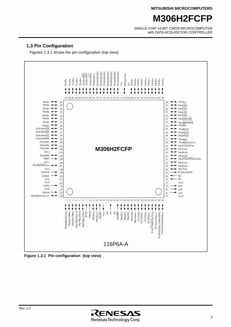
1.3 Pin ConfigurationFigures 1.3.1 shows the pin configuration (top view).
116P6A-A
Figure 1.3.1 Pin configuration (top view)
4
Rev. 1.0
SINGLE-CHIP 16-BIT CMOS MICROCOMPUTERwith DATA ACQUISITION CONTROLLER
MITSUBISHI MICROCOMPUTERS
M306H2FCFP8
P
o
r
t
P
1
0
I / O
p
o
r
t
s P
o
r
t
P
0
8
P
o
r
t
P
1
8
P
o
r
t
P
2
8
Port P3
8
Port P4
8
Port P5
8
P
o
r
t
P
6
8
87
8
P
o
r
t
P
9P
o
r
t
P
8P
o
r
t
P
7
P
o
r
t
P
85
T
i
m
e
r
T
i
m
e
r
T
A
0
(
1
6
b
i
t
s
)T
i
m
e
r
T
A
1
(
1
6
b
i
t
s
)T
i
m
e
r
T
A
2
(
1
6
b
i
t
s
)T
i
m
e
r
T
A
3
(
1
6
b
i
t
s
)T
i
m
e
r
T
A
4
(
1
6
b
i
t
s
)T
i
m
e
r
T
B
0
(
1
6
b
i
t
s
)T
i
m
e
r
T
B
1
(
1
6
b
i
t
s
)T
i
m
e
r
T
B
2
(
1
6
b
i
t
s
)T
i
m
e
r
T
B
3
(
1
6
b
i
t
s
)T
i
m
e
r
T
B
4
(
1
6
b
i
t
s
)T
i
m
e
r
T
B
5
(
1
6
b
i
t
s
)
I n
t
e
r
n
a
l
p
e
r
i
p
h
e
r
a
l
f
u
n
c
t
i
o
n
s
Watchdog timer(15 bits)
DMAC(2 channels)
D-A converter(8 bits X 2 channels)
A
-
D
c
o
n
v
e
r
t
e
r(
8
b
i
t
s
X
8
c
h
a
n
n
e
l
sE
x
p
a
n
d
a
b
l
e
u
p
t
o
1
0
c
h
a
n
n
e
l
s
)
U
A
R
T
/
c
l
o
c
k
s
y
n
c
h
r
o
n
o
u
s
S
I
/
O(
8
b
i
t
s
X
3
c
h
a
n
n
e
l
s
)
System clock generator
XI
N-
XO
U
TXC
I
N-
XC
O
U
T
M16C/60 series16-bit CPU core
R0LR
0
HR
1
H R1LR2R3A0A1F
B
R0LR0HR1H R1L
R
2R
3A0A1FB
Registers
ISPUSP
Stack pointer
Vector table
INTB
C
R
C
a
r
i
t
h
m
e
t
i
c
c
i
r
c
u
i
t
(
C
C
I
T
T)
(
P
o
l
y
n
o
m
i
a
l
:
X1
6+
X1
2+
X5+
1
)
M
u
l
t
i
p
l
i
e
r
M
e
m
o
r
y
ROM (128K bytes)
SB FLG
P
C
Program counter
C
l
o
c
k
s
y
n
c
h
r
o
n
o
u
s
S
I
/
O(
8
b
i
t
s
X
2
c
h
a
n
n
e
l
s
)
Data acquisition controller
P o
r
t
P
1
1
F
l
a
g
r
e
g
i
s
t
e
r
RAM (5K bytes)
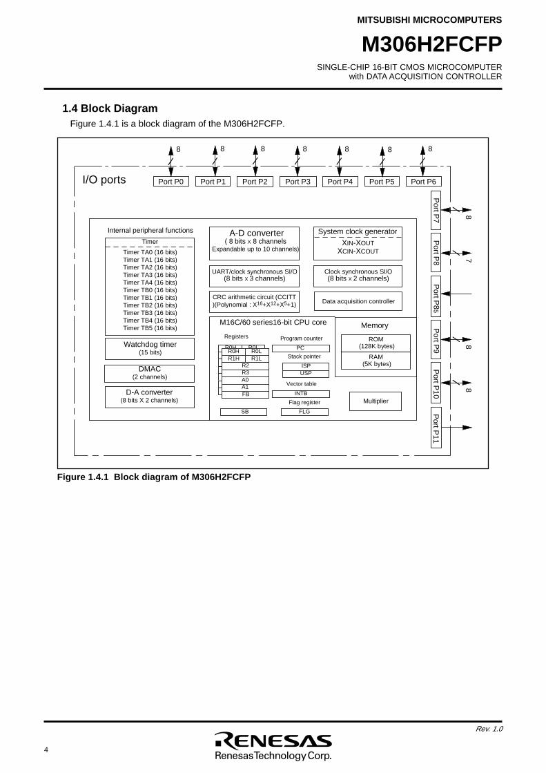
1.4 Block DiagramFigure 1.4.1 is a block diagram of the M306H2FCFP.
Figure 1.4.1 Block diagram of M306H2FCFP
SINGLE-CHIP 16-BIT CMOS MICROCOMPUTERwith DATA ACQUISITION CONTROLLER
MITSUBISHI MICROCOMPUTERS
5
Rev. 1.0
M306H2FCFP
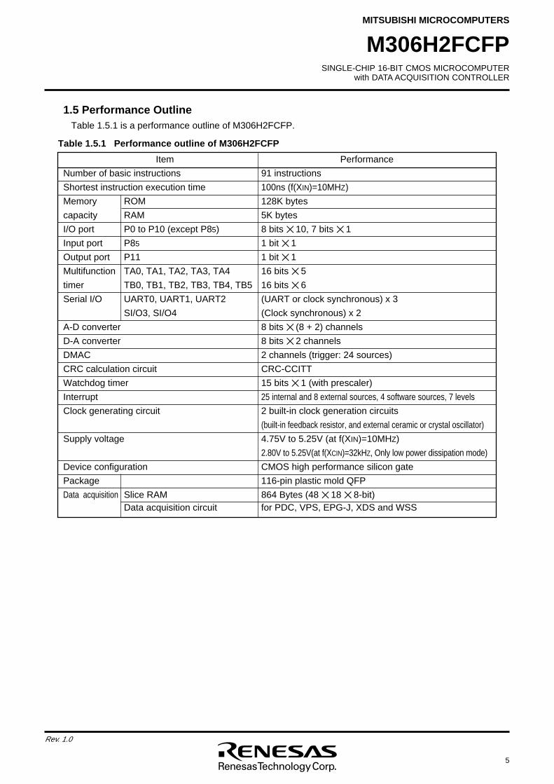
Table 1.5.1 Performance outline of M306H2FCFP
1.5 Performance OutlineTable 1.5.1 is a performance outline of M306H2FCFP.
Item Performance
Number of basic instructions 91 instructions
Shortest instruction execution time 100ns (f(XIN)=10MHZ)
Memory ROM 128K bytes
capacity RAM 5K bytes
I/O port P0 to P10 (except P85) 8 bits 10, 7 bits 1
Input port P85 1 bit 1
Output port P11 1 bit 1
Multifunction TA0, TA1, TA2, TA3, TA4 16 bits 5
timer TB0, TB1, TB2, TB3, TB4, TB5 16 bits 6
Serial I/O UART0, UART1, UART2 (UART or clock synchronous) x 3
SI/O3, SI/O4 (Clock synchronous) x 2
A-D converter 8 bits (8 + 2) channels
D-A converter 8 bits 2 channels
DMAC 2 channels (trigger: 24 sources)
CRC calculation circuit CRC-CCITT
Watchdog timer 15 bits 1 (with prescaler)
Interrupt 25 internal and 8 external sources, 4 software sources, 7 levels
Clock generating circuit 2 built-in clock generation circuits
(built-in feedback resistor, and external ceramic or crystal oscillator)
Supply voltage 4.75V to 5.25V (at f(XIN)=10MHZ)
2.80V to 5.25V(at f(XCIN)=32kHZ, Only low power dissipation mode)
Device configuration CMOS high performance silicon gate
Package 116-pin plastic mold QFP
Data acquisition Slice RAM 864 Bytes (48 18 8-bit)Data acquisition circuit for PDC, VPS, EPG-J, XDS and WSS
6
Rev. 1.0
SINGLE-CHIP 16-BIT CMOS MICROCOMPUTERwith DATA ACQUISITION CONTROLLER
MITSUBISHI MICROCOMPUTERS
M306H2FCFP
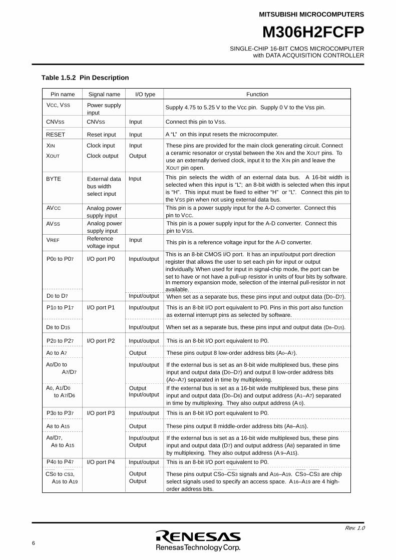
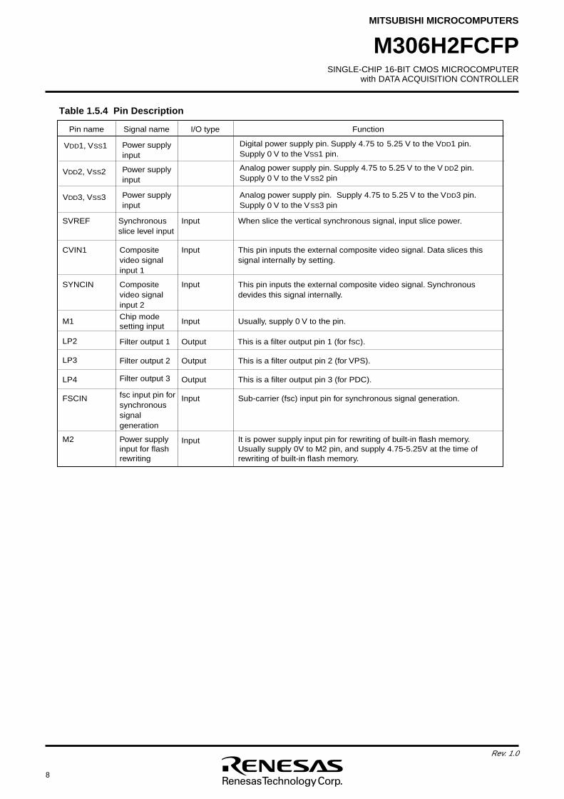
Table 1.5.2 Pin Description
VCC, VSS
CNVSS
Signal name
Power supplyinput
CNVSS
Supply 4.75 to 5.25 V to the Vcc pin. Supply 0 V to the Vss pin.
Function
Connect this pin to VSS.
Pin name
Input
I/O type
XIN
XOUT
Clock input
Clock output
These pins are provided for the main clock generating circuit. Connect a ceramic resonator or crystal between the XIN and the XOUT pins. To use an externally derived clock, input it to the XIN pin and leave the
Input
Output
Reset input A “L” on this input resets the microcomputer.InputRESET
BYTE External data bus width select input
This pin selects the width of an external data bus. A 16-bit width is selected when this input is “L”; an 8-bit width is selected when this input is “H”. This input must be fixed to either “H” or “L”. Connect this pin to the VSS pin when not using external data bus.
Input
AVCC Analog powersupply input
This pin is a power supply input for the A-D converter. Connect this pin to VCC.
XOUT pin open.
VREF Referencevoltage input
This pin is a reference voltage input for the A-D converter.Input
P00 to P07 I/O port P0This is an 8-bit CMOS I/O port. It has an input/output port direction register that allows the user to set each pin for input or output individually. When used for input in signal-chip mode, the port can be set to have or not have a pull-up resistor in units of four bits by software. In memory expansion mode, selection of the internal pull-resistor in not available.
Input/output
AVSS This pin is a power supply input for the A-D converter. Connect this pin to VSS.
Analog powersupply input
P10 to P17 I/O port P1 This is an 8-bit I/O port equivalent to P0. Pins in this port also function as external interrupt pins as selected by software.
Input/output
D0 to D7 When set as a separate bus, these pins input and output data (D0–D7).Input/output
D8 to D15 When set as a separate bus, these pins input and output data (D8–D15).Input/output
P20 to P27 I/O port P2 This is an 8-bit I/O port equivalent to P0.Input/output
A0 to A7 These pins output 8 low-order address bits (A0–A7).Output
A0/D0 to A7/D7
If the external bus is set as an 8-bit wide multiplexed bus, these pins input and output data (D0–D7) and output 8 low-order address bits (A0–A7) separated in time by multiplexing.
Input/output
A0, A1/D0
to A7/D6
If the external bus is set as a 16-bit wide multiplexed bus, these pins input and output data (D0–D6) and output address (A1–A7) separated in time by multiplexing. They also output address (A 0).
OutputInput/output
P30 to P37 I/O port P3 This is an 8-bit I/O port equivalent to P0.Input/output
A8 to A15 These pins output 8 middle-order address bits (A8–A15).Output
A8/D7, A9 to A15
If the external bus is set as a 16-bit wide multiplexed bus, these pins input and output data (D7) and output address (A8) separated in time by multiplexing. They also output address (A 9–A15).
Input/outputOutput
P40 to P47 I/O port P4 This is an 8-bit I/O port equivalent to P0.Input/output
OutputOutput
CS0 to CS3, A16 to A19
These pins output CS0–CS3 signals and A16–A19. CS0–CS3 are chip select signals used to specify an access space. A16–A19 are 4 high- order address bits.
SINGLE-CHIP 16-BIT CMOS MICROCOMPUTERwith DATA ACQUISITION CONTROLLER
MITSUBISHI MICROCOMPUTERS
7
Rev. 1.0
M306H2FCFP
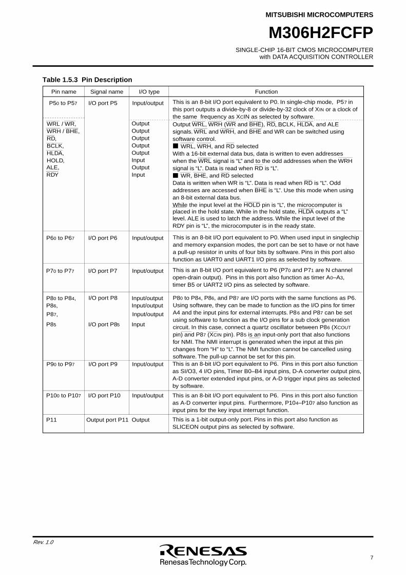
Table 1.5.3 Pin Description
Signal name FunctionPin name I/O type
I/O port P5 Input/outputP50 to P57 This is an 8-bit I/O port equivalent to P0. In single-chip mode, P57 in this port outputs a divide-by-8 or divide-by-32 clock of XIN or a clock of the same frequency as XCIN as selected by software.
OutputOutputOutputOutputOutputInputOutputInput
WRL / WR,WRH / BHE,RD,BCLK,HLDA,HOLD,ALE,RDY
Output WRL, WRH (WR and BHE), RD, BCLK, HLDA, and ALE signals. WRL and WRH, and BHE and WR can be switched using software control. WRL, WRH, and RD selectedWith a 16-bit external data bus, data is written to even addresses when the WRL signal is “L” and to the odd addresses when the WRH signal is “L”. Data is read when RD is “L”. WR, BHE, and RD selectedData is written when WR is “L”. Data is read when RD is “L”. Odd addresses are accessed when BHE is “L”. Use this mode when using an 8-bit external data bus.While the input level at the HOLD pin is “L”, the microcomputer is
level. ALE is used to latch the address. While the input level of the RDY pin is “L”, the microcomputer is in the ready state.
placed in the hold state. While in the hold state, HLDA outputs a “L”
Input/output
Input/output
Input/outputInput/output
Input/output
Input
Input/output
Input/output
I/O port P6
I/O port P7
I/O port P8
I/O port P85
I/O port P9
I/O port P10
P60 to P67
P70 to P77
P80 to P84,P86,
P87,
P85
P90 to P97
P100 to P107
This is an 8-bit I/O port equivalent to P0. When used input in singlechip and memory expansion modes, the port can be set to have or not have a pull-up resistor in units of four bits by software. Pins in this port also function as UART0 and UART1 I/O pins as selected by software.
This is an 8-bit I/O port equivalent to P6 (P70 and P71 are N channel open-drain output). Pins in this port also function as timer A0–A3, timer B5 or UART2 I/O pins as selected by software.
This is an 8-bit I/O port equivalent to P6. Pins in this port also function as SI/O3, 4 I/O pins, Timer B0–B4 input pins, D-A converter output pins, A-D converter extended input pins, or A-D trigger input pins as selected by software.
This is an 8-bit I/O port equivalent to P6. Pins in this port also function as A-D converter input pins. Furthermore, P104–P107 also function as input pins for the key input interrupt function.
P80 to P84, P86, and P87 are I/O ports with the same functions as P6. Using software, they can be made to function as the I/O pins for timer A4 and the input pins for external interrupts. P86 and P87 can be set using software to function as the I/O pins for a sub clock generation circuit. In this case, connect a quartz oscillator between P86 (XCOUT pin) and P87 (XCIN pin). P85 is an input-only port that also functions for NMI. The NMI interrupt is generated when the input at this pin changes from “H” to “L”. The NMI function cannot be cancelled using software. The pull-up cannot be set for this pin.
Output port P11P11 Output This is a 1-bit output-only port. Pins in this port also function as SLICEON output pins as selected by software.
8
Rev. 1.0
SINGLE-CHIP 16-BIT CMOS MICROCOMPUTERwith DATA ACQUISITION CONTROLLER
MITSUBISHI MICROCOMPUTERS
M306H2FCFP
Table 1.5.4 Pin Description
Signal name FunctionPin name I/O type
Synchronous slice level input
SVREF Input When slice the vertical synchronous signal, input slice power.
Composite video signal input 1
CVIN1 Input This pin inputs the external composite video signal. Data slices this signal internally by setting.
Composite video signal input 2
SYNCIN Input
Chip mode setting input
M1 Input Usually, supply 0 V to the pin.
Filter output 1 LP2 Output This is a filter output pin 1 (for fSC).
Filter output 2 LP3 Output This is a filter output pin 2 (for VPS).
fsc input pin forsynchronous signal generation
FSCIN Input Sub-carrier (fsc) input pin for synchronous signal generation.
Filter output 3 LP4 Output This is a filter output pin 3 (for PDC).
This pin inputs the external composite video signal. Synchronous devides this signal internally.
Power supplyinput
VDD1, VSS1 Digital power supply pin. Supply 4.75 to 5.25 V to the VDD1 pin.Supply 0 V to the VSS1 pin.
Power supplyinput
VDD2, VSS2 Analog power supply pin. Supply 4.75 to 5.25 V to the V DD2 pin.Supply 0 V to the VSS2 pin
Power supplyinput
VDD3, VSS3 Analog power supply pin. Supply 4.75 to 5.25 V to the VDD3 pin.Supply 0 V to the VSS3 pin
Power supply input for flash rewriting
M2 Input It is power supply input pin for rewriting of built-in flash memory. Usually supply 0V to M2 pin, and supply 4.75-5.25V at the time of rewriting of built-in flash memory.
SINGLE-CHIP 16-BIT CMOS MICROCOMPUTERwith DATA ACQUISITION CONTROLLER
MITSUBISHI MICROCOMPUTERS
9
Rev. 1.0
M306H2FCFP
2. OPERATION OF FUNCTIONAL BLOKSThe M306H2MC-XXXFP accommodates certain units in a single chip. These units include RAM to store
instructions and data and the central processing unit (CPU) to execute arithmetic/logic operations. Also
included are peripheral units such as timers, serial I/O, D-A converter, DMAC, CRC calculation circuit, A-D
converter, Data slicer circuit and I/O ports.
The following explains each unit.
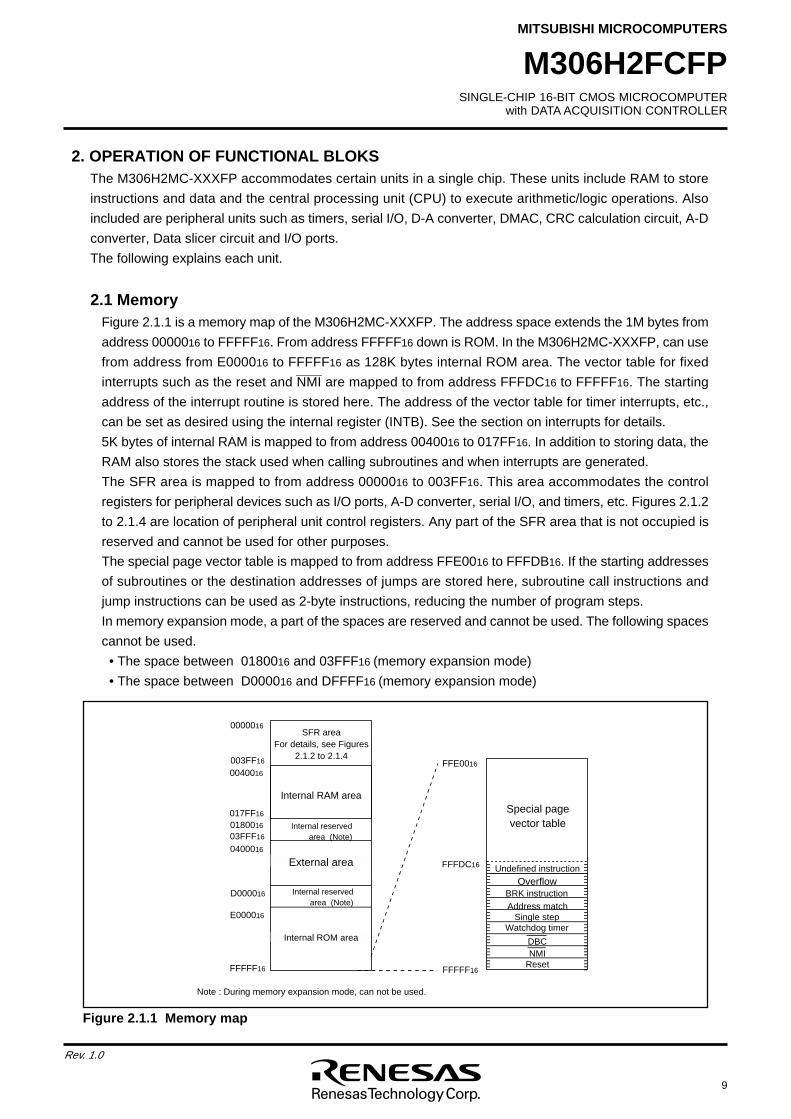
2.1 MemoryFigure 2.1.1 is a memory map of the M306H2MC-XXXFP. The address space extends the 1M bytes from
address 0000016 to FFFFF16. From address FFFFF16 down is ROM. In the M306H2MC-XXXFP, can use
from address from E000016 to FFFFF16 as 128K bytes internal ROM area. The vector table for fixed_______
interrupts such as the reset and NMI are mapped to from address FFFDC16 to FFFFF16. The starting
address of the interrupt routine is stored here. The address of the vector table for timer interrupts, etc.,
can be set as desired using the internal register (INTB). See the section on interrupts for details.
5K bytes of internal RAM is mapped to from address 0040016 to 017FF16. In addition to storing data, the
RAM also stores the stack used when calling subroutines and when interrupts are generated.
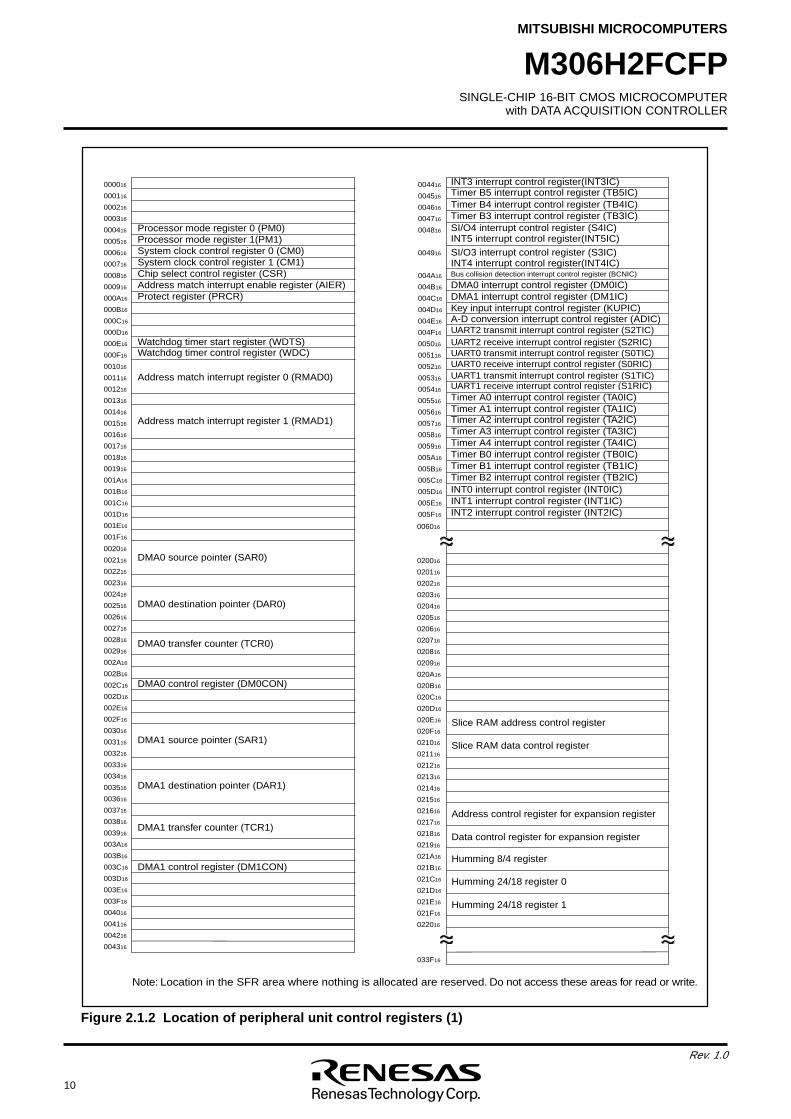
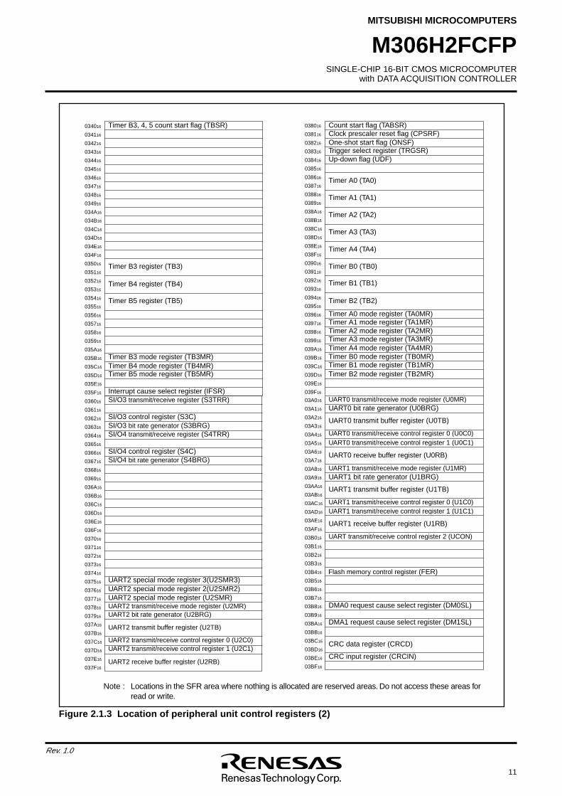
The SFR area is mapped to from address 0000016 to 003FF16. This area accommodates the control
registers for peripheral devices such as I/O ports, A-D converter, serial I/O, and timers, etc. Figures 2.1.2
to 2.1.4 are location of peripheral unit control registers. Any part of the SFR area that is not occupied is
reserved and cannot be used for other purposes.
The special page vector table is mapped to from address FFE0016 to FFFDB16. If the starting addresses
of subroutines or the destination addresses of jumps are stored here, subroutine call instructions and
jump instructions can be used as 2-byte instructions, reducing the number of program steps.
In memory expansion mode, a part of the spaces are reserved and cannot be used. The following spaces
cannot be used.
• The space between 0180016 and 03FFF16 (memory expansion mode)
• The space between D000016 and DFFFF16 (memory expansion mode)
Figure 2.1.1 Memory map
0000016
FFFFF16
0040016
0400016
017FF16
Internal ROM area
SFR areaFor details, see Figures
2.1.2 to 2.1.4
Internal RAM area
Internal reservedarea (Note)
FFE0016
FFFDC16
FFFFF16
Undefined instruction
OverflowBRK instructionAddress match
Single stepWatchdog timer
Reset
Special pagevector table
DBCNMI
0180016 03FFF16
Internal reservedarea (Note)
E000016 D000016
External area
003FF16
Note : During memory expansion mode, can not be used.
10
Rev. 1.0
SINGLE-CHIP 16-BIT CMOS MICROCOMPUTERwith DATA ACQUISITION CONTROLLER
MITSUBISHI MICROCOMPUTERS
M306H2FCFP
Figure 2.1.2 Location of peripheral unit control registers (1)
Note: Location in the SFR area where nothing is allocated are reserved. Do not access these areas for read or write.
000016
000116
000216
000316
000416
000516
000616
000716
000816
000916
000A16
000B16
000C16
000D16
000E16
000F16
001016
001116
001216
001316
001416
001516
001616
001716
001816
001916
001A16
001B16
001C16
001D16
001E16
001F16
002016
002116
002216
002316
002416
002516
002616
002716
002816
002916
002A16
002B16
002C16
002D16
002E16
002F16
003016
003116
003216
003316
003416
003516
003616
003716
003816
003916
003A16
003B16
003C16
003D16
003E16
003F16
004016
004116
004216
004316
004416
004516
004616
004716
004816
004916
004A16
004B16
004C16
004D16
004E16
004F16
005016
005116
005216
005316
005416
005516
005616
005716
005816
005916
005A16
005B16
005C16
005D16
005E16
005F16
006016
020016
020116
020216
020316
020416
020516
020616
020716
020816
020916
020A16
020B16
020C16
020D16
020E16
020F16
021016
021116
021216
021316
021416
021516
021616
021716
021816
021916
021A16
021B16
021C16
021D16
021E16
021F16
022016
033F16
DMA0 control register (DM0CON)
DMA0 source pointer (SAR0)
DMA0 transfer counter (TCR0)
DMA1 control register (DM1CON)
DMA1 source pointer (SAR1)
DMA1 transfer counter (TCR1)
DMA1 destination pointer (DAR1)
Watchdog timer start register (WDTS)Watchdog timer control register (WDC)
Processor mode register 0 (PM0)
Address match interrupt register 0 (RMAD0)
Address match interrupt register 1 (RMAD1)
Chip select control register (CSR)
System clock control register 0 (CM0)System clock control register 1 (CM1)
Address match interrupt enable register (AIER)Protect register (PRCR)
Processor mode register 1(PM1)
DMA0 destination pointer (DAR0)
Timer A1 interrupt control register (TA1IC)
UART0 transmit interrupt control register (S0TIC)
Timer A0 interrupt control register (TA0IC)
Timer A2 interrupt control register (TA2IC)
UART0 receive interrupt control register (S0RIC)UART1 transmit interrupt control register (S1TIC)UART1 receive interrupt control register (S1RIC)
DMA1 interrupt control register (DM1IC)DMA0 interrupt control register (DM0IC)
Key input interrupt control register (KUPIC)A-D conversion interrupt control register (ADIC)
Bus collision detection interrupt control register (BCNIC)
UART2 transmit interrupt control register (S2TIC)UART2 receive interrupt control register (S2RIC)
INT1 interrupt control register (INT1IC)
Timer B0 interrupt control register (TB0IC)
Timer B2 interrupt control register (TB2IC)
Timer A3 interrupt control register (TA3IC)
INT2 interrupt control register (INT2IC)
INT0 interrupt control register (INT0IC)
Timer B1 interrupt control register (TB1IC)
Timer A4 interrupt control register (TA4IC)
INT3 interrupt control register(INT3IC)Timer B5 interrupt control register (TB5IC)Timer B4 interrupt control register (TB4IC)Timer B3 interrupt control register (TB3IC)SI/O4 interrupt control register (S4IC)INT5 interrupt control register(INT5IC)SI/O3 interrupt control register (S3IC)INT4 interrupt control register(INT4IC)
Slice RAM address control register
Slice RAM data control register
Address control register for expansion register
Data control register for expansion register
Humming 8/4 register
Humming 24/18 register 0
Humming 24/18 register 1
SINGLE-CHIP 16-BIT CMOS MICROCOMPUTERwith DATA ACQUISITION CONTROLLER
MITSUBISHI MICROCOMPUTERS
11
Rev. 1.0
M306H2FCFP
Figure 2.1.3 Location of peripheral unit control registers (2)
038016
038116
038216
038316
038416
038516
038616
038716
038816
038916
038A16
038B16
038C16
038D16
038E16
038F16
039016
039116
039216
039316
039416
039516
039616
039716
039816
039916
039A16
039B16
039C16
039D16
039E16
039F16
03A016
03A116
03A216
03A316
03A416
03A516
03A616
03A716
03A816
03A916
03AA16
03AB16
03AC16
03AD16
03AE16
03AF16
03B016
03B116
03B216
03B316
03B416
03B516
03B616
03B716
03B816
03B916
03BA16
03BB16
03BC16
03BD16
03BE16
03BF16
034016
034116
034216
034316
034416
034516
034616
034716
034816
034916
034A16
034B16
034C16
034D16
034E16
034F16
035016
035116
035216
035316
035416
035516
035616
035716
035816
035916
035A16
035B16
035C16
035D16
035E16
035F16
036016
036116
036216
036316
036416
036516
036616
036716
036816
036916
036A16
036B16
036C16
036D16
036E16
036F16
037016
037116
037216
037316
037416
037516
037616
037716
037816
037916
037A16
037B16
037C16
037D16
037E16
037F16
Timer B3 register (TB3)
Timer B4 register (TB4)
Timer B5 register (TB5)
Timer B3, 4, 5 count start flag (TBSR)
Timer B3 mode register (TB3MR)Timer B4 mode register (TB4MR)Timer B5 mode register (TB5MR)
Interrupt cause select register (IFSR)
Timer A0 (TA0)
Timer A1 (TA1)
Timer A2 (TA2)
Timer B0 (TB0)
Timer B1 (TB1)
Timer B2 (TB2)
Count start flag (TABSR)
One-shot start flag (ONSF)
Timer A0 mode register (TA0MR)Timer A1 mode register (TA1MR)Timer A2 mode register (TA2MR)
Timer B0 mode register (TB0MR)Timer B1 mode register (TB1MR)Timer B2 mode register (TB2MR)
Up-down flag (UDF)
Timer A3 (TA3)
Timer A4 (TA4)
Timer A3 mode register (TA3MR)Timer A4 mode register (TA4MR)
Trigger select register (TRGSR)
Clock prescaler reset flag (CPSRF)
UART0 transmit/receive mode register (U0MR)
UART0 transmit buffer register (U0TB)
UART0 receive buffer register (U0RB)
UART1 transmit/receive mode register (U1MR)
UART1 transmit buffer register (U1TB)
UART1 receive buffer register (U1RB)
UART0 bit rate generator (U0BRG)
UART0 transmit/receive control register 0 (U0C0)UART0 transmit/receive control register 1 (U0C1)
UART1 bit rate generator (U1BRG)
UART1 transmit/receive control register 0 (U1C0)UART1 transmit/receive control register 1 (U1C1)
DMA1 request cause select register (DM1SL)
DMA0 request cause select register (DM0SL)
CRC data register (CRCD)
CRC input register (CRCIN)
SI/O3 transmit/receive register (S3TRR)
SI/O4 transmit/receive register (S4TRR)
SI/O3 control register (S3C)SI/O3 bit rate generator (S3BRG)
SI/O4 bit rate generator (S4BRG)SI/O4 control register (S4C)
UART2 special mode register (U2SMR)
UART2 receive buffer register (U2RB)
UART2 transmit buffer register (U2TB)
UART2 transmit/receive control register 0 (U2C0)
UART2 transmit/receive mode register (U2MR)
UART2 transmit/receive control register 1 (U2C1)
UART2 bit rate generator (U2BRG)
UART transmit/receive control register 2 (UCON)
UART2 special mode register 2(U2SMR2)UART2 special mode register 3(U2SMR3)
Flash memory control register (FER)
Note : Locations in the SFR area where nothing is allocated are reserved areas. Do not access these areas forread or write.
12
Rev. 1.0
SINGLE-CHIP 16-BIT CMOS MICROCOMPUTERwith DATA ACQUISITION CONTROLLER
MITSUBISHI MICROCOMPUTERS
M306H2FCFP
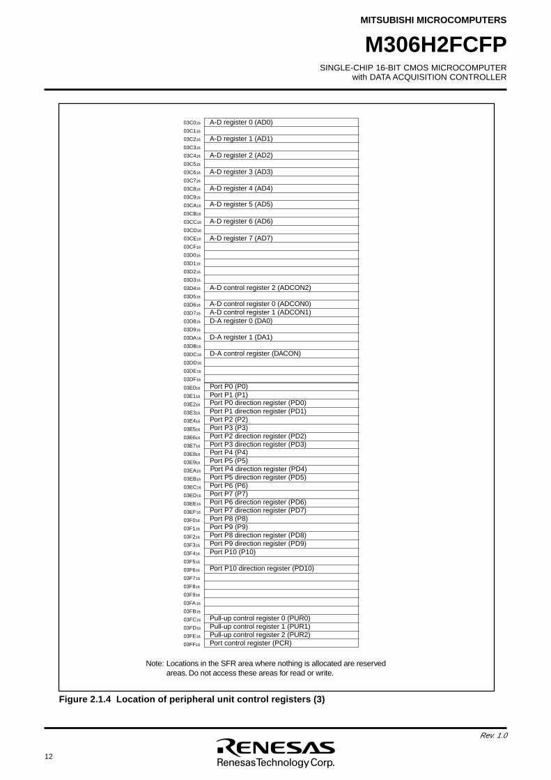
Figure 2.1.4 Location of peripheral unit control registers (3)
03C016
03C116
03C216
03C316
03C416
03C516
03C616
03C716
03C816
03C916
03CA16
03CB16
03CC16
03CD16
03CE16
03CF16
03D016
03D116
03D216
03D316
03D416
03D516
03D616
03D716
03D816
03D916
03DA16
03DB16
03DC16
03DD16
03DE16
03DF16
03E016
03E116
03E216
03E316
03E416
03E516
03E616
03E716
03E816
03E916
03EA16
03EB16
03EC16
03ED16
03EE16
03EF16
03F016
03F116
03F216
03F316
03F416
03F516
03F616
03F716
03F816
03F916
03FA16
03FB16
03FC16
03FD16
03FE16
03FF16
A-D register 7 (AD7)
A-D register 0 (AD0)
A-D register 1 (AD1)
A-D register 2 (AD2)
A-D register 3 (AD3)
A-D register 4 (AD4)
A-D register 5 (AD5)
A-D register 6 (AD6)
Port P0 (P0)
Port P0 direction register (PD0)Port P1 (P1)
Port P1 direction register (PD1)Port P2 (P2)
Port P2 direction register (PD2)Port P3 (P3)
Port P3 direction register (PD3)Port P4 (P4)
Port P4 direction register (PD4)Port P5 (P5)
Port P5 direction register (PD5)Port P6 (P6)
Port P6 direction register (PD6)Port P7 (P7)
Port P7 direction register (PD7)Port P8 (P8)
Port P8 direction register (PD8)Port P9 (P9)
Port P9 direction register (PD9)Port P10 (P10)
Port P10 direction register (PD10)
Pull-up control register 0 (PUR0)Pull-up control register 1 (PUR1)Pull-up control register 2 (PUR2)
A-D control register 0 (ADCON0)A-D control register 1 (ADCON1)D-A register 0 (DA0)
D-A register 1 (DA1)
D-A control register (DACON)
A-D control register 2 (ADCON2)
Port control register (PCR)
Note: Locations in the SFR area where nothing is allocated are reservedareas. Do not access these areas for read or write.
SINGLE-CHIP 16-BIT CMOS MICROCOMPUTERwith DATA ACQUISITION CONTROLLER
MITSUBISHI MICROCOMPUTERS
13
Rev. 1.0
M306H2FCFP
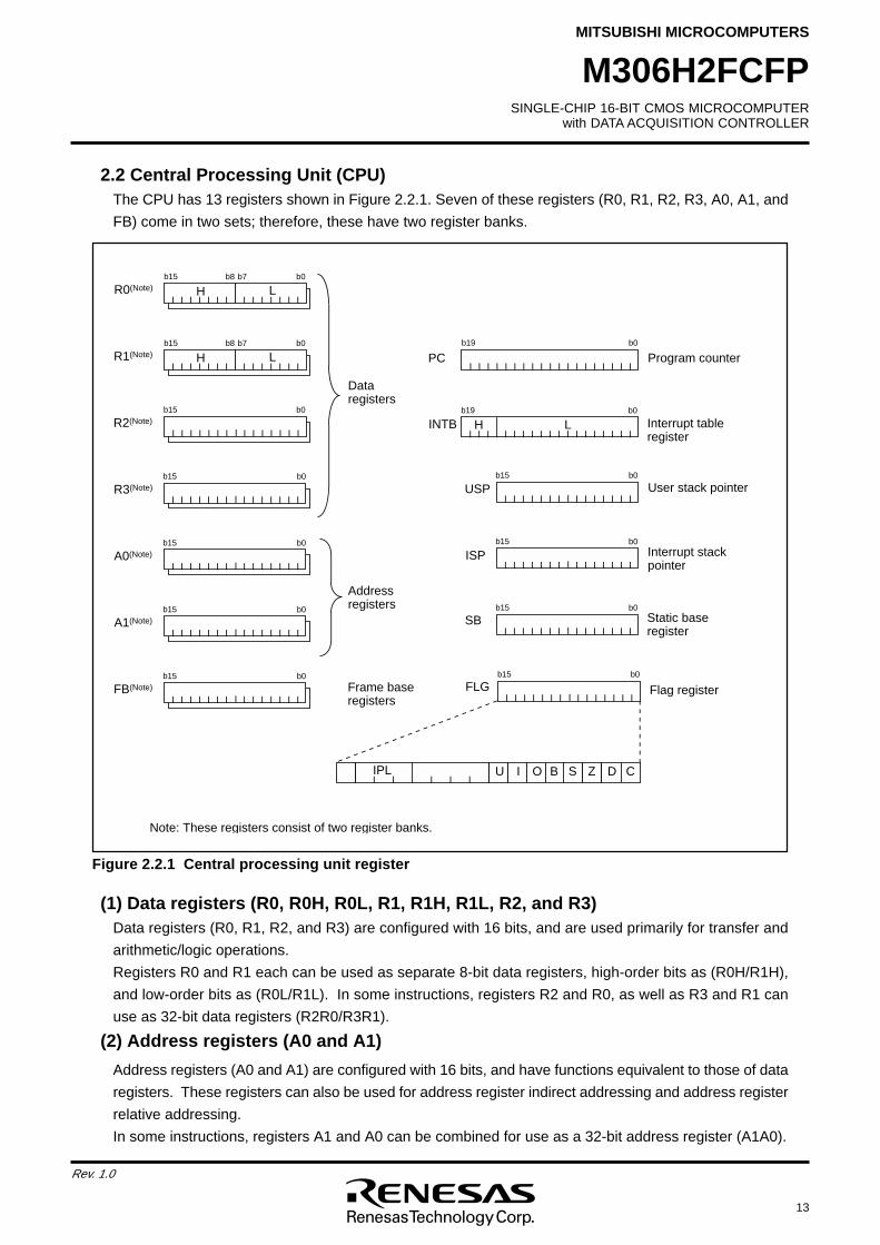
2.2 Central Processing Unit (CPU)The CPU has 13 registers shown in Figure 2.2.1. Seven of these registers (R0, R1, R2, R3, A0, A1, and
FB) come in two sets; therefore, these have two register banks.
AAAAAAAAAAAAAAH L
b15 b8 b7 b0
R0(Note)
AAAAAAAH L
b15 b8 b7 b0
R1(Note)
R2(Note)
AAAAAAAAAAAAAA
b15 b0
R3(Note)
AAAAAAAb15 b0
A0(Note)
AAAAAAAAAAAAAA
b15 b0
A1(Note)
AAAAAAAAAAAAAA
b15 b0
FB(Note)
AAAAAAA
b15 b0
Data registers
Address registers
Frame base registers
b15 b0
b15 b0
b15 b0
b15 b0
b0 b19
b0 b19
H L
Program counter
Interrupt table register
User stack pointer
Interrupt stack pointer
Static base register
Flag register
PC
INTB
USP
ISP
SB
FLG
Note: These registers consist of two register banks.
AAAAAAAAAAAA
AAAAAAAAAAAAAAAA
AAAAAAAAAAAAAA
CDZSBOIUIPL
Figure 2.2.1 Central processing unit register
(1) Data registers (R0, R0H, R0L, R1, R1H, R1L, R2, and R3)Data registers (R0, R1, R2, and R3) are configured with 16 bits, and are used primarily for transfer and
arithmetic/logic operations.
Registers R0 and R1 each can be used as separate 8-bit data registers, high-order bits as (R0H/R1H),
and low-order bits as (R0L/R1L). In some instructions, registers R2 and R0, as well as R3 and R1 can
use as 32-bit data registers (R2R0/R3R1).
(2) Address registers (A0 and A1)
Address registers (A0 and A1) are configured with 16 bits, and have functions equivalent to those of data
registers. These registers can also be used for address register indirect addressing and address register
relative addressing.
In some instructions, registers A1 and A0 can be combined for use as a 32-bit address register (A1A0).
14
Rev. 1.0
SINGLE-CHIP 16-BIT CMOS MICROCOMPUTERwith DATA ACQUISITION CONTROLLER
MITSUBISHI MICROCOMPUTERS
M306H2FCFP
(3) Frame base register (FB)Frame base register (FB) is configured with 16 bits, and is used for FB relative addressing.
(4) Program counter (PC)
Program counter (PC) is configured with 20 bits, indicating the address of an instruction to be executed.
(5) Interrupt table register (INTB)
Interrupt table register (INTB) is configured with 20 bits, indicating the start address of an interrupt vector
table.
(6) Stack pointer (USP/ISP)Stack pointer comes in two types: user stack pointer (USP) and interrupt stack pointer (ISP), each config-
ured with 16 bits.
Your desired type of stack pointer (USP or ISP) can be selected by a stack pointer select flag (U flag).
This flag is located at the position of bit 7 in the flag register (FLG).
(7) Static base register (SB)Static base register (SB) is configured with 16 bits, and is used for SB relative addressing.
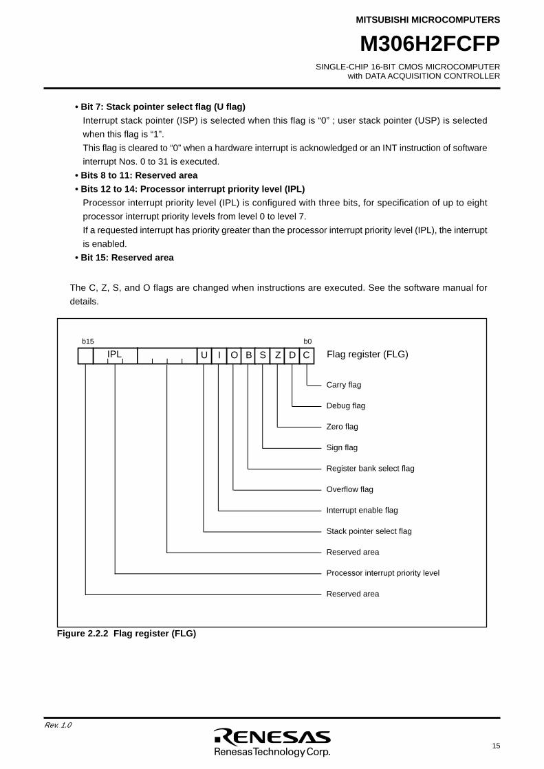
(8) Flag register (FLG)
Flag register (FLG) is configured with 11 bits, each bit is used as a flag. Figure 2.2.2 shows the flag
.register (FLG). The following explains the function of each flag:
• Bit 0: Carry flag (C flag)
This flag retains a carry, borrow, or shift-out bit that has occurred in the arithmetic/logic unit.
• Bit 1: Debug flag (D flag)
This flag enables a single-step interrupt.
When this flag is “1”, a single-step interrupt is generated after instruction execution. This flag is
cleared to “0” when the interrupt is acknowledged.
• Bit 2: Zero flag (Z flag)
This flag is set to “1” when an arithmetic operation resulted in 0; otherwise, cleared to “0”.
• Bit 3: Sign flag (S flag)
This flag is set to “1” when an arithmetic operation resulted in a negative value; otherwise, cleared to “0”.
• Bit 4: Register bank select flag (B flag)
This flag chooses a register bank. Register bank 0 is selected when this flag is “0” ; register bank 1 is
selected when this flag is “1”.
• Bit 5: Overflow flag (O flag)
This flag is set to “1” when an arithmetic operation resulted in overflow; otherwise, cleared to “0”.
• Bit 6: Interrupt enable flag (I flag)
This flag enables a maskable interrupt.
An interrupt is disabled when this flag is “0”, and is enabled when this flag is “1”. This flag is cleared to
“0” when the interrupt is acknowledged.
SINGLE-CHIP 16-BIT CMOS MICROCOMPUTERwith DATA ACQUISITION CONTROLLER
MITSUBISHI MICROCOMPUTERS
15
Rev. 1.0
M306H2FCFP
Figure 2.2.2 Flag register (FLG)
Carry flag
Debug flag
Zero flag
Sign flag
Register bank select flag
Overflow flag
Interrupt enable flag
Stack pointer select flag
Reserved area
Processor interrupt priority level
Reserved area
Flag register (FLG)AAAA
AAAAAA
AAAA
AAAAAAAAAAAAAA
AAAA
AAAAAAAAAAAAAA
CDZSBOIUIPLb0b15
• Bit 7: Stack pointer select flag (U flag)
Interrupt stack pointer (ISP) is selected when this flag is “0” ; user stack pointer (USP) is selected
when this flag is “1”.
This flag is cleared to “0” when a hardware interrupt is acknowledged or an INT instruction of software
interrupt Nos. 0 to 31 is executed.
• Bits 8 to 11: Reserved area
• Bits 12 to 14: Processor interrupt priority level (IPL)
Processor interrupt priority level (IPL) is configured with three bits, for specification of up to eight
processor interrupt priority levels from level 0 to level 7.
If a requested interrupt has priority greater than the processor interrupt priority level (IPL), the interrupt
is enabled.
• Bit 15: Reserved area
The C, Z, S, and O flags are changed when instructions are executed. See the software manual for
details.
16
Rev. 1.0
SINGLE-CHIP 16-BIT CMOS MICROCOMPUTERwith DATA ACQUISITION CONTROLLER
MITSUBISHI MICROCOMPUTERS
M306H2FCFP
RESET VCC
0.95V
RESET
VCC
0V
0V
5V
5V
4.75V
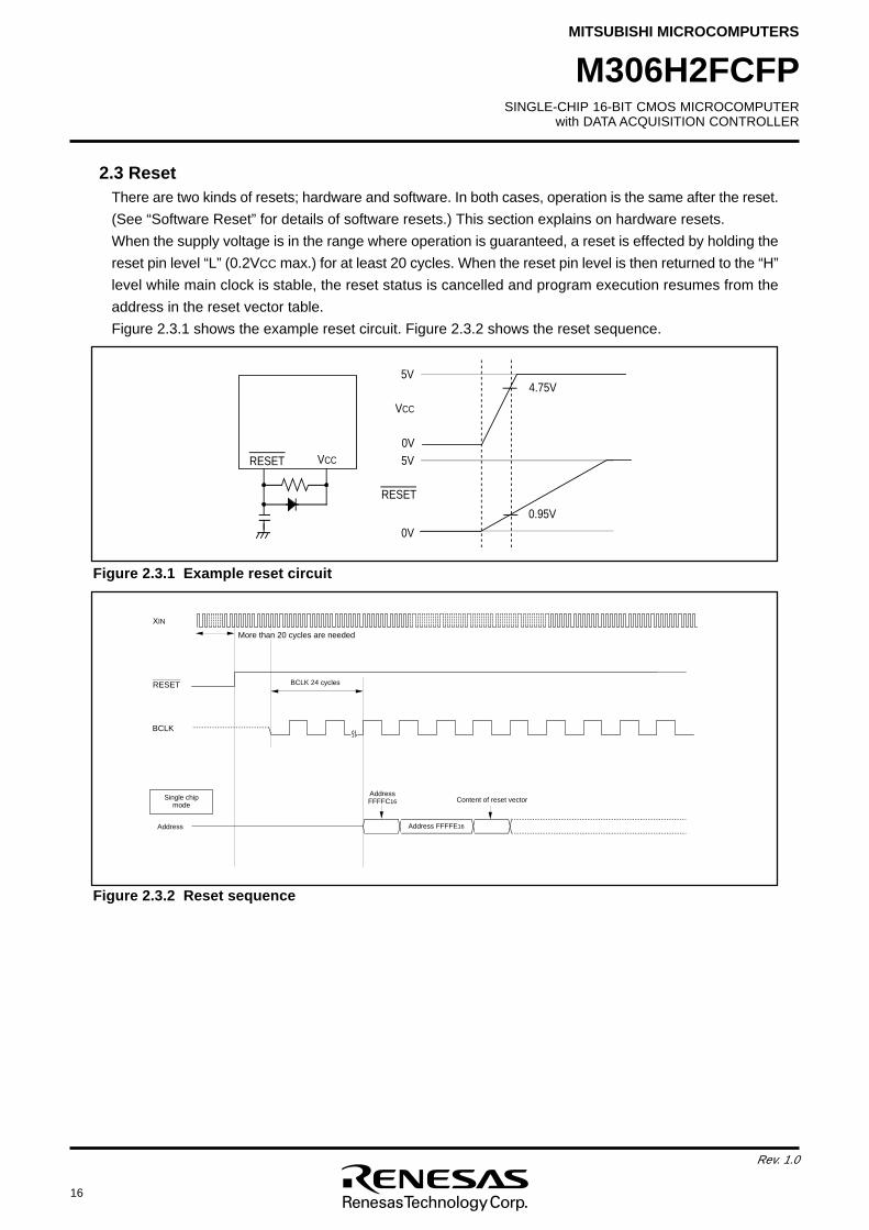
Figure 2.3.1 Example reset circuit
2.3 ResetThere are two kinds of resets; hardware and software. In both cases, operation is the same after the reset.
(See “Software Reset” for details of software resets.) This section explains on hardware resets.
When the supply voltage is in the range where operation is guaranteed, a reset is effected by holding the
reset pin level “L” (0.2VCC max.) for at least 20 cycles. When the reset pin level is then returned to the “H”
level while main clock is stable, the reset status is cancelled and program execution resumes from the
address in the reset vector table.
Figure 2.3.1 shows the example reset circuit. Figure 2.3.2 shows the reset sequence.
Figure 2.3.2 Reset sequence
BCLK
XIN
RESET
More than 20 cycles are needed
BCLK 24 cycles
Single chip mode
Address
Address FFFFC16
Address FFFFE16
Content of reset vector
SINGLE-CHIP 16-BIT CMOS MICROCOMPUTERwith DATA ACQUISITION CONTROLLER
MITSUBISHI MICROCOMPUTERS
17
Rev. 1.0
M306H2FCFP
____________
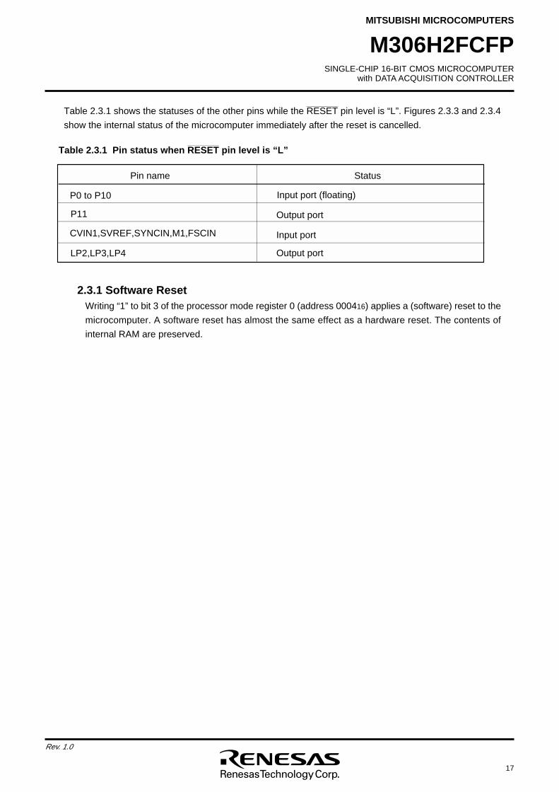
Table 2.3.1 shows the statuses of the other pins while the RESET pin level is “L”. Figures 2.3.3 and 2.3.4
show the internal status of the microcomputer immediately after the reset is cancelled.
2.3.1 Software ResetWriting “1” to bit 3 of the processor mode register 0 (address 000416) applies a (software) reset to the
microcomputer. A software reset has almost the same effect as a hardware reset. The contents of
internal RAM are preserved.
____________
Table 2.3.1 Pin status when RESET pin level is “L”
P0 to P10
P11
CVIN1,SVREF,SYNCIN,M1,FSCIN
LP2,LP3,LP4
Pin name Status
Input port (floating)
Output port
Input port
Output port
18
Rev. 1.0
SINGLE-CHIP 16-BIT CMOS MICROCOMPUTERwith DATA ACQUISITION CONTROLLER
MITSUBISHI MICROCOMPUTERS
M306H2FCFP
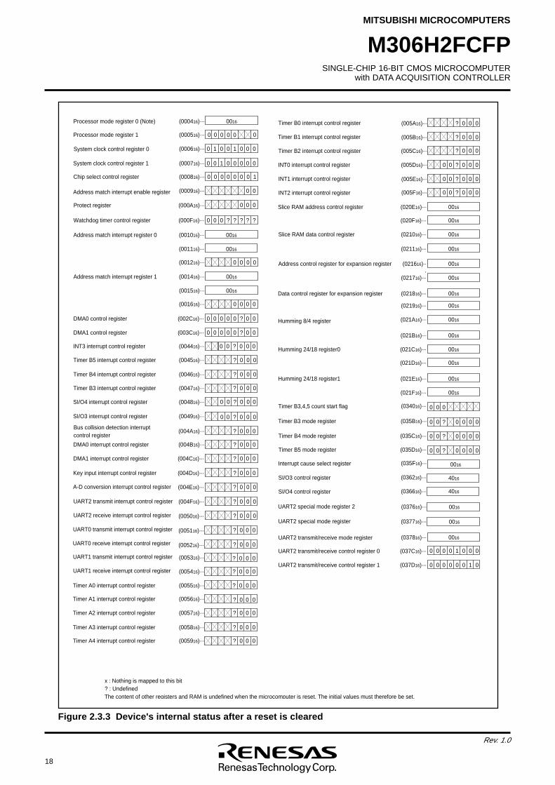
Figure 2.3.3 Device's internal status after a reset is cleared
x : Nothing is mapped to this bit? : UndefinedThe content of other registers and RAM is undefined when the microcomputer is reset. The initial values must therefore be set.
(000416)···Processor mode register 0 (Note) 0016
(000516)···Processor mode register 1 000
(000616)···System clock control register 0 10 00 01 00
(000716)···System clock control register 1 00 01 00 00
(000816)···Chip select control register 00 00 00 10
(000916)···Address match interrupt enable register 00
Protect register (000A16)··· 0 00
00 0
(000F16)···Watchdog timer control register 00 ?0 ? ? ? ?
(001516)···
(001616)··· 0
(001416)···Address match interrupt register 1 0016
0016
0 0 0
(002C16)···DMA0 control register 0 0 0 0 0 ? 0 0
(003C16)···DMA1 control register 0 0 0 0 0 ? 0 0
(004B16)···DMA0 interrupt control register ? 0 0 0
(004C16)···DMA1 interrupt control register ? 0 0 0
(004D16)···Key input interrupt control register ? 0 0 0
(004A16)···Bus collision detection interrupt control register
0 0 0?
(001016)···Address match interrupt register 0
(001116)···
(001216)··· 0
0016
0016
0 0 0
(004416)···INT3 interrupt control register 0 0 ? 0 0 0
(004516)···Timer B5 interrupt control register ? 0 0 0
(004616)···Timer B4 interrupt control register ? 0 0 0
(004716)···Timer B3 interrupt control register ? 0 0 0
(004816)···SI/O4 interrupt control register 0 0 ? 0 0 0
(004916)···SI/O3 interrupt control register 0 0 ? 0 0 0
A-D conversion interrupt control register
UART2 transmit interrupt control register
UART2 receive interrupt control register
(004E16)··· ? 0 0 0
(004F16)···
(005016)···
? 0 0 0
? 0 0 0
UART0 transmit interrupt control register
UART0 receive interrupt control register
(005116)···
(005216)···
? 0 0 0
? 0 0 0
UART1 transmit interrupt control register
UART1 receive interrupt control register
Timer A0 interrupt control register
Timer A1 interrupt control register
Timer A2 interrupt control register
Timer A3 interrupt control register
Timer A4 interrupt control register
(005316)···
(005416)···
(005516)···
(005616)···
(005716)···
(005816)···
(005916)···
? 0 0 0
? 0 0 0
? 0 0 0
? 0 0 0
? 0 0 0
? 0 0 0
? 0 0 0
Timer B0 interrupt control register
Timer B1 interrupt control register
Timer B2 interrupt control register
INT0 interrupt control register
INT1 interrupt control register
INT2 interrupt control register
(005A16)···
(005B16)···
(005C16)···
(005D16)···
(005E16)···
(005F16)···
? 0 0 0
? 0 0 0
? 0 0 0
? 0 0 00 0
? 0 0 00 0
? 0 0 00 0
Slice RAM address control register
Slice RAM data control register
(020E16)··· 0016
(020F16)··· 0016
(021016)··· 0016
(021116)··· 0016
Timer B3,4,5 count start flag
Timer B3 mode register
Timer B4 mode register
Timer B5 mode register
Interrupt cause select register
UART2 transmit/receive control register 1
UART2 transmit/receive control register 0
UART2 transmit/receive mode register
SI/O4 control register
UART2 special mode register
SI/O3 control register
UART2 special mode register 2
Address control register for expansion register
Data control register for expansion register
Humming 8/4 register
Humming 24/18 register0
0016
(037816)···
(037D16)···
(037C16)···
0016
0 0 00 0 0 0 1
0 1 00 0 0 0 0
(034016)···
(035B16)···
(035C16)···
(035D16)···
(035F16)···
(036616)···
(037716)···
(036216)···
0 0 ? 0 0 0 0
0 0 ? 0 0 0 0
0 0 ? 0 0 0 0
4016
0016
4016
0 0 0
(037616)··· 0016
(021616)···
0016
(021716)··· 0016
(021816)··· 0016
(021916)··· 0016
(021A16)··· 0016
(021B16)··· 0016
(021C16)··· 0016
(021D16)··· 0016
(021E16)··· 0016
(021F16)··· 0016
Humming 24/18 register1
SINGLE-CHIP 16-BIT CMOS MICROCOMPUTERwith DATA ACQUISITION CONTROLLER
MITSUBISHI MICROCOMPUTERS
19
Rev. 1.0
M306H2FCFP
(038316)···Trigger select flag
(038416)···Up-down flag
(039616)···Timer A0 mode register
(039716)···Timer A1 mode register
(039816)···Timer A2 mode register
(039B16)···Timer B0 mode register
(039C16)···Timer B1 mode register
(039D16)···Timer B2 mode register
(039916)···Timer A3 mode register
(039A16)···Timer A4 mode register
(038216)···One-shot start flag
0016
0016
0
0016
0016
0016
0016
0016
0 ? 0 0 0 0
0 0 ? 0 0 0 0
0 0 ? 0 0 0 0
(03AC16)···UART1 transmit/receive control register 0
(03AD16)···UART1 transmit/receive control register 1
(03B016)···UART transmit/receive control register 2
(03B816)···DMA0 cause select register
(03BA16)···DMA1 cause select register
0
(03A016)···UART0 transmit/receive mode register
(03A416)···UART0 transmit/receive control register 0
(03A516)···UART0 transmit/receive control register 1
0016
0 0 0 1 0 0 0
0 0 0 0 0 1 0
0
0
(03A816)···UART1 transmit/receive mode register 0016
0 0 0 1 0 0 0
0 0 0 0 0 1 0
0
0
0 0 0 0 00
0016
0016
(03D416)···A-D control register 2
(03D616)···A-D control register 0
(03D716)···A-D control register 1
0
0 0 0 0 ? ? ?0
0016
00 00 0 0 0
Count start flag (038016)··· 0016
0(038116)···Clock prescaler reset flag
x : Nothing is mapped to this bit? : Undefined
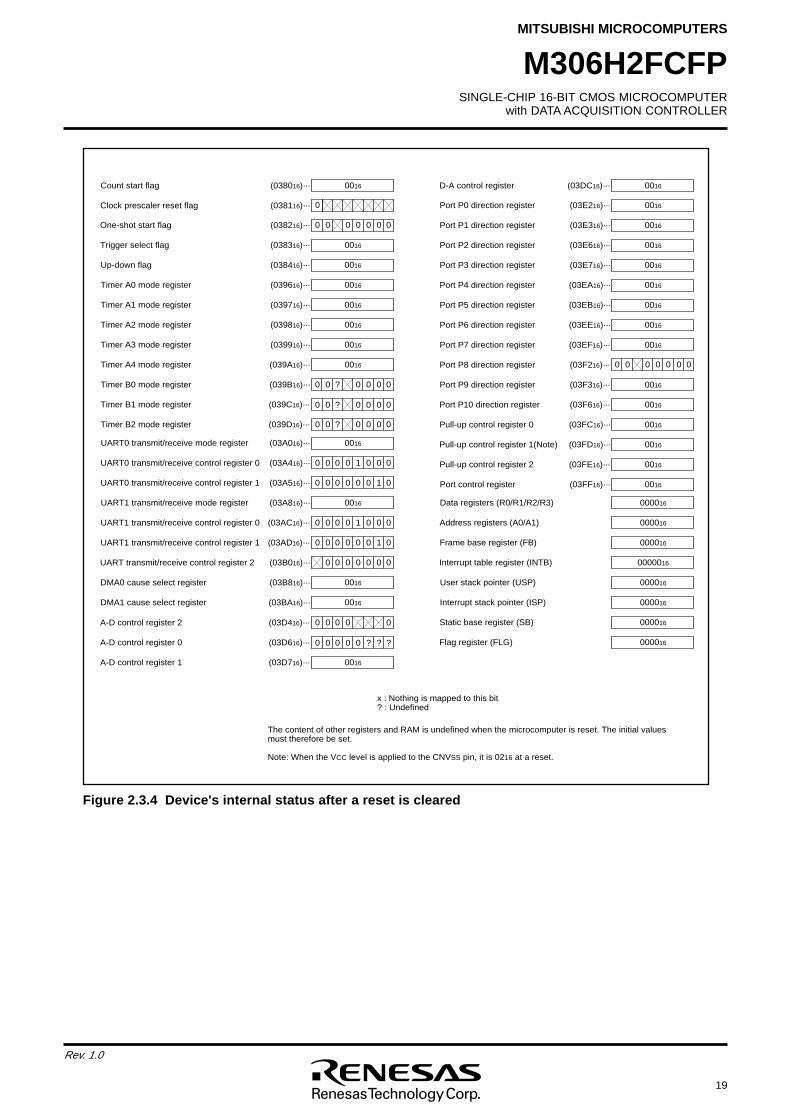
The content of other registers and RAM is undefined when the microcomputer is reset. The initial values must therefore be set.
Note: When the VCC level is applied to the CNVSS pin, it is 0216 at a reset.
(03E216)···Port P0 direction register
(03E316)···Port P1 direction register
(03E616)···Port P2 direction register
(03E716)···Port P3 direction register
(03EA16)···Port P4 direction register
(03EB16)···Port P5 direction register
(03EE16)···Port P6 direction register
(03EF16)···Port P7 direction register
(03F216)···Port P8 direction register
(03F316)···Port P9 direction register
(03F616)···Port P10 direction register
(03FC16)···Pull-up control register 0
(03FD16)···Pull-up control register 1(Note)
(03FE16)···Pull-up control register 2
Port control register
0016
0016
0016
0016
0016
0016
0016
0016
0016
0016
0016
0016
0016
0016
0 0 000 0 0
(03DC16)···D-A control register 0016
Frame base register (FB)
Address registers (A0/A1)
Interrupt table register (INTB)
User stack pointer (USP)
Interrupt stack pointer (ISP)
Static base register (SB)
Flag register (FLG)
000016
000016
0000016
000016
000016
000016
000016
Data registers (R0/R1/R2/R3) 000016
(03FF16)···
0 0 0 0
Figure 2.3.4 Device's internal status after a reset is cleared
20
Rev. 1.0
SINGLE-CHIP 16-BIT CMOS MICROCOMPUTERwith DATA ACQUISITION CONTROLLER
MITSUBISHI MICROCOMPUTERS
M306H2FCFP
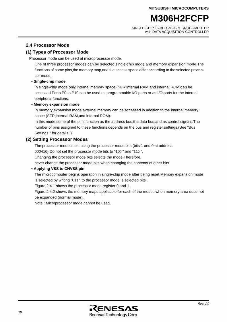
2.4 Processor Mode
(1) Types of Processor ModeProcessor mode can be used at microprocessor mode.
One of three processor modes can be selected:single-chip mode and memory expansion mode.The
functions of some pins,the memory map,and the access space differ according to the selected proces-
sor mode.
• Single-chip mode
In single-chip mode,only internal memory space (SFR,internal RAM,and internal ROM)can be
accessed.Ports P0 to P10 can be used as programmable I/O ports or as I/O ports for the internal
peripheral functions.
• Memory expansion mode
In memory expansion mode,external memory can be accessed in addition to the internal memory
space (SFR,internal RAM,and internal ROM).
In this mode,some of the pins function as the address bus,the data bus,and as control signals.The
number of pins assigned to these functions depends on the bus and register settings.(See "Bus
Settings " for details..)
(2) Setting Processor ModesThe processor mode is set using the processor mode bits (bits 1 and 0 at address
000416).Do not set the processor mode bits to "102 " and "112 ".
Changing the processor mode bits selects the mode.Therefore,
never change the processor mode bits when changing the contents of other bits.
• Applying VSS to CNVSS pin
The microcomputer begins operation in single-chip mode after being reset.Memory expansion mode
is selected by writing "012 " to the processor mode is selected bits..
Figure 2.4.1 shows the processor mode register 0 and 1.
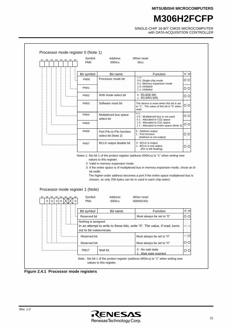
Figure 2.4.2 shows the memory maps applicable for each of the modes when memory area dose not
be expanded (normal mode).
Note : Microprocessor mode cannot be used.
SINGLE-CHIP 16-BIT CMOS MICROCOMPUTERwith DATA ACQUISITION CONTROLLER
MITSUBISHI MICROCOMPUTERS
21
Rev. 1.0
M306H2FCFP
Processor mode register 0 (Note 1)Symbol Address When resetPM0 000416 0016
Bit name FunctionBit symbol WR
b7 b6 b5 b4 b3 b2 b1 b0
0 0: Single-chip mode0 1: Memory expansion mode1 0: Inhibited1 1: Inhibited
b1 b0
PM03
PM01
PM00 Processor mode bit
PM02 R/W mode select bit 0 : RD,BHE,WR1 : RD,WRH,WRL
Software reset bit The device is reset when this bit is set to “1”. The value of this bit is “0” when read.
PM040 0 : Multiplexed bus is not used0 1 : Allocated to CS2 space1 0 : Allocated to CS1 space1 1 : Allocated to entire space (Note 3)
b5 b4 Multiplexed bus space select bit
PM05
PM06
PM07
Port P40 to P43 function select bit (Note 2)
0 : Address output1 : Port function (Address is not output)
BCLK output disable bit 0 : BCLK is output1 : BCLK is not output (Pin is left floating)
Notes 1: Set bit 1 of the protect register (address 000A16) to “1” when writing new values to this register.
2: Valid in memory expansion mode. 3: If the entire space is of multiplexed bus in memory expansion mode, chose an 8- bit width.
The higher-order address becomes a port if the entire space multiplexed bus is chosen, so only 256 bytes can be in used in each chip select.
AAAAAAAAAAAA
AAAAAA
AAAAAA
AAA
AAAAAA
Processor mode register 1 (Note)
Symbol Address When resetPM1 000516 00000XX02
Bit name FunctionBit symbol WR
b7 b6 b5 b4 b3 b2 b1 b0
Nothing is assigned.In an attempt to write to these bits, write “0”. The value, if read, turns out to be indeterminate.
Reserved bit Must always be set to “0”
0
AAA
00
A
Note : Set bit 1 of the protect register (address 000A16) to “1” when writing new values to this register.
PM17 Wait bit 0 : No wait state 1 : Wait state inserted AA
AAAA
Reserved bit Must always be set to “0”
0 0
AA
Reserved bit Must always be set to “0”
AAAA
Figure 2.4.1 Processor mode registers
22
Rev. 1.0
SINGLE-CHIP 16-BIT CMOS MICROCOMPUTERwith DATA ACQUISITION CONTROLLER
MITSUBISHI MICROCOMPUTERS
M306H2FCFP
Figure 2.4.2 Memory maps in each processor mode
SFR area
Internal RAM area
Inhibited
0000016
0040016
017FF16
FFFFF16
External area :Accessing this area allows the user to access a device connected externally to the microcomputer.
0400016
Internal ROM area
D000016
E000016
SFR area
Internal RAM area
External area
Internally reserved area
Internal ROM area
Internally reserved area
Single-chip mode Memory expansion mode
SINGLE-CHIP 16-BIT CMOS MICROCOMPUTERwith DATA ACQUISITION CONTROLLER
MITSUBISHI MICROCOMPUTERS
23
Rev. 1.0
M306H2FCFP
Bus setting Switching factor
Switching external address bus width Bit 6 of processor mode register 0
Switching external data bus width BYTE pin
Switching between separate and multiplex bus Bits 4 and 5 of processor mode register 0
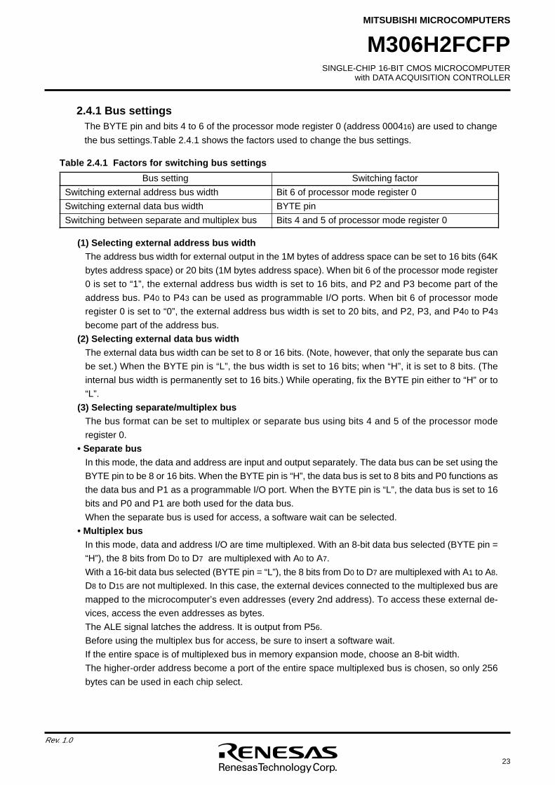
Table 2.4.1 Factors for switching bus settings
(1) Selecting external address bus widthThe address bus width for external output in the 1M bytes of address space can be set to 16 bits (64K
bytes address space) or 20 bits (1M bytes address space). When bit 6 of the processor mode register
0 is set to “1”, the external address bus width is set to 16 bits, and P2 and P3 become part of the
address bus. P40 to P43 can be used as programmable I/O ports. When bit 6 of processor mode
register 0 is set to “0”, the external address bus width is set to 20 bits, and P2, P3, and P40 to P43
become part of the address bus.
(2) Selecting external data bus widthThe external data bus width can be set to 8 or 16 bits. (Note, however, that only the separate bus can
be set.) When the BYTE pin is “L”, the bus width is set to 16 bits; when “H”, it is set to 8 bits. (The
internal bus width is permanently set to 16 bits.) While operating, fix the BYTE pin either to “H” or to
“L”.
(3) Selecting separate/multiplex busThe bus format can be set to multiplex or separate bus using bits 4 and 5 of the processor mode
register 0.
• Separate busIn this mode, the data and address are input and output separately. The data bus can be set using the
BYTE pin to be 8 or 16 bits. When the BYTE pin is “H”, the data bus is set to 8 bits and P0 functions as
the data bus and P1 as a programmable I/O port. When the BYTE pin is “L”, the data bus is set to 16
bits and P0 and P1 are both used for the data bus.
When the separate bus is used for access, a software wait can be selected.
• Multiplex busIn this mode, data and address I/O are time multiplexed. With an 8-bit data bus selected (BYTE pin =
“H”), the 8 bits from D0 to D7 are multiplexed with A0 to A7.
With a 16-bit data bus selected (BYTE pin = “L”), the 8 bits from D0 to D7 are multiplexed with A1 to A8.
D8 to D15 are not multiplexed. In this case, the external devices connected to the multiplexed bus are
mapped to the microcomputer’s even addresses (every 2nd address). To access these external de-
vices, access the even addresses as bytes.
The ALE signal latches the address. It is output from P56.
Before using the multiplex bus for access, be sure to insert a software wait.
If the entire space is of multiplexed bus in memory expansion mode, choose an 8-bit width.
The higher-order address become a port of the entire space multiplexed bus is chosen, so only 256
bytes can be used in each chip select.
2.4.1 Bus settingsThe BYTE pin and bits 4 to 6 of the processor mode register 0 (address 000416) are used to change
the bus settings.Table 2.4.1 shows the factors used to change the bus settings.
24
Rev. 1.0
SINGLE-CHIP 16-BIT CMOS MICROCOMPUTERwith DATA ACQUISITION CONTROLLER
MITSUBISHI MICROCOMPUTERS
M306H2FCFP
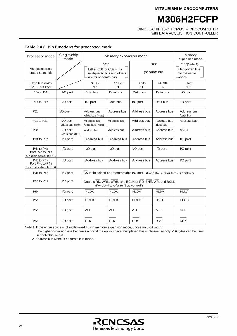
Table 2.4.2 Pin functions for processor mode
P56 I/O port ALE ALE ALE ALE ALE
P57 I/O port RDY RDY RDY RDY RDY
P00 to P07 I/O port Data bus Data bus Data bus Data bus I/O port
(separate bus)
Memory expansion mode
Data bus widthBYTE pin level
Port P40 to P43
function select bit = 0
“00”
8 bits“H”
16 bits “L”
8 bits “H”
16 bits “L”
Note 1: If the entire space is of multiplexed bus in memory expansion mode, chose an 8-bit width. The higher-order address becomes a port if the entire space multiplexed bus is chosen, so only 256 bytes can be used in each chip select. 2: Address bus when in separate bus mode.
Processor mode
Multiplexed busspace select bit
CS (chip select) or programmable I/O port (For details, refer to “Bus control”)
Outputs RD, WRL, WRH, and BCLK or RD, BHE, WR, and BCLK(For details, refer to “Bus control”)
Port P40 to P43
function select bit = 1
P10 to P17 I/O port I/O port Data bus I/O port Data bus I/O port
P21 to P27 I/O port Address bus Address bus Address bus Address bus Address bus/data bus (Note) /data bus (Note) /data bus
P20 I/O port Address bus Address bus Address bus Address bus Address bus/data bus (Note) /data bus
P30 I/O port Address bus Address bus Address bus Address bus A8/D7
/data bus (Note)
P31 to P37 I/O port Address bus Address bus Address bus Address bus I/O port
P40 to P43 I/O port I/O port I/O port I/O port I/O port I/O port
P40 to P43 I/O port Address bus Address bus Address bus Address bus I/O port
P44 to P47 I/O port
P50 to P53 I/O port
P54 I/O port HLDA HLDA HLDA HLDA HLDA
P55 I/O port HOLD HOLD HOLD HOLD HOLD
Either CS1 or CS2 is for multiplexed bus and others are for separate bus
“01”
Single-chip mode
Memory expansion mode
8 bits“H”
Multiplexed bus for the entire space
“11”(Note 1)
SINGLE-CHIP 16-BIT CMOS MICROCOMPUTERwith DATA ACQUISITION CONTROLLER
MITSUBISHI MICROCOMPUTERS
25
Rev. 1.0
M306H2FCFP
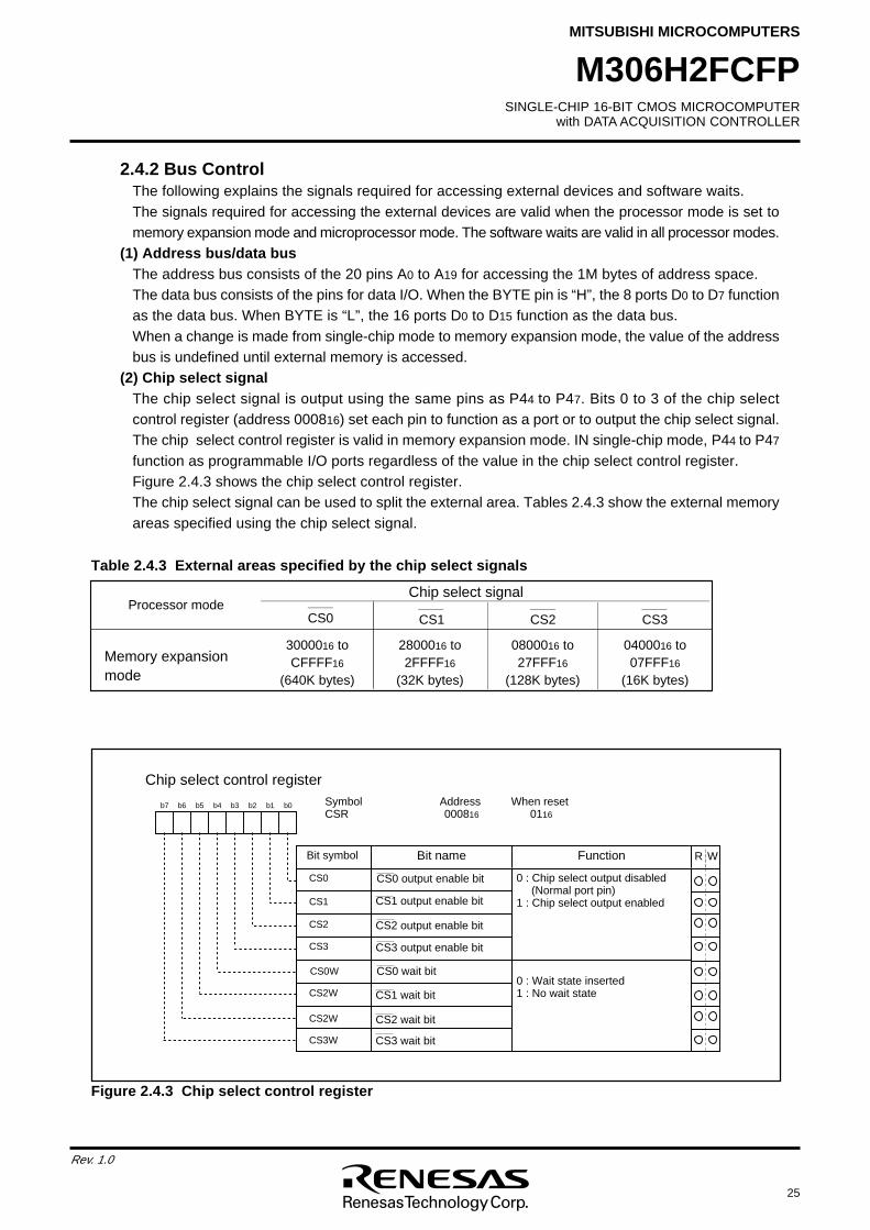
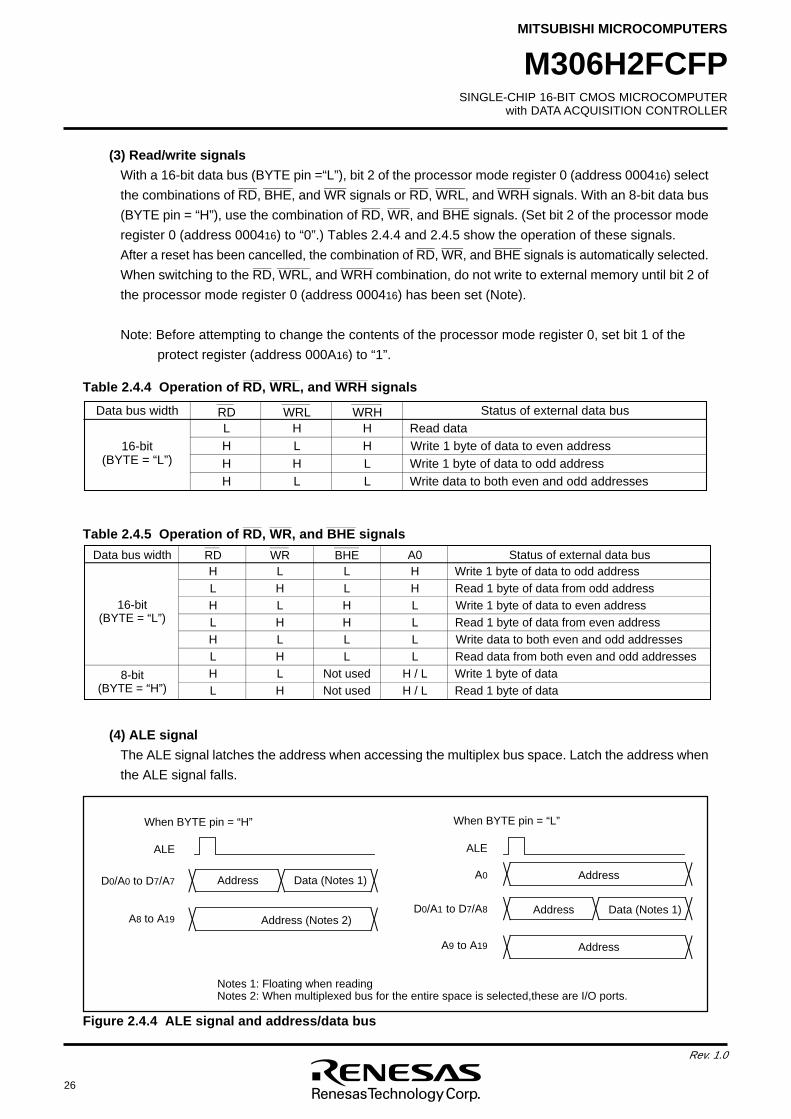
2.4.2 Bus ControlThe following explains the signals required for accessing external devices and software waits.The signals required for accessing the external devices are valid when the processor mode is set tomemory expansion mode and microprocessor mode. The software waits are valid in all processor modes.
(1) Address bus/data busThe address bus consists of the 20 pins A0 to A19 for accessing the 1M bytes of address space.The data bus consists of the pins for data I/O. When the BYTE pin is “H”, the 8 ports D0 to D7 functionas the data bus. When BYTE is “L”, the 16 ports D0 to D15 function as the data bus.When a change is made from single-chip mode to memory expansion mode, the value of the addressbus is undefined until external memory is accessed.
(2) Chip select signalThe chip select signal is output using the same pins as P44 to P47. Bits 0 to 3 of the chip selectcontrol register (address 000816) set each pin to function as a port or to output the chip select signal.The chip select control register is valid in memory expansion mode. IN single-chip mode, P44 to P47
function as programmable I/O ports regardless of the value in the chip select control register.Figure 2.4.3 shows the chip select control register.The chip select signal can be used to split the external area. Tables 2.4.3 show the external memoryareas specified using the chip select signal.
Figure 2.4.3 Chip select control register
Processor modeChip select signal
CS0
Memory expansion mode
CS1
2800016 to 2FFFF16
(32K bytes)
3000016 to CFFFF16
(640K bytes)
CS3
0400016 to 07FFF16
(16K bytes)
CS2
0800016 to 27FFF16
(128K bytes)
Table 2.4.3 External areas specified by the chip select signals
WF
u
n
c
t
i
o
nBit symbol Bit name
C
h
i
p
s
e
l
e
c
t
c
o
n
t
r
o
l
r
e
g
i
s
t
e
rS
y
m
b
o
l A
d
d
r
e
s
s
W
h
e
n
r
e
s
e
t
C
S
R 0
0
0
81
6 0
11
6
R
b
7 b
6 b
5 b
4 b
3 b
2 b
1 b0
C
S
0 0
:
C
h
i
p
s
e
l
e
c
t
o
u
t
p
u
t
d
i
s
a
b
l
e
d
(
N
o
r
m
a
l
p
o
r
t
p
i
n
)1
:
C
h
i
p
s
e
l
e
c
t
o
u
t
p
u
t
e
n
a
b
l
e
d
CS0 output enable bit
C
S
1
C
S
3
W CS3 wait bit
C
S
0
W CS0 wait bit
C
S
2 C
S
2
o
u
t
p
u
t
e
n
a
b
l
e
b
i
t
CS1 output enable bit
0
:
W
a
i
t
s
t
a
t
e
i
n
s
e
r
t
e
d
1
:
N
o
w
a
i
t
s
t
a
t
e
C
S
2
W C
S
2
w
a
i
t
b
i
t
C
S
2
W C
S
1
w
a
i
t
b
i
t
C
S
3 C
S
3
o
u
t
p
u
t
e
n
a
b
l
e
b
i
t
26
Rev. 1.0
SINGLE-CHIP 16-BIT CMOS MICROCOMPUTERwith DATA ACQUISITION CONTROLLER
MITSUBISHI MICROCOMPUTERS
M306H2FCFP
_____ ______ ________
Table 2.4.5 Operation of RD, WR, and BHE signals
Status of external data busRD BHEWRH L LL H LH L HL H H
Write 1 byte of data to odd addressRead 1 byte of data from odd addressWrite 1 byte of data to even addressRead 1 byte of data from even address
Data bus width A0HHLL
H L L LL H L LH L H / LL H H / L
8-bit (BYTE = “H”)
Write data to both even and odd addressesRead data from both even and odd addressesWrite 1 byte of dataRead 1 byte of data
16-bit (BYTE = “L”)
Not usedNot used
Status of external data busRead dataWrite 1 byte of data to even addressWrite 1 byte of data to odd addressWrite data to both even and odd addresses
WRHWRLRDData bus width
16-bit (BYTE = “L”)
HHH
HLHL
HHLL
L
_____ ________ _________
Table 2.4.4 Operation of RD, WRL, and WRH signals
(3) Read/write signals
With a 16-bit data bus (BYTE pin =“L”), bit 2 of the processor mode register 0 (address 000416) select_____ ________ ______ _____ ________ _________
the combinations of RD, BHE, and WR signals or RD, WRL, and WRH signals. With an 8-bit data bus_____ ______ _______
(BYTE pin = “H”), use the combination of RD, WR, and BHE signals. (Set bit 2 of the processor mode
register 0 (address 000416) to “0”.) Tables 2.4.4 and 2.4.5 show the operation of these signals._____ ______ ________
After a reset has been cancelled, the combination of RD, WR, and BHE signals is automatically selected._____ _________ _________
When switching to the RD, WRL, and WRH combination, do not write to external memory until bit 2 of
the processor mode register 0 (address 000416) has been set (Note).
Note: Before attempting to change the contents of the processor mode register 0, set bit 1 of the
protect register (address 000A16) to “1”.
(4) ALE signal
The ALE signal latches the address when accessing the multiplex bus space. Latch the address when
the ALE signal falls.
Figure 2.4.4 ALE signal and address/data bus
When BYTE pin = “H” When BYTE pin = “L”
ALE
Address Data (Notes 1)
Address (Notes 2)
D0/A0 to D7/A7
A8 to A19
ALE
Address Data (Notes 1)
Address
D0/A1 to D7/A8
A9 to A19
AddressA0
Notes 1: Floating when readingNotes 2: When multiplexed bus for the entire space is selected,these are I/O ports.
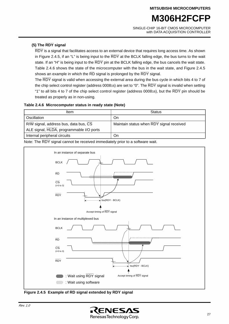
SINGLE-CHIP 16-BIT CMOS MICROCOMPUTERwith DATA ACQUISITION CONTROLLER
MITSUBISHI MICROCOMPUTERS
27
Rev. 1.0
M306H2FCFP
_____ ________
Figure 2.4.5 Example of RD signal extended by RDY signal
BCLK
RD
CSi(i=0 to 3)
RDY
tsu(RDY - BCLK)
AAAA
BCLK
RD
CSi(i=0 to 3)
RDY
tsu(RDY - BCLK)
AAAAAAAAAAAA
AAAA
In an instance of separate bus
In an instance of multiplexed bus
Accept timing of RDY signal : Wait using RDY signal
: Wait using software
Accept timing of RDY signal
________
Note: The RDY signal cannot be received immediately prior to a software wait.
Table 2.4.6 Microcomputer status in ready state (Note)
Item Status
Oscillation On___ _____
R/W signal, address bus, data bus, CS________
Maintain status when RDY signal received__________
ALE signal, HLDA, programmable I/O ports
Internal peripheral circuits On
________
(5) The RDY signal________
RDY is a signal that facilitates access to an external device that requires long access time. As shown________
in Figure 2.4.5, if an “L” is being input to the RDY at the BCLK falling edge, the bus turns to the wait________
state. If an “H” is being input to the RDY pin at the BCLK falling edge, the bus cancels the wait state.
Table 2.4.6 shows the state of the microcomputer with the bus in the wait state, and Figure 2.4.5____ ________
shows an example in which the RD signal is prolonged by the RDY signal.________
The RDY signal is valid when accessing the external area during the bus cycle in which bits 4 to 7 of________
the chip select control register (address 000816) are set to “0”. The RDY signal is invalid when setting________
“1” to all bits 4 to 7 of the chip select control register (address 000816), but the RDY pin should be
treated as properly as in non-using.
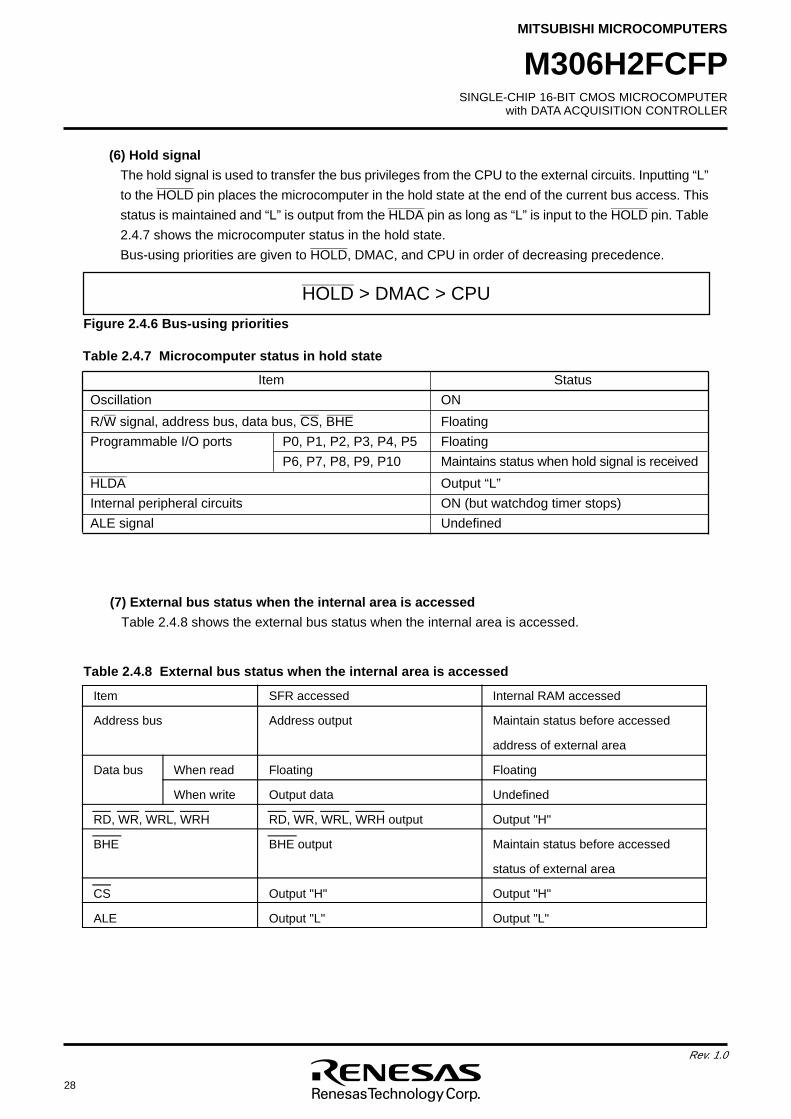
28
Rev. 1.0
SINGLE-CHIP 16-BIT CMOS MICROCOMPUTERwith DATA ACQUISITION CONTROLLER
MITSUBISHI MICROCOMPUTERS
M306H2FCFP
Table 2.4.7 Microcomputer status in hold state
Item Status
Oscillation ON___ _____ _______
R/W signal, address bus, data bus, CS, BHE Floating
Programmable I/O ports P0, P1, P2, P3, P4, P5 Floating
P6, P7, P8, P9, P10 Maintains status when hold signal is received__________
HLDA Output “L”
Internal peripheral circuits ON (but watchdog timer stops)
ALE signal Undefined
__________
HOLD > DMAC > CPU
(6) Hold signal
The hold signal is used to transfer the bus privileges from the CPU to the external circuits. Inputting “L”__________
to the HOLD pin places the microcomputer in the hold state at the end of the current bus access. This__________ __________
status is maintained and “L” is output from the HLDA pin as long as “L” is input to the HOLD pin. Table
2.4.7 shows the microcomputer status in the hold state.__________
Bus-using priorities are given to HOLD, DMAC, and CPU in order of decreasing precedence.
Figure 2.4.6 Bus-using priorities
(7) External bus status when the internal area is accessed
Table 2.4.8 shows the external bus status when the internal area is accessed.
Table 2.4.8 External bus status when the internal area is accessed
Item SFR accessed Internal RAM accessed
Address bus Address output Maintain status before accessed
address of external area
Data bus When read Floating Floating
When write Output data Undefined
RD, WR, WRL, WRH RD, WR, WRL, WRH output Output "H"
BHE BHE output Maintain status before accessed
status of external area
CS Output "H" Output "H"
ALE Output "L" Output "L"
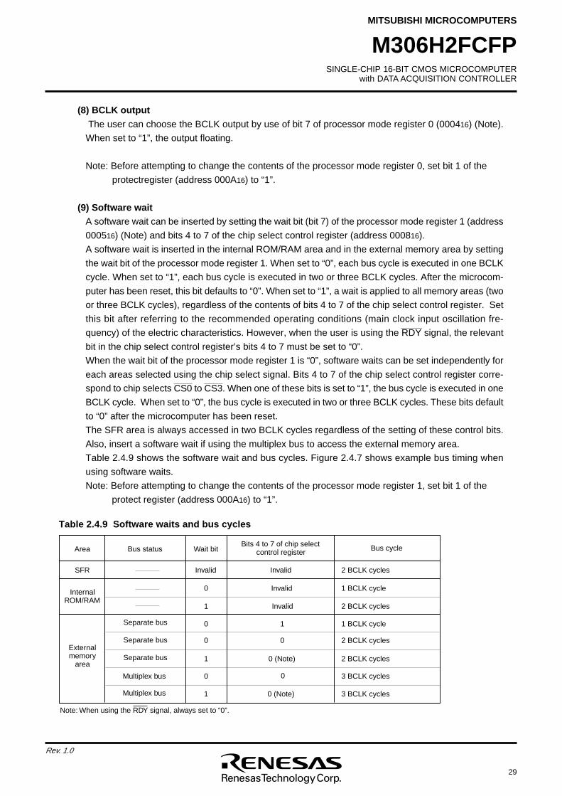
SINGLE-CHIP 16-BIT CMOS MICROCOMPUTERwith DATA ACQUISITION CONTROLLER
MITSUBISHI MICROCOMPUTERS
29
Rev. 1.0
M306H2FCFP
Area Bus status Wait bitBits 4 to 7 of chip select
control register Bus cycle
Invalid1 2 BCLK cycles
External memory
area
Separate bus 0 1 1 BCLK cycle
Separate bus 0 0 2 BCLK cycles
Separate bus 1 0 (Note) 2 BCLK cycles
Multiplex bus 0 3 BCLK cycles
Multiplex bus 1 3 BCLK cycles0 (Note)
SFR
InternalROM/RAM
0 Invalid 1 BCLK cycle
Invalid Invalid 2 BCLK cycles
Note: When using the RDY signal, always set to “0”.
0
Table 2.4.9 Software waits and bus cycles
(8) BCLK output The user can choose the BCLK output by use of bit 7 of processor mode register 0 (000416) (Note).
When set to “1”, the output floating.
Note: Before attempting to change the contents of the processor mode register 0, set bit 1 of the
protectregister (address 000A16) to “1”.
(9) Software waitA software wait can be inserted by setting the wait bit (bit 7) of the processor mode register 1 (address
000516) (Note) and bits 4 to 7 of the chip select control register (address 000816).
A software wait is inserted in the internal ROM/RAM area and in the external memory area by setting
the wait bit of the processor mode register 1. When set to “0”, each bus cycle is executed in one BCLK
cycle. When set to “1”, each bus cycle is executed in two or three BCLK cycles. After the microcom-
puter has been reset, this bit defaults to “0”. When set to “1”, a wait is applied to all memory areas (two
or three BCLK cycles), regardless of the contents of bits 4 to 7 of the chip select control register. Set
this bit after referring to the recommended operating conditions (main clock input oscillation fre-________
quency) of the electric characteristics. However, when the user is using the RDY signal, the relevant
bit in the chip select control register’s bits 4 to 7 must be set to “0”.
When the wait bit of the processor mode register 1 is “0”, software waits can be set independently for
each areas selected using the chip select signal. Bits 4 to 7 of the chip select control register corre-_______ _______
spond to chip selects CS0 to CS3. When one of these bits is set to “1”, the bus cycle is executed in one
BCLK cycle. When set to “0”, the bus cycle is executed in two or three BCLK cycles. These bits default
to “0” after the microcomputer has been reset.
The SFR area is always accessed in two BCLK cycles regardless of the setting of these control bits.
Also, insert a software wait if using the multiplex bus to access the external memory area.
Table 2.4.9 shows the software wait and bus cycles. Figure 2.4.7 shows example bus timing when
using software waits.
Note: Before attempting to change the contents of the processor mode register 1, set bit 1 of the
protect register (address 000A16) to “1”.
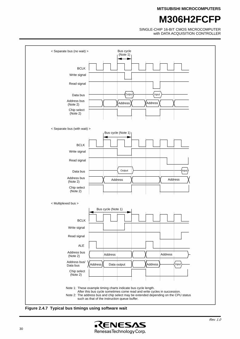
30
Rev. 1.0
SINGLE-CHIP 16-BIT CMOS MICROCOMPUTERwith DATA ACQUISITION CONTROLLER
MITSUBISHI MICROCOMPUTERS
M306H2FCFP
Figure 2.4.7 Typical bus timings using software wait
Output Input
Address Address
Bus cycle (Note 1)< Separate bus (with wait) >
BCLK
Read signal
Write signal
Data bus
Address bus (Note 2)
Chip select (Note 2)
BCLK
Read signal
Address bus/Data bus
Chip select (Note 2)
Address
AddressAddress bus (Note 2)
Data output
Address
Address Input
ALE
Bus cycle (Note 1)
< Multiplexed bus >
Write signal
BCLK
Read signal
Write signal
Address bus (Note 2) Address Address
Bus cycle(Note 1)
< Separate bus (no wait) >
OutputData bus
Chip select (Note 2)
Input
Note 1: These example timing charts indicate bus cycle length. After this bus cycle sometimes come read and write cycles in succession.Note 2: The address bus and chip select may be extended depending on the CPU status such as that of the instruction queue buffer.
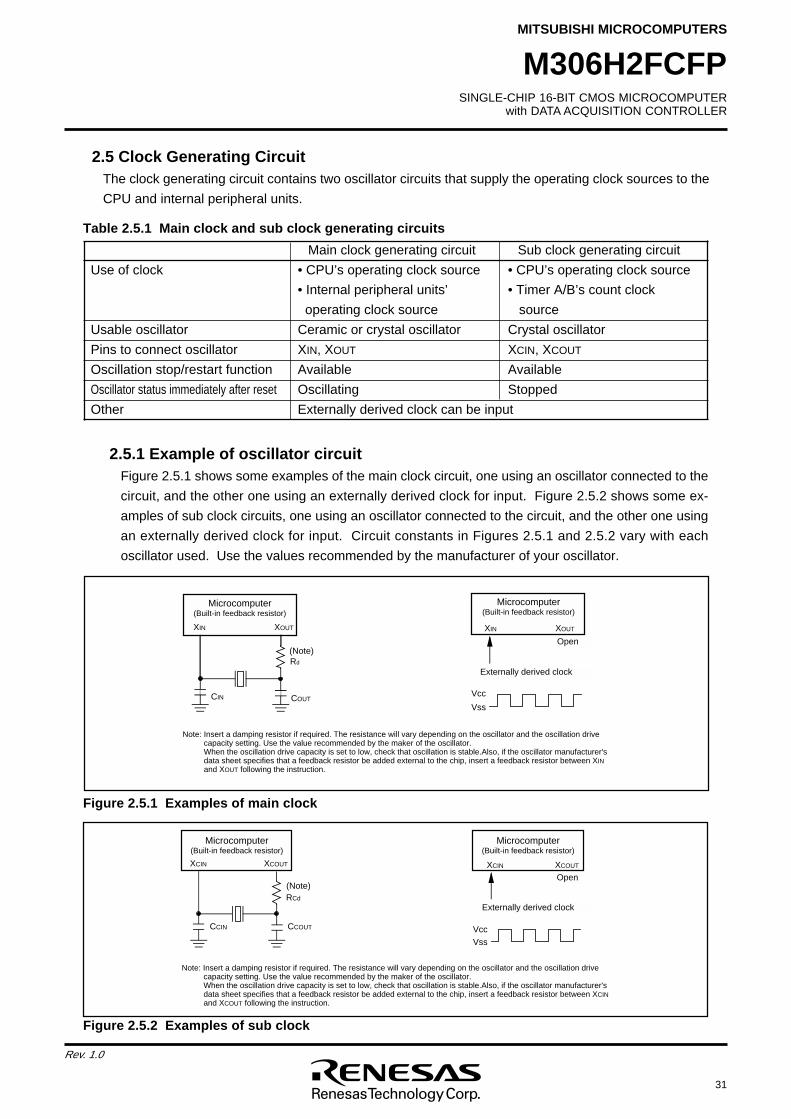
SINGLE-CHIP 16-BIT CMOS MICROCOMPUTERwith DATA ACQUISITION CONTROLLER
MITSUBISHI MICROCOMPUTERS
31
Rev. 1.0
M306H2FCFP
Main clock generating circuit Sub clock generating circuit
Use of clock • CPU’s operating clock source • CPU’s operating clock source
• Internal peripheral units’ • Timer A/B’s count clock
operating clock source source
Usable oscillator Ceramic or crystal oscillator Crystal oscillator
Pins to connect oscillator XIN, XOUT XCIN, XCOUT
Oscillation stop/restart function Available Available
Oscillator status immediately after reset Oscillating Stopped
Other Externally derived clock can be input
Microcomputer(Built-in feedback resistor)
XIN XOUT
Externally derived clock
Open
Vcc
Vss
Microcomputer(Built-in feedback resistor)
XIN XOUT
Rd
CIN COUT
(Note)
Note: Insert a damping resistor if required. The resistance will vary depending on the oscillator and the oscillation drive capacity setting. Use the value recommended by the maker of the oscillator.When the oscillation drive capacity is set to low, check that oscillation is stable.Also, if the oscillator manufacturer's data sheet specifies that a feedback resistor be added external to the chip, insert a feedback resistor between XIN and XOUT following the instruction.
Microcomputer (Built-in feedback resistor)
XCIN XCOUT
Externally derived clock
Open
Vcc
Vss
Note: Insert a damping resistor if required. The resistance will vary depending on the oscillator and the oscillation drive capacity setting. Use the value recommended by the maker of the oscillator.When the oscillation drive capacity is set to low, check that oscillation is stable.Also, if the oscillator manufacturer's data sheet specifies that a feedback resistor be added external to the chip, insert a feedback resistor between XCIN and XCOUT following the instruction.
Microcomputer (Built-in feedback resistor)
XCIN XCOUT
(Note)
CCIN CCOUT
RCd
Table 2.5.1 Main clock and sub clock generating circuits
Figure 2.5.2 Examples of sub clock
Figure 2.5.1 Examples of main clock
2.5.1 Example of oscillator circuitFigure 2.5.1 shows some examples of the main clock circuit, one using an oscillator connected to the
circuit, and the other one using an externally derived clock for input. Figure 2.5.2 shows some ex-
amples of sub clock circuits, one using an oscillator connected to the circuit, and the other one using
an externally derived clock for input. Circuit constants in Figures 2.5.1 and 2.5.2 vary with each
oscillator used. Use the values recommended by the manufacturer of your oscillator.
2.5 Clock Generating CircuitThe clock generating circuit contains two oscillator circuits that supply the operating clock sources to the
CPU and internal peripheral units.
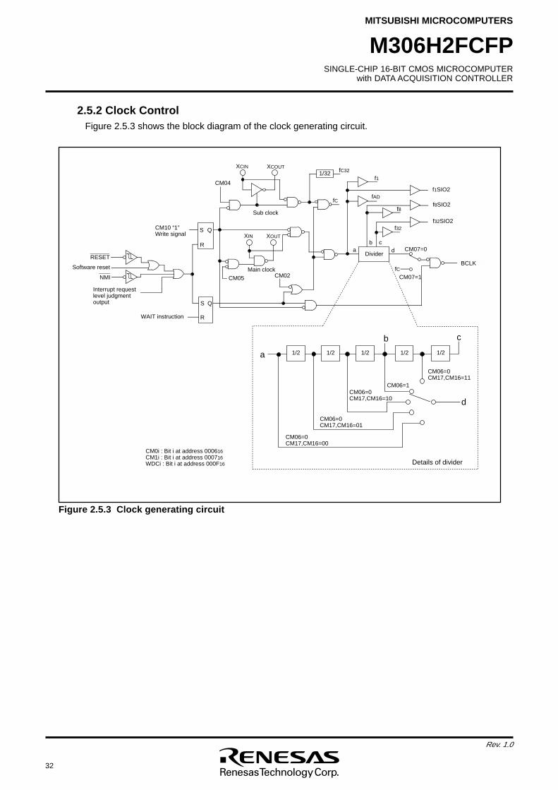
32
Rev. 1.0
SINGLE-CHIP 16-BIT CMOS MICROCOMPUTERwith DATA ACQUISITION CONTROLLER
MITSUBISHI MICROCOMPUTERS
M306H2FCFP
Sub clock
CM04
fC32
CM0i : Bit i at address 000616CM1i : Bit i at address 000716WDCi : Bit i at address 000F16
XCIN
CM10 “1” Write signal
1/32XCOUT
QS
R
WAIT instruction
XOUT
Main clock
CM05
fC
CM02
f1
QS
R
NMI
Interrupt request level judgment output
RESET
Software reset fC
CM07=0
CM07=1
fAD
AAAAAAAADividera d
1/2 1/2 1/2 1/2
CM06=0CM17,CM16=00
CM06=0CM17,CM16=01
CM06=0CM17,CM16=10
CM06=1
CM06=0CM17,CM16=11
d
a
Details of divider
XIN
f8
f32
cb
b
1/2
c
f32SIO2
f8SIO2
f1SIO2
BCLK
Figure 2.5.3 Clock generating circuit
2.5.2 Clock ControlFigure 2.5.3 shows the block diagram of the clock generating circuit.
SINGLE-CHIP 16-BIT CMOS MICROCOMPUTERwith DATA ACQUISITION CONTROLLER
MITSUBISHI MICROCOMPUTERS
33
Rev. 1.0
M306H2FCFP
The following paragraphs describes the clocks generated by the clock generating circuit.
(1) Main clock
The main clock is generated by the main clock oscillation circuit. After a reset, the clock is divided by
8 to the BCLK. The clock can be stopped using the main clock stop bit (bit 5 at address 000616).
Stopping the clock, after switching the operating clock source of CPU to the sub-clock, reduces the
power dissipation.After the oscillation of the main clock oscillation circuit has stabilized, the drive
capacity of the main clock oscillation circuit can be reduced using the XIN-XOUT drive capacity select
bit (bit 5 at address 000716). Reducing the drive capacity of the main clock oscillation circuit reduces
the power dissipation. This bit changes to “1” when shifting from high-speed/medium-speed mode to
stop mode and at a reset. When shifting from low-speed/low power dissipation mode to stop mode,
the value before stop mode is retained.
(2) Sub-clock
The sub-clock is generated by the sub-clock oscillation circuit. No sub-clock is generated after a reset.
After oscillation is started using the port Xc select bit (bit 4 at address 000616), the sub-clock can be
selected as the BCLK by using the system clock select bit (bit 7 at address 000616). However, be sure
that the sub-clock oscillation has fully stabilized before switching.
After the oscillation of the sub-clock oscillation circuit has stabilized, the drive capacity of the sub-clock
oscillation circuit can be reduced using the XCIN-XCOUT drive capacity select bit (bit 3 at address
000616). Reducing the drive capacity of the sub-clock oscillation circuit reduces the power dissipation.
This bit changes to “1” when shifting to stop mode and at a reset.
(3) BCLK
The BCLK is the clock that drives the CPU, and is fc or the clock is derived by dividing the main clock
by 1, 2, 4, 8, or 16. The BCLK is derived by dividing the main clock by 8 after a reset. The BCLK signal
can be output from BCLK pin by the BCLK output disable bit (bit 7 at address 000416) in the memory
expansion and the microprocessor modes.
The main clock division select bit 0(bit 6 at address 000616) changes to “1” when shifting from high-
speed/medium-speed to stop mode and at reset. When shifting from low-speed/low power dissipation
mode to stop mode, the value before stop mode is retained.
(4) Peripheral function clock(f1, f8, f32, f1SIO2, f8SIO2,f32SIO2,fAD)
The clock for the peripheral devices is derived from the main clock or by dividing it by 1, 8, or 32. The
peripheral function clock is stopped by stopping the main clock or by setting the WAIT peripheral
function clock stop bit (bit 2 at 000616) to “1” and then executing a WAIT instruction.
(5) fC32
This clock is derived by dividing the sub-clock by 32. It is used for the timer A and timer B counts.
(6) fC
This clock has the same frequency as the sub-clock. It is used for the BCLK and for the watchdog timer.
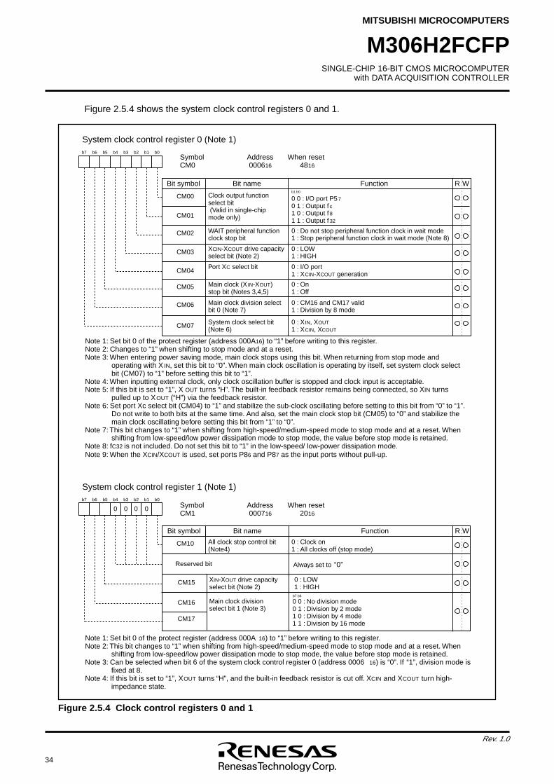
34
Rev. 1.0
SINGLE-CHIP 16-BIT CMOS MICROCOMPUTERwith DATA ACQUISITION CONTROLLER
MITSUBISHI MICROCOMPUTERS
M306H2FCFP
System clock control register 0 (Note 1)
Symbol Address When reset CM0 000616 4816
Bit name FunctionBit symbol
b7 b6 b5 b4 b3 b2 b1 b0
0 0 : I/O port P57
0 1 : Output f c1 0 : Output f 8
1 1 : Output f 32
b1 b0
CM07
CM05
CM04
CM03
CM01
CM02
CM00
CM06
Clock output function select bit (Valid in single-chip mode only)
WAIT peripheral function clock stop bit
0 : Do not stop peripheral function clock in wait mode1 : Stop peripheral function clock in wait mode (Note 8)
XCIN-XCOUT drive capacity select bit (Note 2)
0 : LOW1 : HIGH
Port XC select bit 0 : I/O port 1 : XCIN-XCOUT generation
Main clock (XIN-XOUT) stop bit (Notes 3,4,5)
0 : On1 : Off
Main clock division select bit 0 (Note 7)
0 : CM16 and CM17 valid1 : Division by 8 mode
System clock select bit(Note 6)
0 : XIN, XOUT
1 : XCIN, XCOUT
Note 1: Set bit 0 of the protect register (address 000A16) to “1” before writing to this register.Note 2: Changes to “1” when shifting to stop mode and at a reset.Note 3: When entering power saving mode, main clock stops using this bit. When returning from stop mode and
operating with X IN, set this bit to “0”. When main clock oscillation is operating by itself, set system clock select bit (CM07) to “1” before setting this bit to “1”.
Note 4: When inputting external clock, only clock oscillation buffer is stopped and clock input is acceptable.Note 5: If this bit is set to “1”, X OUT turns “H”. The built-in feedback resistor remains being connected, so XIN turns
pulled up to XOUT (“H”) via the feedback resistor.Note 6: Set port Xc select bit (CM04) to “1” and stabilize the sub-clock oscillating before setting to this bit from “0” to “1”.
Do not write to both bits at the same time. And also, set the main clock stop bit (CM05) to “0” and stabilize the main clock oscillating before setting this bit from “1” to “0”.
Note 7: This bit changes to “1” when shifting from high-speed/medium-speed mode to stop mode and at a reset. When shifting from low-speed/low power dissipation mode to stop mode, the value before stop mode is retained.
Note 8: fC32 is not included. Do not set this bit to “1” in the low-speed/ low-power dissipation mode.Note 9: When the XCIN/XCOUT is used, set ports P86 and P87 as the input ports without pull-up.
System clock control register 1 (Note 1)
Symbol Address When reset CM1 000716 2016
Bit name FunctionBit symbol
b7 b6 b5 b4 b3 b2 b1 b0
CM10 All clock stop control bit(Note4)
0 : Clock on1 : All clocks off (stop mode)
Note 1: Set bit 0 of the protect register (address 000A 16) to “1” before writing to this register.Note 2: This bit changes to “1” when shifting from high-speed/medium-speed mode to stop mode and at a reset. When
shifting from low-speed/low power dissipation mode to stop mode, the value before stop mode is retained.Note 3: Can be selected when bit 6 of the system clock control register 0 (address 0006 16) is “0”. If “1”, division mode is
fixed at 8.Note 4: If this bit is set to “1”, XOUT turns “H”, and the built-in feedback resistor is cut off. XCIN and XCOUT turn high-
impedance state.
WR
WR
00
Reserved bit Always set to “0”
00
CM15 XIN-XOUT drive capacity select bit (Note 2)
0 : LOW 1 : HIGH
CM16
CM17
Main clock division select bit 1 (Note 3)
0 0 : No division mode0 1 : Division by 2 mode1 0 : Division by 4 mode1 1 : Division by 16 mode
b7 b6
Figure 2.5.4 Clock control registers 0 and 1
Figure 2.5.4 shows the system clock control registers 0 and 1.
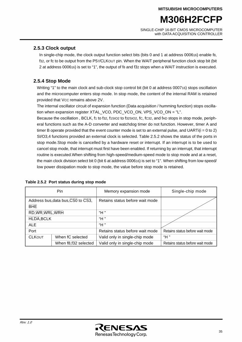
SINGLE-CHIP 16-BIT CMOS MICROCOMPUTERwith DATA ACQUISITION CONTROLLER
MITSUBISHI MICROCOMPUTERS
35
Rev. 1.0
M306H2FCFP
2.5.3 Clock outputIn single-chip mode, the clock output function select bits (bits 0 and 1 at address 000616) enable f8,
f32, or fc to be output from the P57/CLKOUT pin. When the WAIT peripheral function clock stop bit (bit
2 at address 000616) is set to “1”, the output of f8 and f32 stops when a WAIT instruction is executed.
2.5.4 Stop ModeWriting “1” to the main clock and sub-clock stop control bit (bit 0 at address 000716) stops oscillation
and the microcomputer enters stop mode. In stop mode, the content of the internal RAM is retained
provided that VCC remains above 2V.
The internal oscillator circuit of expansion function (Data acquisition / humming function) stops oscilla-
tion when expansion register XTAL_VCO, PDC_VCO_ON, VPS_VCO_ON = "L".
Because the oscillation , BCLK, f1 to f32, f1SIO2 to f32SIO2, fC, fC32, and fAD stops in stop mode, periph-
eral functions such as the A-D converter and watchdog timer do not function. However, timer A and
timer B operate provided that the event counter mode is set to an external pulse, and UARTi(i = 0 to 2)
SI/O3,4 functions provided an external clock is selected. Table 2.5.2 shows the status of the ports in
stop mode.Stop mode is cancelled by a hardware reset or interrupt. If an interrupt is to be used to
cancel stop mode, that interrupt must first have been enabled. If returning by an interrupt, that interrupt
routine is executed.When shifting from high-speed/medium-speed mode to stop mode and at a reset,
the main clock division select bit 0 (bit 6 at address 000616) is set to “1”. When shifting from low-speed/
low power dissipation mode to stop mode, the value before stop mode is retained.
_______ _______
Address bus,data bus,CS0 to CS3, Retains status before wait mode_______
BHE_____ ______ ________ ________
RD,WR,WRL,WRH “H ”__________
HLDA,BCLK “H ”
ALE “H ”
Port Retains status before wait mode Retains status before wait mode
CLKOUT When fC selected Valid only in single-chip mode “H ”
When f8,f32 selected Valid only in single-chip mode Retains status before wait mode
Table 2.5.2 Port status during stop mode
Pin Memory expansion mode Single-chip mode
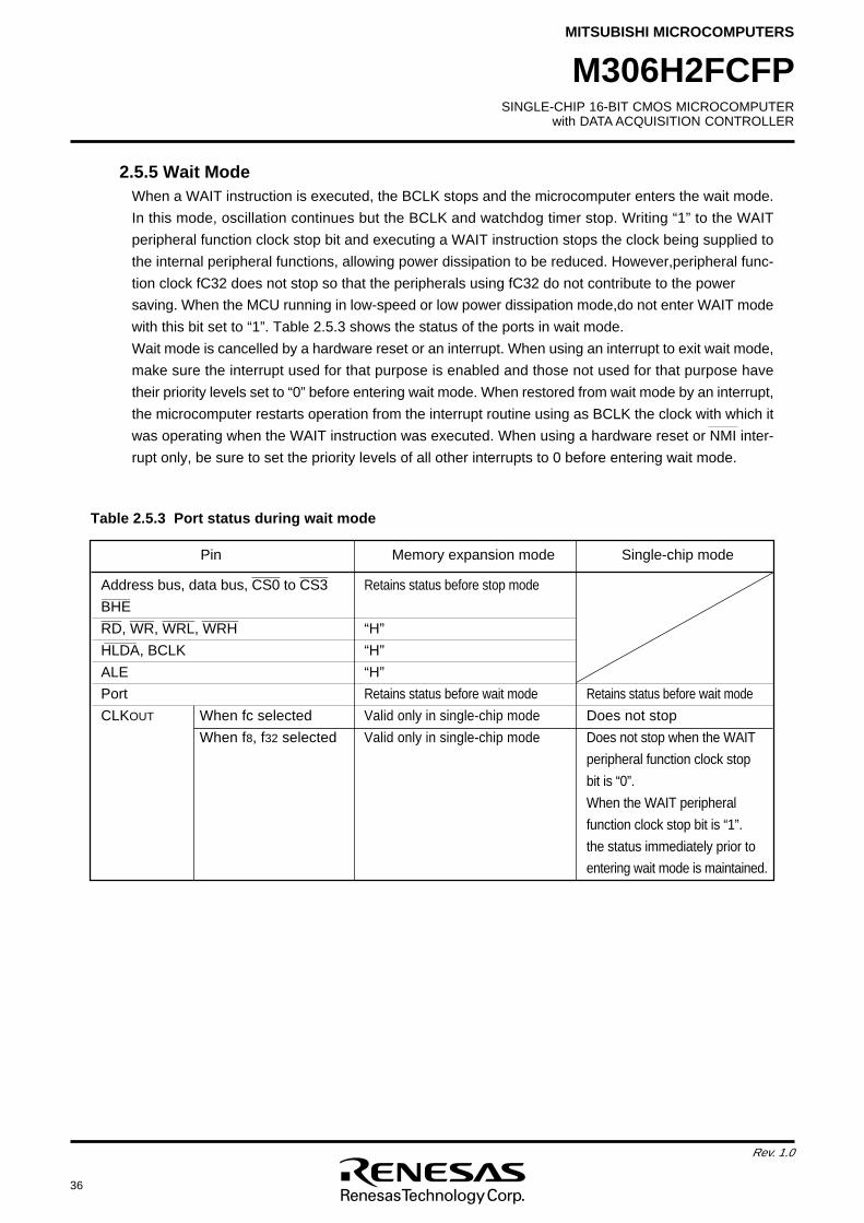
36
Rev. 1.0
SINGLE-CHIP 16-BIT CMOS MICROCOMPUTERwith DATA ACQUISITION CONTROLLER
MITSUBISHI MICROCOMPUTERS
M306H2FCFP
2.5.5 Wait ModeWhen a WAIT instruction is executed, the BCLK stops and the microcomputer enters the wait mode.
In this mode, oscillation continues but the BCLK and watchdog timer stop. Writing “1” to the WAIT
peripheral function clock stop bit and executing a WAIT instruction stops the clock being supplied to
the internal peripheral functions, allowing power dissipation to be reduced. However,peripheral func-
tion clock fC32 does not stop so that the peripherals using fC32 do not contribute to the power
saving. When the MCU running in low-speed or low power dissipation mode,do not enter WAIT mode
with this bit set to “1”. Table 2.5.3 shows the status of the ports in wait mode.
Wait mode is cancelled by a hardware reset or an interrupt. When using an interrupt to exit wait mode,
make sure the interrupt used for that purpose is enabled and those not used for that purpose have
their priority levels set to “0” before entering wait mode. When restored from wait mode by an interrupt,
the microcomputer restarts operation from the interrupt routine using as BCLK the clock with which it
was operating when the WAIT instruction was executed. When using a hardware reset or NMI inter-
rupt only, be sure to set the priority levels of all other interrupts to 0 before entering wait mode.
_______ _______
Address bus, data bus, CS0 to CS3 Retains status before stop mode_______
BHE_____ ______ ________ _________
RD, WR, WRL, WRH “H”________
HLDA, BCLK “H”
ALE “H”
Port Retains status before wait mode Retains status before wait mode
CLKOUT When fc selected Valid only in single-chip mode Does not stop
When f8, f32 selected Valid only in single-chip mode Does not stop when the WAIT
peripheral function clock stop
bit is “0”.
When the WAIT peripheral
function clock stop bit is “1”.
the status immediately prior to
entering wait mode is maintained.
Table 2.5.3 Port status during wait mode
Pin Memory expansion mode Single-chip mode
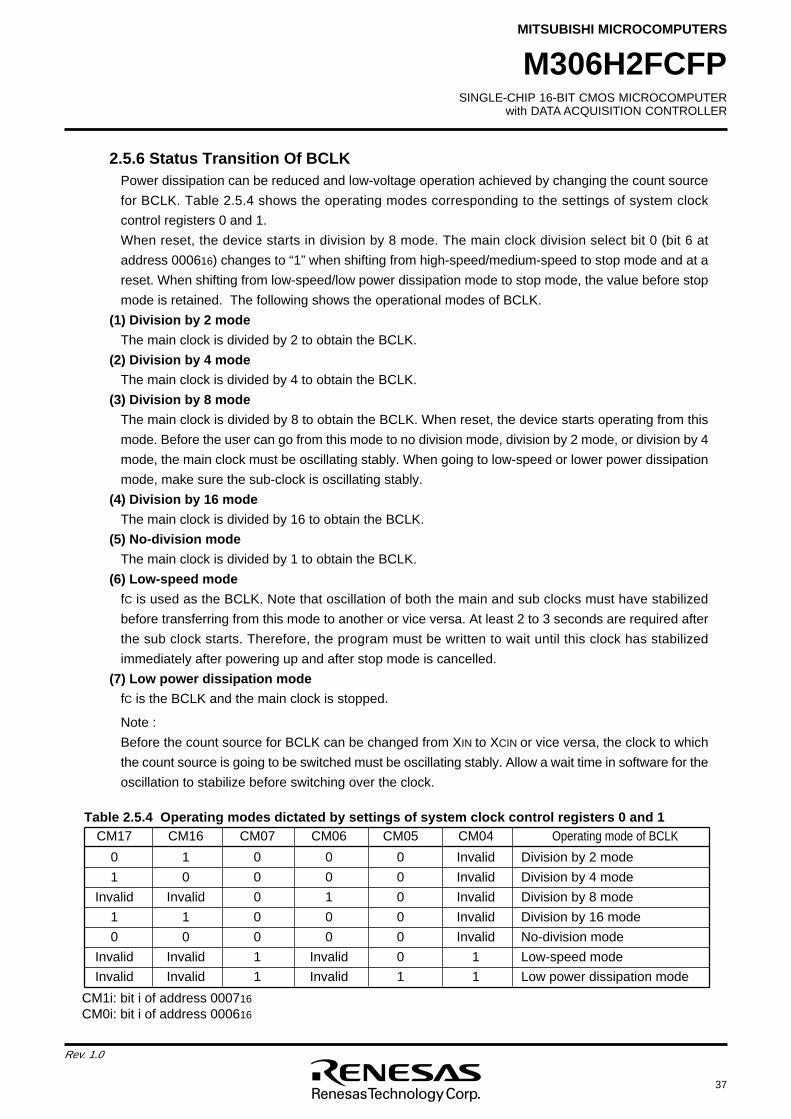
SINGLE-CHIP 16-BIT CMOS MICROCOMPUTERwith DATA ACQUISITION CONTROLLER
MITSUBISHI MICROCOMPUTERS
37
Rev. 1.0
M306H2FCFP
0 1 0 0 0 Invalid Division by 2 mode
1 0 0 0 0 Invalid Division by 4 mode
Invalid Invalid 0 1 0 Invalid Division by 8 mode
1 1 0 0 0 Invalid Division by 16 mode
0 0 0 0 0 Invalid No-division mode
Invalid Invalid 1 Invalid 0 1 Low-speed mode
Invalid Invalid 1 Invalid 1 1 Low power dissipation mode
2.5.6 Status Transition Of BCLKPower dissipation can be reduced and low-voltage operation achieved by changing the count source
for BCLK. Table 2.5.4 shows the operating modes corresponding to the settings of system clock
control registers 0 and 1.
When reset, the device starts in division by 8 mode. The main clock division select bit 0 (bit 6 at
address 000616) changes to “1” when shifting from high-speed/medium-speed to stop mode and at a
reset. When shifting from low-speed/low power dissipation mode to stop mode, the value before stop
mode is retained. The following shows the operational modes of BCLK.
(1) Division by 2 mode
The main clock is divided by 2 to obtain the BCLK.
(2) Division by 4 mode
The main clock is divided by 4 to obtain the BCLK.
(3) Division by 8 mode
The main clock is divided by 8 to obtain the BCLK. When reset, the device starts operating from this
mode. Before the user can go from this mode to no division mode, division by 2 mode, or division by 4
mode, the main clock must be oscillating stably. When going to low-speed or lower power dissipation
mode, make sure the sub-clock is oscillating stably.
(4) Division by 16 mode
The main clock is divided by 16 to obtain the BCLK.
(5) No-division mode
The main clock is divided by 1 to obtain the BCLK.
(6) Low-speed mode
fC is used as the BCLK. Note that oscillation of both the main and sub clocks must have stabilized
before transferring from this mode to another or vice versa. At least 2 to 3 seconds are required after
the sub clock starts. Therefore, the program must be written to wait until this clock has stabilized
immediately after powering up and after stop mode is cancelled.
(7) Low power dissipation mode
fC is the BCLK and the main clock is stopped.
Note :
Before the count source for BCLK can be changed from XIN to XCIN or vice versa, the clock to which
the count source is going to be switched must be oscillating stably. Allow a wait time in software for the
oscillation to stabilize before switching over the clock.
CM17 CM16 CM07 CM06 CM05 CM04 Operating mode of BCLKTable 2.5.4 Operating modes dictated by settings of system clock control registers 0 and 1
CM1i: bit i of address 000716
CM0i: bit i of address 000616
38
Rev. 1.0
SINGLE-CHIP 16-BIT CMOS MICROCOMPUTERwith DATA ACQUISITION CONTROLLER
MITSUBISHI MICROCOMPUTERS
M306H2FCFP
2.5.7 Power controlThe following is a description of the three available power control modes:
Modes
Power control is available in three modes.
(a) Normal operation mode
• High-speed mode
Divide-by-1 frequency of the main clock becomes the BCLK. The CPU operates with the internal
clock selected. Each peripheral function operates according to its assigned clock.
• Medium-speed mode
Divide-by-2, divide-by-4, divide-by-8, or divide-by-16 frequency of the main clock becomes the
BCLK. The CPU operates according to the internal clock selected. Each peripheral function operates
according to its assigned clock.
• Low-speed mode
fC becomes the BCLK. The CPU operates according to the fc clock. The fc clock is supplied by the
secondary clock. Each peripheral function operates according to its assigned clock.
• Low power dissipation mode
The main clock operating in low-speed mode is stopped. The CPU operates according to the fC
clock. The fc clock is supplied by the secondary clock. The only peripheral functions that operate are
those with the sub-clock selected as the count source.
When in single-chip mode, the device can be operated with a low supply voltage (VCC = 3.0 V) only
during low power dissipation mode. Before entering or exiting low power dissipation mode, always
make sure the supply voltage VCC is 5 V.
Note: When operating with a low supply voltage, be aware that only the CPU, ROM, RAM, input/
output ports, timers (timers A and B), and the interrupt control circuit can be used. All other
internal resources (e.g., data slicer, DMAC, A/D, and D/A) cannot be used.
(b) Wait mode
The CPU operation is stopped. The oscillators do not stop.
(c) Stop mode
The main clock and the sub-clock oscillators stop. The CPU and all built-in peripheral functions stop.
This mode, among the three modes listed here, is the most effective in decreasing power consumption.
Figure 2.5.5 is the state transition diagram of the above modes.

SINGLE-CHIP 16-BIT CMOS MICROCOMPUTERwith DATA ACQUISITION CONTROLLER
MITSUBISHI MICROCOMPUTERS
39
Rev. 1.0
M306H2FCFP
Figure 2.5.5 State transition diagram of Power control mode
T
r
a
n
s
i
t
i
o
n
o
f
s
t
o
p
m
o
d
e
,
w
a
i
t
m
o
d
e
T
r
a
n
s
i
t
i
o
n
o
f
n
o
r
m
a
l
m
o
d
e
M
e
d
i
u
m
-
s
p
e
e
d
m
o
d
e(
d
i
v
i
d
e
d
-
b
y
-
8
m
o
d
e
)
B
C
L
K
:
f
(
XI
N)
/
8C
M
0
7
=
“
0
”
C
M
0
6
=
“
1
”
L
o
w
-
s
p
e
e
d
m
o
d
e
H
i
g
h
-
s
p
e
e
d
m
o
d
e
M
a
i
n
c
l
o
c
k
i
s
o
s
c
i
l
l
a
t
i
n
gS
u
b
c
l
o
c
k
i
s
s
t
o
p
p
e
d
M
a
i
n
c
l
o
c
k
i
s
o
s
c
i
l
l
a
t
i
n
gS
u
b
c
l
o
c
k
i
s
s
t
o
p
p
e
d
M
a
i
n
c
l
o
c
k
i
s
s
t
o
p
p
e
dS
u
b
c
l
o
c
k
i
s
o
s
c
i
l
l
a
t
i
n
g
M
a
i
n
c
l
o
c
k
i
s
o
s
c
i
l
l
a
t
i
n
gS
u
b
c
l
o
c
k
i
s
o
s
c
i
l
l
a
t
i
n
g
L
o
w
p
o
w
e
r
d
i
s
s
i
p
a
t
i
o
n
m
o
d
e
(
N
o
t
e
5
)
R
e
s
e
t
M
a
i
n
c
l
o
c
k
i
s
s
t
o
p
p
e
dS
u
b
c
l
o
c
k
i
s
s
t
o
p
p
e
d
M
e
d
i
u
m
-
s
p
e
e
d
m
o
d
e(
d
i
v
i
d
e
d
-
b
y
-
8
m
o
d
e
)I n
t
e
r
r
u
p
t
C
M
1
0
=
“
1
”
S
t
o
p
m
o
d
e W
a
i
t
m
o
d
e
C
P
U
o
p
e
r
a
t
i
o
n
s
t
o
p
p
e
d
I n
t
e
r
r
u
p
t
W
A
I
T
i
n
s
t
r
u
c
t
i
o
n
M
a
i
n
c
l
o
c
k
i
s
s
t
o
p
p
e
dS
u
b
c
l
o
c
k
i
s
s
t
o
p
p
e
d
H
i
g
h
-
s
p
e
e
d
/
m
e
d
i
u
m
-s
p
e
e
d
m
o
d
eS
t
o
p
m
o
d
e W
a
i
t
m
o
d
e
C
P
U
o
p
e
r
a
t
i
o
n
s
t
o
p
p
e
d
I n
t
e
r
r
u
p
t
W
A
I
T
i
n
s
t
r
u
c
t
i
o
nC
M
1
0
=
“
1
”
I n
t
e
r
r
u
p
t
M
a
i
n
c
l
o
c
k
i
s
s
t
o
p
p
e
dS
u
b
c
l
o
c
k
i
s
s
t
o
p
p
e
d C
P
U
o
p
e
r
a
t
i
o
n
s
t
o
p
p
e
d
L
o
w
-
s
p
e
e
d
/
l
o
w
p
o
w
e
rd
i
s
s
i
p
a
t
i
o
n
m
o
d
eS
t
o
p
m
o
d
e W
a
i
t
m
o
d
eI n
t
e
r
r
u
p
t
W
A
I
T
i
n
s
t
r
u
c
t
i
o
n
I n
t
e
r
r
u
p
t
C
M
1
0
=
“
1
”
B
C
L
K
:
f
(
XI
N)
/
2C
M
0
7
=
“
0
”
C
M
0
6
=
“
0
”C
M
1
7
=
“
0
”
C
M
1
6
=
“
1
”
M
e
d
i
u
m
-
s
p
e
e
d
m
o
d
e(
d
i
v
i
d
e
d
-
b
y
-
2
m
o
d
e
)
B
C
L
K
:
f
(
XI
N)
/
1
6C
M
0
7
=
“
0
”
C
M
0
6
=
“
0
”C
M
1
7
=
“
1
”
C
M
1
6
=
“
1
”
M
e
d
i
u
m
-
s
p
e
e
d
m
o
d
e(
d
i
v
i
d
e
d
-
b
y
-
1
6
m
o
d
e
)
B
C
L
K
:
f
(
XI
N)
/
4C
M
0
7
=
“
0
”
C
M
0
6
=
“
0
”C
M
1
7
=
“
1
”
C
M
1
6
=
“
0
”
M
e
d
i
u
m
-
s
p
e
e
d
m
o
d
e(
d
i
v
i
d
e
d
-
b
y
-
4
m
o
d
e
)
B
C
L
K
:
f
(
XI
N)C
M
0
7
=
“
0
”
C
M
0
6
=
“
0
”C
M
1
7
=
“
0
”
C
M
1
6
=
“
0
”
B
C
L
K
:
f
(
XI
N)
/
8
M
e
d
i
u
m
-
s
p
e
e
d
m
o
d
e(
d
i
v
i
d
e
d
-
b
y
-
8
m
o
d
e
)
C
M
0
7
=
“
0
”C
M
0
6
=
“
1
”
H
i
g
h
-
s
p
e
e
d
m
o
d
e
B
C
L
K
:
f
(
XI
N)
/
2C
M
0
7
=
“
0
”
C
M
0
6
=
“
0
”C
M
1
7
=
“
0
”
C
M
1
6
=
“
1
”
M
e
d
i
u
m
-
s
p
e
e
d
m
o
d
e(
d
i
v
i
d
e
d
-
b
y
-
2
m
o
d
e
)
B
C
L
K
:
f
(
XI
N)
/
1
6C
M
0
7
=
“
0
”
C
M
0
6
=
“
0
”C
M
1
7
=
“
1
”
C
M
1
6
=
“
1
”
M
e
d
i
u
m
-
s
p
e
e
d
m
o
d
e(
d
i
v
i
d
e
d
-
b
y
-
1
6
m
o
d
e
)
B
C
L
K
:
f
(
XI
N)
/
4C
M
0
7
=
“
0
”
C
M
0
6
=
“
0
”C
M
1
7
=
“
1
”
C
M
1
6
=
“
0
”
M
e
d
i
u
m
-
s
p
e
e
d
m
o
d
e(
d
i
v
i
d
e
d
-
b
y
-
4
m
o
d
e
)
B
C
L
K
:
f
(
XI
N)C
M
0
7
=
“
0
”
C
M
0
6
=
“
0
”C
M
1
7
=
“
0
”
C
M
1
6
=
“
0
”
B
C
L
K
:
f
(
XC
I
N)
C
M
0
7
=
“
1
”
B
C
L
K
:
f
(
XC
I
N)
C
M
0
7
=
“
1
”
M
a
i
n
c
l
o
c
k
i
s
o
s
c
i
l
l
a
t
i
n
gS
u
b
c
l
o
c
k
i
s
o
s
c
i
l
l
a
t
i
n
g
C
M
0
7
=
“
0
”(
N
o
t
e
1
,
3
)
C
M
0
7
=
“
0
”
(
N
o
t
e
1
)C
M
0
6
=
“
1
”C
M
0
4
=
“
0
”
C
M
0
7
=
“
1
”(
N
o
t
e
2
)
C
M
0
7
=
“
0
”
(
N
o
t
e
1
)C
M
0
6
=
“
0
”
(
N
o
t
e
3
)C
M
0
4
=
“
1
”
C
M
0
7
=
“
1
”
(
N
o
t
e
2
)C
M
0
5
=
“
1
”
C
M
0
5
=
“
0
” C
M
0
5
=
“
1
”
C
M
0
4
=
“
0
” C
M
0
4
=
“
1
”
C
M
0
6
=
“
0
”(
N
o
t
e
s
1
,
3
)
C
M
0
6
=
“
1
”
C
M
0
4
=
“
0
” C
M
0
4
=
“
1
”(
N
o
t
e
s
1
,
3
)
N
o
t
e
1
: S
w
i
t
c
h
c
l
o
c
k
a
f
t
e
r
o
s
c
i
l
l
a
t
i
o
n
o
f
m
a
i
n
c
l
o
c
k
i
s
s
u
f
f
i
c
i
e
n
t
l
y
s
t
a
b
l
e
.N
o
t
e
2
: S
w
i
t
c
h
c
l
o
c
k
a
f
t
e
r
o
s
c
i
l
l
a
t
i
o
n
o
f
s
u
b
c
l
o
c
k
i
s
s
u
f
f
i
c
i
e
n
t
l
y
s
t
a
b
l
e
.N
o
t
e
3
: C
h
a
n
g
e
C
M
0
6
a
f
t
e
r
c
h
a
n
g
i
n
g
C
M
1
7
a
n
d
C
M
1
6
.N
o
t
e
4
: T
r
a
n
s
i
t
i
n
a
c
c
o
r
d
a
n
c
e
w
i
t
h
a
r
r
o
w
.N
o
t
e
5
: T
h
e
d
e
v
i
c
e
c
a
n
b
e
o
p
e
r
a
t
e
d
w
i
t
h
a
l
o
w
s
u
p
p
l
y
v
o
l
t
a
g
e
(
VC
C
=
3
.
0
V
)
i
n
o
n
l
y
l
o
w
p
o
w
e
r
dissipation
m
o
d
e
.
A
l
w
a
y
s
m
a
k
e
s
u
r
e
t
h
e
p
o
w
e
r
s
u
p
p
l
y
v
o
l
t
a
g
e
VC
C
i
s
s
w
i
t
c
h
e
d
b
e
t
w
e
e
n
5
.
0
V
a
n
d
3
.
0
V
i
n
t
h
i
s
m
o
d
e
N
o
r
m
a
l
m
o
d
e( R
e
f
e
r
t
o
t
h
e
f
o
l
l
o
w
i
n
g
f
o
r
t
h
e
t
r
a
n
s
i
t
i
o
n
o
f
n
o
r
m
a
l
m
o
d
e
.
)
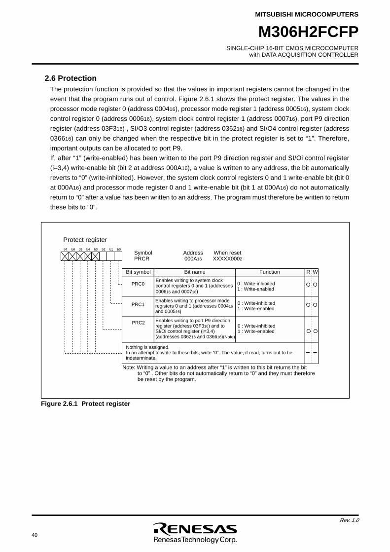
40
Rev. 1.0
SINGLE-CHIP 16-BIT CMOS MICROCOMPUTERwith DATA ACQUISITION CONTROLLER
MITSUBISHI MICROCOMPUTERS
M306H2FCFP
2.6 ProtectionThe protection function is provided so that the values in important registers cannot be changed in the
event that the program runs out of control. Figure 2.6.1 shows the protect register. The values in the
processor mode register 0 (address 000416), processor mode register 1 (address 000516), system clock
control register 0 (address 000616), system clock control register 1 (address 000716), port P9 direction
register (address 03F316) , SI/O3 control register (address 036216) and SI/O4 control register (address
036616) can only be changed when the respective bit in the protect register is set to “1”. Therefore,
important outputs can be allocated to port P9.
If, after “1” (write-enabled) has been written to the port P9 direction register and SI/Oi control register
(i=3,4) write-enable bit (bit 2 at address 000A16), a value is written to any address, the bit automatically
reverts to “0” (write-inhibited). However, the system clock control registers 0 and 1 write-enable bit (bit 0
at 000A16) and processor mode register 0 and 1 write-enable bit (bit 1 at 000A16) do not automatically
return to “0” after a value has been written to an address. The program must therefore be written to return
these bits to “0”.
Protect register
Symbol Address When resetPRCR 000A16 XXXXX0002
Bit nameBit symbol
b7 b6 b5 b4 b3 b2 b1 b0
0 : Write-inhibited1 : Write-enabled
PRC1
PRC0
PRC2
Enables writing to processor mode registers 0 and 1 (addresses 000416 and 000516)
Function
0 : Write-inhibited1 : Write-enabled
Enables writing to system clock control registers 0 and 1 (addresses 000616 and 000716)
Enables writing to port P9 direction register (address 03F316) and to SI/Oi control register (i=3,4)(addresses 036216 and 036616)(Note)
0 : Write-inhibited1 : Write-enabled
WR
AAAAAA
AAA
AAANothing is assigned.In an attempt to write to these bits, write “0”. The value, if read, turns out to be indeterminate.
Note: Writing a value to an address after “1” is written to this bit returns the bit to “0” . Other bits do not automatically return to “0” and they must therefore be reset by the program.
Figure 2.6.1 Protect register
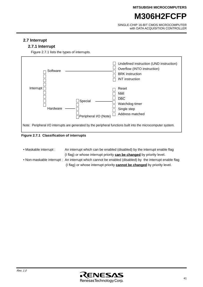
SINGLE-CHIP 16-BIT CMOS MICROCOMPUTERwith DATA ACQUISITION CONTROLLER
MITSUBISHI MICROCOMPUTERS
41
Rev. 1.0
M306H2FCFP
• Maskable interrupt : An interrupt which can be enabled (disabled) by the interrupt enable flag
(I flag) or whose interrupt priority can be changed by priority level.
• Non-maskable interrupt : An interrupt which cannot be enabled (disabled) by the interrupt enable flag
(I flag) or whose interrupt priority cannot be changed by priority level.
Figure 2.7.1 Classification of interrupts
Interrupt
Software
Hardware
Special
Peripheral I/O (Note)
Undefined instruction (UND instruction)
Overflow (INTO instruction)
BRK instruction
INT instruction
Reset
_______
NMI________
DBC
Watchdog timer
Single step
Address matched
Note: Peripheral I/O interrupts are generated by the peripheral functions built into the microcomputer system.
2.7 Interrupt
2.7.1 InterruptFigure 2.7.1 lists the types of interrupts.
42
Rev. 1.0
SINGLE-CHIP 16-BIT CMOS MICROCOMPUTERwith DATA ACQUISITION CONTROLLER
MITSUBISHI MICROCOMPUTERS
M306H2FCFP
2.7.2 Software InterruptsA software interrupt occurs when executing certain instructions. Software interrupts are non-
maskable interrupts.
• Undefined instruction interrupt
An undefined instruction interrupt occurs when executing the UND instruction.
• Overflow interrupt
An overflow interrupt occurs when executing the INTO instruction with the overflow flag (O flag) set to
“1”. The following are instructions whose O flag changes by arithmetic:
ABS, ADC, ADCF, ADD, CMP, DIV, DIVU, DIVX, NEG, RMPA, SBB, SHA, SUB
• BRK interrupt
A BRK interrupt occurs when executing the BRK instruction.
• INT interrupt
An INT interrupt occurs when assiging one of software interrupt numbers 0 through 63 and executing
the INT instruction. Software interrupt numbers 0 through 31 are assigned to peripheral I/O inter-
rupts, so executing the INT instruction allows executing the same interrupt routine that a peripheral I/O
interrupt does.
The stack pointer (SP) used for the INT interrupt is dependent on which software interrupt number is
involved.
So far as software interrupt numbers 0 through 31 are concerned, the microcomputer saves the
stack pointer assignment flag (U flag) when it accepts an interrupt request. If change the U flag to “0”
and select the interrupt stack pointer (ISP), and then execute an interrupt sequence. When returning
from the interrupt routine, the U flag is returned to the state it was before the acceptance of interrupt
request. So far as software numbers 32 through 63 are concerned, the stack pointer does not make
a shift.
SINGLE-CHIP 16-BIT CMOS MICROCOMPUTERwith DATA ACQUISITION CONTROLLER
MITSUBISHI MICROCOMPUTERS
43
Rev. 1.0
M306H2FCFP
2.7.3 Hardware InterruptsHardware interrupts are classified into two types — special interrupts and peripheral I/O interrupts.
(1) Special interruptsSpecial interrupts are non-maskable interrupts.
• Reset____________
Reset occurs if an “L” is input to the RESET pin._______
• NMI interrupt_______ _______
An NMI interrupt occurs if an “L” is input to the NMI pin.________
• DBC interruptThis interrupt is exclusively for the debugger, do not use it in other circumstances.
• Watchdog timer interruptGenerated by the watchdog timer.
• Single-step interruptThis interrupt is exclusively for the debugger, do not use it in other circumstances. With the debug
flag (D flag) set to “1”, a single-step interrupt occurs after one instruction is executed.
• Address match interruptAn address match interrupt occurs immediately before the instruction held in the address indicated
by the address match interrupt register is executed with the address match interrupt enable bit set to
“1”.
If an address other than the first address of the instruction in the address match interrupt register is
set, no address match interrupt occurs. For address match interrupt, see 2.7.10 Address match
Interrupt.
(2) Peripheral I/O interruptsA peripheral I/O interrupt is generated by one of built-in peripheral functions. Built-in peripheral func-
tions are dependent on classes of products, so the interrupt factors too are dependent on classes of
products. The interrupt vector table is the same as the one for software interrupt numbers 0 through
31 the INT instruction uses. Peripheral I/O interrupts are maskable interrupts.
• Bus collision detection interruptThis is an interrupt that the serial I/O bus collision detection generates.
• DMA0 interrupt, DMA1 interruptThese are interrupts that DMA generates.
• Key-input interrupt___
A key-input interrupt occurs if an “L” is input to the KI pin.
• A-D conversion interruptThis is an interrupt that the A-D converter generates.
• UART0, UART1, UART2/NACK, SI/O3 and SI/O4 transmission interruptThese are interrupts that the serial I/O transmission generates.
• UART0, UART1, UART2/ACK, SI/O3 and SI/O4 reception interruptThese are interrupts that the serial I/O reception generates.
• Timer A0 interrupt through timer A4 interruptThese are interrupts that timer A generates
• Timer B0 interrupt through timer B5 interruptThese are interrupts that timer B generates.________ ________
• INT0 interrupt through INT5 interrupt______ ______
An INT interrupt occurs if either a rising edge or a falling edge or a both edge is input to the INT pin.
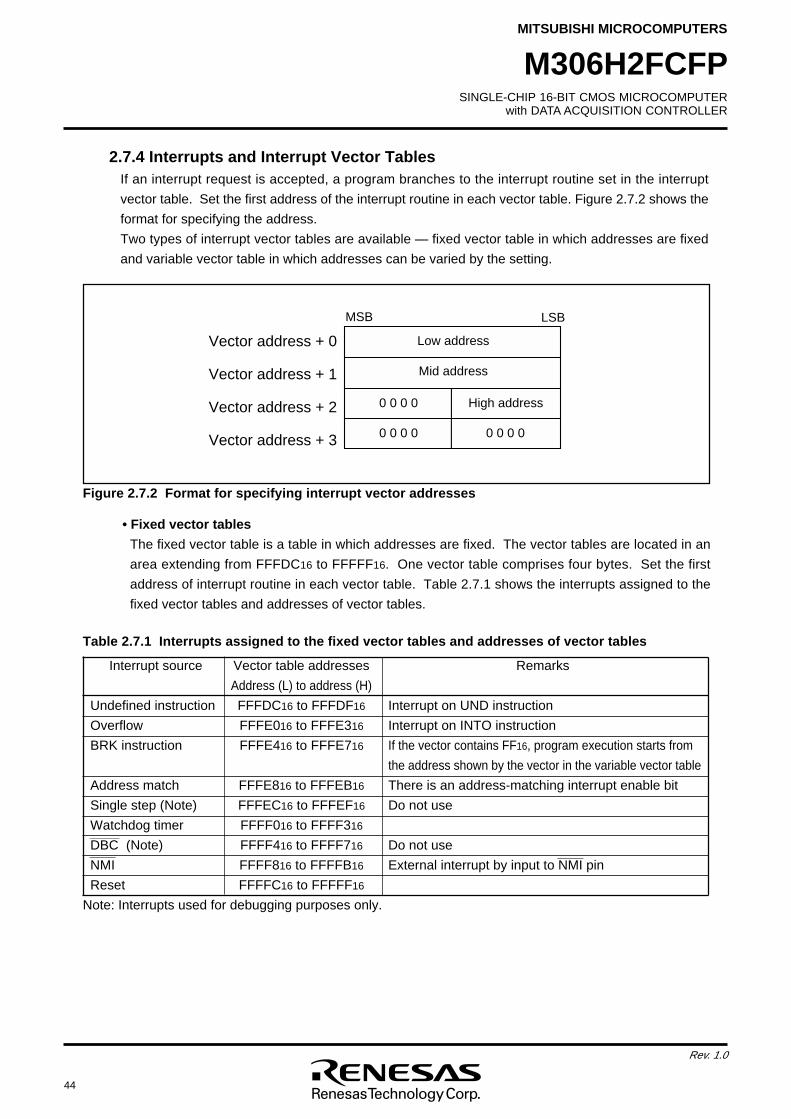
44
Rev. 1.0
SINGLE-CHIP 16-BIT CMOS MICROCOMPUTERwith DATA ACQUISITION CONTROLLER
MITSUBISHI MICROCOMPUTERS
M306H2FCFP
Interrupt source Vector table addresses Remarks
Address (L) to address (H)
Undefined instruction FFFDC16 to FFFDF16 Interrupt on UND instruction
Overflow FFFE016 to FFFE316 Interrupt on INTO instruction
BRK instruction FFFE416 to FFFE716 If the vector contains FF16, program execution starts from
the address shown by the vector in the variable vector table
Address match FFFE816 to FFFEB16 There is an address-matching interrupt enable bit
Single step (Note) FFFEC16 to FFFEF16 Do not use
Watchdog timer FFFF016 to FFFF316________
DBC (Note) FFFF416 to FFFF716 Do not use_______
NMI FFFF816 to FFFFB16_______
External interrupt by input to NMI pin
Reset FFFFC16 to FFFFF16
Note: Interrupts used for debugging purposes only.
Figure 2.7.2 Format for specifying interrupt vector addresses
AAAAAAAAAAAAAAAAAA
Mid addressAAAAAAAAAAAAAAAAAA
Low address
AAAAAAAAAAAAAAAAAA
0 0 0 0 High address
AAAAAAAAAAAAAAAAAA
0 0 0 0 0 0 0 0
Vector address + 0
Vector address + 1
Vector address + 2
Vector address + 3
LSBMSB
2.7.4 Interrupts and Interrupt Vector TablesIf an interrupt request is accepted, a program branches to the interrupt routine set in the interrupt
vector table. Set the first address of the interrupt routine in each vector table. Figure 2.7.2 shows the
format for specifying the address.
Two types of interrupt vector tables are available — fixed vector table in which addresses are fixed
and variable vector table in which addresses can be varied by the setting.
• Fixed vector tables
The fixed vector table is a table in which addresses are fixed. The vector tables are located in an
area extending from FFFDC16 to FFFFF16. One vector table comprises four bytes. Set the first
address of interrupt routine in each vector table. Table 2.7.1 shows the interrupts assigned to the
fixed vector tables and addresses of vector tables.
Table 2.7.1 Interrupts assigned to the fixed vector tables and addresses of vector tables
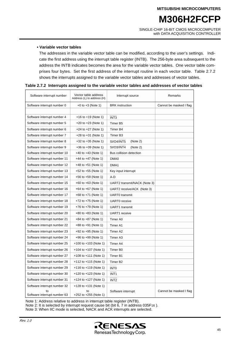
SINGLE-CHIP 16-BIT CMOS MICROCOMPUTERwith DATA ACQUISITION CONTROLLER
MITSUBISHI MICROCOMPUTERS
45
Rev. 1.0
M306H2FCFP
Software interrupt number Interrupt sourceVector table addressAddress (L) to address (H)
Remarks
Cannot be masked I flag+0 to +3 (Note 1) BRK instructionSoftware interrupt number 0
+44 to +47 (Note 1) Software interrupt number 11
+48 to +51 (Note 1)Software interrupt number 12
+52 to +55 (Note 1)Software interrupt number 13
+56 to +59 (Note 1)Software interrupt number 14
+68 to +71 (Note 1)Software interrupt number 17
+72 to +75 (Note 1)Software interrupt number 18
+76 to +79 (Note 1)Software interrupt number 19
+80 to +83 (Note 1)Software interrupt number 20
+84 to +87 (Note 1)Software interrupt number 21
+88 to +91 (Note 1)Software interrupt number 22
+92 to +95 (Note 1)Software interrupt number 23
+96 to +99 (Note 1)Software interrupt number 24
+100 to +103 (Note 1)Software interrupt number 25
+104 to +107 (Note 1)Software interrupt number 26
+108 to +111 (Note 1)Software interrupt number 27
+112 to +115 (Note 1)Software interrupt number 28
+116 to +119 (Note 1)Software interrupt number 29
+120 to +123 (Note 1)Software interrupt number 30
+124 to +127 (Note 1)Software interrupt number 31
+128 to +131 (Note 1)Software interrupt number 32
+252 to +255 (Note 1)Software interrupt number 63to
Note 1: Address relative to address in interrupt table register (INTB).Note 2: It is selected by interrupt request cause bit (bit 6, 7 in address 035F16 ).Note 3: When IIC mode is selected, NACK and ACK interrupts are selected.
Cannot be masked I flag
+40 to +43 (Note 1)Software interrupt number 10
+60 to +63 (Note 1)Software interrupt number 15
+64 to +67 (Note 1)Software interrupt number 16
+20 to +23 (Note 1)Software interrupt number 5
+24 to +27 (Note 1)Software interrupt number 6
+28 to +31 (Note 1)Software interrupt number 7
+32 to +35 (Note 1)Software interrupt number 8
+16 to +19 (Note 1) INT3Software interrupt number 4
+36 to +39 (Note 1) SI/O3/INT4Software interrupt number 9
SI/O4/INT5
Timer B3
Timer B4
Timer B5
(Note 2)
(Note 2)
to
DMA0
DMA1
Key input interrupt
A-D
UART0 transmit
UART0 receive
UART1 transmit
UART1 receive
Timer A0
Timer A1
Timer A2
Timer A3
Timer A4
Timer B0
Timer B1
Timer B2
INT0
INT1
INT2
Software interrupt
Bus collision detection
UART2 transmit/NACK (Note 3)
UART2 receive/ACK (Note 3)
Table 2.7.2 Interrupts assigned to the variable vector tables and addresses of vector tables
• Variable vector tables
The addresses in the variable vector table can be modified, according to the user’s settings. Indi-
cate the first address using the interrupt table register (INTB). The 256-byte area subsequent to the
address the INTB indicates becomes the area for the variable vector tables. One vector table com-
prises four bytes. Set the first address of the interrupt routine in each vector table. Table 2.7.2
shows the interrupts assigned to the variable vector tables and addresses of vector tables.
46
Rev. 1.0
SINGLE-CHIP 16-BIT CMOS MICROCOMPUTERwith DATA ACQUISITION CONTROLLER
MITSUBISHI MICROCOMPUTERS
M306H2FCFP
2.7.5 Interrupt ControlDescriptions are given here regarding how to enable or disable maskable interrupts and how to set the
priority to be accepted. What is described here does not apply to non-maskable interrupts.
Enable or disable a maskable interrupt using the interrupt enable flag (I flag), interrupt priority level
selection bit, or processor interrupt priority level (IPL). Whether an interrupt request is present or
absent is indicated by the interrupt request bit. The interrupt request bit and the interrupt priority level
selection bit are located in the interrupt control register of each interrupt. Also, the interrupt enable
flag (I flag) and the IPL are located in the flag register (FLG).
Figure 2.7.3 shows the memory map of the interrupt control registers.
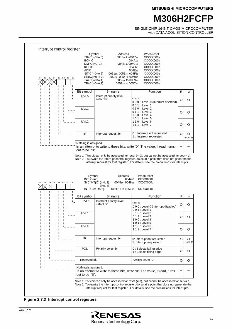
SINGLE-CHIP 16-BIT CMOS MICROCOMPUTERwith DATA ACQUISITION CONTROLLER
MITSUBISHI MICROCOMPUTERS
47
Rev. 1.0
M306H2FCFP
Symbol Address When resetINTiIC(i=3) 004416 XX00X0002SiIC/INTjIC (i=4, 3) 004816, 004916 XX00X0002
(j=5, 4)INTiIC(i=0 to 2) 005D16 to 005F16 XX00X0002
Bit name FunctionBit symbol WR
b7 b6 b5 b4 b3 b2 b1 b0
AAAAAA
ILVL0
IR
POL
Nothing is assigned.In an attempt to write to these bits, write “0”. The value, if read, turns out to be “0”.
Interrupt priority level select bit
Interrupt request bit
Polarity select bit
Reserved bit
0: Interrupt not requested1: Interrupt requested
0 : Selects falling edge1 : Selects rising edge
Always set to “0”
ILVL1
ILVL2
Note 1: This bit can only be accessed for reset (= 0), but cannot be accessed for set (= 1). Note 2: To rewrite the interrupt control register, do so at a point that dose not generate the
interrupt request for that register. For details, see the precautions for interrupts.
(Note 1)
Interrupt control register
b7 b6 b5 b4 b3 b2 b1 b0
AAAAAAAAAAAA
Bit name FunctionBit symbol WR
Symbol Address When reset TBiIC(i=3 to 5) 004516 to 004716 XXXXX0002BCNIC 004A16 XXXXX0002DMiIC(i=0, 1) 004B16, 004C16 XXXXX0002KUPIC 004D16 XXXXX0002ADIC 004E16 XXXXX0002SiTIC(i=0 to 2) 005116, 005316, 004F16 XXXXX0002SiRIC(i=0 to 2) 005216, 005416, 005016 XXXXX0002TAiIC(i=0 to 4) 005516 to 005916 XXXXX0002TBiIC(i=0 to 2) 005A16 to 005C16 XXXXX0002
ILVL0
IR
Interrupt priority level select bit
Interrupt request bit 0 : Interrupt not requested1 : Interrupt requested
ILVL1
ILVL2
Nothing is assigned.In an attempt to write to these bits, write “0”. The value, if read, turns out to be “0”.
(Note 1)
Note 1: This bit can only be accessed for reset (= 0), but cannot be accessed for set (= 1). Note 2: To rewrite the interrupt control register, do so at a point that dose not generate the
interrupt request for that register. For details, see the precautions for interrupts.
0 0 0 : Level 0 (interrupt disabled)0 0 1 : Level 1 0 1 0 : Level 2 0 1 1 : Level 3 1 0 0 : Level 4 1 0 1 : Level 5 1 1 0 : Level 6 1 1 1 : Level 7
b2 b1 b0
0 0 0 : Level 0 (interrupt disabled)0 0 1 : Level 1 0 1 0 : Level 2 0 1 1 : Level 3 1 0 0 : Level 4 1 0 1 : Level 5 1 1 0 : Level 6 1 1 1 : Level 7
b2 b1 b0
0
AAAA
AAAA
AA
AAAA
AAAA
AAAA
Figure 2.7.3 Interrupt control registers
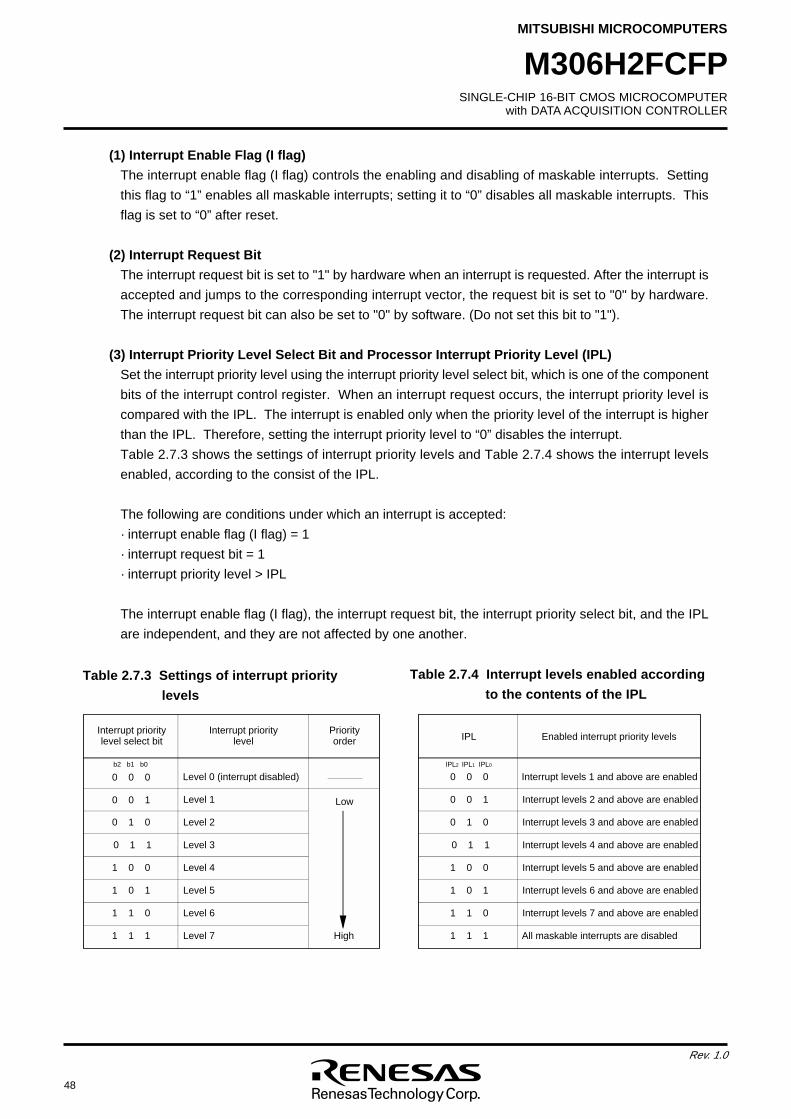
48
Rev. 1.0
SINGLE-CHIP 16-BIT CMOS MICROCOMPUTERwith DATA ACQUISITION CONTROLLER
MITSUBISHI MICROCOMPUTERS
M306H2FCFP
(1) Interrupt Enable Flag (I flag)
The interrupt enable flag (I flag) controls the enabling and disabling of maskable interrupts. Setting
this flag to “1” enables all maskable interrupts; setting it to “0” disables all maskable interrupts. This
flag is set to “0” after reset.
(2) Interrupt Request Bit
The interrupt request bit is set to "1" by hardware when an interrupt is requested. After the interrupt is
accepted and jumps to the corresponding interrupt vector, the request bit is set to "0" by hardware.
The interrupt request bit can also be set to "0" by software. (Do not set this bit to "1").
(3) Interrupt Priority Level Select Bit and Processor Interrupt Priority Level (IPL)
Set the interrupt priority level using the interrupt priority level select bit, which is one of the component
bits of the interrupt control register. When an interrupt request occurs, the interrupt priority level is
compared with the IPL. The interrupt is enabled only when the priority level of the interrupt is higher
than the IPL. Therefore, setting the interrupt priority level to “0” disables the interrupt.
Table 2.7.3 shows the settings of interrupt priority levels and Table 2.7.4 shows the interrupt levels
enabled, according to the consist of the IPL.
The following are conditions under which an interrupt is accepted:
· interrupt enable flag (I flag) = 1
· interrupt request bit = 1
· interrupt priority level > IPL
The interrupt enable flag (I flag), the interrupt request bit, the interrupt priority select bit, and the IPL
are independent, and they are not affected by one another.
Table 2.7.4 Interrupt levels enabled according
to the contents of the IPLTable 2.7.3 Settings of interrupt priority
levels
Interrupt priority level select bit
Interrupt prioritylevel
Priorityorder
0 0 0
0 0 1
0 1 0
0 1 1
1 0 0
1 0 1
1 1 0
1 1 1
Level 0 (interrupt disabled)
Level 1
Level 2
Level 3
Level 4
Level 5
Level 6
Level 7
Low
High
b2 b1 b0
Enabled interrupt priority levels
0 0 0
0 0 1
0 1 0
0 1 1
1 0 0
1 0 1
1 1 0
1 1 1
Interrupt levels 1 and above are enabled
Interrupt levels 2 and above are enabled
Interrupt levels 3 and above are enabled
Interrupt levels 4 and above are enabled
Interrupt levels 5 and above are enabled
Interrupt levels 6 and above are enabled
Interrupt levels 7 and above are enabled
All maskable interrupts are disabled
IPL2 IPL1 IPL0
IPL
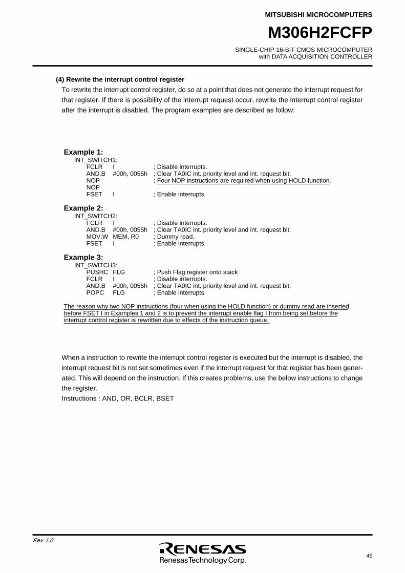
SINGLE-CHIP 16-BIT CMOS MICROCOMPUTERwith DATA ACQUISITION CONTROLLER
MITSUBISHI MICROCOMPUTERS
49
Rev. 1.0
M306H2FCFP
Example 1:INT_SWITCH1:
FCLR I ; Disable interrupts.AND.B #00h, 0055h ; Clear TA0IC int. priority level and int. request bit.NOP ; Four NOP instructions are required when using HOLD function.NOPFSET I ; Enable interrupts.
Example 2:INT_SWITCH2:
FCLR I ; Disable interrupts.AND.B #00h, 0055h ; Clear TA0IC int. priority level and int. request bit.MOV.W MEM, R0 ; Dummy read.FSET I ; Enable interrupts.
Example 3:INT_SWITCH3:
PUSHC FLG ; Push Flag register onto stackFCLR I ; Disable interrupts.AND.B #00h, 0055h ; Clear TA0IC int. priority level and int. request bit.POPC FLG ; Enable interrupts.
The reason why two NOP instructions (four when using the HOLD function) or dummy read are inserted before FSET I in Examples 1 and 2 is to prevent the interrupt enable flag I from being set before the interrupt control register is rewritten due to effects of the instruction queue.
(4) Rewrite the interrupt control register
To rewrite the interrupt control register, do so at a point that does not generate the interrupt request for
that register. If there is possibility of the interrupt request occur, rewrite the interrupt control register
after the interrupt is disabled. The program examples are described as follow:
When a instruction to rewrite the interrupt control register is executed but the interrupt is disabled, the
interrupt request bit is not set sometimes even if the interrupt request for that register has been gener-
ated. This will depend on the instruction. If this creates problems, use the below instructions to change
the register.
Instructions : AND, OR, BCLR, BSET
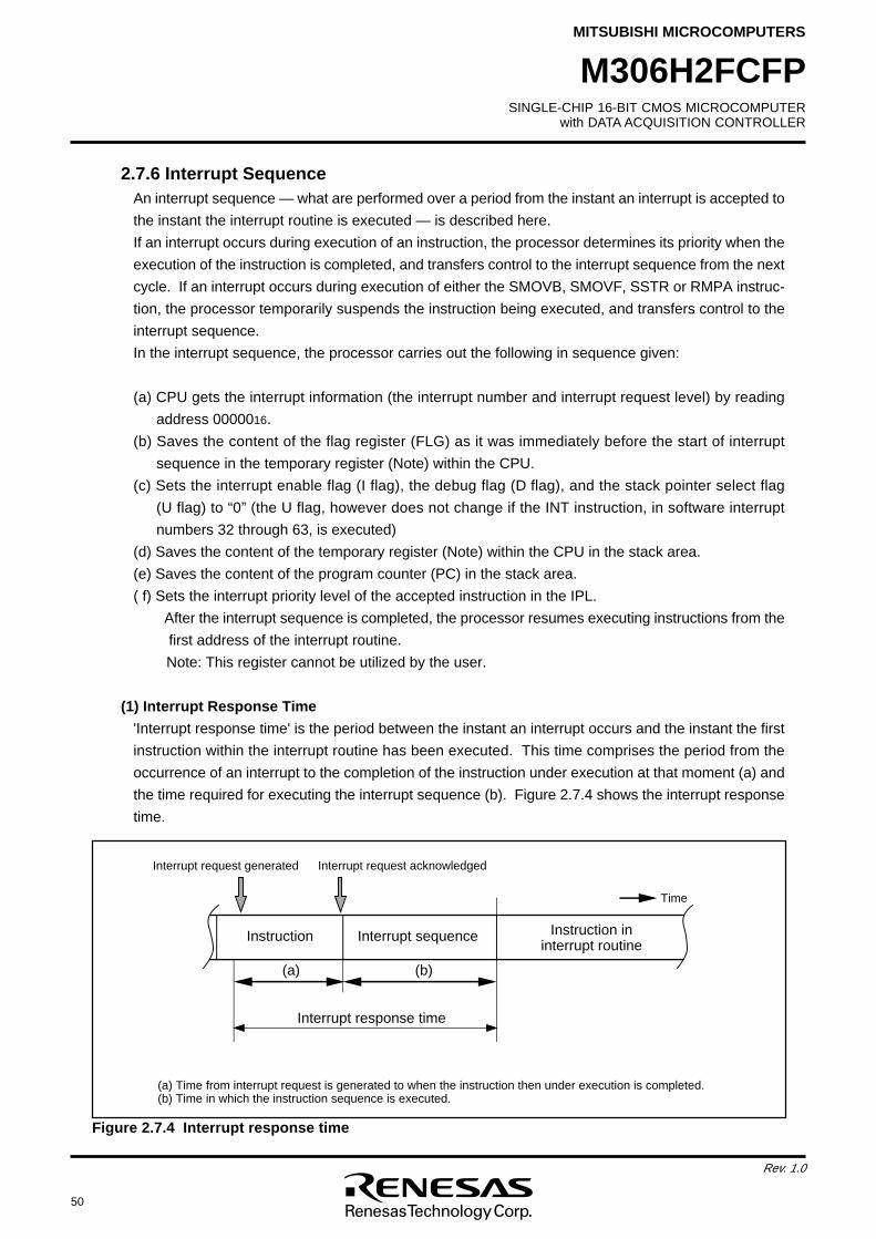
50
Rev. 1.0
SINGLE-CHIP 16-BIT CMOS MICROCOMPUTERwith DATA ACQUISITION CONTROLLER
MITSUBISHI MICROCOMPUTERS
M306H2FCFP
2.7.6 Interrupt SequenceAn interrupt sequence — what are performed over a period from the instant an interrupt is accepted to
the instant the interrupt routine is executed — is described here.
If an interrupt occurs during execution of an instruction, the processor determines its priority when the
execution of the instruction is completed, and transfers control to the interrupt sequence from the next
cycle. If an interrupt occurs during execution of either the SMOVB, SMOVF, SSTR or RMPA instruc-
tion, the processor temporarily suspends the instruction being executed, and transfers control to the
interrupt sequence.
In the interrupt sequence, the processor carries out the following in sequence given:
(a) CPU gets the interrupt information (the interrupt number and interrupt request level) by reading
address 0000016.
(b) Saves the content of the flag register (FLG) as it was immediately before the start of interrupt
sequence in the temporary register (Note) within the CPU.
(c) Sets the interrupt enable flag (I flag), the debug flag (D flag), and the stack pointer select flag
(U flag) to “0” (the U flag, however does not change if the INT instruction, in software interrupt
numbers 32 through 63, is executed)
(d) Saves the content of the temporary register (Note) within the CPU in the stack area.
(e) Saves the content of the program counter (PC) in the stack area.
( f) Sets the interrupt priority level of the accepted instruction in the IPL.
After the interrupt sequence is completed, the processor resumes executing instructions from the
first address of the interrupt routine.
Note: This register cannot be utilized by the user.
(1) Interrupt Response Time
'Interrupt response time' is the period between the instant an interrupt occurs and the instant the first
instruction within the interrupt routine has been executed. This time comprises the period from the
occurrence of an interrupt to the completion of the instruction under execution at that moment (a) and
the time required for executing the interrupt sequence (b). Figure 2.7.4 shows the interrupt response
time.
Instruction Interrupt sequence Instruction in interrupt routine
Time
Interrupt response time
(a) (b)
Interrupt request acknowledgedInterrupt request generated
(a) Time from interrupt request is generated to when the instruction then under execution is completed.(b) Time in which the instruction sequence is executed.
Figure 2.7.4 Interrupt response time
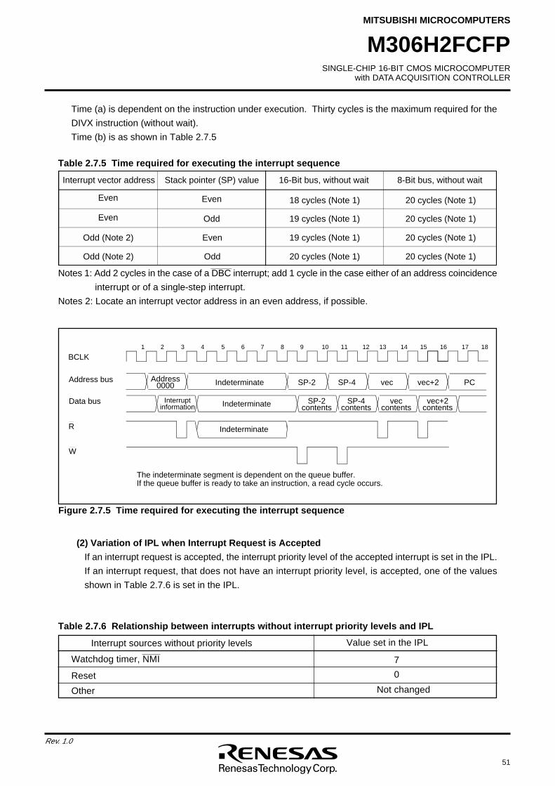
SINGLE-CHIP 16-BIT CMOS MICROCOMPUTERwith DATA ACQUISITION CONTROLLER
MITSUBISHI MICROCOMPUTERS
51
Rev. 1.0
M306H2FCFP
Interrupt sources without priority levels
7
Value set in the IPL_______
Watchdog timer, NMI
Other Not changed
0
Stack pointer (SP) valueInterrupt vector address 16-Bit bus, without wait 8-Bit bus, without wait
Even
Even
Odd (Note 2)
Odd (Note 2)
Even
Odd
Even
Odd
18 cycles (Note 1)
19 cycles (Note 1)
19 cycles (Note 1)
20 cycles (Note 1)
20 cycles (Note 1)
20 cycles (Note 1)
20 cycles (Note 1)
20 cycles (Note 1)
Reset
Indeterminate
1 2 3 4 5 6 7 8 9 10 11 12 13 14 15 16 17 18
The indeterminate segment is dependent on the queue buffer.If the queue buffer is ready to take an instruction, a read cycle occurs.
Indeterminate SP-2 contents
SP-4 contents
vec contents
vec+2 contents
Interrupt information
Address 0000 Indeterminate SP-2 SP-4 vec vec+2 PC
BCLK
Address bus
Data bus
W
R
Table 2.7.6 Relationship between interrupts without interrupt priority levels and IPL
(2) Variation of IPL when Interrupt Request is Accepted
If an interrupt request is accepted, the interrupt priority level of the accepted interrupt is set in the IPL.
If an interrupt request, that does not have an interrupt priority level, is accepted, one of the values
shown in Table 2.7.6 is set in the IPL.
Figure 2.7.5 Time required for executing the interrupt sequence
________
Notes 1: Add 2 cycles in the case of a DBC interrupt; add 1 cycle in the case either of an address coincidence
interrupt or of a single-step interrupt.
Notes 2: Locate an interrupt vector address in an even address, if possible.
Table 2.7.5 Time required for executing the interrupt sequence
Time (a) is dependent on the instruction under execution. Thirty cycles is the maximum required for the
DIVX instruction (without wait).
Time (b) is as shown in Table 2.7.5
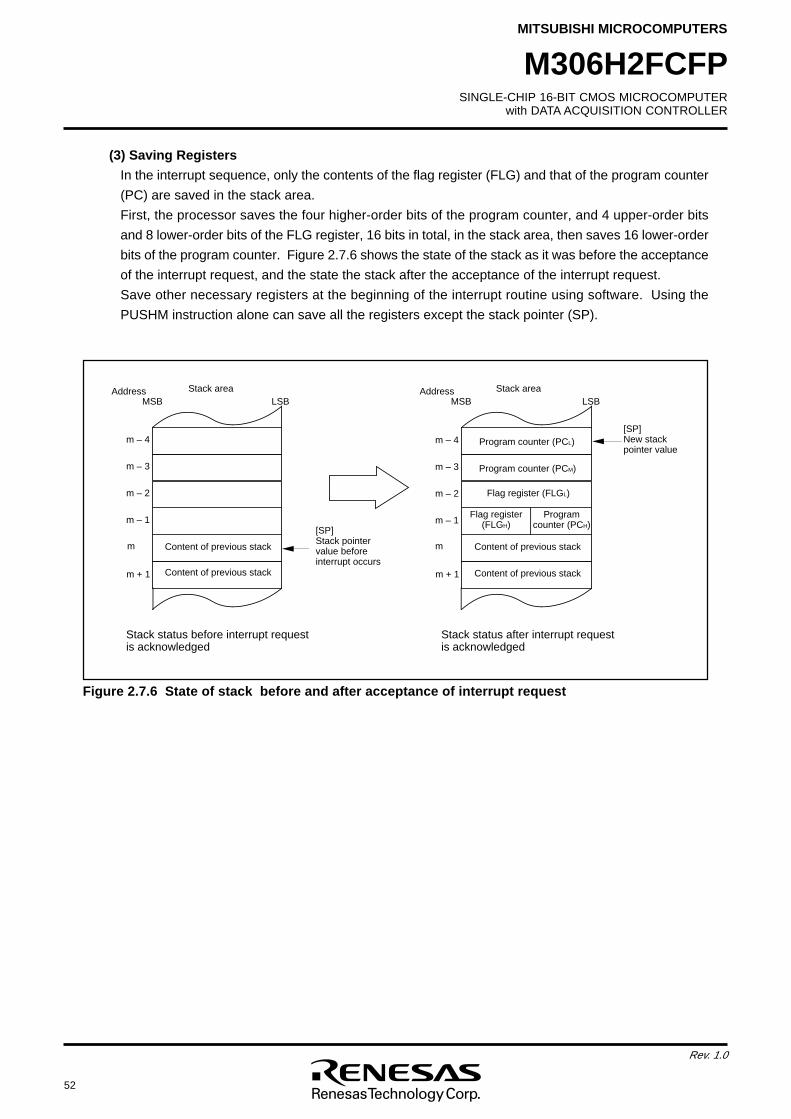
52
Rev. 1.0
SINGLE-CHIP 16-BIT CMOS MICROCOMPUTERwith DATA ACQUISITION CONTROLLER
MITSUBISHI MICROCOMPUTERS
M306H2FCFP
(3) Saving Registers
In the interrupt sequence, only the contents of the flag register (FLG) and that of the program counter
(PC) are saved in the stack area.
First, the processor saves the four higher-order bits of the program counter, and 4 upper-order bits
and 8 lower-order bits of the FLG register, 16 bits in total, in the stack area, then saves 16 lower-order
bits of the program counter. Figure 2.7.6 shows the state of the stack as it was before the acceptance
of the interrupt request, and the state the stack after the acceptance of the interrupt request.
Save other necessary registers at the beginning of the interrupt routine using software. Using the
PUSHM instruction alone can save all the registers except the stack pointer (SP).
Address
Content of previous stack
Stack area
[SP]Stack pointervalue beforeinterrupt occurs
m
m – 1
m – 2
m – 3
m – 4
Stack status before interrupt requestis acknowledged
Stack status after interrupt requestis acknowledged
Content of previous stackm + 1
MSB LSB
m
m – 1
m – 2
m – 3
m – 4
Address
Flag register (FLGL)
Content of previous stack
Stack area
Flag register(FLGH)
Programcounter (PCH)
[SP]New stack pointer value
Content of previous stackm + 1
MSB LSB
Program counter (PCL)
Program counter (PCM)
Figure 2.7.6 State of stack before and after acceptance of interrupt request
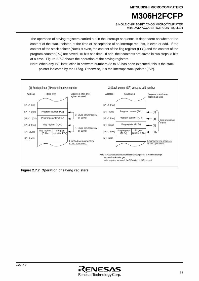
SINGLE-CHIP 16-BIT CMOS MICROCOMPUTERwith DATA ACQUISITION CONTROLLER
MITSUBISHI MICROCOMPUTERS
53
Rev. 1.0
M306H2FCFP
(2) Stack pointer (SP) contains odd number
[SP] (Odd)
[SP] – 1 (Even)
[SP] – 2(Odd)
[SP] – 3 (Even)
[SP] – 4(Odd)
[SP] – 5 (Even)
Address Sequence in which order registers are saved
(2)
(1)
Finished saving registers in four operations.
(3)
(4)
(1) Stack pointer (SP) contains even number
[SP] (Even)
[SP] – 1(Odd)
[SP] – 2 (Even)
[SP] – 3 (Odd)
[SP] – 4 (Even)
[SP] – 5 (Odd)
Note: [SP] denotes the initial value of the stack pointer (SP) when interrupt request is acknowledged.After registers are saved, the SP content is [SP] minus 4.
Address
Program counter (PCM)
Stack area
Flag register (FLGL)
Program counter (PCL)
Sequence in which order registers are saved
(2) Saved simultaneously,all 16 bits
(1) Saved simultaneously,all 16 bits
Finished saving registers in two operations.
Program counter (PCM)
Stack area
Flag register (FLGL)
Program counter (PCL)
Saved simultaneously, all 8 bits
Flag register(FLGH)
Programcounter (PCH)
Flag register(FLGH)
Programcounter (PCH)
The operation of saving registers carried out in the interrupt sequence is dependent on whether the
content of the stack pointer, at the time of acceptance of an interrupt request, is even or odd. If the
content of the stack pointer (Note) is even, the content of the flag register (FLG) and the content of the
program counter (PC) are saved, 16 bits at a time. If odd, their contents are saved in two steps, 8 bits
at a time. Figure 2.7.7 shows the operation of the saving registers.
Note: When any INT instruction in software numbers 32 to 63 has been executed, this is the stack
pointer indicated by the U flag. Otherwise, it is the interrupt stack pointer (ISP).
Figure 2.7.7 Operation of saving registers
54
Rev. 1.0
SINGLE-CHIP 16-BIT CMOS MICROCOMPUTERwith DATA ACQUISITION CONTROLLER
MITSUBISHI MICROCOMPUTERS
M306H2FCFP
(5) Interrupt Priority
If there are two or more interrupt requests occurring at a point in time within a single sampling (check-
ing whether interrupt requests are made), the interrupt assigned a higher priority is accepted.
Assign an arbitrary priority to maskable interrupts (peripheral I/O interrupts) using the interrupt priority
level select bit. If the same interrupt priority level is assigned, however, the interrupt assigned a higher
hardware priority is accepted.
Priorities of the special interrupts, such as Reset (dealt with as an interrupt assigned the highest
priority), watchdog timer interrupt, etc. are regulated by hardware.
Figure 2.7.8 shows the priorities of hardware interrupts.
Software interrupts are not affected by the interrupt priority. If an instruction is executed, control
branches invariably to the interrupt routine.
(4) Returning from an Interrupt Routine
Executing the REIT instruction at the end of an interrupt routine returns the contents of the flag register
(FLG) as it was immediately before the start of interrupt sequence and the contents of the program
counter (PC), both of which have been saved in the stack area. Then control returns to the program
that was being executed before the acceptance of the interrupt request, so that the suspended pro-
cess resumes.
Return the other registers saved by software within the interrupt routine using the POPM or similar
instruction before executing the REIT instruction.
(6) Interrupt resolution circuit
When two or more interrupts are generated simultaneously, this circuit selects the interrupt with the
highest priority level. Figure 2.7.9 shows the circuit that judges the interrupt priority level.
Figure 2.7.8 Hardware interrupts priorities
_______ ________
Reset > NMI > DBC > Watchdog timer > Peripheral I/O > Single step > Address match
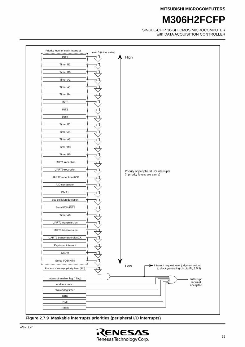
SINGLE-CHIP 16-BIT CMOS MICROCOMPUTERwith DATA ACQUISITION CONTROLLER
MITSUBISHI MICROCOMPUTERS
55
Rev. 1.0
M306H2FCFP
Figure 2.7.9 Maskable interrupts priorities (peripheral I/O interrupts)
Timer B2
Timer B0
Timer A3
Timer A1
Timer B1
Timer A4
Timer A2
UART1 reception
UART0 reception
UART2 reception/ACK
A-D conversion
DMA1
Bus collision detection
Timer A0
UART1 transmission
UART0 transmission
UART2 transmission/NACK
Key input interrupt
DMA0
Processor interrupt priority level (IPL)
Interrupt enable flag (I flag)
INT1
INT2
INT0
Watchdog timer
Reset
DBC
NMI
Interrupt request
accepted
Level 0 (initial value)Priority level of each interrupt
High
Low
Priority of peripheral I/O interrupts(if priority levels are same)
Timer B4
INT3
Timer B3
Timer B5
Serial I/O4/INT5
Serial I/O3/INT4
Address match
Interrupt request level judgment output to clock generating circuit (Fig.2.5.3)
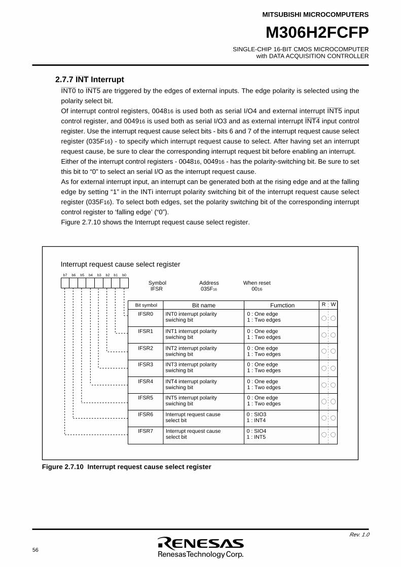
56
Rev. 1.0
SINGLE-CHIP 16-BIT CMOS MICROCOMPUTERwith DATA ACQUISITION CONTROLLER
MITSUBISHI MICROCOMPUTERS
M306H2FCFP
______
2.7.7 INT Interrupt________ ________
INT0 to INT5 are triggered by the edges of external inputs. The edge polarity is selected using the
polarity select bit.________
Of interrupt control registers, 004816 is used both as serial I/O4 and external interrupt INT5 input________
control register, and 004916 is used both as serial I/O3 and as external interrupt INT4 input control
register. Use the interrupt request cause select bits - bits 6 and 7 of the interrupt request cause select
register (035F16) - to specify which interrupt request cause to select. After having set an interrupt
request cause, be sure to clear the corresponding interrupt request bit before enabling an interrupt.
Either of the interrupt control registers - 004816, 004916 - has the polarity-switching bit. Be sure to set
this bit to “0” to select an serial I/O as the interrupt request cause.
As for external interrupt input, an interrupt can be generated both at the rising edge and at the falling
edge by setting “1” in the INTi interrupt polarity switching bit of the interrupt request cause select
register (035F16). To select both edges, set the polarity switching bit of the corresponding interrupt
control register to ‘falling edge’ (“0”).
Figure 2.7.10 shows the Interrupt request cause select register.
Figure 2.7.10 Interrupt request cause select register
Interrupt request cause select register
Bit name FumctionBit symbol WR
Symbol Address When resetIFSR 035F16 0016
IFSR0
b7 b6 b5 b4 b3 b2 b1 b0
AAAAAAAAAAAA
INT0 interrupt polarity swiching bit
0 : SIO31 : INT4
0 : SIO41 : INT5
0 : One edge1 : Two edges
0 : One edge1 : Two edges
0 : One edge1 : Two edges
0 : One edge1 : Two edges
0 : One edge1 : Two edges
INT1 interrupt polarity swiching bit
INT2 interrupt polarity swiching bit
INT3 interrupt polarity swiching bit
INT4 interrupt polarity swiching bit
INT5 interrupt polarity swiching bit
0 : One edge1 : Two edges
Interrupt request cause select bit
Interrupt request cause select bit
IFSR1
IFSR2
IFSR3
IFSR4
IFSR5
IFSR6
IFSR7
AAAAAA
AAAAAA
AAAAAAAAA
AAAAAA
AAAAAA
SINGLE-CHIP 16-BIT CMOS MICROCOMPUTERwith DATA ACQUISITION CONTROLLER
MITSUBISHI MICROCOMPUTERS
57
Rev. 1.0
M306H2FCFP
Interrupt control circuit
Key input interrupt control register (address 004D16)
Key input interrupt request
P107/KI3
P106/KI2
P105/KI1
P104/KI0
Port P104-P107 pull-up select bit
Port P107 direction register
Pull-up transistor
Port P107 direction register
Port P106 direction register
Port P105 direction register
Port P104 direction register
Pull-up transistor
Pull-up transistor
Pull-up transistor
Figure 2.7.11 Block diagram of key input interrupt
______
2.7.8 NMI Interrupt______ ______ ______
An NMI interrupt is generated when the input to the P85/NMI pin changes from “H” to “L”. The NMI
interrupt is a non-maskable external interrupt. The pin level can be checked in the port P85 register (bit
5 at address 03F016).
This pin cannot be used as a normal port input.
2.7.9 Key Input InterruptIf the direction register of any of P104 to P107 is set for input and a falling edge is input to that port, a
key input interrupt is generated. A key input interrupt can also be used as a key-on wakeup function for
cancelling the wait mode or stop mode. However, if you intend to use the key input interrupt, do not
use P104 to P107 as A-D input ports. Figure 2.7.11 shows the block diagram of the key input interrupt.
Note that if an “L” level is input to any pin that has not been disabled for input, inputs to the other pins
are not detected as an interrupt.
58
Rev. 1.0
SINGLE-CHIP 16-BIT CMOS MICROCOMPUTERwith DATA ACQUISITION CONTROLLER
MITSUBISHI MICROCOMPUTERS
M306H2FCFP
2.7.10 Address Match InterruptAn address match interrupt is generated when the address match interrupt address register contents
match the program counter value. Two address match interrupts can be set, each of which can be
enabled and disabled by an address match interrupt enable bit. Address match interrupts are not
affected by the interrupt enable flag (I flag) and processor interrupt priority level (IPL). The value of the
program counter (PC) for an address match interrupt varies depending on the instruction being executed.
Note that when using the external data bus in width of 8 bits, the address match interrupt cannot
be used for external area.
Figure 2.7.12 shows the address match interrupt-related registers.
Bit nameBit symbol
Symbol Address When resetAIER 000916 XXXXXX002
Address match interrupt enable register
Function WR
AAAAAAAAAAAAAAAAAAAAAAAAAAAAAAAAAAAAAAAAAA
AAAAAAAAAAAAAAAAAAAAAAAAAAAAAAAAAAAAAAAAAA
Address match interrupt 0 enable bit
0 : Interrupt disabled1 : Interrupt enabled
AIER0
Address match interrupt 1 enable bit
AIER1
AAAAAAAAAAAAAAAAAAAAAAAAAAAA
Symbol Address When reset RMAD0 001216 to 001016 X0000016RMAD1 001616 to 001416 X0000016
Nothing is assigned.In an attempt to write to these bits, write “0”. The value, if read, turns out to be indeterminated.
b7 b6 b5 b4 b3 b2 b1 b0
WR
Address setting register for address match interrupt
Function Values that can be set
Address match interrupt register i (i = 0, 1)
0000016 to FFFFF16
Nothing is assigned.In an attempt to write to these bits, write “0”. The value, if read, turns out to be indeterminated.
0 : Interrupt disabled1 : Interrupt enabled
b0 b7 b0b3(b19) (b16)
b7 b0(b15) (b8)
b7(b23)
AAAAAA
AAAAAA
Figure 2.7.12 Address match interrupt-related registers
SINGLE-CHIP 16-BIT CMOS MICROCOMPUTERwith DATA ACQUISITION CONTROLLER
MITSUBISHI MICROCOMPUTERS
59
Rev. 1.0
M306H2FCFP
2.7.11 Precautions for Interrupts(1) Reading address 0000016
• When maskable interrupt is occurred, CPU read the interrupt information (the interrupt number and
interrupt request level) in the interrupt sequence. The interrupt request bit of the certain interrupt
written in address 0000016 will then be set to “0”. Reading address 0000016 by software sets
enabled highest priority interrupt source request bit to “0”.
Though the interrupt is generated, the interrupt routine may not be executed.
Do not read address 0000016 by software.
(2) Setting the stack pointer
• The value of the stack pointer immediately after reset is initialized to 000016. Accepting an interrupt
before setting a value in the stack pointer may become a factor of runaway. Be sure to set a value in_______
the stack pointer before accepting an interrupt. When using the NMI interrupt, initialize the stack
point at the beginning of a program. Concerning the first instruction immediately after reset, gener-_______
ating any interrupts including the NMI interrupt is prohibited._______
(3) The NMI interrupt_______
• As for the NMI interrupt pin, an interrupt cannot be disabled. Connect it to the Vcc pin via a resistor
(pull-up) if unused. Be sure to work on it._______
• The NMI pin also serves as P85, which is exclusively input. Reading the contents of the P8 register
allows reading the pin value. Use the reading of this pin only for establishing the pin level at the time_______
when the NMI interrupt is input._______
• Do not reset the CPU with the input to the NMI pin being in the “L” state._______
• Do not attempt to go into stop mode with the input to the NMI pin being in the “L” state. With the input_______
to the NMI being in the “L” state, the CM10 is fixed to “0”, so attempting to go into stop mode is
turned down._______
• Do not attempt to go into wait mode with the input to the NMI pin being in the “L” state. With the input_______
to the NMI pin being in the “L” state, the CPU stops but the oscillation does not stop, so no power is
saved. In this instance, the CPU is returned to the normal state by a later interrupt._______
• Signals input to the NMI pin require an "L" level of 1 clock or more, from the operation clock of the
CPU.
(4) External interrupt________
• Either an “L” level or an “H” level of at least 250 ns width is necessary for the signal input to pins INT0________
through INT5 regardless of the CPU operation clock.________ ________
• When the polarity of the INT0 to INT5 pins is changed, the interrupt request bit is sometimes set to
"1". After changing the polarity, set the interrupt request bit to "0". Figure 2.7.13 shows the proce-______
dure for changing the INT interrupt generate factor.
60
Rev. 1.0
SINGLE-CHIP 16-BIT CMOS MICROCOMPUTERwith DATA ACQUISITION CONTROLLER
MITSUBISHI MICROCOMPUTERS
M306H2FCFP
______
Figure 2.7.13 Switching condition of INT interrupt request
Example 1:INT_SWITCH1:
FCLR I ; Disable interrupts.AND.B #00h, 0055h ; Clear TA0IC int. priority level and int. request bit.NOP ; Four NOP instructions are required when using HOLD function.NOPFSET I ; Enable interrupts.
Example 2:INT_SWITCH2:
FCLR I ; Disable interrupts.AND.B #00h, 0055h ; Clear TA0IC int. priority level and int. request bit.MOV.W MEM, R0 ; Dummy read.FSET I ; Enable interrupts.
Example 3:INT_SWITCH3:
PUSHC FLG ; Push Flag register onto stackFCLR I ; Disable interrupts.AND.B #00h, 0055h ; Clear TA0IC int. priority level and int. request bit.POPC FLG ; Enable interrupts.
The reason why two NOP instructions (four when using the HOLD function) or dummy read are inserted before FSET I in Examples 1 and 2 is to prevent the interrupt enable flag I from being set before the interrupt control register is rewritten due to effects of the instruction queue.
(5) Rewrite the interrupt control register
• To rewrite the interrupt control register, do so at a point that does not generate the interrupt request
for that register. If there is possibility of the interrupt request occur, rewrite the interrupt control
register after the interrupt is disabled. The program examples are described as follow:
Set the polarity select bit
Clear the interrupt request bit to “0”
Set the interrupt priority level to level 1 to 7(Enable the accepting of INTi interrupt request)
Set the interrupt priority level to level 0(Disable INTi interrupt)
Clear the interrupt enable flag to “0”(Disable interrupt)
Set the interrupt enable flag to “1”(Enable interrupt)
Note:Execute the setting above individually.Don't execute two or more settings at once(by one instruction).
• When a instruction to rewrite the interrupt control register is executed but the interrupt is disabled, the
interrupt request bit is not set sometimes even if the interrupt request for that register has been
generated. This will depend on the instruction. If this creates problems, use the below instructions to
change the register.
Instructions : AND, OR, BCLR, BSET
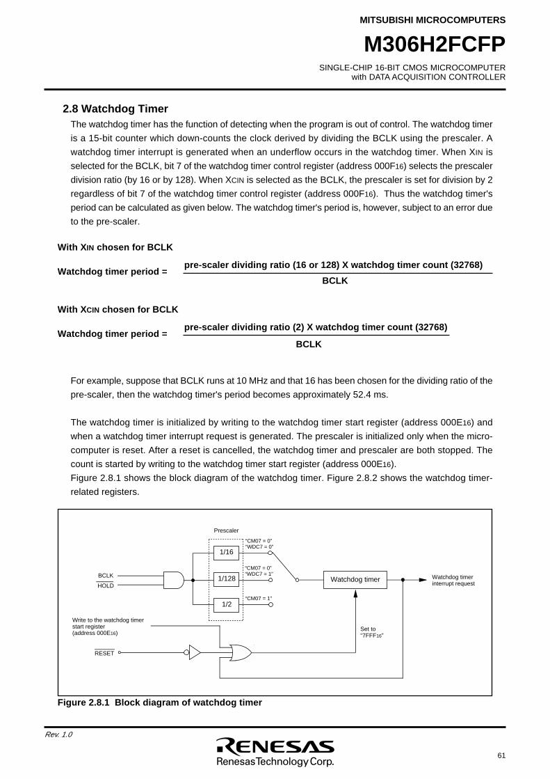
SINGLE-CHIP 16-BIT CMOS MICROCOMPUTERwith DATA ACQUISITION CONTROLLER
MITSUBISHI MICROCOMPUTERS
61
Rev. 1.0
M306H2FCFP
2.8 Watchdog TimerThe watchdog timer has the function of detecting when the program is out of control. The watchdog timer
is a 15-bit counter which down-counts the clock derived by dividing the BCLK using the prescaler. A
watchdog timer interrupt is generated when an underflow occurs in the watchdog timer. When XIN is
selected for the BCLK, bit 7 of the watchdog timer control register (address 000F16) selects the prescaler
division ratio (by 16 or by 128). When XCIN is selected as the BCLK, the prescaler is set for division by 2
regardless of bit 7 of the watchdog timer control register (address 000F16). Thus the watchdog timer's
period can be calculated as given below. The watchdog timer's period is, however, subject to an error due
to the pre-scaler.
BCLK
Write to the watchdog timer start register (address 000E16)
RESET
Watchdog timer interrupt request
Watchdog timer
Set to “7FFF16”
1/128
1/16
“CM07 = 0”“WDC7 = 1”
“CM07 = 0”“WDC7 = 0”
“CM07 = 1”
HOLD
1/2
Prescaler
For example, suppose that BCLK runs at 10 MHz and that 16 has been chosen for the dividing ratio of the
pre-scaler, then the watchdog timer's period becomes approximately 52.4 ms.
The watchdog timer is initialized by writing to the watchdog timer start register (address 000E16) and
when a watchdog timer interrupt request is generated. The prescaler is initialized only when the micro-
computer is reset. After a reset is cancelled, the watchdog timer and prescaler are both stopped. The
count is started by writing to the watchdog timer start register (address 000E16).
Figure 2.8.1 shows the block diagram of the watchdog timer. Figure 2.8.2 shows the watchdog timer-
related registers.
With XIN chosen for BCLK
Watchdog timer period =pre-scaler dividing ratio (16 or 128) X watchdog timer count (32768)
BCLK
With XCIN chosen for BCLK
Watchdog timer period =pre-scaler dividing ratio (2) X watchdog timer count (32768)
BCLK
Figure 2.8.1 Block diagram of watchdog timer
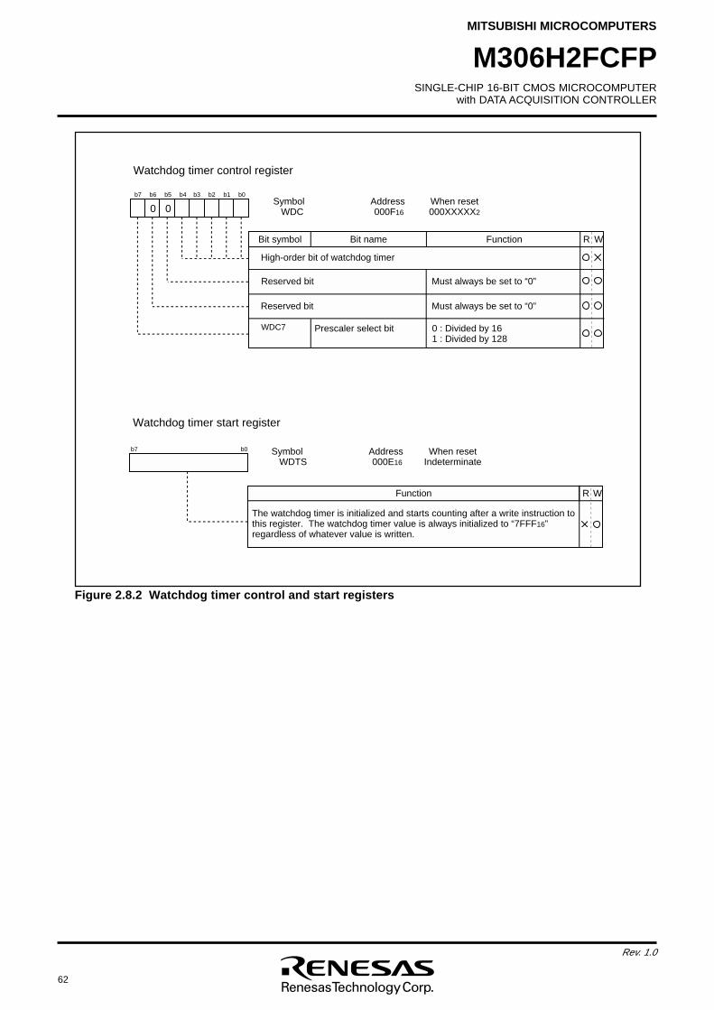
62
Rev. 1.0
SINGLE-CHIP 16-BIT CMOS MICROCOMPUTERwith DATA ACQUISITION CONTROLLER
MITSUBISHI MICROCOMPUTERS
M306H2FCFP
Watchdog timer control register
Symbol Address When reset WDC 000F16 000XXXXX2
FunctionBit symbol WR
b7 b6 b5 b4 b3 b2 b1 b0
High-order bit of watchdog timer
WDC7
Bit name
Prescaler select bit 0 : Divided by 161 : Divided by 128
Watchdog timer start register
Symbol Address When reset WDTS 000E16 Indeterminate
WR
b7 b0
Function
The watchdog timer is initialized and starts counting after a write instruction to this register. The watchdog timer value is always initialized to “7FFF16”regardless of whatever value is written.
Reserved bit
Reserved bit Must always be set to “0”
Must always be set to “0”
00
AAAAAAAAAAA
A
Figure 2.8.2 Watchdog timer control and start registers
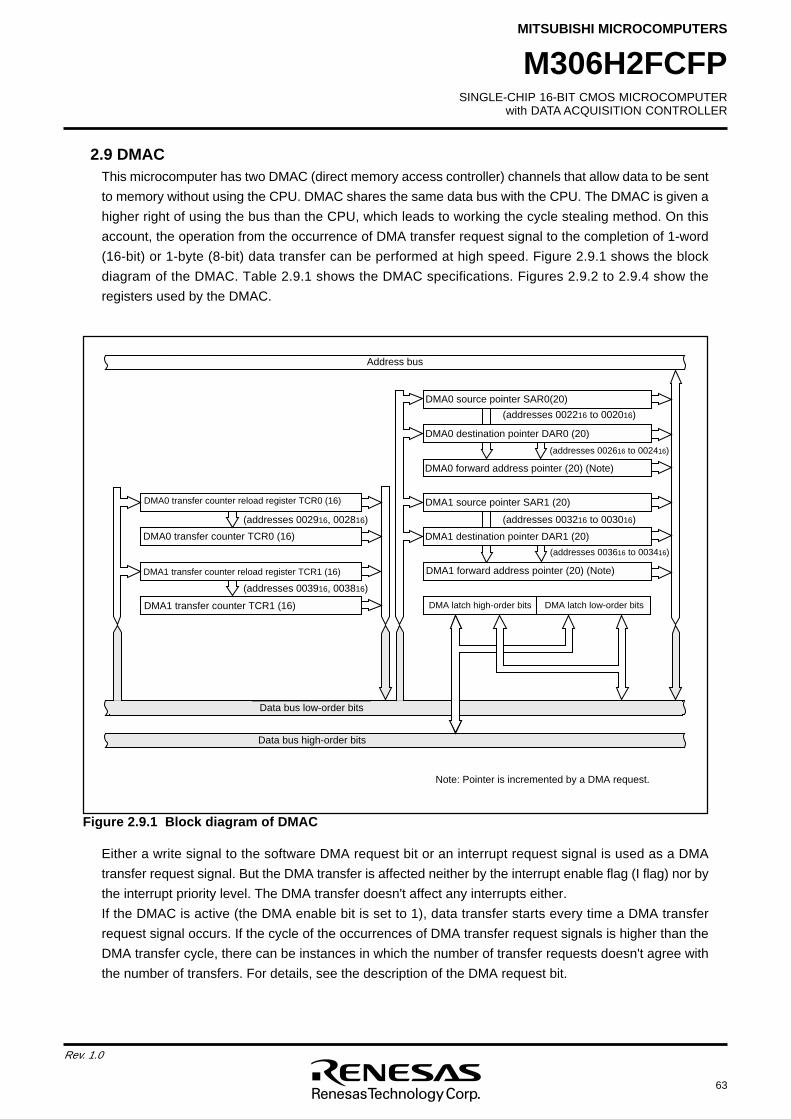
SINGLE-CHIP 16-BIT CMOS MICROCOMPUTERwith DATA ACQUISITION CONTROLLER
MITSUBISHI MICROCOMPUTERS
63
Rev. 1.0
M306H2FCFP
Figure 2.9.1 Block diagram of DMAC
AAA
AAAA AA
AAAA
AA
AA
AAAAAA
AAAA
AA
A
AA
A
Data bus low-order bits
DMA latch high-order bits DMA latch low-order bits
DMA0 source pointer SAR0(20)
DMA0 destination pointer DAR0 (20)
DMA0 forward address pointer (20) (Note)
Data bus high-order bits
AAAA
AA
AA
AAAAAAAAAAAAAAAAAAAAAAAAAAAAAAAAAAAAAAAAAAAAAAAAAAAAAAAA
AAAAAAAAAAAAAAAddress bus
AAAA
AAAAAAAA
DMA1 destination pointer DAR1 (20)
DMA1 source pointer SAR1 (20)
DMA1 forward address pointer (20) (Note)AAAA
AA
DMA0 transfer counter reload register TCR0 (16)
DMA0 transfer counter TCR0 (16)
DMA1 transfer counter reload register TCR1 (16)
DMA1 transfer counter TCR1 (16)A
AA(addresses 002916, 002816)
(addresses 003916, 003816)
(addresses 002216 to 002016)
(addresses 002616 to 002416)
(addresses 003216 to 003016)
(addresses 003616 to 003416)
Note: Pointer is incremented by a DMA request.
AA
AAAA
AA
AAAAAA
AAAA
AAAA
AAAAAA
AAAA
AA
AAAA
AAAA
Either a write signal to the software DMA request bit or an interrupt request signal is used as a DMA
transfer request signal. But the DMA transfer is affected neither by the interrupt enable flag (I flag) nor by
the interrupt priority level. The DMA transfer doesn't affect any interrupts either.
If the DMAC is active (the DMA enable bit is set to 1), data transfer starts every time a DMA transfer
request signal occurs. If the cycle of the occurrences of DMA transfer request signals is higher than the
DMA transfer cycle, there can be instances in which the number of transfer requests doesn't agree with
the number of transfers. For details, see the description of the DMA request bit.
2.9 DMACThis microcomputer has two DMAC (direct memory access controller) channels that allow data to be sent
to memory without using the CPU. DMAC shares the same data bus with the CPU. The DMAC is given a
higher right of using the bus than the CPU, which leads to working the cycle stealing method. On this
account, the operation from the occurrence of DMA transfer request signal to the completion of 1-word
(16-bit) or 1-byte (8-bit) data transfer can be performed at high speed. Figure 2.9.1 shows the block
diagram of the DMAC. Table 2.9.1 shows the DMAC specifications. Figures 2.9.2 to 2.9.4 show the
registers used by the DMAC.
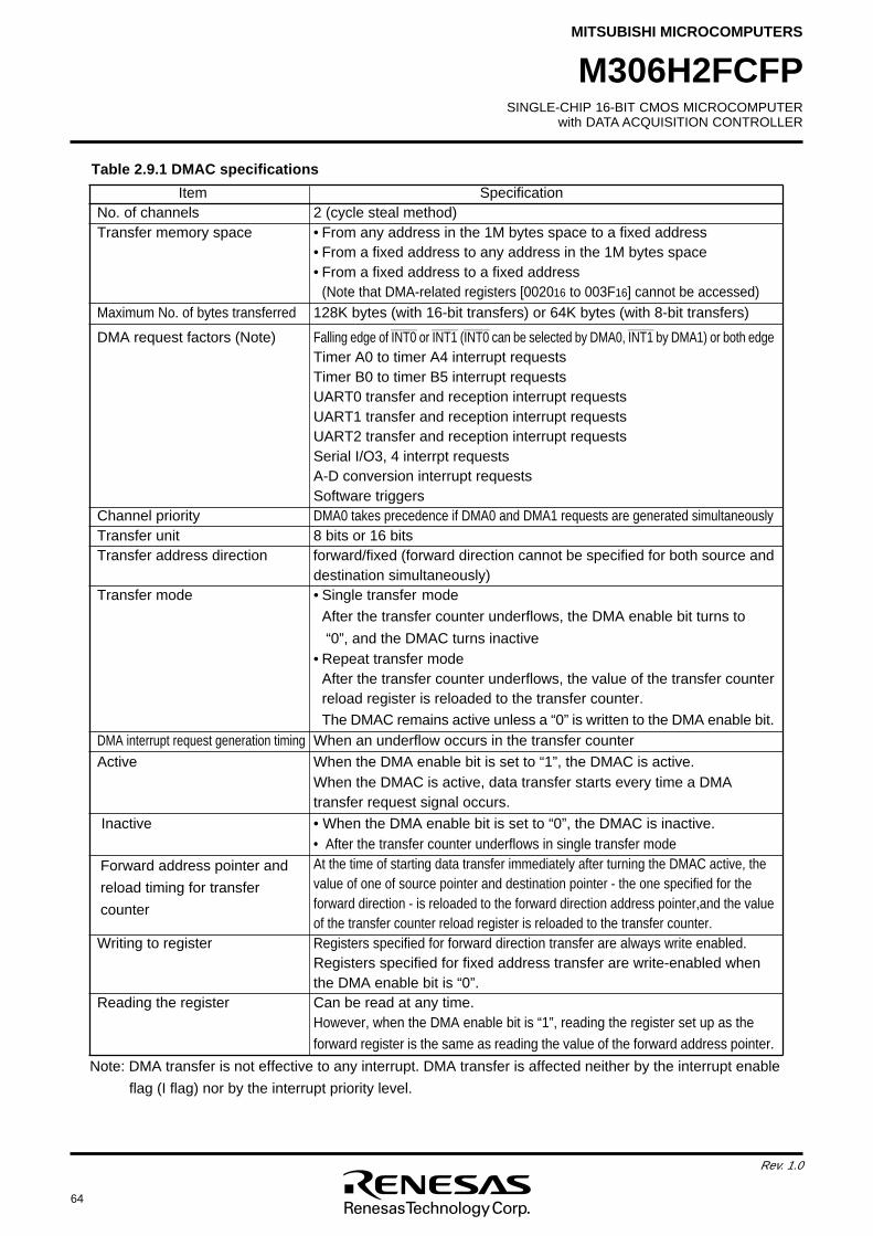
64
Rev. 1.0
SINGLE-CHIP 16-BIT CMOS MICROCOMPUTERwith DATA ACQUISITION CONTROLLER
MITSUBISHI MICROCOMPUTERS
M306H2FCFP
Table 2.9.1 DMAC specifications
Note: DMA transfer is not effective to any interrupt. DMA transfer is affected neither by the interrupt enable
flag (I flag) nor by the interrupt priority level.
Forward address pointer and
reload timing for transfer
counter
Item SpecificationNo. of channels 2 (cycle steal method)Transfer memory space • From any address in the 1M bytes space to a fixed address
• From a fixed address to any address in the 1M bytes space• From a fixed address to a fixed address
(Note that DMA-related registers [002016 to 003F16] cannot be accessed)Maximum No. of bytes transferred 128K bytes (with 16-bit transfers) or 64K bytes (with 8-bit transfers)
DMA request factors (Note)________ ________ ________ ________
Falling edge of INT0 or INT1 (INT0 can be selected by DMA0, INT1 by DMA1) or both edgeTimer A0 to timer A4 interrupt requestsTimer B0 to timer B5 interrupt requestsUART0 transfer and reception interrupt requestsUART1 transfer and reception interrupt requestsUART2 transfer and reception interrupt requestsSerial I/O3, 4 interrpt requestsA-D conversion interrupt requestsSoftware triggers
Channel priority DMA0 takes precedence if DMA0 and DMA1 requests are generated simultaneouslyTransfer unit 8 bits or 16 bitsTransfer address direction forward/fixed (forward direction cannot be specified for both source and
destination simultaneously)Transfer mode • Single transfer mode
After the transfer counter underflows, the DMA enable bit turns to
“0”, and the DMAC turns inactive• Repeat transfer mode
After the transfer counter underflows, the value of the transfer counterreload register is reloaded to the transfer counter.
The DMAC remains active unless a “0” is written to the DMA enable bit.DMA interrupt request generation timing When an underflow occurs in the transfer counter
Active When the DMA enable bit is set to “1”, the DMAC is active.When the DMAC is active, data transfer starts every time a DMAtransfer request signal occurs.
Inactive • When the DMA enable bit is set to “0”, the DMAC is inactive.• After the transfer counter underflows in single transfer modeAt the time of starting data transfer immediately after turning the DMAC active, thevalue of one of source pointer and destination pointer - the one specified for theforward direction - is reloaded to the forward direction address pointer,and the valueof the transfer counter reload register is reloaded to the transfer counter.
Writing to register Registers specified for forward direction transfer are always write enabled.Registers specified for fixed address transfer are write-enabled whenthe DMA enable bit is “0”.
Reading the register Can be read at any time.However, when the DMA enable bit is “1”, reading the register set up as the
forward register is the same as reading the value of the forward address pointer.
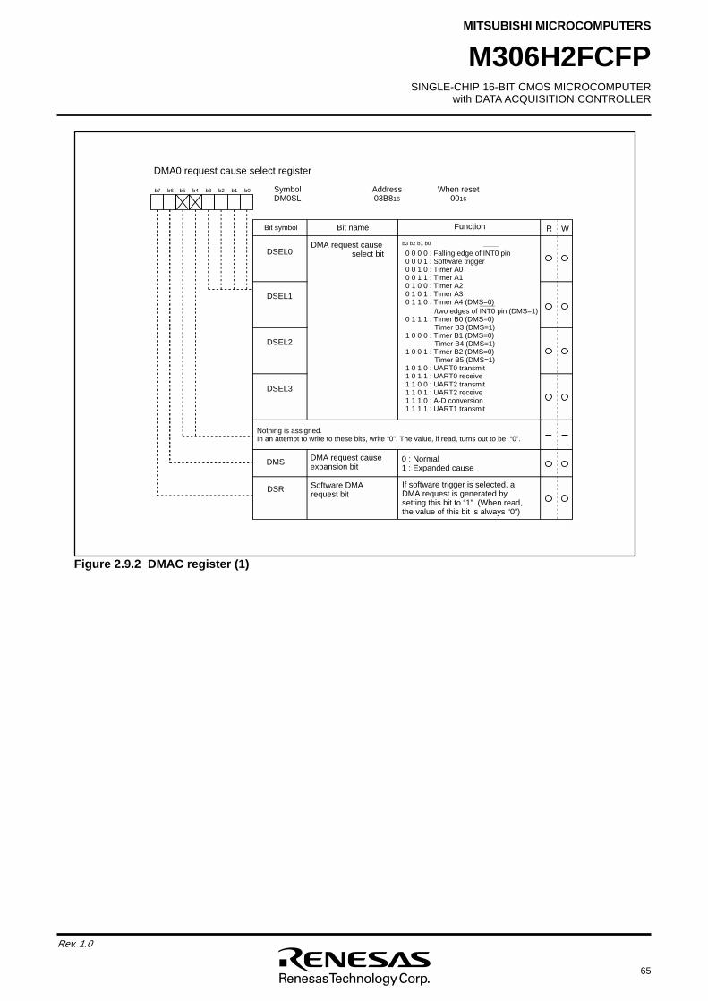
SINGLE-CHIP 16-BIT CMOS MICROCOMPUTERwith DATA ACQUISITION CONTROLLER
MITSUBISHI MICROCOMPUTERS
65
Rev. 1.0
M306H2FCFP
DMA0 request cause select register
Symbol Address When resetDM0SL 03B816 0016
FunctionBit symbol
b7 b6 b5 b4 b3 b2 b1 b0
DMA request cause select bitDSEL0
R W
DSEL1
DSEL2
DSEL3
Nothing is assigned.In an attempt to write to these bits, write “0”. The value, if read, turns out to be “0”.
Software DMA request bit
If software trigger is selected, a DMA request is generated by setting this bit to “1” (When read, the value of this bit is always “0”)
DSR
b3 b2 b1 b0
0 0 0 0 : Falling edge of INT0 pin 0 0 0 1 : Software trigger0 0 1 0 : Timer A00 0 1 1 : Timer A1 0 1 0 0 : Timer A2 0 1 0 1 : Timer A3 0 1 1 0 : Timer A4 (DMS=0)
/two edges of INT0 pin (DMS=1) 0 1 1 1 : Timer B0 (DMS=0)
Timer B3 (DMS=1) 1 0 0 0 : Timer B1 (DMS=0)
Timer B4 (DMS=1) 1 0 0 1 : Timer B2 (DMS=0)
Timer B5 (DMS=1) 1 0 1 0 : UART0 transmit 1 0 1 1 : UART0 receive 1 1 0 0 : UART2 transmit 1 1 0 1 : UART2 receive 1 1 1 0 : A-D conversion 1 1 1 1 : UART1 transmit
AAA
AAA
AAA
AAAAAA
AAAAAA
Bit name
DMA request cause expansion bitDMS 0 : Normal
1 : Expanded cause AAA
Figure 2.9.2 DMAC register (1)
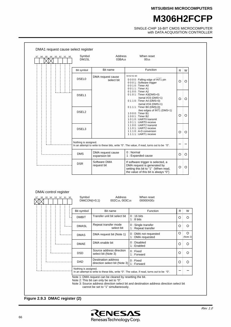
66
Rev. 1.0
SINGLE-CHIP 16-BIT CMOS MICROCOMPUTERwith DATA ACQUISITION CONTROLLER
MITSUBISHI MICROCOMPUTERS
M306H2FCFP
DMAi control registerSymbol Address When resetDMiCON(i=0,1) 002C16, 003C16 00000X002
Bit name FunctionBit symbol
Transfer unit bit select bit
b7 b6 b5 b4 b3 b2 b1 b0
0 : 16 bits1 : 8 bits
DMBIT
R W
DMASL
DMAS
DMAE
Repeat transfer mode select bit
0 : Single transfer1 : Repeat transfer
DMA request bit (Note 1) 0 : DMA not requested1 : DMA requested
0 : Disabled1 : Enabled
0 : Fixed1 : Forward
DMA enable bit
Source address direction select bit (Note 3)
Destination address direction select bit (Note 3)
0 : Fixed1 : Forward
DSD
DAD
Nothing is assigned.In an attempt to write to these bits, write “0”. The value, if read, turns out to be “0”.
Note 1: DMA request can be cleared by resetting the bit.Note 2: This bit can only be set to “0”.Note 3: Source address direction select bit and destination address direction select bit
cannot be set to “1” simultaneously.
(Note 2)
AAAAAAAAAAAAAAA
AAAA
AA
DMA1 request cause select register
Symbol Address When resetDM1SL 03BA16 0016
FunctionBit symbol
b7 b6 b5 b4 b3 b2 b1 b0
DMA request cause select bitDSEL0
R W
DSEL1
DSEL2
DSEL3
Nothing is assigned.In an attempt to write to these bits, write “0”. The value, if read, turns out to be “0”.
Software DMA request bit
If software trigger is selected, a DMA request is generated by setting this bit to “1” (When read, the value of this bit is always “0”)
DSR
b3 b2 b1 b0
0 0 0 0 : Falling edge of INT1 pin 0 0 0 1 : Software trigger0 0 1 0 : Timer A00 0 1 1 : Timer A1 0 1 0 0 : Timer A2 0 1 0 1 : Timer A3(DMS=0)
/serial I/O3 (DMS=1) 0 1 1 0 : Timer A4 (DMS=0)
/serial I/O4 (DMS=1) 0 1 1 1 : Timer B0 (DMS=0)
/two edges of INT1 (DMS=1) 1 0 0 0 : Timer B1 1 0 0 1 : Timer B2 1 0 1 0 : UART0 transmit 1 0 1 1 : UART0 receive 1 1 0 0 : UART2 transmit 1 1 0 1 : UART2 receive 1 1 1 0 : A-D conversion 1 1 1 1 : UART1 receive
AAAAAA
AAA
AAA
AAA
AAAAAA
Bit name
DMA request cause expansion bit
DMS 0 : Normal1 : Expanded cause AAA
Figure 2.9.3 DMAC register (2)
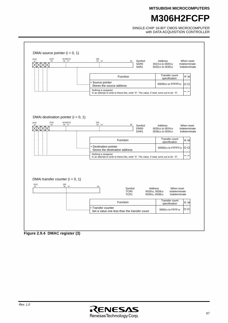
SINGLE-CHIP 16-BIT CMOS MICROCOMPUTERwith DATA ACQUISITION CONTROLLER
MITSUBISHI MICROCOMPUTERS
67
Rev. 1.0
M306H2FCFP
b7 b0 b7 b0(b8)(b15)
Function R W
• Transfer counter Set a value one less than the transfer count
Symbol Address When reset TCR0 002916, 002816 Indeterminate TCR1 003916, 003816 Indeterminate
DMAi transfer counter (i = 0, 1)
Transfer countspecification
000016 to FFFF16
b7(b23)
b3 b0 b7 b0 b7 b0(b8)(b16)(b15)(b19)
Function R W
• Source pointer Stores the source address
Symbol Address When reset SAR0 002216 to 002016 Indeterminate SAR1 003216 to 003016 Indeterminate
DMAi source pointer (i = 0, 1)
Transfer countspecification
0000016 to FFFFF16
Nothing is assigned.In an attempt to write to these bits, write “0”. The value, if read, turns out to be “0”.
Symbol Address When reset DAR0 002616 to 002416 Indeterminate DAR1 003616 to 003416 Indeterminate
b3 b0 b7 b0 b7 b0(b8)(b15)(b16)(b19)
Function R W
• Destination pointer Stores the destination address
DMAi destination pointer (i = 0, 1)
Transfer countspecification
0000016 to FFFFF16
b7(b23)
Nothing is assigned.In an attempt to write to these bits, write “0”. The value, if read, turns out to be “0”.
AAA
AAA
AAA
Figure 2.9.4 DMAC register (3)
68
Rev. 1.0
SINGLE-CHIP 16-BIT CMOS MICROCOMPUTERwith DATA ACQUISITION CONTROLLER
MITSUBISHI MICROCOMPUTERS
M306H2FCFP
(1) Transfer cycleThe transfer cycle consists of the bus cycle in which data is read from memory or from the SFR area
(source read) and the bus cycle in which the data is written to memory or to the SFR area (destination
write). The number of read and write bus cycles depends on the source and destination addresses and,
the level of the BYTE pin. In memory expansion mode, the number of read and write bus cycles also
depends on the level of the BYTE pin. Also, the bus cycle itself is longer when software waits are inserted.
(a) Effect of source and destination addresses
When 16-bit data is transferred on a 16-bit data bus, and the source and destination both start at odd
addresses, there are one more source read cycle and destination write cycle than when the source
and destination both start at even addresses.
(b) Effect of BYTE pin level
When transferring 16-bit data over an 8-bit data bus (BYTE pin = “H”) in memory expansion mode, the
16 bits of data are sent in two 8-bit blocks. Therefore, two bus cycles are required for reading the data
and two are required for writing the data. Also, in contrast to when the CPU accesses internal memory,
when the DMAC accesses internal memory (internal RAM, and SFR), these areas are accessed using
the data size selected by the BYTE pin.
(c) Effect of software wait
When the SFR area or a memory area with a software wait is accessed, the number of cycles is
increased for the wait by 1 bus cycle. The length of the cycle is determined by BCLK.
Figure 2.9.5 shows the example of the transfer cycles for a source read. For convenience, the destination
write cycle is shown as one cycle and the source read cycles for the different conditions are shown. In
reality, the destination write cycle is subject to the same conditions as the source read cycle, with the
transfer cycle changing accordingly. When calculating the transfer cycle, remember to apply the respec-
tive conditions to both the destination write cycle and the source read cycle. For example (2) in Figure
2.9.5, if data is being transferred in 16-bit units on an 8-bit bus, two bus cycles are required for both the
source read cycle and the destination write cycle.
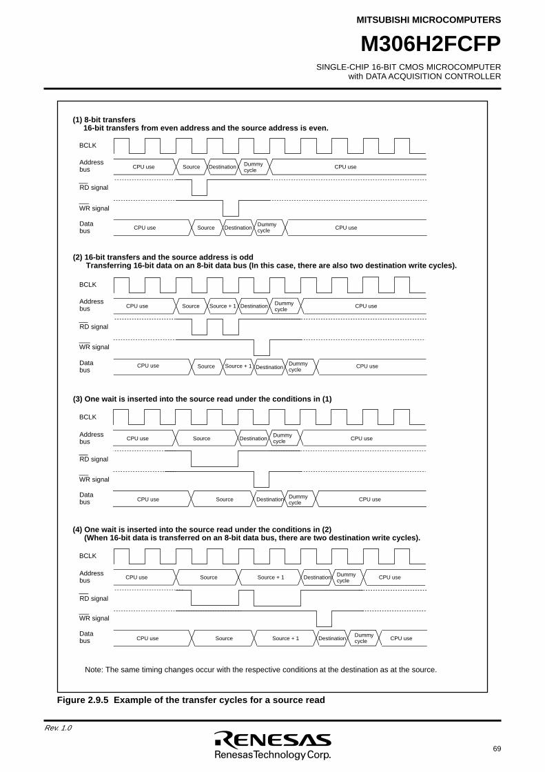
SINGLE-CHIP 16-BIT CMOS MICROCOMPUTERwith DATA ACQUISITION CONTROLLER
MITSUBISHI MICROCOMPUTERS
69
Rev. 1.0
M306H2FCFP
BCLK
Address bus
RD signal
WR signal
Data bus
CPU use
CPU use CPU use
CPU useSource
Source
Destination
Destination
Dummy cycle
Dummy cycle
(1) 8-bit transfers16-bit transfers from even address and the source address is even.
BCLK
Address bus
RD signal
WR signal
Data bus
CPU use
CPU use CPU use
CPU useSource
Source
Destination
Destination
Dummy cycle
Dummy cycle
(3) One wait is inserted into the source read under the conditions in (1)
BCLK
Address bus
RD signal
WR signal
Data bus
CPU use
CPU use CPU use
CPU useSource
Source
Destination
Destination
Dummy cycle
Dummy cycle
Source + 1
Source + 1
(2) 16-bit transfers and the source address is oddTransferring 16-bit data on an 8-bit data bus (In this case, there are also two destination write cycles).
BCLK
Address bus
RD signal
WR signal
Data bus
CPU use
CPU use CPU use
CPU useSource
Source
Destination
Destination
Dummy cycle
Dummy cycle
Source + 1
Source + 1
(4) One wait is inserted into the source read under the conditions in (2) (When 16-bit data is transferred on an 8-bit data bus, there are two destination write cycles).
Note: The same timing changes occur with the respective conditions at the destination as at the source.
Figure 2.9.5 Example of the transfer cycles for a source read
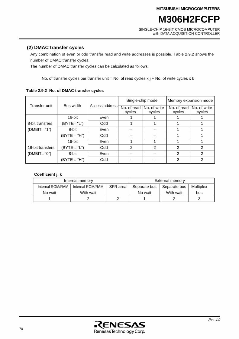
70
Rev. 1.0
SINGLE-CHIP 16-BIT CMOS MICROCOMPUTERwith DATA ACQUISITION CONTROLLER
MITSUBISHI MICROCOMPUTERS
M306H2FCFP
16-bit Even 1 1 1 1
8-bit transfers (BYTE= “L”) Odd 1 1 1 1
(DMBIT= “1”) 8-bit Even – – 1 1
(BYTE = “H”) Odd – – 1 1
16-bit Even 1 1 1 1
16-bit transfers (BYTE = “L”) Odd 2 2 2 2
(DMBIT= “0”) 8-bit Even – – 2 2
(BYTE = “H”) Odd – – 2 2
Table 2.9.2 No. of DMAC transfer cycles
Internal memory External memory
Internal ROM/RAM Internal ROM/RAM SFR area Separate bus Separate bus Multiplex
No wait With wait No wait With wait bus
1 2 2 1 2 3
Coefficient j, k
Transfer unit Bus width Access addressMemory expansion mode
No. of read No. of writecycles cycles
Single-chip mode
No. of read No. of writecycles cycles
(2) DMAC transfer cyclesAny combination of even or odd transfer read and write addresses is possible. Table 2.9.2 shows the
number of DMAC transfer cycles.
The number of DMAC transfer cycles can be calculated as follows:
No. of transfer cycles per transfer unit = No. of read cycles x j + No. of write cycles x k
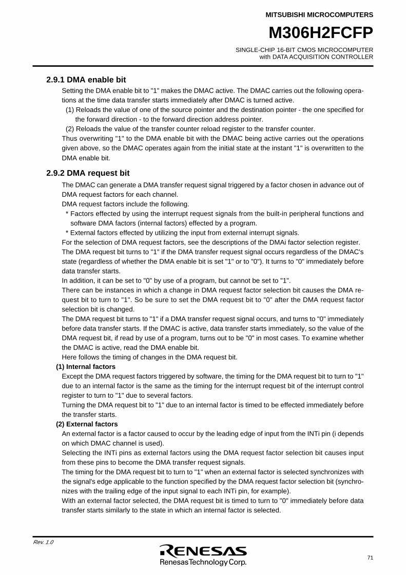
SINGLE-CHIP 16-BIT CMOS MICROCOMPUTERwith DATA ACQUISITION CONTROLLER
MITSUBISHI MICROCOMPUTERS
71
Rev. 1.0
M306H2FCFP
2.9.1 DMA enable bitSetting the DMA enable bit to "1" makes the DMAC active. The DMAC carries out the following opera-tions at the time data transfer starts immediately after DMAC is turned active.
(1) Reloads the value of one of the source pointer and the destination pointer - the one specified for the forward direction - to the forward direction address pointer.
(2) Reloads the value of the transfer counter reload register to the transfer counter.Thus overwriting "1" to the DMA enable bit with the DMAC being active carries out the operationsgiven above, so the DMAC operates again from the initial state at the instant "1" is overwritten to the
DMA enable bit.
2.9.2 DMA request bitThe DMAC can generate a DMA transfer request signal triggered by a factor chosen in advance out ofDMA request factors for each channel.DMA request factors include the following.
* Factors effected by using the interrupt request signals from the built-in peripheral functions andsoftware DMA factors (internal factors) effected by a program.
* External factors effected by utilizing the input from external interrupt signals.For the selection of DMA request factors, see the descriptions of the DMAi factor selection register.The DMA request bit turns to "1" if the DMA transfer request signal occurs regardless of the DMAC'sstate (regardless of whether the DMA enable bit is set "1" or to "0"). It turns to "0" immediately beforedata transfer starts.In addition, it can be set to "0" by use of a program, but cannot be set to "1".There can be instances in which a change in DMA request factor selection bit causes the DMA re-quest bit to turn to "1". So be sure to set the DMA request bit to "0" after the DMA request factorselection bit is changed.The DMA request bit turns to "1" if a DMA transfer request signal occurs, and turns to "0" immediatelybefore data transfer starts. If the DMAC is active, data transfer starts immediately, so the value of theDMA request bit, if read by use of a program, turns out to be "0" in most cases. To examine whetherthe DMAC is active, read the DMA enable bit.Here follows the timing of changes in the DMA request bit.
(1) Internal factorsExcept the DMA request factors triggered by software, the timing for the DMA request bit to turn to "1"due to an internal factor is the same as the timing for the interrupt request bit of the interrupt controlregister to turn to "1" due to several factors.Turning the DMA request bit to "1" due to an internal factor is timed to be effected immediately beforethe transfer starts.
(2) External factorsAn external factor is a factor caused to occur by the leading edge of input from the INTi pin (i dependson which DMAC channel is used).Selecting the INTi pins as external factors using the DMA request factor selection bit causes inputfrom these pins to become the DMA transfer request signals.The timing for the DMA request bit to turn to "1" when an external factor is selected synchronizes withthe signal's edge applicable to the function specified by the DMA request factor selection bit (synchro-nizes with the trailing edge of the input signal to each INTi pin, for example).With an external factor selected, the DMA request bit is timed to turn to "0" immediately before datatransfer starts similarly to the state in which an internal factor is selected.
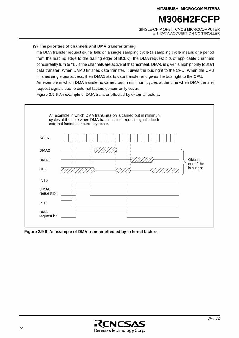
72
Rev. 1.0
SINGLE-CHIP 16-BIT CMOS MICROCOMPUTERwith DATA ACQUISITION CONTROLLER
MITSUBISHI MICROCOMPUTERS
M306H2FCFP
(3) The priorities of channels and DMA transfer timing
If a DMA transfer request signal falls on a single sampling cycle (a sampling cycle means one period
from the leading edge to the trailing edge of BCLK), the DMA request bits of applicable channels
concurrently turn to "1". If the channels are active at that moment, DMA0 is given a high priority to start
data transfer. When DMA0 finishes data transfer, it gives the bus right to the CPU. When the CPU
finishes single bus access, then DMA1 starts data transfer and gives the bus right to the CPU.
An example in which DMA transfer is carried out in minimum cycles at the time when DMA transfer
request signals due to external factors concurrently occur.
Figure 2.9.6 An example of DMA transfer effected by external factors.
BCLK
AAAAAAAADMA0
AAAAAAAA
DMA1
DMA0request bit
DMA1request bit
AAAAAAAAA AAAAAAACPU
INT0
INT1
Obtainment of thebus right
An example in which DMA transmission is carried out in minimum cycles at the time when DMA transmission request signals due to external factors concurrently occur.
Figure 2.9.6 An example of DMA transfer effected by external factors
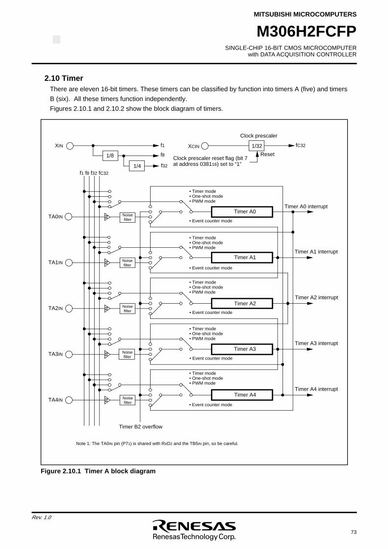
SINGLE-CHIP 16-BIT CMOS MICROCOMPUTERwith DATA ACQUISITION CONTROLLER
MITSUBISHI MICROCOMPUTERS
73
Rev. 1.0
M306H2FCFP
• Timer mode• One-shot mode• PWM mode
• Timer mode• One-shot mode• PWM mode
• Timer mode• One-shot mode• PWM mode
• Timer mode• One-shot mode• PWM mode
• Timer mode• One-shot mode• PWM mode
• Event counter mode
• Event counter mode
• Event counter mode
• Event counter mode
• Event counter mode
TA0IN
TA1IN
TA2IN
TA3IN
TA4IN
Timer A0
Timer A1
Timer A2
Timer A3
Timer A4
f1 f8 f32 fC32
Timer A0 interrupt
Timer A1 interrupt
Timer A2 interrupt
Timer A3 interrupt
Timer A4 interrupt
Noise filter
Noise filter
Noise filter
Noise filter
Noise filter
1/32 fC32
1/8
1/4
f1
f8
f32
XIN XCIN
Clock prescaler reset flag (bit 7at address 038116) set to “1”
Reset
Clock prescaler
Timer B2 overflow
Note 1: The TA0IN pin (P71) is shared with RxD2 and the TB5IN pin, so be careful.
Figure 2.10.1 Timer A block diagram
2.10 TimerThere are eleven 16-bit timers. These timers can be classified by function into timers A (five) and timers
B (six). All these timers function independently.
Figures 2.10.1 and 2.10.2 show the block diagram of timers.
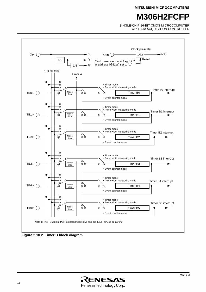
74
Rev. 1.0
SINGLE-CHIP 16-BIT CMOS MICROCOMPUTERwith DATA ACQUISITION CONTROLLER
MITSUBISHI MICROCOMPUTERS
M306H2FCFP
Figure 2.10.2 Timer B block diagram
• Event counter mode
• Event counter mode
• Event counter mode
• Timer mode • Pulse width measuring mode
• Timer mode• Pulse width measuring mode
• Timer mode• Pulse width measuring mode
TB0IN
TB1IN
TB2IN
Timer B0
Timer B1
Timer B2
f1 f8 f32 fC32
Timer B0 interruptNoise filter
Noise filter
Noise filter
1/32 fC32
1/8
1/4
f1
f8
f32
XIN XCIN
Clock prescaler reset flag (bit 7at address 038116) set to “1”
Reset
Clock prescaler
Timer A
• Event counter mode
• Event counter mode
• Event counter mode
• Timer mode • Pulse width measuring mode
• Timer mode• Pulse width measuring mode
• Timer mode• Pulse width measuring mode
TB3IN
TB4IN
TB5IN
Timer B3
Timer B4
Timer B5
Timer B3 interruptNoise filter
Noise filter
Noise filter
Timer B1 interrupt
Timer B2 interrupt
Timer B4 interrupt
Timer B5 interrupt
Note 1: The TB5IN pin (P71) is shared with RxD2 and the TA0IN pin, so be careful.
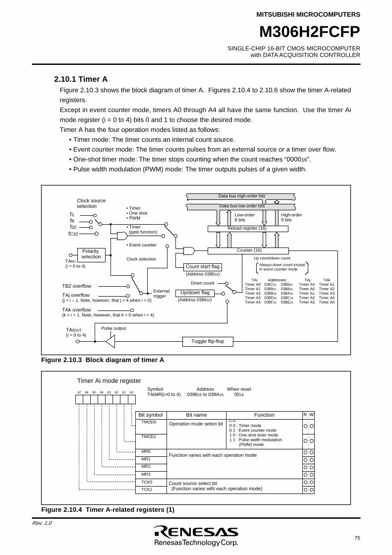
SINGLE-CHIP 16-BIT CMOS MICROCOMPUTERwith DATA ACQUISITION CONTROLLER
MITSUBISHI MICROCOMPUTERS
75
Rev. 1.0
M306H2FCFP
T
i
m
e
r
A
i
m
o
d
e
r
e
g
i
s
t
e
rS
y
m
b
o
l A
d
d
r
e
s
s W
h
e
n
r
e
s
e
tT
A
i
M
R
(
i
=
0
t
o
4
) 0
3
9
61
6
t
o
0
3
9
A1
6 0
01
6
B
i
t
n
a
m
e F
u
n
c
t
i
o
nB
i
t
s
y
m
b
o
l WR
b
7 b6 b
5 b
4 b
3 b
2 b
1 b
0
0 0 : Timer mode 0 1 : Event counter mode 1 0 : One-shot timer mode 1 1 : Pulse width modulation
(PWM) mode
b1 b0
TCK1
MR3
MR2
MR1
TMOD1
MR0
TMOD0
TCK0
F
u
n
c
t
i
o
n
v
a
r
i
e
s
w
i
t
h
e
a
c
h
o
p
e
r
a
t
i
o
n
m
o
d
e
C
o
u
n
t
s
o
u
r
c
e
s
e
l
e
c
t
b
i
t
(
F
u
n
c
t
i
o
n
v
a
r
i
e
s
w
i
t
h
e
a
c
h
o
p
e
r
a
t
i
o
n
m
o
d
e
)
O
p
e
r
a
t
i
o
n
m
o
d
e
s
e
l
e
c
t
b
i
t
Figure 2.10.3 Block diagram of timer A
Figure 2.10.4 Timer A-related registers (1)
C
o
u
n
t
s
t
a
r
t
f
l
a
g
(Address 038016)
Up count/down count
TAi Addresses TAj TAkTimer A0 038716 038616 Timer A4 Timer A1Timer A1 038916 038816 Timer A0 Timer A2Timer A2 038B16 038A16 Timer A1 Timer A3Timer A3 038D16 038C16 Timer A2 Timer A4Timer A4 038F16 038E16 Timer A3 Timer A0
A
l
w
a
y
s
d
o
w
n
c
o
u
n
t
e
x
c
e
p
t
i
n
e
v
e
n
t
c
o
u
n
t
e
r
m
o
d
e
Reload register (16)
Counter (16)
L
o
w
-
o
r
d
e
r
8
b
i
t
sH
i
g
h
-
o
r
d
e
r
8
b
i
t
s
Clock source selection
•
T
i
m
e
r
(
g
a
t
e
f
u
n
c
t
i
o
n
)
•
T
i
m
e
r
•
O
n
e
s
h
o
t
•
P
W
Mf1f8f3
2
External trigger
T
A
iI
N (
i
=
0
t
o
4
)
T
B
2
o
v
e
r
f
l
o
w
• Event counter
fC
3
2
Clock selection
TAj overflow (j = i – 1. Note, however, that j = 4 when i = 0)
Pulse output
Toggle flip-flop
TAiOUT (i = 0 to 4)
Data bus low-order bits
Data bus high-order bits
Up/down flag
Down count
( A
d
d
r
e
s
s
0
3
8
41
6)
T
A
k
o
v
e
r
f
l
o
w
(
k
=
i
+
1
.
N
o
t
e
,
h
o
w
e
v
e
r
,
t
h
a
t
k
=
0
w
h
e
n
i
=
4
)
P
o
l
a
r
i
t
y
s
e
l
e
c
t
i
o
n
2.10.1 Timer AFigure 2.10.3 shows the block diagram of timer A. Figures 2.10.4 to 2.10.6 show the timer A-related
registers.
Except in event counter mode, timers A0 through A4 all have the same function. Use the timer Ai
mode register (i = 0 to 4) bits 0 and 1 to choose the desired mode.
Timer A has the four operation modes listed as follows:
• Timer mode: The timer counts an internal count source.
• Event counter mode: The timer counts pulses from an external source or a timer over flow.
• One-shot timer mode: The timer stops counting when the count reaches “000016”.
• Pulse width modulation (PWM) mode: The timer outputs pulses of a given width.
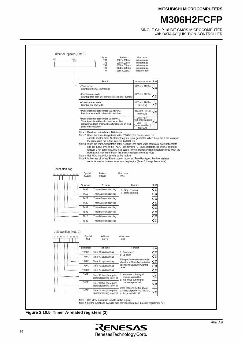
76
Rev. 1.0
SINGLE-CHIP 16-BIT CMOS MICROCOMPUTERwith DATA ACQUISITION CONTROLLER
MITSUBISHI MICROCOMPUTERS
M306H2FCFP
Figure 2.10.5 Timer A-related registers (2)
T
i
m
e
r
A
4
u
p
/
d
o
w
n
f
l
a
g
T
i
m
e
r
A
3
u
p
/
d
o
w
n
f
l
a
g
T
i
m
e
r
A
2
u
p
/
d
o
w
n
f
l
a
g
T
i
m
e
r
A
1
u
p
/
d
o
w
n
f
l
a
g
T
i
m
e
r
A
0
u
p
/
d
o
w
n
f
l
a
g
T
i
m
e
r
A
2
t
w
o
-
p
h
a
s
e
p
u
l
s
e
s
i
g
n
a
l
p
r
o
c
e
s
s
i
n
g
s
e
l
e
c
t
b
i
t
Timer A3 two-phase pulse signal processing select bit
T
i
m
e
r
A
4
t
w
o
-
p
h
a
s
e
p
u
l
s
e
s
i
g
n
a
l
p
r
o
c
e
s
s
i
n
g
s
e
l
e
c
t
b
i
t
S
y
m
b
o
l A
d
d
r
e
s
s W
h
e
n
r
e
s
e
t U
D
F 0
3
8
41
6 0
01
6
T
A
4
P
TA3P
T
A
2
P
U
p
/
d
o
w
n
f
l
a
g
(
N
o
t
e
1
)
Bit name FunctionBit symbol WR
b
7 b
6 b
5 b
4 b
3 b
2 b
1 b
0
T
A
4
U
D
TA3UD
T
A
2
U
D
T
A
1
U
D
T
A
0
U
D 0
:
D
o
w
n
c
o
u
n
t
1
:
U
p
c
o
u
n
t
T
h
i
s
s
p
e
c
i
f
i
c
a
t
i
o
n
b
e
c
o
m
e
s
v
a
l
i
d
w
h
e
n
t
h
e
u
p
/
d
o
w
n
f
l
a
g
c
o
n
t
e
n
t
i
s
s
e
l
e
c
t
e
d
f
o
r
u
p
/
d
o
w
n
s
w
i
t
c
h
i
n
g
c
a
u
s
e
0
:
t
w
o
-
p
h
a
s
e
p
u
l
s
e
s
i
g
n
a
l
p
r
o
c
e
s
s
i
n
g
d
i
s
a
b
l
e
d1
:
t
w
o
-
p
h
a
s
e
p
u
l
s
e
s
i
g
n
a
l
p
r
o
c
e
s
s
i
n
g
e
n
a
b
l
e
d
W
h
e
n
n
o
t
u
s
i
n
g
t
h
e
t
w
o
-
p
h
a
s
e
p
u
l
s
e
s
i
g
n
a
l
p
r
o
c
e
s
s
i
n
g
f
u
n
c
t
i
o
n
,
s
e
t
t
h
e
s
e
l
e
c
t
b
i
t
t
o
“
0
”
S
y
m
b
o
l A
d
d
r
e
s
s W
h
e
n
r
e
s
e
t T
A
B
S
R 0
3
8
01
6 0
01
6
C
o
u
n
t
s
t
a
r
t
f
l
a
g
Bit name FunctionBit symbol WR
b
7 b
6 b
5 b
4 b
3 b
2 b
1 b
0
Timer B2 count start flag
T
i
m
e
r
B
1
c
o
u
n
t
s
t
a
r
t
f
l
a
g
T
i
m
e
r
B
0
c
o
u
n
t
s
t
a
r
t
f
l
a
g
T
i
m
e
r
A
4
c
o
u
n
t
s
t
a
r
t
f
l
a
g
T
i
m
e
r
A
3
c
o
u
n
t
s
t
a
r
t
f
l
a
g
Timer A2 count start flag
T
i
m
e
r
A
1
c
o
u
n
t
s
t
a
r
t
f
l
a
g
T
i
m
e
r
A
0
c
o
u
n
t
s
t
a
r
t
f
l
a
g 0
:
S
t
o
p
s
c
o
u
n
t
i
n
g
1
:
S
t
a
r
t
s
c
o
u
n
t
i
n
g
TB2S
T
B
1
S
T
B
0
S
T
A
4
S
T
A
3
S
TA2S
T
A
1
S
T
A
0
S
S
y
m
b
o
l A
d
d
r
e
s
s W
h
e
n
r
e
s
e
t
T
A
0 0
3
8
71
6,
0
3
8
61
6 I
n
d
e
t
e
r
m
i
n
a
t
e
T
A
1 0
3
8
91
6,
0
3
8
81
6 I
n
d
e
t
e
r
m
i
n
a
t
e
T
A
2 0
3
8
B1
6,
0
3
8
A1
6 I
n
d
e
t
e
r
m
i
n
a
t
e
T
A
3 0
3
8
D1
6,
0
3
8
C1
6 I
n
d
e
t
e
r
m
i
n
a
t
e
T
A
4 0
3
8
F1
6,
0
3
8
E1
6 I
n
d
e
t
e
r
m
i
n
a
t
e
b
7 b
0 b
7 b
0( b
1
5
) (
b
8
)
T
i
m
e
r
A
i
r
e
g
i
s
t
e
r
(
N
o
t
e
1
)
WR
• Timer mode 000016 to FFFF16 Counts an internal count source
F
u
n
c
t
i
o
n V
a
l
u
e
s
t
h
a
t
c
a
n
b
e
s
e
t
•
E
v
e
n
t
c
o
u
n
t
e
r
m
o
d
e 0
0
0
01
6
t
o
F
F
F
F1
6
C
o
u
n
t
s
p
u
l
s
e
s
f
r
o
m
a
n
e
x
t
e
r
n
a
l
s
o
u
r
c
e
o
r
t
i
m
e
r
o
v
e
r
f
l
o
w
(
N
o
t
e
2
,
4
) •
O
n
e
-
s
h
o
t
t
i
m
e
r
m
o
d
e 0
0
0
01
6
t
o
F
F
F
F1
6
C
o
u
n
t
s
a
o
n
e
s
h
o
t
w
i
d
t
h
(
N
o
t
e
3
,
4
)•
P
u
l
s
e
w
i
d
t
h
m
o
d
u
l
a
t
i
o
n
m
o
d
e
(
1
6
-
b
i
t
P
W
M
)
F
u
n
c
t
i
o
n
s
a
s
a
1
6
-
b
i
t
p
u
l
s
e
w
i
d
t
h
m
o
d
u
l
a
t
o
r
•
P
u
l
s
e
w
i
d
t
h
m
o
d
u
l
a
t
i
o
n
m
o
d
e
(
8
-
b
i
t
P
W
M
)
T
i
m
e
r
l
o
w
-
o
r
d
e
r
a
d
d
r
e
s
s
f
u
n
c
t
i
o
n
s
a
s
a
n
8
-
b
i
t
p
r
e
s
c
a
l
e
r
a
n
d
h
i
g
h
-
o
r
d
e
r
a
d
d
r
e
s
s
f
u
n
c
t
i
o
n
s
a
s
a
n
8
-
b
i
t
p
u
l
s
e
w
i
d
t
h
m
o
d
u
l
a
t
o
r
0
01
6
~
F
E1
6
(high-order address)0016 ~ FF16
(low-order address)
(
N
o
t
e
3
,
4
)
0 0
0
01
6
t
o
F
F
F
E1
6
N
o
t
e
1
: R
e
a
d
a
n
d
w
r
i
t
e
d
a
t
a
i
n
1
6
-
b
i
t
u
n
i
t
s
.N
o
t
e
2
: W
h
e
n
t
h
e
t
i
m
e
r
A
i
r
e
g
i
s
t
e
r
i
s
s
e
t
t
o
“
0
0
0
01
6
”
,
t
h
e
c
o
u
n
t
e
r
d
o
e
s
n
o
t o
p
e
r
a
t
e
a
n
d
t
h
e
t
i
m
e
r
A
i
i
n
t
e
r
r
u
p
t
r
e
q
u
e
s
t
i
s
n
o
t
g
e
n
e
r
a
t
e
d
.
W
h
e
n
t
h
e
p
u
l
s
e
i
s
s
e
t
t
o
o
u
t
p
u
t
, t
h
e
p
u
l
s
e
d
o
e
s
n
o
t
o
u
t
p
u
t
f
r
o
m
t
h
e
T
A
i
O
U
T
p
i
n
.N
o
t
e
3
: W
h
e
n
t
h
e
t
i
m
e
r
A
i
r
e
g
i
s
t
e
r
i
s
s
e
t
t
o
“
0
0
0
01
6
”
,
t
h
e
p
u
l
s
e
w
i
d
t
h
m
o
d
u
l
a
t
o
r
d
o
e
s
n
o
t
o
p
e
r
a
t
e
a
n
d
t
h
e
o
u
t
p
u
t
l
e
v
e
l
o
f
t
h
e
T
A
i
O
U
T
p
i
n
r
e
m
a
i
n
s
“
L
”
l
e
v
e
l
,
,
t
h
e
r
e
f
o
r
e
t
h
e
t
i
m
e
r
A
i
i
n
t
e
r
r
u
p
t
r
e
q
u
e
s
t
i
s
n
o
t
g
e
n
e
r
a
t
e
d
.
T
h
i
s
a
l
s
o
o
c
c
u
r
s
i
n
t
h
e
8
-
b
i
t
p
u
l
s
e
w
i
d
t
h
m
o
d
u
l
a
t
o
r
m
o
d
e
w
h
e
n
t
h
e
s
i
g
n
i
f
i
c
a
n
t
8
h
i
g
h
-
o
r
d
e
r
b
i
t
s
i
n
t
h
e
t
i
m
e
r
A
i
r
e
g
i
s
t
e
r
a
r
e
s
e
t
t
o
“
0
01
6
”
.N
o
t
e
4
: U
s
e
M
O
V
i
n
s
t
r
u
c
t
i
o
n
t
o
w
r
i
t
e
t
o
t
h
i
s
r
e
g
i
s
t
e
r
.N
o
t
e
5
:
I
n
t
h
e
c
a
s
e
o
f
u
s
i
n
g
“
E
v
e
n
t
c
o
u
n
t
e
r
m
o
d
e
”
a
s
“
F
r
e
e
-
R
u
n
t
y
p
e
”
,
t
h
e
t
i
m
e
r
r
e
g
i
s
t
e
r c
o
n
t
e
n
t
s
m
a
y
b
e
u
n
k
o
w
n
w
h
e
n
c
o
u
n
t
i
n
g
b
e
g
i
n
s
.
(
R
e
f
e
r
3
.
U
s
a
g
e
P
r
e
c
a
u
t
i
o
n
.
)
N
o
t
e
1
:
U
s
e
M
O
V
i
n
s
t
r
u
c
t
i
o
n
t
o
w
r
i
t
e
t
o
t
h
i
s
r
e
g
i
s
t
e
r
.N
o
t
e
2
:
S
e
t
t
h
e
T
A
i
I
N
a
n
d
T
A
i
O
U
T
p
i
n
s
c
o
r
r
e
s
p
o
n
d
e
n
t
p
o
r
t
d
i
r
e
c
t
i
o
n
r
e
g
i
s
t
e
r
s
t
o
“
0
”
.
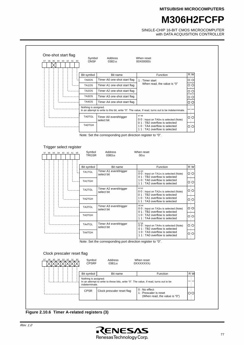
SINGLE-CHIP 16-BIT CMOS MICROCOMPUTERwith DATA ACQUISITION CONTROLLER
MITSUBISHI MICROCOMPUTERS
77
Rev. 1.0
M306H2FCFP
Symbol Address When resetCPSRF 038116 0XXXXXXX2
Clock prescaler reset flag
Bit name FunctionBit symbol
b7 b6 b5 b4 b3 b2 b1 b0
AAAAAAAAAAAAAAAAAAAAAAAAAAAAAAClock prescaler reset flag 0 : No effect
1 : Prescaler is reset (When read, the value is “0”)
CPSR
WR
Nothing is assigned.In an attempt to write to these bits, write “0”. The value, if read, turns out to be indeterminate.
TA1TGL
Symbol Address When resetTRGSR 038316 0016
Timer A1 event/trigger select bit 0 0 : Input on TA1IN is selected (Note)
0 1 : TB2 overflow is selected 1 0 : TA0 overflow is selected 1 1 : TA2 overflow is selected
Trigger select register
Bit name FunctionBit symbol
b7 b6 b5 b4 b3 b2 b1 b0
0 0 : Input on TA2IN is selected (Note) 0 1 : TB2 overflow is selected 1 0 : TA1 overflow is selected 1 1 : TA3 overflow is selected
0 0 : Input on TA3IN is selected (Note) 0 1 : TB2 overflow is selected 1 0 : TA2 overflow is selected 1 1 : TA4 overflow is selected
0 0 : Input on TA4IN is selected (Note) 0 1 : TB2 overflow is selected 1 0 : TA3 overflow is selected 1 1 : TA0 overflow is selected
Timer A2 event/trigger select bit
Timer A3 event/trigger select bit
Timer A4 event/trigger select bit
WR
TA1TGH
TA2TGL
TA2TGH
TA3TGL
TA3TGH
TA4TGL
TA4TGH
b1 b0
b3 b2
b5 b4
b7 b6
Note: Set the corresponding port direction register to “0”.
TA1OS
TA2OS
TA0OS
One-shot start flagSymbol Address When resetONSF 038216 00X000002
Timer A0 one-shot start flag
Timer A1 one-shot start flag
Timer A2 one-shot start flag
Timer A3 one-shot start flag
Timer A4 one-shot start flag
TA3OS
TA4OS
Bit name FunctionBit symbol
b7 b6 b5 b4 b3 b2 b1 b0
Nothing is assigned.In an attempt to write to this bit, write “0”. The value, if read, turns out to be indeterminate.
TA0TGL
TA0TGH
0 0 : Input on TA0IN is selected (Note)0 1 : TB2 overflow is selected1 0 : TA4 overflow is selected1 1 : TA1 overflow is selected
Timer A0 event/trigger select bit
b7 b6
Note: Set the corresponding port direction register to “0”.
WR
1 : Timer start When read, the value is “0” AAA
AAAAAAAAAAAAAAAAAAAAAAAA
AAA
AAAAAA
AAAAAAAAAAAAAAAAAAAAA
AAAAAA
AAAAAA
AAAAAA
Figure 2.10.6 Timer A-related registers (3)
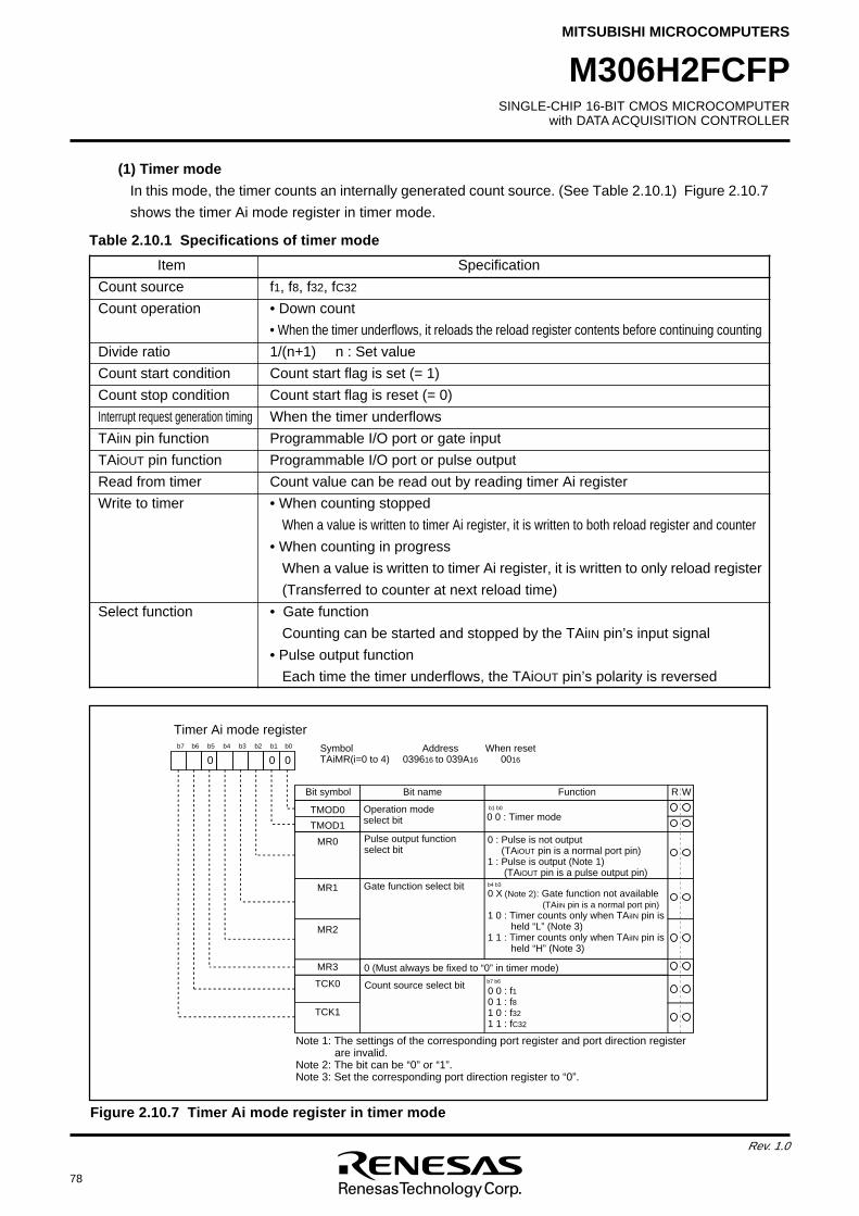
78
Rev. 1.0
SINGLE-CHIP 16-BIT CMOS MICROCOMPUTERwith DATA ACQUISITION CONTROLLER
MITSUBISHI MICROCOMPUTERS
M306H2FCFP
Item Specification
Count source f1, f8, f32, fC32
Count operation • Down count
• When the timer underflows, it reloads the reload register contents before continuing counting
Divide ratio 1/(n+1) n : Set value
Count start condition Count start flag is set (= 1)
Count stop condition Count start flag is reset (= 0)
Interrupt request generation timing When the timer underflows
TAiIN pin function Programmable I/O port or gate input
TAiOUT pin function Programmable I/O port or pulse output
Read from timer Count value can be read out by reading timer Ai register
Write to timer • When counting stopped
When a value is written to timer Ai register, it is written to both reload register and counter
• When counting in progress
When a value is written to timer Ai register, it is written to only reload register
(Transferred to counter at next reload time)
Select function • Gate function
Counting can be started and stopped by the TAiIN pin’s input signal
• Pulse output function
Each time the timer underflows, the TAiOUT pin’s polarity is reversed
Note 1: The settings of the corresponding port register and port direction register are invalid.
Note 2: The bit can be “0” or “1”. Note 3: Set the corresponding port direction register to “0”.
Timer Ai mode registerSymbol Address When resetTAiMR(i=0 to 4) 039616 to 039A16 0016
Bit name FunctionBit symbol WR
b7 b6 b5 b4 b3 b2 b1 b0
Operation mode select bit 0 0 : Timer mode
b1 b0
TMOD1
TMOD0
MR0 Pulse output function select bit
0 : Pulse is not output (TAiOUT pin is a normal port pin)1 : Pulse is output (Note 1) (TAiOUT pin is a pulse output pin)
Gate function select bit0 X (Note 2): Gate function not available (TAiIN pin is a normal port pin)1 0 : Timer counts only when TAiIN pin is
held “L” (Note 3)1 1 : Timer counts only when TAiIN pin is
held “H” (Note 3)
b4 b3
MR2
MR1
MR3 0 (Must always be fixed to “0” in timer mode)
0 0 : f1 0 1 : f8 1 0 : f32 1 1 : fC32
b7 b6
TCK1
TCK0 Count source select bit
0 00
AAAAAA
AA
AAAA
AAAA
AAAA
AAAA
Table 2.10.1 Specifications of timer mode
(1) Timer mode
In this mode, the timer counts an internally generated count source. (See Table 2.10.1) Figure 2.10.7
shows the timer Ai mode register in timer mode.
Figure 2.10.7 Timer Ai mode register in timer mode
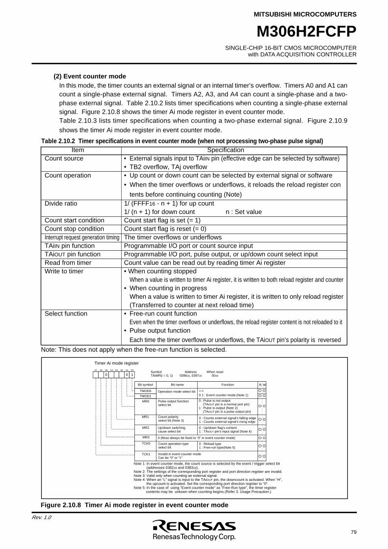
SINGLE-CHIP 16-BIT CMOS MICROCOMPUTERwith DATA ACQUISITION CONTROLLER
MITSUBISHI MICROCOMPUTERS
79
Rev. 1.0
M306H2FCFP
Timer Ai mode register
Note 1: In event counter mode, the count source is selected by the event / trigger select bit (addresses 038216 and 038316).
Note 2: The settings of the corresponding port register and port direction register are invalid.Note 3: Valid only when counting an external signal.Note 4: When an “L” signal is input to the TAiOUT pin, the downcount is activated. When “H”,
the upcount is activated. Set the corresponding port direction register to “0”.Note 5: In the case of using “Event counter mode” as “Free-Run type”, the timer register contents may be unkown when counting begins.(Refer 3. Usage Precaution.)
Symbol Address When resetTAiMR(i = 0, 1) 039616, 039716 0016
WR
b7 b6 b5 b4 b3 b2 b1 b0
Operation mode select bit0 1 : Event counter mode (Note 1)b1 b0 TMOD0
MR0 Pulse output functionselect bit
0 : Pulse is not output(TAiOUT pin is a normal port pin)
1 : Pulse is output (Note 2)(TAiOUT pin is a pulse output pin)
Count polarity select bit (Note 3)
MR2
MR1
MR3 0 (Must always be fixed to “0” in event counter mode)
TCK0 Count operation type select bit
0 10
0 : Counts external signal's falling edge1 : Counts external signal's rising edge
Up/down switching cause select bit
0 : Up/down flag's content1 : TAiOUT pin's input signal (Note 4)
0 : Reload type1 : Free-run type(Note 5)
Bit symbol Bit name Function R W
TCK1 Invalid in event counter modeCan be “0” or “1”
TMOD1AAAAAAAAAAAAAAAAAAAAAAAA
Figure 2.10.8 Timer Ai mode register in event counter mode
(2) Event counter modeIn this mode, the timer counts an external signal or an internal timer’s overflow. Timers A0 and A1 cancount a single-phase external signal. Timers A2, A3, and A4 can count a single-phase and a two-phase external signal. Table 2.10.2 lists timer specifications when counting a single-phase externalsignal. Figure 2.10.8 shows the timer Ai mode register in event counter mode.Table 2.10.3 lists timer specifications when counting a two-phase external signal. Figure 2.10.9
shows the timer Ai mode register in event counter mode.
Table 2.10.2 Timer specifications in event counter mode (when not processing two-phase pulse signal)Item Specification
Count source • External signals input to TAiIN pin (effective edge can be selected by software)• TB2 overflow, TAj overflow
Count operation • Up count or down count can be selected by external signal or software• When the timer overflows or underflows, it reloads the reload register con
tents before continuing counting (Note)Divide ratio 1/ (FFFF16 - n + 1) for up count
1/ (n + 1) for down count n : Set valueCount start condition Count start flag is set (= 1)Count stop condition Count start flag is reset (= 0)Interrupt request generation timing The timer overflows or underflowsTAiIN pin function Programmable I/O port or count source inputTAiOUT pin function Programmable I/O port, pulse output, or up/down count select inputRead from timer Count value can be read out by reading timer Ai registerWrite to timer • When counting stopped
When a value is written to timer Ai register, it is written to both reload register and counter• When counting in progress
When a value is written to timer Ai register, it is written to only reload register(Transferred to counter at next reload time)
Select function • Free-run count functionEven when the timer overflows or underflows, the reload register content is not reloaded to it
• Pulse output functionEach time the timer overflows or underflows, the TAiOUT pin’s polarity is reversed
Note: This does not apply when the free-run function is selected.
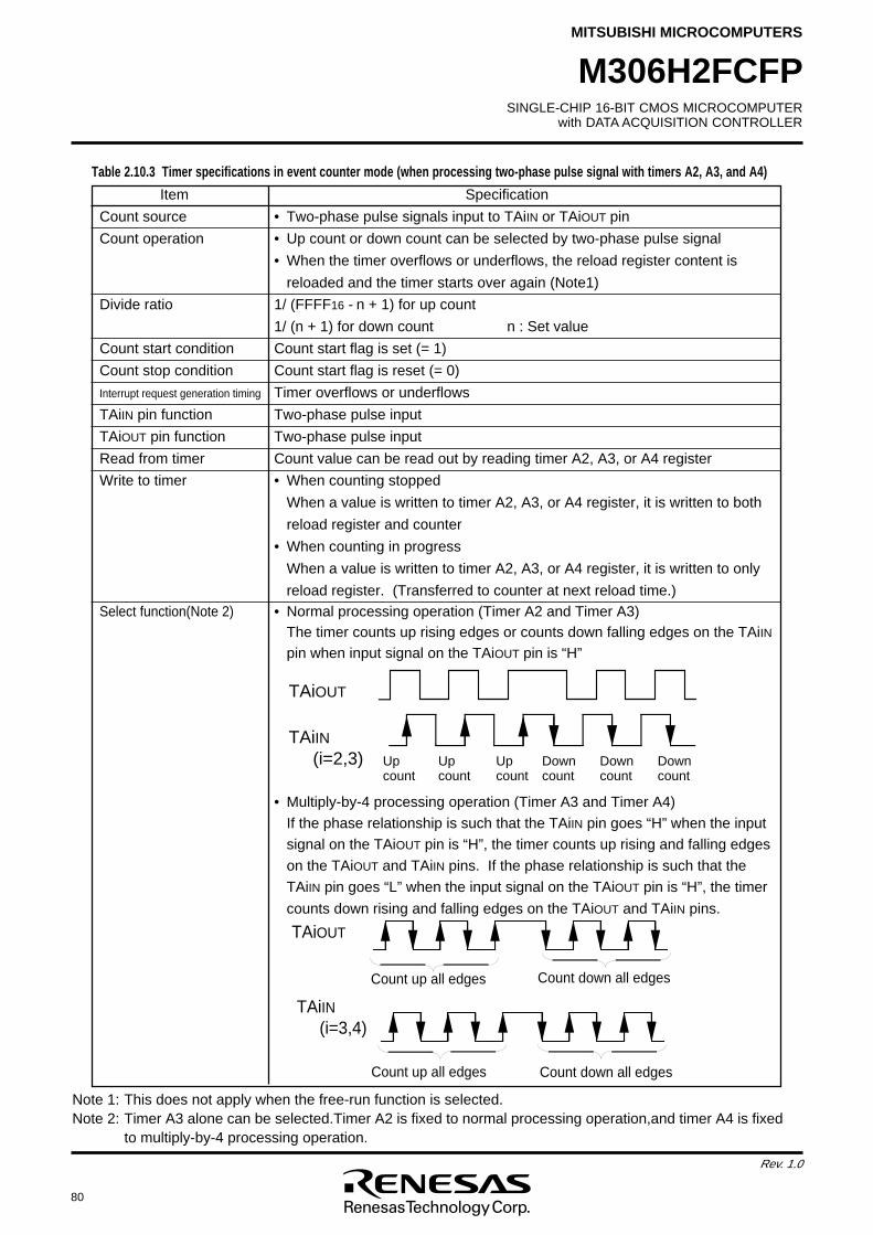
80
Rev. 1.0
SINGLE-CHIP 16-BIT CMOS MICROCOMPUTERwith DATA ACQUISITION CONTROLLER
MITSUBISHI MICROCOMPUTERS
M306H2FCFP
Item Specification
Count source • Two-phase pulse signals input to TAiIN or TAiOUT pin
Count operation • Up count or down count can be selected by two-phase pulse signal
• When the timer overflows or underflows, the reload register content is
reloaded and the timer starts over again (Note1)
Divide ratio 1/ (FFFF16 - n + 1) for up count
1/ (n + 1) for down count n : Set value
Count start condition Count start flag is set (= 1)
Count stop condition Count start flag is reset (= 0)
Interrupt request generation timing Timer overflows or underflows
TAiIN pin function Two-phase pulse input
TAiOUT pin function Two-phase pulse input
Read from timer Count value can be read out by reading timer A2, A3, or A4 register
Write to timer • When counting stopped
When a value is written to timer A2, A3, or A4 register, it is written to both
reload register and counter
• When counting in progress
When a value is written to timer A2, A3, or A4 register, it is written to only
reload register. (Transferred to counter at next reload time.)Select function(Note 2) • Normal processing operation (Timer A2 and Timer A3)
The timer counts up rising edges or counts down falling edges on the TAiINpin when input signal on the TAiOUT pin is “H”
• Multiply-by-4 processing operation (Timer A3 and Timer A4)
If the phase relationship is such that the TAiIN pin goes “H” when the inputsignal on the TAiOUT pin is “H”, the timer counts up rising and falling edges
on the TAiOUT and TAiIN pins. If the phase relationship is such that the
TAiIN pin goes “L” when the input signal on the TAiOUT pin is “H”, the timer
counts down rising and falling edges on the TAiOUT and TAiIN pins.
TAiOUT
TAiIN(i=3,4)
Count up all edges
Count up all edges
Count down all edges
Count down all edges
Table 2.10.3 Timer specifications in event counter mode (when processing two-phase pulse signal with timers A2, A3, and A4)
TAiOUT
Up count
Up count
Up count
Down count
Down count
Down count
TAiIN(i=2,3)
Note 1: This does not apply when the free-run function is selected.Note 2: Timer A3 alone can be selected.Timer A2 is fixed to normal processing operation,and timer A4 is fixed
to multiply-by-4 processing operation.
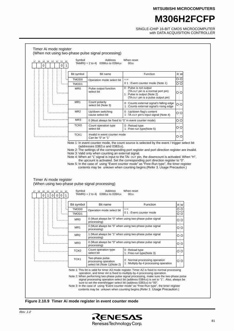
SINGLE-CHIP 16-BIT CMOS MICROCOMPUTERwith DATA ACQUISITION CONTROLLER
MITSUBISHI MICROCOMPUTERS
81
Rev. 1.0
M306H2FCFP
Timer Ai mode register (When not using two-phase pulse signal processing)
Symbol Address When resetTAiMR(i = 2 to 4) 039816 to 039A16 0016
b7 b6 b5 b4 b3 b2 b1 b0
0 10
Note 1: This bit is valid for timer A3 mode register. Timer A2 is fixed to normal processingoperation, and timer A4 is fixed to multiply-by-4 processing operation.
Note 2: When performing two-phase pulse signal processing, make sure the two-phase pulse signal processing operation select bit (address 038416) is set to “1”. Also, always besure to set the event/trigger select bit (address 038316) to “00”.
Note 3: In the case of using “Event counter mode” as “Free-Run type”, the timer register contents may be unkown when counting begins.(Refer 3. Usage Precaution.)
Timer Ai mode register (When using two-phase pulse signal processing)
Symbol Address When resetTAiMR(i = 2 to 4) 039816 to 039A16 0016
b7 b6 b5 b4 b3 b2 b1 b0
Operation mode select bit0 1 : Event counter modeb1 b0
TMOD1
TMOD0
MR0 0 (Must always be “0” when using two-phase pulse signal processing)
0 (Must always be “0” when using two-phase pulse signal processing)
MR2
MR1
MR3 0 (Must always be “0” when using two-phase pulse signal processing)
TCK1
TCK0
0 10
1 (Must always be “1” when using two-phase pulse signal processing)
Bit symbol Bit name Function WR
Count operation type select bit
Two-phase pulse processing operation select bit (Note 1)(Note 2)
0 : Reload type1 : Free-run type(Note 3)
0 : Normal processing operation1 : Multiply-by-4 processing operation
001
Note 1: In event counter mode, the count source is selected by the event / trigger select bit (addresses 038216 and 038316).
Note 2: The settings of the corresponding port register and port direction register are invalid.Note 3: Valid only when counting an external signal.Note 4: When an “L” signal is input to the TAi OUT pin, the downcount is activated. When “H”,
the upcount is activated. Set the corresponding port direction register to “0”.Note 5: In the case of using “Event counter mode” as “Free-Run type”, the timer register contents may be unkown when counting begins.(Refer 3. Usage Precaution.)
WR
Operation mode select bit0 1 : Event counter mode (Note 1)b1 b0 TMOD0
MR0 Pulse output functionselect bit
0 : Pulse is not output(TA iOUT pin is a normal port pin)
1 : Pulse is output (Note 2)(TA iOUT pin is a pulse output pin)
Count polarity select bit (Note 3)
MR2
MR1
MR3 0 (Must always be fixed to “0” in event counter mode)
TCK0 Count operation type select bit
0 : Counts external signal's falling edge1 : Counts external signal's rising edge
Up/down switching cause select bit
0 : Up/down flag's content1 : TA iOUT pin's input signal (Note 4)
0 : Reload type1 : Free-run type(Note 5)
Bit symbol Bit name Function R W
TCK1 Invalid in event counter modeCan be “0” or “1”
TMOD1
Figure 2.10.9 Timer Ai mode register in event counter mode
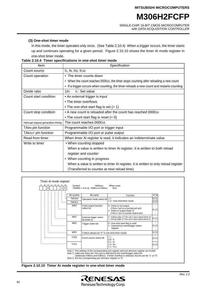
82
Rev. 1.0
SINGLE-CHIP 16-BIT CMOS MICROCOMPUTERwith DATA ACQUISITION CONTROLLER
MITSUBISHI MICROCOMPUTERS
M306H2FCFP
Bit name
Timer Ai mode registerSymbol Address When resetTAiMR(i = 0 to 4) 039616 to 039A16 0016
Function Bit symbol
b7 b6 b5 b4 b3 b2 b1 b0
Operation mode select bit1 0 : One-shot timer modeb1 b0
TMOD1
TMOD0
MR0 Pulse output function select bit
0 : Pulse is not output (TAiOUT pin is a normal port pin)1 : Pulse is output (Note 1) (TAiOUT pin is a pulse output pin)
MR2
MR1
MR3 0 (Must always be “0” in one-shot timer mode)
0 0 : f10 1 : f81 0 : f321 1 : fC32
b7 b6
TCK1
TCK0 Count source select bit
1 00
0 : One-shot start flag is valid1 : Selected by event/trigger select
register
Trigger select bit
External trigger select bit (Note 2)
0 : Falling edge of TAiIN pin's input signal (Note 3)1 : Rising edge of TAiIN pin's input signal (Note 3)
Note 1: The settings of the corresponding port register and port direction register are invalid.Note 2: Valid only when the TAiIN pin is selected by the event/trigger select bit
(addresses 038216 and 038316). If timer overflow is selected, this bit can be “1” or “0”.Note 3: Set the corresponding port direction register to “0”.
WR
AAAA
AAAA
AAAA
AAAA
AAAA
AAAA
(3) One-shot timer mode
In this mode, the timer operates only once. (See Table 2.10.4) When a trigger occurs, the timer starts
up and continues operating for a given period. Figure 2.10.10 shows the timer Ai mode register in
one-shot timer mode.Table 2.10.4 Timer specifications in one-shot timer mode
Figure 2.10.10 Timer Ai mode register in one-shot timer mode
Item Specification
Count source f1, f8, f32, fC32
Count operation • The timer counts down
• When the count reaches 000016, the timer stops counting after reloading a new count
• If a trigger occurs when counting, the timer reloads a new count and restarts counting
Divide ratio 1/n n : Set value
Count start condition • An external trigger is input
• The timer overflows
• The one-shot start flag is set (= 1)
Count stop condition • A new count is reloaded after the count has reached 000016
• The count start flag is reset (= 0)
Interrupt request generation timing The count reaches 000016
TAiIN pin function Programmable I/O port or trigger input
TAiOUT pin function Programmable I/O port or pulse output
Read from timer When timer Ai register is read, it indicates an indeterminate value
Write to timer • When counting stopped
When a value is written to timer Ai register, it is written to both reload
register and counter
• When counting in progress
When a value is written to timer Ai register, it is written to only reload register
(Transferred to counter at next reload time)
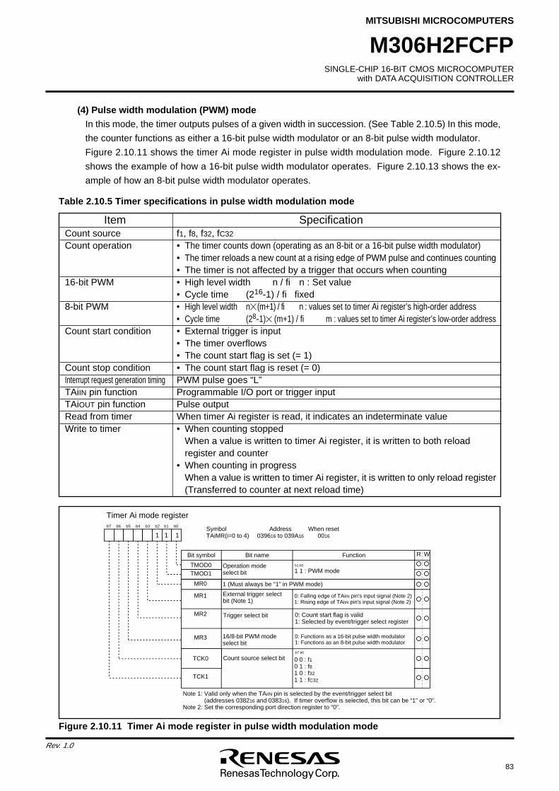
SINGLE-CHIP 16-BIT CMOS MICROCOMPUTERwith DATA ACQUISITION CONTROLLER
MITSUBISHI MICROCOMPUTERS
83
Rev. 1.0
M306H2FCFP
Bit name
Timer Ai mode register
Symbol Address When resetTAiMR(i=0 to 4) 039616 to 039A16 0016
FunctionBit symbol
b7 b6 b5 b4 b3 b2 b1 b0
Operation mode select bit 1 1 : PWM mode
b1 b0
TMOD1TMOD0
MR0
MR2
MR1
MR3
0 0 : f10 1 : f81 0 : f321 1 : fC32
b7 b6
TCK1
TCK0 Count source select bit
WR
1 11
1 (Must always be “1” in PWM mode)
16/8-bit PWM mode select bit
0: Functions as a 16-bit pulse width modulator1: Functions as an 8-bit pulse width modulator
Trigger select bit
External trigger select bit (Note 1)
0: Falling edge of TAiIN pin's input signal (Note 2)1: Rising edge of TAiIN pin's input signal (Note 2)
0: Count start flag is valid1: Selected by event/trigger select register
Note 1: Valid only when the TAiIN pin is selected by the event/trigger select bit(addresses 038216 and 038316). If timer overflow is selected, this bit can be “1” or “0”.
Note 2: Set the corresponding port direction register to “0”.
AAAAAAAAAAAA
AAAAAA
AAAAAAAAA
Figure 2.10.11 Timer Ai mode register in pulse width modulation mode
(4) Pulse width modulation (PWM) mode
In this mode, the timer outputs pulses of a given width in succession. (See Table 2.10.5) In this mode,
the counter functions as either a 16-bit pulse width modulator or an 8-bit pulse width modulator.
Figure 2.10.11 shows the timer Ai mode register in pulse width modulation mode. Figure 2.10.12
shows the example of how a 16-bit pulse width modulator operates. Figure 2.10.13 shows the ex-
ample of how an 8-bit pulse width modulator operates.
Table 2.10.5 Timer specifications in pulse width modulation mode
Item SpecificationCount source f1, f8, f32, fC32
Count operation • The timer counts down (operating as an 8-bit or a 16-bit pulse width modulator)• The timer reloads a new count at a rising edge of PWM pulse and continues counting• The timer is not affected by a trigger that occurs when counting
16-bit PWM • High level width n / fi n : Set value• Cycle time (216-1) / fi fixed
8-bit PWM • High level width n (m+1) / fi n : values set to timer Ai register’s high-order address• Cycle time (28-1) (m+1) / fi m : values set to timer Ai register’s low-order address
Count start condition • External trigger is input• The timer overflows• The count start flag is set (= 1)
Count stop condition • The count start flag is reset (= 0)Interrupt request generation timing PWM pulse goes “L”TAiIN pin function Programmable I/O port or trigger inputTAiOUT pin function Pulse outputRead from timer When timer Ai register is read, it indicates an indeterminate valueWrite to timer • When counting stopped
When a value is written to timer Ai register, it is written to both reloadregister and counter
• When counting in progressWhen a value is written to timer Ai register, it is written to only reload register(Transferred to counter at next reload time)
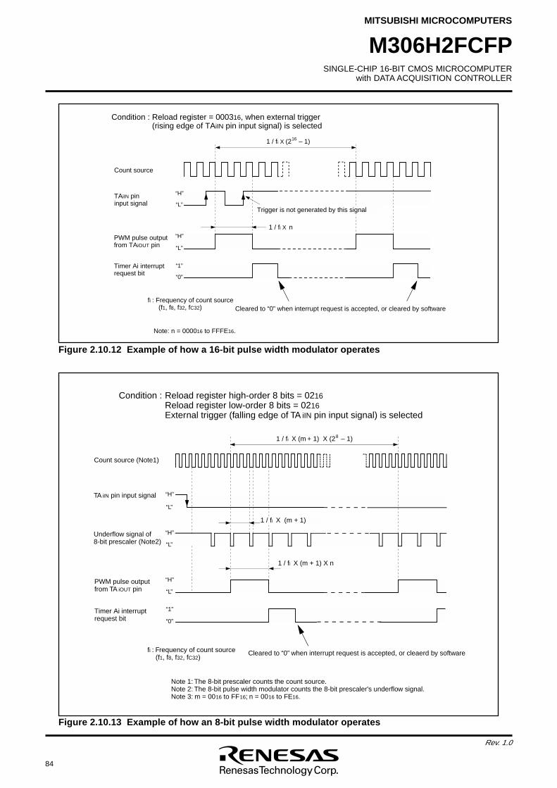
84
Rev. 1.0
SINGLE-CHIP 16-BIT CMOS MICROCOMPUTERwith DATA ACQUISITION CONTROLLER
MITSUBISHI MICROCOMPUTERS
M306H2FCFP
1 / fi X (2 – 1) 16
Count source
TAiIN pin input signal
PWM pulse output from TAiOUT pin
Condition : Reload register = 000316, when external trigger (rising edge of TAiIN pin input signal) is selected
Trigger is not generated by this signal
“H”
“H”
“L”
“L”
Timer Ai interrupt request bit
“1”
“0”
Cleared to “0” when interrupt request is accepted, or cleared by softwarefi : Frequency of count source
(f1, f8, f32, fC32)
Note: n = 000016 to FFFE16.
1 / fi X n
Count source (Note1)
TA iIN pin input signal
Underflow signal of 8-bit prescaler (Note2)
PWM pulse output from TA iOUT pin
“H”
“H”
“H”
“L”
“L”
“L”
“1”
“0”
Timer Ai interrupt request bit
Cleared to “0” when interrupt request is accepted, or cleaerd by softwarefi : Frequency of count source (f1, f8, f32, fC32)
Note 1: The 8-bit prescaler counts the count source.Note 2: The 8-bit pulse width modulator counts the 8-bit prescaler's underflow signal.Note 3: m = 0016 to FF16; n = 0016 to FE16.
Condition : Reload register high-order 8 bits = 0216Reload register low-order 8 bits = 0216External trigger (falling edge of TA iIN pin input signal) is selected
1 / fi X (m + 1) X (2 – 1) 8
1 / fi X (m + 1) X n
1 / fi X (m + 1)
Figure 2.10.13 Example of how an 8-bit pulse width modulator operates
Figure 2.10.12 Example of how a 16-bit pulse width modulator operates
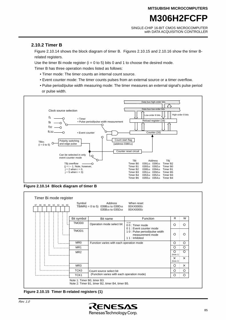
SINGLE-CHIP 16-BIT CMOS MICROCOMPUTERwith DATA ACQUISITION CONTROLLER
MITSUBISHI MICROCOMPUTERS
85
Rev. 1.0
M306H2FCFP
Timer Bi mode registerSymbol Address When resetTBiMR(i = 0 to 5) 039B16 to 039D16 00XX00002
035B16 to 035D16 00XX00002
Bit name FunctionBit symbol WR
b7 b6 b5 b4 b3 b2 b1 b0
0 0 : Timer mode0 1 : Event counter mode1 0 : Pulse period/pulse width
measurement mode1 1 : Inhibited
b1 b0
TCK1
MR3
MR2
MR1
TMOD1
MR0
TMOD0
TCK0
Function varies with each operation mode
Count source select bit (Function varies with each operation mode)
Operation mode select bit
(Note 1)
(Note 2)
Note 1: Timer B0, timer B3.Note 2: Timer B1, timer B2, timer B4, timer B5.
AAAAAAAAAAAAAAAAAA
AAAAAAAAA
A
Clock source selection
(address 038016)
• Event counter
• Timer• Pulse period/pulse width measurement Reload register (16)
Low-order 8 bits High-order 8 bits
Data bus low-order bits
Data bus high-order bits
f1
f8f32
TBj overflow (j = i – 1. Note, however, j = 2 when i = 0, j = 5 when i = 3)
Can be selected in only event counter mode
Count start flag
fC32
Polarity switching and edge pulse
TBiIN
(i = 0 to 5)
Counter reset circuit
Counter (16)
TBi Address TBjTimer B0 039116 039016 Timer B2Timer B1 039316 039216 Timer B0Timer B2 039516 039416 Timer B1Timer B3 035116 035016 Timer B5Timer B4 035316 035216 Timer B3Timer B5 035516 035416 Timer B4
2.10.2 Timer BFigure 2.10.14 shows the block diagram of timer B. Figures 2.10.15 and 2.10.16 show the timer B-
related registers.
Use the timer Bi mode register (i = 0 to 5) bits 0 and 1 to choose the desired mode.
Timer B has three operation modes listed as follows:
• Timer mode: The timer counts an internal count source.
• Event counter mode: The timer counts pulses from an external source or a timer overflow.
• Pulse period/pulse width measuring mode: The timer measures an external signal's pulse period
or pulse width.
Figure 2.10.15 Timer B-related registers (1)
Figure 2.10.14 Block diagram of timer B
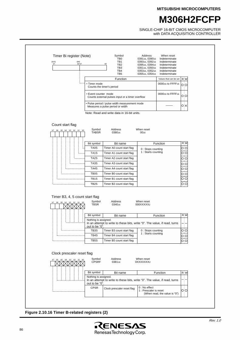
86
Rev. 1.0
SINGLE-CHIP 16-BIT CMOS MICROCOMPUTERwith DATA ACQUISITION CONTROLLER
MITSUBISHI MICROCOMPUTERS
M306H2FCFP
Symbol Address When resetTABSR 038016 0016
Count start flag
Bit nameBit symbol WR
b7 b6 b5 b4 b3 b2 b1 b0
AAAAAAAAAAAAAAAAAAAAAAAAAAAAAAAAAAAAAAAAAAAAAAAAAAAAAAAAAAAAAAAAAAAAAAAAAAAAAAAA
AAAAAAAAAAAAAAAAAAAAAAAAAAAAAAAA
AAAAAAAAAAAAAAAAAAAAAAAAAAAAAAAAAAAAAAAAAAAAAAAAAAAAAAAAAAAAAAAAAAAAAAAAAAAAAAAA
AAAAAAAAAAAAAAAAAAAAAAAAAAAAAAAATimer B2 count start flag
Timer B1 count start flag
Timer B0 count start flag
Timer A4 count start flag
Timer A3 count start flag
Timer A2 count start flag
Timer A1 count start flag
Timer A0 count start flag 0 : Stops counting1 : Starts counting
TB2S
TB1S
TB0S
TA4S
TA3S
TA2S
TA1S
TA0S
Function
AAAAAAAAAAAAAAAAAAAA
Symbol Address When resetCPSRF 038116 0XXXXXXX2
Clock prescaler reset flag
Bit name FunctionBit symbol WR
b7 b6 b5 b4 b3 b2 b1 b0
AAAAAAAAAAAAAAAAAAAAAAAAAAAAAAAAAAAAAAAAAAAAAAAAClock prescaler reset flag 0 : No effect
1 : Prescaler is reset (When read, the value is “0”)
CPSR
AA
Symbol Address When resetTB0 039116, 039016 IndeterminateTB1 039316, 039216 IndeterminateTB2 039516, 039416 IndeterminateTB3 035116, 035016 IndeterminateTB4 035316, 035216 IndeterminateTB5 035516, 035416 Indeterminate
b7 b0 b7 b0(b15) (b8)
Timer Bi register (Note)
WR
• Pulse period / pulse width measurement mode Measures a pulse period or width
• Timer mode 000016 to FFFF16 Counts the timer's period
Function Values that can be set
• Event counter mode 000016 to FFFF16 Counts external pulses input or a timer overflow
Note: Read and write data in 16-bit units.
AA
AAA
Symbol Address When resetTBSR 034016 000XXXXX2
Timer B3, 4, 5 count start flag
Bit nameBit symbol WR
b7 b6 b5 b4 b3 b2 b1 b0
AAAAAAAAAAAAAAAAAAAAAAAAAAAAAAAAAAAAAAAAAAAAAAAAAAAAAAAAAAAAAAAA
AAAAAAAAAAAAAAAAAAAAAAAAAAAAAAAA
AAAAAAAAAAAAAAAAAAAAAAAAAAAAAAAATimer B5 count start flag
Timer B4 count start flag
Timer B3 count start flag 0 : Stops counting1 : Starts counting
TB5S
TB4S
TB3S
Nothing is assigned.In an attempt to write to these bits, write “0”. The value, if read, turns out to be “0”.
Function
AAAAAAAA
Nothing is assigned.In an attempt to write to these bits, write “0”. The value, if read, turns out to be “0”.
Figure 2.10.16 Timer B-related registers (2)
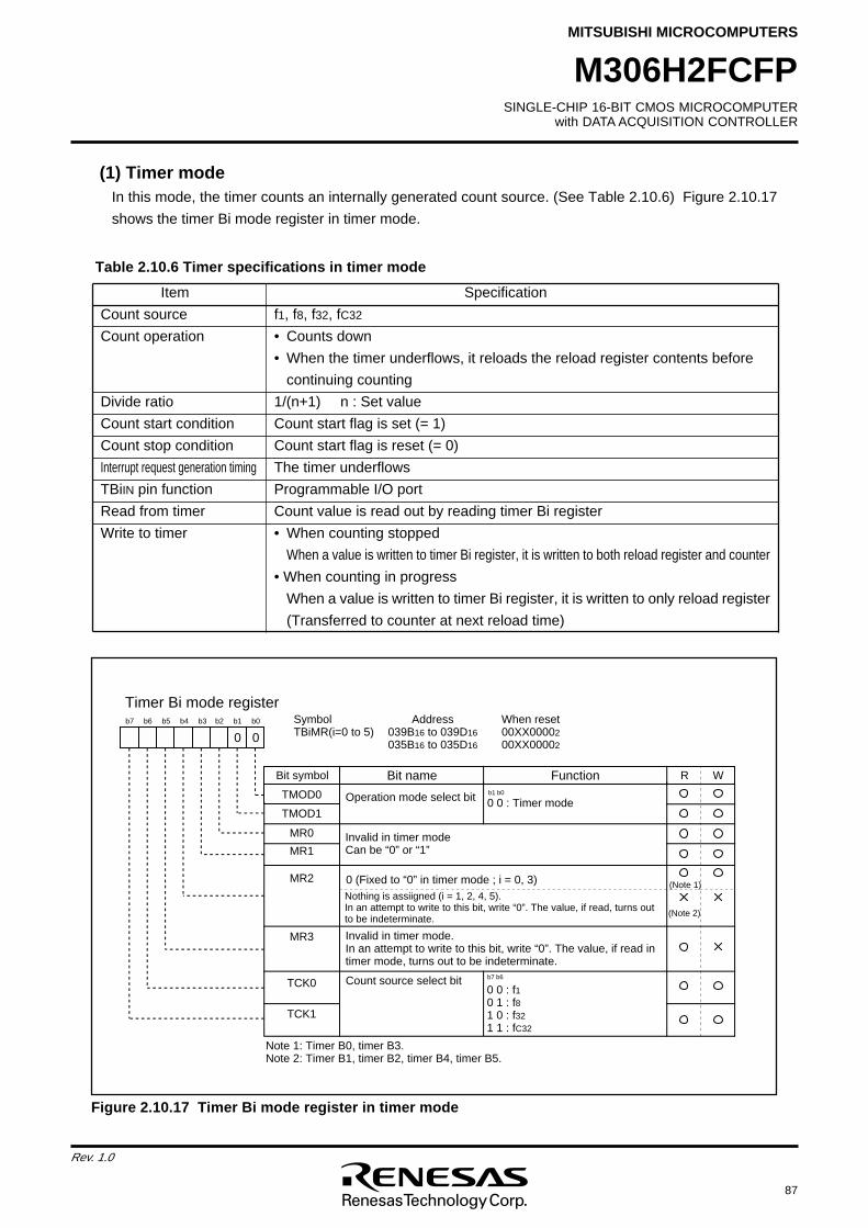
SINGLE-CHIP 16-BIT CMOS MICROCOMPUTERwith DATA ACQUISITION CONTROLLER
MITSUBISHI MICROCOMPUTERS
87
Rev. 1.0
M306H2FCFP
Note 1: Timer B0, timer B3.Note 2: Timer B1, timer B2, timer B4, timer B5.
Timer Bi mode registerSymbol Address When resetTBiMR(i=0 to 5) 039B16 to 039D16 00XX00002
035B16 to 035D16 00XX00002
Bit name FunctionBit symbol WR
b7 b6 b5 b4 b3 b2 b1 b0
AAAAAA
Operation mode select bit 0 0 : Timer modeb1 b0
TMOD1
TMOD0
MR0 Invalid in timer mode Can be “0” or “1”
MR2
MR1
MR3
0 0 : f10 1 : f81 0 : f321 1 : fC32
TCK1
TCK0 Count source select bit
0
Invalid in timer mode.In an attempt to write to this bit, write “0”. The value, if read in timer mode, turns out to be indeterminate.
0
0 (Fixed to “0” in timer mode ; i = 0, 3)Nothing is assiigned (i = 1, 2, 4, 5).In an attempt to write to this bit, write “0”. The value, if read, turns out to be indeterminate.
(Note 1)
(Note 2)
b7 b6
AAAAAAAAAA
AAAA
AA
Figure 2.10.17 Timer Bi mode register in timer mode
(1) Timer modeIn this mode, the timer counts an internally generated count source. (See Table 2.10.6) Figure 2.10.17
shows the timer Bi mode register in timer mode.
Table 2.10.6 Timer specifications in timer mode
Item Specification
Count source f1, f8, f32, fC32
Count operation • Counts down
• When the timer underflows, it reloads the reload register contents before
continuing counting
Divide ratio 1/(n+1) n : Set value
Count start condition Count start flag is set (= 1)
Count stop condition Count start flag is reset (= 0)
Interrupt request generation timing The timer underflows
TBiIN pin function Programmable I/O port
Read from timer Count value is read out by reading timer Bi register
Write to timer • When counting stopped
When a value is written to timer Bi register, it is written to both reload register and counter
• When counting in progress
When a value is written to timer Bi register, it is written to only reload register
(Transferred to counter at next reload time)

88
Rev. 1.0
SINGLE-CHIP 16-BIT CMOS MICROCOMPUTERwith DATA ACQUISITION CONTROLLER
MITSUBISHI MICROCOMPUTERS
M306H2FCFP
Timer Bi mode registerSymbol Address When resetTBiMR(i=0 to 5) 039B16 to 039D16 00XX00002
035B16 to 035D16 00XX00002
Bit name FunctionBit symbol WR
b7 b6 b5 b4 b3 b2 b1 b0
AAAA
Operation mode select bit0 1 : Event counter mode b1 b0
TMOD1
TMOD0
MR0 Count polarity select bit (Note 1)
MR2
MR1
MR3 Invalid in event counter mode.In an attempt to write to this bit, write “0”. The value, if read in event counter mode, turns out to be indeterminate.
TCK1
TCK0
0 1
0 0 : Counts external signal's falling edges
0 1 : Counts external signal's rising edges
1 0 : Counts external signal's falling and rising edges
1 1 : Inhibited
b3 b2
Nothing is assigned (i = 1, 2, 4, 5).In an attempt to write to this bit, write “0”. The value, if read, turns out to be indeterminate.
Note 1: Valid only when input from the TBiIN pin is selected as the event clock.If timer's overflow is selected, this bit can be “0” or “1”.
Note 2: Timer B0, timer B3.Note 3: Timer B1, timer B2, timer B4, timer B5.Note 4: Set the corresponding port direction register to “0”.
Invalid in event counter mode.Can be “0” or “1”.
Event clock select 0 : Input from TBiIN pin (Note 4)1 : TBj overflow
(j = i – 1; however, j = 2 when i = 0, j = 5 when i = 3)
0 (Fixed to “0” in event counter mode; i = 0, 3)(Note 2)
(Note 3)
AAAAAAAAAAAAAAAA
AAAAAAAA
AAAA
AAAA
AAAA
AA
Figure 2.10.18 Timer Bi mode register in event counter mode
(2) Event counter mode
In this mode, the timer counts an external signal or an internal timer's overflow. (See Table 2.10.7)
Figure 2.10.18 shows the timer Bi mode register in event counter mode.
Table 2.10.7 Timer specifications in event counter mode
Item Specification
Count source • External signals input to TBiIN pin
• Effective edge of count source can be a rising edge, a falling edge, or falling
and rising edges as selected by software
Count operation • Counts down
• When the timer underflows, it reloads the reload register contents before
continuing counting
Divide ratio 1/(n+1) n : Set value
Count start condition Count start flag is set (= 1)
Count stop condition Count start flag is reset (= 0)
Interrupt request generation timing The timer underflows
TBiIN pin function Count source input
Read from timer Count value can be read out by reading timer Bi register
Write to timer • When counting stopped
When a value is written to timer Bi register, it is written to both reload register and counter
• When counting in progress
When a value is written to timer Bi register, it is written to only reload register
(Transferred to counter at next reload time)
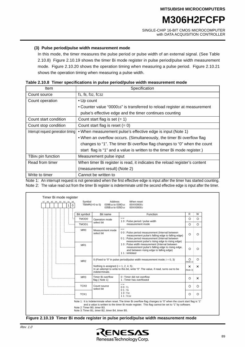
SINGLE-CHIP 16-BIT CMOS MICROCOMPUTERwith DATA ACQUISITION CONTROLLER
MITSUBISHI MICROCOMPUTERS
89
Rev. 1.0
M306H2FCFP
(3) Pulse period/pulse width measurement mode
In this mode, the timer measures the pulse period or pulse width of an external signal. (See Table
2.10.8) Figure 2.10.19 shows the timer Bi mode register in pulse period/pulse width measurement
mode. Figure 2.10.20 shows the operation timing when measuring a pulse period. Figure 2.10.21
shows the operation timing when measuring a pulse width.
Figure 2.10.19 Timer Bi mode register in pulse period/pulse width measurement mode
Table 2.10.8 Timer specifications in pulse period/pulse width measurement mode
Note 1: An interrupt request is not generated when the first effective edge is input after the timer has started counting.Note 2: The value read out from the timer Bi register is indeterminate until the second effective edge is input after the timer.
Item Specification
Count source f1, f8, f32, fC32
Count operation • Up count
• Counter value “000016” is transferred to reload register at measurement
pulse's effective edge and the timer continues counting
Count start condition Count start flag is set (= 1)
Count stop condition Count start flag is reset (= 0)
Interrupt request generation timing • When measurement pulse's effective edge is input (Note 1)
• When an overflow occurs. (Simultaneously, the timer Bi overflow flag
changes to “1”. The timer Bi overflow flag changes to “0” when the count
start flag is “1” and a value is written to the timer Bi mode register.)
TBiIN pin function Measurement pulse input
Read from timer When timer Bi register is read, it indicates the reload register’s content
(measurement result) (Note 2)
Write to timer Cannot be written to
Timer Bi mode registerSymbol Address When resetTBiMR(i=0 to 5) 039B16 to 039D16 00XX00002 035B16 to 035D16 00XX00002
Bit nameBit symbol WR
b7 b6 b5 b4 b3 b2 b1 b0
Operation mode select bit 1 0 : Pulse period / pulse width
measurement mode
b1 b0
TMOD1
TMOD0
MR0 Measurement mode select bit
MR2
MR1
MR3
TCK1
TCK0
01
0 0 : Pulse period measurement (Interval between measurement pulse's falling edge to falling edge)0 1 : Pulse period measurement (Interval between measurement pulse's rising edge to rising edge)1 0 : Pulse width measurement (Interval between measurement pulse's falling edge to rising edge, and between rising edge to falling edge)1 1 : Inhibited
Function
b3 b2
Nothing is assigned (i = 1, 2, 4, 5).In an attempt to write to this bit, write “0”. The value, if read, turns out to be indeterminate.
Count source select bit
Timer Bi overflow flag ( Note 1)
0 : Timer did not overflow1 : Timer has overflowed
0 0 : f10 1 : f8
1 0 : f32
1 1 : fC32
b7 b6
Note 1: It is Indeterminate when reset. The timer Bi overflow flag changes to “0” when the count start flag is “1” and a value is written to the timer Bi mode register. This flag cannot be set to “1” by software.Note 2: Timer B0, timer B3.Note 3: Timer B1, timer B2, timer B4, timer B5.
0 (Fixed to “0” in pulse period/pulse width measurement mode; i = 0, 3)(Note 2)
(Note 3)
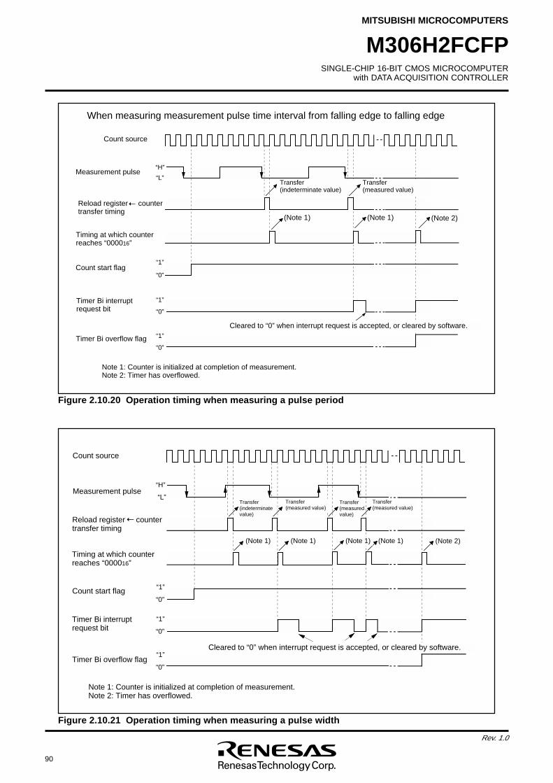
90
Rev. 1.0
SINGLE-CHIP 16-BIT CMOS MICROCOMPUTERwith DATA ACQUISITION CONTROLLER
MITSUBISHI MICROCOMPUTERS
M306H2FCFP
Figure 2.10.21 Operation timing when measuring a pulse width
Measurement pulse“H”
Count source
Count start flag
Timer Bi interrupt request bit
Timing at which counter reaches “000016”
“1”
“1”
Transfer (measured value)
Transfer(measured value)
“L”
“0”
“0”
Timer Bi overflow flag“1”
“0”
Note 1: Counter is initialized at completion of measurement.Note 2: Timer has overflowed.
(Note 1)(Note 1)(Note 1)
Transfer (measured value)
(Note 1)
Cleared to “0” when interrupt request is accepted, or cleared by software.
(Note 2)
Transfer (indeterminate value)
Reload register counter transfer timing
Figure 2.10.20 Operation timing when measuring a pulse period
Count source
Measurement pulse
Count start flag
Timer Bi interrupt request bit
Timing at which counter reaches “000016”
“H”
“1”
Transfer (indeterminate value)
“L”
“0”
“0”
Timer Bi overflow flag “1”
“0”
Note 1: Counter is initialized at completion of measurement.Note 2: Timer has overflowed.
(Note 1)(Note 1)
When measuring measurement pulse time interval from falling edge to falling edge
(Note 2)
Cleared to “0” when interrupt request is accepted, or cleared by software.
Transfer(measured value)
“1”
Reload register counter transfer timing
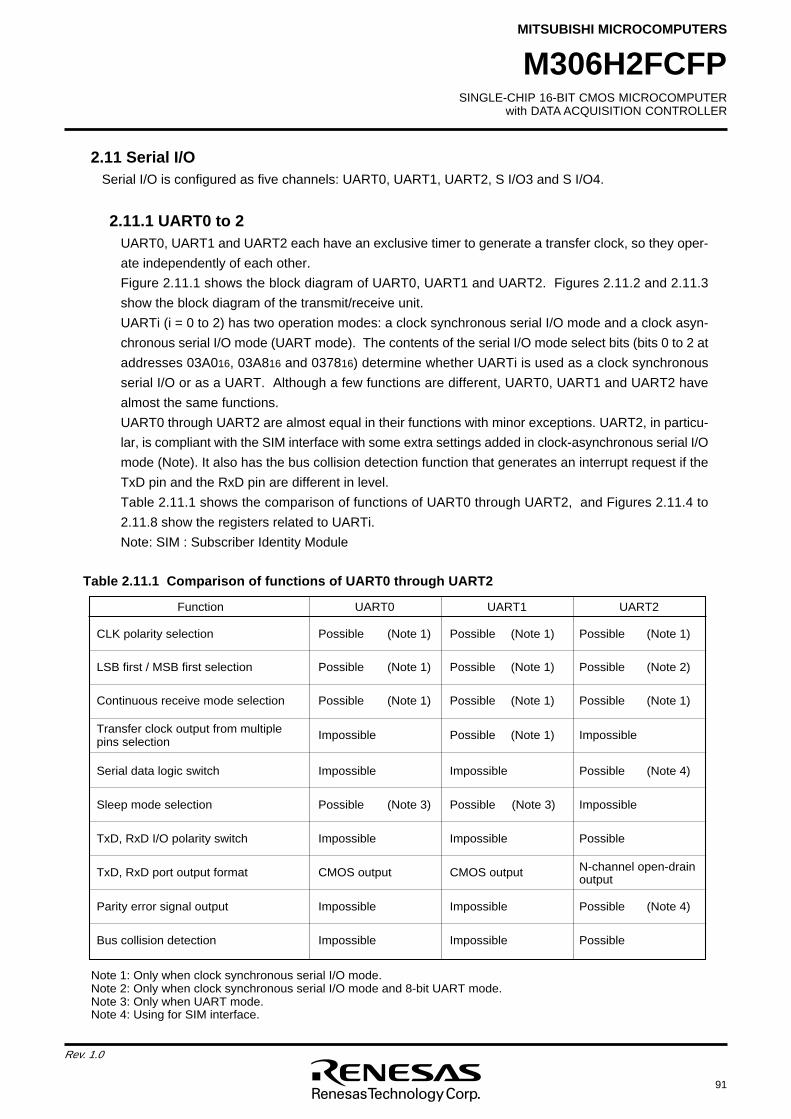
SINGLE-CHIP 16-BIT CMOS MICROCOMPUTERwith DATA ACQUISITION CONTROLLER
MITSUBISHI MICROCOMPUTERS
91
Rev. 1.0
M306H2FCFP
Note 1: Only when clock synchronous serial I/O mode.Note 2: Only when clock synchronous serial I/O mode and 8-bit UART mode.Note 3: Only when UART mode.Note 4: Using for SIM interface.
UART0 UART1 UART2Function
CLK polarity selection
Continuous receive mode selection
LSB first / MSB first selection
ImpossibleTransfer clock output from multiple pins selection
Impossible
Possible (Note 1)
Possible (Note 1)
Possible (Note 1)
Possible (Note 1)
Possible (Note 1)
Possible (Note 1)
Possible (Note 1)
Possible (Note 1)
Possible (Note 2)
Possible (Note 1)
ImpossibleSerial data logic switch Impossible
Sleep mode selection Impossible
ImpossibleTxD, RxD I/O polarity switch Impossible Possible
CMOS outputTxD, RxD port output format CMOS output N-channel open-drain output
ImpossibleParity error signal output Impossible
ImpossibleBus collision detection Impossible Possible
Possible (Note 3) Possible (Note 3)
Possible (Note 4)
Possible (Note 4)
2.11 Serial I/OSerial I/O is configured as five channels: UART0, UART1, UART2, S I/O3 and S I/O4.
2.11.1 UART0 to 2UART0, UART1 and UART2 each have an exclusive timer to generate a transfer clock, so they oper-
ate independently of each other.
Figure 2.11.1 shows the block diagram of UART0, UART1 and UART2. Figures 2.11.2 and 2.11.3
show the block diagram of the transmit/receive unit.
UARTi (i = 0 to 2) has two operation modes: a clock synchronous serial I/O mode and a clock asyn-
chronous serial I/O mode (UART mode). The contents of the serial I/O mode select bits (bits 0 to 2 at
addresses 03A016, 03A816 and 037816) determine whether UARTi is used as a clock synchronous
serial I/O or as a UART. Although a few functions are different, UART0, UART1 and UART2 have
almost the same functions.
UART0 through UART2 are almost equal in their functions with minor exceptions. UART2, in particu-
lar, is compliant with the SIM interface with some extra settings added in clock-asynchronous serial I/O
mode (Note). It also has the bus collision detection function that generates an interrupt request if the
TxD pin and the RxD pin are different in level.
Table 2.11.1 shows the comparison of functions of UART0 through UART2, and Figures 2.11.4 to
2.11.8 show the registers related to UARTi.
Note: SIM : Subscriber Identity Module
Table 2.11.1 Comparison of functions of UART0 through UART2
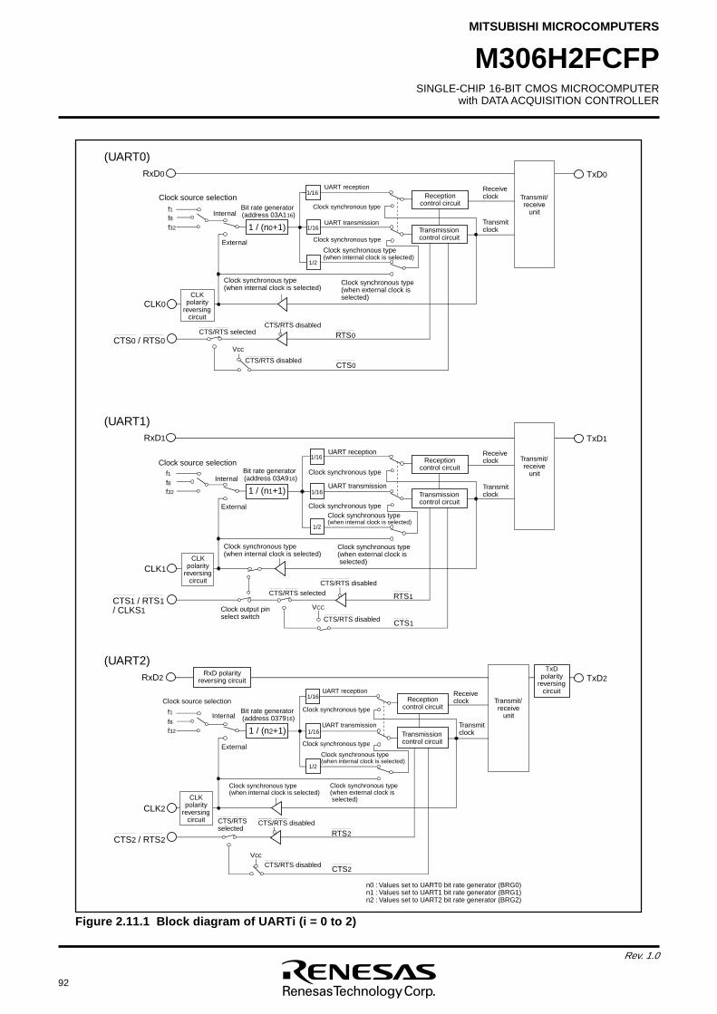
92
Rev. 1.0
SINGLE-CHIP 16-BIT CMOS MICROCOMPUTERwith DATA ACQUISITION CONTROLLER
MITSUBISHI MICROCOMPUTERS
M306H2FCFP
Figure 2.11.1 Block diagram of UARTi (i = 0 to 2)
CLK0
n0 : Values set to UART0 bit rate generator (BRG0)n1 : Values set to UART1 bit rate generator (BRG1)n2 : Values set to UART2 bit rate generator (BRG2)
RxD2
Reception control circuit
Transmission control circuit
1 / (n2+1)
1/16
1/16
1/2
Bit rate generator (address 037916)
Clock synchronous type (when internal clock is selected)
UART reception
Clock synchronous type
UART transmission
Clock synchronous type
Clock synchronous type(when internal clock is selected)
Clock synchronous type (when external clock is selected)
Receive clock
Transmit clock
CLK2
CTS2 / RTS2
f1f8f32
Vcc
RTS2
CTS2
TxD2
(UART2)RxD polarity
reversing circuit
TxD polarity
reversing circuit
RxD0
1 / (n0+1)
1/2
Bit rate generator (address 03A116)
Clock synchronous type (when internal clock is selected)
UART reception
Clock synchronous type
UART transmission
Clock synchronous type
Clock synchronous type(when internal clock is selected)
Clock synchronous type (when external clock is selected)
Receive clock
Transmit clock
Clock source selection
CTS0 / RTS0
f1f8f32
Reception control circuit
Transmission control circuit
Internal
External
Vcc
RTS0
CTS0
TxD0
Transmit/receive
unit
RxD1
1 / (n1+1)
1/16
1/16
1/2
Bit rate generator (address 03A916)
Clock synchronous type (when internal clock is selected)
UART reception
Clock synchronous type
UART transmission
Clock synchronous typeClock synchronous type(when internal clock is selected)
Clock synchronous type (when external clock is selected)
Receive clock
Transmit clock
CLK1
Clock source selectionf1f8f32
Reception control circuit
Transmission control circuit
Internal
External
RTS1
CTS1
TxD1
(UART1)
(UART0)
CLK polarity
reversing circuit
CLK polarity
reversing circuit
CTS/RTS disabled
Clock output pin select switch
CTS/RTS disabledCTS/RTS selected
CTS/RTS disabled
VCC
CTS/RTS disabled
CTS/RTS disabled
CTS/RTS disabled
CTS/RTS selected
CLKpolarity
reversing circuit
Internal
External
Clock source selection
Transmit/receive
unit
Transmit/receive
unit
1/16
1/16
CTS1 / RTS1/ CLKS1
CTS/RTS selected
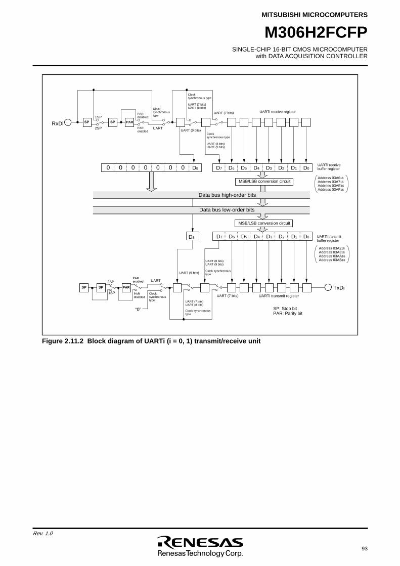
SINGLE-CHIP 16-BIT CMOS MICROCOMPUTERwith DATA ACQUISITION CONTROLLER
MITSUBISHI MICROCOMPUTERS
93
Rev. 1.0
M306H2FCFP
SP SP PAR
2SP
1SP
UART
UART (7 bits)UART (8 bits)
UART (7 bits)
UART (9 bits)
Clock synchronous type
Clock synchronous type
TxDiUARTi transmit register
PAR enabled
PAR disabled
D8 D7 D6 D5 D4 D3 D2 D1 D0
SP: Stop bitPAR: Parity bit
UARTi transmit buffer register
MSB/LSB conversion circuit
UART (8 bits)UART (9 bits)
Clock synchronous type
UARTi receive buffer register
UARTi receive register
2SP
1SP
PAR enabled
PAR disabled
UART
UART (7 bits)
UART (9 bits)
Clock synchronous type
Clock synchronous type
UART (7 bits)UART (8 bits)
RxDi
Clock synchronous type
UART (8 bits)UART (9 bits)
Address 03A616Address 03A716Address 03AE16Address 03AF16
Address 03A216Address 03A316Address 03AA16Address 03AB16
Data bus low-order bits
MSB/LSB conversion circuit
D7 D6 D5 D4 D3 D2 D1 D0D80 0 0 0 0 0 0
SP SP PAR
“0”
Data bus high-order bits
Figure 2.11.2 Block diagram of UARTi (i = 0, 1) transmit/receive unit
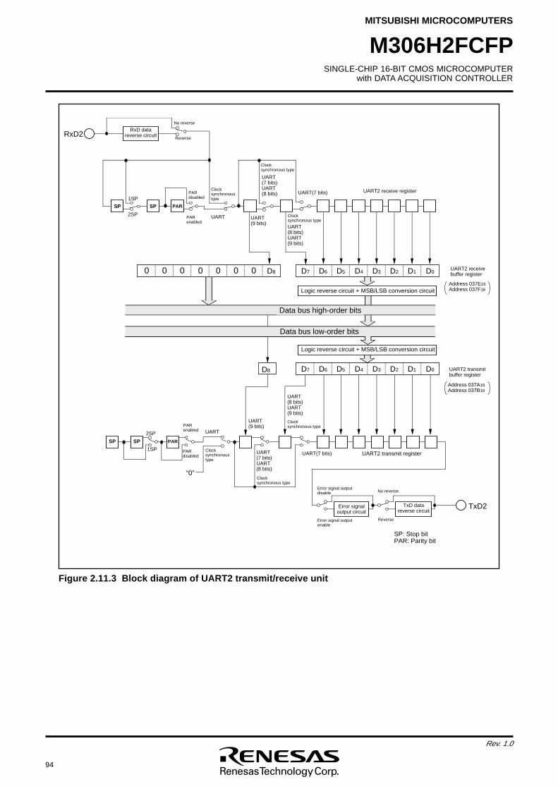
94
Rev. 1.0
SINGLE-CHIP 16-BIT CMOS MICROCOMPUTERwith DATA ACQUISITION CONTROLLER
MITSUBISHI MICROCOMPUTERS
M306H2FCFP
SP SP PAR
2SP
1SP
UART
UART(7 bits)UART(8 bits)
UART(7 bits)
UART(9 bits)
Clock synchronous type
Clock synchronous type
Data bus low-order bits
TxD2
UART2 transmit registerPAR disabled
PAR enabled
D8 D7 D6 D5 D4 D3 D2 D1 D0 UART2 transmit buffer register
UART(8 bits)UART(9 bits)
Clock synchronous type
UART2 receive buffer register
UART2 receive register
2SP
1SP
UART(7 bits)UART(8 bits) UART(7 bits)
UART(9 bits)
Clock synchronous type
Clock synchronous type
RxD2
UART(8 bits)UART(9 bits)
Address 037E16Address 037F16
Address 037A16Address 037B16
Data bus high-order bits
D7 D6 D5 D4 D3 D2 D1 D0D80 0 0 0 0 0 0
SP SP PAR
“0”
Reverse
No reverse
Error signal output circuit
RxD datareverse circuit
Error signal output enable
Error signal output disable
Reverse
No reverse
Logic reverse circuit + MSB/LSB conversion circuit
Logic reverse circuit + MSB/LSB conversion circuit
PAR enabled
PAR disabled
UART
Clock synchronous type
TxD datareverse circuit
SP: Stop bitPAR: Parity bit
Figure 2.11.3 Block diagram of UART2 transmit/receive unit
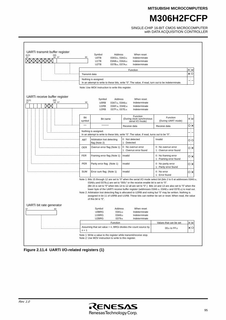
SINGLE-CHIP 16-BIT CMOS MICROCOMPUTERwith DATA ACQUISITION CONTROLLER
MITSUBISHI MICROCOMPUTERS
95
Rev. 1.0
M306H2FCFP
Figure 2.11.4 UARTi I/O-related registers (1)
b7
UARTi bit rate generatorb0 Symbol Address When reset
U0BRG 03A116 IndeterminateU1BRG 03A916 IndeterminateU2BRG 037916 Indeterminate
Function
Assuming that set value = n, BRGi divides the count source by n + 1
0016 to FF16
Values that can be set WR
b7 b0(b15) (b8)
b7 b0
UARTi transmit buffer register
Function
Transmit data
Nothing is assigned.In an attempt to write to these bits, write “0”. The value, if read, turn out to be indeterminate.
Symbol Address When resetU0TB 03A316, 03A216 IndeterminateU1TB 03AB16, 03AA16 IndeterminateU2TB 037B16, 037A16 Indeterminate
WR
(b15) Symbol Address When reset
U0RB 03A716, 03A616 IndeterminateU1RB 03AF16, 03AE16 IndeterminateU2RB 037F16, 037E16 Indeterminate
b7 b0(b8)
b7 b0
UARTi receive buffer register
Function(During UART mode)
Function(During clock synchronous
serial I/O mode)Bit nameBit
symbol
0 : No framing error1 : Framing error found
0 : No parity error1 : Parity error found
0 : No error1 : Error found
Note 1: Bits 15 through 12 are set to “0” when the serial I/O mode select bit (bits 2 to 0 at addresses 03A016, 03A816 and 037816) are set to “0002” or the receive enable bit is set to “0”. (Bit 15 is set to “0” when bits 14 to 12 all are set to “0”.) Bits 14 and 13 are also set to “0” when thelower byte of the UARTi receive buffer register (addresses 03A6 16, 03AE16 and 037E16) is read out.
Note 2: Arbitration lost detecting flag is allocated to U2RB and noting but “0” may be written. Nothing is
Note 1: Write a value to the register while transmit/receive stop.Note 2: Use MOV instruction to write to this register.
assigned in bit 11 of U0RB and U1RB. These bits can neither be set or reset. When read, the value of this bit is “0”.
Invalid
Invalid
Invalid
OER
FER
PER
SUM
Overrun error flag (Note 1)
Framing error flag (Note 1)
Parity error flag (Note 1)
Error sum flag (Note 1)
0 : No overrun error1 : Overrun error found
0 : No overrun error1 : Overrun error found
Nothing is assigned.In an attempt to write to these bits, write “0”. The value, if read, turns out to be “0”.
Receive data
WR
Receive data
ABT Arbitration lost detecting flag (Note 2)
Invalid0 : Not detected1 : Detected
Note: Use MOV instruction to write this register.
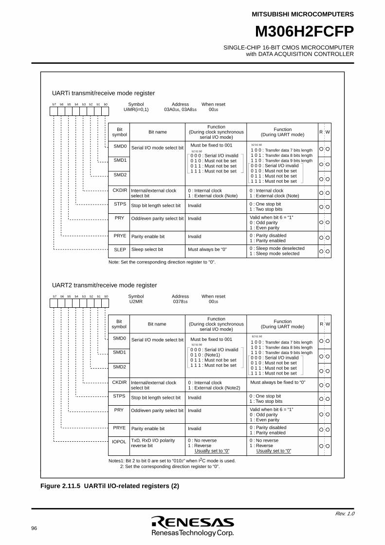
96
Rev. 1.0
SINGLE-CHIP 16-BIT CMOS MICROCOMPUTERwith DATA ACQUISITION CONTROLLER
MITSUBISHI MICROCOMPUTERS
M306H2FCFP
UARTi transmit/receive mode register
Symbol Address When resetUiMR(i=0,1) 03A016, 03A816 0016
b7 b6 b5 b4 b3 b2 b1 b0
Bit nameBit symbol WR
Must be fixed to 001
0 0 0 : Serial I/O invalid0 1 0 : Must not be set0 1 1 : Must not be set1 1 1 : Must not be set
b2 b1 b0
CKDIR
SMD1
SMD0 Serial I/O mode select bit
SMD2
Internal/external clock select bit
STPS
PRY
PRYE
SLEP
Parity enable bit
0 : Internal clock1 : External clock (Note)
Stop bit length select bit
Odd/even parity select bit
Sleep select bit
0 : One stop bit1 : Two stop bits
0 : Parity disabled1 : Parity enabled
0 : Sleep mode deselected1 : Sleep mode selected
1 0 0 : Transfer data 7 bits length1 0 1 : Transfer data 8 bits length1 1 0 : Transfer data 9 bits length0 0 0 : Serial I/O invalid0 1 0 : Must not be set0 1 1 : Must not be set1 1 1 : Must not be set
b2 b1 b0
0 : Internal clock1 : External clock (Note)
Invalid
Valid when bit 6 = “1”0 : Odd parity1 : Even parity
Invalid
Invalid
Must always be “0”
Function(During UART mode)
Function(During clock synchronous
serial I/O mode)
UART2 transmit/receive mode register
Symbol Address When resetU2MR 037816 0016
b7 b6 b5 b4 b3 b2 b1 b0
Bit nameBit symbol WR
Must be fixed to 001
0 0 0 : Serial I/O invalid0 1 0 : (Note1)0 1 1 : Must not be set1 1 1 : Must not be set
b2 b1 b0
CKDIR
SMD1
SMD0 Serial I/O mode select bit
SMD2
Internal/external clock select bit
STPS
PRY
PRYE
IOPOL
Parity enable bit
0 : Internal clock1 : External clock (Note2)
Stop bit length select bit
Odd/even parity select bit
TxD, RxD I/O polarity reverse bit
0 : One stop bit1 : Two stop bits
0 : Parity disabled1 : Parity enabled
0 : No reverse1 : Reverse
Usually set to “0”
1 0 0 : Transfer data 7 bits length1 0 1 : Transfer data 8 bits length1 1 0 : Transfer data 9 bits length0 0 0 : Serial I/O invalid0 1 0 : Must not be set0 1 1 : Must not be set1 1 1 : Must not be set
b2 b1 b0
Invalid
Valid when bit 6 = “1”0 : Odd parity1 : Even parity
Invalid
Invalid
0 : No reverse1 : Reverse
Usually set to “0”
Function(During UART mode)
Function(During clock synchronous
serial I/O mode)
Notes1: Bit 2 to bit 0 are set to “0102” when I2C mode is used. 2: Set the corresponding direction register to “0”.
Note: Set the corresponding direction register to "0".
Must always be fixed to “0”
Figure 2.11.5 UARTil I/O-related registers (2)
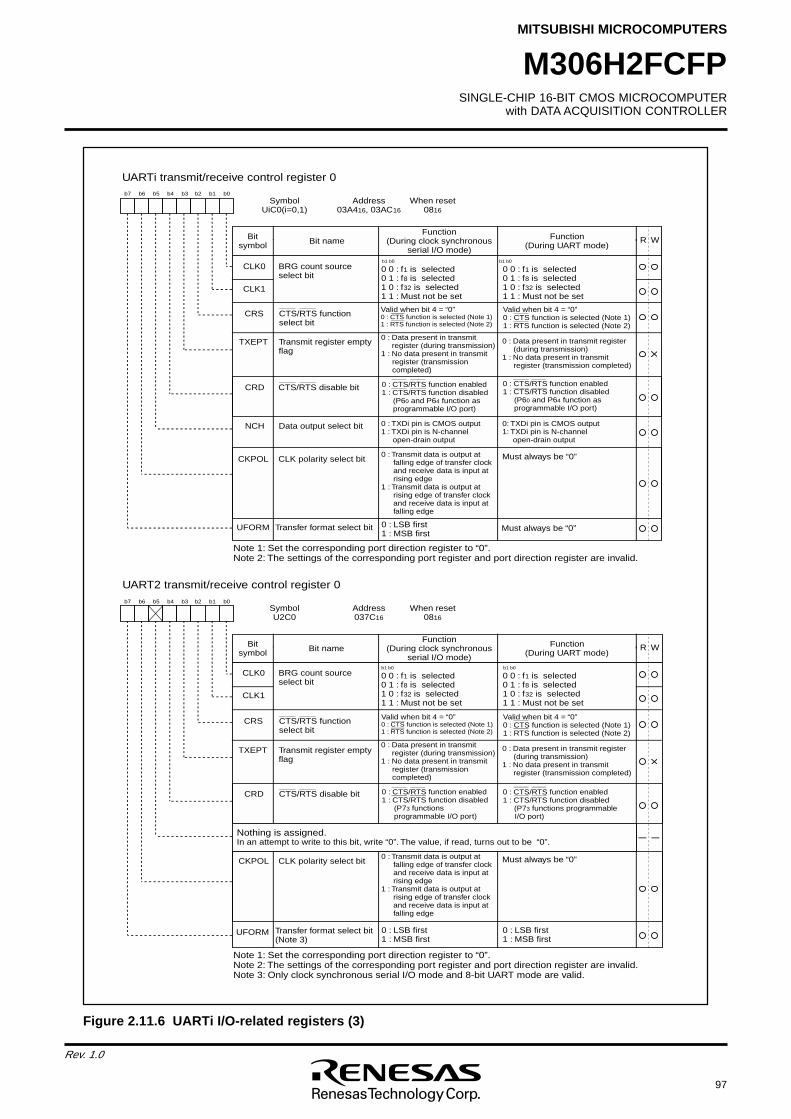
SINGLE-CHIP 16-BIT CMOS MICROCOMPUTERwith DATA ACQUISITION CONTROLLER
MITSUBISHI MICROCOMPUTERS
97
Rev. 1.0
M306H2FCFP
UARTi transmit/receive control register 0
Symbol Address When resetUiC0(i=0,1) 03A416, 03AC16 0816
b7 b6 b5 b4 b3 b2 b1 b0
Function(During UART mode)
WRFunction
(During clock synchronous serial I/O mode)
TXEPT
CLK1
CLK0
CRS
CRD
NCH
CKPOL
BRG count source select bit
Transmit register empty flag
0 : Transmit data is output at falling edge of transfer clock and receive data is input at rising edge
1 : Transmit data is output at rising edge of transfer clock and receive data is input at falling edge
CLK polarity select bit
CTS/RTS function select bit
CTS/RTS disable bit
Data output select bit
0 0 : f1 is selected0 1 : f8 is selected1 0 : f32 is selected1 1 : Must not be set
b1 b0
0 : LSB first1 : MSB first
0 : Data present in transmit register (during transmission)
1 : No data present in transmit register (transmission completed)
0 : CTS/RTS function enabled1 : CTS/RTS function disabled
(P60 and P64 function as programmable I/O port)
0 : TXDi pin is CMOS output1 : TXDi pin is N-channel
open-drain output
UFORM Transfer format select bit
0 0 : f1 is selected0 1 : f8 is selected1 0 : f32 is selected1 1 : Must not be set
b1 b0
Valid when bit 4 = “0”0 : CTS function is selected (Note 1)1 : RTS function is selected (Note 2)
Valid when bit 4 = “0”0 : CTS function is selected (Note 1)1 : RTS function is selected (Note 2)
0 : Data present in transmit register (during transmission)
1 : No data present in transmit register (transmission completed)
0: TXDi pin is CMOS output1: TXDi pin is N-channel
open-drain output
Must always be “0”
Bit nameBit symbol
Must always be “0”
Note 1: Set the corresponding port direction register to “0”.Note 2: The settings of the corresponding port register and port direction register are invalid.
0 : CTS/RTS function enabled1 : CTS/RTS function disabled
(P60 and P64 function as programmable I/O port)
UART2 transmit/receive control register 0
Symbol Address When resetU2C0 037C16 0816
b7 b6 b5 b4 b3 b2 b1 b0
Function(During UART mode)
WRFunction
(During clock synchronous serial I/O mode)
TXEPT
CLK1
CLK0
CRS
CRD
CKPOL
BRG count source select bit
Transmit register empty flag
0 : Transmit data is output at falling edge of transfer clock and receive data is input at rising edge
1 : Transmit data is output at rising edge of transfer clock and receive data is input at falling edge
CLK polarity select bit
CTS/RTS function select bit
CTS/RTS disable bit
0 0 : f1 is selected0 1 : f8 is selected1 0 : f32 is selected1 1 : Must not be set
b1 b0
0 : LSB first1 : MSB first
0 : Data present in transmit register (during transmission)
1 : No data present in transmit register (transmission completed)
0 : CTS/RTS function enabled1 : CTS/RTS function disabled
(P73 functions programmable I/O port)
0 : TXDi pin is CMOS output1 : TXDi pin is N-channel
open-drain output
UFORM Transfer format select bit(Note 3)
0 0 : f1 is selected0 1 : f8 is selected1 0 : f32 is selected1 1 : Must not be set
b1 b0
Valid when bit 4 = “0”0 : CTS function is selected (Note 1)1 : RTS function is selected (Note 2)
Valid when bit 4 = “0”0 : CTS function is selected (Note 1)1 : RTS function is selected (Note 2)
0 : Data present in transmit register (during transmission)
1 : No data present in transmit register (transmission completed)
0: TXDi pin is CMOS output1: TXDi pin is N-channel
open-drain output
Must always be “0”
Bit nameBit symbol
Note 1: Set the corresponding port direction register to “0”.Note 2: The settings of the corresponding port register and port direction register are invalid.Note 3: Only clock synchronous serial I/O mode and 8-bit UART mode are valid.
0 : CTS/RTS function enabled1 : CTS/RTS function disabled
(P73 functions programmable I/O port)
Nothing is assigned.In an attempt to write to this bit, write “0”. The value, if read, turns out to be “0”.
0 : LSB first1 : MSB first
Figure 2.11.6 UARTi I/O-related registers (3)
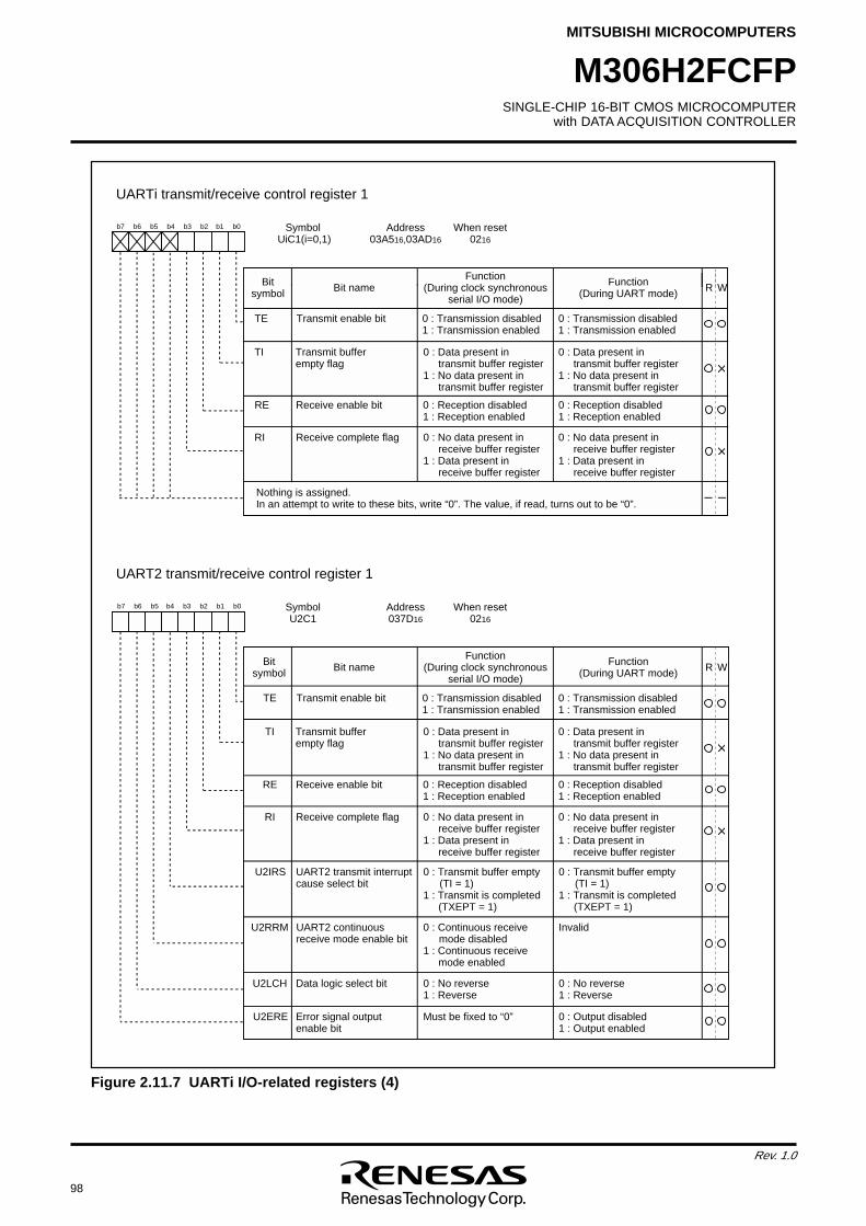
98
Rev. 1.0
SINGLE-CHIP 16-BIT CMOS MICROCOMPUTERwith DATA ACQUISITION CONTROLLER
MITSUBISHI MICROCOMPUTERS
M306H2FCFP
Figure 2.11.7 UARTi I/O-related registers (4)
UARTi transmit/receive control register 1
Symbol Address When resetUiC1(i=0,1) 03A516,03AD16 0216
b7 b6 b5 b4 b3 b2 b1 b0
Bit nameBit symbol WRFunction
(During UART mode)
Function(During clock synchronous
serial I/O mode)
TE
TI
RE
RI
Transmit enable bit
Receive enable bit
Receive complete flag
Transmit buffer empty flag
0 : Transmission disabled1 : Transmission enabled
0 : Data present intransmit buffer register
1 : No data present intransmit buffer register
0 : Reception disabled1 : Reception enabled
0 : Transmission disabled1 : Transmission enabled
0 : Data present intransmit buffer register
1 : No data present intransmit buffer register
0 : Reception disabled1 : Reception enabled
0 : No data present inreceive buffer register
1 : Data present inreceive buffer register
0 : No data present inreceive buffer register
1 : Data present inreceive buffer register
Nothing is assigned.In an attempt to write to these bits, write “0”. The value, if read, turns out to be “0”.
UART2 transmit/receive control register 1
Symbol Address When resetU2C1 037D16 0216
b7 b6 b5 b4 b3 b2 b1 b0
Bit nameBit symbol WRFunction
(During UART mode)
Function(During clock synchronous
serial I/O mode)
TE
TI
RE
RI
Transmit enable bit
Receive enable bit
Receive complete flag
Transmit buffer empty flag
0 : Transmission disabled1 : Transmission enabled
0 : Data present intransmit buffer register
1 : No data present intransmit buffer register
0 : Reception disabled1 : Reception enabled
0 : Transmission disabled1 : Transmission enabled
0 : Data present intransmit buffer register
1 : No data present intransmit buffer register
0 : Reception disabled1 : Reception enabled
0 : No data present inreceive buffer register
1 : Data present inreceive buffer register
0 : No data present inreceive buffer register
1 : Data present inreceive buffer register
U2IRS UART2 transmit interrupt cause select bit
0 : Transmit buffer empty(TI = 1)
1 : Transmit is completed(TXEPT = 1)
0 : Transmit buffer empty(TI = 1)
1 : Transmit is completed(TXEPT = 1)
U2RRM UART2 continuous receive mode enable bit
0 : Continuous receivemode disabled
1 : Continuous receive mode enabled
Invalid
Data logic select bit 0 : No reverse1 : Reverse
0 : No reverse1 : Reverse
U2LCH
U2ERE Error signal output enable bit
Must be fixed to “0” 0 : Output disabled1 : Output enabled
AAA
AA
AA
AAAA
AA
AAAA
AAAA
A
A
A
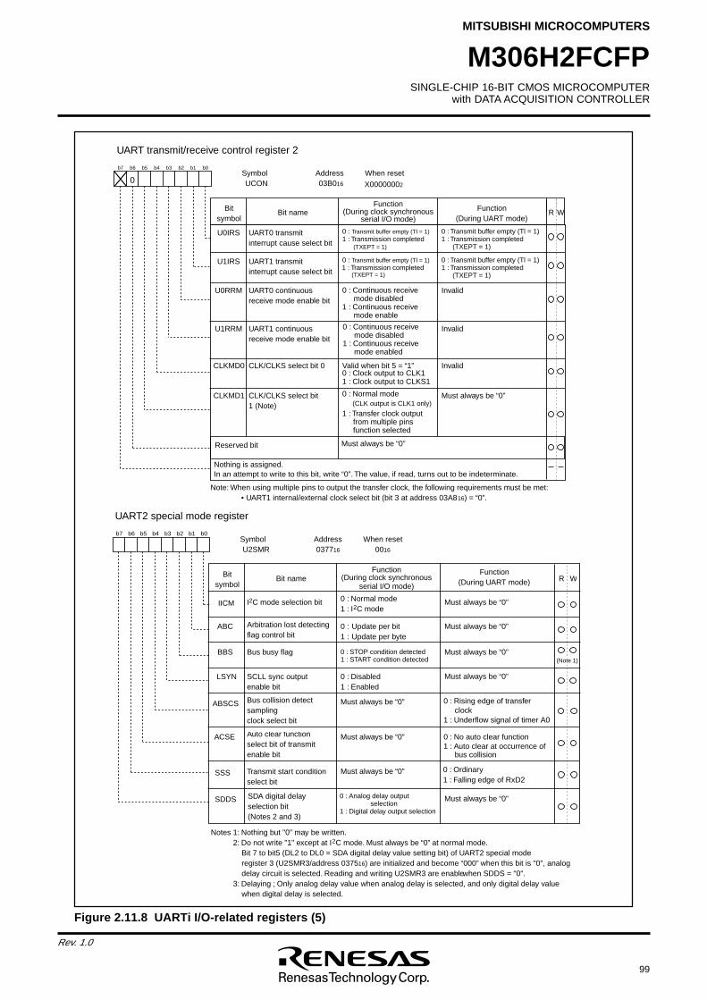
SINGLE-CHIP 16-BIT CMOS MICROCOMPUTERwith DATA ACQUISITION CONTROLLER
MITSUBISHI MICROCOMPUTERS
99
Rev. 1.0
M306H2FCFP
Note: When using multiple pins to output the transfer clock, the following requirements must be met:• UART1 internal/external clock select bit (bit 3 at address 03A816) = “0”.
UART transmit/receive control register 2
Symbol Address When resetUCON 03B016 X00000002
b7 b6 b5 b4 b3 b2 b1 b0
Bit nameBitsymbol
WRFunction(During UART mode)
Function(During clock synchronous
serial I/O mode)
CLKMD0
CLKMD1
Reserved bit
UART0 transmit interrupt cause select bit
UART0 continuous receive mode enable bit
0 : Continuous receive mode disabled
1 : Continuous receivemode enable
UART1 continuous receive mode enable bit
CLK/CLKS select bit 0
UART1 transmit interrupt cause select bit
0 : Transmit buffer empty (Tl = 1) 1 : Transmission completed
(TXEPT = 1)
0 : Transmit buffer empty (Tl = 1)1 : Transmission completed
(TXEPT = 1)
0 : Normal mode (CLK output is CLK1 only)
1 : Transfer clock outputfrom multiple pins function selected
0 : Continuous receivemode disabled
1 : Continuous receivemode enabled
Nothing is assigned.In an attempt to write to this bit, write “0”. The value, if read, turns out to be indeterminate.
0 : Transmit buffer empty (Tl = 1)1 : Transmission completed
(TXEPT = 1)
0 : Transmit buffer empty (Tl = 1)1 : Transmission completed
(TXEPT = 1)
Must always be “0”
U0IRS
U1IRS
U0RRM
U1RRM
Invalid
Invalid
Invalid
CLK/CLKS select bit1 (Note)
Valid when bit 5 = “1” 0 : Clock output to CLK11 : Clock output to CLKS1
UART2 special mode register
Symbol Address When resetU2SMR 037716 0016
b7 b6 b5 b4 b3 b2 b1 b0
Bit nameBitsymbol
Function(During clock synchronous
serial I/O mode)
ABSCS
ACSE
SSS
I2C mode selection bit
Bus busy flag 0 : STOP condition detected1 : START condition detected
SCLL sync output enable bit
Bus collision detectsampling clock select bit
Arbitration lost detecting flag control bit
0 : Normal mode1 : I2C mode
0 : Update per bit1 : Update per byte
IICM
ABC
BBS
LSYN 0 : Disabled1 : Enabled
Transmit start condition select bit
Auto clear function select bit of transmit enable bit
Must always be “0”
Must always be “0”
Must always be “0”
0
Must always be “0”
SDDS SDA digital delay selection bit(Notes 2 and 3)
WRFunction
(During UART mode)
0 : Ordinary1 : Falling edge of RxD2
Must always be “0”
0 : Rising edge of transfer clock
1 : Underflow signal of timer A0
0 : No auto clear function1 : Auto clear at occurrence of
bus collision
Must always be “0”
Must always be “0”
Must always be “0”
Must always be “0”0 : Analog delay output selection
1 : Digital delay output selection
(Note 1)
Notes 1: Nothing but "0" may be written.2: Do not write "1" except at I2C mode. Must always be “0” at normal mode.
Bit 7 to bit5 (DL2 to DL0 = SDA digital delay value setting bit) of UART2 special mode register 3 (U2SMR3/address 037516) are initialized and become “000” when this bit is "0", analog delay circuit is selected. Reading and writing U2SMR3 are enable when SDDS = "0".
3: Delaying ; Only analog delay value when analog delay is selected, and only digital delay value when digital delay is selected.
Figure 2.11.8 UARTi I/O-related registers (5)
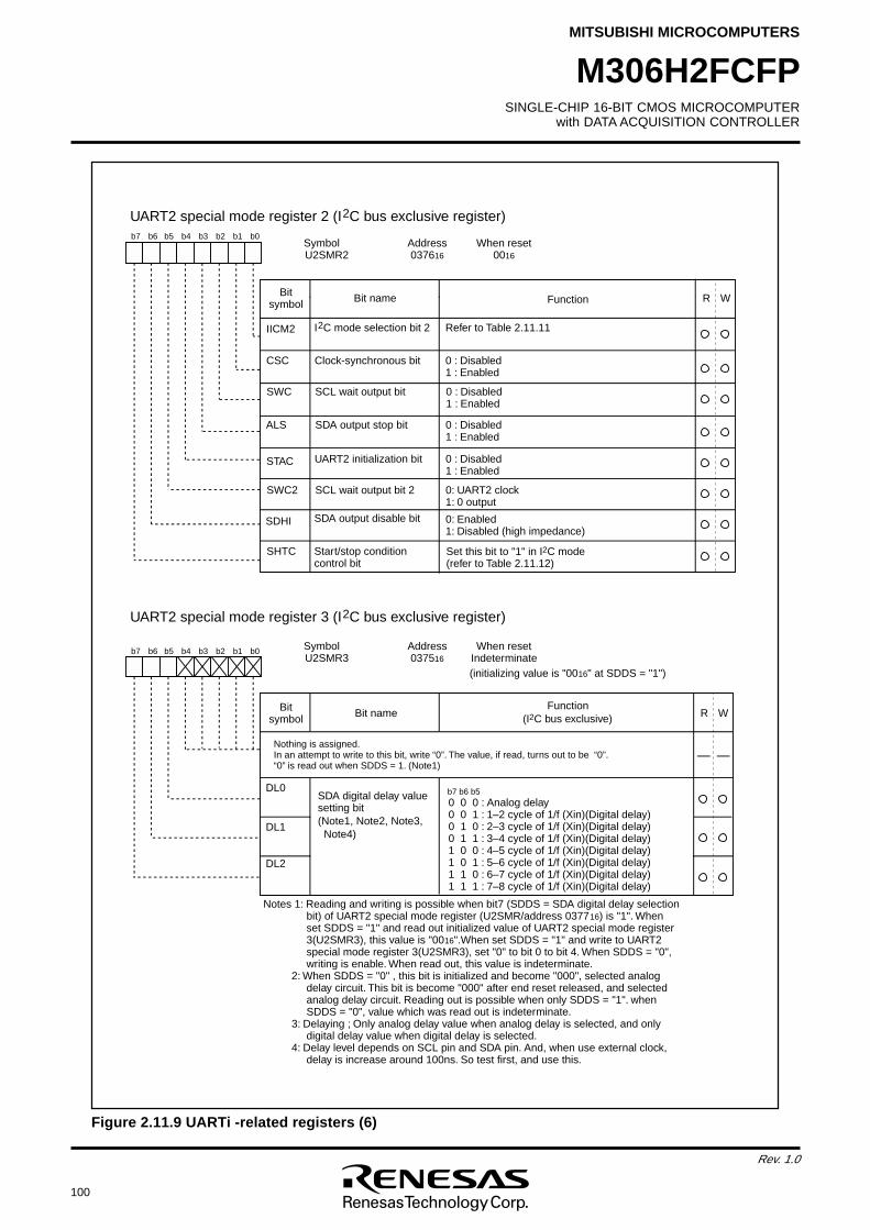
100
Rev. 1.0
SINGLE-CHIP 16-BIT CMOS MICROCOMPUTERwith DATA ACQUISITION CONTROLLER
MITSUBISHI MICROCOMPUTERS
M306H2FCFP
Figure 2.11.9 UARTi -related registers (6)
UART2 special mode register 2 (I2C bus exclusive register)
Symbol Address When reset U2SMR2 037616 0016
b7 b6 b5 b4 b3 b2 b1 b0
Bit nameBit symbol WRFunction
STAC
SWC2
SDHI
I C mode selection bit 2
SCL wait output bit 0 : Disabled1 : Enabled
SDA output stop bit
UART2 initialization bit
Clock-synchronous bit
Refer to Table 2.11.11
0 : Disabled1 : Enabled
IICM2
CSC
SWC
ALS 0 : Disabled1 : Enabled
SDA output disable bit
SCL wait output bit 2
0: Enabled1: Disabled (high impedance)
0 : Disabled1 : Enabled
0: UART2 clock1: 0 output
2
SHTC Start/stop condition control bit
Set this bit to "1" in I2C mode(refer to Table 2.11.12)
UART2 special mode register 3 (I2C bus exclusive register)
Symbol Address When reset U2SMR3 037516 Indeterminate
b7 b6 b5 b4 b3 b2 b1 b0
Bit nameBit symbol
Function(I2C bus exclusive)
SDA digital delay value setting bit(Note1, Note2, Note3, Note4)
b7 b6 b5DL0
DL1
DL2
(initializing value is "0016" at SDDS = "1")
Nothing is assigned.In an attempt to write to this bit, write “0”. The value, if read, turns out to be “0”.“0” is read out when SDDS = 1. (Note1)
WR
Notes 1: Reading and writing is possible when bit7 (SDDS = SDA digital delay selection bit) of UART2 special mode register (U2SMR/address 037716) is "1". When set SDDS = "1" and read out initialized value of UART2 special mode register 3(U2SMR3), this value is "0016".When set SDDS = "1" and write to UART2 special mode register 3(U2SMR3), set "0" to bit 0 to bit 4. When SDDS = "0", writing is enable. When read out, this value is indeterminate.
2: When SDDS = "0" , this bit is initialized and become "000", selected analog delay circuit. This bit is become "000" after end reset released, and selected analog delay circuit. Reading out is possible when only SDDS = "1". when SDDS = "0", value which was read out is indeterminate.
3: Delaying ; Only analog delay value when analog delay is selected, and only digital delay value when digital delay is selected.
4: Delay level depends on SCL pin and SDA pin. And, when use external clock, delay is increase around 100ns. So test first, and use this.
0 0 0 : Analog delay0 0 1 : 1–2 cycle of 1/f (Xin)(Digital delay)0 1 0 : 2–3 cycle of 1/f (Xin)(Digital delay)0 1 1 : 3–4 cycle of 1/f (Xin)(Digital delay)1 0 0 : 4–5 cycle of 1/f (Xin)(Digital delay)1 0 1 : 5–6 cycle of 1/f (Xin)(Digital delay)1 1 0 : 6–7 cycle of 1/f (Xin)(Digital delay)1 1 1 : 7–8 cycle of 1/f (Xin)(Digital delay)
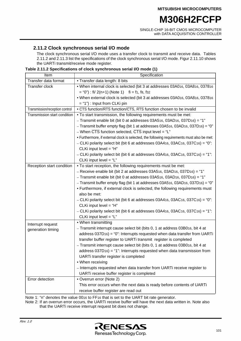
SINGLE-CHIP 16-BIT CMOS MICROCOMPUTERwith DATA ACQUISITION CONTROLLER
MITSUBISHI MICROCOMPUTERS
101
Rev. 1.0
M306H2FCFP
2.11.2 Clock synchronous serial I/O modeThe clock synchronous serial I/O mode uses a transfer clock to transmit and receive data. Tables2.11.2 and 2.11.3 list the specifications of the clock synchronous serial I/O mode. Figur 2.11.10 showsthe UARTi transmit/receive mode register.
Table 2.11.2 Specifications of clock synchronous serial I/O mode (1)
Interrupt requestgeneration timing
Item SpecificationTransfer data format • Transfer data length: 8 bitsTransfer clock • When internal clock is selected (bit 3 at addresses 03A016, 03A816, 037816
= “0”) : fi/ 2(n+1) (Note 1) fi = f1, f8, f32
• When external clock is selected (bit 3 at addresses 03A016, 03A816, 037816
= “1”) : Input from CLKi pinTransmission/reception control
_______ _______ _______ _______
• CTS function/RTS function/CTS, RTS function chosen to be invalidTransmission start condition • To start transmission, the following requirements must be met:
_ Transmit enable bit (bit 0 at addresses 03A516, 03AD16, 037D16) = “1”_ Transmit buffer empty flag (bit 1 at addresses 03A516, 03AD16, 037D16) = “0”
_______ ________ When CTS function selected, CTS input level = “L”• Furthermore, if external clock is selected, the following requirements must also be met:_ CLKi polarity select bit (bit 6 at addresses 03A416, 03AC16, 037C16) = “0”:
CLKi input level = “H”_ CLKi polarity select bit (bit 6 at addresses 03A416, 03AC16, 037C16) = “1”:
CLKi input level = “L”Reception start condition • To start reception, the following requirements must be met:
_ Receive enable bit (bit 2 at addresses 03A516, 03AD16, 037D16) = “1”_ Transmit enable bit (bit 0 at addresses 03A516, 03AD16, 037D16) = “1”_ Transmit buffer empty flag (bit 1 at addresses 03A516, 03AD16, 037D16) = “0”• Furthermore, if external clock is selected, the following requirements must
also be met:_ CLKi polarity select bit (bit 6 at addresses 03A416, 03AC16, 037C16) = “0”:
CLKi input level = “H”_ CLKi polarity select bit (bit 6 at addresses 03A416, 03AC16, 037C16) = “1”:
CLKi input level = “L”• When transmitting_ Transmit interrupt cause select bit (bits 0, 1 at address 03B016, bit 4 at
address 037D16) = “0”: Interrupts requested when data transfer from UARTitransfer buffer register to UARTi transmit register is completed
_ Transmit interrupt cause select bit (bits 0, 1 at address 03B016, bit 4 ataddress 037D16) = “1”: Interrupts requested when data transmission fromUARTi transfer register is completed
• When receiving_ Interrupts requested when data transfer from UARTi receive register to
UARTi receive buffer register is completedError detection • Overrun error (Note 2)
This error occurs when the next data is ready before contents of UARTi
receive buffer register are read out
Note 1: “n” denotes the value 0016 to FF16 that is set to the UART bit rate generator.Note 2: If an overrun error occurs, the UARTi receive buffer will have the next data written in. Note also
that the UARTi receive interrupt request bit does not change.
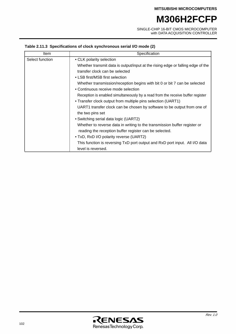
102
Rev. 1.0
SINGLE-CHIP 16-BIT CMOS MICROCOMPUTERwith DATA ACQUISITION CONTROLLER
MITSUBISHI MICROCOMPUTERS
M306H2FCFP
Table 2.11.3 Specifications of clock synchronous serial I/O mode (2)
Item Specification
Select function • CLK polarity selection
Whether transmit data is output/input at the rising edge or falling edge of the
transfer clock can be selected
• LSB first/MSB first selection
Whether transmission/reception begins with bit 0 or bit 7 can be selected
• Continuous receive mode selection
Reception is enabled simultaneously by a read from the receive buffer register
• Transfer clock output from multiple pins selection (UART1)
UART1 transfer clock can be chosen by software to be output from one of
the two pins set
• Switching serial data logic (UART2)
Whether to reverse data in writing to the transmission buffer register or
reading the reception buffer register can be selected.
• TxD, RxD I/O polarity reverse (UART2)
This function is reversing TxD port output and RxD port input. All I/O data
level is reversed.
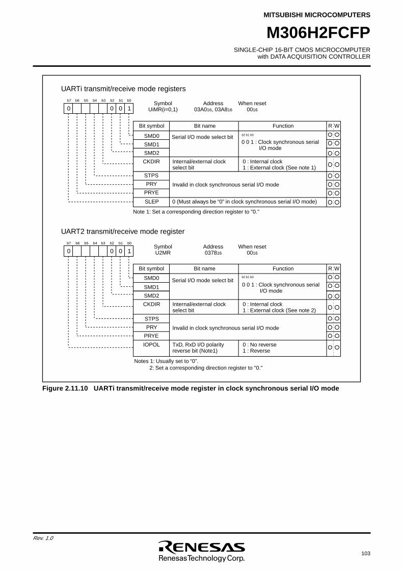
SINGLE-CHIP 16-BIT CMOS MICROCOMPUTERwith DATA ACQUISITION CONTROLLER
MITSUBISHI MICROCOMPUTERS
103
Rev. 1.0
M306H2FCFP
Figure 2.11.10 UARTi transmit/receive mode register in clock synchronous serial I/O mode
Symbol Address When resetUiMR(i=0,1) 03A016, 03A816 0016
CKDIR
UARTi transmit/receive mode registers
Internal/external clock select bit
STPS
PRY
PRYE
SLEP
0 : Internal clock1 : External clock (See note 1)
Bit name FunctionBit symbol WR
b7 b6 b5 b4 b3 b2 b1 b0
0 (Must always be “0” in clock synchronous serial I/O mode)
0 10
SMD0
SMD1
SMD2
Serial I/O mode select bit0 0 1 : Clock synchronous serial
I/O mode
b2 b1 b0
0
Invalid in clock synchronous serial I/O mode
Symbol Address When resetU2MR 037816 0016
CKDIR
UART2 transmit/receive mode register
Internal/external clock select bit
STPS
PRY
PRYE
IOPOL
0 : Internal clock1 : External clock (See note 2)
Bit name FunctionBit symbol WR
b7 b6 b5 b4 b3 b2 b1 b0
0 10
SMD0
SMD1
SMD2
Serial I/O mode select bit0 0 1 : Clock synchronous serial
I/O mode
b2 b1 b0
0
Invalid in clock synchronous serial I/O mode
TxD, RxD I/O polarity reverse bit (Note1)
0 : No reverse1 : Reverse
Notes 1: Usually set to “0”. 2: Set a corresponding direction register to "0."
Note 1: Set a corresponding direction register to "0."
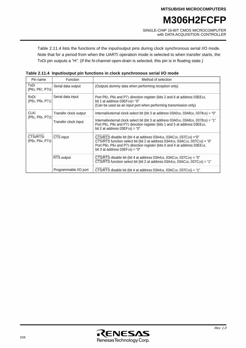
104
Rev. 1.0
SINGLE-CHIP 16-BIT CMOS MICROCOMPUTERwith DATA ACQUISITION CONTROLLER
MITSUBISHI MICROCOMPUTERS
M306H2FCFP
Pin name Function Method of selection
TxDi(P63, P67, P70)
Serial data output
Serial data input
Transfer clock output
Transfer clock input
Programmable I/O port
(Outputs dummy data when performing reception only)
RxDi(P62, P66, P71)
CLKi(P61, P65, P72)
Internal/external clock select bit (bit 3 at address 03A016, 03A816, 037816) = “0”
Internal/external clock select bit (bit 3 at address 03A016, 03A816, 037816) = “1”Port P61, P65 and P72 direction register (bits 1 and 5 at address 03EE16, bit 2 at address 03EF16) = “0”
Port P62, P66 and P71 direction register (bits 2 and 6 at address 03EE16, bit 1 at address 03EF16)= “0” (Can be used as an input port when performing transmission only)
CTS/RTS disable bit (bit 4 at address 03A416, 03AC16, 037C16) =“0” CTS/RTS function select bit (bit 2 at address 03A416, 03AC16, 037C16) = “0” Port P60, P64 and P73 direction register (bits 0 and 4 at address 03EE16, bit 3 at address 03EF16) = “0”
CTS/RTS disable bit (bit 4 at address 03A416, 03AC16, 037C16) = “0” CTS/RTS function select bit (bit 2 at address 03A416, 03AC16, 037C16) = “1”
CTS/RTS disable bit (bit 4 at address 03A416, 03AC16, 037C16) = “1”
CTS input
RTS output
CTSi/RTSi(P60, P64, P73)
Table 2.11.4 lists the functions of the input/output pins during clock synchronous serial I/O mode.
Note that for a period from when the UARTi operation mode is selected to when transfer starts, the
TxDi pin outputs a “H”. (If the N-channel open-drain is selected, this pin is in floating state.)
Table 2.11.4 Input/output pin functions in clock synchronous serial I/O mode
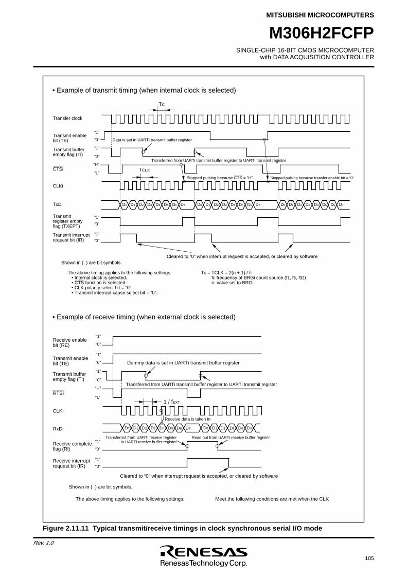
SINGLE-CHIP 16-BIT CMOS MICROCOMPUTERwith DATA ACQUISITION CONTROLLER
MITSUBISHI MICROCOMPUTERS
105
Rev. 1.0
M306H2FCFP
Figure 2.11.11 Typical transmit/receive timings in clock synchronous serial I/O mode
• Example of transmit timing (when internal clock is selected)
D0 D1 D2 D3 D4 D5 D6 D7 D0 D1 D2 D3 D4 D5 D6 D7 D0 D1 D2 D3 D4 D5 D6 D7
T
c
TCLK
S
t
o
p
p
e
d
p
u
l
s
i
n
g
b
e
c
a
u
s
e
t
r
a
n
s
f
e
r
e
n
a
b
l
e
b
i
t
=
“
0
”
D
a
t
a
i
s
s
e
t
i
n
U
A
R
T
i
t
r
a
n
s
m
i
t
b
u
f
f
e
r
r
e
g
i
s
t
e
r
Tc = TCLK = 2(n + 1) / fifi: frequency of BRGi count source (f1, f8, f32)n: value set to BRGi
T
r
a
n
s
f
e
r
c
l
o
c
k
T
r
a
n
s
m
i
t
e
n
a
b
l
eb
i
t
(
T
E
)
T
r
a
n
s
m
i
t
b
u
f
f
e
re
m
p
t
y
f
l
a
g
(
T
l
)
C
L
K
i
T
x
D
i
T
r
a
n
s
m
i
tr
e
g
i
s
t
e
r
e
m
p
t
yf
l
a
g
(
T
X
E
P
T
)
“ H
”
“ L
”
“ 0
”
“ 1
”
“ 0
”
“1”
“ 0
”
“ 1
”
C
T
S
i
The above timing applies to the following settings: • Internal clock is selected. • CTS function is selected. • CLK polarity select bit = “0”. • Transmit interrupt cause select bit = “0”.
T
r
a
n
s
m
i
t
i
n
t
e
r
r
u
p
t
r
e
q
u
e
s
t
b
i
t
(
I
R
) “ 0
”
“ 1
”
Stopped pulsing because CTS = “H”
T
r
a
n
s
f
e
r
r
e
d
f
r
o
m
U
A
R
T
i
t
r
a
n
s
m
i
t
b
u
f
f
e
r
r
e
g
i
s
t
e
r
t
o
U
A
R
T
i
t
r
a
n
s
m
i
t
r
e
g
i
s
t
e
r
S
h
o
w
n
i
n
(
)
a
r
e
b
i
t
s
y
m
b
o
l
s
.Cleared to “0” when interrupt request is accepted, or cleared by software
1 / fEXT
Dummy data is set in UARTi transmit buffer registerT
r
a
n
s
m
i
t
e
n
a
b
l
e
b
i
t
(
T
E
)
T
r
a
n
s
m
i
t
b
u
f
f
e
r
e
m
p
t
y
f
l
a
g
(
T
l
)
C
L
K
i
R
x
D
i
R
e
c
e
i
v
e
c
o
m
p
l
e
t
e
f
l
a
g
(
R
l
)
RTSi“ H
”
“L”
“0”
“1”
“0”
“1”
“0”
“ 1
”
R
e
c
e
i
v
e
e
n
a
b
l
e
b
i
t
(
R
E
) “ 0
”
“1”
Receive data is taken in
T
r
a
n
s
f
e
r
r
e
d
f
r
o
m
U
A
R
T
i
t
r
a
n
s
m
i
t
b
u
f
f
e
r
r
e
g
i
s
t
e
r
t
o
U
A
R
T
i
t
r
a
n
s
m
i
t
r
e
g
i
s
t
e
r
Read out from UARTi receive buffer register
T
h
e
a
b
o
v
e
t
i
m
i
n
g
a
p
p
l
i
e
s
t
o
t
h
e
f
o
l
l
o
w
i
n
g
s
e
t
t
i
n
g
s
:
Transferred from UARTi receive registerto UARTi receive buffer register
R
e
c
e
i
v
e
i
n
t
e
r
r
u
p
t
r
e
q
u
e
s
t
b
i
t
(
I
R
) “0”
“1”
D0 D1 D2 D3 D4 D5 D6 D7 D0 D1 D2 D3 D4 D5
S
h
o
w
n
i
n
(
)
a
r
e
b
i
t
s
y
m
b
o
l
s
.
M
e
e
t
t
h
e
f
o
l
l
o
w
i
n
g
c
o
n
d
i
t
i
o
n
s
a
r
e
m
e
t
w
h
e
n
t
h
e
C
L
K
C
l
e
a
r
e
d
t
o
“
0
”
w
h
e
n
i
n
t
e
r
r
u
p
t
r
e
q
u
e
s
t
i
s
a
c
c
e
p
t
e
d
,
o
r
c
l
e
a
r
e
d
b
y
s
o
f
t
w
a
r
e
• Example of receive timing (when external clock is selected)
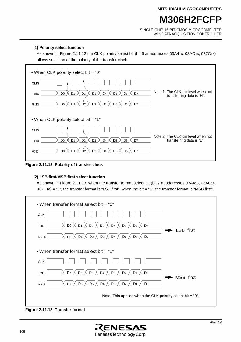
106
Rev. 1.0
SINGLE-CHIP 16-BIT CMOS MICROCOMPUTERwith DATA ACQUISITION CONTROLLER
MITSUBISHI MICROCOMPUTERS
M306H2FCFP
• When CLK polarity select bit = “1”
Note 2: The CLK pin level when not transferring data is “L”.D1 D2 D3 D4 D5 D6 D7
D1 D2 D3 D4 D5 D6 D7
D0
D0
TXDi
RXDi
CLKi
• When CLK polarity select bit = “0”
Note 1: The CLK pin level when nottransferring data is “H”.
D1 D2 D3 D4 D5 D6 D7D0
D1 D2 D3 D4 D5 D6 D7D0
TXDi
RXDi
CLKi
LSB first
• When transfer format select bit = “0”
D0
D0
D1 D2 D3 D4 D5 D6 D7
D1 D2 D3 D4 D5 D6 D7
TXDi
RXDi
CLKi
• When transfer format select bit = “1”
D6 D5 D4 D3 D2 D1 D0D7
D7 D6 D5 D4 D3 D2 D1 D0
TXDi
RXDi
CLKi
MSB first
Note: This applies when the CLK polarity select bit = “0”.
(1) Polarity select function
As shown in Figure 2.11.12 the CLK polarity select bit (bit 6 at addresses 03A416, 03AC16, 037C16)
allows selection of the polarity of the transfer clock.
Figure 2.11.12 Polarity of transfer clock
(2) LSB first/MSB first select function
As shown in Figure 2.11.13, when the transfer format select bit (bit 7 at addresses 03A416, 03AC16,
037C16) = “0”, the transfer format is “LSB first”; when the bit = “1”, the transfer format is “MSB first”.
Figure 2.11.13 Transfer format
SINGLE-CHIP 16-BIT CMOS MICROCOMPUTERwith DATA ACQUISITION CONTROLLER
MITSUBISHI MICROCOMPUTERS
107
Rev. 1.0
M306H2FCFP
(3) Transfer clock output from multiple pins function (UART1)
This function allows the setting two transfer clock output pins and choosing one of the two to output a
clock by using the CLK and CLKS select bit (bits 4 and 5 at address 03B016). (See Figure 2.11.14)
The multiple pins function is valid only when the internal clock is selected for UART1.
Figure 2.11.14 The transfer clock output from the multiple pins function usage
Microcomputer
TXD1 (P67)
CLKS1 (P64)
CLK1 (P65) IN
CLK
IN
CLK
Note: This applies when the internal clock is selected and transmission is performed only in clock synchronous serial I/O mode.
(4) Continuous receive mode
If the continuous receive mode enable bit (bits 2 and 3 at address 03B016, bit 5 at address 037D16) is
set to “1”, the unit is placed in continuous receive mode. In this mode, when the receive buffer register
is read out, the unit simultaneously goes to a receive enable state without having to set dummy data to
the transmit buffer register back again.
(5) Serial data logic switch function (UART2)
When the data logic select bit (bit6 at address 037D16) = “1”, and writing to transmit buffer register or
reading from receive buffer register, data is reversed. Figure 2.11.15 shows the example of serial
data logic switch timing.
Figure 2.11.15 Serial data logic switch timing
D0 D1 D2 D3 D4 D5 D6 D7
D0 D1 D2 D3 D4 D5 D6 D7
Transfer clock
TxD2(no reverse)
TxD2(reverse)
“H”
“L”
“H”
“L”
“H”
“L”
•When LSB first
108
Rev. 1.0
SINGLE-CHIP 16-BIT CMOS MICROCOMPUTERwith DATA ACQUISITION CONTROLLER
MITSUBISHI MICROCOMPUTERS
M306H2FCFP
Note 1: ‘n’ denotes the value 0016 to FF16 that is set to the UARTi bit rate generator.Note 2: fEXT is input from the CLKi pin.Note 3: If an overrun error occurs, the UARTi receive buffer will have the next data written in. Note also that
the UARTi receive interrupt request bit does not change.
Item SpecificationTransfer data format • Character bit (transfer data): 7 bits, 8 bits, or 9 bits as selected
• Start bit: 1 bit• Parity bit: Odd, even, or nothing as selected• Stop bit: 1 bit or 2 bits as selected
Transfer clock • When internal clock is selected (bit 3 at addresses 03A016 ,03A816 ,037816 = “0”) : fi/16(n+1) (Note 1) fi = f1, f8, f32
• When external clock is selected (bit 3 at addresses 03A016 and 03A816 = “1”) :fEXT/16(n+1) (Note 1) (Note 2) (Do not set external clock for UART2)
Transmission/reception control_______ _______ _______ _______
• CTS function/RTS function/CTS, RTS function chosen to be invalidTransmission start condition • To start transmission, the following requirements must be met:
- Transmit enable bit (bit 0 at addresses 03A516, 03AD16, 037D16) = “1”- Transmit buffer empty flag (bit 1 at addresses 03A516, 03AD16, 037D16) = “0”
_______ _______
- When CTS function selected, CTS input level = “L”Reception start condition • To start reception, the following requirements must be met:
- Receive enable bit (bit 2 at addresses 03A516, 03AD16, 037D16) = “1”- Start bit detection
Interrupt request • When transmittinggeneration timing - Transmit interrupt cause select bits (bits 0,1 at address 03B016, bit4 at
address 037D16) = “0”: Interrupts requested when data transfer from UARTitransfer buffer register to UARTi transmit register is completed
- Transmit interrupt cause select bits (bits 0, 1 at address 03B016, bit4 ataddress 037D16) = “1”: Interrupts requested when data transmission fromUARTi transfer register is completed
• When receiving- Interrupts requested when data transfer from UARTi receive register to
UARTi receive buffer register is completedError detection • Overrun error (Note 3)
This error occurs when the next data is ready before contents of UARTireceive buffer register are read out
• Framing errorThis error occurs when the number of stop bits set is not detected
• Parity errorThis error occurs when if parity is enabled, the number of 1’s in parity andcharacter bits does not match the number of 1’s set
• Error sum flagThis flag is set (= 1) when any of the overrun, framing, and parity errors isencountered
2.11.3 Clock asynchronous serial I/O (UART) modeThe UART mode allows transmitting and receiving data after setting the desired transfer rate andtransfer data format. Tables 2.11.5 and 2.11.6 list the specifications of the UART mode. Figure2.11.16 shows the UARTi transmit/receive mode register.
Table 2.11.5 Specifications of UART Mode (1)
SINGLE-CHIP 16-BIT CMOS MICROCOMPUTERwith DATA ACQUISITION CONTROLLER
MITSUBISHI MICROCOMPUTERS
109
Rev. 1.0
M306H2FCFP
Table 2.11.6 Specifications of UART Mode (2)
Item Specification
Select function • Sleep mode selection (UART0, UART1)
This mode is used to transfer data to and from one of multiple slave micro-
computers
• Serial data logic switch (UART2)
This function is reversing logic value of transferring data. Start bit, parity bit
and stop bit are not reversed.
• TXD, RXD I/O polarity switch (UART2)
This function is reversing TXD port output and RXD port input. All I/O data
level is reversed.
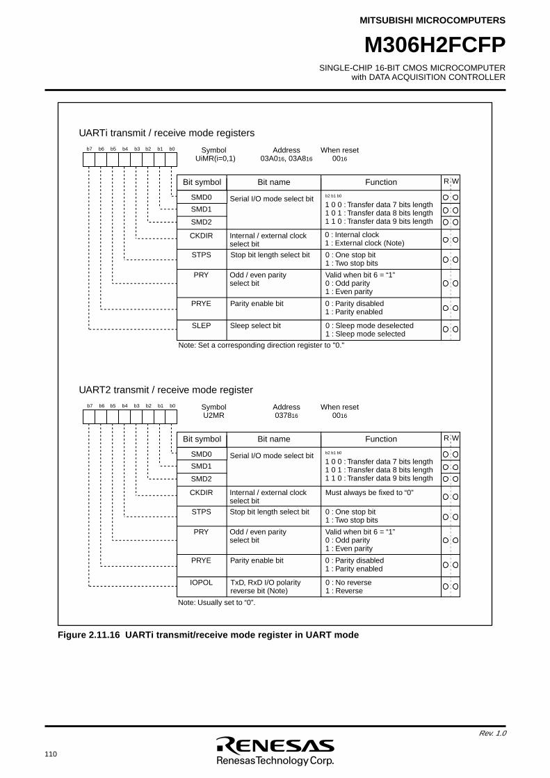
110
Rev. 1.0
SINGLE-CHIP 16-BIT CMOS MICROCOMPUTERwith DATA ACQUISITION CONTROLLER
MITSUBISHI MICROCOMPUTERS
M306H2FCFP
Figure 2.11.16 UARTi transmit/receive mode register in UART mode
Symbol Address When resetUiMR(i=0,1) 03A016, 03A816 0016
CKDIR
UARTi transmit / receive mode registers
Internal / external clock select bit
STPS
PRY
PRYE
SLEP
0 : Internal clock1 : External clock (Note)
Bit name FunctionBit symbol WR
b7 b6 b5 b4 b3 b2 b1 b0
SMD0
SMD1
SMD2
Serial I/O mode select bit b2 b1 b0
0 : One stop bit1 : Two stop bits
0 : Parity disabled1 : Parity enabled
0 : Sleep mode deselected1 : Sleep mode selected
1 0 0 : Transfer data 7 bits length1 0 1 : Transfer data 8 bits length1 1 0 : Transfer data 9 bits length
Valid when bit 6 = “1”0 : Odd parity1 : Even parity
Stop bit length select bit
Odd / even parity select bit
Parity enable bit
Sleep select bit
Symbol Address When resetU2MR 037816 0016
CKDIR
UART2 transmit / receive mode register
Internal / external clock select bit
STPS
PRY
PRYE
IOPOL
Must always be fixed to “0”
Bit name FunctionBit symbol WR
b7 b6 b5 b4 b3 b2 b1 b0
SMD0
SMD1
SMD2
Serial I/O mode select bit b2 b1 b0
0 : One stop bit1 : Two stop bits
0 : Parity disabled1 : Parity enabled
0 : No reverse1 : Reverse
1 0 0 : Transfer data 7 bits length1 0 1 : Transfer data 8 bits length1 1 0 : Transfer data 9 bits length
Valid when bit 6 = “1”0 : Odd parity1 : Even parity
Stop bit length select bit
Odd / even parity select bit
Parity enable bit
TxD, RxD I/O polarity reverse bit (Note)
Note: Usually set to “0”.
Note: Set a corresponding direction register to "0."
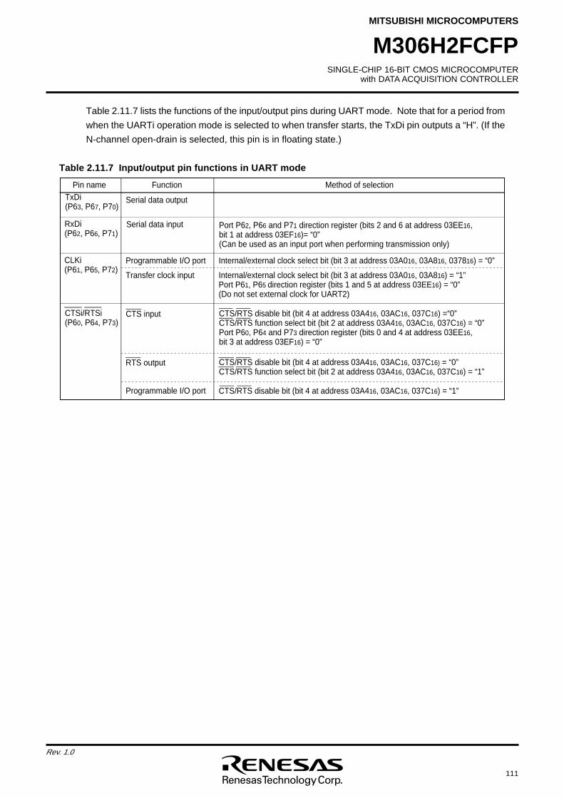
SINGLE-CHIP 16-BIT CMOS MICROCOMPUTERwith DATA ACQUISITION CONTROLLER
MITSUBISHI MICROCOMPUTERS
111
Rev. 1.0
M306H2FCFP
Table 2.11.7 lists the functions of the input/output pins during UART mode. Note that for a period from
when the UARTi operation mode is selected to when transfer starts, the TxDi pin outputs a “H”. (If the
N-channel open-drain is selected, this pin is in floating state.)
Table 2.11.7 Input/output pin functions in UART mode
Pin name Function Method of selectionTxDi (P63, P67, P70)
Serial data output
Serial data input
Programmable I/O port
Transfer clock input
Programmable I/O port
RxDi (P62, P66, P71)
CLKi(P61, P65, P72)
Internal/external clock select bit (bit 3 at address 03A016, 03A816, 037816) = “0”
Internal/external clock select bit (bit 3 at address 03A016, 03A816) = “1” Port P61, P65 direction register (bits 1 and 5 at address 03EE16) = “0”(Do not set external clock for UART2)
Port P62, P66 and P71 direction register (bits 2 and 6 at address 03EE16, bit 1 at address 03EF16)= “0” (Can be used as an input port when performing transmission only)
CTS/RTS disable bit (bit 4 at address 03A416, 03AC16, 037C16) =“0” CTS/RTS function select bit (bit 2 at address 03A416, 03AC16, 037C16) = “0” Port P60, P64 and P73 direction register (bits 0 and 4 at address 03EE16, bit 3 at address 03EF16) = “0”
CTS/RTS disable bit (bit 4 at address 03A416, 03AC16, 037C16) = “0” CTS/RTS function select bit (bit 2 at address 03A416, 03AC16, 037C16) = “1”
CTS/RTS disable bit (bit 4 at address 03A416, 03AC16, 037C16) = “1”
CTS input
RTS output
CTSi/RTSi(P60, P64, P73)
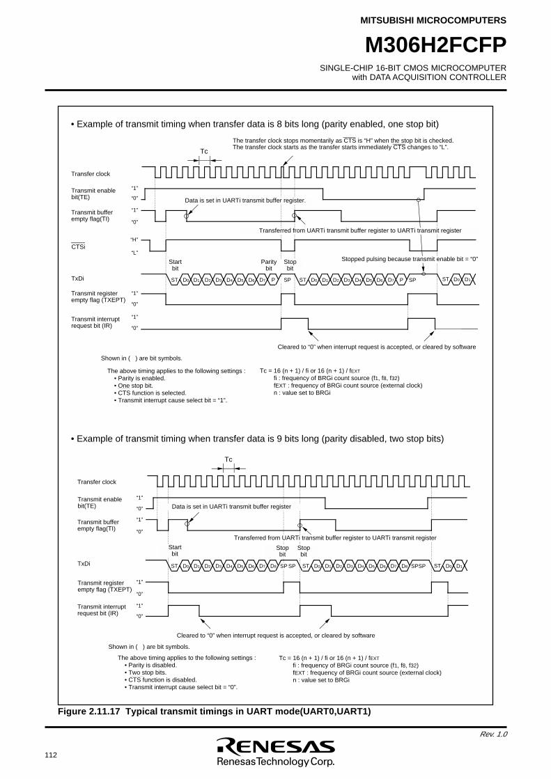
112
Rev. 1.0
SINGLE-CHIP 16-BIT CMOS MICROCOMPUTERwith DATA ACQUISITION CONTROLLER
MITSUBISHI MICROCOMPUTERS
M306H2FCFP
Transmit enable bit(TE)
Transmit buffer empty flag(TI)
Transmit register empty flag (TXEPT)
Startbit
Parity bit
TxDi
CTSi
The above timing applies to the following settings : • Parity is enabled. • One stop bit. • CTS function is selected. • Transmit interrupt cause select bit = “1”.
“1”
“0”
“1”
“L”
“H”
“0”
“1”
Tc = 16 (n + 1) / fi or 16 (n + 1) / fEXT
fi : frequency of BRGi count source (f1, f8, f32)fEXT : frequency of BRGi count source (external clock)n : value set to BRGi
Transmit interrupt request bit (IR) “0”
“1”
Cleared to “0” when interrupt request is accepted, or cleared by software
Transmit enable bit(TE)
Transmit buffer empty flag(TI)
TxDi
Transmit register empty flag (TXEPT)
“0”
“1”
“0”
“1”
“0”
“1”
The above timing applies to the following settings : • Parity is disabled. • Two stop bits. • CTS function is disabled. • Transmit interrupt cause select bit = “0”.
Transfer clock
Tc
Tc = 16 (n + 1) / fi or 16 (n + 1) / fEXT
fi : frequency of BRGi count source (f1, f8, f32)fEXT : frequency of BRGi count source (external clock)n : value set to BRGi
Transmit interrupt request bit (IR) “0”
“1”
Shown in ( ) are bit symbols.
Shown in ( ) are bit symbols.
Tc
Transfer clock
D0 D1 D2 D3 D4 D5 D6 D7ST P D0 D1 D2 D3 D4 D5 D6 D7SP ST P SP D0 D1ST
Stopped pulsing because transmit enable bit = “0”Stop bit
Transferred from UARTi transmit buffer register to UARTi transmit register
Start bit
The transfer clock stops momentarily as CTS is “H” when the stop bit is checked. The transfer clock starts as the transfer starts immediately CTS changes to “L”.
Data is set in UARTi transmit buffer register
D0 D1 D2 D3 D4 D5 D6 D7ST SPD8 D0 D1 D2 D3 D4 D5 D6 D7ST D8 D0 D1STSPSP
Transferred from UARTi transmit buffer register to UARTi transmit register
Stop bit
Stop bit
Data is set in UARTi transmit buffer register.“0”
SP
Cleared to “0” when interrupt request is accepted, or cleared by software
• Example of transmit timing when transfer data is 8 bits long (parity enabled, one stop bit)
• Example of transmit timing when transfer data is 9 bits long (parity disabled, two stop bits)
Figure 2.11.17 Typical transmit timings in UART mode(UART0,UART1)
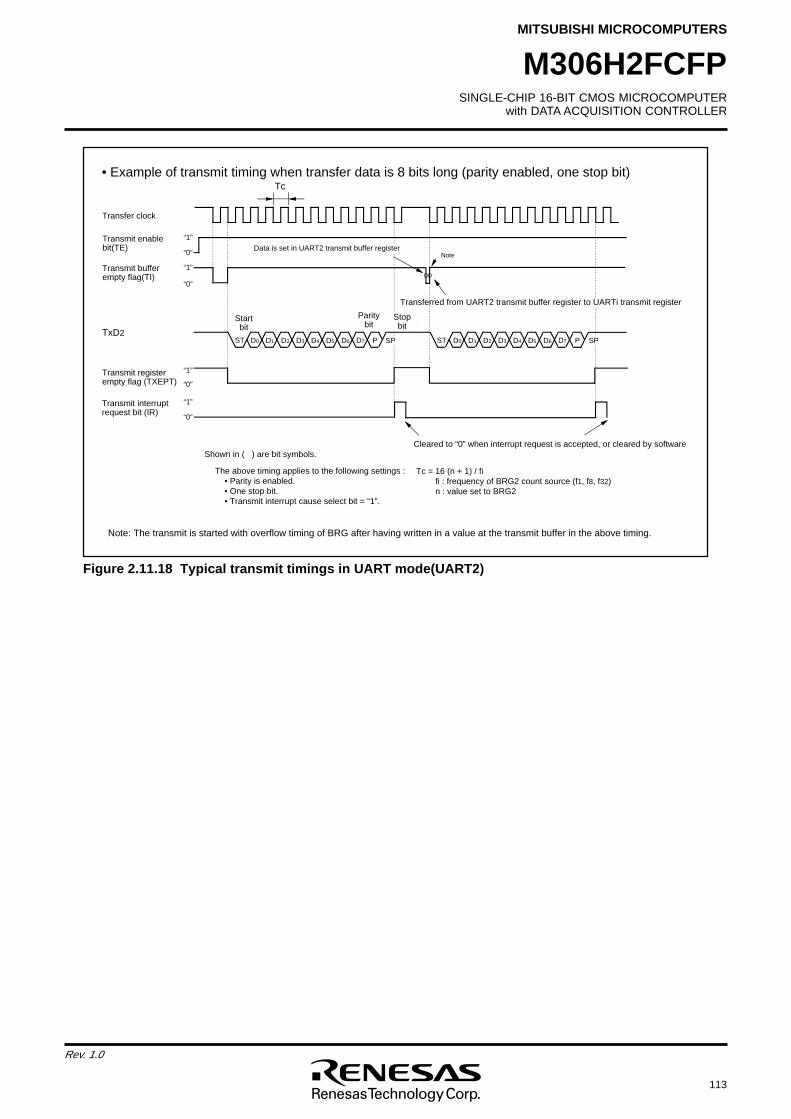
SINGLE-CHIP 16-BIT CMOS MICROCOMPUTERwith DATA ACQUISITION CONTROLLER
MITSUBISHI MICROCOMPUTERS
113
Rev. 1.0
M306H2FCFP
Figure 2.11.18 Typical transmit timings in UART mode(UART2)
D0 D1 D2 D3 D4 D5 D6 D7ST P
Start bit
Parity bit
Cleared to “0” when interrupt request is accepted, or cleared by software
D0 D1 D2 D3 D4 D5 D6 D7ST P
Tc
SP
Stop bit
Data is set in UART2 transmit buffer register
Transferred from UART2 transmit buffer register to UARTi transmit register
SP
Transmit enable bit(TE)
Transmit buffer empty flag(TI)
Transmit register empty flag (TXEPT)
“0”
“1”
“0”
“1”
“0”
“1”
Transmit interrupt request bit (IR)
“0”
“1”
Transfer clock
TxD2
The above timing applies to the following settings : • Parity is enabled. • One stop bit. • Transmit interrupt cause select bit = “1”.
Tc = 16 (n + 1) / fi fi : frequency of BRG2 count source (f1, f8, f32)n : value set to BRG2
Shown in ( ) are bit symbols.
Note
Note: The transmit is started with overflow timing of BRG after having written in a value at the transmit buffer in the above timing.
• Example of transmit timing when transfer data is 8 bits long (parity enabled, one stop bit)
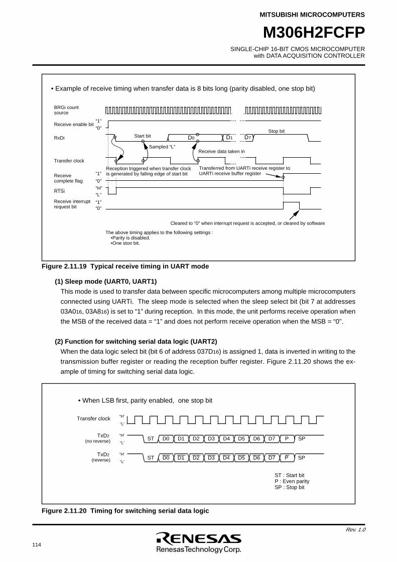
114
Rev. 1.0
SINGLE-CHIP 16-BIT CMOS MICROCOMPUTERwith DATA ACQUISITION CONTROLLER
MITSUBISHI MICROCOMPUTERS
M306H2FCFP
ST : Start bitP : Even paritySP : Stop bit
D
0 D
1 D
2 D
3 D
4 D
5 D
6 D
7 P S
PS
T
S
PS
T D
3 D
4 D
5 D
6 D
7 PD
0 D1 D
2
T
r
a
n
s
f
e
r
c
l
o
c
k
T
x
D2
(
n
o
r
e
v
e
r
s
e
)
T
x
D2
(
r
e
v
e
r
s
e
)
“
H
”
“
L
”
“
H
”
“
L
”
“
H
”
“
L
”
•
W
h
e
n
L
S
B
f
i
r
s
t
,
p
a
r
i
t
y
e
n
a
b
l
e
d
,
o
n
e
s
t
o
p
b
i
t
Figure 2.11.20 Timing for switching serial data logic
• Example of receive timing when transfer data is 8 bits long (parity disabled, one stop bit)
D0Start bit
Sampled “L”R
e
c
e
i
v
e
d
a
t
a
t
a
k
e
n
i
n
B
R
G
i
c
o
u
n
t
s
o
u
r
c
e
R
e
c
e
i
v
e
e
n
a
b
l
e
b
i
t
R
x
D
i
Transfer clock
R
e
c
e
i
v
e
c
o
m
p
l
e
t
e
f
l
a
g
R
T
S
i
Stop bit
“ 1
”
“ 0
”
“ 0
”
“ 1
”
“ H
”
“ L
”
T
h
e
a
b
o
v
e
t
i
m
i
n
g
a
p
p
l
i
e
s
t
o
t
h
e
f
o
l
l
o
w
i
n
g
s
e
t
t
i
n
g
s
:
•
P
a
r
i
t
y
i
s
d
i
s
a
b
l
e
d
.
•
O
n
e
s
t
o
p
b
i
t
.
R
e
c
e
i
v
e
i
n
t
e
r
r
u
p
t
r
e
q
u
e
s
t
b
i
t “ 0
”
“1”
Transferred from UARTi receive register to UARTi receive buffer register
Reception triggered when transfer clock is generated by falling edge of start bit
D7D1
Cleared to “0” when interrupt request is accepted, or cleared by software
Figure 2.11.19 Typical receive timing in UART mode
(1) Sleep mode (UART0, UART1)
This mode is used to transfer data between specific microcomputers among multiple microcomputers
connected using UARTi. The sleep mode is selected when the sleep select bit (bit 7 at addresses
03A016, 03A816) is set to “1” during reception. In this mode, the unit performs receive operation when
the MSB of the received data = “1” and does not perform receive operation when the MSB = “0”.
(2) Function for switching serial data logic (UART2)
When the data logic select bit (bit 6 of address 037D16) is assigned 1, data is inverted in writing to the
transmission buffer register or reading the reception buffer register. Figure 2.11.20 shows the ex-
ample of timing for switching serial data logic.
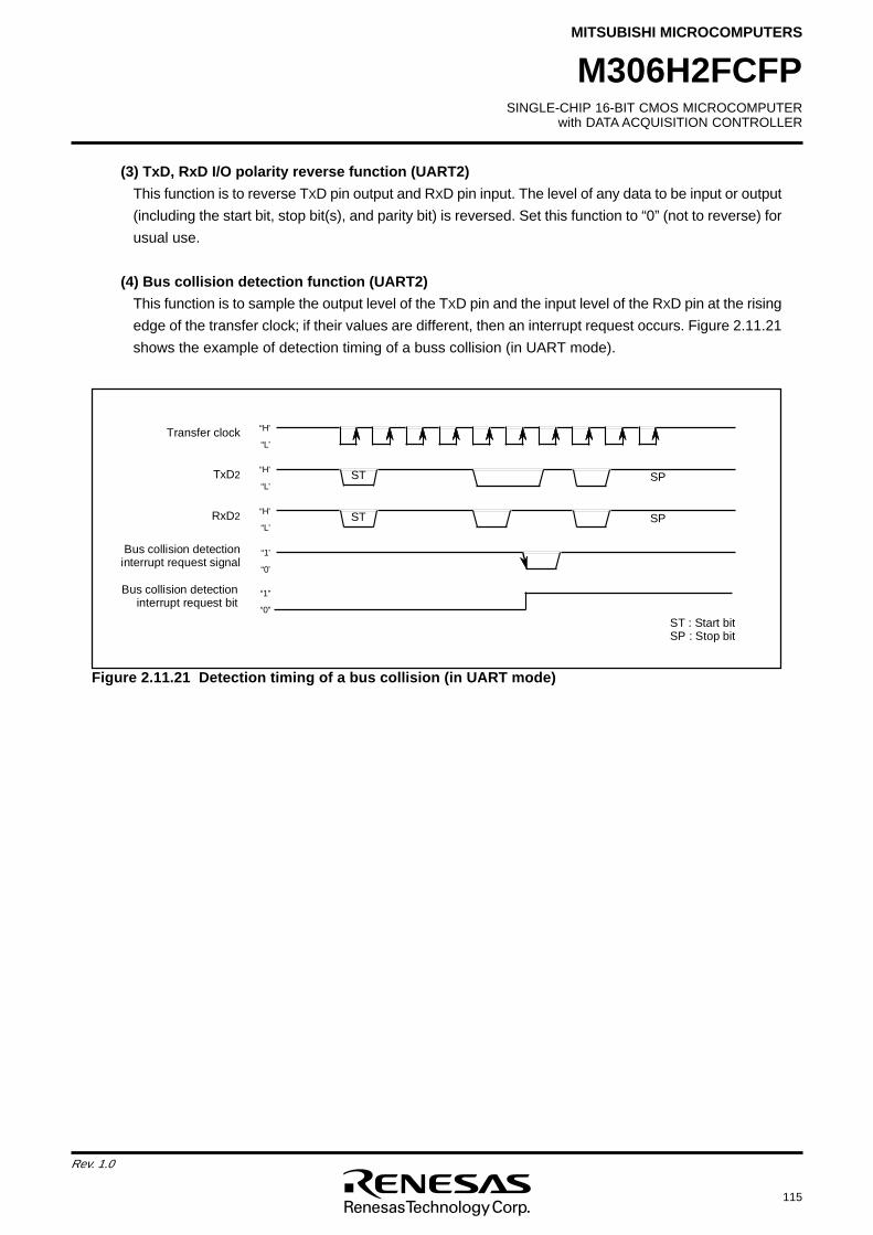
SINGLE-CHIP 16-BIT CMOS MICROCOMPUTERwith DATA ACQUISITION CONTROLLER
MITSUBISHI MICROCOMPUTERS
115
Rev. 1.0
M306H2FCFP
(3) TxD, RxD I/O polarity reverse function (UART2)
This function is to reverse TXD pin output and RXD pin input. The level of any data to be input or output
(including the start bit, stop bit(s), and parity bit) is reversed. Set this function to “0” (not to reverse) for
usual use.
(4) Bus collision detection function (UART2)
This function is to sample the output level of the TXD pin and the input level of the RXD pin at the rising
edge of the transfer clock; if their values are different, then an interrupt request occurs. Figure 2.11.21
shows the example of detection timing of a buss collision (in UART mode).
Figure 2.11.21 Detection timing of a bus collision (in UART mode)
ST : Start bitSP : Stop bit
ST
ST
S
P
S
P
T
r
a
n
s
f
e
r
c
l
o
c
k
T
x
D2
R
x
D2
B
u
s
c
o
l
l
i
s
i
o
n
d
e
t
e
c
t
i
o
ni
n
t
e
r
r
u
p
t
r
e
q
u
e
s
t
s
i
g
n
a
l
“
H
”
“
L
”
“
H
”
“
L
”
“
H
”
“
L
”
“
1
”
“
0
”
Bus collision detectioninterrupt request bit
“1”
“0”
116
Rev. 1.0
SINGLE-CHIP 16-BIT CMOS MICROCOMPUTERwith DATA ACQUISITION CONTROLLER
MITSUBISHI MICROCOMPUTERS
M306H2FCFP
Item Specification
Transfer data format • Transfer data 8-bit UART mode (bit 2 through bit 0 of address 037816 = “1012”)
• One stop bit (bit 4 of address 037816 = “0”)
• With the direct format chosen
Set parity to “even” (bit 5 and bit 6 of address 037816 = “1” and “1” respectively)
Set data logic to “direct” (bit 6 of address 037D16 = “0”).
Set transfer format to LSB (bit 7 of address 037C16 = “0”).
• With the inverse format chosen
Set parity to “odd” (bit 5 and bit 6 of address 037816 = “0” and “1” respectively)
Set data logic to “inverse” (bit 6 of address 037D16 = “1”)
Set transfer format to MSB (bit 7 of address 037C16 = “1”)
Transfer clock • With the internal clock chosen (bit 3 of address 037816 = “0”) : fi / 16 (n + 1) (Note 1) : fi=f1, f8, f32
(Do not set external clock)
Transmission / reception control_______ _______
• Disable the CTS and RTS function (bit 4 of address 037C16 = “1”)
Other settings • The sleep mode select function is not available for UART2
• Set transmission interrupt factor to “transmission completed” (bit 4 of address 037D16 = “1”)
Transmission start condition • To start transmission, the following requirements must be met:
- Transmit enable bit (bit 0 of address 037D16) = “1”
- Transmit buffer empty flag (bit 1 of address 037D16) = “0”
Reception start condition • To start reception, the following requirements must be met:
- Reception enable bit (bit 2 of address 037D16) = “1”
- Detection of a start bit
• When transmitting
When data transmission from the UART2 transfer register is completed
(bit 4 of address 037D16 = “1”)
• When receiving
When data transfer from the UART2 receive register to the UART2 receive
buffer register is completed
Error detection • Overrun error (see the specifications of clock-asynchronous serial I/O) (Note 2)
• Framing error (see the specifications of clock-asynchronous serial I/O)
• Parity error (see the specifications of clock-asynchronous serial I/O)
- On the reception side, an “L” level is output from the TXD2 pin by use of the parity error
signal output function (bit 7 of address 037D16 = “1”) when a parity error is detected
- On the transmission side, a parity error is detected by the level of input to
the RXD2 pin when a transmission interrupt occurs
• The error sum flag (see the specifications of clock-asynchronous serial I/O)
2.11.4 Clock-asynchronous serial I/O mode (compliant with the SIM interface)The SIM interface is used for connecting the microcomputer with a memory card or the like; addingsome extra settings in UART2 clock-asynchronous serial I/O mode allows the user to effect this func-tion. Table 2.11.8 shows the specifications of clock-asynchronous serial I/O mode (compliant with the
SIM interface).
Interrupt request
generation timing
Table 2.11.8 Specifications of clock-asynchronous serial I/O mode (compliant with the SIM interface)
Note 1: ‘n’ denotes the value 0016 to FF16 that is set to the UARTi bit rate generator.Note 2: If an overrun error occurs, the UART2 receive buffer will have the next data written in. Note also that
the UART2 receive interrupt request bit does not change.
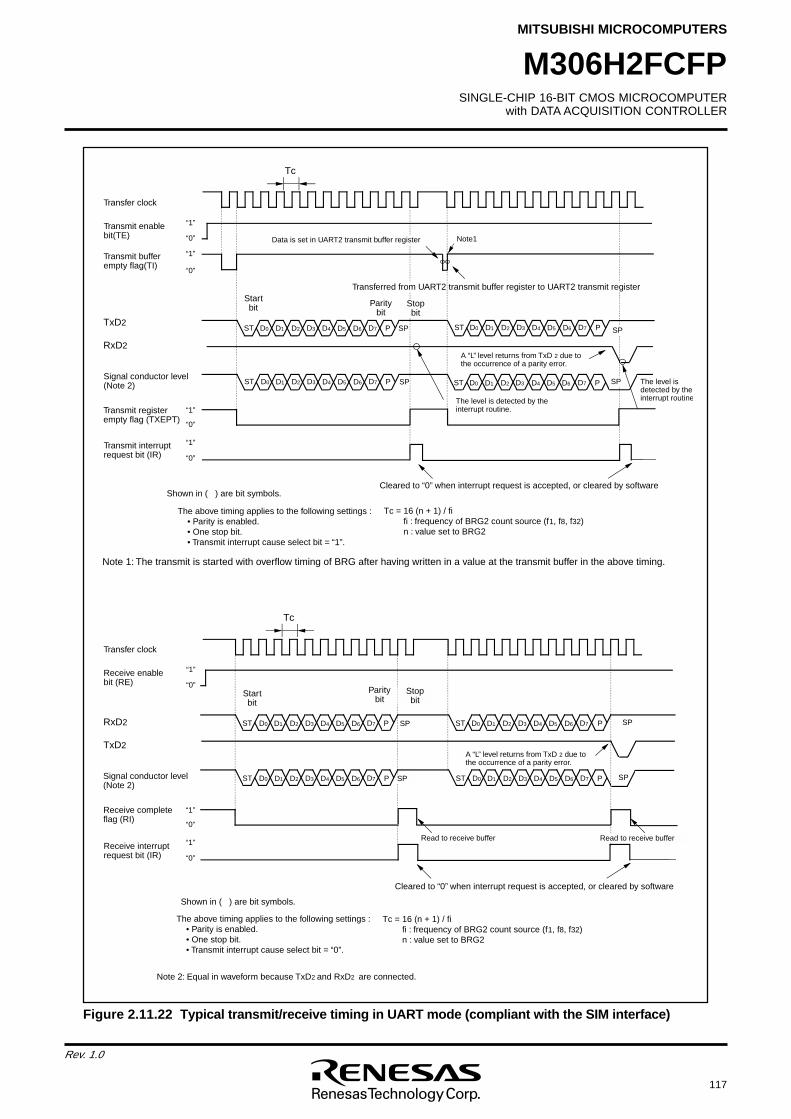
SINGLE-CHIP 16-BIT CMOS MICROCOMPUTERwith DATA ACQUISITION CONTROLLER
MITSUBISHI MICROCOMPUTERS
117
Rev. 1.0
M306H2FCFP
Figure 2.11.22 Typical transmit/receive timing in UART mode (compliant with the SIM interface)
Transmit enable bit(TE)
Transmit buffer empty flag(TI)
Transmit register empty flag (TXEPT)
D0 D1 D2 D3 D4 D5 D6 D7ST P
Start bit Parity
bit
The above timing applies to the following settings : • Parity is enabled. • One stop bit. • Transmit interrupt cause select bit = “1”.
“0”
“1”
“0”
“1”
“0”
“1”
Tc = 16 (n + 1) / fi fi : frequency of BRG2 count source (f1, f8, f32)n : value set to BRG2
Transmit interrupt request bit (IR) “0”
“1”
D0 D1 D2 D3 D4 D5 D6 D7ST P
Shown in ( ) are bit symbols.
Tc
Transfer clock
SP
Stop bit
Data is set in UART2 transmit buffer register
SP
A “L” level returns from TxD 2 due to the occurrence of a parity error.
The level is detected by the interrupt routine.
The level is detected by the interrupt routine
Receive enable bit (RE)
Receive complete flag (RI)
D0 D1 D2 D3 D4 D5 D6 D7ST P
Start bit
Parity bit
RxD2
The above timing applies to the following settings : • Parity is enabled. • One stop bit. • Transmit interrupt cause select bit = “0”.
“0”
“1”
“0”
“1”
Tc = 16 (n + 1) / fifi : frequency of BRG2 count source (f1, f8, f32)n : value set to BRG2
Receive interrupt request bit (IR) “0”
“1”
D0 D1 D2 D3 D4 D5 D6 D7ST P SP
Shown in ( ) are bit symbols.
Tc
Transfer clock
SP
Stop bit
A “L” level returns from TxD 2 due to the occurrence of a parity error.
TxD2
Read to receive buffer Read to receive buffer
D0 D1 D2 D3 D4 D5 D6 D7ST PSignal conductor level (Note 2)
D0 D1 D2 D3 D4 D5 D6 D7ST P SPSP
D0 D1 D2 D3 D4 D5 D6 D7ST P D0 D1 D2 D3 D4 D5 D6 D7ST P SPSP
TxD2
RxD2
Signal conductor level (Note 2)
Note 2: Equal in waveform because TxD2 and RxD2 are connected.
Transferred from UART2 transmit buffer register to UART2 transmit register
Cleared to “0” when interrupt request is accepted, or cleared by software
Cleared to “0” when interrupt request is accepted, or cleared by software
Note 1: The transmit is started with overflow timing of BRG after having written in a value at the transmit buffer in the above timing.
Note1
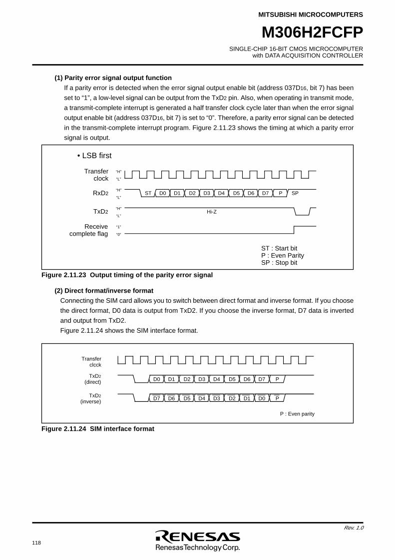
118
Rev. 1.0
SINGLE-CHIP 16-BIT CMOS MICROCOMPUTERwith DATA ACQUISITION CONTROLLER
MITSUBISHI MICROCOMPUTERS
M306H2FCFP
(1) Parity error signal output function
If a parity error is detected when the error signal output enable bit (address 037D16, bit 7) has been
set to “1”, a low-level signal can be output from the TxD2 pin. Also, when operating in transmit mode,
a transmit-complete interrupt is generated a half transfer clock cycle later than when the error signal
output enable bit (address 037D16, bit 7) is set to “0”. Therefore, a parity error signal can be detected
in the transmit-complete interrupt program. Figure 2.11.23 shows the timing at which a parity error
signal is output.
ST : Start bitP : Even ParitySP : Stop bit
D0 D1 D2 D3 D4 D5 D6 D7 P SPST
Hi-Z
Transfer clock
RxD2
TxD2
Receivecomplete flag
“H”
“L”
“H”
“L”
“H”
“L”
“1”
• LSB first
“0”
P : Even parity
D0 D1 D2 D3 D4 D5 D6 D7 P
Transfer clcck
TxD2
(direct)
TxD2
(inverse)D7 D6 D5 D4 D3 D2 D1 D0 P
Figure 2.11.23 Output timing of the parity error signal
(2) Direct format/inverse format
Connecting the SIM card allows you to switch between direct format and inverse format. If you choose
the direct format, D0 data is output from TxD2. If you choose the inverse format, D7 data is inverted
and output from TxD2.
Figure 2.11.24 shows the SIM interface format.
Figure 2.11.24 SIM interface format
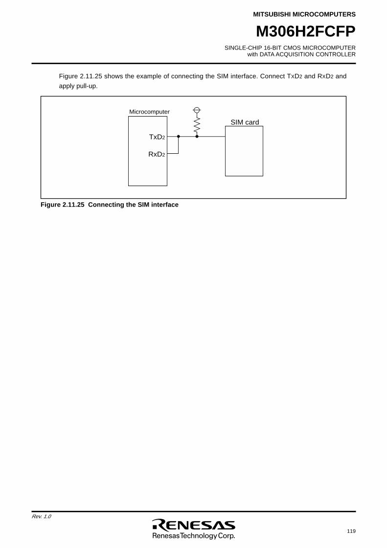
SINGLE-CHIP 16-BIT CMOS MICROCOMPUTERwith DATA ACQUISITION CONTROLLER
MITSUBISHI MICROCOMPUTERS
119
Rev. 1.0
M306H2FCFP
Figure 2.11.25 shows the example of connecting the SIM interface. Connect TXD2 and RXD2 and
apply pull-up.
Figure 2.11.25 Connecting the SIM interface
Microcomputer
SIM card
TxD2
RxD2
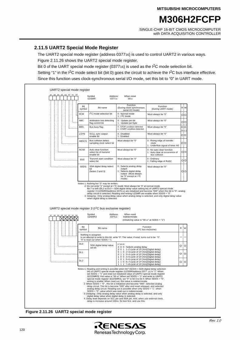
120
Rev. 1.0
SINGLE-CHIP 16-BIT CMOS MICROCOMPUTERwith DATA ACQUISITION CONTROLLER
MITSUBISHI MICROCOMPUTERS
M306H2FCFP
2.11.5 UART2 Special Mode RegisterThe UART2 special mode register (address 037716) is used to control UART2 in various ways.
Figure 2.11.26 shows the UART2 special mode register.
Bit 0 of the UART special mode register (037716) is used as the I2C mode selection bit.
Setting “1” in the I2C mode select bit (bit 0) goes the circuit to achieve the I2C bus interface effective.
Since this function uses clock-synchronous serial I/O mode, set this bit to “0” in UART mode.
Figure 2.11.26 UART2 special mode register
UART2 special mode register
Symbol Address When reset U2SMR 037716 0016
b7 b6 b5 b4 b3 b2 b1 b0
Bit nameBit symbol WRFunction
(During UART mode)
Function(During clock synchronous
serial I/O mode)
ABSCS
ACSE
SSS
I C mode selection bit
Bus busy flag 0 : STOP condition detected1 : START condition detected
SCLL sync output enable bit
Bus collision detectsampling clock select bit
Arbitration lost detecting flag control bit
0 : Normal mode1 : I C mode
0 : Update per bit1 : Update per byte
IICM
ABC
BBS
LSYN
0 : Ordinary1 : Falling edge of RxD2
0 : Disabled1 : Enabled
Transmit start condition select bit
Must always be “0”
0 : Rising edge of transfer clock
1 : Underflow signal of timer A0
Auto clear function select bit of transmit enable bit
0 : No auto clear function1 : Auto clear at occurrence of
bus collision
Must always be “0”
Must always be “0”
Must always be “0”
Must always be “0”
Must always be “0”
Must always be “0”
Notes 1: Nothing but "0" may be written.2: Do not write "1" except at I 2C mode. Must always be “0” at normal mode. Bit 7 to bit5 (DL2 to DL0 = SDA digital delay value setting bit) of UART2 special mode register 3 (U2SMR3/address 0375 16) are initialized and become “000” when this bit is "0", analog delay circuit is selected. Reading and writing U2SMR are enable when SDDS = "0" .3: Delaying ; Only analog delay value when analog delay is selected, and only digital delay value
when digital delay is selected.
(Note 1)
22
SDDS SDA digital delay select bit (Notes 2 and 3)
0 : Selects analog delay output 1 : Selects digital delay output (Must always be “0” except at I 2C mode)
Must always be “0”
UART2 special mode register 3 (I2C bus exclusive register)
Symbol Address When reset U2SMR3 037516 Indeterminate
b7 b6 b5 b4 b3 b2 b1 b0
Bit nameBit symbol
Function(I2C bus exclusive)
SDA digital delay value set bit
b7 b6 b5DL0
DL1
DL2
(initializing value is "00 16" at SDDS = "1")
Nothing is assigned.In an attempt to write to this bit, write “0”. The value, if read, turns out to be “0”.“0” is read out when SDDS = 1.
WR
Notes 1: Reading and writing is possible when bit7 (SDDS = SDA digital delay selection bit) of UART2 special mode register (U2SMR/address 0377 16) is "1". When set SDDS = "1" and read out initialized value of UART2 special mode register 3(U2SMR3), this value is "00 16".When set SDDS = "1" and write to UART2 special mode register 3(U2SMR3), set "0" to bit 0 to bit 4. When SDDS = "0", writing is enable. When read out, this value is indeterminate.2: When SDDS = "0" , this bit is initialized and become "000", selected analog delay circuit. This bit is become "000" after end reset released, and selected analog delay circuit. Reading out is possible when only SDDS = "1". when SDDS = "0", value which was read out is indeterminate.3: Delaying ; Only analog delay value when analog delay is selected, and only digital delay value when digital delay is selected.4: Delay level depends on SCL pin and SDA pin. And, when use external clock, delay is increase around 100ns. So test first, and use this.
0 0 0 : Selects analog delay0 0 1 : 1–2 cycle of 1/f (Xin)(Digital delay)0 1 0 : 2–3 cycle of 1/f (Xin)(Digital delay)0 1 1 : 3–4 cycle of 1/f (Xin)(Digital delay)1 0 0 : 4–5 cycle of 1/f (Xin)(Digital delay)1 0 1 : 5–6 cycle of 1/f (Xin)(Digital delay)1 1 0 : 6–7 cycle of 1/f (Xin)(Digital delay)1 1 1 : 7–8 cycle of 1/f (Xin)(Digital delay)
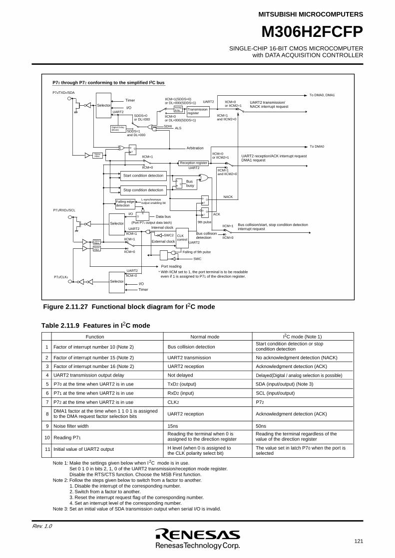
SINGLE-CHIP 16-BIT CMOS MICROCOMPUTERwith DATA ACQUISITION CONTROLLER
MITSUBISHI MICROCOMPUTERS
121
Rev. 1.0
M306H2FCFP
Figure 2.11.27 Functional block diagram for I2C mode
Function Normal mode I2C mode (Note 1)
Factor of interrupt number 15 (Note 2) UART2 transmission No acknowledgment detection (NACK)
Factor of interrupt number 16 (Note 2) UART2 reception
Start condition detection or stop condition detection
UART2 transmission output delay Not delayed Delayed(Digital / analog selection is possible)
P70 at the time when UART2 is in use TxD2 (output) SDA (input/output) (Note 3)
P71 at the time when UART2 is in use RxD2 (input) SCL (input/output)
P72 at the time when UART2 is in use CLK2 P72
DMA1 factor at the time when 1 1 0 1 is assigned to the DMA request factor selection bits UART2 reception Acknowledgment detection (ACK)
Noise filter width 15ns 50ns
Reading P71Reading the terminal when 0 is assigned to the direction register
Reading the terminal regardless of the value of the direction register
1
2
3
4
5
6
7
8
9
Note 1: Make the settings given below when I2C mode is in use.Set 0 1 0 in bits 2, 1, 0 of the UART2 transmission/reception mode register.Disable the RTS/CTS function. Choose the MSB First function.
Note 2: Follow the steps given below to switch from a factor to another.1. Disable the interrupt of the corresponding number.2. Switch from a factor to another.3. Reset the interrupt request flag of the corresponding number.4. Set an interrupt level of the corresponding number.
Note 3: Set an initial value of SDA transmission output when serial I/O is invalid.
Factor of interrupt number 10 (Note 2) Bus collision detection
Acknowledgment detection (ACK)
10
Initial value of UART2 output H level (when 0 is assigned to the CLK polarity select bit)
The value set in latch P70 when the port is selected
11
Table 2.11.9 Features in I2C mode
I I
C
M
=
1
a
n
d
I
I
C
M
2
=
0
IICM=0or IICM2=1
T
o
D
M
A
0
I /
O
NoizeFilter
P
71/
R
X
D2/
S
C
L
R
e
c
e
p
t
i
o
n
r
e
g
i
s
t
e
r
C
L
Kc
o
n
t
r
o
l
UART2
N
o
i
z
eF
i
l
t
e
r
U
A
R
T
2
P72/CLK2
D
T
Q
D
T
Q
U
A
R
T
2
U
A
R
T
2
R
I I
C
M
=
1
I I
C
M
=
0
I I
C
M
=
0
I I
C
M
=
1
I I
C
M
=
1
IICM=0
S
RQ
SWC
F
a
l
l
i
n
g
o
f
9
t
h
p
u
l
s
e
S
W
C
2
S
t
a
r
t
c
o
n
d
i
t
i
o
n
d
e
t
e
c
t
i
o
n
Stop condition detection
F
a
l
l
i
n
g
e
d
g
e
d
e
t
e
c
t
i
o
n
L-synchronous output enabling bit
D
a
t
a
b
u
s
SelectorInternal clock
E
x
t
e
r
n
a
l
c
l
o
c
k
SelectorI / O
Timer
Port reading
Busbusy
U
A
R
T
2
r
e
c
e
p
t
i
o
n
/
A
C
K
i
n
t
e
r
r
u
p
t
r
e
q
u
e
s
t
D
M
A
1
r
e
q
u
e
s
t
N
A
C
K
ACK
IICM=1
IICM=0
* With IICM set to 1, the port terminal is to be readable even if 1 is assigned to P71 of the direction register.
Bus collision detection
9th pulseBus collision/start, stop condition detection interrupt request
N
o
i
z
eF
i
l
t
e
r
D
T
Q
IICM=1and IICM2=0
I I C
M
=
0
o
r
I
I
C
M
2
=
1
T
o
D
M
A
0
,
D
M
A
1
U
A
R
T
2
t
r
a
n
s
m
i
s
s
i
o
n
/N
A
C
K
i
n
t
e
r
r
u
p
t
r
e
q
u
e
s
tI/OUART2
P
70/
T
X
D2/
S
D
A
S
e
l
e
c
t
o
rT
i
m
e
r
T
r
a
n
s
m
i
s
s
i
o
nr
e
g
i
s
t
e
r
Arbitration
A
n
a
l
o
gd
e
l
a
y
UART2I I
C
M
=
1
(
S
D
D
S
=
0
)
o
r
D
L
=
0
0
0
(
S
D
D
S
=
1
)
ALSSDHI
I I C
M
=
0
o
r
D
L
=
0
0
0
(
S
D
D
S
=
1
)
SDDS=1and DL=000
D
i
g
i
t
a
l
D
e
l
a
y(
D
i
v
i
e
r
)
S
D
D
S
=
0o
r
D
L
=
0
0
0
Q
(Port P71 output data latch)
P
70
t
h
r
o
u
g
h
P
72 c
o
n
f
o
r
m
i
n
g
t
o
t
h
e
s
i
m
p
l
i
f
i
e
d
I2C
b
u
s
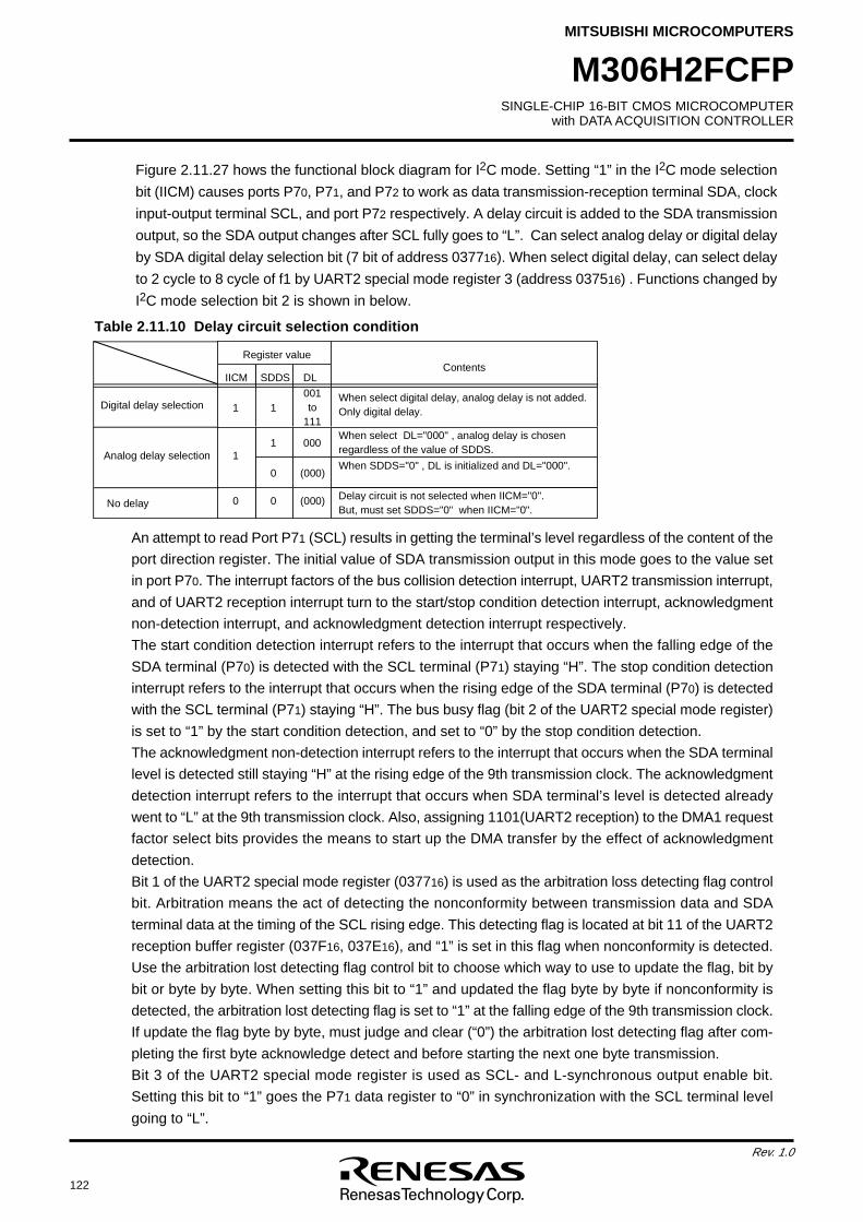
122
Rev. 1.0
SINGLE-CHIP 16-BIT CMOS MICROCOMPUTERwith DATA ACQUISITION CONTROLLER
MITSUBISHI MICROCOMPUTERS
M306H2FCFP
Figure 2.11.27 hows the functional block diagram for I2C mode. Setting “1” in the I2C mode selection
bit (IICM) causes ports P70, P71, and P72 to work as data transmission-reception terminal SDA, clock
input-output terminal SCL, and port P72 respectively. A delay circuit is added to the SDA transmission
output, so the SDA output changes after SCL fully goes to “L”. Can select analog delay or digital delay
by SDA digital delay selection bit (7 bit of address 037716). When select digital delay, can select delay
to 2 cycle to 8 cycle of f1 by UART2 special mode register 3 (address 037516) . Functions changed by
I2C mode selection bit 2 is shown in below.
Table 2.11.10 Delay circuit selection condition
When select digital delay, analog delay is not added.Only digital delay.
001to
111When select DL="000" , analog delay is chosen regardless of the value of SDDS.
When SDDS="0" , DL is initialized and DL="000".
0
0
0
(
0
0
0
)
1
0
1
1 1
Delay circuit is not selected when IICM="0". But, must set SDDS="0" when IICM="0".
0 0 (
0
0
0
)
I I
C
M SDDS D
L
R
e
g
i
s
t
e
r
v
a
l
u
eC
o
n
t
e
n
t
s
D
i
g
i
t
a
l
d
e
l
a
y
s
e
l
e
c
t
i
o
n
A
n
a
l
o
g
d
e
l
a
y
s
e
l
e
c
t
i
o
n
N
o
d
e
l
a
y
An attempt to read Port P71 (SCL) results in getting the terminal’s level regardless of the content of the
port direction register. The initial value of SDA transmission output in this mode goes to the value set
in port P70. The interrupt factors of the bus collision detection interrupt, UART2 transmission interrupt,
and of UART2 reception interrupt turn to the start/stop condition detection interrupt, acknowledgment
non-detection interrupt, and acknowledgment detection interrupt respectively.
The start condition detection interrupt refers to the interrupt that occurs when the falling edge of the
SDA terminal (P70) is detected with the SCL terminal (P71) staying “H”. The stop condition detection
interrupt refers to the interrupt that occurs when the rising edge of the SDA terminal (P70) is detected
with the SCL terminal (P71) staying “H”. The bus busy flag (bit 2 of the UART2 special mode register)
is set to “1” by the start condition detection, and set to “0” by the stop condition detection.
The acknowledgment non-detection interrupt refers to the interrupt that occurs when the SDA terminal
level is detected still staying “H” at the rising edge of the 9th transmission clock. The acknowledgment
detection interrupt refers to the interrupt that occurs when SDA terminal’s level is detected already
went to “L” at the 9th transmission clock. Also, assigning 1101(UART2 reception) to the DMA1 request
factor select bits provides the means to start up the DMA transfer by the effect of acknowledgment
detection.
Bit 1 of the UART2 special mode register (037716) is used as the arbitration loss detecting flag control
bit. Arbitration means the act of detecting the nonconformity between transmission data and SDA
terminal data at the timing of the SCL rising edge. This detecting flag is located at bit 11 of the UART2
reception buffer register (037F16, 037E16), and “1” is set in this flag when nonconformity is detected.
Use the arbitration lost detecting flag control bit to choose which way to use to update the flag, bit by
bit or byte by byte. When setting this bit to “1” and updated the flag byte by byte if nonconformity is
detected, the arbitration lost detecting flag is set to “1” at the falling edge of the 9th transmission clock.
If update the flag byte by byte, must judge and clear (“0”) the arbitration lost detecting flag after com-
pleting the first byte acknowledge detect and before starting the next one byte transmission.
Bit 3 of the UART2 special mode register is used as SCL- and L-synchronous output enable bit.
Setting this bit to “1” goes the P71 data register to “0” in synchronization with the SCL terminal level
going to “L”.
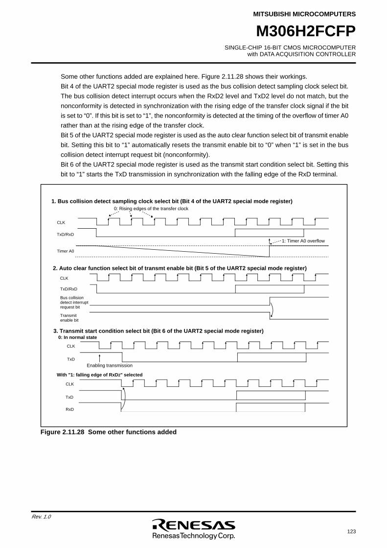
SINGLE-CHIP 16-BIT CMOS MICROCOMPUTERwith DATA ACQUISITION CONTROLLER
MITSUBISHI MICROCOMPUTERS
123
Rev. 1.0
M306H2FCFP
1. Bus collision detect sampling clock select bit (Bit 4 of the UART2 special mode register)0: Rising edges of the transfer clock
CLK
Timer A0
1: Timer A0 overflow
2. Auto clear function select bit of transmt enable bit (Bit 5 of the UART2 special mode register)
CLK
TxD/RxD
Bus collision detect interrupt request bit
Transmit enable bit
3. Transmit start condition select bit (Bit 6 of the UART2 special mode register)
CLK
TxD
Enabling transmission
CLK
TxD
RxD
With "1: falling edge of RxD2" selected
0: In normal state
TxD/RxD
Figure 2.11.28 Some other functions added
Some other functions added are explained here. Figure 2.11.28 shows their workings.
Bit 4 of the UART2 special mode register is used as the bus collision detect sampling clock select bit.
The bus collision detect interrupt occurs when the RxD2 level and TxD2 level do not match, but the
nonconformity is detected in synchronization with the rising edge of the transfer clock signal if the bit
is set to “0”. If this bit is set to “1”, the nonconformity is detected at the timing of the overflow of timer A0
rather than at the rising edge of the transfer clock.
Bit 5 of the UART2 special mode register is used as the auto clear function select bit of transmit enable
bit. Setting this bit to “1” automatically resets the transmit enable bit to “0” when “1” is set in the bus
collision detect interrupt request bit (nonconformity).
Bit 6 of the UART2 special mode register is used as the transmit start condition select bit. Setting this
bit to “1” starts the TxD transmission in synchronization with the falling edge of the RxD terminal.
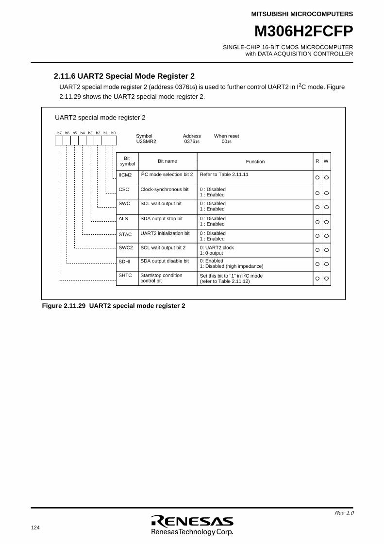
124
Rev. 1.0
SINGLE-CHIP 16-BIT CMOS MICROCOMPUTERwith DATA ACQUISITION CONTROLLER
MITSUBISHI MICROCOMPUTERS
M306H2FCFP
S
y
m
b
o
l A
d
d
r
e
s
s W
h
e
n
r
e
s
e
t
U
2
S
M
R
2 0
3
7
61
6 0
01
6
b
7 b
6 b
5 b
4 b
3 b
2 b
1 b
0
B
i
t
n
a
m
eB
i
t
s
y
m
b
o
l WRF
u
n
c
t
i
o
n
S
T
A
C
S
W
C
2
S
D
H
I
I
C
m
o
d
e
s
e
l
e
c
t
i
o
n
b
i
t
2
S
C
L
w
a
i
t
o
u
t
p
u
t
b
i
t 0
:
D
i
s
a
b
l
e
d
1
:
E
n
a
b
l
e
d
S
D
A
o
u
t
p
u
t
s
t
o
p
b
i
t
U
A
R
T
2
i
n
i
t
i
a
l
i
z
a
t
i
o
n
b
i
t
C
l
o
c
k
-
s
y
n
c
h
r
o
n
o
u
s
b
i
t
R
e
f
e
r
t
o
T
a
b
l
e
2
.
1
1
.
1
1
0
:
D
i
s
a
b
l
e
d
1
:
E
n
a
b
l
e
d
I I C
M
2
C
S
C
S
W
C
A
L
S 0
:
D
i
s
a
b
l
e
d
1
:
E
n
a
b
l
e
d
S
D
A
o
u
t
p
u
t
d
i
s
a
b
l
e
b
i
t
S
C
L
w
a
i
t
o
u
t
p
u
t
b
i
t
2
0 :
E
n
a
b
l
e
d
1
:
D
i
s
a
b
l
e
d
(
h
i
g
h
i
m
p
e
d
a
n
c
e
)
0
:
D
i
s
a
b
l
e
d
1
:
E
n
a
b
l
e
d
0 :
U
A
R
T
2
c
l
o
c
k
1
:
0
o
u
t
p
u
t
2
S
H
T
C S
t
a
r
t
/
s
t
o
p
c
o
n
d
i
t
i
o
n
c
o
n
t
r
o
l
b
i
tS
e
t
t
h
i
s
b
i
t
t
o
"
1
"
i
n
I2C
m
o
d
e(
r
e
f
e
r
t
o
T
a
b
l
e
2
.
1
1
.
1
2
)
U
A
R
T
2
s
p
e
c
i
a
l
m
o
d
e
r
e
g
i
s
t
e
r
2
Figure 2.11.29 UART2 special mode register 2
2.11.6 UART2 Special Mode Register 2UART2 special mode register 2 (address 037616) is used to further control UART2 in I2C mode. Figure
2.11.29 shows the UART2 special mode register 2.
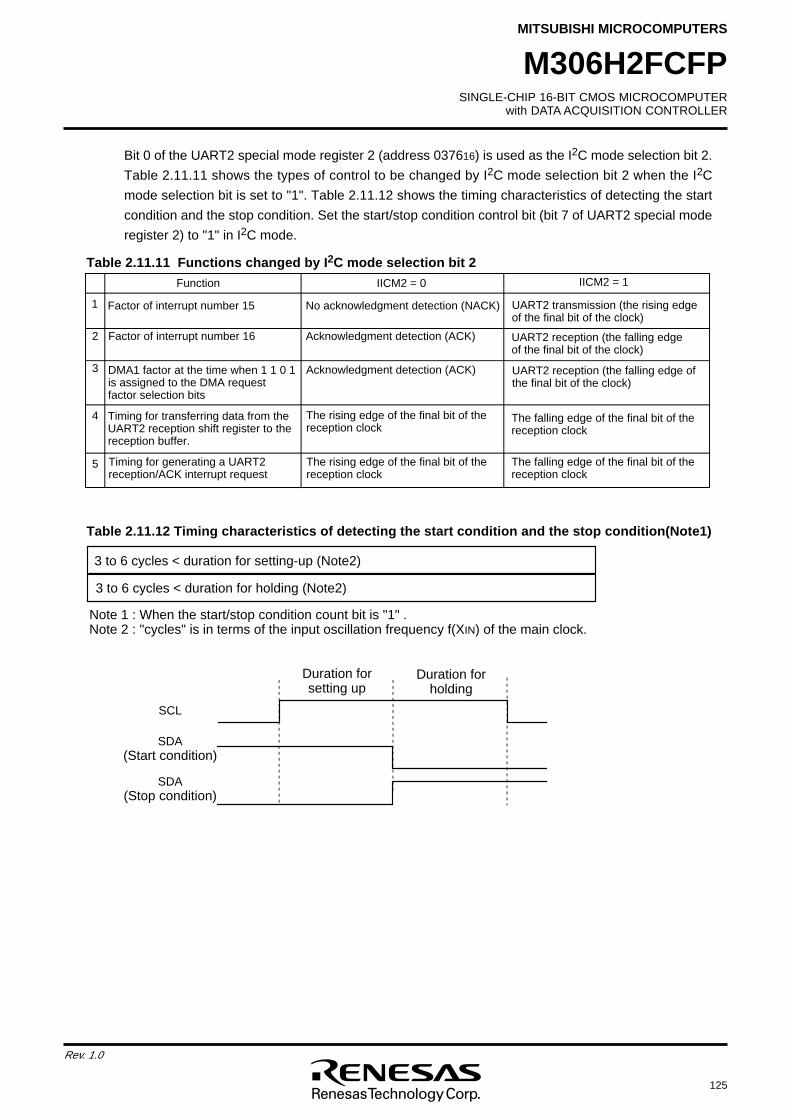
SINGLE-CHIP 16-BIT CMOS MICROCOMPUTERwith DATA ACQUISITION CONTROLLER
MITSUBISHI MICROCOMPUTERS
125
Rev. 1.0
M306H2FCFP
Bit 0 of the UART2 special mode register 2 (address 037616) is used as the I2C mode selection bit 2.
Table 2.11.11 shows the types of control to be changed by I2C mode selection bit 2 when the I2C
mode selection bit is set to "1". Table 2.11.12 shows the timing characteristics of detecting the start
condition and the stop condition. Set the start/stop condition control bit (bit 7 of UART2 special mode
register 2) to "1" in I2C mode.
Function IICM2 = 1IICM2 = 0
Factor of interrupt number 15 No acknowledgment detection (NACK) UART2 transmission (the rising edge of the final bit of the clock)
Factor of interrupt number 16 Acknowledgment detection (ACK) UART2 reception (the falling edge of the final bit of the clock)
DMA1 factor at the time when 1 1 0 1 is assigned to the DMA request factor selection bits
Acknowledgment detection (ACK) UART2 reception (the falling edge of the final bit of the clock)
Timing for transferring data from the UART2 reception shift register to the reception buffer.
The rising edge of the final bit of the reception clock
The falling edge of the final bit of the reception clock
Timing for generating a UART2 reception/ACK interrupt request
The rising edge of the final bit of the reception clock
The falling edge of the final bit of the reception clock
1
2
3
4
5
3 to 6 cycles < duration for setting-up (Note2)
3 to 6 cycles < duration for holding (Note2)
Note 1 : When the start/stop condition count bit is "1" .Note 2 : "cycles" is in terms of the input oscillation frequency f(XIN) of the main clock.
Duration for setting up
Duration for holding
SCL
SDA (Start condition)
SDA (Stop condition)
Table 2.11.11 Functions changed by I2C mode selection bit 2
Table 2.11.12 Timing characteristics of detecting the start condition and the stop condition(Note1)
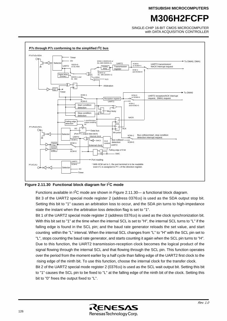
126
Rev. 1.0
SINGLE-CHIP 16-BIT CMOS MICROCOMPUTERwith DATA ACQUISITION CONTROLLER
MITSUBISHI MICROCOMPUTERS
M306H2FCFP
P70/TxD2/SDA
P71/RxD2/SCL
CLK control
P72/CLK2
Falling edge detection
UART2 reception/ACK interrupt request, DMA1 request
To DMA0, DMA1
To DMA0
I/O
Timer
UART2
Timer
UART2IICM=1 (SDDS=0) or DL=000 (SDDS=1) IICM=0
or IICM2=1
IICM=1 and IICM2=0
SDHI
NoizeFilter
Timer
UART2
UART2
I/O
D
T
Q
D
T
Q
D
T
Q
NACK
ACK
UART2
UART2
IICM=1
IICM=0
IICM=0
IICM=1
IICM=1
IICM=0
S
RQ
IICM=1
IICM=0
I/O RQ
ALS
IICM=0 or DL 000 (SDDS=1)
SDDS=0 or DL=000
SDDS=1 and DL 000
SWC2
Falling edge of 9 bit
SWC
IICM=1 and IICM2=0
IICM=0 or IICM2=1
Selector
Selector
Selector
NoizeFilter
NoizeFilter
* With IICM set to 1, the port terminal is to be readable even if 1 is assigned to P7 1 of the direction register.
Port reading
External clock
Internal clock
9th pulse
Bus collision detection
Bus collision/start, stop condition detection interrupt request
UART2 transmission/NACK interrupt request
Start condition detection
Stop condition detection
L-synchronous output enabling bit
(Port P71 output data latch)
Data bus
Reception register
Bus busy
Transmission register
Arbitration
Analog delay
Digital delay(Divider)
P70 through P72 conforming to the simplified I2C bus
Figure 2.11.30 Functional block diagram for I2C mode
Functions available in I2C mode are shown in Figure 2.11.30— a functional block diagram.
Bit 3 of the UART2 special mode register 2 (address 037616) is used as the SDA output stop bit.
Setting this bit to "1" causes an arbitration loss to occur, and the SDA pin turns to high-impedance
state the instant when the arbitration loss detection flag is set to "1".
Bit 1 of the UART2 special mode register 2 (address 037616) is used as the clock synchronization bit.
With this bit set to "1" at the time when the internal SCL is set to "H", the internal SCL turns to "L" if the
falling edge is found in the SCL pin; and the baud rate generator reloads the set value, and start
counting within the "L" interval. When the internal SCL changes from "L" to "H" with the SCL pin set to
"L", stops counting the baud rate generator, and starts counting it again when the SCL pin turns to "H".
Due to this function, the UART2 transmission-reception clock becomes the logical product of the
signal flowing through the internal SCL and that flowing through the SCL pin. This function operates
over the period from the moment earlier by a half cycle than falling edge of the UART2 first clock to the
rising edge of the ninth bit. To use this function, choose the internal clock for the transfer clock.
Bit 2 of the UART2 special mode register 2 (037616) is used as the SCL wait output bit. Setting this bit
to "1" causes the SCL pin to be fixed to "L" at the falling edge of the ninth bit of the clock. Setting this
bit to "0" frees the output fixed to "L".
SINGLE-CHIP 16-BIT CMOS MICROCOMPUTERwith DATA ACQUISITION CONTROLLER
MITSUBISHI MICROCOMPUTERS
127
Rev. 1.0
M306H2FCFP
Bit 4 of the UART2 special mode register 2 (address 037616) is used as the UART2 initialization bit.
Setting this bit to "1", and when the start condition is detected, the microcomputer operates as follows.
(1) The transmission shift register is initialized, and the content of the transmission register is trans-
ferred to the transmission shift register. This starts transmission by dealing with the clock entered
next as the first bit. The UART2 output value, however, doesn’t change until the first bit data is
output after the entrance of the clock, and remains unchanged from the value at the moment when
the microcomputer detected the start condition.
(2) The reception shift register is initialized, and the microcomputer starts reception by dealing with the
clock entered next as the first bit.
(3) The SCL wait output bit turns to "1". This turns the SCL pin to "L" at the falling edge of the ninth bit
of the clock.
Starting to transmit/receive signals to/from UART2 using this function doesn’t change the value of the
transmission buffer empty flag. To use this function, choose the external clock for the transfer clock.
Bit 5 of the UART2 special mode register 2 (037616) is used as the SCL pin wait output bit 2. Setting
this bit to "1" with the serial I/O specified allows the user to forcibly output an "L" from the SCL pin even
if UART2 is in operation. Setting this bit to "0" frees the "L" output from the SCL pin, and the UART2
clock is input/output.
Bit 6 of the UART2 special mode register 2 (037616) is used as the SDA output enable bit. Setting this
bit to "1" forces the SDA pin to turn to the high-impedance state. Refrain from changing the value of
this bit at the rising edge of the UART2 transfer clock. There can be instances in which arbitration lost
detection flag is turned on.
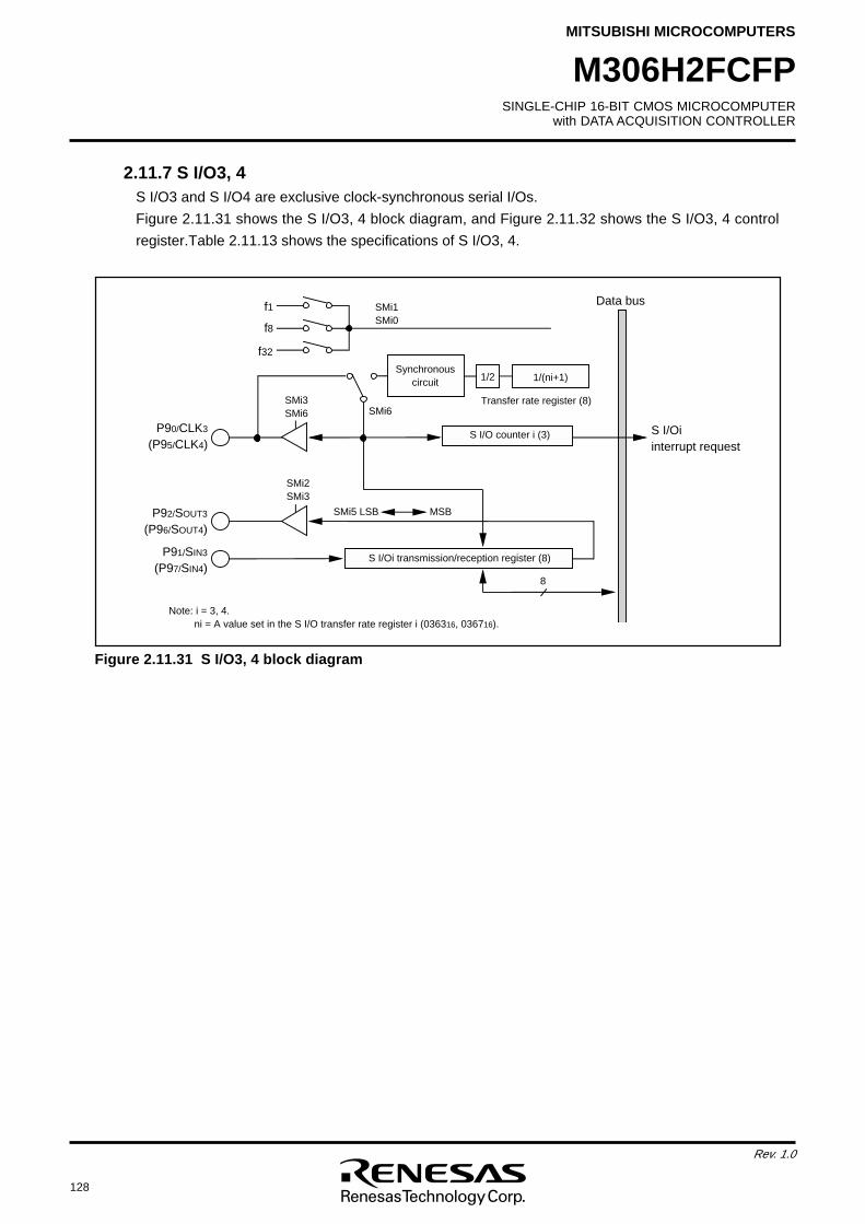
128
Rev. 1.0
SINGLE-CHIP 16-BIT CMOS MICROCOMPUTERwith DATA ACQUISITION CONTROLLER
MITSUBISHI MICROCOMPUTERS
M306H2FCFP
S I/Oi transmission/reception register (8)
S I/O counter i (3)
Synchronous circuit
f1
f8
f32
Data bus
8
S I/Oi interrupt request
SMi5 LSB MSB
SMi2SMi3
SMi3SMi6
SMi1SMi0
P90/CLK3
(P95/CLK4)
P92/SOUT3
(P96/SOUT4)
P91/SIN3
(P97/SIN4)
Transfer rate register (8)SMi6
Note: i = 3, 4. ni = A value set in the S I/O transfer rate register i (036316, 036716).
1/(ni+1)1/2
2.11.7 S I/O3, 4S I/O3 and S I/O4 are exclusive clock-synchronous serial I/Os.
Figure 2.11.31 shows the S I/O3, 4 block diagram, and Figure 2.11.32 shows the S I/O3, 4 control
register.Table 2.11.13 shows the specifications of S I/O3, 4.
Figure 2.11.31 S I/O3, 4 block diagram
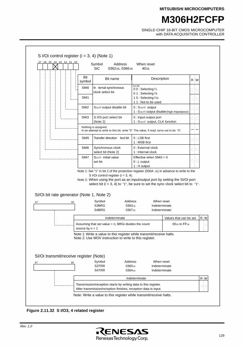
SINGLE-CHIP 16-BIT CMOS MICROCOMPUTERwith DATA ACQUISITION CONTROLLER
MITSUBISHI MICROCOMPUTERS
129
Rev. 1.0
M306H2FCFP
SI/Oi bit rate generator (Note 1, Note 2)
b7 b0 Symbol Address When reset S3BRG 036316 Indeterminate S4BRG 036716 Indeterminate
Indeterminate
Assuming that set value = n, BRGi divides the count source by n + 1
0016 to FF16
Values that can be set WR
SI/Oi transmit/receive register (Note)b7 b0 Symbol Address When reset
S3TRR 036016 Indeterminate S4TRR 036416 Indeterminate
Indeterminate
Transmission/reception starts by writing data to this register.After transmission/reception finishes, reception data is input.
WR
S I/Oi control register (i = 3, 4) (Note 1)
Symbol Address When reset SiC 036216, 036616 4016
b7 b6 b5 b4 b3 b2 b1 b0
WRDescription
SMi5
SMi1
SMi0
SMi3
SMi6
SMi7
In ternal synchronous clock select bit
Transfer direction lect bit
S I/Oi port select bit(Note 2)
SOUTi initial value set bit
0 0 : Selecting f 1 0 1 : Selecting f 8 1 0 : Selecting f 32
1 1 : Not to be used
b1 b0
0 : External clock 1 : Internal clock
Effective when SMi3 = 00 : L output 1 : H output
0 : Input-output port 1 : SOUTi output, CLK function
Bit nameBit symbol
Synchronous clock select bit (Note 2)
0 : LSB first 1 : MSB first
SMi2 SOUTi output disable bit 0 : SOUTi output 1 : SOUTi output disable(high impedance)
Note 1: Set "1" in bit 2 of the protection register (000A 16) in advance to write to the S I/Oi control register (i = 3, 4).Note 2: When using the port as an input/output port by setting the SI/Oi port select bit (i = 3, 4) to "1", be sure to set the sync clock select bit to "1".
Nothing is assigned.In an attempt to write to this bit, write “0”. The value, if read, turns out to be “0”.
Note 1: Write a value to this register while transmit/receive halts.Note 2: Use MOV instruction to write to this register.
Note: Write a value to this register while transmit/receive halts.
Figure 2.11.32 S I/O3, 4 related register
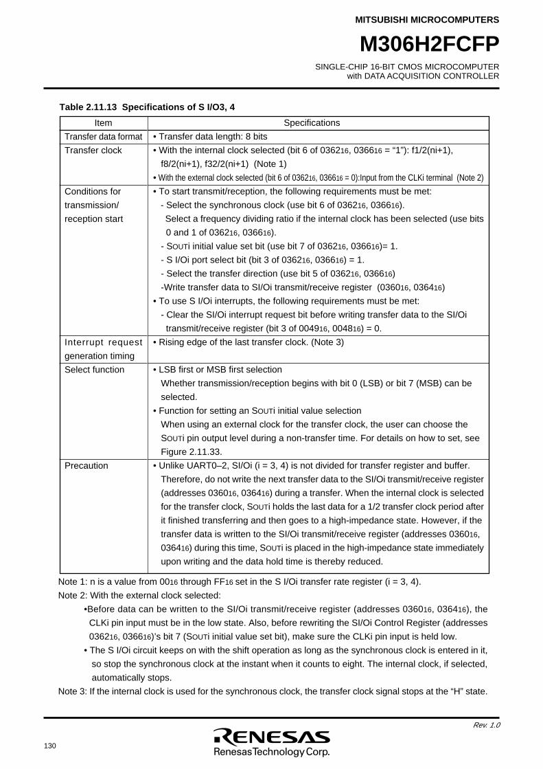
130
Rev. 1.0
SINGLE-CHIP 16-BIT CMOS MICROCOMPUTERwith DATA ACQUISITION CONTROLLER
MITSUBISHI MICROCOMPUTERS
M306H2FCFP
Table 2.11.13 Specifications of S I/O3, 4
Note 1: n is a value from 0016 through FF16 set in the S I/Oi transfer rate register (i = 3, 4).
Note 2: With the external clock selected:
•Before data can be written to the SI/Oi transmit/receive register (addresses 036016, 036416), the
CLKi pin input must be in the low state. Also, before rewriting the SI/Oi Control Register (addresses
036216, 036616)’s bit 7 (SOUTi initial value set bit), make sure the CLKi pin input is held low.
• The S I/Oi circuit keeps on with the shift operation as long as the synchronous clock is entered in it,
so stop the synchronous clock at the instant when it counts to eight. The internal clock, if selected,
automatically stops.
Note 3: If the internal clock is used for the synchronous clock, the transfer clock signal stops at the “H” state.
Item
Transfer data format
Transfer clock
Conditions for
transmission/
reception start
Interrupt request
generation timing
Select function
Precaution
Specifications
• Transfer data length: 8 bits
• With the internal clock selected (bit 6 of 036216, 036616 = “1”): f1/2(ni+1),
f8/2(ni+1), f32/2(ni+1) (Note 1)
• With the external clock selected (bit 6 of 036216, 036616 = 0):Input from the CLKi terminal (Note 2)
• To start transmit/reception, the following requirements must be met:
- Select the synchronous clock (use bit 6 of 036216, 036616).
Select a frequency dividing ratio if the internal clock has been selected (use bits
0 and 1 of 036216, 036616).
- SOUTi initial value set bit (use bit 7 of 036216, 036616)= 1.
- S I/Oi port select bit (bit 3 of 036216, 036616) = 1.
- Select the transfer direction (use bit 5 of 036216, 036616)
-Write transfer data to SI/Oi transmit/receive register (036016, 036416)
• To use S I/Oi interrupts, the following requirements must be met:
- Clear the SI/Oi interrupt request bit before writing transfer data to the SI/Oi
transmit/receive register (bit 3 of 004916, 004816) = 0.
• Rising edge of the last transfer clock. (Note 3)
• LSB first or MSB first selection
Whether transmission/reception begins with bit 0 (LSB) or bit 7 (MSB) can be
selected.
• Function for setting an SOUTi initial value selection
When using an external clock for the transfer clock, the user can choose the
SOUTi pin output level during a non-transfer time. For details on how to set, see
Figure 2.11.33.
• Unlike UART0–2, SI/Oi (i = 3, 4) is not divided for transfer register and buffer.
Therefore, do not write the next transfer data to the SI/Oi transmit/receive register
(addresses 036016, 036416) during a transfer. When the internal clock is selected
for the transfer clock, SOUTi holds the last data for a 1/2 transfer clock period after
it finished transferring and then goes to a high-impedance state. However, if the
transfer data is written to the SI/Oi transmit/receive register (addresses 036016,
036416) during this time, SOUTi is placed in the high-impedance state immediately
upon writing and the data hold time is thereby reduced.
SINGLE-CHIP 16-BIT CMOS MICROCOMPUTERwith DATA ACQUISITION CONTROLLER
MITSUBISHI MICROCOMPUTERS
131
Rev. 1.0
M306H2FCFP
(1) Functions for setting an SOUTi initial value
When using an external clock for the transfer clock, the SOUTi pin output level during a non-transfer
time can be set to the high or the low state. Figure 2.11.33 shows the timing chart for setting an SOUTi
initial value and how to set it.
Figure 2.11.33 Timing chart for setting SOUTi’s initial value and how to set it
(2) S I/Oi operation timing
Figure 2.11.34 shows the S I/Oi operation timing
D7D0 D1 D2 D3 D4 D5 D6
(i= 3, 4)
(i= 3, 4)Hiz Hiz
(i= 3, 4)
1.5 cycle (max)
SI/Oi internal clock
Transfer clock (Note 1)
Signal written to the S I/Oi register
S I/Oi output SOUTi
S I/Oi input SINi
SI/Oi interrupt request bit
Note2
Note 1: With the internal clock selected for the transfer clock, the frequency dividing ratio can be selected using bits 0 and 1 of the S I/Oi control register. (i=3,4) (No frequency division, 8-division frequency, 32-division frequency.)
Note 2: With the internal clock selected for the transfer clock, the SOUTi pin becomes to the high-impedance state after the transfer finishes.Note 3: Shown above is the case where the SOUTi (i = 3, 4) port select bit ="1".
"H""L"
"H""L"
"H""L"
"H""L"
"H""L"
"1""0"
Figure 22.11.34 S I/Oi operation timing chart
S I/Oi port select bit SMi3 = 0
SOUTi initial value select bitSMi7 = 1
(SOUTi: Internal “H” level)
S I/Oi port select bitSMi3 = 0 1
(Port select: Normal port SOUTi)
SOUTi terminal = “H” output
Signal written to the S I/Oi register =“L” “H” “L”
(Falling edge)
SOUTi terminal = Outputting stored data in the S I/Oi transmission/
reception register
Signal written to the S I/Oi transmission/reception
register
SOUTi (internal)
SOUTi's initial value set bit (SMi7)
SOUTi terminal output
S I/Oi port select bit (SMi3)
Setting the SOUTi initial value to H
Port selection (normal port SOUTi)
D0
(i = 3, 4)
Initial value = “H” (Note)
Port output D0
(Example) With “H” selected for SOUTi:
Note: The set value is output only when the external clock has been selected. When initializing SOUTi, make sure the CLKi pin input is held “L” level.If the internal clock has been selected or if SOUT output disable has been set, this output goes to the high-impedance state.

132
Rev. 1.0
SINGLE-CHIP 16-BIT CMOS MICROCOMPUTERwith DATA ACQUISITION CONTROLLER
MITSUBISHI MICROCOMPUTERS
M306H2FCFP
2.12 A-D ConverterThe A-D converter consists of one 8-bit successive approximation A-D converter circuit with a capacitive
coupling amplifier. Pins P100 to P107, P95, and P96 also function as the analog signal input pins. The
direction registers of these pins for A-D conversion must therefore be set to input. The Vref connect bit (bit
5 at address 03D716) can be used to isolate the resistance ladder of the A-D converter from the reference
voltage input pin (VREF) when the A-D converter is not used. Doing so stops any current flowing into the
resistance ladder from VREF, reducing the power dissipation. When using the A-D converter, start A-D
conversion only after setting bit 5 of 03D716 to connect VREF.
The result of A-D conversion is stored in the A-D registers of the selected pins.
Table 2.12.1 shows the performance of the A-D converter. Figure 2.12.1 shows the block diagram of the
A-D converter, and Figures 2.12.2 and 2.12.3 show the A-D converter-related registers.
Note 1: Does not depend on use of sample and hold function.
Note 2: Without sample and hold function, set the φAD frequency to 250kHZ min.
With the sample and hold function, set the φAD frequency to 1MHZ min.
Item PerformanceMethod of A-D conversion Successive approximation (capacitive coupling amplifier)Analog input voltage (Note 1) 0V to AVCC (VCC)Operating clock φ AD (Note 2) fAD/divide-by-2 of fAD/divide-by-4 of fAD, fAD=f(XIN)Resolution 8-bitAbsolute precision Without sample and hold function
±3LSB With sample and hold function
±2LSBOperating modes One-shot mode, repeat mode, single sweep mode, repeat sweep mode 0,
and repeat sweep mode 1Analog input pins 8 pins (AN0 to AN7) + 2pins (ANEX0 and ANEX1)A-D conversion start condition Software trigger
A-D conversion starts when the A-D conversion start flag changes to “1” External trigger (can be retriggered)
A-D conversion starts when the A-D conversion start flag is “1” and the__________
ADTRG/P97 input changes from “H” to “L”Conversion speed per pin Without sample and hold function
49 φ AD cycles With sample and hold function
28 φ AD cycles
Table 2.12.1 Performance of A-D converter
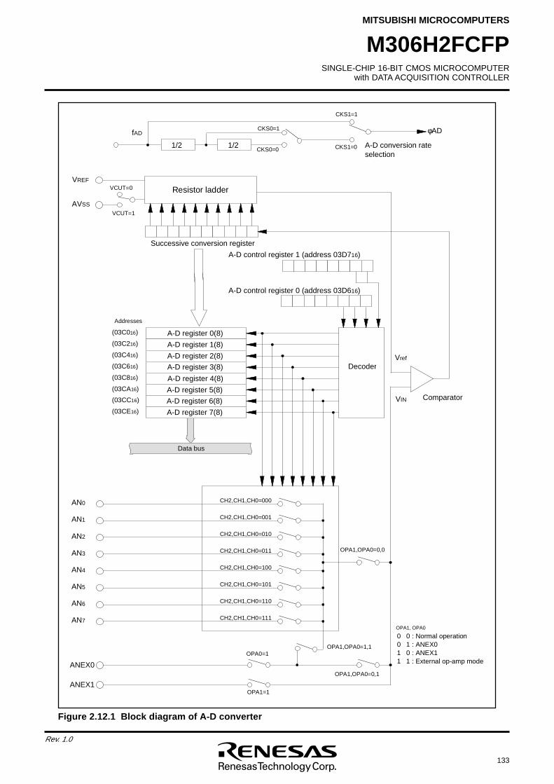
SINGLE-CHIP 16-BIT CMOS MICROCOMPUTERwith DATA ACQUISITION CONTROLLER
MITSUBISHI MICROCOMPUTERS
133
Rev. 1.0
M306H2FCFP
1 /
2 1
/
2
fA
D
A
-
D
c
o
n
v
e
r
s
i
o
n
r
a
t
e
s
e
l
e
c
t
i
o
n
(0
3
C
01
6)
( 0
3
C
21
6)
( 0
3
C
41
6)
( 0
3
C
61
6)
( 0
3
C
81
6)
( 0
3
C
A1
6)
( 0
3
C
C1
6)
( 0
3
C
E1
6)
C
K
S
1
=
1
C
K
S
0
=
0
0
0
:
N
o
r
m
a
l
o
p
e
r
a
t
i
o
n0
1
:
A
N
E
X
01
0
:
A
N
E
X
11
1
:
E
x
t
e
r
n
a
l
o
p
-
a
m
p
m
o
d
e
A
-
D
r
e
g
i
s
t
e
r
0
(
8
)
A
-
D
r
e
g
i
s
t
e
r
1
(
8
)
A
-
D
r
e
g
i
s
t
e
r
2
(
8
)
A
-
D
r
e
g
i
s
t
e
r
3
(
8
)
A
-
D
r
e
g
i
s
t
e
r
4
(
8
)
A
-
D
r
e
g
i
s
t
e
r
5
(
8
)
A
-
D
r
e
g
i
s
t
e
r
6
(
8
)
A
-
D
r
e
g
i
s
t
e
r
7
(
8
)
R
e
s
i
s
t
o
r
l
a
d
d
e
r
A
N
E
X
1
A
N
E
X
0
S
u
c
c
e
s
s
i
v
e
c
o
n
v
e
r
s
i
o
n
r
e
g
i
s
t
e
r
O
P
A
1
,
O
P
A
0
=
0
,
1
O
P
A
0
=
1
O
P
A
1
=
1
O
P
A
1
,
O
P
A
0
=
1
,
1
A
N0
A
N1
A
N2
A
N3
A
N5
A
N6
A
N7
A
-
D
c
o
n
t
r
o
l
r
e
g
i
s
t
e
r
0
(
a
d
d
r
e
s
s
0
3
D
61
6)
A
-
D
c
o
n
t
r
o
l
r
e
g
i
s
t
e
r
1
(
a
d
d
r
e
s
s
0
3
D
71
6)
Vr
e
f
VI
N
D
a
t
a
b
u
s
VR
E
F
A
N4
O
P
A
1
,
O
P
A
0
=
0
,
0
V
C
U
T
=
0
A
VS
S
V
C
U
T
=
1
C
K
S
0
=
1
C
K
S
1
=
0
C
H
2
,
C
H
1
,
C
H
0
=
0
0
0
C
H
2
,
C
H
1
,
C
H
0
=
0
0
1
C
H
2
,
C
H
1
,
C
H
0
=
0
1
0
C
H
2
,
C
H
1
,
C
H
0
=
0
1
1
C
H
2
,
C
H
1
,
C
H
0
=
1
0
0
C
H
2
,
C
H
1
,
C
H
0
=
1
0
1
C
H
2
,
C
H
1
,
C
H
0
=
1
1
0
C
H
2
,
C
H
1
,
C
H
0
=
1
1
1
D
e
c
o
d
e
r
C
o
m
p
a
r
a
t
o
r
O
P
A
1
,
O
P
A
0
A
d
d
r
e
s
s
e
s
φA
D
Figure 2.12.1 Block diagram of A-D converter
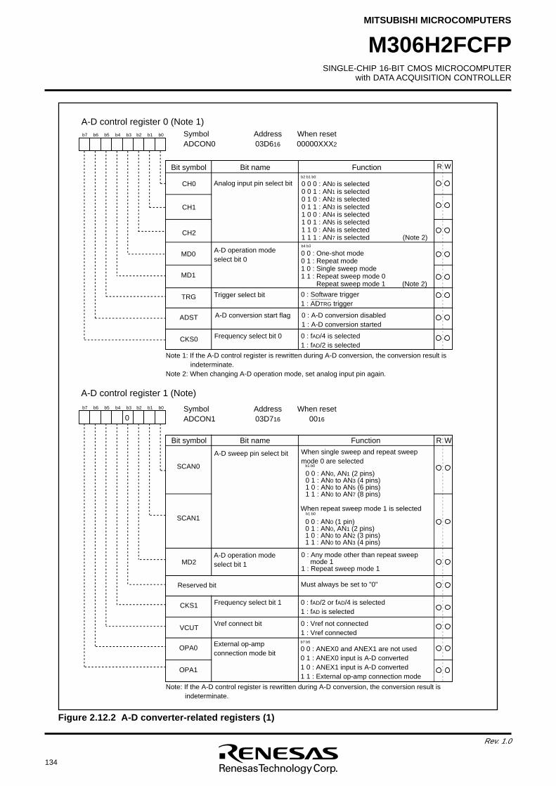
134
Rev. 1.0
SINGLE-CHIP 16-BIT CMOS MICROCOMPUTERwith DATA ACQUISITION CONTROLLER
MITSUBISHI MICROCOMPUTERS
M306H2FCFP
A-D control register 0 (Note 1)Symbol Address When resetADCON0 03D616 00000XXX2
b7 b6 b5 b4 b3 b2 b1 b0
Analog input pin select bit 0 0 0 : AN0 is selected0 0 1 : AN1 is selected0 1 0 : AN2 is selected0 1 1 : AN3 is selected1 0 0 : AN4 is selected1 0 1 : AN5 is selected1 1 0 : AN6 is selected1 1 1 : AN7 is selected (Note 2)
CH0
Bit symbol Bit name Function
CH1
CH2
A-D operation mode select bit 0
0 0 : One-shot mode0 1 : Repeat mode1 0 : Single sweep mode1 1 : Repeat sweep mode 0
Repeat sweep mode 1 (Note 2)
MD0
MD1
Trigger select bit 0 : Software trigger1 : ADTRG trigger
TRG
ADST A-D conversion start flag 0 : A-D conversion disabled1 : A-D conversion started
Frequency select bit 0 0 : fAD/4 is selected1 : fAD/2 is selected
CKS0
WR
A-D control register 1 (Note)
Symbol Address When resetADCON1 03D716 0016
Bit name FunctionBit symbol
b7 b6 b5 b4 b3 b2 b1 b0
A-D sweep pin select bit
SCAN0
SCAN1
MD2
Reserved bit Must always be set to "0"
VCUT
OPA0
Vref connect bit
OPA1
A-D operation mode select bit 1
0 : Any mode other than repeat sweep mode 1
1 : Repeat sweep mode 1
0 : Vref not connected1 : Vref connected
External op-amp connection mode bit
WR
b2 b1 b0
b4 b3
When single sweep and repeat sweep mode 0 are selected
0 0 : AN0, AN1 (2 pins)0 1 : AN0 to AN3 (4 pins)1 0 : AN0 to AN5 (6 pins)1 1 : AN0 to AN7 (8 pins)
b1 b0
When repeat sweep mode 1 is selected
0 0 : AN0 (1 pin)0 1 : AN0, AN1 (2 pins)1 0 : AN0 to AN2 (3 pins)1 1 : AN0 to AN3 (4 pins)
b1 b0
0 0 : ANEX0 and ANEX1 are not used0 1 : ANEX0 input is A-D converted1 0 : ANEX1 input is A-D converted1 1 : External op-amp connection mode
b7 b6
Note 1: If the A-D control register is rewritten during A-D conversion, the conversion result is indeterminate.
Note 2: When changing A-D operation mode, set analog input pin again.
Frequency select bit 1 0 : fAD/2 or fAD/4 is selected 1 : fAD is selected
CKS1
Note: If the A-D control register is rewritten during A-D conversion, the conversion result is indeterminate.
AAAAAA
AAA
AAAAAA
AAAAAAAAA
AAAAAA
AAA
AAAAAA
AAAAAAAAAAAAAAA
AAAAAA
0
Figure 2.12.2 A-D converter-related registers (1)
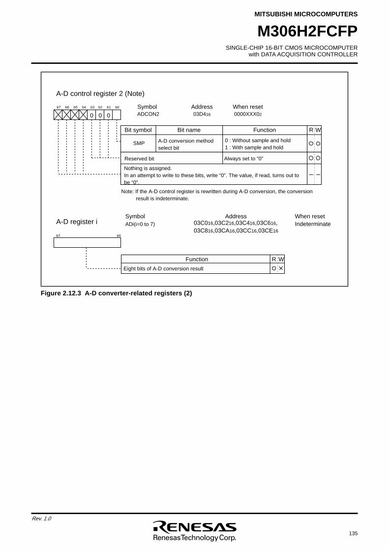
SINGLE-CHIP 16-BIT CMOS MICROCOMPUTERwith DATA ACQUISITION CONTROLLER
MITSUBISHI MICROCOMPUTERS
135
Rev. 1.0
M306H2FCFP
Figure 2.12.3 A-D converter-related registers (2)
A-D control register 2 (Note)
Symbol Address When resetADCON2 03D416 0000XXX02
b7 b6 b5 b4 b3 b2 b1 b0
A-D conversion method select bit
0 : Without sample and hold1 : With sample and hold
Bit symbol Bit name Function R W
Note: If the A-D control register is rewritten during A-D conversion, the conversionresult is indeterminate.
AA
Nothing is assigned.In an attempt to write to these bits, write “0”. The value, if read, turns out to be “0”.
Symbol Address When resetADi(i=0 to 7) IndeterminateA-D register i
b7 b0
Eight bits of A-D conversion result
Function R W
AAAA
SMP
Reserved bit Always set to “0” AA
0 0 0
03C016,03C216,03C416,03C616,03C816,03CA16,03CC16,03CE16
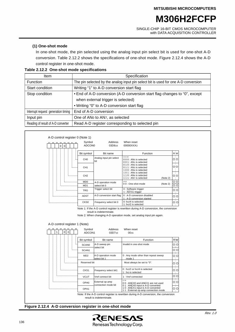
136
Rev. 1.0
SINGLE-CHIP 16-BIT CMOS MICROCOMPUTERwith DATA ACQUISITION CONTROLLER
MITSUBISHI MICROCOMPUTERS
M306H2FCFP
Figure 2.12.4 A-D conversion register in one-shot mode
(1) One-shot mode
In one-shot mode, the pin selected using the analog input pin select bit is used for one-shot A-D
conversion. Table 2.12.2 shows the specifications of one-shot mode. Figure 2.12.4 shows the A-D
control register in one-shot mode.
Table 2.12.2 One-shot mode specifications
Item Specification
Function The pin selected by the analog input pin select bit is used for one A-D conversion
Start condition Writing “1” to A-D conversion start flag
Stop condition • End of A-D conversion (A-D conversion start flag changes to “0”, except
when external trigger is selected)
• Writing “0” to A-D conversion start flag
Interrupt request generation timing End of A-D conversion
Input pin One of AN0 to AN7, as selected
Reading of result of A-D converter Read A-D register corresponding to selected pin
A-D control register 0 (Note 1)Symbol Address When resetADCON0 03D616 00000XXX2
b7 b6 b5 b4 b3 b2 b1 b0
Analog input pin select bit
Bit symbol Bit name Function
CH1
CH2
A-D operation mode select bit 0
MD0
MD1
Trigger select bit 0 : Software trigger1 : ADTRG trigger
TRG
ADST A-D conversion start flag 0 : A-D conversion disabled1 : A-D conversion started
Frequency select bit 0 0: fAD/4 is selected1: fAD/2 is selected
CKS0
WR
00
A-D control register 1 (Note)
Symbol Address When resetADCON1 03D716 0016
Bit name FunctionBit symbol
b7 b6 b5 b4 b3 b2 b1 b0
A-D sweep pin select bit
SCAN0
SCAN1
MD2
Reserved bit Must always be set to "0".
VCUT
OPA0
Vref connect bit
OPA1
A-D operation mode select bit 1
0 : Any mode other than repeat sweep mode 1
1 : Vref connected
External op-amp connection mode bit
0 0 : ANEX0 and ANEX1 are not used0 1 : ANEX0 input is A-D converted1 0 : ANEX1 input is A-D converted1 1 : External op-amp connection mode
WR
Invalid in one-shot mode
0
0 0 0 : AN0 is selected0 0 1 : AN1 is selected0 1 0 : AN2 is selected0 1 1 : AN3 is selected1 0 0 : AN4 is selected1 0 1 : AN5 is selected1 1 0 : AN6 is selected1 1 1 : AN7 is selected (Note 2)
b2 b1 b0
0 0 : One-shot mode (Note 2)b4 b3
CH0
b7 b6
1
Note 1: If the A-D control register is rewritten during A-D conversion, the conversionresult is indeterminate.
Note 2: When changing A-D operation mode, set analog input pin again.
Frequency select bit1 0 : fAD/2 or fAD/4 is selected 1 : fAD is selected
CKS1
Note: If the A-D control register is rewritten during A-D conversion, the conversion result is indeterminate.
AAAAAAAAAAAAAAAA
AAAAAAAAAAAAAAAA
0
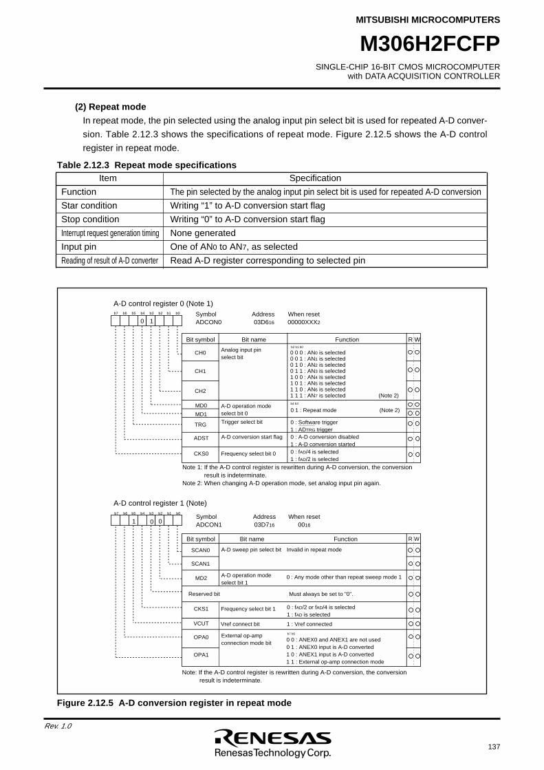
SINGLE-CHIP 16-BIT CMOS MICROCOMPUTERwith DATA ACQUISITION CONTROLLER
MITSUBISHI MICROCOMPUTERS
137
Rev. 1.0
M306H2FCFP
(2) Repeat mode
In repeat mode, the pin selected using the analog input pin select bit is used for repeated A-D conver-
sion. Table 2.12.3 shows the specifications of repeat mode. Figure 2.12.5 shows the A-D control
register in repeat mode.
Table 2.12.3 Repeat mode specificationsItem Specification
Function The pin selected by the analog input pin select bit is used for repeated A-D conversion
Star condition Writing “1” to A-D conversion start flag
Stop condition Writing “0” to A-D conversion start flag
Interrupt request generation timing None generated
Input pin One of AN0 to AN7, as selected
Reading of result of A-D converter Read A-D register corresponding to selected pin
Figure 2.12.5 A-D conversion register in repeat mode
A-D control register 0 (Note 1)Symbol Address When resetADCON0 03D616 00000XXX2
b7 b6 b5 b4 b3 b2 b1 b0
Analog input pin select bit
CH0
Bit symbol Bit name Function
CH1
CH2
A-D operation mode select bit 0
MD0
MD1Trigger select bit 0 : Software trigger
1 : ADTRG triggerTRG
ADST A-D conversion start flag 0 : A-D conversion disabled1 : A-D conversion started
Frequency select bit 0 0 : fAD/4 is selected1 : fAD/2 is selected
CKS0
WR
A-D control register 1 (Note)
Symbol Address When resetADCON1 03D716 0016
Bit name FunctionBit symbol
b7 b6 b5 b4 b3 b2 b1 b0
A-D sweep pin select bitSCAN0
SCAN1
MD2
VCUT
OPA0
Vref connect bit
OPA1
A-D operation mode select bit 1
1 : Vref connected
External op-amp connection mode bit
WR
0 1
Invalid in repeat mode
0
0 0 0 : AN0 is selected0 0 1 : AN1 is selected0 1 0 : AN2 is selected0 1 1 : AN3 is selected1 0 0 : AN4 is selected1 0 1 : AN5 is selected1 1 0 : AN6 is selected1 1 1 : AN7 is selected (Note 2)
b2 b1 b0
0 1 : Repeat mode (Note 2)b4 b3
0 0 : ANEX0 and ANEX1 are not used0 1 : ANEX0 input is A-D converted1 0 : ANEX1 input is A-D converted1 1 : External op-amp connection mode
b7 b6
1
Note 1: If the A-D control register is rewritten during A-D conversion, the conversion result is indeterminate.
Note 2: When changing A-D operation mode, set analog input pin again.
Frequency select bit 1 0 : fAD/2 or fAD/4 is selected 1 : fAD is selected
CKS1
0 : Any mode other than repeat sweep mode 1
Note: If the A-D control register is rewritten during A-D conversion, the conversion result is indeterminate.
AAAAAAAAAAAAAAAAAAAAAAAA
AAAAAAAAAAAAAAAAAAAAAAAA
Reserved bit Must always be set to "0".
0
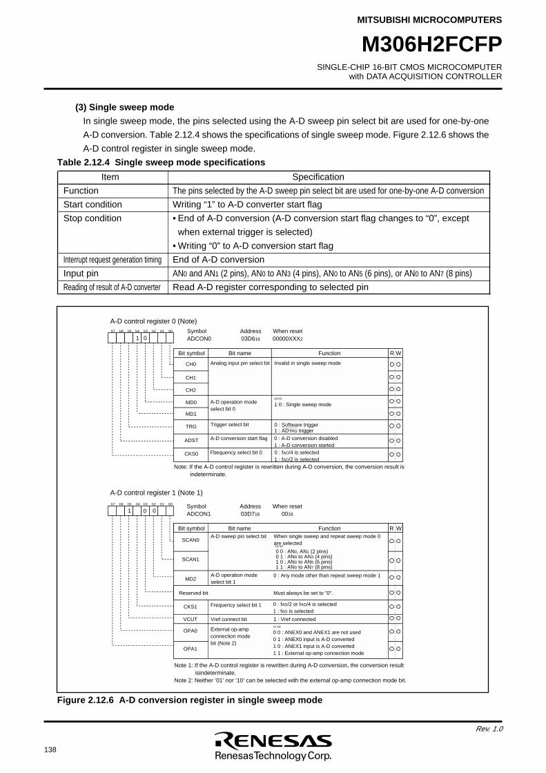
138
Rev. 1.0
SINGLE-CHIP 16-BIT CMOS MICROCOMPUTERwith DATA ACQUISITION CONTROLLER
MITSUBISHI MICROCOMPUTERS
M306H2FCFP
(3) Single sweep mode
In single sweep mode, the pins selected using the A-D sweep pin select bit are used for one-by-one
A-D conversion. Table 2.12.4 shows the specifications of single sweep mode. Figure 2.12.6 shows the
A-D control register in single sweep mode.
Table 2.12.4 Single sweep mode specifications
Figure 2.12.6 A-D conversion register in single sweep mode
Item Specification
Function The pins selected by the A-D sweep pin select bit are used for one-by-one A-D conversion
Start condition Writing “1” to A-D converter start flag
Stop condition • End of A-D conversion (A-D conversion start flag changes to “0”, except
when external trigger is selected)
• Writing “0” to A-D conversion start flag
Interrupt request generation timing End of A-D conversion
Input pin AN0 and AN1 (2 pins), AN0 to AN3 (4 pins), AN0 to AN5 (6 pins), or AN0 to AN7 (8 pins)
Reading of result of A-D converter Read A-D register corresponding to selected pin
A-D control register 0 (Note)Symbol Address When resetADCON0 03D616 00000XXX2
b7 b6 b5 b4 b3 b2 b1 b0
Analog input pin select bitCH0
Bit symbol Bit name Function
CH1
CH2
A-D operation mode select bit 0
1 0 : Single sweep modeMD0
MD1
Trigger select bit 0 : Software trigger1 : ADTRG trigger
TRG
ADST A-D conversion start flag 0 : A-D conversion disabled1 : A-D conversion started
Fbequency select bit 0 0 : fAD/4 is selected1 : fAD/2 is selected
CKS0
WR
A-D control register 1 (Note 1)
Symbol Address When resetADCON1 03D716 0016
Bit name FunctionBit symbol
b7 b6 b5 b4 b3 b2 b1 b0
A-D sweep pin select bitSCAN0
SCAN1
MD2
Reserved bit Must always be set to "0".
VCUT
OPA0
Vref connect bit
0 : Any mode other than repeat sweep mode 1
OPA1
A-D operation mode select bit 1
1 : Vref connected
External op-amp connection mode bit (Note 2)
WR
1 0
Invalid in single sweep mode
0
Note 1: If the A-D control register is rewritten during A-D conversion, the conversion result isindeterminate.Note 2: Neither ‘01’ nor ‘10’ can be selected with the external op-amp connection mode bit.
b4 b3
When single sweep and repeat sweep mode 0 are selected
0 0 : AN0, AN1 (2 pins)0 1 : AN0 to AN3 (4 pins)1 0 : AN0 to AN5 (6 pins)1 1 : AN0 to AN7 (8 pins)
b1 b0
0 0 : ANEX0 and ANEX1 are not used0 1 : ANEX0 input is A-D converted1 0 : ANEX1 input is A-D converted1 1 : External op-amp connection mode
b7 b6
1
Note: If the A-D control register is rewritten during A-D conversion, the conversion result is indeterminate.
Frequency select bit 1 0 : fAD/2 or fAD/4 is selected 1 : fAD is selected
CKS1
AAAAAAAAAAAAAAAAAA
AAAA
AAAA
AAAAAAAA
AAAA
AA
0
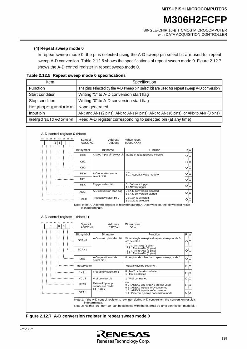
SINGLE-CHIP 16-BIT CMOS MICROCOMPUTERwith DATA ACQUISITION CONTROLLER
MITSUBISHI MICROCOMPUTERS
139
Rev. 1.0
M306H2FCFP
Figure 2.12.7 A-D conversion register in repeat sweep mode 0
Item Specification
Function The pins selected by the A-D sweep pin select bit are used for repeat sweep A-D conversion
Start condition Writing “1” to A-D conversion start flag
Stop condition Writing “0” to A-D conversion start flag
Interrupt request generation timing None generated
Input pin AN0 and AN1 (2 pins), AN0 to AN3 (4 pins), AN0 to AN5 (6 pins), or AN0 to AN7 (8 pins)
Reading of result of A-D converter Read A-D register corresponding to selected pin (at any time)
Table 2.12.5 Repeat sweep mode 0 specifications
(4) Repeat sweep mode 0
In repeat sweep mode 0, the pins selected using the A-D sweep pin select bit are used for repeat
sweep A-D conversion. Table 2.12.5 shows the specifications of repeat sweep mode 0. Figure 2.12.7
shows the A-D control register in repeat sweep mode 0.
A
-
D
c
o
n
t
r
o
l
r
e
g
i
s
t
e
r
0 (
N
o
t
e
)
S
y
m
b
o
l A
d
d
r
e
s
s W
h
e
n
r
e
s
e
t A
D
C
O
N
0 0
3
D
61
6 0
0
0
0
0
X
X
X2
b 7 b
6 b5 b
4 b
3 b
2 b
1 b
0
A
n
a
l
o
g
i
n
p
u
t
p
i
n
s
e
l
e
c
t
b
i
tC
H
0
B
i
t
s
y
m
b
o
l Bit name F
u
n
c
t
i
o
n
C
H
1
C
H
2
A
-
D
o
p
e
r
a
t
i
o
n
m
o
d
e
s
e
l
e
c
t
b
i
t
01 1 : Repeat sweep mode 0M
D
0
M
D
1
T
r
i
g
g
e
r
s
e
l
e
c
t
b
i
t 0 : Software trigger1 : ADTRG trigger
T
R
G
A
D
S
T A
-
D
c
o
n
v
e
r
s
i
o
n
s
t
a
r
t
f
l
a
g 0 : A-D conversion disabled1 : A-D conversion started
F
r
e
q
u
e
n
c
y
s
e
l
e
c
t
b
i
t
0 0 : fAD/4 is selected1 : fAD/2 is selected
C
K
S
0
WR
A
-
D
c
o
n
t
r
o
l
r
e
g
i
s
t
e
r
1
(
N
o
t
e
1
)
S
y
m
b
o
l A
d
d
r
e
s
s W
h
e
n
r
e
s
e
t A
D
C
O
N
1 0
3
D
71
6 0
01
6
B
i
t
n
a
m
e FunctionB
i
t
s
y
m
b
o
l
b 7 b
6 b5 b
4 b
3 b
2 b
1 b
0
A
-
D
s
w
e
e
p
p
i
n
s
e
l
e
c
t
b
i
tS
C
A
N
0
S
C
A
N
1
M
D
2
V
C
U
T
O
P
A
0
V
r
e
f
c
o
n
n
e
c
t
b
i
t
0
:
A
n
y
m
o
d
e
o
t
h
e
r
t
h
a
n
r
e
p
e
a
t
s
w
e
e
p
m
o
d
e
1
O
P
A
1
A
-
D
o
p
e
r
a
t
i
o
n
m
o
d
e
s
e
l
e
c
t
b
i
t
1
1
:
V
r
e
f
c
o
n
n
e
c
t
e
d
E
x
t
e
r
n
a
l
o
p
-
a
m
p
c
o
n
n
e
c
t
i
o
n
m
o
d
e
b
i
t
(
N
o
t
e
2
)
WR
1 1
Invalid in repeat sweep mode 0
0
N
o
t
e
1
:
I
f
t
h
e
A
-
D
c
o
n
t
r
o
l
r
e
g
i
s
t
e
r
i
s
r
e
w
r
i
t
t
e
n
d
u
r
i
n
g
A
-
D
c
o
n
v
e
r
s
i
o
n
,
t
h
e
c
o
n
v
e
r
s
i
o
n
r
e
s
u
l
t
i
s
i
n
d
e
t
e
r
m
i
n
a
t
e
.N
o
t
e
2
:
N
e
i
t
h
e
r
“
0
1
”
n
o
r
“
1
0
”
c
a
n
b
e
s
e
l
e
c
t
e
d
w
i
t
h
t
h
e
e
x
t
e
r
n
a
l
o
p
-
a
m
p
c
o
n
n
e
c
t
i
o
n
m
o
d
e
b
i
t
.
b4 b3
W
h
e
n
s
i
n
g
l
e
s
w
e
e
p
a
n
d
r
e
p
e
a
t
s
w
e
e
p
m
o
d
e
0
a
r
e
s
e
l
e
c
t
e
d
0
0
:
A
N0,
A
N1
(
2
p
i
n
s
)
0
1
:
A
N0
t
o
A
N3
(
4
p
i
n
s
)1
0
:
A
N0
t
o
A
N5
(
6
p
i
n
s
)1
1
:
A
N0
t
o
A
N7
(
8
p
i
n
s
)
b 1
b
0
0
0
:
A
N
E
X
0
a
n
d
A
N
E
X
1
a
r
e
n
o
t
u
s
e
d
0
1
:
A
N
E
X
0
i
n
p
u
t
i
s
A
-
D
c
o
n
v
e
r
t
e
d1
0
:
A
N
E
X
1
i
n
p
u
t
i
s
A
-
D
c
o
n
v
e
r
t
e
d1
1
:
E
x
t
e
r
n
a
l
o
p
-
a
m
p
c
o
n
n
e
c
t
i
o
n
m
o
d
e
b 7
b
6
1
N
o
t
e
:
I
f
t
h
e
A
-
D
c
o
n
t
r
o
l
r
e
g
i
s
t
e
r
i
s
r
e
w
r
i
t
t
e
n
d
u
r
i
n
g
A
-
D
c
o
n
v
e
r
s
i
o
n
,
t
h
e
c
o
n
v
e
r
s
i
o
n
r
e
s
u
l
t
i
s
i
n
d
e
t
e
r
m
i
n
a
t
e
.
F
r
e
q
u
e
n
c
y
s
e
l
e
c
t
b
i
t
1 0
:
fA
D/
2
o
r
fA
D/
4
i
s
s
e
l
e
c
t
e
d
1
:
fA
D
i
s
s
e
l
e
c
t
e
dC
K
S
1
R
e
s
e
r
v
e
d
b
i
t M
u
s
t
a
l
w
a
y
s
b
e
s
e
t
t
o
"
0
"
.
0
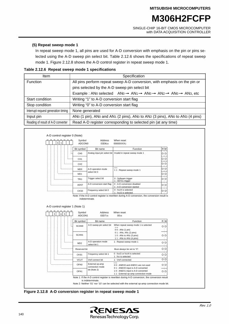
140
Rev. 1.0
SINGLE-CHIP 16-BIT CMOS MICROCOMPUTERwith DATA ACQUISITION CONTROLLER
MITSUBISHI MICROCOMPUTERS
M306H2FCFP
Figure 2.12.8 A-D conversion register in repeat sweep mode 1
(5) Repeat sweep mode 1
In repeat sweep mode 1, all pins are used for A-D conversion with emphasis on the pin or pins se-
lected using the A-D sweep pin select bit. Table 2.12.6 shows the specifications of repeat sweep
mode 1. Figure 2.12.8 shows the A-D control register in repeat sweep mode 1.
Table 2.12.6 Repeat sweep mode 1 specifications
Item Specification
Function All pins perform repeat sweep A-D conversion, with emphasis on the pin or
pins selected by the A-D sweep pin select bit
Example : AN0 selected AN0 AN1 AN0 AN2 AN0 AN3, etc
Start condition Writing “1” to A-D conversion start flag
Stop condition Writing “0” to A-D conversion start flag
Interrupt request generation timing None generated
Input pin AN0 (1 pin), AN0 and AN1 (2 pins), AN0 to AN2 (3 pins), AN0 to AN3 (4 pins)
Reading of result of A-D converter Read A-D register corresponding to selected pin (at any time)
A-D control register 0 (Note)
Symbol Address When resetADCON0 03D616 00000XXX2
b7 b6 b5 b4 b3 b2 b1 b0
Analog input pin select bitCH0
Bit symbol Bit name Function
CH1
CH2
A-D operation mode select bit 0
1 1 : Repeat sweep mode 1MD0
MD1
Trigger select bit 0 : Software trigger1 : ADTRG trigger
TRG
ADST A-D conversion start flag 0 : A-D conversion disabled1 : A-D conversion started
Frequency select bit 0 0 : fAD/4 is selected1 : fAD/2 is selected
CKS0
WR
A-D control register 1 (Note 1)
Symbol Address When resetADCON1 03D716 0016
Bit name FunctionBit symbol
b7 b6 b5 b4 b3 b2 b1 b0
A-D sweep pin select bitSCAN0
SCAN1
MD2
VCUT
OPA0
Vref connect bit
1 : Repeat sweep mode 1
OPA1
A-D operation mode select bit 1
1 : Vref connected
External op-amp connection mode bit (Note 2)
WR
1 1
Invalid in repeat sweep mode 1
1
Note 1: If the A-D control register is rewritten during A-D conversion, the conversion result is indeterminate.Note 2: Neither ‘01’ nor ‘10’ can be selected with the external op-amp connection mode bit.
b4 b3
When repeat sweep mode 1 is selected
0 0 : AN0 (1 pin)0 1 : AN0, AN1 (2 pins)1 0 : AN0 to AN2 (3 pins)1 1 : AN0 to AN3 (4 pins)
b1 b0
0 0 : ANEX0 and ANEX1 are not used0 1 : ANEX0 input is A-D converted1 0 : ANEX1 input is A-D converted1 1 : External op-amp connection mode
b7 b6
1
Note: If the A-D control register is rewritten during A-D conversion, the conversion result is indeterminate.
Frequency select bit 1 0 : fAD/2 or fAD/4 is selected 1 : fAD is selected
CKS1
AAAAAAAAAAAAAAAA
AA
AAAAAAAAAAAAAA
Reserved bit Must always be set to "0".
0
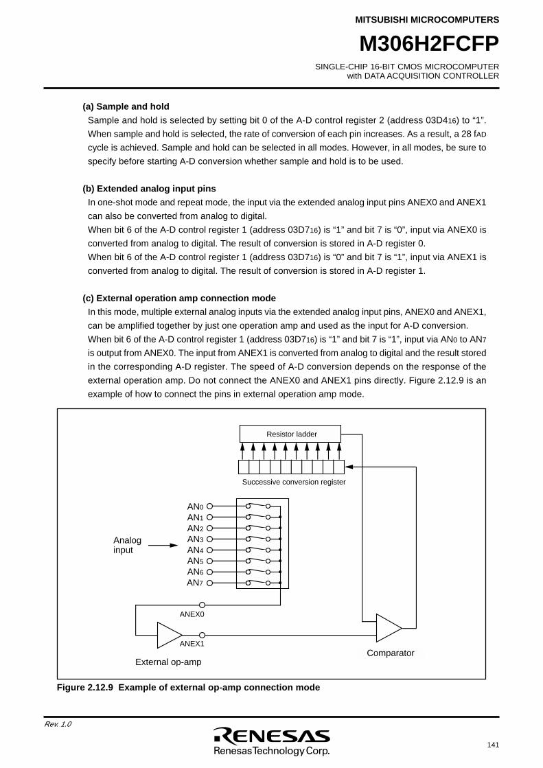
SINGLE-CHIP 16-BIT CMOS MICROCOMPUTERwith DATA ACQUISITION CONTROLLER
MITSUBISHI MICROCOMPUTERS
141
Rev. 1.0
M306H2FCFP
Analog input
External op-amp
AN0
AN7
AN1
AN2
AN3
AN4
AN5
AN6
ANEX1
ANEX0
Resistor ladder
Successive conversion register
Comparator
Figure 2.12.9 Example of external op-amp connection mode
(a) Sample and hold
Sample and hold is selected by setting bit 0 of the A-D control register 2 (address 03D416) to “1”.
When sample and hold is selected, the rate of conversion of each pin increases. As a result, a 28 fAD
cycle is achieved. Sample and hold can be selected in all modes. However, in all modes, be sure to
specify before starting A-D conversion whether sample and hold is to be used.
(b) Extended analog input pins
In one-shot mode and repeat mode, the input via the extended analog input pins ANEX0 and ANEX1
can also be converted from analog to digital.
When bit 6 of the A-D control register 1 (address 03D716) is “1” and bit 7 is “0”, input via ANEX0 is
converted from analog to digital. The result of conversion is stored in A-D register 0.
When bit 6 of the A-D control register 1 (address 03D716) is “0” and bit 7 is “1”, input via ANEX1 is
converted from analog to digital. The result of conversion is stored in A-D register 1.
(c) External operation amp connection mode
In this mode, multiple external analog inputs via the extended analog input pins, ANEX0 and ANEX1,
can be amplified together by just one operation amp and used as the input for A-D conversion.
When bit 6 of the A-D control register 1 (address 03D716) is “1” and bit 7 is “1”, input via AN0 to AN7
is output from ANEX0. The input from ANEX1 is converted from analog to digital and the result stored
in the corresponding A-D register. The speed of A-D conversion depends on the response of the
external operation amp. Do not connect the ANEX0 and ANEX1 pins directly. Figure 2.12.9 is an
example of how to connect the pins in external operation amp mode.
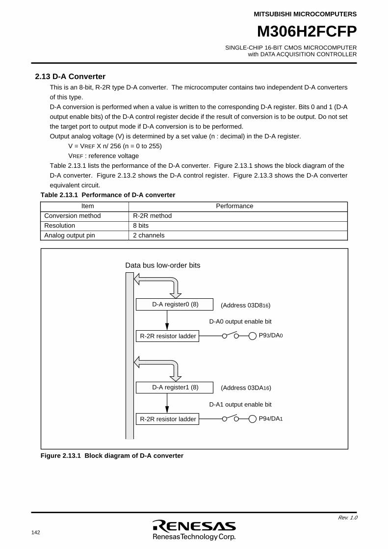
142
Rev. 1.0
SINGLE-CHIP 16-BIT CMOS MICROCOMPUTERwith DATA ACQUISITION CONTROLLER
MITSUBISHI MICROCOMPUTERS
M306H2FCFP
2.13 D-A ConverterThis is an 8-bit, R-2R type D-A converter. The microcomputer contains two independent D-A converters
of this type.
D-A conversion is performed when a value is written to the corresponding D-A register. Bits 0 and 1 (D-A
output enable bits) of the D-A control register decide if the result of conversion is to be output. Do not set
the target port to output mode if D-A conversion is to be performed.
Output analog voltage (V) is determined by a set value (n : decimal) in the D-A register.
V = VREF X n/ 256 (n = 0 to 255)
VREF : reference voltage
Table 2.13.1 lists the performance of the D-A converter. Figure 2.13.1 shows the block diagram of the
D-A converter. Figure 2.13.2 shows the D-A control register. Figure 2.13.3 shows the D-A converter
equivalent circuit.
AAAAAA
P93/DA0
AAAP94/DA1
Data bus low-order bits
D-A register0 (8)
R-2R resistor ladder
D-A0 output enable bit
D-A register1 (8)
R-2R resistor ladder
D-A1 output enable bit
(Address 03D816)
(Address 03DA16)
Figure 2.13.1 Block diagram of D-A converter
Item Performance
Conversion method R-2R method
Resolution 8 bits
Analog output pin 2 channels
Table 2.13.1 Performance of D-A converter
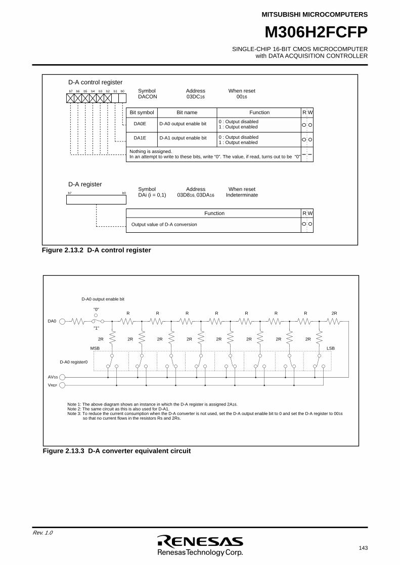
SINGLE-CHIP 16-BIT CMOS MICROCOMPUTERwith DATA ACQUISITION CONTROLLER
MITSUBISHI MICROCOMPUTERS
143
Rev. 1.0
M306H2FCFP
Figure 2.13.2 D-A control register
D-A control registerSymbol Address When resetDACON 03DC16 0016
b7 b6 b5 b4 b3 b2 b1 b0
D-A0 output enable bit DA0E
Bit symbol Bit name Function R W
0 : Output disabled1 : Output enabled
D-A1 output enable bit 0 : Output disabled1 : Output enabled
DA1E
Nothing is assigned.In an attempt to write to these bits, write “0”. The value, if read, turns out to be “0”
D-A registerSymbol Address When resetDAi (i = 0,1) 03D816, 03DA16 Indeterminate
WR
b7 b0
Function R W
Output value of D-A conversion
AAAAAA
AAAAAA
VREF
AVSS
2R
R
2R
R
2R
R
2R
R
2R
R
2R
R
2R
R
2R
2R
DA0
MSB LSB
D-A0 output enable bit
"0"
"1"
D-A0 register0
Note 1: The above diagram shows an instance in which the D-A register is assigned 2A16.Note 2: The same circuit as this is also used for D-A1.Note 3: To reduce the current consumption when the D-A converter is not used, set the D-A output enable bit to 0 and set the D-A register to 0016 so that no current flows in the resistors Rs and 2Rs.
Figure 2.13.3 D-A converter equivalent circuit
144
Rev. 1.0
SINGLE-CHIP 16-BIT CMOS MICROCOMPUTERwith DATA ACQUISITION CONTROLLER
MITSUBISHI MICROCOMPUTERS
M306H2FCFP
2.14 CRC Calculation CircuitThe Cyclic Redundancy Check (CRC) calculation circuit detects an error in data blocks. The microcom-
puter uses a generator polynomial of CRC_CCITT (X16 + X12 + X5 + 1) to generate CRC code.
The CRC code is a 16-bit code generated for a block of a given data length in multiples of 8 bits. The
CRC code is set in a CRC data register each time one byte of data is transferred to a CRC input register
after writing an initial value into the CRC data register. Generation of CRC code for one byte of data is
completed in two machine cycles.
Figure 2.14.1 shows the block diagram of the CRC circuit. Figure 2.14.2 shows the CRC-related regis-
ters. Figure 2.14.3 shows the calculation example using the CRC calculation circuit
Figure 2.14.2 CRC-related registers
Symbol Address When resetCRCD 03BD16, 03BC16 Indeterminate
b7 b0 b7 b0(b15) (b8)
CRC data register
WR
CRC calculation result output register
Function Values that can be set
000016 to FFFF16
Symbo Address When resetCRCIN 03BE16 Indeterminate
b7 b0
CRC input register
WR
Data input register
Function Values that can be set
0016 to FF16
AAA
AAA
Eight low-order bits Eight high-order bits
Data bus high-order bits
Data bus low-order bits
CRC data register (16)
CRC input register (8)
CRC code generating circuit x16 + x12 + x5 + 1
(Addresses 03BD16, 03BC16)
(Address 03BE16)
Figure 2.14.1 Block diagram of CRC circuit
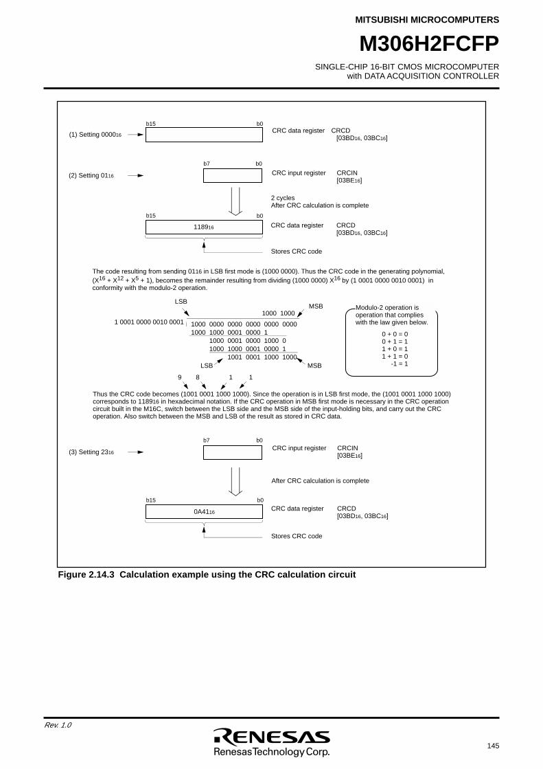
SINGLE-CHIP 16-BIT CMOS MICROCOMPUTERwith DATA ACQUISITION CONTROLLER
MITSUBISHI MICROCOMPUTERS
145
Rev. 1.0
M306H2FCFP
b15 b0
(1) Setting 000016CRC data register CRCD
[03BD16, 03BC16]
b0b7
b15 b0
(2) Setting 0116 CRC input register CRCIN[03BE16]
2 cyclesAfter CRC calculation is complete
CRC data register CRCD[03BD16, 03BC16]
118916
Stores CRC code
b0b7
b15 b0
(3) Setting 2316CRC input register CRCIN
[03BE16]
After CRC calculation is complete
CRC data register CRCD[03BD16, 03BC16]
0A4116
Stores CRC code
The code resulting from sending 0116 in LSB first mode is (1000 0000). Thus the CRC code in the generating polynomial, (X16 + X12 + X5 + 1), becomes the remainder resulting from dividing (1000 0000) X16 by (1 0001 0000 0010 0001) in conformity with the modulo-2 operation.
Thus the CRC code becomes (1001 0001 1000 1000). Since the operation is in LSB first mode, the (1001 0001 1000 1000) corresponds to 118916 in hexadecimal notation. If the CRC operation in MSB first mode is necessary in the CRC operation circuit built in the M16C, switch between the LSB side and the MSB side of the input-holding bits, and carry out the CRC operation. Also switch between the MSB and LSB of the result as stored in CRC data.
1 0001 0000 0010 0001 1000 0000 0000 0000 0000 00001000 1000 0001 0000 1 1000 0001 0000 1000 0 1000 1000 0001 0000 1 1001 0001 1000 1000
1000 1000
LSBMSB
LSB MSB
9 8 1 1
Modulo-2 operation is operation that complies with the law given below.
0 + 0 = 00 + 1 = 11 + 0 = 11 + 1 = 0 -1 = 1
Figure 2.14.3 Calculation example using the CRC calculation circuit
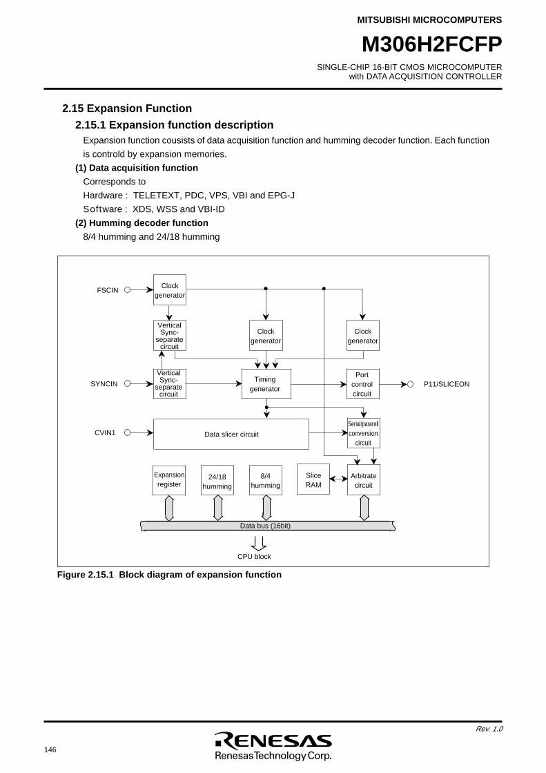
146
Rev. 1.0
SINGLE-CHIP 16-BIT CMOS MICROCOMPUTERwith DATA ACQUISITION CONTROLLER
MITSUBISHI MICROCOMPUTERS
M306H2FCFP
2.15 Expansion Function
2.15.1 Expansion function descriptionExpansion function cousists of data acquisition function and humming decoder function. Each function
is controld by expansion memories.
(1) Data acquisition function
Corresponds to
Hardware : TELETEXT, PDC, VPS, VBI and EPG-J
Software : XDS, WSS and VBI-ID
(2) Humming decoder function
8/4 humming and 24/18 humming
Figure 2.15.1 Block diagram of expansion function
F
S
C
I
N
S
Y
N
C
I
N
C
V
I
N
1
V
e
r
t
i
c
a
lS
y
n
c
-s
e
p
a
r
a
t
e c
i
r
c
u
i
t
C
l
o
c
k g
e
n
e
r
a
t
o
r
D
a
t
a
s
l
i
c
e
r
c
i
r
c
u
i
t
V
e
r
t
i
c
a
lS
y
n
c
-s
e
p
a
r
a
t
e c
i
r
c
u
i
t
C
l
o
c
k g
e
n
e
r
a
t
o
r
T
i
m
i
n
gg
e
n
e
r
a
t
o
r
S
l
i
c
eR
A
M8
/
4
h
u
m
m
i
n
g2
4
/
1
8
h
u
m
m
i
n
g
E
x
p
a
n
s
i
o
nr
e
g
i
s
t
e
rA
r
b
i
t
r
a
t
e
c
i
r
c
u
i
t
P
1
1
/
S
L
I
C
E
O
N
D
a
t
a
b
u
s
(
1
6
b
i
t
)
C
P
U
b
l
o
c
k
P
o
r
t c
o
n
t
r
o
lc
i
r
c
u
i
t
S
e
r
i
a
l
/
p
a
r
a
r
e
l
lc
o
n
v
e
r
s
i
o
nc
i
r
c
u
i
t
C
l
o
c
k g
e
n
e
r
a
t
o
r
SINGLE-CHIP 16-BIT CMOS MICROCOMPUTERwith DATA ACQUISITION CONTROLLER
MITSUBISHI MICROCOMPUTERS
147
Rev. 1.0
M306H2FCFP
2.15.2 Expansion memoryExpansion function memory is divided by 2 patterns ; Slice RAM and expansion register. (Humming
decoder operates by the register placed on SFR). Data writing and read out to the Slice RAM and the
expansion register are carried out 16 bit unit by the data setting register (addresses 020E16, 021016,
021616 and 021816) placed on SFR.
Contents of each memory and data setting register are shown in Table 2.15.1.
Table 2.15.1 Expansion memory composition
Expansion memory Contents Data setting register
Slice RAM Store acquisition data. Slice RAM address control register (020E16)Slice RAM data control register (021016)
Expansion register This register controls data acquisition Expansion register address control register (021616)Expansion register data control register (021816)
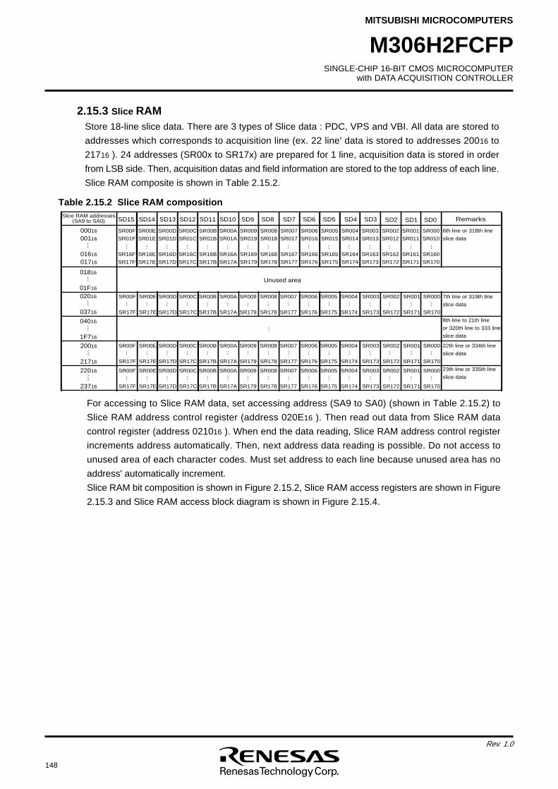
148
Rev. 1.0
SINGLE-CHIP 16-BIT CMOS MICROCOMPUTERwith DATA ACQUISITION CONTROLLER
MITSUBISHI MICROCOMPUTERS
M306H2FCFP
2.15.3 Slice RAMStore 18-line slice data. There are 3 types of Slice data : PDC, VPS and VBI. All data are stored to
addresses which corresponds to acquisition line (ex. 22 line' data is stored to addresses 20016 to
21716 ). 24 addresses (SR00x to SR17x) are prepared for 1 line, acquisition data is stored in order
from LSB side. Then, acquisition datas and field information are stored to the top address of each line.
Slice RAM composite is shown in Table 2.15.2.
Table 2.15.2 Slice RAM composition
For accessing to Slice RAM data, set accessing address (SA9 to SA0) (shown in Table 2.15.2) to
Slice RAM address control register (address 020E16 ). Then read out data from Slice RAM data
control register (address 021016 ). When end the data reading, Slice RAM address control register
increments address automatically. Then, next address data reading is possible. Do not access to
unused area of each character codes. Must set address to each line because unused area has no
address' automatically increment.
Slice RAM bit composition is shown in Figure 2.15.2, Slice RAM access registers are shown in Figure
2.15.3 and Slice RAM access block diagram is shown in Figure 2.15.4.
SR00F
SR17F
SR00E
SR17E
SR00D
SR17D
SR00C
SR17C
SR00B
SR17B
SR00A
SR17A
SR009
SR179
SR008
SR178
SR007
SR177
SR006
SR176
SR005
SR175
SR004
SR174
SR003
SR173
SR002
SR172
SR001
SR171
SR000
SR170
Slice RAM addresses(SA9 to SA0)
00016
00116
01616
01716
Remarks
...
01816
01F16
...
02016
03716
...
04016
1F716
...
20016
21716
...22016
23716
...
6th line or 318th line
slice data
SD15 SD14 SD13 SD12 SD11 SD10 SD9 SD8 SD7 SD6 SD5 SD4 SD3 SD2 SD1 SD0
SR00F
SR01F
SR16F
SR17F
SR00E
SR01E
SR16E
SR17E
SR00D
SR01D
SR16D
SR17D
SR00C
SR01C
SR16C
SR17C
SR00B
SR01B
SR16B
SR17B
SR00A
SR01A
SR16A
SR17A
SR009
SR019
SR169
SR179
SR008
SR018
SR168
SR178
SR007
SR017
SR167
SR177
SR006
SR016
SR166
SR176
SR005
SR015
SR165
SR175
SR004
SR014
SR164
SR174
SR003
SR013
SR163
SR173
SR002
SR012
SR162
SR172
SR001
SR011
SR161
SR171
SR000
SR010
SR160
SR170
Unused area
SR00F
SR17F
SR00E
SR17E
SR00D
SR17D
SR00C
SR17C
SR00B
SR17B
SR00A
SR17A
SR009
SR179
SR008
SR178
SR007
SR177
SR006
SR176
SR005
SR175
SR004
SR174
SR003
SR173
...... ... ... ... ... ... ... ... ... ... ... ... ... ... ...
SR002
SR172
SR001
SR171
SR000
SR170
SR00F
SR17F
SR00E
SR17E
SR00D
SR17D
SR00C
SR17C
SR00B
SR17B
SR00A
SR17A
SR009
SR179
SR008
SR178
SR007
SR177
SR006
SR176
SR005
SR175
SR004
SR174
SR003
SR173...... ... ... ... ... ... ... ... ... ... ... ... ... ... ...
SR002
SR172
SR001
SR171
SR000
SR170...... ... ... ... ... ... ... ... ... ... ... ... ... ... ...
7th line or 319th line
slice data
8th line to 21th line
or 320th line to 333 line
slice data
22th line or 334th line
slice data
23th line or 335th line
slice data
...... ... ... ... ... ... ... ... ... ... ... ... ... ... ......
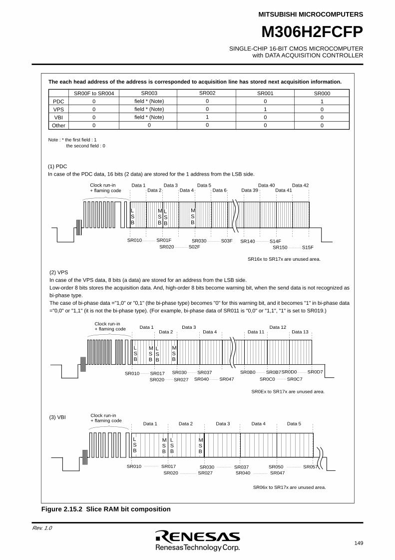
SINGLE-CHIP 16-BIT CMOS MICROCOMPUTERwith DATA ACQUISITION CONTROLLER
MITSUBISHI MICROCOMPUTERS
149
Rev. 1.0
M306H2FCFP
Figure 2.15.2 Slice RAM bit composition
(2) VPSIn case of the VPS data, 8 bits (a data) are stored for an address from the LSB side.Low-order 8 bits stores the acquisition data. And, high-order 8 bits become warning bit, when the send data is not recognized asbi-phase type.The case of bi-phase data ="1,0" or "0,1" (the bi-phase type) becomes "0" for this warning bit, and it becomes "1" in bi-phase data="0,0" or "1,1" (it is not the bi-phase type). (For example, bi-phase data of SR011 is "0,0" or "1,1", "1" is set to SR019.)
(1) PDCIn case of the PDC data, 16 bits (2 data) are stored for the 1 address from the LSB side.
PDC
VPS
VBI
Other
SR00F to SR004
0
0
0
0
SR003
field * (Note)
field * (Note)
field * (Note)
0
SR002
0
0
1
0
SR001
0
1
0
0
SR000
1
0
0
0
SR010 SR01FS
R
0
2
0
S
0
2
FS
R
0
3
0
S
0
3
F S
R
1
4
0
S
1
4
FS
R
1
5
0
S
1
5
F
LSB
MSB
LSB
MSB
LSB
MSB
S
R
1
6
x
t
o
S
R
1
7
x
a
r
e
u
n
u
s
e
d
a
r
e
a
.
C
l
o
c
k
r
u
n
-
i
n
+
f
l
a
m
i
n
g
c
o
d
eD
a
t
a
1D
a
t
a
2D
a
t
a
3D
a
t
a
4D
a
t
a
5D
a
t
a
6D
a
t
a
4
0D
a
t
a
3
9D
a
t
a
4
2D
a
t
a
4
1
Note : * the first field : 1the second field : 0
S
R
0
1
0
S
R
0
1
7S
R
0
2
0
S
R
0
2
7
S
R
0
3
0
S
R
0
3
7
S
R
0
4
0
S
R
0
4
7
S
R
0
B
0
S
R
0
B
7S
R
0
D
0
S
R
0
D
7
S
R
0
C
0
S
R
0
C
7
LSB
MSB
LSB
MSB
S
R
0
E
x
t
o
S
R
1
7
x
a
r
e
u
n
u
s
e
d
a
r
e
a
.
C
l
o
c
k
r
u
n
-
i
n
+
f
l
a
m
i
n
g
c
o
d
e D
a
t
a
1D
a
t
a
2D
a
t
a
3D
a
t
a
4D
a
t
a
1
2D
a
t
a
1
1 D
a
t
a
1
3
(3) VBI
S
R
0
1
0
S
R
0
1
7S
R
0
2
0
S
R
0
2
7S
R
0
3
0
S
R
0
3
7S
R
0
4
0
S
R
0
4
7S
R
0
5
0
S
R
0
5
7
LSB
MSB
LSB
MSB
S
R
0
6
x
t
o
S
R
1
7
x
a
r
e
u
n
u
s
e
d
a
r
e
a
.
C
l
o
c
k
r
u
n
-
i
n
+
f
l
a
m
i
n
g
c
o
d
eD
a
t
a
1 D
a
t
a
2 D
a
t
a
3 D
a
t
a
4 D
a
t
a
5
The each head address of the address is corresponded to acquisition line has stored next acquisition information.
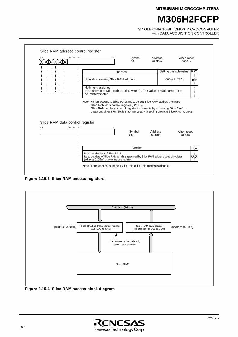
150
Rev. 1.0
SINGLE-CHIP 16-BIT CMOS MICROCOMPUTERwith DATA ACQUISITION CONTROLLER
MITSUBISHI MICROCOMPUTERS
M306H2FCFP
Figure 2.15.3 Slice RAM access registers
Figure 2.15.4 Slice RAM access block diagram
Symbol Address When resetSA 020E16 000016
S
l
i
c
e
R
A
M
a
d
d
r
e
s
s
c
o
n
t
r
o
l
r
e
g
i
s
t
e
r
F
u
n
c
t
i
o
n WRS
e
t
t
i
n
g
p
o
s
s
i
b
l
e
v
a
l
u
e
0 0
01
6
t
o
2
3
71
6S
p
e
c
i
f
y
a
c
c
e
s
s
i
n
g
S
l
i
c
e
R
A
M
a
d
d
r
e
s
s
N
o
t
h
i
n
g
i
s
a
s
s
i
g
n
e
d
.I
n
a
n
a
t
t
e
m
p
t
t
o
w
r
i
t
e
t
o
t
h
e
s
e
b
i
t
s
,
w
r
i
t
e
“
0
”
.
T
h
e
v
a
l
u
e
,
i
f
r
e
a
d
,
t
u
r
n
s
o
u
t
t
o
b
e
i
n
d
e
t
e
r
m
i
n
a
t
e
d
.
S
y
m
b
o
l A
d
d
r
e
s
s W
h
e
n
r
e
s
e
tS
D 0
2
1
01
6 0
0
0
01
6
Slice RAM data control register
F
u
n
c
t
i
o
n WR
Read out the data of Slice RAM.Read out data of Slice RAM which is specified by Slice RAM address control register (address 020E16) by reading this register.
Note : Data access must be 16-bit unit. 8-bit unit access is disable.
N
o
t
e
:
W
h
e
n
a
c
c
e
s
s
t
o
S
l
i
c
e
R
A
M
,
m
u
s
t
b
e
s
e
t
S
l
i
c
e
R
A
M
a
t
f
i
r
s
t
,
t
h
e
n
u
s
e
S
l
i
c
e
R
A
M
d
a
t
a
c
o
n
t
r
o
l
r
e
g
i
s
t
e
r
(
0
2
1
01
6)
.S
l
i
c
e
R
A
M
a
d
d
r
e
s
s
c
o
n
t
r
o
l
r
e
g
i
s
t
e
r
i
n
c
r
e
m
e
n
t
s
b
y
a
c
c
e
s
s
i
n
g
S
l
i
c
e
R
A
M
d
a
t
a
c
o
n
t
r
o
l
r
e
g
i
s
t
e
r
.
S
o
,
i
t
i
s
n
o
t
n
e
c
c
e
s
a
r
y
t
o
s
e
t
t
i
n
g
t
h
e
n
e
x
t
S
l
i
c
e
R
A
M
a
d
d
r
e
s
s
.
b 1
5 b
9 b
8 b
7 b0
b15 b9 b8 b7 b0
D
a
t
a
b
u
s
(
1
6
-
b
i
t
)
( a
d
d
r
e
s
s
0
2
0
E1
6) (
a
d
d
r
e
s
s
0
2
1
01
6)S
l
i
c
e
R
A
M
d
a
t
a
c
o
n
t
r
o
l
r
e
g
i
s
t
e
r
(
1
6
)
(
S
D
1
5
t
o
S
D
0
)S
l
i
c
e
R
A
M
a
d
d
r
e
s
s
c
o
n
t
r
o
l
r
e
g
i
s
t
e
r(
1
0
)
(
S
A
9
t
o
S
A
0
)
I n
c
r
e
m
e
n
t
a
u
t
o
m
a
t
i
c
a
l
l
y
a
f
t
e
r
d
a
t
a
a
c
c
e
s
s
S
l
i
c
e
R
A
M
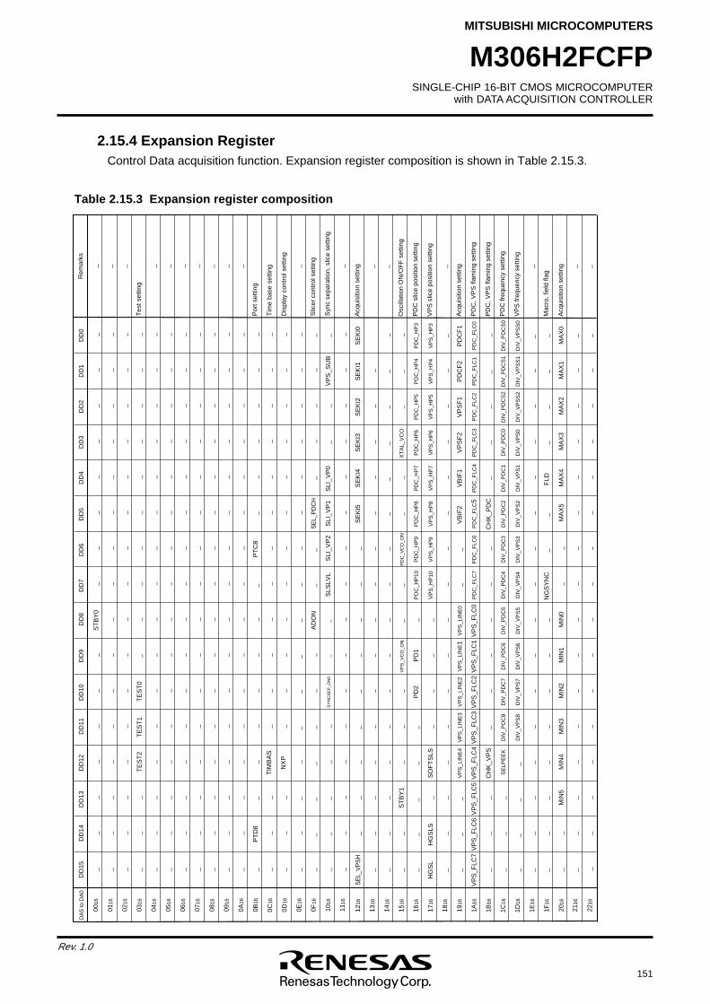
SINGLE-CHIP 16-BIT CMOS MICROCOMPUTERwith DATA ACQUISITION CONTROLLER
MITSUBISHI MICROCOMPUTERS
151
Rev. 1.0
M306H2FCFP
2.15.4 Expansion RegisterControl Data acquisition function. Expansion register composition is shown in Table 2.15.3.
DA
5 to
DA
0D
D15
DD
14
DD
13
DD
12 D
D11
D
D10
D
D9
DD
8D
D7
DD
6 D
D5
DD
4D
D3
DD
2 D
D1
DD
0
0016
0116
0216
0316
0416
0516
0616
0716
0816
0916
0A16
0B16
0C16
0D16
0E16
0F16
1016
1116
_ _
_ T
ES
T2
TE
ST
1 T
ES
T0
_ _
_ _
_ _
_ _
_ _
_P
TD
8_
_ _
_ _
__
PT
C8
_ _
_ _
_ _
_ _
_
_
_
_
_ _
_
_ _
_ _
_ _
_
__
_ _
_ _
_ A
DO
N
_ _
SE
L_P
DC
H
_ _
_ _
_
_ _
_
_ _
S
YN
CS
EP
_ON
0 _
_ S
LSLV
L S
LI_V
P2
SLI
_VP
1 S
LI_V
P0
_ _
V
PS
_SU
B
_
_ _
_ _
_ _
_ _
_ _
_ _
_ _
_ _
Rem
arks
_ _ _
Tes
t set
ting
_ _ _ _ _ _ _
Por
t set
ting
Tim
e ba
se s
ettin
g
Dis
play
con
trol
set
ting
_
Slic
er c
ontr
ol s
ettin
g
Syn
c se
para
tion,
slic
e se
tting
_
_ _
_ _
_ _
_ _
_ _
_ _
_ _
_ _
_ _
_ _
_ _
_S
TB
Y0
_ _
_ _
_ _
_ _
_ _
_ _
_ _
_ _
_ _
_ _
_ _
_ _
_ _
_ _
_ _
_ _
_ _
_ _
_ _
_ _
_ _
_ _
_ _
_ _
_ _
_ _
_ _
_ _
_ _
_ _
_ _
_ _
_ _
_ _
_ _
_ _
_ _
_ _
_ _
_ _
_ _
_ _
_ _
_ _
_ _
_ _
_ _
_ _
_ _
_ _
_ _
_ _
_ _
_ _
_ _
_ _
_ _
_ _
_ _
_ _
_ _
_ _
_ _
_ _
_ _
_ _
_ _
_ _
_ _
_T
IMB
AS
_ _
_ _
_ _
_ _
_ _
_ _
_ _
_N
XP
_ _
_ _
_ _
_ _
_ _
_ _
1216
1316
1416
1516
1616
1716
1816
1916
1A16
1B16
1C16
1D16
1E16
1F16
_ _
_ _
_ _
SE
KI5
S
EK
I4
SE
KI3
S
EK
I2
SE
KI1
S
EK
I0
_
SE
L_V
PS
H _
_ _
_ _
_ _
_ _
_ _
_ _
_ _
_ _
_ _
_ _
_ _
_ _
_ _
__
_ _
_ _
_ _
ST
BY
1 _
_ _
V
PS
_VC
O_O
N
__
PD
C_V
CO
_ON
_
_
XT
AL_
VC
O
__
_
_
_ _
_
PD
2 P
D1
_
PD
C_H
P10
P
DC
_HP
9 P
DC
_HP
8 P
DC
_HP
7 P
DC
_HP
6 P
DC
_HP
5 P
DC
_HP
4 P
DC
_HP
3
HG
SL
HG
SLS
_S
OF
TS
LS _
_ _
_
VP
S_H
P10
V
PS
_HP
9 V
PS
_HP
8 V
PS
_HP
7 V
PS
_HP
6 V
PS
_HP
5 V
PS
_HP
4 V
PS
_HP
3
_
_
_
VP
S_L
INE
4 V
PS
_LIN
E3
VP
S_L
INE
2 V
PS
_LIN
E1
VP
S_L
INE
0
_
_
VB
IF2
VB
IF1
VP
SF
2 V
PS
F1
PD
CF
2 P
DC
F1
VP
S_F
LC7
VP
S_F
LC6
VP
S_F
LC5
VP
S_F
LC4
VP
S_F
LC3
VP
S_F
LC2
VP
S_F
LC1
VP
S_F
LC0
PD
C_F
LC7
PD
C_F
LC6
PD
C_F
LC5
PD
C_F
LC4
PD
C_F
LC3
PD
C_F
LC2
PD
C_F
LC1
PD
C_F
LC0
_ _
_C
HK
_VP
S_
_ _
_ _
_C
HK
_PD
C_
_ _
_ _
_ S
ELP
EE
K
DIV
_PD
C8
DIV
_PD
C7
DIV
_PD
C6
DIV
_PD
C5
DIV
_PD
C4
DIV
_PD
C3
DIV
_PD
C2
DIV
_PD
C1
DIV
_PD
C0
DIV
_PD
CS
2 D
IV_P
DC
S1
DIV
_PD
CS
0
__
_ _
DIV
_VP
S8
DIV
_VP
S7
DIV
_VP
S6
DIV
_VP
S5
DIV
_VP
S4
DIV
_VP
S3
DIV
_VP
S2
DIV
_VP
S1
DIV
_VP
S0
DIV
_VP
SS
2 D
IV_V
PS
S1
DIV
_VP
SS
0
_ _
_ _
_ _
_ _
_ _
_ _
_ _
_ _
_ _
_ _
_ _
_ _
N
GS
YN
C
_ _
FLD
_
__
_M
acro
, fie
ld fl
ag
VP
S fr
eque
ncy
setti
ng
PD
C fr
eque
ncy
setti
ng
PD
C, V
PS
flam
ing
setti
ng
PD
C, V
PS
flam
ing
setti
ng
Acq
uisi
tion
setti
ng
VP
S s
lice
posi
tion
setti
ng
PD
C s
lice
posi
tion
setti
ng
Osc
illat
ion
ON
/OF
F s
ettin
g
_
Acq
uisi
tion
setti
ng
2016
_ _
MIN
5 M
IN4
MIN
3 M
IN2
MIN
1 M
IN0
_ _
MA
X5
MA
X4
MA
X3
MA
X2
MA
X1
MA
X0
2116
_ _
_ _
_ _
_ _
_ _
_ _
_ _
_ _
Acq
uisi
tion
setti
ng
2216
_ _
_ _
_ _
_ _
_ _
_ _
_ _
_ _
_ _
_ _
_ _
_ _
_ _
_ _
_ _
_ _
__ _ _ _
_
__
Table 2.15.3 Expansion register composition
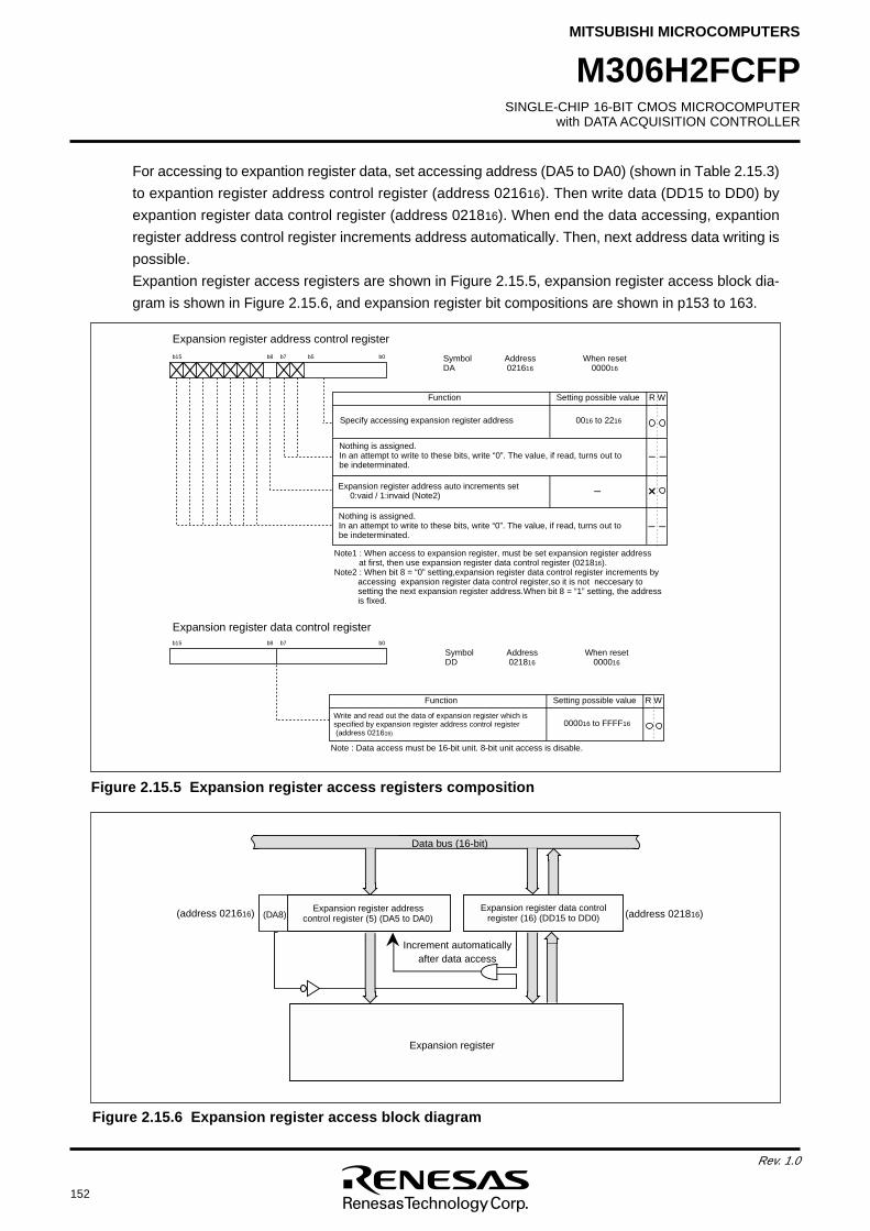
152
Rev. 1.0
SINGLE-CHIP 16-BIT CMOS MICROCOMPUTERwith DATA ACQUISITION CONTROLLER
MITSUBISHI MICROCOMPUTERS
M306H2FCFP
For accessing to expantion register data, set accessing address (DA5 to DA0) (shown in Table 2.15.3)
to expantion register address control register (address 021616). Then write data (DD15 to DD0) by
expantion register data control register (address 021816). When end the data accessing, expantion
register address control register increments address automatically. Then, next address data writing is
possible.
Expantion register access registers are shown in Figure 2.15.5, expansion register access block dia-
gram is shown in Figure 2.15.6, and expansion register bit compositions are shown in p153 to 163.
Figure 2.15.5 Expansion register access registers composition
Figure 2.15.6 Expansion register access block diagram
Symbol Address When resetDA 021616 000016
E
x
p
a
n
s
i
o
n
r
e
g
i
s
t
e
r
a
d
d
r
e
s
s
c
o
n
t
r
o
l
r
e
g
i
s
t
e
r
F
u
n
c
t
i
o
n WRS
e
t
t
i
n
g
p
o
s
s
i
b
l
e
v
a
l
u
e
0016 to 2216S
p
e
c
i
f
y
a
c
c
e
s
s
i
n
g
e
x
p
a
n
s
i
o
n
r
e
g
i
s
t
e
r
a
d
d
r
e
s
s
N
o
t
h
i
n
g
i
s
a
s
s
i
g
n
e
d
.I
n
a
n
a
t
t
e
m
p
t
t
o
w
r
i
t
e
t
o
t
h
e
s
e
b
i
t
s
,
w
r
i
t
e
“
0
”
.
T
h
e
v
a
l
u
e
,
i
f
r
e
a
d
,
t
u
r
n
s
o
u
t
t
o
b
e
i
n
d
e
t
e
r
m
i
n
a
t
e
d
.
S
y
m
b
o
l A
d
d
r
e
s
s W
h
e
n
r
e
s
e
tD
D 0
2
1
81
6 0
0
0
01
6
E
x
p
a
n
s
i
o
n
r
e
g
i
s
t
e
r
d
a
t
a
c
o
n
t
r
o
l
r
e
g
i
s
t
e
r
F
u
n
c
t
i
o
n WRS
e
t
t
i
n
g
p
o
s
s
i
b
l
e
v
a
l
u
e
0 0
0
01
6
t
o
F
F
F
F1
6
Write and read out the data of expansion register which is specified by expansion register address control register (address 021616)
Note : Data access must be 16-bit unit. 8-bit unit access is disable.
N
o
t
e
1
:
W
h
e
n
a
c
c
e
s
s
t
o
e
x
p
a
n
s
i
o
n
r
e
g
i
s
t
e
r
,
m
u
s
t
b
e
s
e
t
e
x
p
a
n
s
i
o
n
r
e
g
i
s
t
e
r
a
d
d
r
e
s
s
a
t
f
i
r
s
t
,
t
h
e
n
u
s
e
e
x
p
a
n
s
i
o
n
r
e
g
i
s
t
e
r
d
a
t
a
c
o
n
t
r
o
l
r
e
g
i
s
t
e
r
(
0
2
1
81
6)
.N
o
t
e
2
:
W
h
e
n
b
i
t
8
=
“
0
”
s
e
t
t
i
n
g
,
e
x
p
a
n
s
i
o
n
r
e
g
i
s
t
e
r
d
a
t
a
c
o
n
t
r
o
l
r
e
g
i
s
t
e
r
i
n
c
r
e
m
e
n
t
s
b
y
a
c
c
e
s
s
i
n
g
e
x
p
a
n
s
i
o
n
r
e
g
i
s
t
e
r
d
a
t
a
c
o
n
t
r
o
l
r
e
g
i
s
t
e
r
,
s
o
i
t
i
s
n
o
t
n
e
c
c
e
s
a
r
y
t
o
s
e
t
t
i
n
g
t
h
e
n
e
x
t
e
x
p
a
n
s
i
o
n
r
e
g
i
s
t
e
r
a
d
d
r
e
s
s
.
W
h
e
n
b
i
t
8
=
“
1
”
s
e
t
t
i
n
g
,
t
h
e
a
d
d
r
e
s
s
i
s
f
i
x
e
d
.
b 1
5 b
8 b
7 b0b
5
b 1
5 b
8 b
7 b0
N
o
t
h
i
n
g
i
s
a
s
s
i
g
n
e
d
.I
n
a
n
a
t
t
e
m
p
t
t
o
w
r
i
t
e
t
o
t
h
e
s
e
b
i
t
s
,
w
r
i
t
e
“
0
”
.
T
h
e
v
a
l
u
e
,
i
f
r
e
a
d
,
t
u
r
n
s
o
u
t
t
o
b
e
i
n
d
e
t
e
r
m
i
n
a
t
e
d
.
E
x
p
a
n
s
i
o
n
r
e
g
i
s
t
e
r
a
d
d
r
e
s
s
a
u
t
o
i
n
c
r
e
m
e
n
t
s
s
e
t
0
:
v
a
i
d
/
1
:
i
n
v
a
i
d
(
N
o
t
e
2
)
Data bus (16-bit)
(address 021616) (address 021816)Expansion register data control
register (16) (DD15 to DD0)Expansion register address
control register (5) (DA5 to DA0)
Increment automaticallyafter data access
Expansion register
(DA8)
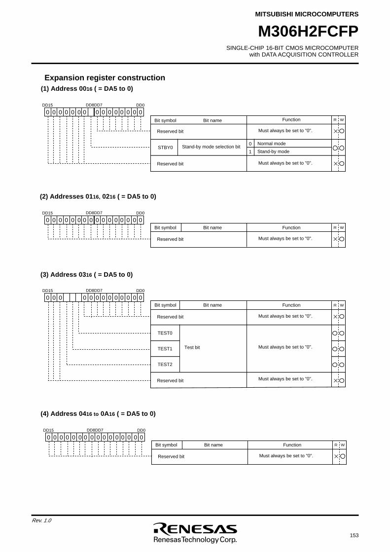
SINGLE-CHIP 16-BIT CMOS MICROCOMPUTERwith DATA ACQUISITION CONTROLLER
MITSUBISHI MICROCOMPUTERS
153
Rev. 1.0
M306H2FCFP
Expansion register construction(1) Address 0016 ( = DA5 to 0)
(2) Addresses 0116, 0216 ( = DA5 to 0)
DD15 DD8DD7 DD0
R WBit symbol Bit name Function
0 00 0 00 0 0 0 0 00 0 0 00
Must always be set to "0".Reserved bit
(3) Address 0316 ( = DA5 to 0)
DD15 DD8DD7 DD0
R WBit symbol Bit name Function
0 00 0 0 0 0 00 0 0 00
Must always be set to "0".Reserved bit
TEST0
TEST1
TEST2
Test bit
Must always be set to "0".
Must always be set to "0".
Reserved bit
STBY0Normal mode
Stand-by mode
0
1Stand-by mode selection bit
DD15 DD8DD7 DD0
R WBit symbol Bit name Function
0 00 0 00 0 0 0 00 0 0 00
Must always be set to "0".Reserved bit
Must always be set to "0".Reserved bit
(4) Address 0416 to 0A16 ( = DA5 to 0)
DD15 DD8DD7 DD0
R WBit symbol Bit name Function
0 00 0 00 0 0 0 0 00 0 0 00
Must always be set to "0".Reserved bit
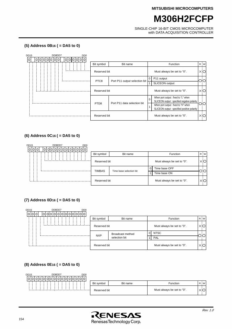
154
Rev. 1.0
SINGLE-CHIP 16-BIT CMOS MICROCOMPUTERwith DATA ACQUISITION CONTROLLER
MITSUBISHI MICROCOMPUTERS
M306H2FCFP
(5) Address 0B16 ( = DA5 to 0)
DD15 DD8DD7 DD0
R WBit symbol Bit name Function
0 0 0 00 0 0 0 00 0 0 00
PTD8
When port output : fixed to "L" whenSLICEON output : specified negative polarityWhen port output : fixed to "H" whenSLICEON output : specified positive polarity
0
1Port P11 data selection bit
Must always be set to "0".Reserved bit
Must always be set to "0".Reserved bit
Must always be set to "0".Reserved bit
PTC8 Port P11 output selection bit0 P11 output
1 SLICEON output
(6) Address 0C16 ( = DA5 to 0)
DD15 DD8DD7 DD0
R WBit symbol Bit name Function
0 00 00 0 0 0 000 0 0 00
Must always be set to "0".Reserved bit
Must always be set to "0".Reserved bit
TIMBAS Time base selection bit0 Time base OFF
1 Time base ON
(7) Address 0D16 ( = DA5 to 0)
DD15 DD8DD7 DD0
R WBit symbol Bit name Function
0 00 00 0 0 0 000 0 0 00
Must always be set to "0".Reserved bit
Must always be set to "0".Reserved bit
NXP Broadcast methodselection bit
0 NTSC
1 PAL
(8) Address 0E16 ( = DA5 to 0)
DD15 DD8DD7 DD0
R WBit symbol Bit name Function
0 00 0 00 0 0 0 0 00 0 0 00
Must always be set to "0".Reserved bit
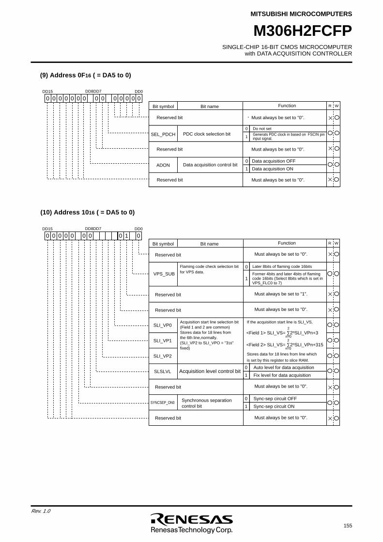
SINGLE-CHIP 16-BIT CMOS MICROCOMPUTERwith DATA ACQUISITION CONTROLLER
MITSUBISHI MICROCOMPUTERS
155
Rev. 1.0
M306H2FCFP
(9) Address 0F16 ( = DA5 to 0)
DD15 DD8DD7 DD0
R WBit symbol Bit name Function
Reserved bit Must always be set to "0".
Reserved bit Must always be set to "0".
0 00 0 0 00 0 0 0 0 00 0
SEL_PDCH
ADON0 Data acquisition OFF
1 Data acquisition ON
Reserved bit Must always be set to "0".
Data acquisition control bit
PDC clock selection bit Generats PDC clock in based on FSCIN pin input signal.
Do not set0
1
(10) Address 1016 ( = DA5 to 0)
DD15 DD8DD7 DD0
R WBit symbol Bit name Function
Synchronous separationcontrol bit
Flaming code check selection bitfor VPS data.
0 Sync-sep circuit OFF
1 Sync-sep circuit ON
Must always be set to "0".Reserved bit
Must always be set to "0".Reserved bit
Must always be set to "0".Reserved bit
Must always be set to "1".Reserved bit
VPS_SUB
Must always be set to "0".Reserved bit
0 00 0 0 1 00 0 0
SLI_VP0
SLI_VP1
SLI_VP2
SLSLVL
SYNCSEP_ON0
0
Acquisition start line selection bit(Field 1 and 2 are common)Stores data for 18 lines fromthe 6th line,normally.(SLI_VP2 to SLI_VPO = "316"fixed)
Later 8bits of flaming code 16bits
If the acquisition start line is SLI_VS,
<Field 1> SLI_VS= ∑2nSLI_VPn+32
n=0
<Field 2> SLI_VS= ∑2nSLI_VPn+3152
n=0
Stores data for 18 lines from line which
is set by this register to slice RAM.
Former 4bits and later 4bits of flamingcode 16bits (Select 8bits which is set inVPS_FLC0 to 7)
0 Auto level for data acquisition
1 Fix level for data acquisitionAcquisition level control bit
1
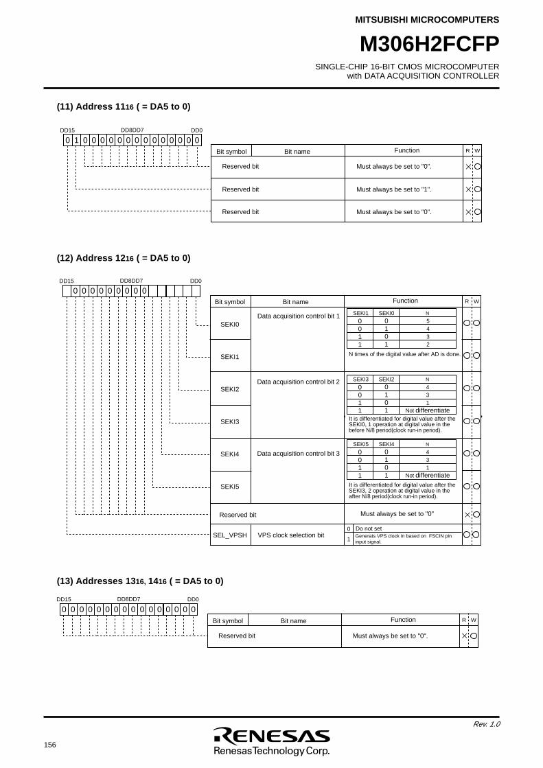
156
Rev. 1.0
SINGLE-CHIP 16-BIT CMOS MICROCOMPUTERwith DATA ACQUISITION CONTROLLER
MITSUBISHI MICROCOMPUTERS
M306H2FCFP
(12) Address 1216 ( = DA5 to 0)
(13) Addresses 1316, 1416 ( = DA5 to 0)
DD15 DD8DD7 DD0
R WBit symbol Bit name Function
Reserved bit Must always be set to "0".
0 00 0 0 0 00 0 00 0 0 0 00
DD15 DD8DD7 DD0
R W
SEKI0
SEKI1
SEKI2
SEKI3
SEKI4
SEKI5
0 00 0 00 0 0
SEKI1 SEKI0 N
0011
0101
5432
N times of the digital value after AD is done.
SEKI3 SEKI2 N
0011
0101
431
Not differentiate
SEKI5 SEKI4 N
0011
0101
431
Not differentiate
It is differentiated for digital value after the SEKI0, 1 operation at digital value in the before N/8 period(clock run-in period).
SEL_VPSH
Bit symbol Bit name Function
Data acquisition control bit 1
Data acquisition control bit 2
Data acquisition control bit 3
It is differentiated for digital value after the SEKI3, 2 operation at digital value in the after N/8 period(clock run-in period).
Must always be set to "0"Reserved bit
VPS clock selection bit Generats VPS clock in based on FSCIN pin input signal.
0
1
0
Do not set
(11) Address 1116 ( = DA5 to 0)
DD15 DD8DD7 DD0
R WBit symbol Bit name Function
Reserved bit Must always be set to "0".
0 01 0 0 0 00 0 00 0 0 0 00
Reserved bit Must always be set to "1".
Reserved bit Must always be set to "0".
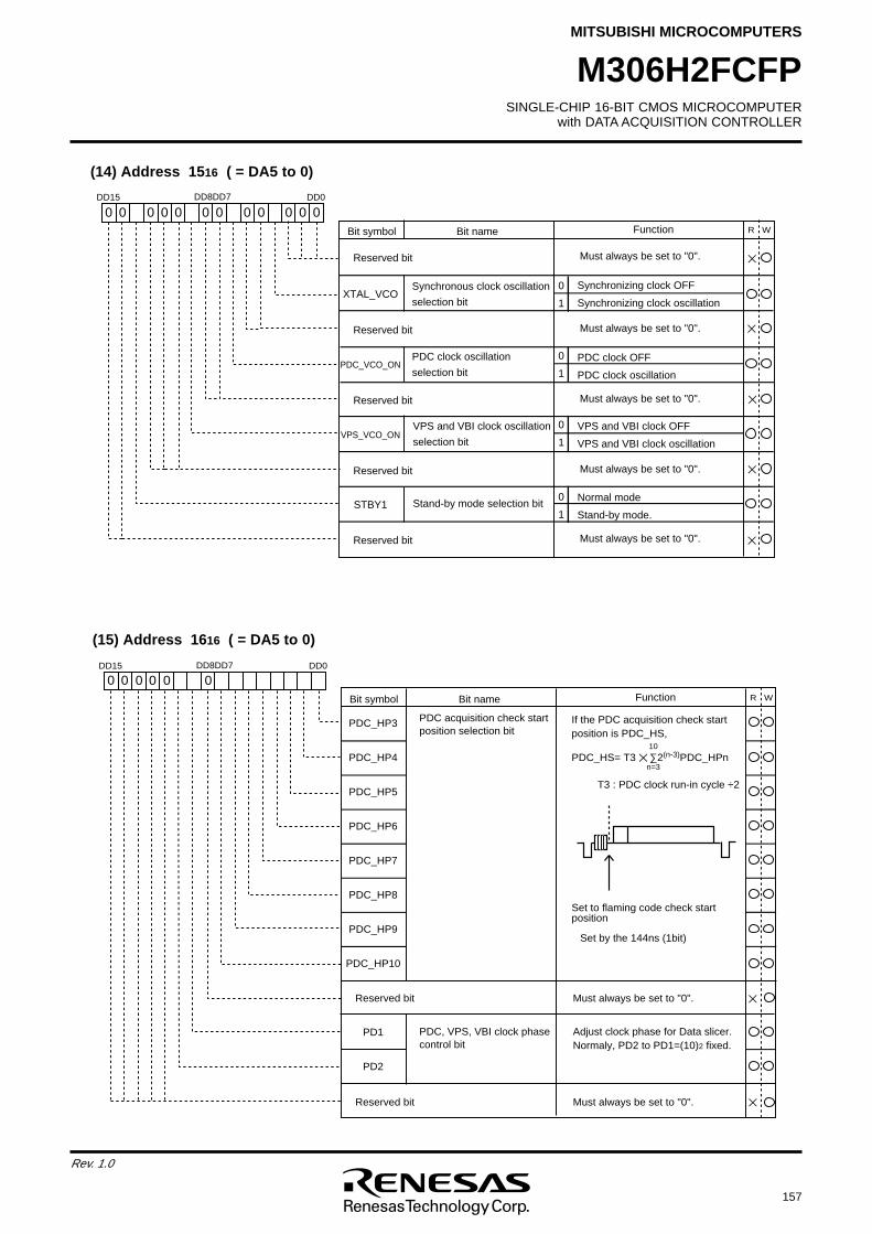
SINGLE-CHIP 16-BIT CMOS MICROCOMPUTERwith DATA ACQUISITION CONTROLLER
MITSUBISHI MICROCOMPUTERS
157
Rev. 1.0
M306H2FCFP
(14) Address 1516 ( = DA5 to 0)
DD15 DD8DD7 DD0
R WBit symbol Bit name Function
0
1
0
1
0
1
0
1
Must always be set to "0".Reserved bit
Must always be set to "0".Reserved bit
Must always be set to "0".Reserved bit
Must always be set to "0".Reserved bit
Must always be set to "0".Reserved bit
XTAL_VCO
PDC_VCO_ON
VPS_VCO_ON
STBY1
Synchronizing clock OFF
Synchronizing clock oscillation
PDC clock OFF
PDC clock oscillation
VPS and VBI clock OFF
VPS and VBI clock oscillation
Normal mode
Stand-by mode.
0 00 00 0 00 0 0 0 0
Synchronous clock oscillation
selection bit
PDC clock oscillation
selection bit
VPS and VBI clock oscillation
selection bit
Stand-by mode selection bit
(15) Address 1616 ( = DA5 to 0)
Reserved bit Must always be set to "0".
DD15 DD8DD7 DD0
R WBit symbol Bit name Function
PDC_HP3
PDC_HP4
PDC_HP5
PDC_HP6
PDC_HP7
PDC_HP8
PDC_HP9
PDC_HP10
PD1
PD2
Adjust clock phase for Data slicer.Normaly, PD2 to PD1=(10)2 fixed.
PDC acquisition check startposition selection bit
If the PDC acquisition check start position is PDC_HS,
PDC_HS= T3 ∑2(n-3)PDC_HPn 10
n=3
0
T3 : PDC clock run-in cycle ÷2
Set to flaming code check startposition
Set by the 144ns (1bit)
0 0
PDC, VPS, VBI clock phasecontrol bit
00
Reserved bit Must always be set to "0".
0
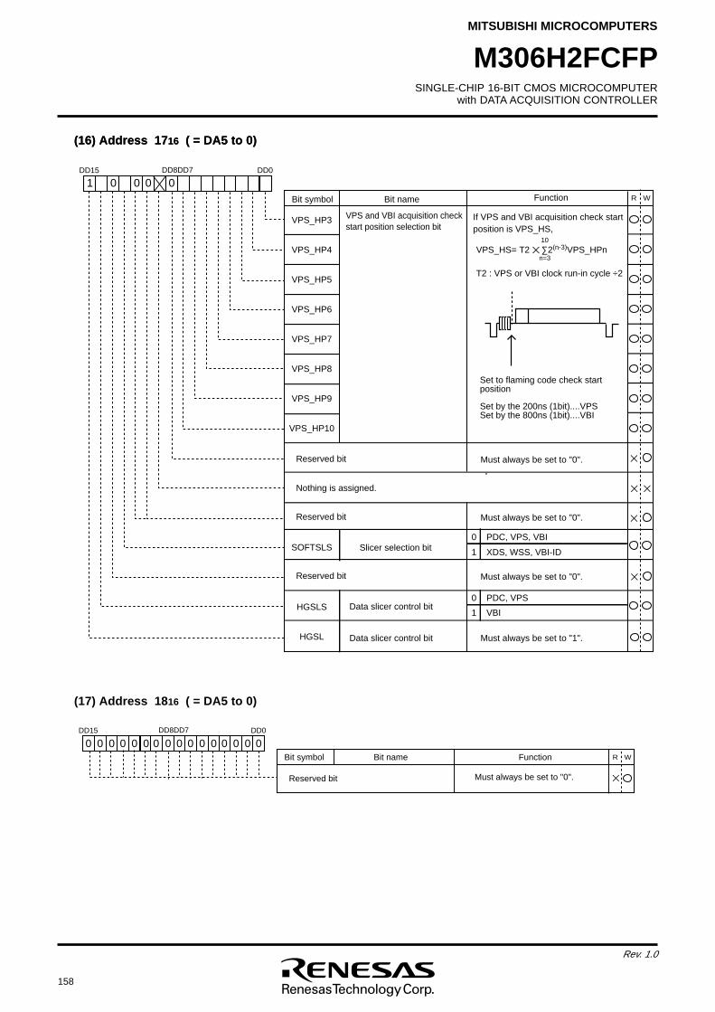
158
Rev. 1.0
SINGLE-CHIP 16-BIT CMOS MICROCOMPUTERwith DATA ACQUISITION CONTROLLER
MITSUBISHI MICROCOMPUTERS
M306H2FCFP
(16) Address 1716 ( = DA5 to 0)
DD15 DD8DD7 DD0
R WBit symbol Bit name Function
VPS_HP3
VPS_HP4
VPS_HP5
VPS_HP6
VPS_HP7
VPS_HP8
VPS_HP9
VPS_HP10
SOFTSLS
HGSLS
HGSL
Reserved bit Must always be set to "0".
VPS and VBI acquisition checkstart position selection bit
If VPS and VBI acquisition check startposition is VPS_HS,
VPS_HS= T2 ∑2(n-3)VPS_HPn 10
n=3
1 0 0 00
T2 : VPS or VBI clock run-in cycle ÷2
Set to flaming code check startposition
Set by the 200ns (1bit)....VPSSet by the 800ns (1bit)....VBI
Must always be set to "1".Data slicer control bit
Reserved bit Must always be set to "0".
Reserved bit Must always be set to "0".
Nothing is assigned.
Slicer selection bit
Data slicer control bit
0 PDC, VPS, VBI
1 XDS, WSS, VBI-ID
0 PDC, VPS
1 VBI
(16) Address 1716 ( = DA5 to 0)
(17) Address 1816 ( = DA5 to 0)
DD15 DD8DD7 DD0
R WBit symbol Bit name Function
0 00 0 00 0 0 0 0 00 0 0 00
Must always be set to "0".Reserved bit
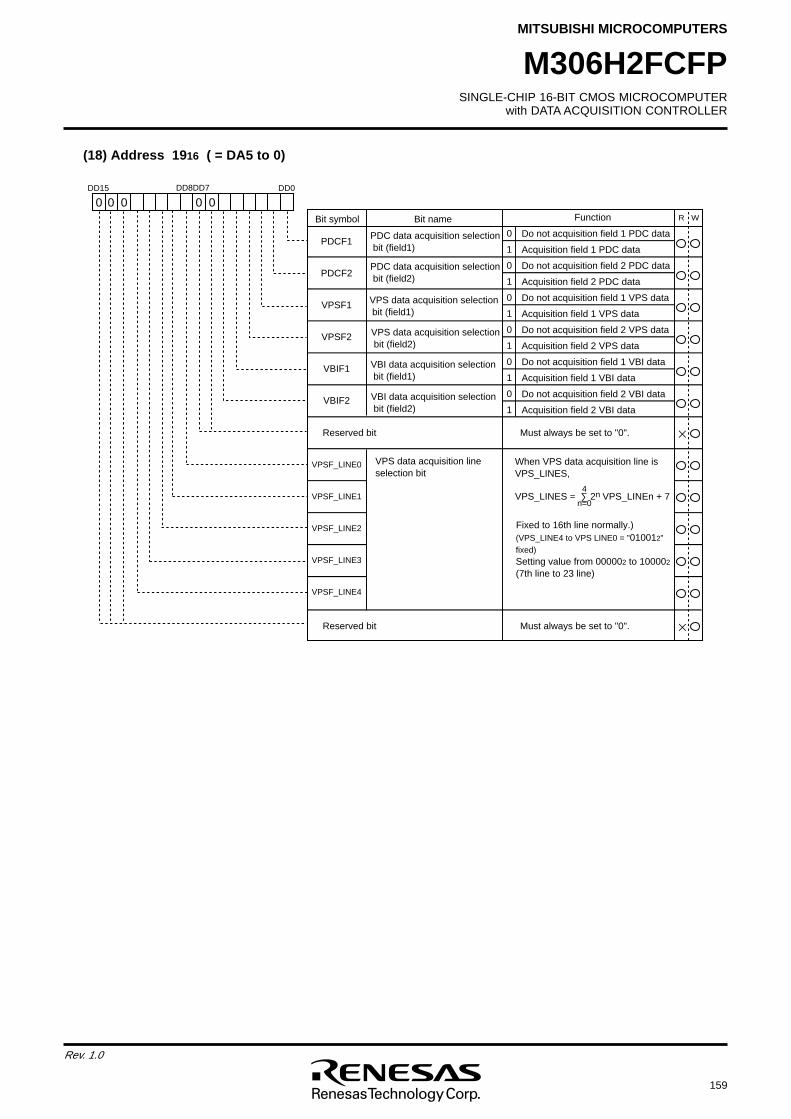
SINGLE-CHIP 16-BIT CMOS MICROCOMPUTERwith DATA ACQUISITION CONTROLLER
MITSUBISHI MICROCOMPUTERS
159
Rev. 1.0
M306H2FCFP
(18) Address 1916 ( = DA5 to 0)
DD15 DD8DD7 DD0
R WBit symbol Bit name Function
PDCF1
PDCF2
VPSF1
VPSF2
VBIF1
VBIF2
VPSF_LINE0
VPSF_LINE1
VPSF_LINE2
VPSF_LINE3
VPSF_LINE4
0
1
0
1
0
1
0
1
0
1
0
1
0 0 0 0 0
Do not acquisition field 1 PDC data
Acquisition field 1 PDC data
Do not acquisition field 2 PDC data
Acquisition field 2 PDC data
Do not acquisition field 1 VPS data
Acquisition field 1 VPS data
Do not acquisition field 2 VPS data
Acquisition field 2 VPS data
Do not acquisition field 1 VBI data
Acquisition field 1 VBI data
Do not acquisition field 2 VBI data
Acquisition field 2 VBI data
PDC data acquisition selection bit (field1)
VBI data acquisition selection bit (field2)
VBI data acquisition selection bit (field1)
VPS data acquisition selection bit (field2)
VPS data acquisition selection bit (field1)
PDC data acquisition selection bit (field2)
Reserved bit Must always be set to "0".
Reserved bit Must always be set to "0".
VPS data acquisition lineselection bit
When VPS data acquisition line isVPS_LINES,
VPS_LINES = ∑ 2n VPS_LINEn + 74
n=0
(VPS_LINE4 to VPS LINE0 = "010012" fixed)Setting value from 000002 to 100002
(7th line to 23 line)
Fixed to 16th line normally.)
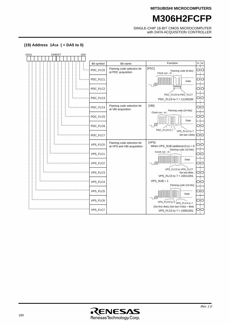
160
Rev. 1.0
SINGLE-CHIP 16-BIT CMOS MICROCOMPUTERwith DATA ACQUISITION CONTROLLER
MITSUBISHI MICROCOMPUTERS
M306H2FCFP
(19) Address 1A16 ( = DA5 to 0)
Clock run - inFlaming code (8 bits)
PDC_FLC0 to PDC_FLC7
Data
Setting
Clock run - inFlaming code (24 bits)
Data
PDC_FLC4 to 7 VPS_FLC0 to 7
Crock run - inFlaming code (16 bits)
Data
VPS_FLC0 to VPS_FLC7
Flaming code (16 bits)
Data
VPS_FLC0 to 3 VPS_FLC4 to 7
DD15 DD8DD7 DD0
R WBit symbol Bit name Function
PDC_FLC0
PDC_FLC1
PDC_FLC2
PDC_FLC3
PDC_FLC4
PDC_FLC5
PDC_FLC6
PDC_FLC7
VPS_FLC0
VPS_FLC1
VPS_FLC2
VPS_FLC3
VPS_FLC4
VPS_FLC5
VPS_FLC6
VPS_FLC7
Flaming code selection bitat PDC acquisition
Flaming code selection bitat VBI acquisition
Flaming code selection bitat VPS and VBI acquisition
[PDC]
PDC_FLC0 to 7 = 11100100
[VBI]
Set last 12bits
[VPS]When VPS_SUB (address1216) = 0
Set last 8bitsVPS_FLC0 to 7 = 10011001
VPS_SUB = 1
VPS_FLC0 to 7 = 10001001
(Set first 4bits) (Set last 4 bits) = 8bits
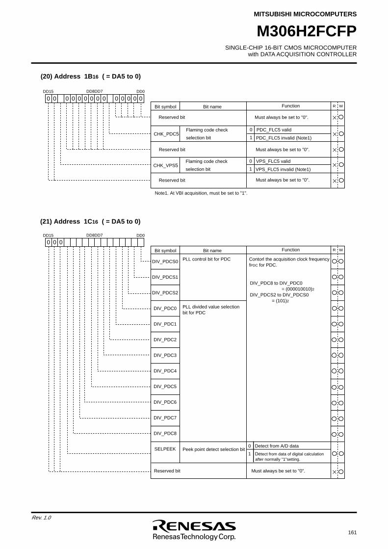
SINGLE-CHIP 16-BIT CMOS MICROCOMPUTERwith DATA ACQUISITION CONTROLLER
MITSUBISHI MICROCOMPUTERS
161
Rev. 1.0
M306H2FCFP
(20) Address 1B16 ( = DA5 to 0)
DD15 DD8DD7 DD0
R WBit symbol Bit name Function
Reserved bit Must always be set to "0".
0 0 0 0 0 00 0 0 0 0 0 00
Reserved bit
Reserved bit Must always be set to "0".
Must always be set to "0".
CHK_PDC5Flaming code check
selection bit
0
1
PDC_FLC5 valid
PDC_FLC5 invalid (Note1)
CHK_VPS5Flaming code check
selection bit
0
1
VPS_FLC5 valid
VPS_FLC5 invalid (Note1)
Note1. At VBI acquisition, must be set to "1".
(21) Address 1C16 ( = DA5 to 0)
DD15 DD8DD7 DD0
R WBit symbol Bit name Function
DIV_PDCS0
DIV_PDCS1
DIV_PDCS2
DIV_PDC0
DIV_PDC1
DIV_PDC2
DIV_PDC3
DIV_PDC4
DIV_PDC5
DIV_PDC6
DIV_PDC7
DIV_PDC8
SELPEEK
PLL control bit for PDC
PLL divided value selectionbit for PDC
Reserved bit Must always be set to "0".
Contorl the acquisition clock frequencyfPDC for PDC.
DIV_PDC8 to DIV_PDC0= (000010010)2
DIV_PDCS2 to DIV_PDCS0= (101)2
0 00
Peek point detect selection bit 0 Detect from A/D data
1 Detect from data of digital calculation after normally "1"setting.
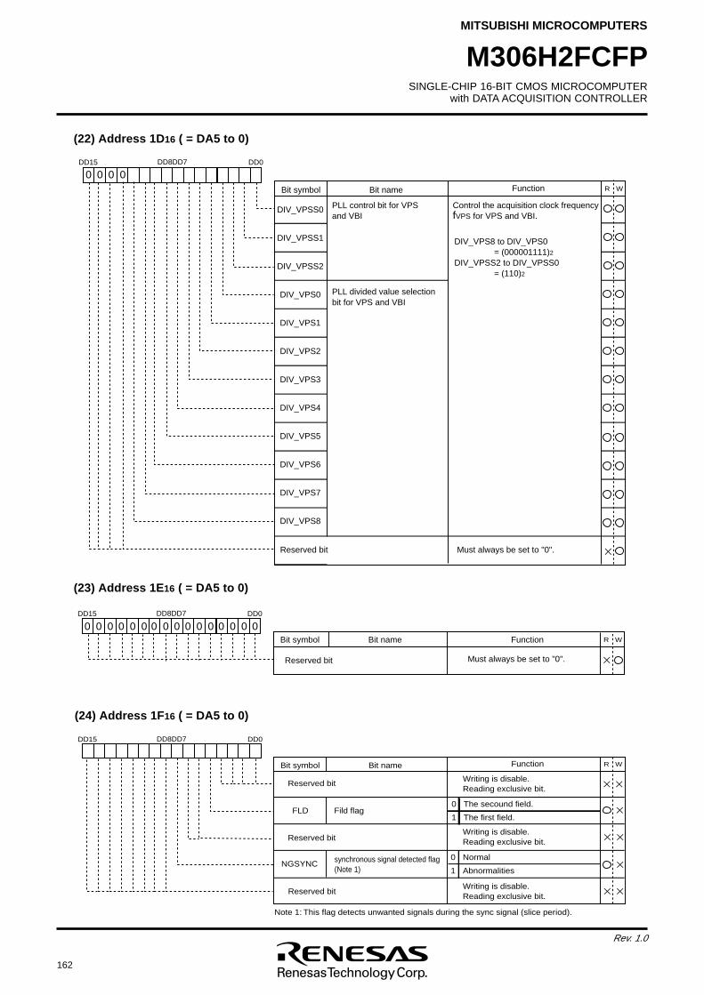
162
Rev. 1.0
SINGLE-CHIP 16-BIT CMOS MICROCOMPUTERwith DATA ACQUISITION CONTROLLER
MITSUBISHI MICROCOMPUTERS
M306H2FCFP
(22) Address 1D16 ( = DA5 to 0)
DD15 DD8DD7 DD0
R WBit symbol Bit name Function
DIV_VPSS0
DIV_VPSS1
DIV_VPSS2
DIV_VPS0
DIV_VPS1
DIV_VPS2
DIV_VPS3
DIV_VPS4
DIV_VPS5
DIV_VPS6
DIV_VPS7
DIV_VPS8
PLL control bit for VPSand VBI
PLL divided value selectionbit for VPS and VBI
Reserved bit Must always be set to "0".
Control the acquisition clock frequencyfVPS for VPS and VBI.
DIV_VPS8 to DIV_VPS0= (000001111)2
DIV_VPSS2 to DIV_VPSS0= (110)2
0 000
(23) Address 1E16 ( = DA5 to 0)
DD15 DD8DD7 DD0
R WBit symbol Bit name Function
0 00 0 00 0 0 0 0 00 0 0 00
Must always be set to "0".Reserved bit
(24) Address 1F16 ( = DA5 to 0)
DD15 DD8DD7 DD0
R WBit symbol Bit name Function
Reserved bit
Reserved bit Writing is disable.Reading exclusive bit.
NGSYNC0 Normal
1 Abnormalitiessynchronous signal detected flag(Note 1)
FLD0 The secound field.
1 The first field.Fild flag
Reserved bitWriting is disable.Reading exclusive bit.
Writing is disable.Reading exclusive bit.
Note 1: This flag detects unwanted signals during the sync signal (slice period).
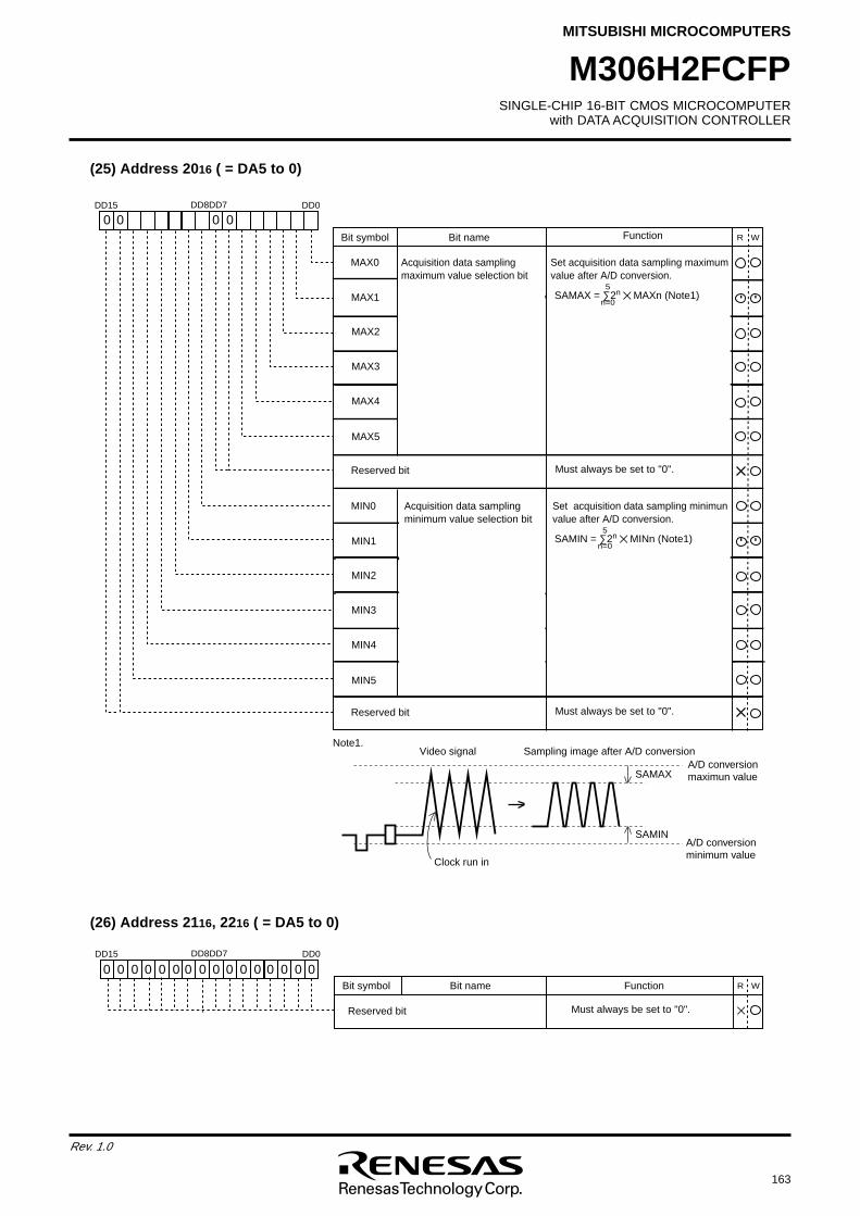
SINGLE-CHIP 16-BIT CMOS MICROCOMPUTERwith DATA ACQUISITION CONTROLLER
MITSUBISHI MICROCOMPUTERS
163
Rev. 1.0
M306H2FCFP
(25) Address 2016 ( = DA5 to 0)
DD15 DD8DD7 DD0
R W
MIN0
Set acquisition data sampling maximumvalue after A/D conversion.
Acquisition data sampling minimum value selection bit
MAX0 Acquisition data sampling maximum value selection bit
0 00 0
5
n=0SAMAX = ∑2n MAXn (Note1)
5
n=0
MAX5
MAX4
MAX3
MAX2
MAX1
MIN5
MIN4
MIN3
MIN2
MIN1
Note1.
Clock run in
SAMAX
SAMIN
Video signal Sampling image after A/D conversionA/D conversionmaximun value
A/D conversionminimum value
Bit symbol Bit name Function
Must always be set to "0".Reserved bit
Must always be set to "0".Reserved bit
Set acquisition data sampling minimunvalue after A/D conversion.
SAMIN = ∑2n MINn (Note1)
(26) Address 2116, 2216 ( = DA5 to 0)
DD15 DD8DD7 DD0
R WBit symbol Bit name Function
0 00 0 00 0 0 0 0 00 0 0 00
Must always be set to "0".Reserved bit
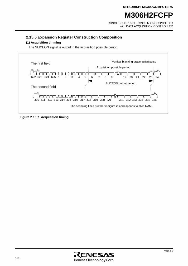
164
Rev. 1.0
SINGLE-CHIP 16-BIT CMOS MICROCOMPUTERwith DATA ACQUISITION CONTROLLER
MITSUBISHI MICROCOMPUTERS
M306H2FCFP
2.15.5 Expansion Register Construction Composition(1) Acquisition timming
The SLICEON signal is output in the acquisition possible period.
Figure 2.15.7 Acquisition timing
1 2 3 4 5 6 7 8 9 19 2 22
12
0 23 2
46
2
2 6
2
3 6
2
4 6
2
5
3 1
4 3
1
5 3
1
6 317 3
1
8 319 3
2
0 321 3
3
1 3
3
23
1
0 3
1
1 312 3
1
3 3
3
3 334 3
3
5 3
3
6
T
h
e
f
i
r
s
t
f
i
e
l
d
T
h
e
s
e
c
o
n
d
f
i
e
l
d
Vertical blanking erase period pulse
Acquisition possible period
S
L
I
C
E
O
N
o
u
t
p
u
t
p
e
r
i
o
d
The scanning lines number in figure is corresponds to slice RAM .

SINGLE-CHIP 16-BIT CMOS MICROCOMPUTERwith DATA ACQUISITION CONTROLLER
MITSUBISHI MICROCOMPUTERS
165
Rev. 1.0
M306H2FCFP
Figure 2.15.8 Decoded result
2.15.6 8/4 Humming Decoder8/4 humming decoder opetates only by written the data which 8/4 humming- decoded to 8/4 humming
register (address 021A16). 8/4 humming register consists of 16 bits, can decode two data at a time.
Can obtain the decoded result by reading 8/4 humming register, and the decoded value and error
information are output. Corrects and outputs the decoded value for single error, and outputs only error
information for double error. Decoded result is shown in Figure 2.15.8 and humming 8/4 register com-
position is shown in Figure 2.15.9.
Figure 2.15.9 Humming 8/4 register composition
Writing
A
d
d
r
e
s
s
R
e
a
d
i
n
g
8
/
4
h
u
m
m
i
n
g
r
e
g
i
s
t
e
r
H
u
m
m
i
n
g
d
a
t
a
➁ Humming data ➀
E
r
r
o
r
i
n
f
o
r
m
a
t
i
o
n➀
E
r
r
o
r
i
n
f
o
r
m
a
t
i
o
n➁
0
2
1
A1 6
0 000
“1” output when double error
“1” output when single error“ 1
”
o
u
t
p
u
t
w
h
e
n
single error
“ 1
”
o
u
t
p
u
t
w
h
e
n
d
o
u
b
l
e
e
r
r
o
r
M
S
B M
S
BL S
B L
S
B
M
S
B L S
BM
S
BL
S
B
D
e
c
o
d
e
v
a
l
u
e➀
D
e
c
o
d
e
v
a
l
u
e➁
b15 b8 b7 b0
S
y
m
b
o
l A
d
d
r
e
s
s W
h
e
n
r
e
s
e
tH
M
8 0
2
1
A1
6 0
0
0
01
6
H
u
m
m
i
n
g
8
/
4
r
e
g
i
s
t
e
r
F
u
n
c
t
i
o
n WR
8
/
4
h
u
m
m
i
n
g
d
e
c
o
d
e
r
o
p
e
t
a
t
e
s
o
n
l
y
b
y
w
r
i
t
t
e
n
t
h
e
d
a
t
a
w
h
i
c
h
8
/
4
h
u
m
m
i
n
g
-
d
e
c
o
d
e
d
t
o
8
/
4
h
u
m
m
i
n
g
r
e
g
i
s
t
e
r
.
C
a
n
o
b
t
a
i
n
t
h
e
d
e
c
o
d
e
d
r
e
s
u
l
t
b
y
r
e
a
d
i
n
g
t
h
i
s
r
e
g
i
s
t
e
r
,
a
n
d
c
a
n
d
e
c
o
d
e
2
c
o
u
p
l
e
s
o
f
d
a
t
a
a
t
t
h
e
s
a
m
e
t
i
m
e
.
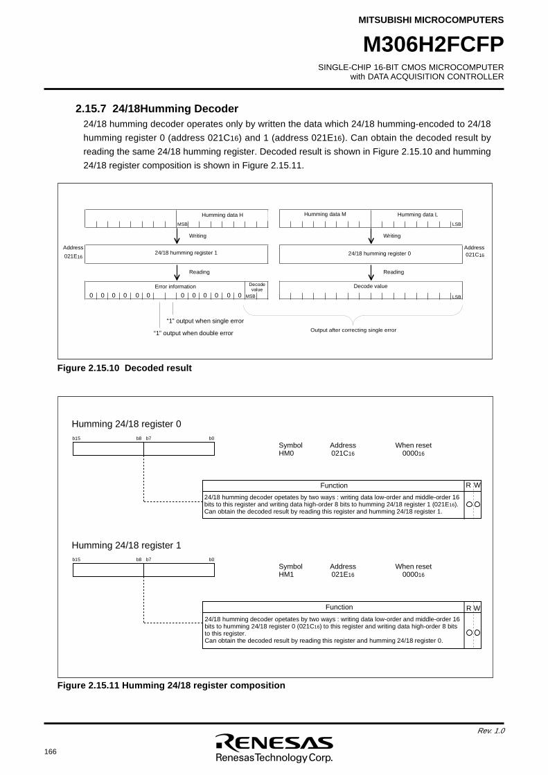
166
Rev. 1.0
SINGLE-CHIP 16-BIT CMOS MICROCOMPUTERwith DATA ACQUISITION CONTROLLER
MITSUBISHI MICROCOMPUTERS
M306H2FCFP
2.15.7 24/18Humming Decoder24/18 humming decoder operates only by written the data which 24/18 humming-encoded to 24/18
humming register 0 (address 021C16) and 1 (address 021E16). Can obtain the decoded result by
reading the same 24/18 humming register. Decoded result is shown in Figure 2.15.10 and humming
24/18 register composition is shown in Figure 2.15.11.
Figure 2.15.10 Decoded result
Figure 2.15.11 Humming 24/18 register composition
b 1
5 b
8 b
7 b
0
Symbol Address When resetHM0 021C16 000016
H
u
m
m
i
n
g
2
4
/
1
8
r
e
g
i
s
t
e
r
0
Function WR
24/18 humming decoder opetates by two ways : writing data low-order and middle-order 16 bits to this register and writing data high-order 8 bits to humming 24/18 register 1 (021E16).Can obtain the decoded result by reading this register and humming 24/18 register 1.
b 1
5 b
8 b
7 b
0
Symbol Address When resetHM1 021E16 000016
H
u
m
m
i
n
g
2
4
/
1
8
r
e
g
i
s
t
e
r
1
F
u
n
c
t
i
o
n WR
2
4
/
1
8
h
u
m
m
i
n
g
d
e
c
o
d
e
r
o
p
e
t
a
t
e
s
b
y
t
w
o
w
a
y
s
:
w
r
i
t
i
n
g
d
a
t
a
l
o
w
-
o
r
d
e
r
a
n
d
m
i
d
d
l
e
-
o
r
d
e
r
1
6
b
i
t
s
t
o
h
u
m
m
i
n
g
2
4
/
1
8
r
e
g
i
s
t
e
r
0
(
0
2
1
C1
6)
t
o
t
h
i
s
r
e
g
i
s
t
e
r
a
n
d
w
r
i
t
i
n
g
d
a
t
a
h
i
g
h
-
o
r
d
e
r
8
b
i
t
s
t
o
t
h
i
s
r
e
g
i
s
t
e
r
.C
a
n
o
b
t
a
i
n
t
h
e
d
e
c
o
d
e
d
r
e
s
u
l
t
b
y
r
e
a
d
i
n
g
t
h
i
s
r
e
g
i
s
t
e
r
a
n
d
h
u
m
m
i
n
g
2
4
/
1
8
r
e
g
i
s
t
e
r
0
.
Output after correcting single error
W
r
i
t
i
n
g Writing
A
d
d
r
e
s
s A
d
d
r
e
s
s
R
e
a
d
i
n
g Reading
H
u
m
m
i
n
g
d
a
t
a
L
D
e
c
o
d
ev a
l
u
e
2
4
/
1
8
h
u
m
m
i
n
g
r
e
g
i
s
t
e
r
1 2
4
/
1
8
h
u
m
m
i
n
g
r
e
g
i
s
t
e
r
0
H
u
m
m
i
n
g
d
a
t
a
H H
u
m
m
i
n
g
d
a
t
a
M
E
r
r
o
r
i
n
f
o
r
m
a
t
i
o
n D
e
c
o
d
e
v
a
l
u
e
0
2
1
E1 6
00 000
“ 1
”
o
u
t
p
u
t
w
h
e
n
d
o
u
b
l
e
e
r
r
o
r
“1
”
o
u
t
p
u
t
w
h
e
n
s
i
n
g
l
e
e
r
r
o
r
LSBMSB
MSB LSB0
0
2
1
C1 6
00 000 0
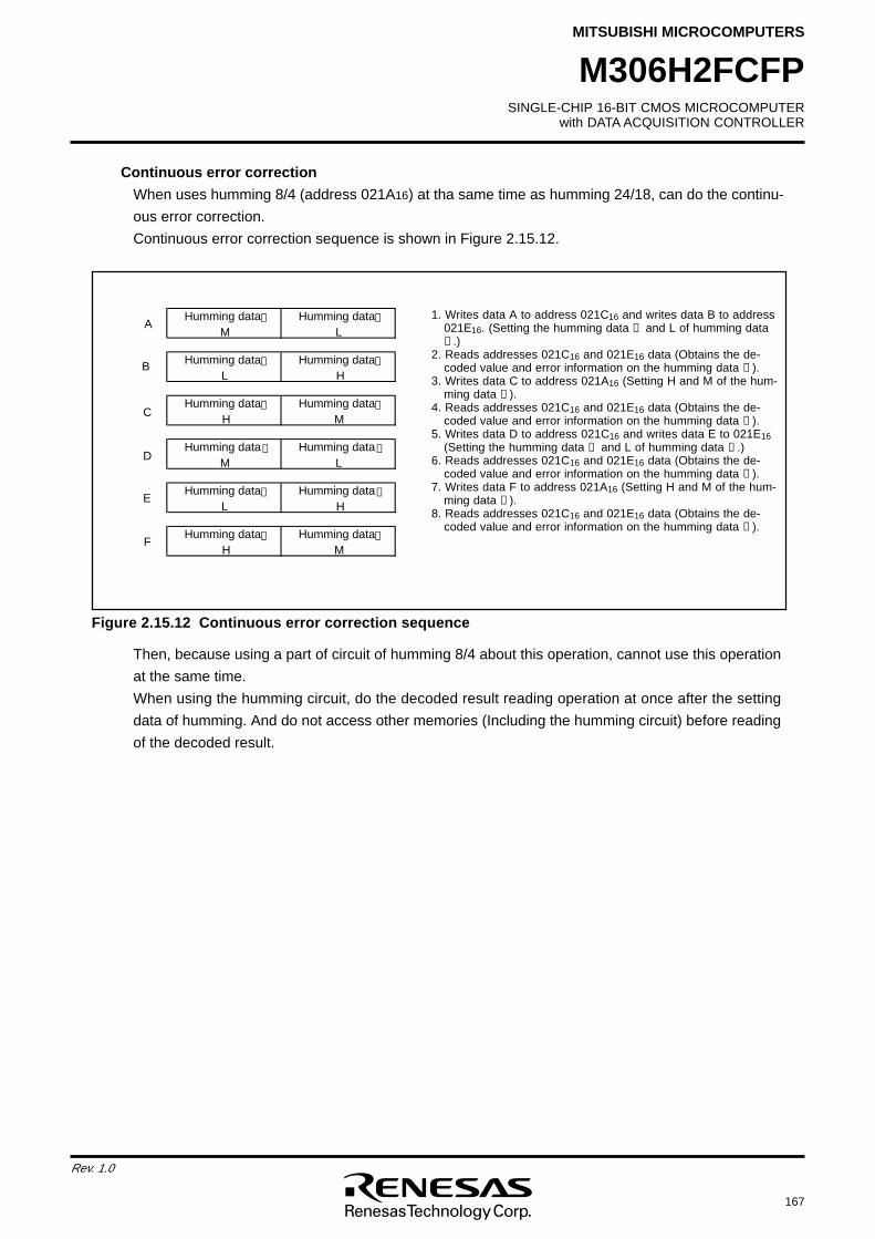
SINGLE-CHIP 16-BIT CMOS MICROCOMPUTERwith DATA ACQUISITION CONTROLLER
MITSUBISHI MICROCOMPUTERS
167
Rev. 1.0
M306H2FCFP
Continuous error correction
When uses humming 8/4 (address 021A16) at tha same time as humming 24/18, can do the continu-
ous error correction.
Continuous error correction sequence is shown in Figure 2.15.12.
Figure 2.15.12 Continuous error correction sequence
Then, because using a part of circuit of humming 8/4 about this operation, cannot use this operation
at the same time.
When using the humming circuit, do the decoded result reading operation at once after the setting
data of humming. And do not access other memories (Including the humming circuit) before reading
of the decoded result.
➀ Humming data ➀M L
➁ Humming data ➀L H
➁ Humming data ➁H M
➂ Humming data ➂M L
➃ Humming data ➂L H
Humming data
Humming data
Humming data
Humming data
Humming data
Humming data ➃ Humming data ➃H M
A
B
C
D
E
F
1. Writes data A to address 021C16 and writes data B to address021E16. (Setting the humming data ➀ and L of humming data➁ .)
2. Reads addresses 021C16 and 021E16 data (Obtains the de-coded value and error information on the humming data ➀ ).
3. Writes data C to address 021A16 (Setting H and M of the hum-ming data ➁ ).
4. Reads addresses 021C16 and 021E16 data (Obtains the de-coded value and error information on the humming data ➁ ).
5. Writes data D to address 021C16 and writes data E to 021E16(Setting the humming data ➂ and L of humming data ➃ .)
6. Reads addresses 021C16 and 021E16 data (Obtains the de-coded value and error information on the humming data ➂ ).
7. Writes data F to address 021A16 (Setting H and M of the hum-ming data ➃ ).
8. Reads addresses 021C16 and 021E16 data (Obtains the de-coded value and error information on the humming data ➃ ).
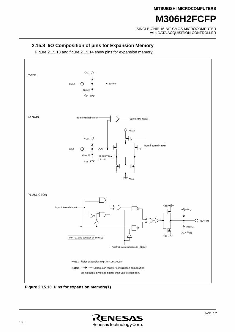
168
Rev. 1.0
SINGLE-CHIP 16-BIT CMOS MICROCOMPUTERwith DATA ACQUISITION CONTROLLER
MITSUBISHI MICROCOMPUTERS
M306H2FCFP
Figure 2.15.13 Pins for expansion memory(1)
2.15.8 I/O Composition of pins for Expansion MemoryFigure 2.15.13 and figure 2.15.14 show pins for expansion memory.
CVIN1
CVIN1
VCC
VSS
SYNCIN
input
VCC
VSS
from internal circuit
VDD2
VSS2
(Note 2)
(Note 2)
to slicer
P11/SLICEON
OUTPUT
VCC
VSS
Port P11 output selection bit (Note 1)
Port P11 data selection bit (Note 1)
VCC
VSS
Note1 : Refer expansion register construction
Note2 : Expamsion register construction composition
to internal circuit
from internal circuit
to internalcircuit
from internal circuit
(Note 2)
Do not apply a voltage higher than Vcc to each port.
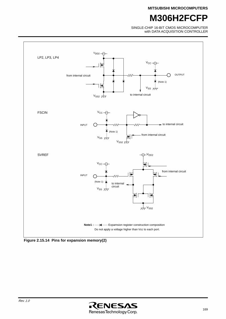
SINGLE-CHIP 16-BIT CMOS MICROCOMPUTERwith DATA ACQUISITION CONTROLLER
MITSUBISHI MICROCOMPUTERS
169
Rev. 1.0
M306H2FCFP
Figure 2.15.14 Pins for expansion memory(2)
F
S
C
I
N
L P
2
,
L
P
3
,
L
P
4
VC
C
VS
S
O
U
T
P
U
T
I N
P
U
T
VC
C
VS
S
S
V
R
E
F
VC
C
VS
S
VD
D
2
VS
S
2
VD
D
2
VS
S
2
VS
S
2
N
o
t
e
1
: E
x
p
a
m
s
i
o
n
r
e
g
i
s
t
e
r
c
o
n
s
t
r
u
c
t
i
o
n
c
o
m
p
o
s
i
t
i
o
n
f r
o
m
i
n
t
e
r
n
a
l
c
i
r
c
u
i
t( N
o
t
e
1
)
t o
i
n
t
e
r
n
a
l
c
i
r
c
u
i
t
I N
P
U
T
( N
o
t
e
1
)
t o
i
n
t
e
r
n
a
l
c
i
r
c
u
i
t
f r
o
m
i
n
t
e
r
n
a
l
c
i
r
c
u
i
t
( N
o
t
e
1
)
t o
i
n
t
e
r
n
a
l
c
i
r
c
u
i
t
f r
o
m
i
n
t
e
r
n
a
l
c
i
r
c
u
i
t
Do not apply a voltage higher than Vcc to each port.
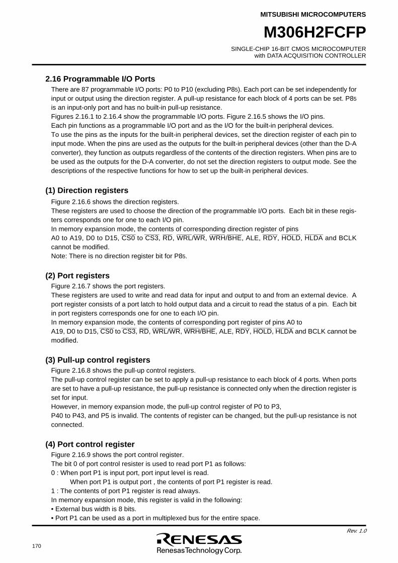
170
Rev. 1.0
SINGLE-CHIP 16-BIT CMOS MICROCOMPUTERwith DATA ACQUISITION CONTROLLER
MITSUBISHI MICROCOMPUTERS
M306H2FCFP
2.16 Programmable I/O PortsThere are 87 programmable I/O ports: P0 to P10 (excluding P85). Each port can be set independently forinput or output using the direction register. A pull-up resistance for each block of 4 ports can be set. P85
is an input-only port and has no built-in pull-up resistance.Figures 2.16.1 to 2.16.4 show the programmable I/O ports. Figure 2.16.5 shows the I/O pins.Each pin functions as a programmable I/O port and as the I/O for the built-in peripheral devices.To use the pins as the inputs for the built-in peripheral devices, set the direction register of each pin toinput mode. When the pins are used as the outputs for the built-in peripheral devices (other than the D-Aconverter), they function as outputs regardless of the contents of the direction registers. When pins are tobe used as the outputs for the D-A converter, do not set the direction registers to output mode. See thedescriptions of the respective functions for how to set up the built-in peripheral devices.
(1) Direction registersFigure 2.16.6 shows the direction registers.These registers are used to choose the direction of the programmable I/O ports. Each bit in these regis-ters corresponds one for one to each I/O pin.In memory expansion mode, the contents of corresponding direction register of pins
________ ________ _____ ________ ______ ________ ________ ________ __________ __________
A0 to A19, D0 to D15, CS0 to CS3, RD, WRL/WR, WRH/BHE, ALE, RDY, HOLD, HLDA and BCLKcannot be modified.Note: There is no direction register bit for P85.
(2) Port registersFigure 2.16.7 shows the port registers.These registers are used to write and read data for input and output to and from an external device. Aport register consists of a port latch to hold output data and a circuit to read the status of a pin. Each bitin port registers corresponds one for one to each I/O pin.In memory expansion mode, the contents of corresponding port register of pins A0 to
________ ________ _____ ________ ______ ________ ________ ________ __________ __________
A19, D0 to D15, CS0 to CS3, RD, WRL/WR, WRH/BHE, ALE, RDY, HOLD, HLDA and BCLK cannot bemodified.
(3) Pull-up control registersFigure 2.16.8 shows the pull-up control registers.The pull-up control register can be set to apply a pull-up resistance to each block of 4 ports. When portsare set to have a pull-up resistance, the pull-up resistance is connected only when the direction register isset for input.However, in memory expansion mode, the pull-up control register of P0 to P3,P40 to P43, and P5 is invalid. The contents of register can be changed, but the pull-up resistance is notconnected.
(4) Port control registerFigure 2.16.9 shows the port control register.The bit 0 of port control resister is used to read port P1 as follows:0 : When port P1 is input port, port input level is read.
When port P1 is output port , the contents of port P1 register is read.1 : The contents of port P1 register is read always.In memory expansion mode, this register is valid in the following:• External bus width is 8 bits.• Port P1 can be used as a port in multiplexed bus for the entire space.
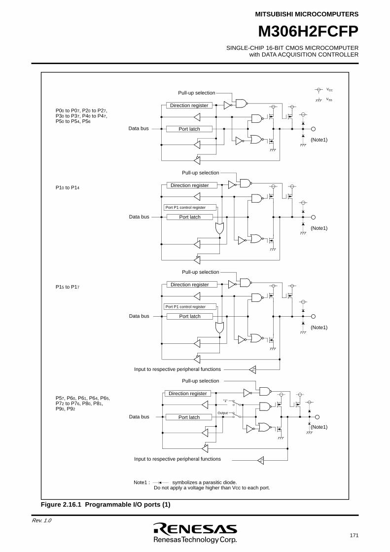
SINGLE-CHIP 16-BIT CMOS MICROCOMPUTERwith DATA ACQUISITION CONTROLLER
MITSUBISHI MICROCOMPUTERS
171
Rev. 1.0
M306H2FCFP
Figure 2.16.1 Programmable I/O ports (1)
P00 to P07, P20 to P27, P30 to P37, P40 to P47, P50 to P54, P56
P10 to P14
P15 to P17
P57, P60, P61, P64, P65, P72 to P76, P80, P81, P90, P92
Data bus
Direction register
Pull-up selection
Port latch
Data bus
Direction register
Pull-up selection
Port latch
Port P1 control register
Direction register
Port latch
Port P1 control register
Pull-up selection
Data bus
Input to respective peripheral functions
Direction register
Port latch
Pull-up selection
Data bus
Input to respective peripheral functions
Note1 : symbolizes a parasitic diode. Do not apply a voltage higher than Vcc to each port.
"1"
Output
(Note1)
(Note1)
(Note1)
(Note1)
VCC
VSS
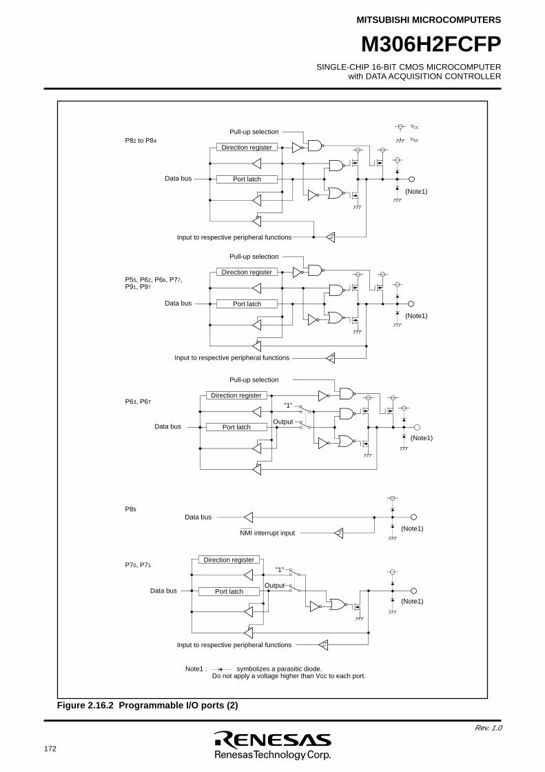
172
Rev. 1.0
SINGLE-CHIP 16-BIT CMOS MICROCOMPUTERwith DATA ACQUISITION CONTROLLER
MITSUBISHI MICROCOMPUTERS
M306H2FCFP
Figure 2.16.2 Programmable I/O ports (2)
P70, P71
P85
P82 to P84
P55, P62, P66, P77, P91, P97
P63, P67
Data bus
Direction register
Pull-up selection
Port latch
Input to respective peripheral functions
Data bus
Direction register
Pull-up selection
Port latch
Input to respective peripheral functions
"1"
OutputData bus
Direction register
Pull-up selection
Port latch
Data bus
NMI interrupt input
"1"
Output
Direction register
Port latch
Input to respective peripheral functions
Note1 : symbolizes a parasitic diode. Do not apply a voltage higher than Vcc to each port.
(Note1)
(Note1)
(Note1)
(Note1)
(Note1)
VCC
VSS
Data bus
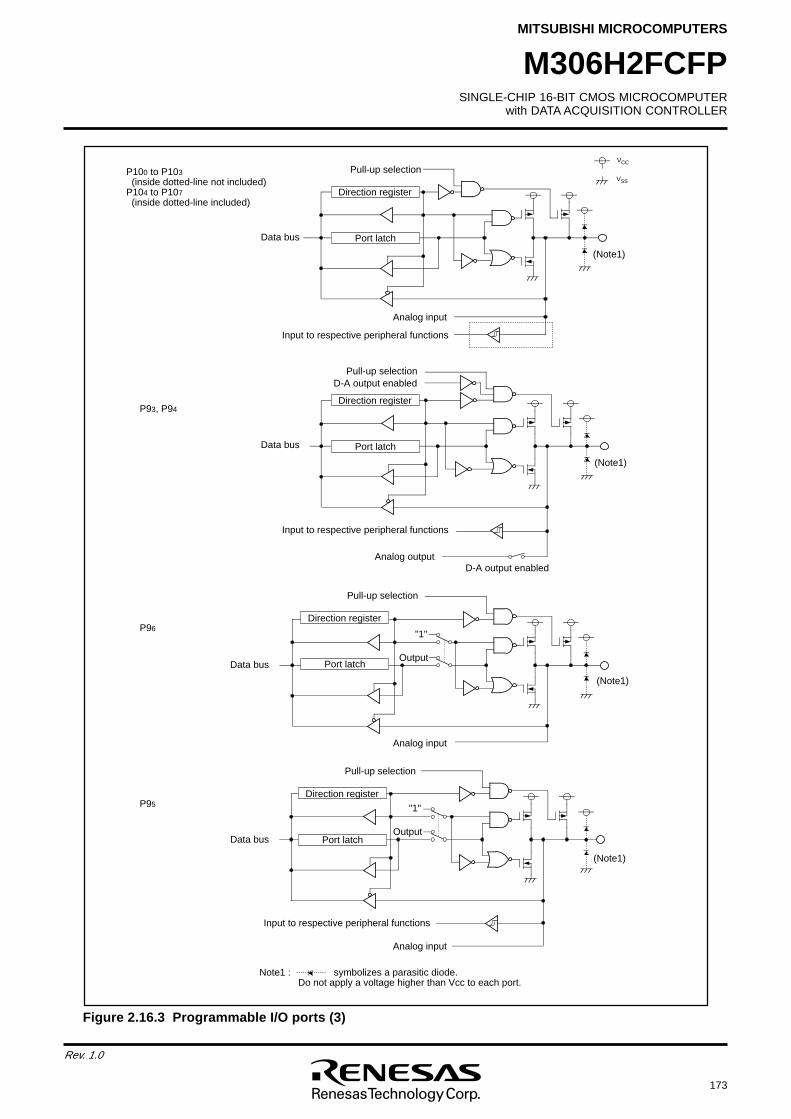
SINGLE-CHIP 16-BIT CMOS MICROCOMPUTERwith DATA ACQUISITION CONTROLLER
MITSUBISHI MICROCOMPUTERS
173
Rev. 1.0
M306H2FCFP
Figure 2.16.3 Programmable I/O ports (3)
P93, P94
P96
P95
Data bus
Direction register
Pull-up selection
Port latch
Analog input
Input to respective peripheral functions
P100 to P103 (inside dotted-line not included)P104 to P107 (inside dotted-line included)
D-A output enabled
Direction register
Pull-up selection
Port latchData bus
Input to respective peripheral functions
D-A output enabledAnalog output
"1"
Output
Direction register
Pull-up selection
Port latchData bus
Analog input
"1"
Output
Direction register
Pull-up selection
Port latchData bus
Analog input
Input to respective peripheral functions
Note1 : symbolizes a parasitic diode. Do not apply a voltage higher than Vcc to each port.
(Note1)
(Note1)
(Note1)
(Note1)
VCC
VSS
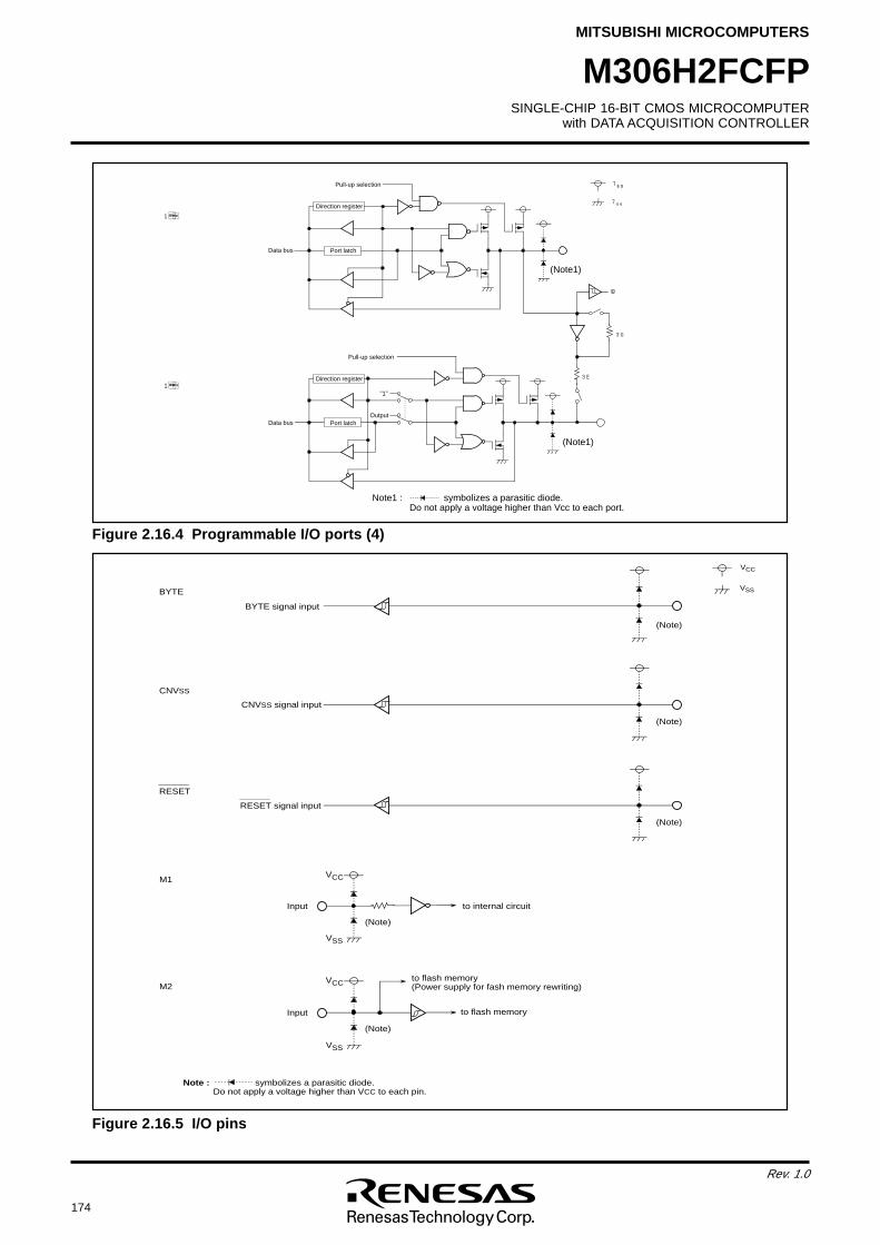
174
Rev. 1.0
SINGLE-CHIP 16-BIT CMOS MICROCOMPUTERwith DATA ACQUISITION CONTROLLER
MITSUBISHI MICROCOMPUTERS
M306H2FCFP
Figure 2.16.5 I/O pins
Figure 2.16.4 Programmable I/O ports (4)
P87
P86
fc
Rf
Rd
VCC
VSS
Data bus
Pull-up selection
Port latch
"1"
Output
Note1 : symbolizes a parasitic diode.Do not apply a voltage higher than Vcc to each port.
(Note1)
Direction register
Data bus
Pull-up selection
Port latch
Direction register
(Note1)
BYTE
CNVSS
RESET
RESET signal input
VCC
VSS
M1VCC
VSS
M2
VSS
VCC
BYTE signal input
CNVSS signal input
(Note)
(Note)
(Note)
(Note)
(Note)
Input
Input
to internal circuit
to flash memory(Power supply for fash memory rewriting)
to flash memory
Note : symbolizes a parasitic diode.Do not apply a voltage higher than VCC to each pin.
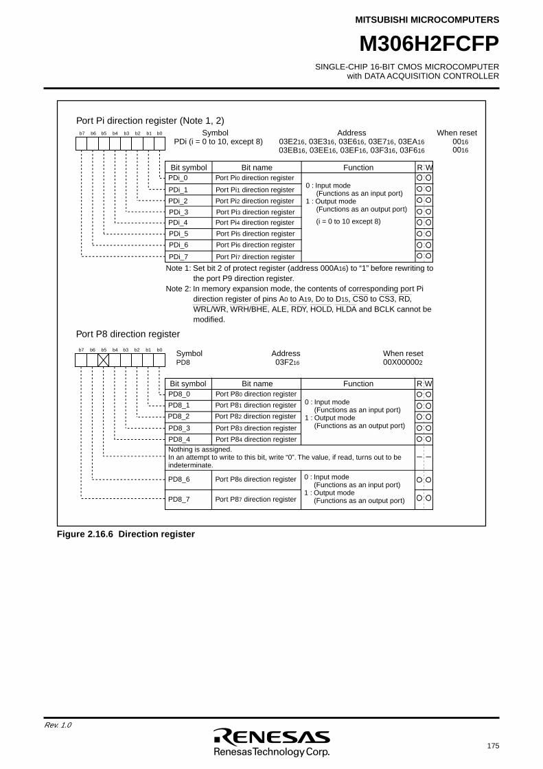
SINGLE-CHIP 16-BIT CMOS MICROCOMPUTERwith DATA ACQUISITION CONTROLLER
MITSUBISHI MICROCOMPUTERS
175
Rev. 1.0
M306H2FCFP
Figure 2.16.6 Direction register
Port Pi direction register (Note 1, 2)Symbol Address When reset
PDi (i = 0 to 10, except 8) 03E216, 03E316, 03E616, 03E716, 03EA16 0016001603EB16, 03EE16, 03EF16, 03F316, 03F616
Bit name FunctionBit symbol WR
b7 b6 b5 b4 b3 b2 b1 b0
PDi_0 Port Pi0 direction register
PDi_1 Port Pi1 direction register
PDi_2 Port Pi2 direction register
PDi_3 Port Pi3 direction register
PDi_4 Port Pi4 direction register
PDi_5 Port Pi5 direction register
PDi_6 Port Pi6 direction register
PDi_7 Port Pi7 direction register
0 : Input mode(Functions as an input port)
1 : Output mode(Functions as an output port)
(i = 0 to 10 except 8)
Port P8 direction register
Symbol Address When resetPD8 03F216 00X000002
Bit name FunctionBit symbol WR
b7 b6 b5 b4 b3 b2 b1 b0
PD8_0 Port P80 direction register
PD8_1 Port P81 direction register
PD8_2 Port P82 direction register
PD8_3 Port P83 direction register
PD8_4 Port P84 direction registerNothing is assigned.In an attempt to write to this bit, write “0”. The value, if read, turns out to be indeterminate.
PD8_6 Port P86 direction register
PD8_7 Port P87 direction register
0 : Input mode(Functions as an input port)
1 : Output mode(Functions as an output port)
0 : Input mode(Functions as an input port)
1 : Output mode(Functions as an output port)
Note 1: Set bit 2 of protect register (address 000A16) to “1” before rewriting to the port P9 direction register.
Note 2: In memory expansion mode, the contents of corresponding port Pi direction register of pins A0 to A19, D0 to D15, CS0 to CS3, RD, WRL/WR, WRH/BHE, ALE, RDY, HOLD, HLDA and BCLK cannot be modified.
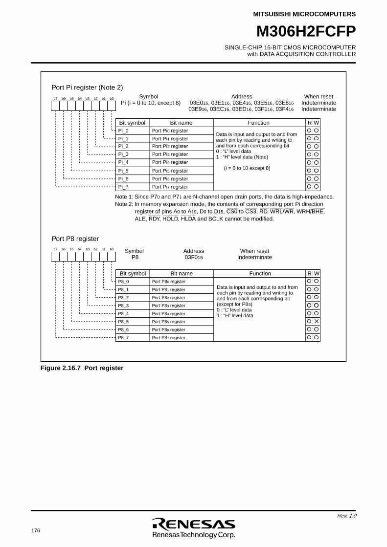
176
Rev. 1.0
SINGLE-CHIP 16-BIT CMOS MICROCOMPUTERwith DATA ACQUISITION CONTROLLER
MITSUBISHI MICROCOMPUTERS
M306H2FCFP
Figure 2.16.7 Port register
Port Pi register (Note 2)
Symbol Address When resetPi (i = 0 to 10, except 8) 03E016, 03E116, 03E416, 03E516, 03E816 Indeterminate
03E916, 03EC16, 03ED16, 03F116, 03F416 Indeterminate
Bit name FunctionBit symbol WR
b7 b6 b5 b4 b3 b2 b1 b0
Pi_0 Port Pi0 register
Pi_1 Port Pi1 register
Pi_2 Port Pi2 register
Pi_3 Port Pi3 register
Pi_4 Port Pi4 register
Pi_5 Port Pi5 register
Pi_6 Port Pi6 register
Pi_7 Port Pi7 register
Data is input and output to and from each pin by reading and writing to and from each corresponding bit0 : “L” level data1 : “H” level data (Note)
(i = 0 to 10 except 8)
Port P8 register
Symbol Address When reset P8 03F016 Indeterminate
Bit name FunctionBit symbol WR
b7 b6 b5 b4 b3 b2 b1 b0
P8_0 Port P80 register
P8_1 Port P81 register
P8_2 Port P82 register
P8_3 Port P83 register
P8_4 Port P84 register
P8_5 Port P85 register
P8_6 Port P86 register
P8_7 Port P87 register
Data is input and output to and from each pin by reading and writing to and from each corresponding bit(except for P85)0 : “L” level data1 : “H” level data
Note 1: Since P70 and P71 are N-channel open drain ports, the data is high-impedance.Note 2: In memory expansion mode, the contents of corresponding port Pi direction
register of pins A0 to A19, D0 to D15, CS0 to CS3, RD, WRL/WR, WRH/BHE, ALE, RDY, HOLD, HLDA and BCLK cannot be modified.
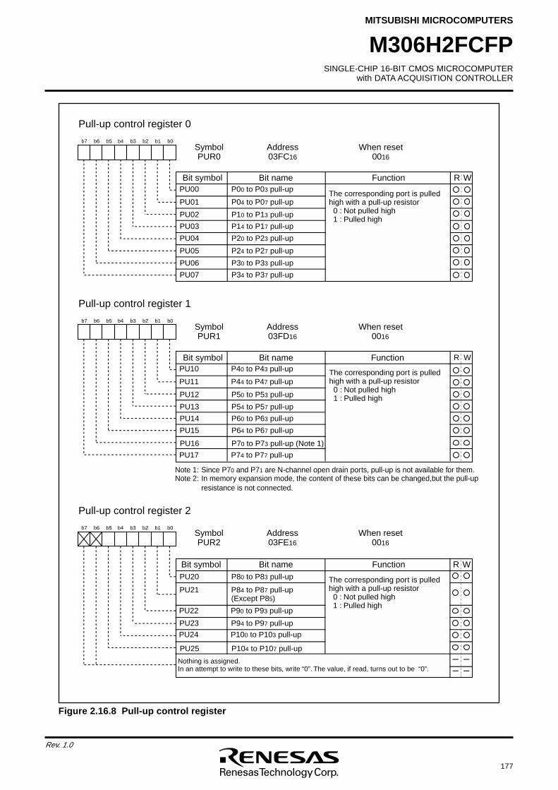
SINGLE-CHIP 16-BIT CMOS MICROCOMPUTERwith DATA ACQUISITION CONTROLLER
MITSUBISHI MICROCOMPUTERS
177
Rev. 1.0
M306H2FCFP
Figure 2.16.8 Pull-up control register
Pull-up control register 0
Symbol Address When resetPUR0 03FC16 0016
Bit name Function Bit symbol WR
b7 b6 b5 b4 b3 b2 b1 b0
PU00 P00 to P03 pull-up
PU01 P04 to P07 pull-up
PU02 P10 to P13 pull-up
PU03 P14 to P17 pull-up
PU04 P20 to P23 pull-up
PU05 P24 to P27 pull-up
PU06 P30 to P33 pull-up
PU07 P34 to P37 pull-up
The corresponding port is pulled high with a pull-up resistor 0 : Not pulled high 1 : Pulled high
Pull-up control register 1
Symbol Address When resetPUR1 03FD16 0016
Bit name Function Bit symbol WR
b7 b6 b5 b4 b3 b2 b1 b0
PU10 P40 to P43 pull-up
PU11 P44 to P47 pull-up
PU12 P50 to P53 pull-up
PU13 P54 to P57 pull-up
PU14 P60 to P63 pull-up
PU15 P64 to P67 pull-up
PU16 P70 to P73 pull-up (Note 1)
PU17 P74 to P77 pull-up
The corresponding port is pulled high with a pull-up resistor 0 : Not pulled high 1 : Pulled high
Note 1: Since P70 and P71 are N-channel open drain ports, pull-up is not available for them.Note 2: In memory expansion mode, the content of these bits can be changed,but the pull-up
resistance is not connected.
Pull-up control register 2
Symbol Address When resetPUR2 03FE16 0016
Bit name FunctionBit symbol WR
b7 b6 b5 b4 b3 b2 b1 b0
PU20 P80 to P83 pull-up
PU21 P84 to P87 pull-up(Except P85)
PU22 P90 to P93 pull-up
PU23 P94 to P97 pull-up
PU24 P100 to P103 pull-up
PU25 P104 to P107 pull-up
Nothing is assigned.In an attempt to write to these bits, write “0”. The value, if read, turns out to be “0”.
The corresponding port is pulled high with a pull-up resistor 0 : Not pulled high 1 : Pulled high
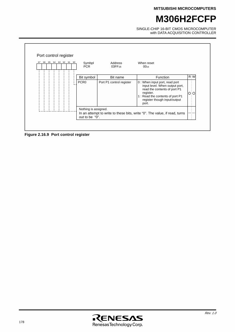
178
Rev. 1.0
SINGLE-CHIP 16-BIT CMOS MICROCOMPUTERwith DATA ACQUISITION CONTROLLER
MITSUBISHI MICROCOMPUTERS
M306H2FCFP
Figure 2.16.9 Port control register
Port control register
Symbpl Address When resetPCR 03FF16 0016
Bit name FunctionBit symbol WR
b7 b6 b5 b4 b3 b2 b1 b0
PCR0 Port P1 control register 0 : When input port, read port input level. When output port, read the contents of port P1 register.
1 : Read the contents of port P1 register though input/output port.
Nothing is assigned.In an attempt to write to these bits, write “0”. The value, if read, turns out to be “0”.
AA
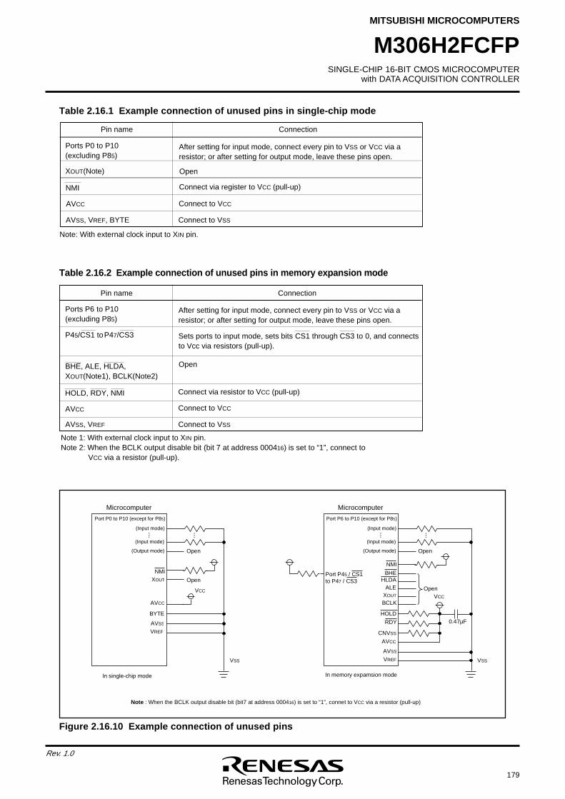
SINGLE-CHIP 16-BIT CMOS MICROCOMPUTERwith DATA ACQUISITION CONTROLLER
MITSUBISHI MICROCOMPUTERS
179
Rev. 1.0
M306H2FCFP
Table 2.16.1 Example connection of unused pins in single-chip mode
Pin name Connection
Ports P0 to P10 (excluding P85)
After setting for input mode, connect every pin to VSS or VCC via a resistor; or after setting for output mode, leave these pins open.
OpenXOUT(Note)
NMI Connect via register to VCC (pull-up)
Connect to VCC
AVSS, VREF, BYTE
AVCC
Connect to VSS
Note: With external clock input to XIN pin.
Table 2.16.2 Example connection of unused pins in memory expansion mode
Pin name Connection
Ports P6 to P10 (excluding P85)
AVSS, VREF
AVCC
After setting for input mode, connect every pin to VSS or VCC via a resistor; or after setting for output mode, leave these pins open.
Open
Connect to VCC
Connect to VSS
Note 1: With external clock input to XIN pin.Note 2: When the BCLK output disable bit (bit 7 at address 000416) is set to “1”, connect to
VCC via a resistor (pull-up).
HOLD, RDY, NMI Connect via resistor to VCC (pull-up)
BHE, ALE, HLDA, XOUT(Note1), BCLK(Note2)
P45/CS1 to P47/CS3 Sets ports to input mode, sets bits CS1 through CS3 to 0, and connects to Vcc via resistors (pull-up).
Figure 2.16.10 Example connection of unused pins
N
M
I
XO
U
T
A
VC
C
A
VS
S
VR
E
F
O
p
e
n
M
i
c
r
o
c
o
m
p
u
t
e
r
VC
C
VS
S
H
O
L
D
R
D
Y
A
L
E
B
C
L
K
B
H
EH
L
D
A
O
p
e
n
P
o
r
t
P
45
/
C
S
1t
o
P
47
/
C
S
3
0 .
4
7
µ
F
C
N
VS
S
P
o
r
t
P
6
t
o
P
1
0
(
e
x
c
e
p
t
f
o
r
P
85)
( I
n
p
u
t
m
o
d
e
)
( O
u
t
p
u
t
m
o
d
e
)
( I
n
p
u
t
m
o
d
e
)
. . .
. . .
B
Y
T
E
A
VS
S
VR
E
F
M
i
c
r
o
c
o
m
p
u
t
e
r
VC
C
VS
S
A
VC
C
O
p
e
n
P
o
r
t
P
0
t
o
P
1
0
(
e
x
c
e
p
t
f
o
r
P
85)
( I
n
p
u
t
m
o
d
e
)
( O
u
t
p
u
t
m
o
d
e
)
( I
n
p
u
t
m
o
d
e
)
. . .
. . .
N
M
IXO
U
T O
p
e
n
I n
s
i
n
g
l
e
-
c
h
i
p
m
o
d
e I n
m
e
m
o
r
y
e
x
p
a
m
s
i
o
n
m
o
d
e
o
r
i
n
m
i
c
r
o
p
r
o
s
s
o
r
m
o
d
e
N
o
t
e
:
W
h
e
n
t
h
e
B
C
L
K
o
u
t
p
u
t
d
i
s
a
b
l
e
b
i
t
(
b
i
t
7
a
t
a
d
d
r
e
s
s
0
0
0
41
6)
i
s
s
e
t
t
o
“
1
”
,
c
o
n
n
e
t
t
o
VC
C
v
i
a
a
r
e
s
i
s
t
o
r
(
p
u
l
l
-
u
p
)
180
Rev. 1.0
SINGLE-CHIP 16-BIT CMOS MICROCOMPUTERwith DATA ACQUISITION CONTROLLER
MITSUBISHI MICROCOMPUTERS
M306H2FCFP
3. USAGE PRECAUTION
Timer A (timer mode)(1) Reading the timer Ai register while a count is in progress allows reading, with arbitrary timing, the
value of the counter. Reading the timer Ai register with the reload timing gets “FFFF16”. Reading
the timer Ai register after setting a value in the timer Ai register with a count halted but before the
counter starts counting gets a proper value.
Timer A (event counter mode)(1) Reading the timer Ai register while a count is in progress allows reading, with arbitrary timing, the
value of the counter. Reading the timer Ai register with the reload timing gets “FFFF16” by underflow
or “000016” by overflow. Reading the timer Ai register after setting a value in the timer Ai register with
a count halted but before the counter starts counting gets a proper value.
(2) When stop counting in free run type, set timer again.
(3) In the case of using “Event counter mode” as “Free-Run type” for timer A, the timer register contents
may be unkown when counting begins. If the timer register is set before counting has started, then the
starting value will be unkown.
This issue will occuer only for the “Event counter mode” operating as “Free-Run type”. The value of
the timer register will not be unkown during counting.
Timer A (one-shot timer mode)(1) Setting the count start flag to “0” while a count is in progress causes as follows:
• The counter stops counting and a content of reload register is reloaded.
• The TAiOUT pin outputs “L” level.
• The interrupt request generated and the timer Ai interrupt request bit goes to “1”.
(2) The timer Ai interrupt request bit goes to “1” if the timer's operation mode is set using any of the
following procedures:
• Selecting one-shot timer mode after reset.
• Changing operation mode from timer mode to one-shot timer mode.
• Changing operation mode from event counter mode to one-shot timer mode.
Therefore, to use timer Ai interrupt (interrupt request bit), set timer Ai interrupt request bit to “0” after
the above listed changes have been made.
Timer A (pulse width modulation mode)
(1) The timer Ai interrupt request bit becomes “1” if setting operation mode of the timer in compliance with
any of the following procedures:
• Selecting PWM mode after reset.
• Changing operation mode from timer mode to PWM mode.
• Changing operation mode from event counter mode to PWM mode.
Therefore, to use timer Ai interrupt (interrupt request bit), set timer Ai interrupt request bit to “0” after
the above listed changes have been made.
(2) Setting the count start flag to “0” while PWM pulses are being output causes the counter to stop
counting. If the TAiOUT pin is outputting an “H” level in this instance, the output level goes to “L”, and
the timer Ai interrupt request bit goes to “1”. If the TAiOUT pin is outputting an “L” level in this instance,
the level does not change, and the timer Ai interrupt request bit does not becomes “1”.
SINGLE-CHIP 16-BIT CMOS MICROCOMPUTERwith DATA ACQUISITION CONTROLLER
MITSUBISHI MICROCOMPUTERS
181
Rev. 1.0
M306H2FCFP
Timer B (timer mode, event counter mode)(1) Reading the timer Bi register while a count is in progress allows reading , with arbitrary timing, the
value of the counter. Reading the timer Bi register with the reload timing gets “FFFF16”. Reading thetimer Bi register after setting a value in the timer Bi register with a count halted but before the counter
starts counting gets a proper value.
Timer B (pulse period/pulse width measurement mode)
(1) If changing the measurement mode select bit is set after a count is started, the timer Bi interruptrequest bit goes to “1”.
(2) When the first effective edge is input after a count is started, an indeterminate value is transferred to
the reload register. At this time, timer Bi interrupt request is not generated.
A-D Converter
(1) Write to each bit (except bit 6) of A-D control register 0, to each bit of A-D control register 1, and to bit0 of A-D control register 2 when A-D conversion is stopped (before a trigger occurs).
In particular, when the Vref connection bit is changed from “0” to “1”, start A-D conversion after anelapse of 1 µs or longer.
(2) When changing A-D operation mode, select analog input pin again.(3) Using one-shot mode or single sweep mode
Read the correspondence A-D register after confirming A-D conversion is finished. (It is known by A-Dconversion interrupt request bit.)
(4) Using repeat mode, repeat sweep mode 0 or repeat sweep mode 1Use the undivided main clock as the internal CPU clock.
Stop Mode and Wait Mode____________
(1) When returning from stop mode by hardware reset, RESET pin must be set to “L” level until mainclock oscillation is stabilized.
(2) When switching to either wait mode or stop mode, instructions occupying four bytes either from theWAIT instruction or from the instruction that sets the every-clock stop bit to “1” within the instructionqueue are prefetched and then the program stops. So put at least four NOPs in succession either tothe WAIT instruction or to the instruction that sets the every-clock stop bit to “1”.
(3) When the MCU running in low-speed or low power dissipation mode, do not enter WAIT mode with
WAIT periphheral function clock stop bit set to “1”.
Interrupts(1) Reading address 0000016
• When maskable interrupt is occurred, CPU read the interrupt information (the interrupt number andinterrupt request level) in the interrupt sequence.The interrupt request bit of the certain interrupt written in address 0000016 will then be set to “0”.Reading address 0000016 by software sets enabled highest priority interrupt source request bit to “0”.Though the interrupt is generated, the interrupt routine may not be executed.Do not read address 0000016 by software.
(2) Setting the stack pointer• The value of the stack pointer immediately after reset is initialized to 000016. Accepting an interrupt
before setting a value in the stack pointer may become a factor of runaway. Be sure to set a value inthe stack pointer before accepting an interrupt.
_______
When using the NMI interrupt, initialize the stack point at the beginning of a program. Concerning the first in_______
struction immediately after reset, generating any interrupts including the NMI interrupt is prohib ited.
182
Rev. 1.0
SINGLE-CHIP 16-BIT CMOS MICROCOMPUTERwith DATA ACQUISITION CONTROLLER
MITSUBISHI MICROCOMPUTERS
M306H2FCFP
_______
(3) The NMI interrupt_______
• As for the NMI interrupt pin, an interrupt cannot be disabled. Connect it to the VCC pin via a resistor
(pull-up) if unused. Be sure to work on it._______
• Do not get either into stop mode with the NMI pin set to “L”.
(4) External interrupt________ ________
• When the polarity of the INT0 to INT5 pins is changed, the interrupt request bit is sometimes set to “1”.
After changing the polarity, set the interrupt request bit to “0”.
(5) Rewrite the interrupt control register
• To rewrite the interrupt control register, do so at a point that does not generate the interrupt request for
that register. If there is possibility of the interrupt request occur, rewrite the interrupt control register
after the interrupt is disabled. The program examples are described as follow:
Example 1:INT_SWITCH1:
FCLR I ; Disable interrupts.AND.B #00h, 0055h ; Clear TA0IC int. priority level and int. request bit.NOP ; Four NOP instructions are required when using HOLD function.NOPFSET I ; Enable interrupts.
Example 2:INT_SWITCH2:
FCLR I ; Disable interrupts.AND.B #00h, 0055h ; Clear TA0IC int. priority level and int. request bit.MOV.W MEM, R0 ; Dummy read.FSET I ; Enable interrupts.
Example 3:INT_SWITCH3:
PUSHC FLG ; Push Flag register onto stackFCLR I ; Disable interrupts.AND.B #00h, 0055h ; Clear TA0IC int. priority level and int. request bit.POPC FLG ; Enable interrupts.
The reason why two NOP instructions (four when using the HOLD function) or dummy read are inserted before FSET I in Examples 1 and 2 is to prevent the interrupt enable flag I from being set before the interrupt control register is rewritten due to effects of the instruction queue.
• When a instruction to rewrite the interrupt control register is executed but the interrupt is disabled, the
interrupt request bit is not set sometimes even if the interrupt request for that register has been gener
ated. This will depend on the instruction. If this creates problems, use the below instructions to change
the register.
Instructions : AND, OR, BCLR, BSET
Electric Characteristic Differences Between Mask ROM and Flash Memory Version MCUs
There are differences in electric characteristics, operation margin, noise immunity, and noise radiationbetween Mask ROM and Flash Memory version MCUs due to the difference in the manufacturingprocesses.When manufacturing an application system with the Flash Memory version and then switching to use ofthe Mask ROM version, please perform sufficient evaluations for the commercial samples of the MaskROM version.
SINGLE-CHIP 16-BIT CMOS MICROCOMPUTERwith DATA ACQUISITION CONTROLLER
MITSUBISHI MICROCOMPUTERS
183
Rev. 1.0
M306H2FCFP
Other Notes
(1) Timing of power supplying
The power need to supply to VCC, VDD1, VDD2, VDD3 and AVCC at a time. While operating, must set
same voltage.
(2) Power supply noise and latch-up
In order to avoid power supply noise and latch-up, connect a bypass capacitor (more than 0.1µF)
directly between the VCC pin and VSS pin, VDD1 pin and VSS1 pin, VDD2 pin and VSS2 pin, VDD3 pin
and VSS3 pin, AVCC pin and AVSS pin using a heavy wire.
(3) When oscillation circuit stop for data slicer
Expansion register XTAL-VCO, PDC_VCO_ON,VPS_VCO_ON is set at “L”, when the data slicer is
not used, and the oscillation is stopped. When starting oscillation again, set data at the folowing
order.
(a) Set expansion register XTAL-VCO = “H”.
(b) Set expansion register PDC_VCO_ON,VPS_VCO_ON = “H”.
(c) 60 ms or more is a waiting state (stability period of internal oscillation circuit + data slice preparation).
To operate slice RAM , set expansion register XTAL_VCO = “H”. And input 4.43 MHz sub carrier
frequency clock from the FSCIN pin.
Access the memories after wating for 20 ms certainly when resuming synchronous oscillation from
the off state , and begin to input clock into the FSCIN pin.
(4) At stop mode (clock is stopped)
Set each input pins to as follows.
(a) Set M1 pin = VSS.
(b) Stop the FSCIN pin input.
(c) Set expansion register STBY0 and STBY1 = “H”.
Set all expansion registers to “L” except for the superscription register.
(5) When operation start from stand-by mode (clock is stopped)
Input FSCIN pin clock after set “L” to register STBY0 and STBY1.
At next, set expansion register as notes (3).
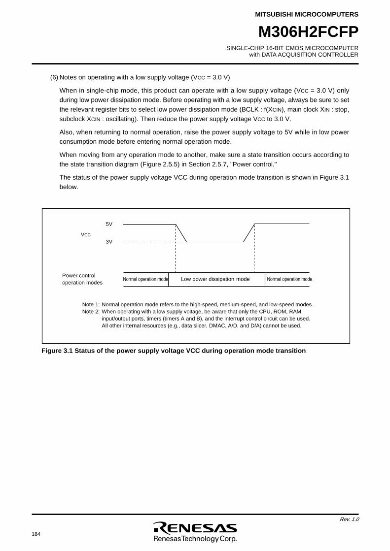
184
Rev. 1.0
SINGLE-CHIP 16-BIT CMOS MICROCOMPUTERwith DATA ACQUISITION CONTROLLER
MITSUBISHI MICROCOMPUTERS
M306H2FCFP
(6) Notes on operating with a low supply voltage (VCC = 3.0 V)
When in single-chip mode, this product can operate with a low supply voltage (VCC = 3.0 V) onlyduring low power dissipation mode. Before operating with a low supply voltage, always be sure to set
the relevant register bits to select low power dissipation mode (BCLK : f(XCIN), main clock XIN : stop,
subclock XCIN : oscillating). Then reduce the power supply voltage VCC to 3.0 V.
Also, when returning to normal operation, raise the power supply voltage to 5V while in low powerconsumption mode before entering normal operation mode.
When moving from any operation mode to another, make sure a state transition occurs according to
the state transition diagram (Figure 2.5.5) in Section 2.5.7, "Power control."
The status of the power supply voltage VCC during operation mode transition is shown in Figure 3.1
below.
Figure 3.1 Status of the power supply voltage VCC during operation mode transition
L o
w
p
o
w
e
r
dissipation
m
o
d
e N
o
r
m
a
l
o
p
e
r
a
t
i
o
n
m
o
d
e
VC
C
5 V
3 V
P
o
w
e
r
c
o
n
t
r
o
l
o
p
e
r
a
t
i
o
n
m
o
d
e
s
N
o
t
e
1
: N
o
r
m
a
l
o
p
e
r
a
t
i
o
n
m
o
d
e
r
e
f
e
r
s
t
o
t
h
e
h
i
g
h
-
s
p
e
e
d
,
m
e
d
i
u
m
-
s
p
e
e
d
,
a
n
d
l
o
w
-
s
p
e
e
d
m
o
d
e
s
.N
o
t
e
2
: W
h
e
n
o
p
e
r
a
t
i
n
g
w
i
t
h
a
l
o
w
s
u
p
p
l
y
v
o
l
t
a
g
e
,
b
e
a
w
a
r
e
t
h
a
t
o
n
l
y
t
h
e
C
P
U
,
R
O
M
,
R
A
M
,
i
n
p
u
t
/
o
u
t
p
u
t
p
o
r
t
s
,
t
i
m
e
r
s
(
t
i
m
e
r
s
A
a
n
d
B
)
,
a
n
d
t
h
e
i
n
t
e
r
r
u
p
t
c
o
n
t
r
o
l
c
i
r
c
u
i
t
c
a
n
b
e
u
s
e
d
.
A
l
l
o
t
h
e
r
i
n
t
e
r
n
a
l
r
e
s
o
u
r
c
e
s
(
e
.
g
.
,
d
a
t
a
s
l
i
c
e
r
,
D
M
A
C
,
A
/
D
,
a
n
d
D
/
A
)
c
a
n
n
o
t
b
e
u
s
e
d
.
N
o
r
m
a
l
o
p
e
r
a
t
i
o
n
m
o
d
e
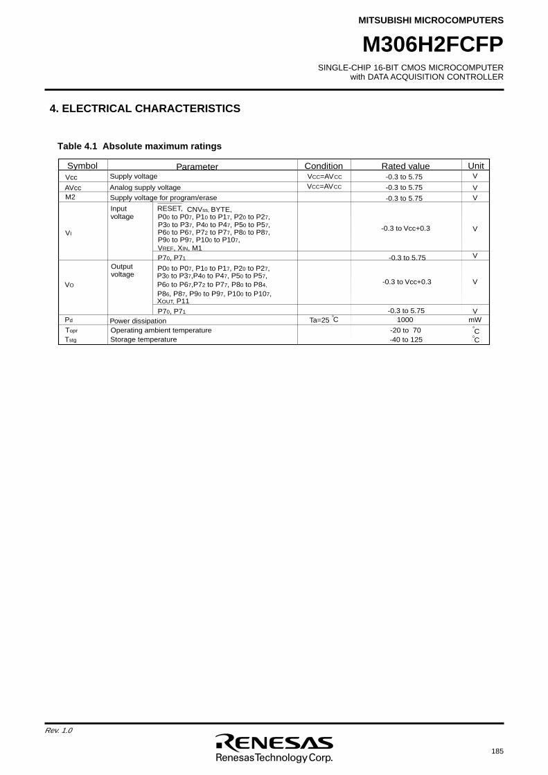
SINGLE-CHIP 16-BIT CMOS MICROCOMPUTERwith DATA ACQUISITION CONTROLLER
MITSUBISHI MICROCOMPUTERS
185
Rev. 1.0
M306H2FCFP
Table 4.1 Absolute maximum ratings
-0.3 to 5.75
-0.3 to 5.75
V
VAVcc
Vcc VCC=AVCC
VCC=AVCC
Symbol Parameter Condition Rated value UnitSupply voltage
Analog supply voltage
VREF, XIN, M1
XOUT, P11
VO
-0.3 to Vcc+0.3
-0.3 to Vcc+0.3
Pd Ta=25
VVI
Tstg
Topr
mW
V
-40 to 125
1000
-20 to 70
P30 to P37, P40 to P47, P50 to P57, P60 to P67, P72 to P77, P80 to P87,
P00 to P07, P10 to P17, P20 to P27, P30 to P37,P40 to P47, P50 to P57, P60 to P67,P72 to P77, P80 to P84,
P00 to P07, P10 to P17, P20 to P27, RESET,
P90 to P97, P100 to P107,
P86, P87, P90 to P97, P100 to P107,
P70, P71
P70, P71
-0.3 to 5.75
-0.3 to 5.75
V
V
CNVss, BYTE,
C C
C
Input voltage
Output voltage
Power dissipationOperating ambient temperatureStorage temperature
-0.3 to 5.75 VM2 Supply voltage for program/erase
4. ELECTRICAL CHARACTERISTICS
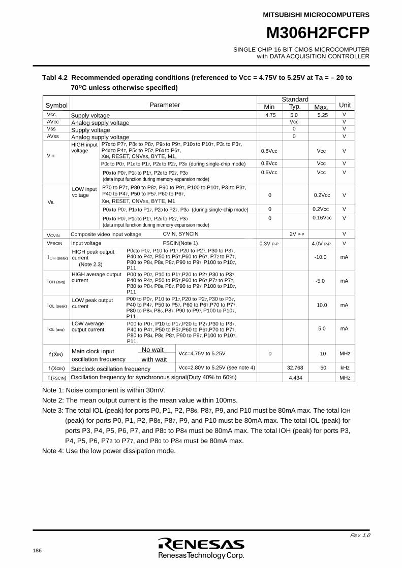
186
Rev. 1.0
SINGLE-CHIP 16-BIT CMOS MICROCOMPUTERwith DATA ACQUISITION CONTROLLER
MITSUBISHI MICROCOMPUTERS
M306H2FCFP
Note 1: Noise component is within 30mV.
Note 2: The mean output current is the mean value within 100ms.
Note 3: The total IOL (peak) for ports P0, P1, P2, P86, P87, P9, and P10 must be 80mA max. The total IOH
(peak) for ports P0, P1, P2, P86, P87, P9, and P10 must be 80mA max. The total IOL (peak) for
ports P3, P4, P5, P6, P7, and P80 to P84 must be 80mA max. The total IOH (peak) for ports P3,
P4, P5, P6, P72 to P77, and P80 to P84 must be 80mA max.
Note 4: Use the low power dissipation mode.
Tabl 4.2 Recommended operating conditions (referenced to VCC = 4.75V to 5.25V at Ta = – 20 to
70oC unless otherwise specified)
P70 to P77, P80 to P87, P90 to P97, P100 to P107, P31 to P37, P40 to P47, P50 to P57, P60 to P67,
4.75 5.25Vcc 5.0VccAVcc V
V00
VIH
VssAVss
0.8Vcc
V
VVcc
V
XIN, RESET, CNVSS, BYTE, M1,
Symbol Parameter UnitStandard
Min Typ. Max.Supply voltageAnalog supply voltageSupply voltageAnalog supply voltageHIGH input voltage
IOH (avg)
mA
mA
V0.8Vcc Vcc
IOH (peak)
-5.0
-10.0
10.0
5.0
mA
f (XIN)
IOL (peak)
mAIOL (avg)
f (XcIN) kHz5032.768
P00 to P07, P10 to P17,P20 to P27,P30 to P37,P40 to P47, P50 to P57,P60 to P67,P70 to P77,P80 to P84, P86, P87, P90 to P97, P100 to P107,P11,
MHz
V
V
0.2Vcc0
0
0
0.2Vcc
0.16Vcc
XIN, RESET, CNVSS, BYTE, M1VIL
LOW input voltage
HIGH peak output current
HIGH average output current
LOW peak output current
LOW average output current
Main clock input oscillation frequency
Subclock oscillation frequency
with wait
No wait
VCVIN CVIN, SYNCIN
VFSCIN Input voltage FSCIN(Note 1)
2V P-P
0.3V P-P 4.0V P-P
V
V
Composite video input voltage
(Note 2.3)
Vcc=4.75V to 5.25V
Vcc=2.80V to 5.25V (see note 4)
100
f (FSCIN) MHz4.434Oscillation frequency for synchronous signal(Duty 40% to 60%)
P00 to P07, P10 to P17, P20 to P27, P30 (during single-chip mode)
V0.5Vcc VccP00 to P07, P10 to P17, P20 to P27, P30
(data input function during memory expansion mode)
P00 to P07, P10 to P17, P20 to P27, P30 (during single-chip mode)
VP00 to P07, P10 to P17, P20 to P27, P30
(data input function during memory expansion mode)
P00 to P07, P10 to P17,P20 to P27,P30 to P37,P40 to P47, P50 to P57,P60 to P67,P72 to P77,P80 to P84, P86, P87, P90 to P97, P100 to P107,P11P00 to P07, P10 to P17,P20 to P27,P30 to P37,P40 to P47, P50 to P57, P60 to P67,P70 to P77,P80 to P84, P86, P87, P90 to P97, P100 to P107,P11
P70 to P77, P80 to P87, P90 to P97, P100 to P107, P31to P37, P40 to P47, P50 to P57, P60 to P67,
P00to P07, P10 to P17,P20 to P27, P30 to P37,P40 to P47, P50 to P57,P60 to P67, P72 to P77,P80 to P84, P86, P87, P90 to P97, P100 to P107,P11
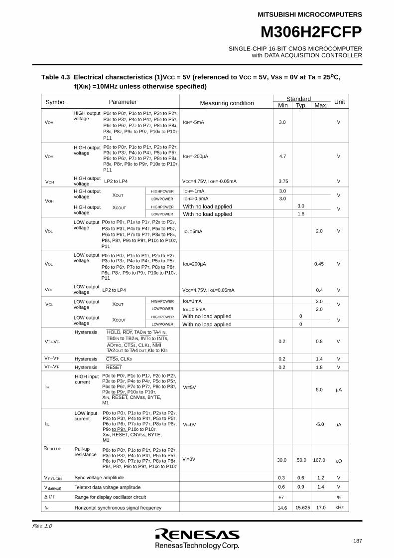
SINGLE-CHIP 16-BIT CMOS MICROCOMPUTERwith DATA ACQUISITION CONTROLLER
MITSUBISHI MICROCOMPUTERS
187
Rev. 1.0
M306H2FCFP
Table 4.3 Electrical characteristics (1)VCC = 5V (referenced to VCC = 5V, VSS = 0V at Ta = 25oC,f(XIN) =10MHZ unless otherwise specified)
IIH
I IL
5.0 µA
P00 to P07, P10 to P17, P20 to P27,P30 to P37, P40 to P47, P50 to P57,P60 to P67, P70 to P77, P80 to P87,P90 to P97, P100 to P107,
XIN, RESET, CNVss, BYTE, M1
VI=5V
VI=0V -5.0
P00 to P07, P10 to P17, P20 to P27,P30 to P37, P40 to P47, P50 to P57,P60 to P67, P70 to P77, P80 to P87,P90 to P97, P100 to P107,
XIN, RESET, CNVss, BYTE, M1
RPULLUP
50.0
P00 to P07, P10 to P17, P20 to P27,P30 to P37, P40 to P47, P50 to P57,P60 to P67, P72 to P77, P80 to P84,P86, P87, P90 to P97, P100 to P107
VI=0V 30.0 167.0
VT+-VT- 0.2 1.8 VRESETHysteresis
HIGH inputcurrent
LOW inputcurrent
Pull-upresistance
µA
1.2 VV SYNCIN 0.3 0.6
1.4 VV dat(text) 0.6 0.9
%∆ f/ f ±7
17.0 kHZfH 14.6 15.625
Sync voltage amplitude
Teletext data voltage amplitude
Range for display oscillator circuit
Horizontal synchronous signal frequency
VT+-VT- 0.2 1.4 VCTS0, CLK0Hysteresis
VOH
VOH
VOH
VOL
VOL
VOL
V
V4.7
VXOUT3.0
3.0
V2.0
0.45 V
VXOUT2.0
2.0
3.0IOH=-5mA
IOH=-1mA
IOH=-200µA
IOH=-0.5mA
IOL=5mA
IOL=1mA
IOL=200µA
IOL=0.5mA
P00 to P07, P10 to P17, P20 to P27,
P00 to P07, P10 to P17, P20 to P27,
P30 to P37, P40 to P47, P50 to P57,
P30 to P37, P40 to P47, P50 to P57,
P60 to P67, P72 to P77, P80 to P84,
P00 to P07, P10 to P17, P20 to P27,P30 to P37, P40 to P47, P50 to P57,P60 to P67, P72 to P77, P80 to P84,
HIGHPOWER
LOWPOWER
P86, P87, P90 to P97, P100 to P107,
HIGHPOWER
LOWPOWER
P60 to P67, P70 to P77, P80 to P84,P86, P87, P90 to P97, P100 to P107,
P86, P87, P90 to P97, P100 to P107,
HIGHPOWER
LOWPOWER
XCOUT 3.0
1.6V
P00 to P07, P10 to P17, P20 to P27,P30 to P37, P40 to P47, P50 to P57,P60 to P67, P70 to P77, P80 to P84,P86, P87, P90 to P97, P100 to P107,
VT+-VT-
TA2OUT to TA4 OUT,KI0 to KI3
0.2 0.8 VTB0IN to TB2IN, INT0 to INT5,
ADTRG, CTS1, CLK1, NMI
HOLD, RDY, TA0IN to TA4 IN,
VXCOUT0
0
HIGHPOWER
LOWPOWER
Symbol Parameter UnitStandardMin Typ. Max.
HIGH output voltage
HIGH output voltage
HIGH output voltage
HIGH output voltage
LOW outputvoltage
LOW outputvoltage
LOW outputvoltage
LOW outputvoltage
Hysteresis
With no load appliedWith no load applied
With no load applied
With no load applied
Measuring condition
P11
P11
LP2 to LP4 VCC=4.75V, I OH=-0.05mA 3.75 V
P11
P11
LP2 to LP4 VCC=4.75V, I OL=0.05mA 0.4 V
VOHHIGH output voltage
VOLLOW outputvoltage
kΩ
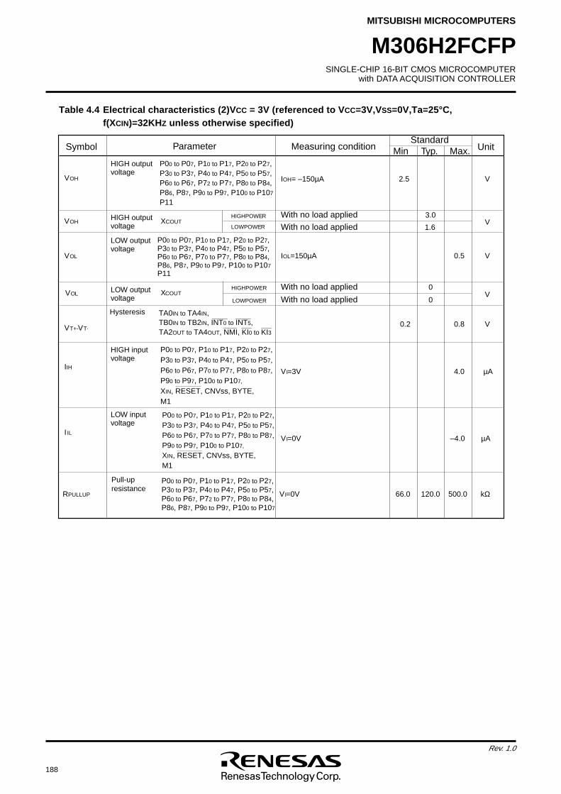
188
Rev. 1.0
SINGLE-CHIP 16-BIT CMOS MICROCOMPUTERwith DATA ACQUISITION CONTROLLER
MITSUBISHI MICROCOMPUTERS
M306H2FCFP
TA2OUT to TA4OUT, NMI, KI0 to KI3TB0IN to TB2IN, INT0 to INT5,
VOH V2.5IOH= –150µA
P00 to P07, P10 to P17, P20 to P27,P30 to P37, P40 to P47, P50 to P57,P60 to P67, P72 to P77, P80 to P84,P86, P87, P90 to P97, P100 to P107
VOH
VOL V0.5IOL=150µA
P00 to P07, P10 to P17, P20 to P27,P30 to P37, P40 to P47, P50 to P57,P60 to P67, P70 to P77, P80 to P84,P86, P87, P90 to P97, P100 to P107
HIGHPOWER
LOWPOWERXCOUT
With no load appliedWith no load applied
3.0
1.6V
P11
P11
VOL
VT+-VT-0.2 0.8 V
TA0IN to TA4IN,
VXCOUT0
0
With no load applied
With no load applied
HIGHPOWER
LOWPOWER
IIH4.0 µA
P00 to P07, P10 to P17, P20 to P27,P30 to P37, P40 to P47, P50 to P57,P60 to P67, P70 to P77, P80 to P87,P90 to P97, P100 to P107,
XIN, RESET, CNVss, BYTE, M1
VI=3V
I ILµAVI=0V –4.0
P00 to P07, P10 to P17, P20 to P27,P30 to P37, P40 to P47, P50 to P57,P60 to P67, P70 to P77, P80 to P87,P90 to P97, P100 to P107,
XIN, RESET, CNVss, BYTE, M1
RPULLUP VI=0V 120.0 kΩ66.0 500.0
Symbol Parameter UnitStandard
Min Typ. Max.Measuring condition
HIGH output voltage
HIGH input voltage
LOW input voltage
HIGH output voltage
LOW output voltage
LOW output voltage
Hysteresis
Pull-upresistance
P00 to P07, P10 to P17, P20 to P27,P30 to P37, P40 to P47, P50 to P57,P60 to P67, P72 to P77, P80 to P84,P86, P87, P90 to P97, P100 to P107
Table 4.4 Electrical characteristics (2)VCC = 3V (referenced to VCC=3V,VSS=0V,Ta=25°C,f(XCIN)=32KHZ unless otherwise specified)
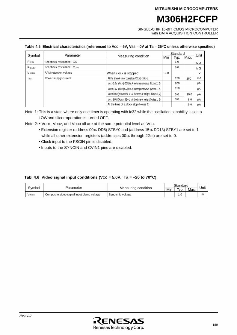
SINGLE-CHIP 16-BIT CMOS MICROCOMPUTERwith DATA ACQUISITION CONTROLLER
MITSUBISHI MICROCOMPUTERS
189
Rev. 1.0
M306H2FCFP
Table 4.5 Electrical characteristics (referenced to VCC = 5V, VSS = 0V at Ta = 25oC unless otherwise specified)
Symbol Parameter UnitStandardMin Typ. Max.Measuring condition
R
R XCIN
V RAM V
fXIN
fXCIN
XIN
6.0
1.0Feedback resistance
Feedback resistance
RAM retention voltage When clock is stopped
I cc Power supply current
MΩ
MΩ
150
2.0
µA
3.0
10.0
150
200
8.0 µA
VCC=5.0V f(XCIN)=32kHz A rectangular wave (Notes 1, 2)
VCC=3.0V f(XCIN)=32kHz A rectangular wave (Notes 1, 2)
VCC=5.0V f(XCIN)=32kHz At the time of weight (Notes 1, 2)
VCC=3.0V f(XCIN)=32kHz At the time of weight (Notes 1, 2)
At the time of slicer operation f(XCIN)=10kHz mA
µA
5.0 µA
µA
180
5.0
At the time of a clock stop (Notes 2)
Tabl 4.6 Video signal input conditions (VCC = 5.0V, Ta = –20 to 70oC)
Symbol Parameter UnitStandard
Min Typ. Max.Measuring condition
VVIN-cu 1.0Composite video signal input clamp voltage Sync-chip voltage
Note 1: This is a state where only one timer is operating with fc32 while the oscillation capability is set to
LOWand slicer operation is turned OFF.
Note 2: • VDD1, VDD2, and VDD3 all are at the same potential level as VCC.
• Extension register (address 0016 DD8) STBY0 and (address 1516 DD13) STBY1 are set to 1
while all other extension registers (addresses 0016 through 2216) are set to 0.
• Clock input to the FSCIN pin is disabled.
• Inputs to the SYNCIN and CVIN1 pins are disabled.
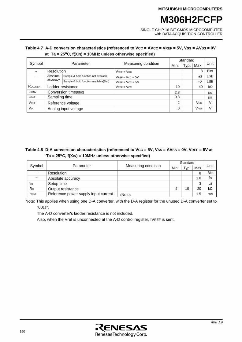
190
Rev. 1.0
SINGLE-CHIP 16-BIT CMOS MICROCOMPUTERwith DATA ACQUISITION CONTROLLER
MITSUBISHI MICROCOMPUTERS
M306H2FCFP
Table 4.7 A-D conversion characteristics (referenced to VCC = AVCC = VREF = 5V, Vss = AVSS = 0V
at Ta = 25oC, f(XIN) = 10MHZ unless otherwise specified)
Table 4.8 D-A conversion characteristics (referenced to VCC = 5V, VSS = AVSS = 0V, VREF = 5V at
Ta = 25oC, f(XIN) = 10MHZ unless otherwise specified)
Note: This applies when using one D-A converter, with the D-A register for the unused D-A converter set to
“0016”.
The A-D converter's ladder resistance is not included.
Also, when the Vref is unconnected at the A-D control register, IVREF is sent.
S
t
a
n
d
a
r
dM
i
n
. T
y
p
. M
a
x
.R
e
s
o
l
u
t
i
o
nA
b
s
o
l
u
t
e
a
c
c
u
r
a
c
y
BitsL
S
BVR
E
F
=
VC
C
± 3
8
S
y
m
b
o
l P
a
r
a
m
e
t
e
r Measuring condition U
n
i
t
VR
E
F
=
VC
C
=
5
VS
a
m
p
l
e
&
h
o
l
d
f
u
n
c
t
i
o
n
n
o
t
a
v
a
i
l
a
b
l
e
S
a
m
p
l
e
&
h
o
l
d
f
u
n
c
t
i
o
n
a
v
a
i
l
a
b
l
e
(
8
b
i
t
) VREF = VCC = 5V ±2 L
S
B
Min. Typ. Max.
tsu
RO
ResolutionAbsolute accuracySetup timeOutput resistanceReference power supply input current
Bits%
mAIVREF
1.0
1.5
8
3
Symbol Parameter Measuring condition Unit
201
04µ
s
(Note)
Standard
RLADDER L a
d
d
e
r
r
e
s
i
s
t
a
n
c
e 1
0 4
0VR
E
F
=
VC
C
µ
s
R
e
f
e
r
e
n
c
e
v
o
l
t
a
g
eA
n
a
l
o
g
i
n
p
u
t
v
o
l
t
a
g
e
V
VI
A
VR
E
F
V0
2 VC
C
VR
E
F
C
o
n
v
e
r
s
i
o
n
t
i
m
e(
8
b
i
t
) 2
.
8tC
O
N
V
tS
A
M
P S
a
m
p
l
i
n
g
t
i
m
e 0
.
3µ
s
k Ω
k Ω
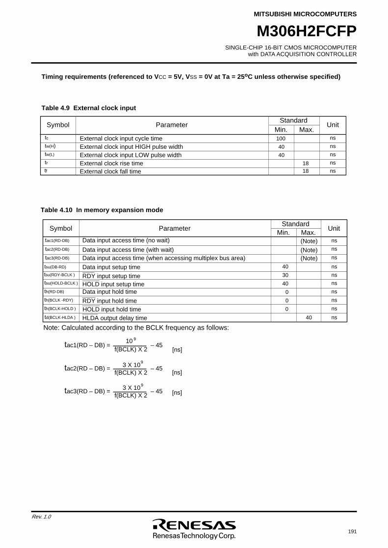
SINGLE-CHIP 16-BIT CMOS MICROCOMPUTERwith DATA ACQUISITION CONTROLLER
MITSUBISHI MICROCOMPUTERS
191
Rev. 1.0
M306H2FCFP
Timing requirements (referenced to VCC = 5V, VSS = 0V at Ta = 25oC unless otherwise specified)
Table 4.9 External clock input
Table 4.10 In memory expansion mode
Max.
External clock rise time nstr
Min.External clock input cycle timeExternal clock input HIGH pulse widthExternal clock input LOW pulse width
External clock fall time
ns
ns
ns
ns
tc
tw(H)
tw(L)
tf
ParameterSymbol UnitStandard
18
100
40
40
18
f(BCLK) X 2
(Note)
(Note)(Note)
40
30
0
0
40
0
Note: Calculated according to the BCLK frequency as follows:
40
Min.
Data input setup time nstsu(DB-RD)
tsu(RDY-BCLK )
ParameterSymbol UnitMax.
Standard
nsRDY input setup time
Data input hold time nsth(RD-DB)
th(BCLK -RDY) nsRDY input hold time
nsHOLD input setup timetsu(HOLD-BCLK )
nsHOLD input hold timeth(BCLK-HOLD )
Data input access time (no wait) nstac1(RD-DB)
ns
ns
tac2(RD-DB)
tac3(RD-DB)
Data input access time (with wait)Data input access time (when accessing multiplex bus area)
nstd(BCLK-HLDA ) HLDA output delay time
tac1(RD – DB) =f(BCLK) X 2
– 4510 9
[ns]
tac2(RD – DB) =f(BCLK) X 2
– 453 X 109
[ns]
tac3(RD – DB) = – 453 X 109
[ns]
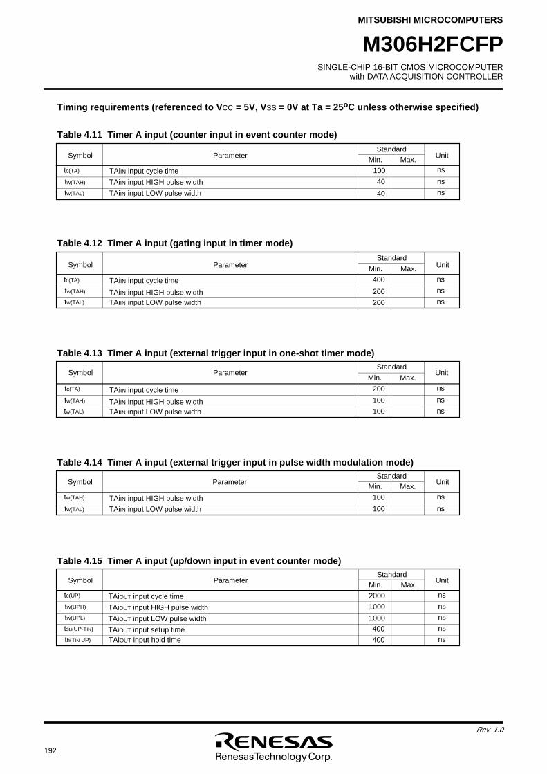
192
Rev. 1.0
SINGLE-CHIP 16-BIT CMOS MICROCOMPUTERwith DATA ACQUISITION CONTROLLER
MITSUBISHI MICROCOMPUTERS
M306H2FCFP
StandardMax.
nsTAiIN input LOW pulse widthtw(TAL)
Min.ns
ns
Unit
Standard
Max.Min.ns
ns
ns
Unit
Standard
Max.Min.ns
ns
ns
Unit
StandardMax.Min.
ns
ns
Unit
StandardMax.Min.
ns
ns
ns
Unit
ns
ns
TAiIN input HIGH pulse widthtw(TAH)
ParameterSymbol
TAiIN input cycle time
TAiIN input HIGH pulse widthTAiIN input LOW pulse width
tc(TA)
tw(TAH)
tw(TAL)
Symbol Parameter
TAiIN input cycle time
TAiIN input HIGH pulse widthTAiIN input LOW pulse width
tc(TA)
tw(TAH)
tw(TAL)
Symbol Parameter
tw(TAH)
tw(TAL)
Symbol Parameter
TAiIN input HIGH pulse width
TAiIN input LOW pulse width
Symbol Parameter
tc(TA) TAiIN input cycle time
TAiOUT input cycle time
TAiOUT input HIGH pulse width
TAiOUT input LOW pulse width
TAiOUT input setup timeTAiOUT input hold time
tc(UP)
tw(UPH)
tw(UPL)
tsu(UP-TIN)
th(TIN-UP)
40
100
40
400
200
200
200
100
100
100
100
2000
1000
1000
400
400
Timing requirements (referenced to VCC = 5V, VSS = 0V at Ta = 25oC unless otherwise specified)
Table 4.11 Timer A input (counter input in event counter mode)
Table 4.12 Timer A input (gating input in timer mode)
Table 4.13 Timer A input (external trigger input in one-shot timer mode)
Table 4.14 Timer A input (external trigger input in pulse width modulation mode)
Table 4.15 Timer A input (up/down input in event counter mode)
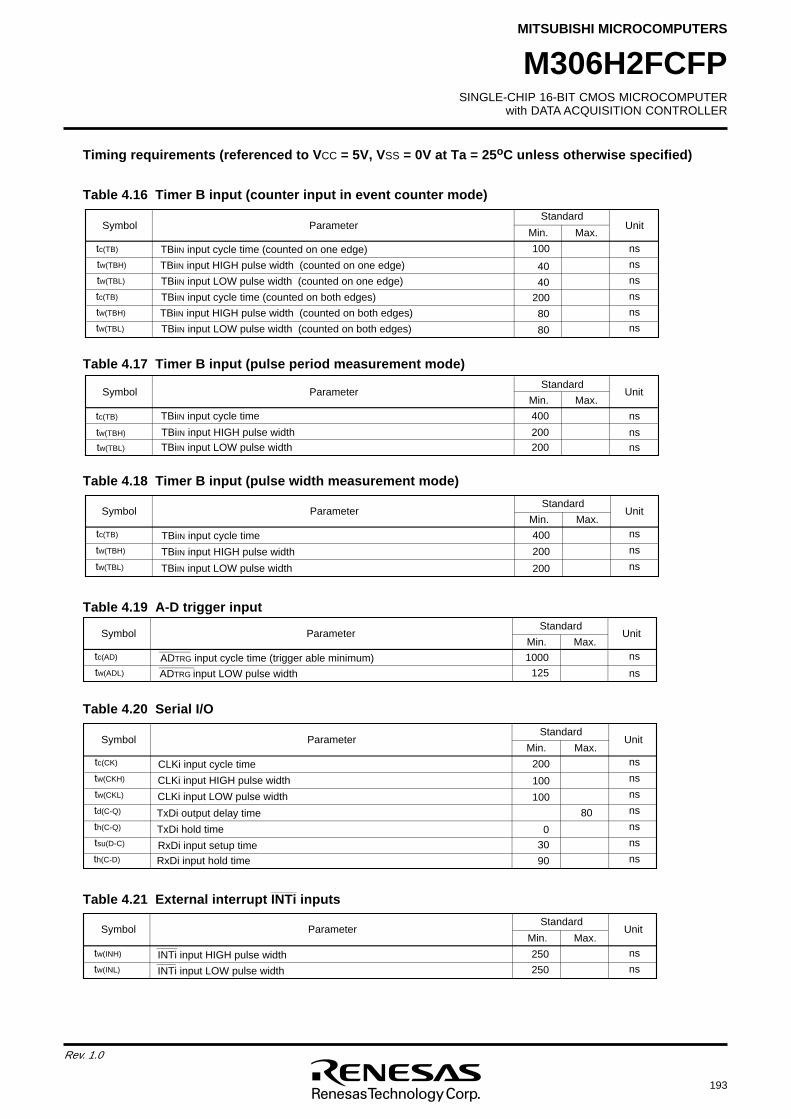
SINGLE-CHIP 16-BIT CMOS MICROCOMPUTERwith DATA ACQUISITION CONTROLLER
MITSUBISHI MICROCOMPUTERS
193
Rev. 1.0
M306H2FCFP
Timing requirements (referenced to VCC = 5V, VSS = 0V at Ta = 25oC unless otherwise specified)
Table 4.16 Timer B input (counter input in event counter mode)
ns
ns
ns
ns
ns
ns
ns
Standard
Max.Min.
TBiIN input cycle time (counted on one edge)
TBiIN input HIGH pulse width (counted on one edge)
TBiIN input LOW pulse width (counted on one edge)
ns
ns
ns
tc(TB)
tw(TBH)
tw(TBL)
ParameterSymbol Unit
tc(TB)
tw(TBL)
tw(TBH)
ns
ns
nsTBiIN input HIGH pulse width (counted on both edges)
TBiIN input LOW pulse width (counted on both edges)
TBiIN input cycle time (counted on both edges)
Standard
Max.Min.
ns
ns
tc(TB)
tw(TBH)
Symbol Parameter Unit
tw(TBL) nsTBiIN input HIGH pulse width
TBiIN input cycle time
TBiIN input LOW pulse width
Standard
Max.Min.ns
ns
tc(TB)
Symbol Parameter Unit
tw(TBL) ns
tw(TBH)
TBiIN input cycle time
TBiIN input HIGH pulse width
TBiIN input LOW pulse width
Standard
Max.Min.ns
ns
tc(AD)
tw(ADL)
Symbol Parameter Unit
ADTRG input cycle time (trigger able minimum)
ADTRG input LOW pulse width
Standard
Max.Min.ns
ns
tw(INH)
tw(INL)
Symbol Parameter Unit
INTi input LOW pulse width
INTi input HIGH pulse width
Standard
Max.Min.
CLKi input cycle time
CLKi input HIGH pulse width
CLKi input LOW pulse width
tc(CK)
tw(CKH)
tw(CKL)
ParameterSymbol Unit
td(C-Q)
tsu(D-C)
th(C-Q) TxDi hold time
RxDi input setup time
TxDi output delay time
th(C-D) RxDi input hold time
100
40
40
80
80
200
400
200200
400
200
200
1000
125
250
250
200
100
100
0
30
90
80
Table 4.17 Timer B input (pulse period measurement mode)
Table 4.18 Timer B input (pulse width measurement mode)
Table 4.19 A-D trigger input
Table 4.20 Serial I/O
_______
Table 4.21 External interrupt INTi inputs
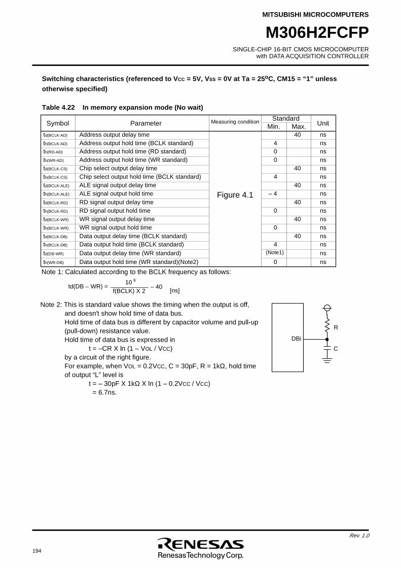
194
Rev. 1.0
SINGLE-CHIP 16-BIT CMOS MICROCOMPUTERwith DATA ACQUISITION CONTROLLER
MITSUBISHI MICROCOMPUTERS
M306H2FCFP
S
y
m
b
o
lS
t
a
n
d
a
r
dM
e
a
s
u
r
i
n
g
c
o
n
d
i
t
i
o
nM
a
x
.M
i
n
.P
a
r
a
m
e
t
e
r U
n
i
t
td
(
B
C
L
K
-
A
D
) A
d
d
r
e
s
s
o
u
t
p
u
t
d
e
l
a
y
t
i
m
e 4 0 n
s
th
(
B
C
L
K
-
A
D
) A
d
d
r
e
s
s
o
u
t
p
u
t
h
o
l
d
t
i
m
e
(
B
C
L
K
s
t
a
n
d
a
r
d
) 4 n s
th
(
B
C
L
K
-
C
S
) C
h
i
p
s
e
l
e
c
t
o
u
t
p
u
t
h
o
l
d
t
i
m
e
(
B
C
L
K
s
t
a
n
d
a
r
d
) 4 n s
td
(
B
C
L
K
-
A
L
E
) A
L
E
s
i
g
n
a
l
o
u
t
p
u
t
d
e
l
a
y
t
i
m
e 4 0 n
s
th
(
B
C
L
K
-
A
L
E
) A
L
E
s
i
g
n
a
l
o
u
t
p
u
t
h
o
l
d
t
i
m
e –
4 n
s
td
(
B
C
L
K
-
R
D
) R
D
s
i
g
n
a
l
o
u
t
p
u
t
d
e
l
a
y
t
i
m
e 4 0 n
s
th
(
B
C
L
K
-
R
D
) R
D
s
i
g
n
a
l
o
u
t
p
u
t
h
o
l
d
t
i
m
e 0 n s
td
(
B
C
L
K
-
W
R
) W
R
s
i
g
n
a
l
o
u
t
p
u
t
d
e
l
a
y
t
i
m
e 4 0 n
s
th
(
B
C
L
K
-
W
R
) W
R
s
i
g
n
a
l
o
u
t
p
u
t
h
o
l
d
t
i
m
e 0 n s
td
(
B
C
L
K
-
D
B
) D
a
t
a
o
u
t
p
u
t
d
e
l
a
y
t
i
m
e
(
B
C
L
K
s
t
a
n
d
a
r
d
) 40 n s
th
(
B
C
L
K
-
D
B
) D
a
t
a
o
u
t
p
u
t
h
o
l
d
t
i
m
e
(
B
C
L
K
s
t
a
n
d
a
r
d
) 4 n s
th
(
W
R
-
D
B
) D
a
t
a
o
u
t
p
u
t
h
o
l
d
t
i
m
e
(
W
R
s
t
a
n
d
a
r
d
)
(
N
o
t
e
2
) 0 n s
td
(
D
B
-
W
R
) D
a
t
a
o
u
t
p
u
t
d
e
l
a
y
t
i
m
e
(
W
R
s
t
a
n
d
a
r
d
) n s(
N
o
t
e
1
)
N
o
t
e
1
:
C
a
l
c
u
l
a
t
e
d
a
c
c
o
r
d
i
n
g
t
o
t
h
e
B
C
L
K
f
r
e
q
u
e
n
c
y
a
s
f
o
l
l
o
w
s
:
t d
(
D
B
–
W
R
)
=f (
B
C
L
K
)
X
21 0 9
–
4
0
[ n
s
]
td
(
B
C
L
K
-
C
S
) C
h
i
p
s
e
l
e
c
t
o
u
t
p
u
t
d
e
l
a
y
t
i
m
e 4 0 n
s
th
(
R
D
-
A
D
) A
d
d
r
e
s
s
o
u
t
p
u
t
h
o
l
d
t
i
m
e
(
R
D
s
t
a
n
d
a
r
d
) 0 n s
th
(
W
R
-
A
D
) A
d
d
r
e
s
s
o
u
t
p
u
t
h
o
l
d
t
i
m
e
(
W
R
s
t
a
n
d
a
r
d
) 0 n s
N
o
t
e
2
:
T
h
i
s
i
s
s
t
a
n
d
a
r
d
v
a
l
u
e
s
h
o
w
s
t
h
e
t
i
m
i
n
g
w
h
e
n
t
h
e
o
u
t
p
u
t
i
s
o
f
f
,
a
n
d
d
o
e
s
n
'
t
s
h
o
w
h
o
l
d
t
i
m
e
o
f
d
a
t
a
b
u
s
. H
o
l
d
t
i
m
e
o
f
d
a
t
a
b
u
s
i
s
d
i
f
f
e
r
e
n
t
b
y
c
a
p
a
c
i
t
o
r
v
o
l
u
m
e
a
n
d
p
u
l
l
-
u
p
(
p
u
l
l
-
d
o
w
n
)
r
e
s
i
s
t
a
n
c
e
v
a
l
u
e
. H
o
l
d
t
i
m
e
o
f
d
a
t
a
b
u
s
i
s
e
x
p
r
e
s
s
e
d
i
n
t
=
–
C
R
X
l
n
(
1
–
VO
L
/
VC
C)
b
y
a
c
i
r
c
u
i
t
o
f
t
h
e
r
i
g
h
t
f
i
g
u
r
e
. F
o
r
e
x
a
m
p
l
e
,
w
h
e
n
VO
L
=
0
.
2
VC
C,
C
=
3
0
p
F
,
R
=
1
kΩ,
h
o
l
d
t
i
m
e
o
f
o
u
t
p
u
t
“
L
”
l
e
v
e
l
i
s
t
=
–
3
0
p
F
X
1
kΩ
X
l
n
(
1
–
0
.
2
VC
C
/
VC
C)
=
6
.
7
n
s
.
D
B
i
R
C
F
i
g
u
r
e
4
.
1
Switching characteristics (referenced to VCC = 5V, VSS = 0V at Ta = 25oC, CM15 = “1” unless
otherwise specified)
Table 4.22 In memory expansion mode (No wait)

SINGLE-CHIP 16-BIT CMOS MICROCOMPUTERwith DATA ACQUISITION CONTROLLER
MITSUBISHI MICROCOMPUTERS
195
Rev. 1.0
M306H2FCFP
S
y
m
b
o
lS
t
a
n
d
a
r
dM
e
a
s
u
r
i
n
g
c
o
n
d
i
t
i
o
nM
a
x
.M
i
n
.P
a
r
a
m
e
t
e
r U
n
i
t
td
(
B
C
L
K
-
A
D
) A
d
d
r
e
s
s
o
u
t
p
u
t
d
e
l
a
y
t
i
m
e 4 0 n
s
th
(
B
C
L
K
-
A
D
) A
d
d
r
e
s
s
o
u
t
p
u
t
h
o
l
d
t
i
m
e
(
B
C
L
K
s
t
a
n
d
a
r
d
) 4 n s
th
(
B
C
L
K
-
C
S
) C
h
i
p
s
e
l
e
c
t
o
u
t
p
u
t
h
o
l
d
t
i
m
e
(
B
C
L
K
s
t
a
n
d
a
r
d
) 4 n s
td
(
B
C
L
K
-
A
L
E
) A
L
E
s
i
g
n
a
l
o
u
t
p
u
t
d
e
l
a
y
t
i
m
e 4 0 n
s
th
(
B
C
L
K
-
A
L
E
) A
L
E
s
i
g
n
a
l
o
u
t
p
u
t
h
o
l
d
t
i
m
e –
4 n
s
td
(
B
C
L
K
-
R
D
) R
D
s
i
g
n
a
l
o
u
t
p
u
t
d
e
l
a
y
t
i
m
e 4 0 n
s
th
(
B
C
L
K
-
R
D
) R
D
s
i
g
n
a
l
o
u
t
p
u
t
h
o
l
d
t
i
m
e 0 n s
td
(
B
C
L
K
-
W
R
) W
R
s
i
g
n
a
l
o
u
t
p
u
t
d
e
l
a
y
t
i
m
e 4 0 n
s
th
(
B
C
L
K
-
W
R
) W
R
s
i
g
n
a
l
o
u
t
p
u
t
h
o
l
d
t
i
m
e 0 n s
td
(
B
C
L
K
-
D
B
) D
a
t
a
o
u
t
p
u
t
d
e
l
a
y
t
i
m
e
(
B
C
L
K
s
t
a
n
d
a
r
d
) 40 n s
th
(
B
C
L
K
-
D
B
) D
a
t
a
o
u
t
p
u
t
h
o
l
d
t
i
m
e
(
B
C
L
K
s
t
a
n
d
a
r
d
) 4 n s
th
(
W
R
-
D
B
) D
a
t
a
o
u
t
p
u
t
h
o
l
d
t
i
m
e
(
W
R
s
t
a
n
d
a
r
d
)
(
N
o
t
e
2
) 0 n s
td
(
D
B
-
W
R
) D
a
t
a
o
u
t
p
u
t
d
e
l
a
y
t
i
m
e
(
W
R
s
t
a
n
d
a
r
d
) n s(
N
o
t
e
1
)
N
o
t
e
1
:
C
a
l
c
u
l
a
t
e
d
a
c
c
o
r
d
i
n
g
t
o
t
h
e
B
C
L
K
f
r
e
q
u
e
n
c
y
a
s
f
o
l
l
o
w
s
:
t d
(
D
B
–
W
R
)
=f (
B
C
L
K
)
1 0 9
–
4
0
[ n
s
]
td
(
B
C
L
K
-
C
S
) C
h
i
p
s
e
l
e
c
t
o
u
t
p
u
t
d
e
l
a
y
t
i
m
e 4 0 n
s
th
(
R
D
-
A
D
) A
d
d
r
e
s
s
o
u
t
p
u
t
h
o
l
d
t
i
m
e
(
R
D
s
t
a
n
d
a
r
d
) 0 n s
th
(
W
R
-
A
D
) A
d
d
r
e
s
s
o
u
t
p
u
t
h
o
l
d
t
i
m
e
(
W
R
s
t
a
n
d
a
r
d
) 0 n s
N
o
t
e
2
:
T
h
i
s
i
s
s
t
a
n
d
a
r
d
v
a
l
u
e
s
h
o
w
s
t
h
e
t
i
m
i
n
g
w
h
e
n
t
h
e
o
u
t
p
u
t
i
s
o
f
f
,
a
n
d
d
o
e
s
n
'
t
s
h
o
w
h
o
l
d
t
i
m
e
o
f
d
a
t
a
b
u
s
. H
o
l
d
t
i
m
e
o
f
d
a
t
a
b
u
s
i
s
d
i
f
f
e
r
e
n
t
b
y
c
a
p
a
c
i
t
o
r
v
o
l
u
m
e
a
n
d
p
u
l
l
-
u
p
(
p
u
l
l
-
d
o
w
n
)
r
e
s
i
s
t
a
n
c
e
v
a
l
u
e
. H
o
l
d
t
i
m
e
o
f
d
a
t
a
b
u
s
i
s
e
x
p
r
e
s
s
e
d
i
n
t
=
–
C
R
X
l
n
(
1
–
VO
L
/
VC
C)
b
y
a
c
i
r
c
u
i
t
o
f
t
h
e
r
i
g
h
t
f
i
g
u
r
e
. F
o
r
e
x
a
m
p
l
e
,
w
h
e
n
VO
L
=
0
.
2
VC
C,
C
=
3
0
p
F
,
R
=
1
kΩ,
h
o
l
d
t
i
m
e
o
f
o
u
t
p
u
t
“
L
”
l
e
v
e
l
i
s
t
=
–
3
0
p
F
X
1
kΩ
X
l
n
(
1
–
0
.
2
VC
C
/
VC
C)
=
6
.
7
n
s
.
D
B
i
R
C
F
i
g
u
r
e
4
.
1
Switching characteristics (refer to VCC = 5V, VSS = 0V at Ta = 25oC, CM15 = “1” unless otherwise
specified)
Table 4.23 In memory expansion mode (With wait, accessing external memory)
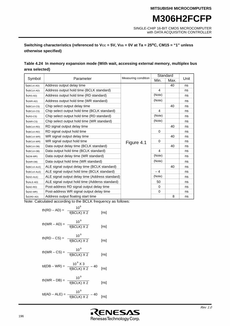
196
Rev. 1.0
SINGLE-CHIP 16-BIT CMOS MICROCOMPUTERwith DATA ACQUISITION CONTROLLER
MITSUBISHI MICROCOMPUTERS
M306H2FCFP
SymbolS
t
a
n
d
a
r
dMeasuring condition
M
a
x
.Min.Parameter Unit
td
(
B
C
L
K
-
A
D
) A
d
d
r
e
s
s
o
u
t
p
u
t
d
e
l
a
y
t
i
m
e 4 0 n
s
th
(
B
C
L
K
-
A
D
) A
d
d
r
e
s
s
o
u
t
p
u
t
h
o
l
d
t
i
m
e
(
B
C
L
K
s
t
a
n
d
a
r
d
) 4 n s
td
(
B
C
L
K
-
C
S
) C
h
i
p
s
e
l
e
c
t
o
u
t
p
u
t
d
e
l
a
y
t
i
m
e 4 0 n
s
th
(
B
C
L
K
-
C
S
) C
h
i
p
s
e
l
e
c
t
o
u
t
p
u
t
h
o
l
d
t
i
m
e
(
B
C
L
K
s
t
a
n
d
a
r
d
) 4 n s
n sth
(
R
D
-
A
D
) A
d
d
r
e
s
s
o
u
t
p
u
t
h
o
l
d
t
i
m
e
(
R
D
s
t
a
n
d
a
r
d
) (
N
o
t
e
)
td
(
B
C
L
K
-
R
D
) R
D
s
i
g
n
a
l
o
u
t
p
u
t
d
e
l
a
y
t
i
m
e 4 0 n
s
th
(
B
C
L
K
-
R
D
) R
D
s
i
g
n
a
l
o
u
t
p
u
t
h
o
l
d
t
i
m
e 0 n s
n sth
(
W
R
-
A
D
) A
d
d
r
e
s
s
o
u
t
p
u
t
h
o
l
d
t
i
m
e
(
W
R
s
t
a
n
d
a
r
d
) (
N
o
t
e
)
td
(
B
C
L
K
-
W
R
) W
R
s
i
g
n
a
l
o
u
t
p
u
t
d
e
l
a
y
t
i
m
e 4 0 n
s
td
(
B
C
L
K
-
D
B
) D
a
t
a
o
u
t
p
u
t
d
e
l
a
y
t
i
m
e
(
B
C
L
K
s
t
a
n
d
a
r
d
) 4 0 n
s
th
(
B
C
L
K
-
D
B
) D
a
t
a
o
u
t
p
u
t
h
o
l
d
t
i
m
e
(
B
C
L
K
s
t
a
n
d
a
r
d
) 4 n s
td(DB-WR) Data output delay time (WR standard) ( N
o
t
e
) ns
td(BCLK-ALE) ALE signal output delay time (BCLK standard) 40 nsth
(
B
C
L
K
-
A
L
E
) A
L
E
s
i
g
n
a
l
o
u
t
p
u
t
h
o
l
d
t
i
m
e
(
B
C
L
K
s
t
a
n
d
a
r
d
) – 4 n s
th(ALE-AD) ALE signal output hold time (Adderss standard) 50 ns
th(BCLK-WR) WR signal output hold time 0 ns
n sth
(
R
D
-
C
S
) C
h
i
p
s
e
l
e
c
t
o
u
t
p
u
t
h
o
l
d
t
i
m
e
(
R
D
s
t
a
n
d
a
r
d
) (
N
o
t
e
)
th
(
W
R
-
C
S
) C
h
i
p
s
e
l
e
c
t
o
u
t
p
u
t
h
o
l
d
t
i
m
e
(
W
R
s
t
a
n
d
a
r
d
) ( N
o
t
e
) n
s
td(AD-RD) Post-address RD signal output delay time ns0td
(
A
D
-
W
R
) P
o
s
t
-
a
d
d
r
e
s
s
W
R
s
i
g
n
a
l
o
u
t
p
u
t
d
e
l
a
y
t
i
m
e n s0
tdZ(RD-AD) Address output floating start time ns8
th
(
W
R
-
D
B
) D
a
t
a
o
u
t
p
u
t
h
o
l
d
t
i
m
e
(
W
R
s
t
a
n
d
a
r
d
) n s(
N
o
t
e
)
N
o
t
e
:
C
a
l
c
u
l
a
t
e
d
a
c
c
o
r
d
i
n
g
t
o
t
h
e
B
C
L
K
f
r
e
q
u
e
n
c
y
a
s
f
o
l
l
o
w
s
:
th(RD – AD) =f (
B
C
L
K
)
X
2
1 09
[ns]
t h
(
W
R
–
A
D
)
=f (
B
C
L
K
)
X
2
1 0 9
[ns]
th(RD – CS) =f (
B
C
L
K
)
X
2
1 0 9
[ns]
th(WR – CS) =f(BCLK) X 2
1 0 9
[ns]
t d
(
D
B
–
W
R
)
=f (
B
C
L
K
)
X
2
10 9
– 40[ns]
X
3
t d
(
A
D
–
A
L
E
)
=f (
B
C
L
K
)
X
210 9
–
4
0
[ns]
t h
(
W
R
–
D
B
)
=
f (
B
C
L
K
)
X
2
1 0 9
[ns]
td
(
A
D
-
A
L
E
) A
L
E
s
i
g
n
a
l
o
u
t
p
u
t
d
e
l
a
y
t
i
m
e
(
A
d
d
r
e
s
s
s
t
a
n
d
a
r
d
) n s(Note)
Figure 4.1
Switching characteristics (referenced to VCC = 5V, VSS = 0V at Ta = 25oC, CM15 = “1” unless
otherwise specified)
Table 4.24 In memory expansion mode (With wait, accessing external memory, multiplex bus
area selected)

SINGLE-CHIP 16-BIT CMOS MICROCOMPUTERwith DATA ACQUISITION CONTROLLER
MITSUBISHI MICROCOMPUTERS
197
Rev. 1.0
M306H2FCFP
Figure 4.1 Port P0 to P11 measurement circuit
P6
P7
P8
P10
P9
P0
P1
P2
P3
P4
P5
30pF
P11
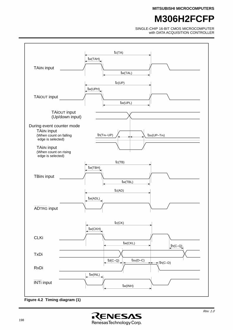
198
Rev. 1.0
SINGLE-CHIP 16-BIT CMOS MICROCOMPUTERwith DATA ACQUISITION CONTROLLER
MITSUBISHI MICROCOMPUTERS
M306H2FCFP
tsu(D–C)
TAiIN input
TAiOUT input
During event counter mode
TBiIN input
CLKi
TxDi
RxDi
tc(TA)
tw(TAH)
tw(TAL)
tc(UP)
tw(UPH)
tw(UPL)
tc(TB)
tw(TBH)
tw(TBL)
tc(AD)
tw(ADL)
tc(CK)
tw(CKH)
tw(CKL)
tw(INL)
tw(INH)
td(C–Q) th(C–D)
th(C–Q)
th(TIN–UP) tsu(UP–TIN)TAiIN input(When count on falling edge is selected)
TAiIN input(When count on rising edge is selected)
TAiOUT input(Up/down input)
INTi input
ADTRG input
Figure 4.2 Timing diagram (1)
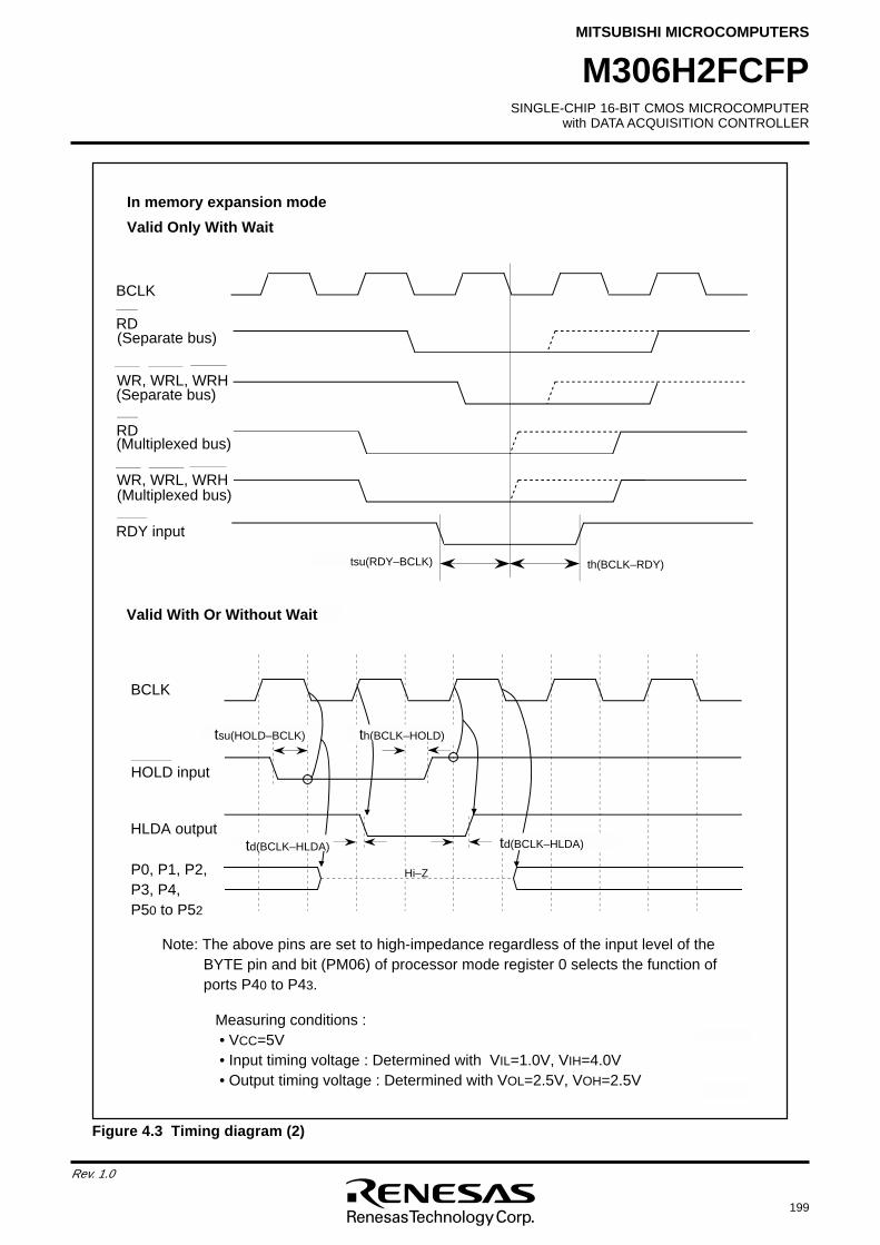
SINGLE-CHIP 16-BIT CMOS MICROCOMPUTERwith DATA ACQUISITION CONTROLLER
MITSUBISHI MICROCOMPUTERS
199
Rev. 1.0
M306H2FCFP
Measuring conditions : • VCC=5V • Input timing voltage : Determined with VIL=1.0V, VIH=4.0V • Output timing voltage : Determined with VOL=2.5V, VOH=2.5V
BCLK
HOLD input
HLDA output
P0, P1, P2, P3, P4, P50 to P52
Valid With Or Without Wait
Note: The above pins are set to high-impedance regardless of the input level of the BYTE pin and bit (PM06) of processor mode register 0 selects the function of ports P40 to P43.
th(BCLK–HOLD)tsu(HOLD–BCLK)
In memory expansion mode
Valid Only With Wait
td(BCLK–HLDA)td(BCLK–HLDA)
Hi–Z
RDY input
tsu(RDY–BCLK) th(BCLK–RDY)
BCLK
RD(Multiplexed bus)
(Multiplexed bus)WR, WRL, WRH
WR, WRL, WRH(Separate bus)
RD(Separate bus)
Figure 4.3 Timing diagram (2)
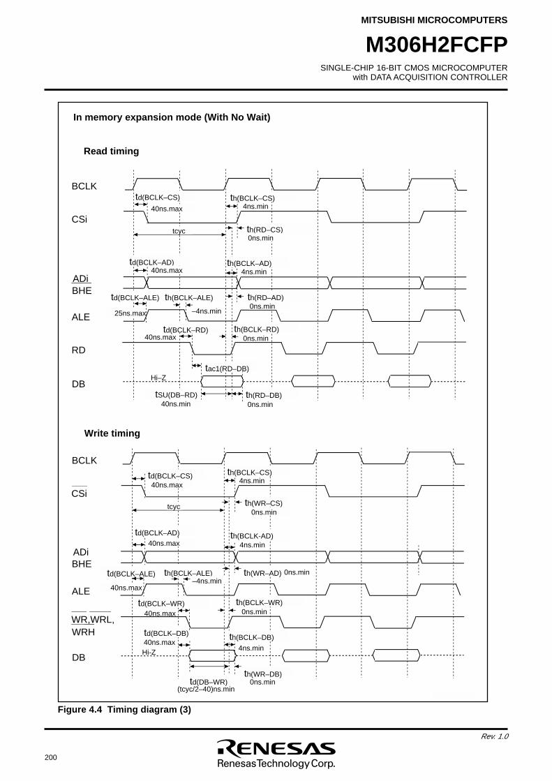
200
Rev. 1.0
SINGLE-CHIP 16-BIT CMOS MICROCOMPUTERwith DATA ACQUISITION CONTROLLER
MITSUBISHI MICROCOMPUTERS
M306H2FCFP
BCLK
CSi
ALE–4ns.min
RD40ns.max 0ns.min
4ns.min
4ns.min
Hi–ZDB
0ns.min
ADiBHE
Read timing
BCLK
CSi
ALE
40ns.max 0ns.min
4ns.min
4ns.min
Hi-ZDB
40ns.max4ns.min
(tcyc/2–40)ns.min
ADiBHE
Write timing
td(BCLK–AD)
td(BCLK–ALE) th(BCLK–ALE)
tSU(DB–RD)
th(BCLK-AD)
td(BCLK–WR)
th(BCLK–DB)
td(BCLK–RD)
td(BCLK–ALE)
40ns.min
tac1(RD–DB)
In memory expansion mode (With No Wait)
WR,WRL,WRH
td(BCLK–CS)
40ns.max
tcyc
th(BCLK–CS)
th(RD–CS)0ns.min
40ns.maxth(BCLK–AD)
th(RD–AD)0ns.min
th(BCLK–RD)
25ns.max
th(RD–DB)
td(BCLK–CS)40ns.max
th(BCLK–CS)
tcyc th(WR–CS)0ns.min
td(BCLK–AD)40ns.max
40ns.max
th(BCLK–ALE)–4ns.min
th(WR–AD) 0ns.min
th(BCLK–WR)
td(BCLK–DB)
td(DB–WR)th(WR–DB)
0ns.min
Figure 4.4 Timing diagram (3)
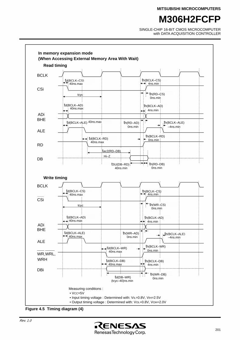
SINGLE-CHIP 16-BIT CMOS MICROCOMPUTERwith DATA ACQUISITION CONTROLLER
MITSUBISHI MICROCOMPUTERS
201
Rev. 1.0
M306H2FCFP
BCLK
CSi
ALE
RD
4ns.min
Hi–ZDB
40ns.min 0ns.min
ADiBHE
Read timing
BCLK
CSi
ALE
4ns.min
th(WR–AD)
ADiBHE
(tcyc–40)ns.min0ns.min
DBi
Write timing
td(BCLK–RD)
0ns.min
0ns.minth(RD–AD)
In memory expansion mode(When Accessing External Memory Area With Wait)
Measuring conditions : • VCC=5V • Input timing voltage : Determined with: VIL=0.8V, VIH=2.5V • Output timing voltage : Determined with: VOL=0.8V, VOH=2.0V
WR,WRL,WRH
td(BCLK–CS)40ns.max
tcyc
th(BCLK–CS)4ns.min
th(RD–CS)0ns.min
th(BCLK–AD)td(BCLK–AD)40ns.max
td(BCLK–ALE) 40ns.max th(BCLK–ALE)–4ns.min
th(BCLK–RD)0ns.min
40ns.max
tac2(RD–DB)
th(RD–DB)tSU(DB–RD)
td(BCLK–CS)40ns.max
tcyc
th(BCLK–CS)4ns.min
th(WR–CS)0ns.min
th(BCLK–AD)td(BCLK–AD)40ns.max
td(BCLK–ALE)40ns.max
th(BCLK–ALE)–4ns.min
th(BCLK–WR)0ns.min
td(BCLK–WR)40ns.max
th(BCLK–DB)4ns.min
td(BCLK–DB)40ns.max
td(DB–WR)th(WR–DB)
Figure 4.5 Timing diagram (4)
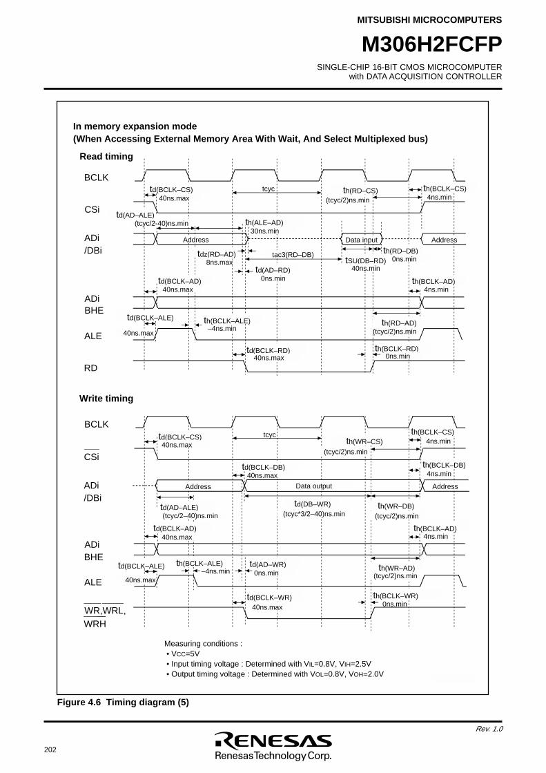
202
Rev. 1.0
SINGLE-CHIP 16-BIT CMOS MICROCOMPUTERwith DATA ACQUISITION CONTROLLER
MITSUBISHI MICROCOMPUTERS
M306H2FCFP
In memory expansion mode(When Accessing External Memory Area With Wait, And Select Multiplexed bus)
BCLK
CSi
ALE
RD
4ns.min
tcyc
ADiBHE
ADi/DBi
td(AD–ALE)
Read timing
0ns.min
BCLK
CSi
ALE–4ns.min
4ns.min
4ns.mintcyc
ADiBHE
ADi/DBi
Write timing
Address
Measuring conditions : • VCC=5V • Input timing voltage : Determined with VIL=0.8V, VIH=2.5V • Output timing voltage : Determined with VOL=0.8V, VOH=2.0V
(tcyc/2)ns.min
AddressData input
(tcyc/2)ns.min
td(BCLK–ALE)
(tcyc/2)ns.minth(WR–CS)
Address
(tcyc*3/2–40)ns.min
td(BCLK–ALE)(tcyc/2)ns.min
(tcyc/2-40)ns.min
Address
40ns.max
tSU(DB–RD)tac3(RD–DB)
(tcyc/2)ns.min
th(ALE–AD)30ns.min
td(AD–RD)0ns.min
tdz(RD–AD)8ns.max
td(AD–WR)0ns.min
Data output
WR,WRL,WRH
td(BCLK–CS)40ns.max
th(RD–CS) th(BCLK–CS)4ns.min
th(BCLK–AD)
th(RD–DB)0ns.min
40ns.min
40ns.maxtd(BCLK–AD)
–4ns.minth(BCLK–ALE)
td(BCLK–RD)40ns.max
th(RD–AD)
th(BCLK–RD)0ns.min
td(BCLK–CS)40ns.max
th(BCLK–CS)
th(BCLK–DB)4ns.min
th(WR–DB)td(DB–WR)
th(BCLK–AD)
td(AD–ALE)(tcyc/2–40)ns.min
td(BCLK–AD)40ns.max
40ns.max
th(BCLK–ALE)
40ns.maxtd(BCLK–WR) th(BCLK–WR)
th(WR–AD)
td(BCLK–DB)40ns.max
Figure 4.6 Timing diagram (5)
SINGLE-CHIP 16-BIT CMOS MICROCOMPUTERwith DATA ACQUISITION CONTROLLER
MITSUBISHI MICROCOMPUTERS
203
Rev. 1.0
M306H2FCFP
Table 5.1.1. Outline performance of the M306H2FCFP (flash memory version)
5. FLASH MEMORY
5.1 Outline PerformanceTable 5.1.1 shows the outline performance of the M306H2FCFP (flash memory version).
Item
Flash memory operation mode
Erase block division
Program method
Erase method
Program/erase control method
Number of commands
Program/erase count
ROM code protect
Performance
Note : The boot ROM area contains a standard serial I/O mode control program which is stored in it when shipped from the factory. This area can be erased and programmed in only parallel I/O mode.
User ROM area
Boot ROM area
Power supply voltage IN) = 10 MHz)
Program/erase voltage
Three modes (parallel I/O, standard serial I/O, CPU rewrite)
Refer to Figure 5.2.1
No division (8 K bytes) (Note 1)
In units of words
Collective erase/block erase
Program/erase control by software command
6 commands
100 times
Parallel I/O and standard serial I/O modes are supported.
4.75V to 5.25 V (at f(X
4.75V to 5.25 V (f(XIN) = 10 MHz, No wait,f(XIN) = 5 MHz, One wait)
204
Rev. 1.0
SINGLE-CHIP 16-BIT CMOS MICROCOMPUTERwith DATA ACQUISITION CONTROLLER
MITSUBISHI MICROCOMPUTERS
M306H2FCFP
5.2 Flash Memory modeThe M306H2FCFP (flash memory version) has an internal new DINOR (DIvided bit line NOR) flash
memory that can be rewritten with a single power source.
For this flash memory, three flash memory modes are available in which to read, program, and erase:
parallel I/O and standard serial I/O modes in which the flash memory can be manipulated using a pro-
grammer and a CPU rewrite mode in which the flash memory can be manipulated by the Central Process-
ing Unit (CPU). Each mode is detailed in the pages to follow.
The flash memory is divided into several blocks as shown in Figure 5.2.1, so that memory can be erased
one block at a time.
In addition to the ordinary user ROM area to store a microcomputer operation control program, the flash
memory has a boot ROM area that is used to store a program to control rewriting in CPU rewrite and
standard serial I/O modes. This boot ROM area has had a standard serial I/O mode control program
stored in it when shipped from the factory. However, the user can write a rewrite control program in this
area that suits the user’s application system. This boot ROM area can be rewritten in only parallel I/O
mode.
Figure 5.2.1. Block diagram of flash memory version
Note 1: The boot ROM area can be rewritten in only parallel input/output mode. (Access to any other areas is inhibited.)
Note 2: To specify a block, use the optional even address in the block.
Flash memory size
Flash memorystart address
128K byte 0E000016
0E000016
0F000016Block 1 : 32K byte
0F800016Block 0 : 32K byte
User ROM area
8K byte0DE00016
0FFFFF16
0DFFFF16Boot ROM area
Block 3 : 32K byte
Block 2 : 32K byte0E800016
SINGLE-CHIP 16-BIT CMOS MICROCOMPUTERwith DATA ACQUISITION CONTROLLER
MITSUBISHI MICROCOMPUTERS
205
Rev. 1.0
M306H2FCFP
5.3 CPU Rewrite ModeIn CPU rewrite mode, the on-chip flash memory can be operated on (read, program, or erase) under
control of the Central Processing Unit (CPU).
In CPU rewrite mode, only the user ROM area shown in Figure 5.2.1 can be rewritten; the boot ROM area
cannot be rewritten. Make sure the program and block erase commands are issued for only the user
ROM area and each block area.
The control program for CPU rewrite mode can be stored in either user ROM or boot ROM area. In the
CPU rewrite mode, because the flash memory cannot be read from the CPU, the rewrite control program
must be transferred to any area other than the internal flash memory before it can be executed.
(1) Microcomputer Mode and Boot Mode
The control program for CPU rewrite mode must be written into the user ROM or boot ROM area in
parallel I/O mode beforehand. (If the control program is written into the boot ROM area, the standard
serial I/O mode becomes unusable.)
See Figure 5.2.1 for details about the boot ROM area.
Normal microcomputer mode is entered when the microcomputer is reset with pulling CNVSS pin low.
In this case, the CPU starts operating using the control program in the user ROM area.
When the microcomputer is reset by pulling the M1 pin low, the CNVSS pin high, the P50 pin high, the
CPU starts operating using the control program in the boot ROM area (program start address is
DE00016 fixation). This mode is called the “boot” mode.
(2) Block Address
Block addresses refer to the optional even address of each block. These addresses are used in the
block erase command.
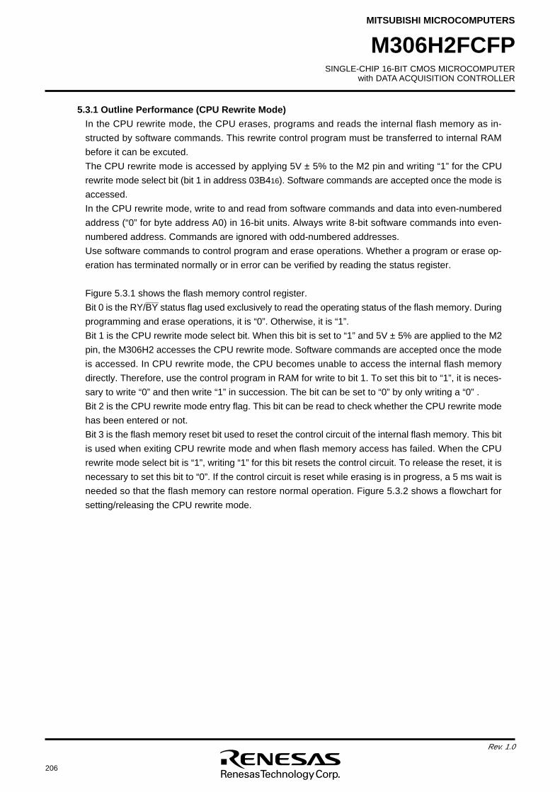
206
Rev. 1.0
SINGLE-CHIP 16-BIT CMOS MICROCOMPUTERwith DATA ACQUISITION CONTROLLER
MITSUBISHI MICROCOMPUTERS
M306H2FCFP
5.3.1 Outline Performance (CPU Rewrite Mode)
In the CPU rewrite mode, the CPU erases, programs and reads the internal flash memory as in-
structed by software commands. This rewrite control program must be transferred to internal RAM
before it can be excuted.
The CPU rewrite mode is accessed by applying 5V ± 5% to the M2 pin and writing “1” for the CPU
rewrite mode select bit (bit 1 in address 03B416). Software commands are accepted once the mode is
accessed.
In the CPU rewrite mode, write to and read from software commands and data into even-numbered
address (“0” for byte address A0) in 16-bit units. Always write 8-bit software commands into even-
numbered address. Commands are ignored with odd-numbered addresses.
Use software commands to control program and erase operations. Whether a program or erase op-
eration has terminated normally or in error can be verified by reading the status register.
Figure 5.3.1 shows the flash memory control register._____
Bit 0 is the RY/BY status flag used exclusively to read the operating status of the flash memory. During
programming and erase operations, it is “0”. Otherwise, it is “1”.
Bit 1 is the CPU rewrite mode select bit. When this bit is set to “1” and 5V ± 5% are applied to the M2
pin, the M306H2 accesses the CPU rewrite mode. Software commands are accepted once the mode
is accessed. In CPU rewrite mode, the CPU becomes unable to access the internal flash memory
directly. Therefore, use the control program in RAM for write to bit 1. To set this bit to “1”, it is neces-
sary to write “0” and then write “1” in succession. The bit can be set to “0” by only writing a “0” .
Bit 2 is the CPU rewrite mode entry flag. This bit can be read to check whether the CPU rewrite mode
has been entered or not.
Bit 3 is the flash memory reset bit used to reset the control circuit of the internal flash memory. This bit
is used when exiting CPU rewrite mode and when flash memory access has failed. When the CPU
rewrite mode select bit is “1”, writing “1” for this bit resets the control circuit. To release the reset, it is
necessary to set this bit to “0”. If the control circuit is reset while erasing is in progress, a 5 ms wait is
needed so that the flash memory can restore normal operation. Figure 5.3.2 shows a flowchart for
setting/releasing the CPU rewrite mode.
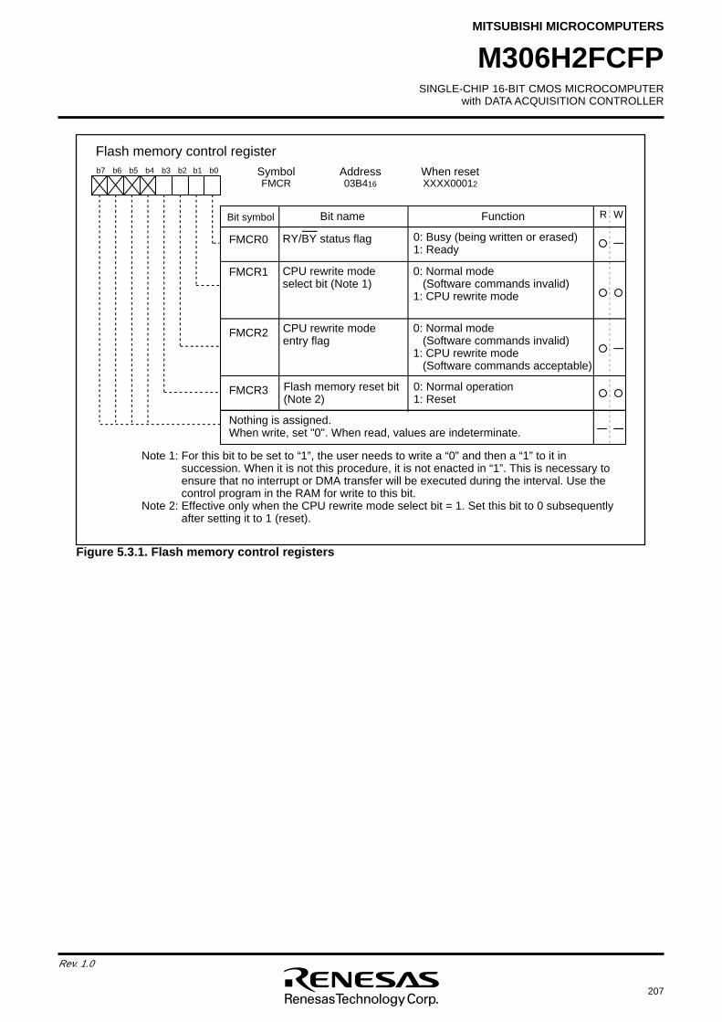
SINGLE-CHIP 16-BIT CMOS MICROCOMPUTERwith DATA ACQUISITION CONTROLLER
MITSUBISHI MICROCOMPUTERS
207
Rev. 1.0
M306H2FCFP
Flash memory control registerSymbol Address When resetFMCR 03B416 XXXX00012
WR
b7 b6 b5 b4 b3 b2 b1 b0
FMCR0
Bit symbol Bit name Function R W
0: Busy (being written or erased)1: Ready
CPU rewrite mode select bit (Note 1)
0: Normal mode (Software commands invalid)1: CPU rewrite mode
FMCR1
CPU rewrite mode entry flag
Flash memory reset bit (Note 2)
0: Normal operation1: Reset
Nothing is assigned. When write, set "0". When read, values are indeterminate.
FMCR2
FMCR3
Note 1: For this bit to be set to “1”, the user needs to write a “0” and then a “1” to it in succession. When it is not this procedure, it is not enacted in “1”. This is necessary to ensure that no interrupt or DMA transfer will be executed during the interval. Use the control program in the RAM for write to this bit.
Note 2: Effective only when the CPU rewrite mode select bit = 1. Set this bit to 0 subsequently after setting it to 1 (reset).
A
AA
A
AA
RY/BY status flag
0: Normal mode (Software commands invalid)1: CPU rewrite mode (Software commands acceptable)
Figure 5.3.1. Flash memory control registers
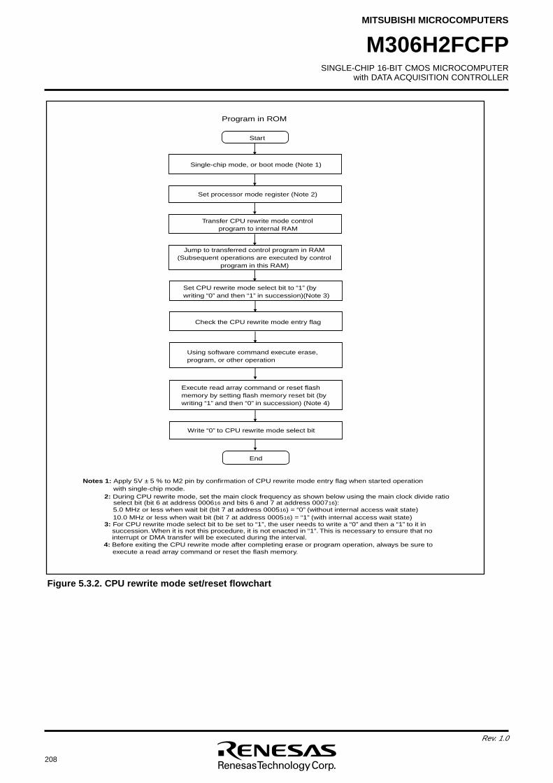
208
Rev. 1.0
SINGLE-CHIP 16-BIT CMOS MICROCOMPUTERwith DATA ACQUISITION CONTROLLER
MITSUBISHI MICROCOMPUTERS
M306H2FCFP
Notes 1: Apply 5V ± 5 % to M2 pin by confirmation of CPU rewrite mode entry flag when started operationwith single-chip mode.
2: During CPU rewrite mode, set the main clock frequency as shown below using the main clock divide ratio 16select bit (bit 6 at address 0006 and bits 6 and 7 at address 000716):
5.0 MHz or less when wait bit (bit 7 at address 000516) = “0” (without internal access wait state)10.0 MHz or less when wait bit (bit 7 at address 000516) = “1” (with internal access wait state)
3: For CPU rewrite mode select bit to be set to “1”, the user needs to write a “0” and then a “1” to it in succession. When it is not this procedure, it is not enacted in “1”. This is necessary to ensure that no interrupt or DMA transfer will be executed during the interval.
4: Before exiting the CPU rewrite mode after completing erase or program operation, always be sure to execute a read array command or reset the flash memory.
End
Execute read array command or reset flash memory by setting flash memory reset bit (by writing “1” and then “0” in succession) (Note 4)
Using software command execute erase, program, or other operation
Write “0” to CPU rewrite mode select bit
Set CPU rewrite mode select bit to “1” (by writing “0” and then “1” in succession)(Note 3)
Check the CPU rewrite mode entry flag
Start
Single-chip mode, or boot mode (Note 1)
Set processor mode register (Note 2)
Jump to transferred control program in RAM (Subsequent operations are executed by control
program in this RAM)
Transfer CPU rewrite mode control program to internal RAM
Program in ROM
Figure 5.3.2. CPU rewrite mode set/reset flowchart
SINGLE-CHIP 16-BIT CMOS MICROCOMPUTERwith DATA ACQUISITION CONTROLLER
MITSUBISHI MICROCOMPUTERS
209
Rev. 1.0
M306H2FCFP
5.3.2 Precautions on CPU Rewrite Mode
Described below are the precautions to be observed when rewriting the flash memory in CPU rewrite
mode.
(1) Operation speed
During CPU rewrite mode, set the main clock frequency as shown below using the main clock divide
ratio select bit (bit 6 at address 000616 and bits 6 and 7 at address 000716):
5.0 MHz or less when wait bit (bit 7 at address 000516) = 0 (without internal access wait state)
10.0 MHz or less when wait bit (bit 7 at address 000516) = 1 (with internal access wait state)
(2) Instructions inhibited against use
The instructions listed below cannot be used during CPU rewrite mode because they refer to the
internal data of the flash memory:
UND instruction, INTO instruction, JMPS instruction, JSRS instruction, and BRK instruction
(3) Interrupts inhibited against use_______
The NMI, address match, and watchdog timer interrupts cannot be used during CPU rewrite mode
because they refer to the internal data of the flash memory. If interrupts have their vector in the
variable vector table, they can be used by transferring the vector into the RAM area.
(4) Reset
If the control circuit is reset while erasing is in progress, a 5 ms wait is needed so that the flash
memory can restore normal operation. Set a 5 ms wait to release the reset operation.
Also, when the reset has been released, the program execute start address is automatically set to
0DE00016 at boot mode, therefore program so that the execute start address of the boot ROM is
0DE00016.
(5) Writing in the user ROM area
If power is lost while rewriting blocks that contain the flash rewrite program with the CPU rewrite
mode, those blocks may not be correctly rewritten and it is possible that the flash memory can no
longer be rewritten after that. Therefore, it is recommended to use the standard serial I/O mode or
parallel I/O mode to rewrite these blocks.
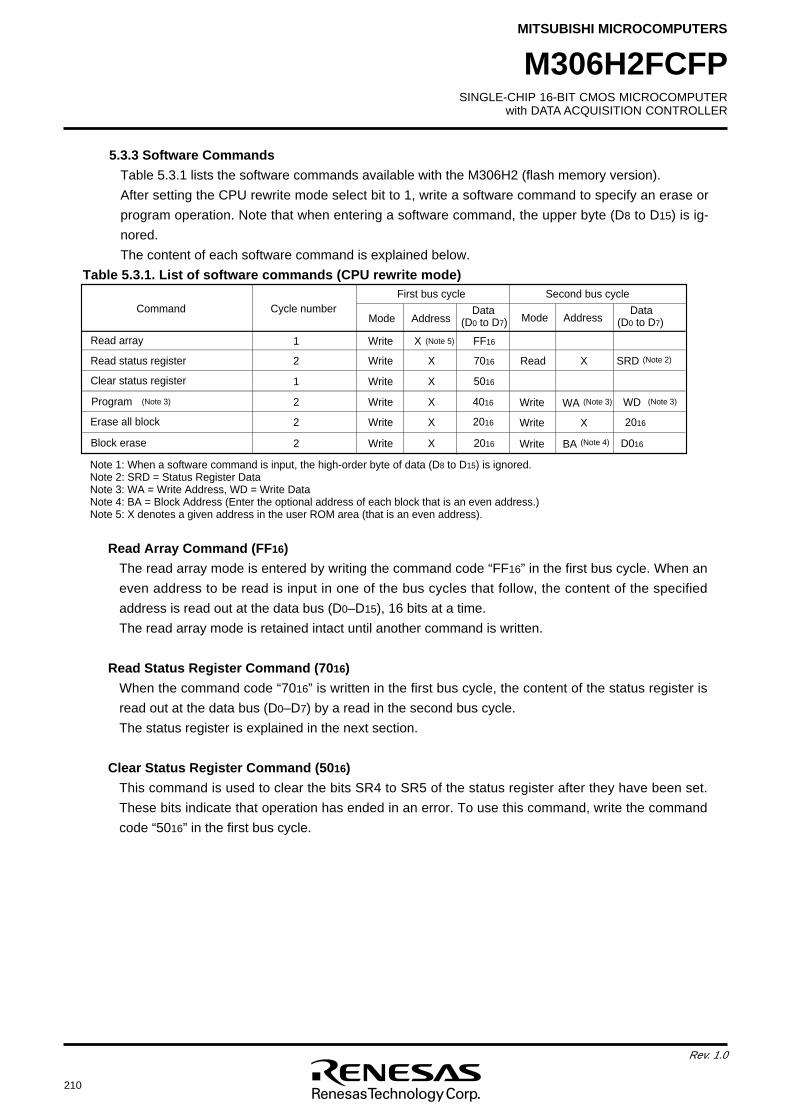
210
Rev. 1.0
SINGLE-CHIP 16-BIT CMOS MICROCOMPUTERwith DATA ACQUISITION CONTROLLER
MITSUBISHI MICROCOMPUTERS
M306H2FCFP
Command
Program
Clear status register
Read array
Read status register
X
X
X
X(Note 3)
First bus cycle Second bus cycle
FF16
7016
5016
4016
Write
Write
Write
Write
X SRDRead
Write
Erase all block X 2016Write X 2016Write
(Note 2)
WA (Note 3) WD (Note 3)
Block erase X 2016Write D016Write BA (Note 4)
Mode Address Mode AddressData
(D0 to D7)Data
(D0 to D7)
(Note 5)
Note 1: When a software command is input, the high-order byte of data (D8 to D15) is ignored.Note 2: SRD = Status Register DataNote 3: WA = Write Address, WD = Write DataNote 4: BA = Block Address (Enter the optional address of each block that is an even address.)Note 5: X denotes a given address in the user ROM area (that is an even address).
Cycle number
1
2
1
2
2
2
5.3.3 Software Commands
Table 5.3.1 lists the software commands available with the M306H2 (flash memory version).
After setting the CPU rewrite mode select bit to 1, write a software command to specify an erase or
program operation. Note that when entering a software command, the upper byte (D8 to D15) is ig-
nored.
The content of each software command is explained below.
Table 5.3.1. List of software commands (CPU rewrite mode)
Read Array Command (FF16)
The read array mode is entered by writing the command code “FF16” in the first bus cycle. When an
even address to be read is input in one of the bus cycles that follow, the content of the specified
address is read out at the data bus (D0–D15), 16 bits at a time.
The read array mode is retained intact until another command is written.
Read Status Register Command (7016)
When the command code “7016” is written in the first bus cycle, the content of the status register is
read out at the data bus (D0–D7) by a read in the second bus cycle.
The status register is explained in the next section.
Clear Status Register Command (5016)
This command is used to clear the bits SR4 to SR5 of the status register after they have been set.
These bits indicate that operation has ended in an error. To use this command, write the command
code “5016” in the first bus cycle.
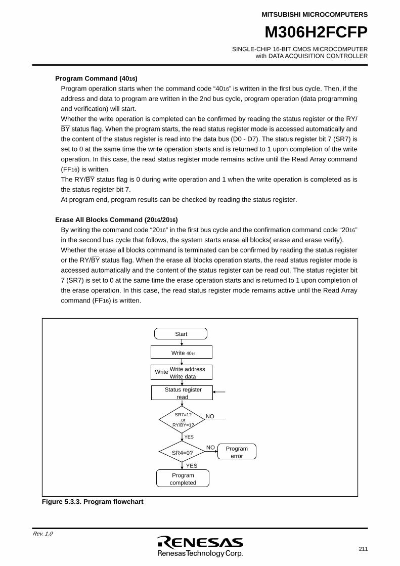
SINGLE-CHIP 16-BIT CMOS MICROCOMPUTERwith DATA ACQUISITION CONTROLLER
MITSUBISHI MICROCOMPUTERS
211
Rev. 1.0
M306H2FCFP
Start
Write 4016
Status registerread
Program completed
NO
YES
Write addressWrite data
SR4=0?Program
error
NO
YES
SR7=1?or
RY/BY=1?
Write
Figure 5.3.3. Program flowchart
Program Command (4016)
Program operation starts when the command code “4016” is written in the first bus cycle. Then, if the
address and data to program are written in the 2nd bus cycle, program operation (data programming
and verification) will start.
Whether the write operation is completed can be confirmed by reading the status register or the RY/_____
BY status flag. When the program starts, the read status register mode is accessed automatically and
the content of the status register is read into the data bus (D0 - D7). The status register bit 7 (SR7) is
set to 0 at the same time the write operation starts and is returned to 1 upon completion of the write
operation. In this case, the read status register mode remains active until the Read Array command
(FF16) is written.____
The RY/BY status flag is 0 during write operation and 1 when the write operation is completed as is
the status register bit 7.
At program end, program results can be checked by reading the status register.
Erase All Blocks Command (2016/2016)
By writing the command code “2016” in the first bus cycle and the confirmation command code “2016”
in the second bus cycle that follows, the system starts erase all blocks( erase and erase verify).
Whether the erase all blocks command is terminated can be confirmed by reading the status register____
or the RY/BY status flag. When the erase all blocks operation starts, the read status register mode is
accessed automatically and the content of the status register can be read out. The status register bit
7 (SR7) is set to 0 at the same time the erase operation starts and is returned to 1 upon completion of
the erase operation. In this case, the read status register mode remains active until the Read Array
command (FF16) is written.
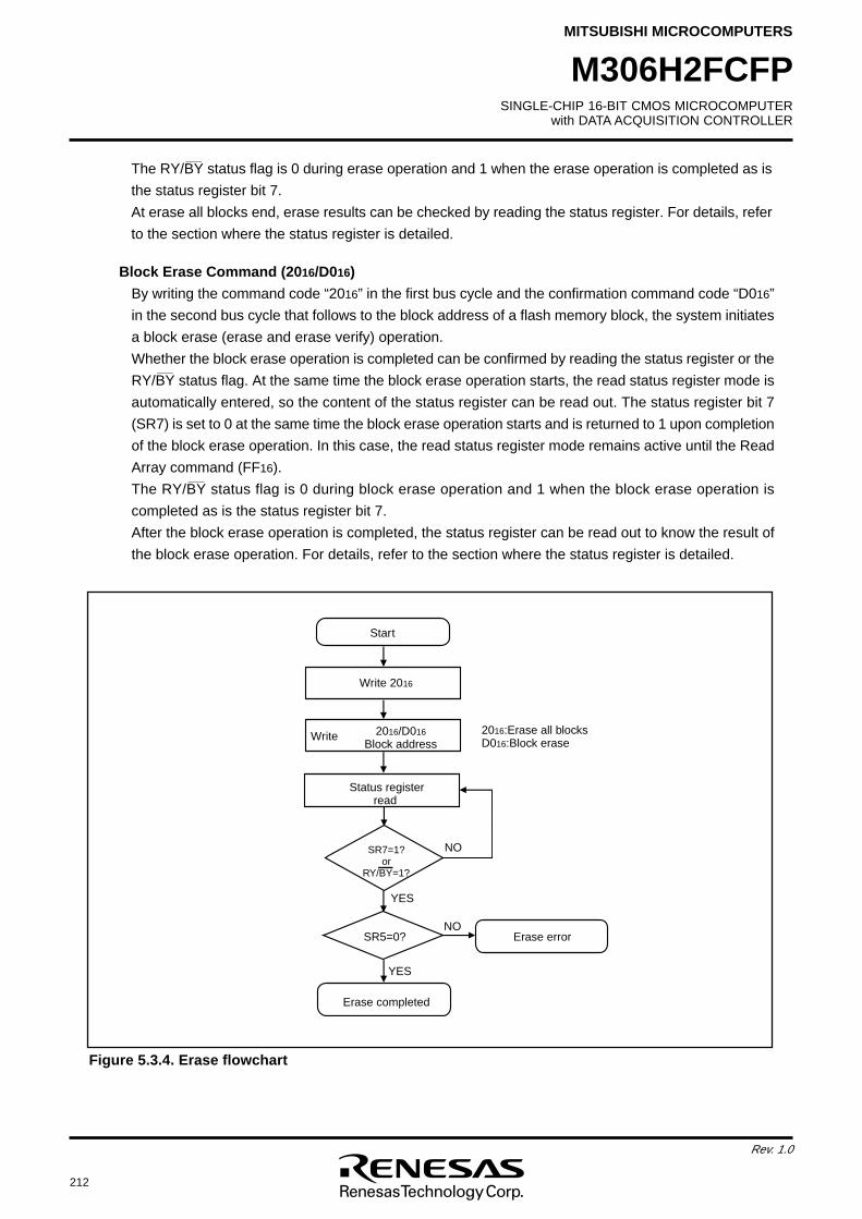
212
Rev. 1.0
SINGLE-CHIP 16-BIT CMOS MICROCOMPUTERwith DATA ACQUISITION CONTROLLER
MITSUBISHI MICROCOMPUTERS
M306H2FCFP
Write 2016
2016/D016
Block address
Erase completed
NO
YES
Start
Write
SR5=0? Erase error
YES
NO
2016:Erase all blocksD016:Block erase
SR7=1?or
RY/BY=1?
Status registerread
Figure 5.3.4. Erase flowchart
Block Erase Command (2016/D016)
By writing the command code “2016” in the first bus cycle and the confirmation command code “D016”
in the second bus cycle that follows to the block address of a flash memory block, the system initiates
a block erase (erase and erase verify) operation.
Whether the block erase operation is completed can be confirmed by reading the status register or the____
RY/BY status flag. At the same time the block erase operation starts, the read status register mode is
automatically entered, so the content of the status register can be read out. The status register bit 7
(SR7) is set to 0 at the same time the block erase operation starts and is returned to 1 upon completion
of the block erase operation. In this case, the read status register mode remains active until the Read
Array command (FF16).____
The RY/BY status flag is 0 during block erase operation and 1 when the block erase operation is
completed as is the status register bit 7.
After the block erase operation is completed, the status register can be read out to know the result of
the block erase operation. For details, refer to the section where the status register is detailed.
____
The RY/BY status flag is 0 during erase operation and 1 when the erase operation is completed as is
the status register bit 7.
At erase all blocks end, erase results can be checked by reading the status register. For details, refer
to the section where the status register is detailed.
SINGLE-CHIP 16-BIT CMOS MICROCOMPUTERwith DATA ACQUISITION CONTROLLER
MITSUBISHI MICROCOMPUTERS
213
Rev. 1.0
M306H2FCFP
5.3.4 Status Register
The status register shows the operating state of the flash memory and whether erase operations and
programs ended successfully or in error. It can be read in the following ways.
(1) By reading an arbitrary address from the user ROM area after writing the read status register
command (7016)
(2) By reading an arbitrary address from the user ROM area in the period from when the program
starts or erase operation starts to when the read array command (FF16) is input
Table 5.3.2 shows the status register.
Also, the status register can be cleared in the following way.
(1) By writing the clear status register command (5016)
After a reset, the status register is set to “8016”.
Each bit in this register is explained below.
Sequencer status (SR7)
After power-on, the sequencer status is set to 1(ready).
The sequencer status indicates the operating status of the device. This status bit is set to 0 (busy)
during write or erase operation and is set to 1 upon completion of these operations.
Erase status (SR5)
The erase status informs the operating status of erase operation to the CPU. When an erase error
occurs, it is set to 1.
The erase status is reset to 0 when cleared.
Program status (SR4)
The program status informs the operating status of write operation to the CPU. When a write error
occurs, it is set to 1.
The program status is reset to 0 when cleared.
If “1” is written for any of the SR5 or SR4 bits, the program, erase all blocks, and block erase com-
mands are not accepted. Before executing these commands, execute the clear status register com-
mand (5016) and clear the status register.
Also, any commands are not correct, both SR5 and SR4 are set to 1.
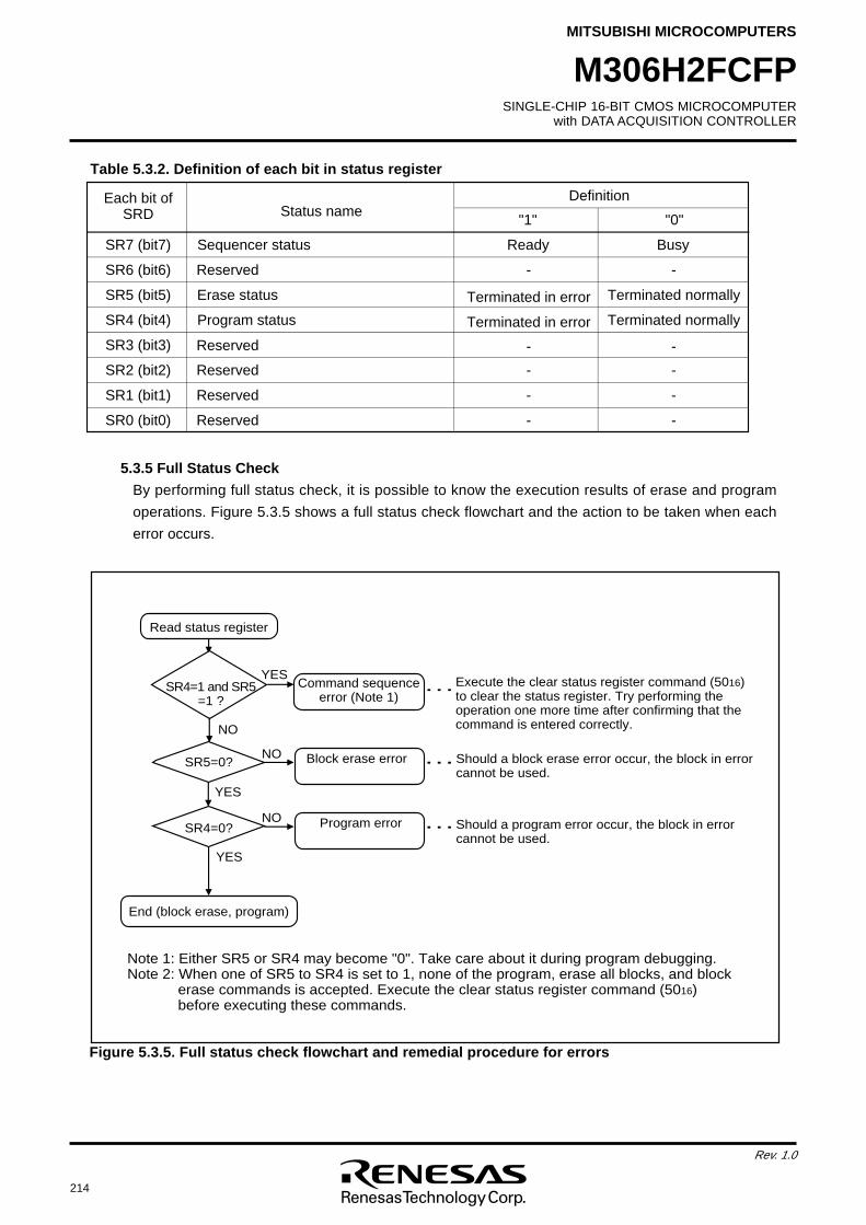
214
Rev. 1.0
SINGLE-CHIP 16-BIT CMOS MICROCOMPUTERwith DATA ACQUISITION CONTROLLER
MITSUBISHI MICROCOMPUTERS
M306H2FCFP
Read status register
SR4=1 and SR5=1 ?
NO
Command sequence error (Note 1)
YES
SR5=0?
YES
Block erase errorNO
SR4=0?
YES
Program errorNO
End (block erase, program)
Execute the clear status register command (5016) to clear the status register. Try performing the operation one more time after confirming that the command is entered correctly.
Should a block erase error occur, the block in error cannot be used.
Note 1: Either SR5 or SR4 may become "0". Take care about it during program debugging.Note 2: When one of SR5 to SR4 is set to 1, none of the program, erase all blocks, and block
erase commands is accepted. Execute the clear status register command (5016) before executing these commands.
Should a program error occur, the block in error cannot be used.
5.3.5 Full Status Check
By performing full status check, it is possible to know the execution results of erase and program
operations. Figure 5.3.5 shows a full status check flowchart and the action to be taken when each
error occurs.
Figure 5.3.5. Full status check flowchart and remedial procedure for errors
Each bit of SRD
SR4 (bit4)
SR5 (bit5)
SR7 (bit7)
SR6 (bit6)
Status nameDefinition
SR1 (bit1)
SR2 (bit2)
SR3 (bit3)
SR0 (bit0)
"1" "0"
Program status
Erase status
Sequencer status
Reserved
Reserved
Reserved
Reserved
Ready Busy
Terminated in error
Terminated in error
Terminated normally
Terminated normally
-
-
-
-
-
-
-
-
- -Reserved
Table 5.3.2. Definition of each bit in status register
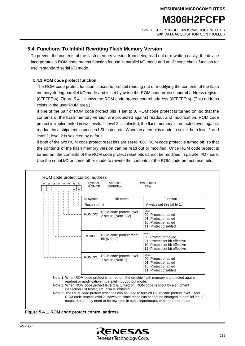
SINGLE-CHIP 16-BIT CMOS MICROCOMPUTERwith DATA ACQUISITION CONTROLLER
MITSUBISHI MICROCOMPUTERS
215
Rev. 1.0
M306H2FCFP
Symbol Address When resetROMCP 0FFFFF16 FF16
ROM code protect level 2 set bit (Note 1, 2) 00: Protect enabled
01: Protect enabled10: Protect enabled11: Protect disabled
ROM code protect control address
Bit name FunctionBit symbol
b7 b6 b5 b4 b3 b2 b1 b0
00: Protect removed01: Protect set bit effective10: Protect set bit effective11: Protect set bit effective
00: Protect enabled01: Protect enabled10: Protect enabled11: Protect disabled
ROM code protect reset bit (Note 3)
ROM code protect level 1 set bit (Note 1)
ROMCP2
ROMCR
ROMCP1
b3 b2
b5 b4
b7 b6
Note 1: When ROM code protect is turned on, the on-chip flash memory is protected against readout or modification in parallel input/output mode.
Note 2: When ROM code protect level 2 is turned on, ROM code readout by a shipment inspection LSI tester, etc. also is inhibited.
Note 3: The ROM code protect reset bits can be used to turn off ROM code protect level 1 and ROM code protect level 2. However, since these bits cannot be changed in parallel input/output mode, they need to be rewritten in serial input/output or some other mode.
Reserved bit Always set this bit to 1.
1 1
5.4 Functions To Inhibit Rewriting Flash Memory VersionTo prevent the contents of the flash memory version from being read out or rewritten easily, the device
incorporates a ROM code protect function for use in parallel I/O mode and an ID code check function for
use in standard serial I/O mode.
5.4.1 ROM code protect function
The ROM code protect function is used to prohibit reading out or modifying the contents of the flash
memory during parallel I/O mode and is set by using the ROM code protect control address register
(0FFFFF16). Figure 5.4.1 shows the ROM code protect control address (0FFFFF16). (This address
exists in the user ROM area.)
If one of the pair of ROM code protect bits is set to 0, ROM code protect is turned on, so that the
contents of the flash memory version are protected against readout and modification. ROM code
protect is implemented in two levels. If level 2 is selected, the flash memory is protected even against
readout by a shipment inspection LSI tester, etc. When an attempt is made to select both level 1 and
level 2, level 2 is selected by default.
If both of the two ROM code protect reset bits are set to “00,” ROM code protect is turned off, so that
the contents of the flash memory version can be read out or modified. Once ROM code protect is
turned on, the contents of the ROM code protect reset bits cannot be modified in parallel I/O mode.
Use the serial I/O or some other mode to rewrite the contents of the ROM code protect reset bits.
Figure 5.4.1. ROM code protect control address
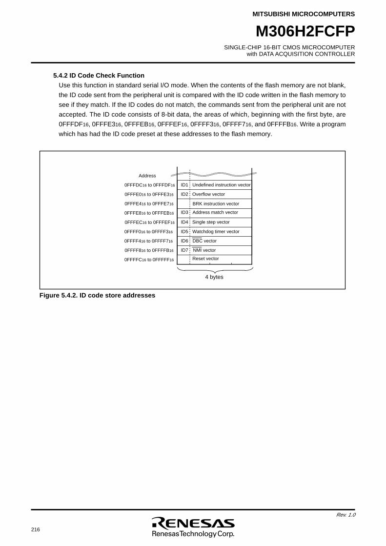
216
Rev. 1.0
SINGLE-CHIP 16-BIT CMOS MICROCOMPUTERwith DATA ACQUISITION CONTROLLER
MITSUBISHI MICROCOMPUTERS
M306H2FCFP
5.4.2 ID Code Check Function
Use this function in standard serial I/O mode. When the contents of the flash memory are not blank,
the ID code sent from the peripheral unit is compared with the ID code written in the flash memory to
see if they match. If the ID codes do not match, the commands sent from the peripheral unit are not
accepted. The ID code consists of 8-bit data, the areas of which, beginning with the first byte, are
0FFFDF16, 0FFFE316, 0FFFEB16, 0FFFEF16, 0FFFF316, 0FFFF716, and 0FFFFB16. Write a program
which has had the ID code preset at these addresses to the flash memory.
Figure 5.4.2. ID code store addresses
Reset vector
Watchdog timer vector
Single step vector
Address match vector
BRK instruction vector
Overflow vector
Undefined instruction vector
ID7
ID6
ID5
ID4
ID3
ID2
ID1
DBC vector
NMI vector
0FFFFC16 to 0FFFFF16
0FFFF816 to 0FFFFB16
0FFFF416 to 0FFFF716
0FFFF016 to 0FFFF316
0FFFEC16 to 0FFFEF16
0FFFE816 to 0FFFEB16
0FFFE416 to 0FFFE716
0FFFE016 to 0FFFE316
0FFFDC16 to 0FFFDF16
4 bytes
Address
SINGLE-CHIP 16-BIT CMOS MICROCOMPUTERwith DATA ACQUISITION CONTROLLER
MITSUBISHI MICROCOMPUTERS
217
Rev. 1.0
M306H2FCFP
5.5 Parallel I/O ModeThe parallel I/O mode inputs and outputs the software commands, addresses and data needed to oper-
ate (read, program, erase, etc.) the internal flash memory. This I/O is parallel.
Use an exclusive programer supporting M306H2 (flash memory version).
Refer to the instruction manual of each programer maker for the details of use.
User ROM and Boot ROM Areas
In parallel I/O mode, the user ROM and boot ROM areas shown in Figure 5.2.1 can be rewritten. Both
areas of flash memory can be operated on in the same way.
Program and block erase operations can be performed in the user ROM area. The user ROM area and its
blocks are shown in Figure 5.2.1.
The boot ROM area is 8 Kbytes in size. In parallel I/O mode, it is located at addresses 0DE00016 through
0DFFFF16. Make sure program and block erase operations are always performed within this address
range. (Access to any location outside this address range is prohibited.)
In the boot ROM area, an erase block operation is applied to only one 8 Kbyte block. The boot ROM area
has had a standard serial I/O mode control program stored in it when shipped from the Mitsubishi factory.
Therefore, using the device in standard serial input/output mode, you do not need to write to the boot
ROM area.
218
Rev. 1.0
SINGLE-CHIP 16-BIT CMOS MICROCOMPUTERwith DATA ACQUISITION CONTROLLER
MITSUBISHI MICROCOMPUTERS
M306H2FCFP
5.6 Standard serial I/O modeThe standard serial I/O mode inputs and outputs the software commands, addresses and data needed to
operate (read, program, erase, etc.) the internal flash memory. This I/O is serial. There are actually two
standard serial I/O modes: mode 1, which is clock synchronized, and mode 2, which is asynchronized.
Both modes require a purpose-specific peripheral unit.
The standard serial I/O mode is different from the parallel I/O mode in that the CPU controls flash memory
rewrite (uses the CPU's rewrite mode), rewrite data input and so forth. The standard serial I/O mode is
started by connecting “H” to the CNVSS pin and P50 pin, connecting “L” to the M1 pin, and releasing the
reset operation. (In the ordinary command mode, set CNVss pin to “L” level.)
This control program is written in the boot ROM area when the product is shipped from Mitsubishi. Ac-
cordingly, make note of the fact that the standard serial I/O mode cannot be used if the boot ROM area is
rewritten in the parallel I/O mode. Figure 5.6.1 shows the pin connections for the standard serial I/O
mode. Serial data I/O uses UART1 and transfers the data serially in 8-bit units. Standard serial I/O
switches between mode 1 (clock synchronized) and mode 2 (clock asynchronized) according to the level
of CLK1 pin when the reset is released.
To use standard serial I/O mode 1 (clock synchronized), set the CLK1 pin to “H” level and release the
reset. The operation uses the four UART1 pins CLK1, RxD1, TxD1 and RTS1 (BUSY). The CLK1 pin is the
transfer clock input pin through which an external transfer clock is input. The TxD1 pin is for CMOS
output. The RTS1 (BUSY) pin outputs an "L" level when ready for reception and an “L” level when recep-
tion starts.
To use standard serial I/O mode 2 (clock asynchronized), set the CLK1 pin to “L” level and release the
reset. The operation uses the two UART1 pins RxD1 and TxD1.
In the standard serial I/O mode, only the user ROM area indicated in Figure 5.2.1 can be rewritten. The
boot ROM cannot.
In the standard serial I/O mode, a 7-byte ID code is used. When there is data in the flash memory,
commands sent from the peripheral unit (programmer) are not accepted unless the ID code matches.
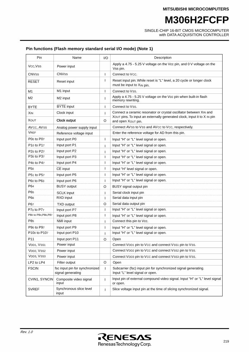
SINGLE-CHIP 16-BIT CMOS MICROCOMPUTERwith DATA ACQUISITION CONTROLLER
MITSUBISHI MICROCOMPUTERS
219
Rev. 1.0
M306H2FCFP
Pin functions (Flash memory standard serial I/O mode) (Note 1)
Pin Description
VCC,VSSApply a 4.75 - 5.25 V voltage on the Vcc pin, and 0 V voltage on the Vss pin.
CNVSS Connect to VCC.
RESET Reset input pin. While reset is "L" level, a 20 cycle or longer clock must be input to XIN pin.
Name
Power input
CNVSS
Reset input
I/O
I
I
OUT pin.
AVCC, AVSS Connect AVSS to VSS and AVCC to VCC, respectively.
P40 to P47 Input "H" or "L" level signal or open.
Analog power supply input
Input port P4
P00 to P07 Input "H" or "L" level signal or open.Input port P0 I
P10 to P17 Input "H" or "L" level signal or open.Input port P1 I
I
P20 to P27 Input "H" or "L" level signal or open.Input port P2 IP30 to P37 Input "H" or "L" level signal or open.Input port P3 I
P80 to P84,P86,P87 Input "H" or "L" level signal or open.
P85
P67 Serial data output pin
P60 to P63
P65 Serial clock input pin
P66 Serial data input pin
Input port P8
NMI input
TXD output
SCLK inputRXD input
P70 to P77 Input "H" or "L" level signal or open.Input port P7 I
I
I
I
I
I
O
P51 to P57
Input "H" or "L" level signal or open.
Input port P5 I
Connect this pin to Vcc.
P90 to P97 Input "H" or "L" level signal or open.
P100 to P107 Input "H" or "L" level signal or open.
Input port P9
Input port P10
I
I
P11 OpenInput port P11
OpenFilter output O
Subcarrier (fsc) input pin for synchronized signal generating.Input "L" level signal or open.
fsc input pin for synchronized signal generating
Input pin of external compound video signal. Input "H" or "L" level signal or open.
Connect a ceramic resonator or crystal oscillator between XIN and XOUT pins. To input an externally generated clock, input it to X IN pin and open XXOUT
Clock input
Clock output
I
OClock output
XIN
M1 M1 input I Connect to VSS.
M2 M2 input I Apply a 4.75 - 5.25 V voltage on the Vcc pin when built-in flash memory rewriting.
BYTE BYTE input I Connect to VSS.
P50
Input "H" or "L" level signal or open.
CE input I
LP2 to LP4
FSCIN
CVIN1, SYNCIN
SVREF
I
I
I
O
Input port P6
VDD1, VSS1 Connect VDD1 pin to VCC and connect VSS1 pin to VSS.Power input
Composite video signalinput
Synchronous slice level input
Slice voltage input pin at the time of slicing synchronized signal.
VDD2, VSS2 Power input Connect VDD2 pin to VCC and connect VSS2 pin to VSS.
VDD3, VSS3 Power input Connect VDD3 pin to VCC and connect VSS3 pin to VSS.
P64 BUSY output O BUSY signal output pin
Input "H" level signal or open.
VREF Enter the reference voltage for AD from this pin.Reference voltage input
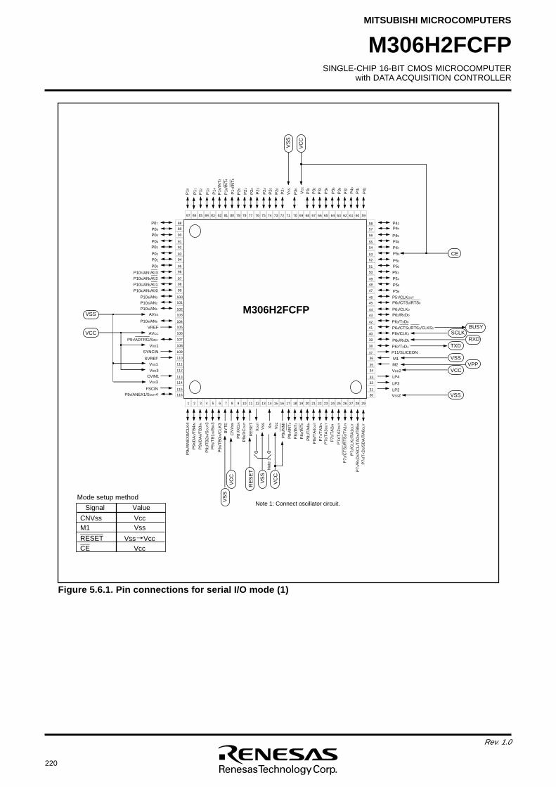
220
Rev. 1.0
SINGLE-CHIP 16-BIT CMOS MICROCOMPUTERwith DATA ACQUISITION CONTROLLER
MITSUBISHI MICROCOMPUTERS
M306H2FCFP
Figure 5.6.1. Pin connections for serial I/O mode (1)
BY
TE
XO
UT
Vss XIN
Vcc
P87
/XC
IN
P86
/XC
OU
T
P81
/TA
4IN
P80
/TA
4OU
T
P77
/TA
3IN
CN
Vss
P90
/TB
0IN/C
LK3
P91
/TB
1IN/S
IN3
P92
/TB
2IN/S
OU
T3
P94
/DA
1/T
B4I
N
P95
/AN
EX
0/C
LK4
P93
/DA
0/T
B3I
N
P31
P42
P41
P40
P32
P33
P34
P35
P36
P37
VC
C
P43
P96/ANEX1/SOUT4
RE
SE
T
P85
/NM
I
P84
/INT
2
P76
/TA
3OU
T
P75
/TA
2IN
P74
/TA
2OU
T
P72
/CLK
2/T
A1O
UT
P71
/RXD
2/S
CL/
TA
0IN/T
B5I
N
P73
/CT
S2/
RT
S2/
TA
1IN
P53
P56
P44
P46
P47
P50
P51
P52
P54
P55
108
107
106
105
104
103
102
101
100
99
98
97
96
95
94
93
92
91
90
89
88
87 86 85 84 83 82 81 80 79 78 77 76 75 74 73 71 70 69 68 67 66 65 64 63 62 61 60 5972
P07
P02
P03
P04
P05
P06
P00
P01
110
111
112
113
114
115
116
109
1 2 3 4 5 6 7 8 9 10 11 12 13 14 15 16 17 18 19 20 21 22 23 24 25 26 27 28 29
30
31
32
33
34
35
36
M306H2FCFP
P83
/INT
1
P82
/INT
0
P61/CLK0
P62/RXD0
P63/TXD0
P65/CLK1
P66/RXD1
P67/TXD1
VREF
AVSS
P57/CLKOUT
P60/CTS0/RTS0
P64/CTS1/RTS1/CLKS1
58
57
56
55
54
53
52
51
50
49
48
47
46
45
44
43
42
41
40
39
38
37 P11/SLICEON
M1
M2VSS1
VDD1
P20
P27
P30
P26
P25
P24
P23
P22
P21
P14
P13
P12
P11
VS
S
P15
/INT
3
P16
/INT
4
P17
/INT
5
P70
/TXD
2/S
DA
/TA
0OU
T
VSS2LP2
LP4
LP3
VDD2
P10
P103/AN3
P102/AN2
P101/AN1
P100/AN0
AVCC
SYNCIN
CVIN1VDD3
VSS3
FSCIN
P97/ADTRG/SIN4
P45
P107/AN7/KI3
P104/AN4/KI0
P105/AN5/KI1
P106/AN6/KI2
SVREF
VSS
VCC
VS
S
VC
C
RE
SE
T
VSS
VCC
VSSVPP
SCLKRXD
TXD
BUSY
VC
C
VS
S
VS
S
CNVss Vcc
RESET
M1 Vss
Vss Vcc
VC
C
CE Vcc
CE
Note 1: Connect oscillator circuit.Mode setup method
Signal Value
Not
e 1
SINGLE-CHIP 16-BIT CMOS MICROCOMPUTERwith DATA ACQUISITION CONTROLLER
MITSUBISHI MICROCOMPUTERS
221
Rev. 1.0
M306H2FCFP
5.6.1 Overview of standard serial I/O mode 1 (clock synchronized)
In standard serial I/O mode 1, software commands, addresses and data are input and output between
the MCU and peripheral units (serial programer, etc.) using 4-wire clock-synchronized serial I/O
(UART1). Standard serial I/O mode 1 is engaged by releasing the reset with the P65 (CLK1) pin "H"
level.
In reception, software commands, addresses and program data are synchronized with the rise of the
transfer clock that is input to the CLK1 pin, and are then input to the MCU via the RxD1 pin. In transmis-
sion, the read data and status are synchronized with the fall of the transfer clock, and output from the
TxD1 pin.
The TxD1 pin is for CMOS output. Transfer is in 8-bit units with LSB first.
When busy, such as during transmission, reception, erasing or program execution, the RTS1 (BUSY)
pin is "H" level. Accordingly, always start the next transfer after the RTS1 (BUSY) pin is "L" level.
Also, data and status registers in memory can be read after inputting software commands. Status,
such as the operating state of the flash memory or whether a program or erase operation ended
successfully or not, can be checked by reading the status register. Here following are explained soft-
ware commands, status registers, etc.
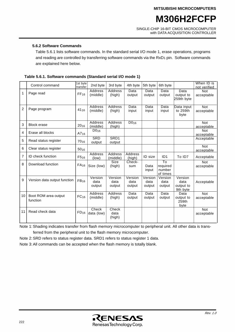
222
Rev. 1.0
SINGLE-CHIP 16-BIT CMOS MICROCOMPUTERwith DATA ACQUISITION CONTROLLER
MITSUBISHI MICROCOMPUTERS
M306H2FCFP
5.6.2 Software Commands
Table 5.6.1 lists software commands. In the standard serial I/O mode 1, erase operations, programs
and reading are controlled by transferring software commands via the RxD1 pin. Software commands
are explained here below.
Table 5.6.1. Software commands (Standard serial I/O mode 1)
Control command 2nd byte 3rd byte 4th byte 5th byte 6th byte
1 Page read
2 Page program
3 Block erase
4 Erase all blocks
5 Read status register
6 Clear status register
7 ID check function
8 Download function
9 Version data output function
10 Boot ROM area outputfunction
11 Read check data
Address(middle)
Address(middle)
Address(middle)
D016
SRDoutput
Address(low)
Size (low)
Versiondata
output
Address(middle)
Checkdata (low)
Address(high)
Address(high)
Address(high)
SRD1output
Address(middle)
Size(high)
Versiondata
output
Address(high)
Checkdata
(high)
Dataoutput
Datainput
D016
Address(high)
Check-sum
Versiondata
output
Dataoutput
Dataoutput
Datainput
ID size
Datainput
Versiondata
output
Dataoutput
Dataoutput
Datainput
ID1
Torequirednumberof timesVersion
dataoutput
Dataoutput
Dataoutput to
259th byte
Data inputto 259th
byte
To ID7
Versiondata
output to9th byte
Dataoutput to
259thbyte
FF16
4116
2016
A716
7016
5016
F516
FA16
FB16
FC16
FD16
When ID isnot verified
Notacceptable
Notacceptable
Notacceptable
NotacceptableAcceptable
Notacceptable
Acceptable
Notacceptable
Acceptable
Notacceptable
Notacceptable
1st bytetransfer
Note 1: Shading indicates transfer from flash memory microcomputer to peripheral unit. All other data is trans-
ferred from the peripheral unit to the flash memory microcomputer.
Note 2: SRD refers to status register data. SRD1 refers to status register 1 data.
Note 3: All commands can be accepted when the flash memory is totally blank.
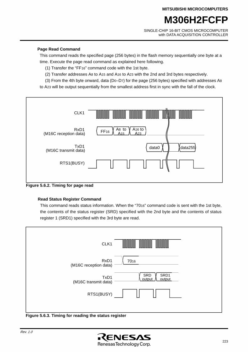
SINGLE-CHIP 16-BIT CMOS MICROCOMPUTERwith DATA ACQUISITION CONTROLLER
MITSUBISHI MICROCOMPUTERS
223
Rev. 1.0
M306H2FCFP
Page Read Command
This command reads the specified page (256 bytes) in the flash memory sequentially one byte at a
time. Execute the page read command as explained here following.
(1) Transfer the “FF16” command code with the 1st byte.
(2) Transfer addresses A8 to A15 and A16 to A23 with the 2nd and 3rd bytes respectively.
(3) From the 4th byte onward, data (D0–D7) for the page (256 bytes) specified with addresses A8
to A23 will be output sequentially from the smallest address first in sync with the fall of the clock.
Figure 5.6.2. Timing for page read
Read Status Register Command
This command reads status information. When the “7016” command code is sent with the 1st byte,
the contents of the status register (SRD) specified with the 2nd byte and the contents of status
register 1 (SRD1) specified with the 3rd byte are read.
Figure 5.6.3. Timing for reading the status register
data0 data255
CLK1
RxD1
TxD1
RTS1(BUSY)
A8 to A15
A16 to A23
FF16(M16C reception data)
(M16C transmit data)
SRD output
SRD1 output
7016(M16C reception data)
(M16C transmit data)
CLK1
RxD1
TxD1
RTS1(BUSY)
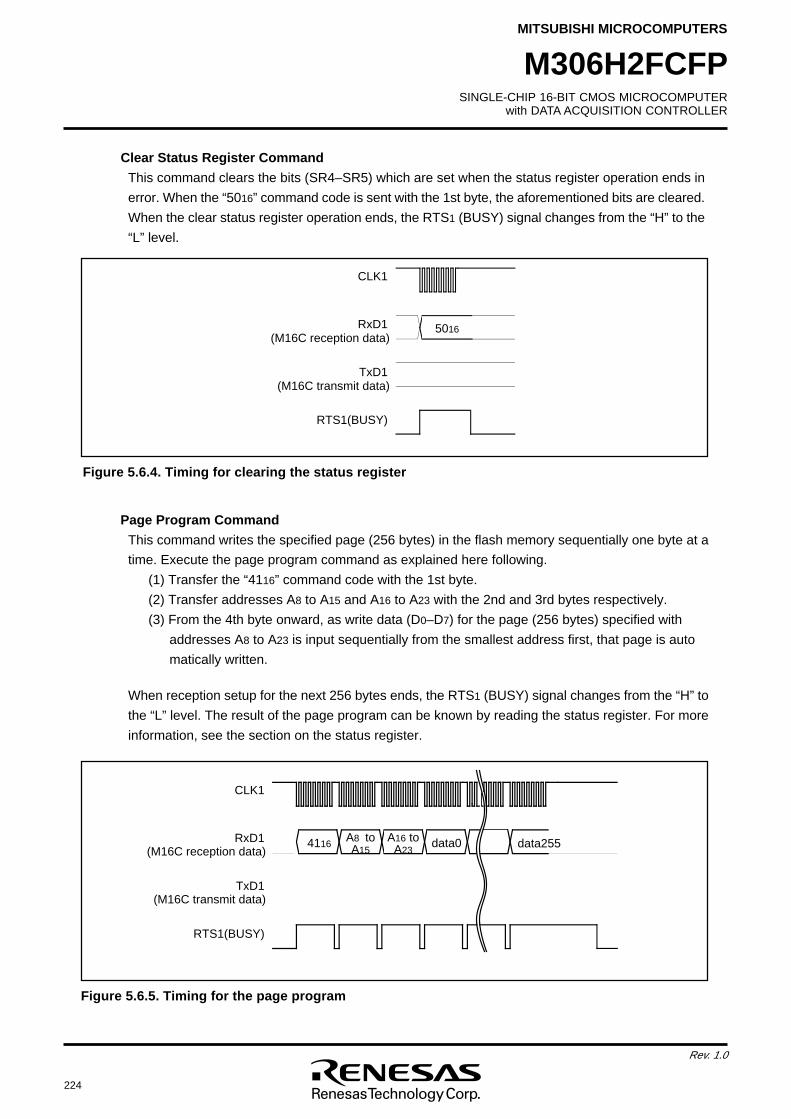
224
Rev. 1.0
SINGLE-CHIP 16-BIT CMOS MICROCOMPUTERwith DATA ACQUISITION CONTROLLER
MITSUBISHI MICROCOMPUTERS
M306H2FCFP
Clear Status Register Command
This command clears the bits (SR4–SR5) which are set when the status register operation ends in
error. When the “5016” command code is sent with the 1st byte, the aforementioned bits are cleared.
When the clear status register operation ends, the RTS1 (BUSY) signal changes from the “H” to the
“L” level.
Figure 5.6.4. Timing for clearing the status register
Page Program Command
This command writes the specified page (256 bytes) in the flash memory sequentially one byte at a
time. Execute the page program command as explained here following.
(1) Transfer the “4116” command code with the 1st byte.
(2) Transfer addresses A8 to A15 and A16 to A23 with the 2nd and 3rd bytes respectively.
(3) From the 4th byte onward, as write data (D0–D7) for the page (256 bytes) specified with
addresses A8 to A23 is input sequentially from the smallest address first, that page is auto
matically written.
When reception setup for the next 256 bytes ends, the RTS1 (BUSY) signal changes from the “H” to
the “L” level. The result of the page program can be known by reading the status register. For more
information, see the section on the status register.
CLK1
RxD1
TxD1
RTS1(BUSY)
5016(M16C reception data)
(M16C transmit data)
Figure 5.6.5. Timing for the page program
CLK1
RxD1
TxD1
RTS1(BUSY)
A8 to A15
A16 to A23
4116 data0 data255(M16C reception data)
(M16C transmit data)
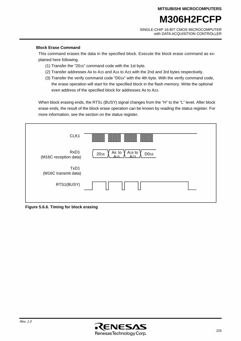
SINGLE-CHIP 16-BIT CMOS MICROCOMPUTERwith DATA ACQUISITION CONTROLLER
MITSUBISHI MICROCOMPUTERS
225
Rev. 1.0
M306H2FCFP
Block Erase Command
This command erases the data in the specified block. Execute the block erase command as ex-
plained here following.
(1) Transfer the “2016” command code with the 1st byte.
(2) Transfer addresses A8 to A15 and A16 to A23 with the 2nd and 3rd bytes respectively.
(3) Transfer the verify command code “D016” with the 4th byte. With the verify command code,
the erase operation will start for the specified block in the flash memory. Write the optional
even address of the specified block for addresses A8 to A23.
When block erasing ends, the RTS1 (BUSY) signal changes from the “H” to the “L” level. After block
erase ends, the result of the block erase operation can be known by reading the status register. For
more information, see the section on the status register.
Figure 5.6.6. Timing for block erasing
A8 to A15
A16 to A23
2016 D016
CLK1
RxD1
TxD1
RTS1(BUSY)
(M16C reception data)
(M16C transmit data)
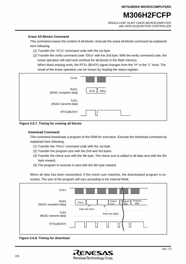
226
Rev. 1.0
SINGLE-CHIP 16-BIT CMOS MICROCOMPUTERwith DATA ACQUISITION CONTROLLER
MITSUBISHI MICROCOMPUTERS
M306H2FCFP
Erase All Blocks Command
This command erases the content of all blocks. Execute the erase all blocks command as explained
here following.
(1) Transfer the “A716” command code with the 1st byte.
(2) Transfer the verify command code “D016” with the 2nd byte. With the verify command code, the
erase operation will start and continue for all blocks in the flash memory.
When block erasing ends, the RTS1 (BUSY) signal changes from the “H” to the “L” level. The
result of the erase operation can be known by reading the status register.
Figure 5.6.7. Timing for erasing all blocks
Download Command
This command downloads a program to the RAM for execution. Execute the download command as
explained here following.
(1) Transfer the “FA16” command code with the 1st byte.
(2) Transfer the program size with the 2nd and 3rd bytes.
(3) Transfer the check sum with the 4th byte. The check sum is added to all data sent with the 5th
byte onward.
(4) The program to execute is sent with the 5th byte onward.
When all data has been transmitted, if the check sum matches, the downloaded program is ex-
ecuted. The size of the program will vary according to the internal RAM.
Figure 5.6.8. Timing for download
CLK1
RxD1
TxD1
RTS1(BUSY)
A716 D016(M16C reception data)
(M16C transmit data)
FA16Program
dataProgram
data
Data size (high)
Data size (low)
Check sum
CLK1
RxD1
TxD1
RTS1(BUSY)
(M16C reception data)
(M16C transmit data)
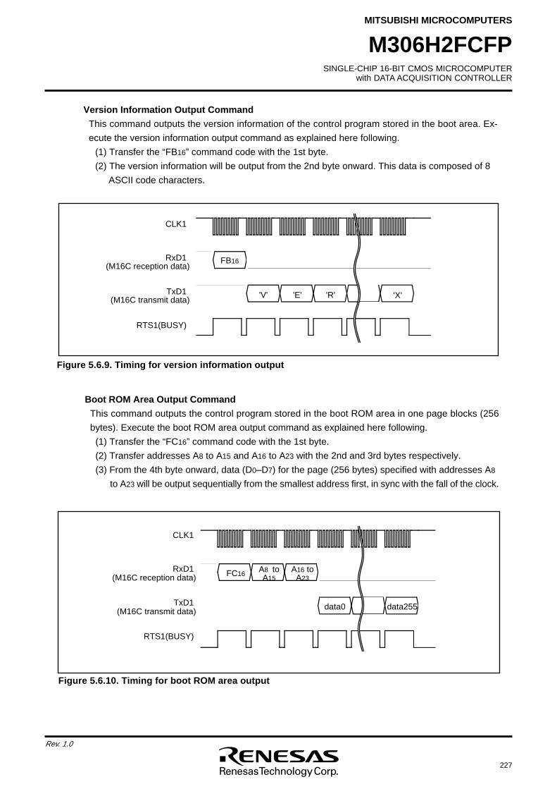
SINGLE-CHIP 16-BIT CMOS MICROCOMPUTERwith DATA ACQUISITION CONTROLLER
MITSUBISHI MICROCOMPUTERS
227
Rev. 1.0
M306H2FCFP
Version Information Output Command
This command outputs the version information of the control program stored in the boot area. Ex-
ecute the version information output command as explained here following.
(1) Transfer the “FB16” command code with the 1st byte.
(2) The version information will be output from the 2nd byte onward. This data is composed of 8
ASCII code characters.
Figure 5.6.9. Timing for version information output
FB16
'X''V' 'E' 'R'
CLK1
RxD1
TxD1
RTS1(BUSY)
(M16C reception data)
(M16C transmit data)
Boot ROM Area Output Command
This command outputs the control program stored in the boot ROM area in one page blocks (256
bytes). Execute the boot ROM area output command as explained here following.
(1) Transfer the “FC16” command code with the 1st byte.
(2) Transfer addresses A8 to A15 and A16 to A23 with the 2nd and 3rd bytes respectively.
(3) From the 4th byte onward, data (D0–D7) for the page (256 bytes) specified with addresses A8
to A23 will be output sequentially from the smallest address first, in sync with the fall of the clock.
Figure 5.6.10. Timing for boot ROM area output
data0 data255
CLK1
RxD1
TxD1
RTS1(BUSY)
A8 to A15
A16 to A23
FC16(M16C reception data)
(M16C transmit data)
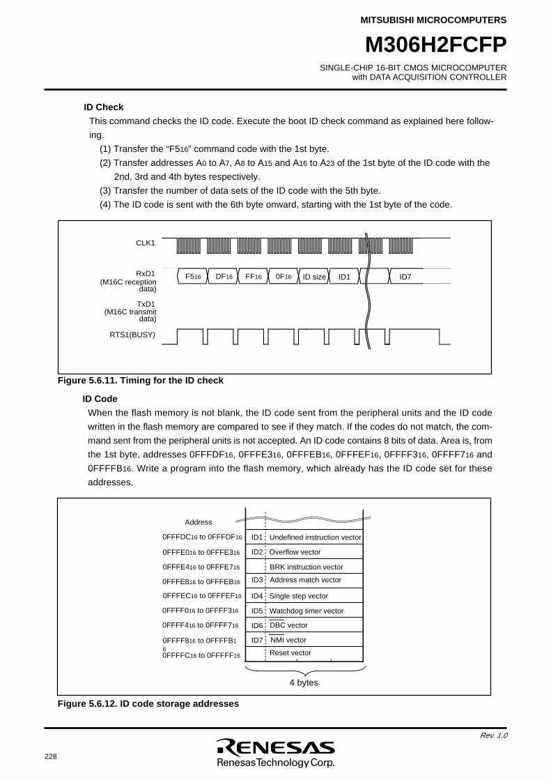
228
Rev. 1.0
SINGLE-CHIP 16-BIT CMOS MICROCOMPUTERwith DATA ACQUISITION CONTROLLER
MITSUBISHI MICROCOMPUTERS
M306H2FCFP
ID Check
This command checks the ID code. Execute the boot ID check command as explained here follow-
ing.
(1) Transfer the “F516” command code with the 1st byte.
(2) Transfer addresses A0 to A7, A8 to A15 and A16 to A23 of the 1st byte of the ID code with the
2nd, 3rd and 4th bytes respectively.
(3) Transfer the number of data sets of the ID code with the 5th byte.
(4) The ID code is sent with the 6th byte onward, starting with the 1st byte of the code.
Figure 5.6.11. Timing for the ID check
ID size ID1 ID7
CLK1
RxD1
TxD1
RTS1(BUSY)
F516 DF16 FF16 0F16(M16C reception
data)
(M16C transmit data)
Reset vector
Watchdog timer vector
Single step vector
Address match vector
BRK instruction vector
Overflow vector
Undefined instruction vector
ID7
ID6
ID5
ID4
ID3
ID2
ID1
DBC vector
NMI vector
0FFFFC16 to 0FFFFF16
0FFFF816 to 0FFFFB16
0FFFF416 to 0FFFF716
0FFFF016 to 0FFFF316
0FFFEC16 to 0FFFEF16
0FFFE816 to 0FFFEB16
0FFFE416 to 0FFFE716
0FFFE016 to 0FFFE316
0FFFDC16 to 0FFFDF16
4 bytes
Address
ID Code
When the flash memory is not blank, the ID code sent from the peripheral units and the ID code
written in the flash memory are compared to see if they match. If the codes do not match, the com-
mand sent from the peripheral units is not accepted. An ID code contains 8 bits of data. Area is, from
the 1st byte, addresses 0FFFDF16, 0FFFE316, 0FFFEB16, 0FFFEF16, 0FFFF316, 0FFFF716 and
0FFFFB16. Write a program into the flash memory, which already has the ID code set for these
addresses.
Figure 5.6.12. ID code storage addresses
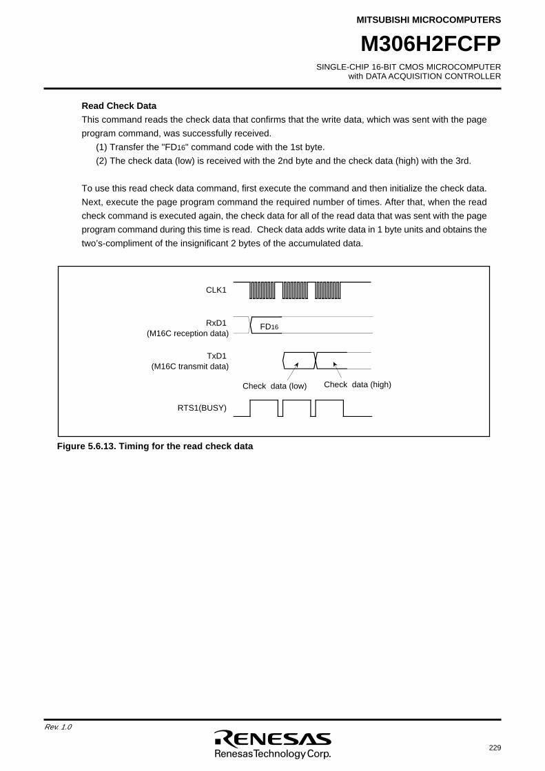
SINGLE-CHIP 16-BIT CMOS MICROCOMPUTERwith DATA ACQUISITION CONTROLLER
MITSUBISHI MICROCOMPUTERS
229
Rev. 1.0
M306H2FCFP
Read Check Data
This command reads the check data that confirms that the write data, which was sent with the page
program command, was successfully received.
(1) Transfer the "FD16" command code with the 1st byte.
(2) The check data (low) is received with the 2nd byte and the check data (high) with the 3rd.
To use this read check data command, first execute the command and then initialize the check data.
Next, execute the page program command the required number of times. After that, when the read
check command is executed again, the check data for all of the read data that was sent with the page
program command during this time is read. Check data adds write data in 1 byte units and obtains the
two’s-compliment of the insignificant 2 bytes of the accumulated data.
Figure 5.6.13. Timing for the read check data
Check data (low)
CLK1
RxD1
TxD1
RTS1(BUSY)
FD16(M16C reception data)
(M16C transmit data)
Check data (high)
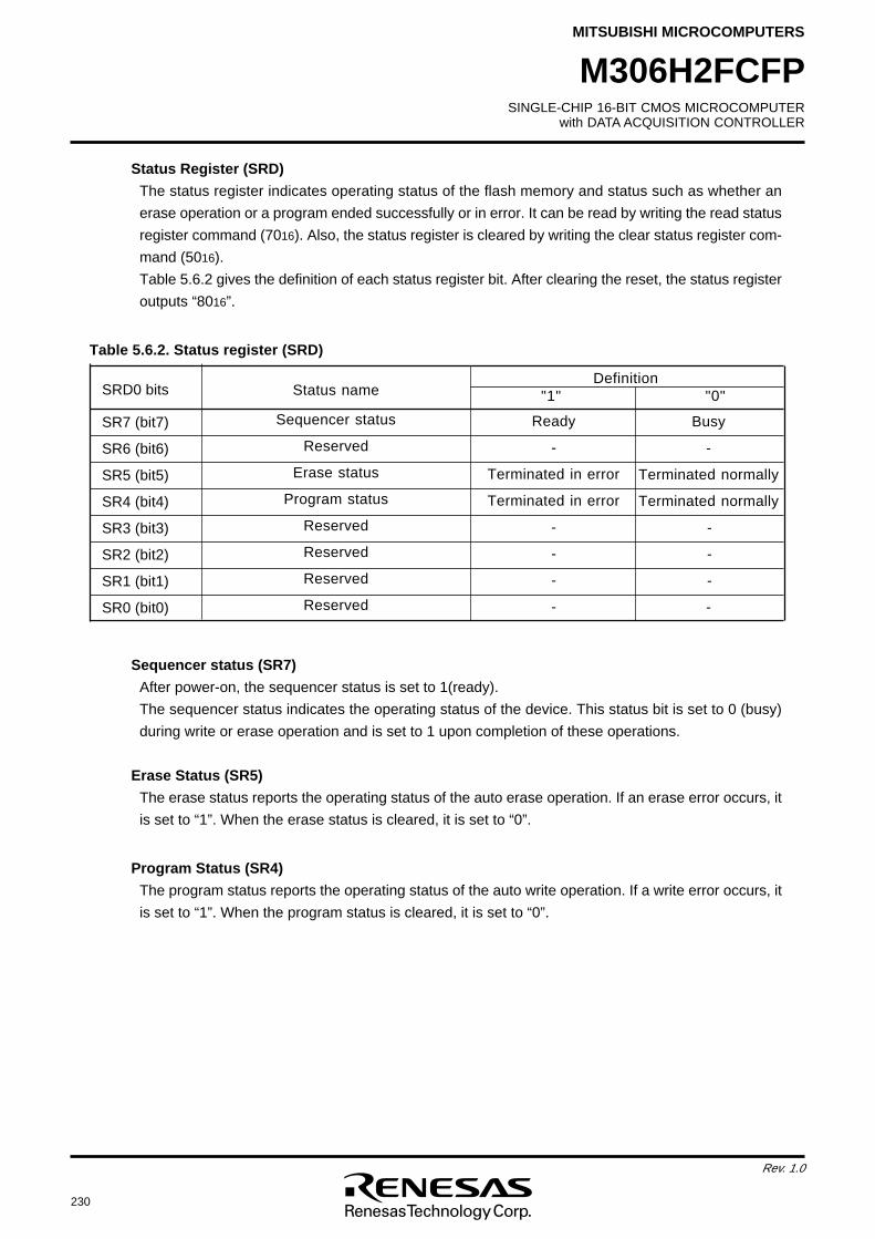
230
Rev. 1.0
SINGLE-CHIP 16-BIT CMOS MICROCOMPUTERwith DATA ACQUISITION CONTROLLER
MITSUBISHI MICROCOMPUTERS
M306H2FCFP
Status Register (SRD)
The status register indicates operating status of the flash memory and status such as whether an
erase operation or a program ended successfully or in error. It can be read by writing the read status
register command (7016). Also, the status register is cleared by writing the clear status register com-
mand (5016).
Table 5.6.2 gives the definition of each status register bit. After clearing the reset, the status register
outputs “8016”.
Table 5.6.2. Status register (SRD)
Sequencer status (SR7)
After power-on, the sequencer status is set to 1(ready).
The sequencer status indicates the operating status of the device. This status bit is set to 0 (busy)
during write or erase operation and is set to 1 upon completion of these operations.
Erase Status (SR5)
The erase status reports the operating status of the auto erase operation. If an erase error occurs, it
is set to “1”. When the erase status is cleared, it is set to “0”.
Program Status (SR4)
The program status reports the operating status of the auto write operation. If a write error occurs, it
is set to “1”. When the program status is cleared, it is set to “0”.
SRD0 bits
SR7 (bit7)
SR6 (bit6)
SR5 (bit5)
SR4 (bit4)
SR3 (bit3)
SR2 (bit2)
SR1 (bit1)
SR0 (bit0)
Status name
Sequencer status
Reserved
Erase status
Program status
Reserved
Reserved
Reserved
Reserved
Definition"1" "0"
Ready
-
Terminated in error
Terminated in error
-
-
-
-
Busy
-
Terminated normally
Terminated normally
-
-
-
-
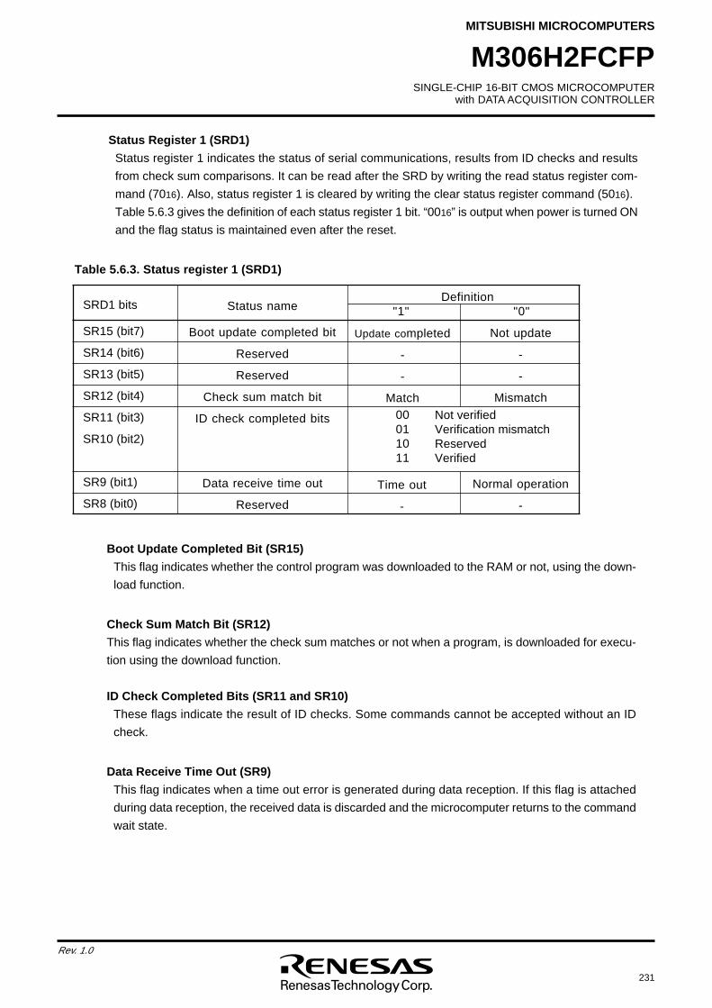
SINGLE-CHIP 16-BIT CMOS MICROCOMPUTERwith DATA ACQUISITION CONTROLLER
MITSUBISHI MICROCOMPUTERS
231
Rev. 1.0
M306H2FCFP
Status Register 1 (SRD1)
Status register 1 indicates the status of serial communications, results from ID checks and results
from check sum comparisons. It can be read after the SRD by writing the read status register com-
mand (7016). Also, status register 1 is cleared by writing the clear status register command (5016).
Table 5.6.3 gives the definition of each status register 1 bit. “0016” is output when power is turned ON
and the flag status is maintained even after the reset.
Table 5.6.3. Status register 1 (SRD1)
Boot Update Completed Bit (SR15)
This flag indicates whether the control program was downloaded to the RAM or not, using the down-
load function.
Check Sum Match Bit (SR12)
This flag indicates whether the check sum matches or not when a program, is downloaded for execu-
tion using the download function.
ID Check Completed Bits (SR11 and SR10)
These flags indicate the result of ID checks. Some commands cannot be accepted without an ID
check.
Data Receive Time Out (SR9)
This flag indicates when a time out error is generated during data reception. If this flag is attached
during data reception, the received data is discarded and the microcomputer returns to the command
wait state.
SRD1 bits
SR15 (bit7)
SR14 (bit6)
SR13 (bit5)
SR12 (bit4)
SR11 (bit3)
SR10 (bit2)
SR9 (bit1)
SR8 (bit0)
Status name
Boot update completed bit
Reserved
Reserved
Check sum match bit
ID check completed bits
Data receive time out
Reserved
Definition"1" "0"
Update completed
-
-
Match00011011
Not update
-
-
Mismatch
Normal operation
-
Not verifiedVerification mismatchReservedVerified
Time out
-
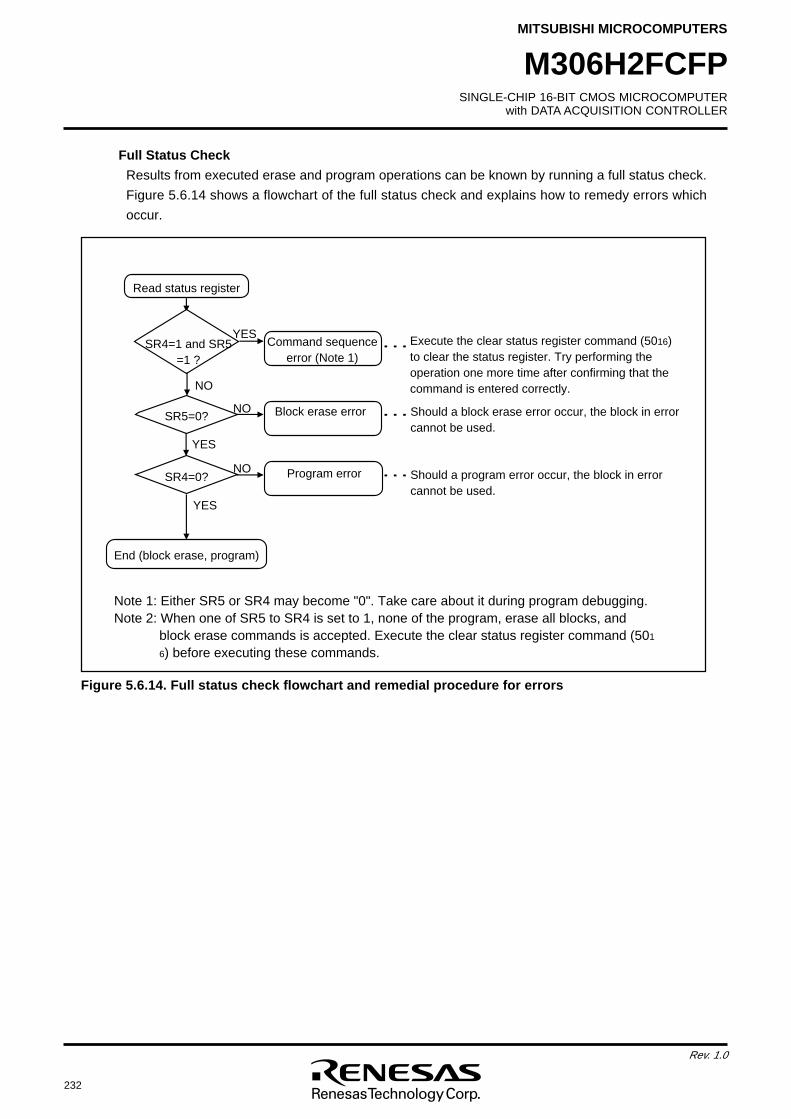
232
Rev. 1.0
SINGLE-CHIP 16-BIT CMOS MICROCOMPUTERwith DATA ACQUISITION CONTROLLER
MITSUBISHI MICROCOMPUTERS
M306H2FCFP
Full Status Check
Results from executed erase and program operations can be known by running a full status check.
Figure 5.6.14 shows a flowchart of the full status check and explains how to remedy errors which
occur.
Read status register
SR4=1 and SR5=1 ?
NO
Command sequence error (Note 1)
YES
SR5=0?
YES
Block erase errorNO
SR4=0?
YES
Program errorNO
End (block erase, program)
Execute the clear status register command (5016) to clear the status register. Try performing the operation one more time after confirming that the command is entered correctly.
Should a block erase error occur, the block in error cannot be used.
Note 1: Either SR5 or SR4 may become "0". Take care about it during program debugging.Note 2: When one of SR5 to SR4 is set to 1, none of the program, erase all blocks, and
block erase commands is accepted. Execute the clear status register command (501
6) before executing these commands.
Should a program error occur, the block in error cannot be used.
Figure 5.6.14. Full status check flowchart and remedial procedure for errors
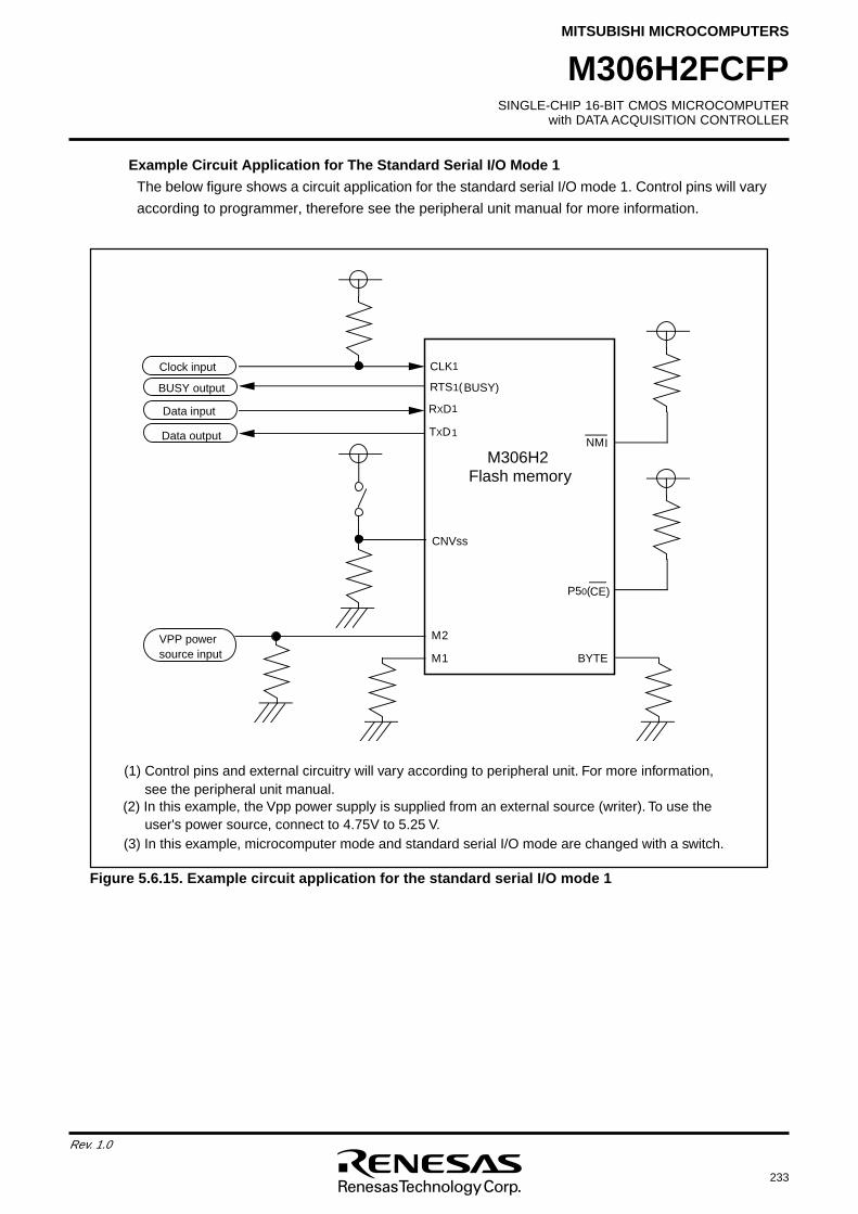
SINGLE-CHIP 16-BIT CMOS MICROCOMPUTERwith DATA ACQUISITION CONTROLLER
MITSUBISHI MICROCOMPUTERS
233
Rev. 1.0
M306H2FCFP
Example Circuit Application for The Standard Serial I/O Mode 1
The below figure shows a circuit application for the standard serial I/O mode 1. Control pins will vary
according to programmer, therefore see the peripheral unit manual for more information.
Figure 5.6.15. Example circuit application for the standard serial I/O mode 1
Flash memory
(1) Control pins and external circuitry will vary according to peripheral unit. For more information,see the peripheral unit manual.
(2) In this example, the Vpp power supply is supplied from an external source (writer). To use the user's power source, connect to 4.75V to 5.25 V.
(3) In this example, microcomputer mode and standard serial I/O mode are changed with a switch.
RTS1(BUSY)
CLK1
RXD1
TXD1
CNVss
M306H2NMI
M2
M1
P50(CE)
BYTE
VPP power source input
Clock input
BUSY output
Data input
Data output
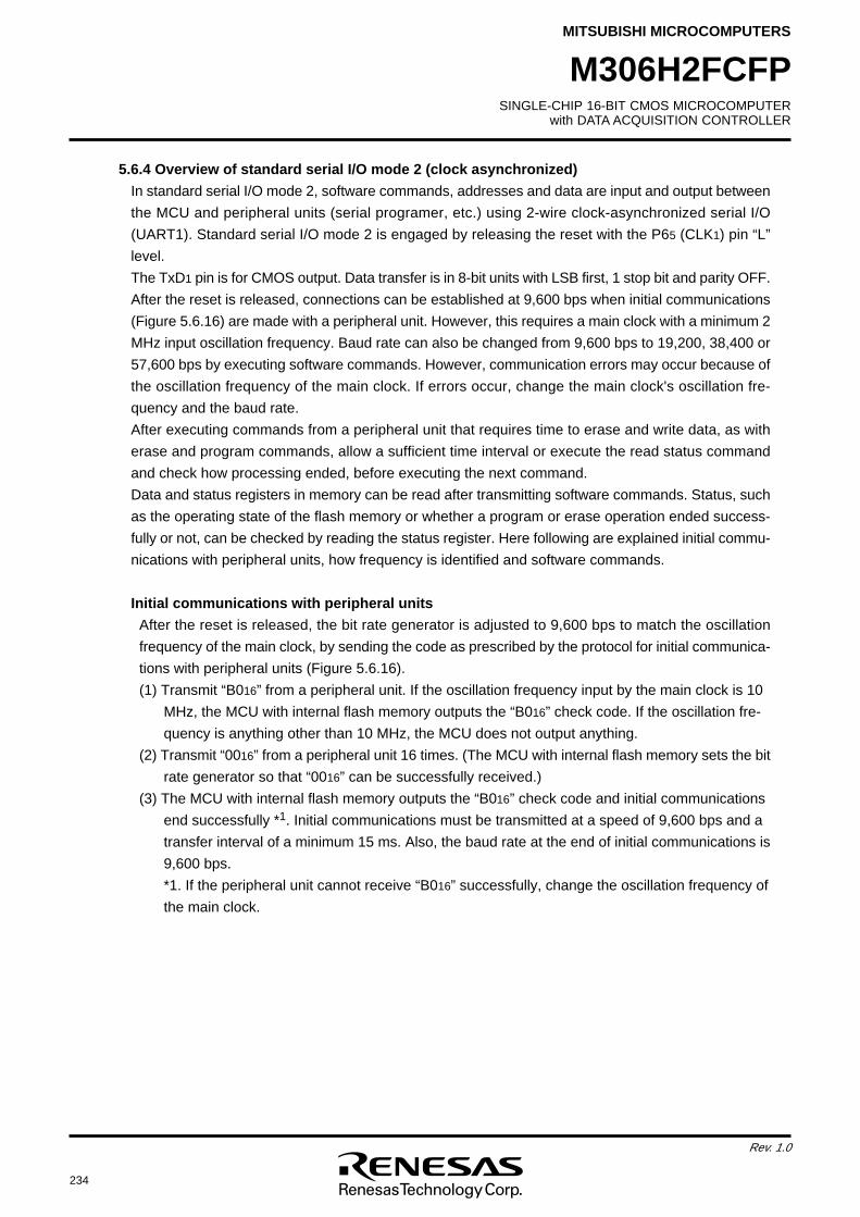
234
Rev. 1.0
SINGLE-CHIP 16-BIT CMOS MICROCOMPUTERwith DATA ACQUISITION CONTROLLER
MITSUBISHI MICROCOMPUTERS
M306H2FCFP
5.6.4 Overview of standard serial I/O mode 2 (clock asynchronized)
In standard serial I/O mode 2, software commands, addresses and data are input and output between
the MCU and peripheral units (serial programer, etc.) using 2-wire clock-asynchronized serial I/O
(UART1). Standard serial I/O mode 2 is engaged by releasing the reset with the P65 (CLK1) pin “L”
level.
The TxD1 pin is for CMOS output. Data transfer is in 8-bit units with LSB first, 1 stop bit and parity OFF.
After the reset is released, connections can be established at 9,600 bps when initial communications
(Figure 5.6.16) are made with a peripheral unit. However, this requires a main clock with a minimum 2
MHz input oscillation frequency. Baud rate can also be changed from 9,600 bps to 19,200, 38,400 or
57,600 bps by executing software commands. However, communication errors may occur because of
the oscillation frequency of the main clock. If errors occur, change the main clock's oscillation fre-
quency and the baud rate.
After executing commands from a peripheral unit that requires time to erase and write data, as with
erase and program commands, allow a sufficient time interval or execute the read status command
and check how processing ended, before executing the next command.
Data and status registers in memory can be read after transmitting software commands. Status, such
as the operating state of the flash memory or whether a program or erase operation ended success-
fully or not, can be checked by reading the status register. Here following are explained initial commu-
nications with peripheral units, how frequency is identified and software commands.
Initial communications with peripheral units
After the reset is released, the bit rate generator is adjusted to 9,600 bps to match the oscillation
frequency of the main clock, by sending the code as prescribed by the protocol for initial communica-
tions with peripheral units (Figure 5.6.16).
(1) Transmit “B016” from a peripheral unit. If the oscillation frequency input by the main clock is 10
MHz, the MCU with internal flash memory outputs the “B016” check code. If the oscillation fre-
quency is anything other than 10 MHz, the MCU does not output anything.
(2) Transmit “0016” from a peripheral unit 16 times. (The MCU with internal flash memory sets the bit
rate generator so that “0016” can be successfully received.)
(3) The MCU with internal flash memory outputs the “B016” check code and initial communications
end successfully *1. Initial communications must be transmitted at a speed of 9,600 bps and a
transfer interval of a minimum 15 ms. Also, the baud rate at the end of initial communications is
9,600 bps.
*1. If the peripheral unit cannot receive “B016” successfully, change the oscillation frequency of
the main clock.
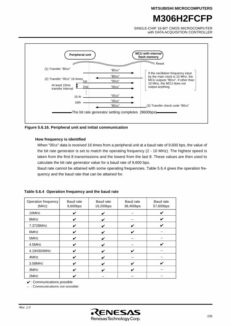
SINGLE-CHIP 16-BIT CMOS MICROCOMPUTERwith DATA ACQUISITION CONTROLLER
MITSUBISHI MICROCOMPUTERS
235
Rev. 1.0
M306H2FCFP
How frequency is identified
When "0016" data is received 16 times from a peripheral unit at a baud rate of 9,600 bps, the value of
the bit rate generator is set to match the operating frequency (2 - 10 MHz). The highest speed is
taken from the first 8 transmissions and the lowest from the last 8. These values are then used to
calculate the bit rate generator value for a baud rate of 9,600 bps.
Baud rate cannot be attained with some operating frequencies. Table 5.6.4 gives the operation fre-
quency and the baud rate that can be attained for.
Table 5.6.4 Operation frequency and the baud rate
Operation frequency(MHZ)
Baud rate9,600bps
Baud rate19,200bps
Baud rate38,400bps
Baud rate57,600bps
10MHZ
8MHZ
7.3728MHZ
6MHZ
5MHZ
4.5MHZ
4.194304MHZ
4MHZ
3.58MHZ
3MHZ
2MHZ
: Communications possible– : Communications not possible
–
–
–
–
–
–
–
–
–
–
–
–
–
Figure 5.6.16. Peripheral unit and initial communication
MCU with internal flash memory
Peripheral unit
(1) Transfer "B016"If the oscillation frequency input by the main clock is 10 MHz, the MCU outputs "B016". If other than 10 MHz, the MCU does not output anything.
(2) Transfer "0016" 16 times
At least 15ms transfer interval
1st
2nd
15 th
16th(3) Transfer check code "B016"
"B016"
"0016"
"0016"
"0016"
"B016"
"B016"
"0016"
Reset
The bit rate generator setting completes (9600bps)
236
Rev. 1.0
SINGLE-CHIP 16-BIT CMOS MICROCOMPUTERwith DATA ACQUISITION CONTROLLER
MITSUBISHI MICROCOMPUTERS
M306H2FCFP
5.6.5 Software Commands
Table 5.6.5 lists software commands. In the standard serial I/O mode 2, erase operations, programs
and reading are controlled by transferring software commands via the RxD1 pin. Standard serial I/O
mode 2 adds four transmission speed commands - 9,600, 19,200, 38,400 and 57,600 bps - to the
software commands of standard serial I/O mode 1. Software commands are explained here below.
Table 5.6.5. Software commands (Standard serial I/O mode 2)
Control command 2nd byte 3rd byte 4th byte 5th byte 6th byte
1 Page read
2 Page program
3 Block erase
4 Erase all unlocked blocks
5 Read status register
6 Clear status register
7 ID check function
8 Download function
9 Version data output function
10 Boot ROM area output
function
11 Read check data
12 Baud rate 9600
13 Baud rate 19200
14 Baud rate 38400
15 Baud rate 57600
Address(middle)
Address(middle)
Address(middle)
D016
SRDoutput
Address(low)
Size (low)
Versiondata
output
Address(middle)
Checkdata (low)
B016
B116
B216
B316
Address(high)
Address(high)
Address(high)
SRD1output
Address(middle)
Size(high)
Versiondata
output
Address(high)
Checkdata
(high)
Dataoutput
Datainput
D016
Address(high)
Check-sum
Versiondata
output
Dataoutput
Dataoutput
Datainput
ID size
Datainput
Versiondata
output
Dataoutput
Dataoutput
Datainput
ID1
Torequirednumberof timesVersion
dataoutput
Dataoutput
Dataoutput to
259th byteData inputto 259th
byte
To ID7
Versiondata
output to9th byte
Dataoutput to
259th byte
FF16
4116
2016
A716
7016
5016
F516
FA16
FB16
FC16
FD16
B016
B116
B216
B316
When ID isnot verified
Notacceptable
Notacceptable
Notacceptable
NotacceptableAcceptable
Notacceptable
Acceptable
Notacceptable
Acceptable
Notacceptable
Notacceptable
Acceptable
Acceptable
Acceptable
Acceptable
1st bytetransfer
Note 1: Shading indicates transfer from flash memory microcomputer to peripheral unit. All other data is trans-
ferred from the peripheral unit to the flash memory microcomputer.
Note 2: SRD refers to status register data. SRD1 refers to status register 1 data.
Note 3: All commands can be accepted when the flash memory is totally blank.
SINGLE-CHIP 16-BIT CMOS MICROCOMPUTERwith DATA ACQUISITION CONTROLLER
MITSUBISHI MICROCOMPUTERS
237
Rev. 1.0
M306H2FCFP
Page Read Command
This command reads the specified page (256 bytes) in the flash memory sequentially one byte at a
time. Execute the page read command as explained here following.
(1) Transfer the “FF16” command code with the 1st byte.
(2) Transfer addresses A8 to A15 and A16 to A23 with the 2nd and 3rd bytes respectively.
(3) From the 4th byte onward, data (D0–D7) for the page (256 bytes) specified with addresses A8 to
A23 will be output sequentially from the smallest address first.
Figure 5.6.17. Timing for page read
Read Status Register Command
This command reads status information. When the “7016” command code is sent with the 1st byte,
the contents of the status register (SRD) specified with the 2nd byte and the contents of status
register 1 (SRD1) specified with the 3rd byte are read.
Figure 5.6.18. Timing for reading the status register
FF16 A8 to A15 A16 to A23
data0 data255
RxD1
TxD1
(M16C reception data)
(M16C transmit data)
7016
SRD output
SRD1 output
RxD1
TxD1
(M16C reception data)
(M16C transmit data)
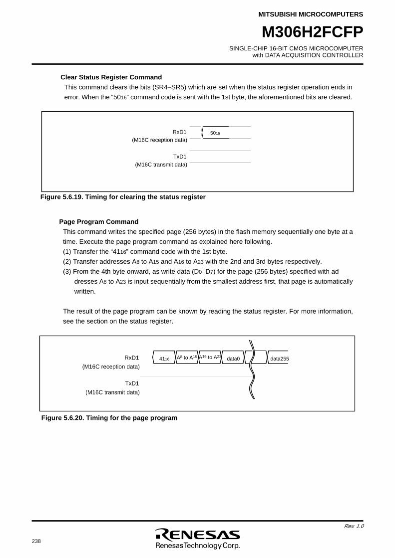
238
Rev. 1.0
SINGLE-CHIP 16-BIT CMOS MICROCOMPUTERwith DATA ACQUISITION CONTROLLER
MITSUBISHI MICROCOMPUTERS
M306H2FCFP
Clear Status Register Command
This command clears the bits (SR4–SR5) which are set when the status register operation ends in
error. When the “5016” command code is sent with the 1st byte, the aforementioned bits are cleared.
Figure 5.6.19. Timing for clearing the status register
Page Program Command
This command writes the specified page (256 bytes) in the flash memory sequentially one byte at a
time. Execute the page program command as explained here following.
(1) Transfer the “4116” command code with the 1st byte.
(2) Transfer addresses A8 to A15 and A16 to A23 with the 2nd and 3rd bytes respectively.
(3) From the 4th byte onward, as write data (D0–D7) for the page (256 bytes) specified with ad
dresses A8 to A23 is input sequentially from the smallest address first, that page is automatically
written.
The result of the page program can be known by reading the status register. For more information,
see the section on the status register.
Figure 5.6.20. Timing for the page program
5016RxD1
TxD1
(M16C reception data)
(M16C transmit data)
4116 A8 to A15 A16 to A23 data0 data255RxD1
TxD1
(M16C reception data)
(M16C transmit data)

SINGLE-CHIP 16-BIT CMOS MICROCOMPUTERwith DATA ACQUISITION CONTROLLER
MITSUBISHI MICROCOMPUTERS
239
Rev. 1.0
M306H2FCFP
Erase All Blocks Command
This command erases the content of all blocks. Execute the erase all blocks command as explained
here following.
(1) Transfer the “A716” command code with the 1st byte.
(2) Transfer the verify command code “D016” with the 2nd byte. With the verify command code, the
erase operation will start and continue for all blocks in the flash memory.
The result of the erase operation can be known by reading the status register.
Block Erase Command
This command erases the data in the specified block. Execute the block erase command as ex-
plained here following.
(1) Transfer the “2016” command code with the 1st byte.
(2) Transfer addresses A8 to A15 and A16 to A23 with the 2nd and 3rd bytes respectively.
(3) Transfer the verify command code “D016” with the 4th byte. With the verify command code, the
erase operation will start for the specified block in the flash memory. Write the optional even
address of the specified block for addresses A8 to A23.
After block erase ends, the result of the block erase operation can be known by reading the status
register. For more information, see the section on the status register.
Figure 5.6.22. Timing for erasing all blocks
Figure 5.6.21. Timing for block erasing
A8 to A15 A16 to A232016 D016RxD1
TxD1
(M16C received data)
(M16C transmitted data)
ˇˇ D016A716RxD1
TxD1
(M16C reception data)
(M16C transmit data)
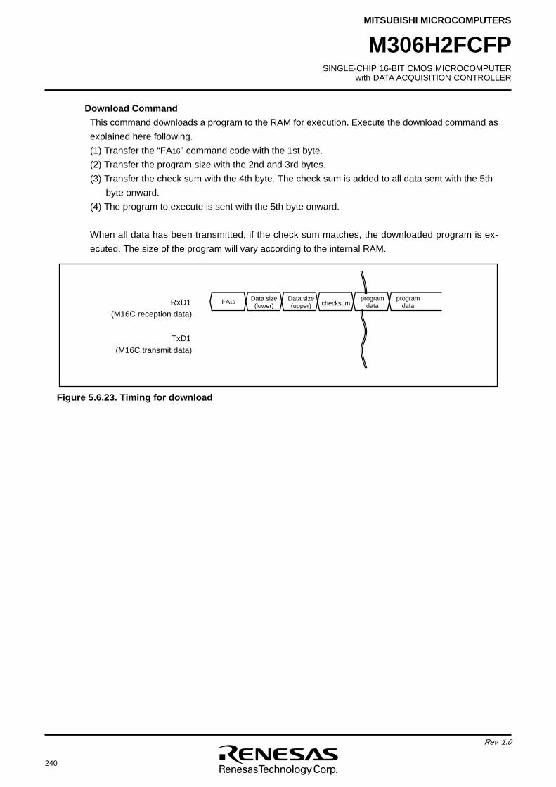
240
Rev. 1.0
SINGLE-CHIP 16-BIT CMOS MICROCOMPUTERwith DATA ACQUISITION CONTROLLER
MITSUBISHI MICROCOMPUTERS
M306H2FCFP
Download Command
This command downloads a program to the RAM for execution. Execute the download command as
explained here following.
(1) Transfer the “FA16” command code with the 1st byte.
(2) Transfer the program size with the 2nd and 3rd bytes.
(3) Transfer the check sum with the 4th byte. The check sum is added to all data sent with the 5th
byte onward.
(4) The program to execute is sent with the 5th byte onward.
When all data has been transmitted, if the check sum matches, the downloaded program is ex-
ecuted. The size of the program will vary according to the internal RAM.
Figure 5.6.23. Timing for download
FA16Data size
(lower)Data size(upper) checksum
programdata
programdataRxD1
TxD1
(M16C reception data)
(M16C transmit data)
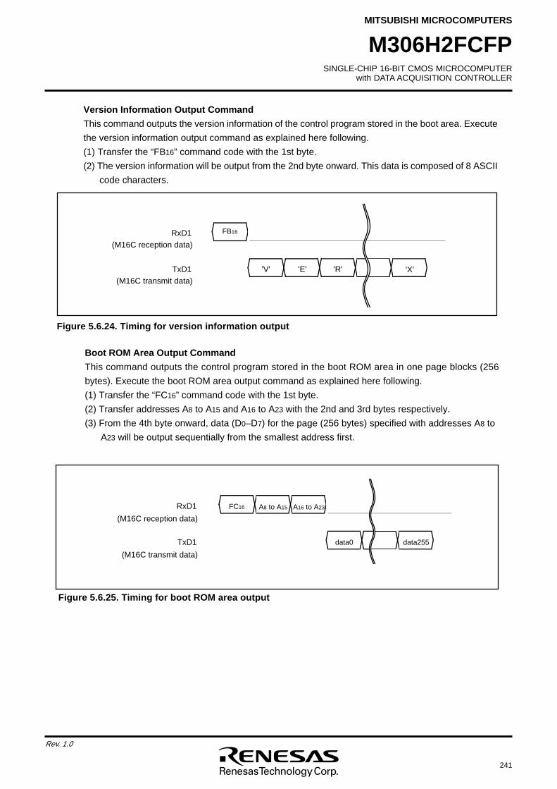
SINGLE-CHIP 16-BIT CMOS MICROCOMPUTERwith DATA ACQUISITION CONTROLLER
MITSUBISHI MICROCOMPUTERS
241
Rev. 1.0
M306H2FCFP
Version Information Output Command
This command outputs the version information of the control program stored in the boot area. Execute
the version information output command as explained here following.
(1) Transfer the “FB16” command code with the 1st byte.
(2) The version information will be output from the 2nd byte onward. This data is composed of 8 ASCII
code characters.
Figure 5.6.24. Timing for version information output
Boot ROM Area Output Command
This command outputs the control program stored in the boot ROM area in one page blocks (256
bytes). Execute the boot ROM area output command as explained here following.
(1) Transfer the “FC16” command code with the 1st byte.
(2) Transfer addresses A8 to A15 and A16 to A23 with the 2nd and 3rd bytes respectively.
(3) From the 4th byte onward, data (D0–D7) for the page (256 bytes) specified with addresses A8 to
A23 will be output sequentially from the smallest address first.
Figure 5.6.25. Timing for boot ROM area output
FB16
'X''V' 'E' 'R'
RxD1
TxD1
(M16C reception data)
(M16C transmit data)
FC16 A8 to A15 A16 to A23
data0 data255
RxD1
TxD1
(M16C reception data)
(M16C transmit data)
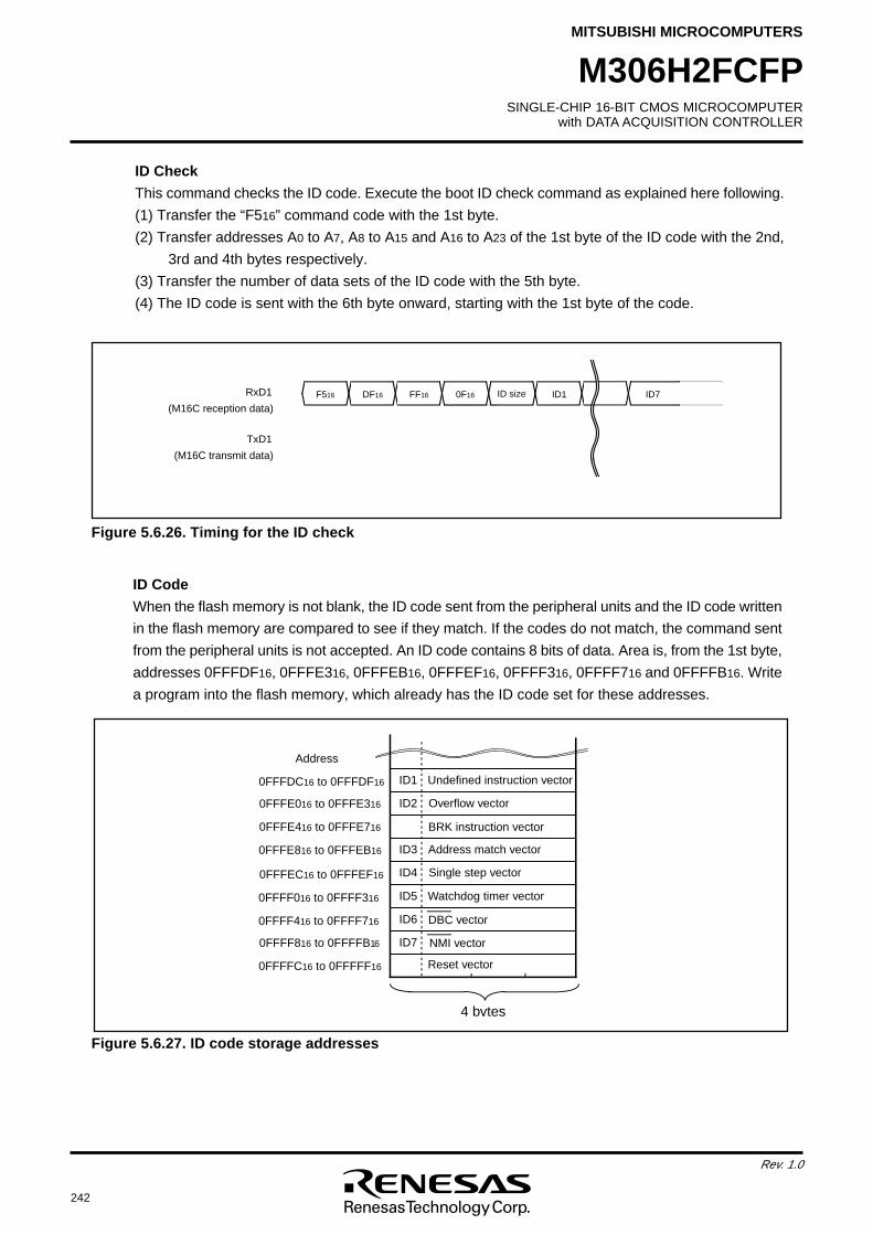
242
Rev. 1.0
SINGLE-CHIP 16-BIT CMOS MICROCOMPUTERwith DATA ACQUISITION CONTROLLER
MITSUBISHI MICROCOMPUTERS
M306H2FCFP
ID Check
This command checks the ID code. Execute the boot ID check command as explained here following.
(1) Transfer the “F516” command code with the 1st byte.
(2) Transfer addresses A0 to A7, A8 to A15 and A16 to A23 of the 1st byte of the ID code with the 2nd,
3rd and 4th bytes respectively.
(3) Transfer the number of data sets of the ID code with the 5th byte.
(4) The ID code is sent with the 6th byte onward, starting with the 1st byte of the code.
F516 ID1 ID7DF16 FF16 0F16 ID sizeRxD1
TxD1
(M16C reception data)
(M16C transmit data)
Figure 5.6.26. Timing for the ID check
ID Code
When the flash memory is not blank, the ID code sent from the peripheral units and the ID code written
in the flash memory are compared to see if they match. If the codes do not match, the command sent
from the peripheral units is not accepted. An ID code contains 8 bits of data. Area is, from the 1st byte,
addresses 0FFFDF16, 0FFFE316, 0FFFEB16, 0FFFEF16, 0FFFF316, 0FFFF716 and 0FFFFB16. Write
a program into the flash memory, which already has the ID code set for these addresses.
Figure 5.6.27. ID code storage addresses
Reset vector
Watchdog timer vector
Single step vector
Address match vector
BRK instruction vector
Overflow vector
Undefined instruction vector
ID7
ID6
ID5
ID4
ID3
ID2
ID1
DBC vector
NMI vector
0FFFFC16 to 0FFFFF16
0FFFF816 to 0FFFFB16
0FFFF416 to 0FFFF716
0FFFF016 to 0FFFF316
0FFFEC16 to 0FFFEF16
0FFFE816 to 0FFFEB16
0FFFE416 to 0FFFE716
0FFFE016 to 0FFFE316
0FFFDC16 to 0FFFDF16
4 bytes
Address
SINGLE-CHIP 16-BIT CMOS MICROCOMPUTERwith DATA ACQUISITION CONTROLLER
MITSUBISHI MICROCOMPUTERS
243
Rev. 1.0
M306H2FCFP
Read Check Data
This command reads the check data that confirms that the write data, which was sent with the page
program command, was successfully received.
(1) Transfer the "FD16" command code with the 1st byte.
(2) The check data (low) is received with the 2nd byte and the check data (high) with the 3rd.
To use this read check data command, first execute the command and then initialize the check data.
Next, execute the page program command the required number of times. After that, when the read
check command is executed again, the check data for all of the read data that was sent with the page
program command during this time is read. Check data adds write data in 1 byte units and obtains
the two’s-compliment of the insignificant 2 bytes of the accumulated data.
Baud Rate 9600
This command changes baud rate to 9,600 bps. Execute it as follows.
(1) Transfer the "B016" command code with the 1st byte.
(2) After the "B016" check code is output with the 2nd byte, change the baud rate to 9,600 bps.
Figure 5.6.28. Timing for the read check data
Figure 5.6.29. Timing of baud rate 9600
FD16
Data size(lower)
Data size(upper)
RxD1
TxD1
(M16C reception data)
(M16C transmit data)
RxD1
TxD1
B016(M16C reception data)
(M16C transmit data)B016
244
Rev. 1.0
SINGLE-CHIP 16-BIT CMOS MICROCOMPUTERwith DATA ACQUISITION CONTROLLER
MITSUBISHI MICROCOMPUTERS
M306H2FCFP
Baud Rate 19200
This command changes baud rate to 19,200 bps. Execute it as follows.
(1) Transfer the "B116" command code with the 1st byte.
(2) After the "B116" check code is output with the 2nd byte, change the baud rate to 19,200 bps.
Figure 5.6.30. Timing of baud rate 19200
Baud Rate 38400
This command changes baud rate to 38,400 bps. Execute it as follows.
(1) Transfer the "B216" command code with the 1st byte.
(2) After the "B216" check code is output with the 2nd byte, change the baud rate to 38,400 bps.
Figure 5.6.31. Timing of baud rate 38400
Baud Rate 57600
This command changes baud rate to 57,600 bps. Execute it as follows.
(1) Transfer the "B316" command code with the 1st byte.
(2) After the "B316" check code is output with the 2nd byte, change the baud rate to 57,600 bps.
Figure 5.6.32. Timing of baud rate 57600
B116
B116
RxD1
TxD1
(M16C reception data)
(M16C transmit data)
B216
B216
RxD1
TxD1
(M16C reception data)
(M16C transmit data)
B316
B316
RxD1
TxD1
(M16C reception data)
(M16C transmit data)

SINGLE-CHIP 16-BIT CMOS MICROCOMPUTERwith DATA ACQUISITION CONTROLLER
MITSUBISHI MICROCOMPUTERS
245
Rev. 1.0
M306H2FCFP
5.6.6 Example Circuit Application for The Standard Serial I/O Mode 2
The below figure shows a circuit application for the standard serial I/O mode 2.
Figure 5.6.23. Example circuit application for the standard serial I/O mode 2
BUSY
CLK1
RXD1
TXD1
CNVss
M306H2Flash memory
NMI
M2
M1
P50(CE)
BYTE
Monitor output
Data input
Data output
(1) In this example, the Vpp power supply is supplied from an external source (writer). To use the user's power source, connect to 4.75V to 5.25 V.(2) In this example, microcomputer mode and standard serial I/O mode are changed with a switch.
VPP power source input
246
Rev. 1.0
SINGLE-CHIP 16-BIT CMOS MICROCOMPUTERwith DATA ACQUISITION CONTROLLER
MITSUBISHI MICROCOMPUTERS
M306H2FCFP
5.7 Electrical Characteristics
Operating ambient temperature (Note)
Inputvoltage
Analog supply voltage
Supply voltage
Outputvoltage
Power dissipation
Storage temperature
Parameter Unit Rated value Condition Symbol
Note: It is a value in flash memory mode. Other parameter becomes same as a value in microcomputer mode.
VREF, XIN, M1
XOUT, P11
VO
- 0.3 to Vcc+0.3
- 0.3 to Vcc+0.3
Pd Ta=25 °C
- 0.3 to 5.75 V
V
V
°C
VI
AVcc
Vcc
Tstg
Topr
°C
mW
V
- 40 to 125
1000
25 ± 5
P40 to P47, P50 to P57, P60 to P67, P72 to P77, P80 to P87,
P00 to P07, P10 to P17, P20 to P27, P30 to P37,P40 to P47, P50 to P57, P60 to P67,P72 to P77, P80 to P84,
P00 to P07, P10 to P17, P20 to P27, P30 to P37,RESET,
P90 to P97, P100 to P107,
P86, P87, P90 to P97, P100 to P107,
P70, P71
P70, P71,
- 0.3 to 5.75 V
V
CNVSS, BYTE,
VCC=AVCC
VCC=AVCC - 0.3 to 5.75
- 0.3 to 5.75
VM2 - 0.3 to 5.75Supply voltage for program/erase
Table 5.7.1 Absolute maximum ratings
SINGLE-CHIP 16-BIT CMOS MICROCOMPUTERwith DATA ACQUISITION CONTROLLER
MITSUBISHI MICROCOMPUTERS
247
Rev. 1.0
M306H2FCFP
Table 5.7.2 DC electrical characteristics (referenced to VCC = 5.0V at Ta = 25oC unless otherwise
specified)
Rated value Min. Typ. Max.
VPP power supply current (at read) VPP =VCC
60100
Symbol Parameter Condition Unit
µA
V4.75
70
IPP1
IPP2
IPP3
VPP
VPP =VCC
VPP =VCC
VPP power supply current (at program)
VPP power supply current (at erase)
VPP power supply voltage
mA
mA
5.25
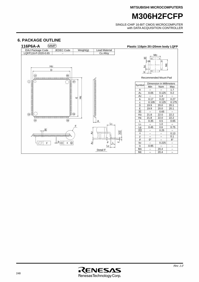
248
Rev. 1.0
SINGLE-CHIP 16-BIT CMOS MICROCOMPUTERwith DATA ACQUISITION CONTROLLER
MITSUBISHI MICROCOMPUTERS
M306H2FCFP
6. PACKAGE OUTLINE
LQFP116-P-2020-0.65Weight(g)
– 1.78JEDEC CodeEIAJ Package Code Lead Material
Cu Alloy
116P6A-A Plastic 116pin 20 20mm body LQFP
–0.125
–
– –0.2
––
– –
––
––
–
SymbolMin Nom Max
A
A2
bcDE
HE
LL1
y
b2
Dimension in Millimeters
HD
A1
0.225––I2 0.95––MD 20.4––ME 20.4
8°0°0.1
1.00.650.50.35
22.222.021.822.222.021.8
0.6520.120.019.920.120.019.90.1750.1250.1050.270.220.17
1.40.05
1.7
e
Lp 0.45––
0.60.25–
0.75–
0.13xA3
MMP
y x M
ME
b2e
l2
MD
LpL c
A3
L1
A1
A2
b
E HE
HD
D
A
e
88
87
59
5830
29
1
116
Detail F
F
Recommended Mount Pad
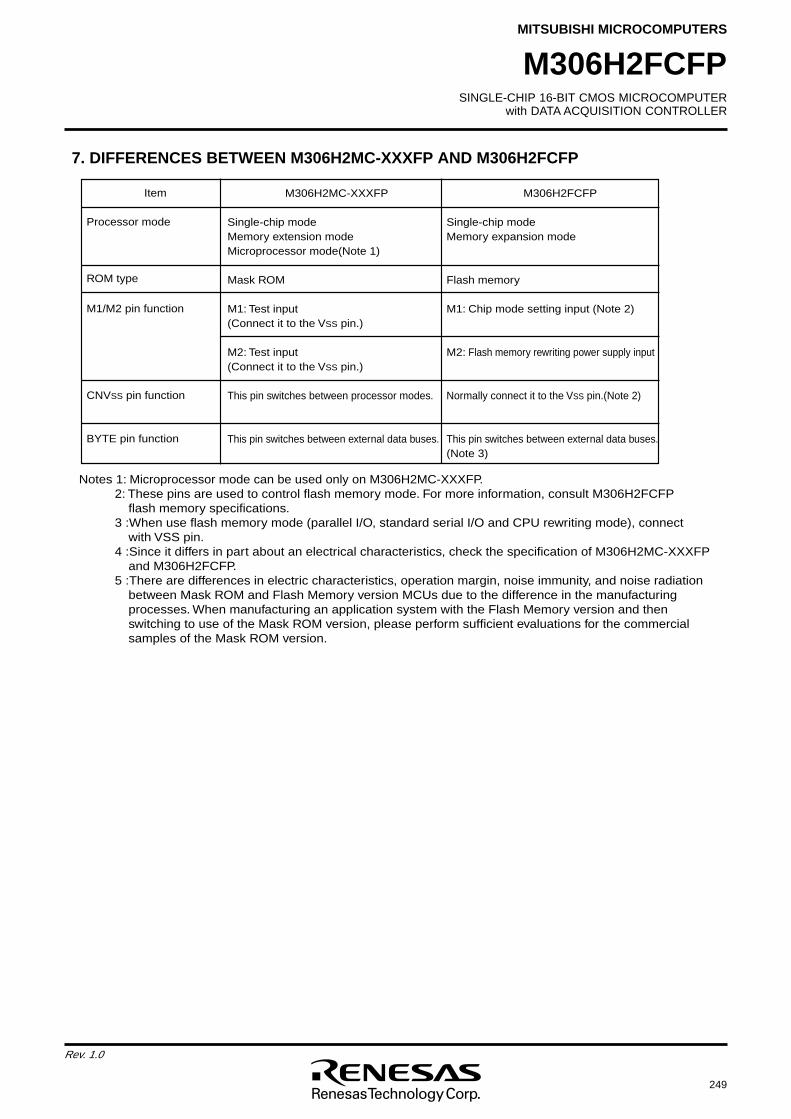
SINGLE-CHIP 16-BIT CMOS MICROCOMPUTERwith DATA ACQUISITION CONTROLLER
MITSUBISHI MICROCOMPUTERS
249
Rev. 1.0
M306H2FCFP
Item
Processor mode
ROM type
M1/M2 pin function
CNVSS pin function
BYTE pin function
Notes 1: Microprocessor mode can be used only on M306H2MC-XXXFP.2: These pins are used to control flash memory mode. For more information, consult M306H2FCFP
flash memory specifications.3 :When use flash memory mode (parallel I/O, standard serial I/O and CPU rewriting mode), connect
with VSS pin.4 :Since it differs in part about an electrical characteristics, check the specification of M306H2MC-XXXFP
and M306H2FCFP.5 :There are differences in electric characteristics, operation margin, noise immunity, and noise radiation
between Mask ROM and Flash Memory version MCUs due to the difference in the manufacturing processes. When manufacturing an application system with the Flash Memory version and then switching to use of the Mask ROM version, please perform sufficient evaluations for the commercial samples of the Mask ROM version.
M306H2MC-XXXFP
Single-chip mode Memory extension modeMicroprocessor mode(Note 1)
Mask ROM
M1: Test input(Connect it to the VSS pin.)
M2: Test input(Connect it to the VSS pin.)
This pin switches between processor modes.
This pin switches between external data buses.
M306H2FCFP
Single-chip modeMemory expansion mode
Flash memory
M1: Chip mode setting input (Note 2)
M2: Flash memory rewriting power supply input
Normally connect it to the VSS pin.(Note 2)
This pin switches between external data buses.(Note 3)
7. DIFFERENCES BETWEEN M306H2MC-XXXFP AND M306H2FCFP
Rev. Rev.
No. date
1.0 PDF First Edition 0202
Revision Description
REVISION HISTORY M306H2FCFP (Rev.1.0) DATA SHEET
(1/1)