M37274MA-XXXSP DATASHEET - Renesas
134
To our customers, Old Company Name in Catalogs and Other Documents On April 1 st , 2010, NEC Electronics Corporation merged with Renesas Technology Corporation, and Renesas Electronics Corporation took over all the business of both companies. Therefore, although the old company name remains in this document, it is a valid Renesas Electronics document. We appreciate your understanding. Renesas Electronics website: http://www.renesas.com April 1 st , 2010 Renesas Electronics Corporation Issued by: Renesas Electronics Corporation (http://www.renesas.com ) Send any inquiries to http://www.renesas.com/inquiry .
-
Upload
khangminh22 -
Category
Documents
-
view
0 -
download
0
Transcript of M37274MA-XXXSP DATASHEET - Renesas

To our customers,
Old Company Name in Catalogs and Other Documents
On April 1st, 2010, NEC Electronics Corporation merged with Renesas Technology
Corporation, and Renesas Electronics Corporation took over all the business of both companies. Therefore, although the old company name remains in this document, it is a valid Renesas Electronics document. We appreciate your understanding.
Renesas Electronics website: http://www.renesas.com
April 1st, 2010 Renesas Electronics Corporation
Issued by: Renesas Electronics Corporation (http://www.renesas.com)
Send any inquiries to http://www.renesas.com/inquiry.

Notice 1. All information included in this document is current as of the date this document is issued. Such information, however, is
subject to change without any prior notice. Before purchasing or using any Renesas Electronics products listed herein, please confirm the latest product information with a Renesas Electronics sales office. Also, please pay regular and careful attention to additional and different information to be disclosed by Renesas Electronics such as that disclosed through our website.
2. Renesas Electronics does not assume any liability for infringement of patents, copyrights, or other intellectual property rights of third parties by or arising from the use of Renesas Electronics products or technical information described in this document. No license, express, implied or otherwise, is granted hereby under any patents, copyrights or other intellectual property rights of Renesas Electronics or others.
3. You should not alter, modify, copy, or otherwise misappropriate any Renesas Electronics product, whether in whole or in part. 4. Descriptions of circuits, software and other related information in this document are provided only to illustrate the operation of
semiconductor products and application examples. You are fully responsible for the incorporation of these circuits, software, and information in the design of your equipment. Renesas Electronics assumes no responsibility for any losses incurred by you or third parties arising from the use of these circuits, software, or information.
5. When exporting the products or technology described in this document, you should comply with the applicable export control laws and regulations and follow the procedures required by such laws and regulations. You should not use Renesas Electronics products or the technology described in this document for any purpose relating to military applications or use by the military, including but not limited to the development of weapons of mass destruction. Renesas Electronics products and technology may not be used for or incorporated into any products or systems whose manufacture, use, or sale is prohibited under any applicable domestic or foreign laws or regulations.
6. Renesas Electronics has used reasonable care in preparing the information included in this document, but Renesas Electronics does not warrant that such information is error free. Renesas Electronics assumes no liability whatsoever for any damages incurred by you resulting from errors in or omissions from the information included herein.
7. Renesas Electronics products are classified according to the following three quality grades: “Standard”, “High Quality”, and “Specific”. The recommended applications for each Renesas Electronics product depends on the product’s quality grade, as indicated below. You must check the quality grade of each Renesas Electronics product before using it in a particular application. You may not use any Renesas Electronics product for any application categorized as “Specific” without the prior written consent of Renesas Electronics. Further, you may not use any Renesas Electronics product for any application for which it is not intended without the prior written consent of Renesas Electronics. Renesas Electronics shall not be in any way liable for any damages or losses incurred by you or third parties arising from the use of any Renesas Electronics product for an application categorized as “Specific” or for which the product is not intended where you have failed to obtain the prior written consent of Renesas Electronics. The quality grade of each Renesas Electronics product is “Standard” unless otherwise expressly specified in a Renesas Electronics data sheets or data books, etc.
“Standard”: Computers; office equipment; communications equipment; test and measurement equipment; audio and visual equipment; home electronic appliances; machine tools; personal electronic equipment; and industrial robots.
“High Quality”: Transportation equipment (automobiles, trains, ships, etc.); traffic control systems; anti-disaster systems; anti-crime systems; safety equipment; and medical equipment not specifically designed for life support.
“Specific”: Aircraft; aerospace equipment; submersible repeaters; nuclear reactor control systems; medical equipment or systems for life support (e.g. artificial life support devices or systems), surgical implantations, or healthcare intervention (e.g. excision, etc.), and any other applications or purposes that pose a direct threat to human life.
8. You should use the Renesas Electronics products described in this document within the range specified by Renesas Electronics, especially with respect to the maximum rating, operating supply voltage range, movement power voltage range, heat radiation characteristics, installation and other product characteristics. Renesas Electronics shall have no liability for malfunctions or damages arising out of the use of Renesas Electronics products beyond such specified ranges.
9. Although Renesas Electronics endeavors to improve the quality and reliability of its products, semiconductor products have specific characteristics such as the occurrence of failure at a certain rate and malfunctions under certain use conditions. Further, Renesas Electronics products are not subject to radiation resistance design. Please be sure to implement safety measures to guard them against the possibility of physical injury, and injury or damage caused by fire in the event of the failure of a Renesas Electronics product, such as safety design for hardware and software including but not limited to redundancy, fire control and malfunction prevention, appropriate treatment for aging degradation or any other appropriate measures. Because the evaluation of microcomputer software alone is very difficult, please evaluate the safety of the final products or system manufactured by you.
10. Please contact a Renesas Electronics sales office for details as to environmental matters such as the environmental compatibility of each Renesas Electronics product. Please use Renesas Electronics products in compliance with all applicable laws and regulations that regulate the inclusion or use of controlled substances, including without limitation, the EU RoHS Directive. Renesas Electronics assumes no liability for damages or losses occurring as a result of your noncompliance with applicable laws and regulations.
11. This document may not be reproduced or duplicated, in any form, in whole or in part, without prior written consent of Renesas Electronics.
12. Please contact a Renesas Electronics sales office if you have any questions regarding the information contained in this document or Renesas Electronics products, or if you have any other inquiries.
(Note 1) “Renesas Electronics” as used in this document means Renesas Electronics Corporation and also includes its majority-owned subsidiaries.
(Note 2) “Renesas Electronics product(s)” means any product developed or manufactured by or for Renesas Electronics.

Regarding the change of names mentioned in the document, such as Mitsubishi Electric and Mitsubishi XX, to Renesas Technology Corp.
The semiconductor operations of Hitachi and Mitsubishi Electric were transferred to Renesas
Technology Corporation on April 1st 2003. These operations include microcomputer, logic, analog
and discrete devices, and memory chips other than DRAMs (flash memory, SRAMs etc.)
Accordingly, although Mitsubishi Electric, Mitsubishi Electric Corporation, Mitsubishi
Semiconductors, and other Mitsubishi brand names are mentioned in the document, these names
have in fact all been changed to Renesas Technology Corp. Thank you for your understanding.
Except for our corporate trademark, logo and corporate statement, no changes whatsoever have been
made to the contents of the document, and these changes do not constitute any alteration to the
contents of the document itself.
Note : Mitsubishi Electric will continue the business operations of high frequency & optical devices
and power devices.
Renesas Technology Corp.
Customer Support Dept.
April 1, 2003
To all our customers

DESCRIPTIONThe M37274MA-XXXSP is a single-chip microcomputer designed with
CMOS silicon gate technology. It is housed in a 52-pin shrink plasticmolded DIP.
In addition to their simple instruction sets, the ROM, RAM and I/O
addresses are placed on the same memory map to enable easy pro-gramming.
The M37274MA-XXXSP has a OSD function and a data slicer func-tion, so it is useful for a channel selection system for TV with a closed
caption decoder.
SINGLE-CHIP 8-BIT CMOS MICROCOMPUTER with CLOSED CAPTION DECODERand ON-SCREEN DISPLAY CONTROLLER
PRELIMINARY
Notice: This is not a final specification.
Some paramentic limits are subject to change.
MITSUBISHI MICROCOMPUTERS
M37274MA-XXXSP
• OSD function
Display characters ............................... 36 characters 12 lines
Kinds of characters ...................................................... 256 kinds(In EXOSD mode, they can be combined with 16 kinds of extra
fonts)
Character display area ........................ CC mode : 16 26 dotsOSD mode : 16 20 dots
EXOSD mode : 16 26 dotsKinds of character sizes ............................... CC mode : 2 types
OSD mode : 14 types
EXOSD mode : 6 typesIt can be specified by a character unit (maximum 7 kinds).
Character font coloring, character background coloring
It can be specified by a screen unit (maximum 7 kinds).Extra font coloring, raster coloring, border coloring
Kinds of character colors ............... CC mode : 7 kinds (R, G, B)OSD mode : 7 kinds (R, G, B)
EXOSD mode : 5 kinds (R, G, B)
Display positionHorizontal ................................................................ 256 levels
Vertical .................................................................. 1024 levelsAttribute ......................CC mode : smooth italic, underline, flash
OSD mode : border
EXOSD mode : border,extra font (16 kinds)
Automatic solid space function
Window functionDual layer OSD function
APPLICATIONTV with a closed caption decoder
FEATURES• Number of basic instructions ..................................................... 71
• Memory size
ROM ....................................................... 40 K bytesRAM ..........................................................768 bytes
ROM correction memory ............................. 64 bytes
ROM for OSD ....................................... 11072 bytesRAM for OSD .......................................... 1296 bytes
• Minimum instruction execution time......................................... 0.5 µs (at 8 MHz oscillation frequency)
• Power source voltage ...................................................5 V ± 10 %
• Subroutine nesting ............................................. 128 levels (Max.)
• Interrupts ....................................................... 18 types, 16 vectors
• 8-bit timers .................................................................................. 6
• Programmable I/O ports (Ports P0, P1, P2, P30, P31) .............. 26
• Input ports (Ports P40–P46, P63, P64, P70–P72) ...................... 12
• Output ports (Ports P52–P55) ...................................................... 4
• 12 V withstand ports .................................................................... 7
• LED drive ports ........................................................................... 2
• Serial I/O ............................................................ 8-bit 1 channel
• Multi-master I2C-BUS interface ................................1 (2 systems)
• A-D converter (8-bit resolution) .................................... 4 channels
• PWM output circuit ......................................... 14-bit 1, 8-bit 7
• Power dissipation
In high-speed mode .......................................................... 165mW(at VCC = 5.5V, 8MHz oscillation frequency, CRT on, and Data
slicer on)
In low-speed mode ........................................................... 0.33mW(at VCC = 5.5V, 32kHz oscillation frequency)
• Data slicer
• ROM correction function

2
SINGLE-CHIP 8-BIT CMOS MICROCOMPUTER with CLOSED CAPTION DECODERand ON-SCREEN DISPLAY CONTROLLER
M37274MA-XXXSP
PRELIMINARY
Notice: This is not a final specification.
Some paramentic limits are subject to change.
MITSUBISHI MICROCOMPUTERS
PIN CONFIGURATION (TOP VIEW)
Outline 52P4B
1
2
3
4
5
6
7
8
9
10
11
12
13
14
15
16
52
51
50
49
48
47
46
45
44
43
42
41
40
39
38
HLF/AD6
HSYNC
VSYNC
P40/AD4
P41/INT2
P42/TIM2
P43/TIM3
P24/AD3
P25/AD2
P01/PWM5
P02/PWM6P17/SIN
P44/INT1
P46/SCLK
AVCC
P72/RVCO
P52/R
P53/GP54/B
P55/OUT1
P04/PWM0
P05/PWM1
P10/OUT2
P11/SCL1P12/SCL2
P13/SDA1
P14/SDA2P15
P16/INT3
P30
P31
RESET
P64/OSC2/XCOUT
P63/OSC1/XCIN
VCC
P03/DA
P26/AD1
P27/AD5P00/PWM4
P45/SOUT
P06/PWM2
P21
P22
P23
17
18
19
20
37
36
35
34
33
M37274M
A-X
XX
SP
P70/CVIN
P71/VHOLD
CNVSS
XOUT
XIN
VSS
21
22
23
24
25
26
32
31
30
29
28
27
P07/PWM3
P20

3
SINGLE-CHIP 8-BIT CMOS MICROCOMPUTER with CLOSED CAPTION DECODERand ON-SCREEN DISPLAY CONTROLLER
M37274MA-XXXSP
PRELIMINARY
Notice: This is not a final specification.
Some paramentic limits are subject to change.
MITSUBISHI MICROCOMPUTERS
FU
NC
TIO
NA
L B
LOC
K D
IAG
RA
M o
f M37
274M
A-X
XX
SP
Clo
ck in
put
Clo
ck o
utpu
t
XIN
XO
UT
Res
et in
put A
VC
CV
CC
VS
SC
NV
SS
Pin
s fo
r da
ta s
licer
Clo
ck o
utpu
t for
OS
D/
sub-
cloc
k ou
tput
Inpu
t por
ts P
63,
P6
4
OS
C1
OS
C2
Clo
ck in
put f
or O
SD
/su
b-cl
ock
inpu
t
P1
(8)
Mul
ti-m
aste
r I2
C-B
US
inte
rfac
e
P3
(2)
SDA1SCL2SCL1
SDA2
P2
(8)
P0
(8)
P4
(7)
SIN
SCLK
SOUT
SI/O
(8)
P6
(2)
INT1INT2
PWM6PWM5PWM4PWM3PWM2PWM1PWM0
P5
(4)
OUT1BGR
HSYNC
VSYNC
OUT2
A-D
co
nver
ter
8-bi
t P
WM
circ
uit
8-bi
tar
ithm
etic
and
logi
cal u
nit
Acc
umul
ator
A (
8)
Tim
er 6
T6
(8)
Tim
er 5
T5
(8)
Tim
er 4
T4
(8)
Tim
er 3
T3
(8)
Tim
er 2
T2
(8)
Tim
er 1
T1
(8)
Tim
er c
ount
sou
rce
sele
ctio
n ci
rcui
t
TIM
2
TIM
3
Dat
a sl
icer
Inst
ruct
ion
regi
ster
(8)
Inst
ruct
ion
deco
der
Con
trol
sig
nal
CR
T c
ircui
t
Pro
cess
orst
atus
regi
ster
PS
(8)
Sta
ckpo
inte
rS
(8)
Inde
x
regi
ster
Y (
8)
Inde
x
regi
ster
X (
8)
RO
M
40 K
byt
esP
rogr
am
coun
ter
PC
L (8
)
Pro
gam
coun
ter
PC
H (
8)
RA
M
768
byte
s
Dat
a bu
s
Clo
ck
gene
ratin
g ci
rcui
t
2425
30R
ES
ET
1827
2623
CV
IN
2221
19
VH
OLD
20R
VC
OH
LF
2829
Add
ress
bus
3114
3435
3637
3839
4010
98
741
4243
4445
4647
4833
1312
1117
1615
65
43
4950
5152
21
I/O p
orts
P
30, P
31I/O
por
t P1
I/O p
ort P
2I/O
por
t P0
Inpu
t por
ts P
40–
P46
Out
put p
ort P
5S
ync
sign
al in
put
INT3
32
P7
(3)
A-D
con
vert
er
RO
M
corr
ectio
n
func
tion
Inpu
t por
ts P
70–
P72
14bi
tP
WM

4
SINGLE-CHIP 8-BIT CMOS MICROCOMPUTER with CLOSED CAPTION DECODERand ON-SCREEN DISPLAY CONTROLLER
M37274MA-XXXSP
PRELIMINARY
Notice: This is not a final specification.
Some paramentic limits are subject to change.
MITSUBISHI MICROCOMPUTERS
Number of basic instructions
Instruction execution time
Clock frequency
Memory size
Input/Output ports
Serial I/O
Multi-master I2C-BUS interface
A-D converter
PWM output circuit
Timers
Subroutine nesting
Interrupt
Clock generating circuit
Data slicer
ROM
RAM
OSD ROM
OSD RAM
P00–P02,P04–P07
P03
P10, P15–P17
P11–P14
P2
P30, P31
P40–P44
P45, P46
P52–P55
P63
P64
P70–P72
ROM correction memory
I/O
I/O
I/O
I/O
I/O
I/OInput
Input
Output
Input
Input
Input
71
0.5 µs (the minimum instruction execution time, at 8 MHz oscillation fre-quency)
8 MHz (maximum)
40 K bytes
768 bytes
11072 bytes
1296 bytes
7-bit 1 (N-channel open-drain output structure, can be used as 8-bitPWM output pins)
1-bit 1(CMOS input/output structure, can be used as 14-bit PWM output pin)
4-bit 1 (CMOS input/output structure, can be used as OSD output pin,INT input pin, serial input pin)
4-bit 1 (N-channel open-drain output structure, can be used as multi-master I2C-BUS interface)
8-bit 1 (CMOS input/output structure, can be used as A-D input pins)
2-bit 1 (CMOS input/output structure)
5-bit 1 (can be used as A-D input pins, INT input pins, external clockinput pins)
2-bit 1 (N-channel open-drain output structure when serial I/O is used,can be used as serial I/O pins)
4-bit 1 (CMOS output structure, can be used as OSD output)
1-bit 1 (can be used as sub-clock input pin, OSD clock input pin)
1-bit 1 (CMOS output structure when LC is oscillating, can be used assub-clock output pin, OSD clock output pin)
3-bit 1 (can be used as data slicer input/output)
8-bit 1
1
6 channels (8-bit resolution)
14-bit 1, 8-bit 7
8-bit timer 6
128 levels (maximum)
External interrupt 3, Internal timer interrupt 6, Serial I/O interrupt 1,OSD interrupt 1, Multi-master I2C-BUS interface interrupt 1,Data slicer interrupt 1, f(XIN)/4092 interrupt 1, VSYNC interrupt 1, A-D conversion interrupt 1, BRK instruction interrupt 1
2 built-in circuits (externally connected to a ceramic resonator or a quartz-crystal oscillator)
Parameter Functions
FUNCTIONS
64 bytes
Built in

5
SINGLE-CHIP 8-BIT CMOS MICROCOMPUTER with CLOSED CAPTION DECODERand ON-SCREEN DISPLAY CONTROLLER
M37274MA-XXXSP
PRELIMINARY
Notice: This is not a final specification.
Some paramentic limits are subject to change.
MITSUBISHI MICROCOMPUTERS
Functions
5 V ± 10 %
165 mW typ. (at oscillation frequency f(XIN) = 8 MHz, fOSC = 13 MHz)
82.5 mW typ. (at oscillation frequency f(XIN) = 8 MHz)
0.33mW typ. (at oscillation frequency f(XCIN) = 32 kHz, f(XIN) = stopped)
0.055 mW (maximum)
–10 °C to 70 °CCMOS silicon gate process
52-pin shrink plastic molded DIP
Number of display characters
Character display area
Kinds of characters
Kinds of character sizes
Kinds of character colors
Display position (horizontal, vertical)
FUNCTIONS (continued)
OSD function
Power source voltage
Power dissipation
36 characters 12 lines
CC mode: 16 26 dots (dot structure: 16 20 dots)
OSD mode: 16 20 dots
EXOSD mode: 16 26 dots
256 kinds
(In EXOSDmode, they can be combined with 16 kinds of extra fonts)
CC mode: 2 kinds
OSD mode: 14 kinds
EXOSD mode: 6 kinds
CC mode: 7 kinds (R, G, B)
OSD mode: 7 kinds (R, G, B)
EXOSD mode: 5 kinds (R, G, B)
256 levels (horizontal) 1024 levels (vertical)
Data slicer ON
Data slicer OFF
Data slicer OFF
In high-speedmode
In low-speedmode
In stop mode
OSD ON
OSD OFF
OSD OFF
Operating temperature range
Device structure
Package
Parameter

6
SINGLE-CHIP 8-BIT CMOS MICROCOMPUTER with CLOSED CAPTION DECODERand ON-SCREEN DISPLAY CONTROLLER
M37274MA-XXXSP
PRELIMINARY
Notice: This is not a final specification.
Some paramentic limits are subject to change.
MITSUBISHI MICROCOMPUTERS
VCC,AVCC,VSS
CNVSS_____
RESET
XIN
XOUT
P00/PWM4–P02/PWM6,P03/DA,P04/PWM0–P07/PWM3
P10/OUT2,P11/SCL1,P12/SCL2,P13/SDA1,P14/SDA2,P15,P16/INT3,P17/SIN
P20–P23P24/AD3–P26/AD1,P27/AD5
P30, P31
P40/AD4,P41/INT2,P42/TIM2,P43/TIM3,P44/INT1,P45/SOUT,P46/SCLK
P52/R,P53/G,P54/B,P55/OUT1
Power source
CNVSS
Reset input
Clock input
Clock output
I/O port P0
8-bit PWM output
I/O port P1
OSD output
Multi-masterI2C-BUS interface
Serial I/O datainput
I/O port P2
Analog input
I/O port P3
Input port P4
Analog input
External interruptinput
External clock input
Serial I/O dataoutput
Serial I/Osynchronous clockinput/output
Output port P5
OSD output
Input
Input
Output
I/O
Output
I/O
Output
Output
Input
I/O
Input
I/O
Input
Input
Input
Input
Output
I/O
Output
Output
Apply voltage of 5 V ± 10 % (typical) to VCC and AVCC, and 0 V to VSS.
Connected to VSS.
To enter the reset state, the reset input pin must be kept at a “L” for 2 µs or more (undernormal VCC conditions).If more time is needed for the quartz-crystal oscillator to stabilize, this “L” condition shouldbe maintained for the required time.
This chip has an internal clock generating circuit. To control generating frequency, anexternal ceramic resonator or a quartz-crystal oscillator is connected between pins XIN andXOUT. If an external clock is used, the clock source should be connected to the XIN pin andthe XOUT pin should be left open.
Port P0 is an 8-bit I/O port with direction register allowing each I/O bit to be individuallyprogrammed as input or output. At reset, this port is set to input mode. The output structureof P03 is CMOS output, that of P00–P02 and P04–P07 are N-channel open-drain output.See notes at end of Table for full details of port P0 functions.
Pin P03 is also used as 14-bit PWM output pin DA. The output structure is CMOS output.
Pins P00–P02 and P04–P07 are also used as PWM output pins PWM4–PWM6 and PWM0–PWM3 respectively. The output structure is N-channel open-drain output.
Port P1 is an 8-bit I/O port and has basically the same functions as port P0. The outputstructure of P10 and P15–P17 is CMOS output, that of P11–P14 is N-channel open-drainoutput.
Pin P10 is also used as OSD output pin OUT2. The output structure is CMOS output.
Pin P11 is used as SCL1, SCL2, SDA1 and SDA2 respectively, when multi-master I2C-BUS interface is used. The output structure is N-channel open-drain output.
Pin P17 is also used as serial I/O data input pin SIN.
Port P2 is an 8-bit I/O port and has basically the same functions as port P0. The outputstructure is CMOS output.
Pins P24–P26, P27 are also used as analog input pins AD3–AD1, AD5 respectively.
Ports P30 and P31 are 2-bit I/O ports and have basically the same functions as port P0.The output structure is CMOS output.
Ports P40–P46 are a 7-bit input port.
Pin P40 is also used as analog input pin AD4.
Pins P41, P44 are also used as external interrupt input pins INT2, INT1.
Pins P42 and P43 are also used as external clock input pins TIM2, TIM3 respectively.
Pin P45 is used as serial I/O data output pin SOUT. The output structure is N-channel open-drain output.
Pin P46 is used as serial I/O synchronous clock input/output pin SCLK. The output structureis N-channel open-drain output.
Ports P52–P55 are 4-bit output ports. The output structure is CMOS output.
Pins P52–P55 are also used as OSD output pins R, G, B, OUT1 respectively.
PIN DESCRIPTION
Pin Name FunctionsInput/Output
DA output
External interruptinput
Output
Input Pin P16 is also used as external interrupt input pin INT3.

7
SINGLE-CHIP 8-BIT CMOS MICROCOMPUTER with CLOSED CAPTION DECODERand ON-SCREEN DISPLAY CONTROLLER
M37274MA-XXXSP
PRELIMINARY
Notice: This is not a final specification.
Some paramentic limits are subject to change.
MITSUBISHI MICROCOMPUTERS
Ports P63 and P64 are 2-bit input port.
Pin P63 is also used as OSD clock input pin OSC1.
Pin P64 is also used as OSD clock output pin OSC2. The output structure is CMOS output.
Pin P64 is also used as sub-clock output pin XCOUT. The output structure is CMOS output.
Pin P63 is also used as sub-clock input pin XCIN.
Ports P70–P72 are 3-bit input port.
Pins P70, P71 are also used as data slicer input pins CVIN, VHOLD respectively. Whenusing data slicer, input composite video signal through a capacitor. Connect a capacitorbetween VHOLD and VSS.
Pins P72 pin is also used as input/output pin for data slicer RVCO. When using data slicer,connect a resistor between RVCO and VSS.
When using data slicer, connect a filter using of a capacitor and a resistor between HLFand VSS.
This is a horizontal synchronous signal input for OSD.
This is a vertical synchronous signal input for OSD.
PIN DESCRIPTION (continued)
Note : As shown in the memory map (Figure 5), port P0 is accessed as a memory at address 00C016 of zero page. Port P0 has the port P0direction register (address 00C116 of zero page) which can be used to program each bit as an input (“0”) or an output (“1”). The pinsprogrammed as “1” in the direction register are output pins. When pins are programmed as “0,” they are input pins. When pins areprogrammed as output pins, the output data are written into the port latch and then output. When data is read from the output pins, theoutput pin level is not read but the data of the port latch is read. This allows a previously-output value to be read correctly even if theoutput “L” voltage has risen, for example, because a light emitting diode was directly driven. The input pins float, so the values of the pinscan be read. When data is written into the input pin, it is written only into the port latch, while the pin remains in the floating state.
Pin Name FunctionsInput/Output
Analog input Input This is an analog input pin AD6.
I/OInput/output fordata slicer
P63/OSC1/XCIN,P64/OSC2/XCOUT
P70/CVIN,P71/VHOLD,P72/RVCO
HLF/AD6
HSYNC
VSYNC
Input port
Clock input for OSD
Clock output for OSD
Sub-clock output
Sub-clock input
Input port P7
Input for data slicer
HSYNC input
VSYNC input
Input
Input
Output
Output
Input
Input
Input
Input
Input
8
SINGLE-CHIP 8-BIT CMOS MICROCOMPUTER with CLOSED CAPTION DECODERand ON-SCREEN DISPLAY CONTROLLER
M37274MA-XXXSP
PRELIMINARY
Notice: This is not a final specification.
Some paramentic limits are subject to change.
MITSUBISHI MICROCOMPUTERS
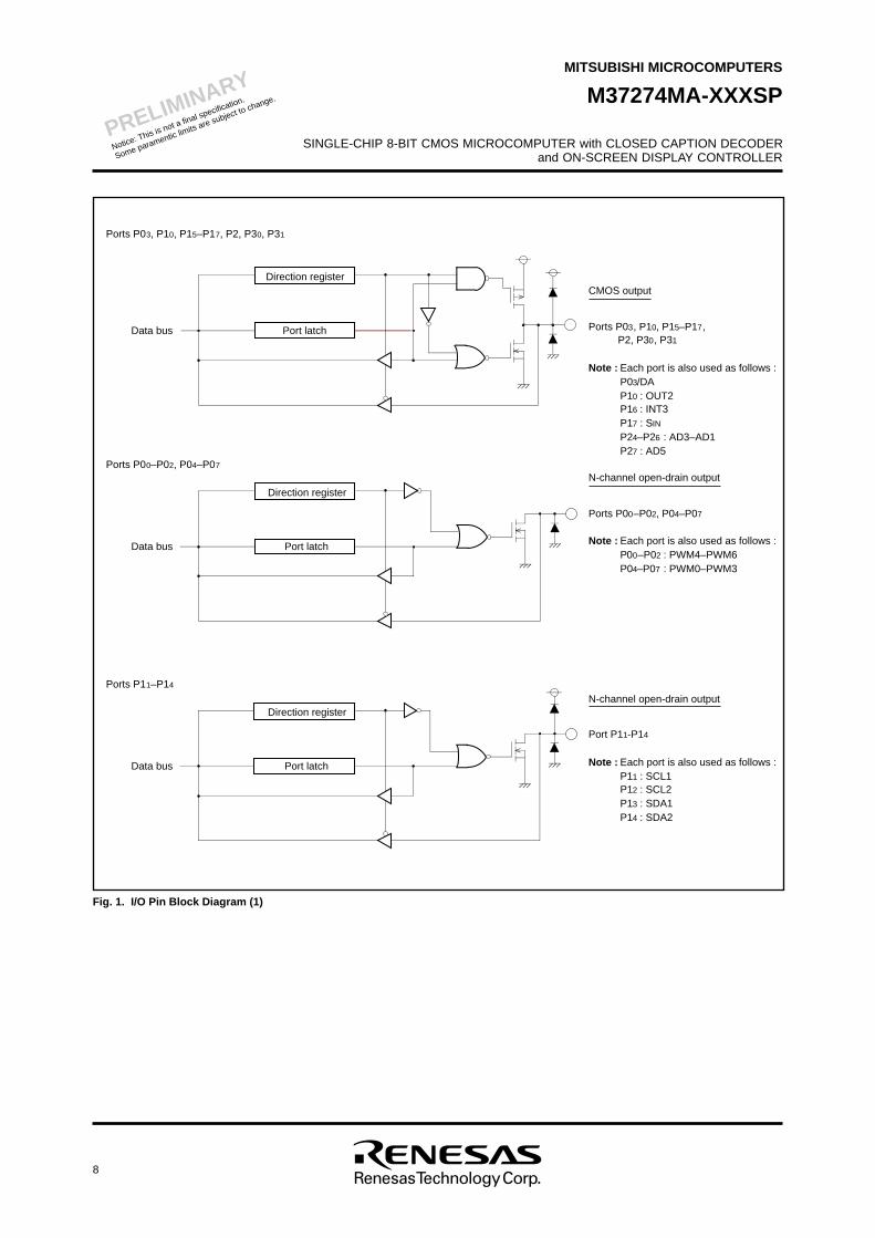
Fig. 1. I/O Pin Block Diagram (1)
N-channel open-drain output
Ports P00–P02, P04–P07
Note : Each port is also used as follows :P00–P02 : PWM4–PWM6P04–P07 : PWM0–PWM3
N-channel open-drain output
Port P11-P14
Note : Each port is also used as follows :P11 : SCL1P12 : SCL2P13 : SDA1P14 : SDA2
CMOS output
Ports P03, P10, P15–P17,P2, P30, P31
Note : Each port is also used as follows :P03/DAP10 : OUT2P16 : INT3P17 : SIN
P24–P26 : AD3–AD1P27 : AD5
Ports P03, P10, P15–P17, P2, P30, P31
Data bus
Direction register
Port latch
Data bus
Direction register
Port latch
Data bus
Direction register
Port latch
Ports P00–P02, P04–P07
Ports P11–P14

9
SINGLE-CHIP 8-BIT CMOS MICROCOMPUTER with CLOSED CAPTION DECODERand ON-SCREEN DISPLAY CONTROLLER
M37274MA-XXXSP
PRELIMINARY
Notice: This is not a final specification.
Some paramentic limits are subject to change.
MITSUBISHI MICROCOMPUTERS
N-channel open-drain output
Ports P45, P46
Note : Each pin is also usedas follows :P45 : SOUT
P46 : SCLK
P52–P55
Note : Each port is also usedas follows :P52 : R P54 : BP53 : G P55 : OUT1
CMOS output
HSYNC, VSYNC
Schmidt input
Fig. 2. I/O Pin Block Diagram (2)
Ports P40–P44
Note : Each port is also used as below :P40 : AD4P41 : INT2P42 : TIM2P43 : TIM3P44 : INT1
Input
HSYNC, VSYNC
SOUT, SCLK
P52–P55
Data bus
Direction register
Internal circuit
Data bus
Ports P40–P44
Internal circuit

10
SINGLE-CHIP 8-BIT CMOS MICROCOMPUTER with CLOSED CAPTION DECODERand ON-SCREEN DISPLAY CONTROLLER
M37274MA-XXXSP
PRELIMINARY
Notice: This is not a final specification.
Some paramentic limits are subject to change.
MITSUBISHI MICROCOMPUTERS
FUNCTIONAL DESCRIPTIONCentral Processing Unit (CPU)The M37274MA-XXXSP uses the standard 740 Family instructionset. Refer to the table of 740 Family addressing modes and machine
instructions or the SERIES 740 <Software> User’s Manual for de-tails on the instruction set.
Machine-resident 740 Family instructions are as follows:
The FST, SLW instruction cannot be used.The MUL, DIV, WIT and STP instructions can be used.
CPU Mode RegisterThe CPU mode register contains the stack page selection bit and
internal system clock selection bit. The CPU mode register is allo-
cated at address 00FB16.
Fig. 3. CPU Mode Register
7 0
1 1 00CPU mode register (CPUM (CM) : address 00FB 16)
Processor mode bits b1 b0 0 0 : Single-chip mode 0 1 : 1 0 : 1 1 :
Stack page selection bit (Note) 0 : Zero page 1 : 1 page
Fix these bits to “1.”
Note: This bit is set to “1” after the reset release.
XCOUT drivability selection bit 0 : LOW drive 1 : HIGH drive
Main colock (XIN–XOUT) stop bit 0 : Oscillating 1 : Stopped
Internal system clock selection bit 0 : XIN–XOUT selected (high-speed mode) 1 : XCIN–XCOUT selected (low-speed mode)
Not available

11
SINGLE-CHIP 8-BIT CMOS MICROCOMPUTER with CLOSED CAPTION DECODERand ON-SCREEN DISPLAY CONTROLLER
M37274MA-XXXSP
PRELIMINARY
Notice: This is not a final specification.
Some paramentic limits are subject to change.
MITSUBISHI MICROCOMPUTERS
MEMORYSpecial Function Register (SFR) AreaThe special function register (SFR) area in the zero page containscontrol registers such as I/O ports and timers.
RAMRAM is used for data storage and for stack area of subroutine calls
and interrupts.
ROMROM is used for storing user programs as well as the interrupt vectorarea.
RAM for OSDRAM for display is used for specifying the character codes and col-
ors to display.
ROM for OSDROM for display is used for storing character data.
Interrupt Vector AreaThe interrupt vector area contains reset and interrupt vectors.
Zero PageThe 256 bytes from addresses 000016 to 00FF16 are called the zeropage area. The internal RAM and the special function registers (SFR)
are allocated to this area.
The zero page addressing mode can be used to specify memory andregister addresses in the zero page area. Access to this area with
only 2 bytes is possible in the zero page addressing mode.
Special PageThe 256 bytes from addresses FF0016 to FFFF16 are called the spe-cial page area. The special page addressing mode can be used to
specify memory addresses in the special page area. Access to this
area with only 2 bytes is possible in the special page addressingmode.
ROM Correction Memory (RAM)This is used as the program area for ROM correction.
Fig. 4. Memory map
000016
00C016
00FF16
0DF316
SFR1 area
Not used
FFFF16
FFDE16FF0016
080016
Interrupt vector area
Not used
1080016
1FFFF16
Special page
ROM(40 K bytes)
RAM for OSD (Note)(1296 bytes)
RAM(768 bytes)
Zero page
020016
024816
600016
SFR2 area
Not used
030016
Not used
155FF16
1800016
Not used1E41F16
1000016
ROM for OSD(11072 bytes)
043F16
Not used
Note : Refer to Table 15. Contents of OSD RAM.
02C016
02FF16
ROM correction memoryBlock 1 : addresses 02C016 to 02DF16
Block 2 : addresses 02E016 to 02FF16

12
SINGLE-CHIP 8-BIT CMOS MICROCOMPUTER with CLOSED CAPTION DECODERand ON-SCREEN DISPLAY CONTROLLER
M37274MA-XXXSP
PRELIMINARY
Notice: This is not a final specification.
Some paramentic limits are subject to change.
MITSUBISHI MICROCOMPUTERS
Fig. 5. Memory Map of Special Function Register 1 (SFR1) (1)
SFR1 area (addresses C016 to DF16)
D016
D116
D216
D316
D416
D516
D616
D716
D816
D916
DA16
DB16
DC16
DD16
DE16
DF16
C016
C116
C216
C316
C416
C516
C616
C716
C816
C916
CB16
CC16
CD16
CE16
CF16
CA16
Address
Port P5 (P5)
OSD control register (OC)
Horizontal position register (HP)
Block control register 1 (BC1)
Port P1 (P1)
Port P1 direction register (D1)
Port P3 (P3)
Port P3 direction register (D3)
Port P2 (P2)
Port P2 direction register (D2)
Register
Port P0 (P0)
Port P0 direction register (D0)
Block control register 2 (BC2)
Block control register 3 (BC3)
Block control register 4 (BC4)
Block control register 5 (BC5)
Block control register 6 (BC6)
Block control register 7 (BC7)
b7 b0Bit allocation State immediately after reset
?0016
b7 b0
?0016
?0016
?????
??
??
?
Port P4 (P4)Port P4 direction register (D4)
OSD port control register (PF)Port P6 (P6)
Block control register 8 (BC8)
Block control register 9 (BC9)
Block control register 10 (BC10)
Block control register 11 (BC11)
Block control register 12 (BC12)
R 0 0GBOUT1OUT2
00 ?00 ??0
?
??
?
??
?
OC6OC7 OC4OC5 OC2OC3 OC0OC1 0016
BC11BC12BC13BC14BC15BC16BC17BC18
BC21BC22BC23BC24BC25BC26BC27BC28
BC31BC32BC33BC34BC35BC36BC37BC38
BC41BC42BC43BC44BC45BC46BC47BC48
BC51BC52BC53BC54BC55BC56BC57BC58
BC61BC62BC63BC64BC65BC66BC67BC68
BC71BC72BC73BC74BC75BC76BC77BC78
BC81BC82BC83BC84BC85BC86BC87BC88
BC91BC92BC93BC94BC95BC96BC97BC98
BC101BC102BC103BC104BC105BC106BC107BC108
BC111BC112BC113BC114BC115BC116BC117BC118
BC121BC122BC123BC124BC125BC126BC127BC128
HP6HP7 HP4HP5 HP2HP3 HP0HP1 0016
0
0
0016
?0016
?0016
?Port P7 (P7)
: Fix to this bit to “0” (do not write to “1”)
:
< Bit allocation > State immediately after reset
Function bit
: No function bit
: Fix to this bit to “1” (do not write to “0”)
Name :
: “0” immediately after reset
: Indeterminate immediately after reset
0
1
?
: “1” immediately after reset
1
0
T3SC
< >

13
SINGLE-CHIP 8-BIT CMOS MICROCOMPUTER with CLOSED CAPTION DECODERand ON-SCREEN DISPLAY CONTROLLER
M37274MA-XXXSP
PRELIMINARY
Notice: This is not a final specification.
Some paramentic limits are subject to change.
MITSUBISHI MICROCOMPUTERS
Fig. 6. Memory Map of Special Function Register 1 (SFR2) (2)
F016
F116
F216
F316
F416
F516
F616
F716
F816
F916
FA16
FB16
FC16
FD16
FE16
FF16
E016
E116
E216
E316
E416
E516
E616
E716
E816
E916
EB16
EC16
ED16
EE16
EF16
EA16 Data slicer control register 1 (DSC1)
Data register 3 (CD3)
A-D conversion register (AD)A-D control register (ADCON)Timer 1 (TM1)
Window register (WN)
Clock run-in register 1 (CR1)Clock run-in register 2 (CR2)
Data register 1 (CD1)Data register 2 (CD2)
Caption position register (CP)Start bit position register (SP)
Timer 2 (TM2)Timer 3 (TM3)Timer 4 (TM4)Timer mode register 1 (TM1)Timer mode register 2 (TM2)I2C data shift register (S0)
I2C control register (S1D)I2C clock control register (S2)
Interrupt request register 1 (IREQ1)Interrupt request register 2 (IREQ2)Interrupt control register 1 (ICON1)Interrupt control register 2 (ICON2)
Clock run-in detect register 1 (CRD1)
Clock run-in detect register 2 (CRD2)
Data register 4 (CD4)
CPU mode register (CPUM)
b7 b0
ADIN0ADIN1ADVREF ADSTR
TM20TM21TM22TM23TM24
TM10TM11TM12TM13TM14
CM2
TM1RTM2RTM3RTM4RCRTRVSCRADR
CK0 INT1RDSRSIOR
TM1ETM2ETM3ETM4ECRTEVSCE
INT1EDSESIOEINT2E
TM25
b7 b0
0016
? 0 0 1 0 0 00FF16
0716
FF16
0716
10 0 1 1 1 0 0
Sync slice register (SSL)
Data slicer control register 2 (DSC2)
I2C status register (S1)I2C address register (S0D)
? 0 ? 0 0 0? 0
0016
?
TM15TM16TM17
TM26TM27
?SAD0SAD1SAD2SAD3SAD4SAD5SAD6 RBW
LRBAD0AASALPINBBTRXMST
BC0BC1BC2ES0ALS10 BITSAD
BSEL0BSEL1
CCR0CCR1CCR2CCR3CCR4FASTMODE
ACKBITACK
0016
0016
0016
000 001 ?0
1MSRINT2RIICRT56R
ADE
1MSEIICET56ET56S
CM7 CM5CM6
DSC20DSC21DSC22DSC25DSC27
DSC10DSC11DSC12DSC15DSC17
SSL7
CP0CP1CP2CP3CP4
SP0SP1SP2SP3SP4SP5SP6SP7
WN0WN1WN2WN3WN4WN5
CRD20CRD21CRD22CRD25CRD27 CRD25 CRD25 CRD25
CR21
CR11
CRD15CRD17 CRD15 CRD15 CRD15
SFR1 area (addresses E016 to FF16)
Address Register Bit allocation State immediately after reset
1 0 0
0 0 0 0 01 10 0
1 0 0 1 1 1 10 1 0 1
0 0 00 0 0
0
0
1 1 0 0
0016
0016
0016
0016
0016
0016
0016
0016
0016
0016
0016
0016
0016
0016
0016
: Fix to this bit to “0” (do not write to “1”)
:
< Bit allocation > < State immediately after reset >
Function bit
: No function bit
: Fix to this bit to “1” (do not write to “0”)
Name :
: “0” immediately after reset
: Indeterminate immediately after reset
0
1
?
: “1” immediately after reset
1
0
CR13 CR12 CR10
ADIN2
? 0 ? 0 0 00 00016

14
SINGLE-CHIP 8-BIT CMOS MICROCOMPUTER with CLOSED CAPTION DECODERand ON-SCREEN DISPLAY CONTROLLER
M37274MA-XXXSP
PRELIMINARY
Notice: This is not a final specification.
Some paramentic limits are subject to change.
MITSUBISHI MICROCOMPUTERS
Fig. 7. Memory Map of Special Function Register 2 (SFR2) (1)
21016
21116
21216
21316
21416
21516
21616
21716
21816
21916
21A16
21B16
21C16
21D16
21E16
21F16
20016
20116
20216
20316
20416
20516
20616
20716
20816
20916
20B16
20C16
20D16
20E16
20F16
20A16 PWM mode register 1 (PN)
Timer 5 (TM5)
Sync pulse counter register (SYC)
Data slicer control register 3 (DSC3)
PWM2 register (PWM2)
PWM6 register (PWM6)
PWM4 register (PWM4)
PWM5 register (PWM5)
PWM0 register (PWM0)
PWM1 register (PWM1)
Interrupt input polarity register (IP)
Serial I/O mode register (SM)
Serial I/O register (SIO)
Clock source control register (CS)
Extra font color register (EC)
Window H register 1 (WH1)
Window L register 1 (WH1)Window H register 2 (WH2)
Window L register 2 (WH2)
Clock run-in detect register 3 (CRD3)
Clock run-in register (CR3)
Timer 6 (TM6)
Border color register (FC)
b7 b0
SYC0
FC2
b7 b0
0016
PWM3 register (PWM3)
PWM mode register 2 (PW)
Raster color register (RC)
I/O polarity control register (PC)
?
??????
FF16
0016
0016
PW0PW1PW2PW3PW4PW5PW6
PN3
SYC1SYC2SYC3SYC4SYC5
DSC30DSC31DSC32DSC37 DSC35
RE1RE2RE5INT3POL
AD/INT3SEL
INT3POL
AD/INT3SEL
SM0RE1RE2RE3SM4RE5INT3POL
AD/INT3SEL SM1SM2SM3SM5
PC0RE1RE2RE3PC4RE5INT3POL
AD/INT3SEL PC1PC2PC5PC6PC7
RE1RE2RE3RE5INT3POL
AD/INT3SEL CS0CS4 CS1CS2CS3CS5CS6
RC0RE1RE2RE3RE5INT3POL
AD/INT3SEL RC1RC2RC5RC6RC7
RE1RE2RE3RE5INT3POL
AD/INT3SEL
FC0FC1
WH20WH21
WL20WL21
??
01 0 0 0 0 0 0
??
?0016DSC36 DSC34 DSC33
? ? ? ? 0 000016
0
CRD31CRD32CRD33CRD34CRD35
SFR2 area (addresses 20016 to 21F16)
Address Register Bit allocation State immediately after reset
PN0PN1PN2
0
0016
0 0
00
00 EC0EC1EC2
00
?
0016
?
0716
0016
0016
0016
0016
0016
??
: Fix to this bit to “0” (do not write to “1”)
:
< Bit allocation > < State immediately after reset >
Function bit
: No function bit
: Fix to this bit to “1” (do not write to “0”)
Name :
: “0” immediately after reset
: Indeterminate immediately after reset
0
1
?
: “1” immediately after reset
1
0
CR36 CR35 CR34 CR33 CR32 CR31 CR30
0 0 0 0
WH10WH11
WL10WL11
WH12WH13
WL12WL13
WH14
WL14
WH15
WL15
WH16
WL16
WH17
WL17
INT2POL
INT1POL
0 0 0 0 0 0016

15
SINGLE-CHIP 8-BIT CMOS MICROCOMPUTER with CLOSED CAPTION DECODERand ON-SCREEN DISPLAY CONTROLLER
M37274MA-XXXSP
PRELIMINARY
Notice: This is not a final specification.
Some paramentic limits are subject to change.
MITSUBISHI MICROCOMPUTERS
Fig. 8. Memory Map of Special Function Register 2 (SFR2) (2)
23016
23116
23216
23316
23416
23516
23616
23716
23816
23916
23A16
23B16
23C16
23D16
23E16
23F16
22016
22116
22216
22316
22416
22516
22616
22716
22816
22916
22B16
22C16
22D16
22E16
22F16
22A16 Vertical position register 111 (VP111)
Vertical position register 13 (VP13)
Vertical position register 17 (VP17)
Vertical position register 15 (VP15)
Vertical position register 16 (VP16)
Vertical position register 11 (VP11)
Vertical position register 12 (VP12)
Vertical position register 19 (VP19)
Vertical position register 110 (VP110)
b7 b0 b7 b0
Vertical position register 14 (VP14)
Vertical position register 112 (VP112)
????VP111
Vertical position register 18 (VP18)
Vertical position register 23 (VP23)
Vertical position register 27 (VP27)
Vertical position register 25 (VP25)
Vertical position register 26 (VP26)
Vertical position register 21 (VP21)
Vertical position register 29 (VP29)
Vertical position register 210 (VP210)
Vertical position register 24 (VP24)
Vertical position register 212 (VP212)
Vertical position register 28 (VP28)
Vertical position register 22 (VP22)
Vertical position register 211 (VP211)
VP112VP113VP114VP115VP116VP117VP118
VP121VP122VP123VP124VP125VP126VP127VP128
VP131VP132VP133VP134VP135VP136VP137VP138
VP141VP142VP143VP144VP145VP146VP147VP148
VP151VP152VP153VP154VP155VP156VP157VP158
VP161VP162VP163VP164VP165VP166VP167VP168
VP171VP172VP173VP174VP175VP176VP177VP178
VP181VP182VP183VP184VP185VP186VP187VP188
VP191VP192VP193VP194VP195VP196VP197VP198
VP1101VP1102VP1103VP1104VP1105VP1106VP1107VP1108
VP1111VP1112VP1113VP1114VP1115VP1116VP1117VP1118
VP1121VP1122VP1123VP1124VP1125VP1126VP1127VP1128
VP211VP212
VP221VP222
VP231VP232
VP241VP242
VP251VP252
VP261VP262
VP271VP272
VP281VP282
VP291VP292
VP2101VP2102
VP2111VP2112
VP2121VP2122
????
???
?
???
?
SFR2 area (addresses 22016 to 24816)
Address Register Bit allocation State immediately after reset
????
????
???
?
???
?
: Fix to this bit to “0” (do not write to “1”)
:
< Bit allocation > State immediately after reset
Function bit
: No function bit
: Fix to this bit to “1” (do not write to “0”)
Name :
: “0” immediately after reset
: Indeterminate immediately after reset
0
1
?
: “1” immediately after reset
1
0
24016
24116
24216
24316
24416
24516
24616
24716
ROM correction address 1 (high-order)
ROM correction enable register (RCR)
ROM correction address 2 (high-order)
ROM correction address 2 (low-order)
DA-H register (DA-H)
ROM correction address 1 (low-order)
DA-L register (DA-L)
RCR0RCR1
0016
0016
?
0016
0016
0016
0016
0016000
00
0 0 ? ? ? ? ? ?
24816
0016
< >

16
SINGLE-CHIP 8-BIT CMOS MICROCOMPUTER with CLOSED CAPTION DECODERand ON-SCREEN DISPLAY CONTROLLER
M37274MA-XXXSP
PRELIMINARY
Notice: This is not a final specification.
Some paramentic limits are subject to change.
MITSUBISHI MICROCOMPUTERS
Fig. 9. Internal State of Processor Status Register and Program Counter at Reset
b7 b0 b7 b0
1
Register
Processor status register (PS)
Bit allocation State immediately after reset
Program counter (PCH)
Program counter (PCL)Contents of address FFFF16
Contents of address FFFE16
I Z CDBTVN ?????
: Fix to this bit to “0” (do not write to “1”)
:
< Bit allocation > < State immediately after reset >
Function bit
: No function bit
: Fix to this bit to “1” (do not write to “0”)
Name :
: “0” immediately after reset
: Indeterminate immediately after reset
0
1
?
: “1” immediately after reset
1
0
? ?

17
SINGLE-CHIP 8-BIT CMOS MICROCOMPUTER with CLOSED CAPTION DECODERand ON-SCREEN DISPLAY CONTROLLER
M37274MA-XXXSP
PRELIMINARY
Notice: This is not a final specification.
Some paramentic limits are subject to change.
MITSUBISHI MICROCOMPUTERS
INTERRUPTSInterrupts can be caused by 18 different sources consisting of 4 ex-
ternal, 12 internal, 1 software, and reset. Interrupts are vectored in-terrupts with priorities as shown in Table 1. Reset is also included in
the table because its operation is similar to an interrupt.
When an interrupt is accepted,(1) The contents of the program counter and processor status
register are automatically stored into the stack.(2) The interrupt disable flag I is set to “1” and the corresponding
interrupt request bit is set to “0.”
(3) The jump destination address stored in the vector address entersthe program counter.
Other interrupts are disabled when the interrupt disable flag is set to
“1.”All interrupts except the BRK instruction interrupt have an interrupt
request bit and an interrupt enable bit. The interrupt request bits arein interrupt request registers 1 and 2 and the interrupt enable bits are
in interrupt control registers 1 and 2. Figure 11 shows the interrupt-
related registers.Interrupts other than the BRK instruction interrupt and reset are ac-
cepted when the interrupt enable bit is “1,” interrupt request bit is “1,”and the interrupt disable flag is “0.” The interrupt request bit can be
set to “0” by a program, but not set to “1.” The interrupt enable bit can
be set to “0” and “1” by a program.Reset is treated as a non-maskable interrupt with the highest priority.
Figure 10 shows interrupt control.
Interrupt Causes(1) VSYNC and OSD interrupts
The VSYNC interrupt is an interrupt request synchronized withthe vertical sync signal.
The OSD interrupt occurs after character block display to the
CRT is completed.(2) INT1, INT2, INT3 interrupts
With an external interrupt input, the system detects that the levelof a pin changes from “L” to “H” or from “H” to “L,” and generates
an interrupt request. The input active edge can be selected by
bits 3, 4 and 6 of the interrupt input polarity register (address021216) : when this bit is “0,” a change from “L” to “H” is detected;
when it is “1,” a change from “H” to “L” is detected. Note that all
bits are cleared to “0” at reset.(3) Timer 1, 2, 3 and 4 interrupts
An interrupt is generated by an overflow of timer 1, 2, 3 or 4.(4) Serial I/O interrupt
This is an interrupt request from the clock synchronous serial
I/O function.(5) f(XIN)/4096 interrupt
This interrupt occurs regularly with a f(XIN)/4096 period. Set bit 0of the PWM mode register 1 to “0.”
(6) Data slicer interrupt
An interrupt occurs when slicing data is completed.(7) Multi-master I2C-BUS interface interrupt
This is an interrupt request related to the multi-master I2C-BUS
interface.
(8) A-D conversion interrupt
An interrupt occurs at the completion of A-D conversion. SinceA-D conversion interrupt and the INT3 interrupt share the same
vector, an interrupt source is selected by bit 7 of the interrupt
interval determination control register (address 021216).
Vector Addresses
FFFF16, FFFE16
FFFD16, FFFC16
FFFB16, FFFA16
FFF916, FFF816
FFF716, FFF616
FFF516, FFF416
FFF316, FFF216
FFF116, FFF016
FFEF16, FFEE16
FFED16, FFEC16
FFEB16, FFEA16
FFE916, FFE816
FFE716, FFE616
FFE516, FFE416
FFE316, FFE216
FFDF16, FFDE16
Interrupt Source
Reset
OSD interrupt
INT1 interrupt
Data slicer interrupt
Serial I/O interrupt
Timer 4 interrupt
f(XIN)/4096 interrupt
VSYNC interrupt
Timer 3 interrupt
Timer 2 interrupt
Timer 1 interrupt
A-D convertion · INT3 interrupt
INT2 interrupt
Multi-master I2C-BUS interface interrupt
Timer 5 · 6 interrupt
BRK instruction interrupt
Remarks
Non-maskable
Active edge selectable
Active edge selectable
Software switch by software (See note)/
When selecting INT3 interrupt, active edge selectable.
Active edge selectable
Software switch by software (See note)
Non-maskable (software interrupt)
Table 1. Interrupt Vector Addresses and Priority
Priority
1
2
3
4
5
6
7
8
9
10
11
12
13
14
15
16
Note : Switching a source during a program causes an unnecessary interrupt occurs. Accordingly, set a source at initializing of program.

18
SINGLE-CHIP 8-BIT CMOS MICROCOMPUTER with CLOSED CAPTION DECODERand ON-SCREEN DISPLAY CONTROLLER
M37274MA-XXXSP
PRELIMINARY
Notice: This is not a final specification.
Some paramentic limits are subject to change.
MITSUBISHI MICROCOMPUTERS
(9)Timer 5 · 6 interruptAn interrupt is generated by an overflow of timer 5 or 6. Their
priorities are same, and can be switched by software.
(10)BRK instruction interruptThis software interrupt has the least significant priority. It does
not have a corresponding interrupt enable bit, and it is not af-fected by the interrupt disable flag I (non-maskable).
Fig. 10. Interrupt Control
Interrupt request bitInterrupt enable bit
Interrupt disable flag I
BRK instructionReset
Interruptrequest

19
SINGLE-CHIP 8-BIT CMOS MICROCOMPUTER with CLOSED CAPTION DECODERand ON-SCREEN DISPLAY CONTROLLER
M37274MA-XXXSP
PRELIMINARY
Notice: This is not a final specification.
Some paramentic limits are subject to change.
MITSUBISHI MICROCOMPUTERS
Fig. 11. Interrupt-related Registers
7Interrupt request register 1 (IREQ1: address 00FC16)
Timer 1 interrupt request bit
0
Timer 2 interrupt request bit
Timer 3 interrupt request bit
Timer 4 interrupt request bit
OSD interrupt request bit
VSYNC interrupt request bit Multi-master I2C-BUS interface interrupt request bit
Timer 5 • 6 interrupt request bit
0 : No interrupt request issued1 : Interrupt request issued
7Interrupt request register 2(IREQ2: address 00FD16)
INT1 interrupt request bit
0
Data slicer interrupt request bit
Serial I/O interrupt request bit
INT2 interrupt request bit
Fix this bit to “0.”
0
0 : Interrupt disabled1 : Interrupt enabled
7Interrupt control register 2( ICON2 : address 00FF16)
INT1 interrupt enable bit
0
Data slicer interrupt enable bit
Serial I/O interrupt enable bit
7Interrupt control register 1 ( ICON1: address 00FE16)
Timer 1 interrupt enable bit
0
Timer 2 interrupt enable bit
Timer 3 interrupt enable bit
Timer 4 interrupt enable bit
OSD interrupt enable bit
VSYNC interrupt enable bit
f(XIN)/4096 interrupt request bit
Multi-master I2C-BUS interface enable bit
Timer 5 • 6 interrupt enable bit
INT2 interrupt enable bit
Timer 5 • 6 interrupt switch bit
f(XIN)/4096 interrupt enable bit
A-D conversion • INT3 interrupt request bit
0 : Timer 51 : Timer 6
A-D conversion • INT3 interrupt request bit
Fix this bit to “0.”
INT3 polarity switch bit0 : Positive polarity1 : Negative polarity
Interrupt input polarity register (IP : address 021216)
Fix these bits to “0.”
INT1 polarity switch bit0 : Positive polarity1 : Negative polarity
INT2 polarity switch bit0 : Positive polarity1 : Negative polarity
7 0
0 0
A-D conversion. INT3 interrupt source selection bit0 : INT3 interrupt1 : A-D conversion interrupt
00

20
SINGLE-CHIP 8-BIT CMOS MICROCOMPUTER with CLOSED CAPTION DECODERand ON-SCREEN DISPLAY CONTROLLER
M37274MA-XXXSP
PRELIMINARY
Notice: This is not a final specification.
Some paramentic limits are subject to change.
MITSUBISHI MICROCOMPUTERS
TIMERSThe M37271MF-XXXSP has 6 timers: timer 1, timer 2, timer 3,
timer 4, timer 5, and timer 6. All timers are 8-bit timers with the 8-bittimer latch. The timer block diagram is shown in Figure 13.
All of the timers count down and their divide ratio is 1/(n+1), where n
is the value of timer latch. By writing a count value to the correspond-ing timer latch (addresses 00F016 to 00F316 : timers 1 to 4, addresses
020C16 and 020D16 : timers 5 and 6), the value is also set to a timer,
simultaneously.The count value is decremented by 1. The timer interrupt request bit
is set to “1” by a timer overflow at the next count pulse, after thecount value reaches “0016”.
(1) Timer 1Timer 1 can select one of the following count sources:
• f(XIN)/16 or f(XCIN)/16
• f(XIN)/4096 or f(XCIN)/4096
• External clock from the P42 TIM2 pin
The count source of timer 1 is selected by setting bits 5 and 0 oftimer mode register 1 (address 00F416). Either f(XIN) or f(XCIN) is
selected by bit 7 of the CPU mode register.
Timer 1 interrupt request occurs at timer 1 overflow.
(2) Timer 2Timer 2 can select one of the following count sources:
• f(XIN)/16 or f(XCIN)/16
• Timer 1 overflow signal
• External clock from the TIM2 pin
The count source of timer 2 is selected by setting bits 4 and 1 of
timer mode register 1 (address 00F416). Either f(XIN) or f(XCIN) isselected by bit 7 of the CPU mode register. When timer 1 overflow
signal is a count source for the timer 2, the timer 1 functions as an 8-bit prescaler.
Timer 2 interrupt request occurs at timer 2 overflow.
(3) Timer 3Timer 3 can select one of the following count sources:
• f(XIN)/16 or f(XCIN)/16
• f(XCIN)
• External clock from the TIM3 pinThe count source of timer 3 is selected by setting bit 0 of timer mode
register 2 (address 00F516) and bit 6 at address 00C716. Either f(XIN)
or f(XCIN) is selected by bit 7 of the CPU mode register.Timer 3 interrupt request occurs at timer 3 overflow.
(4) Timer 4Timer 4 can select one of the following count sources:
• f(XIN)/16 or f(XCIN)/16
• f(XIN)/2 or f(XCIN)/2
• f(XCIN)
The count source of timer 3 is selected by setting bits 1 and 4 oftimer mode register 2 (address 00F516). Either f(XIN) or f(XCIN) is
selected by bit 7 of the CPU mode register. When timer 3 overflowsignal is a count source for the timer 4, the timer 3 functions as an 8-
bit prescaler.
Timer 4 interrupt request occurs at timer 4 overflow.
(5) Timer 5Timer 5 can select one of the following count sources:
• f(XIN)/16 or f(XCIN)/16
• Timer 2 overflow signal
• Timer 4 overflow signal
The count source of timer 3 is selected by setting bit 6 of timer moderegister 1 (address 00F416) and bit 7 of timer mode register 2 (ad-
dress 00F516). When overflow of timer 2 or 4 is a count source for
timer 5, either timer 2 or 4 functions as an 8-bit prescaler. Eitherf(XIN) or f(XCIN) is selected by bit 7 of the CPU mode register.
Timer 5 interrupt request occurs at timer 5 overflow.
(6) Timer 6Timer 6 can select one of the following count sources:
• f(XIN)/16 or f(XCIN)/16
• Timer 5 overflow signal
The count source of timer 6 is selected by setting bit 7 of timer moderegister 1 (address 00F416). Either f(XIN) or f(XCIN) is selected by bit
7 of the CPU mode register. When timer 5 overflow signal is a countsource for timer 6, timer 5 functions as an 8-bit prescaler.
Timer 6 interrupt request occurs at timer 6 overflow.
At reset, timers 3 and 4 are connected by hardware and “FF16” is
automatically set in timer 3; “0716” in timer 4. The f(XIN) /16 is se-lected as the timer 3 count source. The internal reset is released by
timer 4 overflow in this state and the internal clock is connected.
At execution of the STP instruction, timers 3 and 4 are connected byhardware and “FF16” is automatically set in timer 3; “0716” in timer 4.
However, the f(XIN) /16 is not selected as the timer 3 count source.
So set both bit 0 of timer mode register 2 (address 00F516) and bit 6at address 00C716 to “0” before execution of the STP instruction
(f(XIN) /16 is selected as the timer 3 count source). The internalSTP state is released by timer 4 overflow in this state and the inter-
nal clock is connected.
As a result of the above procedure, the program can start under astable clock.
: When bit 7 of the CPU mode register (CM7) is “1,” f(XIN) be-
comes f(XCIN).The structure of timer-related registers is shown in Figure 12.

21
SINGLE-CHIP 8-BIT CMOS MICROCOMPUTER with CLOSED CAPTION DECODERand ON-SCREEN DISPLAY CONTROLLER
M37274MA-XXXSP
PRELIMINARY
Notice: This is not a final specification.
Some paramentic limits are subject to change.
MITSUBISHI MICROCOMPUTERS
Fig. 12. Timer-related Registers
7 0Timer mode register 1(TM1 : address 00F416)
Timer 1 count source selection bit 1 0 : f(XIN)/16 or f(XCIN)/16 (Note) 1 : Count source selected by bit 5 of TM1
Timer 2 count source selection bit 1 0 : Count source selected by bit 4 of TM1 1 : External clock from TIM2 pin
Timer 1 count stop bit 0 : Count start 1 : Count stop
Timer 2 count stop bit 0 : Count start 1 : Count stop
Timer 2 count source selection bit 2 0 : f(XIN)/16 or f(XCIN)/16 (Note) 1 : Timer 1 overflow
Timer 1 count source selection bit 2 0 : f(XIN)/4096 or f(XCIN)/4096 (Note) 1 : External clock from TIM2 pin
Timer 5 count source selection bit 2 0 : Timer 2 overflow 1 : Timer 4 overflow
Timer 6 count source selection bit 0 : f(XIN)/16 or f(XCIN)/16 (Note) 1 : Timer 5 overflow
7 0Timer mode register 2(TM2 : address 00F516)
Timer 3 count stop bit 0 : Count start 1 : Count stop
Timer 4 count stop bit 0 : Count start 1 : Count stop
Timer 5 count stop bit 0 : Count start 1 : Count stop
Timer 6 count stop bit 0 : Count start 1 : Count stop
Timer 5 count source selection bit 1 0 : f(XIN)/16 or f(XCIN)/16 (Note) 1 : Count source selected by bit 6 of TM1
Timer 3 count source selection bit
0 0 : f(XIN)/16 or f(XCIN)/16 (Note) 1 0 : f(XCIN) 0 1 : 1 1 :
(Bit 6 at address 00C716)
External clock from TIM3 pin
Timer 4 count source selection bits b4 b1 0 0 : Timer 3 overflow 0 1 : f(XIN)/16 or f(XCIN)/16 (Note) 1 0 : f(XIN)/2 or f(XCIN)/2 (Note) 1 1 : f(XCIN)
b0
Note : Either f(XIN) or f(XCIN) is selected by bit 7 of the CPU mode register.

22
SINGLE-CHIP 8-BIT CMOS MICROCOMPUTER with CLOSED CAPTION DECODERand ON-SCREEN DISPLAY CONTROLLER
M37274MA-XXXSP
PRELIMINARY
Notice: This is not a final specification.
Some paramentic limits are subject to change.
MITSUBISHI MICROCOMPUTERS
Fig. 13. Timer Block Diagram
Timer 1 (8)
1/4096
1/2
CM7TM15
1/8
Timer 1 latch (8)
8
8
8
TM10TM12
TM14
TM11TM13
Timer 2 (8)
Timer 2 latch (8)
8
8
8
Timer 3 (8)
Timer 3 latch (8)
8
8
8
Timer 4 (8)
Timer 4 latch (8)
8
8
8
Timer 5 (8)
Timer 5 latch (8)
8
8
8
Timer 6 (8)
Timer 6 latch (8)
8
8
8
Data bus
Timer 1interrupt request
Timer 2interrupt request
Timer 3interrupt request
ResetSTP instruction
TM20TM22
TM3EL
Timer 4interrupt requestTM24
TM23
TM21
TM16
Timer 5interrupt requestTM27
TM25
Timer 6interrupt requestTM17
TM26
TM21
XCIN
XIN
TIM2
TIM3
Selection gate : Connected to black side atreset
TM1 : Timer mode register 1TM2 : Timer mode register 2TM3EL : Timer 3 count source switch bit (address 00C7 16)CM : CPU mode register
Notes 1: HIGH pulse width of external clock inputs TIM2 and TIM3 needs 4 machine cycles or more.2: When the external clock source is selected, timers 1, 2, and 3 are counted at a rising edge of input signal.
FF16
0716
3: In the stop mode or the wait mode, external clock inputs TIM2 and TIM3 cannot be used.

23
SINGLE-CHIP 8-BIT CMOS MICROCOMPUTER with CLOSED CAPTION DECODERand ON-SCREEN DISPLAY CONTROLLER
M37274MA-XXXSP
PRELIMINARY
Notice: This is not a final specification.
Some paramentic limits are subject to change.
MITSUBISHI MICROCOMPUTERS
SERIAL I/OThe M37274MA-XXXSP has a built-in serial I/O which can either trans-
mit or receive 8-bit data serially in the clock synchronous mode.The serial I/O block diagram is shown in Figure 14. The synchronous
clock I/O pin (SCLK), and data output pin (SOUT) also function as port
P4, data input pin (SIN) also functions as port P1.Bit 2 of the serial I/O mode register (address 021316) selects whether
the synchronous clock is supplied internally or externally (from theP46/SCLK pin). When an internal clock is selected, bits 1 and 0 select
whether f(XIN) or f(XCIN) is divided by 8, 16, 32, or 64. To use SOUT
and P46/SCLK pins for serial I/O, set the corresponding bits of theport P4 direction register (address 00C916) to “0.” To use SIN pin for
serial I/O, set the corresponding bit of the port P1 direction register
(address 00C316) to “0.”
Fig. 14. Serial I/O Block Diagram
The operation of the serial I/O is described below. The operation ofthe serial I/O differs depending on the clock source; external clock or
internal clock.
8
Serial I/O shift register (8)
Data bus
Serial I/Ointerrupt request
Selection gate: Connect to black side atreset.
Synchronouscircuit
Frequency divider
1/81/4 1/16SM1SM0
Serial I/O counter (8)
SM5 : LSB MSB
S
SM2
1/2XIN
SIN
SOUT
SCLK
1/2
(Address 021416)
XCIN
1/2
CM7 1/2
Note : When the data is set in the serial I/O register (address 0214 16), the register functions as the serial I/O shift register.
(Note)
CM : CPU mode registerSM : Serial I/O mode register

24
SINGLE-CHIP 8-BIT CMOS MICROCOMPUTER with CLOSED CAPTION DECODERand ON-SCREEN DISPLAY CONTROLLER
M37274MA-XXXSP
PRELIMINARY
Notice: This is not a final specification.
Some paramentic limits are subject to change.
MITSUBISHI MICROCOMPUTERS
Fig. 16. Serial I/O Mode Register
Internal clock : The serial I/O counter is set to “7” during the write
cycle into the serial I/O register (address 021416), and the transfer
clock goes “H” forcibly. At each falling edge of the transfer clock afterthe write cycle, serial data is output from the SOUT pin. Transfer di-
rection can be selected by bit 5 of the serial I/O mode register. At
each rising edge of the transfer clock, data is input from the SIN pinand data in the serial I/O register is shifted 1 bit.
After the transfer clock has counted 8 times, the serial I/O counterbecomes “0” and the transfer clock stops at HIGH. At this time the
interrupt request bit is set to “1.”
External clock : The an external clock is selected as the clock source,the interrupt request is set to “1” after the transfer clock has been
counted 8 counts. However, transfer operation does not stop, so the
clock should be controlled externally. Use the external clock of 500kHzor less with a duty cycle of 50%.
The serial I/O timing is shown in Figure 15. When using an externalclock for transfer, the external clock must be held at HIGH for initial-
izing the serial I/O counter. When switching between an internal clock
and an external clock, do not switch during transfer. Also, be sure toinitialize the serial I/O counter after switching.
Notes 1: On programming, note that the serial I/O counter is set by
writing to the serial I/O register with the bit managing in-
structions, such as SEB and CLB.2: When an external clock is used as the synchronous clock,
write transmit data to the serial I/O register when the trans-
fer clock input level is HIGH.
Fig. 15. Serial I/O Timing (for LSB first)
Synchronous clock
Transfer clock
Serial I/O register write signal
Serial I/O outputSOUT
D0 D1 D2 D3 D4 D5 D6 D7
(Note)
Serial I/O inputSIN
Note : When an internal clock is selected, the S OUT pin is at high-impedance after transfer is completed.
Interrupt request bit is set to “1”
7Serial I/O mode register(SM : address 021316)
Internal synchronous clock selection bitsb1 b00 0 : f(XIN)/8 or f(XCIN)/80 1 : f(XIN)/16 or f(XCIN)/161 0 : f(XIN)/32 or f(XCIN)/321 1 : f(XIN)/64 or f(XCIN)/64
0
0
Synchronous clock selection bit 0 : External clock 1 : Internal clock
Port function selection bit 0 : P11, P13 functions as port 1 : SCL1, SDA1
Port function selection bit 0 : P12, P14 functions as port 1 : SCL2, SDA2
Transfer direction selection bit 0 : LSB first 1 : MSB first
Fix these bits to “0”
0

25
SINGLE-CHIP 8-BIT CMOS MICROCOMPUTER with CLOSED CAPTION DECODERand ON-SCREEN DISPLAY CONTROLLER
M37274MA-XXXSP
PRELIMINARY
Notice: This is not a final specification.
Some paramentic limits are subject to change.
MITSUBISHI MICROCOMPUTERS
(4) Operating of 14-bit PWMAs with 8-bit PWM, set the bit 0 of the PWM mode register 1 (ad-
dress 020A16) to “0” (at reset, bit 0 is already set to “0” automati-cally), so that the PWM count source is supplied. Pin DA is also used
as port P03. Select output mode by setting bit 3 of the port P0 direc-tion register. Next, select the output polarity by bit 3 of the PWM
mode register 1. Then, the 14-bit PWM outputs from the D-A output
pin by setting bit 1 of the PWM mode register 1 to “0” (at reset, this bitalready set to “0” automatically) to select the DA output.
The output example of the 14-bit PWM is shown in Figure 19.
The 14-bit PWM divides the data of the DA latch into the low-order 6bits and the high-order 8 bits.
The fundamental waveform is determined with the high-order 8-bitdata “DH.” A “H” level area with a length τ DH(“H” level area of
fundamental waveform) is output every short area of “t” = 256τ =64 ms (τ is the minimum resolution bit width of 0.25 µs). The “H” levelarea increase interval (tm) is determined with the low-order 6-bit data
“DL.” The “H” level are of smaller intervals “tm” shown in Table 6 islonger by τ than that of other smaller intervals in PWM repeat period
“T” = 64t. Thus, a rectangular waveform with the different “H” width is
output from the D-A pin. Accordingly, the PWM output changes by τunit pulse width by changing the contents of the DA-H and DA-L
registers. A length of entirely “H” output cannot be output, i. e. 256/
256.
(5) Output after ResetAt reset, the output of ports P00–P02 and P04–P07 is in the high-
impedance state and the contents of the PWM register and the PWM
circuit are undefined. Note that after reset, the PWM output is unde-fined until setting the PWM register.
PWM OUTPUT FUNCTIONThe M37274MA-XXXSP is equipped with a 14-bit PWM (DA) seven
8-bit PWMs (PWM0–PWM6). DA has a 14-bit resolution with theminimum resolution bit width of 0.25 µs and a repeat period of
4096 ms (for f(XIN) = 8 MHz). PWM0–PWM6 have the same circuit
structure and an 8-bit resolution with minimum resolution bit width of4 µs and repeat period of 1024 µs (for f(XIN) = 8 MHz) .
Figure 17 shows the PWM block diagram. The PWM timing generat-ing circuit applies individual control signals to PWM0–PWM6 using
f(XIN) divided by 2 as a reference signal.
(1) Data SettingWhen outputting DA, first set the high-order 8 bits to the DA-H regis-
ter (address 024016), then the low-order 6 bits to the DA-L register(address 024116). When outputting PWM0–PWM6, set 8-bit output
data to the PWMi register (i means 0 to 6; addresses 020016 to020616).
(2) Transmitting Data from Register to PWM circuitData transfer from the 8-bit PWM register to the 8-bit PWM circuit is
executed at writing data to the register.The signal output from the 8-bit PWM output pin corresponds to the
contents of this register.
Also, data transfer from the DA register (addresses 024016 and024116) to the 14-bit PWM circuit is executed at writing data to the
DA-L register (address 024116). Reading from the DA-H register (ad-
dress 024016) means reading this transferred data. Accordingly, it ispossible to confirm the data being output from the D-A output pin by
reading the DA register.
(3) Operating of 8-bit PWMThe following explains PWM operation.First, set the bit 0 of PWM mode register 1 (address 020A16) to “0”
(at reset, bit 0 is already set to “0” automatically), so that the PWM
count source is supplied.PWM0–PWM3 are also used as pins P04–P07, PWM4–PWM6 are
also used as pins P00–P02, respectively. Set the corresponding bitsof the port P0 direction register to “1” (output mode). And select each
output polarity by bit 3 of PWM mode register 1 (address 020A16).
Then, set bits 7 to 0 of PWM mode register 2 to “1” (PWM output).The PWM waveform is output from the PWM output pins by setting
these registers.Figure 18 shows the 8-bit PWM timing. One cycle (T) is composed
of 256 (28) segments. The 8 kinds of pulses, relative to the weight of
each bit (bits 0 to 7), are output inside the circuit during 1 cycle.Refer to Figure 20 (a). The 8-bit PWM outputs waveform which is
the logical sum (OR) of pulses corresponding to the contents of bits
0 to 7 of the 8-bit PWM register. Several examples are shown inFigure 20 (b). 256 kinds of output (HIGH area: 0/256 to 255/256) are
selected by changing the contents of the PWM register. A length ofentirely HIGH cannot be output, i.e. 256/256.

26
SINGLE-CHIP 8-BIT CMOS MICROCOMPUTER with CLOSED CAPTION DECODERand ON-SCREEN DISPLAY CONTROLLER
M37274MA-XXXSP
PRELIMINARY
Notice: This is not a final specification.
Some paramentic limits are subject to change.
MITSUBISHI MICROCOMPUTERS
LSB
Table 2. Relation Between Low-order 6-bit Data and High-levelArea Increase Interval
Area Longer by τ Than That of Other tm (m = 0 to 63)
Nothing
m = 32
m = 16, 48
m = 8, 24, 40, 56
m = 4, 12, 20, 28, 36, 44, 52, 60
m = 2, 6, 10, 14, 18, 22, 26, 30, 34, 38, 42, 46, 50, 54, 58, 62
m = 1, 3, 5, 7, ................................. 57, 59, 61, 63
Low-order 6 bits of Data
0 0 0 0 0 0
0 0 0 0 0 1
0 0 0 0 1 0
0 0 0 1 0 0
0 0 1 0 0 0
0 1 0 0 0 0
1 0 0 0 0 0
Fig. 17. PWM Block Diagram
PNPWP0D0
: PWM mode register 1 (address 020A16): PWM mode register 2 (address 020B16): Port P0 register (address 00C016): Port P0 direction register ( address 00C116)
Selection gate :Connected to black side atreset.
is as same contents with the others.
PWM1 register (Address 020116)
PWM2 register (Address 020216)
PWM3 register (Address 020316)
PWM4 register (Address 020416)
PWM5 register (Address 020516)
PWM6 register (Address 020616)
Data bus
PWM0 register(Address 020016)
b7 b0
8
8-bit PWM circuit
POL P04
PW0
D04 PWM0
P05
PW1
D05 PWM1
P06
PW2
D06 PWM2
P07
PW3
D07 PWM3
P00
PW4
D00 PWM4
P01
PW5
D01 PWM5
P02
PW6
D02 PWM6
Inside of
PN0
1/2XINPWM timing generating
circuit
14-bit PWM circuit
PN2 P03
PN1
D03
MSB
DA-H register(Address : 024016)
DA latch(14 bits)
DA-L register (Note)(Address : 024116)
LSB
86
146
D-A
b7 b0

27
SINGLE-CHIP 8-BIT CMOS MICROCOMPUTER with CLOSED CAPTION DECODERand ON-SCREEN DISPLAY CONTROLLER
M37274MA-XXXSP
PRELIMINARY
Notice: This is not a final specification.
Some paramentic limits are subject to change.
MITSUBISHI MICROCOMPUTERS
Fig. 18. 8-bit PWM Timing
(a)
Pul
ses
show
ing
the
wei
ght o
f eac
h bi
t
13
57
920
3040
5060
7080
9010
011
012
013
014
015
016
017
018
019
020
021
022
023
024
025
025
5
412
2028
3644
5260
6876
8492
100
108
116
124
132
140
148
156
164
172
180
188
196
204
212
220
228
236
244
252
8
1648
8011
214
417
620
824
0
2440
5672
8810
412
013
615
216
818
420
021
623
224
8
3296
160
224
6419
2
Bit
7
26
1014
1822
2630
3438
4246
5054
5862
6670
7478
8286
9094
9810
210
611
011
411
812
212
613
013
413
814
214
615
015
415
816
216
617
017
417
818
218
619
019
419
820
220
621
021
421
822
222
623
023
423
824
224
625
025
4
Bit
6
Bit
5
Bit
4
Bit
3
Bit
2
Bit
1
128
Bit
0
PW
M o
utpu
tt =
4 µ
s T
= 1
024
µsf(
XIN
) =
8 M
Hz
(b)
Exa
mpl
e of
8-b
it P
WM
t
1 (
0)
1 (
1)
1 (
24)
(25
5)
T =
256
t
0016
0116
1816
FF
16

28
SINGLE-CHIP 8-BIT CMOS MICROCOMPUTER with CLOSED CAPTION DECODERand ON-SCREEN DISPLAY CONTROLLER
M37274MA-XXXSP
PRELIMINARY
Notice: This is not a final specification.
Some paramentic limits are subject to change.
MITSUBISHI MICROCOMPUTERS
Fig. 19. 14-bit PWM Output Example (f(X IN) = 8MHz)
0.25 s
b7 b0b6 b5 b4 b3 b2 b1
0 00 1 0 1 1 0
b13 b6
0 0 1 0 1 1 0
b0b5
1 0 1 0 0 0
Set “2C16” to DA-H register.
[DA-H register]
DH
At writing of DA-L
b0b6 b5 b4 b3 b2 b1
01 0 1 0 0
Set “2816” to DA-L register.
[DA-L register] DL
At writing of DA-L
Undefined
These bits decide “H” level area of fundamental waveform.
These bits decide smaller interval “tm” in which “H” leval area is [“H” level area of fundamental waveform + τ ].
=Minimum resolution bit width 0.25 s
High-order 8-bit value of DA latch
“H” level area of fundamental waveform
FF 00D3FE FD … D6 D4 02 01D5
14-bit PWM output
8-bit counter
0.25 s 44
FF 00D3FE FD D6 D4 02 01D5
14-bit PWM output
8-bit counter
0.25 s 45
Fundamental waveform
Waveform of smaller interval “tm” specified by low-order 6 bits
Fundamental waveform of smaller interval “tm” which is not specified by low-order 6 bits is not changed.
14-bit PWM output
Low-order 6-bit output of DA latch
0.25 s 44 τ = 0.25 s
T = 4096 sRepeat period
t0 t1 t2 t3 t4 t5 t59 t60 t61 t62 t63
[DA latch]
…
b7
2C 2B 2A … 03 02 01 00 2C 2B 2A … 03 02 01 00
0
……

29
SINGLE-CHIP 8-BIT CMOS MICROCOMPUTER with CLOSED CAPTION DECODERand ON-SCREEN DISPLAY CONTROLLER
M37274MA-XXXSP
PRELIMINARY
Notice: This is not a final specification.
Some paramentic limits are subject to change.
MITSUBISHI MICROCOMPUTERS
Fig. 20. PWM-related Registers
PWM count source selection bit 0 : Count source supply 1 : Count source stop
DA/P03 output selection bit 0 : P03 output 1 : DA output
PWM mode register 1(PN: address 020A16)
P04/PWM0 output selection bit 0 : P04 output 1 : PWM0 output
P05/PWM1 output selection bit 0 : P05 output 1 : PWM1 output
P06/PWM2 output selection bit 0 : P06 output 1 : PWM2 output
P07/PWM3 output selection bit 0 : P07 output 1 : PWM3 output
07
PWM mode register 2(PW: address 020B16)
P00/PWM4 output selection bit 0 : P00 output 1 : PWM4 output
P01/PWM5 output selection bit 0 : P01 output 1 : PWM5 output
P02/PWM6 output selection bit 0 : P02 output 1 : PWM6 output
Fix this bit to “0.”
0
DA output polarity selection bit 0 : Positive polarity 1 : Negative polarity
PWM output polarity selection bit 0 : Positive polarity 1 : Negative polarity

30
SINGLE-CHIP 8-BIT CMOS MICROCOMPUTER with CLOSED CAPTION DECODERand ON-SCREEN DISPLAY CONTROLLER
M37274MA-XXXSP
PRELIMINARY
Notice: This is not a final specification.
Some paramentic limits are subject to change.
MITSUBISHI MICROCOMPUTERS
A-D control register (ADCON: address 00EF16)
A-D conversion completion bit 0 : Conversion in purogress 1 : Conversion completed
Analog input pin selection bits b2 b1 b0 0 0 0 : AD1 0 0 1 : AD2 0 1 0 : AD3 0 1 1 : AD4 1 0 0 : AD5 1 0 1 : AD6 1 1 0 : 1 1 1 :
VCC connection selection bit 0 : OFF 1 : ONFix this bit to “0.”
0
7
Do not set.
A-D CONVERTER(1)A-D Conversion Register (AD)A-D conversion reigister is a read-only register that stores the resultof an A-D conversion. This register should not be read during A-D
conversion.
(2)A-D Control Register (ADCON)The A-D control register controls A-D conversion. Bits 1 and 0 of thisregister select analog input pins. When these pins are not used as
anlog input pins, they are used as ordinary I/O pins. Bit 3 is the A-D
conversion completion bit, A-D conversion is started by writing “0” tothis bit. The value of this bit remains at “0” during an A-D conversion,
then changes to “1” when the A-D conversion is completed.
Bit 4 controls connection between the resistor ladder and VCC. Whennot using the A-D converter, the resistor ladder can be cut off from
the internal VCC by setting this bit to “0,” accordingly providing low-power dissipation.
(3)Comparison Voltage Generator (ResistorLadder)
The voltage generator divides the voltage between VSS and VCC by256, and outputs the divided voltages to the comparator as the refer-
ence voltage Vref.
(4)Channel SelectorThe channel selector connects an analog input pin, selected by bits
1 and 0 of the A-D control register, to the comparator.
(5)Comparator and Control CircuitThe conversion result of the analog input voltage and the reference
voltage “Vref” is stored in the A-D conversion register. The A-D con-version completion bit and A-D conversion interrupt request bit are
set to “1” at the completion of A-D conversion.
Fig. 21. A-D Control Register
Fig. 22. A-D Comparator Block Diagram
A-D control register(address 00EF16)
A-D control circuit
Data bus
Switch tree
A-D conversion interrupt request
Resistor ladder
Compa-rator
Cha
nnel
sel
ecto
r A-D conversion registerAD1
AD2
AD3
AD4
(address 00EE16)
b7 b0
2
8
VSS VCC
AD5
AD6
0

31
SINGLE-CHIP 8-BIT CMOS MICROCOMPUTER with CLOSED CAPTION DECODERand ON-SCREEN DISPLAY CONTROLLER
M37274MA-XXXSP
PRELIMINARY
Notice: This is not a final specification.
Some paramentic limits are subject to change.
MITSUBISHI MICROCOMPUTERS
VREF
256 (n – 0.5)1 to 255
0
Note: VREF indicates the voltage of internal VCC.
Fig. 23. Changes in A-D Conversion Register and Comparison Voltage during A-D Conversion
(6) Conversion MethodSet bit 7 of the interrupt input polarity register (address 021216) to
“1” to generate an interrupt request at completion of A-D conver-sion.
Set the A-D conversion • INT3 interrupt request bit to “0” (even
when A-D conversion is started, the A-D conversion • INT3 inter-rupt reguest bit is not set to “0” automatically).
When using A-D conversion interrupt, enable interrupts by settingA-D conversion • INT3 interrupt request bit to “1” and setting the
interrupt disable flag to “0.”
Set the VCC connection selection bit to “1” to connect VCC to theresistor ladder.
Select analog input pins by the analog input selection bit of the A-
D control register.Set the A-D conversion completion bit to “0.” This write operation
starts the A-D conversion. Do not read the A-D conversion regis-ter during the A-D conversion.
Verify the completion of the conversion by the state (“1”) of the
A-D conversion completion bit, the state (“1”) of A-D conversion •INT3 interrupt reguest bit, or the occurrence of an A-D conversion
interrupt.Read the A-D conversion register to obtain the conversion results.
Note : When the ladder resistor is disconnect from VCC, set the VCC
connection selection bit to “0” between steps 7and 8.
(7) Internal OperationWhen the A-D conversion starts, the following operations are auto-
matically performed.
The A-D conversion register is set to “0016.”The most significant bit of the A-D conversion register becomes
“1, ” and the comparison voltage “Vref” is input to the comparator.
At this point, Vref is compared with the analog input voltage “VIN .”Bit 7 is determined by the comparison results as follows.
When Vref < VIN : bit 7 holds “1”When Vref > VIN : bit 7 becomes “0”
With the above operations, the analog value is converted into a digi-
tal value. The A-D conversion terminates in a maximum of 50 ma-chine cycles (12.5 s at f(XIN) = 8 MHz) after it starts, and the con-
version result is stored in the A-D conversion register.
An A-D conversion interrupt request occurs at the same time as A-Dconversion completion, the A-D conversion • INT3 interrupt request
bit becomes “1.” The A-D conversion completion bit also becomes“1.”
Table 3. Expression for Vref and VREF
A-D conversion register contents “n”
(decimal notation)Vref (V)
1 2 3 4 5 6 7 8
1 0 0 0 0 0 0 0
1 2 1 0 0 0 0 0
1 0 0 0 0 0 01
1 2 3 4 5 6 7 1
VREF
2VREF
512–
VREF
2VREF
4VREF
512–±
VREF
2VREF
4VREF
8VREF
512–±
0 0 0 0 0 0 0 0
Contents of A-D conversion register Reference voltage (Vref) [V]
0A-D conversion start
1st comparison start
3rd comparison start
8th comparison start
2nd comparison start
Digital value corresponding to analog input voltage.
A-D conversion completion
(8th comparison completion)
VREF
2VREF
4VREF
8±
VREF
512–
VREF
256±.......
: Value determined by mth (m = 1 to 8) resultm
.....
±
± ±
0
1
2
3
4
5
6
7
8
12
3

32
SINGLE-CHIP 8-BIT CMOS MICROCOMPUTER with CLOSED CAPTION DECODERand ON-SCREEN DISPLAY CONTROLLER
M37274MA-XXXSP
PRELIMINARY
Notice: This is not a final specification.
Some paramentic limits are subject to change.
MITSUBISHI MICROCOMPUTERS
[ LSB]
[ LSB ]
(8) Definition of A-D Conversion AccuracyThe definition of A-D conversion accuracy is described below.
Relative accuracy• Zero transition error (V 0T)
The deviation of the input voltage at which A-D conversion output
data changes from “0” to “1,” from the corresponding ideal A-Dconversion characteristics between 0 and VREF.
• Non-linearity errorThe deviation of the actual A-D conversion characteristics, from the
ideal A-D conversion characteristics between V0 and V254.
(V0 – 1/2 VREF/256)
1LSBV0T =
(VREF – 3/2 VREF/256)– V254
1LSBVFST=
Non-linearity error =
[ LSB]
[ LSB]
• Differential non-linearity errorThe deviation of the input voltage required to change output data
by “1,” from the corresponding ideal A-D conversion characteris-tics between 0 and VREF.
Absolute accuracy
• Absolute accuracy errorThe deviation of the actual A-D conversion characteristics, from the
ideal A-D conversion characteristics between 0 and VREF.
Vn – (1LSB n + V0)
1LSB
[ LSB]Differential non-linearity error =(Vn+1– Vn)– 1LSB
1LSB
Absolute accuracy error =
1LSBA with respect to absolute accuracy =
1LSB with respect to relative accuracy =
Note: The analog input voltage “Vn” at which A-D conversion output
data changes from “n” to “n + 1” (n ; 0 to 254) is as follows(refer to Figure 24) :
V254 – V0
254
VREF
256
[ V ]
[ V ]
Fig. 24. Definition of A-D Conversion Accuracy
• Full-scale transition error (V FST)The deviation of the input voltage at which A-D conversion outputdata changes from “255” to “254,” from the corresponding ideal A-
D conversion characteristics between 0 and VREF.
Vn – 1LSBA (n + 1/2)
1LSBA
Output data
0
Analog input voltage (V)
V0 Vn Vn+1 V254 VREF
n
n+1
254
255
Zero transition error (V 0T)
Differential non-linearity error
LSBA
Actual A-D
conversion
characteristics
12
32
V1
1LSB A
Ideal A-D conversion characteristics
between V0 and V254LSBA
1LSB
Absolute accuracy
Non-linearity error
Full-scale transition error(VFST)
1LSB

33
SINGLE-CHIP 8-BIT CMOS MICROCOMPUTER with CLOSED CAPTION DECODERand ON-SCREEN DISPLAY CONTROLLER
M37274MA-XXXSP
PRELIMINARY
Notice: This is not a final specification.
Some paramentic limits are subject to change.
MITSUBISHI MICROCOMPUTERS
1 0 0
0 0 0 0 1 0 1
Compositevideosignal Hundred of kiloohms
Sync pulse counterregister(address 020F16)
Clock run-in register 2 (address 00E716)
Data slicer control register 2 s(address 00EB16)
Data slicer control register 1(address 00EA16)
Window register(address 00E216)
Clock run-in register 1(address 00E616)
Caption position register(address 00E016)
Start bit position register(address 00E116)
Clock run-in detect register 1 t(address 00E816)
Clock run-in detect register 2(address 00E916)
Interrupt request generating circuit
Data slicer interruptrequest
Synchronizingsignal counter
Synchronizingseparationcircuit
Sync slicecircuit
Clampingcircuit
Low-passfilter
Timing signalgeneratingcircuit
Clock run-indeterminationcircuit
Data slice linespecificationcircuit
Start bit detecting circuit
Data clock generating circuit
16-bit shift register
Data register 1(address 00E416)
Data register 2(address 00E516)
Sync slice register 3(address 00E316)
Data bus
Comparator
01 0 1 1 1
0
0
0 0
0 1 0 1
560 pF
CVIN
200 pF
HSYNC HLF RVCO
+
–
Referencevoltagegeneratingcircuit
VHOLD
1000 pF
high-order low-order
Data slicer ON/OFF
Data register 4(address 00ED16)
Data register 3(address 00EC16)
Data slicer controlregister 3(address 021016)
Clock run-in detect register 3(address 020816)
Clock run-in register 3(address 020916)
External circuit
Note: Make the length of wiring which is connected to VHOLD, HLF, RVCO and CVIN pin as short as possible so that a leakage current may not be generated when mounting a resistor or a capacitor on each pin.
1
DATA SLICERThe M37274MA-XXXSP includes the data slicer function for the
closed caption decoder (referred to as the CCD). This function takesout the caption data superimposed in the vertical blanking interval of
a composite video signal. A composite video signal which makes the
sync chip’s polarity negative is input to the CVIN pin.
When the data slicer function is not used, the data slicer circuit can
be cut off by setting bit 0 of data slicer control register 1 (address00EA16) to “0.” Also, the timing signal generating circuit can be cut
off by setting bit 0 of data slicer control register 2 (address 00EB16)to “0.” These settings can realize the low-power dissipation.
Fig. 25. Data Slicer Block Diagram
0
0
0
0
to 1 M
0.1 F 470
1 F
1k 15k

34
SINGLE-CHIP 8-BIT CMOS MICROCOMPUTER with CLOSED CAPTION DECODERand ON-SCREEN DISPLAY CONTROLLER
M37274MA-XXXSP
PRELIMINARY
Notice: This is not a final specification.
Some paramentic limits are subject to change.
MITSUBISHI MICROCOMPUTERS
0 0 0
07
Data slicer control register 1(DSC1: address 00EA16)
Data slicer control bit 0: Data slicer stopped 1: Data slicer operating
Field to be sliced data selection bit
Fix this bit to “0.”
Data latch completion flag for caption
data in main data slice line
0: Data is not yet latched 1: Data is latched
Field determination flag
0 0 0
07
Hsep
Vsep
Hsep
Vsep
0 :
1 :
Field of main dataslice line
Field for settingreference voltage b2 b1
0 0 F2 0 1 F1 1 0 F1 and F2 1 1 F1 and F2
F2 F1F2 F1
Definition of fields 1 (F1) and 2 (F2)
Hsep
VSYNC
Vsep
F1 :
Hsep
VSYNC
Vsep
F2 :
F2 F1F2 F1
07
Data slicer control register 3(DSC3: address 021016)
Line selection bit for slice voltage o 0: Main data slice line 1: Sub-data slice line
Field of sub-data slice line b2 b1
0 0 F2 0 1 F1 1 0 F1 and F2 1 1 F1 and F2
Field to be sliced data select i
Setting bit of sub-data slice line l
Field for settingreference voltage
Fix these bits to “0.”
Data slicer control register 2(DSC2: address 00EB16)
Timing signal generating circuit icontrol bit 0: Stopped 1: Operating
Reference clock source selection obit 0: Video signal 1: HSYNC signal
Test bit: read-only
Fix these bits to “0.”
V-pulse shape determination flag a 0: Match 1: Mismatch
Fix this bit to “0.”
Test bit: read-only
Figure 26 shows the data slicer control registers.
Fig. 26. Data Slicer Control Registers
ion bit

35
SINGLE-CHIP 8-BIT CMOS MICROCOMPUTER with CLOSED CAPTION DECODERand ON-SCREEN DISPLAY CONTROLLER
M37274MA-XXXSP
PRELIMINARY
Notice: This is not a final specification.
Some paramentic limits are subject to change.
MITSUBISHI MICROCOMPUTERS
(1) Clamping Circuit and Low-pass FilterThis filter attenuates the noise of the composite video signal inputfrom the CVIN pin. The CVIN pin to which composite video signal is
input requires a capacitor (0.1 µF) coupling outside. Pull down the
CVIN pin with a resistor of hundreds of kiloohms to 1 M . In addition,we recommend to install externally a simple low-pass filter using a
resistor and a capacitor at the CVIN pin (refer to Figure 25).
(2) Sync Slice CircuitThis circuit takes out a composite sync signal from the output signalof the low-pass filter. Figure 27 shows the structure of the sync slice
register.
(3) Synchronous Signal Separation CircuitThis circuit separates a horizontal synchronous signal and a verticalsynchronous signal from the composite sync signal taken out in the
sync slice circuit.
Horizontal synchronous signal (Hsep)A one-shot horizontal synchronous signal Hsep is generated at
the falling edge of the composite sync signal.Vertical synchronous signal (Vsep)
As a Vsep signal generating method, it is possible to select one of
the following 2 methods by using bit 7 of the sync slice register(address 00E316).
•Method 1 The “L” level width of the composite sync signal is
measured. If this width exceeds a certain time, a Vsep
signal is generated in synchronization with the rising
of the timing signal immediately after this “L” level. •Method 2 The “L” level width of the composite sync signal is
measured. If this width exceeds a certain time, it is
detected whether a falling of the composite syncsignal exits or not in the “L” level period of the timing
signal immediately after this “L” level. If a falling exists,a Vsep signal is generated in synchronization with
the rising of the timing signal (refer to Figure 28).
Figure 28 shows a Vsep generating timing. The timing signal shownin the figure is generated from the reference clock which the timing
generating circuit outputs.
Reading bit 5 of data slicer control register 2 permits determinatingthe shape of the V-pulse portion of the composite sync signal. As
shown in Figure 29, when the A level matches the B level, this bit is“0.” In the case of a mismatch, the bit is “1.”
For the pins RVCO and the HLF, connect a resistor and a capacitor
as shown in Figure 25. Make the length of wiring which is connectedto these pins as short as possible so that a leakage current may not
be generated.
Note: It takes a few tens of milliseconds until the reference clock
becomes stable after the data slicer and the timing signalgenerating circuit are started. In this period, various timing
signals, Hsep signals and Vsep signals become unstable. For
this reason, take stabilization time into consideration whenprogramming.
Fig. 27. Sync Slice Register
Fig. 28. Vsep Generating Timing (method 2)
0 0 0
07
Sync slice register(SSL : address 00E316)
Fix these bits to “0000101 2”
Vertical synchronizing signal (Vsep) generating method selection bit 0 : Method 1 1 : Method 2
0 0 11
Composite sync signal
Timing signal
Vsep signal
A Vsep signal is generated at a rising of the timing signal immediately after the “L” level width of the composite sync signal exceeds a certain time.
1
2 Measure “L” period

36
SINGLE-CHIP 8-BIT CMOS MICROCOMPUTER with CLOSED CAPTION DECODERand ON-SCREEN DISPLAY CONTROLLER
M37274MA-XXXSP
PRELIMINARY
Notice: This is not a final specification.
Some paramentic limits are subject to change.
MITSUBISHI MICROCOMPUTERS
(4) Timing Signal Generating CircuitThis circuit generates a reference clock which is 832 times as largeas the horizontal synchronous signal frequency. It also generates
various timing signals on the basis of the reference clock, horizontal
synchronous signal and vertical synchronizing signal. The circuitoperates by setting bit 0 of data slicer control register 2 (address
00EB16) to “1.”The reference clock can be used as a display clock for OSD function
in addition to the data slicer. The HSYNC signal can be used as a
count source instead of the composite sync signal. However, whenthe HSYNC signal is selected, the data slicer cannot be used. A count
source of the reference clock can be selected by bit 1 of data slicer
control register 2 (address 00EB16).
Fig. 29. Determination of V-pulse Waveform
Composite sync signal
A B
0
1
1
Bit 5 of DSC2

37
SINGLE-CHIP 8-BIT CMOS MICROCOMPUTER with CLOSED CAPTION DECODERand ON-SCREEN DISPLAY CONTROLLER
M37274MA-XXXSP
PRELIMINARY
Notice: This is not a final specification.
Some paramentic limits are subject to change.
MITSUBISHI MICROCOMPUTERS
Selection of field to be sliced data
In the case of the main data slice line, the field to be sliced data isselected by bits 2 and 1 of the data slicer control register 1 (address
00EA16). In the case of the sub-data slice line, the field is selected
by bits 2 and 1 of the data slicer control register 3. When bit 2 ofthe data slicer control register 1 is set to “1,” it is possible to slice
data of both fields (refer to Figure 26).Specification of line to set slice voltage
The reference voltage for slicing (slice voltage) is generated by
integrating the amplitude of the clock run-in pulse in the particularline (refer to Table 4).
Field determinationThe field determination flag can be read out by bit 5 of the data
slicer control register 1. This flag charge at the falling edge of
Vsep.
Fig. 30. Signals in Vertical Blanking Interval
(5) Data Slice Line Specification CircuitSpecification of data slice lineM37274MA-XXXSP has 2 data slice line specification circuits for
slicing arbitrary 2 Hsep in 1 field. The following 2 data slice lines
are specified .<Main data slice line>
This line is specified by the caption position register (address00E016).
<Sub-data slice line>
This line is specified by the data slicer control register 3 (address00EB16).
The counter is reset at the falling edge of Vsep and is incremented
by 1 every Hsep pulse. When the counter value matched the valuespecified by bits 4 to 0 of the caption position register (in case of
the sub-data slice line, by bits 3 to 7 of the data slicer control register3), this Hsep is sliced.
The values of “0016” to “1F16” can be set in the caption position
register. Bit 7 to bit 5 are used for testing. Set “1002.” Figure 30shows the signals in the vertical blanking interval. Figure 31 shows
the structure of the caption position register.
Line
Line specified by bits 4 to 0 of CP(Main data slice line)
Line specified by bits 7 to 3 of DSC3(Sub-data slice line)
Table 4. Specifying of Field Whose Sets Reference Voltage
DSC1 : Data slice control register 1
DSC3 : Data slice control register 3CP : Caption position register
Field
Field specified by bit 1 of DSC1 0: F2 1: F1
Field specified by bit 1 of DSC3 0: F2 1: F1
Bit 0 of DSC3
0
1
Video signal Vertical blanking interval
Composite video signal
Count value to be set in the caption position register (“11 16” in this case)
Hsep
Vsep
Hsep
Magnified drawing
Clock run-in Start bit + 16-bit data
Start bit
Time to be set in the start bit position register
Composite video signal min. max.
Line 21

38
SINGLE-CHIP 8-BIT CMOS MICROCOMPUTER with CLOSED CAPTION DECODERand ON-SCREEN DISPLAY CONTROLLER
M37274MA-XXXSP
PRELIMINARY
Notice: This is not a final specification.
Some paramentic limits are subject to change.
MITSUBISHI MICROCOMPUTERS
4 set value of the start bit position
register reference clock period<
Fig. 31. Caption Position Register
(6) Reference Voltage Generating Circuit andComparator
The composite video signal clamped by the clamping circuit is input
to the reference voltage generating circuit and the comparator.Reference voltage generating circuit
This circuit generates a reference voltage (slice voltage) by using
the amplitude of the clock run-in pulse in line specified by the dataslice line specification circuit. Connect a capacitor between the
VHOLD pin and the VSS pin, and make the length of wiring as short
as possible so that a leakage current may not be generated.Comparator
The comparator compares the voltage of the composite video signalwith the voltage (reference voltage) generated in the reference
voltage generating circuit, and converts the composite video signal
into a digital value.
(7) Start Bit Detecting CircuitThis circuit detects a start bit at line decided in the data slice linespecification circuit. For start bit detection, it is possible to select one
of the following two types by using bit 1 of clock run-in register 2(address 00E716).
After the lapse of the time corresponding to the set value of the
start bit position register (address 00E116), the first rising of thecomposite video signal is detected as a start bit.
The time is set in bits 0 to 6 of the start bit position register (address00E116) (refer to Figure 32). Set a value fit for the following
conditions.
Figure 32 shows the structure of the start bit position register.
Time from the falling of the horizontal
synchronizing signal to the last risingof the clock run-in
Fig. 32. Start Bit Position Register
Caption position register(CP : address 00E016)
Specification main data slice line
7 0
1 0 0
Fix these bits to “1002”
7 0
Start bit generating timeTime from a falling of the horizontal synchronizing signal to occurrence of a start bit = 4 set value (“0016” to “7F16”) reference clock period
Start bit position register(SP : address 00E116)
DSC1 bit 7 control bit 0 : Generation of 16 pulses 1 : Generation of 16 pulses and
detection of clock run-in pulse (4 to 6 pulses)
Time from the faling of the horizontal
synchronous signal to occurrence ofthe start bit
<

39
SINGLE-CHIP 8-BIT CMOS MICROCOMPUTER with CLOSED CAPTION DECODERand ON-SCREEN DISPLAY CONTROLLER
M37274MA-XXXSP
PRELIMINARY
Notice: This is not a final specification.
Some paramentic limits are subject to change.
MITSUBISHI MICROCOMPUTERS
After a falling of the clock run-in pulse set in bits 2 to 0 of clock run-
in detect register 2 (address 00E916) is detected, a start bit is
detected by sampling a comparator output. A sampling clock forsampling is obtained by dividing the reference clock generated in
the timing signal generating circuit by 13.Figure 34 shows the structure of clock run-in detect register 2.
The contents of bits 2 to 0 of clock run-in detect register 2 and bit
1 of clock run-in register 2 are written at a falling of the horizontalsynchronous signal. For this reason, even if an instruction for setting
is executed, the contents of the register cannot be rewritten until a
falling of the horizontal synchronous signal.
Fig. 33. Clock Run-in Register 2
(8) Clock run-in determination circuitThis circuit sets a window in the clock run-in portion in the composite
video signal, and then determinates clock run-in by counting the
number of pulses in this window. Set the time from a falling of thehorizontal synchronizing signal to a start of the window by bits 0 to 5
of the window register (address 00E216; refer to Figure 35). The
window ends according to the contents of the setting of the start bitposition register (refer to Figure 32).
Fig. 35. Window Register
Fig. 34. Clock Run-in Detect Register 2
7 0
1
Start bit detecting method selection bit 0 : Method 1 1 : Method 2
Clock run-in register 2 (CR2 : address 00E716)
Fix this bit to “1”
Fix these bits to “1001112”
0 0 1 1 1 1
7 0
Clock run-in pulses for sampling b2 b1 b0 0 0 0 : Not available 0 0 1 : 1st pulse 0 1 0 : 2nd pulse 0 1 1 : 3rd pulse 1 0 0 : 4th pulse 1 0 1 : 5th pulse 1 1 0 : 6th pulse 1 1 1 : 7th pulse
Clock run-in detect register 2(CRD2 : address 00E916)
Data clock generating time Time from detection of a start bit to occurrence of a data clock = (13 + set value) reference clock period
7 0
Window start time Time from a falling of the horizontal synchronizing signalto a start of the window = 4 setvalue (“0016” to “3F16”) reference clock period
Window register (WN : address 00E216)
Fix these bits to “0”
0 0

40
SINGLE-CHIP 8-BIT CMOS MICROCOMPUTER with CLOSED CAPTION DECODERand ON-SCREEN DISPLAY CONTROLLER
M37274MA-XXXSP
PRELIMINARY
Notice: This is not a final specification.
Some paramentic limits are subject to change.
MITSUBISHI MICROCOMPUTERS
Fig. 36. Clock Run-in Register 1
Fig. 39. Clock Run-in Detect Registers 1 and 3
Fig. 38. Window Setting
Fig. 37. Clock Run-in Register 3
For the main data slice line, the count value of pulses in the window
is stored in clock run-in register 1 (address 00E616; refer to Figure
36). For the sub-data slice line, the count value of pulses in the windowis stored in clock run-in register 3 (address 020916; refer to Figure
37). When this count value is 4 to 6, it is determined as a clock run-in.
Accordingly, set the count value so that the window may start afterthe first pulse of the clock run-in (refer to Figure 38).
The contents to be set in the window register are written at a fallingof the horizontal synchronous signal. For this reason, even if an
instruction for setting is executed, the contents of the register cannot
be rewritten until a falling of the horizontal synchronous signal.For the main data slice line, reference clock is counted in the period
from a falling of the clock pulse set in bits 0 to 2 of clock run-in
detect register 2 (address 00E916) to the next falling. The count valueis stored in bits 3 to 7 of clock run-in detect register 1 (address
00E816) (When the count value exceeds “1F16,” “1F16” is held). Forthe sub-data slice line, the count value is stored in bits 3 to 7 of
clock run-in detect register 3 (address 020816). Read out these bits
after the occurence of a data slicer interrupt (refer to (11) InterruptRequest Generating Circuit).
Figure 39 shows the structure of clock run-in detect registers 1 and3.
7 0
Clock run-in count value ofmain-data slice line
Clock run-in register 1(CR1 : address 00E616)
Fix these bits to “0101 2”
0 1 0 1
7
Clock run-in count value of sub-dataslice line
Clock run-in register 3(CR3 : address 020916)
Data latch completion flag for caption data in isub-data slice line
0: Data is not latched yet 1: Data is latched
Data slice line selection bit for interruptrequest 0: Main data slice line 1: Sub-data slice line
Interrupt mode selection bit 0: Interrupt occurs at end of data slice line a 1: Interrupt occurs at completion of caption data latch
When the count value in the window is 4 to 6, this is determined as a clock run-in.
Horizontal synchronous signal
Composite video signal
Window
Clock run-inStart bit data + 16-bit data
Time to be set in the window register
Time to be set in the start bit position register
7 0
Number of reference clocks to be counted in one clock run-in pulse period
Clock run-in detect registers 1, 3( CRD1 : address 00E816)( CRD3 : address 020816)
Test bits : read-only
0

41
SINGLE-CHIP 8-BIT CMOS MICROCOMPUTER with CLOSED CAPTION DECODERand ON-SCREEN DISPLAY CONTROLLER
M37274MA-XXXSP
PRELIMINARY
Notice: This is not a final specification.
Some paramentic limits are subject to change.
MITSUBISHI MICROCOMPUTERS
Conditions for Setting Bit 4 of DSC3 to “1”
Data clock of 16 pulses has occured in sub-data slaice line
Data clock of 16 pulses has occured in sub-data slaice line
AND
Clock run-in pulse are detected 4 to 6 times
(10) 16-bit Shift RegisterThe caption data converted into a digital value by the comparator isstored into the 16-bit shift register in synchronization with the data
clock. For the main data slice line, the contents of the high-order 8
bits of the stored caption data and the contents of the low-order 8bits of the same data can be obtained by reading out data register 2
(address 00E516) and data register 1 (address 00E416), respectively.
For the sub-data slice line, the contents of the high-order 8 bits andthe contents of the low-order 8 bits can be obtained by reading out
the data register 4 (address 00ED16) and data register 3 (address00EC16), respectively. These registers are reset to “0” at a falling of
Vsep. Read out data registers 1 and 2 after the occurence of a data
slicer interrupt (refer to (11) Interrupt Request Generating Circuit).
(11) Interrupt Request Generating CircuitThe interrupt requests as shown in Table 6 are generated bycombination of the following bits; bits 5 and 6 of the clock run-in register
3 (address 020916), bit 1 of the clock run-in register 2 (address
00E716). Read out the contents of data registers 1 to 4 and thecontents of bits 3 to 7 of clock run-in detect registers 1 and 3 after the
occurence of a data slicer interrupt request.
For a data clock, 16 pulses are generated. When just 16 pulses have
been generated, bit 7 of the data slicer control register is set to “1”
(refer to Figure 26). When method 1 is already selected as a start bitdetecting method, this bit becomes a logical product (AND) value
with a clock run-in determination result by setting bit 7 of the start bit
position register to “1.”When method 2 is already selected as a start bit detecting method
and 16 pulses are generated of a data clock regardless of bit 7 of thestart bit position register, this bit is set to “1.” The contents of this bit
are reset at a falling of the vertical synchronizing signal (Vsep).
Table 5. Setting Conditions for Caption Data Latch Completion Flag
Bit 7 of SP
0
1
Conditions for Setting Bit 7 of DSC1 to “1”
Data clock of 16 pulses has occured in main data slaice line
Data clock of 16 pulses has occured in main data slaice line
AND
Clock run-in pulse are detected 4 to 6 times
(9) Data clock generating circuitThis circuit generates a data clock synchronized with the start
bit detected in the start bit detecting circuit.Set the time from detection of the start bit to occurrence of the data
clock in bits 3 to 7 of clock run-in detect register 2 (address
00E916). The time to be set is represented by the following expression:
Time = (13 + set value) reference clock period
Slice line
Main data slice line
Sub-data slice line
b5
0
1
Sources
At end of data slice line
Data clock of 16 pulses has occured ANDClock run-in pulse are detected 4 to 6 times
Data clock of 16 pulses has occured
At end of data slice line
Data clock of 16 pulses has occured ANDClock run-in pulse are detected 4 to 6 times
Data clock of 16 pulses has occured
b6
0
1
0
1
CR2
b1
0
1
0
1
0
1
0
1
CR3
Table 6. Occurence Sources of Interrupt Request
Occurence Souces of Interrupt Request

42
SINGLE-CHIP 8-BIT CMOS MICROCOMPUTER with CLOSED CAPTION DECODERand ON-SCREEN DISPLAY CONTROLLER
M37274MA-XXXSP
PRELIMINARY
Notice: This is not a final specification.
Some paramentic limits are subject to change.
MITSUBISHI MICROCOMPUTERS
Fig. 40. Sync Pulse Counter Register
(12) Synchronous Signal CounterThe synchronous signal counter counts the composite sync signaltaken out from a video signal in the data slicer circuit or the vertical
synchronous signal Vsep as a count source.
The count value in a certain time (T time) generated by f(XIN)/213 orf(XIN)/213 is stored into the 5-bit latch. Accordingly, the latch value
changes in the cycle of T time. When the count value exceeds “1F16,”
“1F16” is stored into the latch.The latch value can be obtained by reading out the sync pulse counter
register (address 020F16). A count source is selected by bit 5 of thesync pulse counter register.
The synchronous signal counter is used when bit 0 of PWM mode
register 1 (address 02EA16).Figure 40 shows the structure of the sync pulse counter and Figure
41 shows the synchronous signal counter block diagram.
Fig. 41. Synchronous Signal Counter Block Diagram
Sync pulse counter register(SYC : address 020F16)
Count value
Count source Count time
0: HSYNC
signal
1: Composite sync signal
f(XIN)/213 (1024 s, f(XIN) = 8 MHz)
7 0
Reset
5-bit counter
Latch (5 bits)
f(XIN)/213
Composite sync signal
HSYNC signal Counter
Sync pulse counter register
Data busSelection gate : connected to black
colored side when reset.
b5

43
MITSUBISHI MICROCOMPUTERS
SINGLE-CHIP 8-BIT CMOS MICROCOMPUTER with CLOSED CAPTION DECODERand ON-SCREEN DISPLAY CONTROLLER
M37274MA-XXXSP
PRELIMINARY
Notice: This is not a final specification.
Some paramentic limits are subject to change.
Function
In conformity with Philips I2C-BUSstandard: 10-bit addressing format 7-bit addressing format High-speed clock mode Standard clock mode
In conformity with Philips I2C-BUSstandard: Master transmission Master reception Slave transmission Slave reception
16.1 kHz to 400 kHz (at φ = 4 MHz)
Table 7. Multi-master I 2C-BUS Interface Functions
Item
Format
Communication mode
SCL clock frequency
φ : System clock = f(XIN)/2
Note: We are not responsible for any third party’s infringement ofpatent rights or other rights attributable to the use of the con-
trol function (bits 6 and 7 of the I2C control register at address00F916) for connections between the I2C-BUS interface and
ports (SCL1, SCL2, SDA1, SDA2).
MULTI-MASTER I2C-BUS INTERFACEThe multi-master I2C-BUS interface is a serial communications cir-
cuit, conforming to the Philips I2C-BUS data transfer format. Thisinterface, offering both arbitration lost detection and a synchronous
functions, is useful for the multi-master serial communications.
Figure 42 shows a block diagram of the multi-master I2C-BUS inter-face and Table 7 shows multi-master I2C-BUS interface functions.
This multi-master I2C-BUS interface consists of the I2C address reg-ister, the I2C data shift register, the I2C clock control register, the I2C
control register, the I2C status register and other control circuits.
Fig. 42. Block Diagram of Multi-master I 2C-BUS Interface
I2C address register (S0D)b7 b0
SAD6 SAD5 SAD4 SAD3 SAD2 SAD1 SAD0 RBW
Noiseeliminationcircuit
Serial
data(SDA)
Address comparator
b7
I C data shift register
b0Datacontrolcircuit
I2C clock control register (S2)
System clock ( )
Interruptgeneratingcircuit
Interruptrequest signal(IICIRQ)
b7
MST TRX BB PINAL AAS AD0 LRB
b0
I C statusregister (S1)
b7 b0
BSEL1 BSEL0 10BITSAD
ALS BC2 BC1 BC0
I2C clock control register (S1D)
Bit counter
BBcircuit
Clockcontrolcircuit
Noiseeliminationcircuit
Serial
clock(SCL)
b7 b0
ACK ACKBIT
FASTMODE CCR4 CCR3 CCR2 CCR1 CCR0
Internal data bus
Clock division
S0
ALcircuit
ESO
2
2

44
MITSUBISHI MICROCOMPUTERS
SINGLE-CHIP 8-BIT CMOS MICROCOMPUTER with CLOSED CAPTION DECODERand ON-SCREEN DISPLAY CONTROLLER
M37274MA-XXXSP
PRELIMINARY
Notice: This is not a final specification.
Some paramentic limits are subject to change.
SAD6 SAD5 SAD4 SAD3 SAD2 SAD1 SAD0 RBW
Slave address
I2 C address register(S0D: address 00F716)
Read/write bit
7 0
(1) I2C Data Shift RegisterThe I2C data shift register (S0 : address 00F616) is an 8-bit shiftregister to store receive data and write transmit data.
When transmit data is written into this register, it is transferred to the
outside from bit 7 in synchronization with the SCL clock, and eachtime one-bit data is output, the data of this register are shifted one bit
to the left. When data is received, it is input to this register from bit 0in synchronization with the SCL clock, and each time one-bit data is
input, the data of this register are shifted one bit to the left.
The I2C data shift register is in a write enable status only when theESO bit of the I2C control register (address 00F916) is “1.” The bit
counter is reset by a write instruction to the I2C data shift register.When both the ESO bit and the MST bit of the I2C status register
(address 00F816) are “1,” the SCL is output by a write instruction to
the I2C data shift register. Reading data from the I2C data shift regis-ter is always enabled regardless of the ESO bit value.
Note: To write data into the I2C data shift register after setting theMST bit to “0” (slave mode), keep an interval of 8 machine
cycles or more.
(2) I2C Address RegisterThe I2C address register (address 00F716) consists of a 7-bit slave
___
address and a read/write bit. In the addressing mode, the slave ad-
dress written in this register is compared with the address data to be
received immediately after the START condition are detected.____
Bit 0: Read/Write Bit (RBW)
Not used when comparing addresses, in the 7-bit addressing mode.In the 10-bit addressing mode, the first address data to be received
is compared with the contents (SAD6 to SAD0 + RBW) of the I2C
address register.The RBW bit is cleared to “0” automatically when the stop condition
is detected. Bits 1 to 7: Slave Address (SAD0–SAD6)
These bits store slave addresses. Regardless of the 7-bit address-
ing mode and the 10-bit addressing mode, the address data trans-mitted from the master is compared with the contents of these bits.
(3) I2C Clock Control RegisterThe I2C clock control register (address 00FA16) is used to set ACK
control, SCL mode and SCL frequency. Bits 0 to 4: SCL Frequency Control Bits (CCR0–CCR4)
These bits control the SCL frequency. Refer to Table 7.
Bit 5: SCL Mode Specification Bit (FAST MODE)This bit specifies the SCL mode. When this bit is set to “0,” the stan-
dard clock mode is set. When the bit is set to “1,” the high-speedclock mode is set.
Bit 6: ACK Bit (ACK BIT)
This bit sets the SDA status when an ACK clock is generated. Whenthis bit is set to “0,” the ACK return mode is set and SDA goes to
LOW at the occurrence of an ACK clock. When the bit is set to “1,”
the ACK non-return mode is set. The SDA is held in the HIGH statusat the occurrence of an ACK clock.
However, when the slave address matches the address data in thereception of address data at ACK BIT = “0,” the SDA is automatically
made LOW (ACK is returned). If there is a mismatch between the
slave address and the address data, the SDA is automatically madeHIGH (ACK is not returned).
ACK clock: Clock for acknowledgement
Bit 7: ACK Clock Bit (ACK)This bit specifies a mode of acknowledgment which is an acknowl-
edgment response of data transmission. When this bit is set to “0,”
the no ACK clock mode is set. In this case, no ACK clock occursafter data transmission. When the bit is set to “1,” the ACK clock
mode is set and the master generates an ACK clock upon comple-tion of each 1-byte data transmission.The device for transmitting
address data and control data releases the SDA at the occurrence of
an ACK clock (make SDA HIGH) and receives the ACK bit gener-ated by the data receiving device.
Note: Do not write data into the I2C clock control register duringtransmission. If data is written during transmission, the I2C
clock generator is reset, so that data cannot be transmittednormally.
Fig. 43. I 2C Address Register

45
MITSUBISHI MICROCOMPUTERS
SINGLE-CHIP 8-BIT CMOS MICROCOMPUTER with CLOSED CAPTION DECODERand ON-SCREEN DISPLAY CONTROLLER
M37274MA-XXXSP
PRELIMINARY
Notice: This is not a final specification.
Some paramentic limits are subject to change.
Table 8. Set Values of I 2C Clock Control Register and SCLFrequency
(4) I2C Control RegisterThe I2C control register (address 00F916) controls the data commu-nication format.
Bits 0 to 2: Bit Counter (BC0–BC2)
These bits decide the number of bits for the next 1-byte data to betransmitted. An interrupt request signal occurs immediately after the
number of bits specified with these bits are transmitted.When a START condition is received, these bits become “0002” and
the address data is always transmitted and received in 8 bits.
Bit 3: I2C Interface Use Enable Bit (ESO)This bit enables usage of the multimaster I2C BUS interface. When
this bit is set to “0,” the use disable status is provided, so the SDAand the SCL become high-impedance. When the bit is set to “1,” use
of the interface is enabled.
When ESO = “0,” the following is performed.
•PIN = “1,” BB = “0” and AL = “0” are set (they are bits of the I2C
status register at address 00F816 ).
•Writing data to the I2C data shift register (address 00F616) is dis-abled.
Bit 4: Data Format Selection Bit (ALS)This bit decides whether or not to recognize slave addresses. When
this bit is set to “0,” the addressing format is selected, so that ad-
dress data is recognized. When a match is found between a slaveaddress and address data as a result of comparison or when a gen-
eral call (refer to “(5) I2C Status Register,” bit 1) is received, trans-
mission processing can be performed. When this bit is set to “1,” thefree data format is selected, so that slave addresses are not recog-
nized. Bit 5: Addressing Format Selection Bit (10BIT SAD)
This bit selects a slave address specification format. When this bit is
set to “0,” the 7-bit addressing format is selected. In this case, onlythe high-order 7 bits (slave address) of the I2C address register (ad-
dress 00F716) are compared with address data. When this bit is setto “1,” the 10-bit addressing format is selected, all the bits of the I2C
address register are compared with address data.
Bits 6 and 7: Connection Control Bits between I2C-BUS Interfaceand Ports (BSEL0, BSEL1)
These bits controls the connection between SCL and ports or SDA
and ports (refer to Figure 46).
Fig. 44. I2C Clock Control Register
SCL frequency(at = 4MHz, unit : kHz)
Setting value ofCCR4–CCR0
Standard clockmode
Setup disabled
Setup disabled
Setup disabled
Setup disabled
Setup disabled
100
83.3
500/CCR value
17.2
16.6
16.1
High-speed clockmode
Setup disabled
Setup disabled
Setup disabled
333
250
400(Note)
166
1000/CCR value
34.5
33.3
32.3
CCR4
0
0
0
0
0
0
0
1
1
1
CCR3
0
0
0
0
0
0
0
1
1
1
CCR2
0
0
0
0
1
1
1
1
1
1
CCR1
0
0
1
1
0
0
1
0
1
1
CCR0
0
1
0
1
0
1
0
1
0
1
Note: At 400 kHz in the high-speed clock mode, the duty is as be-low.
LOW period : HIGH period = 3 : 2
In the other cases, the duty is 50%.
… … … ……
ACK ACKBIT
FASTMODE
CCR4 CCR3 CCR2 CCR1 CCR0 I2C clock control register(S2 : address 00FA16)
7
SCL frequency control bits Refer to Table 8.
SCL mode specification bit 0 : Standard clock
mode 1 : High-speed clock
mode
ACK bit 0 : ACK is returned. 1 : ACK is not returned.
ACK clock bit 0 : No ACK clock 1 : ACK clock
0

46
MITSUBISHI MICROCOMPUTERS
SINGLE-CHIP 8-BIT CMOS MICROCOMPUTER with CLOSED CAPTION DECODERand ON-SCREEN DISPLAY CONTROLLER
M37274MA-XXXSP
PRELIMINARY
Notice: This is not a final specification.
Some paramentic limits are subject to change.
Fig. 46. I2C Control Register
(5) I2C Status RegisterThe I2C status register (address 00F816) controls the I2C-BUS inter-
face status. The low-order 4 bits are read-only bits and the high-order 4 bits can be read out and written to.
Bit 0: Last Receive Bit (LRB)
This bit stores the last bit value of received data and can also beused for ACK receive confirmation. If ACK is returned when an ACK
clock occurs, the LRB bit is set to “0.” If ACK is not returned, this bit
is set to “1.” Except in the ACK mode, the last bit value of receiveddata is input. The state of this bit is changed from “1” to “0” by execut-
ing a write instruction to the I2C data shift register (address 00F616).
Bit 1: General Call Detecting Flag (AD0)This bit is set to “1” when a general call whose address data is all “0”
is received in the slave mode. By a general call of the master device,every slave device receives control data after the general call. The
AD0 bit is set to “0” by detecting the STOP condition or START con-
dition.
General call: The master transmits the general call address “0016”
to all slaves.
Bit 2: Slave Address Comparison Flag (AAS)This flag indicates a comparison result of address data.
In the slave receive mode, when the 7-bit addressing format is
selected, this bit is set to “1” in one of the following conditions.
•The address data immediately after occurrence of a START
condition matches the slave address stored in the high-order
7 bits of the I2C address register (address 00F716).
•A general call is received.
In the slave reception mode, when the 10-bit addressing format isselected, this bit is set to “1” with the following condition.
•When the address data is compared with the I2C address
register (8 bits consists of slave address and RBW), the firstbytes match.
The state of this bit is changed from “1” to “0” by executing a writeinstruction to the I2C data shift register (address 00F616).
Fig. 45. Connection Port Control by BSEL0 and BSEL1
“0”“1” BSEL0
SCL1/P11
SCL2/P12
“0”“1” BSEL1
“0”“1” BSEL0
SDA1/P13
SDA2/P14
“0”“1” BSEL1
Multi-master I2C-BUS interface
SCL
SDA
7
BSEL1 BSEL0 10 BITSAD ALS ESO BC2 BC1 BC0
0
Connection control bits between I2C-BUS interface and ports
b7 b6 Connection port 0 0 : None 0 1 : SCL1, SDA11 0 : SCL2, SDA2
1 1 : SCL1, SDA1,SCL2, SDA2
I2C control register (S1D : address 00F916)
Bit counter (Number of transmit/receive bits)
b2 b1 b0 0 0 0 : 8 0 0 1 : 7 0 1 0 : 6 0 1 1 : 5 1 0 0 : 4 1 0 1 : 3 1 1 0 : 2 1 1 1 : 1
I2C-BUS interface use enable bit 0 : Disabled 1 : Enabled
Data format selection bit 0 : Addressing format 1 : Free data format
Addressing format selection bit 0 : 7-bit addressing
format 1 : 10-bit addressing
format
Note: When using multi-master I2C-BUS interface, set bits 3 and
4 of the serial I/O mode register (address 021316) to “1.”
Moreover, set the corresponding direction register to “1” touse the port as multi-master I2C-BUS interface.

47
MITSUBISHI MICROCOMPUTERS
SINGLE-CHIP 8-BIT CMOS MICROCOMPUTER with CLOSED CAPTION DECODERand ON-SCREEN DISPLAY CONTROLLER
M37274MA-XXXSP
PRELIMINARY
Notice: This is not a final specification.
Some paramentic limits are subject to change.
Bit 3: Arbitration Lost Detecting Flag (AL)
In the master transmission mode, when a device other than the mi-crocomputer sets the SDA to “L,”, arbitration is judged to have been
lost, so that this bit is set to “1.” At the same time, the TRX bit is set to
“0,” so that immediately after transmission of the byte whose arbitra-tion was lost is completed, the MST bit is set to “0.” When arbitration
is lost during slave address transmission, the TRX bit is set to “0”and the reception mode is set. Consequently, it becomes possible to
receive and recognize its own slave address transmitted by another
master device.
Arbitration lost: The status in which communication as a master is
disabled. Bit 4: I2C-BUS Interface Interrupt Request Bit (PIN)
This bit generates an interrupt request signal. Each time 1-byte datais transmitted, the state of the PIN bit changes from “1” to “0.” At the
same time, an interrupt request signal is sent to the CPU. The PIN bit
is set to “0” in synchronization with a falling edge of the last clock(including the ACK clock) of an internal clock and an interrupt re-
quest signal occurs in synchronization with a falling edge of the PINbit. When the PIN bit is “0,” the SCL is kept in the “0” state and clock
generation is disabled. Figure 40 shows an interrupt request signal
generating timing chart.The PIN bit is set to “1” in any one of the following conditions.
•Executing a write instruction to the I2C data shift register (address
00F616).
•When the ESO bit is “0”
•At resetThe conditions in which the PIN bit is set to “0” are shown below:
• Immediately after completion of 1-byte data transmission (includ-
ing when arbitration lost is detected)
• Immediately after completion of 1-byte data reception
• In the slave reception mode, with ALS = “0” and immediately after
completion of slave address or general call address reception
• In the slave reception mode, with ALS = “1” and immediately after
completion of address data reception Bit 5: Bus Busy Flag (BB)
This bit indicates the status of use of the bus system. When this bit is
set to “0,” this bus system is not busy and a START condition can begenerated. When this bit is set to “1,” this bus system is busy and the
occurrence of a START condition is disabled by the START condi-tion duplication prevention function (Note).
This flag can be written by software only in the master transmission
mode. In the other modes, this bit is set to “1” by detecting a STARTcondition and set to “0” by detecting a STOP condition. When the
ESO bit of the I2C control register (address 00F916) is “0” and at
reset, the BB flag is kept in the “0” state. Bit 6: Communication Mode Specification Bit (transfer direction
specification bit: TRX)This bit decides the direction of transfer for data communication. When
this bit is “0,” the reception mode is selected and the data of a trans-
mitting device is received. When the bit is “1,” the transmission modeis selected and address data and control data are output into the
SDA in synchronization with the clock generated on the SCL.
When the ALS bit of the I2C control register (address 00F916) is “0”in the slave reception mode is selected, the TRX bit is set to “1”
__
(transmit) if the least significant bit (R/W bit) of the address data trans-
__
mitted by the master is “1.” When the ALS bit is “0” and the R/W bit is“0,” the TRX bit is cleared to “0” (receive).
The TRX bit is cleared to “0” in one of the following conditions.
•When arbitration lost is detected.
•When a STOP condition is detected.
•When occurence of a START condition is disabled by the STARTcondition duplication prevention function (Note).
•With MST = “0” and when a START condition is detected.
•With MST = “0” and when ACK non-return is detected.
•At reset
Bit 7: Communication Mode Specification Bit (master/slave speci-fication bit: MST)
This bit is used for master/slave specification for data communica-
tion. When this bit is “0,” the slave is specified, so that a STARTcondition and a STOP condition generated by the master are re-
ceived, and data communication is performed in synchronization with
the clock generated by the master. When this bit is “1,” the master isspecified and a START condition and a STOP condition are gener-
ated, and also the clocks required for data communication are gen-erated on the SCL.
The MST bit is cleared to “0” in one of the following conditions.
• Immediately after completion of 1-byte data transmission when ar-bitration lost is detected
•When a STOP condition is detected.
•When occurence of a START condition is disabled by the STARTcondition duplication preventing function (Note).
•At reset
Note: The START condition duplication prevention function disables
the START condition generation, reset of bit counter reset,and SCL output, when the following condition is satisfied:
• a START condition is set by another master device.

48
MITSUBISHI MICROCOMPUTERS
SINGLE-CHIP 8-BIT CMOS MICROCOMPUTER with CLOSED CAPTION DECODERand ON-SCREEN DISPLAY CONTROLLER
M37274MA-XXXSP
PRELIMINARY
Notice: This is not a final specification.
Some paramentic limits are subject to change.
(6) START Condition Generation MethodWhen the ESO bit of the I2C control register (address 00F916) is “1,”execute a write instruction to the I2C status register (address 00F816)
to set the MST, TRX and BB bits to “1.” A START condition will then
be generated. After that, the bit counter becomes “0002” and an SCLfor 1 byte is output. The START condition generation timing and BB
bit set timing are different in the standard clock mode and the high-speed clock mode. Refer to Figure 49 for the START condition gen-
eration timing diagram, and Table 9 for the START condition/STOP
condition generation timing table.
Fig. 49. START Condition Generation Timing Diagram
Fig. 48. Interrupt Request Signal Generation Timing
Fig. 47. I2C Status Register
(7) RESTART Condition Generation MethodTo generate the RESTART condition, take the following sequence:
Set “2016” to the I2C status register (S1).
Write a transmit data to the I2C data shift register.
Set “F016” to the I2C status register (S1) again.<Example of Setting of RESTART Condition>
I2C status register ; S1 = 2016
I2C data shift register ; S0 = transmit data after restart
I2C status register ; S1 = F016
7
MST
0I2C status register(S1 : address 00F816)
Last receive bit (Note) 0 : Last bit = “0” 1 : Last bit = “1”
General call detecting flag(Note) 0 : No general call detected 1 : General call detected
Slave address comparison flag (Note) 0 : Address mismatch 1 : Address match
Arbitration lost detecting flag(Note) 0 : Not detected 1 : Detected
I2C-BUS interface interruptrequest bit 0 : Interrupt request issued 1 : No interrupt request issued
Bus busy flag 0 : Bus free 1 : Bus busy
Communication mode specification bits 00 : Slave receive mode 01 : Slave transmit mode 10 : Master receive mode 11 : Master transmit mode
TRX BB PIN AL AAS AD0 LRB
Note: These bit and flags can be read out but cannot be written.
SCL
PIN
IICIRQ
I2C status register write signal
Set time for BB flag
Hold timeSetup time
SCL
SDA
BB flagSetup time

49
MITSUBISHI MICROCOMPUTERS
SINGLE-CHIP 8-BIT CMOS MICROCOMPUTER with CLOSED CAPTION DECODERand ON-SCREEN DISPLAY CONTROLLER
M37274MA-XXXSP
PRELIMINARY
Notice: This is not a final specification.
Some paramentic limits are subject to change.
(9) START/STOP Condition Detect ConditionsThe START/STOP condition detect conditions are shown in Figure
51 and Table 10. Only when the 3 conditions of Table 10 are satis-fied, a START/STOP condition can be detected.
Note: When a STOP condition is detected in the slave mode
(MST = 0), an interrupt request signal “IICIRQ” is generated
to the CPU.
(8) STOP Condition Generation MethodWhen the ES0 bit of the I2C control register (address 00F916) is “1,”
execute a write instruction to the I2C status register (address 00F816)
for setting the MST bit and the TRX bit to “1” and the BB bit to “0”. ASTOP condition will then be generated. The STOP condition genera-
tion timing and the BB flag reset timing are different in the standardclock mode and the high-speed clock mode. Refer to Figure 50 for
the STOP condition generation timing diagram, and Table 9 for the
START condition/STOP condition generation timing table.
Fig. 50. STOP Condition Generation Timing Diagram Fig. 51. START Condition/STOP Condition Detect TimingDiagram
Standard Clock Mode6.5 µs (26 cycles) < SCL release time3.25 µs (13 cycles) < Setup time3.25 µs (13 cycles) < Hold time
High-speed Clock Mode1.0 µs (4 cycles) < SCL release time0.5 µs (2 cycles) < Setup time0.5 µs (2 cycles) < Hold time
Table 10. START Condition/STOP Condition Detect ConditionsTable 9. START Condition/STOP Condition Generation TimingTable
ItemSetup timeHold timeSet/reset timefor BB flag
Standard Clock Mode5.0 µs (20 cycles)5.0 µs (20 cycles)
3.0 µs (12 cycles)
High-speed Clock Mode2.5 µs (10 cycles)2.5 µs (10 cycles)
1.5 µs (6 cycles)
Note: Absolute time at φ = 4 MHz. The value in parentheses de-
notes the number of φ cycles.
Note: Absolute time at φ = 4 MHz. The value in parentheses de-notes the number of φ cycles.
I2C status register write signal
Reset time for BB flag
Hold timeSetup time
SCL
SDA
BB flag
Hold timeSetup time
SCL
SDA(START condition)
SDA(STOP condition)
SCL release time
Hold timeSetup time

50
MITSUBISHI MICROCOMPUTERS
SINGLE-CHIP 8-BIT CMOS MICROCOMPUTER with CLOSED CAPTION DECODERand ON-SCREEN DISPLAY CONTROLLER
M37274MA-XXXSP
PRELIMINARY
Notice: This is not a final specification.
Some paramentic limits are subject to change.
(10) Address Data CommunicationThere are two address data communication formats, namely, 7-bit
addressing format and 10-bit addressing format. The respective ad-
dress communication formats is described below.➀ 7-bit addressing format
To meet the 7-bit addressing format, set the 10BIT SAD bit of theI2C control register (address 00F916) to “0.” The first 7-bit address
data transmitted from the master is compared with the high-order
7-bit slave address stored in the I2C address register (address00F716). At the time of this comparison, address comparison of
the RBW bit of the I2C address register (address 00F716) is not
made. For the data transmission format when the 7-bit address-ing format is selected, refer to Figure 52, (1) and (2).
➁ 10-bit addressing formatTo meet the 10-bit addressing format, set the 10BIT SAD bit of the
I2C control register (address 00F916) to “1.” An address compari-
son is made between the first-byte address data transmitted fromthe master and the 7-bit slave address stored in the I2C address
register (address 00F716). At the time of this comparison, an ad-dress comparison between the RBW bit of the I2C address regis-
__
ter (address 00F716) and the R/W bit which is the last bit of the
address data transmitted from the master is made. In the 10-bit__
addressing mode, the R/W bit which is the last bit of the address
data not only specifies the direction of communication for control
data but also is processed as an address data bit.When the first-byte address data matches the slave address, the
AAS bit of the I2C status register (address 00F816) is set to “1.” Afterthe second-byte address data is stored into the I2C data shift register
(address 00F616), make an address comparison between the sec-
ond-byte data and the slave address by software. When the addressdata of the 2nd bytes matches the slave address, set the RBW bit of
the I2C address register (address 00F716) to “1” by software. This__
processing can match the 7-bit slave address and R/W data, whichare received after a RESTART condition is detected, with the value
of the I2C address register (address 00F716). For the data transmis-sion format when the 10-bit addressing format is selected, refer to
Figure 52, (3) and (4).
(11) Example of Master TransmissionAn example of master transmission in the standard clock mode, atthe SCL frequency of 100 kHz and in the ACK return mode is shown
below.
➀ Set a slave address in the high-order 7 bits of the I2C addressregister (address 00F716) and “0” in the RBW bit.
➁ Set the ACK return mode and SCL = 100 kHz by setting “8516” in
the I2C clock control register (address 00FA16).➂ Set “1016” in the I2C status register (address 00F816) and hold
the SCL at the HIGH.➃ Set a communication enable status by setting “4816” in the I2C
control register (address 00F916).
➄ Set the address data of the destination of transmission in the high-order 7 bits of the I2C data shift register (address 00F616) and set
“0” in the least significant bit.
➅ Set “F016” in the I2C status register (address 00F816) to generatea START condition. At this time, an SCL for 1 byte and an ACK
clock automatically occurs.
➆ Set transmit data in the I2C data shift register (address 00F616).At this time, an SCL and an ACK clock automatically occurs.
➇ When transmitting control data of more than 1 byte, repeat step➆.
➈ Set “D016” in the I2C status register (address 00F816). After this,
if ACK is not returned or transmission ends, a STOP condition willbe generated.
(12) Example of Slave ReceptionAn example of slave reception in the high-speed clock mode, at the
SCL frequency of 400 kHz, in the ACK non-return mode, using theaddressing format, is shown below.
➀ Set a slave address in the high-order 7 bits of the I2C address
register (address 00F716) and “0” in the RBW bit.➁ Set the no ACK clock mode and SCL = 400 kHz by setting “2516”
in the I2C clock control register (address 00FA16).➂ Set “1016” in the I2C status register (address 00F816) and hold
the SCL at the HIGH.
➃ Set a communication enable status by setting “4816” in the I2Ccontrol register (address 00F916).
➄ When a START condition is received, an address comparison is
made.➅ •When all transmitted addresses are “0” (general call) :
AD0 of the I2C status register (address 00F816) is set to “1” andan interrupt request signal occurs.
•When the transmitted addresses match the address set in ➀:
AAS of the I2C status register (address 00F816) is set to “1” andan interrupt request signal occurs.
•In the cases other than the above :
AD0 and AAS of the I2C status register (address 00F816) areset to “0” and no interrupt request signal occurs.
➆ Set dummy data in the I2C data shift register (address 00F616).➇ When receiving control data of more than 1 byte, repeat step ➆.
➈ When a STOP condition is detected, the communication ends.

51
MITSUBISHI MICROCOMPUTERS
SINGLE-CHIP 8-BIT CMOS MICROCOMPUTER with CLOSED CAPTION DECODERand ON-SCREEN DISPLAY CONTROLLER
M37274MA-XXXSP
PRELIMINARY
Notice: This is not a final specification.
Some paramentic limits are subject to change.
Fig. 52. Address Data Communication Format
S Slave address A Data A Data A/A PR/W
7 bits “0” 1 to 8 bits 1 to 8 bits
S Slave address A Data A Data A P
7 bits “1” 1 to 8 bits 1 to 8 bits
(1) A master-transmitter transmits data to a slave-receiver
S Slave address1st 7 bits
A A Data
7 bits “0” 8 bits 1 to 8 bits
(2) A master-receiver receives data from a slave-transmitter
Slave address2nd byte
A Data A/A P
1 to 8 bits
S Slave address1st 7 bits
A A
7 bits “0” 8 bits 7 bits
(3) A master-transmitter transmits data to a slave-receiver with a 10-bit address
Slave address2nd byte
Data
1 to 8 bits
Sr Slave address1st 7 bits
A Data A P
1 to 8 bits“1”(4) A master-receiver receives data from a slave-transmitter with a 10-bit address
S : START condition P : STOP conditionA : ACK bit R/W : Read/Write bitSr : Restart condition
From master to slaveFrom slave to master
R/W
R/W
R/W R/W

52
SINGLE-CHIP 8-BIT CMOS MICROCOMPUTER with CLOSED CAPTION DECODERand ON-SCREEN DISPLAY CONTROLLER
M37274MA-XXXSP
PRELIMINARY
Notice: This is not a final specification.
Some paramentic limits are subject to change.
MITSUBISHI MICROCOMPUTERS
OSD Mode(On-screen display mode)
36 characters 12 lines
16 20 dots
14 kinds 1, 2, 3
1TC 1/2H, 1TC 1H, 1.5TC 1/2H,1.5TC 1H, 2TC 2H, 3TC 3HBorder1 screen : 7 kinds, Max. 7 kinds (acharacter unit)
Possible (a screen unit, 1 screen :7 kinds, max. 7 kinds)
Possible (a character unit, 1 screen: 7 kinds, max. 7 kinds)
Possible (a screen unit, 1 screen :7 kinds, max. 7 kinds)
R, G, B, OUT1, OUT2Dual layer OSD function (layer 2)
Possible
OSD FUNCTIONSTable 11 outlines the OSD functions of the M37271MF-XXXSP.
The M37274MA-XXXSP incorporates an OSD circuit of 36 charac-ters 12 lines. OSD is controlled by the OSD control register. There
are 3 display modes and they are selected by a block unit. The dis-
play modes are selected by block control register i (i = 1 to 12).The features of each mode are described below.
EXOSD Mode(Extra on-screen display mode)
36 characters 12 lines
16 26 dots
6 kinds 1, 2, 3
1TC 1/2H, 1TC 1H
Border, extra font (16 kinds)1 screen : 5 kinds, Max. 5 kinds(a character unit)
Possible (a screen unit, 1 screen :7 kinds, max. 7 kinds)
Possible (a character unit, 1 screen :7 kinds, max. 7 kinds)
Possible (a screen unit, 1 screen :7 kinds, max. 7 kinds)
Possible (a screen unit, 1 screen :7 kinds, max. 7 kinds)
R, G, B, OUT1, OUT2
Possible
CC Mode(Closed caption mode)
36 characters 12 lines
16 26 dots(character dot structure : 20 16 dots)
2 kinds 1, 2
1TC 1/2H
Smooth italic, under line, flash1 screen : 7 kinds, Max. 7 kinds(a character unit)
Possible (a screen unit, 1 screen : 7kinds, max. 7 kinds)
Possible (a character unit, 1 screen: 7 kinds, max. 7 kinds)
R, G, B, OUT1, OUT2Auto solid space functionWindow functionDual layer OSD function (layer 1)Possible
Parameter
Number of displaycharactersCharacter display area
Kinds of charactersKinds of character sizes
AttributeCharacter font coloring
Raster coloring
Character backgroundcoloring
Border coloring
Extra font coloring
OSD outputFunction
Display expansion(multiline display)
Pre-divideratio (Note)Dot size
Table 11. Features of Each Display Mode
Display Mode
256 kinds (In EXOSD mode, they can be combined with 16 kinds of extra fonts)
Notes 1: The divide ratio of the frequency divider (the pre-divide circuit) is referred as “pre-divide ratio” hereafter.2: The character size is specified with dot size and pre-divide ratio (refer to (3) Dote size).
Note : Note that EPROM version has 40 characters 16 lines whenprogramming.

53
SINGLE-CHIP 8-BIT CMOS MICROCOMPUTER with CLOSED CAPTION DECODERand ON-SCREEN DISPLAY CONTROLLER
M37274MA-XXXSP
PRELIMINARY
Notice: This is not a final specification.
Some paramentic limits are subject to change.
MITSUBISHI MICROCOMPUTERS
The OSD circuit has an extended display mode. This mode allows
multiple lines (16 lines or more) to be displayed on the screen by
interrupting the display each time one line is displayed and rewritingdata in the block for which display is terminated by software.
Figure 53 shows the configuration of OSD character. Figure 54 shows
the block diagram of the OSD circuit. Figure 55 shows the structureof the OSD control register. Figure 56 shows the structure of the
block control register.
Fig. 53. Configuration of OSD Character Display Area
16 dots
26 d
ots
20 d
ots
Underline area *
Blank area*
* : Displayed only in CCD mode.
Blank area*
26 d
ots
20 d
ots
Character font
26 d
ots
20 d
ots
OSD modeCC mode
Extra font
EXOSD mode
16 dots
16 dots
16 dots 16 dots
logicalsum(OR)

54
SINGLE-CHIP 8-BIT CMOS MICROCOMPUTER with CLOSED CAPTION DECODERand ON-SCREEN DISPLAY CONTROLLER
M37274MA-XXXSP
PRELIMINARY
Notice: This is not a final specification.
Some paramentic limits are subject to change.
MITSUBISHI MICROCOMPUTERS
Fig. 54. Block Diagram of OSD Circuit
HSYNC VSYNC
RAM for OSD20 bytes 36 characters 12 lines
Data bus
ROM for OSD(16 dots 20 dots 256 characters) + 16 dots 26 dots 16 characters)
Shift register 216-bit
Shift register 116-bit
Clock for OSD
Output circuit
R G B
OSD Control circuit
OUT1 OUT2
Control registers for OSD
(address 00CE16)(address 00CF16)(addresses 00D016 to 00DB16)(address 021616)(address 021716)(address 021816)(address 021916)(address 021B16)(addresses 021C16 to 021F16)(addresses 022016 to 023B16)
OSD control registerHorizontal position registerBlock control registersClock source control registerI/O polarity control registerRaster color registerExtra font color registerBorder color registerWindow H/L registersVertical position registers
Displayoscillation
circuit
OSC1 OSC2
Data slicer clockOscillation circuit
XIN XOUT
Main clock

55
SINGLE-CHIP 8-BIT CMOS MICROCOMPUTER with CLOSED CAPTION DECODERand ON-SCREEN DISPLAY CONTROLLER
M37274MA-XXXSP
PRELIMINARY
Notice: This is not a final specification.
Some paramentic limits are subject to change.
MITSUBISHI MICROCOMPUTERS
Display Layer
Layer 1
Layer 2
Dot Size
1TC 1/2H
1TC 1H
2TC 2H
3TC 3H
1TC 1/2H
1TC 1H
2TC 2H
3TC 3H
1TC 1/2H
1TC 1H
2TC 2H
3TC 3H
1TC 1/2H
1TC 1H
1TC 1/2H
1TC 1H
1.5TC 1/2H
1.5TC 1H
b3
01
0
1
0
1
0
1
0
1
0
1
0
1
0
1
0
1
b4
00
1
1
0
0
1
1
0
0
1
1
—
—
0
0
1
1
b6
0
0
1
1
1
Table 12. Setting Value of Block Control Registers
Pre-divideRatio
1
2
3
1
2
b5
0
1
0
1
1
CS6
—
—
—
0
1
Notes 1: CS6 : Bit 6 of clock control register (Address 021616)
2: TC : OSD clock cycle divided in the pre-divide circuit
3: H : HSYNC
Fig. 56. Block Control Registers
Fig. 55. OSD Control Register
Flash mode selection bit 0 : Color signal of character background part does not flash 1 : Color signal of character background part flashes
7OSD control register(OC : address 00CE16)
OSD control bit (Note 1) 0 : All-blocks display off 1 : All-blocks display on
Scan mode selection bit 0 : Normal scan mode 1 : Bi-scan mode
Border type selection bit 0 : All bordered 1 : Shadow bordered (Note 2)
Automatic solid space controlbit 0 : OFF 1 : ON
Window control bit 0 : OFF 1 : ON
Layer mixing control bits (Note 3) b7 b6 0 0 : Logical sum (OR) of layer 1’s color and layer 2’s color 0 1 : Layer 1’s color has priority 1 0 : Layer 2’s color has priority 1 1 : Do not set
Notes 1 : Even this bit is switched during display, the display screen remains unchanged until a rising (falling) of the next V SYNC. 2 : Shadow border is output at right and bottom side of the font. 3 : Set “00” during displaying extra fonts.
7Block control register i(i = 1 to 12)(BCi : addresses 00D016 to 00BF)
Display mode selection bits b1 b0 0 0 : Display OFF 0 1 : OSD mode 1 0 : CC mode 1 1 : EXOSD mode
Border control bit 0 : Border OFF 1 : Border ON
Notes 1: Bit RC 14 of OSD RAM controls OUT1 output when bit 7 is “0.” Bit RC 14 of OSD RAM controls OUT2 output when bit 7 is “1.” 2: Note that EPROM version the block control registers at addresses 00D0 16 to 00DF16 when programming.
Dot size selection bit Refer to Table 12.
Pre-divide ratio • layer selection bits Refer to Table 12.
OUT 2 output control bit (Note) 0 : OUT2 output OFF 1 : OUT2 output ON
0
0

56
SINGLE-CHIP 8-BIT CMOS MICROCOMPUTER with CLOSED CAPTION DECODERand ON-SCREEN DISPLAY CONTROLLER
M37274MA-XXXSP
PRELIMINARY
Notice: This is not a final specification.
Some paramentic limits are subject to change.
MITSUBISHI MICROCOMPUTERS
OSD mode
Same as layer 1
Same as layer 1 (Note)
Pre-divide ratio = 1 Pre-divide ratio = 2
1TC 1/2H 1TC 1/2H, 1.5TC 1/2H
1TC 1H 1TC 1H, 1.5TC 1H
Same position as layer 1
(1) Dual Layer OSDM37274MA-XXXSP has 2 layers; layer 1 and layer 2. These layers
display the OSD for controlling TV and the closed caption display atthe same time and overlayed on each other.
Each block can be assigned to either layer by bits 6 and 5 of the
block control register (refer to Figure 56). For example, only whenboth bits 5 and 6 are “1,” the block is assigned to layer 2. Other bit
combinations assign the block to layer 1.When a block of layer 1 is overlapped with that of layer 2, a screen is
combined (refer to Figure 58) by bits 7 and 6 of the OSD control
register (refer to Figure 55).
Note: When using the dual layer OSD, note Table 13.
Fig. 57. Image of Dual Layer OSD
CC mode
Data slicer clock or OSC1 or main clock
1 or 2 (all blocks)
1TC 1/2H
Arbitrary
Display mode
OSD Clock source
Pre-divide ratio
Dot size
Horizontal display start position
Table 13. Conditions of Dual Layer
Note: For the pre-divide ratio of the layer 2, select the same as the layer 1’s ratio by bit 6 of the clock control register.
Block in Layer 1 Block in Layer 2
Fig. 58. Display Example of Dual Layer OSD
BlockParameter
Display example of layer 1 = “HELLO,” layer 2 = “CH5”
CH5HELLO
Logical sum (OR) of layer 1’s color andlayer 2’s colorBit 7 = “0,” bit 6 = “0”
Layer 1’s color has priority Bit 7 = “0”, bit 6 = “1”
CH5HELLO
Layer 2’s color has priority Bit 7 = “1,” bit 6 = “0”
HELLOCH5
Layer 2
Layer 1
Block 1Block 2
Block 7Block 8
...
Block 9
Block 10
Block 11
Block 12
Block
Block

57
SINGLE-CHIP 8-BIT CMOS MICROCOMPUTER with CLOSED CAPTION DECODERand ON-SCREEN DISPLAY CONTROLLER
M37274MA-XXXSP
PRELIMINARY
Notice: This is not a final specification.
Some paramentic limits are subject to change.
MITSUBISHI MICROCOMPUTERS
(2) Display PositionThe display positions of characters are specified by a block. There
are 12 blocks, blocks 1 to 12. Up to 36 characters can be displayed
in each block (refer to (6) Memory for OSD).The display position of each block can be set in both horizontal and
vertical directions by software.The display position in the horizontal direction can be selected for all
blocks in common from 256-step display positions in units of 4 TOSC
(TOSC = OSD oscillation cycle).The display position in the vertical direction for each block can be
selected from 1024-step display positions in units of 1 TH ( TH = HSYNC
cycle).
Blocks are displayed in conformance with the following rules:
➀ When the display position is overlapped with another block
(Figure 59, (b)), a lower block number (1 to 12) is displayed onthe front.
➁ When another block display position appears while one block isdisplayed (Figure 59 (c)), the block with a larger set value as the
vertical display start position is displayed. However, do not dis-
play block with the dot size of 2TC 2H or 3TC 3H during dis-play period ( ) of another block.
In the case of OSD mode block: 20 dots in vertical from the verti-
cal display start position. In the case of CC or EXOSD mode block: 26 dots in vertical from
the vertical display start position.
Fig. 59. Display Position
(HR)
VP12, VP22
Block 1
Block 2
(a) Example when each block is separated
VP13, VP23Block 3
(HR)
VP11, VP12 = VP21, VP22Block 1
(b) Example when block 2 overlaps with block 1
(Block 2 is not displayed)
(HR)
VP11, VP21VP12, VP22
(c) Example when block 2 overlaps in process of block 1
Block 1
Block 2
Note: VP1i or VP2i (i : 1 to 12) indicates the vertical display start position of display block i.
VP11, VP21

58
SINGLE-CHIP 8-BIT CMOS MICROCOMPUTER with CLOSED CAPTION DECODERand ON-SCREEN DISPLAY CONTROLLER
M37274MA-XXXSP
PRELIMINARY
Notice: This is not a final specification.
Some paramentic limits are subject to change.
MITSUBISHI MICROCOMPUTERS
The display position in the vertical direction is determined by count-
ing the horizontal sync signal (HSYNC). At this time, when VSYNC andHSYNC are positive polarity (negative polarity), it starts to count the
rising edge (falling edge) of HSYNC signal from after fixed cycle ofrising edge (falling edge) of VSYNC signal. So interval from rising edge
(falling edge) of VSYNC signal to rising edge (falling edge) of HSYNC
signal needs enough time (2 machine cycles or more) for avoidingjitter. The polarity of HSYNC and VSYNC signals can select with the
I/O polarity control register (address 021716).
Fig. 60. Supplement Explanation for Display Position
The vertical position for each block can be set in 1024 steps (whereeach step is 1TH (TH: HSYNC cycle)) as values “0016” to “FF16” in
vertical position register 1i (i = 1 to 12) (addresses 022016 to 022B16)and values “0016” to “0316” in vertical position register 2i (i = 1 to 12)
(addresses 023016 to 023B16). The structure of the vertical position
registers is shown in Figure 61.
Fig. 61. Vertical Position Registers
The horizontal position is common to all blocks, and can be set in256 steps (where 1 step is 4TOSC, TOSC being the oscillating cycle
for display) as values “0016” to “FF16” in bits 0 to 7 of the horizontal
position register (address 00CF16). The structure of the horizontalposition register is shown in Figure 62.
Fig. 62. Horizontal Position Register
When bits 0 and 1 of the I/O polarity control register(address 021716) are set to “1” (negative polarity)
VSYNC signal input
VSYNC control signal in microcomputer
0.25 to 0.50 [µs]( at f(XIN) = 8MHz)
Period of counting HSYNC signal
(Note 2)
HSYNC signal input
Not count
1 2 3 4 5
Notes 1 : The vertical position is determined by counting falling edge of HSYNC signal after rising edge of VSYNC control signal in the microcomputer.
2 : Do not generate falling edge of HSYNC signal near rising edge of VSYNC control signal in microcomputer to avoid jitter.
3 : The pulse width of VSYNC and HSYNC needs 8 machine cycles or more.
8 machine cycles or more
8 machine cycles or more
7
Vertical position register 1i (i = 1 to 12) (VP1i : addresses 022016 to 022B16)
Control bits of vertical display start positions (Note) Vertical display start positions (low-order 8 bits)TH (setting value of low-order 2 bits of VP2i 16+ setting value of low-order 4 bits of VP1i 16+ setting value of low-order 4 bits of VP1i 16 )
Note : Set values except “0016” and “0116” to VP1i when VP2i is “0016.”
2
1
0
7
Vertical position register 2i (i = 1 to 12) (VP2i : addresses 023016 to 023B16)
Control bits of vertical display start positions (Note) Vertical display start positions (high-order 2 bits)TH (setting value of low-order 2 bits of VP2i 16
setting value of low-order 4 bits of VP1i 16setting value of low-order 4 bits of VP1i 16 )
2
1
0
Note : The setting value synchronizes with the V SYNC.
7
Horizontal position register (HP : address 00CF16)
Control bits of horizontal displaystart positions Horizontal display start positions4TOSC (setting value of high-order 4 bits 16+setting value of low-order 4 bits 16 )
1
0
++
0
0
0

59
SINGLE-CHIP 8-BIT CMOS MICROCOMPUTER with CLOSED CAPTION DECODERand ON-SCREEN DISPLAY CONTROLLER
M37274MA-XXXSP
PRELIMINARY
Notice: This is not a final specification.
Some paramentic limits are subject to change.
MITSUBISHI MICROCOMPUTERS
Notes 1 : 1TC (TC : OSD clock cycle divided by prescaler) gap oc-
curs between the horizontal display start position set by
the horizontal position register and the most left dot of the1st block. Accordingly, when 2 blocks have different pre-
divide ratios, their horizontal display start position will not
match. Ordinaly, this gap is 1TC regardless of character sizes,
however, the gap is 1.5TC only when the character size is1.5TC.
2 : The horizontal start position is based on the OSD clock
source cycle selected for each block. Accordingly, when 2
blocks have different OSD clock source cycles, their hori-zontal display start position will not match.
Fig. 63. Notes on Horizontal Display Start Position
HSYNC
1TC
1TC
Block 1 (Pre-divide ratio 1, clock source data slicer clock)
1TC
1TC
4TOSC N
4TOSC’ N
Note 1
Note 2
Block 2 (Pre-divide ratio 2, clock source data slicer clock)
Block 3 (Pre-divide ratio 3, clock source = data slicer clock)
Block 5 (Pre-divide ratio 3, clock source OSC1)
Block 4 (Pre-divide ratio 2, character size 1.5Tc, clock source data slicer clock)1.5TC
: Value of horizontal position register (decimal notation): OSD clock cycle divided in the pre-divide circuit: OSD oscillation cycle: 62 Tosc
N1Tc
ToscTdef
=
=
=
=
=
=
= =
= =

60
SINGLE-CHIP 8-BIT CMOS MICROCOMPUTER with CLOSED CAPTION DECODERand ON-SCREEN DISPLAY CONTROLLER
M37274MA-XXXSP
PRELIMINARY
Notice: This is not a final specification.
Some paramentic limits are subject to change.
MITSUBISHI MICROCOMPUTERS
(3) Dot SizeThe dot size can be selected by a block unit. The dot size in vertical
direction is determined by dividing HSYNC in the vertical dot size con-trol circuit. The dot size in horizontal is determined by dividing the
following clock in the horizontal dot size control circuit : the clock
gained by dividing the OSD clock source (data slicer clock, OSC1,main clock) in the pre-divide circuit. The clock cycle divided in the
pre-divide circuit is defined as 1TC.The dot size of the layer 1 is specified by bits 6 to 3 of the block
control register.
The dot size of the layer 2 is specified by the following bits : bits 3and 4 of the block control register, bit 6 of the clock source control
register. Refer to Figure 56 (the structure of the block control regis-
ter), refer to Figure 65 (the structure of the clock source control reg-
ister).
The block diagram of dot size control circuit is shown in Figure 64.
Notes 1 : The pre-divide ratio = 3 cannot be used in the CC mode.
2 : The pre-divide ratio of the OSD mode block on the layer 2must be same as that of the CC mode block on the layer 1
by bit 6 of the clock source control register.3 : In the bi-scan mode, the dot size in the vertical direction is
2 times as compared with the normal mode. Refer to “(13)
Scan Mode” about the scan mode.
Fig. 64. Block Diagram of Dot Size Control Circuit
Fig. 65. Definition of Dot Sizes
HSYNC
Main clockSynchronous Cycle2
circuit
Cycle3
Pre-divide circuit
Clock cycle= 1TC
Horizontal dot size control circuit
Vertical dot size control circuit
OSD control circuit
Data slicerclock
(Note)
OSC1
Note: To use data slicer clock, set bit 0 of data slicer control register to “0.”
1 dot
Scanning line of F1(F2)Scanning line of F2(F1)
1/2H 1H2H
3H
3TC2TC1TC1TC

61
SINGLE-CHIP 8-BIT CMOS MICROCOMPUTER with CLOSED CAPTION DECODERand ON-SCREEN DISPLAY CONTROLLER
M37274MA-XXXSP
PRELIMINARY
Notice: This is not a final specification.
Some paramentic limits are subject to change.
MITSUBISHI MICROCOMPUTERS
InputPort
1
0
1
(4) Clock for OSDAs a clock for display to be used for OSD, it is possible to select one
of the following 4 types.
•Main clock (8 MHz)
•Data slicer clock output from the data slicer (approximately 26 MHz)
•Clock from the LC oscillator supplied from the pins OSC1 and OSC2
• Clock from the ceramic resonator or the quartz-crystal oscillator
from the pins OSC1 and OSC2This OSD clock for each block can be selected by the following bits
: bit 7 of the port P3 direction register, bits 5 and 4 of the clock source
control register (addresses 021616). A variety of character sizes canbe obtained by combining dot sizes with OSD clocks. When not us-
ing the pins OSC1 and OSC2 for the OSD clock I/O pins, the pins
can be used as sub-clock I/O pins or port P6.
Fig. 67. Block Diagram of OSD Selection Circuit
Fig. 66. Clock Control Register
Table 14. Setting for P6 3/OSC1/XCIN, P64/OSC2/XCOUT
b7 of port P3 direction
register
Clock source
control register
OSD ClockI/O Pin
0
1 1
0 1
b5
b4
Sub-clockI/O Pin
0
0
0
FunctionRegister
Notes 1: When setting “102,” main clock is set as a clock in the CCmode and EXOSD mode regardless of bits 0, 3.
2: Be sure to set bit 7 to “0” for program of the mask and the EPROM versions. For the emulator MCU version (M37274ERSS), be sure to set bit 7 to “1” when using the data slicer clock for software debugging.
7
Clock source control register(CS : address 021616)
CC mode clock selection bit0 : Data slicer clock1 : OSC1 clock
OSD mode clock selection bits b2 b1
0 0 : Data slicer clock0 1 : OSC1 clock1 0 : Main clock (Note 1)1 1 : Do not set
EXOSD mode clock selection bit 0 : Data slicer clock
1 : OSC1 clock
Pre-divide ratio of layer 2 selection bit0 : 11 : 2
Test bit (Note 2)
OSD1 oscillating mode selection bits b5 b4
0 0 : 32 kHZ oscillating mode 0 1 : Input ports P63, P64
1 0 : LC oscillating mode1 1 : Ceramic • quartz-crystal
oscillating mode
“0”
“11”
“10”
“0”
“0”
32 kHZ
Data slicer circuit
Data slicer clock
OSC1 clock
LC
Ceramic •quartz-crystal
Oscillating mode for OSD
CS5, CS4
“00”“1”
“1”
“1”
CS0
CS1
CS3
CS2 = “0”
CC mode block
OSD mode block
EXOSD mode block
Except “10”
“10”
“10” CS2, CS1
Except “10”
Clock oscillationcircuit
Main clock
Except “10”
CS2, CS1
CS2, CS1
(Note)
Note : To use data slicer clock, set bit 0 of data slicer control register to “1.”
0

62
SINGLE-CHIP 8-BIT CMOS MICROCOMPUTER with CLOSED CAPTION DECODERand ON-SCREEN DISPLAY CONTROLLER
M37274MA-XXXSP
PRELIMINARY
Notice: This is not a final specification.
Some paramentic limits are subject to change.
MITSUBISHI MICROCOMPUTERS
(5) Field Determination DisplayTo display the block with vertical dot size of 1/2H, whether an even
field or an odd field is determined through differences in a synchro-nizing signal waveform of interlacing system. The dot line 0 or 1 (re-
fer to Figure 69) corresponding to the field is displayed alternately.
In the following, the field determination standard for the case whereboth the horizontal sync signal and the vertical sync signal are nega-
tive-polarity inputs will be explained. A field determination is deter-mined by detecting the time from a falling edge of the horizontal sync
signal until a falling edge of the VSYNC control signal (refer to Figure
60) in the microcomputer and then comparing this time with the timeof the previous field. When the time is longer than the comparing
time, it is regarded as even field. When the time is shorter, it is re-
garded as odd fieldThe contents of this field can be read out by the field determination
flag (bit 7 of the I/O polarity control register at address 021716). A dotline is specified by bit 6 of the I/O polarity control register (refer to
Figure 69).
However, the field determination flag read out from the CPU is fixedto “0” at even field or “1” at odd field, regardless of bit 6.
Fig. 68. I/O Polarity Control Register
07
I/O polarity control register(PC : address 021716)
HSYNC input polarity switch bit 0 : Positive polarity input 1 : Negative polarity input
OUT2 output polarity switch bit 0 : Positive polarity output 1 : Negative polarity output
VSYNC input polarity switch bit 0 : Positive polarity input 1 : Negative polarity input
R/G/B output polarity switch bit 0 : Positive polarity output 1 : Negative polarity output
OUT1 output polarity switch bit 0 : Positive polarity output 1 : Negative polarity output
Display dot line selection bit (Note)
Field determination flag 0 : Even field 1 : Odd field
Note : Refer to Figure 69.
“ ” at odd field
“ ” at odd field
1 : “ ” at even field
0 : “ ” at even field

63
SINGLE-CHIP 8-BIT CMOS MICROCOMPUTER with CLOSED CAPTION DECODERand ON-SCREEN DISPLAY CONTROLLER
M37274MA-XXXSP
PRELIMINARY
Notice: This is not a final specification.
Some paramentic limits are subject to change.
MITSUBISHI MICROCOMPUTERS
Fig. 69. Relation between Field Determination Flag and Display Font
Both HSYNC signal and VSYNC signal are negative-polarity input
Field
Even
Odd
Fielddeterminationflag(Note)
Display dot lineselection bit
Display dot line
0 (T2 > T1)
1 (T3 < T2)
0
1
0
1
When using the field determination flag, be sure to set bit 0 of the PWM mode register 1 (address 020A 16) to “0.”
T2
T3
OSD ROM font configuration diagram
Dot line 0
Dot line 1
Odd
Dot line 0
Dot line 1
(n – 1) field(Odd-numbered)
T10.25 to 0.50[µs] atf(XIN) = 8 MHz
CC mode · EXOSD mode
1 3 5 7 9 11 13 15
1
3
5
7
9
11
13
15
17
19
21
23
2526
24
22
20
18
16
14
12
10
8
6
4
2
2 4 6 8 10 12 14 16
1
3
5
7
9
11
13
15
17
1920
18
16
14
12
10
8
6
4
2
1 3 5 7 9 11 13 152 4 6 8 10 12 14 16
OSD mode
HSYNC
VSYNC and VSYNC
control signal in microcom-puter
Upper : VSYNC signal
Lower : VSYNC control signal in micro- computer
(n) field(Even-numbered)
(n + 1) field(Odd-numbered)
When the display dot line selection bit is “0,”the “ ” font is displayed at even field, the “ ” font is displayed at odd field. Bit 7 of the I/O polarity control register can be read as thefield determination flag : “1” is read at odd field,“0” is read at even field.
Note : The field determination flag changes at a rising edge of the V SYNC control signal (negative-polarity input) in the microcomputer.

64
SINGLE-CHIP 8-BIT CMOS MICROCOMPUTER with CLOSED CAPTION DECODERand ON-SCREEN DISPLAY CONTROLLER
M37274MA-XXXSP
PRELIMINARY
Notice: This is not a final specification.
Some paramentic limits are subject to change.
MITSUBISHI MICROCOMPUTERS
(6) Memory for OSDThere are 2 types of memory for OSD : ROM for OSD (addresses
1080016 to 155FF16, 1800016 to 1E41F16) used to store characterdot data (masked) and RAM for OSD (addresses 080016 to 0DF316)
used to specify the characters and colors to be displayed. The fol-
lowing describes each type of memory.
ROM for OSD (addresses 1080016 to 155FF16, 1800016 to1E43F16)
The ROM for OSD contains dot pattern data for characters to be
displayed. To actually display the character code and the extra codestored in this ROM, it is necessary to specify them by writing the
character code inherent to each character (code determined based
on the addresses in the ROM for OSD) into the RAM for OSD.
The OSD ROM of the character font has a capacity of 11072 bytes.
Since 40 bytes are required for 1 character data, the ROM can stores
up to 256 kinds of characters. The OSD ROM of the extra font has acapacity of 832 bytes. Since 52 bytes are required for 1 character
data, the ROM can stores up to 16 kinds of characters.
Data of the character font and extra font is specified shown in Figure70.
Fig. 70. OSD Character Data Storing Form
OSD ROM address of character font data
AD16 AD15 AD14 AD13 AD12 AD11 AD10 AD9 AD8 AD7 AD6 AD5 AD4 AD3 AD2 AD1 AD0
Line numberCharacter codeFont bit
= “0216” to “1516”= “0016” to “13F16”= 0 : left font 1 : right font
OSD ROM address bit
Line number/character code/font bit
1 0 Line number Character code Fontbit
AD16 AD15 AD14 AD13 AD12 AD11 AD10 AD9 AD8 AD7 AD6 AD5 AD4 AD3 AD2 AD1 AD0
1 1 0 00 0
0216 000016
7FF016
7FF816
601C16
600C16
600C16
600C16
600C160916
0316
0416
0516
0616
0716
0816
0A16 601C16
7FF816
7FF016
630016
638016
61C016
60E016
6070161116
0B16
0C16
0D16
0E16
0F16
1016
603816
601C16
600C16
0000161516
1216
1316
1416
b0b7 b0b7
0216 000316
000316
000316
000316
000316
000316
000316
0003160916
0316
0416
0516
0616
0716
0816
0A16 000316
000316
000316
000316
000316
000316
000316
0003161116
0B16
0C16
0D16
0E16
0F16
1016
000316
000316
000316
0003161516
1216
1316
1416
b0b7 b0b7
FFFF16
FFFE16
000016
0000161916
1616
1716
1816
0016
0116
FFFE16
FFFF16
Line number
Line numberExtra codeFont bit
“0016” to “1916” “0016” to “1F16” 0 : left font 1 : right font
OSD ROM address bit
Line number/extra code /font bit
Extra code
Line number
Leftfont
Rightfont
Line number
Data in OSD ROM
Leftfont
Rightfont
Data in OSD ROM
OSD ROM address of extra font data
Character font
Extra font
Fontbit
0
0
===

65
SINGLE-CHIP 8-BIT CMOS MICROCOMPUTER with CLOSED CAPTION DECODERand ON-SCREEN DISPLAY CONTROLLER
M37274MA-XXXSP
PRELIMINARY
Notice: This is not a final specification.
Some paramentic limits are subject to change.
MITSUBISHI MICROCOMPUTERS
Character Code Specification
080016
080116
:081716
081816
:
082216
082316
088016
088116
:089716
0E9816
:
08A216
08A316
090016
090116
:091716
091816
:
092216
092316
098016
098116
:099716
099816
:
09A216
09A316
0A0016
0A0116
:0A1716
0A1816
:
0A2216
0A2316
Color Code 2 Specification
082816
082916
:083F16
086816
:
087216
087316
08A816
08A916
:08BF16
08E816
:
08F216
08F316
092816
092916
:093F16
096816
:
097216
097316
09A816
09A916
:09BF16
09E816
:
09F216
09F316
0A2816
0A2916
:0A3F16
0A6816
:
0A7216
0A7316
Display Position (from left)
1st character
2nd character:
24th character
25th character
:
35th character
36th character
1st character
2nd character:
24th character
25th character
:
35th character
36th character
1st character
2nd character:
24th character
25th character
:
35th character
36th character
1st character
2nd character:
24th character
25th character
:
35th character
36th character
1st character
2nd character:
24th character
25th character
:
35th character
36th character
Block
Block 1
Block 2
Block 3
Block 4
Block 5
Table 15. Contents of OSD RAM
RAM for OSD (addresses 0800 16 to 0DF316)The RAM for OSD is allocated at addresses 080016 to 0DF316, and
is divided into a display character code specification part, color code1 specification part, and color code 2 specification part for each block.
Table 15 shows the contents of the RAM for OSD.
For example, to display 1 character position (the left edge) in block1, write the character code in address 080016, write color code 1 at
084016, and write color code 2 at 082816.The structure of the RAM for OSD is shown in Figure 72.
Note: For the OSD mode block with dot size of 1.5TC 1/2H and
1.5TC 1H, the 3nth (n = 1 to 13) character is skipped ascompared with ordinary block. Accordingly, maximum 24 char-
acters are only displayed in 1 block. The RAM data for the
3nth character does not effect the display. Any character datacan be stored here (refer to Figure 71).
Note that EPROM version has maximum 27 characters (Theright 1/3 part of the 27th's character area is not displayed.) in
1 block when programming.
Blocks with dot size of 1TC 1/2H and 1TC 1H, or blocks
on the layer 1
Color Code 1 Specification
084016
084116
:085716
085816
:
086216
086316
08C016
08C116
:08D716
08D816
:
08E216
08E316
094016
094116
:095716
095816
:
096216
096316
09C016
09C116
:09D716
08D816
:
09E216
09E316
0A4016
0A4116
:0A5716
0A5816
:
0A6216
0A6316
2

66
SINGLE-CHIP 8-BIT CMOS MICROCOMPUTER with CLOSED CAPTION DECODERand ON-SCREEN DISPLAY CONTROLLER
M37274MA-XXXSP
PRELIMINARY
Notice: This is not a final specification.
Some paramentic limits are subject to change.
MITSUBISHI MICROCOMPUTERS
Table 15. Contents of OSD RAM (continued)
Color Code 2 Specification
0AA816
0AA916
:0ABF16
0AE816
:
0AF216
0AF316
0B2816
0B2916
:0B3F16
0B6816
:
0B7216
0B7316
0BA816
0BA916
:0BBF16
0BE816
:
0BF216
0BF316
0C2816
0C2916
:0C3F16
0C6816
:
0C7216
0C7316
0CA816
0CA916
:0CBF16
0CE816
:
0CF216
0CF316
0D2816
0D2916
:0D3F16
0D6816
:
0D7216
0D7316
0DA816
0DA916
:0DBF16
0DE816
:0DF216
0DF316
Display Position (from left)
1st character
2nd character:
24th character
25th character
:
35th character
36th character
1st character
2nd character:
24th character
25th character
:
35th character
36th character
1st character
2nd character:
24th character
25th character
:
35th character
36th character
1st character
2nd character:
24th character
25th character
:
35th character
36th character
1st character
2nd character:
24th character
25th character
:
35th character
36th character
1st character
2nd character:
24th character
25th character
:
35th character
36th character
1st character
2nd character:
24th character
25th character:
35th character
36th character
Block
Block 6
Block 7
Block 8
Block 9
Block 10
Block 11
Block 12
Color Code 1 Specification
0AC016
0AC116
:0AD716
0AD816
:
0AE216
0AE316
0B4016
0B4116
:0B5716
0B5816
:
0B6216
0B6316
0BC016
0BC116
:0BD716
0BD816
:
0BE216
0BE316
0C4016
0C4116
:0C5716
0C5816
:
0C6216
0C6316
0CC016
0CC116
:0CD716
0CD816
:
0CE216
0CE316
0D4016
0D4116
:0D5716
0D5816
:
0D6216
0D6316
0DC016
0DC116
:0DD716
0DD816
:0DE216
0DE316
Character Code Specification
0A8016
0A8116
:0A9716
0A9816
:
0AA216
0AA316
0B0016
0B0116
:0B1716
0B1816
:
0B2216
0B2316
0B8016
0B8116
:0B9716
0B9816
:
0BA216
0BA316
0C0016
0C0116
:0C1716
0C1816
:
0C2216
0C2316
0C8016
0C8116
:0C9716
0C9816
:
0CA216
0CA316
0D0016
0D0116
:0D1716
0D1816
:
0D2216
0D2316
0D8016
0D8116
:0D9716
0D9816
:0DA216
0DA316

67
SINGLE-CHIP 8-BIT CMOS MICROCOMPUTER with CLOSED CAPTION DECODERand ON-SCREEN DISPLAY CONTROLLER
M37274MA-XXXSP
PRELIMINARY
Notice: This is not a final specification.
Some paramentic limits are subject to change.
MITSUBISHI MICROCOMPUTERS
Fig. 71. RAM Data for 3nth Character
1
1
2
2
3
4
4
5
5
7
6
8
7
10
8
11
9
13
10
14
11
16
12
17
13
19
14
20
15
22
16
23
17
25
18
26
19
28
20
29
21
31
22
32
23
34
24
35
1 2 3 4 5 6 7 8 9 10 11 12 13 14 15 16 17 18 19 20 21 22 23 2425 26 27 28 29 30 31 32 33 34 35 36
1 2 3 4 5 6 7 8 9 10 11 12 13 1415 16 17 1819 20 2122 23 24 25 26 27 28 29 30 31 3233 34 35 36
Display sequence
RAMaddress
order
Display sequence
RAMaddress
order
1.5Tc sizeblock
1Tc sizeblock
Note: Do not read from and write to addresses shown in Table 16.
Table 16. List of Access Disable Addresses
087816
08F816
097816
09F816
0A7816
0AF816
0B7816
0BF816
0C7816
0CF816
0D7816
0DF816
0E7816
0EF816
0F7816
0FF816
087916
08F916
097916
09F916
0A7916
0AF916
0B7916
0BF916
0C7916
0CF916
0D7916
0DF916
0E7916
0EF916
0F7916
0FF916
087A16
08FA16
097A16
09FA16
0A7A16
0AFA16
0B7A16
0BFA16
0C7A16
0CFA16
0D7A16
0DFA16
0E7A16
0EFA16
0F7A16
0FFA16

68
SINGLE-CHIP 8-BIT CMOS MICROCOMPUTER with CLOSED CAPTION DECODERand ON-SCREEN DISPLAY CONTROLLER
M37274MA-XXXSP
PRELIMINARY
Notice: This is not a final specification.
Some paramentic limits are subject to change.
MITSUBISHI MICROCOMPUTERS
Fig. 72. Structure of OSD RAM
Bit
RF0
RF1
RF2
RF3
RF4
RF5
RF6
RF7
RC10
RC11
RC12
RC13
RC14
RC15
RC16
RC17
RC20
RC21
RC22
RC23
Bit name
Character code
(Low-order 8 bits)
0
Control of
character color R
Control of
character color G
Control of
character color B
OUT1 control
Flash control
Underline control
Italic control
Control of background
color R
Control of background
color G
Control of background
color B
Not used
Function
Specification of
character code in
OSD ROM
0: Color signal output OFF
1: Color signal output ON
0: Character output
1: Background output
0: Flash OFF
1: Flash ON
0: Underline OFF
1: Underline ON
0: Italic OFF
1: Italic ON
0: Color signal output OFF
1: Color signal output ON
Bit name
Character code
(Low-order 8 bits)
0
Control of
character color R
Control of
character color G
Control of
character color B
OUT1 control
Not used
Control of background
color R
Control of background
color G
Control of background
color B
Not used
Function
Specification of
character code in
OSD ROM
0: Color signal output OFF
1: Color signal output ON
0: Character output
1: Background output
0: Color signal output OFF
1: Color signal output ON
Bit name
Character code
(Low-order 8 bits)
0
Character color code 0
(CC0)
Character color code 1
(CC1)
Character color code 2
(CC2)
OUT1 control
Extra code 0
(EX0)
Extra code 1
(EX1)
Extra code 2
(EX2)
Background color code 0
(BCC0)
Background color code 1
(BCC1)
Background color code 2
(BCC2)
Extra code 3
(EX3)
Function
Specification of
character code in
OSD ROM
Specification of
character color
0: Character output
1: Background output
Specification of
extra code in OSD
ROM
Specification of
background color
Specification of
extra code in OSD
ROM
CC mode OSD mode EXOSD mode
Notes 1: Read value of bits 4 to 7 of the color code 2 is undefined.
2: For “not used” bits, the write value is read.3: Set “0” to RC10.
b0
RF6 RF5 RF4 RF3 RF2 RF1 RF0 RC17 RC16 RC15 RC14 RC13 RC12 RC11 RC10 RC23 RC22 RC21 RC20RF7
b3b0b7b0b7
Blocks 1 to16
Character code Color code 1 Color code 2

69
SINGLE-CHIP 8-BIT CMOS MICROCOMPUTER with CLOSED CAPTION DECODERand ON-SCREEN DISPLAY CONTROLLER
M37274MA-XXXSP
PRELIMINARY
Notice: This is not a final specification.
Some paramentic limits are subject to change.
MITSUBISHI MICROCOMPUTERS
B
0
0
0
0
0
1
1
1
G
0
0
1
1
1
1
1
1
R
0
1
0
1
1
1
0
1
Table 17. Correspondence Table of Color Code 1 and ColorSignal Output in EXOSD Mode
Table 18. Correspondence Table of Color Code 2 and ColorSignal Output in EXOSD Mode
(7) Character colorThe color for each character is displayed by the color code 1. The
kinds and specification method of character color are different de-pending on each mode.
• CC mode .................. 7 kinds
Specified by bits 1 (R), 2 (G), and 3 (B) ofcolor code 1
• OSD mode ............... 7 kindsSpecified by bits 1 (R), 2 (G) and 3 (B)of color
code 1
• EXOSD mode .......... 5 kindsSpecified by bits 1 (CC0), 2 (CC1), and
3 (CC2) of color code 1
The correspondence Table of color code 1 and color signal output inthe EXOSD mode is shown in Table 17.
(8) Character background colorThe character background color can be displayed in the character
display area. The character background color for each character isspecified by color code 2. The kinds and specification method of char-
acter background color are different depending on each mode.
• CC mode .................. 7 kinds
Specified by bits 0 (R), 1 (G), and 2 (B) of
color code 2
• OSD mode ............... 7 kinds
Specified by bits 0 (R), 1 (G), and 2 (B) of
color code 2
• EXOSD mode .......... 5 kinds
Specified by bits 0 (BCC0), 1 (BCC1), and2 (BCC2) of color code 2
The correspondence table of the color code 2 and color signal output
in the EXOSD mode is shown in Table 18.
Note : The character background color is displayed in the following
part :(character display area)–(character font)–(border)–(extra font).
Accordingly, the character background color does not mix withthese color signal.
Bit 3
CC2
0
0
0
0
1
1
1
1
Bit 2
CC1
0
0
1
1
0
0
1
1
Bit 1
CC0
0
1
0
1
0
1
0
1
R
0
1
0
1
1
1
0
1
G
0
0
1
1
1
1
1
1
Color Code 1
Bit 2
BCC2
0
0
0
0
1
1
1
1
Bit 1
BCC1
0
0
1
1
0
0
1
1
Bit 0
BCC0
0
1
0
1
0
1
0
1
Color Code 2
Color Signal Output
Color Signal Output
B
0
0
0
0
0
1
1
1

70
SINGLE-CHIP 8-BIT CMOS MICROCOMPUTER with CLOSED CAPTION DECODERand ON-SCREEN DISPLAY CONTROLLER
M37274MA-XXXSP
PRELIMINARY
Notice: This is not a final specification.
Some paramentic limits are subject to change.
MITSUBISHI MICROCOMPUTERS
(9) OUT1, OUT2 signalsThe OUT1, OUT2 signals are used to control the luminance of the
video signal. The output waveform of the OUT1, OUT2 signals iscontrolled by bit 4 of color code 1 (refer to Figure 72), bits 2 and 7 of
Fig. 73. Setting Value for Controlling OUT1, OUT2 and Corresponding Output Waveform
the block control register (refer to Figure 56). The setting values for
controlling OUT1, OUT2 and the corresponding output waveform is
shown in Figure 73.
0
1
0
1
0
1
0
1
0
1
0
1
0
1
OUT1
OUT2
OUT1
OUT2
OUT1
OUT2
OUT1
OUT2
OUT1
OUT2
OUT1
OUT2
OUT1
OUT2
OUT1
OUT2
Block control register
OUT2 output control bit (b7)
Border output control bit (b2)
Outputwaveform
OUT1control(b4 of color code 1)

71
SINGLE-CHIP 8-BIT CMOS MICROCOMPUTER with CLOSED CAPTION DECODERand ON-SCREEN DISPLAY CONTROLLER
M37274MA-XXXSP
PRELIMINARY
Notice: This is not a final specification.
Some paramentic limits are subject to change.
MITSUBISHI MICROCOMPUTERS
(10) AttributeThe attributes (flash, underline, italic) are controlled to the characterfont. The attributes for each character are specified by the color codes1 and 2 (refer to Figure 71). The attributes to be controlled are differ-ent depending on each mode.CC mode ..................... Flash, underline, italicOSD mode ..................Border (all bordered, shadow bordered can
be selected)EXOSD mode .............Border (all bordered, shadow bordered can
be selected) , extra font (16 kinds)
Under lineThe underline is output at the 23th and 24th dots in vertical directiononly in the CC mode. The underline is controlled by bit 6 of colorcode 1. The color of underline is the same color as that of the charac-ter font.
FlashThe parts of the character font, the underline, and the character back-ground are flashed only in the CC mode. The color signals (R, G, B,OUT1) of the character font and the underline are controlled by bit 5of color code 1. All of the color signals for the character font flash.However, the color signal for the character background can be con-trolled by bit 3 of the OSD control register (refer to Figure 52). Theflash cycle bases on the VSYNC count. · VSYNC cycle 48 800 ms (at flash ON) · VSYNC cycle 16 267 ms (at flash OFF)
ItalicThe italic is made by slanting the font stored in OSD ROM to the rightonly in the CC mode. The italic is controlled by bit 7 of color code 1.
The display example of the italic and underline is shown in Figure 75.In this case, “R” is displayed.
Notes 1: When setting both the italic and the flash, the italic charac-ter flashes.
2: When the pre-divide ratio = 1, the italic character with slantof 1 dot 5 steps is displayed (refer to Figure 74 (c)). Whenthe pre-divide ratio = 2, the italic character with slant of 1/2dot 10 steps is displayed (refer to Figure 74 (d)).
3: The boundary of character color is displayed in italic. How-ever, the boundary of character background color is not af-fected by the italic (refer to Figure 75).
4: The adjacent character (one side or both side) to an italiccharacter is displayed in italic even when the character isnot specified to display in italic (refer to Figure 75).
5: When displaying the italic character in the block with thepre-divide ratio = 1, set the OSD clock frequency to 11 MHzto 14 MHz.
➀
➁
➂

72
SINGLE-CHIP 8-BIT CMOS MICROCOMPUTER with CLOSED CAPTION DECODERand ON-SCREEN DISPLAY CONTROLLER
M37274MA-XXXSP
PRELIMINARY
Notice: This is not a final specification.
Some paramentic limits are subject to change.
MITSUBISHI MICROCOMPUTERS
Fig. 75. Example of Italic Display
Fig. 74. Example of Attribute Display (in CC mode)
0 0 1 0
0 1 0 1
Color code 1
Bit 6 Bit 7
Color code 1
Bit 6 Bit 7
Color code 1
Bit 6 Bit 7
Color code 1
Bit 6 Bit 7
(a) Ordinary (b) Underline
(c) Italic (pre-divide ratio = 1) (d) Italic (pre-divide ratio = 2)
1 0 0 1 1 0 1
Italic on one side Italic on both sides
Bit 7 of color code 1
Note : The wavy-lined is the boundary of character color

73
SINGLE-CHIP 8-BIT CMOS MICROCOMPUTER with CLOSED CAPTION DECODERand ON-SCREEN DISPLAY CONTROLLER
M37274MA-XXXSP
PRELIMINARY
Notice: This is not a final specification.
Some paramentic limits are subject to change.
MITSUBISHI MICROCOMPUTERS
Extra fontThere are 16 kinds of the extra fonts configured with 16 26 dots in
OSD ROM. This 16 kinds fonts can be displayed by ORed with thecharacter font by a character unit (refer to Figure 53). In only the
EXOSD mode, the extra font is controlled the following : bits 7 to 5 of
the color code 1 and bit 3 of the color code 2.The extra font color for each screen is specified by the extra color
register. When the character font overlaps with the extra font, thecolor of the area becomes the ORed color of both fonts.
Notes 1 : When using the extra font, set bits 7 and 6 of the OSDcontrol register to “0” (refer to Figure 55).
2 : Extra fonts are always displayed by ORed with the char-
acter font. Accordingly, when displaying only a extra font,set a blank for a character font and OR with it.
Fig. 76. Extra Font Color Register
Fig. 77. Display Example of Only Extra Font
7
Extra font colorregister(EC : address 021916)
Extra font color R control bit
0 : No output1 : Output
Extra font color G control bit
0 : No output1 : Output
Extra font color B control bit
0 : No output1 : Output
Fix these bits to “0.”
0 0
16 dots
20 d
ots
16 dots
26 d
ots
16 dots
26 d
ots+
(OR)
Extra font specified by EX0 to EX3Blank character font
0

74
SINGLE-CHIP 8-BIT CMOS MICROCOMPUTER with CLOSED CAPTION DECODERand ON-SCREEN DISPLAY CONTROLLER
M37274MA-XXXSP
PRELIMINARY
Notice: This is not a final specification.
Some paramentic limits are subject to change.
MITSUBISHI MICROCOMPUTERS
BorderThe border is output in the OSD mode and the EXOSD mode. The all
bordered (bordering around of character font) and the shadow bor-dered (bordering right and bottom sides of character font) are se-
lected (refer to Figure 77) by bit 2 of the OSD control register (refer to
Figure 55). The border ON/OFF is controlled by bit 2 of the blockcontrol register (refer to Figure 56).
The OUT1 signal is used for border output. The border color for eachscreen is specified by the border color register.
The horizontal size (x) of border is 1TC (OSD clock cycle divided in
the pre-divide circuit) regardless of the character font dot size. How-ever, only when the pre-divide ratio = 2 and character size = 1.5TC,
the horizontal size is 1.5TC. The vertical size (y) different depending
on the screen scan mode and the vertical dot size of character font.
Notes 1 : There is no border for the extra font.
2 : The border dot area is the shaded area as shown in Figure
79. In the EXOSD mode, top and bottom of character fontdisplay area is not bordered.
3 : When the border dot overlaps on the next character
font, the character font has priority (refer to Figure 80 A).When the border dot overlaps on the next character back
ground, the border has priority (refer to Figure 80 B).4 : The border is not displayed at right side of the most right
dot in the display area of the 36th character (the character
located at the most right of the block).However, note that EPROM version can display the bor-
der above when programming.
(The border for the right edge dots of the 40th’s characterarea is not displayed.)
Fig. 78. Example of Border Display
Fig. 79. Horizontal and Vertical Size of Border
All bordered Shadow bordered
y
x
1/2H 1H, 2H, 3H 1/2H, 1H, 2H, 3H
1/2H 1H 1H
Vertical dot size of character font
Borderdot size
Scan mode
Horizontal size (x)
Vertical size (y)
Normal scan mode Bi-scan mode
1TC (OSD clock cycle divided in pre-divide circuit)1.5TC when selecting 1.5TC for character size.

75
SINGLE-CHIP 8-BIT CMOS MICROCOMPUTER with CLOSED CAPTION DECODERand ON-SCREEN DISPLAY CONTROLLER
M37274MA-XXXSP
PRELIMINARY
Notice: This is not a final specification.
Some paramentic limits are subject to change.
MITSUBISHI MICROCOMPUTERS
Fig. 80. Border Area
Fig. 81. Border Priority Fig. 82. Border Color Register
16 dots
16 dots
Characterfont area
20 d
ots
OSD mode EXOSD mode
1 dot width of border 1 dot width of border
1 dot width of border 1 dot width of border
Characterfont area
20 d
ots
Character boundaryB
Character boundaryA
Character boundaryB
7Border color register(FC : address 021B16)
Border color R control bit 0 : No output 1 : Output
Border color G control bit 0 : No output 1 : Output
Border color B control bit 0 : No output 1 : Output
Fix these bits to “0.”
0 0
0

76
SINGLE-CHIP 8-BIT CMOS MICROCOMPUTER with CLOSED CAPTION DECODERand ON-SCREEN DISPLAY CONTROLLER
M37274MA-XXXSP
PRELIMINARY
Notice: This is not a final specification.
Some paramentic limits are subject to change.
MITSUBISHI MICROCOMPUTERS
(11) Multiline DisplayThe M37274MA-XXXSP can ordinarily display 16 lines on the CRT
screen by displaying 16 blocks at different vertical positions. In addi-tion, it can display up to 12 lines by using OSD interrupts.
An OSD interrupt request occurs at the point at which display of each
block has been completed. In other words, when a scanning linereaches the point of the display position (specified by the vertical
position registers) of a certain block, the character display of thatblock starts, and an interrupt occurs at the point at which the scan-
ning line exceeds the block. The mode in which an OSD interrupt
occurs is different depending on the setting of the raster color regis-ter (refer to Figure 89).
• When bit 7 of the raster color register is “0”
An OSD interrupt occurs at the end of block display in the OSDand the EXOSD mode.
• When bit 7 of the raster color register is “1”An OSD interrupt occurs at the end of block display in the CC mode.
Notes 1: An OSD interrupt does not occur at the end of display when
the block is not displayed. In other words, if a block is set to
off display by the display control bit of the block control reg-ister (addresses 00D016 to 00DB16), an OSD interrupt re-
quest does not occur (refer to Figure 83 (A)).
2: When another block display appeares while one block isdisplayed, an OSD interrupt request occurs only once at
the end of the another block display (refer to Figure 83 (B)).3: On the screen setting window, an OSD interrupt occurs
even at the end of the CC mode block (off display) out of
window (refer to Figure 83 (C)).
Fig. 83. Note on Occurence of OSD Interrupt
(B) (C)
Block 1 (on display)
Block 2 (on display)
Block 3 (on display)
Block 4 (on display)
Block 1 (on display)
Block 2 (on display)
Block 3 (off display)
Block 4 (off display)
“OSD interrupt request”
“OSD interrupt request”
“OSD interrupt request”
“OSD interrupt request”
“OSD interrupt request”
“OSD interrupt request”
No “OSD interrupt request”
Block 1
Block 2 “OSD interrupt request”
“OSD interrupt request”
“OSD interrupt request”
“OSD interrupt request”
Block 1
Block 2
Block 3
On display (OSD interrupt request occursat the end of block display)
Off display (OSD interrupt request doesnot occur at the end of block display)
In CC mode
Window
No “OSD interrupt request”
No “OSD interrupt request”
(A)

77
SINGLE-CHIP 8-BIT CMOS MICROCOMPUTER with CLOSED CAPTION DECODERand ON-SCREEN DISPLAY CONTROLLER
M37274MA-XXXSP
PRELIMINARY
Notice: This is not a final specification.
Some paramentic limits are subject to change.
MITSUBISHI MICROCOMPUTERS
Bit 4 of OSD control register
Bit 7 of block control register
Bit 4 of color code 1
OUT1 output signal
OUT2 output signal
Note : When using this function, set “0916” to the character below :
· The 1st character
· The 34th character and the following character.
(12) Automatic Solid Space FunctionThis function generates automatically the solid space (OUT1 or OUT2
blank output) of the character area in the CC mode.The solid space is output in the following area :
· the character area except character code “0916 ”
· the character area on the left and right sidesThis function is turned on and off by bit 4 of the OSD control register
(refer to Figure 55).
0
0 1
Character Character
font part display
area
OFF
Table 19. Setting for Automatic Solid Space
0
1
0 1
Character
font part
OFF Character
display
area
0
0 1
Solid
space
OFF
1
1
0 1
Character
font part
Solid
space
Fig. 84. Display Screen Example of Automatic Solid Space
09 05 09 09 09 06 0616 16 16 16 16 16 16
06 0916 16
• • •
• • •
0916
0916
When setting the character code “05 16” as the character A, “06 16” as the character B.
(OSD RAM) Character to be displayed
(Display screen)
2ndcharacter
3rdcharacter
(See note 1 )
No blank output 34thcharacter
35thcharacter
36thcharacter
(See note 1 )
1stcharacter

78
SINGLE-CHIP 8-BIT CMOS MICROCOMPUTER with CLOSED CAPTION DECODERand ON-SCREEN DISPLAY CONTROLLER
M37274MA-XXXSP
PRELIMINARY
Notice: This is not a final specification.
Some paramentic limits are subject to change.
MITSUBISHI MICROCOMPUTERS
(13) Scan ModeM37271MF-XXXSP has the bi-scan mode for corresponding to HSYNC
of double speed frequency. In the bi-scan mode, the vertical startdisplay position and the vertical size is two times as compared with
the normal scan mode. The scan mode is selected by bit 1 of the
OSD control register (refer to Figure 55).
(14) Window FunctionThis function sets the top and bottom boundary of display limit on a
screen. The window function is valid only in the CC mode. The top
boundary is set by window H registers 1 and 2. The bottom bound-ary is set by window L registers 1 and 2. This function is turned on
and off by bit 5 of the OSD control register (refer to Figure 55).The structure of window H registers 1 and 2 is shown in Figure 86,
the structure of window L registers 1 and 2 is shown in Figure 87.
Notes 1: Set values except “0016” and “0116” to the window H regis-
ter 1 when the window H register 2 is “0016.”2: Set the register value fit for the following condition :
(WH1 + WH2) < (WL1 + WL2)
Bit 1 of OSD control register
Vertical display start position
Vertical dot size
Table 20. Setting for Scan Mode
Normal Scan
0
Value of vertical position register 1H
1TC 1/2H
1TC 1H
2TC 2H
3TC 3H
Bi-Scan
1
Value of vertical position register 2H
1TC 1H
1TC 2H
2TC 4H
3TC 6H
Scan ModeParameter
Fig. 85. Example of Window Function
EXOSD mode
Window
F G H I J CC mode
K L M N O CC mode
P Q R S TCC mode
OSD mode Bottom boundaryof window
Top boundary of window
Screen
A B C D E
U V W X Y

79
SINGLE-CHIP 8-BIT CMOS MICROCOMPUTER with CLOSED CAPTION DECODERand ON-SCREEN DISPLAY CONTROLLER
M37274MA-XXXSP
PRELIMINARY
Notice: This is not a final specification.
Some paramentic limits are subject to change.
MITSUBISHI MICROCOMPUTERS
Fig. 87. Window L Registers
Fig. 86. Window H Registers
7
7
Window L register 1(WL1 : address 021D16)
Control bits of window bottom boundary (Note)
Bottom boundary position (low-order 8bits)TH (setting value of low-order 2bits of WL2 16 + setting value of high-order 4bits of WL1 16 + setting value of low-order 4bits of WL1 16 )
2
01
Window L register 2(WL2 : address 021F16)
Control bits of window bottom boundary (Note)
Bottom boundary position (high-order 2bits)TH (setting value of low-order 2bits of WL2 16 + setting value of high-order 4bits of WL1 16 + setting value of low-order 4bits of WL1 16 )
2
0
1
Note : Set values fit for the following condition : (WH1 + WH2) < (WL1 + WL2).
7
7
Window H register 1(WH1 : address 021C16)
Control bits of window top boundary (Note)
Top boundary position (low-order 8bits)TH (setting value of low-order 2bits of WH2 16 + setting value of high-order 4bits of WH1 16 + setting value of low-order 4bits of WH1 16 )
2
0
1
Window H register 2(WH2 : address 021E16)
Control bits of window top boundary (Note)
Top boundary position (high-order 2bits)TH (setting value of low-order 2bits of WH2 16 + setting value of high-order 4bits of WH1 16 + setting value of low-order 4bits of WH1 16 )
2
01
Note : Set values except “0016” and “0116” to the WH1 when the WH2 is “0016.”
0
0
0
0

80
SINGLE-CHIP 8-BIT CMOS MICROCOMPUTER with CLOSED CAPTION DECODERand ON-SCREEN DISPLAY CONTROLLER
M37274MA-XXXSP
PRELIMINARY
Notice: This is not a final specification.
Some paramentic limits are subject to change.
MITSUBISHI MICROCOMPUTERS
(15) OSD Output Pin ControlThe OSD output pins R, G, B, and OUT1 can also function as ports
P52, P53, P54 and P55. Set the corresponding bit of the OSD portcontrol register (address 00CB16) to “0” to specify these pins as OSD
output pins, or set it to “1” to specify it as a general-purpose port P5
pins. The OUT2 can also function as port P10. Set the correspondingbit of the port P1 direction register (address 00C316) to “1” (output
mode). After that, switch between the OSD output function and theport function by the OSD port control register. Set the corresponding
bit to “1” to specify the pin as OSD output pin, or set it to “0” to specify
as port P1 pin.The input polarity of the HSYNC, VSYNC and output polarity of signals
R, G, B, OUT1 and OUT2 can be specified with the I/O polarity con-
trol register (address 021716) . Set a bit to “0” to specify positivepolarity; set it to “1” to specify negative polarity (refer to Figure 68).
The OSD port control register is shown in Figure 88.
Fig. 88. OSD Port Control Register
7 0
0OSD port control register(PF : address 00CB16)
Fix these bits to “0.”
Port P52 output signal selection bit 0 : R signal output 1 : Port P52 output
Port P53 output signal selection bit 0 : G signal output 1 : Port P53 output
Port P54 output signal selection bit 0 : B signal output 1 : Port P54 output
Port P55 output signal selection bit 0 : OUT1 signal output 1 : Port P55 output
Port P10 output signal selection bit 0 : Port P10 output 1 : OUT2 signal output
Fix this bit to “0.”
0 0

81
SINGLE-CHIP 8-BIT CMOS MICROCOMPUTER with CLOSED CAPTION DECODERand ON-SCREEN DISPLAY CONTROLLER
M37274MA-XXXSP
PRELIMINARY
Notice: This is not a final specification.
Some paramentic limits are subject to change.
MITSUBISHI MICROCOMPUTERS
(16) Raster Coloring FunctionAn entire screen (raster) can be colored by setting the bits 6 to 0 of
the raster color register. Since each of the R, G, B, OUT1, and OUT2pins can be switched to raster coloring output, 7 raster colors can be
obtained.
If the OUT1 pin has been set to raster coloring output, a raster color-ing signal is always output during 1 horizontal scanning period. This
setting is necessary for erasing a background TV image.If the R, G, and B pins have been set to output, a raster coloring
signal is output in the part except a no-raster colored character (in
Figure 90, a character “1”) and the character background output dur-ing 1 horizontal scanning period. This ensures that the character color/
the character background color is not mixed with the raster color.
The structure of the raster color register is shown in Figure 89, theexample of raster coloring is shown in Figure 90.
Fig. 89. Raster Color Register
Fig. 90. Example of Raster Coloring
7
Raster color register(RC : address 021816)
Raster color R control bit 0 : No output 1 : Output
Raster color G control bit 0 : No output 1 : Output
Raster color B control bit 0 : No output 1 : Output
Raster color I1 control bit 0 : No output 1 : Output
Raster color OUT2 control bit 0 : No output 1 : Output
OSD interrupt sourceselection bit 0 : Interrupt occurs at end of OSD or EXOSD block display 1 : Interrupt occurs at end of CC mode block display
HSYNC
A'A
OUT1
R
G
B
: Character color “RED” (R)
: Border color “GREEN” (G)
: Background color “MAGENTA” (R and B)
: Raster color “BLUE” (B and OUT1)
Signals acrossA-A'
0

82
SINGLE-CHIP 8-BIT CMOS MICROCOMPUTER with CLOSED CAPTION DECODERand ON-SCREEN DISPLAY CONTROLLER
M37274MA-XXXSP
PRELIMINARY
Notice: This is not a final specification.
Some paramentic limits are subject to change.
MITSUBISHI MICROCOMPUTERS
Fig. 92. ROM Correction Enable Register
Fig. 91. ROM Correction Address Registers
ROM CORRECTION FUNCTIONThis can correct program data in ROM. Up to 2 addresses (2 blocks)
can be corrected, a program for correction is stored in the ROM cor-
rection memory in RAM. The ROM memory for correction is 32 bytes 2 blocks.
Block 1 : addresses 02C016 to 02DF16
Block 2 : addresses 02E016 to 02FF16
Set the address of the ROM data to be corrected into the ROM cor-rection address register. When the value of the counter matches the
ROM data address in the ROM correction address, the main pro-gram branches to the correction program stored in the ROM memory
for correction. To return from the correction program to the main pro-
gram, the op code and operand of the JMP instruction (total of 3bytes) are necessary at the end of the correction program. When the
blocks 1 and 2 are used in series, the above instruction is not needed
at the end of the block 1.The ROM correction function is controlled by the ROM correction
enable register.
Notes 1 : Specify the first address (op code address) of eachinstruction as the ROM correction address.
2 : Use the JMP instruction (total of 3 bytes) to return from
the main program to the correction program.
3 : Do not set the same ROM correction address to blocks1 and 2.
024216ROM correction address 1 (high-order)
024316ROM correction address 1 (low-order)
024416ROM correction address 2 (high-order)
024516ROM correction address 2 (low-order)
00
7
Fix these bits to “ 0.”
ROM correction enable register(RCR : address 024616)
0
0 : Disabled 1 : Enabled
0 : Disabled 1 : Enabled
Block 1 enable bit
Block 2 enable bit

83
SINGLE-CHIP 8-BIT CMOS MICROCOMPUTER with CLOSED CAPTION DECODERand ON-SCREEN DISPLAY CONTROLLER
M37274MA-XXXSP
PRELIMINARY
Notice: This is not a final specification.
Some paramentic limits are subject to change.
MITSUBISHI MICROCOMPUTERS
RESET CIRCUITWhen the oscillation of a quartz-crystal oscillator or a ceramic reso-nator is stable and the power source voltage is 5 V ± 10 %, hold the______
RESET pin at LOW for 2 µs or more, then return is to HIGH. Then, asshown in Figure 94, reset is released and the program starts form
the address formed by using the content of address FFFF16 as the
high-order address and the content of the address FFFE16 as thelow-order address. The internal state of microcomputer at reset are
shown in Figures 5 to 9.
An example of the reset circuit is shown in Figure 93.The reset input voltage must be kept 0.9 V or less until the power
source voltage surpasses 4.5 V.
Fig. 94. Reset Sequence
Fig. 93. Example of Reset Circuit
Power source voltage 0 V
Reset input voltage 0 V
4.5 V
0.9 V
Poweron
26
30
27Vcc
RESET
Vss
M37274MA-XXXSP
1
5
4
3 0.1 µF
M51953AL
XIN
φ
RESET
Internal RESET
SYNC
Address
Data
32768 count of XIN clock cycle (Note 3)
Reset address from the vector table
? ? 01, S 01, S-1 01, S-2 FFFE FFFF ADH,ADL
? ? ? ? ? ADL ADH
Notes 1 : f(XIN) and f( ) are in the relation : f(XIN) = 2·f (φ).2 : A question mark (?) indicates an undefined state that
depends on the previous state.3 : Immediately after a reset, timer 3 and timer 4 are
connected by hardware. At this time, “FF 16” is set in timer 3 and “0716” is set to timer 4. Timer 3 counts down with f(XIN)/16, and reset state is released by the timer 4overflow signal.

84
SINGLE-CHIP 8-BIT CMOS MICROCOMPUTER with CLOSED CAPTION DECODERand ON-SCREEN DISPLAY CONTROLLER
M37274MA-XXXSP
PRELIMINARY
Notice: This is not a final specification.
Some paramentic limits are subject to change.
MITSUBISHI MICROCOMPUTERS
CLOCK GENERATING CIRCUITThe M37274MA-XXXSP has 2 built-in oscillation circuits. An oscilla-
tion circuit can be formed by connecting a resonator between XIN
and XOUT (XCIN and XCOUT). Use the circuit constants in accordance
with the resonator manufacturer’s recommended values. No exter-nal resistor is needed between XIN and XOUT since a feed-back re-
sistor exists on-chip. However, an external feed-back resistor is
needed between XCIN and XCOUT. When using XCIN-XCOUT as sub-clock, clear bits 5 and 4 of the clock source control register to “0.” To
supply a clock signal externally, input it to the XIN (XCIN) pin and
make the XOUT (XCOUT) pin open. When not using XCIN clock, con-nect the XCIN to VSS and make the XCOUT pin open.
After reset has completed, the internal clock φ is half the frequency ofXIN. Immediately after poweron, both the XIN and XCIN clock start
oscillating. To set the internal clock φ to low-speed operation mode,
set bit 7 of the CPU mode register (address 00FB16) to “1.”
Oscillation Control(1) Stop modeThe built-in clock generating circuit is shown in Figure 95. When the
STP instruction is executed, the internal clock φ stops at HIGH. Atthe same time, timers 3 and 4 are connected by hardware and “FF16”
is set in timer 3 and “0716” is set in timer 4. Select f(XIN)/16 or f(XCIN)/
16 as the timer 3 count source (set both bit 0 of the timer moderegister 2 and bit 6 at address 00C716 to “0” before the execution of
the STP instruction). Moreover, set the timer 3 and timer 4 interruptenable bits to disabled (“0”) before execution of the STP instruction.
The oscillator restarts when external interrupt is accepted. However,
the internal clock φ keeps its “H” level until timer 4 overflows, allow-ing time for oscillation stabilization when a ceramic resonator or a
quartz-crystal oscillator is used.
(2) Wait modeWhen the WIT instruction is executed, the internal clock φ stops inthe “H” level but the oscillator continues running. This wait state is
released at reset or when an interrupt is accepted (Note). Since the
oscillator does not stop, the next instruction can be executed at once.
Note: In the wait mode, the following interrupts are invalid.
(1) VSYNC interrupt(2) OSD interrupt
(3) Timers 1 and 2 interrupts using TIM2 pin input as countsource
(4) Timer 3 interrupt using TIM3 pin input as count source
(5) Data slicer interrupt(6) Multi-master I2C-BUS interface interrupt
(7) f(XIN)/4096 interrupt(8) All timer interrupts using f(XIN)/2 or f(XCIN)/2 as count source
(9) All timer interrupts using f(XIN)/4096 or f(XCIN)/4096 as
count source(10) A-D conversion interrupt
Fig. 95. Ceramic Resonator Circuit Example
Fig. 96. External Clock Input Circuit Example
(3) Low-Speed ModeIf the internal clock is generated from the sub-clock (XCIN), a low
power consumption operation can be realized by stopping only themain clock XIN. To stop the main clock, set bit 6 (CM6) of the CPU
mode register (00FB16) to “1.” When the main clock XIN is restarted,
the program must allow enough time to for oscillation to stabilize.Note that in low-power-consumption mode the XCIN-XCOUT drivability
can be reduced, allowing even lower power consumption. To reducethe XCIN-XCOUT drivability, clear bit 5 (CM5) of the CPU mode regis-
ter (00FB16) to “0.” At reset, this bit is set to “1” and strong drivability
is selected to help the oscillation to start. When an STP instruction isexecuted, set this bit to “1” by software before executing.
XCIN XIN
CCIN
M37274MA-XXXSP
XCOUT
RfRd
CCOUT
XOUT
CIN COUT
XCIN
M37274MA-XXXSP
External oscillation circuit or external pulse
XCOUT XIN XOUT
Open Open
External oscillation circuit
VccVss
VccVss

85
SINGLE-CHIP 8-BIT CMOS MICROCOMPUTER with CLOSED CAPTION DECODERand ON-SCREEN DISPLAY CONTROLLER
M37274MA-XXXSP
PRELIMINARY
Notice: This is not a final specification.
Some paramentic limits are subject to change.
MITSUBISHI MICROCOMPUTERS
Fig. 97. Clock Generating Circuit Block Diagram
XCIN XCOUT
OSC1 oscillating mode selection bits (Notes 1, 4)
Internal system clockselection bit (Notes 1, 3)
Internal system clockselection bit (Notes 1, 3)
Main clock (XIN–XOUT) stop bit (Notes 1, 3)
R
SQ
STP instruction WIT instruction
R
S Q
Reset
Interrupt disable flag I
Interrupt request
R
SQReset
STP instruction
Timing(Internal clock)
Timer 3count source selection bit (Notes 1, 2)
“1”
Timer 3 countstop bit (Notes 1, 2)
Timer 4 countstop bit (Notes 1, 2)
Timer 3 Timer 4
1/2 1/8
XOUTXIN
“1”
“0”“0”
Notes 1 : The value at reset is “0.” 2 : Refer to the structure of timer mode register 2. 3 : Refer to the structure of CPU mode register (next page). 4 : Refer to the structure of clock source control register.

86
SINGLE-CHIP 8-BIT CMOS MICROCOMPUTER with CLOSED CAPTION DECODERand ON-SCREEN DISPLAY CONTROLLER
M37274MA-XXXSP
PRELIMINARY
Notice: This is not a final specification.
Some paramentic limits are subject to change.
MITSUBISHI MICROCOMPUTERS
Fig. 98. State Transitions of System Clock
Reset
The example assumes that 8 MHz is being applied to the X IN pin and 32 kHz to the X CIN pin. The φ indicates the internal clock.
WIT instruction
CM7 : Internal system clock selection bit 0 : XIN-XOUT selected (high-speed mode) 1 : XCIN-XCOUT selected (low-speed mode)
CPU mode register(Address : 00FB16)
CM6 : Main clock (X IN–XOUT) stop bit 0 : Oscillating 1 : Stopped
8MHz oscillating32kHz oscillating
φ is stopped (HIGH)Timer operating
8MHz oscillating32kHz oscillating
f(φ) = 4MHz
8MHz stopped32kHz stopped
φ is stopped (HIGH)
8MHz oscillating32kHz oscillating
φ is stopped (HIGH)Timer operating
(Note 3)
8MHz oscillating32kHz oscillating
f(φ) = 16kHz
8MHz stopped32kHz stopped
φ is stopped (HIGH)
8MHz stopped32kHz stopped
φ = stopped (HIGH )
8MHz stopped32kHz oscillating
f(φ) = 16kHz
8MHz stopped32kHz oscillating
φ is stopped (HIGH)Timer operating
(Note 3)
Interrupt
STP instruction
Interrupt (Note 1)
WIT instruction
Interrupt
WIT instruction
Interrupt
STP instruction
Interrupt (Note 2)
STP instruction
Interrupt (Note 2)
CM7 = 1
CM7 = 0
CM6 = 1
CM6 = 0
External INT,timer interrupt, or SI/O interrupt
External INT
Notes 1: When the STP state is ended, a delay of approximately 8ms is automatically generated by timer 3 and timer 4. 2: The delay after the STP state ends is approximately 2s. 3: When the internal clock φ divided by 8 is used as the timer count source, the frequency of the count source is 2kHz.
The program must allow time for 8MHz oscillation to stabilize
High-speed operation start mode

87
SINGLE-CHIP 8-BIT CMOS MICROCOMPUTER with CLOSED CAPTION DECODERand ON-SCREEN DISPLAY CONTROLLER
M37274MA-XXXSP
PRELIMINARY
Notice: This is not a final specification.
Some paramentic limits are subject to change.
MITSUBISHI MICROCOMPUTERS
DISPLAY OSCILLATION CIRCUITThe OSD oscillation circuit has a built-in clock oscillation circuits, so
that a clock for OSD can be obtained simply by connecting an LC, aceramic resonator, or a quartz-crystal oscillator across the pins OSC1
and OSC2. Which of the sub-clock or the OSD oscillation circuit is
selected by setting bits 5 and 4 of the clock source control register(address 021616).
ADDRESSING MODEThe memory access is reinforced with 17 kinds of addressing modes.
Refer to SERIES 740 <Software> User’s Manual for details.
MACHINE INSTRUCTIONSThere are 71 machine instructions. Refer to SERIES 740 <Soft- ware>User’s Manual for details.
PROGRAMMING NOTES(1) The divide ratio of the timer is 1/(n+1).
(2) Even though the BBC and BBS instructions are executed imme-diately after the interrupt request bits are modified (by the pro-
gram), those instructions are only valid for the contents before
the modification. At least one instruction cycle is needed (such asan NOP) between the modification of the interrupt request bits
and the execution of the BBC and BBS instructions.(3) After the ADC and SBC instructions are executed (in the decimal
mode), one instruction cycle (such as an NOP) is needed before
the SEC, CLC, or CLD instruction is executed.(4) An NOP instruction is needed immediately after the execution of
a PLP instruction.(5) In order to avoid noise and latch-up, connect a bypass capacitor
(≈ 0.1 mF) directly between the VCC pin–VSS pin, AVCC pin–VSS
pin, and the VCC pin–CNVSS pin, using a thick wire.
DATA REQUIRED FOR MASK ORDERSThe following are necessary when ordering a mask ROM produc-tion:
(1) Mask ROM Order Confirmation Form
(2) Mark Specification Form
(3) Data to be written to ROM, in EPROM form (32-pin DIP Type27C101, three identical copies)
Fig. 99. Display Oscillation Circuit
AUTO-CLEAR CIRCUITWhen a power source is supplied, the auto-clear function will oper-
______
ate by connecting the following circuit to the RESET pin.
Fig. 100. Auto-clear Circuit Example
OSC2OSC1
LC1 C2
RESET
Vss
Vcc
Circuit example 1
RESET
Vss
Vcc
Circuit example 2
Note : Make the level change from “L” to “H” at the point at which the power source voltage exceeds the specified voltage.

88
SINGLE-CHIP 8-BIT CMOS MICROCOMPUTER with CLOSED CAPTION DECODERand ON-SCREEN DISPLAY CONTROLLER
M37274MA-XXXSP
PRELIMINARY
Notice: This is not a final specification.
Some paramentic limits are subject to change.
MITSUBISHI MICROCOMPUTERS
IOL2
IOL3
IOL4
f(XIN)
f(XCIN)
7.9
29
11.0
26.5
15.2621.5
Input frequency TIM2, TIM3, INT1, INT2, INT3Input frequency SCLK
Input frequency SCL1, SCL2Input frequency Horizontal sync. signal of video signalInput amplitude video signal CVIN
Oscillation frequency (for OSD) OSC1
Power source voltageVCC, AVCC
Input voltage CNVSS
Input voltage P00–P07, P10–P17, P20–P27,P30, P31, P40–P46, P64, P63,P70–P72, XIN, HSYNC, VSYNC,______
RESET
Output voltage P03, P10–P17, P20–P27, P30,P31, P52–P55, SOUT, SCLK, XOUT,OSC2
Output voltage P00–P02, P04–P07
Circuit current P52–P55, P10, P03, P15–P17,P20–P27, P30, P31
Circuit current P52–P55, P10, , P03, P15–P17,P20–P27, SOUT, SCLK
Circuit current P11–P14
Circuit current P00–P02, P04–P07
Circuit current P30, P31
Power dissipation
Operating temperature
Storage temperature
VO
IOH
IOL1
IOL2
IOL3
Limits
Symbol
VCC, AVCC
VI
VI
VO
ABSOLUTE MAXIMUM RATINGSConditions
All voltages are basedon VSS.Output transistors arecut off.
Parameter
–0.3 to 13
0 to 1 (Note 1)
0 to 2 (Note 2)
0 to 6 (Note 2)
0 to 1 (Note 2)
0 to 10 (Note 3)
550
–10 to 70
–40 to 125
V
mA
mA
mA
mA
mA
mW
°C
°C
Min.4.52.0
00.8VCC
0.7VCC
0
00
Typ.5.0
0
Max.5.55.5
0VCC
VCC
0.4 VCC
0.3 VCC
0.2 VCC
1
2
VVVV
VV
VV
mA
mA
RECOMMENDED OPERATING CONDITIONS (Ta = –10 °C to 70 °C, VCC = 5 V ± 10 %, unless otherwise noted)
Power source voltage (Note 4), During CPU, OSD, data slicer operationRAM hold voltage (when clock is stopped)Power source voltageHIGH input voltage P00–P07, P10–P17, P20–P27, P30, P31,
P40–P46, P64, P70–P72, HSYNC, VSYNC,______
RESET, XIN, P63
HIGH input voltage SCL1, SCL2, SDA1, SDA2LOW input voltage P00–P07, P10–P17, P20–P27, P30, P31,
P40–P46, P63, P64, P70–P72
LOW input voltage SCL1, SCL2, SDA1, SDA2LOW input voltage (Note 6)
______
RESET, XIN, OSC1, HSYNC, VSYNC,INT1, INT2, INT3, TIM2, TIM3, SCLK, SIN
HIGH average output current (Note 1) P52–P55, P10, P03, P15–P17, P20–P27,P30, P31
LOW average output current (Note 2) P52–P55, P10, P03, P15–P17, P20–P27,SOUT, SCLK
LOW average output current (Note 2) P11–P14
LOW average output current (Note 2) P00–P02, P04–P07
LOW average output current (Note 3) P30, P31
Oscillation frequency (for CPU operation) (Note 5) XIN
Oscillation frequency (for sub-clock operation) XCIN
VCC, AVCC
VCC, AVCC
VSS
VIH1
VIH2
VIL1
VIL2
VIL3
IOH
IOL1
Symbol Parameter Unit
fhs1
fhs2
fhs3
fhs4
VI
kHzMHzkHzkHzV
MHz
mA
mA
mA
MHz
kHz
6
1
10
8.1
35
27.0
27.5
1001
40016.206
2.5
8.0
32
27.0
15.7342.0
IOL4
Pd
Topr
Tstg
fOSC LC oscillating modeCeramic oscillating mode
Ta = 25 °C
Unit
V
V
V
V
Ratings
–0.3 to 6
–0.3 to 6
–0.3 to VCC + 0.3
–0.3 to VCC + 0.3

89
SINGLE-CHIP 8-BIT CMOS MICROCOMPUTER with CLOSED CAPTION DECODERand ON-SCREEN DISPLAY CONTROLLER
M37274MA-XXXSP
PRELIMINARY
Notice: This is not a final specification.
Some paramentic limits are subject to change.
MITSUBISHI MICROCOMPUTERS
Power source current
HIGH output voltage P52–P55, P10, P03, P15–P17,P20–P27, P30, P31
LOW output voltage P52–P55, P10, SOUT, SCLK,P00–P07, P15–P17, P20–P27
LOW output voltage P30, P31
LOW output voltage P11–P14
Hysteresis (Note 6)______
RESET, HSYNC, VSYNC, INT1,INT2, INT3, TIM2, TIM3, SIN, SCLK,SCL1, SCL2, SDA1, SDA2
HIGH input leak current______
RESET, P03, P10–P17, P20–P27,P30, P31, P40–P46, P63, P64,P70–P72, HSYNC, VSYNC
HIGH input leak current P00–P02, P04–P07
LOW input leak current______
RESET, P00–P07, P10–P17, P20–P27, P30, P31, P40–P46, P63,P64, P70–P72, HSYNC, VSYNC
I2C-BUS·BUS switch connection resistor(between SCL1 and SCL2, SDA1 and SDA2)
VCC = 4.5 VIOL = 10.0 mA
VCC = 4.5 V IOL = 3 mAIOL = 6 mA
VCC = 5.0 V
VCC = 5.5 VVI = 5.5 V
VCC = 5.5 VVI = 12 V
VCC = 5.5 VVI = 0 V
VCC = 4.5 V
mA
µA
mA
µA
V
V
Max.
30
50
200
4
100
10
0.4
Limits
Min.
2.4
ELECTRIC CHARACTERISTICS (VCC = 5 V ± 10 %, VSS = 0 V, f(XIN) = 8 MHz, Ta = –10 °C to 70 °C, unless otherwise noted)
ICC
VOH
VOL
Typ.
15
30
60
2
25
1
Symbol Parameter Test conditions Unit
Wait mode
Stop mode
System operation
VCC = 5.5 V, f(XIN) = 0,f(XCIN) = 32kHz,OSD OFF, Data slicer OFF,Low-power dissipationmode set (CM5 = “0”,CM6 = “1”)
VCC = 5.5 V, f(XIN) = 8 MHz
VCC = 5.5 V, f(XIN) = 0,f(XCIN) = 32kHz,Low-power dissipationmode set (CM5 = “0”,CM6 = “1”)
VCC = 5.5 V, f(XIN) = 0,f(XCIN) = 0
VCC = 4.5 VIOH = –0.5 mA
VCC = 4.5 VIOL = 0.5 mA
CRT OFFData slicer OFF
CRT ONData slicer ON
VCC = 5.5 V,f(XIN) = 8 MHz
0.5
3.0
0.40.6
1.3
5
10
5
130
VT+–VT–
IIZH
IIZL
RBS
V
µA
µA
Ω
Notes 1: The total current that flows out of the IC must be 20 or less.2: The total input current to IC (IOL1 + IOL2 + IOL3) must be 20 mA or less.3: The total average input current for ports P30, P31 to IC must be 10 mA or less.4: Connect 0.1 µF or more capacitor externally between the power source pins VCC–VSS and AVCC–VSS so as to reduce power source
noise.Also connect 0.1 µF or more capacitor externally between the pins VCC–CNVSS.
5: Use a quartz-crystal oscillator or a ceramic resonator for the CPU oscillation circuit. When using the data slicer, use 8 MHz.6: P16, P41–P44 have the hysteresis when these pins are used as interrupt input pins or timer input pins. P11–P14 have the hysteresis
when these pins are used as multi-master I2C-BUS interface ports. P17 and P46 have the hysteresis when these pins are used asserial I/O pins.
7: When using the sub-clock, set fCLK < fCPU/3.
8: Pin names in each parameter is described as below.(1) Dedicated pins: dedicated pin names.
(2) Duble-/triple-function ports• When the same limits: I/O port name.
• When the limits of functins except ports are different from I/O port limits: function pin name.

90
SINGLE-CHIP 8-BIT CMOS MICROCOMPUTER with CLOSED CAPTION DECODERand ON-SCREEN DISPLAY CONTROLLER
M37274MA-XXXSP
PRELIMINARY
Notice: This is not a final specification.
Some paramentic limits are subject to change.
MITSUBISHI MICROCOMPUTERS
A-D CONVERTER CHARACTERISTICS(VCC = 5 V ± 10 %, VSS = 0 V, f(XIN) = 8 MHz, Ta = –10 °C to 70 °C, unless otherwise noted)
Resolution
Non-linearity error
Differential non-linearity error
Zero transition error
Full-scale transition error
Conversion time
Reference voltage
Ladder resistor
Analog input current
Max.
8
±2
±0.9
2
4
12.5
VCC
VREF
bits
LSB
LSB
LSB
LSB
µs
V
k Ω
V
Min.
0
0
0
0
12.25
0
Limits
Typ.UnitTest conditionsParameterSymbol
—
—
—
VOT
VFST
TCONV
VREF
RLADDER
VIA
VCC = 5.12VIOL (SUM) = 0mA
VCC = 5.12V
25
MULTI-MASTER I2C-BUS BUS LINE CHARACTERISTICS
Bus free time
Hold time for START condition
LOW period of SCL clock
Rising time of both SCL and SDA signals
Data hold time
HIGH period of SCL clock
Falling time of both SCL and SDA signals
Data set-up time
Set-up time for repeated START condition
Set-up time for STOP condition
tBUF
tHD:STA
tLOW
tR
tHD:DAT
tHIGH
tF
tSU:DAT
tSU:STA
tSU:STO
Max.
1000
300
Min.
1.3
0.6
1.3
20+0.1Cb
0
0.6
20+0.1Cb
100
0.6
0.6
Max.
300
0.9
300
µs
µs
µs
ns
µs
µs
ns
ns
µs
µs
UnitStandard clock mode High-speed clock mode
ParameterSymbol
Note: Cb = total capacitance of 1 bus line
Fig. 101. Definition Diagram of Timing on Multi-master I 2C-BUS
Min.
4.7
4.0
4.7
0
4.0
250
4.7
4.0
SDA
SCLP
tBUF
S
tHD:STA
tLOWtR
tHD:DAT tHIGH
tF
tSU:DAT tSU:STA
Sr P
tSU:STOtHD:STA
SSrP
: Start condition: Restart condition: Stop condition

91
SINGLE-CHIP 8-BIT CMOS MICROCOMPUTER with CLOSED CAPTION DECODERand ON-SCREEN DISPLAY CONTROLLER
M37274MA-XXXSP
PRELIMINARY
Notice: This is not a final specification.
Some paramentic limits are subject to change.
MITSUBISHI MICROCOMPUTERS
PACKAGE OUTLINE

92
SINGLE-CHIP 8-BIT CMOS MICROCOMPUTER with CLOSED CAPTION DECODERand ON-SCREEN DISPLAY CONTROLLER
M37274MA-XXXSP
PRELIMINARY
Notice: This is not a final specification.
Some paramentic limits are subject to change.
MITSUBISHI MICROCOMPUTERS
GZZ–SH11–19B < 69A0 >
740 FAMILY MASK ROM CONFIRMATION FORMSINGLE-CHIP MICROCOMPUTER M37274MA-XXXSP
MITSUBISHI ELECTRIC
Mask ROM number
Date :Supervisorsignature
Rec
eipt
Section headsignature
Customer
Companyname
Dateissued Date :
TEL
( )
Note : Please fill in all items marked .
Submitted by Supervisor
Issu
ance
sign
atur
e
1. ConfirmationSpecify the name of the product being ordered and the type of EPROMs submitted.
Three EPROMs are required for each pattern.
If at least two of the three sets of EPROMs submitted contain identical data, we will produce masks based on
this data. We shall assume the responsibility for errors only if the mask ROM data on the products we produce
differs from this data. Thus, extreme care must be taken to verify the data in the submitted EPROMs.
Checksum code for entire EPROM (hexadecimal notation)
27C101EPROM address
0000016 Product nameASCII code :
‘M37274MA –’0000F16
0FFFF16
Set “FF16” in the shaded area and in the addresses at which OSD ROM data does not present
(refer to page 4/4).
Write the ASCII codes that indicates the product name of “M37274MA–” to addresses 00000 16 to 0000F16.
(1)
EPROM type (indicate the type used)
0600016ROM (40 K)
1FFFF16
2. Mark specification
Mark specification must be submitted using the correct form for the type package being ordered fill out the appropriate
mark specification form (52P4B for M37274MA-XXXSP) and attach to the mask ROM confirmation form.
(1/4)
Do you set “FF16” in the shaded areaand in the addresses at which OSD ROM
data does not present (refer to page 4/4)?
Do you write the ASCII codes that indicates the product name of “M37274MA–”
to addresses 0000016 to 0000F16 ?
EPROM data check item (Refer the EPROM data and check “ ” in the appropriate box)
→ Yes→ Yes
•
•
1080016
OSD ROM
1E41F16
(2)

93
SINGLE-CHIP 8-BIT CMOS MICROCOMPUTER with CLOSED CAPTION DECODERand ON-SCREEN DISPLAY CONTROLLER
M37274MA-XXXSP
PRELIMINARY
Notice: This is not a final specification.
Some paramentic limits are subject to change.
MITSUBISHI MICROCOMPUTERS
GZZ–SH11–19B < 69A0 >
740 FAMILY MASK ROM CONFIRMATION FORMSINGLE-CHIP MICROCOMPUTER M37274MA-XXXSP
MITSUBISHI ELECTRIC
‘M’ = 164 D16‘3’ = 3 316‘7’ = 3 716‘2’ = 3 216‘7’ = 3 716‘4’ = 3 416‘M’ = 4 D16‘A’ = 4 1
000016
000116
000216
000316
000416
000516
000616
000716
Address‘–’ = 162 D
16F F16F F16F F16F F16F F16F F16F F
000816
000916
000A16
000B16
000C16
000D16
000E16
000F16
Address
Addresses 0000016 to 0000F16 store the product name, and addresses 10800 16 to 1FFFF16 store the character pattern.
If the name of the product contained in the EPROMs does not match the name on the mask ROM confirmation form,
the ROM processing is disabled. Write the data correctly.
Inputting the name of the product with the ASCII code
ASCII codes ‘M37274MA-’ are listed on the right.
The addresses and data are in hexadecimal notation.
1.
Inputting the character ROM
Input the character ROM data to character ROM. For the character ROM data, see the next page and on.
2.
Writing the product name and character ROM data onto EPROMs
(2/4)

94
SINGLE-CHIP 8-BIT CMOS MICROCOMPUTER with CLOSED CAPTION DECODERand ON-SCREEN DISPLAY CONTROLLER
M37274MA-XXXSP
PRELIMINARY
Notice: This is not a final specification.
Some paramentic limits are subject to change.
MITSUBISHI MICROCOMPUTERS
GZZ–SH11–19B < 69A0>
SERIES MELPS 740 MASK ROM CONFIRMATION FORMSINGLE-CHIP MICROCOMPUTER M37274MA-XXXSP
MITSUBISHI ELECTRIC
Mask ROM number
Font data must be stored in the proper OSD ROM address according to the following table.
(3/4)
(2)OSD ROM address of extra font data
(1)OSD ROM address of character font data
Line number = 0216 to 1516
Character code = 00 16 to FF16
Font bit = 0 : Left font 1 : Right font
OSD ROM address bit
Line number / Character code / Font bit
AD16 AD15 AD14 AD13 AD12 AD11 AD10 AD9 AD8 AD7 AD6 AD5 AD4 AD3 AD2 AD1 AD0
1 0Font bitLine number Character code
OSD ROM address bit
Line number / Extra code / Font bit
AD16 AD15 AD14 AD13 AD12 AD11 AD10 AD9 AD8 AD7 AD6 AD5 AD4 AD3 AD2 AD1 AD0
1 1 Font bitLine number Extra code0 0 0 0
Example) The font data “60” (shaded area ) of the character code “AA 16” is stored in address
1 0 0 1 0 1 0 0 1 0 1 0 1 0 1 0 0 2 =1295416.
0216
0316
0416
0516
0616
0716
0816
0916
0A16
0B16
0C16
0D16
0E16
0F16
1016
1116
1216
1316
1416
1516
DB7 DB6 DB5 DB4 DB3 DB2 DB1 DB0 DB7 DB6 DB5 DB4 DB3 DB2 DB1 DB0
Left font Right font
Line number
(1) Character code “AA 16”
Line number
1916
(2) Extra code “0A16”
DB7 DB6 DB5 DB4 DB3 DB2 DB1 DB0 DB7 DB6 DB5 DB4 DB3 DB2 DB1 DB0Left font Right font
0016
0116
0216
0316
0416
0516
0616
0716
0816
0916
0A16
0B16
0C16
0D16
0E16
0F16
1016
1116
1216
1316
1416
1516
1616
1716
1816
Line number = 0016 to 1916
Extra code = 0016 to 0F16
Font bit = 0 : Left font 1 : Right font
Example) The font data “03” (shaded area ) of the extra code “0A 16” is stored in address
1 1 1 0 1 0 1 0 0 0 0 0 1 0 1 0 1 2 =1D41516.
0

95
SINGLE-CHIP 8-BIT CMOS MICROCOMPUTER with CLOSED CAPTION DECODERand ON-SCREEN DISPLAY CONTROLLER
M37274MA-XXXSP
PRELIMINARY
Notice: This is not a final specification.
Some paramentic limits are subject to change.
MITSUBISHI MICROCOMPUTERS
GZZ–SH11–19B < 69A0 >
740 FAMILY MASK ROM CONFIRMATION FORMSINGLE-CHIP MICROCOMPUTER M37274MA-XXXSP
MITSUBISHI ELECTRIC
(4/4)
10A0016 to 10BFF16
10E0016 to 10FFF16
1120016 to 113FF16
1160016 to 117FF16
11A0016 to 11BFF16
11E0016 to 11FFF16
1220016 to 123FF16
1260016 to 127FF16
12A0016 to 12BFF16
12E0016 to 12FFF16
1320016 to 133FF16
1360016 to 137FF16
13A0016 to 13BFF16
13E0016 to 13FFF16
1420016 to 143FF16
1460016 to 147FF16
14A0016 to 14BFF16
14E0016 to 14FFF16
1520016 to 153FF16
1560016 to 17FFF16
1802016 to 183FF16
1842016 to 187FF16
1882016 to 18BFF16
18C2016 to 18FFF16
1902016 to 193FF16
1942016 to 197FF16
1982016 to 19BFF16
19C2016 to 19FFF16
1A02016 to 1A3FF16
1A42016 to 1A7FF16
1A82016 to 1ABFF16
1AC2016 to 1AFFF16
1B02016 to 1B3FF16
1B42016 to 1B7FF16
1B82016 to 1BBFF16
1BC2016 to 1BFFF16
1C02016 to 1C3FF16
1C42016 to 1C7FF16
1C82016 to 1CBFF16
1CC2016 to 1CFFF16
1D02016 to 1D3FF16
1D42016 to 1D7FF16
1D82016 to 1DBFF16
1DC2016 to 1DFFF16
1E02016 to 1E3FF16
The following OSD ROM addresses must be set “FF.” There are no font data in these addresses.

96
SINGLE-CHIP 8-BIT CMOS MICROCOMPUTER with CLOSED CAPTION DECODERand ON-SCREEN DISPLAY CONTROLLER
M37274MA-XXXSP
PRELIMINARY
Notice: This is not a final specification.
Some paramentic limits are subject to change.
MITSUBISHI MICROCOMPUTERS

97
MITSUBISHI MICROCOMPUTERS
SINGLE-CHIP 8-BIT CMOS MICROCOMPUTER with CLOSED CAPTION DECODERand ON-SCREEN DISPLAY CONTROLLER
M37274MA-XXXSP
PRELIMINARY
Notice: This is not a final specification.
Some paramentic limits are subject to change.
APPENDIX
Pin Configuration (TOP VIEW)
Outline 52P4B
1
2
3
4
5
6
7
8
9
10
11
12
13
14
15
16
52
51
50
49
48
47
46
45
44
43
42
41
40
39
38
HLF/AD6
HSYNC
VSYNC
P40/AD4
P41/INT2
P42/TIM2
P43/TIM3
P24/AD3
P25/AD2
P01/PWM5
P02/PWM6P17/SIN
P44/INT1
P46/SCLK
AVCC
P72/RVCO
P52/R
P53/GP54/B
P55/OUT1
P04/PWM0
P05/PWM1
P10/OUT2
P11/SCL1P12/SCL2
P13/SDA1
P14/SDA2P15
P16/INT3
P30
P31
RESET
P64/OSC2/XCOUT
P63/OSC1/XCIN
VCC
P03/DA
P26/AD1
P27/AD5P00/PWM4
P45/SOUT
P06/PWM2
P21
P22
P23
17
18
19
20
37
36
35
34
33
M37274M
A-X
XX
SP
P70/CVIN
P71/VHOLD
CNVSS
XOUT
XIN
VSS
21
22
23
24
25
26
32
31
30
29
28
27
P07/PWM3
P20

98
MITSUBISHI MICROCOMPUTERS
SINGLE-CHIP 8-BIT CMOS MICROCOMPUTER with CLOSED CAPTION DECODERand ON-SCREEN DISPLAY CONTROLLER
M37274MA-XXXSP
PRELIMINARY
Notice: This is not a final specification.
Some paramentic limits are subject to change.
Memory Map
000016
00C016
00FF16
0DF316
SFR1 area
Not used
FFFF16
FFDE16FF0016
080016
Interrupt vector area
Not used
1080016
1FFFF16
Special page
ROM(40 K bytes)
RAM for OSD (Note)(1296 bytes)
RAM(768 bytes)
Zero page
020016
024816
600016
SFR2 area
Not used
030016
Not used
155FF16
1800016
Not used1E41F16
1000016
ROM for OSD(11072 bytes)
043F16
Not used
Note : Refer to Table 15. Contents of OSD RAM.
02C016
02FF16
ROM correction memoryBlock 1 : addresses 02C016 to 02DF16
Block 2 : addresses 02E016 to 02FF16

99
MITSUBISHI MICROCOMPUTERS
SINGLE-CHIP 8-BIT CMOS MICROCOMPUTER with CLOSED CAPTION DECODERand ON-SCREEN DISPLAY CONTROLLER
M37274MA-XXXSP
PRELIMINARY
Notice: This is not a final specification.
Some paramentic limits are subject to change.
Memory Map of Special Function Register(SFR)
SFR1 area (addresses C016 to DF16)
D016
D116
D216
D316
D416
D516
D616
D716
D816
D916
DA16
DB16
DC16
DD16
DE16
DF16
C016
C116
C216
C316
C416
C516
C616
C716
C816
C916
CB16
CC16
CD16
CE16
CF16
CA16
Address
Port P5 (P5)
OSD control register (OC)
Horizontal position register (HP)
Block control register 1 (BC1)
Port P1 (P1)
Port P1 direction register (D1)
Port P3 (P3)
Port P3 direction register (D3)
Port P2 (P2)
Port P2 direction register (D2)
Register
Port P0 (P0)
Port P0 direction register (D0)
Block control register 2 (BC2)
Block control register 3 (BC3)
Block control register 4 (BC4)
Block control register 5 (BC5)
Block control register 6 (BC6)
Block control register 7 (BC7)
b7 b0Bit allocation State immediately after reset
?0016
b7 b0
?0016
?0016
?????
??
??
?
Port P4 (P4)Port P4 direction register (D4)
OSD port control register (PF)Port P6 (P6)
Block control register 8 (BC8)
Block control register 9 (BC9)
Block control register 10 (BC10)
Block control register 11 (BC11)
Block control register 12 (BC12)
R 0 0GBOUT1OUT2
00 ?00 ??0
?
??
?
??
?
OC6OC7 OC4OC5 OC2OC3 OC0OC1 0016
BC11BC12BC13BC14BC15BC16BC17BC18
BC21BC22BC23BC24BC25BC26BC27BC28
BC31BC32BC33BC34BC35BC36BC37BC38
BC41BC42BC43BC44BC45BC46BC47BC48
BC51BC52BC53BC54BC55BC56BC57BC58
BC61BC62BC63BC64BC65BC66BC67BC68
BC71BC72BC73BC74BC75BC76BC77BC78
BC81BC82BC83BC84BC85BC86BC87BC88
BC91BC92BC93BC94BC95BC96BC97BC98
BC101BC102BC103BC104BC105BC106BC107BC108
BC111BC112BC113BC114BC115BC116BC117BC118
BC121BC122BC123BC124BC125BC126BC127BC128
HP6HP7 HP4HP5 HP2HP3 HP0HP1 0016
0
0
0016
?0016
?0016
?Port P7 (P7)
: Fix to this bit to “0” (do not write to “1”)
:
< Bit allocation > < State immediately after reset >
Function bit
: No function bit
: Fix to this bit to “1” (do not write to “0”)
Name :
: “0” immediately after reset
: Indeterminate immediately after reset
0
1
?
: “1” immediately after reset
1
0
T3SC

100
MITSUBISHI MICROCOMPUTERS
SINGLE-CHIP 8-BIT CMOS MICROCOMPUTER with CLOSED CAPTION DECODERand ON-SCREEN DISPLAY CONTROLLER
M37274MA-XXXSP
PRELIMINARY
Notice: This is not a final specification.
Some paramentic limits are subject to change.
F016
F116
F216
F316
F416
F516
F616
F716
F816
F916
FA16
FB16
FC16
FD16
FE16
FF16
E016
E116
E216
E316
E416
E516
E616
E716
E816
E916
EB16
EC16
ED16
EE16
EF16
EA16 Data slicer control register 1 (DSC1)
Data register 3 (CD3)
A-D conversion register (AD)A-D control register (ADCON)Timer 1 (TM1)
Window register (WN)
Clock run-in register 1 (CR1)Clock run-in register 2 (CR2)
Data register 1 (CD1)Data register 2 (CD2)
Caption position register (CP)Start bit position register (SP)
Timer 2 (TM2)Timer 3 (TM3)Timer 4 (TM4)Timer mode register 1 (TM1)Timer mode register 2 (TM2)I2C data shift register (S0)
I2C control register (S1D)I2C clock control register (S2)
Interrupt request register 1 (IREQ1)Interrupt request register 2 (IREQ2)Interrupt control register 1 (ICON1)Interrupt control register 2 (ICON2)
Clock run-in detect register 1 (CRD1)
Clock run-in detect register 2 (CRD2)
Data register 4 (CD4)
CPU mode register (CPUM)
b7 b0
ADIN0ADIN1ADVREF ADSTR
TM20TM21TM22TM23TM24
TM10TM11TM12TM13TM14
CM2
TM1RTM2RTM3RTM4RCRTRVSCRADR
CK0 INT1RDSRSIOR
TM1ETM2ETM3ETM4ECRTEVSCE
INT1EDSESIOEINT2E
TM25
b7 b0
0016
? 0 0 1 0 0 00FF16
0716
FF16
0716
10 0 1 1 1 0 0
Sync slice register (SSL)
Data slicer control register 2 (DSC2)
I2C status register (S1)I2C address register (S0D)
? 0 ? 0 0 0? 0
0016
?
TM15TM16TM17
TM26TM27
?SAD0SAD1SAD2SAD3SAD4SAD5SAD6 RBW
LRBAD0AASALPINBBTRXMST
BC0BC1BC2ES0ALS10 BITSAD
BSEL0BSEL1
CCR0CCR1CCR2CCR3CCR4FASTMODE
ACKBITACK
0016
0016
0016
000 001 ?0
1MSRINT2RIICRT56R
ADE
1MSEIICET56ET56S
CM7 CM5CM6
DSC20DSC21DSC22DSC25DSC27
DSC10DSC11DSC12DSC15DSC17
SSL7
CP0CP1CP2CP3CP4
SP0SP1SP2SP3SP4SP5SP6SP7
WN0WN1WN2WN3WN4WN5
CRD20CRD21CRD22CRD25CRD27 CRD25 CRD25 CRD25
CR21
CR11
CRD15CRD17 CRD15 CRD15 CRD15
SFR1 area (addresses E016 to FF16)
Address Register Bit allocation State immediately after reset
1 0 0
0 0 0 0 01 10 0
1 0 0 1 1 1 10 1 0 1
0 0 00 0 0
0
0
1 1 0 0
0016
0016
0016
0016
0016
0016
0016
0016
0016
0016
0016
0016
0016
0016
0016
: Fix to this bit to “0” (do not write to “1”)
:
< Bit allocation > < State immediately after reset >
Function bit
: No function bit
: Fix to this bit to “1” (do not write to “0”)
Name :
: “0” immediately after reset
: Indeterminate immediately after reset
0
1
?
: “1” immediately after reset
1
0
CR13 CR12 CR10
ADIN2
? 0 ? 0 0 00 00016

101
MITSUBISHI MICROCOMPUTERS
SINGLE-CHIP 8-BIT CMOS MICROCOMPUTER with CLOSED CAPTION DECODERand ON-SCREEN DISPLAY CONTROLLER
M37274MA-XXXSP
PRELIMINARY
Notice: This is not a final specification.
Some paramentic limits are subject to change.
21016
21116
21216
21316
21416
21516
21616
21716
21816
21916
21A16
21B16
21C16
21D16
21E16
21F16
20016
20116
20216
20316
20416
20516
20616
20716
20816
20916
20B16
20C16
20D16
20E16
20F16
20A16 PWM mode register 1 (PN)
Timer 5 (TM5)
Sync pulse counter register (SYC)
Data slicer control register 3 (DSC3)
PWM2 register (PWM2)
PWM6 register (PWM6)
PWM4 register (PWM4)
PWM5 register (PWM5)
PWM0 register (PWM0)
PWM1 register (PWM1)
Interrupt input polarity register (IP)
Serial I/O mode register (SM)
Serial I/O register (SIO)
Clock source control register (CS)
Extra font color register (EC)
Window H register 1 (WH1)
Window L register 1 (WH1)Window H register 2 (WH2)
Window L register 2 (WH2)
Clock run-in detect register 3 (CRD3)
Clock run-in register (CR3)
Timer 6 (TM6)
Border color register (FC)
b7 b0
SYC0
FC2
b7 b0
0016
PWM3 register (PWM3)
PWM mode register 2 (PW)
Raster color register (RC)
I/O polarity control register (PC)
?
??????
FF16
0016
0016
PW0PW1PW2PW3PW4PW5PW6
PN3
SYC1SYC2SYC3SYC4SYC5
DSC30DSC31DSC32DSC37 DSC35
RE1RE2RE5INT3POL
AD/INT3SEL
INT3POL
AD/INT3SEL
SM0RE1RE2RE3SM4RE5INT3POL
AD/INT3SEL SM1SM2SM3SM5
PC0RE1RE2RE3PC4RE5INT3POL
AD/INT3SEL PC1PC2PC5PC6PC7
RE1RE2RE3RE5INT3POL
AD/INT3SEL CS0CS4 CS1CS2CS3CS5CS6
RC0RE1RE2RE3RE5INT3POL
AD/INT3SEL RC1RC2RC5RC6RC7
RE1RE2RE3RE5INT3POL
AD/INT3SEL
FC0FC1
WH20WH21
WL20WL21
??
01 0 0 0 0 0 0
??
?0016DSC36 DSC34 DSC33
? ? ? ? 0 000016
0
CRD31CRD32CRD33CRD34CRD35
SFR2 area (addresses 20016 to 21F16)
Address Register Bit allocation State immediately after reset
PN0PN1PN2
0
0016
0 0
00
00 EC0EC1EC2
00
?
0016
?
0716
0016
0016
0016
0016
0016
??
: Fix to this bit to “0” (do not write to “1”)
:
< Bit allocation > < State immediately after reset >
Function bit
: No function bit
: Fix to this bit to “1” (do not write to “0”)
Name :
: “0” immediately after reset
: Indeterminate immediately after reset
0
1
?
: “1” immediately after reset
1
0
CR36 CR35 CR34 CR33 CR32 CR31 CR30
0 0 0 0
WH10WH11
WL10WL11
WH12WH13
WL12WL13
WH14
WL14
WH15
WL15
WH16
WL16
WH17
WL17
INT2POL
INT1POL
0 0 0 0 0 0016

102
MITSUBISHI MICROCOMPUTERS
SINGLE-CHIP 8-BIT CMOS MICROCOMPUTER with CLOSED CAPTION DECODERand ON-SCREEN DISPLAY CONTROLLER
M37274MA-XXXSP
PRELIMINARY
Notice: This is not a final specification.
Some paramentic limits are subject to change.
23016
23116
23216
23316
23416
23516
23616
23716
23816
23916
23A16
23B16
23C16
23D16
23E16
23F16
22016
22116
22216
22316
22416
22516
22616
22716
22816
22916
22B16
22C16
22D16
22E16
22F16
22A16 Vertical position register 111 (VP111)
Vertical position register 13 (VP13)
Vertical position register 17 (VP17)
Vertical position register 15 (VP15)
Vertical position register 16 (VP16)
Vertical position register 11 (VP11)
Vertical position register 12 (VP12)
Vertical position register 19 (VP19)
Vertical position register 110 (VP110)
b7 b0 b7 b0
Vertical position register 14 (VP14)
Vertical position register 112 (VP112)
????VP111
Vertical position register 18 (VP18)
Vertical position register 23 (VP23)
Vertical position register 27 (VP27)
Vertical position register 25 (VP25)
Vertical position register 26 (VP26)
Vertical position register 21 (VP21)
Vertical position register 29 (VP29)
Vertical position register 210 (VP210)
Vertical position register 24 (VP24)
Vertical position register 212 (VP212)
Vertical position register 28 (VP28)
Vertical position register 22 (VP22)
Vertical position register 211 (VP211)
VP112VP113VP114VP115VP116VP117VP118
VP121VP122VP123VP124VP125VP126VP127VP128
VP131VP132VP133VP134VP135VP136VP137VP138
VP141VP142VP143VP144VP145VP146VP147VP148
VP151VP152VP153VP154VP155VP156VP157VP158
VP161VP162VP163VP164VP165VP166VP167VP168
VP171VP172VP173VP174VP175VP176VP177VP178
VP181VP182VP183VP184VP185VP186VP187VP188
VP191VP192VP193VP194VP195VP196VP197VP198
VP1101VP1102VP1103VP1104VP1105VP1106VP1107VP1108
VP1111VP1112VP1113VP1114VP1115VP1116VP1117VP1118
VP1121VP1122VP1123VP1124VP1125VP1126VP1127VP1128
VP211VP212
VP221VP222
VP231VP232
VP241VP242
VP251VP252
VP261VP262
VP271VP272
VP281VP282
VP291VP292
VP2101VP2102
VP2111VP2112
VP2121VP2122
????
???
?
???
?
SFR2 area (addresses 22016 to 24816)
Address Register Bit allocation State immediately after reset
????
????
???
?
???
?
: Fix to this bit to “0” (do not write to “1”)
:
< Bit allocation > State immediately after reset
Function bit
: No function bit
: Fix to this bit to “1” (do not write to “0”)
Name :
: “0” immediately after reset
: Indeterminate immediately after reset
0
1
?
: “1” immediately after reset
1
0
24016
24116
24216
24316
24416
24516
24616
24716
ROM correction address 1 (high-order)
ROM correction enable register (RCR)
ROM correction address 2 (high-order)
ROM correction address 2 (low-order)
DA-H register (DA-H)
ROM correction address 1 (low-order)
DA-L register (DA-L)
RCR0RCR1
0016
0016
?
0016
0016
0016
0016
0016000
00
0 0 ? ? ? ? ? ?
24816
0016
< >

103
MITSUBISHI MICROCOMPUTERS
SINGLE-CHIP 8-BIT CMOS MICROCOMPUTER with CLOSED CAPTION DECODERand ON-SCREEN DISPLAY CONTROLLER
M37274MA-XXXSP
PRELIMINARY
Notice: This is not a final specification.
Some paramentic limits are subject to change.
Internal State of Processor Status Register andProgram Counter at Reset
b7 b0 b7 b0
1
Register
Processor status register (PS)
Bit allocation State immediately after reset
Program counter (PCH)
Program counter (PCL)Contents of address FFFF16
Contents of address FFFE16
I Z CDBTVN ?????
: Fix to this bit to “0” (do not write to “1”)
:
< Bit allocation > < State immediately after reset >
Function bit
: No function bit
: Fix to this bit to “1” (do not write to “0”)
Name :
: “0” immediately after reset
: Indeterminate immediately after reset
0
1
?
: “1” immediately after reset
1
0
? ?

104
MITSUBISHI MICROCOMPUTERS
SINGLE-CHIP 8-BIT CMOS MICROCOMPUTER with CLOSED CAPTION DECODERand ON-SCREEN DISPLAY CONTROLLER
M37274MA-XXXSP
PRELIMINARY
Notice: This is not a final specification.
Some paramentic limits are subject to change.
Structure of RegisterThe figure of each register structure describes its functions, contentsat reset, and attributes as follows:
Note : The following registers are the mask version’s registers.
Values immediately after reset releaseBit attributes
(Note 1)
(Note 2)Bits
2: Bit attributes••••••The attributes of control register bits are classified into 3 types : read-only, write-only and read and write. In the figure, these attributes are represented as follows :
: Bit in which nothing is assigned
Notes 1: Values immediately after reset release 0••••••“0” after reset release 1••••••“1” after reset release ?••••••Indeterminate after reset release
••••••Read enabled••••••Read disabled
R••••••Read••••••Write enabled••••••Write disabled••••••“0” can be set by software, but “1” cannot be set.
W••••••Write
b7b6 b5b4b3 b2b1b0
B After reset R W
CPU Mode Register
0, 1
2
3, 4
0
1
Name Functions
Processor mode bits(CM0, CM1) 0 0: Single-chip mode
0 1:1 0: Not available1 1:
Fix these bits to “1.”
0Stack page selection bit (Note) (CM2)
1
b1 b0
0: 0 page1: 1 page
1 00
5 Nothing is assigned. This bit is write disable bit. When this bit is read out, the value is “0.”
6, 7 0Clock switch bits(CM6, CM7) 0 0: f(XIN) = 8 MHz
0 1: f(XIN) = 12 MHz1 0: f(XIN) = 16 MHz1 1: Do not set
b7 b6
CPU mode register (CPUM) (CM) [Address FB 16]
R W
R W
R W
R W
R W
1

105
MITSUBISHI MICROCOMPUTERS
SINGLE-CHIP 8-BIT CMOS MICROCOMPUTER with CLOSED CAPTION DECODERand ON-SCREEN DISPLAY CONTROLLER
M37274MA-XXXSP
PRELIMINARY
Notice: This is not a final specification.
Some paramentic limits are subject to change.
Port Pi Direction Register
Port P3 Direction Register
Addresses 00C1 16, 00C316, 00C516
Address 00C7 16
b7 b6 b5 b4 b3 b2 b1 b0
Port Pi direction register (Di) (i=0,1,2) [Addresses 00C1 16, 00C316, 00C516]
B Name Functions After reset R W
Port Pi Direction Register
0 0 : Port Pi0 input mode1 : Port Pi0 output mode
0
1 0 : Port Pi1 input mode1 : Port Pi1 output mode
0
2 0 : Port Pi2 input mode1 : Port Pi2 output mode
0
3 0 : Port Pi3 input mode1 : Port Pi3 output mode
0
4 0 : Port Pi4 input mode1 : Port Pi4 output mode
0
5 0 : Port Pi5 input mode1 : Port Pi5 output mode
0
6 0 : Port Pi6 input mode1 : Port Pi6 output mode
0
7 0 : Port Pi7 input mode1 : Port Pi7 output mode
0
Port Pi direction register R W
R W
R W
R W
R W
R W
R W
R W
b7 b6 b5 b4 b3 b2 b1 b0
Port P3 direction register (D3) [Address 00C7 16]
B Name Functions After reset R W
Port P3 Direction Register
0 0 : Port P30 input mode1 : Port P30 output mode
0
1 0 : Port P31 input mode1 : Port P31 output mode
0
0
Port P3 direction register
Nothing is assigned. These bits are write disable bits.When these bits are read out, the values are “0.”
R W
R W
R —
6 Refer to Timer mode register 2(address 00F516).
Timer 3 count source selection bit (T3SC)
0 R W
2to5
7 Refer to clock source control register (address 021616).
Ports P63, P64 selection bit
0 R W

106
MITSUBISHI MICROCOMPUTERS
SINGLE-CHIP 8-BIT CMOS MICROCOMPUTER with CLOSED CAPTION DECODERand ON-SCREEN DISPLAY CONTROLLER
M37274MA-XXXSP
PRELIMINARY
Notice: This is not a final specification.
Some paramentic limits are subject to change.
Port P4 Direction RegisterAddress 00C9 16
b7 b6 b5 b4 b3 b2 b1 b0
Port P4 direction register (D4) [Address 00C9 16]
B Name Functions After reset R W
Port P4 Direction Register
0
1 to 4,7
0
Fix this bit to “0.”
Nothing is assigned. These bits are write disable bits.When these bits are read out, the values are “0.”
R W
R —
5 0: SOUT pin1: Input port P45
Port P45 selection bit 0 R W
6 0: SCLK pin1: Input port P46
Port P46 selection bit 0 R W
0
OSD Port Control RegisterAddress 00CB 16
b7 b6 b5 b4 b3 b2 b1 b0
OSD port control register (PF) [Address 00CB 16]
B Name Functions After reset R W
OSD Port Control Register
0
2
3 0 : G signal output1 : Port P53 output
0
0
Fix these bits to “0.” R W
R W
R W
R W
0, 1, 7
Port P53 output signalselection bit (G)
4 0 : B signal output1 : Port P54 output
0 R WPort P54 output signalselection bit (B)
0 R W
0 : R signal output1 : Port P52 output
Port P52 output signalselection bit (R)
5 0 : OUT1 signal output1 : Port P55 output
Port P55 output signalselection bit (OUT1)
6 0 : Port P10 output1 : OUT2 signal output
Port P10 output signalselection bit (OUT2)
0 0 0
0
0

107
MITSUBISHI MICROCOMPUTERS
SINGLE-CHIP 8-BIT CMOS MICROCOMPUTER with CLOSED CAPTION DECODERand ON-SCREEN DISPLAY CONTROLLER
M37274MA-XXXSP
PRELIMINARY
Notice: This is not a final specification.
Some paramentic limits are subject to change.
OSD Control Register
Address 00CE 16
b7 b6 b5b4 b3 b2b1 b0
OSD control register (OC) [Address 00CE 16]
B Name Functions After reset R W
OSD Control Register
0 OSD control bit (OC0) (See note 1)
0 : All-blocks display off1 : All-blocks display on
0
1 Scan mode selection bit (OC1)
0 : Normal scnan mode1 : Bi-scan mode
0
2 0 : All bordered1 : Shadow bordered (See note 2)
0
0
4 Automatic solid space control bit (OC4)
0
Border type selection bit (OC2)
R W
R W
R W
R W
R W
3 0 : Color signal of character backgroundpart does not flash
1 : Color signal of character backgroundpart flashes
Flash mode selection bit (OC3)
6, 7 Layer mixing control bits (OC6, OC7)(See note 3)
0 0: Logic sum (OR) of layer 1’s color and layer 2’s color
0 1: Layer 1’s color has priority1 0: Layer 2’s color has priority1 1: Do not set.
b7 b6
0 : OFF1 : ON
0 R W
5 Window control bit (OC5)
0 R W0 : OFF1 : ON
Notes 1 : Even this bit is switched during display, the display screen remains unchanged until a rising (falling) of the next V SYNC. 2 : Shadow border is output at right and bottom side of the font. 3 : Set “00” during displaying extra fonts.
Horizontal Position RegisterAddress 00CF 16
b7 b6 b5b4 b3 b2b1 b0
Horizontal position register (HP) [Address 00CF 16]
B Name Functions After reset R W
Horizontal Position Register
Control bits of horizontal display start positions (HP0 to HP7)
Horizontal display start positions4TOSC (setting value of high-order 4 bits 161 +setting value of low-order 4 bits 160 )
0 R W0to7
Note: The setting value synchronizes with the V SYNC.

108
MITSUBISHI MICROCOMPUTERS
SINGLE-CHIP 8-BIT CMOS MICROCOMPUTER with CLOSED CAPTION DECODERand ON-SCREEN DISPLAY CONTROLLER
M37274MA-XXXSP
PRELIMINARY
Notice: This is not a final specification.
Some paramentic limits are subject to change.
Block Control Register iAddresses 00D016 to 00DB16
b7 b6 b5b4 b3 b2b1 b0
Block control register i (BCi) (i=1 to 12) [Addresses 00D0 16 to 00BF16](See note 1)
Block Control register i
0, 1 Display mode selection bits(BCi0, BCi1) (See note)
Indeterminate
3, 4 Dot size selection bits (BCi3, BCi4)
5, 6 Pre-divide ratio • layer selection bit (BCi5, BCi6)
7 OUT2 output control bit (BCi7) (See not 2)
b1 b0
0 0: Display OFF 0 1: OSD mode 1 0: CC mode 1 1: EXOSD mode
BC17: Window top boundaryBC27: Window bottom boundary
B Name Functions After reset R W
R W
Indeterminate R W
Indeterminate R W
Indeterminate R W
2 Border control bit(BCi2)
0: Border OFF1: Border ON
Indeterminate R W
Notes 1: Note that EPROM version the block control registers at addresses 00D0 16 to 00DF16 when programming.
2: Bit 4 of the color code 1 controls OUT1 output when bit 7 is “0.” Bit 4 of the color code 1 controls OUT2 output when bit 7 is “1.”
b6 b5 b4 b3 CS6 Pre-divide Dot size Display Iayer
0
01
10
0
11
00
11
——
00
11
0
1
0
1
1
1
2
3
1
2
1Tc 1/2H1Tc 1H2Tc 2H3Tc 3H1Tc 1/2H1Tc 1H2Tc 2H3Tc 3H1Tc 1/2H1Tc 1H2Tc 2H3Tc 3H1Tc 1/2H1Tc 1H1Tc 1/2H1Tc 1H1.5Tc 1/2H1.5Tc 1H
0
0
1
1
1
Layer1
Layer2
—
—
—
0
1
0
01
10
1
01
01
01
01
01
01
ratio

109
MITSUBISHI MICROCOMPUTERS
SINGLE-CHIP 8-BIT CMOS MICROCOMPUTER with CLOSED CAPTION DECODERand ON-SCREEN DISPLAY CONTROLLER
M37274MA-XXXSP
PRELIMINARY
Notice: This is not a final specification.
Some paramentic limits are subject to change.
Window Register
Start Bit Position Register
Caption Position RegisterAddress 00E0 16
Address 00E1 16
Address 00E2 16
b7 b6 b5 b4 b3 b2 b1 b0
Caption Position Register (CPS) [Address 00E0 16]
Caption Position Register
0to4
0 R W
0 R W
Specification main data slice line (CP0 to CP4)
7 Fix this bit to “0.”
5, 6 Fix these bits to “0.”
B After resetFunctionsName R W
1 0 0
0 R W
b7 b6 b5 b4 b3 b2 b1 b0
Start bit position register (SP) [Address 00E1 16]
Start Bit Position Register
0to6
0 R W
0 R W
Start bit generating time(SP0 to SP6)
7 DSC1 bit 7 control bit(SP7)
B After resetFunctionsName R W
0 : Generation of 16 pulses 1 : Generation of 16 pulses and
detection of clock run-in pulse (4 to 6 pulses)
Time from a falling of the horizontal synchronous signal to occurrence of a start bit = 4 set value (“0016” to “7F16”) reference clock period
b7 b6 b5 b4 b3 b2 b1 b0
Window register (WN) [Address 00E216]
Window Register
0to5
0 R W
0 R W
Window start time(WN0 to WN5)
6, 7 Fix these bits to “0.”
B After resetFunctionsName R W
Time from a falling of the horizontal synchronous signal to start of the window = 4 set value (“0016” to “3F16”) reference clock period
0 0

110
MITSUBISHI MICROCOMPUTERS
SINGLE-CHIP 8-BIT CMOS MICROCOMPUTER with CLOSED CAPTION DECODERand ON-SCREEN DISPLAY CONTROLLER
M37274MA-XXXSP
PRELIMINARY
Notice: This is not a final specification.
Some paramentic limits are subject to change.
Clock Run-in Register 2
Sync Slice Register
Address 00E7 16
Address 00E3 16
Clock Run-in Register 1Address 00E6 16
b7 b6 b5 b4 b3 b2 b1 b0
Sync slice register (SSL) [Address 00E316]
Sync Slice Register
7
0 R W
0 R WVertical synchronous signal (Vsep) generating method selection bit(SSL7)
0, 2 Fix these bits to “1.”
B After resetFunctionsName R W
0: Method 11: Method 2
0 0 0 1 0 1
0 R W1, 3 to 6
Fix these bits to “0.”
0
b7 b6 b5 b4 b3 b2 b1 b0
Clock run-in register 1 (CR1) [Address 00E6 16]
Clock Run-in Register 1
0to3
0 R WClock run-in count value of main-data slice line(CR10 to CR13)
0 R W4, 6 Fix these bits to “1.”
B After resetFunctionsName R W
1 0 1
0 R W5, 7 Fix these bits to “0.”
0
b7 b6 b5 b4 b3 b2 b1 b0
Clock run-in register 2 (CR2) [Address 00E7 16]
Clock Run-in Register 2
0 R W0, 2 to 4,
7
Fix these bits to “1.”
B After resetFunctionsName R W
0 0 1
0 R W5, 6 Fix these bits to “0.”
1 1 1 1
1 Start bit detecting method selection bit(CR21)
0: Method 11: Method 2
0 R W

111
MITSUBISHI MICROCOMPUTERS
SINGLE-CHIP 8-BIT CMOS MICROCOMPUTER with CLOSED CAPTION DECODERand ON-SCREEN DISPLAY CONTROLLER
M37274MA-XXXSP
PRELIMINARY
Notice: This is not a final specification.
Some paramentic limits are subject to change.
Clock Run-in detect Register 2
Clock Run-in detect Register iAddresses 00E8 16, 020816
Address 00E9 16
b7 b6 b5 b4 b3 b2 b1 b0
Clock run-in detect register i (CRDi) (i=1, 3) [Addresses 00E8 16, 020816]
Clock Run-in Detect Register i
0to2
0 R WTest bits
0 R —3to7
Clock run-in detection bits (CRDi3 to CRDi7)
B After resetFunctionsName R W
Read-only
Number of reference clock s to be counted one clock run-in pulse period
b7 b6 b5 b4 b3 b2 b1 b0
Clock run-in detect register 2 (CRD2) [Address 00E9 16]
Clock Run-in Detect Register 2
B After resetFunctionsName R W
0 R W
0to 2
0 R WClock run-in pulses for sampling(CRD20 to CRD22)
3to 7
Data clock generating time(CRD23 to CRD27)
b2 b1 b0 0 0 0 : Not available 0 0 1 : 1st pulse 0 1 0 : 2nd pulse 0 1 1 : 3rd pulse 1 0 0 : 4th pulse 1 0 1 : 5th pulse 1 1 0 : 6th pulse 1 1 1 : 7th pulse
Time from detection of a start bit to occurrence of a data clock = (13 + set value) reference clock period

112
MITSUBISHI MICROCOMPUTERS
SINGLE-CHIP 8-BIT CMOS MICROCOMPUTER with CLOSED CAPTION DECODERand ON-SCREEN DISPLAY CONTROLLER
M37274MA-XXXSP
PRELIMINARY
Notice: This is not a final specification.
Some paramentic limits are subject to change.
Data Slicer Control Register 1Address 00EA 16
b7 b6 b5 b4 b3 b2 b1 b0
Data slicer control register 1(DSC1) [Address 00EA 16]
B Bit Functions After reset R W
Data Slicer Control Register 1
0 0 R W
0 R W
0 R W
Indeterminate R —
0
0: Data slicer stopped1: Data slicer operating
Data slicer control bit(DSC10)
Fix these bits to “0.”3, 4, 6
0 0
1, 2 Field to be sliced dataselection bit(DSC11, DSC12)
5 Field determination flag(DSC15)
Hsep
Vsep
Hsep
Vsep
0 :
1 :
Definition of fields 1 (F1) and 2 (F2)
Hsep
VSYNC
Vsep
F1 :
Hsep
VSYNC
Vsep
F2 :
Field of main data slice line b2 b1
0 0 F2 0 1 F1 1 0 F1 and F2 1 1 F1 and F2
F2 F1F2 F1
Field for setting refernce voltage
7 0: Data is not yet latched1: Data is latched
Data latch completion flag for caption data in main data slice line(DSC17)
Indeterminate R W

113
MITSUBISHI MICROCOMPUTERS
SINGLE-CHIP 8-BIT CMOS MICROCOMPUTER with CLOSED CAPTION DECODERand ON-SCREEN DISPLAY CONTROLLER
M37274MA-XXXSP
PRELIMINARY
Notice: This is not a final specification.
Some paramentic limits are subject to change.
A-D Control Register
Data Slicer Control Register 2Address 00EB 16
Address 00EF 16
b7 b6 b5 b4 b3 b2 b1 b0
Data slicer Control register 2 (DSC2) [Address 00EB 16]
B Name Functions After reset R W
Data slicer Control Register 2
0
1 0 R W
Indeterminate R —
0 R W
0
0: Stopped1: Operating
Timing signal generating circuit control bit (DSC20)
2, 7 Read-onlyTest bit
3, 4, 6
Fix these bits to “0.”
5 0: Match1: Mis match
V-pulse shape determination flag (DSC25)
Indeterminate R —
0 0
0: Video signal1: HSYNC signal
Reference clock source selection bit (DSC21)
b7 b6 b5 b4 b3 b2 b1 b0
A-D control register (ADCON) [Address 00EF 16]
B After reset R W
A-D Control Register
0to2
Analog input pin selection bits(ADIN0 to ADIN2)
Name Functions
b2 b1 b0 0 0 0 : AD1 0 0 1 : AD2 0 1 0 : AD3 0 1 1 : AD4 1 0 0 : AD5 1 0 1 : AD6 1 1 0 : 1 1 1 :
4 VCC connection selection bit (ADVREF)
0: OFF1: ON
0
Indeterminate
Do not set.
6 Nothing is assigned. This bit is a write disable bit.When this bit is read out, the value is indeterminate.
R W
R W
R —
3 A-D conversion completion bit (ADSTR)
0: Conversion in progress1: Convertion completed
Indeterminate R W
05, 7 Fix these bits to “0.” R —
0 0
Indeterminate
0 R W
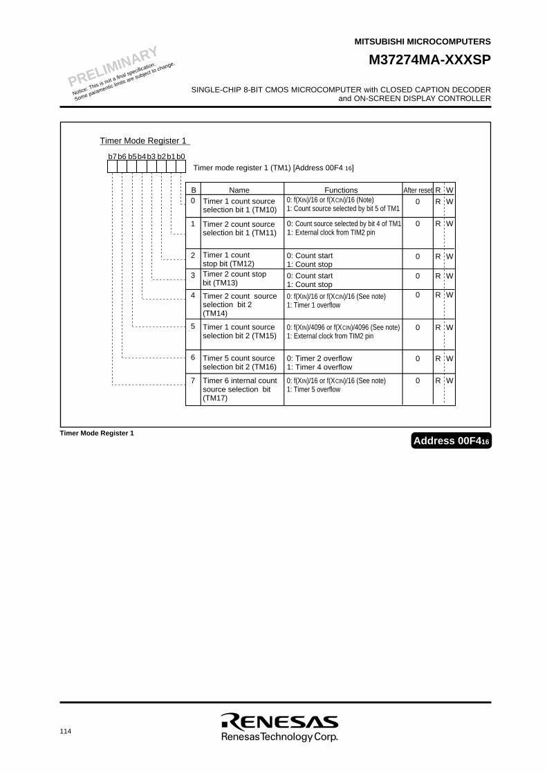
114
MITSUBISHI MICROCOMPUTERS
SINGLE-CHIP 8-BIT CMOS MICROCOMPUTER with CLOSED CAPTION DECODERand ON-SCREEN DISPLAY CONTROLLER
M37274MA-XXXSP
PRELIMINARY
Notice: This is not a final specification.
Some paramentic limits are subject to change.
Timer Mode Register 1Address 00F4 16
b7b6 b5b4b3 b2b1b0
Timer mode register 1 (TM1) [Address 00F4 16]
B After reset W
Timer Mode Register 1
0
1
2
3
4
Name FunctionsTimer 1 count source selection bit 1 (TM10)
0: f(XIN)/16 or f(XCIN)/16 (Note)1: Count source selected by bit 5 of TM1
Timer 2 count source selection bit 1 (TM11)
0: Count source selected by bit 4 of TM11: External clock from TIM2 pin
Timer 1 count stop bit (TM12)
0: Count start1: Count stop
Timer 2 count stop bit (TM13)
0: Count start1: Count stop
Timer 2 count source selection bit 2 (TM14)
R
0
0
0
0
0
WR
WR
WR
WR
WR0: f(XIN)/16 or f(XCIN)/16 (See note)1: Timer 1 overflow
5 Timer 1 count source selection bit 2 (TM15)
0: f(XIN)/4096 or f(XCIN)/4096 (See note)1: External clock from TIM2 pin
0 WR
6 Timer 5 count source selection bit 2 (TM16)
0: Timer 2 overflow1: Timer 4 overflow
0 WR
7 Timer 6 internal count source selection bit (TM17)
0 WR0: f(XIN)/16 or f(XCIN)/16 (See note)1: Timer 5 overflow

115
MITSUBISHI MICROCOMPUTERS
SINGLE-CHIP 8-BIT CMOS MICROCOMPUTER with CLOSED CAPTION DECODERand ON-SCREEN DISPLAY CONTROLLER
M37274MA-XXXSP
PRELIMINARY
Notice: This is not a final specification.
Some paramentic limits are subject to change.
I2C Data Shift Register
Timer Mode Register 2
Address 00F5 16
Address 00F6 16
b7b6 b5b4b3 b2b1b0
Timer mode register 2 (TM2) [Address 00F5 16]
B After reset R W
Timer Mode Register 2
0Name Functions
Timer 3 count source selection bit (TM20)
0 R W
1, 4 Timer 4 count source selection bits (TM21, TM24)
0 R W
2
3
0
Timer 3 count stop bit (TM22)
0: Count start1: Count stop
Timer 4 count stop bit (TM23)
0: Count start1: Count stop
0
0
5 Timer 5 count stop bit (TM25)
0: Count start1: Count stop
0
6 Timer 6 count stop bit (TM26)
0: Count start1: Count stop
0
R W
R W
R W
R W
R W7 Timer 5 count source selection bit 1(TM27)
0: f(XIN)/16 or f(XCIN)/16 (See note)1: Count source selected by bit 6
of TM1
b0 0 0 : f(XIN)/16 or f(XCIN)/16 (See note) 0 1 : f(XCIN) 1 0 : 1 1 :
(b6 at address 00C716)
External clock from TIM3 pin
b4 b1 0 0 : Timer 3 overflow signal 0 1 : f(XIN)/16 or f(XCIN)/16 (See note) 1 0 : f(XIN)/2 or f(XCIN)/2 (See note) 1 1 : f(XCIN)
Note: Either f(XIN) or f(XCIN) is selected by bit 7 of the CPU mode register.
b7 b6 b5 b4 b3 b2 b1 b0
I C data shift register1(S0) [Address 00F616]
B Functions After reset R W
I C Data Shift Register
0to7
This is an 8-bit shift register to store receive data and write transmit data.
Indeterminate
2
2
Note: 2To write data into the I C data shift register after setting the MST bit to“0” (slave mode), keep an interval of 8 machine cycles or more.
Name
D0 to D7 R W

116
MITSUBISHI MICROCOMPUTERS
SINGLE-CHIP 8-BIT CMOS MICROCOMPUTER with CLOSED CAPTION DECODERand ON-SCREEN DISPLAY CONTROLLER
M37274MA-XXXSP
PRELIMINARY
Notice: This is not a final specification.
Some paramentic limits are subject to change.
I2C Status Register
I2C Address RegisterAddress 00F7 16
Address 00F8 16
b7 b6 b5 b4 b3 b2 b1 b0
0 Read/write bit(RBW)
1to7
Slave address(SAD0 to SAD6)
0: Read1: Write
0
0The address data transmitted from the master is compared with the contents of these bits.
I2C Address Register
I2C address register (S0D) [Address 00F7 16]
B Name Functions After reset R W
R —
R W
b7 b6 b5 b4 b3 b2 b1 b0
I2C status register (S1) [Address 00F8 16]
I2C Status Register
0
3
4
5
6, 7 b7 b6 0 0 : Slave recieve mode 0 1 : Slave transmit mode 1 0 : Master recieve mode 1 1 : Master transmit mode
1
2
0
0
0
0
0
B Name Functions After reset R W
Communication mode specification bits (TRX, MST)
0 : Bus free1 : Bus busy
Bus busy flag (BB)
0 : Interrupt request issued1 : No interrupt request issued
I2C-BUS interface interrupt request bit (PIN)
0 : Not detected1 : Detected
Arbitration lost detecting flag (AL) (See note)
0 : Address mismatch1 : Address match
Slave address comparison flag (AAS) (See note)
0 : No general call detected1 : General call detected
General call detecting flag (AD0) (See note)
0 : Last bit = “0 ”1 : Last bit = “1 ”
Last receive bit (LRB)(See note)
Note : These bits and flags can be read out, but cannnot be written.
Indeterminate R —
R —
R —
R —
R —
R W
0 R W
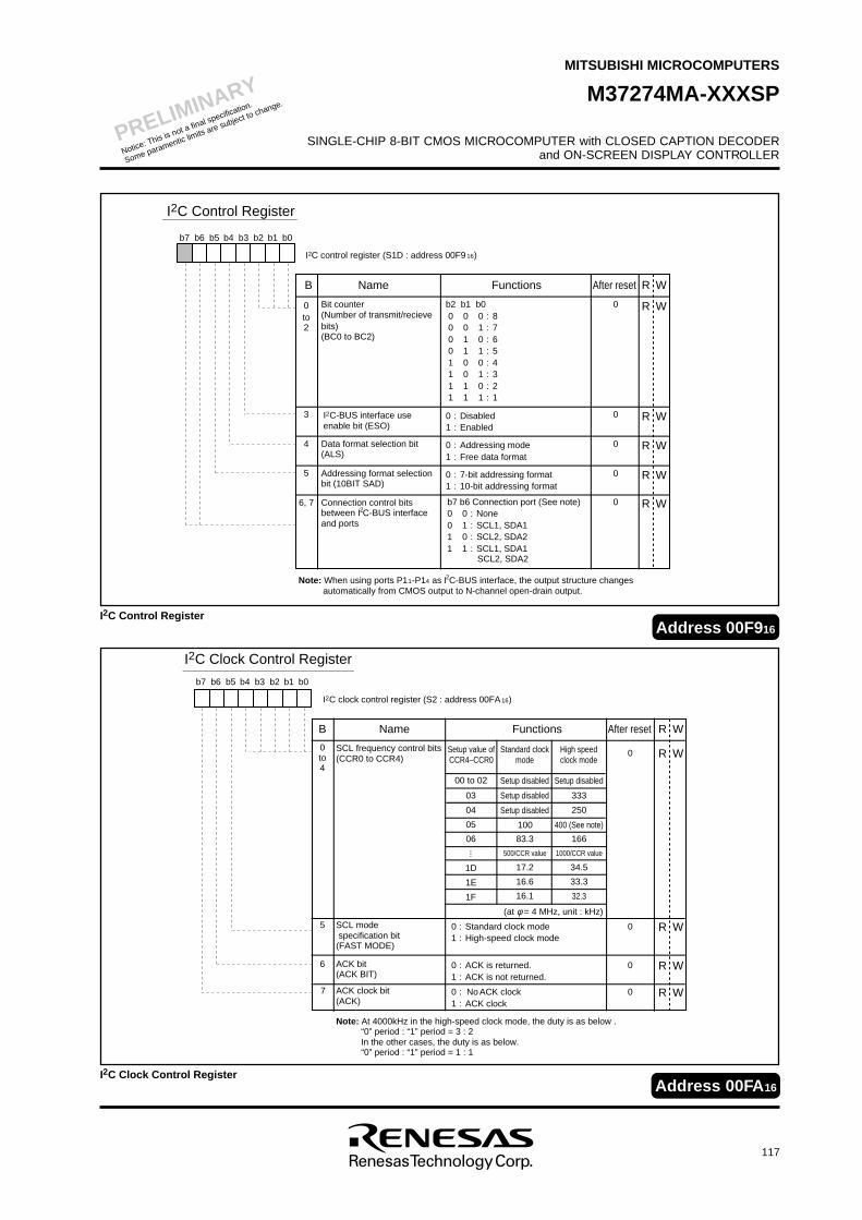
117
MITSUBISHI MICROCOMPUTERS
SINGLE-CHIP 8-BIT CMOS MICROCOMPUTER with CLOSED CAPTION DECODERand ON-SCREEN DISPLAY CONTROLLER
M37274MA-XXXSP
PRELIMINARY
Notice: This is not a final specification.
Some paramentic limits are subject to change.
I2C Clock Control Register
I2C Control RegisterAddress 00F9 16
Address 00FA 16
b7 b6 b5 b4 b3 b2 b1 b0
0to2
Bit counter (Number of transmit/recievebits)(BC0 to BC2)
b2 b1 b0 0 0 0 : 8 0 0 1 : 7 0 1 0 : 6 0 1 1 : 5 1 0 0 : 4 1 0 1 : 3 1 1 0 : 2 1 1 1 : 1
3 I2C-BUS interface use enable bit (ESO)
0 : Disabled1 : Enabled
4 Data format selection bit(ALS)
0 : Addressing mode1 : Free data format
5 Addressing format selection bit (10BIT SAD)
0 : 7-bit addressing format1 : 10-bit addressing format
6, 7 Connection control bits between I C-BUS interface and ports
b7 b6 Connection port (See note)0 0 : None0 1 : SCL1, SDA11 0 : SCL2, SDA21 1 : SCL1, SDA1 SCL2, SDA2
0
0
0
0
0
I2C control register (S1D : address 00F9 16)
I2C Control Register
B Name Functions After reset R W
Note: When using ports P11-P14 as I C-BUS interface, the output structure changes automatically from CMOS output to N-channel open-drain output.
2
2
R W
R W
R W
R W
R W
b7 b6 b5 b4 b3 b2 b1 b0
I2C clock control register (S2 : address 00FA16)
I2C Clock Control Register
0to4
SCL frequency control bits(CCR0 to CCR4)
7
5
6
SCL mode specification bit(FAST MODE)
0 : Standard clock mode1 : High-speed clock mode
0Standard clockmode
B Name Functions After reset R W
0
0
0
ACK bit(ACK BIT)
ACK clock bit(ACK)
0 : ACK is returned.1 : ACK is not returned.
0 : No ACK clock1 : ACK clock
High speedclock mode
Setup disabled Setup disabled00 to 02
Setup disabled 33303
Setup disabled 25004
100 400 (See note)05
83.3 16606
500/CCR value 1000/CCR value
...
17.2 34.51D
16.6 33.31E
16.1 32.31F
(at φ = 4 MHz, unit : kHz)
Note: At 4000kHz in the high-speed clock mode, the duty is as below . “0” period : “1” period = 3 : 2 In the other cases, the duty is as below. “0” period : “1” period = 1 : 1
Setup value of CCR4–CCR0
R W
R W
R W
R W

118
MITSUBISHI MICROCOMPUTERS
SINGLE-CHIP 8-BIT CMOS MICROCOMPUTER with CLOSED CAPTION DECODERand ON-SCREEN DISPLAY CONTROLLER
M37274MA-XXXSP
PRELIMINARY
Notice: This is not a final specification.
Some paramentic limits are subject to change.
Interrupt Request Register 1
CPU Mode RegisterAddress 00FB 16
Address 00FC 16
b7b6 b5b4b3 b2b1b0
B After reset R W
CPU Mode Register
0, 1
2
3, 4
0
1
Name Functions
Processor mode bits(CM0, CM1) 0 0: Single-chip mode
0 1:1 0: Not available1 1:
Fix these bits to “1.”
1Stack page selection bit (CM2) (See note)
1
b1 b0
0: 0 page1: 1 page
1 00
5
6 Main Clock (XIN–XOUT) stop bit(CM6)
CPU mode register (CPUM) (CM) [Address FB 16]
R W
R W
R W
R W
R W
XCOUT drivability selection bit (CM5)
0: LOW drive1: HIGH drive
0: Oscillating1: Stopped
7 Internal system clock selection bit(CM7)
R W0: XIN–XOUT selected (high-speed mode)
1: XCIN–XCOUT selected(high-speed mode)
Note: This bit is set to “1” after the reset release.
b7b6 b5b4b3 b2b1b0
Interrupt request register 1 (IREQ1) [Address 00FC
B Name Functions After reset R W
Interrupt Request Register 1
0 0 : No interrupt request issued1 : Interrupt request issued
Timer 1 interrupt request bit (TM1R)
1 Timer 2 interrupt request bit (TM2R)
2 Timer 3 interrupt request bit (TM3R)
3 Timer 4 interrupt request bit (TM4R)
4 OSD interrupt request bit (CRTR)
5 VSYNC interrupt request bit (VSCR)
6 A-D conversion • INT3 interrupt request bit (ADR)
7
0 : No interrupt request issued1 : Interrupt request issued
0 : No interrupt request issued1 : Interrupt request issued0 : No interrupt request issued1 : Interrupt request issued0 : No interrupt request issued1 : Interrupt request issued
0 : No interrupt request issued1 : Interrupt request issued0 : No interrupt request issued1 : Interrupt request issued
0
0
0
0
0
0
0
0
: “0” can be set by software, but “1” cannot be set.
—
16]
R
R
R
R
R
R
R
RNothing is assigned. This bit is a write disable bit.When this bit is read out, the value is “0.”
1
0
0

119
MITSUBISHI MICROCOMPUTERS
SINGLE-CHIP 8-BIT CMOS MICROCOMPUTER with CLOSED CAPTION DECODERand ON-SCREEN DISPLAY CONTROLLER
M37274MA-XXXSP
PRELIMINARY
Notice: This is not a final specification.
Some paramentic limits are subject to change.
Interrupt Control Register 1
Interrupt Request Register 2Address 00FD 16
Address 00FE 16
b7b6 b5b4b3 b2b1b0
Interrupt request register 2 (IREQ2) [Address 00FD
B Name Functions After reset R W
Interrupt Request Register 2
0 INT1 interrupt request bit (INT1R)
0 : No interrupt request issued1 : Interrupt request issued
1 Data slicer interruptrequest bit (DSR)
2 Serial I/O interruptrequest bit (SIOR)
3
4 INT2 interrupt request bit (INT2R)
5
7 Fix this bit to “0.”
0
0 : No interrupt request issued1 : Interrupt request issued
0 : No interrupt request issued1 : Interrupt request issued
0
: “0” can be set by software, but “1” cannot be set.
0
0
0
0
0
0
0 : No interrupt request issued1 : Interrupt request issued
16]
R
R
R
R
R
R
R W
f(XIN)/4096 interrupt request bit (1MSR)
0 : No interrupt request issued1 : Interrupt request issued
Multi-master I2C-BUS interrupt request bit (IICR)
0 : No interrupt request issued1 : Interrupt request issued
6 Timer 5 • 6 interrupt request bit (T56R)
0 : No interrupt request issued1 : Interrupt request issued
0
R
b7b6 b5b4b3 b2b1b0
Interrupt control register 1 (ICON1) [Address 00FE 16]
B Name Functions After reset R W
Interrupt Control Register 1
0 Timer 1 interrupt enable bit (TM1E)
0 : Interrupt disabled1 : Interrupt enabled
1 Timer 2 interrupt enable bit (TM2E)
2 Timer 3 interrupt enable bit (TM3E)
3
4 OSD interrupt enable bit (CRTE)
0 : Interrupt disabled1 : Interrupt enabled
0 : Interrupt disabled1 : Interrupt enabled
0 : Interrupt disabled1 : Interrupt enabled
0
0
0
0
0
0 R W
R W
R W
R W
R W
R —7 Nothing is assigned. This bit is a write disable bit. When this bit is read out, the value is “0.”
Timer 4 interrupt enable bit (TM4E)
0 : Interrupt disabled1 : Interrupt enabled
5 VSYNC interrupt enable bit (VSCR)
0 : Interrupt disabled1 : Interrupt enabled
0 R W
6 A-D conversion • INT3 interrupt enable bit (ADE)
0 : Interrupt disabled1 : Interrupt enabled
0 R W

120
MITSUBISHI MICROCOMPUTERS
SINGLE-CHIP 8-BIT CMOS MICROCOMPUTER with CLOSED CAPTION DECODERand ON-SCREEN DISPLAY CONTROLLER
M37274MA-XXXSP
PRELIMINARY
Notice: This is not a final specification.
Some paramentic limits are subject to change.
Clock Run-in Register 3
Interrupt Control Register 2Address 00FF 16
Address 0209 16
b7b6 b5b4b3 b2b1b0
Interrupt control register 2 (ICON2) [Address 00FF 16]
B Name Functions After reset R W
Interrupt Control Register 2
0 INT1 interrupt enable bit (INT1E)
0 : Interrupt disabled1 : Interrupt enabled
1 Data slicer interrupt enable bit (DSR)
2 Serial I/O interrupt enable bit (SIOE)
3
4 INT2 interrupt enable bit (INT2E)
0 : Interrupt disabled1 : Interrupt enabled
0 : Interrupt disabled1 : Interrupt enabled
0 : Interrupt disabled1 : Interrupt enabled
0
0
0
0
0 R W
R W
R W
R W
R W
f(XIN)/4096 interrupt enable bit (1MSE)
0 : Interrupt disabled1 : Interrupt enabled
5 Multi-master I2C-BUS interface interrupt enable bit (IICE)
0 : Interrupt disabled1 : Interrupt enabled
0 R W
6 Timer 5 • 6 interrupt enable bit (T56E)
0 : Interrupt disabled1 : Interrupt enabled
0 R W
7 Timer 5 • 6 interrupt switch bit (TM56S)
0 : Timer 51 : Timer 6
0 R W
b7 b6 b5 b4 b3 b2 b1 b0
Clock run-in register 3 (CR3) [Address 0209 16]
B Name Functions After reset R W
Clock Run-in Register 3
0to3
0 R W
4 R WIndeterminate
R W
Clock run-in count value of sub-data slice line (CR30 to CR33)
5
6 Interrupt mode selection bit (CR36)
Indeterminate R W
0: Data is not latched yet1: Data is latched
Data latch completion flag for caption data in sub-data slice line (CR34)
Data slice line selection bit for interrupt request (CR35)
0: Main data slice line1: Sub- data slice line
0: Interrupt occurs at endof data slice line
1: Interrupt occurs at completion of caption data latch
Nothing is assigned. This bit is a write disable bit.When this bit is read out, the value is “0.”
7
Indeterminate
Indeterminate R —

121
MITSUBISHI MICROCOMPUTERS
SINGLE-CHIP 8-BIT CMOS MICROCOMPUTER with CLOSED CAPTION DECODERand ON-SCREEN DISPLAY CONTROLLER
M37274MA-XXXSP
PRELIMINARY
Notice: This is not a final specification.
Some paramentic limits are subject to change.
PWM Mode Register 2
PWM Mode Register 1Address 020A 16
Address 020B 16
b7b6 b5b4b3 b2b1b0
PWM mode register 2 (PW) [Address 020B 16]
B After reset R W
PWM Mode Register 2
0
1
2
3
4
0
Name FunctionsP04/PWM0 output selection bit (PW0)
0 : P04 output1 : PWM0 output
P06/PWM2 output selection bit (PW2)
0 : P06 output1 : PWM2 output
P07/PWM3 output selection bit (PW3)
0 : P07 output1 : PWM3 output
P00/PWM4 output selection bit (PW4)
0 : P00 output1 : PWM4 output
5 P01/PWM5 output selection bit (PW5)
0: P01 output1: PWM5 output
7 Fix this bit to “0.”
P05/PWM1 output selection bit (PW1)
0 : P05 output1 : PWM1 output
0
0
0
0
0
0
R W
R W
R W
R W
R W
R W
R W
0
6 P02/PWM6 output selection bit (PW6)
0: P02 output1: PWM6 output
0 R W
b7b6 b5b4b3 b2b1b0
PWM mode register 1 (PN) [Address 020A 16]
B After reset R W
PWM Mode Register 1
0
4 to 7
1
0
Name Functions
DA/P03 output selection bit (PN1)
Indeterminate
0
Nothing is assigned. These bits are write disable bits. When these bits are read out, the values are “0.”
0 : P03 output1 : DA output
R W
R —
R W
PWM counts source selection bit (PN0)
0 : Count source supply1 : Count source stop
2 DA output polarity selection bit (PN2)
00 : Positive polarity1 : Negative polarity
R W
3 PWM output polarity selection bit (PN3)
00 : Positive polarity1 : Negative polarity
R W

122
MITSUBISHI MICROCOMPUTERS
SINGLE-CHIP 8-BIT CMOS MICROCOMPUTER with CLOSED CAPTION DECODERand ON-SCREEN DISPLAY CONTROLLER
M37274MA-XXXSP
PRELIMINARY
Notice: This is not a final specification.
Some paramentic limits are subject to change.
Data Slicer Control Register 3
Sync Pulse Counter RegisterAddress 020F 16
Address 0210 16
b7 b6 b5 b4 b3 b2 b1 b0
Sync pulse counter register (SYC) [Address 020F 16]
R W
Sync Pulse Counter Register
0to4
0 R —
6, 7 0 R —
Count value (SYC0 to SYC4)
5 0 R WCount source (SYC5) 0: HSYNC signal1: Composite sync signal
B After resetFunctionsName
Nothing is assigned. These bits are write disable bits.When these bits are read out, the values are “0.”
b7 b6 b5 b4 b3 b2 b1 b0
Data slicer control register 3 (DSC3) [Address 0210 16]
B Bit Functions After reset R W
Data Slicer Control Register 3
0
0 R W
0 R W
0: Main data slice line1: Sub-data slice line
Line selection bit for slice voltage (DSC30)
3to7
1, 2 Field to be sliced dataselection bit(DSC31, DSC32)
Definition of fields 1 (F1) and 2 (F2)
Hsep
VSYNC
Vsep
F1 :
Hsep
VSYNC
Vsep
F2 :
Field of sub-data slice line b2 b1
0 0 F2 0 1 F1 1 0 F1 and F2 1 1 F1 and F2
F2 F1F2 F1
Field for setting refernce voltage
Setting bit of sub-data slice line(DSC33 to DSC37)
0 R W

123
MITSUBISHI MICROCOMPUTERS
SINGLE-CHIP 8-BIT CMOS MICROCOMPUTER with CLOSED CAPTION DECODERand ON-SCREEN DISPLAY CONTROLLER
M37274MA-XXXSP
PRELIMINARY
Notice: This is not a final specification.
Some paramentic limits are subject to change.
Serial I/O Mode Register
Interrupt Input Polarity RegisterAddress 0212 16
Address 0213 16
b7 b6 b5 b4 b3 b2 b1 b0
Interrupt input polarity register (IP) [Address 0212 16]
B Name Functions After reset R W
Interrupt Input Polarity Register
00 to 2, 5
Fix these bits to “0.” R W
INT1 polarity switch bit(INT1POL)
0
0
3
0 : Positive polarity1 : Negative polarity
4
0 : Positive polarity1 : Negative polarity
6
INT2 polarity switch bit(INT2POL)
INT3 polarity switch bit(INT3POL)
0 R W
R W
R W
0 : Positive polarity1 : Negative polarity
0 0 0 0
00 : Positive polarity1 : Negative polarity
7 A-D conversion • INT3 interrupt source selection bit (RE7)
R W
b7b6 b5b4b3 b2b1b0
Serial I/O mode register (SM) [Address 0213 16]
B Name Functions After reset R W
Serial I/O Mode Register
0, 1 Internal synchronous clock selection bits (SM0, SM1)
b1 b0 0 0: f(XIN)/4 or f(XCIN)/4 0 1: f(XIN)/16 or f(XCIN)/16 1 0: f(XIN)/32 or f(XCIN)/32 1 1: f(XIN)/64 or f(XCIN)/64
2 Synchronous clock selection bit (SM2)
3 Port function selection bit (SM3)
6, 7
5 Transfer direction selection bit (SM5)
0
0: P11, P13
1: SCL1, SDA1
0: External clock1: Internal clock
0: LSB first1: MSB first
Fix these bits to “0.” 0
0
0
0
0
0 R W
R W
R W
R W
R W
R W
0
4 Port function selection bit (SM4)
0: P12, P141: SCL2, SDA2

124
MITSUBISHI MICROCOMPUTERS
SINGLE-CHIP 8-BIT CMOS MICROCOMPUTER with CLOSED CAPTION DECODERand ON-SCREEN DISPLAY CONTROLLER
M37274MA-XXXSP
PRELIMINARY
Notice: This is not a final specification.
Some paramentic limits are subject to change.
Clock Source Control RegisterAddress 0216 16
b7 b6 b5 b4 b3 b2 b1 b0
Clock source control register (CS) [Address 021616]
B Name Functions After reset R W
Clock Source Control Register
0 CC mode clock selection bit (CS0)
0 R W
1, 2 OSD mode clock selection bits (CS1, CS2)
0: Data slicer clock1: OSC1 clock
0 R W
3 EXOSD mode clock selection bit (CS3)
0: Data slicer clock1: OSC1 clock
0 R W
4, 5 0 W
6 Pre-divide ratio of layer 2 selection bit (CS6)
0: 11: 2
0 R W
7
0 0: Data slicer clock0 1: OSC1 clock1 0: Main clock (See note 1)1 1: Do not set
b2 b1
Test bit (See note 3)
ROSD oscillating mode selection bits (CS4, CS5) 0 0: 32 kHz oscillating mode
0 1: Input ports P63, P64
(See note 2)1 0: LC oscillating mode1 1: Ceramic • quartz-crystal
oscillating mode
b5 b4
Notes 1: When setting “102,” main clock is set as a clock in the CC mode and EXOSD mode regardless of bits 0, 3.
2: When selecting input ports P63 and P64, set bit 7 at address 00C716
to “1.”3: Be sure to set bit 7 to “0” for program of the mask and the EPROM
versions. For the emulator MCU version (M37274ERSS), be sure to set bit 7 to “1” when using the data slicer clock for software debugging.
R W0

125
MITSUBISHI MICROCOMPUTERS
SINGLE-CHIP 8-BIT CMOS MICROCOMPUTER with CLOSED CAPTION DECODERand ON-SCREEN DISPLAY CONTROLLER
M37274MA-XXXSP
PRELIMINARY
Notice: This is not a final specification.
Some paramentic limits are subject to change.
Raster Color Register
I/O Polarity Control RegisterAddress 0217 16
Address 0218 16
b7 b6 b5 b4 b3 b2 b1 b0
I/O polarity control register (PC) [Address 021716]
B Name Functions After reset R W
I/O Polarity Control Register
0 HSYNC input polarity switch bit (PC0)
0 : Positive polarity input1 : Negative polarity input
0
1 0 : Positive polarity input1 : Negative polarity input
0
2 R, G, B output polarity switch bit (PC2)
0 : Positive polarity output1 : Negative polarity output
0
3 0
VSYNC input polarity switch bit (PC1)
R W
R W
R W
R —
Note: Refer to the corresponding figure (P62).
0 : “ ” at even field
“ ” at odd field
1 : “ ” at even field
“ ” at odd field
4 OUT1 output polarity switch bit (PC4)
0 : Positive polarity output1 : Negative polarity output
0
5 OUT2 output polarity switch bit (PC5)
0 : Positive polarity output1 : Negative polarity output
0
6 Display dot line selection bit (PC6) (See note)
0
7 Field determination flag(PC7)
0 : Even field1 : Odd field
1
R W
R W
R W
R —
Nothing is assigned. Ths bit is a write disable bit.When this bit is read out, the value is “0.”
b7 b6 b5b4 b3 b2b1 b0
Raster color register (RC) [Address 0218 16]
B Name Functions After reset R W
Raster Color Register
0 Raster color R control bit (RC0)
0 : No output1 : Output
0
1 Raster color G control bit (RC1)
0 : No output1 : Output
0
2 0 : No output1 : Output
0Raster color B control bit (RC2)
R W
R W
R W
3, 4
0
6 Raster color OUT2 control bit (RC6)
0
R W
R W
5 0 : No output1 : Output
Raster color OUT1 control bit (RC5)
0 : No output1 : Output
7
0 R —
0 R W
0 0
OSD interrupt source selection bit (RC7)
0 : Interrupt occurs at end of OSD or EXOSD block display
1 : Interrupt occurs at end of CC mode block display
Nothing is assigned. These bits are write disable bits.When these bits are read out, the values are “0.”

126
MITSUBISHI MICROCOMPUTERS
SINGLE-CHIP 8-BIT CMOS MICROCOMPUTER with CLOSED CAPTION DECODERand ON-SCREEN DISPLAY CONTROLLER
M37274MA-XXXSP
PRELIMINARY
Notice: This is not a final specification.
Some paramentic limits are subject to change.
Border Color Register
Extra Font Color RegisterAddress 0219 16
Address 021B 16
b7b6 b5b4b3 b2b1b0
Extra font color register (EC) [Address 0219 16]
B After reset R W
Extra Font Color Register
0
3, 4
1
0
Name Functions
Extra font color G control bit (EC1)
0
Fix these bits to “0.”
0 : No output1 : Output
R W
R —
R W
Extra font color R control bit (EC0)
0 : No output1 : Output
2 Extra font color B control bit (EC2)
00 : No output1 : Output
R W
0 R W
00
Nothing is assigned. These bits are write disable bits. When these bits are read out, the values are “0.”
5to7
0
b7b6 b5b4b3 b2b1b0
Border color register (FC) [Address 021B 16]
B After reset R W
Border Color Register
0
3, 4
1
0
Name Functions
Border color G control bit (FC1)
0
Fix these bits to “0.”
0 : No output1 : Output
R W
R —
R W
Border color R control bit (FC0)
0 : No output1 : Output
2 Border color B control bit (FC2)
00 : No output1 : Output
R W
0 R W
00
Nothing is assigned. These bits are write disable bits. When these bits are read out, the values are “0.”
5to7
0

127
MITSUBISHI MICROCOMPUTERS
SINGLE-CHIP 8-BIT CMOS MICROCOMPUTER with CLOSED CAPTION DECODERand ON-SCREEN DISPLAY CONTROLLER
M37274MA-XXXSP
PRELIMINARY
Notice: This is not a final specification.
Some paramentic limits are subject to change.
Window H Register 2
Window H Register 1Address 021C 16
Address 021E 16
Window L Register 1Address 021D 16
b7 b6 b5b4 b3 b2b1 b0
Window H register 1 (WH1) [Address 021C 16]
B Name Functions After reset R W
Window H Register 1
0to7
Control bits of window top boundary (WN10 to WN17)(See note 1)
Top boundary position (low-order 8 bits)TH (setting value of low-order 2 bits of WH2 162
+ setting value of high-order 4 bits of WH1 161
+ setting value of low-order 4 bits of WH1 160)
Indeterminate R W
Notes 1: Set values except “00 16” to the WH1 when WH2 is “00 16.”2: TH is cycle of HSYNC.
b7 b6 b5b4 b3 b2b1 b0
Window L register 1 (WL1) [Address 021D 16]
B Name Functions After reset R W
Window L Register 1
0to7
Control bits of window top boundary (WL10 to WL17)(See note 1)
Top boundary position (low-order 8 bits)TH (setting value of low-order 2 bits of WL2 162
+ setting value of high-order 4 bits of WL1 161
+ setting value of low-order 4 bits of WL1 160)
Indeterminate R W
Notes 1: Set values fit for the following condition: (WH1+WH2)<(WL1+WL2)2: TH is cycle of HSYNC.
b7 b6 b5b4 b3 b2b1 b0
Window H register 2 (WH2) [Address 021E 16]
B Name Functions After reset R W
Window H Register 2
0, 1 Control bits of window top boundary (WN20 to WN27)(See note 1)
Top boundary position (high-order 2 bits)TH (setting value of low-order 2 bits of WH2 162
+ setting value of high-order 4 bits of WH1 161
+ setting value of low-order 4 bits of WH1 160)
Indeterminate R W
Notes 1: Set values except “00 16” to the WH1 when WH2 is “00 16.”2: TH is cycle of HSYNC.
Nothing is assigned. These bits are write disable bits. When these bits are read out, the values are indeterminate.
2to7
Indeterminate R —

128
MITSUBISHI MICROCOMPUTERS
SINGLE-CHIP 8-BIT CMOS MICROCOMPUTER with CLOSED CAPTION DECODERand ON-SCREEN DISPLAY CONTROLLER
M37274MA-XXXSP
PRELIMINARY
Notice: This is not a final specification.
Some paramentic limits are subject to change.
Vertical Position Register 2i
Window L Register 2Address 021F 16
Addresses 0230 16 to 023B 16
Vertical Position Register 1iAddresses 0220 16 to 022B 16
b7 b6 b5b4 b3 b2b1 b0
Window L register 2 (WL2) [Address 021F 16]
B Name Functions After reset R W
Window L Register 2
0, 1 Control bits of window top boundary (WL20 to WL27)(See note 1)
Top boundary position (high-order 2 bits)TH (setting value of low-order 2 bits of WL2 162
+ setting value of high-order 4 bits of WL1 161
+ setting value of low-order 4 bits of WL1 160)
Indeterminate R W
Notes 1: Set values fit for the following condition: (WH1+WH2)<(WL1+WL2)2: TH is cycle of HSYNC.
Nothing is assigned. These bits are write disable bits. When these bits are read out, the values are indeterminate.
2to7
Indeterminate R —
b7 b6 b5b4 b3 b2b1 b0
Vertical position register 1i (VP1i) (i = 1 to 12) [Addresses 0220 16 to 022B16]
B Name Functions After reset R W
Vertical Position Register 1i
0to7
Control bits of vertical display start positions(VP1i0 to VP1i7)(See note 1)
Vertical display start positions (low-order 8 bits)TH (setting value of low-order 2 bits of VP2i 162
+ setting value of low-order 4 bits of VP1i 161
+ setting value of low-order 4 bits of VP1i 160)
Indeterminate R W
Notes 1: Set values except “00 16” “0116” to VP1i when VP2i is “00 16.”2: TH is cycle of HSYNC.
b7 b6 b5b4 b3 b2b1 b0
Vertical position register 2i (VP2i) (i = 1 to 12) [Addresses 0230 16 to 023B16]
B Name Functions After reset R W
Vertical Position Register 2i
0, 1 Control bits of vertical display start positions(VP1i0 to VP1i7)(See note 1)
Vertical display start positions (high-order 2 bits)TH (setting value of low-order 2 bits of VP2i 162
+ setting value of low-order 4 bits of VP1i 161
+ setting value of low-order 4 bits of VP1i 160)
Indeterminate R W
Nothing is assigned. These bits are write disable bits. When these bits are read out, the values are indeterminate.
2to7
Indeterminate R —
Notes 1: Set values except “00 16” “0116” to VP1i when VP2i is “00 16.”2: TH is cycle of HSYNC.

129
MITSUBISHI MICROCOMPUTERS
SINGLE-CHIP 8-BIT CMOS MICROCOMPUTER with CLOSED CAPTION DECODERand ON-SCREEN DISPLAY CONTROLLER
M37274MA-XXXSP
PRELIMINARY
Notice: This is not a final specification.
Some paramentic limits are subject to change.
ROM Correction Enable RegisterAddress 0246 16
b7 b6 b5 b4 b3 b2 b1 b0
ROM correction enable register (RCR) [Address 0246 16]
B After reset R W
ROM Correction Enable Register
0 Block 1 enable bit (RC0)
Name Functions
0: Disabled1: Enabled
1 Block 2 enable bit (RC1) 0: Disabled1: Enabled
4to7
Nothing is assigned. These bits are write disable bits. When these bits are read out, the values are “0.”
0
0
0
R W
R W
R —
00
2, 3 Fix these bits to “0.” 0 R W

© 1997 MITSUBISHI ELECTRIC CORP.New publication, effective Nov. 1997.Specifications subject to change without notice.
Notes regarding these materials• These materials are intended as a reference to assist our customers in the selection of the Mitsubishi semiconductor product best suited to the customer’s application; they do not convey any license under any
intellectual property rights, or any other rights, belonging to Mitsubishi Electric Corporation or a third party.• Mitsubishi Electric Corporation assumes no responsibility for any damage, or infringement of any third-party’s rights, originating in the use of any product data, diagrams, charts or circuit application examples
contained in these materials.• All information contained in these materials, including product data, diagrams and charts, represent information on products at the time of publication of these materials, and are subject to change by Mitsubishi
Electric Corporation without notice due to product improvements or other reasons. It is therefore recommended that customers contact Mitsubishi Electric Corporation or an authorized Mitsubishi Semiconductorproduct distributor for the latest product information before purchasing a product listed herein.
• Mitsubishi Electric Corporation semiconductors are not designed or manufactured for use in a device or system that is used under circumstances in which human life is potentially at stake. Please contactMitsubishi Electric Corporation or an authorized Mitsubishi Semiconductor product distributor when considering the use of a product contained herein for any specific purposes, such as apparatus or systems fortransportation, vehicular, medical, aerospace, nuclear, or undersea repeater use.
• The prior written approval of Mitsubishi Electric Corporation is necessary to reprint or reproduce in whole or in part these materials.• If these products or technologies are subject to the Japanese export control restrictions, they must be exported under a license from the Japanese government and cannot be imported into a country other than the
approved destination.Any diversion or reexport contrary to the export control laws and regulations of Japan and/or the country of destination is prohibited.
• Please contact Mitsubishi Electric Corporation or an authorized Mitsubishi Semiconductor product distributor for further details on these materials or the products contained therein.
Keep safety first in your circuit designs!• Mitsubishi Electric Corporation puts the maximum effort into making semiconductor products better and more reliable, but there is always the possibility that trouble may occur with them. Trouble with
semiconductors may lead to personal injury, fire or property damage. Remember to give due consideration to safety when making your circuit designs, with appropriate measures such as (i) placement ofsubstitutive, auxiliary circuits, (ii) use of non-flammable material or (iii) prevention against any malfunction or mishap.

Rev. Rev.
No. date
1.0 First Edition
2.0 Information about copywright note, revision number, release date added (last page).
REVISION DESCRIPTION LIST
(1/1)
Revision Description
971130
M37274MA-XXXSP DATA SHEET
9706