SH7722 Data Sheet - Renesas
354
To our customers, Old Company Name in Catalogs and Other Documents On April 1 st , 2010, NEC Electronics Corporation merged with Renesas Technology Corporation, and Renesas Electronics Corporation took over all the business of both companies. Therefore, although the old company name remains in this document, it is a valid Renesas Electronics document. We appreciate your understanding. Renesas Electronics website: http://www.renesas.com April 1 st , 2010 Renesas Electronics Corporation Issued by: Renesas Electronics Corporation (http://www.renesas.com ) Send any inquiries to http://www.renesas.com/inquiry .
-
Upload
khangminh22 -
Category
Documents
-
view
1 -
download
0
Transcript of SH7722 Data Sheet - Renesas

To our customers,
Old Company Name in Catalogs and Other Documents
On April 1st, 2010, NEC Electronics Corporation merged with Renesas Technology
Corporation, and Renesas Electronics Corporation took over all the business of both companies. Therefore, although the old company name remains in this document, it is a valid Renesas Electronics document. We appreciate your understanding.
Renesas Electronics website: http://www.renesas.com
April 1st, 2010 Renesas Electronics Corporation
Issued by: Renesas Electronics Corporation (http://www.renesas.com)
Send any inquiries to http://www.renesas.com/inquiry.

Notice 1. All information included in this document is current as of the date this document is issued. Such information, however, is
subject to change without any prior notice. Before purchasing or using any Renesas Electronics products listed herein, please confirm the latest product information with a Renesas Electronics sales office. Also, please pay regular and careful attention to additional and different information to be disclosed by Renesas Electronics such as that disclosed through our website.
2. Renesas Electronics does not assume any liability for infringement of patents, copyrights, or other intellectual property rights of third parties by or arising from the use of Renesas Electronics products or technical information described in this document. No license, express, implied or otherwise, is granted hereby under any patents, copyrights or other intellectual property rights of Renesas Electronics or others.
3. You should not alter, modify, copy, or otherwise misappropriate any Renesas Electronics product, whether in whole or in part. 4. Descriptions of circuits, software and other related information in this document are provided only to illustrate the operation of
semiconductor products and application examples. You are fully responsible for the incorporation of these circuits, software, and information in the design of your equipment. Renesas Electronics assumes no responsibility for any losses incurred by you or third parties arising from the use of these circuits, software, or information.
5. When exporting the products or technology described in this document, you should comply with the applicable export control laws and regulations and follow the procedures required by such laws and regulations. You should not use Renesas Electronics products or the technology described in this document for any purpose relating to military applications or use by the military, including but not limited to the development of weapons of mass destruction. Renesas Electronics products and technology may not be used for or incorporated into any products or systems whose manufacture, use, or sale is prohibited under any applicable domestic or foreign laws or regulations.
6. Renesas Electronics has used reasonable care in preparing the information included in this document, but Renesas Electronics does not warrant that such information is error free. Renesas Electronics assumes no liability whatsoever for any damages incurred by you resulting from errors in or omissions from the information included herein.
7. Renesas Electronics products are classified according to the following three quality grades: “Standard”, “High Quality”, and “Specific”. The recommended applications for each Renesas Electronics product depends on the product’s quality grade, as indicated below. You must check the quality grade of each Renesas Electronics product before using it in a particular application. You may not use any Renesas Electronics product for any application categorized as “Specific” without the prior written consent of Renesas Electronics. Further, you may not use any Renesas Electronics product for any application for which it is not intended without the prior written consent of Renesas Electronics. Renesas Electronics shall not be in any way liable for any damages or losses incurred by you or third parties arising from the use of any Renesas Electronics product for an application categorized as “Specific” or for which the product is not intended where you have failed to obtain the prior written consent of Renesas Electronics. The quality grade of each Renesas Electronics product is “Standard” unless otherwise expressly specified in a Renesas Electronics data sheets or data books, etc.
“Standard”: Computers; office equipment; communications equipment; test and measurement equipment; audio and visual equipment; home electronic appliances; machine tools; personal electronic equipment; and industrial robots.
“High Quality”: Transportation equipment (automobiles, trains, ships, etc.); traffic control systems; anti-disaster systems; anti-crime systems; safety equipment; and medical equipment not specifically designed for life support.
“Specific”: Aircraft; aerospace equipment; submersible repeaters; nuclear reactor control systems; medical equipment or systems for life support (e.g. artificial life support devices or systems), surgical implantations, or healthcare intervention (e.g. excision, etc.), and any other applications or purposes that pose a direct threat to human life.
8. You should use the Renesas Electronics products described in this document within the range specified by Renesas Electronics, especially with respect to the maximum rating, operating supply voltage range, movement power voltage range, heat radiation characteristics, installation and other product characteristics. Renesas Electronics shall have no liability for malfunctions or damages arising out of the use of Renesas Electronics products beyond such specified ranges.
9. Although Renesas Electronics endeavors to improve the quality and reliability of its products, semiconductor products have specific characteristics such as the occurrence of failure at a certain rate and malfunctions under certain use conditions. Further, Renesas Electronics products are not subject to radiation resistance design. Please be sure to implement safety measures to guard them against the possibility of physical injury, and injury or damage caused by fire in the event of the failure of a Renesas Electronics product, such as safety design for hardware and software including but not limited to redundancy, fire control and malfunction prevention, appropriate treatment for aging degradation or any other appropriate measures. Because the evaluation of microcomputer software alone is very difficult, please evaluate the safety of the final products or system manufactured by you.
10. Please contact a Renesas Electronics sales office for details as to environmental matters such as the environmental compatibility of each Renesas Electronics product. Please use Renesas Electronics products in compliance with all applicable laws and regulations that regulate the inclusion or use of controlled substances, including without limitation, the EU RoHS Directive. Renesas Electronics assumes no liability for damages or losses occurring as a result of your noncompliance with applicable laws and regulations.
11. This document may not be reproduced or duplicated, in any form, in whole or in part, without prior written consent of Renesas Electronics.
12. Please contact a Renesas Electronics sales office if you have any questions regarding the information contained in this document or Renesas Electronics products, or if you have any other inquiries.
(Note 1) “Renesas Electronics” as used in this document means Renesas Electronics Corporation and also includes its majority-owned subsidiaries.
(Note 2) “Renesas Electronics product(s)” means any product developed or manufactured by or for Renesas Electronics.

www.renesas.com
Renesas 32-Bit RISC Microcomputer SH7780 Series R8A7722
-Preliminary -
SH7722
Data Sheet
32
Rev.1.00 2008.10

1. This document is provided for reference purposes only so that Renesas customers may select the appropriate Renesas products for their use. Renesas neither makes warranties or representations with respect to the accuracy or completeness of the information contained in this document nor grants any license to any intellectual property rights or any other rights of Renesas or any third party with respect to the information in this document. 2. Renesas shall have no liability for damages or infringement of any intellectual property or other rights arising out of the use of any information in this document, including, but not limited to, product data, diagrams, charts, programs, algorithms, and application circuit examples.3. You should not use the products or the technology described in this document for the purpose of military applications such as the development of weapons of mass destruction or for the purpose of any other military use. When exporting the products or technology described herein, you should follow the applicable export control laws and regulations, and procedures required by such laws and regulations.4. All information included in this document such as product data, diagrams, charts, programs, algorithms, and application circuit examples, is current as of the date this document is issued. Such information, however, is subject to change without any prior notice. Before purchasing or using any Renesas products listed in this document, please confirm the latest product information with a Renesas sales office. Also, please pay regular and careful attention to additional and different information to be disclosed by Renesas such as that disclosed through our website. (http://www.renesas.com )5. Renesas has used reasonable care in compiling the information included in this document, but Renesas assumes no liability whatsoever for any damages incurred as a result of errors or omissions in the information included in this document.6. When using or otherwise relying on the information in this document, you should evaluate the information in light of the total system before deciding about the applicability of such information to the intended application. Renesas makes no representations, warranties or guaranties regarding the suitability of its products for any particular application and specifically disclaims any liability arising out of the application and use of the information in this document or Renesas products. 7. With the exception of products specified by Renesas as suitable for automobile applications, Renesas products are not designed, manufactured or tested for applications or otherwise in systems the failure or malfunction of which may cause a direct threat to human life or create a risk of human injury or which require especially high quality and reliability such as safety systems, or equipment or systems for transportation and traffic, healthcare, combustion control, aerospace and aeronautics, nuclear power, or undersea communication transmission. If you are considering the use of our products for such purposes, please contact a Renesas sales office beforehand. Renesas shall have no liability for damages arising out of the uses set forth above.8. Notwithstanding the preceding paragraph, you should not use Renesas products for the purposes listed below: (1) artificial life support devices or systems (2) surgical implantations (3) healthcare intervention (e.g., excision, administration of medication, etc.) (4) any other purposes that pose a direct threat to human life Renesas shall have no liability for damages arising out of the uses set forth in the above and purchasers who elect to use Renesas products in any of the foregoing applications shall indemnify and hold harmless Renesas Technology Corp., its affiliated companies and their officers, directors, and employees against any and all damages arising out of such applications. 9. You should use the products described herein within the range specified by Renesas, especially with respect to the maximum rating, operating supply voltage range, movement power voltage range, heat radiation characteristics, installation and other product characteristics. Renesas shall have no liability for malfunctions or damages arising out of the use of Renesas products beyond such specified ranges.10. Although Renesas endeavors to improve the quality and reliability of its products, IC products have specific characteristics such as the occurrence of failure at a certain rate and malfunctions under certain use conditions. Please be sure to implement safety measures to guard against the possibility of physical injury, and injury or damage caused by fire in the event of the failure of a Renesas product, such as safety design for hardware and software including but not limited to redundancy, fire control and malfunction prevention, appropriate treatment for aging degradation or any other applicable measures. Among others, since the evaluation of microcomputer software alone is very difficult, please evaluate the safety of the final products or system manufactured by you. 11. In case Renesas products listed in this document are detached from the products to which the Renesas products are attached or affixed, the risk of accident such as swallowing by infants and small children is very high. You should implement safety measures so that Renesas products may not be easily detached from your products. Renesas shall have no liability for damages arising out of such detachment.12. This document may not be reproduced or duplicated, in any form, in whole or in part, without prior written approval from Renesas. 13. Please contact a Renesas sales office if you have any questions regarding the information contained in this document, Renesas semiconductor products, or if you have any other inquiries.
Notes regarding these materials

General Precautions on Handling of Product
1. Treatment of NC Pins
Note: Do not connect anything to the NC pins. The NC (not connected) pins are either not connected to any of the internal circuitry or are used as test pins or to reduce noise. If something is connected to the NC pins, the operation of the LSI is not guaranteed.
2. Treatment of Unused Input Pins
Note: Fix all unused input pins to high or low level. Generally, the input pins of CMOS products are high-impedance input pins. If unused pins are in their open states, intermediate levels are induced by noise in the vicinity, a pass-through current flows internally, and a malfunction may occur.
3. Processing before Initialization
Note: When power is first supplied, the product's state is undefined. The states of internal circuits are undefined until full power is supplied throughout the chip and a low level is input on the reset pin. During the period where the states are undefined, the register settings and the output state of each pin are also undefined. Design your system so that it does not malfunction because of processing while it is in this undefined state. For those products which have a reset function, reset the LSI immediately after the power supply has been turned on.
4. Prohibition of Access to Undefined or Reserved Addresses
Note: Access to undefined or reserved addresses is prohibited. The undefined or reserved addresses may be used to expand functions, or test registers may have been be allocated to these addresses. Do not access these registers; the system's operation is not guaranteed if they are accessed.
5. Reading from/Writing Reserved Bit of Each Register
Note: Treat the reserved bit of register used in each module as follows except in cases where the specifications for values which are read from or written to the bit are provided in the description. The bit is always read as 0. The write value should be 0 or one, which has been read immediately before writing. Writing the value, which has been read immediately before writing has the advantage of preventing the bit from being affected on its extended function when the function is assigned.


Preface
This LSI is a RISC (Reduced Instruction Set Computer) microcomputer which includes a Renesas Technology-original RISC CPU as its core, and the peripheral functions required to configure a system. This LSI includes the SH4AL-DSP extended functions that have functional upward compatibility with the SH4AL-DSP. Target Users: This manual was written for users who will be using this LSI in the design of
application systems. Users of this manual are expected to understand the fundamentals of electrical circuits, logical circuits, and microcomputers.
Objective: This manual was written to explain the hardware functions and electrical characteristics of this LSI to the above users.
Note: This data sheet contains references to the SH7722 Hardware Manual. The contents of the SH7722 Hardware Manual will be disclosed upon acceptance of a confidentiality agreement. For details, please contact a Renesas Technology sales representative.

Abbreviations
ALU Arithmetic Logic Unit
ASID Address Space Identifier
BSC Bus State Controller
CMT Compare Match Timer
CPG Clock Pulse Generator
CPU Central Processing Unit
DMA Direct Memory Access
DMAC Direct Memory Access Controller
DSP Digital Signal Processor
ETU Elementary Time Unit
FIFO First-In First-Out
FLCTL Flash Memory Controller
H-UDI User Debugging Interface
IIC Inter IC Bus
INTC Interrupt Controller
JTAG Joint Test Action Group
KEYSC Key Scan Interface
LCDC LCD Controller
LRU Least Recently Used
LSB Least Significant Bit
MMC Multi Media Card

MMU Memory Management Unit
MSB Most Significant Bit
PC Program Counter
PFC Pin Function Controller
RISC Reduced Instruction Set Computer
RWDT RCLK Watchdog Timer
SBSC SDRAM Bus State Controller
SCIF Serial Communication Interface with FIFO
SIO Serial Interface
SIOF Serial Interface with FIFO
SIU Sound Interface Unit
TAP Test Access Port
TLB Translation Lookaside Buffer
TMU Timer Unit
UART Universal Asynchronous Receiver/Transmitter
UBC User Break Controller
VIO Video I/O
VOU Video Output Unit
VPU Video Processing Unit
All trademarks and registered trademarks are the property of their respective owners.


Content
Section 1 Overview..................................................................................................1 1.1 Features................................................................................................................................. 1 1.2 Block Diagram.................................................................................................................... 14 1.3 Pin Assignments ................................................................................................................. 15
1.3.1 BGA-449 Pin Assignments................................................................................. 15 1.3.2 BGA-417 Pin Assignments................................................................................. 33
1.4 Pin Functions ...................................................................................................................... 51
Section 2 DSP Unit ................................................................................................63 2.1 Overview............................................................................................................................. 63
Section 3 Memory Management Unit (MMU) ......................................................67 3.1 Overview of MMU ............................................................................................................. 68
3.1.1 Address Spaces ................................................................................................... 70
Section 4 Caches ....................................................................................................77 4.1 Features............................................................................................................................... 77
Section 5 On-Chip Memory...................................................................................81 5.1 Features............................................................................................................................... 81
Section 6 Interrupt Controller (INTC) ...................................................................85 6.1 Features............................................................................................................................... 85 6.2 Input/Output Pins................................................................................................................ 87 6.3 Interrupt Sources................................................................................................................. 88
6.3.1 NMI Interrupt...................................................................................................... 88 6.3.2 IRQ Interrupts ..................................................................................................... 88 6.3.3 On-Chip Peripheral Module Interrupts ............................................................... 89 6.3.4 Interrupt Exception Handling and Priority.......................................................... 90
6.4 Operation ............................................................................................................................ 93 6.4.1 Interrupt Sequence .............................................................................................. 93 6.4.2 Multiple Interrupts .............................................................................................. 96 6.4.3 Interrupt Masking by MAI Bit ............................................................................ 96 6.4.4 Interrupt Disabling Function in User Mode ........................................................ 97
6.5 Interrupt Response Time..................................................................................................... 98

Section 7 Bus State Controller (BSC) ...................................................................99 7.1 Features............................................................................................................................... 99 7.2 Input/Output Pins.............................................................................................................. 101 7.3 Area Overview.................................................................................................................. 103
7.3.1 Area Division.................................................................................................... 103
Section 8 Bus State Controller for SDRAM (SBSC) ..........................................105 8.1 Features............................................................................................................................. 105 8.2 Input/Output Pins.............................................................................................................. 107 8.3 Area Overview.................................................................................................................. 108
8.3.1 Address Map..................................................................................................... 108 8.3.2 Memory Bus Width .......................................................................................... 109 8.3.3 Data Alignment................................................................................................. 109
Section 9 Direct Memory Access Controller (DMAC).......................................111 9.1 Features............................................................................................................................. 111 9.2 Input/Output Pins.............................................................................................................. 113
Section 10 Clock Pulse Generator (CPG) ...........................................................115 10.1 Features............................................................................................................................. 115 10.2 Block Diagram.................................................................................................................. 116 10.3 Input/Output Pins.............................................................................................................. 118
Section 11 Reset and Power-Down Modes .........................................................119 11.1 Features............................................................................................................................. 119
11.1.1 Division of Power-Supply Areas ...................................................................... 119 11.1.2 Types of Resets and Power-Down Modes ........................................................ 120
11.2 Input/Output Pins.............................................................................................................. 121
Section 12 RCLK Watchdog Timer (RWDT).....................................................123 12.1 Features............................................................................................................................. 123 12.2 Input/Output Pins for RWDT............................................................................................ 124
Section 13 Timer Unit (TMU).............................................................................125 13.1 Features............................................................................................................................. 125
Section 14 16-Bit Timer Pulse Unit (TPU) .........................................................127 14.1 Features............................................................................................................................. 127 14.2 Block Diagram.................................................................................................................. 129 14.3 Input/Output Pin ............................................................................................................... 130

Section 15 Compare Match Timer (CMT)...........................................................131 15.1 Features............................................................................................................................. 131
Section 16 Serial I/O (SIO)..................................................................................133 16.1 Features............................................................................................................................. 133 16.2 Input/Output Pins.............................................................................................................. 135
Section 17 Serial I/O with FIFO (SIOF)..............................................................137 17.1 Features............................................................................................................................. 137 17.2 Input/Output Pins.............................................................................................................. 139
Section 18 Serial Communication Interface with FIFO (SCIF) ..........................141 18.1 Features............................................................................................................................. 141 18.2 Input/Output Pins.............................................................................................................. 144
Section 19 SIM Card Module (SIM) ...................................................................145 19.1 Features............................................................................................................................. 145 19.2 Input/Output Pins.............................................................................................................. 147
Section 20 IrDA Interface (IrDA)........................................................................149 20.1 Features............................................................................................................................. 149 20.2 Input/Output Pins.............................................................................................................. 150
Section 21 I2C Bus Interface (IIC) .......................................................................151 21.1 Features............................................................................................................................. 151 21.2 Input/Output Pins.............................................................................................................. 153
Section 22 AND/NAND Flash Memory Controller (FLCTL) ............................155 22.1 Features............................................................................................................................. 155 22.2 Input/Output Pins.............................................................................................................. 160
Section 23 Realtime Clock (RTC) .......................................................................161 23.1 Features............................................................................................................................. 161 23.2 Input/Output Pin ............................................................................................................... 163
Section 24 Video Processing Unit (VPU)............................................................165 24.1 Features............................................................................................................................. 165
Section 25 Video I/O (VIO).................................................................................171 25.1 Features............................................................................................................................. 171

25.2 Functional Overview of CEU ........................................................................................... 174 25.3 Pin Configuration of CEU ................................................................................................ 177
Section 26 JPEG Processing Unit (JPU) .............................................................179 26.1 Features............................................................................................................................. 179
Section 27 LCD Controller (LCDC) ...................................................................181 27.1 Features............................................................................................................................. 181 27.2 Input/Output Pins.............................................................................................................. 185
Section 28 Video Output Unit (VOU).................................................................187 28.1 Features............................................................................................................................. 187 28.2 Pin Configuration.............................................................................................................. 189
Section 29 TS Interface (TSIF) ...........................................................................191 29.1 Features............................................................................................................................. 191 29.2 Input/Output Pins.............................................................................................................. 193
Section 30 Sound Interface Unit (SIU) ...............................................................195 30.1 Features............................................................................................................................. 195
30.1.1 RAM Overview................................................................................................. 201 30.2 Input/Output Pins.............................................................................................................. 202
Section 31 USB Function Module (USBF) .........................................................205 31.1 Features............................................................................................................................. 205 31.2 Input / Output Pins............................................................................................................ 207
Section 32 Key Scan Interface (KEYSC)............................................................209 32.1 Features............................................................................................................................. 209 32.2 Input/Output Pins.............................................................................................................. 211
Section 33 2D Graphics Accelerator (2DG)........................................................213 33.1 Features............................................................................................................................. 213
Section 34 Pin Function Controller (PFC) ..........................................................215 34.1 Overview .......................................................................................................................... 215
Section 35 I/O Ports.............................................................................................223 35.1 Port A................................................................................................................................ 223 35.2 Port B................................................................................................................................ 224

35.3 Port C ................................................................................................................................ 224 35.4 Port D................................................................................................................................ 225 35.5 Port E ................................................................................................................................ 225 35.6 Port F ................................................................................................................................ 226 35.7 Port G................................................................................................................................ 227 35.8 Port H................................................................................................................................ 227 35.9 Port J ................................................................................................................................. 228 35.10 Port K................................................................................................................................ 228 35.11 Port L ................................................................................................................................ 229 35.12 Port M ............................................................................................................................... 229 35.13 Port N................................................................................................................................ 230 35.14 Port Q................................................................................................................................ 230 35.15 Port R ................................................................................................................................ 231 35.16 Port S ................................................................................................................................ 231 35.17 Port T ................................................................................................................................ 232 35.18 Port U................................................................................................................................ 232 35.19 Port V................................................................................................................................ 233 35.20 Port W............................................................................................................................... 233 35.21 Port X................................................................................................................................ 234 35.22 Port Y................................................................................................................................ 234 35.23 Port Z ................................................................................................................................ 235
Section 36 User Break Controller (UBC) ............................................................237 36.1 Features............................................................................................................................. 237
Section 37 User Debugging Interface (H-UDI) ...................................................239 37.1 Features............................................................................................................................. 239 37.2 Input/Output Pins.............................................................................................................. 240
Section 38 Electrical Characteristics ...................................................................243 38.1 Absolute Maximum Ratings ............................................................................................. 243 38.2 Recommended Operating Conditions ............................................................................... 244 38.3 Power-On and Power-Off Order ....................................................................................... 245 38.4 DC Characteristics ............................................................................................................ 247 38.5 AC Characteristics ............................................................................................................ 251
38.5.1 Clock Timing .................................................................................................... 252 38.5.2 Interrupt Signal Timing..................................................................................... 255 38.5.3 BSC Bus Timing ............................................................................................... 256 38.5.4 SDRAM Timing (SDRAM Bus Timing).......................................................... 271 38.5.5 I/O Port Signal Timing...................................................................................... 291

38.5.6 DMAC Module Signal Timing ......................................................................... 292 38.5.7 SIM Module Signal Timing .............................................................................. 293 38.5.8 TPU Module Signal Timing.............................................................................. 293 38.5.9 SIO Module Signal Timing............................................................................... 294 38.5.10 SIOF Module Signal Timing ............................................................................ 297 38.5.11 SCIF Module Signal Timing............................................................................. 301 38.5.12 I2C Module Signal Timing ................................................................................ 303 38.5.13 FLCTL Module Signal Timing......................................................................... 305 38.5.14 VIO Module Signal Timing .............................................................................. 313 38.5.15 LCDC Module Signal Timing .......................................................................... 314 38.5.16 VOU Module Signal Timing ............................................................................ 318 38.5.17 TSIF Module Signal Timing............................................................................. 319 38.5.18 SIU Module Signal Timing............................................................................... 320 38.5.19 USB Transceiver Timing (Full-Speed) ............................................................. 321 38.5.20 KEYSC Module Signal Timing ........................................................................ 322 38.5.21 AC Characteristic Test Conditions ................................................................... 323
Appendix .............................................................................................................325 A. Pin States in Reset and Power-Down States ..................................................................... 326 B. Package Dimensions ......................................................................................................... 335

Section 1 Overview
Rev. 1.00 Oct. 9, 2008 Page 1 of 336
REJ03B0272-0100
Section 1 Overview
The SH7722 is a system LSI that incorporates an SH4AL-DSP microcontroller with a clock speed of up to 333 MHz as its core, together with a variety of functions required for multimedia applications. These include MPEG4 and H.264 accelerators, a 2D graphics accelerator, LCD controller, camera interface, and sound input/output module.
The SH4AL-DSP microcontroller is a 32-bit RISC-type SuperH architecture CPU with a DSP extension function, and is a new generation CPU core which is upward compatible with SH-1, SH2, and SH3-DSP at the instruction set level. Super scalar design in which two instructions are executed simultaneously allows high-speed processing. In addition, the strong power-management functions keep both operating current and standby current low.
This LSI is ideal for use in multimedia devices that require both high-performance operation and low power consumption.
1.1 Features
The features of this LSI are listed in table 1.1.

Section 1 Overview
Rev. 1.00 Oct. 9, 2008 Page 2 of 336
REJ03B0272-0100
Table 1.1 Features of This LSI
Item Features
CPU • Renesas Technology original architecture
• Upward compatible with SH-1, SH-2, SH-3, and SH3-DSP at instruction set
level
• 32-bit internal data bus
• General-register files
⎯ Sixteen 32-bit general registers (eight 32-bit shadow registers)
⎯ Seven 32-bit control registers
⎯ Four 32-bit system registers
• RISC-type instruction set (upward compatible with SH-1, SH-2, SH-3, and SH3-DSP)
⎯ Instruction length: 16-bit fixed length for improved code efficiency
⎯ Load/store architecture
⎯ Delayed branch instructions
⎯ Instructions executed with conditions
⎯ Instruction set based on the C language
• Super scalar design which executes two instructions simultaneously
• Instruction execution time: Two instructions per cycle (max.)
• Virtual address space: 4 Gbytes
• Space identifier ASID: 8 bits, 256 virtual address spaces
• On-chip multiplier
• Eight-stage pipeline

Section 1 Overview
Rev. 1.00 Oct. 9, 2008 Page 3 of 336
REJ03B0272-0100
Item Features
DSP • Mixture of 16-bit and 32-bit instructions
• 32-/40-bit internal data bus
• Multiplier, ALU, and barrel shifter
• 32-bit multiplier for 16-bit x 16-bit operations
• Large-capacity DSP data register files
⎯ Six 32-bit data registers
⎯ Two 40-bit data registers
• Extended Harvard architecture for DSP data bus
⎯ Two data buses
⎯ One instruction bus
• Maximum of four parallel operations: ALU, multiplication, two load/store operations
• Two addressing units to generate addresses for two memory access
• DSP data addressing modes:
⎯ Increment and indexing (with or without modulo addressing)
• Zero-overhead repeat loop control
• Conditional execution instructions
• User DSP mode and privileged DSP mode
Memory management unit (MMU)
• 4-Gbyte address space, 256 address spaces (8-bit ASID)
• Single virtual memory mode and multiple virtual memory mode
• Supports multiple page sizes: 1 Kbyte, 4 Kbytes, 64 Kbytes, or 1 Mbyte
• 4-entry full associative TLB for instructions
• 64-entry full associative TLB for instructions and operands
• Specifies replacement way by software and supports random replacement
algorithm
• Address mapping allows direct access to TLB contents
Note: This LSI does not support the 32-bit address extended mode or the 32-bit boot function.
Cache memory • Instruction cache (IC)
⎯ 32-kbyte, 4-way set associative
⎯ 32-byte block length
• Operand cache (OC)
⎯ 32-kbyte, 4-way set associative
⎯ 32-byte block length
⎯ Selectable write mode (copy-back or write-through)

Section 1 Overview
Rev. 1.00 Oct. 9, 2008 Page 4 of 336
REJ03B0272-0100
Item Features
X/Y memory • Three independent read/write ports
⎯ 8-/16-/32-bit access from CPU
⎯ Maximum of two 16-bit accesses from DSP
⎯ 8-/16-/32-/64-bit or 16-/32-byte access by SuperHyway bus master
• Total of 16 kbytes
• Memory protective functions specialized for DSP access in addition to
memory protective functions for CPU access
U memory • Two independent read/write ports
⎯ 8-/16-/32-bit access from CPU
⎯ 8-/16-/32-/64-bit or 16-/32-byte access by SuperHyway bus master
• Large 128-kbyte memory
IL memory (ILRAM)
• Three independent read/write ports
⎯ Instruction fetch access from CPU using virtual address
⎯ Instruction fetch access from CPU using physical address and 8-/16-/32-
bit operand access from CPU
⎯ 8-/16-/32-/64-bit or 16-/32-byte access by SuperHyway bus master
• Total of 4 kbytes
Interrupt controller (INTC)
• Nine external interrupt pins (NMI, IRQ7 to IRQ0)
⎯ NMI: Fall/rise selectable
⎯ IRQ: Fall/rise/high level/low level selectable
• On-chip peripheral interrupts: Priority can be specified for each module
Bus state controller (BSC)
• Supports SRAM, burst ROM, and PCMCIA interfaces.
• Physical address space is provided to support six areas in total: two areas (areas 0 and 4) of up to 64 Mbytes each and four areas (areas 5A, 5B, 6A,
and 6B) of up to 32 Mbytes each.
• The following settings can be individually made for each area.
⎯ Memory type: SRAM, NOR-Flash, burst ROM, PCMCIA
⎯ Data bus width: Selectable from 16 bits and 32 bits (16 bits when the selected data bus width for the SBSC is 64 bits.)
⎯ Number of wait cycles

Section 1 Overview
Rev. 1.00 Oct. 9, 2008 Page 5 of 336
REJ03B0272-0100
Item Features
Bus state controller for SDRAM (SBSC)
• 3.3 V SDR-SDRAM can be directly connected
• Physical address space is provided to support two areas (areas 2 and 3) of
up to 64 Mbytes
• Up to 128 Mbytes of SDRAM can be connected
• Data bus width: Selectable from 16 bits, 32 bits, and 64 bits (only 16 bits or 32 bits can be selected when the selected data bus width for the BSC is 32 bits.)
• Supports auto-refresh and self-refresh
• Auto-precharge mode or bank active mode can be selected
Direct memory access controller (DMAC)
• Number of channels: Six channels. One of these channels (channel 0) can receive an external request
• Address space: 4 Gbytes on architecture
• Data transfer length: Bytes, words (2 bytes), longwords (4 bytes), 16 bytes, and 32 bytes
• Maximum transfer count: 16,777,216 transfers
• Address mode: Dual address mode
• Transfer request: Selectable from three types of external request, on-chip
peripheral module request, and auto request
• Bus mode: Selectable from cycle steal mode (normal mode and intermittent mode) and burst mode
• Priority: Selectable from fixed channel priority mode and round-robin mode
• Interrupt request: Supports interrupt request to CPU at the end of data transfer
• Repeat function: Automatically resets the transfer source, destination, and
count at the end of DMA transfer
• Reload function: Automatically resets the transfer source and destination at the end of the specified number of DMA transfers

Section 1 Overview
Rev. 1.00 Oct. 9, 2008 Page 6 of 336
REJ03B0272-0100
Item Features
Clock pulse generator (CPG)
• Clock mode: Input clock selectable from external inputs (EXTAL and RCLK)
• Generates six types of system clocks
⎯ CPU clock (Iφ): Maximum 333.4 MHz (VDD = 1.25 to 1.35 V)
⎯ SH clock (SHφ): Maximum 133.4 MHz
⎯ U memory clock (Uφ): Maximum 133.4 MHz
⎯ SDRAM clock (B3φ): Maximum 133.4 MHz
⎯ Bus clock (Bφ): Maximum 66.7 MHz
⎯ Peripheral clock (Pφ): Maximum 33.4 MHz
• Supports power-down mode
⎯ Module standby function (stops clocks for individual modules.)
⎯ Sleep mode (stops clocks for the CPU core.)
⎯ Software standby mode (stops clocks in the LSI except the I/O area and
the RCLK operation area.)
⎯ U-standby mode (turns off the power in the LSI except the I/O area and the RCLK operation area.)
Timer unit (TMU) • Internal three-channel 32-bit timer
• Auto-reload type 32-bit down counter
• Internal prescaler for Pφ
• Interrupt request
Compare match timer (CMT)
• 32-bit timer of one channel (16 bits/32 bits can be selected)
• Source clock: RCLK
• Compare match function provided
• Interrupt requests
R watchdog timer (RWDT)
• One-channel watchdog timer operating at RCLK
• Operational in power-down modes
• Generates a system reset when a counter overflow occurs
Realtime clock (RTC)
• Operates at RCLK and includes clock and calendar functions
• Generates alarm interrupt and periodic interrupt
Timer pulse unit (TPU)
• Four pulse outputs possible
• Maximum of 4-phase PWM output possible

Section 1 Overview
Rev. 1.00 Oct. 9, 2008 Page 7 of 336
REJ03B0272-0100
Item Features
Serial I/O (SIO) • One channel
• Clocked synchronous mode (clock/data/strobe x 2)
• Data length programmable
• Programmable processing of clock polarity and data values in idle state
(such as low level or high impedance)
• Eight-bit fixed-length address, programmable data length
• Strobe position programmable, level/edge-ready
• MSB/LSB changeable
• Internal prescaler for Pφ
• Interrupt request
Serial I/O with FIFO (SIOF)
• Two channels
• Internal 64-byte transmit/receive FIFOs
• Supports 8-/16-bit data and 16-bit stereo audio input/output
• Sampling rate clock input selectable from Pφ and external pin
• Internal prescaler for Pφ
• Interrupt request and DMAC request
• SPI mode
⎯ Provides continuous full-duplex communication with SPI slave device in fixed master mode
⎯ Serial clock (SCK) rise or fall edge selectable for data sampling timing
⎯ SCK clock phase selectable for transmit timing
⎯ Three slave devices selectable
⎯ Transmit/receive data length fixed to 8 bits
Serial communication interface with FIFO (SCIF)
• Three channels
• Internal 16-byte transmit/receive FIFOs
• High-speed UART for Bluetooth
• Internal prescaler for Pφ
• Interrupt request and DMAC request
• Both asynchronous and clock synchronous serial communications possible

Section 1 Overview
Rev. 1.00 Oct. 9, 2008 Page 8 of 336
REJ03B0272-0100
Item Features
SIM card interface (SIM)
• One channel. Conforms to the ISO 7816-3 data protocol. (T = 0, T = 1) • Asynchronous half-duplex character transmission protocol • Data length: 8 bits
• Parity bit generation and check • Selectable output clock cycles per etu (elementary time unit) • Selectable direct convention/inverse convention
• On-chip prescaler • Switchable clock polarity (high or low) in idle state • Interrupt request and DMAC request
IrDA interface (IrDA)
• Conforms to version 1.2a • CRC calculation function
I2C bus interface (IIC)
• Supports single master transmission/reception • Supports standard mode (100 kHz) and high-speed mode (400 kHz)
AND/NAND flash memory controller (FLCTL)
• Directly connected memory interface with AND-/NAND-type flash memory • Read/write in sectors • Two types of transfer modes: Command access mode and sector access
mode (512-byte data + 16-byte management code: with 4-bit ECC) • Interrupt request and DMAC transfer request • Supports up to 4-Gbit of flash memory
Video processing unit (VPU)
• MPEG-4 single video object plane (VOP) encoding and decoding
• Applicable standard: MPEG-4 Simple Profile, MPEG-4 H.264 (Baseline)*
• Image size: Sub-QCIF to VGA
• Bit rate: Maximum 8 Mbps
• Motion detection: Layer tracking (Renesas Technology original method)
• Rate control: Control with quantizing amount predicted (Renesas Technology original method), both VOP and MB supported
• Interrupt request and no DMAC request (bus master function supported)
Note: Some of Baseline tools are not supported.

Section 1 Overview
Rev. 1.00 Oct. 9, 2008 Page 9 of 336
REJ03B0272-0100
Item Features
Video I/O (VIO) A module that provides the interface with camera module and image processing• CEU block (image capturing from camera module)
⎯ Camera module interface: Data (8 bits: YCbCr 4:2:2), horizontal sync signal (HD), vertical sync signal (VD)
⎯ Size of captured image: 5M pixels, 3M pixels, 2M pixels, UXGA, SXGA, XGA, SVGA, VGA, CIF, QVGA, QCIF, QQVGA, Sub-QCIF, etc.
⎯ Output image format: YCbCr (4:2:2/4:2:0) ⎯ Image format conversion function:
Reduced image generating prefilter function YCbCr 4:2:2 → YCbCr 4:2:2, YCbCr 4:2:0 YCbCr format (Y: 8 bits and CbCr: 16 bits)
• VEU block (image processing in memory) A. Video image processing function
Input image format: YCbCr image (Y/CbCr plane image), RGB image (RGB pack image) Output image format: YCbCr image (Y/CbCr plane image), RGB image (RGB pack image) Image processing function: Scaling image generating filter function YCbCr → RGB/RGB → YCbCr conversion function Dithering function (in RGB color subtraction)
B. Filter processing function Mirroring, vertical inversion, point symmetry, ±90-degree image conversion functions Deblocking filter Median filter
C. Video image processing and filter processing combined operation • BEU block (image blending)
A. PinP function Input image format: YCbCr image (Y/CbCr plane image), RGB image (RGB pack image) Output image format: YCbCr image (Y/CbCr plane image), RGB image (RGB pack image)
B. Graphic processing function Input graphic format: YCbCr/RGB image Output graphic format: YCbCr/RGB image
C. PinP and graphic combined operation Two PinP planes and one graphic plane can be blended simultaneously
D. Results of processing are written back to memory • Strobe control function (manual mode/auto mode) • Frame drop function (1/2, 1/3, 1/4, 1/5, or 1/6 drop) • Interrupt request is supported but DMAC request is not supported (with bus
master function)

Section 1 Overview
Rev. 1.00 Oct. 9, 2008 Page 10 of 336
REJ03B0272-0100
Item Features
JPEG processing unit (JPU)
• Conforming specification: JPEG baseline
• Operating precision: Conforming to JPEG Part 2 and ISO-IEC10918-2
• Color format: YCbCr 4:2:2/YCbCr 4:2:0
• Quantization tables: Four tables
• Huffman tables: Four tables (two AC tables and two DC tables)
• Target markers: Start of image (SOI), start of frame type 0 (SOF0), start of
scan (SOS), define quantization tables (DQT), define Huffman tables (DHT), define restart interval (DRI), restart (RSTm), and end of image (EOI)
• Interrupt request and no DMAC request (bus master function supported)
LCD controller (LCDC)
• Supported LCD panel: TFT color LCD
• Input data format: 8, 12, 16, 18, or 24 bpp
• LCD driver interface
⎯ Specialized LCD bus, independent of memory bus
⎯ RGB interface or 80-series CPU bus interface selectable
⎯ Bus width: 8, 9, 12, 16, 18, or 24 bits
⎯ One-pixel one-time, two-time, or three-time transfer mode selectable
⎯ Signal polarity and SYNC output timing and width programmable in RGB
interface
⎯ Access cycle programmable in 80-series CPU bus interface
• Dot clock: Bus clock, peripheral clock, or external clock selectable as the source clock
• Display data fetch: Continuous mode (according to the refresh rate of the LCD panel) and one-shot mode (according to the frame rate of the movie)
are supported. Image data can be fetched only for updated sections.
• Writing back the display data on the sub-LCD panel is supported.
• 256-entry, 24-bit-input/output built-in color palette
• An interrupt can be generated at the frame and the user-specified line
• Interrupt request and no DMAC request (bus master function supported)
Video output unit (VOU)
• Output format: 16-bit interface with 8-bit Y and 8-bit C
• Pixel frequency: 13.5 MHz, 27 MHz
• Partial image display: Any background color (specified through the register) + display image
• Supported image size: Sub-QCIF, QVGA, VGA, etc.
• Interrupt request and no DMAC request (bus master function supported)

Section 1 Overview
Rev. 1.00 Oct. 9, 2008 Page 11 of 336
REJ03B0272-0100
Item Features
TS interface (TSIF)
• Serial TS data input
• Filters 38 kinds of PIDs in total (The PID values of PAT and CAT packets are fixed. For PCR, video, and audio packets, the PID values are predefined.)
• Interrupt request and DMAC request
Sound interface unit (SIUA/SIUB)
• Internal two channels
• 16-bit stereo
• Supports PCM and I2S formats
• IEC60958 (SPDIF) supports stereo consumer mode
• Two sound output systems and two sound input systems
• DSP functions (FIR filter, IIR filter, equalizer, etc.)
• Serial I/O can be directly connected to external A/D or D/A converter.
• Internal prescaler
• Supports slave mode
• Interrupt request and DMA transfer request
USB function module (USBF)
• Supports USB 2.0 high-speed mode (480 Mbps) and full-speed mode (12 Mbps)
• Internal USB transceivers
• Eight endpoints are supported in total. The endpoint number is switchable.
• Provides Control (endpoint 0), Bulk-transfer (five endpoints in total), Interrupt (two endpoints in total), and Isochronous (two endpoints in total)
• Supports USB standard commands. The class/vendor commands are processed by firmware.
• FIFO buffers for endpoints (Bulk and Isochronous)
• Module input clock: 48 MHz
• Interrupt request and DMAC request
Key scan interface (KEYSC)
• Key scan: Chattering elimination in key input interrupt detection is possible
• Input or output bit numbers can be set to be programmable
(5 inputs/6 outputs, 6 inputs/5 outputs, 7 inputs/4 outputs.)
• Canceling software standby and U-standby modes by a key input
SD card host interface (SDHI)
• SD memory/SDIO interface supported
• Maximum operating frequency: 25 MHz
• Card detection function
• Interrupt request and DMA transfer request

Section 1 Overview
Rev. 1.00 Oct. 9, 2008 Page 12 of 336
REJ03B0272-0100
Item Features
2D graphics accelerator (2DG)
• BitBLT function
• Supports the quadrangle drawing function and associated drawing modes
• Figure drawing functions
⎯ Drawing rectangles and quadrangles
Filling with a single color or gradations between colors
Texture mapping
(Methods of mapping: Magnification, minification, and repetition)
(Filtering: Nearest neighbor interpolation, bilinear interpolation, and average pixel methods)
Coordinate transformation
Flipping graphics
⎯ Drawing horizontal straight lines
Drawing with a single color or gradations between colors
Texture mapping
(Methods of mapping: Magnification, minification, and repetition) (Filtering: Nearest neighbor interpolation, bilinear interpolation, and
average pixel methods)
• Pixel processing functions
⎯ Scissor testing, alpha blending, shadowing, raster operation (ROP), and
color conversion
⎯ Color key and writing-mask control
• Interrupt request and no DMAC request (bus master function supported)

Section 1 Overview
Rev. 1.00 Oct. 9, 2008 Page 13 of 336
REJ03B0272-0100
Item Features
I/O port • I/O port is switchable for each bit
User break controller (UBC)
• Debugging with user break interrupts supported
• Two break channels
• All of address, data value, access type, and data size can be set as break conditions
• Supports sequential break function
User debugging interface (H-UDI)
• Supports E10A emulator
• Realtime branch trace
Package • PRBG0449GA-A, 449-pin BGA package: 21 mm × 21 mm, 0.8 mm-pitch
• 417-pin LFBFA package: 13 mm × 13 mm, 0.5 mm-pitch
Power-supply voltage
• I/O: 3.0 to 3.6 V
• Internal: 1.15 to 1.35 V
Process • 90-nm CMOS, 7 metal layers

Section 1 Overview
Rev. 1.00 Oct. 9, 2008 Page 14 of 336
REJ03B0272-0100
1.2 Block Diagram
Figure 1.1 shows a block diagram of this LSI.
DSP
UBC
CPU
AUD
HPB
H-UDI
INTC
CPG
RWDT
DMAC
BSC
LCDC
SBSC
CPU:UBC:DSP:AUD:XYRAM:URAM:I-Cache:MMU:O-Cache:DMAC:VIO:VOU:VPU:JPU:LCDC:BSC:SIM:TSIF: SBSC:HPB:
TPU:RWDT:INTC:CPG:TMU:CMT:SIO: SIOF:SCIF:I2C:FLCTL:SIU:USBF:KEYSC:IrDA:SDHI:H-UDI:PFC: 2DG:RTC:
MMU
2DG
VIO
VOU
VPU
JPU
[Legend]
SIO
IrDA
SIOF
SCIF
I2C
FLCTL
SIU
USBF
KEYSC
SDHI
TSIF
SIM
RTC
TMU
CMT
TPU
I/O port(PFC)
External bus
External bus
External bus
XYRAM16 Kbytes
URAM128 Kbytes
I-Cache32 Kbytes
O-Cache32 Kbytes
ILRAM4 Kbytes
X bus
Inst
ruct
ion
bus
Per
iphe
ral b
us
Ope
rand
bus
Y bus
Inte
rnal
bus
for
cach
e an
d R
AM
Sup
erH
yway
bus
Central processing unitUser break controllerDigital signal processorAdvanced user debuggerX/Y memoryUser memoryInstruction cacheMemory management unitOperand (data) cacheDirect memory access controllerVideo I/OVideo output unitVideo processing unitJPEG processing unitLCD controllerBus state controllerSIM card interfaceTS interfaceSDRAM bus state controllerPeripheral bus bridge
Timer pulse unit RCLK watchdog timerInterrupt controllerClock pulse generatorTimer unitCompare match timerSerial I/OSerial I/O with FIFOSerial communication interface with FIFOI2C bus controllerAND/NAND flash memory controllerSound interface unitUSB function moduleKey scan interfaceIrDA interfaceSD card host interfaceUser debugging interfacePin function controller2D graphics acceleratorRealtime clock
Figure 1.1 Block Diagram

Section 1 Overview
Rev. 1.00 Oct. 9, 2008 Page 15 of 336
REJ03B0272-0100
1.3 Pin Assignments
1.3.1 BGA-449 Pin Assignments
Figure 1.2 and table 1.2 show the pin assignments of BGA-449.
20
19
18
17
23
22
21
16
15
14
13
12
11
10
9
8
7
3
2
1
6
5
4
A B C D E F G H J K L M N P R T U V W Y AA AB AC
25
24
AD AE
(Top View)
Figure 1.2 Pin Assignments (BGA-449)

Section 1 Overview
Rev. 1.00 Oct. 9, 2008 Page 16 of 336
REJ03B0272-0100
Table 1.2 Pin Assignments (BGA449)
Pin No. Pin Name Description Treatment of Unused Pin
A1 AV33 3.3 V power supply for USB reference power supply circuit
Always used
A2 VSS Ground Always used
A3 XTAL Clock output Open
A4 EXTAL External clock input Pulled down
A5 PTG3/AUDATA3 Port/AUD data output Open
A6 AUDCK AUD clock Open
A7 TCK H-UDI test clock input Open
A8 PTJ6 Port Open
A9 RCLK 32.768 kHz clock input Always used
A10 TSTMD Test mode setting Pulled up
A11 MD0 Mode setting pin Always used
A12 PTS1/SCIF0_RXD Port/SCIF receive data Open
A13 PTK4/SIUAOLR/SIOF1_SYNC Port/SIU port A sound output L-R clock/SIOF1 frame signal
Open
A14 PTK1/SIUAOSLD/SIOF1_TXD Port/SIU port A sound output serial data/SIOF1 output data
Open
A15 PTK0/SIUMCKA/SIUFCKA/ SIOF1_MCK
Port/SIU port A master clock input/SIU port A sampling clock output/SIOF1 master clock input
Open
A16 PTQ4/SIOF0_SYNC/ TS_SDEN
Port/SIOF frame signal/ TS serial data enable
Open
A17 PTF6/SIUMCKB/SIUFCKB/ SIOMCK
Port/SIU port B master clock input/SIU port B sampling clock output/SIO master clock
Open
A18 PTF2/SIUBILR/SIOD Port/SIU port B sound input L-R clock/SIO Transmit/receive data
Open
A19 PTD5/SDHID3 Port/SD data bus Pulled up
A20 PTD1/SDHICMD Port/SD command Open
A21 PTR3/CS6B/CE1B/LCDCS2 Port/chip select/LCD chip select 2 Open
A22 PTH6/LCDVSYN2/DACK0 Port/LCD vertical sync signal/DMA transfer request acknowledge
Open

Section 1 Overview
Rev. 1.00 Oct. 9, 2008 Page 17 of 336
REJ03B0272-0100
Pin No. Pin Name Description Treatment of Unused Pin
A23 VDD_PLL PLL power supply Always used
A24 VSS_PLL PLL ground Always used
A25 VSS Ground Always used
B1 AV12 1.2 V power supply for USB-PLL Always used
B2 VSS Ground Always used
B3 PTZ1/KEYIN0/IRQ6 Port/key input/interrupt request Open
B4 PTJ0/IRQ0 Port/interrupt request Open
B5 PTG4/AUDSYNC Port/AUD sync signal Open
B6 PTG0/AUDATA0 Port/AUD data output Open
B7 TDI H-UDI test data input Open
B8 PDSTATUS/PTJ5 Power-down status output/port Open
B9 RESETP Power-on reset Always used
B10 MD8 Mode setting pin Pulled up or Pulled down
B11 MD1 Mode setting pin Always used
B12 PTS2/SCIF0_SCK/TPUTO Port/SCIF serial clock/TPU output Open
B13 PTK5/SIUAIBT/SIOF1_SS1 Port/SIU port A sound input bit clock/SPI slave device select
Open
B14 PTK3/SIUAOBT/SIOF1_SCK Port/SIU port A sound output bit clock/SIOF1 serial clock
Open
B15 PTQ6/SIOF0_SS2/SIM_RST Port/SIOF0 slave device select/SIM reset
Open
B16 PTQ1/SIOF0_TXD/SIM_CLK/ IrDA_OUT
Port/SIOF0 transmit data/SIM clock/IrDA transmit data output
Open
B17 PTF4/SIUBOLR/SIOSTRB1 Port/SIU port B sound output L-R clock/SIO serial strobe
Open
B18 PTF1/SIUBISLD/SIORXD Port/SIU port B sound input serial data/SIO input data
Open
B19 PTD6/SDHIWP Port/SD write protect Pulled up
B20 PTD2/SDHID0 Port/SD data bus Pulled up
B21 WAIT/PTR2 WAIT/port Pulled up
B22 PTH5/LCDVSYN Port/LCD vertical sync signal Open
B23 VSS Ground Always used

Section 1 Overview
Rev. 1.00 Oct. 9, 2008 Page 18 of 336
REJ03B0272-0100
Pin No. Pin Name Description Treatment of Unused Pin
B24 VSS Ground Always used
B25 VSS_DLL DLL ground Always used
C1 DM USB DM pin Open
C2 VSS Ground Always used
C3 PTZ2/KEYIN1 Port/key input Open
C4 PTJ1/IRQ1 Port/interrupt request Open
C5 MPMD E10 ASE mode set input Open
C6 PTG2/AUDATA2 Port/AUD data output Open
C7 TRST H-UDI test reset input Always used
C8 TST Test pin (fix to VCCQ) Pulled up
C9 PTJ7/STATUS0 Port/status output Open
C10 RESETA System reset input Pulled up
C11 MD2 Mode setting pin Always used
C12 PTS4/SCIF0_CTS/SIUAISPD Port/SCIF CTS input/SPDIF input serial data
Open
C13 PTS0/SCIF0_TXD Port/SCIF transmit data Open
C14 PTK2/SIUAISLD/SIOF1_RXD Port/SIU port A sound input serial data/SIOF1 input data
Open
C15 PTQ5/SIOF0_SS1/TS_SPSYNC
Port/SPI slave device select/ TS serial data sync signal
Open
C16 PTQ0/SIOF0_MCK/IRQ3/SIM_D
Port/SIOF0 master clock input/ interrupt request/SIM data
Open
C17 PTF3/SIUBIBT/SIOSTRB0 Port/SIU port B sound input bit clock/SIO serial strobe
Open
C18 PTD4/SDHID2/ IRQ2 Port/SD data bus/interrupt request Pulled up
C19 PTD0/SDHICLK Port/SD clock Open
C20 PTD3/SDHID1 Port/SD data bus Pulled up
C21 PTR0/LCDVEPWC/LCDVEPWC2
Port/LCD power supply control/ LCD power supply control
Open
C22 PTH4/LCDDISP/LCDRS Port/LCD display enable signal/ LCD register select
Open
C23 PTH2/LCDDON/LCDDON2 Port/LCD display ON-OFF signal/LCD display ON-OFF signal
Open

Section 1 Overview
Rev. 1.00 Oct. 9, 2008 Page 19 of 336
REJ03B0272-0100
Pin No. Pin Name Description Treatment of Unused Pin
C24 PTX5/LCDD23 Port/LCD data bus Open
C25 VDD_DLL DLL power supply Always used
D1 DP USB DP pin Open
D2 DG12 1.2 V power supply ground for USB driver/receiver
Always used
D3 DG33 3.3 V power supply ground for USB driver/receiver
Always used
D4 VSS Ground Always used
D5 NMI Nonmaskable interrupt Pulled up
D6 ASEBRK/BRKAK E10A emulator brake input/acknowledge
Open
D7 PTG1/AUDATA1 Port/AUD data output Open
D8 TDO H-UDI test data output Open
D9 TMS H-UDI test mode select input Open
D10 RESETOUT Reset output Open
D11 MD5 Mode setting pin Always used
D12 PTS3/SCIF0_RTS/SIUAOSPD Port/SCIF RTS output/SPDIF output serial data
Open
D13 PTK6/SIUAILR/SIOF1_SS2 Port/SIU port A sound input L-R clock/SPI slave device select
Open
D14 PTQ3/SIOF0_SCK/TS_SCK Port/SIOF0 serial clock/ TS serial clock
Open
D15 PTQ2/SIOF0_RXD/TS_SDAT/IrDA_IN
Port/SIOF0 receive data/TS serial data input/IrDA receive data input
Open
D16 PTF5/SIUBOBT/SIOSCK Port/SIU port B sound output bit clock/SIO serial clock
Open
D17 PTF0/SIUBOSLD/SIOTXD Port/SIU port B sound output serial data/SIO output data
Open
D18 PTD7/SDHICD Port/SD card detection Pulled up
D19 PTR1/LCDDCK/LCDWR Port/LCD dot clock signal/write strobe Open
D20 PTR4/LCDRD Port/read strobe Open
D21 PTH7/LCDVCPWC/ LCDVCPWC2
Port/LCD power supply control/ LCD power supply control
Open

Section 1 Overview
Rev. 1.00 Oct. 9, 2008 Page 20 of 336
REJ03B0272-0100
Pin No. Pin Name Description Treatment of Unused Pin
D22 PTH3/LCDHSYN/LCDCS Port/LCD horizontal sync signal/ LCD chip select
Open
D23 PTX4/LCDD22 Port/LCD data bus Open
D24 PTX2/LCDD20 Port/LCD data bus Open
D25 PTX0/LCDD18/DV_CLK Port/LCD data bus/pixel clock output Open
E1 REFRIN External resistor pin for USB constant current circuit
Pulled down
E2 DG12 1.2 V power supply ground for USB driver/receiver
Always used
E3 DG33 3.3 V power supply ground for USB driver/receiver
Always used
E4 DV33 3.3 V power supply for USB driver/receiver (3.3 V)
Always used
E5 VSS Ground Always used
E6 VSS Ground Always used
E7 VSS Ground Always used
E8 VCCQ I/O power supply (3.3 V) Always used
E9 VCCQ I/O power supply (3.3 V) Always used
E10 VCCQ I/O power supply (3.3 V) Always used
E11 VCCQ I/O power supply (3.3 V) Always used
E12 VSS Ground Always used
E13 VSS Ground Always used
E14 VSS Ground Always used
E15 VCCQ I/O power supply (3.3 V) Always used
E16 VCCQ I/O power supply (3.3 V) Always used
E17 VCCQ I/O power supply (3.3 V) Always used
E18 VCCQ I/O power supply (3.3 V) Always used
E19 VSS Ground Always used
E20 VSS Ground Always used
E21 VSS Ground Always used
E22 PTX1/LCDD19/DV_CLKI Port/LCD data bus/video clock input Open
E23 PTH1/LCDD17/DV_HSYNC Port/LCD data bus/ VOU horizontal sync signal
Open

Section 1 Overview
Rev. 1.00 Oct. 9, 2008 Page 21 of 336
REJ03B0272-0100
Pin No. Pin Name Description Treatment of Unused Pin
E24 PTH0/LCDD16/DV_VSYNC Port/LCD data bus/ VOU vertical sync signal
Open
E25 PTL6/LCDD14/DV_D14 Port/LCD data bus/pixel data Open
F1 AG33 3.3 V power supply ground for USB reference power supply circuit
Always used
F2 AG12 1.2 V power supply ground for USB-PLL
Always used
F3 UG12 1.2 V power supply ground for USB-UTM480
Always used
F4 VBUS USB VBUS pin Pulled down
F5 DV33 3.3 V power supply for USB driver/receiver (3.3 V)
Always used
F21 VSS Ground Always used
F22 PTL7/LCDD15/DV_D15 Port/LCD data bus/pixel data Open
F23 PTL4/LCDD12/DV_D12 Port/LCD data bus/pixel data Open
F24 PTL3/LCDD11/DV_D11 Port/LCD data bus/pixel data Open
F25 PTL2/LCDD10/DV_D10 Port/LCD data bus/pixel data Open
G1 EXTALUSB 48-MHz oscillator connection pin input for USB
Pulled down
G2 PTZ3/KEYIN2 Port/key input Open
G3 VSS Ground Always used
G4 DV12 1.2 V power supply for USB driver/receiver (1.2 V)
Always used
G5 DV12 1.2 V power supply for USB driver/receiver (1.2 V)
Always used
G21 VSS Ground Always used
G22 PTX3/LCDD21 Port/LCD data bus Open
G23 PTL1/LCDD9/DV_D9 Port/LCD data bus/pixel data Open
G24 PTL0/LCDD8/DV_D8 Port/LCD data bus/pixel data Open
G25 PTM6/LCDD6/DV_D6 Port/LCD data bus/pixel data Open
H1 XTALUSB 48-MHz oscillator connection pin output for USB
Open
H2 PTZ5/KEYIN4/IRQ7 Port/key input/interrupt request Open
H3 PTZ4/KEYIN3 Port/key input Open

Section 1 Overview
Rev. 1.00 Oct. 9, 2008 Page 22 of 336
REJ03B0272-0100
Pin No. Pin Name Description Treatment of Unused Pin
H4 UV12 1.2 V power supply for USB-UTM480 Always used
H5 UV12 1.2 V power supply for USB-UTM480 Always used
H21 VCCQ I/O power supply (3.3 V) Always used
H22 PTM7/LCDD7/DV_D7 Port/LCD data bus/pixel data Open
H23 PTM5/LCDD5/DV_D5 Port/LCD data bus/pixel data Open
H24 PTM4/LCDD4/DV_D4 Port/LCD data bus/pixel data Open
H25 PTM3/LCDD3/DV_D3 Port/LCD data bus/pixel data Open
J1 PTY1/KEYOUT1 Port/key output Open
J2 PTY5/KEYOUT5/KEYIN5 Port/key output/key input Open
J3 PTY3/KEYOUT3 Port/key output Open
J4 PTY2/KEYOUT2 Port/key output Open
J5 PTY0/KEYOUT0 Port/key output Open
J21 VCCQ I/O power supply (3.3 V) Always used
J22 PTL5/LCDD13/DV_D13 Port/LCD data bus/pixel data Open
J23 PTM1/LCDD1/DV_D1 Port/LCD data bus/pixel data Open
J24 PTM2/LCDD2/DV_D2 Port/LCD data bus/pixel data Open
J25 PTM0/LCDD0/DV_D0 Port/LCD data bus/pixel data Open
K1 PTT3/FWE Port/AND-NAND flash memory write enable
Open
K2 PTT2/FSC Port/AND-NAND flash memory chip enable
Open
K3 PTT1/DREQ0 Port/DMA transfer request Open
K4 PTT0/FCDE Port/AND-NAND flash memory/command data enable
Open
K5 PTY4/KEYOUT4/KEYIN6 Port/key output/key input Open
K10 VDD Internal power supply (1.2 V) Always used
K11 VDD Internal power supply (1.2 V) Always used
K12 VDD Internal power supply (1.2 V) Always used
K13 VDD Internal power supply (1.2 V) Always used
K14 VDD Internal power supply (1.2 V) Always used
K15 VDD Internal power supply (1.2 V) Always used
K16 VDD Internal power supply (1.2 V) Always used

Section 1 Overview
Rev. 1.00 Oct. 9, 2008 Page 23 of 336
REJ03B0272-0100
Pin No. Pin Name Description Treatment of Unused Pin
K21 VCCQ I/O power supply (3.3 V) Always used
K22 HPD63/PTN7 SDRAM upper data bus/port Open
K23 HPD48/PTB0 SDRAM upper data bus/port Open
K24 HPD62/PTN6 SDRAM upper data bus/port Open
K25 HPD61/PTN5 SDRAM upper data bus/port Open
L1 PTU3/NAF1/VIO_D9 Port/AND-NAND flash memory data bus/VIO data input
Open
L2 PTU2/NAF0/VIO_D8 Port/AND-NAND flash memory data bus/VIO data input
Open
L3 PTU1/FRB/VIO_CLK2 Port/AND-NAND flash memory ready/busy/VIO clock
Open
L4 PTU0/FCE/VIO_HD2 Port/AND-NAND flash memory chip enable/VIO horizontal sync
Open
L5 VCCQ I/O power supply (3.3 V) Always used
L10 VDD Internal power supply (1.2 V) Always used
L11 VDD Internal power supply (1.2 V) Always used
L12 VSS Ground Always used
L13 VSS Ground Always used
L14 VSS Ground Always used
L15 VDD Internal power supply (1.2 V) Always used
L16 VDD Internal power supply (1.2 V) Always used
L21 VCCQ I/O power supply (3.3 V) Always used
L22 HPD49/PTB1 SDRAM upper data bus/port Open
L23 HPD50/PTB2 SDRAM upper data bus/port Open
L24 HPD60/PTN4 SDRAM upper data bus/port Open
L25 HPD59/PTN3 SDRAM upper data bus/port Open
M1 PTV1/NAF4/VIO_D12 Port/AND-NAND flash memory data bus/VIO data input
Open
M2 PTV0/NAF3/VIO_D11 Port/AND-NAND flash memory data bus/VIO data input
Open
M3 PTU4/NAF2/VIO_D10 Port/AND-NAND flash memory data bus/VIO data input
Open

Section 1 Overview
Rev. 1.00 Oct. 9, 2008 Page 24 of 336
REJ03B0272-0100
Pin No. Pin Name Description Treatment of Unused Pin
M4 PTT4/FOE/VIO_VD2 Port/AND-NAND flash memory output enable/VIO vertical sync
Open
M5 VSS Ground Always used
M10 VDD Internal power supply (1.2 V) Always used
M11 VSS Ground Always used
M12 VSS Ground Always used
M13 VSS Ground Always used
M14 VSS Ground Always used
M15 VSS Ground Always used
M16 VDD Internal power supply (1.2 V) Always used
M21 VSS Ground Always used
M22 HPD51/PTB3 SDRAM upper data bus/port Open
M23 HPD58/PTN2 SDRAM upper data bus/port Open
M24 HPD52/PTB4 SDRAM upper data bus/port Open
M25 HPD53/PTB5 SDRAM upper data bus/port Open
N1 PTV2/NAF5/VIO_D13 Port/AND-NAND flash memory data bus/VIO data input
Open
N2 SCL I2C serial clock input/output Pulled up
N3 PTV3/NAF6/VIO_D14 Port/AND-NAND flash memory data bus/VIO data input
Open
N4 PTV4/NAF7/VIO_D15 Port/AND-NAND flash memory data bus/VIO data input
Open
N5 VSS Ground Always used
N10 VDD Internal power supply (1.2 V) Always used
N11 VSS Ground Always used
N12 VSS Ground Always used
N13 VSS Ground Always used
N14 VSS Ground Always used
N15 VSS Ground Always used
N16 VDD Internal power supply (1.2 V) Always used
N21 VSS Ground Always used
N22 HPD56/PTN0 SDRAM upper data bus/port Open

Section 1 Overview
Rev. 1.00 Oct. 9, 2008 Page 25 of 336
REJ03B0272-0100
Pin No. Pin Name Description Treatment of Unused Pin
N23 HPD55/PTB7 SDRAM upper data bus/port Open
N24 HPD54/PTB6 SDRAM upper data bus/port Open
N25 HPD57/PTN1 SDRAM upper data bus/port Open
P1 SDA I2C serial data input/output Pulled up
P2 PTA1/VIO_D1 Port/VIO data input Open
P3 PTA2/VIO_D2 Port/VIO data input Open
P4 PTA0/VIO_D0/LCDLCLK Port/VIO data input/LCD clock source input
Open
P5 VSS Ground Always used
P10 VDD Internal power supply (1.2 V) Always used
P11 VSS Ground Always used
P12 VSS Ground Always used
P13 VSS Ground Always used
P14 VSS Ground Always used
P15 VSS Ground Always used
P16 VDD Internal power supply (1.2 V) Always used
P21 VSS Ground Always used
P22 HPD31 SDRAM lower data bus Open
P23 HPD30 SDRAM lower data bus Open
P24 HPD16 SDRAM lower data bus Open
P25 HPCLKR SDRAM interface synchronous clock Open
R1 PTA3/VIO_D3 Port/VIO data input Open
R2 PTA4/VIO_D4 Port/VIO data input Open
R3 PTA5/VIO_D5/SCIF1_TXD Port/VIO data input/SCIF transmit data
Open
R4 PTW2/VIO_HD/SCIF2_RXD Port/VIO horizontal sync/SCIF receive data
Open
R5 VCCQ I/O power supply (3.3 V) Always used
R10 VDD Internal power supply (1.2 V) Always used
R11 VDD Internal power supply (1.2 V) Always used
R12 VSS Ground Always used
R13 VSS Ground Always used

Section 1 Overview
Rev. 1.00 Oct. 9, 2008 Page 26 of 336
REJ03B0272-0100
Pin No. Pin Name Description Treatment of Unused Pin
R14 VSS Ground Always used
R15 VDD Internal power supply (1.2 V) Always used
R16 VDD Internal power supply (1.2 V) Always used
R21 VCCQ I/O power supply (3.3 V) Always used
R22 HPD19 SDRAM lower data bus Open
R23 HPD18 SDRAM lower data bus Open
R24 HPD29 SDRAM lower data bus Open
R25 HPD17 SDRAM lower data bus Open
T1 PTA6/VIO_D6/SCIF1_RXD Port/VIO data input/SCIF receive data Open
T2 PTA7/VIO_D7/SCIF1_SCK Port/VIO data input/SCIF serial clock Open
T3 PTW0/VIO_CLK/SCIF1_RTS Port/VIO clock input/SCIF RTS output Open
T4 RDWR Read/write signal Open
T5 VCCQ I/O power supply (3.3 V) Always used
T10 VDD Internal power supply (1.2 V) Always used
T11 VDD Internal power supply (1.2 V) Always used
T12 VDD Internal power supply (1.2 V) Always used
T13 VDD Internal power supply (1.2 V) Always used
T14 VDD Internal power supply (1.2 V) Always used
T15 VDD Internal power supply (1.2 V) Always used
T16 VDD Internal power supply (1.2 V) Always used
T21 VCCQ I/O power supply (3.3 V) Always used
T22 HPD26 SDRAM lower data bus Open
T23 HPD20 SDRAM lower data bus Open
T24 HPD27 SDRAM lower data bus Open
T25 HPD28 SDRAM lower data bus Open
U1 PTW1/VIO_VD/SCIF1_CTS Port/VIO vertical sync/ SCIF CTS input
Open
U2 PTW3/VIO_STEM/SCIF2_TXD Port/VIO strobe emission signal/ SCIF transmit data
Open

Section 1 Overview
Rev. 1.00 Oct. 9, 2008 Page 27 of 336
REJ03B0272-0100
Pin No. Pin Name Description Treatment of Unused Pin
U3 PTW4/VIO_STEX/SCIF2_SCK Port/VIO strobe emission signal/ SCIF serial clock
Open
U4 D3 Data bus Open
U5 VCCQ I/O power supply (3.3 V) Always used
U21 VCCQ I/O power supply (3.3 V) Always used
U22 HPD24 SDRAM lower data bus Open
U23 HPD22 SDRAM lower data bus Open
U24 HPD25 SDRAM lower data bus Open
U25 HPD21 SDRAM lower data bus Open
V1 PTW5/VIO_CKO/SCIF2_RTS Port/VIO clock output/ SCIF RTS output
Open
V2 PTW6/VIO_FLD/SCIF2_CTS Port/VIO field signal/SCIF CTS input Open
V3 CS5B/CE1A Chip select/PCMCIA card select Open
V4 CS4 Chip select Open
V5 VCCQ I/O power supply (3.3 V) Always used
V21 VCCQ I/O power supply (3.3 V) Always used
V22 HPDQM0 SDRAM interface lower LL side data mask
Open
V23 HPDQM1 SDRAM interface lower LU side data mask
Open
V24 HPDQM3 SDRAM interface lower UU side data mask
Open
V25 HPD23 SDRAM lower data bus Open
W1 PTX6/CS6A/CE2B Port/chip select/PCMCIA card select Open
W2 D15 Data bus Open
W3 D7 Data bus Open
W4 D14 Data bus Open
W5 VSS Ground Always used
W21 VSS Ground Always used
W22 HPA7 SDRAM interface address bus Open
W23 HPA15 SDRAM interface address bus Open
W24 HPA16 SDRAM interface address bus Open

Section 1 Overview
Rev. 1.00 Oct. 9, 2008 Page 28 of 336
REJ03B0272-0100
Pin No. Pin Name Description Treatment of Unused Pin
W25 HPDQM2 SDRAM interface lower UL side data mask
Open
Y1 D6 Data bus Open
Y2 D13 Data bus Open
Y3 D5 Data bus Open
Y4 D12 Data bus Open
Y5 VSS Ground Always used
Y21 VSS Ground Always used
Y22 HPA2 SDRAM interface address bus Open
Y23 HPA12 SDRAM interface address bus Open
Y24 HPA13 SDRAM interface address bus Open
Y25 HPA14 SDRAM interface address bus Open
AA1 D4 Data bus Open
AA2 D11 Data bus Open
AA3 D10 Data bus Open
AA4 D2 Data bus Open
AA5 VSS Ground Always used
AA6 VSS Ground Always used
AA7 VSS Ground Always used
AA8 VCCQ I/O power supply (3.3 V) Always used
AA9 VCCQ I/O power supply (3.3 V) Always used
AA10 VCCQ I/O power supply (3.3 V) Always used
AA11 VCCQ I/O power supply (3.3 V) Always used
AA12 VSS Ground Always used
AA13 VSS Ground Always used
AA14 VSS Ground Always used
AA15 VCCQ I/O power supply (3.3 V) Always used
AA16 VCCQ I/O power supply (3.3 V) Always used
AA17 VCCQ I/O power supply (3.3 V) Always used
AA18 VCCQ I/O power supply (3.3 V) Always used
AA19 VSS Ground Always used

Section 1 Overview
Rev. 1.00 Oct. 9, 2008 Page 29 of 336
REJ03B0272-0100
Pin No. Pin Name Description Treatment of Unused Pin
AA20 VSS Ground Always used
AA21 VSS Ground Always used
AA22 HPA9 SDRAM interface address Open
AA23 HPA8 SDRAM interface address Open
AA24 HPA10 SDRAM interface address Open
AA25 HPA11 SDRAM interface address Open
AB1 D9 Data bus Open
AB2 D1 Data bus Open
AB3 D8 Data bus Open
AB4 WE1/WE D15 to D8 write/PCMCIA memory write
Open
AB5 A25/PTE7 Address bus/port Open
AB6 A15 Address bus Open
AB7 A21 Address bus Open
AB8 A3 Address bus Open
AB9 A11 Address bus Open
AB10 A9 Address bus Open
AB11 A5 Address bus Open
AB12 IOIS16/PTC5 PCMCIA-IF 16 bits/port Pulled up
AB13 D31/HPD47 Upper data bus/ SDRAM upper data bus
Open
AB14 D27/HPD43 Upper data bus/ SDRAM upper data bus
Open
AB15 D26/HPD42 Upper data bus/ SDRAM upper data bus
Open
AB16 D24/HPD40 Upper data bus/ SDRAM upper data bus
Open
AB17 HPD0 SDRAM lower data bus Open
AB18 HPD4 SDRAM lower data bus Open
AB19 HPD9 SDRAM lower data bus Open
AB20 HPD7 SDRAM lower data bus Open
AB21 HPDQM7/PTC4 SDRAM interface upper UU side data mask/port
Open

Section 1 Overview
Rev. 1.00 Oct. 9, 2008 Page 30 of 336
REJ03B0272-0100
Pin No. Pin Name Description Treatment of Unused Pin
AB22 HPA4 SDRAM interface address bus Open
AB23 HPA5 SDRAM interface address bus Open
AB24 HPA6 SDRAM interface address bus Open
AB25 HPCLK SDRAM interface synchronous clock Open
AC1 D0 Data bus Open
AC2 CS0 Chip select Open
AC3 RD Read signal Open
AC4 WE3/ICIOWR D31 to D24 write/PCMCIA IO write Open
AC5 A23/PTE5 Address bus/port Open
AC6 A19 Address bus Open
AC7 A18 Address bus Open
AC8 A13 Address bus Open
AC9 A7 Address bus Open
AC10 A4 Address bus Open
AC11 A0 Address bus Open
AC12 PTC7 Port Open
AC13 D30/HPD46 Upper data bus/ SDRAM upper data bus
Open
AC14 D18/HPD34 Upper data bus/ SDRAM upper data bus
Open
AC15 D20/HPD36 Upper data bus/ SDRAM upper data bus
Open
AC16 D22/HPD38 Upper data bus/ SDRAM upper data bus
Open
AC17 HPD14 SDRAM lower data bus Open
AC18 HPD12 SDRAM lower data bus Open
AC19 HPD10 SDRAM lower data bus Open
AC20 HPD8 SDRAM lower data bus Open
AC21 HPDQM6/PTC3 SDRAM interface upper UL side data mask
Open
AC22 HPRAS SDRAM interface row address Open
AC23 HPCS3 SDRAM interface chip select Open

Section 1 Overview
Rev. 1.00 Oct. 9, 2008 Page 31 of 336
REJ03B0272-0100
Pin No. Pin Name Description Treatment of Unused Pin
AC24 HPA1 SDRAM interface address bus Open
AC25 HPA3 SDRAM interface address bus Open
AD1 VSS Ground Always used
AD2 VSS Ground Always used
AD3 WE0 D7 to D0 write Open
AD4 MD3 Data bus width set Always used
AD5 A22/PTE4 Address bus/port Open
AD6 A17 Address bus Open
AD7 A14 Address bus Open
AD8 A10 Address bus Open
AD9 A6 Address bus Open
AD10 A1 Address bus Open
AD11 CS5A/CE2A Chip select/PCMCIA card select Open
AD12 PTE0/IRQ4/BS Port/interrupt request/bus start Pulled up
AD13 D17/HPD33 Upper data bus/ SDRAM upper data bus
Open
AD14 D28/HPD44 Upper data bus/ SDRAM upper data bus
Open
AD15 D21/HPD37 Upper data bus/ SDRAM upper data bus
Open
AD16 D23/HPD39 Upper data bus/ SDRAM upper data bus
Open
AD17 HPD1 SDRAM lower data bus Open
AD18 HPD2 SDRAM lower data bus Open
AD19 HPD11 SDRAM lower data bus Open
AD20 HPD6 SDRAM lower data bus Open
AD21 HPDQM5/PTC2 SDRAM interface upper LU side data mask/port
Open
AD22 HPCAS SDRAM interface column address Open
AD23 HPCS2 SDRAM interface chip select Open
AD24 VSS Ground Always used
AD25 VSS Ground Always used

Section 1 Overview
Rev. 1.00 Oct. 9, 2008 Page 32 of 336
REJ03B0272-0100
Pin No. Pin Name Description Treatment of Unused Pin
AE1 VSS Ground Always used
AE2 VSS Ground Always used
AE3 WE2/ICIORD D23 to D16 write/PCMCIA IO read Open
AE4 A24/PTE6 Address bus/port Open
AE5 A20 Address bus Open
AE6 A16 Address bus Open
AE7 A12 Address bus Open
AE8 A8 Address bus Open
AE9 A2 Address bus Open
AE10 CKO System clock Open
AE11 PTE1/IRQ5 Port/interrupt request Pulled up
AE12 D16/HPD32 Upper data bus/ SDRAM upper data bus
Open
AE13 D29/HPD45 Upper data bus/ SDRAM upper data bus
Open
AE14 D19/HPD35 Upper data bus/ SDRAM upper data bus
Open
AE15 D25/HPD41 Upper data bus/ SDRAM upper data bus
Open
AE16 HPCLKD SDRAM interface synchronous clock Open
AE17 HPD15 SDRAM lower data bus Open
AE18 HPD13 SDRAM lower data bus Open
AE19 HPD3 SDRAM lower data bus Open
AE20 HPD5 SDRAM lower data bus Open
AE21 HPDQM4/PTC0 SDRAM interface upper LL side data bus/port
Open
AE22 HPRDWR SDRAM interface read/write Open
AE23 HPCKE SDRAM interface clock enable Open
AE24 VSS Ground Always used
AE25 VSS Ground Always used

Section 1 Overview
Rev. 1.00 Oct. 9, 2008 Page 33 of 336
REJ03B0272-0100
1.3.2 BGA-417 Pin Assignments
Figure 1.3 and table 1.3 show the pin assignments of BGA-417.
19
18
17
16
22
21
20
15
14
13
12
11
10
9
8
7
6
2
1
5
4
3
A B C D E F G H J K L M N P R T U V W Y AA AB AC
24
23
AD
(Top View)
Figure 1.3 Pin Assignments (BGA-417)

Section 1 Overview
Rev. 1.00 Oct. 9, 2008 Page 34 of 336
REJ03B0272-0100
Table 1.3 Pin Assignments (BGA-417)
Pin No. Pin Name Description Treatment of Unused Pin
A1 DV33 3.3 V power supply for USB driver/receiver (3.3 V)
Always used
A2 XTAL Clock output Open
A3 EXTAL External clock input Pulled down
A4 PTG4/AUDSYNC Port/AUD sync signal Open
A5 PTG0/AUDATA0 Port/AUD data output Open
A6 TRST H-UDI test reset input Always used
A7 TCK H-UDI test clock input Open
A8 STATUS0/PTJ7 Port/status output Open
A9 RCLK 32.768 kHz clock input Always used
A10 TSTMD Test mode setting Pulled up
A11 PTS4/SCIF0_CTS/SIUAISPD Port/SCIF CTS input/SPDIF input serial data
Open
A12 PTS0/SCIF0_TXD Port /SCIF transmission data Open
A13 PTK3/SIUAOBT/SIOF1_SCK Port/SIU port A sound output bit clock/SIOF1 serial clock
Open
A14 PTQ6/SIOF0_SS2/SIM_RST Port/SIOF0 slave device selection/SIM reset
Open
A15 PTQ2/SIOF0_RXD/TS_SDAT/IrDA_IN
Port/SIOF0 reception data/TS serial data input/IrDA reception data input
Open
A16 PTF5/SIUBOBT/SIOSCK Port/SIU port B sound output bit clock/SIO input data
Open
A17 PTF1/SIUBISLD/SIORXD Port/SIU port B sound input serial data/SIO input data
Open
A18 PTD5/SDHID3 Port/SD data bus Pulled up
A19 PTD0/SDHICLK Port/SD clock Open
A20 VDD_PLL PLL power supply Always used
A21 VSS_PLL PLL ground Always used
A22 VDD_DLL DLL power supply Always used

Section 1 Overview
Rev. 1.00 Oct. 9, 2008 Page 35 of 336
REJ03B0272-0100
Pin No. Pin Name Description Treatment of Unused Pin
A23 VSS_DLL DLL ground Always used
A24 VSS Ground Always used
B1 DM USB DM pin Open
B2 PTZ1/KEYIN0/IRQ6 Port/key input/interrupt request Open
B3 NMI Nonmaskable interrupt Pulled up
B4 PTG2/AUDATA2 Port/AUD data output Open
B5 AUDCK AUD clock Open
B6 TDI H-UDI test data input Open
B7 PDSTATUS/PTJ5 Power-down status output/port Open
B8 RESETP Power-on reset Always used
B9 MD8 Mode setting pin Always used
B10 MD1 Mode setting pin Always used
B11 PTS2/SCIF0_SCK/TPUTO Port/SCIF serial clock/TPU output Open
B12 PTK5/SIUAIBT/SIOF1_SS1 Port/SIU port A sound input bit clock/SIOF1 slave device selection
Open
B13 PTK1/SIUAOSLD/SIOF1_TXD Port/SIU port A sound output serial data/SIOF1 output data
Open
B14 PTQ4/SIOF0_SYNC/TS_SDEN Port/SIOF frame signal/IrDA port/TS serial data enable
Open
B15 PTQ0/SIOF0_MCK/IRQ3/ SIM_D
Port/SIOF0 master clock input/ interrupt request/SIM data
Open
B16 PTF3/SIUBIBT/SIOSTRB0 Port/SIU port B sound input bit clock/SIO serial strobe
Open
B17 PTD4/SDHID2/IRQ2 Port/SD data bus/interrupt request Pulled up
B18 PTD6/SDHIWP Port/SD write protect Pulled up
B19 PTD2/SDHID0 Port/SD data bus Pulled up
B20 PTR4/LCDRD Port/read strobe Open
B21 WAIT/PTR2 WAIT/port Pulled up
B22 PTH3/LCDHSYN/LCDCS Port/LCD horizontal sync signal/LCD chip selection
Open
B23 PTX5/LCDD23 Port/LCD data bus Open

Section 1 Overview
Rev. 1.00 Oct. 9, 2008 Page 36 of 336
REJ03B0272-0100
Pin No. Pin Name Description Treatment of Unused Pin
B24 PTX4/LCDD22 Port/LCD data bus Open
C1 DP USB DP pin Open
C2 DG33 3.3 V power supply ground for USB driver-receiver
Always used
C3 PTZ2/KEYIN1 Port/key input Open
C4 MPMD E10 ASE mode setting input Pulled up
C5 PTG3/AUDATA3 Port/AUD data output Open
C6 TDO H-UDI test data output Open
C7 TST Test pin (fixed at VCCQ level) Pulled up
C8 RESETOUT Reset output Open
C9 MD5 Mode setting pin Always used
C10 MD0 Mode setting pin Always used
C11 PTS1/SCIF0_RXD Port/SCIF reception data Open
C12 PTK4/SIUAOLR/SIOF1_SYNC Port/SIU port B sound output L-R clock/SIOF1 frame signal
Open
C13 PTK0/SIUMCKA/SIUFCKA/ SIOF1_MCK
Port/SIU port A master clock input/SIU port A sampling clock output/SIOF1 master clock input
Open
C14 PTQ3/SIOF0_SCK/TS_SCK Port/SIOF0 serial clock/IrDA clock/TS serial clock
Open
C15 PTF6/SIUMCKB/SIUFCKB/ SIOMCK
Port/SIU port B master clock input/SIU port B sampling clock output/SIO serial clock
Open
C16 PTF2/SIUBILR/SIOD Port/SIU port B sound input L-R clock/SIO transmission and reception data
Open
C17 PTD7/SDHICD Port/SD card detection Pulled up
C18 PTD3/SDHID1 Port/SD data bus Pulled up
C19 PTR0/LCDVEPWC/ LCDVEPWC2
Port/LCD power supply control/LCD power supply control
Open
C20 PTH7/LCDVCPWC/ LCDVCPWC2
Port/LCD power supply control/LCD power supply control
Open
C21 PTH6/LCDVSYN2/DACK0 Port/LCD vertical sync signal/ DMA transfer request acknowledge
Open

Section 1 Overview
Rev. 1.00 Oct. 9, 2008 Page 37 of 336
REJ03B0272-0100
Pin No. Pin Name Description Treatment of Unused Pin
C22 PTH2/LCDDON/LCDDON2 Port/LCD display ON-OFF signal/LCD display ON-OFF signal
Open
C23 PTX2/LCDD20 Port/LCD data bus Open
C24 PTX0/LCDD18/DV_CLK Port/LCD data bus/clock output Open
D1 DV12 1.2 V power supply for USB driver/receiver (1.2 V)
Always used
D2 DG12 1.2 V power supply ground for USB driver/receiver
Always used
D3 PTJ1/IRQ1 Port/Interrupt request Open
D4 ASEBRK/BRKAK E10A emulator brake input/acknowledge
Open
D5 PTG1/AUDATA1 Port/AUD data output Open
D6 TMS H-UDI test mode selection input Open
D7 PTJ6 Port Open
D8 RESETA Reset input Pulled up
D9 MD2 Mode setting pin Always used
D10 PTS3/SCIF0_RTS/SIUAOSPD Port/SCIF RTS output/SPDIF output serial data
Open
D11 PTK6/SIUAILR/SIOF1_SS2 Port/SIU port A sound input L-R clock/SIOF slave device selection
Open
D12 PTK2/SIUAISLD/SIOF1_RXD Port/SIU port A sound input serial data/SIOF1 input data
Open
D13 PTQ5/SIOF0_SS1/ TS_SPSYNC
Port/SIOF0 slave device selection/TS serial data sync signal
Open
D14 PTQ1/SIOF0_TXD/SIM_CLK/ IrDA_OUT
Port/SIOF0 transmission data/SIM clock/IrDA transmission data output
Open
D15 PTF4/SIUBOLR/SIOSTRB1 Port/SIU port B sound output L-R clock/SIO serial strobe
Open
D16 PTF0/SIUBOSLD/SIOTXD Port/SIU port B sound output serial data/SIO output data
Open
D17 PTD1/SDHICMD Port/SD command Open
D18 PTR3/CS6B/CE1B/LCDCS2 Port/Port/chip selection/LCD chip selection 2
Open

Section 1 Overview
Rev. 1.00 Oct. 9, 2008 Page 38 of 336
REJ03B0272-0100
Pin No. Pin Name Description Treatment of Unused Pin
D19 PTR1/LCDDCK/LCDWR Port/LCD dot clock signal/write strobe Open
D20 PTH5/LCDVSYN Port/LCD vertical sync signal Open
D21 PTH4/LCDDISP/LCDRS Port/LCD display enable signal/LCD register selection
Open
D22 PTX1/LCDD19/DV_CLKI Port/LCD data bus/video clock input Open
D23 PTH0/LCDD16/DV_VSYNC Port/LCD data bus/VOU vertical sync signal
Open
D24 PTL7/LCDD15/DV_D15 Port/LCD data bus/pixel data Open
E1 UV12 1.2 V power supply for USB-UTM480 Always used
E2 UG12 1.2 V power supply ground for USB-UTM480
Always used
E3 VBUS USB VBUS pin Pulled down
E4 PTJ0/IRQ0 Port/interrupt request Open
E21 PTX3/LCDD21 Port/LCD data bus Open
E22 PTH1/LCDD17/DV_HSYNC Port/LCD data bus/VOU horizontal sync signal
Open
E23 PTL4/LCDD12/DV_D12 Port/LCD data bus/pixel data Open
E24 PTL5/LCDD13/DV_D13 Port/LCD data bus/pixel data Open
F1 AG33 3.3 V power supply ground for USB standard current circuit
Always used
F2 REFRIN External resistor pin for USB constant current circuit
Pulled down
F3 PTZ4/KEYIN3 Port/key input Open
F4 PTZ3/KEYIN2 Port/key input Open
F6 VSS Ground Always used
F7 VCCQ I/O power supply (3.3 V) Always used
F8 VSS Ground Always used
F9 VCCQ I/O power supply (3.3 V) Always used
F10 VCCQ I/O power supply (3.3 V) Always used
F11 VSS Ground Always used
F12 VCCQ I/O power supply (3.3 V) Always used

Section 1 Overview
Rev. 1.00 Oct. 9, 2008 Page 39 of 336
REJ03B0272-0100
Pin No. Pin Name Description Treatment of Unused Pin
F13 VCCQ I/O power supply (3.3 V) Always used
F14 VSS Ground Always used
F15 VCCQ I/O power supply (3.3 V) Always used
F16 VCCQ I/O power supply (3.3 V) Always used
F17 VSS Ground Always used
F18 VCCQ I/O power supply (3.3 V) Always used
F19 VSS Ground Always used
F21 PTL6/LCDD14/DV_D14 Port/LCD data bus/pixel data Open
F22 PTL3/LCDD11/DV_D11 Port/LCD data bus/pixel data Open
F23 PTL2/LCDD10/DV_D10 Port/LCD data bus/pixel data Open
F24 PTL0/LCDD8/DV_D8 Port/LCD data bus/pixel data Open
G1 EXTALUSB 48 MHz-oscillator connection pin input for USB
Pulled down
G2 PTY1/KEYOUT1 Port/key output Open
G3 PTZ5/KEYIN4/IRQ7 Port/key input Open
G4 PTY0/KEYOUT0 Port/key output Open
G6 AG12 1.2 V power supply ground for USB-PLL
Always used
G7 VSS Ground Always used
G8 VDD Internal power supply (1.2 V) Always used
G9 VSS Ground Always used
G10 VSS Ground Always used
G11 VDD Internal power supply (1.2 V) Always used
G12 VSS Ground Always used
G13 VSS Ground Always used
G14 VDD Internal power supply (1.2 V) Always used
G15 VSS Ground Always used
G16 VSS Ground Always used
G17 VDD Internal power supply (1.2 V) Always used
G18 VSS Ground Always used

Section 1 Overview
Rev. 1.00 Oct. 9, 2008 Page 40 of 336
REJ03B0272-0100
Pin No. Pin Name Description Treatment of Unused Pin
G19 VCCQ I/O power supply (3.3 V) Always used
G21 PTL1/LCDD9/DV_D9 Port/LCD data bus/pixel data Open
G22 PTM7/LCDD7/DV_D7 Port/LCD data bus/pixel data Open
G23 PTM6/LCDD6/DV_D6 Port/LCD data bus/pixel data Open
G24 PTM4/LCDD4/DV_D4 Port/LCD data bus/pixel data Open
H1 XTALUSB 48 MHz-oscillator connection pin output for USB
Open
H2 PTY3/KEYOUT3 Port/key output Open
H3 PTY2/KEYOUT2 Port/key output Open
H4 PTY4/KEYOUT4/KEYIN6 Port/key output and input Open
H6 VSS Ground Always used
H7 VSS Ground Always used
H8 VSS Ground Always used
H18 VDD Internal power supply (1.2 V) Always used
H19 VSS Ground Always used
H21 PTM5/LCDD5/DV_D5 Port/LCD data bus/pixel data Open
H22 PTM3/LCDD3/DV_D3 Port/LCD data bus/pixel data Open
H23 PTM2/LCDD2/DV_D2 Port/LCD data bus/pixel data Open
H24 PTM0/LCDD0/DV_D0 Port/LCD data bus/pixel data Open
J1 PTY5/KEYOUT5/KEYIN5 Port/key output-input Open
J2 PTT1/DREQ0 Port/DMA transmission request Open
J3 PTT0/FCDE Port/command data enable Open
J4 PTT2/FSC Port/AND-NAND flash memory chip enable
Open
J6 VCCQ I/O power supply (3.3V) Always used
J7 AV33 3.3 V power supply for USB standard current circuit
Always used
J18 VSS Ground Always used
J19 VCCQ I/O power supply (3.3 V) Always used
J21 PTM1/LCDD1/DV_D1 Port/LCD data bus/pixel data Open
J22 HPD63/PTN7 SDRAM upper data bus/port Open

Section 1 Overview
Rev. 1.00 Oct. 9, 2008 Page 41 of 336
REJ03B0272-0100
Pin No. Pin Name Description Treatment of Unused Pin
J23 HPD48/PTB0 SDRAM upper data bus/port Open
J24 HPD62/PTN6 SDRAM upper data bus/port Open
K1 PTT3/FWE Port/AND-NAND flash memory write enable
Open
K2 PTU0/FCE/VIO_HD2 Port/AND-NAND flash memory chip enable/VIO horizontal sync
Open
K3 PTT4/FOE/VIO_VD2 Port/AND-NAND flash memory output enable/VIO vertical sync
Open
K4 PTU1/FRB/VIO_CLK2 Port/AND-NAND flash memory ready-busy/VIO clock
Open
K6 VCCQ I/O power supply (3.3 V) Always used
K7 AV12 1.2 V power supply for USB-PLL Always used
K18 VSS Ground Always used
K19 VCCQ I/O power supply (3.3 V) Always used
K21 HPD61/PTN5 SDRAM upper data bus/port Open
K22 HPD60/PTN4 SDRAM upper data bus/port Open
K23 HPD49/PTB1 SDRAM upper data bus/port Open
K24 HPD50/PTB2 SDRAM upper data bus/port Open
L1 PTU2/NAF0/VIO_D8 Port/AND-NAND flash memory data bus/VIO data input
Open
L2 PTU4/NAF2/VIO_D10 Port/AND-NAND flash memory data bus/VIO data input
Open
L3 PTU3/NAF1/VIO_D9 Port/AND-NAND flash memory data bus/VIO data input
Open
L4 PTV0/NAF3/VIO_D11 Port/AND-NAND flash memory data bus/VIO data input
Open
L6 VSS Ground Always used
L7 VDD Internal power supply (1.2 V) Always used
L18 VDD Internal power supply (1.2 V) Always used
L19 VSS Ground Always used
L21 HPD59/PTN3 SDRAM upper data bus/port Open
L22 HPD58/PTN2 SDRAM upper data bus/port Open

Section 1 Overview
Rev. 1.00 Oct. 9, 2008 Page 42 of 336
REJ03B0272-0100
Pin No. Pin Name Description Treatment of Unused Pin
L23 HPD51/PTB3 SDRAM upper data bus/port Open
L24 HPD52/PTB4 SDRAM upper data bus/port Open
M1 PTV1/NAF4/VIO_D12 Port/AND-NAND flash memory data bus/VIO data input
Open
M2 PTV3/NAF6/VIO_D14 Port/AND-NAND flash memory data bus/VIO data input
Open
M3 PTV2/NAF5/VIO_D13 Port/AND-NAND flash memory data bus/VIO data input
Open
M4 PTV4/NAF7/VIO_D15 Port/AND-NAND flash memory data bus/VIO data input
Open
M6 VCCQ I/O power supply (3.3 V) Always used
M7 VSS Ground Always used
M18 VSS Ground Always used
M19 VCCQ I/O power supply (3.3 V) Always used
M21 HPD57/PTN1 SDRAM upper data bus/port Open
M22 HPD56/PTN0 SDRAM upper data bus/port Open
M23 HPD53/PTB5 SDRAM upper data bus/port Open
M24 HPD54/PTB6 SDRAM upper data bus/port Open
N1 SCL I2C serial clock I/O Pulled up
N2 SDA I2C serial data I/O Pulled up
N3 PTA0/VIO_D0/LCDLCLK Port/VIO data input/LCD clock source input
Open
N4 PTA2/VIO_D2 Port/VIO data input Open
N6 VCCQ I/O power supply (3.3 V) Always used
N7 VSS Ground Always used
N18 VSS Ground Always used
N19 VCCQ I/O power supply (3.3 V) Always used
N21 HPD17 SDRAM lower data bus Open
N22 HPD16 SDRAM lower data bus Open
N23 HPD55/PTB7 SDRAM lower data bus/port Open
N24 HPCLKR SDRAM interface sync clock Open

Section 1 Overview
Rev. 1.00 Oct. 9, 2008 Page 43 of 336
REJ03B0272-0100
Pin No. Pin Name Description Treatment of Unused Pin
P1 PTA1/VIO_D1 Port/VIO data input Open
P2 PTA3/VIO_D3 Port/VIO data input Open
P3 PTA4/VIO_D4 Port/VIO data input Open
P4 PTA6/VIO_D6/SCIF1_RXD Port/VIO data input/SCIF reception data
Open
P6 VSS Ground Always used
P7 VDD Internal power supply (1.2 V) Always used
P18 VDD Internal power supply (1.2 V) Always used
P19 VSS Ground Always used
P21 HPD18 SDRAM lower data bus Open
P22 HPD19 SDRAM lower data bus Open
P23 HPD31 SDRAM lower data bus Open
P24 HPD30 SDRAM lower data bus Open
R1 PTA5/VIO_D5/SCIF1_TXD Port/VIO data input/SCIF transmission data
Open
R2 PTA7/VIO_D7/SCIF1_SCK Port/VIO data input/SCIF serial clock Open
R3 PTW0/VIO_CLK/SCIF1_RTS Port/VIO clock input/SCIF RTS output Open
R4 PTW2/VIO_HD/SCIF2_RXD Port/VIO horizontal sync/SCIF reception data
Open
R6 VCCQ I/O power supply (3.3 V) Always used
R7 VSS Ground Always used
R18 VSS Ground Always used
R19 VCCQ I/O power supply (3.3 V) Always used
R21 HPD21 SDRAM lower data bus Open
R22 HPD20 SDRAM lower data bus Open
R23 HPD29 SDRAM lower data bus Open
R24 HPD28 SDRAM lower data bus Open
T1 PTW1/VIO_VD/SCIF1_CTS Port/VIO vertical sync/SCIF CTS input
Open
T2 PTW3/VIO_STEM/SCIF2_TXD Port/VIO strobe emission signal/SCIF transmission data
Open

Section 1 Overview
Rev. 1.00 Oct. 9, 2008 Page 44 of 336
REJ03B0272-0100
Pin No. Pin Name Description Treatment of Unused Pin
T3 PTW4/VIO_STEX/SCIF2_SCK Port/VIO strobe dimmer signal/SCIF serial clock
Open
T4 PTW6/VIO_FLD/SCIF2_CTS Port/VIO field signal/SCIF CTS input Open
T6 VCCQ I/O power supply (3.3 V) Always used
T7 VSS Ground Always used
T18 VSS Ground Always used
T19 VCCQ I/O power supply (3.3 V) Always used
T21 HPD23 SDRAM lower data bus Open
T22 HPD22 SDRAM lower data bus Open
T23 HPD27 SDRAM lower data bus Open
T24 HPD26 SDRAM lower data bus Open
U1 PTW5/VIO_CKO/SCIF2_RTS Port/VIO clock output/SCIF RTS output
Open
U2 CS5B/CE1A Chip selection/chip selection Open
U3 CS4 Chip selection Open
U4 RDWR Read/write signal Open
U6 VSS Ground Always used
U7 VDD Internal power supply (1.2 V) Always used
U18 VDD Internal power supply (1.2 V) Always used
U19 VSS Ground Always used
U21 HPDQM0 SDRAM-I/F lower LL side data mask Open
U22 HPDQM2 SDRAM-I/F lower UL side data mask Open
U23 HPD25 SDRAM lower data bus Open
U24 HPD24 SDRAM lower data bus Open
V1 PTX6/CS6A/CE2B Port/chip selection/PCMCIA card selection
Open
V2 D15 Data bus Open
V3 D7 Data bus Open
V4 D5 Data bus Open
V6 VCCQ I/O power supply (3.3 V) Open
V7 VSS Ground Always used

Section 1 Overview
Rev. 1.00 Oct. 9, 2008 Page 45 of 336
REJ03B0272-0100
Pin No. Pin Name Description Treatment of Unused Pin
V8 VDD Internal power supply (1.2 V) Always used
V9 VSS Ground Always used
V10 VSS Ground Always used
V11 VDD Internal power supply (1.2 V) Always used
V12 VSS Ground Always used
V13 VSS Ground Always used
V14 VDD Internal power supply (1.2 V) Always used
V15 VSS Ground Always used
V16 VSS Ground Always used
V17 VDD Internal power supply (1.2 V) Always used
V18 VSS Ground Always used
V19 VCCQ I/O power supply (3.3 V) Always used
V21 HPA13 SDRAM interface address bus Open
V22 HPA15 SDRAM interface address bus Open
V23 HPDQM3 SDRAM-I/F lower LL side data mask Open
V24 HPDQM1 SDRAM-I/F lower UL side data mask Open
W1 D14 Data bus Open
W2 D6 Data bus Open
W3 D12 Data bus Open
W4 D3 Data bus Open
W6 VSS Ground Open
W7 VCCQ I/O power supply (3.3 V) Always used
W8 VSS Ground Always used
W9 VCCQ I/O power supply (3.3 V) Always used
W10 VCCQ I/O power supply (3.3 V) Always used
W11 VSS Ground Always used
W12 VCCQ I/O power supply (3.3 V) Always used
W13 VCCQ I/O power supply (3.3 V) Always used
W14 VSS Ground Always used
W15 VCCQ I/O power supply (3.3 V) Always used

Section 1 Overview
Rev. 1.00 Oct. 9, 2008 Page 46 of 336
REJ03B0272-0100
Pin No. Pin Name Description Treatment of Unused Pin
W16 VCCQ I/O power supply (3.3 V) Always used
W17 VSS Ground Always used
W18 VCCQ I/O power supply (3.3 V) Always used
W19 VSS Ground Always used
W21 HPA7 SDRAM interface address bus Open
W22 HPA11 SDRAM interface address bus Open
W23 HPA16 SDRAM interface address bus Open
W24 HPA14 SDRAM interface address bus Open
Y1 D13 Data bus Open
Y2 D4 Data bus Open
Y3 D2 Data bus Open
Y4 D8 Data bus Open
Y21 HPA5 SDRAM interface address bus Open
Y22 HPA6 SDRAM interface address bus Open
Y23 HPA12 SDRAM interface address bus Open
Y24 HPA10 SDRAM interface address bus Open
AA1 D11 Data bus Open
AA2 D10 Data bus Open
AA3 D9 Data bus Open
AA4 WE0 Write in D7 to D0 Open
AA5 A23/PTE5 Address bus/port Open
AA6 A21 Address bus Open
AA7 A15 Address bus Open
AA8 A11 Address bus Open
AA9 A7 Address bus Open
AA10 A3 Address bus Open
AA11 IOIS16/PTC5 16-bit PCMCIA interface/port Pulled up
AA12 D31/HPD47 Upper data bus/SDRAM upper data bus
Open
AA13 D28/HPD44 Upper data bus/SDRAM upper data bus
Open

Section 1 Overview
Rev. 1.00 Oct. 9, 2008 Page 47 of 336
REJ03B0272-0100
Pin No. Pin Name Description Treatment of Unused Pin
AA14 D26/HPD42 Upper data bus/SDRAM upper data bus
Open
AA15 D25/HPD41 Upper data bus/SDRAM upper data bus
Open
AA16 HPD0 SDRAM lower data bus Open
AA17 HPD13 SDRAM lower data bus Open
AA18 HPD4 SDRAM lower data bus Open
AA19 HPD6 SDRAM lower data bus Open
AA20 HPDQM4/PTC0 SDRAM interface upper LL side data mask
Open
AA21 HPCS3 SDRAM interface chip selection Open
AA22 HPA2 SDRAM interface address bus Open
AA23 HPA9 SDRAM interface address bus Open
AA24 HPA8 SDRAM interface address bus Open
AB1 D1 Data bus Open
AB2 CS0 Chip selection Open
AB3 WE1/WE Writ in D15 to D8/PCMCIA memory write
Open
AB4 WE3/ICIOWR Write in D31 to D24/PCMCIA IO write Open
AB5 A25/PTE7 Address bus/port Open
AB6 A17 Address bus Open
AB7 A13 Address bus Open
AB8 A9 Address bus Open
AB9 A5 Address bus Open
AB10 A1 Address bus Open
AB11 PTE1/IRQ5 Port/interrupt request Pulled up
AB12 D30/HPD46 Upper data bus/SDRAM upper data bus
Open
AB13 D29/HPD45 Upper data bus/SDRAM upper data bus
Open
AB14 D27/HPD43 Upper data bus/SDRAM upper data bus
Open

Section 1 Overview
Rev. 1.00 Oct. 9, 2008 Page 48 of 336
REJ03B0272-0100
Pin No. Pin Name Description Treatment of Unused Pin
AB15 D24/HPD40 Upper data bus/SDRAM upper data bus
Open
AB16 HPD1 SDRAM lower data bus Open
AB17 HPD3 SDRAM lower data bus Open
AB18 HPD10 SDRAM lower data bus Open
AB19 HPD7 SDRAM lower data bus Open
AB20 HPDQM7/PTC4 SDRAM interface upper UU side data mask
Open
AB21 HPCAS SDRAM interface column address Open
AB22 HPCS2 SDRAM interface chip selection Open
AB23 HPA3 SDRAM interface address bus Open
AB24 HPA4 SDRAM interface address bus Open
AC1 D0 Data bus Open
AC2 WE2/ICIORD Write in D23 to D16/PCMCIA IO read Open
AC3 A24/PTE6 Address bus/port Open
AC4 A20 Address bus Open
AC5 A18 Address bus Open
AC6 A14 Address bus Open
AC7 A10 Address bus Open
AC8 A6 Address bus Open
AC9 A2 Address bus Open
AC10 A0 Address bus Open
AC11 PTC7 Port Open
AC12 D16/HPD32 Upper data bus/SDRAM upper data bus
Open
AC13 D18/HPD34 Upper data bus/SDRAM upper data bus
Open
AC14 D20/HPD36 Upper data bus/SDRAM upper data bus
Open
AC15 D22/HPD38 Upper data bus/SDRAM upper data bus
Open
AC16 HPD15 SDRAM lower data bus Open

Section 1 Overview
Rev. 1.00 Oct. 9, 2008 Page 49 of 336
REJ03B0272-0100
Pin No. Pin Name Description Treatment of Unused Pin
AC17 HPD14 SDRAM lower data bus Open
AC18 HPD12 SDRAM lower data bus Open
AC19 HPD5 SDRAM lower data bus Open
AC20 HPD8 SDRAM lower data bus Open
AC21 HPDQM6/PTC3 SDRAM interface upper UL side data mask
Open
AC22 HPRAS SDRAM interface low address Open
AC23 HPA1 SDRAM interface address bus Open
AC24 HPCLK SDRAM interface sync clock Open
AD1 VSS Ground Always used
AD2 RD Read signal Open
AD3 MD3 Mode setting pin Open
AD4 A22/PTE4 Address bus/port Always used
AD5 A19 Address bus Open
AD6 A16 Address bus Open
AD7 A12 Address bus Open
AD8 A8 Address bus Open
AD9 A4 Address bus Open
AD10 CKO System clock Open
AD11 CS5A/CE2A Chip selection/chip selection Open
AD12 PTE0/IRQ4/BS Port/interrupt request/bus start Pulled up
AD13 D17/HPD33 Upper data bus/SDRAM upper data bus
Open
AD14 D19/HPD35 Upper data bus/SDRAM upper data bus
Open
AD15 D21/HPD37 Upper data bus/SDRAM upper data bus
Open
AD16 D23/HPD39 Upper data bus/SDRAM upper data bus
Open
AD17 HPCLKD SDRAM interface sync clock Open
AD18 HPD2 SDRAM lower data bus Open
AD19 HPD11 SDRAM lower data bus Open

Section 1 Overview
Rev. 1.00 Oct. 9, 2008 Page 50 of 336
REJ03B0272-0100
Pin No. Pin Name Description Treatment of Unused Pin
AD20 HPD9 SDRAM lower data bus Open
AD21 HPDQM5/PTC2 SDRAM interface upper LU side data mask
Open
AD22 HPRDWR SDRAM interface read-write Open
AD23 HPCKE SDRAM interface clock enable Open
AD24 VSS Ground Always used

Section 1 Overview
Rev. 1.00 Oct. 9, 2008 Page 51 of 336
REJ03B0272-0100
1.4 Pin Functions
Table 1.4 lists the pin functions.
Table 1.4 Pin Functions
Classification Symbol I/O Name Function
VDD Input Power supply Internal LSI power supply. Connect all VDD pins to system power supply. If there is any open pin, the system will not work.
VSS Input Ground Ground pin. Connect all VSS pins to system power supply (0 V). If there is any open pin, the system will not work.
VCCQ Input Power supply Power supply for I/O pins. Connect all VCC pins to system power supply. If there is any open pin, the system will not work.
Power supply
DV33, DV12, AV33, AV12, UV12
Input Power supply for USB
DV33: 3.3 V-digital power supply for USB
DV12: 1.2 V-digital power supply for USB
AV33: 3.3 V-analog power supply for USB
AV12: 1.2 V-analog power supply for USB
UV12: 1.2 V-digital power supply for USB

Section 1 Overview
Rev. 1.00 Oct. 9, 2008 Page 52 of 336
REJ03B0272-0100
Classification Symbol I/O Name Function
VDD_PLL Input PLL power supply
Power supply pin for on-chip PLL oscillator
VSS_PLL Input PLL ground Ground pin for on-chip PLL oscillator
VDD_DLL Input DLL power supply
Power supply pin for on-chip DLL oscillator
VSS_DLL Input DLL ground Ground pin for on-chip DLL oscillator
EXTAL Input External clock Inputs external clock. When this pin is not used, this pin should be connected to VSS.
XTAL Output Clock output This pin should be open.
RCLK Input RTC clock Connects the 32.768-kHz RTC clock. This clock must always be input while this LSI is operating.
SIUMCKA
SIUMCKB
Input SIU external clock
Supplies external clock to the SIU module.
EXTALUSB Input
Clock
XTALUSB Output
USB clock 48-MHz clock pin for USB
Crystal resonator should be connected between EXTALUSB and XTALUSB. When using an external clock input, an external clock signal should be connected to EXTALSUB: and XTALUSB should be open.

Section 1 Overview
Rev. 1.00 Oct. 9, 2008 Page 53 of 336
REJ03B0272-0100
Classification Symbol I/O Name Function
Operating mode control
MD8, MD5, TSTMD, MD3, MD2, MD1, MD0
Input Mode setting Sets operating mode. Do not change any of these pins during operation. MD2 to MD0 are for setting clock mode; MD3 for selecting bus width; MD5 for setting endian; MD8 for setting test mode. TSTMD is a test pin used during the shipping inspection of the LSIs, and should be fixed to VccQ.
RESETP Input Power-on reset System enters the power-on reset state when this pin goes low.
RESETOUT Output Reset output This pin goes low while this LSI is in the reset state.
RESETA Input Reset input System enters the reset state when this pin goes low with power being supplied.
STATUS0 Output Status output This pin goes high while this LSI is in the U-standby mode.
PDSTATUS Output Power-down status output
This pin goes high while this LSI at U-standby mode.
System control
TST Input Test pin Test pin used during shipping inspection of the LSIs
Should be fixed to VccQ.
NMI Input Nonmaskable interrupt
Nonmaskable interrupt request pin. Fix the pin high when not in use.
Interrupt
IRQ7 to IRQ0 Input Interrupt request 7 to 0
Maskable interrupt request pins. Either level input or edge input is selectable. For level input, high level and low level are selectable. For edge input, rising edge and falling edge are selectable.

Section 1 Overview
Rev. 1.00 Oct. 9, 2008 Page 54 of 336
REJ03B0272-0100
Classification Symbol I/O Name Function
A25 to A0 Output Address bus Outputs an address.
D31 to D0 I/O Data bus 16-/32-bit bidirectional bus
CS0, CS4, CS5A, CS5B, CS6A, CS6B
Output Chip select Chip select signal for external memory or device
CKO Output System clock Supplies system clock to an external device.
RD Output Read strobe Indicates that data is read from an external device.
RDWR Output Read/write Read/write signal pin
WE3 to WE0 Output Write enable 3 to 0
Indicates that data is written to an external memory or device.
WAIT Input Wait Input for inserting a wait cycle into bus cycle during access to the external space
BS Output Bus start Signal to indicate the start of bus cycles.
Asserted when normal space, burst ROM (clock asynchronous), or PCMCIA is accessed
CE1A, CE2A, CE1B, CE2B
Output PCICIA card select
PCMCIA card select signal
ICIOWR Output PCMCIA IO write Strobe signal to indicate the I/O write
ICIORD Output PCMCIA IO read Strobe signal to indicate the I/O read
WE Output PCMCIA memory write
Strobe signal to indicate memory write cycles.
BSC (asynchronous bus)
IOIS16 Input PCMCIA 16-bit I/O
Signal to indicate the 16-bit I/O of PCMCIA
Enabled only in little endian mode.
In big endian mode, drive this pin low.

Section 1 Overview
Rev. 1.00 Oct. 9, 2008 Page 55 of 336
REJ03B0272-0100
Classification Symbol I/O Name Function
HPA16 to HPA1 Output Address bus Outputs an address.
HPD63 to HPD0 I/O Data bus 16-/32-/64-bit bidirectional bus
HPCS2, HPSC3 Output Chip select 2, 3 Chip select signal for SDRAM
HPCLK, HPCLKR, HPCLKD
Output Synchronous clock
SDRAM synchronous clock signal
The same clock signals are output.
HPRDWR Output Read/write Read/write signal pin
HPDQM7 to HPDQM0
Output Data mask 7 to 0 Indicates that data bits in SDRAM are selected.
HPCAS Output Column address Specifies the SDRAM column address.
HPRAS Output Row address Specifies the SDRAM row address
SBSC (SDRAM bus)
HPCKE Output Clock enable SDRAM clock enable signal
DREQ0 Input DMA transfer request
External DMA transfer request input pin
Direct memory access controller (DMAC) DACK0 Output DMA transfer
request acknowledge
Output pin for acknowledgement of external DMA transfer request
Timer pulse unit (TPU)
TPUTO Output Output signal Pulse output from the TPU
SIOTXD Output Transmit data Transmit data pin
SIORXD Input Receive data Receive data pin
SIOD I/O Transmit/receive data
Transmit/receive data pin
SIOSTRB0, SIOSTRB1
Output Serial strobe Synchronizing signal pin
SIOSCK Output Serial clock Clock output pin
Serial I/O (SIO)
SIOMCK Input Serial master clock
Serial master clock input pin (common to transmission and reception)

Section 1 Overview
Rev. 1.00 Oct. 9, 2008 Page 56 of 336
REJ03B0272-0100
Classification Symbol I/O Name Function
SIOF0_TXD, SIOF1_TXD
Output Transmit data Transmit data pin
SIOF0_RXD, SIOF1_RXD
Input Receive data Receive data pin
SIOF0_SCK SIOF1_SCK
I/O Serial clock Serial clock pin (common to transmission and reception). This becomes an output fixed pin in SPI mode.
SIOF0_MCK, SIOF1_MCK
Input Master clock Master clock input pin
SIOF0_SYNC SIOF1_SYNC
I/O Frame synchronizing signal
Frame synchronizing signal pin (common to transmission and reception). This selects fixed output and slave device 0 in SPI mode.
SIOF0_SS1, SIOF1_SS1
Output Slave device 1 select
Pin for selecting slave device 1 in SPI mode
Serial I/O with FIFO (SIOF)
SIOF0_SS2, SIOF1_SS2
Output Slave device 2 select
Pin for selecting slave device 2 in SPI mode
SCIF0_TXD, SCIF1_TXD, SCIF2_TXD
Output Transmit data Transmit data pin
SCIF0_RXD, SCIF1_RXD, SCIF2_RXD
Input Receive data Receive data pin
SCIF0_SCK, SCIF1_SCK, SCIF2_SCK
I/O Serial clock Clock I/O pin
SCIF0_RTS, SCIF1_RTS, SCIF2_RTS
Output RTS signal RTS output pin
Serial communication interface with FIFO (SCIF)
SCIF0_CTS, SCIF1_CTS, SCIF2_CTS
Input CTS signal CTS input pin

Section 1 Overview
Rev. 1.00 Oct. 9, 2008 Page 57 of 336
REJ03B0272-0100
Classification Symbol I/O Name Function
SIM_RST Output Reset Smart card reset output pin
SIM_CLK Output Clock Smart card clock output pin
SIM card module (SIM)
SIM_D I/O Transmit/ receive data
Smart card transmit/receive data I/O pin
IrDA_IN Input Receive data input
Receive data input IrDA interface (IrDA)
IrDA_OUT Output Transmit data output
Transmit data output
SCL I/O I2C clock I/O I2C bus clock I/O pin with bus drive function. Output type is NMOS open drain.
I2C bus interface (IIC)
SDA I/O I2C data I/O I2C bus data I/O pin with bus drive function. Output type is NMOS open drain.
FOE Output Flash memory output enable
Address latch enable: Asserted for address output and negated for data I/O.
Output enable: Asserted for data input/status read.
FSC Output Flash memory serial clock
Read enable: Reads data at failing edge.
Serial clock: Inputs/outputs data in synchronization with the signal.
FCE Output Flash memory chip enable
Chip enable: Enables the flash memory connected to this LSI.
FCDE Output Flash memory command data enable
Command latch enable: Asserted at command output.
Command data enable: Asserted at command output.
FRB Input Flash memory ready/busy
Ready/busy: High level indicates ready state and low level indicates busy state.
FWE Output Flash memory write enable
Write enable: Flash memory latches commands, addresses, and data at rising edge.
AND/NAND flash memory controller (FLCTL)
NAF7 to NAF0 I/O Flash memory data
Data I/O pins

Section 1 Overview
Rev. 1.00 Oct. 9, 2008 Page 58 of 336
REJ03B0272-0100
Classification Symbol I/O Name Function
VIO_D15 to VIO_D0
Input VIO data bus VIO camera image data input
VIO_CLK, VIO_CLK2
Input VIO clock VIO camera clock input
VIO_VD, VIO_VD2
Input VIO vertical sync VIO camera vertical sync signal input
VIO_HD, VIO_HD2
Input VIO horizontal sync
VIO camera horizontal sync signal input
VIO_STEM Output Strobe emission Strobe emission signal
VIO_STEX Input Strobe exposed Strobe exposed signal
VIO_FLD Input Field signal Field identification signal
Video I/O (VIO)
VIO_CKO Output Clock output for camera
Clock output to camera
LCDD23 to LCDD0
Output LCD data bus 24-bit LCD panel data
LCDDON Output Display ON/OFF signal
Display ON/OFF signal (for main LCD)
LCDDON2 Output Display ON/OFF signal 2
Display ON/OFF signal (for sub LCD)
LCDHSYN Output Horizontal sync signal
Horizontal sync signal
LCDDISP Output Display enable signal
Display enable signal
LCDVSYN Output Vertical sync signal
Vertical sync signal
LCDVSYN2 Output Vertical sync signal 2
Vertical sync signal (for sub LCD)
LCDVCPWC Output Power supply control
LCD module power supply control signal (for main LCD)
LCDVCPWC2 Output Power supply control 2
LCD module power supply control signal (for sub LCD)
LCDVEPWC Output Power supply control
LCD module power supply control signal (for main LCD)
LCDVEPWC2 Output Power supply control 2
LCD module power supply control signal (for sub LCD)
LCD controller (RGB interface)
LCDDCK Output Dot clock signal Data synchronizing signal

Section 1 Overview
Rev. 1.00 Oct. 9, 2008 Page 59 of 336
REJ03B0272-0100
Classification Symbol I/O Name Function
LCD controller (RGB interface)
LCDLCLK Input Input clock Input clock signal
LCDD23 to LCDD0
I/O LCD data bus 24-bit LCD panel data
LCDDON Output Display ON/OFF signal
Display ON/OFF signal (for main LCD)
LCDDON2 Output Display ON/OFF signal 2
Display ON/OFF signal (for sub LCD)
LCDCS Output Chip select Chip select signal (for main LCD)
LCDRD Output Read strobe Read strobe signal
LCDRS Output Register select Register select signal
LCDVSYN I/O Vertical sync signal
Vertical sync signal
LCDVSYN2 I/O Vertical sync signal 2
Vertical sync signal (for sub LCD)
LCDVCPWC Output Power supply control
LCD module power supply control signal (for main LCD)
LCDVCPWC2 Output Power supply control 2
LCD module power supply control signal (for sub LCD)
LCDVEPWC Output Power supply control
LCD module power supply control signal (for main LCD)
LCDVEPWC2 Output Power supply control 2
LCD module power supply control signal (for sub LCD)
LCDWR Output Write strobe Write strobe signal
LCDCS2 Output Chip select 2 Chip select signal 2 (for sub LCD)
LCD controller (SYS interface)
LCDLCLK Input Input clock Input clock signal
DV_D15 to DV_D0
Output Data output Data output
DV_CLK Output Clock output Pixel clock output
DV_VSYNC Output Vertical sync signal output
VOU vertical sync signal output
DV_HSYNC Output Horizontal sync signal output
VOU horizontal sync signal output
Video output unit (VOU)
DV_CLKI Input Video clock input Video clock input pin

Section 1 Overview
Rev. 1.00 Oct. 9, 2008 Page 60 of 336
REJ03B0272-0100
Classification Symbol I/O Name Function
TS_SCK Input Clock TS input clock
TS_SDAT Input Receive data TS serial data
TS_SDEN Input Data enable TS data enable signal
TS interface (TSIF)
TS_SPSYNC Input Data sync signal TS data sync signal
SIUAOLR
SIUBOLR
I/O Sound output L/R clock
Sound output L/R clock pins (master or slave).
SIUAOBT
SIUBOBT
I/O Sound output bit clock
Sound output bit clock pins (master or slave).
SIUAOSLD
SIUBOSLD
Output Sound output serial data
Sound output serial data pins
SIUAOSPD Output SPDIF output serial data
SPDIF output serial data pin
SIUAILR
SIUBILR
I/O Sound input L/R clock
Sound input L/R clock pins (master or slave).
SIUAIBT
SIUBIBT
I/O Sound input bit clock
Sound input bit clock pins (master or slave).
SIUAISLD
SIUBISLD
Input Sound input serial data
Sound input serial data pins
SIUAISPD Input SPDIF input serial data
SPDIF input serial data pin
Sound interface unit (SIUA/SIUB)
SIUFCKA, SIUFCKB
Output Sampling clock output
Sampling clock (clk_fsa and clk_fsb) output pins
VBUS Input USB power source detection
USB cable connection monitor pin
DP I/O D+ I/O USB internal transceiver D+ I/O pin
DM I/O D– I/O USB internal transceiver D– I/O pin
USB function module (USBF)
REFRIN ⎯ ⎯ Reference resistor connection pin for constant current circuit. Should be pulled down and connected to AG33.

Section 1 Overview
Rev. 1.00 Oct. 9, 2008 Page 61 of 336
REJ03B0272-0100
Classification Symbol I/O Name Function
KEYIN6 to KEYIN0
Input Key input Key scan interface for input Key scan interface (KEYSC)
KEYOUT5 to KEYOUT0
Output Key output Key scan interface for output
I/O ports PTA to PTZ I/O Input Output
General port General I/O port pins
SDHICD Input Card detection SD card detection signal
SDHIWP Input Write protection SD write protection signal
SDHID3 to SDHID0
I/O Data bus SD data bus signals
SDHICMD I/O Command output and response input
SD command output and response input signal
SD host interface (SDHI)
SDHICLK Output Clock SD clock output pin
TCK Input Test clock Test clock input pin
TMS Input Test mode select Test mode select signal input pin
TDI Input Test data input Serial input pin for instructions and data
TDO Output Test data output Serial output pin for instructions and data
TRST Input Test reset H-UDI reset pin
When supplying a power, the TRST pin should be asserted at least for the same period as the RESETP pin.
ASEBRK/ BRKACK
I/O Break input/ acknowledge
Break signal input from emulator/break acknowledge output signal
User debugging interface (H-UDI)*
MPMD Input ASE mode Sets ASE mode. When an emulator is not used, this pin should be open.

Section 1 Overview
Rev. 1.00 Oct. 9, 2008 Page 62 of 336
REJ03B0272-0100
Classification Symbol I/O Name Function
AUDATA3 to AUDATA0
Output AUD data Branch destination address output pins in branch trace mode
AUDCK Output AUD clock Synchronizing clock output pin in branch trace mode
Advanced user debugger (AUD)
AUDSYNC Output AUD synchronizing signal
Data start position recognition signal output pin in branch trace mode
Note: * When an emulator is used, see the relevant User's Manual.

Section 2 DSP Unit
Rev. 1.00 Oct. 9, 2008 Page 63 of 336
REJ03B0272-0100
Section 2 DSP Unit
Note: This section contains references to the SH7722 Hardware Manual. The contents of the SH7722 Hardware Manual will be disclosed upon acceptance of a confidentiality agreement. For details, please contact a Renesas Technology sales representative.
2.1 Overview
This LSI incorporates a DSP unit and X/Y memory directly connected to the DSP unit. The SH4AL-DSP supports the DSP extended function instruction sets needed to control the DSP unit and X/Y memory. The DSP extended function instructions are divided into four groups.
(1) Extended System Control Instructions for the CPU
If the DSP extended function is enabled, the following extended system control instructions can be used for the CPU.
• Repeat loop control instructions and repeat loop control register access instructions are added. Looped programs can be executed efficiently by using the zero-overhead repeat control unit. For details, refer to section 6.3, CPU Extended Instructions, in the SH7722 Hardware Manual.
• Modulo addressing control instructions and control register access instructions are added. Function allows access to data with a circular structure. For details, refer to section 6.4, DSP Data Transfer Instructions, in the SH7722 Hardware Manual.
• DSP unit register access instructions are added. Some of the DSP unit registers can be used in the same way as the CPU system registers. For details, refer to section 6.4, DSP Data Transfer Instructions, in the SH7722 Hardware Manual.
Note: This LSI emulates the conventional repeat control of SETRC instruction by using the
extended repeat control of LDRC instruction. It changes the value of RF bits in SR register, RS and RE registers during the conventional repeat control. This specification is different from the original SH3-DSP's one. If the conventional repeat is used, then replace it to the repeat macro (REPEAT) or perform LDRS and LDRE instructions before setting the repeat count more than one cycle by SETRC instruction. The extended repeat control of LDRC instruction is highly recommended, because the conventional repeat control has some restrictions.

Section 2 DSP Unit
Rev. 1.00 Oct. 9, 2008 Page 64 of 336
REJ03B0272-0100
(2) Data Transfer Instructions for Data Transfers between DSP Unit and On-Chip X/Y Memory
Data transfer instructions for data transfers between the DSP unit and on-chip X/Y memory are called double-data transfer instructions. Instruction codes for these double-transfer instructions are 16 bit codes like CPU instruction codes. These data transfer instructions perform data transfers between the DSP unit and on-chip X/Y memory that is directly connected to the DSP unit. These data transfer instructions can be described in combination with other DSP unit operation instructions. For details, refer to section 6.4, DSP Data Transfer Instructions, in the SH7722 Hardware Manual.
(3) Data Transfer Instructions for Data Transfers between DSP Unit Registers and All Logical Address Spaces
Data transfer instructions for data transfers between DSP unit registers and all logical address spaces are called single-data transfer instructions. Instruction codes for the single-transfer instructions are 16 bit codes like CPU instruction codes. These data transfer instructions performs data transfers between the DSP unit registers and all logical address spaces. For details, refer to section 6.4, DSP Data Transfer Instructions, in the SH7722 Hardware Manual.
(4) DSP Unit Operation Instructions
DSP unit operation instructions are called DSP data operation instructions. These instructions are provided to execute digital signal processing operations at high speed using the DSP. Instruction codes for these instructions are 32 bits. The DSP data operation instruction fields consist of two fields: field A and field B. In field A, a function for double data transfer instructions can be descried. In field B, ALU operation instructions and multiply instructions can be described. The instructions described in fields A and B can be executed in parallel. A maximum of four instructions (ALU operation, multiply, and two data transfers) can be executed in parallel. For details, refer to section 6.5, DSP Data Operation Instructions, in the SH7722 Hardware Manual.
Notes: 1. 32-bit instruction codes are handled as two consecutive 16-bit instruction codes. Accordingly, 32-bit instruction codes can be assigned to a word boundary. 32-bit instruction codes must be stored in memory, address 2n and address 2n + 2, in this order, in word units.
2. In little endian, the upper and lower words must be stored in memory as data to be accessed in word units.

Section 2 DSP Unit
Rev. 1.00 Oct. 9, 2008 Page 65 of 336
REJ03B0272-0100
CPU core instruction
15
0000
1110
111100
111101
111110
A Field
A Field
A Field B Field
0
15 0
15
10
10
9
12 11
9 0
31 1626 25 015
Double-data transfer instruction
Single-data transfer instruction
DSP data operation instruction
- Operand
Figure 2.1 DSP Instruction Format

Section 2 DSP Unit
Rev. 1.00 Oct. 9, 2008 Page 66 of 336
REJ03B0272-0100

Section 3 Memory Management Unit (MMU)
Rev. 1.00 Oct. 9, 2008 Page 67 of 336
REJ03B0272-0100
Section 3 Memory Management Unit (MMU)
Note: This section contains references to the SH7722 Hardware Manual. The contents of the SH7722 Hardware Manual will be disclosed upon acceptance of a confidentiality agreement. For details, please contact a Renesas Technology sales representative.
This LSI supports an 8-bit address space identifier, a 32-bit virtual address space, and a 29-bit or 32-bit physical address space. Address translation from virtual addresses to physical addresses is enabled by the memory management unit (MMU) in this LSI. The MMU performs high-speed address translation by caching user-created address translation table information in an address translation buffer (translation lookaside buffer: TLB).
This LSI has four instruction TLB (ITLB) entries and 64 unified TLB (UTLB) entries. UTLB copies are stored in the ITLB by hardware. A paging system is used for address translation. It is possible to set the virtual address space access right and implement memory protection independently for privileged mode and user mode.
The MMU of this LSI runs in several operating modes. In view of flag functions of the MMU, TLB compatible mode (four paging sizes with four protection bits) and TLB extended mode (eight paging sizes with six protection bits) are provided.
Selection between TLB compatible mode and TLB extended mode is made by setting the relevant control register (bit ME in the MMUCR register) by software.
The flag functions of the MMU are explained in parallel for both TLB compatible mode and TLB extended mode.
Note: The 32-bit address extended mode is an option. For support/unsupport of this mode, see the hardware manual of the product.

Section 3 Memory Management Unit (MMU)
Rev. 1.00 Oct. 9, 2008 Page 68 of 336
REJ03B0272-0100
3.1 Overview of MMU
The MMU was conceived as a means of making efficient use of physical memory. As shown in (0) in figure 3.1, when a process is smaller in size than the physical memory, the entire process can be mapped onto physical memory, but if the process increases in size to the point where it does not fit into physical memory, it becomes necessary to divide the process into smaller parts, and map the parts requiring execution onto physical memory as occasion arises ((1) in figure 3.1). Having this mapping onto physical memory executed consciously by the process itself imposes a heavy burden on the process. The virtual memory system was devised as a means of handling all physical memory mapping to reduce this burden ((2) in figure 3.1). With a virtual memory system, the size of the available virtual memory is much larger than the actual physical memory, and processes are mapped onto this virtual memory. Thus processes only have to consider their operation in virtual memory, and mapping from virtual memory to physical memory is handled by the MMU. The MMU is normally managed by the OS, and physical memory switching is carried out so as to enable the virtual memory required by a process to be mapped smoothly onto physical memory. Physical memory switching is performed via secondary storage, etc.
The virtual memory system that came into being in this way works to best effect in a time sharing system (TSS) that allows a number of processes to run simultaneously ((3) in figure 3.1). Running a number of processes in a TSS did not increase efficiency since each process had to take account of physical memory mapping. Efficiency is improved and the load on each process reduced by the use of a virtual memory system ((4) in figure 3.1). In this virtual memory system, virtual memory is allocated to each process. The task of the MMU is to map a number of virtual memory areas onto physical memory in an efficient manner. It is also provided with memory protection functions to prevent a process from inadvertently accessing another process's physical memory.
When address translation from virtual memory to physical memory is performed using the MMU, it may happen that the translation information has not been recorded in the MMU, or the virtual memory of a different process is accessed by mistake. In such cases, the MMU will generate an exception, change the physical memory mapping, and record the new address translation information.
Although the functions of the MMU could be implemented by software alone, having address translation performed by software each time a process accessed physical memory would be very inefficient. For this reason, a buffer for address translation (the translation lookaside buffer: TLB) is provided by hardware, and frequently used address translation information is placed here. The TLB can be described as a cache for address translation information. However, unlike a cache, if address translation fails—that is, if an exception occurs—switching of the address translation information is normally performed by software. Thus memory management can be performed in a flexible manner by software.

Section 3 Memory Management Unit (MMU)
Rev. 1.00 Oct. 9, 2008 Page 69 of 336
REJ03B0272-0100
There are two methods by which the MMU can perform mapping from virtual memory to physical memory: the paging method, using fixed-length address translation, and the segment method, using variable-length address translation. With the paging method, the unit of translation is a fixed-size address space called a page.
In the following descriptions, the address space in virtual memory is referred to as virtual address space, and the address space in physical memory as physical address space.
MMU
MMU
Process 1
PhysicalMemory
(1)
(0)
(2)
(3) (4)
PhysicalMemory
PhysicalMemory
PhysicalMemory
VirtualMemory
VirtualMemory
PhysicalMemory
Process 1
Process 1
Process 2
Process 3
Process 1
Process 1
Process 2
Process 3
Figure 3.1 Role of MMU

Section 3 Memory Management Unit (MMU)
Rev. 1.00 Oct. 9, 2008 Page 70 of 336
REJ03B0272-0100
3.1.1 Address Spaces
(1) Virtual Address Space
This LSI supports a 32-bit virtual address space, and can access a 4-Gbyte address space. The virtual address space is divided into a number of areas, as shown in figures 3.2 and 3.3. In privileged mode, the 4-Gbyte space from the P0 area to the P4 area can be accessed. In user mode, a 2-Gbyte space in the U0 area can be accessed. When the DSP bit in SR is 1 or the RMD bit in the on-chip memory control register (RAMCR) is 1, a 16-Mbyte space in the Uxy area can be accessed. Accessing areas other than the U0 area and Uxy area in user mode will cause an address error.
When the AT bit in MMUCR is set to 1 and the MMU is enabled, the P0, P3, and U0 areas can be mapped onto any physical address space in 1-, 4-, 64-Kbyte, or 1-Mbyte page units in TLB compatible mode and in 1-, 4-, 8-, 64-, 256-Kbyte, 1-, 4-, or 64-Mbyte page units in TLB extended mode. By using an 8-bit address space identifier, the P0, P3, and U0 areas can be increased to a maximum of 256. Mapping from the virtual address space to the 29-bit physical address space is carried out using the TLB.
Area 0Area 1Area 2Area 3Area 4Area 5Area 6Area 7
Physical addressspace
Address error
Address error
Uxy area*
User mode
Note: * This area exists only when DSP bit in SR = 1 or RMD bit in RAMCR = 1
Privileged mode
P1 areaCacheable
P0 areaCacheable
P2 areaNon-cacheable
P3 areaCacheable
P4 areaNon-cacheable
U0 areaCacheable
H'0000 0000
H'8000 0000
H'E500 0000H'E5FF FFFF
H'FFFF FFFF
H'0000 0000
H'8000 0000
H'FFFF FFFF
H'A000 0000
H'C000 0000
H'E000 0000
Figure 3.2 Virtual Address Space (AT in MMUCR= 0)

Section 3 Memory Management Unit (MMU)
Rev. 1.00 Oct. 9, 2008 Page 71 of 336
REJ03B0272-0100
Area 0Area 1Area 2Area 3Area 4Area 5Area 6Area 7
Physical addressspace
256256
U0 areaCacheable
Address translation possible
Address error
Address error
P0 areaCacheable
Address translation possible
User modePrivileged mode
P1 areaCacheable
Address translation not possibleP2 area
Non-cacheableAddress translation not possible
P3 areaCacheable
Address translation possibleP4 area
Non-cacheableAddress translation not possible
Uxy area*
H'FFFF FFFF
H'E000 0000H'E500 0000H'E5FF FFFF
H'C000 0000
H'A000 0000
H'8000 0000
H'0000 0000
H'FFFF FFFF
H'8000 0000
H'0000 0000
Note: * This area exists only when DSP bit in SR = 1 or RMD bit in RAMCR = 1
Figure 3.3 Virtual Address Space (AT in MMUCR= 1)
(a) P0, P3, and U0 Areas
The P0, P3, and U0 areas allow address translation using the TLB and access using the cache.
When the MMU is disabled, replacing the upper 3 bits of an address with 0s gives the corresponding physical address. Whether or not the cache is used is determined by the CCR setting. When the cache is used, switching between the copy-back method and the write-through method for write accesses is specified by the WT bit in CCR.
When the MMU is enabled, these areas can be mapped onto any physical address space in 1-, 4-, 64-Kbyte, or 1-Mbyte page units in TLB compatible mode and in 1-, 4-, 8-, 64-, 256-Kbyte, 1-, 4-, or 64-Mbyte page units in TLB extended mode using the TLB. When CCR is in the cache enabled state and the C bit for the corresponding page of the TLB entry is 1, accesses can be performed using the cache. When the cache is used, switching between the copy-back method and the write-through method for write accesses is specified by the WT bit of the TLB entry.
When the P0, P3, and U0 areas are mapped onto the control register area which is allocated in the areas 1 and 7 in physical address space by means of the TLB, the C bit for the corresponding page must be cleared to 0.

Section 3 Memory Management Unit (MMU)
Rev. 1.00 Oct. 9, 2008 Page 72 of 336
REJ03B0272-0100
(b) P1 Area
The P1 area does not allow address translation using the TLB but can be accessed using the cache.
Regardless of whether the MMU is enabled or disabled, clearing the upper 3 bits of an address to 0 gives the corresponding physical address. Whether or not the cache is used is determined by the CCR setting. When the cache is used, switching between the copy-back method and the write-through method for write accesses is specified by the CB bit in CCR.
(c) P2 Area
The P2 area does not allow address translation using the TLB and access using the cache.
Regardless of whether the MMU is enabled or disabled, clearing the upper 3 bits of an address to 0 gives the corresponding physical address.
(d) P4 Area
The P4 area is mapped onto the internal resource. This area does not allow address translation using the TLB. This area cannot be accessed using the cache. The P4 area is shown in detail in figure 3.4.

Section 3 Memory Management Unit (MMU)
Rev. 1.00 Oct. 9, 2008 Page 73 of 336
REJ03B0272-0100
H'E000 0000
H'E500 0000
H'F000 0000
H'F100 0000
H'F200 0000
H'F300 0000
H'F400 0000
H'F500 0000
H'F600 0000
H'F700 0000
H'F800 0000
H'FC00 0000
Reserved area
Reserved area
On-chip memory area
Instruction cache address array
Instruction cache data array
Instruction TLB address array
Instruction TLB data array
Operand cache address array
Operand cache data array
Unified TLB address array
Unified TLB data array
Reserved area
Control register area
H'FFFF FFFF
H'E5FF FFFF
Figure 3.4 P4 Area

Section 3 Memory Management Unit (MMU)
Rev. 1.00 Oct. 9, 2008 Page 74 of 336
REJ03B0272-0100
The area from H'F000 0000 to H'F0FF FFFF is used for direct access to the instruction cache address array. For details, see section 8.6.1, IC Address Array, in the SH7722 Hardware Manual.
The area from H'F100 0000 to H'F1FF FFFF is used for direct access to the instruction cache data array. For details, see section 8.6.2, IC Data Array, in the SH7722 Hardware Manual.
The area from H'F200 0000 to H'F2FF FFFF is used for direct access to the instruction TLB address array. For details, see section 7.7.1, ITLB Address Array, in the SH7722 Hardware Manual.
The area from H'F300 0000 to H'F37F FFFF is used for direct access to instruction TLB data array. For details, see section 7.7.2, ITLB Data Array (TLB Compatible Mode) and section 7.7.3, ITLB Data Array (TLB Extended Mode), in the SH7722 Hardware Manual.
The area from H'F400 0000 to H'F4FF FFFF is used for direct access to the operand cache address array. For details, see section 8.6.3, OC Address Array, in the SH7722 Hardware Manual.
The area from H'F500 0000 to H'F5FF FFFF is used for direct access to the operand cache data array. For details, see section 8.6.4, OC Data Array, in the SH7722 Hardware Manual.
The area from H'F600 0000 to H'F60F FFFF is used for direct access to the unified TLB address array. For details, see section 7.7.4, UTLB Address Array, in the SH7722 Hardware Manual.
The area from H'F700 0000 to H'F70F FFFF is used for direct access to unified TLB data array. For details, see section 7.7.5, UTLB Data Array (TLB Compatible Mode) and section 7.7.6, UTLB Data Array (TLB Extended Mode), in the SH7722 Hardware Manual.
The area from H'FC00 0000 to H'FFFF FFFF is the on-chip peripheral module control register area. For details, see register descriptions in each section of the hardware manual of the product.
(e) Uxy Area
The Uxy area is available in user mode when the DSP bit in SR is 1 or the RMD bit in RAMCR is 1. This area is mapped to the on-chip memory of this LSI. In user mode, accessing this area when the DSP bit in SR is 0 and the RMD bit in RAMCR is 0 will cause an address error. This area does not allow address translation using the TLB and access using the cache. For details on the Uxy area, see section 9, On-Chip Memory, in the SH7722 Hardware Manual.

Section 3 Memory Management Unit (MMU)
Rev. 1.00 Oct. 9, 2008 Page 75 of 336
REJ03B0272-0100
(2) Physical Address Space
This LSI supports a 29-bit physical address space. The physical address space is divided into eight areas as shown in figure 3.5. Area 7 is a reserved area. For details, see the section 11, Bus State Controller (BSC).
Only when area 7 in the physical address space is accessed using the TLB, addresses H'1C00 0000 to H'1FFF FFFF of area 7 are not designated as a reserved area, but are equivalent to the control register area in the P4 area in the virtual address space.
H'0000 0000
H'0400 0000
H'0800 0000
H'0C00 0000
H'1000 0000
H'1400 0000
H'1800 0000
H'1C00 0000H'1FFF FFFF
Area 0
Area 1
Area 2
Area 3
Area 4
Area 5
Area 6
Area 7 (reserved area)
Figure 3.5 Physical Address Space
(3) Address Translation
When the MMU is used, the virtual address space is divided into units called pages, and translation to physical addresses is carried out in these page units. The address translation table in external memory contains the physical addresses corresponding to virtual addresses and additional information such as memory protection codes. Fast address translation is achieved by caching the contents of the address translation table located in external memory into the TLB. Basically, the ITLB is used for instruction accesses and the UTLB for data accesses. In the event of an access to an area other than the P4 area, the accessed virtual address is translated to a physical address. If the virtual address belongs to the P1 or P2 area, the physical address is uniquely determined without accessing the TLB. If the virtual address belongs to the P0, U0, or P3 area, the TLB is searched using the virtual address, and if the virtual address is recorded in the TLB, a TLB hit is made and the corresponding physical address is read from the TLB. If the accessed virtual address is not recorded in the TLB, a TLB miss exception is generated and processing switches to the TLB miss exception handling routine. In the TLB miss exception handling routine, the address translation table in external memory is searched, and the corresponding physical address and page management information are recorded in the TLB. After the return from the exception handling routine, the instruction which caused the TLB miss exception is re-executed.

Section 3 Memory Management Unit (MMU)
Rev. 1.00 Oct. 9, 2008 Page 76 of 336
REJ03B0272-0100
(4) Single Virtual Memory Mode and Multiple Virtual Memory Mode
There are two virtual memory systems, single virtual memory and multiple virtual memory, either of which can be selected with the SV bit in MMUCR. In the single virtual memory system, a number of processes run simultaneously, using virtual address space on an exclusive basis, and the physical address corresponding to a particular virtual address is uniquely determined. In the multiple virtual memory system, a number of processes run while sharing the virtual address space, and particular virtual addresses may be translated into different physical addresses depending on the process. The only difference between the single virtual memory and multiple virtual memory systems in terms of operation is in the TLB address comparison method (see section 7.3.3, Address Translation Method), in the SH7722 Hardware Manual.
(5) Address Space Identifier (ASID)
In multiple virtual memory mode, an 8-bit address space identifier (ASID) is used to distinguish between multiple processes running simultaneously while sharing the virtual address space. Software can set the 8-bit ASID of the currently executing process in PTEH in the MMU. The TLB does not have to be purged when processes are switched by means of ASID.
In single virtual memory mode, ASID is used to provide memory protection for multiple processes running simultaneously while using the virtual address space on an exclusive basis.
Note: Two or more entries with the same virtual page number (VPN) but different ASID must not be set in the TLB simultaneously in single virtual memory mode.

Section 4 Caches
Rev. 1.00 Oct. 9, 2008 Page 77 of 336
REJ03B0272-0100
Section 4 Caches
Note: This section contains references to the SH7722 Hardware Manual. The contents of the SH7722 Hardware Manual will be disclosed upon acceptance of a confidentiality agreement. For details, please contact a Renesas Technology sales representative.
This LSI has an on-chip 32-kbyte instruction cache (IC) for instructions and an on-chip 32-kbyte operand cache (OC) for data.
4.1 Features
The features of the cache are given in table 4.1.
Table 4.1 Cache Features
Item Instruction Cache Operand Cache
Capacity 32-kbyte cache 32-kbyte cache
Type 4-way set-associative, virtual address index/physical address tag
4-way set-associative, virtual address index/physical address tag
Line size 32 bytes 32 bytes
Entries 256 entries/way 256 entries/way
Write method ⎯ Copy-back/write-through selectable
Replacement method LRU (least-recently-used) algorithm LRU (least-recently-used) algorithm
The operand cache of this LSI is the 4-way set-associative, each way comprising 256 cache lines. Figure 4.1 shows the configuration of the operand cache.
The instruction cache is 4-way set-associative, each way comprising 256 cache lines. Figure 4.2 shows the configuration of the instruction cache.
This LSI incorporates an instruction cache (IC) way-prediction scheme to reduce power consumption. In addition, the non-support detection exception register (EXPMASK) can be used to detect memory-mapped associative write functions as exceptions. For details, see section 5, Exception Handling, in the SH7722 Hardware Manual.

Section 4 Caches
Rev. 1.00 Oct. 9, 2008 Page 78 of 336
REJ03B0272-0100
Comparison
31 5 4 2
LW0
32 bits
LW1
32 bits
LW2
32 bits
LW3
32 bits
LW4
32 bits
LW5
32 bits
LW6
32 bits
LW7
32 bits 6 bits
MMU
[12:5]
255 19 bits 1 bit 1 bit
Tag U V
Address array(way 0 to way 3)
Data array (way 0 to way3) LRU
Entry selection Longword (LW) selection
Virtual address
38
22
19
0
Write dataRead data
Hit signal
(Way 0 to way 3)
12 10 0
Figure 4.1 Configuration of Operand Cache (OC)

Section 4 Caches
Rev. 1.00 Oct. 9, 2008 Page 79 of 336
REJ03B0272-0100
31 5 4 2
LW0
32 bits
LW1
32 bits
LW2
32 bits
LW3
32 bits
LW4
32 bits
LW5
32 bits
LW6
32 bits
LW7
32 bits
[12:5]
255 19 bits 1 bit
Tag V
Address array(way 0 to way 3)
Data array(way 0 to way3)
Entry selection
Longword (LW) selection
Virtual address
38
22
19
0
Read data
13 12 10 0
6 bits
LRU
Hit signal
(Way 0 to way 3)
Comparison
MMU
Figure 4.2 Configuration of Instruction Cache (IC)

Section 4 Caches
Rev. 1.00 Oct. 9, 2008 Page 80 of 336
REJ03B0272-0100
(1) Tag
Stores the upper 19 bits of the 29-bit physical address of the data line to be cached. The tag is not initialized by a power-on or manual reset.
(2) V bit (validity bit)
Indicates that valid data is stored in the cache line. When this bit is 1, the cache line data is valid. The V bit is initialized to 0 by a power-on reset, but retains its value in a manual reset.
(3) U bit (dirty bit)
The U bit is set to 1 if data is written to the cache line while the cache is being used in copy-back mode. That is, the U bit indicates a mismatch between the data in the cache line and the data in external memory. The U bit is never set to 1 while the cache is being used in write-through mode, unless it is modified by accessing the memory-mapped cache (see section 8.6, Memory-Mapped Cache Configuration), in the SH7722 Hardware Manual. The U bit is initialized to 0 by a power-on reset, but retains its value in a manual reset.
(4) Data array
The data field holds 32 bytes (256 bits) of data per cache line. The data array is not initialized by a power-on or manual reset.
(5) LRU
In a 4-way set-associative method, up to 4 items of data can be registered in the cache at each entry address. When an entry is registered, the LRU bit indicates which of the 4 ways it is to be registered in. The LRU mechanism uses 6 bits of each entry, and its usage is controlled by hardware. The LRU (least-recently-used) algorithm is used for way selection, and selects the less recently accessed way. The LRU bits are initialized to 0 by a power-on reset but not by a manual reset. The LRU bits cannot be read from or written to by software.

Section 5 On-Chip Memory
Rev. 1.00 Oct. 9, 2008 Page 81 of 336
REJ03B0272-0100
Section 5 On-Chip Memory
This LSI includes three types of memory modules for storage of instructions and data: X/Y memory, IL memory, and U memory. The X/Y memory holds DSP-processing and other data, while the IL memory is suitable for instruction storage. The U memory can store instructions and/or data.
5.1 Features
(1) X/Y Memory
• Capacity
Total X/Y memory is 16 kbytes.
• Page
There are four pages. The X memory is divided into two pages (pages 0 and 1) and the Y memory is divided into two pages (pages 0 and 1).
• Memory map
Both X memory and Y memory are allocated in a virtual address space, physical address space, and either an X bus address space or Y bus address space.
With virtual address space, X/Y memory is allocated in the addresses shown in table 5.1. These addresses are included either in the area called P4 (when SR.MD = 1) or the area called Uxy (when SR.MD = 0 and SR.DSP = 1) according to CPU operating mode.
Table 5.1 X/Y Memory Virtual Addresses
Memory Size (Four Pages Total)
Page 16 kbytes
Page 0 of X memory H'E5007000 to H'E5007FFF
Page 1 of X memory H'E5008000 to H'E5008FFF
Page 0 of Y memory H'E5017000 to H'E5017FFF
Page 1 of Y memory H'E5018000 to H'E5018FFF
On the other hand, with physical address space, the X/Y memory is allocated in a part of area 1. When X/Y memory is accessed from the physical address space, addresses where the upper three bits of the addresses shown in table 5.1 are made 0 are used.

Section 5 On-Chip Memory
Rev. 1.00 Oct. 9, 2008 Page 82 of 336
REJ03B0272-0100
The X bus and Y bus address spaces are 16-bit address spaces; therefore, addresses where the respective upper sixteen bits of the X memory and Y memory addresses shown in table 5.1 are ignored are used.
• Ports
Each page has four independent read/write ports and is connected to each bus. The X memory is connected to the SuperHyway bus, the cache/RAM internal bus, the X bus, and the operand bus. The Y memory is connected to the SuperHyway bus, the cache/RAM internal bus, the Y bus, and the operand bus. The operand bus is used for memory access from the virtual address space. The cache/RAM internal bus is used for memory access from the physical address space. The X bus and the Y bus are used for memory access from the X bus and Y bus address spaces. The SuperHyway bus is used for memory access from the SuperHyway bus master module.
In the event of simultaneous accesses to the same page from different buses, access is processed according to priority. For the X memory, the priority order is: SuperHyway bus > cache/RAM internal bus > X bus > operand bus. For the Y memory, the priority order is: SuperHyway bus > cache/RAM internal bus > Y bus > operand bus.
• Priority order
In the event of simultaneous accesses to the same page from different buses, access is processed according to priority. For X memory the priority order is: SuperHyway bus > cache/RAM internal bus > X bus > operand bus. For Y memory the priority order is: SuperHyway bus > cache/RAM internal bus > Y bus > operand bus.
(2) IL Memory
• Capacity
The IL memory is 4 kbytes.
• Page
The IL memory is only one page.
• Memory map
The IL memory is allocated to both the virtual address space and the physical address space.
With virtual address space, the IL memory is allocated in the addresses shown in table 5.2. These addresses are included either in the area called P4 (when SR.MD = 1) or the area called Uxy (when SR.MD = 0 and SR.DSP = 1) according to CPU operating mode.

Section 5 On-Chip Memory
Rev. 1.00 Oct. 9, 2008 Page 83 of 336
REJ03B0272-0100
Table 5.2 IL Memory Addresses
Memory Size
Page 4 kbytes
IL memory H'E520 0000 to H'E520 0FFF
On the other hand, in physical address space, the IL memory is allocated in part of the area 1. When the IL memory is accessed from the physical address space, addresses where the upper three bits of the addresses shown in table 5.2 are made 0 are used.
• Ports
The page has three independent read/write ports and is connected to the SuperHyway bus, the cache/RAM internal bus, and the instruction bus. The instruction bus is used for memory access from the virtual address space through instruction fetch. The cache/RAM internal bus is used when the IL memory is accessed through instruction fetch and operand access. The SuperHyway bus is used for IL memory access from the SuperHyway bus master module.
• Priority
In the event of simultaneous accesses to the same page from different buses, the access requests are processed according to priority. The priority order is: SuperHyway bus > cache/RAM internal bus > instruction bus.
(3) U Memory
• Capacity
Total U memory is 128 kbytes.
• Methods for accessing the U memory
U memory can be accessed both through cacheable access suitable for instruction fetch and random access, as well as through non-cacheable access which is optimized for sequential operand access by using the read buffer.
• Memory map
U memory is allocated in the addresses shown in table 5.3 in both the virtual address space and the physical address space.
The address in the virtual address space can be accessed from the P4 area (when SR.MD = 1) or from the Uxy area (when SR.MD = 0 and SR.DSP = 1) according to CPU operating mode. When this address is used, the U memory is always accessed through non-cacheable access.

Section 5 On-Chip Memory
Rev. 1.00 Oct. 9, 2008 Page 84 of 336
REJ03B0272-0100
The address in the physical address space can be accessed from areas U0, P0, P1 or P3. When one of these addresses is used, whether the U memory is accessed through cacheable access or non-cacheable access depends on the settings of the CCR register, the MMUCR register, and TLB.
Table 5.3 U Memory Addresses
Memory Size
Address Space 128 kbytes
Virtual address H'A55F0000 to H'A560FFFF
Physical address H'055F0000 to H'0560FFFF
• Ports
The U memory has three independent read/write ports and is connected to the operand bus, the cache/RAM internal bus, and the SuperHyway bus. The operand bus is used when U memory is accessed through non-cacheable operand access. The cache/RAM internal bus is used when U memory is accessed through instruction fetch and cacheable operand access. The SuperHyway bus is used for U memory access from the SuperHyway bus master module.
• Priority
In the event of simultaneous access to the U memory from different buses, the access requests are processed according to priority. The priority order is: SuperHyway bus > cache/RAM internal bus > operand bus.

Section 6 Interrupt Controller (INTC)
Rev. 1.00 Oct. 9, 2008 Page 85 of 336
REJ03B0272-0100
Section 6 Interrupt Controller (INTC)
The interrupt controller (INTC) determines the priority of interrupt sources and controls interrupt requests to the CPU. Some INTC registers set the priority of each interrupt and interrupt requests are processed according to the user-set priority.
6.1 Features
The INTC has the following features.
• Fifteen levels of interrupt priority can be set
By setting the interrupt priority registers, the priorities of on-chip peripheral module interrupts can be selected from 15 levels for individual request sources.
• NMI noise canceler function
An NMI input-level bit indicates the NMI pin state. By reading this bit in the interrupt exception handling routine, the pin state can be checked, enabling it to be used as a noise canceler.
• NMI request masking when the block bit (BL) in the status register (SR) is set to 1
Whether to mask NMI requests when the BL bit in SR is set to 1 can be selected.
• User-mode interrupt disabling function
Specifying an interrupt mask level in the user interrupt mask level register (USERIMASK) disables interrupts which are not higher in priority than the specified mask level in user mode.

Section 6 Interrupt Controller (INTC)
Rev. 1.00 Oct. 9, 2008 Page 86 of 336
REJ03B0272-0100
Figure 6.1 shows a block diagram of the INTC.
NMI
/4
4
/4
/4
/8
IRQ7 to IRQ0
ICR0
NMIFCR
ICR1
INTC CPU
INTPRI00IPRA to IPRL
INTREQ00
USERIMASK
INTMSK00 IMR0 to IMR11
INTMSKCLR00 IMCR0 to IMCR11
UIMASK
NMIrequest
(Interrupt request)
(Interrupt request)
(Interrupt request)
(Interrupt request)
Interruptrequest
Inte
rnal
bus
Bus interface
Inputcontrol
Peripheralmodules
NMI acceptance
Interruptacceptance
ICR0, ICR1: NMIFCR:INTPRI00, IPRA to IPRL:INTREQ00: INTMSK00, IMR0 to IMR11:INTMSKCLR00, IMCR0 to IMCR11: USERIMASK:
Interrupt control registers 0, 1NMI flag control registerInterrupt priority registersInterrupt request register Interrupt mask registersInterrupt mask clear registers User interrupt mask level register
[Legend]
Prioritydetermination
Compa-rator
Figure 6.1 Block Diagram of INTC

Section 6 Interrupt Controller (INTC)
Rev. 1.00 Oct. 9, 2008 Page 87 of 336
REJ03B0272-0100
6.2 Input/Output Pins
Table 6.1 shows the INTC pin configuration.
Table 6.1 Pin Configuration
Pin Name Function I/O Description
NMI Nonmaskable interrupt input pin
Input Input of interrupt request signal that is not maskable
IRQ7 to IRQ0 IRQ7 to IRQ0 interrupt input pins
Input Input of IRQ7 to IRQ0 interrupt request signals
(maskable by the IMASK bit setting in SR)

Section 6 Interrupt Controller (INTC)
Rev. 1.00 Oct. 9, 2008 Page 88 of 336
REJ03B0272-0100
6.3 Interrupt Sources
There are three types of interrupt sources: NMI, IRQ, and on-chip peripheral modules. Each interrupt has a priority level (16 to 0), with 1 the lowest and 16 the highest. Priority level 0 masks an interrupt, so the interrupt request is ignored.
6.3.1 NMI Interrupt
The NMI interrupt has the highest priority level of 16. When the BL bit in SR of the CPU is 0, NMI interrupts are always accepted. In sleep or standby mode, NMI interrupts are accepted regardless of the BL setting. In addition, NMI interrupts are accepted by setting the NMIB bit in ICR0 regardless of the BL setting.
The NMI signal is edge-detected. The NMIE bit in ICR0 is used to select either rising or falling edge detection. After the NMIE bit in ICR0 is modified, NMI interrupts are not detected for a maximum of six bus clock cycles.
NMI interrupt exception handling does not affect the interrupt mask level (IMASK) in SR.
6.3.2 IRQ Interrupts
IRQ interrupts are input from pins IRQ7 to IRQ0. When level-sensing is selected for IRQ interrupts by the IRQnS bits (n = 0 to 7) in ICR1, the pin levels must be retained until the CPU accepts the interrupts and starts interrupt handling.
If an interrupt request is canceled before the CPU accepts it, the INTC holds the interrupt source until the CPU accepts another interrupt. The interrupt held in the INTC can be cleared by setting the corresponding interrupt mask bit (IMR bit in the interrupt mask register) to 1.
When the INTMU bit in CPUOPM is set to 1, the interrupt mask level (IMASK) in SR is automatically modified to the level of the accepted interrupt. When the INTMU bit is cleared to 0, the IMASK value in SR is not affected by the accepted interrupt.

Section 6 Interrupt Controller (INTC)
Rev. 1.00 Oct. 9, 2008 Page 89 of 336
REJ03B0272-0100
6.3.3 On-Chip Peripheral Module Interrupts
On-chip peripheral module interrupts are generated by the peripheral modules.
Not every interrupt source is assigned a different interrupt vector. Sources are reflected in the interrupt event register (INTEVT). It is easy to identify sources by using the value of INTEVT as a branch offset in the exception handling routine.
A priority level (from 15 to 0) can be set for each module by writing to IPRA to IPRL.
When the INTMU bit in the CPUOPM is set to 1, the interrupt mask level (IMASK) in SR is automatically modified to the level of the accepted interrupt. When the INTMU bit in CPUOPM is cleared to 0, the IMASK value in SR is not affected by the accepted interrupt.
The interrupt source flags and interrupt enable flags in each peripheral module must be updated only while the BL bit in SR is set to 1 or corresponding interrupt request is masked by the IMASK bit in SR, IMRs, or USERIMASK. To prevent accepting unintentional interrupts that should have been updated, read the on-chip peripheral register with the corresponding flag, wait for the priority determination time for peripheral modules shown in table 10.8 (e.g. a period required to read a register in INTC once which are driven by the peripheral module clock), and then clear the BL bit to 0 or clear the corresponding interrupt mask by changing the mask setting. Thus, the necessary interval for internal processing is ensured. To update multiple flags, after updating the last flag, read only the register that includes the last flag.
If a flag is updated while the BL bit is 0, execution may branch to the interrupt handling routine with INTEVT = 0; interrupt handling may start depending on the timing relationship between flag updating and interrupt request detection in the LSI. In this case, operation can be continued without causing any problems by executing the RTE instruction.

Section 6 Interrupt Controller (INTC)
Rev. 1.00 Oct. 9, 2008 Page 90 of 336
REJ03B0272-0100
6.3.4 Interrupt Exception Handling and Priority
Tables 6.2 and 6.3 show the interrupt sources, the codes for the interrupt event register (INTEVT), and the interrupt priority.
Each interrupt source is assigned to a unique INTEVT code. The start address of the exception handling routine is common for all interrupt sources. This is why, for instance, the value of INTEVT is used as an offset at the start of the exception handling routine to branch execution in order to identify the interrupt source.
On-chip peripheral module interrupt priorities can be set freely between 15 and 0 for each module by using IPRA to IPRL. A reset assigns priority level 0 to the on-chip peripheral module interrupts.
If the same priority level is assigned to two or more interrupt sources and interrupts from those sources occur simultaneously, their priority is determined according to the default priority indicated at the right in tables 6.2 and 6.3.
Interrupt priority registers and interrupt mask registers must be updated only while the BL bit in SR is set to 1. To prevent accepting unintentional interrupts, read any interrupt priority register and then clear the BL bit to 0, which ensures the necessary interval for internal processing.
Table 6.2 External Interrupt Sources and Priority
Interrupt Source INTEVT Code
Interrupt Priority (Initial Value)
IPR (Bit Numbers)
Priority within IPR Setting Range
Default Priority
NMI H'1C0 16 — — High
IRQ0 H'600 15 to 0 (0) INTPRI00 (31 to 28) —
IRQ1 H'620 15 to 0 (0) INTPRI00 (27 to 24) —
IRQ2 H'640 15 to 0 (0) INTPRI00 (23 to 20) —
IRQ3 H'660 15 to 0 (0) INTPRI00 (19 to 16) —
IRQ4 H'680 15 to 0 (0) INTPRI00 (15 to 12) —
IRQ5 H'6A0 15 to 0 (0) INTPRI00 (11 to 8) —
IRQ6 H'6C0 15 to 0 (0) INTPRI00 (7 to 4) —
IRQ
IRQ7 H'6E0 15 to 0 (0) INTPRI00 (3 to 0) — Low

Section 6 Interrupt Controller (INTC)
Rev. 1.00 Oct. 9, 2008 Page 91 of 336
REJ03B0272-0100
Table 6.3 On-Chip Peripheral Module Interrupt Sources and Priority
Interrupt Source INTEVT Code
Interrupt Priority (Initial Value)
Corresponding IPR (Bit Numbers)
Priority within IPR Setting Range
Default Priority
HUDI H'5E0 15 — — High
ERI H'700 15 to 0 (0) High
RXI H'720 15 to 0 (0)
TXI H'740 15 to 0 (0)
SIM
TEI H'760 15 to 0 (0)
IPRB (7 to 4)
Low
ATI H'780 15 to 0 (0) High
PRI H'7A0 15 to 0 (0)
RTC
CUI H'7C0 15 to 0 (0)
IPRI (3 to 0)
Low
DEI0 H'800 15 to 0 (0) High
DEI1 H'820 15 to 0 (0)
DEI2 H'840 15 to 0 (0)
DMAC0/ DMAC1/ DMAC2/ DMAC3
DEI3 H'860 15 to 0 (0)
IPRE (15 to 12)
Low
CEUI H'880 15 to 0 (0) High
BEUI H'8A0 15 to 0 (0)
VEUI H'8C0 15 to 0 (0)
VIO/VOU
VOUI H'8E0 15 to 0 (0)
IPRE (11 to 8)
Low
VPU VPUI H'980 15 to 0 (0) IPRE (3 to 0) —
TPU TPUI H'9A0 15 to 0 (0) IPRL (7 to 4) —
USB USBI0 H'A20 15 to 0 (0) IPRF (7 to 4) —
DEI4 H'B80 15 to 0 (0) High
DEI5 H'BA0 15 to 0 (0)
DMAC4/ DMAC5
DADERR H'BC0 15 to 0 (0)
IPRF (11 to 8)
Low
KEYSC KEYI H'BE0 15 to 0 (0) IPRF (15 to 12) —
SCIF0 H'C00 15 to 0 (0) IPRG (15 to 12) —
SCIF1 H'C20 15 to 0 (0) IPRG (11 to 8) —
SCIF
SCIF2 H'C40 15 to 0 (0) IPRG (7 to 4) —
SIOFI0 H'C80 15 to 0 (0) IPRH (15 to 12) —
SIOF
SIOFI1 H'CA0 15 to 0 (0) IPRH (11 to 8) — Low

Section 6 Interrupt Controller (INTC)
Rev. 1.00 Oct. 9, 2008 Page 92 of 336
REJ03B0272-0100
Interrupt Source INTEVT Code
Interrupt Priority (Initial Value)
Corresponding IPR (Bit Numbers)
Priority within IPR Setting Range
Default Priority
SIO SIOI H'D00 15 to 0 (0) IPRI (15 to 12) —
FLSTEI H'D80 15 to 0 (0) High
FLTENDI H'DA0 15 to 0 (0)
FLTREQ0I H'DC0 15 to 0 (0)
High
FLCTL
FLTREQ1I H'DE0 15 to 0 (0)
IPRK (7 to 4)
Low
ALI0 H'E00 15 to 0 (0) High
TACKI0 H'E20 15 to 0 (0)
WAITI0 H'E40 15 to 0 (0)
I2C(0)
DTEI0 H'E60 15 to 0 (0)
IPRH (3 to 0)
Low
SDHII0 H'E80 15 to 0 (0) High
SDHII1 H'EA0 15 to 0 (0)
SDHII2 H'EC0 15 to 0 (0)
SDHI
SDHII3 H'EE0 15 to 0 (0)
IPRK (3 to 0)
Low
CMT CMTI H'F00 15 to 0 (0) IPRF (3 to 0) —
TSIF TSIFI H'F20 15 to 0 (0) IPRI (7 to 4) —
SIU SIUI H'F80 15 to 0 (0) IPRJ (7 to 4) —
2DG 2DGI H'FA0 15 to 0 (0) IPRL (15 to 12) —
TMU0 TUNI0 H'400 15 to 0 (0) IPRA (15 to 12) —
TMU1 TUNI1 H'420 15 to 0 (0) IPRA (11 to 8) —
TMU2 TUNI2 H'440 15 to 0 (0) IPRA (7 to 4) —
IrDA IRDAI H'480 15 to 0 (0) IPRA (3 to 0) —
JPU JPEGI H'560 15 to 0 (0) IPRB (15 to 12) —
LCDC LCDCI H'580 15 to 0 (0) IPRB (11 to 8) — Low

Section 6 Interrupt Controller (INTC)
Rev. 1.00 Oct. 9, 2008 Page 93 of 336
REJ03B0272-0100
6.4 Operation
6.4.1 Interrupt Sequence
The sequence of interrupt operations is described below. Figures 6.2 and 6.3 are flowcharts of the operations.
1. The interrupt request sources send interrupt request signals to the INTC.
2. The INTC selects the highest-priority interrupt from the sent interrupt requests according to the interrupt priority registers. Lower-priority interrupts are held pending. If two of these interrupts have the same priority level or if multiple interrupts occur within a single module, the interrupt with the highest priority is selected according to tables 6.2 and 6.3.
3. The priority level of the interrupt selected by the INTC is compared with the interrupt mask level (IMASK) set in SR of the CPU. If the priority level is higher than the mask level, the INTC accepts the interrupt and sends an interrupt request signal to the CPU.
4. The CPU accepts an interrupt at a break in instructions.
5. The interrupt source code is set in the interrupt event register (INTEVT).
6. SR and program counter (PC) are saved to SSR and SPC, respectively. R15 is saved to SGR at this time.
7. The BL, MD, and RB bits in SR are set to 1.
8. Execution jumps to the start address of the interrupt exception handling routine (the sum of the value set in the vector base register (VBR) and H'0000 0600).
In the exception handling routine, execution may branch with the INTEVT value used as its offset in order to identify the interrupt source. This enables execution to branch to the handling routine for the individual interrupt source.
Notes: 1. When the INTMU bit in the CPU operating mode register (CPUOPM) is set to 1, the interrupt mask level (IMASK) in SR is automatically set to the level of the accepted interrupt. When the INTMU bit is cleared to 0, the IMASK value in SR is not affected by the accepted interrupt.
2. The interrupt source flag should be cleared in the interrupt handler. To ensure that an interrupt source that should have been cleared is not inadvertently accepted again, read the interrupt source flag, wait for the priority determination time for peripheral modules shown in table 6.4 (e.g. a period required to read a register in INTC once which is driven by the peripheral module clock), and then clear the BL bit or execute an RTE instruction.

Section 6 Interrupt Controller (INTC)
Rev. 1.00 Oct. 9, 2008 Page 94 of 336
REJ03B0272-0100
Program execution state
Interruptgenerated?
ICR1.MAI = 1?
SR.BL = 0, sleep mode,
or standby mode?
Yes
Yes
Yes
Yes
Yes
Yes
Yes
Yes
Yes
Yes
No
No
No
No
No
No
No
No
NMI?
No
YesNo
Yes
NMI input is low?
Level 15interrupt?
No
No
Set interrupt source codein INTEVT
Branch toexception handling routine
SR.IMASK levelis 14 or lower?
Level 14interrupt?
Level 1interrupt?
NMI?
Save SR to SSR;save PC to SPC
SR.IMASK levelis 13 or lower?
SR.IMASK levelis 0?
ICR0.NMIB = 1?
Figure 6.2 Interrupt Operation Flowchart (when CPUOPM.INTMU = 0)

Section 6 Interrupt Controller (INTC)
Rev. 1.00 Oct. 9, 2008 Page 95 of 336
REJ03B0272-0100
Program execution state
Interruptgenerated?
ICR1.MAI = 1?
SR.BL = 0, sleep mode,
or standby mode?
Yes
Yes
Yes
Yes
Yes
Yes
Yes
Yes
Yes
Yes
No
No
No
No
No
No
No
No
NMI?
No
YesNo
Yes
NMI input is low?
Level 15interrupt?
No
No
Set interrupt source codein INTEVT
Set SR.IMASK to acceptedinterrupt level
Branch toexception handling routine
SR.IMASK levelis 14 or lower?
Level 14interrupt?
Level 1interrupt?
NMI?
Save SR to SSR;save PC to SPC
SSR.IMASK levelis 13 or lower?
SR.IMASK levelis 0?
ICR0.NMIB = 1?
Figure 6.3 Interrupt Operation Flowchart (when CPUOPM.INTMU = 1)

Section 6 Interrupt Controller (INTC)
Rev. 1.00 Oct. 9, 2008 Page 96 of 336
REJ03B0272-0100
6.4.2 Multiple Interrupts
When handling multiple interrupts, an interrupt handling routine should include the following procedures:
1. To identify the interrupt source, branch to a specific interrupt handling routine for the interrupt source by using the INTEVT code as an offset.
2. Clear the interrupt source in each specific interrupt handling routine.
3. Save SSR and SPC to the stack.
4. Clear the BL bit in SR. When the INTMU bit in CPUOPM is set to 1, the interrupt mask level (IMASK) in SR is automatically modified to the level of the accepted interrupt. When the INTMU bit in CPUOPM is cleared to 0, set the IMASK bit in SR by software to the accepted interrupt level.
5. Handle the interrupt as required.
6. Set the BL bit in SR to 1.
7. Restore SSR and SPC from memory.
8. Execute the RTE instruction. When these procedures are followed in order, an interrupt of higher priority than the one being handled can be accepted if multiple interrupts occur after step 4. This reduces the interrupt response time for urgent processing.
6.4.3 Interrupt Masking by MAI Bit
Setting the MAI bit in ICR0 to 1 masks interrupts while the NMI signal is low regardless of the BL and IMASK bit settings in SR.
• Normal operation or sleep mode
All interrupts are masked while the NMI signal is low. Note that only NMI interrupts due to NMI signal input occur.
• Standby mode
All interrupts including NMI are masked while the NMI signal is low. While the MAI bit is set to 1, the NMI interrupt cannot be used to clear standby mode.

Section 6 Interrupt Controller (INTC)
Rev. 1.00 Oct. 9, 2008 Page 97 of 336
REJ03B0272-0100
6.4.4 Interrupt Disabling Function in User Mode
Setting the interrupt mask level in USERIMASK disables interrupts having an equal or lower priority level than the specified mask level. This function can disable less-urgent interrupts in a task (such as device driver) operating in user mode to accelerate urgent processing.
USERIMASK is allocated to a different 64-Kbyte page than where the other INTC registers are allocated. When accessing this register in user mode, translate the address through the MMU. In the system that uses a multitasking OS, processes that can access USERIMASK must be controlled by using memory protection functions of the MMU. When terminating the task or switching to another task, be sure to clear USERIMASK to 0 before quitting the task. If the UIMASK bits are left set to a non-zero value, interrupts which are not higher in priority than the UIMASK level are held disabled, and correct operation may not be performed (for example, the OS cannot switch tasks).
A sample sequence of user-mode interrupt disabling operation is described below.
1. Classify interrupts into A and B shown below, and assign higher interrupt levels to A than B.
A. Interrupts that should be accepted in the device driver (interrupts used by the OS, such as timer interrupts)
B. Interrupts that should be disabled in the device driver
2. Make the MMU settings so that the address space including USERIMASK can only be accessed by the device driver in which interrupts should be disabled.
3. Branch to the device driver.
4. Specify the UIMASK bits so that interrupts B are masked in the device driver operating in user mode.
5. Perform urgent processing in the device driver.
6. Clear the UIMASK bits to 0 to return from the device driver processing.

Section 6 Interrupt Controller (INTC)
Rev. 1.00 Oct. 9, 2008 Page 98 of 336
REJ03B0272-0100
6.5 Interrupt Response Time
Table 6.4 shows the interrupt response time, which is the interval from when an interrupt request occurs until the interrupt exception handling is started and the start instruction of the exception handling routine is fetched.
Table 6.4 Interrupt Response Time
Number of States
Item NMI IRQ Peripheral Module Remarks
Priority determination time 5 Bcyc + 2 Pcyc 4 Bcyc + 2 Pcyc 5 Pcyc
Wait time until the CPU finishes the current sequence
S - 1 (≥ 0) × Icyc
Interval from when interrupt exception handling begins (saving SR and PC) until an SuperHyway bus request is issued to fetch the start instruction of the exception handling routine
11 Icyc + 1 Scyc
Total (S + 10) Icyc + 1 Scyc + 5 Bcyc + 2 Pcyc
(S + 10) Icyc + 1 Scyc + 4 Bcyc + 2 Pcyc
(S + 10) Icyc + 1 Scyc + 5 Pcyc
Response time
Minimum 18 Icyc + S × Icyc 17 Icyc + S × Icyc 16 Icyc + S × Icyc When Icyc:Scyc:Bcyc: Pcyc = 1:1:1:1
[Legend]
Icyc: Period for one CPU clock cycle Scyc: Period for one SH clock cycle Bcyc: Period for one bus clock cycle
Pcyc: Period for one peripheral clock cycle S: Number of instruction execution states

Section 7 Bus State Controller (BSC)
Rev. 1.00 Oct. 9, 2008 Page 99 of 336
REJ03B0272-0100
Section 7 Bus State Controller (BSC)
Note: This section contains references to the SH7722 Hardware Manual. The contents of the SH7722 Hardware Manual will be disclosed upon acceptance of a confidentiality agreement. For details, please contact a Renesas Technology sales representative.
The bus state controller (BSC) outputs control signals for various types of memory that is connected to the external address space and external devices. The BSC functions enable this LSI to connect directly with SRAM, burst ROM, and other memory storage devices, and external devices. SDRAM is controlled by the bus state controller for SDRAM (SBSC).
7.1 Features
The BSC has the following features:
1. External address space
• Supports totally 256 Mbytes at a maximum. The space is divided into either six or four areas as shown below.
⎯ Address map 1: Six areas of CS0, CS4, CS5A, CS5B, CS6A, and CS6B
⎯ Address map 2: Four areas of CS0, CS4, CS5, and CS6 • Can specify the normal space interface, SRAM interface with byte selection, burst ROM
(clock asynchronous), or various PCMCIA interfaces for each address space
• Can select the data bus width (8, 16, or 32 bits) for each address space
• Controls insertion of wait cycle for each address space
• Controls insertion of wait cycle for each read access and write access
• Can set independent idle cycles in the continuous access for five cases: read-write (in the same space/different spaces), read-read (in the same space/different spaces), or the first cycle is a write access
2. Normal space interface
• Supports the interface that can be connected directly to SRAM
3. Burst ROM interface (clock asynchronous)
• High-speed access to ROM that has the page mode function
4. SRAM interface with byte selection
• Supports the interface that can be connected directly to SRAM with byte selection
5. PCMCIA direct-connection interfaces
• Supports the "IC memory card and I/O card interface" provided with JEIDA Ver4.2 (PCMCIA2.1)

Section 7 Bus State Controller (BSC)
Rev. 1.00 Oct. 9, 2008 Page 100 of 336
REJ03B0272-0100
• Controls the insertion of wait states by the program
• Supports the bus-sizing function of the I/O bus width. (only in little endian mode.) Note: For the PCMCIA direct-connection interfaces, the BSC supports only the signals and bus
protocols listed in table 7.1. Use an external circuit for the other control signals.
A block diagram of the BSC is shown in figure 7.1.
CMNCR
CS0WCR
CS6BWCR
RWTCNT
CS0BCR
CS6BBCR
Busmastership controller
Wait controller
Area controller
Internal master module
Internal slave module
Inte
rnal
bus
Memory controller
[Legend]
Mod
ule
bus
BSC
CS0, CS4, CS5A, CS5B, CS6A, CS6B
WAIT
MD5, MD3
CMNCR:CSnBCR:CSnWCR:RBWTCNT:
Common control registerCSn space bus control register (n = 0, 4, 5A, 5B, 6A, 6B)CSn space wait control register (n = 0, 4, 5A, 5B, 6A, 6B)Reset bus wait counter
. . .
. . .. . .
. . .. . .
D31 to D0
A25 to A0, BS, RDWR, RD,WE3(BE3) to WE0(BE0), CE2A, CE2B, CE1A, CE1B, ICIORD, ICIOWR
IOIS16
Figure 7.1 Block Diagram of BSC

Section 7 Bus State Controller (BSC)
Rev. 1.00 Oct. 9, 2008 Page 101 of 336
REJ03B0272-0100
7.2 Input/Output Pins
Table 7.1 lists the BSC pin configuration.
Table 7.1 Pin Configuration
Name I/O Description
A25 to A0 Output Address output
D31 to D0 I/O Data bus
BS Output Signal to indicate the start of bus cycles
Asserted when normal space, burst ROM (clock asynchronous), or PCMCIA is accessed.
CS0, CS4 Output Chip select
CS5A/CE2A Output Chip select
Activated only when address map 1 is selected
Correspond to PCMCIA card select signals D15 to D8 when PCMCIA is used
CS5B/CE1A Output Chip select
Correspond to PCMCIA card select signals D7 to D0 when PCMCIA is used
CS6A/CE2B Output Chip select
Activated only when address map 1 is selected
Correspond to PCMCIA card select signals D15 to D8 when PCMCIA is used
CS6B/CE1B Output Chip select
Correspond to PCMCIA card select signals D7 to D0 when PCMCIA is used
RDWR Output Read/write signal
Connected to the WE pin when SRAM with byte selection is connected
RD Output Read pulse signal (read data output enable signal)
Strobe signal to indicate memory read cycles when PCMCIA is used
WE3(BE3)/ ICIOWR
Output Byte write indication signal corresponding to D31 to D24
Connected to the byte select pin when SRAM with byte selection is connected
Strobe signal to indicate the I/O write when PCMCIA is used

Section 7 Bus State Controller (BSC)
Rev. 1.00 Oct. 9, 2008 Page 102 of 336
REJ03B0272-0100
Name I/O Description
WE2(BE2)/ ICIORD
Output Byte write indication signal corresponding to D23 to D16
Connected to the byte select pin when SRAM with byte selection is connected
Strobe signal to indicate the I/O read when PCMCIA is used
WE1(BE1)/ WE
Output Byte write indication signal corresponding to D15 to D8
Connected to the byte select pin when SRAM with byte selection is connected
Strobe signal to indicate the memory write cycles when PCMCIA is used
WE0(BE0) Output Byte write indication signal corresponding to D7 to D0
Connected to the byte select pin when SRAM with byte selection is connected
IOIS16 Input Signal to indicate the 16-bit I/O of PCMCIA
Enabled only in little endian mode.
In big endian mode, drive this pin low.
WAIT Input External wait input
MD5, MD3 Input MD5: Data alignment (big/little endian selectable)
MD3: Bus width of area 0 (16/32 bits), HPD[47:32]/D[31:16] selectable

Section 7 Bus State Controller (BSC)
Rev. 1.00 Oct. 9, 2008 Page 103 of 336
REJ03B0272-0100
7.3 Area Overview
7.3.1 Area Division
In the architecture, this LSI has 32-bit address spaces. The cache access method that is classified into P0 to P4 spaces by the upper three bits is shown. For details, see section 8, Caches, in the SH7722 Hardware Manual. The remaining 29 bits are used for division of the space into ten areas (address map 1) or eight areas (address map 2) according to the setting of the MAP bit in CMNCR. The BSC performs control for this 29-bit space.
As listed in tables 11.2 and 11.3, in the SH7722 Hardware Manual, this LSI can connect eight or six physical areas to each type of memory, and it outputs chip select signals (CS0, HPCS2, HPCS3 (see section 12, Bus State Controller for SDRAM (SBSC)), CS4, CS5A, CS5B, CS6A, and CS6B) for each of them. CS0 is asserted during area 0 access. During area 5A access, CS5A is asserted when address map 1 is selected, and CS5B is asserted when address map 2 is selected.

Section 7 Bus State Controller (BSC)
Rev. 1.00 Oct. 9, 2008 Page 104 of 336
REJ03B0272-0100

Section 8 Bus State Controller for SDRAM (SBSC)
Rev. 1.00 Oct. 9, 2008 Page 105 of 336
REJ03B0272-0100
Section 8 Bus State Controller for SDRAM (SBSC)
Note: This section contains references to the SH7722 Hardware Manual. The contents of the SH7722 Hardware Manual will be disclosed upon acceptance of a confidentiality agreement. For details, please contact a Renesas Technology sales representative.
The bus state controller for SDRAM (SBSC) outputs control signals for SDRAM that is connected to the external address space. The SBSC functions enable this LSI to connect directly with SDRAM.
8.1 Features
The SBSC has the following features:
• External address space
⎯ A maximum 64 Mbytes of external address space
⎯ Can select the data bus width as 16 or 32 bits
⎯ Controls insertion of wait states according to the SDRAM specifications
• SDRAM interface
⎯ Multiplex output for row address/column address
⎯ Single read/write and burst read/write selectable
⎯ High-speed access by bank-active mode
⎯ Supports auto-refresh and self-refresh
• Write protect function
⎯ Three types of write protected area are selectable; 128 Mbits, 256 Mbits, or 512 Mbits from the start address of area 3
• Refresh function
⎯ Supports auto-refresh and self-refresh
⎯ Specifies the refresh interval using the refresh counter and clock selection
⎯ Can execute concentrated refresh by specifying the refresh count (1, 2, 4, 6, or 8) A block diagram of the SBSC is shown in figure 8.1.

Section 8 Bus State Controller for SDRAM (SBSC)
Rev. 1.00 Oct. 9, 2008 Page 106 of 336
REJ03B0272-0100
Waitcontroller
SDWCR
SDPCR
SDCR0
RTCSR
RTCNT
Comparator
RTCOR
MD5
HPA16 to HPA1,HPRAS,HPCAS,
HPRDWR,HPDQM7 to HPDQM0,
HPCKE,HPCS2,HPCS3
Memorycontroller
Refreshcontroller
Internalmastermodule
Internalslave
module
HPD63 to HPD0
SBSC
PFCSBSCR
Inte
rnal
bus
inte
rfac
e Inte
rnal
bus
[Legend]
SDCR0: SDCR1:SDWCR: SDWCR2:SDPCR: RTCSR:RTCNT:RTCOR:SDWPCR:SDWRCR:BSTRCNT:
SDRAM control register 0 SDRAM control register 1SDRAM wait control register SDRAM wait control register 2SDRAM pin control register Refresh timer control/status registerRefresh timer counterRefresh time constant registerSDRAM write protect control registerSDRAM mode register setting control registerBurst refresh count register
SDWCR2
SDWPCR
SDMRCR
SDCR1
SDWPCR
BSTRCNT
Figure 8.1 Block Diagram of SBSC

Section 8 Bus State Controller for SDRAM (SBSC)
Rev. 1.00 Oct. 9, 2008 Page 107 of 336
REJ03B0272-0100
8.2 Input/Output Pins
Table 8.1 lists the SBSC pin configuration.
Table 8.1 Pin Configuration
Name Function I/O Description
HPA16 to HPA1 Address bus Output Address output
HPD63 to HPD0 Data bus I/O 16-/32-/64-bit bidirectional bus
HPCS2 Chip select Output Chip select signal for area 2
HPCS3 Chip select Output Chip select signal for area 3
HPRDWR Read/write Output Read/write signal pin. Connected to the WE pin of SDRAM.
HPDQM7 Mask for UU data Output Byte-selection signal corresponding to D63 to D56 of SDRAM
HPDQM6 Mask for UU data Output Byte-selection signal corresponding to D55 to D48 of SDRAM
HPDQM5 Mask for UU data Output Byte-selection signal corresponding to D47 to D40 of SDRAM
HPDQM4 Mask for UU data Output Byte-selection signal corresponding to D39 to D32 of SDRAM
HPDQM3 Mask for UU data Output Byte-selection signal corresponding to D31 to D24 of SDRAM
HPDQM2 Mask for UL data Output Byte-selection signal corresponding to D23 to D16 of SDRAM
HPDQM1 Mask for LU data Output Byte-selection signal corresponding to D15 to D8 of SDRAM
HPDQM0 Mask for LL data Output Byte-selection signal corresponding to D7 to D0 of SDRAM
HPRAS Row address Output Specifies the SDRAM row address. Connected to the RAS pin of SDRAM.
HPCAS Column address Output Specifies the SDRAM column address. Connected to the CAS pin of SDRAM.
HPCKE Clock enable Output SDRAM clock enable signal. Connected to the CKE pin of SDRAM.
HPCLK Synchronous clock Output Synchronous clock output pin
MD5, MD3 Mode setting Input MD5: Data alignment (big endian or little endian selectable)
MD3: Selects HPD[47:32]/D[31:16]

Section 8 Bus State Controller for SDRAM (SBSC)
Rev. 1.00 Oct. 9, 2008 Page 108 of 336
REJ03B0272-0100
8.3 Area Overview
8.3.1 Address Map
The external address space of this LSI has a capacity of 384 Mbytes and is used divided into six partial spaces. Among these partial spaces, the SBSC controls area 3. Areas 0, and 4 to 6 are controlled by the BSC. The kind of memory to be connected and the data bus width are specified in each partial space. The address map for the external address space is listed in table 8.2.
Table 8.2 Address Map of External Address Space
Address Area Memory to be Connected Capacity
H'0000 0000 to H'03FF FFFF Area 0 (BSC) Normal memory
Burst ROM (asynchronous)
SRAM with byte selection
64 Mbytes
H'0400 0000 to H'07FF FFFF Area 1 Internal I/O register area*3 ⎯
H'0800 0000 to H'0BFF FFFF Area 2 (SBSC) SDRAM*1 64 Mbytes
H'0C00 0000 to H'0FFF FFFF Area 3 (SBSC) SDRAM*1 64 Mbytes
H'1000 0000 to H'13FF FFFF Area 4 (BSC) Normal memory
SRAM with byte selection
Burst ROM (asynchronous)
64 Mbytes
H'1400 0000 to H'17FF FFFF Area 5*2 (BSC) Normal memory
SRAM with byte selection
64 Mbytes
H'1800 0000 to H'1BFF FFFF Area 6*2 (BSC) Normal memory
SRAM with byte selection
64 Mbytes
H'1C00 0000 to H'1FFF FFFF Area 7 Reserved area*3 ⎯
Notes: 1. The access between DDR and SDRAM is not supported.
2. Areas 5 and 6 can each be further divided into two 32-Mbyte spaces by the BSC register settings.
3. Do not access the reserved area. If the reserved area is accessed, correct operation cannot be guaranteed.

Section 8 Bus State Controller for SDRAM (SBSC)
Rev. 1.00 Oct. 9, 2008 Page 109 of 336
REJ03B0272-0100
8.3.2 Memory Bus Width
The memory bus width in this LSI can be set as 16, 32, or 64 bits by the SZ[1:0] bits in the SDRAM control registers 0 and 1 (SDCR0, SDCR1). When the width of 64 bits is specified, select HPD[47:32] while the MD3 pin is low at a power-on reset. When the width of 16 or 32 bits is specified, set the MD3 pin in accordance with the bus width in area 0. For details, see table 11.4, Correspondence between External Pin (MD3) and Bus Width, in the SH7722 Hardware Manual.
8.3.3 Data Alignment
This LSI supports the big endian and little endian methods of data alignment. The data alignment method is specified using the external pin (MD5) at a power-on reset.
Table 8.3 Correspondence between External Pin (MD5) and Endians
MD5 Endian
0 Big endian
1 Little endian

Section 8 Bus State Controller for SDRAM (SBSC)
Rev. 1.00 Oct. 9, 2008 Page 110 of 336
REJ03B0272-0100

Section 9 Direct Memory Access Controller (DMAC)
Rev. 1.00 Oct. 9, 2008 Page 111 of 336
REJ03B0272-0100
Section 9 Direct Memory Access Controller (DMAC)
This LSI includes the direct memory access controller (DMAC).
The DMAC can be used in place of the CPU to perform high-speed transfers between external devices that have DACK (transfer request acknowledge signal), external memory, on-chip memory, memory-mapped external devices, and on-chip peripheral modules.
9.1 Features
• Six channels (one channel can receive an external request)
• 4-Gbyte physical address space
• Data transfer unit is selectable: Byte, word (2 bytes), longword (4 bytes), 8 bytes, 16 bytes, and 32 bytes
• Maximum transfer count: 16,777,216 transfers
• Address mode: Dual address mode
• Transfer requests:
External request, on-chip peripheral module request, or auto request can be selected.
The following modules can issue an on-chip peripheral module request.
⎯ SCIF0/1/2, IrDA, SIOF0/1, USB, FLCTL, SIM, SIUA/B, SDHI, and TSIF
• Selectable bus modes:
Cycle steal mode (normal mode and intermittent mode) or burst mode can be selected.
• Selectable channel priority levels:
The channel priority levels are selectable between fixed mode and round-robin mode.
• Interrupt request: An interrupt request can be generated to the CPU after half of the transfers ended, all transfers ended, or an address error occurred.
• External request detection: There are following four types of DREQ input detection.
⎯ Low level detection
⎯ High level detection
⎯ Rising edge detection
⎯ Falling edge detection
• Transfer request acknowledge signal:
Active levels for DACK can be set independently.

Section 9 Direct Memory Access Controller (DMAC)
Rev. 1.00 Oct. 9, 2008 Page 112 of 336
REJ03B0272-0100
Figure 9.1 shows the block diagram of the DMAC.
On-chipmemory
Sup
erH
yway
bus
Interrupt controller
Peripheralbus controller
On-chipperipheral
module
Iteratiaoncontrol
Registercontrol
Start-upcontrol
Requestprioritycontrol
SARm
SARBn
DARm
DARBn
TCRm
TCRBn
CHCRm
DMAOR
DMARS0 to 2
DMA transfer request signalDMA transfer acknowledge signal
INTmAdrsErr
Bus statecontroller
External ROM
External RAM
External I/O(memory mapped)
DREQ0
DACK0
External I/O(with acknowledge-
ment )
[Legend]SARm: SARBn: DARm: DARBn: TCRm: TCRBn: CHCRm: DMAOR: DMARS0 toDMARS2: INTm: AdrsErr: m:n:
DMA source address registerDMA source address register BDMA destination address registerDMA destination address register BDMA transfer count registerDMA transfer count register BDMA channel control registerDMA operation register
DMA extended resource selectors 0 to 2DMA transfer end/half-end interrupt request*Address error interrupt request0, 1, 2, 3, 4, 50, 1, 2, 3
Businterface
Note: * The half-end interrupt request is available in channels 0 to 3.
Figure 9.1 Block Diagram of DMAC

Section 9 Direct Memory Access Controller (DMAC)
Rev. 1.00 Oct. 9, 2008 Page 113 of 336
REJ03B0272-0100
9.2 Input/Output Pins
The external pins for the DMAC are described below. Table 9.1 lists the configuration of the pins that are connected to external bus. The DMAC has pins for one channel (channel 0) for external bus use.
Table 9.1 Pin Configuration
Channel Pin Name Function I/O Description
DREQ0 DMA transfer request Input DMA transfer request input from external device to channel 0
0
DACK0 DMA transfer request acknowledge
Output DMA transfer request acknowledge output from channel 0 to external device

Section 9 Direct Memory Access Controller (DMAC)
Rev. 1.00 Oct. 9, 2008 Page 114 of 336
REJ03B0272-0100

Section 10 Clock Pulse Generator (CPG)
Rev. 1.00 Oct. 9, 2008 Page 115 of 336
REJ03B0272-0100
Section 10 Clock Pulse Generator (CPG)
Note: This section contains references to the SH7722 Hardware Manual. The contents of the SH7722 Hardware Manual will be disclosed upon acceptance of a confidentiality agreement. For details, please contact a Renesas Technology sales representative.
The clock pulse generator generates the clocks used in this LSI and consists of a PLL circuit, a DLL circuit, dividers, and the associated control circuit.
10.1 Features
• Generation of the various clocks for LSI internal operations
CPU clock (Iφ): Operating clock for the CPU core
SH clock (SHφ): Operating clock for the SuperHyway bus
U memory clock (Uφ): Operating clock for the U memory
Bus clock (Bφ): Operating clock for the BSC. Operating clock for peripheral modules on the SuperHyway bus
SDRAM clock (B3φ): Operating clock for the SBSC
Peripheral clock (Pφ): Operating clock for peripheral modules on the HPB (peripheral bus).
• Generation of clocks for external interfaces
Bus clock (CKO): Clock for the BSC bus interface (same as Bφ)
SDRAM clock (HPCLK): Clock for the SDRAM interface (same as B3φ)
Video clock (VIO_CKO): Clock output for cameras
SIU clock A (SIUCKA): Clock for the SIU external interface
SIU clock B (SIUCKB): Clock for the SIU external interface
IrDA clock (IrDACK): IrDA clock output
• Frequency-change function
The frequency of each clock can be changed independently by using the PLL circuit, DLL circuit, or dividers within the CPG. Frequencies are changed under software control by register settings.
• Clock mode
The clock mode pin setting selects the EXTAL or RCLK input as the clock source. In addition, the PLL and DLL can be turned on or off by the clock mode pin setting after a power-on reset.
• Power-down mode control
The clocks are stopped in sleep mode, software standby mode, and U-standby mode; clocks for specific modules can be stopped by using the module standby function. For details, see section 15, Reset and Power-Down Modes, in the SH7722 Hardware Manual.

Section 10 Clock Pulse Generator (CPG)
Rev. 1.00 Oct. 9, 2008 Page 116 of 336
REJ03B0272-0100
10.2 Block Diagram
A block diagram of the CPG is shown in figure 10.1.
PLL circuit× 1 to × 16
DLL circuit
Divider 2× 1/1× 2/3× 1/2 × 2/5× 1/3 × 1/4 × 1/5× 1/6× 1/8
× 1/10× 1/12 × 1/16 × 1/20
× 1/1..
× 1/20
Divider 3× 1/1 to × 1/20
Divider 1× 1/2
HPB bus
Control circuit
Multiplicationcontrol
FRQCR PLLCR
VCLKCR
Division control
SCLKACR
SCLKBCR
IrDACLKCR
Stop control
DLLFRQ
HPB bus interface
STBCR
FRQCR:PLLCR: DLLFRQ:STBCR:
VCLKCR:SCLKACR:SCLKBCR:IrDACLKCR:
[Legend]
Frequency control registerPLL control registerDLL multiplication registerStandby control register (For details, see section 15, Reset and Power-Down Modes, in the SH7722 Hardware Manual.)Video clock frequency control registerSIU clock A frequency control registerSIU clock B frequency control registerIrDA clock frequency control register
CPU clock (Iφ)
U memory clock (Uφ)
SH clock (SHφ)
Peripheral clock (Pφ)
Bus clock (Bφ)
SDRAM clock (B3φ)
SIU clock A (SIUCKA)
SIU clock B (SIUCKB)
IrDA clock (IrDACK)
EXTAL
RCLK
VIO_CKO
CKO
HPCLK
SIUMCKA
SIUMCKB
MD1
MD0
Figure 10.1 Block Diagram of CPG

Section 10 Clock Pulse Generator (CPG)
Rev. 1.00 Oct. 9, 2008 Page 117 of 336
REJ03B0272-0100
The CPG blocks function as follows:
(1) DLL Circuit
The DLL circuit multiples the clock frequency (32.768 kHz) input from the RCLK pin. This circuit is only enabled in clock mode 3. The multiplication rate is set in the DLL multiplication register (DLLFRQ). The initial value of the multiplication rate is 824 and the generated clock is at 32.768 kHz × 824 = 27.00 MHz.
(2) PLL Circuit
The PLL circuit multiples, by factors from 1 to 16, the frequency of the clock input from the EXTAL pin or of the multiplied clock signal produced by the DLL circuit. The multiplication rate is set in the frequency control register (FRQCR). The PLL circuit is turned on or off by the settings of the clock mode pins or the PLL control register (PLLCR).
The input clock frequency for the PLL circuit is in the range from 10 to 66 MHz. The output clock frequency is in the range from 10 to 333 MHz (when VDD = 1.25 to 1.35 V, the output frequency is in the range from 266 to 333 MHz).
(3) Divider 1
Divider 1 halves the frequency of the clock input from the EXTAL pin or of the multiplied clock produced by the DLL circuit. When the PLL circuit is turned off, the clock output from divider 1 is input to dividers 2 and 3.
(4) Divider 2
Divider 2 divides the frequency of the clock output from the PLL circuit or divider 1 and generates the operating clocks. The division ratio is set in the relevant frequency control register.
(5) Divider 3
Divider 3 generates the video clock (VIO_CKO) by dividing the frequency of the clock output by the PLL circuit or divider 1. The division ratio is set by VCLKCR.
(6) Control Circuit
The control circuit controls the clock frequency according to the settings of the MD0 and MD1 pins and the frequency control registers.

Section 10 Clock Pulse Generator (CPG)
Rev. 1.00 Oct. 9, 2008 Page 118 of 336
REJ03B0272-0100
10.3 Input/Output Pins
Table 10.1 lists the CPG pin configuration.
Table 10.1 Pin Configuration and Functions of CPG
Pin Name Function I/O Description
MD0 Input Sets the clock operating mode.
MD1 Input Sets the clock operating mode.
MD2
Clock mode control pins
Input Reserved*1
EXTAL Input Used as an external clock input pin.
XTAL Output Reserved
RCLK Input Inputs the RTC clock (32.768 kHz).*2
SIUMCKA Input Clock input for SIU interface
SIUMCKB
Clock pins
Input Clock input for SIU interface
CKO Bus clock output pin Output Used as a BSC interface clock output pin.
HPCLK SDRAM clock output pin
Output Used as a SDRAM interface clock output pin.
VIO_CKO Video clock Output Used as a clock output pin for cameras.
Notes: 1. Always input low level to the MD2 pin. 2. Always input RCLK in this LSI even when the DLL circuit is not used.

Section 11 Reset and Power-Down Modes
Rev. 1.00 Oct. 9, 2008 Page 119 of 336
REJ03B0272-0100
Section 11 Reset and Power-Down Modes
This LSI supports U-standby mode, in which low power consumption is achieved by turning off the internal power-supply to part of the chip. This LSI also supports sleep mode, software standby mode, and module standby function, in which clock supply to the LSI is controlled optimally.
11.1 Features
• Supports a variety of power-down modes, i.e. sleep, software standby, module standby, and U-standby modes.
• In U-standby mode, the RWDT, CMT, KEYSC, and RTC that operate on RCLK are operational.
11.1.1 Division of Power-Supply Areas
To realize power-down modes, this LSI is divided into the following three power-supply areas.
• Core area
This area is operated by the VDD power supply and encompasses all areas other than the following two. Power consumption on standby is greatly reduced in U-standby mode by turning off the power to this area.
• Sub area
This area is operated by the VDD power supply and encompasses the RWDT, CMT, KEYSC, and RTC.
• I/O area
This area is operated by the VCC power supply and encompasses the I/O buffer.

Section 11 Reset and Power-Down Modes
Rev. 1.00 Oct. 9, 2008 Page 120 of 336
REJ03B0272-0100
11.1.2 Types of Resets and Power-Down Modes
This LSI has the following types of power-down modes. Table 11.1 shows the state in each mode and methods for making transitions and canceling each mode.
• Sleep mode: Supply of the clock to the CPU core is stopped.
• Software standby mode: Supply of the clock is stopped throughout the LSI.
• Module standby function: The operation of modules that are not in use can be stopped under software control.
• U-standby mode: The supply of power to core areas is stopped. (A power is supplied to I/O area and sub area.)
Table 11.1 States of Resets and Power-Down Modes
State
Power-Down Mode
Transition Conditions CPG CPU Core
CPU Registers On-Chip Memory
On-Chip Peripheral Modules*1
External SDRAM
Canceling Method
Sleep mode Execute the SLEEP instruction with STBY = 0 and USTBY = 0 in STBCR.
Operating Stopped Retained U memory continues to operate while others are stopped (contents retained)
Operating Auto-refreshing
• Interrupt
• Power-on
reset
• System
reset
Software standby mode
Execute the SLEEP instruction with STBY = 1 and USTBY = 0 in STBCR.
Stopped Stopped Retained Stopped (contents retained)
Stopped*2 Self-refreshing
• IRQ, NMI,
CMT,
KEYSC,
RTC
• Power-on
reset
• System
reset
Module standby function
Set the MSTP bit of the respective module to 1 in MSTPCR.
Operating Operatingor stopped
Retained Specified module stopped (contents retained)
Specified module stopped
Auto-refreshing
• Clear the
MSTP bit to
0.

Section 11 Reset and Power-Down Modes
Rev. 1.00 Oct. 9, 2008 Page 121 of 336
REJ03B0272-0100
State
Power-Down Mode
Transition Conditions CPG CPU Core
CPU Registers On-Chip Memory
On-Chip Peripheral Modules*1
External SDRAM
Canceling Method
U-standby mode
Execute the SLEEP instruction with USTBY = 1 and STBY = 0 in STBCR.
Stopped Stopped Not retained
Not retained Stopped*2 Self-refreshing
• CMT,
KEYSC,
RTC
• Power-on
reset
• System
reset
Power-on reset Drive the RESETP pin low.
Initial state
Initial state Initial state
Initial state Initial state Initial state ⎯
System reset Drive the RESETA pin low.
RWDT overflows.
Initial state
Initial state Initial state
Initial state Initial state Initial state ⎯
Manual reset Generate an exception other than a user break while SR.BL = 1.
Retained Initial state Initial state
Initial state/retained*3
Initial state/retained*3
Auto-refreshing
⎯
Notes: 1 The on-chip peripheral modules refer to modules that are directly connected to the Super-Hyway bus or peripheral bus.
2 Modules with RCLK operation (RWDT, CMT, KEYSC, and RTC) continue to operate. 3. This depends on the module. See the sections on the individual modules.
11.2 Input/Output Pins
Table 11.2 lists the pin configuration related to resets and power-down modes.
Table 11.2 Pin Configuration
Pin Name Function I/O Description
STATUS0 Processing state 0 Output Becomes high level in various standby modes (software standby mode and U-standby mode).
RESETP Reset input pin Input This LSI enters the power-on reset state when this pin becomes low level.
RESETA Reset input pin Input This LSI enters the system reset state when this pin becomes low level.
RESETOUT Reset output signal Output Becomes low level while this LSI is being reset.
PDSTATUS Power-down state signal
Output Becomes high level when the power-supply separating region is turned off. PDSTATUS can control the supply current to the regulator.

Section 11 Reset and Power-Down Modes
Rev. 1.00 Oct. 9, 2008 Page 122 of 336
REJ03B0272-0100

Section 12 RCLK Watchdog Timer (RWDT)
Rev. 1.00 Oct. 9, 2008 Page 123 of 336
REJ03B0272-0100
Section 12 RCLK Watchdog Timer (RWDT)
This LSI includes the RCLK watchdog timer (RWDT).
The RWDT is a single-channel timer that uses a RTC clock as an input and can be used as a watchdog timer for the system monitoring.
This LSI can be reset by the overflow of the counter when the value of the counter has not been updated because of a system runaway.
12.1 Features
• Can be used as a watchdog timer. A system reset is generated when the counter overflows.
• Choice of eight counter input clocks.
Eight clocks (RCLK/1 to RCLK/4096) that are obtained by dividing the RCLK. Figures 12.1 shows block diagrams of the RWDT.
RWTCSR RWTCNT
RWDT
U-standby operation region
RCLK
Resetcontrol
Divider
Internal reset request
Clock selector
Peripheral bus
[Legend]RWTCSR:RWTCNT:
RCLK watchdog timer control/status registerRCLK watchdog timer counter
Figure 12.1 Block Diagram of RWDT

Section 12 RCLK Watchdog Timer (RWDT)
Rev. 1.00 Oct. 9, 2008 Page 124 of 336
REJ03B0272-0100
12.2 Input/Output Pins for RWDT
Table 12.1 lists the pin configuration and functions of the RWDT.
Table 12.1 RWDT Pin Configuration
Pin Name Function I/O Description
RCLK RTC clock Input Clock input from an external RTC

Section 13 Timer Unit (TMU)
Rev. 1.00 Oct. 9, 2008 Page 125 of 336
REJ03B0272-0100
Section 13 Timer Unit (TMU)
This LSI includes a three-channel 32-bit timer unit (TMU).
13.1 Features
• Each channel is provided with an auto-reload 32-bit down counter
• All channels are provided with 32-bit constant registers and 32-bit down counters that can be read or written to at any time
• All channels generate interrupt requests when the 32-bit down counter underflows (H'00000000 → H'FFFFFFFF)
• Allows selection among five counter input clocks: Pφ/4, Pφ/16, Pφ/64, Pφ/256, and Pφ/1024

Section 13 Timer Unit (TMU)
Rev. 1.00 Oct. 9, 2008 Page 126 of 336
REJ03B0272-0100
Figure 13.1 shows a block diagram of the TMU.
Prescaler
TSTR
TCR_0
TCNT_0
Per
iphe
ral b
us
Inte
rnal
bus
TCOR_0
TCR_1
TCNT_1
TCOR_1
Countercontroller
Pφ
TUNI0
Bus interface
Ch. 0
Interruptcontroller
Interruptcontroller
Interruptcontroller
Countercontroller
Countercontroller
TUNI1
TUNI2
TCR_2
TCNT_2
TCOR_2
TMU
Ch. 1
Ch. 2
Clockcontroller
TSTR:TCR:
[Legend]
Timer start register Timer control register
TCNT:TCOR:
Timer counterTimer constant register
Figure 13.1 Block Diagram of TMU

Section 14 16-Bit Timer Pulse Unit (TPU)
Rev. 1.00 Oct. 9, 2008 Page 127 of 336
REJ03B0272-0100
Section 14 16-Bit Timer Pulse Unit (TPU)
This LSI has an on-chip 16-bit timer pulse unit (TPU) which consists of four 16-bit timer channels.
14.1 Features
• Various timer general registers
TPU has a total of 16 timer general registers provided with four registers (TPU_TGRA to TPU_TGRD) for each channel. TPU_TGRA enables an output compare setting. TPU_TGRB, TPU_TGRC, and TPU_TGRD in each channel can be used as the timer counter clear registers. TPU_TGRC and TPU_TGRD can be used as the buffer registers.
• The following operation can be set for each channel:
Counter clear operation: Counter clearing possible by compare match
• Buffer operation settable for each channel Automatic rewriting of output compare register possible
• One interrupt request
Enabling or disabling the compare match/overflow interrupt request can be set independently for each interrupt source.
• The following output can be made from only channel 0.
Waveform output at compare match: Selection of 0, 1, or toggle output PWM mode: Any PWM output duty cycle can be set

Section 14 16-Bit Timer Pulse Unit (TPU)
Rev. 1.00 Oct. 9, 2008 Page 128 of 336
REJ03B0272-0100
Table 14.1 describes the TPU functions.
Table 14.1 TPU Functions
Item TPU: Channel 0
TPU: Channel 1
TPU: Channel 2
TPU: Channel 3
Count clock Bφ/1
Bφ/4
Bφ/16
Bφ/64
Bφ/1
Bφ/4
Bφ/16
Bφ/64
Bφ/1
Bφ/4
Bφ/16
Bφ/64
Bφ/1
Bφ/4
Bφ/16
Bφ/64
General register TPU_TGR0A
TPU_TGR0B
TPU_TGR1A
TPU_TGR1B
TPU_TGR2A
TPU_TGR2B
TPU_TGR3A
TPU_TGR3B
General register/ Buffer register
TPU_TGR0C
TPU_TGR0D
TPU_TGR1C
TPU_TGR1D
TPU_TGR2C
TPU_TGR2D
TPU_TGR3C
TPU_TGR3D
Output pin TPUTO Not assigned Not assigned Not assigned
Counter clear function TPU_TGR compare match
TPU_TGR compare match
TPU_TGR compare match
TPU_TGR compare match
0 output O × × ×
1 output O × × ×
Compare match output
Toggle output
O × × ×
PWM mode O × × ×
Buffer mode O O O O
Interrupt request 5 sources
• Compare match
• Overflow
5 sources
• Compare match
• Overflow
5 sources
• Compare match
• Overflow
5 sources
• Compare match
• Overflow

Section 14 16-Bit Timer Pulse Unit (TPU)
Rev. 1.00 Oct. 9, 2008 Page 129 of 336
REJ03B0272-0100
14.2 Block Diagram
A block diagram of the TPU is shown in figure 14.1.
TGRA
Bφ TPUTO
Bφ/1
Bφ/4
Bφ/16
Bφ/64
TGRB
TGRC
TGRD
Clear
Divider
BufferC
ompa
rato
r
Clock selection
Edge selection
Counterup
Output control
Channel 0
Channel 1
Channel 2
Channel 3
Same configuration as channel 0
Same configuration as channel 0
Same configuration as channel 0
Figure 14.1 TPU Block Diagram

Section 14 16-Bit Timer Pulse Unit (TPU)
Rev. 1.00 Oct. 9, 2008 Page 130 of 336
REJ03B0272-0100
14.3 Input/Output Pin
Table 14.2 shows the pin configuration of the TPU.
Table 14.2 Pin Configuration
Channel Pin Name Function I/O Description
0 TPUTO TPU output compare match 0
Output TPU_TGR0A output compare output/ PWM output pin

Section 15 Compare Match Timer (CMT)
Rev. 1.00 Oct. 9, 2008 Page 131 of 336
REJ03B0272-0100
Section 15 Compare Match Timer (CMT)
This LSI includes a 32-bit compare match timer (CMT) of one channel.
15.1 Features
• 16 bits/32 bits can be selected.
• Provided with an auto-reload up counter.
• Provided with 32-bit constant registers and 32-bit up counters that can be written or read at any time.
• The CMT of this LSI can operate the counting even in U-standby mode.
• Allows selection among 3 counter input clocks:
⎯ External clock (RCLK) input: 1/8, 1/32, and 1/128
• One-shot operation and free-running operation are selectable.
• Allows selection of compare match or overflow for the interrupt source.
• Supports canceling of the standby state in U-standby mode.
• Module standby mode can be set. Figure 15.1 shows a block diagram of the CMT.
Internal interrupt
Internal standby cancel
Per
iphe
ral b
us
CMSTR
RCLK
CMT
Pre-scaler
CMCNT CMCOR
CMCSR
Sub area
Interrupt control
[Legend]CMSTR: Compare match timer start registerCMCSR: Compare match timer control/status registerCMCNT: Compare match timer counterCMCOR: Compare match timer constant register
Figure 15.1 Block Diagram of CMT

Section 15 Compare Match Timer (CMT)
Rev. 1.00 Oct. 9, 2008 Page 132 of 336
REJ03B0272-0100

Section 16 Serial I/O (SIO)
Rev. 1.00 Oct. 9, 2008 Page 133 of 336
REJ03B0272-0100
Section 16 Serial I/O (SIO)
This LSI includes a serial I/O module (SIO).
16.1 Features
• Serial transfer
32-bit double-buffering (independent transmission/reception)
Two separately settable strobe circuits
Supports 7/8/9/12/14/16/17/20/24-bit I/O frame formats
MSB/LSB-selectable for data transmission and reception
Synchronization by either pulse or level
• Serial clock
An external pin input (SIOMCK) or internal clock (Pφ) can be selected as the clock source.
• Interrupts: One type
Transmission interrupt source
Reception interrupt source
Error interrupt source

Section 16 Serial I/O (SIO)
Rev. 1.00 Oct. 9, 2008 Page 134 of 336
REJ03B0272-0100
Figure 16.1 shows a block diagram of the SIO.
Bus interface
Peripheral bus
Control registers
Transmit data register Receive data register
Timing control
P/S
SIOTXD*
S/P
SIORXD*SIOD*SIOSTRB1 and SIOSTRB0
SIOSCK
SIO interrupt request
BRG
SIOMCK
Pφ
[Legend]BRG: Baud rate generator P/S: Parallel/serial conversionS/P: Serial/parallel conversion
Note: When SIOD is used for communications, set the port so as SIORXD does not perform the SIORXD function. When SIOTXD and SIORXD are used for communications, set the port so as SIOD does not perform the SIOD function.
*
Figure 16.1 SIO Block Diagram

Section 16 Serial I/O (SIO)
Rev. 1.00 Oct. 9, 2008 Page 135 of 336
REJ03B0272-0100
16.2 Input/Output Pins
The pin configuration in this module is shown in table 16.1.
Table 16.1 Pin Configuration
Name Function I/O Description
SIOTXD Transmit data Output Transmit data pin
SIORXD Receive data Input Receive data pin
SIOD Transmit/receive data I/O Transmit/receive data pin
SIOSTRB0 Serial strobe 0 Output Synchronous signal pin, channel 0 (for transmission)
SIOSTRB1 Serial strobe 1 Output Synchronous signal pin, channel 1 (for transmission)
SIOSCK Serial clock Output Serial clock output pin (common to transmission and reception)
SIOMCK Serial master clock Input Serial master clock input pin (Common to transmission and reception)

Section 16 Serial I/O (SIO)
Rev. 1.00 Oct. 9, 2008 Page 136 of 336
REJ03B0272-0100

Section 17 Serial I/O with FIFO (SIOF)
Rev. 1.00 Oct. 9, 2008 Page 137 of 336
REJ03B0272-0100
Section 17 Serial I/O with FIFO (SIOF)
This LSI includes a clock-synchronized serial I/O module with FIFO (SIOF) of two channels. The SIOF can perform serial communication with a serial peripheral interface bus (SPI).
17.1 Features
• Serial transfer
16-stage 32-bit FIFOs (transmission and reception are independent of each other)
Supports 8-bit data/16-bit data/16-bit stereo audio input/output
MSB first for data transmission
Supports a maximum of 48-kHz sampling rate
Synchronization by either frame synchronization pulse or left/right channel switch
Supports CODEC control data interface
Connectable to linear, audio, or A-Law or μ-Law CODEC chip
Supports both master and slave modes
• Serial clock
An external pin input or internal clock (Pφ) can be selected as the clock source.
• Interrupts: One type
• DMA transfer
Supports DMA transfer by a transfer request for transmission and reception
• SPI mode
Fixed master mode can perform the full-duplex communication with the SPI slave devices continuously.
Selects the falling/rising edge of the SCK as data sampling.
Selects the clock phase of the SCK as a transmit timing.
Possible to select three slave devices.
The length of transmit/receive data is fixed to 8 bits.

Section 17 Serial I/O with FIFO (SIOF)
Rev. 1.00 Oct. 9, 2008 Page 138 of 336
REJ03B0272-0100
Figure 17.1 shows a block diagram of the SIOF.
Controlregisters
Timingcontrol
Baud rategenerator
P/S S/P
TransmitFIFO
(32 bits x16stages)
ReceiveFIFO
(32 bits x16stages)
Receive controldata
Transmit control data
Bus interface
Peripheral bus
Pφ
1/nMCLK
SIOFMCK SIOFSCK SIOFSYNC SIOFTXD SIOFRXD
SIOF interruptrequest
Figure 17.1 Block Diagram of One-Channel SIOF

Section 17 Serial I/O with FIFO (SIOF)
Rev. 1.00 Oct. 9, 2008 Page 139 of 336
REJ03B0272-0100
17.2 Input/Output Pins
The pin configuration in this module is shown in table 17.1.
Table 17.1 Pin Configuration
Channel Pin Name Abbreviation*1 I/O Description
SIOF0_MCK SIOFMCK Input Master clock input
SIOF0_SCK (SCK)
SIOFSCK (SCK)
I/O*2 Serial clock (common to transmission/reception)
SIOF0_SYNC (SS0)
SIOFSYNC (SS0)
I/O*2 Frame synchronous signal (common to transmission/reception)
In SPI mode, this pin selects slave device 0.
SIOF0_SS1 (SS1) Output In SPI mode, this pin selects slave device 1.
SIOF0_SS2 (SS2) Output In SPI mode, this pin selects slave device 2.
SIOF0_TXD SIOFTXD (MOSI)
Output Transmit data
0
SIOF0_RXD SIOFRXD (MISO)
Input Receive data
SIOF1_MCK SIOFMCK Input Master clock input
SIOF1_SCK (SCK)
SIOFSCK (SCK)
I/O*2 Serial clock (common to transmission/reception)
SIOF1_SYNC (SS0)
SIOFSYNC (SS0)
I/O*2 Frame synchronous signal (common to transmission/reception)
In SPI mode, this pin selects slave device 0.
SIOF1_SS1 (SS1) Output In SPI mode, this pin selects slave device 1.
SIOF1_SS2 (SS2) Output In SPI mode, this pin selects slave device 2.
SIOF1_TXD SIOFTXD (MOSI)
Output Transmit data
1
SIOF1_RXD SIOFRXD (MISO)
Input Receive data
Notes: 1. The channel number is omitted in the following descriptions, and SIOFMCK, SIOFSCK, SIOFSYNC, SIOFTXD, and SIOFRXD are used as generic terms. In SPI mode, SCK, SS0, SS1, SS2, MOSI, and MISO are used respectively.
2. In SPI mode, these pins function as output pins.

Section 17 Serial I/O with FIFO (SIOF)
Rev. 1.00 Oct. 9, 2008 Page 140 of 336
REJ03B0272-0100

Section 18 Serial Communication Interface with FIFO (SCIF)
Rev. 1.00 Oct. 9, 2008 Page 141 of 336
REJ03B0272-0100
Section 18 Serial Communication Interface with FIFO (SCIF)
This LSI has a serial communication interface with on-chip FIFO buffers (Serial Communication Interface with FIFO: SCIF) of three channels. The SCIF can perform both asynchronous and clock synchronous serial communications.
16-stage FIFO buffers are provided for both transmission and reception, enabling fast, efficient, and continuous communication.
18.1 Features
The SCIF has the following features.
• Asynchronous mode
Serial data communication is executed using an asynchronous system in which synchronization is achieved character by character. Serial data communication can be carried out with standard asynchronous communication LSIs, such as a Universal Asynchronous Receiver/Transmitter (UART) or Asynchronous Communication Interface Adapter (ACIA).
There is a choice of 8 serial data communication formats.
⎯ Data length: 7 or 8 bits
⎯ Stop bit length: 1 or 2 bits
⎯ Parity: Even/odd/none
⎯ Receive error detection: Parity, framing, and overrun errors
⎯ Break detection: A break is detected when a framing error lasts for more than 1 frame length at space 0 (low level).
• Clock synchronous mode
Serial data communication is synchronized with a clock. Serial data communication can be carried out with other LSIs that have a synchronous communication function. There is a single serial data communication format.
⎯ Data length: 8 bits
⎯ Receive error detection: Overrun errors
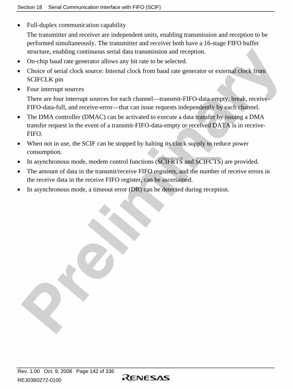
Section 18 Serial Communication Interface with FIFO (SCIF)
Rev. 1.00 Oct. 9, 2008 Page 142 of 336
REJ03B0272-0100
• Full-duplex communication capability
The transmitter and receiver are independent units, enabling transmission and reception to be performed simultaneously. The transmitter and receiver both have a 16-stage FIFO buffer structure, enabling continuous serial data transmission and reception.
• On-chip baud rate generator allows any bit rate to be selected.
• Choice of serial clock source: Internal clock from baud rate generator or external clock from SCIFCLK pin
• Four interrupt sources
There are four interrupt sources for each channel—transmit-FIFO-data-empty, break, receive-FIFO-data-full, and receive-error—that can issue requests independently by each channel.
• The DMA controller (DMAC) can be activated to execute a data transfer by issuing a DMA transfer request in the event of a transmit-FIFO-data-empty or received DATA is in receive-FIFO.
• When not in use, the SCIF can be stopped by halting its clock supply to reduce power consumption.
• In asynchronous mode, modem control functions (SCIFRTS and SCIFCTS) are provided.
• The amount of data in the transmit/receive FIFO registers, and the number of receive errors in the receive data in the receive FIFO register, can be ascertained.
• In asynchronous mode, a timeout error (DR) can be detected during reception.

Section 18 Serial Communication Interface with FIFO (SCIF)
Rev. 1.00 Oct. 9, 2008 Page 143 of 336
REJ03B0272-0100
Figure 18.1 shows a block diagram of SCIF.
Parity generation
Parity check
Clock
External clock
PφPφ/4Pφ/16
Pφ/64
[Legend]SCRSR:SCFRDR:SCTSR:SCFTDR:SCSMR:SCSCR:
Receive shift registerReceive FIFO data registerTransmit shift registerTransmit FIFO data registerSerial mode registerSerial control register
SCFSR:SCBRR:SCFCR:SCFDR:SCLSR:
Serial status registerBit rate registerFIFO control registerFIFO data count registerLine status register
SCFRDR (16 stages)
SCRSRSCIFRXD
SCIFTXD
SCIFSCK
SCIFRTS
SCIFCTS
SCFTDR (16 stages)
SCTSR
SCFDR
SCFCR
SCFSR
SCSCR
SCLSR
SCSMR
SCBRR
Transmit/receivecontrol
Baud rategenerator
TXIRXIERIBRI
SCIF
Bus
inte
rfac
e
Per
iphe
ral b
us
Figure 18.1 Block Diagram of One-Channel SCIF
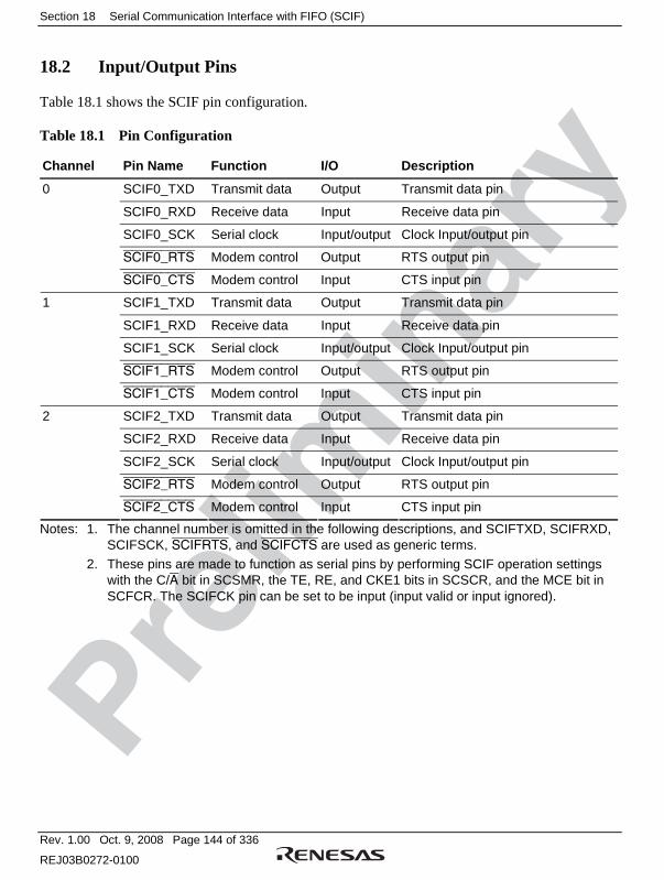
Section 18 Serial Communication Interface with FIFO (SCIF)
Rev. 1.00 Oct. 9, 2008 Page 144 of 336
REJ03B0272-0100
18.2 Input/Output Pins
Table 18.1 shows the SCIF pin configuration.
Table 18.1 Pin Configuration
Channel Pin Name Function I/O Description
SCIF0_TXD Transmit data Output Transmit data pin
SCIF0_RXD Receive data Input Receive data pin
SCIF0_SCK Serial clock Input/output Clock Input/output pin
SCIF0_RTS Modem control Output RTS output pin
0
SCIF0_CTS Modem control Input CTS input pin
SCIF1_TXD Transmit data Output Transmit data pin
SCIF1_RXD Receive data Input Receive data pin
SCIF1_SCK Serial clock Input/output Clock Input/output pin
SCIF1_RTS Modem control Output RTS output pin
1
SCIF1_CTS Modem control Input CTS input pin
SCIF2_TXD Transmit data Output Transmit data pin
SCIF2_RXD Receive data Input Receive data pin
SCIF2_SCK Serial clock Input/output Clock Input/output pin
SCIF2_RTS Modem control Output RTS output pin
2
SCIF2_CTS Modem control Input CTS input pin
Notes: 1. The channel number is omitted in the following descriptions, and SCIFTXD, SCIFRXD, SCIFSCK, SCIFRTS, and SCIFCTS are used as generic terms.
2. These pins are made to function as serial pins by performing SCIF operation settings with the C/A bit in SCSMR, the TE, RE, and CKE1 bits in SCSCR, and the MCE bit in SCFCR. The SCIFCK pin can be set to be input (input valid or input ignored).

Section 19 SIM Card Module (SIM)
Rev. 1.00 Oct. 9, 2008 Page 145 of 336
REJ03B0272-0100
Section 19 SIM Card Module (SIM)
The smart card interface supports IC cards (smart cards) conforming to the ISO/IEC 7816-3 (Identification Card) specification.
19.1 Features
The smart card interface has the following features.
• General functions
Asynchronous half-duplex transmission
Protocol selectable between T = 0 and T = 1 modes
Data length: 8 bits
Parity bit generation and check
Selectable character protection addition time N
Selectable output clock cycles per etu
Transmission of error signal (parity error) in receive mode when T = 0
Detection of error signal and automatic character retransmission in transmit mode when T = 0
Selectable minimum character interval of 11 etu (N = 255) when T = 1 (etu: Elementary Time Unit)
Selectable direct convention/inverse convention
Output clock can be fixed at high or low
• Freely selectable bit rate by on-chip baud rate generator
• Four types of interrupt source
The four interrupt sources, transmit data empty, receive data full, transmit/receive error, and transmit complete, can be requested separately.
• DMA transfer
Through DMA transfer requests for transmit data empty and receive data full, the direct memory access controller (DMAC) can be started and used for data transfer.
• The time waiting for the operation when T = 0, and the time waiting for a character when T = 1 can be observed.

Section 19 SIM Card Module (SIM)
Rev. 1.00 Oct. 9, 2008 Page 146 of 336
REJ03B0272-0100
Figure 19.1 shows a block diagram of the smart card interface.
SIM_CLK
SIM_D
SIM_RSTERI
TXI
RXI
TEI
SCRDR SCTDR
SCRSR SCTSR
SCSMR
SCSCR
SCSSR
SCSCMR
SCSC2R
SCWAIT
SCGRD
SCDMAEN
SCBRR
SCSMPL
Pφ
Module data bus
Baud rategenerator
SCSCMR:SCRSR:SCRDR:SCTSR:SCTDR:SCSMR:SCSCR:
SCSC2R:SCSSR: SCBRR:SCWAIT: SCGRD:SCSMPL:SCDMAEN:
Smart card mode registerReceive shift registerReceive data registerTransmit shift registerTransmit data registerSerial mode registerSerial control register
Serial control 2 registerSerial status registerBit rate registerWait time registerGuard extension registerSampling registerDMA enable register
Serial clockTr
ansm
it/re
ceiv
eco
ntro
l
Transmit data empty
Receive data full
Interruptcontroller
DMA controller
Paritygeneration
Parity check
Peripheral bus
Bus
inte
rfac
e
[Legend]
Figure 19.1 Smart Card Interface

Section 19 SIM Card Module (SIM)
Rev. 1.00 Oct. 9, 2008 Page 147 of 336
REJ03B0272-0100
19.2 Input/Output Pins
The pin configuration of the smart card interface is shown in table 19.1.
Table 19.1 Pin Configuration
Pin Name Function I/O Description
SIM_D* Smart card data I/O Smart card data input/output
SIM_CLK Smart card clock Output Smart card clock output
SIM_RST Smart card reset Output Smart card reset output
Note: * In explaining transmit and receive operations, the transmit data and receive data sides shall be referred to as TXD and RXD, respectively.

Section 19 SIM Card Module (SIM)
Rev. 1.00 Oct. 9, 2008 Page 148 of 336
REJ03B0272-0100

Section 20 IrDA Interface (IrDA)
Rev. 1.00 Oct. 9, 2008 Page 149 of 336
REJ03B0272-0100
Section 20 IrDA Interface (IrDA)
The IrDA interface (IrDA) performs infrared data communication conforming to IrDA standard 1.2a through an external infrared transceiver unit connected to this LSI.
The IrDA includes a UART block to control data transmission and reception as well as an infrared transmit and receive (light-emit and light-receive) pulse modulator/demodulator block and a CRC engine block in front of the UART. The UART block controls serial data transmission and reception in the asynchronous mode. The infrared transmit and receive pulse modulator/demodulator block controls communication pulses and checks pulses received through infrared baseband modulation/demodulation conforming to IrDA standard 1.2a. The CRC engine block reads 8-bit input data and outputs a 16-bit CRC calculation result.
20.1 Features
The IrDA has the following UART features.
• Asynchronous serial communication
⎯ Data length: Eight bits
⎯ Stop bit: One bit
⎯ Parity bit: None
• Reception error detection: Overrun error and framing error
• Baud rate error correction: 16 decimal fractions can be selected.
• Baud rate count: Up to 65536 can be specified. The IrDA has the following infrared transmit and receive pulse modulator/demodulator features.
• Infrared transmit (light-emit) pulse width: 1-bit width × 3/16 or 1.63 μs can be selected.
• Pulse width check: An out-of-standard pulse (insufficient or excess width) can be detected.
• 1.8432-MHz clock generator
⎯ Up to 16 can be specified for the integer part of the baud rate count.
⎯ The fraction part can be selected from 16 values.

Section 20 IrDA Interface (IrDA)
Rev. 1.00 Oct. 9, 2008 Page 150 of 336
REJ03B0272-0100
The IrDA has the following CRC calculation features.
• Generator polynomial: X16 + X12 + X5 + 1
• Data input
⎯ Input in bytes
⎯ CRC is calculated in 8-bit units starting from the lower bits.
• CRC output: 16-bit CRC is output.
• Maximum data length: 4096 bytes Figure 20.1 shows a block diagram of the IrDA.
UART block
UART transmit signal
Infrared transmit and receive pulse
modulator/demodulator block
UART receive signal
Clock (baud rate × 16)
Infrared transmit pulse
Infrared receive pulse
SCLK
CRC engine block
IrDA interface
MSFCLK_IN
TXDTXD
MSFCLK_OUT
RXD RXD
IROUT
IRIN
Infrared transceiver
Internal
data
bus
(IrDA)
Figure 20.1 Block Diagram of IrDA
20.2 Input/Output Pins
Table 20.1 shows the IrDA pin configuration.
Table 20.1 Pin Configuration
Pin Name Abbreviation I/O Function
IrDA_IN IRIN Input Infrared receive (light-receive) pulse input (negative logic)
IrDA_OUT IROUT Output Infrared transmit (light-emit) pulse output (positive logic)

Section 21 I2C Bus Interface (IIC)
Rev. 1.00 Oct. 9, 2008 Page 151 of 336
REJ03B0272-0100
Section 21 I2C Bus Interface (IIC)
This LSI has an I2C bus interface of one channel.
Each I2C bus interface uses only one data line (SDA) and one clock line (SCL) to transfer data, saving board and connector space.
21.1 Features
• Start and stop conditions generated automatically
• Selection of acknowledge output levels when receiving
• Automatic loading of acknowledge bit when transmitting
• Data transfer conforming to the I2C format
• Wait function
A wait can be inserted by driving the SCL pin low after data transfer, excluding acknowledgement.
The wait can be cleared by clearing the interrupt flag.
• I2C module corresponds to single master bus only
This module is always in master mode. Since the slave mode is not incorporated, operation stops with bus open during loss of arbitration in data transfer.
• Four interrupt sources
⎯ Data transfer enable
⎯ Wait state
⎯ Non-acknowledge detection
⎯ Arbitration lost (operation stops with bus open when bus conflict is detected)
• Data transfer speed
⎯ Standard mode (100 kHz) and high-speed mode (400 kHz)
⎯ SCL clock can be set by clock control register setting
• Clock synchronous processing of SCL line
A hazard (spike noise) generated in the high-count period by SCL is detected as an arbitration loss.
Figure 21.1 shows a block diagram of the I2C bus interface.

Section 21 I2C Bus Interface (IIC)
Rev. 1.00 Oct. 9, 2008 Page 152 of 336
REJ03B0272-0100
Bus Interface
Interrupt control
Register file
State flagcontrol
Format control
Clock control
Noise cancel
SCL
Noise cancel
Transmit and receive control
Peripheral bus
Pφ
AL, TACK, WAIT, DTE
SDA
Figure 21.1 Block Diagram of I2C Bus Interface
SCLin
VccQ
SCLout
SDAin
(Master)
(Slave 1) (Slave 2)This LSI
SCL SDA SCL SDA
SCL
SDA
SDAout
Rp Rp
[Legend]Rp: Pull-up resistor
Figure 21.2 I2C Bus Interface Connections

Section 21 I2C Bus Interface (IIC)
Rev. 1.00 Oct. 9, 2008 Page 153 of 336
REJ03B0272-0100
21.2 Input/Output Pins
Table 21.1 summarizes the input/output pins used by the I2C bus interface.
Table 21.1 I2C Bus Interface Pins
Abbreviation Function I/O Description
SCL (O/D) I2C clock input/ output
I/O I2C bus clock input/output pin
Equipped with the bus drive function. The output format is the NMOS open-drain.
SDA (O/D) I2C data input/ output
I/O I2C bus data input/output pin
Equipped with the bus drive function. The output format is the NMOS open-drain.

Section 21 I2C Bus Interface (IIC)
Rev. 1.00 Oct. 9, 2008 Page 154 of 336
REJ03B0272-0100

Section 22 AND/NAND Flash Memory Controller (FLCTL)
Rev. 1.00 Oct. 9, 2008 Page 155 of 336
REJ03B0272-0100
Section 22 AND/NAND Flash Memory Controller (FLCTL)
The AND/NAND flash memory controller (FLCTL) provides interfaces for an external AND-type flash memory and NAND-type flash memory.
To take measures for errors specific to flash memory, the FLCTL supports the ECC-code generation function and error detection function. For supporting the flash memory using the multiple level cell (MLC) technology, the FLCTL has an ECC circuit capable of up to four-symbol ECC-code generation, error detection, and hardware error correction pattern circuit in addition to the three-symbol ECC detection circuit incorporated in the previous-version FLCTL.
22.1 Features
(1) AND-Type Flash Memory Interface
• Interface directly connectable to AND-type flash memory
• Read or write in sector units (512 + 16 bytes) and ECC processing executed
An access unit of 2048 + 64 bytes, referred to as a page, is used in some datasheets for AND-type flash memory. In this manual, an access unit of 512 + 16 bytes, referred to as a sector, is always used.
• Read or write in byte units
• Supports addresses of up to 5 bytes Note: An access unit of 512 + 16 bytes is referred to as a page in some AND-type flash memory
datasheets. In this manual, however, an access unit of 512 + 16 bytes is referred to as a sector. For a product in which 2048 + 64 bytes are referred to as a page, the page is described as four sectors in this manual because 2048 + 64 bytes divided by 512 + 16 bytes (one sector) is four sectors.
(2) NAND-Type Flash Memory Interface
• Interface directly connectable to NAND-type flash memory
• Read or write in sector units (512 + 16 bytes) and ECC processing executed
• Read or write in byte units
• Supports addresses of up to 5 bytes

Section 22 AND/NAND Flash Memory Controller (FLCTL)
Rev. 1.00 Oct. 9, 2008 Page 156 of 336
REJ03B0272-0100
Note: An access unit of 512 + 16 bytes is referred to as a page in some NAND-type flash memory data sheets. In this manual, however, an access unit of 512 + 16 bytes is referred to as a sector. For a product in which 2048 + 64 bytes are referred to as a page, the page is described as four sectors in this manual because 2048 + 64 bytes divided by 512 + 16 bytes (one sector) is four sectors.
(3) Access Modes
The FLCTL can select one of the following two access modes.
• Command access mode: Performs an access by specifying a command to be issued from the FLCTL to flash memory, address, and data size to be input or output. Read, write, or erasure of data without ECC processing can be achieved.
• Sector access mode: Performs a read or write in physical sector units by specifying a physical sector and controls ECC-code generation and check. By specifying the number of sectors, the continuous physical sectors can be read or written.
• While using sector access mode, specify the start address of a page as a value to be set in the address register. Continuous access from an address in the middle of the page is not guaranteed.
(4) Sectors and Control Codes
• A sector is comprised of 512-byte data and 16-byte control code. The 16-byte control code includes 8-byte ECC.
• When the four-symbol ECC circuit is used, 10 bytes of ECC are included.
• The position of the ECC in the control code can be specified in 4-byte units.
• When the four-symbol ECC circuit is used, the user can write data to the 0th to 5th bytes of the control area.
• User information can be written to the control code other than the ECC.

Section 22 AND/NAND Flash Memory Controller (FLCTL)
Rev. 1.00 Oct. 9, 2008 Page 157 of 336
REJ03B0272-0100
(5) Three-Symbol ECC
• 8-byte ECC code is generated and error check is performed for a sector (512-byte data + 16-byte control code). Note that the ECC code generation in the 16-byte control code and the number of bytes to be checked differ depending on the specifications.
• Error correction capability is up to three errors.
• In a write operation, an ECC code is generated for data and control code prior to the ECC. The control code following the ECC is not considered.
• In a read operation, an ECC error is checked for data and control code prior to the ECC. An ECC on the control code in the FIFO is replaced with the check result by the ECC circuit, not an ECC code read from flash memory.
• An error correction is not performed even when an ECC error occurs. Error corrections must be performed by software.
(6) Four-Symbol ECC
• 80 bits (10 bytes) of ECC codes are added for a sector (512-byte data + 6-byte control code).
• Up to four errors can be detected and corrected in a random order (up to 40 bits).
• In a write operation, an ECC code is generated for data and control codes prior to the ECC.
• In a read operation, an ECC error is checked for data and control code prior to the ECC. Some part of the control area in the FIFO is used as a work area for the four-symbol ECC. Bytes 6th to 15th of the control area data that are saved are thus invalid.
• The four-symbol ECC circuit in the FLCTL can generate error correction patterns by hardware. The error correction pattern generation is executed for each sector.
• When the hardware error correction is performed, addresses indicating the error positions and error correction patterns are output. Data must be replaced by software.
(7) Data Error
• When a program error or erase error occurs, the error is reflected on the error source flags. Interrupts for each source can be specified.
• When a read error occurs, an ECC in the control code is other than 0. This read error is reflected on the ECC error source flag.
• When an ECC error occurs, perform an error correction, specify another sector to be replaced, and copy the contents of the block to another sector as required.

Section 22 AND/NAND Flash Memory Controller (FLCTL)
Rev. 1.00 Oct. 9, 2008 Page 158 of 336
REJ03B0272-0100
(8) Data Transfer FIFO and Data Register
• The 224-byte FLDTFIFO is incorporated for data transfer of flash memory.
• The 32-byte FLECFIFO is incorporated for data transfer of control code.
• The overrun/underrun detection flag is provided for the access from the CPU and DMA. (9) DMA Transfer
• By individually specifying the destinations of data and control code of flash memory to the DMA controller, data and control code can be sent to different areas.
(10) Access Size
• Registers can be accessed in 32 bits or 8 bits. Registers must be accessed in the specified access size.
• The FIFO is accessed in 32-bit (4-byte) units. If reading/writing is performed with the number of bytes that is not a multiple of four, the fractional bytes are treated as padding data.
• When an access is performed with an illegal size, the register contents are destroyed. (11) Access Time
• The FLCTL pins operate with the clock FLCK which is generated by dividing the frequency of the peripheral clock Pφ. The division ratio can be specified by the FCKSEL bit and the QTSEL bit in the common control register (FLCMNCR).
• In NAND-type flash memory, the FSC and FWE pins operate with the FCLK. In AND-type flash memory, the FSC pin operates with the FCLK and the FWE pin operates with the FCLK. To secure the setup time, these operating frequencies must be specified within the maximum operating frequency of memory to be connected.

Section 22 AND/NAND Flash Memory Controller (FLCTL)
Rev. 1.00 Oct. 9, 2008 Page 159 of 336
REJ03B0272-0100
Figure 22.1 shows a block diagram of the FLCTL.
DMAC
32
32
ECC
FLASH IF
AND/NANDFLASH
FIFO256 bytes
32
8
8
8
8
32 32
FLCTL
CPG
FCKSEL
×1, ×1/2,×1/4
FCLK
DMA transferrequests(2 lines)
Peripheral bus
Peripheral bus interface
Interrupts(4 lines)
Registers Statemachine
Transmission/reception
control
Control signalNote: FCLK is an operating clock for interface signals with flash memory. It is specified by the CPG.
QTSEL
Peripheral clock Pφ
Figure 22.1 FLCTL Block Diagram

Section 22 AND/NAND Flash Memory Controller (FLCTL)
Rev. 1.00 Oct. 9, 2008 Page 160 of 336
REJ03B0272-0100
22.2 Input/Output Pins
The pin configuration of the FLCTL is listed in table 22.1.
Table 22.1 Pin Configuration
Corresponding Flash Memory Pin
Pin Name Function I/O
NAND Type
AND Type Description
FCE Chip enable Output CE CE Enables flash memory connected to this LSI.
NAF7 to NAF0
Data I/O pins I/O I/O7 to I/O0
I/O7 to I/O0
I/O pins for command, address, and data.
FCDE Command data enable
Output CLE CDE Command Latch Enable (CLE)
Asserted when a command is output.
Command Data Enable (CDE)
Asserted when a command is output.
FOE Output enable Output ALE OE Address Latch Enable (ALE)
Asserted when an address is output and negated when data is input or output.
Output Enable (OE)
Asserted when data is input or when a status is read.
FSC Serial clock Output RE SC Read Enable (RE)
Reads data at the falling edge of RE.
Serial Clock (SC)
Inputs or outputs data synchronously with the SC.
FWE Write enable Output WE WE Write Enable
Flash memory latches a command, address, and data at the rising edge of WE.
FRB Ready/busy Input R/B R/B Ready/Busy
Indicates ready state at high level; indicates busy state at low level.
—* — — WP RES Write Protect/Reset
When this pin goes low, erroneous erasure or programming at power on or off can be prevented.
—* — — SE — Spare Area Enable
Used to access spare area. This pin must be fixed at low in sector access mode.
Note: * Not supported in this LSI.

Section 23 Realtime Clock (RTC)
Rev. 1.00 Oct. 9, 2008 Page 161 of 336
REJ03B0272-0100
Section 23 Realtime Clock (RTC)
This LSI has a realtime clock (RTC).
23.1 Features
• Clock and calendar functions (BCD format): Seconds, minutes, hours, date, day of the week, month, and year
• 1-Hz to 64-Hz timer (binary format)
64-Hz counter indicates the state of the RTC divider circuit between 64 Hz and 1 Hz
• Start/stop function
• 30-second adjust function
• Alarm interrupt: Frame comparison of seconds, minutes, hours, date, day of the week, month, and year can be used as conditions for the alarm interrupt
• Periodic interrupts: the interrupt cycle may be 1/256 second, 1/64 second, 1/16 second, 1/4 second, 1/2 second, 1 second, or 2 seconds
• Carry interrupt: a carry interrupt indicates when a carry occurs during a counter read
• Automatic leap year adjustment Note: This LSI does not have a separate power supply for the RTC. The RTC has the same
power supply as that for input and output (VccQ and VssQ). Operating the RTC alone by shutting down the other power supplies is thus not possible.

Section 23 Realtime Clock (RTC)
Rev. 1.00 Oct. 9, 2008 Page 162 of 336
REJ03B0272-0100
Figure 23.1 shows the block diagram of RTC.
RSECCNT:RMINCNT:RHRCNT:RWKCNT:RDAYCNT: RMONCNT: RYRCNT:R64CNT:RCR1:
Second counter (8 bits) Minute counter (8 bits)Hour counter (8 bits)Day of week counter (8 bits)Date counterMonth counter (8 bits)Year counter (16 bits)64-Hz counter (8 bits)RTC control register 1 (8 bits)
Interruptcontrol circuit
RCLK Prescaler
RTC operationcontrol circuit
Count
Interruptsignals
RSECAR:RMINAR: RHRAR:RWKAR:RDAYAR:RMONAR:RYRAR:RCR2:RCR3:
Second alarm register (8 bits) Minute alarm registger (8 bits)Hour alarm register (8 bits) Day of week alarm register (8 bits)Date alarm register (8 bits)Month alarm register (8 bits)Year alarm register (16 bits)RTC control register 2 (8 bits)RTC control register 3
[Legend]
Bus
inte
rfac
e
Per
iphe
ral m
odul
e in
tern
al b
usRHRCNT
RMINCNT
RDAYCNT
RYRCNT
RMONCNT
RCR2
RCR3
RWKCNT
RHRAR
RMINAR
RDAYAR
RWKAR
32.768 kHz128 Hz
ATI
PRI
CU
RCR1
R64CNT RSECCNT RSECAR
RMONAR
RYRAR
Figure 23.1 RTC Block Diagram

Section 23 Realtime Clock (RTC)
Rev. 1.00 Oct. 9, 2008 Page 163 of 336
REJ03B0272-0100
23.2 Input/Output Pin
Table 23.1 shows the RTC pin configuration.
Table 23.1 Pin Configuration
Name Abbreviation I/O Function
External clock for RTC EXTAL_RTC Input Inputs the 32.768-kHz clock for RTC.

Section 23 Realtime Clock (RTC)
Rev. 1.00 Oct. 9, 2008 Page 164 of 336
REJ03B0272-0100

Section 24 Video Processing Unit (VPU)
Rev. 1.00 Oct. 9, 2008 Page 165 of 336
REJ03B0272-0100
Section 24 Video Processing Unit (VPU)
The video processing unit (VPU) encodes and decodes bit streams conforming to the MPEG-4 standard (ISO/IEC 14496).
The VPU supports the simple profile (MPEG-4SP), advanced simple profile (MPEG-4ASP), short header, and AVC baseline profile, which are specified in the MPEG-4 video standard.
In this section, the simple profile, advanced simple profile, and short header are referred to as MPEG-4, and the AVC baseline profile as AVC.
24.1 Features
The VPU provides the following features.
• Dynamic timeslot method (DTME)
The slot lengths of the pipeline being processed can be changed dynamically depending on the bus state. This makes it possible to maintain the minimum processing time when the volume of bus traffic is large.
• VOP encoding for MPEG-4 and AVC
Images in memory are encoded for each video object plane (VOP) for MPEG-4 and for each slice for AVC, and a bit stream is generated. B-VOP encoding (bidirectional search) for MPEG and multi-reference encoding (two-plane) for AVC are supported. For AVC encoding, search in units of 1/4 pixel for an 8 × 8 block (minimum) is possible.
With adaptive realtime motion estimation (ARME), the quality of motion estimation can be enhanced by expanding the search range and increasing the search count (common to MPEG-4 and AVC).
With predict from original image (POI), an intra prediction mode allowing search at realtime is available (for AVC).
With active skip prediction (ASP), controlling search to increase the number of skipped macroblocks improves the image quality at a low bit rate (for AVC).
With custom weighted quantization (CWQ), code amount control is available for each macroblock (MB) in a plane to be encoded. When encoding a portrait, as an example, weighted codes in the center of the image can enable more detailed expression.

Section 24 Video Processing Unit (VPU)
Rev. 1.00 Oct. 9, 2008 Page 166 of 336
REJ03B0272-0100
• Decoding for MPEG-4 and AVC
A bit stream is read from memory. For MPEG-4, the stream data is decoded for each VOP, and for AVC, the stream data is decoded for each slice.
Multiple concealment modes are supported for concealing areas and block boundaries where an error has occurred.
• Deblocking filter
A deblocking filtered image can be output for both a decoded image and a local decode image when encoding.
• Video header search for MPEG-4
A bit stream is read from the memory and the next start code is detected. Table 24.1 shows the VPU basic specifications. Note that the video syntax layer to be accelerated differs for each profile in the VPU. For details, see table 24.2.
Table 24.1 VPU Basic Specifications
• Decoding
Applicable Standard
MPEG-4
Simple Profile L2
MPEG-4
Advanced Simple Profile L3
AVC/H.264
(Baseline & Main)@L2.1
Maximum 352 × 288 (CIF) 640 × 480 (VGA) 640 × 480 (VGA)
Minimum 48 × 48 48 × 48 48 × 48
Image size
Unit of size Four horizontal pixels and four vertical pixels
Four horizontal pixels and four vertical pixels
16 horizontal pixels and 16 vertical pixels*
Bit rate 384 kbps 8 Mbps 8 Mbps
Supported type I and P: VOP I, P, and B: VOP IDR, I, and P: Slice
Supported format 4:2:0 4:2:0 4:2:0
General specifications
Supported structure Progressive Progressive Interlace
Progressive

Section 24 Video Processing Unit (VPU)
Rev. 1.00 Oct. 9, 2008 Page 167 of 336
REJ03B0272-0100
Applicable Standard
MPEG-4
Simple Profile L2
MPEG-4
Advanced Simple Profile L3
AVC/H.264
(Baseline & Main)@L2.1
Supported MV UMV 4MV
UMV 4MV DirectB
UMV 1 to 16MV
Unit of MV 1/2 pixel 1/2 pixel 1/4 pixel
Maximum detection range
Horizontal position −2048 to +2047
Horizontal position −2048 to +2047
Horizontal position −2048 to +2047
Detection mode ⎯ ⎯ ⎯
Unit of processed blocks
8 × 8 or 16 × 16 8 × 8 or 16 × 16 4 × 4 to 16 × 16
Number of reference planes
1 2 16
ME/MC
Deblocking filter Output in parallel with post-processing
Output in parallel with post-processing
Output to inside of loop
Prediction Mode IntraDC/AC IntraDC/AC IntraDC/V/H/Diag
Q/IQ Mode Type 1 or type 2 Type 1 or type 2 IntDCT + QHadamard
VLC Error resilience Resync marker Data partitioning Reversible VLC (no inverse decoding) Error concealment
Resync marker Data partitioning Reversible VLC (no inverse decoding) Error concealment
Error concealment
Others Short header
vop_coded = 1 only supported
⎯ ⎯
[Legend]
ME: Motion estimation MC: Motion compensation Q: Quantization
IQ: Inverse quantization VLC: Variable length coding and decoding Note: * Cropping is not performed, and it is always output as a 16-pixel image.

Section 24 Video Processing Unit (VPU)
Rev. 1.00 Oct. 9, 2008 Page 168 of 336
REJ03B0272-0100
• Encoding
Applicable Standard
MPEG-4
Simple Profile L2
MPEG-4
Advanced Simple Profile L3
AVC/H.264
(Baseline & Main)@L2.1
Maximum 352 × 288 (CIF) 640 × 480 (VGA) 640 × 480 (VGA)
Minimum 48 × 48 48 × 48 48 × 48
Image size
Unit of size Four horizontal pixels and four vertical pixels
Four horizontal pixels and four vertical pixels
Four horizontal pixels and four vertical pixels
Bit rate 384 kbps 8 Mbps 8 Mbps
Supported type I and P: VOP I, P, and B: VOP IDR, I, and P: Slice
Supported format 4:2:0 4:2:0 4:2:0
General specifications
Supported structure Progressive Progressive Progressive
Supported MV UMV UMV UMV 1 to 4MV
Unit of MV 1/2 pixel 1/2 pixel 1/4 pixel
Maximum detection range
±32 ±32 ±32
Detection mode Tracking type Tracking type Tracking type
Unit of processed blocks
16 × 16 16 × 16 8 × 8 to 16 × 16
Number of reference planes
1 2 2
ME/MC
Deblocking filter ⎯ ⎯ Output to inside of loop
Prediction Mode IntraDC/AC IntraDC/AC IntraDC/V/H/Diag
Q/IQ Mode Type 1 or type 2 Type 1 or type 2 IntDCT + QHadamard
VLC Error resilience Resync marker Data partitioning Reversible VLC
Resync marker Data partitioning Reversible VLC
⎯
Others Short header ⎯ ⎯
[Legend] ME: Motion estimation MC: Motion compensation
Q: Quantization IQ: Inverse quantization VLC: Variable length coding and decoding

Section 24 Video Processing Unit (VPU)
Rev. 1.00 Oct. 9, 2008 Page 169 of 336
REJ03B0272-0100
Table 24.2 VPU Covered Processings
Units of Processing Encoding Decoding
MPEG-4 ASP
MPEG-4SP
VOP
Video packet
GOB
Macroblock
Block
VOP
Video packet
GOB
Macroblock
Block
MPEG-4 AVC I-slice
P-slice
IDR-slice
Note: Slice header cannot be encoded.
I-slice
P-slice
IDR-slice
Note: Slice header cannot be decoded.
[Legend]
VOP: Video object plane GOB: Group of block IDR: Instantaneous decoding refresh in raw byte sequence payload (RBSP)

Section 24 Video Processing Unit (VPU)
Rev. 1.00 Oct. 9, 2008 Page 170 of 336
REJ03B0272-0100
Figure 24.1 shows the VPU block diagram.
SMB
SMB
CTRL
RAM
RAM RAM RAM RAM RAM
RATE
DMA readDMA write
Coarse MEMC Deblock
Fine ME
PRED/Q/IQ
DCT/IDCTAVC Transform
VLCSTREAMIF
[Legend]SMB:DMA read:Coarse ME:MC:DCT:Q:AVC Transform:PRED:VLC:
CTRL:DMA write:Fine ME:Deblock:IDTC:IQ:RATE:STREAMIF:
SuperHyway multimedia brouterImage readCoarse search for motion estimationMotion compensationDiscrete cosine transformQuantizationInteger transform, Hadamard transformDCT coefficient predictionVariable length coding and decoding
Entire control blockImage writeFine search motion estimationDeblocking filterInverse discrete cosine transformInverse quantizationRate controlStream input/output
Figure 24.1 VPU Block Diagram

Section 25 Video I/O (VIO)
Rev. 1.00 Oct. 9, 2008 Page 171 of 336
REJ03B0272-0100
Section 25 Video I/O (VIO)
Note: This section contains references to the SH7722 Hardware Manual. The contents of the SH7722 Hardware Manual will be disclosed upon acceptance of a confidentiality agreement. For details, please contact a Renesas Technology sales representative.
This LSI incorporates a video I/O (VIO) module that can be used to perform capturing of an externally input image, format conversion of a YCbCr/RGB image, scaling, tone reduction, and blending of displays.
25.1 Features
The VIO consists of a capture engine unit (CEU), a video engine unit (VEU), and a blending engine unit (BEU). The features of each unit are listed below.
(1) CEU (Capture Engine Unit)
The CEU is a capture module that fetches image data externally input and transfers it to the memory. The CEU is connected to the system bus via bus bridge modules.
(2) VEU (Video Engine Unit)
The VEU is a module used connected to the buses via bus bridge modules. The VEU reads an image from a specified memory area, and writes it back to a specified address.
• Format conversion using the RGB ↔ YCbCr conversion function
• Scaling of an image using the filter function
• Tone reduction (quantization) to pack RGB data in 32-bit units
• Dithering for tone reduction of RGB data
• Removal of high-frequency components using the low-pass filter function
• Low-pass filter is applied to only the boundary of the blocks using the deblocking filter function
• Median filter function
• Edge enhancement of an image (enhancer function)

Section 25 Video I/O (VIO)
Rev. 1.00 Oct. 9, 2008 Page 172 of 336
REJ03B0272-0100
(3) BEU (Blending Engine Unit)
The BEU is a module used connected to the buses via bus bridge modules, and also connected to the VOU and the LCDC. The BEU blends three displays, and has a multiwindow function that displays four windows overlaying the blended display.
• Supports Video display
• Supports OSD (On Screen Display)
• Supports Graphic display
• Blends the three planes of Video1, Video2, and OSD/Graphic
• The three displays can be blended at desired positions.
• Any one of the three inputs can be used as the parent display.
• The location of a child display can overflow from the parent display, but the overflowed area is not output.
• Raster operation 2 function
• Multiwindow function (four windows are displayed overlaying the three blended displays)
• Selection between output to the memory, output to the VOU, output to the LCDC, and simultaneous output to the memory and VOU or LCDC

Section 25 Video I/O (VIO)
Rev. 1.00 Oct. 9, 2008 Page 173 of 336
REJ03B0272-0100
Figure 25.1 shows a block diagram of the VIO.
CEU
VIO
VIO
_CLK
VIO
_VD
VIO
_HD
VIO
_FLD
VIO
_D15
to V
IO_D
0
VIO
_ST
EM
VIO
_ST
EX
VIO
_CK
O*
VEU
BEU
VOU
CPG
LCDC
LCD panelB. T. 601 output
Note: * For details on the VIO_CKO function, see section 14, Clock Pulse Generator (CPG), in the SH7722 Hardware Manual.
Brid
ge
Sup
erH
yway
bus
Figure 25.1 Block Diagram of VIO

Section 25 Video I/O (VIO)
Rev. 1.00 Oct. 9, 2008 Page 174 of 336
REJ03B0272-0100
25.2 Functional Overview of CEU
The CEU (Capture Engine Unit) is a capture module that fetches image data externally input and transfers it to the memory. The CEU is connected to the system bus via bus bridge modules. The functional overview of the CEU is shown in table 25.1, and the main functions and their details are shown in table 25.2.
Table 25.1 Functional Overview of CEU
Classification Item Function Description Note
5M pixels 2560 pixels × 1920 lines
3M pixels 2048 pixels × 1536 lines
2M pixels 1632 pixels × 1224 lines
UXGA 1600 pixels × 1200 lines
SXGA (1) 1280 pixels × 1024 lines
SXGA (2) 1280 pixels × 960 lines
XGA 1024 pixels × 768 lines
SVGA 800 pixels × 600 lines
VGA 640 pixels × 480 lines
CIF 352 pixels × 288 lines
QVGA 320 pixels × 240 lines
QCIF 176 pixels × 144 lines
QQVGA 160 pixels × 120 lines
Connectable camera
Size
Sub-QCIF 128 pixels × 96 lines
Horizontal: 4-pixel units
Vertical: 4-line units
Cb0, Y0, Cr0, Y1…
Cr0, Y0, Cb0, Y1…
Y0, Cb0, Y1, Cr0…
YCbCr 4:2:2 8 bits
Y0, Cr0, Y1, Cb0…
{Y0, Cb0}, {Y1, Cr0}, …
Input format
YCbCr 4:2:2 16 bits {Y0, Cr0}, {Y1, Cb0}, …
Supports clock ratio of 1:1

Section 25 Video I/O (VIO)
Rev. 1.00 Oct. 9, 2008 Page 175 of 336
REJ03B0272-0100
Classification Item Function Description Note
Specified amount to be fetched on edges of the sync signal
Connectable camera
Input format Binary data
Data is fetched with the horizontal sync signal as an enable signal.
Written sequentially
Horizontal and vertical sync signal polarities
Arbitrary High-active and low-active
Capture start location
Arbitrary Can be specified in camera input clock units
Horizontal: 1-cycle units
Vertical: 1-HD (horizontal sync signal) units
Number of captured pixels
Arbitrary Can be specified in 4-pixel units horizontally and in 4-line units vertically
Stored as a field image Interlace Both-field capture
Stored as a frame image
Capture: 2-VD (vertical sync signal) units
One-field capture Top field or bottom field can be specified
Capture: 1-VD units
Memory write Output format YCbCr 4:2:2 YCbCr 4:2:0
YCbCr 4:2:0 is realized by simple skipping
Strobe function Strobe control
Automatic mode Emission time is controlled by the emission start counter, strobe exposed signal, or vertical sync signal
Emission start = Register setting Emission stop = Strobe exposed signal
Emission start = Register setting Emission stop = Register setting
Emission start = Vertical sync signal Emission stop = Vertical sync signal
Manual mode Emission pin is controlled by modifying the register
Emission start = Modifying the register
Emission stop = Clearing the register

Section 25 Video I/O (VIO)
Rev. 1.00 Oct. 9, 2008 Page 176 of 336
REJ03B0272-0100
Classification Item Function Description Note
No scaling or scale-down
Scale-down of captured display
Desired scaling factor from 1/16 to 1 (scaled-down display must not exceed VGA)
Filter function
Low-pass filter
Removal of high-frequency components
Only in the horizontal direction
Display information acquisition
Complexity level
Acquisition of complexity level of captured display
Variation of pixel values is indicated
Used for MPEG-4
16-line units, 8-line units, or 1-display units can be selected
Table 25.2 Main Functions of CEU and Their Details
Main Function Detailed Description
Image data fetch • Captures an image output from an external module and writes YCbCr
data to the memory with it separated into Y data and CbCr data.
• Fetches image data other than YCbCr data, e.g. JPEG data, from an externally connected module, such as a camera, and sequentially writes the image data to the memory.
• Fetches an interlace source image in both-field units or one-field units
and writes it to the memory. In both-field capture, an image can be stored in the memory as a frame image.
Filter processing Performs scale-down and removal of high-frequency components (only in the horizontal direction) for an image using internal filters.
Note that the scaled-down image must not exceed VGA. The filter processing can be applied to only YCbCr input data.
Display information acquisition
Acquires the complexity level of the captured display and writes it to the memory. This information output at MPEG-4 encoding is useful for determining the scene change.
Format conversion Converts image data input in the YCbCr 4:2:2 format into the YCbCr 4:2:0 format and writes it to the memory.
Note that the conversion algorithm is simple skipping in which the chrominance component (CbCr) of the even-numbered lines is skipped.
Strobe control Controls the emission signal by a register or an external signal.

Section 25 Video I/O (VIO)
Rev. 1.00 Oct. 9, 2008 Page 177 of 336
REJ03B0272-0100
Figure 25.2 shows a block diagram of the CEU.
Camera Filter block (FLB)
Capture interface
block (CIB)Strobe
Dataarrangement
block (DAB)
Register block (RGB)
Write buffer block (WBB)
Bus-bridge interface
block (BIB) Bus
bridge
Figure 25.2 Block Diagram of CEU
25.3 Pin Configuration of CEU
The pin configuration of the CEU is shown in table 25.3.
Table 25.3 Pin Configuration of CEU
Pin Name Function I/O Description
VIO_D15 to VIO_D8/ VIO_D7 to VIO_D0
VIO data bus Input Camera image data input to the VIO
VIO_CLK/VIO_CLK2 VIO clock Input Camera clock input to the VIO
VIO_VD/VIO_VD2 VIO vertical sync Input Camera vertical sync signal input to the VIO
VIO_HD/VIO_HD2 VIO horizontal sync Input Camera horizontal sync signal input to the VIO
VIO_STEM Strobe emission Output Strobe emission signal
VIO_STEX Strobe exposed Input Strobe exposed signal
VIO_FLD Field signal Input Field identification signal
VIO_CKO Camera clock output Output Clock output to the camera

Section 25 Video I/O (VIO)
Rev. 1.00 Oct. 9, 2008 Page 178 of 336
REJ03B0272-0100

Section 26 JPEG Processing Unit (JPU)
Rev. 1.00 Oct. 9, 2008 Page 179 of 336
REJ03B0272-0100
Section 26 JPEG Processing Unit (JPU)
The JPEG processing unit (JPU) incorporates the JPEG codec with an encoding and decoding function conforming to the JPEG baseline process, so that the JPU can encode image data and decode JPEG data quickly.
For the encoding and decoding processes, frame buffers or line buffers for raster block conversion are necessary in an external buffer (such as an SDRAM) which is externally connected to the LSI.
26.1 Features
The JPU has the following features.
• Conforming specification: JPEG baseline
• Operating precision: Conforming to JPEG Part 2, ISO-IEC10918-2
• Color format: YCbCr 4:2:2 (H = 2:1:1, V = 1:1:1), YCbCr 4:2:0 (H = 2:1:1, V = 2:1:1)
• Quantization tables: Four tables
• Huffman tables: Four tables (two AC tables, two DC tables)
• Target markers: Start of image (SOI), start of frame type 0 (SOF0), start of scan (SOS), define quantization tables (DQT), define Huffman tables (DHT), define restart interval (DRI), restart (RSTm), end of image (EOI)
• Image data rate: Maximum 133 Mbytes/s (66.7 MHz operation)
• The frame buffer can be reduced from the RAM area such as the SDRAM by using line buffer mode.
This mode cannot be used with some pixel clock frequencies of the camera sensor or RAM bandwidth.
• Image rotation (by 90°, 180°, or 270°) can be performed in the encoding process (only in frame buffer mode).
• In reload mode, address toggling at every transfer of a specified amount of data during stream reading and writing is supported so that the buffer capacity can be reduced.
• Processing unit: 8-byte address boundary, 4-byte data length
Note that the output data size during encoding is determined by the 16-byte boundary at the end of the address.
• Processable image size: Minimum 16 (horizontal) × 16 (vertical) pixels
Image is processed in 4-pixel units.

Section 26 JPEG Processing Unit (JPU)
Rev. 1.00 Oct. 9, 2008 Page 180 of 336
REJ03B0272-0100
Note: Do not perform unsupported color formatting or encoding or decoding of an image with an unsupported size.
Figure 26.1 shows the connection between the JPU and peripheral modules.
CPU bus
CPU bus
Imag
e da
ta
from
cam
era
JPE
G e
ncod
ed
data
/imag
e da
taVIO
VPU
Quantization table
DCT/quantization
block
CEU Huffman table
Huffman coding
Slave interface Core controller
Interface controller
JPEG core
JPU
Figure 26.1 Connection between JPU and Peripheral Modules

Section 27 LCD Controller (LCDC)
Rev. 1.00 Oct. 9, 2008 Page 181 of 336
REJ03B0272-0100
Section 27 LCD Controller (LCDC)
The LCD controller (LCDC) reads display data from an external memory or receives display data from the blend engine unit (BEU). The LCDC uses the palette memory to determine the colors according to the settings and then sends the data to the LCD module. This LCDC allows connection of TFT LCD modules that support the RGB interface or the 80-Series CPU's bus interface (SYS interface). (However, LCD modules with the NTSC/PAL type or LVDS interface cannot be connected.)
27.1 Features
The LCDC has the following features.
• Supports TFT LCD modules
• LCD module interface
RGB interface (8/9/12/16/18/24-bit bus width)
80-Series CPU's bus interface (SYS interface, 8/9/12/16/18/24-bit bus width)
• SYS interface supports the following input/output mode for the main and sub LCD module
Main LCD module: VSYNC input and output modes
Sub LCD module: VSYNC input and output modes
• Supports 8/12/16/18/24-bpp display image data formats
• Display image data is read in continuous or one-shot mode: continuous mode where display image data is continuously read according to the refresh rate of the LCD module and one-shot mode where display image data is read at intervals of the frame rate.
• Display image data is read in full or partial screen mode: full screen mode where the size of the display image data to be read depends on the panel size of the LCD module and partial screen mode where the size of the display image data to be read depends on the size of the screen to be updated.
• Display image data can be written back to the external memory
• Each of the RGB colors can be corrected by the 256-entry, 24-bit-input/output internal color palette memory
• Supports inversion of output signals to agree with the LCD module's signal polarity
• Interrupts can be generated every frame or user-specified line
• YCbCr signals are read and converted into RGB signals for output to the LCD module

Section 27 LCD Controller (LCDC)
Rev. 1.00 Oct. 9, 2008 Page 182 of 336
REJ03B0272-0100
Table 27.1 shows the LCDC functions.
Table 27.1 LCDC Functions
Function Remakes
8 bpp RGB 332 Input data format 12 bpp RGB 444
16 bpp RGB 565
18 bpp RGB 666
BGR 666
24 bpp RGB 888
BGR 888
YCbCr YCbCr 4:2:0, 4:2:2, 4:4:4
RGB interface RGB8 3 cycle/pixel Output data format RGB9 2 cycle/pixel
RGB12a 2 cycle/pixel
RGB12b 1 cycle/pixel
RGB16 1 cycle/pixel
RGB18 1 cycle/pixel
RGB24 1 cycle/pixel
SYS interface SYS8a 3 cycle/pixel
SYS8b 3 cycle/pixel
SYS8c 2 cycle/pixel
SYS8d 2 cycle/pixel
SYS9 2 cycle/pixel
SYS12 2 cycle/pixel
SYS16a 1 cycle/pixel
SYS16b 2 cycle/pixel
SYS16c 2 cycle/pixel
SYS18 1 cycle/pixel
SYS24 1 cycle/pixel
WB8a
Display data write-back WB8d
WB9
WB16
WB18
WB24
• Packed format available
• Write-back operation in units of 32 bits
• Byte or word swap

Section 27 LCD Controller (LCDC)
Rev. 1.00 Oct. 9, 2008 Page 183 of 336
REJ03B0272-0100
Function Remakes
LCD driver interface
RGB interface Interface with HSYNC and VSYNC
• Polarity inversion
• Output pulse width and position setting
SYS interface 80-Series bus interface
• Support of VSYNC input/output
• Sub LCD connectable
Dot clock Source clock Bus clock, peripheral clock, external clock
Division ratio n/m
m = 60, 54, 48, 42
1 ≤ n ≤ m/3, m/2
Interrupt User setting Interrupt generated when reading of specified lines of data is completed
Frame Interrupt generated when the first pixel data of a frame starts to be output
Interrupt generated when output of the last pixel data of a frame is completed
VRAM read Interrupt generated when access to a frame of data in VRAM is completed
Interrupt generated when access to a line of data in VRAM is completed
VSYNC Interrupt generated when VSYNC is asserted
Interrupt generated when VSYNC is negated
Display image Image data read
Image data read depending on the refresh rate of LCD module
Image data read depending on the frame rate of display image
Display image size
Full screen
Only the specified area is updated.
Image data processing
Each color of R, G, and B is converted using the color palette
• 256 entries
• 24-bit input/output
Format conversion
YCbCr to RGB YCbCr data is converted into RGB for output.

Section 27 LCD Controller (LCDC)
Rev. 1.00 Oct. 9, 2008 Page 184 of 336
REJ03B0272-0100
Figure 27.1 is a block diagram of the LCDC.
LCDDCK
LCDD24 to LCDD0LCDRSLCDWRLCDRDLCDHSYNLCDDISPLCDDONLCDVCPWCLCDVEPWCLCDVSYNLCDCSLCDDON2LCDVCPWC2LCDVEPWC2LCDVSYN2LCDCS2
LCDC
VIO(BEU)
Bus clock (Bφ)
External clock (LCDLCLK)
Peripheral clock (Pφ)
SuperHyway bus
Dot clock generator
Line memory Palette memory
Main LCD power controller
Sub LCD power controller
LCD interface
LCD module
Display data
Write-back data
Palette data
Controlling power supply
Controlling power supply
Figure 27.1 Block Diagram of LCDC

Section 27 LCD Controller (LCDC)
Rev. 1.00 Oct. 9, 2008 Page 185 of 336
REJ03B0272-0100
27.2 Input/Output Pins
Table 27.2 shows the pin configuration of the LCDC.
Table 27.2 Pin Configuration
Name Function I/O Description
LCDDON/ LCDDON2
Display on signal Output Display start signal (DON) for main LCD/display start signal (DON) for sub LCDs
LCDVCPWC/ LCDVCPWC2
Power control Output Main LCD module power control (VCC)/sub LCD module power control (VCC)
LCDVEPWC/ LCDVEPWC2
Power control Output Main LCD module power control (VEE)/sub LCD module power control (VEE)
LCDDCK/ LCDWR
Dot clock/ write strobe
Output Dot clock signal (RGB interface)/write strobe signal (SYS interface)
LCDVSYN Vertical sync signal Output/ I/O
Vertical sync signal (VSYNC) for main LCD
Output for RGB interface or I/O for SYS interface
LCDVSYN2 Vertical sync signal 2 Output/ I/O
Vertical sync signal (VSYNC) for sub LCD
Output for RGB interface or I/O for SYS interface
LCDHSYN/ LCDCS
Horizontal sync signal/chip select
Output Horizontal sync signal (RGB interface)/chip select signal for main LCD (SYS interface)
LCDCS2 Chip select Output Chip select signal for sub LCD(SYS interface)
LCDDISP/ LCDRS
Display enable/ Register select
Output Display enable signal (RGB interface)/register select signal (SYS interface)
LCDRD Read strobe Output Read strobe signal (SYS interface)
LCDD24 to LCDD0
LCD data bus Output/ I/O
LCD panel data (output for RGB interface or I/O for SYS interface)
LCDLCLK Input clock Input LCD source clock (external input)

Section 27 LCD Controller (LCDC)
Rev. 1.00 Oct. 9, 2008 Page 186 of 336
REJ03B0272-0100

Section 28 Video Output Unit (VOU)
Rev. 1.00 Oct. 9, 2008 Page 187 of 336
REJ03B0272-0100
Section 28 Video Output Unit (VOU)
The video output unit (VOU) converts image data that is obtained from the blend engine unit (BEU) or memory and outputs it as ITU-R BT.601 or ITU-R BT.656 digital data.
The VOU also scales up images.
28.1 Features
The VOU has the following features.
• Supported video system: NTSC
• Output digital level: Conforms to ITU-R BT.601, ITU-R BT.656
• Output interface: 16-bit Y/C interface, 8-bit multiplexed YC interface
• Output timing: 13.5 MHz in 16-bit Y/C interface, 27 MHz in 8-bit multiplexed YC interface
• Output pixel frequency: 13.5 MHz, 27 MHz
• Supported source image: sub-QCIF, QVGA, WQVGA, VGA
• Maximum destination image size: 720 × 240 per field
• Source image format: YCbCr 4:2:2, YCbCr 4:2:0, YCbCr 4:4:4, RGB
• Scaling up of images
Horizontal factor: 1, 1.125, 2, 2.25, or 4
Vertical factor: 1, 2, or 4
• RGB → YCbCr conversion function: Outputs YCbCr after converting obtained RGB data
• Double-buffered register: Efficient register access through a double-buffered mechanism Note: The image is enlarged by 4 pixels in the horizontal and vertical directions.

Section 28 Video Output Unit (VOU)
Rev. 1.00 Oct. 9, 2008 Page 188 of 336
REJ03B0272-0100
Figure 28.1 shows a block diagram of the VOU. S
uper
Hyw
ay b
us
DV_CLKDV_VSYNCDV_HSYNC
DV_D15 to DV_D8
DV_D7 to DV_D0
VOU
DV_CLKI
RAM control block
Output control block
Register block
BEU
Bridge
Line memory
Synchronization block
SYNC generation block
Clock select
Output block
Supplies clock to every blocks
CPU
Figure 28.1 VOU Block Diagram

Section 28 Video Output Unit (VOU)
Rev. 1.00 Oct. 9, 2008 Page 189 of 336
REJ03B0272-0100
28.2 Pin Configuration
The VOU pin configuration is shown in table 28.1.
Table 28.1 Pin Configuration
Name Function I/O Description
DV_CLK Pixel clock output Output Pixel clock output (13.5 MHz, 27 MHz)
DV_VSYNC Vertical sync signal Output VOU vertical sync signal output
DV_HSYNC Horizontal sync signal output
Output VOU horizontal sync signal output
DV_D15 to DV_D8 Data output Output Upper pixel data
(Y: 16-bit interface)
(YC: 8-bit multiplexed YC interface)
(Rec. 656 output)
DV_D7 to DV_D0 Data output Output Lower pixel data
(C: 16-bit interface)
(H'80: 8-bit multiplexed YC interface)
(H'80: Rec. 656 output)
DV_CLKI Video clock input Input Video clock input pin (27 MHz)

Section 28 Video Output Unit (VOU)
Rev. 1.00 Oct. 9, 2008 Page 190 of 336
REJ03B0272-0100

Section 29 TS Interface (TSIF)
Rev. 1.00 Oct. 9, 2008 Page 191 of 336
REJ03B0272-0100
Section 29 TS Interface (TSIF)
The transport stream interface (TSIF) is a module for receiving the MPEG2 transport stream (TS) used in one-segment broadcasting implemented as part of the digital terrestrial broadcasting services. The TSIF extracts packet data and controls PCR, which are required to decode the system layer of the MPEG2 standard.
29.1 Features
The TSIF has the following features.
• Serial data input
• Support for TS data transfer by DMA auto request
• Acquisition of TS packets
⎯ Filters 38 kinds of PIDs (Packet ID) in total (The PID values of PAT and CAT packets are fixed. For PCR, video, and audio packets, the PID values are predefined.)
⎯ Supports all valid packet receive mode (Null packet is deleted).
⎯ Supports all packet receive mode including Null packet.
⎯ Supports duplicate packet delete mode.
⎯ The endian type at the TS packet data reading can be set.
⎯ Supports the time stamp function at the TS packet data acquisition.
• TS data analysis
⎯ Detects random access indicator.
⎯ Detects discontinuity indicator.
⎯ Detects video start code and short header.
• Extraction of PCR information
• Support for system clock generation [Legend]
MPEG: Moving picture expert group
TS: Transport stream
PID: Packet ID
PAT: Program association table
CAT: Conditional access table
PCR: Program clock reference
ES: Elementary stream

Section 29 TS Interface (TSIF)
Rev. 1.00 Oct. 9, 2008 Page 192 of 336
REJ03B0272-0100
Figure 29.1 shows a block diagram of the TSIF.
The signals to transfer or control TS data are input as an input signal, and the TS packet data filtered by this module will be output as an output signal.
The serially input TS data is converted into 8-bit parallel data and the header of the TS packet is detected by the TS synchronous detection circuit. The TS filter circuit then determines and filters the PID of the TS packet according to the predefined PID table and stores the TS packet in the buffer for TS packets. Following these processes, only predefined TS packets are stored in the buffer and transferred to memories via a bus interface.
The analysis circuit of a TS header is a block that analyses the header of a TS packet, acquires the header information, and generates a trigger signal sent to other blocks. The ES data search circuit searches the start code and short header of an elementary stream (ES) contained in a TS packet. This result can be used as supplementary data to control the start timing of image decoding through the upper-level software that controls image decoding.
Based on the PCR information extracted from the TS packet, the PCR control unit outputs information needed for system clock control.
Bus
inte
rfac
e
Per
iphe
ral b
us
Buffer
Information extraction
Search result
System clock information
Hit determination
PCR_PID determination
PID
Video_PID determination
Adaptation field indicator
TS filtering
TS synchronization PID table
TS header analysis
Adaptation field analysis
ES datasearch
PCR control
TS_SDAT
TS_SCLK
TS_SDEN
TS_SPSYNC
Figure 29.1 TSIF Block Diagram

Section 29 TS Interface (TSIF)
Rev. 1.00 Oct. 9, 2008 Page 193 of 336
REJ03B0272-0100
29.2 Input/Output Pins
Table 29.1 shows the pin configuration.
Table 29.1 Pin Configuration
Pin Name Function I/O Description
TS_SDAT TS serial data Input Serial input pin of TS packet data
Polarity inversion is enabled by register setting.
TS_SCK TS serial clock Input Serial input clock pin
Polarity inversion is enabled by register setting. The initial value is synchronized with the rising edge.
TS_SDEN TS data enable Input Serial input enable signal pin
Polarity inversion and On/Off setting are enabled by register setting. The initial value is On and enabled after the TS_SDEN signal is driven high.
TS_SPSYNC TS data synchronization
Input Byte boundary signal pin
Polarity inversion is enabled by register setting. The initial value is set on a byte boundary at the rising edge. If an LSI that does not have the TS_SPSYNC signal is connected, connect the TS_SDEN signal to this pin.

Section 29 TS Interface (TSIF)
Rev. 1.00 Oct. 9, 2008 Page 194 of 336
REJ03B0272-0100

Section 30 Sound Interface Unit (SIU)
Rev. 1.00 Oct. 9, 2008 Page 195 of 336
REJ03B0272-0100
Section 30 Sound Interface Unit (SIU)
Note: This section contains references to the SH7722 Hardware Manual. The contents of the SH7722 Hardware Manual will be disclosed upon acceptance of a confidentiality agreement. For details, please contact a Renesas Technology sales representative.
The sound interface unit (SIU) is a serial interface unit with FIFO which has an interface for sound input and output to be connected with the D/A and A/D converters, and it inputs/outputs PCM data and inputs digital data conforming to the IEC60958 (SPDIF: version of December, 1999). The SIU has a DSP dedicated for filter processing, and signal processing operation of the filter application can be performed by a DSP program.
30.1 Features
The features of the SIU are listed in table 30.1.

Section 30 Sound Interface Unit (SIU)
Rev. 1.00 Oct. 9, 2008 Page 196 of 336
REJ03B0272-0100
Table 30.1 SIU Functions
Item Contents Details
Memory • PRAM: 24 bits × 2048 words
• XRAM: 32 bits × 512 words
• YRAM: 32 bits × 512 words
Operators • 24-bit × 24-bit multiplier
• 16-bit divider
• 42-bit ALU
• General operator for pointers
Special instructions • Branch instruction with reference of flag at desired bit location
• Instruction to set desired bit location
• Instruction to reset desired bit location
• Maximum value search instruction
• Clipping instruction
Special control • Instruction loop
• Modulo addressing
• Subroutine
FIFO control On-chip FIFO control circuit
DSP functions
Applications • FIR filter
• IIR filter
• Equalizer
• SRC (sampling rate conversion)

Section 30 Sound Interface Unit (SIU)
Rev. 1.00 Oct. 9, 2008 Page 197 of 336
REJ03B0272-0100
Item Contents Details
3-line serial output (× 2: ports A and B)
• Master mode, clock = 64, 128, 256, or
512 × fs (sampling frequency)
• Supports slave mode
• 32 or 64 bit/fs
• 16-bit front filling or end filling at 64 bit/fs
• Supports I2S (Inter IC Sound) format
Output interface
SPDIF output (port A) • Master mode, clock = 512 × fs
• Supports channel status and user data
• Supports only 16-bit stereo
3-line serial input (× 2: ports A and B)
• Master mode, clock =
64, 128, 256, or 512 × fs
• Supports slave mode
• 32 or 64 bit/fs
• 16-bit front filling or end filling at 64 bit/fs
• Supports I2S format
Input interface
SPDIF input (port A) • Master mode, clock = 512 × fs
• Supports channel status and user data
• Supports only 16-bit stereo
Volume Supports digital volume Others
Mixing L/R mixing

Section 30 Sound Interface Unit (SIU)
Rev. 1.00 Oct. 9, 2008 Page 198 of 336
REJ03B0272-0100
Figure 30.1 shows a block diagram of the SIU.
FCL
SPB
SIU
CPUIFFIFO3 SDOA
IFCTL
SPDIF IN
BφReset
SDIA
SDOB
SDIB
FIFO0
FIFO4
FIFO1
TMR
TEST
RLD
RAMIF
HPB(includes IRQ, DREQ, DACK, and CLK)
Pφ
SPRAM24 bits ×
2048 words(PRAM)
SPRAM32 bits ×
512 words(XRAM)
SPRAM32 bits ×
512 words(YRAM)
DPRAM32 bits ×64 words
(FIFORAM0)
Port A
3-line serial
SPDIF OUT
3-line serial
Port B
3-line serial
3-line serial
Note: In this product, port A corresponds to external pins SIUA***, and port B corresponds to external pins SIUB***. For details on multiplexed pins, see the pin list of this product, in the SH7722 Hardware Manual.
CPUIF: CPU interfaceFCL: FIFO controlIFCTL: Interface controlSDOA: Serial data through port ASDIA: Serial data/SPDIF data input through port ASDOB: Serial data output through port BSDIB: Serial data input through port B
RLD: Record level detectorSPB: Sound processing blockTMR: Timer blockTEST: Testing blockRAMIF: RAM interfaceBRGA: Baud rate generator ABRGB: Baud rate generator B
[Legend]
SIUMCKA
PLL circuit output
PLL circuit output
SIUMCKB
SIUCKA
SIUFCKA
SIUCKB
BRGA
BRGB
clk_fsa
clk_fsb
SIUFCKB
Figure 30.1 Block Diagram of SIU

Section 30 Sound Interface Unit (SIU)
Rev. 1.00 Oct. 9, 2008 Page 199 of 336
REJ03B0272-0100
The SIU operates in the following 18 blocks and four SRAMs.
(1) CPUIF
The CPU interface (CPUIF) is an interface that controls access to the registers and data transfer between the CPU that functions as the host and SRAM (PRAM, XRAM, YRAM, and FIFORAM0) controlled by the SIU. It is connected to the SH peripheral bus (HPB). The SIU operates according to the program written in PRAM via the CPUIF.
(2) FCL
The FIFO control (FCL) is a block that controls FIFOs for input/output data of ports A and B. The FCL automatically controls the FIFORAM addresses to write each FIFO data at the predetermined location and read data from the predetermined location.
(3) FIFO0, FIFO1, FIFO3, and FIFO4
The FIFOs store SPDIF input/output data, 3-line serial input/output data, and sound source input data.
Each FIFO has its own use as shown below.
• FIFO0: Data input from port A is temporarily stored.
• FIFO1: Data input from port B is temporarily stored.
• FIFO3: Data to be output to port A is temporarily stored.
• FIFO4: Data to be output to port B is temporarily stored. (4) IFCTL
The interface control (IFCTL) controls SPDIF input/output and 3-line serial input/output, according to the settings of the host.
(5) SDOA
The SDOA is an interface for serial data output through port A. 3-line serial data and SPDIF data can be output. The SDOA should be mainly used to output audio stereo data.
(6) SDIA
The SDIA is an interface for serial data input and SPDIF data input of port A. 3-line serial data and SPDIF data can be input. The SDIA should be mainly used to input audio stereo data.

Section 30 Sound Interface Unit (SIU)
Rev. 1.00 Oct. 9, 2008 Page 200 of 336
REJ03B0272-0100
(7) SDOB
The SDOB is an interface for serial data output through port B. 3-line serial data can be output. The SDOB should be mainly used to output audio monaural data.
(8) SDIB
The SDIB is an interface for serial data input through port B. 3-line serial data can be input. The SDIB should be mainly used to input audio monaural data.
(9) RLD
The record level detector (RLD) monitors the input level of port A, and is capable of fetching the peak level as an absolute value. The RLD incorporates a circuit for detecting the silent period, and can set a flag if a sound equal to or lower than the specified mute level continues for the specified sampling period.
(10) SPB
The sound processing block (SPB) is a block that plays the center role in SIU signal processing. It accesses PRAM for programs and XRAM and YRAM for saving data to implement signal processing. The SPB incorporates a DSP that operates by the program written in PRAM, and implements signal processing such as FIR filter, IIR filter, equalizer, or SRC.
(11) TMR
The timer block (TMR) generates the signal to activate the SPB hardware and the timer interrupt signal issued to the TSIF module. When the SPB hardware has been activated, the TMR is normally not used, and the FIFO event activation is used instead.
(12) TEST
The TEST is a module that generates a reset signal for the registers in each block.
(13) RAMIF
The RAM interface (RAMIF) is a module that controls input/output of RAM by switching between the host and internal control. Though the sound processing block (SPB) in the SIU has the privilege to access RAM during operation, the host control signal can be used to pass the privilege to access RAM to the host (CPUIF).

Section 30 Sound Interface Unit (SIU)
Rev. 1.00 Oct. 9, 2008 Page 201 of 336
REJ03B0272-0100
(14) BRGA
Baud rate generator A (BRGA) supplies SIUCKA directly or after dividing it as a basic operating clock to sound input/output port A. The SIUCKA dividing ratio can be specified by a register.
(15) BRGB
Baud rate generator B (BRGB) supplies SIUCKB directly or after dividing it as a basic operating clock to sound input/output port B. The SIUCKB dividing ratio can be specified by a register.
30.1.1 RAM Overview
(1) PRAM
PRAM is a single-port SRAM of 24 bits × 2048 words. It is used to store SIU programs consisting of 24-bit instructions, and the stored programs command the DSP in the SIU to carry out necessary signal processing.
(2) XRAM and YRAM
XRAM and YRAM are single-port SRAMs of 32 bits × 512 words. They store data such as audio samples or filter coefficients during processing such as filtering by the DSP in the SIU.
(3) FIFORAM0
FIFORAM0 is a dual-port SRAM of 32 bits × 64 words. Unlike audio data FIFOs (FIFO0, FIFO1, FIFO3, and FIFO4) for input/output outside the LSI, they are RAM FIFOs for audio data input/output from or to the CPU.
FIFORAM0 is divided into four 16-stage FIFOs; RAM port A input FIFO (FIFO5), RAM port B input FIFO (FIFO6), RAM port A output FIFO (FIFO7), and RAM port B output FIFO (FIFO8).
For details, refer to section 34.4, Memory Descriptions, and section 34.8.8, FIFO Specifications, in the SH7722 Hardware Manual.

Section 30 Sound Interface Unit (SIU)
Rev. 1.00 Oct. 9, 2008 Page 202 of 336
REJ03B0272-0100
30.2 Input/Output Pins
Table 30.2 shows the SIU pin configuration.
Table 30.2 Pin Configuration
SIU Block Pin Name Function I/O Description
SIUAOLR Port A sound output L/R clock
I/O* Sound output L/R clock pin (master or slave)
SIUAOBT Port A sound output bit clock I/O* Sound output bit clock pin (master or slave)
SIUAOSLD Port A sound output serial data
Output Sound output serial data pin
SIUAOSPD SPDIF output A serial data Output SPDIF serial data pin
SIUAILR Port A sound input L/R clock I/O* Sound input L/R clock pin (master or slave)
SIUAIBT Port A sound input bit clock I/O* Sound input bit clock pin (master or slave)
SIUAISLD Port A sound input serial data
Input Sound input serial data pin
SIUAISPD Port A SPDIF input serial data
Input SPDIF input serial data pin
SIUMCKA Port A master clock input Input Master clock input pin for port A
SIUA
SIUFCKA Port A sampling clock output Output Sampling clock (clk_fsa) output pin for port A
SIUBOLR Port B sound output L/R clock
I/O* Sound output L/R clock pin (master or slave)
SIUBOBT Port B sound output bit clock I/O* Sound output bit clock pin (master or slave)
SIUBOSLD Port B sound output serial data
Output Sound output serial data pin
SIUBILR Port B sound input L/R clock I/O* Sound input L/R clock pin (master or slave)
SIUBIBT Port B sound input bit clock I/O* Sound input bit clock pin (master or slave)
SIUB
SIUBISLD Port B sound input serial data
Input Sound input serial data pin

Section 30 Sound Interface Unit (SIU)
Rev. 1.00 Oct. 9, 2008 Page 203 of 336
REJ03B0272-0100
SIU Block Pin Name Function I/O Description
SIUMCKB Port B master clock input Input Master clock input pin for port B
SIUB
SIUFCKB Port B sampling clock output Output Sampling clock (clk_fsb) output pin for port B
Note: * Set to output when the master is specified or set to input when the slave is specified.

Section 30 Sound Interface Unit (SIU)
Rev. 1.00 Oct. 9, 2008 Page 204 of 336
REJ03B0272-0100

Section 31 USB Function Module (USBF)
Rev. 1.00 Oct. 9, 2008 Page 205 of 336
REJ03B0272-0100
Section 31 USB Function Module (USBF)
This LSI has a USB function module (USBF) to support high-speed transfer and full-speed transfer of the USB 2.0 standard, and supports all transfer types of the USB standard.
This module has a 4-kbyte buffer memory for data transfer, providing a maximum of eight pipes.
31.1 Features
(1) Supports USB Rev. 2.0 High-Speed
• Conforms to the Universal Serial Bus Specification Revision 2.0
• Supports high-speed transfer (480 Mbps) and full-speed transfer (12 Mbps) (2) Supports All USB Transfer Types
• Control transfers
• Bulk transfers
• Interrupt transfers (high bandwidth transfers not supported)
• Isochronous transfers (high bandwidth transfers not supported) (3) Internal Bus Interfaces
• On-chip DMA interfaces of one channel (4) Pipe Configuration
• On-chip 4-kbyte buffer memory for USB communications
• Up to eight selectable pipes (including the default control pipe)
• Programmable pipe configuration
• Endpoint numbers arbitrarily allocated to PIPE1 to PIPE7

Section 31 USB Function Module (USBF)
Rev. 1.00 Oct. 9, 2008 Page 206 of 336
REJ03B0272-0100
• Transfer conditions that can be set for each pipe:
PIPE0: Control transfers, continuous transfer mode, 256-byte fixed single buffer
PIPE1 and PIPE2: Bulk transfers/isochronous transfers, continuous transfer mode, programmable buffer size (can be specified as up to a 1.8-kbyte double buffer)
PIPE3 to PIPE5: Bulk transfers, continuous transfer mode, programmable buffer size (can be specified as up to a 1.8-kbyte double buffer)
PIPE6 and PIPE7: Interrupt transfer, 64-byte fixed single buffer (5) Other Features
• Thirty-five interrupts of eight kinds
Selectable interrupt notice according to the kind and the source depending on the software setting
• Automatic recognition of high-speed mode or full-speed mode through the reset handshake automatic response
• Transaction counting in DMA transfer
• Completes DMA transfer with interrupts
• Controls control transfer stage
• Device state control
• Automatic response to SET_ADDRESS request
• SOF interpolation
• Adds a zero-length packet at the end of a DMA transfer (DEZPM)
• Changes the BRDY interrupt event notice timing (BFRE)
• Automatically clears the buffer memory after reading the data of the pipe specified by the D0FIFO port (DCLRM)
• NAK setting for the response PID at the end of transfer (this module automatically recognizes the end of transfer by short packet reception or a transaction counter) (SHTNAK)
• NAK response interrupts (NRDY)

Section 31 USB Function Module (USBF)
Rev. 1.00 Oct. 9, 2008 Page 207 of 336
REJ03B0272-0100
Figure 31.1 shows a block diagram of the USBF.
Peripheral bus
Interrupt requestsDMA transfer requests
Status andcontrol registers
FIFO
SIE
Transceiver
USB function module
Clock (48 MHz)
SIE: Serial interface engine
[Legend]
DP
VBUS
DM
Figure 31.1 Block Diagram of the USBF
31.2 Input / Output Pins
Table 31.1 shows the pin configuration of the USBF.
Table 31.1 USBF Pin Configuration
Pin Name Function I/O Description
DP D+ I/O I/O D+ I/O of the USB on-chip transceiver
DM D− I/O I/O D− I/O of the USB on-chip transceiver
VBUS USB power supply detection
Input USB cable connection monitor pin
REFRIN Reference input ⎯ Reference resistor connection pin for constant current circuit.
EXTALUSB 48-MHz clock pin for USB
Input
XTALUSB 48-MHz clock pin for USB
Output
48-MHz clock pin for USB
Crystal resonator should be connected between EXTALUSB and XTALUSB. When using an external clock input, an external clock signal should be connected to EXTALSUB: and XTALUSB should be open.

Section 31 USB Function Module (USBF)
Rev. 1.00 Oct. 9, 2008 Page 208 of 336
REJ03B0272-0100

Section 32 Key Scan Interface (KEYSC)
Rev. 1.00 Oct. 9, 2008 Page 209 of 336
REJ03B0272-0100
Section 32 Key Scan Interface (KEYSC)
This LSI has a key scan interface (KEYSC) that can set the input or output bit numbers to be programmable.
32.1 Features
• On-chip chattering elimination circuit
• Chattering elimination time can be set to be programmable
• Measures to deal with multiple key presses
• Level/edge-selectable internal interrupts
• Canceling software standby and U-standby modes by the key input (level) interrupt.
• Input or output bit numbers can be set to be programmable

Section 32 Key Scan Interface (KEYSC)
Rev. 1.00 Oct. 9, 2008 Page 210 of 336
REJ03B0272-0100
Figure 32.1 shows a block diagram of the key scan interface.
Reg
iste
r co
ntro
l
Per
iphe
ral b
us
KEY
KEYIN0 KEYIN1 KEYIN2 KEYIN3
KEYIN4 K
YIN
DR
KY
OU
TD
R
KEYOUT0
KEYOUT1KEYOUT2
KEYOUT3KEYOUT4
KEYOUT5
Hi-Z controllable
EOREOR
EOREOREOR
KYCR1, KYCR2
5
RCLKKEYSC
SubareaInternal interrupts
Internal standby cancel
Chatteringelimination/
interrupt detection
Input pull-up
[Legend]KYCR1, 2: Key scan control registers 1 and 2KYINDR: Key scan-in data registerKYOUTDR: Key scan-out data register
Figure 32.1 Block Diagram of Key Scan Interface (Key Pin Mode 1)

Section 32 Key Scan Interface (KEYSC)
Rev. 1.00 Oct. 9, 2008 Page 211 of 336
REJ03B0272-0100
32.2 Input/Output Pins
The pin configuration of the key scan interface is listed in table 32.1.
Table 32.1 Pin Configuration
Name Abbreviation I/O Function
Input key scan interface 6 to 0
KEYIN6 to KEYIN0
Input Key scan interface for input
Output key scan interface 5 to 0
KEYOUT5 to KEYOUT0
Output Key scan interface for output
The KEYOUT5 and KEYOUT4 pins are multiplexed with the KEYIN5 and KEYIN6 pins respectively. Setting the KYMD1 and KYMD0 bits in the key scan control register 1 (KYCR1) selects either those functions. Table 32.2 shows the possible combinations between the KEYIN and KEYOUT pins.
Table 32.2 Multiplex Pin Setting
Name KYMD1 KYMD0 KEYOUT5/KEYIN5 Pin KEYOUT4/KEYIN6 Pin
Key pin mode 1 0 0 Selects KEYOUT5 pin Selects KEYOUT4 pin
Key pin mode 2 0 1 Selects KEYIN5 pin Selects KEYOUT4 pin
Key pin mode 3 1 0 Selects KEYIN5 pin Selects KEYIN6 pin

Section 32 Key Scan Interface (KEYSC)
Rev. 1.00 Oct. 9, 2008 Page 212 of 336
REJ03B0272-0100

Section 33 2D Graphics Accelerator (2DG)
Rev. 1.00 Oct. 9, 2008 Page 213 of 336
REJ03B0272-0100
Section 33 2D Graphics Accelerator (2DG)
The 2D graphics accelerator (2DG) supports the drawing of quadrangles and associated drawing modes. A unified memory architecture has been adopted for the 2DG; that is, a region of the external memory is used for the frame buffers.
33.1 Features
The 2DG provides the following features.
(1) Figure Drawing Functions
• Rectangles and quadrangles
Filling with a single color or gradations between colors
Texture mapping
⎯ Methods of mapping: Magnification, minification, and repetition
⎯ Filtering: Nearest neighbor interpolation, bilinear interpolation, and average pixel methods
Coordinate transformation
Flipping graphics (only texture-mapped rectangles)
• Drawing horizontal straight lines
Drawing with a single color or gradations between colors
Texture mapping
⎯ Methods of mapping: Magnification, minification, and repetition
⎯ Filtering: Nearest neighbor interpolation, bilinear interpolation, and average pixel methods (2) Pixel Processing
• Scissor testing
• Alpha blending
• Shadowing
• Raster operation (ROP)
• Color conversion
• Color key
• Writing-mask control (3) Others
• Maximum resolution: 4096 × 4096

Section 33 2D Graphics Accelerator (2DG)
Rev. 1.00 Oct. 9, 2008 Page 214 of 336
REJ03B0272-0100

Section 34 Pin Function Controller (PFC)
Rev. 1.00 Oct. 9, 2008 Page 215 of 336
REJ03B0272-0100
Section 34 Pin Function Controller (PFC)
34.1 Overview
The pin function controller (PFC) consists of registers to select the functions and I/O directions of multiplexed pins. Pin functions and I/O directions can be individually selected for every pin regardless of the LSI operating mode.
Table 34.1 lists the multiplexed pins of this LSI. Functions are selectable from a general port, functions 1, 2, and 3 for each pin. Functions 1, 2, and 3 can be selected by setting the corresponding bit in the port control register to B'00. Use the pin select register to select which function to use among functions 1, 2, and 3.
The functions in the shaded area in the table are available immediately after a reset. The settings of the I/O buffer Hi-Z control registers A, B, and C have priorities over the setting of the port control register.
Table 34.1 Multiplexed Pins
General Port Function 1 (Related Module)
Function 2 (Related Module)
Function 3 (Related Module)
PTA7 input/output VIO_D7 input (VIO) SCIF1_SCK input/output (SCIF)
⎯
PTA6 input VIO_D6 input (VIO) SCIF1_RXD input (SCIF) ⎯
PTA5 input/output VIO_D5 input (VIO) SCIF1_TXD output (SCIF) ⎯
PTA4 input VIO_D4 input (VIO) ⎯ ⎯
PTA3 input VIO_D3 input (VIO) ⎯ ⎯
PTA2 input VIO_D2 input (VIO) ⎯ ⎯
PTA1 input VIO_D1 input (VIO) ⎯ ⎯
PTA0 input VIO_D0 input (VIO) LCDLCLK input (LCDC) ⎯
PTB7 input/output HPD55 input/output (SBSC)
⎯ ⎯
PTB6 input/output HPD54 input/output (SBSC)
⎯ ⎯
PTB5 input/output HPD53 input/output (SBSC)
⎯ ⎯

Section 34 Pin Function Controller (PFC)
Rev. 1.00 Oct. 9, 2008 Page 216 of 336
REJ03B0272-0100
General Port Function 1 (Related Module)
Function 2 (Related Module)
Function 3 (Related Module)
PTB4 input/output HPD52 input/output (SBSC)
⎯ ⎯
PTB3 input/output HPD51 input/output (SBSC)
⎯ ⎯
PTB2 input/output HPD50 input/output (SBSC)
⎯ ⎯
PTB1 input/output HPD49 input/output (SBSC)
⎯ ⎯
PTB0 input/output HPD48 input/output (SBSC)
⎯ ⎯
PTC7 input ⎯ ⎯ ⎯
PTC5 input IOIS16 input (BSC) ⎯ ⎯
PTC4 input/output HPDQM7 output (SBSC) ⎯ ⎯
PTC3 input/output HPDQM6 output (SBSC) ⎯ ⎯
PTC2 input/output HPDQM5 output (SBSC) ⎯ ⎯
PTC0 input/output HPDQM4 output (SBSC) ⎯ ⎯
PTD7 input SDHICD input (SDHI) ⎯ ⎯
PTD6 input/output SDHIWP input (SDHI) ⎯ ⎯
PTD5 input/output SDHID3 input/output (SDHI)
⎯ ⎯
PTD4 input/output IRQ2 input (CPU) SDHID2 input/output (SDHI)
⎯
PTD3 input/output SDHID1 input/output (SDHI)
⎯ ⎯
PTD2 input/output SDHID0 input/output (SDHI)
⎯ ⎯
PTD1 input/output SDHICMD input/output (SDHI)
⎯ ⎯
PTD0 output SDHICLK output (SDHI) ⎯ ⎯
PTE7 input/output A25 output (BSC) ⎯ ⎯
PTE6 input/output A24 output (BSC) ⎯ ⎯
PTE5 input/output A23 output (BSC) ⎯ ⎯
PTE4 input/output A22 output (BSC) ⎯ ⎯
PTE1 input/output IRQ5 input (CPU) ⎯ ⎯

Section 34 Pin Function Controller (PFC)
Rev. 1.00 Oct. 9, 2008 Page 217 of 336
REJ03B0272-0100
General Port Function 1 (Related Module)
Function 2 (Related Module)
Function 3 (Related Module)
PTE0 input/output IRQ4 input (CPU) BS output (BSC) ⎯
PTF6 input/output SIOMCK input (SIO) SIUMCKB input (SIU) SIUFCKB output (SIU)
PTF5 input/output SIOSCK input/output (SIO)
SIUBOBT input/output (SIU)
⎯
PTF4 input/output SIOSTRB1 output (SIO) SIUBOLR input/output (SIU)
⎯
PTF3 input/output SIOSTRB0 output (SIO) SIUBIBT input/output (SIU)
⎯
PTF2 input/output SIOD input/output (SIO) SIUBILR input/output (SIU)
⎯
PTF1 input SIORXD input (SIO) SIUBISLD input (SIU) ⎯
PTF0 output SIOTXD output (SIO) SIUBOSLD output (SIU) ⎯
PTG4 output AUDSYNC output (AUD) ⎯ ⎯
PTG3 output AUDATA3 output (AUD) ⎯ ⎯
PTG2 output AUDATA2 output (AUD) ⎯ ⎯
PTG1 output AUDATA1 output (AUD) ⎯ ⎯
PTG0 output AUDATA0 output (AUD) ⎯ ⎯
PTH7 output LCDVCPWC output (LCDC)
LCDVCPWC2 output (LCDC)
⎯
PTH6 input/output LCDVSYN2 input/output (LCDC)
DACK output (DMAC) ⎯
PTH5 input/output LCDVSYN input/output (LCDC)
⎯ ⎯
PTH4 output LCDDISP output (LCDC) LCDRS output (LCDC) ⎯
PTH3 output LCDHSYN output (LCDC) LCDCS output (LCDC) ⎯
PTH2 output LCDDON output (LCDC) LCDDON2 output (LCDC) ⎯
PTH1 input/output LCDD17 input/output (LCDC)
DV_HSYNC output (VOU) ⎯
PTH0 input/output LCDD16 input/output (LCDC)
DV_VSYNC output (VOU) ⎯
PTJ7 output STATUS0 output (CPG) ⎯ ⎯
PTJ6 output ⎯ ⎯ ⎯
PTJ5 output PDSTATUS output (CPG) ⎯ ⎯

Section 34 Pin Function Controller (PFC)
Rev. 1.00 Oct. 9, 2008 Page 218 of 336
REJ03B0272-0100
General Port Function 1 (Related Module)
Function 2 (Related Module)
Function 3 (Related Module)
PTJ1 input/output IRQ1 input (CPU) ⎯ ⎯
PTJ0 input/output IRQ0 input (CPU) ⎯ ⎯
PTK6 input/output SIUAILR input/output (SIU)
SIOF1_SS2 output (SIOF) ⎯
PTK5 input/output SIUAIBT input/output (SIU)
SIOF1_SS1 output (SIOF) ⎯
PTK4 input/output SIUAOLR input/output (SIU)
SIOF1_SYNC input/output (SIOF)
⎯
PTK3 input/output SIUAOBT input/output (SIU)
SIOF1_SCK input/output (SIOF)
⎯
PTK2 input SIUAISLD input (SIU) SIOF1_RXD input (SIOF) ⎯
PTK1 output SIUAOSLD output (SIU) SIOF1_TXD output (SIOF) ⎯
PTK0 input/output SIUMCKA input (SIU) SIOF1_MCK input (SIOF) SIUFCKA output (SIU)
PTL7 input/output LCDD15 input/output (LCDC)
DV_D15 output (VOU) ⎯
PTL6 input/output LCDD14 input/output (LCDC)
DV_D14 output (VOU) ⎯
PTL5 input/output LCDD13 input/output (LCDC)
DV_D13 output (VOU) ⎯
PTL4 input/output LCDD12 input/output (LCDC)
DV_D12 output (VOU) ⎯
PTL3 input/output LCDD11 input/output (LCDC)
DV_D11 output (VOU) ⎯
PTL2 input/output LCDD10 input/output (LCDC)
DV_D10 output (VOU) ⎯
PTL1 input/output LCDD9 input/output (LCDC)
DV_D9 output (VOU) ⎯
PTL0 input/output LCDD8 input/output (LCDC)
DV_D8 output (VOU) ⎯
PTM7 input/output LCDD7 input/output (LCDC)
DV_D7 output (VOU) ⎯
PTM6 input/output LCDD6 input/output (LCDC)
DV_D6 output (VOU) ⎯

Section 34 Pin Function Controller (PFC)
Rev. 1.00 Oct. 9, 2008 Page 219 of 336
REJ03B0272-0100
General Port Function 1 (Related Module)
Function 2 (Related Module)
Function 3 (Related Module)
PTM5 input/output LCDD5 input/output (LCDC)
DV_D5 output (VOU) ⎯
PTM4 input/output LCDD4 input/output (LCDC)
DV_D4 output (VOU) ⎯
PTM3 input/output LCDD3 input/output (LCDC)
DV_D3 output (VOU) ⎯
PTM2 input/output LCDD2 input/output (LCDC)
DV_D2 output (VOU) ⎯
PTM1 input/output LCDD1 input/output (LCDC)
DV_D1 output (VOU) ⎯
PTM0 input/output LCDD0 input/output (LCDC)
DV_D0 output (VOU) ⎯
PTN7 input/output HPD63 input/output (SBSC)
⎯ ⎯
PTN6 input/output HPD62 input/output (SBSC)
⎯ ⎯
PTN5 input/output HPD61 input/output (SBSC)
⎯ ⎯
PTN4 input/output HPD60 input/output (SBSC)
⎯ ⎯
PTN3 input/output HPD59 input/output (SBSC)
⎯ ⎯
PTN2 input/output HPD58 input/output (SBSC)
⎯ ⎯
PTN1 input/output HPD57 input/output (SBSC)
⎯ ⎯
PTN0 input/output HPD56 input/output (SBSC)
⎯ ⎯
PTQ6 output SIOF0_SS2 output (SIOF) SIM_RST output (SIM) ⎯
PTQ5 input/output SIOF0_SS1 output (SIOF) TS_SPSYNC input (TSIF) ⎯
PTQ4 input/output SIOF0_SYNC input/output (SIOF)
TS_SDEN input (TSIF) ⎯
PTQ3 input/output SIOF0_SCK input/output (SIOF)
TS_SCK input (TSIF) ⎯

Section 34 Pin Function Controller (PFC)
Rev. 1.00 Oct. 9, 2008 Page 220 of 336
REJ03B0272-0100
General Port Function 1 (Related Module)
Function 2 (Related Module)
Function 3 (Related Module)
PTQ2 input SIOF0_RXD input (SIOF) IrDA_IN input (IrDA) TS_SDAT input (TSIF)
PTQ1 output SIOF0_TXD output (SIOF) IrDA_OUT output (IrDA) SIM_CLK output (SIM)
PTQ0 input/output SIOF0_MCK input (SIOF) IRQ3 input (CPU) SIM_D input/output (SIM)
PTR4 output LCDRD output (LCDC) ⎯ ⎯
PTR3 output CS6B/CE1B output (BSC) LCDCS2 output (LCDC) ⎯
PTR2 input WAIT input (BSC) ⎯ ⎯
PTR1 output LCDDCK output (LCDC) LCDWR output (LCDC) ⎯
PTR0 output LCDVEPWC output (LCDC)
LCDVEPWC2 output (LCDC)
⎯
PTS4 input SCIF0_CTS input (SCIF) SIUAISPD input (SIU) ⎯
PTS3 output SCIF0_RTS output (SCIF) SIUAOSPD output (SIU) ⎯
PTS2 input/output SCIF0_SCK input/output (SCIF)
TPUTO output (TPU) ⎯
PTS1 input SCIF0_RXD input (SCIF) ⎯ ⎯
PTS0 output SCIF0_TXD output (SCIF) ⎯ ⎯
PTT4 input/output FOE output (FLCTL) VIO_VD2 input (VIO) ⎯
PTT3 input/output FWE output (FLCTL) ⎯ ⎯
PTT2 input/output FSC output (FLCTL) ⎯ ⎯
PTT1 input DREQ0 input (DMAC) ⎯ ⎯
PTT0 output FCDE output (FLCTL) ⎯ ⎯
PTU4 input/output NAF2 input/output (FLCTL)
VIO_D10 input (VIO) ⎯
PTU3 input/output NAF1 input/output (FLCTL)
VIO_D9 input (VIO) ⎯
PTU2 input/output NAF0 input/output (FLCTL)
VIO_D8 input (VIO) ⎯
PTU1 input FRB input (FLCTL) VIO_CLK2 input (VIO) ⎯
PTU0 input/output FCE output (FLCTL) VIO_HD2 input (VIO) ⎯
PTV4 input/output NAF7 input/output (FLCTL)
VIO_D15 input (VIO) ⎯
PTV3 input/output NAF6 input/output (FLCTL)
VIO_D14 input (VIO) ⎯

Section 34 Pin Function Controller (PFC)
Rev. 1.00 Oct. 9, 2008 Page 221 of 336
REJ03B0272-0100
General Port Function 1 (Related Module)
Function 2 (Related Module)
Function 3 (Related Module)
PTV2 input/output NAF5 input/output (FLCTL)
VIO_D13 input (VIO) ⎯
PTV1 input/output NAF4 input/output (FLCTL)
VIO_D12 input (VIO) ⎯
PTV0 input/output NAF3 input/output (FLCTL)
VIO_D11 input (VIO) ⎯
PTW6 input VIO_FLD input (VIO) SCIF2_CTS input (SCIF) ⎯
PTW5 output VIO_CKO output (VIO) SCIF2_RTS output (SCIF) ⎯
PTW4 input/output VIO_STEX input (VIO) SCIF2_SCK input/output (SCIF)
⎯
PTW3 input/output VIO_STEM output (VIO) SCIF2_TXD output (SCIF) ⎯
PTW2 input/output VIO_HD input (VIO) SCIF2_RXD input (SCIF) ⎯
PTW1 input/output VIO_VD input (VIO) SCIF1_CTS input (SCIF) ⎯
PTW0 input/output VIO_CLK input (VIO) SCIF1_RTS output (SCIF) ⎯
PTX6 input/output CS6A/CE2B output (BSC) ⎯ ⎯
PTX5 input/output LCDD23 output (LCDC) ⎯ ⎯
PTX4 input/output LCDD22 output (LCDC) ⎯ ⎯
PTX3 input/output LCDD21 output (LCDC) ⎯ ⎯
PTX2 input/output LCDD20 output (LCDC) ⎯ ⎯
PTX1 input/output LCDD19 output (LCDC) DV_CLKI input (VOU) ⎯
PTX0 input/output LCDD18 output (LCDC) DV_CLK output (VOU) ⎯
PTY5 input/output KEYOUT5/KEYIN5 input/output (KEY)
⎯ ⎯
PTY4 input/output KEYOUT4/KEYIN6 input/output (KEY)
⎯ ⎯
PTY3 input/output KEYOUT3 output (KEY) ⎯ ⎯
PTY2 input/output KEYOUT2 output (KEY) ⎯ ⎯
PTY1 output KEYOUT1 output (KEY) ⎯ ⎯
PTY0 input/output KEYOUT0 output (KEY) ⎯ ⎯
PTZ5 input KEYIN4 input (KEY) IRQ7 input (CPU) ⎯
PTZ4 input KEYIN3 input (KEY) ⎯ ⎯
PTZ3 input KEYIN2 input (KEY) ⎯ ⎯

Section 34 Pin Function Controller (PFC)
Rev. 1.00 Oct. 9, 2008 Page 222 of 336
REJ03B0272-0100
General Port Function 1 (Related Module)
Function 2 (Related Module)
Function 3 (Related Module)
PTZ2 input KEYIN1 input (KEY) ⎯ ⎯
PTZ1 input KEYIN0 input (KEY) IRQ6 input (CPU) ⎯
⎯ D31 to D16 input/output (BSC)*
HPD47 to HPD32 input/output (SBSC)*
⎯
Note: * When the MD3 pin is low, HPD47 to HPD32 are selected. When the MD3 pin is high, D31 to D16 are selected.

Section 35 I/O Ports
Rev. 1.00 Oct. 9, 2008 Page 223 of 336
REJ03B0272-0100
Section 35 I/O Ports
This LSI has twenty-three general ports (ports A to Z). All port pins are multiplexed with other pin functions, and the pin function controller (PFC) handles the selection of pin functions and pull-up MOS control. Each port has a data register which stores data for the pins.
35.1 Port A
Port A is an input/output port with the pin configuration shown in table 35.1. The port A control register (PACR) of the PFC handles the selection of multiplexed functions and pull-up/pull-down MOS control.
Table 35.1 Port A Configuration
Port Name Selectable General Port Function Corresponding Data Register Bit
PTA7 Output Input (Pull-down on) Input (Pull-down off) PA7DT
PTA6 ⎯ Input (Pull-down on) Input (Pull-down off) PA6DT
PTA5 Output Input (Pull-down on) Input (Pull-down off) PA5DT
PTA4 ⎯ Input (Pull-down on) Input (Pull-down off) PA4DT
PTA3 ⎯ Input (Pull-down on) Input (Pull-down off) PA3DT
PTA2 ⎯ Input (Pull-down on) Input (Pull-down off) PA2DT
PTA1 ⎯ Input (Pull-down on) Input (Pull-down off) PA1DT
PTA0 ⎯ Input (Pull-down on) Input (Pull-down off) PA0DT

Section 35 I/O Ports
Rev. 1.00 Oct. 9, 2008 Page 224 of 336
REJ03B0272-0100
35.2 Port B
Port B is an input/output port with the pin configuration shown in table 35.2. The port B control register (PBCR) of the PFC handles the selection of multiplexed functions and pull-up/pull-down MOS control.
Table 35.2 Port B Configuration
Port Name Selectable General Port Function Corresponding Data Register Bit
PTB7 Output ⎯ Input (Pull-up off) PB7DT
PTB6 Output ⎯ Input (Pull-up off) PB6DT
PTB5 Output ⎯ Input (Pull-up off) PB5DT
PTB4 Output ⎯ Input (Pull-up off) PB4DT
PTB3 Output ⎯ Input (Pull-up off) PB3DT
PTB2 Output ⎯ Input (Pull-up off) PB2DT
PTB1 Output ⎯ Input (Pull-up off) PB1DT
PTB0 Output ⎯ Input (Pull-up off) PB0DT
35.3 Port C
Port C is an input/output port with the pin configuration shown in table 35.3. The port C control register (PCCR) of the PFC handles the selection of multiplexed functions and pull-up/pull-down MOS control.
Table 35.3 Port C Configuration
Port Name Selectable General Port Function Corresponding Data Register Bit
PTC7 ⎯ Input (Pull-up on) Input (Pull-up off) PC7DT
PTC5 ⎯ Input (Pull-up on) Input (Pull-up off) PC5DT
PTC4 Output ⎯ Input (Pull-up off) PC4DT
PTC3 Output ⎯ Input (Pull-up off) PC3DT
PTC2 Output ⎯ Input (Pull-up off) PC2DT
PTC0 Output ⎯ Input (Pull-up off) PC0DT

Section 35 I/O Ports
Rev. 1.00 Oct. 9, 2008 Page 225 of 336
REJ03B0272-0100
35.4 Port D
Port D is an input/output port with the pin configuration shown in table 35.4. The port D control register (PDCR) of the PFC handles the selection of multiplexed functions and pull-up/pull-down MOS control.
Table 35.4 Port D Configuration
Port Name Selectable General Port Function Corresponding Data Register Bit
PTD7 ⎯ Input (Pull-up on) Input (Pull-up off) PD7DT
PTD6 Output Input (Pull-up on) Input (Pull-up off) PD6DT
PTD5 Output Input (Pull-up on) Input (Pull-up off) PD5DT
PTD4 Output Input (Pull-up on) Input (Pull-up off) PD4DT
PTD3 Output Input (Pull-up on) Input (Pull-up off) PD3DT
PTD2 Output Input (Pull-up on) Input (Pull-up off) PD2DT
PTD1 Output Input (Pull-up on) Input (Pull-up off) PD1DT
PTD0 Output ⎯ ⎯ PD0DT
35.5 Port E
Port E is an input/output port with the pin configuration shown in table 35.5. The port E control register (PECR) of the PFC handles the selection of multiplexed functions and pull-up/pull-down MOS control.
Table 35.5 Port E Configuration
Port Name Selectable General Port Function Corresponding Data Register Bit
PTE7 Output Input (Pull-down on) Input (Pull-down off) PE7DT
PTE6 Output Input (Pull-down on) Input (Pull-down off) PE6DT
PTE5 Output Input (Pull-down on) Input (Pull-down off) PE5DT
PTE4 Output Input (Pull-down on) Input (Pull-down off) PE4DT
PTE1 Output Input (Pull-up on) Input (Pull-up off) PE1DT
PTE0 Output Input (Pull-up on) Input (Pull-up off) PE0DT

Section 35 I/O Ports
Rev. 1.00 Oct. 9, 2008 Page 226 of 336
REJ03B0272-0100
35.6 Port F
Port F is an input/output port with the pin configuration shown in table 35.6. The port F control register (PFCR) of the PFC handles the selection of multiplexed functions and pull-up/pull-down MOS control.
Table 35.6 Port F Configuration
Port Name Selectable General Port Function
Corresponding Data Register Bit
PTF6 Output Input (Pull-down on)
Input (Pull-down off)
PF6DT
PTF5 Output Input (Pull-down on)
Input (Pull-down off)
PF5DT
PTF4 Output Input (Pull-down on)
Input (Pull-down off)
PF4DT
PTF3 Output Input (Pull-down on)
Input (Pull-down off)
PF3DT
PTF2 Output Input (Pull-down on)
Input (Pull-down off)
PF2DT
PTF1 ⎯ Input (Pull-down on)
Input (Pull-down off)
PF1DT
PTF0 Output ⎯ ⎯ PF0DT

Section 35 I/O Ports
Rev. 1.00 Oct. 9, 2008 Page 227 of 336
REJ03B0272-0100
35.7 Port G
Port G is an input/output port with the pin configuration shown in table 35.7. The port G control register (PGCR) of the PFC handles the selection of multiplexed functions and pull-up/pull-down MOS control.
Table 35.7 Port G Configuration
Port Name Selectable General Port Function Corresponding Data Register Bit
PTG4 Output ⎯ ⎯ PG4DT
PTG3 Output ⎯ ⎯ PG3DT
PTG2 Output ⎯ ⎯ PG2DT
PTG1 Output ⎯ ⎯ PG1DT
PTG0 Output ⎯ ⎯ PG0DT
35.8 Port H
Port H is an input/output port with the pin configuration shown in table 35.8. The port H control register (PHCR) of the PFC handles the selection of multiplexed functions and pull-up/pull-down MOS control.
Table 35.8 Port H Configuration
Port Name Selectable General Port Function Corresponding Data Register Bit
PTH7 Output ⎯ ⎯ PH7DT
PTH6 Output Input (Pull-down on) Input (Pull-down off) PH6DT
PTH5 Output Input (Pull-down on) Input (Pull-down off) PH5DT
PTH4 Output ⎯ ⎯ PH4DT
PTH3 Output ⎯ ⎯ PH3DT
PTH2 Output ⎯ ⎯ PH2DT
PTH1 Output Input (Pull-down on) Input (Pull-down off) PH1DT
PTH0 Output Input (Pull-down on) Input (Pull-down off) PH0DT

Section 35 I/O Ports
Rev. 1.00 Oct. 9, 2008 Page 228 of 336
REJ03B0272-0100
35.9 Port J
Port J is an input/output port with the pin configuration shown in table 35.9. The port J control register (PJCR) of the PFC handles the selection of multiplexed functions and pull-up/pull-down MOS control.
Table 35.9 Port J Configuration
Port Name Selectable General Port Function Corresponding Data Register Bit
PTJ7 Output ⎯ ⎯ PJ7DT
PTJ6 Output ⎯ ⎯ PJ6DT
PTJ5 Output ⎯ ⎯ PJ5DT
PTJ1 Output Input (Pull-up on) Input (Pull-up off) PJ1DT
PTJ0 Output Input (Pull-up on) Input (Pull-up off) PJ0DT
35.10 Port K
Port K is an input/output port with the pin configuration shown in table 35.10. The port K control register (PKCR) of the PFC handles the selection of multiplexed functions and pull-up/pull-down MOS control.
Table 35.10 Port K Configuration
Port Name Selectable General Port Function Corresponding Data Register Bit
PTK6 Output Input (Pull-down on) Input (Pull-down off) PK6DT
PTK5 Output Input (Pull-down on) Input (Pull-down off) PK5DT
PTK4 Output Input (Pull-down on) Input (Pull-down off) PK4DT
PTK3 Output Input (Pull-down on) Input (Pull-down off) PK3DT
PTK2 ⎯ Input (Pull-down on) Input (Pull-down off) PK2DT
PTK1 Output ⎯ ⎯ PK1DT
PTK0 Output Input (Pull-down on) Input (Pull-down off) PK0DT

Section 35 I/O Ports
Rev. 1.00 Oct. 9, 2008 Page 229 of 336
REJ03B0272-0100
35.11 Port L
Port L is an input/output port with the pin configuration shown in table 35.11. The port L control register (PLCR) of the PFC handles the selection of multiplexed functions and pull-up/pull-down MOS control.
Table 35.11 Port L Configuration
Port Name Selectable General Port Function Corresponding Data Register Bit
PTL7 Output Input (Pull-down on) Input (Pull-down off) PL7DT
PTL6 Output Input (Pull-down on) Input (Pull-down off) PL6DT
PTL5 Output Input (Pull-down on) Input (Pull-down off) PL5DT
PTL4 Output Input (Pull-down on) Input (Pull-down off) PL4DT
PTL3 Output Input (Pull-down on) Input (Pull-down off) PL3DT
PTL2 Output Input (Pull-down on) Input (Pull-down off) PL2DT
PTL1 Output Input (Pull-down on) Input (Pull-down off) PL1DT
PTL0 Output Input (Pull-down on) Input (Pull-down off) PL0DT
35.12 Port M
Port M is an input/output port with the pin configuration shown in table 35.12. The port M control register (PMCR) of the PFC handles the selection of multiplexed functions and pull-up/pull-down MOS control.
Table 35.12 Port M Configuration
Port Name Selectable General Port Function Corresponding Data Register Bit
PTM7 Output Input (Pull-down on) Input (Pull-down off) PM7DT
PTM6 Output Input (Pull-down on) Input (Pull-down off) PM6DT
PTM5 Output Input (Pull-down on) Input (Pull-down off) PM5DT
PTM4 Output Input (Pull-down on) Input (Pull-down off) PM4DT
PTM3 Output Input (Pull-down on) Input (Pull-down off) PM3DT
PTM2 Output Input (Pull-down on) Input (Pull-down off) PM2DT
PTM1 Output Input (Pull-down on) Input (Pull-down off) PM1DT
PTM0 Output Input (Pull-down on) Input (Pull-down off) PM0DT

Section 35 I/O Ports
Rev. 1.00 Oct. 9, 2008 Page 230 of 336
REJ03B0272-0100
35.13 Port N
Port N is an input/output port with the pin configuration shown in table 35.13. The port N control register (PNCR) of the PFC handles the selection of multiplexed functions and pull-up/pull-down MOS control.
Table 35.13 Port N Configuration
Port Name Selectable General Port Function Corresponding Data Register Bit
PTN7 Output ⎯ Input (Pull-up off) PN7DT
PTN6 Output ⎯ Input (Pull-up off) PN6DT
PTN5 Output ⎯ Input (Pull-up off) PN5DT
PTN4 Output ⎯ Input (Pull-up off) PN4DT
PTN3 Output ⎯ Input (Pull-up off) PN3DT
PTN2 Output ⎯ Input (Pull-up off) PN2DT
PTN1 Output ⎯ Input (Pull-up off) PN1DT
PTN0 Output ⎯ Input (Pull-up off) PN0DT
35.14 Port Q
Port Q is an input/output port with the pin configuration shown in table 35.14. The port Q control register (PQCR) of the PFC handles the selection of multiplexed functions and pull-up/pull-down MOS control.
Table 35.14 Port Q Configuration
Port Name Selectable General Port Function Corresponding Data Register Bit
PTQ6 Output ⎯ ⎯ PQ6DT
PTQ5 Output Input (Pull-down on) Input (Pull-down off) PQ5DT
PTQ4 Output Input (Pull-down on) Input (Pull-down off) PQ4DT
PTQ3 Output Input (Pull-down on) Input (Pull-down off) PQ3DT
PTQ2 ⎯ Input (Pull-down on) Input (Pull-down off) PQ2DT
PTQ1 Output ⎯ ⎯ PQ1DT
PTQ0 Output Input (Pull-up on) Input (Pull-up off) PQ0DT

Section 35 I/O Ports
Rev. 1.00 Oct. 9, 2008 Page 231 of 336
REJ03B0272-0100
35.15 Port R
Port R is an input/output port with the pin configuration shown in table 35.15. The port R control register (PRCR) of the PFC handles the selection of multiplexed functions and pull-up/pull-down MOS control.
Table 35.15 Port R Configuration
Port Name Selectable General Port Function Corresponding Data Register Bit
PTR4 Output ⎯ ⎯ PR4DT
PTR3 Output ⎯ ⎯ PR3DT
PTR2 ⎯ Input (Pull-up on) Input (Pull-up off) PR2DT
PTR1 Output ⎯ ⎯ PR1DT
PTR0 Output ⎯ ⎯ PR0DT
35.16 Port S
Port S is an input/output port with the pin configuration shown in table 35.16. The port S control register (PSCR) of the PFC handles the selection of multiplexed functions and pull-up/pull-down MOS control.
Table 35.16 Port S Configuration
Port Name Selectable General Port Function Corresponding Data Register Bit
PTS4 ⎯ Input (Pull-down on) Input (Pull-down off) PS4DT
PTS3 Output ⎯ ⎯ PS3DT
PTS2 Output Input (Pull-down on) Input (Pull-down off) PS2DT
PTS1 ⎯ Input (Pull-down on) Input (Pull-down off) PS1DT
PTS0 Output ⎯ ⎯ PS0DT

Section 35 I/O Ports
Rev. 1.00 Oct. 9, 2008 Page 232 of 336
REJ03B0272-0100
35.17 Port T
Port T is an input/output port with the pin configuration shown in table 35.17. The port T control register (PTCR) of the PFC handles the selection of multiplexed functions and pull-up/pull-down MOS control.
Table 35.17 Port T Configuration
Port Name Selectable General Port Function Corresponding Data Register Bit
PTT4 Output Input (Pull-down on) Input (Pull-down off) PT4DT
PTT3 Output Input (Pull-down on) Input (Pull-down off) PT3DT
PTT2 Output Input (Pull-down on) Input (Pull-down off) PT2DT
PTT1 ⎯ Input (Pull-down on) Input (Pull-down off) PT1DT
PTT0 Output ⎯ ⎯ PT0DT
35.18 Port U
Port U is an input/output port with the pin configuration shown in table 35.18. The port U control register (PUCR) of the PFC handles the selection of multiplexed functions and pull-up/pull-down MOS control.
Table 35.18 Port U Configuration
Port Name Selectable General Port Function Corresponding Data Register Bit
PTU4 Output Input (Pull-down on) Input (Pull-down off) PU4DT
PTU3 Output Input (Pull-down on) Input (Pull-down off) PU3DT
PTU2 Output Input (Pull-down on) Input (Pull-down off) PU2DT
PTU1 ⎯ Input (Pull-up on) Input (Pull-up off) PU1DT
PTU0 Output Input (Pull-up on) Input (Pull-up off) PU0DT

Section 35 I/O Ports
Rev. 1.00 Oct. 9, 2008 Page 233 of 336
REJ03B0272-0100
35.19 Port V
Port V is an input/output port with the pin configuration shown in table 35.19. The port V control register (PVCR) of the PFC handles the selection of multiplexed functions and pull-up/pull-down MOS control.
Table 35.19 Port V Configuration
Port Name Selectable General Port Function Corresponding Data Register Bit
PTV4 Output Input (Pull-down on) Input (Pull-down off) PV4DT
PTV3 Output Input (Pull-down on) Input (Pull-down off) PV3DT
PTV2 Output Input (Pull-down on) Input (Pull-down off) PV2DT
PTV1 Output Input (Pull-down on) Input (Pull-down off) PV1DT
PTV0 Output Input (Pull-down on) Input (Pull-down off) PV0DT
35.20 Port W
Port W is an input/output port with the pin configuration shown in table 35.20. The port W control register (PWCR) of the PFC handles the selection of multiplexed functions and pull-up/pull-down MOS control.
Table 35.20 Port W Configuration
Port Name Selectable General Port Function Corresponding Data Register Bit
PTW6 ⎯ Input (Pull-down on) Input (Pull-down off) PW6DT
PTW5 Output ⎯ ⎯ PW5DT
PTW4 Output Input (Pull-down on) Input (Pull-down off) PW4DT
PTW3 Output Input (Pull-down on) Input (Pull-down off) PW3DT
PTW2 Output Input (Pull-down on) Input (Pull-down off) PW2DT
PTW1 Output Input (Pull-down on) Input (Pull-down off) PW1DT
PTW0 Output Input (Pull-down on) Input (Pull-down off) PW0DT

Section 35 I/O Ports
Rev. 1.00 Oct. 9, 2008 Page 234 of 336
REJ03B0272-0100
35.21 Port X
Port X is an input/output port with the pin configuration shown in table 35.21. The port X control register (PXCR) of the PFC handles the selection of multiplexed functions and pull-up/pull-down MOS control.
Table 35.21 Port X Configuration
Port Name Selectable General Port Function Corresponding Data Register Bit
PTX6 Output Input (Pull-up on) Input (Pull-up off) PX6DT
PTX5 Output Input (Pull-down on) Input (Pull-down off) PX5DT
PTX4 Output Input (Pull-down on) Input (Pull-down off) PX4DT
PTX3 Output Input (Pull-down on) Input (Pull-down off) PX3DT
PTX2 Output Input (Pull-down on) Input (Pull-down off) PX2DT
PTX1 Output Input (Pull-down on) Input (Pull-down off) PX1DT
PTX0 Output Input (Pull-down on) Input (Pull-down off) PX0DT
35.22 Port Y
Port Y is an input/output port with the pin configuration shown in table 35.22. The port Y control register (PYCR) of the PFC handles the selection of multiplexed functions and pull-up/pull-down MOS control.
Table 35.22 Port Y Configuration
Port Name Selectable General Port Function Corresponding Data Register Bit
PTY5 Output Input (Pull-up on) Input (Pull-up off) PY5DT
PTY4 Output Input (Pull-up on) Input (Pull-up off) PY4DT
PTY3 Output Input (Pull-up on) Input (Pull-up off) PY3DT
PTY2 Output Input (Pull-up on) Input (Pull-up off) PY2DT
PTY1 Output ⎯ ⎯ PY1DT
PTY0 Output Input (Pull-up on) Input (Pull-up off) PY0DT

Section 35 I/O Ports
Rev. 1.00 Oct. 9, 2008 Page 235 of 336
REJ03B0272-0100
35.23 Port Z
Port Z is an input/output port with the pin configuration shown in table 35.23. The port Z control register (PZCR) of the PFC handles the selection of multiplexed functions and pull-up/pull-down MOS control.
Table 35.23 Port Z Configuration
Port Name Selectable General Port Function Corresponding Data Register Bit
PTZ5 ⎯ Input (Pull-up on) Input (Pull-up off) PZ5DT
PTZ4 ⎯ Input (Pull-up on) Input (Pull-up off) PZ4DT
PTZ3 ⎯ Input (Pull-up on) Input (Pull-up off) PZ3DT
PTZ2 ⎯ Input (Pull-up on) Input (Pull-up off) PZ2DT
PTZ1 ⎯ Input (Pull-up on) Input (Pull-up off) PZ1DT

Section 35 I/O Ports
Rev. 1.00 Oct. 9, 2008 Page 236 of 336
REJ03B0272-0100

Section 36 User Break Controller (UBC)
Rev. 1.00 Oct. 9, 2008 Page 237 of 336
REJ03B0272-0100
Section 36 User Break Controller (UBC)
The user break controller (UBC) provides versatile functions to facilitate program debugging. These functions help to ease creation of a self-monitor/debugger, which allows easy program debugging using this LSI alone, without using the in-circuit emulator. Various break conditions can be set in the UBC: instruction fetch or read/write access of an operand, operand size, data contents, address value, and program stop timing for instruction fetch.
36.1 Features
1. The following break conditions can be set.
Break channels: Two (channels 0 and 1)
User break conditions can be set independently for channels 0 and 1, and can also be set as a single sequential condition for the two channels, that is, a sequential break. (Sequential break involves two cases such that the channel 0 break condition is satisfied in a certain bus cycle and then the channel 1 break condition is satisfied in a different bus cycle, and vice versa.)
• Address
When 40 bits containing ASID and 32-bit address are compared with the specified value, all the ASID bits can be compared or masked.
32-bit address can be masked bit by bit, allowing the user to mask the address in desired page sizes such as lower 12 bits (4-Kbyte page) and lower 10 bits (1-Kbyte page).
One address bus can be selected among three operand buses: operand address bus (SAB), X memory address bus (XAB), and Y memory address bus (YAB)
• Data
32 bits can be masked only for channel 1.
One data bus can be selected among three data buses: operand data bus (SDB), X memory data bus (XDB), and Y memory data bus (YDB)
• Bus cycle
The program can break either for instruction fetch (PC break) or operand access.
• Read or write access
• Operand sizes
Byte, word, and longword are supported.
2. The user-designated exception handling routine for the user break condition can be executed.
3. Pre-instruction-execution or post-instruction-execution can be selected as the PC break timing.
4. A maximum of 212 – 1 repetition counts can be specified as the break condition (available only for channel 1).

Section 36 User Break Controller (UBC)
Rev. 1.00 Oct. 9, 2008 Page 238 of 336
REJ03B0272-0100
Figure 36.1 shows the UBC block diagram.
XAB/YAB SAB
Internal bus
Accesscomparator
Addresscomparator
Channel 0operation
control
Channel 1operation
control
Accesscomparator
Addresscomparator
Datacomparator
Control
CBR0
CAR0
CAMR0
CRR0
CBR1
CAR1
CAMR1
CDR1
CDMR1
CETR1
CRR1
CCMFR
CBCR
User break is requested. SDB/XDB/YDB
Accesscontrol
CBR0:CRR0:CAR0:CAMR0:CBR1:CRR1:CAR1:
CAMR1:CDR1:CDMR1:CETR1:CCMFR:CBCR:
[Legend]
ASID comparator
ASIDcomparator
ASID
Match condition setting register 0Match operation setting register 0Match address setting register 0Match address mask setting register 0Match condition setting register 1Match operation setting register 1Match address setting register 1
Match address mask setting register 1Match data setting register 1Match data mask setting register 1Execution count break register 1Channel match flag registerBreak control register
Figure 36.1 Block Diagram of UBC

Section 37 User Debugging Interface (H-UDI)
Rev. 1.00 Oct. 9, 2008 Page 239 of 336
REJ03B0272-0100
Section 37 User Debugging Interface (H-UDI)
Note: This section contains references to the SH7722 Hardware Manual. The contents of the SH7722 Hardware Manual will be disclosed upon acceptance of a confidentiality agreement. For details, please contact a Renesas Technology sales representative.
The H-UDI is a serial interface which conforms to the JTAG (IEEE 1149.4: IEEE Standard Test Access Port and Boundary-Scan Architecture) standard. The H-UDI is also used for emulator connection.
37.1 Features
The H-UDI is a serial interface which conforms to the JTAG standard. The H-UDI is also used for emulator connection. When using an emulator, H-UDI functions should not be used. Refer to the appropriate emulator users manual for the method of connecting the emulator.
The H-UDI has six pins: TCK, TMS, TDI, TDO, TRST, and ASEBRK/BRKACK. The pin functions except ASEBRK/BRKACK and serial communications protocol conform to the JTAG standard. This LSI has additional six pins for emulator connection: (AUDSYNC, AUDCK, and AUDATA3 to AUDATA0).
Figure 37.1 shows a block diagram of the H-UDI.
The TAP (Test Access Port) controller and five registers (SDBPR, SDIR, SDDRH, SDDRL, and SDINT). SDBPR supports the JTAG bypass mode, SDIR is used for commands, SDDR is used for data, and SDINT is used for H-UDI interrupts. SDIR is directly accessed from the TDI and TDO pins.
The TAP controller and control registers are initialized by driving the TRST pin low or by applying the TCK signal for five or more clock cycles with the TMS pin set to 1. This initialization sequence is independent of the reset pin for this LSI. Other circuits are initialized by a normal reset.

Section 37 User Debugging Interface (H-UDI)
Rev. 1.00 Oct. 9, 2008 Page 240 of 336
REJ03B0272-0100
SDIR
TCK
TDO
TDI
TMS
TRST
Shi
ft re
gist
er
TAP controllerDecoder
Per
iphe
ral b
us
SDINT
SDDRH
SDDRL
Trace controller
Break controller Interrupt/
reset etc
ASEBRK/BRKACK
SDBPR
MUX
AUDSYNC
AUDCK
AUDATA3 to AUDATA0
Figure 37.1 H-UDI Block Diagram
37.2 Input/Output Pins
Table 37.1 shows the pin configuration for the H-UDI.
Table 37.1 Pin Configuration
Pin Name Abbreviation I/O Function When Not in Use
Clock TCK Input Functions as the serial clock input pin stipulated in the JTAG standard. Data input to the H-UDI via the TDI pin or data output via the TDO pin is performed in synchronization with this signal.
Open*1
Mode TMS Input Mode Select Input
Changing this signal in synchronization with the TCK signal determines the significance of data input via the TDI pin. Its protocol conforms to the JTAG standard (IEEE standard 1149.1).
Open*1

Section 37 User Debugging Interface (H-UDI)
Rev. 1.00 Oct. 9, 2008 Page 241 of 336
REJ03B0272-0100
Pin Name Abbreviation I/O Function When Not in Use
Reset TRST*2 Input H-UDI Reset Input
This signal is received asynchronously with a TCK signal. Asserting this signal resets the JTAG interface circuit. When a power is supplied, the TRST pin should be asserted for a given period regardless of whether or not the JTAG function is used, which differs from the JTAG standard.
Fixed to ground or connected to the RESET pin.*3
Data input TDI Input Data Input
Data is sent to the H-UDI by changing this signal in synchronization with the TCK signal.
Open*1
Data output
TDO Output Data Output
Data is read from the H-UDI in synchronization with the TCK signal.
Open
Emulator ASEBRK/ BRKACK
I/O Pins for an emulator Open*1
Emulator AUDSYNC, AUDCK, AUDATA3 to AUDATA0
Output Pins for an emulator Open
Notes: 1. This pin is pulled up in this LSI. When using interrupts or resets via the H-UDI or emulator, the use of external pull-up resistors will not cause any problem.
2. When using interrupts or resets via the H-UDI or emulator, the TRST pin should be designed so that it can be controlled independently and can be controlled to retain low level while the RESET pin is asserted at a power-on reset.
3. This pin should be connected to ground, the RESET, or another pin which operates in the same manner as the RESET pin. However, when connected to a ground pin, the following problem occurs. Since the TRST pin is pulled up within this LSI, a weak current flows when the pin is externally connected to a ground pin. The value of the current is determined by a resistance of the pull-up MOS for the port pin. Although this current does not affect the operation of this LSI, it consumes unnecessary power. Pulling up the TRST pin can be disabled by the pull-down control register (PULCR) of the pin function controller (PFC). For details, see section 38, Pin Function Controller (PFC), in the SH7722 Hardware Manual.
The TCK clock or the CPG of this LSI should be set to ensure that the frequency of the TCK clock is less than the peripheral-clock frequency of this LSI.

Section 37 User Debugging Interface (H-UDI)
Rev. 1.00 Oct. 9, 2008 Page 242 of 336
REJ03B0272-0100

Section 38 Electrical Characteristics
Rev. 1.00 Oct. 9, 2008 Page 243 of 336
REJ03B0272-0100
Section 38 Electrical Characteristics
38.1 Absolute Maximum Ratings
Table 38.1 shows the absolute maximum ratings.
Table 38.1 Absolute Maximum Ratings
Item Symbol Rating Unit
Power supply voltage (I/O)
VCCQ, DV33, AV33 −0.3 to 4.6 V
Power supply voltage (Internal)
VDD, VDD_PLL, VDD_DLL, DV12, AV12, UV12
−0.3 to 1.8 V
Input voltage Vin –0.3 to VCCQ + 0.3 V
Storage temperature Tstg −55 to 125 °C
Caution: Operating the chip in excess of the absolute maximum ratings may result in permanent damage.

Section 38 Electrical Characteristics
Rev. 1.00 Oct. 9, 2008 Page 244 of 336
REJ03B0272-0100
38.2 Recommended Operating Conditions
Table 38.2 lists the recommended operating conditions. The specification in this section assumes the use under the conditions of table 38.2 unless otherwise noted.
Table 38.2 Recommended Operating Conditions
Item Symbol Min. Typ. Max. Unit Test Conditions
Operating temperature Topr −20 ⎯ 70 °C Ambient temperature Ta
I/O power supply
VCCQ 3.0 3.3 3.6 V
Core power supply
VDD 1.15 1.2/1.3 1.35 V
Power supply for PLL
VDD_PLL 1.15 1.2/1.3 1.35 V
Power supply for DLL
VDD_DLL 1.15 1.2/1.3 1.35 V
USB digital 3.3-V power supply
DV33 3.0 3.3 3.6 V
USB digital 1.2-V power supply
DV12 1.15 1.2/1.3 1.35 V
USB analog 3.3-V power supply
AV33 3.0 3.3 3.6 V
USB analog 1.2-V power supply
AV12 1.15 1.2/1.3 1.35 V
Power supply voltage
USB digital 1.2-V power supply
UV12 1.15 1.2/1.3 1.35 V

Section 38 Electrical Characteristics
Rev. 1.00 Oct. 9, 2008 Page 245 of 336
REJ03B0272-0100
38.3 Power-On and Power-Off Order
1. Order of turning on 1.2 V power (VDD, VDD_PLL, VDD_DLL) and 3.3 V power (VCCQ)
⎯ First turn on the 3.3 V power, and then turn on the 1.2 V power. This interval is as shown in table 38.3. The system design must ensure that the states of pins or undefined period of an internal state do not cause erroneous system operation. The power settling time (trVCCQ) of the power supply voltage for VCCQ must be shorter than those of any other 3.3 V power.
⎯ First turn on the 3.3 V power, and input RCLK before turning on the 1.2 V.
⎯ Until voltage is applied to all power supplies and a low level is input to the RESETP pin, internal circuits remain unsettled, and so pin states are also undefined. The system design must ensure that these undefined states do not cause erroneous system operation.
Waveforms at power-on are shown in the following figure.
trVcc
VccQ
trVDD
tPWU tUNC
GND
RESETP
RCLK
VDD (min.) voltage
VDD : 1.2 V power
VccQ (min.) voltage
Pins status undefined Normal operation period
Power-on reset state Pins status undefined
Note: * Except power/GND, clock-related, and analog pins
Other pins*

Section 38 Electrical Characteristics
Rev. 1.00 Oct. 9, 2008 Page 246 of 336
REJ03B0272-0100
Table 38.3 Recommended Timing in Power-On
Item Symbol Time Unit
VCCQ power settling time trVCCQ 300 μs
Time difference between 3.3 V VCC and 1.2 V VDD at power-on
tPWU 0 to 10 ms
VDD power settling time trVDD ≤ 1 ms
Time over which the state is undefined tUNC tPWU + trVDD + 3tRCLK ms
Note: The 3.3 V power should be turned on at the same time as much as possible.
The state-undefined time represents the time in which rising of each power is in transition. This ensures that the pins are in the reset state after tUNC has elapsed.
2. Power-off order
⎯ In the reverse order of power-on, first turn off the 1.2 V VDD power, then turn off the 3.3 V VCCQ power within 10 ms. This interval should be as short as possible. The system design must ensure that the states of pins or undefined period of an internal state do not cause erroneous system operation.
⎯ Pin states are undefined while only the 1.2 V VDD power is off. The system design must ensure that these undefined states do not cause erroneous system operation.
tPWD
GND
VDD : 1.2 V power
VCCQ : 3.3 V power
VDD (min.) voltage
Normal operation period Operation stopped
Table 38.4 Recommended Timing in Power-Off
Item Symbol Maximum Value Unit
Time difference between the power-off of 1.2 V VDD and 3.3 V VCCQ levels
tPWD 0 to 10 ms
Note: The values in the table above are recommended values, so they represent guidelines rather than strict requirements.

Section 38 Electrical Characteristics
Rev. 1.00 Oct. 9, 2008 Page 247 of 336
REJ03B0272-0100
38.4 DC Characteristics
Tables 38.5, 38.6, and 38.7 list the DC characteristics.
Table 38.5 DC Characteristics
Item Symbol Min. Typ. Max. Unit Test Conditions
MD0, MD1, MD2,
MD3, MD5, MD8,
TSTMD, TST,
TRST, MPMD,
ASEBRK/
BRKAK
RESETP, NMI,
RESETA, PTU0,
PTX6, PTE1,
PTE0, PTQ0
VIHS VCCQ × 0.8 ⎯ VCCQ + 0.3 V
VBUS pin VIH 4.35 — 5.25 V
Input high voltage
Other input pins
VIH 2.0 — VCCQ + 0.3 V
MD0, MD1, MD2,
MD3, MD5, MD8,
TSTMD, TST,
TRST, MPMD,
ASEBRK/
BRKAK
RESETP, NMI,
RESETA, PTU0,
PTX6, PTE1,
PTE0, PTQ0
VILS –0.3 — VCCQ × 0.2 V Input low voltage
Other input pins
VIL –0.3 — 0.8 V
2.4 — — V IOH = –2 mA Output high voltage
All output pins VOH
VCCQ × 0.9 — — V IOH = –200 μA
Output pins other than I2C
VOL — — 0.5 V IOL = 2 mA Output low voltage
SCL and SDA pins
VOL — — 0.4 V

Section 38 Electrical Characteristics
Rev. 1.00 Oct. 9, 2008 Page 248 of 336
REJ03B0272-0100
Item Symbol Min. Typ. Max. Unit Test Conditions
Squelch detection threshold input voltage (differential voltage)
DP and DM pins
VHSSQ 100 150 mV Input characteristics during high-speed operation
Common mode input voltage range
DP and DM pins
VHSCM –50 500 mV Input characteristics during high-speed operation
Idle state DP and DM pins
VHSOI –10 10 mV Output characteristics during high-speed operation
High output voltage
DP and DM pins
VHSOH 360 440 mV
Low output voltage
DP and DM pins
VHSOL –10 10 mV
Chirp J output voltage (differential)
DP and DM pins
VCHIRPJ 700 1100 mV
Chirp K output voltage (differential)
DP and DM pins
VCHIRPK –900 –500 mV

Section 38 Electrical Characteristics
Rev. 1.00 Oct. 9, 2008 Page 249 of 336
REJ03B0272-0100
Table 38.6 DC Characteristics
Item Symbol Min. Typ. Max. Unit Test Conditions
⎯ 160 320 mA VDD
= 1.2 V
Iφ = 266 MHz
Bφ = 66 MHz
B3φ = 133 MHz
IDD
⎯ 220 435 mA VDD
= 1.3 V
Iφ = 333 MHz
Bφ = 66 MHz
B3φ = 133 MHz
Current
consumption
Normal operation
ICC
⎯ 120 150 mA VCC
Q3 = 3.3 V
Bφ = 66 MHz
B3φ = 133 MHz
BSC data bus width: 16
bits
SBSC data bus width:
64 bits
⎯ 150 180 mA VCC
Q3 = 3.3 V
Bφ = 66 MHz
B3φ = 133 MHz
BSC data bus width: 16
bits
SBSC data bus width:
32 bits
IDD
⎯ 25 70 mA
Sleep mode*
ICC
⎯ 55 80
*: When external bus
cycles other than the
refresh cycle are not
specified.
All module stop: ON
VDD
= 1.2 V
VCC
Q = 3.3 V
Bφ = 66 MHz
B3φ = 133 MHz
Software standby
mode
Istby
⎯ 2.0 12 mA Ta = 25°C
VCC
Q = 3.3 V
VDD
= 1.2 V
U-standby mode Iustby
⎯ ⎯ 60 μA Ta = 25°C
VCC
Q = 3.3 V
VDD
= 1.2 V
Input clock off

Section 38 Electrical Characteristics
Rev. 1.00 Oct. 9, 2008 Page 250 of 336
REJ03B0272-0100
Item Symbol Min. Typ. Max. Unit Test Conditions
All input
pins (except
SBSC pins)
|Iin | ⎯ ⎯ 1 Input leak
current
SBSC pins |IinSB
| ⎯ ⎯ 3
μA Vin =
0.5 to VCC
Q – 0.5 V
I/O, all output
pins (off
condition)
(except SBSC
pins)
|ISTI
| ⎯ ⎯ 1 μA Three-state leak
current
SBSC pins |IinSB
| ⎯ ⎯ 3
Vin =
0.5 to VCC
Q – 0.5 V
Pull-up/
pull-down
resistance
Port pins Ppull
20 — 150 kΩ
SBSC pins CSB
— — 10 pF Pin
capacitance All pins C — — 10 pF
Notes: 1. Make sure to connect the VCCQ pin to the system power and the VSS pin to the system ground (0 V).
2. Current consumption values in the table are for VIHmin = VCCQ − 0.5 V and VILmax = 0.5 V with all output pins unloaded.
3. IDD is the total of current flowing through the VDD, VDD-PLL, VDD-DLL, DV12, AV12, and UV12 pins. ICC is the total of current flowing through the VCCQ, DV33, and AV33 pins. ISTBY is the total of IDD and ICC in standby mode. IUSTBY is the total of IDD and ICC in U-standby mode.
Table 38.7 Permissible Output Current Values
Item Symbol Min. Typ. Max. Unit
Permissible output low current (per pin) IOL — — 2.0 mA
Permissible output low current (total) ΣIOL — — 40 mA
Permissible output high current (per pin) –IOH — — 2.0 mA
Permissible output high current (total) Σ (–IOH) — — 40 mA
Permissible I2C output low current (SCL, SDA)
IOL — — 10 mA
Note: To ensure chip reliability, do not exceed the output current values given in table 38.7.

Section 38 Electrical Characteristics
Rev. 1.00 Oct. 9, 2008 Page 251 of 336
REJ03B0272-0100
38.5 AC Characteristics
The inputs of this LSI are synchronous as a rule. The setup and hold time of each input signal must be satisfied unless otherwise noted.
Table 38.8 Operating Frequency Range
Item Symbol Min. Typ. Max. Unit Remarks
10 — 266.7 VDD = 1.15 V to 1.30 V
CPU, DSP, cache (Iφ)
10 — 333.4 VDD = 1.25 V to 1.35 V
U-memory (Uφ) 10 — 133.4
SuperHyway bus (SHφ) 10 — 133.4
BSC bus (Bφ) 10 — 66.7
SBSC bus (B3φ) 10 — 133.4
Peripheral module (Pφ) 2.5 — 33.4
SIU clock A (SIUCKA) — — 33.4
SIU clock B (SIUCKB) — — 33.4
IrDA clock (IrDACK) — — 33.4
Operating frequency
Video clock (VIO_CKO)
f
— — 66.7
MHz

Section 38 Electrical Characteristics
Rev. 1.00 Oct. 9, 2008 Page 252 of 336
REJ03B0272-0100
38.5.1 Clock Timing
Table 38.9 Clock Timing
Item Symbol Min. Max. Unit Figure
EXTAL clock input frequency fEX 10 66 MHz
EXTAL clock input cycle time tEXcyc 15 100 ns
EXTAL clock input low pulse width tEXL 4.5 ⎯ ns
EXTAL clock input high pulse width tEXH 4.5 ⎯ ns
EXTAL clock input rise time tEXr ⎯ 3 ns
EXTAL clock input fall time tEXf ⎯ 3 ns
RCLK clock input frequency fRCLK 32 33 kHz
RCLK clock input cycle time tRCLKcyc 30.3 31.3 μs
RCLK clock input low pulse width tRCLKL 10 ⎯ μs
RCLK clock input high pulse width tRCLKH 10 ⎯ μs
RCLK clock input rise time tRCLKr ⎯ 200 ns
RCLK clock input fall time tRCLKf ⎯ 200 ns
38.1
CKO clock output frequency fCKO 5 66 MHz
CKO clock output cycle time tCKOcyc 15 200 ns
CKO clock output low pulse width tCKOL 3 ⎯ ns
CKO clock output high pulse width tCKOH 3 ⎯ ns
CKO clock output rise time tCKOr ⎯ 3 ns
CKO clock output fall time tCKOf ⎯ 3 ns
HPCLK clock output frequency fHPC 5*1 133 MHz
HPCLK clock output cycle time tHPCcyc 7.5 200*1 ns
HPCLK clock output low pulse width tHPCL 1 ⎯ ns
HPCLK clock output high pulse width tHPCH 1 ⎯ ns
HPCLK clock output rise time tHPCr ⎯ 3 ns
HPCLK clock output fall time tHPCf ⎯ 3 ns
38.2
RESETP assert time tRESPW 4 ⎯ tRCLKcyc
RESETOUT assert time (clock mode 0) tRESOUTM0 ⎯ 300 μs
RESETOUT assert time (clock mode 1) tRESOUTM1 ⎯ 100 μs
RESETOUT assert time (clock mode 3) tRESOUTM3 ⎯ 2.3 ms
38.3 to 38.5

Section 38 Electrical Characteristics
Rev. 1.00 Oct. 9, 2008 Page 253 of 336
REJ03B0272-0100
Item Symbol Min. Max. Unit Figure
Software standby return time (clock mode 0) tSOSM0 ⎯ 300 μs
Software standby return time (clock mode 1) tSOSM1 ⎯ 40 tPCYC*2
Software standby return time (clock mode 3) tSOSM3 ⎯ 2.3 ms
38.6 to 38.8
Notes: 1. This is the value when the PLL is turned off. When the PLL is turned on, fop (min.) is 25 MHz and tcyc (max.) is 40 ns.
2. Pφ cycle time in operation.
tEXH
tEXf tEXr
tEXL
tEXcyc
VIH VIHVIH1/2 V
CCQ
1/2 VCC
QVIL VIL
tRCLKH
tRCLKf tRCLKr
tRCLKL
tRCLKcyc
VIHVIH VIH1/2 V
CCQ 1/2 V
CCQ
VIL VIL
EXTAL*(input)
RCLK(input)
Note: * When the clock is input on the EXTAL pin.
Figure 38.1 Clock Input Timing of EXTAL and RCLK
tHPCcyc
tHPCLtHPCH
VOH1/2VCCQ
HPCLK(output)
1/2VCCQ
tHPCrtHPCf
VOH
VOL VOL
VOH
tCKOcyc
tCKOLtCKOH
VOH1/2VCCQ
CKO(output)
1/2VCCQ
tCKOrtCKOf
VOH
VOL VOL
VOH
Figure 38.2 Clock Output Timing of CKO and HPCLK
CKO
RESETP
tRESOUTM0
tRESPW
RESETOUT
Figure 38.3 Power-On Oscillation Settling Time (Clock Mode 0)

Section 38 Electrical Characteristics
Rev. 1.00 Oct. 9, 2008 Page 254 of 336
REJ03B0272-0100
CKO
RESETP
tRESOUTM1
tRESPW
RESETOUT
Figure 38.4 Power-On Oscillation Settling Time (Clock Mode 1)
CKO
RESETP
tRESOUTM3
tRESPW
RESETOUT
Figure 38.5 Power-On Oscillation Settling Time (Clock Mode 3)
CKO
NMI, IRQ7 to IRQ0
tSOSM0
Figure 38.6 Oscillation Settling Time on Return from Software Standby by NMI or IRQ (Clock Mode 0)
CKO
NMI, IRQ7 to IRQ0
tSOSM1
Figure 38.7 Oscillation Settling Time on Return from Software Standby by NMI or IRQ (Clock Mode 1)

Section 38 Electrical Characteristics
Rev. 1.00 Oct. 9, 2008 Page 255 of 336
REJ03B0272-0100
CKO
tSOSM3
NMI, IRQ7 to IRQ0
Figure 38.8 Oscillation Settling Time on Return from Software Standby by NMI or IRQ (Clock Mode 3)
38.5.2 Interrupt Signal Timing
Table 38.10 Interrupt Signal Timing
Item Symbol Min. Max. Unit Figure
NMI setup time* tNMIS 12 — ns
NMI hold time tNMIH 6 — ns
IRQ7 to IRQ0 setup time* tIRQS 12 — ns
IRQ7 to IRQ0 hold time tIRQH 6 — ns
38.9
Note: * NMI and IRQ7 to IRQ0 are asynchronous signals. When the setup time in the table is satisfied, a change is detected at the rising edge of the clock. When the setup time is not satisfied, a change may not be detected until the next rising edge of the clock.
CKO
NMI
tNMIH tNMIS
VIH
VIL
IRQ7 to IRQ0
tIRQH tIRQS
VIH
VIL
Figure 38.9 Interrupt Signal Input Timing

Section 38 Electrical Characteristics
Rev. 1.00 Oct. 9, 2008 Page 256 of 336
REJ03B0272-0100
38.5.3 BSC Bus Timing
Table 38.11 BSC Bus Timing
Condition: Ta = –20 to 70°C
Item Symbol Min. Max. Unit Figure
Address delay time 1 tAD1 1 15 ns 38.10 to 38.23
Address delay time 2 tAD2 1/2tcyc 1/2tcyc + 15 ns 38.19
Address setup time tAS 0 ⎯ ns 38.10 to 38.19
Address hold time tAH 0 ⎯ ns 38.11
CS delay time 1 tCSD1 1 15 ns 38.10 to 38.23
Read/write delay time 1 tRWD1 1 15 ns 38.10 to 38.23
Read strobe delay time tRSD 1/2tcyc 1/2tcyc + 15 ns 38.10 to 38.21
Read data setup time 1 tRDS1 1/2tcyc + 10 ⎯ ns 38.10 to 38.16, 38.20 to 38.23
Read data setup time 3 tRDS3 1/2tcyc + 10 ⎯ ns 38.17 to 38.19
Read data hold time 1 tRDH1 0 ⎯ ns 38.10 to 38.16, 38.20 to 38.23
Read data hold time 3 tRDH3 0 ⎯ ns 38.17 to 38.19
Write enable delay time 1 tWED1 1/2tcyc 1/2tcyc + 15 ns 38.10 to 38.18, 38.20, 38.21
Write enable delay time 2 tWED2 0 15 ns 38.16, 38.17
Write data delay time 1 tWDD1 ⎯ 15 ns 38.10 to 38.18, 38.20 to 38.23
Write data hold time 1 tWDH1 1 ⎯ ns 38.10 to 38.16, 38.20 to 38.23
WAIT setup time 1 tWTS1 1/2tcyc + 7 ⎯ ns 38.10 to 38.19
WAIT hold time 1 tWTH1 1/2tcyc + 6 ⎯ ns 38.10 to 38.19

Section 38 Electrical Characteristics
Rev. 1.00 Oct. 9, 2008 Page 257 of 336
REJ03B0272-0100
T1 T2
CKO
A25 to A0
CSn
RDWR
RD
D15 to D0
WEn
D15 to D0
WAIT
tAD1
tRSD tRSD
tAD1
tCSD1 tAS
tRWD1
tRDH1
tRWD1
tRDS1
tWDD1 tWDH1
tCSD1
tWED1 tWED1
tWTS1
tWTH1
Read
Write
Figure 38.10 Basic Bus Cycle in Normal Space (No Wait)

Section 38 Electrical Characteristics
Rev. 1.00 Oct. 9, 2008 Page 258 of 336
REJ03B0272-0100
T1
tAD1
tAS
tCSD1
Tw T2
tAD1
tRWD1 tRWD1
tCSD1
tRSD tRSD tAH
tRDH1
tRDS1
tWED1 tWED1 tAH
tWTH1
tWTS1
tWDH1tWDD1
CKO
A25 to A0
CSn
RDWR
RD
D15 to D0
WEn
WAIT
D15 to D0
Read
Write
Figure 38.11 Basic Bus Cycle in Normal Space (Software Wait 1)

Section 38 Electrical Characteristics
Rev. 1.00 Oct. 9, 2008 Page 259 of 336
REJ03B0272-0100
T1 Twx T2
CKO
A25 to A0
CSn
RDWR
RD
D15 to D0
WEn
D15 to D0
WAIT
tAD1
tRSD tRSD
tAD1
tCSD1 tAS
tRWD1
tRDH1
tRWD1
tRDS1
tWDD1 tWDH1
tCSD1
tWED1 tWED1
tWTH1
tWTS1 tWTS1
tWTH1
Read
Write
Figure 38.12 Basic Bus Cycle in Normal Space (Asynchronous External Wait 1)

Section 38 Electrical Characteristics
Rev. 1.00 Oct. 9, 2008 Page 260 of 336
REJ03B0272-0100
T1 Tw T2 Taw T1 Tw T2
CKO
A25 to A0
CSn
RDWR
RD
D15 to D0
WEn
D15 to D0
WAIT
tAD1
tRSD
tWED1 tWED1 tWED1 tWED1
tRSD tRSD tRSD
tAD1 tAD1 tAD1
tCSD1
tRWD1 tRWD1
tRDH1 tRDH1
tRWD1 tRWD1
tCSD1
tRDS1
tWTH1
tWTS1 tWTS1
tWTH1
tWDD1 tWDH1 tWDD1 tWDH1
tRDS1
tCSD1 tCSD1tAS tAS
Read
Write
Figure 38.13 Basic Bus Cycle in Normal Space (Software Wait 1, Asynchronous External Wait Valid (WM Bit = 0), No Idle Cycle)

Section 38 Electrical Characteristics
Rev. 1.00 Oct. 9, 2008 Page 261 of 336
REJ03B0272-0100
Th T1 Twx T2 Tf
CKO
A25 to A0
CSn
RDWR
RD
D15 to D0
WEn
D15 to D0
WAIT
tAD1
tRSD tRSD
tAD1
tCSD1
tRWD1
tRDH1
tRWD1
tRDS1
tWTH1
tWTS1 tWTS1
tWTH1
tWDD1 tWDH1
tCSD1
tWED1 tWED1
Read
Write
Figure 38.14 CS Extended Bus Cycle in Normal Space (SW = 1 Cycle, HW = 1 Cycle, Asynchronous External Wait 1)

Section 38 Electrical Characteristics
Rev. 1.00 Oct. 9, 2008 Page 262 of 336
REJ03B0272-0100
Th T1 Twx T2 Tf
CKO
A25 to A0
CSn
WEn
RDWR
RD
D15 to D0
RDWR
D15 to D0
WAIT
tAD1 tAD1
tCSD1
tWED1 tWED1
tCSD1
tWTS1
tWTH1 tWTH1
tWTS1
tRSD tRSD
tRDH1tRDS1
tRWD1 tRWD1
tWDH1tWDD1
tRWD1 tRWD1
Read
Write
Figure 38.15 Bus Cycle of SRAM with Byte Selection (SW = 1 Cycle, HW = 1 Cycle, Asynchronous External Wait 1,
BAS = 0 (UB and LB in Write Cycle Controlled))

Section 38 Electrical Characteristics
Rev. 1.00 Oct. 9, 2008 Page 263 of 336
REJ03B0272-0100
Th T1 Twx T2 Tf
CKO
A25 to A0
CSn
RDWR
RDWR
RD
D15 to D0
D15 to D0
WEn
WAIT
tAD1 tAD1
tCSD1 tCSD1
tRWD1
tRSD tRSD
tRDH1tRDS1
tWDD1 tWDH1
tWED2 tWED2
tWTS1
tWTH1 tWTH1
tWTS1
tRWD2 tRWD2 tRWD1
Read
Write
Figure 38.16 SRAM Bus Cycle with Byte Selection (SW = 1 Cycle, HW = 1 Cycle, Asynchronous External Wait 1, BAS = 1
(Write Cycle WE Control))

Section 38 Electrical Characteristics
Rev. 1.00 Oct. 9, 2008 Page 264 of 336
REJ03B0272-0100
T1 Tw Tw T2B Tw
CKO
A25 to A0
CSn
RDWR
RD
D15 to D0
WEn
WAIT
tAD1 tAD2 tAD2 tAD2
tCSD1tAS
T2
tCSD1
tWED2
tRSD tRSD
tRDH3tRDS3
tRDH3tRDS3
tRWD1
tWED2
tWTH1 tWTH1
tWTS1 tWTS1
Figure 38.17 SRAM Page Mode Read Bus Cycle with Byte Selection PMD = 1, BAS = 1 (Software Wait 1, Asynchronous External Wait 1, Burst Wait 1, 2 Bursts)

Section 38 Electrical Characteristics
Rev. 1.00 Oct. 9, 2008 Page 265 of 336
REJ03B0272-0100
T1 Tw Tw T2B Tw
CKO
A25 to A0
CSn
RDWR
RD
D15 to D0
WEn
WAIT
tAD1 tAD2 tAD2 tAD2
tCSD1tAS
T2
tCSD1
tWED1
tRSD tRSD
tRDH3tRDS3
tRDH3tRDS3
tRWD1
tWED1
tWTH1 tWTH1
tWTS1 tWTS1
Figure 38.18 SRAM Page Mode Read Bus Cycle with Byte Selection PMD = 1, BAS = 0 (Software Wait 1, Asynchronous External Wait 1, Burst Wait 1, 2 Bursts)

Section 38 Electrical Characteristics
Rev. 1.00 Oct. 9, 2008 Page 266 of 336
REJ03B0272-0100
T1 Tw Twx T2B Twb
CKO
A25 to A0
CSn
RD/WR
RD
D15 to D0
WEn
WAIT
tAD1 tAD2 tAD2 tAD2
tCSD1
tRWD1
tAS
T2B
tCSD1
tRSD tRSD
tRDH3tRDS3
tRDH3tRDS3
tWTS1
tWTH1 tWTH1
tWTS1
tRWD1
Figure 38.19 Read Bus Cycle of Burst ROM (Software Wait 1, Asynchronous External Wait 1, Burst Wait 1, 2 Bursts)

Section 38 Electrical Characteristics
Rev. 1.00 Oct. 9, 2008 Page 267 of 336
REJ03B0272-0100
Tpcm1 Tpcm1w Tpcm1w Tpcm1w
CKO
A25 to A0
CExx
RDWR
RD
D15 to D0
D15 to D0
WE
BS
tAD1
Tpcm2
tAD1
tCSD1 tCSD1
tRWD1 tRWD1
tRSD tRSD
tRDS1
tRDH1
tWED1 tWED1
tWDH5
tWDH1tWDD1
tBSD tBSD
Read
Write
Figure 38.20 PCMCIA Memory Card Interface Bus Timing

Section 38 Electrical Characteristics
Rev. 1.00 Oct. 9, 2008 Page 268 of 336
REJ03B0272-0100
Tpcm0wTpcm0 Tpcm1 Tpcm1w Tpcm1w Tpcm1w Tpcm1w
CKO
A25 to A0
CExx
RDWR
RD
D15 to D0
D15 to D0
WE
BS
WAIT
tAD1
Tpcm2 Tpcm2w
tAD1
tCSD1 tCSD1
tRWD1 tRWD1
tRSD tRSD
tRDS1
tRDH1
tWED1 tWED1
tWDH5
tWDH1tWDD1
tBSD tBSD
tWTS1 tWTS1
tWTH1 tWTH1
Read
Write
Figure 38.21 PCMCIA Memory Card Interface Bus Timing (TED[3:0] = B'0010, TEH[3:0] = B'0001, Software Wait 1, Hardware Wait 1)

Section 38 Electrical Characteristics
Rev. 1.00 Oct. 9, 2008 Page 269 of 336
REJ03B0272-0100
Tpci1 Tpci1w Tpci1w Tpci1w
CKO
A25 to A0
CExx
RDWR
ICIORD
D15 to D0
D15 to D0
ICIOWR
BS
tAD1
Tpci2
tAD1
tCSD1 tCSD1
tRWD1 tRWD1
tICRSD tICRSD
tRDS1
tRDH1
tICWSD tICWSD
tWDH5
tWDH1tWDD1
tBSD tBSD
Read
Write
Figure 38.22 PCMCIA I/O Card Interface Bus Timing

Section 38 Electrical Characteristics
Rev. 1.00 Oct. 9, 2008 Page 270 of 336
REJ03B0272-0100
Tpci0wTpci0 Tpci1 Tpci1w Tpci1w Tpci1w Tpci1w
CKO
A25 to A0
CExx
RDWR
ICIORD
D15 to D0
D15 to D0
ICIOWR
BS
WAIT
IOIS16
tAD1
Tpci2 Tpci2w
tAD1
tCSD1 tCSD1
tRWD1 tRWD1
tICRSD tICRSD
tRDS1
tRDH1
tICWSD tICWSD
tWDH5
tWDH1tWDD1
tBSD
tIO16H tIO16H
tBSD
tWTS1 tWTS1
tWTH1 tWTH1
Read
Write
Figure 38.23 PCMCIA I/O Card Interface Bus Timing (TED[3:0] = B'0010, TEH[3:0] = B'0001, Software Wait 1, Hardware Wait 1)

Section 38 Electrical Characteristics
Rev. 1.00 Oct. 9, 2008 Page 271 of 336
REJ03B0272-0100
38.5.4 SDRAM Timing (SDRAM Bus Timing)
Table 38.12 SDRAM Bus Timing (when SBSCR = H'0044, HPCLK frequency: 133.4 MHz)
Item Symbol Min. Max. Unit Figure
Address delay time tHPAD 1.0 6.0 ns 38.24 to 38.42
CS delay time tHPCSD 1.0 6.0 ns 38.24 to 38.42
Read/write delay time tHPRWD 1.0 6.0 ns 38.24 to 38.42
Read data setup time tHPRDS 2.0 — ns 38.24 to 38.27, 38.32 to 38.34, 38.41, 38.42
Read data hold time tHPRDH 2.0 — ns 38.24 to 38.27, 38.32 to 38.34, 38.41, 38.42
Write data delay time tHPWDD — 6.0 ns 38.28 to 38.31, 38.35 to 38.37, 38.41, 38.42
Write data hold time tHPWHD 1.0 — ns 38.28 to 38.31, 38.35 to 38.37, 38.41, 38.42
RAS delay time tHPRASD 1.0 6.0 ns 38.24 to 38.42
CAS delay time tHPCASD 1.0 6.0 ns 38.24 to 38.42
DQM delay time tHPDQMD 1.0 6.0 ns 38.24 to 38.42
CKE delay time tHPCKED 1.0 6.0 ns 38.24 to 38.42

Section 38 Electrical Characteristics
Rev. 1.00 Oct. 9, 2008 Page 272 of 336
REJ03B0272-0100
Tr Tc Tcw Td1
HPCLK
HPA16 to HPA1
HPA12, HPA11*
HPCS3
HPRDWR
HPRAS
HPCAS
HPDQMn
HPCKE
HPD31 to HPD0
(High)
tHPAD
Rowaddress
Columnaddress
tHPAD tHPAD
tHPAD
READAcommand
tHPAD tHPAD
tHPCSD tHPCSD
tHPRWD
tHPRASD tHPRASD
tHPRDH
tHPRDS
tHPRWD
tHPRASD
tHPCASD tHPCASD tHPCASD
tHPDQMD tHPDQMD
Note: * An address pin to be connected to pin A10 of SDRAM.
Figure 38.24 Single Read Bus Cycle of SDRAM (Auto Precharge Mode, CAS Latency 2, TRCD = 1 Cycle)

Section 38 Electrical Characteristics
Rev. 1.00 Oct. 9, 2008 Page 273 of 336
REJ03B0272-0100
Tr Trw Tc Tcw Td1
(High)
tHPAD
Rowaddress
Columnaddress
tHPAD tHPAD
tHPAD
READAcommand
tHPAD tHPAD
tHPCSD tHPCSD
tHPRWD
tHPRASD tHPRASD
tHPRDH
tHPRDS
tHPRWD
tHPRASD
tHPCASD tHPCASD tHPCASD
tHPDQMD tHPDQMD
HPCKE
HPD31 to HPD0
HPCLK
HPA16 to HPA1
HPA12, HPA11*
HPCS3
HPRDWR
HPRAS
HPCAS
HPDQMn
Note: * An address pin to be connected to pin A10 of SDRAM.
Figure 38.25 Single Read Bus Cycle of SDRAM (Auto Precharge Mode, CAS Latency 2, TRCD = 2 Cycles)

Section 38 Electrical Characteristics
Rev. 1.00 Oct. 9, 2008 Page 274 of 336
REJ03B0272-0100
Tr Tc1 Tc2Td1 Tc3
Td2 Tc4
(High)
tHPAD
Columnaddress 4
Rowaddress
Td3 Td4
tHPAD
Columnaddress 1
tHPAD
Columnaddress 2
tHPAD
Columnaddress 3
tHPAD tHPAD
tHPAD
READAcommand
READcommand
tHPADtHPAD tHPAD
tHPCSD tHPCSD
tHPRWD
tHPRASD tHPRASD
tHPRDH
tHPRDS
tHPRDH
tHPRDS
tHPRDH
tHPRDS
tHPRDH
tHPRDS
tHPRWD
tHPRASD
tHPCASD tHPCASD tHPCASD
tHPDQMD tHPDQMD
HPCKE
HPD31 to HPD0
HPCLK
HPA16 to HPA1
HPA12, HPA11*
HPCS3
HPRDWR
HPRAS
HPCAS
HPDQMn
Note: * An address pin to be connected to pin A10 of SDRAM.
Figure 38.26 Burst Read Bus Cycle of SDRAM (Auto Precharge Mode, CAS Latency 2, TRCD = 1 Cycle)

Section 38 Electrical Characteristics
Rev. 1.00 Oct. 9, 2008 Page 275 of 336
REJ03B0272-0100
Tr Tc1 Tc2Td1 Tc3
Td2 Tc4
(High)
tHPAD
Rowaddress
Trw Td3 Td4
tHPAD
Columnaddress 1
tHPAD
Columnaddress 2
tHPAD
tHPAD
Columnaddress 3
tHPAD tHPAD
tHPAD
READAcommand
READcommand
tHPADtHPAD
tHPCSD tHPCSD
tHPRWD
tHPRASD tHPRASD
tHPRDH
tHPRDS
tHPRDH
tHPRDS
tHPRDH
tHPRDS
tHPRDH
tHPRDS
tHPRWD
tHPRASD
tHPCASD tHPCASD tHPCASD
tHPDQMD tHPDQMD
HPCLK
HPA16 to HPA1
HPA12, HPA11*
HPCS3
HPRDWR
HPRAS
HPCAS
HPDQMn
HPCKE
HPD31 to HPD0
Columnaddress 4
Note: * An address pin to be connected to pin A10 of SDRAM.
Figure 38.27 Burst Read Bus Cycle of SDRAM (Auto Precharge Mode, CAS Latency 2, TRCD = 2 Cycles)

Section 38 Electrical Characteristics
Rev. 1.00 Oct. 9, 2008 Page 276 of 336
REJ03B0272-0100
Tr Trwl
(High)
tHPAD
Columnaddress
Rowaddress
Tc
tHPAD tHPAD
tHPAD
WRITAcommand
tHPAD tHPAD
tHPCSD tHPCSD
tHPRWD
tHPRASD tHPRASD
tHPRWD tHPRWD
tHPRASD
tHPCASD tHPCASD tHPCASD
tHPDQMD tHPDQMD
tHPWDHtHPWDD
HPCLK
HPA16 to HPA1
HPA12, HPA11*
HPCS3
HPRDWR
HPRAS
HPCAS
HPDQMn
HPCKE
HPD31 to HPD0
Note: * An address pin to be connected to pin A10 of SDRAM.
Figure 38.28 Single Write Bus Cycle of SDRAM (Auto Precharge Mode, TRWL = 2 Cycles)

Section 38 Electrical Characteristics
Rev. 1.00 Oct. 9, 2008 Page 277 of 336
REJ03B0272-0100
Tr Trw
(High)
tHPAD
Rowaddress
Trw TrwlTc
tHPAD tHPAD
tHPAD
WRITAcommand
tHPAD tHPAD
tHPCSD tHPCSD
tHPRWD
tHPRASD tHPRASD
tHPRWD tHPRWD
tHPRASD
tHPCASD tHPCASD tHPCASD
tHPDQMD tHPDQMD
tHPWDHtHPWDD
Columnaddress
HPCLK
HPA16 to HPA1
HPA12, HPA11*
HPCS3
HPRDWR
HPRAS
HPCAS
HPDQMn
HPCKE
HPD31 to HPD0
Note: * An address pin to be connected to pin A10 of SDRAM.
Figure 38.29 Single Write Bus Cycle of SDRAM (Auto Precharge Mode, TRCD = 3 Cycles, TRWL = 2 Cycles)

Section 38 Electrical Characteristics
Rev. 1.00 Oct. 9, 2008 Page 278 of 336
REJ03B0272-0100
Tr Tc1 Tc2 Tc3 Tc4
(High)
tHPAD
Columnaddress 4
Rowaddress
Trwl
tHPAD
Columnaddress 1
tHPAD
Columnaddress 2
tHPAD
Columnaddress 3
tHPAD tHPAD
tHPAD
WRITAcommand
WRITcommand
tHPADtHPAD tHPAD
tHPCSD tHPCSD
tHPRWD
tHPRASD tHPRASD
tHPWDH
tHPWDD
tHPWDH
tHPWDD
tHPWDH
tHPWDD
tHPWDH
tHPWDD
tHPRWD
tHPRASD
tHPCASD tHPCASDtHPCASD
tHPDQMD tHPDQMD
tHPRWD
HPCLK
HPA16 to HPA1
HPA12, HPA11*
HPCS3
HPRDWR
HPRAS
HPCAS
HPDQMn
HPCKE
HPD31 to HPD0
Note: * An address pin to be connected to pin A10 of SDRAM.
Figure 38.30 Burst Write Bus Cycle of SDRAM (Auto Precharge Mode, TRCD = 1 Cycle, TRWL = 2 Cycles)

Section 38 Electrical Characteristics
Rev. 1.00 Oct. 9, 2008 Page 279 of 336
REJ03B0272-0100
Tr Tc1 Tc2 Tc3 Tc4
(High)
tHPAD
Rowaddress
TrwlTrw
tHPAD
Columnaddress 1
tHPAD
Columnaddress 2
tHPAD
Columnaddress 3
tHPAD tHPAD
tHPAD
WRITAcommand
WRITcommand
tHPADtHPAD tHPAD
tHPCSD tHPCSD
tHPRWD
tHPRASD tHPRASD
tHPWDH
tHPWDD
tHPWDH
tHPWDD
tHPWDH
tHPWDD
tHPWDH
tHPWDD
tHPRWD
tHPRASD
tHPCASD tHPCASD tHPCASD
tHPDQMD tHPDQMD
tHPRWD
HPCLK
HPA16 to HPA1
HPA12, HPA11*
HPCS3
HPRDWR
HPRAS
HPCAS
HPDQMn
HPCKE
HPD31 to HPD0
Note: * An address pin to be connected to pin A10 of SDRAM.
Columnaddress 4
Figure 38.31 Burst Write Bus Cycle of SDRAM (Auto Precharge Mode, TRCD = 2 Cycles, TRWL = 2 Cycles)

Section 38 Electrical Characteristics
Rev. 1.00 Oct. 9, 2008 Page 280 of 336
REJ03B0272-0100
Tr Tc1 Tc2Td1 Tc3
Td2 Tc4
(High)
tHPAD
Columnaddress 4
Rowaddress
Td3 Td4 Tde
tHPAD tHPAD tHPAD tHPAD tHPAD
tHPADtHPAD tHPAD
Columnaddress 1
Columnaddress 2
Columnaddress 3
READcommand
tHPCSD tHPCSD
tHPRWD
tHPRASD tHPRASD
tHPRDH
tHPRDS
tHPRDH
tHPRDS
tHPRDH
tHPRDS
tHPRDH
tHPRDS
tHPRWD
tHPRASD
tHPCASD tHPCASD tHPCASD
tHPDQMD tHPDQMD
HPCLK
HPA16 to HPA1
HPA12, HPA11*
HPCS3
HPRDWR
HPRAS
HPCAS
HPDQMn
HPCKE
HPD31 to HPD0
Note: * An address pin to be connected to pin A10 of SDRAM.
Figure 38.32 Burst Read Bus Cycle of SDRAM (Bank Active Mode: ACTV + READ Commands, CAS Latency 2, TRCD = 1 Cycle)

Section 38 Electrical Characteristics
Rev. 1.00 Oct. 9, 2008 Page 281 of 336
REJ03B0272-0100
Tc1 Tc2Td1 Tc3
Td2 Tc4
(High)
tHPAD
Columnaddress 4
Td3 Td4
tHPAD
Columnaddress 1
tHPAD
Columnaddress 2
tHPAD
Columnaddress 3
tHPAD
tHPAD
READcommand
tHPAD
tHPCSD tHPCSD
tHPRWD
tHPRASD
tHPRDH
tHPRDS
tHPRDH
tHPRDS
tHPRDH
tHPRDS
tHPRDH
tHPRDS
tHPRWD
tHPRASD
tHPCASD tHPCASD
tHPDQMD tHPDQMD
HPCLK
HPA16 to HPA1
HPA12, HPA11*
HPCS3
HPRDWR
HPRAS
HPCAS
HPDQMn
HPCKE
HPD31 to HPD0
Note: * An address pin to be connected to pin A10 of SDRAM.
Figure 38.33 Burst Read Bus Cycle of SDRAM (Bank Active Mode: READ Command, Same Row Address, CAS Latency 2)

Section 38 Electrical Characteristics
Rev. 1.00 Oct. 9, 2008 Page 282 of 336
REJ03B0272-0100
(High)
tHPAD
Tr Tc1Tp Tpw Tc2Td1 Tc3
Td2 Tc4 Td3 Td4
tHPAD
Columnaddress 1
tHPAD
Columnaddress 2
tHPAD
Columnaddress 3
tHPAD tHPAD
tHPAD
READcommand
tHPADtHPAD tHPAD
tHPCSD
tHPRWD
tHPRDS
tHPRDH
tHPRDS
tHPRDH
tHPRDS
tHPRDH
tHPRDS
tHPRWD
tHPCASD tHPCASD tHPCASD
tHPDQMD tHPDQMD
tHPCSD
tHPRWD
tHPRASDtHPRASD tHPRASD
tHPRASD tHPRASD
tHPRDH
Columnaddress 4
Rowaddress
HPCLK
HPA16 to HPA1
HPA12, HPA11*
HPCS3
HPRDWR
HPRAS
HPCAS
HPDQMn
HPCKE
HPD31 to HPD0
Note: * An address pin to be connected to pin A10 of SDRAM.
Figure 38.34 Burst Read Bus Cycle of SDRAM (Bank Active Mode: PRE + ACTV + READ Commands,
Different Row Address, CAS Latency 2, TRCD = 1 Cycle)

Section 38 Electrical Characteristics
Rev. 1.00 Oct. 9, 2008 Page 283 of 336
REJ03B0272-0100
Tr Tc1 Tc2 Tc3 Tc4
(High)
Columnaddress 4
Rowaddress
tHPAD
Columnaddress 1
tHPAD
Columnaddress 2
tHPAD
Columnaddress 3
tHPAD tHPAD
WRITcommand
tHPCSD tHPCSD
tHPRWD
tHPRASD tHPRASD
tHPWDH
tHPWDD
tHPWDH
tHPWDD
tHPWDH
tHPWDD
tHPWDH
tHPWDD
tHPRWD
tHPRASD
tHPCASD tHPCASD tHPCASD
tHPDQMD tHPDQMD
tHPRWD
HPCLK
HPA16 to HPA1
HPA12, HPA11*
HPCS3
HPRDWR
HPRAS
HPCAS
HPDQMn
HPCKE
HPD31 to HPD0
Note: * An address pin to be connected to pin A10 of SDRAM.
tHPADtHPAD tHPAD
tHPAD
Figure 38.35 Burst Write Bus Cycle of SDRAM (Bank Active Mode: ACTV + WRIT Commands, TRCD = 1 Cycle)

Section 38 Electrical Characteristics
Rev. 1.00 Oct. 9, 2008 Page 284 of 336
REJ03B0272-0100
Tc1 Tc2 Tc3 Tc4
(High)
Columnaddress 4
tHPAD
Columnaddress 1
tHPAD
Columnaddress 2
tHPAD
Columnaddress 3
tHPAD tHPAD
WRITcommand
tHPADtHPAD
tHPCSD tHPCSD
tHPWDH
tHPWDD
tHPWDH
tHPWDD
tHPWDH
tHPWDD
tHPWDH
tHPWDD
tHPRWD
tHPRASDtHPRASD
tHPCASD tHPCASD
tHPDQMD tHPDQMD
tHPRWD
HPCLK
HPA16 to HPA1
HPA12, HPA11*
HPCS3
HPRDWR
HPRAS
HPCAS
HPDQMn
HPCKE
HPD31 to HPD0
Note: * An address pin to be connected to pin A10 of SDRAM.
Figure 38.36 Burst Write Bus Cycle of SDRAM (Single Write × 4) (Bank Active Mode: WRIT Command)

Section 38 Electrical Characteristics
Rev. 1.00 Oct. 9, 2008 Page 285 of 336
REJ03B0272-0100
Tr Tc1Tp Tpw Tc2
(High)
tHPAD
Rowaddress
Tc3 Tc4
tHPAD
Columnaddress 1
tHPAD
Columnaddress 2
tHPAD
Columnaddress 3
tHPAD tHPAD
tHPAD
WRITcommand
tHPADtHPAD tHPAD
tHPCSD
tHPRWD
tHPWDHtHPWDH
tHPWDD tHPWDD
tHPWDH
tHPWDD tHPWDD
tHPRWD
tHPCASD tHPCASD tHPCASD
tHPDQMD tHPDQMD
tHPCSD
tHPRWD
tHPRASD tHPRASD tHPRASD tHPRASD tHPRASD
tHPWDH
Columnaddress 4
tHPRWD
HPCLK
HPA16 to HPA1
HPA12, HPA11*
HPCS3
HPRDWR
HPRAS
HPCAS
HPDQMn
HPCKE
HPD31 to HPD0
Note: * An address pin to be connected to pin A10 of SDRAM.
Figure 38.37 Burst Write Bus Cycle of SDRAM (Bank Active Mode: PRE + ACTV + WRIT Commands, TRCD = 1 Cycle)

Section 38 Electrical Characteristics
Rev. 1.00 Oct. 9, 2008 Page 286 of 336
REJ03B0272-0100
Tp Tpw Trr Trc Trc
(High)
tHPAD
Trc Trc
tHPAD tHPAD
tHPAD tHPADtHPAD
tHPCSD tHPCSD
tHPRWD
tHPCSD tHPCSD tHPCSD
tHPRWD
tHPCASD tHPCASD tHPCASD tHPCASD
tHPRASD tHPRASD tHPRASD tHPRASD tHPRASD
tHPDQMD tHPDQMD
(High-Z)
tHPRWD
HPCLK
HPA16 to HPA1
HPA12, HPA11*
HPCS3
HPRDWR
HPRAS
HPCAS
HPDQMn
HPCKE
HPD31 to HPD0
Note: * An address pin to be connected to pin A10 of SDRAM.
Figure 38.38 Auto Refresh Timing of SDRAM (TRP = 2 Cycles)

Section 38 Electrical Characteristics
Rev. 1.00 Oct. 9, 2008 Page 287 of 336
REJ03B0272-0100
Tp Tpw Trr Trc
tHPAD
Trc Trc Trc Trc
tHPAD tHPAD
tHPAD tHPADtHPAD
tHPCSD tHPCSD
tHPRWD
tHPCSD tHPCSD tHPCSD
tHPRWD
tHPCKEDtHPCKED tHPCKED
tHPCASD tHPCASD tHPCASD tHPCASD
tHPRASD tHPRASD tHPRASD tHPRASD tHPRASD
tHPDQMD tHPDQMD
(High-Z)
tHPRWD
HPCLK
HPA16 to HPA1
HPA12, HPA11*
HPCS3
HPRDWR
HPRAS
HPCAS
HPDQMn
HPCKE
HPD31 to HPD0
Note: * An address pin to be connected to pin A10 of SDRAM.
Figure 38.39 Self Refresh Timing of SDRAM (TRP = 2 Cycles)

Section 38 Electrical Characteristics
Rev. 1.00 Oct. 9, 2008 Page 288 of 336
REJ03B0272-0100
Tp Tpw Trr Trc
tHPAD
Trr Trc Trc Tmw Tde
tHPADtHPAD tHPAD
tHPCSD tHPCSD
tHPRWD
tHPCSD tHPCSD tHPCSD tHPCSD tHPCSD tHPCSD tHPCSD
tHPRWD
tCKED1
tHPCASD tHPCASD tHPCASD tHPCASD tHPCASD tHPCASD
tHPRASD tHPRASD tHPRASD tHPRASD tHPRASD tHPRASD tHPRASD tHPRASD tHPRASD
tHPDQMD tHPDQMD
(High-Z)
(High)
tHPRWDtHPRWDtHPRWD
tHPAD tHPAD tHPAD tHPAD
HPCLK
HPA16 to HPA1
HPA12, HPA11*
HPCS3
HPRDWR
HPRAS
HPCAS
HPDQMn
HPCKE
HPD31 to HPD0
Note: * An address pin to be connected to pin A10 of SDRAM.
Figure 38.40 Power-On Sequence of SDRAM (Mode Write Timing, TRP = 2 Cycles)

Section 38 Electrical Characteristics
Rev. 1.00 Oct. 9, 2008 Page 289 of 336
REJ03B0272-0100
Tr Tc Trwl Tr Tc Tcw Td1
tHPAD tHPAD tHPADtHPAD tHPAD
tHPAD
tHPCSD
tHPAD tHPAD
tHPCSD
tHPRASD
tHPCASD tHPCASDtHPCASD
tHPRASD tHPRASDtHPRASD
tHPADtHPAD tHPAD
tHPDQMD
tHPCKED
tHPCSD
tHPDQMD
tHPRWD tHPRWD
tHPCASD
tHPDQMD
tHPCKED
tHPRDH
tHPRWD
tHPCSD
tHPDQMD
tHPWDD tHPRDStHPWDH
Rowaddress
Columnaddress
Columnaddress
Rowaddress
WRITAcommand
READAcommand
HPCLK
HPA16 to HPA1
HPA12, HPA11*
HPCS3
HPRDWR
HPRAS
HPCAS
HPDQMn
HPCKE
HPD31 to HPD0
Note: * An address pin to be connected to pin A10 of SDRAM.
Figure 38.41 Write to Read Bus Cycle in Power-Down Mode of SDRAM (Auto Precharge Mode, TRCD = 1 Cycle, TRP = 1 Cycle, TRWL = 1 Cycle)

Section 38 Electrical Characteristics
Rev. 1.00 Oct. 9, 2008 Page 290 of 336
REJ03B0272-0100
Tr Tc Tcw Td1 Tr Tc Trwl
tHPAD tHPAD tHPAD tHPAD tHPAD tHPAD
tHPAD
tHPCSD
tHPAD tHPAD tHPADtHPAD tHPAD
tHPCSD
tHPAD
tHPRASD
tHPCASD tHPCASDtHPCASD
tHPRASD tHPRASDtHPRASD
tHPDQMD
tHPCKED
tHPCSD
tHPDQMD
tHPRWD tHPRWD
tHPCASD
tHPDQMD
tHPCKED
tHPWDH
tHPRWD
tHPCASD
tHPRASD
tHPCSD
tHPDQMD
tHPRDS tHPWDDtHPRDH
Rowaddress
Rowaddress
READAcommand
WRITAcommand
Columnaddress
Columnaddress
HPCLK
HPA16 to HPA1
HPA12, HPA11*
HPCS3
HPRDWR
HPRAS
HPCAS
HPDQMn
HPCKE
HPD31 to HPD0
Note: * An address pin to be connected to pin A10 of SDRAM.
Figure 38.42 Read to Write Bus Cycle in Power-Down Mode of SDRAM (Auto Precharge Mode, TRCD = 1 Cycle, TRP = 1 Cycle, TRWL = 1 Cycle)

Section 38 Electrical Characteristics
Rev. 1.00 Oct. 9, 2008 Page 291 of 336
REJ03B0272-0100
38.5.5 I/O Port Signal Timing
Table 38.13 I/O Port Signal Timing
Item Symbol Min. Max. Unit Figure
Output data delay time tPORTD — 17
Input data setup time tPORTS 17 —
Input data hold time tPORTH 10 —
ns 38.43
tPORTS
CKO
tPORTH
tPORTD
Ports 7 to 0(Read)
Ports 7 to 0(Write)
Figure 38.43 I/O Port Timing

Section 38 Electrical Characteristics
Rev. 1.00 Oct. 9, 2008 Page 292 of 336
REJ03B0272-0100
38.5.6 DMAC Module Signal Timing
Table 38.14 DMAC Module Signal Timing
Item Symbol Min. Max. Unit Figure
DREQ setup time tDREQS 8 —
DREQ hold time tDREQH 8 —
38.44
DACK delay time tDACD — 15
ns
38.45
tDREQS tDREQH
CKO
DREQ0
Figure 38.44 DREQ Input Timing (DREQ Low Level Detected)
CKO
DACKn
tDACD tDACD
Figure 38.45 DACK Output Timing

Section 38 Electrical Characteristics
Rev. 1.00 Oct. 9, 2008 Page 293 of 336
REJ03B0272-0100
38.5.7 SIM Module Signal Timing
Table 38.15 SIM Module Signal Timing
Item Symbol Min. Max. Unit Figure
SIM_CLK clock cycle tSMCYC 2/tpcyc 16/tpcyc ns
SIM_CLK clock high level width tSMCWH 0.4 × tSMCYC ⎯ ns
SIM_CLK clock low level width tSMCWL 0.4 × tSMCYC ⎯ ns
SIM_RST reset output delay time tSMRD ⎯ 20 ns
38.46
Note: tpcyc is a cycle time of a peripheral clock (Pφ).
tSMCWH
tSMCWL
tSMRD
tSMRD
tSMCYC
SIM_CLK
SIM_RST
Figure 38.46 SIM Module Signal Timing
38.5.8 TPU Module Signal Timing
Table 38.16 TPU Module Signal Timing
Item Symbol Min. Max. Unit Figure
Output data delay time tTOD ⎯ 15 ns 38.47
CKO
tTOD
TPUTO
Figure 38.47 TPU Output Timing

Section 38 Electrical Characteristics
Rev. 1.00 Oct. 9, 2008 Page 294 of 336
REJ03B0272-0100
38.5.9 SIO Module Signal Timing
Table 38.17 SIO Module Signal Timing
Item Symbol Min. Max. Unit Figure
SIOMCK clock cycle tSOMCYC 2 × tpcyc ⎯ ns 38.48
SIOMCK clock high level width tSOMWH 0.4 × tSOMCYC ⎯ ns 38.48
SIOMCK clock low level width tSOMWL 0.4 × tSOMCYC ⎯ ns 38.48
SIOSCK clock cycle tSOCYC 2 × tpcyc ⎯ ns 38.49
SIOSCK clock high level width tSOWH 0.4 × tSOCYC ⎯ ns 38.49
SIOSCK clock low level width tSOWL 0.4 × tSOCYC ⎯ ns 38.49
SIOSTRB output delay time tSOSD ⎯ 20 ns 38.49 to 38.52
SIOTXD output data delay time tSOTDD ⎯ 20 ns 38.49 to 38.52
SIORXD input data setup time tSORDS 20 ⎯ ns 38.49 to 38.52
SIORXD input data hold time tSORDH 20 ⎯ ns 38.49 to 38.52
Note: tpcyc is a cycle time of a peripheral clock (Pφ).
SIOMCK
tSOMCYC
tSOMWH tSOMWL
Figure 38.48 SIOMCK Input Timing

Section 38 Electrical Characteristics
Rev. 1.00 Oct. 9, 2008 Page 295 of 336
REJ03B0272-0100
tSOCYC
tSOWLtSOWH
tSOTDD tSOTDD
tSORDS tSORDH
tSOSD tSOSD
SIOSCK
SIOSTRB0SIOSTRB1
SIOTXD
SIORXD
Figure 38.49 SIO Transmission/Reception Timing (Fall Sampling of Strobe Pulse)
tSOTDD tSOTDD
tSORDS tSORDH
tSOSD tSOSD
SIOSCK
SIOSTRB0SIOSTRB1
SIOTXD
SIORXD
Figure 38.50 SIO Transmission/Reception Timing (Rise Sampling of Strobe Pulse)

Section 38 Electrical Characteristics
Rev. 1.00 Oct. 9, 2008 Page 296 of 336
REJ03B0272-0100
tSOTDDtSOTDD
tSORDS tSORDH
tSOSD tSOSD
SIOSCK
SIOSTRB0SIOSTRB1
SIOTXD
SIORXD
Figure 38.51 SIO Transmission/Reception Timing (Rise Sampling of Strobe Level)
tSOTDDtSOTDD
tSORDS tSORDH
tSOSD
SIOSCK
SIOSTRB0SIOSTRB1
SIOTXD
SIORXD
Figure 38.52 SIO Transmission/Reception Timing (Fall Sampling from Transmission to Reception)

Section 38 Electrical Characteristics
Rev. 1.00 Oct. 9, 2008 Page 297 of 336
REJ03B0272-0100
38.5.10 SIOF Module Signal Timing
Table 38.18 SIOF Module Signal Timing
Item Symbol Min. Max. Unit Figure
SIOFMCK clock input cycle time tMCYC tpcyc*1 ⎯ ns 38.53
SIOFMCK input high level width tMWH 0.4 × tMCYC ⎯ ns 38.53
SIOFMCK input low level width tMWL 0.4 × tMCYC ⎯ ns 38.53
SIOFSCK clock cycle time tSICYC tpcyc*1 ⎯ ns 38.54 to 38.58
SIOFSCK output high level width tSWHO 0.4 × tSICYC ⎯ ns 38.54 to 38.57
SIOFSCK output low level width tSWLO 0.4 × tSICYC ⎯ ns 38.54 to 38.57
SIOFSYNC output delay time tFSD ⎯ 20 ns 38.54 to 38.57
SIOFSCK input high level width tSWHI 0.4 × tSICYC ⎯ ns 38.58
SIOFSCK input low level width tSWLI 0.4 × tSICYC ⎯ ns 38.58
SIOFSYNC input setup time tFSS 20 ⎯ ns 38.58
SIOFSYNC input hold time tFSH 20 ⎯ ns 38.58
SIOFTXD output delay time tSTDD ⎯ 20 ns 38.54 to 38.58
SIOFRXD input setup time tSRDS 20 ⎯ ns 38.54 to 38.58
SIOFRXD input hold time tSRDH 20 ⎯ ns 38.54 to 38.58
Slave select setup time tSSS tSICYC/2 × n*2 −20 ⎯ ns 38.59, 38.60
Slave select hold time tSSH tSICYC/2 × n*2 ⎯ ns 38.59, 38.60
Notes: 1. tpcyc is a cycle time of a peripheral clock (Pφ). 2. tSICYC/2 × n is defined according to bits SSAST[1:0] in SPICR.
tMWH tMWL
tMCYC
SIOFMCK
Figure 38.53 SIOFMCLK Input Timing

Section 38 Electrical Characteristics
Rev. 1.00 Oct. 9, 2008 Page 298 of 336
REJ03B0272-0100
tSICYC
tSWLOtSWHO
tFSD
tSTDD tSTDD
tSRDS tSRDH
tFSD
SIOFSCK
SIOFSYNC
SIOFTXD
SIOFRXD
Figure 38.54 SIOF Transmission/Reception Timing (Master Mode 1, Fall Sampling)
tSICYC
tSWHOtSWLO
tFSD
tSTDD tSTDD
tSRDS tSRDH
tFSD
SIOFSCK
SIOFSYNC
SIOFTXD
SIOFRXD
Figure 38.55 SIOF Transmission/Reception Timing (Master Mode 1, Rise Sampling)

Section 38 Electrical Characteristics
Rev. 1.00 Oct. 9, 2008 Page 299 of 336
REJ03B0272-0100
tSICYC
tSWLOtSWHO
tSTDD tSTDDtSTDD tSTDD
tSRDS tSRDH
tFSD tFSD
SIOFSCK
SIOFSYNC
SIOFTXD
SIOFRXD
Figure 38.56 SIOF Transmission/Reception Timing (Master Mode 2, Fall Sampling)
tSICYC
tSWHOtSWLO
tSTDD tSTDDtSTDD tSTDD
tSRDS tSRDH
tFSD tFSD
SIOFSCK
SIOFSYNC
SIOFTXD
SIOFRXD
Figure 38.57 SIOF Transmission/Reception Timing (Master Mode 2, Rise Sampling)

Section 38 Electrical Characteristics
Rev. 1.00 Oct. 9, 2008 Page 300 of 336
REJ03B0272-0100
tSICYC
tSWLItSWHI
tFSH
tSTDD tSTDD
tSRDS tSRDH
tFSS
SIOFSCK
SIOFSYNC
SIOFTXD
SIOFRXD
Figure 38.58 SIOF Transmission/Reception Timing (Slave Mode 1, Slave Mode 2)
tSTDD
tSSStSSH
tSRDS tSRDH
SIOFSCK (CPOL = 0)
SIOFSCK (CPOL = 1)
SIOFTXD
SIOFRXD
SIOFSSn/SIOFSYNC
MSB
MSB
LSB
LSB
Figure 38.59 SIOF Transmission/Reception Timing (SPI Mode, CPHA = B'0, SSAST[1:0] = B'01)

Section 38 Electrical Characteristics
Rev. 1.00 Oct. 9, 2008 Page 301 of 336
REJ03B0272-0100
tSSS tSSH
tSRDS tSRDH
SIOFSCK (CPOL = 0)
SIOFSCK (CPOL = 1)
SIOFTXD
SIOFRXD
SIOFSSn/SIOFSYNC
MSB
MSB
LSB
LSB
tSTDD
Figure 38.60 SIOF Transmission/Reception Timing (SPI Mode, CPHA = B'1, SSAST[1:0] = B'01)
38.5.11 SCIF Module Signal Timing
Table 38.19 SCIF Module Signal Timing (Asynchronous Mode)
Item Symbol Min. Max. Unit Figure
SCIF input clock cycle tSCYC 4 × tpcyc —
SCIF input clock high level width tSCWH 0.4 × tSCYC —
SCIF input clock low level width tSCWL 0.4 × tSCYC —
ns 38.61
Note: tpcyc is a cycle time of a peripheral clock (Pφ).

Section 38 Electrical Characteristics
Rev. 1.00 Oct. 9, 2008 Page 302 of 336
REJ03B0272-0100
Table 38.20 SCIF Module Signal Timing (Clock Synchronous Mode)
Item Symbol Min. Max. Unit Figure
SCIF_SCK input clock cycle tSCYC 4 × tpcyc —
SCIF_SCK input clock high level width tSCWH 0.4 × tSCYC —
SCIF_SCK input clock low level width tSCWL 0.4 × tSCYC —
ns 38.61
SCIF_TXD output data delay time (at SCK input)
— 3 × tpcyc + 50
SCIF_TXD output data delay time (at SCK output)
tTXD — 50
SCIF_RXD input data setup time (SCK input/output common)
tRXS 4 × tpcyc —
SCIF_RXD input data hold time (SCK input/output common)
tRXH 4 × tpcyc —
ns 38.62
Note: tpcyc is a cycle time of a peripheral clock (Pφ).
tSCWH
tSCWL
tSCYC
SCIFSCK
Figure 38.61 SCIF Module Signal Timing
tSCYC
tTXD
SCIF_SCK
SCIF_TxD(Data transmission)
SCIF_RxD(Data reception)
tRXHtRXS
Figure 38.62 SCIF Input/Output Timing at Clock Synchronous Mode
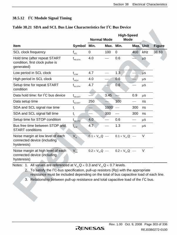
Section 38 Electrical Characteristics
Rev. 1.00 Oct. 9, 2008 Page 303 of 336
REJ03B0272-0100
38.5.12 I2C Module Signal Timing
Table 38.21 SDA and SCL Bus Line Characteristics for I2C Bus Device
Normal Mode High-Speed
Mode
Item Symbol Min. Max. Min. Max. Unit Figure
SCL clock frequency fSCL 0 100 0 400 kHz
Hold time (after repeat START condition, first clock pulse is generated)
tHD;STA 4.0 ⎯ 0.6 ⎯ μs
Low period in SCL clock tLOW 4.7 ⎯ 1.3 ⎯ μs
High period in SCL clock tHIGH 4.0 ⎯ 0.6 ⎯ μs
Setup time for repeat START condition
tSU;STA 4.7 ⎯ 0.6 ⎯ μs
Data hold time: for I2C bus device tHD;DAT ⎯ 3.45 ⎯ 0.9 μs
Data setup time tSU;DAT 250 ⎯ 100 ⎯ ns
SDA and SCL signal rise time tr ⎯ 1000 ⎯ 300 ns
SDA and SCL signal fall time tf ⎯ 300 ⎯ 300 ns
Setup time for STOP condition tSU;STO 4.0 ⎯ 0.6 ⎯ μs
Bus free time between STOP and START conditions
tBUF 4.7 ⎯ 1.3 ⎯ μs
Noise margin at low level of each connected device (including hysteresis)
VnL 0.1 × VCCQ ⎯ 0.1 × VCCQ ⎯ V
Noise margin at high level of each connected device (including hysteresis)
VnH 0.2 × VCCQ ⎯ 0.2 × VCCQ ⎯ V
38.63
Notes: 1. All values are referenced at VCCQ × 0.3 and VCCQ × 0.7 levels. 2. To satisfy the I2C-bus specification, pull-up resistors (Rp) with the appropriate
resistance must be included depending on the total of bus capacitive load of each line. 3. Relationship between pull-up resistance and total capacitive load of the I2C bus.

Section 38 Electrical Characteristics
Rev. 1.00 Oct. 9, 2008 Page 304 of 336
REJ03B0272-0100
0.0
2.0
4.0
6.0
8.0
10.0
12.0
14.0
0
5
10
15
20
25
30
35
40
45
50
20 40 6030 50 70 80 90 100 20 40 60 8030 50 70 90 100
(1) When SCL = 100 kHz
Total of bus capacitive load (pF)(2) When SCL = 400 kHz
Total of bus capacitive load (pF)
Pul
l-up
resi
stan
ce R
p (k
Ω)
Pul
l-up
resi
stan
ce R
p (k
Ω)
Maximum valueof RpMinimum valueof Rp
Maximum valueof RpMinimum valueof Rp
* A hold time of at least 300 ns is internally assured for the SDA signal (relative to VIHmin of the SCL signal). The state of the SDA signal is stabilized on falling edges of the SCL signal.
tLOW
VCC × 0.3
VCC × 0.7
tHD; STA
tHD;DAT
tr
tf
tSU; DAT
tHIGH
tSU; STA
tHD; STAtSU; STO tBUF
tSP
VnH
tf
tr
VnL
SCL
SDA
S Sr P S
Figure 38.63 Device Timing Definition on I2C Bus

Section 38 Electrical Characteristics
Rev. 1.00 Oct. 9, 2008 Page 305 of 336
REJ03B0272-0100
38.5.13 FLCTL Module Signal Timing
Table 38.22 AND-Type Flash Memory Interface Timing
Item Symbol Min. Max. Unit Figure
Command issue setup time tACDS 2 × tfcyc − 10 ⎯ ns
Command issue hold time tACDH 2 × tfcyc − 10 ⎯ ns
38.64, 38.68
Data output setup time tADOS tfcyc − 10 ⎯ ns
Data output hold time tADOH tfcyc − 10 ⎯ ns
38.64, 38.65, 38.68
Data output setup time 2 tADOS2 0.5 × tfcyc − 10 ⎯ ns
Data output hold time 2 tADOH2 0.5 × tfcyc − 10 ⎯ ns
38.67
FWE cycle time tACWC 2 × tfcyc − 5 ⎯ ns 38.65
FWE low pulse width tAWP tfcyc − 5 ⎯ ns 38.64, 38.65, 38.68
FWE high pulse width tAWPH tfcyc − 5 ⎯ ns
Command to address transition time tACAS 4 × tfcyc ⎯ ns
38.65
Address to data read transition time tAADDR 32 × tpcyc ⎯ ns
Address to ready/busy transition time tAADRB ⎯ 35 × tpcyc ns
Ready/busy to data read transition time
tARBDR tfcyc ⎯ ns
Data read setup time tADRS tfcyc − 10 ⎯ ns
38.66
FSC cycle time tASCC tfcyc − 5 ⎯ ns
FSC high pulse width tASP 0.5 × tfcyc − 5 ⎯ ns
FSC low pulse width tASPL 0.5 × tfcyc − 5 ⎯ ns
38.66, 38.67
Read data setup time tARDS 24 ⎯ ns
Read data hold time tARDH 5 ⎯ ns
38.67, 38.68
Address to data write transition time tAADDW 32 × tPCYC ⎯ ns
Data write setup time tADWS 4.5 × tfcyc + tpcyc − 10
⎯ ns
38.67
FSC to FOE hold time tASOH 2 × tfcyc − 10 ⎯ ns 38.66
Note: tfcyc indicates the period of one cycle of the FCLK.
tpcyc indicates the period of one cycle of the peripheral clock (Pφ).

Section 38 Electrical Characteristics
Rev. 1.00 Oct. 9, 2008 Page 306 of 336
REJ03B0272-0100
tADOS
tACDS tAWP tACDH
tADOH
(Low)
(Low)
(High)
(High)
FCE
FCDE
FOE
FWE
FSC
NAF7 to NAF0
FRB
Command
Figure 38.64 Command Issue Timing of AND-Type Flash Memory
tAWP
tACWC
tAWPtAWPH
tADOS tADOS tADOHtADOH
tACAS
(Low)
(Low)
(High)
(High)
FCE
FCDE
FOE
FWE
FSC
NAF7 to NAF0
FRB
Address Address
Figure 38.65 Address Issue Timing of AND-Type Flash Memory

Section 38 Electrical Characteristics
Rev. 1.00 Oct. 9, 2008 Page 307 of 336
REJ03B0272-0100
tASPtAADDR
tAADRB tARBDR
tADRS tASPL
tARDS tARDH
tASPLtASOHtASP
tASCC
(Low)
(High)
FCE
FCDE
FOE
FWE
FSC
NAF7 to NAF0
FRB
Data Data
Figure 38.66 Data Read Timing of AND-Type Flash Memory
tASP
tAADDW tADWS
tASPL
tADOH2
tADOS2
tADOS2
tADOS2
tADOS2
tADOH2
tADOH2
tASPLtASP tASPtASPL
tASCC
(Low)FCE
FCDE
FOE
FWE
FSC
NAF7 to NAF0
NRB
(High)
(High)
DataData Data
Figure 38.67 Data Write Timing of AND-Type Flash Memory

Section 38 Electrical Characteristics
Rev. 1.00 Oct. 9, 2008 Page 308 of 336
REJ03B0272-0100
tADOS
tACDS tAWP tACDH
tADOH
(Low)
(Low)
(High)
FCE
FCDE
FOE
FWE
FSC
NAF7 to NAF0
FRB
tARDS tARDH
Command Status
Figure 38.68 Status Read Timing of AND-Type Flash Memory

Section 38 Electrical Characteristics
Rev. 1.00 Oct. 9, 2008 Page 309 of 336
REJ03B0272-0100
Table 38.23 NAND-Type Flash Memory Interface Timing
Item Symbol Min. Max. Unit Figure
Command output setup time tNCDS 2 × tfcyc − 10 ⎯ ns
Command output hold time tNCDH 1.5 × tfcyc − 5 ⎯ ns
38.69, 38.73
Data output setup time tNDOS 0.5 × tfcyc − 5 ⎯ ns
Data output hold time tNDOH 0.5 × tfcyc − 10 ⎯ ns
38.69, 38.70, 38.72, 38.73
Command to address transition time 1 tNCDAD1 1.5 × tfcyc − 10 ⎯ ns 38.69, 38.70
Command to address transition time 2 tNCDAD2 2 × tfcyc − 10 ⎯ ns 38.70
FWE cycle time tNWC tfcyc − 5 ⎯ ns 38.70, 38.72
FWE low pulse width tNWP 0.5 × tfcyc − 5 ⎯ ns 38.69, 38.70, 38.72, 38.73
FWE high pulse width tNWH 0.5 × tfcyc − 5 ⎯ ns 38.70, 38.72
Address to ready/busy transition time tNADRB ⎯ 32 × tpcyc ns 38.70, 38.71
Ready/busy to data read transition time 1
tNRBDR1 1.5 × tfcyc ⎯ ns
Ready/busy to data read transition time 2
tNRBDR2 32 × tpcyc ⎯ ns
FSC cycle time tNSCC tfcyc − 5 ⎯ ns
38.71
FSC low pulse width tNSP 0.5 × tfcyc − 5 ⎯ ns 38.71, 38.73
FSC high pulse width tNSPH 0.5 × tfcyc − 5 ⎯ ns 38.71
Read data setup time tNRDS 24 ⎯ ns
Read data hold time tNRDH 5 ⎯ ns
38.71, 38.73
Data write setup time tNDWS 32 × tpcyc ⎯ ns 38.72
Command to status read transition time
tNCDSR 4 × tfcyc ⎯ ns
Command output off to status read transition time
tNCDFSR 3.5 × tfcyc ⎯ ns
Status read setup time tNSTS 2.5 × tfcyc ⎯ ns
38.73
Note: tfcyc indicates the period of one cycle of the FCLK.
tpcyc indicates the period of one cycle of the peripheral clock (Pφ).

Section 38 Electrical Characteristics
Rev. 1.00 Oct. 9, 2008 Page 310 of 336
REJ03B0272-0100
tNDOS
tNCDS tNWP tNCDH
tNCDAD1
tNDOH
(Low)
(High)
(High)
FCE
FCDE
FOE
FWE
FSC
NAF7 to NAF0
FRB
Command
Figure 38.69 Command Issue Timing of NAND-Type Flash Memory
tNWP tNWP tNCDAD1
tNADRB
tNWH tNWP tNWH
tNDOS tNDOH tNDOS tNDOH tNDOS tNDOH
tNWC
tNCDAD2
(Low)
(High)
(High)
FCE
FCDE
FOE
FWE
FSC
NAF7 to NAF0
FRB
Address Address Address
Figure 38.70 Address Issue Timing of NAND-Type Flash Memory

Section 38 Electrical Characteristics
Rev. 1.00 Oct. 9, 2008 Page 311 of 336
REJ03B0272-0100
tNSPtNRBDR2
tNADRB tNRBDR1
tNSPH
tNRDS tNRDH
tNSPtNSP
tNSCC
tNRDS tNRDS tNRDH
(Low)
(Low)
FCE
FCDE
FOE
FWE
FSC
NAF7 to NAF0
FRB
(High)
Data Data
Figure 38.71 Data Read Timing of NAND-Type Flash Memory
tNWPtNDWS tNWH
tNDOS tNDOH
tNWPtNWP
tNWC
tNDOS tNDOS tNDOH
(Low)
(Low)
FCE
FCDE
FOE
FWE
FSC
NAF7 to NAF0
FRB
(High)
(High)
Data Data
Figure 38.72 Data Write Timing of NAND-Type Flash Memory

Section 38 Electrical Characteristics
Rev. 1.00 Oct. 9, 2008 Page 312 of 336
REJ03B0272-0100
tNDOS
tNCDS tNWP tNCDH tNSTS
tNCDFSR
tNDOH
(Low)
(High)
FCE
FCDE
FOE
FWE
FSC
NAF7 to NAF0
FRB
(Low)
tNRDS
tNSPtNCDSR
tNRDH
Command Status
Figure 38.73 Status Read Timing of NAND-Type Flash Memory

Section 38 Electrical Characteristics
Rev. 1.00 Oct. 9, 2008 Page 313 of 336
REJ03B0272-0100
38.5.14 VIO Module Signal Timing
Table 38.24 VIO Module Signal Timing
Item Symbol Min. Max. Unit Figure
Vertical sync (VIO_VD) setup time tVVDS 10 ⎯ ns
Vertical sync (VIO_VD) hold time tVVDH 10 ⎯ ns
Horizontal sync (VIO_HD) setup time tVHDS 10 ⎯ ns
Horizontal sync (VIO_HD) hold time tVHDH 10 ⎯ ns
Capture image data (VIO_D) setup time tVDTS 10 ⎯ ns
Capture image data (VIO_D) hold time tVDTH 10 ⎯ ns
Camera clock cycle tVCYC tbcyc* ⎯ ns
Camera clock high width tVHW 0.4 × tVcyc ⎯ ns
Camera clock low width tVLW 0.4 × tVcyc ⎯ ns
Field identification signal (VIO_FLD) setup time tVFDS 10 ⎯ ns
Field identification signal (VIO_FLD) hold time tVFDH 10 ⎯ ns
38.74
Note: * tbcyc is a cycle time of an internal bus clock (Bφ).
tVHDH
tVCYC
tVHW tVLW
tVHDS
tVVDH
tVVDS
tVDTH
tVDTS
VIO_CLK
VIO_HD
VIO_VD
tVFDH
tVFDS
VIO_FLD
VIO_D15 toVIO_D0
Data
Figure 38.74 VIO Module Signal Timing

Section 38 Electrical Characteristics
Rev. 1.00 Oct. 9, 2008 Page 314 of 336
REJ03B0272-0100
38.5.15 LCDC Module Signal Timing
Table 38.25 LCDC Module Signal Timing
Item Symbol Min. Max. Unit Figure
Clock (LCDDCK) cycle time tLCC 30 ⎯ ns
Clock (LCDLCLK) cycle time tLCLC 1/fBφ ⎯ ns
Clock (LCDDCK) high pulse time tLCHW 9 ⎯ ns
Clock (LCDDCK) low pulse time tLCLW 9 ⎯ ns
Data (LCDD) delay time tLDD −12 12 ns
Display enable (LCDDISP) delay time tLID −12 12 ns
Horizontal sync signal (LCDHSYN) delay time tLHD −12 12 ns
Vertical sync signal (LCDVSYN) delay time tLVD −12 12 ns
38.75
Chip select signal (LCDCS, LCDCS2) SYS interface command delay time
tLSYSCSD ⎯ 22 ns
Write strobe signal (LCDDCK) SYS interface command delay time
tLSYSWRD ⎯ 22 ns
Register select signal (LCDDISP) SYS interface command delay time
tLSYSRSD ⎯ 22 ns
Data (LCDD) SYS interface command write data delay time
tLSYSDD ⎯ 22 ns
38.76
Read strobe signal (LCDRD) SYS interface command delay time
tLSYSRDD ⎯ 22 ns
Data (LCDD) SYS interface read data setup time tLSYSRDS 10 ⎯ ns
Data (LCDD) SYS interface read data hold time tLSYSRDH 5 ⎯ ns
Read write signal (LCDVCPWC) SYS interface command delay time
tLSYSRDWRD −12 12 ns
38.77
Write strobe signal (LCDWR) SYS interface data cycle time
tLSYSDWRC 30 ⎯ ns
Write strobe signal (LCDWR) SYS interface data high pulse time
tLSYSDWRHW 9 ⎯ ns
38.78

Section 38 Electrical Characteristics
Rev. 1.00 Oct. 9, 2008 Page 315 of 336
REJ03B0272-0100
Item Symbol Min. Max. Unit Figure
Write strobe signal (LCDWR) SYS interface data low pulse time
tLSYSDWRLW 9 ⎯ ns
Write strobe signal (LCDWR) SYS interface data address setup time
tLSYSDAS 1 tLSYSDWRC − 12
1 tLSYSDWRC + 12
ns
Write strobe signal (LCDWR) SYS interface data address hold time*
tLSYSDAH 1 tLSYSDWRHW − 12
1 tLSYSDWRHW + 12
ns
Data (LCDD) SYS interface data delay time tLSYSDDD −12 12 ns
38.78
Input vertical sync signal (LCDVSYN, LCDVSYN2) setup time
tLVIS 10 ⎯ ns
Input vertical sync signal (LCDVSYN, LCDVSYN2) hold time
tLVIH 5 ⎯ ns
38.79
Note: * The minimum value of tLSYSDAH is one unit of tLSYSDWRHW. tLSYSDWRHW can be arbitrarily set by LCDDCKPATxR (x = 1 to 4).
tLDD
tLCHW tLCLW tLCC
LCDD17 toLCDD0
LCDDCK
LCDDISP
LCDRD
LCDHSYN
LCDVSYN
tLID
tLRDD
tLHD
tLVD
0.8Vcc
0.2Vcc
Figure 38.75 LCDC AC Characteristics

Section 38 Electrical Characteristics
Rev. 1.00 Oct. 9, 2008 Page 316 of 336
REJ03B0272-0100
CKO
(Low)
tLSYSCSD
tLSYSWRD
tLSYSRSD
tLSYSDD
tLSYSCSD
tLSYSWRD
tLSYSRSD
tLSYSDD
LCDHSYN
LCDDCK
LCDD17 to LCDD0
VCPWC
LCDDISP
Figure 38.76 LCDC AC Characteristics SYS Interface, Command Write Bus Cycle (MLDMT2R.WCEC = 4, MLDMT2R.WCLW = 3, SLDMT2R.WCEC = 4, SLDMT2R.WCLW = 3)
CKO
tLSYSCSD
tLSYSRDD
tLSYSRSD
tLSYSRDS
tLSYSCSD
tLSYSRDD
tLSYSRDWRD tLSYSRDWRD
tLSYSRSD
tLSYSRDH
LCDHSYN
LCDRD
LCDD17 toLCDD0
VCPWC
LCDDISP
Figure 38.77 LCDC AC Characteristics SYS Interface, Command Read Bus Cycle (MLDMT3R.RDLC = 4, MLDMT3R.RCEC = 4, MLDMT3R.RCLW = 3,
SLDMT3R.RDLC = 4, SLDMT3R.RDLC = 4, SLDMT3R.RCEC = 4, SLDMT3R.RCLW = 3)

Section 38 Electrical Characteristics
Rev. 1.00 Oct. 9, 2008 Page 317 of 336
REJ03B0272-0100
LCDCS
LCDWR
tLSYSDWRHW
tLSYSDDD
(Low or High)
(Low)
tLSYSDAHtLSYSDWRLW
LCDD17 toLCDD0
LCDVCPWC
LCDRS
tLSYSDAS tLSYSDWRC
Figure 38.78 LCDC AC Characteristics (SYS Interface, Data Write Bus Cycle)
CKO
tLVIS tLVIH
LCDVSYN2
tLVIS tLVIH
LCDVSYN(Input)
Figure 38.79 LCDC AC Characteristics (VSYNC Input Mode)

Section 38 Electrical Characteristics
Rev. 1.00 Oct. 9, 2008 Page 318 of 336
REJ03B0272-0100
38.5.16 VOU Module Signal Timing
Table 38.26 VOU Module Signal Timing
Item Symbol Min. Typ. Max. Unit Figure
Output clock frequency fpx1 13.5 ⎯ 27 MHz
Output clock cycle t pxcyc1 37 ⎯ 74.1 ns
Output clock high width t pxwH1 14 ⎯ ⎯ ns
Output clock low width t pxwL1 14 ⎯ ⎯ ns
Output data delay time t pxd1 −4 ⎯ 4 ns
38.80
Output clock frequency 2 fpx2 13.5 ⎯ 27 MHz
Output clock cycle 2 t pxcyc2 37 ⎯ 74.1 ns
Output clock high width 2 t pxwH2 14 ⎯ ⎯ ns
Output clock low width 2 t pxwL2 14 ⎯ ⎯ ns
Output data delay time 2 t pxd2 −4 ⎯ 4 ns
38.81
DV_CLK
tpxd1
tpxwH1
tpxcyc1
tpxwL1
DV_HSYNCDV_VSYNCDV_D15 to DV_D0
Figure 38.80 VOU AC Characteristics (VOUCR.CKPL = 0)
DV_CLK
tpxd2
tpxwH2
tpxcyc2
tpxwL2
DV_HSYNCDV_VSYNCDV_D15 to DV_D0
Figure 38.81 VOU AC Characteristics (VOUCR.CKPL = 1)

Section 38 Electrical Characteristics
Rev. 1.00 Oct. 9, 2008 Page 319 of 336
REJ03B0272-0100
38.5.17 TSIF Module Signal Timing
Table 38.27 TSIF Module Signal Timing
Item Symbol Min. Max. Unit Figure
Bφ ≥ 40 MHz tTSCYC 25 ⎯ ns TSIF input clock cycle
Bφ < 40 MHz tTSCYC tbcyc* ⎯ ns
TSIF input clock high width tTSHW 0.4 × tTSCYC ⎯ ns
TSIF input clock low width tTSLW 0.4 × tTSCYC ⎯ ns
TSIF input data setup time tTSDTS 5 ⎯ ns
TSIF input data hold time tTSDTH 5 ⎯ ns
TSIF input data enable signal setup time tTSDES 5 ⎯ ns
TSIF input data enable signal hold time tTSDEH 5 ⎯ ns
TSIF input data sync signal setup time tTSSYS 5 ⎯ ns
TSIF input data sync signal hold time tTSSYH 5 ⎯ ns
38.82
Note: * tbcyc is a cycle time of an internal bus clock (Bφ).
tTSCYC
tTSLW
tTSDEH
tTSHW
tTSDTS tTSDTH
tTSDES
TS_SCK
TS_SDAT
TS_SDEN
tTSSYHtTSSYS
TS_SPSYNC
Figure 38.82 TSIF Module Signal Timing (TSCTLR.TSDATP = 0, TSCTLR.TSCLKP = 1,
TSCTLR.TSVLDP = 0, TSCTLR.PSYCP = 0)

Section 38 Electrical Characteristics
Rev. 1.00 Oct. 9, 2008 Page 320 of 336
REJ03B0272-0100
38.5.18 SIU Module Signal Timing
Table 38.28 SIU Module Signal Timing
Item Symbol Min. Max. Unit Figure
SIUMCK clock input cycle time tSIUMCYC 40 ⎯ ns
SIUMCK input high width tSIUMWH 0.4 × tSIUMCYC ⎯ ns
SIUMCK input low width tSIUMWL 0.4 × tSIUMCYC ⎯ ns
38.84
SIU_BT clock cycle time tSIUSICYC 300 ⎯ ns
SIU_BT output high width tSIUSWHO 0.4 × tSIUSICYC ⎯ ns
SIU_BT output low width tSIUSWLO 0.4 × tSIUSICYC ⎯ ns
SIU_LR output delay time tSIUFSD — 20 ns
SIU_BT input high width tSIUSWHI 0.4 × tSIUSICYC ⎯ ns
SIU_BT input low width tSIUSWLI 0.4 × tSIUSICYC ⎯ ns
SIU_SLD output delay time tSIUSTDD — 20 ns
SIU_SLD input setup time tSIUSRDS 20 ⎯ ns
SIU_SLD input hold time tSIUSRDH 20 ⎯ ns
38.83
tSIUSICYC
tSIUSWHOtSIUSWLO
tSIUSTDD tSIUSTDDtSIUSTDDtSIUSTDD
tSIUSRDS tSIUSRDH
tSIUFSD tSIUFSD
SIUAOLR SIUAILRSIUBOLR SIUBILR
SIUAOBTSIUAIBTSIUBOBTSIUBIBT
SIUAOSLDSIUBOSLD
SIUAISLDSIUBISLD
tSIUSWHItSIUSWLI
Figure 38.83 SIU Transmission Timing

Section 38 Electrical Characteristics
Rev. 1.00 Oct. 9, 2008 Page 321 of 336
REJ03B0272-0100
tSIUMWH tSIUMWL
tSIUMCYC
SIUMCKA, SIUMCKB
Figure 38.84 SIUMCK Input Timing
38.5.19 USB Transceiver Timing (Full-Speed)
Table 38.29 USB Transceiver Timing (Full-Speed)
Item Symbol Min. Max. Unit Test Condition
Rising time tr 4 20 ns Data signal: 10% of amplitude → 90%
CL = 50 pF
Falling time tf 4 20 ns Data signal: 90% of amplitude → 10%
CL = 50 pF
Ratio of rising time to falling time tr/tf 90 111.1 %
Output signal crossover voltage 1.3 2.0 V CL = 50 pF
Output driver resistance* ZDRU 28 44 Ω
Note: This transceiver timing is a timing at full-speed.

Section 38 Electrical Characteristics
Rev. 1.00 Oct. 9, 2008 Page 322 of 336
REJ03B0272-0100
RL = 15 kΩ CL
GND
VDD
DM
DPD+
RL = 15 kΩ CL
D−
1. tr and tf are determined by the time taken for the trasitions between 10% and 90% of amplitude.2. The electrostatic capacitance, CL, includes the stray capacitance of the wiring connection and the input capacitance of the probe.
Test element
Notes:
Figure 38.85 Test Circuit for USB Transceiver (Full-Speed)
38.5.20 KEYSC Module Signal Timing
Table 38.30 KEYSC Module Signal Timing
Item Symbol Min. Max. Unit Figure
KEYIN input setup time tKEYINS 15 ⎯ ns
KEYIN input hold time tKEYINH 15 ⎯ ns
38.85
KEYOUT delay time tKEYOUTD ⎯ 15 ns 38.86
RCLK
KEYIN6 to KEYIN0
tKEYINS tKEYINH
Note: KEYIN is an asynchronous signal. When the setup time in this figure is satisfied, a change is detected at the rising edge of the clock. When the setup time is not satisfied, a change may not be detected until the next rising edge of the clock.
Figure 38.86 KEYIN Input Timing

Section 38 Electrical Characteristics
Rev. 1.00 Oct. 9, 2008 Page 323 of 336
REJ03B0272-0100
RCLK
KEYOUT5 to KEYOUT0
tKEYOUTD
Figure 38.87 KEYOUT Output Timing
38.5.21 AC Characteristic Test Conditions
VCCQ2• I/O signal reference level:
• Input pulse level: Vss to VCCQ
• Input rise and fall times: 1 ns
IOL
IOH
CL VREF
LSI output pin
Reference voltageof output load switch
Notes: CL is the total value that includes the capacitance of measurement instruments,and is set as follows for each pin:30 pF: CKO, CS0, CS2 to CS6B50 pF: All other pinsIOL = 0.2 mA, IOH = −0.2 mA
1.
2.
Figure 38.88 Output Load Circuit

Section 38 Electrical Characteristics
Rev. 1.00 Oct. 9, 2008 Page 324 of 336
REJ03B0272-0100

Appendix
Rev. 1.00 Oct. 9, 2008 Page 325 of 336
REJ03B0272-0100
Appendix

Appendix
Rev. 1.00 Oct. 9, 2008 Page 326 of 336
REJ03B0272-0100
A. Pin States in Reset and Power-Down States
Category Pin Name During Reset*1 After Reset*2 Sleep
Software
Standby U-Standby*9
EXTAL I I I I I
RCLK I I I I I
Clock
XTAL O O O O O
MD2 to MD0 I I I I I
MD3 I I I I I
MD5 I I I I I
MD8 I I I I I
TST I I I I I
Operating
mode control
TSTMD I I I I I
RESETA I I I I I
RESETOUT L H O O O
RESETP I I I I I
PDSTATUS L O L L H
System
control
STATUS0 L O L H H
IRQ1, IRQ0 ⎯ ⎯ I I I
IRQ2 ⎯ ⎯ I I I
IRQ5 to IRQ3 ⎯ ⎯ I I I
IRQ6 ⎯ ⎯ I I I
IRQ7 ⎯ ⎯ I I I
Interrupt
NMI I I I I I
A25 to A0 L O O O/Z*3 O/Z*3
D31 to D0 Z Z Z/I/O Z Z
BS ⎯ ⎯ O H/Z*3 H/Z*3
CKO O O O O/Z*3 O/Z*3
CS0 H O O H/Z*3 H/Z*3
CS4 H O O H/Z*3 H/Z*3
BSC
CS5A H O O H/Z*3 H/Z*3

Appendix
Rev. 1.00 Oct. 9, 2008 Page 327 of 336
REJ03B0272-0100
Category Pin Name During Reset*1 After Reset*2 Sleep
Software
Standby U-Standby*9
CS5B H O O H/Z*3 H/Z*3
CS6A ⎯ ⎯ O H/Z*3 H/Z*3
CS6B H O O H/Z*3 H/Z*3
RD H O O H/Z*3 H/Z*3
RDWR H O O H/Z*3 H/Z*3
WE3 to WE0 H O O H/Z*3 H/Z*3
WAIT IU IU IU IU IU
BSC
IOIS16 I I I Z Z
HPA16 to HPA1 L O O O/Z*4 O/Z*4
HPD63 to HPD0 Z Z Z/I/O Z Z
HPCS2 H O O O/Z*4 O/Z*4
HPCS3 H O O O/Z*4 O/Z*4
HPCAS H O O O/Z*4 O/Z*4
HPRAS H O O O/Z*4 O/Z*4
HPCKE O O O O/Z*4 O/Z*4
HPCLK O O O O/Z*4 O/Z*4
HPCLKR O O O O/Z*4 O/Z*4
HPCLKD O O O O/Z*4 O/Z*4
HPDQM7 to HPDQM0 H O O O/Z*4 O/Z*4
SBSC (SDRAM bus)
HPRDWR H O O O/Z*4 O/Z*4
DACK0 ⎯ ⎯ O O O DMAC
DREQ0 ⎯ ⎯ I Z Z
TPU TPUTO ⎯ ⎯ O O O
SIOD ⎯ ⎯ Z/I/O*5 Z/I/O*5 Z/I/O*5
SIOMCK ⎯ ⎯ I Z Z
SIORXD ⎯ ⎯ I Z Z
SIOSCK ⎯ ⎯ O O O
SIOSTRB0,
SIOSTRB1
⎯ ⎯ O O O
SIO
SIOTXD ⎯ ⎯ O Z/O*5 Z/O*5

Appendix
Rev. 1.00 Oct. 9, 2008 Page 328 of 336
REJ03B0272-0100
Category Pin Name During Reset*1 After Reset*2 Sleep
Software
Standby U-Standby*9
SIOF0_MCK,
SIOF1_MCK ⎯ ⎯ I Z Z
SIOF0_RXD,
SIOF1_RXD
⎯ ⎯ I Z Z
SIOF0_SCK,
SIOF1_SCK
⎯ ⎯ O/I*5 O/Z*5 O/Z*5
SIOF0_SS1, SIOF1_SS1
⎯ ⎯ O O O
SIOF0_SS2, SIOF1_SS2
⎯ ⎯ O O O
SIOF0_SYNC,
SIOF1_SYNC
⎯ ⎯ O/I*5 O/Z*5 O/Z*5
SIOF
SIOF0_TXD,
SIOF1_TXD
⎯ ⎯ O O O
SCIF0_CTS, SCIF1_CTS, SCIF2_CTS
⎯ ⎯ I Z Z
SCIF0_RTS, SCIF1_RTS, SCIF2_RTS
⎯ ⎯ O Z Z
SCIF0_RXD,
SCIF1_RXD, SCIF2_RXD
⎯ ⎯ I Z Z
SCIF0_SCK,
SCIF1_SCK,
SCIF2_SCK
⎯ ⎯ I Z Z
SCIF
SCIF0_TXD,
SCIF1_TXD,
SCIF2_TXD
⎯ ⎯ O Z Z
SIM_CLK ⎯ ⎯ O O O
SIM_D ⎯ ⎯ I/O Z Z
SIM
SIM_RST ⎯ ⎯ O O O
IrDA_IN ⎯ ⎯ I Z Z IrDA
IrDA_OUT ⎯ ⎯ O O O
SCL Z Z I/O Z Z IIC
SDA Z Z I/O Z Z

Appendix
Rev. 1.00 Oct. 9, 2008 Page 329 of 336
REJ03B0272-0100
Category Pin Name During Reset*1 After Reset*2 Sleep
Software
Standby U-Standby*9
FCDE ⎯ ⎯ O O/Z*5 O/Z*5
FCE ⎯ ⎯ O O O
FOE ⎯ ⎯ O O O
FRB ⎯ ⎯ I Z Z
FSC ⎯ ⎯ O O O
FWE ⎯ ⎯ O O O
FLCTL
NAF7 to NAF0 ⎯ ⎯ Z/I/O Z Z
VIO_CKO ⎯ ⎯ O O O
VIO_CLK ⎯ ⎯ I Z Z
VIO_CLK2 ⎯ ⎯ I Z Z
VIO_D15 to VIO_D0 ⎯ ⎯ I Z Z
VIO_FLD ⎯ ⎯ I Z Z
VIO_HD ⎯ ⎯ I Z Z
VIO_HD2 ⎯ ⎯ I Z Z
VIO_STEM ⎯ ⎯ O O O
VIO_STEX ⎯ ⎯ I Z Z
VIO_VD ⎯ ⎯ I Z Z
VIO
VIO_VD2 ⎯ ⎯ I Z Z
DV_CLK ⎯ ⎯ O O O
DV_CLKI ⎯ ⎯ I Z Z
DV_D15 to DV_D0 ⎯ ⎯ O O O
DV_HSYNC ⎯ ⎯ O O O
VOU
DV_VSYNC ⎯ ⎯ O O O
LCDLCLK ⎯ ⎯ I Z Z
LCDCS ⎯ ⎯ O O O
LCDCS2 ⎯ ⎯ O O O
LCDD23 to LCDD0 ⎯ ⎯ O/I O/Z O/Z
LCDDCK ⎯ ⎯ O O O
LCDDISP ⎯ ⎯ O O O
LCDDON, LCDDON2 ⎯ ⎯ O O O
LCDC
LCDHSYN ⎯ ⎯ O O O

Appendix
Rev. 1.00 Oct. 9, 2008 Page 330 of 336
REJ03B0272-0100
Category Pin Name During Reset*1 After Reset*2 Sleep
Software
Standby U-Standby*9
LCDRD ⎯ ⎯ O O O
LCDRS ⎯ ⎯ O O O
LCDVCPWC/
LCDVCPWC2
⎯ ⎯ O O O
LCDVEPWC/
LCDVEPWC2
⎯ ⎯ O O O
LCDVSYN, LCDVSYN2 ⎯ ⎯ O/Z*5 O/Z*5 O/Z*5
LCDC
LCDWR ⎯ ⎯ O O O
TS_SCK ⎯ ⎯ I Z Z
TS_SDAT ⎯ ⎯ I Z Z
TS_SDEN ⎯ ⎯ I Z Z
TSIF
TS_SPSYNC ⎯ ⎯ I Z Z
SIUAIBT,
SIUBIBT
⎯ ⎯ I/O*5 Z/O*5 Z/O*5
SIUAILR,
SIUBILR
⎯ ⎯ I/O*5 Z/O*5 Z/O*5
SIUAISLD,
SIUBISLD
⎯ ⎯ I Z Z
SIUAISPD ⎯ ⎯ I Z Z
SIUAOBT,
SIUBOBT
⎯ ⎯ I/O*5 Z/O*5 Z/O*5
SIUAOLR,
SIUBOLR
⎯ ⎯ I/O*5 Z/O*5 Z/O*5
SIUAOSLD,
SIUBOSLD
⎯ ⎯ O O O
SIUAOSPD ⎯ ⎯ O O O
SIUFCKA, SIUFCKB ⎯ ⎯ O O O
SIU
SIUMCKA, SIUMCKB ⎯ ⎯ I Z Z
DM L L Z/I/O Z Z
DP H H Z/I/O Z Z
VBUS I I I I I
EXTALUSB I I I I I
USB
XTALUSB O O O O O

Appendix
Rev. 1.00 Oct. 9, 2008 Page 331 of 336
REJ03B0272-0100
Category Pin Name During Reset*1 After Reset*2 Sleep
Software
Standby U-Standby*9
KEYIN1, KEYIN0 ⎯ ⎯ IU IU IU
KEYIN4 to KEYIN2 ⎯ ⎯ IU IU IU
KEYOUT3 to
KEYOUT0
⎯ ⎯ Z/O*5 Z/O*5 Z/O*5
KEYOUT4/IN6 ⎯ ⎯ Z/I/O*5 Z/I/O*5 Z/I/O*5
KEYSC
KEYOUT5/IN5 ⎯ ⎯ Z/I/O*5 Z/I/O*5 Z/I/O*5
SDHICD ⎯ ⎯ I Z Z
SDHIWP ⎯ ⎯ I Z Z
SDHID3 to SDHID0 ⎯ ⎯ I/O Z Z
SDHICLK ⎯ ⎯ O Z Z
SDHI
SDHICMD ⎯ ⎯ I/O Z Z
TCK IU IU IU IU IU
TDI IU IU IU IU IU
TDO Z/O Z/O Z/O*6 Z/O*6 Z/O*6
TMS IU IU IU IU IU
TRST IU IU IU*7 IU*7 IU*7
ASEBRK/BRKAK IU/OU*8 IU/OU*8 IU/OU*8 IU/OU*8 IU/OU*8
H-UDI
MPMD IU IU IU IU IU
AUDATA3 to AUDATA0 ⎯ ⎯ O O O
AUDCK O O O O O
AUD
AUDSYNC ⎯ ⎯ O O O
Port A PTA7 to PTA0 ZD ID P K K
Port B PTB7 to PTB0 ⎯ ⎯ P K K
PTC4 to PTC2, PTC0 ⎯ ⎯ P K K
PTC5 ⎯ ⎯ P K K
Port C
PTC7 ZU IU P K K
PTD0 L O P K K
PTD1 ZU IU P K K
PTD5 to PTD2 ZU I P K K
PTD6 ZU IU P K K
Port D
PTD7 ZU IU P K K

Appendix
Rev. 1.00 Oct. 9, 2008 Page 332 of 336
REJ03B0272-0100
Category Pin Name During Reset*1 After Reset*2 Sleep
Software
Standby U-Standby*9
PTE1, PTE0 ZU IU P K K Port E
PTE7 to PTE4 ⎯ ⎯ P K K
PTF0 L O P K K
PTF1 ZD ID P K K
Port F
PTF6 to PTF2 ZD ID P K K
Port G PTG4 to PTG0 L O P K K
PTH1, PTH0 ZD ID P K K
PTH4 to PTH2 L O P K K
PTH6, PTH5 ZD ID P K K
Port H
PTH7 L O P K K
PTJ1, PTJ0 ZU IU P K K
PTJ5 ⎯ ⎯ P K K
PTJ6 L O P K K
Port J
PTJ7 ⎯ ⎯ P K K
PTK0 ZD ID P K K
PTK1 L O P K K
PTK2 ZD ID P K K
Port K
PTK6 to PTK3 ZD ID P K K
Port L PTL7 to PTL0 ZD ID P K K
Port M PTM7 to PTM0 ZD ID P K K
Port N PTN7 to PTN0 ⎯ ⎯ P K K
PTQ0 ZU IU P K K
PTQ1 L O P K K
PTQ2 ZD ID P K K
PTQ5 to PTQ3 ZD ID P K K
Port Q
PTQ6 L O P K K
PTR1, PTR0 L O P K K
PTR2 ⎯ ⎯ P K K
PTR3 ⎯ ⎯ P K K
Port R
PTR4 L O P K K

Appendix
Rev. 1.00 Oct. 9, 2008 Page 333 of 336
REJ03B0272-0100
Category Pin Name During Reset*1 After Reset*2 Sleep
Software
Standby U-Standby*9
PTS0 L O P K K
PTS1 ZD ID P K K
PTS2 ZD ID P K K
PTS3 L O P K K
Port S
PTS4 ZD ID P K K
PTT0 L O P K K
PTT1 ZD ID P K K
Port T
PTT4 to PTT2 ZD ID P K K
PTU0 Z Z P K K
PTU1 Z Z P K K
Port U
PTU4 to PTU2 ZD ID P K K
Port V PTV4 to PTV0 ZD ID P K K
PTW0 ZD ID P K K
PTW4 to PTW1 ZD ID P K K
PTW5 L O P K K
Port W
PTW6 ZD ID P K K
PTX5 to PTX0 ZD ID P K K Port X
PTX6 ZU IU P K K
PTY0 Z Z P K K
PTY1 Z Z P K K
Port Y
PTY5 to PTY2 Z Z P K K
PTZ2, PTZ1 ZU Z P K K Port Z
PTZ5 to PTZ3 Z Z P K K
[Legend] I: Input (pull-up/pull-down MOS off) IU: Input (pull-up MOS on)
ID: Input (pull-down MOS on) H: High-level output L: Low-level output
O: Output OU: Output (pull-up MOS on) P: Port function (whether pins are inputs or outputs, or are pulled up or down, depends on the
register settings)

Appendix
Rev. 1.00 Oct. 9, 2008 Page 334 of 336
REJ03B0272-0100
K: Port state retained (fixed to input, output buffer state retained, pull-up/pull-down states retained)
Z: High impedance (fixed to input, output buffer off, pull-up/pull-down MOS off) ZU: Pull-up state (fixed to input, output buffer off, pull-up MOS on) ZD: Pull-down state (fixed to input, output buffer off, pull-down MOS on)
/: Default state on the left side of a slash (/) ⎯: Not selected for the initial function Notes: 1. Period when RESETOUT is asserted after RESETP is negated.
2. After RESETOUT is negated. 3. Z or H/L depending on the HIZMEM and HIZCNT bits in the CMNCR register of BSC. 4. Z or H/L depending on the HIZSTB bit in the SDPCR register of SBSC.
5. Depends on the register setting. 6. Depends on the TAP controller state when MPMD = H. However, the state is on the
right side of a slash (/) when MPMD = L. 7. Able to switch between pull-up MOS on/off, depending on the PULCR register setting. 8. Switching the I/O by the register setting by I/O with pull-up when MPMD = L. Input when
TRST = L. Always input when MPMD = H. 9. On return from U-standby, the states of pins other than clock control and system control
pins are temporarily undefined. The period over which the states are undefined is the following periods at maximum: the system reset asserting period and the DLL/PLL oscillation settling times.

Appendix
Rev. 1.00 Oct. 9, 2008 Page 335 of 336
REJ03B0272-0100
B. Package Dimensions
26 481014 121618202224
B
D
F
H
K
M
P
T
V
Y
AD
AB
A
C
E
G
J
L
N
R
U
W
AE
AC
AA
0.20
SB
21.0
0
0.20 S A
B
0.15
21.00
(Index)
0.80
4 ×
449 × φ 0.50 ± 0.05
0.4
0 ±
0.0
51.
9 M
ax0.10 S
0.200.
900.90
S
A0.80
φ 0.08 M S BA
Unit : mm
Package CodeJEDECJEITAMass
PRBG0449GA-A—— 1.4g
137 591115 131719212325
Figure B.1 Package Dimensions (BGA 449)

Appendix
Rev. 1.00 Oct. 9, 2008 Page 336 of 336
REJ03B0272-0100
2319 21171511 1397531
AC
AA
W
U
R
N
L
J
G
E
A
C
AD
AB
Y
V
T
P
M
K
H
F
B
D
0.2
SB
13.0
0.2 S A
B
0.15
13.0
0.50
4 ×
417 × φ 0.30 ± 0.05
0.2
5 ±
0.0
51.
55 M
ax0.08 S
S0.2
0.75
0.75
S
A0.50
φ 0.05 M S BA
Unit : mm
Package CodeJEDECJEITAMass
— — —0.45g
242118 20161410 128642
Figure B.2 Package Dimensions (LFBGA 417)

Sales Strategic Planning Div. Nippon Bldg., 2-6-2, Ohte-machi, Chiyoda-ku, Tokyo 100-0004, Japan
http://www.renesas.comRefer to "http://www.renesas.com/en/network" for the latest and detailed information.
Renesas Technology America, Inc.450 Holger Way, San Jose, CA 95134-1368, U.S.ATel: <1> (408) 382-7500, Fax: <1> (408) 382-7501 Renesas Technology Europe LimitedDukes Meadow, Millboard Road, Bourne End, Buckinghamshire, SL8 5FH, U.K.Tel: <44> (1628) 585-100, Fax: <44> (1628) 585-900
Renesas Technology (Shanghai) Co., Ltd.Unit 204, 205, AZIACenter, No.1233 Lujiazui Ring Rd, Pudong District, Shanghai, China 200120Tel: <86> (21) 5877-1818, Fax: <86> (21) 6887-7858/7898 Renesas Technology Hong Kong Ltd.7th Floor, North Tower, World Finance Centre, Harbour City, Canton Road, Tsimshatsui, Kowloon, Hong Kong Tel: <852> 2265-6688, Fax: <852> 2377-3473
Renesas Technology Taiwan Co., Ltd.10th Floor, No.99, Fushing North Road, Taipei, Taiwan Tel: <886> (2) 2715-2888, Fax: <886> (2) 3518-3399 Renesas Technology Singapore Pte. Ltd.1 Harbour Front Avenue, #06-10, Keppel Bay Tower, Singapore 098632 Tel: <65> 6213-0200, Fax: <65> 6278-8001
Renesas Technology Korea Co., Ltd.Kukje Center Bldg. 18th Fl., 191, 2-ka, Hangang-ro, Yongsan-ku, Seoul 140-702, KoreaTel: <82> (2) 796-3115, Fax: <82> (2) 796-2145 Renesas Technology Malaysia Sdn. BhdUnit 906, Block B, Menara Amcorp, Amcorp Trade Centre, No.18, Jln Persiaran Barat, 46050 Petaling Jaya, Selangor Darul Ehsan, MalaysiaTel: <603> 7955-9390, Fax: <603> 7955-9510
RENESAS SALES OFFICES
Colophon 6.2

REJ03B0272-01001753, Shimonumabe, Nakahara-ku, Kawasaki-shi , Kanagawa 211-8668 Japan
SH7722Data Sheet