EP9301 Data Sheet - Farnell
41
This document contains information for a new product. Cirrus Logic reserves the right to modify this product without notice. ©Copyright 2005 Cirrus Logic (All Rights Reserved) MAR ‘05 DS636PP5 1 http://www.cirrus.com Entry-level ARM9 System-on-chip Processor EP9301 Data Sheet Preliminary Product Information FEATURES • 166-MHz ARM920T Processor • 16-kbyte Instruction Cache • 16-kbyte Data Cache • Linux ® , Microsoft ® Windows ® CE, enabled MMU • 66-MHz System Bus • MaverickKey ™ IDs • 32-bit unique ID can be used for DRM-compliant, 128-bit random ID. • Integrated Peripheral Interfaces • 16-bit SDRAM Interface (up to 4 banks) • 16-bit SRAM / FLASH / ROM • Serial EEPROM Interface • 1/10/100 Mbps Ethernet MAC • Two UARTs • Two-port USB 2.0 Full-speed Host (OHCI) (12 Mbits per second) • IrDA Interface • ADC • Serial Peripheral Interface (SPI) Port • 6-channel Serial Audio Interface (I 2 S) • 2-channel Low-cost Serial Audio Interface (AC'97) • Internal Peripherals • 12 Direct Memory Access (DMA) Channels • Real-time Clock with software Trim • Dual PLL controls all clock domains. • Watchdog Timer • Two General-purpose 16-bit Timers • One General-purpose 32-bit Timer • One 40-bit Debug Timer • Interrupt Controller • Boot ROM • Package • 208-pin LQFP Unified SDRAM I/F (2) USB Hosts Ethernet MAC Bus Bridge Boot ROM MaverickKey TM 12 Channel DMA SRAM & Flash I/F ARM920T MMU D-Cache 16KB I-Cache 16KB Processor Bus Peripheral Bus Serial Audio Interface Interrupts & GPIO Clocks & Timers (2) UARTs w/ IrDA COMMUNICATIONS PORTS USER INTERFACE MEMORY AND STORAGE
-
Upload
khangminh22 -
Category
Documents
-
view
0 -
download
0
Transcript of EP9301 Data Sheet - Farnell

Entry-level ARM9 System-on-chip Processor
EP9301 Data Sheet
FEATURES• 166-MHz ARM920T Processor
• 16-kbyte Instruction Cache• 16-kbyte Data Cache
• Linux®, Microsoft® Windows® CE, enabled MMU• 66-MHz System Bus
• MaverickKey™ IDs• 32-bit unique ID can be used for DRM-compliant,
128-bit random ID. • Integrated Peripheral Interfaces
• 16-bit SDRAM Interface (up to 4 banks)• 16-bit SRAM / FLASH / ROM • Serial EEPROM Interface• 1/10/100 Mbps Ethernet MAC• Two UARTs• Two-port USB 2.0 Full-speed Host (OHCI)
(12 Mbits per second)• IrDA Interface• ADC• Serial Peripheral Interface (SPI) Port
• 6-channel Serial Audio Interface (I2S)• 2-channel Low-cost Serial Audio Interface (AC'97)
This documentCirrus Logic re
©Copyright 2005 Cirrus L
http://www.cirrus.com
Preliminary Product Information
(2) USBHosts
EthernetMAC
BootROM
MaverickKeyTM
12 Channel DMA
D-1
Processor Bus
SerialAudio
Interface
(2) UARTsw/
IrDA
CO
MM
UN
ICA
TIO
NS
POR
TS
MEMORY AND
• Internal Peripherals• 12 Direct Memory Access (DMA) Channels • Real-time Clock with software Trim • Dual PLL controls all clock domains.• Watchdog Timer• Two General-purpose 16-bit Timers• One General-purpose 32-bit Timer• One 40-bit Debug Timer• Interrupt Controller• Boot ROM
• Package• 208-pin LQFP
contains information for a new product.serves the right to modify this product without notice.
ogic (All Rights Reserved) MAR ‘05DS636PP5
1
UnifiedSDRAM I/F
Bus Bridge
SRAM &Flash I/F
ARM920T
MMU
Cache6KB
I-Cache16KB
Peripheral Bus
Interrupts& GPIO
Clocks &Timers
USER
INTER
FAC
E
STORAGE

EP9301Entry Level ARM9 System-on-Chip Processor
OVERVIEW
The EP9301 is an ARM920T-based system-on-a-chipdesign with a large peripheral set targeted to a variety ofapplications:• Industrial controls • Digital media servers • Integrated home media gateways • Digital audio jukeboxes • Streaming audio players • Set-top boxes • Point-of-sale terminals • Thin clients • Biometric security systems • GPS & fleet management systems • Educational toys • Industrial computers• Industrial hand-held devices• Voting machines • Medical equipment
The EP9301 is one of a series of ARM920T-baseddevices. Other members of the family have differentperipheral sets, a coprocessor, and different packageconfigurations.
2 ©Copyright 2005 Cirrus L
The ARM920T microprocessor core has a separate 16-kbyte, 64-way set-associative instruction and datacaches.
The MaverickKey™ unique hardware programmed IDsare a solution to the growing concern over secure webcontent and commerce. With Internet security playing animportant role in the delivery of digital media such asbooks or music, traditional software methods are quicklybecoming unreliable. The MaverickKey unique IDsprovide OEMs with a method of utilizing specifichardware IDs such as those assigned for SDMI (SecureDigital Music Initiative) or any other authenticationmechanism. A high-performance 1/10/100 Mbps Ethernet mediaaccess controller (EMAC) is included along with externalinterfaces to SPI, AC’97 and I2S audio. A two-port USB2.0 Full-speed Host (OHCI) (12 Mbits per second), twoUARTs, and a analog voltage measurement analog-to-digital converter (ADC) are included as well.
The EP9301 is a high-performance, low-power RISC-based, single-chip computer built around an ARM920Tmicroprocessor core with a maximum operating clockrate of 166 MHz. The ARM core operates from a 1.8 Vsupply, while the I/O operates at 3.3 V with power usagebetween 100 mW and 675 mW.
Table A. Change History
Revision Date Changes
1 October 2003 Initial Release.
2 February 2004 Update timing specifications.
3 July 2004 Update AC data.
4 July 2004 Add ADC data.
5 March 2005 Update with most-current characterization data.
ogic (All Rights Reserved) DS636PP5
EP9301Entry Level ARM9 System-on-Chip Processor
Table of Contents
FEATURES .........................................................................................................1OVERVIEW .........................................................................................................2
Processor Core - ARM920T ......................................................................................... 6MaverickKey™ Unique ID ............................................................................................ 6General Purpose Memory Interface (SDRAM, SRAM, ROM, FLASH) ........................ 6Ethernet Media Access Controller (MAC) .................................................................... 7Serial Interfaces (SPI, I2S, and AC ’97) ....................................................................... 712-bit Analog-to-digital Converter (ADC) ..................................................................... 7Universal Asynchronous Receiver/Transmitters (UARTs) ............................................ 8Dual Port USB Host ..................................................................................................... 8Two-Wire Interface With EEPROM Support ................................................................ 8Real-Time Clock with Software Trim ............................................................................ 8PLL and Clocking ......................................................................................................... 9Timers .......................................................................................................................... 9Interrupt Controller ....................................................................................................... 9Dual LED Drivers ......................................................................................................... 9General Purpose Input/Output (GPIO) ......................................................................... 9Reset and Power Management ................................................................................. 10Hardware Debug Interface ......................................................................................... 1012-Channel DMA Controller ....................................................................................... 10Internal Boot ROM ..................................................................................................... 10
Electrical Specifications ................................................................................. 11Absolute Maximum Ratings ........................................................................................11Recommended Operating Conditions .........................................................................11DC Characteristics ..................................................................................................... 12
Timings .............................................................................................................13Memory Interface ....................................................................................................... 14Ethernet MAC Interface ............................................................................................ 27Audio Interface ........................................................................................................... 29AC’97 ........................................................................................................................ 32ADC ........................................................................................................................... 33JTAG .......................................................................................................................... 34
208 Pin LQFP Package Outline .....................................................................35208 Pin LQFP Pinout ................................................................................................. 36
Acronyms and Abbreviations ........................................................................40Units of Measurement .....................................................................................40ORDERING INFORMATION ............................................................................41
DS636PP5 ©Copyright 2005 Cirrus Logic (All Rights Reserved) 3

EP9301Entry Level ARM9 System-on-Chip Processor
List of Figures
Figure 1. Timing Diagram Drawing Key .................................................................................13Figure 2. SDRAM Load Mode Register Cycle Timing Measurement .....................................14Figure 3. SDRAM Burst Read Cycle Timing Measurement ...................................................15Figure 4. SDRAM Burst Write Cycle Timing Measurement ...................................................16Figure 5. SDRAM Auto Refresh Cycle Timing Measurement ................................................17Figure 6. Static Memory Multiple Word Read 8-bit Cycle Timing Measurement ....................18Figure 7. Static Memory Multiple Word Write 8-bit Cycle Timing Measurement ....................19Figure 8. Static Memory Multiple Word Read 16-bit Cycle Timing Measurement ..................20Figure 9. Static Memory Multiple Word Write 16-bit Cycle Timing Measurement ..................21Figure 10. Static Memory Burst Read Cycle Timing Measurement .......................................22Figure 11. Static Memory Burst Write Cycle Timing Measurement .......................................23Figure 12. Static Memory Single Read Wait Cycle Timing Measurement .............................24Figure 13. Static Memory Single Write Wait Cycle Timing Measurement ..............................25Figure 14. Static Memory Turnaround Cycle Timing Measurement .......................................26Figure 15. Ethernet MAC Timing Measurement .....................................................................28Figure 16. TI Single Transfer Timing Measurement ...............................................................29Figure 17. Microwire Frame Format, Single Transfer ............................................................29Figure 18. SPI Format with SPH=1 Timing Measurement .....................................................30Figure 19. Inter-IC Sound (I2S) Timing Measurement ...........................................................31Figure 20. AC ‘97 Configuration Timing Measurement ..........................................................32Figure 21. ADC Transfer Function .........................................................................................33Figure 22. JTAG Timing Measurement ..................................................................................34
4 ©Copyright 2005 Cirrus Logic (All Rights Reserved) DS636PP5

EP9301Entry Level ARM9 System-on-Chip Processor
List of Tables
Table A. Change History .......................................................................................................... 2Table B. General Purpose Memory Interface Pin Assignments .............................................. 6Table C. Ethernet Media Access Controller Pin Assignments ................................................. 7Table D. Audio Interfaces Pin Assignment .............................................................................. 7Table E. 12-bit Analog-to-Digital Converter Pin Assignments ................................................. 7Table F. Universal Asynchronous Receiver/Transmitters Pin Assignments ............................ 8Table G.Dual Port USB Host Pin Assignments ....................................................................... 8Table H. Two-Wire Port with EEPROM Support Pin Assignments .......................................... 8Table I. Real-Time Clock with Pin Assignments ..................................................................... 8Table J. PLL and Clocking Pin Assignments .......................................................................... 9Table K. Interrupt Controller Pin Assignment .......................................................................... 9Table L. Dual LED Pin Assignments ....................................................................................... 9Table M.General Purpose Input/Output Pin Assignment ........................................................ 9Table N. Reset and Power Management Pin Assignments ................................................... 10Table O.Hardware Debug Interface ...................................................................................... 10Table P. Pin List in Numerical Order by Pin Number ............................................................. 36Table Q.Pin Description ...................................................................................................... 38Table R. Pin Multiplex Usage Information ............................................................................. 39
DS636PP5 ©Copyright 2005 Cirrus Logic (All Rights Reserved) 5
EP9301Entry Level ARM9 System-on-Chip Processor
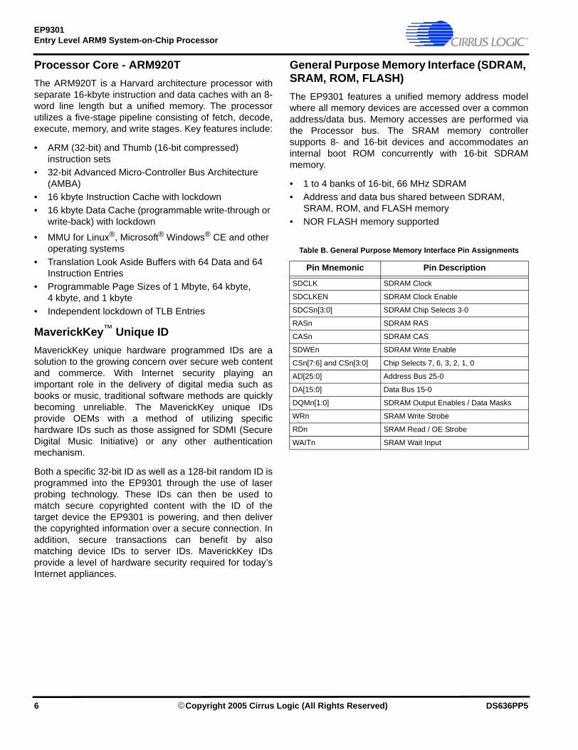
Processor Core - ARM920TThe ARM920T is a Harvard architecture processor withseparate 16-kbyte instruction and data caches with an 8-word line length but a unified memory. The processorutilizes a five-stage pipeline consisting of fetch, decode,execute, memory, and write stages. Key features include:
• ARM (32-bit) and Thumb (16-bit compressed) instruction sets
• 32-bit Advanced Micro-Controller Bus Architecture (AMBA)
• 16 kbyte Instruction Cache with lockdown• 16 kbyte Data Cache (programmable write-through or
write-back) with lockdown
• MMU for Linux®, Microsoft® Windows® CE and other operating systems
• Translation Look Aside Buffers with 64 Data and 64 Instruction Entries
• Programmable Page Sizes of 1 Mbyte, 64 kbyte, 4 kbyte, and 1 kbyte
• Independent lockdown of TLB Entries
MaverickKey™ Unique IDMaverickKey unique hardware programmed IDs are asolution to the growing concern over secure web contentand commerce. With Internet security playing animportant role in the delivery of digital media such asbooks or music, traditional software methods are quicklybecoming unreliable. The MaverickKey unique IDsprovide OEMs with a method of utilizing specifichardware IDs such as those assigned for SDMI (SecureDigital Music Initiative) or any other authenticationmechanism.
Both a specific 32-bit ID as well as a 128-bit random ID isprogrammed into the EP9301 through the use of laserprobing technology. These IDs can then be used tomatch secure copyrighted content with the ID of thetarget device the EP9301 is powering, and then deliverthe copyrighted information over a secure connection. Inaddition, secure transactions can benefit by alsomatching device IDs to server IDs. MaverickKey IDsprovide a level of hardware security required for today’sInternet appliances.
General Purpose Memory Interface (SDRAM, SRAM, ROM, FLASH)The EP9301 features a unified memory address modelwhere all memory devices are accessed over a commonaddress/data bus. Memory accesses are performed viathe Processor bus. The SRAM memory controllersupports 8- and 16-bit devices and accommodates aninternal boot ROM concurrently with 16-bit SDRAMmemory.
• 1 to 4 banks of 16-bit, 66 MHz SDRAM• Address and data bus shared between SDRAM,
SRAM, ROM, and FLASH memory• NOR FLASH memory supported
Table B. General Purpose Memory Interface Pin Assignments
Pin Mnemonic Pin Description
SDCLK SDRAM Clock
SDCLKEN SDRAM Clock Enable
SDCSn[3:0] SDRAM Chip Selects 3-0
RASn SDRAM RAS
CASn SDRAM CAS
SDWEn SDRAM Write Enable
CSn[7:6] and CSn[3:0] Chip Selects 7, 6, 3, 2, 1, 0
AD[25:0] Address Bus 25-0
DA[15:0] Data Bus 15-0
DQMn[1:0] SDRAM Output Enables / Data Masks
WRn SRAM Write Strobe
RDn SRAM Read / OE Strobe
WAITn SRAM Wait Input
6 ©Copyright 2005 Cirrus Logic (All Rights Reserved) DS636PP5

EP9301Entry Level ARM9 System-on-Chip Processor
Ethernet Media Access Controller (MAC) The MAC subsystem is compliant with the ISO/TEC802.3 topology for a single shared medium with severalstations. Multiple MII-compliant PHYs are supported.Features include:
• Supports 1/10/100 Mbps transfer rates for home / small-business / large-business applications
• Interfaces to an off-chip PHY through industry standard Media Independent Interface (MII)
Serial Interfaces (SPI, I2S, and AC ’97)The Serial Peripheral Interface (SPI) port can beconfigured as a master or a slave, supporting theNational Semiconductor®, Motorola®, and TexasInstruments® signaling protocols.
The AC'97 port supports multiple codecs for multichannelaudio output with a single stereo input. The I2S portsupports stereo 24-bit audio.
These ports are multiplexed so that the I2S port will takeover either the AC'97 pins or the SPI pins.
• Normal Mode: One SPI Port and one AC’97 Port
• I2S on SSP Mode: One AC’97 Port and one I2S Port
• I2S on AC’97 Mode: One SPI Port and one I2S Port
Note: I2S may not be output on AC’97 and SSP ports at the same time.
12-bit Analog-to-digital Converter (ADC)The ADC block consists of a 12-bit analog-to-digitalconverter with a analog input multiplexer. The multiplexercan select to measure battery voltage and othermiscellaneous voltages on the external measurementpins. Features include:
• 5 external pins for ADC measurement • Measurement pin input range: 0 to 3.3 V. • ADC-conversion-complete interrupt signal
Table C. Ethernet Media Access Controller Pin Assignments
Pin Mnemonic Pin Description
MDC Management Data Clock
MDIO Management Data I/O
RXCLK Receive Clock
MIIRXD[3:0] Receive Data
RXDVAL Receive Data Valid
RXERR Receive Data Error
TXCLK Transmit Clock
MIITXD[3:0] Transmit Data
TXEN Transmit Enable
TXERR Transmit Error
CRS Carrier Sense
CLD Collision Detect
Table D. Audio Interfaces Pin Assignment
PinName
Normal Mode I2S on SSP Mode
I2S on AC'97 Mode
Pin Description Pin Description Pin Description
SCLK1 SPI Bit Clock I2S Serial Clock SPI Bit Clock
SFRM1 SPI Frame Clock I2S Frame Clock SPI Frame Clock
SSPRX1 SPI Serial Input I2S Serial Input SPI Serial Input
SSPTX1 SPI Serial Output I2S Serial Output SPI Serial Output
(No I2S Master Clock)
ARSTn AC'97 Reset AC'97 Reset I2S Master Clock
ABITCLK AC'97 Bit Clock AC'97 Bit Clock I2S Serial Clock
ASYNC AC'97 Frame Clock
AC'97 Frame Clock I2S Frame Clock
ASDI AC'97 Serial Input AC'97 Serial Input I2S Serial Input
ASDO AC'97 Serial Output AC'97 Serial Output I2S Serial Output
Table E. 12-bit Analog-to-Digital Converter Pin Assignments
Pin Mnemonic Pin Description
ADC[0] (Ym, pin 135) External Analog Measurement Input
ADC[1] (sXp, pin 134) External Analog Measurement Input
ADC[2] (sXm, pin 133) External Analog Measurement Input
ADC[3] (sYp, pin 132) External Analog Measurement Input
ADC[4] (sYm, pin 131) External Analog Measurement Input
DS636PP5 ©Copyright 2005 Cirrus Logic (All Rights Reserved) 7

EP9301Entry Level ARM9 System-on-Chip Processor
Universal Asynchronous Receiver/Transmitters (UARTs) Two 16550-compatible UARTs are supplied. Oneprovides asynchronous HDLC (High-level Data LinkControl) protocol support for full duplex transmit andreceive. The HDLC receiver handles framing, addressmatching, CRC checking, control-octet transparency, andoptionally passes the CRC to the host at the end of thepacket. The HDLC transmitter handles framing, CRCgeneration, and control-octet transparency. The hostmust assemble the frame in memory beforetransmission. The HDLC receiver and transmitter use theUART FIFOs to buffer the data streams. The secondUART provides IrDA® compatibility.
• UART1 supports modem bit rates up to 115.2 kbps, supports HDLC and includes a 16 byte FIFO for receive and a 16 byte FIFO for transmit. Interrupts are generated on Rx, Tx and modem status change.
• UART2 contains an IrDA encoder operating at either the slow (up to 115 kbps), medium (0.576 or 1.152 Mbps), or fast (4 Mbps) IR data rates. It also has a 16 byte FIFO for receive and a 16 byte FIFO for transmit.
Dual Port USB Host The USB Open Host Controller Interface (Open HCI)provides full speed serial communications ports at abaud rate of 12 Mbits/sec. Up to 127 USB devices(printer, mouse, camera, keyboard, etc.) and USB hubscan be connected to the USB host in the USB “tiered-start” topology.
This includes the following feature:
• Compliance with the USB 2.0 specification• Compliance with the Open HCI Rev 1.0 specification
• Supports both low speed (1.5 Mbps) and full speed (12 Mbps) USB device connections
• Root HUB integrated with 2 downstream USB ports• Transceiver buffers integrated, over-current protection
on ports• Supports power management• Operates as a master on the busThe Open HCI host controller initializes the master DMAtransfer with the AHB bus:
• Fetches endpoint descriptors and transfer descriptors• Accesses endpoint data from system memory• Accesses the HC communication area• Writes status and retire transfer descriptor
Note: USBm[1] and USBp[1] are not bonded out.
Two-Wire Interface With EEPROM SupportThe two-wire interface provides communication andcontrol for synchronous-serial-driven devices.
Real-Time Clock with Software Trim The software trim feature on the real time clock (RTC)provides software controlled digital compensation of the32.768 KHz input clock. This compensation is accurate to± 1.24 sec/month.
Note: A real time clock must be connected to RTCXTALI or the EP9301device will not boot.
Table F. Universal Asynchronous Receiver/Transmitters Pin Assignments
Pin Mnemonic Pin Name - Description
TXD0 UART1 Transmit
RXD0 UART1 Receive
CTSn UART1 Clear To Send / Transmit Enable
DSRn / DCDn UART1 Data Set Ready / Data Carrier Detect
DTRn UART1 Data Terminal Ready
RTSn UART1 Ready To Send
EGPIO[0] / RI UART1 Ring Indicator
TXD1 / SIROUT UART2 Transmit / IrDA Output
RXD1 / SIRIN UART2 Receive / IrDA Input
Table G. Dual Port USB Host Pin Assignments
Pin Mnemonic Pin Name - Description
USBp[2,0] USB Positive signals
USBm[2,0] USB Negative Signals
Table H. Two-Wire Port with EEPROM Support Pin Assignments
Pin Mnemonic Pin Name - Description Alternative Usage
EECLK Two-wire Interface Clock GeneralPurpose I/O
EEDATA Two-wire Interface Data GeneralPurpose I/O
Table I. Real-Time Clock with Pin Assignments
Pin Mnemonic Pin Name - Description
RTCXTALI Real-Time Clock Oscillator Input
RTCXTALO Real-Time Clock Oscillator Output
8 ©Copyright 2005 Cirrus Logic (All Rights Reserved) DS636PP5

EP9301Entry Level ARM9 System-on-Chip Processor
PLL and Clocking The Processor and the Peripheral Clocks operate from asingle 14.7456 MHz crystal.
The Real Time Clock operates from a 32.768 KHzexternal oscillator.
TimersThe Watchdog Timer ensures proper operation byrequiring periodic attention to prevent a reset-on-time-out.
Two 16-bit timers operate as free-running down countersor as periodic timers for fixed-interval interrupts and havea range of 0.03 ms to 4.27 seconds.
One 32-bit timer, plus a 6-bit prescale counter, has arange of 0.03 µs to 73.3 hours.
One 40-bit debug timer, plus a 6-bit prescale counter, hasa range of 1.0 µs to 12.7 days.
Interrupt ControllerThe interrupt controller allows up to 54 interrupts togenerate an Interrupt Request (IRQ) or Fast InterruptRequest (FIQ) signal to the processor core. Thirty-twohardware priority assignments are provided for assistingIRQ vectoring, and two levels are provided for FIQvectoring. This allows time-critical interrupts to beprocessed in the shortest time possible. Internalinterrupts may be programmed as active high or activelow level sensitive inputs. GPIO pins programmed asinterrupts may be programmed as active high levelsensitive, active low level sensitive, rising edge triggered,falling edge triggered, or combined rising/falling edgetriggered.
• Supports 54 interrupts from a variety of sources (such as UARTs, GPIO and ADC)
• Routes interrupt sources to either the ARM920T’s IRQ or FIQ (Fast IRQ) inputs
• Three dedicated off-chip interrupt lines INT[2:0] operate as active-high level-sensitive interrupts
• Any of the 19 GPIO lines maybe configured to generate interrupts
• Software supported priority mask for all FIQs and IRQs
Note: INT[2] is not bonded out.
Dual LED Drivers Two pins are assigned specifically to drive externalLEDs.
General Purpose Input/Output (GPIO)The 16 EGPIO and the 3 FGPIO pins may each beconfigured individually as an output, an input or aninterrupt input.
There are 10 pins that may alternatively be used as input,output, or open-drain pins, but do not support interrupts.These pins are:
• Ethernet MDIO• Both LED Outputs• EEPROM Clock and Data• HGPIO[5:2]• CGPIO[0]
6 pins may alternatively be used as inputs only:• CTSn, DSRn / DCDn• 3 Interrupt Lines
2 pins may alternatively be used as outputs only:• RTSn• ARSTn
Table J. PLL and Clocking Pin Assignments
Pin Mnemonic Pin Name - Description
XTALI Main Oscillator Input
XTALO Main Oscillator Output
VDD_PLL Main Oscillator Power
GND_PLL Main Oscillator Ground
Table K. External Interrupt Controller Pin Assignment
Pin Mnemonic Pin Name - Description
INT[3] and INT[1:0] External Interrupts 2, 1, 0
Table L. Dual LED Pin Assignments
Pin Mnemonic Pin Name - Description Alternative Usage
GRLED Green LED General Purpose I/O
REDLED Red LED General Purpose I/O
Table M. General Purpose Input/Output Pin Assignment
Pin Mnemonic Pin Name - Description
EGPIO[15:0] Expanded General Purpose Input / Output Pins with Interrupts
FGPIO[3:1] Expanded General Purpose Input / Output Pins with Interrupts
DS636PP5 ©Copyright 2005 Cirrus Logic (All Rights Reserved) 9

EP9301Entry Level ARM9 System-on-Chip Processor
Reset and Power ManagementThe chip may be reset through the PRSTn pin or throughthe open drain common reset pin, RSTOn.
Clocks are managed on a peripheral-by-peripheral basisand may be turned off to conserve power.
The processor clock is dynamically adjustable from 0 to166 MHz.
Hardware Debug InterfaceThe JTAG interface allows use of ARM’s Multi-ICE orother in-circuit emulators.
12-channel DMA Controller The DMA module contains 12 separate DMA channels.Ten of these may be used for peripheral-to-memory ormemory-to-peripheral access. Two of these arededicated to memory-to-memory transfers. Each DMAchannel is connected to the 16-bit DMA request bus.
The request bus is a collection of requests, Serial Audioand UARTs. Each DMA channel can be usedindependently or dedicated to any request signal. Foreach DMA channel, source and destination addressingcan be independently programmed to increment,decrement, or stay at the same value. All DMAaddresses are physical, not virtual addresses.
Internal Boot ROM The Internal 16 kbyte ROM allows booting from FLASHmemory, SPI or UART. Consult the EP93xx User’sManual for operational details.
Table N. Reset and Power Management Pin Assignments
Pin Mnemonic Pin Name - Description
PRSTn Power On Reset
RSTOn User Reset In/Out – Open Drain – Preserves Real Time Clock value
Table O. Hardware Debug Interface
Pin Mnemonic Pin Name - Description
TCK JTAG Clock
TDI JTAG Data In
TDO JTAG Data Out
TMS JTAG Test Mode Select
TRSTn JTAG Port Reset
10 ©Copyright 2005 Cirrus Logic (All Rights Reserved) DS636PP5

EP9301Entry Level ARM9 System-on-Chip Processor
Electrical Specifications
Absolute Maximum Ratings
Note: 1. Includes all power generated by AC and/or DC output loading.2. The power supply pins are at recommended maximum values.3. At ambient temperatures above 70° C, total power dissipation must be limited to less than 2.5 Watts.
WARNING: Operation beyond these limits may result in permanent damage to the device.Normal operation is not guaranteed at these extremes.
Recommended Operating Conditions
(All grounds = 0 V, all voltages with respect to 0 V)
Parameter Symbol Min Max Unit
Power Supplies
RVDDCVDD
VDD_PLLVDD_ADC
----
3.962.162.163.96
VVVV
Total Power Dissipation (Note 1) - 2 W
Input Current per Pin, DC (Except supply pins) - ±10 mA
Output current per pin, DC - ±50 mA
Digital Input voltage (Note 2) -0.3 RVDD+0.3 V
Storage temperature -40 +125 °C
(All grounds = 0 V, all voltages with respect to 0 V)
Parameter Symbol Min Typ Max Unit
Power Supplies
RVDDCVDD
VDD_PLLVDD_ADC
3.01.651.653.0
3.31.801.803.3
3.61.941.943.6
VVVV
Operating Ambient Temperature - Commercial TA 0 +25 +70 °C
Operating Ambient Temperature - Industrial TA -40 +25 +85 °C
Processor Clock Speed - Commercial FCLK - - 166 MHz
Processor Clock Speed - Industrial FCLK - - 166 MHz
System Clock Speed - Commercial HCLK - - 66 MHz
System Clock Speed - Industrial HCLK - - 66 MHz
DS636PP5 ©Copyright 2005 Cirrus Logic (All Rights Reserved) 11

EP9301Entry Level ARM9 System-on-Chip Processor
DC Characteristics
Note: 4. For open drain pins, high level output voltage is dependent on the external load.5. All inputs that do not include internal pull-ups or pull-downs, must be externally driven for proper operation (See Table Q on page 38). If an input is not driven, it should be tied to power or ground, depending on the particular function. If an I/O pin is not driven and programmed as an input, it should be tied to power or ground through its own resistor.
(TA = 0 to 70° C; CVDD = VDD_PLL = 1.8; RVDD = 3.3 V; All grounds = 0 V; all voltages with respect to 0 V unless otherwise noted)
Parameter Symbol Min Max Unit
High level output voltage Iout = -4 mA (Note 4) Voh 0.85 × RVDD - V
Low level output voltage Iout = 4 mA Vol - 0.15 × RVDD V
High level input voltage (Note 5) Vih 0.65 × RVDD VDD + 0.3 V
Low level input voltage (Note 5) Vil −0.3 0.35 × RVDD V
High level leakage current Vin = 3.3 V (Note 5) Iih - 10 µA
Low level leakage current Vin = 0 (Note 5) Iil - -10 µA
Parameter Min Typ Max Unit
Power Supply Pins (Outputs Unloaded), 25° CPower Supply Current: CVDD / VDD_PLL Total
RVDD--
18045
23080
mAmA
Low-Power Mode Supply Current CVDD / VDD_PLL TotalRVDD
--
21.0
3.52
mAmA
12 ©Copyright 2005 Cirrus Logic (All Rights Reserved) DS636PP5

EP9301Entry Level ARM9 System-on-Chip Processor
TimingsTiming Diagram Conventions
This data sheet contains one or more timing diagrams. The following key explains the components used in thesediagrams. Any variations are clearly labelled when they occur. Therefore, no additional meaning should be attachedunless specifically stated.
Figure 1. Timing Diagram Drawing Key
Timing Conditions
Unless specified otherwise, the following conditions are true for all timing measurements.
• TA = 0 to 70° C
• CVDD = VDD_PLL = 1.8V
• RVDD = 3.3 V
• All grounds = 0 V
• Logic 0 = 0 V, Logic 1 = 3.3 V
• Output loading = 50 pF
• Timing reference levels = 1.5 V
• The Processor Bus Clock (HCLK) is programmable and is set by the user. The frequency is typically between 33 MHz and 100 MHz (92 MHz for industrial conditions).
Clock
High to Low
High/Low to High
Bus Change
Bus Valid
Undefined/Invalid
Valid Bus to Tristate
Bus/Signal Omission
DS636PP5 ©Copyright 2005 Cirrus Logic (All Rights Reserved) 13
EP9301Entry Level ARM9 System-on-Chip Processor
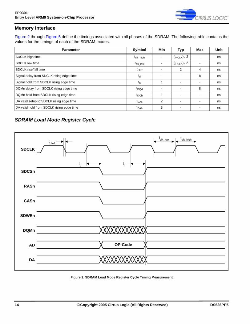
Memory Interface
SDRAM Load Mode Register Cycle
Figure 2 through Figure 5 define the timings associated with all phases of the SDRAM. The following table contains thevalues for the timings of each of the SDRAM modes.
Parameter Symbol Min Typ Max Unit
SDCLK high time tclk_high - (tHCLK) / 2 - ns
SDCLK low time tclk_low - (tHCLK) / 2 - ns
SDCLK rise/fall time tclkrf - 2 4 ns
Signal delay from SDCLK rising edge time td - - 8 ns
Signal hold from SDCLK rising edge time th 1 - - ns
DQMn delay from SDCLK rising edge time tDQd - - 8 ns
DQMn hold from SDCLK rising edge time tDQh 1 - - ns
DA valid setup to SDCLK rising edge time tDAs 2 - - ns
DA valid hold from SDCLK rising edge time tDAh 3 - - ns
Figure 2. SDRAM Load Mode Register Cycle Timing Measurement
SDCLK
SDCSn
RASn
CASn
SDWEn
DQMn
AD
DA
OP-Code
tclk_hightclk_lowtclkrf
td th
14 ©Copyright 2005 Cirrus Logic (All Rights Reserved) DS636PP5

EP9301Entry Level ARM9 System-on-Chip Processor
SDRAM Burst Read Cycle
Figure 3. SDRAM Burst Read Cycle Timing Measurement
n n + 1 n + 2 n + 3
SDCLK
SDCSn
RASn
CASn
SDWEn
DQMnCL = 2
AD
DACL = 2
tDAs
tclk_low tclk_high
tclkrf
DS636PP5 ©Copyright 2005 Cirrus Logic (All Rights Reserved) 15
EP9301Entry Level ARM9 System-on-Chip Processor
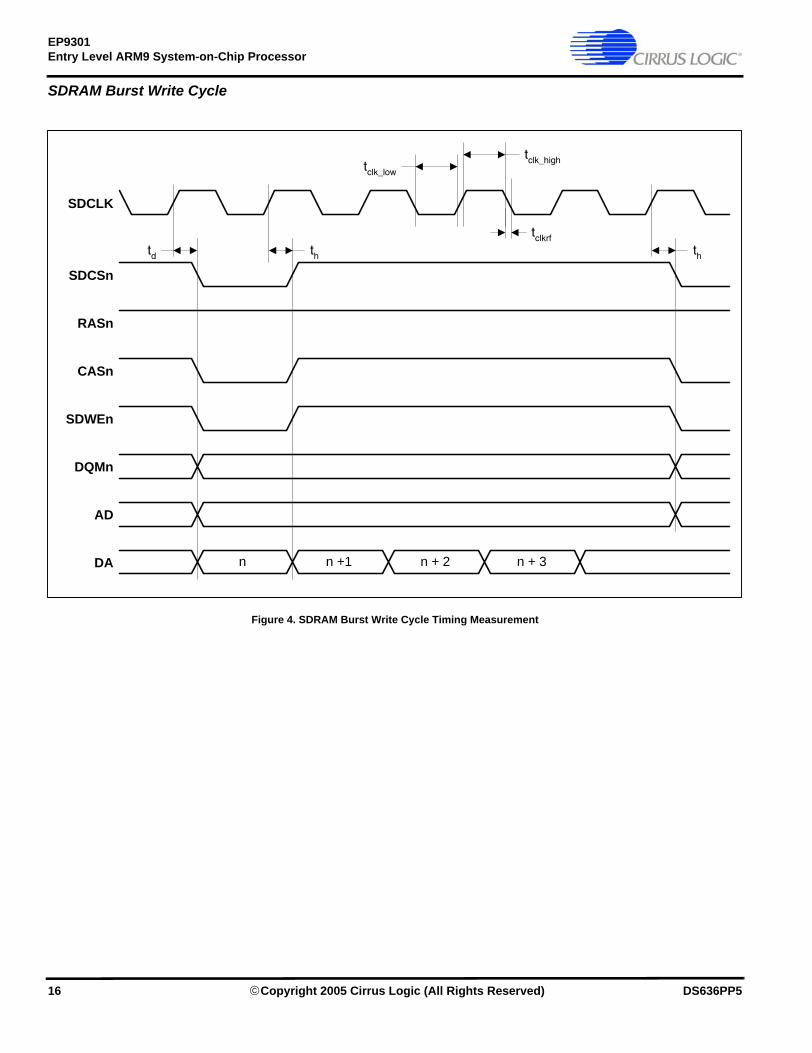
SDRAM Burst Write Cycle
Figure 4. SDRAM Burst Write Cycle Timing Measurement
SDCLK
SDCSn
RASn
CASn
SDWEn
DQMn
AD
DA
tclk_low
tclk_high
tclkrf
td th th
n n +1 n + 2 n + 3
16 ©Copyright 2005 Cirrus Logic (All Rights Reserved) DS636PP5

EP9301Entry Level ARM9 System-on-Chip Processor
SDRAM Auto Refresh Cycle
Note: Chip select shown as bus to illustrate multiple devices being put into auto refresh in one access
Figure 5. SDRAM Auto Refresh Cycle Timing Measurement
SDCLK
SDCSn
RASn
CASn
SDWEn
tclk_low
tclk_high
7 b d e
td th
tclkrf
DS636PP5 ©Copyright 2005 Cirrus Logic (All Rights Reserved) 17

EP9301Entry Level ARM9 System-on-Chip Processor
Static Memory 32-bit Read on 8-bit External Bus
Parameter Symbol Min Typ Max Unit
AD setup to CSn assert time tADs tHCLK - - ns
CSn assert to Address transition time tAD1 - tHCLK × (WST1 + 1) - ns
Address assert time tAD2 - tHCLK × (WST1 + 1) - ns
AD transition to CSn deassert time tAD3 - tHCLK × (WST1 + 2) - ns
AD hold from CSn deassert time tADh tHCLK - - ns
RDn assert time tRDpwL - tHCLK × (4 × WST1 + 5) - ns
CSn to RDn delay time tRDd - - 3 ns
CSn assert to DQMn assert delay time tDQMd - - 1 ns
DA setup to AD transition time tDAs1 15 - - ns
DA setup to RDn deassert time tDAs2 tHCLK + 12 - - ns
DA hold from AD transition time tDAh1 0 - - ns
DA hold from RDn deassert time tDAh2 0 - - ns
Figure 6. Static Memory Multiple Word Read 8-bit Cycle Timing Measurement
1
CSn
WRn
RDn
DA
AD
DQMn
tADs tAD1 tAD2 tAD2
tDAs1
tRDd
tDAh1 tDAh1tDAh1
tDAs1 tDAs1 tDAs2
tDAh2
tADh
WAIT
tRDd
tDQMd
tAD3
18 ©Copyright 2005 Cirrus Logic (All Rights Reserved) DS636PP5

EP9301Entry Level ARM9 System-on-Chip Processor
Static Memory 32-bit Write on 8-bit External Bus
Parameter Symbol Min Typ Max Unit
AD setup to WRn assert time tADs tHCLK − 3 - - ns
WRn/DQMn deassert to AD transition time tADd - - tHCLK + 6 ns
AD hold from WRn deassert time tADh tHCLK × 2 - - ns
CSn hold from WRn deassert time tCSh 7 - - ns
CSn to WRn assert delay time tWRd - - 2 ns
WRn assert time tWRpwL - tHCLK × (WST1 + 1) - ns
WRn deassert time tWRpwH - tHCLK × 2 (tHCLK × 2) + 14 ns
CSn to DQMn assert delay time tDQMd - - 1 ns
DQMn assert time tDQMpwL - tHCLK × (WST1 + 1) - ns
DQMn deassert time tDQMpwH - - (tHCLK × 2) + 7 ns
WRn / DQMn deassert to DA transition time tDAh tHCLK - - ns
WRn / DQMn assert to DA valid time tDAV - - 8 ns
Figure 7. Static Memory Multiple Word Write 8-bit Cycle Timing Measurement
CSn
WRn
RDn
DQMn
AD
DA
tADs
tWRd
tDQMd
tWRpwL
tDAh
tWRpwH
tADd
tCSh
tADh
tDQMpwL
tDQMpwH
tWRpwL
tWRpwH
tWRpwL
tWRpwH
tDQMpwL
tDQMpwH
tDQMpwL
tDQMpwH
tDAh tDAh tDAh
tADd tADd
WAIT
tDAV tDAV tDAV tDAV
DS636PP5 ©Copyright 2005 Cirrus Logic (All Rights Reserved) 19

EP9301Entry Level ARM9 System-on-Chip Processor
Static Memory 32-bit Read on 16-bit External Bus
Parameter Symbol Min Typ Max Unit
AD setup to CSn assert time tADs tHCLK - - ns
CSn assert to AD transition time tADd1 - tHCLK × (WST1 + 1) - ns
AD transition to CSn deassert time tADd2 - tHCLK × (WST1 + 2) - ns
AD hold from CSn deassert time tADh tHCLK - - ns
RDn assert time tRDpwL - tHCLK × ((2 × WST1) + 3) - ns
CSn to RDn delay time tRDd - - 3 ns
CSn assert to DQMn assert delay time tDQMd - - 1 ns
DA setup to AD transition time tDAs1 15 - - ns
DA to RDn deassert time tDAs2 tHCLK + 12 - - ns
DA hold from AD transition time tDAh1 0 - - ns
DA hold from RDn deassert time tDAh2 0 - - ns
Figure 8. Static Memory Multiple Word Read 16-bit Cycle Timing Measurement
CSn
WRn
RDn
DA
AD
DQMn
tRDpwl
tADd1
tRDh
tDQMh
tDAh2tDAs1 tDAh1 tDAs2
WAIT
tADs
tRDd
tDQMd
tADhtADd2
20 ©Copyright 2005 Cirrus Logic (All Rights Reserved) DS636PP5

EP9301Entry Level ARM9 System-on-Chip Processor
Static Memory 32-bit Write on 16-bit External Bus
Parameter Symbol Min Typ Max Unit
AD setup to WRn assert time tADs tHCLK – 3 - - ns
WRn/DQMn deassert to AD transition time tADd - - tHCLK + 6 ns
AD hold from WRn deassert time tADh tHCLK × 2 - - ns
CSn hold from WRn deassert time tCSh 7 - - ns
CSn to WRn assert delay time tWRd - - 2 ns
WRn assert time tWRpwL - tHCLK × (WST1 + 1) - ns
WRn deassert time tWRpwH - - (tHCLK × 2) + 14 ns
CSn to DQMn assert delay time tDQMd - - 1 ns
DQMn assert time tDQMpwL - tHCLK × (WST1 + 1) - ns
DQMn deassert time tDQMpwH - - (tHCLK × 2) + 7 ns
WRn / DQMn deassert to DA transition time tDAh1 tHCLK - - ns
WRn / DQMn assert to DA valid time tDAV - - 8 ns
Figure 9. Static Memory Multiple Word Write 16-bit Cycle Timing Measurement
CSn
WRn
RDn
DQMn
AD
DA
tADs
tWRd tWRpwL
tDAh
tADd
tWRpwH
tDQMd
tADh
tDAh
tWRpwL
tDQpwL
tDQpwH
tDQpwL
WAIT
tCSh
tDAV tDAV
DS636PP5 ©Copyright 2005 Cirrus Logic (All Rights Reserved) 21

EP9301Entry Level ARM9 System-on-Chip Processor
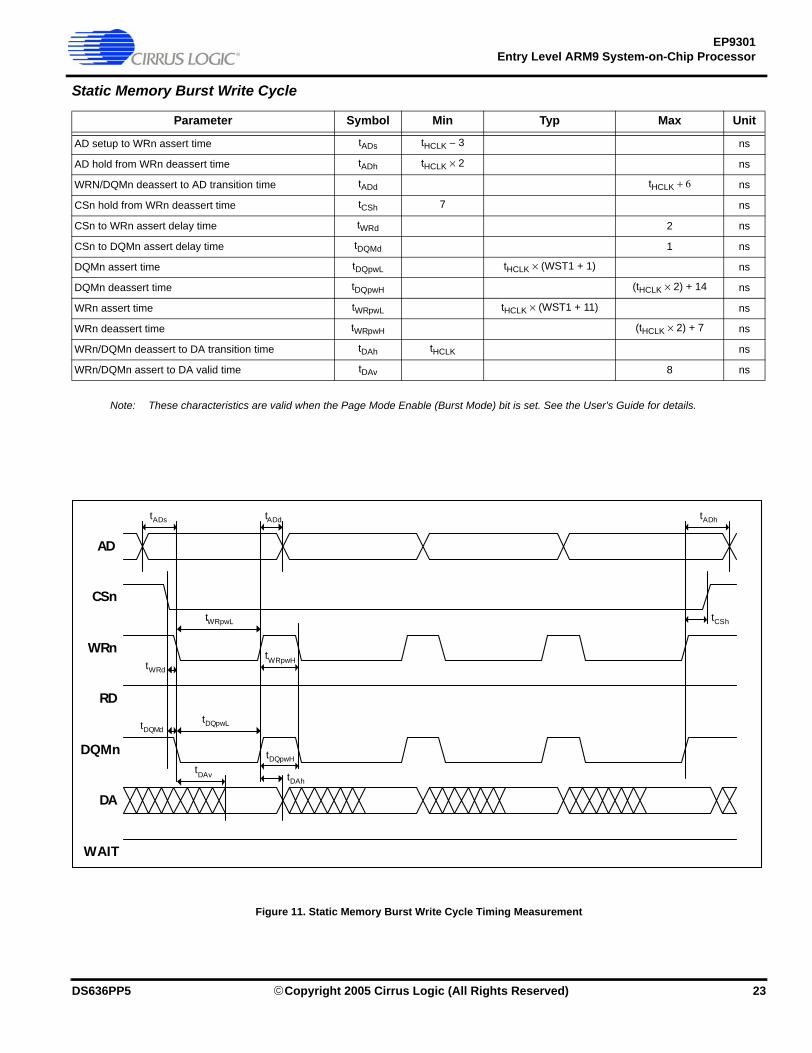
Static Memory Burst Write Cycle
Note: These characteristics are valid when the Page Mode Enable (Burst Mode) bit is set. See the User's Guide for details.
Parameter Symbol Min Typ Max Unit
AD setup to WRn assert time tADs tHCLK − 3 ns
AD hold from WRn deassert time tADh tHCLK × 2 ns
WRN/DQMn deassert to AD transition time tADd tHCLK + 6 ns
CSn hold from WRn deassert time tCSh 7 ns
CSn to WRn assert delay time tWRd 2 ns
CSn to DQMn assert delay time tDQMd 1 ns
DQMn assert time tDQpwL tHCLK × (WST1 + 1) ns
DQMn deassert time tDQpwH (tHCLK × 2) + 14 ns
WRn assert time tWRpwL tHCLK × (WST1 + 11) ns
WRn deassert time tWRpwH (tHCLK × 2) + 7 ns
WRn/DQMn deassert to DA transition time tDAh tHCLK ns
WRn/DQMn assert to DA valid time tDAv 8 ns
Figure 11. Static Memory Burst Write Cycle Timing Measurement
AD
CSn
WRn
RD
DQMn
DA
WAIT
tADs tADd
tWRpwL
tDQpwL
tDQpwH
tWRpwH
tDAv tDAh
tWRd
tDQMd
tCSh
tADh
DS636PP5 ©Copyright 2005 Cirrus Logic (All Rights Reserved) 23

EP9301Entry Level ARM9 System-on-Chip Processor
Static Memory Single Read Wait Cycle
Parameter Symbol Min Typ Max Unit
CSn assert to WAIT time tWAITd - - tHCLK × (WST1-2) ns
WAIT assert time tWAITpw tHCLK × 2 - tHCLK × 510 ns
WAIT to CSn deassert delay time tCSnd tHCLK × 3 - tHCLK × 5 ns
Figure 12. Static Memory Single Read Wait Cycle Timing Measurement
CSn
WRn
RDn
DQMn
AD
DA
WAIT tWAITpw
tWAITd tCSnd
24 ©Copyright 2005 Cirrus Logic (All Rights Reserved) DS636PP5

EP9301Entry Level ARM9 System-on-Chip Processor
Static Memory Single Write Wait Cycle
Parameter Symbol Min Typ Max Unit
WAIT to WRn deassert delay time tWRd tHCLK × 2 - tHCLK × 4 ns
CSn assert to WAIT time tWAITd - - tHCLK × (WST1-2) ns
WAIT assert time tWAITpw tHCLK × 2 - tHCLK × 510 ns
WAIT to CSn deassert delay time tCSnd tHCLK × 3 - tHCLK × 5 ns
Figure 13. Static Memory Single Write Wait Cycle Timing Measurement
CSn
WRn
RDn
DQMn
AD
DA
WAITtWAITpw
tWAITd tCSnd
tWRd
DS636PP5 ©Copyright 2005 Cirrus Logic (All Rights Reserved) 25

EP9301Entry Level ARM9 System-on-Chip Processor
Static Memory Turnaround Cycle
Notes: 1. X and Y represent any two chip select numbers.2. IDCY occurs on read-to-write and write-to-read.3. IDCY is honored when going from a asynchronous device (CSx) to a synchronous device (/SDCSy).
Parameter Symbol Min Typ Max Unit
CSnX deassert to CSnY assert time tBTcyc - tHCLK × (IDCY+1) - ns
Figure 14. Static Memory Turnaround Cycle Timing Measurement
AD
CSnX
WRn
RDn
DQMn
DA
CSnY
tBTcyc
WAIT
26 ©Copyright 2005 Cirrus Logic (All Rights Reserved) DS636PP5
EP9301Entry Level ARM9 System-on-Chip Processor
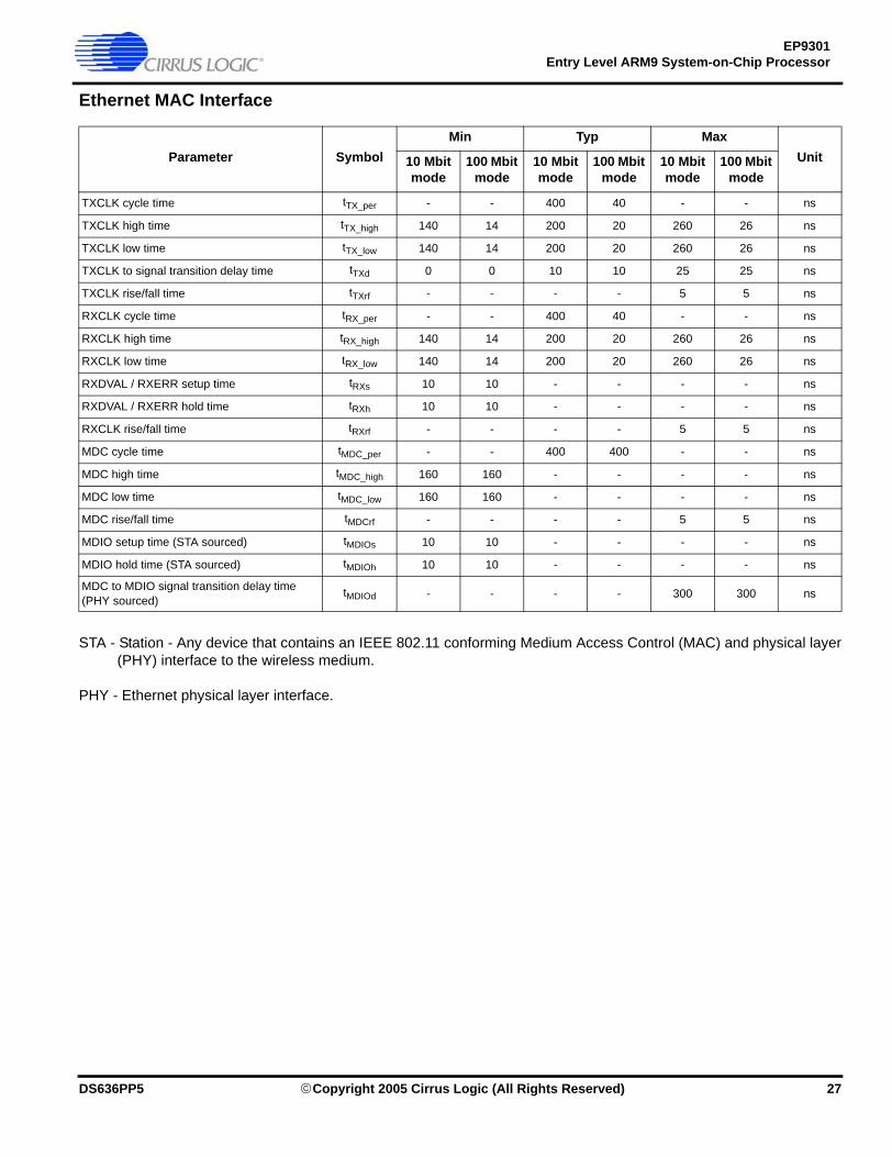
Ethernet MAC Interface
STA - Station - Any device that contains an IEEE 802.11 conforming Medium Access Control (MAC) and physical layer(PHY) interface to the wireless medium.
PHY - Ethernet physical layer interface.
Parameter SymbolMin Typ Max
Unit10 Mbit mode
100 Mbit mode
10 Mbit mode
100 Mbit mode
10 Mbit mode
100 Mbit mode
TXCLK cycle time tTX_per - - 400 40 - - ns
TXCLK high time tTX_high 140 14 200 20 260 26 ns
TXCLK low time tTX_low 140 14 200 20 260 26 ns
TXCLK to signal transition delay time tTXd 0 0 10 10 25 25 ns
TXCLK rise/fall time tTXrf - - - - 5 5 ns
RXCLK cycle time tRX_per - - 400 40 - - ns
RXCLK high time tRX_high 140 14 200 20 260 26 ns
RXCLK low time tRX_low 140 14 200 20 260 26 ns
RXDVAL / RXERR setup time tRXs 10 10 - - - - ns
RXDVAL / RXERR hold time tRXh 10 10 - - - - ns
RXCLK rise/fall time tRXrf - - - - 5 5 ns
MDC cycle time tMDC_per - - 400 400 - - ns
MDC high time tMDC_high 160 160 - - - - ns
MDC low time tMDC_low 160 160 - - - - ns
MDC rise/fall time tMDCrf - - - - 5 5 ns
MDIO setup time (STA sourced) tMDIOs 10 10 - - - - ns
MDIO hold time (STA sourced) tMDIOh 10 10 - - - - ns
MDC to MDIO signal transition delay time (PHY sourced)
tMDIOd - - - - 300 300 ns
DS636PP5 ©Copyright 2005 Cirrus Logic (All Rights Reserved) 27

EP9301Entry Level ARM9 System-on-Chip Processor
Figure 15. Ethernet MAC Timing Measurement
TXCLK
TXD[3:0]/TXEN/
TXERR
RXCLK
RXD[3:0]/RXDVAL/
RXERR
MDC
MDIO(Sourcedby STA)
MDC
MDIO(Sourcedby PHY)
tTXd
tRXs
tRXh
tMDIOs tMDIOh
tTX_high tTX_low
tRX_hightRX_low
tMDC_high tMDC_low
tTX_per
tRX_per
tMDC_per
tMDIOd
28 ©Copyright 2005 Cirrus Logic (All Rights Reserved) DS636PP5

EP9301Entry Level ARM9 System-on-Chip Processor
Audio Interface
Note: The tspix_clk is programmable by the user.
Texas Instruments’ Synchronous Serial Format
Microwire
The following table contains the values for the timings of each of the SPI modes.
Parameter Symbol Min Typ Max Unit
SCLK cycle time tclk_per - tspix_clk - ns
SCLK high time tclk_high - (tspix_clk) / 2 - ns
SCLK low time tclk_low - (tspix_clk) / 2 - ns
SCLK rise/fall time tclkrf 1 - 8 ns
Data from master valid delay time tDMd - - 3 ns
Data from master setup time tDMs 20 - - ns
Data from master hold time tDMh 40 - - ns
Data from slave setup time tDSs 20 - - ns
Data from slave hold time tDSh 40 - - ns
Figure 16. TI Single Transfer Timing Measurement
Figure 17. Microwire Frame Format, Single Transfer
SCLK
SFRM
SSPTXD/SSPRXD
4 to 16 bits
MSB LSB
tclk_per
tclk_low
tclk_high tclkrf
SCLK
SFRM
SSPTXD
SSPRXD 0 MSB LSB
4 to 16 bits output data
tclkrftclk_high
tclk_low
tclk_per
MSB LSB
8-bit control
DS636PP5 ©Copyright 2005 Cirrus Logic (All Rights Reserved) 29

EP9301Entry Level ARM9 System-on-Chip Processor
30 ©Copyright 2005 Cirrus Logic (All Rights Reserved) DS636PP5

EP9301Entry Level ARM9 System-on-Chip Processor
Inter-IC Sound - I2S
Note: ti2s_clk is programmable by the user.
Parameter Symbol Min Typ Max Unit
SCLK cycle time tclk_per - ti2s_clk - ns
SCLK high time tclk_high - (ti2s_clk) / 2 - ns
SCLK low time tclk_low - (ti2s_clk) / 2 - ns
SCLK rise/fall time tclkrf 1 4 8 ns
SCLK to LRCLK assert delay time tLRd - - 3 ns
Hold between SCLK assert then LRCLK deassertorHold between LRCLK deassert then SCLK assert
tLRh 0 - - ns
SDI to SCLK deassert setup time tSDIs 12 - - ns
SDI from SCLK deassert hold time tSDIh 0 - - ns
SCLK assert to SDO delay time tSDOd - - 9 ns
SDO from SCLK assert hold time tSDOh 1 - - ns
Figure 19. Inter-IC Sound (I2S) Timing Measurement
SCLK
LRCLK
SDI
tLRd tLRh
tSDIh
tclk_high
tSDIs
tclk_low
tclk_per
tclkrf
tSDOh
SDO
tSDOd
DS636PP5 ©Copyright 2005 Cirrus Logic (All Rights Reserved) 31

EP9301Entry Level ARM9 System-on-Chip Processor
AC’97
Parameter Symbol Min Typ Max Unit
ABITCLK input cycle time tclk_per - 81.4 - ns
ABITCLK input high time tclk_high 36 - 45 ns
ABITCLK input low time tclk_low 36 - 45 ns
ABITCLK input rise/fall time tclkrf 2 - 6 ns
ASDI setup to ABITCLK falling ts 10 - - ns
ASDI hold after ABITCLK falling th 10 - - ns
ASDI input rise/fall time trfin 2 - 6 ns
ABITCLK rising to ASDO / ASYNC valid, CL = 55 pF tco 2 - 15 ns
ASYNC / ASDO rise/fall time, CL = 55 pF trfout 2 - 6 ns
Figure 20. AC ‘97 Configuration Timing Measurement
ABITCLK
ASDI
ASDO
ASYNC
tco
trfout trfout
tstrfin
tco
trfout tco
tclkrf
tclk_high tclk_low
th
tclk_per
tclkrf
32 ©Copyright 2005 Cirrus Logic (All Rights Reserved) DS636PP5
EP9301Entry Level ARM9 System-on-Chip Processor
ADC
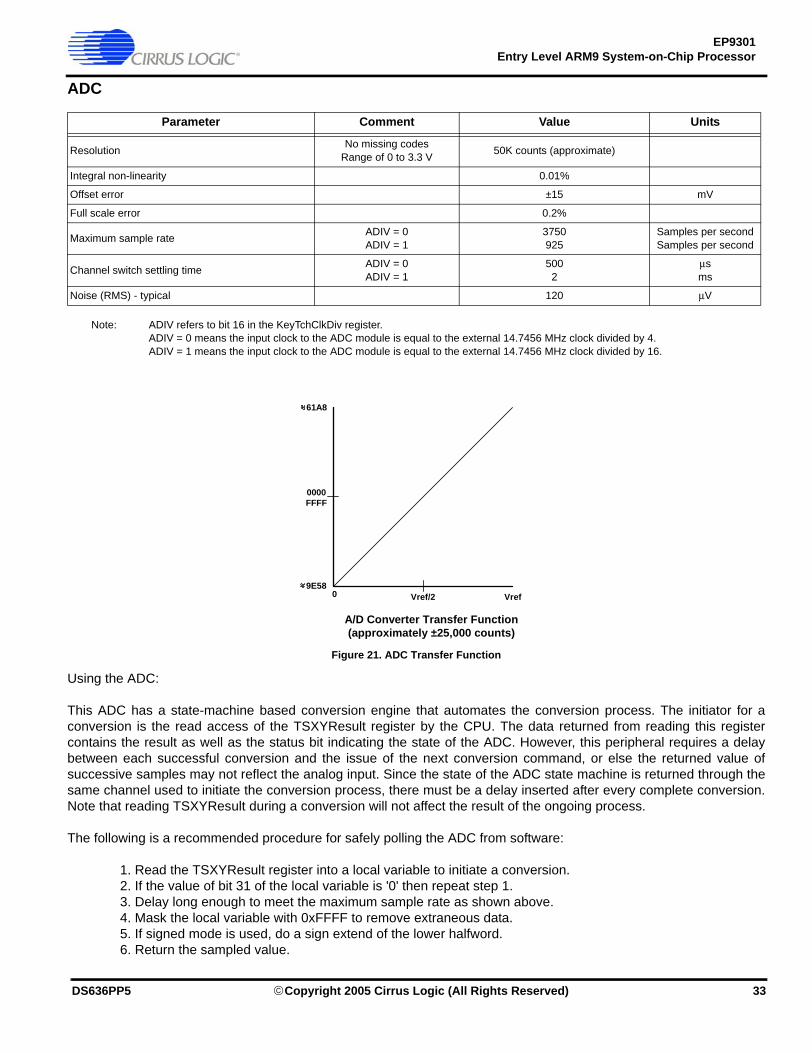
Note: ADIV refers to bit 16 in the KeyTchClkDiv register. ADIV = 0 means the input clock to the ADC module is equal to the external 14.7456 MHz clock divided by 4.ADIV = 1 means the input clock to the ADC module is equal to the external 14.7456 MHz clock divided by 16.
Using the ADC:
This ADC has a state-machine based conversion engine that automates the conversion process. The initiator for aconversion is the read access of the TSXYResult register by the CPU. The data returned from reading this registercontains the result as well as the status bit indicating the state of the ADC. However, this peripheral requires a delaybetween each successful conversion and the issue of the next conversion command, or else the returned value ofsuccessive samples may not reflect the analog input. Since the state of the ADC state machine is returned through thesame channel used to initiate the conversion process, there must be a delay inserted after every complete conversion.Note that reading TSXYResult during a conversion will not affect the result of the ongoing process.
The following is a recommended procedure for safely polling the ADC from software:
1. Read the TSXYResult register into a local variable to initiate a conversion.2. If the value of bit 31 of the local variable is '0' then repeat step 1.3. Delay long enough to meet the maximum sample rate as shown above.4. Mask the local variable with 0xFFFF to remove extraneous data.5. If signed mode is used, do a sign extend of the lower halfword.6. Return the sampled value.
Parameter Comment Value Units
Resolution No missing codesRange of 0 to 3.3 V 50K counts (approximate)
Integral non-linearity 0.01%
Offset error ±15 mV
Full scale error 0.2%
Maximum sample rate ADIV = 0ADIV = 1
3750925
Samples per secondSamples per second
Channel switch settling time ADIV = 0ADIV = 1
5002
µsms
Noise (RMS) - typical 120 µV
Figure 21. ADC Transfer Function
0 Vref/2 Vref
0000FFFF
61A8
9E58
A/D Converter Transfer Function(approximately ±25,000 counts)
DS636PP5 ©Copyright 2005 Cirrus Logic (All Rights Reserved) 33

EP9301Entry Level ARM9 System-on-Chip Processor
JTAG
Parameter Symbol Min Max Units
TCK clock period tclk_per 100 - ns
TCK clock high time tclk_high 50 - ns
TCK clock low time tclk_low 50 - ns
TMS / TDI to clock rising setup time tJPs 20 - ns
Clock rising to TMS / TDI hold time tJPh 45 - ns
JTAG port clock to output tJPco - 30 ns
JTAG port high impedance to valid output tJPzx - 30 ns
JTAG port valid output to high impedance tJPxz - 30 ns
Figure 22. JTAG Timing Measurement
TDO
TCK
TDI
TMS
tJPh
tclk_high tclk_low
tJPzx tJPco tJPxz
tclk_per tJPs
34 ©Copyright 2005 Cirrus Logic (All Rights Reserved) DS636PP5

EP9301Entry Level ARM9 System-on-Chip Processor
208 Pin LQFP Package Outline
2.19 208-Pin LQFP (28 × 28 × 1.40-mm Body)
NOTES:1) Dimensions are in millimeters, and controlling dimension is millimeter.
2) Package body dimensions do not include mold protrusion, which is 0.25 mm (0.010 in).
3) Pin 1 identification may be either ink dot or dimple.
4) Package top dimensions can be smaller than bottom dimensions by 0.20 mm (0.008 in).
5) The ‘lead width with plating’ dimension does not include a total allowable dambar protrusion of 0.08 mm(at maximum material condition).
6) Ejector pin marks in molding are present on every package.
7) Drawing above does not reflect exact package pin count.
Pin 1 Indicator
29.60 (1.165)30.40 (1.197)
0.17 (0.007)0.27 (0.011)
27.80 (1.094)28.20 (1.110)
0.50(0.0197)
BSC
29.60 (1.165)30.40 (1.197)
27.80 (1.094)28.20 (1.110)
1.35 (0.053)1.45 (0.057)
0° MIN7° MAX
0.09 (0.004)0.20 (0.008)
1.40 (0.055)
0.45 (0.018)0.75 (0.030)
0.05 (0.002)
1.00 (0.039) BSC
Pin 1
Pin 208
1.60 (0.063) 0.15 (0.006)
DS636PP5 ©Copyright 2005 Cirrus Logic (All Rights Reserved) 35

EP9301Entry Level ARM9 System-on-Chip Processor
208 Pin LQFP Pinout The following table shows the 208 pin LQFP pinout.
• VDD_core is CVDD.• VDD_ring is RVDD.• NC means that the pin is not connected.
Pin ListThe following Low-Profile Quad Flat Pack (LQFP) pin assignment table is sorted in order of pin.
Table P. Pin List in Numerical Order by Pin Number
Pin Number
Pin Name
Pin Number
Pin Name
Pin Number
Pin Name
Pin Number
Pin Name
Pin Number
Pin Name
Pin Number
Pin Name
1 CSn[7] 36 AD[5] 71 AD[9] 106 USBp[0] 141 EGPIO[10] 176 TXEN
2 CSn[6] 37 DA[12] 72 DA[1] 107 ABITCLK 142 EGPIO[9] 177 MIITXD[0]
3 CSn[3] 38 AD[4] 73 AD[8] 108 CTSn 143 EGPIO[8] 178 MIITXD[1]
4 CSn[2] 39 DA[11] 74 DA[0] 109 RXD[0] 144 EGPIO[7] 179 MIITXD[2]
5 CSn[1] 40 AD[3] 75 DSRn 110 RXD[1] 145 EGPIO[6] 180 MIITXD[3]
6 AD[25] 41 vdd_ring 76 DTRn 111 vdd_ring 146 EGPIO[5] 181 TXCLK
7 vdd_ring 42 gnd_ring 77 TCK 112 gnd_ring 147 EGPIO[4] 182 RXERR
8 gnd_ring 43 DA[10] 78 TDI 113 TXD[0] 148 EGPIO[3] 183 RXDVAL
9 AD[24] 44 AD[2] 79 TDO 114 TXD[1] 149 gnd_ring 184 MIIRXD[0]
10 SDCLK 45 DA[9] 80 TMS 115 CGPIO[0] 150 vdd_ring 185 MIIRXD[1]
11 AD[23] 46 AD[1] 81 vdd_ring 116 gnd_core 151 EGPIO[2] 186 MIIRXD[2]
12 vdd_core 47 DA[8] 82 gnd_ring 117 PLL_GND 152 EGPIO[1] 187 gnd_ring
13 gnd_core 48 AD[0] 83 BOOT[1] 118 XTALI 153 EGPIO[0] 188 vdd_ring
14 SDWEn 49 vdd_ring 84 BOOT[0] 119 XTALO 154 ARSTn 189 MIIRXD[3]
15 SDCSn[3] 50 gnd_ring 85 gnd_ring 120 PLL_VDD 155 TRSTn 190 RXCLK
16 SDCSn[2] 51 NC 86 NC 121 vdd_core 156 ASDI 191 MDIO
17 SDCSn[1] 52 NC 87 EECLK 122 gnd_ring 157 USBm[2] 192 MDC
18 SDCSn[0] 53 vdd_ring 88 EEDAT 123 vdd_ring 158 USBp[2] 193 RDn
19 vdd_ring 54 gnd_ring 89 ASYNC 124 RSTOn 159 WAITn 194 WRn
20 gnd_ring 55 AD[15] 90 vdd_core 125 PRSTn 160 EGPIO[15] 195 AD[16]
21 RASn 56 DA[7] 91 gnd_core 126 CSn[0] 161 gnd_ring 196 AD[17]
22 CASn 57 vdd_core 92 ASDO 127 gnd_core 162 vdd_ring 197 gnd_core
23 DQMn[1] 58 gnd_core 93 SCLK1 128 vdd_core 163 EGPIO[14] 198 vdd_core
24 DQMn[0] 59 AD[14] 94 SFRM1 129 gnd_ring 164 EGPIO[13] 199 HGPIO[2]
25 AD[22] 60 DA[6] 95 SSPRX1 130 vdd_ring 165 EGPIO[12] 200 HGPIO[3]
26 AD[21] 61 AD[13] 96 SSPTX1 131 ADC[4] 166 gnd_core 201 HGPIO[4]
27 vdd_ring 62 DA[5] 97 GRLED 132 ADC[3] 167 vdd_core 202 HGPIO[5]
28 gnd_ring 63 AD[12] 98 RDLED 133 ADC[2] 168 FGPIO[3] 203 gnd_ring
29 DA[15] 64 DA[4] 99 vdd_ring 134 ADC[1] 169 FGPIO[2] 204 vdd_ring
30 AD[7] 65 AD[11] 100 gnd_ring 135 ADC[0] 170 FGPIO[1] 205 AD[18]
31 DA[14] 66 vdd_ring 101 INT[3] 136 ADC_VDD 171 gnd_ring 206 AD[19]
32 AD[6] 67 gnd_ring 102 INT[1] 137 RTCXTALI 172 vdd_ring 207 AD[20]
33 DA[13] 68 DA[3] 103 INT[0] 138 RTCXTALO 173 CLD 208 SDCLKEN
34 vdd_core 69 AD[10] 104 RTSn 139 ADC_GND 174 CRS
35 gnd_core 70 DA[2] 105 USBm[0] 140 EGPIO[11] 175 TXERR
36 ©Copyright 2005 Cirrus Logic (All Rights Reserved) DS636PP5

EP9301Entry Level ARM9 System-on-Chip Processor
The following section focuses on the EP9301 pin signalsfrom two viewpoints - the pin usage and padcharacteristics, and the pin multiplexing usage. The firsttable (Table Q) is a summary of all the EP9301 pinsignals. The second table (Table R) illustrates the pinsignal multiplexing and configuration options.
Table Q is a summary of the EP9301 pin signals, whichillustrates the pad type and pad pull type (if any). Thesymbols used in the table are defined as follows. (Note: Ablank box means Not Applicable (NA) or, for Pull Type,No Pull (NP).)
Under the Pad Type column:
• A - Analog pad• P - Power pad• G - Ground pad• I - Pin is an input only• I/O - Pin is input/output• 4mA - Pin is a 4mA output driver• 8mA - Pin is an 8mA output driver• 12mA - Pin is an 12mA output driverSee the text description for additional information aboutbi-directional pins.
Under the Pull Type Column:
• PU - Resistor is a pull up to the RVDD supply• PD - Resistor is a pull down to the RGND supply
DS636PP5 ©Copyright 2005 Cirrus Logic (All Rights Reserved) 37

EP9301Entry Level ARM9 System-on-Chip Processor
.Table Q. Pin Description
Pin Name Block PadType
PullType Description
TCK JTAG I PD JTAG clock in
TDI JTAG I PD JTAG data in
TDO JTAG 4ma JTAG data out
TMS JTAG I PD JTAG test mode select
TRSTn JTAG I PD JTAG reset
BOOT[1:0] System I PD Boot mode select in
XTALI PLL A Main oscillator input
XTALO PLL A Main oscillator output
VDD_PLL PLL P Main oscillator power, 1.8V
GND_PLL PLL G Main oscillator ground
RTCXTALI RTC A RTC oscillator input
RTCXTALO RTC A RTC oscillator output
WRn EBUS 4ma SRAM Write strobe out
RDn EBUS 4ma SRAM Read / OE strobe out
WAITn EBUS I PU SRAM Wait in
AD[25:0] EBUS 8ma Shared Address bus out
DA[15:0] EBUS 8ma PU Shared Data bus in/out
CSn[3:0] EBUS 4ma PU Chip select out
CSn[7:6] EBUS 4ma PU Chip select out
DQMn[1:0] EBUS 8ma Shared data mask out
SDCLK SDRAM 8ma SDRAM clock out
SDCLKEN SDRAM 8ma SDRAM clock enable out
SDCSn[3:0] SDRAM 4ma SDRAM chip selects out
RASn SDRAM 8ma SDRAM RAS out
CASn SDRAM 8ma SDRAM CAS out
SDWEn SDRAM 8ma SDRAM write enable out
ADC[4:0] ADC A External Analog Measurement Input
VDD_ADC ADC P ADC power, 3.3V
GND_ADC ADC G ADC ground
USBp[2, 0] USB A USB positive signals
USBm[2, 0] USB A USB negative signals
TXD0 UART1 4ma Transmit out
RXD0 UART1 I PU Receive in
CTSn UART1 I PU Clear to send / transmit enable
DSRn UART1 I PU Data set ready / Data Carrier Detect
DTRn UART1 4ma Data Terminal Ready output
RTSn UART1 4ma Ready to send
TXD1 UART2 4ma Transmit / IrDA output
RXD1 UART2 I PU Receive / IrDA input
MDC EMAC 4ma Management data clock
MDIO EMAC 4ma PU Management data input/output
RXCLK EMAC I PD Receive clock in
MIIRXD[3:0] EMAC I PD Receive data in
RXDVAL EMAC I PD Receive data valid
RXERR EMAC I PD Receive data error
TXCLK EMAC I PU Transmit clock in
MIITXD[3:0] EMAC 4ma PD Transmit data out
TXEN EMAC 4ma PD Transmit enable
TXERR EMAC 4ma PD Transmit error
CRS EMAC I PD Carrier sense
CLD EMAC I PU Collision detect
GRLED LED 12ma Green LED
RDLED LED 12ma Red LED
EECLK EEPROM 4ma PU EEPROM / Two-wire Interface clock
EEDAT EEPROM 4ma PU EEPROM / Two-wire Interface data
ABITCLK AC97 8ma PD AC97 bit clock
ASYNC AC97 8ma PD AC97 frame sync
ASDI AC97 I PD AC97 Primary input
ASDO AC97 8ma PU AC97 output
ARSTn AC97 8ma AC97 reset
SCLK1 SPI1 I/O, 8ma PD SPI bit clock
SFRM1 SPI1 I/O, 8ma PD SPI Frame Clock
SSPRX1 SPI1 I PD SPI input
SSPTX1 SPI1 8ma SPI output
INT[3], INT[1:0] INT I PD External interrupts
PRSTn Syscon I PU Power on reset
RSTOn Syscon 4ma User Reset in out - open drain
EGPIO[15:0] GPIO I/O, 4ma PU Enhanced GPIO
FGPIO[3:1] GPIO I/O, 8ma PU GPIO on Port F
HGPIO[5:2] GPIO I/O, 8ma PU GPIO on Port H
CGPIO[0] GPIO I/O, 8ma PU GPIO on Port C
CVDD Power P Digital power, 1.8V
RVDD Power P Digital power, 3.3V
CGND Ground G Digital ground
RGND Ground G Digital ground
Table Q. Pin Description (Continued)
Pin Name Block PadType
PullType Description
38 ©Copyright 2005 Cirrus Logic (All Rights Reserved) DS636PP5

EP9301Entry Level ARM9 System-on-Chip Processor
Table R illustrates the pin signal multiplexing and configuration options.
Table R. Pin Multiplex Usage Information
Physical Pin Name Description Multiplex signal name
EGPIO[0] Ring Indicator Input RI
EGPIO[1] 1Hz clock monitor CLK1HZ
EGPIO[3] HDLC Clock HDLCCLK1
EGPIO[4] I2S Transmit Data 1 SDO1
EGPIO[5] I2S Receive Data 1 SDI1
EGPIO[6] I2S Transmit Data 2 SDO2
EGPIO[7] DMA Request 0 DREQ0
EGPIO[8] DMA Acknowledge 0 DACK0
EGPIO[9] DMA EOT 0 DEOT0
EGPIO[10] DMA Request 1 DREQ1
EGPIO[11] DMA Acknowledge 1 DACK1
EGPIO[12] DMA EOT 1 DEOT1
EGPIO[13] I2S Receive Data 2 SDI2
EGPIO[14] PWM1 Output PWMOUT1
EGPIO[15] Device active / present DASP
ABITCLK I2S Serial clock SCLK
ASYNC I2S Frame Clock LRCK
ASDO I2S Transmit Data 0 SDO0
ASDI I2S Receive Data 0 SDI0
ARSTn I2S Master clock MCLK
SCLK1 I2S Serial clock SCLK
SFRM1 I2S Frame Clock LRCK
SSPTX1 I2S Transmit Data 0 SDO0
SSPRX1 I2S Receive Data 0 SDI0
DS636PP5 ©Copyright 2005 Cirrus Logic (All Rights Reserved) 39

EP9301Entry Level ARM9 System-on-Chip Processor
Acronyms and AbbreviationsThe following tables list abbreviations and acronymsused in this data sheet.
Units of Measurement
Term Definition
ADC Analog-to-Digital Converter
ALT Alternative
AMBA Advanced Micro-controller Bus Architecture
ATAPI ATA Packet Interface
CODEC COder / DECoder
CRC Cyclic Redundancy Check
DAC Digital-to-Analog Converter
DMA Direct-Memory Access
EEPROM Electronically Erasable Programmable Read Only Memory
EMAC Ethernet Media Access Controller
EBUS External Memory Bus
FIFO First In / First Out
FIQ Fast Interrupt Request
FLASH Flash memory
GPIO General Purpose I/O
HDLC High-level Data Link Control
I/F Interface
I2S Inter-IC Sound
IC Integrated Circuit
ICE In-Circuit Emulator
IDE Integrated Drive Electronics
IEEE Institute of Electronics and Electrical Engineers
IrDA Infrared Data Association
IRQ Standard Interrupt Request
ISO International Standards Organization
JTAG Joint Test Action Group
LFSR Linear Feedback Shift Register
MII Media Independent Interface
MMU Memory Management Unit
OHCI Open Host Controller Interface
PHY Ethernet PHYsical layer interface
PIO Programmed I/O
RISC Reduced Instruction Set Computer
SDMI Secure Digital Music Initiative
SDRAM Synchronous Dynamic RAM
SPI Serial Peripheral Interface
SRAM Static Random Access Memory
STAStation - Any device that contains an IEEE 802.11 conforming Medium Access Control (MAC) and physical layer (PHY) interface to the wireless medium
TFT Thin Film Transistor
TLB Translation Lookaside Buffer
USB Universal Serial Bus
Symbol Unit of Measure
°C degree Celsius
Hz Hertz = cycle per second
kbps Kilobits per second
kbyte Kilobyte
KHz KiloHertz = 1000 Hz
Mbps Megabits per second
MHz MegaHertz = 1,000 KiloHertz
µA microAmpere = 10-6 Ampere
µs microsecond = 1,000 nanoseconds = 10-6 seconds
mA milliAmpere = 10-3 Ampere
ms millisecond = 1,000 microseconds = 10-3 seconds
mW milliWatt = 10-3 Watts
ns nanosecond = 10-9 seconds
pF picoFarad = 10-12 Farads
V Volt
W Watt
Term Definition
40 ©Copyright 2005 Cirrus Logic (All Rights Reserved) DS636PP5

EP9301Entry Level ARM9 System-on-Chip Processor
ORDERING INFORMATIONThe order numbers for the device are:
EP9301-CQ 0°C to +70°C 208-pin LQFPEP9301-CQZ 0°C to +70°C 208-pin LQFP Lead FreeEP9301-IQ -40°C to +85°C 208-pin LQFPEP9301-IQZ -40°C to +85°C 208-pin LQFP Lead Free
EP9301 — CQZ
Product Line:Embedded Processor
Part Number
Temperature Range:C = Commercial
Package Type:Q = 208 pin, Low Profile Quad Flat Pack (28 mm x 28 mm)
Note: Go to the Cirrus Logic Internet site at http://www.cirrus.com to find contact information for your local sales representative.
Z = Lead FreeLead Material:
E = Extended Operating VersionI = Industrial Operating Version
Contacting Cirrus Logic SupportFor all product questions and inquiries contact a Cirrus Logic Sales Representative. To find one nearest you go to www.cirrus.comIMPORTANT NOTICE"Preliminary" product information describes products that are in production, but for which full characterization data is not yet available. Cirrus Logic, Inc. and its subsidiaries("Cirrus") believe that the information contained in this document is accurate and reliable. However, the information is subject to change without notice and is provided "ASIS" without warranty of any kind (express or implied). Customers are advised to obtain the latest version of relevant information to verify, before placing orders, that infor-mation being relied on is current and complete. All products are sold subject to the terms and conditions of sale supplied at the time of order acknowledgment, includingthose pertaining to warranty, indemnification, and limitation of liability. No responsibility is assumed by Cirrus for the use of this information, including use of this informationas the basis for manufacture or sale of any items, or for infringement of patents or other rights of third parties. This document is the property of Cirrus and by furnishingthis information, Cirrus grants no license, express or implied under any patents, mask work rights, copyrights, trademarks, trade secrets or other intellectual property rights.Cirrus owns the copyrights associated with the information contained herein and gives consent for copies to be made of the information only for use within your organizationwith respect to Cirrus integrated circuits or other products of Cirrus. This consent does not extend to other copying such as copying for general distribution, advertising orpromotional purposes, or for creating any work for resale.
CERTAIN APPLICATIONS USING SEMICONDUCTOR PRODUCTS MAY INVOLVE POTENTIAL RISKS OF DEATH, PERSONAL INJURY, OR SEVERE PROPERTYOR ENVIRONMENTAL DAMAGE ("CRITICAL APPLICATIONS"). CIRRUS PRODUCTS ARE NOT DESIGNED, AUTHORIZED OR WARRANTED FOR USE IN AIR-CRAFT SYSTEMS, MILITARY APPLICATIONS, PRODUCTS SURGICALLY IMPLANTED INTO THE BODY, AUTOMOTIVE SAFETY OR SECURITY DEVICES, LIFESUPPORT PRODUCTS OR OTHER CRITICAL APPLICATIONS. INCLUSION OF CIRRUS PRODUCTS IN SUCH APPLICATIONS IS UNDERSTOOD TO BE FULLYAT THE CUSTOMER'S RISK AND CIRRUS DISCLAIMS AND MAKES NO WARRANTY, EXPRESS, STATUTORY OR IMPLIED, INCLUDING THE IMPLIED WARRAN-TIES OF MERCHANTABILITY AND FITNESS FOR PARTICULAR PURPOSE, WITH REGARD TO ANY CIRRUS PRODUCT THAT IS USED IN SUCH A MANNER. IFTHE CUSTOMER OR CUSTOMER'S CUSTOMER USES OR PERMITS THE USE OF CIRRUS PRODUCTS IN CRITICAL APPLICATIONS, CUSTOMER AGREES, BYSUCH USE, TO FULLY INDEMNIFY CIRRUS, ITS OFFICERS, DIRECTORS, EMPLOYEES, DISTRIBUTORS AND OTHER AGENTS FROM ANY AND ALL LIABILITY,INCLUDING ATTORNEYS' FEES AND COSTS, THAT MAY RESULT FROM OR ARISE IN CONNECTION WITH THESE USES.
Cirrus Logic, Cirrus, MaverickCrunch, MaverickKey, and the Cirrus Logic logo designs are trademarks of Cirrus Logic, Inc. All other brand and product names in this doc-ument may be trademarks or service marks of their respective owners.Microsoft and Windows are registered trademarks of Microsoft Corporation. Microwire is a trademark of National Semiconductor Corp. National Semiconductor is a registered trademark of National Semiconductor Corp.Texas Instruments is a registered trademark of Texas Instruments, Inc.Motorola and SPI are registered trademarks of Motorola, Inc.LINUX is a registered trademark of Linus Torvalds.
DS636PP5 ©Copyright 2005 Cirrus Logic (All Rights Reserved) 41