Datasheet - Display Technology
25
Datasheet DD-Group G121XN01V0-V554 UP-02-080 The information contained in this document has been carefully researched and is, to the best of our knowledge, accurate. However, we assume no liability for any product failures or damages, immediate or consequential, resulting from the use of the information provided herein. Our products are not intended for use in systems in which failures of product could result in personal injury. All trademarks mentioned herein are property of their respective owners. All specifications are subject to change without notice.
-
Upload
khangminh22 -
Category
Documents
-
view
2 -
download
0
Transcript of Datasheet - Display Technology

Datasheet
DD-Group
G121XN01V0-V554
UP-02-080
The information contained in this document has been carefully researched and is, to the best
of our knowledge, accurate. However, we assume no liability for any product failures or
damages, immediate or consequential, resulting from the use of the information provided
herein. Our products are not intended for use in systems in which failures of product could
result in personal injury. All trademarks mentioned herein are property of their respective
owners. All specifications are subject to change without notice.

G121XN01 V0-V554
G121XN01 V0-V554
Page 2 of 25
Content Revision History .................................................................................................................................................................................. 3
1. Operating Precautions .................................................................................................................................................................... 4
2. General Description ........................................................................................................................................................................ 5
2.1 Display Characteristics ............................................................................................................................................................... 5
2.2 Optical Characteristics ............................................................................................................................................................. 6
3.FunctionalBlock Diagram ............................................................................................................................................................... 9
4. Absolute Maximum Ratings ......................................................................................................................................................... 10
4.1 Absolute Ratings of TFT LCD Module .................................................................................................................................. 10
4.2 Absolute Ratings of Environment ......................................................................................................................................... 10
5. Electrical Characteristics ............................................................................................................................................................. 11
5.1 TFT LCD Module ..................................................................................................................................................................... 11
5.1.1 Power Specification ........................................................................................................................................................ 11
5.1.2 Signal Electrical Characteristics .................................................................................................................................... 12
5.2 Backlight Specification ........................................................................................................................................................... 13
6. Signal Characteristics .................................................................................................................................................................. 14
6.1 Pixel Format Image ................................................................................................................................................................ 14
6.2 Scanning Direction ................................................................................................................................................................. 14
6.3 TFT-LCD Interface Signal Description .................................................................................................................................. 15
6.4 The Input Data Format ........................................................................................................................................................... 16
6.5 TFT-LCD Interface Timing ...................................................................................................................................................... 17
6.5.1 Timing Characteristics .................................................................................................................................................... 17
6.5.2 Input Timing Diagram ........................................................................................................................................................ 17
6.6 Power ON/OFF Sequence ...................................................................................................................................................... 18
7. Connector & Pin Assignment....................................................................................................................................................... 19
7.1 TFT-LCD Signal (CN1): LCD Connector ................................................................................................................................ 19
7.2 LED Backlight Unit .................................................................................................................................................................. 19
8. Reliability Test Criteria ................................................................................................................................................................. 20
9. Mechanical Characteristics ......................................................................................................................................................... 21
9.1 LCM Outline Dimensions (Front View) ...................................................................................................................................... 21
9.1 LCM Outline Dimensions (Rear View) ...................................................................................................................................... 22
10. Label and Packaging .................................................................................................................................................................. 23
10.1 Shipping Label (on the rear side of TFT-LCD display) .......................................................................................................... 23
10.2 Carton Package .................................................................................................................................................................... 23
11 Safety ............................................................................................................................................................................................ 24
11.1 Sharp Edge Requirements ................................................................................................................................................... 24
11.2 Materials ................................................................................................................................................................................ 24
11.2.1 Toxicity ........................................................................................................................................................................... 24
11.2.2 Flammability ................................................................................................................................................................... 24
11.3 Capacitors ............................................................................................................................................................................. 24
11.4 National Test Lab Requirement .......................................................................................................................................... 24

G121XN01 V0-V554
G121XN01 V0-V554
Page 3 of 25
Revision History
Version and Date Page description
1.0 2012/09/26 All Preliminary Edition
2.0 2015/03/11 6 min. brightness

G121XN01 V0-V554
G121XN01 V0-V554
Page 4 of 25
1. Operating Precautions
1) Since front polarizer is easily damaged, please be cautious and not to scratch it.
2) Be sure to turn off power supply when inserting or disconnecting from input connector.
3) Wipe off water drop immediately. Long contact with water may cause discoloration or
spots.
4) When the panel surface is soiled, wipe it with absorbent cotton or soft cloth.
5) Since the panel is made of glass, it may be broken or cracked if dropped or bumped on
hard surface.
6) To avoid ESD (Electro Static Discharde) damage, be sure to ground yourself before handling
TFT-LCD Module.
7) Do not open nor modify the module assembly.
8) Do not press the reflector sheet at the back of the module to any direction.
9) In case if a module has to be put back into the packing container slot after it was taken
out from the container, do not press the center of the LED light bar edge. Instead, press
at the far ends of the LED light bar edge softly. Otherwise the TFT Module may be
damaged.
10) At the insertion or removal of the Signal Interface Connector, be sure not to rotate nor
tilt the Interface Connector of the TFT Module.
11) TFT-LCD Module is not allowed to be twisted & bent even force is added on module in a very
short time. Please design your display product well to avoid external force applying to module
by end-user directly.
12) Small amount of materials without flammability grade are used in the TFT-LCD module. The
TFT-LCD module should be supplied by power complied with requirements of Limited Power
Source (IEC60950 or UL1950), or be applied exemption.
13) Severe temperature condition may result in different luminance, response time and lamp
ignition voltage.
14) Continuous operating TFT-LCD display under low temperature environment may accelerate
lamp exhaustion and reduce luminance dramatically.
15) The data on this specification sheet is applicable when LCD module is placed in landscape
position.
16) Continuous displaying fixed pattern may induce image sticking. It’s recommended to use
screen saver or shuffle content periodically if fixed pattern is displayed on the screen.

G121XN01 V0-V554
G121XN01 V0-V554
Page 5 of 25
2. General Description
This specification applies to the Color Active Matrix Liquid Crystal Display G121XN01 V0-V554
composed of a TFT-LCD display and a LED backlight.
The screen format is intended to support XGA (1024(H) x 768(V)) screen and 16.2M (RGB 8-bits)
or 262k colors (RGB 6-bits).
G121XN01 V0-V554 designed with wide viewing angle; wide temperature and long life LED
backlight is well suited for industrial applications. G121XN01 V0-V554 is a RoHS product.
2.1 Display Characteristics
The following items are characteristics summary on the table under 25 condition:
Items Unit Specifications
Screen Diagonal [inch] 12.1
Active Area [mm] 245.76 (H) x 184.32 (V)
Pixels H x V 1024 x 768
Pixel Pitch [mm] 0.24 x 0.24
Pixel Arrangement R.G.B.W Rectangle
Display Mode TN, Normally White
Nominal Input Voltage VDD [Volt] 3.3 (typ.)
Typical Power Consumption
[Watt]
9.15(typ.) All black pattern
Weight [Grams] 495 (Max.)
Physical Size [mm] 279.0(H) x 209.0(V) x 9.0(D) (Max.)
Electrical Interface 1 channel LVDS
Surface Treatment
Anti-glare, Hardness 3H
Support Color
16.2M / 262K colors
Temperature Range Operating Storage (Non-Operating)
[°C]
[°C]
-30 to +55 at 1500cd/m² -30 to +70 at 1250cd/m² -30 to +85 at 1100cd/m² -30 to +85
RoHS Compliance RoHS Compliance

G121XN01 V0-V554
G121XN01 V0-V554
Page 6 of 25
2.2 Optical Characteristics
The optical characteristics are measured under stable conditions
Item Unit Conditions Min. Typ. Max. Remark
White Luminance
[cd/m2] IF= 1.0A/1 LED Line (center point)
900
1100
-
Note 1
Uniformity
%
5 Points
80
-
-
Note 2, 3
Contrast Ratio
500
700
-
Note 4
Response Time
[msec] Rising
- 25 35
Note 5 [msec] Falling
-
10
20
[msec] Raising + Falling
-
35
55
Viewing Angle
[degree] [degree]
Horizontal (Right) CR = 10 (Left)
70
70
80
80
-
-
Note 6
[degree] [degree]
Vertical (Upper) CR = 10 (Lower)
70
70
80
80
-
-
Color / Chromaticity Coordinates (CIE
1931)
Red x
0.592
0.642
0.692
Red y
0.292
0.342
0.392
Green x
0.276
0.326
0.376
Green y
0.565
0.615
0.665
Blue x
0.098
0.148
0.198
Blue y
0.006
0.056
0.106
White x
0.260
0.310
0.360
White y
0.280
0.330
0.380
Color Gamut
%
-
70
-
Note 1: Measurement method
Equipment Pattern Generator, Power Supply, Digital Voltmeter, Luminance meter (SR_3 or equivalent)
Aperture
Test Point Center
Environment < 1 lux
LCD Module SR_3 or
equivalent
Measuring distance
Module Driving Equipment
G121XN01 V0-V554
G121XN01 V0-V554
Page 7 of 25
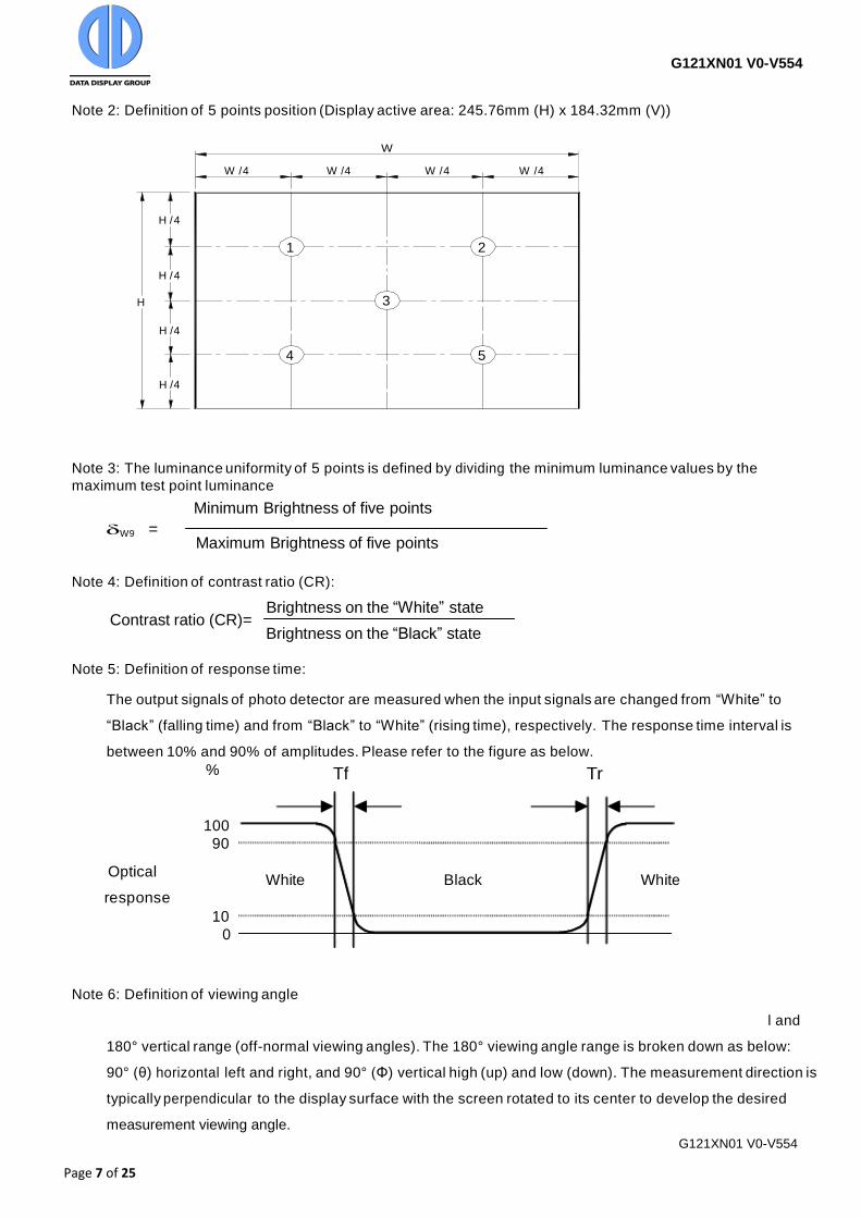
Note 2: Definition of 5 points position (Display active area: 245.76mm (H) x 184.32mm (V))
W
W / 4 W /4 W / 4 W /4
H / 4
1 2
H / 4
H 3
H /4
4 5
H /4
Note 3: The luminance uniformity of 5 points is defined by dividing the minimum luminance values by the
maximum test point luminance
Minimum Brightness of five points
δW9 = Maximum Brightness of five points
Note 4: Definition of contrast ratio (CR):
Brightness on the “White” state Contrast ratio (CR)=
Brightness on the “Black” state Note 5: Definition of response time:
The output signals of photo detector are measured when the input signals are changed from “White” to
“Black” (falling time) and from “Black” to “White” (rising time), respectively. The response time interval is
between 10% and 90% of amplitudes. Please refer to the figure as below.
% Tf Tr
Optical
response
100 90
10 0
White Black White
Note 6: Definition of viewing angle l and
180° vertical range (off-normal viewing angles). The 180° viewing angle range is broken down as below:
90° (θ) horizontal left and right, and 90° (Φ) vertical high (up) and low (down). The measurement direction is
typically perpendicular to the display surface with the screen rotated to its center to develop the desired
measurement viewing angle.

G121XN01 V0-V554
G121XN01 V0-V554
Page 8 of 25
Normal Line
4> = oo, e =0°
6 O'clock y' x' directiop
<j> L = 9Q
G121XN01 V0-V554
G121XN01 V0-V554
Page 9 of 25
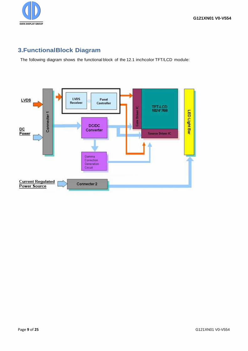
3.FunctionalBlock Diagram
The following diagram shows the functional block of the 12.1 inchcolor TFT/LCD module:

G121XN01 V0-V554
G121XN01 V0-V554
Page 10 of 25
4. Absolute Maximum Ratings
4.1 Absolute Ratings of TFT LCD Module
Item Symbol Min Max Unit
Logic/LCD Drive Voltage Vin -0.3 +3.6 [Volt]
4.2 Absolute Ratings of Environment
Item Symbol Min Max Unit
Operating Temperature TOP -30 +85 o [ C]
Operation Humidity HOP 5 90 [%RH]
Storage Temperature TST -30 +85 o [ C]
Storage Humidity HST 5 90 [%RH]
Note: Maximum Wet- and no condensation.
G121XN01 V0-V554
G121XN01 V0-V554
Page 11 of 25
VCC
1
2
D1
D2
D5
D6
G
S
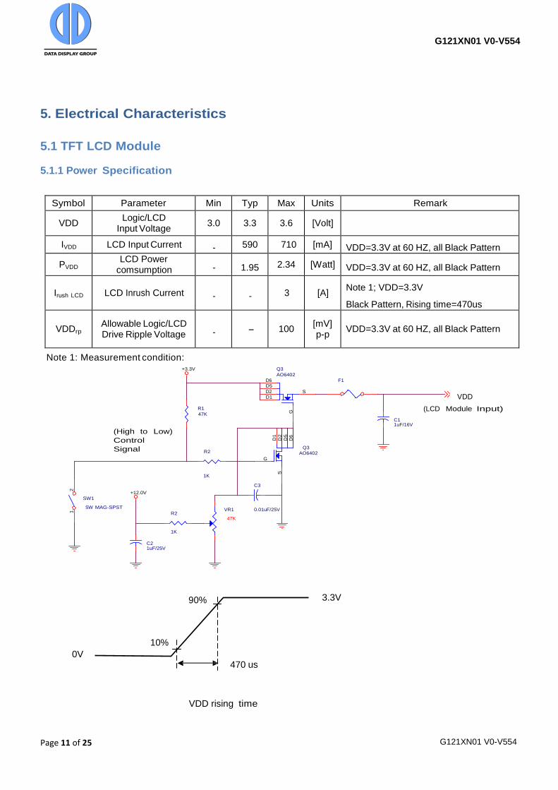
5. Electrical Characteristics
5.1 TFT LCD Module
5.1.1 Power Specification
Symbol Parameter Min Typ Max Units Remark
VDD Logic/LCD
Input Voltage
3.0
3.3
3.6
[Volt]
IVDD LCD Input Current
- 590 710 [mA]
VDD=3.3V at 60 HZ, all Black Pattern
PVDD LCD Power
comsumption
-
1.95
2.34
[Watt]
VDD=3.3V at 60 HZ, all Black Pattern
Irush LCD
LCD Inrush Current
-
-
3
[A]
Note 1; VDD=3.3V
Black Pattern, Rising time=470us
VDDrp
Allowable Logic/LCD Drive Ripple Voltage
-
-
100
[mV] p-p
VDD=3.3V at 60 HZ, all Black Pattern
Note 1: Measurement condition: +3.3V
Q3
AO6402
D6 F1 D5
(High to Low)
Control
Signal
R1
47K
R2
D2 S D1
Q3 AO6402
C1 1uF/16V
VDD
(LCD Module Input)
G
SW1
SW MAG-SPST
+12.0V
R2
1K
1K
VR1
47K
C3
0.01uF/25V
C2 1uF/25V
90% 3.3V
10%
0V
470 us
VDD rising time

G121XN01 V0-V554
G121XN01 V0-V554
Page 12 of 25
5.1.2 Signal Electrical Characteristics
Input signals shall be low or Hi-Z state when VDD is off.
Symbol Item Min. Typ. Max. Unit Remark
VTH
Differential Input High Threshold
-
-
100
[mV]
VCM=1.2V
VTL
Differential Input Low Threshold
100
-
-
[mV]
VCM=1.2V
VID Input Differential Voltage
100
400
600
[mV]
VICM
Differential Input Common Mode Voltage
1.15
1.2
1.45
[V]
VTH/VTL=+-100mV
Note: LVDS Signal Waveform.

G121XN01 V0-V554
G121XN01 V0-V554
Page 13 of 25
5.2 Backlight Specification
ITEM SYMBOL MIN .
TYP. MAX. UNIT Remarks
LED Forward Voltage VL -- 8.4 -- V *1), IL = 1A
LED Forward Current IL -- 1000 -- mA *2)
Powe.r Consumption WL -- 8.4 -- W IL = 1A
Backlight Lifetime BL 70,000 -- Hr *3),*4)
*1) VL is specified as the sum of the white LED forward voltages.
*2) LEDs are best powered using a constant current source. To avoid chromaticity shifts while dimming use pulse-width modulation
(PWM) techniques.
*3) Backlight lifetime is defined as the time when brightness becomes 50% of the initial value.
*4) The lifetime of the backlight is dependent of the ambient temperature. The lifetime will decrease under
temperatures above 80°C unless LED forward current is reduced accordingly.
*5) LED forward current derating curve:
6*) Recommended backlight power supply data
PART NUMBER MANUFACTURER
SmartLED 1x1000A
IN-50-001 – analog
IN-51-001 - PWM
Apollo Display Technologies Corp.

G121XN01 V0-V554
G121XN01 V0-V554
Page 14 of 25
6. Signal Characteristics
6.1 Pixel Format Image
Following figure shows the relationship between input signal and LCD pixel format.
6.2 Scanning Direction
The following figures show the image seen from the front view. The arrow indicates the direction of scan.
Fig. 1 Normal scan (Pin19, RSV = Low or NC) Fig. 2 Reverse scan (Pin19, RSV = High or VDD)

G121XN01 V0-V554
G121XN01 V0-V554
Page 15 of 25
6.3 TFT-LCD Interface Signal Description
The module using a LVDS receiver embaded in AUO’s ASIC. LVDS is a differential signal technology for LCD interface and a high-speed data transfer device.
Input Signal Interface
Pin No.
Symbol
Description
1
VDD
Power Supply, 3.3V (typical)
2
VDD
Power Supply, 3.3V (typical)
3
GND
Ground
4
SEL68
6/ 8bits LVDS data input selection [H: 8bits L/NC: 6bit] *Note4
5
RIN0-
LVDS receiver signal channel 0
LVDS Differential Data Input (R0, R1, R2, R3, R4, R5, G0)
6
RIN0+
7
GND
Ground
8
RIN1- LVDS receiver signal channel 1 LVDS Differential Data Input (G1, G2, G3, G4, G5, B0, B1)
9
RIN1+
10
GND
Ground
11
RIN2-
LVDS receiver signal channel 2
LVDS Differential Data Input (B2, B3, B4, B5, HS, VS, DE)
12
RIN2+
13
GND
Ground
14
CLKIN-
LVDS receiver signal clock
15
CLKIN+
16
GND
Ground
17
RIN3-
LVDS receiver signal channel 3, NC for 6 bit LVDS Input. *Note5
LVDS Differential Data Input (R6, R7, G6, G7, B6, B7, RSV)
18
RIN3+
19
RSV
Reverse Scan Function [H: Enable; L/NC: Disable]
20
NC/GND
Reserved for AUO internal test. Please treat it as NC.
Note 1: Input Signals shall be in low status when VDD is off. Note 2: High stands for “3.3V”, Low stands for “0V”, NC stands for “No Connection”. Note 3: RSV stands for “Reserved”.
Note 4: Input signals shall be in low status when VDD is off. Note 5: If 6 bits mode, please keep the Pin 17 & Pin 18 NC or make sure that the Voltage of Pin 17 is always higher
than the Voltage of Pin 18.

G121XN01 V0-V554
G121XN01 V0-V554
Page 16 of 25
6.4 The Input Data Format
6.4.1 SEL68
SEL68 =“Low” or “NC” for 6 bits LVDS Input
SEL68 = “High” for 8 bits LVDS Input
Note1: Please follow PSWG.
Note2: R/G/B data 7:MSB, R/G/B data 0:LSB
Signal Name Description +RED5(R5) +RED4(R4) +RED3(R3) +RED2(R2) +RED1(R1) +RED0(R0)
Red Data 5 (MSB) Red Data 4 Red Data 3 Red Data 2 Red Data 1 Red Data 0 (LSB) Red-pixel Data
Red-pixel Data Each red pixel’s brightness data consists of these 6 bits pixel data.
+GREEN5(G5) +GREEN4(G4)
+GREEN3(G3) +GREEN2(G2)
+GREEN1(G1) +GREEN0(G0)
Green Data 5 (MSB) Green Data 4 Green Data 3 Green Data 2 Green Data 1 Green Data 0 (LSB) Green-pixel Data
Green-pixel Data Each green pixel’s brightness data consists of these 6 bits pixel data.
+BLUE5(B5) +BLUE4(B4) +BLUE3(B3) +BLUE2(B2) +BLUE1(B1) +BLUE0(B0)
Blue Data 5 (MSB) Blue Data 4 Blue Data 3 Blue Data 2 Blue Data 1 Blue Data 0 (LSB) Blue-pixel Data
Blue-pixel Data Each blue pixel’s brightness data consists of these 6 bits pixel data.
CLK Data Clock The typical frequency is 65MHz. The signal is used to strobe the pixel data and DE signals. All pixel data shall be valid at the falling edge when the DE signal is high.
DE Display Timing This signal is strobed at the falling edge of CLK. When the signal is high, the pixel data shall be valid to be displayed.
Note: Output signals from any system shall be low or Hi-Z state when VDD is off.

G121XN01 V0-V554
G121XN01 V0-V554
Page 17 of 25
6.5 TFT-LCD Interface Timing
6.5.1 Timing Characteristics
Signal
Symbol
Min.
Typ.
Max.
Unit
Clock Frequency
1/ TClock 50 65 80
MHz
Vertical
Section
Period
TV 776 806 1023
TLine
Active
TVD - 768 -
Blanking
TVB 8 38 255
Horizontal
Section
Period
TH 1054 1344 2047
TClock
Active
THD - 1024 -
Blanking
THB 40 320 1023
Note 1: Frame rate is 60 Hz. Note 2: DE mode.
6.5.2 Input Timing Diagram

G121XN01 V0-V554
G121XN01 V0-V554
Page 18 of 25
6.6 Power ON/OFF Sequence VDD power and lamp on/off sequence is as below. Interface signals are also shown in the chart. Signals from any system shall be Hi-Z state or low level when VDD is off.
Power ON/OFF sequence timing
Parameter
Value
Units
Min.
Typ.
Max.
T1
0.5
-
10
[ms]
T2
30
40
50
[ms]
T3
200
-
-
[ms]
T4
10
-
-
[ms]
T5
10
-
-
[ms]
T6
0
-
-
[ms]
T7
10
-
-
[ms]
T8
100
-
-
[ms]
T9
0
16
50
[ms]
T10
-
-
10
[ms]
T11
1000
-
-
[ms]
The above on/off sequence should be applied to avoid abnormal function in the display. Please make sure to turn
off the power when you plug the cable into the input connector or pull the cable out of the connector.

G121XN01 V0-V554
G121XN01 V0-V554
Page 19 of 25
7. Connector & Pin Assignment Physical interface is described as for the connector on module. These connectors are capable of accommodating the following signals and will be following components.
7.1 TFT-LCD Signal (CN1): LCD Connector
Connector Name / Designation Signal Connector
Manufacturer STM or compatible
Connector Model Number MSB240420-E or compatible
Adaptable Plug P240420 or compatible
Pin No. Symbol Pin No. Symbol
1 VDD 2 VDD
3 GND 4 SEL68
5 RIN0- 6 RIN0+
7 GND 8 RIN1-
9 RIN1+ 10 GND
11 RIN2- 12 RIN2+
13 GND 14 CLKIN-
15 CLKIN+ 16 GND
17 RIN3- 18 RIN3+
19 RSV 20 NC/GND
7.2 LED Backlight Unit
Connector Name / Designation Lamp Connector
Manufacturer Molex
Connector Model Number 22-01-3027
Mating Model Number 22-05-3021
Pin No. symbol description Color
Pin1 HV Input Power Red
Pin2 LV GND Black
VL = HV – LV

G121XN01 V0-V554
G121XN01 V0-V554
Page 20 of 25
8. Reliability Test Criteria
Items
Required Condition
Note
Temperature Humidity Bias 40 oC, 90%RH, 300 hours
High Temperature Operation 50 oC, 300 hours
Low Temperature Operation -30 oC, 300 hours
Hot Storage 85 oC, 300 hours
Cold Storage -30 oC, 300 hours
Thermal Shock Test -20 oC / 30 min, 50
oC / 30 min, 100cycles
Hot Start Test 50 oC / 1Hr min. power on/off per 5 minutes, 5 times
Cold Start Test -30 oC / 1Hr min. power on/off per 5 minutes, 5 times
Shock Test (Non-Operating)
50G, 20ms, Half-sine wave, ( ±X, ±Y, ±Z)
Vibration Test
(Non-Operating)
1.5G, (10~200Hz, Sine wave)
30 mins/axis, 3 direction (X, Y, Z)
On/off test
On/10 sec, Off/10 sec, 30,000 cycles
ESD
Contact Discharge: ± 8KV, 150pF(330Ω ) 1sec, 8 points, 25 times/ point
Air Discharge: ± 15KV, 150pF(330Ω ) 1sec, 8 points, 25 times/ point
Note 1
EMI
30-230 MHz, limit 30 dBu V/m, 230-1000 MHz, limit 37 dBu V/m
Note1: According to EN61000-4-2, ESD class B: Some performance degradation allowed. No data lost
Self-recoverable. No hardware failures.
Note2:
• Water condensation is not allowed for each test items.
• Each test is done by new TFT-LCD module. Don’t use the same TFT-LCD module repeatedly for reliability test.
• The reliability test is performed only to examine the TFT-LCD module capability.
• To inspect TFT-LCD module after reliability test, please store it at room temperature and room humidity for 24
hours at least in advance.

G121XN01 V0-V554
G121XN01 V0-V554
Page 21 of 25
9. Mechanical Characteristics
9.1 LCM Outline Dimensions (Front View)

G121XN01 V0-V554
G121XN01 V0-V554
Page 22 of 25
9.1 LCM Outline Dimensions (Rear View)

G121XN01 V0-V554
G121XN01 V0-V554
Page 23 of 25
10. Label and Packaging
10.1 Shipping Label (on the rear side of TFT-LCD display)
10.2 Carton Package
Note: 1. Max. Capacity: 20pcs LCD Modules / per carton 2. Max. Weight: 14.8 kg / per carton 3. The outside dimension of carton is 570(L) mm x 320(W) mm x 420(H) mm
-V554

G121XN01 V0-V554
G121XN01 V0-V554
Page 24 of 25
11 Safety
11.1 Sharp Edge Requirements
There will be no sharp edges or comers on the display assembly that could cause injury.
11.2 Materials
11.2.1 Toxicity
There will be no carcinogenic materials used anywhere in the display module. If toxic materials are
used, they will be reviewed and approved by the responsible AUO toxicologist.
11.2.2 Flammability
All components including electrical components that do not meet the flammability grade UL94-V1 in
the module will complete the flammability rating exception approval process.
The printed circuit board will be made from material rated 94-V1 or better. The actual UL flammability
rating will be printed on the printed circuit board.
11.3 Capacitors
If any polarized capacitors are used in the display assembly, provisions will be made to keep them
from being inserted backwards.
11.4 National Test Lab Requirement
The display module will satisfy all requirements for compliance to:
UL 1950, First Edition U.S.A. Information Technology Equipment

Our company network supports you worldwide with offices in Germany, Great Britain, Italy, Turkey and the
USA. For more information please contact: Distec GmbH
Augsburger Str. 2b
82110 Germering
Germany
Phone: +49 (0)89 / 89 43 63-0
Fax: +49 (0)89 / 89 43 63-131
E-Mail: [email protected]
Internet: www.datadisplay-group.de
Display Technology Ltd.
5 The Oaks Business Village
Revenge Road, Lordswood
Chatham, Kent, ME5 8LF
United Kingdom
Phone: +44 (0)1634 / 67 27 55
Fax: +44 (0)1634 / 67 27 54
E-Mail: [email protected]
Internet: www.datadisplay-group.co.uk
Data Display S.r.l.
Via Marco Polo, 9/D
I-35010 Trebaseleghe (PD)
Italy
Phone: +39 049 / 72 40 038
Fax: +39 049 / 72 40 039
E-Mail: [email protected]
Internet: www.datadisplay-group.it
Data Display Teknoloji Elektronik San Ve Diş Tic
A.Ş.
Kustepe Leylak Sok.
Nursanlar Is Merkezi
Kat. 6 No: 21
Sisli / Istanbul
Turkey
Phone: +90 (0)212 / 356 04 20
Fax: +90 (0)212 / 356 04 25
E-Mail: [email protected]
Internet: www.datadisplay-group.com.tr
Apollo Display Technologies, Corp.
87 Raynor Avenue, Unit 1
Ronkonkoma, NY 11779
United States of America Phone: +1 631 / 580-43 60 Fax: +1 631 / 580-43 70 E-Mail: [email protected] Internet: www.datadisplay-group.com