MX29LV065B DATASHEET - Macronix
55
1 P/N:PM1082 REV. 1.7, APR. 18, 2008 MX29LV065B MX29LV065B DATASHEET The MX29LV065B product will be phase-out, and is not recommended for new design.
-
Upload
khangminh22 -
Category
Documents
-
view
3 -
download
0
Transcript of MX29LV065B DATASHEET - Macronix
1
P/N:PM1082 REV. 1.7, APR. 18, 2008
MX29LV065B
MX29LV065B
DATASHEET
The MX29LV065B product will be phase-out, and is not recommended for newdesign.
2
P/N:PM1082 REV. 1.7, APR. 18, 2008
MX29LV065B
FEATURES
GENERAL FEATURES• 8,388,608 x 8 structure• One hundred twenty-eight Equal Sectors with 64KB each
- Any combination of sectors can be erased with erase suspend/resume function• Thirty-two Sector Groups
- Provides sector group protect function to prevent program or erase operation in the protected sector group- Provides chip unprotected function to allow code changing- Provides temporary sector group unprotected function for code changing in previously protected sector groups
• Single Power Supply Operation- 2.7 to 3.6 volt for read, erase, and program operations
• Latch-up protected to 250mA from -1V to Vcc + 1V• Low Vcc write inhibit is equal to or less than 2.5V• Compatible with JEDEC standard
- Pinout and software compatible to single power supply Flash• Extra 128-byte sector for security
- Feature factory locked and identifiable, and customer locked
PERFORMANCE• High Performance
- Fast access time: 90/120ns- Fast program time: 7us/byte, 42s/chip (typical)- Fast erase time: 0.9s/sector, 45s/chip (typical)
• Low Power Consumption- Low active read current: 9mA (typical) at 5MHz- Low standby current: 200nA (typical)
• Minimum 100,000 erase/program cycle• 20-years data retention
SOFTWARE FEATURES• Erase Suspend/ Erase Resume
- Suspends sector erase operation to read data from or program data to another sector which is not being erased• Status Reply
- Data# polling & Toggle bits provide detection of program and erase operation completion• Support Command Flash Interface (CFI)
HARDWARE FEATURES• Ready/Busy# (RY/BY#) Output
- Provides a hardware method of detecting program and erase operation completion• Hardware Reset (RESET#) Input
- Provides a hardware method to reset the internal state machine to read mode• ACC input pin
- Provides accelerated program capability
64M-BIT [8M x 8] EQUAL SECTORFLASH MEMORY
The MX29LV065B product will be phase-out, and is not recommended for newdesign.
3
P/N:PM1082 REV. 1.7, APR. 18, 2008
MX29LV065B
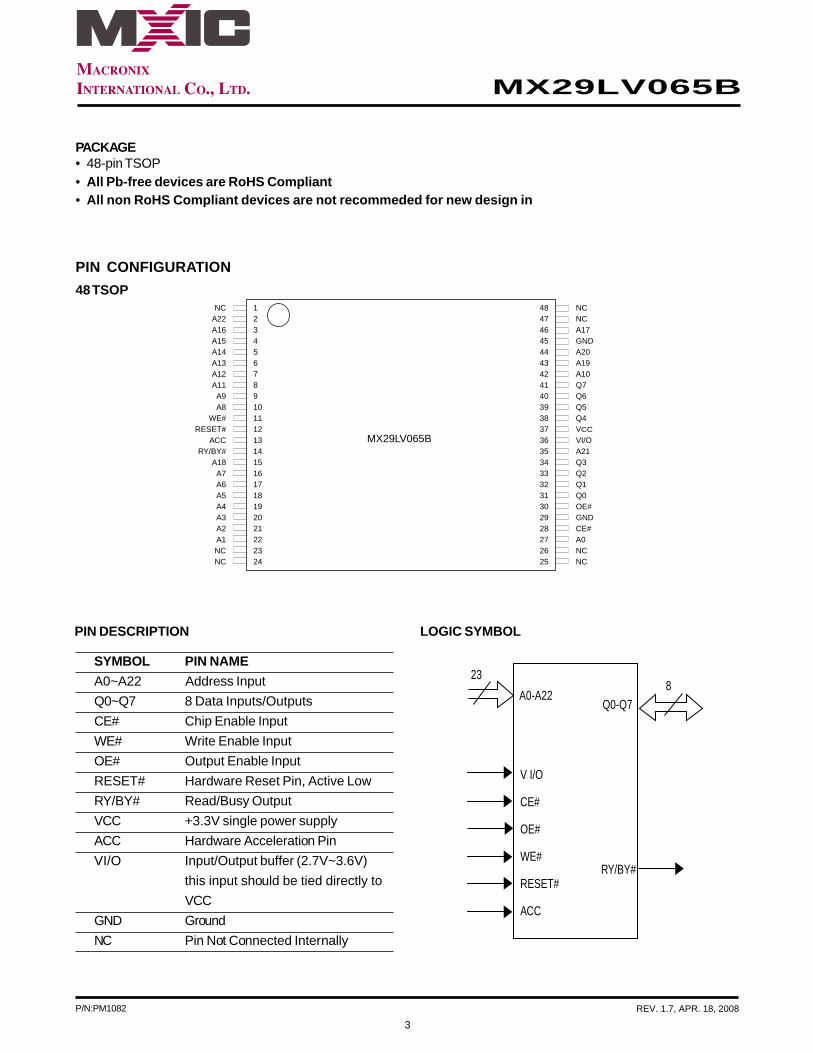
PIN CONFIGURATION
48 TSOP
SYMBOL PIN NAME
A0~A22 Address Input
Q0~Q7 8 Data Inputs/Outputs
CE# Chip Enable Input
WE# Write Enable Input
OE# Output Enable Input
RESET# Hardware Reset Pin, Active Low
RY/BY# Read/Busy Output
VCC +3.3V single power supply
ACC Hardware Acceleration Pin
VI/O Input/Output buffer (2.7V~3.6V)
this input should be tied directly to
VCC
GND Ground
NC Pin Not Connected Internally
PIN DESCRIPTION LOGIC SYMBOL
NCA22A16A15A14A13A12A11A9A8
WE#RESET#
ACCRY/BY#
A18A7A6A5A4A3A2A1NCNC
123456789101112131415161718192021222324
NCNCA17GNDA20A19A10Q7Q6Q5Q4VCC
VI/OA21Q3Q2Q1Q0OE#GNDCE#A0NCNC
484746454443424140393837363534333231302928272625
MX29LV065B
8
Q0-Q7
RY/BY#
A0-A22
V I/O
CE#
OE#
WE#
RESET#
ACC
23
PACKAGE• 48-pin TSOP• All Pb-free devices are RoHS Compliant• All non RoHS Compliant devices are not recommeded for new design in
4
P/N:PM1082 REV. 1.7, APR. 18, 2008
MX29LV065B
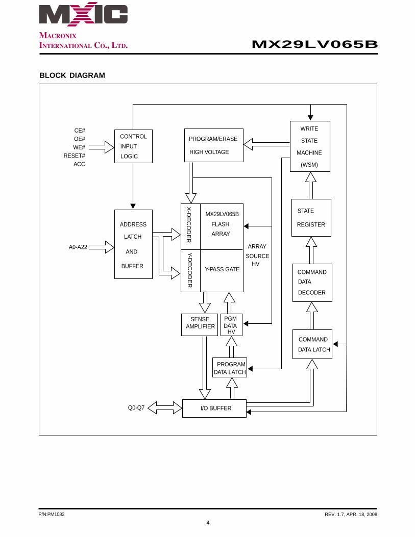
BLOCK DIAGRAM
CONTROL
INPUT
LOGIC
PROGRAM/ERASE
HIGH VOLTAGE
WRITE
STATE
MACHINE
(WSM)
STATE
REGISTER
MX29LV065B
FLASH
ARRAYX
-DE
CO
DE
RADDRESS
LATCH
AND
BUFFER Y-PASS GATE
Y-DE
CO
DE
R
ARRAY
SOURCEHV
COMMAND
DATA
DECODER
COMMAND
DATA LATCH
I/O BUFFER
PGMDATA
HV
PROGRAMDATA LATCH
SENSEAMPLIFIER
Q0-Q7
A0-A22
CE#OE#WE#
RESET#ACC
5
P/N:PM1082 REV. 1.7, APR. 18, 2008
MX29LV065B
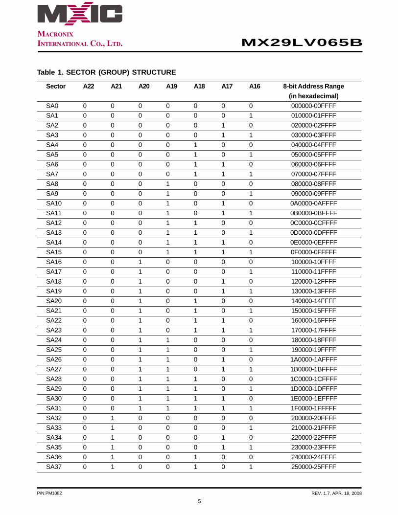
Table 1. SECTOR (GROUP) STRUCTURE
Sector A22 A21 A20 A19 A18 A17 A16 8-bit Address Range
(in hexadecimal)
SA0 0 0 0 0 0 0 0 000000-00FFFF
SA1 0 0 0 0 0 0 1 010000-01FFFF
SA2 0 0 0 0 0 1 0 020000-02FFFF
SA3 0 0 0 0 0 1 1 030000-03FFFF
SA4 0 0 0 0 1 0 0 040000-04FFFF
SA5 0 0 0 0 1 0 1 050000-05FFFF
SA6 0 0 0 0 1 1 0 060000-06FFFF
SA7 0 0 0 0 1 1 1 070000-07FFFF
SA8 0 0 0 1 0 0 0 080000-08FFFF
SA9 0 0 0 1 0 0 1 090000-09FFFF
SA10 0 0 0 1 0 1 0 0A0000-0AFFFF
SA11 0 0 0 1 0 1 1 0B0000-0BFFFF
SA12 0 0 0 1 1 0 0 0C0000-0CFFFF
SA13 0 0 0 1 1 0 1 0D0000-0DFFFF
SA14 0 0 0 1 1 1 0 0E0000-0EFFFF
SA15 0 0 0 1 1 1 1 0F0000-0FFFFF
SA16 0 0 1 0 0 0 0 100000-10FFFF
SA17 0 0 1 0 0 0 1 110000-11FFFF
SA18 0 0 1 0 0 1 0 120000-12FFFF
SA19 0 0 1 0 0 1 1 130000-13FFFF
SA20 0 0 1 0 1 0 0 140000-14FFFF
SA21 0 0 1 0 1 0 1 150000-15FFFF
SA22 0 0 1 0 1 1 0 160000-16FFFF
SA23 0 0 1 0 1 1 1 170000-17FFFF
SA24 0 0 1 1 0 0 0 180000-18FFFF
SA25 0 0 1 1 0 0 1 190000-19FFFF
SA26 0 0 1 1 0 1 0 1A0000-1AFFFF
SA27 0 0 1 1 0 1 1 1B0000-1BFFFF
SA28 0 0 1 1 1 0 0 1C0000-1CFFFF
SA29 0 0 1 1 1 0 1 1D0000-1DFFFF
SA30 0 0 1 1 1 1 0 1E0000-1EFFFF
SA31 0 0 1 1 1 1 1 1F0000-1FFFFF
SA32 0 1 0 0 0 0 0 200000-20FFFF
SA33 0 1 0 0 0 0 1 210000-21FFFF
SA34 0 1 0 0 0 1 0 220000-22FFFF
SA35 0 1 0 0 0 1 1 230000-23FFFF
SA36 0 1 0 0 1 0 0 240000-24FFFF
SA37 0 1 0 0 1 0 1 250000-25FFFF
6
P/N:PM1082 REV. 1.7, APR. 18, 2008
MX29LV065B
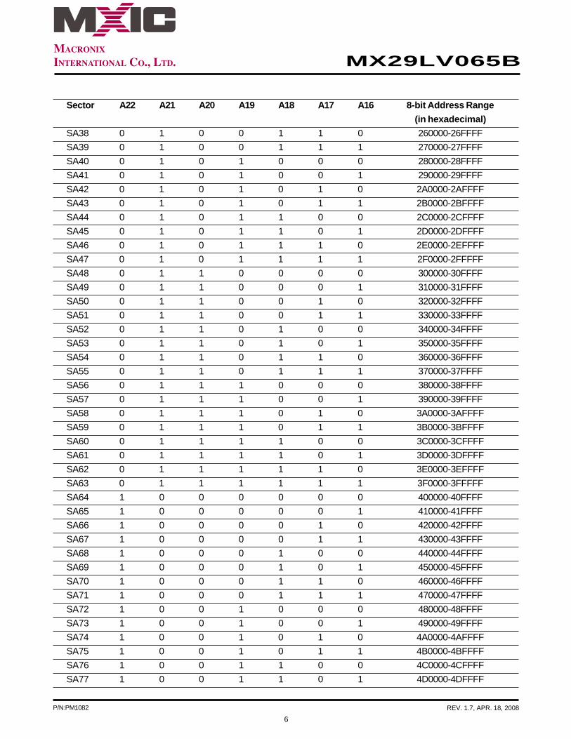
Sector A22 A21 A20 A19 A18 A17 A16 8-bit Address Range
(in hexadecimal)
SA38 0 1 0 0 1 1 0 260000-26FFFF
SA39 0 1 0 0 1 1 1 270000-27FFFF
SA40 0 1 0 1 0 0 0 280000-28FFFF
SA41 0 1 0 1 0 0 1 290000-29FFFF
SA42 0 1 0 1 0 1 0 2A0000-2AFFFF
SA43 0 1 0 1 0 1 1 2B0000-2BFFFF
SA44 0 1 0 1 1 0 0 2C0000-2CFFFF
SA45 0 1 0 1 1 0 1 2D0000-2DFFFF
SA46 0 1 0 1 1 1 0 2E0000-2EFFFF
SA47 0 1 0 1 1 1 1 2F0000-2FFFFF
SA48 0 1 1 0 0 0 0 300000-30FFFF
SA49 0 1 1 0 0 0 1 310000-31FFFF
SA50 0 1 1 0 0 1 0 320000-32FFFF
SA51 0 1 1 0 0 1 1 330000-33FFFF
SA52 0 1 1 0 1 0 0 340000-34FFFF
SA53 0 1 1 0 1 0 1 350000-35FFFF
SA54 0 1 1 0 1 1 0 360000-36FFFF
SA55 0 1 1 0 1 1 1 370000-37FFFF
SA56 0 1 1 1 0 0 0 380000-38FFFF
SA57 0 1 1 1 0 0 1 390000-39FFFF
SA58 0 1 1 1 0 1 0 3A0000-3AFFFF
SA59 0 1 1 1 0 1 1 3B0000-3BFFFF
SA60 0 1 1 1 1 0 0 3C0000-3CFFFF
SA61 0 1 1 1 1 0 1 3D0000-3DFFFF
SA62 0 1 1 1 1 1 0 3E0000-3EFFFF
SA63 0 1 1 1 1 1 1 3F0000-3FFFFF
SA64 1 0 0 0 0 0 0 400000-40FFFF
SA65 1 0 0 0 0 0 1 410000-41FFFF
SA66 1 0 0 0 0 1 0 420000-42FFFF
SA67 1 0 0 0 0 1 1 430000-43FFFF
SA68 1 0 0 0 1 0 0 440000-44FFFF
SA69 1 0 0 0 1 0 1 450000-45FFFF
SA70 1 0 0 0 1 1 0 460000-46FFFF
SA71 1 0 0 0 1 1 1 470000-47FFFF
SA72 1 0 0 1 0 0 0 480000-48FFFF
SA73 1 0 0 1 0 0 1 490000-49FFFF
SA74 1 0 0 1 0 1 0 4A0000-4AFFFF
SA75 1 0 0 1 0 1 1 4B0000-4BFFFF
SA76 1 0 0 1 1 0 0 4C0000-4CFFFF
SA77 1 0 0 1 1 0 1 4D0000-4DFFFF
7
P/N:PM1082 REV. 1.7, APR. 18, 2008
MX29LV065B
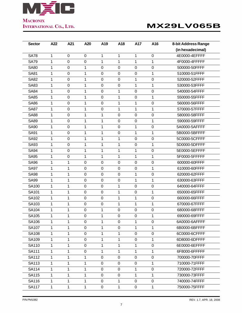
Sector A22 A21 A20 A19 A18 A17 A16 8-bit Address Range
(in hexadecimal)
SA78 1 0 0 1 1 1 0 4E0000-4EFFFF
SA79 1 0 0 1 1 1 1 4F0000-4FFFFF
SA80 1 0 1 0 0 0 0 500000-50FFFF
SA81 1 0 1 0 0 0 1 510000-51FFFF
SA82 1 0 1 0 0 1 0 520000-52FFFF
SA83 1 0 1 0 0 1 1 530000-53FFFF
SA84 1 0 1 0 1 0 0 540000-54FFFF
SA85 1 0 1 0 1 0 1 550000-55FFFF
SA86 1 0 1 0 1 1 0 560000-56FFFF
SA87 1 0 1 0 1 1 1 570000-57FFFF
SA88 1 0 1 1 0 0 0 580000-58FFFF
SA89 1 0 1 1 0 0 1 590000-59FFFF
SA90 1 0 1 1 0 1 0 5A0000-5AFFFF
SA91 1 0 1 1 0 1 1 5B0000-5BFFFF
SA92 1 0 1 1 1 0 0 5C0000-5CFFFF
SA93 1 0 1 1 1 0 1 5D0000-5DFFFF
SA94 1 0 1 1 1 1 0 5E0000-5EFFFF
SA95 1 0 1 1 1 1 1 5F0000-5FFFFF
SA96 1 1 0 0 0 0 0 600000-60FFFF
SA97 1 1 0 0 0 0 1 610000-60FFFF
SA98 1 1 0 0 0 1 0 620000-62FFFF
SA99 1 1 0 0 0 1 1 630000-63FFFF
SA100 1 1 0 0 1 0 0 640000-64FFFF
SA101 1 1 0 0 1 0 1 650000-65FFFF
SA102 1 1 0 0 1 1 0 660000-66FFFF
SA103 1 1 0 0 1 1 1 670000-67FFFF
SA104 1 1 0 1 0 0 0 680000-68FFFF
SA105 1 1 0 1 0 0 1 690000-69FFFF
SA106 1 1 0 1 0 1 0 6A0000-6AFFFF
SA107 1 1 0 1 0 1 1 6B0000-6BFFFF
SA108 1 1 0 1 1 0 0 6C0000-6CFFFF
SA109 1 1 0 1 1 0 1 6D8000-6DFFFF
SA110 1 1 0 1 1 1 0 6E0000-6EFFFF
SA111 1 1 0 1 1 1 1 6F8000-6FFFFF
SA112 1 1 1 0 0 0 0 700000-70FFFF
SA113 1 1 1 0 0 0 1 710000-71FFFF
SA114 1 1 1 0 0 1 0 720000-72FFFF
SA115 1 1 1 0 0 1 1 730000-73FFFF
SA116 1 1 1 0 1 0 0 740000-74FFFF
SA117 1 1 1 0 1 0 1 750000-75FFFF
8
P/N:PM1082 REV. 1.7, APR. 18, 2008
MX29LV065B
Sectpr A21 A20 A19 A18 A17 A16 A15 8-bit Address Range
(in hexadecimal)
SA118 1 1 1 0 1 1 0 760000-76FFFF
SA119 1 1 1 0 1 1 1 770000-77FFFF
SA120 1 1 1 1 0 0 0 780000-78FFFF
SA121 1 1 1 1 0 0 1 790000-79FFFF
SA122 1 1 1 1 0 1 0 7A0000-7AFFFF
SA123 1 1 1 1 0 1 1 7B0000-7BFFFF
SA124 1 1 1 1 1 0 0 7C0000-7CFFFF
SA125 1 1 1 1 1 0 1 7D0000-7DFFFF
SA126 1 1 1 1 1 1 0 7E0000-7EFFFF
SA127 1 1 1 1 1 1 1 7F0000-7FFFFF
Note: All sector groups are 64K bytes in size.
9
P/N:PM1082 REV. 1.7, APR. 18, 2008
MX29LV065B
Sector Group Protection/Unprotected Address Table
Sector Group A21-A17
SA0-SA3 00000
SA4-SA7 00001
SA8-SA11 00010
SA12-SA15 00011
SA16-SA19 00100
SA20-SA23 00101
SA24-SA27 00110
SA28-SA31 00111
SA32-SA35 01000
SA36-SA39 01001
SA40-SA43 01010
SA44-SA47 01011
SA48-SA51 01100
SA52-SA55 01101
SA56-SA59 01110
SA60-SA63 01111
SA64-SA67 10000
SA68-SA71 10001
SA72-SA75 10010
SA76-SA79 10011
SA80-SA83 10100
SA84-SA87 10101
SA88-SA91 10110
SA92-SA95 10111
SA96-SA99 11000
SA100-SA103 11001
SA104-SA107 11010
SA108-SA111 11011
SA112-SA115 11100
SA116-SA119 11101
SA120-SA123 11110
SA124-SA127 11111
Note: All sector groups are 256K bytes in size.
10
P/N:PM1082 REV. 1.7, APR. 18, 2008
MX29LV065B
Table 2. BUS OPERATION--1
Notes:1. All sectors will be unprotected if ACC=Vhv.2. Q0~Q7 are input (DIN) or output (DOUT) pins according to the requests of command sequence, sector protection,
or data polling algorithm.3. AM: MSB of address.
Mode Select RESET# CE# WE# OE# ACC Address Data (I/O)
Q0~Q7
Device Reset L X X X X X HighZ
Standby Mode Vcc±0.3V Vcc±0.3V X X H X HighZ
Output Disable H L H H X X HighZ
Read Mode H L H L X AIN DOUT
Write (Note1) H L L H X AIN DIN
Temporary Vhv X X X X AIN DIN
Sector-Group
Unprotect
Sector-Group Vhv L L H X Sector Address, DIN, DOUT
Protect (Note2) A6=L, A1=H,
A0=L
Chip Unprotect Vhv L L H X Sector Address, DIN, DOUT
(Note2) A6=H, A1=H,
A0=L
Accelerated H L L H Vhv AIN DIN, DOUT
Program
11
P/N:PM1082 REV. 1.7, APR. 18, 2008
MX29LV065B
BUS OPERATION--2
Item Control Input AM A11 A8 A5
CE# WE# OE# to to A9 to A6 to A1 A0 Q0~Q7
A12 A10 A7 A2
Sector Lock Status L H L SA x Vhv
x L x H L 01h or
Verification 00h
(Note1)
Read Silicon ID L H L x x Vhv
x L x L L C2H
Manufacturer Code
Read Silicon ID L H L x x Vhv
x L x L H 93H
Read Indicator Bit L H L x x Vhv
x L x H H 90h or
(Q7) For Security 10h
Sector (Note2)
Notes:1. Sector unprotected code:00h. Sector protected code:01h.2. Factory locked code: 90h. Factory unlocked code: 10h.3. AM: MSB of address.
12
P/N:PM1082 REV. 1.7, APR. 18, 2008
MX29LV065B
WRITE COMMANDS/COMMAND SEQUENCES
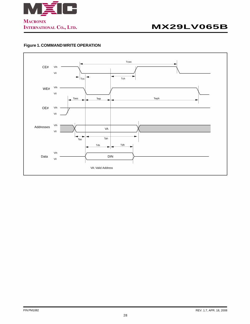
To write a command to the device, system must drive WE# and CE# to Vil, and OE# to Vih. In a command cycle, alladdress are latched at the later falling edge of CE# and WE#, and all data are latched at the earlier rising edge of CE#and WE#.
Figure 1 illustrates the AC timing waveform of a write command, and Table 3 defines all the valid command sets of thedevice. System is not allowed to write invalid commands not defined in this datasheet. Writing an invalid command willbring the device to an undefined state.
REQUIREMENTS FOR READING ARRAY DATA
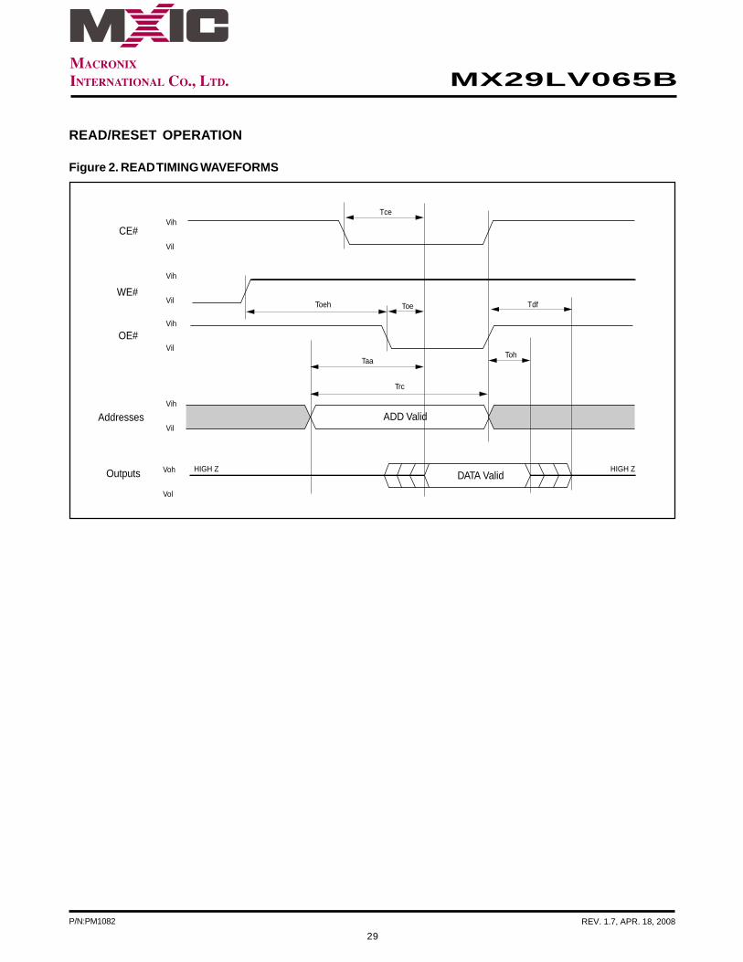
Read array action is to read the data stored in the array. While the memory device is in powered up or has been reset,it will automatically enter the status of read array. If the microprocessor wants to read the data stored in the array, it hasto drive CE# (device enable control pin) and OE# (Output control pin) as Vil, and input the address of the data to beread into address pin at the same time. After a period of read cycle (Tce or Taa), the data being read out will bedisplayed on output pin for microprocessor to access. If CE# or OE# is Vih, the output will be in tri-state, and there willbe no data displayed on output pin at all.
After the memory device completes embedded operation (automatic Erase or Program), it will automatically return tothe status of read array, and the device can read the data in any address in the array. In the process of erasing, if thedevice receives the Erase suspend command, erase operation will be stopped temporarily after a period of time nomore than Tready1 and the device will return to the status of read array. At this time, the device can read the datastored in any address except the sector being erased in the array. In the status of erase suspend, if user wants to readthe data in the sectors being erased, the device will output status data onto the output. Similarly, if program commandis issued after erase suspend, after program operation is completed, system can still read array data in any addressexcept the sectors to be erased.
The device needs to issue reset command to enable read array operation again in order to arbitrarily read the data inthe array in the following two situations:
1. In program or erase operation, the programming or erasing failure causes Q5 to go high.
2. The device is in auto select mode or CFI mode.
In the two situations above, if reset command is not issued, the device is not in read array mode and system mustissue reset command before reading array data.
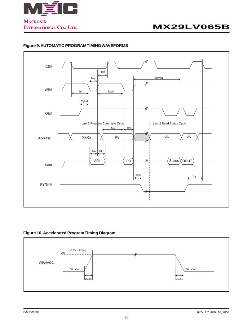
ACCELERATED PROGRAM OPERATION
The accelerated program can improve programming performance compared with byte program. By applying Vhv onACC pin, the device will enter accelerated program and draw current no more than Icw from ACC pin. Removing theVhv from ACC pin will put the device back to normal operation (not accelerated).
13
P/N:PM1082 REV. 1.7, APR. 18, 2008
MX29LV065B
RESET# OPERATION
Driving RESET# pin low for a period more than Trp will reset the device back to read mode. If the device is in programor erase operation, the reset operation will take at most a period of Tready1 for the device to return to read array mode.Before the device returns to read array mode, the RY/BY# pin remains low (busy status).
When RESET# pin is held at GND±0.3V, the device consumes standby current(Isb).However, device draws largercurrent if RESET# pin is held at Vil but not within GND±0.3V.
It is recommended that the system to tie its reset signal to RESET# pin of flash memory, so that the flash memory willbe reset during system reset and allows system to read boot code from flash memory.
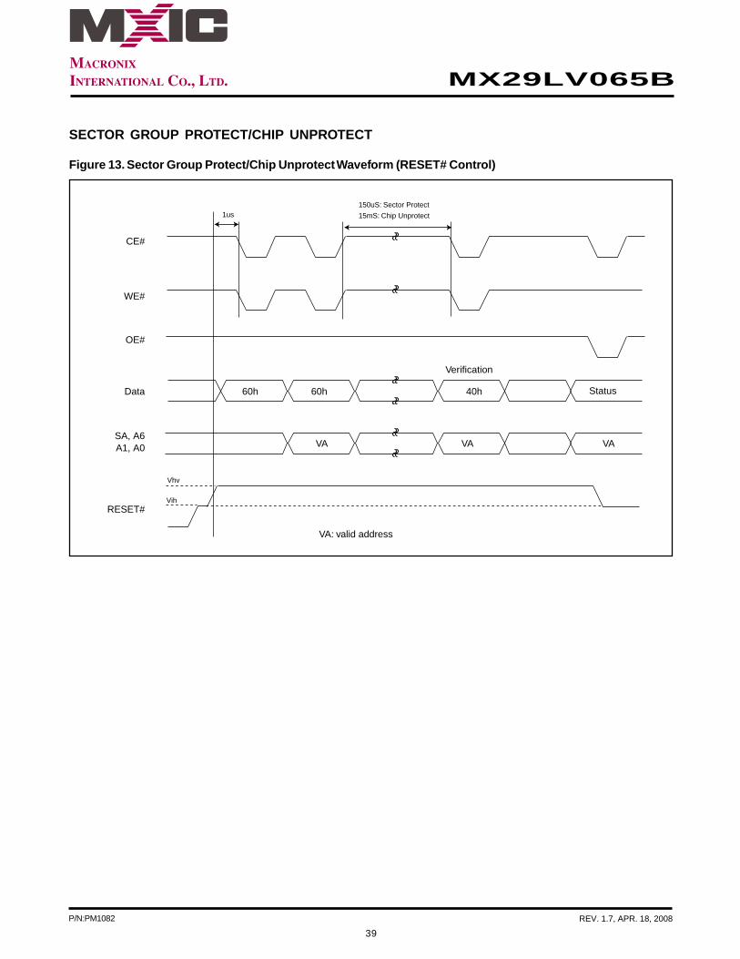
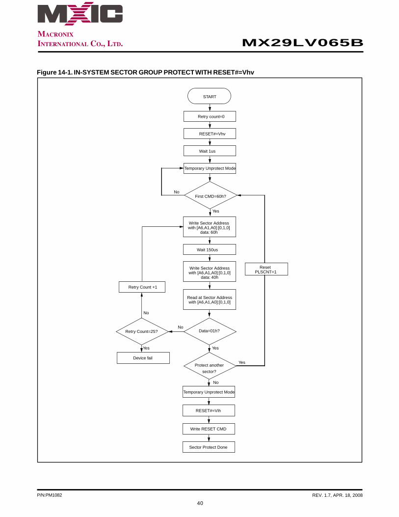
SECTOR GROUP PROTECT OPERATION
When a sector group is protected, program or erase operation will be disabled on these sectors. MX29LV065B providestwo methods for sector group protection.
Once the sector group is protected, the sector group remains protected until next chip unprotect, or is temporarilyunprotected by asserting RESET# pin at Vhv. Refer to temporary sector group unprotect operation for further details.
The first method is by applying Vhv on RESET# pin. Refer to Figure 13 for timing diagram and Figure 14 for thealgorithm for this method.
The other method is asserting Vhv on A9 and OE# pins, with A6 and CE# at Vil. The protection operation begins at thefalling edge of WE# and terminates at the rising edge. Contact Macronix for details.
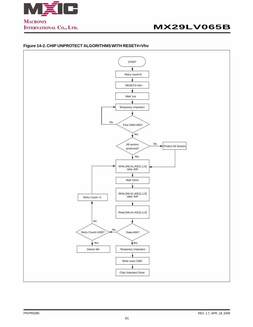
CHIP UNPROTECT OPERATION
MX29LV065B provides two methods for chip unprotect. The chip unprotect operation unprotects all sectors within thedevice. It is recommended to protect all sectors before activating chip unprotect mode. All sector groups are unpro-tected when shipped from the factory.
The first method is by applying Vhv on RESET# pin. Refer to Figure 13 for timing diagram and Figure 14 for algorithmof the operation.
The other method is asserting Vhv on A9 and OE# pins, with A6 at Vih and CE# at Vil (see Table 2). The unprotectoperation begins at the falling edge of WE# and terminates at the rising edge. Contact Macronix for details.
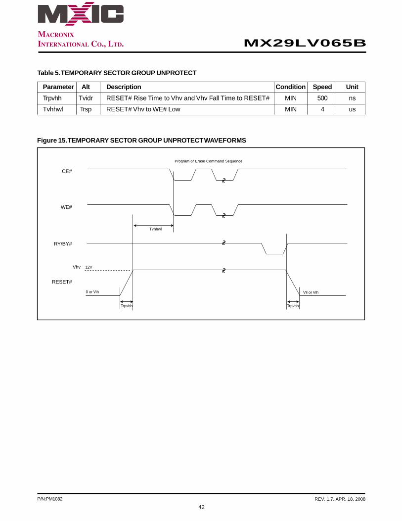
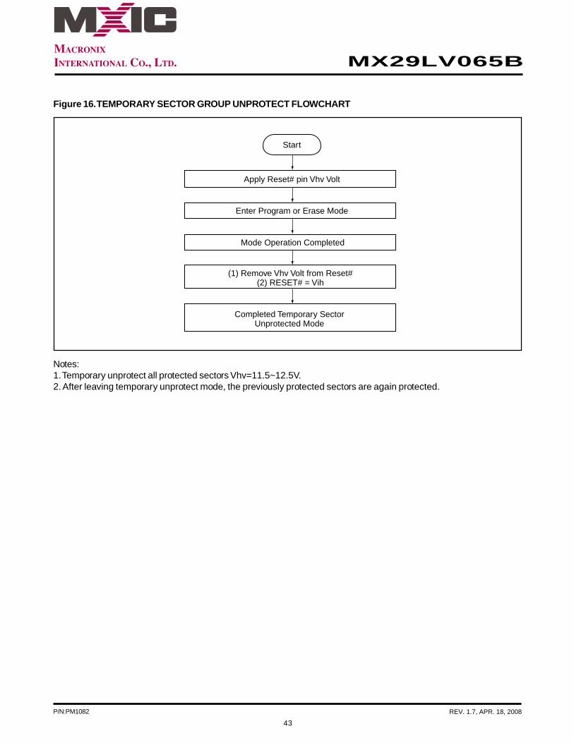
TEMPORARY SECTOR GROUP UNPROTECT OPERATION
System can apply RESET# pin at Vhv to place the device in temporary unprotect mode. In this mode, previouslyprotected sectors can be programmed or erased just as it is unprotected. The devices returns to normal operation onceVhv is removed from RESET# pin and previously protected sectors are again protected.
14
P/N:PM1082 REV. 1.7, APR. 18, 2008
MX29LV065B
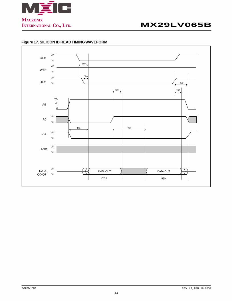
AUTOMATIC SELECT OPERATION
When the device is in Read array mode, erase-suspended read array mode or CFI mode, user can issue read siliconID command to enter read silicon ID mode. After entering read silicon ID mode, user can query several silicon IDscontinuously and does not need to issue read silicon ID mode again. When A0 is Low, device will output MacronixManufacture ID C2. When A0 is high, device will output Device ID. In read silicon ID mode, issuing reset command willreset device back to read array mode or erase-suspended read array mode.
Another way to enter read silicon ID is to apply high voltage on A9 pin with CE#, OE#, A6 and A1 at Vil. While the highvoltage of A9 pin is discharged, device will automatically leave read silicon ID mode and go back to read array modeor erase-suspended read array mode. When A0 is Low, device will output Macronix Manufacture ID C2. When A0 ishigh, device will output Device ID.
VERIFY SECTOR GROUP PROTECT STATUS OPERATION
MX29LV065B provides hardware sector protection against Program and Erase operation for protected sectors. Thesector protect status can be read through Sector Protect Verify command. This method requires Vhv on A9 pin, Vih onWE# and A1 pins, Vil on CE#, OE#, A6 and A0 pins, and sector address on A12 to Am pins. If the read out data is 01H,the designated sector is protected. Oppositely, if the read out data is 00H, the designated sector is not protected.
SECURITY SECTOR FLASH MEMORY REGION
The security sectors can be locked upon shipping from factory, or it can be locked by customer after shipping.Customer can issue Security Sector Factory Protect Verify and/or Security Sector Protect Verify to query the lockstatus of the device.
In factory-locked device, security sector region is protected when shipped from factory and the security silicon sectorindicator bit is set to "1". In customer lockable device, security sector region is unprotected when shipped from factoryand the security silicon indicator bit is set to "0".
Factory Locked: Security Sector Programmed and Protected at the Factory
In a factory locked device, the security silicon region is permanently locked after shipping from factory. The device willhave a 16-byte ESN in the security region. In device : 000000h - 00000Fh.
Customer Lockable: Security Sector NOT Programmed or Protected at the Factory
When the security feature is not required, the security region can act as an extra memory space. The security siliconsector can be read, programmed at address 000010h-00008Fh.
Security silicon sector can also be protected by two methods. Note that once the security silicon sector is protected,there is no way to unprotect the security silicon sector and the content of it can no longer be altered.
The first method is to write a three-cycle command of Enter Security Region, and then follow the sector group protectalgorithm as illustrated in Figure 14, except that RESET# pin may at either Vih or Vhv.
The other method is to write a three-cycle command of Enter Security Region, and then follow the alternate method of
15
P/N:PM1082 REV. 1.7, APR. 18, 2008
MX29LV065B
sector protect with A9, OE# at Vhv.
After the security silicon is locked and verified, system must write Exit Security Sector Region, go through a powercycle, or issue a hardware reset to return the device to read normal array mode.
DATA PROTECTION
To avoid accidental erasure or programming of the device, the device is automatically reset to read array mode duringpower up. Besides, only after successful completion of the specified command sets will the device begin its erase orprogram operation.
Other features to protect the data from accidental alternation are described as followed.
LOW VCC WRITE INHIBIT
The device refuses to accept any write command when Vcc is less than 2.5V. This prevents data from spuriouslyaltered. The device automatically resets itself when Vcc is lower than 2.5V and write cycles are ignored until Vcc isgreater than 2.5V. System must provide proper signals on control pins after Vcc is larger than 2.5V to avoid uninten-tional program or erase operation
WRITE PULSE "GLITCH" PROTECTION
CE#, WE#, OE# pulses shorter than 5ns are treated as glitches and will not be regarded as an effective write cycle.
LOGICAL INHIBIT
A valid write cycle requires both CE# and WE# at Vil with OE# at Vih. Write cycle is ignored when either CE# at Vih,WE# a Vih, or OE# at Vil.
POWER-UP SEQUENCE
Upon power up, MX29LV065B is placed in read array mode. Furthermore, program or erase operation will begin onlyafter successful completion of specified command sequences.
POWER-UP WRITE INHIBIT
When WE#, CE# is held at Vil and OE# is held at Vih during power up, the device ignores the first command on therising edge of WE#.
POWER SUPPLY DECOUPLING
A 0.1uF capacitor should be connected between the Vcc and GND to reduce the noise effect.
16
P/N:PM1082 REV. 1.7, APR. 18, 2008
MX29LV065B
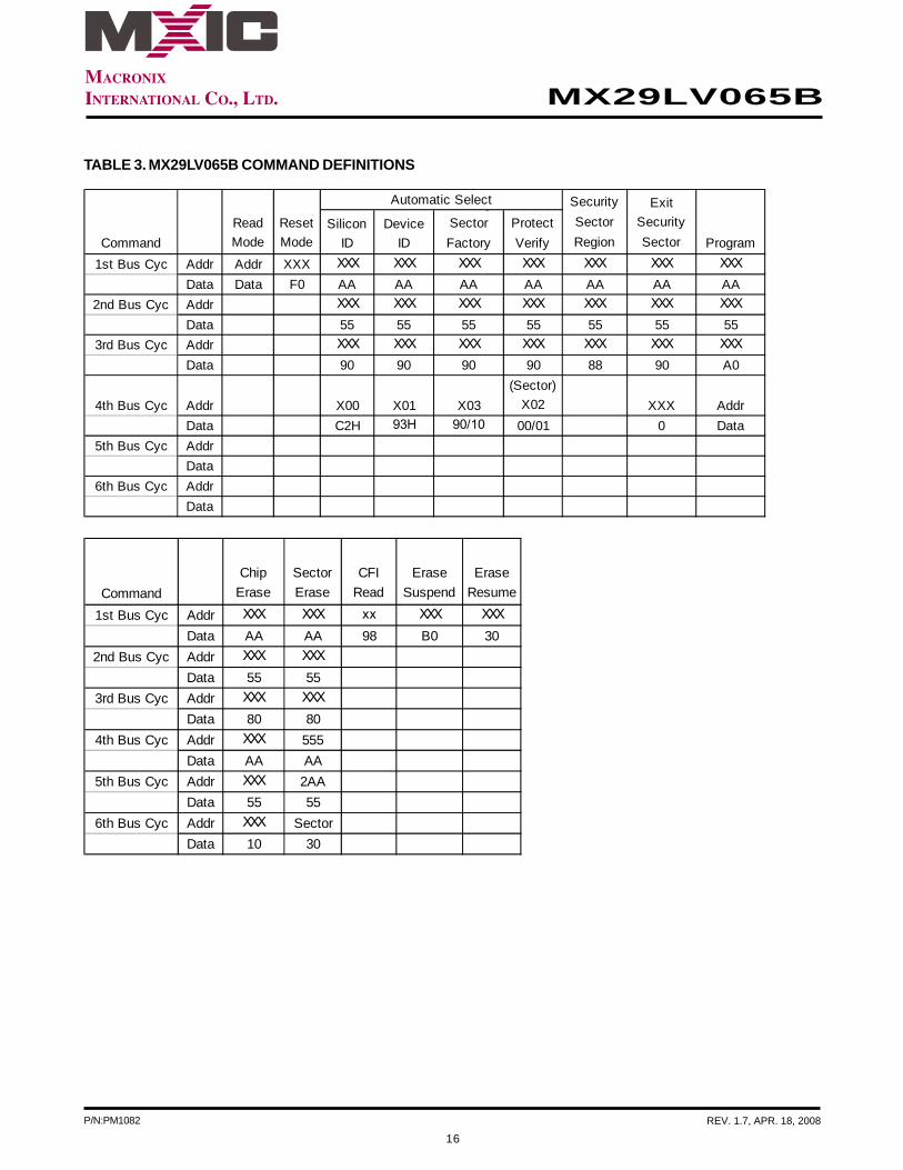
TABLE 3. MX29LV065B COMMAND DEFINITIONS
SiliconID
DeviceID
ySectorFactory
ProtectVerify
1st Bus Cyc Addr Addr XXX XXX XXX XXX XXX XXX XXX XXX
Data Data F0 AA AA AA AA AA AA AA2nd Bus Cyc Addr XXX XXX XXX XXX XXX XXX XXX
Data 55 55 55 55 55 55 553rd Bus Cyc Addr XXX XXX XXX XXX XXX XXX XXX
Data 90 90 90 90 88 90 A0
4th Bus Cyc Addr X00 X01 X03(Sector)
X02 XXX AddrData C2H 93H 90/10 00/01 0 Data
5th Bus Cyc AddrData
6th Bus Cyc AddrData
CommandReadMode
ResetMode
Automatic Select SecuritySectorRegion
ExitSecuritySector Program
1st Bus Cyc Addr XXX XXX xx XXX XXX
Data AA AA 98 B0 302nd Bus Cyc Addr XXX XXX
Data 55 553rd Bus Cyc Addr XXX XXX
Data 80 804th Bus Cyc Addr XXX 555
Data AA AA5th Bus Cyc Addr XXX 2AA
Data 55 556th Bus Cyc Addr XXX Sector
Data 10 30
CommandErase
ResumeChip
EraseSectorErase
CFIRead
EraseSuspend
17
P/N:PM1082 REV. 1.7, APR. 18, 2008
MX29LV065B
RESET
In the following situations, executing reset command will reset device back to read array mode:• Among erase command sequence (before the full command set is completed)• Sector erase time-out period• Erase fail (while Q5 is high)• Among program command sequence (before the full command set is completed, erase-suspended program in-
cluded)• Program fail (while Q5 is high, and erase-suspended program fail is included)• Read silicon ID mode• Sector protect verify• CFI mode
While device is at the status of program fail or erase fail (Q5 is high), user must issue reset command to reset deviceback to read array mode. While the device is in read silicon ID mode, sector protect verify or CFI mode, user mustissue reset command to reset device back to read array mode.
When the device is in the progress of programming (not program fail) or erasing (not erase fail), device will ignore resetcommand.
AUTOMATIC SELECT COMMAND SEQUENCE
Automatic Select mode is used to access the manufacturer ID, device ID and to verify whether or not secured siliconis locked and whether or not a sector is protected. The automatic select mode has four command cycles. The first twoare unlock cycles, and followed by a specific command. The fourth cycle is a normal read cycle, and user can read atany address any number of times without entering another command sequence. The reset command is necessary toexit the Automatic Select mode and back to read array. The following table shows the identification code with corre-sponding address.
Address Data (Hex) Representation
Manufacturer ID X00 C2
Device ID X02 93h
Secured Silicon X06 90/10 Factory locked/unlocked
Sector Protect Verify (Sector address) X 04 00/01 Unprotected/protected
There is an alternative method to that shown in Table 2, which is intended for EPROM programmers and requires Vhvon address bit A9.
18
P/N:PM1082 REV. 1.7, APR. 18, 2008
MX29LV065B
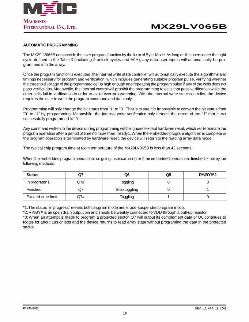
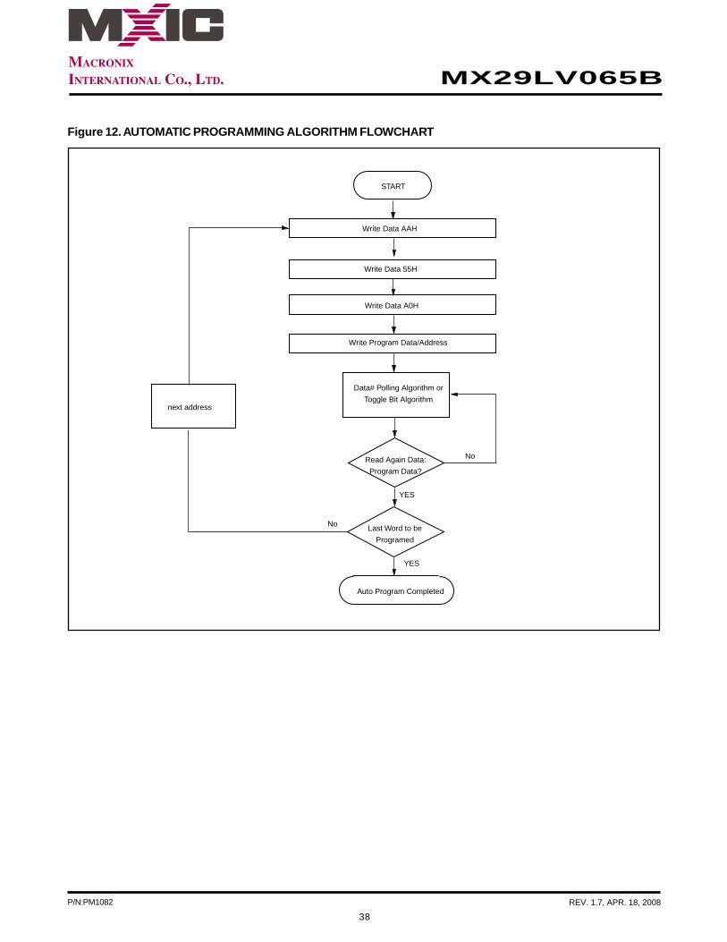
AUTOMATIC PROGRAMMING
The MX29LV065B can provide the user program function by the form of Byte-Mode. As long as the users enter the rightcycle defined in the Table.3 (including 2 unlock cycles and A0H), any data user inputs will automatically be pro-grammed into the array.
Once the program function is executed, the internal write state controller will automatically execute the algorithms andtimings necessary for program and verification, which includes generating suitable program pulse, verifying whetherthe threshold voltage of the programmed cell is high enough and repeating the program pulse if any of the cells does notpass verification. Meanwhile, the internal control will prohibit the programming to cells that pass verification while theother cells fail in verification in order to avoid over-programming. With the internal write state controller, the devicerequires the user to write the program command and data only.
Programming will only change the bit status from "1" to "0". That is to say, it is impossible to convert the bit status from"0" to "1" by programming. Meanwhile, the internal write verification only detects the errors of the "1" that is notsuccessfully programmed to "0".
Any command written to the device during programming will be ignored except hardware reset, which will terminate theprogram operation after a period of time no more than Tready1. When the embedded program algorithm is complete orthe program operation is terminated by hardware reset, the device will return to the reading array data mode.
The typical chip program time at room temperature of the MX29LV065B is less than 42 seconds.
When the embedded program operation is on going, user can confirm if the embedded operation is finished or not by thefollowing methods:
Status Q7 Q6 Q5 RY/BY#*2
In progress*1 Q7# Toggling 0 0
Finished Q7 Stop toggling 0 1
Exceed time limit Q7# Toggling 1 0
*1: The status "in progress" means both program mode and erase-suspended program mode.*2: RY/BY# is an open drain output pin and should be weakly connected to VDD through a pull-up resistor.*3: When an attempt is made to program a protected sector, Q7 will output its complement data or Q6 continues totoggle for about 1us or less and the device returns to read array state without programing the data in the protectedsector.
19
P/N:PM1082 REV. 1.7, APR. 18, 2008
MX29LV065B
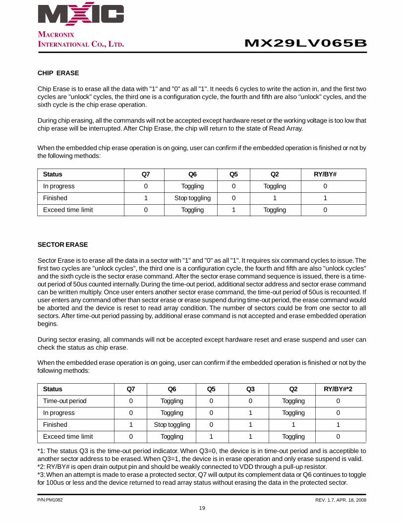
SECTOR ERASE
Sector Erase is to erase all the data in a sector with "1" and "0" as all "1". It requires six command cycles to issue. Thefirst two cycles are "unlock cycles", the third one is a configuration cycle, the fourth and fifth are also "unlock cycles"and the sixth cycle is the sector erase command. After the sector erase command sequence is issued, there is a time-out period of 50us counted internally. During the time-out period, additional sector address and sector erase commandcan be written multiply. Once user enters another sector erase command, the time-out period of 50us is recounted. Ifuser enters any command other than sector erase or erase suspend during time-out period, the erase command wouldbe aborted and the device is reset to read array condition. The number of sectors could be from one sector to allsectors. After time-out period passing by, additional erase command is not accepted and erase embedded operationbegins.
During sector erasing, all commands will not be accepted except hardware reset and erase suspend and user cancheck the status as chip erase.
When the embedded chip erase operation is on going, user can confirm if the embedded operation is finished or not bythe following methods:
Status Q7 Q6 Q5 Q2 RY/BY#
In progress 0 Toggling 0 Toggling 0
Finished 1 Stop toggling 0 1 1
Exceed time limit 0 Toggling 1 Toggling 0
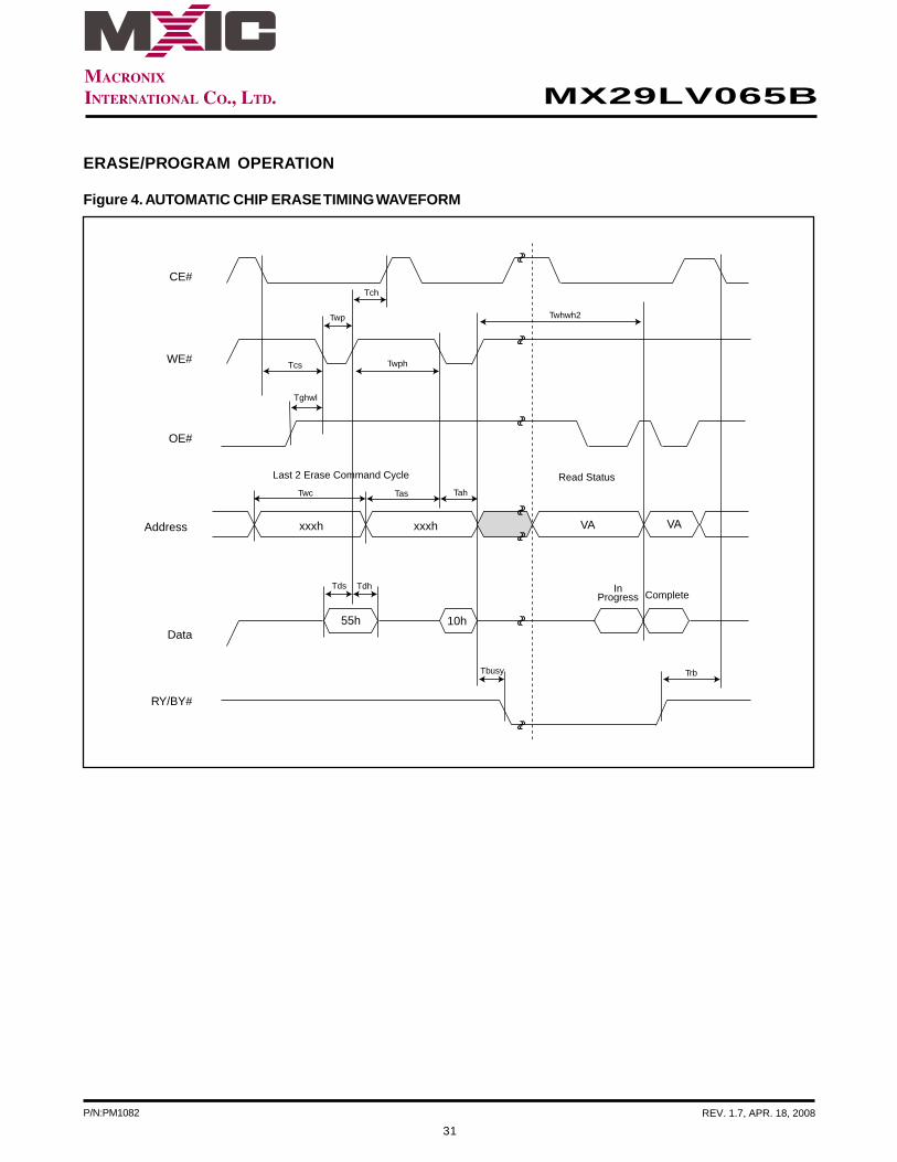
CHIP ERASE
Chip Erase is to erase all the data with "1" and "0" as all "1". It needs 6 cycles to write the action in, and the first twocycles are "unlock" cycles, the third one is a configuration cycle, the fourth and fifth are also "unlock" cycles, and thesixth cycle is the chip erase operation.
During chip erasing, all the commands will not be accepted except hardware reset or the working voltage is too low thatchip erase will be interrupted. After Chip Erase, the chip will return to the state of Read Array.
*1: The status Q3 is the time-out period indicator. When Q3=0, the device is in time-out period and is acceptible toanother sector address to be erased. When Q3=1, the device is in erase operation and only erase suspend is valid.*2: RY/BY# is open drain output pin and should be weakly connected to VDD through a pull-up resistor.*3: When an attempt is made to erase a protected sector, Q7 will output its complement data or Q6 continues to togglefor 100us or less and the device returned to read array status without erasing the data in the protected sector.
When the embedded erase operation is on going, user can confirm if the embedded operation is finished or not by thefollowing methods:
Status Q7 Q6 Q5 Q3 Q2 RY/BY#*2
Time-out period 0 Toggling 0 0 Toggling 0
In progress 0 Toggling 0 1 Toggling 0
Finished 1 Stop toggling 0 1 1 1
Exceed time limit 0 Toggling 1 1 Toggling 0
20
P/N:PM1082 REV. 1.7, APR. 18, 2008
MX29LV065B
When the device has suspended erasing, user can execute the command sets except sector erase and chip erase,such as read silicon ID, sector protect verify, program, CFI query and erase resume.
SECTOR ERASE RESUME
Sector erase resume command is valid only when the device is in erase suspend state. After erase resume, user canissue another erase suspend command, but there should be a 4mS interval between erase resume and the next erasesuspend. If user issue infinite suspend-resume loop, or suspend-resume exceeds 1024 times, the time for erasing willincrease.
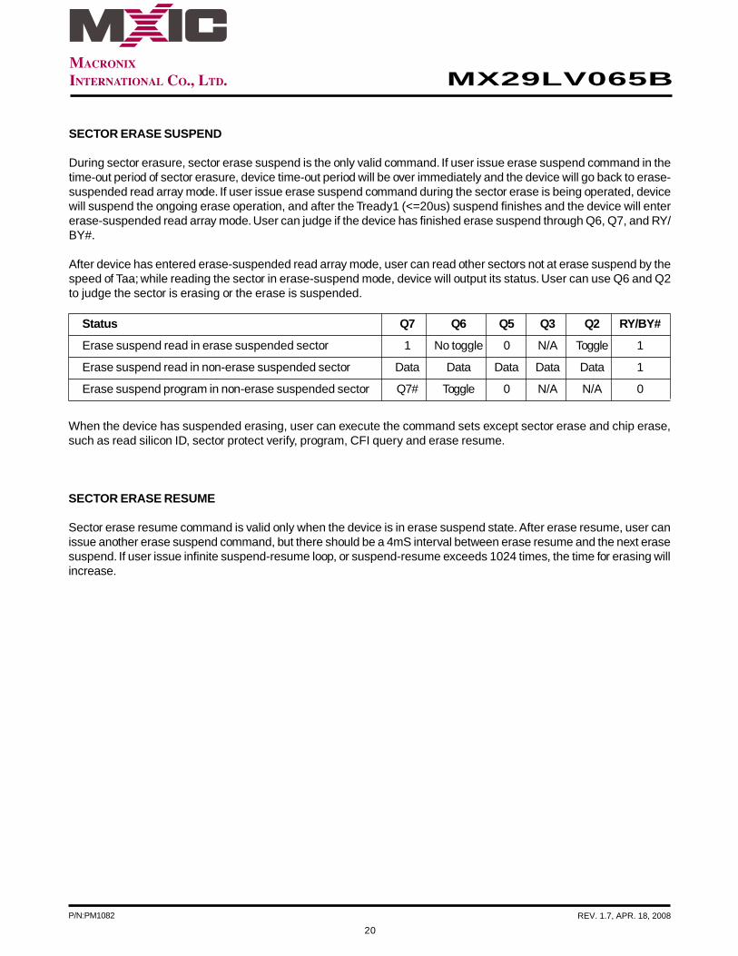
Status Q7 Q6 Q5 Q3 Q2 RY/BY#
Erase suspend read in erase suspended sector 1 No toggle 0 N/A Toggle 1
Erase suspend read in non-erase suspended sector Data Data Data Data Data 1
Erase suspend program in non-erase suspended sector Q7# Toggle 0 N/A N/A 0
SECTOR ERASE SUSPEND
During sector erasure, sector erase suspend is the only valid command. If user issue erase suspend command in thetime-out period of sector erasure, device time-out period will be over immediately and the device will go back to erase-suspended read array mode. If user issue erase suspend command during the sector erase is being operated, devicewill suspend the ongoing erase operation, and after the Tready1 (<=20us) suspend finishes and the device will entererase-suspended read array mode. User can judge if the device has finished erase suspend through Q6, Q7, and RY/BY#.
After device has entered erase-suspended read array mode, user can read other sectors not at erase suspend by thespeed of Taa; while reading the sector in erase-suspend mode, device will output its status. User can use Q6 and Q2to judge the sector is erasing or the erase is suspended.
21
P/N:PM1082 REV. 1.7, APR. 18, 2008
MX29LV065B
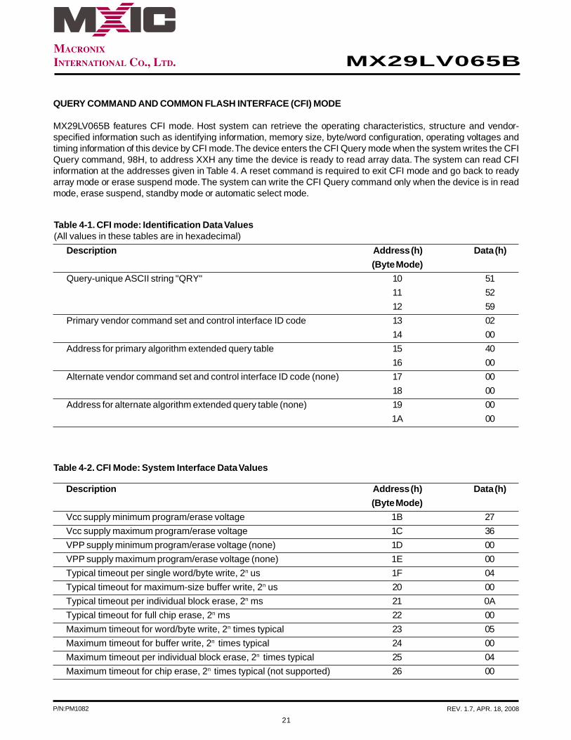
Table 4-1. CFI mode: Identification Data Values(All values in these tables are in hexadecimal)
Table 4-2. CFI Mode: System Interface Data Values
QUERY COMMAND AND COMMON FLASH INTERFACE (CFI) MODE
MX29LV065B features CFI mode. Host system can retrieve the operating characteristics, structure and vendor-specified information such as identifying information, memory size, byte/word configuration, operating voltages andtiming information of this device by CFI mode. The device enters the CFI Query mode when the system writes the CFIQuery command, 98H, to address XXH any time the device is ready to read array data. The system can read CFIinformation at the addresses given in Table 4. A reset command is required to exit CFI mode and go back to readyarray mode or erase suspend mode. The system can write the CFI Query command only when the device is in readmode, erase suspend, standby mode or automatic select mode.
Description Address (h) Data (h)
(Byte Mode)
Query-unique ASCII string "QRY" 10 51
11 52
12 59
Primary vendor command set and control interface ID code 13 02
14 00
Address for primary algorithm extended query table 15 40
16 00
Alternate vendor command set and control interface ID code (none) 17 00
18 00
Address for alternate algorithm extended query table (none) 19 00
1A 00
Description Address (h) Data (h)
(Byte Mode)
Vcc supply minimum program/erase voltage 1B 27
Vcc supply maximum program/erase voltage 1C 36
VPP supply minimum program/erase voltage (none) 1D 00
VPP supply maximum program/erase voltage (none) 1E 00
Typical timeout per single word/byte write, 2n us 1F 04
Typical timeout for maximum-size buffer write, 2n us 20 00
Typical timeout per individual block erase, 2n ms 21 0A
Typical timeout for full chip erase, 2n ms 22 00
Maximum timeout for word/byte write, 2n times typical 23 05
Maximum timeout for buffer write, 2n times typical 24 00
Maximum timeout per individual block erase, 2n times typical 25 04
Maximum timeout for chip erase, 2n times typical (not supported) 26 00
22
P/N:PM1082 REV. 1.7, APR. 18, 2008
MX29LV065B
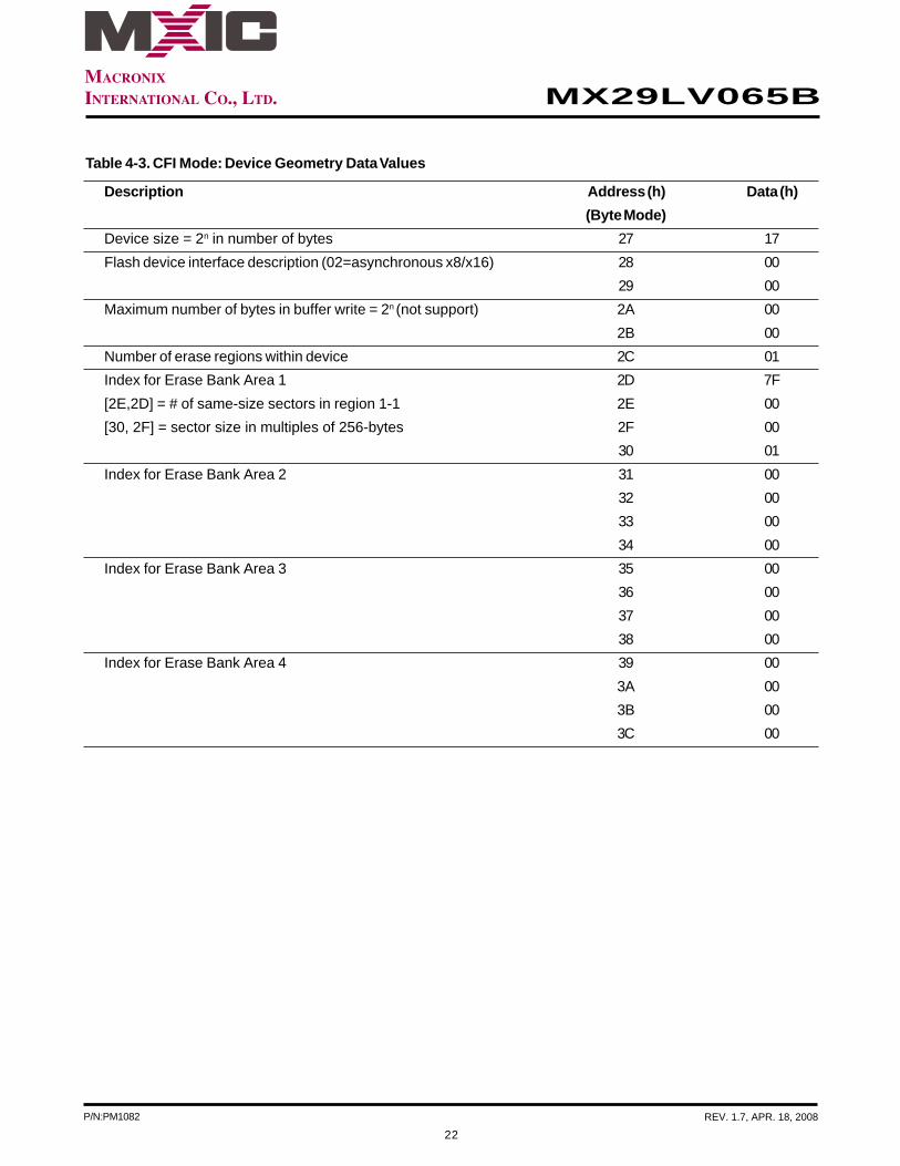
Table 4-3. CFI Mode: Device Geometry Data Values
Description Address (h) Data (h)
(Byte Mode)
Device size = 2n in number of bytes 27 17
Flash device interface description (02=asynchronous x8/x16) 28 00
29 00
Maximum number of bytes in buffer write = 2n (not support) 2A 00
2B 00
Number of erase regions within device 2C 01
Index for Erase Bank Area 1 2D 7F
[2E,2D] = # of same-size sectors in region 1-1 2E 00
[30, 2F] = sector size in multiples of 256-bytes 2F 00
30 01
Index for Erase Bank Area 2 31 00
32 00
33 00
34 00
Index for Erase Bank Area 3 35 00
36 00
37 00
38 00
Index for Erase Bank Area 4 39 00
3A 00
3B 00
3C 00
23
P/N:PM1082 REV. 1.7, APR. 18, 2008
MX29LV065B
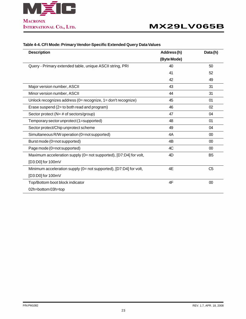
Table 4-4. CFI Mode: Primary Vendor-Specific Extended Query Data Values
Description Address (h) Data (h)
(Byte Mode)
Query - Primary extended table, unique ASCII string, PRI 40 50
41 52
42 49
Major version number, ASCII 43 31
Minor version number, ASCII 44 31
Unlock recognizes address (0= recognize, 1= don't recognize) 45 01
Erase suspend (2= to both read and program) 46 02
Sector protect (N= # of sectors/group) 47 04
Temporary sector unprotect (1=supported) 48 01
Sector protect/Chip unprotect scheme 49 04
Simultaneous R/W operation (0=not supported) 4A 00
Burst mode (0=not supported) 4B 00
Page mode (0=not supported) 4C 00
Maximum acceleration supply (0= not supported), [D7:D4] for volt, 4D B5
[D3:D0] for 100mV
Minimum acceleration supply (0= not supported), [D7:D4] for volt, 4E C5
[D3:D0] for 100mV
Top/Bottom boot block indicator 4F 00
02h=bottom 03h=top
24
P/N:PM1082 REV. 1.7, APR. 18, 2008
MX29LV065B
ABSOLUTE MAXIMUM STRESS RATINGS
Surrounding Temperature with Bias . . . . . . . . . . . . . . . . . . . . . . . . . . . . . . . . . . . . . . . . . . . . . . . . . . . . . . . -65oC to +125oC
Storage Temperature . . . . . . . . . . . .. . . . . . . . . . . . . . . . . . . . . . . . . . . . . . . . . . . . . . . . . . . . . . . . . . . . . -65oC to +150oC
Voltage Range
Vcc . . . . . . . . . . . . . . . . .. . . . . . . . . . . . . . . . . . . . . . . . . . . . . . . . . . . . . . . . . . . . . . . . . . . . . . . . . . -0.5 V to +4.0 V
RESET#, A9 and OE# . .. . . . . . .. . . . . . . . . . . . . . . . . . . . . . . . . . . . . . . . . . . . . . . . . . . . . . . . . . . . -0.5 V to +12.5 V
The other pins. . . . . . . . . . . . . . . . . . . . . . . . . . . . . . . . . . . . . . . . . . . . . . . . . . . . . . . . . . . . . . . . .-0.5 V to Vcc +0.5 V
Output Short Circuit Current (less than one second) . . . . . . . . . . . . . . . . . . . . . . . . . . . . . . . . . . . . . . . . . . . . . . . . .200 mA
OPERATING TEMPERATURE AND VOLTAGE
Commercial (C) Grade
Surrounding Temperature (TA ). . . . . . . . . . . . . . . . . . . . . . . . . . . . . . . . . . . . . . . . . . . . . . . . . . . . . . . . . . . 0°C to +70°CIndustrial (I) Grade
Surrounding Temperature (TA ). . . . . . . . . . . . . . . . . . . . . . . . . . . . . . . . . . . . . . . . . . . . . . . . . . . . . . . . . -40°C to +85°CVCC Supply Voltages
VCC range. . . . . . . . . . . . . . . . . . . . . . . . . . . . . . . . . . . . . . . . . . . . . . . . . . . . . . . . . . . . . . . . . . . . . . . . . +2.7 V to 3.6 V
25
P/N:PM1082 REV. 1.7, APR. 18, 2008
MX29LV065B
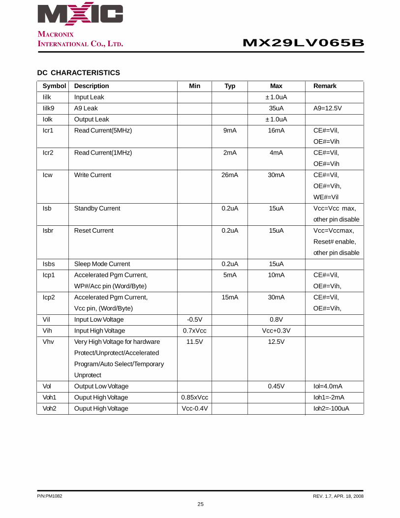
DC CHARACTERISTICS
Symbol Description Min Typ Max Remark
Iilk Input Leak ± 1.0uA
Iilk9 A9 Leak 35uA A9=12.5V
Iolk Output Leak ± 1.0uA
Icr1 Read Current(5MHz) 9mA 16mA CE#=Vil,
OE#=Vih
Icr2 Read Current(1MHz) 2mA 4mA CE#=Vil,
OE#=Vih
Icw Write Current 26mA 30mA CE#=Vil,
OE#=Vih,
WE#=Vil
Isb Standby Current 0.2uA 15uA Vcc=Vcc max,
other pin disable
Isbr Reset Current 0.2uA 15uA Vcc=Vccmax,
Reset# enable,
other pin disable
Isbs Sleep Mode Current 0.2uA 15uA
Icp1 Accelerated Pgm Current, 5mA 10mA CE#=Vil,
WP#/Acc pin (Word/Byte) OE#=Vih,
Icp2 Accelerated Pgm Current, 15mA 30mA CE#=Vil,
Vcc pin, (Word/Byte) OE#=Vih,
Vil Input Low Voltage -0.5V 0.8V
Vih Input High Voltage 0.7xVcc Vcc+0.3V
Vhv Very High Voltage for hardware 11.5V 12.5V
Protect/Unprotect/Accelerated
Program/Auto Select/Temporary
Unprotect
Vol Output Low Voltage 0.45V Iol=4.0mA
Voh1 Ouput High Voltage 0.85xVcc Ioh1=-2mA
Voh2 Ouput High Voltage Vcc-0.4V Ioh2=-100uA
26
P/N:PM1082 REV. 1.7, APR. 18, 2008
MX29LV065B
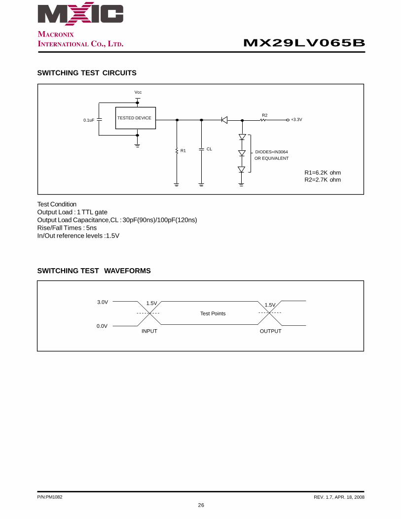
SWITCHING TEST CIRCUITS
Test ConditionOutput Load : 1 TTL gateOutput Load Capacitance,CL : 30pF(90ns)/100pF(120ns)Rise/Fall Times : 5nsIn/Out reference levels :1.5V
SWITCHING TEST WAVEFORMS
1.5V 1.5V
Test Points
3.0V
0.0VOUTPUTINPUT
R1=6.2K ohmR2=2.7K ohm
TESTED DEVICE
DIODES=IN3064
OR EQUIVALENT
CLR1
Vcc
0.1uFR2
+3.3V
27
P/N:PM1082 REV. 1.7, APR. 18, 2008
MX29LV065B
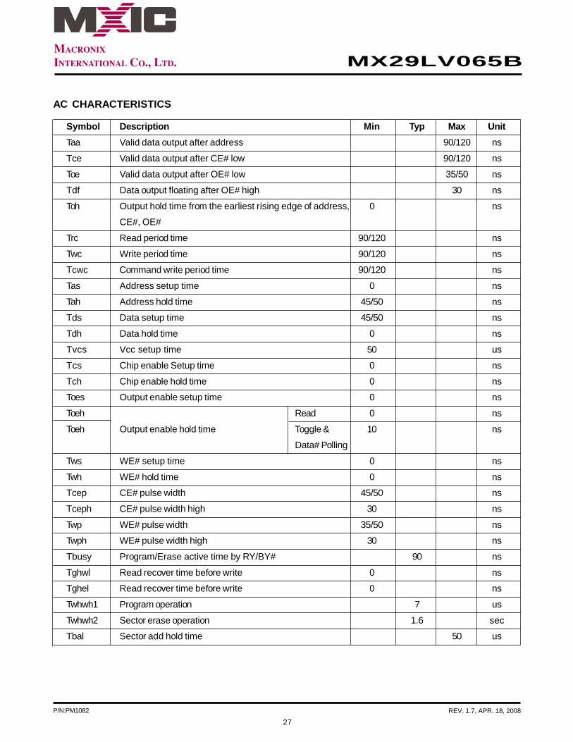
AC CHARACTERISTICS
Symbol Description Min Typ Max Unit
Taa Valid data output after address 90/120 ns
Tce Valid data output after CE# low 90/120 ns
Toe Valid data output after OE# low 35/50 ns
Tdf Data output floating after OE# high 30 ns
Toh Output hold time from the earliest rising edge of address, 0 ns
CE#, OE#
Trc Read period time 90/120 ns
Twc Write period time 90/120 ns
Tcwc Command write period time 90/120 ns
Tas Address setup time 0 ns
Tah Address hold time 45/50 ns
Tds Data setup time 45/50 ns
Tdh Data hold time 0 ns
Tvcs Vcc setup time 50 us
Tcs Chip enable Setup time 0 ns
Tch Chip enable hold time 0 ns
Toes Output enable setup time 0 ns
Toeh Read 0 ns
Toeh Output enable hold time Toggle & 10 ns
Data# Polling
Tws WE# setup time 0 ns
Twh WE# hold time 0 ns
Tcep CE# pulse width 45/50 ns
Tceph CE# pulse width high 30 ns
Twp WE# pulse width 35/50 ns
Twph WE# pulse width high 30 ns
Tbusy Program/Erase active time by RY/BY# 90 ns
Tghwl Read recover time before write 0 ns
Tghel Read recover time before write 0 ns
Twhwh1 Program operation 7 us
Twhwh2 Sector erase operation 1.6 sec
Tbal Sector add hold time 50 us
28
P/N:PM1082 REV. 1.7, APR. 18, 2008
MX29LV065B
Figure 1. COMMAND WRITE OPERATION
Addresses
CE#
OE#
WE#
DIN
Tds
Tah
Data
Tdh
Tcs Tch
Tcwc
TwphTwpToes
Tas
Vih
Vil
Vih
Vil
Vih
Vil
Vih
Vil
Vih
Vil
VA
VA: Valid Address
29
P/N:PM1082 REV. 1.7, APR. 18, 2008
MX29LV065B
READ/RESET OPERATION
Figure 2. READ TIMING WAVEFORMS
Addresses
CE#
OE#
Taa
WE#
Vih
Vil
Vih
Vil
Vih
Vil
Vih
Vil
Voh
Vol
HIGH Z HIGH ZDATA Valid
ToeToeh Tdf
Tce
Trc
Outputs
Toh
ADD Valid

30
P/N:PM1082 REV. 1.7, APR. 18, 2008
MX29LV065B
Figure 3. RESET# TIMING WAVEFORM
AC CHARACTERISTICS
Item Description Setup Speed Unit
Trp1 RESET# Pulse Width (During Automatic Algorithms) MIN 10 us
Trp2 RESET# Pulse Width (NOT During Automatic Algorithms) MIN 500 ns
Trh RESET# High Time Before Read MIN 50 ns
Trb1 RY/BY# Recovery Time (to CE#, OE# go low) MIN 0 ns
Tready1 RESET# PIN Low (During Automatic Algorithms) MAX 20 us
to Read or Write
Tready2 RESET# PIN Low (NOT During Automatic MAX 500 ns
Algorithms) to Read or Write
Trh
Trb1
Trp2
Trp1
Tready2
Tready1
RY/BY#
CE#, OE#
RESET#
Reset Timing NOT during Automatic Algorithms
Reset Timing during Automatic Algorithms
RY/BY#
CE#, OE#
RESET#
31
P/N:PM1082 REV. 1.7, APR. 18, 2008
MX29LV065B
ERASE/PROGRAM OPERATION
Figure 4. AUTOMATIC CHIP ERASE TIMING WAVEFORM
Twc
Address
OE#
CE#
55h
xxxh xxxh
10h
InProgress Complete
VA VA
Tas Tah
Tghwl
Tch
Twp
Tds Tdh
Twhwh2
Read StatusLast 2 Erase Command Cycle
Tbusy Trb
Tcs TwphWE#
Data
RY/BY#
32
P/N:PM1082 REV. 1.7, APR. 18, 2008
MX29LV065B
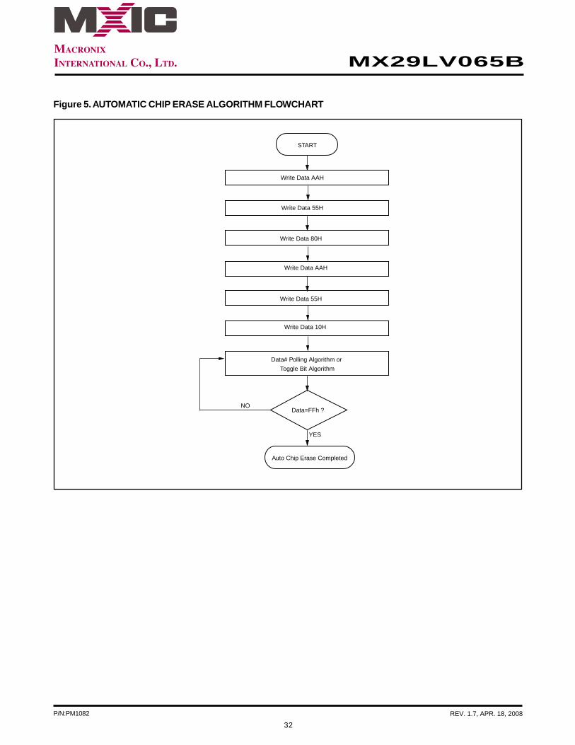
Figure 5. AUTOMATIC CHIP ERASE ALGORITHM FLOWCHART
START
Write Data AAH
Write Data 55H
Write Data AAH
Write Data 80H
YES
NOData=FFh ?
Write Data 10H
Write Data 55H
Data# Polling Algorithm or
Toggle Bit Algorithm
Auto Chip Erase Completed
33
P/N:PM1082 REV. 1.7, APR. 18, 2008
MX29LV065B
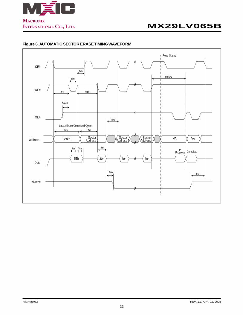
Figure 6. AUTOMATIC SECTOR ERASE TIMING WAVEFORM
Twc
Address
OE#
CE#
55h
SectorAddress 1
SectorAddress 0
30h
InProgress Complete
VA VA
30h
xxxh SectorAddress n
Tas
Tah
Tbal
Tghwl
Tch
Twp
Tds Tdh
Twhwh2
Read Status
Last 2 Erase Command Cycle
TbusyTrb
Tcs TwphWE#
Data
RY/BY#
30h
34
P/N:PM1082 REV. 1.7, APR. 18, 2008
MX29LV065B
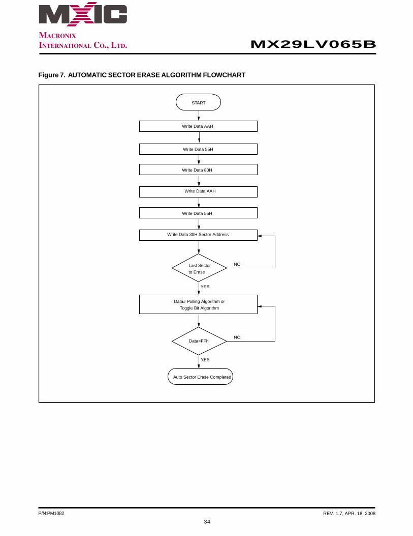
Figure 7. AUTOMATIC SECTOR ERASE ALGORITHM FLOWCHART
START
Write Data AAH
Write Data 55H
Write Data AAH
Write Data 80H
Write Data 30H Sector Address
Write Data 55H
Data# Polling Algorithm or
Toggle Bit Algorithm
Auto Sector Erase Completed
NOLast Sector
to Erase
YES
YES
NOData=FFh
35
P/N:PM1082 REV. 1.7, APR. 18, 2008
MX29LV065B
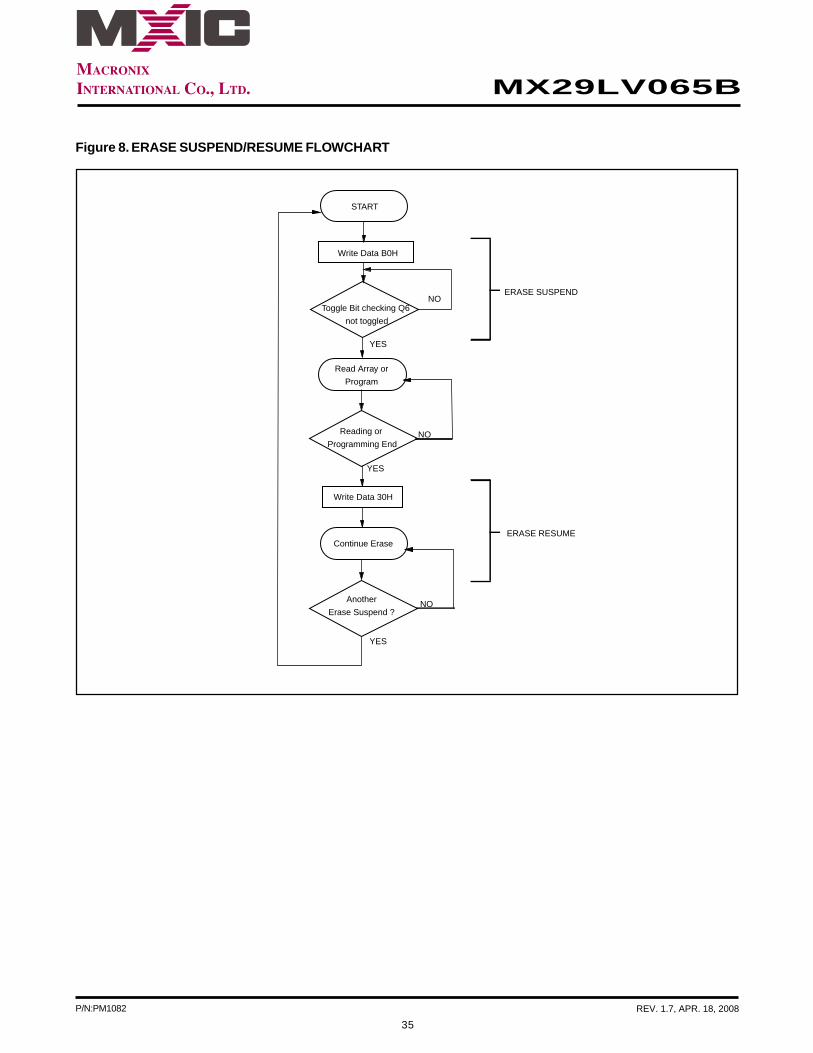
Figure 8. ERASE SUSPEND/RESUME FLOWCHART
START
Write Data B0H
Toggle Bit checking Q6
not toggled
ERASE SUSPEND
YES
NO
Write Data 30H
Continue Erase
Reading or
Programming End
Read Array or
Program
Another
Erase Suspend ?NO
YES
YES
NO
ERASE RESUME
36
P/N:PM1082 REV. 1.7, APR. 18, 2008
MX29LV065B
Figure 9. AUTOMATIC PROGRAM TIMING WAVEFORMS
Figure 10. Accelerated Program Timing Diagram
WP#/ACC
250nS 250nS
Vhv(11.5V ~ 12.5V)
Vil or Vih Vil or Vih
Address
OE#
CE#
A0h
XXXh PA
PD Status DOUT
VA VA
Tas Tah
Tghwl
Tch
Twp
Tds Tdh
Twhwh1
Last 2 Read Status CycleLast 2 Program Command Cycle
TbusyTrb
Tcs TwphWE#
Data
RY/BY#
37
P/N:PM1082 REV. 1.7, APR. 18, 2008
MX29LV065B
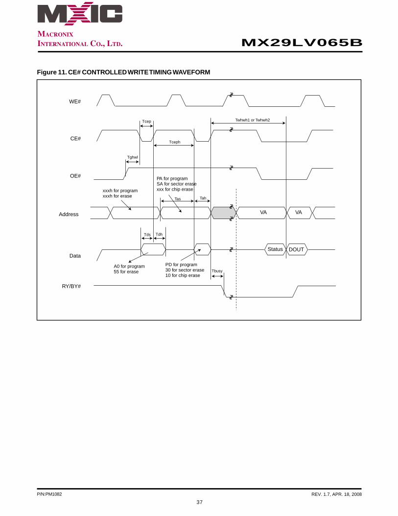
Figure 11. CE# CONTROLLED WRITE TIMING WAVEFORM
Address
OE#
CE#
Status DOUT
VA VA
Tas Tah
Tghwl
xxxh for programxxxh for erase
A0 for program55 for erase
PA for programSA for sector erasexxx for chip erase
PD for program30 for sector erase10 for chip erase
Tcep
Tds Tdh
Twhwh1 or Twhwh2
Tbusy
Tceph
WE#
Data
RY/BY#
38
P/N:PM1082 REV. 1.7, APR. 18, 2008
MX29LV065B
Figure 12. AUTOMATIC PROGRAMMING ALGORITHM FLOWCHART
START
Write Data AAH
Write Data 55H
Write Program Data/Address
Write Data A0H
YES
Read Again Data:
Program Data?
YES
Auto Program Completed
Data# Polling Algorithm or
Toggle Bit Algorithmnext address
Last Word to be
Programed
No
No
39
P/N:PM1082 REV. 1.7, APR. 18, 2008
MX29LV065B
SECTOR GROUP PROTECT/CHIP UNPROTECT
Figure 13. Sector Group Protect/Chip Unprotect Waveform (RESET# Control)
150uS: Sector Protect
15mS: Chip Unprotect1us
Vhv
Vih
Data
SA, A6A1, A0
CE#
WE#
OE#
VA VA VA
Status
VA: valid address
40h60h60h
Verification
RESET#
40
P/N:PM1082 REV. 1.7, APR. 18, 2008
MX29LV065B
Figure 14-1. IN-SYSTEM SECTOR GROUP PROTECT WITH RESET#=Vhv
START
Retry count=0
RESET#=Vhv
Wait 1us
Write Sector Addresswith [A6,A1,A0]:[0,1,0]
data: 60h
Write Sector Addresswith [A6,A1,A0]:[0,1,0]
data: 40h
Read at Sector Addresswith [A6,A1,A0]:[0,1,0]
Wait 150us
Reset PLSCNT=1
Temporary Unprotect Mode
RESET#=Vih
Write RESET CMD
Sector Protect Done
Device fail
Temporary Unprotect Mode
Retry Count +1
First CMD=60h?
Data=01h?Retry Count=25?
Yes
YesYes
Yes
No
No
No
No
Protect another
sector?
41
P/N:PM1082 REV. 1.7, APR. 18, 2008
MX29LV065B
Figure 14-2. CHIP UNPROTECT ALGORITHMS WITH RESET#=Vhv
Write [A6,A1,A0]:[1,1,0]data: 60h
Write [A6,A1,A0]:[1,1,0]data: 40h
Read [A6,A1,A0]:[1,1,0]
Wait 15ms
Temporary Unprotect
Write reset CMD
Chip Unprotect Done
Retry Count +1
Device fail
All sectors
protected?
Data=00h?Retry Count=1000?
YesYes
No
No
Yes
Protect All Sectors
START
Retry count=0
RESET#=Vhv
Wait 1us
Temporary Unprotect
First CMD=60h?
Yes
No
No
42
P/N:PM1082 REV. 1.7, APR. 18, 2008
MX29LV065B
Figure 15. TEMPORARY SECTOR GROUP UNPROTECT WAVEFORMS
Table 5. TEMPORARY SECTOR GROUP UNPROTECT
Parameter Alt Description Condition Speed Unit
Trpvhh Tvidr RESET# Rise Time to Vhv and Vhv Fall Time to RESET# MIN 500 ns
Tvhhwl Trsp RESET# Vhv to WE# Low MIN 4 us
RESET#
CE#
WE#
RY/BY#
Trpvhh
12VVhv
0 or Vih Vil or Vih
Tvhhwl
Trpvhh
Program or Erase Command Sequence
43
P/N:PM1082 REV. 1.7, APR. 18, 2008
MX29LV065B
Figure 16. TEMPORARY SECTOR GROUP UNPROTECT FLOWCHART
Start
Apply Reset# pin Vhv Volt
Enter Program or Erase Mode
(1) Remove Vhv Volt from Reset#(2) RESET# = Vih
Completed Temporary SectorUnprotected Mode
Mode Operation Completed
Notes:1. Temporary unprotect all protected sectors Vhv=11.5~12.5V.2. After leaving temporary unprotect mode, the previously protected sectors are again protected.
44
P/N:PM1082 REV. 1.7, APR. 18, 2008
MX29LV065B
Figure 17. SILICON ID READ TIMING WAVEFORM
Taa
Tce
Taa
Toe
Toh Toh
Tdf
DATA OUT
C2H 93H
Vhv
Vih
VilA9
ADD
CE#
A1
OE#
WE#
A0
DATA OUTDATAQ0-Q7
Vih
Vil
Vih
Vil
Vih
Vil
Vih
Vil
Vih
Vil
Vih
Vil
Vih
Vil
45
P/N:PM1082 REV. 1.7, APR. 18, 2008
MX29LV065B
WRITE OPERATION STATUS
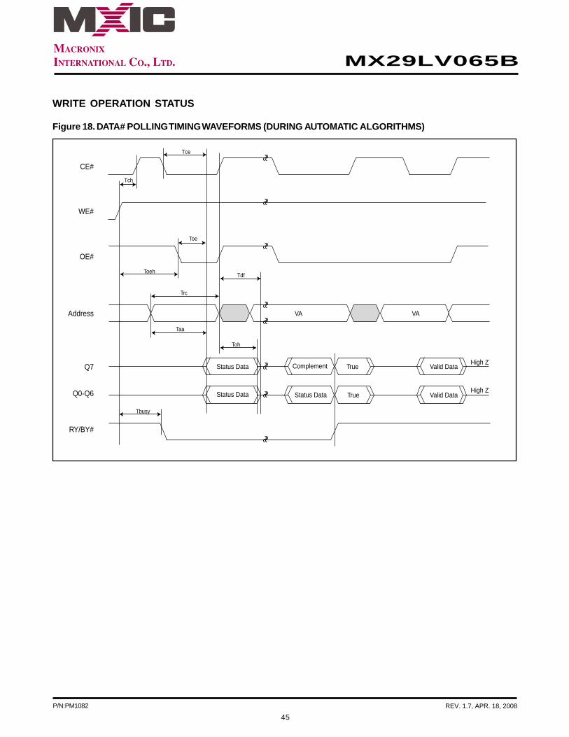
Figure 18. DATA# POLLING TIMING WAVEFORMS (DURING AUTOMATIC ALGORITHMS)
Tdf
Tce
Tch
Toe
Toeh
Toh
CE#
OE#
WE#
Q7
Q0-Q6
RY/BY#
Tbusy
Status Data Status Data
Status Data Complement True Valid Data
Taa
Trc
Address VAVA
High Z
High ZValid DataTrue
46
P/N:PM1082 REV. 1.7, APR. 18, 2008
MX29LV065B
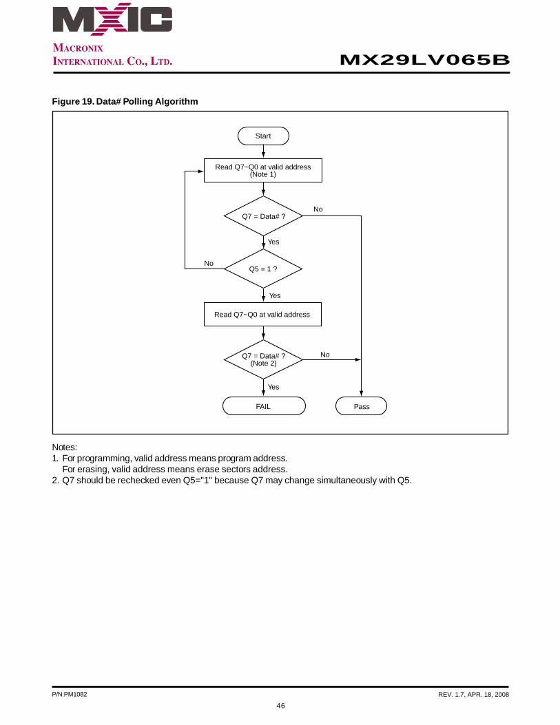
Figure 19. Data# Polling Algorithm
Read Q7~Q0 at valid address(Note 1)
Read Q7~Q0 at valid address
Start
Q7 = Data# ?
Q5 = 1 ?
Q7 = Data# ?(Note 2)
FAIL Pass
No
No
No
Yes
Yes
Yes
Notes:1. For programming, valid address means program address.
For erasing, valid address means erase sectors address.2. Q7 should be rechecked even Q5="1" because Q7 may change simultaneously with Q5.
47
P/N:PM1082 REV. 1.7, APR. 18, 2008
MX29LV065B
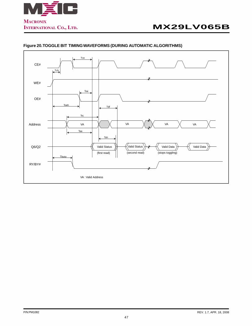
Figure 20. TOGGLE BIT TIMING WAVEFORMS (DURING AUTOMATIC ALGORITHMS)
Tdf
Tce
Tch
Toe
Toeh
Taa
Trc
Toh
Address
CE#
OE#
WE#
Q6/Q2
RY/BY#
Tbusy
Valid Status
(first read)
Valid Status
(second read) (stops toggling)
Valid Data
VA VAVA
VA : Valid Address
VA
Valid Data
48
P/N:PM1082 REV. 1.7, APR. 18, 2008
MX29LV065B
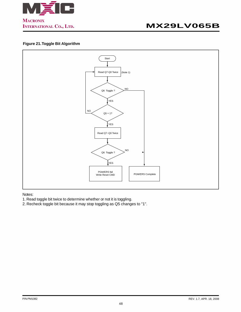
Figure 21. Toggle Bit Algorithm
Notes:1. Read toggle bit twice to determine whether or not it is toggling.2. Recheck toggle bit because it may stop toggling as Q5 changes to "1".
Read Q7-Q0 Twice
Q5 = 1?
Read Q7~Q0 Twice
PGM/ERS failWrite Reset CMD PGM/ERS Complete
Q6 Toggle ?
Q6 Toggle ?
NO
(Note 1)
YES
NO
NO
YES
YES
Start
49
P/N:PM1082 REV. 1.7, APR. 18, 2008
MX29LV065B
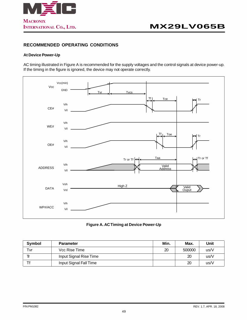
RECOMMENDED OPERATING CONDITIONS
At Device Power-Up
AC timing illustrated in Figure A is recommended for the supply voltages and the control signals at device power-up.If the timing in the figure is ignored, the device may not operate correctly.
Figure A. AC Timing at Device Power-Up
Symbol Parameter Min. Max. Unit
Tvr Vcc Rise Time 20 500000 us/V
Tr Input Signal Rise Time 20 us/V
Tf Input Signal Fall Time 20 us/V
Vcc
ADDRESS
CE#
WE#
OE#
DATA
Tvr
TaaTr or Tf Tr or Tf
TceTf
Vcc(min)
GND
Vih
Vil
Vih
Vil
Vih
Vil
Vih
Vil
Vih
Vil
VohHigh Z
Vol
WP#/ACC
ValidOuput
ValidAddress
Tvcs
Tr
ToeTfTr
50
P/N:PM1082 REV. 1.7, APR. 18, 2008
MX29LV065B
MIN. MAX.
Input Voltage voltage difference with GND on all pins except I/O pins -1.0V 13.5V
Input Voltage voltage difference with GND on all I/O pins -1.0V Vcc + 1.0V
Vcc Current -100mA +100mA
All pins included except Vcc. Test conditions: Vcc = 3.0V, one pin per testing
LIMITS
PARAMETER MIN. TYP. MAX. UNITS
Chip Erase Time 45 65 sec
Sector Erase Time 0.9 15 sec
Erase/Program Cycles 100,000 Cycles
Chip Programming Time 42 126 sec
Byte Programming Time 7 150 us
Accelerated Byte Program Time 4 120 us
LATCH-UP CHARACTERISTICS
ERASE AND PROGRAMMING PERFORMANCE
Parameter Symbol Parameter Description Test Set TYP MAX UNIT
CIN2 Control Pin Capacitance VIN=0 7.5 9 pF
COUT Output Capacitance VOUT=0 8.5 12 pF
CIN Input Capacitance VIN=0 6 7.5 pF
TSOP PIN CAPACITANCE
51
P/N:PM1082 REV. 1.7, APR. 18, 2008
MX29LV065B
ORDERING INFORMATION
PART NO. ACCESS TIME PACKAGE Remark
(ns)
MX29LV065BTC-90 90 48 Pin TSOP Commercial grade,
(Normal Type) Note 1
MX29LV065BTC-12 120 48 Pin TSOP Commercial grade,
(Normal Type) Note 1
MX29LV065BTI-90 90 48 Pin TSOP Industrial grade,
(Normal Type) Note 1
MX29LV065BTI-12 120 48 Pin TSOP Industrial grade,
(Normal Type) Note 1
MX29LV065BTC-90G 90 48 Pin TSOP Commercial grade,
(Normal Type) Pb-free
MX29LV065BTC-12G 120 48 Pin TSOP Commercial grade,
(Normal Type) Pb-free
MX29LV065BTI-90G 90 48 Pin TSOP Industrial grade,
(Normal Type) Pb-free
MX29LV065BTI-12G 120 48 Pin TSOP Industrial grade,
(Normal Type) Pb-free
Note 1: The part no. is not recommended for new design in.
52
P/N:PM1082 REV. 1.7, APR. 18, 2008
MX29LV065B
PART NAME DESCRIPTION
MX 29 LV 70B T C G
OPTION:G: Pb-freeblank: normal
SPEED:90: 90ns120: 120ns
TEMPERATURE RANGE:C: Commercial (0˚CC to 70˚CI: Industrial (-40˚CC to 85˚CC
PACKAGE:T: TSOP
REVISION:B
DENSITY & MODE:065: 64Mb, x8 Equal Sector
TYPE:LV: 3.3V
DEVICE:29:Flash
065
53
P/N:PM1082 REV. 1.7, APR. 18, 2008
MX29LV065B
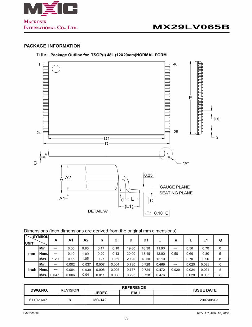
PACKAGE INFORMATION
54
P/N:PM1082 REV. 1.7, APR. 18, 2008
MX29LV065B
REVISION HISTORY
Revision No. Description Page Date1.0 1. Removed "Preliminary" P1 MAR/08/20051.1 1. Removed 63-CSP package information All JAN/09/20061.2 1. Datasheet format changed All AUG/15/20061.3 1. Data modification All AUG/24/20061.4 1. Added statement P54 NOV/06/20061.5 1. Added recommedation for non RoHS compliant devices P1,50 JAN/24/2007
2. Modified sector erase resume: 400uS --> 4mS P191.6 1. Modified Figure 11. CE# Controlled Write Timing Waveform P36 FEB/26/20081.7 1. Announced "phase-out" wording P1,2 APR/18/2008
MX29LV065B
55
MACRONIX INTERNATIONAL CO., LTD.
HeadquartersMacronix, Int'l Co., Ltd.16, Li-Hsin Road, Science Park,Hsinchu, Taiwan, R.O.C.Tel: +886-3-5786688Fax: +886-3-5632888
Macronix America, Inc.680 North McCarthy Blvd.Milpitas, CA 95035, U.S.A.Tel: +1-408-262-8887Fax: +1-408-262-8810Email: [email protected]
Macronix Japan Cayman Islands Ltd.NKF Bldg. 5F, 1-2 Higashida-cho,Kawasaki-ku Kawasaki-shi,Kanagawa Pref. 210-0005, JapanTel: +81-44-246-9100Fax: +81-44-246-9105
Macronix (Hong Kong) Co., Limited.702-703, 7/F, Building 9,Hong Kong Science Park,5 Science Park West Avenue, Sha Tin, N.T.Tel: +86-852-2607-4289Fax: +86-852-2607-4229
http : //www.macronix.com
MACRONIX INTERNATIONAL CO., LTD. reserves the right to change product and specifications without notice.
Taipei OfficeMacronix, Int'l Co., Ltd.19F, 4, Min-Chuan E. Road, Sec. 3,Taipei, Taiwan, R.O.C.Tel: +886-2-2509-3300Fax: +886-2-2509-2200
Macronix Europe N.V.Koningin Astridlaan 59, Bus 11780 Wemmel BelgiumTel: +32-2-456-8020Fax: +32-2-456-8021
Singapore OfficeMacronix Pte. Ltd.1 Marine Parade Central#11-03 Parkway CentreSingapore 449408Tel: +65-6346-5505Fax: +65-6348-8096
Macronix's products are not designed, manufactured, or intended for use for any high risk applications in which the failureof a single component could cause death, personal injury, severe physical damage, or other substantial harm to persons orproperty, such as life-support systems, high temperature automotive, medical, aircraft and military application. Macronixand its suppliers will not be liable to you and/or any third party for any claims, injuries or damages that may be incurred dueto use of Macronix's products in the prohibited applications.