AVR XMEGA D4 Devices Datasheet - Microchip Technology
328
Atmel-8135S-AVR-ATxmega16D4-32D4-64D4-128D4-Datasheet–09/2016 Features High-performance, low-power Atmel ® AVR ® XMEGA ® 8/16-bit Microcontroller Nonvolatile program and data memories 16K - 128KBytes of in-system self-programmable flash 4K - 8KBytes boot section 1K - 2KBytes EEPROM 2K - 8KBytes internal SRAM Peripheral Features Four-channel event system Four 16-bit timer/counters Two timer/counters with 4 output compare or input capture channels Two timer/counters with 2 output compare or input capture channels High-resolution extensions on all timer/counters Advanced waveform extension (AWeX) on one timer/counter Two USARTs with IrDA support for one USART Two two-wire interfaces with dual address match (I 2 C and SMBus compatible) Two serial peripheral interfaces (SPIs) CRC-16 (CRC-CCITT) and CRC-32 (IEEE 802.3) generator 16-bit real time counter (RTC) with separate oscillator One twelve-channel, 12-bit, 200ksps Analog to Digital Converter Two Analog Comparators with window compare function, and current sources External interrupts on all general purpose I/O pins Programmable watchdog timer with separate on-chip ultra low power oscillator QTouch ® library support Capacitive touch buttons, sliders and wheels Special microcontroller features Power-on reset and programmable brown-out detection Internal and external clock options with PLL and prescaler Programmable multilevel interrupt controller Five sleep modes Programming and debug interfaces PDI (program and debug interface) I/O and packages 34 Programmable I/O pins 44 - lead TQFP 44 - pad VQFN/QFN 49 - ball VFBGA Operating voltage 1.6 – 3.6V Operating frequency 0 – 12MHz from 1.6V 0 – 32MHz from 2.7V 8/16-bit Atmel XMEGA D4 Microcontroller ATxmega128D4 / ATxmega64D4 / ATxmega32D4 / ATxmega16D4
-
Upload
khangminh22 -
Category
Documents
-
view
3 -
download
0
Transcript of AVR XMEGA D4 Devices Datasheet - Microchip Technology
8/16-bit Atmel XMEGA D4 Microcontroller
ATxmega128D4 / ATxmega64D4 /ATxmega32D4 / ATxmega16D4
Features
High-performance, low-power Atmel® AVR® XMEGA® 8/16-bit Microcontroller Nonvolatile program and data memories
16K - 128KBytes of in-system self-programmable flash 4K - 8KBytes boot section 1K - 2KBytes EEPROM 2K - 8KBytes internal SRAM
Peripheral Features Four-channel event system Four 16-bit timer/counters
Two timer/counters with 4 output compare or input capture channels Two timer/counters with 2 output compare or input capture channels High-resolution extensions on all timer/counters Advanced waveform extension (AWeX) on one timer/counter
Two USARTs with IrDA support for one USART Two two-wire interfaces with dual address match (I2C and SMBus compatible) Two serial peripheral interfaces (SPIs) CRC-16 (CRC-CCITT) and CRC-32 (IEEE 802.3) generator 16-bit real time counter (RTC) with separate oscillator One twelve-channel, 12-bit, 200ksps Analog to Digital Converter Two Analog Comparators with window compare function, and current sources External interrupts on all general purpose I/O pins Programmable watchdog timer with separate on-chip ultra low power oscillator QTouch® library support
Capacitive touch buttons, sliders and wheels Special microcontroller features
Power-on reset and programmable brown-out detection Internal and external clock options with PLL and prescaler Programmable multilevel interrupt controller Five sleep modes Programming and debug interfaces
PDI (program and debug interface) I/O and packages
34 Programmable I/O pins 44 - lead TQFP 44 - pad VQFN/QFN 49 - ball VFBGA
Operating voltage 1.6 – 3.6V
Operating frequency 0 – 12MHz from 1.6V 0 – 32MHz from 2.7V
Atmel-8135S-AVR-ATxmega16D4-32D4-64D4-128D4-Datasheet–09/2016
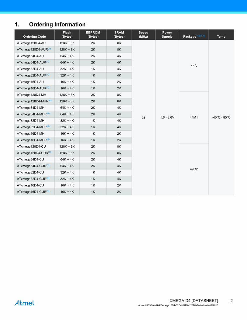
1. Ordering Information
Ordering CodeFlash
(Bytes)EEPROM (Bytes)
SRAM (Bytes)
Speed (MHz)
Power Supply Package(1)(2)(3) Temp
ATxmega128D4-AU 128K + 8K 2K 8K
32 1.6 - 3.6V
44A
-40C - 85C
ATxmega128D4-AUR(4) 128K + 8K 2K 8K
ATxmega64D4-AU 64K + 4K 2K 4K
ATxmega64D4-AUR(4) 64K + 4K 2K 4K
ATxmega32D4-AU 32K + 4K 1K 4K
ATxmega32D4-AUR(4) 32K + 4K 1K 4K
ATxmega16D4-AU 16K + 4K 1K 2K
ATxmega16D4-AUR(4) 16K + 4K 1K 2K
ATxmega128D4-MH 128K + 8K 2K 8K
44M1
ATxmega128D4-MHR(4) 128K + 8K 2K 8K
ATxmega64D4-MH 64K + 4K 2K 4K
ATxmega64D4-MHR(4) 64K + 4K 2K 4K
ATxmega32D4-MH 32K + 4K 1K 4K
ATxmega32D4-MHR(4) 32K + 4K 1K 4K
ATxmega16D4-MH 16K + 4K 1K 2K
ATxmega16D4-MHR(4) 16K + 4K 1K 2K
ATxmega128D4-CU 128K + 8K 2K 8K
49C2
ATxmega128D4-CUR(4) 128K + 8K 2K 8K
ATxmega64D4-CU 64K + 4K 2K 4K
ATxmega64D4-CUR(4) 64K + 4K 2K 4K
ATxmega32D4-CU 32K + 4K 1K 4K
ATxmega32D4-CUR(4) 32K + 4K 1K 4K
ATxmega16D4-CU 16K + 4K 1K 2K
ATxmega16D4-CUR(4) 16K + 4K 1K 2K
2XMEGA D4 [DATASHEET]Atmel-8135S-AVR-ATxmega16D4-32D4-64D4-128D4-Datasheet–09/2016

Notes: 1. This device can also be supplied in wafer form. Please contact your local Atmel sales office for detailed ordering information.
2. Pb-free packaging, complies to the European Directive for Restriction of Hazardous Substances (RoHS directive). Also Halide free and fully Green.
3. For packaging information see ”Packaging information” on page 64.
4. Tape and Reel.
Typical Applications
ATxmega128D4-AN 128K + 8K 2K 8K
32 1.6 - 3.6V
44A
-40C - 105C
ATxmega128D4-ANR(4) 128K + 8K 2K 8K
ATxmega64D4-AN 64K + 4K 2K 4K
ATxmega64D4-ANR(4) 64K + 4K 2K 4K
ATxmega32D4-AN 32K + 4K 1K 4K
ATxmega32D4-ANR(4) 32K + 4K 1K 4K
ATxmega16D4-AN 16K + 4K 1K 2K
ATxmega16D4-ANR(4) 16K + 4K 1K 2K
ATxmega128D4-M7 128K + 8K 2K 8K
44M1
ATxmega128D4-M7R(4) 128K + 8K 2K 8K
ATxmega64D4-M7 64K + 4K 2K 4K
ATxmega64D4-M7R(4) 64K + 4K 2K 4K
ATxmega32D4-M7 32K + 4K 1K 4K
ATxmega32D4-M7R(4) 32K + 4K 1K 4K
ATxmega16D4-M7 16K + 4K 1K 2K
ATxmega16D4-M7R(4) 16K + 4K 1K 2K
Package type
44A 44-lead, 10*10mm body size, 1.0mm body thickness, 0.8mm lead pitch, thin profile plastic quad flat package (TQFP)
44M1 44-Pad, 7*7*1mm body, lead pitch 0.50mm, 5.20mm exposed pad, thermally enhanced plastic very thin quad no lead package (VQFN)
49C2 49-ball (7 * 7 Array), 0.65mm pitch, 5.0*5.0*1.0mm, very thin, fine-pitch ball grid array package (VFBGA)
Industrial control Climate control Low power battery applications
Factory automation RF and ZigBee® Power tools
Building control USB connectivity HVAC
Board control Sensor control Utility metering
White goods Optical Medical applications
Ordering CodeFlash
(Bytes)EEPROM (Bytes)
SRAM (Bytes)
Speed (MHz)
Power Supply Package(1)(2)(3) Temp
3XMEGA D4 [DATASHEET]Atmel-8135S-AVR-ATxmega16D4-32D4-64D4-128D4-Datasheet–09/2016
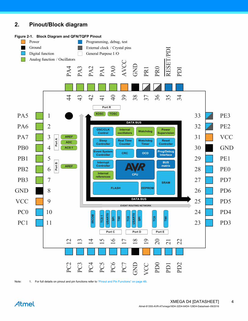
2. Pinout/Block diagram
Figure 2-1. Block Diagram and QFN/TQFP Pinout
Note: 1. For full details on pinout and pin functions refer to “Pinout and Pin Functions” on page 49.
1
2
3
4
44 43 42 41 40 39 38
5
6
7
8
9
10
11
33
32
31
30
29
28
27
26
25
24
23
37 36 35 34
12 13 14 15 16 17 18 19 20 21 22
PA0
PA1
PA2
PA3
PA4
PB0
PB1
PB3
PB2
PA7
PA6
PA5
GND
VCC
PC0
VCC
GN
D
PC1
PC2
PC3
PC4
PC5
PC6
PC7
PD0
PD1
PD2
PD3
PD4
PD5
PD6
VCC
GND
PD7
PE0
PE1
PE2
PE3
RESE
T/PD
I
PDI
PR0
PR1
AV
CC
GN
DPower
Supervision
Port
A
EVENT ROUTING NETWORK
BUS matrix
SRAM
FLASH
ADC
AC0:1
OCD
Port EPort D
Prog/DebugInterface
EEPROM
Port C
TC0:
1
Event System Controller
Watchdog Timer
WatchdogOSC/CLK Control
Real TimeCounter
Interrupt Controller
DATA BUS
DATA BUS
Port RU
SART
0
TWI
SPI
TC0
USA
RT0
SPI
TC0
TWI
Port
B
AREF
AREFSleep
ControllerReset
Controller
IRCO
M
CRC
CPUInternalreferences
Internaloscillators
XOSC TOSC
Digital functionAnalog function / Oscillators
Programming, debug, testExternal clock / Crystal pinsGeneral Purpose I /O
GroundPower
4XMEGA D4 [DATASHEET]Atmel-8135S-AVR-ATxmega16D4-32D4-64D4-128D4-Datasheet–09/2016
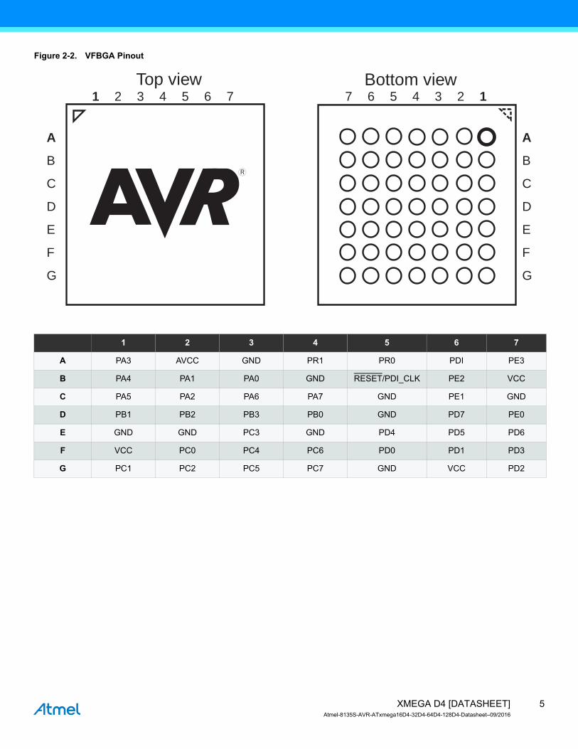
Figure 2-2. VFBGA Pinout
1 2 3 4 5 6 7
A PA3 AVCC GND PR1 PR0 PDI PE3
B PA4 PA1 PA0 GND RESET/PDI_CLK PE2 VCC
C PA5 PA2 PA6 PA7 GND PE1 GND
D PB1 PB2 PB3 PB0 GND PD7 PE0
E GND GND PC3 GND PD4 PD5 PD6
F VCC PC0 PC4 PC6 PD0 PD1 PD3
G PC1 PC2 PC5 PC7 GND VCC PD2
A
B
C
D
E
F
G
1 2 3 4 5 6 7
A
B
C
D
E
F
G
7 6 5 4 3 2 1Top view Bottom view
5XMEGA D4 [DATASHEET]Atmel-8135S-AVR-ATxmega16D4-32D4-64D4-128D4-Datasheet–09/2016

3. Overview
The Atmel AVR XMEGA is a family of low power, high performance, and peripheral rich 8/16-bit microcontrollers based on the AVR enhanced RISC architecture. By executing instructions in a single clock cycle, the AVR XMEGA device achieves throughputs CPU approaching one million instructions per second (MIPS) per megahertz, allowing the system designer to optimize power consumption versus processing speed.
The AVR CPU combines a rich instruction set with 32 general purpose working registers. All 32 registers are directly connected to the arithmetic logic unit (ALU), allowing two independent registers to be accessed in a single instruction, executed in one clock cycle. The resulting architecture is more code efficient while achieving throughputs many times faster than conventional single-accumulator or CISC based microcontrollers.
The AVR XMEGA D4 devices provide the following features: in-system programmable flash with read-while-write capabilities; internal EEPROM and SRAM; four-channel event system and programmable multilevel interrupt controller, 34 general purpose I/O lines, 16-bit real-time counter (RTC); four flexible, 16-bit timer/counters with compare and PWM channels; two USARTs; two two-wire serial interfaces (TWIs); two serial peripheral interfaces (SPIs); one twelve-channel, 12-bit ADC with optional differential input with programmable gain; two analog comparators (ACs) with window mode; programmable watchdog timer with separate internal oscillator; accurate internal oscillators with PLL and prescaler; and programmable brown-out detection.
The program and debug interface (PDI), a fast, two-pin interface for programming and debugging, is available.
The XMEGA D4 devices have five software selectable power saving modes. The idle mode stops the CPU while allowing the SRAM, event system, interrupt controller, and all peripherals to continue functioning. The power-down mode saves the SRAM and register contents, but stops the oscillators, disabling all other functions until the next TWI, or pin-change interrupt, or reset. In power-save mode, the asynchronous real-time counter continues to run, allowing the application to maintain a timer base while the rest of the device is sleeping. In standby mode, the external crystal oscillator keeps running while the rest of the device is sleeping. This allows very fast startup from the external crystal, combined with low power consumption. In extended standby mode, both the main oscillator and the asynchronous timer continue to run. To further reduce power consumption, the peripheral clock to each individual peripheral can optionally be stopped in active mode and idle sleep mode.
Atmel offers a free QTouch library for embedding capacitive touch buttons, sliders and wheels functionality into AVR microcontrollers.
The devices are manufactured using Atmel high-density, nonvolatile memory technology. The program flash memory can be reprogrammed in-system through the PDI interface. A boot loader running in the device can use any interface to download the application program to the flash memory. The boot loader software in the boot flash section will continue to run while the application flash section is updated, providing true read-while-write operation. By combining an 8/16-bit RISC CPU with in-system, self-programmable flash, the AVR XMEGA is a powerful microcontroller family that provides a highly flexible and cost effective solution for many embedded applications.
All Atmel AVR XMEGA devices are supported with a full suite of program and system development tools, including C compilers, macro assemblers, program debugger/simulators, programmers, and evaluation kits.
6XMEGA D4 [DATASHEET]Atmel-8135S-AVR-ATxmega16D4-32D4-64D4-128D4-Datasheet–09/2016

3.1 Block Diagram
Figure 3-1. XMEGA D4 Block Diagram
Power SupervisionPOR/BOD &
RESET
PORT A (8)
PORT B (4)
SRAMADCA
ACA
OCD
Int. Refs.
PDI
PA[0..7]
PB[0..3]
Watchdog Timer
WatchdogOscillator
Interrupt Controller
DATA BUS
Prog/DebugController
VCC
GND
Oscillator Circuits/
Clock Generation
Oscillator Control
Real TimeCounter
Event System Controller
AREFA
AREFB
PDI_DATA
RESET/
PDI_CLK
Sleep Controller
CRC
PORT C (8)
PC[0..7]
TCC
0:1
USA
RTC
0
TWIC
SPIC
PD[0..7] PE[0..3]
PORT D (8)
TCD
0
USA
RTD
0
SPID
TCE0
TWIE
PORT E (4)
Tempref
VCC/10
PORT R (2)
XTAL/
TOSC1
XTAL2/
TOSC2
PR[0..1]
DATA BUS
NVM Controller
MORPEEhsalF
IRC
OM
BUS Matrix
CPU
TOSC1
TOSC2
To Clock
Generator
EVENT ROUTING NETWORK
Digital functionAnalog function
Programming, debug, testOscillator/Crystal/ClockGeneral Purpose I/O
7XMEGA D4 [DATASHEET]Atmel-8135S-AVR-ATxmega16D4-32D4-64D4-128D4-Datasheet–09/2016

4. Resources
A comprehensive set of development tools, application notes and datasheets are available for download on http://www.atmel.com/avr.
4.1 Recommended Reading Atmel AVR XMEGA D manual
XMEGA application notes
This device data sheet only contains part specific information with a short description of each peripheral and module. The XMEGA D manual describes the modules and peripherals in depth. The XMEGA application notes contain example code and show applied use of the modules and peripherals.
All documentations are available from www.atmel.com/avr.
5. Capacitive Touch Sensing
The Atmel QTouch library provides a simple to use solution to realize touch sensitive interfaces on most Atmel AVR microcontrollers. The patented charge-transfer signal acquisition offers robust sensing and includes fully debounced reporting of touch keys and includes Adjacent Key Suppression® (AKS®) technology for unambiguous detection of key events. The QTouch library includes support for the QTouch and QMatrix acquisition methods.
Touch sensing can be added to any application by linking the appropriate Atmel QTouch library for the AVR microcontroller. This is done by using a simple set of APIs to define the touch channels and sensors, and then calling the touch sensing API’s to retrieve the channel information and determine the touch sensor states.
The QTouch library is FREE and downloadable from the Atmel website at the following location: http://www.atmel.com/tools/QTOUCHLIBRARY.aspx. For implementation details and other information, refer to the QTouch library user guide - also available for download from the Atmel website.
8XMEGA D4 [DATASHEET]Atmel-8135S-AVR-ATxmega16D4-32D4-64D4-128D4-Datasheet–09/2016

6. AVR CPU
6.1 Features 8/16-bit, high-performance Atmel AVR RISC CPU
137 instructions Hardware multiplier
32x8-bit registers directly connected to the ALU
Stack in RAM
Stack pointer accessible in I/O memory space
Direct addressing of up to 16MB of program memory and 16MB of data memory
True 16/24-bit access to 16/24-bit I/O registers
Efficient support for 8-, 16-, and 32-bit arithmetic
Configuration change protection of system-critical features
6.2 Overview
All Atmel AVR XMEGA devices use the 8/16-bit AVR CPU. The main function of the CPU is to execute the code and perform all calculations. The CPU is able to access memories, perform calculations, control peripherals, and execute the program in the flash memory. Interrupt handling is described in a separate section, refer to “Interrupts and Programmable Multilevel Interrupt Controller” on page 27.
6.3 Architectural Overview
In order to maximize performance and parallelism, the AVR CPU uses a Harvard architecture with separate memories and buses for program and data. Instructions in the program memory are executed with single-level pipelining. While one instruction is being executed, the next instruction is pre-fetched from the program memory. This enables instructions to be executed on every clock cycle. For details of all AVR instructions, refer to http://www.atmel.com/avr.
Figure 6-1. Block Diagram of the AVR CPU Architecture
9XMEGA D4 [DATASHEET]Atmel-8135S-AVR-ATxmega16D4-32D4-64D4-128D4-Datasheet–09/2016

The arithmetic logic unit (ALU) supports arithmetic and logic operations between registers or between a constant and a register. Single-register operations can also be executed in the ALU. After an arithmetic operation, the status register is updated to reflect information about the result of the operation.
The ALU is directly connected to the fast-access register file. The 32 x 8-bit general purpose working registers all have single clock cycle access time allowing single-cycle arithmetic logic unit (ALU) operation between registers or between a register and an immediate. Six of the 32 registers can be used as three 16-bit address pointers for program and data space addressing, enabling efficient address calculations.
The memory spaces are linear. The data memory space and the program memory space are two different memory spaces.
The data memory space is divided into I/O registers, SRAM, and external RAM. In addition, the EEPROM can be memory mapped in the data memory.
All I/O status and control registers reside in the lowest 4KB addresses of the data memory. This is referred to as the I/O memory space. The lowest 64 addresses can be accessed directly, or as the data space locations from 0x00 to 0x3F. The rest is the extended I/O memory space, ranging from 0x0040 to 0x0FFF. I/O registers here must be accessed as data space locations using load (LD/LDS/LDD) and store (ST/STS/STD) instructions.
The SRAM holds data. Code execution from SRAM is not supported. It can easily be accessed through the five different addressing modes supported in the AVR architecture. The first SRAM address is 0x2000.
Data addresses 0x1000 to 0x1FFF are reserved for memory mapping of EEPROM.
The program memory is divided in two sections, the application program section and the boot program section. Both sections have dedicated lock bits for write and read/write protection. The SPM instruction that is used for self-programming of the application flash memory must reside in the boot program section. The application section contains an application table section with separate lock bits for write and read/write protection. The application table section can be used for safe storing of nonvolatile data in the program memory.
6.4 ALU - Arithmetic Logic Unit
The arithmetic logic unit (ALU) supports arithmetic and logic operations between registers or between a constant and a register. Single-register operations can also be executed. The ALU operates in direct connection with all 32 general purpose registers. In a single clock cycle, arithmetic operations between general purpose registers or between a register and an immediate are executed and the result is stored in the register file. After an arithmetic or logic operation, the status register is updated to reflect information about the result of the operation.
ALU operations are divided into three main categories – arithmetic, logical, and bit functions. Both 8- and 16-bit arithmetic is supported, and the instruction set allows for efficient implementation of 32-bit aritmetic. The hardware multiplier supports signed and unsigned multiplication and fractional format.
6.4.1 Hardware Multiplier
The multiplier is capable of multiplying two 8-bit numbers into a 16-bit result. The hardware multiplier supports different variations of signed and unsigned integer and fractional numbers:
Multiplication of unsigned integers
Multiplication of signed integers
Multiplication of a signed integer with an unsigned integer
Multiplication of unsigned fractional numbers
Multiplication of signed fractional numbers
Multiplication of a signed fractional number with an unsigned one
A multiplication takes two CPU clock cycles.
10XMEGA D4 [DATASHEET]Atmel-8135S-AVR-ATxmega16D4-32D4-64D4-128D4-Datasheet–09/2016

6.5 Program Flow
After reset, the CPU starts to execute instructions from the lowest address in the flash programmemory ‘0.’ The program counter (PC) addresses the next instruction to be fetched.
Program flow is provided by conditional and unconditional jump and call instructions capable of addressing the whole address space directly. Most AVR instructions use a 16-bit word format, while a limited number use a 32-bit format.
During interrupts and subroutine calls, the return address PC is stored on the stack. The stack is allocated in the general data SRAM, and consequently the stack size is only limited by the total SRAM size and the usage of the SRAM. After reset, the stack pointer (SP) points to the highest address in the internal SRAM. The SP is read/write accessible in the I/O memory space, enabling easy implementation of multiple stacks or stack areas. The data SRAM can easily be accessed through the five different addressing modes supported in the AVR CPU.
6.6 Status Register
The status register (SREG) contains information about the result of the most recently executed arithmetic or logic instruction. This information can be used for altering program flow in order to perform conditional operations. Note that the status register is updated after all ALU operations, as specified in the instruction set reference. This will in many cases remove the need for using the dedicated compare instructions, resulting in faster and more compact code.
The status register is not automatically stored when entering an interrupt routine nor restored when returning from an interrupt. This must be handled by software.
The status register is accessible in the I/O memory space.
6.7 Stack and Stack Pointer
The stack is used for storing return addresses after interrupts and subroutine calls. It can also be used for storing temporary data. The stack pointer (SP) register always points to the top of the stack. It is implemented as two 8-bit registers that are accessible in the I/O memory space. Data are pushed and popped from the stack using the PUSH and POP instructions. The stack grows from a higher memory location to a lower memory location. This implies that pushing data onto the stack decreases the SP, and popping data off the stack increases the SP. The SP is automatically loaded after reset, and the initial value is the highest address of the internal SRAM. If the SP is changed, it must be set to point above address 0x2000, and it must be defined before any subroutine calls are executed or before interrupts are enabled.
During interrupts or subroutine calls, the return address is automatically pushed on the stack. The return address can be two or three bytes, depending on program memory size of the device. For devices with 128KB or less of program memory, the return address is two bytes, and hence the stack pointer is decremented/incremented by two. For devices with more than 128KB of program memory, the return address is three bytes, and hence the SP is decremented/incremented by three. The return address is popped off the stack when returning from interrupts using the RETI instruction, and from subroutine calls using the RET instruction.
The SP is decremented by one when data are pushed on the stack with the PUSH instruction, and incremented by one when data is popped off the stack using the POP instruction.
To prevent corruption when updating the stack pointer from software, a write to SPL will automatically disable interrupts for up to four instructions or until the next I/O memory write.
After reset the stack pointer is initialized to the highest address of the SRAM. See Figure 7-2 on page 15.
6.8 Register File
The register file consists of 32 x 8-bit general purpose working registers with single clock cycle access time. The register file supports the following input/output schemes:
One 8-bit output operand and one 8-bit result input
Two 8-bit output operands and one 8-bit result input
Two 8-bit output operands and one 16-bit result input
One 16-bit output operand and one 16-bit result input
11XMEGA D4 [DATASHEET]Atmel-8135S-AVR-ATxmega16D4-32D4-64D4-128D4-Datasheet–09/2016

Six of the 32 registers can be used as three 16-bit address register pointers for data space addressing, enabling efficient address calculations. One of these address pointers can also be used as an address pointer for lookup tables in flash program memory.
7. Memories
7.1 Features Flash program memory
One linear address space In-system programmable Self-programming and boot loader support Application section for application code Application table section for application code or data storage Boot section for application code or boot loader code Separate read/write protection lock bits for all sections Built in fast CRC check of a selectable flash program memory section
Data memory One linear address space Single-cycle access from CPU SRAM EEPROM
Byte and page accessible Optional memory mapping for direct load and store
I/O memory Configuration and status registers for all peripherals and modules 16 bit-accessible general purpose registers for global variables or flags
Production signature row memory for factory programmed data ID for each microcontroller device type Serial number for each device Calibration bytes for factory calibrated peripherals
User signature row One flash page in size Can be read and written from software Content is kept after chip erase
7.2 Overview
The Atmel AVR architecture has two main memory spaces, the program memory and the data memory. Executable code can reside only in the program memory, while data can be stored in the program memory and the data memory. The data memory includes the internal SRAM, and EEPROM for nonvolatile data storage. All memory spaces are linear and require no memory bank switching. Nonvolatile memory (NVM) spaces can be locked for further write and read/write operations. This prevents unrestricted access to the application software.
A separate memory section contains the fuse bytes. These are used for configuring important system functions, and can only be written by an external programmer.
The available memory size configurations are shown in “Ordering Information” on page 2. In addition, each device has a Flash memory signature row for calibration data, device identification, serial number etc.
12XMEGA D4 [DATASHEET]Atmel-8135S-AVR-ATxmega16D4-32D4-64D4-128D4-Datasheet–09/2016
7.3 Flash Program Memory
The Atmel AVR XMEGA devices contain on-chip, in-system reprogrammable flash memory for program storage. The flash memory can be accessed for read and write from an external programmer through the PDI or from application software running in the device.
All AVR CPU instructions are 16 or 32 bits wide, and each flash location is 16 bits wide. The flash memory is organized in two main sections, the application section and the boot loader section. The sizes of the different sections are fixed, but device-dependent. These two sections have separate lock bits, and can have different levels of protection. The store program memory (SPM) instruction, which is used to write to the flash from the application software, will only operate when executed from the boot loader section.
The application section contains an application table section with separate lock settings. This enables safe storage of nonvolatile data in the program memory.
Figure 7-1. Flash Program Memory (Hexadecimal Address)
7.3.1 Application Section
The Application section is the section of the flash that is used for storing the executable application code. The protection level for the application section can be selected by the boot lock bits for this section. The application section can not store any boot loader code since the SPM instruction cannot be executed from the application section.
7.3.2 Application Table Section
The application table section is a part of the application section of the flash memory that can be used for storing data. The size is identical to the boot loader section. The protection level for the application table section can be selected by the boot lock bits for this section. The possibilities for different protection levels on the application section and the application table section enable safe parameter storage in the program memory. If this section is not used for data, application code can reside here.
7.3.3 Boot Loader Section
While the application section is used for storing the application code, the boot loader software must be located in the boot loader section because the SPM instruction can only initiate programming when executing from this section. The SPM instruction can access the entire flash, including the boot loader section itself. The protection level for the boot loader section can be selected by the boot loader lock bits. If this section is not used for boot loader software, application code can be stored here.
Word address
ATxmega128D4 ATxmega64D4 ATxmega32D4 ATxmega16D4
0 0 0 0 Application section(128K/64K/32K/16K)
...
EFFF / 77FF / 37FF / 17FF
F000 / 7800 / 3800 / 1800 Application table section(8K/4K/4K/4K)FFFF / 7FFF / 3FFF / 1FFF
10000 / 8000 / 4000 / 2000 Boot section(8K/4K/4K/4K)10FFF / 87FF / 47FF / 27FF
13XMEGA D4 [DATASHEET]Atmel-8135S-AVR-ATxmega16D4-32D4-64D4-128D4-Datasheet–09/2016
7.3.4 Production Signature Row
The production signature row is a separate memory section for factory programmed data. It contains calibration data for functions such as oscillators and analog modules. Some of the calibration values will be automatically loaded to the corresponding module or peripheral unit during reset. Other values must be loaded from the signature row and written to the corresponding peripheral registers from software. For details on calibration conditions, refer to “Electrical Characteristics” on page 64.
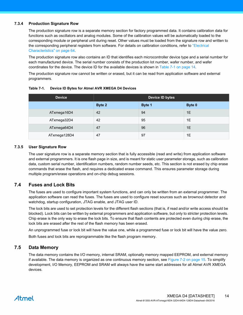
The production signature row also contains an ID that identifies each microcontroller device type and a serial number for each manufactured device. The serial number consists of the production lot number, wafer number, and wafer coordinates for the device. The device ID for the available devices is shown in Table 7-1 on page 14.
The production signature row cannot be written or erased, but it can be read from application software and external programmers.
Table 7-1. Device ID Bytes for Atmel AVR XMEGA D4 Devices
7.3.5 User Signature Row
The user signature row is a separate memory section that is fully accessible (read and write) from application software and external programmers. It is one flash page in size, and is meant for static user parameter storage, such as calibration data, custom serial number, identification numbers, random number seeds, etc. This section is not erased by chip erase commands that erase the flash, and requires a dedicated erase command. This ensures parameter storage during multiple program/erase operations and on-chip debug sessions.
7.4 Fuses and Lock Bits
The fuses are used to configure important system functions, and can only be written from an external programmer. The application software can read the fuses. The fuses are used to configure reset sources such as brownout detector and watchdog, startup configuration, JTAG enable, and JTAG user ID.
The lock bits are used to set protection levels for the different flash sections (that is, if read and/or write access should be blocked). Lock bits can be written by external programmers and application software, but only to stricter protection levels. Chip erase is the only way to erase the lock bits. To ensure that flash contents are protected even during chip erase, the lock bits are erased after the rest of the flash memory has been erased.
An unprogrammed fuse or lock bit will have the value one, while a programmed fuse or lock bit will have the value zero.
Both fuses and lock bits are reprogrammable like the flash program memory.
7.5 Data Memory
The data memory contains the I/O memory, internal SRAM, optionally memory mapped EEPROM, and external memory if available. The data memory is organized as one continuous memory section, see Figure 7-2 on page 15. To simplify development, I/O Memory, EEPROM and SRAM will always have the same start addresses for all Atmel AVR XMEGA devices.
Device Device ID bytes
Byte 2 Byte 1 Byte 0
ATxmega16D4 42 94 1E
ATxmega32D4 42 95 1E
ATxmega64D4 47 96 1E
ATxmega128D4 47 97 1E
14XMEGA D4 [DATASHEET]Atmel-8135S-AVR-ATxmega16D4-32D4-64D4-128D4-Datasheet–09/2016

Figure 7-2. Data Memory Map (Hexadecimal Address)
7.6 EEPROM
XMEGA D devices have EEPROM for nonvolatile data storage. It is either addressable in a separate data space (default) or memory mapped and accessed in normal data space. The EEPROM supports both byte and page access. Memory mapped EEPROM allows highly efficient EEPROM reading and EEPROM buffer loading. When doing this, EEPROM is accessible using load and store instructions. Memory mapped EEPROM will always start at hexadecimal address 0x1000.
7.7 I/O Memory
The status and configuration registers for peripherals and modules, including the CPU, are addressable through I/O memory locations. All I/O locations can be accessed by the load (LD/LDS/LDD) and store (ST/STS/STD) instructions, which are used to transfer data between the 32 registers in the register file and the I/O memory. The IN and OUT instructions can address I/O memory locations in the range of 0x00 to 0x3F directly. In the address range 0x00 - 0x1F, single-cycle instructions for manipulation and checking of individual bits are available.
The I/O memory address for all peripherals and modules in XMEGA D4 is shown in the “Peripheral Module Address Map” on page 54.
7.7.1 General Purpose I/O Registers
The lowest 16 I/O memory addresses are reserved as general purpose I/O registers. These registers can be used for storing global variables and flags, as they are directly bit-accessible using the SBI, CBI, SBIS, and SBIC instructions.
Byte address ATxmega64D4 Byte address ATxmega32D4 Byte address ATxmega16D4
0I/O Registers (4K)
0I/O Registers (4K)
0I/O Registers (4K)
FFF FFF FFF
1000EEPROM (2K)
1000EEPROM (1K)
1000EEPROM (1K)
17FF 13FF 13FF
RESERVED RESERVED RESERVED
2000Internal SRAM (4K)
2000Internal SRAM (4K)
2000Internal SRAM (2K)
2FFF 2FFF 27FF
Byte address ATxmega128D4
0I/O Registers (4K)
FFF
1000EEPROM (2K)
17FF
RESERVED
2000Internal SRAM (8K)
3FFF
15XMEGA D4 [DATASHEET]Atmel-8135S-AVR-ATxmega16D4-32D4-64D4-128D4-Datasheet–09/2016

7.8 Data Memory and Bus Arbitration
Since the data memory is organized as four separate sets of memories, the bus masters (CPU, etc.) can access different memory sections at the same time.
7.9 Memory Timing
Read and write access to the I/O memory takes one CPU clock cycle. A write to SRAM takes one cycle, and a read from SRAM takes two cycles. EEPROM page load (write) takes one cycle, and three cycles are required for read. For burst read, new data are available every second cycle. Refer to the instruction summary for more details on instructions and instruction timing.
7.10 Device ID and Revision
Each device has a three-byte device ID. This ID identifies Atmel as the manufacturer of the device and the device type. A separate register contains the revision number of the device.
7.11 I/O Memory Protection
Some features in the device are regarded as critical for safety in some applications. Due to this, it is possible to lock the I/O register related to the clock system, the event system, and the advanced waveform extensions. As long as the lock is enabled, all related I/O registers are locked and they can not be written from the application software. The lock registers themselves are protected by the configuration change protection mechanism.
7.12 Flash and EEPROM Page Size
The flash program memory and EEPROM data memory are organized in pages. The pages are word accessible for the flash and byte accessible for the EEPROM.
Table 7-2 on page 16 shows the Flash Program Memory organization and Program Counter (PC) size. Flash write and erase operations are performed on one page at a time, while reading the Flash is done one byte at a time. For Flash access the Z-pointer (Z[m:n]) is used for addressing. The most significant bits in the address (FPAGE) give the page number and the least significant address bits (FWORD) give the word in the page.
Table 7-2. Number of Words and Pages in the Flash
Table 7-3 on page 17 shows EEPROM memory organization for the Atmel AVR XMEGA D4 devices. EEEPROM write and erase operations can be performed one page or one byte at a time, while reading the EEPROM is done one byte at a time. For EEPROM access the NVM address register (ADDR[m:n]) is used for addressing. The most significant bits in the address (E2PAGE) give the page number and the least significant address bits (E2BYTE) give the byte in the page.
Devices PC size Flash size Page Size FWORD FPAGE Application Boot
bits bytes words Size No of pages Size No of pages
ATxmega16D4 14 16K + 4K 128 Z[7:1] Z[13:8] 16K 64 4K 16
ATxmega32D4 15 32K + 4K 128 Z[7:1] Z[14:8] 32K 128 4K 16
ATxmega64D4 16 64K + 4K 128 Z[7:1] Z[15:8] 64K 256 4K 16
ATxmega128D4 17 128K + 8K 128 Z[9:1] Z[16:8] 128K 512 8K 32
16XMEGA D4 [DATASHEET]Atmel-8135S-AVR-ATxmega16D4-32D4-64D4-128D4-Datasheet–09/2016
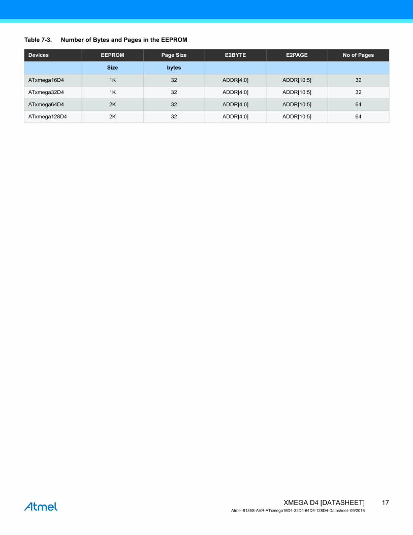
Table 7-3. Number of Bytes and Pages in the EEPROM
Devices EEPROM Page Size E2BYTE E2PAGE No of Pages
Size bytes
ATxmega16D4 1K 32 ADDR[4:0] ADDR[10:5] 32
ATxmega32D4 1K 32 ADDR[4:0] ADDR[10:5] 32
ATxmega64D4 2K 32 ADDR[4:0] ADDR[10:5] 64
ATxmega128D4 2K 32 ADDR[4:0] ADDR[10:5] 64
17XMEGA D4 [DATASHEET]Atmel-8135S-AVR-ATxmega16D4-32D4-64D4-128D4-Datasheet–09/2016
8. Event System
8.1 Features System for direct peripheral-to-peripheral communication and signaling
Peripherals can directly send, receive, and react to peripheral events CPU independent operation 100% predictable signal timing Short and guaranteed response time
Four event channels for up to four different and parallel signal routing configurations
Events can be sent and/or used by most peripherals, clock system, and software
Additional functions include Quadrature decoders Digital filtering of I/O pin state
Works in active mode and idle sleep mode
8.2 Overview
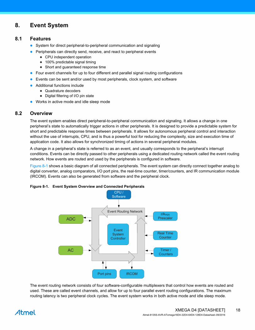
The event system enables direct peripheral-to-peripheral communication and signaling. It allows a change in one peripheral’s state to automatically trigger actions in other peripherals. It is designed to provide a predictable system for short and predictable response times between peripherals. It allows for autonomous peripheral control and interaction without the use of interrupts, CPU, and is thus a powerful tool for reducing the complexity, size and execution time of application code. It also allows for synchronized timing of actions in several peripheral modules.
A change in a peripheral’s state is referred to as an event, and usually corresponds to the peripheral’s interrupt conditions. Events can be directly passed to other peripherals using a dedicated routing network called the event routing network. How events are routed and used by the peripherals is configured in software.
Figure 8-1 shows a basic diagram of all connected peripherals. The event system can directly connect together analog to digital converter, analog comparators, I/O port pins, the real-time counter, timer/counters, and IR communication module (IRCOM). Events can also be generated from software and the peripheral clock.
Figure 8-1. Event System Overview and Connected Peripherals
The event routing network consists of four software-configurable multiplexers that control how events are routed and used. These are called event channels, and allow for up to four parallel event routing configurations. The maximum routing latency is two peripheral clock cycles. The event system works in both active mode and idle sleep mode.
Timer /
Counters
ADC
Real Time
Counter
Port pins
CPU /
Software
IRCOM
Event Routing Network
Event
System
Controller
clkPER
Prescaler
AC
18XMEGA D4 [DATASHEET]Atmel-8135S-AVR-ATxmega16D4-32D4-64D4-128D4-Datasheet–09/2016

9. System Clock and Clock Options
9.1 Features Fast start-up time
Safe run-time clock switching
Internal oscillators: 32MHz run-time calibrated and tuneable oscillator 2MHz run-time calibrated oscillator 32.768kHz calibrated oscillator 32kHz ultra low power (ULP) oscillator with 1kHz output
External clock options 0.4MHz - 16MHz crystal oscillator 32.768kHz crystal oscillator External clock
PLL with 20MHz - 128MHz output frequency Internal and external clock options and 1x to 31x multiplication Lock detector
Clock prescalers with 1x to 2048x division
Fast peripheral clocks running at two and four times the CPU clock
Automatic run-time calibration of internal oscillators
External oscillator and PLL lock failure detection with optional non-maskable interrupt
9.2 Overview
Atmel AVR XMEGA D4 devices have a flexible clock system supporting a large number of clock sources. It incorporates both accurate internal oscillators and external crystal oscillator and resonator support. A high-frequency phase locked loop (PLL) and clock prescalers can be used to generate a wide range of clock frequencies. A calibration feature (DFLL) is available, and can be used for automatic run-time calibration of the internal oscillators to remove frequency drift over voltage and temperature. An oscillator failure monitor can be enabled to issue a non-maskable interrupt and switch to the internal oscillator if the external oscillator or PLL fails.
When a reset occurs, all clock sources except the 32kHz ultra low power oscillator are disabled. After reset, the device will always start up running from the 2MHz internal oscillator. During normal operation, the system clock source and prescalers can be changed from software at any time.
Figure 9-1 on page 20 presents the principal clock system in the XMEGA D4 family of devices. Not all of the clocks need to be active at a given time. The clocks for the CPU and peripherals can be stopped using sleep modes and power reduction registers, as described in “Power Management and Sleep Modes” on page 22.
19XMEGA D4 [DATASHEET]Atmel-8135S-AVR-ATxmega16D4-32D4-64D4-128D4-Datasheet–09/2016

Figure 9-1. The Clock System, Clock Sources and Clock Distribution
9.3 Clock Sources
The clock sources are divided in two main groups: internal oscillators and external clock sources. Most of the clock sources can be directly enabled and disabled from software, while others are automatically enabled or disabled, depending on peripheral settings. After reset, the device starts up running from the 2MHz internal oscillator. The other clock sources, DFLLs and PLL, are turned off by default.
The internal oscillators do not require any external components to run. For details on characteristics and accuracy of the internal oscillators, refer to the device datasheet.
9.3.1 32kHz Ultra Low Power Internal Oscillator
This oscillator provides an approximate 32kHz clock. The 32kHz ultra low power (ULP) internal oscillator is a very low power clock source, and it is not designed for high accuracy. The oscillator employs a built-in prescaler that provides a
Real Time
CounterPeripherals RAM AVR CPU
Non-Volatile
Memory
Watchdog
Timer
Brown-out
Detector
System Clock Prescalers
System Clock Multiplexer
(SCLKSEL)
PLLSRC
RTCSRC
DIV
32
32 kHz
Int. ULP
32.768 kHz
Int. OSC
32.768 kHz
TOSC
2 MHz
Int. Osc
32 MHz
Int. Osc
0.4 – 16 MHz
XTAL
DIV
32
DIV
32
DIV
4XOSCSEL
PLL
TO
SC
1
TO
SC
2
XT
AL1
XT
AL2
clkSYSclkRTC
clkPER2
clkPER
clkCPU
clkPER4
20XMEGA D4 [DATASHEET]Atmel-8135S-AVR-ATxmega16D4-32D4-64D4-128D4-Datasheet–09/2016
1kHz output. The oscillator is automatically enabled/disabled when it is used as clock source for any part of the device. This oscillator can be selected as the clock source for the RTC.
9.3.2 32.768kHz Calibrated Internal Oscillator
This oscillator provides an approximate 32.768kHz clock. It is calibrated during production to provide a default frequency close to its nominal frequency. The calibration register can also be written from software for run-time calibration of the oscillator frequency. The oscillator employs a built-in prescaler, which provides both a 32.768kHz output and a 1.024kHz output.
9.3.3 32.768kHz Crystal Oscillator
A 32.768kHz crystal oscillator can be connected between the TOSC1 and TOSC2 pins and enables a dedicated low frequency oscillator input circuit. A low power mode with reduced voltage swing on TOSC2 is available. This oscillator can be used as a clock source for the system clock and RTC, and as the DFLL reference clock.
9.3.4 0.4 - 16MHz Crystal Oscillator
This oscillator can operate in four different modes optimized for different frequency ranges, all within 0.4 - 16MHz.
9.3.5 2MHz Run-time Calibrated Internal Oscillator
The 2MHz run-time calibrated internal oscillator is the default system clock source after reset. It is calibrated during production to provide a default frequency close to its nominal frequency. A DFLL can be enabled for automatic run-time calibration of the oscillator to compensate for temperature and voltage drift and optimize the oscillator accuracy.
9.3.6 32MHz Run-time Calibrated Internal Oscillator
The 32MHz run-time calibrated internal oscillator is a high-frequency oscillator. It is calibrated during production to provide a default frequency close to its nominal frequency. A digital frequency looked loop (DFLL) can be enabled for automatic run-time calibration of the oscillator to compensate for temperature and voltage drift and optimize the oscillator accuracy. This oscillator can also be adjusted and calibrated to any frequency between 30MHz and 55MHz.
9.3.7 External Clock Sources
The XTAL1 and XTAL2 pins can be used to drive an external oscillator, either a quartz crystal or a ceramic resonator. XTAL1 can be used as input for an external clock signal. The TOSC1 and TOSC2 pins is dedicated to driving a 32.768kHz crystal oscillator.
9.3.8 PLL with 1x-31x Multiplication Factor
The built-in phase locked loop (PLL) can be used to generate a high-frequency system clock. The PLL has a user-selectable multiplication factor of from 1 to 31. In combination with the prescalers, this gives a wide range of output frequencies from all clock sources.
21XMEGA D4 [DATASHEET]Atmel-8135S-AVR-ATxmega16D4-32D4-64D4-128D4-Datasheet–09/2016
10. Power Management and Sleep Modes
10.1 Features Power management for adjusting power consumption and functions
Five sleep modes Idle Power down Power save Standby Extended standby
Power reduction register to disable clock and turn off unused peripherals in active and idle modes
10.2 Overview
Various sleep modes and clock gating are provided in order to tailor power consumption to application requirements. This enables the Atmel AVR XMEGA microcontroller to stop unused modules to save power.
All sleep modes are available and can be entered from active mode. In active mode, the CPU is executing application code. When the device enters sleep mode, program execution is stopped and interrupts or a reset is used to wake the device again. The application code decides which sleep mode to enter and when. Interrupts from enabled peripherals and all enabled reset sources can restore the microcontroller from sleep to active mode.
In addition, power reduction registers provide a method to stop the clock to individual peripherals from software. When this is done, the current state of the peripheral is frozen, and there is no power consumption from that peripheral. This reduces the power consumption in active mode and idle sleep modes and enables much more fine-tuned power management than sleep modes alone.
10.3 Sleep Modes
Sleep modes are used to shut down modules and clock domains in the microcontroller in order to save power. XMEGA microcontrollers have five different sleep modes tuned to match the typical functional stages during application execution. A dedicated sleep instruction (SLEEP) is available to enter sleep mode. Interrupts are used to wake the device from sleep, and the available interrupt wake-up sources are dependent on the configured sleep mode. When an enabled interrupt occurs, the device will wake up and execute the interrupt service routine before continuing normal program execution from the first instruction after the SLEEP instruction. If other, higher priority interrupts are pending when the wake-up occurs, their interrupt service routines will be executed according to their priority before the interrupt service routine for the wake-up interrupt is executed. After wake-up, the CPU is halted for four cycles before execution starts.
The content of the register file, SRAM and registers are kept during sleep. If a reset occurs during sleep, the device will reset, start up, and execute from the reset vector.
10.3.1 Idle Mode
In idle mode the CPU and nonvolatile memory are stopped (note that any ongoing programming will be completed), but all peripherals, including the interrupt controller, and event system are kept running. Any enabled interrupt will wake the device.
10.3.2 Power-down Mode
In power-down mode, all clocks, including the real-time counter clock source, are stopped. This allows operation only of asynchronous modules that do not require a running clock. The only interrupts that can wake up the MCU are the two-wire interface address match interrupt, and asynchronous port interrupts.
22XMEGA D4 [DATASHEET]Atmel-8135S-AVR-ATxmega16D4-32D4-64D4-128D4-Datasheet–09/2016
10.3.3 Power-save Mode
Power-save mode is identical to power down, with one exception. If the real-time counter (RTC) is enabled, it will keep running during sleep, and the device can also wake up from either an RTC overflow or compare match interrupt.
10.3.4 Standby Mode
Standby mode is identical to power down, with the exception that the enabled system clock sources are kept running while the CPU, peripheral, and RTC clocks are stopped. This reduces the wake-up time.
10.3.5 Extended Standby Mode
Extended standby mode is identical to power-save mode, with the exception that the enabled system clock sources are kept running while the CPU and peripheral clocks are stopped. This reduces the wake-up time.
23XMEGA D4 [DATASHEET]Atmel-8135S-AVR-ATxmega16D4-32D4-64D4-128D4-Datasheet–09/2016

11. System Control and Reset
11.1 Features Reset the microcontroller and set it to initial state when a reset source goes active
Multiple reset sources that cover different situations Power-on reset External reset Watchdog reset Brownout reset PDI reset Software reset
Asynchronous operation No running system clock in the device is required for reset
Reset status register for reading the reset source from the application code
11.2 Overview
The reset system issues a microcontroller reset and sets the device to its initial state. This is for situations where operation should not start or continue, such as when the microcontroller operates below its power supply rating. If a reset source goes active, the device enters and is kept in reset until all reset sources have released their reset. The I/O pins are immediately tri-stated. The program counter is set to the reset vector location, and all I/O registers are set to their initial values. The SRAM content is kept. However, if the device accesses the SRAM when a reset occurs, the content of the accessed location can not be guaranteed.
After reset is released from all reset sources, the default oscillator is started and calibrated before the device starts running from the reset vector address. By default, this is the lowest program memory address, 0, but it is possible to move the reset vector to the lowest address in the boot section.
The reset functionality is asynchronous, and so no running system clock is required to reset the device. The software reset feature makes it possible to issue a controlled system reset from the user software.
The reset status register has individual status flags for each reset source. It is cleared at power-on reset, and shows which sources have issued a reset since the last power-on.
11.3 Reset Sequence
A reset request from any reset source will immediately reset the device and keep it in reset as long as the request is active. When all reset requests are released, the device will go through three stages before the device starts running again:
Reset counter delay
Oscillator startup
Oscillator calibration
If another reset requests occurs during this process, the reset sequence will start over again.
24XMEGA D4 [DATASHEET]Atmel-8135S-AVR-ATxmega16D4-32D4-64D4-128D4-Datasheet–09/2016

11.4 Reset Sources
11.4.1 Power-on Reset
A power-on reset (POR) is generated by an on-chip detection circuit. The POR is activated when the VCC rises and reaches the POR threshold voltage (VPOT), and this will start the reset sequence.
The POR is also activated to power down the device properly when the VCC falls and drops below the VPOT level.
The VPOT level is higher for falling VCC than for rising VCC. Consult the datasheet for POR characteristics data.
11.4.2 Brownout Detection
The on-chip brownout detection (BOD) circuit monitors the VCC level during operation by comparing it to a fixed, programmable level that is selected by the BODLEVEL fuses. If disabled, BOD is forced on at the lowest level during chip erase and when the PDI is enabled.
11.4.3 External Reset
The external reset circuit is connected to the external RESET pin. The external reset will trigger when the RESET pin is driven below the RESET pin threshold voltage, VRST, for longer than the minimum pulse period, tEXT. The reset will be held as long as the pin is kept low. The RESET pin includes an internal pull-up resistor.
11.4.4 Watchdog Reset
The watchdog timer (WDT) is a system function for monitoring correct program operation. If the WDT is not reset from the software within a programmable timeout period, a watchdog reset will be given. The watchdog reset is active for one to two clock cycles of the 2MHz internal oscillator. For more details see “WDT – Watchdog Timer” on page 26.
11.4.5 Software Reset
The software reset makes it possible to issue a system reset from software by writing to the software reset bit in the reset control register.The reset will be issued within two CPU clock cycles after writing the bit. It is not possible to execute any instruction from when a software reset is requested until it is issued.
11.4.6 Program and Debug Interface Reset
The program and debug interface reset contains a separate reset source that is used to reset the device during external programming and debugging. This reset source is accessible only from external debuggers and programmers.
25XMEGA D4 [DATASHEET]Atmel-8135S-AVR-ATxmega16D4-32D4-64D4-128D4-Datasheet–09/2016

12. WDT – Watchdog Timer
12.1 Features Issues a device reset if the timer is not reset before its timeout period
Asynchronous operation from dedicated oscillator
1kHz output of the 32kHz ultra low power oscillator
11 selectable timeout periods, from 8ms to 8s
Two operation modes: Normal mode Window mode
Configuration lock to prevent unwanted changes
12.2 Overview
The watchdog timer (WDT) is a system function for monitoring correct program operation. It makes it possible to recover from error situations such as runaway or deadlocked code. The WDT is a timer, configured to a predefined timeout period, and is constantly running when enabled. If the WDT is not reset within the timeout period, it will issue a microcontroller reset. The WDT is reset by executing the WDR (watchdog timer reset) instruction from the application code.
The window mode makes it possible to define a time slot or window inside the total timeout period during which WDT must be reset. If the WDT is reset outside this window, either too early or too late, a system reset will be issued. Compared to the normal mode, this can also catch situations where a code error causes constant WDR execution.
The WDT will run in active mode and all sleep modes, if enabled. It is asynchronous, runs from a CPU-independent clock source, and will continue to operate to issue a system reset even if the main clocks fail.
The configuration change protection mechanism ensures that the WDT settings cannot be changed by accident. For increased safety, a fuse for locking the WDT settings is also available.
26XMEGA D4 [DATASHEET]Atmel-8135S-AVR-ATxmega16D4-32D4-64D4-128D4-Datasheet–09/2016

13. Interrupts and Programmable Multilevel Interrupt Controller
13.1 Features Short and predictable interrupt response time
Separate interrupt configuration and vector address for each interrupt
Programmable multilevel interrupt controller Interrupt prioritizing according to level and vector address Three selectable interrupt levels for all interrupts: low, medium and high Selectable, round-robin priority scheme within low-level interrupts Non-maskable interrupts for critical functions
Interrupt vectors optionally placed in the application section or the boot loader section
13.2 Overview
Interrupts signal a change of state in peripherals, and this can be used to alter program execution. Peripherals can have one or more interrupts, and all are individually enabled and configured. When an interrupt is enabled and configured, it will generate an interrupt request when the interrupt condition is present. The programmable multilevel interrupt controller (PMIC) controls the handling and prioritizing of interrupt requests. When an interrupt request is acknowledged by the PMIC, the program counter is set to point to the interrupt vector, and the interrupt handler can be executed.
All peripherals can select between three different priority levels for their interrupts: low, medium, and high. Interrupts are prioritized according to their level and their interrupt vector address. Medium-level interrupts will interrupt low-level interrupt handlers. High-level interrupts will interrupt both medium- and low-level interrupt handlers. Within each level, the interrupt priority is decided from the interrupt vector address, where the lowest interrupt vector address has the highest interrupt priority. Low-level interrupts have an optional round-robin scheduling scheme to ensure that all interrupts are serviced within a certain amount of time.
Non-maskable interrupts (NMI) are also supported, and can be used for system critical functions.
13.3 Interrupt Vectors
The interrupt vector is the sum of the peripheral’s base interrupt address and the offset address for specific interrupts in each peripheral. The base addresses for the Atmel AVR XMEGA D4 devices are shown in Table 13-1 on page 28. Offset addresses for each interrupt available in the peripheral are described for each peripheral in the XMEGA D manual. For peripherals or modules that have only one interrupt, the interrupt vector is shown in Table 13-1 on page 28. The program address is the word address.
27XMEGA D4 [DATASHEET]Atmel-8135S-AVR-ATxmega16D4-32D4-64D4-128D4-Datasheet–09/2016
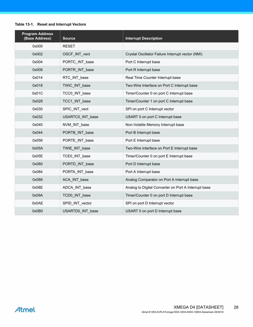
Table 13-1. Reset and Interrupt Vectors
Program Address(Base Address) Source Interrupt Description
0x000 RESET
0x002 OSCF_INT_vect Crystal Oscillator Failure Interrupt vector (NMI)
0x004 PORTC_INT_base Port C Interrupt base
0x008 PORTR_INT_base Port R Interrupt base
0x014 RTC_INT_base Real Time Counter Interrupt base
0x018 TWIC_INT_base Two-Wire Interface on Port C Interrupt base
0x01C TCC0_INT_base Timer/Counter 0 on port C Interrupt base
0x028 TCC1_INT_base Timer/Counter 1 on port C Interrupt base
0x030 SPIC_INT_vect SPI on port C Interrupt vector
0x032 USARTC0_INT_base USART 0 on port C Interrupt base
0x040 NVM_INT_base Non-Volatile Memory Interrupt base
0x044 PORTB_INT_base Port B Interrupt base
0x056 PORTE_INT_base Port E Interrupt base
0x05A TWIE_INT_base Two-Wire Interface on Port E Interrupt base
0x05E TCE0_INT_base Timer/Counter 0 on port E Interrupt base
0x080 PORTD_INT_base Port D Interrupt base
0x084 PORTA_INT_base Port A Interrupt base
0x088 ACA_INT_base Analog Comparator on Port A Interrupt base
0x08E ADCA_INT_base Analog to Digital Converter on Port A Interrupt base
0x09A TCD0_INT_base Timer/Counter 0 on port D Interrupt base
0x0AE SPID_INT_vector SPI on port D Interrupt vector
0x0B0 USARTD0_INT_base USART 0 on port D Interrupt base
28XMEGA D4 [DATASHEET]Atmel-8135S-AVR-ATxmega16D4-32D4-64D4-128D4-Datasheet–09/2016

14. I/O Ports
14.1 Features 34 general purpose input and output pins with individual configuration
Output driver with configurable driver and pull settings: Totem-pole Wired-AND Wired-OR Bus-keeper Inverted I/O
Input with synchronous and/or asynchronous sensing with interrupts and events Sense both edges Sense rising edges Sense falling edges Sense low level
Optional pull-up and pull-down resistor on input and Wired-OR/AND configurations
Asynchronous pin change sensing that can wake the device from all sleep modes
Two port interrupts with pin masking per I/O port
Efficient and safe access to port pins Hardware read-modify-write through dedicated toggle/clear/set registers Configuration of multiple pins in a single operation Mapping of port registers into bit-accessible I/O memory space
Peripheral clocks output on port pin
Real-time counter clock output to port pin
Event channels can be output on port pin
Remapping of digital peripheral pin functions Selectable USART, SPI, and timer/counter input/output pin locations
14.2 Overview
One port consists of up to eight port pins: pin 0 to 7. Each port pin can be configured as input or output with configurable driver and pull settings. They also implement synchronous and asynchronous input sensing with interrupts and events for selectable pin change conditions. Asynchronous pin-change sensing means that a pin change can wake the device from all sleep modes, included the modes where no clocks are running.
All functions are individual and configurable per pin, but several pins can be configured in a single operation. The pins have hardware read-modify-write (RMW) functionality for safe and correct change of drive value and/or pull resistor configuration. The direction of one port pin can be changed without unintentionally changing the direction of any other pin.
The port pin configuration also controls input and output selection of other device functions. It is possible to have both the peripheral clock and the real-time clock output to a port pin, and available for external use. The same applies to events from the event system that can be used to synchronize and control external functions. Other digital peripherals, such as USART, SPI, and timer/counters, can be remapped to selectable pin locations in order to optimize pin-out versus application needs.
The notation of the ports are PORTA, PORTB, PORTC, PORTD, PORTE, and PORTR.
29XMEGA D4 [DATASHEET]Atmel-8135S-AVR-ATxmega16D4-32D4-64D4-128D4-Datasheet–09/2016

14.3 Output Driver
All port pins (Pxn) have programmable output configuration.
14.3.1 Push-pull
Figure 14-1. I/O Configuration - Totem-pole
14.3.2 Pull-down
Figure 14-2. I/O Configuration - Totem-pole with Pull-down (on Input)
14.3.3 Pull-up
Figure 14-3. I/O Configuration - Totem-pole with Pull-up (on Input)
14.3.4 Bus-keeper
The bus-keeper’s weak output produces the same logical level as the last output level. It acts as a pull-up if the last level was ‘1’, and pull-down if the last level was ‘0’.
INxn
OUTxn
DIRxn
Pxn
INxn
OUTxn
DIRxn
Pxn
INxn
OUTxn
DIRxn
Pxn
30XMEGA D4 [DATASHEET]Atmel-8135S-AVR-ATxmega16D4-32D4-64D4-128D4-Datasheet–09/2016

Figure 14-4. I/O Configuration - Totem-pole with Bus-keeper
14.3.5 Others
Figure 14-5. Output Configuration - Wired-OR with Optional Pull-down
Figure 14-6. I/O Configuration - Wired-AND with Optional Pull-up
14.4 Input Sensing
Input sensing is synchronous or asynchronous depending on the enabled clock for the ports, and the configuration is shown in Figure 14-7.
INxn
OUTxn
DIRxn
Pxn
INxn
OUTxn
Pxn
INxn
OUTxn
Pxn
31XMEGA D4 [DATASHEET]Atmel-8135S-AVR-ATxmega16D4-32D4-64D4-128D4-Datasheet–09/2016

Figure 14-7. Input Sensing System Overview
When a pin is configured with inverted I/O, the pin value is inverted before the input sensing.
14.5 Alternate Port Functions
Most port pins have alternate pin functions in addition to being a general purpose I/O pin. When an alternate function is enabled, it might override the normal port pin function or pin value. This happens when other peripherals that require pins are enabled or configured to use pins. If and how a peripheral will override and use pins is described in the section for that peripheral. “Pinout and Pin Functions” on page 49 shows which modules on peripherals that enable alternate functions on a pin, and which alternate functions that are available on a pin.
D Q
R
INVERTED I/O
Interrupt
Control
D Q
R
PxnSynchronizer
INnEDGE
DETECT
Synchronous sensing
EDGE
DETECT
Asynchronous sensing
IRQ
Synchronous
Events
Asynchronous
Events
32XMEGA D4 [DATASHEET]Atmel-8135S-AVR-ATxmega16D4-32D4-64D4-128D4-Datasheet–09/2016
15. TC0/1 – 16-bit Timer/Counter Type 0 and 1
15.1 Features Four 16-bit timer/counters
Three timer/counters of type 0 One timer/counter of type 1
32-bit timer/counter support by cascading two timer/counters
Up to four compare or capture (CC) channels Four CC channels for timer/counters of type 0 Two CC channels for timer/counters of type 1
Double buffered timer period setting
Double buffered capture or compare channels
Waveform generation: Frequency generation Single-slope pulse width modulation Dual-slope pulse width modulation
Input capture: Input capture with noise cancelling Frequency capture Pulse width capture 32-bit input capture
Timer overflow and error interrupts/events
One compare match or input capture interrupt/event per CC channel
Can be used with event system for: Quadrature decoding Count and direction control Capture
High-resolution extension Increases frequency and waveform resolution by 4x (2-bit) or 8x (3-bit)
Advanced waveform extension: Low- and high-side output with programmable dead-time insertion (DTI)
Event controlled fault protection for safe disabling of drivers
15.2 Overview
Atmel AVR XMEGA devices have a set of four flexible 16-bit Timer/Counters (TC). Their capabilities include accurate program execution timing, frequency and waveform generation, and input capture with time and frequency measurement of digital signals. Two timer/counters can be cascaded to create a 32-bit timer/counter with optional 32-bit capture.
A timer/counter consists of a base counter and a set of compare or capture (CC) channels. The base counter can be used to count clock cycles or events. It has direction control and period setting that can be used for timing. The CC channels can be used together with the base counter to do compare match control, frequency generation, and pulse width waveform modulation, as well as various input capture operations. A timer/counter can be configured for either capture or compare functions, but cannot perform both at the same time.
A timer/counter can be clocked and timed from the peripheral clock with optional prescaling or from the event system. The event system can also be used for direction control and capture trigger or to synchronize operations.
There are two differences between timer/counter type 0 and type 1. Timer/counter 0 has four CC channels, and timer/counter 1 has two CC channels. All information related to CC channels 3 and 4 is valid only for timer/counter 0. Only Timer/Counter 0 has the split mode feature that split it into two 8-bit Timer/Counters with four compare channels each.
33XMEGA D4 [DATASHEET]Atmel-8135S-AVR-ATxmega16D4-32D4-64D4-128D4-Datasheet–09/2016
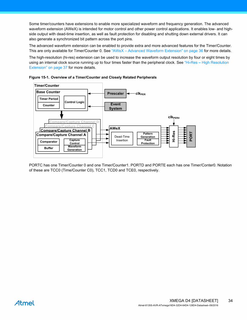
Some timer/counters have extensions to enable more specialized waveform and frequency generation. The advanced waveform extension (AWeX) is intended for motor control and other power control applications. It enables low- and high-side output with dead-time insertion, as well as fault protection for disabling and shutting down external drivers. It can also generate a synchronized bit pattern across the port pins.
The advanced waveform extension can be enabled to provide extra and more advanced features for the Timer/Counter. This are only available for Timer/Counter 0. See “AWeX – Advanced Waveform Extension” on page 36 for more details.
The high-resolution (hi-res) extension can be used to increase the waveform output resolution by four or eight times by using an internal clock source running up to four times faster than the peripheral clock. See “Hi-Res – High Resolution Extension” on page 37 for more details.
Figure 15-1. Overview of a Timer/Counter and Closely Related Peripherals
PORTC has one Timer/Counter 0 and one Timer/Counter1. PORTD and PORTE each has one Timer/Conter0. Notation of these are TCC0 (Time/Counter C0), TCC1, TCD0 and TCE0, respectively.
AWeX
Compare/Capture Channel DCompare/Capture Channel C
Compare/Capture Channel BCompare/Capture Channel A
Waveform Generation
Buffer
Comparator Hi-
Res
Fault Protection
Capture Control
Base Counter
CounterControl Logic
Timer Period
Prescaler
Dead-Time Insertion
Pattern Generation
clkPER4
PO
RT
Event System
clkPER
Timer/Counter
34XMEGA D4 [DATASHEET]Atmel-8135S-AVR-ATxmega16D4-32D4-64D4-128D4-Datasheet–09/2016

16. TC2 Timer/Counter Type 2
16.1 Features Six eight-bit timer/counters
Three Low-byte timer/counter Three High-byte timer/counter
Up to eight compare channels in each Timer/Counter 2 Four compare channels for the low-byte timer/counter Four compare channels for the high-byte timer/counter
Waveform generation Single slope pulse width modulation
Timer underflow interrupts/events
One compare match interrupt/event per compare channel for the low-byte timer/counter
Can be used with the event system for count control
16.2 Overview
There are three Timer/Counter 2. These are realized when a Timer/Counter 0 is set in split mode. It is then a system of two eight-bit timer/counters, each with four compare channels. This results in eight configurable pulse width modulation (PWM) channels with individually controlled duty cycles, and is intended for applications that require a high number of PWM channels.
The two eight-bit timer/counters in this system are referred to as the low-byte timer/counter and high-byte timer/counter, respectively. The difference between them is that only the low-byte timer/counter can be used to generate compare match interrupts and events. The two eight-bit timer/counters have a shared clock source and separate period and compare settings. They can be clocked and timed from the peripheral clock, with optional prescaling, or from the event system. The counters are always counting down.
PORTC, PORTD and PORTE each has one Timer/Counter 2. Notation of these are TCC2 (Time/Counter C2), TCD2 and TCE2, respectively.
35XMEGA D4 [DATASHEET]Atmel-8135S-AVR-ATxmega16D4-32D4-64D4-128D4-Datasheet–09/2016
17. AWeX – Advanced Waveform Extension
17.1 Features Waveform output with complementary output from each compare channel
Four dead-time insertion (DTI) units 8-bit resolution Separate high and low side dead-time setting Double buffered dead time Optionally halts timer during dead-time insertion
Pattern generation unit creating synchronised bit pattern across the port pins Double buffered pattern generation Optional distribution of one compare channel output across the port pins
Event controlled fault protection for instant and predictable fault triggering
17.2 Overview
The advanced waveform extension (AWeX) provides extra functions to the timer/counter in waveform generation (WG) modes. It is primarily intended for use with different types of motor control and other power control applications. It enables low- and high side output with dead-time insertion and fault protection for disabling and shutting down external drivers. It can also generate a synchronized bit pattern across the port pins.
Each of the waveform generator outputs from the timer/counter 0 are split into a complimentary pair of outputs when any AWeX features are enabled. These output pairs go through a dead-time insertion (DTI) unit that generates the non-inverted low side (LS) and inverted high side (HS) of the WG output with dead-time insertion between LS and HS switching. The DTI output will override the normal port value according to the port override setting.
The pattern generation unit can be used to generate a synchronized bit pattern on the port it is connected to. In addition, the WG output from compare channel A can be distributed to and override all the port pins. When the pattern generator unit is enabled, the DTI unit is bypassed.
The fault protection unit is connected to the event system, enabling any event to trigger a fault condition that will disable the AWeX output. The event system ensures predictable and instant fault reaction, and gives flexibility in the selection of fault triggers.
The AWeX is available for TCC0. The notation of this is AWEXC.
36XMEGA D4 [DATASHEET]Atmel-8135S-AVR-ATxmega16D4-32D4-64D4-128D4-Datasheet–09/2016

18. Hi-Res – High Resolution Extension
18.1 Features Increases waveform generator resolution up to 8x (three bits)
Supports frequency, single-slope PWM, and dual-slope PWM generation
Supports the AWeX when this is used for the same timer/counter
18.2 Overview
The high-resolution (hi-res) extension can be used to increase the resolution of the waveform generation output from a timer/counter by four or eight. It can be used for a timer/counter doing frequency, single-slope PWM, or dual-slope PWM generation. It can also be used with the AWeX if this is used for the same timer/counter.
The hi-res extension uses the peripheral 4x clock (ClkPER4). The system clock prescalers must be configured so the peripheral 4x clock frequency is four times higher than the peripheral and CPU clock frequency when the hi-res extension is enabled.
There is one hi-res extension that can be enabled for each timer/counter on PORTC. The notation of this is HIRESC.
37XMEGA D4 [DATASHEET]Atmel-8135S-AVR-ATxmega16D4-32D4-64D4-128D4-Datasheet–09/2016
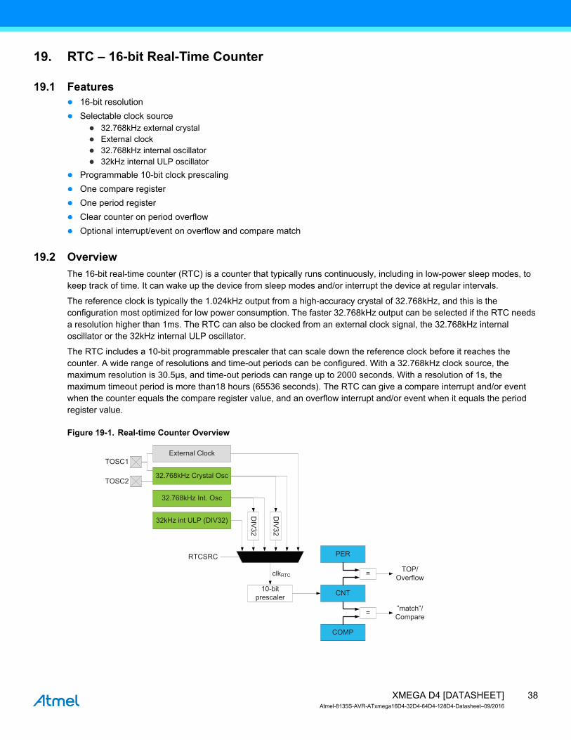
19. RTC – 16-bit Real-Time Counter
19.1 Features 16-bit resolution
Selectable clock source 32.768kHz external crystal External clock 32.768kHz internal oscillator 32kHz internal ULP oscillator
Programmable 10-bit clock prescaling
One compare register
One period register
Clear counter on period overflow
Optional interrupt/event on overflow and compare match
19.2 Overview
The 16-bit real-time counter (RTC) is a counter that typically runs continuously, including in low-power sleep modes, to keep track of time. It can wake up the device from sleep modes and/or interrupt the device at regular intervals.
The reference clock is typically the 1.024kHz output from a high-accuracy crystal of 32.768kHz, and this is the configuration most optimized for low power consumption. The faster 32.768kHz output can be selected if the RTC needs a resolution higher than 1ms. The RTC can also be clocked from an external clock signal, the 32.768kHz internal oscillator or the 32kHz internal ULP oscillator.
The RTC includes a 10-bit programmable prescaler that can scale down the reference clock before it reaches the counter. A wide range of resolutions and time-out periods can be configured. With a 32.768kHz clock source, the maximum resolution is 30.5µs, and time-out periods can range up to 2000 seconds. With a resolution of 1s, the maximum timeout period is more than18 hours (65536 seconds). The RTC can give a compare interrupt and/or event when the counter equals the compare register value, and an overflow interrupt and/or event when it equals the period register value.
Figure 19-1. Real-time Counter Overview
32.768kHz Crystal Osc
32.768kHz Int. Osc
TOSC1
TOSC2
External Clock
DIV
32
DIV
32
32kHz int ULP (DIV32)
RTCSRC
10-bit
prescaler
clkRTC
CNT
PER
COMP
=
=
”match”/
Compare
TOP/
Overflow
38XMEGA D4 [DATASHEET]Atmel-8135S-AVR-ATxmega16D4-32D4-64D4-128D4-Datasheet–09/2016
20. TWI – Two-Wire Interface
20.1 Features Two identical two-wire interface peripherals
Bidirectional, two-wire communication interface Phillips I2C compatible System Management Bus (SMBus) compatible
Bus master and slave operation supported Slave operation Single bus master operation Bus master in multi-master bus environment Multi-master arbitration
Flexible slave address match functions 7-bit and general call address recognition in hardware 10-bit addressing supported Address mask register for dual address match or address range masking Optional software address recognition for unlimited number of addresses
Slave can operate in all sleep modes, including power-down
Slave address match can wake device from all sleep modes
100kHz and 400kHz bus frequency support
Slew-rate limited output drivers
Input filter for bus noise and spike suppression
Support arbitration between start/repeated start and data bit (SMBus)
Slave arbitration allows support for address resolve protocol (ARP) (SMBus)
20.2 Overview
The two-wire interface (TWI) is a bidirectional, two-wire communication interface. It is I2C and System Management Bus (SMBus) compatible. The only external hardware needed to implement the bus is one pull-up resistor on each bus line.
A device connected to the bus must act as a master or a slave. The master initiates a data transaction by addressing a slave on the bus and telling whether it wants to transmit or receive data. One bus can have many slaves and one or several masters that can take control of the bus. An arbitration process handles priority if more than one master tries to transmit data at the same time. Mechanisms for resolving bus contention are inherent in the protocol.
The TWI module supports master and slave functionality. The master and slave functionality are separated from each other, and can be enabled and configured separately. The master module supports multi-master bus operation and arbitration. It contains the baud rate generator. Both 100kHz and 400kHz bus frequency is supported. Quick command and smart mode can be enabled to auto-trigger operations and reduce software complexity.
The slave module implements 7-bit address match and general address call recognition in hardware. 10-bit addressing is also supported. A dedicated address mask register can act as a second address match register or as a register for address range masking. The slave continues to operate in all sleep modes, including power-down mode. This enables the slave to wake up the device from all sleep modes on TWI address match. It is possible to disable the address matching to let this be handled in software instead.
The TWI module will detect START and STOP conditions, bus collisions, and bus errors. Arbitration lost, errors, collision, and clock hold on the bus are also detected and indicated in separate status flags available in both master and slave modes.
It is possible to disable the TWI drivers in the device, and enable a four-wire digital interface for connecting to an external TWI bus driver. This can be used for applications where the device operates from a different VCC voltage than used by the TWI bus.
PORTC and PORTE each has one TWI. Notation of these peripherals are TWIC and TWIE.
39XMEGA D4 [DATASHEET]Atmel-8135S-AVR-ATxmega16D4-32D4-64D4-128D4-Datasheet–09/2016
21. SPI – Serial Peripheral Interface
21.1 Features Two identical SPI peripherals
Full-duplex, three-wire synchronous data transfer
Master or slave operation
Lsb first or msb first data transfer
Eight programmable bit rates
Interrupt flag at the end of transmission
Write collision flag to indicate data collision
Wake up from idle sleep mode
Double speed master mode
21.2 Overview
The Serial Peripheral Interface (SPI) is a high-speed synchronous data transfer interface using three or four pins. It allows fast communication between an Atmel AVR XMEGA device and peripheral devices or between several microcontrollers. The SPI supports full-duplex communication.
A device connected to the bus must act as a master or slave. The master initiates and controls all data transactions.
PORTC and PORTD each has one SPI. Notation of these peripherals are SPIC and SPID.
40XMEGA D4 [DATASHEET]Atmel-8135S-AVR-ATxmega16D4-32D4-64D4-128D4-Datasheet–09/2016
22. USART
22.1 Features Two identical USART peripherals
Full-duplex operation
Asynchronous or synchronous operation Synchronous clock rates up to 1/2 of the device clock frequency Asynchronous clock rates up to 1/8 of the device clock frequency
Supports serial frames with 5, 6, 7, 8, or 9 data bits and 1 or 2 stop bits
Fractional baud rate generator Can generate desired baud rate from any system clock frequency No need for external oscillator with certain frequencies
Built-in error detection and correction schemes Odd or even parity generation and parity check Data overrun and framing error detection Noise filtering includes false start bit detection and digital low-pass filter
Separate interrupts for Transmit complete Transmit data register empty Receive complete
Multiprocessor communication mode Addressing scheme to address a specific devices on a multidevice bus Enable unaddressed devices to automatically ignore all frames
Master SPI mode Double buffered operation Operation up to 1/2 of the peripheral clock frequency
IRCOM module for IrDA compliant pulse modulation/demodulation
22.2 Overview
The universal synchronous and asynchronous serial receiver and transmitter (USART) is a fast and flexible serial communication module. The USART supports full-duplex communication and asynchronous and synchronous operation. The USART can be configured to operate in SPI master mode and used for SPI communication.
Communication is frame based, and the frame format can be customized to support a wide range of standards. The USART is buffered in both directions, enabling continued data transmission without any delay between frames. Separate interrupts for receive and transmit complete enable fully interrupt driven communication. Frame error and buffer overflow are detected in hardware and indicated with separate status flags. Even or odd parity generation and parity check can also be enabled.
The clock generator includes a fractional baud rate generator that is able to generate a wide range of USART baud rates from any system clock frequencies. This removes the need to use an external crystal oscillator with a specific frequency to achieve a required baud rate. It also supports external clock input in synchronous slave operation.
When the USART is set in master SPI mode, all USART-specific logic is disabled, leaving the transmit and receive buffers, shift registers, and baud rate generator enabled. Pin control and interrupt generation are identical in both modes. The registers are used in both modes, but their functionality differs for some control settings.
An IRCOM module can be enabled for one USART to support IrDA 1.4 physical compliant pulse modulation and demodulation for baud rates up to 115.2kbps.
PORTC and PORTD each has one USART. Notation of these peripherals are USARTC0 and USARTD0 respectively.
41XMEGA D4 [DATASHEET]Atmel-8135S-AVR-ATxmega16D4-32D4-64D4-128D4-Datasheet–09/2016

23. IRCOM – IR Communication Module
23.1 Features Pulse modulation/demodulation for infrared communication
IrDA compatible for baud rates up to 115.2kbps
Selectable pulse modulation scheme 3/16 of the baud rate period Fixed pulse period, 8-bit programmable Pulse modulation disabled
Built-in filtering
Can be connected to and used by any USART
23.2 Overview
Atmel AVR XMEGA devices contain an infrared communication module (IRCOM) that is IrDA compatible for baud rates up to 115.2Kbps. It can be connected to any USART to enable infrared pulse encoding/decoding for that USART.
42XMEGA D4 [DATASHEET]Atmel-8135S-AVR-ATxmega16D4-32D4-64D4-128D4-Datasheet–09/2016
24. CRC – Cyclic Redundancy Check Generator
24.1 Features Cyclic redundancy check (CRC) generation and checking for
Communication data Program or data in flash memory Data in SRAM and I/O memory space
Integrated with flash memory and CPU Automatic CRC of the complete or a selectable range of the flash memory CPU can load data to the CRC generator through the I/O interface
CRC polynomial software selectable to CRC-16 (CRC-CCITT) CRC-32 (IEEE 802.3)
Zero remainder detection
24.2 Overview
A cyclic redundancy check (CRC) is an error detection technique test algorithm used to find accidental errors in data, and it is commonly used to determine the correctness of a data transmission, and data present in the data and program memories. A CRC takes a data stream or a block of data as input and generates a 16- or 32-bit output that can be appended to the data and used as a checksum. When the same data are later received or read, the device or application repeats the calculation. If the new CRC result does not match the one calculated earlier, the block contains a data error. The application will then detect this and may take a corrective action, such as requesting the data to be sent again or simply not using the incorrect data.
Typically, an n-bit CRC applied to a data block of arbitrary length will detect any single error burst not longer than n bits (any single alteration that spans no more than n bits of the data), and will detect the fraction 1-2-n of all longer error bursts. The CRC module in Atmel AVR XMEGA devices supports two commonly used CRC polynomials; CRC-16 (CRC-CCITT) and CRC-32 (IEEE 802.3).
CRC-16:
CRC-32:
Polynomial: x16+x12+x5+1
Hex value: 0x1021
Polynomial: x32+x26+x23+x22+x16+x12+x11+x10+x8+x7+x5+x4+x2+x+1
Hex value: 0x04C11DB7
43XMEGA D4 [DATASHEET]Atmel-8135S-AVR-ATxmega16D4-32D4-64D4-128D4-Datasheet–09/2016

25. ADC – 12-bit Analog to Digital Converter
25.1 Features One Analog to Digital Converters (ADC)
12-bit resolution
Up to 200 thousand samples per second Down to 3.6µs conversion time with 8-bit resolution Down to 5.0µs conversion time with 12-bit resolution
Differential and single-ended input Up to 12 single-ended inputs 12x4 differential inputs without gain 12x4 differential input with gain
Built-in differential gain stage 1/2x, 1x, 2x, 4x, 8x, 16x, 32x, and 64x gain options
Single, continuous and scan conversion options
Three internal inputs Internal temperature sensor AVCC voltage divided by 10 1.1V bandgap voltage
Internal and external reference options
Compare function for accurate monitoring of user defined thresholds
Optional event triggered conversion for accurate timing
Optional interrupt/event on compare result
25.2 Overview
The ADC converts analog signals to digital values. The ADC has 12-bit resolution and is capable of converting up to 200 thousand samples per second (ksps). The input selection is flexible, and both single-ended and differential measurements can be done. For differential measurements, an optional gain stage is available to increase the dynamic range. In addition, several internal signal inputs are available. The ADC can provide both signed and unsigned results.
The ADC measurements can either be started by application software or an incoming event from another peripheral in the device. The ADC measurements can be started with predictable timing, and without software intervention.
Both internal and external reference voltages can be used. An integrated temperature sensor is available for use with the ADC. The AVCC/10 and the bandgap voltage can also be measured by the ADC.
The ADC has a compare function for accurate monitoring of user defined thresholds with minimum software intervention required.
44XMEGA D4 [DATASHEET]Atmel-8135S-AVR-ATxmega16D4-32D4-64D4-128D4-Datasheet–09/2016

Figure 25-1. ADC overview
The ADC may be configured for 8- or 12-bit result, reducing the minimum conversion time (propagation delay) from 5.0µs for 12-bit to 3.6µs for 8-bit result.
ADC conversion results are provided left- or right adjusted with optional ‘1’ or ‘0’ padding. This eases calculation when the result is represented as a signed integer (signed 16-bit number).
Notation of this peripheral is ADCA. The PORTA has ADCA inputs 0..7 and PORTB has ADCA inputs 8..11.
CH0 Result
Compare Register
<> Threshold
(Int Req)
Internal 1.00V
Internal AVCC/1.6V
AREFA
AREFB
VINP
VINN
Internal
signals
Internal AVCC/2
ADC0
ADC11
•••
ADC0
ADC7
•••
Reference
Voltage
45XMEGA D4 [DATASHEET]Atmel-8135S-AVR-ATxmega16D4-32D4-64D4-128D4-Datasheet–09/2016

26. AC – Analog Comparator
26.1 Features Two Analog Comparators (ACs)
Selectable hysteresis No Small Large
Analog comparator output available on pin
Flexible input selection All pins on the port Bandgap reference voltage A 64-level programmable voltage scaler of the internal AVCC voltage
Interrupt and event generation on: Rising edge Falling edge Toggle
Window function interrupt and event generation on: Signal above window Signal inside window Signal below window
Constant current source with configurable output pin selection
26.2 Overview
The analog comparator (AC) compares the voltage levels on two inputs and gives a digital output based on this comparison. The analog comparator may be configured to generate interrupt requests and/or events upon several different combinations of input change.
The important property of the analog comparator’s dynamic behavior is the hysteresis. It can be adjusted in order to achieve the optimal operation for each application.
The input selection includes analog port pins, several internal signals, and a 64-level programmable voltage scaler. The analog comparator output state can also be output on a pin for use by external devices.
A constant current source can be enabled and output on a selectable pin. This can be used to replace, for example, external resistors used to charge capacitors in capacitive touch sensing applications.
The analog comparators are always grouped in pairs on each port. These are called analog comparator 0 (AC0) and analog comparator 1 (AC1). They have identical behavior, but separate control registers. Used as pair, they can be set in window mode to compare a signal to a voltage range instead of a voltage level.
PORTA has one AC pair. Notation is ACA.
46XMEGA D4 [DATASHEET]Atmel-8135S-AVR-ATxmega16D4-32D4-64D4-128D4-Datasheet–09/2016

Figure 26-1. Analog Comparator Overview
The window function is realized by connecting the external inputs of the two analog comparators in a pair as shown in Figure 26-2.
Figure 26-2. Analog Comparator Window Function
ACnMUXCTRL ACnCTRLInterrupt
Mode
Enable
Enable
Hysteresis
Hysteresis
AC1OUT
WINCTRL
InterruptSensititivity
Control&
WindowFunction
Events
Interrupts
AC0OUT
Pin Input
Pin Input
Pin Input
Pin Input
VoltageScaler
Bandgap
+
-
+
-
AC0
+
-
AC1
+
-
Input signal
Upper limit of window
Lower limit of window
Interrupt sensitivity
control
Interrupts
Events
47XMEGA D4 [DATASHEET]Atmel-8135S-AVR-ATxmega16D4-32D4-64D4-128D4-Datasheet–09/2016

27. Programming and Debugging
27.1 Features Programming
External programming through PDI interface Minimal protocol overhead for fast operation Built-in error detection and handling for reliable operation
Boot loader support for programming through any communication interface
Debugging Nonintrusive, real-time, on-chip debug system No software or hardware resources required from device except pin connection Program flow control
Go, Stop, Reset, Step Into, Step Over, Step Out, Run-to-Cursor Unlimited number of user program breakpoints Unlimited number of user data breakpoints, break on:
Data location read, write, or both read and write Data location content equal or not equal to a value Data location content is greater or smaller than a value Data location content is within or outside a range
No limitation on device clock frequency
Program and Debug Interface (PDI) Two-pin interface for external programming and debugging Uses the Reset pin and a dedicated pin No I/O pins required during programming or debugging
27.2 Overview
The Program and Debug Interface (PDI) is an Atmel proprietary interface for external programming and on-chip debugging of a device.
The PDI supports fast programming of nonvolatile memory (NVM) spaces; flash, EEPOM, fuses, lock bits, and the user signature row.
Debug is supported through an on-chip debug system that offers nonintrusive, real-time debug. It does not require any software or hardware resources except for the device pin connection. Using the Atmel tool chain, it offers complete program flow control and support for an unlimited number of program and complex data breakpoints. Application debug can be done from a C or other high-level language source code level, as well as from an assembler and disassembler level.
Programming and debugging can be done through the PDI physical layer. This is a two-pin interface that uses the Reset pin for the clock input (PDI_CLK) and one other dedicated pin for data input and output (PDI_DATA). Any external programmer or on-chip debugger/emulator can be directly connected to this interface.
48XMEGA D4 [DATASHEET]Atmel-8135S-AVR-ATxmega16D4-32D4-64D4-128D4-Datasheet–09/2016

28. Pinout and Pin Functions
The device pinout is shown in ”Pinout/Block Diagram” on page 3. In addition to general purpose I/O functionality, each pin can have several alternate functions. This will depend on which peripheral is enabled and connected to the actual pin. Only one of the pin functions can be used at time.
28.1 Alternate Pin Function Description
The tables below show the notation for all pin functions available and describe its function.
28.1.1 Operation/Power Supply
28.1.2 Port Interrupt functions
28.1.3 Analog Functions
28.1.4 Timer/Counter and AWEX Functions
28.1.5 Communication Functions
VCC Digital supply voltage
AVCC Analog supply voltage
GND Ground
SYNC Port pin with full synchronous and limited asynchronous interrupt function
ASYNC Port pin with full synchronous and full asynchronous interrupt function
ACn Analog Comparator input pin n
ACnOUT Analog Comparator n Output
ADCn Analog to Digital Converter input pin n
AREF Analog reference input pin
OCnxLS Output Compare Channel x Low Side for Timer/Counter n
OCnxHS Output Compare Channel x High Side for Timer/Counter n
SCL Serial Clock for TWI
SDA Serial Data for TWI
XCKn Transfer Clock for USART n
RXDn Receiver Data for USART n
TXDn Transmitter Data for USART n
SS Slave Select for SPI
MOSI Master Out Slave In for SPI
MISO Master In Slave Out for SPI
SCK Serial Clock for SPI
49XMEGA D4 [DATASHEET]Atmel-8135S-AVR-ATxmega16D4-32D4-64D4-128D4-Datasheet–09/2016

28.1.6 Oscillators, Clock and Event
28.1.7 Debug/System Functions
TOSCn Timer Oscillator pin n
XTALn Input/Output for Oscillator pin n
CLKOUT Peripheral Clock Output
EVOUT Event Channel Output
RTCOUT RTC Clock Source Output
RESET Reset pin
PDI_CLK Program and Debug Interface Clock pin
PDI_DATA Program and Debug Interface Data pin
50XMEGA D4 [DATASHEET]Atmel-8135S-AVR-ATxmega16D4-32D4-64D4-128D4-Datasheet–09/2016
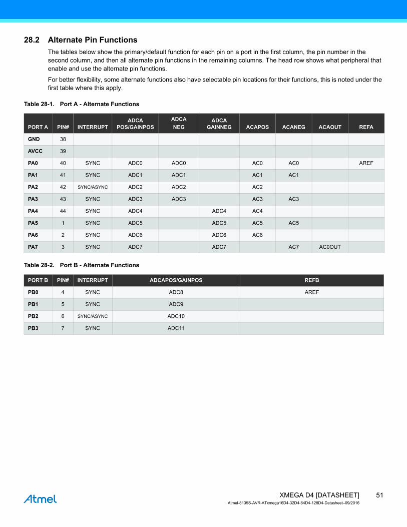
28.2 Alternate Pin Functions
The tables below show the primary/default function for each pin on a port in the first column, the pin number in the second column, and then all alternate pin functions in the remaining columns. The head row shows what peripheral that enable and use the alternate pin functions.
For better flexibility, some alternate functions also have selectable pin locations for their functions, this is noted under the first table where this apply.
Table 28-1. Port A - Alternate Functions
Table 28-2. Port B - Alternate Functions
PORT A PIN# INTERRUPTADCA
POS/GAINPOS
ADCA
NEGADCA
GAINNEG ACAPOS ACANEG ACAOUT REFA
GND 38
AVCC 39
PA0 40 SYNC ADC0 ADC0 AC0 AC0 AREF
PA1 41 SYNC ADC1 ADC1 AC1 AC1
PA2 42 SYNC/ASYNC ADC2 ADC2 AC2
PA3 43 SYNC ADC3 ADC3 AC3 AC3
PA4 44 SYNC ADC4 ADC4 AC4
PA5 1 SYNC ADC5 ADC5 AC5 AC5
PA6 2 SYNC ADC6 ADC6 AC6
PA7 3 SYNC ADC7 ADC7 AC7 AC0OUT
PORT B PIN# INTERRUPT ADCAPOS/GAINPOS REFB
PB0 4 SYNC ADC8 AREF
PB1 5 SYNC ADC9
PB2 6 SYNC/ASYNC ADC10
PB3 7 SYNC ADC11
51XMEGA D4 [DATASHEET]Atmel-8135S-AVR-ATxmega16D4-32D4-64D4-128D4-Datasheet–09/2016
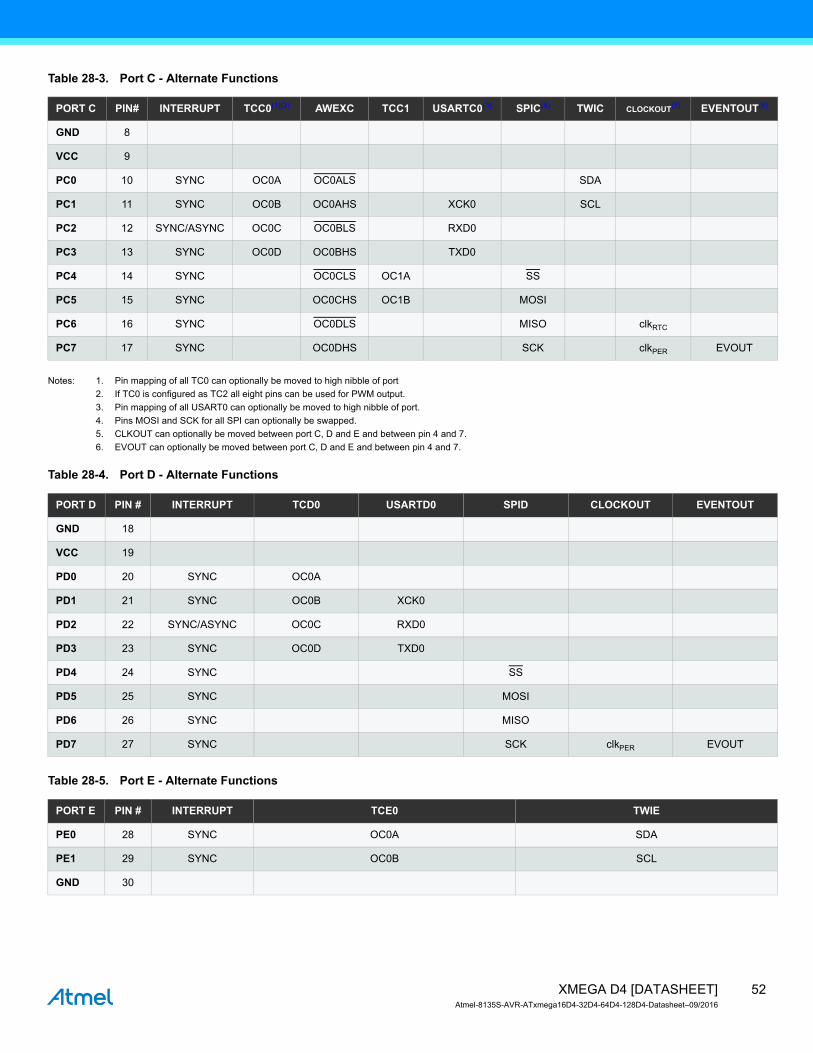
Table 28-3. Port C - Alternate Functions
Notes: 1. Pin mapping of all TC0 can optionally be moved to high nibble of port
2. If TC0 is configured as TC2 all eight pins can be used for PWM output.
3. Pin mapping of all USART0 can optionally be moved to high nibble of port.
4. Pins MOSI and SCK for all SPI can optionally be swapped.
5. CLKOUT can optionally be moved between port C, D and E and between pin 4 and 7.
6. EVOUT can optionally be moved between port C, D and E and between pin 4 and 7.
Table 28-4. Port D - Alternate Functions
Table 28-5. Port E - Alternate Functions
PORT C PIN# INTERRUPT TCC0(1)(2) AWEXC TCC1 USARTC0(3) SPIC(4) TWIC CLOCKOUT(5) EVENTOUT(6)
GND 8
VCC 9
PC0 10 SYNC OC0A OC0ALS SDA
PC1 11 SYNC OC0B OC0AHS XCK0 SCL
PC2 12 SYNC/ASYNC OC0C OC0BLS RXD0
PC3 13 SYNC OC0D OC0BHS TXD0
PC4 14 SYNC OC0CLS OC1A SS
PC5 15 SYNC OC0CHS OC1B MOSI
PC6 16 SYNC OC0DLS MISO clkRTC
PC7 17 SYNC OC0DHS SCK clkPER EVOUT
PORT D PIN # INTERRUPT TCD0 USARTD0 SPID CLOCKOUT EVENTOUT
GND 18
VCC 19
PD0 20 SYNC OC0A
PD1 21 SYNC OC0B XCK0
PD2 22 SYNC/ASYNC OC0C RXD0
PD3 23 SYNC OC0D TXD0
PD4 24 SYNC SS
PD5 25 SYNC MOSI
PD6 26 SYNC MISO
PD7 27 SYNC SCK clkPER EVOUT
PORT E PIN # INTERRUPT TCE0 TWIE
PE0 28 SYNC OC0A SDA
PE1 29 SYNC OC0B SCL
GND 30
52XMEGA D4 [DATASHEET]Atmel-8135S-AVR-ATxmega16D4-32D4-64D4-128D4-Datasheet–09/2016

Table 28-6. Port F - Alternate Functions
Note: 1. TOSC pins can optionally be moved to PE2/PE3
VCC 31
PE2 32 SYNC/ASYNC OC0C
PE3 33 SYNC OC0D
PORT R PIN # INTERRUPT PDI XTAL TOSC(1)
PDI 34 PDI_DATA
RESET 35 PDI_CLOCK
PRO 36 SYNC XTAL2 TOSC2
PR1 37 SYNC XTAL1 TOSC1
PORT E PIN # INTERRUPT TCE0 TWIE
53XMEGA D4 [DATASHEET]Atmel-8135S-AVR-ATxmega16D4-32D4-64D4-128D4-Datasheet–09/2016

29. Peripheral Module Address Map
The address maps show the base address for each peripheral and module in Atmel AVR XMEGA D4. For complete register description and summary for each peripheral module, refer to the XMEGA D manual.
Table 29-1. Peripheral Module Address Map
Base address Name Description
0x0000 GPIO General purpose IO registers
0x0010 VPORT0 Virtual Port 0
0x0014 VPORT1 Virtual Port 1
0x0018 VPORT2 Virtual Port 2
0x001C VPORT3 Virtual Port 2
0x0030 CPU CPU
0x0040 CLK Clock control
0x0048 SLEEP Sleep controller
0x0050 OSC Oscillator control
0x0060 DFLLRC32M DFLL for the 32 MHz internal RC oscillator
0x0068 DFLLRC2M DFLL for the 2 MHz RC oscillator
0x0070 PR Power reduction
0x0078 RST Reset controller
0x0080 WDT Watch-dog timer
0x0090 MCU MCU control
0x00A0 PMIC Programmable multilevel interrupt controller
0x00B0 PORTCFG Port configuration
0x0180 EVSYS Event system
0x00D0 CRC CRC module
0x01C0 NVM Nonvolatile memory (NVM) controller
0x0200 ADCA Analog to digital converter on port A
0x0380 ACA Analog comparator pair on port A
0x0400 RTC Real time counter
0x0480 TWIC Two wire interface on port C
0x04A0 TWIE Two wire interface on port E
0x0600 PORTA Port A
0x0620 PORTB Port B
0x0640 PORTC Port C
0x0660 PORTD Port D
54XMEGA D4 [DATASHEET]Atmel-8135S-AVR-ATxmega16D4-32D4-64D4-128D4-Datasheet–09/2016

0x0680 PORTE Port E
0x07E0 PORTR Port R
0x0800 TCC0 Timer/counter 0 on port C
0x0840 TCC1 Timer/counter 1 on port C
0x0880 AWEXC Advanced waveform extension on port C
0x0890 HIRESC High resolution extension on port C
0x08A0 USARTC0 USART 0 on port C
0x08C0 SPIC Serial peripheral interface on port C
0x08F8 IRCOM Infrared communication module
0x0900 TCD0 Timer/counter 0 on port D
0x09A0 USARTD0 USART 0 on port D
0x09C0 SPID Serial peripheral interface on port D
0x0A00 TCE0 Timer/counter 0 on port E
Base address Name Description
55XMEGA D4 [DATASHEET]Atmel-8135S-AVR-ATxmega16D4-32D4-64D4-128D4-Datasheet–09/2016
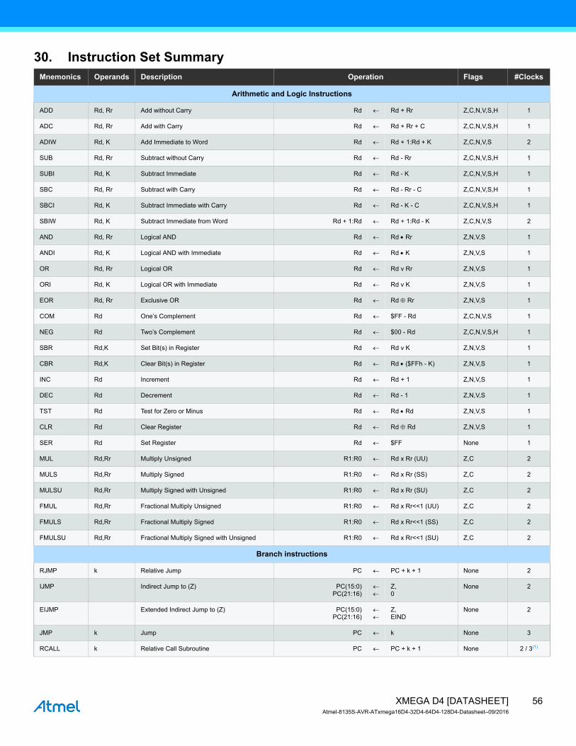
30. Instruction Set SummaryMnemonics Operands Description Operation Flags #Clocks
Arithmetic and Logic Instructions
ADD Rd, Rr Add without Carry Rd Rd + Rr Z,C,N,V,S,H 1
ADC Rd, Rr Add with Carry Rd Rd + Rr + C Z,C,N,V,S,H 1
ADIW Rd, K Add Immediate to Word Rd Rd + 1:Rd + K Z,C,N,V,S 2
SUB Rd, Rr Subtract without Carry Rd Rd - Rr Z,C,N,V,S,H 1
SUBI Rd, K Subtract Immediate Rd Rd - K Z,C,N,V,S,H 1
SBC Rd, Rr Subtract with Carry Rd Rd - Rr - C Z,C,N,V,S,H 1
SBCI Rd, K Subtract Immediate with Carry Rd Rd - K - C Z,C,N,V,S,H 1
SBIW Rd, K Subtract Immediate from Word Rd + 1:Rd Rd + 1:Rd - K Z,C,N,V,S 2
AND Rd, Rr Logical AND Rd Rd Rr Z,N,V,S 1
ANDI Rd, K Logical AND with Immediate Rd Rd K Z,N,V,S 1
OR Rd, Rr Logical OR Rd Rd v Rr Z,N,V,S 1
ORI Rd, K Logical OR with Immediate Rd Rd v K Z,N,V,S 1
EOR Rd, Rr Exclusive OR Rd Rd Rr Z,N,V,S 1
COM Rd One’s Complement Rd $FF - Rd Z,C,N,V,S 1
NEG Rd Two’s Complement Rd $00 - Rd Z,C,N,V,S,H 1
SBR Rd,K Set Bit(s) in Register Rd Rd v K Z,N,V,S 1
CBR Rd,K Clear Bit(s) in Register Rd Rd ($FFh - K) Z,N,V,S 1
INC Rd Increment Rd Rd + 1 Z,N,V,S 1
DEC Rd Decrement Rd Rd - 1 Z,N,V,S 1
TST Rd Test for Zero or Minus Rd Rd Rd Z,N,V,S 1
CLR Rd Clear Register Rd Rd Rd Z,N,V,S 1
SER Rd Set Register Rd $FF None 1
MUL Rd,Rr Multiply Unsigned R1:R0 Rd x Rr (UU) Z,C 2
MULS Rd,Rr Multiply Signed R1:R0 Rd x Rr (SS) Z,C 2
MULSU Rd,Rr Multiply Signed with Unsigned R1:R0 Rd x Rr (SU) Z,C 2
FMUL Rd,Rr Fractional Multiply Unsigned R1:R0 Rd x Rr<<1 (UU) Z,C 2
FMULS Rd,Rr Fractional Multiply Signed R1:R0 Rd x Rr<<1 (SS) Z,C 2
FMULSU Rd,Rr Fractional Multiply Signed with Unsigned R1:R0 Rd x Rr<<1 (SU) Z,C 2
Branch instructions
RJMP k Relative Jump PC PC + k + 1 None 2
IJMP Indirect Jump to (Z) PC(15:0)PC(21:16)
Z,0
None 2
EIJMP Extended Indirect Jump to (Z) PC(15:0)PC(21:16)
Z,EIND
None 2
JMP k Jump PC k None 3
RCALL k Relative Call Subroutine PC PC + k + 1 None 2 / 3(1)
56XMEGA D4 [DATASHEET]Atmel-8135S-AVR-ATxmega16D4-32D4-64D4-128D4-Datasheet–09/2016
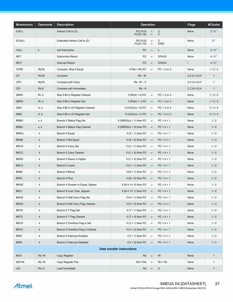
ICALL Indirect Call to (Z) PC(15:0)PC(21:16)
Z,0
None 2 / 3(1)
EICALL Extended Indirect Call to (Z) PC(15:0)PC(21:16)
Z,EIND
None 3(1)
CALL k call Subroutine PC k None 3 / 4(1)
RET Subroutine Return PC STACK None 4 / 5(1)
RETI Interrupt Return PC STACK I 4 / 5(1)
CPSE Rd,Rr Compare, Skip if Equal if (Rd = Rr) PC PC + 2 or 3 None 1 / 2 / 3
CP Rd,Rr Compare Rd - Rr Z,C,N,V,S,H 1
CPC Rd,Rr Compare with Carry Rd - Rr - C Z,C,N,V,S,H 1
CPI Rd,K Compare with Immediate Rd - K Z,C,N,V,S,H 1
SBRC Rr, b Skip if Bit in Register Cleared if (Rr(b) = 0) PC PC + 2 or 3 None 1 / 2 / 3
SBRS Rr, b Skip if Bit in Register Set if (Rr(b) = 1) PC PC + 2 or 3 None 1 / 2 / 3
SBIC A, b Skip if Bit in I/O Register Cleared if (I/O(A,b) = 0) PC PC + 2 or 3 None 2 / 3 / 4
SBIS A, b Skip if Bit in I/O Register Set If (I/O(A,b) =1) PC PC + 2 or 3 None 2 / 3 / 4
BRBS s, k Branch if Status Flag Set if (SREG(s) = 1) then PC PC + k + 1 None 1 / 2
BRBC s, k Branch if Status Flag Cleared if (SREG(s) = 0) then PC PC + k + 1 None 1 / 2
BREQ k Branch if Equal if (Z = 1) then PC PC + k + 1 None 1 / 2
BRNE k Branch if Not Equal if (Z = 0) then PC PC + k + 1 None 1 / 2
BRCS k Branch if Carry Set if (C = 1) then PC PC + k + 1 None 1 / 2
BRCC k Branch if Carry Cleared if (C = 0) then PC PC + k + 1 None 1 / 2
BRSH k Branch if Same or Higher if (C = 0) then PC PC + k + 1 None 1 / 2
BRLO k Branch if Lower if (C = 1) then PC PC + k + 1 None 1 / 2
BRMI k Branch if Minus if (N = 1) then PC PC + k + 1 None 1 / 2
BRPL k Branch if Plus if (N = 0) then PC PC + k + 1 None 1 / 2
BRGE k Branch if Greater or Equal, Signed if (N V= 0) then PC PC + k + 1 None 1 / 2
BRLT k Branch if Less Than, Signed if (N V= 1) then PC PC + k + 1 None 1 / 2
BRHS k Branch if Half Carry Flag Set if (H = 1) then PC PC + k + 1 None 1 / 2
BRHC k Branch if Half Carry Flag Cleared if (H = 0) then PC PC + k + 1 None 1 / 2
BRTS k Branch if T Flag Set if (T = 1) then PC PC + k + 1 None 1 / 2
BRTC k Branch if T Flag Cleared if (T = 0) then PC PC + k + 1 None 1 / 2
BRVS k Branch if Overflow Flag is Set if (V = 1) then PC PC + k + 1 None 1 / 2
BRVC k Branch if Overflow Flag is Cleared if (V = 0) then PC PC + k + 1 None 1 / 2
BRIE k Branch if Interrupt Enabled if (I = 1) then PC PC + k + 1 None 1 / 2
BRID k Branch if Interrupt Disabled if (I = 0) then PC PC + k + 1 None 1 / 2
Data transfer instructions
MOV Rd, Rr Copy Register Rd Rr None 1
MOVW Rd, Rr Copy Register Pair Rd+1:Rd Rr+1:Rr None 1
LDI Rd, K Load Immediate Rd K None 1
Mnemonics Operands Description Operation Flags #Clocks
57XMEGA D4 [DATASHEET]Atmel-8135S-AVR-ATxmega16D4-32D4-64D4-128D4-Datasheet–09/2016

LDS Rd, k Load Direct from data space Rd (k) None 2(1)(2)
LD Rd, X Load Indirect Rd (X) None 1(1)(2)
LD Rd, X+ Load Indirect and Post-Increment RdX
(X)X + 1
None 1(1)(2)
LD Rd, -X Load Indirect and Pre-Decrement X X - 1,Rd (X)
X - 1(X)
None 2(1)(2)
LD Rd, Y Load Indirect Rd (Y) (Y) None 1(1)(2)
LD Rd, Y+ Load Indirect and Post-Increment RdY
(Y)Y + 1
None 1(1)(2)
LD Rd, -Y Load Indirect and Pre-Decrement YRd
Y - 1(Y)
None 2(1)(2)
LDD Rd, Y+q Load Indirect with Displacement Rd (Y + q) None 2(1)(2)
LD Rd, Z Load Indirect Rd (Z) None 1(1)(2)
LD Rd, Z+ Load Indirect and Post-Increment RdZ
(Z),Z+1
None 1(1)(2)
LD Rd, -Z Load Indirect and Pre-Decrement ZRd
Z - 1,(Z)
None 2(1)(2)
LDD Rd, Z+q Load Indirect with Displacement Rd (Z + q) None 2(1)(2)
STS k, Rr Store Direct to Data Space (k) Rd None 2(1)
ST X, Rr Store Indirect (X) Rr None 1(1)
ST X+, Rr Store Indirect and Post-Increment (X)X
Rr,X + 1
None 1(1)
ST -X, Rr Store Indirect and Pre-Decrement X(X)
X - 1,Rr
None 2(1)
ST Y, Rr Store Indirect (Y) Rr None 1(1)
ST Y+, Rr Store Indirect and Post-Increment (Y)Y
Rr,Y + 1
None 1(1)
ST -Y, Rr Store Indirect and Pre-Decrement Y(Y)
Y - 1,Rr
None 2(1)
STD Y+q, Rr Store Indirect with Displacement (Y + q) Rr None 2(1)
ST Z, Rr Store Indirect (Z) Rr None 1(1)
ST Z+, Rr Store Indirect and Post-Increment (Z)Z
RrZ + 1
None 1(1)
ST -Z, Rr Store Indirect and Pre-Decrement Z Z - 1 None 2(1)
STD Z+q,Rr Store Indirect with Displacement (Z + q) Rr None 2(1)
LPM Load Program Memory R0 (Z) None 3
LPM Rd, Z Load Program Memory Rd (Z) None 3
LPM Rd, Z+ Load Program Memory and Post-Increment RdZ
(Z),Z + 1
None 3
ELPM Extended Load Program Memory R0 (RAMPZ:Z) None 3
ELPM Rd, Z Extended Load Program Memory Rd (RAMPZ:Z) None 3
ELPM Rd, Z+ Extended Load Program Memory and Post-Increment
RdZ
(RAMPZ:Z),Z + 1
None 3
SPM Store Program Memory (RAMPZ:Z) R1:R0 None -
Mnemonics Operands Description Operation Flags #Clocks
58XMEGA D4 [DATASHEET]Atmel-8135S-AVR-ATxmega16D4-32D4-64D4-128D4-Datasheet–09/2016

SPM Z+ Store Program Memory and Post-Increment by 2
(RAMPZ:Z)Z
R1:R0,Z + 2
None -
IN Rd, A In From I/O Location Rd I/O(A) None 1
OUT A, Rr Out To I/O Location I/O(A) Rr None 1
PUSH Rr Push Register on Stack STACK Rr None 1(1)
POP Rd Pop Register from Stack Rd STACK None 2(1)
XCH Z, Rd Exchange RAM location TempRd(Z)
Rd,(Z),Temp
None 2
LAS Z, Rd Load and Set RAM location TempRd(Z)
Rd,(Z),Temp v (Z)
None 2
LAC Z, Rd Load and Clear RAM location TempRd(Z)
Rd,(Z),($FFh – Rd) (Z)
None 2
LAT Z, Rd Load and Toggle RAM location TempRd(Z)
Rd,(Z),Temp (Z)
None 2
Bit and bit-test instructions
LSL Rd Logical Shift Left Rd(n+1)Rd(0)
C
Rd(n),0,Rd(7)
Z,C,N,V,H 1
LSR Rd Logical Shift Right Rd(n)Rd(7)
C
Rd(n+1),0,Rd(0)
Z,C,N,V 1
ROL Rd Rotate Left Through Carry Rd(0)Rd(n+1)
C
C,Rd(n),Rd(7)
Z,C,N,V,H 1
ROR Rd Rotate Right Through Carry Rd(7)Rd(n)
C
C,Rd(n+1),Rd(0)
Z,C,N,V 1
ASR Rd Arithmetic Shift Right Rd(n) Rd(n+1), n=0..6 Z,C,N,V 1
SWAP Rd Swap Nibbles Rd(3..0) Rd(7..4) None 1
BSET s Flag Set SREG(s) 1 SREG(s) 1
BCLR s Flag Clear SREG(s) 0 SREG(s) 1
SBI A, b Set Bit in I/O Register I/O(A, b) 1 None 1
CBI A, b Clear Bit in I/O Register I/O(A, b) 0 None 1
BST Rr, b Bit Store from Register to T T Rr(b) T 1
BLD Rd, b Bit load from T to Register Rd(b) T None 1
SEC Set Carry C 1 C 1
CLC Clear Carry C 0 C 1
SEN Set Negative Flag N 1 N 1
CLN Clear Negative Flag N 0 N 1
SEZ Set Zero Flag Z 1 Z 1
CLZ Clear Zero Flag Z 0 Z 1
SEI Global Interrupt Enable I 1 I 1
CLI Global Interrupt Disable I 0 I 1
Mnemonics Operands Description Operation Flags #Clocks
59XMEGA D4 [DATASHEET]Atmel-8135S-AVR-ATxmega16D4-32D4-64D4-128D4-Datasheet–09/2016

Notes: 1. Cycle times for data memory accesses assume internal memory accesses, and are not valid for accesses via the external RAM interface.
2. One extra cycle must be added when accessing internal SRAM.
SES Set Signed Test Flag S 1 S 1
CLS Clear Signed Test Flag S 0 S 1
SEV Set Two’s Complement Overflow V 1 V 1
CLV Clear Two’s Complement Overflow V 0 V 1
SET Set T in SREG T 1 T 1
CLT Clear T in SREG T 0 T 1
SEH Set Half Carry Flag in SREG H 1 H 1
CLH Clear Half Carry Flag in SREG H 0 H 1
MCU control instructions
BREAK Break (See specific descr. for BREAK) None 1
NOP No Operation None 1
SLEEP Sleep (see specific descr. for Sleep) None 1
WDR Watchdog Reset (see specific descr. for WDR) None 1
Mnemonics Operands Description Operation Flags #Clocks
60XMEGA D4 [DATASHEET]Atmel-8135S-AVR-ATxmega16D4-32D4-64D4-128D4-Datasheet–09/2016
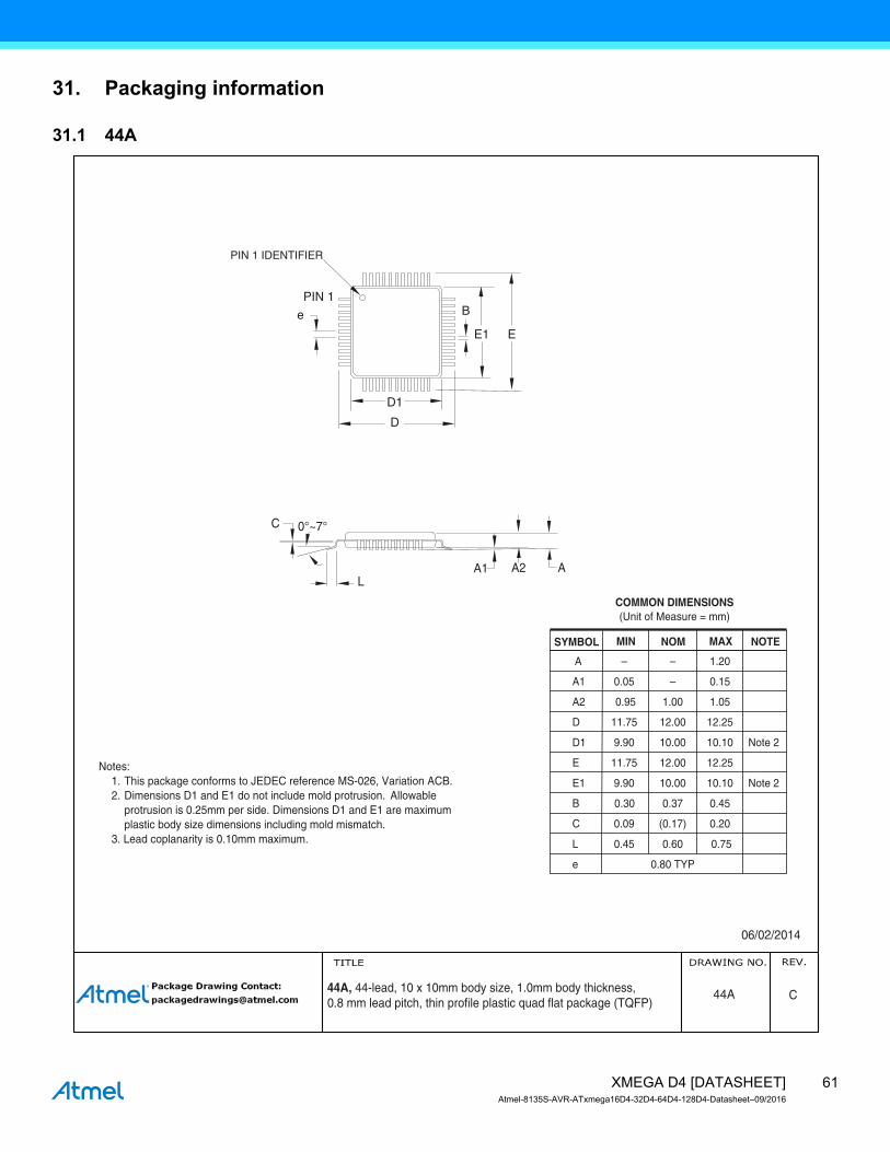
31. Packaging information
31.1 44A
44A, 44-lead, 10 x 10mm body size, 1.0mm body thickness,0.8 mm lead pitch, thin profile plastic quad flat package (TQFP)
C44A
06/02/2014
PIN 1 IDENTIFIER
0°~7°
PIN 1
L
C
A1 A2 A
D1
D
e
E1 E
B
COMMON DIMENSIONS(Unit of Measure = mm)
SYMBOL MIN NOM MAX NOTE
Notes: 1. This package conforms to JEDEC reference MS-026, Variation ACB. 2. Dimensions D1 and E1 do not include mold protrusion. Allowable protrusion is 0.25mm per side. Dimensions D1 and E1 are maximum plastic body size dimensions including mold mismatch. 3. Lead coplanarity is 0.10mm maximum.
A – – 1.20
A1 0.05 – 0.15
A2 0.95 1.00 1.05
D 11.75 12.00 12.25
D1 9.90 10.00 10.10 Note 2
E 11.75 12.00 12.25
E1 9.90 10.00 10.10 Note 2
B 0.30 0.37 0.45
C 0.09 (0.17) 0.20
L 0.45 0.60 0.75
e 0.80 TYP
61XMEGA D4 [DATASHEET]Atmel-8135S-AVR-ATxmega16D4-32D4-64D4-128D4-Datasheet–09/2016

31.2 44M1
TITLE DRAWING NO.GPC REV. Package Drawing Contact: [email protected] 44M1ZWS H
44M1, 44-pad, 7 x 7 x 1.0mm body, lead pitch 0.50mm, 5.20mm exposed pad, thermally enhanced plastic very thin quad flat no lead package (VQFN)
02/13/2014
COMMON DIMENSIONS(Unit of Measure = mm)
SYMBOL MIN NOM MAX NOT E
A 0.80 0.90 1.00
A1 – 0.02 0.05
A3 0.20 REF
b 0.18 0.23 0.30
D
D2 5.00 5.20 5.40
6.90 7.00 7.10
6.90 7.00 7.10
E
E2 5.00 5.20 5.40
e 0.50 BSC
L 0.59 0.64 0.69
K 0.20 0.26 0.41Note: JEDEC Standard MO-220, Fig . 1 (S AW Singulation) VKKD-3 .
TOP VIE W
SIDE VIEW
B OT TOM VIE W
D
E
Marked Pin# 1 I D
E2
D2
b e
Pin #1 Co rnerL
A1
A3
A
SE ATING PLAN E
Pin #1 Triangle
Pin #1 Cham fer(C 0.30)
Option A
Option B
Pin #1 Notch(0.20 R)
Option C
K
K
123
62XMEGA D4 [DATASHEET]Atmel-8135S-AVR-ATxmega16D4-32D4-64D4-128D4-Datasheet–09/2016
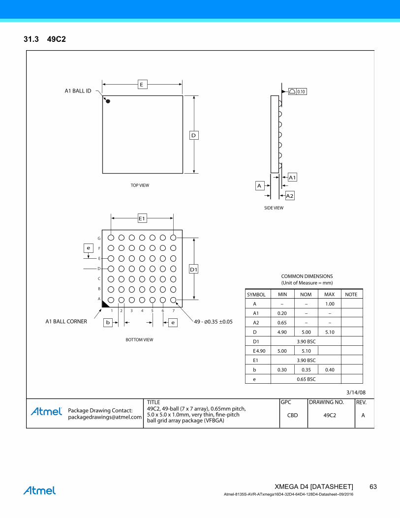
31.3 49C2
TITLE DRAWING NO.GPC REV. Package Drawing Contact: [email protected] 49C2CBD A
49C2, 49-ball (7 x 7 array), 0.65mm pitch, 5.0 x 5.0 x 1.0mm, very thin, fine-pitch ball grid array package (VFBGA)
3/14/08
COMMON DIMENSIONS(Unit of Measure = mm)
SYMBOL MIN NOM MAX NOTE
A – – 1.00
A1 0.20 – –
A2 0.65 – –
D 4.90 5.00 5.10
D1 3.90 BSC
E 4.90 5.00 5.10
E1 3.90 BSC
b 0.30 0.35 0.40
e 0.65 BSC
TOP VIEW
SIDE VIEW
A1 BALL ID
G
F
E
D
C
B
A
1 2 3 4 5 6 7
A
A1
A2
D
E0.10
E1
D1
49 - Ø0.35 ±0.05
e
A1 BALL CORNER
BOTTOM VIEW
b e
63XMEGA D4 [DATASHEET]Atmel-8135S-AVR-ATxmega16D4-32D4-64D4-128D4-Datasheet–09/2016
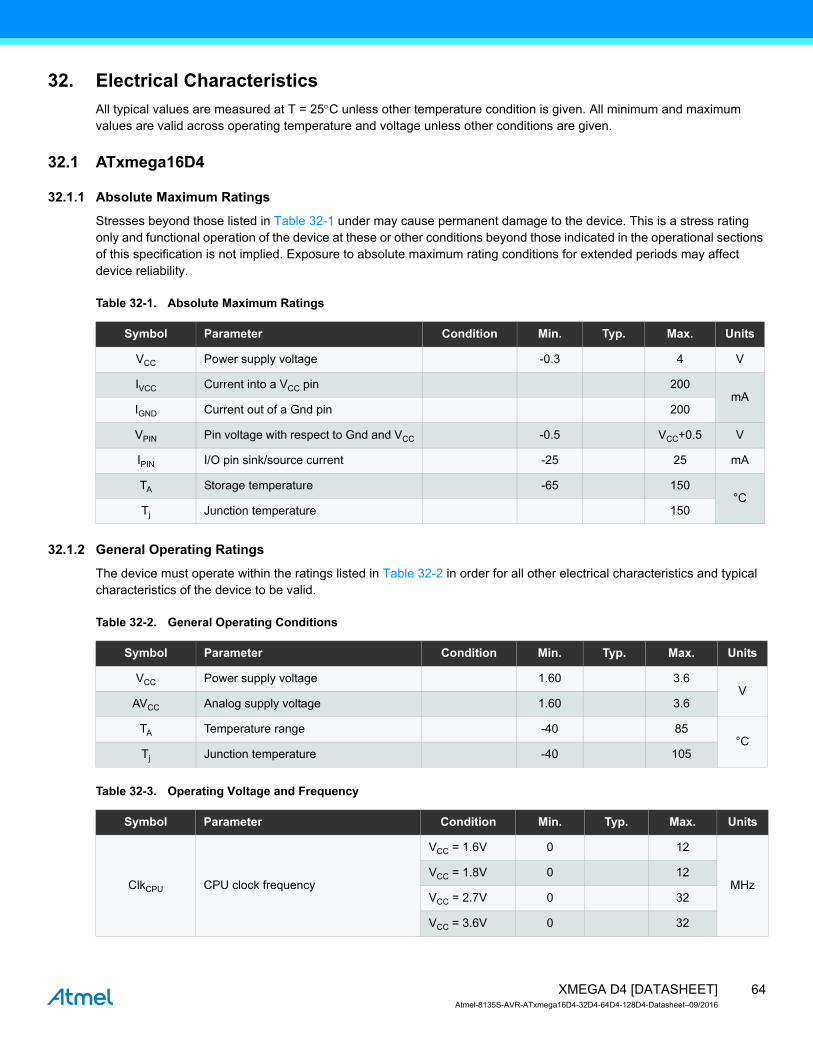
32. Electrical Characteristics
All typical values are measured at T = 25C unless other temperature condition is given. All minimum and maximum values are valid across operating temperature and voltage unless other conditions are given.
32.1 ATxmega16D4
32.1.1 Absolute Maximum Ratings
Stresses beyond those listed in Table 32-1 under may cause permanent damage to the device. This is a stress rating only and functional operation of the device at these or other conditions beyond those indicated in the operational sections of this specification is not implied. Exposure to absolute maximum rating conditions for extended periods may affect device reliability.
Table 32-1. Absolute Maximum Ratings
32.1.2 General Operating Ratings
The device must operate within the ratings listed in Table 32-2 in order for all other electrical characteristics and typical characteristics of the device to be valid.
Table 32-2. General Operating Conditions
Table 32-3. Operating Voltage and Frequency
Symbol Parameter Condition Min. Typ. Max. Units
VCC Power supply voltage -0.3 4 V
IVCC Current into a VCC pin 200mA
IGND Current out of a Gnd pin 200
VPIN Pin voltage with respect to Gnd and VCC -0.5 VCC+0.5 V
IPIN I/O pin sink/source current -25 25 mA
TA Storage temperature -65 150°C
Tj Junction temperature 150
Symbol Parameter Condition Min. Typ. Max. Units
VCC Power supply voltage 1.60 3.6V
AVCC Analog supply voltage 1.60 3.6
TA Temperature range -40 85°C
Tj Junction temperature -40 105
Symbol Parameter Condition Min. Typ. Max. Units
ClkCPU CPU clock frequency
VCC = 1.6V 0 12
MHzVCC = 1.8V 0 12
VCC = 2.7V 0 32
VCC = 3.6V 0 32
64XMEGA D4 [DATASHEET]Atmel-8135S-AVR-ATxmega16D4-32D4-64D4-128D4-Datasheet–09/2016

The maximum CPU clock frequency depends on VCC. As shown in Figure 32-15 the Frequency vs. VCC curve is linear between 1.8V < VCC < 2.7V.
Figure 32-1. Maximum Frequency vs. VCC
1.8
12
32
MHz
V2.7 3.61.6
Safe Operating Area
65XMEGA D4 [DATASHEET]Atmel-8135S-AVR-ATxmega16D4-32D4-64D4-128D4-Datasheet–09/2016

32.1.3 Current Consumption
Table 32-4. Current Consumption for Active Mode and Sleep Modes
Notes: 1. All Power Reduction Registers set.
2. Maximum limits are based on characterization, and not tested in production.
Symbol Parameter Condition Min. Typ. Max. Units
ICC
Active powerconsumption(1)
32kHz, Ext. ClkVCC = 1.8V 40
µA
VCC = 3.0V 80
1MHz, Ext. ClkVCC = 1.8V 200
VCC = 3.0V 410
2MHz, Ext. ClkVCC = 1.8V 350 600
VCC = 3.0V0.75 1.4
mA32MHz, Ext. Clk 7.5 12
Idle powerconsumption(1)
32kHz, Ext. ClkVCC = 1.8V 2.0
µA
VCC = 3.0V 2.8
1MHz, Ext. ClkVCC = 1.8V 42
VCC = 3.0V 85
2MHz, Ext. ClkVCC = 1.8V 85 225
VCC = 3.0V170 350
32MHz, Ext. Clk 2.7 5.5 mA
Power-down powerconsumption
T = 25°C
VCC = 3.0V
0.1 1.0
µA
T = 85°C 2.0 4.5
T = 105°C 0.1 7.0
WDT and sampled BOD enabled,T = 25°C
VCC = 3.0V
1.4 3.0
WDT and sampled BOD enabled,T = 85°C
3.0 6.0
WDT and sampled BOD enabled,T = 105°C
1.4 10
Power-save powerconsumption(2)
RTC from ULP clock, WDT andsampled BOD enabled, T = 25°C
VCC = 1.8V 1.5
VCC = 3.0V 1.5
RTC from 1.024kHz low power32.768kHz TOSC, T = 25°C
VCC = 1.8V 0.6 2.0
VCC = 3.0V 0.7 2.0
RTC from low power 32.768kHzTOSC, T = 25°C
VCC = 1.8V 0.8 3.0
VCC = 3.0V 1.0 3.0
Reset power consumptionCurrent through RESET pinsubstracted
VCC = 3.0V 300
66XMEGA D4 [DATASHEET]Atmel-8135S-AVR-ATxmega16D4-32D4-64D4-128D4-Datasheet–09/2016
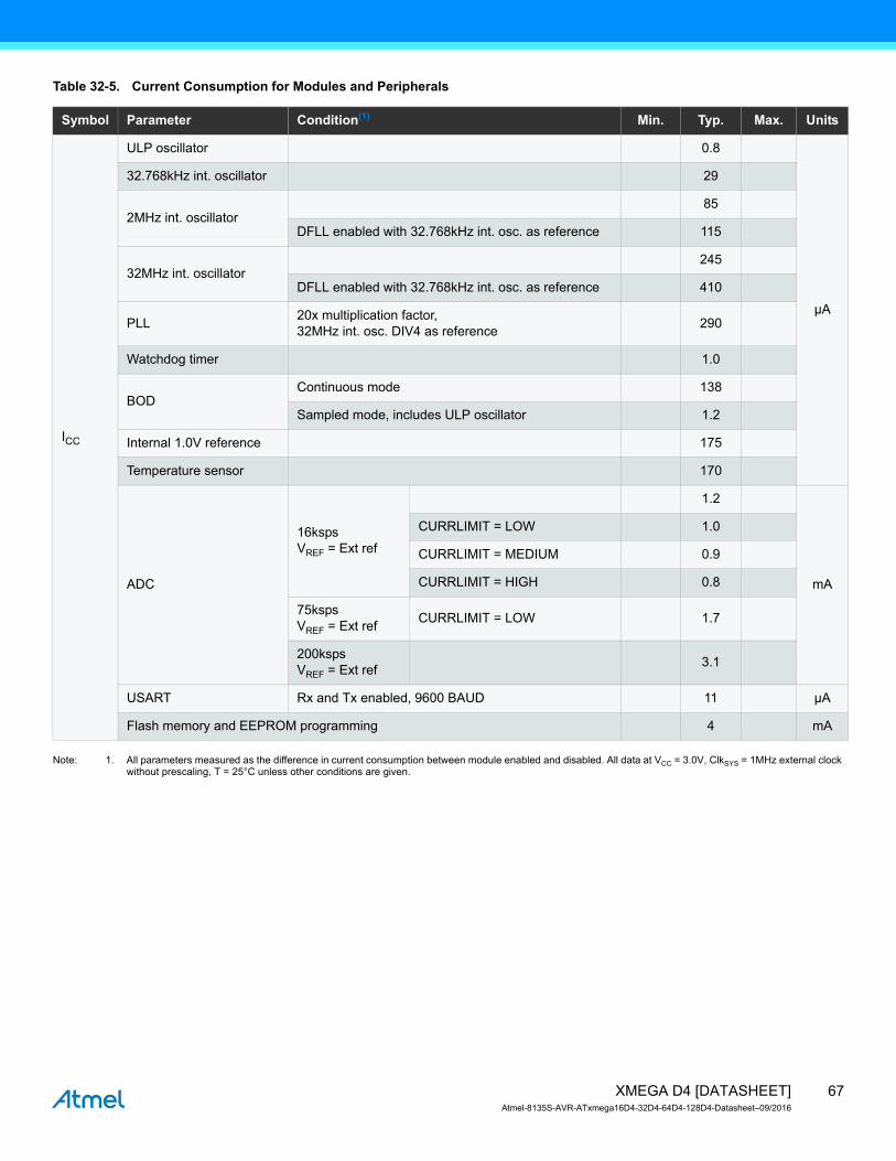
Table 32-5. Current Consumption for Modules and Peripherals
Note: 1. All parameters measured as the difference in current consumption between module enabled and disabled. All data at VCC = 3.0V, ClkSYS = 1MHz external clock without prescaling, T = 25°C unless other conditions are given.
Symbol Parameter Condition(1) Min. Typ. Max. Units
ICC
ULP oscillator 0.8
µA
32.768kHz int. oscillator 29
2MHz int. oscillator85
DFLL enabled with 32.768kHz int. osc. as reference 115
32MHz int. oscillator245
DFLL enabled with 32.768kHz int. osc. as reference 410
PLL20x multiplication factor,32MHz int. osc. DIV4 as reference
290
Watchdog timer 1.0
BODContinuous mode 138
Sampled mode, includes ULP oscillator 1.2
Internal 1.0V reference 175
Temperature sensor 170
ADC
16kspsVREF = Ext ref
1.2
mA
CURRLIMIT = LOW 1.0
CURRLIMIT = MEDIUM 0.9
CURRLIMIT = HIGH 0.8
75kspsVREF = Ext ref
CURRLIMIT = LOW 1.7
200kspsVREF = Ext ref
3.1
USART Rx and Tx enabled, 9600 BAUD 11 µA
Flash memory and EEPROM programming 4 mA
67XMEGA D4 [DATASHEET]Atmel-8135S-AVR-ATxmega16D4-32D4-64D4-128D4-Datasheet–09/2016
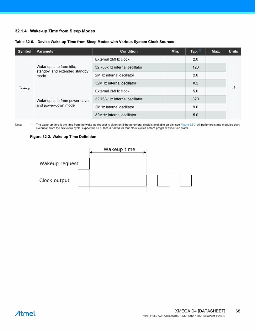
32.1.4 Wake-up Time from Sleep Modes
Table 32-6. Device Wake-up Time from Sleep Modes with Various System Clock Sources
Note: 1. The wake-up time is the time from the wake-up request is given until the peripheral clock is available on pin, see Figure 32-2. All peripherals and modules start execution from the first clock cycle, expect the CPU that is halted for four clock cycles before program execution starts.
Figure 32-2. Wake-up Time Definition
Symbol Parameter Condition Min. Typ.(1) Max. Units
twakeup
Wake-up time from idle, standby, and extended standby mode
External 2MHz clock 2.0
µs
32.768kHz internal oscillator 120
2MHz internal oscillator 2.0
32MHz internal oscillator 0.2
Wake-up time from power-save and power-down mode
External 2MHz clock 5.0
32.768kHz internal oscillator 320
2MHz internal oscillator 9.0
32MHz internal oscillator 5.0
Wakeup request
Clock output
Wakeup time
68XMEGA D4 [DATASHEET]Atmel-8135S-AVR-ATxmega16D4-32D4-64D4-128D4-Datasheet–09/2016

32.1.5 I/O Pin Characteristics
The I/O pins complies with the JEDEC LVTTL and LVCMOS specification and the high- and low level input and output voltage limits reflect or exceed this specification.
Table 32-7. I/O Pin Characteristics
Notes: 1. The sum of all IOH for PORTA and PORTB must not exceed 100mA.The sum of all IOH for PORTC, PORTD, PORTE must for each port not exceed 200mA.The sum of all IOH for pins PF[0-5] on PORTF must not exceed 200mA.The sum of all IOL for pins PF[6-7] on PORTF, PORTR and PDI must not exceed 100mA.
2. The sum of all IOL for PORTA and PORTB must not exceed 100mA.The sum of all IOL for PORTC, PORTD, PORTE must for each port not exceed 200mA.The sum of all IOL for pins PF[0-5] on PORTF must not exceed 200mA.The sum of all IOL for pins PF[6-7] on PORTF, PORTR and PDI must not exceed 100mA.
Symbol Parameter Condition Min. Typ. Max. Units
IOH (1)/
IOL (2) I/O pin source/sink current -20 20 mA
VIH High level input voltageVCC = 2.4 - 3.6V 0.7*Vcc VCC+0.5
V
VCC = 1.6 - 2.4V 0.8*VCC VCC+0.5
VIL Low level input voltageVCC = 2.4- 3.6V -0.5 0.3*VCC
VCC = 1.6 - 2.4V -0.5 0.2*VCC
VOH High level output voltage
VCC = 3.3V IOH = -4mA 2.6 2.9
VCC = 3.0V IOH = -3mA 2.1 2.7
VCC = 1.8V IOH = -1mA 1.4 1.6
VOL Low level output voltage
VCC = 3.3V IOL = 8mA 0.4 0.76
VCC = 3.0V IOL = 5mA 0.3 0.64
VCC = 1.8V IOL = 3mA 0.2 0.46
IIN Input leakage current I/O pin T = 25°C <0.01 1 µA
RP Pull/buss keeper resistor 25 k
69XMEGA D4 [DATASHEET]Atmel-8135S-AVR-ATxmega16D4-32D4-64D4-128D4-Datasheet–09/2016
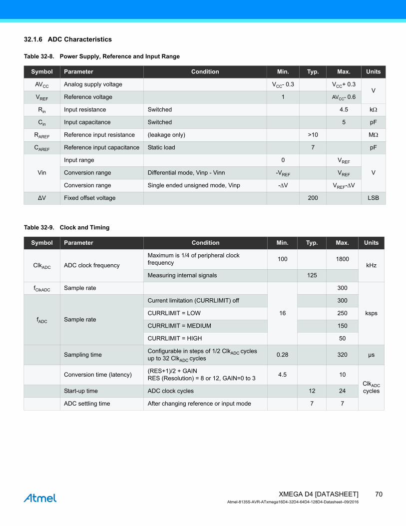
32.1.6 ADC Characteristics
Table 32-8. Power Supply, Reference and Input Range
Table 32-9. Clock and Timing
Symbol Parameter Condition Min. Typ. Max. Units
AVCC Analog supply voltage VCC- 0.3 VCC+ 0.3V
VREF Reference voltage 1 AVCC- 0.6
Rin Input resistance Switched 4.5 k
Cin Input capacitance Switched 5 pF
RAREF Reference input resistance (leakage only) >10 M
CAREF Reference input capacitance Static load 7 pF
Vin
Input range 0 VREF
VConversion range Differential mode, Vinp - Vinn -VREF VREF
Conversion range Single ended unsigned mode, Vinp -V VREF-V
∆V Fixed offset voltage 200 LSB
Symbol Parameter Condition Min. Typ. Max. Units
ClkADC ADC clock frequency
Maximum is 1/4 of peripheral clock frequency
100 1800kHz
Measuring internal signals 125
fClkADC Sample rate
16
300
kspsfADC Sample rate
Current limitation (CURRLIMIT) off 300
CURRLIMIT = LOW 250
CURRLIMIT = MEDIUM 150
CURRLIMIT = HIGH 50
Sampling timeConfigurable in steps of 1/2 ClkADC cyclesup to 32 ClkADC cycles
0.28 320 µs
Conversion time (latency)(RES+1)/2 + GAINRES (Resolution) = 8 or 12, GAIN=0 to 3
4.5 10
ClkADCcyclesStart-up time ADC clock cycles 12 24
ADC settling time After changing reference or input mode 7 7
70XMEGA D4 [DATASHEET]Atmel-8135S-AVR-ATxmega16D4-32D4-64D4-128D4-Datasheet–09/2016
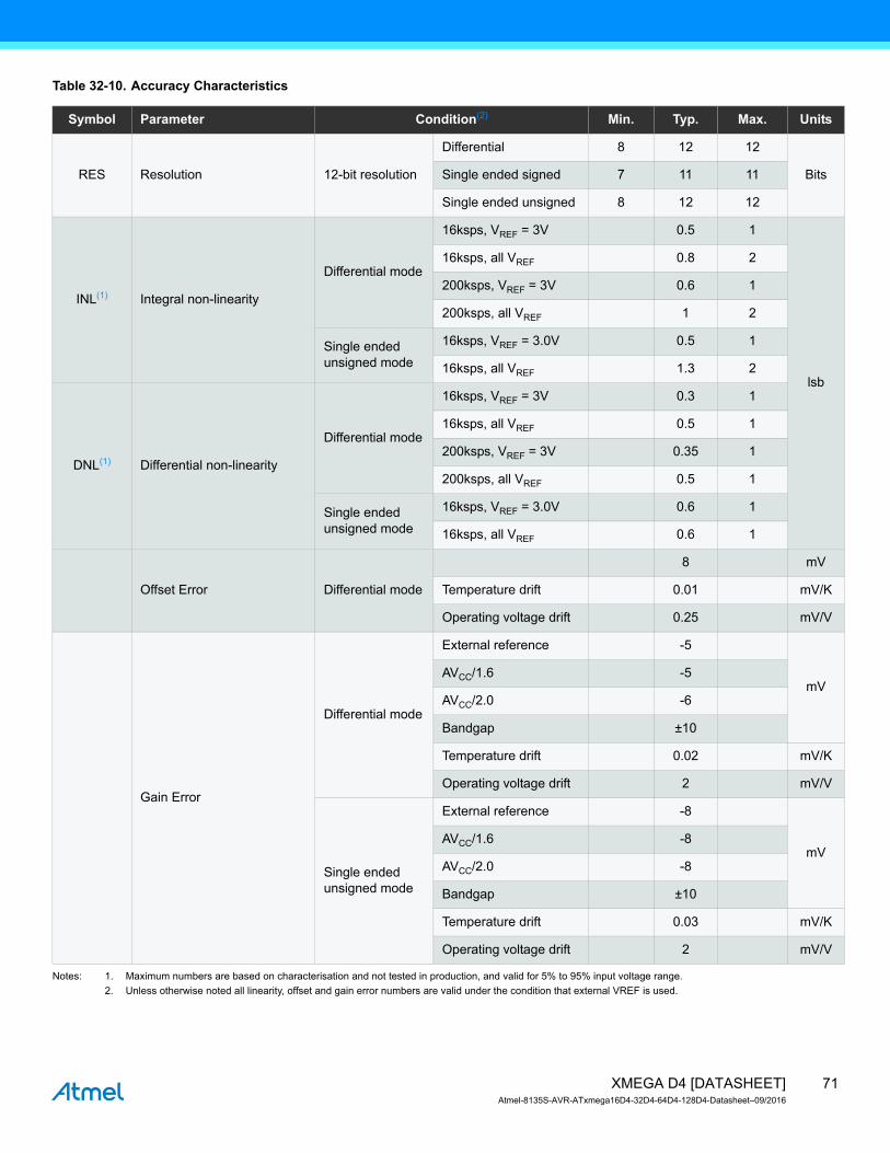
Table 32-10. Accuracy Characteristics
Notes: 1. Maximum numbers are based on characterisation and not tested in production, and valid for 5% to 95% input voltage range.
2. Unless otherwise noted all linearity, offset and gain error numbers are valid under the condition that external VREF is used.
Symbol Parameter Condition(2) Min. Typ. Max. Units
RES Resolution 12-bit resolution
Differential 8 12 12
BitsSingle ended signed 7 11 11
Single ended unsigned 8 12 12
INL(1) Integral non-linearity
Differential mode
16ksps, VREF = 3V 0.5 1
lsb
16ksps, all VREF 0.8 2
200ksps, VREF = 3V 0.6 1
200ksps, all VREF 1 2
Single endedunsigned mode
16ksps, VREF = 3.0V 0.5 1
16ksps, all VREF 1.3 2
DNL(1) Differential non-linearity
Differential mode
16ksps, VREF = 3V 0.3 1
16ksps, all VREF 0.5 1
200ksps, VREF = 3V 0.35 1
200ksps, all VREF 0.5 1
Single endedunsigned mode
16ksps, VREF = 3.0V 0.6 1
16ksps, all VREF 0.6 1
Offset Error Differential mode
8 mV
Temperature drift 0.01 mV/K
Operating voltage drift 0.25 mV/V
Gain Error
Differential mode
External reference -5
mVAVCC/1.6 -5
AVCC/2.0 -6
Bandgap ±10
Temperature drift 0.02 mV/K
Operating voltage drift 2 mV/V
Single endedunsigned mode
External reference -8
mVAVCC/1.6 -8
AVCC/2.0 -8
Bandgap ±10
Temperature drift 0.03 mV/K
Operating voltage drift 2 mV/V
71XMEGA D4 [DATASHEET]Atmel-8135S-AVR-ATxmega16D4-32D4-64D4-128D4-Datasheet–09/2016

Table 32-11. Gain Stage Characteristics
32.1.7 Analog Comparator Characteristics
Table 32-12. Analog Comparator Characteristics
Rin Input resistance Switched in normal mode 4.0 k
Csample Input capacitance Switched in normal mode 4.4 pF
Signal range Gain stage output 0 AVCC- 0.6 V
Propagation delay ADC conversion rate 1/2 1 3ClkADCcycles
Clock frequency Same as ADC 100 1800 kHz
Gain Error
0.5x gain, normal mode -1
%1x gain, normal mode -1
8x gain, normal mode -1
64x gain, normal mode 10
Offset Error,output referred
0.5x gain, normal mode 10
mV1x gain, normal mode 5
8x gain, normal mode -20
64x gain, normal mode -150
Symbol Parameter Condition Min. Typ. Max. Units
Voff Input offset voltage VCC=1.6V - 3.6V <±10 mV
Ilk Input leakage current VCC=1.6V - 3.6V <1 nA
Input voltage range -0.1 AVCC V
AC startup time 100 µs
Vhys1 Hysteresis, none VCC=1.6V - 3.6V 0
mVVhys2 Hysteresis, small VCC=1.6V - 3.6V 11
Vhys3 Hysteresis, large VCC=1.6V - 3.6V 26
tdelay Propagation delayVCC = 3.0V, T= 85°C 16 90
nsVCC=1.6V - 3.6V 16
64-level voltage scaler Integral non-linearity (INL) 0.3 0.5 lsb
72XMEGA D4 [DATASHEET]Atmel-8135S-AVR-ATxmega16D4-32D4-64D4-128D4-Datasheet–09/2016

32.1.8 Bandgap and Internal 1.0V Reference Characteristics
Table 32-13. Bandgap and Internal 1.0V Reference Characteristics
32.1.9 Brownout Detection Characteristics
Table 32-14. Brownout Detection Characteristics(1)
Note: 1. BOD is calibrated at 85°C within BOD level 0 values, and BOD level 0 is the default level.
32.1.10 External Reset Characteristics
Table 32-15. External Reset Characteristics
Symbol Parameter Condition Min. Typ. Max. Units
Startup timeAs reference for ADC 1 ClkPER + 2.5µs
µsAs input voltage to ADC and AC 1.5
Bandgap voltage 1.1V
INT1V Internal 1.00V reference T= 85°C, after calibration 0.98 1 1.02
Variation over voltage and temperature Calibrated at T= 85°C, VCC = 3.0V ±1.0 %
Symbol Parameter Condition Min. Typ. Max. Units
VBOT
BOD level 0 falling VCC 1.50 1.62 1.75
V
BOD level 1 falling VCC 1.8
BOD level 2 falling VCC 2.0
BOD level 3 falling VCC 2.2
BOD level 4 falling VCC 2.4
BOD level 5 falling VCC 2.6
BOD level 6 falling VCC 2.8
BOD level 7 falling VCC 3.0
tBOD Detection timeContinuous mode 0.4
µsSampled mode 1000
VHYST Hysteresis 1.2 %
Symbol Parameter Condition Min. Typ. Max. Units
tEXT Minimum reset pulse width 1000 90 ns
VRST
Reset threshold voltage (VIH)VCC = 2.7 - 3.6V 0.6*VCC
VVCC = 1.6 - 2.7V 0.6*VCC
Reset threshold voltage (VIL)VCC = 2.7 - 3.6V 0.5*VCC
VCC = 1.6 - 2.7V 0.4*VCC
RRST Reset pin pull-up resistor 25 k
73XMEGA D4 [DATASHEET]Atmel-8135S-AVR-ATxmega16D4-32D4-64D4-128D4-Datasheet–09/2016
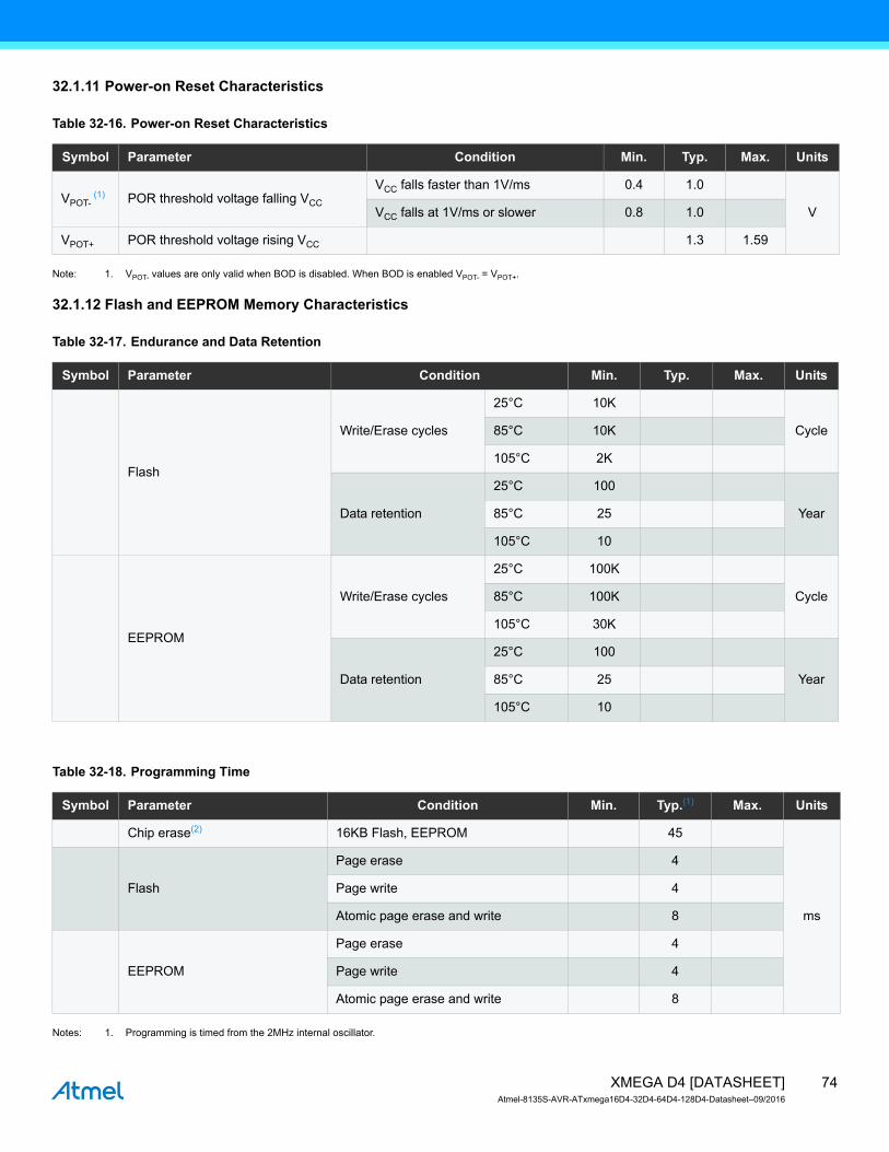
32.1.11 Power-on Reset Characteristics
Table 32-16. Power-on Reset Characteristics
Note: 1. VPOT- values are only valid when BOD is disabled. When BOD is enabled VPOT- = VPOT+.
32.1.12 Flash and EEPROM Memory Characteristics
Table 32-17. Endurance and Data Retention
Table 32-18. Programming Time
Notes: 1. Programming is timed from the 2MHz internal oscillator.
Symbol Parameter Condition Min. Typ. Max. Units
VPOT- (1) POR threshold voltage falling VCC
VCC falls faster than 1V/ms 0.4 1.0
VVCC falls at 1V/ms or slower 0.8 1.0
VPOT+ POR threshold voltage rising VCC 1.3 1.59
Symbol Parameter Condition Min. Typ. Max. Units
Flash
Write/Erase cycles
25°C 10K
Cycle85°C 10K
105°C 2K
Data retention
25°C 100
Year85°C 25
105°C 10
EEPROM
Write/Erase cycles
25°C 100K
Cycle85°C 100K
105°C 30K
Data retention
25°C 100
Year85°C 25
105°C 10
Symbol Parameter Condition Min. Typ.(1) Max. Units
Chip erase(2) 16KB Flash, EEPROM 45
ms
Flash
Page erase 4
Page write 4
Atomic page erase and write 8
EEPROM
Page erase 4
Page write 4
Atomic page erase and write 8
74XMEGA D4 [DATASHEET]Atmel-8135S-AVR-ATxmega16D4-32D4-64D4-128D4-Datasheet–09/2016
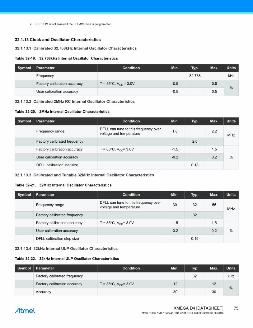
2. EEPROM is not erased if the EESAVE fuse is programmed.
32.1.13 Clock and Oscillator Characteristics
32.1.13.1 Calibrated 32.768kHz Internal Oscillator Characteristics
Table 32-19. 32.768kHz Internal Oscillator Characteristics
32.1.13.2 Calibrated 2MHz RC Internal Oscillator Characteristics
Table 32-20. 2MHz Internal Oscillator Characteristics
32.1.13.3 Calibrated and Tunable 32MHz Internal Oscillator Characteristics
Table 32-21. 32MHz Internal Oscillator Characteristics
32.1.13.4 32kHz Internal ULP Oscillator Characteristics
Table 32-22. 32kHz Internal ULP Oscillator Characteristics
Symbol Parameter Condition Min. Typ. Max. Units
Frequency 32.768 kHz
Factory calibration accuracy T = 85C, VCC = 3.0V -0.5 0.5%
User calibration accuracy -0.5 0.5
Symbol Parameter Condition Min. Typ. Max. Units
Frequency rangeDFLL can tune to this frequency over voltage and temperature
1.8 2.2MHz
Factory calibrated frequency 2.0
Factory calibration accuracy T = 85C, VCC= 3.0V -1.5 1.5
%User calibration accuracy -0.2 0.2
DFLL calibration stepsize 0.18
Symbol Parameter Condition Min. Typ. Max. Units
Frequency rangeDFLL can tune to this frequency over voltage and temperature
30 32 55MHz
Factory calibrated frequency 32
Factory calibration accuracy T = 85C, VCC= 3.0V -1.5 1.5
%User calibration accuracy -0.2 0.2
DFLL calibration step size 0.19
Symbol Parameter Condition Min. Typ. Max. Units
Factory calibrated frequency 32 kHz
Factory calibration accuracy T = 85C, VCC= 3.0V -12 12%
Accuracy -30 30
75XMEGA D4 [DATASHEET]Atmel-8135S-AVR-ATxmega16D4-32D4-64D4-128D4-Datasheet–09/2016

32.1.13.5 Internal Phase Locked Loop (PLL) Characteristics
Table 32-23. Internal PLL Characteristics.
Note: 1. The maximum output frequency vs. supply voltage is linear between 1.8V and 2.7V, and can never be higher than four times the maximum CPU frequency.
32.1.13.6 External Clock Characteristics
Figure 32-3. External Clock Drive Waveform
Table 32-24. External Clock(1)
Notes: 1. System Clock Prescalers must be set so that maximum CPU clock frequency for device is not exceeded.
2. The maximum frequency vs. supply voltage is linear between 1.8V and 2.7V, and the same applies for all other parameters with supply voltage conditions.
Symbol Parameter Condition Min. Typ. Max. Units
fIN Input frequency Output frequency must be within fOUT 0.4 64
MHzfOUT Output frequency (1)
VCC= 1.6 - 1.8V 20 48
VCC= 2.7 - 3.6V 20 128
Start-up time 25µs
Re-lock time 25
Symbol Parameter Condition Min. Typ. Max. Units
1/tCK Clock frequency(2)VCC = 1.6 - 1.8V 0 90
MHzVCC = 2.7 - 3.6V 0 142
tCK Clock periodVCC = 1.6 - 1.8V 11
nsVCC = 2.7 - 3.6V 7.0
tCH/CL Clock high/low timeVCC = 1.6 - 1.8V 4.5
VCC = 2.7 - 3.6V 2.4
VIL/IH Low/high level input voltage See Table 32-7 on page 69 V
tCKReduction in period time from oneclock cycle to the next
10 %
tCH
tCL
tCK
tCH
VIL1
VIH1
tCR tCF
76XMEGA D4 [DATASHEET]Atmel-8135S-AVR-ATxmega16D4-32D4-64D4-128D4-Datasheet–09/2016

32.1.13.7 External 16MHz Crystal Oscillator and XOSC Characteristics
Table 32-25. .External 16MHz Crystal Oscillator and XOSC Characteristics
Symbol Parameter Condition Min. Typ. Max. Units
Cycle to cycle jitterXOSCPWR=0
FRQRANGE=0 0
ns
FRQRANGE=1, 2, or 3 0
XOSCPWR=1 0
Long term jitterXOSCPWR=0
FRQRANGE=0 0
FRQRANGE=1, 2, or 3 0
XOSCPWR=1 0
Frequency errorXOSCPWR=0
FRQRANGE=0 0.03
%
FRQRANGE=1 0.03
FRQRANGE=2 or 3 0.03
XOSCPWR=1 0.003
Duty cycleXOSCPWR=0
FRQRANGE=0 50
FRQRANGE=1 50
FRQRANGE=2 or 3 50
XOSCPWR=1 50
RQ Negative impedance
XOSCPWR=0,FRQRANGE=0
0.4MHz resonator, CL=100pF
44k
1MHz crystal, CL=20pF 67k
2MHz crystal, CL=20pF 67k
XOSCPWR=0,FRQRANGE=1,CL=20pF
2MHz crystal 82k
8MHz crystal 1500
9MHz crystal 1500
XOSCPWR=0,FRQRANGE=2,CL=20pF
8MHz crystal 2700
9MHz crystal 2700
12MHz crystal 1000
XOSCPWR=0,FRQRANGE=3,CL=20pF
9MHz crystal 3600
12MHz crystal 1300
16MHz crystal 590
XOSCPWR=1,FRQRANGE=0,CL=20pF
9MHz crystal 390
12MHz crystal 50
16MHz crystal 10
77XMEGA D4 [DATASHEET]Atmel-8135S-AVR-ATxmega16D4-32D4-64D4-128D4-Datasheet–09/2016

32.1.13.8 External 32.768kHz Crystal Oscillator and TOSC Characteristics
Table 32-26. External 32.768kHz Crystal Oscillator and TOSC Characteristics
Note: See Figure 32-4 for definition.
RQ Negative impedance
XOSCPWR=1,FRQRANGE=1,CL=20pF
9MHz crystal 1500
12MHz crystal 650
16MHz crystal 270
XOSCPWR=1,FRQRANGE=2,CL=20pF
12MHz crystal 1000
16MHz crystal 440
XOSCPWR=1,FRQRANGE=3,CL=20pF
12MHz crystal 1300
16MHz crystal 590
ESR SF = safety factor min(RQ)/SF k
Start-up time
XOSCPWR=0,FRQRANGE=0
0.4MHz resonator, CL=100pF
1.0
ms
XOSCPWR=0,FRQRANGE=1
2MHz crystal, CL=20pF 2.6
XOSCPWR=0,FRQRANGE=2
8MHz crystal, CL=20pF 0.8
XOSCPWR=0,FRQRANGE=3
12MHz crystal, CL=20pF 1.0
XOSCPWR=1,FRQRANGE=3
16MHz crystal, CL=20pF 1.4
CXTAL1Parasitic capacitanceXTAL1 pin
5.9
pFCXTAL2
Parasitic capacitanceXTAL2 pin
8.3
CLOAD Parasitic capacitance load 3.5
Symbol Parameter Condition Min. Typ. Max. Units
Symbol Parameter Condition Min. Typ. Max. Units
ESR/R1Recommended crystal equivalentseries resistance (ESR)
Crystal load capacitance 6.5pF 60k
Crystal load capacitance 9.0pF 35
Crystal load capacitance 12pF 28
CTOSC1 Parasitic capacitance TOSC1 pin 3.5pF
CTOSC2 Parasitic capacitance TOSC2 pin 3.5
Recommended safety factorcapacitance load matched to crystal specification
3
78XMEGA D4 [DATASHEET]Atmel-8135S-AVR-ATxmega16D4-32D4-64D4-128D4-Datasheet–09/2016

Figure 32-4. TOSC Input Capacitance
The parasitic capacitance between the TOSC pins is CL1 + CL2 in series as seen from the crystal when oscillating without external capacitors.
32.1.14 SPI Characteristics
Figure 32-5. SPI Timing Requirements in Master Mode
CL1 CL2
2CSOT1CSOT Device internal
External
32.768KHz crystal
MSB LSB
BSLBSM
tMOS
tMIS tMIH
tSCKW
tSCK
tMOH tMOH
tSCKFtSCKR
tSCKW
MOSI
(Data Output)
MISO
(Data Input)
SCK
(CPOL = 1)
SCK
(CPOL = 0)
SS
79XMEGA D4 [DATASHEET]Atmel-8135S-AVR-ATxmega16D4-32D4-64D4-128D4-Datasheet–09/2016

Figure 32-6. SPI Timing Requirements in Slave Mode
MSB LSB
BSLBSM
tSIS tSIH
tSSCKW
tSSCKW
tSSCK
tSSH
tSOSSH
tSCKR tSCKF
tSOS
tSSS
tSOSSS
MISO(Data Output)
MOSI(Data Input)
SCK
(CPOL = 1)
SCK
(CPOL = 0)
SS
80XMEGA D4 [DATASHEET]Atmel-8135S-AVR-ATxmega16D4-32D4-64D4-128D4-Datasheet–09/2016
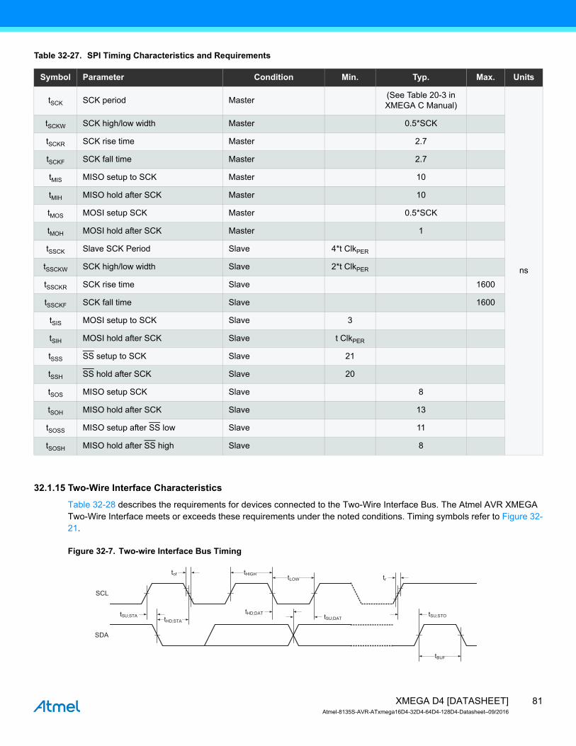
Table 32-27. SPI Timing Characteristics and Requirements
32.1.15 Two-Wire Interface Characteristics
Table 32-28 describes the requirements for devices connected to the Two-Wire Interface Bus. The Atmel AVR XMEGA Two-Wire Interface meets or exceeds these requirements under the noted conditions. Timing symbols refer to Figure 32-21.
Figure 32-7. Two-wire Interface Bus Timing
Symbol Parameter Condition Min. Typ. Max. Units
tSCK SCK period Master(See Table 20-3 in XMEGA C Manual)
ns
tSCKW SCK high/low width Master 0.5*SCK
tSCKR SCK rise time Master 2.7
tSCKF SCK fall time Master 2.7
tMIS MISO setup to SCK Master 10
tMIH MISO hold after SCK Master 10
tMOS MOSI setup SCK Master 0.5*SCK
tMOH MOSI hold after SCK Master 1
tSSCK Slave SCK Period Slave 4*t ClkPER
tSSCKW SCK high/low width Slave 2*t ClkPER
tSSCKR SCK rise time Slave 1600
tSSCKF SCK fall time Slave 1600
tSIS MOSI setup to SCK Slave 3
tSIH MOSI hold after SCK Slave t ClkPER
tSSS SS setup to SCK Slave 21
tSSH SS hold after SCK Slave 20
tSOS MISO setup SCK Slave 8
tSOH MISO hold after SCK Slave 13
tSOSS MISO setup after SS low Slave 11
tSOSH MISO hold after SS high Slave 8
tHD;STA
tof
SDA
SCL
tLOW
tHIGH
tSU;STA
tBUF
tr
tHD;DATtSU;DAT
tSU;STO
81XMEGA D4 [DATASHEET]Atmel-8135S-AVR-ATxmega16D4-32D4-64D4-128D4-Datasheet–09/2016

Table 32-28. Two-wire Interface Characteristics
Notes: 1. Required only for fSCL > 100kHz.
2. Cb = Capacitance of one bus line in pF.
3. fPER = Peripheral clock frequency.
Symbol Parameter Condition Min. Typ. Max. Units
VIH Input high voltage 0.7VCC VCC+0.5
VVIL Input low voltage -0.5 0.3VCC
Vhys Hysteresis of Schmitt trigger inputs 0.05VCC (1)
VOL Output low voltage 3mA, sink current 0 0.4
tr Rise time for both SDA and SCL 20+0.1Cb (1)(2) 300
nstof Output fall time from VIHmin to VILmax 10pF < Cb < 400pF (2) 20+0.1Cb (1)(2) 250
tSP Spikes suppressed by input filter 0 50
II Input current for each I/O Pin 0.1VCC < VI < 0.9VCC -10 10 µA
CI Capacitance for each I/O Pin 10 pF
fSCL SCL clock frequency fPER (3)>max(10fSCL, 250kHz) 0 400 kHz
RP Value of pull-up resistor
fSCL 100kHz
fSCL > 100kHz
tHD;STA Hold time (repeated) START conditionfSCL 100kHz 4.0
µs
fSCL > 100kHz 0.6
tLOW Low period of SCL clockfSCL 100kHz 4.7
fSCL > 100kHz 1.3
tHIGH High period of SCL clockfSCL 100kHz 4.0
fSCL > 100kHz 0.6
tSU;STASet-up time for a repeated START condition
fSCL 100kHz 4.7
fSCL > 100kHz 0.6
tHD;DAT Data hold timefSCL 100kHz 0 3.45
µsfSCL > 100kHz 0 0.9
tSU;DAT Data setup timefSCL 100kHz 250
nsfSCL > 100kHz 100
tSU;STO Setup time for STOP conditionfSCL 100kHz 4.0
µsfSCL > 100kHz 0.6
tBUFBus free time between a STOP and START condition
fSCL 100kHz 4.7µs
fSCL > 100kHz 1.3
VCC 0.4V–
3mA----------------------------
100nsCb---------------
300nsCb---------------
82XMEGA D4 [DATASHEET]Atmel-8135S-AVR-ATxmega16D4-32D4-64D4-128D4-Datasheet–09/2016

32.2 ATxmega32D4
32.2.1 Absolute Maximum Ratings
Stresses beyond those listed in Table 32-29 under may cause permanent damage to the device. This is a stress rating only and functional operation of the device at these or other conditions beyond those indicated in the operational sections of this specification is not implied. Exposure to absolute maximum rating conditions for extended periods may affect device reliability.
Table 32-29. Absolute Maximum Ratings
32.2.2 General Operating Ratings
The device must operate within the ratings listed in Table 32-30 in order for all other electrical characteristics and typical characteristics of the device to be valid.
Table 32-30. General Operating Conditions
Table 32-31. Operating Voltage and Frequency
The maximum CPU clock frequency depends on VCC. As shown in Figure 32-8 the Frequency vs. VCC curve is linear between 1.8V < VCC < 2.7V.
Symbol Parameter Condition Min. Typ. Max. Units
VCC Power supply voltage -0.3 4 V
IVCC Current into a VCC pin 200mA
IGND Current out of a Gnd pin 200
VPINPin voltage with respect to Gnd and VCC
-0.5 VCC+0.5 V
IPIN I/O pin sink/source current -25 25 mA
TA Storage temperature -65 150°C
Tj Junction temperature 150
Symbol Parameter Condition Min. Typ. Max. Units
VCC Power supply voltage 1.60 3.6V
AVCC Analog supply voltage 1.60 3.6
TA Temperature range -40 85°C
Tj Junction temperature -40 105
Symbol Parameter Condition Min. Typ. Max. Units
ClkCPU CPU clock frequency
VCC = 1.6V 0 12
MHzVCC = 1.8V 0 12
VCC = 2.7V 0 32
VCC = 3.6V 0 32
83XMEGA D4 [DATASHEET]Atmel-8135S-AVR-ATxmega16D4-32D4-64D4-128D4-Datasheet–09/2016
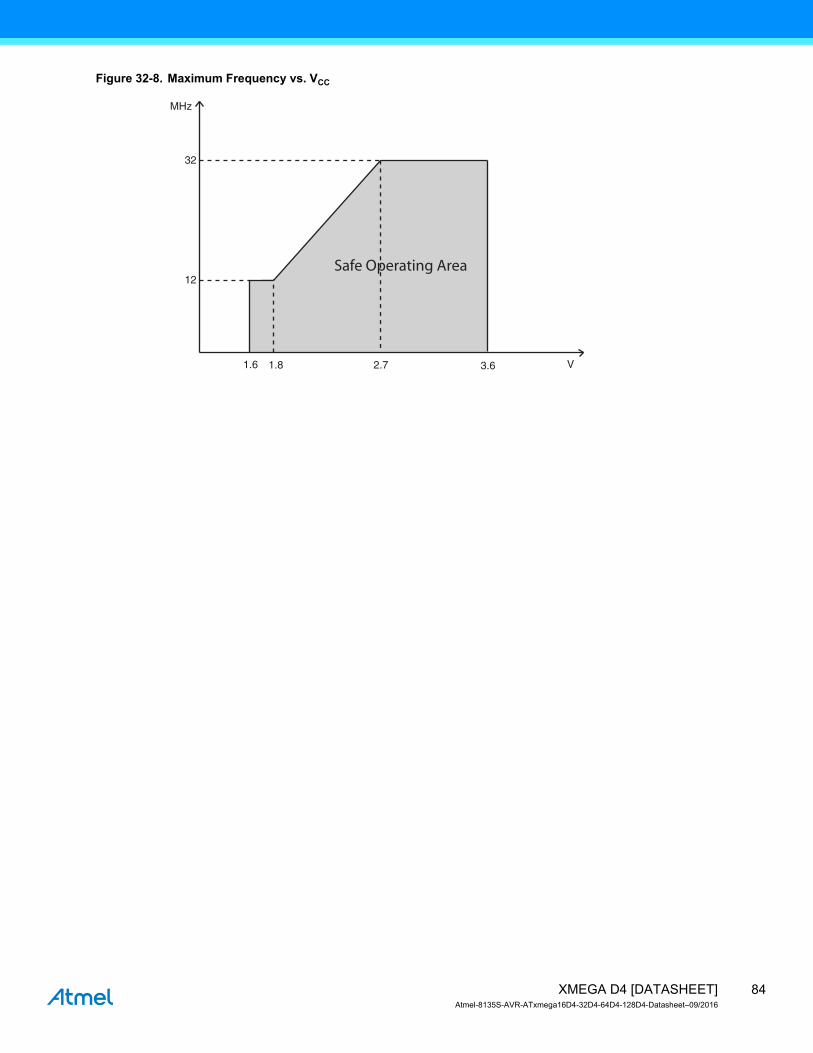
Figure 32-8. Maximum Frequency vs. VCC
1.8
12
32
MHz
V2.7 3.61.6
Safe Operating Area
84XMEGA D4 [DATASHEET]Atmel-8135S-AVR-ATxmega16D4-32D4-64D4-128D4-Datasheet–09/2016

32.2.3 Current Consumption
Table 32-32. Current Consumption for Active Mode and Sleep Modes
Notes: 1. All Power Reduction Registers set.
2. Maximum limits are based on characterization, and not tested in production.
Symbol Parameter Condition Min. Typ. Max. Units
ICC
Active powerconsumption(1)
32kHz, Ext. ClkVCC = 1.8V 40
µA
VCC = 3.0V 80
1MHz, Ext. ClkVCC = 1.8V 200
VCC = 3.0V 410
2MHz, Ext. ClkVCC = 1.8V 350 600
VCC = 3.0V0.75 1.4
mA32MHz, Ext. Clk 7.5 12
Idle powerconsumption(1)
32kHz, Ext. ClkVCC = 1.8V 2.0
µA
VCC = 3.0V 2.8
1MHz, Ext. ClkVCC = 1.8V 42
VCC = 3.0V 85
2MHz, Ext. ClkVCC = 1.8V 85 225
VCC = 3.0V170 350
32MHz, Ext. Clk 2.7 5.5 mA
Power-down powerconsumption
T = 25°C
VCC = 3.0V
0.1 1.0
µA
T = 85°C 2.0 4.5
T = 105°C 0.1 7.0
WDT and sampled BOD enabled,T = 25°C
VCC = 3.0V
1.4 3.0
WDT and sampled BOD enabled,T = 85°C
3.0 6.0
WDT and sampled BOD enabled,T = 105°C
1.4 10
Power-save powerconsumption(2)
RTC from ULP clock, WDT andsampled BOD enabled, T = 25°C
VCC = 1.8V 1.5
VCC = 3.0V 1.5
RTC from 1.024kHz low power32.768kHz TOSC, T = 25°C
VCC = 1.8V 0.6 2.0
VCC = 3.0V 0.7 2.0
RTC from low power 32.768kHzTOSC, T = 25°C
VCC = 1.8V 0.8 3.0
VCC = 3.0V 1.0 3.0
Reset power consumptionCurrent through RESET pinsubstracted
VCC = 3.0V 300
85XMEGA D4 [DATASHEET]Atmel-8135S-AVR-ATxmega16D4-32D4-64D4-128D4-Datasheet–09/2016

Table 32-33. Current Consumption for Modules and Peripherals
Note: 1. All parameters measured as the difference in current consumption between module enabled and disabled. All data at VCC = 3.0V, ClkSYS = 1MHz external clock without prescaling, T = 25°C unless other conditions are given.
Symbol Parameter Condition(1) Min. Typ. Max. Units
ICC
ULP oscillator 0.8
µA
32.768kHz int. oscillator 29
2MHz int. oscillator85
DFLL enabled with 32.768kHz int. osc. as reference 115
32MHz int. oscillator245
DFLL enabled with 32.768kHz int. osc. as reference 410
PLL20x multiplication factor,32MHz int. osc. DIV4 as reference
290
Watchdog timer 1.0
BODContinuous mode 138
Sampled mode, includes ULP oscillator 1.2
Internal 1.0V reference 175
Temperature sensor 170
ADC
16kspsVREF = Ext ref
1.2
mA
CURRLIMIT = LOW 1.0
CURRLIMIT = MEDIUM 0.9
CURRLIMIT = HIGH 0.8
75kspsVREF = Ext ref
CURRLIMIT = LOW 1.7
200kspsVREF = Ext ref
3.1
USART Rx and Tx enabled, 9600 BAUD 11 µA
Flash memory and EEPROM programming 4 mA
86XMEGA D4 [DATASHEET]Atmel-8135S-AVR-ATxmega16D4-32D4-64D4-128D4-Datasheet–09/2016

32.2.4 Wake-up Time from Sleep Modes
Table 32-34. Device Wake-up Time from Sleep Modes with Various System Clock Sources
Note: 1. The wake-up time is the time from the wake-up request is given until the peripheral clock is available on pin, see Figure 32-9. All peripherals and modules start execution from the first clock cycle, expect the CPU that is halted for four clock cycles before program execution starts.
Figure 32-9. Wake-up Time Definition
Symbol Parameter Condition Min. Typ. (1) Max. Units
twakeup
Wake-up time from idle,standby, and extended standbymode
External 2MHz clock 2.0
µs
32.768kHz internal oscillator 120
2MHz internal oscillator 2.0
32MHz internal oscillator 0.2
Wake-up time from power-saveand power-down mode
External 2MHz clock 5.0
32.768kHz internal oscillator 320
2MHz internal oscillator 9.0
32MHz internal oscillator 5.0
Wakeup request
Clock output
Wakeup time
87XMEGA D4 [DATASHEET]Atmel-8135S-AVR-ATxmega16D4-32D4-64D4-128D4-Datasheet–09/2016

32.2.5 I/O Pin Characteristics
The I/O pins complies with the JEDEC LVTTL and LVCMOS specification and the high- and low level input and output voltage limits reflect or exceed this specification.
Table 32-35. I/O Pin Characteristics
Notes: 1. The sum of all IOH for PORTA and PORTB must not exceed 100mA.The sum of all IOH for PORTC, PORTD, PORTE must for each port not exceed 200mA.The sum of all IOH for pins PF[0-5] on PORTF must not exceed 200mA.The sum of all IOL for pins PF[6-7] on PORTF, PORTR and PDI must not exceed 100mA.
2. The sum of all IOL for PORTA and PORTB must not exceed 100mA.The sum of all IOL for PORTC, PORTD, PORTE must for each port not exceed 200mA.The sum of all IOL for pins PF[0-5] on PORTF must not exceed 200mA.The sum of all IOL for pins PF[6-7] on PORTF, PORTR and PDI must not exceed 100mA.
Symbol Parameter Condition Min. Typ. Max. Units
IOH (1)/
IOL (2) I/O pin source/sink current -20 20 mA
VIH High level input voltageVCC = 2.4 - 3.6V 0.7*Vcc VCC+0.5
V
VCC = 1.6 - 2.4V 0.8*VCC VCC+0.5
VIL Low level input voltageVCC = 2.4- 3.6V -0.5 0.3*VCC
VCC = 1.6 - 2.4V -0.5 0.2*VCC
VOH High level output voltage
VCC = 3.3V IOH = -4mA 2.6 2.9
VCC = 3.0V IOH = -3mA 2.1 2.7
VCC = 1.8V IOH = -1mA 1.4 1.6
VOL Low level output voltage
VCC = 3.3V IOL = 8mA 0.4 0.76
VCC = 3.0V IOL = 5mA 0.3 0.64
VCC = 1.8V IOL = 3mA 0.2 0.46
IIN Input leakage current I/O pin T = 25°C <0.01 1 µA
RP Pull/buss keeper resistor 25 k
88XMEGA D4 [DATASHEET]Atmel-8135S-AVR-ATxmega16D4-32D4-64D4-128D4-Datasheet–09/2016
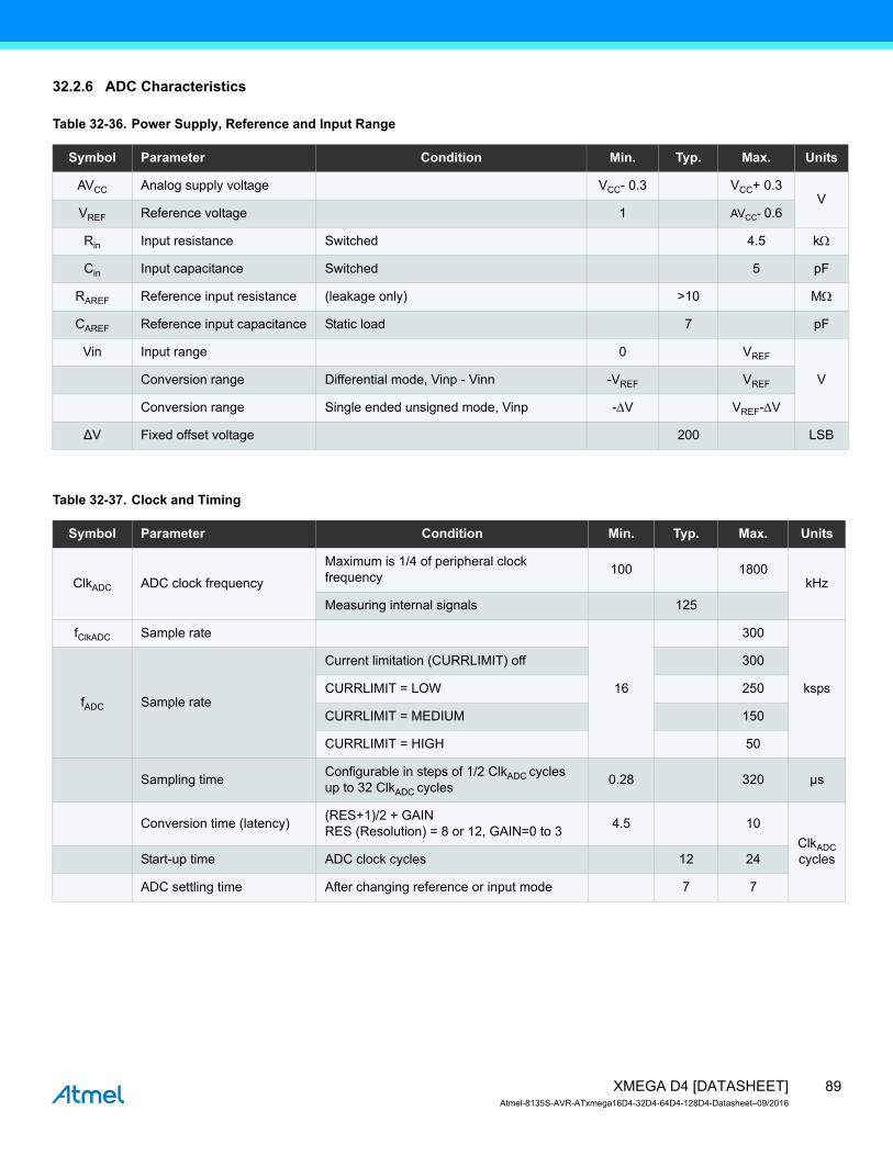
32.2.6 ADC Characteristics
Table 32-36. Power Supply, Reference and Input Range
Table 32-37. Clock and Timing
Symbol Parameter Condition Min. Typ. Max. Units
AVCC Analog supply voltage VCC- 0.3 VCC+ 0.3V
VREF Reference voltage 1 AVCC- 0.6
Rin Input resistance Switched 4.5 k
Cin Input capacitance Switched 5 pF
RAREF Reference input resistance (leakage only) >10 M
CAREF Reference input capacitance Static load 7 pF
Vin Input range 0 VREF
VConversion range Differential mode, Vinp - Vinn -VREF VREF
Conversion range Single ended unsigned mode, Vinp -V VREF-V
∆V Fixed offset voltage 200 LSB
Symbol Parameter Condition Min. Typ. Max. Units
ClkADC ADC clock frequency
Maximum is 1/4 of peripheral clock frequency
100 1800kHz
Measuring internal signals 125
fClkADC Sample rate
16
300
kspsfADC Sample rate
Current limitation (CURRLIMIT) off 300
CURRLIMIT = LOW 250
CURRLIMIT = MEDIUM 150
CURRLIMIT = HIGH 50
Sampling timeConfigurable in steps of 1/2 ClkADC cycles up to 32 ClkADC cycles
0.28 320 µs
Conversion time (latency)(RES+1)/2 + GAINRES (Resolution) = 8 or 12, GAIN=0 to 3
4.5 10
ClkADCcyclesStart-up time ADC clock cycles 12 24
ADC settling time After changing reference or input mode 7 7
89XMEGA D4 [DATASHEET]Atmel-8135S-AVR-ATxmega16D4-32D4-64D4-128D4-Datasheet–09/2016

Table 32-38. Accuracy Characteristics
Notes: 1. Maximum numbers are based on characterisation and not tested in production, and valid for 5% to 95% input voltage range.
2. Unless otherwise noted all linearity, offset and gain error numbers are valid under the condition that external VREF is used.
Symbol Parameter Condition(2) Min. Typ. Max. Units
RES Resolution 12-bit resolution
Differential 8 12 12
BitsSingle ended signed 7 11 11
Single ended unsigned 8 12 12
INL(1) Integral non-linearity
Differential mode
16ksps, VREF = 3V 0.5 1
lsb
16ksps, all VREF 0.8 2
200ksps, VREF = 3V 0.6 1
200ksps, all VREF 1 2
Single endedunsigned mode
16ksps, VREF = 3.0V 0.5 1
16ksps, all VREF 1.3 2
DNL(1) Differential non-linearity
Differential mode
16ksps, VREF = 3V 0.3 1
16ksps, all VREF 0.5 1
200ksps, VREF = 3V 0.35 1
200ksps, all VREF 0.5 1
Single endedunsigned mode
16ksps, VREF = 3.0V 0.6 1
16ksps, all VREF 0.6 1
Offset Error Differential mode
8 mV
Temperature drift 0.01 mV/K
Operating voltage drift 0.25 mV/V
Gain Error Differential mode
External reference -5
mVAVCC/1.6 -5
AVCC/2.0 -6
Bandgap ±10
Temperature drift 0.02 mV/K
Operating voltage drift 2 mV/V
Gain ErrorSingle endedunsigned mode
External reference -8
mVAVCC/1.6 -8
AVCC/2.0 -8
Bandgap ±10
Temperature drift 0.03 mV/K
Operating voltage drift 2 mV/V
90XMEGA D4 [DATASHEET]Atmel-8135S-AVR-ATxmega16D4-32D4-64D4-128D4-Datasheet–09/2016

Table 32-39. Gain Stage Characteristics
32.2.7 Analog Comparator Characteristics
Table 32-40. Analog Comparator Characteristics
Rin Input resistance Switched in normal mode 4.0 k
Csample Input capacitance Switched in normal mode 4.4 pF
Signal range Gain stage output 0 AVCC- 0.6 V
Propagation delay ADC conversion rate 1/2 1 3ClkADCcycles
Clock rate Same as ADC 100 1800 kHz
Gain error
0.5x gain, normal mode -1
%1x gain, normal mode -1
8x gain, normal mode -1
64x gain, normal mode 10
Offset error,output referred
0.5x gain, normal mode 10
mV1x gain, normal mode 5
8x gain, normal mode -20
64x gain, normal mode -150
Symbol Parameter Condition Min. Typ. Max. Units
Voff Input offset voltage VCC=1.6V - 3.6V <±10 mV
Ilk Input leakage current VCC=1.6V - 3.6V <1 nA
Input voltage range -0.1 AVCC V
AC startup time 100 µs
Vhys1 Hysteresis, none VCC=1.6V - 3.6V 0
mVVhys2 Hysteresis, small VCC=1.6V - 3.6V 11
Vhys3 Hysteresis, large VCC=1.6V - 3.6V 26
tdelay Propagation delayVCC = 3.0V, T= 85°C 16 90
nsVCC=1.6V - 3.6V 16
64-level voltage scaler Integral non-linearity (INL) 0.3 0.5 lsb
91XMEGA D4 [DATASHEET]Atmel-8135S-AVR-ATxmega16D4-32D4-64D4-128D4-Datasheet–09/2016
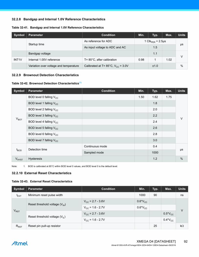
32.2.8 Bandgap and Internal 1.0V Reference Characteristics
Table 32-41. Bandgap and Internal 1.0V Reference Characteristics
32.2.9 Brownout Detection Characteristics
Table 32-42. Brownout Detection Characteristics(1)
Note: 1. BOD is calibrated at 85°C within BOD level 0 values, and BOD level 0 is the default level.
32.2.10 External Reset Characteristics
Table 32-43. External Reset Characteristics
Symbol Parameter Condition Min. Typ. Max. Units
Startup timeAs reference for ADC 1 ClkPER + 2.5µs
µsAs input voltage to ADC and AC 1.5
Bandgap voltage 1.1V
INT1V Internal 1.00V reference T= 85°C, after calibration 0.98 1 1.02
Variation over voltage and temperature Calibrated at T= 85°C, VCC = 3.0V ±1.0 %
Symbol Parameter Condition Min. Typ. Max. Units
VBOT
BOD level 0 falling VCC 1.50 1.62 1.75
V
BOD level 1 falling VCC 1.8
BOD level 2 falling VCC 2.0
BOD level 3 falling VCC 2.2
BOD level 4 falling VCC 2.4
BOD level 5 falling VCC 2.6
BOD level 6 falling VCC 2.8
BOD level 7 falling VCC 3.0
tBOD Detection timeContinuous mode 0.4
µsSampled mode 1000
VHYST Hysteresis 1.2 %
Symbol Parameter Condition Min. Typ. Max. Units
tEXT Minimum reset pulse width 1000 90 ns
VRST
Reset threshold voltage (VIH)VCC = 2.7 - 3.6V 0.6*VCC
VVCC = 1.6 - 2.7V 0.6*VCC
Reset threshold voltage (VIL)VCC = 2.7 - 3.6V 0.5*VCC
VCC = 1.6 - 2.7V 0.4*VCC
RRST Reset pin pull-up resistor 25 k
92XMEGA D4 [DATASHEET]Atmel-8135S-AVR-ATxmega16D4-32D4-64D4-128D4-Datasheet–09/2016
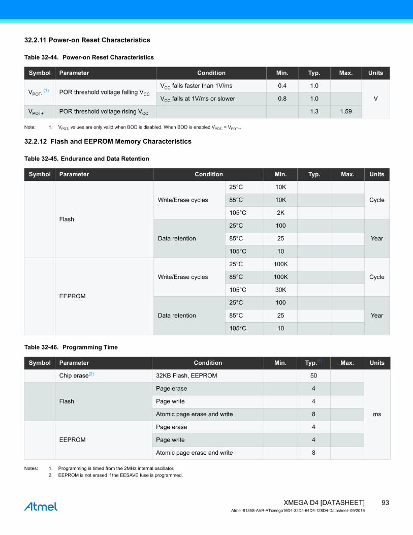
32.2.11 Power-on Reset Characteristics
Table 32-44. Power-on Reset Characteristics
Note: 1. VPOT- values are only valid when BOD is disabled. When BOD is enabled VPOT- = VPOT+.
32.2.12 Flash and EEPROM Memory Characteristics
Table 32-45. Endurance and Data Retention
Table 32-46. Programming Time
Notes: 1. Programming is timed from the 2MHz internal oscillator.
2. EEPROM is not erased if the EESAVE fuse is programmed.
Symbol Parameter Condition Min. Typ. Max. Units
VPOT- (1) POR threshold voltage falling VCC
VCC falls faster than 1V/ms 0.4 1.0
VVCC falls at 1V/ms or slower 0.8 1.0
VPOT+ POR threshold voltage rising VCC 1.3 1.59
Symbol Parameter Condition Min. Typ. Max. Units
Flash
Write/Erase cycles
25°C 10K
Cycle85°C 10K
105°C 2K
Data retention
25°C 100
Year85°C 25
105°C 10
EEPROM
Write/Erase cycles
25°C 100K
Cycle85°C 100K
105°C 30K
Data retention
25°C 100
Year85°C 25
105°C 10
Symbol Parameter Condition Min. Typ.(1) Max. Units
Chip erase(2) 32KB Flash, EEPROM 50
ms
Flash
Page erase 4
Page write 4
Atomic page erase and write 8
EEPROM
Page erase 4
Page write 4
Atomic page erase and write 8
93XMEGA D4 [DATASHEET]Atmel-8135S-AVR-ATxmega16D4-32D4-64D4-128D4-Datasheet–09/2016

32.2.13 Clock and Oscillator Characteristics
32.2.13.1 Calibrated 32.768kHz Internal Oscillator Characteristics
Table 32-47. 32.768kHz Internal Oscillator Characteristics
32.2.13.2 Calibrated 2MHz RC Internal Oscillator Characteristics
Table 32-48. 2MHz Internal Oscillator Characteristics
32.2.13.3 Calibrated and Tunable 32MHz Internal Oscillator Characteristics
Table 32-49. 32MHz Internal Oscillator Characteristics
32.2.13.4 32kHz Internal ULP Oscillator Characteristics
Table 32-50. 32kHz Internal ULP Oscillator Characteristics
Symbol Parameter Condition Min. Typ. Max. Units
Frequency 32.768 kHz
Factory calibration accuracy T = 85C, VCC = 3.0V -0.5 0.5%
User calibration accuracy -0.5 0.5
Symbol Parameter Condition Min. Typ. Max. Units
Frequency rangeDFLL can tune to this frequency over voltage and temperature
1.8 2.2MHz
Factory calibrated frequency 2.0
Factory calibration accuracy T = 85C, VCC= 3.0V -1.5 1.5
%User calibration accuracy -0.2 0.2
DFLL calibration stepsize 0.18
Symbol Parameter Condition Min. Typ. Max. Units
Frequency rangeDFLL can tune to this frequency over voltage and temperature
30 32 55MHz
Factory calibrated frequency 32
Factory calibration accuracy T = 85C, VCC= 3.0V -1.5 1.5
%User calibration accuracy -0.2 0.2
DFLL calibration step size 0.19
Symbol Parameter Condition Min. Typ. Max. Units
Factory calibrated frequency 32 kHz
Factory calibration accuracy T = 85C, VCC= 3.0V -12 12%
Accuracy -30 30
94XMEGA D4 [DATASHEET]Atmel-8135S-AVR-ATxmega16D4-32D4-64D4-128D4-Datasheet–09/2016

32.2.13.5 Internal Phase Locked Loop (PLL) Characteristics
Table 32-51. Internal PLL Characteristics
Note: 1. The maximum output frequency vs. supply voltage is linear between 1.8V and 2.7V, and can never be higher than four times the maximum CPU frequency.
32.2.13.6External Clock Characteristics
Figure 32-10.External Clock Drive Waveform
Table 32-52. External Clock(1)
Notes: 1. System Clock Prescalers must be set so that maximum CPU clock frequency for device is not exceeded.
2. The maximum frequency vs. supply voltage is linear between 1.8V and 2.7V, and the same applies for all other parameters with supply voltage conditions.
Symbol Parameter Condition Min. Typ. Max. Units
fIN Input frequency Output frequency must be within fOUT 0.4 64
MHzfOUT Output frequency(1)
VCC= 1.6 - 1.8V 20 48
VCC= 2.7 - 3.6V 20 128
Start-up time 25µs
Re-lock time 25
Symbol Parameter Condition Min. Typ. Max. Units
1/tCK Clock frequency(2)VCC = 1.6 - 1.8V 0 90
MHzVCC = 2.7 - 3.6V 0 142
tCK Clock periodVCC = 1.6 - 1.8V 11
nsVCC = 2.7 - 3.6V 7.0
tCH/CL Clock high/low timeVCC = 1.6 - 1.8V 4.5
VCC = 2.7 - 3.6V 2.4
VIL/IH Low/high level input voltage See Table 32-7 on page 69 V
tCKReduction in period time from oneclock cycle to the next
10 %
tCH
tCL
tCK
tCH
VIL1
VIH1
tCR tCF
95XMEGA D4 [DATASHEET]Atmel-8135S-AVR-ATxmega16D4-32D4-64D4-128D4-Datasheet–09/2016
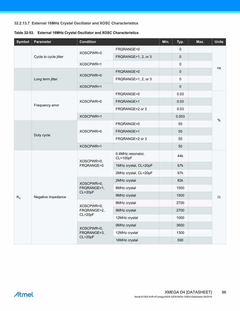
32.2.13.7 External 16MHz Crystal Oscillator and XOSC Characteristics
Table 32-53. .External 16MHz Crystal Oscillator and XOSC Characteristics
Symbol Parameter Condition Min. Typ. Max. Units
Cycle to cycle jitterXOSCPWR=0
FRQRANGE=0 0
ns
FRQRANGE=1, 2, or 3 0
XOSCPWR=1 0
Long term jitterXOSCPWR=0
FRQRANGE=0 0
FRQRANGE=1, 2, or 3 0
XOSCPWR=1 0
Frequency errorXOSCPWR=0
FRQRANGE=0 0.03
%
FRQRANGE=1 0.03
FRQRANGE=2 or 3 0.03
XOSCPWR=1 0.003
Duty cycleXOSCPWR=0
FRQRANGE=0 50
FRQRANGE=1 50
FRQRANGE=2 or 3 50
XOSCPWR=1 50
RQ Negative impedance
XOSCPWR=0,FRQRANGE=0
0.4MHz resonator, CL=100pF
44k
1MHz crystal, CL=20pF 67k
2MHz crystal, CL=20pF 67k
XOSCPWR=0,FRQRANGE=1,CL=20pF
2MHz crystal 82k
8MHz crystal 1500
9MHz crystal 1500
XOSCPWR=0,FRQRANGE=2,CL=20pF
8MHz crystal 2700
9MHz crystal 2700
12MHz crystal 1000
XOSCPWR=0,FRQRANGE=3,CL=20pF
9MHz crystal 3600
12MHz crystal 1300
16MHz crystal 590
96XMEGA D4 [DATASHEET]Atmel-8135S-AVR-ATxmega16D4-32D4-64D4-128D4-Datasheet–09/2016
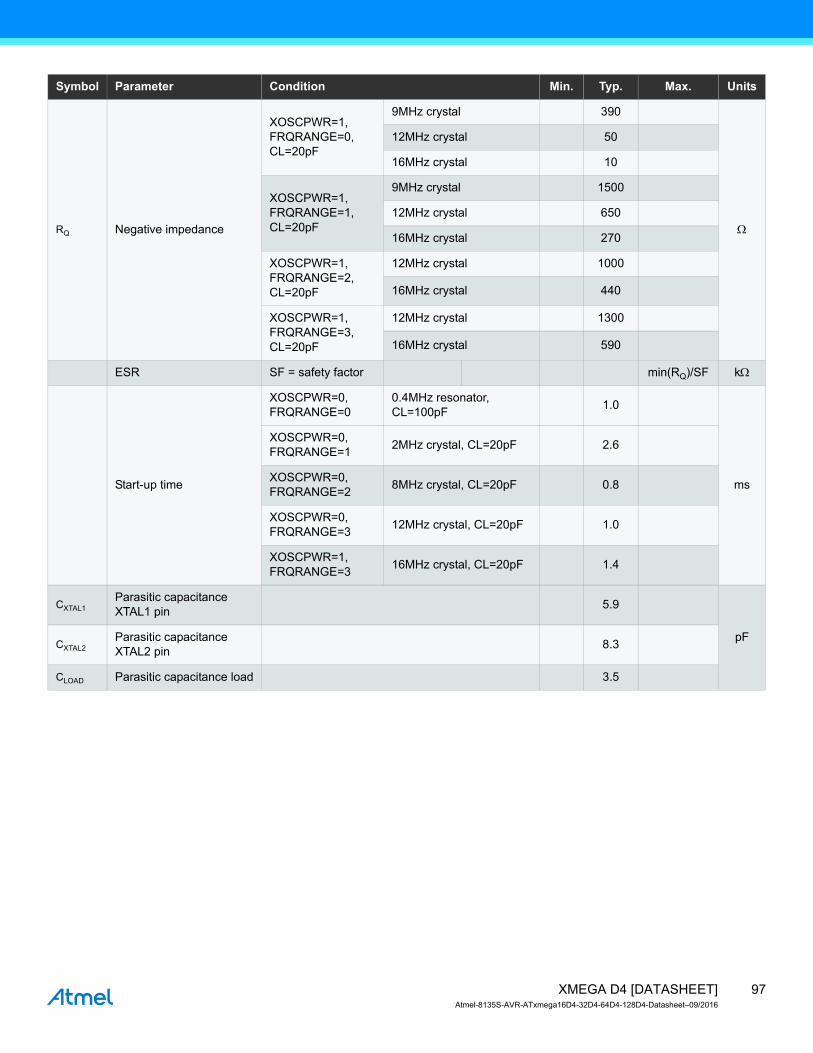
RQ Negative impedance
XOSCPWR=1,FRQRANGE=0,CL=20pF
9MHz crystal 390
12MHz crystal 50
16MHz crystal 10
XOSCPWR=1,FRQRANGE=1,CL=20pF
9MHz crystal 1500
12MHz crystal 650
16MHz crystal 270
XOSCPWR=1,FRQRANGE=2,CL=20pF
12MHz crystal 1000
16MHz crystal 440
XOSCPWR=1,FRQRANGE=3,CL=20pF
12MHz crystal 1300
16MHz crystal 590
ESR SF = safety factor min(RQ)/SF k
Start-up time
XOSCPWR=0,FRQRANGE=0
0.4MHz resonator, CL=100pF
1.0
ms
XOSCPWR=0,FRQRANGE=1
2MHz crystal, CL=20pF 2.6
XOSCPWR=0,FRQRANGE=2
8MHz crystal, CL=20pF 0.8
XOSCPWR=0,FRQRANGE=3
12MHz crystal, CL=20pF 1.0
XOSCPWR=1,FRQRANGE=3
16MHz crystal, CL=20pF 1.4
CXTAL1Parasitic capacitanceXTAL1 pin
5.9
pFCXTAL2
Parasitic capacitanceXTAL2 pin
8.3
CLOAD Parasitic capacitance load 3.5
Symbol Parameter Condition Min. Typ. Max. Units
97XMEGA D4 [DATASHEET]Atmel-8135S-AVR-ATxmega16D4-32D4-64D4-128D4-Datasheet–09/2016

32.2.13.8 External 32.768kHz Crystal Oscillator and TOSC Characteristics
Table 32-54. External 32.768kHz Crystal Oscillator and TOSC Characteristics
Note: See Figure 32-11 for definition.
Figure 32-11.TOSC Input Capacitance
The parasitic capacitance between the TOSC pins is CL1 + CL2 in series as seen from the crystal when oscillating without external capacitors.
Symbol Parameter Condition Min. Typ. Max. Units
ESR/R1Recommended crystal equivalentseries resistance (ESR)
Crystal load capacitance 6.5pF 60k
Crystal load capacitance 9.0pF 35
Crystal load capacitance 12pF 28
CTOSC1 Parasitic capacitance TOSC1 pin 3.5pF
CTOSC2 Parasitic capacitance TOSC2 pin 3.5
Recommended safety factorcapacitance load matched tocrystal specification
3
CL1 CL2
2CSOT1CSOT Device internal
External
32.768KHz crystal
98XMEGA D4 [DATASHEET]Atmel-8135S-AVR-ATxmega16D4-32D4-64D4-128D4-Datasheet–09/2016

32.2.14 SPI Characteristics
Figure 32-12.SPI Timing Requirements in Master Mode
Figure 32-13.SPI Timing Requirements in Slave Mode
MSB LSB
BSLBSM
tMOS
tMIS tMIH
tSCKW
tSCK
tMOH tMOH
tSCKFtSCKR
tSCKW
MOSI
(Data Output)
MISO
(Data Input)
SCK
(CPOL = 1)
SCK
(CPOL = 0)
SS
MSB LSB
BSLBSM
tSIS tSIH
tSSCKW
tSSCKW
tSSCK
tSSH
tSOSSH
tSCKR tSCKF
tSOS
tSSS
tSOSSS
MISO(Data Output)
MOSI(Data Input)
SCK
(CPOL = 1)
SCK
(CPOL = 0)
SS
99XMEGA D4 [DATASHEET]Atmel-8135S-AVR-ATxmega16D4-32D4-64D4-128D4-Datasheet–09/2016

Table 32-55. SPI Timing Characteristics and Requirements
32.2.15 Two-Wire Interface Characteristics
Table 32-56 describes the requirements for devices connected to the Two-Wire Interface Bus. The Atmel AVR XMEGA Two-Wire Interface meets or exceeds these requirements under the noted conditions. Timing symbols refer to Figure 32-14.
Figure 32-14.Two-wire Interface Bus Timing
Symbol Parameter Condition Min. Typ. Max. Units
tSCK SCK period Master(See Table 20-3 in XMEGA C Manual)
ns
tSCKW SCK high/low width Master 0.5*SCK
tSCKR SCK rise time Master 2.7
tSCKF SCK fall time Master 2.7
tMIS MISO setup to SCK Master 10
tMIH MISO hold after SCK Master 10
tMOS MOSI setup SCK Master 0.5*SCK
tMOH MOSI hold after SCK Master 1
tSSCK Slave SCK Period Slave 4*t ClkPER
tSSCKW SCK high/low width Slave 2*t ClkPER
tSSCKR SCK rise time Slave 1600
tSSCKF SCK fall time Slave 1600
tSIS MOSI setup to SCK Slave 3
tSIH MOSI hold after SCK Slave t ClkPER
tSSS SS setup to SCK Slave 21
tSSH SS hold after SCK Slave 20
tSOS MISO setup SCK Slave 8
tSOH MISO hold after SCK Slave 13
tSOSS MISO setup after SS low Slave 11
tSOSH MISO hold after SS high Slave 8
tHD;STA
tof
SDA
SCL
tLOW
tHIGH
tSU;STA
tBUF
tr
tHD;DATtSU;DAT
tSU;STO
100XMEGA D4 [DATASHEET]Atmel-8135S-AVR-ATxmega16D4-32D4-64D4-128D4-Datasheet–09/2016

Table 32-56. Two-wire Interface Characteristics
Notes: 1. Required only for fSCL > 100kHz.
2. Cb = Capacitance of one bus line in pF.
3. fPER = Peripheral clock frequency.
Symbol Parameter Condition Min. Typ. Max. Units
VIH Input high voltage 0.7VCC VCC+0.5
VVIL Input low voltage -0.5 0.3VCC
Vhys Hysteresis of Schmitt trigger inputs 0.05VCC (1)
VOL Output low voltage 3mA, sink current 0 0.4
tr Rise time for both SDA and SCL 20+0.1Cb (1)(2) 300
nstof Output fall time from VIHmin to VILmax 10pF < Cb < 400pF (2) 20+0.1Cb (1)(2) 250
tSP Spikes suppressed by input filter 0 50
II Input current for each I/O Pin 0.1VCC < VI < 0.9VCC -10 10 µA
CI Capacitance for each I/O Pin 10 pF
fSCL SCL clock frequency fPER (3)>max(10fSCL, 250kHz) 0 400 kHz
RP Value of pull-up resistor
fSCL 100kHz
fSCL > 100kHz
tHD;STA Hold time (repeated) START conditionfSCL 100kHz 4.0
µs
fSCL > 100kHz 0.6
tLOW Low period of SCL clockfSCL 100kHz 4.7
fSCL > 100kHz 1.3
tHIGH High period of SCL clockfSCL 100kHz 4.0
fSCL > 100kHz 0.6
tSU;STASet-up time for a repeated START condition
fSCL 100kHz 4.7
fSCL > 100kHz 0.6
tHD;DAT Data hold timefSCL 100kHz 0 3.45
µsfSCL > 100kHz 0 0.9
tSU;DAT
Data setup time fSCL 100kHz 250ns
fSCL > 100kHz 100
tSU;STO Setup time for STOP conditionfSCL 100kHz 4.0
µsfSCL > 100kHz 0.6
tBUFBus free time between a STOP and START condition
fSCL 100kHz 4.7µs
fSCL > 100kHz 1.3
VCC 0.4V–
3mA----------------------------
100nsCb---------------
300nsCb---------------
101XMEGA D4 [DATASHEET]Atmel-8135S-AVR-ATxmega16D4-32D4-64D4-128D4-Datasheet–09/2016
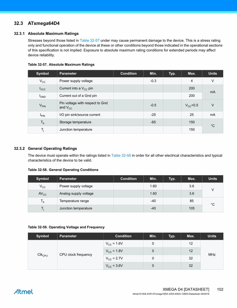
32.3 ATxmega64D4
32.3.1 Absolute Maximum Ratings
Stresses beyond those listed in Table 32-57 under may cause permanent damage to the device. This is a stress rating only and functional operation of the device at these or other conditions beyond those indicated in the operational sections of this specification is not implied. Exposure to absolute maximum rating conditions for extended periods may affect device reliability.
Table 32-57. Absolute Maximum Ratings
32.3.2 General Operating Ratings
The device must operate within the ratings listed in Table 32-58 in order for all other electrical characteristics and typical characteristics of the device to be valid.
Table 32-58. General Operating Conditions
Table 32-59. Operating Voltage and Frequency
Symbol Parameter Condition Min. Typ. Max. Units
VCC Power supply voltage -0.3 4 V
IVCC Current into a VCC pin 200mA
IGND Current out of a Gnd pin 200
VPINPin voltage with respect to Gnd and VCC
-0.5 VCC+0.5 V
IPIN I/O pin sink/source current -25 25 mA
TA Storage temperature -65 150°C
Tj Junction temperature 150
Symbol Parameter Condition Min. Typ. Max. Units
VCC Power supply voltage 1.60 3.6V
AVCC Analog supply voltage 1.60 3.6
TA Temperature range -40 85°C
Tj Junction temperature -40 105
Symbol Parameter Condition Min. Typ. Max. Units
ClkCPU CPU clock frequency
VCC = 1.6V 0 12
MHzVCC = 1.8V 0 12
VCC = 2.7V 0 32
VCC = 3.6V 0 32
102XMEGA D4 [DATASHEET]Atmel-8135S-AVR-ATxmega16D4-32D4-64D4-128D4-Datasheet–09/2016
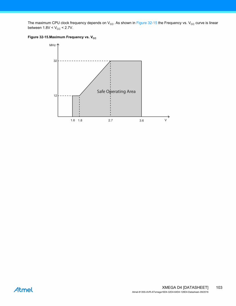
The maximum CPU clock frequency depends on VCC. As shown in Figure 32-15 the Frequency vs. VCC curve is linear between 1.8V < VCC < 2.7V.
Figure 32-15.Maximum Frequency vs. VCC
1.8
12
32
MHz
V2.7 3.61.6
Safe Operating Area
103XMEGA D4 [DATASHEET]Atmel-8135S-AVR-ATxmega16D4-32D4-64D4-128D4-Datasheet–09/2016

32.3.3 Current Consumption
Table 32-60. Current Consumption for Active Mode and Sleep Modes
Notes: 1. All Power Reduction Registers set.
2. Maximum limits are based on characterization, and not tested in production.
Symbol Parameter Condition Min. Typ. Max. Units
ICC
Active power consumption(1)
32kHz, Ext. ClkVCC = 1.8V 68
µA
VCC = 3.0V 145
1MHz, Ext. ClkVCC = 1.8V 260
VCC = 3.0V 540
2MHz, Ext. ClkVCC = 1.8V 460 600
VCC = 3.0V0.96 1.4
mA32MHz, Ext. Clk 9.8 12
Idle powerconsumption(1)
32kHz, Ext. ClkVCC = 1.8V 2.4
µA
VCC = 3.0V 3.9
1MHz, Ext. ClkVCC = 1.8V 62
VCC = 3.0V 118
2MHz, Ext. ClkVCC = 1.8V 125 225
VCC = 3.0V240 350
32MHz, Ext. Clk 3.8 5.5 mA
Power-down powerconsumption
T = 25°C
VCC = 3.0V
0.1 1.0
µA
T = 85°C 1.2 4.5
T = 105°C 0.1 6.0
WDT and sampled BOD enabled,T = 25°C
VCC = 3.0V
1.3 3.0
WDT and sampled BOD enabled,T = 85°C
2.4 6.0
WDT and sampled BOD enabled,T = 105°C
1.3 8.0
Power-save powerconsumption(2)
RTC from ULP clock, WDT andsampled BOD enabled, T = 25°C
VCC = 1.8V 1.2
VCC = 3.0V 1.3
RTC from 1.024kHz low power32.768kHz TOSC, T = 25°C
VCC = 1.8V 0.6 2
VCC = 3.0V 0.7 2
RTC from low power 32.768kHzTOSC, T = 25°C
VCC = 1.8V 0.8 3
VCC = 3.0V 1.0 3
Reset power consumptionCurrent through RESET pinsubstracted
VCC = 3.0V 320
104XMEGA D4 [DATASHEET]Atmel-8135S-AVR-ATxmega16D4-32D4-64D4-128D4-Datasheet–09/2016

Table 32-61. Current Consumption for Modules and Peripherals
Note: 1. All parameters measured as the difference in current consumption between module enabled and disabled. All data at VCC = 3.0V, ClkSYS = 1MHz external clock without prescaling, T = 25°C unless other conditions are given.
Symbol Parameter Condition(1) Min. Typ. Max. Units
ICC
ULP oscillator 1.0
µA
32.768kHz int. oscillator 27
2MHz int. oscillator85
DFLL enabled with 32.768kHz int. osc. as reference 115
32MHz int. oscillator270
DFLL enabled with 32.768kHz int. osc. as reference 460
PLL20x multiplication factor, 32MHz int. osc. DIV4 as reference
220
Watchdog Timer 1.0
BODContinuous mode 138
Sampled mode, includes ULP oscillator 1.2
Internal 1.0V reference 100
Temperature sensor 95
ADC150kspsVREF = Ext ref
3.0
mACURRLIMIT = LOW 2.6
CURRLIMIT = MEDIUM 2.1
CURRLIMIT = HIGH 1.6
AC High Speed Mode 330
µATimer/Counter 16
USART Rx and Tx enabled, 9600 BAUD 2.5
Flash memory and EEPROM programming 4 8 mA
105XMEGA D4 [DATASHEET]Atmel-8135S-AVR-ATxmega16D4-32D4-64D4-128D4-Datasheet–09/2016
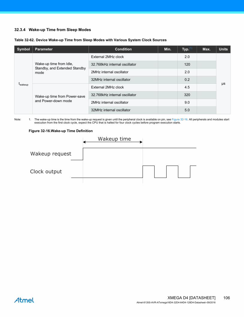
32.3.4 Wake-up Time from Sleep Modes
Table 32-62. Device Wake-up Time from Sleep Modes with Various System Clock Sources
Note: 1. The wake-up time is the time from the wake-up request is given until the peripheral clock is available on pin, see Figure 32-16. All peripherals and modules start execution from the first clock cycle, expect the CPU that is halted for four clock cycles before program execution starts.
Figure 32-16.Wake-up Time Definition
Symbol Parameter Condition Min. Typ.(1) Max. Units
twakeup
Wake-up time from Idle,Standby, and Extended Standbymode
External 2MHz clock 2.0
µs
32.768kHz internal oscillator 120
2MHz internal oscillator 2.0
32MHz internal oscillator 0.2
Wake-up time from Power-saveand Power-down mode
External 2MHz clock 4.5
32.768kHz internal oscillator 320
2MHz internal oscillator 9.0
32MHz internal oscillator 5.0
Wakeup request
Clock output
Wakeup time
106XMEGA D4 [DATASHEET]Atmel-8135S-AVR-ATxmega16D4-32D4-64D4-128D4-Datasheet–09/2016

32.3.5 I/O Pin Characteristics
The I/O pins complies with the JEDEC LVTTL and LVCMOS specification and the high- and low level input and output voltage limits reflect or exceed this specification.
Table 32-63. I/O Pin Characteristics
Notes: 1. The sum of all IOH for PORTA and PORTB must not exceed 100mA.The sum of all IOH for PORTC must not exceed 200mA.The sum of all IOH for PORTD and pins PE[0-1] on PORTE must not exceed 200mA.The sum of all IOH for PE[2-3] on PORTE, PORTR and PDI must not exceed 100mA.
2. The sum of all IOL for PORTA and PORTB must not exceed 100mA.The sum of all IOL for PORTC must not exceed 200mA.The sum of all IOL for PORTD and pins PE[0-1] on PORTE must not exceed 200mA.The sum of all IOL for PE[2-3] on PORTE, PORTR and PDI must not exceed 100mA.
Symbol Parameter Condition Min. Typ. Max. Units
IOH(1)/
IOL(2) I/O pin source/sink current -15 15 mA
VIH High level input voltage
VCC = 2.7 - 3.6V 2 VCC+0.3 V
VCC = 2.0 - 2.7V 0.7*VCC VCC+0.3
VCC = 1.6 - 2.0V 0.7*VCC VCC+0.3
VIL Low level input voltage
VCC = 2.7- 3.6V -0.3 0.3*VCC
VCC = 2.0 - 2.7V -0.3 0.3*VCC
VCC = 1.6 - 2.0V -0.3 0.3*VCC
VOH High level output voltage
VCC = 3.0 - 3.6V IOH = -2mA 2.4 0.94*VCC
VCC = 3.3V IOH = -4mA 2.6 2.9
VCC = 3.0V IOH = -3mA 2.1 2.6
VCC = 1.8V IOH = -1mA 1.4 1.6
VOL Low level output voltage
VCC = 3.0 - 3.6V IOL = 2mA 0.05*VCC 0.4
VCC = 3.3V IOL = 8mA 0.4 0.76
VCC = 3.0V IOL = 5mA 0.3 0.64
VCC = 1.8V IOL = 3mA 0.2 0.46
IIN Input leakage current T = 25°C <0.001 0.1 µA
RP Pull/Buss keeper resistor 24 k
tr Rise time No load 4 ns
107XMEGA D4 [DATASHEET]Atmel-8135S-AVR-ATxmega16D4-32D4-64D4-128D4-Datasheet–09/2016
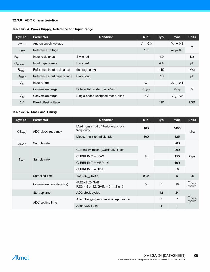
32.3.6 ADC Characteristics
Table 32-64. Power Supply, Reference and Input Range
Table 32-65. Clock and Timing
Symbol Parameter Condition Min. Typ. Max. Units
AVCC Analog supply voltage VCC- 0.3 VCC+ 0.3V
VREF Reference voltage 1.0 AVCC- 0.6
Rin Input resistance Switched 4.0 k
Csample Input capacitance Switched 4.4 pF
RAREF Reference input resistance (leakage only) >10 M
CAREF Reference input capacitance Static load 7.0 pF
VIN Input range -0.1 AVCC+0.1
VConversion range Differential mode, Vinp - Vinn -VREF VREF
VIN Conversion range Single ended unsigned mode, Vinp -V VREF-V
∆V Fixed offset voltage 190 LSB
Symbol Parameter Condition Min. Typ. Max. Units
ClkADC ADC clock frequency
Maximum is 1/4 of Peripheral clock frequency
100 1400kHz
Measuring internal signals 100 125
fClkADC Sample rate
14
200
kspsfADC Sample rate
Current limitation (CURRLIMIT) off 200
CURRLIMIT = LOW 150
CURRLIMIT = MEDIUM 100
CURRLIMIT = HIGH 50
Sampling time 1/2 ClkADC cycle 0.25 5 µs
Conversion time (latency)(RES+2)/2+GAINRES = 8 or 12, GAIN = 0, 1, 2 or 3
5 7 10ClkADCcycles
Start-up time ADC clock cycles 12 24
ClkADCcyclesADC settling time
After changing reference or input mode 7 7
After ADC flush 1 1
108XMEGA D4 [DATASHEET]Atmel-8135S-AVR-ATxmega16D4-32D4-64D4-128D4-Datasheet–09/2016
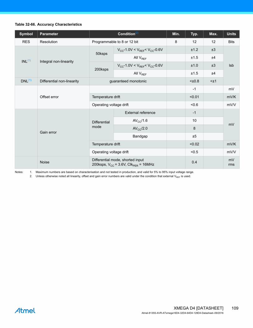
Table 32-66. Accuracy Characteristics
Notes: 1. Maximum numbers are based on characterisation and not tested in production, and valid for 5% to 95% input voltage range.
2. Unless otherwise noted all linearity, offset and gain error numbers are valid under the condition that external VREF is used.
Symbol Parameter Condition(2) Min. Typ. Max. Units
RES Resolution Programmable to 8 or 12 bit 8 12 12 Bits
INL(1) Integral non-linearity
50kspsVCC-1.0V < VREF< VCC-0.6V ±1.2 ±3
lsb
All VREF ±1.5 ±4
200kspsVCC-1.0V < VREF< VCC-0.6V ±1.0 ±3
All VREF ±1.5 ±4
DNL(1) Differential non-linearity guaranteed monotonic <±0.8 <±1
Offset error
-1 mV
Temperature drift <0.01 mV/K
Operating voltage drift <0.6 mV/V
Gain error
Differentialmode
External reference -1
mVAVCC/1.6 10
AVCC/2.0 8
Bandgap ±5
Temperature drift <0.02 mV/K
Operating voltage drift <0.5 mV/V
NoiseDifferential mode, shorted input200ksps, VCC = 3.6V, ClkPER = 16MHz
0.4mV rms
109XMEGA D4 [DATASHEET]Atmel-8135S-AVR-ATxmega16D4-32D4-64D4-128D4-Datasheet–09/2016
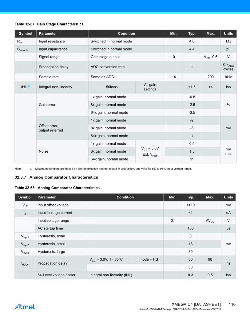
Table 32-67. Gain Stage Characteristics
Note: 1. Maximum numbers are based on characterisation and not tested in production, and valid for 5% to 95% input voltage range.
32.3.7 Analog Comparator Characteristics
Table 32-68. Analog Comparator Characteristics
Symbol Parameter Condition Min. Typ. Max. Units
Rin Input resistance Switched in normal mode 4.0 k
Csample Input capacitance Switched in normal mode 4.4 pF
Signal range Gain stage output 0 VCC- 0.6 V
Propagation delay ADC conversion rate 1ClkADCcycles
Sample rate Same as ADC 14 200 kHz
INL(1) Integral non-linearity 50kspsAll gain settings
±1.5 ±4 lsb
Gain error
1x gain, normal mode -0.8
%8x gain, normal mode -2.5
64x gain, normal mode -3.5
Offset error,output referred
1x gain, normal mode -2
mV8x gain, normal mode -5
64x gain, normal mode -4
Noise
1x gain, normal modeVCC = 3.6V
Ext. VREF
0.5
mV rms
8x gain, normal mode 1.5
64x gain, normal mode 11
Symbol Parameter Condition Min. Typ. Max. Units
Voff Input offset voltage <±10 mV
Ilk Input leakage current <1 nA
Input voltage range -0.1 AVCC V
AC startup time 100 µs
Vhys1 Hysteresis, none 0
mVVhys2 Hysteresis, small 13
Vhys3 Hysteresis, large 30
tdelay Propagation delayVCC = 3.0V, T= 85°C mode = HS 30 90
ns30
64-Level voltage scaler Integral non-linearity (INL) 0.3 0.5 lsb
110XMEGA D4 [DATASHEET]Atmel-8135S-AVR-ATxmega16D4-32D4-64D4-128D4-Datasheet–09/2016
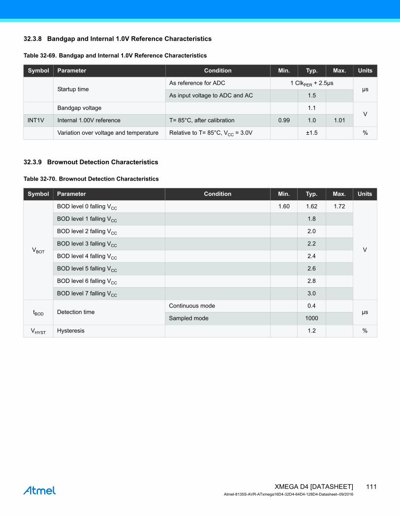
32.3.8 Bandgap and Internal 1.0V Reference Characteristics
Table 32-69. Bandgap and Internal 1.0V Reference Characteristics
32.3.9 Brownout Detection Characteristics
Table 32-70. Brownout Detection Characteristics
Symbol Parameter Condition Min. Typ. Max. Units
Startup timeAs reference for ADC 1 ClkPER + 2.5µs
µsAs input voltage to ADC and AC 1.5
Bandgap voltage 1.1V
INT1V Internal 1.00V reference T= 85°C, after calibration 0.99 1.0 1.01
Variation over voltage and temperature Relative to T= 85°C, VCC = 3.0V ±1.5 %
Symbol Parameter Condition Min. Typ. Max. Units
VBOT
BOD level 0 falling VCC 1.60 1.62 1.72
V
BOD level 1 falling VCC 1.8
BOD level 2 falling VCC 2.0
BOD level 3 falling VCC 2.2
BOD level 4 falling VCC 2.4
BOD level 5 falling VCC 2.6
BOD level 6 falling VCC 2.8
BOD level 7 falling VCC 3.0
tBOD Detection timeContinuous mode 0.4
µsSampled mode 1000
VHYST Hysteresis 1.2 %
111XMEGA D4 [DATASHEET]Atmel-8135S-AVR-ATxmega16D4-32D4-64D4-128D4-Datasheet–09/2016
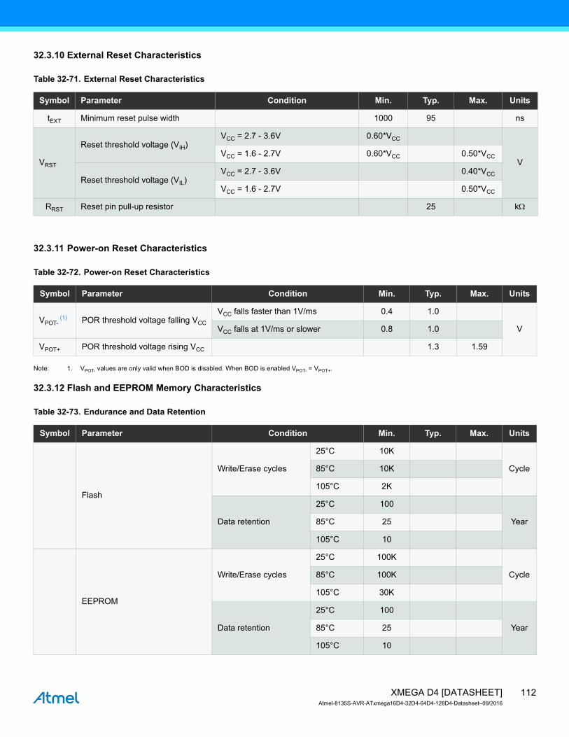
32.3.10 External Reset Characteristics
Table 32-71. External Reset Characteristics
32.3.11 Power-on Reset Characteristics
Table 32-72. Power-on Reset Characteristics
Note: 1. VPOT- values are only valid when BOD is disabled. When BOD is enabled VPOT- = VPOT+.
32.3.12 Flash and EEPROM Memory Characteristics
Table 32-73. Endurance and Data Retention
Symbol Parameter Condition Min. Typ. Max. Units
tEXT Minimum reset pulse width 1000 95 ns
VRST
Reset threshold voltage (VIH)VCC = 2.7 - 3.6V 0.60*VCC
VVCC = 1.6 - 2.7V 0.60*VCC 0.50*VCC
Reset threshold voltage (VIL)VCC = 2.7 - 3.6V 0.40*VCC
VCC = 1.6 - 2.7V 0.50*VCC
RRST Reset pin pull-up resistor 25 k
Symbol Parameter Condition Min. Typ. Max. Units
VPOT- (1) POR threshold voltage falling VCC
VCC falls faster than 1V/ms 0.4 1.0
VVCC falls at 1V/ms or slower 0.8 1.0
VPOT+ POR threshold voltage rising VCC 1.3 1.59
Symbol Parameter Condition Min. Typ. Max. Units
Flash
Write/Erase cycles
25°C 10K
Cycle85°C 10K
105°C 2K
Data retention
25°C 100
Year85°C 25
105°C 10
EEPROM
Write/Erase cycles
25°C 100K
Cycle85°C 100K
105°C 30K
Data retention
25°C 100
Year85°C 25
105°C 10
112XMEGA D4 [DATASHEET]Atmel-8135S-AVR-ATxmega16D4-32D4-64D4-128D4-Datasheet–09/2016

Table 32-74. Programming Time
Notes: 1. Programming is timed from the 2MHz internal oscillator.
2. EEPROM is not erased if the EESAVE fuse is programmed.
32.3.13 Clock and Oscillator Characteristics
32.3.13.1 Calibrated 32.768kHz Internal Oscillator Characteristics
Table 32-75. 32.768kHz Internal Oscillator Characteristics
32.3.13.2 Calibrated 2MHz RC Internal Oscillator Characteristics
Table 32-76. 2MHz Internal Oscillator Characteristics
Symbol Parameter Condition Min. Typ.(1) Max. Units
Chip erase 64KB Flash, EEPROM(2) and SRAM erase 55 ms
Flash
Page erase 4
Page write 4
Atomic Page Erase and write 8
EEPROM
Page erase 4
Page write 4
Atomic Page erase and write 8
Symbol Parameter Condition Min. Typ. Max. Units
Frequency 32.768 kHz
Factory calibration accuracy T = 85C, VCC = 3.0V -0.5 0.5%
User calibration accuracy -0.5 0.5
Symbol Parameter Condition Min. Typ. Max. Units
Frequency rangeDFLL can tune to this frequency over voltage and temperature
1.8 2.2MHz
Factory calibrated frequency 2.0
Factory calibration accuracy T = 85C, VCC= 3.0V -1.5 1.5
%User calibration accuracy -0.2 0.2
DFLL calibration stepsize 0.21
113XMEGA D4 [DATASHEET]Atmel-8135S-AVR-ATxmega16D4-32D4-64D4-128D4-Datasheet–09/2016
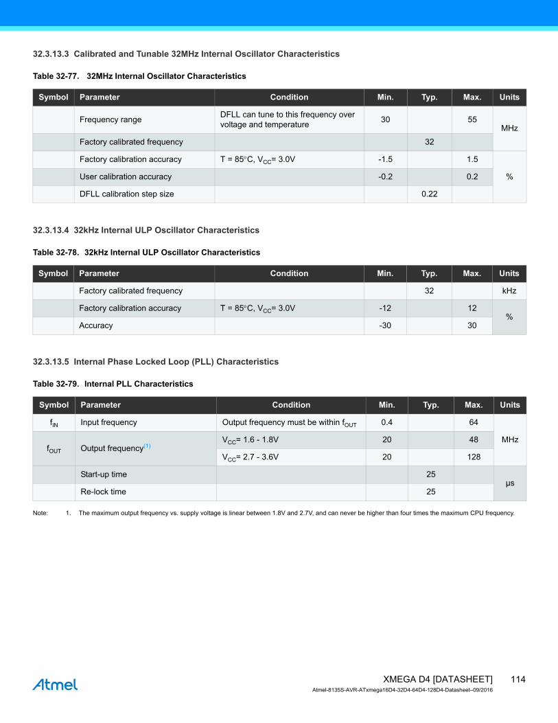
32.3.13.3 Calibrated and Tunable 32MHz Internal Oscillator Characteristics
Table 32-77. 32MHz Internal Oscillator Characteristics
32.3.13.4 32kHz Internal ULP Oscillator Characteristics
Table 32-78. 32kHz Internal ULP Oscillator Characteristics
32.3.13.5 Internal Phase Locked Loop (PLL) Characteristics
Table 32-79. Internal PLL Characteristics
Note: 1. The maximum output frequency vs. supply voltage is linear between 1.8V and 2.7V, and can never be higher than four times the maximum CPU frequency.
Symbol Parameter Condition Min. Typ. Max. Units
Frequency rangeDFLL can tune to this frequency over voltage and temperature
30 55MHz
Factory calibrated frequency 32
Factory calibration accuracy T = 85C, VCC= 3.0V -1.5 1.5
%User calibration accuracy -0.2 0.2
DFLL calibration step size 0.22
Symbol Parameter Condition Min. Typ. Max. Units
Factory calibrated frequency 32 kHz
Factory calibration accuracy T = 85C, VCC= 3.0V -12 12%
Accuracy -30 30
Symbol Parameter Condition Min. Typ. Max. Units
fIN Input frequency Output frequency must be within fOUT 0.4 64
MHzfOUT Output frequency(1)
VCC= 1.6 - 1.8V 20 48
VCC= 2.7 - 3.6V 20 128
Start-up time 25µs
Re-lock time 25
114XMEGA D4 [DATASHEET]Atmel-8135S-AVR-ATxmega16D4-32D4-64D4-128D4-Datasheet–09/2016

32.3.13.6 External Clock Characteristics
Figure 32-17.External Clock Drive Waveform
Table 32-80. External Clock Used as System Clock without Prescaling
Note: 1. System Clock Prescalers must be set so that maximum CPU clock frequency for device is not exceeded.
tCH
tCL
tCK
tCH
VIL1
VIH1
tCR tCF
Symbol Parameter Condition Min. Typ. Max. Units
1/tCK Clock frequency(1)VCC = 1.6 - 1.8V 0 12
MHzVCC = 2.7 - 3.6V 0 32
tCK Clock periodVCC = 1.6 - 1.8V 83.3
ns
VCC = 2.7 - 3.6V 31.5
tCH Clock high timeVCC = 1.6 - 1.8V 30.0
VCC = 2.7 - 3.6V 12.5
tCL Clock low timeVCC = 1.6 - 1.8V 30.0
VCC = 2.7 - 3.6V 12.5
tCR Rise time (for maximum frequency)VCC = 1.6 - 1.8V 10
VCC = 2.7 - 3.6V 3
tCF Fall time (for maximum frequency)VCC = 1.6 - 1.8V 10
VCC = 2.7 - 3.6V 3
tCK Change in period from one clock cycle to the next 10 %
115XMEGA D4 [DATASHEET]Atmel-8135S-AVR-ATxmega16D4-32D4-64D4-128D4-Datasheet–09/2016
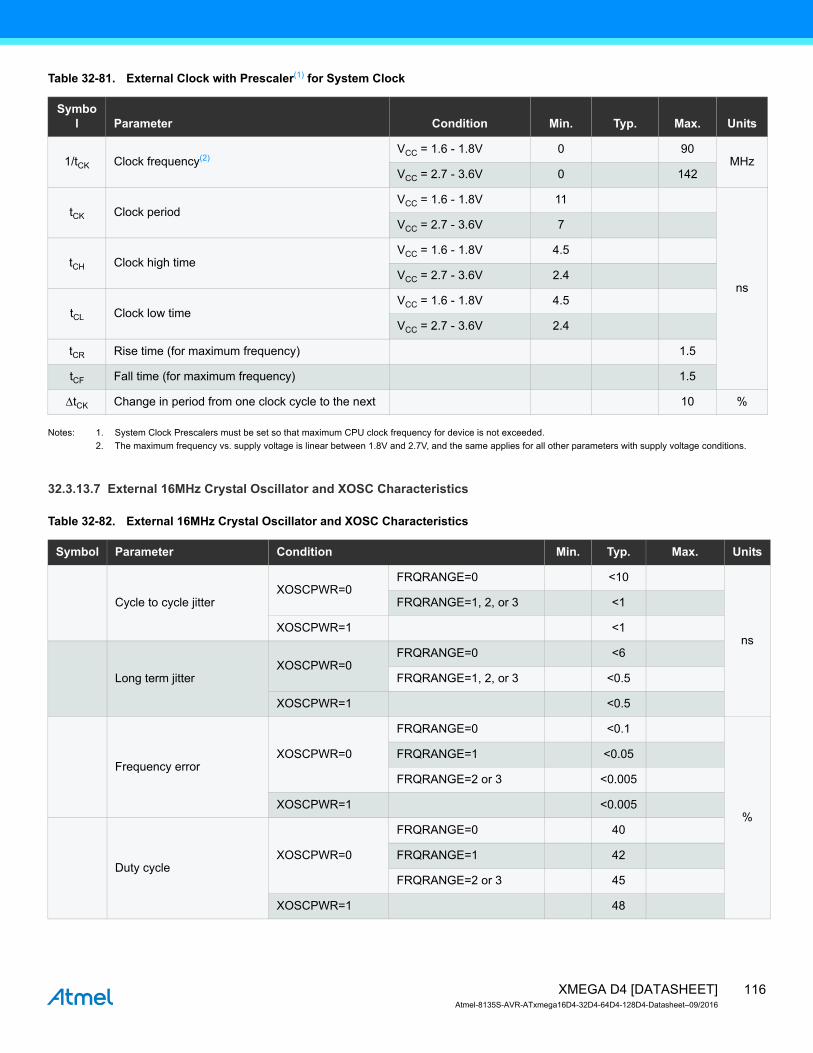
Table 32-81. External Clock with Prescaler(1) for System Clock
Notes: 1. System Clock Prescalers must be set so that maximum CPU clock frequency for device is not exceeded.
2. The maximum frequency vs. supply voltage is linear between 1.8V and 2.7V, and the same applies for all other parameters with supply voltage conditions.
32.3.13.7 External 16MHz Crystal Oscillator and XOSC Characteristics
Table 32-82. External 16MHz Crystal Oscillator and XOSC Characteristics
Symbol Parameter Condition Min. Typ. Max. Units
1/tCK Clock frequency(2)VCC = 1.6 - 1.8V 0 90
MHzVCC = 2.7 - 3.6V 0 142
tCK Clock periodVCC = 1.6 - 1.8V 11
ns
VCC = 2.7 - 3.6V 7
tCH Clock high timeVCC = 1.6 - 1.8V 4.5
VCC = 2.7 - 3.6V 2.4
tCL Clock low timeVCC = 1.6 - 1.8V 4.5
VCC = 2.7 - 3.6V 2.4
tCR Rise time (for maximum frequency) 1.5
tCF Fall time (for maximum frequency) 1.5
tCK Change in period from one clock cycle to the next 10 %
Symbol Parameter Condition Min. Typ. Max. Units
Cycle to cycle jitterXOSCPWR=0
FRQRANGE=0 <10
ns
FRQRANGE=1, 2, or 3 <1
XOSCPWR=1 <1
Long term jitterXOSCPWR=0
FRQRANGE=0 <6
FRQRANGE=1, 2, or 3 <0.5
XOSCPWR=1 <0.5
Frequency errorXOSCPWR=0
FRQRANGE=0 <0.1
%
FRQRANGE=1 <0.05
FRQRANGE=2 or 3 <0.005
XOSCPWR=1 <0.005
Duty cycleXOSCPWR=0
FRQRANGE=0 40
FRQRANGE=1 42
FRQRANGE=2 or 3 45
XOSCPWR=1 48
116XMEGA D4 [DATASHEET]Atmel-8135S-AVR-ATxmega16D4-32D4-64D4-128D4-Datasheet–09/2016

RQ Negative impedance(1)
XOSCPWR=0,FRQRANGE=0
0.4MHz resonator, CL=100pF
2.4k
1MHz crystal, CL=20pF 8.7k
2MHz crystal, CL=20pF 2.1k
XOSCPWR=0,FRQRANGE=1,CL=20pF
2MHz crystal 4.2k
8MHz crystal 250
9MHz crystal 195
XOSCPWR=0,FRQRANGE=2,CL=20pF
8MHz crystal 360
9MHz crystal 285
12MHz crystal 155
XOSCPWR=0,FRQRANGE=3,CL=20pF
9MHz crystal 365
12MHz crystal 200
16MHz crystal 105
XOSCPWR=1,FRQRANGE=0,CL=20pF
9MHz crystal 435
12MHz crystal 235
16MHz crystal 125
XOSCPWR=1,FRQRANGE=1,CL=20pF
9MHz crystal 495
12MHz crystal 270
16MHz crystal 145
XOSCPWR=1,FRQRANGE=2,CL=20pF
12MHz crystal 305
16MHz crystal 160
XOSCPWR=1,FRQRANGE=3,CL=20pF
12MHz crystal 380
16MHz crystal 205
ESR SF = safety factor min(RQ)/SF k
Start-up time
XOSCPWR=0,FRQRANGE=0
0.4MHz resonator, CL=100pF
1.0
ms
XOSCPWR=0,FRQRANGE=1
2MHz crystal, CL=20pF 2.6
XOSCPWR=0,FRQRANGE=2
8MHz crystal, CL=20pF 0.8
XOSCPWR=0,FRQRANGE=3
12MHz crystal, CL=20pF 1.0
XOSCPWR=1,FRQRANGE=3
16MHz crystal, CL=20pF 1.4
Symbol Parameter Condition Min. Typ. Max. Units
117XMEGA D4 [DATASHEET]Atmel-8135S-AVR-ATxmega16D4-32D4-64D4-128D4-Datasheet–09/2016

Note: 1. Numbers for negative impedance are not tested in production but guaranteed from design and characterization.
32.3.13.8 External 32.768kHz Crystal Oscillator and TOSC Characteristics
Table 32-83. External 32.768kHz Crystal Oscillator and TOSC Characteristics
Note: 1. See Figure 32-18 on page 118 for definition.
Figure 32-18.TOSC Input Capacitance
The parasitic capacitance between the TOSC pins is CL1 + CL2 in series as seen from the crystal when oscillating without external capacitors.
CXTAL1Parasitic capacitanceXTAL1 pin
5.9
pFCXTAL2
Parasitic capacitanceXTAL2 pin
8.3
CLOAD Parasitic capacitance load 3.5
Symbol Parameter Condition Min. Typ. Max. Units
ESR/R1Recommended crystal equivalentseries resistance (ESR)
Crystal load capacitance 6.5pF 60k
Crystal load capacitance 9.0pF 35
CTOSC Parasitic capacitanceNormal mode 4.7
pFLow power mode 5.2
Recommended safety factorCapacitance load matched tocrystal specification
3
Symbol Parameter Condition Min. Typ. Max. Units
CL1 CL2
2CSOT1CSOT Device internal
External
32.768KHz crystal
118XMEGA D4 [DATASHEET]Atmel-8135S-AVR-ATxmega16D4-32D4-64D4-128D4-Datasheet–09/2016

32.3.14 SPI Characteristics
Figure 32-19.SPI Timing Requirements in Master Mode
Figure 32-20.SPI Timing Requirements in Slave Mode
MSB LSB
BSLBSM
tMOS
tMIS tMIH
tSCKW
tSCK
tMOH tMOH
tSCKFtSCKR
tSCKW
MOSI
(Data Output)
MISO
(Data Input)
SCK
(CPOL = 1)
SCK
(CPOL = 0)
SS
MSB LSB
BSLBSM
tSIS tSIH
tSSCKW
tSSCKW
tSSCK
tSSH
tSOSSH
tSCKR tSCKF
tSOS
tSSS
tSOSSS
MISO(Data Output)
MOSI(Data Input)
SCK
(CPOL = 1)
SCK
(CPOL = 0)
SS
119XMEGA D4 [DATASHEET]Atmel-8135S-AVR-ATxmega16D4-32D4-64D4-128D4-Datasheet–09/2016

Table 32-84. SPI Timing Characteristics and Requirements
Symbol Parameter Condition Min. Typ. Max. Units
tSCK SCK period Master(See Table 17-4 in XMEGA D Manual)
ns
tSCKW SCK high/low width Master 0.5*SCK
tSCKR SCK rise time Master 2.7
tSCKF SCK fall time Master 2.7
tMIS MISO setup to SCK Master 10
tMIH MISO hold after SCK Master 10
tMOS MOSI setup SCK Master 0.5*SCK
tMOH MOSI hold after SCK Master 1
tSSCK Slave SCK period Slave 4*t ClkPER
tSSCKW SCK high/low width Slave 2*t ClkPER
tSSCKR SCK rise time Slave 1600
tSSCKF SCK fall time Slave 1600
tSIS MOSI setup to SCK Slave 3
tSIH MOSI hold after SCK Slave t ClkPER
tSSS SS setup to SCK Slave 21
tSSH SS hold after SCK Slave 20
tSOS MISO setup SCK Slave 8.0
tSOH MISO hold after SCK Slave 13.0
tSOSS MISO setup after SS low Slave 11.0
tSOSH MISO hold after SS high Slave 8.0
120XMEGA D4 [DATASHEET]Atmel-8135S-AVR-ATxmega16D4-32D4-64D4-128D4-Datasheet–09/2016

32.3.15 Two-Wire Interface Characteristics
Table 32-85 describes the requirements for devices connected to the Two-Wire Interface Bus. The Atmel AVR XMEGA Two-Wire Interface meets or exceeds these requirements under the noted conditions. Timing symbols refer to Figure 32-21.
Figure 32-21.Two-wire Interface Bus Timing
Table 32-85. Two-wire Interface Characteristics
tHD;STA
tof
SDA
SCL
tLOW
tHIGH
tSU;STA
tBUF
tr
tHD;DATtSU;DAT
tSU;STO
Symbol Parameter Condition Min. Typ. Max. Units
VIH Input high voltage 0.7*VCC VCC+0.5
VVIL Input low voltage -0.5 0.3*VCC
Vhys Hysteresis of Schmitt Trigger Inputs 0.05*VCC(1)
VOL Output low voltage 3mA, sink current 0 0.4
tr Rise time for both SDA and SCL 20+0.1Cb(1)(2) 300
nstof Output fall time from VIHmin to VILmax 10pF < Cb < 400pF(2) 20+0.1Cb(1)(2) 250
tSP Spikes suppressed by input filter 0 50
II Input current for each I/O pin 0.1VCC < VI < 0.9VCC -10 10 µA
CI Capacitance for each I/O pin 10 pF
fSCL SCL clock frequency fPER(3)>max(10fSCL, 250kHz) 0 400 kHz
RP Value of pull-up resistor
fSCL 100kHz
fSCL > 100kHz
VCC 0.4V–
3mA----------------------------
100nsCb---------------
300nsCb---------------
121XMEGA D4 [DATASHEET]Atmel-8135S-AVR-ATxmega16D4-32D4-64D4-128D4-Datasheet–09/2016

Notes: 1. Required only for fSCL > 100kHz.
2. Cb = Capacitance of one bus line in pF.
3. fPER = Peripheral clock frequency.
tHD;STA Hold time (repeated) START conditionfSCL 100kHz 4.0
µs
fSCL > 100kHz 0.6
tLOW Low period of SCL clockfSCL 100kHz 4.7
fSCL > 100kHz 1.3
tHIGH High period of SCL clockfSCL 100kHz 4.0
fSCL > 100kHz 0.6
tSU;STASet-up time for a repeated START condition
fSCL 100kHz 4.7
fSCL > 100kHz 0.6
tHD;DAT Data hold timefSCL 100kHz 0 3.45
µsfSCL > 100kHz 0 0.9
tSU;DAT Data setup timefSCL 100kHz 250
nsfSCL > 100kHz 100
tSU;STO Setup time for STOP conditionfSCL 100kHz 4.0
µsfSCL > 100kHz 0.6
tBUFBus free time between a STOP and START condition
fSCL 100kHz 4.7µs
fSCL > 100kHz 1.3
Symbol Parameter Condition Min. Typ. Max. Units
122XMEGA D4 [DATASHEET]Atmel-8135S-AVR-ATxmega16D4-32D4-64D4-128D4-Datasheet–09/2016

32.4 ATxmega128D4
32.4.1 Absolute Maximum Ratings
Stresses beyond those listed in Table 32-86 under may cause permanent damage to the device. This is a stress rating only and functional operation of the device at these or other conditions beyond those indicated in the operational sections of this specification is not implied. Exposure to absolute maximum rating conditions for extended periods may affect device reliability.
Table 32-86. Absolute Maximum Ratings
32.4.2 General Operating Ratings
The device must operate within the ratings listed in Table 32-87 in order for all other electrical characteristics and typical characteristics of the device to be valid.
Table 32-87. General Operating Conditions
Table 32-88. Operating Voltage and Frequency
Symbol Parameter Condition Min. Typ. Max. Units
VCC Power supply voltage -0.3 4 V
IVCC Current into a VCC pin 200mA
IGND Current out of a Gnd pin 200
VPINPin voltage with respect to Gnd and VCC
-0.5 VCC+0.5 V
IPIN I/O pin sink/source current -25 25 mA
TA Storage temperature -65 150°C
Tj Junction temperature 150
Symbol Parameter Condition Min. Typ. Max. Units
VCC Power supply voltage 1.60 3.6V
AVCC Analog supply voltage 1.60 3.6
TA Temperature range -40 85°C
Tj Junction temperature -40 105
Symbol Parameter Condition Min. Typ. Max. Units
ClkCPU CPU clock frequency
VCC = 1.6V 0 12
MHzVCC = 1.8V 0 12
VCC = 2.7V 0 32
VCC = 3.6V 0 32
123XMEGA D4 [DATASHEET]Atmel-8135S-AVR-ATxmega16D4-32D4-64D4-128D4-Datasheet–09/2016

The maximum CPU clock frequency depends on VCC. As shown in Figure 32-22 the Frequency vs. VCC curve is linear between 1.8V < VCC < 2.7V.
Figure 32-22.Maximum Frequency vs. VCC
1.8
12
32
MHz
V2.7 3.61.6
Safe Operating Area
124XMEGA D4 [DATASHEET]Atmel-8135S-AVR-ATxmega16D4-32D4-64D4-128D4-Datasheet–09/2016
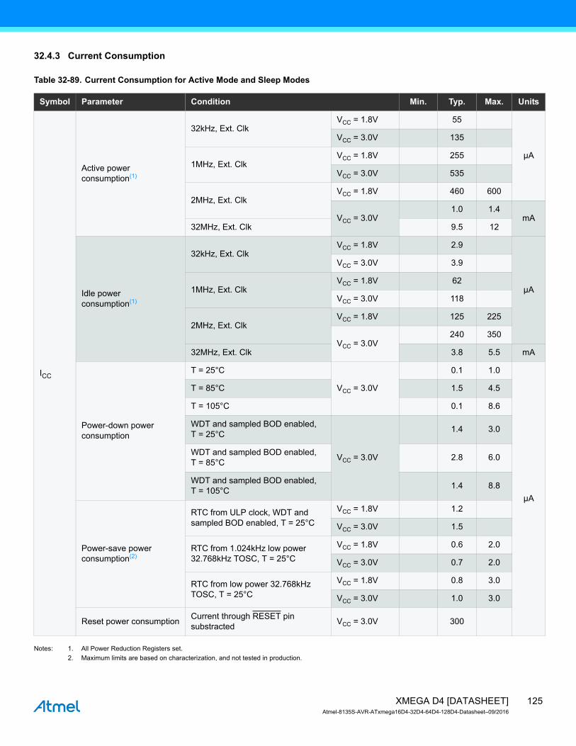
32.4.3 Current Consumption
Table 32-89. Current Consumption for Active Mode and Sleep Modes
Notes: 1. All Power Reduction Registers set.
2. Maximum limits are based on characterization, and not tested in production.
Symbol Parameter Condition Min. Typ. Max. Units
ICC
Active power consumption(1)
32kHz, Ext. ClkVCC = 1.8V 55
µA
VCC = 3.0V 135
1MHz, Ext. ClkVCC = 1.8V 255
VCC = 3.0V 535
2MHz, Ext. ClkVCC = 1.8V 460 600
VCC = 3.0V1.0 1.4
mA32MHz, Ext. Clk 9.5 12
Idle powerconsumption(1)
32kHz, Ext. ClkVCC = 1.8V 2.9
µA
VCC = 3.0V 3.9
1MHz, Ext. ClkVCC = 1.8V 62
VCC = 3.0V 118
2MHz, Ext. ClkVCC = 1.8V 125 225
VCC = 3.0V240 350
32MHz, Ext. Clk 3.8 5.5 mA
Power-down powerconsumption
T = 25°C
VCC = 3.0V
0.1 1.0
µA
T = 85°C 1.5 4.5
T = 105°C 0.1 8.6
WDT and sampled BOD enabled,T = 25°C
VCC = 3.0V
1.4 3.0
WDT and sampled BOD enabled,T = 85°C
2.8 6.0
WDT and sampled BOD enabled,T = 105°C
1.4 8.8
Power-save powerconsumption(2)
RTC from ULP clock, WDT andsampled BOD enabled, T = 25°C
VCC = 1.8V 1.2
VCC = 3.0V 1.5
RTC from 1.024kHz low power32.768kHz TOSC, T = 25°C
VCC = 1.8V 0.6 2.0
VCC = 3.0V 0.7 2.0
RTC from low power 32.768kHzTOSC, T = 25°C
VCC = 1.8V 0.8 3.0
VCC = 3.0V 1.0 3.0
Reset power consumptionCurrent through RESET pinsubstracted
VCC = 3.0V 300
125XMEGA D4 [DATASHEET]Atmel-8135S-AVR-ATxmega16D4-32D4-64D4-128D4-Datasheet–09/2016
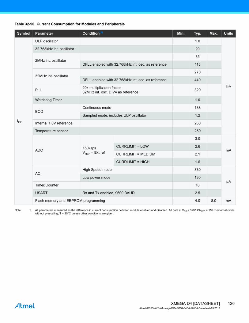
Table 32-90. Current Consumption for Modules and Peripherals
Note: 1. All parameters measured as the difference in current consumption between module enabled and disabled. All data at VCC = 3.0V, ClkSYS = 1MHz external clock without prescaling, T = 25°C unless other conditions are given.
Symbol Parameter Condition(1) Min. Typ. Max. Units
ICC
ULP oscillator 1.0
µA
32.768kHz int. oscillator 29
2MHz int. oscillator85
DFLL enabled with 32.768kHz int. osc. as reference 115
32MHz int. oscillator270
DFLL enabled with 32.768kHz int. osc. as reference 440
PLL20x multiplication factor, 32MHz int. osc. DIV4 as reference
320
Watchdog Timer 1.0
BODContinuous mode 138
Sampled mode, includes ULP oscillator 1.2
Internal 1.0V reference 260
Temperature sensor 250
ADC150kspsVREF = Ext ref
3.0
mACURRLIMIT = LOW 2.6
CURRLIMIT = MEDIUM 2.1
CURRLIMIT = HIGH 1.6
ACHigh Speed mode 330
µALow power mode 130
Timer/Counter 16
USART Rx and Tx enabled, 9600 BAUD 2.5
Flash memory and EEPROM programming 4.0 8.0 mA
126XMEGA D4 [DATASHEET]Atmel-8135S-AVR-ATxmega16D4-32D4-64D4-128D4-Datasheet–09/2016

32.4.4 Wake-up Time from Sleep Modes
Table 32-91. Device Wake-up Time from Sleep Modes with Various System Clock Sources
Note: 1. The wake-up time is the time from the wake-up request is given until the peripheral clock is available on pin, see Figure 32-23. All peripherals and modules start execution from the first clock cycle, expect the CPU that is halted for four clock cycles before program execution starts.
Figure 32-23.Wake-up Time Definition
Symbol Parameter Condition Min. Typ.(1) Max. Units
twakeup
Wake-up time from Idle,Standby, and Extended Standbymode
External 2MHz clock 2.0
µs
32.768kHz internal oscillator 120
2MHz internal oscillator 2.0
32MHz internal oscillator 0.2
Wake-up time from Power-saveand Power-down mode
External 2MHz clock 4.5
32.768kHz internal oscillator 320
2MHz internal oscillator 9.0
32MHz internal oscillator 5.0
Wakeup request
Clock output
Wakeup time
127XMEGA D4 [DATASHEET]Atmel-8135S-AVR-ATxmega16D4-32D4-64D4-128D4-Datasheet–09/2016

32.4.5 I/O Pin Characteristics
The I/O pins complies with the JEDEC LVTTL and LVCMOS specification and the high- and low level input and output voltage limits reflect or exceed this specification.
Table 32-92. I/O Pin Characteristics
Notes: 1. The sum of all IOH for PORTA and PORTB must not exceed 100mA.The sum of all IOH for PORTC must not exceed 200mA.The sum of all IOH for PORTD and pins PE[0-1] on PORTE must not exceed 200mA.The sum of all IOH for PE[2-3] on PORTE, PORTR and PDI must not exceed 100mA.
2. The sum of all IOL for PORTA and PORTB must not exceed 100mA.The sum of all IOL for PORTC must not exceed 200mA.The sum of all IOL for PORTD and pins PE[0-1] on PORTE must not exceed 200mA.The sum of all IOL for PE[2-3] on PORTE, PORTR and PDI must not exceed 100mA.
Symbol Parameter Condition Min. Typ. Max. Units
IOH(1)/
IOL(2) I/O pin source/sink current -20 20 mA
VIH High level input voltage
VCC = 2.7 - 3.6V 2.0 VCC+0.3
V
VCC = 2.0 - 2.7V 0.7*VCC VCC+0.3
VCC = 1.6 - 2.0V 0.8*VCC VCC+0.3
VIL Low level input voltage
VCC = 2.7- 3.6V -0.3 0.8
VCC = 2.0 - 2.7V -0.3 0.3*VCC
VCC = 1.6 - 2.0V -0.3 0.2*VCC
VOH High level output voltage
VCC = 3.0 - 3.6V IOH = -2mA 2.4 0.94*VCC
VCC = 2.3 - 2.7VIOH = -1mA 2.0 0.96*VCC
IOH = -2mA 1.7 0.92*VCC
VCC = 3.3V IOH = -8mA 2.6 2.9
VCC = 3.0V IOH = -6mA 2.1 2.6
VCC = 1.8V IOH = -2mA 1.4 1.6
VOL Low level output voltage
VCC = 3.0 - 3.6V IOL = 2mA 0.05 0.4
VCC = 2.3 - 2.7VIOL = 1mA 0.03 0.4
IOL = 2mA 0.06 0.7
VCC = 3.3V IOL = 15mA 0.4 0.76
VCC = 3.0V IOL = 10mA 0.3 0.64
VCC = 1.8V IOL = 5mA 0.2 0.46
IIN Input leakage current T = 25°C <0.01 0.1 µA
RP Pull/Buss keeper resistor 24 k
tr Rise time No load4.0
nsslew rate limitation 7.0
128XMEGA D4 [DATASHEET]Atmel-8135S-AVR-ATxmega16D4-32D4-64D4-128D4-Datasheet–09/2016

32.4.6 ADC Characteristics
Table 32-93. Power Supply, Reference and Input Range
Table 32-94. Clock and Timing
Symbol Parameter Condition Min. Typ. Max. Units
AVCC Analog supply voltage VCC- 0.3 VCC+ 0.3V
VREF Reference voltage 1.0 AVCC- 0.6
Rin Input resistance Switched 4.0 k
Csample Input capacitance Switched 4.4 pF
RAREF Reference input resistance (leakage only) >10 M
CAREF Reference input capacitance Static load 7.0 pF
VIN Input range -0.1 AVCC+0.1
VConversion range Differential mode, Vinp - Vinn -VREF VREF
Conversion range Single ended unsigned mode, Vinp -V VREF-V
∆V Fixed offset voltage 190 lsb
Symbol Parameter Condition Min. Typ. Max. Units
ClkADC ADC clock frequency
Maximum is 1/4 of Peripheral clock frequency
100 1400kHz
Measuring internal signals 100 125
fADC Sample rate
Current limitation (CURRLIMIT) off 14 200
kspsCURRLIMIT = LOW 14 150
CURRLIMIT = MEDIUM 14 100
CURRLIMIT = HIGH 50
Sampling time 1/2 ClkADC cycle 0.25 5 µs
Conversion time (latency)(RES+2)/2+GAINRES = 8 or 12, GAIN = 0, 1, 2 or 3
5 7 10ClkADCcycles
Start-up time ADC clock cycles 12 24
ClkADCcyclesADC settling time
After changing reference or input mode 7 7
After ADC flush 1 1
129XMEGA D4 [DATASHEET]Atmel-8135S-AVR-ATxmega16D4-32D4-64D4-128D4-Datasheet–09/2016

Table 32-95. Accuracy Characteristics
Notes: 1. Maximum numbers are based on characterisation and not tested in production, and valid for 5% to 95% input voltage range.
2. Unless otherwise noted all linearity, offset and gain error numbers are valid under the condition that external VREF is used.
Symbol Parameter Condition(2) Min. Typ. Max. Units
RES Resolution Programmable to 8 or 12 bit 8 12 12 Bits
INL(1) Integral non-linearity
50kspsVCC-1.0V < VREF< VCC-0.6V ±1.2 ±2
lsb
All VREF ±1.5 ±3
200kspsVCC-1.0V < VREF< VCC-0.6V ±1.0 ±2
All VREF ±1.5 ±3
DNL(1) Differential non-linearity guaranteed monotonic <±0.8 <±1
Offset error
-1 mV
Temperature drift <0.01 mV/K
Operating voltage drift <0.6 mV/V
Gain error
Differentialmode
External reference -1
mVAVCC/1.6 10
AVCC/2.0 8
Bandgap ±5
Temperature drift <0.02 mV/K
Operating voltage drift <0.5 mV/V
NoiseDifferential mode, shorted input200ksps, VCC = 3.6V, ClkPER = 16MHz
0.4mV rms
130XMEGA D4 [DATASHEET]Atmel-8135S-AVR-ATxmega16D4-32D4-64D4-128D4-Datasheet–09/2016
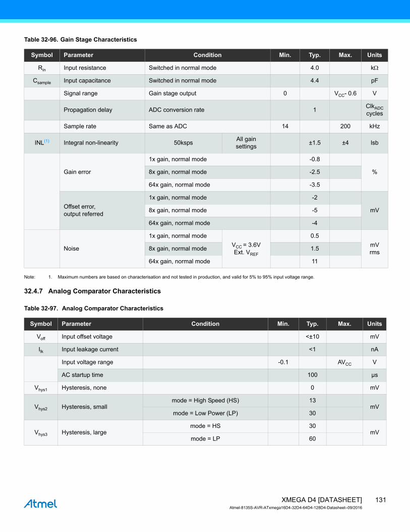
Table 32-96. Gain Stage Characteristics
Note: 1. Maximum numbers are based on characterisation and not tested in production, and valid for 5% to 95% input voltage range.
32.4.7 Analog Comparator Characteristics
Table 32-97. Analog Comparator Characteristics
Symbol Parameter Condition Min. Typ. Max. Units
Rin Input resistance Switched in normal mode 4.0 k
Csample Input capacitance Switched in normal mode 4.4 pF
Signal range Gain stage output 0 VCC- 0.6 V
Propagation delay ADC conversion rate 1ClkADCcycles
Sample rate Same as ADC 14 200 kHz
INL(1) Integral non-linearity 50kspsAll gainsettings
±1.5 ±4 lsb
Gain error
1x gain, normal mode -0.8
%8x gain, normal mode -2.5
64x gain, normal mode -3.5
Offset error,output referred
1x gain, normal mode -2
mV8x gain, normal mode -5
64x gain, normal mode -4
Noise
1x gain, normal mode
VCC = 3.6VExt. VREF
0.5
mV rms
8x gain, normal mode 1.5
64x gain, normal mode 11
Symbol Parameter Condition Min. Typ. Max. Units
Voff Input offset voltage <±10 mV
Ilk Input leakage current <1 nA
Input voltage range -0.1 AVCC V
AC startup time 100 µs
Vhys1 Hysteresis, none 0 mV
Vhys2 Hysteresis, smallmode = High Speed (HS) 13
mVmode = Low Power (LP) 30
Vhys3 Hysteresis, largemode = HS 30
mVmode = LP 60
131XMEGA D4 [DATASHEET]Atmel-8135S-AVR-ATxmega16D4-32D4-64D4-128D4-Datasheet–09/2016
32.4.8 Bandgap and Internal 1.0V Reference Characteristics
Table 32-98. Bandgap and Internal 1.0V Reference Characteristics
32.4.9 Brownout Detection Characteristics
Table 32-99. Brownout Detection Characteristics
tdelay Propagation delayVCC = 3.0V, T= 85°C mode = HS 30 90
ns30
64-Level voltage scaler Integral non-linearity (INL) 0.3 0.5 lsb
Symbol Parameter Condition Min. Typ. Max. Units
Symbol Parameter Condition Min. Typ. Max. Units
Startup timeAs reference for ADC 1 ClkPER + 2.5µs
µsAs input voltage to ADC and AC 1.5
Bandgap voltage 1.1V
INT1V Internal 1.00V reference T= 85°C, after calibration 0.99 1.0 1.01
Variation over voltage and temperature Relative to T= 85°C, VCC = 3.0V ±1.5 %
Symbol Parameter Condition Min. Typ. Max. Units
VBOT
BOD level 0 falling VCC 1.60 1.62 1.72
V
BOD level 1 falling VCC 1.8
BOD level 2 falling VCC 2.0
BOD level 3 falling VCC 2.2
BOD level 4 falling VCC 2.4
BOD level 5 falling VCC 2.6
BOD level 6 falling VCC 2.8
BOD level 7 falling VCC 3.0
tBOD Detection timeContinuous mode 0.4
µsSampled mode 1000
VHYST Hysteresis 1.2 %
132XMEGA D4 [DATASHEET]Atmel-8135S-AVR-ATxmega16D4-32D4-64D4-128D4-Datasheet–09/2016

32.4.10 External Reset Characteristics
Table 32-100.External Reset Characteristics
32.4.11 Power-on Reset Characteristics
Table 32-101.Power-on Reset Characteristics
Note: 1. VPOT- values are only valid when BOD is disabled. When BOD is enabled VPOT- = VPOT+.
32.4.12 Flash and EEPROM Memory Characteristics
Table 32-102.Endurance and Data Retention
Symbol Parameter Condition Min. Typ. Max. Units
tEXT Minimum reset pulse width 1000 95 ns
VRST
Reset threshold voltage (VIH)VCC = 2.7 - 3.6V 0.60*VCC
VVCC = 1.6 - 2.7V 0.60*VCC 0.50*VCC
Reset threshold voltage (VIL)VCC = 2.7 - 3.6V 0.40*VCC
VCC = 1.6 - 2.7V 0.50*VCC
RRST Reset pin pull-up resistor 25 k
Symbol Parameter Condition Min. Typ. Max. Units
VPOT- (1) POR threshold voltage falling VCC
VCC falls faster than 1V/ms 0.4 1.0
VVCC falls at 1V/ms or slower 0.8 1.0
VPOT+ POR threshold voltage rising VCC 1.3 1.59
Symbol Parameter Condition Min. Typ. Max. Units
Flash
Write/Erase cycles
25°C 10K
Cycle85°C 10K
105°C 2K
Data retention
25°C 100
Year85°C 25
105°C 10
EEPROM
Write/Erase cycles
25°C 100K
Cycle85°C 100K
105°C 30K
Data retention
25°C 100
Year85°C 25
105°C 10
133XMEGA D4 [DATASHEET]Atmel-8135S-AVR-ATxmega16D4-32D4-64D4-128D4-Datasheet–09/2016

Table 32-103.Programming Time
Notes: 1. Programming is timed from the 2MHz internal oscillator.
2. EEPROM is not erased if the EESAVE fuse is programmed.
32.4.13 Clock and Oscillator Characteristics
32.4.13.1 Calibrated 32.768kHz Internal Oscillator Characteristics
Table 32-104. 32.768kHz Internal Oscillator Characteristics
32.4.13.2 Calibrated 2MHz RC Internal Oscillator Characteristics
Table 32-105. 2MHz Internal Oscillator Characteristics
Symbol Parameter Condition Min. Typ.(1) Max. Units
Chip erase 128KB Flash, EEPROM(2) and SRAM erase 75 ms
Application erase Section erase 6
Flash
Page erase 4
Page write 4
Atomic Page Erase and write 8
EEPROM
Page erase 4
Page write 4
Atomic Page erase and write 8
Symbol Parameter Condition Min. Typ. Max. Units
Frequency 32.768 kHz
Factory calibration accuracy T = 85C, VCC = 3.0V -0.5 0.5%
User calibration accuracy -0.5 0.5
Symbol Parameter Condition Min. Typ. Max. Units
Frequency rangeDFLL can tune to this frequency over voltage and temperature
1.8 2.2MHz
Factory calibrated frequency 2.0
Factory calibration accuracy T = 85C, VCC= 3.0V -1.5 1.5
%User calibration accuracy -0.2 0.2
DFLL calibration stepsize 0.21
134XMEGA D4 [DATASHEET]Atmel-8135S-AVR-ATxmega16D4-32D4-64D4-128D4-Datasheet–09/2016

32.4.13.3 Calibrated and Tunable 32MHz Internal Oscillator Characteristics
Table 32-106. 32MHz Internal Oscillator Characteristics
32.4.13.4 32kHz Internal ULP Oscillator Characteristics
Table 32-107. 32kHz Internal ULP Oscillator Characteristics
32.4.13.5 Internal Phase Locked Loop (PLL) Characteristics
Table 32-108. Internal PLL Characteristics
Note: 1. The maximum output frequency vs. supply voltage is linear between 1.8V and 2.7V, and can never be higher than four times the maximum CPU frequency.
Symbol Parameter Condition Min. Typ. Max. Units
Frequency rangeDFLL can tune to this frequency over voltage and temperature
30 55MHz
Factory calibrated frequency 32
Factory calibration accuracy T = 85C, VCC= 3.0V -1.5 1.5
%User calibration accuracy -0.2 0.2
DFLL calibration step size 0.22
Symbol Parameter Condition Min. Typ. Max. Units
Factory calibrated frequency 32 kHz
Factory calibration accuracy T = 85C, VCC= 3.0V -12 12%
Accuracy -30 30
Symbol Parameter Condition Min. Typ. Max. Units
fIN Input frequency Output frequency must be within fOUT 0.4 64
MHzfOUT Output frequency(1)
VCC= 1.6 - 1.8V 20 48
VCC= 2.7 - 3.6V 20 128
Start-up time 25µs
Re-lock time 25
135XMEGA D4 [DATASHEET]Atmel-8135S-AVR-ATxmega16D4-32D4-64D4-128D4-Datasheet–09/2016
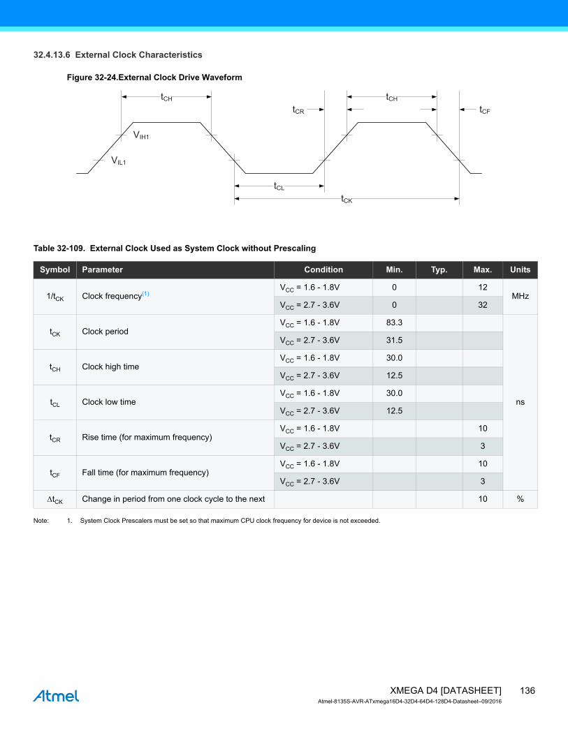
32.4.13.6 External Clock Characteristics
Figure 32-24.External Clock Drive Waveform
Table 32-109. External Clock Used as System Clock without Prescaling
Note: 1. System Clock Prescalers must be set so that maximum CPU clock frequency for device is not exceeded.
tCH
tCL
tCK
tCH
VIL1
VIH1
tCR tCF
Symbol Parameter Condition Min. Typ. Max. Units
1/tCK Clock frequency(1)VCC = 1.6 - 1.8V 0 12
MHzVCC = 2.7 - 3.6V 0 32
tCK Clock periodVCC = 1.6 - 1.8V 83.3
ns
VCC = 2.7 - 3.6V 31.5
tCH Clock high timeVCC = 1.6 - 1.8V 30.0
VCC = 2.7 - 3.6V 12.5
tCL Clock low timeVCC = 1.6 - 1.8V 30.0
VCC = 2.7 - 3.6V 12.5
tCR Rise time (for maximum frequency)VCC = 1.6 - 1.8V 10
VCC = 2.7 - 3.6V 3
tCF Fall time (for maximum frequency)VCC = 1.6 - 1.8V 10
VCC = 2.7 - 3.6V 3
tCK Change in period from one clock cycle to the next 10 %
136XMEGA D4 [DATASHEET]Atmel-8135S-AVR-ATxmega16D4-32D4-64D4-128D4-Datasheet–09/2016

Table 32-110. External Clock with Prescaler(1) for System Clock
Notes: 1. System Clock Prescalers must be set so that maximum CPU clock frequency for device is not exceeded.
2. The maximum frequency vs. supply voltage is linear between 1.8V and 2.7V, and the same applies for all other parameters with supply voltage conditions.
32.4.13.7 External 16MHz Crystal Oscillator and XOSC Characteristics
Table 32-111. External 16MHz Crystal Oscillator and XOSC Characteristics
Symbol Parameter Condition Min. Typ. Max. Units
1/tCK Clock frequency(2)VCC = 1.6 - 1.8V 0 90
MHzVCC = 2.7 - 3.6V 0 142
tCK Clock periodVCC = 1.6 - 1.8V 11
ns
VCC = 2.7 - 3.6V 7
tCH Clock high timeVCC = 1.6 - 1.8V 4.5
VCC = 2.7 - 3.6V 2.4
tCL Clock low timeVCC = 1.6 - 1.8V 4.5
VCC = 2.7 - 3.6V 2.4
tCR Rise time (for maximum frequency) 1.5
tCF Fall time (for maximum frequency) 1.5
tCK Change in period from one clock cycle to the next 10 %
Symbol Parameter Condition Min. Typ. Max. Units
Cycle to cycle jitterXOSCPWR=0
FRQRANGE=0 <10
ns
FRQRANGE=1, 2, or 3 <1
XOSCPWR=1 <1
Long term jitterXOSCPWR=0
FRQRANGE=0 <6
FRQRANGE=1, 2, or 3 <0.5
XOSCPWR=1 <0.5
Frequency errorXOSCPWR=0
FRQRANGE=0 <0.1
%
FRQRANGE=1 <0.05
FRQRANGE=2 or 3 <0.005
XOSCPWR=1 <0.005
Duty cycleXOSCPWR=0
FRQRANGE=0 40
FRQRANGE=1 42
FRQRANGE=2 or 3 45
XOSCPWR=1 48
137XMEGA D4 [DATASHEET]Atmel-8135S-AVR-ATxmega16D4-32D4-64D4-128D4-Datasheet–09/2016
RQ Negative impedance(1)
XOSCPWR=0,FRQRANGE=0
0.4MHz resonator, CL=100pF
2.4k
1MHz crystal, CL=20pF 8.7k
2MHz crystal, CL=20pF 2.1k
XOSCPWR=0,FRQRANGE=1,CL=20pF
2MHz crystal 4.2k
8MHz crystal 250
9MHz crystal 195
XOSCPWR=0,FRQRANGE=2,CL=20pF
8MHz crystal 360
9MHz crystal 285
12MHz crystal 155
XOSCPWR=0,FRQRANGE=3,CL=20pF
9MHz crystal 365
12MHz crystal 200
16MHz crystal 105
XOSCPWR=1,FRQRANGE=0,CL=20pF
9MHz crystal 435
12MHz crystal 235
16MHz crystal 125
XOSCPWR=1,FRQRANGE=1,CL=20pF
9MHz crystal 495
12MHz crystal 270
16MHz crystal 145
XOSCPWR=1,FRQRANGE=2,CL=20pF
12MHz crystal 305
16MHz crystal 160
XOSCPWR=1,FRQRANGE=3,CL=20pF
12MHz crystal 380
16MHz crystal 205
ESR SF = safety factor min(RQ)/SF k
Start-up time
XOSCPWR=0,FRQRANGE=0
0.4MHz resonator, CL=100pF
1.0
ms
XOSCPWR=0,FRQRANGE=1
2MHz crystal, CL=20pF 2.6
XOSCPWR=0,FRQRANGE=2
8MHz crystal, CL=20pF 0.8
XOSCPWR=0,FRQRANGE=3
12MHz crystal, CL=20pF 1.0
XOSCPWR=1,FRQRANGE=3
16MHz crystal, CL=20pF 1.4
Symbol Parameter Condition Min. Typ. Max. Units
138XMEGA D4 [DATASHEET]Atmel-8135S-AVR-ATxmega16D4-32D4-64D4-128D4-Datasheet–09/2016

Note: 1. Numbers for negative impedance are not tested in production but guaranteed from design and characterization.
32.4.13.8 External 32.768kHz Crystal Oscillator and TOSC Characteristics
Table 32-112. External 32.768kHz Crystal Oscillator and TOSC Characteristics
Note: 1. See Figure 32-25 for definition.
Figure 32-25.TOSC Input Capacitance
The parasitic capacitance between the TOSC pins is CL1 + CL2 in series as seen from the crystal when oscillating without external capacitors.
CXTAL1Parasitic capacitanceXTAL1 pin
5.9
pFCXTAL2
Parasitic capacitanceXTAL2 pin
8.3
CLOAD Parasitic capacitance load 3.5
Symbol Parameter Condition Min. Typ. Max. Units
ESR/R1Recommended crystal equivalentseries resistance (ESR)
Crystal load capacitance 6.5pF 60k
Crystal load capacitance 9.0pF 35
CTOSC Parasitic capacitanceNormal mode 4.7
pFLow power mode 5.2
Recommended safety factorCapacitance load matched tocrystal specification
3
Symbol Parameter Condition Min. Typ. Max. Units
CL1 CL2
2CSOT1CSOT Device internal
External
32.768KHz crystal
139XMEGA D4 [DATASHEET]Atmel-8135S-AVR-ATxmega16D4-32D4-64D4-128D4-Datasheet–09/2016
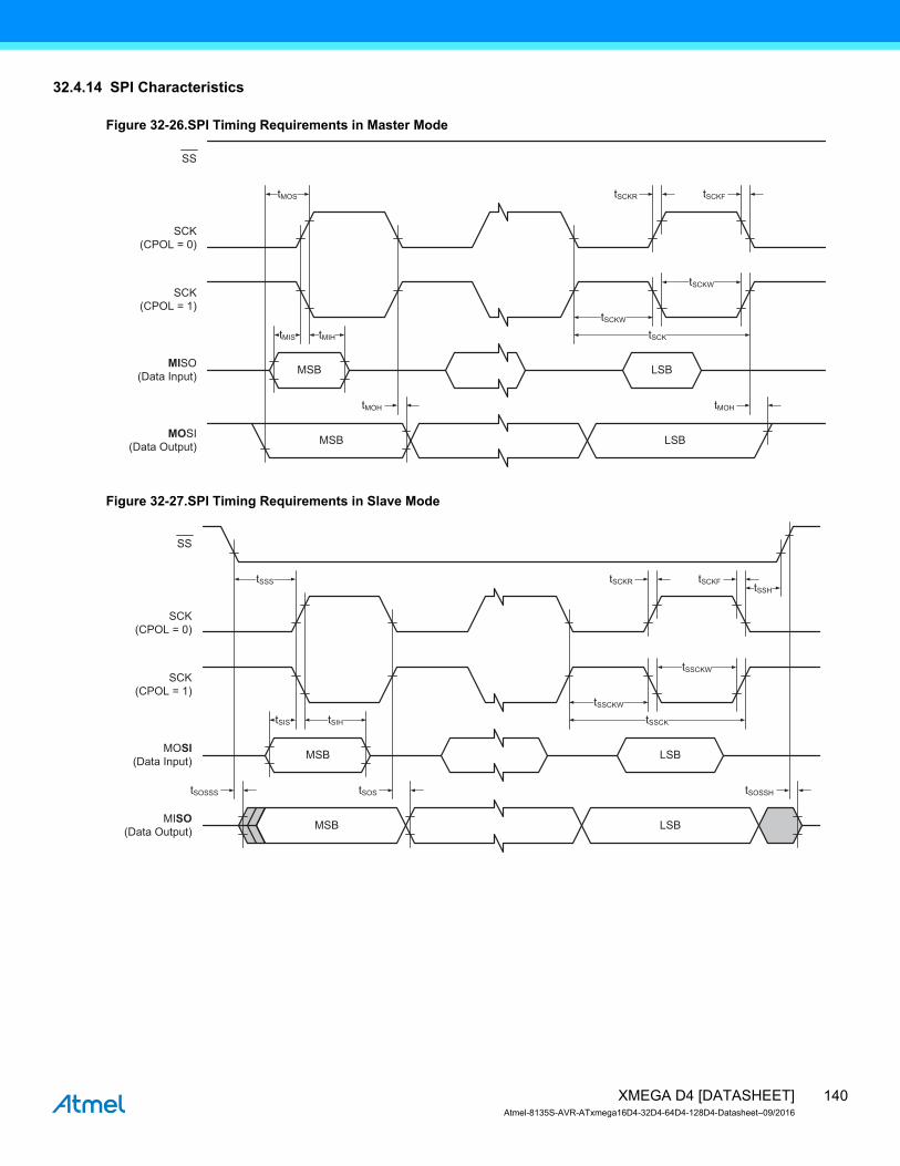
32.4.14 SPI Characteristics
Figure 32-26.SPI Timing Requirements in Master Mode
Figure 32-27.SPI Timing Requirements in Slave Mode
MSB LSB
BSLBSM
tMOS
tMIS tMIH
tSCKW
tSCK
tMOH tMOH
tSCKFtSCKR
tSCKW
MOSI
(Data Output)
MISO
(Data Input)
SCK
(CPOL = 1)
SCK
(CPOL = 0)
SS
MSB LSB
BSLBSM
tSIS tSIH
tSSCKW
tSSCKW
tSSCK
tSSH
tSOSSH
tSCKR tSCKF
tSOS
tSSS
tSOSSS
MISO(Data Output)
MOSI(Data Input)
SCK
(CPOL = 1)
SCK
(CPOL = 0)
SS
140XMEGA D4 [DATASHEET]Atmel-8135S-AVR-ATxmega16D4-32D4-64D4-128D4-Datasheet–09/2016
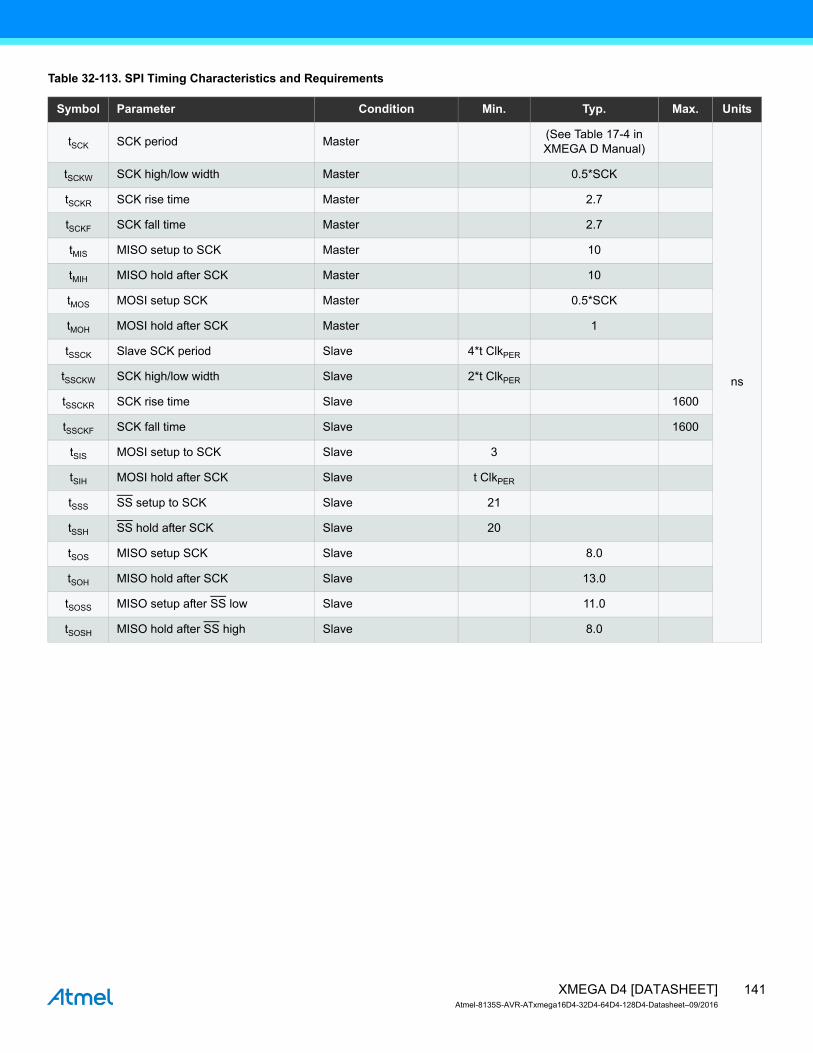
Table 32-113. SPI Timing Characteristics and Requirements
Symbol Parameter Condition Min. Typ. Max. Units
tSCK SCK period Master(See Table 17-4 in XMEGA D Manual)
ns
tSCKW SCK high/low width Master 0.5*SCK
tSCKR SCK rise time Master 2.7
tSCKF SCK fall time Master 2.7
tMIS MISO setup to SCK Master 10
tMIH MISO hold after SCK Master 10
tMOS MOSI setup SCK Master 0.5*SCK
tMOH MOSI hold after SCK Master 1
tSSCK Slave SCK period Slave 4*t ClkPER
tSSCKW SCK high/low width Slave 2*t ClkPER
tSSCKR SCK rise time Slave 1600
tSSCKF SCK fall time Slave 1600
tSIS MOSI setup to SCK Slave 3
tSIH MOSI hold after SCK Slave t ClkPER
tSSS SS setup to SCK Slave 21
tSSH SS hold after SCK Slave 20
tSOS MISO setup SCK Slave 8.0
tSOH MISO hold after SCK Slave 13.0
tSOSS MISO setup after SS low Slave 11.0
tSOSH MISO hold after SS high Slave 8.0
141XMEGA D4 [DATASHEET]Atmel-8135S-AVR-ATxmega16D4-32D4-64D4-128D4-Datasheet–09/2016

32.4.15 Two-Wire Interface Characteristics
Table 32-114 describes the requirements for devices connected to the Two-Wire Interface Bus. The Atmel AVR XMEGA Two-Wire Interface meets or exceeds these requirements under the noted conditions. Timing symbols refer to Figure 32-28.
Figure 32-28.Two-wire Interface Bus Timing
Table 32-114. Two-wire Interface Characteristics
tHD;STA
tof
SDA
SCL
tLOW
tHIGH
tSU;STA
tBUF
tr
tHD;DATtSU;DAT
tSU;STO
Symbol Parameter Condition Min. Typ. Max. Units
VIH Input high voltage 0.7*VCC VCC+0.5
VVIL Input low voltage -0.5 0.3*VCC
Vhys Hysteresis of Schmitt Trigger Inputs 0.05*VCC(1)
VOL Output low voltage 3mA, sink current 0 0.4
tr Rise time for both SDA and SCL 20+0.1Cb(1)(2) 300
nstof Output fall time from VIHmin to VILmax 10pF < Cb < 400pF(2) 20+0.1Cb(1)(2) 250
tSP Spikes suppressed by input filter 0 50
II Input current for each I/O pin 0.1VCC < VI < 0.9VCC -10 10 µA
CI Capacitance for each I/O pin 10 pF
fSCL SCL clock frequency fPER(3)>max(10fSCL, 250kHz) 0 400 kHz
RP Value of pull-up resistor
fSCL 100kHz
fSCL > 100kHz
VCC 0.4V–
3mA----------------------------
100nsCb---------------
300nsCb---------------
142XMEGA D4 [DATASHEET]Atmel-8135S-AVR-ATxmega16D4-32D4-64D4-128D4-Datasheet–09/2016
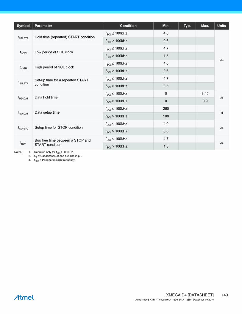
Notes: 1. Required only for fSCL > 100kHz.
2. Cb = Capacitance of one bus line in pF.
3. fPER = Peripheral clock frequency.
tHD;STA Hold time (repeated) START conditionfSCL 100kHz 4.0
µs
fSCL > 100kHz 0.6
tLOW Low period of SCL clockfSCL 100kHz 4.7
fSCL > 100kHz 1.3
tHIGH High period of SCL clockfSCL 100kHz 4.0
fSCL > 100kHz 0.6
tSU;STASet-up time for a repeated START condition
fSCL 100kHz 4.7
fSCL > 100kHz 0.6
tHD;DAT Data hold timefSCL 100kHz 0 3.45
µsfSCL > 100kHz 0 0.9
tSU;DAT Data setup timefSCL 100kHz 250
nsfSCL > 100kHz 100
tSU;STO Setup time for STOP conditionfSCL 100kHz 4.0
µsfSCL > 100kHz 0.6
tBUFBus free time between a STOP and START condition
fSCL 100kHz 4.7µs
fSCL > 100kHz 1.3
Symbol Parameter Condition Min. Typ. Max. Units
143XMEGA D4 [DATASHEET]Atmel-8135S-AVR-ATxmega16D4-32D4-64D4-128D4-Datasheet–09/2016
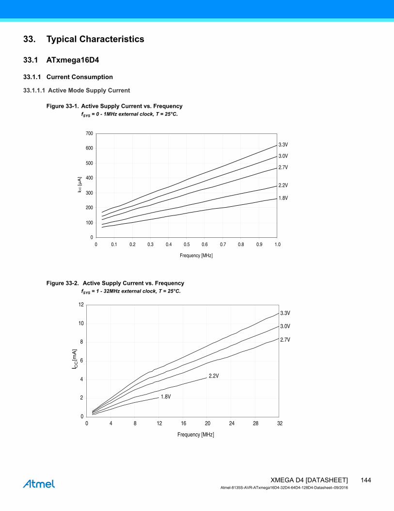
33. Typical Characteristics
33.1 ATxmega16D4
33.1.1 Current Consumption
33.1.1.1 Active Mode Supply Current
Figure 33-1. Active Supply Current vs. FrequencyfSYS = 0 - 1MHz external clock, T = 25°C.
Figure 33-2. Active Supply Current vs. FrequencyfSYS = 1 - 32MHz external clock, T = 25°C.
3.3V
3.0V
2.7V
2.2V
1.8V
0
100
200
300
400
500
600
700
0 0.1 0.2 0.3 0.4 0.5 0.6 0.7 0.8 0.9 1.0
Frequency [MHz]
ICC [µA
]
3.3V
3.0V
2.7V
0
2
4
6
8
10
12
0 4 8 12 16 20 24 28 32
Frequency [MHz]
I CC
[mA
]
2.2V
1.8V
144XMEGA D4 [DATASHEET]Atmel-8135S-AVR-ATxmega16D4-32D4-64D4-128D4-Datasheet–09/2016
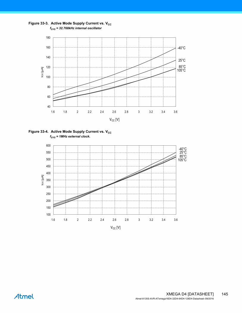
Figure 33-3. Active Mode Supply Current vs. VCC
fSYS = 32.768kHz internal oscillator
Figure 33-4. Active Mode Supply Current vs. VCC
fSYS = 1MHz external clock.
105°C85°C
25 °C
-40 °C
40
60
80
100
120
140
160
180
1.6 1.8 2 2.2 2.4 2.6 2.8 3 3.2 3.4 3.6
Icc [µ
A]
VCC [V]
105 °C85 °C25 °C
-40 °C
100
150
200
250
300
350
400
450
500
550
600
1.6 1.8 2 2.2 2.4 2.6 2.8 3 3.2 3.4 3.6
Icc [µ
A]
VCC [V]
145XMEGA D4 [DATASHEET]Atmel-8135S-AVR-ATxmega16D4-32D4-64D4-128D4-Datasheet–09/2016
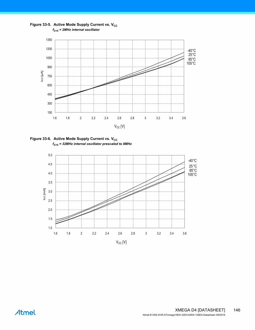
Figure 33-5. Active Mode Supply Current vs. VCC
fSYS = 2MHz internal oscillator
Figure 33-6. Active Mode Supply Current vs. VCC
fSYS = 32MHz internal oscillator prescaled to 8MHz
105 °C85 °C
25 °C-40 °C
150
300
450
600
750
900
1050
1200
1350
1.6 1.8 2 2.2 2.4 2.6 2.8 3 3.2 3.4 3.6
Icc [µ
A]
VCC [V]
105 °C85 °C25 °C
-40 °C
1.0
1.5
2.0
2.5
3.0
3.5
4.0
4.5
5.0
1.6 1.8 2 2.2 2.4 2.6 2.8 3 3.2 3.4 3.6
Icc [m
A]
VCC [V]
146XMEGA D4 [DATASHEET]Atmel-8135S-AVR-ATxmega16D4-32D4-64D4-128D4-Datasheet–09/2016
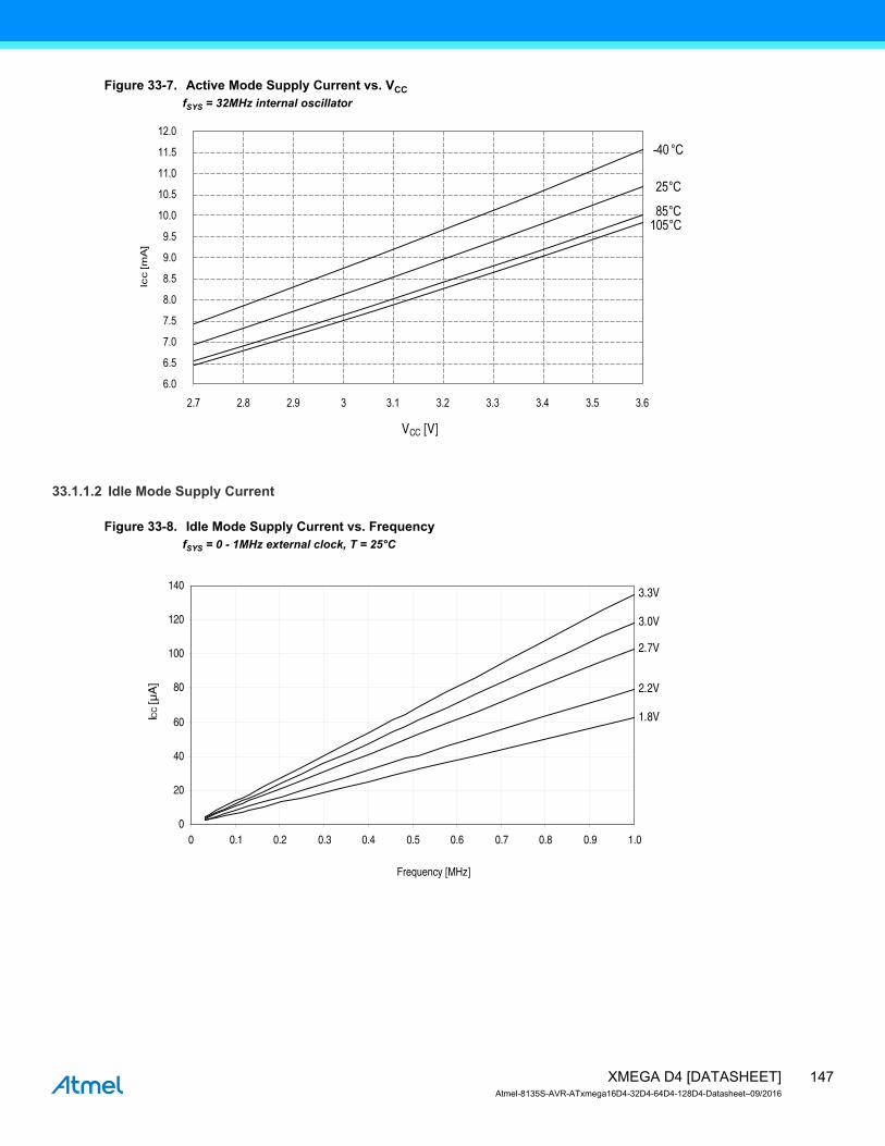
Figure 33-7. Active Mode Supply Current vs. VCC
fSYS = 32MHz internal oscillator
33.1.1.2 Idle Mode Supply Current
Figure 33-8. Idle Mode Supply Current vs. FrequencyfSYS = 0 - 1MHz external clock, T = 25°C
105 °C85 °C
25 °C
-40 °C
6.0
6.5
7.0
7.5
8.0
8.5
9.0
9.5
10.0
10.5
11.0
11.5
12.0
2.7 2.8 2.9 3 3.1 3.2 3.3 3.4 3.5 3.6
Icc [m
A]
VCC [V]
3.3V
3.0V
2.7V
2.2V
1.8V
0
20
40
60
80
100
120
140
0 0.1 0.2 0.3 0.4 0.5 0.6 0.7 0.8 0.9 1.0
Frequency [MHz]
ICC [µA
]
147XMEGA D4 [DATASHEET]Atmel-8135S-AVR-ATxmega16D4-32D4-64D4-128D4-Datasheet–09/2016
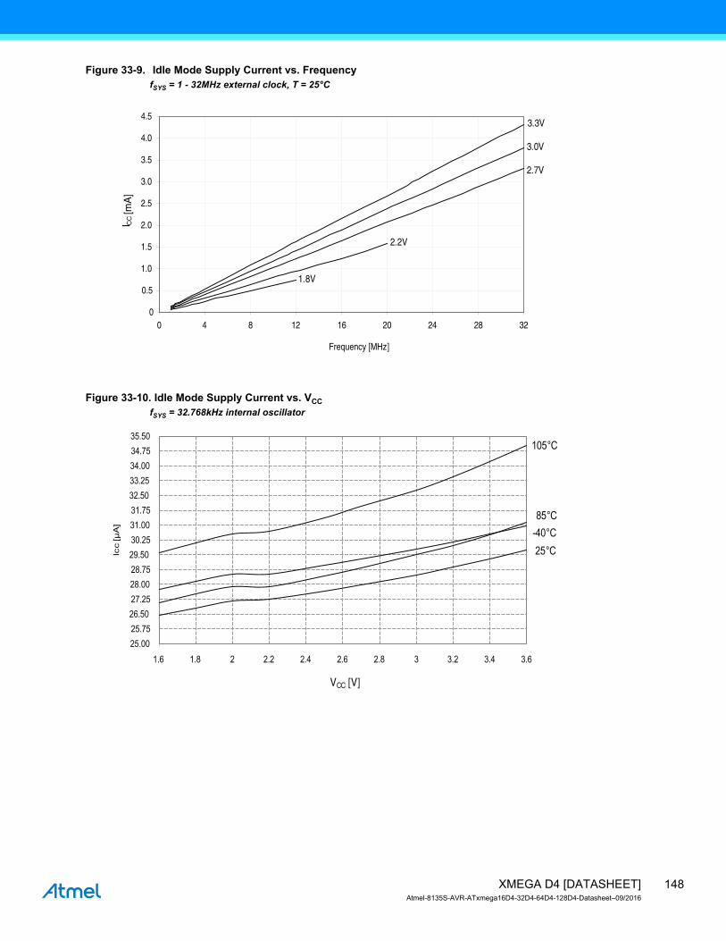
Figure 33-9. Idle Mode Supply Current vs. FrequencyfSYS = 1 - 32MHz external clock, T = 25°C
Figure 33-10. Idle Mode Supply Current vs. VCC
fSYS = 32.768kHz internal oscillator
3.3V
3.0V
2.7V
0
0.5
1.0
1.5
2.0
2.5
3.0
3.5
4.0
4.5
0 4 8 12 16 20 24 28 32
Frequency [MHz]
I CC
[mA
]
2.2V
1.8V
105 °C
85 °C
25 °C
-40 °C
25.00
25.75
26.50
27.25
28.00
28.75
29.50
30.25
31.00
31.75
32.50
33.25
34.00
34.75
35.50
1.6 1.8 2 2.2 2.4 2.6 2.8 3 3.2 3.4 3.6
Icc [µ
A]
VCC [V]
148XMEGA D4 [DATASHEET]Atmel-8135S-AVR-ATxmega16D4-32D4-64D4-128D4-Datasheet–09/2016

Figure 33-11. Idle Mode Supply Current vs. VCC
fSYS = 1MHz external clock
Figure 33-12. Idle Mode Supply Current vs. VCC
fSYS = 2MHz internal oscillator
105 °C
85 °C25 °C
-40 °C
30
40
50
60
70
80
90
100
110
120
130
1.6 1.8 2 2.2 2.4 2.6 2.8 3 3.2 3.4 3.6
Icc [µ
A]
VCC [V]
105 °C85 °C25 °C
-40 °C
110
130
150
170
190
210
230
250
270
290
310
330
1.6 1.8 2 2.2 2.4 2.6 2.8 3 3.2 3.4 3.6
Icc [µ
A]
VCC [V]
149XMEGA D4 [DATASHEET]Atmel-8135S-AVR-ATxmega16D4-32D4-64D4-128D4-Datasheet–09/2016

Figure 33-13. Idle Mode Supply Current vs. VCC
fSYS = 32MHz internal oscillator prescaled to 8MHz
Figure 33-14. Idle Mode Current vs. VCC
fSYS = 32MHz internal oscillator
105°C85 °C25 °C
-40 °C
500
600
700
800
900
1000
1100
1200
1300
1400
1500
1600
1.6 1.8 2 2.2 2.4 2.6 2.8 3 3.2 3.4 3.6
Icc [µ
A]
VCC [V]
105 °C85 °C
25 °C
-40°C
2.25
2.50
2.75
3.00
3.25
3.50
3.75
4.00
4.25
2.7 2.8 2.9 3 3.1 3.2 3.3 3.4 3.5 3.6
Icc [m
A]
VCC [V]
150XMEGA D4 [DATASHEET]Atmel-8135S-AVR-ATxmega16D4-32D4-64D4-128D4-Datasheet–09/2016

33.1.1.3 Power-down Mode Supply Current
Figure 33-15. Power-down Mode Supply Current vs. VCC
All functions disabled
Figure 33-16. Power-down Mode Supply Current vs. VCC
Watchdog and sampled BOD enabled
105 °C
85 °C
25°C
-40°C1.0
1.5
2.0
2.5
3.0
3.5
4.0
4.5
5.0
5.5
6.0
6.5
1.8 2 2.2 2.4 2.6 2.8 3 3.2 3.4 3.6
Icc [µ
A]
VCC [V]
105 °C
85 °C
25 °C
-40 °C0.0
0.5
1.0
1.5
2.0
2.5
3.0
3.5
4.0
4.5
5.0
5.5
1.6 1.8 2 2.2 2.4 2.6 2.8 3 3.2 3.4 3.6
Icc [µ
A]
VCC [V]
151XMEGA D4 [DATASHEET]Atmel-8135S-AVR-ATxmega16D4-32D4-64D4-128D4-Datasheet–09/2016

Figure 33-17. Power-down Mode Supply Current vs. TemperatureWatchdog and sampled BOD enabled and running from internal ULP oscillator
33.1.1.4 Power-save Mode Supply Current
Figure 33-18. Power-save Mode Supply Current vs.VCC
Real Time Counter enabled and running from 1.024kHz output of 32.768kHz TOSC
3.6V
3.0V2.7V
2.2V1.8V
1.0
1.5
2.0
2.5
3.0
3.5
4.0
4.5
5.0
5.5
6.0
6.5
7.0
7.5
-45 -35 -25 -15 -5 5 15 25 35 45 55 65 75 85 95 105
Icc [µ
A]
Temperature [°C]
Normal mode
Low-power mode
0
0.1
0.2
0.3
0.4
0.5
0.6
0.7
0.8
0.9
VCC [V]
I CC [µ
A]
1.6 1.8 2.0 2.2 2.4 2.6 2.8 3.0 3.2 3.4 3.6
152XMEGA D4 [DATASHEET]Atmel-8135S-AVR-ATxmega16D4-32D4-64D4-128D4-Datasheet–09/2016
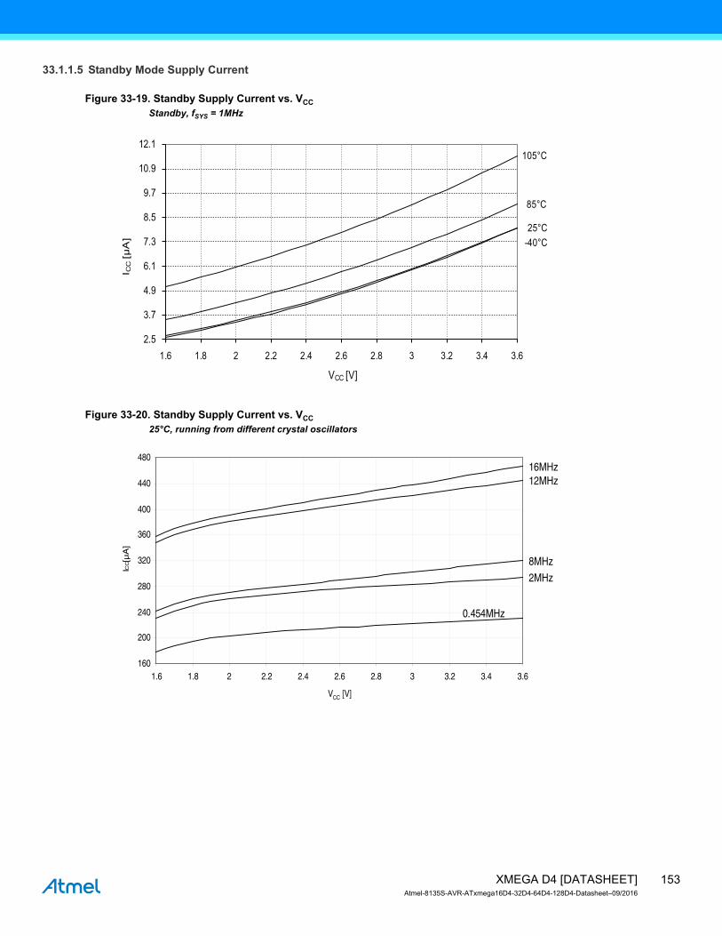
33.1.1.5 Standby Mode Supply Current
Figure 33-19. Standby Supply Current vs. VCC
Standby, fSYS = 1MHz
Figure 33-20. Standby Supply Current vs. VCC
25°C, running from different crystal oscillators
105°C
85°C
25°C
-40°C
2.5
3.7
4.9
6.1
7.3
8.5
9.7
10.9
12.1
1.6 1.8 2 2.2 2.4 2.6 2.8 3 3.2 3.4 3.6
I CC
[µA
]
VCC [V]
16MHz12MHz
8MHz
2MHz
0.454MHz
160
200
240
280
320
360
400
440
480
1.6 1.8 2 2.2 2.4 2.6 2.8 3 3.2 3.4 3.6
VCC [V]
ICC[µ
A]
153XMEGA D4 [DATASHEET]Atmel-8135S-AVR-ATxmega16D4-32D4-64D4-128D4-Datasheet–09/2016

33.1.2 I/O Pin Characteristics
33.1.2.1 Pull-up
Figure 33-21. I/O Pin Pull-up Resistor Current vs. Input VoltageVCC = 1.8V
Figure 33-22. I/O Pin Pull-up Resistor Current vs. Input VoltageVCC = 3.0V
105°C
85°C25°C
-40°C
0
8
16
24
32
40
48
56
64
72
0.1 0.3 0.5 0.7 0.9 1.1 1.3 1.5 1.7
VPIN [V]
I PIN [
µA
]
105°C85°C25°C
-40°C
0
12
24
36
48
60
72
84
96
108
120
0.1 0.3 0.5 0.7 0.9 1.1 1.3 1.5 1.7 1.9 2.1 2.3 2.5 2.7 2.9
VPIN [V]
I PIN [
µA
]
154XMEGA D4 [DATASHEET]Atmel-8135S-AVR-ATxmega16D4-32D4-64D4-128D4-Datasheet–09/2016

Figure 33-23. I/O pin pull-up Resistor Current vs. Input VoltageVCC = 3.3V
33.1.2.2 Output Voltage vs. Sink/Source Current
Figure 33-24. I/O Pin Output Voltage vs. Source CurrentVCC = 1.8V
105°C85°C
25°C
-40°C
0
15
30
45
60
75
90
105
120
135
0.1 0.3 0.5 0.7 0.9 1.1 1.3 1.5 1.7 1.9 2.1 2.3 2.5 2.7 2.9 3.1 3.3
VPIN [V]
I PIN [
µA
]
105°C85°C25°C-40°C
0
0.2
0.4
0.6
0.8
1.0
1.2
1.4
1.6
1.8
2.0
-5 -4.5 -4 -3.5 -3 -2.5 -2 -1.5 -1 -0.5 0
IPIN [mA]
V PIN [V
]
155XMEGA D4 [DATASHEET]Atmel-8135S-AVR-ATxmega16D4-32D4-64D4-128D4-Datasheet–09/2016
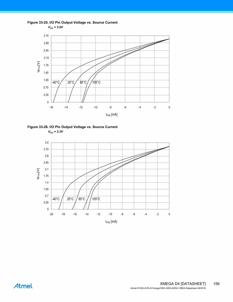
Figure 33-25. I/O Pin Output Voltage vs. Source CurrentVCC = 3.0V
Figure 33-26. I/O Pin Output Voltage vs. Source CurrentVCC = 3.3V
105 °C85 °C25 °C-40 °C
0
0.35
0.70
1.05
1.40
1.75
2.10
2.45
2.80
3.15
-16 -14 -12 -10 -8 -6 -4 -2 0
IPIN [mA]
VP
IN [
V]
105°C85°C25°C-40°C
0
0.35
0.7
1.05
1.4
1.75
2.1
2.45
2.8
3.15
3.5
-20 -18 -16 -14 -12 -10 -8 -6 -4 -2 0
IPIN [mA]
VP
IN [
V]
156XMEGA D4 [DATASHEET]Atmel-8135S-AVR-ATxmega16D4-32D4-64D4-128D4-Datasheet–09/2016

Figure 33-27. I/O Pin Output Voltage vs. Source Current
Figure 33-28. I/O Pin Output Voltage vs. Sink CurrentVCC = 1.8V
3.6 V
3.3 V
2.7 V
2.2 V
1.8 V
0
0.3
0.6
0.9
1.2
1.5
1.8
2.1
2.4
2.7
3
3.3
3.6
-20 -18 -16 -14 -12 -10 -8 -6 -4 -2 0
IPIN [mA]
VP
IN [
V]
0
0.1
0.2
0.3
0.4
0.5
0.6
0.7
0.8
0.9
1
0 1 2 3 4 5 6 7 8 9 10
105°C 85°C 25°C -40°C
IPIN [mA]
VP
IN [
V]
157XMEGA D4 [DATASHEET]Atmel-8135S-AVR-ATxmega16D4-32D4-64D4-128D4-Datasheet–09/2016

Figure 33-29. I/O Pin Output Voltage vs. Sink CurrentVCC = 3.0V
Figure 33-30. I/O Pin Output Voltage vs. Sink CurrentVCC = 3.3V
0
0.1
0.2
0.3
0.4
0.5
0.6
0.7
0.8
0.9
1.0
1.1
0 2 4 6 8 10 12 14 16
IPIN [mA]
VP
IN [
V]
85°C
25°C
-40°C
105°C
0
0.1
0.2
0.3
0.4
0.5
0.6
0.7
0.8
0.9
1
0 2 4 6 8 10 12 14 16
IPIN [mA]
VP
IN [
V]
85°C
25°C
-40°C
105°C
158XMEGA D4 [DATASHEET]Atmel-8135S-AVR-ATxmega16D4-32D4-64D4-128D4-Datasheet–09/2016

Figure 33-31. I/O Pin Output Voltage vs. Sink Current
33.1.2.3 Thresholds and Hysteresis
Figure 33-32. I/O Pin Input Threshold Voltage vs. VCC
T = 25C
0
0.15
0.3
0.45
0.6
0.75
0.9
1.05
1.2
1.35
1.5
0 2 4 6 8 10 12 14 16 18 20
IPIN [mA]
VP
IN [
V]
3.6V3.3V
3.0V
2.7V1.8V1.6V
VIL
VIH
0
0.2
0.4
0.6
0.8
1.0
1.2
1.4
1.6
1.8
1.6 1.8 2.0 2.2 2.4 2.6 2.8 3.0 3.2 3.4 3.6
VCC [V]
Vth
res
ho
ld [V
]
159XMEGA D4 [DATASHEET]Atmel-8135S-AVR-ATxmega16D4-32D4-64D4-128D4-Datasheet–09/2016
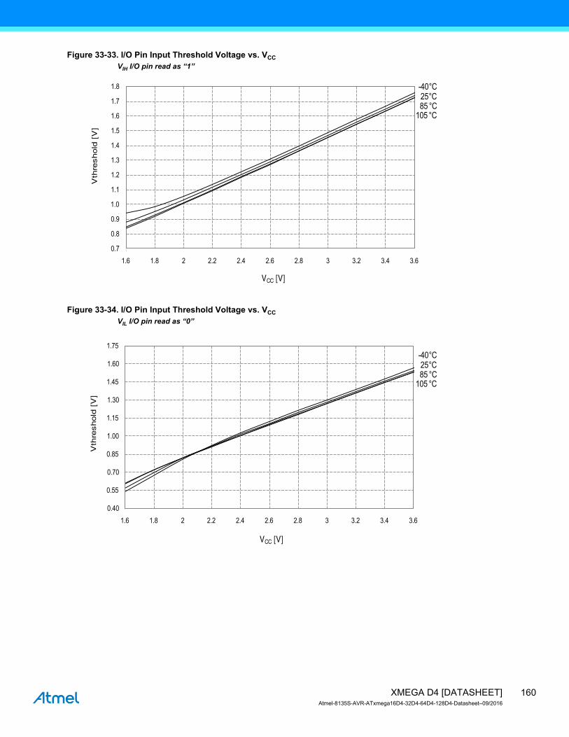
Figure 33-33. I/O Pin Input Threshold Voltage vs. VCC
VIH I/O pin read as “1”
Figure 33-34. I/O Pin Input Threshold Voltage vs. VCC
VIL I/O pin read as “0”
0.7
0.8
0.9
1.0
1.1
1.2
1.3
1.4
1.5
1.6
1.7
1.8
1.6 1.8 2 2.2 2.4 2.6 2.8 3 3.2 3.4 3.6
105 °C85 °C25 °C
-40 °C
VCC [V]
Vth
reshold
[V
]
0.40
0.55
0.70
0.85
1.00
1.15
1.30
1.45
1.60
1.75
1.6 1.8 2 2.2 2.4 2.6 2.8 3 3.2 3.4 3.6
105 °C85 °C25 °C
-40 °C
VCC [V]
Vth
reshold
[V
]
160XMEGA D4 [DATASHEET]Atmel-8135S-AVR-ATxmega16D4-32D4-64D4-128D4-Datasheet–09/2016

Figure 33-35. I/O Pin Input Hysteresis vs. VCC
33.1.3 ADC Characteristics
Figure 33-36. INL Error vs. External VREF
T = 25C, VCC = 3.6V, external reference
0.15
0.18
0.21
0.24
0.27
0.3
0.33
0.36
0.39
0.42
1.6 1.8 2 2.2 2.4 2.6 2.8 3 3.2 3.4 3.6
VCC [V]
Vth
reshold
[V
]
85°C
25°C
-40°C
105°C
Differential mode
Single-ended signed mode
Single-ended unsigned mode
0.0
0.2
0.4
0.6
0.8
1.0
1.2
1.4
1.6
1.0 1.2 1.4 1.6 1.8 2.0 2.2 2.4 2.6 2.8 3.0
VREF [V]
INL[L
SB
]
161XMEGA D4 [DATASHEET]Atmel-8135S-AVR-ATxmega16D4-32D4-64D4-128D4-Datasheet–09/2016
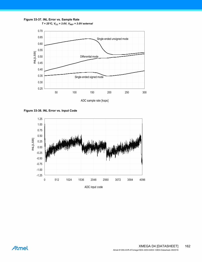
Figure 33-37. INL Error vs. Sample RateT = 25C, VCC = 3.6V, VREF = 3.0V external
Figure 33-38. INL Error vs. Input Code
Differential mode
Single-ended signed mode
Single-ended unsigned mode
0.25
0.30
0.35
0.40
0.45
0.50
0.55
0.60
0.65
0.70
ADC sample rate [ksps]
INL[L
SB
]
50 100 150 200 250 300
-1.25
-1.00
-0.75
-0.50
-0.25
0.00
0.25
0.50
0.75
1.00
1.25
0 512 1024 1536 2048 2560 3072 3584 4096
ADC input code
INL[L
SB
]
162XMEGA D4 [DATASHEET]Atmel-8135S-AVR-ATxmega16D4-32D4-64D4-128D4-Datasheet–09/2016
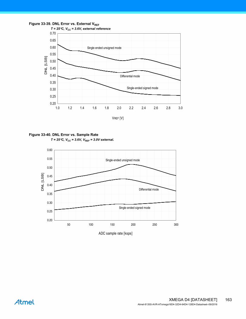
Figure 33-39. DNL Error vs. External VREF
T = 25C, VCC = 3.6V, external reference
Figure 33-40. DNL Error vs. Sample RateT = 25C, VCC = 3.6V, VREF = 3.0V external.
Differential mode
Single-ended signed mode
Single-ended unsigned mode
0.20
0.25
0.30
0.35
0.40
0.45
0.50
0.55
0.60
0.65
0.70
1.0 1.2 1.4 1.6 1.8 2.0 2.2 2.4 2.6 2.8 3.0
VREF [V]
DN
L [
LS
B]
Differential mode
Single-ended signed mode
Single-ended unsigned mode
0.20
0.25
0.30
0.35
0.40
0.45
0.50
0.55
0.60
50 100 150 200 250 300
ADC sample rate [ksps]
DN
L [
LS
B]
163XMEGA D4 [DATASHEET]Atmel-8135S-AVR-ATxmega16D4-32D4-64D4-128D4-Datasheet–09/2016

Figure 33-41. DNL Error vs. Input Code
Figure 33-42. Gain Error vs. VREF
T = 25C, VCC = 3.6V, ADC sample rate = 200ksps
-0.6
-0.4
-0.2
0
0.2
0.4
0.6
0.8
1
0 512 1024 1536 2048 2560 3072 3584 4096
ADC input code
DN
L [LS
B]
Differential mode
Single-ended signed mode
Single-ended unsigned mode
-15
-14
-13
-12
-11
-10
-9
-8
-7
-6
-5
1.0 1.2 1.4 1.6 1.8 2.0 2.2 2.4 2.6 2.8 3.0
VREF [V]
Gain
err
or
[m
V]
164XMEGA D4 [DATASHEET]Atmel-8135S-AVR-ATxmega16D4-32D4-64D4-128D4-Datasheet–09/2016
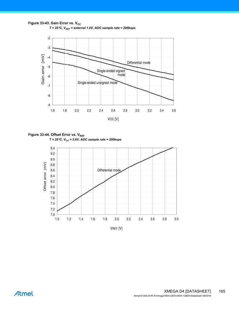
Figure 33-43. Gain Error vs. VCC
T = 25C, VREF = external 1.0V, ADC sample rate = 200ksps
Figure 33-44. Offset Error vs. VREF
T = 25C, VCC = 3.6V, ADC sample rate = 200ksps
Differential mode
Single-ended signed mode
Single-ended unsigned mode
-9
-8
-7
-6
-5
-4
-3
-2
1.6 1.8 2.0 2.2 2.4 2.6 2.8 3.0 3.2 3.4 3.6
VCC [V]
Gain
err
or
[m
V]
Differential mode
7.0
7.2
7.4
7.6
7.8
8.0
8.2
8.4
8.6
8.8
9.0
9.2
9.4
1.0 1.2 1.4 1.6 1.8 2.0 2.2 2.4 2.6 2.8 3.0
VREF [V]
Off
set
err
or
[m
V]
165XMEGA D4 [DATASHEET]Atmel-8135S-AVR-ATxmega16D4-32D4-64D4-128D4-Datasheet–09/2016
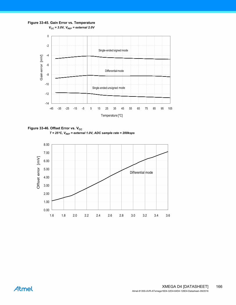
Figure 33-45. Gain Error vs. TemperatureVCC = 3.0V, VREF = external 2.0V
Figure 33-46. Offset Error vs. VCC
T = 25C, VREF = external 1.0V, ADC sample rate = 200ksps
Differential mode
Single-ended signed mode
Single-ended unsigned mode
-14
-12
-10
-8
-6
-4
-2
0
-45 -35 -25 -15 -5 5 15 25 35 45 55 65 75 85 95 105
Gain
err
or [m
V]
Temperature [°C]
Differential mode
0.00
1.00
2.00
3.00
4.00
5.00
6.00
7.00
8.00
1.6 1.8 2.0 2.2 2.4 2.6 2.8 3.0 3.2 3.4 3.6
Off
set
err
or
[m
V]
166XMEGA D4 [DATASHEET]Atmel-8135S-AVR-ATxmega16D4-32D4-64D4-128D4-Datasheet–09/2016

33.1.4 Analog Comparator Characteristics
Figure 33-47. Analog Comparator Hysteresis vs. VCC
High speed, small hysteresis
Figure 33-48. Analog Comparator Hysteresis vs. VCC
High speed, large hysteresis
4
5
6
7
8
9
10
11
12
13
14
1.6 1.8 2 2.2 2.4 2.6 2.8 3 3.2 3.4 3.6
-40°C
25°C
85°C
VCC [V]
VH
YS
T [m
V]
105°C
14
16
18
20
22
24
26
28
30
32
1.6 1.8 2 2.2 2.4 2.6 2.8 3 3.2 3.4 3.6
-40°C
25°C
85°C
VCC [V]
VH
YS
T [m
V]
105°C
167XMEGA D4 [DATASHEET]Atmel-8135S-AVR-ATxmega16D4-32D4-64D4-128D4-Datasheet–09/2016
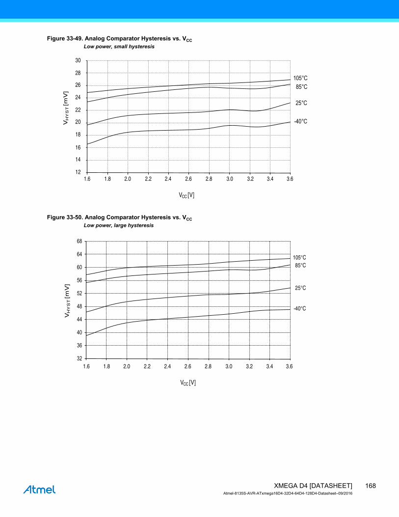
Figure 33-49. Analog Comparator Hysteresis vs. VCC
Low power, small hysteresis
Figure 33-50. Analog Comparator Hysteresis vs. VCC
Low power, large hysteresis
1.6 1.8 2.0 2.2 2.4 2.6 2.8 3.0 3.2 3.4 3.6
VCC [V]
VH
YS
T [m
V]
12
14
16
18
20
22
24
26
28
30
105 °C
85 °C
25°C
-40°C
32
36
40
44
48
52
56
60
64
68
-40°C
25°C
85°C
1.6 1.8 2.0 2.2 2.4 2.6 2.8 3.0 3.2 3.4 3.6
VCC [V]
VH
YS
T [m
V]
105°C
168XMEGA D4 [DATASHEET]Atmel-8135S-AVR-ATxmega16D4-32D4-64D4-128D4-Datasheet–09/2016

Figure 33-51. Analog Comparator Current Source vs. Calibration ValueT = 25C
Figure 33-52. Analog Comparator Current Source vs. Calibration ValueVCC = 3.0V
3.6V
3.0V
2.2V
1.8V2
2.75
3.5
4.25
5
5.75
6.5
7.25
8
0 1 2 3 4 5 6 7 8 9 10 11 12 13 14 15
CALIBA [3..0]
I CU
RR
EN
TS
OU
RC
E [µ
A]
105°C85 °C25 °C
-40 °C
3.0
3.4
3.8
4.2
4.6
5.0
5.4
5.8
6.2
6.6
7.0
0 1 2 3 4 5 6 7 8 9 10 11 12 13 14 15
CALIBA [3..0]
I CU
RR
EN
TS
OU
RC
E [µ
A]
169XMEGA D4 [DATASHEET]Atmel-8135S-AVR-ATxmega16D4-32D4-64D4-128D4-Datasheet–09/2016
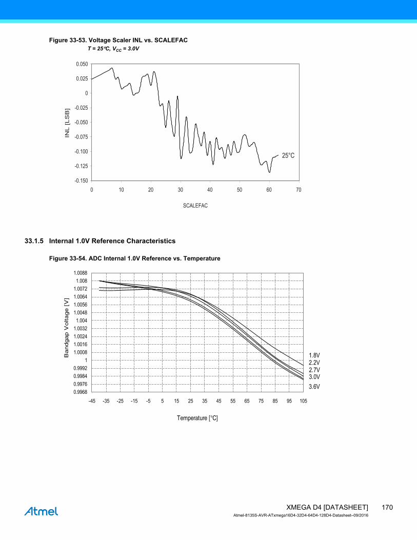
Figure 33-53. Voltage Scaler INL vs. SCALEFACT = 25C, VCC = 3.0V
33.1.5 Internal 1.0V Reference Characteristics
Figure 33-54. ADC Internal 1.0V Reference vs. Temperature
25°C
-0.150
-0.125
-0.100
-0.075
-0.050
-0.025
0
0.025
0.050
0 10 20 30 40 50 60 70
SCALEFAC
INL [
LS
B]
3.6V
3.0V2.7V2.2V1.8V
0.9968
0.9976
0.9984
0.9992
1
1.0008
1.0016
1.0024
1.0032
1.004
1.0048
1.0056
1.0064
1.0072
1.008
1.0088
-45 -35 -25 -15 -5 5 15 25 35 45 55 65 75 85 95 105
Temperature [°C]
Bandgap V
oltage [
V]
170XMEGA D4 [DATASHEET]Atmel-8135S-AVR-ATxmega16D4-32D4-64D4-128D4-Datasheet–09/2016

33.1.6 BOD Characteristics
Figure 33-55. BOD Thresholds vs. TemperatureBOD level = 1.6V
Figure 33-56. BOD Thresholds vs. TemperatureBOD level = 3.0V
1.538
1.542
1.546
1.55
1.554
1.558
1.562
1.566
1.57
1.574
-45 -35 -25 -15 -5 5 15 25 35 45 55 65 75 85 95 105
Rising Vcc
Falling Vcc
Temperature [°C]
VB
OT
[V]
2.92
2.928
2.936
2.944
2.952
2.96
2.968
2.976
2.984
2.992
-45 -35 -25 -15 -5 5 15 25 35 45 55 65 75 85 95 105
Rising Vcc
Falling Vcc
Temperature [°C]
VB
OT
[V]
171XMEGA D4 [DATASHEET]Atmel-8135S-AVR-ATxmega16D4-32D4-64D4-128D4-Datasheet–09/2016
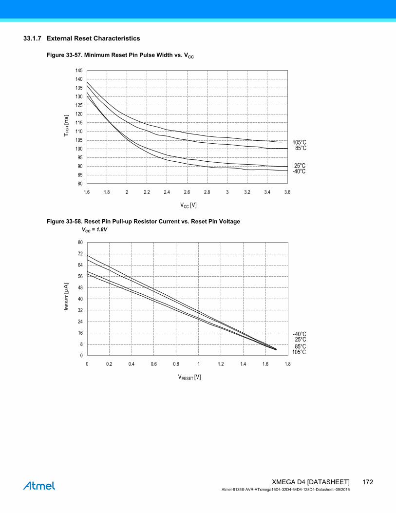
33.1.7 External Reset Characteristics
Figure 33-57. Minimum Reset Pin Pulse Width vs. VCC
Figure 33-58. Reset Pin Pull-up Resistor Current vs. Reset Pin VoltageVCC = 1.8V
105°C85°C
25°C-40°C
80
85
90
95
100
105
110
115
120
125
130
135
140
145
1.6 1.8 2 2.2 2.4 2.6 2.8 3 3.2 3.4 3.6
VCC [V]
TR
ST [
ns]
105°C85°C25°C
-40°C
0
8
16
24
32
40
48
56
64
72
80
0 0.2 0.4 0.6 0.8 1 1.2 1.4 1.6 1.8
VRESET [V]
I RE
SE
T [µ
A]
172XMEGA D4 [DATASHEET]Atmel-8135S-AVR-ATxmega16D4-32D4-64D4-128D4-Datasheet–09/2016

Figure 33-59. Reset Pin Pull-up Resistor Current vs. Reset Pin VoltageVCC = 3.0V
Figure 33-60. Reset Pin Pull-up Resistor Current vs. Reset Pin VoltageVCC = 3.3V
0
15
30
45
60
75
90
105
120
135
0 0.3 0.6 0.9 1.2 1.5 1.8 2.1 2.4 2.7 3
105°C85°C25°C
-40°C
VRESET [V]
I RE
SE
T [µ
A]
0
15
30
45
60
75
90
105
120
135
150
0 0.3 0.6 0.9 1.2 1.5 1.8 2.1 2.4 2.7 3 3.3
105°C85°C25°C
-40°C
VRESET [V]
I RE
SE
T [µ
A]
173XMEGA D4 [DATASHEET]Atmel-8135S-AVR-ATxmega16D4-32D4-64D4-128D4-Datasheet–09/2016

Figure 33-61. Reset Pin Input Threshold Voltage vs. VCC
VIH - Reset pin read as “1”
Figure 33-62. Reset Pin Input Threshold Voltage vs. VCC
VIL - Reset pin read as “0”
105°C
85°C
25°C-40°C
1.00
1.10
1.20
1.30
1.40
1.50
1.60
1.70
1.80
1.90
2.00
2.10
1.6 1.8 2.0 2.2 2.4 2.6 2.8 3.0 3.2 3.4 3.6
Vth
resh
old
[V]
VCC [V]
0.4
0.5
0.6
0.7
0.8
0.9
1
1.1
1.2
1.3
1.4
1.5
1.6
1.7
1.6 1.8 2 2.2 2.4 2.6 2.8 3 3.2 3.4 3.6
105 °C85 °C25 °C
-40 °C
VCC [V]
Vth
reshold
[V
]
174XMEGA D4 [DATASHEET]Atmel-8135S-AVR-ATxmega16D4-32D4-64D4-128D4-Datasheet–09/2016

33.1.8 Power-on Reset Characteristics
Figure 33-63. Power-on Reset Current Consumption vs. VCC
BOD level = 3.0V, enabled in continuous mode
Figure 33-64. Power-on Reset Current Consumption vs. VCC
BOD level = 3.0V, enabled in sampled mode
105°C85°C
25°C
-40°C
0
100
200
300
400
500
600
700
0.4 0.7 1.0 1.3 1.6 1.9 2.2 2.5 2.8
I CC
[µA
]
VCC [V]
105°C
85°C
25°C
-40°C
0
65
130
195
260
325
390
455
520
585
650
0.4 0.7 1 1.3 1.6 1.9 2.2 2.5 2.8
I CC
[µA
]
VCC [V]
175XMEGA D4 [DATASHEET]Atmel-8135S-AVR-ATxmega16D4-32D4-64D4-128D4-Datasheet–09/2016

33.1.9 Oscillator Characteristics
33.1.9.1 Ultra Low-Power Internal Oscillator
Figure 33-65. Ultra Low-Power Internal Oscillator Frequency vs. Temperature
33.1.9.2 32.768kHz Internal Oscillator
Figure 33-66. 32.768kHz Internal Oscillator Frequency vs. Temperature
3.6V3.3V3.0V
2.7V
2.0V1.8V30.9
31.2
31.5
31.8
32.1
32.4
32.7
33.0
33.3
33.6
33.9
34.2
34.5
34.8
35.1
35.4
-45 -35 -25 -15 -5 5 15 25 35 45 55 65 75 85 95 105
Temperature [°C]
Fre
quency [
kH
z]
3.6V3.3V3.0V2.7V2.2V
1.8V
32.3
32.35
32.4
32.45
32.5
32.55
32.6
32.65
32.7
32.75
32.8
32.85
32.9
-45 -35 -25 -15 -5 5 15 25 35 45 55 65 75 85 95 105
Temperature [°C]
Fre
qu
en
cy [kH
z]
176XMEGA D4 [DATASHEET]Atmel-8135S-AVR-ATxmega16D4-32D4-64D4-128D4-Datasheet–09/2016

Figure 33-67. 32.768kHz Internal Oscillator Frequency vs. Calibration ValueVCC = 3.0V, T = 25°C
33.1.9.3 2MHz Internal Oscillator
Figure 33-68. 2MHz Internal Oscillator Frequency vs. TemperatureDFLL disabled
3.0V
15
19
23
27
31
35
39
43
47
51
55
0 16 32 48 64 80 96 112 128 144 160 176 192 208 224 240 256
RC32KCAL [7..0]
Fre
quency [
kH
z]
3.6V3.3V
3.0V
2.7V
2.2V1.8V
1.94
1.96
1.98
2.00
2.02
2.04
2.06
2.08
2.10
2.12
2.14
2.16
-45 -35 -25 -15 -5 5 15 25 35 45 55 65 75 85 95 105
Temperature [°C]
Fre
quency [
MH
z]
177XMEGA D4 [DATASHEET]Atmel-8135S-AVR-ATxmega16D4-32D4-64D4-128D4-Datasheet–09/2016
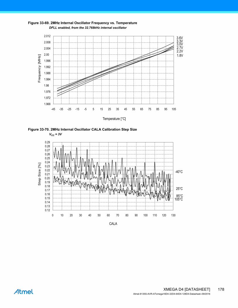
Figure 33-69. 2MHz Internal Oscillator Frequency vs. TemperatureDFLL enabled, from the 32.768kHz internal oscillator
Figure 33-70. 2MHz Internal Oscillator CALA Calibration Step SizeVCC = 3V
3.6V3.3V3.0V2.7V2.2V1.8V
1.968
1.972
1.976
1.98
1.984
1.988
1.992
1.996
2.00
2.004
2.008
2.012
-45 -35 -25 -15 -5 5 15 25 35 45 55 65 75 85 95 105
Temperature [°C]
Fre
quency [
MH
z]
105°C85°C
25°C
-40°C
0.12
0.13
0.14
0.15
0.16
0.17
0.18
0.19
0.20
0.21
0.22
0.23
0.24
0.25
0.26
0.27
0.28
0.29
0 10 20 30 40 50 60 70 80 90 100 110 120 130
CALA
Ste
p S
ize [
%]
178XMEGA D4 [DATASHEET]Atmel-8135S-AVR-ATxmega16D4-32D4-64D4-128D4-Datasheet–09/2016

33.1.9.4 32MHz Internal Oscillator
Figure 33-71. 32MHz Internal Oscillator Frequency vs. TemperatureDFLL disabled
Figure 33-72. 32MHz Internal Oscillator Frequency vs. TemperatureDFLL enabled, from the 32.768kHz internal oscillator
3.6V
3.3V
3.0V2.7V2.2V1.8V31.5
31.95
32.4
32.85
33.3
33.75
34.2
34.65
35.1
35.55
36
36.45
-45 -35 -25 -15 -5 5 15 25 35 45 55 65 75 85 95 105
Temperature [°C]
Fre
quency [
MH
z]
3.6V3.3V
3.0V2.7V2.2V1.8V
31.5
31.55
31.6
31.65
31.7
31.75
31.8
31.85
31.9
31.95
32
32.05
32.1
32.15
-45 -35 -25 -15 -5 5 15 25 35 45 55 65 75 85 95 105
Temperature [°C]
Fre
quency [
MH
z]
179XMEGA D4 [DATASHEET]Atmel-8135S-AVR-ATxmega16D4-32D4-64D4-128D4-Datasheet–09/2016
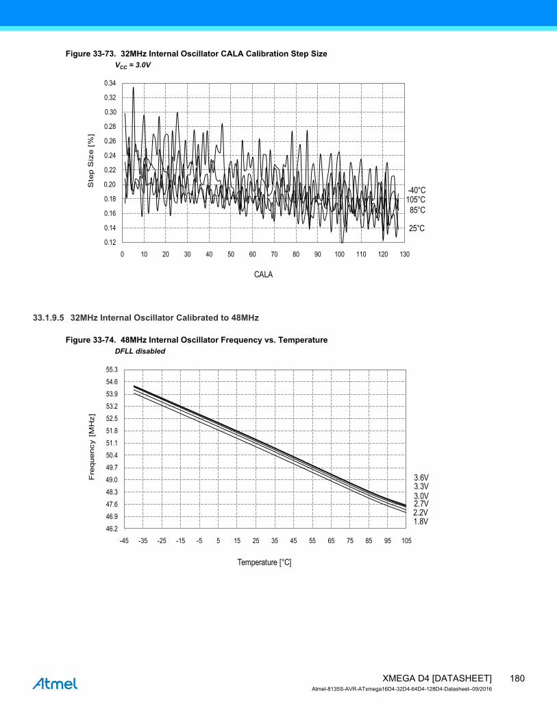
Figure 33-73. 32MHz Internal Oscillator CALA Calibration Step SizeVCC = 3.0V
33.1.9.5 32MHz Internal Oscillator Calibrated to 48MHz
Figure 33-74. 48MHz Internal Oscillator Frequency vs. TemperatureDFLL disabled
105°C
85°C
25°C
-40°C
0.12
0.14
0.16
0.18
0.20
0.22
0.24
0.26
0.28
0.30
0.32
0.34
0 10 20 30 40 50 60 70 80 90 100 110 120 130
CALA
Ste
p S
ize [
%]
3.6V3.3V3.0V2.7V2.2V1.8V
46.2
46.9
47.6
48.3
49.0
49.7
50.4
51.1
51.8
52.5
53.2
53.9
54.6
55.3
-45 -35 -25 -15 -5 5 15 25 35 45 55 65 75 85 95 105
Temperature [°C]
Fre
quency [
MH
z]
180XMEGA D4 [DATASHEET]Atmel-8135S-AVR-ATxmega16D4-32D4-64D4-128D4-Datasheet–09/2016

Figure 33-75. 48MHz Internal Oscillator Frequency vs. TemperatureDFLL enabled, from the 32.768kHz internal oscillator
Figure 33-76. 48MHz Internal Oscillator CALA Calibration Step SizeVCC = 3.0V
3.6V3.3V
3.0V2.7V2.2V1.8V
31.5
31.55
31.6
31.65
31.7
31.75
31.8
31.85
31.9
31.95
32
32.05
32.1
32.15
-45 -35 -25 -15 -5 5 15 25 35 45 55 65 75 85 95 105
Temperature [°C]
Fre
quency [
MH
z]
105°C
85°C
25°C
-40°C
0.09
0.11
0.13
0.15
0.17
0.19
0.21
0.23
0.25
0.27
0.29
0 10 20 30 40 50 60 70 80 90 100 110 120 130
CALA
Ste
p S
ize [
%]
181XMEGA D4 [DATASHEET]Atmel-8135S-AVR-ATxmega16D4-32D4-64D4-128D4-Datasheet–09/2016
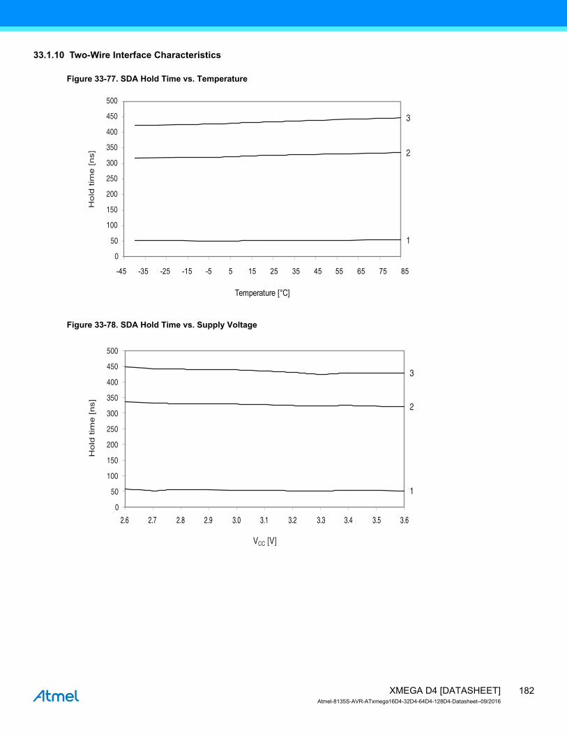
33.1.10 Two-Wire Interface Characteristics
Figure 33-77. SDA Hold Time vs. Temperature
Figure 33-78. SDA Hold Time vs. Supply Voltage
3
2
1
0
50
100
150
200
250
300
350
400
450
500H
old
tim
e [
ns]
-45 -35 -25 -15 -5 5 15 25 35 45 55 65 75 85
Temperature [°C]
3
2
1
0
50
100
150
200
250
300
350
400
450
500
VCC [V]
Ho
ld tim
e [n
s]
2.6 2.7 2.8 2.9 3.0 3.1 3.2 3.3 3.4 3.5 3.6
182XMEGA D4 [DATASHEET]Atmel-8135S-AVR-ATxmega16D4-32D4-64D4-128D4-Datasheet–09/2016
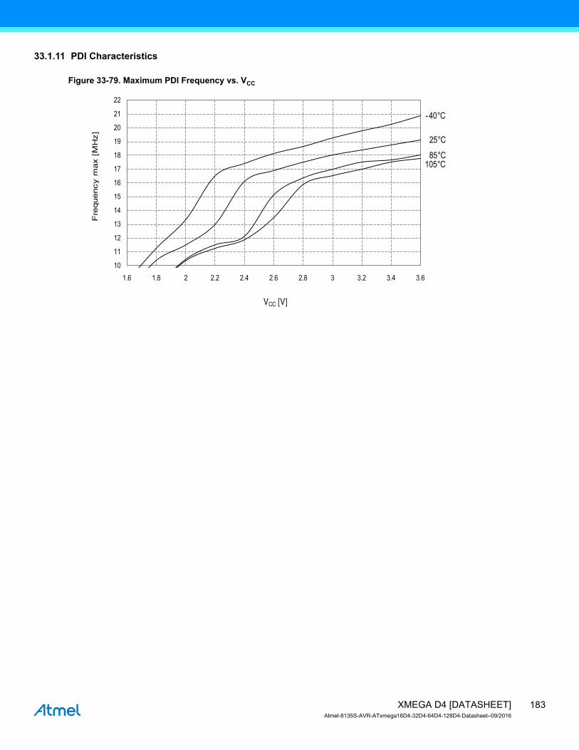
33.1.11 PDI Characteristics
Figure 33-79. Maximum PDI Frequency vs. VCC
105 °C85 °C
25 °C
-40 °C
10
11
12
13
14
15
16
17
18
19
20
21
22
1.6 1.8 2 2.2 2.4 2.6 2.8 3 3.2 3.4 3.6
VCC [V]
Fre
quency m
ax [
MH
z]
183XMEGA D4 [DATASHEET]Atmel-8135S-AVR-ATxmega16D4-32D4-64D4-128D4-Datasheet–09/2016

33.2 ATxmega32D4
33.2.1 Current Consumption
33.2.1.1 Active Mode Supply Current
Figure 33-80. Active Supply Current vs. FrequencyfSYS = 0 - 1MHz external clock, T = 25°C
Figure 33-81. Active Supply Current vs. FrequencyfSYS = 1 - 32MHz external clock, T = 25°C
3.6V
3.0V
2.7V
2.2V
1.8V
0
50
100
150
200
250
300
350
400
450
500
550
600
0 0.1 0.2 0.3 0.4 0.5 0.6 0.7 0.8 0.9 1
Frequency [MHz]
I CC [
µA
]
3.6V
3.0V
2.7V
0
1
2
3
4
5
6
7
8
9
10
11
0 2 4 6 8 10 12 14 16 18 20 22 24 26 28 30 32
Frequency [MHz]
I CC
[mA
]
1.8V
2.2V
184XMEGA D4 [DATASHEET]Atmel-8135S-AVR-ATxmega16D4-32D4-64D4-128D4-Datasheet–09/2016

Figure 33-82. Active Mode Supply Current vs. VCC
fSYS = 32.768kHz internal oscillator
Figure 33-83. Active Mode Supply Current vs. VCC
fSYS = 1MHz external clock
105°C85°C
25 °C
-40 °C
40
60
80
100
120
140
160
180
1.6 1.8 2 2.2 2.4 2.6 2.8 3 3.2 3.4 3.6
Icc [µ
A]
VCC [V]
105 °C85 °C25 °C
-40 °C
100
150
200
250
300
350
400
450
500
550
600
1.6 1.8 2 2.2 2.4 2.6 2.8 3 3.2 3.4 3.6
Icc [µ
A]
VCC [V]
185XMEGA D4 [DATASHEET]Atmel-8135S-AVR-ATxmega16D4-32D4-64D4-128D4-Datasheet–09/2016

Figure 33-84. Active Mode Supply Current vs. VCC
fSYS = 2MHz internal oscillator
Figure 33-85. Active Mode Supply Current vs. VCC
fSYS = 32MHz internal oscillator prescaled to 8MHz
105 °C85 °C
25 °C-40 °C
150
300
450
600
750
900
1050
1200
1350
1.6 1.8 2 2.2 2.4 2.6 2.8 3 3.2 3.4 3.6
Icc [µ
A]
VCC [V]
105 °C85 °C25 °C
-40 °C
1.0
1.5
2.0
2.5
3.0
3.5
4.0
4.5
5.0
1.6 1.8 2 2.2 2.4 2.6 2.8 3 3.2 3.4 3.6
Icc [m
A]
VCC [V]
186XMEGA D4 [DATASHEET]Atmel-8135S-AVR-ATxmega16D4-32D4-64D4-128D4-Datasheet–09/2016
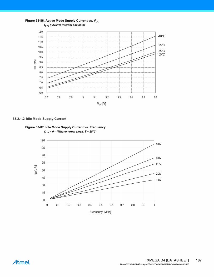
Figure 33-86. Active Mode Supply Current vs. VCC
fSYS = 32MHz internal oscillator
33.2.1.2 Idle Mode Supply Current
Figure 33-87. Idle Mode Supply Current vs. FrequencyfSYS = 0 - 1MHz external clock, T = 25°C
105 °C85 °C
25 °C
-40 °C
6.0
6.5
7.0
7.5
8.0
8.5
9.0
9.5
10.0
10.5
11.0
11.5
12.0
2.7 2.8 2.9 3 3.1 3.2 3.3 3.4 3.5 3.6
Icc [m
A]
VCC [V]
3.6V
3.0V
2.7V
2.2V
1.8V
0
15
30
45
60
75
90
105
120
0 0.1 0.2 0.3 0.4 0.5 0.6 0.7 0.8 0.9 1
Frequency [MHz]
I CC[
uA
]
187XMEGA D4 [DATASHEET]Atmel-8135S-AVR-ATxmega16D4-32D4-64D4-128D4-Datasheet–09/2016

Figure 33-88. Idle Mode Supply Current vs. FrequencyfSYS = 1 - 32MHz external clock, T = 25°C
Figure 33-89. Idle Mode Supply Current vs. VCC
fSYS = 32.768kHz internal oscillator
3.6V
3.0V
2.7V
0
0.4
0.8
1.2
1.6
2.0
2.4
2.8
3.2
3.6
4.0
0 2 4 6 8 10 12 14 16 18 20 22 24 26 28 30 32
Frenquecy [MHz]
Icc [
mA
]
2.2V
1.8V
105 °C
85 °C
25 °C
-40 °C
25.00
25.75
26.50
27.25
28.00
28.75
29.50
30.25
31.00
31.75
32.50
33.25
34.00
34.75
35.50
1.6 1.8 2 2.2 2.4 2.6 2.8 3 3.2 3.4 3.6
Icc [µ
A]
VCC [V]
188XMEGA D4 [DATASHEET]Atmel-8135S-AVR-ATxmega16D4-32D4-64D4-128D4-Datasheet–09/2016

Figure 33-90. Idle Mode Supply Current vs. VCC
fSYS = 1MHz external clock
Figure 33-91. Idle Mode Supply Current vs. VCC
fSYS = 2MHz internal oscillator
105 °C
85 °C25 °C
-40 °C
30
40
50
60
70
80
90
100
110
120
130
1.6 1.8 2 2.2 2.4 2.6 2.8 3 3.2 3.4 3.6
Icc [µ
A]
VCC [V]
105 °C85 °C25 °C
-40 °C
110
130
150
170
190
210
230
250
270
290
310
330
1.6 1.8 2 2.2 2.4 2.6 2.8 3 3.2 3.4 3.6
Icc [µ
A]
VCC [V]
189XMEGA D4 [DATASHEET]Atmel-8135S-AVR-ATxmega16D4-32D4-64D4-128D4-Datasheet–09/2016

Figure 33-92. Idle Mode Supply Current vs. VCC
fSYS = 32MHz internal oscillator prescaled to 8MHz
Figure 33-93. Idle Mode Current vs. VCC
fSYS = 32MHz internal oscillator
105°C85 °C25 °C
-40 °C
500
600
700
800
900
1000
1100
1200
1300
1400
1500
1600
1.6 1.8 2 2.2 2.4 2.6 2.8 3 3.2 3.4 3.6
Icc [µ
A]
VCC [V]
105 °C85 °C
25 °C
-40°C
2.25
2.50
2.75
3.00
3.25
3.50
3.75
4.00
4.25
2.7 2.8 2.9 3 3.1 3.2 3.3 3.4 3.5 3.6
Icc [m
A]
VCC [V]
190XMEGA D4 [DATASHEET]Atmel-8135S-AVR-ATxmega16D4-32D4-64D4-128D4-Datasheet–09/2016
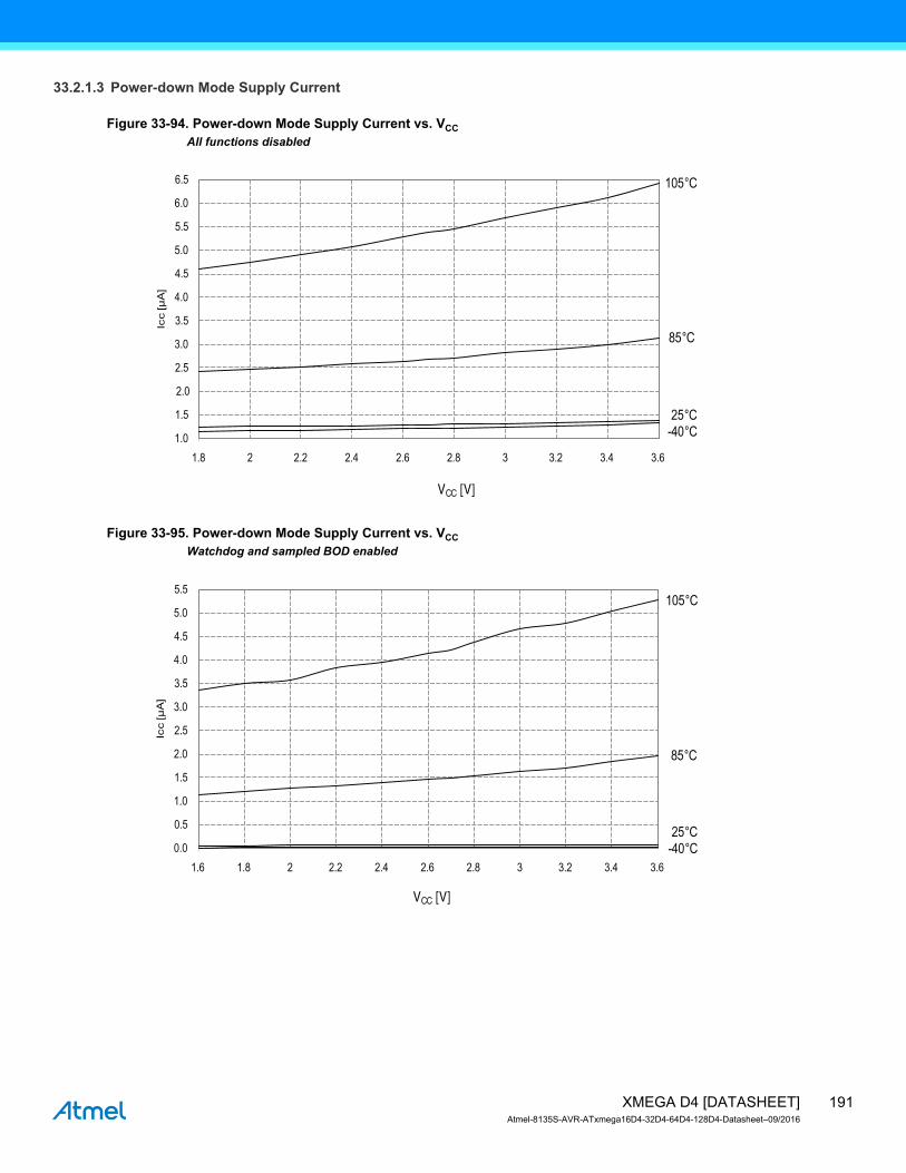
33.2.1.3 Power-down Mode Supply Current
Figure 33-94. Power-down Mode Supply Current vs. VCC
All functions disabled
Figure 33-95. Power-down Mode Supply Current vs. VCC
Watchdog and sampled BOD enabled
105 °C
85 °C
25°C
-40°C1.0
1.5
2.0
2.5
3.0
3.5
4.0
4.5
5.0
5.5
6.0
6.5
1.8 2 2.2 2.4 2.6 2.8 3 3.2 3.4 3.6
Icc [µ
A]
VCC [V]
105 °C
85 °C
25 °C
-40 °C0.0
0.5
1.0
1.5
2.0
2.5
3.0
3.5
4.0
4.5
5.0
5.5
1.6 1.8 2 2.2 2.4 2.6 2.8 3 3.2 3.4 3.6
Icc [µ
A]
VCC [V]
191XMEGA D4 [DATASHEET]Atmel-8135S-AVR-ATxmega16D4-32D4-64D4-128D4-Datasheet–09/2016

Figure 33-96. Power-down Mode Supply Current vs. TemperatureWatchdog and sampled BOD enabled and running from internal ULP oscillator
33.2.1.4 Power-save Mode Supply Current
Figure 33-97. Power-save Mode Supply Current vs.VCC
Real Time Counter enabled and running from 1.024kHz output of 32.768kHz TOSC
3.6V
3.0V2.7V
2.2V1.8V
1.0
1.5
2.0
2.5
3.0
3.5
4.0
4.5
5.0
5.5
6.0
6.5
7.0
7.5
-45 -35 -25 -15 -5 5 15 25 35 45 55 65 75 85 95 105
Icc [µ
A]
Temperature [°C]
Normal mode
Low-power mode
0
0.1
0.2
0.3
0.4
0.5
0.6
0.7
0.8
0.9
VCC [V]
I CC [µ
A]
1.6 1.8 2.0 2.2 2.4 2.6 2.8 3.0 3.2 3.4 3.6
192XMEGA D4 [DATASHEET]Atmel-8135S-AVR-ATxmega16D4-32D4-64D4-128D4-Datasheet–09/2016
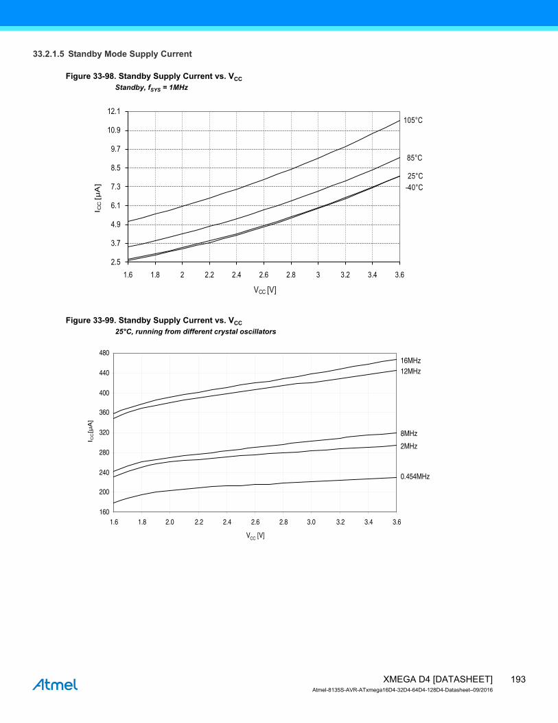
33.2.1.5 Standby Mode Supply Current
Figure 33-98. Standby Supply Current vs. VCC
Standby, fSYS = 1MHz
Figure 33-99. Standby Supply Current vs. VCC
25°C, running from different crystal oscillators
105°C
85°C
25°C
-40°C
2.5
3.7
4.9
6.1
7.3
8.5
9.7
10.9
12.1
1.6 1.8 2 2.2 2.4 2.6 2.8 3 3.2 3.4 3.6
I CC
[µA
]
VCC [V]
16MHz12MHz
8MHz
2MHz
0.454MHz
160
200
240
280
320
360
400
440
480
1.6 1.8 2.0 2.2 2.4 2.6 2.8 3.0 3.2 3.4 3.6
VCC [V]
I CC[µ
A]
193XMEGA D4 [DATASHEET]Atmel-8135S-AVR-ATxmega16D4-32D4-64D4-128D4-Datasheet–09/2016
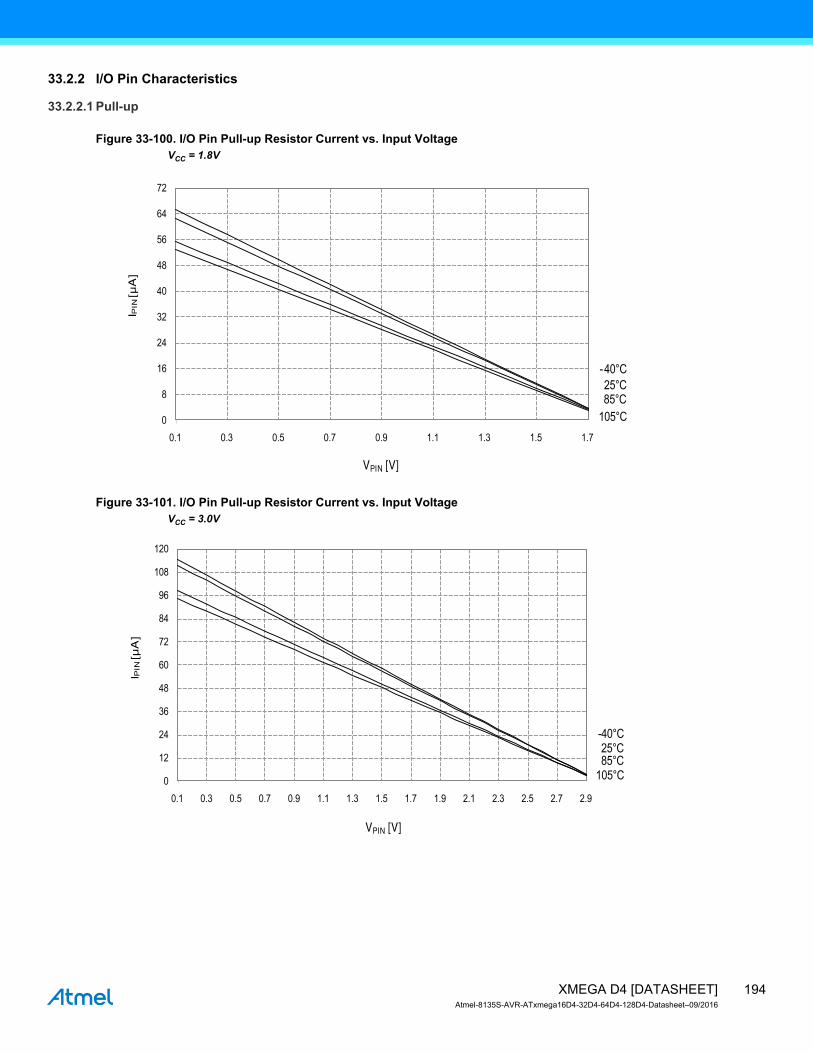
33.2.2 I/O Pin Characteristics
33.2.2.1 Pull-up
Figure 33-100. I/O Pin Pull-up Resistor Current vs. Input VoltageVCC = 1.8V
Figure 33-101. I/O Pin Pull-up Resistor Current vs. Input VoltageVCC = 3.0V
105°C
85°C25°C
-40°C
0
8
16
24
32
40
48
56
64
72
0.1 0.3 0.5 0.7 0.9 1.1 1.3 1.5 1.7
VPIN [V]
I PIN [
µA
]
105°C85°C25°C
-40°C
0
12
24
36
48
60
72
84
96
108
120
0.1 0.3 0.5 0.7 0.9 1.1 1.3 1.5 1.7 1.9 2.1 2.3 2.5 2.7 2.9
VPIN [V]
I PIN [
µA
]
194XMEGA D4 [DATASHEET]Atmel-8135S-AVR-ATxmega16D4-32D4-64D4-128D4-Datasheet–09/2016

Figure 33-102. I/O Pin Pull-up Resistor Current vs. Input VoltageVCC = 3.3V
33.2.2.2 Output Voltage vs. Sink/Source Current
Figure 33-103. I/O Pin Output Voltage vs. Source CurrentVCC = 1.8V
105°C85°C
25°C
-40°C
0
15
30
45
60
75
90
105
120
135
0.1 0.3 0.5 0.7 0.9 1.1 1.3 1.5 1.7 1.9 2.1 2.3 2.5 2.7 2.9 3.1 3.3
VPIN [V]
I PIN [
µA
]
105°C85°C25°C-40°C
0
0.2
0.4
0.6
0.8
1.0
1.2
1.4
1.6
1.8
2.0
-5 -4.5 -4 -3.5 -3 -2.5 -2 -1.5 -1 -0.5 0
IPIN [mA]
V PIN [V
]
195XMEGA D4 [DATASHEET]Atmel-8135S-AVR-ATxmega16D4-32D4-64D4-128D4-Datasheet–09/2016

Figure 33-104. I/O Pin Output Voltage vs. Source CurrentVCC = 3.0V
Figure 33-105. I/O Pin Output Voltage vs. Source CurrentVCC = 3.3V
105 °C85 °C25 °C-40 °C
0
0.35
0.70
1.05
1.40
1.75
2.10
2.45
2.80
3.15
-16 -14 -12 -10 -8 -6 -4 -2 0
IPIN [mA]
VP
IN [
V]
105°C85°C25°C-40°C
0
0.35
0.7
1.05
1.4
1.75
2.1
2.45
2.8
3.15
3.5
-20 -18 -16 -14 -12 -10 -8 -6 -4 -2 0
IPIN [mA]
VP
IN [
V]
196XMEGA D4 [DATASHEET]Atmel-8135S-AVR-ATxmega16D4-32D4-64D4-128D4-Datasheet–09/2016

Figure 33-106. I/O Pin Output Voltage vs. Source Current
Figure 33-107. I/O Pin Output Voltage vs. Sink CurrentVCC = 1.8V
3.6 V
3.3 V
2.7 V
2.2 V
1.8 V
0
0.3
0.6
0.9
1.2
1.5
1.8
2.1
2.4
2.7
3
3.3
3.6
-20 -18 -16 -14 -12 -10 -8 -6 -4 -2 0
IPIN [mA]
VP
IN [
V]
0
0.1
0.2
0.3
0.4
0.5
0.6
0.7
0.8
0.9
1
0 1 2 3 4 5 6 7 8 9 10
105°C 85°C 25°C -40°C
IPIN [mA]
VP
IN [
V]
197XMEGA D4 [DATASHEET]Atmel-8135S-AVR-ATxmega16D4-32D4-64D4-128D4-Datasheet–09/2016
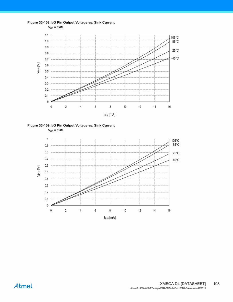
Figure 33-108. I/O Pin Output Voltage vs. Sink CurrentVCC = 3.0V
Figure 33-109. I/O Pin Output Voltage vs. Sink CurrentVCC = 3.3V
0
0.1
0.2
0.3
0.4
0.5
0.6
0.7
0.8
0.9
1.0
1.1
0 2 4 6 8 10 12 14 16
IPIN [mA]
VP
IN [
V]
85°C
25°C
-40°C
105°C
0
0.1
0.2
0.3
0.4
0.5
0.6
0.7
0.8
0.9
1
0 2 4 6 8 10 12 14 16
IPIN [mA]
VP
IN [
V]
85°C
25°C
-40°C
105°C
198XMEGA D4 [DATASHEET]Atmel-8135S-AVR-ATxmega16D4-32D4-64D4-128D4-Datasheet–09/2016
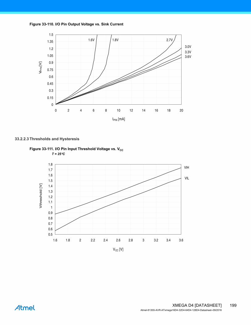
Figure 33-110. I/O Pin Output Voltage vs. Sink Current
33.2.2.3 Thresholds and Hysteresis
Figure 33-111. I/O Pin Input Threshold Voltage vs. VCC
T = 25C
0
0.15
0.3
0.45
0.6
0.75
0.9
1.05
1.2
1.35
1.5
0 2 4 6 8 10 12 14 16 18 20
IPIN [mA]
VP
IN [
V]
3.6V3.3V
3.0V
2.7V1.8V1.6V
0.5
0.6
0.7
0.8
0.9
1
1.11.2
1.3
1.4
1.5
1.6
1.7
1.8
1.6 1.8 2 2.2 2.4 2.6 2.8 3 3.2 3.4 3.6
VCC [V]
Vth
reshold
[V
]
VIL
VIH
199XMEGA D4 [DATASHEET]Atmel-8135S-AVR-ATxmega16D4-32D4-64D4-128D4-Datasheet–09/2016

Figure 33-112. I/O Pin Input Threshold Voltage vs. VCC
VIH I/O pin read as “1”
Figure 33-113. I/O Pin Input Threshold Voltage vs. VCC
VIL I/O pin read as “0”
0.7
0.8
0.9
1.0
1.1
1.2
1.3
1.4
1.5
1.6
1.7
1.8
1.6 1.8 2 2.2 2.4 2.6 2.8 3 3.2 3.4 3.6
105 °C85 °C25 °C
-40 °C
VCC [V]
Vth
reshold
[V
]
0.40
0.55
0.70
0.85
1.00
1.15
1.30
1.45
1.60
1.75
1.6 1.8 2 2.2 2.4 2.6 2.8 3 3.2 3.4 3.6
105 °C85 °C25 °C
-40 °C
VCC [V]
Vth
reshold
[V
]
200XMEGA D4 [DATASHEET]Atmel-8135S-AVR-ATxmega16D4-32D4-64D4-128D4-Datasheet–09/2016

Figure 33-114. I/O Pin Input Hysteresis vs. VCC
33.2.3 ADC Characteristics
Figure 33-115. INL Error vs. External VREF
T = 25C, VCC = 3.6V, external reference
0.15
0.18
0.21
0.24
0.27
0.3
0.33
0.36
0.39
0.42
1.6 1.8 2 2.2 2.4 2.6 2.8 3 3.2 3.4 3.6
VCC [V]
Vth
reshold
[V
]
85°C
25°C
-40°C
105°C
Differential mode
Single-ended signed mode
Single-ended unsigned mode
0.0
0.2
0.4
0.6
0.8
1.0
1.2
1.4
1.6
1.0 1.2 1.4 1.6 1.8 2.0 2.2 2.4 2.6 2.8 3.0
VREF [V]
INL[L
SB
]
201XMEGA D4 [DATASHEET]Atmel-8135S-AVR-ATxmega16D4-32D4-64D4-128D4-Datasheet–09/2016
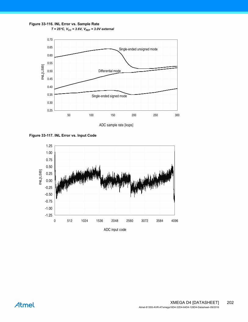
Figure 33-116. INL Error vs. Sample RateT = 25C, VCC = 3.6V, VREF = 3.0V external
Figure 33-117. INL Error vs. Input Code
Differential mode
Single-ended signed mode
Single-ended unsigned mode
0.25
0.30
0.35
0.40
0.45
0.50
0.55
0.60
0.65
0.70
ADC sample rate [ksps]
INL[L
SB
]
50 100 150 200 250 300
-1.25
-1.00
-0.75
-0.50
-0.25
0.00
0.25
0.50
0.75
1.00
1.25
0 512 1024 1536 2048 2560 3072 3584 4096
ADC input code
INL[L
SB
]
202XMEGA D4 [DATASHEET]Atmel-8135S-AVR-ATxmega16D4-32D4-64D4-128D4-Datasheet–09/2016
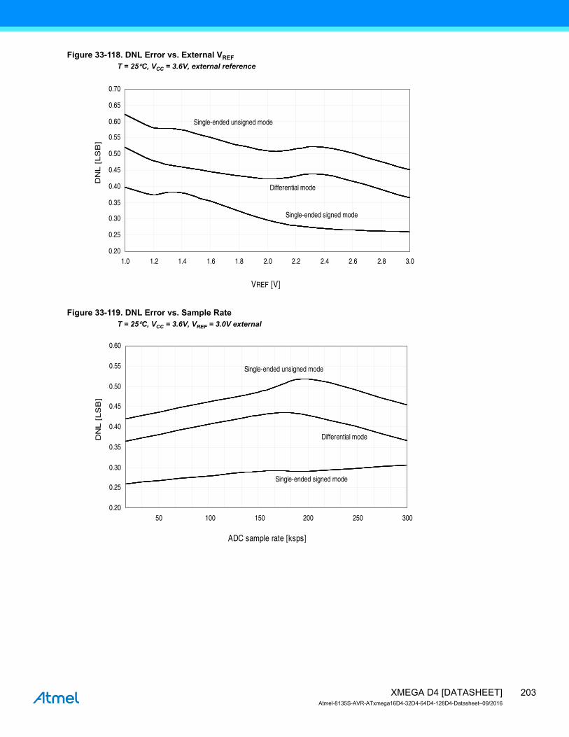
Figure 33-118. DNL Error vs. External VREF
T = 25C, VCC = 3.6V, external reference
Figure 33-119. DNL Error vs. Sample RateT = 25C, VCC = 3.6V, VREF = 3.0V external
Differential mode
Single-ended signed mode
Single-ended unsigned mode
0.20
0.25
0.30
0.35
0.40
0.45
0.50
0.55
0.60
0.65
0.70
1.0 1.2 1.4 1.6 1.8 2.0 2.2 2.4 2.6 2.8 3.0
VREF [V]
DN
L [
LS
B]
Differential mode
Single-ended signed mode
Single-ended unsigned mode
0.20
0.25
0.30
0.35
0.40
0.45
0.50
0.55
0.60
50 100 150 200 250 300
ADC sample rate [ksps]
DN
L [
LS
B]
203XMEGA D4 [DATASHEET]Atmel-8135S-AVR-ATxmega16D4-32D4-64D4-128D4-Datasheet–09/2016

Figure 33-120. DNL Error vs. Input code
Figure 33-121. Gain Error vs. VREF
T = 25C, VCC = 3.6V, ADC sample rate = 200ksps
-0.6
-0.4
-0.2
0
0.2
0.4
0.6
0.8
1
0 512 1024 1536 2048 2560 3072 3584 4096
ADC input code
DN
L [LS
B]
Differential mode
Single-ended signed mode
Single-ended unsigned mode
-15
-14
-13
-12
-11
-10
-9
-8
-7
-6
-5
1.0 1.2 1.4 1.6 1.8 2.0 2.2 2.4 2.6 2.8 3.0
VREF [V]
Gain
err
or
[m
V]
204XMEGA D4 [DATASHEET]Atmel-8135S-AVR-ATxmega16D4-32D4-64D4-128D4-Datasheet–09/2016

Figure 33-122. Gain Error vs. VCC
T = 25C, VREF = external 1.0V, ADC sample rate = 200ksps
Figure 33-123. Gain Error vs. TemperatureVCC = 3.0V, VREF = external 2.0V
Differential mode
Single-ended signed mode
Single-ended unsigned mode
-9
-8
-7
-6
-5
-4
-3
-2
1.6 1.8 2.0 2.2 2.4 2.6 2.8 3.0 3.2 3.4 3.6
VCC [V]
Gain
err
or
[m
V]
Differential mode
Single-ended signed mode
Single-ended unsigned mode
-14
-12
-10
-8
-6
-4
-2
0
-45 -35 -25 -15 -5 5 15 25 35 45 55 65 75 85 95 105
Gain
err
or [m
V]
Temperature [°C]
205XMEGA D4 [DATASHEET]Atmel-8135S-AVR-ATxmega16D4-32D4-64D4-128D4-Datasheet–09/2016

Figure 33-124. Offset Error vs. VREF
T = 25C, VCC = 3.6V, ADC sample rate = 200ksps
Figure 33-125. Offset Error vs. VCC
T = 25C, VREF = external 1.0V, ADC sample rate = 200ksps
Differential mode
7.0
7.2
7.4
7.6
7.8
8.0
8.2
8.4
8.6
8.8
9.0
9.2
9.4
1.0 1.2 1.4 1.6 1.8 2.0 2.2 2.4 2.6 2.8 3.0
VREF [V]
Off
set
err
or
[m
V]
Differential mode
0.00
1.00
2.00
3.00
4.00
5.00
6.00
7.00
8.00
1.6 1.8 2.0 2.2 2.4 2.6 2.8 3.0 3.2 3.4 3.6
VCC [V]
Off
set
err
or
[m
V]
206XMEGA D4 [DATASHEET]Atmel-8135S-AVR-ATxmega16D4-32D4-64D4-128D4-Datasheet–09/2016

33.2.4 Analog Comparator Characteristics
Figure 33-126. Analog Comparator Hysteresis vs. VCC
High speed, small hysteresis
Figure 33-127. Analog Comparator Hysteresis vs. VCC
High speed, large hysteresis
4
5
6
7
8
9
10
11
12
13
14
1.6 1.8 2 2.2 2.4 2.6 2.8 3 3.2 3.4 3.6
-40°C
25°C
85°C
VCC [V]
VH
YS
T [m
V]
105°C
14
16
18
20
22
24
26
28
30
32
1.6 1.8 2 2.2 2.4 2.6 2.8 3 3.2 3.4 3.6
-40°C
25°C
85°C
VCC [V]
VH
YS
T [m
V]
105°C
207XMEGA D4 [DATASHEET]Atmel-8135S-AVR-ATxmega16D4-32D4-64D4-128D4-Datasheet–09/2016

Figure 33-128. Analog Comparator Hysteresis vs. VCC
Low power, small hysteresis
Figure 33-129. Analog Comparator Hysteresis vs. VCC
Low power, large hysteresis
1.6 1.8 2.0 2.2 2.4 2.6 2.8 3.0 3.2 3.4 3.6
VCC [V]
VH
YS
T [m
V]
12
14
16
18
20
22
24
26
28
30
105 °C
85 °C
25°C
-40°C
32
36
40
44
48
52
56
60
64
68
-40°C
25°C
85°C
1.6 1.8 2.0 2.2 2.4 2.6 2.8 3.0 3.2 3.4 3.6
VCC [V]
VH
YS
T [m
V]
105°C
208XMEGA D4 [DATASHEET]Atmel-8135S-AVR-ATxmega16D4-32D4-64D4-128D4-Datasheet–09/2016
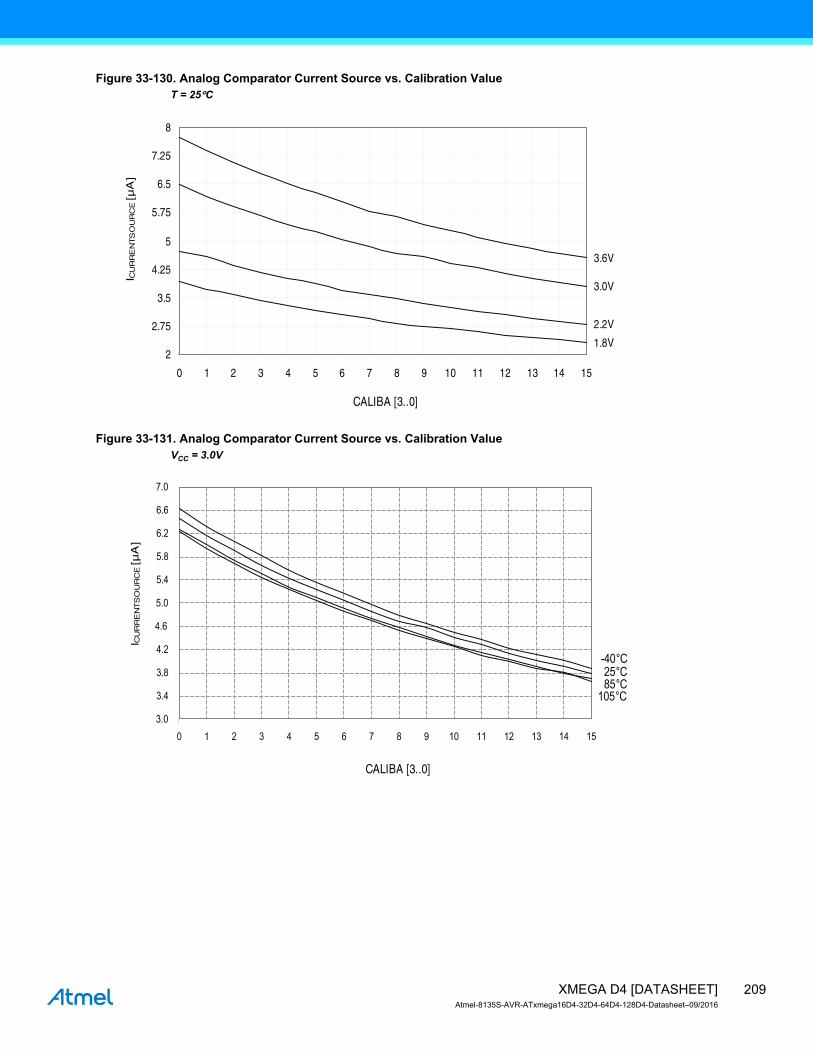
Figure 33-130. Analog Comparator Current Source vs. Calibration ValueT = 25C
Figure 33-131. Analog Comparator Current Source vs. Calibration ValueVCC = 3.0V
3.6V
3.0V
2.2V
1.8V2
2.75
3.5
4.25
5
5.75
6.5
7.25
8
0 1 2 3 4 5 6 7 8 9 10 11 12 13 14 15
CALIBA [3..0]
I CU
RR
EN
TS
OU
RC
E [µ
A]
105°C85 °C25 °C
-40 °C
3.0
3.4
3.8
4.2
4.6
5.0
5.4
5.8
6.2
6.6
7.0
0 1 2 3 4 5 6 7 8 9 10 11 12 13 14 15
CALIBA [3..0]
I CU
RR
EN
TS
OU
RC
E [µ
A]
209XMEGA D4 [DATASHEET]Atmel-8135S-AVR-ATxmega16D4-32D4-64D4-128D4-Datasheet–09/2016

Figure 33-132. Voltage Scaler INL vs. SCALEFACT = 25C, VCC = 3.0V
33.2.5 Internal 1.0V reference Characteristics
Figure 33-133. ADC Internal 1.0V Reference vs. Temperature
25°C
-0.150
-0.125
-0.100
-0.075
-0.050
-0.025
0
0.025
0.050
0 10 20 30 40 50 60 70
SCALEFAC
INL [
LS
B]
3.6V
3.0V2.7V2.2V1.8V
0.9968
0.9976
0.9984
0.9992
1
1.0008
1.0016
1.0024
1.0032
1.004
1.0048
1.0056
1.0064
1.0072
1.008
1.0088
-45 -35 -25 -15 -5 5 15 25 35 45 55 65 75 85 95 105
Temperature [°C]
Bandgap V
oltage [
V]
210XMEGA D4 [DATASHEET]Atmel-8135S-AVR-ATxmega16D4-32D4-64D4-128D4-Datasheet–09/2016

33.2.6 BOD Characteristics
Figure 33-134. BOD Thresholds vs. TemperatureBOD level = 1.6V
Figure 33-135. BOD thresholds vs. TemperatureBOD level = 3.0V
1.538
1.542
1.546
1.55
1.554
1.558
1.562
1.566
1.57
1.574
-45 -35 -25 -15 -5 5 15 25 35 45 55 65 75 85 95 105
Rising Vcc
Falling Vcc
Temperature [°C]
VB
OT
[V]
2.92
2.928
2.936
2.944
2.952
2.96
2.968
2.976
2.984
2.992
-45 -35 -25 -15 -5 5 15 25 35 45 55 65 75 85 95 105
Rising Vcc
Falling Vcc
Temperature [°C]
VB
OT
[V]
211XMEGA D4 [DATASHEET]Atmel-8135S-AVR-ATxmega16D4-32D4-64D4-128D4-Datasheet–09/2016

33.2.7 External Reset Characteristics
Figure 33-136. Minimum Reset Pin Pulse Width vs. VCC
Figure 33-137. Reset Pin Pull-up Resistor Current vs. Reset Pin VoltageVCC = 1.8V
105°C85°C
25°C-40°C
80
85
90
95
100
105
110
115
120
125
130
135
140
145
1.6 1.8 2 2.2 2.4 2.6 2.8 3 3.2 3.4 3.6
VCC [V]
TR
ST [
ns]
105°C85°C25°C
-40°C
0
8
16
24
32
40
48
56
64
72
80
0 0.2 0.4 0.6 0.8 1 1.2 1.4 1.6 1.8
VRESET [V]
I RE
SE
T [µ
A]
212XMEGA D4 [DATASHEET]Atmel-8135S-AVR-ATxmega16D4-32D4-64D4-128D4-Datasheet–09/2016

Figure 33-138. Reset Pin Pull-up Resistor Current vs. Reset Pin VoltageVCC = 3.0V
Figure 33-139. Reset Pin Pull-up Resistor Current vs. Reset Pin VoltageVCC = 3.3V
0
15
30
45
60
75
90
105
120
135
0 0.3 0.6 0.9 1.2 1.5 1.8 2.1 2.4 2.7 3
105°C85°C25°C
-40°C
VRESET [V]
I RE
SE
T [µ
A]
0
15
30
45
60
75
90
105
120
135
150
0 0.3 0.6 0.9 1.2 1.5 1.8 2.1 2.4 2.7 3 3.3
105°C85°C25°C
-40°C
VRESET [V]
I RE
SE
T [µ
A]
213XMEGA D4 [DATASHEET]Atmel-8135S-AVR-ATxmega16D4-32D4-64D4-128D4-Datasheet–09/2016
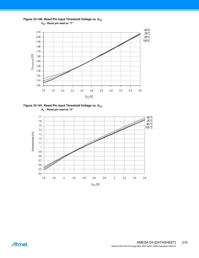
Figure 33-140. Reset Pin Input Threshold Voltage vs. VCC
VIH - Reset pin read as “1”
Figure 33-141. Reset Pin Input Threshold Voltage vs. VCC
VIL - Reset pin read as “0”
105°C
85°C
25°C-40°C
1.00
1.10
1.20
1.30
1.40
1.50
1.60
1.70
1.80
1.90
2.00
2.10
1.6 1.8 2.0 2.2 2.4 2.6 2.8 3.0 3.2 3.4 3.6
Vth
resh
old
[V]
VCC [V]
0.4
0.5
0.6
0.7
0.8
0.9
1
1.1
1.2
1.3
1.4
1.5
1.6
1.7
1.6 1.8 2 2.2 2.4 2.6 2.8 3 3.2 3.4 3.6
105 °C85 °C25 °C
-40 °C
VCC [V]
Vth
reshold
[V
]
214XMEGA D4 [DATASHEET]Atmel-8135S-AVR-ATxmega16D4-32D4-64D4-128D4-Datasheet–09/2016
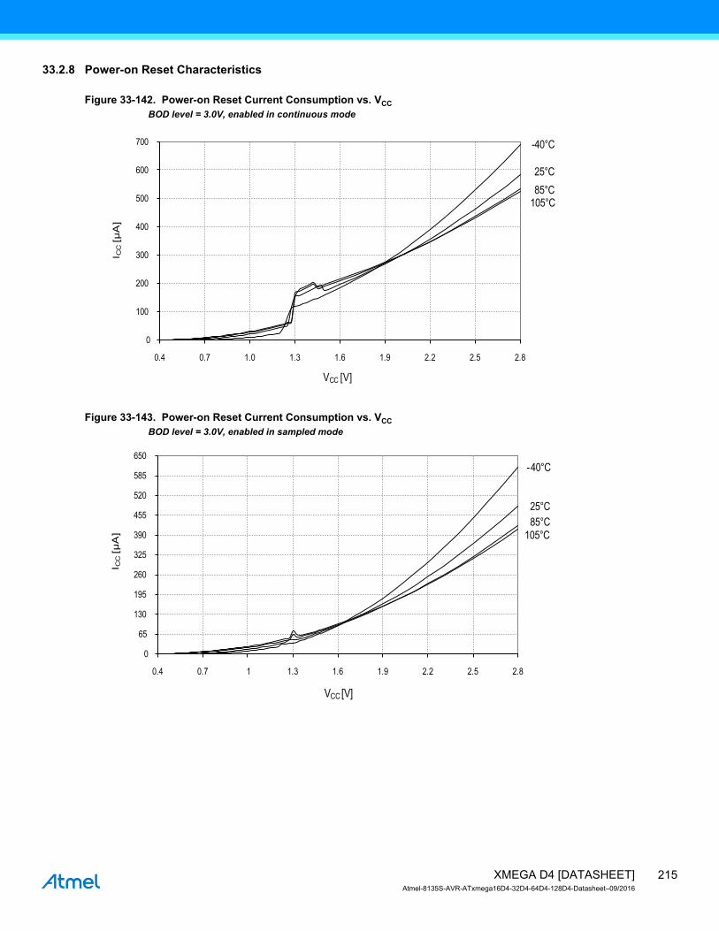
33.2.8 Power-on Reset Characteristics
Figure 33-142. Power-on Reset Current Consumption vs. VCC
BOD level = 3.0V, enabled in continuous mode
Figure 33-143. Power-on Reset Current Consumption vs. VCC
BOD level = 3.0V, enabled in sampled mode
105°C85°C
25°C
-40°C
0
100
200
300
400
500
600
700
0.4 0.7 1.0 1.3 1.6 1.9 2.2 2.5 2.8
I CC
[µA
]
VCC [V]
105°C
85°C
25°C
-40°C
0
65
130
195
260
325
390
455
520
585
650
0.4 0.7 1 1.3 1.6 1.9 2.2 2.5 2.8
I CC
[µA
]
VCC [V]
215XMEGA D4 [DATASHEET]Atmel-8135S-AVR-ATxmega16D4-32D4-64D4-128D4-Datasheet–09/2016

33.2.9 Oscillator Characteristics
33.2.9.1 Ultra Low-Power Internal Oscillator
Figure 33-144. Ultra Low-Power Internal Oscillator Frequency vs. Temperature
33.2.9.2 32.768kHz Internal Oscillator
Figure 33-145. 32.768kHz Internal Oscillator Frequency vs. Temperature
3.6V3.3V3.0V
2.7V
2.0V1.8V30.9
31.2
31.5
31.8
32.1
32.4
32.7
33.0
33.3
33.6
33.9
34.2
34.5
34.8
35.1
35.4
-45 -35 -25 -15 -5 5 15 25 35 45 55 65 75 85 95 105
Temperature [°C]
Fre
quency [
kH
z]
3.6V3.3V3.0V2.7V2.2V
1.8V
32.3
32.35
32.4
32.45
32.5
32.55
32.6
32.65
32.7
32.75
32.8
32.85
32.9
-45 -35 -25 -15 -5 5 15 25 35 45 55 65 75 85 95 105
Temperature [°C]
Fre
qu
en
cy [kH
z]
216XMEGA D4 [DATASHEET]Atmel-8135S-AVR-ATxmega16D4-32D4-64D4-128D4-Datasheet–09/2016
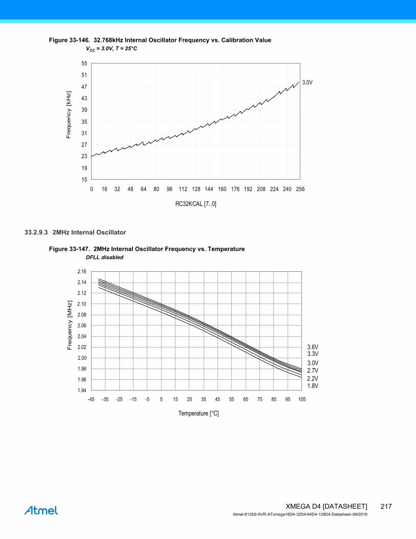
Figure 33-146. 32.768kHz Internal Oscillator Frequency vs. Calibration ValueVCC = 3.0V, T = 25°C
33.2.9.3 2MHz Internal Oscillator
Figure 33-147. 2MHz Internal Oscillator Frequency vs. TemperatureDFLL disabled
3.0V
15
19
23
27
31
35
39
43
47
51
55
0 16 32 48 64 80 96 112 128 144 160 176 192 208 224 240 256
RC32KCAL [7..0]
Fre
quency [
kH
z]
3.6V3.3V
3.0V
2.7V
2.2V1.8V
1.94
1.96
1.98
2.00
2.02
2.04
2.06
2.08
2.10
2.12
2.14
2.16
-45 -35 -25 -15 -5 5 15 25 35 45 55 65 75 85 95 105
Temperature [°C]
Fre
quency [
MH
z]
217XMEGA D4 [DATASHEET]Atmel-8135S-AVR-ATxmega16D4-32D4-64D4-128D4-Datasheet–09/2016

Figure 33-148. 2MHz Internal Oscillator Frequency vs. TemperatureDFLL enabled, from the 32.768kHz internal oscillator
Figure 33-149. 2MHz Internal Oscillator CALA Calibration Step SizeVCC = 3V
3.6V3.3V3.0V2.7V2.2V1.8V
1.968
1.972
1.976
1.98
1.984
1.988
1.992
1.996
2.00
2.004
2.008
2.012
-45 -35 -25 -15 -5 5 15 25 35 45 55 65 75 85 95 105
Temperature [°C]
Fre
quency [
MH
z]
105°C85°C
25°C
-40°C
0.12
0.13
0.14
0.15
0.16
0.17
0.18
0.19
0.20
0.21
0.22
0.23
0.24
0.25
0.26
0.27
0.28
0.29
0 10 20 30 40 50 60 70 80 90 100 110 120 130
CALA
Ste
p S
ize [
%]
218XMEGA D4 [DATASHEET]Atmel-8135S-AVR-ATxmega16D4-32D4-64D4-128D4-Datasheet–09/2016

33.2.9.4 32MHz Internal Oscillator
Figure 33-150. 32MHz Internal Oscillator Frequency vs. TemperatureDFLL disabled
Figure 33-151. 32MHz Internal Oscillator Frequency vs. TemperatureDFLL enabled, from the 32.768kHz internal oscillator
3.6V
3.3V
3.0V2.7V2.2V1.8V31.5
31.95
32.4
32.85
33.3
33.75
34.2
34.65
35.1
35.55
36
36.45
-45 -35 -25 -15 -5 5 15 25 35 45 55 65 75 85 95 105
Temperature [°C]
Fre
quency [
MH
z]
3.6V3.3V
3.0V2.7V2.2V1.8V
31.5
31.55
31.6
31.65
31.7
31.75
31.8
31.85
31.9
31.95
32
32.05
32.1
32.15
-45 -35 -25 -15 -5 5 15 25 35 45 55 65 75 85 95 105
Temperature [°C]
Fre
quency [
MH
z]
219XMEGA D4 [DATASHEET]Atmel-8135S-AVR-ATxmega16D4-32D4-64D4-128D4-Datasheet–09/2016

Figure 33-152. 32MHz Internal Oscillator CALA Calibration Step SizeVCC = 3.0V
33.2.9.5 32MHz Internal Oscillator Calibrated to 48MHz
Figure 33-153. 48MHz Internal Oscillator Frequency vs. TemperatureDFLL disabled
105°C
85°C
25°C
-40°C
0.12
0.14
0.16
0.18
0.20
0.22
0.24
0.26
0.28
0.30
0.32
0.34
0 10 20 30 40 50 60 70 80 90 100 110 120 130
CALA
Ste
p S
ize [
%]
3.6V3.3V3.0V2.7V2.2V1.8V
46.2
46.9
47.6
48.3
49.0
49.7
50.4
51.1
51.8
52.5
53.2
53.9
54.6
55.3
-45 -35 -25 -15 -5 5 15 25 35 45 55 65 75 85 95 105
Temperature [°C]
Fre
quency [
MH
z]
220XMEGA D4 [DATASHEET]Atmel-8135S-AVR-ATxmega16D4-32D4-64D4-128D4-Datasheet–09/2016

Figure 33-154. 48MHz Internal Oscillator Frequency vs. TemperatureDFLL enabled, from the 32.768kHz internal oscillator
Figure 33-155. 48MHz Internal Oscillator CALA Calibration Step SizeVCC = 3.0V
3.6V3.3V
3.0V2.7V2.2V1.8V
31.5
31.55
31.6
31.65
31.7
31.75
31.8
31.85
31.9
31.95
32
32.05
32.1
32.15
-45 -35 -25 -15 -5 5 15 25 35 45 55 65 75 85 95 105
Temperature [°C]
Fre
quency [
MH
z]
105°C
85°C
25°C
-40°C
0.09
0.11
0.13
0.15
0.17
0.19
0.21
0.23
0.25
0.27
0.29
0 10 20 30 40 50 60 70 80 90 100 110 120 130
CALA
Ste
p S
ize [
%]
221XMEGA D4 [DATASHEET]Atmel-8135S-AVR-ATxmega16D4-32D4-64D4-128D4-Datasheet–09/2016
33.2.10 Two-Wire Interface Characteristics
Figure 33-156. SDA Hold Time vs. Temperature
Figure 33-157. SDA Hold Time vs. Supply Voltage
3
2
1
0
50
100
150
200
250
300
350
400
450
500H
old
tim
e [
ns]
-45 -35 -25 -15 -5 5 15 25 35 45 55 65 75 85
Temperature [°C]
3
2
1
0
50
100
150
200
250
300
350
400
450
500
VCC [V]
Ho
ld tim
e [n
s]
2.6 2.7 2.8 2.9 3.0 3.1 3.2 3.3 3.4 3.5 3.6
222XMEGA D4 [DATASHEET]Atmel-8135S-AVR-ATxmega16D4-32D4-64D4-128D4-Datasheet–09/2016

33.2.11 PDI Characteristics
Figure 33-158. Maximum PDI Frequency vs. VCC
105 °C85 °C
25 °C
-40 °C
10
11
12
13
14
15
16
17
18
19
20
21
22
1.6 1.8 2 2.2 2.4 2.6 2.8 3 3.2 3.4 3.6
VCC [V]
Fre
quency m
ax [
MH
z]
223XMEGA D4 [DATASHEET]Atmel-8135S-AVR-ATxmega16D4-32D4-64D4-128D4-Datasheet–09/2016

33.3 ATxmega64D4
33.3.1 Current Consumption
33.3.1.1 Active Mode Supply Current
Figure 33-159. Active Supply Current vs. FrequencyfSYS = 0 - 1MHz external clock, T = 25°C
Figure 33-160. Active Supply Current vs. FrequencyfSYS = 1 - 32MHz external clock, T = 25°C
3.6V
3.0V
2.7V
2.2V
1.8V1.6V
0
100
200
300
400
500
600
700
0 0.1 0.2 0.3 0.4 0.5 0.6 0.7 0.8 0.9 1
I CC
[µA
]
Frequency [MHz]
3.6V
3.0V
2.7V
1.8V1.6V
0
2
4
6
8
10
12
0 4 8 12 16 20 24 28 32
I CC
[mA
]
Frequency [MHz]
2.2V
224XMEGA D4 [DATASHEET]Atmel-8135S-AVR-ATxmega16D4-32D4-64D4-128D4-Datasheet–09/2016
Figure 33-161. Active Mode Supply Current vs. VCC
fSYS = 32.768kHz internal oscillator
Figure 33-162. Active Mode Supply Current vs. VCC
fSYS = 1MHz external clock
105°C
85°C
25°C
- 40°C
50
70
90
110
130
150
170
190
210
230
250
1.6 1.8 2.0 2.2 2.4 2.6 2.8 3.0 3.2 3.4 3.6
I CC
[µA
]
VCC [V]
105°C85°C25°C
- 40°C
180
230
280
330
380
430
480
530
580
630
680
1.6 1.8 2.0 2.2 2.4 2.6 2.8 3.0 3.2 3.4 3.6
I CC
[µA
]
VCC [V]
225XMEGA D4 [DATASHEET]Atmel-8135S-AVR-ATxmega16D4-32D4-64D4-128D4-Datasheet–09/2016

Figure 33-163. Active Mode Supply Current vs. VCC
fSYS = 2MHz internal oscillator
Figure 33-164. Active Mode Supply Current vs. VCC
fSYS = 32MHz internal oscillator prescaled to 8MHz
105°C85°C25°C
- 40°C
400
500
600
700
800
900
1000
1100
1200
1300
1.6 1.8 2.0 2.2 2.4 2.6 2.8 3.0 3.2 3.4 3.6
I CC
[µA
]
VCC [V]
105°C85°C25°C
- 40°C
1.2
1.6
2.0
2.4
2.8
3.2
3.6
4.0
4.4
4.8
1.6 1.8 2.0 2.2 2.4 2.6 2.8 3.0 3.2 3.4 3.6
I CC
[mA
]
VCC [V]
226XMEGA D4 [DATASHEET]Atmel-8135S-AVR-ATxmega16D4-32D4-64D4-128D4-Datasheet–09/2016

Figure 33-165. Active Mode Supply Current vs. VCC
fSYS = 32MHz internal oscillator
33.3.1.2 Idle Mode Supply Current
Figure 33-166. Idle Mode Supply Current vs. FrequencyfSYS = 0 - 1MHz external clock, T = 25°C
105°C85°C
25°C
- 40°C
7.0
7.5
8.0
8.5
9.0
9.5
10.0
10.5
11.0
11.5
12.0
2.7 2.8 2.9 3.0 3.1 3.2 3.3 3.4 3.5 3.6
I CC
[mA
]
VCC [V]
3.6 V
3.0 V
2.7 V
2.2 V
1.8 V1.6 V
0
15
30
45
60
75
90
105
120
135
150
0 0.1 0.2 0.3 0.4 0.5 0.6 0.7 0.8 0.9 1
I CC
[µA
]
Frequency [MHz]
227XMEGA D4 [DATASHEET]Atmel-8135S-AVR-ATxmega16D4-32D4-64D4-128D4-Datasheet–09/2016
Figure 33-167. Idle Mode Supply Current vs. FrequencyfSYS = 1 - 32MHz external clock, T = 25°C
Figure 33-168. Idle Mode Supply Current vs. VCC
fSYS = 32.768kHz internal oscillator
3.6 V
3.0 V
2.7 V
1.8 V1.6 V
0.0
0.5
1.0
1.5
2.0
2.5
3.0
3.5
4.0
4.5
0 4 8 12 16 20 24 28 32
I CC
[mA
]
F [MH ]
2.2 V
105°C
85°C25°C
- 40°C
28.00
28.75
29.50
30.25
31.00
31.75
32.50
33.25
34.00
34.75
1.6 1.8 2.0 2.2 2.4 2.6 2.8 3.0 3.2 3.4 3.6
I CC
[µA
]
VCC [V]
228XMEGA D4 [DATASHEET]Atmel-8135S-AVR-ATxmega16D4-32D4-64D4-128D4-Datasheet–09/2016
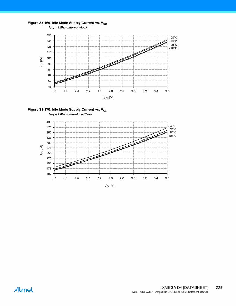
Figure 33-169. Idle Mode Supply Current vs. VCC
fSYS = 1MHz external clock
Figure 33-170. Idle Mode Supply Current vs. VCC
fSYS = 2MHz internal oscillator
105°C
85°C
25°C- 40°C
45
57
69
81
93
105
117
129
141
153
1.6 1.8 2.0 2.2 2.4 2.6 2.8 3.0 3.2 3.4 3.6
I CC
[µA
]
VCC [V]
105°C85°C25°C
- 40°C
150
175
200
225
250
275
300
325
350
375
400
1.6 1.8 2.0 2.2 2.4 2.6 2.8 3.0 3.2 3.4 3.6
I CC
[µA
]
VCC [V]
229XMEGA D4 [DATASHEET]Atmel-8135S-AVR-ATxmega16D4-32D4-64D4-128D4-Datasheet–09/2016
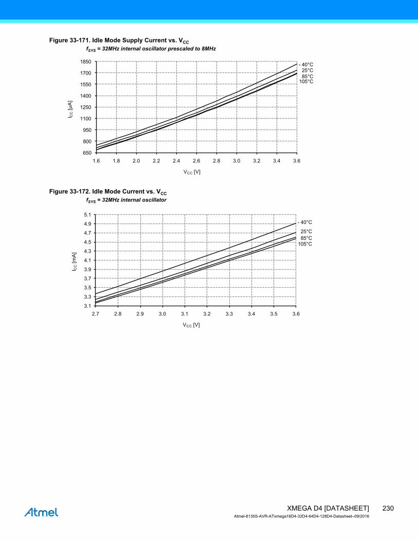
Figure 33-171. Idle Mode Supply Current vs. VCC
fSYS = 32MHz internal oscillator prescaled to 8MHz
Figure 33-172. Idle Mode Current vs. VCC
fSYS = 32MHz internal oscillator
105°C85°C
25°C- 40°C
650
800
950
1100
1250
1400
1550
1700
1850
1.6 1.8 2.0 2.2 2.4 2.6 2.8 3.0 3.2 3.4 3.6
I CC
[µA
]
VCC [V]
105°C85°C
25°C
- 40°C
3.1
3.3
3.5
3.7
3.9
4.1
4.3
4.5
4.7
4.9
5.1
2.7 2.8 2.9 3.0 3.1 3.2 3.3 3.4 3.5 3.6
I CC
[mA
]
VCC [V]
230XMEGA D4 [DATASHEET]Atmel-8135S-AVR-ATxmega16D4-32D4-64D4-128D4-Datasheet–09/2016

33.3.1.3 Power-down Mode Supply Current
Figure 33-173. Power-down Mode Supply Current vs. TemperatureAll functions disabled
Figure 33-174. Power-down Mode Supply Current vs. VCC
All functions disabled
3.6 V
3.0 V2.7 V2.2 V1.8 V1.6 V
0.0
0.3
0.6
0.9
1.2
1.5
1.8
2.1
2.4
2.7
-45 -30 -15 0 15 30 45 60 75 90 105
I CC
[µA
]
Temperature [°C]
105°C
85°C
25°C- 40°C0.0
0.3
0.6
0.9
1.2
1.5
1.8
2.1
2.4
2.7
1.6 1.8 2.0 2.2 2.4 2.6 2.8 3.0 3.2 3.4 3.6
I CC
[µA
]
VCC [V]
231XMEGA D4 [DATASHEET]Atmel-8135S-AVR-ATxmega16D4-32D4-64D4-128D4-Datasheet–09/2016
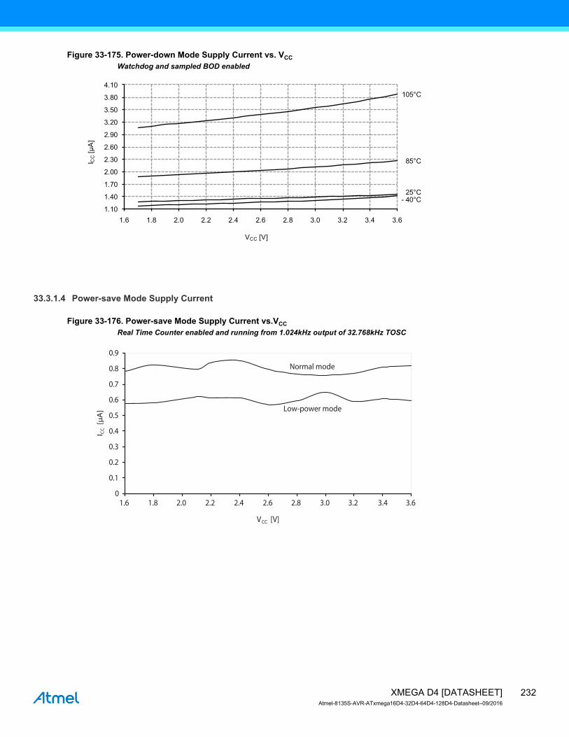
Figure 33-175. Power-down Mode Supply Current vs. VCC
Watchdog and sampled BOD enabled
33.3.1.4 Power-save Mode Supply Current
Figure 33-176. Power-save Mode Supply Current vs.VCC
Real Time Counter enabled and running from 1.024kHz output of 32.768kHz TOSC
105°C
85°C
25°C- 40°C
1.10
1.40
1.70
2.00
2.30
2.60
2.90
3.20
3.50
3.80
4.10
1.6 1.8 2.0 2.2 2.4 2.6 2.8 3.0 3.2 3.4 3.6
I CC
[µA
]
VCC [V]
Normal mode
Low-power mode
0
0.1
0.2
0.3
0.4
0.5
0.6
0.7
0.8
0.9
VCC [V]
I CC
[µA
]
1.6 1.8 2.0 2.2 2.4 2.6 2.8 3.0 3.2 3.4 3.6
232XMEGA D4 [DATASHEET]Atmel-8135S-AVR-ATxmega16D4-32D4-64D4-128D4-Datasheet–09/2016

33.3.1.5 Standby Mode Supply Current
Figure 33-177. Standby Supply Current vs. VCC
Standby, fSYS = 1MHz
Figure 33-178. Standby Supply Current vs. VCC
25°C, running from different crystal oscillators
105 °C
85 °C
25 °C-40 °C
2.5
3.5
4.5
5.5
6.5
7.5
8.5
9.5
10.5
11.5
12.5
1.6 1.8 2 2.2 2.4 2.6 2.8 3 3.2 3.4 3.6
I CC
[uA
]
VCC [V]
16MHz12MHz
8MHz
2MHz
0.454MHz
160
200
240
280
320
360
400
440
480
1.6 1.8 2 2.2 2.4 2.6 2.8 3 3.2 3.4 3.6
VCC [V]
ICC [
µA
]
233XMEGA D4 [DATASHEET]Atmel-8135S-AVR-ATxmega16D4-32D4-64D4-128D4-Datasheet–09/2016

33.3.2 I/O Pin Characteristics
33.3.2.1 Pull-up
Figure 33-179. I/O Pin Pull-up Resistor Current vs. Input VoltageVCC = 1.8V
Figure 33-180. I/O Pin Pull-up Resistor Current vs. Input VoltageVCC = 3.0V
105°C85°C
25°C
- 40°C
0
10
20
30
40
50
60
70
0.0 0.2 0.4 0.6 0.8 1.0 1.2 1.4 1.6 1.8
I PIN
[uA
]
VPIN [V]
105°C85°C25°C
- 40°C
0
15
30
45
60
75
90
105
120
0.0 0.3 0.6 0.9 1.2 1.5 1.8 2.1 2.4 2.7 3.0
I PIN
[µA
]
VPIN [V]
234XMEGA D4 [DATASHEET]Atmel-8135S-AVR-ATxmega16D4-32D4-64D4-128D4-Datasheet–09/2016

Figure 33-181. I/O Pin Pull-up Resistor Current vs. Input VoltageVCC = 3.3V
33.3.2.2 Output Voltage vs. Sink/Source Current
Figure 33-182. I/O Pin Output Voltage vs. Source CurrentVCC = 1.8V
105°C
85°C25°C
- 40°C
0
15
30
45
60
75
90
105
120
135
0.0 0.3 0.6 0.9 1.2 1.5 1.8 2.1 2.4 2.7 3.0 3.3
I PIN
[µA
]
VPIN [V]
105°C85°C
25°C
- 40°C
0.5
0.7
0.9
1.1
1.3
1.5
1.7
1.9
-9 -8 -7 -6 -5 -4 -3 -2 -1 0
VP
IN[V
]
IPIN [mA]
235XMEGA D4 [DATASHEET]Atmel-8135S-AVR-ATxmega16D4-32D4-64D4-128D4-Datasheet–09/2016

Figure 33-183. I/O Pin Output Voltage vs. Source CurrentVCC = 3.0V
Figure 33-184. I/O Pin Output Voltage vs. Source CurrentVCC = 3.3V
105°C
85°C25°C
- 40°C
0.0
0.4
0.8
1.2
1.6
2.0
2.4
2.8
3.2
-30 -27 -24 -21 -18 -15 -12 -9 -6 -3 0
VP
IN[V
]
IPIN [mA]
105°C
85°C
25°C
- 40°C
0.0
0.4
0.8
1.2
1.6
2.0
2.4
2.8
3.2
3.6
-30 -27 -24 -21 -18 -15 -12 -9 -6 -3 0
VP
IN[V
]
IPIN [mA]
236XMEGA D4 [DATASHEET]Atmel-8135S-AVR-ATxmega16D4-32D4-64D4-128D4-Datasheet–09/2016

Figure 33-185. I/O Pin Output Voltage vs. Source Current
Figure 33-186. I/O Pin Output Voltage vs. Sink CurrentVCC = 1.8V
3.6 V
3.3 V
3.0 V
2.7 V
1.8 V1.6 V
0.5
0.9
1.3
1.7
2.1
2.5
2.9
3.3
3.7
-24 -21 -18 -15 -12 -9 -6 -3 0
VP
IN[V
]
IPIN [mA]
- 40°C
0.0
0.1
0.2
0.3
0.4
0.5
0.6
0.7
0.8
0.9
1.0
0 2 4 6 8 10 12 14 16 18 20
VP
IN[V
]
IPIN [mA]
25°C
85°C
105°C
237XMEGA D4 [DATASHEET]Atmel-8135S-AVR-ATxmega16D4-32D4-64D4-128D4-Datasheet–09/2016

Figure 33-187. I/O Pin Output Voltage vs. Sink CurrentVCC = 3.0V
Figure 33-188. I/O Pin Output Voltage vs. Sink CurrentVCC = 3.3V
105°C85°C
25°C
- 40°C
0.0
0.1
0.2
0.3
0.4
0.5
0.6
0.7
0.8
0.9
1.0
0 3 6 9 12 15 18 21 24 27 30
VP
IN[V
]
IPIN [mA]
105°C85°C
25°C
- 40°C
0.0
0.1
0.2
0.3
0.4
0.5
0.6
0.7
0.8
0.9
1.0
0 3 6 9 12 15 18 21 24 27 30
VP
IN[V
]
IPIN [mA]
238XMEGA D4 [DATASHEET]Atmel-8135S-AVR-ATxmega16D4-32D4-64D4-128D4-Datasheet–09/2016
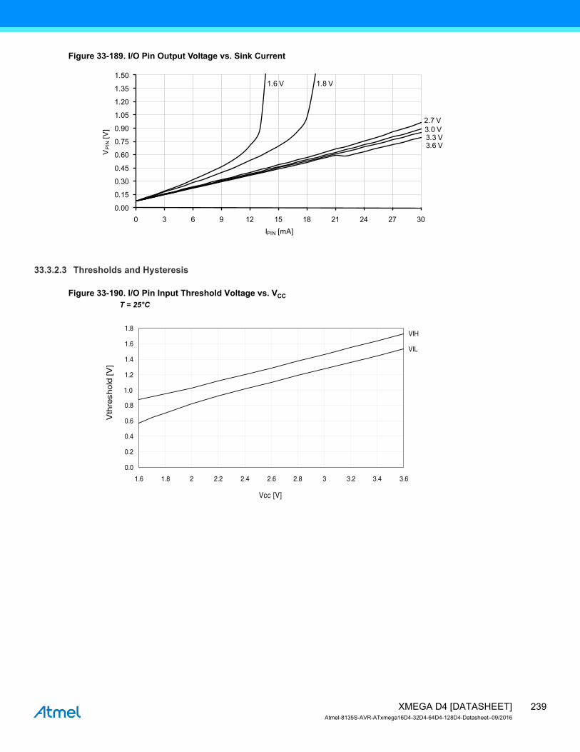
Figure 33-189. I/O Pin Output Voltage vs. Sink Current
33.3.2.3 Thresholds and Hysteresis
Figure 33-190. I/O Pin Input Threshold Voltage vs. VCC
T = 25°C
3.6 V3.3 V3.0 V
2.7 V
0.00
0.15
0.30
0.45
0.60
0.75
0.90
1.05
1.20
1.35
1.50
0 3 6 9 12 15 18 21 24 27 30
VP
IN[V
]
IPIN [mA]
1.6 V 1.8 V
VIL
VIH
0.0
0.2
0.4
0.6
0.8
1.0
1.2
1.4
1.6
1.8
1.6 1.8 2 2.2 2.4 2.6 2.8 3 3.2 3.4 3.6
Vcc [V]
Vth
reshold
[V
]
239XMEGA D4 [DATASHEET]Atmel-8135S-AVR-ATxmega16D4-32D4-64D4-128D4-Datasheet–09/2016
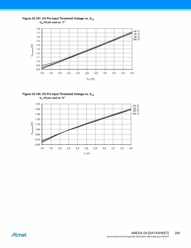
Figure 33-191. I/O Pin Input Threshold Voltage vs. VCC
VIH I/O pin read as “1”
Figure 33-192. I/O Pin Input Threshold Voltage vs. VCC
VIL I/O pin read as “0”
105 °C85 °C
25 °C
-40 °C
0.8
0.9
1.0
1.1
1.2
1.3
1.4
1.5
1.6
1.7
1.8
1.6 1.8 2.0 2.2 2.4 2.6 2.8 3.0 3.2 3.4 3.6
Vth
resh
old
[V]
VCC [V]
105 °C
85 °C25 °C
-40 °C
0.55
0.70
0.85
1.00
1.15
1.30
1.45
1.60
1.75
1.6 1.8 2.0 2.2 2.4 2.6 2.8 3.0 3.2 3.4 3.6
Vth
resh
old
[V]
VCC [V]
240XMEGA D4 [DATASHEET]Atmel-8135S-AVR-ATxmega16D4-32D4-64D4-128D4-Datasheet–09/2016

Figure 33-193. I/O Pin Input Hysteresis vs. VCC
33.3.3 ADC Characteristics
Figure 33-194. INL Error vs. External VREF
T = 25C, VCC = 3.6V, external reference
105 °C
85 °C
25 °C -40 °C
0.08
0.11
0.14
0.17
0.20
0.23
0.26
0.29
0.32
1.6 1.8 2.0 2.2 2.4 2.6 2.8 3.0 3.2 3.4 3.6
Vth
resh
old
[V]
VCC [V]
Single-ended unsigned mode
Single-ended signed mode
Dif ferential mode
0.0
0.3
0.6
0.9
1.2
1.5
1.8
2.1
2.4
2.7
1.0 1.2 1.4 1.6 1.8 2.0 2.2 2.4 2.6 2.8 3.0
INL [L
SB
]
Vref [V]
241XMEGA D4 [DATASHEET]Atmel-8135S-AVR-ATxmega16D4-32D4-64D4-128D4-Datasheet–09/2016

Figure 33-195. INL Error vs. Sample RateT = 25C, VCC = 2.7V, VREF = 1.0V external
Figure 33-196. INL Error vs. Input Code
Single-ended signed mode
Single-ended signed mode
Dif ferential mode
0.0
0.2
0.4
0.6
0.8
1.0
1.2
1.4
1.6
500 650 800 950 1100 1250 1400 1550 1700 1850 2000
INL [L
SB
]
ADC sample rate [kSps]
0 512 1024 1536 2048 2560 3072 3584 4096
2.0
1.5
1.0
0.5
0.0
-0.5
-1.0
-1.5
-2.0
INL
[LSB]
ADC input code
242XMEGA D4 [DATASHEET]Atmel-8135S-AVR-ATxmega16D4-32D4-64D4-128D4-Datasheet–09/2016
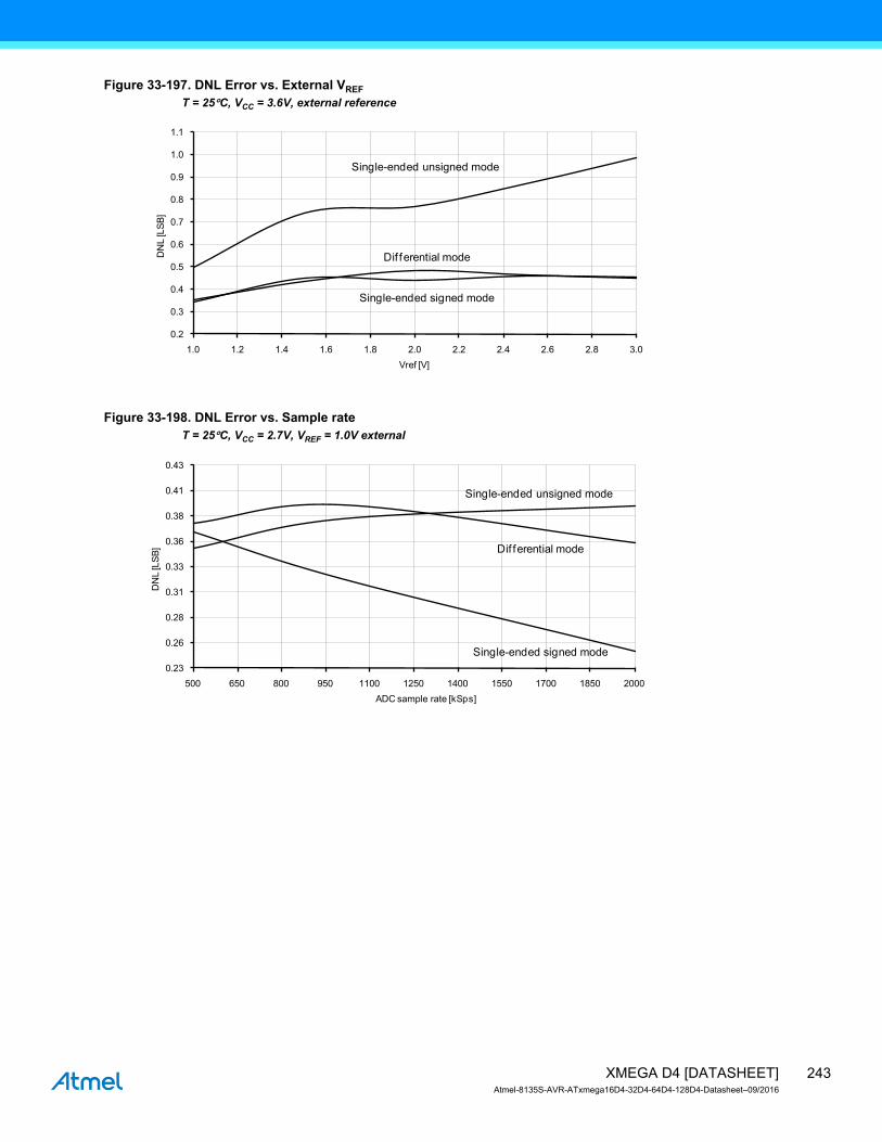
Figure 33-197. DNL Error vs. External VREF
T = 25C, VCC = 3.6V, external reference
Figure 33-198. DNL Error vs. Sample rateT = 25C, VCC = 2.7V, VREF = 1.0V external
Single-ended unsigned mode
Single-ended signed mode
Dif ferential mode
0.2
0.3
0.4
0.5
0.6
0.7
0.8
0.9
1.0
1.1
1.0 1.2 1.4 1.6 1.8 2.0 2.2 2.4 2.6 2.8 3.0
DN
L [L
SB
]
Vref [V]
Single-ended unsigned mode
Single-ended signed mode
Dif ferential mode
0.23
0.26
0.28
0.31
0.33
0.36
0.38
0.41
0.43
500 650 800 950 1100 1250 1400 1550 1700 1850 2000
DN
L [L
SB
]
ADC sample rate [kSps]
243XMEGA D4 [DATASHEET]Atmel-8135S-AVR-ATxmega16D4-32D4-64D4-128D4-Datasheet–09/2016
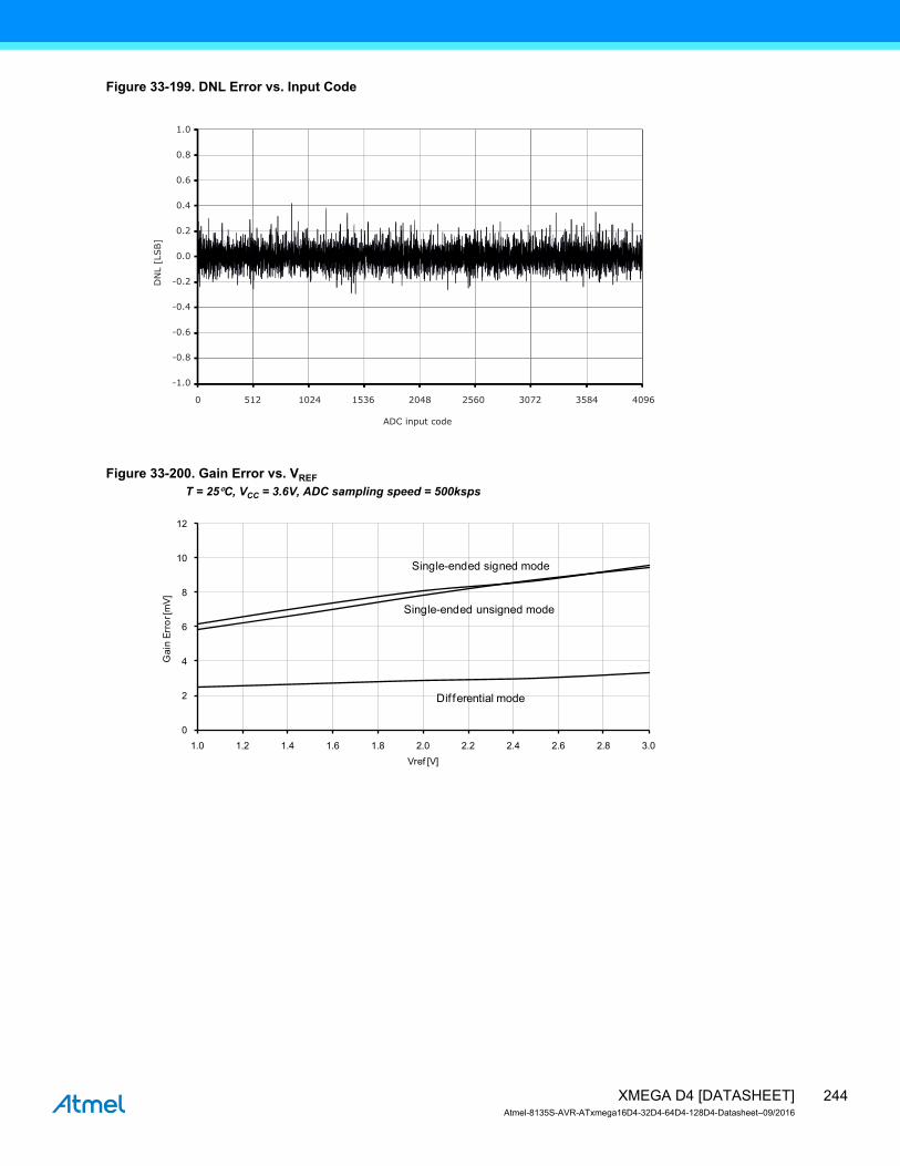
Figure 33-199. DNL Error vs. Input Code
Figure 33-200. Gain Error vs. VREF
T = 25C, VCC = 3.6V, ADC sampling speed = 500ksps
0 512 1024 1536 2048 2560 3072 3584 4096
1.0
0.8
0.6
0.4
0.2
0.0
-0.2
-0.4
-0.6
-0.8
-1.0
DN
L [L
SB]
ADC input code
Single-ended unsigned mode
Single-ended signed mode
Dif ferential mode
0
2
4
6
8
10
12
1.0 1.2 1.4 1.6 1.8 2.0 2.2 2.4 2.6 2.8 3.0
Gain
Err
or [
mV
]
Vref [V]
244XMEGA D4 [DATASHEET]Atmel-8135S-AVR-ATxmega16D4-32D4-64D4-128D4-Datasheet–09/2016
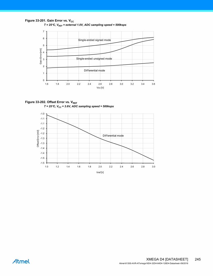
Figure 33-201. Gain Error vs. VCC
T = 25C, VREF = external 1.0V, ADC sampling speed = 500ksps
Figure 33-202. Offset Error vs. VREF
T = 25C, VCC = 3.6V, ADC sampling speed = 500ksps
Single-ended unsigned mode
Single-ended signed mode
Dif ferential mode
0
1
2
3
4
5
6
7
1.6 1.8 2.0 2.2 2.4 2.6 2.8 3.0 3.2 3.4 3.6
Gain
Err
or [
mV
]
Vcc [V]
Dif ferential mode
-1.5
-1.5
-1.4
-1.4
-1.3
-1.3
-1.2
-1.2
-1.1
-1.1
-1.0
1.0 1.2 1.4 1.6 1.8 2.0 2.2 2.4 2.6 2.8 3.0
Offset E
rro
r [m
V]
Vref [V]
245XMEGA D4 [DATASHEET]Atmel-8135S-AVR-ATxmega16D4-32D4-64D4-128D4-Datasheet–09/2016
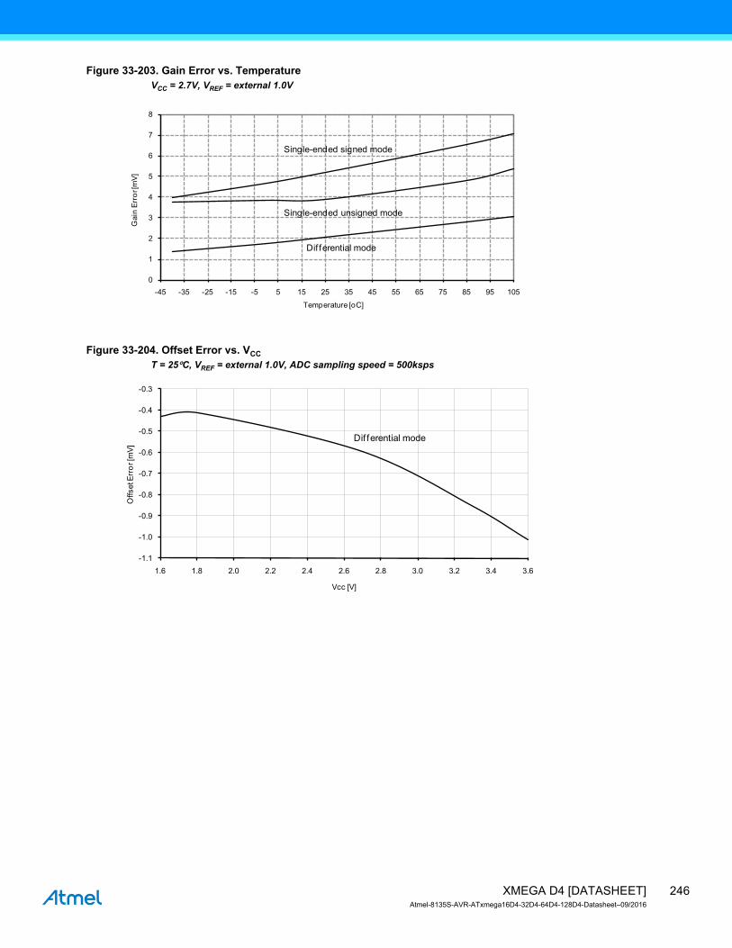
Figure 33-203. Gain Error vs. TemperatureVCC = 2.7V, VREF = external 1.0V
Figure 33-204. Offset Error vs. VCC
T = 25C, VREF = external 1.0V, ADC sampling speed = 500ksps
Single-ended unsigned mode
Single-ended signed mode
Dif ferential mode
0
1
2
3
4
5
6
7
8
-45 -35 -25 -15 -5 5 15 25 35 45 55 65 75 85 95 105
Gain
Err
or [
mV
]
Temperature [oC]
Dif ferential mode
-1.1
-1.0
-0.9
-0.8
-0.7
-0.6
-0.5
-0.4
-0.3
1.6 1.8 2.0 2.2 2.4 2.6 2.8 3.0 3.2 3.4 3.6
Offset E
rro
r [m
V]
Vcc [V]
246XMEGA D4 [DATASHEET]Atmel-8135S-AVR-ATxmega16D4-32D4-64D4-128D4-Datasheet–09/2016

Figure 33-205. Noise vs. VREF
T = 25C, VCC = 3.6V, ADC sampling speed = 500ksps
Figure 33-206. Noise vs. VCC
T = 25C, VREF = external 1.0V, ADC sampling speed = 500ksps
Single-ended unsigend mode
Single-ended signed mode
Dif ferential mode
0.0
0.1
0.2
0.3
0.4
0.5
0.6
0.7
0.8
0.9
1.0 1.2 1.4 1.6 1.8 2.0 2.2 2.4 2.6 2.8 3.0
No
ise [m
V R
MS
]
Vref [V]
Single-ended unsigned mode
Single-ended signed mode
Dif ferential mode
0.0
0.1
0.2
0.3
0.4
0.5
0.6
0.7
0.8
1.6 1.8 2.0 2.2 2.4 2.6 2.8 3.0 3.2 3.4 3.6
No
ise [m
V R
MS
]
Vcc [V]
247XMEGA D4 [DATASHEET]Atmel-8135S-AVR-ATxmega16D4-32D4-64D4-128D4-Datasheet–09/2016
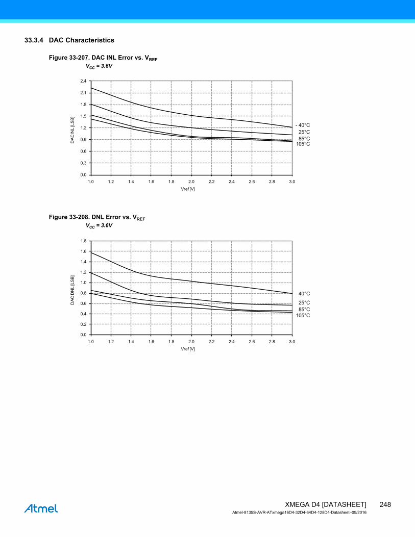
33.3.4 DAC Characteristics
Figure 33-207. DAC INL Error vs. VREF
VCC = 3.6V
Figure 33-208. DNL Error vs. VREF
VCC = 3.6V
105°C85°C
25°C
- 40°C
0.0
0.3
0.6
0.9
1.2
1.5
1.8
2.1
2.4
1.0 1.2 1.4 1.6 1.8 2.0 2.2 2.4 2.6 2.8 3.0
DA
CIN
L [L
SB
]
Vref [V]
105°C
85°C
25°C
- 40°C
0.0
0.2
0.4
0.6
0.8
1.0
1.2
1.4
1.6
1.8
1.0 1.2 1.4 1.6 1.8 2.0 2.2 2.4 2.6 2.8 3.0
DA
C D
NL [L
SB
]
Vref [V]
248XMEGA D4 [DATASHEET]Atmel-8135S-AVR-ATxmega16D4-32D4-64D4-128D4-Datasheet–09/2016

Figure 33-209. DAC Noise vs. TemperatureVCC = 2.7V, VREF = 1.0V
33.3.5 Analog Comparator Characteristics
Figure 33-210. Analog Comparator Hysteresis vs. VCC
High-speed, small hysteresis
0.160
0.162
0.164
0.166
0.168
0.170
0.172
0.174
0.176
0.178
-45 -35 -25 -15 -5 5 15 25 35 45 55 65 75 85 95 105
No
ise[m
V R
MS
]
Temperature [oC]
105°C
85°C
25°C
- 40°C
15
16
17
18
19
20
21
22
23
24
25
1.6 1.8 2.0 2.2 2.4 2.6 2.8 3.0 3.2 3.4 3.6
VH
YS
T[m
V]
VCC [V]
249XMEGA D4 [DATASHEET]Atmel-8135S-AVR-ATxmega16D4-32D4-64D4-128D4-Datasheet–09/2016
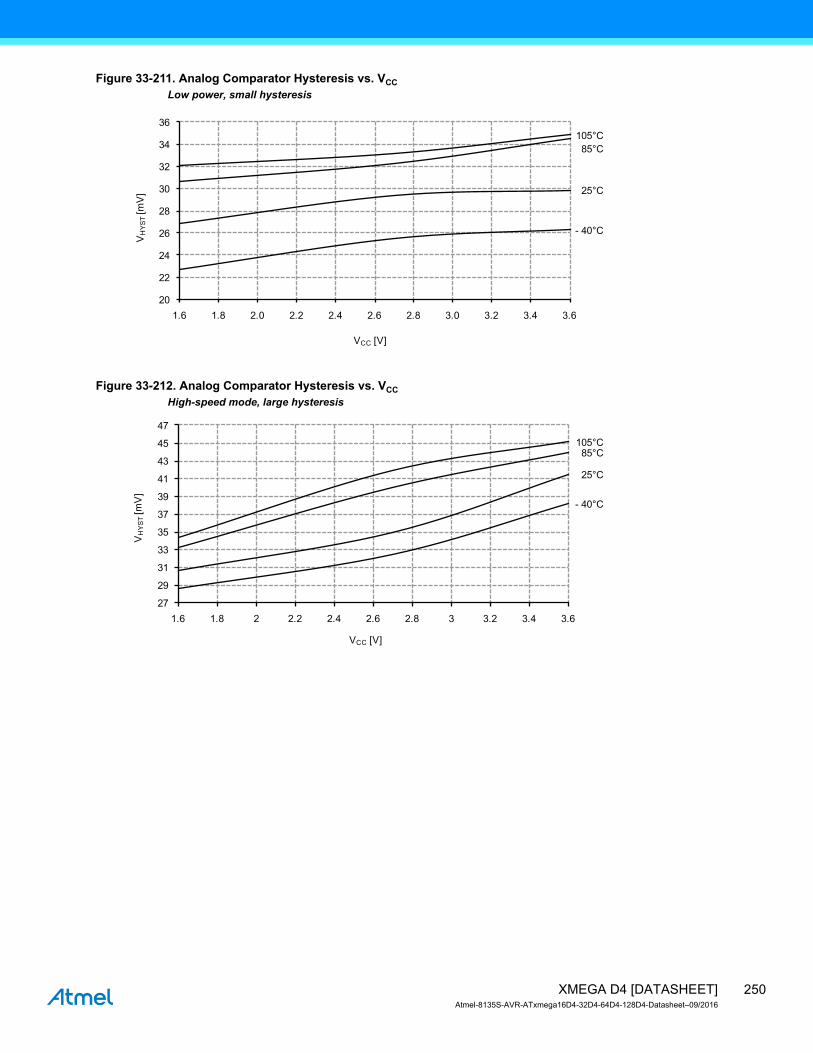
Figure 33-211. Analog Comparator Hysteresis vs. VCC
Low power, small hysteresis
Figure 33-212. Analog Comparator Hysteresis vs. VCC
High-speed mode, large hysteresis
105°C
85°C
25°C
- 40°C
20
22
24
26
28
30
32
34
36
1.6 1.8 2.0 2.2 2.4 2.6 2.8 3.0 3.2 3.4 3.6
VH
YS
T[m
V]
VCC [V]
105°C85°C
25°C
- 40°C
27
29
31
33
35
37
39
41
43
45
47
1.6 1.8 2 2.2 2.4 2.6 2.8 3 3.2 3.4 3.6
VH
YS
T[m
V]
VCC [V]
250XMEGA D4 [DATASHEET]Atmel-8135S-AVR-ATxmega16D4-32D4-64D4-128D4-Datasheet–09/2016

Figure 33-213. Analog Comparator Hysteresis vs. VCC
Low power, large hysteresis
Figure 33-214. Analog Comparator Current Source vs. Calibration ValueTemperature = 25°C
105°C
85°C
25°C
- 40°C
46
49
52
55
58
61
64
67
70
73
76
1.6 1.8 2.0 2.2 2.4 2.6 2.8 3.0 3.2 3.4 3.6
VH
YS
T[m
V]
VCC [V]
2
3
4
5
6
7
8
0 1 2 3 4 5 6 7 8 9 10 11 12 13 14 15
I CU
RR
EN
TS
OU
RC
E[µ
A]
CURRCALIBA[3..0]
3.6V3.0V2.7V2.2V1.8V1.6V
251XMEGA D4 [DATASHEET]Atmel-8135S-AVR-ATxmega16D4-32D4-64D4-128D4-Datasheet–09/2016
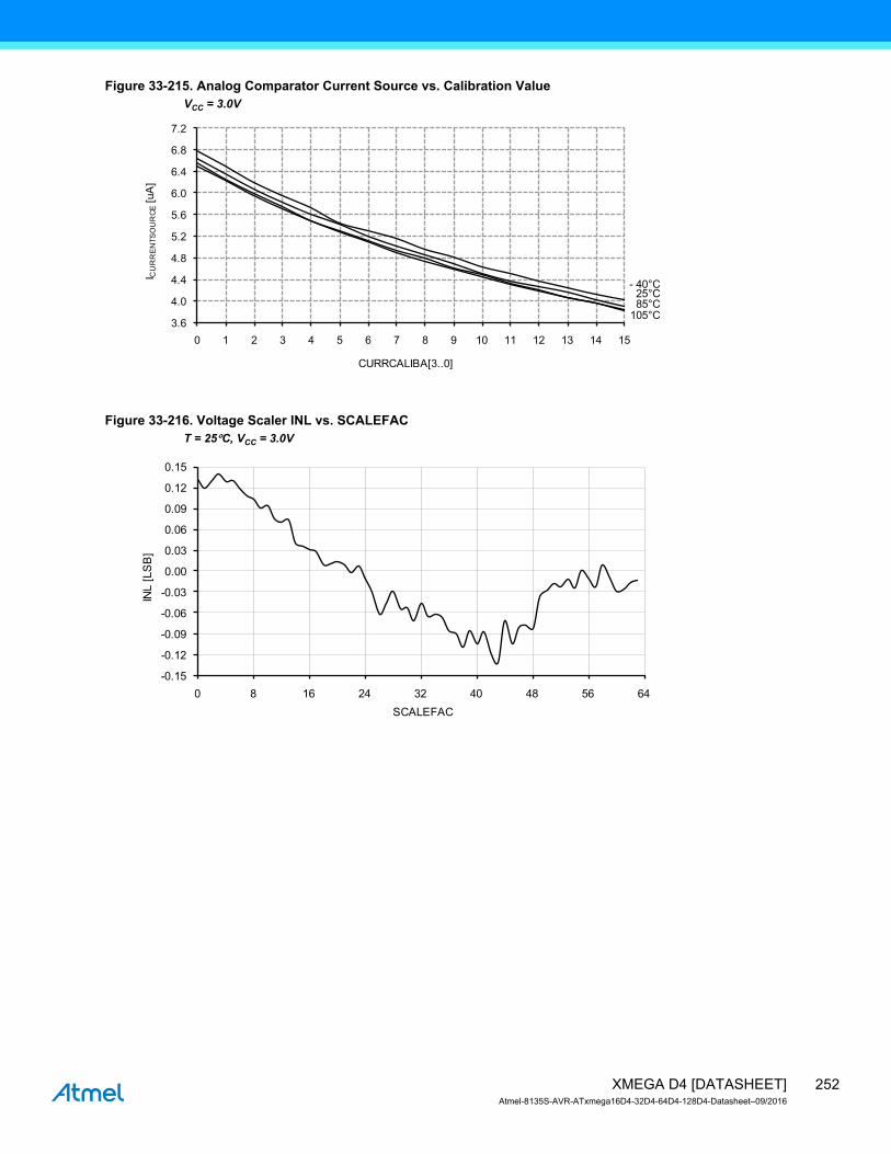
Figure 33-215. Analog Comparator Current Source vs. Calibration ValueVCC = 3.0V
Figure 33-216. Voltage Scaler INL vs. SCALEFACT = 25C, VCC = 3.0V
105°C85°C25°C
- 40°C
3.6
4.0
4.4
4.8
5.2
5.6
6.0
6.4
6.8
7.2
0 1 2 3 4 5 6 7 8 9 10 11 12 13 14 15
I CU
RR
EN
TS
OU
RC
E[u
A]
CURRCALIBA[3..0]
-0.15
-0.12
-0.09
-0.06
-0.03
0.00
0.03
0.06
0.09
0.12
0.15
0 8 16 24 32 40 48 56 64
INL [
LS
B]
SCALEFAC
252XMEGA D4 [DATASHEET]Atmel-8135S-AVR-ATxmega16D4-32D4-64D4-128D4-Datasheet–09/2016
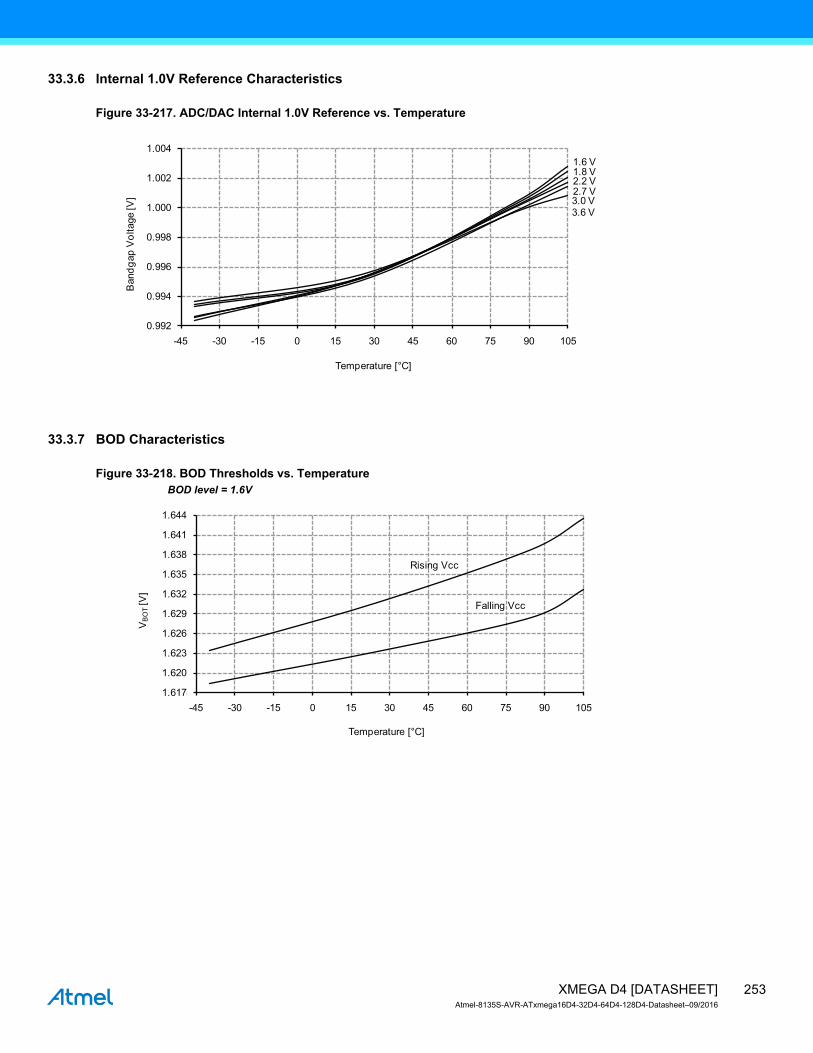
33.3.6 Internal 1.0V Reference Characteristics
Figure 33-217. ADC/DAC Internal 1.0V Reference vs. Temperature
33.3.7 BOD Characteristics
Figure 33-218. BOD Thresholds vs. TemperatureBOD level = 1.6V
3.6 V
3.0 V2.7 V2.2 V1.8 V1.6 V
0.992
0.994
0.996
0.998
1.000
1.002
1.004
-45 -30 -15 0 15 30 45 60 75 90 105
Band
gap
Vo
ltage [V
]
Temperature [°C]
Rising Vcc
Falling Vcc
1.617
1.620
1.623
1.626
1.629
1.632
1.635
1.638
1.641
1.644
-45 -30 -15 0 15 30 45 60 75 90 105
VB
OT
[V]
Temperature [°C]
253XMEGA D4 [DATASHEET]Atmel-8135S-AVR-ATxmega16D4-32D4-64D4-128D4-Datasheet–09/2016
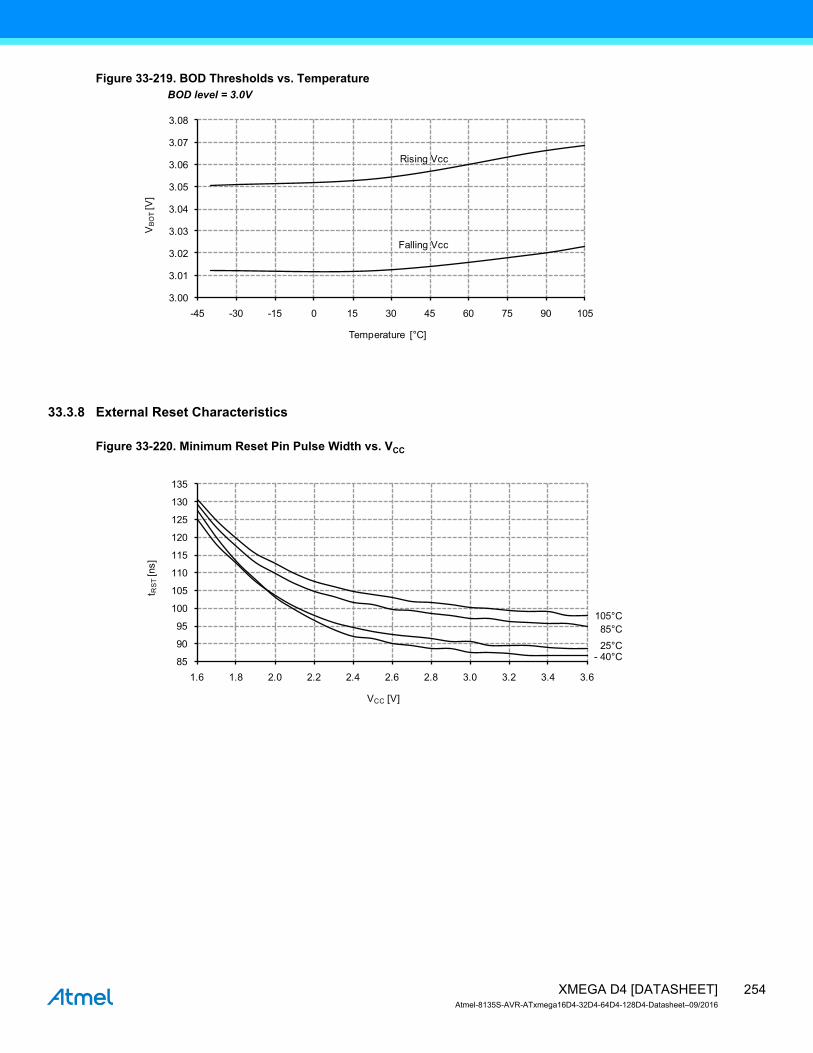
Figure 33-219. BOD Thresholds vs. TemperatureBOD level = 3.0V
33.3.8 External Reset Characteristics
Figure 33-220. Minimum Reset Pin Pulse Width vs. VCC
Rising Vcc
Falling Vcc
3.00
3.01
3.02
3.03
3.04
3.05
3.06
3.07
3.08
-45 -30 -15 0 15 30 45 60 75 90 105
VB
OT
[V]
Temperature [°C]
105°C
85°C
25°C- 40°C
85
90
95
100
105
110
115
120
125
130
135
1.6 1.8 2.0 2.2 2.4 2.6 2.8 3.0 3.2 3.4 3.6
t RS
T[n
s]
VCC [V]
254XMEGA D4 [DATASHEET]Atmel-8135S-AVR-ATxmega16D4-32D4-64D4-128D4-Datasheet–09/2016

Figure 33-221. Reset Pin Pull-up Resistor Current vs. Reset Pin VoltageVCC = 1.8V
Figure 33-222. Reset Pin Pull-up Resistor Current vs. Reset Pin VoltageVCC = 3.0V
105°C
85°C
25°C
- 40°C
0
10
20
30
40
50
60
70
80
0.0 0.2 0.4 0.6 0.8 1.0 1.2 1.4 1.6 1.8
I RE
SE
T[µ
A]
VRESET [V]
105°C
85°C
25°C
- 40°C
0
15
30
45
60
75
90
105
120
0.0 0.3 0.6 0.9 1.2 1.5 1.8 2.1 2.4 2.7 3.0
I RE
SE
T[µ
A]
VRESET [V]
255XMEGA D4 [DATASHEET]Atmel-8135S-AVR-ATxmega16D4-32D4-64D4-128D4-Datasheet–09/2016
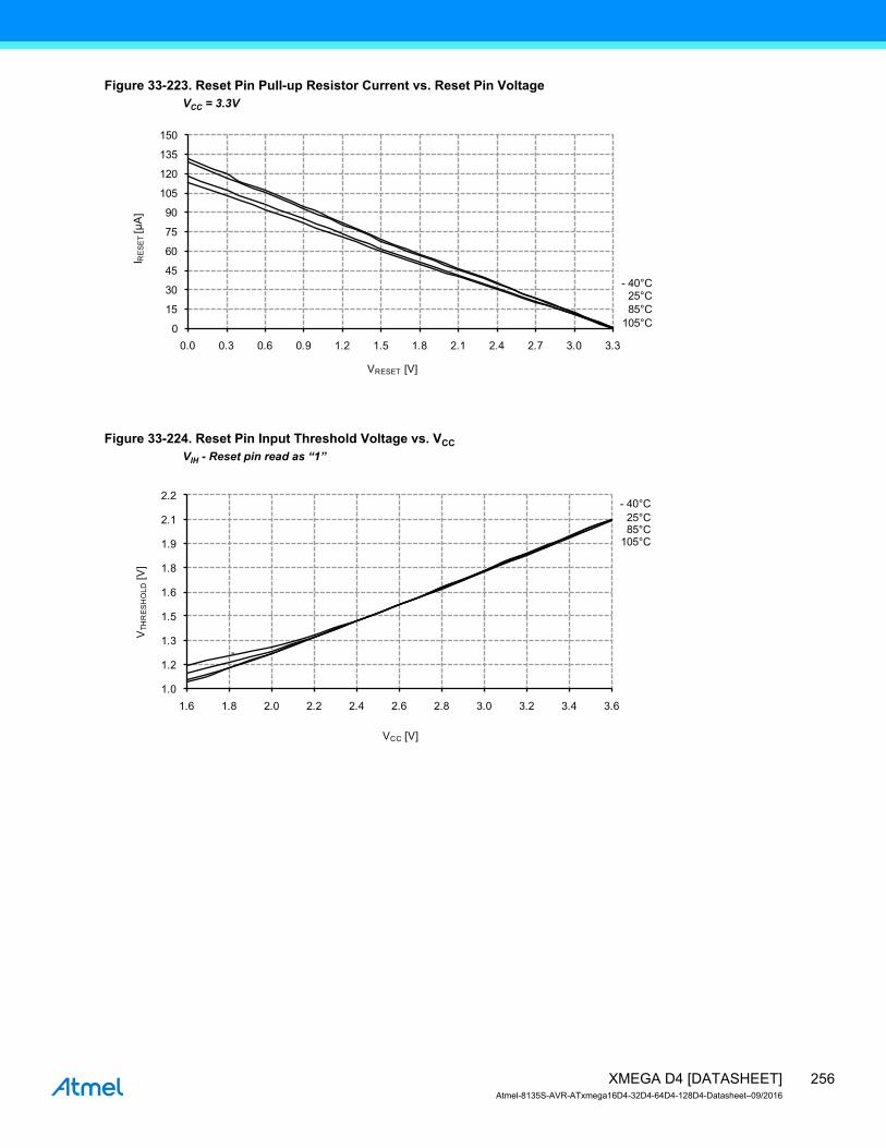
Figure 33-223. Reset Pin Pull-up Resistor Current vs. Reset Pin VoltageVCC = 3.3V
Figure 33-224. Reset Pin Input Threshold Voltage vs. VCC
VIH - Reset pin read as “1”
105°C
85°C
25°C
- 40°C
0
15
30
45
60
75
90
105
120
135
150
0.0 0.3 0.6 0.9 1.2 1.5 1.8 2.1 2.4 2.7 3.0 3.3
I RE
SE
T[µ
A]
VRESET [V]
105°C85°C25°C
-
- 40°C
1.0
1.2
1.3
1.5
1.6
1.8
1.9
2.1
2.2
1.6 1.8 2.0 2.2 2.4 2.6 2.8 3.0 3.2 3.4 3.6
VTH
RE
SH
OL
D[V
]
VCC [V]
256XMEGA D4 [DATASHEET]Atmel-8135S-AVR-ATxmega16D4-32D4-64D4-128D4-Datasheet–09/2016
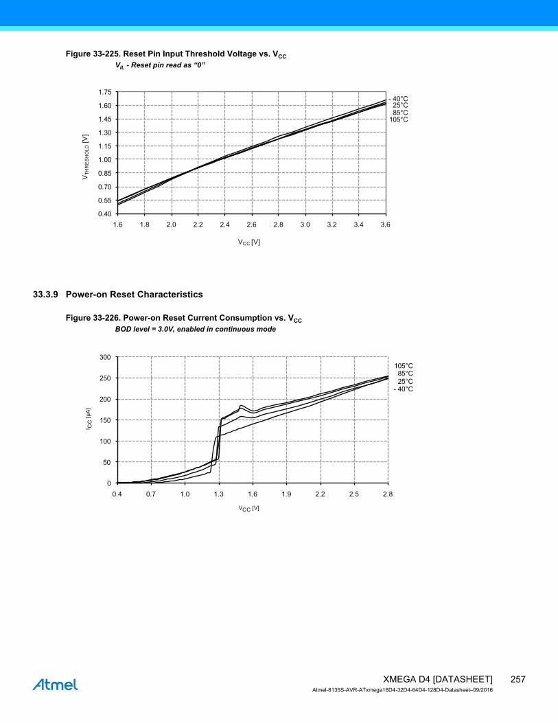
Figure 33-225. Reset Pin Input Threshold Voltage vs. VCC
VIL - Reset pin read as “0”
33.3.9 Power-on Reset Characteristics
Figure 33-226. Power-on Reset Current Consumption vs. VCC
BOD level = 3.0V, enabled in continuous mode
105°C85°C25°C
- 40°C
0.40
0.55
0.70
0.85
1.00
1.15
1.30
1.45
1.60
1.75
1.6 1.8 2.0 2.2 2.4 2.6 2.8 3.0 3.2 3.4 3.6
VTH
RE
SH
OLD
[V]
VCC [V]
105°C85°C
25°C- 40°C
0
50
100
150
200
250
300
0.4 0.7 1.0 1.3 1.6 1.9 2.2 2.5 2.8
I CC
[µ
A]
VCC [V]
257XMEGA D4 [DATASHEET]Atmel-8135S-AVR-ATxmega16D4-32D4-64D4-128D4-Datasheet–09/2016
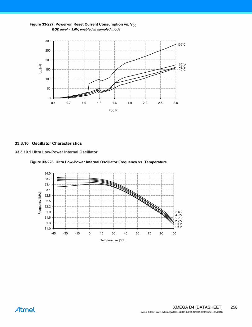
Figure 33-227. Power-on Reset Current Consumption vs. VCC
BOD level = 3.0V, enabled in sampled mode
33.3.10 Oscillator Characteristics
33.3.10.1 Ultra Low-Power Internal Oscillator
Figure 33-228. Ultra Low-Power Internal Oscillator Frequency vs. Temperature
105°C
85°C25°C
- 40°C
0
50
100
150
200
250
300
0.4 0.7 1.0 1.3 1.6 1.9 2.2 2.5 2.8
I CC
[µ
A]
VCC [V]
3.6 V3.0 V2.7 V2.2 V1.8 V1.6 V
31.0
31.3
31.6
31.9
32.2
32.5
32.8
33.1
33.4
33.7
34.0
-45 -30 -15 0 15 30 45 60 75 90 105
Fre
quency [
kH
z]
Temperature [°C]
258XMEGA D4 [DATASHEET]Atmel-8135S-AVR-ATxmega16D4-32D4-64D4-128D4-Datasheet–09/2016
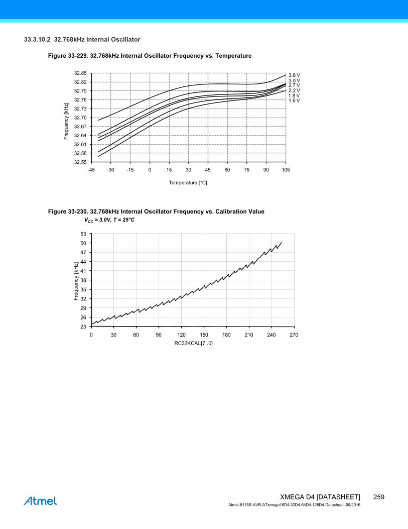
33.3.10.2 32.768kHz Internal Oscillator
Figure 33-229. 32.768kHz Internal Oscillator Frequency vs. Temperature
Figure 33-230. 32.768kHz Internal Oscillator Frequency vs. Calibration ValueVCC = 3.0V, T = 25°C
3.6 V3.0 V2.7 V2.2 V1.8 V1.6 V
32.55
32.58
32.61
32.64
32.67
32.70
32.73
32.76
32.79
32.82
32.85
-45 -30 -15 0 15 30 45 60 75 90 105
Fre
quency [kH
z]
Temperature [°C]
23
26
29
32
35
38
41
44
47
50
53
0 30 60 90 120 150 180 210 240 270
Fre
quency [
kH
z]
RC32KCAL[7..0]
259XMEGA D4 [DATASHEET]Atmel-8135S-AVR-ATxmega16D4-32D4-64D4-128D4-Datasheet–09/2016

33.3.10.3 2MHz Internal Oscillator
Figure 33-231. 2MHz Internal Oscillator Frequency vs. TemperatureDFLL disabled
Figure 33-232. 2MHz Internal Oscillator Frequency vs. TemperatureDFLL enabled, from the 32.768kHz internal oscillator
3.6 V
3.0 V
2.7 V
2.2 V1.8 V1.6 V
1.94
1.96
1.98
2.00
2.02
2.04
2.06
2.08
2.10
2.12
-45 -30 -15 0 15 30 45 60 75 90 105
Fre
quency [
MH
z]
Temperature [°C]
3.6 V
3.0 V
2.7 V
2.2 V
1.8 V
1.6 V
1.988
1.990
1.992
1.994
1.996
1.998
2.000
2.002
2.004
2.006
2.008
2.010
-45 -30 -15 0 15 30 45 60 75 90 105
Fre
quency [
MH
z]
Temperature [°C]
260XMEGA D4 [DATASHEET]Atmel-8135S-AVR-ATxmega16D4-32D4-64D4-128D4-Datasheet–09/2016
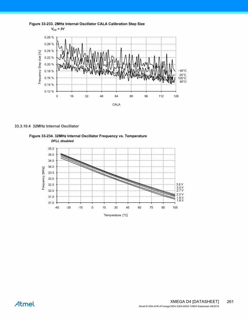
Figure 33-233. 2MHz Internal Oscillator CALA Calibration Step SizeVCC = 3V
33.3.10.4 32MHz Internal Oscillator
Figure 33-234. 32MHz Internal Oscillator Frequency vs. TemperatureDFLL disabled
105°C85°C
25°C
- 40°C
0.12 %
0.14 %
0.16 %
0.18 %
0.20 %
0.22 %
0.24 %
0.26 %
0.28 %
0 16 32 48 64 80 96 112 128
Fre
quency S
tep
siz
e [
%]
CALA
3.6 V3.0 V2.7 V
2.2 V1.8 V1.6 V
31.0
31.5
32.0
32.5
33.0
33.5
34.0
34.5
35.0
35.5
-45 -30 -15 0 15 30 45 60 75 90 105
Fre
quency [
MH
z]
Temperature [°C]
261XMEGA D4 [DATASHEET]Atmel-8135S-AVR-ATxmega16D4-32D4-64D4-128D4-Datasheet–09/2016
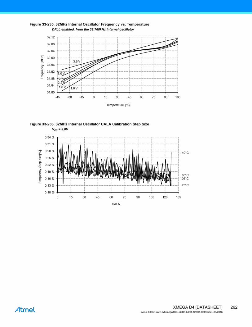
Figure 33-235. 32MHz Internal Oscillator Frequency vs. TemperatureDFLL enabled, from the 32.768kHz internal oscillator
Figure 33-236. 32MHz Internal Oscillator CALA Calibration Step SizeVCC = 3.0V
3.6 V
3.0 V
2.7 V
2.2 V
1.8 V 1.6 V
31.80
31.84
31.88
31.92
31.96
32.00
32.04
32.08
32.12
-45 -30 -15 0 15 30 45 60 75 90 105
Fre
quency [
MH
z]
Temperature [°C]
105°C85°C
25°C
- 40°C
0.10 %
0.13 %
0.16 %
0.19 %
0.22 %
0.25 %
0.28 %
0.31 %
0.34 %
0 15 30 45 60 75 90 105 120 135
Fre
quency S
tep
siz
e[%
]
CALA
262XMEGA D4 [DATASHEET]Atmel-8135S-AVR-ATxmega16D4-32D4-64D4-128D4-Datasheet–09/2016
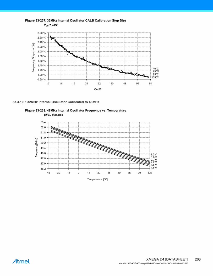
Figure 33-237. 32MHz Internal Oscillator CALB Calibration Step SizeVCC = 3.0V
33.3.10.5 32MHz Internal Oscillator Calibrated to 48MHz
Figure 33-238. 48MHz Internal Oscillator Frequency vs. TemperatureDFLL disabled
105°C85°C
25°C- 40°C
0.80 %
1.00 %
1.20 %
1.40 %
1.60 %
1.80 %
2.00 %
2.20 %
2.40 %
2.60 %
2.80 %
0 8 16 24 32 40 48 56 64
Fre
quency S
tep
siz
e [
%]
CALB
3.6 V3.0 V2.7 V2.2 V1.8 V1.6 V46.2
47.0
47.8
48.6
49.4
50.2
51.0
51.8
52.6
53.4
-45 -30 -15 0 15 30 45 60 75 90 105
Fre
quency[M
Hz]
Temperature [°C]
263XMEGA D4 [DATASHEET]Atmel-8135S-AVR-ATxmega16D4-32D4-64D4-128D4-Datasheet–09/2016
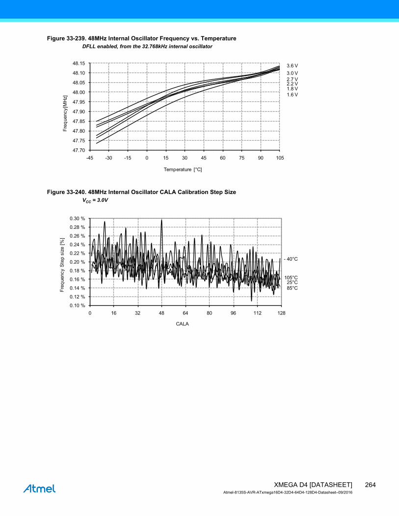
Figure 33-239. 48MHz Internal Oscillator Frequency vs. TemperatureDFLL enabled, from the 32.768kHz internal oscillator
Figure 33-240. 48MHz Internal Oscillator CALA Calibration Step SizeVCC = 3.0V
3.6 V
3.0 V
2.7 V2.2 V1.8 V
1.6 V
47.70
47.75
47.80
47.85
47.90
47.95
48.00
48.05
48.10
48.15
-45 -30 -15 0 15 30 45 60 75 90 105
Fre
quency[M
Hz]
Temperature [°C]
105°C
85°C
25°C
- 40°C
0.10 %
0.12 %
0.14 %
0.16 %
0.18 %
0.20 %
0.22 %
0.24 %
0.26 %
0.28 %
0.30 %
0 16 32 48 64 80 96 112 128
Fre
quency S
tep
siz
e [
%]
CALA
264XMEGA D4 [DATASHEET]Atmel-8135S-AVR-ATxmega16D4-32D4-64D4-128D4-Datasheet–09/2016

33.3.11 Two-Wire Interface Characteristics
Figure 33-241. SDA Hold Time vs. Supply Voltage
33.3.12 PDI Characteristics
Figure 33-242. Maximum PDI Frequency vs. VCC
105°C
85°C
25°C
- 40°C
260
265
270
275
280
285
290
295
300
2.6 2.7 2.8 2.9 3.0 3.1 3.2 3.3 3.4 3.5 3.6
Ho
ldtim
e [ns]
Vcc [V]
105°C
85°C
25°C
-
- 40°C
10
12
14
16
18
20
22
24
26
28
30
1.6 1.8 2.0 2.2 2.4 2.6 2.8 3.0 3.2 3.4 3.6
Maxim
um
Fre
quency [
MH
z]
VCC [V]
265XMEGA D4 [DATASHEET]Atmel-8135S-AVR-ATxmega16D4-32D4-64D4-128D4-Datasheet–09/2016
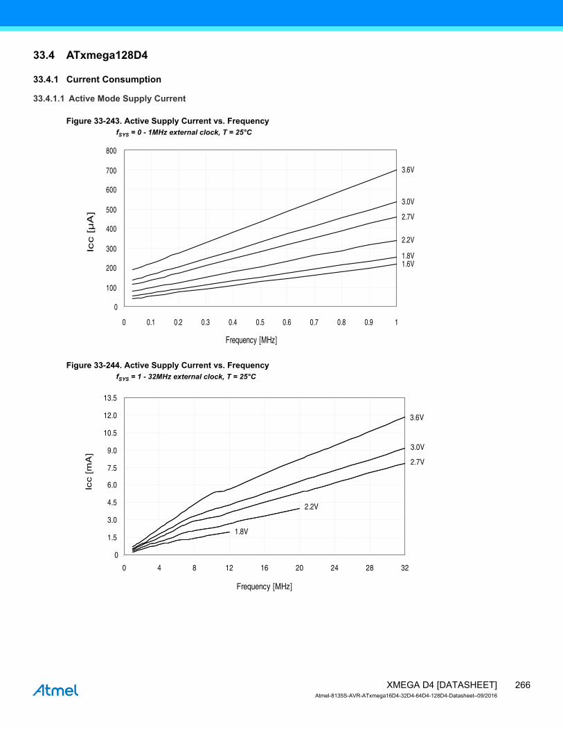
33.4 ATxmega128D4
33.4.1 Current Consumption
33.4.1.1 Active Mode Supply Current
Figure 33-243. Active Supply Current vs. FrequencyfSYS = 0 - 1MHz external clock, T = 25°C
Figure 33-244. Active Supply Current vs. FrequencyfSYS = 1 - 32MHz external clock, T = 25°C
3.6V
3.0V
2.7V
2.2V
1.8V1.6V
0
100
200
300
400
500
600
700
800
0 0.1 0.2 0.3 0.4 0.5 0.6 0.7 0.8 0.9 1
Frequency [MHz]
Icc [µA
]
3.6V
3.0V
2.7V
0
1.5
3.0
4.5
6.0
7.5
9.0
10.5
12.0
13.5
0 4 8 12 16 20 24 28 32
Frequency [MHz]
Icc [m
A]
2.2V
1.8V
266XMEGA D4 [DATASHEET]Atmel-8135S-AVR-ATxmega16D4-32D4-64D4-128D4-Datasheet–09/2016
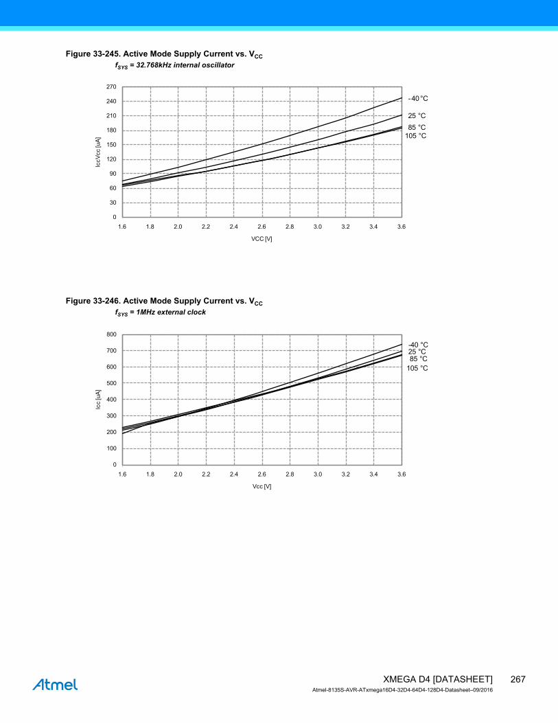
Figure 33-245. Active Mode Supply Current vs. VCC
fSYS = 32.768kHz internal oscillator
Figure 33-246. Active Mode Supply Current vs. VCC
fSYS = 1MHz external clock
105 °C
85 °C
25 °C
- 40 °C
0
30
60
90
120
150
180
210
240
270
1.6 1.8 2.0 2.2 2.4 2.6 2.8 3.0 3.2 3.4 3.6
IccV
cc [u
A]
VCC [V]
105 °C
85 °C25 °C-40 °C
0
100
200
300
400
500
600
700
800
1.6 1.8 2.0 2.2 2.4 2.6 2.8 3.0 3.2 3.4 3.6
Icc [u
A]
Vcc [V]
267XMEGA D4 [DATASHEET]Atmel-8135S-AVR-ATxmega16D4-32D4-64D4-128D4-Datasheet–09/2016

Figure 33-247. Active Mode Supply Current vs. VCC
fSYS = 2MHz internal oscillator
Figure 33-248. Active Mode Supply Current vs. VCC
fSYS = 32MHz internal oscillator prescaled to 8MHz
105 °C
85 °C25 °C-40 °C
0
175
350
525
700
875
1050
1225
1400
1.6 1.8 2 2.2 2.4 2.6 2.8 3 3.2 3.4 3.6
Icc [u
A]
Vcc [V]
105 °C
85 °C25 °C
-40 °C
1000
1600
2200
2800
3400
4000
4600
5200
5800
1.6 1.8 2.0 2.2 2.4 2.6 2.8 3.0 3.2 3.4 3.6
Icc [u
A]
VCC [V]
268XMEGA D4 [DATASHEET]Atmel-8135S-AVR-ATxmega16D4-32D4-64D4-128D4-Datasheet–09/2016

Figure 33-249. Active Mode Supply Current vs. VCC
fSYS = 32MHz internal oscillator
33.4.1.2 Idle Mode Supply Current
Figure 33-250. Idle Mode Supply Current vs. FrequencyfSYS = 0 - 1MHz external clock, T = 25°C
105 °C85 °C25 °C-40 °C
7.0
7.8
8.6
9.4
10.2
11.0
11.8
12.6
13.4
2.7 2.8 2.9 3.0 3.1 3.2 3.3 3.4 3.5 3.6
Icc [m
A]
VCC [V]
3.6 V
3.0 V
2.7 V
2.2 V
1.8 V1.6 V
0
20
40
60
80
100
120
140
160
0 0.1 0.2 0.3 0.4 0.5 0.6 0.7 0.8 0.9 1
Frequency [MHz]
Icc [µ
A]
269XMEGA D4 [DATASHEET]Atmel-8135S-AVR-ATxmega16D4-32D4-64D4-128D4-Datasheet–09/2016

Figure 33-251. Idle Mode Supply Current vs. FrequencyfSYS = 1 - 32MHz external clock, T = 25°C
Figure 33-252. Idle Mode Supply Current vs. VCC
fSYS = 32.768kHz internal oscillator
3.6V
3.0V
2.7V
0
0.6
1.2
1.8
2.4
3.0
3.6
4.2
4.8
5.4
0 4 8 12 16 20 24 28 32
Frenquecy [MHz]
Icc [m
A]
2.2V
1.8V
105 °C
85 °C
25 °C
-40 °C
27
28
29
30
31
32
33
34
35
36
37
38
1.6 1.8 2.0 2.2 2.4 2.6 2.8 3.0 3.2 3.4 3.6
Icc [u
A]
Vcc [V]
270XMEGA D4 [DATASHEET]Atmel-8135S-AVR-ATxmega16D4-32D4-64D4-128D4-Datasheet–09/2016
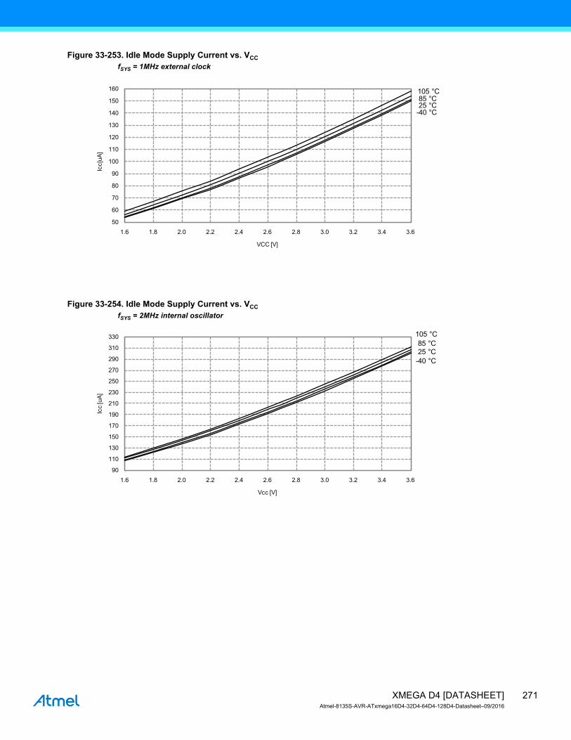
Figure 33-253. Idle Mode Supply Current vs. VCC
fSYS = 1MHz external clock
Figure 33-254. Idle Mode Supply Current vs. VCC
fSYS = 2MHz internal oscillator
105 °C85 °C25 °C
-40 °C
50
60
70
80
90
100
110
120
130
140
150
160
1.6 1.8 2.0 2.2 2.4 2.6 2.8 3.0 3.2 3.4 3.6
Icc[u
A]
VCC [V]
105 °C
85 °C
25 °C
-40 °C
90
110
130
150
170
190
210
230
250
270
290
310
330
1.6 1.8 2.0 2.2 2.4 2.6 2.8 3.0 3.2 3.4 3.6
Icc [u
A]
Vcc [V]
271XMEGA D4 [DATASHEET]Atmel-8135S-AVR-ATxmega16D4-32D4-64D4-128D4-Datasheet–09/2016

Figure 33-255. Idle Mode Supply Current vs. VCC
fSYS = 32MHz internal oscillator prescaled to 8MHz
Figure 33-256. Idle Mode Current vs. VCC
fSYS = 32MHz internal oscillator
105 °C85 °C25 °C
-40 °C
600
800
1000
1200
1400
1600
1800
2000
1.6 1.8 2.0 2.2 2.4 2.6 2.8 3.0 3.2 3.4 3.6
Icc [u
A]
Vcc [V]
105 °C85 °C
25 °C
-40 °C
3000
3250
3500
3750
4000
4250
4500
4750
5000
2.7 2.8 2.9 3.0 3.1 3.2 3.3 3.4 3.5 3.6
Icc [u
A]
Vcc [V]
272XMEGA D4 [DATASHEET]Atmel-8135S-AVR-ATxmega16D4-32D4-64D4-128D4-Datasheet–09/2016

33.4.1.3 Power-down Mode Supply Current
Figure 33-257. Power-down Mode Supply Current vs. TemperatureAll functions disabled
Figure 33-258. Power-down Mode Supply Current vs. VCC
All functions disabled
3.6 V
3.0 V2.7 V
2.2 V1.8 V1.6 V
0.0
0.5
1.0
1.5
2.0
2.5
3.0
3.5
4.0
4.5
5.0
-45 -35 -25 -15 -5 5 15 25 35 45 55 65 75 85 95 105
Icc [u
A]
Temperature [°C]
105 °C
85 °C
25 °C-40 °C0.0
0.5
1.0
1.5
2.0
2.5
3.0
3.5
4.0
4.5
5.0
1.8 2.0 2.2 2.4 2.6 2.8 3.0 3.2 3.4 3.6
Icc [u
A]
Vcc [V]
273XMEGA D4 [DATASHEET]Atmel-8135S-AVR-ATxmega16D4-32D4-64D4-128D4-Datasheet–09/2016

Figure 33-259. Power-down Mode Supply Current vs. VCC
Watchdog and sampled BOD enabled
33.4.1.4 Power-save Mode Supply Current
Figure 33-260. Power-save Mode Supply Current vs.VCC
Real Time Counter enabled and running from 1.024kHz output of 32.768kHz TOSC
105 °C
85 °C
25 °C-40 °C0.8
1.3
1.8
2.3
2.8
3.3
3.8
4.3
4.8
5.3
5.8
6.3
6.8
7.3
1.8 2.0 2.2 2.4 2.6 2.8 3.0 3.2 3.4 3.6
Icc [u
A]
Vcc [V]
Normal mode
Low-power mode
0
0.1
0.2
0.3
0.4
0.5
0.6
0.7
0.8
0.9
VCC [V]
I CC
[µA
]
1.6 1.8 2.0 2.2 2.4 2.6 2.8 3.0 3.2 3.4 3.6
274XMEGA D4 [DATASHEET]Atmel-8135S-AVR-ATxmega16D4-32D4-64D4-128D4-Datasheet–09/2016
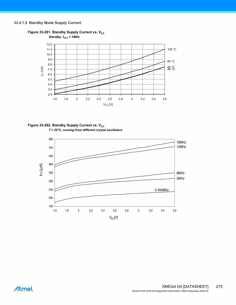
33.4.1.5 Standby Mode Supply Current
Figure 33-261. Standby Supply Current vs. VCC
Standby, fSYS = 1MHz
Figure 33-262. Standby Supply Current vs. VCC
T = 25°C, running from different crystal oscillators
105 °C
85 °C
25 °C-40 °C
2.5
3.5
4.5
5.5
6.5
7.5
8.5
9.5
10.5
11.5
12.5
1.6 1.8 2 2.2 2.4 2.6 2.8 3 3.2 3.4 3.6
I CC
[uA
]
VCC [V]
16MHz12MHz
8MHz
2MHz
0.454MHz
160
200
240
280
320
360
400
440
480
1.6 1.8 2 2.2 2.4 2.6 2.8 3 3.2 3.4 3.6
VCC [V]
ICC
[µA
]
275XMEGA D4 [DATASHEET]Atmel-8135S-AVR-ATxmega16D4-32D4-64D4-128D4-Datasheet–09/2016
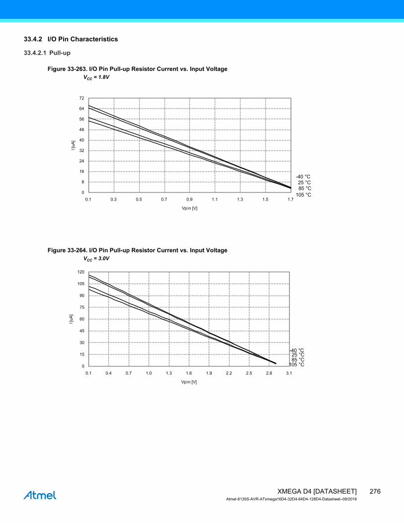
33.4.2 I/O Pin Characteristics
33.4.2.1 Pull-up
Figure 33-263. I/O Pin Pull-up Resistor Current vs. Input VoltageVCC = 1.8V
Figure 33-264. I/O Pin Pull-up Resistor Current vs. Input VoltageVCC = 3.0V
105 °C
85 °C25 °C
-40 °C
0
8
16
24
32
40
48
56
64
72
0.1 0.3 0.5 0.7 0.9 1.1 1.3 1.5 1.7
I [uA
]
Vpin [V]
105 °C85 °C25 °C
-40 °C
0
15
30
45
60
75
90
105
120
0.1 0.4 0.7 1.0 1.3 1.6 1.9 2.2 2.5 2.8 3.1
I [uA
]
Vpin [V]
276XMEGA D4 [DATASHEET]Atmel-8135S-AVR-ATxmega16D4-32D4-64D4-128D4-Datasheet–09/2016

Figure 33-265. I/O Pin Pull-up Resistor Current vs. Input VoltageVCC = 3.3V
33.4.2.2 Output Voltage vs. Sink/Source Current
Figure 33-266. I/O Pin Output Voltage vs. Source CurrentVCC = 1.8V
105 °C85 °C
25 °C
-40 °C
0
15
30
45
60
75
90
105
120
135
0.1 0.4 0.7 1.0 1.3 1.6 1.9 2.2 2.5 2.8 3.1 3.4
I [uA
]
Vpin [V]
105 °C85 °C25 °C-40 °C
0.5
0.6
0.7
0.8
0.9
1.0
1.1
1.2
1.3
1.4
1.5
1.6
1.7
1.8
1.9
-10 -9 -8 -7 -6 -5 -4 -3 -2 -1 0
Vp
in [V
]
Ipin [mA]
277XMEGA D4 [DATASHEET]Atmel-8135S-AVR-ATxmega16D4-32D4-64D4-128D4-Datasheet–09/2016

Figure 33-267. I/O Pin Output Voltage vs. Source CurrentVCC = 3.0V
Figure 33-268. I/O Pin Output Voltage vs. Source CurrentVCC = 3.3V
105 °C85 °C25 °C-40 °C
0.50
0.85
1.20
1.55
1.90
2.25
2.60
2.95
3.30
-30 -27 -24 -21 -18 -15 -12 -9 -6 -3 0
Vp
in [V
]
Ipin [mA]
105 °C85 °C
25 °C
-40 °C
0.5
0.8
1.1
1.4
1.7
2.0
2.3
2.6
2.9
3.2
3.5
-30 -27 -24 -21 -18 -15 -12 -9 -6 -3 0
Vp
in [V
]
Ipin [mA]
278XMEGA D4 [DATASHEET]Atmel-8135S-AVR-ATxmega16D4-32D4-64D4-128D4-Datasheet–09/2016
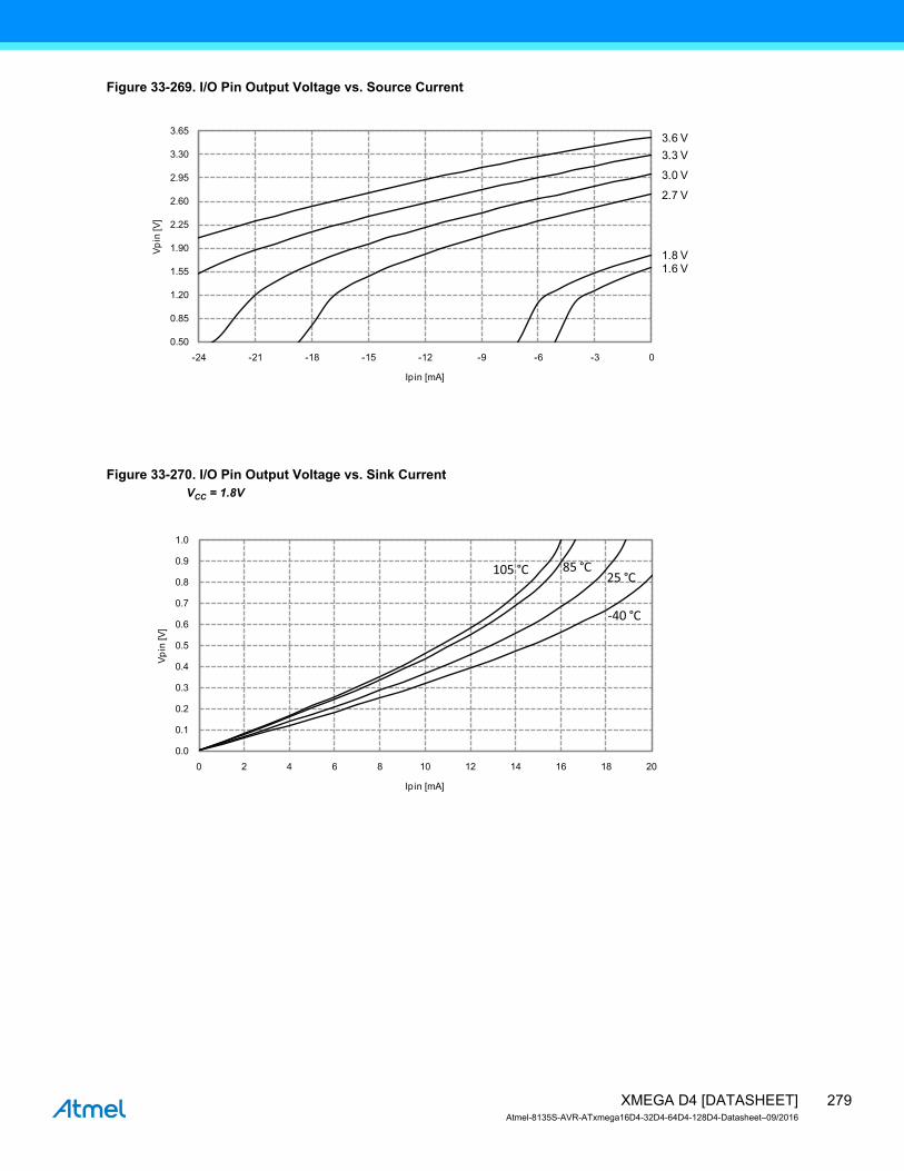
Figure 33-269. I/O Pin Output Voltage vs. Source Current
Figure 33-270. I/O Pin Output Voltage vs. Sink CurrentVCC = 1.8V
3.6 V
3.3 V
3.0 V
2.7 V
1.8 V
1.6 V
0.50
0.85
1.20
1.55
1.90
2.25
2.60
2.95
3.30
3.65
-24 -21 -18 -15 -12 -9 -6 -3 0
Vp
in [V
]
Ipin [mA]
0.0
0.1
0.2
0.3
0.4
0.5
0.6
0.7
0.8
0.9
1.0
0 2 4 6 8 10 12 14 16 18 20
Vp
in [V
]
Ipin [mA]
-40 °C
25 °C105 °C 85 °C
279XMEGA D4 [DATASHEET]Atmel-8135S-AVR-ATxmega16D4-32D4-64D4-128D4-Datasheet–09/2016
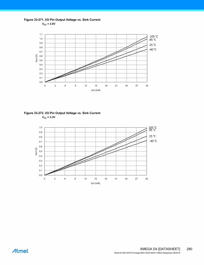
Figure 33-271. I/O Pin Output Voltage vs. Sink CurrentVCC = 3.0V
Figure 33-272. I/O Pin Output Voltage vs. Sink CurrentVCC = 3.3V
0.0
0.1
0.2
0.3
0.4
0.5
0.6
0.7
0.8
0.9
1.0
1.1
0 3 6 9 12 15 18 21 24 27 30
Vp
in [V
]
Ipin [mA]
-40 °C25 °C
85 °C 105 °C
0.0
0.1
0.2
0.3
0.4
0.5
0.6
0.7
0.8
0.9
1.0
0 3 6 9 12 15 18 21 24 27 30
Vp
in [V
]
Ipin [mA]
-40 °C25 °C
85 °C105 °C
280XMEGA D4 [DATASHEET]Atmel-8135S-AVR-ATxmega16D4-32D4-64D4-128D4-Datasheet–09/2016

Figure 33-273. I/O Pin Output Voltage vs. Sink Current
33.4.2.3 Thresholds and Hysteresis
Figure 33-274. I/O Pin Input Threshold Voltage vs. VCC
T = 25°C
3.6 V3.3 V3.0 V2.7 V
0.00
0.15
0.30
0.45
0.60
0.75
0.90
1.05
1.20
1.35
1.50
0 3 6 9 12 15 18 21 24 27 30
Vp
in [V
]
Ipin [mA]
1.6 V
1.8 V
VIL
VIH
0.0
0.2
0.4
0.6
0.8
1.0
1.2
1.4
1.6
1.8
1.6 1.8 2 2.2 2.4 2.6 2.8 3 3.2 3.4 3.6
Vcc [V]
Vth
reshold
[V
]
281XMEGA D4 [DATASHEET]Atmel-8135S-AVR-ATxmega16D4-32D4-64D4-128D4-Datasheet–09/2016

Figure 33-275. I/O Pin Input Threshold Voltage vs. VCC
VIH I/O pin read as “1”
Figure 33-276. I/O Pin Input Threshold Voltage vs. VCC
VIL I/O pin read as “0”
0.8
0.9
1.0
1.1
1.2
1.3
1.4
1.5
1.6
1.7
1.8
1.6 1.8 2.0 2.2 2.4 2.6 2.8 3.0 3.2 3.4 3.6
Vth
resh
old
[V]
Vcc [V]
105 °C85 °C25 °C
-40 °C
0.40
0.55
0.70
0.85
1.00
1.15
1.30
1.45
1.60
1.75
1.6 1.8 2.0 2.2 2.4 2.6 2.8 3.0 3.2 3.4 3.6
Vth
resh
old
[V]
Vcc [V]
105 °C85 °C
-40 °C25 °C
282XMEGA D4 [DATASHEET]Atmel-8135S-AVR-ATxmega16D4-32D4-64D4-128D4-Datasheet–09/2016

Figure 33-277. I/O Pin Input Hysteresis vs. VCC
33.4.3 ADC Characteristics
Figure 33-278. INL Error vs. External VREF
T = 25C, VCC = 3.6V, external reference
0.17
0.19
0.21
0.23
0.25
0.27
0.29
0.31
0.33
0.35
0.37
0.39
0.41
1.6 1.8 2.0 2.2 2.4 2.6 2.8 3.0 3.2 3.4 3.6
Vth
resh
old
[V]
Vcc [V]
25 °C
85 °C
105 °C
-40 °C
Single-ended Unsigned
Single-ended Signed
Differential Signed
0.7
0.8
0.9
1
1.1
1.2
1.3
1.4
1.5
1.6
1.7
1.8
1 1.2 1.4 1.6 1.8 2 2.2 2.4 2.6 2.8 3
V [V]
INL [
LS
B]
REF
283XMEGA D4 [DATASHEET]Atmel-8135S-AVR-ATxmega16D4-32D4-64D4-128D4-Datasheet–09/2016
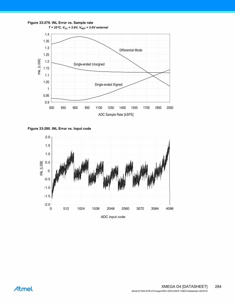
Figure 33-279. INL Error vs. Sample rateT = 25C, VCC = 3.6V, VREF = 3.0V external
Figure 33-280. INL Error vs. Input code
Single-ended Unsigned
Single-ended Signed
Differential Mode
0.9
0.95
1
1.05
1.1
1.15
1.2
1.25
1.3
1.35
1.4
500 650 800 950 1100 1250 1400 1550 1700 1850 2000
ADC Sample Rate [kSPS]
INL [
LS
B]
-2.0
-1.5
-1.0
-0.5
0
0.5
1.0
1.5
2.0
0 512 1024 1536 2048 2560 3072 3584 4096
ADC input code
INL
[LS
B]
284XMEGA D4 [DATASHEET]Atmel-8135S-AVR-ATxmega16D4-32D4-64D4-128D4-Datasheet–09/2016
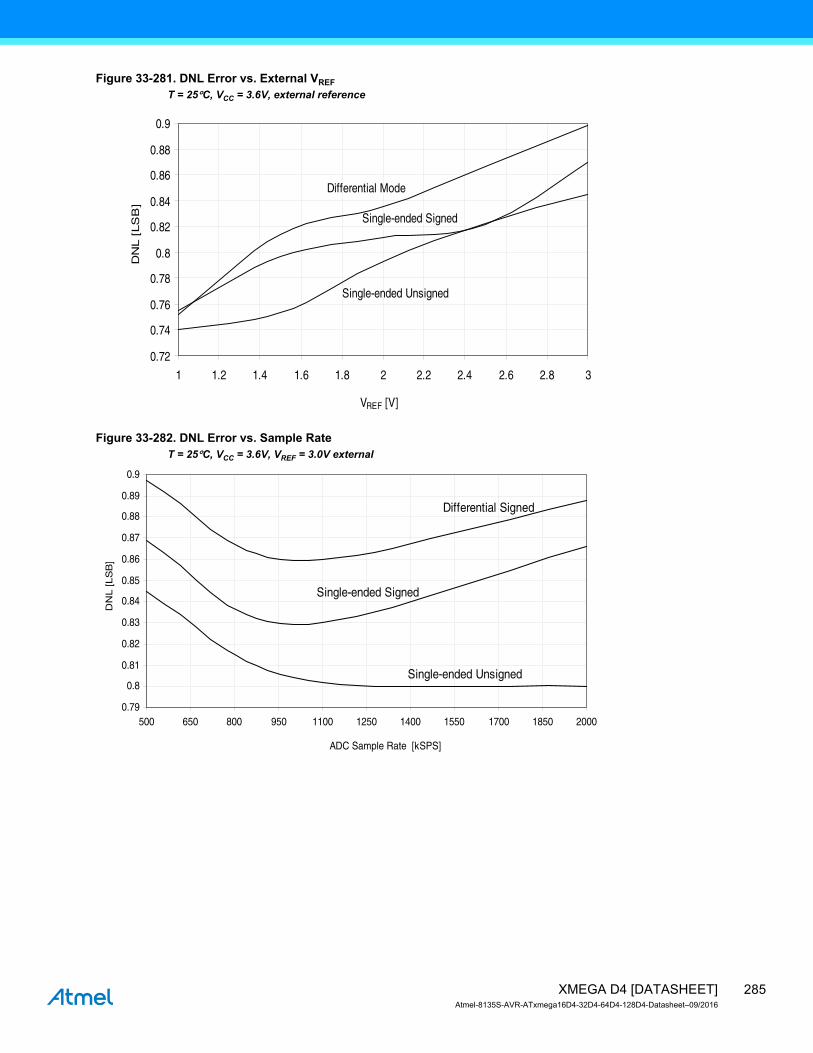
Figure 33-281. DNL Error vs. External VREF
T = 25C, VCC = 3.6V, external reference
Figure 33-282. DNL Error vs. Sample RateT = 25C, VCC = 3.6V, VREF = 3.0V external
Single-ended Unsigned
Single-ended Signed
Differential Mode
0.72
0.74
0.76
0.78
0.8
0.82
0.84
0.86
0.88
0.9
1 1.2 1.4 1.6 1.8 2 2.2 2.4 2.6 2.8 3
DN
L [
LS
B]
V [V]REF
Single-ended Unsigned
Single-ended Signed
Differential Signed
0.79
0.8
0.81
0.82
0.83
0.84
0.85
0.86
0.87
0.88
0.89
0.9
500 650 800 950 1100 1250 1400 1550 1700 1850 2000
ADC Sample Rate [kSPS]
DN
L [LS
B]
285XMEGA D4 [DATASHEET]Atmel-8135S-AVR-ATxmega16D4-32D4-64D4-128D4-Datasheet–09/2016

Figure 33-283. DNL Error vs. Input Code
Figure 33-284. Gain Error vs. VREF
T = 25C, VCC = 3.6V, ADC sampling speed = 500ksps
-0.6
-0.4
-0.2
0
0.2
0.4
0.6
0.8
0 512 1024 1536 2048 2560 3072 3584 4096
ADC Input Code
DN
L [L
SB
]
Single-ended Unsigned
Single-ended Signed
Differential Mode
-4
-3
-2
-1
0
1
2
3
1 1.2 1.4 1.6 1.8 2 2.2 2.4 2.6 2.8 3
V
Gain
Err
or
[mV
]
REF [V]
286XMEGA D4 [DATASHEET]Atmel-8135S-AVR-ATxmega16D4-32D4-64D4-128D4-Datasheet–09/2016
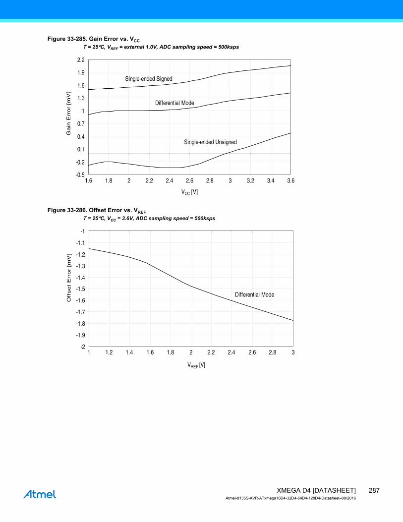
Figure 33-285. Gain Error vs. VCC
T = 25C, VREF = external 1.0V, ADC sampling speed = 500ksps
Figure 33-286. Offset Error vs. VREF
T = 25C, VCC = 3.6V, ADC sampling speed = 500ksps
Single-ended Unsigned
Single-ended Signed
Differential Mode
-0.5
-0.2
0.1
0.4
0.7
1
1.3
1.6
1.9
2.2
1.6 1.8 2 2.2 2.4 2.6 2.8 3 3.2 3.4 3.6
VCC [V]
Gain
Err
or
[mV
]
Differential Mode
-2
-1.9
-1.8
-1.7
-1.6
-1.5
-1.4
-1.3
-1.2
-1.1
-1
1 1.2 1.4 1.6 1.8 2 2.2 2.4 2.6 2.8 3
Off
set
Err
or
[mV
]
VREF [V]
287XMEGA D4 [DATASHEET]Atmel-8135S-AVR-ATxmega16D4-32D4-64D4-128D4-Datasheet–09/2016

Figure 33-287. Gain Error vs. TemperatureVCC = 3.0V, VREF = external 2.0V
Figure 33-288. Offset Error vs. VCC
T = 25C, VREF = external 1.0V, ADC sampling speed = 500ksps
Single-ended Unsigned
Single-ended Signed
Differential Signed
-4
-3
-2
-1
0
1
2
3
-45 -35 -25 -15 -5 5 15 25 35 45 55 65 75 85
Temperature [ºC]
Gain
Err
or
[mV
]
Differential Signed
-1.2
-1.1
-1
-0.9
-0.8
-0.7
-0.6
-0.5
-0.4
-0.3
1.6 1.8 2 2.2 2.4 2.6 2.8 3 3.2 3.4 3.6
VCC [V]
Offset E
rror
[mV
]
288XMEGA D4 [DATASHEET]Atmel-8135S-AVR-ATxmega16D4-32D4-64D4-128D4-Datasheet–09/2016

Figure 33-289. Noise vs. VREF
T = 25C, VCC = 3.6V, ADC sampling speed = 500ksps
Figure 33-290. Noise vs. VCC
T = 25C, VREF = external 1.0V, ADC sampling speed = 500ksps
Single-ended Unsigned
Single-ended Signed
Differential Signed
0.4
0.55
0.7
0.85
1
1.15
1.3
1 1.2 1.4 1.6 1.8 2 2.2 2.4 2.6 2.8 3
VREF [V]
Nois
e [m
V R
MS
]
Single-ended Unsigned
Single-ended Signed
Differential Signed
0.3
0.4
0.5
0.6
0.7
0.8
0.9
1
1.1
1.2
1.3
1.6 1.8 2 2.2 2.4 2.6 2.8 3 3.2 3.4 3.6
VCC [V]
Nois
e [m
V R
MS
]
289XMEGA D4 [DATASHEET]Atmel-8135S-AVR-ATxmega16D4-32D4-64D4-128D4-Datasheet–09/2016

33.4.4 DAC Characteristics
Figure 33-291. DAC INL Error vs. VREF
VCC = 3.6V
Figure 33-292. DNL Error vs. VREF
T = 25C, VCC = 3.6V
25°C
1.1
1.2
1.3
1.4
1.5
1.6
1.7
1.8
1.9
VREF [V]
INL
[L
SB
]
1.0 1.2 1.4 1.6 1.8 2.0 2.2 2.4 2.6 2.8 3.0
25ºC0.6
0.65
0.7
0.75
0.8
0.85
0.9
1.6 1.8 2 2.2 2.4 2.6 2.8 3
DN
L [
LS
B]
V [V]REF
290XMEGA D4 [DATASHEET]Atmel-8135S-AVR-ATxmega16D4-32D4-64D4-128D4-Datasheet–09/2016
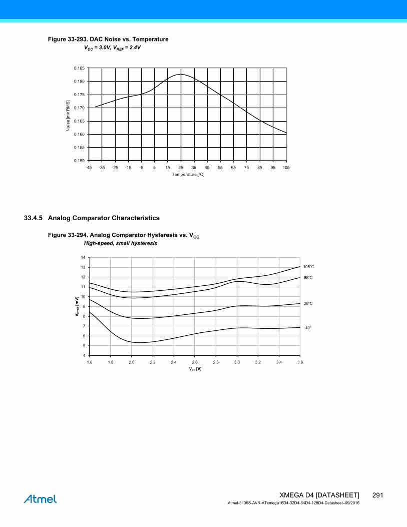
Figure 33-293. DAC Noise vs. TemperatureVCC = 3.0V, VREF = 2.4V
33.4.5 Analog Comparator Characteristics
Figure 33-294. Analog Comparator Hysteresis vs. VCC
High-speed, small hysteresis
0.150
0.155
0.160
0.165
0.170
0.175
0.180
0.185
-45 -35 -25 -15 -5 5 15 25 35 45 55 65 75 85 95 105
No
ise [m
V R
MS
]
Temperature [ºC]
-40°
25°C
85°C
105°
4
5
6
7
8
9
10
11
12
13
14
1.6 1.8 2.0 2.2 2.4 2.6 2.8 3.0 3.2 3.4 3.6
V HY
ST[m
V]
VCC [V]
C
291XMEGA D4 [DATASHEET]Atmel-8135S-AVR-ATxmega16D4-32D4-64D4-128D4-Datasheet–09/2016
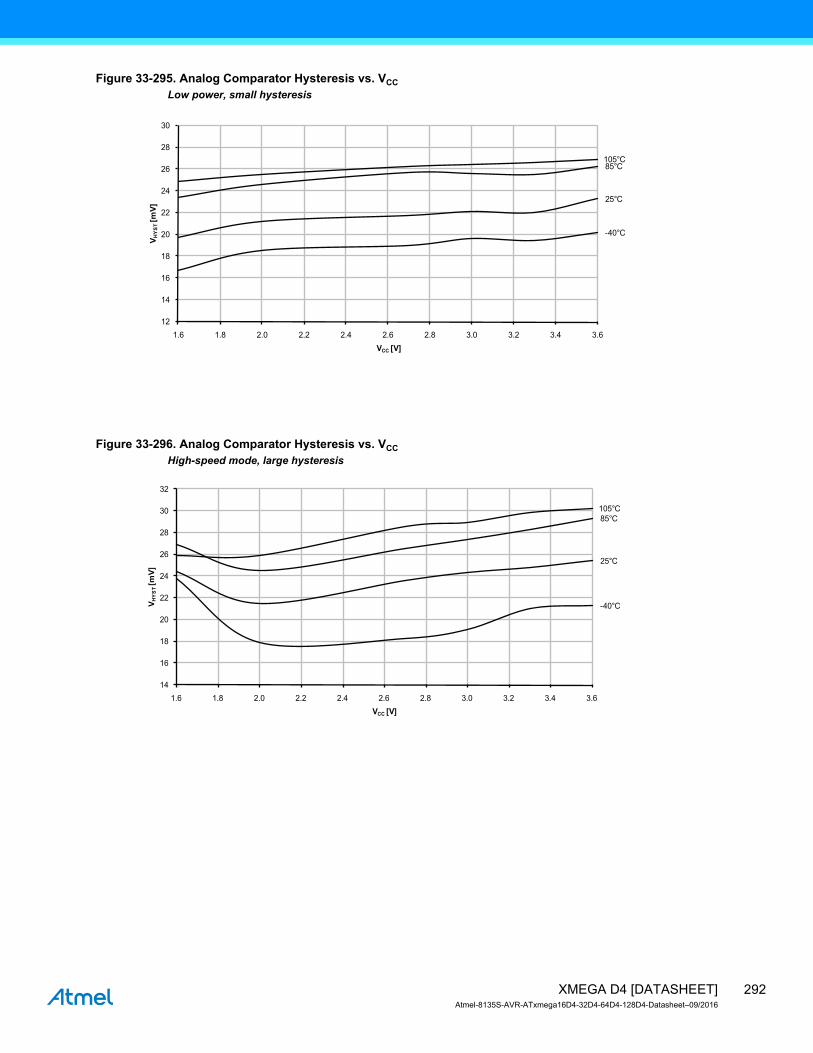
Figure 33-295. Analog Comparator Hysteresis vs. VCC
Low power, small hysteresis
Figure 33-296. Analog Comparator Hysteresis vs. VCC
High-speed mode, large hysteresis
-40°C
25°C
85°C105°C
12
14
16
18
20
22
24
26
28
30
1.6 1.8 2.0 2.2 2.4 2.6 2.8 3.0 3.2 3.4 3.6
V HY
ST[m
V]
VCC [V]
-40°C
25°C
85°C
105°C
14
16
18
20
22
24
26
28
30
32
1.6 1.8 2.0 2.2 2.4 2.6 2.8 3.0 3.2 3.4 3.6
V HY
ST[m
V]
VCC [V]
292XMEGA D4 [DATASHEET]Atmel-8135S-AVR-ATxmega16D4-32D4-64D4-128D4-Datasheet–09/2016

Figure 33-297. Analog Comparator Hysteresis vs. VCC
Low power, large hysteresis
Figure 33-298. Analog Comparator Current Source vs. Calibration ValueTemperature = 25°C
-40°C
25°C
85°C
105°C
32
36
40
44
48
52
56
60
64
68
1.6 1.8 2.0 2.2 2.4 2.6 2.8 3.0 3.2 3.4 3.6
V HY
ST[m
V]
VCC [V]
3.6V
3.0V
2.2V1.8V
2
2.5
3
3.5
4
4.5
5
5.5
6
6.5
7
7.5
8
0 1 2 3 4 5 6 7 8 9 10 11 12 13 14 15
CURRCALIBA[3..0]
I CU
RR
EN
TS
OU
RC
E [µ
A]
293XMEGA D4 [DATASHEET]Atmel-8135S-AVR-ATxmega16D4-32D4-64D4-128D4-Datasheet–09/2016

Figure 33-299. Analog Comparator Current Source vs. Calibration ValueVCC = 3.0V
Figure 33-300. Voltage Scaler INL vs. SCALEFACT = 25C, VCC = 3.0V
85°C25°C
-40°C
3
3.5
4
4.5
5
5.5
6
6.5
7
0 1 2 3 4 5 6 7 8 9 10 11 12 13 14 15
CURRCALIBA[3..0]
I CU
RR
EN
TS
OU
RC
E [µ
A]
25°C
-0.150
-0.125
-0.100
-0.075
-0.050
-0.025
0
0.025
0.050
0 10 20 30 40 50 60 70
SCALEFAC
INL [
LS
B]
294XMEGA D4 [DATASHEET]Atmel-8135S-AVR-ATxmega16D4-32D4-64D4-128D4-Datasheet–09/2016

33.4.6 Internal 1.0V Reference Characteristics
Figure 33-301. ADC/DAC Internal 1.0V Reference vs. Temperature
33.4.7 BOD Characteristics
Figure 33-302. BOD Thresholds vs. TemperatureBOD level = 1.6V
3.6V
3.0V2.7V
1.8V1.6V
0.9988
0.9992
0.9996
1.0000
1.0004
1.0008
1.0012
1.0016
1.0020
1.0024
-40 -30 -20 -10 0 10 20 30 40 50 60 70 80 90 100
Ban
dg
ap V
olta
ge [V
]
Temperature [°C]
Rising Vcc
Falling Vcc
1.572
1.575
1.578
1.581
1.584
1.587
1.590
1.593
1.596
-45 -35 -25 -15 -5 5 15 25 35 45 55 65 75 85 95 105
Vbo
t [V
]
Temperature [°C]
295XMEGA D4 [DATASHEET]Atmel-8135S-AVR-ATxmega16D4-32D4-64D4-128D4-Datasheet–09/2016

Figure 33-303. BOD Thresholds vs. TemperatureBOD level = 3.0V
33.4.8 External Reset Characteristics
Figure 33-304. Minimum Reset Pin Pulse Width vs. VCC
Rising Vcc
Falling Vcc
2.94
2.95
2.96
2.97
2.98
2.99
3.00
3.01
3.02
3.03
-45 -35 -25 -15 -5 5 15 25 35 45 55 65 75 85 95 105
Vbo
t [V
]
Temperature [°C]
105 °C
85 °C
25 °C-40 °C
80
85
90
95
100
105
110
115
120
125
130
135
1.6 1.8 2.0 2.2 2.4 2.6 2.8 3.0 3.2 3.4 3.6
Trs
t [n
s]
Vcc [V]
296XMEGA D4 [DATASHEET]Atmel-8135S-AVR-ATxmega16D4-32D4-64D4-128D4-Datasheet–09/2016

Figure 33-305. Reset Pin Pull-up Resistor Current vs. Reset Pin VoltageVCC = 1.8V
Figure 33-306. Reset Pin Pull-up Resistor Current vs. Reset Pin VoltageVCC = 3.0V
105 °C85 °C25 °C
-40 °C
0
8
16
24
32
40
48
56
64
72
80
0.0 0.2 0.4 0.6 0.8 1.0 1.2 1.4 1.6 1.8
Ireset [
uA
]
Vreset [V]
105 °C85 °C25 °C-40 °C
0
15
30
45
60
75
90
105
120
135
0.0 0.3 0.6 0.9 1.2 1.5 1.8 2.1 2.4 2.7 3.0
Ireset [
uA
]
Vreset [V]
297XMEGA D4 [DATASHEET]Atmel-8135S-AVR-ATxmega16D4-32D4-64D4-128D4-Datasheet–09/2016

Figure 33-307. Reset Pin Pull-up Resistor Current vs. Reset Pin VoltageVCC = 3.3V
Figure 33-308. Reset Pin Input Threshold Voltage vs. VCC
VIH - Reset pin read as “1”
105 °C85 °C
25 °C-40 °C
0
15
30
45
60
75
90
105
120
135
150
0.0 0.3 0.6 0.9 1.2 1.5 1.8 2.1 2.4 2.7 3.0 3.3
Ireset [
uA
]
Vreset [V]
105 °C
85 °C
25 °C-40 °C
1.00
1.15
1.30
1.45
1.60
1.75
1.90
2.05
2.20
1.6 1.8 2.0 2.2 2.4 2.6 2.8 3.0 3.2 3.4 3.6
Vth
resh
old
[V]
VCC [V]
298XMEGA D4 [DATASHEET]Atmel-8135S-AVR-ATxmega16D4-32D4-64D4-128D4-Datasheet–09/2016
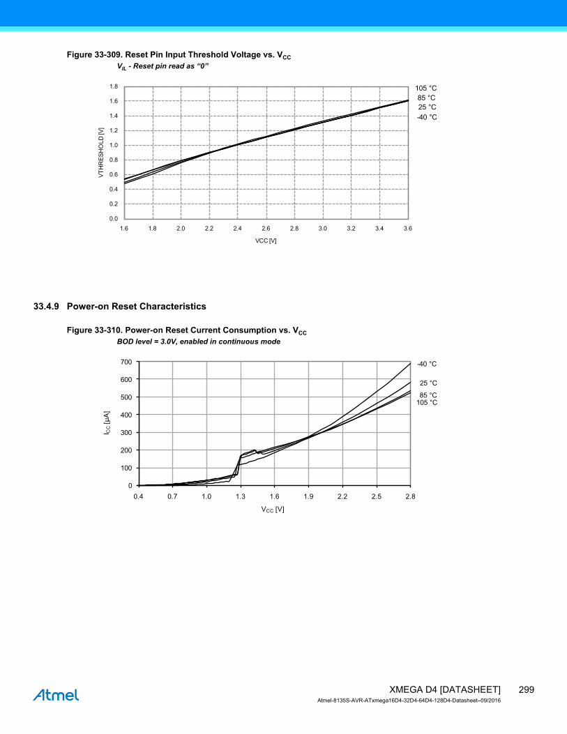
Figure 33-309. Reset Pin Input Threshold Voltage vs. VCC
VIL - Reset pin read as “0”
33.4.9 Power-on Reset Characteristics
Figure 33-310. Power-on Reset Current Consumption vs. VCC
BOD level = 3.0V, enabled in continuous mode
105 °C
85 °C
25 °C
-40 °C
0.0
0.2
0.4
0.6
0.8
1.0
1.2
1.4
1.6
1.8
1.6 1.8 2.0 2.2 2.4 2.6 2.8 3.0 3.2 3.4 3.6
VT
HR
ES
HO
LD
[V]
VCC [V]
105 °C85 °C
25 °C
-40 °C
0
100
200
300
400
500
600
700
0.4 0.7 1.0 1.3 1.6 1.9 2.2 2.5 2.8
I CC
[µA
]
VCC [V]
299XMEGA D4 [DATASHEET]Atmel-8135S-AVR-ATxmega16D4-32D4-64D4-128D4-Datasheet–09/2016

Figure 33-311. Power-on Reset Current Consumption vs. VCC
BOD level = 3.0V, enabled in sampled mode
33.4.10 Oscillator Characteristics
33.4.10.1 Ultra Low-Power Internal Oscillator
Figure 33-312. Ultra Low-Power Internal Oscillator Frequency vs. Temperature
105 °°C85 ° °C
25 °C
-40 °C
0
65
130
195
260
325
390
455
520
585
650
0.4 0.7 1 1.3 1.6 1.9 2.2 2.5 2.8
I CC
[µA
]
VCC [V]
3.6 V
3.3 V3.0 V2.7 V1.8 V
1.6 V30.75
31.00
31.25
31.50
31.75
32.00
32.25
32.50
32.75
33.00
33.25
33.50
33.75
-40 -30 -20 -10 0 10 20 30 40 50 60 70 80 90 100
Fre
quen
cy [k
Hz]
Temperature [°C]
300XMEGA D4 [DATASHEET]Atmel-8135S-AVR-ATxmega16D4-32D4-64D4-128D4-Datasheet–09/2016

33.4.10.2 32.768kHz Internal Oscillator
Figure 33-313. 32.768kHz Internal Oscillator Frequency vs. Temperature
Figure 33-314. 32.768kHz Internal Oscillator Frequency vs. Calibration ValueVCC = 3.0V, T = 25°C
3.6 V
3.3 V
3.0 V2.7 V
2.2 V
1.8 V
32.46
32.49
32.52
32.55
32.58
32.61
32.64
32.67
32.70
32.73
32.76
32.79
32.82
-40 -30 -20 -10 0 10 20 30 40 50 60 70 80 90 100
Fre
quen
cy [k
Hz]
Temperature [°C]
3.0 V
22
25
28
31
34
37
40
43
46
49
52
0 24 48 72 96 120 144 168 192 216 240 264
Fre
quen
cy [k
Hz]
RC32KCA L[7..0]
301XMEGA D4 [DATASHEET]Atmel-8135S-AVR-ATxmega16D4-32D4-64D4-128D4-Datasheet–09/2016

33.4.10.3 2MHz Internal Oscillator
Figure 33-315. 2MHz Internal Oscillator Frequency vs. TemperatureDFLL disabled
Figure 33-316. 2MHz Internal Oscillator Frequency vs. TemperatureDFLL enabled, from the 32.768kHz internal oscillator
3.6 V
3.3 V3.0 V2.7 V2.2 V1.8 V
1.96
1.98
2.00
2.02
2.04
2.06
2.08
2.10
2.12
2.14
2.16
-40 -30 -20 -10 0 10 20 30 40 50 60 70 80 90 100
Fre
quen
cy [M
Hz]
Temperature [°C]
3.6 V3.3 V
3.0 V
2.7 V2.2 V
1.8 V
1.980
1.982
1.984
1.986
1.988
1.990
1.992
1.994
1.996
1.998
2.000
2.002
2.004
2.006
-40 -30 -20 -10 0 10 20 30 40 50 60 70 80 90 100
Fre
quen
cy [M
Hz]
Temperature [°C]
302XMEGA D4 [DATASHEET]Atmel-8135S-AVR-ATxmega16D4-32D4-64D4-128D4-Datasheet–09/2016
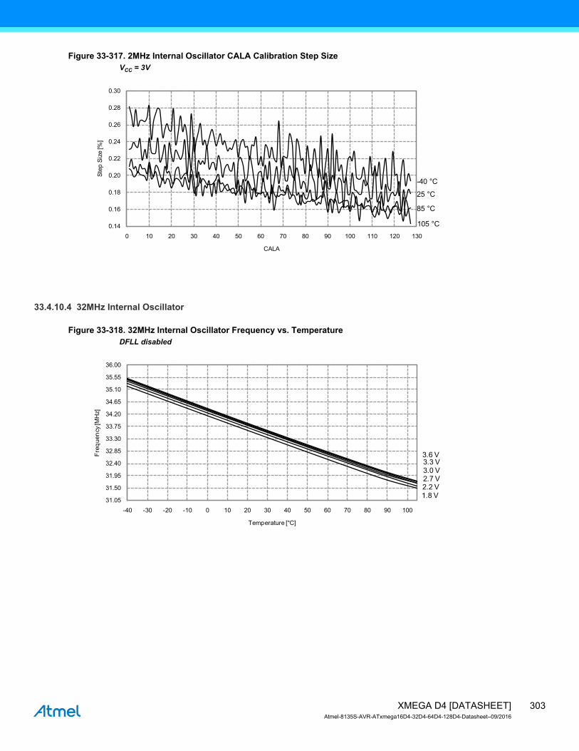
Figure 33-317. 2MHz Internal Oscillator CALA Calibration Step SizeVCC = 3V
33.4.10.4 32MHz Internal Oscillator
Figure 33-318. 32MHz Internal Oscillator Frequency vs. TemperatureDFLL disabled
105 °C
85 °C
25 °C
-40 °C
0.14
0.16
0.18
0.20
0.22
0.24
0.26
0.28
0.30
0 10 20 30 40 50 60 70 80 90 100 110 120 130
Ste
p S
ize [%
]
CALA
3.6 V3.3 V3.0 V2.7 V2.2 V1.8 V
31.05
31.50
31.95
32.40
32.85
33.30
33.75
34.20
34.65
35.10
35.55
36.00
-40 -30 -20 -10 0 10 20 30 40 50 60 70 80 90 100
Fre
quen
cy [M
Hz]
Temperature [°C]
303XMEGA D4 [DATASHEET]Atmel-8135S-AVR-ATxmega16D4-32D4-64D4-128D4-Datasheet–09/2016
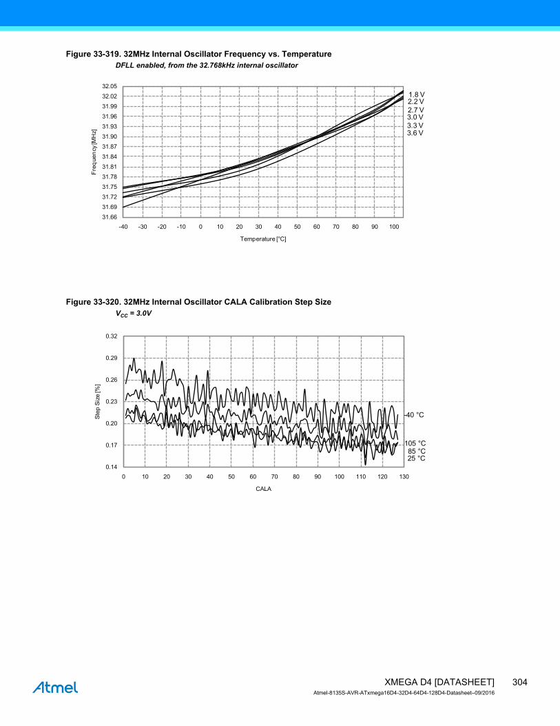
Figure 33-319. 32MHz Internal Oscillator Frequency vs. TemperatureDFLL enabled, from the 32.768kHz internal oscillator
Figure 33-320. 32MHz Internal Oscillator CALA Calibration Step SizeVCC = 3.0V
3.6 V3.3 V
3.0 V2.7 V
2.2 V1.8 V
31.66
31.69
31.72
31.75
31.78
31.81
31.84
31.87
31.90
31.93
31.96
31.99
32.02
32.05
-40 -30 -20 -10 0 10 20 30 40 50 60 70 80 90 100
Fre
quen
cy [M
Hz]
Temperature [°C]
105 °C85 °C25 °C
-40 °C
0.14
0.17
0.20
0.23
0.26
0.29
0.32
0 10 20 30 40 50 60 70 80 90 100 110 120 130
Ste
p S
ize [%
]
CALA
304XMEGA D4 [DATASHEET]Atmel-8135S-AVR-ATxmega16D4-32D4-64D4-128D4-Datasheet–09/2016

33.4.10.5 32MHz Internal Oscillator Calibrated to 48MHz
Figure 33-321. 48MHz Internal Oscillator Frequency vs. TemperatureDFLL disabled
Figure 33-322. 48MHz Internal Oscillator Frequency vs. TemperatureDFLL enabled, from the 32.768kHz internal oscillator
3.6 V
3.3 V3.0 V
2.7 V2.2 V1.8 V46.2
46.9
47.6
48.3
49.0
49.7
50.4
51.1
51.8
52.5
53.2
53.9
-40 -30 -20 -10 0 10 20 30 40 50 60 70 80 90 100
Fre
quen
cy [M
Hz]
Temperature [°C]
3.6 V3.3 V3.0 V
2.7 V2.2 V
1.8 V
47.5
47.6
47.7
47.8
47.9
48.0
48.1
48.2
48.3
-40 -30 -20 -10 0 10 20 30 40 50 60 70 80 90 100
Fre
quen
cy [M
Hz]
Temperature [°C]
305XMEGA D4 [DATASHEET]Atmel-8135S-AVR-ATxmega16D4-32D4-64D4-128D4-Datasheet–09/2016
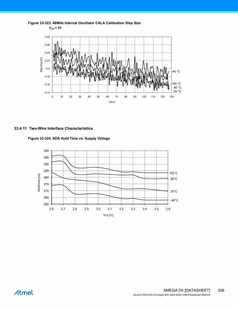
Figure 33-323. 48MHz Internal Oscillator CALA Calibration Step SizeVCC = 3V
33.4.11 Two-Wire Interface Characteristics
Figure 33-324. SDA Hold Time vs. Supply Voltage
105 °C
85 °C
25 °C
-40 °C
0.14
0.16
0.18
0.2
0.22
0.24
0.26
0.28
0 10 20 30 40 50 60 70 80 90 100 110 120 130
Ste
p S
ize [%
]
CALA
105°C
85°C
25°C
- 40°C
260
265
270
275
280
285
290
295
300
2.6 2.7 2.8 2.9 3.0 3.1 3.2 3.3 3.4 3.5 3.6
Ho
ldtim
e [ns]
Vcc [V]
306XMEGA D4 [DATASHEET]Atmel-8135S-AVR-ATxmega16D4-32D4-64D4-128D4-Datasheet–09/2016

33.4.12 PDI Characteristics
Figure 33-325. Maximum PDI Frequency vs. VCC
105 °C85 °C25 °C
-40 °C
10
13
16
19
22
25
28
31
1.6 1.8 2.0 2.2 2.4 2.6 2.8 3.0 3.2 3.4 3.6
Fre
quen
cy m
ax [M
Hz]
Vcc [V]
307XMEGA D4 [DATASHEET]Atmel-8135S-AVR-ATxmega16D4-32D4-64D4-128D4-Datasheet–09/2016

34. Errata
34.1 ATxmega16D4 / ATxmega32D4
34.1.1 Rev. I
Temperature sensor not calibrated
1. Temperature sensor not calibrated
Temperature sensor factory calibration not implemented.
Problem fix/Workaround
None.
34.1.2 Rev. F/G/H
Not sampled.
34.1.3 Rev. E
ADC propagation delay is not correct when gain is used
CRC fails for Range CRC when end address is the last word address of a flash section
AWeX fault protection restore is not done correct in Pattern Generation Mode
Erroneous interrupt when using Timer/Counter with QDEC
AC system status flags are only valid if AC-system is enabled
Temperature sensor not calibrated
1. ADC propagation delay is not correct when gain is used
The propagation delay will increase by only one ADC clock cycle for all gain setting.
Problem fix/Workaround
None.
2. CRC fails for Range CRC when end address is the last word address of a flash section
If boot read lock is enabled, the range CRC cannot end on the last address of the application section. If application table read lock is enabled, the range CRC cannot end on the last address before the application table.
Problem fix/Workaround
Ensure that the end address used in Range CRC does not end at the last address before a section with read lock enabled. Instead, use the dedicated CRC commands for complete applications sections.
3. AWeX fault protection restore is not done correct in Pattern Generation Mode
When a fault is detected the OUTOVEN register is cleared, and when fault condition is cleared, OUTOVEN is restored according to the corresponding enabled DTI channels. For Common Waveform Channel Mode (CWCM), this has no effect as the OUTOVEN is correct after restoring from fault. For Pattern Generation Mode (PGM), OUTOVEN should instead have been restored according to the DTILSBUF register.
308XMEGA D4 [DATASHEET]Atmel-8135S-AVR-ATxmega16D4-32D4-64D4-128D4-Datasheet–09/2016

Problem fix/Workaround
For CWCM no workaround is required.
For PGM in latched mode, disable the DTI channels before returning from the fault condition. Then, set correct OUTOVEN value and enable the DTI channels, before the direction (DIR) register is written to enable the correct outputs again.
For PGM in cycle-by-cycle mode there is no workaround.
4. Erroneous interrupt when using Timer/Counter with QDEC
When the Timer/Counter is set in Dual Slope mode with QDEC enabled, an additional underflow interrupt (and event) will be given when the counter counts from BOTTOM to one.
Problem fix/Workaround
When receiving underflow interrupt check direction and value of counter. If direction is UP and counter value is zero, change the counter value to one. This will also remove the additional event. If the counter value is above zero, clear the interrupt flag.
5. AC system status flags are only valid if AC-system is enabled
The status flags for the ac-output are updated even though the AC is not enabled which is invalid. Also, it is not possible to clear the AC interrupt flags without enabling either of the Analog comparators.
Problem fix/Workaround
Software should clear the AC system flags once, after enabling the AC system before using the AC system status flags.
6. Temperature sensor not calibrated
Temperature sensor factory calibration not implemented.
Problem fix/Workaround
None.
34.1.4 Rev. C/D
Not sampled.
309XMEGA D4 [DATASHEET]Atmel-8135S-AVR-ATxmega16D4-32D4-64D4-128D4-Datasheet–09/2016
34.1.5 Rev. A/B
Bandgap voltage input for the ACs can not be changed when used for both ACs simultaneously
VCC voltage scaler for AC is non-linear
ADC gain stage cannot be used for single conversion
ADC has increased INL error for some operating conditions
ADC gain stage output range is limited to 2.4 V
ADC Event on compare match non-functional
ADC propagation delay is not correct when 8x -64x gain is used
Bandgap measurement with the ADC is non-functional when VCC is below 2.7V
Accuracy lost on first three samples after switching input to ADC gain stage
Configuration of PGM and CWCM not as described in XMEGA A Manual
PWM is not restarted properly after a fault in cycle-by-cycle mode
BOD: BOD will be enabled at any reset
Sampled BOD in Active mode will cause noise when bandgap is used as reference
EEPROM page buffer always written when NVM DATA0 is written
Pending full asynchronous pin change interrupts will not wake the device
Pin configuration does not affect Analog Comparator Output
NMI Flag for Crystal Oscillator Failure automatically cleared
Flash Power Reduction Mode can not be enabled when entering sleep
Crystal start-up time required after power-save even if crystal is source for RTC
RTC Counter value not correctly read after sleep
Pending asynchronous RTC-interrupts will not wake up device
TWI Transmit collision flag not cleared on repeated start
Clearing TWI Stop Interrupt Flag may lock the bus
TWI START condition at bus timeout will cause transaction to be dropped
TWI Data Interrupt Flag (DIF) erroneously read as set
WDR instruction inside closed window will not issue reset
Inverted I/O enable does not affect Analog Comparator Output
TWIE is not available
CRC generator module is not available
ADC 1/x gain setting and VCC/2 reference setting is not available
TOSC alternate pin locations is not available
TWI SDAHOLD time configuration is not available
Timer/Counter 2 is not available
HIRES+ option is not available
Alternate pin locations for digital peripherals are not available
XOSCPWR high drive option for external crystal is not available
PLL divide by two option is not available
Real Time Counter non-prescaled 32kHZ clock options are not available
PLL lock detection failure function is not available
Non available functions and options
Temperature sensor not calibrated
Disabling the USART transmitter does not automatically set the TxD pin direction to output.
310XMEGA D4 [DATASHEET]Atmel-8135S-AVR-ATxmega16D4-32D4-64D4-128D4-Datasheet–09/2016

1. Bandgap voltage input for the ACs can not be changed when used for both ACs simultaneously
If the Bandgap voltage is selected as input for one Analog Comparator (AC) and then selected/deselected as input for another AC, the first comparator will be affected for up to 1 ìs and could potentially give a wrong comparison result.
Problem fix/Workaround
If the Bandgap is required for both ACs simultaneously, configure the input selection for both ACs before enabling any of them.
2. VCC voltage scaler for AC is non-linear
The 6-bit VCC voltage scaler in the Analog Comparators is non-linear.
Figure 34-1. Analog Comparator Voltage Scaler vs. ScalefacT = 25°C
Problem fix/Workaround
Use external voltage input for the analog comparator if accurate voltage levels are needed.
3. ADC has increased INL error for some operating conditions
Some ADC configurations or operating condition will result in increased INL error.
In signed mode INL is increased to:
6LSB for sample rates above 130ksps, and up to 8LSB for 200ksps sample rate.
6LSB for reference voltage below 1.1V when VCC is above 3.0V.
20LSB for ambient temperature below 0 degree C and reference voltage below 1.3V.
In unsigned mode, the INL error cannot be guaranteed, and this mode should not be used.
Problem fix/Workaround
None. Avoid using the ADC in the above configurations in order to prevent increased INL error. Use the ADC in signed mode also for single ended measurements.
4. ADC gain stage output range is limited to 2.4V
The amplified output of the ADC gain stage will never go above 2.4V, hence the differential input will only give cor-rect output when below 2.4V/gain. For the available gain settings, this gives a differential input range of:
3.3V
2.7V
1.8V
0
0.5
1
1.5
2
2.5
3
3.5
0 5 10 15 20 25 30 35 40 45 50 55 60 65
SCALEFAC
VS
CA
LE [V
]
311XMEGA D4 [DATASHEET]Atmel-8135S-AVR-ATxmega16D4-32D4-64D4-128D4-Datasheet–09/2016

Problem fix/Workaround
Keep the amplified voltage output from the ADC gain stage below 2.4V in order to get a correct result, or keep ADC voltage reference below 2.4V.
5. ADC Event on compare match non-functional
ADC signalling event will be given at every conversion complete even if Interrupt mode (INTMODE) is set to BELOW or ABOVE.
Problem fix/Workaround
Enable and use interrupt on compare match when using the compare function.
6. ADC propagation delay is not correct when 8x -64x gain is used
The propagation delay will increase by only one ADC clock cycle for 8x and 16x gain setting, and 32x and 64x gain settings.
Problem fix/Workaround
None.
7. Bandgap measurement with the ADC is non-functional when VCC is below 2.7V
The ADC can not be used to do bandgap measurements when VCC is below 2.7V.
Problem fix/Workaround
None.
8. Accuracy lost on first three samples after switching input to ADC gain stage
Due to memory effect in the ADC gain stage, the first three samples after changing input channel must be disre-garded to achieve 12-bit accuracy.
Problem fix/Workaround
Run three ADC conversions and discard these results after changing input channels to ADC gain stage.
9. Configuration of PGM and CWCM not as described in XMEGA A Manual
Enabling Common Waveform Channel Mode will enable Pattern generation mode (PGM), but not Common Wave-form Channel Mode.
Enabling Pattern Generation Mode (PGM) and not Common Waveform Channel Mode (CWCM) will enable both Pattern Generation Mode and Common Waveform Channel Mode.
1x gain: 2.4V
2x gain: 1.2V
4x gain: 0.6v
8x gain: 300mV
16x gain: 150mV
32x gain: 75mV
64x gain: 38mV
312XMEGA D4 [DATASHEET]Atmel-8135S-AVR-ATxmega16D4-32D4-64D4-128D4-Datasheet–09/2016
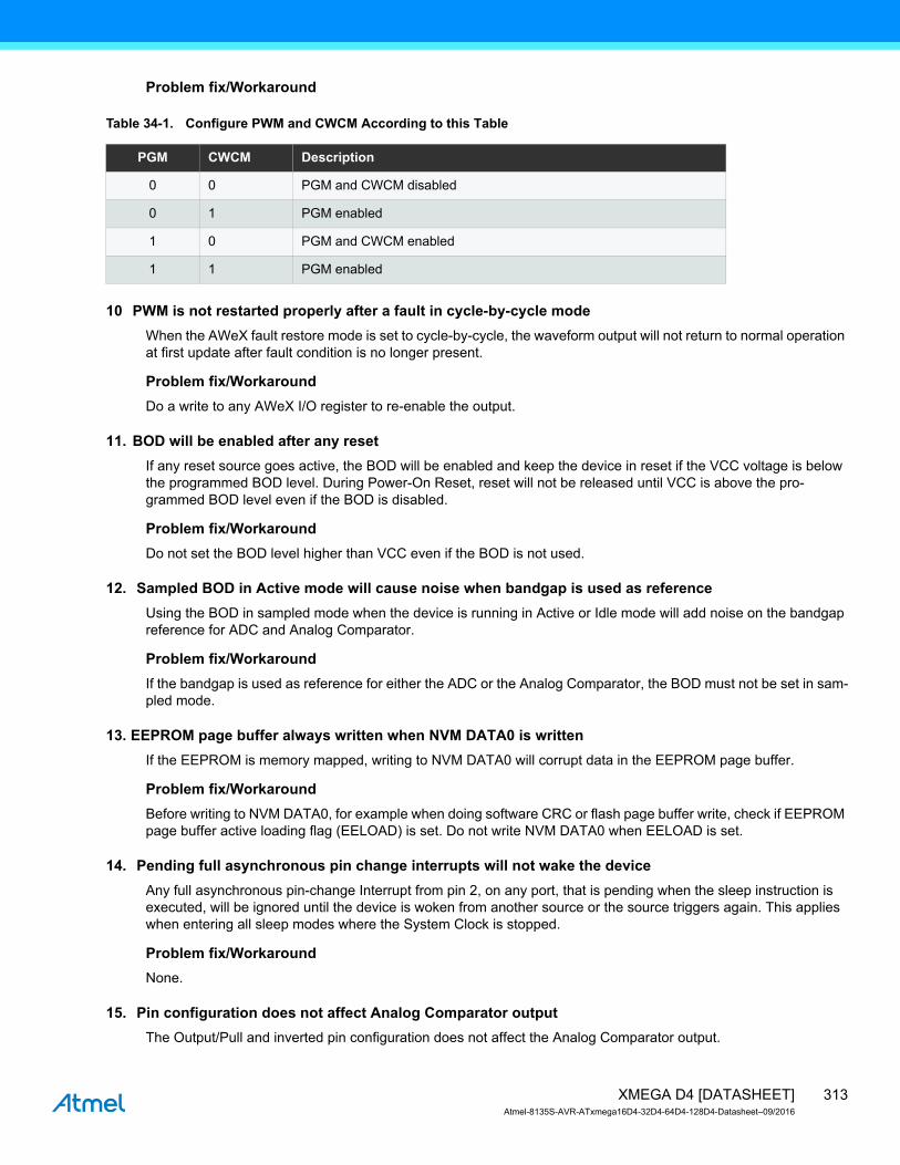
Problem fix/Workaround
Table 34-1. Configure PWM and CWCM According to this Table
10 PWM is not restarted properly after a fault in cycle-by-cycle mode
When the AWeX fault restore mode is set to cycle-by-cycle, the waveform output will not return to normal operation at first update after fault condition is no longer present.
Problem fix/Workaround
Do a write to any AWeX I/O register to re-enable the output.
11. BOD will be enabled after any reset
If any reset source goes active, the BOD will be enabled and keep the device in reset if the VCC voltage is below the programmed BOD level. During Power-On Reset, reset will not be released until VCC is above the pro-grammed BOD level even if the BOD is disabled.
Problem fix/Workaround
Do not set the BOD level higher than VCC even if the BOD is not used.
12. Sampled BOD in Active mode will cause noise when bandgap is used as reference
Using the BOD in sampled mode when the device is running in Active or Idle mode will add noise on the bandgap reference for ADC and Analog Comparator.
Problem fix/Workaround
If the bandgap is used as reference for either the ADC or the Analog Comparator, the BOD must not be set in sam-pled mode.
13. EEPROM page buffer always written when NVM DATA0 is written
If the EEPROM is memory mapped, writing to NVM DATA0 will corrupt data in the EEPROM page buffer.
Problem fix/Workaround
Before writing to NVM DATA0, for example when doing software CRC or flash page buffer write, check if EEPROM page buffer active loading flag (EELOAD) is set. Do not write NVM DATA0 when EELOAD is set.
14. Pending full asynchronous pin change interrupts will not wake the device
Any full asynchronous pin-change Interrupt from pin 2, on any port, that is pending when the sleep instruction is executed, will be ignored until the device is woken from another source or the source triggers again. This applies when entering all sleep modes where the System Clock is stopped.
Problem fix/Workaround
None.
15. Pin configuration does not affect Analog Comparator output
The Output/Pull and inverted pin configuration does not affect the Analog Comparator output.
PGM CWCM Description
0 0 PGM and CWCM disabled
0 1 PGM enabled
1 0 PGM and CWCM enabled
1 1 PGM enabled
313XMEGA D4 [DATASHEET]Atmel-8135S-AVR-ATxmega16D4-32D4-64D4-128D4-Datasheet–09/2016

Problem fix/Workaround
None for Output/Pull configuration.
For inverted I/O, configure the Analog Comparator to give an inverted result (i.e. connect positive input to the neg-ative AC input and vice versa), or use and external inverter to change polarity of Analog Comparator output.
16. NMI Flag for Crystal Oscillator Failure automatically cleared
NMI flag for Crystal Oscillator Failure (XOSCFDIF) will be automatically cleared when executing the NMI interrupt handler
Problem fix/Workaround
This device revision has only one NMI interrupt source, so checking the interrupt source in software is not required
17. Flash Power Reduction Mode can not be enabled when entering sleep
If Flash Power Reduction Mode is enabled when entering Power-save or Extended Standby sleep mode, the device will only wake up on every fourth wake-up request. If Flash Power Reduction Mode is enabled when enter-ing Idle sleep mode, the wake-up time will vary with up to 16 CPU clock cycles.
Problem fix/Workaround
Disable Flash Power Reduction mode before entering sleep mode.
18. Crystal start-up time required after power-save even if crystal is source for RTC
Even if 32.768 kHz crystal is used for RTC during sleep, the clock from the crystal will not be ready for the system before the specified start-up time. See "XOSCSEL[3:0]: Crystal Oscillator Selection " in XMEGA A Manual. If BOD is used in active mode, the BOD will be on during this period (0.5s).
Problem fix/Workaround
If faster start-up is required, go to sleep with internal oscillator as system clock
19. RTC Counter value not correctly read after sleep
If the RTC is set to wake up the device on RTC Overflow and bit 0 of RTC CNT is identical to bit 0 of RTC PER as the device is entering sleep, the value in the RTC count register can not be read correctly within the first prescaled RTC clock cycle after wakeup. The value read will be the same as the value in the register when entering sleep.
The same applies if RTC Compare Match is used as wake-up source.
Problem fix/Workaround
Wait at least one prescaled RTC clock cycle before reading the RTC CNT value.
20. Pending asynchronous RTC-interrupts will not wake up device
Asynchronous Interrupts from the Real-Time-Counter that is pending when the sleep instruction is executed, will be ignored until the device is woken from another source or the source triggers again.
Problem fix/Workaround
None.
21. TWI Transmit collision flag not cleared on repeated start
The TWI transmit collision flag should be automatically cleared on start and repeated start, but is only cleared on start.
Problem fix/Workaround
Clear the flag in software after address interrupt.
314XMEGA D4 [DATASHEET]Atmel-8135S-AVR-ATxmega16D4-32D4-64D4-128D4-Datasheet–09/2016
22. Clearing TWI Stop Interrupt Flag may lock the bus
If software clears the STOP Interrupt Flag (APIF) on the same Peripheral Clock cycle as the hardware sets this flag due to a new address received, CLKHOLD is not cleared and the SCL line is not released. This will lock the bus.
Problem fix/Workaround
Check if the bus state is IDLE. If this is the case, it is safe to clear APIF. If the bus state is not IDLE, wait for the SCL pin to be low before clearing APIF.
Code:/* Only clear the interrupt flag if within a "safe zone". */while ( /* Bus not IDLE: */ ((COMMS_TWI.MASTER.STATUS & TWI_MASTER_BUSSTATE_gm) != TWI_MASTER_BUSSTATE_IDLE_gc)) && /* SCL not held by slave: */ !(COMMS_TWI.SLAVE.STATUS & TWI_SLAVE_CLKHOLD_bm) ){ /* Ensure that the SCL line is low */ if ( !(COMMS_PORT.IN & PIN1_bm) ) if ( !(COMMS_PORT.IN & PIN1_bm) ) break;}/* Check for an pending address match interrupt */if ( !(COMMS_TWI.SLAVE.STATUS & TWI_SLAVE_CLKHOLD_bm) ){ /* Safely clear interrupt flag */ COMMS_TWI.SLAVE.STATUS |= (uint8_t)TWI_SLAVE_APIF_bm;}
23. TWI START condition at bus timeout will cause transaction to be dropped
If Bus Timeout is enabled and a timeout occurs on the same Peripheral Clock cycle as a START is detected, the transaction will be dropped.
Problem fix/Workaround
None.
24. TWI Data Interrupt Flag erroneously read as set
When issuing the TWI slave response command CMD=0b11, it takes 1 Peripheral Clock cycle to clear the data interrupt flag (DIF). A read of DIF directly after issuing the command will show the DIF still set.
Problem fix/Workaround
Add one NOP instruction before checking DIF.
25. WDR instruction inside closed window will not issue reset
When a WDR instruction is execute within one ULP clock cycle after updating the window control register, the counter can be cleared without giving a system reset.
Problem fix/Workaround
Wait at least one ULP clock cycle before executing a WDR instruction.
26. Inverted I/O enable does not affect Analog Comparator Output
The inverted I/O pin function does not affect the Analog Comparator output function.
315XMEGA D4 [DATASHEET]Atmel-8135S-AVR-ATxmega16D4-32D4-64D4-128D4-Datasheet–09/2016

Problem fix/Workaround
Configure the analog comparator setup to give an inverted result, or use an external inverter to change polarity of Analog Comparator Output.
27. Non available functions and options
The below function and options are not available. Writing to any registers or fuse to try and enable or configure these functions or options will have no effect, and will be as writing to a reserved address location.● TWIE, the TWI module on PORTE.
● TWI SDAHOLD option in the TWI CTRL register is one bit.
● CRC generator module.
● ADC 1/2x gain option, and this configuration option in the GAIN bits in the ADC Channel CTRL register.
● ADC VCC/2 reference option and this configuration option in the REFSEL bits on the ADC REFCTRL register.
● ADC option to use internal Gnd as negative input in differential measurements and this configuration option in the MUXNEG bits in the ADC Channel MUXCTRL register.
● ADC channel scan and the ADC SCAN register
● ADC current limitation option, and the CURRLIMIT bits in the ADC CTRLB register
● ADC impedance mode selection for the gain stage, and the IMPMODE bit in the ADC CTRLB register.
● Timer/Counter 2 and the SPLITMODE configuration option in the BYTEM bits in the Timer/Counter 0 CTRLE register.
● Analog Comparator (AC) current output option, and the AC CURRCTRL and CURRCALIB registers.
● PORT remap functions with alternate pin locations for Timer/Counter output compare channels, USART0 and SPI, and the PORT REMAP register.
● PORT RTC clock output option and the RTCOUT bit in the PORT CLKEVOUT register.
● PORT remap functions with alternate pin locations for the clock and event output, and the CLKEVPIN bit in the PORT CLKEVOUT register.
● TOSC alternate pin locations, and TOSCSEL bit in FUSEBYTE2
● Real Time Counter clock source options of external clock from TOSC1, and 32.768kHz from TOSC, and 32.768kHz from the 32.768kHz internal oscillator, and these configuration options in the RTCSRC bits in the Clock RTCTRL register.
● PLL divide by two option, and the PLLDIV bit in the Clock PLLCTRL register.
● PLL lock detection failure function and the PLLDIF and PLLFDEN bits in the Clock XOSCFAIL register.
● The high drive option for external crystal and the XOSCPWR bit on the Oscillator XOSCCTRL register.
● The option to enable sequential startup of the analog modules and the ANAINIT register in MCU Control memory.
Problem fix/Workaround
None.
28. Temperature sensor not calibrated
Temperature sensor factory calibration not implemented.
Problem fix/Workaround
None.
29. Disabling of USART transmitter does not automatically set the TxD pin direction to input
If the USART transmitter is idle with no frames to transmit, setting TXEN to zero will not automatically set the TxD pin direction to input.
Problem fix/Workaround
The TxD pin direction can be set to input using the Port DIR register. Be advised that setting the Port DIR register to input will be immediate. Ongoing transmissions will be truncated.
316XMEGA D4 [DATASHEET]Atmel-8135S-AVR-ATxmega16D4-32D4-64D4-128D4-Datasheet–09/2016
34.2 ATxmega64D4
34.2.1 Rev. D
Temperature sensor not calibrated
1. Temperature sensor not calibrated
Temperature sensor factory calibration not implemented.
Problem fix/Workaround
None.
34.2.2 Rev. B/C
Not sampled.
34.2.3 Rev. A
ADC may have missing codes in SE unsigned mode at low temp and low VCC
Temperature sensor not calibrated
1. ADC may have missing codes in SE unsigned mode at low temp and low VCC
The ADC may have missing codes i single ended (SE) unsigned mode below 0C when Vcc is below 1.8V.
Problem fix/Workaround
Use the ADC in SE signed mode.
2. Temperature sensor not calibrated
Temperature sensor factory calibration not implemented.
Problem fix/Workaround
None.
34.3 ATxmega128D4
34.3.1 Rev. A
Temperature sensor not calibrated
1. Temperature sensor not calibrated
Temperature sensor factory calibration not implemented.
Problem fix/Workaround
None.
317XMEGA D4 [DATASHEET]Atmel-8135S-AVR-ATxmega16D4-32D4-64D4-128D4-Datasheet–09/2016
35. Datasheet Revision History
Please note that the referring page numbers in this section are referred to this document. The referring revision in this section are referring to the document revision.
35.1 8135S – 09/2016
35.2 8135R – 02/2015
35.3 8135Q – 09/2014
35.4 8135P – 01/2014
1. Updated “Instruction Set Summary” on page 56. Removed “DES” instruction.
2. Updated “Gain Stage Characteristics” : Table 32-11 on page 72, Table 32-39 on page 91Table 32-67 on page 110 and Table 32-96 on page 131. “Offset Error, input referred” is changed to “Offset Error, output referred.
1. Updated Figure 25-1 on page 45
2. Updated the “Packaging information” on page 61. Replaced “44M1” on page 62 by a correct package.
3. Updated tables Table 32-8 on page 70and Table 32-36 on page 89 with information on fixed voltage offset.
4. Updated use of capitals in heading, table headings and figure titles.
1. Updated the “Ordering Information” on page 2. Added ordering information for ATxmega16D4/32D4/64D4/128D4 @ 105C.
2. Updated the Application table section from 4K/4K/4K/4K to 8K/4K/4K/4K in the Figure 7-1 on page 13
3.Updated Table 32-4 on page 66, Table 32-33 on page 86, Table 32-60 on page 104 and Table 32-89 on page 125. Added Icc Power-down power consumption for T=105C for all functions disabled and for WDT and sampled BOD enabled
4.Updated Table 32-17 on page 74, Table 32-45 on page 93, Table 32-73 on page 112 and Table 32-102 on page 133. Updated all tables to include values for T=85C and T=105C. Removed T=55C
5.Changed Vcc to AVcc in Figure 25-1 on page 45 and in the text in Section 25. “ADC – 12-bit Analog to Digital Converter” on page 44 and in Section 26. “AC – Analog Comparator” on page 46
6.Changed unit parameter for tSU;DAT to ns in Table 32-28 on page 82, Table 32-56 on page 101, Table 32-85 on page 121 and Table 32-114 on page 142.
7.Added ERRATA information on disabling of USART transmitter to Section 34.1 “ATxmega16D4 / ATxmega32D4” on page 308.
8. Updated the typical characteristics of “ATxmega64D4” and “ATxmega128D4” with characterizations @105C
1. Updated the typical characteristics of “ATxmega16D4” and “ATxmega32D4” with characterizations @ 105C
318XMEGA D4 [DATASHEET]Atmel-8135S-AVR-ATxmega16D4-32D4-64D4-128D4-Datasheet–09/2016

35.5 8135O – 08/2013
35.6 8135N – 04/2013
35.7 8135M – 02/2013
35.8 8135L – 08/2012
1. Updated “Errata” :
● ATxmega16D4/32D4: Added Temperature sensor not calibrated to “Rev. I” , “Rev. E” and “Rev. A/B”
● ATxmega64D4: Added Temperature sensor not calibrated to “Rev. D” and “Rev. A”
● ATxmega128D4: Added Temperature sensor not calibrated to “Rev. A”
1. Updated description in “ADC – 12-bit Analog to Digital Converter” on page 44.
2. Updated “Errata” :
● ATxmega16D4/32D4: Added revision F, G, H, I
● ATxmega64D4: Added revision A, B, C
● ATxmega128D4: Added revision A
1. Updated the datasheet with the Atmel new datasheet template.
2. Updated Figure 2-1 on page 4. PE2/PE3 are now half gray.
3. Updated Figure 2-1 on page 4. Pin 19 is VCC and not VDD.
4. Updated Table 7-2 on page 16. FWORD column updated: Z[X,0] replaced by Z[X,1]. FPAGE column updated to Z[Y,8]
5. Updated “I/O Ports” on page 29. Removed “Optional slew rate control”. The feature doesn't exist in XMEGA C and XMEGA D devices.
6. Updated “Analog Comparator Overview” on page 47, Figure 26-1.
7. Updated Table 32-25 on page 77, Table 32-53 on page 96 and Table 32-82 on page 116. Added ESR parameter.
8. Updated TWI specification. VIL Min is -0.5V and not 0.5V.
9. Added new “Electrical Characteristics” for “ATxmega16D4” on page 64 and “ATxmega32D4” on page 83.
10. Added new “Typical Characteristics” for “ATxmega16D4” on page 144 and “ATxmega32D4” on page 184.
11. Updated “Errata” on page 308. AC system status flags are only valid if AC-system is enabled.
1. Editing updates.
2. Updated all tables in the “Electrical Characteristics” on page 64.
3. Added new “Typical Characteristics” on page 144.
4. Added new Errata “Rev. E” on page 308.
5. Added new ERRATA on “Rev. A/B” on page 310: Non available functions and options
319XMEGA D4 [DATASHEET]Atmel-8135S-AVR-ATxmega16D4-32D4-64D4-128D4-Datasheet–09/2016

35.9 8135K – 06/2012
35.10 8135J – 12/10
35.11 8135I – 10/10
35.12 8135H – 09/10
35.13 8135G – 08/10
35.14 8135F – 02/10
1. ATxmega64D4-CU is added in “Ordering Information” on page 2
1. Datasheet status changed to complete: Preliminary removed from the front page.
2. Updated all tables in the “Electrical Characteristics” on page 64.
3. Replaced Table 31-11 on page 64.
4. Replaced Table 31-17 on page 65 and added the figure ”TOSC input capacitance” on page 66.
5. Updated ERRATA ADC (ADC has increased INL for some operating conditions).
6. Updated ERRATA ”rev. A/B” on page 90 with TWIE (TWIE is not available).
7. Updated the last page with Atmel new Brand Style Guide.
1. Updated Table 31-1 on page 58.
1. Updated ”Errata” on page 90.
1. Updated the Footnote 3 of ”Ordering Information” on page 2.
2. All references to CRC removed. Updated Figure 3-1 on page 7.
3. Updated ”Features” on page 26. Event Channel 0 output on port pin 7.
4. Updated ”DC Characteristics” on page 58 by adding Icc for Flash/EEPROM Programming.
5. Added AVCC in ”ADC Characteristics” on page 62.
6. Updated Start up time in ”ADC Characteristics” on page 62.
7. Updated and fixed typo in “Errata” section.
1. Added ”PDI Speed” on page 89.
320XMEGA D4 [DATASHEET]Atmel-8135S-AVR-ATxmega16D4-32D4-64D4-128D4-Datasheet–09/2016
35.15 8135E – 02/10
35.16 8135D – 12/09
35.17 8135C – 10/09
35.18 8135B – 09/09
1. Updated the device pin-out Figure 2-1 on page 3. PDI_CLK and PDI_DATA renamed only PDI.
2. Updated Table 7-3 on page 18. No of Pages for ATxmega32D4: 32
3. Updated ”Alternate Port Functions” on page 29.
4. Updated ”ADC - 12-bit Analog to Digital Converter” on page 39.
5. Updated Figure 25-1 on page 50.
6. Updated ”Alternate Pin Functions” on page 48.
7. Updated ”Timer/Counter and AWEX functions” on page 46.
8. Added Table 31-17 on page 65.
9. Added Table 31-18 on page 66.
10. Changed Internal Oscillator Speed to ”Oscillators and Wake-up Time” on page 85.
11. Updated ”Errata” on page 90.
1. Added ATxmega128D4 device and updated the datasheet accordingly.
2. Updated ”Electrical Characteristics” on page 58 with Max/Min numbers.
3. Added ”Flash and EEPROM Memory Characteristics” on page 61.
4. Updated Table 31-10 on page 64, Input hysteresis is in V and not in mV.
5. Added ”Errata” on page 90.
1. Updated ”Features” on page 1 with Two Two-Wire Interfaces.
2. Updated ”Block Diagram and QFN/TQFP pinout” on page 3.
3. Updated ”Overview” on page 5.
4. Updated ”XMEGA D4 Block Diagram” on page 7.
5. Updated Table 13-1 on page 24.
6. Updated ”Overview” on page 35.
7. Updated Table 27-5 on page 49.
8. Updated ”Peripheral Module Address Map” on page 50.
1. Added ”Electrical Characteristics” on page 58.
2. Added ”Typical Characteristics” on page 67.
321XMEGA D4 [DATASHEET]Atmel-8135S-AVR-ATxmega16D4-32D4-64D4-128D4-Datasheet–09/2016

35.19 8135A – 03/09
1. Initial revision.
322XMEGA D4 [DATASHEET]Atmel-8135S-AVR-ATxmega16D4-32D4-64D4-128D4-Datasheet–09/2016

Table of Contents
Features1
1 Ordering Information ............................................................................... 2
2 Pinout/Block diagram .............................................................................. 4
3 Overview ................................................................................................... 6
3.1Block Diagram ........................................................................................................... 7
4 Resources ................................................................................................. 8
4.1Recommended Reading............................................................................................ 8
5 Capacitive Touch Sensing ....................................................................... 8
6 AVR CPU ................................................................................................... 9
6.1Features .................................................................................................................... 9
6.2Overview.................................................................................................................... 9
6.3Architectural Overview............................................................................................... 9
6.4ALU - Arithmetic Logic Unit ..................................................................................... 10
6.5Program Flow .......................................................................................................... 11
6.6Status Register ........................................................................................................ 11
6.7Stack and Stack Pointer .......................................................................................... 11
6.8Register File ............................................................................................................ 11
7 Memories ................................................................................................. 12
7.1Features .................................................................................................................. 12
7.2Overview.................................................................................................................. 12
7.3Flash Program Memory ........................................................................................... 13
7.4Fuses and Lock Bits ................................................................................................ 14
7.5Data Memory ........................................................................................................... 14
7.6EEPROM ................................................................................................................. 15
7.7I/O Memory.............................................................................................................. 15
7.8Data Memory and Bus Arbitration ........................................................................... 16
7.9Memory Timing........................................................................................................ 16
7.10Device ID and Revision ......................................................................................... 16
7.11I/O Memory Protection........................................................................................... 16
7.12Flash and EEPROM Page Size............................................................................. 16
8 Event System .......................................................................................... 18
8.1Features .................................................................................................................. 18
8.2Overview.................................................................................................................. 18
iXMEGA D4 [DATASHEET]Atmel-8135S-AVR-ATxmega16D4-32D4-64D4-128D4-Datasheet–09/2016

9 System Clock and Clock Options .........................................................19
9.1Features .................................................................................................................. 19
9.2Overview.................................................................................................................. 19
9.3Clock Sources ......................................................................................................... 20
10 Power Management and Sleep Modes ................................................. 22
10.1Features ................................................................................................................ 22
10.2Overview................................................................................................................ 22
10.3Sleep Modes.......................................................................................................... 22
11 System Control and Reset ..................................................................... 24
11.1Features ................................................................................................................ 24
11.2Overview................................................................................................................ 24
11.3Reset Sequence .................................................................................................... 24
11.4Reset Sources ....................................................................................................... 25
12 WDT – Watchdog Timer ......................................................................... 26
12.1Features ................................................................................................................ 26
12.2Overview................................................................................................................ 26
13 Interrupts and Programmable Multilevel Interrupt Controller ............ 27
13.1Features ................................................................................................................ 27
13.2Overview................................................................................................................ 27
13.3Interrupt Vectors .................................................................................................... 27
14 I/O Ports .................................................................................................. 29
14.1Features ................................................................................................................ 29
14.2Overview................................................................................................................ 29
14.3Output Driver ......................................................................................................... 30
14.4Input Sensing......................................................................................................... 31
14.5Alternate Port Functions ........................................................................................ 32
15 TC0/1 – 16-bit Timer/Counter Type 0 and 1 .......................................... 33
15.1Features ................................................................................................................ 33
15.2Overview................................................................................................................ 33
16 TC2 Timer/Counter Type 2 ..................................................................... 35
16.1Features ................................................................................................................ 35
16.2Overview................................................................................................................ 35
17 AWeX – Advanced Waveform Extension ............................................. 36
17.1Features ................................................................................................................ 36
iiXMEGA D4 [DATASHEET]Atmel-8135S-AVR-ATxmega16D4-32D4-64D4-128D4-Datasheet–09/2016

17.2Overview................................................................................................................ 36
18 Hi-Res – High Resolution Extension .................................................... 37
18.1Features ................................................................................................................ 37
18.2Overview................................................................................................................ 37
19 RTC – 16-bit Real-Time Counter ........................................................... 38
19.1Features ................................................................................................................ 38
19.2Overview................................................................................................................ 38
20 TWI – Two-Wire Interface .......................................................................39
20.1Features ................................................................................................................ 39
20.2Overview................................................................................................................ 39
21 SPI – Serial Peripheral Interface ........................................................... 40
21.1Features ................................................................................................................ 40
21.2Overview................................................................................................................ 40
22 USART ..................................................................................................... 41
22.1Features ................................................................................................................ 41
22.2Overview................................................................................................................ 41
23 IRCOM – IR Communication Module .................................................... 42
23.1Features ................................................................................................................ 42
23.2Overview................................................................................................................ 42
24 CRC – Cyclic Redundancy Check Generator ...................................... 43
24.1Features ................................................................................................................ 43
24.2Overview................................................................................................................ 43
25 ADC – 12-bit Analog to Digital Converter ............................................ 44
25.1Features ................................................................................................................ 44
25.2Overview................................................................................................................ 44
26 AC – Analog Comparator .......................................................................46
26.1Features ................................................................................................................ 46
26.2Overview................................................................................................................ 46
27 Programming and Debugging ............................................................... 48
27.1Features ................................................................................................................ 48
27.2Overview................................................................................................................ 48
28 Pinout and Pin Functions ...................................................................... 49
28.1Alternate Pin Function Description ........................................................................ 49
iiiXMEGA D4 [DATASHEET]Atmel-8135S-AVR-ATxmega16D4-32D4-64D4-128D4-Datasheet–09/2016

28.2Alternate Pin Functions ......................................................................................... 51
29 Peripheral Module Address Map ........................................................... 54
30 Instruction Set Summary .......................................................................56
31 Packaging information ........................................................................... 61
31.144A ........................................................................................................................ 61
31.244M1...................................................................................................................... 62
31.349C2 ...................................................................................................................... 63
32 Electrical Characteristics ...................................................................... 64
32.1ATxmega16D4....................................................................................................... 64
32.2ATxmega32D4....................................................................................................... 83
32.3ATxmega64D4..................................................................................................... 102
32.4ATxmega128D4................................................................................................... 123
33 Typical Characteristics ........................................................................ 144
33.1ATxmega16D4..................................................................................................... 144
33.2ATxmega32D4..................................................................................................... 184
33.3ATxmega64D4..................................................................................................... 224
33.4ATxmega128D4................................................................................................... 266
34 Errata ..................................................................................................... 308
34.1ATxmega16D4 / ATxmega32D4.......................................................................... 308
34.2ATxmega64D4..................................................................................................... 317
34.3ATxmega128D4................................................................................................... 317
35 Datasheet Revision History ................................................................. 318
35.18135S – 09/2016 ................................................................................................. 318
35.28135R – 02/2015 ................................................................................................. 318
35.38135Q – 09/2014................................................................................................. 318
35.48135P – 01/2014 ................................................................................................. 318
35.58135O – 08/2013................................................................................................. 319
35.68135N – 04/2013 ................................................................................................. 319
35.78135M – 02/2013................................................................................................. 319
35.88135L – 08/2012.................................................................................................. 319
35.98135K – 06/2012 ................................................................................................. 320
35.108135J – 12/10.................................................................................................... 320
35.118135I – 10/10..................................................................................................... 320
35.128135H – 09/10 ................................................................................................... 320
ivXMEGA D4 [DATASHEET]Atmel-8135S-AVR-ATxmega16D4-32D4-64D4-128D4-Datasheet–09/2016
35.138135G – 08/10................................................................................................... 320
35.148135F – 02/10 ................................................................................................... 320
35.158135E – 02/10 ................................................................................................... 321
35.168135D – 12/09 ................................................................................................... 321
35.178135C – 10/09 ................................................................................................... 321
35.188135B – 09/09 ................................................................................................... 321
35.198135A – 03/09 ................................................................................................... 322
Table of Contentsi
vXMEGA D4 [DATASHEET]Atmel-8135S-AVR-ATxmega16D4-32D4-64D4-128D4-Datasheet–09/2016

XX X XX X
Atmel Corporation 1600 Technology Drive, San Jose, CA 95110 USA T: (+1)(408) 441.0311 F: (+1)(408) 436.4200 | www.atmel.com
© 2015 Atmel Corporation. / Rev.: Atmel-8135R-AVR-ATxmega16D4-32D4-64D4-128D4-Datasheet_09/2016.
Atmel®, Atmel logo and combinations thereof, Enabling Unlimited Possibilities®, and others are registered trademarks or trademarks of Atmel Corporation in U.S. and other countries. Other terms and product names may be trademarks of others.
DISCLAIMER: The information in this document is provided in connection with Atmel products. No license, express or implied, by estoppel or otherwise, to any intellectual property rightis granted by this document or in connection with the sale of Atmel products. EXCEPT AS SET FORTH IN THE ATMEL TERMS AND CONDITIONS OF SALES LOCATED ON THEATMEL WEBSITE, ATMEL ASSUMES NO LIABILITY WHATSOEVER AND DISCLAIMS ANY EXPRESS, IMPLIED OR STATUTORY WARRANTY RELATING TO ITS PRODUCTSINCLUDING, BUT NOT LIMITED TO, THE IMPLIED WARRANTY OF MERCHANTABILITY, FITNESS FOR A PARTICULAR PURPOSE, OR NON-INFRINGEMENT. IN NO EVENTSHALL ATMEL BE LIABLE FOR ANY DIRECT, INDIRECT, CONSEQUENTIAL, PUNITIVE, SPECIAL OR INCIDENTAL DAMAGES (INCLUDING, WITHOUT LIMITATION, DAMAGESFOR LOSS AND PROFITS, BUSINESS INTERRUPTION, OR LOSS OF INFORMATION) ARISING OUT OF THE USE OR INABILITY TO USE THIS DOCUMENT, EVEN IF ATMEL HASBEEN ADVISED OF THE POSSIBILITY OF SUCH DAMAGES. Atmel makes no representations or warranties with respect to the accuracy or completeness of the contents of thisdocument and reserves the right to make changes to specifications and products descriptions at any time without notice. Atmel does not make any commitment to update the informationcontained herein. Unless specifically provided otherwise, Atmel products are not suitable for, and shall not be used in, automotive applications. Atmel products are not intended,authorized, or warranted for use as components in applications intended to support or sustain life.
SAFETY-CRITICAL, MILITARY, AND AUTOMOTIVE APPLICATIONS DISCLAIMER: Atmel products are not designed for and will not be used in connection with any applications wherethe failure of such products would reasonably be expected to result in significant personal injury or death (“Safety-Critical Applications”) without an Atmel officer's specific writtenconsent. Safety-Critical Applications include, without limitation, life support devices and systems, equipment or systems for the operation of nuclear facilities and weapons systems.Atmel products are not designed nor intended for use in military or aerospace applications or environments unless specifically designated by Atmel as military-grade. Atmel products arenot designed nor intended for use in automotive applications unless specifically designated by Atmel as automotive-grade.