Texas Instruments MSP430 Microcontrollers - "Modular ...
240
Modular Electronics Learning (ModEL) project v1 1 0 dc 12 v2 2 1 dc 15 r1 2 3 4700 r2 3 0 7100 .end * SPICE ckt V = I R .dc v1 12 12 1 .print dc v(2,3) .print dc i(v2) Texas Instruments MSP430 Microcontrollers c 2020-2021 by Tony R. Kuphaldt – under the terms and conditions of the Creative Commons Attribution 4.0 International Public License Last update = 30 November 2021 This is a copyrighted work, but licensed under the Creative Commons Attribution 4.0 International Public License. A copy of this license is found in the last Appendix of this document. Alternatively, you may visit http://creativecommons.org/licenses/by/4.0/ or send a letter to Creative Commons: 171 Second Street, Suite 300, San Francisco, California, 94105, USA. The terms and conditions of this license allow for free copying, distribution, and/or modification of all licensed works by the general public.
-
Upload
khangminh22 -
Category
Documents
-
view
1 -
download
0
Transcript of Texas Instruments MSP430 Microcontrollers - "Modular ...

Modular Electronics Learning (ModEL)project
v1 1 0 dc 12
v2 2 1 dc 15
r1 2 3 4700
r2 3 0 7100
.end
* SPICE ckt
V = I R
.dc v1 12 12 1
.print dc v(2,3)
.print dc i(v2)
Texas Instruments MSP430 Microcontrollers
c© 2020-2021 by Tony R. Kuphaldt – under the terms and conditions of theCreative Commons Attribution 4.0 International Public License
Last update = 30 November 2021
This is a copyrighted work, but licensed under the Creative Commons Attribution 4.0 InternationalPublic License. A copy of this license is found in the last Appendix of this document. Alternatively,you may visit http://creativecommons.org/licenses/by/4.0/ or send a letter to CreativeCommons: 171 Second Street, Suite 300, San Francisco, California, 94105, USA. The terms andconditions of this license allow for free copying, distribution, and/or modification of all licensedworks by the general public.

ii

Contents
1 Introduction 3
2 Case Tutorial 52.1 Assembly example: adding two numbers . . . . . . . . . . . . . . . . . . . . . . . . . 62.2 C example: adding two numbers . . . . . . . . . . . . . . . . . . . . . . . . . . . . . 92.3 Sketch example: adding two numbers . . . . . . . . . . . . . . . . . . . . . . . . . . . 112.4 Assembly example: subtracting two numbers . . . . . . . . . . . . . . . . . . . . . . 132.5 Assembly example: bitwise operations . . . . . . . . . . . . . . . . . . . . . . . . . . 152.6 C example: bitwise operations . . . . . . . . . . . . . . . . . . . . . . . . . . . . . . . 172.7 Assembly example: rotate right instruction . . . . . . . . . . . . . . . . . . . . . . . 192.8 Assembly example: alternating LED blink . . . . . . . . . . . . . . . . . . . . . . . . 212.9 C example: alternating LED blink . . . . . . . . . . . . . . . . . . . . . . . . . . . . 242.10 Sketch example: alternating LED blink . . . . . . . . . . . . . . . . . . . . . . . . . 272.11 Assembly example: blink all Port 1 lines . . . . . . . . . . . . . . . . . . . . . . . . . 292.12 Assembly example: pushbutton control of LED . . . . . . . . . . . . . . . . . . . . . 322.13 C example: pushbutton control of LED . . . . . . . . . . . . . . . . . . . . . . . . . 342.14 C example: start-stop control . . . . . . . . . . . . . . . . . . . . . . . . . . . . . . . 382.15 Assembly example: pushing and popping the stack . . . . . . . . . . . . . . . . . . . 422.16 Assembly example: driving Port 2 lines with Timer . . . . . . . . . . . . . . . . . . . 452.17 Assembly example: interrupt triggered by pushbutton . . . . . . . . . . . . . . . . . 482.18 C example: interrupt triggered by pushbutton . . . . . . . . . . . . . . . . . . . . . . 522.19 Assembly example: LED blink with watchdog . . . . . . . . . . . . . . . . . . . . . . 542.20 C example: pushbutton-triggered timer . . . . . . . . . . . . . . . . . . . . . . . . . 582.21 C example: Boolean SOP expression . . . . . . . . . . . . . . . . . . . . . . . . . . . 622.22 C example: sine wave signal generator . . . . . . . . . . . . . . . . . . . . . . . . . . 652.23 C example: pulse-width modulation output . . . . . . . . . . . . . . . . . . . . . . . 682.24 C example: crude analog input . . . . . . . . . . . . . . . . . . . . . . . . . . . . . . 722.25 C example: analog-controlled LEDs . . . . . . . . . . . . . . . . . . . . . . . . . . . . 752.26 C example: UART serial text transmission . . . . . . . . . . . . . . . . . . . . . . . . 792.27 C example: UART serial text and number transmission . . . . . . . . . . . . . . . . 832.28 C example: UART transmission of analog data . . . . . . . . . . . . . . . . . . . . . 882.29 C example: simple datalogger . . . . . . . . . . . . . . . . . . . . . . . . . . . . . . . 972.30 Example: interposing MCU to a heavy load . . . . . . . . . . . . . . . . . . . . . . . 1042.31 C example: sine-wave inverter . . . . . . . . . . . . . . . . . . . . . . . . . . . . . . . 111
iii

iv CONTENTS
3 Tutorial 1153.1 Microcontrollers versus microprocessors . . . . . . . . . . . . . . . . . . . . . . . . . 1153.2 MSP430G2553 pin functions . . . . . . . . . . . . . . . . . . . . . . . . . . . . . . . . 1193.3 Elementary output and input . . . . . . . . . . . . . . . . . . . . . . . . . . . . . . . 1213.4 Bit-level output instructions . . . . . . . . . . . . . . . . . . . . . . . . . . . . . . . . 1273.5 Bit-level input instructions . . . . . . . . . . . . . . . . . . . . . . . . . . . . . . . . 1303.6 MSP430G2553 architecture . . . . . . . . . . . . . . . . . . . . . . . . . . . . . . . . 131
3.6.1 Registers . . . . . . . . . . . . . . . . . . . . . . . . . . . . . . . . . . . . . . 1323.6.2 Memory map . . . . . . . . . . . . . . . . . . . . . . . . . . . . . . . . . . . . 1333.6.3 I/O ports . . . . . . . . . . . . . . . . . . . . . . . . . . . . . . . . . . . . . . 1343.6.4 Interrupts . . . . . . . . . . . . . . . . . . . . . . . . . . . . . . . . . . . . . . 1373.6.5 Watchdog timer . . . . . . . . . . . . . . . . . . . . . . . . . . . . . . . . . . 142
3.7 MSP430G2553 auxiliary functions . . . . . . . . . . . . . . . . . . . . . . . . . . . . 1443.7.1 Clocks . . . . . . . . . . . . . . . . . . . . . . . . . . . . . . . . . . . . . . . . 1453.7.2 General timers . . . . . . . . . . . . . . . . . . . . . . . . . . . . . . . . . . . 1463.7.3 Watchdog timer . . . . . . . . . . . . . . . . . . . . . . . . . . . . . . . . . . 1463.7.4 Analog-Digital conversion . . . . . . . . . . . . . . . . . . . . . . . . . . . . . 1463.7.5 Analog comparators . . . . . . . . . . . . . . . . . . . . . . . . . . . . . . . . 1463.7.6 Serial data interfaces . . . . . . . . . . . . . . . . . . . . . . . . . . . . . . . . 146
3.8 CCS assembly-language programming . . . . . . . . . . . . . . . . . . . . . . . . . . 1463.9 CCS C-language programming . . . . . . . . . . . . . . . . . . . . . . . . . . . . . . 1493.10 Energia programming . . . . . . . . . . . . . . . . . . . . . . . . . . . . . . . . . . . 1543.11 Debugging tools . . . . . . . . . . . . . . . . . . . . . . . . . . . . . . . . . . . . . . . 157
4 Derivations and Technical References 1734.1 Introduction to assembly language programming . . . . . . . . . . . . . . . . . . . . 174
4.1.1 Machine code to blink an LED . . . . . . . . . . . . . . . . . . . . . . . . . . 1754.1.2 Assembly code to blink an LED . . . . . . . . . . . . . . . . . . . . . . . . . . 1774.1.3 Slowing down the blinking . . . . . . . . . . . . . . . . . . . . . . . . . . . . . 1794.1.4 Simplifying with symbols . . . . . . . . . . . . . . . . . . . . . . . . . . . . . 1824.1.5 Using the stack . . . . . . . . . . . . . . . . . . . . . . . . . . . . . . . . . . . 183
5 Questions 1875.1 Conceptual reasoning . . . . . . . . . . . . . . . . . . . . . . . . . . . . . . . . . . . . 191
5.1.1 Reading outline and reflections . . . . . . . . . . . . . . . . . . . . . . . . . . 1925.1.2 Foundational concepts . . . . . . . . . . . . . . . . . . . . . . . . . . . . . . . 1935.1.3 Terminal assignments and limits . . . . . . . . . . . . . . . . . . . . . . . . . 1945.1.4 Interrupt capabilities . . . . . . . . . . . . . . . . . . . . . . . . . . . . . . . . 1955.1.5 Disabling the watchdog timer . . . . . . . . . . . . . . . . . . . . . . . . . . . 196
5.2 Quantitative reasoning . . . . . . . . . . . . . . . . . . . . . . . . . . . . . . . . . . . 1975.2.1 Miscellaneous physical constants . . . . . . . . . . . . . . . . . . . . . . . . . 1985.2.2 Introduction to spreadsheets . . . . . . . . . . . . . . . . . . . . . . . . . . . 1995.2.3 Integer conversion table . . . . . . . . . . . . . . . . . . . . . . . . . . . . . . 2025.2.4 Setting up Port 1 I/O . . . . . . . . . . . . . . . . . . . . . . . . . . . . . . . 2025.2.5 Setting up Timer A . . . . . . . . . . . . . . . . . . . . . . . . . . . . . . . . 2035.2.6 Selecting sub-main clock source . . . . . . . . . . . . . . . . . . . . . . . . . . 203

CONTENTS 1
5.2.7 MSP430 header file . . . . . . . . . . . . . . . . . . . . . . . . . . . . . . . . . 2045.3 Diagnostic reasoning . . . . . . . . . . . . . . . . . . . . . . . . . . . . . . . . . . . . 205
5.3.1 Poor interface design . . . . . . . . . . . . . . . . . . . . . . . . . . . . . . . . 2065.3.2 Improving a debug session . . . . . . . . . . . . . . . . . . . . . . . . . . . . . 2075.3.3 Incorrect sum . . . . . . . . . . . . . . . . . . . . . . . . . . . . . . . . . . . . 208
A Problem-Solving Strategies 209
B Instructional philosophy 211
C Tools used 217
D Creative Commons License 221
E References 229
F Version history 231
Index 234

2 CONTENTS
Chapter 1
Introduction
The MSP430 series of microcontrollers are an excellent platform for learning microcontrollertechnology, featuring a clean design and a multiple development tools. This module will discusssome of the basic features of this microcontroller product line with an emphasis on programming. Inno way should the Tutorial contained in this module be considered a substitute for the volumes oftechnical literature published by Texas Instruments on their product, but rather more of a “GettingStarted” or “Quick Reference” guide for the student new to the MSP430 and to microcontrollers ingeneral.
Important concepts related to microcontrollers in general and to the MSP430 series ofmicrocontrollers in particular include busses, ports, development software, registers, memorymaps, binary and hexadecimal numeration, masks, interrupts, oscillators, clocks, timers,analog-digital conversion, comparators, and serial data communication.
Here are some good questions to ask of yourself while studying this subject:
• What purposes do microprocessors serve best, versus microcontrollers?
• How does a program get written to the internal memory of a microcontroller?
• What does the program counter do in a microprocessor or microcontroller?
• What does the stack pointer do in a microprocessor or microcontroller?
• What types of information will you find stored within the status register of a microprocessoror microcontroller?
• How do we tell the microcontroller to use an I/O pin as an input versus as an output?
• What is the sequence of operations when the device receives an interrupt signal?
• Why might we want to adjust the clock speed of a microcontroller?
A very important resource for anyone learning to program the MSP430 series of microcontrollersis the Case Tutorial chapter, showing a range of simple programming examples in multiple languages.
3

4 CHAPTER 1. INTRODUCTION
Like learning a spoken or written language, it is very helpful to experience practical examples ofthat language in action.

Chapter 2
Case Tutorial
The idea behind a Case Tutorial is to explore new concepts by way of example. In this chapter youwill read less presentation of theory compared to other Turorial chapters, but by close observationand comparison of the given examples be able to discern patterns and principles much the same wayas a scientific experimenter. Hopefully you will find these cases illuminating, and a good supplementto text-based tutorials.
These examples also serve well as challenges following your reading of the other Tutorial(s) inthis module – can you explain why the circuits behave as they do?
5

6 CHAPTER 2. CASE TUTORIAL
2.1 Assembly example: adding two numbers
Schematic diagram
MS
P430G
2553IN20
VSSVCC (+3.3 V)
P1.0
P1.1
P1.2
P1.3
P1.4
P1.5
P2.0
P2.1
P2.2
P2.6
P2.7
TEST
RST
P1.7
P1.6
P2.5
P2.4
P2.3
+3.3V
+3.3V
On the next page is a listing of the entire assembly-language code, tested and run on a modelMSP430G2553IN20 microcontroller using a LaunchPad model MSP-EXP430G2ET developmentboard and version 10 of Code Composer Studio (CCS). Only the code found between the “CodeBegin” and “Code End” comment lines are specific to this example program’s purpose, with therest being assembler directives and other instructions necessary for any simple assembly-languageprogram to run on this microcontroller.
All statements beginning with a dot (e.g. .text) are directives telling the assembler how toconvert the assembly source code into executable machine code for the microcontroller to run.Similarly, the RESET and StopWDT labels mark general set-up instructions for the microcontrollerand are not specifically related to the program’s main function.

2.1. ASSEMBLY EXAMPLE: ADDING TWO NUMBERS 7
Assembly code listing
.cdecls C,LIST,"msp430.h"
.def RESET
.text
.retain
.retainrefs
RESET mov.w #__STACK_END,SP ; Initialize stackpointer
StopWDT mov.w #WDTPW|WDTHOLD,&WDTCTL ; Stop watchdog timer
;================================= Code Begin =================================
MAIN
mov #0x05,R4
add #0x06,R4
;================================== Code End ==================================
.global __STACK_END
.sect .stack
.sect ".reset"
.short RESET
When run, the result of this code executing is that the value 0x0B (eleven) is left in registerR4. There is no way to verify that the addition has taken place, aside from using the programmingsoftware to view the microcontroller’s register values. The microcontroller has no console display,and we have not connected any devices to its pins to indicate bit states.
Note that in assembly-language programming we use semicolons to denote single-line comments:all text to the right of a semicolon are ignored by the assembler and have no impact whatsoever onthe final “machine code” instructions executed by the microcontroller. Comments are present onlyfor clarifying purposes, to any human beings reading the assembly code.

8 CHAPTER 2. CASE TUTORIAL
It is also possible to specify an absolute address in memory rather than use a general-purposeregisters (e.g. R4), as shown here using address 0x0200:
Assembly code listing
.cdecls C,LIST,"msp430.h"
.def RESET
.text
.retain
.retainrefs
RESET mov.w #__STACK_END,SP ; Initialize stackpointer
StopWDT mov.w #WDTPW|WDTHOLD,&WDTCTL ; Stop watchdog timer
;================================= Code Begin =================================
MAIN
mov #0x05,&0x0200
add #0x06,&0x0200
;================================== Code End ==================================
.global __STACK_END
.sect .stack
.sect ".reset"
.short RESET
When run, the sum will be the same (0x0B or eleven) but stored in address 0x0200 rather thanin register R4. Again, to view this sum we would have to utilize software capable of reading themicrocontroller’s memory contents.

2.2. C EXAMPLE: ADDING TWO NUMBERS 9
2.2 C example: adding two numbers
Schematic diagram
MS
P430G
2553IN20
VSSVCC (+3.3 V)
P1.0
P1.1
P1.2
P1.3
P1.4
P1.5
P2.0
P2.1
P2.2
P2.6
P2.7
TEST
RST
P1.7
P1.6
P2.5
P2.4
P2.3
+3.3V
+3.3V
On the next page is a listing of the entire C-language code, tested and run on a modelMSP430G2553IN20 microcontroller using a LaunchPad model MSP-EXP430G2ET developmentboard and version 10 of Code Composer Studio (CCS).
The statement beginning with a pound symbol (#include <msp430.h>) is a directive telling thecompiler how to convert the C source code into object code and then executable machine code forthe microcontroller to run.

10 CHAPTER 2. CASE TUTORIAL
C code listing
#include <msp430.h>
int x = 5;
int y = 6;
int z;
int main(void)
WDTCTL = WDTPW | WDTHOLD; // stop watchdog timer
z = x + y;
return 0;
All characters to the right of double-slash symbols (//) are comments which are ignored by thecompiler and appear only as an aid to understanding for any human reading the code.
The following “hex dump” of microcontroller memory from address1 0x0200 to address 0x0205taken after the program ran shows the quantities involved in this calculation:
0x0200 06 00 05 00 0B 00
As you can see, x is stored at 0x0202 with a value of five, y is stored at 0x0200 with a value ofsix, and the sum z is stored at 0x0204 with a value of eleven (0x0B).
1There is nothing in the code suggesting that variables x, y, and z are stored in this region of the microcontroller’smemory – you would just have to know that from researching the “memory map” for this particular model ofmicrocontroller

2.3. SKETCH EXAMPLE: ADDING TWO NUMBERS 11
2.3 Sketch example: adding two numbers
Schematic diagram
MS
P430G
2553IN20
VSSVCC (+3.3 V)
P1.0
P1.1
P1.2
P1.3
P1.4
P1.5
P2.0
P2.1
P2.2
P2.6
P2.7
TEST
RST
P1.7
P1.6
P2.5
P2.4
P2.3
+3.3V
+3.3V
The popular Arduino microcontroller development platform has popularized a superset of the Cprogramming language called Sketch, and a development tool called Energia allows Sketch programsto be written for and loaded into the Texas Instruments MSP430 devices. On the next page is alisting of the Sketch code, tested and run on a model MSP430G2553IN20 microcontroller using aLaunchPad model MSP-EXP430G2ET development board, version 10 of Code Composer Studio(CCS), and version 1.8.10E23 of Energia.

12 CHAPTER 2. CASE TUTORIAL
Sketch code listing
int x = 5;
int y = 6;
int z;
void setup()
void loop()
// put your main code here, to run repeatedly:
z = x + y;
Every Sketch program contains two important functions: setup() and loop(). All codeappearing between the curly-brace symbols ( and ) in the setup() function is executed once whenthe microcontroller powers up or gets reset. All code appearing between the curly-brace symbols (and ) in the loop() function is executed repeatedly with no need to insert “jump” instructions orwhile conditionals. The whole point of Sketch as a programming language is to shield those normaldetails from the developer who is assumed to be a rank beginner.
All characters to the right of double-slash symbols (//) are comments which are ignored by thecompiler and appear only as an aid to understanding for any human reading the code.
Note that this program’s function is entirely empty, as there are no special bits that need tobe set or cleared, or any other initial conditions that need to be configured, in order to add twonumbers together.
Interestingly, the disassembled code listing for this simple program is enormous compared to theassembly and even the C versions. This is the price you pay for a simplified programming language:the compiler has to generate a lot of code to make the microcontroller do what your easy instructionscommand, and this often results in “code inflation”.

2.4. ASSEMBLY EXAMPLE: SUBTRACTING TWO NUMBERS 13
2.4 Assembly example: subtracting two numbers
Schematic diagram
MS
P430G
2553IN20
VSSVCC (+3.3 V)
P1.0
P1.1
P1.2
P1.3
P1.4
P1.5
P2.0
P2.1
P2.2
P2.6
P2.7
TEST
RST
P1.7
P1.6
P2.5
P2.4
P2.3
+3.3V
+3.3V
On the next page is a listing of the entire assembly-language code, tested and run on a modelMSP430G2553IN20 microcontroller using a LaunchPad model MSP-EXP430G2ET developmentboard and version 10 of Code Composer Studio (CCS). Only the code found between the “CodeBegin” and “Code End” comment lines are specific to this example program’s purpose, with therest being assembler directives and other instructions necessary for any simple assembly-languageprogram to run on this microcontroller.
All statements beginning with a dot (e.g. .text) are directives telling the assembler how toconvert the assembly source code into executable machine code for the microcontroller to run.Similarly, the RESET and StopWDT labels mark general set-up instructions for the microcontrollerand are not specifically related to the program’s main function.

14 CHAPTER 2. CASE TUTORIAL
Assembly code listing
.cdecls C,LIST,"msp430.h"
.def RESET
.text
.retain
.retainrefs
RESET mov.w #__STACK_END,SP
StopWDT mov.w #WDTPW|WDTHOLD,&WDTCTL
;============================ BEGIN CODE ===============================
MAIN
mov #0x22, R5
sub #0x23, R5
;============================ END CODE ===============================
.global __STACK_END
.sect .stack
.sect ".reset"
.short RESET
The result of this code executing is that the value 0xFF (negative one, in signed integer format)is left in register R4.

2.5. ASSEMBLY EXAMPLE: BITWISE OPERATIONS 15
2.5 Assembly example: bitwise operations
Schematic diagram
MS
P430G
2553IN20
VSSVCC (+3.3 V)
P1.0
P1.1
P1.2
P1.3
P1.4
P1.5
P2.0
P2.1
P2.2
P2.6
P2.7
TEST
RST
P1.7
P1.6
P2.5
P2.4
P2.3
+3.3V
+3.3V
On the next page is a listing of the entire assembly-language code, tested and run on a modelMSP430G2553IN20 microcontroller using a LaunchPad model MSP-EXP430G2ET developmentboard and version 10 of Code Composer Studio (CCS). Only the code found between the “CodeBegin” and “Code End” comment lines are specific to this example program’s purpose, with therest being assembler directives and other instructions necessary for any simple assembly-languageprogram to run on this microcontroller.
All statements beginning with a dot (e.g. .text) are directives telling the assembler how toconvert the assembly source code into executable machine code for the microcontroller to run.Similarly, the RESET and StopWDT labels mark general set-up instructions for the microcontrollerand are not specifically related to the program’s main function.

16 CHAPTER 2. CASE TUTORIAL
Assembly code listing
.cdecls C,LIST,"msp430.h"
.def RESET
.text
.retain
.retainrefs
RESET mov.w #__STACK_END,SP
StopWDT mov.w #WDTPW|WDTHOLD,&WDTCTL
;============================ BEGIN CODE ===============================
MAIN
mov #0xA471, R4
bis #0x00FF, R4
mov #0xA471, R5
bic #0x00FF, R5
mov #0xA471, R6
xor #0x00FF, R6
mov #0xA471, R7
and #0x00FF, R7
;============================ END CODE ===============================
.global __STACK_END
.sect .stack
.sect ".reset"
.short RESET
The result of this code executing is the following register values:
• Register R4 = 0xA4FF
• Register R5 = 0xA400
• Register R6 = 0xA48E
• Register R7 = 0x0071

2.6. C EXAMPLE: BITWISE OPERATIONS 17
2.6 C example: bitwise operations
Schematic diagram
MS
P430G
2553IN20
VSSVCC (+3.3 V)
P1.0
P1.1
P1.2
P1.3
P1.4
P1.5
P2.0
P2.1
P2.2
P2.6
P2.7
TEST
RST
P1.7
P1.6
P2.5
P2.4
P2.3
+3.3V
+3.3V
On the next page is a listing of the entire C-language code, tested and run on a modelMSP430G2553IN20 microcontroller using a LaunchPad model MSP-EXP430G2ET developmentboard and version 10 of Code Composer Studio (CCS).
The statement beginning with a pound symbol (#include <msp430.h>) is a directive telling thecompiler how to convert the C source code into object code and then executable machine code forthe microcontroller to run.
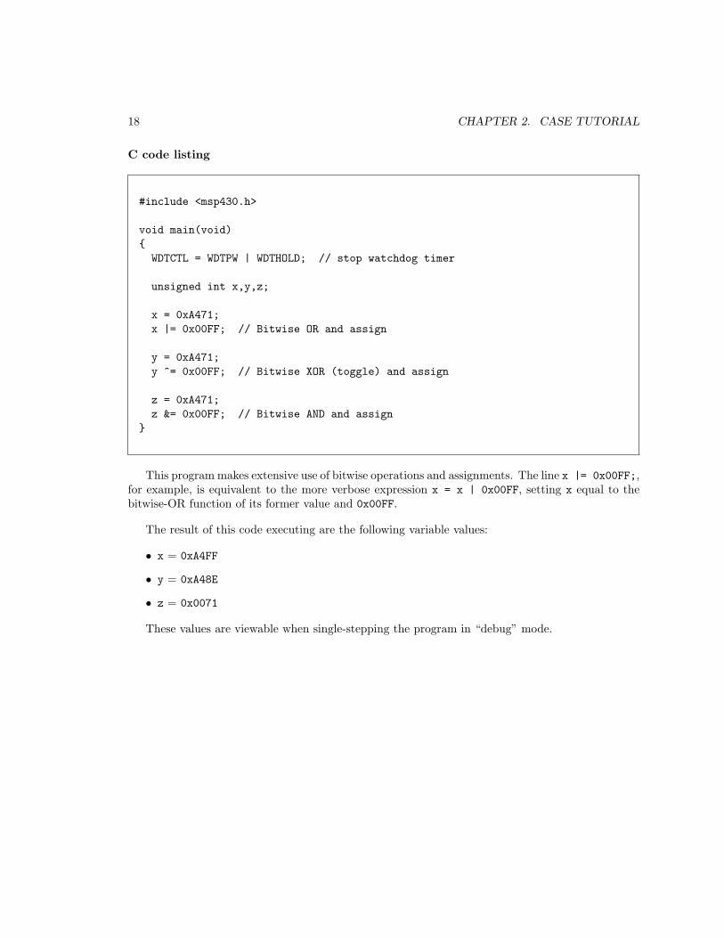
18 CHAPTER 2. CASE TUTORIAL
C code listing
#include <msp430.h>
void main(void)
WDTCTL = WDTPW | WDTHOLD; // stop watchdog timer
unsigned int x,y,z;
x = 0xA471;
x |= 0x00FF; // Bitwise OR and assign
y = 0xA471;
y ^= 0x00FF; // Bitwise XOR (toggle) and assign
z = 0xA471;
z &= 0x00FF; // Bitwise AND and assign
This program makes extensive use of bitwise operations and assignments. The line x |= 0x00FF;,for example, is equivalent to the more verbose expression x = x | 0x00FF, setting x equal to thebitwise-OR function of its former value and 0x00FF.
The result of this code executing are the following variable values:
• x = 0xA4FF
• y = 0xA48E
• z = 0x0071
These values are viewable when single-stepping the program in “debug” mode.

2.7. ASSEMBLY EXAMPLE: ROTATE RIGHT INSTRUCTION 19
2.7 Assembly example: rotate right instruction
Schematic diagram
MS
P430G
2553IN20
VSSVCC (+3.3 V)
P1.0
P1.1
P1.2
P1.3
P1.4
P1.5
P2.0
P2.1
P2.2
P2.6
P2.7
TEST
RST
P1.7
P1.6
P2.5
P2.4
P2.3
+3.3V
+3.3V
On the next page is a listing of the entire assembly-language code, tested and run on a modelMSP430G2553IN20 microcontroller using a LaunchPad model MSP-EXP430G2ET developmentboard and version 10 of Code Composer Studio (CCS). Only the code found between the “CodeBegin” and “Code End” comment lines are specific to this example program’s purpose, with therest being assembler directives and other instructions necessary for any simple assembly-languageprogram to run on this microcontroller.
All statements beginning with a dot (e.g. .text) are directives telling the assembler how toconvert the assembly source code into executable machine code for the microcontroller to run.Similarly, the RESET and StopWDT labels mark general set-up instructions for the microcontrollerand are not specifically related to the program’s main function.

20 CHAPTER 2. CASE TUTORIAL
Assembly code listing
.cdecls C,LIST,"msp430.h"
.def RESET
.text
.retain
.retainrefs
RESET mov.w #__STACK_END,SP
StopWDT mov.w #WDTPW|WDTHOLD,&WDTCTL
;============================ BEGIN CODE ===============================
SETUP
mov #0xAA77, R7
LOOP
rrc R7
jnz LOOP
;============================ END CODE ===============================
.global __STACK_END
.sect .stack
.sect ".reset"
.short RESET
The result of this code executing is the following values in register R7:
• 0xAA77
• 0x553B
• 0xAA9D
• 0xD54E
• 0x6AA7
• · · ·
These values are viewable when single-stepping the program in “debug” mode.
2.8. ASSEMBLY EXAMPLE: ALTERNATING LED BLINK 21
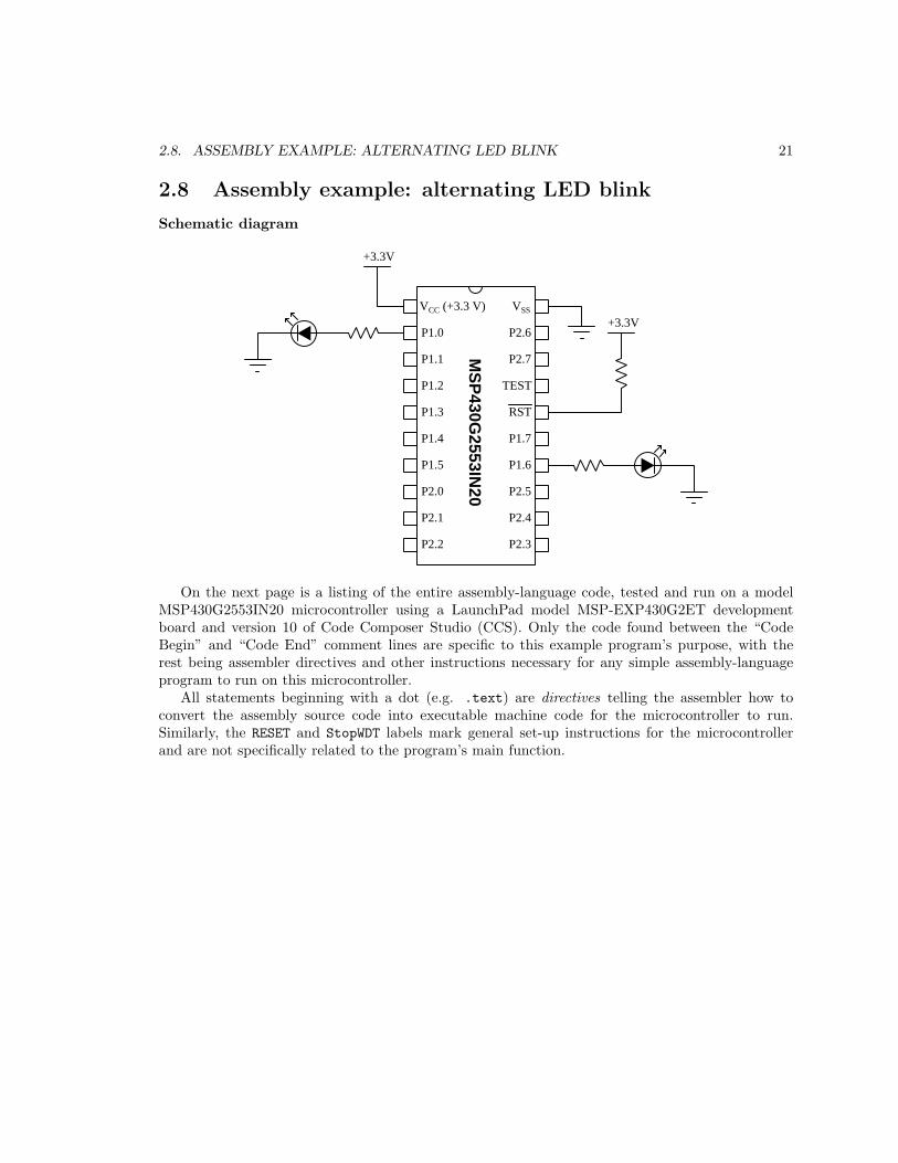
2.8 Assembly example: alternating LED blink
Schematic diagram
MS
P430G
2553IN20
VSSVCC (+3.3 V)
P1.0
P1.1
P1.2
P1.3
P1.4
P1.5
P2.0
P2.1
P2.2
P2.6
P2.7
TEST
RST
P1.7
P1.6
P2.5
P2.4
P2.3
+3.3V
+3.3V
On the next page is a listing of the entire assembly-language code, tested and run on a modelMSP430G2553IN20 microcontroller using a LaunchPad model MSP-EXP430G2ET developmentboard and version 10 of Code Composer Studio (CCS). Only the code found between the “CodeBegin” and “Code End” comment lines are specific to this example program’s purpose, with therest being assembler directives and other instructions necessary for any simple assembly-languageprogram to run on this microcontroller.
All statements beginning with a dot (e.g. .text) are directives telling the assembler how toconvert the assembly source code into executable machine code for the microcontroller to run.Similarly, the RESET and StopWDT labels mark general set-up instructions for the microcontrollerand are not specifically related to the program’s main function.

22 CHAPTER 2. CASE TUTORIAL
Assembly code listing
.cdecls C,LIST,"msp430.h" ; Include device header file
.def RESET ; Export program entry-point to
; make it known to linker.
.text ; Assemble into program memory.
.retain ; Override ELF conditional linking
; and retain current section.
.retainrefs ; Retain any sections that have
; references to current section.
RESET mov.w #__STACK_END,SP ; Initialize stackpointer
StopWDT mov.w #WDTPW|WDTHOLD,&WDTCTL ; Stop watchdog timer
;================================= Code Begin =================================
mov #0xFF, P1DIR ; Sets all Port 1 pin directions to output (1)
LOOP
mov #0x01, P1OUT ; Sets P1.0 high (Port 1 bit 0) and others low
call #DELAY
mov #0x40, P1OUT ; Sets P1.6 high (Port 1 bit 6) and others low
call #DELAY
jmp LOOP
DELAY
mov #0xFFFF, R4 ; Loads general register R4 with delay value
DELAYLOOP
sub #0x01, R4 ; Decrement R4 by one
jnz DELAYLOOP ; Repeat if result is not zero
ret
;================================== Code End ==================================
.global __STACK_END ; Stack pointer definition
.sect .stack
.sect ".reset" ; MSP430 RESET Vector
.short RESET
Note how the main loop of this program calls on the subroutine DELAY twice in order to providea time period following each change of LED status. It is important that a “pound” symbol precede

2.8. ASSEMBLY EXAMPLE: ALTERNATING LED BLINK 23
the name of the subroutine so that the assembler recognizes that as the literal (“immediate”) labelfor the subroutine, because other addressing modes are possible with the call instruction. The jmp
(“jump”) instruction needs no such modifier because it only operates on labels.

24 CHAPTER 2. CASE TUTORIAL
2.9 C example: alternating LED blink
Schematic diagram
MS
P430G
2553IN20
VSSVCC (+3.3 V)
P1.0
P1.1
P1.2
P1.3
P1.4
P1.5
P2.0
P2.1
P2.2
P2.6
P2.7
TEST
RST
P1.7
P1.6
P2.5
P2.4
P2.3
+3.3V
+3.3V
On the next page is a listing of the entire C-language code, tested and run on a modelMSP430G2553IN20 microcontroller using a LaunchPad model MSP-EXP430G2ET developmentboard and version 10 of Code Composer Studio (CCS).
The statement beginning with a pound symbol (#include <msp430.h>) is a directive telling thecompiler how to convert the C source code into object code and then executable machine code forthe microcontroller to run.

2.9. C EXAMPLE: ALTERNATING LED BLINK 25
C code listing
#include <msp430.h>
void delayloop(void);
void main(void)
WDTCTL = WDTPW | WDTHOLD; // stop watchdog timer
P1DIR |= 0xFF; // configure all Port 1 pins as outputs
while(1)
P1OUT = 0x01;
delayloop();
P1OUT = 0x40;
delayloop();
void delayloop()
unsigned int delay;
for(delay=0xFFFF; delay>0; --delay);
The line P1DIR |= 0xFF; is an example of a bitwise operation and assignment. It is equivalent tothe more verbose expression P1DIR = P1DIR | 0xFF, setting P1DIR equal to the bitwise-OR functionof its former value and 0xFF.
An interesting point to note about this program is that the compiler identified the delayloop()
function as an inefficient use of computational power and recommended the use of the MCU’s built-in timer capabilities. With standard optimization turned on (-O2) the compiler actually skippedthe for loop which left the program with no time delay at all! I had to disable all optimizationsin order to have the code compile and run as written. Interestingly, when run in debug mode andsingle-stepped, the program did exactly what it was supposed to do.
26 CHAPTER 2. CASE TUTORIAL
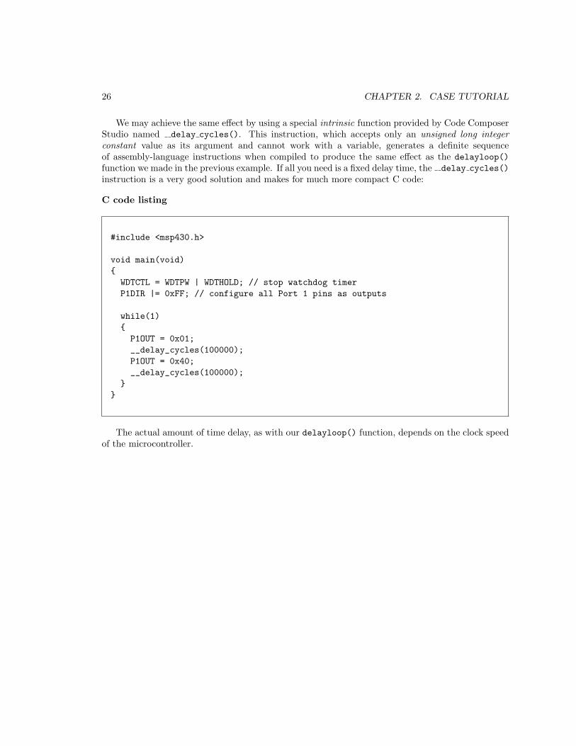
We may achieve the same effect by using a special intrinsic function provided by Code ComposerStudio named delay cycles(). This instruction, which accepts only an unsigned long integerconstant value as its argument and cannot work with a variable, generates a definite sequenceof assembly-language instructions when compiled to produce the same effect as the delayloop()
function we made in the previous example. If all you need is a fixed delay time, the delay cycles()
instruction is a very good solution and makes for much more compact C code:
C code listing
#include <msp430.h>
void main(void)
WDTCTL = WDTPW | WDTHOLD; // stop watchdog timer
P1DIR |= 0xFF; // configure all Port 1 pins as outputs
while(1)
P1OUT = 0x01;
__delay_cycles(100000);
P1OUT = 0x40;
__delay_cycles(100000);
The actual amount of time delay, as with our delayloop() function, depends on the clock speedof the microcontroller.

2.10. SKETCH EXAMPLE: ALTERNATING LED BLINK 27
2.10 Sketch example: alternating LED blink
Schematic diagram
MS
P430G
2553IN20
VSSVCC (+3.3 V)
P1.0
P1.1
P1.2
P1.3
P1.4
P1.5
P2.0
P2.1
P2.2
P2.6
P2.7
TEST
RST
P1.7
P1.6
P2.5
P2.4
P2.3
+3.3V
+3.3V
The popular Arduino microcontroller development platform has popularized a superset of the Cprogramming language called Sketch, and a development tool called Energia allows Sketch programsto be written for and loaded into the Texas Instruments MSP430 devices. On the next page is alisting of the Sketch code, tested and run on a model MSP430G2553IN20 microcontroller using aLaunchPad model MSP-EXP430G2ET development board, version 10 of Code Composer Studio(CCS), and version 1.8.10E23 of Energia.
28 CHAPTER 2. CASE TUTORIAL
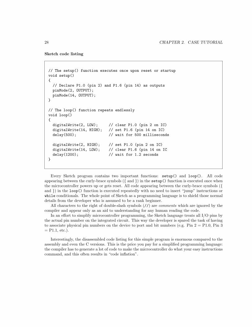
Sketch code listing
// The setup() function executes once upon reset or startup
void setup()
// Declare P1.0 (pin 2) and P1.6 (pin 14) as outputs
pinMode(2, OUTPUT);
pinMode(14, OUTPUT);
// The loop() function repeats endlessly
void loop()
digitalWrite(2, LOW); // clear P1.0 (pin 2 on IC)
digitalWrite(14, HIGH); // set P1.6 (pin 14 on IC)
delay(500); // wait for 500 milliseconds
digitalWrite(2, HIGH); // set P1.0 (pin 2 on IC)
digitalWrite(14, LOW); // clear P1.6 (pin 14 on IC
delay(1200); // wait for 1.2 seconds
Every Sketch program contains two important functions: setup() and loop(). All codeappearing between the curly-brace symbols ( and ) in the setup() function is executed once whenthe microcontroller powers up or gets reset. All code appearing between the curly-brace symbols (and ) in the loop() function is executed repeatedly with no need to insert “jump” instructions orwhile conditionals. The whole point of Sketch as a programming language is to shield those normaldetails from the developer who is assumed to be a rank beginner.
All characters to the right of double-slash symbols (//) are comments which are ignored by thecompiler and appear only as an aid to understanding for any human reading the code.
In an effort to simplify microcontroller programming, the Sketch language treats all I/O pins bythe actual pin number on the integrated circuit. This way the developer is spared the task of havingto associate physical pin numbers on the device to port and bit numbers (e.g. Pin 2 = P1.0, Pin 3= P1.1, etc.).
Interestingly, the disassembled code listing for this simple program is enormous compared to theassembly and even the C versions. This is the price you pay for a simplified programming language:the compiler has to generate a lot of code to make the microcontroller do what your easy instructionscommand, and this often results in “code inflation”.

2.11. ASSEMBLY EXAMPLE: BLINK ALL PORT 1 LINES 29
2.11 Assembly example: blink all Port 1 lines
Schematic diagram
MS
P430G
2553IN20
VSSVCC (+3.3 V)
P1.0
P1.1
P1.2
P1.3
P1.4
P1.5
P2.0
P2.1
P2.2
P2.6
P2.7
TEST
RST
P1.7
P1.6
P2.5
P2.4
P2.3
+3.3V
+3.3V
On the next page is a listing of the entire assembly-language code, tested and run on a modelMSP430G2553IN20 microcontroller using a LaunchPad model MSP-EXP430G2ET developmentboard and version 10 of Code Composer Studio (CCS). Only the code found between the “CodeBegin” and “Code End” comment lines are specific to this example program’s purpose, with therest being assembler directives and other instructions necessary for any simple assembly-languageprogram to run on this microcontroller.
All statements beginning with a dot (e.g. .text) are directives telling the assembler how toconvert the assembly source code into executable machine code for the microcontroller to run.Similarly, the RESET and StopWDT labels mark general set-up instructions for the microcontrollerand are not specifically related to the program’s main function.

30 CHAPTER 2. CASE TUTORIAL
Assembly code listing
.cdecls C,LIST,"msp430.h"
.def RESET
.text
.retain
.retainrefs
RESET mov.w #__STACK_END,SP
StopWDT mov.w #WDTPW|WDTHOLD,&WDTCTL
;================================= Code Begin =================================
mov #0xFF, P1DIR ; Set all Port 1 pin directions to output (1)
mov #0xFF, P1OUT ; Initialize Port 1 pin states to high (1)
LOOP
xor #0xFF, P1OUT ; toggle all bits in P1OUT using XOR function
mov #0xFFF, R4 ; Load general register R4 with delay value
DELAYLOOP
sub #0x01, R4 ; subtract 1 from register R4 . . .
jnz DELAYLOOP ; once we reach zero exit delay loop
jmp LOOP
;================================== Code End ==================================
.global __STACK_END
.sect .stack
.sect ".reset"
.short RESET
2.11. ASSEMBLY EXAMPLE: BLINK ALL PORT 1 LINES 31
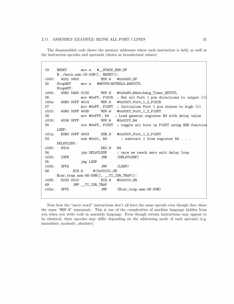
The disassembled code shows the memory addresses where each instruction is held, as well asthe instruction opcodes and operands (shown as hexadecimal values):
19 RESET mov.w #__STACK_END,SP
$../main.asm:19:42$(), RESET():
c000: 4031 0400 MOV.W #0x0400,SP
20 StopWDT mov.w #WDTPW|WDTHOLD,&WDTCTL
StopWDT:
c004: 40B2 5A80 0120 MOV.W #0x5a80,&Watchdog_Timer_WDTCTL
26 mov #0xFF, P1DIR ; Set all Port 1 pin directions to output (1)
c00a: 40B0 00FF 4014 MOV.W #0x00ff,Port_1_2_P1DIR
27 mov #0xFF, P1OUT ; Initialize Port 1 pin states to high (1)
c010: 40B0 00FF 400D MOV.W #0x00ff,Port_1_2_P1OUT
28 mov #0xFFF, R4 ; Load general register R4 with delay value
c016: 4034 0FFF MOV.W #0x0fff,R4
30 xor #0xFF, P1OUT ; toggle all bits in P1OUT using XOR function
LOOP:
c01a: E0B0 00FF 4003 XOR.W #0x00ff,Port_1_2_P1OUT
33 sub #0x01, R4 ; subtract 1 from register R4 . . .
DELAYLOOP:
c020: 8314 DEC.W R4
34 jnz DELAYLOOP ; once we reach zero exit delay loop
c022: 23FE JNE (DELAYLOOP)
35 jmp LOOP
c024: 3FFA JMP (LOOP)
48 BIS.W #(0x0010),SR
$isr_trap.asm:48:59$(), __TI_ISR_TRAP():
c026: D032 0010 BIS.W #0x0010,SR
49 JMP __TI_ISR_TRAP
c02a: 3FFD JMP ($isr_trap.asm:48:59$)
Note how the “move word” instructions don’t all have the same opcode even though they sharethe same “MOV.W” mnemonic. This is one of the complexities of machine language hidden fromyou when you write code in assembly language. Even though certain instructions may appear tobe identical, their opcodes may differ depending on the addressing mode of each operand (e.g.immediate, symbolic, absolute).

32 CHAPTER 2. CASE TUTORIAL
2.12 Assembly example: pushbutton control of LED
Schematic diagram
MS
P430G
2553IN20
VSSVCC (+3.3 V)
P1.0
P1.1
P1.2
P1.3
P1.4
P1.5
P2.0
P2.1
P2.2
P2.6
P2.7
TEST
RST
P1.7
P1.6
P2.5
P2.4
P2.3
+3.3V
+3.3V
+3.3V
On the next page is a listing of the entire assembly-language code, tested and run on a modelMSP430G2553IN20 microcontroller using a LaunchPad model MSP-EXP430G2ET developmentboard and version 10 of Code Composer Studio (CCS). Only the code found between the “CodeBegin” and “Code End” comment lines are specific to this example program’s purpose, with therest being assembler directives and other instructions necessary for any simple assembly-languageprogram to run on this microcontroller.
All statements beginning with a dot (e.g. .text) are directives telling the assembler how toconvert the assembly source code into executable machine code for the microcontroller to run.Similarly, the RESET and StopWDT labels mark general set-up instructions for the microcontrollerand are not specifically related to the program’s main function.

2.12. ASSEMBLY EXAMPLE: PUSHBUTTON CONTROL OF LED 33
Assembly code listing
.cdecls C,LIST,"msp430.h"
.def RESET
.text
.retain
.retainrefs
RESET mov.w #__STACK_END,SP
StopWDT mov.w #WDTPW|WDTHOLD,&WDTCTL
;============================ BEGIN CODE ===============================
SETUP
mov #0xF7, P1DIR ; P1.3 as input, all other Port 1 pins as outputs
bic #0xF7, P1OUT ; Begin with all outputs low
LOOP
bit #0x08, P1IN ; Checks if P1.3 (input) is high
jz OUT_LOW ; If not, make P1.0 low
OUT_HIGH
bis #0x01, P1OUT ; If so, set P1.0 bit
jmp LOOP
OUT_LOW
bic #0x01, P1OUT ; Clear P1.0 bit
jmp LOOP
;============================ END CODE ===============================
.global __STACK_END
.sect .stack
.sect ".reset"
.short RESET
The LED is energized when the pushbutton is unpressed (open), and de-energizes when you press(close) the pushbutton. Basically, the logical state of output P1.0 mirrors the logical state of inputP1.3.

34 CHAPTER 2. CASE TUTORIAL
2.13 C example: pushbutton control of LED
Schematic diagram
MS
P430G
2553IN20
VSSVCC (+3.3 V)
P1.0
P1.1
P1.2
P1.3
P1.4
P1.5
P2.0
P2.1
P2.2
P2.6
P2.7
TEST
RST
P1.7
P1.6
P2.5
P2.4
P2.3
+3.3V
+3.3V
+3.3V
On the next page is a listing of the entire C-language code, tested and run on a modelMSP430G2553IN20 microcontroller using a LaunchPad model MSP-EXP430G2ET developmentboard and version 10 of Code Composer Studio (CCS).
The statement beginning with a pound symbol (#include <msp430.h>) is a directive telling thecompiler how to convert the C source code into object code and then executable machine code forthe microcontroller to run.

2.13. C EXAMPLE: PUSHBUTTON CONTROL OF LED 35
C code listing
#include <msp430.h>
void main(void)
WDTCTL = WDTPW | WDTHOLD; // stop watchdog timer
P1DIR = 0b01000001; // P1.0 and P1.6 are outputs (1)
// All others are inputs (0)
while(1)
if (P1IN & 0b00001000) // Turn off P1.0 LED if P1.3 is high
P1OUT &= 0b11111110;
else
P1OUT |= 0b00000001; // Turn on P1.0 LED if P1.3 is low
The LED is de-energized when the pushbutton is unpressed (open) and P1.3 is high. The LEDenergizes when you press (close) the pushbutton and make P1.3 low. Basically, the logical state ofoutput P1.0 is the inverse of the logical state of input P1.3.

36 CHAPTER 2. CASE TUTORIAL
In this next version of the same program, we use hexadecimal values instead of binary valuesto specify bits in the P1DIR, P1IN, and P1OUT registers. Otherwise, this version of the program isfunctionally identical to the first:
C code listing
#include <msp430.h>
void main(void)
WDTCTL = WDTPW | WDTHOLD; // stop watchdog timer
P1DIR = 0x41; // P1.0 and P1.6 are outputs (1)
// All others are inputs (0)
while(1)
if (P1IN & 0x08) // Turn off P1.0 LED if P1.3 is high
P1OUT &= 0xFE;
else
P1OUT |= 0x01; // Turn on P1.0 LED if P1.3 is low

2.13. C EXAMPLE: PUSHBUTTON CONTROL OF LED 37
Finally, we will modify the bit-specifying values in this program once more to use pre-definedconstants in the msp430g2553.h header file2, where BIT0 is equivalent to 0b00000001, BIT1 isequivalent to 0b00000010, etc. Otherwise, this version of the program is functionally identical tothe first two:
C code listing
#include <msp430.h>
void main(void)
WDTCTL = WDTPW | WDTHOLD; // stop watchdog timer
P1DIR = BIT6 + BIT0; // P1.0 and P1.6 are outputs (1)
// All others are inputs (0)
while(1)
if (P1IN & BIT3) // Turn off P1.0 LED if P1.3 is high
P1OUT &= ~BIT0;
else
P1OUT |= BIT0; // Turn on P1.0 LED if P1.3 is low
It should be clear just how much more legible this C code is to the human reader. No longerdo you have to count bit-places to tell which Port 1 pin is being specified by a binary value, orconvert hexadecimal to binary and then do the same. Note also the clever use of the complement(~) operator where we write to P1OUT to turn off the LED: when we need a mask consisting ofall 1’s except for bit 0, we just invert the value of BIT0 (binary 0b00000001) so that it becomes0b11111110.
Of course, the decision to use binary, hexadecimal, bit-symbol, or even decimal values to specifybit positions is completely arbitrary and at the discretion of you, the programmer.
2You will note that this source code listing merely includes msp430.h rather than the specific header file for theMSP430G2553 model of microcontroller. This is okay, as the generic msp430.h header includes links to all the model-specific header files, which are resolved by the CCS compiler based on the specified “target” of the project. Some of theheader-specified constants differ from model to model of MSP430 microcontroller, hence the need for model-specificheader files. Having a single generic msp430.h header file that links to the others is another programming convenienceoffered to you by the developers of Code Composer Studio.

38 CHAPTER 2. CASE TUTORIAL
2.14 C example: start-stop control
Schematic diagram
MS
P430G
2553IN20
VSSVCC (+3.3 V)
P1.0
P1.1
P1.2
P1.3
P1.4
P1.5
P2.0
P2.1
P2.2
P2.6
P2.7
TEST
RST
P1.7
P1.6
P2.5
P2.4
P2.3
+3.3V
StopStart
(Using internal pullup resistorson input pins P1.3 and P1.4)
+3.3V
On the next page is a listing of the entire C-language code, tested and run on a modelMSP430G2553IN20 microcontroller using a LaunchPad model MSP-EXP430G2ET developmentboard and version 10 of Code Composer Studio (CCS).
The statement beginning with a pound symbol (#include <msp430.h>) is a directive telling thecompiler how to convert the C source code into object code and then executable machine code forthe microcontroller to run.

2.14. C EXAMPLE: START-STOP CONTROL 39
C code listing
#include <msp430.h>
void main(void)
WDTCTL = WDTPW | WDTHOLD; // stop watchdog timer
P2DIR = 0x01; // Pin P2.0 is an output (LED)
P2OUT = 0x00; // Ensure LED begins in the "off" state
P1DIR = 0x00; // All P1.x pins are inputs
P1REN = 0x18; // Enable pullup resistors for P1.4 and P1.3
P1OUT = 0x18; // Resistors are pullup, not pulldown
while(1)
if ((P1IN & BIT4) == 0) // Stop LED if switch P1.4 pressed
P2OUT &= ~BIT0;
else if ((P1IN & BIT3) == 0) // Start LED if switch P1.3 pressed
P2OUT |= BIT0;
Note the use of the symbolic constants BIT0, BIT3, and BIT4 to represent the hexadecimalvalues 0x01, 0x08, and 0x10, respectively. The “tilde” symbol (~) is the bitwise logical operator forinversion, which means while BIT0 represents 0b00000001, ~BIT0 must represent 0b11111110.
These symbolic constants, as well as many more, are all defined in the header file msp430.h forthe purpose of making the source code of your program easier to read. The microcontroller doesn’tcare whether you use BIT0 or 0b00000001 or 0x01, as the assembler replaces all those symbols withthe constant values they represent.
This form of program is useful for controlling the starting and stopping of a load such as an LEDor an electric motor. In fact, the only modification we would have to make to the circuit to control amotor is to have the microcontroller drive a transistor and/or relay to switch more voltage/currentto the motor than output P2.0 is capable of delivering on its own (see an example of this on thenext page).
A safety feature of this program is how the “stop” command is given precedence over the “start”command. This is why an else if conditional is used for the “start” instruction: if both “start” and“stop” buttons are pressed, the program will execute the “stop” condition and skip any evaluationof the “start” condition. This is also why the P2OUT register is cleared immediately after enablingpin P2.0 as an output: to ensure the LED (or motor) will not begin in an energized state by chance.

40 CHAPTER 2. CASE TUTORIAL
The following schematic shows how this same start-stop program could be used to controlan electric motor operating on a higher-voltage power supply, using both a transistor and anelectromechanical relay to “interpose” between the microcontroller and motor:
MS
P430G
2553IN20
VSSVCC (+3.3 V)
P1.0
P1.1
P1.2
P1.3
P1.4
P1.5
P2.0
P2.1
P2.2
P2.6
P2.7
TEST
RST
P1.7
P1.6
P2.5
P2.4
P2.3
+3.3V
StopStart
(Using internal pullup resistorson input pins P1.3 and P1.4)
+3.3V
+12 V
Motor
Both the +12 Volt and the +3.3 Volt DC supplies must share a common ground connection, sothat current from pin P2.0 driving the NPN transistor’s base terminal can find a path back to the+3.3 Volt source after exiting the transistor’s emitter terminal, but otherwise should be separatepower sources. The reason for this separation is to eliminate the potential problem of electrical“noise” generated by the motor interfering with the microcontroller (which requires very “clean”DC power). Note also the presence of “decoupling” capacitors across the microcontroller’s powerterminals and motor terminals, both helpful in mitigating3 electrical noise produced by the motor.
The commutating diode connected “backwards” in parallel with the relay’s coil provides a safedischarge path for any inductive “kickback” that may result when the transistor turns off andthe stored energy in the relay’s coil inductance acts to maintain current in the same direction asbefore when the transistor was on. This diode will be reverse-biased and non-conducting when thetransistor is turned on, but when the relay coil’s inductance generates a reverse voltage polaritywhen the transistor turns off this diode will forward-bias and conduct to provide that inductance anon-destructive pathway for its current. Without this commutating diode in place, we run the riskof destroying the transistor (and also the microcontroller!) when de-energizing an inductive load.
What was formerly a current-limiting resistor for the LED is now a current-limiting resistor forthe transistor’s base terminal. It must be of sufficient resistance to keep the driving current less
3Without this mitigation, it’s entirely possible that the electrical noise produced by the running motor will causethe microcontroller to “glitch” (i.e. reset).

2.14. C EXAMPLE: START-STOP CONTROL 41
than both the transistor’s base terminal current limit and the microcontroller’s output pin currentlimit (usually on the order of several milliAmperes – but check the datasheets to be sure!), but notso large in resistance that the transistor fails to fully turn on (saturate) for efficient operation.

42 CHAPTER 2. CASE TUTORIAL
2.15 Assembly example: pushing and popping the stack
Schematic diagram
MS
P430G
2553IN20
VSSVCC (+3.3 V)
P1.0
P1.1
P1.2
P1.3
P1.4
P1.5
P2.0
P2.1
P2.2
P2.6
P2.7
TEST
RST
P1.7
P1.6
P2.5
P2.4
P2.3
+3.3V
+3.3V
On the next page is a listing of the entire assembly-language code, tested and run on a modelMSP430G2553IN20 microcontroller using a LaunchPad model MSP-EXP430G2ET developmentboard and version 10 of Code Composer Studio (CCS). Only the code found between the “CodeBegin” and “Code End” comment lines are specific to this example program’s purpose, with therest being assembler directives and other instructions necessary for any simple assembly-languageprogram to run on this microcontroller.
All statements beginning with a dot (e.g. .text) are directives telling the assembler how toconvert the assembly source code into executable machine code for the microcontroller to run.Similarly, the RESET and StopWDT labels mark general set-up instructions for the microcontrollerand are not specifically related to the program’s main function.

2.15. ASSEMBLY EXAMPLE: PUSHING AND POPPING THE STACK 43
Assembly code listing
.cdecls C,LIST,"msp430.h"
.def RESET
.text
.retain
.retainrefs
RESET mov.w #__STACK_END,SP ; Initialize stackpointer
StopWDT mov.w #WDTPW|WDTHOLD,&WDTCTL ; Stop watchdog timer
;================================= Code Begin =================================
MAIN
mov #0x1234,R5
mov #0xABCD,R6
push R5
push R6
pop R5
pop R6
;================================== Code End ==================================
.global __STACK_END
.sect .stack
.sect ".reset"
.short RESET
When run, the result of this code executing is that registers R5 and R6 become populated withthe values 0x1234 and 0xABCD, respectively, then by using the two push and pop instructions thecontents of those two registers becomes swapped so that R5 now contains 0xABCD and R6 nowcontains 0x1234. This is due to the fact that the microcontroller’s stack acts as a last-in-first-out(LIFO) register. Pushing R5 and R6’s contents onto the stack and then popping back off the stackresults in the data coming off the stack in reverse order from how it was pushed on.

44 CHAPTER 2. CASE TUTORIAL
This next version does much the same, only with four registers rather than two:
Assembly code listing
.cdecls C,LIST,"msp430.h"
.def RESET
.text
.retain
.retainrefs
RESET mov.w #__STACK_END,SP ; Initialize stackpointer
StopWDT mov.w #WDTPW|WDTHOLD,&WDTCTL ; Stop watchdog timer
;================================= Code Begin =================================
MAIN
mov #0x1234,R4
mov #0x5678,R5
mov #0x9ABC,R6
mov #0xDEF0,R7
push R4
push R5
push R6
push R7
pop R4
pop R5
pop R6
pop R7
;================================== Code End ==================================
.global __STACK_END
.sect .stack
.sect ".reset"
.short RESET
The values written to R4, R5, R6, and R7 get sequentially pushed onto the stack, and then whenpopped off the stack the result is a reversal of order such that R4 now stores what R7 contained,R5 now stores with R6 contained, R6 now stores what R5 contained, and R7 now stores what R4contained.
Stack operations are particularly useful in assembly-language programming to temporarily storethe contents of special registers such as the microcontroller’s status register (SR) which is used andre-used by many different types of instructions. Between executing one status-altering instructionand another, a push SR instruction may be used to save the first status for later use, retrieved byusing pop SR later on in the program.
2.16. ASSEMBLY EXAMPLE: DRIVING PORT 2 LINES WITH TIMER 45
2.16 Assembly example: driving Port 2 lines with Timer
Schematic diagram
MS
P430G
2553IN20
VSSVCC (+3.3 V)
P1.0
P1.1
P1.2
P1.3
P1.4
P1.5
P2.0
P2.1
P2.2
P2.6
P2.7
TEST
RST
P1.7
P1.6
P2.5
P2.4
P2.3
+3.3V
+3.3V
On the next page is a listing of the entire assembly-language code, tested and run on a modelMSP430G2553IN20 microcontroller using a LaunchPad model MSP-EXP430G2ET developmentboard and version 10 of Code Composer Studio (CCS). Only the code found between the “CodeBegin” and “Code End” comment lines are specific to this example program’s purpose, with therest being assembler directives and other instructions necessary for any simple assembly-languageprogram to run on this microcontroller.
All statements beginning with a dot (e.g. .text) are directives telling the assembler how toconvert the assembly source code into executable machine code for the microcontroller to run.Similarly, the RESET and StopWDT labels mark general set-up instructions for the microcontrollerand are not specifically related to the program’s main function.
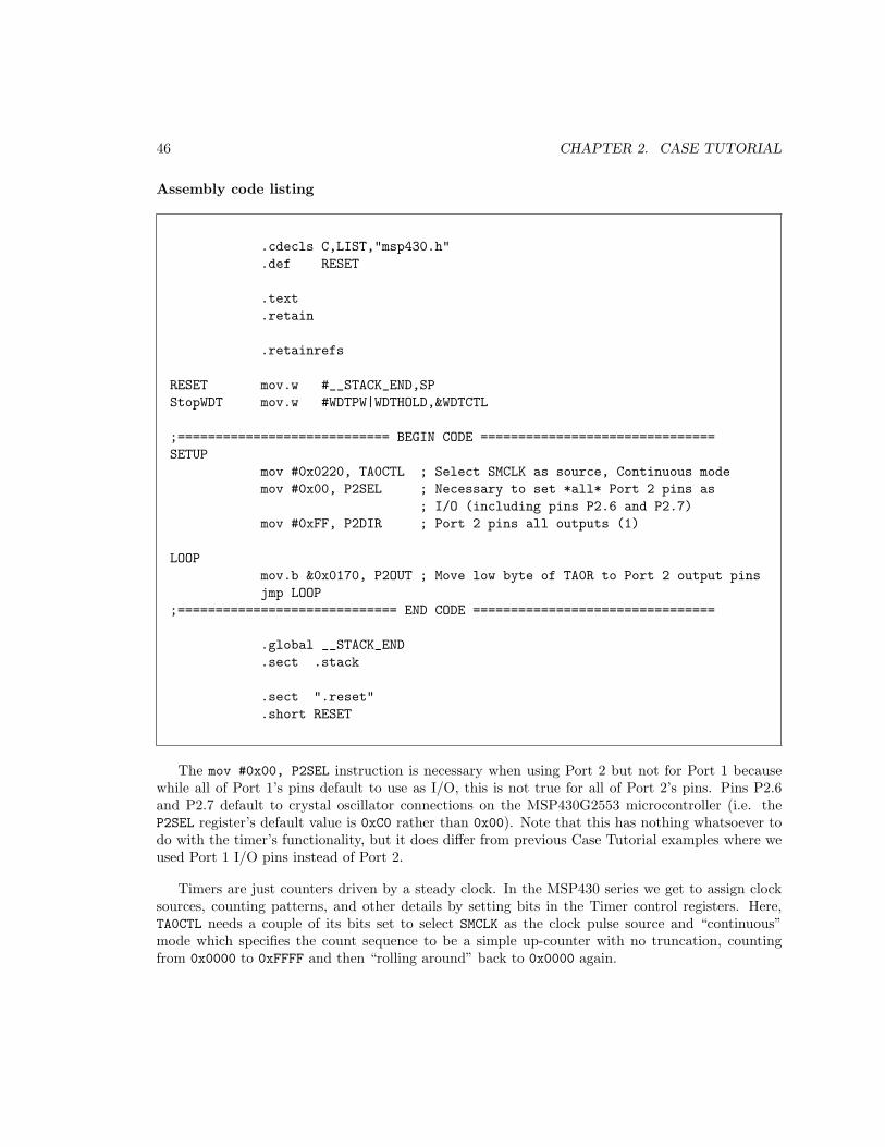
46 CHAPTER 2. CASE TUTORIAL
Assembly code listing
.cdecls C,LIST,"msp430.h"
.def RESET
.text
.retain
.retainrefs
RESET mov.w #__STACK_END,SP
StopWDT mov.w #WDTPW|WDTHOLD,&WDTCTL
;============================ BEGIN CODE ===============================
SETUP
mov #0x0220, TA0CTL ; Select SMCLK as source, Continuous mode
mov #0x00, P2SEL ; Necessary to set *all* Port 2 pins as
; I/O (including pins P2.6 and P2.7)
mov #0xFF, P2DIR ; Port 2 pins all outputs (1)
LOOP
mov.b &0x0170, P2OUT ; Move low byte of TA0R to Port 2 output pins
jmp LOOP
;============================= END CODE ================================
.global __STACK_END
.sect .stack
.sect ".reset"
.short RESET
The mov #0x00, P2SEL instruction is necessary when using Port 2 but not for Port 1 becausewhile all of Port 1’s pins default to use as I/O, this is not true for all of Port 2’s pins. Pins P2.6and P2.7 default to crystal oscillator connections on the MSP430G2553 microcontroller (i.e. theP2SEL register’s default value is 0xC0 rather than 0x00). Note that this has nothing whatsoever todo with the timer’s functionality, but it does differ from previous Case Tutorial examples where weused Port 1 I/O pins instead of Port 2.
Timers are just counters driven by a steady clock. In the MSP430 series we get to assign clocksources, counting patterns, and other details by setting bits in the Timer control registers. Here,TA0CTL needs a couple of its bits set to select SMCLK as the clock pulse source and “continuous”mode which specifies the count sequence to be a simple up-counter with no truncation, countingfrom 0x0000 to 0xFFFF and then “rolling around” back to 0x0000 again.
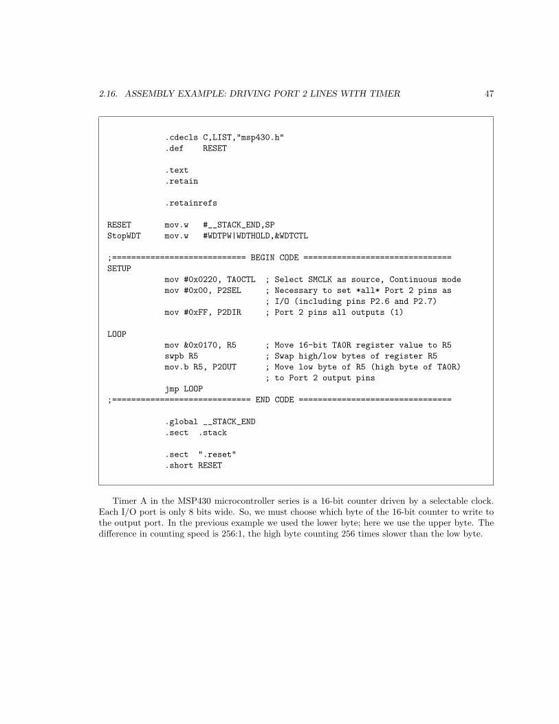
2.16. ASSEMBLY EXAMPLE: DRIVING PORT 2 LINES WITH TIMER 47
.cdecls C,LIST,"msp430.h"
.def RESET
.text
.retain
.retainrefs
RESET mov.w #__STACK_END,SP
StopWDT mov.w #WDTPW|WDTHOLD,&WDTCTL
;============================ BEGIN CODE ===============================
SETUP
mov #0x0220, TA0CTL ; Select SMCLK as source, Continuous mode
mov #0x00, P2SEL ; Necessary to set *all* Port 2 pins as
; I/O (including pins P2.6 and P2.7)
mov #0xFF, P2DIR ; Port 2 pins all outputs (1)
LOOP
mov &0x0170, R5 ; Move 16-bit TA0R register value to R5
swpb R5 ; Swap high/low bytes of register R5
mov.b R5, P2OUT ; Move low byte of R5 (high byte of TA0R)
; to Port 2 output pins
jmp LOOP
;============================= END CODE ================================
.global __STACK_END
.sect .stack
.sect ".reset"
.short RESET
Timer A in the MSP430 microcontroller series is a 16-bit counter driven by a selectable clock.Each I/O port is only 8 bits wide. So, we must choose which byte of the 16-bit counter to write tothe output port. In the previous example we used the lower byte; here we use the upper byte. Thedifference in counting speed is 256:1, the high byte counting 256 times slower than the low byte.
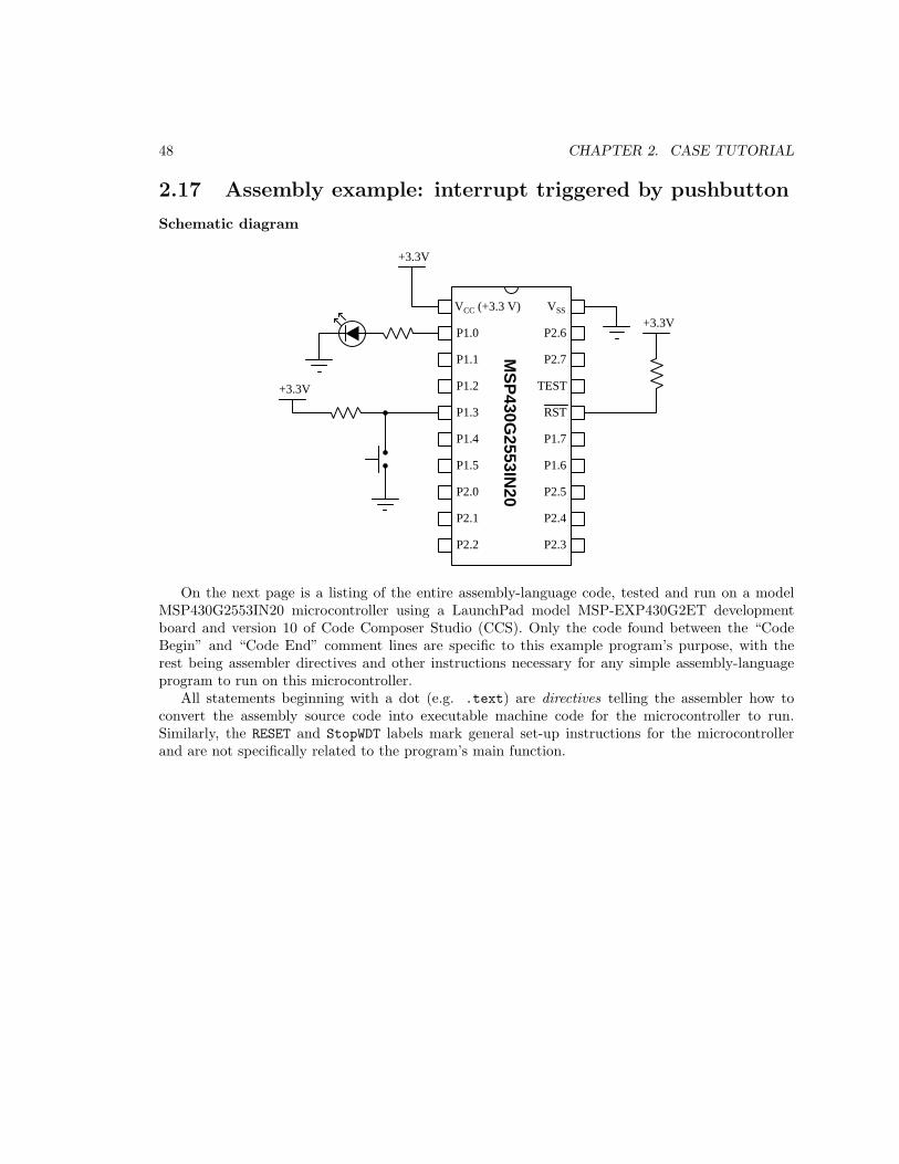
48 CHAPTER 2. CASE TUTORIAL
2.17 Assembly example: interrupt triggered by pushbutton
Schematic diagram
MS
P430G
2553IN20
VSSVCC (+3.3 V)
P1.0
P1.1
P1.2
P1.3
P1.4
P1.5
P2.0
P2.1
P2.2
P2.6
P2.7
TEST
RST
P1.7
P1.6
P2.5
P2.4
P2.3
+3.3V
+3.3V
+3.3V
On the next page is a listing of the entire assembly-language code, tested and run on a modelMSP430G2553IN20 microcontroller using a LaunchPad model MSP-EXP430G2ET developmentboard and version 10 of Code Composer Studio (CCS). Only the code found between the “CodeBegin” and “Code End” comment lines are specific to this example program’s purpose, with therest being assembler directives and other instructions necessary for any simple assembly-languageprogram to run on this microcontroller.
All statements beginning with a dot (e.g. .text) are directives telling the assembler how toconvert the assembly source code into executable machine code for the microcontroller to run.Similarly, the RESET and StopWDT labels mark general set-up instructions for the microcontrollerand are not specifically related to the program’s main function.

2.17. ASSEMBLY EXAMPLE: INTERRUPT TRIGGERED BY PUSHBUTTON 49
Assembly code listing
.cdecls C,LIST,"msp430.h"
.def RESET
.text
.retain
.retainrefs
RESET mov.w #__STACK_END,SP
StopWDT mov.w #WDTPW|WDTHOLD,&WDTCTL
;============================ BEGIN CODE ===============================
SETUP
mov #0xF7, P1DIR ; P1.3 as input, all others outputs
mov #0x08, P1OUT ; Begin with all outputs low
mov #0x08, P1IE ; Enable interrupt on P1.3
bis #0x08, P1IES ; Interrupt on high-to-low transition
bic #0x08, P1IFG ; Clear any pending P1.3 interrupt flag
bis #0x08, SR ; Set the General Interrupt Enable (GIE) bit
LOOP ; A useless loop -- does absolutely nothing!
jmp LOOP
P1_ISR
xor #0x01, P1OUT ; Toggle P1.0 bit
bic #0x08, P1IFG ; Clear the P1.3 interrupt flag
reti ; Return from ISR
;============================ END CODE ===============================
.global __STACK_END
.sect .stack
.sect ".reset"
.short RESET
.sect ".int02" ; .int02 = Port 1 interrupt vector section
; (shared by all P1.x pins)
.short P1_ISR ;
The LED toggles (i.e. switches states) whenever the pushbutton is pressed, because pressing thepushbutton generates a falling-edge pulse (high-to-low logical transition) which triggers the interruptand causes the processor to jump out of its useless loop to the interrupt service routine (ISR) wherethe XOR logical bitwise function executes.
An alternative to using .sect ".int02" followed by .short P1 ISR is to use the single interruptdirective .intvec ".int02", P1 ISR.

50 CHAPTER 2. CASE TUTORIAL
The following is a “disassembly” view of the MCU’s memory for this program, showing theprogram code as well as the interrupt vectors:
$../main.asm:7:29$(), RESET():
c000: 4031 0400 MOV.W #0x0400,SP
StopWDT:
c004: 40B2 5A80 0120 MOV.W #0x5a80,&Watchdog_Timer_WDTCTL
SETUP:
c00a: 40B0 00F7 4014 MOV.W #0x00f7,Port_1_2_P1DIR
c010: 42B0 400F MOV.W #8,Port_1_2_P1OUT
c014: 42B0 400F MOV.W #8,Port_1_2_P1IE
c018: D2B0 400A BIS.W #8,Port_1_2_P1IES
c01c: C2B0 4005 BIC.W #8,Port_1_2_P1IFG
c020: D232 EINT
LOOP:
c022: 3FFF JMP (LOOP)
P1_ISR:
c024: E390 3FFB XOR.W #1,Port_1_2_P1OUT
c028: C2B0 3FF9 BIC.W #8,Port_1_2_P1IFG
c02c: 1300 RETI
$isr_trap.asm:48:59$(), __TI_ISR_TRAP():
c02e: D032 0010 BIS.W #0x0010,SR
c032: 3FFD JMP ($isr_trap.asm:48:59$)
c034: 4303 NOP
*
ffda: FFFF FFFF AND.B @R15+,0xffff(R15)
ffde: FFFF C02E AND.B @R15+,0xc02e(R15)
ffe2: FFFF C024 AND.B @R15+,0xc024(R15)
ffe6: C02E BIC.W @PC,R14
ffe8: FFFF C02E AND.B @R15+,0xc02e(R15)
ffec: C02E BIC.W @PC,R14
ffee: C02E BIC.W @PC,R14
fff0: C02E BIC.W @PC,R14
fff2: C02E BIC.W @PC,R14
fff4: C02E BIC.W @PC,R14
fff6: C02E BIC.W @PC,R14
fff8: C02E BIC.W @PC,R14
fffa: C02E BIC.W @PC,R14
fffc: C02E BIC.W @PC,R14
fffe: C000 BIC.W PC,PC
Note: the AND.B and BIC.W instructions shown at the end are meaningless. Disassembly is aprocess by which all memory content is interpreted as instructions. However, from 0xffda to 0xfffe
there is no program code, only interrupt vectors (i.e. memory addresses to “jump” to in the eventof a detected interrupt). The address 0xC024 is for the P1 ISR routine and the address 0xC02E
is for the RESET routine. The disassembler mistakenly interpreted all 0xFFFF content as AND.B
instructions and all reset vectors as BIC.W instructions.

2.17. ASSEMBLY EXAMPLE: INTERRUPT TRIGGERED BY PUSHBUTTON 51
This is a memory map showing the same in unannotated “hex dump” format:
0xC000 31 40 00 04 B2 40 80 5A 20 01 B0 40 F7 00 14 40
0xC010 B0 42 0F 40 B0 42 0F 40 B0 D2 0A 40 B0 C2 05 40
0xC020 32 D2 FF 3F 90 E3 FB 3F B0 C2 F9 3F 00 13 32 D0
0xC030 10 00 FD 3F 03 43 FF FF FF FF FF FF FF FF FF FF
*
0xFFE0 2E C0 FF FF 24 C0 2E C0 FF FF 2E C0 2E C0 2E C0
0xFFF0 2E C0 2E C0 2E C0 2E C0 2E C0 2E C0 2E
Note how all specified addresses are stored in little-endian format (e.g. the interrupt vector0xC02E stored at 0xFFE0 actual shows as being 2E C0). The interrupt vector for the pushbuttonservice routine (P1 ISR, vector 0xC024) is seen starting at address 0xFFE4, as 24 C0.

52 CHAPTER 2. CASE TUTORIAL
2.18 C example: interrupt triggered by pushbutton
Schematic diagram
MS
P430G
2553IN20
VSSVCC (+3.3 V)
P1.0
P1.1
P1.2
P1.3
P1.4
P1.5
P2.0
P2.1
P2.2
P2.6
P2.7
TEST
RST
P1.7
P1.6
P2.5
P2.4
P2.3
+3.3V
+3.3V
+3.3V
On the next page is a listing of the entire C-language code, tested and run on a modelMSP430G2553IN20 microcontroller using a LaunchPad model MSP-EXP430G2ET developmentboard and version 10 of Code Composer Studio (CCS).
The statement beginning with a pound symbol (#include <msp430.h>) is a directive telling thecompiler how to convert the C source code into object code and then executable machine code forthis specific model of microcontroller to run.

2.18. C EXAMPLE: INTERRUPT TRIGGERED BY PUSHBUTTON 53
C code listing
#include "msp430.h"
void main(void)
WDTCTL = WDTPW + WDTHOLD; // Disable the Watchdog Timer
/* Configure Port 1 pins for LEDs and pushbutton */
P1DIR = 0x41; // Set P1.0 and P1.6 as outputs, all other pins inputs
P1IE = 0x08; // Enable P1.3 interrupt
P1IES = 0x08; // P1.3 interrupt on falling edge (high-to-low)
P1IFG = 0x00; // Clear all Port 1 interrupt flags
__bis_SR_register(GIE); // General Interrupts Enabled
while(1) // Useless while() loop
#pragma vector=PORT1_VECTOR
__interrupt void Timer_ISR (void)
P1OUT ^= 0x01; // Toggles output P1.0
P1IFG = 0x00; // Clears all Port 1 interrupt flag bits
The LED toggles (i.e. switches states) whenever the pushbutton is pressed, because pressing thepushbutton generates a falling-edge pulse (high-to-low logical transition) which triggers the interruptand causes the processor to jump out of its useless loop to the interrupt service routine (ISR) wherethe XOR logical bitwise function executes.

54 CHAPTER 2. CASE TUTORIAL
2.19 Assembly example: LED blink with watchdog
Schematic diagram
MS
P430G
2553IN20
VSSVCC (+3.3 V)
P1.0
P1.1
P1.2
P1.3
P1.4
P1.5
P2.0
P2.1
P2.2
P2.6
P2.7
TEST
RST
P1.7
P1.6
P2.5
P2.4
P2.3
+3.3V
+3.3V
On the next page is a listing of the entire assembly-language code, tested and run on a modelMSP430G2553IN20 microcontroller using a LaunchPad model MSP-EXP430G2ET developmentboard and version 10 of Code Composer Studio (CCS). Only the code found between the “CodeBegin” and “Code End” comment lines are specific to this example program’s purpose, with therest being assembler directives and other instructions necessary for any simple assembly-languageprogram to run on this microcontroller.
All statements beginning with a dot (e.g. .text) are directives telling the assembler how toconvert the assembly source code into executable machine code for the microcontroller to run.Similarly, the RESET and StopWDT labels mark general set-up instructions for the microcontrollerand are not specifically related to the program’s main function.

2.19. ASSEMBLY EXAMPLE: LED BLINK WITH WATCHDOG 55
Assembly code listing
.cdecls C,LIST,"msp430.h"
.def RESET
.text
.retain
.retainrefs
RESET mov.w #__STACK_END,SP ; Initialize stackpointer
;================================= Code Begin =================================
mov #0xFF, P1DIR ; Sets all Port 1 pin directions to output (1)
LOOP
mov #0x01, P1OUT ; Sets P1.0 high (Port 1 bit 0) and others low
call #DELAY
mov #0x40, P1OUT ; Sets P1.6 high (Port 1 bit 6) and others low
call #DELAY
jmp LOOP
DELAY
mov #0xFFFF, R4 ; Loads general register R4 with delay value
DELAYLOOP
sub #0x01, R4 ; Decrement R4 by one
mov.w #WDTPW | WDTCNTCL, &WDTCTL ; Clear watchdog timer
jnz DELAYLOOP ; Repeat if result is not zero
ret
;================================== Code End ==================================
.global __STACK_END ; Stack pointer definition
.sect .stack
.sect ".reset" ; MSP430 RESET Vector
.short RESET
Rather than “hold” the watchdog timer near the start of the program as is customary for somany other example programs, here we include a mov instruction within the time delay loop thatsets the WDTCNTCL bit to clear the watchdog timer’s 16-bit counter to zero with every pass throughthe loop. This way, if anything were to (somehow) halt the normal execution of our program, thewatchdog timer would restart the microcontroller and the program would begin afresh.

56 CHAPTER 2. CASE TUTORIAL
If we modify the location of this watchdog-clear instruction to be outside of the time delay loop,we find that it fails:
Assembly code listing
.cdecls C,LIST,"msp430.h"
.def RESET
.text
.retain
.retainrefs
RESET mov.w #__STACK_END,SP ; Initialize stackpointer
;================================= Code Begin =================================
mov #0xFF, P1DIR ; Sets all Port 1 pin directions to output (1)
LOOP
mov #0x01, P1OUT ; Sets P1.0 high (Port 1 bit 0) and others low
call #DELAY
mov #0x40, P1OUT ; Sets P1.6 high (Port 1 bit 6) and others low
call #DELAY
jmp LOOP
DELAY
mov #0xFFFF, R4 ; Loads general register R4 with delay value
mov.w #WDTPW | WDTCNTCL, &WDTCTL ; Clear watchdog timer
DELAYLOOP
sub #0x01, R4 ; Decrement R4 by one
jnz DELAYLOOP ; Repeat if result is not zero
ret
;================================== Code End ==================================
.global __STACK_END ; Stack pointer definition
.sect .stack
.sect ".reset" ; MSP430 RESET Vector
.short RESET
The reason this program fails is because DELAYLOOP takes too long to go through its 0xFFFF-to-0x0000 counting cycle, and the watchdog timer “times out” before the watchdog-clear instructiongets executed. The result is the P1.0 LED remains energized all the time because that output bitgets set with the first instruction following LOOP, then the watchdog timer resets the microcontrollerbefore the DELAY routine completes, causing the program to start again from the top.
A good experiment would be to alter the numerical value moved into register R4 until a number

2.19. ASSEMBLY EXAMPLE: LED BLINK WITH WATCHDOG 57
is found that results in a short enough DELAYLOOP cycle time to permit the watchdog timer to becleared at a reasonable interval.

58 CHAPTER 2. CASE TUTORIAL
2.20 C example: pushbutton-triggered timer
Schematic diagram
MS
P430G
2553IN20
VSSVCC (+3.3 V)
P1.0
P1.1
P1.2
P1.3
P1.4
P1.5
P2.0
P2.1
P2.2
P2.6
P2.7
TEST
RST
P1.7
P1.6
P2.5
P2.4
P2.3
+3.3V
+3.3V
+3.3V
On the next page is a listing of the entire C-language code, tested and run on a modelMSP430G2553IN20 microcontroller using a LaunchPad model MSP-EXP430G2ET developmentboard and version 10 of Code Composer Studio (CCS).
The statement beginning with a pound symbol (#include <msp430.h>) is a directive telling thecompiler how to convert the C source code into object code and then executable machine code forthis specific model of microcontroller to run.
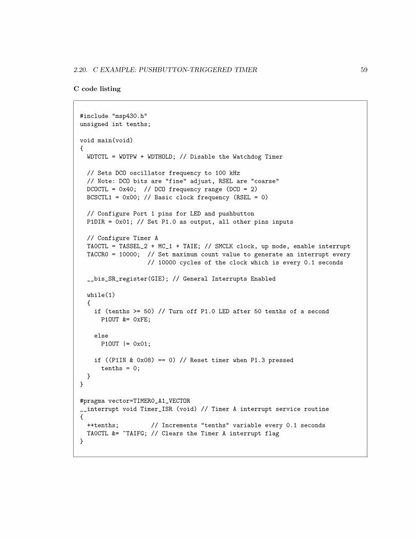
2.20. C EXAMPLE: PUSHBUTTON-TRIGGERED TIMER 59
C code listing
#include "msp430.h"
unsigned int tenths;
void main(void)
WDTCTL = WDTPW + WDTHOLD; // Disable the Watchdog Timer
// Sets DCO oscillator frequency to 100 kHz
// Note: DCO bits are "fine" adjust, RSEL are "coarse"
DCOCTL = 0x40; // DCO frequency range (DCO = 2)
BCSCTL1 = 0x00; // Basic clock frequency (RSEL = 0)
// Configure Port 1 pins for LED and pushbutton
P1DIR = 0x01; // Set P1.0 as output, all other pins inputs
// Configure Timer A
TA0CTL = TASSEL_2 + MC_1 + TAIE; // SMCLK clock, up mode, enable interrupt
TACCR0 = 10000; // Set maximum count value to generate an interrupt every
// 10000 cycles of the clock which is every 0.1 seconds
__bis_SR_register(GIE); // General Interrupts Enabled
while(1)
if (tenths >= 50) // Turn off P1.0 LED after 50 tenths of a second
P1OUT &= 0xFE;
else
P1OUT |= 0x01;
if ((P1IN & 0x08) == 0) // Reset timer when P1.3 pressed
tenths = 0;
#pragma vector=TIMER0_A1_VECTOR
__interrupt void Timer_ISR (void) // Timer A interrupt service routine
++tenths; // Increments "tenths" variable every 0.1 seconds
TA0CTL &= ~TAIFG; // Clears the Timer A interrupt flag

60 CHAPTER 2. CASE TUTORIAL
The digitally-controlled oscillator (DCO) for the microcontroller is set to a frequency of 100kHz4, and the timer is configured for “up” counting mode where it counts from zero to whatevervalue is stored in register TACCR0 and then resets. With TACCR0 = 10000 and a clock frequency of100000 Hz this means the timer will reset itself ten times per second5, or once every 0.1 seconds. Atevery reset the timer generates an interrupt, and inside the interrupt service routine we incrementan integer variable named tenths as well as clear the interrup flag before returning execution tothe main code’s while() loop. Thus, the variable tenths increments once every tenth of a second,making it a convenient variable to use for time delays with a resolution of 0.1 seconds.
Code inside the while() loop writes to and reads from this tenths variable, turning the P1.0
LED either on or off based on the value stored in tenths. In this program example, tenths isallowed to increment whenever pushbutton P1.3 is released, but clamped to a value of zero whenthe pushbutton is pressed. If tenths is less than 50, the LED turns on. Therefore, pressing thepushbutton guarantees the LED will energize. When released, tenths is allowed to increment, andwhen it reaches a count value of 50 the LED turns off. Thus, we have created a classic off-delaytiming function that immediately energizes the output when the switch is actuated but delays turningoff until 5 seconds after the switch returns to its resting (“normal”) state:
P1.3Pressed
Released
P1.0LED on
LED off
delay
4This is not a precision clock source, and so with the DCOCTL and BCSCTL1 parameters shown in the example codeyour actual clock frequency may vary slightly from the expected value of 100 kHz. Altering the DCOCTL register’s valueallows you to “fine-tune” the oscillator to achieve close to 100 kHz. There are seven settings for the DCO frequencyrange, set by the most-significant three bits of the DCOCTL register.
5If adjusting the DCOCTL and/or BCSCTL1 register values still doesn’t get the clock frequency close enough to 100kHz for your purposes, you may also skew the value stored in register TACCR0 until the interrupt period is close enoughto 10 times per second. For example, let’s say that despite your best efforts to get the DCO clock to be exactly 100kHz, it ends up being just a little bit faster than 100 kHz. To compensate for this, you could increase the value ofTACCR0 beyond 10000 so that additional clock cycles were necessary between interrupts, which will have the effect ofslowing down the increment of tenths. Given that 10000 is a fairly large number, this gives you very fine-resolutionadjustability for the interrupt timing.

2.20. C EXAMPLE: PUSHBUTTON-TRIGGERED TIMER 61
Obtaining other forms of timing function only requires edits to code inside the while() loop.No changes need to be made to the timer setup or the interrupt service routine, as they still workto generate an incrementing tenths variable every tenth of a second. For example, here is a codesnippet for a classic on-delay timing function with a delay time of 5 seconds:
while(1)
if (tenths >= 50) // Turn on P1.0 LED after 50 tenths of a second
P1OUT |= 0x01;
else
P1OUT &= 0xFE;
if ((P1IN & 0x08) == 0x08) // Reset timer when P1.3 released
tenths = 0;
P1.3Pressed
Released
P1.0LED on
LED off
delay
For applications where the tenths variable would be free to increment for long periods of time,we must contend with a problem posed by our original code, namely what happens when tenths
reaches its maximum 16-bit value of 65535? Any unsigned integer that reaches its maximum positivevalue and is incremented one more time will “recycle” back to zero. If our timing function is based ontenths being greater than some limit, this will mean that condition will reset when tenths recyclesback to zero again.
A fix for this problem is to limit how high tenths is allowed to count, and to do so within theinterrupt service routine where we may block its incrementing before counting too far. We just needone more line of code in the interrupt service routine, taking the form of an if() statement:
#pragma vector=TIMER0_A1_VECTOR
__interrupt void Timer_ISR (void) // Timer A interrupt service routine
if (tenths < 0xFFFF)
++tenths; // Increments if less than maximum positive value
TA0CTL &= ~TAIFG; // Clears the Timer A interrupt flag

62 CHAPTER 2. CASE TUTORIAL
2.21 C example: Boolean SOP expression
Schematic diagram
MS
P430G
2553IN20
VSSVCC (+3.3 V)
P1.0
P1.1
P1.2
P1.3
P1.4
P1.5
P2.0
P2.1
P2.2
P2.6
P2.7
TEST
RST
P1.7
P1.6
P2.5
P2.4
P2.3
+3.3V
+3.3V
C B A
Out
Out = CBA + CBA + CBA
Boolean expression implemented by MCU
+3.3V
On the next page is a listing of the entire C-language code, tested and run on a modelMSP430G2553IN20 microcontroller using a LaunchPad model MSP-EXP430G2ET developmentboard and version 10 of Code Composer Studio (CCS).
The statement beginning with a pound symbol (#include <msp430.h>) is a directive telling thecompiler how to convert the C source code into object code and then executable machine code forthe microcontroller to run.

2.21. C EXAMPLE: BOOLEAN SOP EXPRESSION 63
C code listing
#include <msp430.h>
void main(void)
WDTCTL = WDTPW | WDTHOLD; // stop watchdog timer
P1DIR = 0x01; // P1.0 as output, P1.1-1.7 as inputs
while (1)
if ((P1IN & 0x0E) == 0x0A) // Evaluates CB’A term
P1OUT |= 0x01; // Bitwise OR/assign sets (only) P1.0
else if ((P1IN & 0x0E) == 0x02) // Evaluates C’B’A term
P1OUT |= 0x01; // Bitwise OR/assign sets (only) P1.0
else if ((P1IN & 0x0E) == 0x0E) // Evaluates CBA term
P1OUT |= 0x01; // Bitwise OR/assign sets (only) P1.0
else
P1OUT &= 0xFE; // Bitwise AND/assign clears (only) P1.0
All characters to the right of double-slash symbols (//) are comments which are ignored by thecompiler and appear only as an aid to understanding for any human reading the code.
This would be a simpler program if we weren’t mixing inputs and output functions on the sameI/O port, but it is a good example to show how you can manage those different functions usingbitwise logical operators. Pin P1.0 is an output, and all other pins on Port 1 are inputs. We areusing three of the input pins (P1.1, P1.2, and P1.3) as inputs for our Boolean Sum-Of-Products(SOP) expression.
The first problem this program solves is how to evaluate those three inputs’ states while ignoringthe states of the other Port 1 pins. Since the if statements read all eight bits of Port 1 whenevaluating bit states, we need some way of “masking off” the pins that aren’t the three inputs forour SOP expression. In other words, our conditional statements must ignore the status of P1.0 (thebit outputting signal to our LED) as well as P1.4, P1.5, P1.6, and P1.7 which are not connected toany switches and therefore might have random high/low values at any given time6. Since our inputpins represent bits 3, 2, and 1 of the Port 1 word (P1IN), we may use the mask 0x0E (binary value
6If the nature of this problem isn’t clear, consider if we tried to test for one of the “true” conditions of our Booleanexpression by assuming all other bits were low (0). The statement if (P1IN == 0x0E) would be “true” if our threebuttons were all unpressed and all the other bits of Port 1 happened to be low. Since those other bit states are notcontrolled by switches but may assume random values, any code that assumed all unused bits are zero would be

64 CHAPTER 2. CASE TUTORIAL
0b00001110) with a bitwise AND function to force all the other bits to zero except for the threebits representing the input states we care about.
Within each if conditional statement, we use the same 0x0E mask to ignore the irrelevant bits,then check for equality against hexadecimal values expressing those three combinations resultingin our SOP expression having a value of one. For CBA the bit states for P1.3, P1.2, and P1.1
are 1, 0, and 1, respectively. This equates to a masked value of 0b00001010 which is 0x0A inhexadecimal. The other SOP terms follow the same pattern, with C BA represented by a maskedvalue of 0b00000010 (0x02), and with CBA represented by a masked value of 0b00001110 (0x0E).
If any of these three conditions are met, we set P1.0 to a high state, using a bitwise OR andassignment operator. Just as a bitwise AND function gives priority to a zero state (i.e. the ANDingof 0 and anything else is 0), the bitwise OR function prioritizes a one state (i.e. the ORing of a 1and anything else is 1). Using the bitwise OR/assign operator allows us to only set P1.0 withoutdisturbing any of the other bits in the P1OUT word.
Conversely, if none of the three conditions are met, the else conditional is true which lets usclear P1.0 to a low state using a bitwise AND and assignment operator. The bitwise AND/assignoperator makes sure that P1.0 is the only bit cleared in the P1OUT word, leaving all other bits inthat word unaltered.
unreliable. Therefore, a better line of code would read if ((P1IN & 0x0E) == 0x0E), which first passes the bit statesof Port 1 through a mask having a value of 0b00001110 which masks off the LSB as well as the four most-significantbits, so that the equality check (==) only sees the three bits representing our three pushbuttons.

2.22. C EXAMPLE: SINE WAVE SIGNAL GENERATOR 65
2.22 C example: sine wave signal generator
Schematic diagram
MS
P430G
2553IN20
VSSVCC (+3.3 V)
P1.0
P1.1
P1.2
P1.3
P1.4
P1.5
P2.0
P2.1
P2.2
P2.6
P2.7
TEST
RST
P1.7
P1.6
P2.5
P2.4
P2.3
+3.3V
+3.3V
2RR2R R2R
R2R
R2R
R2R
R2R
R2R 2R
−
+
R
-6 V
On the next page is a listing of the entire C-language code, tested and run on a modelMSP430G2553IN20 microcontroller using a LaunchPad model MSP-EXP430G2ET developmentboard and version 10 of Code Composer Studio (CCS).
The statement beginning with a pound symbol (#include <msp430G2553.h>) is a directivetelling the compiler how to convert the C source code into object code and then executable machinecode for this specific model of microcontroller to run. The code presented on the next page wasderived from code written by Jason Wahl on 29 January 2021.

66 CHAPTER 2. CASE TUTORIAL
C code listing
#include "msp430G2553.h"
unsigned char wave[127] = // Sine table ranging 0 to 255
127,134,140,146,153,159,165,171,177,182,
188,194,199,204,209,214,218,223,227,230,
234,237,240,243,246,248,250,251,253,254,
255,255,255,255,254,253,252,251,249,247,
245,242,239,236,232,229,225,220,216,211,
206,201,196,191,185,180,174,168,162,156,
149,143,137,131,124,118,112,106,99,93,
87,81,75,70,64,59,54,49,44,39,
35,30,26,23,19,16,13,10,8,6,
4,3,2,1,0,0,0,0,1,2,
4,5,7,9,12,15,18,21,25,28,
32,37,41,46,51,56,61,67,73,78,
84,90,96,102,109,115,121;
void main(void)
unsigned int i; // Used in for() loop
WDTCTL = WDTPW + WDTHOLD; // Stop WDT
DCOCTL = 0xE0; // Maximum DCO frequency range (DCO = 7)
BCSCTL1 = 0x0F; // Maximum basic clock frequency (RSEL = 15)
BCSCTL2 = 0x00; // Sets DCOCLK as the source for MCLK and SMCLK
P2SEL = 0x00; // Sets P2.6 + P2.7 to standard output mode
P2DIR = 0xFF; // All P2.x pins are outputs
while(1)
for (i = 0; i < 127; ++i)
P2OUT = wave[i];

2.22. C EXAMPLE: SINE WAVE SIGNAL GENERATOR 67
The model MSP430G2553 microcontroller lacks a built-in digital-to-analog converter (DAC), andso here we build our own based on a R−2R “ladder” network. This program counts through a seriesof numerical values ranging from 0 to 255, chosen to emulate the evolution of a sine wave with acenter value of 127 peaking at 255 (positive) and 0 (negative). When output to P2OUT this numericalvalue drives the eight output pins such that they activate the eight terminals of the resistor “ladder”network. Each numerical value represents a different amplitude along the course of the sine wave,and the operational amplifier produces an analog voltage output in response.
A square-wave signal may be obtained on the most significant bit (pin P2.7) with the samefrequency as the sine wave, which for this code and this model of microcontroller is approximately7.4 kHz.

68 CHAPTER 2. CASE TUTORIAL
2.23 C example: pulse-width modulation output
Schematic diagram
MS
P430G
2553IN20
VSSVCC (+3.3 V)
P1.0
P1.1
P1.2
P1.3
P1.4
P1.5
P2.0
P2.1
P2.2
P2.6
P2.7
TEST
RST
P1.7
P1.6
P2.5
P2.4
P2.3
+3.3V
+3.3V
+3.3V
On the next page is a listing of the entire C-language code, tested and run on a modelMSP430G2553IN20 microcontroller using a LaunchPad model MSP-EXP430G2ET developmentboard and version 10 of Code Composer Studio (CCS).
The statement beginning with a pound symbol (#include <msp430G2553.h>) is a directivetelling the compiler how to convert the C source code into object code and then executable machinecode for this specific model of microcontroller to run.

2.23. C EXAMPLE: PULSE-WIDTH MODULATION OUTPUT 69
C code listing
#include "msp430G2553.h"
void main(void)
WDTCTL = WDTPW + WDTHOLD; // Disable the Watchdog Timer
// Set Digitally Controlled Oscillator to 1 MHz
BCSCTL1 = CALBC1_1MHZ;
DCOCTL = CALDCO_1MHZ;
// Configure P1.3 pin
P1DIR &= ~BIT3; // Set P1.3 as input (for pushbutton)
// Configure P1.6 pin (Note: BIT6 is a symbol for the constant 0b01000000
// When P1DIR=1 and P1SEL=1 and P1SEL2=0 for timer output TA0.1 on pin 6
P1DIR |= BIT6; // Sets bit 6 while leaving the other bits untouched
P1SEL |= BIT6; // Sets bit 6 while leaving the other bits untouched
P1SEL2 &= ~BIT6; // Clears bit 6 while leaving the other bits untouched
// Configure timer A for pulse-width modulation
TA0CTL = TASSEL_2 + MC_1 + ID_0;
// TASSEL_2 = SMCLK as input clock,
// MC_1 = Mode Control 1
// (counts "up" to TA0CCR0 then resets),
// ID_0 = No clock frequency division
TA0CCR0 = 10000; // Maximum count value determines frequency =
// SMCLK/ClockDivide/TACCR0 (1 MHz/1/10000 = 100 Hz)
TA0CCR1 = 100; // Initialize the duty cycle at 1.00% = TACCR1/TACCR0
TA0CCTL1 = OUTMOD_7; // TA0.1 output high when counter < TA0CCR1
while(1)
if ((P1IN & BIT3) == 0x00)
TA0CCR1 = 2500; // 25.00% duty cycle when P1.3 pushbutton pressed
else
TA0CCR1 = 7500; // 75.00% duty cycle when P1.3 pushbutton released

70 CHAPTER 2. CASE TUTORIAL
This program uses Timer A to generate a precise pulse-width modulation output signal to energizethe LED connected to pin P1.6, the signal having a frequency of 100 Hz and a duty cycle set foreither 25% or 75% depending on whether or not the pushbutton connected to pin P1.3 is pressed.
Noteworthy features of this program include:
• Extensive use of symbolic constants to represent what would otherwise be arcane bit patterns;e.g. BIT6 is a symbol for the binary constant 0b01000000 (hex 0x40)
• Use of the timer circuit’s functionality to replace what would otherwise be code running withinthe while() loop to generate the on/off times of the PWM pulse
• Explicit setting of the clock frequency in order to achieve a precise PWM signal frequency
Let’s examine this code section by section.
The two oscillator-control words BCSCTL1 and DCOCTL are initialized to configure the system’sclock oscillator for a frequency of 1 MHz.
Pins P1.3 and P1.6 need to be configured as input and output, respectively. However, pin P1.6
will not be used as a general-purpose output where its value is controlled by register P1OUT as youmight normally do. Instead, we will use a special feature of the MSP430G2553 microcontroller whichassigns that pin to the TA0.1 output bit of Timer A. Since the timer is its own circuit which runsindependently of the MCU’s central processing unit (CPU), this allows the timer to drive pin P1.6
all on its own. The only code needed to control the duty cycle of this pulsing will be whatever wewrite within the while() loop to set the duty cycle percentage – once set, the timer does all therest! In order to select this special pin assignment, we need to set bit 6 of P1SEL (high) and clearbit 6 of P1SEL2 (low). Such special functions vary from one model of MSP430 microcontroller toanother, details of which may be found in the datasheet for your specific microcontroller.
Timer A is a sixteen-bit counter capable of counting from 0x0000 to 0xFFFF, but offers a greatdeal of functionality beyond that simple count sequence. This functionality is controlled by a setof registers, and so the largest section of code within this program is devoted to the initializationof those registers. This includes selecting the timer’s clock source and frequency division ratio, andthe Mode Control (in this case we’re telling the timer to truncate its count to be limited to a highvalue we place within register TA0CCR0. Furthermore, the Output mode is set to a value of seven,representing a mode suitable for pulse-width modulation, where output bit TA0.1 will be set anytime the count value is less than that of register TA0CCR1 and cleared any other time. As Timer A’scount value increments from zero to TA0CCR0 and repeats, output bit TA0.1 alternates between highand low depending on the value of TA0CCR1. This causes TA0.1 to produce a pulse-width modulatedsignal, with a duty cycle equal to the ratio between TA0CCR1 and TA0CCR0. With the maximumcount (TA0CCR0) set at 10000, the duty cycle will be 0.00% at TA0CCR1 = 0, 25.00% at TA0CCR1 =2500, 50.00% at TA0CCR1 = 5000, 75% at TA0CCR1 = 7500, and 100.00% at TA0CCR1 = 10000.
Lastly, the only code in this program that executes repeatedly is the while() loop, and it simplycontains an if/else conditional based on the status of input pin P1.3. Note the use of the bitwise-AND function to check for the value of bit 3 in the P1IN register while ignoring all the other bits inthat word.
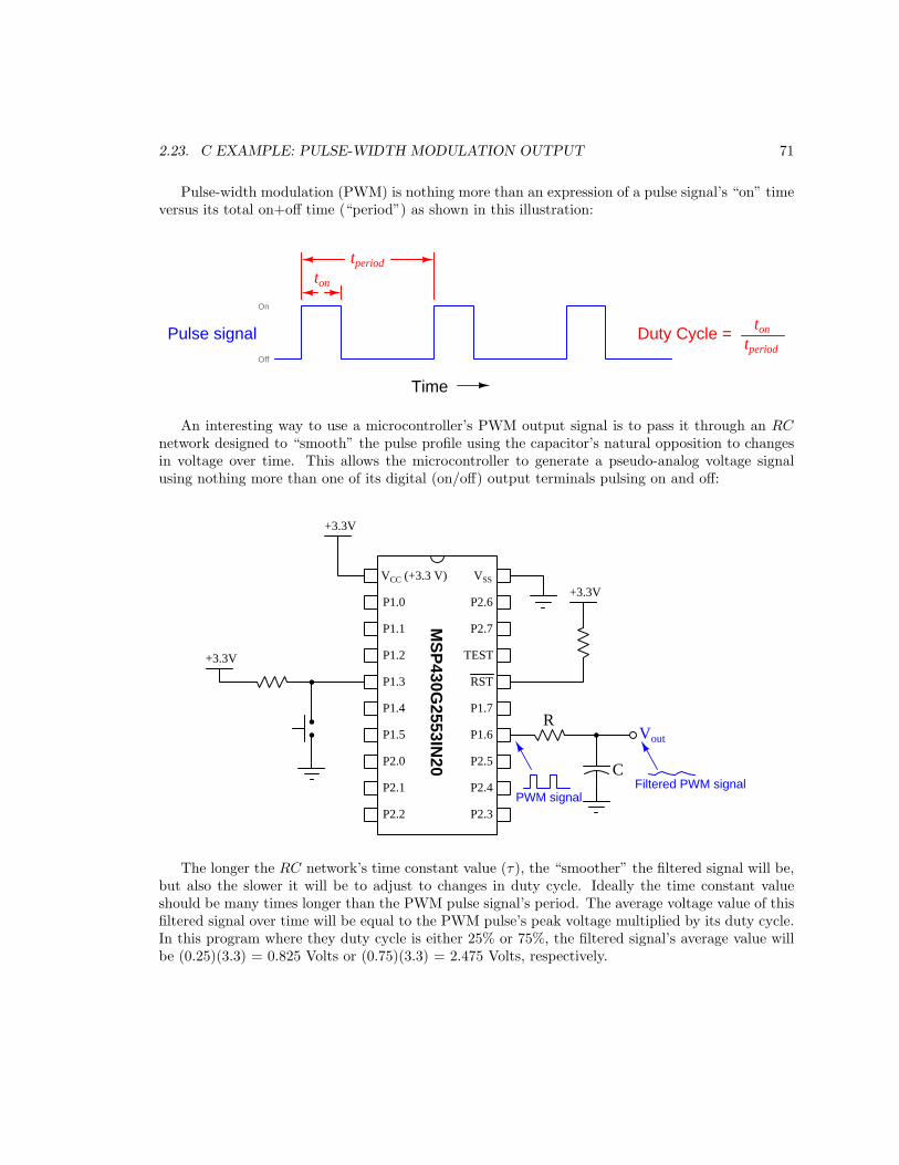
2.23. C EXAMPLE: PULSE-WIDTH MODULATION OUTPUT 71
Pulse-width modulation (PWM) is nothing more than an expression of a pulse signal’s “on” timeversus its total on+off time (“period”) as shown in this illustration:
Pulse signal
Time
ton
tperiod
On
Off
Duty Cycle = ton
tperiod
An interesting way to use a microcontroller’s PWM output signal is to pass it through an RC
network designed to “smooth” the pulse profile using the capacitor’s natural opposition to changesin voltage over time. This allows the microcontroller to generate a pseudo-analog voltage signalusing nothing more than one of its digital (on/off) output terminals pulsing on and off:
MS
P430G
2553IN20
VSSVCC (+3.3 V)
P1.0
P1.1
P1.2
P1.3
P1.4
P1.5
P2.0
P2.1
P2.2
P2.6
P2.7
TEST
RST
P1.7
P1.6
P2.5
P2.4
P2.3
+3.3V
+3.3V
+3.3V
Vout
R
C
PWM signalFiltered PWM signal
The longer the RC network’s time constant value (τ), the “smoother” the filtered signal will be,but also the slower it will be to adjust to changes in duty cycle. Ideally the time constant valueshould be many times longer than the PWM pulse signal’s period. The average voltage value of thisfiltered signal over time will be equal to the PWM pulse’s peak voltage multiplied by its duty cycle.In this program where they duty cycle is either 25% or 75%, the filtered signal’s average value willbe (0.25)(3.3) = 0.825 Volts or (0.75)(3.3) = 2.475 Volts, respectively.

72 CHAPTER 2. CASE TUTORIAL
2.24 C example: crude analog input
Schematic diagram
MS
P430G
2553IN20
VSSVCC (+3.3 V)
P1.0
P1.1
P1.2
P1.4
P1.5
P2.0
P2.1
P2.2
P2.6
P2.7
TEST
RST
P1.7
P1.6
P2.5
P2.4
P2.3
+3.3V
+3.3V
10k P1.3/A3
+3.3V
On the next page is a listing of the entire C-language code, tested and run on a modelMSP430G2553IN20 microcontroller using a LaunchPad model MSP-EXP430G2ET developmentboard and version 10 of Code Composer Studio (CCS) in Debug mode.
The statement beginning with a pound symbol (#include <msp430G2553.h>) is a directivetelling the compiler how to convert the C source code into object code and then executable machinecode for this specific model of microcontroller to run.

2.24. C EXAMPLE: CRUDE ANALOG INPUT 73
C code listing
#include "msp430G2553.h"
void main(void)
WDTCTL = WDTPW + WDTHOLD; // Disable the Watchdog Timer
/* Configure ADC */
ADC10CTL0 = SREF_0 + ADC10ON + ADC10SHT_3; // VCC ref, enable ADC, 64/sample
ADC10AE0 |= BIT3; // Enable P1.3 as analog (A3) instead of general I/O
ADC10CTL1 = INCH_3; // Select ADC Channel (channel A3)
while(1)
ADC10CTL0 |= ENC + ADC10SC; // Enables/starts analog-digital conversion
This is an extremely simple program for reading a single analog input channel on the MSP430microcontroller, and in fact it is only usable while using the “Step Into” function of Code ComposerStudio’s “Debug” mode because there is no time delay in the code or any other provision to givethe microcontroller enough time to adequately process the analog signal. By repeatedly clicking onthe “Step Into” button within CCS, you may watch the numerical value stored in ADC10MEM as youvary the voltage applied between pin P1.3 and Ground on the microcontroller.
In this example circuit, the analog voltage is provided to pin P1.3 using a three-terminalcomponent called a potentiometer. This resistive device uses a movable “wiper” contact to dividethe 3.3 Volt DC power supply voltage by a proportion determined by the wiper’s position. Withthe wiper placed fully up pin P1.3 sees 3.3 Volts with respect to ground; placed fully down it sees0 Volts; when placed mid-position the voltage will be 1.65 Volts.
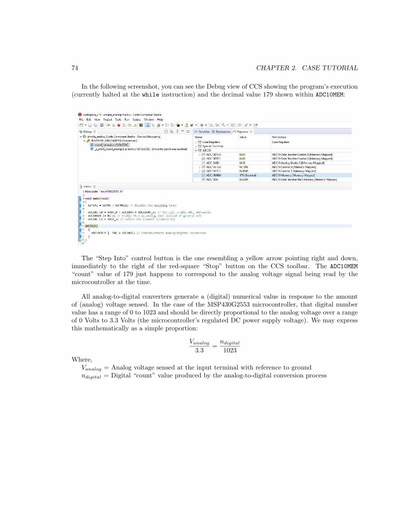
74 CHAPTER 2. CASE TUTORIAL
In the following screenshot, you can see the Debug view of CCS showing the program’s execution(currently halted at the while instruction) and the decimal value 179 shown within ADC10MEM:
The “Step Into” control button is the one resembling a yellow arrow pointing right and down,immediately to the right of the red-square “Stop” button on the CCS toolbar. The ADC10MEM
“count” value of 179 just happens to correspond to the analog voltage signal being read by themicrocontroller at the time.
All analog-to-digital converters generate a (digital) numerical value in response to the amountof (analog) voltage sensed. In the case of the MSP430G2553 microcontroller, that digital numbervalue has a range of 0 to 1023 and should be directly proportional to the analog voltage over a rangeof 0 Volts to 3.3 Volts (the microcontroller’s regulated DC power supply voltage). We may expressthis mathematically as a simple proportion:
Vanalog
3.3=
ndigital
1023
Where,Vanalog = Analog voltage sensed at the input terminal with reference to groundndigital = Digital “count” value produced by the analog-to-digital conversion process

2.25. C EXAMPLE: ANALOG-CONTROLLED LEDS 75
2.25 C example: analog-controlled LEDs
Schematic diagram
MS
P430G
2553IN20
VSSVCC (+3.3 V)
P1.0
P1.1
P1.2
P1.4
P1.5
P2.0
P2.1
P2.2
P2.6
P2.7
TEST
RST
P1.7
P1.6
P2.5
P2.4
P2.3
+3.3V
+3.3V
10k P1.3/A3
+3.3V
On the next page is a listing of the entire C-language code, tested and run on a modelMSP430G2553IN20 microcontroller using a LaunchPad model MSP-EXP430G2ET developmentboard and version 10 of Code Composer Studio (CCS).
The statement beginning with a pound symbol (#include <msp430G2553.h>) is a directivetelling the compiler how to convert the C source code into object code and then executable machinecode for this specific model of microcontroller to run.

76 CHAPTER 2. CASE TUTORIAL
C code listing
#include "msp430G2553.h"
void main(void)
WDTCTL = WDTPW + WDTHOLD; // Disable the Watchdog Timer
/* Configure Output pins for LEDs */
P1DIR |= BIT0 + BIT6; // Set P1.0 and P1.6 as outputs
/* Configure Timer A */
TA0CTL = TASSEL_2 + MC_2 + TAIE; // SMCLK clock, continuous, enable interrupt
/* Configure ADC */
ADC10CTL0 = SREF_0 + ADC10ON + ADC10SHT_3; // VCC ref, enable ADC, 64/sample
ADC10AE0 |= BIT3; // Enable P1.3 as analog (A3) instead of general I/O
ADC10CTL1 = INCH_3; // Select ADC Channel (channel A3)
__bis_SR_register(GIE); // General Interrupts Enabled
while(1)
if (ADC10MEM > 341) // ADC count value stored in ADC10MEM register
P1OUT |= BIT6; // Turn on P1.6 if voltage > 1/3 of VCC
if (ADC10MEM <= 341)
P1OUT &= ~BIT6; // Turn off P1.6 if voltage <= 1/3 of VCC
if (ADC10MEM > 682)
P1OUT |= BIT0; // Turn on P1.0 if voltage > 2/3 of VCC
if (ADC10MEM <= 682)
P1OUT &= ~BIT0; // Turn off P1.0 if voltage < 2/3 of VCC
#pragma vector=TIMER0_A1_VECTOR
__interrupt void Timer_ISR (void) // Timer A interrupt service routine
ADC10CTL0 |= ENC + ADC10SC; // Enables/starts analog-digital conversion
TA0CTL &= ~TAIFG; // Clears the Timer A interrupt flag

2.25. C EXAMPLE: ANALOG-CONTROLLED LEDS 77
This program uses Timer A to generate a periodic interrupt event to re-enable and re-start theanalog-to-digital conversion process.
Noteworthy features of this program include:
• Extensive use of symbolic constants to represent what would otherwise be arcane bit patterns;e.g. BIT6 is a symbol for the binary constant 0b01000000 (hex 0x40)
• Use of the timer circuit’s functionality to replace what would otherwise be code running withinthe while() loop to repeatedly activate the microcontroller’s on-board 10-bit analog-to-digitalconverter
• Inclusion of an interrupt service routine (ISR) called by Timer A’s interrupt event
Let’s examine this code section by section.
After disabling the watchdog timer, the first instruction sets the “direction” of pins P1.0 andP1.6 to both be outputs. We will use these two outputs to drive LEDs, turning each of them on atdifferent sensed voltage levels.
The on-board 10-bit analog-to-digital converter requires a short period of time to completeeach conversion of a sampled analog input voltage, and must be re-started after each conversion iscomplete. A convenient way to do this periodic re-start is to configure the on-board timer (whichis nothing more than a 16-bit counter driven by the clock signal) and have that timer generate aninterrupt request every time it “rolls over” from full-count back to zero. This is called the timer’s“continuous” mode, where it counts from 0x0000 to 0xFFFF repeatedly, setting its interrupt requestflag (IFG) every time it returns to a value of zero. The TAOCTL initialization line sets up Timer Afor this purpose.
Next, we need to initialize registers controlling the analog-to-digital converter itself. The exampleshown here is perhaps the simplest configuration possible for the MSP430’s 10-bit ADC: we declarethe analog reference voltages to be the chip’s power supply (VCC = 3.3 Volts and VSS = 0 Volts),enable the ADC, and specify 64 counts per sample-and-hold cycle to give the analog signal voltagethe maximum time to settle. On the model MSP430G2553IN20, every pin associated with Port 1 isable to serve as an analog input rather than a general I/O pin, and with the ADC10AE0 initializationwe declare the pin normally associated with I/O P1.3 to be A3 instead. Lastly, we select thisanalog-enabled pin to be the analog input signal for the ADC.
The last instruction executed before entering the while() loop sets the General Interrupt Enable(GIE) bit in the microcontroller’s Status Register, a necessary action if we are to use any generalinterrupts in our program.
In its default mode, the ADC10 converter generates an unsigned 10-bit count value rangingfrom 0 to 1023 (decimal) for a corresponding analog voltage signal ranging from the low referencevoltage value to the high reference voltage value. Since we are using the chip’s power supply asthose reference limits, we should expect to find a count value of 0 in the ADC10MEM register whenpin A3 senses 0 Volts, 1023 in that same register when it senses full (+3.3 Volts) signal voltage, anda count value proportionate to these limits for any voltage in-between +3.3 and 0 Volts. It is the

78 CHAPTER 2. CASE TUTORIAL
intent of this program to energize LED P1.6 for any voltage greater than 13 of the supply voltage,
and energize LED P1.0 for any voltage exceeding 23 the supply voltage. Therefore, the values 341
(one-third of 1023) and 682 (two-thirds of 1023) serve as the conditional thresholds for activatingthese LEDs.
The interrupt service routine function contains two instructions: one of them re-enables andre-starts the analog-digital conversion process, necessary after each conversion has completed. Thesecond instruction clears the interrupt flag that was set by the timer when it returned to a valueof zero. This clearing of the flag bit is typical for interrupt service routines, and is necessary7 toprevent that routine from being repeatedly called in an endless loop.
7Interestingly, certain interrupt flags within the MSP430 microcontroller do not require the ISR to explicitly clearthe flag bit. An example of this is the Capture/Compare interrupt flag generated by certain counting modes of thetimer (CCIFG), which gets automatically cleared every time the interrupt request is granted. For most interrupts,expect that you will have to clear that interrupt flag bit within the code you write for the interrupt service requestfunction.
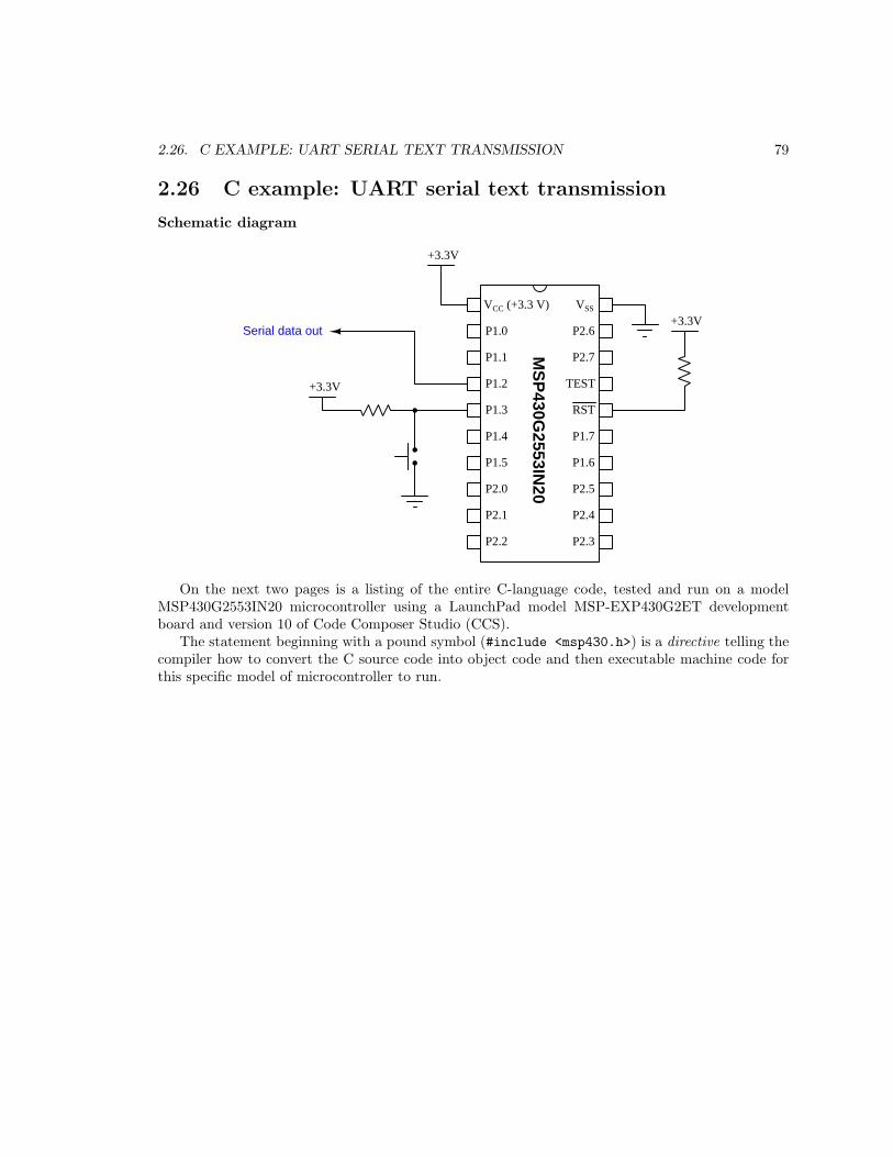
2.26. C EXAMPLE: UART SERIAL TEXT TRANSMISSION 79
2.26 C example: UART serial text transmission
Schematic diagram
MS
P430G
2553IN20
VSSVCC (+3.3 V)
P1.0
P1.1
P1.2
P1.3
P1.4
P1.5
P2.0
P2.1
P2.2
P2.6
P2.7
TEST
RST
P1.7
P1.6
P2.5
P2.4
P2.3
+3.3V
+3.3V
+3.3VSerial data out
On the next two pages is a listing of the entire C-language code, tested and run on a modelMSP430G2553IN20 microcontroller using a LaunchPad model MSP-EXP430G2ET developmentboard and version 10 of Code Composer Studio (CCS).
The statement beginning with a pound symbol (#include <msp430.h>) is a directive telling thecompiler how to convert the C source code into object code and then executable machine code forthis specific model of microcontroller to run.

80 CHAPTER 2. CASE TUTORIAL
C code listing
#include <msp430.h>
void transmit_ASCII(char * tx_data); // Prototype for transmit function
void main(void)
unsigned int button, lastbutton;
WDTCTL = WDTPW + WDTHOLD; // Stop watchdog timer
BCSCTL1 = CALBC1_1MHZ; // Set DCO to 1 MHz
DCOCTL = CALDCO_1MHZ;
P1DIR = 0xF7; // P1.3 input, all other P1 pins output
P1REN = 0x08; // Enables pullup/pulldown resistor on P1.3
P1OUT = 0x08; // Selects pullup resistor for P1.3
P1SEL = BIT1 + BIT2; // P1.1 is UCA0RXD and P1.2 is UCA0TXD
P1SEL2 = BIT1 + BIT2; // when P1SEL and P1SEL2 bits set
UCA0CTL1 |= UCSSEL_2; // Have USCI use System Master Clock
UCA0BR0 = 104; // These two USCI_A0 8-bit clock prescalers
UCA0BR1 = 0; // comprise a 16-bit value to set bit rate.
// Value of 104 = 9600 bps with 1MHz clock
// (as per table 15.4 in MSP430 user guide)
UCA0MCTL = UCBRS0; // Bit rate may be further tweaked using the
// "modulation" register
UCA0CTL1 &= ~UCSWRST; // Start the USCI’s state machine
while(1) // Endless loop
if ((P1IN & BIT3) == BIT3) // "button" represents state of P1.3
button = 1; // == 1 when P1.3 is high
else
button = 0; // == 0 when P1.3 is low
if((button == 0) && (lastbutton == 1)) // Detects P1.3 high-to-low
// without requiring interrupt
transmit_ASCII("Hello world!\r\n"); // Transmit text
transmit_ASCII("Goodbye now.\r\n"); // Transmit more text
lastbutton = button;

2.26. C EXAMPLE: UART SERIAL TEXT TRANSMISSION 81
void transmit_ASCII(char * char_array) // Function accepts char. array pointer
unsigned int n = 0;
while(char_array[n]) // Increment until null pointer (0) reached
while ((UCA0STAT & UCBUSY)); // Wait if line TX/RX module busy with data
UCA0TXBUF = char_array[n]; // Load each character into transmit buffer
++n; // Increment variable for array address
Pressing the pushbutton brings P1.3 input to a “low” state. When the present state is lowand the last state was high it means a high-to-low transition has occurred and this initiates thetransmission of our text message. Without some provision to detect the falling edge of this inputsignal what would happen is the message would be transmitted over and over again for as longas P1.3 remains low. Other methods exist for detecting a high-to-low transition (e.g. using aninterrupt generated by P1.3), but this current/last state method is worth considering which is whyI presented it in this example.
In the C language it is impossible to pass an array or other complex data structure as anargument to function, and so instead the transmit ASCII() function receives a pointer to an arraycomprised of ASCII characters, that array being named char array within the function. Withinthe transmit ASCII function’s while() loop we index this array to read its contents one characterat a time until the end is reached as indicated by a “null” value. Note also the inner while() loopwhich acts to halt the microcontroller’s execution (by uselessly looping) until the status is no longerbusy.

82 CHAPTER 2. CASE TUTORIAL
When the output signal (P1.2) is measured on a digital oscilloscope capable of RS-232 serialdata decoding, we see the following result:

2.27. C EXAMPLE: UART SERIAL TEXT AND NUMBER TRANSMISSION 83
2.27 C example: UART serial text and number transmission
Schematic diagram
MS
P430G
2553IN20
VSSVCC (+3.3 V)
P1.0
P1.1
P1.2
P1.3
P1.4
P1.5
P2.0
P2.1
P2.2
P2.6
P2.7
TEST
RST
P1.7
P1.6
P2.5
P2.4
P2.3
+3.3V
+3.3V
+3.3VSerial data out
On the next two pages is a listing of the entire C-language code, tested and run on a modelMSP430G2553IN20 microcontroller using a LaunchPad model MSP-EXP430G2ET developmentboard and version 10 of Code Composer Studio (CCS).
The statement beginning with a pound symbol (#include <msp430.h>) is a directive telling thecompiler how to convert the C source code into object code and then executable machine code forthis specific model of microcontroller to run.
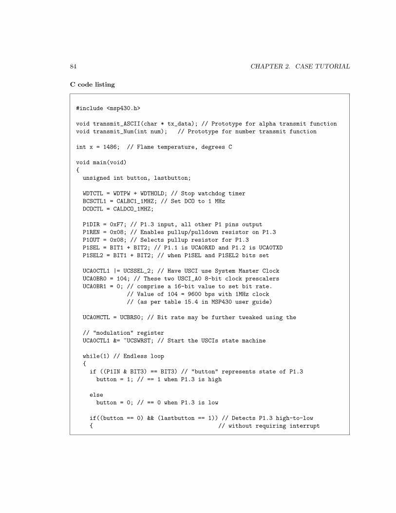
84 CHAPTER 2. CASE TUTORIAL
C code listing
#include <msp430.h>
void transmit_ASCII(char * tx_data); // Prototype for alpha transmit function
void transmit_Num(int num); // Prototype for number transmit function
int x = 1486; // Flame temperature, degrees C
void main(void)
unsigned int button, lastbutton;
WDTCTL = WDTPW + WDTHOLD; // Stop watchdog timer
BCSCTL1 = CALBC1_1MHZ; // Set DCO to 1 MHz
DCOCTL = CALDCO_1MHZ;
P1DIR = 0xF7; // P1.3 input, all other P1 pins output
P1REN = 0x08; // Enables pullup/pulldown resistor on P1.3
P1OUT = 0x08; // Selects pullup resistor for P1.3
P1SEL = BIT1 + BIT2; // P1.1 is UCA0RXD and P1.2 is UCA0TXD
P1SEL2 = BIT1 + BIT2; // when P1SEL and P1SEL2 bits set
UCA0CTL1 |= UCSSEL_2; // Have USCI use System Master Clock
UCA0BR0 = 104; // These two USCI_A0 8-bit clock prescalers
UCA0BR1 = 0; // comprise a 16-bit value to set bit rate.
// Value of 104 = 9600 bps with 1MHz clock
// (as per table 15.4 in MSP430 user guide)
UCA0MCTL = UCBRS0; // Bit rate may be further tweaked using the
// "modulation" register
UCA0CTL1 &= ~UCSWRST; // Start the USCIs state machine
while(1) // Endless loop
if ((P1IN & BIT3) == BIT3) // "button" represents state of P1.3
button = 1; // == 1 when P1.3 is high
else
button = 0; // == 0 when P1.3 is low
if((button == 0) && (lastbutton == 1)) // Detects P1.3 high-to-low
// without requiring interrupt
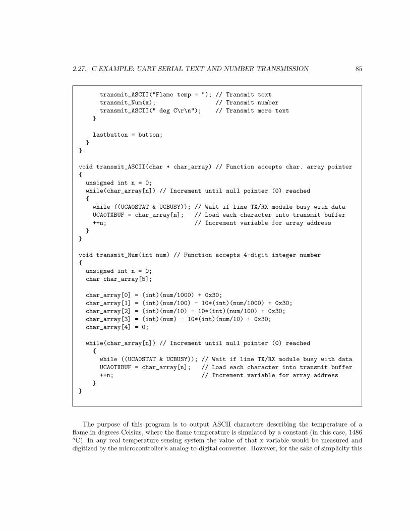
2.27. C EXAMPLE: UART SERIAL TEXT AND NUMBER TRANSMISSION 85
transmit_ASCII("Flame temp = "); // Transmit text
transmit_Num(x); // Transmit number
transmit_ASCII(" deg C\r\n"); // Transmit more text
lastbutton = button;
void transmit_ASCII(char * char_array) // Function accepts char. array pointer
unsigned int n = 0;
while(char_array[n]) // Increment until null pointer (0) reached
while ((UCA0STAT & UCBUSY)); // Wait if line TX/RX module busy with data
UCA0TXBUF = char_array[n]; // Load each character into transmit buffer
++n; // Increment variable for array address
void transmit_Num(int num) // Function accepts 4-digit integer number
unsigned int n = 0;
char char_array[5];
char_array[0] = (int)(num/1000) + 0x30;
char_array[1] = (int)(num/100) - 10*(int)(num/1000) + 0x30;
char_array[2] = (int)(num/10) - 10*(int)(num/100) + 0x30;
char_array[3] = (int)(num) - 10*(int)(num/10) + 0x30;
char_array[4] = 0;
while(char_array[n]) // Increment until null pointer (0) reached
while ((UCA0STAT & UCBUSY)); // Wait if line TX/RX module busy with data
UCA0TXBUF = char_array[n]; // Load each character into transmit buffer
++n; // Increment variable for array address
The purpose of this program is to output ASCII characters describing the temperature of aflame in degrees Celsius, where the flame temperature is simulated by a constant (in this case, 1486oC). In any real temperature-sensing system the value of that x variable would be measured anddigitized by the microcontroller’s analog-to-digital converter. However, for the sake of simplicity this

86 CHAPTER 2. CASE TUTORIAL
demonstration program merely shows how an integer number may be broken down and transmittedas individual ASCII characters. You would have to add more code to the main() function to performany real temperature measurement.
Many elements of this program are identical to that of the simpler text-only transmission example,and so will not be repeated here. For details on how the pushbutton’s state transition is detected,or how the transmit ASCII() function works, refer to the prior example.
The transmit Num() function receives a single integer as its argument, and through a series ofinteger arithmetic this number is broken down into its individual digits. ASCII codes for the digits0 through 9 are 0b00110000 through 0b00111001, respectively, and so all we need to do to converta single decimal digit into its corresponding ASCII code is add 0x30 to it. This is done four times,placing the respective ASCII characters into another char array character array. The last elementof that array is set to zero (null), and then it is processed just like it was in the transmit ASCII()
function.Converting a four-digit integer number into four individual characters involves some creative
arithmetic. If you force the computer to perform division and to cast the quotient as an integernumber, it has the effect of dropping any digits to the right of the decimal point. For example,(int)(12 / 5) would yield a result of 2 even though 12
5 = 2.4 when performed ordinarily. Therefore,dividing a four-digit decimal number by 1000 will yield its most-significant digit. Similarly, dividinga four-digit decimal number by 100 yields its two most significant digits, which may be reducedto the least-significant of those by subtracting ten times the most-significant digit. This process isrepeated four times until all four digits of the integer number have been represented as single ASCIIcharacter values. There are more computationally elegant ways of doing this, but showing all foursteps as separate lines of code makes the algorithm easier to understand, and my purpose here isstrictly educational.

2.27. C EXAMPLE: UART SERIAL TEXT AND NUMBER TRANSMISSION 87
When the output signal (P1.2) is measured on a digital oscilloscope capable of RS-232 serialdata decoding, we see the following result:

88 CHAPTER 2. CASE TUTORIAL
2.28 C example: UART transmission of analog data
Schematic diagram
MS
P430G
2553IN20
VSSVCC (+3.3 V)
P1.0
P1.1
P1.2
P1.3
P1.4
P1.5
P2.0
P2.1
P2.2
P2.6
P2.7
TEST
RST
P1.7
P1.6
P2.5
P2.4
P2.3
+3.3V
+3.3V
+3.3V
Serial data out+3.3V
Analog voltage in
On the next two pages is a listing of the entire C-language code, tested and run on a modelMSP430G2553IN20 microcontroller using a LaunchPad model MSP-EXP430G2ET developmentboard and version 10 of Code Composer Studio (CCS).
The statement beginning with a pound symbol (#include <msp430.h>) is a directive telling thecompiler how to convert the C source code into object code and then executable machine code forthis specific model of microcontroller to run.

2.28. C EXAMPLE: UART TRANSMISSION OF ANALOG DATA 89
C code listing
#include <msp430.h>
void transmit_ASCII(char * tx_data); // Prototype for alpha transmit function
void transmit_Num(int num); // Prototype for number transmit function
void main(void)
unsigned int button, lastbutton;
WDTCTL = WDTPW + WDTHOLD; // Stop watchdog timer
// Configure DCO oscillator for 1 MHz
BCSCTL1 = CALBC1_1MHZ;
DCOCTL = CALDCO_1MHZ;
// Configure Port 1 I/O
P1DIR = 0x77; // P1.3 and P1.7 inputs, all other P1 pins output
P1REN = 0x08; // Enables pullup/pulldown resistor on P1.3
P1OUT = 0x08; // Selects pullup resistor for P1.3
P1SEL = BIT1 + BIT2; // P1.1 is UCA0RXD and P1.2 is UCA0TXD
P1SEL2 = BIT1 + BIT2; // when P1SEL and P1SEL2 bits set
// Configure Timer A
TA0CTL = TASSEL_2 + MC_1 + TAIE; // SMCLK clock, up mode, enable interrupt
TACCR0 = 10000; // Set maximum count value to generate an interrupt every
// 10000 cycles of the clock which is every 0.01 seconds
// Configure ADC
ADC10CTL0 = SREF_0 + ADC10ON + ADC10SHT_3; // VCC ref, enable ADC, 64/sample
ADC10AE0 |= BIT7; // Enable P1.7 as analog (A7) instead of general I/O
ADC10CTL1 = INCH_7; // Select ADC Channel (channel A7)
// Configure UART
UCA0CTL1 |= UCSSEL_2; // Have USCI use System Master Clock
UCA0BR0 = 104; // These two USCI_A0 8-bit clock prescalers
UCA0BR1 = 0; // comprise a 16-bit value to set bit rate.
// Value of 104 = 9600 bps with 1MHz clock
// (as per table 15.4 in MSP430 user guide)
UCA0MCTL = UCBRS0; // Bit rate may be further tweaked using the
// "modulation" register
UCA0CTL1 &= ~UCSWRST; // Start the USCIs state machine

90 CHAPTER 2. CASE TUTORIAL
__bis_SR_register(GIE); // General Interrupts Enabled
while(1)
// NOTE: ADC count value stored in ADC10MEM register
if (ADC10MEM > 341)
P1OUT |= BIT6; // Turn on P1.6 if voltage > 1/3 of VCC
if (ADC10MEM <= 341)
P1OUT &= ~BIT6; // Turn off P1.6 if voltage <= 1/3 of VCC
if (ADC10MEM > 682)
P1OUT |= BIT0; // Turn on P1.0 if voltage > 2/3 of VCC
if (ADC10MEM <= 682)
P1OUT &= ~BIT0; // Turn off P1.0 if voltage < 2/3 of VCC
if ((P1IN & BIT3) == BIT3) // "button" represents state of P1.3
button = 1; // == 1 when P1.3 is high
else
button = 0; // == 0 when P1.3 is low
if((button == 0) && (lastbutton == 1)) // Detects P1.3 high-to-low
// without requiring interrupt
transmit_ASCII("ADC value = "); // Transmit text
transmit_Num(ADC10MEM); // Transmit number (ADC value)
transmit_ASCII(" counts\r\n"); // Transmit more text
lastbutton = button;
void transmit_ASCII(char * char_array) // Function accepts char. array pointer
unsigned int n = 0;
while(char_array[n]) // Increment until null pointer (0) reached
while ((UCA0STAT & UCBUSY)); // Wait if line TX/RX module busy with data
UCA0TXBUF = char_array[n]; // Load each character into transmit buffer
++n; // Increment variable for array address
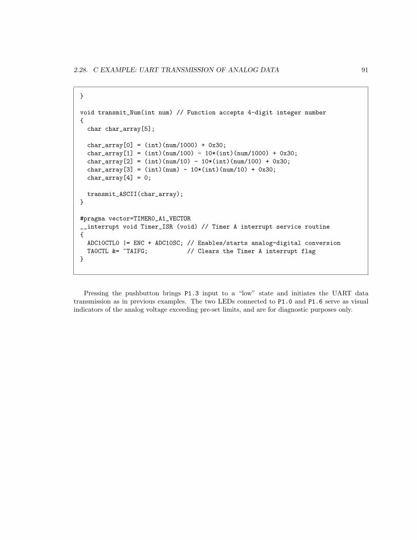
2.28. C EXAMPLE: UART TRANSMISSION OF ANALOG DATA 91
void transmit_Num(int num) // Function accepts 4-digit integer number
char char_array[5];
char_array[0] = (int)(num/1000) + 0x30;
char_array[1] = (int)(num/100) - 10*(int)(num/1000) + 0x30;
char_array[2] = (int)(num/10) - 10*(int)(num/100) + 0x30;
char_array[3] = (int)(num) - 10*(int)(num/10) + 0x30;
char_array[4] = 0;
transmit_ASCII(char_array);
#pragma vector=TIMER0_A1_VECTOR
__interrupt void Timer_ISR (void) // Timer A interrupt service routine
ADC10CTL0 |= ENC + ADC10SC; // Enables/starts analog-digital conversion
TA0CTL &= ~TAIFG; // Clears the Timer A interrupt flag
Pressing the pushbutton brings P1.3 input to a “low” state and initiates the UART datatransmission as in previous examples. The two LEDs connected to P1.0 and P1.6 serve as visualindicators of the analog voltage exceeding pre-set limits, and are for diagnostic purposes only.

92 CHAPTER 2. CASE TUTORIAL
Serial output signal (P1.2) decoded on a digital oscilloscope with potentiometer turned to 0 Volts(wiper fully down), resulting in a count value of 0000 from the 10-bit ADC:
Serial output signal (P1.2) decoded on a digital oscilloscope with potentiometer turned to 3.3Volts (wiper fully up), resulting in a count value of 1023 from the 10-bit ADC (210 − 1):

2.28. C EXAMPLE: UART TRANSMISSION OF ANALOG DATA 93
Another version of this program automatically transmits the approximate analog voltage every5 seconds:
#include <msp430.h>
void transmit_ASCII(char * tx_data); // Prototype for alpha transmit function
void transmit_Num(int num); // Prototype for number transmit function
unsigned int hundredths, seconds, minutes;
void main(void)
unsigned int button, lastbutton, time, lasttime;
WDTCTL = WDTPW + WDTHOLD; // Stop watchdog timer
// Configure DCO oscillator for 1 MHz
BCSCTL1 = CALBC1_1MHZ;
DCOCTL = CALDCO_1MHZ;
// Configure Port 1 I/O
P1DIR = 0x77; // P1.3 and P1.7 inputs, all other P1 pins output
P1REN = 0x08; // Enables pullup/pulldown resistor on P1.3
P1OUT = 0x08; // Selects pullup resistor for P1.3
P1SEL = BIT1 + BIT2; // P1.1 is UCA0RXD and P1.2 is UCA0TXD
P1SEL2 = BIT1 + BIT2; // when P1SEL and P1SEL2 bits set
// Configure Timer A
TA0CTL = TASSEL_2 + MC_1 + TAIE; // SMCLK clock, up mode, enable interrupt
TACCR0 = 10000; // Set maximum count value to generate an interrupt every
// 10000 cycles of the clock which is every 0.01 seconds
// Configure ADC
ADC10CTL0 = SREF_0 + ADC10ON + ADC10SHT_3; // VCC ref, enable ADC, 64/sample
ADC10AE0 |= BIT7; // Enable P1.7 as analog (A7) instead of general I/O
ADC10CTL1 = INCH_7; // Select ADC Channel (channel A7)
// Configure UART
UCA0CTL1 |= UCSSEL_2; // Have USCI use System Master Clock
UCA0BR0 = 104; // These two USCI_A0 8-bit clock prescalers
UCA0BR1 = 0; // comprise a 16-bit value to set bit rate.
// Value of 104 = 9600 bps with 1MHz clock
// (as per table 15.4 in MSP430 user guide)
UCA0MCTL = UCBRS0; // Bit rate may be further tweaked using the
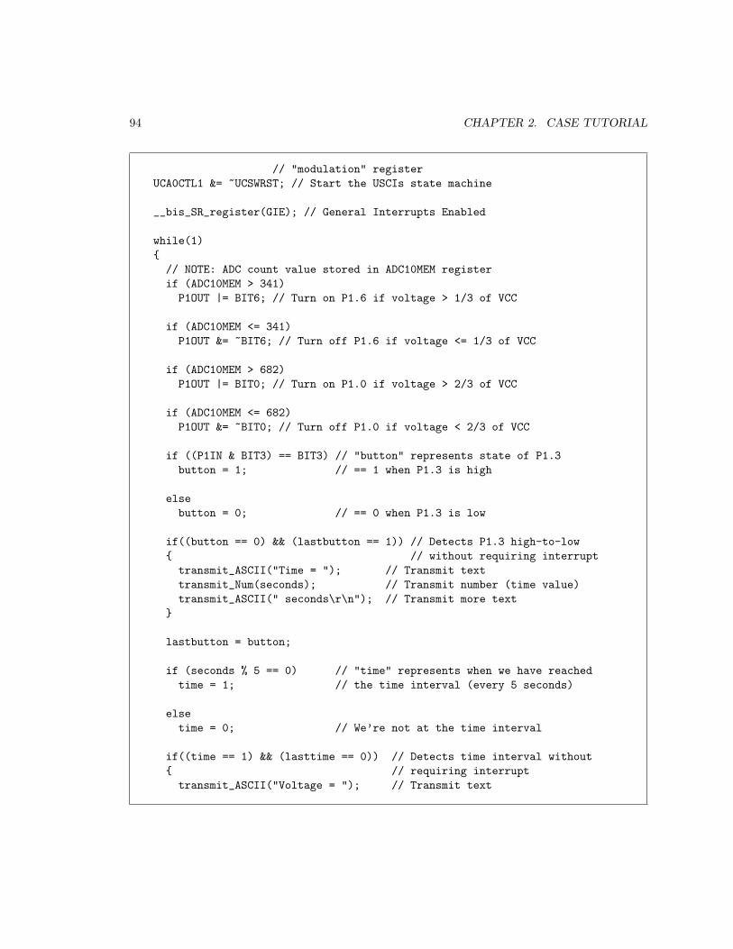
94 CHAPTER 2. CASE TUTORIAL
// "modulation" register
UCA0CTL1 &= ~UCSWRST; // Start the USCIs state machine
__bis_SR_register(GIE); // General Interrupts Enabled
while(1)
// NOTE: ADC count value stored in ADC10MEM register
if (ADC10MEM > 341)
P1OUT |= BIT6; // Turn on P1.6 if voltage > 1/3 of VCC
if (ADC10MEM <= 341)
P1OUT &= ~BIT6; // Turn off P1.6 if voltage <= 1/3 of VCC
if (ADC10MEM > 682)
P1OUT |= BIT0; // Turn on P1.0 if voltage > 2/3 of VCC
if (ADC10MEM <= 682)
P1OUT &= ~BIT0; // Turn off P1.0 if voltage < 2/3 of VCC
if ((P1IN & BIT3) == BIT3) // "button" represents state of P1.3
button = 1; // == 1 when P1.3 is high
else
button = 0; // == 0 when P1.3 is low
if((button == 0) && (lastbutton == 1)) // Detects P1.3 high-to-low
// without requiring interrupt
transmit_ASCII("Time = "); // Transmit text
transmit_Num(seconds); // Transmit number (time value)
transmit_ASCII(" seconds\r\n"); // Transmit more text
lastbutton = button;
if (seconds % 5 == 0) // "time" represents when we have reached
time = 1; // the time interval (every 5 seconds)
else
time = 0; // We’re not at the time interval
if((time == 1) && (lasttime == 0)) // Detects time interval without
// requiring interrupt
transmit_ASCII("Voltage = "); // Transmit text
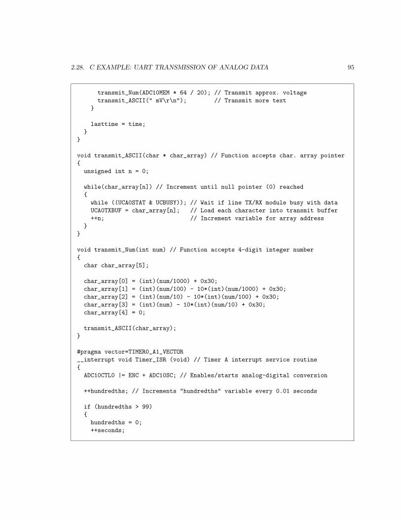
2.28. C EXAMPLE: UART TRANSMISSION OF ANALOG DATA 95
transmit_Num(ADC10MEM * 64 / 20); // Transmit approx. voltage
transmit_ASCII(" mV\r\n"); // Transmit more text
lasttime = time;
void transmit_ASCII(char * char_array) // Function accepts char. array pointer
unsigned int n = 0;
while(char_array[n]) // Increment until null pointer (0) reached
while ((UCA0STAT & UCBUSY)); // Wait if line TX/RX module busy with data
UCA0TXBUF = char_array[n]; // Load each character into transmit buffer
++n; // Increment variable for array address
void transmit_Num(int num) // Function accepts 4-digit integer number
char char_array[5];
char_array[0] = (int)(num/1000) + 0x30;
char_array[1] = (int)(num/100) - 10*(int)(num/1000) + 0x30;
char_array[2] = (int)(num/10) - 10*(int)(num/100) + 0x30;
char_array[3] = (int)(num) - 10*(int)(num/10) + 0x30;
char_array[4] = 0;
transmit_ASCII(char_array);
#pragma vector=TIMER0_A1_VECTOR
__interrupt void Timer_ISR (void) // Timer A interrupt service routine
ADC10CTL0 |= ENC + ADC10SC; // Enables/starts analog-digital conversion
++hundredths; // Increments "hundredths" variable every 0.01 seconds
if (hundredths > 99)
hundredths = 0;
++seconds;

96 CHAPTER 2. CASE TUTORIAL
if (seconds > 59)
seconds = 0;
++minutes;
TA0CTL &= ~TAIFG; // Clears the Timer A interrupt flag
In this version, the interrupt service routine increments hundredths, seconds, and minutes
variables to give the main function’s while() loop a way of knowing how much time has elapsed.In addition to printing the value of the seconds variable with every press of pushbutton P1.3, thisprogram automatically transmits an approximation of analog voltage every 5 seconds.
The scaling of an integer count value (range = 0 to 1023) to an analog voltage value is approximatebecause our mathematical operations are limited to integer arithmetic. We multiply ADC10MEM by64 in order to create a value as close to the 16-bit maximum of 65535 without exceeding it, thendivide by another factor (in this case, 20) to yield a value for millivoltage. The calculation isn’tperfect, as a 3.3 Volt input will yield a transmitted number of 3273 mV rather than 3300 mV, butthis error decreases with signal voltage.

2.29. C EXAMPLE: SIMPLE DATALOGGER 97
2.29 C example: simple datalogger
Schematic diagram
MS
P430G
2553IN20
VSSVCC (+3.3 V)
P1.0
P1.1
P1.2
P1.3
P1.4
P1.5
P2.0
P2.1
P2.2
P2.6
P2.7
TEST
RST
P1.7
P1.6
P2.5
P2.4
P2.3
+3.3V
+3.3V
+3.3V
Analog voltage in
6 V
6 V
2 5
EIA/TIA-232male connector
on PC
Pin 2 = RXDPin 5 = GND
On the next two pages is a listing of the entire C-language code, tested and run on a modelMSP430G2553IN20 microcontroller using a LaunchPad model MSP-EXP430G2ET developmentboard and version 10 of Code Composer Studio (CCS).
The statement beginning with a pound symbol (#include <msp430.h>) is a directive telling thecompiler how to convert the C source code into object code and then executable machine code forthis specific model of microcontroller to run.

98 CHAPTER 2. CASE TUTORIAL
C code listing
#include <msp430.h>
void transmit_ASCII(char * tx_data); // Prototype for alpha transmit function
void transmit_Num(int num); // Prototype for number transmit function
unsigned int hundredths, seconds, minutes, sample;
unsigned int data[128]; // Array for storing logged data
void main(void)
unsigned int button, lastbutton, time, lasttime;
WDTCTL = WDTPW + WDTHOLD; // Stop watchdog timer
// Configure DCO oscillator for 1 MHz
BCSCTL1 = CALBC1_1MHZ;
DCOCTL = CALDCO_1MHZ;
// Configure Port 1 I/O
P1DIR = 0x77; // P1.3 and P1.7 inputs, all other P1 pins output
P1REN = 0x08; // Enables pullup/pulldown resistor on P1.3
P1OUT = 0x08; // Selects pullup resistor for P1.3
P1SEL = BIT1 + BIT2; // P1.1 is UCA0RXD and P1.2 is UCA0TXD
P1SEL2 = BIT1 + BIT2; // when P1SEL and P1SEL2 bits set
// Configure Timer A
TA0CTL = TASSEL_2 + MC_1 + TAIE; // SMCLK clock, up mode, enable interrupt
TACCR0 = 10000; // Set maximum count value to generate an interrupt every
// 10000 cycles of the clock which is every 0.01 seconds
// Configure ADC
ADC10CTL0 = SREF_0 + ADC10ON + ADC10SHT_3; // VCC ref, enable ADC, 64/sample
ADC10AE0 |= BIT7; // Enable P1.7 as analog (A7) instead of general I/O
ADC10CTL1 = INCH_7; // Select ADC Channel (channel A7)
// Configure UART
UCA0CTL1 |= UCSSEL_2; // Have USCI use System Master Clock
UCA0BR0 = 104; // These two USCI_A0 8-bit clock prescalers
UCA0BR1 = 0; // comprise a 16-bit value to set bit rate.
// Value of 104 = 9600 bps with 1MHz clock
// (as per table 15.4 in MSP430 user guide)
UCA0MCTL = UCBRS0; // Bit rate may be further tweaked using the

2.29. C EXAMPLE: SIMPLE DATALOGGER 99
// "modulation" register
UCA0CTL1 &= ~UCSWRST; // Start the USCIs state machine
__bis_SR_register(GIE); // General Interrupts Enabled
while(1)
// NOTE: ADC count value stored in ADC10MEM register
if ((P1IN & BIT3) == BIT3) // "button" represents state of P1.3
button = 1; // == 1 when P1.3 is high
else
button = 0; // == 0 when P1.3 is low
if((button == 0) && (lastbutton == 1)) // Detects P1.3 high-to-low
// without requiring interrupt
for (sample = 0 ; sample < 128 ; ++sample)
transmit_Num(sample); // Transmit sample number
transmit_ASCII(" , "); // Transmit comma delimiter
transmit_Num(data[sample]); // Transmit logged data
transmit_ASCII("\r\n"); // Transmit new line
lastbutton = button;
if (seconds % 5 == 0) // "time" represents when we have reached
time = 1; // the time interval (every 5 seconds)
else
time = 0; // We’re not at the time interval
// Recording a sample to the data[] array
if((time == 1) && (lasttime == 0)) // Detects time interval without
// requiring interrupt
P1OUT ^= BIT6; // Toggle P1.6 to visually indicate new sample
data[sample & 0x7F] = ADC10MEM;
++sample;
lasttime = time;

100 CHAPTER 2. CASE TUTORIAL
void transmit_ASCII(char * char_array) // Function accepts char. array pointer
unsigned int n = 0;
while(char_array[n]) // Increment until null pointer (0) reached
while ((UCA0STAT & UCBUSY)); // Wait if line TX/RX module busy with data
UCA0TXBUF = char_array[n]; // Load each character into transmit buffer
++n; // Increment variable for array address
void transmit_Num(int num) // Function accepts 4-digit integer number
char char_array[5];
char_array[0] = (int)(num/1000) + 0x30;
char_array[1] = (int)(num/100) - 10*(int)(num/1000) + 0x30;
char_array[2] = (int)(num/10) - 10*(int)(num/100) + 0x30;
char_array[3] = (int)(num) - 10*(int)(num/10) + 0x30;
char_array[4] = 0;
transmit_ASCII(char_array);
#pragma vector=TIMER0_A1_VECTOR
__interrupt void Timer_ISR (void) // Timer A interrupt service routine
ADC10CTL0 |= ENC + ADC10SC; // Enables/starts analog-digital conversion
++hundredths; // Increments "hundredths" variable every 0.01 seconds
if (hundredths > 99)
hundredths = 0;
++seconds;
if (seconds > 59)
seconds = 0;
++minutes;

2.29. C EXAMPLE: SIMPLE DATALOGGER 101
TA0CTL &= ~TAIFG; // Clears the Timer A interrupt flag
Pressing the pushbutton brings P1.3 input to a “low” state and initiates the UART datatransmission, producing a comma-separated variable (CSV) text listing showing 128 samples storedin the data[] array. In this particular example, a new sample is stored in the array every 5 seconds.Pressing the P1.3 switch both prompts the UART transmission of the entire array as well as resetsthe sample variable so that new data entries begin at the start of the array. The LED connectedto P1.6 toggles every time a new sample is saved to the array, providing visual indication that theprogram is functioning. Every time that LED turns on, a new sample is taken; every time it turnsoff, another sample is taken.
The sample variable increments once per sample, and since its value may go well beyond the0-127 limit imposed by the array’s size, we use a bitwise-AND operation with 0x7F to only use thelower seven bits of its 16-bit value. When sample increments to a value equal to or greater than anymultiple of 128, new data overwrites old data stored in the beginning elements of the array.
EIA/TIA-232 requires a bipolar signal (above and below ground potential) of at least ±5 Voltsfor reliable operation. Rather than use a specialized “driver” IC to interface the microcontroller toa personal computer serial port, we have instead cobbled together a simple driver circuit consistingof an opto-isolator and two 6 Volt batteries.

102 CHAPTER 2. CASE TUTORIAL
Data is received by a personal computer running a serial terminal software application such asTermite or Kermit or Hyperterminal. Here is a screenshot showing Termite capturing the serialdata stream after pressing pushbutton P1.3. I used the computer’s mouse to select the first 25samples and then pasted the text into a text editor, saving it as a file named data.csv:

2.29. C EXAMPLE: SIMPLE DATALOGGER 103
Once stored as a text file, this CSV data may be read by any spreadsheet software (e.g. MicrosoftExcel) to generate a graph:

104 CHAPTER 2. CASE TUTORIAL
2.30 Example: interposing MCU to a heavy load
The following MCU controls the illumination of two LEDs, one connected to output pin P1.0 andthe other connected to output pin P1.6:
MS
P430G
2553IN20
VSSVCC (+3.3 V)
P1.0
P1.1
P1.2
P1.3
P1.4
P1.5
P2.0
P2.1
P2.2
P2.6
P2.7
TEST
RST
P1.7
P1.6
P2.5
P2.4
P2.3
+3.3V
+3.3V
Suppose we wanted to control a load with much higher current requirements than a simpleLED – something requiring far more current than the MCU can source or sink through any of itsoutput pins. This will require some electrically-controlled switching device to “interpose” betweenthe MCU’s output and the high-current load. A transistor is a good candidate for this task.

2.30. EXAMPLE: INTERPOSING MCU TO A HEAVY LOAD 105
Connecting a bipolar junction transistor (BJT) of the NPN variety between the output pin andthe load will suffice:
MS
P430G
2553IN20
VSSVCC (+3.3 V)
P1.0
P1.1
P1.2
P1.3
P1.4
P1.5
P2.0
P2.1
P2.2
P2.6
P2.7
TEST
RST
P1.7
P1.6
P2.5
P2.4
P2.3
+3.3V
+3.3V
Load
+12 V
Rlimit
The current-limiting resistor Rlimit allows just enough current from output pin P1.6 of themicrocontroller to drive the BJT into saturation, where it is as fully “on” as it is able. Whensaturated, we would expect to see approximately 0.7 Volts dropped between the BJT’s base andemitter terminals, and approximately 0.3 Volts dropped between the BJT’s collector and emitterterminals. This means the load receives approximately 11.7 Volts with P1.6 in its “high” state.When P1.6 goes to a “low” state the BJT will turn off, dropping zero voltage between its base andemitter, and dropping the full 12 Volts between its collector and emitter.
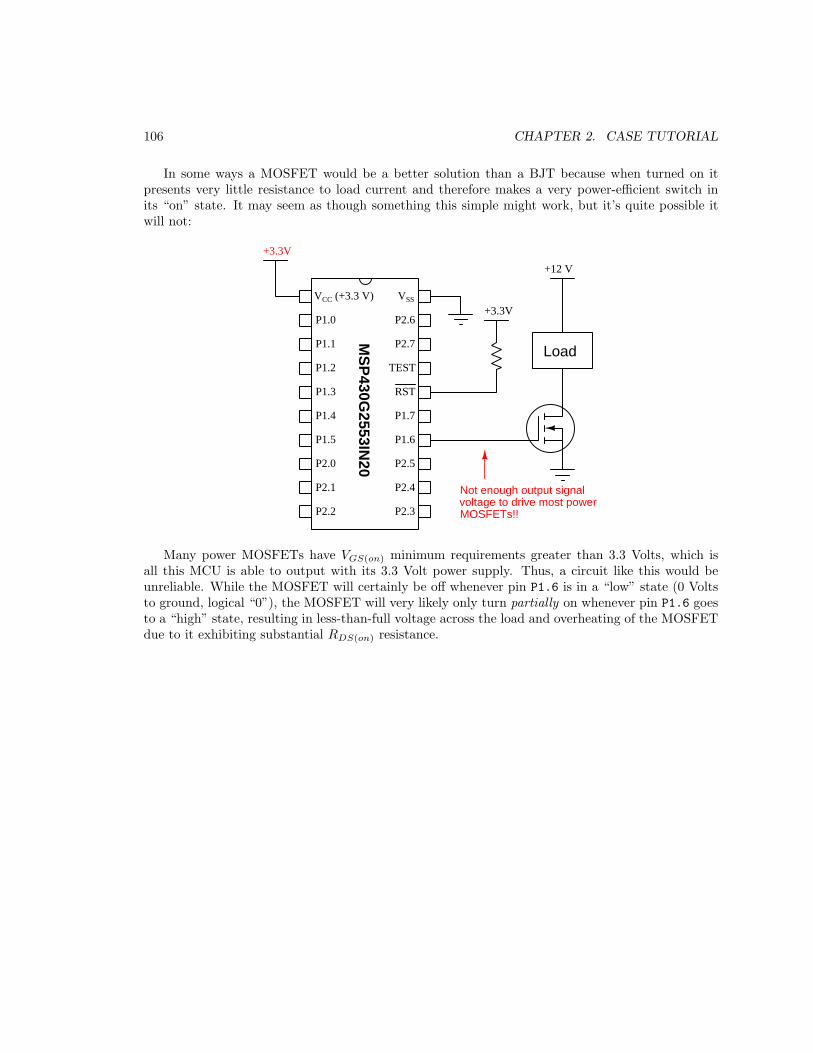
106 CHAPTER 2. CASE TUTORIAL
In some ways a MOSFET would be a better solution than a BJT because when turned on itpresents very little resistance to load current and therefore makes a very power-efficient switch inits “on” state. It may seem as though something this simple might work, but it’s quite possible itwill not:
MS
P430G
2553IN20
VSSVCC (+3.3 V)
P1.0
P1.1
P1.2
P1.3
P1.4
P1.5
P2.0
P2.1
P2.2
P2.6
P2.7
TEST
RST
P1.7
P1.6
P2.5
P2.4
P2.3
+3.3V
+3.3V
Load
+12 V
Not enough output signalvoltage to drive most powerMOSFETs!!
Many power MOSFETs have VGS(on) minimum requirements greater than 3.3 Volts, which isall this MCU is able to output with its 3.3 Volt power supply. Thus, a circuit like this would beunreliable. While the MOSFET will certainly be off whenever pin P1.6 is in a “low” state (0 Voltsto ground, logical “0”), the MOSFET will very likely only turn partially on whenever pin P1.6 goesto a “high” state, resulting in less-than-full voltage across the load and overheating of the MOSFETdue to it exhibiting substantial RDS(on) resistance.

2.30. EXAMPLE: INTERPOSING MCU TO A HEAVY LOAD 107
The following solution is simple, using a BJT directly driven by the MCU to provide a higher-voltage gate-to-source signal for the MOSFET to operate on. The MCU will have no troubleactivating the BJT since bipolar junction transistors only require 0.7 Volts base-to-emitter to turnon, which is far less than the several Volts of gate-source voltage typically required to activate apower MOSFET:
MS
P430G
2553IN20
VSSVCC (+3.3 V)
P1.0
P1.1
P1.2
P1.3
P1.4
P1.5
P2.0
P2.1
P2.2
P2.6
P2.7
TEST
RST
P1.7
P1.6
P2.5
P2.4
P2.3
+3.3V
+3.3V
Load
+12 V
The resistor between pin P1.6 and the BJT’s base terminal simply limits base current to a levelacceptable to the MCU. The resistor between the +12 Volt power supply terminal and the BJT’scollector terminal simply acts as a “pull-up” to provide a “high” voltage to the MOSFET’s gateterminal whenever the BJT is off, so its value may be quite large8.
A caveat to be aware of with this added BJT stage is that the MCU’s output logic state will bethe inverse of the load’s energization state: the load will now be energized when MCU pin P1.6 is“low” (0 Volts to ground, which is a “0” digital state) and de-energized when pin P1.6 is “high”(+3.3 Volts to ground, a “1” digital state). However, it is generally easy to alter the programmingof the MCU to re-invert the logic so that the load energizes with an internal “1” digital state andturns off with a “0” digital state if that is what you desire.
8The only real limit here is that this pull-up resistor must “charge” up the MOSFET’s gate-to-source capacitancein a reasonably short amount of time, but since CGS is typically very small for most MOSFETs this is generally nota concern. Only if the switching frequency is very high would we concern ourselves about sizing that pull-up resistorsmall enough to charge up CGS quickly enough. Otherwise, a relatively large pull-up resistor value – say, 10 kΩ ormore – will minimize power dissipation when the BJT is “on” which is a good thing.
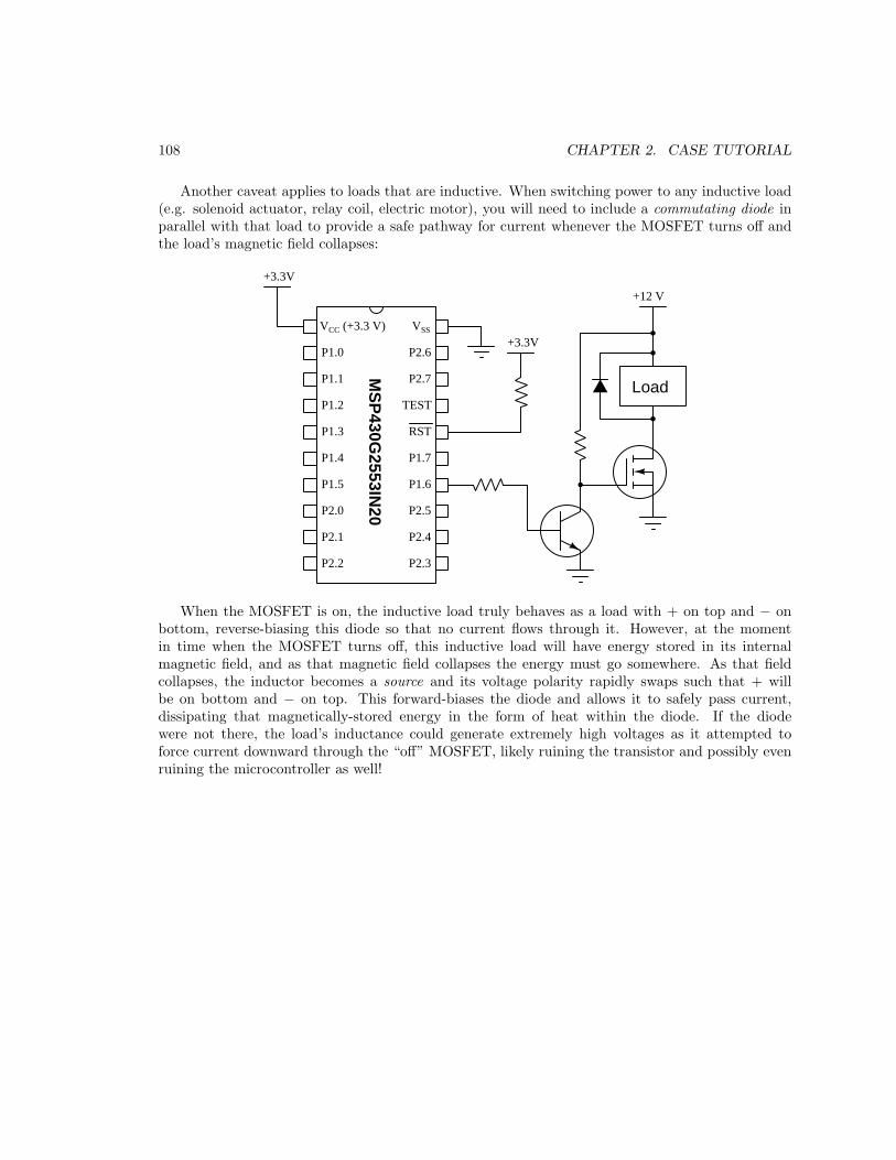
108 CHAPTER 2. CASE TUTORIAL
Another caveat applies to loads that are inductive. When switching power to any inductive load(e.g. solenoid actuator, relay coil, electric motor), you will need to include a commutating diode inparallel with that load to provide a safe pathway for current whenever the MOSFET turns off andthe load’s magnetic field collapses:
MS
P430G
2553IN20
VSSVCC (+3.3 V)
P1.0
P1.1
P1.2
P1.3
P1.4
P1.5
P2.0
P2.1
P2.2
P2.6
P2.7
TEST
RST
P1.7
P1.6
P2.5
P2.4
P2.3
+3.3V
+3.3V
Load
+12 V
When the MOSFET is on, the inductive load truly behaves as a load with + on top and − onbottom, reverse-biasing this diode so that no current flows through it. However, at the momentin time when the MOSFET turns off, this inductive load will have energy stored in its internalmagnetic field, and as that magnetic field collapses the energy must go somewhere. As that fieldcollapses, the inductor becomes a source and its voltage polarity rapidly swaps such that + willbe on bottom and − on top. This forward-biases the diode and allows it to safely pass current,dissipating that magnetically-stored energy in the form of heat within the diode. If the diodewere not there, the load’s inductance could generate extremely high voltages as it attempted toforce current downward through the “off” MOSFET, likely ruining the transistor and possibly evenruining the microcontroller as well!
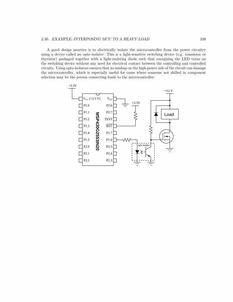
2.30. EXAMPLE: INTERPOSING MCU TO A HEAVY LOAD 109
A good design practice is to electrically isolate the microcontroller from the power circuitryusing a device called an opto-isolator. This is a light-sensitive switching device (e.g. transistor orthyristor) packaged together with a light-emitting diode such that energizing the LED turns onthe switching device without any need for electrical contact between the controlling and controlledcircuits. Using opto-isolators ensures that no mishap on the high-power side of the circuit can damagethe microcontroller, which is especially useful for cases where someone not skilled in componentselection may be the person connecting loads to the microcontroller:
MS
P430G
2553IN20
VSSVCC (+3.3 V)
P1.0
P1.1
P1.2
P1.3
P1.4
P1.5
P2.0
P2.1
P2.2
P2.6
P2.7
TEST
RST
P1.7
P1.6
P2.5
P2.4
P2.3
+3.3V
+3.3V
Load
+12 V
opto-isolator

110 CHAPTER 2. CASE TUTORIAL
Opto-isolators are more expensive than ordinary transistors, and generally have low switchingcurrent limits, but are unparalleled in their ability to electrically isolate one circuit from another. Ihighly recommend their use when interposing high-power circuitry to microcontroller I/O pins. Thefollowing photograph shows several opto-isolators (model PVT 322) soldered into a printed circuitboard:
Larger opto-isolators with higher voltage and/or current switching ratings are called solid staterelays (SSRs), and are similarly useful for interposing sensitive microcontroller output pins to high-power circuits:

2.31. C EXAMPLE: SINE-WAVE INVERTER 111
2.31 C example: sine-wave inverter
Schematic diagram
MS
P430G
2553IN20
VSSVCC (+3.3 V)
P1.0
P1.1
P1.2
P1.3
P1.4
P1.5
P2.0
P2.1
P2.2
P2.6
P2.7
TEST
RST
P1.7
P1.6
P2.5
P2.4
P2.3
+3.3V
+3.3V
MCU ground MCU groundDC powerground
DC powerground
+DC power +DC power+DC power
DC powerground
DC powerground
To AC load
PWM signal
Opto-isolator Opto-isolator
Steering signal
Fuse
+3.3V
MCU ground
MCU ground
On the next two pages is a listing of the entire C-language code, tested and run on a modelMSP430G2553IN20 microcontroller using a LaunchPad model MSP-EXP430G2ET developmentboard and version 10 of Code Composer Studio (CCS).
The statement beginning with a pound symbol (#include <msp430.h>) is a directive telling thecompiler how to convert the C source code into object code and then executable machine code forthis specific model of microcontroller to run.

112 CHAPTER 2. CASE TUTORIAL
C code listing
#include "msp430.h"
// Array of sine values, eight values per quarter-wave, 16 values per half-wave
// 260 * sin((pi/2) * (n/8)) for n = 1 through 8
unsigned int sinearray[16] = 0,51,99,144,184,216,240,255,260,
255,240,216,184,144,99,51;
unsigned int n;
void main(void)
WDTCTL = WDTPW + WDTHOLD; // Disable the Watchdog Timer
// Set Digitally Controlled Oscillator to 1 MHz
BCSCTL1 = CALBC1_1MHZ;
DCOCTL = CALDCO_1MHZ;
P1DIR = 0xFF; // Set all P1 pins as outputs
// Configure P1.6 pin (Note: BIT6 is a symbol for the constant 0b01000000)
// When P1DIR=1 and P1SEL=1 and P1SEL2=0 for timer output TA0.1 on pin 6
P1DIR |= BIT6; // Sets bit 6 while leaving the other bits untouched
P1SEL |= BIT6; // Sets bit 6 while leaving the other bits untouched
P1SEL2 &= ~BIT6; // Clears bit 6 while leaving the other bits untouched
// Configure timer A for pulse-width modulation
TA0CTL = TASSEL_2 + MC_3 + ID_0 + TAIE;
// TASSEL_2 = SMCLK as input clock,
// MC_3 = Mode Control 3 (up/down)
// (counts "up" to TA0CCR0 then counts down to 0)
// ID_0 = No clock frequency division
// TAIE = Enable timer interrupt
TA0CCR0 = 260; // Maximum count value determines frequency =
// SMCLK/ClockDivide/TACCR0 (1 MHz/1/260 = 3846.15 Hz)
// Gives 60 Hz sinewave in up/down mode given 16 steps per half-cycle
TA0CCR1 = 0; // Initialize the duty cycle at 0% = TACCR1/TACCR0
TA0CCTL1 = OUTMOD_2; // "Toggle/Reset" = TA0.1 high when TA0CCR1 > count
__bis_SR_register(GIE); // General Interrupts Enabled

2.31. C EXAMPLE: SINE-WAVE INVERTER 113
#pragma vector=TIMER0_A1_VECTOR
__interrupt void Timer_ISR (void) // Timer A interrupt service routine
++n;
TA0CCR1 = sinearray[n & 0x0F]; // Only uses four LSB’s of n for a
// 0-15 count
if (TA0CCR1 == 0) // Toggle P1.0 once every zero-crossing
P1OUT ^= BIT0;
TA0CTL &= ~TAIFG; // Clears the Timer A interrupt flag
The purpose of this program is to output two signals capable of driving a pair of transistors forconverting DC into AC power. The timer functions as a pulse-width-modulator, outputting a PWMsignal on pin P1.6 designed to mimic the amplitude of a sine wave in sixteen steps every half-cycle.Pin P1.0 simply toggles once at every “zero” point of the pseudo-sine wave PWM signal, servingas a “steering” signal for the two AND gates external to the microcontroller. These AND gatesensure only one power transistor gets activated at any moment in time. With TA0CCR0 set to a valueof 260 (establishing the maximum count value for the timer) and a clock frequency of 1 MHz, the“steering” pulse signal out of P1.0 has a frequency very nearly equal to 60 Hz.
Both signals are shown here on an oscilloscope, P1.0 as the red trace and P1.6 as the blue trace:

114 CHAPTER 2. CASE TUTORIAL
The interrupt service routine code bears some explanation. Its job is to step through the sixteensinearray values one by one using n as the index variable. One could write some conditional codeto ensure n only counts from 0 to 15 and then recycles back to 0 again, but such instructions couldadd variable delay times to the ISR’s execution. The code shown here is computationally simplerand consistent in its execution time, simply applying a bitwise-AND mask to the value of n whichis in reality a 16-bit unsigned binary number, so that the sinearray only sees an effective n valuefrom 0 to 15 (0x00 to 0x0F).
Note the safeguards in the interface and power circuitry. Opto-isolators provide completeelectrical isolation between the microcontroller and the power transistors. A fuse protects theDC source and power circuitry from overcurrent. Zener diodes clamp voltage across each powertransistor in the event of inductive “kickback” from the transformer’s primary winding when noload is connected to the secondary. These features are not trivial for power circuitry, but areessential for safety.
Chapter 3
Tutorial
3.1 Microcontrollers versus microprocessors
A processor is a subsystem of a digital computer whose function it is to fetch and execute instructionsstored in memory. A microprocessor is a digital processor built on a single semiconductor die,packaged as an integrated circuit. A microcontroller goes one step further to include volatile andnonvolatile memory as well as I/O drivers and other useful peripherals on the same chip. In otherwords, while a microprocessor is the central element of a digital computer, a microcontroller is a self-contained digital computer on a single chip. With most microcontrollers it is possible to have themexecute code with no other integrated circuits connected to it, making them ideal for “embedding”within larger electronic circuits.
General-purpose digital computers typically utilize microprocessors rather than microcontrollers,due to the impracticality of building large amounts of ROM and RAM into a single integrated circuit.It simply makes more sense to build a general-purpose computer from one or more microprocessorssurrounded by high-capacity memory devices. This means microcontrollers are designed for relativelysmall-scale computing applications – in terms of physical size, of power requirements, and also interms of code size – especially applications where the device is expected to monitor and/or controlreal-world quantities.
Modern life in an industrialized nation is replete with microcontrollers “embedded” withinvarious products. Most automobiles have several microcontrollers (e.g. engine control unit,drivetrain control unit, entertainment system controller, security system controller, etc.), most full-featured home appliances have at least one, and we even see microcontrollers used within electronictoothbrushes.
115

116 CHAPTER 3. TUTORIAL
When you examine the pin diagram for a typical microprocessor you will find a majority of pinfunctions1 for bus lines, both address and data. A diagram showing pin functions on the venerableZilog Z80 microprocessor is shown below:
Z80
Clk
+5V
Gnd
A0A1A2A3A4A5A6A7A8A9A10A11A12A13A14A15
D0D1D2D3D4D5D6D7
Address bus
Data bus
M1MREQIORQ
RDWR
RFSH
System control
WAITHALT
INTNMI
RESET
CPU control
BUSRQBUSACK CPU bus control
Control bus
As you can see, most of these pins’ functions relate to memory access and control of the bussesthat connect the microprocessor to external devices. This is an IC built to exchange data with otherICs.
1Early microprocessors had just a few pins designated for power rails, but some modern microprocessors reservemost of their pins just for + and − DC power. The reason for this is the high current demand of modern high-speedmicroprocessors, necessitating multiple pins to safely conduct that current between the IC and the printed circuitboard, as well as multiple points on the silicon die to convey that current without generating excessive heat.
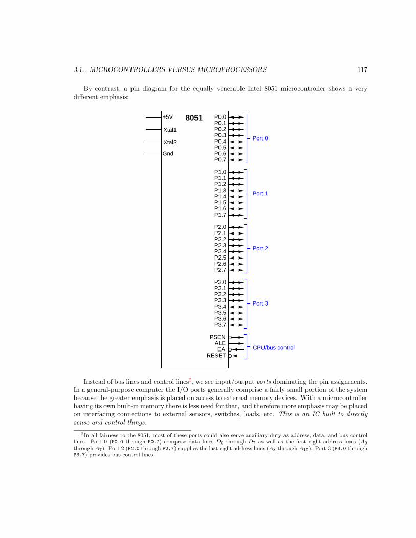
3.1. MICROCONTROLLERS VERSUS MICROPROCESSORS 117
By contrast, a pin diagram for the equally venerable Intel 8051 microcontroller shows a verydifferent emphasis:
+5V
Gnd
RESET
8051
Xtal1
Xtal2
P0.0P0.1P0.2P0.3P0.4P0.5P0.6P0.7
Port 0
Port 1
P1.0P1.1P1.2P1.3P1.4P1.5P1.6P1.7
Port 2
P2.0P2.1P2.2P2.3P2.4P2.5P2.6P2.7
Port 3
P3.0P3.1P3.2P3.3P3.4P3.5P3.6P3.7
PSENALEEA CPU/bus control
Instead of bus lines and control lines2, we see input/output ports dominating the pin assignments.In a general-purpose computer the I/O ports generally comprise a fairly small portion of the systembecause the greater emphasis is placed on access to external memory devices. With a microcontrollerhaving its own built-in memory there is less need for that, and therefore more emphasis may be placedon interfacing connections to external sensors, switches, loads, etc. This is an IC built to directlysense and control things.
2In all fairness to the 8051, most of these ports could also serve auxiliary duty as address, data, and bus controllines. Port 0 (P0.0 through P0.7) comprise data lines D0 through D7 as well as the first eight address lines (A0
through A7). Port 2 (P2.0 through P2.7) supplies the last eight address lines (A8 through A15). Port 3 (P3.0 throughP3.7) provides bus control lines.
118 CHAPTER 3. TUTORIAL
Microcontroller memory maps also differ from that of microprocessors. For many microprocessorsthe memory map is defined by the ways in which memory and I/O devices are wired to the IC, givingthe computer designer some degree of choice where data will be located in the microprocessor’saddressable space. Microcontrollers tend to have a memory map fixed by the manufacturer, whichmakes sense given that the memory is built-in to the microcontroller itself3.
Instruction sets are another point of distinguishing microprocessors from microcontrollers. Sincethe emphasis of a microcontroller is on sensing and controlling external discrete devices, you willtypically find microcontrollers offering more bit-level instructions (e.g. instructions allowing theprogrammer to individually set and clear bits within a digital word, and to test the logic state ofindividual bits as well) than microprocessors.
Furthermore, microcontrollers often contain subcircuits that are rarely if ever found inside ofgeneral-purpose microprocessors. These include, but are not limited to:
• Clock oscillators
• Timer circuits
• Analog-digital converters
• Digital-analog converters
• Serial data communication drivers
• Analog comparators
• Watchdog timers4
3It should be noted that most microcontrollers both legacy and modern offer the option of external (supplemental)memory and are not necessarily limited to the on-board memory.
4A “watchdog timer” is a dedicated timing circuit intended to serve as a self-check on the processor’s operation.Routine execution of the user program keeps resetting the watchdog timer before it has an opportunity to “timeout”. If the watchdog timer does reach the end of its count without being reset, the assumption is that the programhas halted for some reason. This may be used to trigger an automatic reset of the microcontroller to get it runningagain. This feature is obviously useful for critical measurement and control applications where the consequences ofthe microcontroller “crashing” may be severe.

3.2. MSP430G2553 PIN FUNCTIONS 119
3.2 MSP430G2553 pin functions
A microcontroller is a complete computer on a single integrated circuit (IC) “chip” designed toreceive data from and send data to other digital circuits. Being very small in size means thatmicrocontrollers typically have far less computing power and memory space than general-purposecomputers such as personal computers. They find wide application as controllers embedded withindevices such as personal appliances (e.g. electronic toothbrushes, stopwatches), complex machines(e.g. automobiles, aircraft), and industrial devices (e.g. pressure sensors, thermostats).
In order to incorporate a microcontroller into any digital circuit design, we must first understandwhat each of the pins on the microcontroller IC do. This is the purpose of this Tutorial section. Wewill focus on the Texas Instruments model MSP430G2553 microcontroller in this Tutorial, as it iswell-documented, reliable, and very inexpensive.
The model MSP430G2553 microcontroller is part of the larger MSP430 “family” ofmicrocontrollers manufactured by Texas Instruments, and it will be the model most of this Tutorialreferences. A functional pin diagram for the 20-pin version of the MSP430G2553 is shown here:
+5V
Gnd
RESET
Port 1
P1.0P1.1P1.2P1.3P1.4P1.5P1.6P1.7
Port 2
P2.0P2.1P2.2P2.3P2.4P2.5P2.6P2.7
MSP430G2553
TEST
Nearly every one of these pins serves multiple functions. For example, the RESET and TEST
pins also function as the “Spy-Bi-Wire” serial programming interface pins used for programming thedevice’s built-in Flash memory and for information exchange related to program debugging. Also,every port pin supports addition functions such as timer inputs, analog inputs, serial data inputs andoutputs, etc. Most of the Port pins default to functioning as digital I/O upon power-up, but somedo not: a case in point are the pins shown here as P2.6 and P2.7 which default to crystal oscillatorconnections (but which may be configured to function as digital I/O by setting the appropriate bitswithin the P2SEL register).
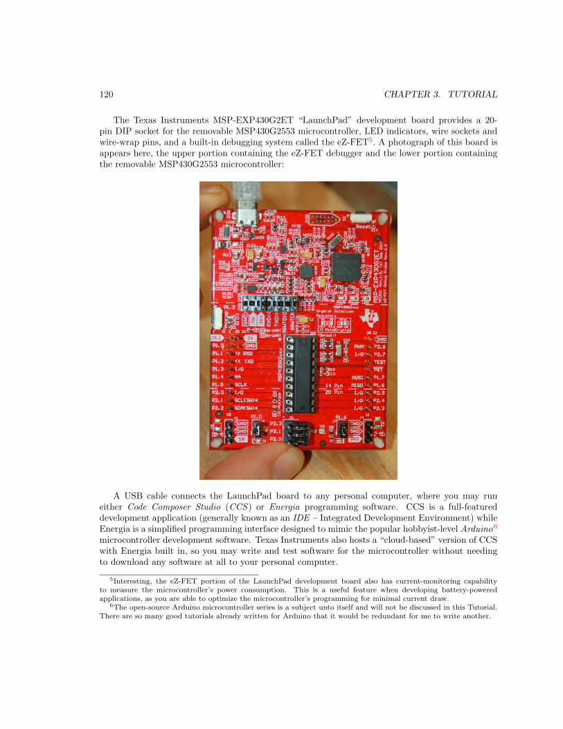
120 CHAPTER 3. TUTORIAL
The Texas Instruments MSP-EXP430G2ET “LaunchPad” development board provides a 20-pin DIP socket for the removable MSP430G2553 microcontroller, LED indicators, wire sockets andwire-wrap pins, and a built-in debugging system called the eZ-FET5. A photograph of this board isappears here, the upper portion containing the eZ-FET debugger and the lower portion containingthe removable MSP430G2553 microcontroller:
A USB cable connects the LaunchPad board to any personal computer, where you may runeither Code Composer Studio (CCS ) or Energia programming software. CCS is a full-featureddevelopment application (generally known as an IDE – Integrated Development Environment) whileEnergia is a simplified programming interface designed to mimic the popular hobbyist-level Arduino6
microcontroller development software. Texas Instruments also hosts a “cloud-based” version of CCSwith Energia built in, so you may write and test software for the microcontroller without needingto download any software at all to your personal computer.
5Interesting, the eZ-FET portion of the LaunchPad development board also has current-monitoring capabilityto measure the microcontroller’s power consumption. This is a useful feature when developing battery-poweredapplications, as you are able to optimize the microcontroller’s programming for minimal current draw.
6The open-source Arduino microcontroller series is a subject unto itself and will not be discussed in this Tutorial.There are so many good tutorials already written for Arduino that it would be redundant for me to write another.

3.3. ELEMENTARY OUTPUT AND INPUT 121
3.3 Elementary output and input
General-purpose I/O (input/output) terminals on a microcontroller are typically organized as ports,in this case each port having eight terminals. In their most basic usage, these pins are digital innature which means they will either be at a “low” or “high” logic state as represented by a ground-referenced voltage signal. Inside the microcontroller there will either be a special hardware registeror an area of general memory associated with each I/O port, and this is how those pins’ logic statesare represented to the program executing on the microcontroller’s processor: as individual bits in adata word located at some specific memory address.
Looking closely at a functional pin diagram for the MSP430G2553 microcontroller, we see double-headed arrows on all the port pins. This means these pins may function as either inputs or outputs:
+5V
Gnd
RESET
Port 1
P1.0P1.1P1.2P1.3P1.4P1.5P1.6P1.7
Port 2
P2.0P2.1P2.2P2.3P2.4P2.5P2.6P2.7
MSP430G2553
TEST
As output pins, their logic states will be driven by bits written into each port’s register bythe running code. As input pins, logic states asserted on those pins by external circuitry will beread as individual bits in another register associated with that port. For example, on the MSP430microcontroller there is an input and an output register pair for Port 1, and an input and outputregister pair for Port 2 as shown in the following list:
• Port 1 input register = P1IN
• Port 1 output register = P1OUT
• Port 2 input register = P2IN
• Port 2 output register = P2OUT
In fact, in the MSP430 there are several different registers associated with each port, not justinput and output. These other registers determine such things as the direction for each pin (whetherit will be an input or an output), whether the pin is able to function as an interrupt, etc. Writing

122 CHAPTER 3. TUTORIAL
programs to make use of these I/O pins is a matter of writing to and reading from the appropriateregisters. This section will describe the most elementary uses of general-purpose I/O ports on theMSP430.
Suppose we wished to use all eight pins of Port 1 to drive LED indicator lamps. Our schematicdiagram would look something like this:
MS
P430G
2553IN20
VSSVCC (+3.3 V)
P1.0
P1.1
P1.2
P1.3
P1.4
P1.5
P2.0
P2.1
P2.2
P2.6
P2.7
TEST
RST
P1.7
P1.6
P2.5
P2.4
P2.3
+3.3V
+3.3V
The VCC pin is the microcontroller’s positive DC power supply terminal, and VSS is its negativesupply terminal; between these terminals we must apply 3.3 Volts DC. The Reset (RST ) line isactive-low, which means the microcontroller will be forced into its “reset” state and halt executionof any program when this input line is at a logical “low” state (grounded). Therefore, we mustconnect the Reset line “high” (to +3.3 Volts) in order to ensure the microcontroller will be able torun its program. Here we use a pull-up resistor to make the Reset input high rather than a directwire connection, because using a resistor gives us the freedom to ground the Reset pin at any timeto force the microcontroller to reset without having to disconnect a wire from +V. Lastly, we seethe eight LEDs connected to the Port 1 pins, each with its own current-limiting resistor.
3.3. ELEMENTARY OUTPUT AND INPUT 123
Outputting data to these eight LEDs requires at minimum two instructions running in themicrocontroller’s program: first, we must configure all eight pins of Port 1 to be outputs rather thaninputs; second, we must write the desired bit states to the eight bits of Port 1’s output register.
The input versus output functionality of Port 1’s pins are assigned by bits written to the P1DIR
register, with 1 designating an output and 0 designating an input. Once this has been done, we maycause Port 1’s pins to go to “high” or “low” states by writing a value to the P1OUT register. Thefollowing code examples show segments of code (not a complete program!) for setting all eight bitsof Port 1 as outputs and then turning on an arbitrary pattern of LEDs:
Assembly source code:
mov #0b11111111,P1DIR
mov #0b01011101,P1OUT
As you can see, in MSP430 assembly language we use the “move” (mov) instruction to writenumerical values to each of these registers. Here, we specify those values in binary format to makeit very easy for us to relate the values to individual pin functions and logic states on Port 1. Wecould have just as readily specified those values in any other numeration system (e.g. octal, hex, ordecimal) and the port would function just as well.
C source code:
P1DIR = 0b11111111;
P1OUT = 0b01011101;
Performing the same register-write operation in the C programming language consists of treatingP1DIR and P1OUT as integer variables, setting each of them equal to the desired binary values.

124 CHAPTER 3. TUTORIAL
Using red coloring to indicate energized LEDs, this is the result of writing those numerical valuesto the P1DIR and P1OUT registers:
MS
P430G
2553IN20
VSSVCC (+3.3 V)
P1.0
P1.1
P1.2
P1.3
P1.4
P1.5
P2.0
P2.1
P2.2
P2.6
P2.7
TEST
RST
P1.7
P1.6
P2.5
P2.4
P2.3
+3.3V
+3.3V
0
1
1
1
1
0 1
0
write
write
P1DIR = 0b11111111
P1OUT = 0b01011101

3.3. ELEMENTARY OUTPUT AND INPUT 125
To use all eight bits of Port 1 as inputs rather than outputs, we must first connect those pins toexternal circuitry capable of asserting “high” and “low” states on those pins. Thus, our schematicneeds to be modified. Instead of LEDs and current-limiting resistors, we have toggle switches andpull-down resistors connected to the eight Port 1 pins:
MS
P430G
2553IN20
VSSVCC (+3.3 V)
P1.0
P1.1
P1.2
P1.3
P1.4
P1.5
P2.0
P2.1
P2.2
P2.6
P2.7
TEST
RST
P1.7
P1.6
P2.5
P2.4
P2.3
+3.3V
+3.3V
+3.3V
Register P1IN is where all input bit states reside in the microcontroller’s memory. We must stillwrite data to the direction register P1DIR, this time clearing (0) all eight bits rather than setting (1)them as shown in these Assembly-language and C-language program instruction examples:
Assembly source code: mov #0b00000000,P1DIR
C source code: P1DIR = 0b00000000;
Instead of writing data to the P1OUT register as we did before, we will let the external switchesdetermine the bit states of the P1IN register, which may be read an acted upon by conditionalinstructions we place in our code.
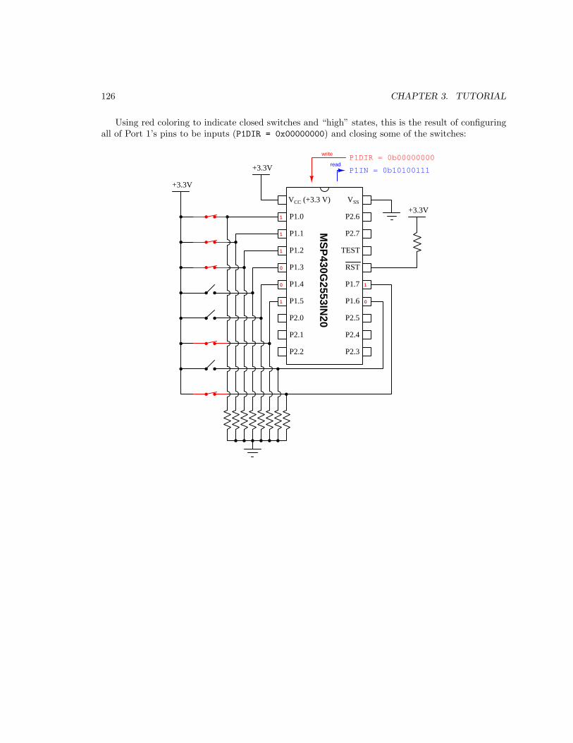
126 CHAPTER 3. TUTORIAL
Using red coloring to indicate closed switches and “high” states, this is the result of configuringall of Port 1’s pins to be inputs (P1DIR = 0x00000000) and closing some of the switches:
MS
P430G
2553IN20
VSSVCC (+3.3 V)
P1.0
P1.1
P1.2
P1.3
P1.4
P1.5
P2.0
P2.1
P2.2
P2.6
P2.7
TEST
RST
P1.7
P1.6
P2.5
P2.4
P2.3
+3.3V
+3.3V
+3.3V
1
01
1
1
1
0
0
write
readP1DIR = 0b00000000
P1IN = 0b10100111

3.4. BIT-LEVEL OUTPUT INSTRUCTIONS 127
3.4 Bit-level output instructions
Writing to an output port is as simple as assigning a value to the proper PxOUT register, but bearin mind that this register holds eight bits (for upwards of eight output pins) and therefore yourassignment instruction is dealing with all eight pins of that port at a time. When programming inassembly language or in C/C++, the instructions are remarkably similar. For example, suppose wewished to set pin P1.7 high and clear all other port 1 pins low. This would mean writing 0b10000000
to the P1OUT register:
Assembly-language example:
mov #0b10000000, P1OUT
C-language example:
P1OUT = 0b10000000;
This is fine if your intent is to make pin P1.7 high and all other pins on that port low, but what ifyou just want to control pin P1.7 while leaving the other bits’ states untouched? For this we may usebitwise operations to selectively alter specific bits within the word. For example, to set the P1.7 bitwhile leaving all the other P1.x bits in their original states, we may use the bitwise-OR-and-assignoperator in C/C++ as shown here:
P1OUT |= 0b10000000; // Comment: this sets bit P1.7 (outputs a high)
The single “1” bit specified by 0b10000000 forces P1.7 high while the seven “0” bits leave theothers unaltered, each respective pair of bits in the P1OUT register and the 0b10000000 operandbeing OR’d with each other. Similarly, if we wish to clear bit P1.7 (i.e. make it low) while leavingthe other bits in P1OUT untouched, we may use the bitwise-AND-and-assign operator in C/C++along with the binary value 0b01111111:
P1OUT &= 0b01111111; // Comment: this clears bit P1.7 (outputs a low)
The single “0” bit forces P1.7 low while the seven “1” bits leave the others unaltered after beingrespectively ANDed.

128 CHAPTER 3. TUTORIAL
If we happen to be programming the microcontroller in assembly language, we have available tous two instructions specially designed for this purpose: bit set (bis) and bit clear (bic). The waythese instructions work is to specify a value delineating which bits of the word we wish to set orclear, respectively. The “bit set” instruction is logically equivalent to a bitwise-OR-and-assign, andlooks like this:
Assembly-language example showing the “bit set” instruction:
bis #0b10000000, P1OUT ; Comment = This sets bit P1.7 (outputs a high)
Similarly, the “bit clear” instruction requires you specify which bit(s) to clear. Unlike “bit set”,the “bit clear” instruction is not logically equivalent to any general-purpose bitwise instruction:
Assembly-language example showing the “bit clear” instruction:
bic #0b10000000, P1OUT ; Comment = This clears bit P1.7 (outputs a low)
Even though the bic instruction achieves the same result as a bitwise-AND, it does so in adifferent manner. With the bitwise AND we needed to make the operand byte all 1’s except forthe bit-positions we wished to clear, because the nature of an AND function is that any 0 inputforces the output to be 0 while any 1 input lets the other input state pass through. With the bic
instruction our operand bit-states are inverted: we need to set those bit-positions we wish to clearand clear those bit-positions we wish to leave unaltered. In other words, bic #0b10000000, P1OUT
in MSP430 assembly language is equivalent to P1OUT &= 0b01111111 in C or C++. As strange asthis may seem for anyone accustomed to using standard bitwise functions with “mask” operands,the existence of these two complementary functions (bis and bic) makes selective-bit programmingfairly easy to do in assembly language because they both accept the same operand (mask) valuesfor the same bits: bis #0b10000000 sets the MSB and bic #0b10000000 clears the MSB.
Of course, if you are programming in the Sketch language within the Energia programmingenvironment, there are very intuitive and easy-to-use instructions for setting and clearing outputpins:
Sketch-language example:
digitalWrite(15, HIGH); // Comment = This sets bit P1.7 (pin 15 on IC)
The desired state is simply coded as either HIGH or LOW, and the pin identifier is actually thephysical pin number on the integrated circuit rather than being a bit number within a port’s byteregister. Suffice it to say, Sketch is designed to make microcontroller programming very easy.

3.4. BIT-LEVEL OUTPUT INSTRUCTIONS 129
A very useful programming aid included with Code Composer Studio are header files, eachcontaining symbolic constants with easily-remembered names to help simplify the setting and clearingof bits within registers. Some of these symbols are generic while others are highly specific to themicrocontroller model. By including the header file msp430.h the assembler/compiler knows torecognize any of these symbols written in your code as aliases for certain binary values. For example,the following “standard bits” are defined as specific hexadecimal values within every MSP430 headerfile:
(from msp430g2553.h)
#define BIT0 (0x0001)
#define BIT1 (0x0002)
#define BIT2 (0x0004)
#define BIT3 (0x0008)
#define BIT4 (0x0010)
#define BIT5 (0x0020)
#define BIT6 (0x0040)
#define BIT7 (0x0080)
To show how this simplifies bit-writing, consider the following C-language statements which dothe exact same thing:
P1OUT |= 0b10000000; // Comment: this sets bit P1.7 (outputs a high)
P1OUT |= BIT7; // Comment: this sets bit P1.7 (outputs a high)
If your goal is to set the output bit P1.7, BIT7 certainly makes more intuitive sense than0b10000000, which in turn makes your code easier to understand and troubleshoot.
Recall that in C we had to use a bitwise-AND function with a “mask” consisting of a single 0 andthe other bits 1 in order to clear one bit in a byte. We can also use a BIT symbol for this purpose, byprepending the complementation operator (i.e. if BIT7 = 0b10000000 then ~BIT7 = 0b01111111).Here again we see two example lines of C code, each one doing exactly the same thing:
P1OUT &= 0b01111111; // Comment: this clears bit P1.7 (outputs a low)
P1OUT &= ~BIT7; // Comment: this clears bit P1.7 (outputs a low)
Again, we see how the instruction using the BIT symbol is much easier to comprehend.
130 CHAPTER 3. TUTORIAL
3.5 Bit-level input instructions
Reading from an input port is as simple as reading the value from the proper PxIN register, but justlike output registers the input registers each hold eight bits (for upwards of eight input pins) andtherefore the binary value read refers to all eight pins of that port at a time. When programming inassembly language or in C/C++, the instructions are remarkably similar. For example, suppose wewished to read all eight pin states of Port 1 (P1.0 through P1.7) into the R5 general-purpose register(assembly) or into an integer variable named switch (C/C++). The following example programsshow what the code would look like in each case:
Assembly-language example:
mov P1IN, R5
C-language example:
switch = P1IN;
Often, though, what we really need is the ability to take action on the status of a single inputline (i.e. just one of the bits in the PxIN register). MSP430 assembly language offers a specialinstruction just for this purpose, called bit-test and abbreviated bit. This instruction affects theZero bit (among others) in the microcontroller’s Status register, which means we may take actionon the state of the tested bit by using the jz (“Jump if Zero-bit is set”) instruction immediatelyafterward:
bit #0x04, P1IN ; Checks logical state of P1.2 bit
jz PIN_LOW ; If P1.2=0 the Zero bit will be set, jump to label PIN_LOW
; otherwise if P1.2=1 we just execute the next instruction
In other words, executing the bit instruction results in the Status register’s “Zero” bit reflecting7
the value of the tested bit. From there we may use any appropriate conditional jump instruction totake action on that value.
7Understanding the meaning of the Status register’s “Zero” bit can be difficult because the logic seems backwards.For example, if a bit-test or arithetic operation concludes in a zero result (e.g. the tested bit is zero, or the arithmeticresult is zero), then the Status register’s “Zero” bit becomes set to a value of one, flagging us that the test/arithmeticfunctions’ result was zero. In other words, a calculated result of zero sets the “Zero” bit (1), but a non-zero calculatedresult clears the “Zero” bit (0). Confusing, no?
3.6. MSP430G2553 ARCHITECTURE 131
Bit-testing in C or C+ requires the use of bitwise operators to select the desired bit(s) fromthe multi-bit word, similar to how we used bitwise instructions to selectively set certain bits in anoutput register. We may use the bitwise-AND instruction to “mask off” all bits except for the onewe’re interested in, and then use the resulting value as a Boolean true/false condition within an if
instruction like this:
if (P1IN & 0x04) // Checks logical state of P1.2 bit
do_something(); // If P1.2=1 then we do this...
else
do_something_else(); // Executed if P1.2=0
3.6 MSP430G2553 architecture
The MSP430 microcontroller series uses 16-bit addressing and 16-bit data busses, and is somewhatunique for a microcontroller in that there is only one of each. This is called Von Neumannarchitecture, and it is the de facto standard for general-purpose microprocessor systems. Themore traditional architecture used in microcontrollers is called Harvard architecture, where separatememory arrays (and address/data busses) exist for program instructions and program data. Manytraditional microcontrollers use Harvard architecture, including the Intel 8051, Motorola 68HC11and 68HC12, and Microchip PIC microcontroller family.

132 CHAPTER 3. TUTORIAL
3.6.1 Registers
Another feature of the MSP430 series is a large number of general-purpose registers for temporarilystoring numerical values. The MSP430 has sixteen 16-bit registers, the first four being dedicated tospecific purposes and the last twelve open for general use:
• Register R0 = Program Counter
• Register R1 = Stack Pointer
• Register R2 = Status
• Register R3 = Constant Generator
• Register R4 through R15 = General Purpose
Most of these registers simply function as 16-bit binary values. The Program Counter register,for example, contains the memory address of the current instruction being executed. However, theStatus register (R2) is one where individual bits have specific meanings of their own, acting as flagsfor specific conditions within the microcontroller. The following illustration shows all 16 bits of theStatus register from MSB (left) to LSB (right), and the meanings of each:
Carry bit
C
Bit 0Bit 1Bit 2Bit 3Bit 4Bit 5Bit 6Bit 7Bit 8Bits 9-15
ReservedZero bit
Z
Negative bit
NEnable
GIE
General InterruptCPU off
CPUOFF
Oscillator off
OSCOFF
System ClockGenerator 1 Generator 0
SCG0SCG1
System ClockOverflow bit
V
For example, the Overflow bit (bit 8) in the Status register defaults to a reset (0) state unlessan arithmetic operation on signed integers results in a value exceeding the allowable range, in whichcase that bit automatically becomes set (1) by the processor’s arithmetic logic unit (ALU). A line ofcode reading this bit will be able to tell, for example, whether or not the last addition/subtractionoperation yielded a valid result.
Another example in this register is the General Interrupt Enable bit (bit 3) which must be writtento a set (1) state in order to permit any of the user-defined interrupts to function at all. Unlike theOverflow bit which is written by the ALU and read by the programmed code, this Interrupt bit iswritten by the programmed code and then read by the interrupt hardware.

3.6. MSP430G2553 ARCHITECTURE 133
3.6.2 Memory map
The MSP430G2553’s memory map is as follows:
• 8-bit Special Function Registers = 0x00 to 0x0F
• 8-bit peripherals = 0x10 to 0xFF
• 16-bit peripherals = 0x100 to 0x1FF
• General (RAM) = 0x200 to 0x3FF
• Information memory (Flash EEPROM) = 0x1000 to 0x10FF
• Code memory (Flash EEPROM) = 0xC000 to 0xFFFF
• Interrupt vectors (Flash EEPROM) = 0xFFC0 to 0xFFFF
All memory in the MSP430 is byte-oriented, i.e. one byte (eight bits) per address. 16-bit wordstherefore occupy two addresses, little-endian style, and always begin with an even-numbered address.

134 CHAPTER 3. TUTORIAL
3.6.3 I/O ports
All I/O on the MSP430 microcontroller is memory-mapped, which means it is accessed by the sameaddressing and the same address bus as the rest of the system’s memory. Each 8-bit I/O porton the microcontroller has several registers dedicated to the port’s configuration. For the modelMSP430G2553IN20 with 20 pins8, the two I/O ports’ memory bytes are organized as follows:
Port 1
• Input register = P1IN located at memory address 0x020
• Output register = P1OUT located at memory address 0x021
• Direction register = P1DIR located at memory address 0x022
• Interrupt Flag register = P1IFG located at memory address 0x023
• Interrupt Edge Detect register = P1IES located at memory address 0x024
• Interrupt Enable register = P1IE located at memory address 0x025
• Port Select register = P1SEL located at memory address 0x026
• Resistor Enable register = P1REN located at memory address 0x027
• Port Select 2 register = P1SEL2 located at memory address 0x041
Port 2
• Input register = P2IN located at memory address 0x028
• Output register = P2OUT located at memory address 0x029
• Direction register = P2DIR located at memory address 0x02A
• Interrupt Flag register = P2IFG located at memory address 0x02B
• Interrupt Edge Detect register = P2IES located at memory address 0x02C
• Interrupt Enable register = P2IE located at memory address 0x02D
• Port Select register = P2SEL located at memory address 0x02E
• Resistor Enable register = P2REN located at memory address 0x02F
• Port Select 2 register = P2SEL2 located at memory address 0x042
8The 28-pin version of the MSP430G2553 offers a Port 3 in addition to the standard Port 1 and Port 2.

3.6. MSP430G2553 ARCHITECTURE 135
The following illustration shows all the registers associated with the microcontroller’s pins. Each“x” refers to the port number; e.g. Port 1 registers would be P1IN, P1OUT, P1DIR, etc. while Port 2registers would be P2IN, P2OUT, P2DIR, etc. Not every port in the MSP430 family supports interruptinputs, which is why the upper three registers appear in grey:
Px.0Px.1Px.2Px.3Px.4Px.5Px.6Px.7
PxIN
PxOUT
PxDIR
1=High
0=Low
1=High
0=Low
1=High
0=Low
1=High
0=Low
1=High
0=Low
1=High
0=Low
1=High
0=Low
1=High
0=Low
1=Set
0=Clear
1=Set
0=Clear
1=Set
0=Clear
1=Set
0=Clear
1=Set
0=Clear
1=Set
0=Clear
1=Set
0=Clear
1=Set
0=Clear
1=Output
0=Input
1=Output
0=Input
1=Output
0=Input
1=Output
0=Input
1=Output
0=Input
1=Output
0=Input
1=Output
0=Input
1=Output
0=Input
PxIFG
PxREN1=Enabled
0=Disabled
1=Enabled
0=Disabled
1=Enabled
0=Disabled
1=Enabled
0=Disabled
1=Enabled
0=Disabled
1=Enabled
0=Disabled
1=Enabled
0=Disabled
1=Enabled
0=Disabled
PxSEL2/PxSEL00=I/O
01=Primary
10=(reserved)
11=Secondary
00=I/O
01=Primary
10=(reserved)
11=Secondary
00=I/O
01=Primary
10=(reserved)
11=Secondary
00=I/O
01=Primary
10=(reserved)
11=Secondary
00=I/O
01=Primary
10=(reserved)
11=Secondary
00=I/O
01=Primary
10=(reserved)
11=Secondary
00=I/O
01=Primary
10=(reserved)
11=Secondary
00=I/O
01=Primary
10=(reserved)
11=Secondary
Write output states here
Read input states here
Write bits to activateinternal Rpullup/down
Write bits to this register
I/O pins
1=Pending
0=Not pending
PxIESWrite bits to define edge type
1=Falling edge
0=Rising edge
1=Falling edge
0=Rising edge
1=Pending
0=Not pending
1=Falling edge
0=Rising edge
1=Falling edge
0=Rising edge
1=Pending
0=Not pending
1=Pending
0=Not pending
1=Falling edge
0=Rising edge
1=Falling edge
0=Rising edge
1=Pending
0=Not pending
1=Pending
0=Not pending
1=Falling edge
0=Rising edge
1=Falling edge
0=Rising edge
1=Pending
0=Not pending
1=Pending
0=Not pending
PxIEWrite bits to enable interrupts
1=Enabled
0=Disabled
1=Enabled
0=Disabled
1=Enabled
0=Disabled
1=Enabled
0=Disabled
1=Enabled
0=Disabled
1=Enabled
0=Disabled
1=Enabled
0=Disabled
1=Enabled
0=Disabled
for inputs
pair to define pin function
Write bits to define I/O direction
Read/write interrupt flag bits
Portregisters
For example, if we wished to read the status of pin P1.3, we would have to read bit 3 of theInput register P1IN. If we wished to output a high state on pin P2.7, we would have to “set” bit7 of the Output register P2OUT. If we wished to output a low state on pin P1.6, we would have to“clear” bit 6 of Output register P1OUT.
Since all I/O pins on this microcontroller are bidirectional, we need a way to configure thedirection of each pin individually, and this is done with the Direction register for each port. Forexample, if we wanted to use the pins P1.0 through P1.2 as outputs and the rest of Port 1’s pins asinputs, we would have to write the binary value 0b00000111 (or hexadecimal value 0x07) to P1DIR
because the microcontroller regards any “0” bits in the Direction register to represent input and any“1” bits to represent output.
A convenient feature when using I/O pins as inputs is the provision of an internal pull-up/pull-down resistor. This eliminates the need for connecting external resistors to input pins in order toavoid indeterminate logic states. To enable a pin’s internal resistor, simply set (1) the respective bitin the PxREN register. The resistor will pull up if the respective bit in the PxOUT register is set (1)and will pull down if the PxOUT bit is cleared (0).
Pins have multiple functions in the MSP430 microcontroller series, and these are selectable bythe Select and Select 2 registers. When the same bit position in both registers are cleared (0,0) thatpin will function as basic digital I/O (Px.y). However, for the other three bit combinations (0,1 ; 1,0

136 CHAPTER 3. TUTORIAL
; 1,1) in the Select and Select 2 registers the pin will assume other functions. The specific functionsselected are model-dependent, so the manufacturer’s literature is your best guide here. Most pinsdefault as I/O (0,0), but not all! A noteworthy example of pins defaulting to one of these “other”functions are pins P2.6 and P2.7 which default to crystal oscillator connections, necessary if themicrocontroller is to use an external crystal to regulate its clock frequency. If you wish to use eitherof these two pins as regular I/O, you must clear those respective bits in the register. By defaultP2SEL has a hexadecimal value of 0xC0, but to use all Port 2 pins as general I/O we would need tomake P2SEL have a value of 0x00.
Lastly, while all port pins on the microcontroller have the ability to function inputs, some of themhave the ability to function as a special kind of input called an interrupt. Unlike a regular inputpin that simply sets or clears its bit in the PxIN register depending on the logic state provided to itby an external device, an interrupt pin causes the running program to cease its current action andimmediately jump to a new section of code called the ISR (Interrupt Service Routine) to performsome time-critical function9. These are maskable interrupts because you have the ability to enableor disable each one with the bit states written to register PxIE. Since these are time-critical events,what matters is the leading edge of the pulse signal sensed by the pin, and so another register (PxIES)defines whether it will be a rising edge (a low-to-high transition) or a falling edge (a high-to-lowtransition) that will set the interrupt flag. This microcontroller relies on the ISR code to clear theflag upon completion.
When using the MSP430G2553 microcontroller on the MSP-EXP430G2ET “LaunchPad”development board, the following I/O pins come pre-connected to some external devices. Thisis useful for proof-of-concept demonstration programs:
• Green LED = P1.0
• Red LED = P1.6
• Multicolor LED:
Red = P2.1
Green = P2.3
Blue = P2.5
• Pushbutton switch = P1.3 (pin goes low when pressed)
9An example of an interrupt input on a microcontroller would be a timing signal coming from an external clockdevice or some sensor measuring an event demanding immediate attention (e.g. the signal in an automobile enginecontroller indicating when the engine’s crankshaft reaches the top-dead-center position once every revolution, as allother time-critical engine control events such as spark timing and fuel injection timing depend on this signal

3.6. MSP430G2553 ARCHITECTURE 137
3.6.4 Interrupts
An interrupt is a facility within a microprocessor or microcontroller allowing it to have its normalflow of program execution interrupted by some event. When an interrupt event occurs, a bit inone of the special-function registers called an interrupt flag becomes set, causing the program tocomplete its current instruction execution cycle and then immediately jump to a pre-designatedlocation in memory (called the interrupt vector). Within the interrupt vector address is stored thememory address for the start of some new code to execute. This new section of code is called theinterrupt service routine (or ISR) and its purpose is to do whatever needs to be done in responseto the interrupt event. The last two lines of code in the ISR terminate the interrupt by clearing theinterrupt flag bit and then commanding a return to the main program.
Interrupts, therefore, are similar to subroutines in that the normal thread of execution is haltedso that the processor can jump to some other location in program memory and perform a differentfunction, then jump back to resume what it was doing before. The major10 difference betweenan interrupt and a subroutine is that while a subroutine is “called” by an instruction in the mainprogram, an interrupt is forced by some event independent of the main program.
Interrupts are necessary when the processor must respond to highly time-critical events. Anexample of such an event includes incoming data received by a serial receiver from some other device.If the processor ignores incoming data and continues whatever other task its main program wouldhave it do, data bits may be “lost” by the time the processor finishes its other task(s). Therefore,serial data reception is a common interrupt source for microprocessors and microcontrollers alike:incoming serial data causes an interrupt, which halts the main program’s execution and forces theprocessor to “service” the incoming data to ensure none of it is lost. Other examples includeinternally-generated interrupts from microcontroller timers for the purpose of ensuring certaincalculations are performed at regular intervals (e.g. integral and derivative calculations for a PIDcontrol algorithm).
Interrupts are one of those areas of microprocessor/microcontroller architecture that tends tovary widely between models and manufacturers. For this reason it should be understood that therest of this subsection should be read as a description specific to the Texas Instruments MSP430microcontrollers, and to not generalize too much to other devices.
In the MSP430 microcontroller family, the highest addresses in Flash EEPROM memory arereserved as interrupt vectors: 0xFFC0 through 0xFFFF, ordered in terms of priority in case multipleinterrupt events occur simultaneously. Address 0xFFFE, for example, is the highest priority interruptvector and it is reserved for resets of the microcontroller (e.g. power-up, external reset input, illegalinstruction fetch, etc.). As we can see in this example, sometimes the triggering event for an interruptis external (e.g. reset pin) while other times it may be internally generated by the microcontroller(e.g. illegal instruction).
10Other differences exist as well between subroutines and interrupts, including the fact that during an interruptboth the Program Counter and the Status Register are automatically pushed to the stack (in that order), and bothare automatically popped off the stack when returning from the interrupt service routine. For subroutines only theProgram Counter gets pushed to and popped off the stack – the Status Register remains unaffected in case thesubroutine requires the last status values to properly function. With interrupts the MSP430 assumes present StatusRegister bit conditions are irrelevant to the interrupt event and pushes the old Status Register to the stack beforeclearing all Status Register bits prior to executing the ISR. This also has the effect of clearing the GIE bit (GeneralInterrupt Enable) in the Status Register which means the ISR itself cannot be interrupted by any other interruptevents regardless of priority.

138 CHAPTER 3. TUTORIAL
Some interrupts are maskable which means they may be enabled or disabled by programmingcertain bit states in the Special Function Registers. The P1IE and P2IE Interrupt Enable registersare an example of this, where bit states in those registers enable (1) or disable (0) respective I/Opins as external interrupt signal sources. A non-maskable interrupt (or NMI ), by contrast, cannotbe disabled by the user.
When any interrupt event occurs, a flag bit becomes set which indicates to the processor thatit must reference the interrupt vector and then jump to the appropriate ISR. This flag bit remainsset until the user’s program clears it. This is why all ISRs should have a bit-clear instruction11
somewhere in their code.
Port-driven interrupts in the MSP430 series are edge-triggered just like the “clock” input on aflip-flop. Additional registers exist for the user to specify whether the triggering transition will bea rising edge (low-to-high) or falling edge (high-to-low): P1IES for Port 1 bits and P2IES for Port 2bits.
When writing programs to use maskable interrupts, one must enable the desired interrupt andalso enable the General Interrupt Enable (GIE) bit before the interrupt will be functional. It is alsogood practice to initialize all enabled interrupt flags to their zero (0) states, just in case one or moreof them happened to become set during power-up.
11MSP430 assembly language conveniently provides a “bit clear” bic instruction. For example, clearing the interruptflag for Port 1 bit 3 could be done with the assembly instruction bic #0x08, P1IFG. However, when programming inC or C++ there is no comparable “bit clear” instruction, and so the usual technique is to use a bitwise-AND-assignoperator. For example, clearing the interrupt flag for Port 1 bit 3 could be done with the C/C++ instruction P1IFG
&= 0xF7; or P1IFG &= ~BIT3;.

3.6. MSP430G2553 ARCHITECTURE 139
The ISR must also be specified by the user’s program in order for an interrupt to be useful.The Code Composer Studio assembler uses sections to define specific regions of code that willbe loaded into the microcontroller’s memory. When programming in either C or C++, interruptservice routines are selected using the #pragma directive, each vector having a specific name. Theseassembly-language sections and C/C++ name are listed here in descending order of priority for themodel MSP430G2553:
Interrupt source Vector address Assembly section C/C++ name
Reset 0xFFFE .reset RESET VECTOR
Non-maskable 0xFFFC .int14 NMI VECTOR
TIMER1 A0 0xFFFA .int13 TIMER1 A0 VECTOR
TIMER1 A1 0xFFF8 .int12 TIMER1 A1 VECTOR
Comparator A 0xFFF6 .int11 COMPARATORA VECTOR
Watchdog timer 0xFFF4 .int10 WDT VECTOR
TIMER0 A0 0xFFF2 .int09 TIMER0 A0 VECTOR
TIMER0 A1 0xFFF0 .int08 TIMER0 A1 VECTOR
USCIAB0RX 0xFFEE .int07 USCIAB0RX VECTOR
USCIAB0TX 0xFFEC .int06 USCIAB0TX VECTOR
ADC10 0xFFEA .int05 ADC10 VECTOR
Port 2 I/O 0xFFE6 .int03 PORT2 VECTOR
Port 1 I/O 0xFFE4 .int02 PORT1 VECTOR

140 CHAPTER 3. TUTORIAL
If we examine a very simple assembly-language program for the MSP430G2553, we see how thereset interrupt vector is configured:
.cdecls C,LIST,"msp430.h"
.def RESET
.text
.retain
.retainrefs
RESET mov.w #__STACK_END,SP ; Initialize stackpointer
StopWDT mov.w #WDTPW|WDTHOLD,&WDTCTL ; Stop watchdog timer
;================================= Code Begin =================================
MAIN
mov #0x05,R4
add #0x06,R4
;================================== Code End ==================================
.global __STACK_END
.sect .stack
.sect ".reset"
.short RESET
The last two lines of this program configure the RESET interrupt vector. First, the appropriatesection is declared (.sect ".reset") for this particular interrupt vector, and then the label for theISR is specified (.short RESET). When any of the interrupt flags belonging to the reset function areset, the vector at 0xFFFE points to the memory address resolved to the label RESET by the assembler,which in turn executes the mov.w instruction to initialize the stack pointer.

3.6. MSP430G2553 ARCHITECTURE 141
An example of a port-driven interrupt is seen in the following assembly-language program, writtento toggle the state of output P1.0 every time input P1.3 transitions from a high logic level to a lowlogic level:
.cdecls C,LIST,"msp430.h"
.def RESET
.text
.retain
.retainrefs
RESET mov.w #__STACK_END,SP
StopWDT mov.w #WDTPW|WDTHOLD,&WDTCTL
;============================ BEGIN CODE ===============================
SETUP
mov #0xF7, P1DIR ; P1.3 as input, all others outputs
mov #0x08, P1OUT ; Begin with all outputs low
mov #0x08, P1IE ; Enable interrupt on P1.3
bis #0x08, P1IES ; Interrupt on high-to-low transition
bic #0x08, P1IFG ; Clear any pending P1.3 interrupt flag
bis #0x08, SR ; Set the General Interrupt Enable (GIE) bit
LOOP ; A useless loop -- does absolutely nothing!
jmp LOOP
P1_ISR
xor #0x01, P1OUT ; Toggle P1.0 bit
bic #0x08, P1IFG ; Clear the P1.3 interrupt flag
reti ; Return from ISR
;============================ END CODE ===============================
.global __STACK_END
.sect .stack
.sect ".reset"
.short RESET
.sect ".int02" ; .int02 = Port 1 interrupt vector section
; (shared by all P1.x pins)
.short P1_ISR ;
In addition to the obligatory reset interrupt assignment, we also have the interrupt vector forPort 1 assigned to the address resolved to label P1 ISR by the .sect ".int02" and .short P1 ISR
directives. Alternatively, we could have used the single directive .intvec ".int02", P1 ISR to dothe same.

142 CHAPTER 3. TUTORIAL
3.6.5 Watchdog timer
A watchdog timer is any electronic timer designed to monitor another system for indications ofhalting. In the MSP430 series of microcontrollers, the built-in watchdog timer function is a 16-bit counter circuit inside of the microcontroller driven by the clock signal, designed to issue ageneral system interrupt at the highest level to reset the program if the watchdog timer itself is notperiodically reset to zero before reaching the end of its count by the running program. The notionis, if the programmed code happens to “hang” for any reason (e.g. a programming error, an infiniteloop, an inordinate delay, etc.) it is better for the microcontroller to re-start itself than to remain“frozen” and inoperative.
This is a safety feature useful for any microcontroller controlling a critical system (e.g. airbagdeployment in an automobie), but an annoyance to students, hobbyists, and developers just tryingto get their code to function as they want it. For this reason the MSP430’s watchdog timer may bedisabled by setting the appropriate bit in its control register, that 16-bit register named WDTCTL.
Some of the more important bits within the WDTCTL register are defined as follows:
• Bits 15-8 = Watchdog timer register password
• Bit 7 = Watchdog timer hold (stops timer when set to 1)
• Bit 3 = Watchdog timer counter clear (resets counter value to zero when this bit is set to 1)
• Bit 2 = Watchdog timer clock source select (0 = Sub-Main Clock SMCLK, 1 = Auxiliary ClockACLK)
• Bits 1-0 = Watchdog timer interval (00 = clock/32768 ; 01 = clock/8192 ; 10 = clock/512 ;11 = clock/64)
Any time a bit state changes in the WDTCTL register, it must be accompanied by the writing of a“password” value of 0x5A to the upper eight bits of the register. This validates the other bit-changesas being valid. If one or more bits get changed in the WDTCTL register without the accompanyingpassword written to the most-significant eight bits, the microcontroller gets reset as though thewatchdog timer has timed out. Immediately after a WDTCTL register write operation, those passwordbits (15 through 8) default to a value of 0x69.
To anyone accustomed to the use of passwords to authenticate human users on a computersystem, this use of a password to “protect” an internal microncontroller register may seem strange.After all, who can even access this register once the microcontroller has been programmed, and alsohow difficult would it be for a programmer to “hack” into this register when there is only one properpassword and it’s given to you right in the instruction manual? The purpose, though, is not to guardagainst improper human intrusion, but rather to guard against accidental overwrites in memory thatcould result from any number of causes such as stack overflow. If the purpose of the watchdog timeris to provide a fail-safe recovery method for a halted or otherwise errant program, the last thingyou would want is for this protective feature to become accidently disabled by illegitimate writeoperations made by that same errant program.

3.6. MSP430G2553 ARCHITECTURE 143
Many simple MSP430 programs begin with a line of code near the very beginning of the sourcefile disabling the watchdog timer prior to any other instructions being executed. Take these twoexamples, one written in assembly language and another in C:
Assembly code listing
mov.w #WDTPW | WDTHOLD, &WDTCTL
C code listing
WDTCTL = WDTPW | WDTHOLD;
The symbols WDTPW (WatchDog Timer PassWord) and WDTHOLD (WatchDog Timer HOLD)are both defined in the header file for the particular model of MSP430 microcontroller beingprogrammed, equivalent to 0x5A00 and 0x0080, respectively. The bitwise-OR operator (|) combinesthe bit-states of these two symbols into 0x5A80. This means the following code examples are exactlyequivalent:
Assembly code listing
mov.w #0x5A80, &WDTCTL
C code listing
WDTCTL = 0x5A80;
However, using these symbolic constants instead of obscure hexadecimal (or binary!) numbervalues makes the program easier for human readers to interpret.

144 CHAPTER 3. TUTORIAL
To actually use the watchdog timer (and not just disable it), a line of code must be inserted intoyour program at such a location that it should be periodically executed at a time interval shorterthan the time it takes for the watchdog timer’s counter to “time out”. This line of code is verysimilar to the lines shown previously to disable the watchdog timer, except setting the “watchdogtimer counter clear” bit (WDTCNTCL) rather than the “Watchdog timer hold” bit (WDTHOLD). Examplesin both assembly and C follow:
Assembly code listing
mov.w #WDTPW | WDTCNTCL, &WDTCTL
C code listing
WDTCTL = WDTPW | WDTCNTCL;
3.7 MSP430G2553 auxiliary functions
General-purpose microprocessors require an array of supporting hardware to function, includingROM, RAM, I/O drivers, clock pulse sources, etc. Microcontrollers, on the other hand, include mostif not all of these functions within a single integrated circuit in order to present a “system-on-a-chip”for minimal-hardware designs. As a result, it is relatively simple to build and use microcontrollersfor simple electronic projects, whereas a microprocessor demands a much greater level of design andPCB layout work just to be functional.
The MSP430G2553 microcontroller is no exception, and as one would expect it sports a range ofuseful auxiliary functions to make it extremely capable as a stand-alone IC. The following subsectionssummarize these auxiliary features.

3.7. MSP430G2553 AUXILIARY FUNCTIONS 145
3.7.1 Clocks
All microprocessors require a clock signal to synchronize the operations necessary to fetch andexecute instructions stored in memory. General-purpose microprocessors rely on external oscillatorcircuits for their clock signals, but microcontrollers typically offer internal clock signal sources torelieve the end-user from having to specify and/or design an oscillator to drive the chip.
The MSP430 series offers multiple oscillator sources, and translates these raw pulse sources intomultiple clock signals used internally to drive the CPU and peripheral functions:
Oscillator options:
• DCOCLK = Digitally Controlled Oscillator (internal to the microcontroller)
• VLOCLK = Very Low Power Oscillator (internal to the microcontroller)
• LFXT1CLK = Low-Frequency Crystal Oscillator (external to the microcontroller)
• XT2CLK = High-Frequency Crystal Oscillator (external to the microcontroller)
Available clock signals:
• MCLK = Master Clock, drives the CPU and is sourced by any one of the four oscillators withoptions for 1/2/4/8 frequency division (all software-selectable)
• SMCLK = Sub-Main Clock, sourced by any one of the four oscillators with options for 1/2/4/8frequency division (all software-selectable)
• ACLK = Auxiliary Clock, sourced by either LFXT1CLK or VLOCLK (all software-selectable)
A set of Basic Clock System Control registers (BCSCTL1 through BCSCTL3) establish oscillatorsources for each of the three clock signals, as well as frequency ranges for the crystal-driven sources.
The Master Clock frequency is obviously important to the speed of program execution, sinceit is what drives the processor. High speed is good when the program must respond quickly toexternal events. However, low speed conserves power12, which is often a prime consideration formicrocontrollers when used in battery-powered and other limited-power applications.
Various auxiliary functions within the microcontroller also require a reliable clock signal, andgiven the software-selectability of these signals it not only possible but very commonplace to haveperipheral functions running on a different clock frequency than the CPU. Such functions includeserial data communication, timers, and analog-digital converters.
12The fundamental reason for this is the CMOS circuitry from which modern microprocessors and microcontrollersare fabricated. Unlike bipolar TTL logic which tends to dissipate the same amount of electrical power in heatregardless of operating frequency, MOSFET logic circuits draw most of their current during transitional states. Instatic conditions a CMOS logic circuit consumes negligible power, but power demand rises with frequency becauseeach complementary MOSFET stage passes some current from source to drain when both transistors are in theirpartially-on modes. The more often these transistors must transition between fully-on and fully-off states (in eitherdirection), the more power they dissipate. This is why overclocking a microprocessor is usually limited by the chip’scooling system: its ability to reject the additional heat that comes with higher operating frequency.

146 CHAPTER 3. TUTORIAL
3.7.2 General timers
PENDING
3.7.3 Watchdog timer
PENDING
3.7.4 Analog-Digital conversion
PENDING
3.7.5 Analog comparators
PENDING
3.7.6 Serial data interfaces
PENDING
3.8 CCS assembly-language programming
Texas Instruments’ Code Composer Studio integrated development environment (IDE) offers fullsupport for assembly-language programming of the MSP430 microcontroller series. The examplescreenshots shown here were taken with version 10 of Code Composer Studio.
When starting a new assembly project, first select “CCS Project” under the “New” projectdrop-down option:
It is very important to specify that you wish to start a new project as opposed to simply openinga new file, as a “project” entails not just the source code files but also other files (e.g. headers,Makefiles) needed for compilation.
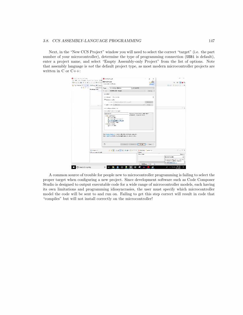
3.8. CCS ASSEMBLY-LANGUAGE PROGRAMMING 147
Next, in the “New CCS Project” window you will need to select the correct “target” (i.e. the partnumber of your microcontroller), determine the type of programming connection (USB1 is default),enter a project name, and select “Empty Assembly-only Project” from the list of options. Notethat assembly language is not the default project type, as most modern microcontroller projects arewritten in C or C++:
A common source of trouble for people new to microcontroller programming is failing to select theproper target when configuring a new project. Since development software such as Code ComposerStudio is designed to output executable code for a wide range of microcontroller models, each havingits own limitations and programming idiosyncrasies, the user must specify which microcontrollermodel the code will be sent to and run on. Failing to get this step correct will result in code that“compiles” but will not install correctly on the microcontroller!

148 CHAPTER 3. TUTORIAL
This will present a view of a “template” assembly language source file with all the defaultdeclarations needed for most assembly-language programs:
Two different options exist for compilation and loading of your program into the microcontrollerunder the “hammer” icon: Debug and Release. Selecting “debug” will assemble the source codein preparation for a live debugging session where you may single-step the program’s execution toverify its proper operation while viewing register contents, the memory map, etc. Selecting “release”will assemble the source code and ready the object code for loading into the microcontroller withno debugging facilities activated: i.e. the code will be assembled in preparation to run as a final“release” version:
In order to load the assembled object code into the microcontroller, you must click on either theinsect icon (debug) or the folder icon containing curly-braces (release).

3.9. CCS C-LANGUAGE PROGRAMMING 149
3.9 CCS C-language programming
Texas Instruments’ Code Composer Studio integrated development environment (IDE) offers fullsupport for both C and C++ language programming of the MSP430 microcontroller series. Theexample screenshots shown here were taken with version 10 of Code Composer Studio, showing anexample program written in C.
When starting a new assembly project, first select “CCS Project” under the “New” projectdrop-down option:
It is very important to specify that you wish to start a new project as opposed to simply openinga new file, as a “project” entails not just the source code files but also other files (e.g. headers,Makefiles) needed for compilation.

150 CHAPTER 3. TUTORIAL
Next, in the “New CCS Project” window you will need to choose the proper “target” (i.e.microcontroller part number), choose a suitable programming connection (USB1 is the default),enter a project name, and select “Empty Project (with main.c)” from the list of options:
A common source of trouble for people new to microcontroller programming is failing to select theproper target when configuring a new project. Since development software such as Code ComposerStudio is designed to output executable code for a wide range of microcontroller models, each havingits own limitations and programming idiosyncrasies, the user must specify which microcontrollermodel the code will be sent to and run on. Failing to get this step correct will result in code that“compiles” but will not install correctly on the microcontroller!
This will present a view of a “template” main.c source file with all the default declarationsneeded for most C-language programs:
As you can see, there isn’t much to this template source file. A single #include directive instructsthe compiler to include the contents of the msp430.h header file for compilation, and the main()
function helpfully contains a statement disabling the default watchdog timer within the MSP430microcontroller.

3.9. CCS C-LANGUAGE PROGRAMMING 151
Two different options exist for compilation and loading of your program into the microcontrollerunder the “hammer” icon: Debug and Release. Selecting “debug” will compile and link the sourcecode in preparation for a live debugging session where you may single-step the program’s execution toverify its proper operation while viewing register contents, the memory map, etc. Selecting “release”will compile and link the source code and ready the object code for loading into the microcontrollerwith no debugging facilities activated: i.e. the code will be assembled in preparation to run as afinal “release” version:
In order to load the assembled object code into the microcontroller, you must click on either theinsect icon (debug) or the folder icon containing curly-braces (release).

152 CHAPTER 3. TUTORIAL
In an effort to make programming the MSP430 series easy for beginners, the developers includeda very simple “Blink The LED” program as a New CCS Project option rather than a mostly-blankmain.c template file. This may be selected in lieu of the “Empty Project (with main.c) optionshown earlier:
After selecting this option and opening the new project, we see the source code as shown here:
As with the Empty Project option, this main.c source file contains the obligatory header inclusiondirective as well as the watchdog timer disabling statement. New additions to the source code includea statement setting the first pin of port 1 to be an output, a variable declaration for an integer namedi, a while() loop set to execute without end, a bitwise Exclusive-OR function toggling the state ofthe P1.0 bit, and a simple for() loop creating a time delay by counting backwards from 10000 tozero. This code is designed to toggle the P1.0 output bit, wait for a short time period, then repeat.
3.9. CCS C-LANGUAGE PROGRAMMING 153
The comment following the variable declaration line deserves further elaboration. When a high-level language such as C or C++ is “compiled” into machine language, there is always more thanone practical way to do that translation. Often times the most direct and literal compilation doesnot yield the most compact machine code, and so all compilers offer a feature called optimizationwhereby the compiled code may be streamlined for some purpose such as minimum memory spaceor maximum speed. Microcontrollers are limited in memory capacity for the obvious reason thattheir primary (and often only) memory is on-board the MCU chip, which means compilers designedto compile executable code for microcontrollers often default to optimization favoring minimummemory usage.
Optimization is unknown to assembly-language programming, because the point of assembly-language programming is to mimic the machine code which will be written to memory. The pricewe pay for programming in assembly language is having to think like the microcontroller, unableto perform complex operations with single statements. Languages such as C and C++ offer vastlymore sophisticated capabilities, but at the expense of relatively lengthy machine code and slowerexecution times.
Code Composer Studio offers some rather aggressive optimization features, one of them being toeliminate code it deems useless or redundant. In the default level of optimization, the compiler willevaluate the time-delay for() loop and determine that it performs no “useful” function, and omit itentirely from the program! This, of course, would leave the program with no time delay at all whichwould cause the LED connected to pin P1.0 to blink on and off as fast as it was able rather thanat a slow blink pace. This is why the author of this example program forced optimization off bydeclaring the integer variable i in a strange manner. It is also possible to select optimization optionsprior to clicking on the “build” (compile) icon, but forcing optimization off within the source codemakes it so the program is ready to compile in the simplest way with no further actions needed bythe new user.

154 CHAPTER 3. TUTORIAL
3.10 Energia programming
Energia is an independent project intended to provide Arduino-like programming functionality tothe Texas Instruments MSP430 microcontroller series. It integrates with Code Composer Studio,enabling the developer to write code in the Arduino sketch language rather than C, C++, orassembly.
Since Energia is not an official part of TI’s Code Composer Studio software, it must be installedseparately on the host computer13 and then invoked by selecting the “Other” category for Newprojects14. The following example screenshots were taken with Code Composer Studio version 10:
13When you download Energia, it is a simple .zip archive which must be extracted and placed in a directory onyour computer’s hard drive. Upon first invoking Energia Sketch as a project option within Code Composer Studio,you will be prompted to provide the path to this Energia directory.
14Alternatively, going to the Project drop-down menu and selecting the “New Energia Sketch” option.

3.10. ENERGIA PROGRAMMING 155
Among the setup “Wizard” options in the “Other” category you will find “Energia Sketch” listed:

156 CHAPTER 3. TUTORIAL
Selecting this option presents a host of pre-written example programs in the Sketch language,as well as the option for an “Empty Sketch” to allow programming starting with a blank page. Inthis “New Energia Sketch” window you must select the correct microcontroller development boardso Code Composer Studio will be aware of the proper target device, just as in assembly-languageand C-language project setup:
A common source of trouble for people new to microcontroller programming is failing to selectthe proper target (board, in the case of Energia Sketch) when configuring a new project. Sincedevelopment software such as Code Composer Studio is designed to output executable code for a widerange of microcontroller models, each having its own limitations and programming idiosyncrasies,the user must specify which microcontroller model the code will be sent to and run on. Failingto get this step correct will result in code that “compiles” but will not install correctly on themicrocontroller!
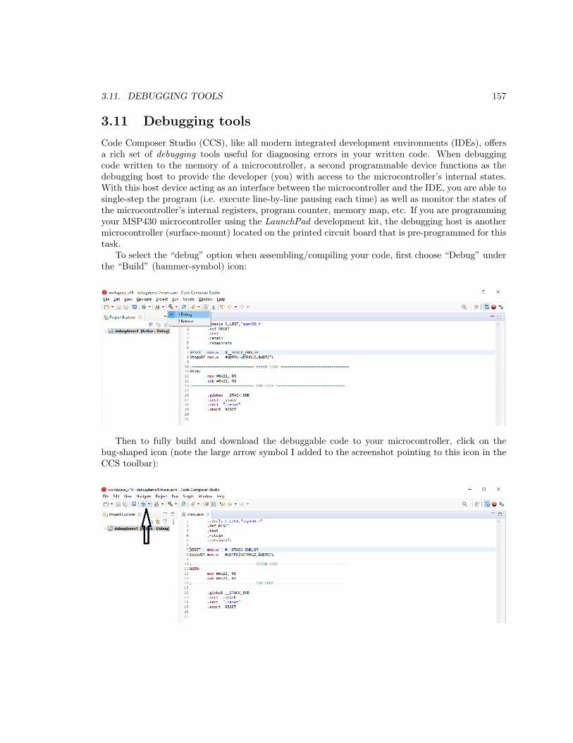
3.11. DEBUGGING TOOLS 157
3.11 Debugging tools
Code Composer Studio (CCS), like all modern integrated development environments (IDEs), offersa rich set of debugging tools useful for diagnosing errors in your written code. When debuggingcode written to the memory of a microcontroller, a second programmable device functions as thedebugging host to provide the developer (you) with access to the microcontroller’s internal states.With this host device acting as an interface between the microcontroller and the IDE, you are able tosingle-step the program (i.e. execute line-by-line pausing each time) as well as monitor the states ofthe microcontroller’s internal registers, program counter, memory map, etc. If you are programmingyour MSP430 microcontroller using the LaunchPad development kit, the debugging host is anothermicrocontroller (surface-mount) located on the printed circuit board that is pre-programmed for thistask.
To select the “debug” option when assembling/compiling your code, first choose “Debug” underthe “Build” (hammer-symbol) icon:
Then to fully build and download the debuggable code to your microcontroller, click on thebug-shaped icon (note the large arrow symbol I added to the screenshot pointing to this icon in theCCS toolbar):

158 CHAPTER 3. TUTORIAL
Next, a window will appear showing the debugger configuration in progress. This typicallyrequires just a few seconds of time:
Meanwhile, the CCS workspace switches automatically to the “debug” view, and within the“Debug” pane you will see the name of your project followed by “Code Composer Studio – DeviceDebugging”. If this does not appear, it generally means there is an old debugging session still activethat was not properly shut down. Closing and re-starting Code Composer Studio will remedy thisstate.

3.11. DEBUGGING TOOLS 159
Once the debugging session finally starts you will see additional text within the “Debug” panedeclaring the USB connection to the microcontroller and underneath that text declaring the sourcecode listing that will be animated during the session. One line in the source code will be color-highlighted to show the next step in execution, and a set of buttons in the toolbar will be availablethat were not before: a red square (stop) and yellow arrows (“step into” and “step over”). Clickingon either yellow arrow causes the program to “single-step” one instruction at a time in the sourcecode listing, allowing you to witness the program’s execution at a pace you manually decide. A largearrow symbol (added to the screenshot) points to the “step into” icon:
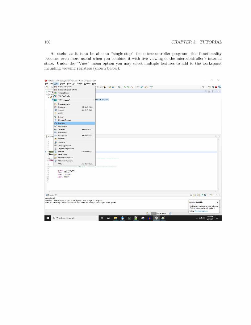
160 CHAPTER 3. TUTORIAL
As useful as it is to be able to “single-step” the microcontroller program, this functionalitybecomes even more useful when you combine it with live viewing of the microcontroller’s internalstate. Under the “View” menu option you may select multiple features to add to the workspace,including viewing registers (shown below):

3.11. DEBUGGING TOOLS 161
Clicking on this option will open a new pane in the workspace with a view of all themicrocontroller’s internal registers, allowing you to view their states as you single-step the program.Here we see the Register pane open, with a list of registers shown:
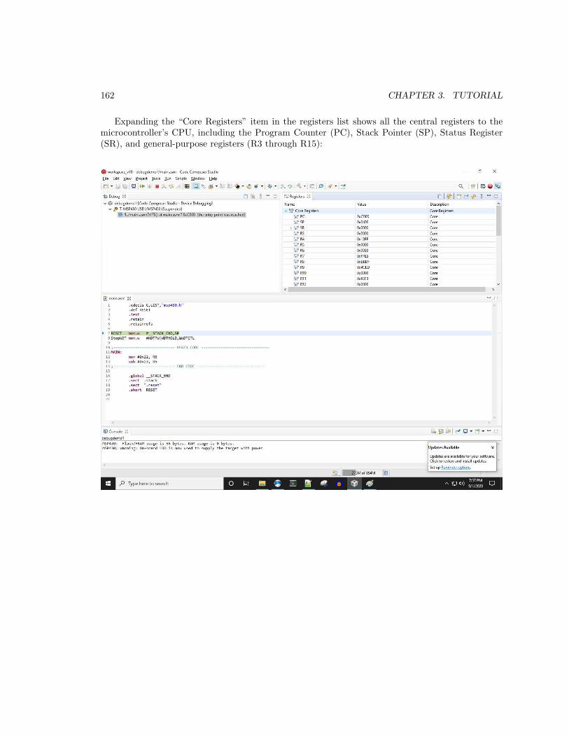
162 CHAPTER 3. TUTORIAL
Expanding the “Core Registers” item in the registers list shows all the central registers to themicrocontroller’s CPU, including the Program Counter (PC), Stack Pointer (SP), Status Register(SR), and general-purpose registers (R3 through R15):

3.11. DEBUGGING TOOLS 163
Clicking the “step into” arrow button once advances the program’s execution from the RESET
line in the assembly-language source code listing to the StopWDT line, and with this advance we seethe Program Counter register has incremented from 0xC000 to its present value of 0xC004:
This Program Counter value change is reflected in the fact that it shows up as yellow-highlightedtext within the “Registers” viewing pane.
It is important to realize that the color-highlighted line is the instruction that will be executedon the next click of the “step into” button. For example, they way we see it in this screenshot, themicrocontroller has just executed the RESET instruction but it has not yet executed the StopWDT
instruction.
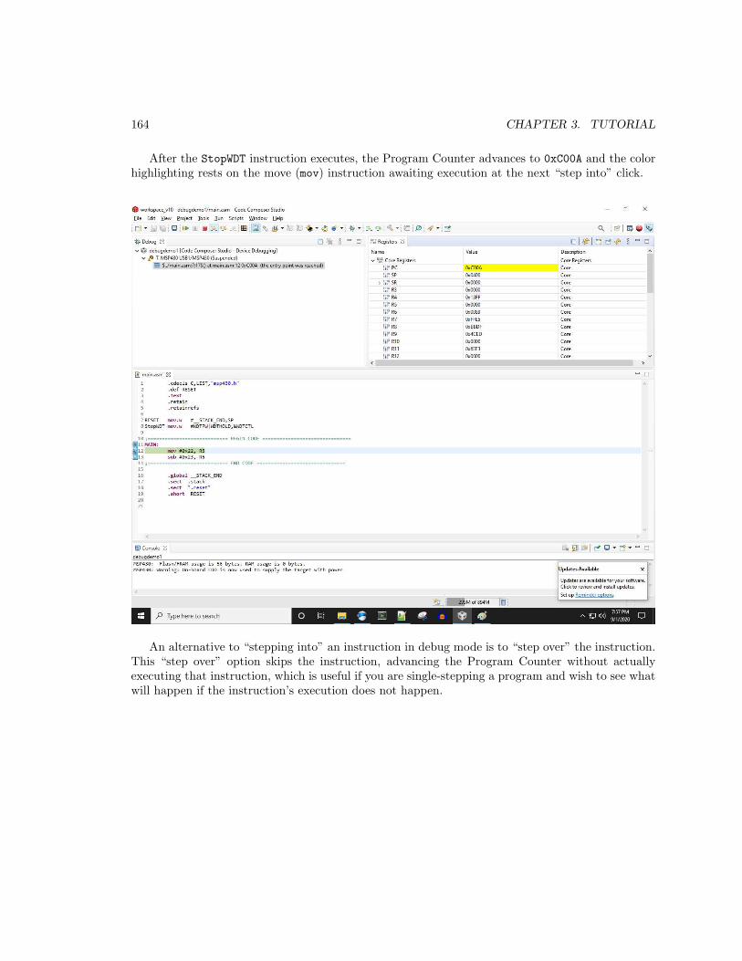
164 CHAPTER 3. TUTORIAL
After the StopWDT instruction executes, the Program Counter advances to 0xC00A and the colorhighlighting rests on the move (mov) instruction awaiting execution at the next “step into” click.
An alternative to “stepping into” an instruction in debug mode is to “step over” the instruction.This “step over” option skips the instruction, advancing the Program Counter without actuallyexecuting that instruction, which is useful if you are single-stepping a program and wish to see whatwill happen if the instruction’s execution does not happen.

3.11. DEBUGGING TOOLS 165
When the mov instruction executes, it moves the eight-bit value 0x22 into register R5:
As with the incrementing Program Counter, the “Registers” viewing pane shows all changedvalues color-highlighted in yellow. Previously, register R5 contained the value 0x0000 but now itcontains 0x0022 due to the mov instruction’s action.
The color-highlighted line in the source code listing tells us the subtract (sub) instruction willbe next to execute when we click again on the “step into” button.

166 CHAPTER 3. TUTORIAL
Following the sub instruction’s execution, we see a few changes in the register states. TheProgram Counter of course incremented, but along with that we see the result of the mathematicalsubtraction now stored in register R5 (0x0022 minus 0x0023 equals negative one, which in 16-bitsigned binary form is 1111 1111 1111 1111 or 0xFFFF in hexadecimal):
Another change is the Status Register (SR), which has updated following the arithmeticsubtraction operation. This is very typical for microprocessors, that the status register gets refreshedfollowing any mathematical or logical operation. Bits within the Status Register will indicate suchthings as whether the result was zero, whether an overflow occurred, etc.
Something else changed if you look at the source code listing. Instead of showing main.asm asbefore, a new tab has appeared for a listing named isr trap.asm. The reason for this change is thatour simple subtraction program came to a halt after executing the sub instruction, and this triggeredan automatic interrupt. In a real program we would have an infinite loop to cause the program toexecute continually. For this simple demonstration we need not concern ourselves with practicality,

3.11. DEBUGGING TOOLS 167
and this sudden halt also serves to show how the debugging session directs your attention to suchan interruption.
Another viewing option we have within the “Debug” environment is the “Memory Browser”showing a hex dump view of the microcontroller’s memory contents. In order to demonstrate howthis works, I edited the assembly-language program to store and subtract to the absolute address0x0200 rather than register R5, then reassembled it and started up a new debugging session:
This new program is now ready for single-step execution.

168 CHAPTER 3. TUTORIAL
After the mov instruction executes, we see the moved value 0x22 now stored in memory address0x0200, appearing as red text in the “Memory Browser” pane:

3.11. DEBUGGING TOOLS 169
Following the sub instruction’s execution, we see the result (0xFFFF) stored in memory address0x0200 just where it should be:
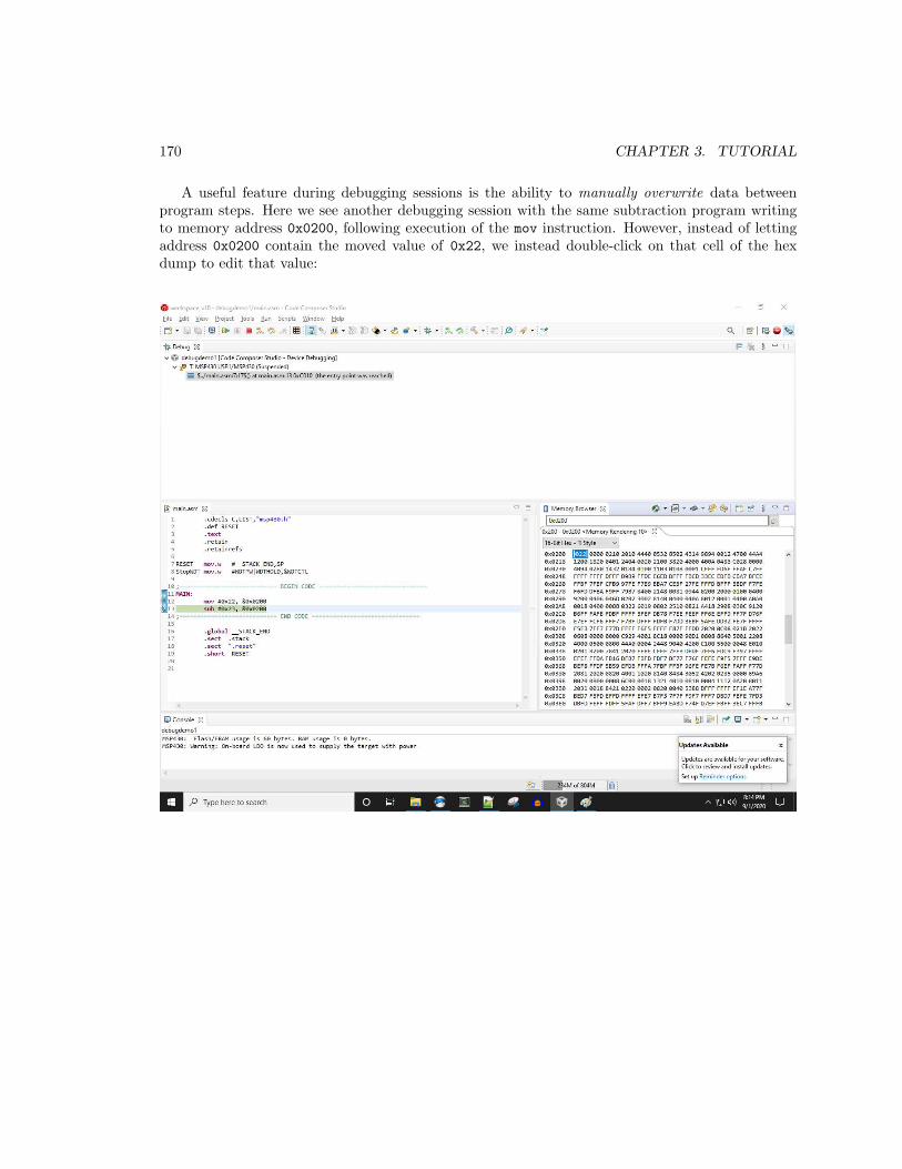
170 CHAPTER 3. TUTORIAL
A useful feature during debugging sessions is the ability to manually overwrite data betweenprogram steps. Here we see another debugging session with the same subtraction program writingto memory address 0x0200, following execution of the mov instruction. However, instead of lettingaddress 0x0200 contain the moved value of 0x22, we instead double-click on that cell of the hexdump to edit that value:

3.11. DEBUGGING TOOLS 171
Here we see the value 0x25 residing in memory address 0x0200 following our hand-edit of thatdata:
Note that we have not yet executed the sub instruction. This will happen when we next clickon the “step into” button.

172 CHAPTER 3. TUTORIAL
Now we see the result 0x0002 stored in memory address 0x0200, the proper result of subtracting0x23 from 0x25:
One final note: it is important to properly close a debugging session when you are finished, priorto editing the source code or doing anything else. A good way to do this is to right-click on thetext within the “Debug” pane and select the option to “Terminate and Remove”. When this isdone, the descriptive text within the “Debug” pane will disappear. If this is not done properly, theunterminated debugging session will still be running when you go to download a new version of yourprogram or try to start another debugging session, and will interfere with your new intent.
Chapter 4
Derivations and TechnicalReferences
This chapter is where you will find mathematical derivations too detailed to include in the tutorial,and/or tables and other technical reference material.
173
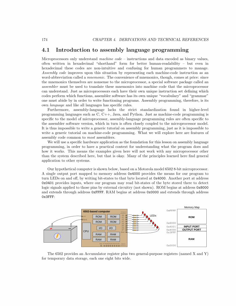
174 CHAPTER 4. DERIVATIONS AND TECHNICAL REFERENCES
4.1 Introduction to assembly language programming
Microprocessors only understand machine code – instructions and data encoded as binary values,often written in hexadecimal “shorthand” form for better human-readability – but even inhexadecimal these codes are non-intuitive and confusing for human programmers to manage.Assembly code improves upon this situation by representing each machine-code instruction as anword-abbreviation called a mnemonic. The convenience of mnemonics, though, comes at price: sincethe mnemonics themselves are nonsense to the microprocessor, a special software package called anassembler must be used to translate these mnemonics into machine code that the microprocessorcan understand. Just as microprocessors each have their own unique instruction set defining whichcodes perform which functions, assembler software has its own unique “vocabulary” and “grammar”one must abide by in order to write functioning programs. Assembly programming, therefore, is itsown language and like all languages has specific rules.
Furthermore, assembly-language lacks the strict standardization found in higher-levelprogramming languages such as C, C++, Java, and Python. Just as machine-code programming isspecific to the model of microprocessor, assembly-language programming rules are often specific tothe assembler software version, which in turn is often closely coupled to the microprocessor model.It is thus impossible to write a generic tutorial on assembly programming, just as it is impossible towrite a generic tutorial on machine-code programming. What we will explore here are features ofassembly code common to most assemblers.
We will use a specific hardware application as the foundation for this lesson on assembly languageprogramming, in order to have a practical context for understanding what the program does andhow it works. This means the examples given here will not work with any microprocessor otherthan the system described here, but that is okay. Many of the principles learned here find generalapplication to other systems.
Our hypothetical computer is shown below, based on a Motorola model 6502 8-bit microprocessor.A single output port mapped to memory address 0x4000 provides the means for our program toturn LEDs on and off, by writing bit-states to that byte located at 0x4000. Another port at address0x0401 provides inputs, where our program may read bit-states of the byte stored there to detectlogic signals applied to those pins by external circuitry (not shown). ROM begins at address 0x8000and extends through address 0xFFFF. RAM begins at address 0x0000 and extends through address0x3FFF:
6502-based computer
CPURAM
+V
Gnd
Gnd
P0
I/O
P1P2P3P4P5P6P7
LEDs
Memory Map
0x0000
ROM
RAM
OUTPUT PORT
RAM
I/O
P0P1P2P3P4P5P6P7Gnd
INPUT PORT
Outputs
Inputs
0x3FFF0x40000x4001
0x8000
0xFFFF(0x4000)
(0x4001)
RAM RAM
ROM ROM
ROMROM
The 6502 provides an Accumulator register plus two general-purpose registers (named X and Y)for temporary data storage, each one eight bits wide.

4.1. INTRODUCTION TO ASSEMBLY LANGUAGE PROGRAMMING 175
4.1.1 Machine code to blink an LED
Suppose we wish to make the LED connected to output pin P0 on the computer blink on and off.This means writing a 1 and then a 0 to bit 0 of the byte located at 0x4000 while clearing (makingzero) all the other bits at that address. Our program will execute the following steps:
1. Write the binary value 0b00000001 to address 0x4000
2. Toggle the least-significant bit of that byte in address 0x4000
3. Go back to second instruction and repeat indefinitely
The same steps, using instructions available in the 6502’s instruction set:
1. Load the binary value 0b00000001 into the Accumulator register
2. Store the Accumulator’s value to address 0x4000
3. Apply the Exclusive-OR function to the LSB in the Accumulator using the mask1
0b00000001.
4. Jump to the second instruction and repeat indefinitely
Researching opcodes and operand formats for the model 6502 microprocessor, we find thefollowing:
• The opcode for “Load Accumulator with immediate value” is 0xA9 followed by the desiredvalue to load (0x01)
• The opcode for “Store Accumulator value to absolute memory address” is 0x8D followed bytwo bytes specifying the destination address in little-endian order (low byte first, high bytelast: 00 40 for address 0x4000)
• The opcode for “Exclusive-OR with immediate value” is 0x49 followed by the mask value(0x01)
• The opcode for “Unconditional Jump to absolute memory address” is 0x4C followed by thetarget address in little-endian order
1In programming, a mask is a set of bits intended to apply a bit-wise logical operation to bits within a larger wordof data. Here, our mask of 0b00000001 means the LSB will be XOR’d with 1 (i.e. toggled, to make it switch statesfrom whatever it was before to the opposite of that) while all other bits within the Accumulator’s 8-bit word will beXOR’d with 0 (i.e. left alone).

176 CHAPTER 4. DERIVATIONS AND TECHNICAL REFERENCES
If we write all these opcodes and operands in order, one line per complete instruction, we getthe following hand-assembled machine code:
A9 01
8D 00 40
49 01
4C ?? ??
The question-marks are there in our code because we need to determine where our program willbegin in the computer’s ROM memory space in order to know which address we need to “jump” toin the last instruction. Let’s assume our program starts at the very first address in ROM (0x8000)and re-write the program showing the starting address of each line2:
8000 A9 01
8002 8D 00 40
8005 49 01
8007 4C ?? ??
Recall that the purpose of our “Jump” instruction (last line, 0x4C) was to go back to the “StoreAccumulator” instruction (0x8D) so that our recently XOR’d data will be re-written to the outputport at address 0x4000. Therefore, the address we need to jump to is 0x8002. Knowing this, wemay edit our machine code listing to include this address in the last instruction, in “little-endian”byte order because the model 6502 microprocessor happens to be a little-endian machine:
8000 A9 01
8002 8D 00 40
8005 49 01
8007 4C 02 80
If we were to write this program to the computer’s ROM and then read it back to display inconventional “hex dump” format, it would look like this:
8000 A9 01 8D 00 40 49 01 4C 02 80
If the ROM IC(s) in our computer are socketed and therefore easily removed for programmingby an external device, we could use a PROM programmer3 to write this short program into aprogrammable ROM memory chip and then re-insert it into our computer’s board to run.
2This is beginning to resemble the common “hex dump” memory display format, except that each line of text islimited to just one instruction
3Commercially-available PROM programming tools consist of a unit connected to a personal computer with azero-insertion-force (ZIF) IC socket to facilitate easy plugging and unplugging of memory ICs. Software provided

4.1. INTRODUCTION TO ASSEMBLY LANGUAGE PROGRAMMING 177
4.1.2 Assembly code to blink an LED
Now that we have seen the “hand-assembly” method of creating a simple LED-blinking programfor our 6502-based computer, let us explore how we could do the same using assembly language.Starting with the original program specification telling us what we need the computer to do:
1. Write the binary value 0b00000001 to address 0x4000
2. Toggle the least-significant bit of that byte in address 0x4000
3. Go back to second instruction and repeat indefinitely
Next, we refer to instructions available in the 6502’s instruction set, but this time we write themnemonic abbreviations given in that instruction set instead of opcodes:
1. LDA value 0b00000001
2. STA to 0x4000
3. EOR mask 0b00000001
4. JMP to second instruction
We are almost done with our assembly-language program! All we need to do now is write itusing the proper syntax4 expected by our assembler software, being sure to include a directive5 tothe assembler to begin at address 0x8000.
.ORG $8000
LDA #$01
LOOP
STA $4000
EOR #$01
JMP LOOP
This program you see above is completely functioning, ready to be assembled into machine codeand written to the computer’s ROM.
with the programmer allow you to type the hex dump data into an editor window (or into a plain-ASCII text file)and then have that data written to the memory IC with the click of a button or a command-line instruction typedinto the personal computer. If you really desire a low-level learning experience, you can program the PROM chip byconnecting address, data, and write-enable lines to toggle switches, then toggling those switches to specify addresses,data to be written to those addresses, and pressing the write-enable switch to “burn” that data into the chip whenyou are ready. Needless to say, the latter option is the most tedious.
4We are assuming here that our assembler does not understand binary notation and expects all numerical valuesto be expressed in hexadecimal instead.
5A “directive” is an instruction given not to the microprocessor, but rather to the assembler software. It tells theassembler to translate the assembly “source” code into machine code in some particular manner.

178 CHAPTER 4. DERIVATIONS AND TECHNICAL REFERENCES
Optional comments help make our code easier to read:
.ORG $8000 ; Begin at address 0x8000
LDA #$01 ; Load 0x01 into Accumulator
LOOP ; Mark the beginning of the loop
STA $4000 ; Store Accumulator value to Output port
EOR #$01 ; XOR the least-significant bit
JMP LOOP ; Jump to the beginning of the loop
Take note of some important details of this assembly-language program:
• Order of execution is left-to-right, top-to-bottom in the same order as reading English-languagetext.
• Any left-justified text (e.g. LOOP) is considered a label rather than an instruction, whether onits own line or preceding an instruction.
• Instructions (e.g. LDA, STA, etc.) must be preceded by whitespace. The number of space ortab characters doesn’t matter.
• Operands to those instructions (e.g. $4000, etc.) must be separated to the right of thoseinstructions by some whitespace as well. The number of space or tab characters doesn’tmatter. In this listing I’ve adjusted the number of spaces to make the columns neatly align.
• Any text to the right of a semicolon (;) character is considered a comment, ignored by theassembler and not included in the machine code at all.
• Any instruction preceded by a dot (e.g. .ORG) is a directive to the assembler, telling how todo some aspect of the translation into machine code, but not appearing in the final machinecode itself.
• Note how the Jump instruction’s target address was resolved by the assembler, with no needfor us to count address numbers to figure out where it should jump to. We simply place alabel and let the assembler figure out those details for us.
• This assembler uses a dollar-symbol ($) to denote any hexadecimal value.
• The pound symbol (#) denotes an immediate value, meaning the literal number value specified.Otherwise, the operand value is considered to be a memory address location.
It should be noted that some of these conventions vary from assembler to assembler. Forexample, some assemblers require all labels to contain a colon at the end (e.g. LOOP: rather thanLOOP). Some assemblers allow C-style hexadecimal notation (e.g. 0x4000) while others insist onthe $ character. Some assemblers allow binary notation (e.g. 0b00000001 or %00000001) whileothers don’t. Some assemblers require directives be preceded by a dot (e.g. .ORG) while othersinsist directives not be preceded by any character. As always when using software, refer to themanufacturer’s documentation for details!

4.1. INTRODUCTION TO ASSEMBLY LANGUAGE PROGRAMMING 179
4.1.3 Slowing down the blinking
If we were to actually assemble and write this program to ROM, then start the computer to initiateprogram execution, we would likely find the LED blinking on and off so fast that it appeared to besteadily lit (albeit dimmer than usual). The reason for this is the fast fetch/execute cycle time of atypical microprocessor. A model 6502 running at a clock speed of 1 MHz would blink the LED onand off at a rate far too quick for the human eye to see6.
In order to make the blinking rate slow enough to see, we must somehow delay the loop’srepetition. One easy way to do this is to insert a “counting” loop inside of our program’s blinkingloop. This counting loop keeps the microprocessor occupied by doing nothing but sequentiallycounting, in order to purposely waste time and thereby delay its toggling of the LED output bit.
Here is a section of assembly code using common 6502 instructions to perform this delay task byforcing the microprocessor to count backwards from 255 (0xFF) until it reaches zero, complete withexplanatory comments:
LDX #$FF ; Load value 0xFF into register X
DELAY_LOOP
DEX ; Decrement (subtract 1 from) value stored in X
CPX #$00 ; Compare that value to zero
BNE DELAY_LOOP ; If unequal, "branch" to DELAY_LOOP to repeat
One way to incorporate this delay code into our program is to simply insert it “in-line” with theoriginal code between the EOR and JMP instructions, like this:
.ORG $8000 ; Begin at address 0x8000
LDA #$01 ; Load 0x01 into Accumulator
LOOP ; Mark the beginning of the loop
STA $4000 ; Store Accumulator value to Output port
EOR #$01 ; XOR the least-significant bit
LDX #$FF ; Load value 0xFF into register X
DELAY_LOOP
DEX ; Decrement (subtract 1 from) value stored in X
CPX #$00 ; Compare that value to zero
BNE DELAY_LOOP ; If unequal, "branch" to DELAY_LOOP to repeat
JMP LOOP ; Jump to the beginning of the loop
6According the the model 6502 manual,, the STA instruction requires 4 clock cycles, the EOR instruction 2 clockcycles, and the JMP instruction 3 clock cycles. This means 9 clock cycles would be required for every pass throughthe program, with two passes required for a full cycle of the LED’s blink (i.e. on and off). Dividing 1 MHz by the 18clock cycles necessary to fully cycle the LED gives an LED blinking frequency of 55.556 kHz!
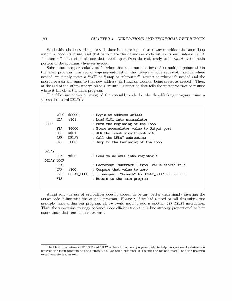
180 CHAPTER 4. DERIVATIONS AND TECHNICAL REFERENCES
While this solution works quite well, there is a more sophisticated way to achieve the same “loopwithin a loop” structure, and that is to place the delay-time code within its own subroutine. A“subroutine” is a section of code that stands apart from the rest, ready to be called by the mainportion of the program whenever needed.
Subroutines are particularly useful when that code must be invoked at multiple points withinthe main program. Instead of copying-and-pasting the necessary code repeatedly in-line whereneeded, we simply insert a “call” or “jump to subroutine” instruction where it’s needed and themicroprocessor will jump to that new address (its Program Counter being preset as needed). Then,at the end of the subroutine we place a “return” instruction that tells the microprocessor to resumewhere it left off in the main program.
The following shows a listing of the assembly code for the slow-blinking program using asubroutine called DELAY7:
.ORG $8000 ; Begin at address 0x8000
LDA #$01 ; Load 0x01 into Accumulator
LOOP ; Mark the beginning of the loop
STA $4000 ; Store Accumulator value to Output port
EOR #$01 ; XOR the least-significant bit
JSR DELAY ; Call the DELAY subroutine
JMP LOOP ; Jump to the beginning of the loop
DELAY
LDX #$FF ; Load value 0xFF into register X
DELAY_LOOP
DEX ; Decrement (subtract 1 from) value stored in X
CPX #$00 ; Compare that value to zero
BNE DELAY_LOOP ; If unequal, "branch" to DELAY_LOOP and repeat
RTS ; Return to the main program
Admittedly the use of subroutines doesn’t appear to be any better than simply inserting theDELAY code in-line with the original program. However, if we had a need to call this subroutinemultiple times within our program, all we would need to add is another JSR DELAY instruction.Thus, the subroutine strategy becomes more efficient than the in-line strategy proportional to howmany times that routine must execute.
7The blank line between JMP LOOP and DELAY is there for esthetic purposes only, to help our eyes see the distinctionbetween the main program and the subroutine. We could eliminate this blank line (or add more!) and the programwould execute just as well.

4.1. INTRODUCTION TO ASSEMBLY LANGUAGE PROGRAMMING 181
An useful tool provided by most assemblers is a disassembly option. This takes the assembledmachine code and translates it “backwards” into assembly code, displaying the memory addresses,machine code hex dump, and equivalent assembly side-by-side for comparison:
Address Hexdump Disassembly
---------------------------------
$8000 A9 01 LDA #$01
$8002 8D 00 40 STA $4000
$8005 49 01 EOR #$01
$8007 20 0D 00 JSR $000D
$800A 4C 02 80 JMP $8002
$800D A2 FF LDX #$FF
$800F CA DEX
$8010 E0 00 CPX #$00
$8012 D0 FB BNE $800F
$8014 60 RTS
Note how the “jump” and “branch” instructions all specify address locations in one way oranother, but not the “return instruction” at the end of the subroutine. How does the microprocessorknow which memory address to return to after completing the subroutine? The answer lies in afeature of the microprocessor called the stack : a section of volatile memory used by the processorto remember such things as previous Program Counter values. A jump-to-subroutine instructioncauses the current memory address value held in the Program Counter to be “pushed” onto thestack before jumping to the subroutine’s starting memory address. A “return” instruction causesthe microprocessor to “pop” the former address value off the stack and into the Program Counteragain, so that execution resumes right where it left off8. The model 6502 processor uses a portionof its RAM memory space for its stack (0x0100 through 0x01FF).
If you examine this disassembled code closely, you will notice something strange with the “branch-if-not-equal” instruction: the disassembled code says BNE $800F but the machine code does notactually contain the 0x800F address. Instead, it only contains the opcode for BNE (D0) and a bytewith a value of 0xFB. This is an example of relative addressing, where the operand to the instructiondeclares not the address itself, but rather how many addresses to skip, either forward or backward.As an eight-bit signed number, 0xFB is equal to negative five. This tells the microprocessor todecrement its Program Counter by five to repeat the DELAY LOOP. If you count from address 0x8013where the 0xFB operand was resides to 0x800F where the delay loop begins, you count five addresses(inclusive). Relative addressing is more efficient than absolute addressing because we only needone byte telling the instruction how far to jump instead of two bytes to specify a 16-bit address.Interestingly, the disassembler opted to show us an absolute address even though that’s not reallyhow the 6502’s BNE instruction works.
8Stacks are analogous to a pile (stack) of paper notes. If a person is reading a book and they suddenly get told toturn to a different chapter to read a passage there, they may write the current page number on a note and “push”that note to the top of the stack so they won’t forget it while turning to the new passage. After reading the newpassage, the person retrieves their note from the top of the stack (i.e. “popping” it off the stack) and references it toreturn to the page where they left off. This may occur more than once, and the stack will “remember” not only thepage numbers but also keep everything in the right order as the person eventually returns to their original place inthe book.

182 CHAPTER 4. DERIVATIONS AND TECHNICAL REFERENCES
4.1.4 Simplifying with symbols
Another technique useful for making our assembly-language programs easier to read and to maintainis the use of symbols to represent numerical values. Consider the last version of our LED-blinkingprogram re-written to incorporate three symbols, defined at the very beginning of the code listing:
DTIME .EQU $FF ; Create a symbol "DTIME" for the delay time parameter
OUTPT .EQU $4000 ; Create a symbol "OUTPT" for the Output port address
LED .EQU $01 ; Create a symbol "LED" for the LED’s bit number
.ORG $8000 ; Begin at address 0x8000
LDA #LED ; Load 0x01 into Accumulator
LOOP ; Mark the beginning of the loop
STA OUTPT ; Store Accumulator value to Output port
EOR #LED ; XOR the least-significant bit
JSR DELAY ; Call the DELAY subroutine
JMP LOOP ; Jump to the beginning of the loop
DELAY
LDX #DTIME ; Load value 0xFF into register X
DELAY_LOOP
DEX ; Decrement (subtract 1 from) value stored in X
CPX #$00 ; Compare that value to zero
BNE DELAY_LOOP ; If unequal, "branch" to DELAY_LOOP and repeat
RTS ; Return to the main program
The .EQU directive tells the assembler to treat the symbol (on the left) as an alias of the value(on the right). This lets us use lettered symbols within our code rather than numerical values forimportant parameters such as I/O addresses, delay time, etc. These symbols may be used as manytimes as desired, and they will always mean the same thing (e.g. the LED symbol is used twice inthis program, and it means $01 both times).

4.1. INTRODUCTION TO ASSEMBLY LANGUAGE PROGRAMMING 183
4.1.5 Using the stack
Previously we mentioned the microprocessor’s stack, a section of RAM used to hold data in sequentialorder. Stacks may be thought of as a Last-In First-Out shift register, where data retrieved from thestack is in reverse order of how data is placed onto the stack. The analogy of a microprocessor’sstack being a literal stack of paper sheets is helpful here: if we pull papers from the top of the stack,we will find their sequence is in reverse order of how we placed those sheets on the stack.
Microprocessors use their stack to manage subroutine calls, “pushing” the last Program Countermemory address to the stack prior to jumping to the subroutine’s address, then “popping” that oldaddress off the stack when the subroutine completes so it knows where to resume its previous place inthe main program. This form of stack usage is automatic, being built-in to the finite state machinesequence as part of each subroutine “call” instruction and each subroutine “return” instruction.Interrupts also use a stack to remember where to jump back in the main program after completingthe interrupt service routine (ISR).
Certain instructions exist to make use of the stack in ways that are not necessarily related tosubroutines or interrupts, and these can be very useful. Here we will explore one such practicaluse of the stack. Consider this simple “chasing LED” program using the 6502’s “Rotate Right”instruction to shift the place of a single “1” bit in the Accumulator byte, the goal being to create a“chasing” LED display on our computer where the light appears to repeatedly sweep along the rowof LEDs:
.ORG $8000 ; Begin at address 0x8000
LDA #$01 ; Load 0x01 into Accumulator
LOOP ; Mark the beginning of the loop
STA $4000 ; Store Accumulator value to Output port
ROR ; Rotate Accumulator bits one place right
JMP LOOP ; Jump to the beginning of the loop
This code is every bit as simple as our original LED-blinking program. When run, it producesthe following pattern of light (sequence shown chronologically from top to bottom):
P0P1P2P3P4P5P6P7 Accumulator value
0x01
0x00
0x80
0x40
0x20
0x10
0x08
0x04
0x02
0x01
Tim
e

184 CHAPTER 4. DERIVATIONS AND TECHNICAL REFERENCES
During the step where no LEDs are lit, the “1” bit resides in the Carry bit of the microprocessor’sStatus register, a special register used to store the results of certain mathematical and logicaloperations.
This pattern of light is what we expect the ROR instruction to produce after the Accumulatoris initially loaded with 0x01. All is well, except for the same problem we had with our original“blinking LED” program: the sequence runs too fast for our eyes to discern. It just looks like a blurof eight LEDs all (dimly) lit!
We already know how to slow programs down, by inserting a counting loop that “wastes” themicroprocessor’s time, so let’s modify this program accordingly:
.ORG $8000 ; Begin at address 0x8000
LDA #$01 ; Load 0x01 into Accumulator
LOOP ; Mark the beginning of the loop
STA $4000 ; Store Accumulator value to Output port
ROR ; Rotate Accumulator bits one place right
JSR DELAY ; Call the DELAY subroutine
JMP LOOP ; Jump to the beginning of the loop
DELAY
LDX #DTIME ; Load value 0xFF into register X
DELAY_LOOP
DEX ; Decrement (subtract 1 from) value stored in X
CPX #$00 ; Compare that value to zero
BNE DELAY_LOOP ; If unequal, "branch" to DELAY_LOOP and repeat
RTS ; Return to the main program
However, when we run this program we get a different light sequence:
P0P1P2P3P4P5P6P7 Accumulator value
0x01
0x00
0x80
Tim
e
0xC0
0xE0
0xF0
0xF8
0xFC
0xFE
0xFF
For some reason, the “0” states rotated off the LSB-end of the byte are becoming “1” states tofill the MSB. Recall that the ROR instruction draws from the Carry bit of the Status register to fill

4.1. INTRODUCTION TO ASSEMBLY LANGUAGE PROGRAMMING 185
the MSB at each iteration. A reasonable hypothesis is that something other than the ROR is settingthe Carry bit.
Indeed something does act to set the Carry bit when we don’t want it to: the “compare X”CPX instruction inside our DELAY subroutine. According to the 6502 instruction set manual, theCPX sets the Carry bit if ever the X register’s value is equal to or greater than the value it’s beingcompared against. In fact, this is how the BNE instruction knows when to branch: it checks theStatus register which is updated by all mathematical, logical, and comparison instructions. Giventhe design of our time-delay subroutine where the X register begins at a large value and countsdown toward the comparison value of zero, we are guaranteed to return from that subroutine withthe Carry bit set.
This causes problems for our ROR instruction, which takes the “1” value left in the Carry bit fromthe subroutine’s CPX instruction and adds it to our chasing light sequence, which we do not want.Somehow we need the ROR to act on the Carry bit it generated, not the new Carry bit generated bythe subroutine’s CPX instruction.
Our stack ends up being a simple solution to this problem. All we need to do is “push” theStatus register’s state to the stack prior to calling the subroutine, then “pop” that old data back offthe stack and into the Status register again before the ROR instruction reads the Carry bit. In otherwords, we can use the stack as temporary storage for the Status bits, and recall those bits after thesubroutine is done using the Status register for its own purposes.
All this requires is the addition of two new instructions surrounding the “jump to subroutine”:a PHP instruction (“push processor status on stack”) prior to the jump, and PLP instruction (“pullprocessor status from stack”) after the jump:
.ORG $8000 ; Begin at address 0x8000
LDA #$01 ; Load 0x01 into Accumulator
LOOP ; Mark the beginning of the loop
STA $4000 ; Store Accumulator value to Output port
ROR ; Rotate Accumulator bits one place right
PHP ; Push Status register to stack
JSR DELAY ; Call the DELAY subroutine
PLP ; Pop Status register off stack
JMP LOOP ; Jump to the beginning of the loop
DELAY
LDX #DTIME ; Load value 0xFF into register X
DELAY_LOOP
DEX ; Decrement (subtract 1 from) value stored in X
CPX #$00 ; Compare that value to zero
BNE DELAY_LOOP ; If unequal, "branch" to DELAY_LOOP and repeat
RTS ; Return to the main program
The stack is a very useful feature of any microprocessor, but it does have its limitations. If wepush far more data onto the stack than we pop off, we can get a stack overflow where the oldest

186 CHAPTER 4. DERIVATIONS AND TECHNICAL REFERENCES
data gets overwritten and is lost. Also, we need to be very careful that we push from the correctsources and pop to the correct destinations. For example, in the above program we pushed theStatus register to the stack, then immediately after that the JSR instruction pushed the ProgramCounter value to the stack before going to the subroutine. When the subroutine completed, itpopped the old Program Counter value off the stack, and then immediately after that we poppedthe old Status register off the stack. This works because those sources and destinations came in thecorrect sequence, and so the data going on and off the stack went where it should.
Chapter 5
Questions
This learning module, along with all others in the ModEL collection, is designed to be used in aninverted instructional environment where students independently read1 the tutorials and attemptto answer questions on their own prior to the instructor’s interaction with them. In place oflecture2, the instructor engages with students in Socratic-style dialogue, probing and challengingtheir understanding of the subject matter through inquiry.
Answers are not provided for questions within this chapter, and this is by design. Solved problemsmay be found in the Tutorial and Derivation chapters, instead. The goal here is independence, andthis requires students to be challenged in ways where others cannot think for them. Rememberthat you always have the tools of experimentation and computer simulation (e.g. SPICE) to exploreconcepts!
The following lists contain ideas for Socratic-style questions and challenges. Upon inspection,one will notice a strong theme of metacognition within these statements: they are designed to fostera regular habit of examining one’s own thoughts as a means toward clearer thinking. As such thesesample questions are useful both for instructor-led discussions as well as for self-study.
1Technical reading is an essential academic skill for any technical practitioner to possess for the simple reasonthat the most comprehensive, accurate, and useful information to be found for developing technical competence is intextual form. Technical careers in general are characterized by the need for continuous learning to remain currentwith standards and technology, and therefore any technical practitioner who cannot read well is handicapped intheir professional development. An excellent resource for educators on improving students’ reading prowess throughintentional effort and strategy is the book textitReading For Understanding – How Reading Apprenticeship ImprovesDisciplinary Learning in Secondary and College Classrooms by Ruth Schoenbach, Cynthia Greenleaf, and LynnMurphy.
2Lecture is popular as a teaching method because it is easy to implement: any reasonably articulate subject matterexpert can talk to students, even with little preparation. However, it is also quite problematic. A good lecture alwaysmakes complicated concepts seem easier than they are, which is bad for students because it instills a false sense ofconfidence in their own understanding; reading and re-articulation requires more cognitive effort and serves to verifycomprehension. A culture of teaching-by-lecture fosters a debilitating dependence upon direct personal instruction,whereas the challenges of modern life demand independent and critical thought made possible only by gatheringinformation and perspectives from afar. Information presented in a lecture is ephemeral, easily lost to failures ofmemory and dictation; text is forever, and may be referenced at any time.
187

188 CHAPTER 5. QUESTIONS
General challenges following tutorial reading
• Summarize as much of the text as you can in one paragraph of your own words. A helpfulstrategy is to explain ideas as you would for an intelligent child: as simple as you can withoutcompromising too much accuracy.
• Simplify a particular section of the text, for example a paragraph or even a single sentence, soas to capture the same fundamental idea in fewer words.
• Where did the text make the most sense to you? What was it about the text’s presentationthat made it clear?
• Identify where it might be easy for someone to misunderstand the text, and explain why youthink it could be confusing.
• Identify any new concept(s) presented in the text, and explain in your own words.
• Identify any familiar concept(s) such as physical laws or principles applied or referenced in thetext.
• Devise a proof of concept experiment demonstrating an important principle, physical law, ortechnical innovation represented in the text.
• Devise an experiment to disprove a plausible misconception.
• Did the text reveal any misconceptions you might have harbored? If so, describe themisconception(s) and the reason(s) why you now know them to be incorrect.
• Describe any useful problem-solving strategies applied in the text.
• Devise a question of your own to challenge a reader’s comprehension of the text.

189
General follow-up challenges for assigned problems
• Identify where any fundamental laws or principles apply to the solution of this problem,especially before applying any mathematical techniques.
• Devise a thought experiment to explore the characteristics of the problem scenario, applyingknown laws and principles to mentally model its behavior.
• Describe in detail your own strategy for solving this problem. How did you identify andorganized the given information? Did you sketch any diagrams to help frame the problem?
• Is there more than one way to solve this problem? Which method seems best to you?
• Show the work you did in solving this problem, even if the solution is incomplete or incorrect.
• What would you say was the most challenging part of this problem, and why was it so?
• Was any important information missing from the problem which you had to research or recall?
• Was there any extraneous information presented within this problem? If so, what was it andwhy did it not matter?
• Examine someone else’s solution to identify where they applied fundamental laws or principles.
• Simplify the problem from its given form and show how to solve this simpler version of it.Examples include eliminating certain variables or conditions, altering values to simpler (usuallywhole) numbers, applying a limiting case (i.e. altering a variable to some extreme or ultimatevalue).
• For quantitative problems, identify the real-world meaning of all intermediate calculations:their units of measurement, where they fit into the scenario at hand. Annotate any diagramsor illustrations with these calculated values.
• For quantitative problems, try approaching it qualitatively instead, thinking in terms of“increase” and “decrease” rather than definite values.
• For qualitative problems, try approaching it quantitatively instead, proposing simple numericalvalues for the variables.
• Were there any assumptions you made while solving this problem? Would your solution changeif one of those assumptions were altered?
• Identify where it would be easy for someone to go astray in attempting to solve this problem.
• Formulate your own problem based on what you learned solving this one.
General follow-up challenges for experiments or projects
• In what way(s) was this experiment or project easy to complete?
• Identify some of the challenges you faced in completing this experiment or project.

190 CHAPTER 5. QUESTIONS
• Show how thorough documentation assisted in the completion of this experiment or project.
• Which fundamental laws or principles are key to this system’s function?
• Identify any way(s) in which one might obtain false or otherwise misleading measurementsfrom test equipment in this system.
• What will happen if (component X) fails (open/shorted/etc.)?
• What would have to occur to make this system unsafe?

5.1. CONCEPTUAL REASONING 191
5.1 Conceptual reasoning
These questions are designed to stimulate your analytic and synthetic thinking3. In a Socraticdiscussion with your instructor, the goal is for these questions to prompt an extended dialoguewhere assumptions are revealed, conclusions are tested, and understanding is sharpened. Yourinstructor may also pose additional questions based on those assigned, in order to further probe andrefine your conceptual understanding.
Questions that follow are presented to challenge and probe your understanding of various conceptspresented in the tutorial. These questions are intended to serve as a guide for the Socratic dialoguebetween yourself and the instructor. Your instructor’s task is to ensure you have a sound grasp ofthese concepts, and the questions contained in this document are merely a means to this end. Yourinstructor may, at his or her discretion, alter or substitute questions for the benefit of tailoring thediscussion to each student’s needs. The only absolute requirement is that each student is challengedand assessed at a level equal to or greater than that represented by the documented questions.
It is far more important that you convey your reasoning than it is to simply convey a correctanswer. For this reason, you should refrain from researching other information sources to answerquestions. What matters here is that you are doing the thinking. If the answer is incorrect, yourinstructor will work with you to correct it through proper reasoning. A correct answer without anadequate explanation of how you derived that answer is unacceptable, as it does not aid the learningor assessment process.
You will note a conspicuous lack of answers given for these conceptual questions. Unlike standardtextbooks where answers to every other question are given somewhere toward the back of the book,here in these learning modules students must rely on other means to check their work. The best wayby far is to debate the answers with fellow students and also with the instructor during the Socraticdialogue sessions intended to be used with these learning modules. Reasoning through challengingquestions with other people is an excellent tool for developing strong reasoning skills.
Another means of checking your conceptual answers, where applicable, is to use circuit simulationsoftware to explore the effects of changes made to circuits. For example, if one of these conceptualquestions challenges you to predict the effects of altering some component parameter in a circuit,you may check the validity of your work by simulating that same parameter change within softwareand seeing if the results agree.
3Analytical thinking involves the “disassembly” of an idea into its constituent parts, analogous to dissection.Synthetic thinking involves the “assembly” of a new idea comprised of multiple concepts, analogous to construction.Both activities are high-level cognitive skills, extremely important for effective problem-solving, necessitating frequentchallenge and regular practice to fully develop.

192 CHAPTER 5. QUESTIONS
5.1.1 Reading outline and reflections
“Reading maketh a full man; conference a ready man; and writing an exact man” – Francis Bacon
Francis Bacon’s advice is a blueprint for effective education: reading provides the learner withknowledge, writing focuses the learner’s thoughts, and critical dialogue equips the learner toconfidently communicate and apply their learning. Independent acquisition and application ofknowledge is a powerful skill, well worth the effort to cultivate. To this end, students shouldread these educational resources closely, write their own outline and reflections on the reading, anddiscuss in detail their findings with classmates and instructor(s). You should be able to do all of thefollowing after reading any instructional text:
√Briefly OUTLINE THE TEXT, as though you were writing a detailed Table of Contents. Feel
free to rearrange the order if it makes more sense that way. Prepare to articulate these points indetail and to answer questions from your classmates and instructor. Outlining is a good self-test ofthorough reading because you cannot outline what you have not read or do not comprehend.
√Demonstrate ACTIVE READING STRATEGIES, including verbalizing your impressions as
you read, simplifying long passages to convey the same ideas using fewer words, annotating textand illustrations with your own interpretations, working through mathematical examples shown inthe text, cross-referencing passages with relevant illustrations and/or other passages, identifyingproblem-solving strategies applied by the author, etc. Technical reading is a special case of problem-solving, and so these strategies work precisely because they help solve any problem: paying attentionto your own thoughts (metacognition), eliminating unnecessary complexities, identifying what makessense, paying close attention to details, drawing connections between separated facts, and notingthe successful strategies of others.
√Identify IMPORTANT THEMES, especially GENERAL LAWS and PRINCIPLES, expounded
in the text and express them in the simplest of terms as though you were teaching an intelligentchild. This emphasizes connections between related topics and develops your ability to communicatecomplex ideas to anyone.
√Form YOUR OWN QUESTIONS based on the reading, and then pose them to your instructor
and classmates for their consideration. Anticipate both correct and incorrect answers, the incorrectanswer(s) assuming one or more plausible misconceptions. This helps you view the subject fromdifferent perspectives to grasp it more fully.
√Devise EXPERIMENTS to test claims presented in the reading, or to disprove misconceptions.
Predict possible outcomes of these experiments, and evaluate their meanings: what result(s) wouldconfirm, and what would constitute disproof? Running mental simulations and evaluating results isessential to scientific and diagnostic reasoning.
√Specifically identify any points you found CONFUSING. The reason for doing this is to help
diagnose misconceptions and overcome barriers to learning.

5.1. CONCEPTUAL REASONING 193
5.1.2 Foundational concepts
Correct analysis and diagnosis of electric circuits begins with a proper understanding of some basicconcepts. The following is a list of some important concepts referenced in this module’s full tutorial.Define each of them in your own words, and be prepared to illustrate each of these concepts with adescription of a practical example and/or a live demonstration.
???
???
???
???
???
???

194 CHAPTER 5. QUESTIONS
5.1.3 Terminal assignments and limits
Reference the datasheet for the MSP430G2553 20-terminal microcontroller and identify some ofthe alternate functions of its package terminals (i.e. those functions other than digital I/O portassignments such as P1.0-P1.7 for the various pins in the IC chip).
Reference the datasheet for the MSP430G2553 20-terminal microcontroller and identify some ofthe electrical limits:
• Maximum and minimum power supply voltage =
• Maximum and minimum analog input voltage =
• Maximum I/O pin current =
Challenges
• Suppose you needed to have the microcontroller turn a discrete load on and off, with anexpected load current of 1 Ampere. Identify ways to interface the microcontroller output pinto this (relatively) high-current load.

5.1. CONCEPTUAL REASONING 195
5.1.4 Interrupt capabilities
An important concept in microprocessor and microcontroller operation is the notion of an interrupt.This is a signal, either received from some external source or generated internally, that causes theprocessor to halt its regular execution of the program and “jump” to a new location in programmemory where other instructions exist to tell it how to service (i.e. deal with) this interruptingevent.
Interrupts are often classified as being either maskable or non-maskable. This simply refers towhether the user is able to disable interrupts or now. A “maskable” interrupt is one that can bedisabled by setting certain bits in a register of the processor, and a “non-maskable” is one that isalways alert and cannot be disabled. The reset function on a microprocessor or microcontroller is atypical example of a non-maskable interrupt.
The way this usually works is that an interrupt event causes the Program Counter to go to apre-designated address in memory called a vector, which contains the memory address where thefirst instruction of the service routine (typically called an “Interrupt Service Routine” or ISR) exists.These interrupt vectors are often hard-coded into the processor at the time of manufacture, but theuser (programmer) is free to place their ISR code wherever they wish in memory and to write theappropriate starting addresses for those routines into the appropriate interrupt vector location(s).
In the MSP430 microcontroller series, an interrupt enable bit determines whether a maskableinterrupt is able to function, while an interrupt flag bit records if an interrupt event actually happens.
Reference the datasheet for the MSP430G2553 microcontroller and identify some of the availableinterrupt sources, priorities, flags, and vectors.
Challenges
• Describe a practical application for interrupting a microcontroller from its regular programexecution.

196 CHAPTER 5. QUESTIONS
5.1.5 Disabling the watchdog timer
When you open a new assembly-language project in Code Composer Studio (CCS) the .asm sourcecode file does not begin in an empty state. Instead, it is pre-populated by several directives, labels,and instructions. One of those is as follows (complete with its own comment):
StopWDT mov.w #WDTPW|WDTHOLD,&WDTCTL ; Stop watchdog timer
Reference the datasheet4 for the MSP430G2553 20-terminal microcontroller to identify theinternal watchdog timer’s function in the microcontroller, and also explain why you think CCSdefaults to disabling it.
Challenges
• Identify a practical application for using the microcontroller’s watchdog timer.
4If you are interested in diving deeper into this topic, you will find much more information on the watchdog timerin the MSP430x2xx Family User’s Guide than in the datasheet.

5.2. QUANTITATIVE REASONING 197
5.2 Quantitative reasoning
These questions are designed to stimulate your computational thinking. In a Socratic discussion withyour instructor, the goal is for these questions to reveal your mathematical approach(es) to problem-solving so that good technique and sound reasoning may be reinforced. Your instructor may also poseadditional questions based on those assigned, in order to observe your problem-solving firsthand.
Mental arithmetic and estimations are strongly encouraged for all calculations, because withoutthese abilities you will be unable to readily detect errors caused by calculator misuse (e.g. keystrokeerrors).
You will note a conspicuous lack of answers given for these quantitative questions. Unlikestandard textbooks where answers to every other question are given somewhere toward the backof the book, here in these learning modules students must rely on other means to check their work.My advice is to use circuit simulation software such as SPICE to check the correctness of quantitativeanswers. Refer to those learning modules within this collection focusing on SPICE to see workedexamples which you may use directly as practice problems for your own study, and/or as templatesyou may modify to run your own analyses and generate your own practice problems.
Completely worked example problems found in the Tutorial may also serve as “test cases5” forgaining proficiency in the use of circuit simulation software, and then once that proficiency is gainedyou will never need to rely6 on an answer key!
5In other words, set up the circuit simulation software to analyze the same circuit examples found in the Tutorial.If the simulated results match the answers shown in the Tutorial, it confirms the simulation has properly run. Ifthe simulated results disagree with the Tutorial’s answers, something has been set up incorrectly in the simulationsoftware. Using every Tutorial as practice in this way will quickly develop proficiency in the use of circuit simulationsoftware.
6This approach is perfectly in keeping with the instructional philosophy of these learning modules: teaching students
to be self-sufficient thinkers. Answer keys can be useful, but it is even more useful to your long-term success to havea set of tools on hand for checking your own work, because once you have left school and are on your own, there willno longer be “answer keys” available for the problems you will have to solve.

198 CHAPTER 5. QUESTIONS
5.2.1 Miscellaneous physical constants
Note: constants shown in bold type are exact, not approximations. Values inside of parentheses showone standard deviation (σ) of uncertainty in the final digits: for example, Avogadro’s number givenas 6.02214179(30) × 1023 means the center value (6.02214179×10²³) plus or minus 0.00000030×10²³.
Avogadro’s number (NA) = 6.02214179(30) × 1023 per mole (mol−1)
Boltzmann’s constant (k) = 1.3806504(24) × 10−23 Joules per Kelvin (J/K)
Electronic charge (e) = 1.602176487(40) × 10−19 Coulomb (C)
Faraday constant (F ) = 9.64853399(24) × 104 Coulombs per mole (C/mol)
Magnetic permeability of free space (µ0) = 1.25663706212(19) × 10−6 Henrys per meter (H/m)
Electric permittivity of free space (ǫ0) = 8.8541878128(13) × 10−12 Farads per meter (F/m)
Characteristic impedance of free space (Z0) = 376.730313668(57) Ohms (Ω)
Gravitational constant (G) = 6.67428(67) × 10−11 cubic meters per kilogram-seconds squared(m3/kg-s2)
Molar gas constant (R) = 8.314472(15) Joules per mole-Kelvin (J/mol-K) = 0.08205746(14) liters-atmospheres per mole-Kelvin
Planck constant (h) = 6.62606896(33) × 10−34 joule-seconds (J-s)
Stefan-Boltzmann constant (σ) = 5.670400(40) × 10−8 Watts per square meter-Kelvin4 (W/m2·K4)
Speed of light in a vacuum (c) = 299792458 meters per second (m/s) = 186282.4 miles persecond (mi/s)
Note: All constants taken from NIST data “Fundamental Physical Constants – Extensive Listing”,from http://physics.nist.gov/constants, National Institute of Standards and Technology(NIST), 2006; with the exception of the permeability of free space which was taken from NIST’s2018 CODATA recommended values database.

5.2. QUANTITATIVE REASONING 199
5.2.2 Introduction to spreadsheets
A powerful computational tool you are encouraged to use in your work is a spreadsheet. Availableon most personal computers (e.g. Microsoft Excel), spreadsheet software performs numericalcalculations based on number values and formulae entered into cells of a grid. This grid istypically arranged as lettered columns and numbered rows, with each cell of the grid identifiedby its column/row coordinates (e.g. cell B3, cell A8). Each cell may contain a string of text, anumber value, or a mathematical formula. The spreadsheet automatically updates the results of allmathematical formulae whenever the entered number values are changed. This means it is possibleto set up a spreadsheet to perform a series of calculations on entered data, and those calculationswill be re-done by the computer any time the data points are edited in any way.
For example, the following spreadsheet calculates average speed based on entered values ofdistance traveled and time elapsed:
1
2
3
4
5
A B C
Distance traveled
Time elapsed
Kilometers
Hours
Average speed km/h
D
46.9
1.18
= B1 / B2
Text labels contained in cells A1 through A3 and cells C1 through C3 exist solely for readabilityand are not involved in any calculations. Cell B1 contains a sample distance value while cell B2contains a sample time value. The formula for computing speed is contained in cell B3. Note howthis formula begins with an “equals” symbol (=), references the values for distance and speed bylettered column and numbered row coordinates (B1 and B2), and uses a forward slash symbol fordivision (/). The coordinates B1 and B2 function as variables7 would in an algebraic formula.
When this spreadsheet is executed, the numerical value 39.74576 will appear in cell B3 ratherthan the formula = B1 / B2, because 39.74576 is the computed speed value given 46.9 kilometerstraveled over a period of 1.18 hours. If a different numerical value for distance is entered into cellB1 or a different value for time is entered into cell B2, cell B3’s value will automatically update. Allyou need to do is set up the given values and any formulae into the spreadsheet, and the computerwill do all the calculations for you.
Cell B3 may be referenced by other formulae in the spreadsheet if desired, since it is a variablejust like the given values contained in B1 and B2. This means it is possible to set up an entire chainof calculations, one dependent on the result of another, in order to arrive at a final value. Thearrangement of the given data and formulae need not follow any pattern on the grid, which meansyou may place them anywhere.
7Spreadsheets may also provide means to attach text labels to cells for use as variable names (Microsoft Excelsimply calls these labels “names”), but for simple spreadsheets such as those shown here it’s usually easier just to usethe standard coordinate naming for each cell.
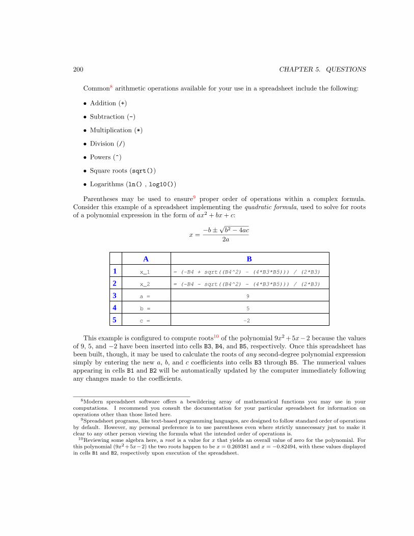
200 CHAPTER 5. QUESTIONS
Common8 arithmetic operations available for your use in a spreadsheet include the following:
• Addition (+)
• Subtraction (-)
• Multiplication (*)
• Division (/)
• Powers (^)
• Square roots (sqrt())
• Logarithms (ln() , log10())
Parentheses may be used to ensure9 proper order of operations within a complex formula.Consider this example of a spreadsheet implementing the quadratic formula, used to solve for rootsof a polynomial expression in the form of ax2 + bx + c:
x =−b ±
√b2 − 4ac
2a
1
2
3
4
5
A B
5
-2
x_1
x_2
a =
b =
c =
9
= (-B4 - sqrt((B4^2) - (4*B3*B5))) / (2*B3)
= (-B4 + sqrt((B4^2) - (4*B3*B5))) / (2*B3)
This example is configured to compute roots10 of the polynomial 9x2 +5x−2 because the valuesof 9, 5, and −2 have been inserted into cells B3, B4, and B5, respectively. Once this spreadsheet hasbeen built, though, it may be used to calculate the roots of any second-degree polynomial expressionsimply by entering the new a, b, and c coefficients into cells B3 through B5. The numerical valuesappearing in cells B1 and B2 will be automatically updated by the computer immediately followingany changes made to the coefficients.
8Modern spreadsheet software offers a bewildering array of mathematical functions you may use in yourcomputations. I recommend you consult the documentation for your particular spreadsheet for information onoperations other than those listed here.
9Spreadsheet programs, like text-based programming languages, are designed to follow standard order of operationsby default. However, my personal preference is to use parentheses even where strictly unnecessary just to make itclear to any other person viewing the formula what the intended order of operations is.
10Reviewing some algebra here, a root is a value for x that yields an overall value of zero for the polynomial. Forthis polynomial (9x2 +5x−2) the two roots happen to be x = 0.269381 and x = −0.82494, with these values displayedin cells B1 and B2, respectively upon execution of the spreadsheet.

5.2. QUANTITATIVE REASONING 201
Alternatively, one could break up the long quadratic formula into smaller pieces like this:
y =√
b2 − 4ac z = 2a
x =−b ± y
z
1
2
3
4
5
A B
5
-2
x_1
x_2
a =
b =
c =
9
C
= sqrt((B4^2) - (4*B3*B5))
= 2*B3
= (-B4 + C1) / C2
= (-B4 - C1) / C2
Note how the square-root term (y) is calculated in cell C1, and the denominator term (z) in cellC2. This makes the two final formulae (in cells B1 and B2) simpler to interpret. The positioning ofall these cells on the grid is completely arbitrary11 – all that matters is that they properly referenceeach other in the formulae.
Spreadsheets are particularly useful for situations where the same set of calculations representinga circuit or other system must be repeated for different initial conditions. The power of a spreadsheetis that it automates what would otherwise be a tedious set of calculations. One specific applicationof this is to simulate the effects of various components within a circuit failing with abnormal values(e.g. a shorted resistor simulated by making its value nearly zero; an open resistor simulated bymaking its value extremely large). Another application is analyzing the behavior of a circuit designgiven new components that are out of specification, and/or aging components experiencing driftover time.
11My personal preference is to locate all the “given” data in the upper-left cells of the spreadsheet grid (each datapoint flanked by a sensible name in the cell to the left and units of measurement in the cell to the right as illustratedin the first distance/time spreadsheet example), sometimes coloring them in order to clearly distinguish which cellscontain entered data versus which cells contain computed results from formulae. I like to place all formulae in cellsbelow the given data, and try to arrange them in logical order so that anyone examining my spreadsheet will be ableto figure out how I constructed a solution. This is a general principle I believe all computer programmers shouldfollow: document and arrange your code to make it easy for other people to learn from it.

202 CHAPTER 5. QUESTIONS
5.2.3 Integer conversion table
Complete this table, performing all necessary conversions between numeration systems of theseunsigned integer quantities:
Binary Octal Decimal Hexadecimal
10010
92
1A
67
1100101
122
1000
1011010110
12
134
32
110111
101
290
1111101000
336 DE
2D6
Challenges
• Which type of conversion do you find most difficult to perform, and why is that?
5.2.4 Setting up Port 1 I/O
Suppose you wish to use pins P1.0 through P1.5 as inputs, and use pins P1.6 and P1.7 as outputs.Write the necessary assembly-language instructions to configure these pins as such, and also aninstruction to set P1.6 and clear P1.7.
Challenges
• Explain why we don’t need to write any data to P1SEL or P1SEL2.
• Explain why we would have to write data to P2SEL if this were Port 2 we were using.

5.2. QUANTITATIVE REASONING 203
5.2.5 Setting up Timer A
The MSP430 microcontroller series offer multiple timer functions, which are counters driven byclock pulse sources. Not being dependent upon the CPU’s fetch/execute cycle means these timerswill track true time independently of the CPU’s programming, which makes them very useful forreal-time control and precision timing applications.
Reference the MSP430x2xx Family User’s Guide document and determine how to configure TimerA0 to be driven by the microcontroller’s Auxiliary Clock (ACLK) signal at one-quarter that signal’sfrequency, in up/down mode, with interrupt capabilities disabled.
Challenges
• Identify the clock divider options for this counter, and how you think these are obtained inhardware.
5.2.6 Selecting sub-main clock source
The MSP430 microcontroller series offer multiple oscillator signal sources for its internal clock signals.One of these signals is SMCLK, the Sub-Main Clock signal used to drive certain peripheral functions(i.e. other than the CPU).
Reference the MSP430x2xx Family User’s Guide document and determine how to configure theSMCLK signal to be driven by the VLOCLK on-board oscillator at one-eighth that oscillator’s frequency.
Challenges
• Identify the criteria important to determining proper clock frequency in a microcontroller.

204 CHAPTER 5. QUESTIONS
5.2.7 MSP430 header file
Locate and view the header file for your particular microcontroller (e.g. msp430g2553.h), and locatewithin that file the various symbolic constants used as human-readable bit labels for various registerswithin the microcontroller. Then, answer the following questions:
• Identify the binary equivalent of BIT4
• Identify the hexadecimal and binary equivalents for the Watchdog Timer Password (WDTPW)
• Show how the Watchdog Timer interval may be set with a single symbolic constant (e.g.WDT ADLY 1000) that is itself comprised of other symbolic constants
• How exactly are these symbolic constants useful to us when writing programs for the MSP430microcontroller?
Challenges
• Explain how you could create your own symbolic constant(s) customized for a particularprogram you are writing.

5.3. DIAGNOSTIC REASONING 205
5.3 Diagnostic reasoning
These questions are designed to stimulate your deductive and inductive thinking, where you mustapply general principles to specific scenarios (deductive) and also derive conclusions about the failedcircuit from specific details (inductive). In a Socratic discussion with your instructor, the goal is forthese questions to reinforce your recall and use of general circuit principles and also challenge yourability to integrate multiple symptoms into a sensible explanation of what’s wrong in a circuit. Yourinstructor may also pose additional questions based on those assigned, in order to further challengeand sharpen your diagnostic abilities.
As always, your goal is to fully explain your analysis of each problem. Simply obtaining acorrect answer is not good enough – you must also demonstrate sound reasoning in order tosuccessfully complete the assignment. Your instructor’s responsibility is to probe and challengeyour understanding of the relevant principles and analytical processes in order to ensure you have astrong foundation upon which to build further understanding.
You will note a conspicuous lack of answers given for these diagnostic questions. Unlike standardtextbooks where answers to every other question are given somewhere toward the back of the book,here in these learning modules students must rely on other means to check their work. The best wayby far is to debate the answers with fellow students and also with the instructor during the Socraticdialogue sessions intended to be used with these learning modules. Reasoning through challengingquestions with other people is an excellent tool for developing strong reasoning skills.
Another means of checking your diagnostic answers, where applicable, is to use circuit simulationsoftware to explore the effects of faults placed in circuits. For example, if one of these diagnosticquestions requires that you predict the effect of an open or a short in a circuit, you may check thevalidity of your work by simulating that same fault (substituting a very high resistance in place ofthat component for an open, and substituting a very low resistance for a short) within software andseeing if the results agree.

206 CHAPTER 5. QUESTIONS
5.3.1 Poor interface design
Explain why this attempt at interfacing the microcontroller to a high-current load is flawed, andpropose a better solution:
MS
P430G
2553IN20
VSSVCC (+3.3 V)
P1.0
P1.1
P1.2
P1.3
P1.4
P1.5
P2.0
P2.1
P2.2
P2.6
P2.7
TEST
RST
P1.7
P1.6
P2.5
P2.4
P2.3
+3.3V +12 V
Load
Challenges
• Write a snippet of assembly-language code to turn on the load.

5.3. DIAGNOSTIC REASONING 207
5.3.2 Improving a debug session
A very helpful feature of any software development application is debugging, where you get tointerrupt the normal flow of execution and “single-step” the code to see what the microprocessor isdoing at each line of code.
Suppose a student is developing a program to blink eight LEDs connected to the eight pins ofPort 1 on a MSP430G2553 microcontroller, a partial12 listing of their code shown below:
mov #0x00, P1OUT ; Initializes Port 1 pin states to low (0)
mov #0xFF, P1DIR ; Sets all Port 1 pin directions to outputs (1)
LOOP
xor #0xFF, P1OUT ; toggle all bits in P1OUT using XOR function
call #DELAY
jmp LOOP
DELAY
mov #0xFFFF, R4
DELAYLOOP
sub #0x01, R4 ; Decrement R4 by one
jnz DELAYLOOP
ret
When the student assembles this code and tries to run a debug session, she finds herself “stuck”in the DELAYLOOP for a great many steps. Identify a way for her to alter this program so that it doesnot linger in the “time delay” loop as long as it normally would when running at full speed.
Challenges
• Identify how to use a comment to very quickly eliminate the delay loop entirely from thiscode’s execution.
12Assembler directives and other “boilerplate” code has been removed for simplicity.

208 CHAPTER 5. QUESTIONS
5.3.3 Incorrect sum
A student writes a simple program to add two numbers together on a MSP430G2553 microcontroller,a partial13 listing of their code shown below:
MAIN
mov #0xF200, R5
add #0xFF00, R5
When run, the sum in register R5 is 0xF100 which is an incorrect sum. Identify the correct sum,and explain why this one is wrong.
Challenges
• Convert these quantities to decimal and show their proper addition.
13Assembler directives and other “boilerplate” code has been removed for simplicity.

Appendix A
Problem-Solving Strategies
The ability to solve complex problems is arguably one of the most valuable skills one can possess,and this skill is particularly important in any science-based discipline.
• Study principles, not procedures. Don’t be satisfied with merely knowing how to computesolutions – learn why those solutions work.
• Identify what it is you need to solve, identify all relevant data, identify all units of measurement,identify any general principles or formulae linking the given information to the solution, andthen identify any “missing pieces” to a solution. Annotate all diagrams with this data.
• Sketch a diagram to help visualize the problem. When building a real system, always devisea plan for that system and analyze its function before constructing it.
• Follow the units of measurement and meaning of every calculation. If you are ever performingmathematical calculations as part of a problem-solving procedure, and you find yourself unableto apply each and every intermediate result to some aspect of the problem, it means youdon’t understand what you are doing. Properly done, every mathematical result should havepractical meaning for the problem, and not just be an abstract number. You should be able toidentify the proper units of measurement for each and every calculated result, and show wherethat result fits into the problem.
• Perform “thought experiments” to explore the effects of different conditions for theoreticalproblems. When troubleshooting real systems, perform diagnostic tests rather than visuallyinspecting for faults, the best diagnostic test being the one giving you the most informationabout the nature and/or location of the fault with the fewest steps.
• Simplify the problem until the solution becomes obvious, and then use that obvious case as amodel to follow in solving the more complex version of the problem.
• Check for exceptions to see if your solution is incorrect or incomplete. A good solution willwork for all known conditions and criteria. A good example of this is the process of testingscientific hypotheses: the task of a scientist is not to find support for a new idea, but ratherto challenge that new idea to see if it holds up under a battery of tests. The philosophical
209

210 APPENDIX A. PROBLEM-SOLVING STRATEGIES
principle of reductio ad absurdum (i.e. disproving a general idea by finding a specific casewhere it fails) is useful here.
• Work “backward” from a hypothetical solution to a new set of given conditions.
• Add quantities to problems that are qualitative in nature, because sometimes a little mathhelps illuminate the scenario.
• Sketch graphs illustrating how variables relate to each other. These may be quantitative (i.e.with realistic number values) or qualitative (i.e. simply showing increases and decreases).
• Treat quantitative problems as qualitative in order to discern the relative magnitudes and/ordirections of change of the relevant variables. For example, try determining what happens if acertain variable were to increase or decrease before attempting to precisely calculate quantities:how will each of the dependent variables respond, by increasing, decreasing, or remaining thesame as before?
• Consider limiting cases. This works especially well for qualitative problems where you need todetermine which direction a variable will change. Take the given condition and magnify thatcondition to an extreme degree as a way of simplifying the direction of the system’s response.
• Check your work. This means regularly testing your conclusions to see if they make sense.This does not mean repeating the same steps originally used to obtain the conclusion(s), butrather to use some other means to check validity. Simply repeating procedures often leads torepeating the same errors if any were made, which is why alternative paths are better.

Appendix B
Instructional philosophy
“The unexamined circuit is not worth energizing” – Socrates (if he had taught electricity)
These learning modules, although useful for self-study, were designed to be used in a formallearning environment where a subject-matter expert challenges students to digest the content andexercise their critical thinking abilities in the answering of questions and in the construction andtesting of working circuits.
The following principles inform the instructional and assessment philosophies embodied in theselearning modules:
• The first goal of education is to enhance clear and independent thought, in order thatevery student reach their fullest potential in a highly complex and inter-dependent world.Robust reasoning is always more important than particulars of any subject matter, becauseits application is universal.
• Literacy is fundamental to independent learning and thought because text continues to be themost efficient way to communicate complex ideas over space and time. Those who cannot readwith ease are limited in their ability to acquire knowledge and perspective.
• Articulate communication is fundamental to work that is complex and interdisciplinary.
• Faulty assumptions and poor reasoning are best corrected through challenge, not presentation.The rhetorical technique of reductio ad absurdum (disproving an assertion by exposing anabsurdity) works well to discipline student’s minds, not only to correct the problem at handbut also to learn how to detect and correct future errors.
• Important principles should be repeatedly explored and widely applied throughout a courseof study, not only to reinforce their importance and help ensure their mastery, but also toshowcase the interconnectedness and utility of knowledge.
211

212 APPENDIX B. INSTRUCTIONAL PHILOSOPHY
These learning modules were expressly designed to be used in an “inverted” teachingenvironment1 where students first read the introductory and tutorial chapters on their own, thenindividually attempt to answer the questions and construct working circuits according to theexperiment and project guidelines. The instructor never lectures, but instead meets regularlywith each individual student to review their progress, answer questions, identify misconceptions,and challenge the student to new depths of understanding through further questioning. Regularmeetings between instructor and student should resemble a Socratic2 dialogue, where questionsserve as scalpels to dissect topics and expose assumptions. The student passes each module onlyafter consistently demonstrating their ability to logically analyze and correctly apply all majorconcepts in each question or project/experiment. The instructor must be vigilant in probing eachstudent’s understanding to ensure they are truly reasoning and not just memorizing. This is why“Challenge” points appear throughout, as prompts for students to think deeper about topics and asstarting points for instructor queries. Sometimes these challenge points require additional knowledgethat hasn’t been covered in the series to answer in full. This is okay, as the major purpose of theChallenges is to stimulate analysis and synthesis on the part of each student.
The instructor must possess enough mastery of the subject matter and awareness of students’reasoning to generate their own follow-up questions to practically any student response. Evencompletely correct answers given by the student should be challenged by the instructor for thepurpose of having students practice articulating their thoughts and defending their reasoning.Conceptual errors committed by the student should be exposed and corrected not by directinstruction, but rather by reducing the errors to an absurdity3 through well-chosen questions andthought experiments posed by the instructor. Becoming proficient at this style of instruction requirestime and dedication, but the positive effects on critical thinking for both student and instructor arespectacular.
An inspection of these learning modules reveals certain unique characteristics. One of these isa bias toward thorough explanations in the tutorial chapters. Without a live instructor to explainconcepts and applications to students, the text itself must fulfill this role. This philosophy results inlengthier explanations than what you might typically find in a textbook, each step of the reasoningprocess fully explained, including footnotes addressing common questions and concerns studentsraise while learning these concepts. Each tutorial seeks to not only explain each major conceptin sufficient detail, but also to explain the logic of each concept and how each may be developed
1In a traditional teaching environment, students first encounter new information via lecture from an expert, andthen independently apply that information via homework. In an “inverted” course of study, students first encounternew information via homework, and then independently apply that information under the scrutiny of an expert. Theexpert’s role in lecture is to simply explain, but the expert’s role in an inverted session is to challenge, critique, andif necessary explain where gaps in understanding still exist.
2Socrates is a figure in ancient Greek philosophy famous for his unflinching style of questioning. Although heauthored no texts, he appears as a character in Plato’s many writings. The essence of Socratic philosophy is toleave no question unexamined and no point of view unchallenged. While purists may argue a topic such as electriccircuits is too narrow for a true Socratic-style dialogue, I would argue that the essential thought processes involvedwith scientific reasoning on any topic are not far removed from the Socratic ideal, and that students of electricity andelectronics would do very well to challenge assumptions, pose thought experiments, identify fallacies, and otherwiseemploy the arsenal of critical thinking skills modeled by Socrates.
3This rhetorical technique is known by the Latin phrase reductio ad absurdum. The concept is to expose errors bycounter-example, since only one solid counter-example is necessary to disprove a universal claim. As an example ofthis, consider the common misconception among beginning students of electricity that voltage cannot exist withoutcurrent. One way to apply reductio ad absurdum to this statement is to ask how much current passes through afully-charged battery connected to nothing (i.e. a clear example of voltage existing without current).

213
from “first principles”. Again, this reflects the goal of developing clear and independent thought instudents’ minds, by showing how clear and logical thought was used to forge each concept. Studentsbenefit from witnessing a model of clear thinking in action, and these tutorials strive to be just that.
Another characteristic of these learning modules is a lack of step-by-step instructions in theProject and Experiment chapters. Unlike many modern workbooks and laboratory guides wherestep-by-step instructions are prescribed for each experiment, these modules take the approach thatstudents must learn to closely read the tutorials and apply their own reasoning to identify theappropriate experimental steps. Sometimes these steps are plainly declared in the text, just not asa set of enumerated points. At other times certain steps are implied, an example being assumedcompetence in test equipment use where the student should not need to be told again how to usetheir multimeter because that was thoroughly explained in previous lessons. In some circumstancesno steps are given at all, leaving the entire procedure up to the student.
This lack of prescription is not a flaw, but rather a feature. Close reading and clear thinking arefoundational principles of this learning series, and in keeping with this philosophy all activities aredesigned to require those behaviors. Some students may find the lack of prescription frustrating,because it demands more from them than what their previous educational experiences required. Thisfrustration should be interpreted as an unfamiliarity with autonomous thinking, a problem whichmust be corrected if the student is ever to become a self-directed learner and effective problem-solver.Ultimately, the need for students to read closely and think clearly is more important both in thenear-term and far-term than any specific facet of the subject matter at hand. If a student takeslonger than expected to complete a module because they are forced to outline, digest, and reasonon their own, so be it. The future gains enjoyed by developing this mental discipline will be wellworth the additional effort and delay.
Another feature of these learning modules is that they do not treat topics in isolation. Rather,important concepts are introduced early in the series, and appear repeatedly as stepping-stonestoward other concepts in subsequent modules. This helps to avoid the “compartmentalization”of knowledge, demonstrating the inter-connectedness of concepts and simultaneously reinforcingthem. Each module is fairly complete in itself, reserving the beginning of its tutorial to a review offoundational concepts.
This methodology of assigning text-based modules to students for digestion and then usingSocratic dialogue to assess progress and hone students’ thinking was developed over a period ofseveral years by the author with his Electronics and Instrumentation students at the two-year collegelevel. While decidedly unconventional and sometimes even unsettling for students accustomed toa more passive lecture environment, this instructional philosophy has proven its ability to conveyconceptual mastery, foster careful analysis, and enhance employability so much better than lecturethat the author refuses to ever teach by lecture again.
Problems which often go undiagnosed in a lecture environment are laid bare in this “inverted”format where students must articulate and logically defend their reasoning. This, too, may beunsettling for students accustomed to lecture sessions where the instructor cannot tell for sure whocomprehends and who does not, and this vulnerability necessitates sensitivity on the part of the“inverted” session instructor in order that students never feel discouraged by having their errorsexposed. Everyone makes mistakes from time to time, and learning is a lifelong process! Part ofthe instructor’s job is to build a culture of learning among the students where errors are not seen asshameful, but rather as opportunities for progress.

214 APPENDIX B. INSTRUCTIONAL PHILOSOPHY
To this end, instructors managing courses based on these modules should adhere to the followingprinciples:
• Student questions are always welcome and demand thorough, honest answers. The only typeof question an instructor should refuse to answer is one the student should be able to easilyanswer on their own. Remember, the fundamental goal of education is for each student to learnto think clearly and independently. This requires hard work on the part of the student, whichno instructor should ever circumvent. Anything done to bypass the student’s responsibility todo that hard work ultimately limits that student’s potential and thereby does real harm.
• It is not only permissible, but encouraged, to answer a student’s question by asking questionsin return, these follow-up questions designed to guide the student to reach a correct answerthrough their own reasoning.
• All student answers demand to be challenged by the instructor and/or by other students.This includes both correct and incorrect answers – the goal is to practice the articulation anddefense of one’s own reasoning.
• No reading assignment is deemed complete unless and until the student demonstrates theirability to accurately summarize the major points in their own terms. Recitation of the originaltext is unacceptable. This is why every module contains an “Outline and reflections” questionas well as a “Foundational concepts” question in the Conceptual reasoning section, to promptreflective reading.
• No assigned question is deemed answered unless and until the student demonstrates theirability to consistently and correctly apply the concepts to variations of that question. This iswhy module questions typically contain multiple “Challenges” suggesting different applicationsof the concept(s) as well as variations on the same theme(s). Instructors are encouraged todevise as many of their own “Challenges” as they are able, in order to have a multitude ofways ready to probe students’ understanding.
• No assigned experiment or project is deemed complete unless and until the studentdemonstrates the task in action. If this cannot be done “live” before the instructor, video-recordings showing the demonstration are acceptable. All relevant safety precautions must befollowed, all test equipment must be used correctly, and the student must be able to properlyexplain all results. The student must also successfully answer all Challenges presented by theinstructor for that experiment or project.

215
Students learning from these modules would do well to abide by the following principles:
• No text should be considered fully and adequately read unless and until you can express everyidea in your own words, using your own examples.
• You should always articulate your thoughts as you read the text, noting points of agreement,confusion, and epiphanies. Feel free to print the text on paper and then write your notes inthe margins. Alternatively, keep a journal for your own reflections as you read. This is trulya helpful tool when digesting complicated concepts.
• Never take the easy path of highlighting or underlining important text. Instead, summarizeand/or comment on the text using your own words. This actively engages your mind, allowingyou to more clearly perceive points of confusion or misunderstanding on your own.
• A very helpful strategy when learning new concepts is to place yourself in the role of a teacher,if only as a mental exercise. Either explain what you have recently learned to someone else,or at least imagine yourself explaining what you have learned to someone else. The simple actof having to articulate new knowledge and skill forces you to take on a different perspective,and will help reveal weaknesses in your understanding.
• Perform each and every mathematical calculation and thought experiment shown in the texton your own, referring back to the text to see that your results agree. This may seem trivialand unnecessary, but it is critically important to ensuring you actually understand what ispresented, especially when the concepts at hand are complicated and easy to misunderstand.Apply this same strategy to become proficient in the use of circuit simulation software, checkingto see if your simulated results agree with the results shown in the text.
• Above all, recognize that learning is hard work, and that a certain level of frustration isunavoidable. There are times when you will struggle to grasp some of these concepts, and thatstruggle is a natural thing. Take heart that it will yield with persistent and varied4 effort, andnever give up!
Students interested in using these modules for self-study will also find them beneficial, althoughthe onus of responsibility for thoroughly reading and answering questions will of course lie withthat individual alone. If a qualified instructor is not available to challenge students, a workablealternative is for students to form study groups where they challenge5 one another.
To high standards of education,
Tony R. Kuphaldt
4As the old saying goes, “Insanity is trying the same thing over and over again, expecting different results.” Ifyou find yourself stumped by something in the text, you should attempt a different approach. Alter the thoughtexperiment, change the mathematical parameters, do whatever you can to see the problem in a slightly different light,and then the solution will often present itself more readily.
5Avoid the temptation to simply share answers with study partners, as this is really counter-productive to learning.Always bear in mind that the answer to any question is far less important in the long run than the method(s) used toobtain that answer. The goal of education is to empower one’s life through the improvement of clear and independentthought, literacy, expression, and various practical skills.

216 APPENDIX B. INSTRUCTIONAL PHILOSOPHY

Appendix C
Tools used
I am indebted to the developers of many open-source software applications in the creation of theselearning modules. The following is a list of these applications with some commentary on each.
You will notice a theme common to many of these applications: a bias toward code. AlthoughI am by no means an expert programmer in any computer language, I understand and appreciatethe flexibility offered by code-based applications where the user (you) enters commands into a plainASCII text file, which the software then reads and processes to create the final output. Code-basedcomputer applications are by their very nature extensible, while WYSIWYG (What You See Is WhatYou Get) applications are generally limited to whatever user interface the developer makes for you.
The GNU/Linux computer operating system
There is so much to be said about Linus Torvalds’ Linux and Richard Stallman’s GNU
project. First, to credit just these two individuals is to fail to do justice to the mob ofpassionate volunteers who contributed to make this amazing software a reality. I firstlearned of Linux back in 1996, and have been using this operating system on my personalcomputers almost exclusively since then. It is free, it is completely configurable, and itpermits the continued use of highly efficient Unix applications and scripting languages(e.g. shell scripts, Makefiles, sed, awk) developed over many decades. Linux not onlyprovided me with a powerful computing platform, but its open design served to inspiremy life’s work of creating open-source educational resources.
Bram Moolenaar’s Vim text editor
Writing code for any code-based computer application requires a text editor, which maybe thought of as a word processor strictly limited to outputting plain-ASCII text files.Many good text editors exist, and one’s choice of text editor seems to be a deeply personalmatter within the programming world. I prefer Vim because it operates very similarly tovi which is ubiquitous on Unix/Linux operating systems, and because it may be entirelyoperated via keyboard (i.e. no mouse required) which makes it fast to use.
217

218 APPENDIX C. TOOLS USED
Donald Knuth’s TEX typesetting system
Developed in the late 1970’s and early 1980’s by computer scientist extraordinaire DonaldKnuth to typeset his multi-volume magnum opus The Art of Computer Programming,this software allows the production of formatted text for screen-viewing or paper printing,all by writing plain-text code to describe how the formatted text is supposed to appear.TEX is not just a markup language for documents, but it is also a Turing-completeprogramming language in and of itself, allowing useful algorithms to be created to controlthe production of documents. Simply put, TEX is a programmer’s approach to wordprocessing. Since TEX is controlled by code written in a plain-text file, this meansanyone may read that plain-text file to see exactly how the document was created. Thisopenness afforded by the code-based nature of TEX makes it relatively easy to learn howother people have created their own TEX documents. By contrast, examining a beautifuldocument created in a conventional WYSIWYG word processor such as Microsoft Wordsuggests nothing to the reader about how that document was created, or what the usermight do to create something similar. As Mr. Knuth himself once quipped, conventionalword processing applications should be called WYSIAYG (What You See Is All YouGet).
Leslie Lamport’s LATEX extensions to TEX
Like all true programming languages, TEX is inherently extensible. So, years after therelease of TEX to the public, Leslie Lamport decided to create a massive extensionallowing easier compilation of book-length documents. The result was LATEX, whichis the markup language used to create all ModEL module documents. You could saythat TEX is to LATEX as C is to C++. This means it is permissible to use any and all TEXcommands within LATEX source code, and it all still works. Some of the features offeredby LATEX that would be challenging to implement in TEX include automatic index andtable-of-content creation.
Tim Edwards’ Xcircuit drafting program
This wonderful program is what I use to create all the schematic diagrams andillustrations (but not photographic images or mathematical plots) throughout the ModELproject. It natively outputs PostScript format which is a true vector graphic format (thisis why the images do not pixellate when you zoom in for a closer view), and it is so simpleto use that I have never had to read the manual! Object libraries are easy to create forXcircuit, being plain-text files using PostScript programming conventions. Over theyears I have collected a large set of object libraries useful for drawing electrical andelectronic schematics, pictorial diagrams, and other technical illustrations.

219
Gimp graphic image manipulation program
Essentially an open-source clone of Adobe’s PhotoShop, I use Gimp to resize, crop, andconvert file formats for all of the photographic images appearing in the ModEL modules.Although Gimp does offer its own scripting language (called Script-Fu), I have neverhad occasion to use it. Thus, my utilization of Gimp to merely crop, resize, and convertgraphic images is akin to using a sword to slice bread.
SPICE circuit simulation program
SPICE is to circuit analysis as TEX is to document creation: it is a form of markuplanguage designed to describe a certain object to be processed in plain-ASCII text.When the plain-text “source file” is compiled by the software, it outputs the final result.More modern circuit analysis tools certainly exist, but I prefer SPICE for the followingreasons: it is free, it is fast, it is reliable, and it is a fantastic tool for teaching students ofelectricity and electronics how to write simple code. I happen to use rather old versions ofSPICE, version 2g6 being my “go to” application when I only require text-based output.NGSPICE (version 26), which is based on Berkeley SPICE version 3f5, is used when Irequire graphical output for such things as time-domain waveforms and Bode plots. Inall SPICE example netlists I strive to use coding conventions compatible with all SPICEversions.
Andrew D. Hwang’s ePiX mathematical visualization programming library
This amazing project is a C++ library you may link to any C/C++ code for the purposeof generating PostScript graphic images of mathematical functions. As a completelyfree and open-source project, it does all the plotting I would otherwise use a ComputerAlgebra System (CAS) such as Mathematica or Maple to do. It should be said thatePiX is not a Computer Algebra System like Mathematica or Maple, but merely amathematical visualization tool. In other words, it won’t determine integrals for you(you’ll have to implement that in your own C/C++ code!), but it can graph the results, andit does so beautifully. What I really admire about ePiX is that it is a C++ programminglibrary, which means it builds on the existing power and toolset available with thatprogramming language. Mr. Hwang could have probably developed his own stand-aloneapplication for mathematical plotting, but by creating a C++ library to do the same thinghe accomplished something much greater.

220 APPENDIX C. TOOLS USED
gnuplot mathematical visualization software
Another open-source tool for mathematical visualization is gnuplot. Interestingly, thistool is not part of Richard Stallman’s GNU project, its name being a coincidence. Forthis reason the authors prefer “gnu” not be capitalized at all to avoid confusion. This isa much “lighter-weight” alternative to a spreadsheet for plotting tabular data, and thefact that it easily outputs directly to an X11 console or a file in a number of differentgraphical formats (including PostScript) is very helpful. I typically set my gnuplot
output format to default (X11 on my Linux PC) for quick viewing while I’m developinga visualization, then switch to PostScript file export once the visual is ready to include inthe document(s) I’m writing. As with my use of Gimp to do rudimentary image editing,my use of gnuplot only scratches the surface of its capabilities, but the important pointsare that it’s free and that it works well.
Python programming language
Both Python and C++ find extensive use in these modules as instructional aids andexercises, but I’m listing Python here as a tool for myself because I use it almost dailyas a calculator. If you open a Python interpreter console and type from math import
* you can type mathematical expressions and have it return results just as you wouldon a hand calculator. Complex-number (i.e. phasor) arithmetic is similarly supportedif you include the complex-math library (from cmath import *). Examples of this areshown in the Programming References chapter (if included) in each module. Of course,being a fully-featured programming language, Python also supports conditionals, loops,and other structures useful for calculation of quantities. Also, running in a consoleenvironment where all entries and returned values show as text in a chronologically-ordered list makes it easy to copy-and-paste those calculations to document exactly howthey were performed.

Appendix D
Creative Commons License
Creative Commons Attribution 4.0 International Public License
By exercising the Licensed Rights (defined below), You accept and agree to be bound by the termsand conditions of this Creative Commons Attribution 4.0 International Public License (“PublicLicense”). To the extent this Public License may be interpreted as a contract, You are granted theLicensed Rights in consideration of Your acceptance of these terms and conditions, and the Licensorgrants You such rights in consideration of benefits the Licensor receives from making the LicensedMaterial available under these terms and conditions.
Section 1 – Definitions.
a. Adapted Material means material subject to Copyright and Similar Rights that is derivedfrom or based upon the Licensed Material and in which the Licensed Material is translated, altered,arranged, transformed, or otherwise modified in a manner requiring permission under the Copyrightand Similar Rights held by the Licensor. For purposes of this Public License, where the LicensedMaterial is a musical work, performance, or sound recording, Adapted Material is always producedwhere the Licensed Material is synched in timed relation with a moving image.
b. Adapter’s License means the license You apply to Your Copyright and Similar Rights inYour contributions to Adapted Material in accordance with the terms and conditions of this PublicLicense.
c. Copyright and Similar Rights means copyright and/or similar rights closely related tocopyright including, without limitation, performance, broadcast, sound recording, and Sui GenerisDatabase Rights, without regard to how the rights are labeled or categorized. For purposes of thisPublic License, the rights specified in Section 2(b)(1)-(2) are not Copyright and Similar Rights.
d. Effective Technological Measures means those measures that, in the absence of properauthority, may not be circumvented under laws fulfilling obligations under Article 11 of the WIPOCopyright Treaty adopted on December 20, 1996, and/or similar international agreements.
e. Exceptions and Limitations means fair use, fair dealing, and/or any other exception or
221

222 APPENDIX D. CREATIVE COMMONS LICENSE
limitation to Copyright and Similar Rights that applies to Your use of the Licensed Material.
f. Licensed Material means the artistic or literary work, database, or other material to whichthe Licensor applied this Public License.
g. Licensed Rights means the rights granted to You subject to the terms and conditions ofthis Public License, which are limited to all Copyright and Similar Rights that apply to Your use ofthe Licensed Material and that the Licensor has authority to license.
h. Licensor means the individual(s) or entity(ies) granting rights under this Public License.
i. Share means to provide material to the public by any means or process that requirespermission under the Licensed Rights, such as reproduction, public display, public performance,distribution, dissemination, communication, or importation, and to make material available to thepublic including in ways that members of the public may access the material from a place and at atime individually chosen by them.
j. Sui Generis Database Rights means rights other than copyright resulting from Directive96/9/EC of the European Parliament and of the Council of 11 March 1996 on the legal protectionof databases, as amended and/or succeeded, as well as other essentially equivalent rights anywherein the world.
k. You means the individual or entity exercising the Licensed Rights under this Public License.Your has a corresponding meaning.
Section 2 – Scope.
a. License grant.
1. Subject to the terms and conditions of this Public License, the Licensor hereby grants You aworldwide, royalty-free, non-sublicensable, non-exclusive, irrevocable license to exercise the LicensedRights in the Licensed Material to:
A. reproduce and Share the Licensed Material, in whole or in part; and
B. produce, reproduce, and Share Adapted Material.
2. Exceptions and Limitations. For the avoidance of doubt, where Exceptions and Limitationsapply to Your use, this Public License does not apply, and You do not need to comply with its termsand conditions.
3. Term. The term of this Public License is specified in Section 6(a).
4. Media and formats; technical modifications allowed. The Licensor authorizes You to exercisethe Licensed Rights in all media and formats whether now known or hereafter created, and to maketechnical modifications necessary to do so. The Licensor waives and/or agrees not to assert any rightor authority to forbid You from making technical modifications necessary to exercise the LicensedRights, including technical modifications necessary to circumvent Effective Technological Measures.

223
For purposes of this Public License, simply making modifications authorized by this Section 2(a)(4)never produces Adapted Material.
5. Downstream recipients.
A. Offer from the Licensor – Licensed Material. Every recipient of the Licensed Materialautomatically receives an offer from the Licensor to exercise the Licensed Rights under the termsand conditions of this Public License.
B. No downstream restrictions. You may not offer or impose any additional or different termsor conditions on, or apply any Effective Technological Measures to, the Licensed Material if doingso restricts exercise of the Licensed Rights by any recipient of the Licensed Material.
6. No endorsement. Nothing in this Public License constitutes or may be construed as permissionto assert or imply that You are, or that Your use of the Licensed Material is, connected with,or sponsored, endorsed, or granted official status by, the Licensor or others designated to receiveattribution as provided in Section 3(a)(1)(A)(i).
b. Other rights.
1. Moral rights, such as the right of integrity, are not licensed under this Public License, norare publicity, privacy, and/or other similar personality rights; however, to the extent possible, theLicensor waives and/or agrees not to assert any such rights held by the Licensor to the limited extentnecessary to allow You to exercise the Licensed Rights, but not otherwise.
2. Patent and trademark rights are not licensed under this Public License.
3. To the extent possible, the Licensor waives any right to collect royalties from You for theexercise of the Licensed Rights, whether directly or through a collecting society under any voluntaryor waivable statutory or compulsory licensing scheme. In all other cases the Licensor expresslyreserves any right to collect such royalties.
Section 3 – License Conditions.
Your exercise of the Licensed Rights is expressly made subject to the following conditions.
a. Attribution.
1. If You Share the Licensed Material (including in modified form), You must:
A. retain the following if it is supplied by the Licensor with the Licensed Material:
i. identification of the creator(s) of the Licensed Material and any others designated to receiveattribution, in any reasonable manner requested by the Licensor (including by pseudonym ifdesignated);
ii. a copyright notice;

224 APPENDIX D. CREATIVE COMMONS LICENSE
iii. a notice that refers to this Public License;
iv. a notice that refers to the disclaimer of warranties;
v. a URI or hyperlink to the Licensed Material to the extent reasonably practicable;
B. indicate if You modified the Licensed Material and retain an indication of any previousmodifications; and
C. indicate the Licensed Material is licensed under this Public License, and include the text of,or the URI or hyperlink to, this Public License.
2. You may satisfy the conditions in Section 3(a)(1) in any reasonable manner based on themedium, means, and context in which You Share the Licensed Material. For example, it may bereasonable to satisfy the conditions by providing a URI or hyperlink to a resource that includes therequired information.
3. If requested by the Licensor, You must remove any of the information required by Section3(a)(1)(A) to the extent reasonably practicable.
4. If You Share Adapted Material You produce, the Adapter’s License You apply must notprevent recipients of the Adapted Material from complying with this Public License.
Section 4 – Sui Generis Database Rights.
Where the Licensed Rights include Sui Generis Database Rights that apply to Your use of theLicensed Material:
a. for the avoidance of doubt, Section 2(a)(1) grants You the right to extract, reuse, reproduce,and Share all or a substantial portion of the contents of the database;
b. if You include all or a substantial portion of the database contents in a database in whichYou have Sui Generis Database Rights, then the database in which You have Sui Generis DatabaseRights (but not its individual contents) is Adapted Material; and
c. You must comply with the conditions in Section 3(a) if You Share all or a substantial portionof the contents of the database.
For the avoidance of doubt, this Section 4 supplements and does not replace Your obligationsunder this Public License where the Licensed Rights include other Copyright and Similar Rights.
Section 5 – Disclaimer of Warranties and Limitation of Liability.
a. Unless otherwise separately undertaken by the Licensor, to the extent possible, the Licensoroffers the Licensed Material as-is and as-available, and makes no representations or warranties ofany kind concerning the Licensed Material, whether express, implied, statutory, or other. Thisincludes, without limitation, warranties of title, merchantability, fitness for a particular purpose,non-infringement, absence of latent or other defects, accuracy, or the presence or absence of errors,
225
whether or not known or discoverable. Where disclaimers of warranties are not allowed in full or inpart, this disclaimer may not apply to You.
b. To the extent possible, in no event will the Licensor be liable to You on any legal theory(including, without limitation, negligence) or otherwise for any direct, special, indirect, incidental,consequential, punitive, exemplary, or other losses, costs, expenses, or damages arising out of thisPublic License or use of the Licensed Material, even if the Licensor has been advised of the possibilityof such losses, costs, expenses, or damages. Where a limitation of liability is not allowed in full orin part, this limitation may not apply to You.
c. The disclaimer of warranties and limitation of liability provided above shall be interpreted ina manner that, to the extent possible, most closely approximates an absolute disclaimer and waiverof all liability.
Section 6 – Term and Termination.
a. This Public License applies for the term of the Copyright and Similar Rights licensed here.However, if You fail to comply with this Public License, then Your rights under this Public Licenseterminate automatically.
b. Where Your right to use the Licensed Material has terminated under Section 6(a), it reinstates:
1. automatically as of the date the violation is cured, provided it is cured within 30 days of Yourdiscovery of the violation; or
2. upon express reinstatement by the Licensor.
For the avoidance of doubt, this Section 6(b) does not affect any right the Licensor may have toseek remedies for Your violations of this Public License.
c. For the avoidance of doubt, the Licensor may also offer the Licensed Material under separateterms or conditions or stop distributing the Licensed Material at any time; however, doing so willnot terminate this Public License.
d. Sections 1, 5, 6, 7, and 8 survive termination of this Public License.
Section 7 – Other Terms and Conditions.
a. The Licensor shall not be bound by any additional or different terms or conditionscommunicated by You unless expressly agreed.
b. Any arrangements, understandings, or agreements regarding the Licensed Material not statedherein are separate from and independent of the terms and conditions of this Public License.
Section 8 – Interpretation.
a. For the avoidance of doubt, this Public License does not, and shall not be interpreted to,reduce, limit, restrict, or impose conditions on any use of the Licensed Material that could lawfully

226 APPENDIX D. CREATIVE COMMONS LICENSE
be made without permission under this Public License.
b. To the extent possible, if any provision of this Public License is deemed unenforceable, it shallbe automatically reformed to the minimum extent necessary to make it enforceable. If the provisioncannot be reformed, it shall be severed from this Public License without affecting the enforceabilityof the remaining terms and conditions.
c. No term or condition of this Public License will be waived and no failure to comply consentedto unless expressly agreed to by the Licensor.
d. Nothing in this Public License constitutes or may be interpreted as a limitation upon, orwaiver of, any privileges and immunities that apply to the Licensor or You, including from the legalprocesses of any jurisdiction or authority.

227
Creative Commons is not a party to its public licenses. Notwithstanding, Creative Commonsmay elect to apply one of its public licenses to material it publishes and in those instances willbe considered the “Licensor.” Except for the limited purpose of indicating that material is sharedunder a Creative Commons public license or as otherwise permitted by the Creative Commonspolicies published at creativecommons.org/policies, Creative Commons does not authorize theuse of the trademark “Creative Commons” or any other trademark or logo of Creative Commonswithout its prior written consent including, without limitation, in connection with any unauthorizedmodifications to any of its public licenses or any other arrangements, understandings, or agreementsconcerning use of licensed material. For the avoidance of doubt, this paragraph does not form partof the public licenses.
Creative Commons may be contacted at creativecommons.org.

228 APPENDIX D. CREATIVE COMMONS LICENSE

Appendix E
References
Hemingway, Bruce, “Lecture 3 – MSP430 Interrupts”, CSE 466 “Software for Embedded Systems”course lecture notes, Department of Computer Science and Engineering, University of Washington,Autumn 2010.
“Intel Pentium Dual-Core Desktop Processor E2000 Series” datasheet, document number 316981-004, Intel Corporation, December 2007.
lnk msp430g2553.cmd, linker command file, version 1.198, Texas Instruments Incorporated, 2016.
MacKenzie, I. Scott, The 8051 Microcontroller, MacMillan Publishing Company, New York, NY,1992.
“MSP430G2553 LaunchPad Development Kit” user’s guide, document number SLAU772, TexasInstruments Incorporated, June 2018.
“MSP430G2x53, MSP430G2x13 Mixed-Signal Microcontroller” datasheet, document numberSLAS735J, Texas Instruments Incorporated, May 2013.
“MSP430x2xx Family User’s Guide”, document number SLAU144J, Texas InstrumentsIncorporated, July 2013.
229

230 APPENDIX E. REFERENCES

Appendix F
Version history
This is a list showing all significant additions, corrections, and other edits made to this learningmodule. Each entry is referenced by calendar date in reverse chronological order (newest versionfirst), which appears on the front cover of every learning module for easy reference. Any contributorsto this open-source document are listed here as well.
30 November 2021 – corrected a LaTeX typo, where I failed to include an escape character beforea pound symbol in one of the instructor notes. This error went undetected when compiling thedocument for student use, but failed when I tried to compile an instructor version.
26 November 2021 – minor edit to a footnote.
14-15 November 2021 – eliminated reference to memory address locations for variables in the “Cexample: bitwise operations” Case Tutorial because they were really not germane to the topic athand. Also added another section to the Tutorial on bit-level input instructions, another sectionon the watchdog timer, and a new Case Tutorial showing use of the watchdog timer in a trivialprogram.
9 November 2021 – corrected typographical errors in image 5445 and image 5446. In both casesI mistakenly used the 0x prefix when I should have used 0b because the port control register valueswere in binary and not hexadecimal.
7 September 2021 – minor typographical error corrections.
26 August 2021 – minor edits to the “Elementary output and input” section of the Tutorial. Also,moved the “Writing to output pins” subsection to become a new section following “Elementaryoutput and input” called “Bit-level output instructions”.
22 August 2021 – added commentary to some of the Case Tutorial examples. Also added“Integer conversion table” Quantitative Reasoning question, and made some minor typographicalerror corrections.
20 June 2021 – added more content to the Tutorial on starting new projects, especially the
231

232 APPENDIX F. VERSION HISTORY
importance of selecting the proper “target” microcontroller.
14 June 2021 – added to one of the existing Case Tutorial sections on PWM, showing how an RCnetwork may be used to produce a pseudo analog output channel.
13 June 2021 – added another Case Tutorial section, on crude analog input demonstration.
10 May 2021 – commented out or deleted empty chapters.
3 May 2021 – added BJT-only solution to the “Example: interposing MCU to a heavy load” CaseTutorial.
28 April 2021 – added more explanatory text to the Case Tutorial example “C example: BooleanSOP expression”.
12 April 2021 – added two new Case Tutorial examples. One shows analog-digital conversion of avoltage signal and reporting of the ADC count value using the UART. The other takes this conceptfurther by showing how the microcontroller may be used as a simple datalogger, storing 128 sampledanalog voltage signals in an array and transmitting that stored data in comma-separated variable(CSV) format using the UART.
11 April 2021 – corrected code error in two Case Tutorial examples showing how to use the UART.The error was a single ampersand (&) rather than a double-ampersand (&&).
6 April 2021 – edited the Case Tutorial example on interposing heavy loads to show commutatingdiodes and optoisolators.
5 April 2021 – added a new Case Tutorial section showing MCU driving two BJTs as a sine-waveDC-to-AC converter.
29 March 2021 – added a reference to the intrinsic function delay cycles() in the “C example:alternating LED blink” Case Tutorial. Also fixed a code error in the “C example: pushbutton-triggered timer” where the value of tenths was being limited to 0xFF rather than 0xFFFF as itshould have been. Also added a footnote to the timer Case Tutorial explaining how to adjust theTACCR0 register for super-fine adjustment of the 1
10 second interrupt period.
25 March 2021 – improved and expanded upon code examples in the Case Tutorial section “Cexample: pushbutton-triggered timer”. Also added a new Case Tutorial section showing how totransmit both letter and number characters in ASCII format via the UART.
17 March 2021 – added more commentary to the Tutorial chapter regarding the default functionsof pins P2.6 and P2.7.
12 March 2021 – added a new Case Tutorial section showing MCU driving BJT driving MOSFET.
6-7 March 2021 – added a Case Tutorial section showing UART transmission of ASCII text.
22-25 February 2021 – added a Case Tutorial section showing pushbutton-based interrupt in C.
233
Also added some clarifying text in the Tutorial chapter regarding the same topic. Additionally,added some explanatory text about the use of BIT macros pre-defined in the msp430.h header file.
19 February 2021 – added a Case Tutorial section showing simple stack operations, and also addedsome content to a couple of existing Case Tutorial examples.
3 February 2021 – added instructor notes, and also a pagebeak prior to the ”Improving a debugsession”. Also added decoupling capacitors to the motor start/stop Case Tutorial.
30 January 2021 – added new Case Tutorial section showing how to use the microcontroller tosynthesize a sine wave, based on code written by Jason Wahl on 29 January 2021.
29 January 2021 – divided part of the I/O subsection into its own subsection, discussing in detailhow to set and clear output pin bits.
26 January 2021 – modified schematic diagram in Case Tutorial example showing how to drivean electric motor. I added a relay to the transistor interposing in order to provide greater electricalisolation between the motor and the MCU.
11 December 2020 – modified the Case Tutorial section on start-stop control, to include aschematic showing how a transistor could interpose between the MCU and an electric motor.
22 September 2020 – corrected typographical error in the C source code for the bitwise operationsCase Tutorial example, courtesy of Tysha Eisele.
18 September 2020 – corrected errors on pin diagrams for all Case Tutorial schematics, where Ifailed to show the active-low Reset pin tied high!
15 September 2020 – moved interrupt section bullet-list into a table.
8 September 2020 – minor typographical correction in “Setting up Port 1 I/O” question.
7 September 2020 – added Case Tutorial sections on pulse-width modulation output using TimerA, analog-digital conversion using Timer A interrupt, and motor start-stop control (all written inC).
2 September 2020 – fixed typographical error in the “subtracting two numbers” assembly-languageexample within the Case Tutorial chapter. Also, added a new “Debugging tools” section. Fixedanother typographical error in the I/O subsection as well (wrong hex representation for a binarynumber).
30 August 2020 – added screenshots showing set-up of C project in Code Composer Studio.
29 August 2020 – significantly edited the Introduction chapter to make it more suitable as apre-study guide and to provide cues useful to instructors leading “inverted” teaching sessions.
25 August 2020 – added screenshots showing set-up of Energia project in Code Composer Studio.

234 APPENDIX F. VERSION HISTORY
18 August 2020 – added Case Tutorial example for Boolean SOP function written in C.
18 July 2020 – added Case Tutorial examples written in both C and Sketch to add two numbers.
8 July 2020 – added Case Tutorial example for a program coded in Sketch rather than C orassembly.
26 June 2020 – added Case Tutorial example some programs coded in C rather than assembly.
23-24 June 2020 – added Case Tutorial example showing external (Port 1) interrupt, and a newTutorial section on interrupt handling for the MSP430 microcontroller series.
12-17 June 2020 – added more Case Tutorial examples, Tutorial content, and questions.
11 June 2020 – document first created.

Index
Absolute addressing mode, 8, 31, 167Accumulator, 174Adding quantities to a qualitative problem, 210Address resolution, 178Addressing mode, 8, 31, 167Addressing, relative, 181ALU, 132Annotating diagrams, 209Arduino, 120Arithmetic Logic Unit, 132Assembly code, 174
Bitwise operation, 127
Calling a subroutine, 180CCS, 120Checking for exceptions, 210Checking your work, 210Clock, 179Code Composer Studio, 120Code, computer, 217Comment, 178Commutating diode, 40
Debug mode, 148, 151Debug session, properly closing, 158, 172Delay, 179Dimensional analysis, 209Diode, commutating, 40Directive, 177Disassembler, 181
Edwards, Tim, 218Endianness, 133, 175Energia, 120eZ-FET, 120
Fetch/execute cycle, 179
General Interrupt Enable bit, 137, 138GIE bit, 137, 138Graph values to solve a problem, 210Greenleaf, Cynthia, 187
Harvard architecture, 131Hex dump, 176How to teach with these modules, 212Hwang, Andrew D., 219
I/O port, 121Identify given data, 209Identify relevant principles, 209Immediate addressing mode, 31Inductive kickback, 40Instructions for projects and experiments, 213Intermediate results, 209Interposing, 40Interrupt, 136, 137, 183, 195Interrupt service routine, 183, 195Interrupt vector, 137Inverted instruction, 212ISR, 136, 137, 183, 195
Jump instruction, 175
Kickback, inductive, 40Knuth, Donald, 218
Label, 178Lamport, Leslie, 218LaunchPad, 120Limiting cases, 210Little-endian, 133, 175
Machine code, 174Mask, 64, 128, 136, 138, 195Maskable interrupt, 138
235

236 INDEX
Metacognition, 192Microcontroller, 115Microprocessor, 115Moolenaar, Bram, 217MOS 6502 microprocessor, 174Murphy, Lynn, 187
NMI, 138Non-maskable interrupt, 138
Opcode, 175Open-source, 217Operand, 175Optimization, compiler, 153
P2SEL, 136Pin assignments, MSP430G2553IN20, 119Popping from the stack, 181, 183Port, I/O, 121Problem-solving: annotate diagrams, 209Problem-solving: check for exceptions, 210Problem-solving: checking work, 210Problem-solving: dimensional analysis, 209Problem-solving: graph values, 210Problem-solving: identify given data, 209Problem-solving: identify relevant principles, 209Problem-solving: interpret intermediate results,
209Problem-solving: limiting cases, 210Problem-solving: qualitative to quantitative, 210Problem-solving: quantitative to qualitative, 210Problem-solving: reductio ad absurdum, 210Problem-solving: simplify the system, 209Problem-solving: thought experiment, 209Problem-solving: track units of measurement,
209Problem-solving: visually represent the system,
209Problem-solving: work in reverse, 210Processor, 115Program counter, 180Pushing to the stack, 181, 183
Qualitatively approaching a quantitativeproblem, 210
Reading Apprenticeship, 187
Reductio ad absurdum, 210–212Register, 174Relative addressing, 181Release mode, 148, 151Return from subroutine, 180
Schoenbach, Ruth, 187Scientific method, 192setup(), 12Shift register, 183Simplifying a system, 209Socrates, 211Socratic dialogue, 212SPICE, 187Stack, 181, 183Stallman, Richard, 217Status register, 184, 185Subroutine, 137, 180Symbolic addressing mode, 31Symbols, 39, 70, 77, 129System on a chip, 144
Thought experiment, 209Time delay, 179Torvalds, Linus, 217
Unconditional jump, 175Units of measurement, 209
Visualizing a system, 209Von Neumann architecture, 131
Work in reverse to solve a problem, 210WYSIWYG, 217, 218