Vertical comb-finger capacitive actuation and sensing for CMOS-MEMS
Upload
undar-jombangCategory
view
0download
0
Chapter 4
Modular Combinational Logic
Decoders
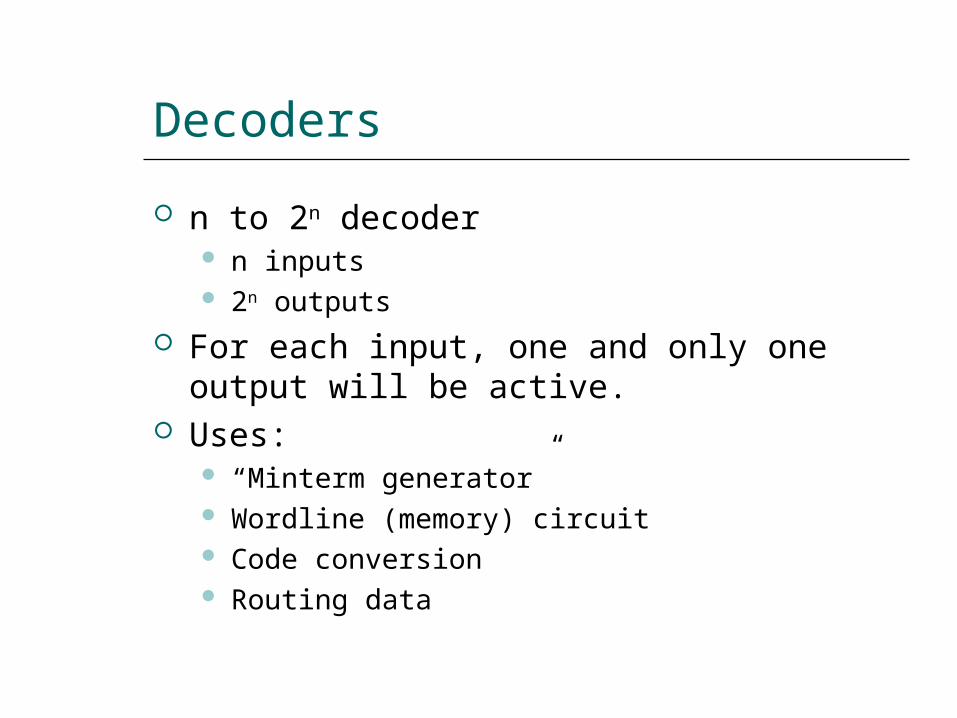
Decoders n to 2n decoder
n inputs 2n outputs
For each input, one and only one output will be active.
Uses: “Minterm generator” Wordline (memory) circuit Code conversion Routing data

2 to 4 Decoder Example
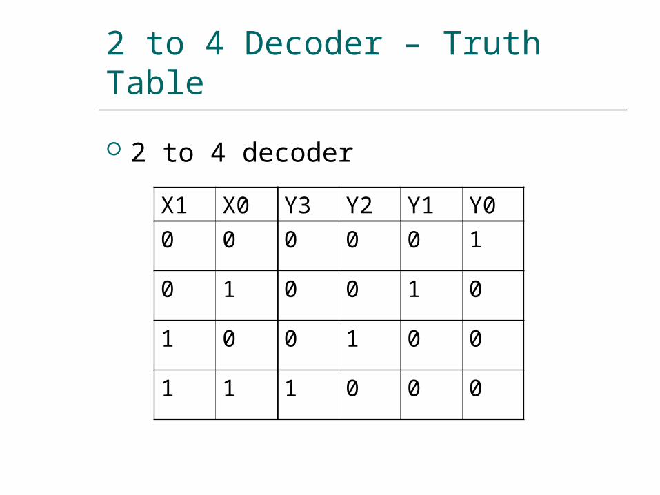
2 to 4 Decoder – Truth Table 2 to 4 decoder
X1 X0 Y3 Y2 Y1 Y00 0 0 0 0 1
0 1 0 0 1 0
1 0 0 1 0 0
1 1 1 0 0 0
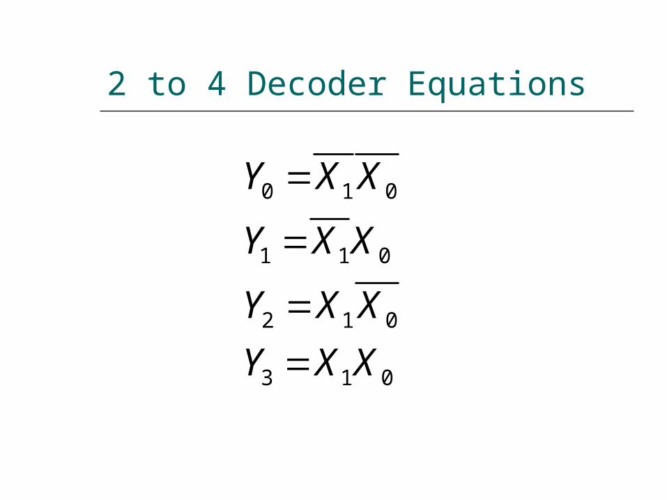
2 to 4 Decoder Equations
0 1 0
1 1 0
2 1 0
3 1 0
Y X XY X XY X XY X X

2 to 4 Decoder: Circuit
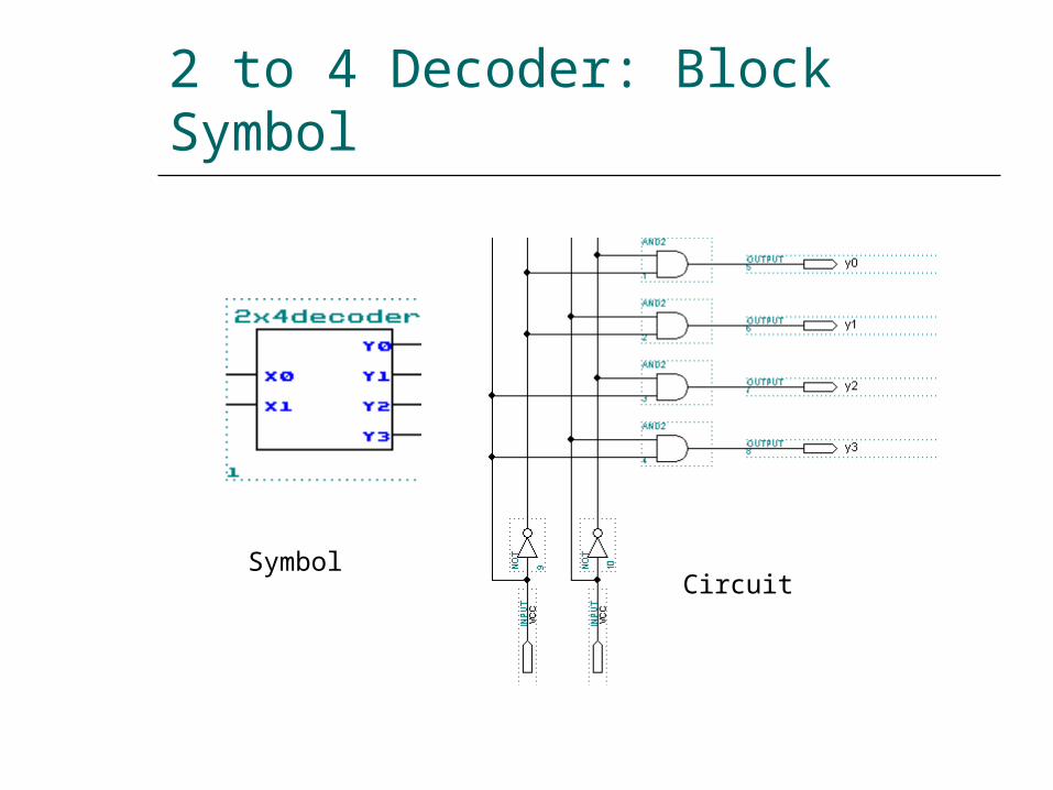
2 to 4 Decoder: Block Symbol
SymbolCircuit
3 to 8 Decoder Example
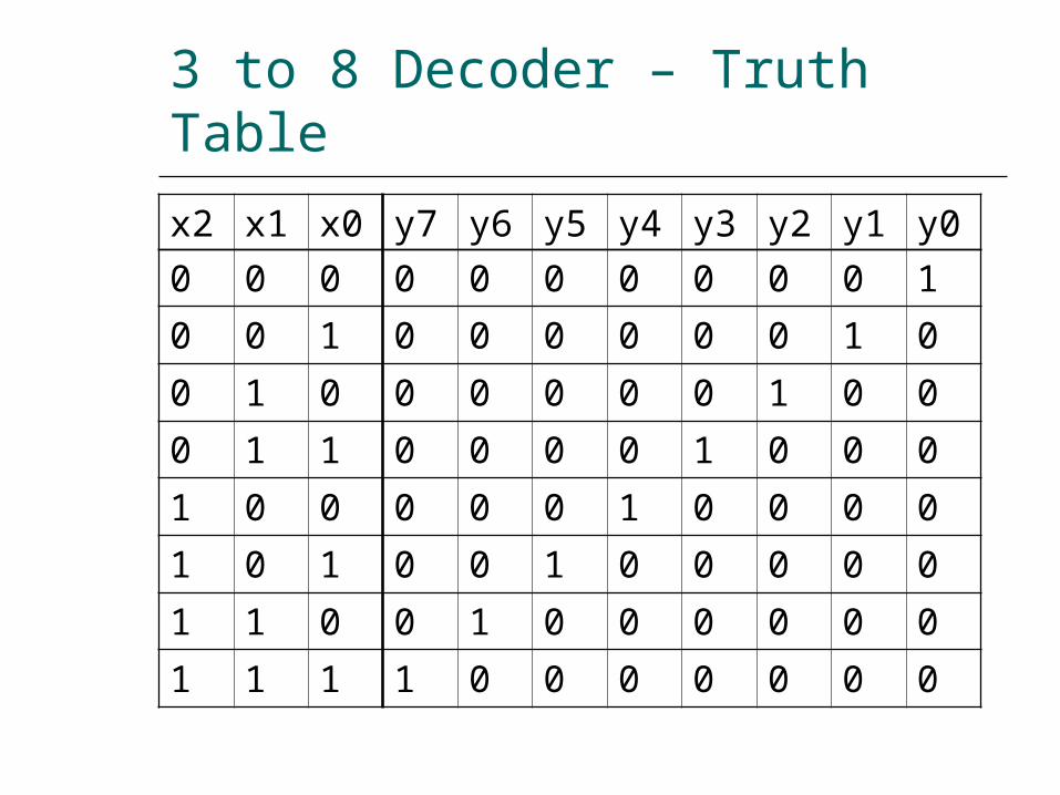
3 to 8 Decoder – Truth Tablex2 x1 x0 y7 y6 y5 y4 y3 y2 y1 y00 0 0 0 0 0 0 0 0 0 10 0 1 0 0 0 0 0 0 1 00 1 0 0 0 0 0 0 1 0 00 1 1 0 0 0 0 1 0 0 01 0 0 0 0 0 1 0 0 0 01 0 1 0 0 1 0 0 0 0 01 1 0 0 1 0 0 0 0 0 01 1 1 1 0 0 0 0 0 0 0
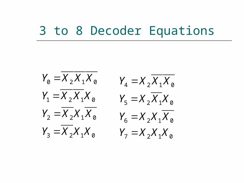
3 to 8 Decoder Equations
0 2 1 0
1 2 1 0
2 2 1 0
3 2 1 0
Y X X XY X X XY X X XY X X X
4 2 1 0
5 2 1 0
6 2 1 0
7 2 1 0
Y X X XY X X XY X X XY X X X
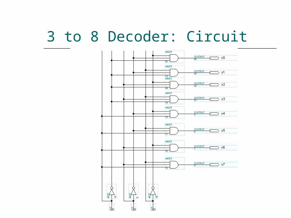
3 to 8 Decoder: Circuit
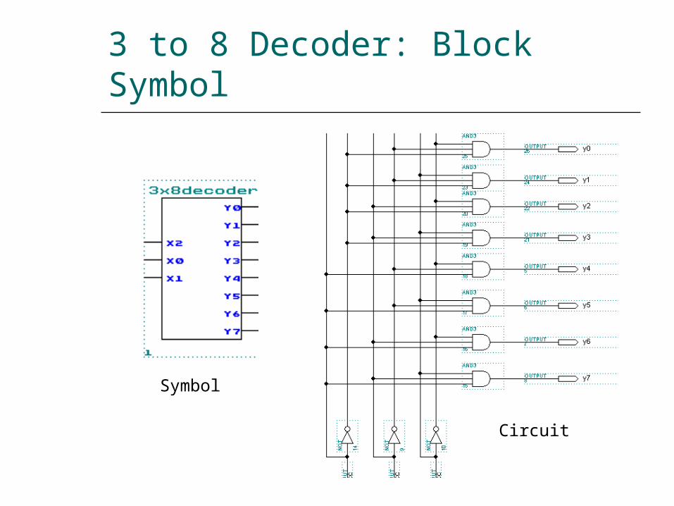
3 to 8 Decoder: Block Symbol
Symbol
Circuit

Design Example
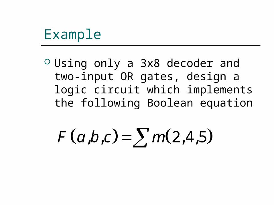
Example Using only a 3x8 decoder and two-input OR gates, design a logic circuit which implements the following Boolean equation
, , 2,4,5F a b c m
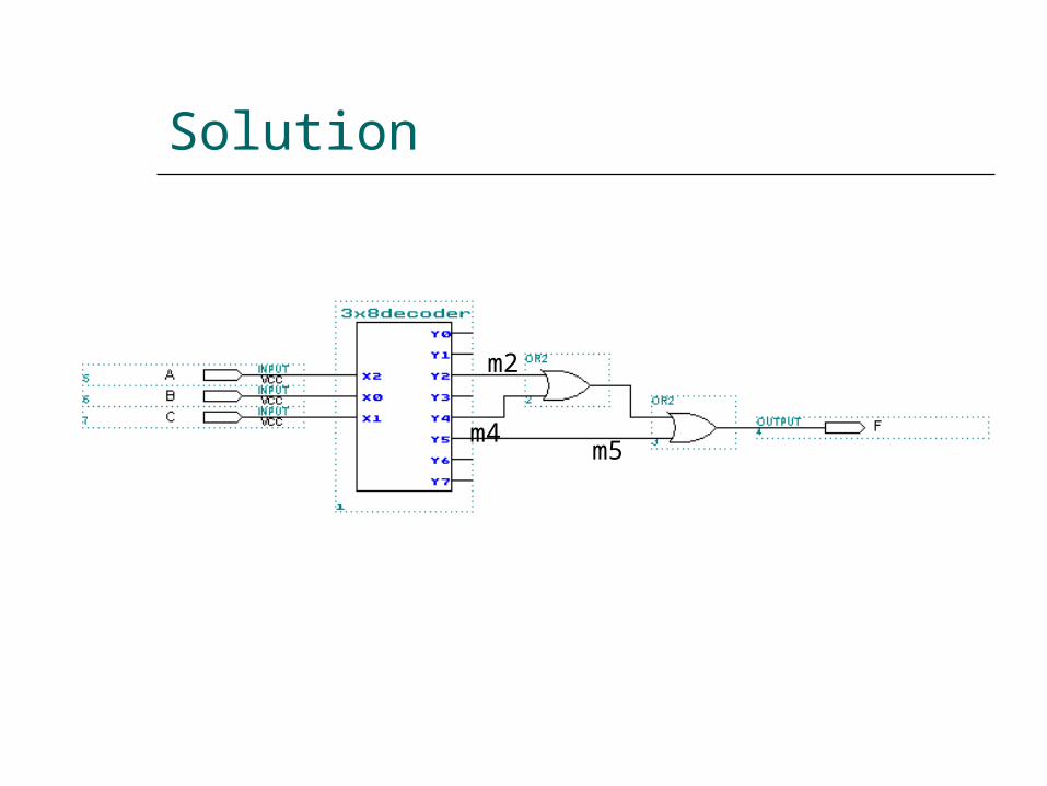
Solution
m2
m4 m5
2 to 4 Decoder with Enable
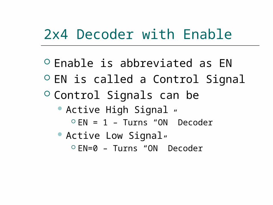
2x4 Decoder with Enable Enable is abbreviated as EN EN is called a Control Signal Control Signals can be
Active High Signal EN = 1 – Turns “ON” Decoder
Active Low Signal EN=0 – Turns “ON” Decoder
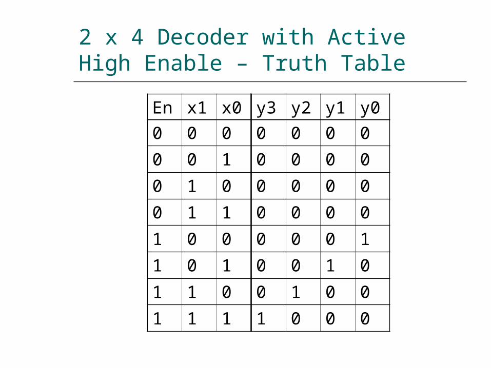
2 x 4 Decoder with Active High Enable – Truth Table
En x1 x0 y3 y2 y1 y00 0 0 0 0 0 00 0 1 0 0 0 00 1 0 0 0 0 00 1 1 0 0 0 01 0 0 0 0 0 11 0 1 0 0 1 01 1 0 0 1 0 01 1 1 1 0 0 0
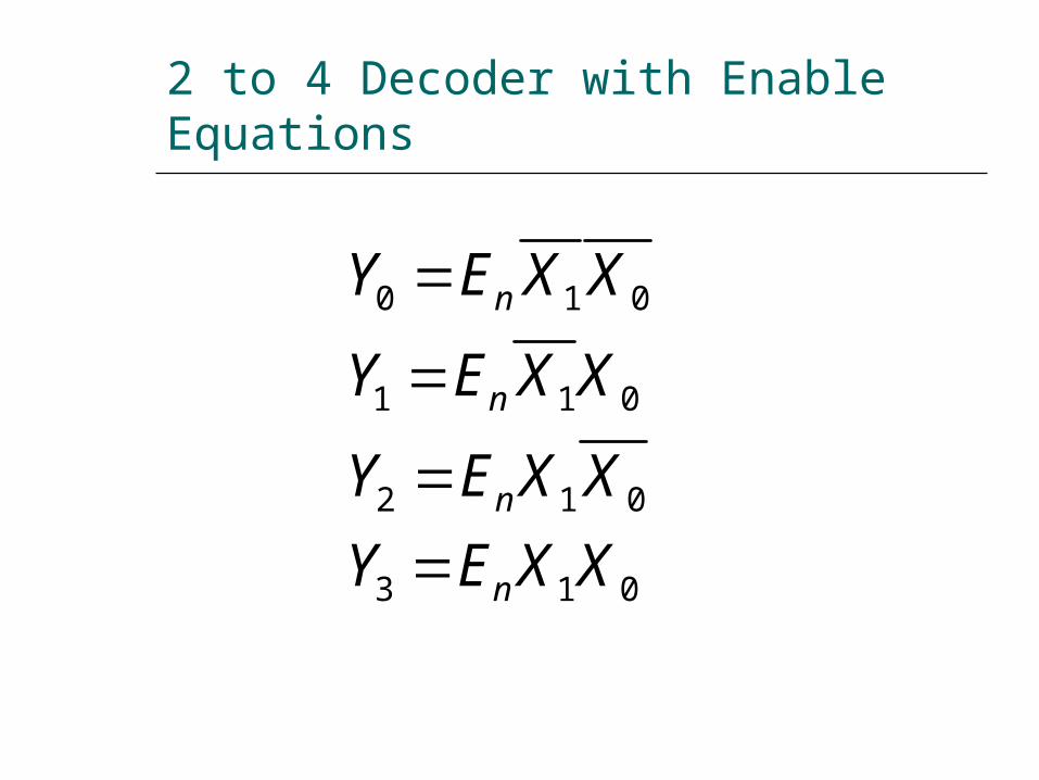
2 to 4 Decoder with Enable Equations
0 1 0
1 1 0
2 1 0
3 1 0
n
n
n
n
Y E X XY E X XY E X XY E X X
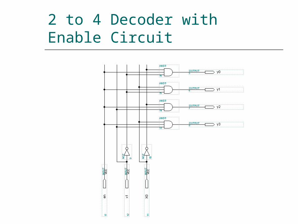
2 to 4 Decoder with Enable Circuit
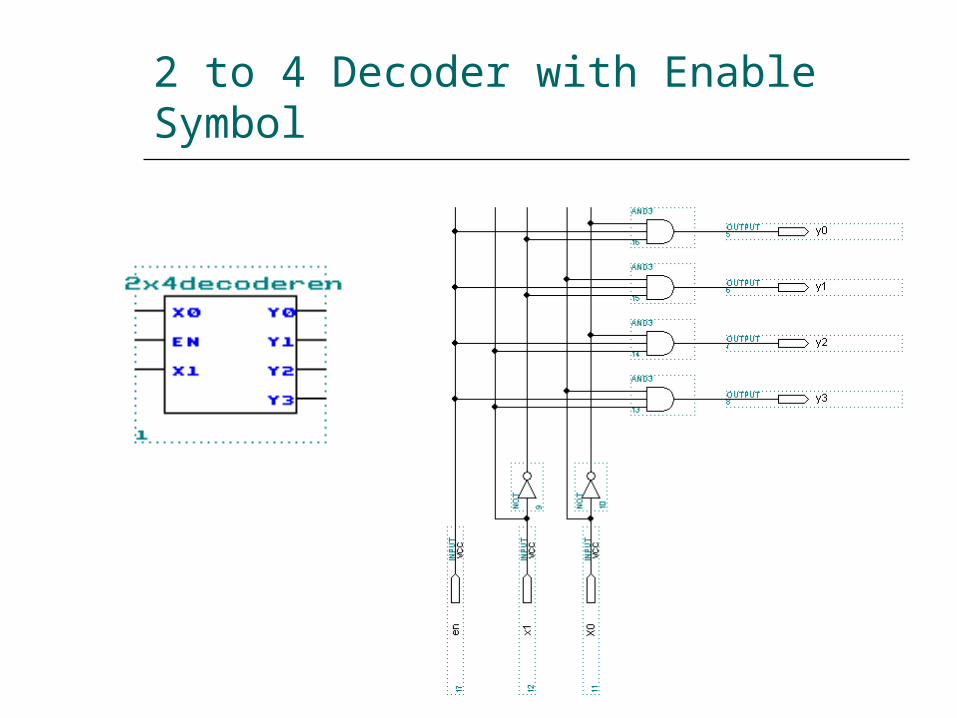
2 to 4 Decoder with Enable Symbol
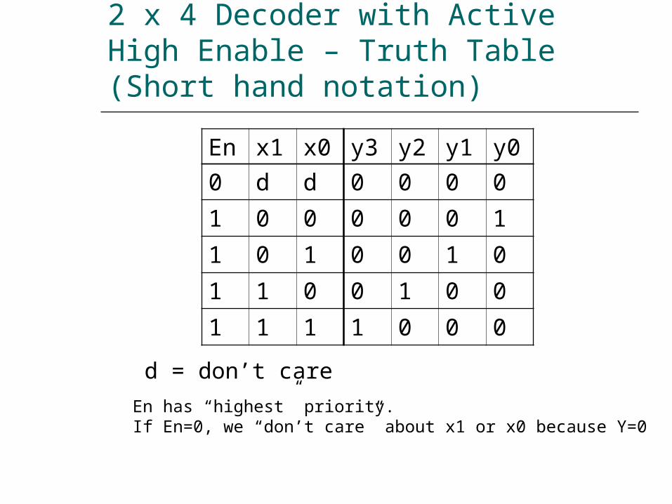
2 x 4 Decoder with Active High Enable – Truth Table (Short hand notation)
En x1 x0 y3 y2 y1 y00 d d 0 0 0 01 0 0 0 0 0 11 0 1 0 0 1 01 1 0 0 1 0 01 1 1 1 0 0 0
d = don’t careEn has “highest” priority. If En=0, we “don’t care” about x1 or x0 because Y=0
2 x 4 Decoder with Active Low Enable – Truth Table (Short hand notation)
EnL x1 x0 y3 y2 y1 y01 d d 0 0 0 00 0 0 0 0 0 10 0 1 0 0 1 00 1 0 0 1 0 00 1 1 1 0 0 0
d = don’t careEn has “highest” priority. If En=1, we “don’t care” about x1 or x0 because Y=0

2 to 4 Decoder with Active Low Enable Circuit
Design Example

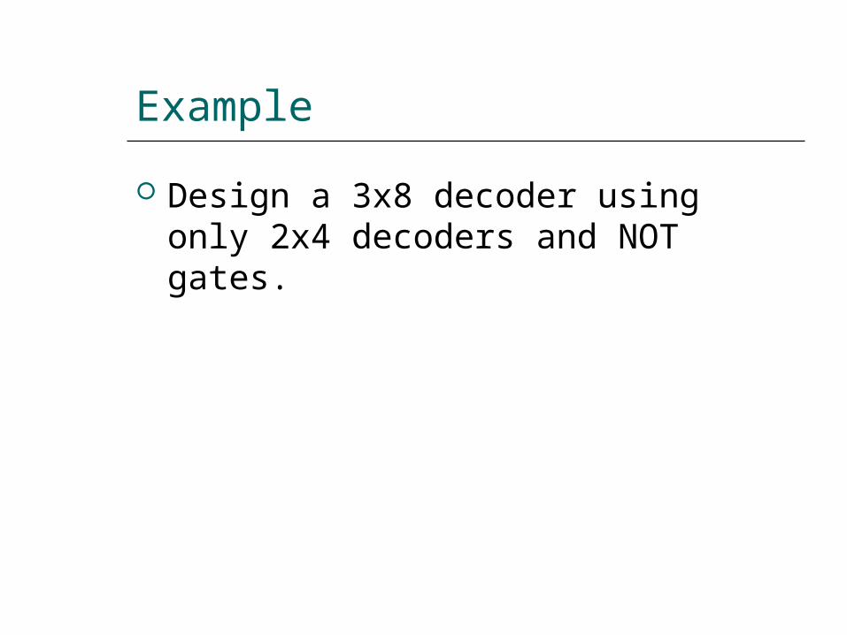
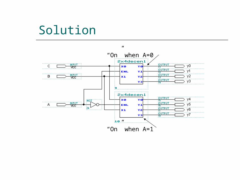
Example Design a 3x8 decoder using only 2x4 decoders and NOT gates.

Solution
“On” when A=1
“On” when A=0
Encoders
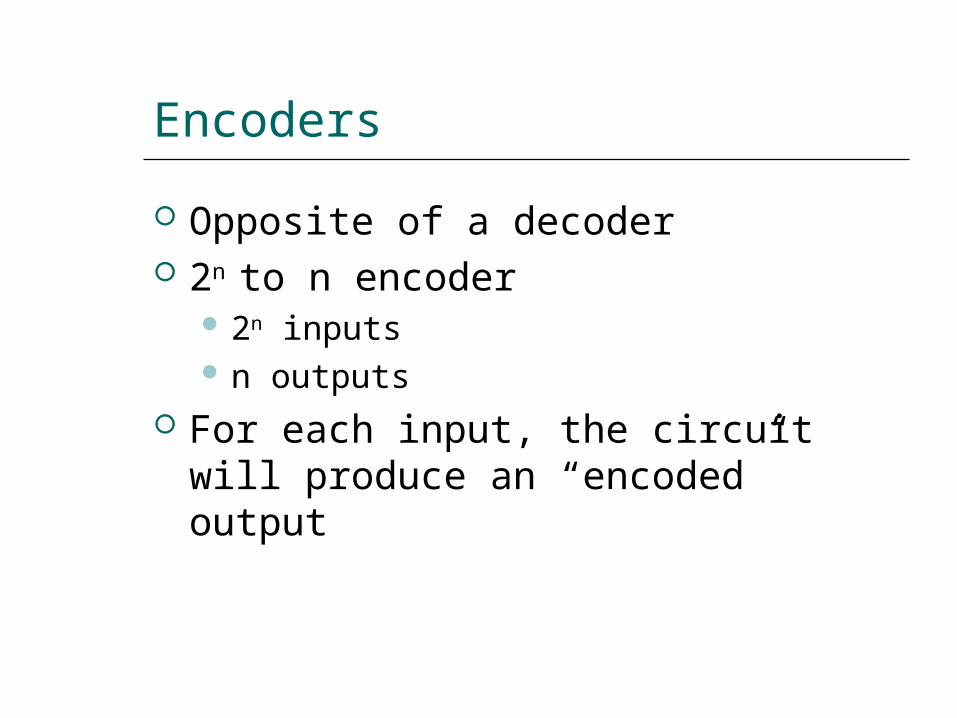
Encoders Opposite of a decoder 2n to n encoder
2n inputs n outputs
For each input, the circuit will produce an “encoded” output
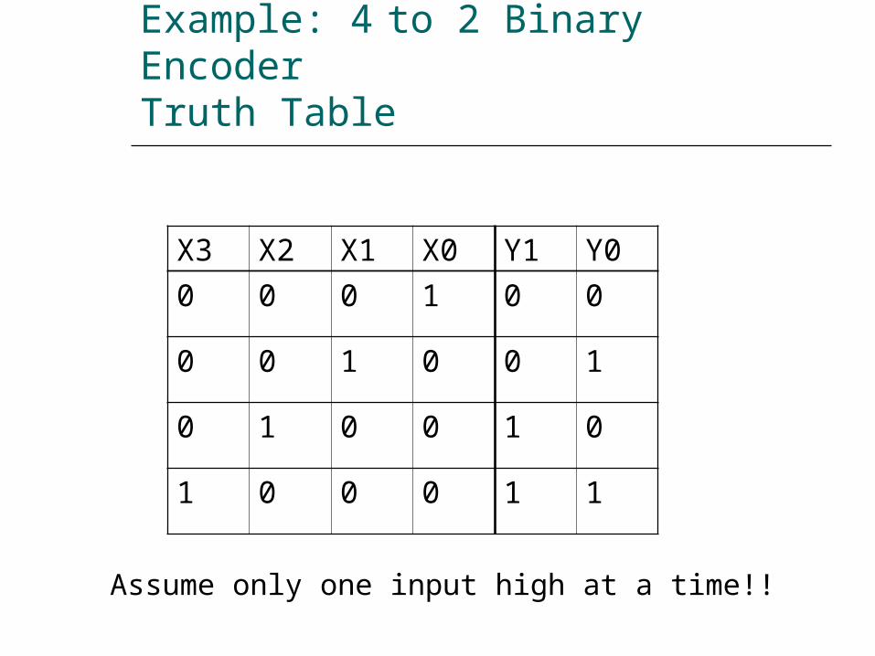
Example: 4 to 2 Binary EncoderTruth Table
X3 X2 X1 X0 Y1 Y00 0 0 1 0 0
0 0 1 0 0 1
0 1 0 0 1 0
1 0 0 0 1 1
Assume only one input high at a time!!
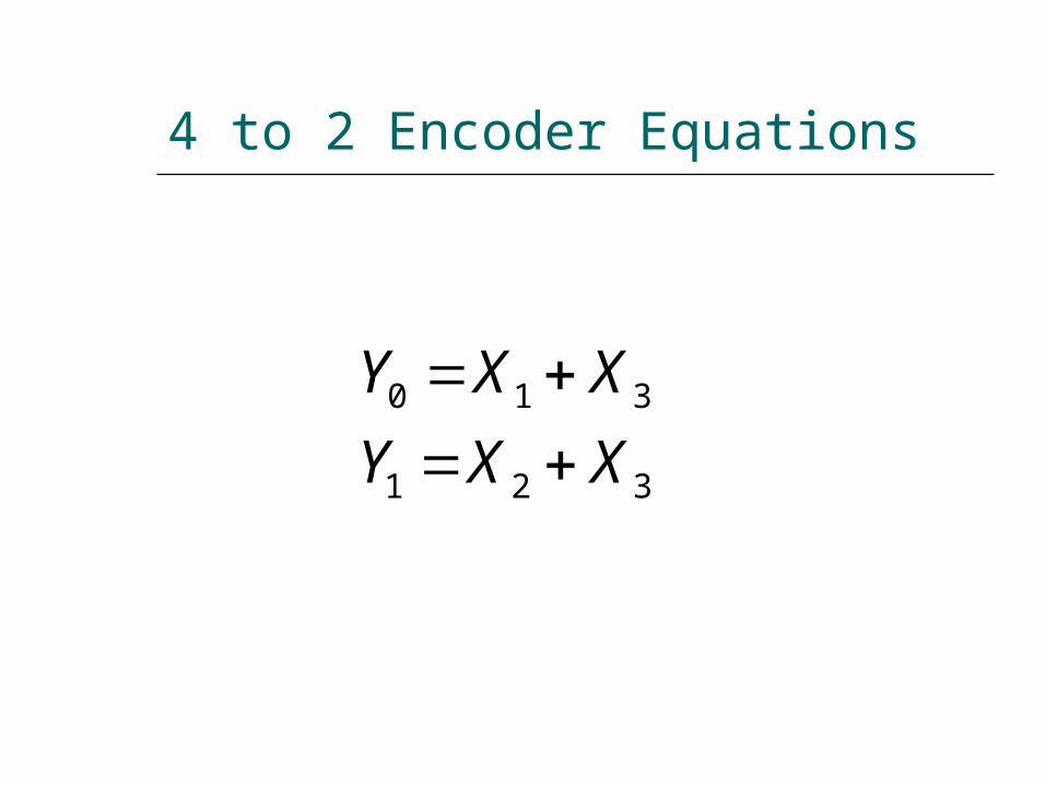
4 to 2 Encoder Equations
0 1 3
1 2 3
Y X XY X X
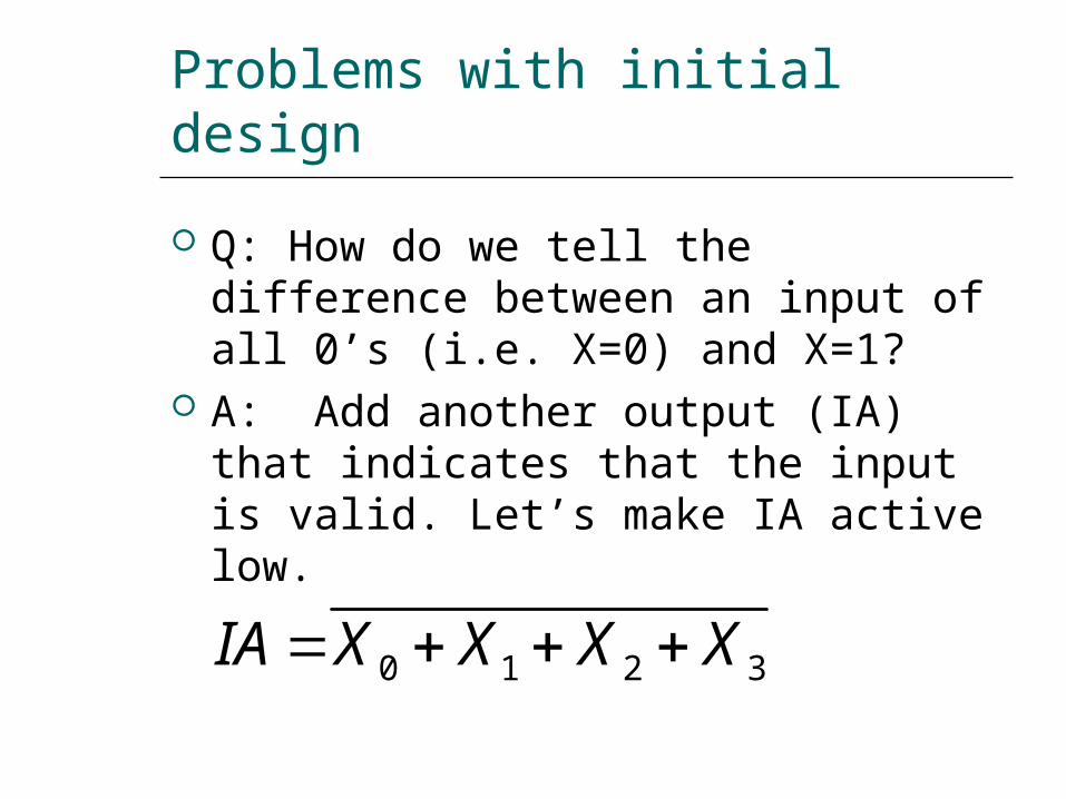
Problems with initial design Q: How do we tell the difference between an input of all 0’s (i.e. X=0) and X=1?
A: Add another output (IA) that indicates that the input is valid. Let’s make IA active low.
0 1 2 3IA X X X X
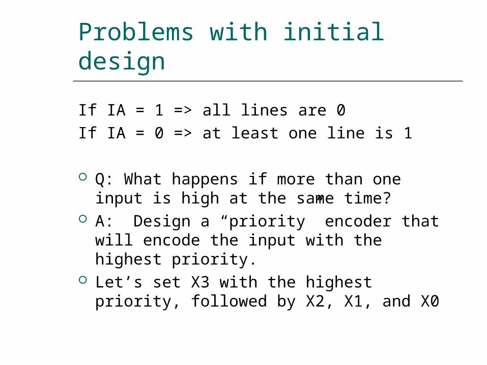
Problems with initial designIf IA = 1 => all lines are 0If IA = 0 => at least one line is 1
Q: What happens if more than one input is high at the same time?
A: Design a “priority” encoder that will encode the input with the highest priority.
Let’s set X3 with the highest priority, followed by X2, X1, and X0
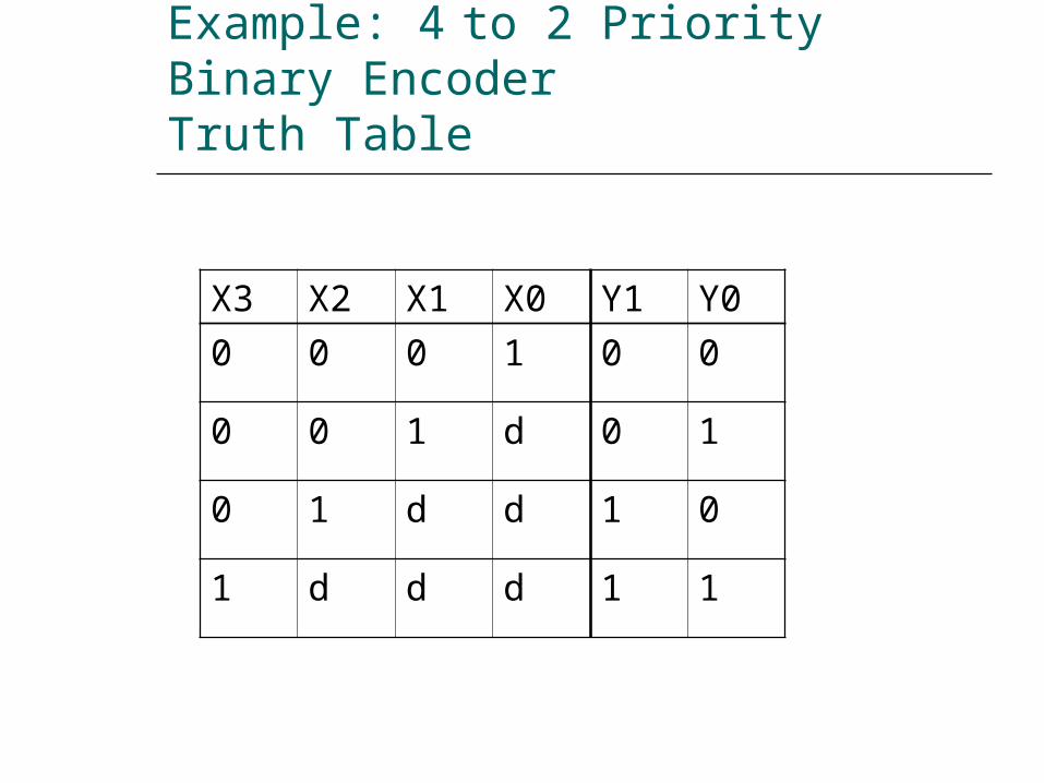
Example: 4 to 2 Priority Binary EncoderTruth Table
X3 X2 X1 X0 Y1 Y00 0 0 1 0 0
0 0 1 d 0 1
0 1 d d 1 0
1 d d d 1 1
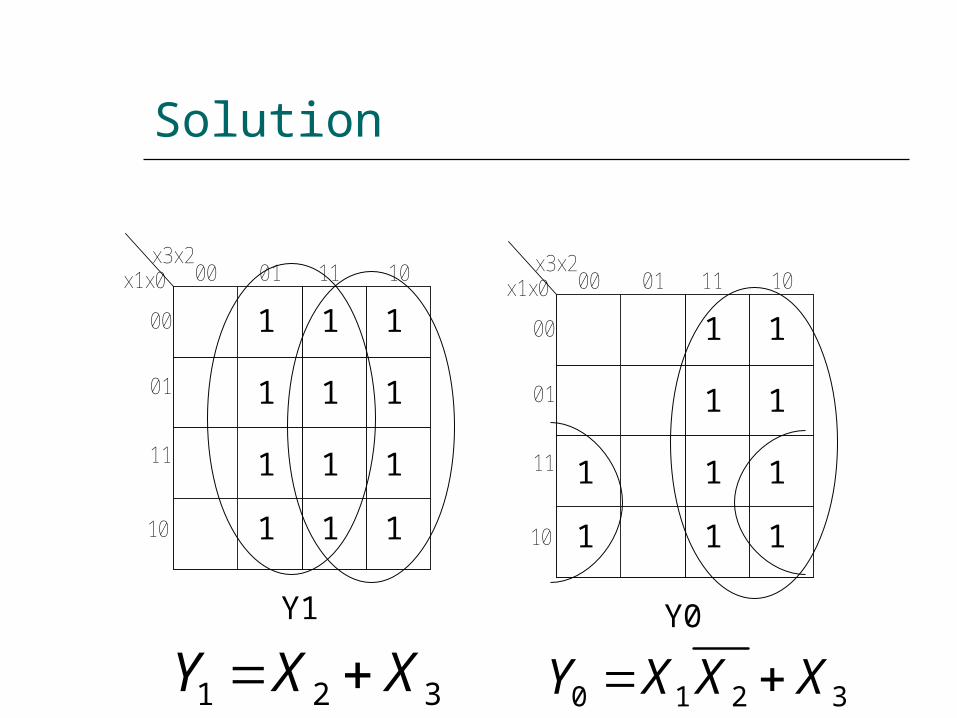
Solution
x3x2x1x0 00 01 11 10
00
01
11
10
Y1
x3x2x1x0 00 01 11 10
00
01
11
10
Y0
1
1
11
1
1
11
1
1
11
1
1
11
1
1
11
11
1 2 3Y X X 0 1 2 3Y X X X
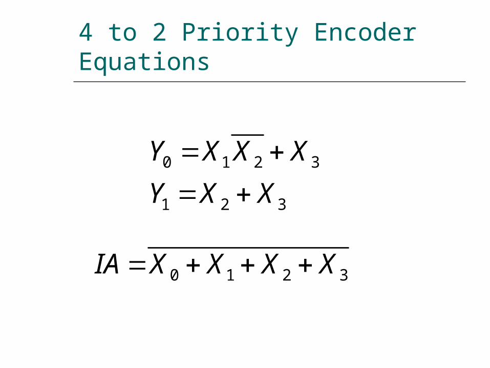
4 to 2 Priority Encoder Equations
0 1 2 3
1 2 3
Y X X XY X X
0 1 2 3IA X X X X
Multiplexer/Data Selectors
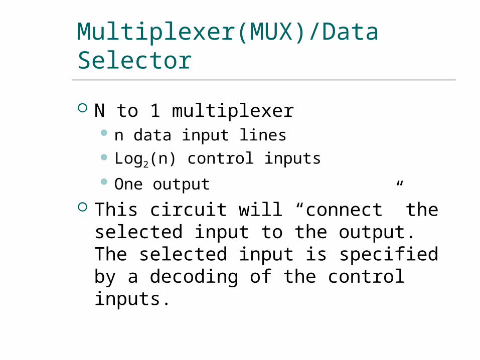
Multiplexer(MUX)/Data Selector N to 1 multiplexer
n data input lines Log2(n) control inputs One output
This circuit will “connect” the selected input to the output. The selected input is specified by a decoding of the control inputs.
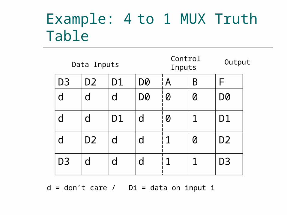
Example: 4 to 1 MUX Truth Table
D3 D2 D1 D0 A B Fd d d D0 0 0 D0
d d D1 d 0 1 D1
d D2 d d 1 0 D2
D3 d d d 1 1 D3
d = don’t care / Di = data on input i
Data Inputs ControlInputs Output
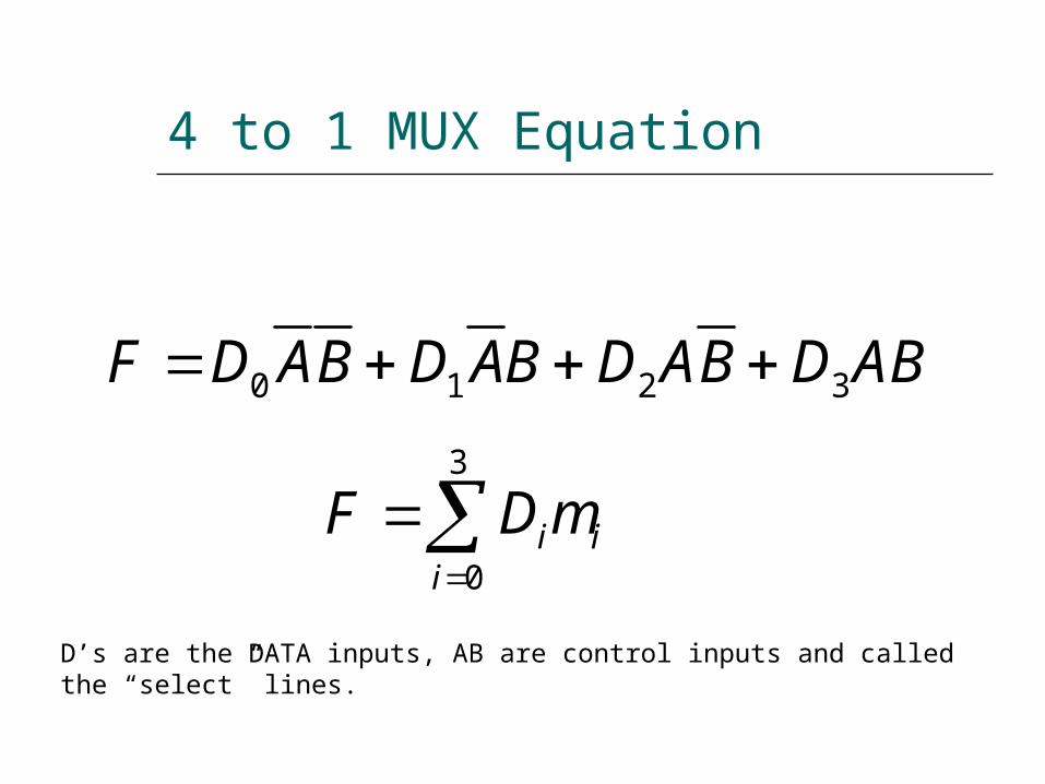
4 to 1 MUX Equation
0 1 2 3F D AB D AB D AB D AB
3
0i i
iF D m
D’s are the DATA inputs, AB are control inputs and calledthe “select” lines.
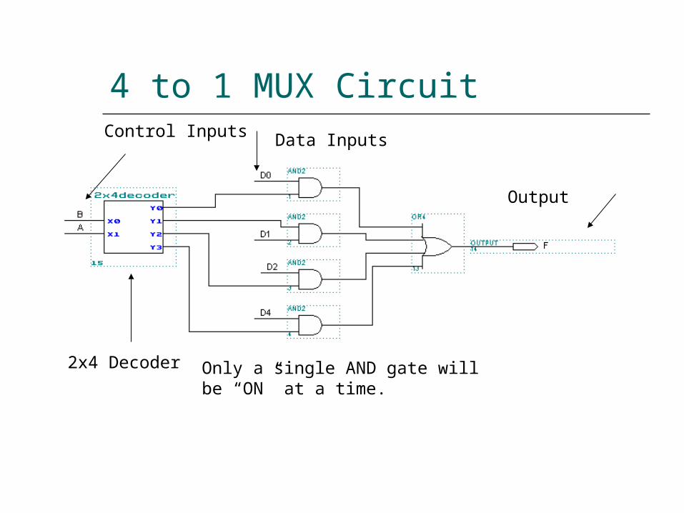
4 to 1 MUX Circuit
2x4 Decoder Only a single AND gate willbe “ON” at a time.
Output
Control Inputs Data Inputs
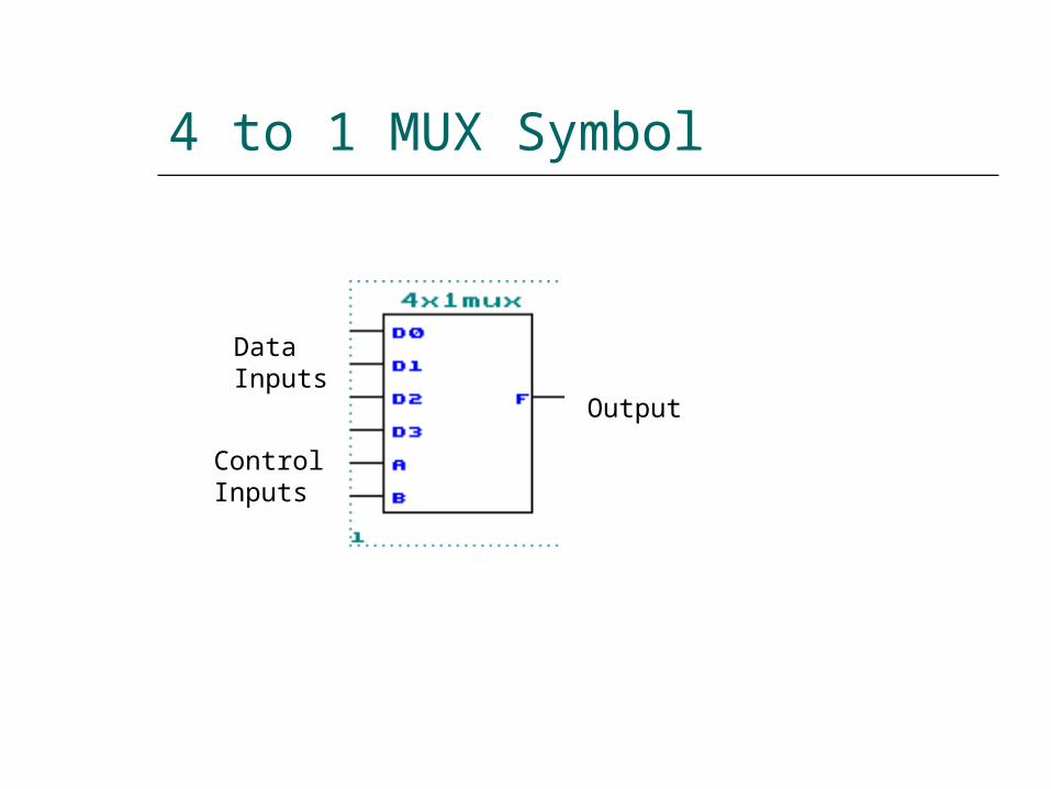
4 to 1 MUX Symbol
DataInputs
ControlInputs
Output
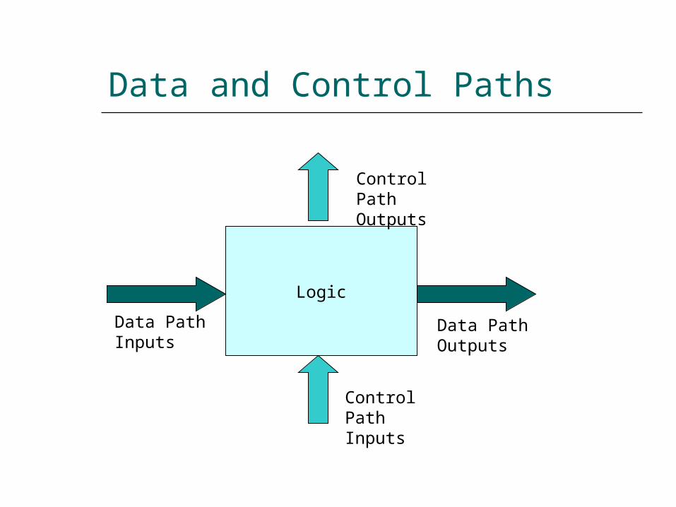
Data and Control Paths
LogicData PathInputs
Data PathOutputs
Control PathInputs
Control PathOutputs
MUX Applications
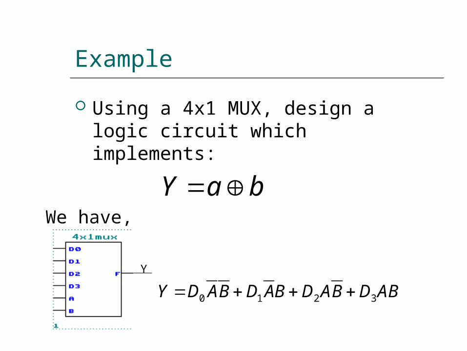
Example Using a 4x1 MUX, design a logic circuit which implements:
Y a b We have,
Y
0 1 2 3Y D AB D AB D AB D AB
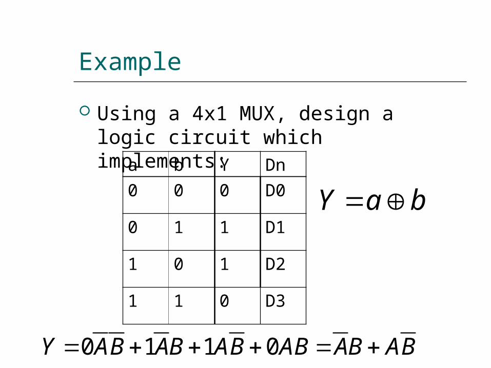
Example Using a 4x1 MUX, design a logic circuit which implements:
Y a b a b Y Dn0 0 0 D0
0 1 1 D1
1 0 1 D2
1 1 0 D3
0 1 1 0Y AB AB AB AB AB AB
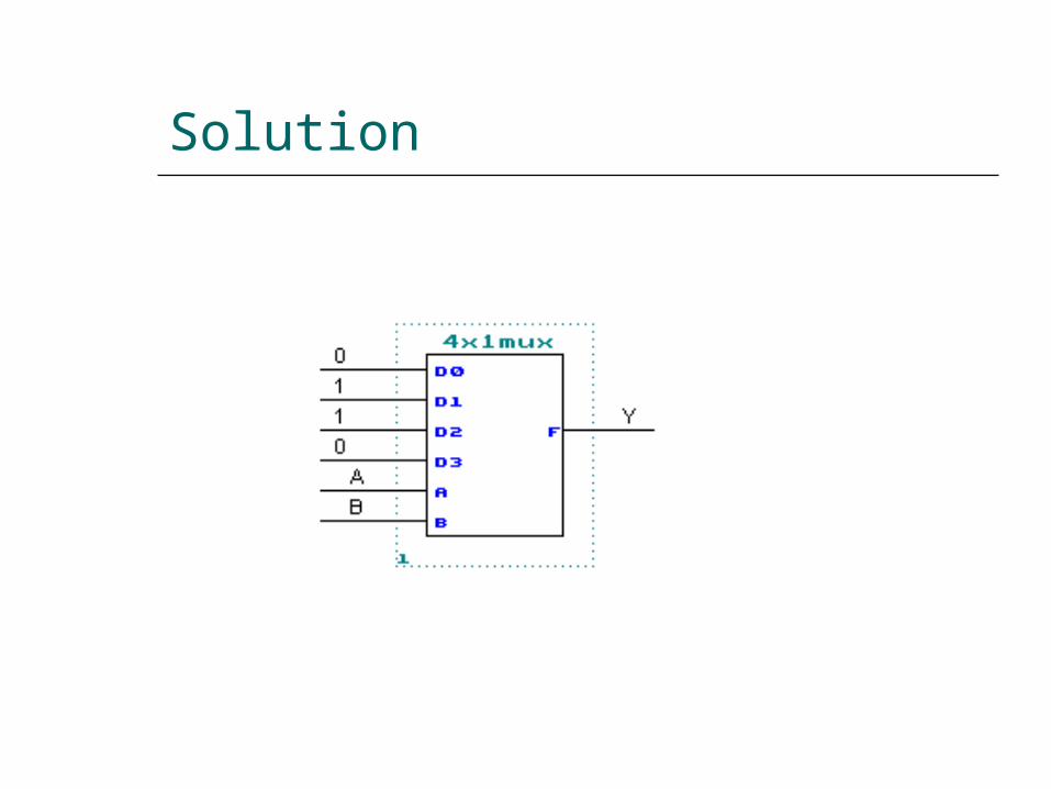
Solution
Multibit Multiplexers
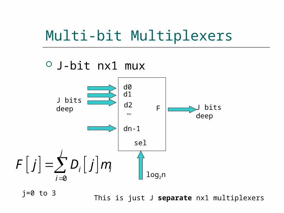
Multi-bit Multiplexers J-bit nx1 mux
sel
d0d1
…
dn-1
d2 FJ bitsdeep
log2n
J bitsdeep
0
j
i ii
F j D j m
j=0 to 3 This is just J separate nx1 multiplexers
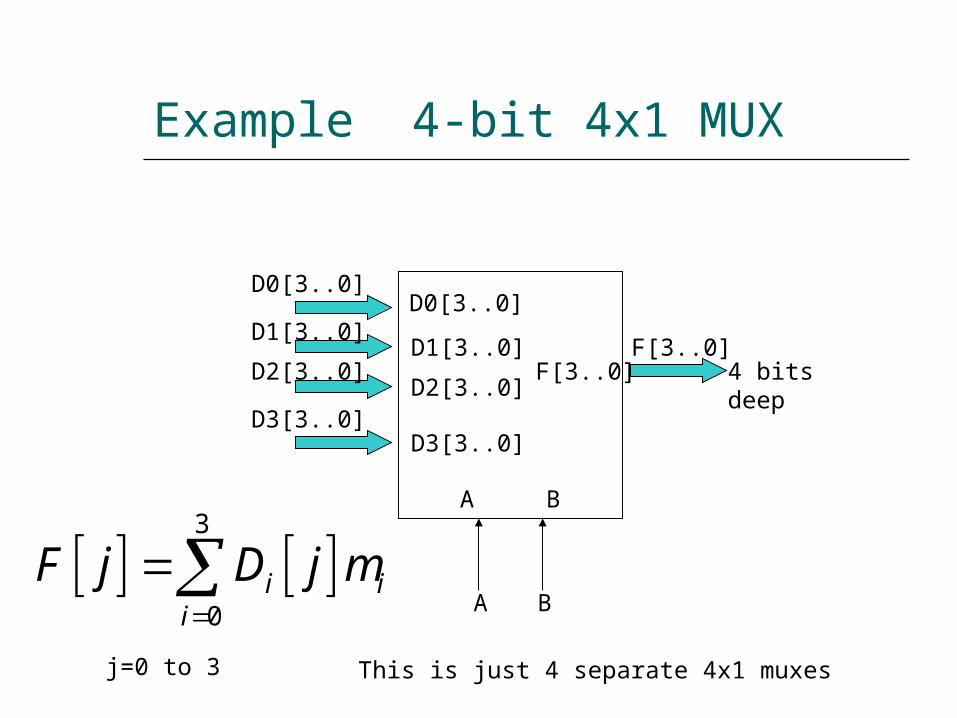
Example 4-bit 4x1 MUX
A B
D0[3..0]D1[3..0]
D3[3..0]
D2[3..0] F[3..0] 4 bits deep
D0[3..0]D1[3..0]D2[3..0]D3[3..0]
A B
F[3..0]
3
0i i
iF j D j m
j=0 to 3 This is just 4 separate 4x1 muxes
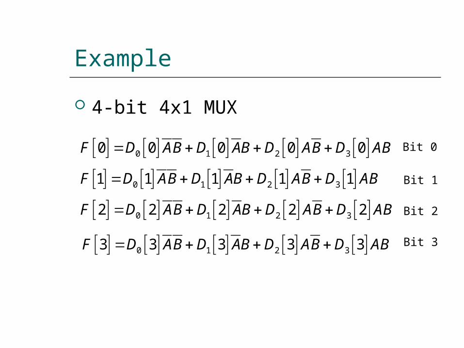
Example 4-bit 4x1 MUX
0 1 2 30 0 0 0 0F D AB D AB D AB D AB
0 1 2 31 1 1 1 1F D AB D AB D AB D AB
0 1 2 32 2 2 2 2F D AB D AB D AB D AB
0 1 2 33 3 3 3 3F D AB D AB D AB D AB
Bit 0
Bit 3
Bit 2
Bit 1
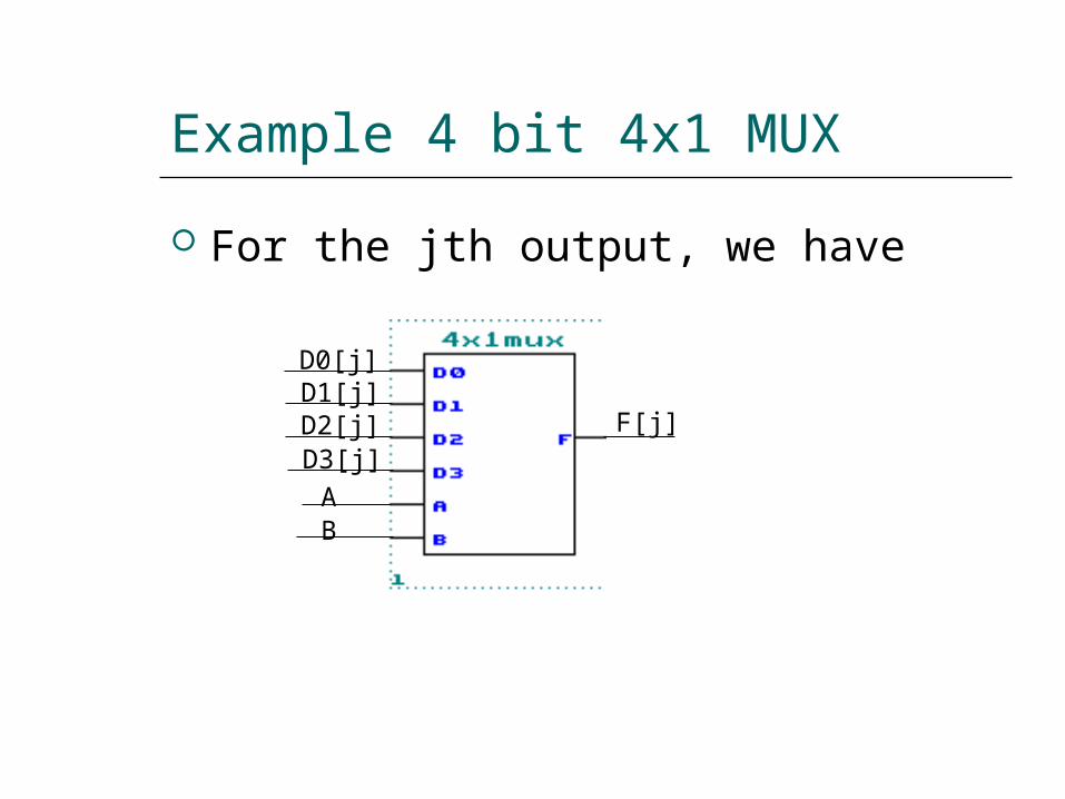
Example 4 bit 4x1 MUX For the jth output, we have
D0[j]D1[j]D2[j]D3[j]AB
F[j]

Example 4 bit 4x1 MUX For the bit 0 output, we have
D0[0]D1[0]D2[0]D3[0]AB
F[0]
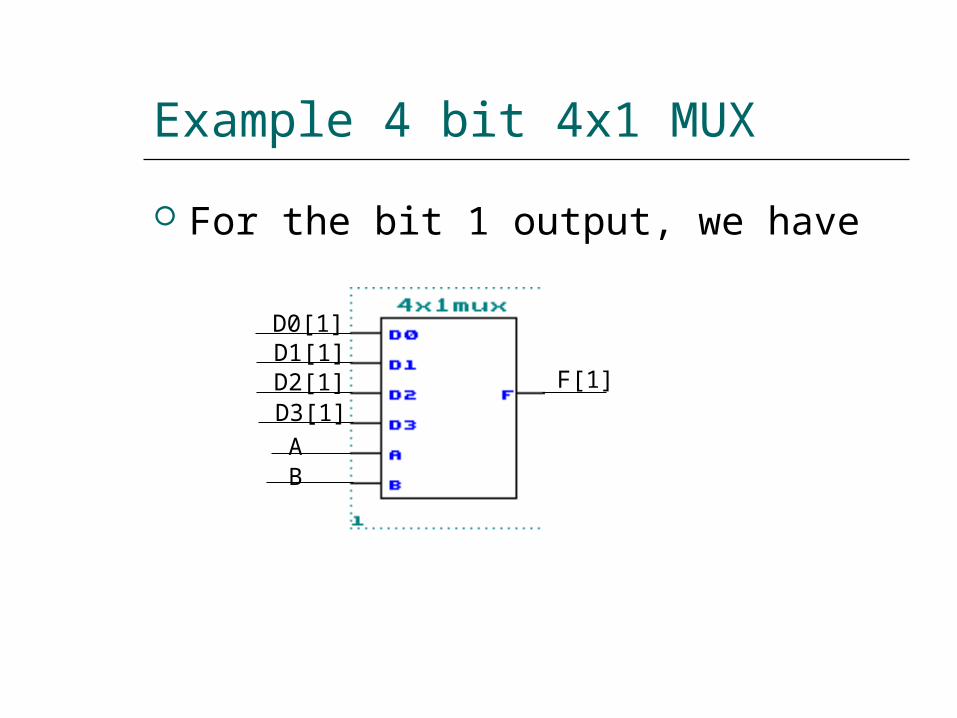
Example 4 bit 4x1 MUX For the bit 1 output, we have
D0[1]D1[1]D2[1]D3[1]AB
F[1]

Example 4 bit 4x1 MUX For the bit 2 output, we have
D0[2]D1[2]D2[2]D3[2]AB
F[2]

Example 4 bit 4x1 MUX For the bit 3 output, we have
D0[3]D1[3]D2[3]D3[3]AB
F[3]
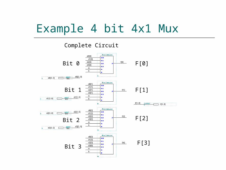
Example 4 bit 4x1 Mux
F[0]
F[1]
F[2]
F[3]
Complete Circuit
Bit 0
Bit 1
Bit 2
Bit 3
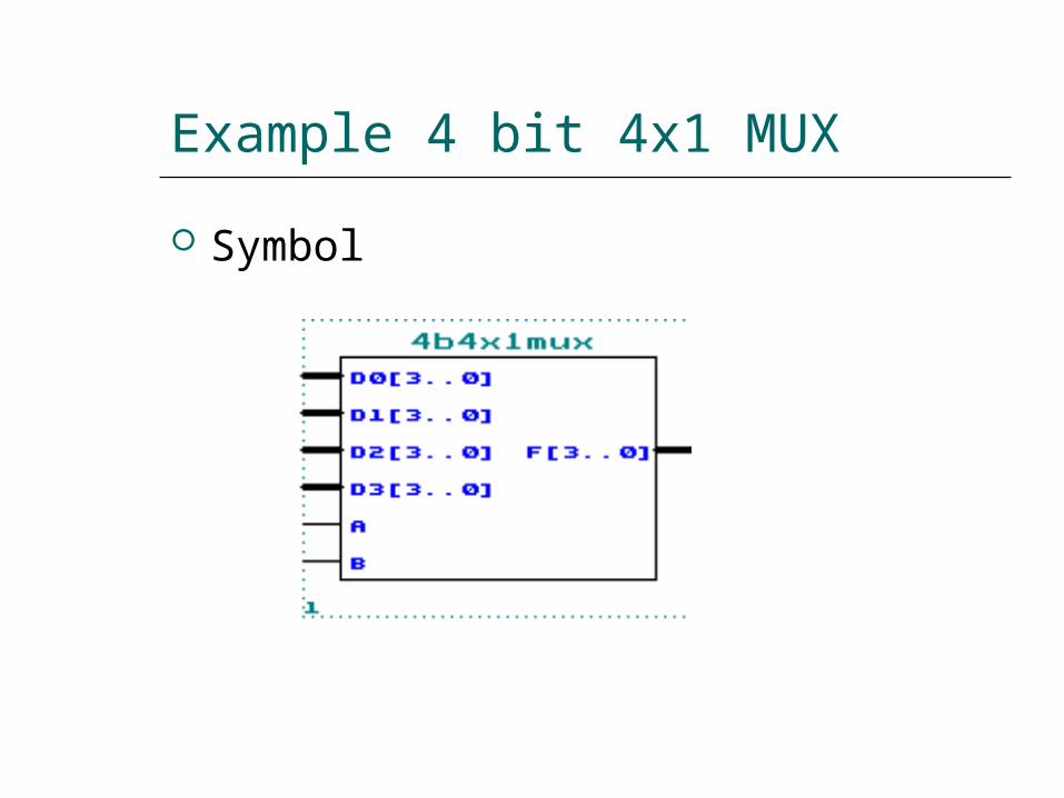
Example 4 bit 4x1 MUX Symbol
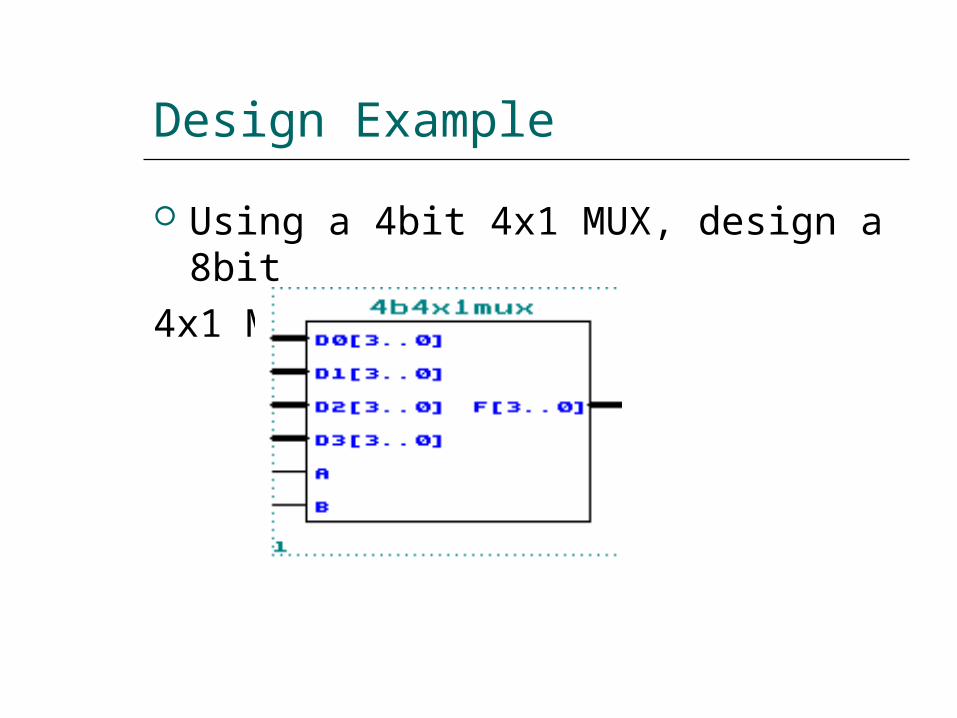
Design Example Using a 4bit 4x1 MUX, design a 8bit
4x1 MUX

Solution
DeMultiplexers/Data Distributors
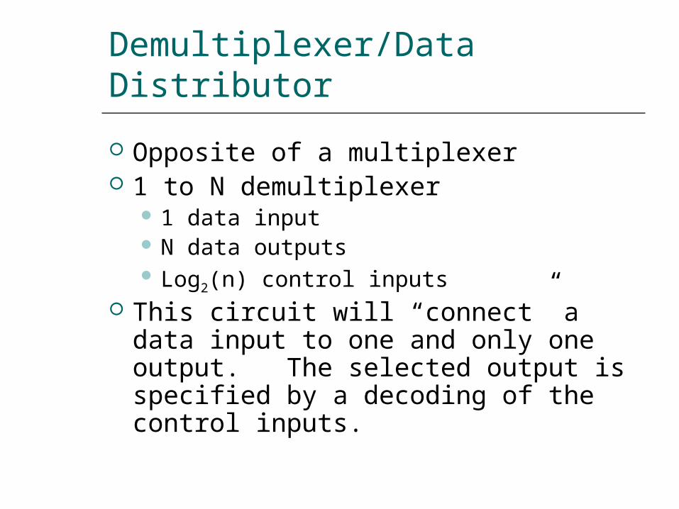
Demultiplexer/Data Distributor Opposite of a multiplexer 1 to N demultiplexer
1 data input N data outputs Log2(n) control inputs
This circuit will “connect” a data input to one and only one output. The selected output is specified by a decoding of the control inputs.
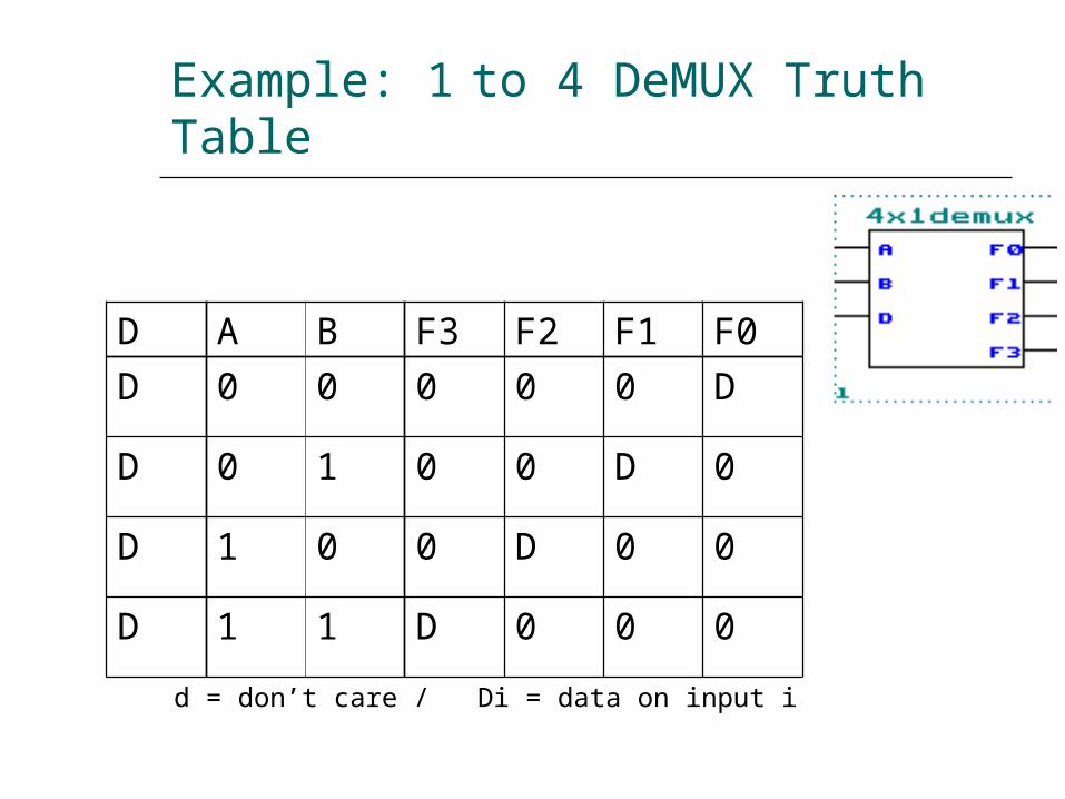
Example: 1 to 4 DeMUX Truth Table
D A B F3 F2 F1 F0D 0 0 0 0 0 D
D 0 1 0 0 D 0
D 1 0 0 D 0 0
D 1 1 D 0 0 0d = don’t care / Di = data on input i
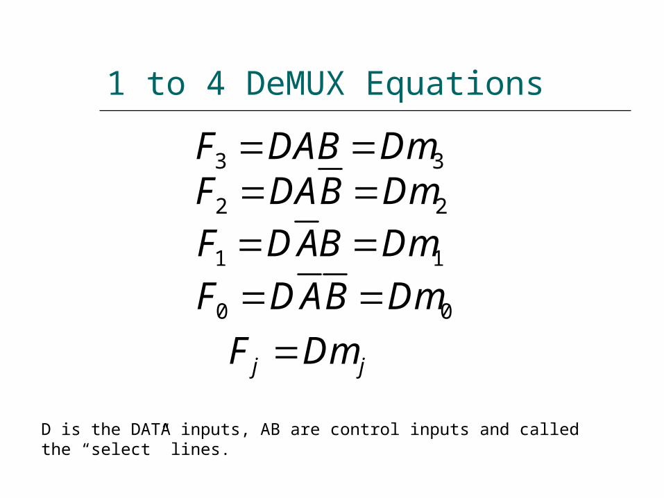
1 to 4 DeMUX Equations
3 3F DAB Dm
j jF Dm
D is the DATA inputs, AB are control inputs and calledthe “select” lines.
1 1F D AB Dm 2 2F DAB Dm
0 0F D AB Dm
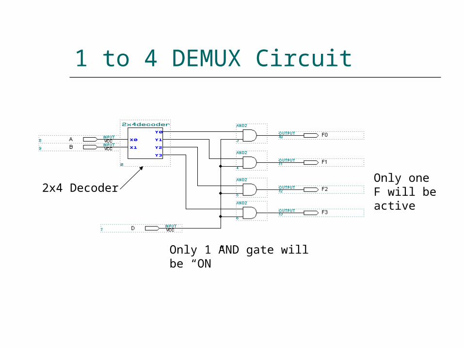
1 to 4 DEMUX Circuit
Only 1 AND gate willbe “ON”
2x4 DecoderOnly oneF will beactive
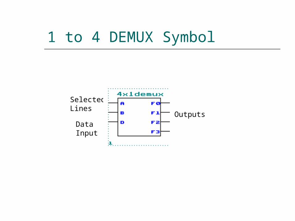
1 to 4 DEMUX Symbol
DataInput
SelectedLines Outputs
Example Design a 3x8 decoder using only 2x4 decoders and NOT gates.
Solution
“On” when A=1
“On” when A=0
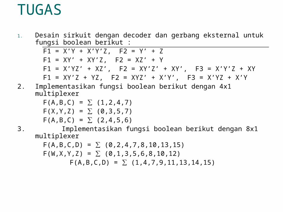
TUGAS1. Desain sirkuit dengan decoder dan gerbang eksternal untuk
fungsi boolean berikut : F1 = X’Y + X’Y’Z, F2 = Y’ + Z F1 = XY’ + XY’Z, F2 = XZ’ + Y F1 = X’YZ’ + XZ’, F2 = XY’Z’ + XY’, F3 = X’Y’Z + XY F1 = XY’Z + YZ, F2 = XYZ’ + X’Y’, F3 = X’YZ + X’Y
2. Implementasikan fungsi boolean berikut dengan 4x1 multiplexer F(A,B,C) = ∑ (1,2,4,7) F(X,Y,Z) = (0,3,5,7)∑ F(A,B,C) = (2,4,5,6)∑
3. Implementasikan fungsi boolean berikut dengan 8x1 multiplexer F(A,B,C,D) = ∑ (0,2,4,7,8,10,13,15) F(W,X,Y,Z) = (0,1,3,5,6,8,10,12)∑
F(A,B,C,D) = (1,4,7,9,11,13,14,15)∑
Basic Arithmetic Elements
Half Adder
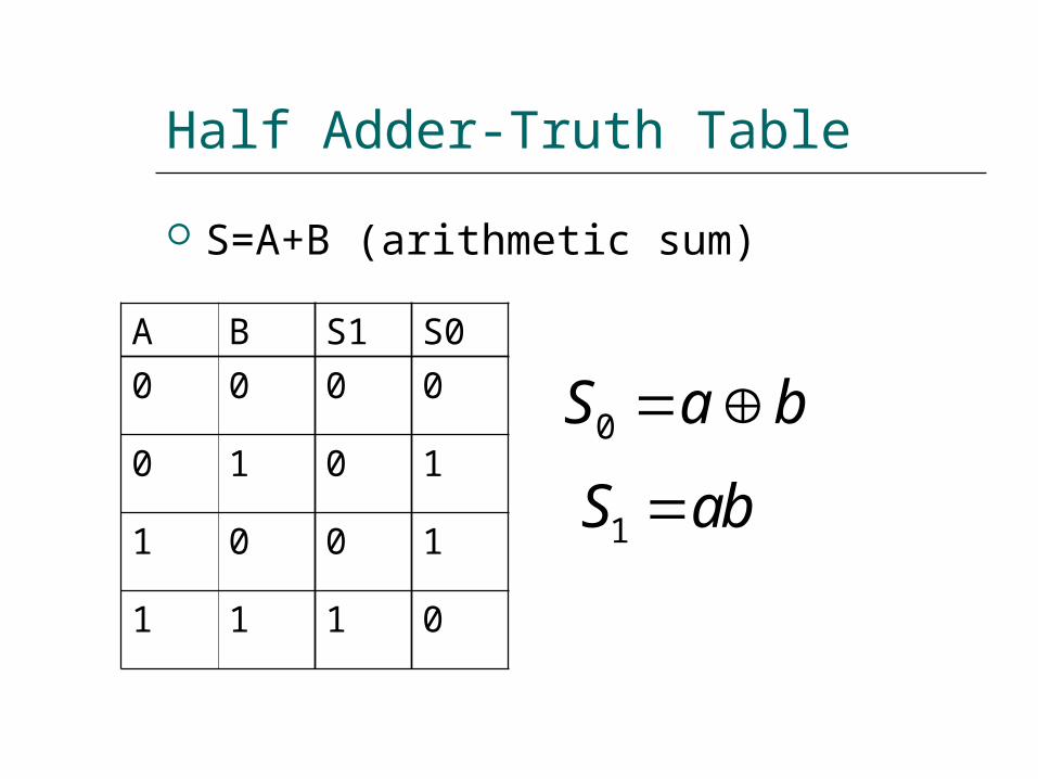
Half Adder-Truth Table S=A+B (arithmetic sum)
A B S1 S00 0 0 0
0 1 0 1
1 0 0 1
1 1 1 0
0S a b
1S ab
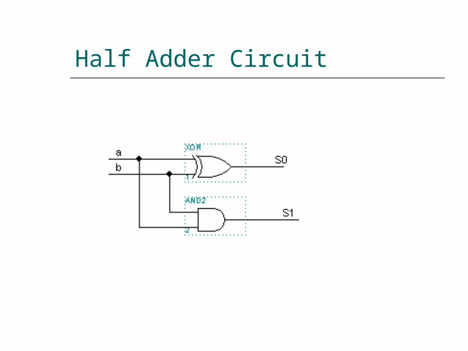
Half Adder Circuit
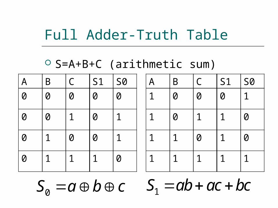
Full Adder-Truth Table S=A+B+C (arithmetic sum)
A B C S1 S00 0 0 0 0
0 0 1 0 1
0 1 0 0 1
0 1 1 1 0
0S a b c 1S ab ac bc
A B C S1 S01 0 0 0 1
1 0 1 1 0
1 1 0 1 0
1 1 1 1 1
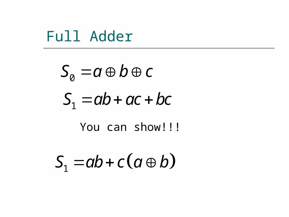
Full Adder
0S a b c
1S ab ac bc
You can show!!!
1S ab c a b
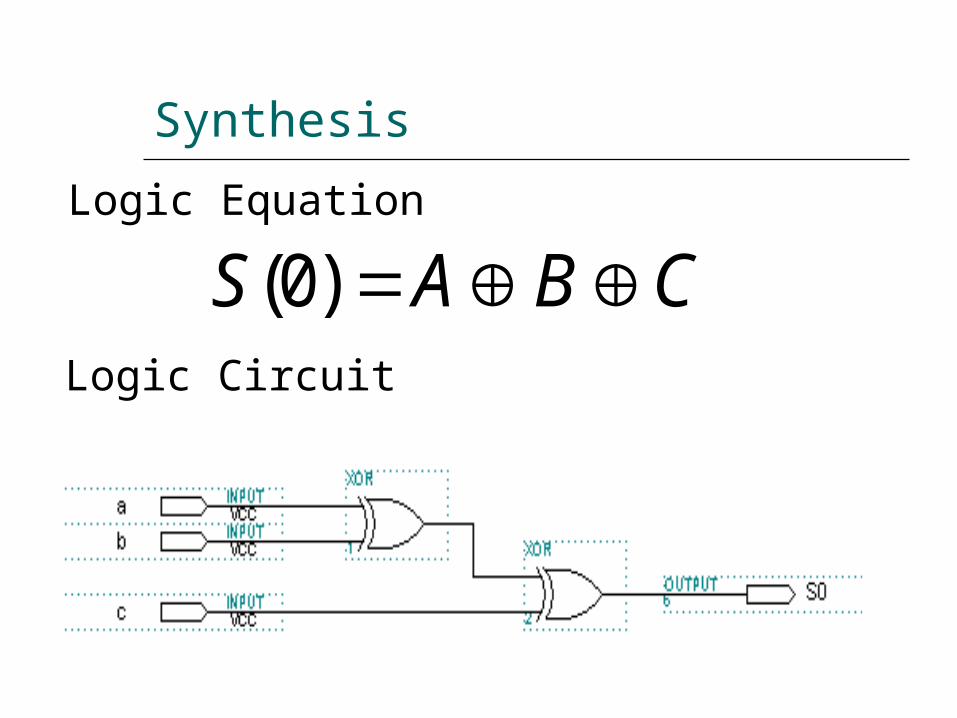
Synthesis
(0)S A B C Logic Equation
Logic Circuit
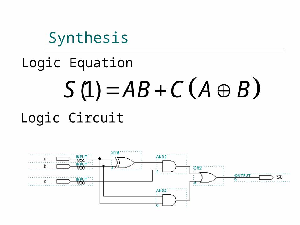
Synthesis
(1)S AB C A B Logic Equation
Logic Circuit
17
AND2 18
OR2
19 coutOUTPUT16
AND2
VCC14 Cin INPUT
VCC13 B INPUT10
XOR
11
XOR
15 sumOUTPUTVCC12 A INPUT
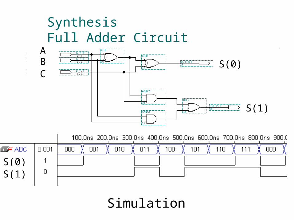
Synthesis Full Adder Circuit
S(0)
S(1)
C
AB
S(0)S(1)
Simulation
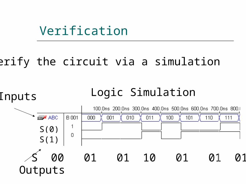
Verification
S(0)S(1)
We verify the circuit via a simulation
Logic SimulationInputs
OutputsS 00 01 01 10 01 01 01 11
17
AND2 18
OR2
19 coutOUTPUT16
AND2
VCC14 Cin INPUT
VCC13 B INPUT10
XOR
11
XOR
15 sumOUTPUTVCC12 A INPUT
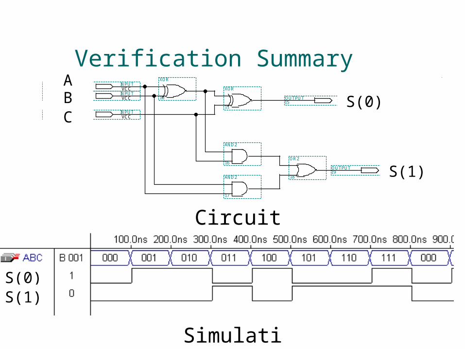
Verification SummaryS(0)
S(1)
C
AB
S(0)S(1)
Simulation
Circuit
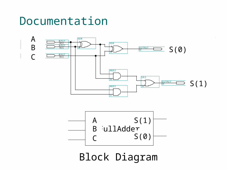
Documentation
17
AND2 18
OR2
19 coutOUTPUT16
AND2
VCC14 Cin INPUT
VCC13 B INPUT10
XOR
11
XOR
15 sumOUTPUTVCC12 A INPUT
S(0)
S(1)
C
AB
FullAdderC
AB
S(0)
S(1)
Block Diagram

Ripple Carry Adder
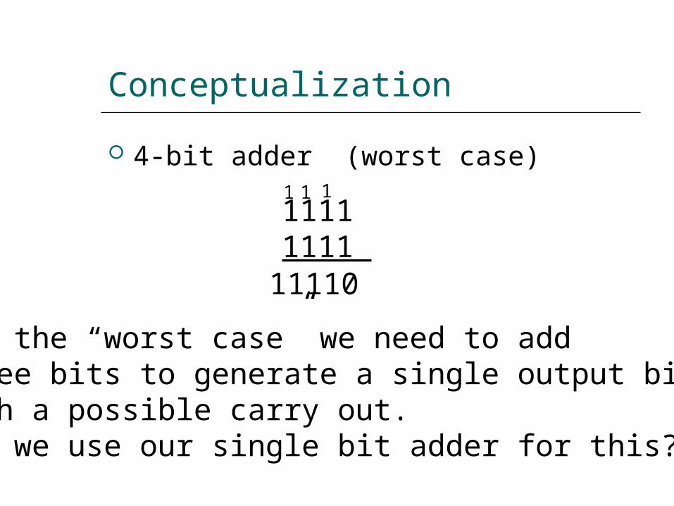
Conceptualization 4-bit adder (worst case)
11111111 11110
111
For the “worst case” we need to addthree bits to generate a single output bitwith a possible carry out.Can we use our single bit adder for this?
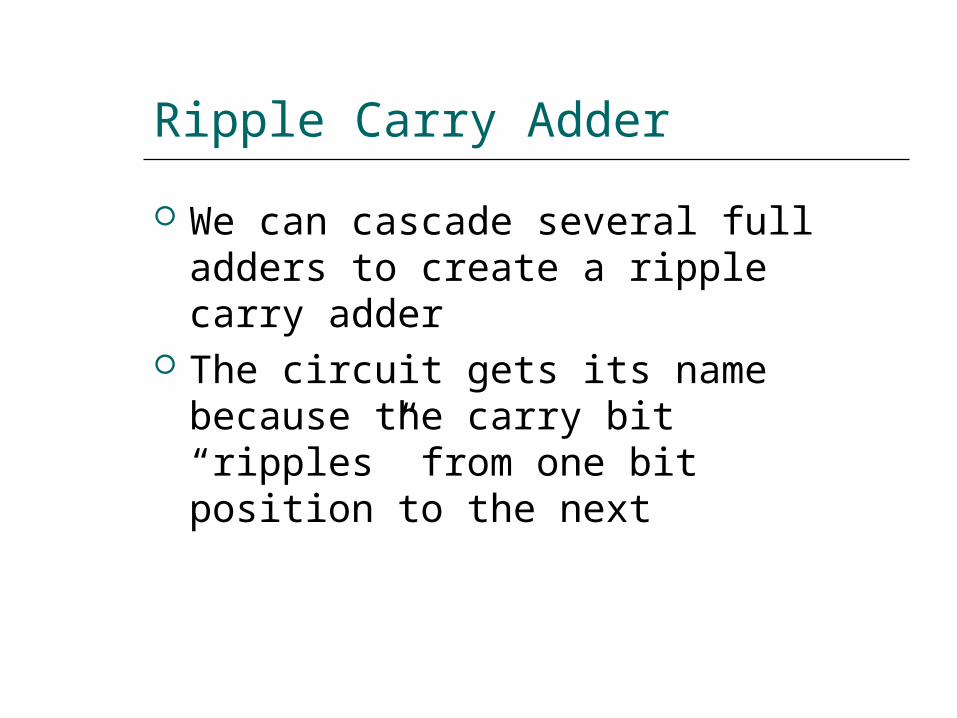
Ripple Carry Adder We can cascade several full adders to create a ripple carry adder
The circuit gets its name because the carry bit “ripples” from one bit position to the next
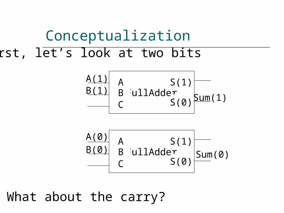
Conceptualization
FullAdderC
AB
S(0)
S(1)
FullAdderC
AB
S(0)
S(1)
First, let’s look at two bits
A(0)B(0)
B(1)A(1)
Sum(0)
Sum(1)
What about the carry?
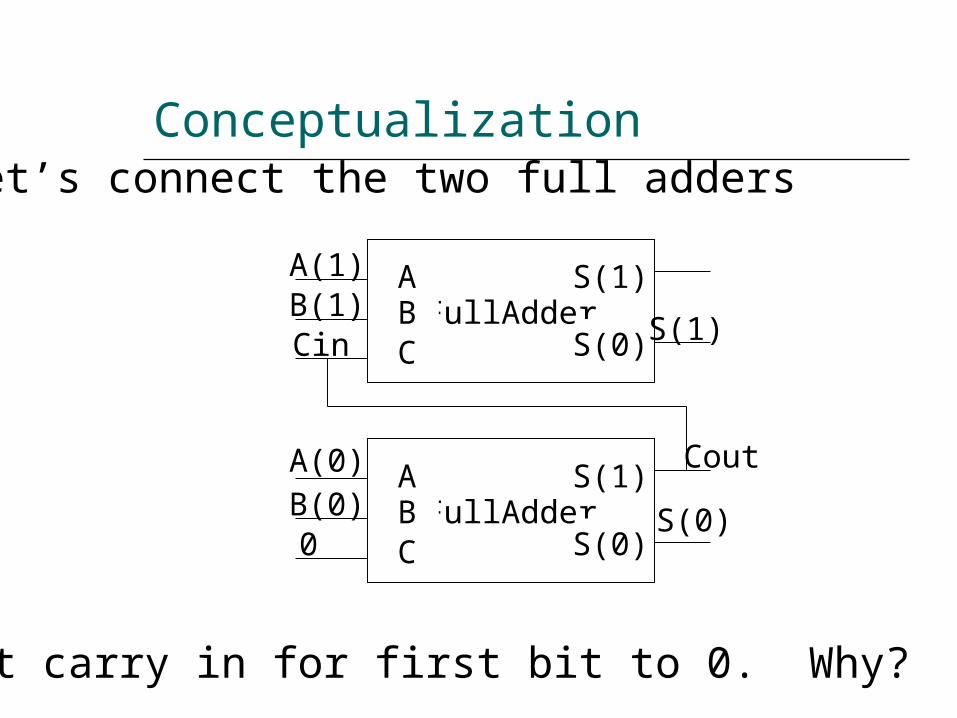
Conceptualization
FullAdderC
AB
S(0)
S(1)
FullAdderC
AB
S(0)
S(1)
Let’s connect the two full adders
A(0)B(0)
B(1)A(1)
S(0)
S(1)
Set carry in for first bit to 0. Why?
Cout
Cin
0
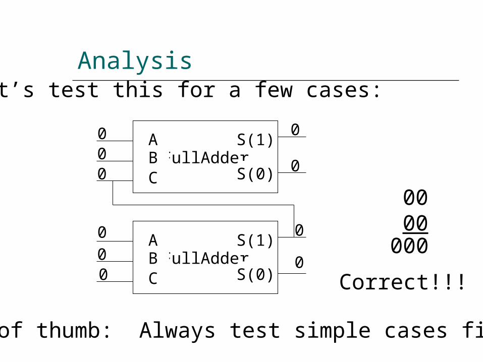
Analysis
FullAdderC
AB
S(0)
S(1)
FullAdderC
AB
S(0)
S(1)
Let’s test this for a few cases:
00
00
0
000
0
0
0000000
Correct!!!
Rule of thumb: Always test simple cases first!!
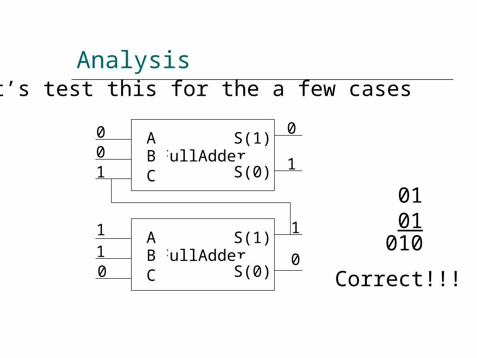
Analysis
FullAdderC
AB
S(0)
S(1)
FullAdderC
AB
S(0)
S(1)
Let’s test this for the a few cases
01
11
1
110
1
1
1111110
Correct!!!
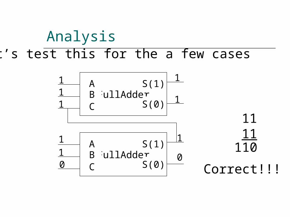
Analysis
FullAdderC
AB
S(0)
S(1)
FullAdderC
AB
S(0)
S(1)
Let’s test this for the a few cases
11
00
0
1
1
1
0
0
0101010
Correct!!!
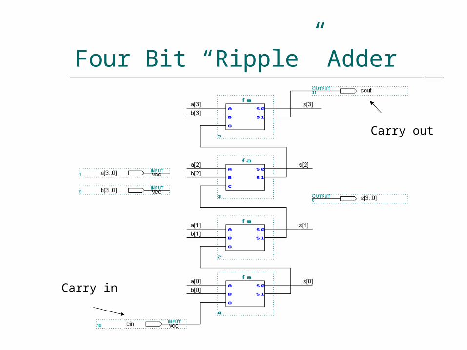
Four Bit “Ripple” Adder
Carry in
Carry out
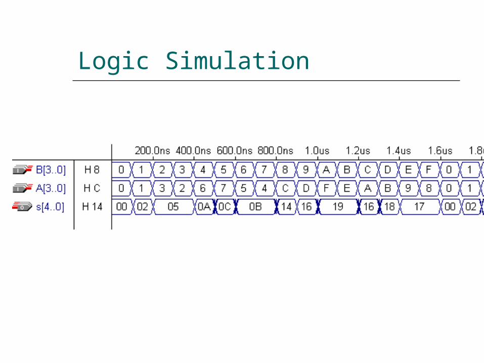
Logic Simulation
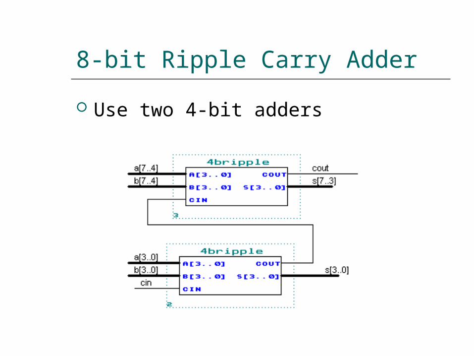
8-bit Ripple Carry Adder Use two 4-bit adders
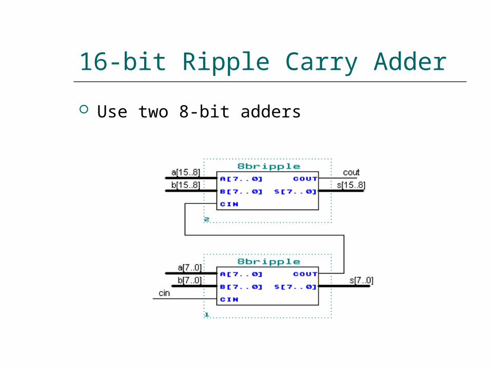
16-bit Ripple Carry Adder Use two 8-bit adders
Subtraction Circuit
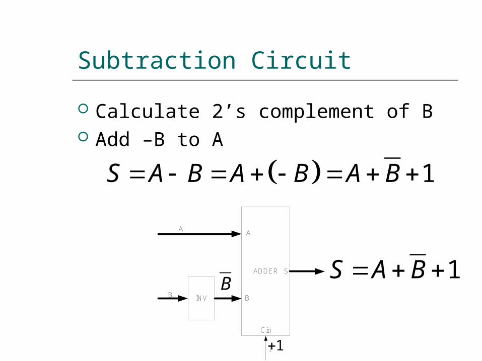
Subtraction Circuit Calculate 2’s complement of B Add –B to A
ADDER
INV
A
B
S
1
Cin
A
B
1S A B A B A B
B
1
1S A B
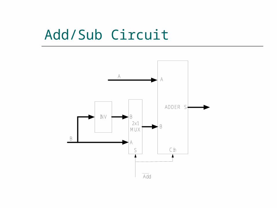
Add/Sub Circuit
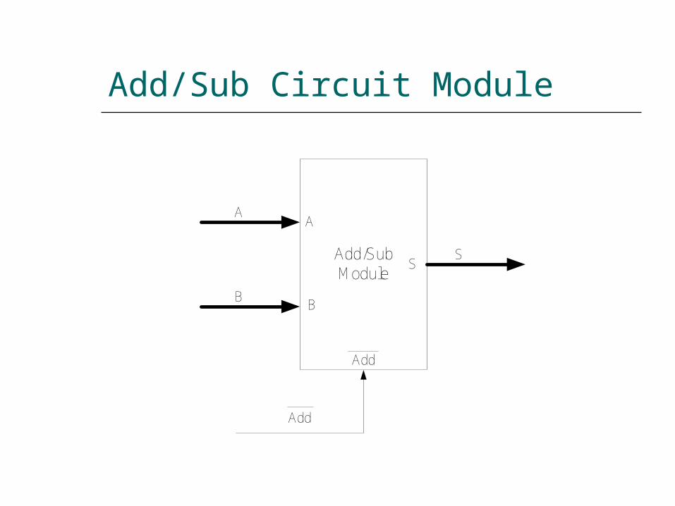
Add/Sub Circuit Module
Add/SubM odule
A
B
S
Add
A
B
Add
S
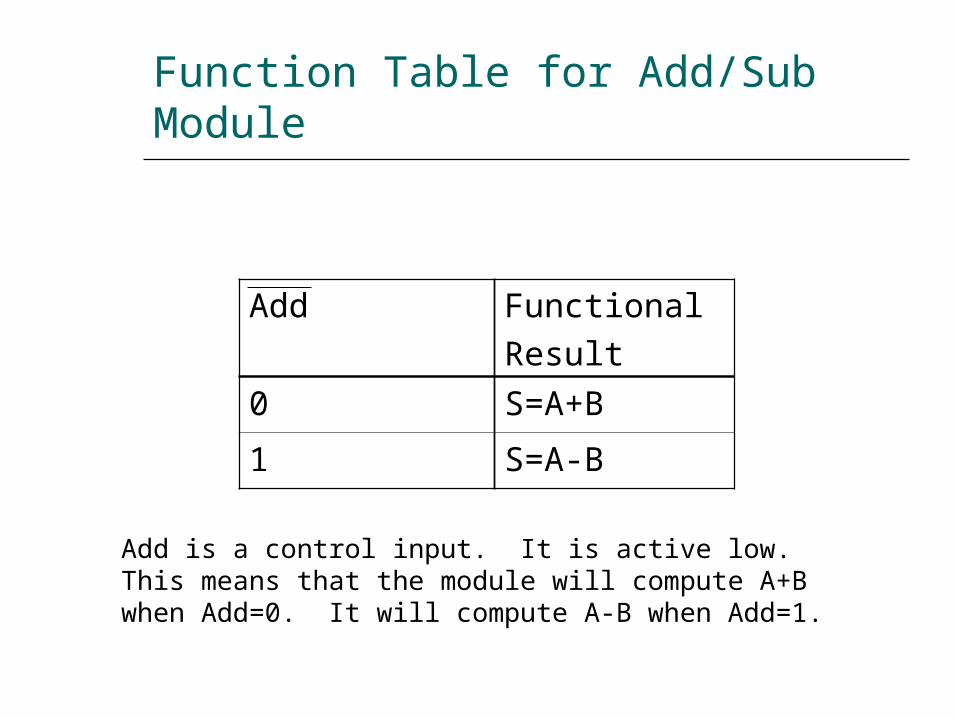
Function Table for Add/Sub Module
Add FunctionalResult
0 S=A+B1 S=A-B
Add is a control input. It is active low. This means that the module will compute A+B when Add=0. It will compute A-B when Add=1.
Add/Sub Circuit
Design using Modules
Add/Sub Circuit
ADDERINV
2x1M UX
A
B
S
B
B
AS Cin
A
Add
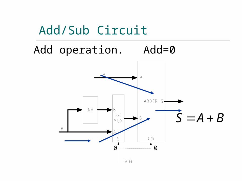
Add/Sub Circuit
ADDERINV
2x1M UX
A
B
S
B
B
AS Cin
A
Add
Add operation. Add=0
0 0
S A B
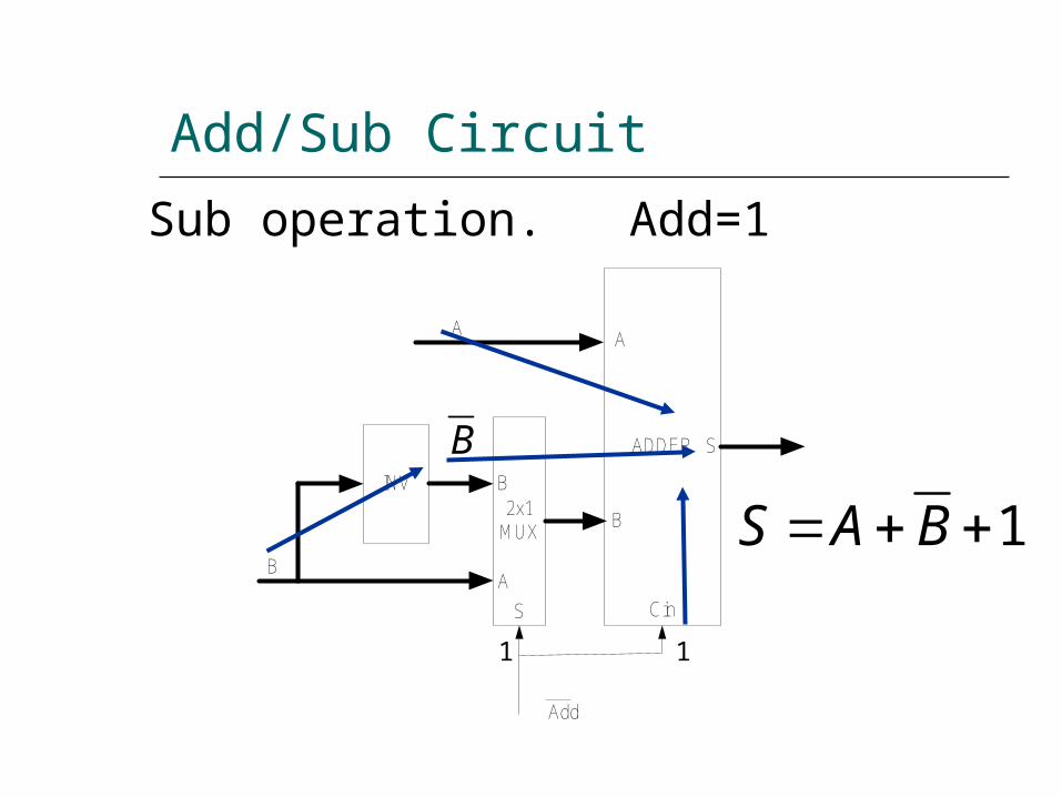
Add/Sub Circuit
ADDERINV
2x1M UX
A
B
S
B
B
AS Cin
A
Add
Sub operation. Add=1
1 1
1S A B
B
Overflow/Underflow Detection
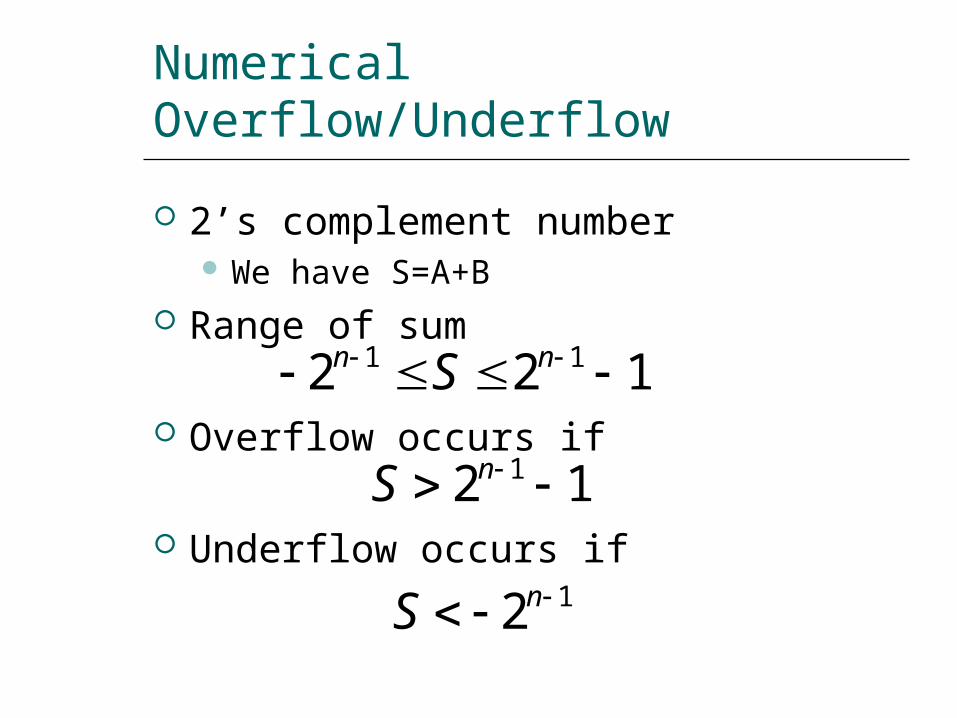
Numerical Overflow/Underflow 2’s complement number
We have S=A+B Range of sum
Overflow occurs if
Underflow occurs if
1 12 2 1n nS
12 1nS
12nS
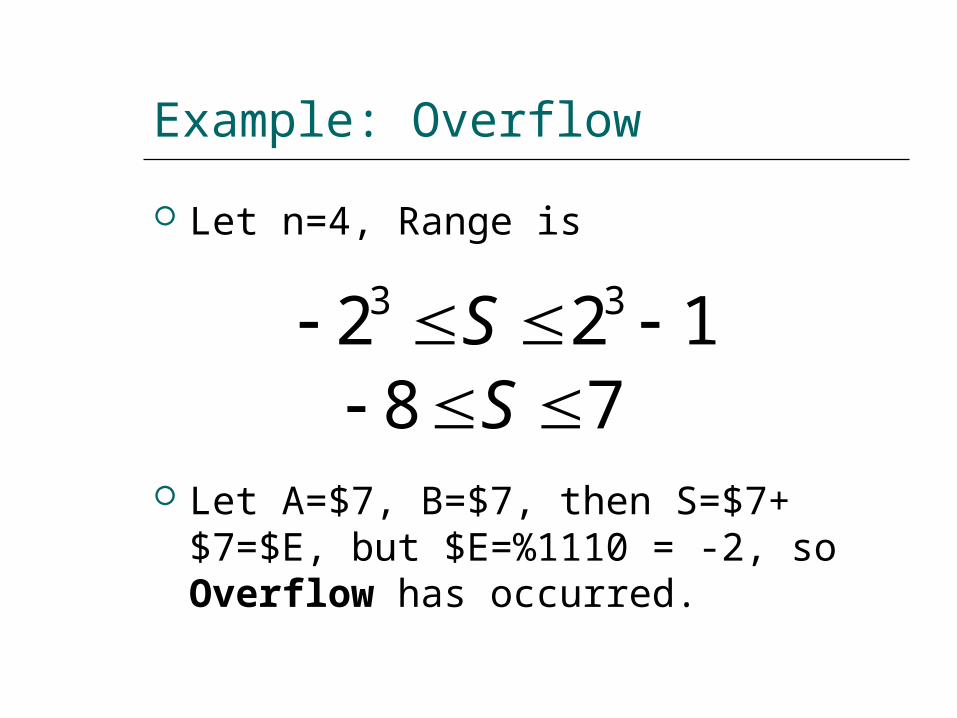
Example: Overflow Let n=4, Range is
Let A=$7, B=$7, then S=$7+$7=$E, but $E=%1110 = -2, so Overflow has occurred.
8 7S
3 32 2 1S
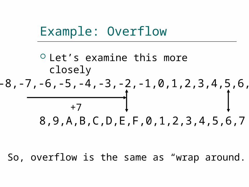
Example: Overflow Let’s examine this more closely
-8,-7,-6,-5,-4,-3,-2,-1,0,1,2,3,4,5,6,7
+7
So, overflow is the same as “wrap around.”
8,9,A,B,C,D,E,F,0,1,2,3,4,5,6,7
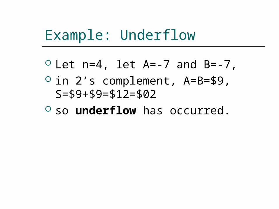
Example: Underflow Let n=4, let A=-7 and B=-7, in 2’s complement, A=B=$9, S=$9+$9=$12=$02
so underflow has occurred.
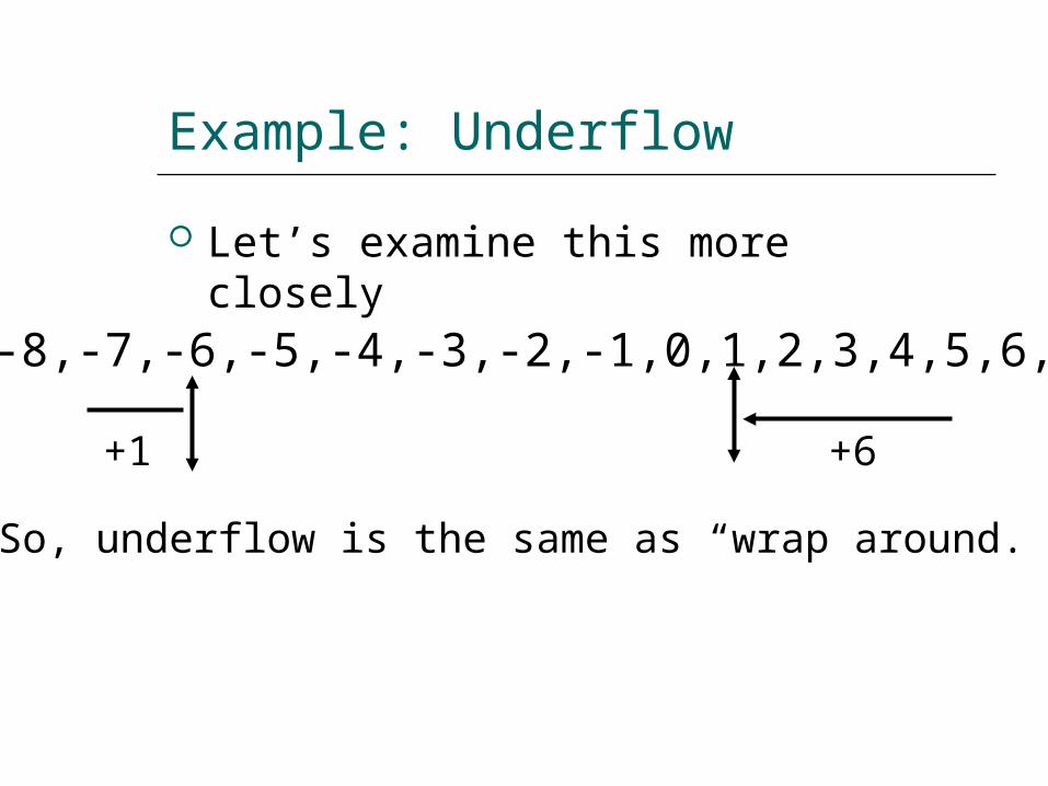
Example: Underflow Let’s examine this more closely
-8,-7,-6,-5,-4,-3,-2,-1,0,1,2,3,4,5,6,7
+6
So, underflow is the same as “wrap around.”
+1
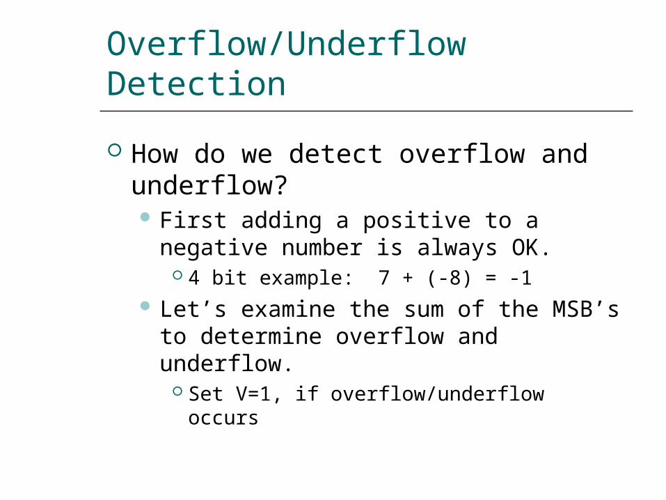
Overflow/Underflow Detection How do we detect overflow and underflow? First adding a positive to a negative number is always OK.
4 bit example: 7 + (-8) = -1 Let’s examine the sum of the MSB’s to determine overflow and underflow.
Set V=1, if overflow/underflow occurs
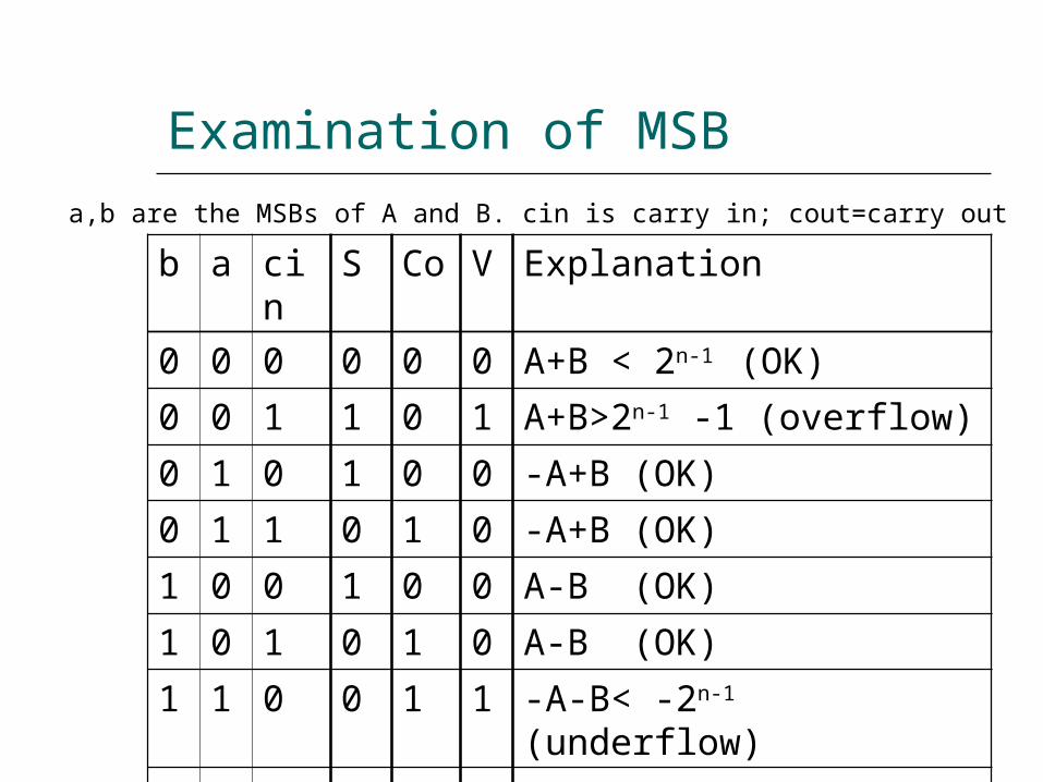
Examination of MSB
b a cin
S Co V Explanation
0 0 0 0 0 0 A+B < 2n-1 (OK)0 0 1 1 0 1 A+B>2n-1 -1 (overflow)0 1 0 1 0 0 -A+B (OK)0 1 1 0 1 0 -A+B (OK)1 0 0 1 0 0 A-B (OK)1 0 1 0 1 0 A-B (OK)1 1 0 0 1 1 -A-B< -2n-1
(underflow)1 1 1 1 1 0 -A-B > -2n-1 (OK)
a,b are the MSBs of A and B. cin is carry in; cout=carry out
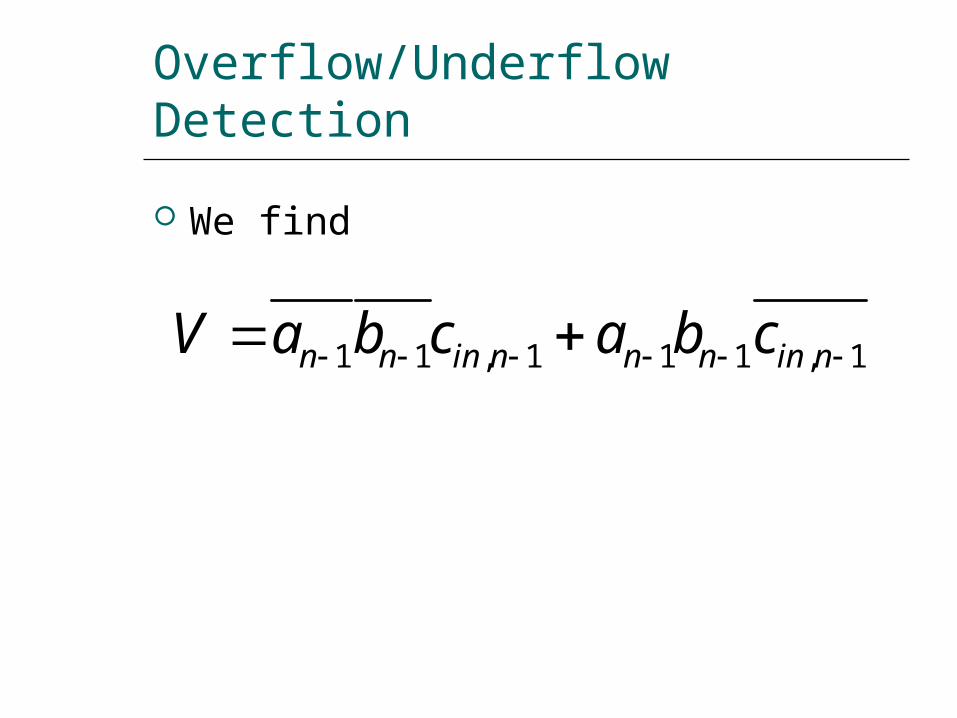
Overflow/Underflow Detection We find
1 1 , 1 1 1 , 1n n in n n n in nV a b c a b c
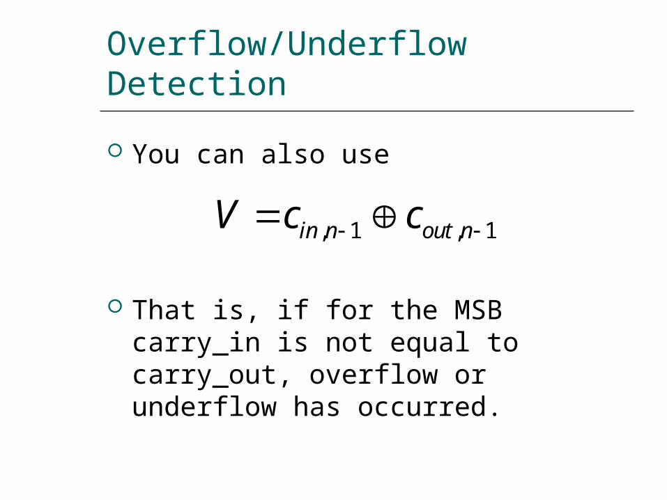
Overflow/Underflow Detection
, 1 , 1in n out nV c c
You can also use
That is, if for the MSB carry_in is not equal to carry_out, overflow or underflow has occurred.
Comparators
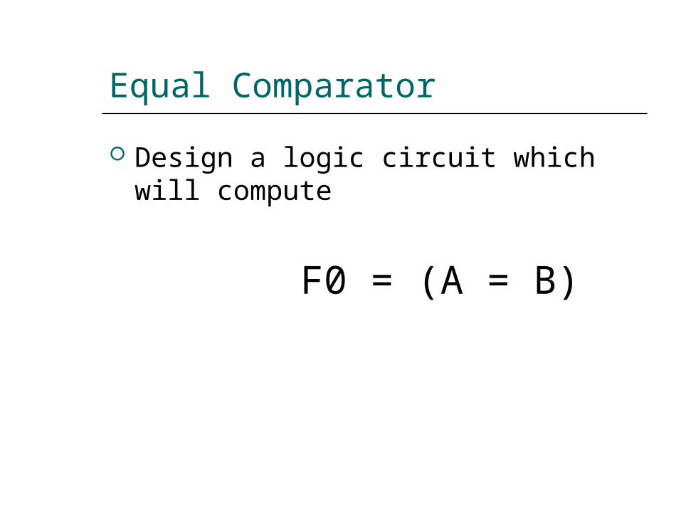
Equal Comparator Design a logic circuit which will compute
F0 = (A = B)
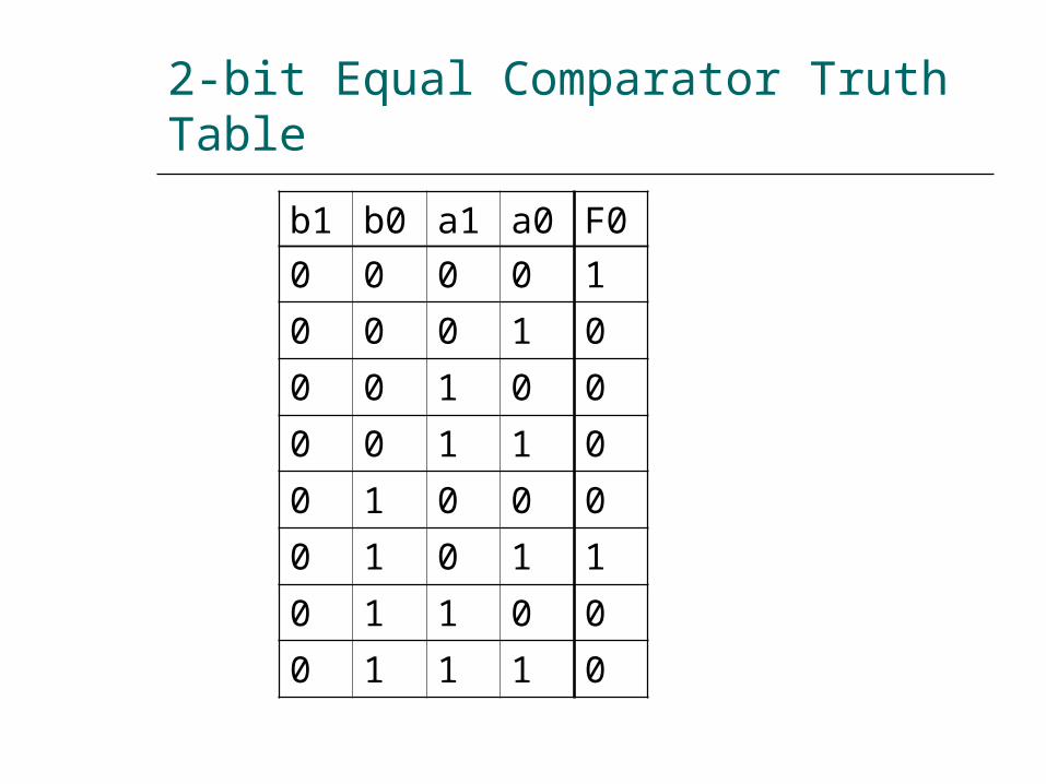
2-bit Equal Comparator Truth Table
b1 b0 a1 a0 F00 0 0 0 10 0 0 1 00 0 1 0 00 0 1 1 00 1 0 0 00 1 0 1 10 1 1 0 00 1 1 1 0
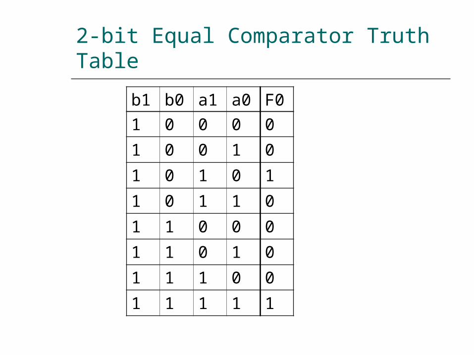
2-bit Equal Comparator Truth Table
b1 b0 a1 a0 F01 0 0 0 01 0 0 1 01 0 1 0 11 0 1 1 01 1 0 0 01 1 0 1 01 1 1 0 01 1 1 1 1
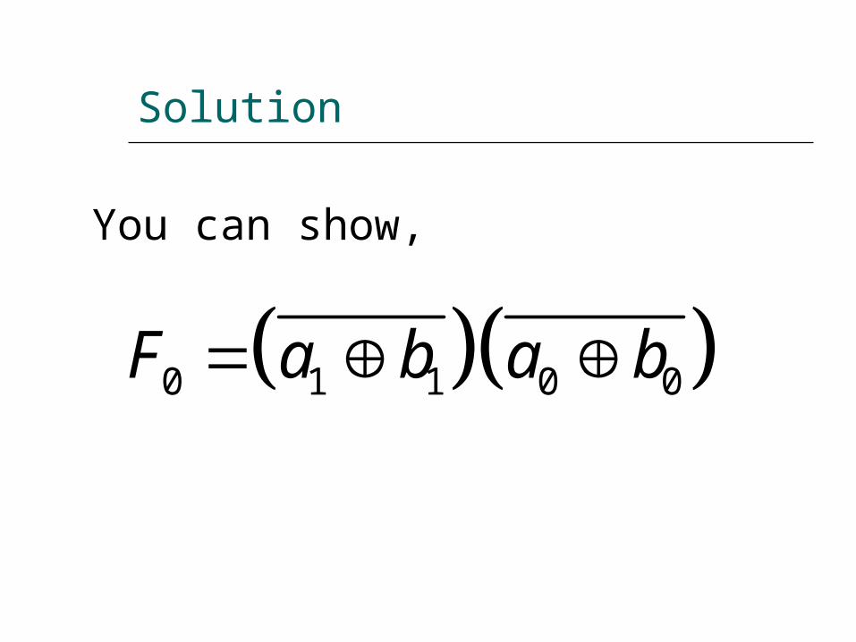
Solution
0 1 1 0 0F a b a b
You can show,
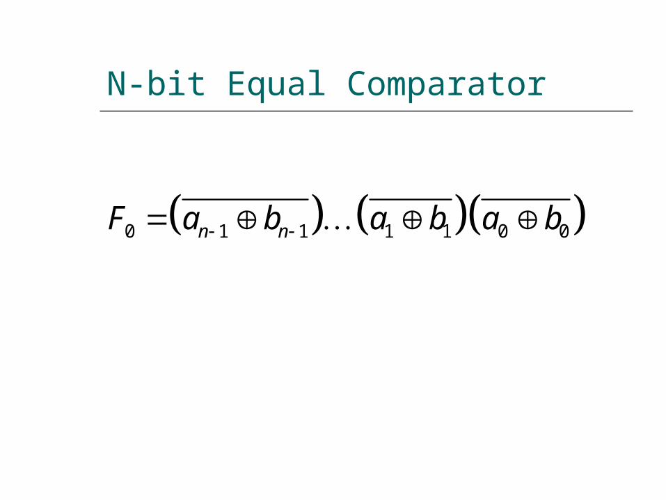
N-bit Equal Comparator
0 1 1 1 1 0 0n nF a b a b a b
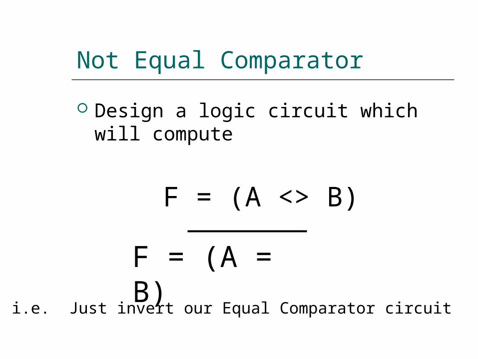
Not Equal Comparator Design a logic circuit which will compute
F = (A <> B)
F = (A = B)i.e. Just invert our Equal Comparator circuit
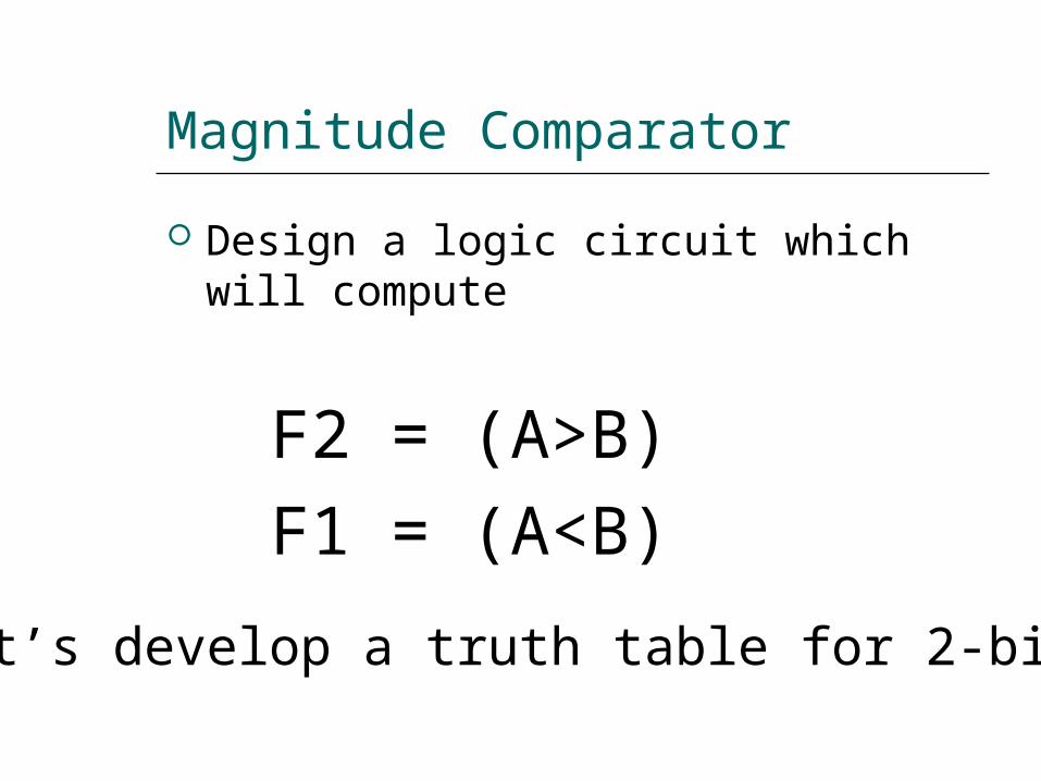
Magnitude Comparator Design a logic circuit which will compute
F2 = (A>B)F1 = (A<B)
Let’s develop a truth table for 2-bits
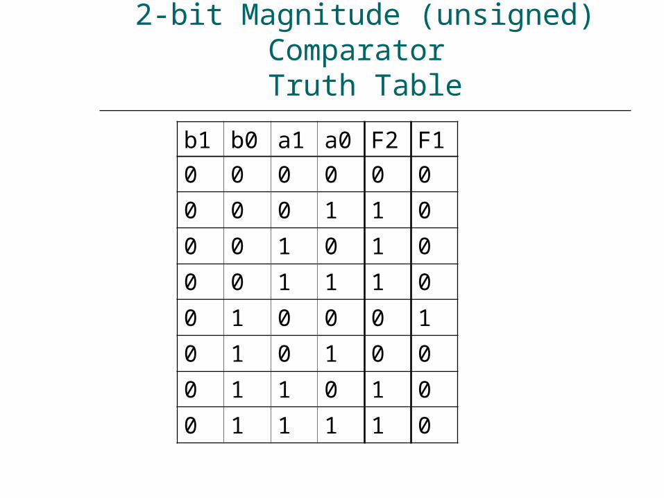
2-bit Magnitude (unsigned) Comparator Truth Table
b1 b0 a1 a0 F2 F10 0 0 0 0 00 0 0 1 1 00 0 1 0 1 00 0 1 1 1 00 1 0 0 0 10 1 0 1 0 00 1 1 0 1 00 1 1 1 1 0
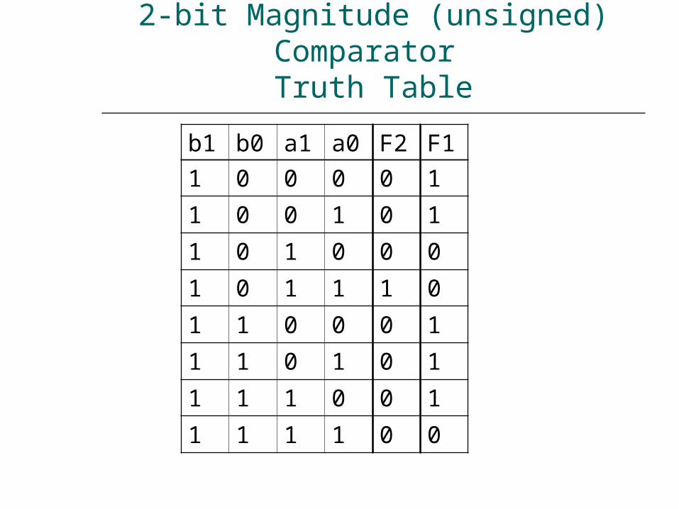
2-bit Magnitude (unsigned) Comparator Truth Table
b1 b0 a1 a0 F2 F11 0 0 0 0 11 0 0 1 0 11 0 1 0 0 01 0 1 1 1 01 1 0 0 0 11 1 0 1 0 11 1 1 0 0 11 1 1 1 0 0
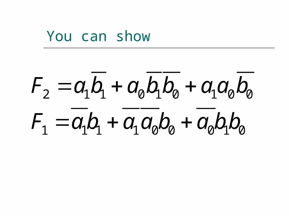
You can show
2 1 1 0 1 0 1 0 0F a b a bb aa b
1 1 1 1 0 0 0 1 0F ab a a b a bb
Arithmetic Logic Units (ALUs)
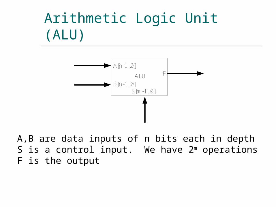
Arithmetic Logic Unit (ALU)
ALUA[n-1,,0]
B[n-1..0]F
S[m -1..0]
A,B are data inputs of n bits each in depthS is a control input. We have 2m operationsF is the output

Example Let n=4,m=3 We have A[3..0] and B[3..0] With m=3, we have 23 = 8 operations
Let’s look at a possible function table
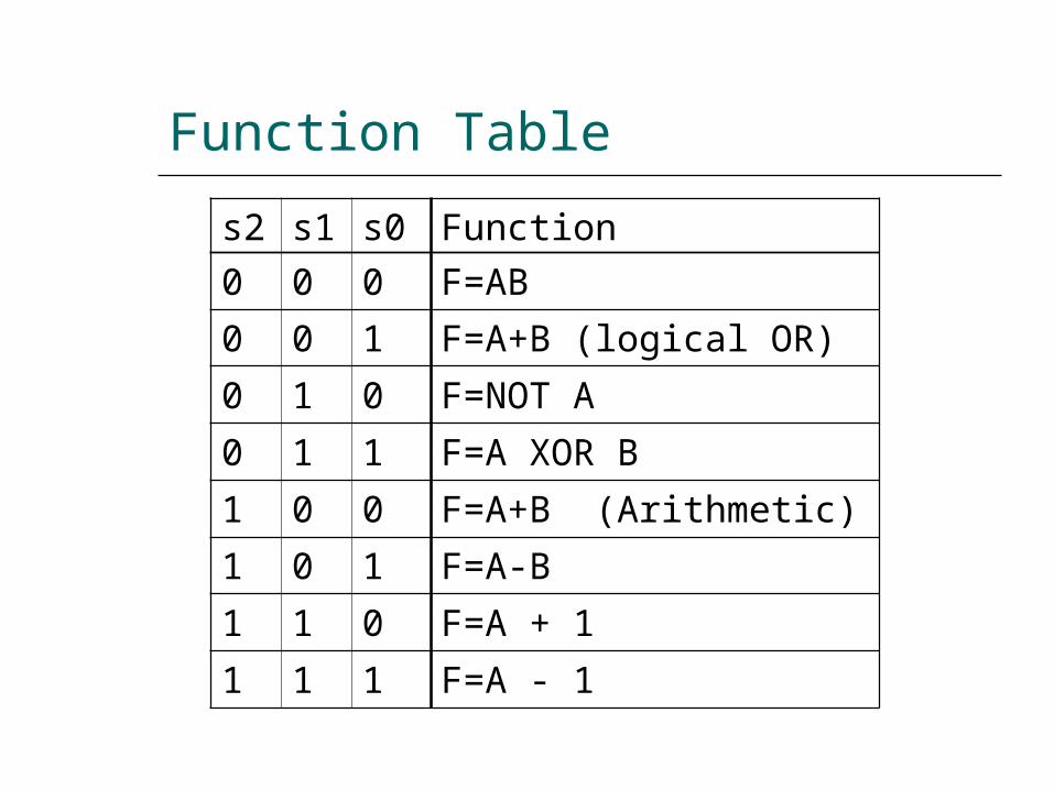
Function Tables2 s1 s0 Function0 0 0 F=AB0 0 1 F=A+B (logical OR)0 1 0 F=NOT A0 1 1 F=A XOR B1 0 0 F=A+B (Arithmetic)1 0 1 F=A-B1 1 0 F=A + 11 1 1 F=A - 1
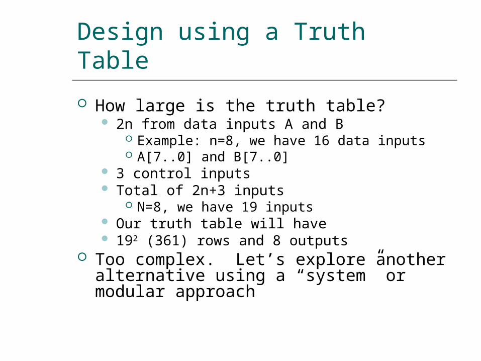
Design using a Truth Table How large is the truth table?
2n from data inputs A and B Example: n=8, we have 16 data inputs A[7..0] and B[7..0]
3 control inputs Total of 2n+3 inputs
N=8, we have 19 inputs Our truth table will have 192 (361) rows and 8 outputs
Too complex. Let’s explore another alternative using a “system” or modular approach
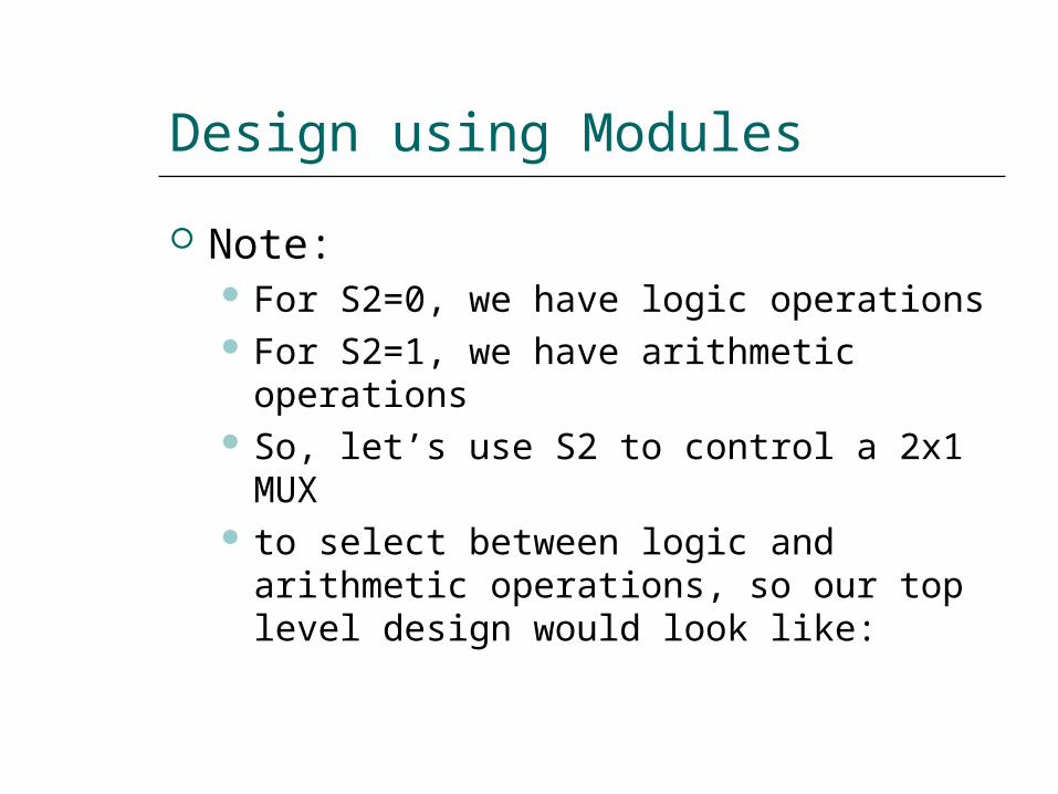
Design using Modules Note:
For S2=0, we have logic operations For S2=1, we have arithmetic operations
So, let’s use S2 to control a 2x1 MUX
to select between logic and arithmetic operations, so our top level design would look like:
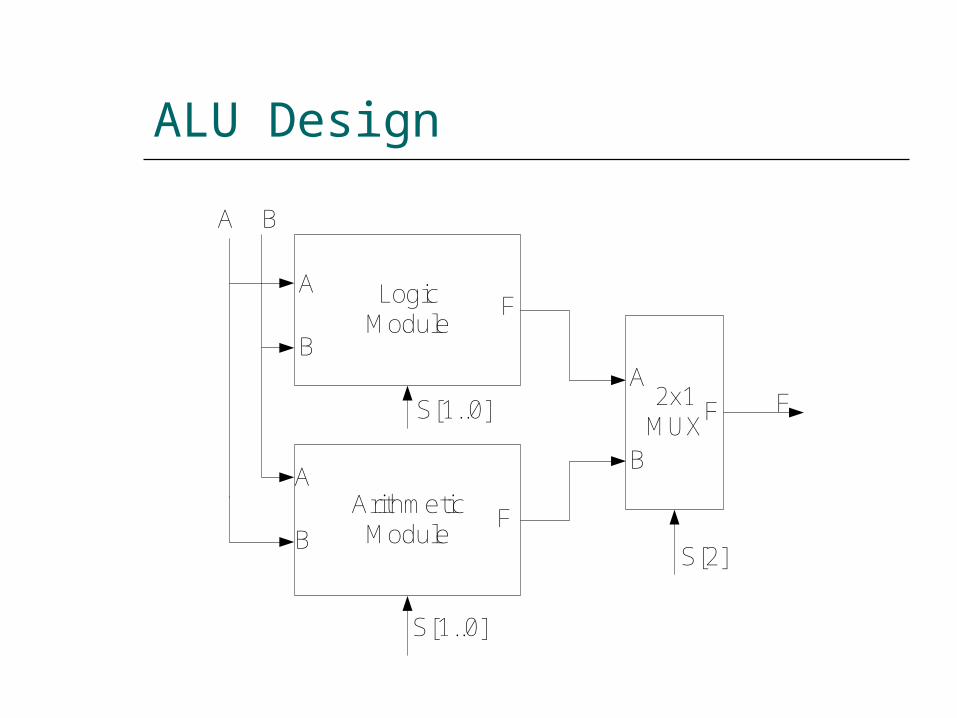
ALU Design
LogicM odule
Arithm eticM odule
2x1M UX
S[2]
A B
A
A
BF
A
BF
S[1..0]
S[1..0]B
F F
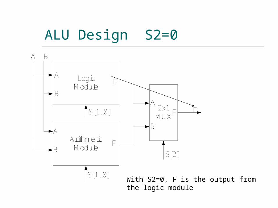
ALU Design S2=0
LogicM odule
Arithm eticM odule
2x1M UX
S[2]
A B
A
A
BF
A
BF
S[1..0]
S[1..0]B
F F
With S2=0, F is the output fromthe logic module
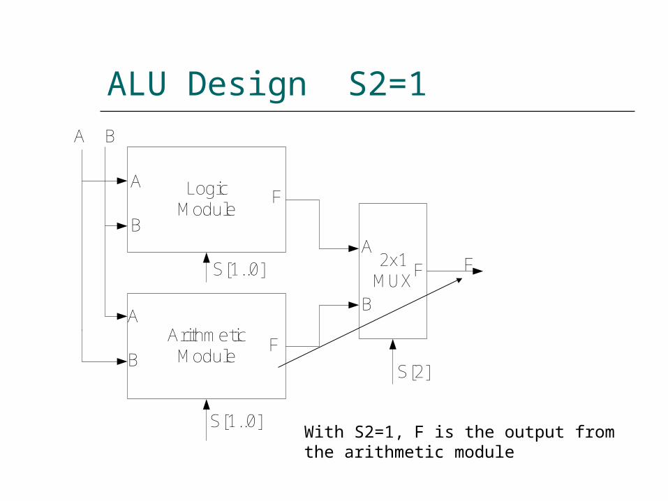
ALU Design S2=1
LogicM odule
Arithm eticM odule
2x1M UX
S[2]
A B
A
A
BF
A
BF
S[1..0]
S[1..0]B
F F
With S2=1, F is the output fromthe arithmetic module
Logic Module Design
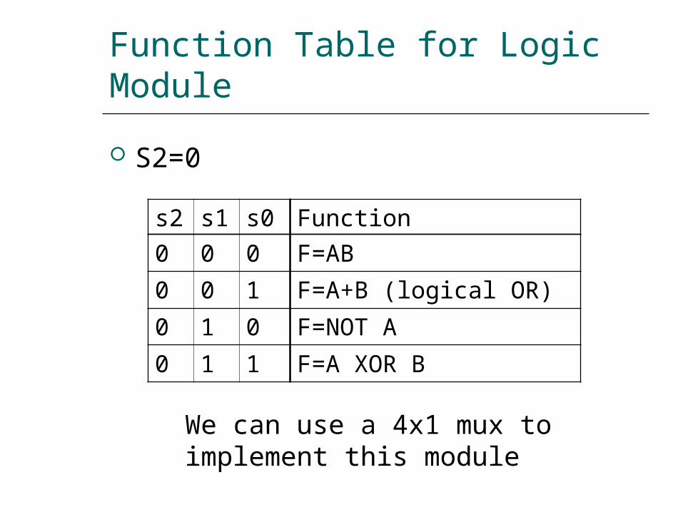
Function Table for Logic Module S2=0
s2 s1 s0 Function0 0 0 F=AB0 0 1 F=A+B (logical OR)0 1 0 F=NOT A0 1 1 F=A XOR B
We can use a 4x1 mux to implement this module
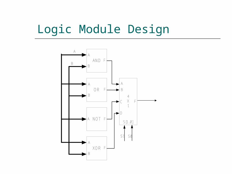
Logic Module Design
OR
NOT
XOR
AND
AB
C
D
4X1
F
S[1..0]
S1 S0
A
A
BF
A
BF
A
BF
A F
B
Logic Module Design
OR
NOT
XOR
AND
AB
C
D
4X1
F
S[1..0]
S1 S0
A
A
BF
A
BF
A
BF
A F
B
AND OperationS[1..0]=00
0 0
F=AB
Logic Module Design
OR
NOT
XOR
AND
AB
C
D
4X1
F
S[1..0]
S1 S0
A
A
BF
A
BF
A
BF
A F
B
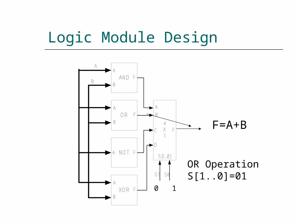
OR OperationS[1..0]=01
0 1
F=A+B
Logic Module Design
OR
NOT
XOR
AND
AB
C
D
4X1
F
S[1..0]
S1 S0
A
A
BF
A
BF
A
BF
A F
B
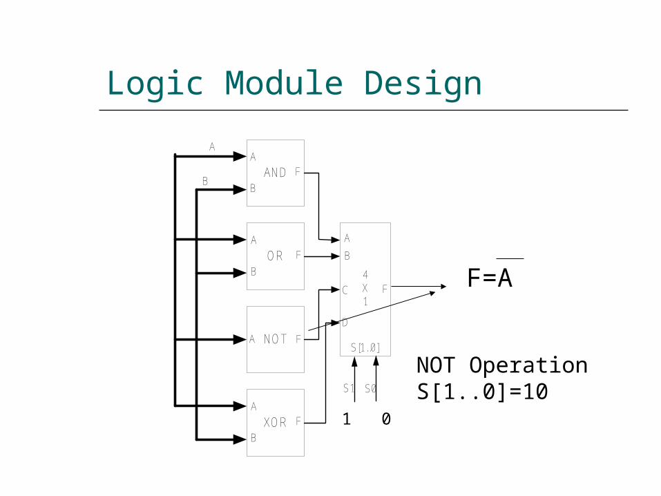
NOT OperationS[1..0]=10
1 0
F=A
Logic Module Design
OR
NOT
XOR
AND
AB
C
D
4X1
F
S[1..0]
S1 S0
A
A
BF
A
BF
A
BF
A F
B
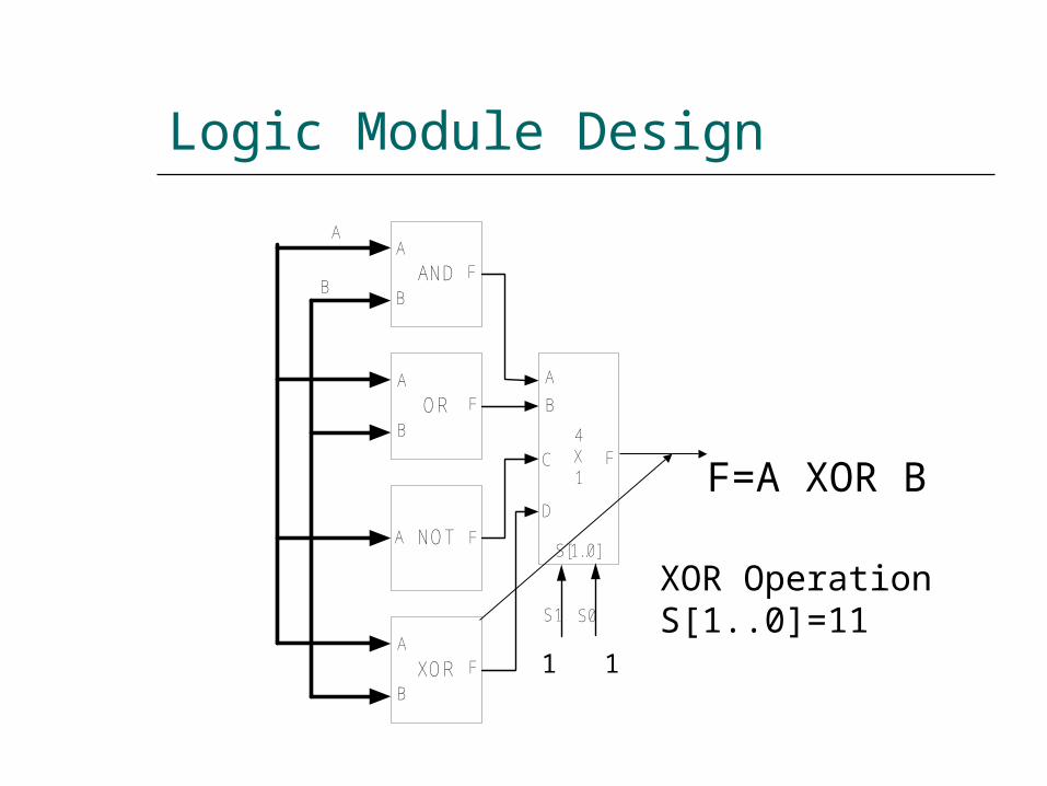
XOR OperationS[1..0]=11
1 1
F=A XOR B
What do these logic modules
look like?
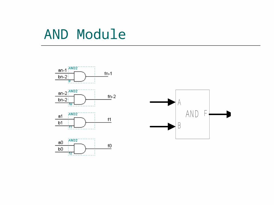
AND Module
ANDA
BF
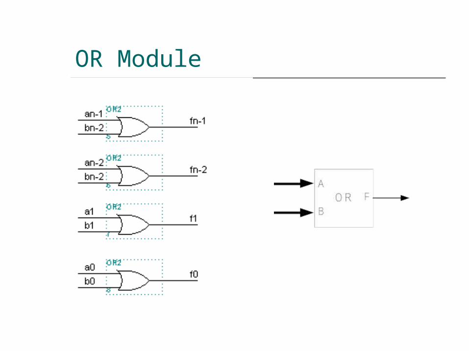
OR Module

NOT Module
NOTA F
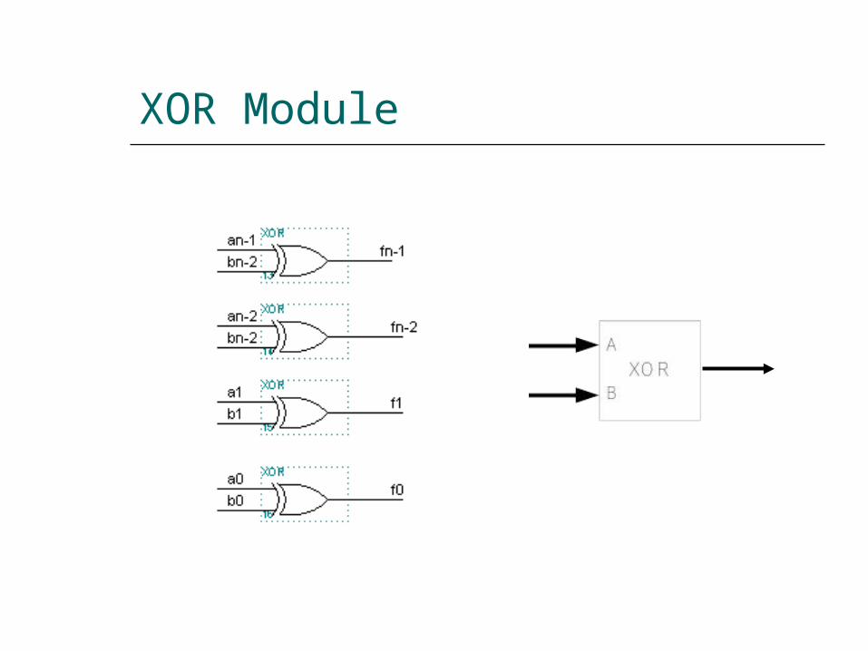
XOR Module
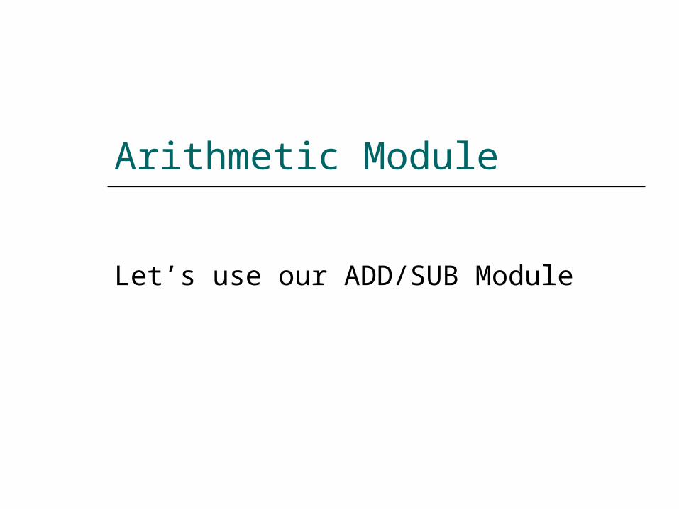
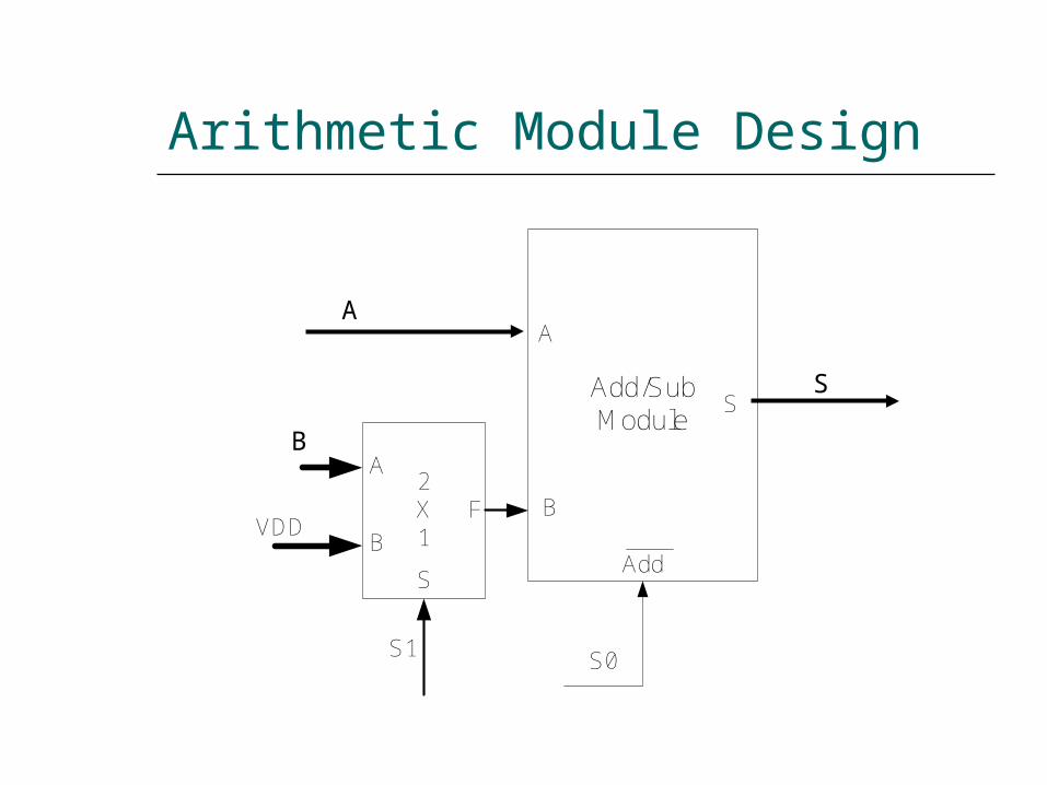
Arithmetic Module
Let’s use our ADD/SUB Module

Add/Sub Circuit Module
Add/SubM odule
A
B
S
Add
A
B
Add
S
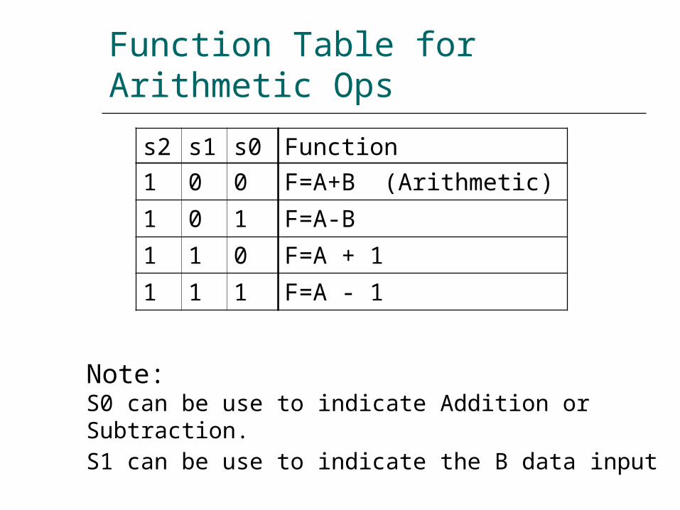
Function Table for Arithmetic Ops
s2 s1 s0 Function1 0 0 F=A+B (Arithmetic)1 0 1 F=A-B1 1 0 F=A + 11 1 1 F=A - 1
Note:S0 can be use to indicate Addition or Subtraction.S1 can be use to indicate the B data input

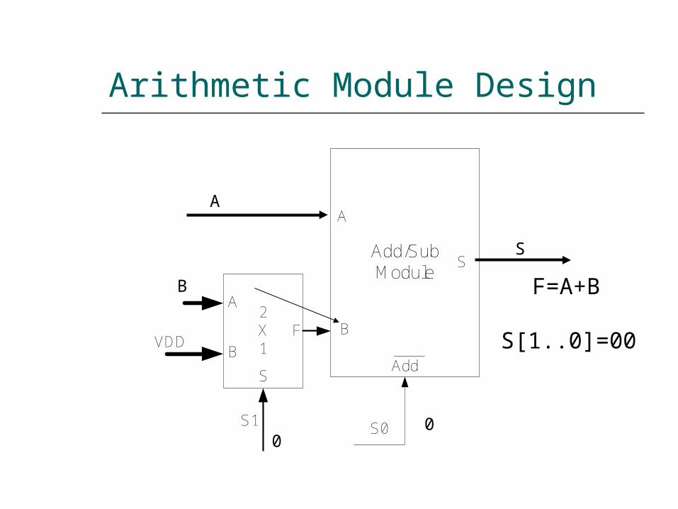
Arithmetic Module Design
Add/SubM odule
S0
A
B
Add
S
S
2X1
A
BFVDD
S1
B
A
S
Arithmetic Module Design
Add/SubM odule
S0
A
B
Add
S
S
2X1
A
BFVDD
S1
B
A
S
00
F=A+B
S[1..0]=00

Arithmetic Module Design
Add/SubM odule
S0
A
B
Add
S
S
2X1
A
BFVDD
S1
B
A
S
10
F=A-B
S[1..0]=01
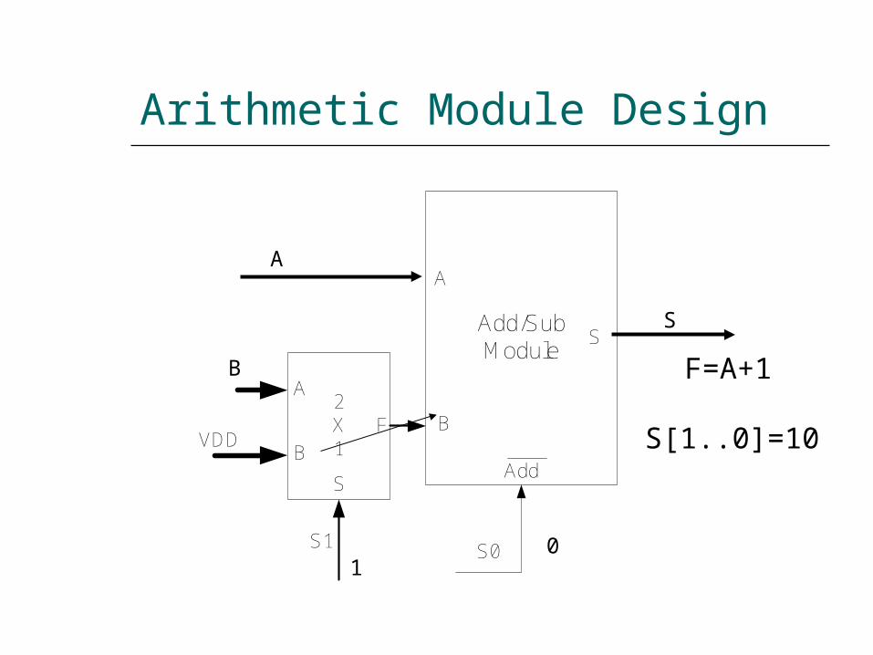
Arithmetic Module Design
Add/SubM odule
S0
A
B
Add
S
S
2X1
A
BFVDD
S1
B
A
S
01
F=A+1
S[1..0]=10
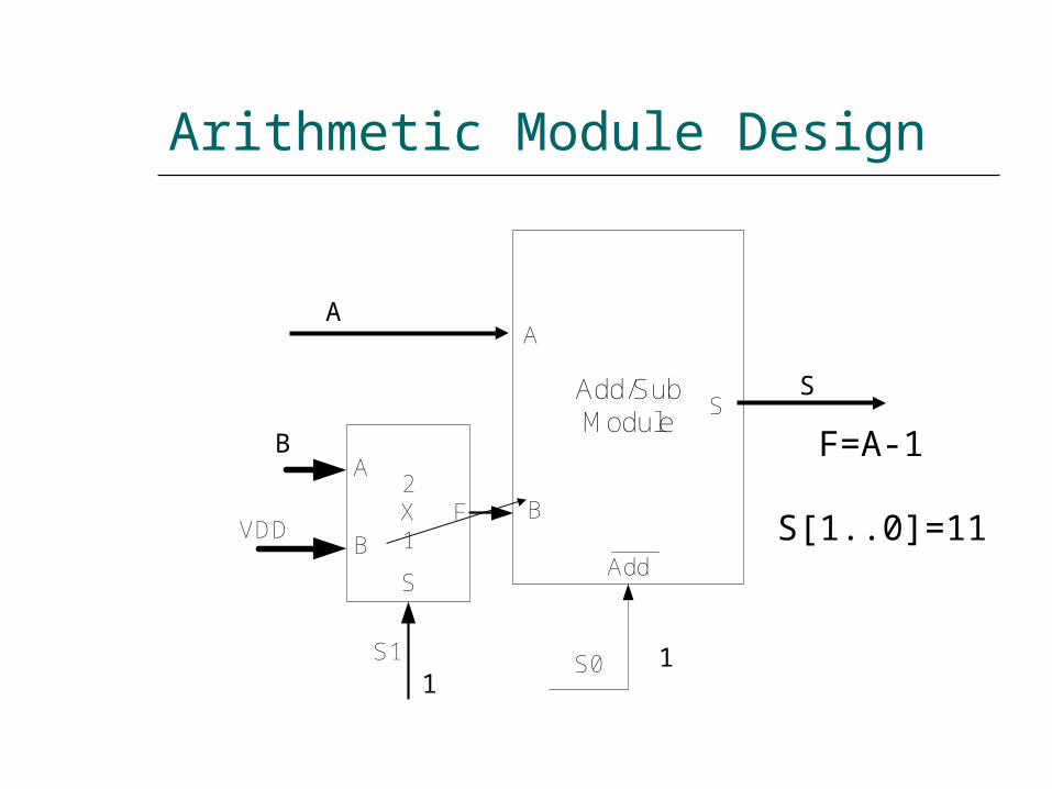
Arithmetic Module Design
Add/SubM odule
S0
A
B
Add
S
S
2X1
A
BFVDD
S1
B
A
S
11
F=A-1
S[1..0]=11
Overall Design
We have

ALU Design
LogicM odule
Arithm eticM odule
2x1M UX
S[2]
A B
A
A
BF
A
BF
S[1..0]
S[1..0]B
F F

Logic Module Design
OR
NOT
XOR
AND
AB
C
D
4X1
F
S[1..0]
S1 S0
A
A
BF
A
BF
A
BF
A F
B
Arithmetic Module Design
Add/SubM odule
S0
A
B
Add
S
S
2X1
A
BFVDD
S1
B
A
S
Total Design
OR
NOT
XOR
AND
AB
C
D
4X1
F
S[1..0]
Add/SubM odule
A
S
S0
A
B
Add
S
BS
F2X1
S2
S
2X1
A
BFVDD
S1 S0
S1
A B
A
BF
A
BF
A
BF
A F
Logic Module
Arithmetic Module
End of Chapter 4
Copyright © 2022 FDOKUMEN