Multivalued Logic Circuit Design for Binary Logic Interface
72
i Multivalued Logic Circuit Design for Binary Logic Interface A Dissertation Submitted in partial fulfillment for the award of the Degree of Master of Technology in Department of Computer Engineering (With specialization in COMPUTER SCIENCE & ENGINEERING) Supervisor Submitted by Dr. S.C. Jain Hitesh Gupta Professor Enrolment No.: 09E2UCCSM4XP606 Department of Computer Engineering University College of Engineering Rajasthan Technical University, Kota (Rajasthan) August – 2013
-
Upload
khangminh22 -
Category
Documents
-
view
5 -
download
0
Transcript of Multivalued Logic Circuit Design for Binary Logic Interface
i
Multivalued Logic Circuit Design for Binary Logic
Interface
A
Dissertation
Submitted
in partial fulfillment
for the award of the Degree of
Master of Technology
in Department of Computer Engineering
(With specialization in COMPUTER SCIENCE & ENGINEERING)
Supervisor Submitted by
Dr. S.C. Jain Hitesh Gupta
Professor Enrolment No.:
09E2UCCSM4XP606
Department of Computer Engineering
University College of Engineering
Rajasthan Technical University, Kota (Rajasthan)
August – 2013
ii
Candidate’s Declaration
I hereby declare the work, which is being presented in the Dissertation, entitled
“Multivalued Logic Circuit Design for Binary Logic Interface” in partial fulfillment for
the award of Degree of “Master of Technology” in Department of Computer Engineering
with specialization in Computer Science & Engineering, and submitted to the Department of
Computer Engineering, University College of Engineering, Rajasthan Technical University is
a record of my own investigation carried under the Guidance of Dr. S.C. Jain, Professor,
Department of Computer Engineering, University College of Engineering, RTU Kota.
I have not submitted the matter presented in this Dissertation anywhere for the award
of any other Degree.
(Hitesh Gupta)
M.Tech. (Computer Engineering)
Enrolment No.: 09E2UCCSM4XP606
University College of Engineering, RTU, KOTA
Counter Signed by
Dr. S.C. Jain
Professor
Department of Computer Science & Engineering
University College of Engineering
Rajasthan Technical University, Kota
iii
CERTIFICATE
This is to certify that this Project entitled “Multivalued Logic Circuit Design for
Binary Logic Interface” has been successfully carried out by Hitesh Gupta (Enrolment
No.: 09E2UCCSM4XP606), under my supervision and guidance, in partial fulfilment of the
requirement for the award of Master of Technology degree in Computer Science &
Engineering from University College of Engineering, Rajasthan Technical University,
Kota for year 2009-2011.
Dr. S.C. Jain
(Professor)
Department of Computer Engineering
University College of Engineering
Rajasthan Technical University, Kota
Place: Kota
Date:

iv
ACKNOWEDGMENTS
I would like to take this opportunity to acknowledge and thank those who made this
work possible and unforgettable to me.
First and foremost, thanks from bottom of my heart to the God, the omnipotent, for
his blessing, showing me light even in a time of great darkness, and giving me strength. I
would like to express my sincere gratitude to my Dissertation guide Dr. S. C. Jain, Professor
in Department of Computer Science for his constant encouragement, able guidance and for
giving me a new platform to build my career by giving me a chance to learn different fields
of this technology. I am extremely grateful for what he has provided me.
I would also like to say thanks to my friend and research colleagues for their constant
support and encouragement. I am extending my thanks to the M.Tech. students of university
College of Engineering, Rajasthan Technical University, Kota for their invaluable support.
I express my deep sense of reverence to my parents and family members for their
unconditional support, patience and encouragement.
Date: HITESH GUPTA
v
CONTENTS
CANDIDATE’S DECLARATION i
CERTIFICATE ii
ACKNOWLEDGEMENT iii
TABLE OF CONTENTS iv
LIST OF TABLES vi
LIST OF FIGURES vii
LIST OF ALGORITHMS ix
ABSTRACT 1
1. INTRODUCTION 2
1.1 Multivalued Gates 3
1.2 Multivalued Algebra 7
1.3 Multivalued Conversion 9
1.4 Objective and Motivation 10
1.5 Organization of Dissertation 10
2. LITERATURE REVIEW
2.1 Multivalued Logic System 12
2.1.1 Ternary Logic System 12
2.1.2 Quaternary Circuit 13
2.1.3 Multivalued Logic 14
2.2 Survey Extraction 15
3. MULTIVALUED LOGIC SYSTEM
3.1 Multivalued Logic Gate 16
3.2 Multivalued Algebra 22
3.2.1 Quaternary Operators 22
3.2.2 Properties of Quaternary Algebra 23
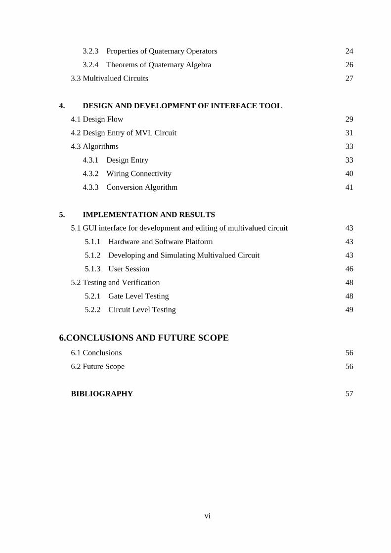
vi
3.2.3 Properties of Quaternary Operators 24
3.2.4 Theorems of Quaternary Algebra 26
3.3 Multivalued Circuits 27
4. DESIGN AND DEVELOPMENT OF INTERFACE TOOL
4.1 Design Flow 29
4.2 Design Entry of MVL Circuit 31
4.3 Algorithms 33
4.3.1 Design Entry 33
4.3.2 Wiring Connectivity 40
4.3.3 Conversion Algorithm 41
5. IMPLEMENTATION AND RESULTS
5.1 GUI interface for development and editing of multivalued circuit 43
5.1.1 Hardware and Software Platform 43
5.1.2 Developing and Simulating Multivalued Circuit 43
5.1.3 User Session 46
5.2 Testing and Verification 48
5.2.1 Gate Level Testing 48
5.2.2 Circuit Level Testing 49
6.CONCLUSIONS AND FUTURE SCOPE
6.1 Conclusions 56
6.2 Future Scope 56
BIBLIOGRAPHY 57
vii
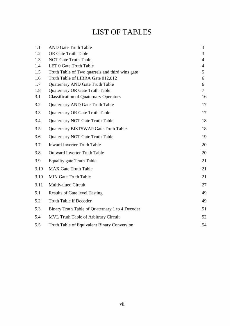
LIST OF TABLES
1.1 AND Gate Truth Table 3
1.2 OR Gate Truth Table 3
1.3 NOT Gate Truth Table 4
1.4 LET 0 Gate Truth Table 4
1.5 Truth Table of Two quarrels and third wins gate 5
1.6 Truth Table of LIBRA Gate 012,012 6
1.7 Quaternary AND Gate Truth Table 6
1.8 Quaternary OR Gate Truth Table 7
3.1 Classification of Quaternary Operators 16
3.2 Quaternary AND Gate Truth Table 17
3.3 Quaternary OR Gate Truth Table 17
3.4 Quaternary NOT Gate Truth Table 18
3.5 Quaternary BISTSWAP Gate Truth Table 18
3.6 Quaternary NOT Gate Truth Table 19
3.7 Inward Inverter Truth Table 20
3.8 Outward Inverter Truth Table 20
3.9 Equality gate Truth Table 21
3.10 MAX Gate Truth Table 21
3.10 MIN Gate Truth Table 21
3.11 Multivalued Circuit 27
5.1 Results of Gate level Testing 49
5.2 Truth Table if Decoder 49
5.3 Binary Truth Table of Quaternary 1 to 4 Decoder 51
5.4 MVL Truth Table of Arbitrary Circuit 52
5.5 Truth Table of Equivalent Binary Conversion 54
viii
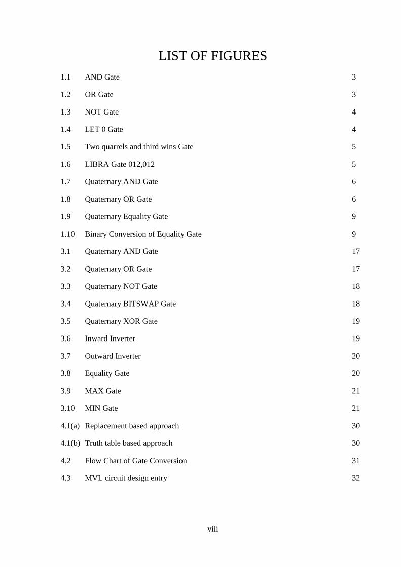
LIST OF FIGURES
1.1 AND Gate 3
1.2 OR Gate 3
1.3 NOT Gate 4
1.4 LET 0 Gate 4
1.5 Two quarrels and third wins Gate 5
1.6 LIBRA Gate 012,012 5
1.7 Quaternary AND Gate 6
1.8 Quaternary OR Gate 6
1.9 Quaternary Equality Gate 9
1.10 Binary Conversion of Equality Gate 9
3.1 Quaternary AND Gate 17
3.2 Quaternary OR Gate 17
3.3 Quaternary NOT Gate 18
3.4 Quaternary BITSWAP Gate 18
3.5 Quaternary XOR Gate 19
3.6 Inward Inverter 19
3.7 Outward Inverter 20
3.8 Equality Gate 20
3.9 MAX Gate 21
3.10 MIN Gate 21
4.1(a) Replacement based approach 30
4.1(b) Truth table based approach 30
4.2 Flow Chart of Gate Conversion 31
4.3 MVL circuit design entry 32
ix
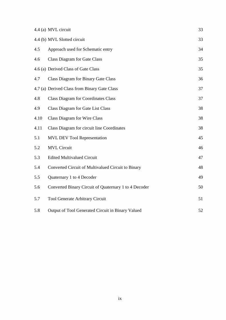
4.4 (a) MVL circuit 33
4.4 (b) MVL Slotted circuit 33
4.5 Approach used for Schematic entry 34
4.6 Class Diagram for Gate Class 35
4.6 (a) Derived Class of Gate Class 35
4.7 Class Diagram for Binary Gate Class 36
4.7 (a) Derived Class from Binary Gate Class 37
4.8 Class Diagram for Coordinates Class 37
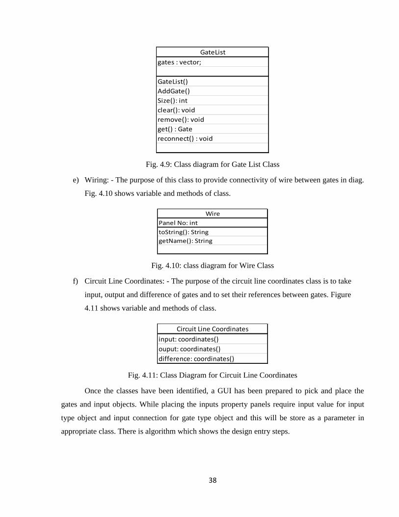
4.9 Class Diagram for Gate List Class 38
4.10 Class Diagram for Wire Class 38
4.11 Class Diagram for circuit line Coordinates 38
5.1 MVL DEV Tool Representation 45
5.2 MVL Circuit 46
5.3 Edited Multivalued Circuit 47
5.4 Converted Circuit of Multivalued Circuit to Binary 48
5.5 Quaternary 1 to 4 Decoder 49
5.6 Converted Binary Circuit of Quaternary 1 to 4 Decoder 50
5.7 Tool Generate Arbitrary Circuit 51
5.8 Output of Tool Generated Circuit in Binary Valued 52

x
LIST OF ALGORITHMS
4.1 Design Entry Algorithm 39
4.2 Wiring Algorithm 41
4.3 Convert MVL to BVL 42
xi
ABSTRACT
Binary logic and devices have been in used since inception with advancement and
technology and millennium gate design era. The development in binary logic has become
tedious and cumbersome. Multivalued logic enables significantly more information to be
packed within a single digit. The design and development of logic circuits becomes very
compact and easier. Attempts are being made to fabricate multivalued logic based devices.
Since present devices can be implemented only in binary system, it is necessary to
evolve a system that can built the circuit in multivalued logic system and convert in binary
logic system.
In multivalued logic system logic gates differ in different logic systems, a quaternary
has become mature in terms of logic algebra and gates. Hence logic design based on above
system can be done using standard procedure.
In this dissertation a logic circuit design entry based on multivalued logic system has
been taken up that can provide the ease of circuit design in multivalued system and output as
binary valued circuit. The named “MVL-DEV” offers editing, storage and conversion into
binary facility.
2
Chapter 1
INTRODUCTION
Since inception digital devices have been designed using binary logic till date.
Researchers have found the development in binary logic is cumbersome, complex and difficult
to understand. Since multivalued logic enables more information to be packed in a single digit
researchers have been working on multivalued logic for many years [1]-[3]. With development
of novel electronic devices and optical devices, it is now possible to implements circuit for more
complicated logic system [4]-[6].
Many of these devices are capable of dealing with more than two logic states but they
are at experimental stage. Some multivalued logic systems such as ternary and quaternary logic
schemes have been developed but successful implementation is yet to become available.
Quaternary logic has several advantages over binary logic. Since it require half the
number of digits to store any information than its binary equivalent it is good for storage; the
quaternary storage mechanism is less than twice as complex as the binary system. For the same
reason, quaternary devices require simpler parallel circuit to process same amount of data than
that needed in binary logic devices. Although several theoretical and physical variants of
quaternary logic can already be found in [6]-[16].
The development of multivalued logic offers significant comfort over binary logic, but
doesn’t find target platform for implementation. We undertake this project to convert the
multivalued logic to binary equivalent.
In this chapter section 1.1 describes about multivalued gates, section 1.2 describes about
multivalued algebra, section 1.3 describes about multivalued conversion 1.4 describes about
motivation section 1.5 describes about organization of dissertation.
3
1.1 Multivalued Gates
Logic gates constitute the foundation blocks for digital logic. Traditional binary gates are
use in current digital devices. In multivalued logic gates have not been standardized but ternary
and quaternary gates are two commonly used multivalued logic gates described in literature.
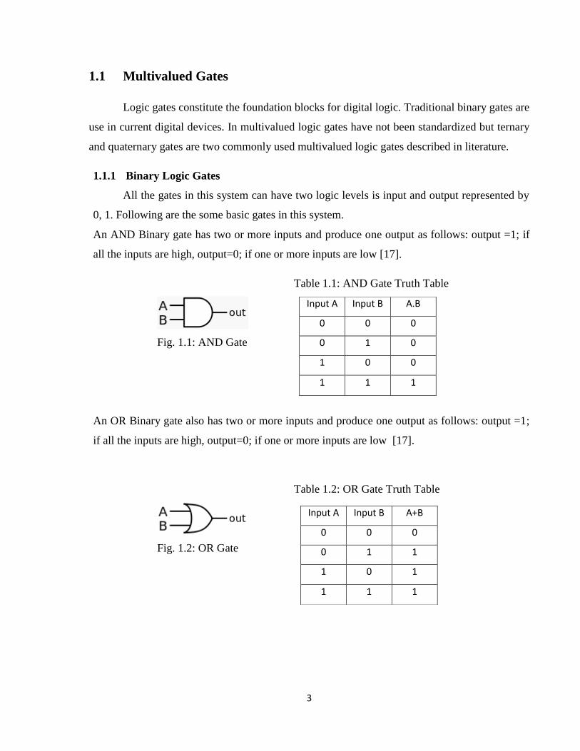
1.1.1 Binary Logic Gates
All the gates in this system can have two logic levels is input and output represented by
0, 1. Following are the some basic gates in this system.
An AND Binary gate has two or more inputs and produce one output as follows: output =1; if
all the inputs are high, output=0; if one or more inputs are low [17].
Table 1.1: AND Gate Truth Table
Fig. 1.1: AND Gate
An OR Binary gate also has two or more inputs and produce one output as follows: output =1;
if all the inputs are high, output=0; if one or more inputs are low [17].
Table 1.2: OR Gate Truth Table
Fig. 1.2: OR Gate
Input A Input B A.B
0 0 0
0 1 0
1 0 0
1 1 1
Input A Input B A+B
0 0 0
0 1 1
1 0 1
1 1 1
4
The inverter gate has one input and produces one output as follows: output =1; if input is low,
output= 0; if input is high [17].
Table 1.3: NOT Gate Truth Table
Fig. 1.3: NOT Gate
1.1.2 Ternary Logic Gates
Ternary logic system contain 3 input logic levels (0, 1, 2) different from quaternary and
binary. In this multivalued logic system we have found some different gates. Some commonly
used gates are discussed below and there symbols and truth tables are given below.
Table 1.4: LET 0 Gate Truth Table
Fig. 1.4: LET 0 Gate
These gates are with one input and one output. There are few gates in this category like
LET 1, LET 2, ROT 1, and ROT 2.
Now we will discuss gates with two inputs and one output. These gates based on concept
when two quarrels and third win.
Input A Output
0 1
1 0
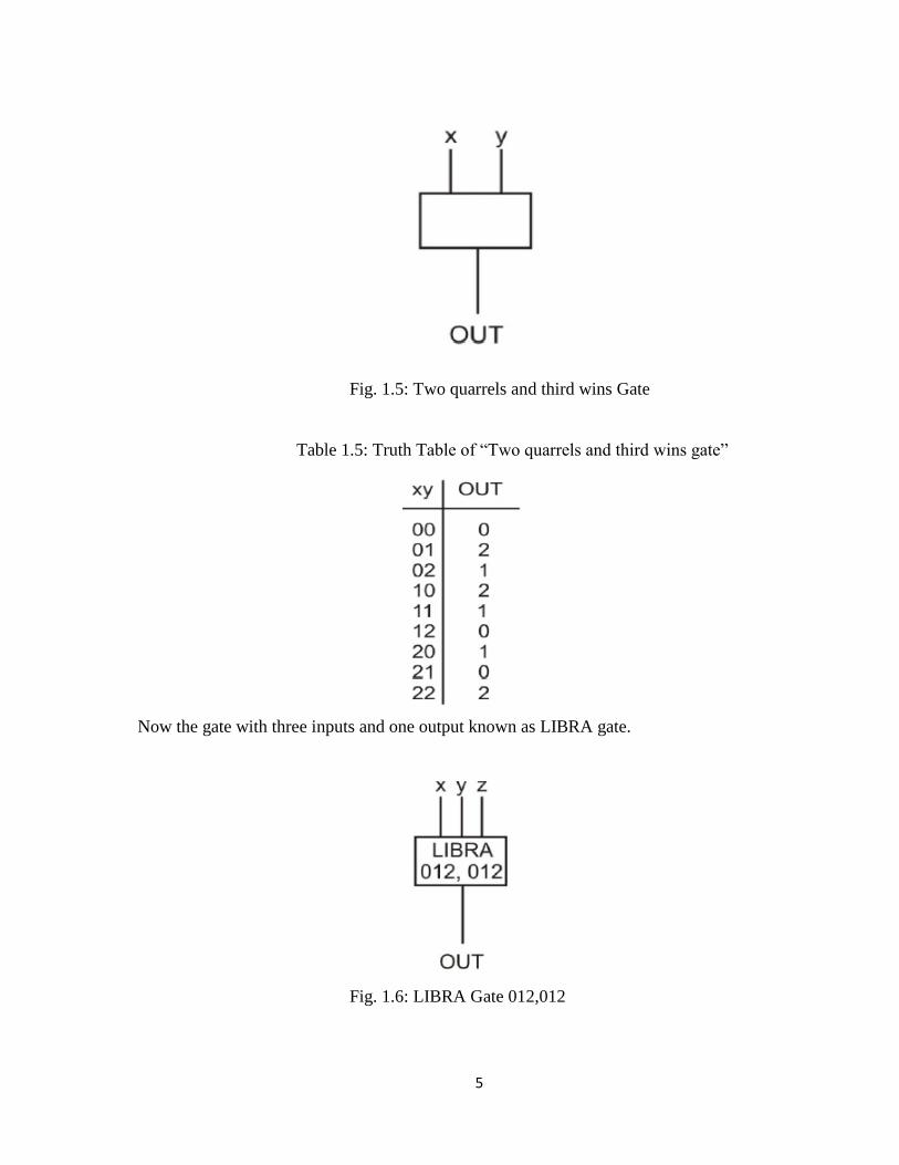
5
Fig. 1.5: Two quarrels and third wins Gate
Table 1.5: Truth Table of “Two quarrels and third wins gate”
Now the gate with three inputs and one output known as LIBRA gate.
Fig. 1.6: LIBRA Gate 012,012
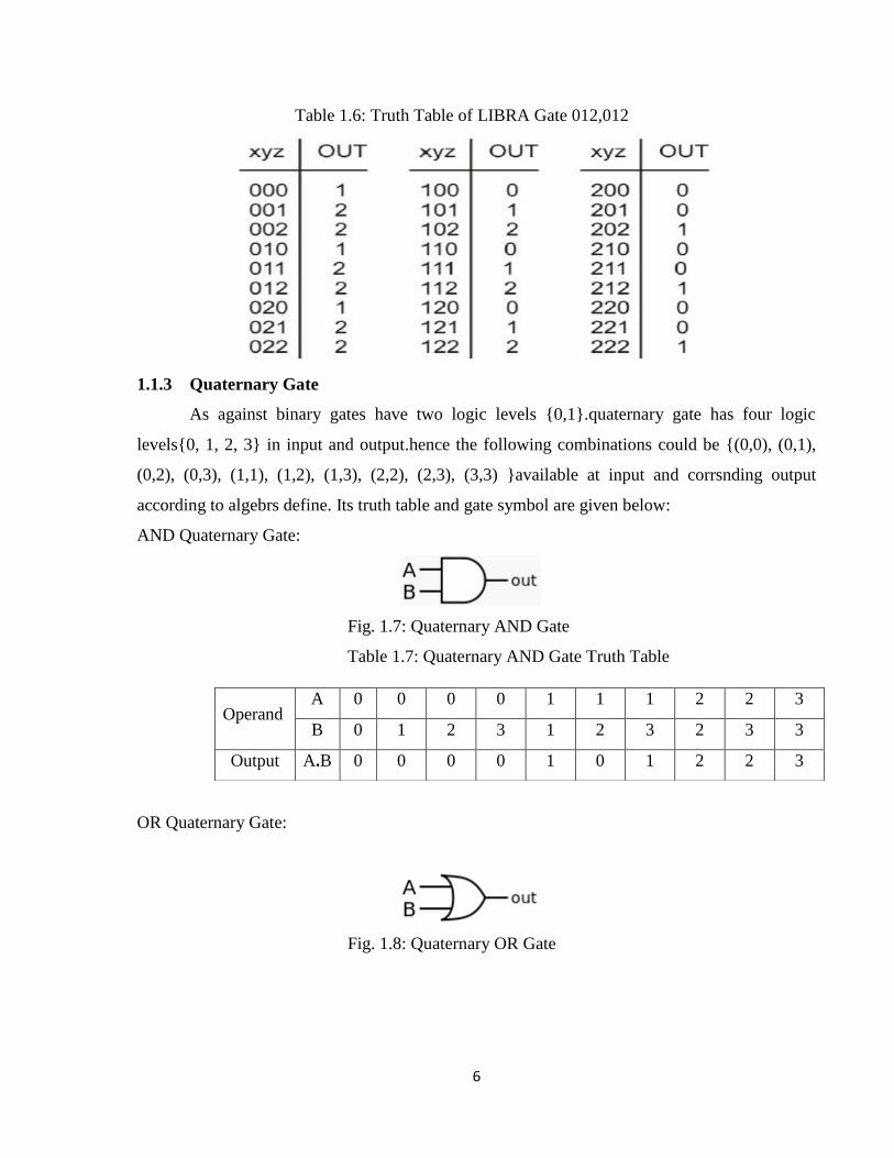
6
Table 1.6: Truth Table of LIBRA Gate 012,012
1.1.3 Quaternary Gate
As against binary gates have two logic levels {0,1}.quaternary gate has four logic
levels{0, 1, 2, 3} in input and output.hence the following combinations could be {(0,0), (0,1),
(0,2), (0,3), (1,1), (1,2), (1,3), (2,2), (2,3), (3,3) }available at input and corrsnding output
according to algebrs define. Its truth table and gate symbol are given below:
AND Quaternary Gate:
Fig. 1.7: Quaternary AND Gate
Table 1.7: Quaternary AND Gate Truth Table
OR Quaternary Gate:
Fig. 1.8: Quaternary OR Gate
Operand A 0 0 0 0 1 1 1 2 2 3
B 0 1 2 3 1 2 3 2 3 3
Output A.B 0 0 0 0 1 0 1 2 2 3
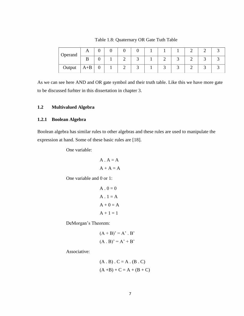
7
Table 1.8: Quaternary OR Gate Tuth Table
As we can see here AND and OR gate symbol and their truth table. Like this we have more gate
to be discussed furhter in this dissertation in chapter 3.
1.2 Multivalued Algebra
1.2.1 Boolean Algebra
Boolean algebra has similar rules to other algebras and these rules are used to manipulate the
expression at hand. Some of these basic rules are [18].
One variable:
A . A = A
A + A = A
One variable and 0 or 1:
A . 0 = 0
A . 1 = A
A + 0 = A
A + 1 = 1
DeMorgan’s Theorem:
(A + B)’ = A’ . B’
(A . B)’ = A’ + B’
Associative:
(A . B) . C = A . (B . C)
(A +B) + C = A + (B + C)
Operand A 0 0 0 0 1 1 1 2 2 3
B 0 1 2 3 1 2 3 2 3 3
Output A+B 0 1 2 3 1 3 3 2 3 3
8
Commutative:
A . B = B . A
A + B = B + A
Distributive:
A .(B + C) = A . B + A . C
A + (B . C) = (A + B) . (A + C)
1.2.2 Quaternary Algebra
In this section we will present fundamental properties of quaternary algebra. These
properties are helpful to express and manipulate complicated functions algebraically to ensure
efficient implementation. The packed-binary representation of quaternary digits and operators
show that all fundamental operators except the bitswap obey the axioms and properties of
Boolean operators. Most of these properties have their dual forms, where AND and OR
operators are interchanged, at the same time the constants are inverted via NOT. The properties
given below show that our proposed logic satisfies all the requirements to be algebra, as
suggested by Huntington [19].
1) Closure
For every dyadic operator, F (A, B){0, 1, 2, 3} , which is evident from definition. For every
unary operator, G (A){0, 1, 2, 3}.
2) Complement
There exists a unary operator NOT for which the following properties are true-
( ) A + A = a1 + a 1, a0 + a 0 >= <1, 1 >= 3
( ) A . A = a1 . a 1, a0 . a 0 > = <0, 0 >= 0
Like these it also has some other properties of associativity, commutativity, distributivity,
boundness. These properties would be discussed in detailed in further chapters 3.
9
1.3 Multivalued Conversion
As we have seen multivalued logic gates and their algebra are quite different ways for
each binary, Quaternary, and Ternary. But the conversion between them is not straight forward.
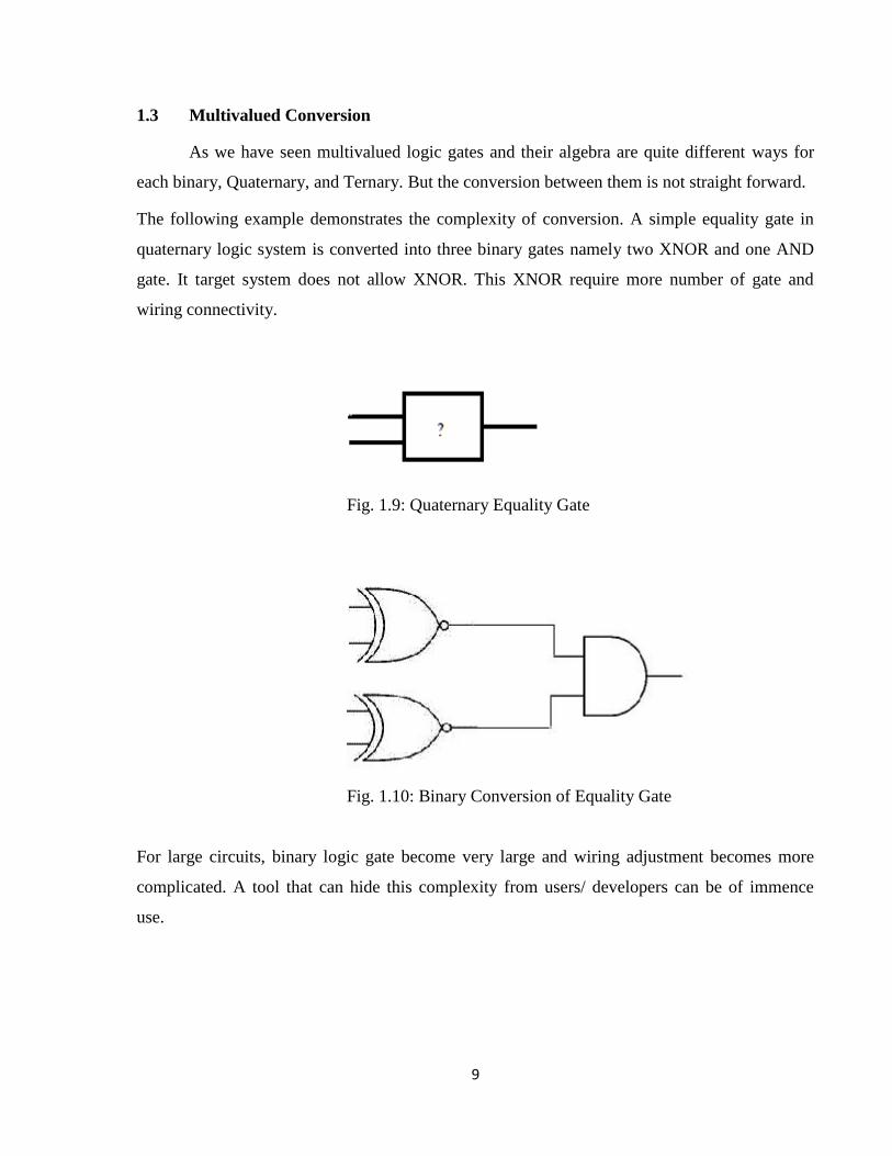
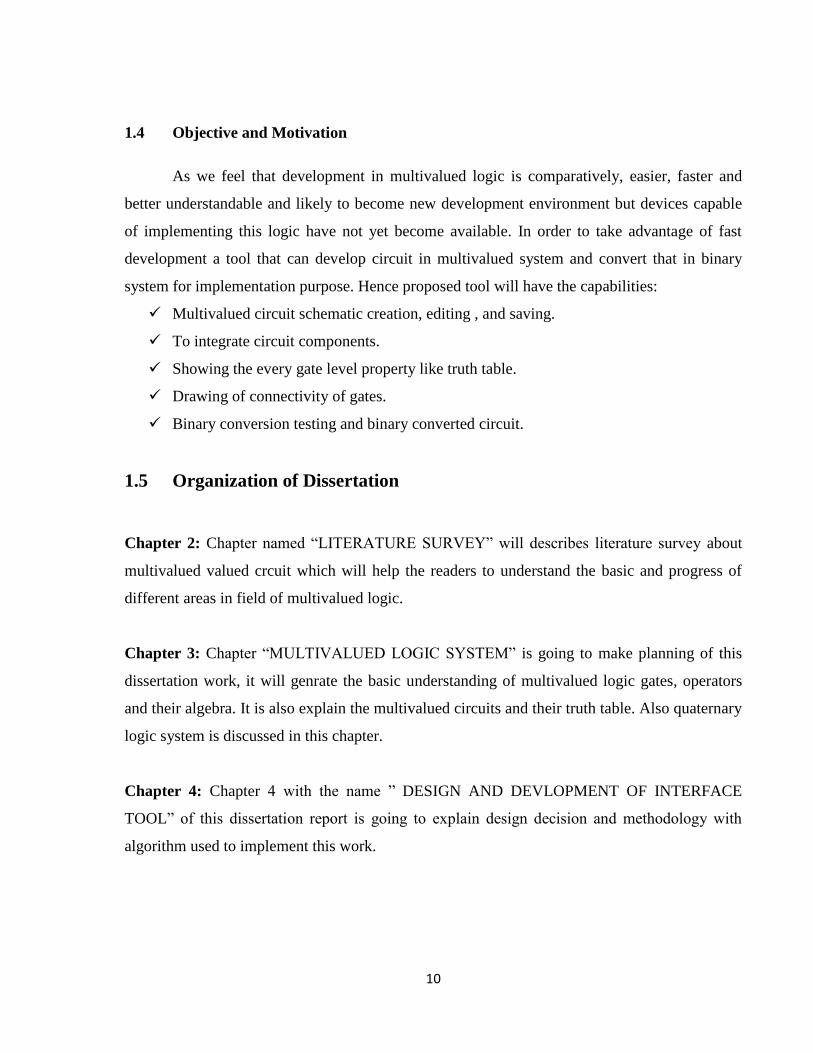
The following example demonstrates the complexity of conversion. A simple equality gate in
quaternary logic system is converted into three binary gates namely two XNOR and one AND
gate. It target system does not allow XNOR. This XNOR require more number of gate and
wiring connectivity.
Fig. 1.9: Quaternary Equality Gate
Fig. 1.10: Binary Conversion of Equality Gate
For large circuits, binary logic gate become very large and wiring adjustment becomes more
complicated. A tool that can hide this complexity from users/ developers can be of immence
use.
10
1.4 Objective and Motivation
As we feel that development in multivalued logic is comparatively, easier, faster and
better understandable and likely to become new development environment but devices capable
of implementing this logic have not yet become available. In order to take advantage of fast
development a tool that can develop circuit in multivalued system and convert that in binary
system for implementation purpose. Hence proposed tool will have the capabilities:
Multivalued circuit schematic creation, editing , and saving.
To integrate circuit components.
Showing the every gate level property like truth table.
Drawing of connectivity of gates.
Binary conversion testing and binary converted circuit.
1.5 Organization of Dissertation
Chapter 2: Chapter named “LITERATURE SURVEY” will describes literature survey about
multivalued valued crcuit which will help the readers to understand the basic and progress of
different areas in field of multivalued logic.
Chapter 3: Chapter “MULTIVALUED LOGIC SYSTEM” is going to make planning of this
dissertation work, it will genrate the basic understanding of multivalued logic gates, operators
and their algebra. It is also explain the multivalued circuits and their truth table. Also quaternary
logic system is discussed in this chapter.
Chapter 4: Chapter 4 with the name ” DESIGN AND DEVLOPMENT OF INTERFACE
TOOL” of this dissertation report is going to explain design decision and methodology with
algorithm used to implement this work.

11
Chapter 5: This chapter name “IMPLEMENTATION AND RESULTS ” is made for the
purpose of graphical representaion and testing results.
Chapter 6: Finally this dissertation work is concluded with giving ideas of future extension of
this dissertation work in this chapter with the name ” CONCLUSION AND FUTURE SCOPE”.
12
Chapter 2
LITERATURE SURVEY
As discussed earlier multivalued logic system is offering significant advantage like
compact and easy development of circuits. A number of researchers have been working for
evolution of multivalued logic system and complete algebra.
This chapter presents a survey of previous work in this area. The survey is organized in
two major categories namely; multivalued logic system and multivalued logic algebra. Of
course survey extension is given at the end of chapter.
2.1 Multivalued Logic System
Two logic systems namely ternary and quaternary have been developed and found in
literature. A generic format named Galois field is also reported by researchers. We categorized
our survey and these areas.
2.1.1 Ternary Logic System
Ternary logic system was reported in following literature: -
In 1990 X.W. Wu et al proposed CMOS compatible ternary logic based circuit and
analyzed its implementation and difficulties. They describe that multiple power sources will be
needed for multiple thresholds and a new theory of transmission function will be required [20].
In 2006 Xiaoqiang Shou, et al proposed a design methodology of latches with three
stable operating points. Open-loop analysis is used to obtain insight into how a conventional
binary latch structure can be modified to yield a ternary latch [21].
In 0 0 Ion Profeanu proposed “A Ternary Arithmetic and Logic”. This paper
introduces ternary arithmetic and logic [22].
13
In 2010 Kanchan S. Gorde proposed The PTI and NTI have been designed using an
inverter and pass-transistors at its output. The design of PTI and NTI is fully compatible with
current CMOS technology [23].
In 2011 Afolayan A. Obiniyi, Ezugwu E. Absalom, Kwanashie Adako proposed
“Arithmetic logic design with color coded ternary for ternary computing”. This paper introduces
a novel means of representing ternary states using color-codes, suggests a logic design model
for a ternary half adder circuit and separate carry circuits. A ternary simulator was also
developed to aid in the research and development of ternary systems [24].
In 2012 V.T.Gaikwad et al reviewed the development & advantages of ternary multi
valued logic system and its CMOS implementation [25].
2.1.2 Quaternary Circuit
Quaternary logic system was reported in following literature: -
In 000 “Takagi”, et al suggested an extension of regular ternary logic function to
function on discrete interval truth values. They presented this extension into quaternary valued
logic and its mathematical properties [26].
In 2000 again Files et al have proposed multivalued decision diagrams (MDDs) similar
to binary valued decision diagrams. For Boolean/multivalued input and output,
completely/incompletely specified functions with application to logic synthesis, machine
learning, data mining and knowledge discovery in databases [27].
In 2004 Khatri, et al proposed a PLA based Wire Removal techniques using SPFD
method (sets of pairs of functions to be distinguished) for binary and multivalued circuits [28].
In 2005, Bundalo, et al have proposed a Design method for quaternary multiple valued
combinational logic systems and circuits [29].
14
In 2010, Patel et al presented the design of a multiple-valued half adder and full adder
circuits that are implemented in Multiple-Valued voltage-Mode Logic (MV-VML) [30].
In 2010, Cristiano Lazzari et al proposed a new FPGA structure based on a low-power
quaternary voltage-mode device [31].
In 2010 Vasundara et al proposed a 4-bit counter using Multiple-valued D flip-flops and
the proposed circuit is shown to exhibit less power dissipation [32].
In 2010 Vasundara et al presented arithmetic operations like addition, subtraction and
multiplications in Modulo-4 arithmetic and in Galois field for the use in multi-valued logic
design [33].
In 2012 Sheng Lin et al proposed a new novel design of a ternary memory cell using
carbon nanotube field-effect transistors (CNTFETs) [34].
In 2012 Kumar et al studied the design, simulation of a CMOS quaternary logic
generator having a single stage CMOS body [35].
Ifat Jahangir et al proposed but yet unpublished a new Quaternary algebra for
implementing any quaternary circuit .In the paper a new minimal normal form for the
quaternary algebra is proposed and the conversion of the quaternary logic into the binary is also
stated [36].
2.1.3 Multivalued Logic
In 1993 D. Etiemble et al proposed a new algorithms for the sum of two (three and four)
digits in the Binary Stored-Carry number system by using the smallest set of values for the
positional sum. New adder is proposed using the same and the performance is evaluated against
normal circuit [37].
15
In 1999 Elena Dubrova presented an overview of recent developments in multiple-
valued logic circuit design, revealing both the opportunities they offer and the challenges they
face [38].
In 1999 Brayton et al survey some of the methods used for manipulating, representing,
and optimizing multi-valued logic with the view of both building a better understanding of the
more specialized binary-valued logic, as well as motivating re-search towards a true multi-
valued multi-level optimization package [39].
In 2000 Muthukrishnan et al, developed a multi-valued logic for quantum computing for
use in multi-level quantum systems, and discuss the practical advantages of this approach for
scaling up a quantum computer. The paper also generalizes the methods of binary quantum logic
[40].
In 2004 A. Morgül et al proposed a new current-mode CMOS restoration circuit to
restore or recover the nominal levels of the signal after a certain number of cascaded stages and
the same is evaluated [41].
In 2011 Dhabhai et al performed the node reduction, area reduction and delay reduction
by AIG rewriting [42].
2.2 Survey Extraction
In the above literature survey it is observed that multivalued circuits offer a great
advantage over binary valued circuit in design size, effort and time. But implementation plat
form available is only binary.
Amongst the multivalued logic systems, quaternary logic system is well defined and
offer significant advantage and design ease compared to others but in order to achieve
compatibility with existing binary system (for implementation), an interfacing tool is necessary.
In this project, we undertake development of such tool name “MVL-DEV”. Subsequent chapters
describe multivalued logic system and development of such tool.
16
Chapter 3
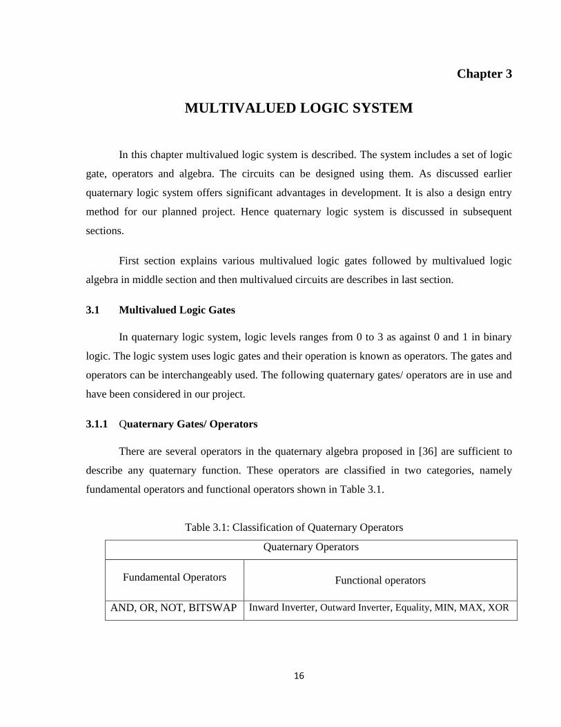
MULTIVALUED LOGIC SYSTEM
In this chapter multivalued logic system is described. The system includes a set of logic
gate, operators and algebra. The circuits can be designed using them. As discussed earlier
quaternary logic system offers significant advantages in development. It is also a design entry
method for our planned project. Hence quaternary logic system is discussed in subsequent
sections.
First section explains various multivalued logic gates followed by multivalued logic
algebra in middle section and then multivalued circuits are describes in last section.
3.1 Multivalued Logic Gates
In quaternary logic system, logic levels ranges from 0 to 3 as against 0 and 1 in binary
logic. The logic system uses logic gates and their operation is known as operators. The gates and
operators can be interchangeably used. The following quaternary gates/ operators are in use and
have been considered in our project.
3.1.1 Quaternary Gates/ Operators
There are several operators in the quaternary algebra proposed in [36] are sufficient to
describe any quaternary function. These operators are classified in two categories, namely
fundamental operators and functional operators shown in Table 3.1.
Table 3.1: Classification of Quaternary Operators
Quaternary Operators
Fundamental Operators Functional operators
AND, OR, NOT, BITSWAP Inward Inverter, Outward Inverter, Equality, MIN, MAX, XOR
17
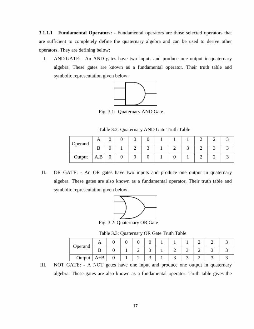
3.1.1.1 Fundamental Operators: - Fundamental operators are those selected operators that
are sufficient to completely define the quaternary algebra and can be used to derive other
operators. They are defining below:
I. AND GATE: - An AND gates have two inputs and produce one output in quaternary
algebra. These gates are known as a fundamental operator. Their truth table and
symbolic representation given below.
Fig. 3.1: Quaternary AND Gate
Table 3.2: Quaternary AND Gate Truth Table
II. OR GATE: - An OR gates have two inputs and produce one output in quaternary
algebra. These gates are also known as a fundamental operator. Their truth table and
symbolic representation given below.
Fig. 3.2: Quaternary OR Gate
Table 3.3: Quaternary OR Gate Truth Table
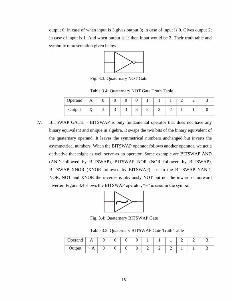
III. NOT GATE: - A NOT gates have one input and produce one output in quaternary
algebra. These gates are also known as a fundamental operator. Truth table gives the
Operand A 0 0 0 0 1 1 1 2 2 3
B 0 1 2 3 1 2 3 2 3 3
Output A.B 0 0 0 0 1 0 1 2 2 3
Operand A 0 0 0 0 1 1 1 2 2 3
B 0 1 2 3 1 2 3 2 3 3
Output A+B 0 1 2 3 1 3 3 2 3 3
18
output 0; in case of when input is 3.gives output 3; in case of input is 0. Gives output 2;
in case of input is 1. And when output is 1; then input would be 2. Their truth table and
symbolic representation given below.
Fig. 3.3: Quaternary NOT Gate
Table 3.4: Quaternary NOT Gate Truth Table
IV. BITSWAP GATE: - BITSWAP is only fundamental operator that does not have any
binary equivalent and unique in algebra. It swaps the two bits of the binary equivalent of
the quaternary operand. It leaves the symmetrical numbers unchanged but inverts the
asymmetrical numbers. When the BITSWAP operator follows another operator, we get a
derivative that might as well serve as an operator. Some example are BITSWAP AND
(AND followed by BITSWAP), BITSWAP NOR (NOR followed by BITSWAP),
BITSWAP XNOR (XNOR followed by BITSWAP) etc. In the BITSWAP NAND,
NOR, NOT and XNOR the inverter is obviously NOT but not the inward or outward
inverter. Figure 3.4 shows the BITSWAP operator, “~” is used in the symbol.
Fig. 3.4: Quaternary BITSWAP Gate
Table 3.5: Quaternary BITSWAP Gate Truth Table
Operand A 0 0 0 0 1 1 1 2 2 3
Output A 3 3 3 3 2 2 2 1 1 0
Operand A 0 0 0 0 1 1 1 2 2 3
Output ~ A 0 0 0 0 2 2 2 1 1 3
19
3.1.1.2 Functional operators: - The functional operators are those operators that are described
as the combination of two or more fundamental operators. It will be shown later that functional
operators can also be used to express any arbitrary quaternary function [36]. Table 3.1 describes
the operators as per this classification.
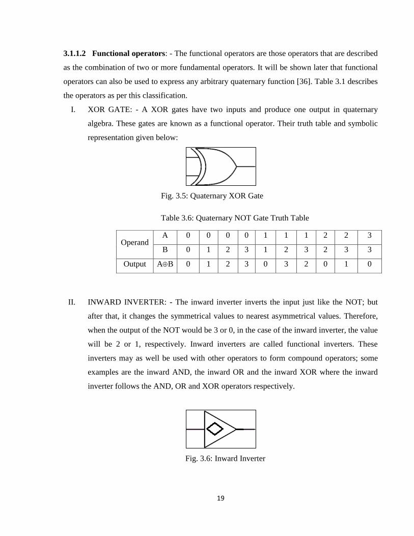
I. XOR GATE: - A XOR gates have two inputs and produce one output in quaternary
algebra. These gates are known as a functional operator. Their truth table and symbolic
representation given below:
Fig. 3.5: Quaternary XOR Gate
Table 3.6: Quaternary NOT Gate Truth Table
II. INWARD INVERTER: - The inward inverter inverts the input just like the NOT; but
after that, it changes the symmetrical values to nearest asymmetrical values. Therefore,
when the output of the NOT would be 3 or 0, in the case of the inward inverter, the value
will be 2 or 1, respectively. Inward inverters are called functional inverters. These
inverters may as well be used with other operators to form compound operators; some
examples are the inward AND, the inward OR and the inward XOR where the inward
inverter follows the AND, OR and XOR operators respectively.
Fig. 3.6: Inward Inverter
Operand A 0 0 0 0 1 1 1 2 2 3
B 0 1 2 3 1 2 3 2 3 3
Output AB 0 1 2 3 0 3 2 0 1 0
20
Table 3.7: Inward Inverter Truth Table
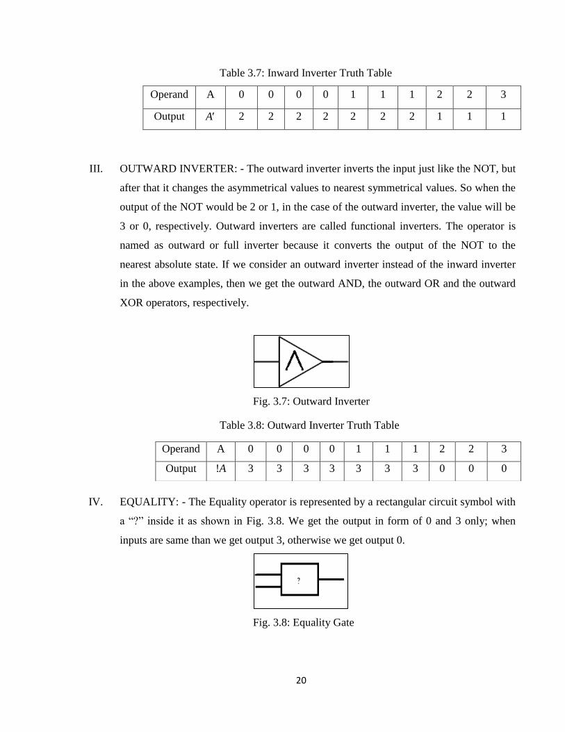
III. OUTWARD INVERTER: - The outward inverter inverts the input just like the NOT, but
after that it changes the asymmetrical values to nearest symmetrical values. So when the
output of the NOT would be 2 or 1, in the case of the outward inverter, the value will be
3 or 0, respectively. Outward inverters are called functional inverters. The operator is
named as outward or full inverter because it converts the output of the NOT to the
nearest absolute state. If we consider an outward inverter instead of the inward inverter
in the above examples, then we get the outward AND, the outward OR and the outward
XOR operators, respectively.
Fig. 3.7: Outward Inverter
Table 3.8: Outward Inverter Truth Table
IV. EQUALITY: - The Equality operator is represented by a rectangular circuit symbol with
a “?” inside it as shown in Fig. 3.8. We get the output in form of 0 and 3 only; when
inputs are same than we get output 3, otherwise we get output 0.
Fig. 3.8: Equality Gate
Operand A 0 0 0 0 1 1 1 2 2 3
Output A 2 2 2 2 2 2 2 1 1 1
Operand A 0 0 0 0 1 1 1 2 2 3
Output !A 3 3 3 3 3 3 3 0 0 0
21
Table 3.9: Equality Gate Truth Table
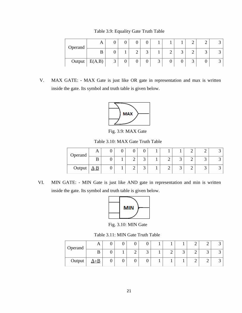
V. MAX GATE: - MAX Gate is just like OR gate in representation and max is written
inside the gate. Its symbol and truth table is given below.
Fig. 3.9: MAX Gate
Table 3.10: MAX Gate Truth Table
VI. MIN GATE: - MIN Gate is just like AND gate in representation and min is written
inside the gate. Its symbol and truth table is given below.
Fig. 3.10: MIN Gate
Table 3.11: MIN Gate Truth Table
Operand A 0 0 0 0 1 1 1 2 2 3
B 0 1 2 3 1 2 3 2 3 3
Output E(AB) 3 0 0 0 3 0 0 3 0 3
Operand A 0 0 0 0 1 1 1 2 2 3
B 0 1 2 3 1 2 3 2 3 3
Output A B 0 1 2 3 1 2 3 2 3 3
Operand A 0 0 0 0 1 1 1 2 2 3
B 0 1 2 3 1 2 3 2 3 3
Output A B 0 0 0 0 1 1 1 2 2 3
22
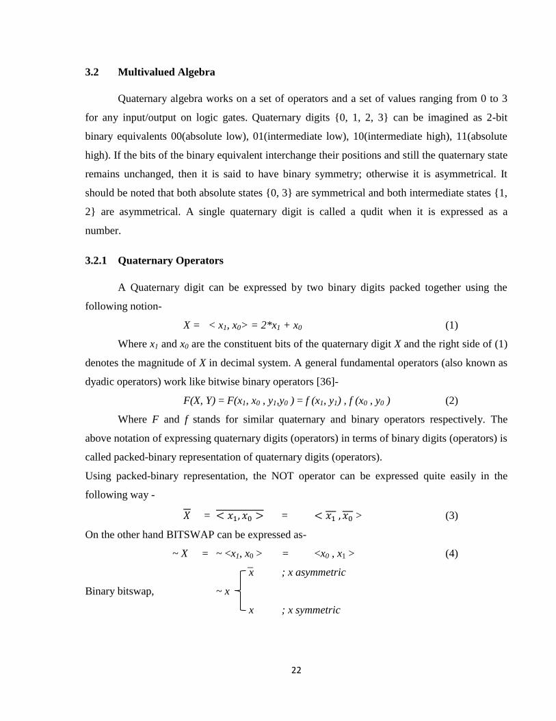
3.2 Multivalued Algebra
Quaternary algebra works on a set of operators and a set of values ranging from 0 to 3
for any input/output on logic gates. Quaternary digits {0, 1, 2, 3} can be imagined as 2-bit
binary equivalents 00(absolute low), 01(intermediate low), 10(intermediate high), 11(absolute
high). If the bits of the binary equivalent interchange their positions and still the quaternary state
remains unchanged, then it is said to have binary symmetry; otherwise it is asymmetrical. It
should be noted that both absolute states {0, 3} are symmetrical and both intermediate states {1,
2} are asymmetrical. A single quaternary digit is called a qudit when it is expressed as a
number.
3.2.1 Quaternary Operators
A Quaternary digit can be expressed by two binary digits packed together using the
following notion-
X = < x1, x0> = 2*x1 + x0 (1)
Where x1 and x0 are the constituent bits of the quaternary digit X and the right side of (1)
denotes the magnitude of X in decimal system. A general fundamental operators (also known as
dyadic operators) work like bitwise binary operators [36]-
F(X, Y) = F(x1, x0 , y1,y0 ) = f (x1, y1) , f (x0 , y0 ) (2)
Where F and f stands for similar quaternary and binary operators respectively. The
above notation of expressing quaternary digits (operators) in terms of binary digits (operators) is
called packed-binary representation of quaternary digits (operators).
Using packed-binary representation, the NOT operator can be expressed quite easily in the
following way -
= = > (3)
On the other hand BITSWAP can be expressed as-
~ X = ~ <x1, x0 > = <x0 , x1 > (4)
x ; x asymmetric
Binary bitswap, ~ x
x ; x symmetric
23
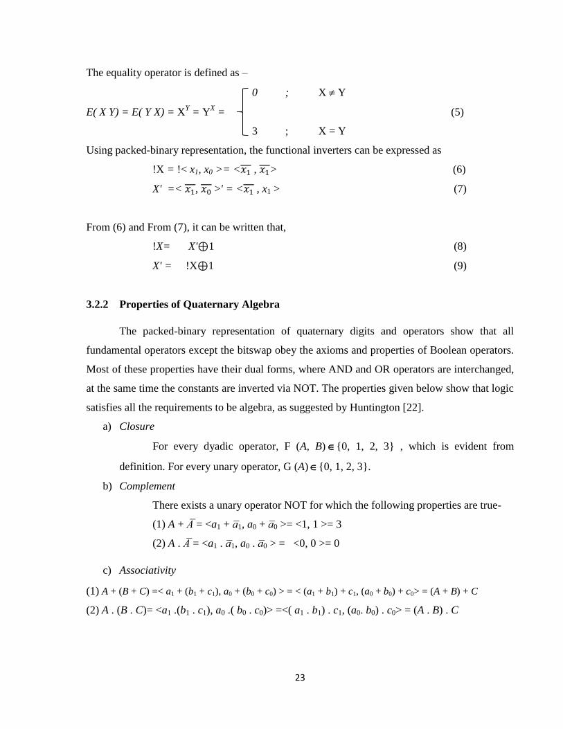
The equality operator is defined as –
0 ; X Y
E( X Y) = E( Y X) = XY = Y
X = (5)
3 ; X = Y
Using packed-binary representation, the functional inverters can be expressed as
!X = !< x1, x0 >= < , > (6)
X' =< , >' = < , x1 > (7)
From (6) and From (7), it can be written that,
!X= X'⊕1 (8)
X' = !X⊕1 (9)
3.2.2 Properties of Quaternary Algebra
The packed-binary representation of quaternary digits and operators show that all
fundamental operators except the bitswap obey the axioms and properties of Boolean operators.
Most of these properties have their dual forms, where AND and OR operators are interchanged,
at the same time the constants are inverted via NOT. The properties given below show that logic
satisfies all the requirements to be algebra, as suggested by Huntington [22].
a) Closure
For every dyadic operator, F (A, B){0, 1, 2, 3} , which is evident from
definition. For every unary operator, G (A){0, 1, 2, 3}.
b) Complement
There exists a unary operator NOT for which the following properties are true-
(1) A + = <a1 + 1, a0 + 0 >= <1, 1 >= 3
(2) A . = <a1 . 1, a0 . 0 > = <0, 0 >= 0
c) Associativity
(1) A + (B + C) =< a1 + (b1 + c1), a0 + (b0 + c0) > = < (a1 + b1) + c1, (a0 + b0) + c0> = (A + B) + C
(2) A . (B . C)= <a1 .(b1 . c1), a0 .( b0 . c0)> =<( a1 . b1) . c1, (a0. b0) . c0> = (A . B) . C
24
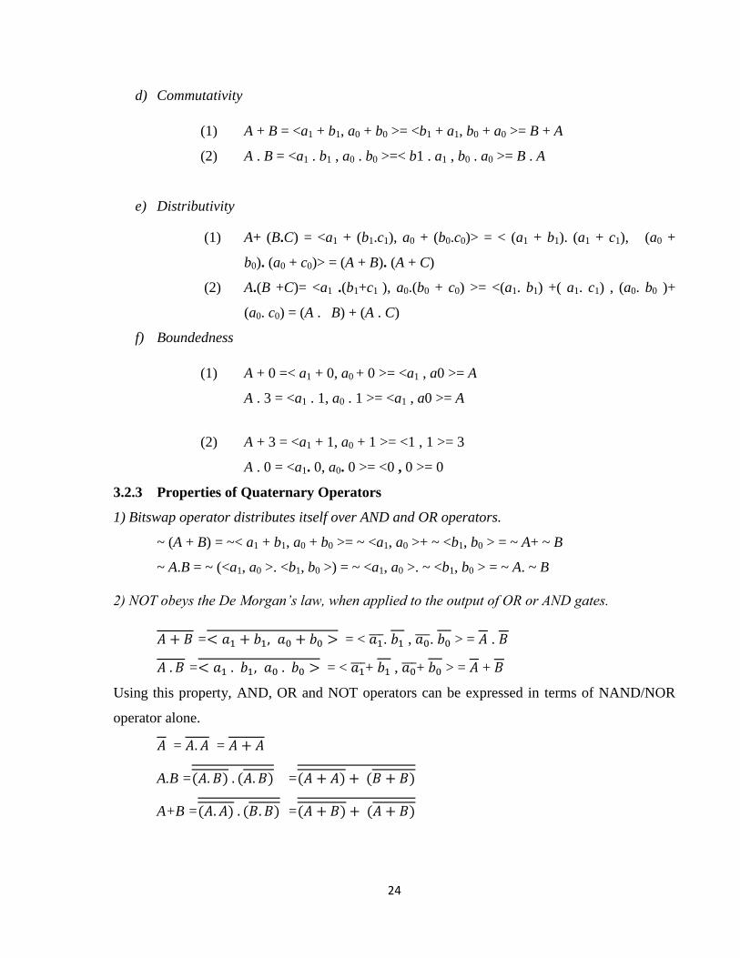
d) Commutativity
(1) A + B = <a1 + b1, a0 + b0 >= <b1 + a1, b0 + a0 >= B + A
(2) A . B = <a1 . b1 , a0 . b0 >=< b1 . a1 , b0 . a0 >= B . A
e) Distributivity
(1) A+ (B.C) = <a1 + (b1.c1), a0 + (b0.c0)> = < (a1 + b1). (a1 + c1), (a0 +
b0). (a0 + c0)> = (A + B). (A + C)
(2) A.(B +C)= <a1 .(b1+c1 ), a0.(b0 + c0) >= <(a1. b1) +( a1. c1) , (a0. b0 )+
(a0. c0) = (A . B) + (A . C)
f) Boundedness
(1) A + 0 =< a1 + 0, a0 + 0 >= <a1 , a0 >= A
A . 3 = <a1 . 1, a0 . 1 >= <a1 , a0 >= A
(2) A + 3 = <a1 + 1, a0 + 1 >= <1 , 1 >= 3
A . 0 = <a1. 0, a0. 0 >= <0 , 0 >= 0
3.2.3 Properties of Quaternary Operators
1) Bitswap operator distributes itself over AND and OR operators.
~ (A + B) = ~< a1 + b1, a0 + b0 >= ~ <a1, a0 >+ ~ <b1, b0 > = ~ A+ ~ B
~ A.B = ~ (<a1, a0 >. <b1, b0 >) = ~ <a1, a0 >. ~ <b1, b0 > = ~ A. ~ B
2) NOT obeys the De Morg n’s l w, when pplied to the output of OR or ND g tes.
= = < ̅̅ ̅. , ̅̅ ̅. > = .
= = < ̅̅ ̅+ , ̅̅ ̅+ > = +
Using this property, AND, OR and NOT operators can be expressed in terms of NAND/NOR
operator alone.
= =
A.B = =
A+B = =
25
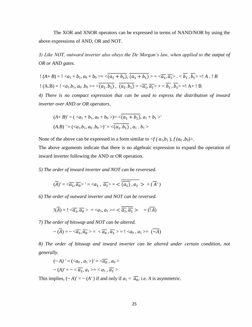
The XOR and XNOR operators can be expressed in terms of NAND/NOR by using the
above expressions of AND, OR and NOT.
3) Like NOT, outw rd inverter lso obeys the De Morg n’s l w, when pplied to the output of
OR or AND gates.
! (A+ B) = ! <a1 + b1, a0 + b0 >= < , > = < > . < > =! A . ! B
! (A.B) = ! <a1.b1, a0 .b0 >= < = < > + < > =! A+ ! B
4) There is no compact expression that can be used to express the distribution of inward
inverter over AND or OR operators.
(A+ B)' = ( <a1 + b1, a0 + b0 >)= < , a1 + b1 >'
(A.B) ' = (<a1.b1, a0 .b0 >)' = < , a1 . b1 >
None of the above can be expressed in a form similar to <f ( a1,b1 ), f (a0 ,b0)>.
The above arguments indicate that there is no algebraic expression to expand the operation of
inward inverter following the AND or OR operation.
5) The order of inward inverter and NOT can be reveresed.
( )' = < > ' = < > = = ( ' )
6) The order of outward inverter and NOT can be reversed.
!( ) = ! < > = <a1, a1 >= = ( )
7) The order of bitswap and NOT can be altered.
~ ( ) = ~ < > = < > = ! <a0 , a1 >= ( )
8) The order of bitswap and inward inverter can be altered under certain condition, not
generally.
(~ A) ' = (<a0 , a1 >)' = < , a0 >
~ (A)' = ~ < , a1 >= < a1 , >
This implies, (~ A)' = ~ (A' ) if and only if a1 = , i.e. A is asymmetric.
26
9) The order of bitswap and outward inverter can be altered under certain condition, not
generally.
~(! A) = ~< > = < >
! (~ A) = !< a0 , a1 >=< >
This implies, ~ (! A) =! (~ A) if and only if a1 =a0 , i.e. A is symmetric.
10) The order of inward and outward inverters can never be reversed under any condition.
(!A) ' = (< >) ' = <a1 >
!( A' ) = !< , a1 > = < a1, a1 >
This implies, (! A)' ! (A' ) under any circumstances.
3.2.4 Theorems of Quaternary Algebra
There are several theorems in quaternary algebra that are derived from the fundamental
postulates of the algebra and properties of the operators. Here we present a list of theorems that
are useful in algebraic operations –
1) The Law of Idempotency:
X + X = X, X . X = X
2) The Law of Absorption:
X + (X . Y) = X , X . (X + Y) = X
3) The Law of Identity:
X + Y = X , X . Y = X ; for X = Y
4) The Law of Complements with NOT:
X + Y = 3 , X . Y = 0 ; for X =
5) The Law of Involution with NOT and bitswap:
X = X , X = ~ (~ X)
6) The Law of Elimination with NOT:
X + .Y = X +Y , X.( + Y )= X.Y
7) The Law of Concensus with NOT:
X.Y + .Z +Y.Z = X.Y + .Z
(X +Y ).( + Z ).(Y + Z ) =(X +Y ). + Z )
27
8) The Law of Interchange with NOT:
(X.Y )+ ( .Z)=(X +Y ) .( + Z)
(X +Y ) .( + Z)=(X. Z ) +( . Y )
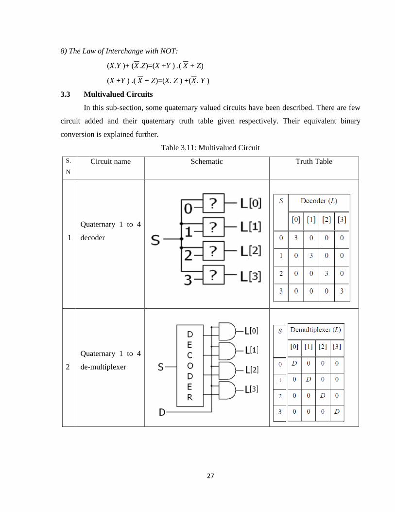
3.3 Multivalued Circuits
In this sub-section, some quaternary valued circuits have been described. There are few
circuit added and their quaternary truth table given respectively. Their equivalent binary
conversion is explained further.
Table 3.11: Multivalued Circuit
S.
N
Circuit name Schematic Truth Table
1
Quaternary 1 to 4
decoder
2
Quaternary 1 to 4
de-multiplexer
28
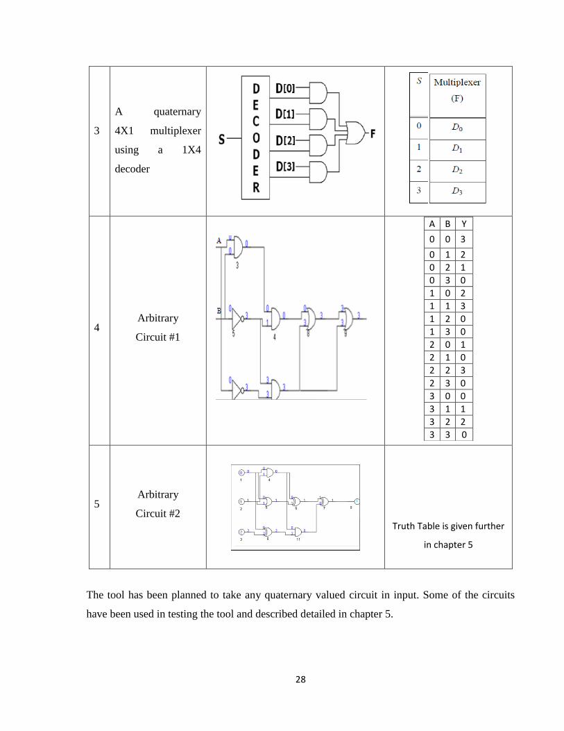
3
A quaternary
4X1 multiplexer
using a 1X4
decoder
4 Arbitrary
Circuit #1
A B Y
0 0 3
0 1 2
0 2 1
0 3 0
1 0 2
1 1 3
1 2 0
1 3 0
2 0 1
2 1 0
2 2 3
2 3 0
3 0 0
3 1 1
3 2 2
3 3 0
5 Arbitrary
Circuit #2
Truth Table is given further
in chapter 5
The tool has been planned to take any quaternary valued circuit in input. Some of the circuits
have been used in testing the tool and described detailed in chapter 5.
29
Chapter 4
DESIGN AND DEVLOPMENT OF INTERFACE TOOL
This chapter describes design and development of logic design entry tool named ―MVL
DEV‖. Objective of this tool is to capture multivalued logic based design and work as a plugin
for binary value system.
The tool will provide multivalued circuit development environment. This chapter is
going to explain Design flow, GUI Design and conversion algorithm. This tool will be discussed
in subsequent sections.
4.1 Design Flow
In order to obtain binary logic based circuit, there are two approaches considered for
conversion. Design flow of both is described in fig 4.1 (a) and 4.1 (b).
A former approach is based on schematic design entry, followed by replacement based
conversion. Whereas later approach converts at truth table level and synthesize binary valued
circuit from truth table.
Replacement based conversion of the circuit starts replacing circuit components from
beginning and continues replacement till end. The algorithm then optimizes the circuit wherever
required and setup connections within binary system.
Later approach converts the circuit in quaternary truth table and then converts into
binary truth table. Using logic synthesis process, binary circuits can be drawn.
Former approach can be helpful in incremental design but later cannot be used till full
design is complete. Hence we have considered former approach in our development.
30
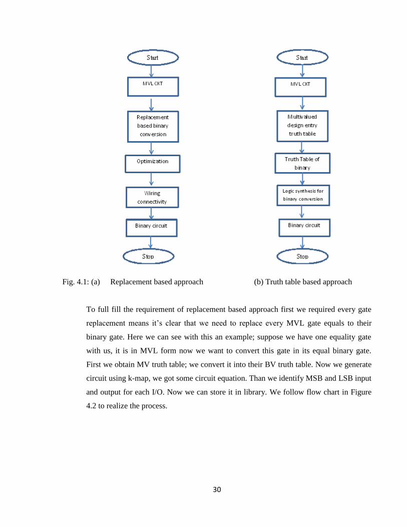
Fig. 4.1: (a) Replacement based approach (b) Truth table based approach
To full fill the requirement of replacement based approach first we required every gate
replacement means it’s clear that we need to replace every MVL gate equals to their
binary gate. Here we can see with this an example; suppose we have one equality gate
with us, it is in MVL form now we want to convert this gate in its equal binary gate.
First we obtain MV truth table; we convert it into their BV truth table. Now we generate
circuit using k-map, we got some circuit equation. Than we identify MSB and LSB input
and output for each I/O. Now we can store it in library. We follow flow chart in Figure
4.2 to realize the process.
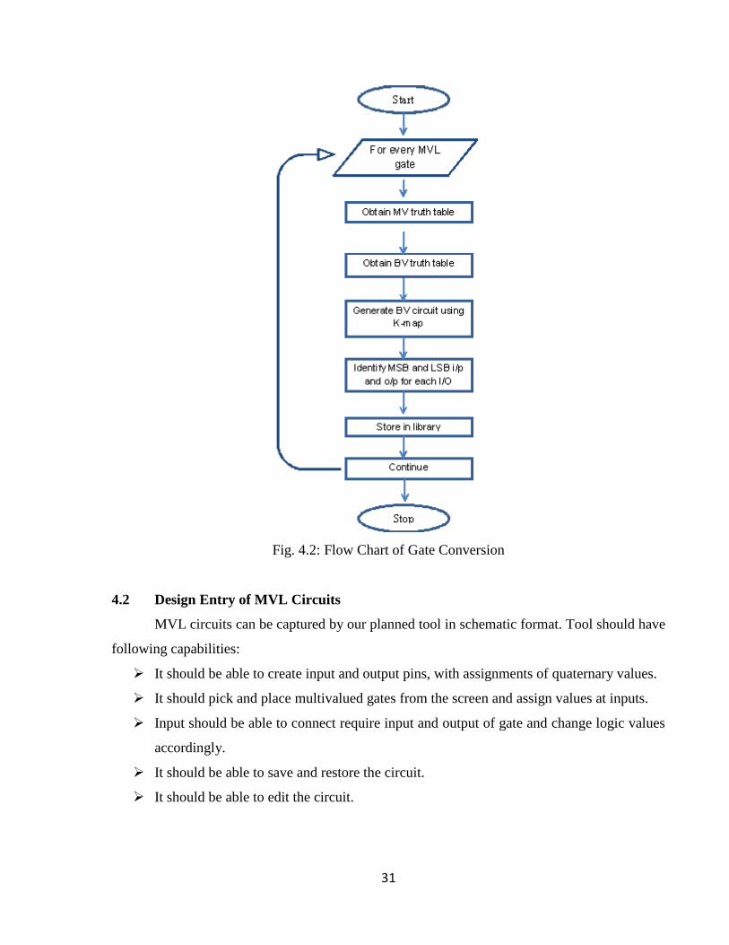
31
Fig. 4.2: Flow Chart of Gate Conversion
4.2 Design Entry of MVL Circuits
MVL circuits can be captured by our planned tool in schematic format. Tool should have
following capabilities:
It should be able to create input and output pins, with assignments of quaternary values.
It should pick and place multivalued gates from the screen and assign values at inputs.
Input should be able to connect require input and output of gate and change logic values
accordingly.
It should be able to save and restore the circuit.
It should be able to edit the circuit.
32
It should be able to display truth table of any gate.
It should be able to convert and display binary circuit schematic.
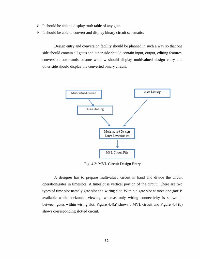
Design entry and conversion facility should be planned in such a way so that one
side should contain all gates and other side should contain input, output, editing features,
conversion commands etc.one window should display multivalued design entry and
other side should display the converted binary circuit.
Fig. 4.3: MVL Circuit Design Entry
A designer has to prepare multivalued circuit in hand and divide the circuit
operation/gates in timeslots. A timeslot is vertical portion of the circuit. There are two
types of time slot namely gate slot and wiring slot. Within a gate slot at most one gate is
available while horizontal viewing, whereas only wiring connectivity is shown in
between gates within wiring slot. Figure 4.4(a) shows a MVL circuit and Figure 4.4 (b)
shows corresponding slotted circuit.
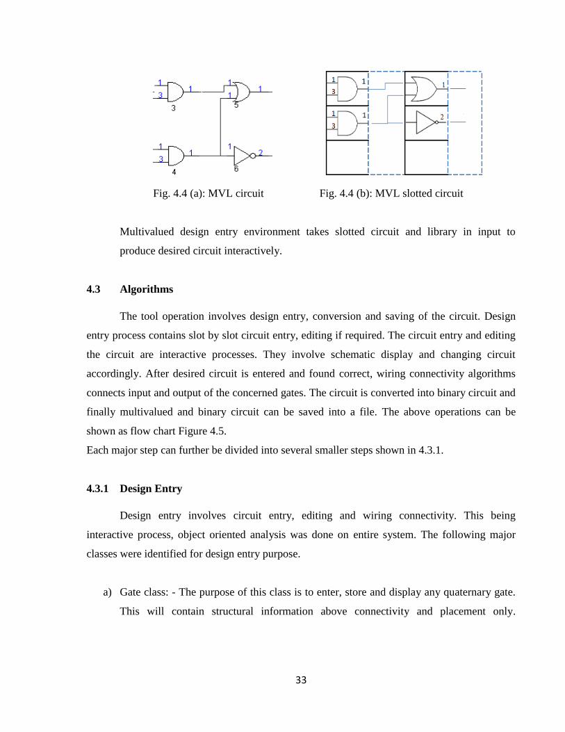
33
Fig. 4.4 (a): MVL circuit Fig. 4.4 (b): MVL slotted circuit
Multivalued design entry environment takes slotted circuit and library in input to
produce desired circuit interactively.
4.3 Algorithms
The tool operation involves design entry, conversion and saving of the circuit. Design
entry process contains slot by slot circuit entry, editing if required. The circuit entry and editing
the circuit are interactive processes. They involve schematic display and changing circuit
accordingly. After desired circuit is entered and found correct, wiring connectivity algorithms
connects input and output of the concerned gates. The circuit is converted into binary circuit and
finally multivalued and binary circuit can be saved into a file. The above operations can be
shown as flow chart Figure 4.5.
Each major step can further be divided into several smaller steps shown in 4.3.1.
4.3.1 Design Entry
Design entry involves circuit entry, editing and wiring connectivity. This being
interactive process, object oriented analysis was done on entire system. The following major
classes were identified for design entry purpose.
a) Gate class: - The purpose of this class is to enter, store and display any quaternary gate.
This will contain structural information above connectivity and placement only.
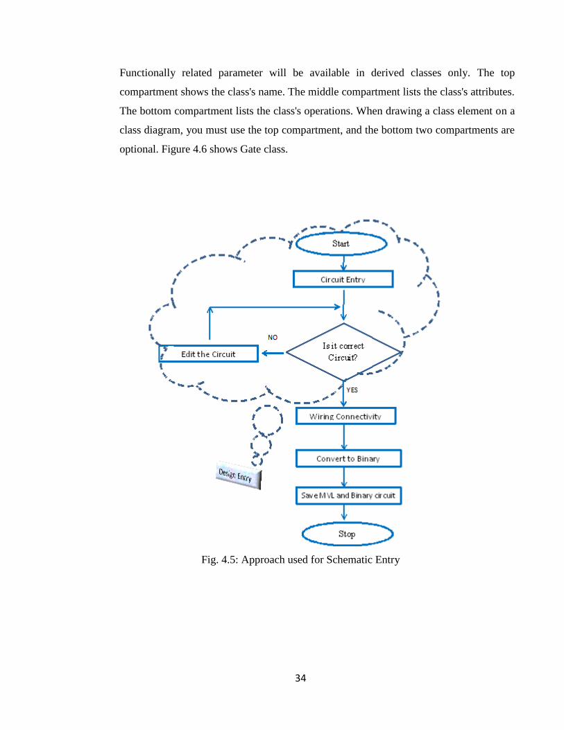
34
Functionally related parameter will be available in derived classes only. The top
compartment shows the class's name. The middle compartment lists the class's attributes.
The bottom compartment lists the class's operations. When drawing a class element on a
class diagram, you must use the top compartment, and the bottom two compartments are
optional. Figure 4.6 shows Gate class.
Fig. 4.5: Approach used for Schematic Entry
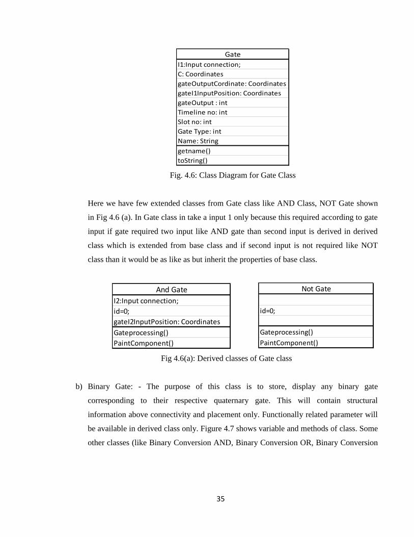
35
Fig. 4.6: Class Diagram for Gate Class
Here we have few extended classes from Gate class like AND Class, NOT Gate shown
in Fig 4.6 (a). In Gate class in take a input 1 only because this required according to gate
input if gate required two input like AND gate than second input is derived in derived
class which is extended from base class and if second input is not required like NOT
class than it would be as like as but inherit the properties of base class.
Fig 4.6(a): Derived classes of Gate class
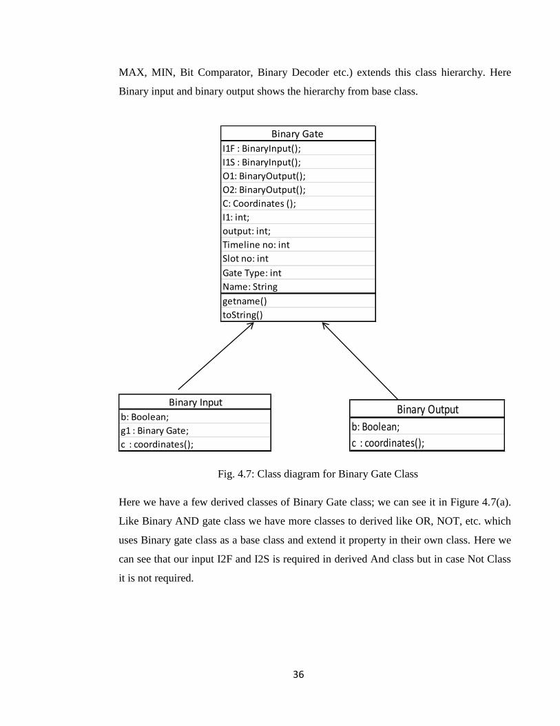
b) Binary Gate: - The purpose of this class is to store, display any binary gate
corresponding to their respective quaternary gate. This will contain structural
information above connectivity and placement only. Functionally related parameter will
be available in derived class only. Figure 4.7 shows variable and methods of class. Some
other classes (like Binary Conversion AND, Binary Conversion OR, Binary Conversion
Gate
I1:Input connection;
C: Coordinates
gateOutputCordinate: Coordinates
gateI1InputPosition: Coordinates
gateOutput : int
Timeline no: int
Slot no: int
Gate Type: int
Name: String
getname()
toString()
And Gate
I2:Input connection;
id=0;
gateI2InputPosition: Coordinates
Gateprocessing()
PaintComponent()
Not Gate
id=0;
Gateprocessing()
PaintComponent()
36
MAX, MIN, Bit Comparator, Binary Decoder etc.) extends this class hierarchy. Here
Binary input and binary output shows the hierarchy from base class.
Fig. 4.7: Class diagram for Binary Gate Class
Here we have a few derived classes of Binary Gate class; we can see it in Figure 4.7(a).
Like Binary AND gate class we have more classes to derived like OR, NOT, etc. which
uses Binary gate class as a base class and extend it property in their own class. Here we
can see that our input I2F and I2S is required in derived And class but in case Not Class
it is not required.
Binary Gate
I1F : BinaryInput();
I1S : BinaryInput();
O1: BinaryOutput();
O2: BinaryOutput();
C: Coordinates ();
I1: int;
output: int;
Timeline no: int
Slot no: int
Gate Type: int
Name: String
getname()
toString()
Binary Input
b: Boolean;
g1 : Binary Gate;
c : coordinates();
Binary Output
b: Boolean;
c : coordinates();
37
Fig 4.7 (a): Derived Class from Binary Gate Class
c) Coordinates: - The purpose of this class to store the coordinates on x axis and y axis. Fig.
4.8 shows variable of class. This class calls the coordinate and set parameters.
Fig. 4.8: Class Diagram for Coordinates Class
d) Gate List: - The purpose of this class to store gate, add gate, clear gate, remove and
reconnect gate in vector data structure. This is also a part of super class. Fig. 4.9 shows
variable and methods of class.
Binary And Gate
I2F : BinaryInput();
I2S : BinaryInput();
id=0: int
x: int
y: int
I2: int
a1: String
a0: String
out1: String
out0: String
b1, b0: String
Gateprocessing()
PaintComponent()
Binary Not Gate
id=0: int
x: int
y: int
a1: String
a0: String
out1: String
out0: String
b1, b0: String
Gateprocessing()
PaintComponent()
Coordinates
X: int
Y: int
38
Fig. 4.9: Class diagram for Gate List Class
e) Wiring: - The purpose of this class to provide connectivity of wire between gates in diag.
Fig. 4.10 shows variable and methods of class.
Fig. 4.10: class diagram for Wire Class
f) Circuit Line Coordinates: - The purpose of the circuit line coordinates class is to take
input, output and difference of gates and to set their references between gates. Figure
4.11 shows variable and methods of class.
Fig. 4.11: Class Diagram for Circuit Line Coordinates
Once the classes have been identified, a GUI has been prepared to pick and place the
gates and input objects. While placing the inputs property panels require input value for input
type object and input connection for gate type object and this will be store as a parameter in
appropriate class. There is algorithm which shows the design entry steps.
GateList
gates : vector;
GateList()
AddGate()
Size(): int
clear(): void
remove(): void
get() : Gate
reconnect() : void
Wire
Panel No: int
toString(): String
getName(): String
Circuit Line Coordinates
input: coordinates()
ouput: coordinates()
difference: coordinates()

39
Algorithm 4.1: Design Entry Algorithm
INPUT: MVL Circuit
OUTPUT: BVL Circuit
// MVL circuits are divided in time slots (TL) such that TL=0 input, TL=1 wiring, TL=2 gate,
TL=3 wiring and last slot output.
// Schematic area is divided slot wise.
1. Initialize GUI and display
2. Initialize circuit array list
// circuit array list contain gateItems (gate, inpin, outpin, and its parameter)
3. Read mouse click and event source
4. Case event source:
5. Select Input: Display input at leftmost corner.
5.1 Auto-generate number
5.2 Assign input value from dialog box
5.3 Store in circuit array list
5.4 Break;
6. Select Output: Display output at left most corner;
6.1 Auto generate number
6.2 Store in circuit array list
6.3 Break;
7. Select Gate: Capture gate and its input
7.1 Display at left most corner
7.2 Auto generate number
7.3 Store in circuit array list
7.4 Break;
8 Select moveToSlot: Select Displayed item move to appropriate slot and place
8.1 Break;
9 Case Wiring: Call Wiring algorithm
9.1 Break;
40
10 Case Convert: Call Convert algorithm
11 Case Delete Gate: Delete gate
11.1 Break;
12 Case Delete Input: Delete input
12.1 Break;
13 Case Delete Output: Delete output
13.1 Break;
14 Case Open File: Open and display circuit from file
14.1 Break;
15 Save circuit: MVL & BVL
15.1 Break;
16 Case exit: Exit
17 End switch
18 Continue forever
19 End
After the above algorithm design entry algorithm will perform. Now we will show further
wiring connectivity algorithm and convert algorithm.
4.3.2 Wiring Connectivity
In order to diagrammatically show the connectivity a menu in panel has been planned to
provide gate connectivity drawing, a gate list class and objects contains the list of gates entered
in the design. The design is divided into timeslot and time line. Each time line and slot will
contain display area and connectivity area duly defined through coordinates.
The connections are established as per the following algorithm. There will be a wiring/draw
button in panel which activate this algorithm.
41
Algorithm 4.2: Wiring
INPUT: MVL Circuit with Gate
OUTPUT: Interconnected MVL Circuit
// Assuming MVL circuit is complete and store in time slotted manner.
// Timeslot TL=0 is input, TL=1 wiring, TL=2 gate, TL=3 wiring, TL=4 gate and last slot is
output.
1. Capture MVL circuit and its data structure
2. For Time slot TL=2 to last TL increment by 2
3. Extract gateItems list from current slot Circuit array list
4. For every gateItem in current slot
5. For every input connection of current slot gates
6. Obtain input source
7. Compute fan-out of input source
8. Compute wiring path and display
9. Continue till last timeslot is over
10. End
After above algorithm connections are displayed.
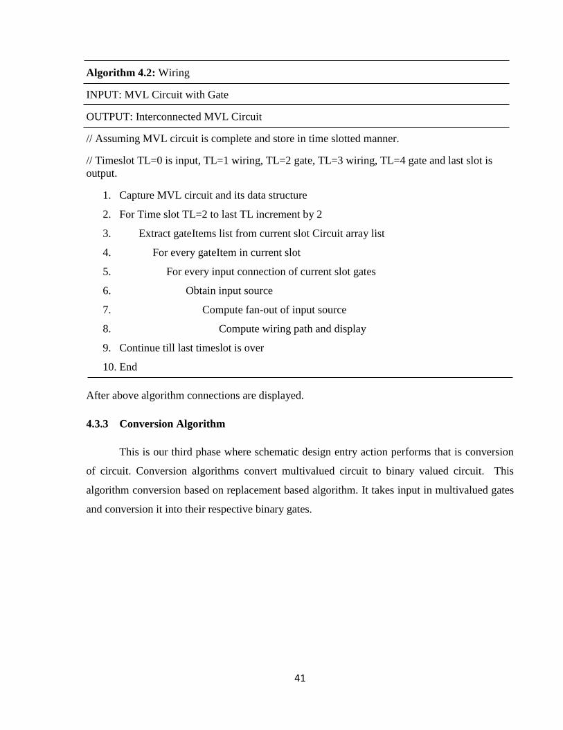
4.3.3 Conversion Algorithm
This is our third phase where schematic design entry action performs that is conversion
of circuit. Conversion algorithms convert multivalued circuit to binary valued circuit. This
algorithm conversion based on replacement based algorithm. It takes input in multivalued gates
and conversion it into their respective binary gates.

42
Algorithm 4.3: Convert MVL to BVL
INPUT: MVL Circuit Gates and Connectivity
OUTPUT: BVL Circuit
// Gate Item can be gate or input or output
// Assuming MVL circuit is complete and store in time slotted manner.
// Timeslot TL=0 is input, TL=1 wiring, TL=2 gate, TL=3 wiring, TL=4 gate and last slot is
output.
// conversion library contains BVL gates with MSB and LSB input and output points.
1. Capture MVL circuit and its data structure.
2. Time slot TL=0 to last TL increment by 2
3. Extract gate item in current slot
4. For every gate item in current slot.
4.1 Obtain corresponding binary valued gate item
4.2 Display and update BVL data structure with MSB & LSB input/output points.
5. Continue till last slot output display
// for wiring connectivity in BVL circuit
6. Time slot TL=2 to last TL increment by 2
7. Extract gateItems list of current slot from circuit array list
8. For every gateItems in current slot
9. For every input connection of current slot gate item
9.1 Obtain MSB and LSB input of gate item and its source item.
9.2 Connect MSB input of gate item to MSB input of source item
9.3 Connect LSB input of gate item to LSB input of source item
10. Continue till last gate item of last time slot.
11. End
The chapter worked out on tool development plan and algorithms to be implemented.
User interface and result obtained will show & discussed in next chapter.
43
Chapter 5
IMPLEMENTATION AND RESULTS
After developing a tool name ―MVL-DEV ― the graphical representation and testing
results are describe in this chapter.
5.1 GUI Interface for development and editing of Multivalued Circuit
This GUI interface will allow you to develop the multivalued circuit and edit them as
well as allow us to set the properties of every gate and convert it in their respective binary
conversion.
5.1.1 Hardware and Software Platform
For making the tool we use to hardware and software platform for that we use:
Processor: Intel(R) Core(TM) i3 CPU M 370 @ 2.40GHz, 2394 Mhz, 2 Core(s), 4 Logical
Processor(s)
RAM: 4 GB
OS platform: Microsoft Windows 7 Ultimate, 64 bit OS
Software Platform: Net Beans IDE 7.0.1
Language: Java 1.6.0; Java Hot Spot(TM) Client VM 1.6.0-b105
5.1.2 Developing and Simulating Multivalued Circuit.
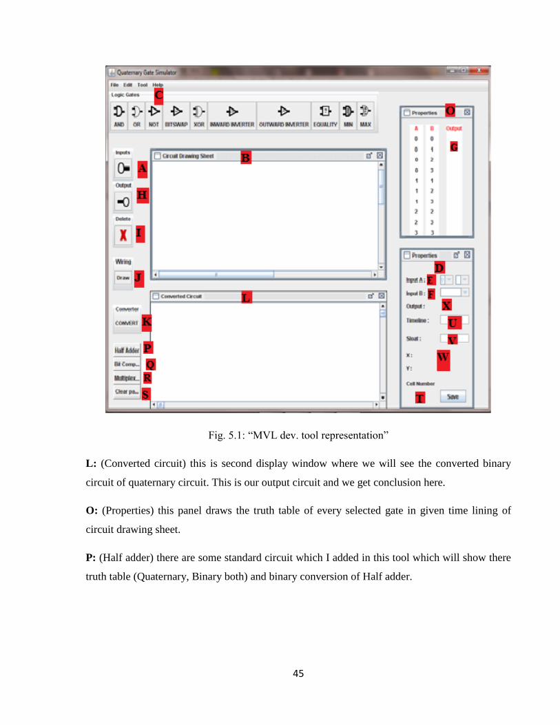
A: (Inputs) for developing and simulating the circuit first we require taking the input whether it
can be (0, 1, 2, and 3) any of them and you take multiple inputs together.
B: (Circuit Drawing Sheet) when we select the inputs then it will draw on circuit drawing sheet
which is middle of the tool. The input gate will draw in top left corner by default and then we

44
will move it in any of the time slot in which we require. The partition of this window is done by
beauty of art. It representation is very splendor. When gate is draw in top left corner than we
move it, by mouse in any time slot or first time slot. Likewise we can draw multiple of gates
here. The whole circuit will draw in this window which would be converted further in next
window.
C: (Logic Gates) this section known as Logic Gates, here total ten gates are showing, name are
given like this AND, OR, NOT, BITSWAP, XOR, INWARD INVERTER, OUTWARD
INVRTER, EQULITY, MIN, MAX. When we click on any of gates it will display in top left
corner of drawing sheet by default, now we move these gate in time lines.so we can add
multiple gates together.
D: (Properties) this section shows the name properties. This will help us in to set the property of
every input and gates. It gives the idea that how we can set every input value of every gate and
save their values in data structure. So this section have some other section E, F, X, W, U, V, T
which we will discuss in there turn.
E: (Input A) Input A require input reference of section A or input gates.
F: (Input B) Input B requires input reference of section A or input gates.
G: (Table) this section will show the truth table of every gate.
H: (Output) the output will give the final output according to truth-table combination and will
display it into the output.
I: (Delete) by selecting gate Delete button will delete the gate from data structure and help us to
add other gate on their respective position.
J: (Draw) when we click on draw button than on drawing sheet wires will be connected between
gates ad input and outputs according to their input references.
K: (Convert) Quaternary circuit we will draw on circuit drawing sheet that will convert into
binary circuit with replacement of every gate.
45
Fig. 5.1: ―MVL dev. tool representation‖
L: (Converted circuit) this is second display window where we will see the converted binary
circuit of quaternary circuit. This is our output circuit and we get conclusion here.
O: (Properties) this panel draws the truth table of every selected gate in given time lining of
circuit drawing sheet.
P: (Half adder) there are some standard circuit which I added in this tool which will show there
truth table (Quaternary, Binary both) and binary conversion of Half adder.
46
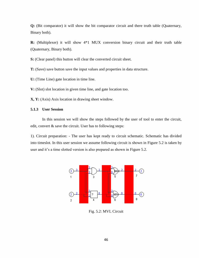
Q: (Bit comparator) it will show the bit comparator circuit and there truth table (Quaternary,
Binary both).
R: (Multiplexer) it will show 4*1 MUX conversion binary circuit and their truth table
(Quaternary, Binary both).
S: (Clear panel) this button will clear the converted circuit sheet.
T: (Save) save button save the input values and properties in data structure.
U: (Time Line) gate location in time line.
V: (Slot) slot location in given time line, and gate location too.
X, Y: (Axis) Axis location in drawing sheet window.
5.1.3 User Session
In this session we will show the steps followed by the user of tool to enter the circuit,
edit, convert & save the circuit. User has to following steps:
1). Circuit preparation: - The user has kept ready to circuit schematic. Schematic has divided
into timeslot. In this user session we assume following circuit is shown in Figure 5.2 is taken by
user and it’s a time slotted version is also prepared as shown in Figure 5.2.
Fig. 5.2: MVL Circuit
47
2). Entering the circuit: - For entering the circuit first we take the input values after selecting
input button, it could be any between 0 to 3 than input will display in top left corner of the
display window. Every selected input, output and gates first will display in this top left corner
block. Now we will drag through mouse that input in timeline and slots. Now we can add more
gates in this circuitry. By selecting each single gates/ inputs we can set their properties, also set
their input references of every gate. After adding each gate in circuitry and set their properties
we can click on draw button that will draw the wiring connectivity of circuit according to input
references. A circuit diagram is shown in Figure 5.2.
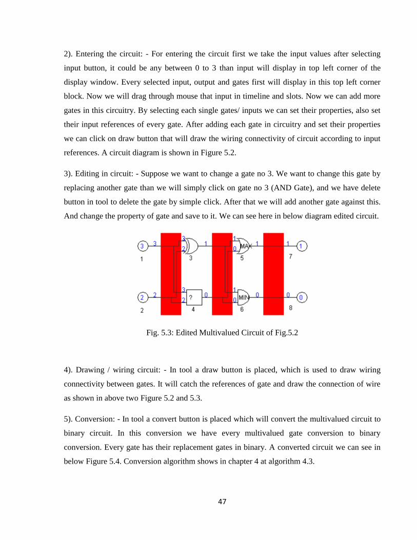
3). Editing in circuit: - Suppose we want to change a gate no 3. We want to change this gate by
replacing another gate than we will simply click on gate no 3 (AND Gate), and we have delete
button in tool to delete the gate by simple click. After that we will add another gate against this.
And change the property of gate and save to it. We can see here in below diagram edited circuit.
Fig. 5.3: Edited Multivalued Circuit of Fig.5.2
4). Drawing / wiring circuit: - In tool a draw button is placed, which is used to draw wiring
connectivity between gates. It will catch the references of gate and draw the connection of wire
as shown in above two Figure 5.2 and 5.3.
5). Conversion: - In tool a convert button is placed which will convert the multivalued circuit to
binary circuit. In this conversion we have every multivalued gate conversion to binary
conversion. Every gate has their replacement gates in binary. A converted circuit we can see in
below Figure 5.4. Conversion algorithm shows in chapter 4 at algorithm 4.3.
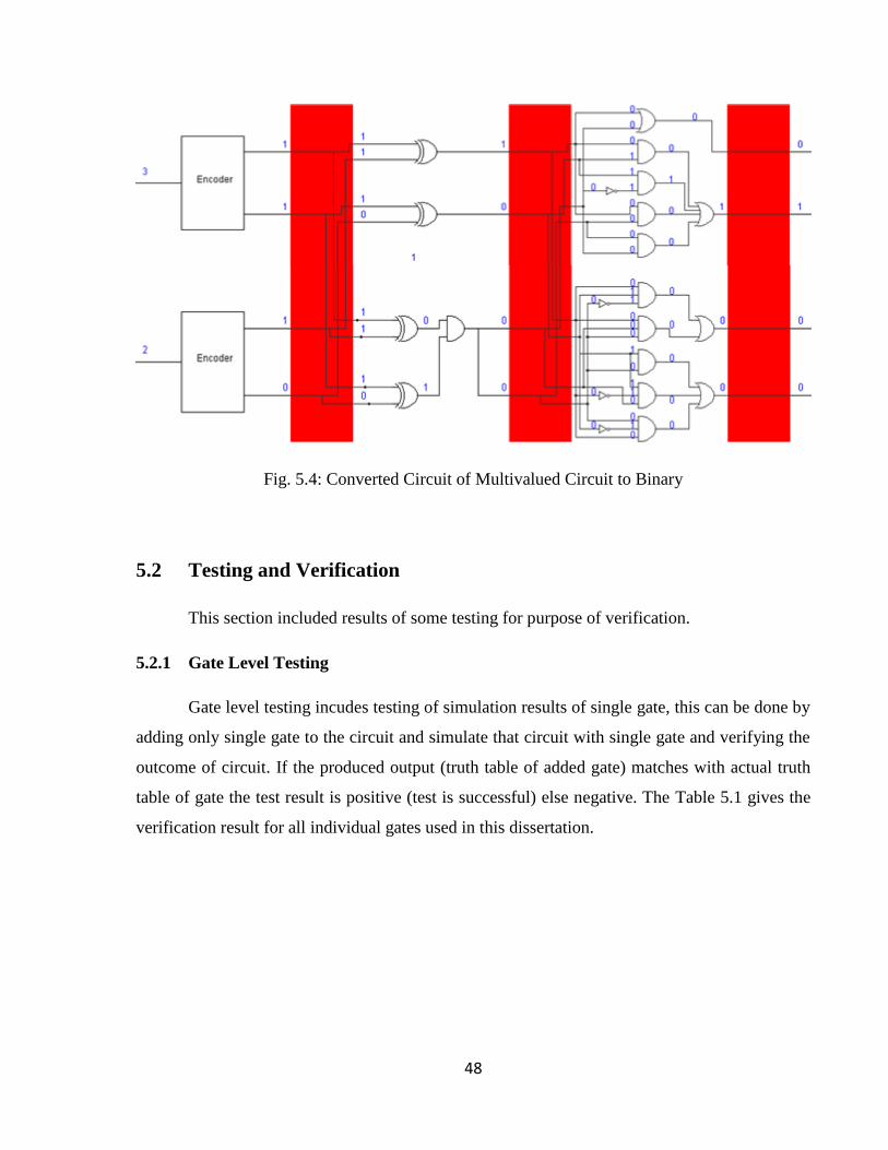
48
Fig. 5.4: Converted Circuit of Multivalued Circuit to Binary
5.2 Testing and Verification
This section included results of some testing for purpose of verification.
5.2.1 Gate Level Testing
Gate level testing incudes testing of simulation results of single gate, this can be done by
adding only single gate to the circuit and simulate that circuit with single gate and verifying the
outcome of circuit. If the produced output (truth table of added gate) matches with actual truth
table of gate the test result is positive (test is successful) else negative. The Table 5.1 gives the
verification result for all individual gates used in this dissertation.
49
Table 5.1: Results of Gate Level Testing
Sr No Test case Verification result Test result
1 AND Gate Result verified Test Successful
2 OR Gate Result verified Test Successful
3 NOT Gate Result verified Test Successful
4 XOR Gate Result verified Test Successful
5 BIT SWAP Gate Result verified Test Successful
6 INWARD INVERTER Gate Result verified Test Successful
7 OUTWARD INVERTER Gate Result verified Test Successful
8 EQUILITY Gate Result verified Test Successful
9 MAX Gate Result verified Test Successful
10 MIN Gate Result verified Test Successful
5.2.2 Circuit Level Testing
Circuit level testing includes testing of a circuit with their equivalent conversion in
binary. We already discussed few multivalued circuit in chapter 3.here we have their converted
circuit in binary and their truth table so that we can prove their circuit level testing.
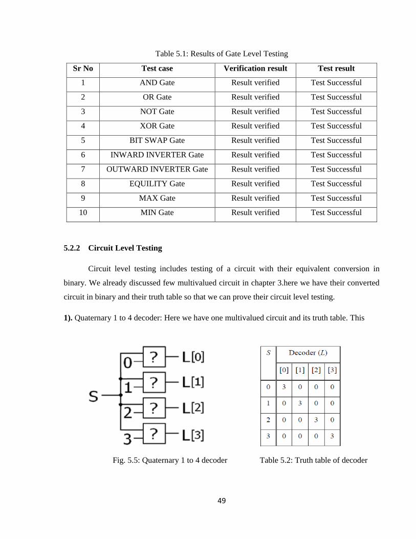
1). Quaternary 1 to 4 decoder: Here we have one multivalued circuit and its truth table. This
Fig. 5.5: Quaternary 1 to 4 decoder Table 5.2: Truth table of decoder
50
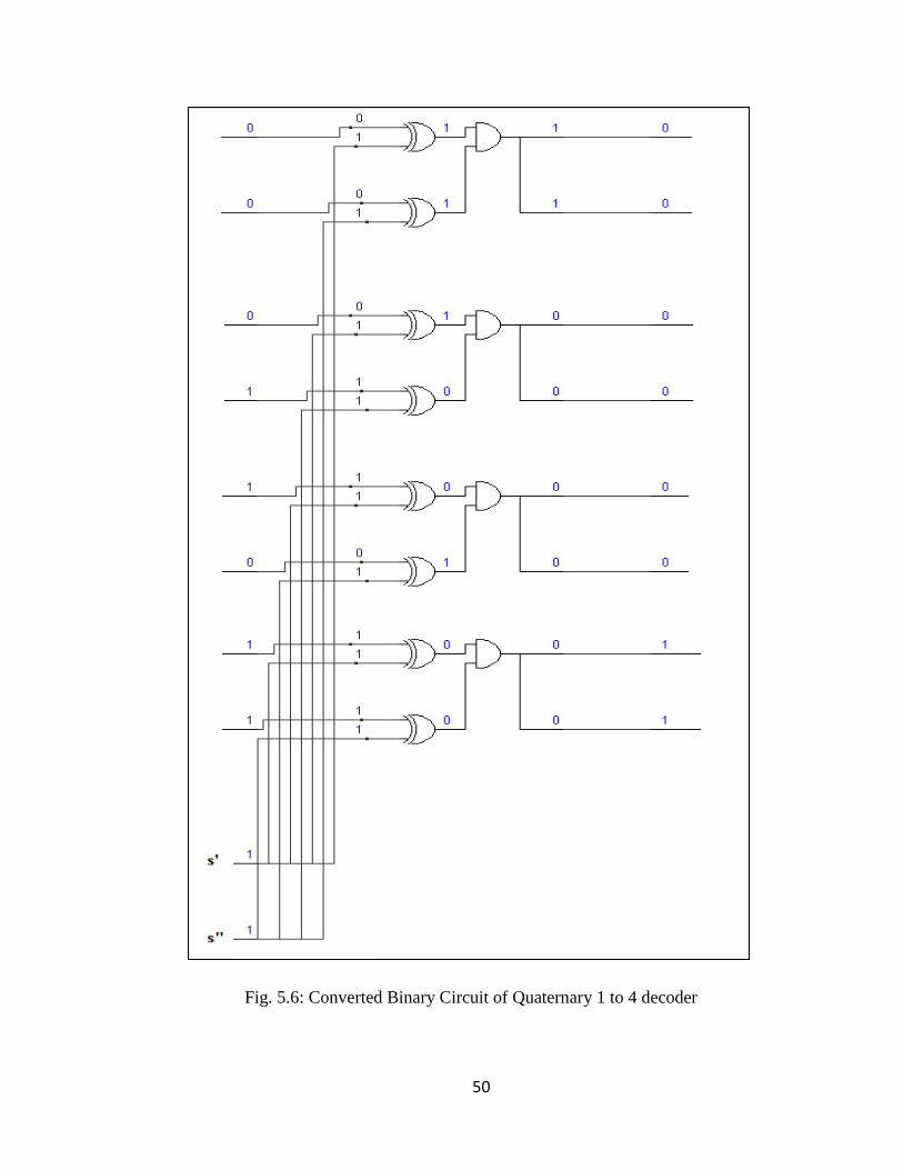
Fig. 5.6: Converted Binary Circuit of Quaternary 1 to 4 decoder
51
Table 5.3: Binary Truth Table of Quaternary 1 to 4 Decoder
A quaternary circuit 1-to-4 decoder has one input and four outputs. Only one of the outputs can
be equal to 3 at a time, all other outputs remain 0 as Figure 5.5 shows a Quaternary circuit and
its equivalent Table 5.2 in quaternary. In Figure 5.6 binary equivalent circuit is shown, here we
give input 3 on selection lines S’ and S‖ and get an output on 3. Tool will convert the
multivalued circuit into binary circuit. Table 5.3 shows there binary equivalent of Table 5.2.
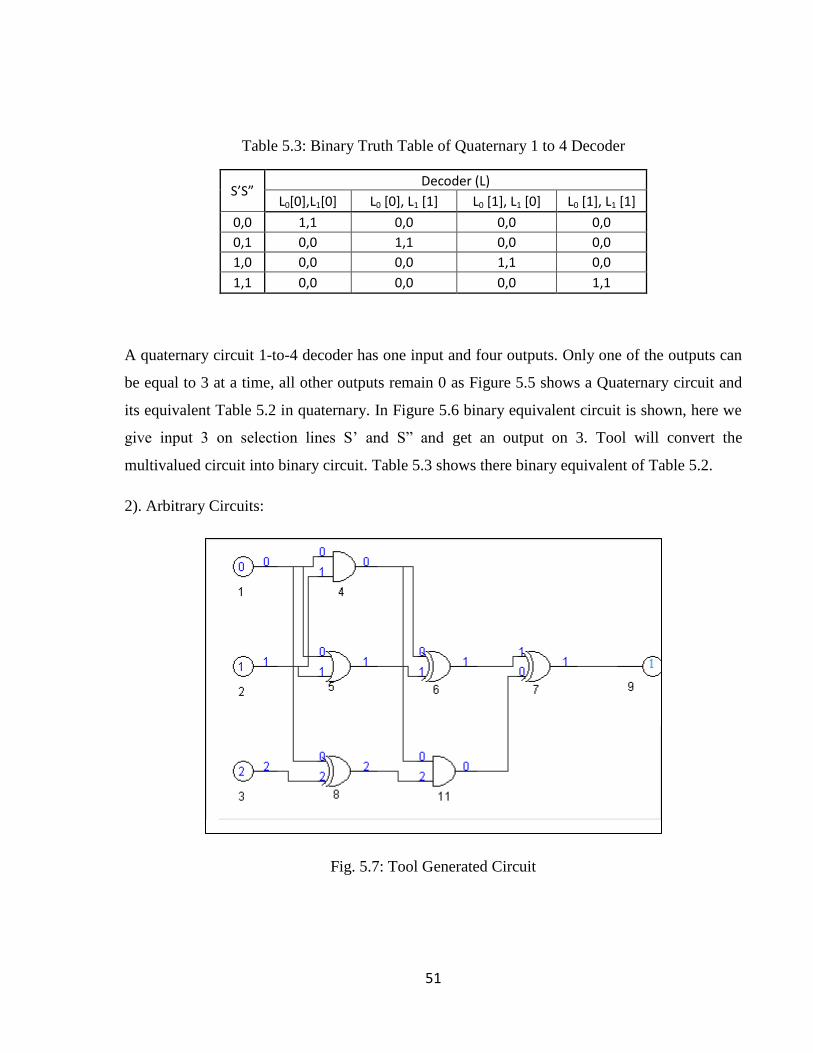
2). Arbitrary Circuits:
Fig. 5.7: Tool Generated Circuit
S’S” Decoder (L)
L0[0],L1[0] L0 [0], L1 [1] L0 [1], L1 [0] L0 [1], L1 [1]
0,0 1,1 0,0 0,0 0,0
0,1 0,0 1,1 0,0 0,0
1,0 0,0 0,0 1,1 0,0
1,1 0,0 0,0 0,0 1,1
52
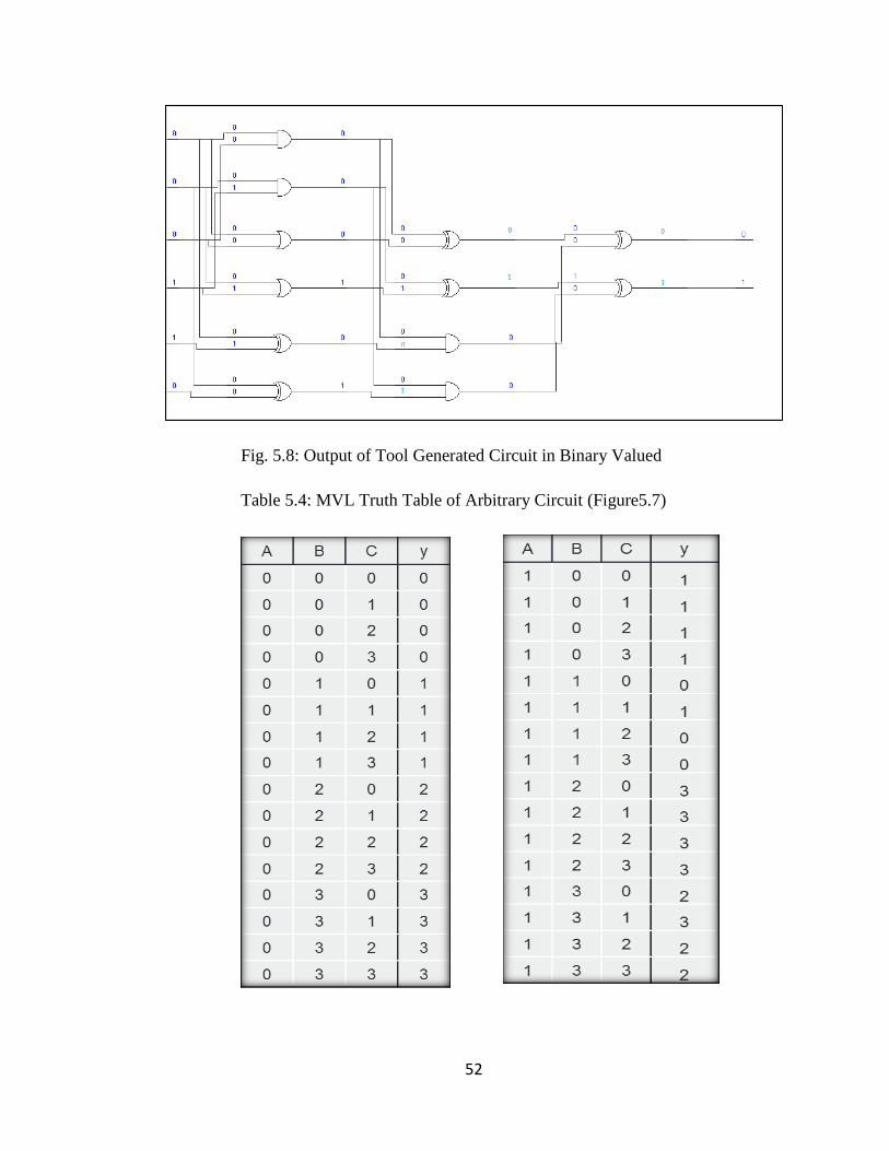
Fig. 5.8: Output of Tool Generated Circuit in Binary Valued
Table 5.4: MVL Truth Table of Arbitrary Circuit (Figure5.7)
53
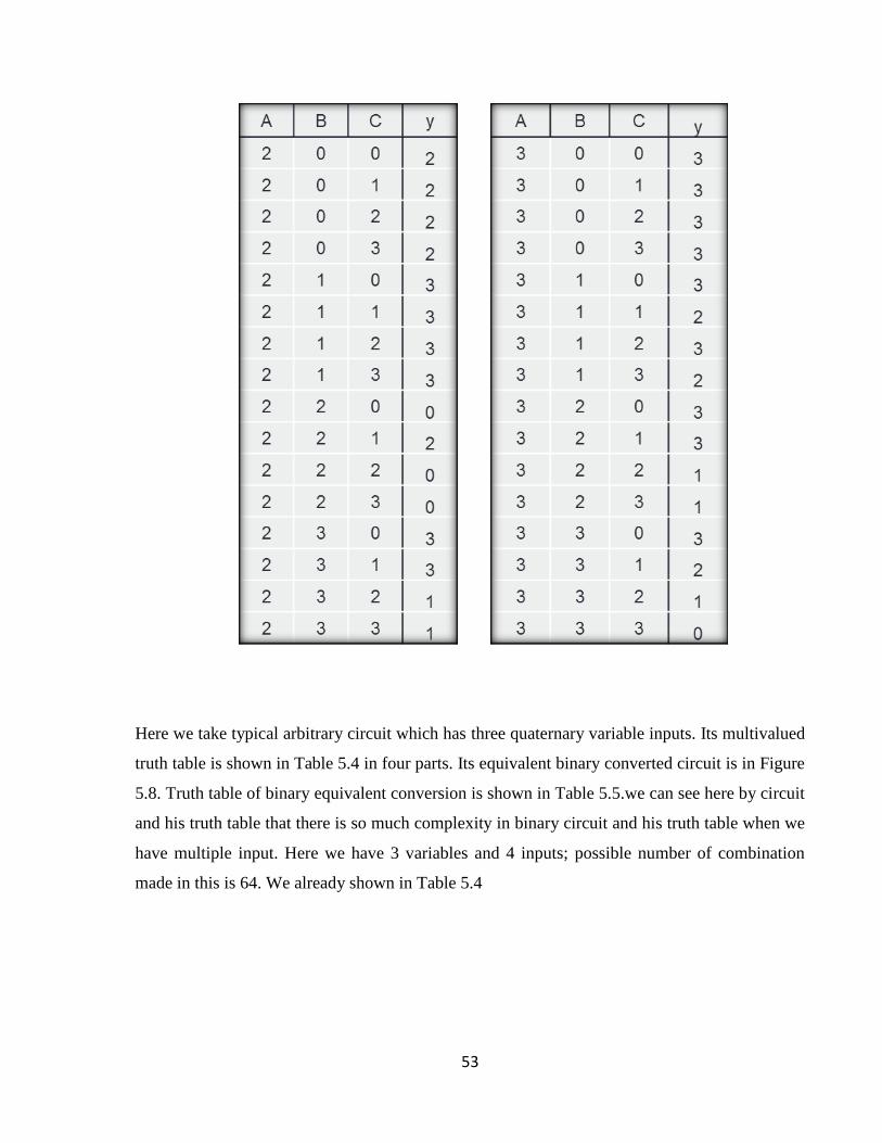
Here we take typical arbitrary circuit which has three quaternary variable inputs. Its multivalued
truth table is shown in Table 5.4 in four parts. Its equivalent binary converted circuit is in Figure
5.8. Truth table of binary equivalent conversion is shown in Table 5.5.we can see here by circuit
and his truth table that there is so much complexity in binary circuit and his truth table when we
have multiple input. Here we have 3 variables and 4 inputs; possible number of combination
made in this is 64. We already shown in Table 5.4
54
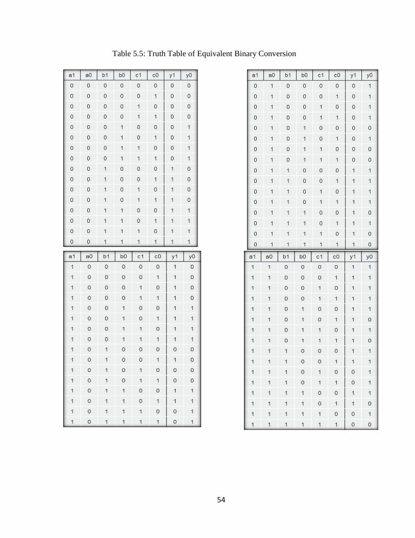
Table 5.5: Truth Table of Equivalent Binary Conversion

55
Hence we observe our tool is able to perform design entry editing and conversion and saving
task correctly. It will be useful for multivalued design entry and interfacing with binary logic
based system.
56
Chapter 6
CONCLUSION AND FUTURE SCOPE
In this dissertation we plan a multivalued circuit processing environment that it offers
ease of multivalued circuit design and development platform of binary valued system.
Looking to complexity of today’s circuit (i.e. multi millennium gate size circuit), it is
important that to develop circuits at higher than binary logic system so that design complexity is
reduced. However implementation platform available are only in binary logic system.
We have developed a tool‖ MVL-DEV‖ that can be useful for developers for generating
and testing multivalued circuits. Our specific contribution in this dissertation by developing
―Multivalued circuit processing environment‖ that can be
Creation of standard libraries in MVL.
Simulate the developed multivalued circuit to view output of quaternary circuit and truth
table of gates.
Editing in multivalued circuit.
Drawing wiring connectivity in multivalued circuit.
Conversion of quaternary to binary circuit.
Saving the generated circuit.
Providing standard circuits as ready example design capture.
Future Scope
The developed tool is now able to capture multivalued design entry and provide binary
valued logic design. This tool can be further improved by:
Saving in more than one format.
This can also extended for converting the design in reversible/quantum circuit.
Further extension is possible by interfacing with hardware description languages.
It may also be extended to take ternary and other multivalued design formats.
57
BIBLIOGRAPHY
[1] Hurst, S.L, ―Multiple-Valued Logic; its Status and its Future‖, Computers, IEEE
Transactions on, 33 (12), Dec. 1984, pp.1160-1179.
[2] Miller, D.M. Thornton, and M.A. ―Multiple Valued Logic: Concepts and Representations‖,
Synthesis Lectures on Digital Circuits and Systems, Morgan & Claypool Publishers, 2007.
[3] Smith, K.C., ―The Prospects for Multivalued Logic- A Technology and Applications View‖,
Computers, IEEE Transactions on, 30, pp. 619-634, 1981.
[4] Fijany, A., Vatan, F.Mojarradi, M., Toomarian, B. Blalock, B.Akarvardar, K. Cristoloveanu,
S. and Gentil, P. ―The G4-FET- a universal and programmable logic gate‖, Proceedings of the
15th ACM Great Lakes symposium on VLSI (GLSVLSI2005), pp. 349-352, April 2005.
[5] Keshavarzian, A.P. and Navi, K., ―Optimum Quaternary Galois Field Circuit Design through
Carbon Nano Tube Technology‖, Proceedings, International Conference on Advanced
Computing and Communications (ADCOM 2007), pp. 214-219, Dec 2007.
[6] Chattopadhyay, T. Taraphdar, C. Roy, and J.N, ―Quaternary Galois field adder based all-
optical multivalued logic circuits‖, Applied Optics, 48 (22), pp. E35-E44, 2009.
[7] Khan, and M.H.A., ―Reversible Realization of Quaternary Decoder, Multiplexer, and
Demultiplexer Circuits‖, Engineering Letters, 15 (2), pp. 203-207, 2007.
[8] Falkowski, B.J., and Rahardja S. ―Generalized hybrid arithmetic canonical expansions for
completely specified quaternary functions‖, Electronics Letters, 37 (16), pp. 1006-1007, Aug.
2001.
58
[9] Khan, M.H.A., Siddika, N.K. Perkowski, and M.A.; ―Minimization of Quaternary Galois
Field Sum of Products Expression for Multi-Output Quaternary Logic Function Using
Quaternary Galois Field Decision Diagram‖, Proceedings, 38th IEEE International Symposium
on Multiple-Valued Logic (ISMVL 2008), pp. 125-130, May 2008.
[10] Khan, M.M.M., Biswas, A.K., Chowdhury, S. Tanzid, M., Mohsin, K.M., Hasan, M.,
Khan, and A.I. ―Quantum realization of some quaternary circuits‖, Proceedings, TENCON
2008, IEEE Region 10 Conference, Nov. 2008.
[11] Yasuda, Y., Tokuda, Y., Zaima, S., Pak, K., Nakamura, T. and Yoshida A., ―Realization of
quaternary logic circuits by n-channel MOS devices‖, Solid-State Circuits, IEEE Journal of, 21
(1), pp. 162-168, Feb. 1986.
[12] Park S.J., Yoon B.H., Yoon K.S., Kim H.S., ―Design of quaternary logic gate using double
pass-transistor logic with neuron MOS down literal circuit‖, Proceedings, 34th IEEE
International Symposium on Multiple-Valued Logic (ISMVL 2004), pp.198-203, May 2004.
[13] Da Silva, R.C.G., Boudinov, H. and Carro L., ―A novel Voltage-mode CMOS quaternary
logic design‖, Electron Devices, IEEE Transactions on, 53 (6), pp. 1480, June 2006.
[14] Inaba, M., Tanno, K., Ishizuka, O. ―Realization of NMAX and NMIN functions with multi-
valued voltage comparators‖, Proceedings, 31st IEEE International Symposium on Multiple-
Valued Logic (ISMVL 2001), pp. 27-32, May 2001.
[15] Datla, S.R., Thornton, and M.A., ―Quaternary Voltage-Mode Logic Cells and Fixed-Point
Multiplication Circuits‖, Proceedings, 40th IEEE International Symposium on Multiple-Valued
Logic (ISMVL 2010), pp. 128-133, June 2010.
59
[16] Chattopadhyay, T. Roy and J.N, ―Polarization-encoded all-optical quaternary multiplexer
and demultiplexer - A proposal‖, Optik - International Journal for Light and Electron Optics,
120 (17), pp. 941-946, Nov. 2009.
[17] Bartelt, Terry. Wisconsin Technical College System.―Wisc-Online‖.Basic Logic Gates.
[http://www.wisc-online.com/Objects/ViewObject.aspx?ID=dig1302].
[18] Imperial College, London. Department of Computing. ‖Lecture 1: An Introduction to
Boolean Algebra‖, [http://www.doc.ic.ac.uk/~dfg/hardware/HardwareLecture01.pdf].
[19] Huntington, and E.V., ―Sets of Independent Postulates for the Algebra of Logic‖,
Transactions of the American Mathematical Society, 5(3), pp. 288-309, July1904.
[20] X.W.Wu, ―CMOS ternary logic circuits‖, IEEE PROCEEDINGS, Vol. 137, Pt. G, No. I,
February 1990.
[21] Xiaoqiang Shou, Nader Kalantari, Michael M. Green, ―Design of CMOS Ternary Latches‖,
IEEE TRANSACTIONS ON CIRCUITS AND SYSTEMS—I: REGULAR PAPERS, VOL. 53,
NO. 12, December 2006.
[22] Ion Profeanu, ―A Ternary Arithmetic and Logic‖, ISBN: 978-988-17012-9-9, ISSN: 2078-
0958 (Print); ISSN: 2078-0966 (Online); Proceedings of the World Congress on Engineering
2010 Vol. I , WCE 2010, June 30 - July 2, 2010, London, U.K.
[23] Kanchan S. Gorde, ―Design and simulation of ternary logic based arithmetic circuits‖ issue
2, vol-1, april-june 2010.
60
[24] Afolayan A. Obiniyi, Ezugwu E. Absalom, Kwanashie Adako, ―Arithmetic logic design
with color coded ternary for ternary computing‖ International Journal of Computer Applications
(0975 – 8887) Volume 26– No.11, July 2011.
[25] V.T.Gaikwad, and Dr. P. R. Deshmukh, ―Multi-Valued Logic Applications in the Design of
Switching Circuits‖ International Journal of Advanced Research in Computer Science and
Software Engineering, Volume 2, Issue 5, ISSN: 2277 128X, May 2012.
[26] Noboru Takagi, and Kyoichi Nakashima, ―Discrete Interval Truth Values Logic and its
Application‖. IEEE TRANSACTIONS ON COMPUTERS, VOL. 49, NO.3, MARCH 2000.
[27] Craig M. Files and Marek A. Perkowski, ‖New Multivalued Functional Decomposition
Algorithms Based on MDDs‖. IEEE TRANSACTIONS ON COMPUTER AIDED DESIGN OF
INTEGRATED CIRCUITS AND SYSTEMS, VOL. 19, NO. 9, SEPTEMBER 2000.
[28] Sunil P. Khatri, Subarnarekha Sinha, Robert K. Brayton, and Alberto L. Sangiovanni-
Vincentelli, ―SPFD-Based Wire Removal in Standard-Cell and Network of PLA Circuits‖.IEEE
TRANSACTIONS ON COMPUTER-AIDED DESIGN OF INTEGRATED CIRCUITS AND
SYSTEMS, VOL. 23, NO. 7, JULY 2004.
[29] DušankaBundalo, ZlatkoBundalo, and BranimirDordevic, ―Design of Quaternary Logic
Systems and Circuits‖. ; FACTA UNIVERSITATIS (NIŠ) SER.: ELEC. ENERG. vol. 18, No.
1, April 2005, 45-56.
[30] Vasundara Patel K S, K S Gurumurthy, ―Design of High Performance Quaternary
Adders‖.International Journal of Computer Theory and Engineering, Vol.2, No.6, December,
2010, 1793-8201.
61
[31] Cristiano Lazzari,Paulo Flores, Jos´eMonteiro, and Luigi Carro ―A New Quaternary FPGA
Based on a Voltage-mode Multi-valued Circuit‖ 978-3-9810801-6-2/DATE10 © 2010.
[32] Vasundara Patel K S, and K S Gurumurthy, ―Quaternary Sequential Circuits‖ IJCSNS
International Journal of Computer Science and Network Security, VOL.10 No.7, July 2010.
[33] Vasundara Patel k s, and k s gurumurthy; ―Arithmetic operation in multivalued logic
―International journal of vlsi design & communication system (VLSCS) , vol 1, no 1, march
2010.
[34] Sheng Lin, Yong-Bin Kim, and Fabrizio Lombardi, ―Design of a Ternary Memory Cell
Using CNTFETs‖ IEEE TRANSACTIONS ON NANOTECHNOLOGY, VOL. 11, NO. 5,
SEPTEMBER 2012.
[35] Umesh Kumar and Rajiv Kapoor, ―CMOS Body Driven Quaternary Logic Generator‖.
IOSR Journal of VLSI and Signal Processing (IOSR-JVSP) ISSN: 2319 – 4200, ISBN No. :
2319 – 4197 Volume 1, Issue 1 (Sep-Oct. 2012), PP 46-50.
[36] Ifat Jahangir, Anindya Das and MasudHasan., ―Formulation and Development of a Novel
Quaternary Algebra‖
[37] D. Etiemble and K. Navi, ―Algorithms and multi-valued circuits for the multioperand
addition in the binary stored-carry number system‖ 1993 IEEE 1063-6889/93.
[38] Elena Dubrova, ―Multiple-Valued Logic in VLSI: Challenges and Opportunities‖
[39] Robert K Brayton and Sunil P Khatri,―Multi-valued Logic Synthesis‖
62
[40]Ashok Muthukrishnan and C. R. Stroud, ―Multi-Valued Logic Gates for Quantum
Computation‖ arXiv:quant-ph/0002033v2 12 Jun 2000.
[41] A. Morgül and TurgayTemel, ―Level Restoration for Multivalued Logic Circuit‖.
[42] Hemant Dhabhai, Abhishek Katariya, Geetam Tomar, Yogesh Krishna, ―Optimization of
Binary and Multivalued Digital Circuit using MVSIS and AIG rewriting‖ Journal of Electronic
and Electrical Engineering ,ISSN: 0976–8106 & E-ISSN: 0976–8114, Vol. 2, Issue 1, pp-24-29,
2011.