TMS320F28004x Microcontrollers datasheet (Rev. F) - Texas ...
Upload
khangminh22Category
view
1download
0
Document No. U17890EJ2V0UD00 (2nd edition)
Date Published October 2007 NS
Printed in Japan ©
μPD78F0711 μPD78F0712
μPD78F0711, 78F0712 8-Bit Single-Chip Microcontrollers
User’s Manual
2006

User’s Manual U17890EJ2V0UD 2
[MEMO]

User’s Manual U17890EJ2V0UD 3
1
2
3
4
VOLTAGE APPLICATION WAVEFORM AT INPUT PIN
Waveform distortion due to input noise or a reflected wave may cause malfunction. If the input of the
CMOS device stays in the area between VIL (MAX) and VIH (MIN) due to noise, etc., the device may
malfunction. Take care to prevent chattering noise from entering the device when the input level is fixed,
and also in the transition period when the input level passes through the area between VIL (MAX) and
VIH (MIN).
HANDLING OF UNUSED INPUT PINS
Unconnected CMOS device inputs can be cause of malfunction. If an input pin is unconnected, it is
possible that an internal input level may be generated due to noise, etc., causing malfunction. CMOS
devices behave differently than Bipolar or NMOS devices. Input levels of CMOS devices must be fixed
high or low by using pull-up or pull-down circuitry. Each unused pin should be connected to VDD or GND
via a resistor if there is a possibility that it will be an output pin. All handling related to unused pins must
be judged separately for each device and according to related specifications governing the device.
PRECAUTION AGAINST ESD
A strong electric field, when exposed to a MOS device, can cause destruction of the gate oxide and
ultimately degrade the device operation. Steps must be taken to stop generation of static electricity as
much as possible, and quickly dissipate it when it has occurred. Environmental control must be
adequate. When it is dry, a humidifier should be used. It is recommended to avoid using insulators that
easily build up static electricity. Semiconductor devices must be stored and transported in an anti-static
container, static shielding bag or conductive material. All test and measurement tools including work
benches and floors should be grounded. The operator should be grounded using a wrist strap.
Semiconductor devices must not be touched with bare hands. Similar precautions need to be taken for
PW boards with mounted semiconductor devices.
STATUS BEFORE INITIALIZATION
Power-on does not necessarily define the initial status of a MOS device. Immediately after the power
source is turned ON, devices with reset functions have not yet been initialized. Hence, power-on does
not guarantee output pin levels, I/O settings or contents of registers. A device is not initialized until the
reset signal is received. A reset operation must be executed immediately after power-on for devices
with reset functions.
POWER ON/OFF SEQUENCE
In the case of a device that uses different power supplies for the internal operation and external
interface, as a rule, switch on the external power supply after switching on the internal power supply.
When switching the power supply off, as a rule, switch off the external power supply and then the
internal power supply. Use of the reverse power on/off sequences may result in the application of an
overvoltage to the internal elements of the device, causing malfunction and degradation of internal
elements due to the passage of an abnormal current.
The correct power on/off sequence must be judged separately for each device and according to related
specifications governing the device.
INPUT OF SIGNAL DURING POWER OFF STATE
Do not input signals or an I/O pull-up power supply while the device is not powered. The current
injection that results from input of such a signal or I/O pull-up power supply may cause malfunction and
the abnormal current that passes in the device at this time may cause degradation of internal elements.
Input of signals during the power off state must be judged separately for each device and according to
related specifications governing the device.
NOTES FOR CMOS DEVICES
5
6

User’s Manual U17890EJ2V0UD 4
EEPROM, IECUBE, and MINICUBE are registered trademarks of NEC Electronics Corporation in japan and Germany. Windows, Windows NT, and Windows XP are registered trademarks or trademarks of Microsoft Corporation in the United States and/or other countries. PC/AT is a trademark of International Business Machines Corporation. HP9000 series 700 and HP-UX are trademarks of Hewlett-Packard Company. SPARCstation is a trademark of SPARC International, Inc. Solaris and SunOS are trademarks of Sun Microsystems, Inc. TRON is an abbreviation of The Realtime Operating system Nucleus. ITRON is an abbreviation of Industrial TRON. SuperFlash is a registered trademark of Silicon Storage Technology, Inc. in several countries including the United States and Japan.
Caution: This product uses SuperFlash® technology licensed from Silicon Storage Technology, inc.
The information in this document is current as of August, 2007. The information is subject to change without notice. For actual design-in, refer to the latest publications of NEC Electronics data sheets or data books, etc., for the most up-to-date specifications of NEC Electronics products. Not all products and/or types are available in every country. Please check with an NEC Electronics sales representative for availability and additional information.No part of this document may be copied or reproduced in any form or by any means without the prior written consent of NEC Electronics. NEC Electronics assumes no responsibility for any errors that may appear in this document.NEC Electronics does not assume any liability for infringement of patents, copyrights or other intellectual property rights of third parties by or arising from the use of NEC Electronics products listed in this document or any other liability arising from the use of such products. No license, express, implied or otherwise, is granted under any patents, copyrights or other intellectual property rights of NEC Electronics or others.Descriptions of circuits, software and other related information in this document are provided for illustrative purposes in semiconductor product operation and application examples. The incorporation of these circuits, software and information in the design of a customer's equipment shall be done under the full responsibility of the customer. NEC Electronics assumes no responsibility for any losses incurred by customers or third parties arising from the use of these circuits, software and information.While NEC Electronics endeavors to enhance the quality, reliability and safety of NEC Electronics products, customers agree and acknowledge that the possibility of defects thereof cannot be eliminated entirely. To minimize risks of damage to property or injury (including death) to persons arising from defects in NEC Electronics products, customers must incorporate sufficient safety measures in their design, such as redundancy, fire-containment and anti-failure features.NEC Electronics products are classified into the following three quality grades: "Standard", "Special" and "Specific". The "Specific" quality grade applies only to NEC Electronics products developed based on a customer-designated "quality assurance program" for a specific application. The recommended applications of an NEC Electronics product depend on its quality grade, as indicated below. Customers must check the quality grade of each NEC Electronics product before using it in a particular application.
The quality grade of NEC Electronics products is "Standard" unless otherwise expressly specified in NEC Electronics data sheets or data books, etc. If customers wish to use NEC Electronics products in applications not intended by NEC Electronics, they must contact an NEC Electronics sales representative in advance to determine NEC Electronics' willingness to support a given application.
(Note)
•
•
•
•
•
•
M8E 02. 11-1
(1)
(2)
"NEC Electronics" as used in this statement means NEC Electronics Corporation and also includes its majority-owned subsidiaries."NEC Electronics products" means any product developed or manufactured by or for NEC Electronics (as defined above).
Computers, office equipment, communications equipment, test and measurement equipment, audioand visual equipment, home electronic appliances, machine tools, personal electronic equipmentand industrial robots.Transportation equipment (automobiles, trains, ships, etc.), traffic control systems, anti-disastersystems, anti-crime systems, safety equipment and medical equipment (not specifically designedfor life support).Aircraft, aerospace equipment, submersible repeaters, nuclear reactor control systems, lifesupport systems and medical equipment for life support, etc.
"Standard":
"Special":
"Specific":

User’s Manual U17890EJ2V0UD 5
INTRODUCTION
Readers This manual is intended for user engineers who wish to understand the functions of the
μPD78F0711, 78F0712 and design and develop application systems and programs for
this device.
The target product is as follows.
μPD78F0711, 78F0712
Purpose This manual is intended to give users an understanding of the functions described in the
Organization below.
Organization The μPD78F0711, 78F0712 manual is separated into two parts: this manual and the
instructions edition (common to the 78K/0 Series).
μPD78F0711, 78F0712 User’s Manual (This Manual)
78K/0 Series User’s Manual Instructions
• Pin functions
• Internal block functions
• Interrupts
• Other on-chip peripheral functions
• Electrical specifications
• CPU functions
• Instruction set
• Explanation of each instruction
How to Read This Manual It is assumed that the readers of this manual have general knowledge of electrical
engineering, logic circuits, and microcontrollers.
• To gain a general understanding of functions:
→ Read this manual in the order of the CONTENTS. The mark “<R>” shows major
revised points. The revised points can be easily searched by copying an “<R>” in
the PDF file and specifying it in the “Find what:” field.
• How to interpret the register format:
→ For a bit number enclosed in angle brackets, the bit name is defined as a
reserved word in the RA78K0, and is defined as an sfr variable using the
#pragma sfr directive in the CC78K0.
• To check the details of a register when you know the register name.
→ See APPENDIX B REGISTER INDEX.
• To know details of the 78K/0 Series instructions.
→ Refer to the separate document 78K/0 Series Instructions User’s Manual
(U12326E).
Conventions Data significance: Higher digits on the left and lower digits on the right
Active low representations: ××× (overscore over pin and signal name)
Note: Footnote for item marked with Note in the text.
Caution: Information requiring particular attention
Remark: Supplementary information
Numerical representations: Binary ... ×××× or ××××B
Decimal ... ××××
Hexadecimal ... ××××H

User’s Manual U17890EJ2V0UD 6
Related Documents The related documents indicated in this publication may include preliminary versions.
However, preliminary versions are not marked as such.
Documents Related to Devices
Document Name Document No.
μPD78F0711, 78F0712 User’s Manual This manual
78K/0 Series Instructions User’s Manual U12326E
Documents Related to Development Tools (Software) (User’s Manuals)
Document Name Document No.
Operation U17199E
Language U17198E
RA78K0 Ver.3.80 Assembler Package
Structured Assembly Language U17197E
Operation U17201E CC78K0 Ver.3.70 C Compiler
Language U17200E
ID78K0-QB Series Integrated Debugger Ver. 2.94 or Later Operation U18330E
PM+ Ver. 5.20 U16934E
Documents Related to Development Tools (Hardware) (User’s Manuals)
Document Name Document No.
QB-780714 In-Circuit Emulator U17081E
QB-78K0MINI On-Chip Debug Emulator U17029E
QB-MINI2 On-Chip Debug Emulator with Programming Function U18371E
Documents Related to Flash Memory Programming
Document Name Document No.
PG-FP4 Flash Memory Programmer User’s Manual U15260E
Other Documents
Document Name Document No.
SEMICONDUCTOR SELECTION GUIDE − Products and Packages − X13769X
Semiconductor Device Mount Manual Note
Quality Grades on NEC Semiconductor Devices C11531E
NEC Semiconductor Device Reliability/Quality Control System C10983E
Guide to Prevent Damage for Semiconductor Devices by Electrostatic Discharge (ESD) C11892E
Note See the “Semiconductor Device Mount Manual” website (http://www.necel.com/pkg/en/mount/index.html).
Caution The related documents listed above are subject to change without notice. Be sure to use the latest
version of each document when designing.
<R>
User’s Manual U17890EJ2V0UD 7
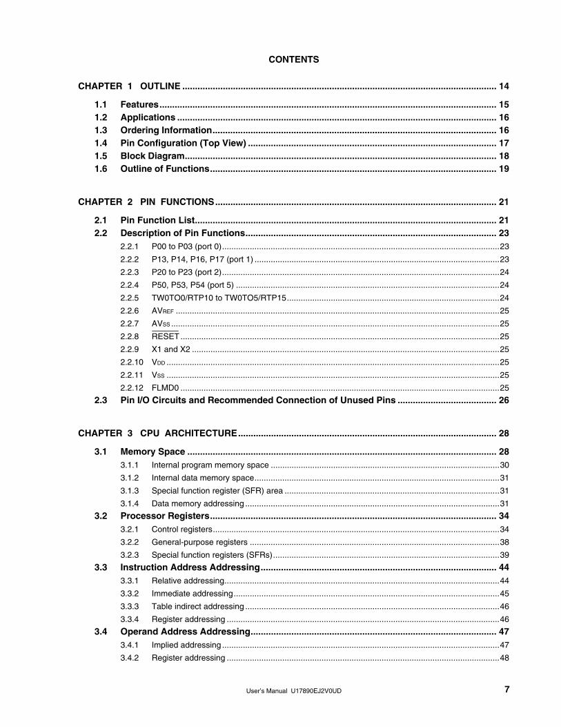
CONTENTS
CHAPTER 1 OUTLINE ............................................................................................................................ 14
1.1 Features..................................................................................................................................... 15 1.2 Applications .............................................................................................................................. 16 1.3 Ordering Information................................................................................................................ 16 1.4 Pin Configuration (Top View) .................................................................................................. 17 1.5 Block Diagram........................................................................................................................... 18 1.6 Outline of Functions................................................................................................................. 19
CHAPTER 2 PIN FUNCTIONS............................................................................................................... 21
2.1 Pin Function List....................................................................................................................... 21 2.2 Description of Pin Functions................................................................................................... 23
2.2.1 P00 to P03 (port 0)........................................................................................................................23 2.2.2 P13, P14, P16, P17 (port 1) ..........................................................................................................23 2.2.3 P20 to P23 (port 2)........................................................................................................................24 2.2.4 P50, P53, P54 (port 5) ..................................................................................................................24 2.2.5 TW0TO0/RTP10 to TW0TO5/RTP15............................................................................................24 2.2.6 AVREF ............................................................................................................................................25 2.2.7 AVSS ..............................................................................................................................................25 2.2.8 RESET ..........................................................................................................................................25 2.2.9 X1 and X2 .....................................................................................................................................25 2.2.10 VDD ................................................................................................................................................25 2.2.11 VSS ................................................................................................................................................25 2.2.12 FLMD0 ..........................................................................................................................................25
2.3 Pin I/O Circuits and Recommended Connection of Unused Pins ....................................... 26
CHAPTER 3 CPU ARCHITECTURE...................................................................................................... 28
3.1 Memory Space .......................................................................................................................... 28 3.1.1 Internal program memory space ...................................................................................................30 3.1.2 Internal data memory space..........................................................................................................31 3.1.3 Special function register (SFR) area .............................................................................................31 3.1.4 Data memory addressing ..............................................................................................................31
3.2 Processor Registers................................................................................................................. 34 3.2.1 Control registers............................................................................................................................34 3.2.2 General-purpose registers ............................................................................................................38 3.2.3 Special function registers (SFRs)..................................................................................................39
3.3 Instruction Address Addressing............................................................................................. 44 3.3.1 Relative addressing.......................................................................................................................44 3.3.2 Immediate addressing...................................................................................................................45 3.3.3 Table indirect addressing ..............................................................................................................46 3.3.4 Register addressing ......................................................................................................................46
3.4 Operand Address Addressing................................................................................................. 47 3.4.1 Implied addressing ........................................................................................................................47 3.4.2 Register addressing ......................................................................................................................48
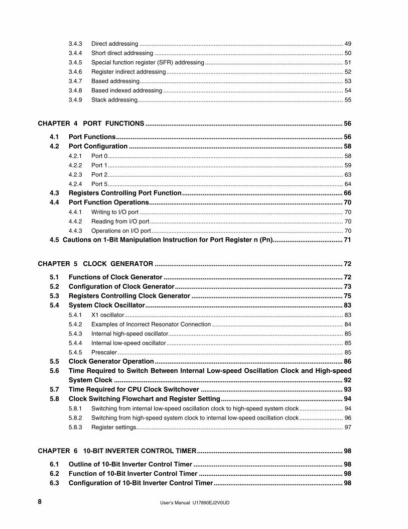
User’s Manual U17890EJ2V0UD 8
3.4.3 Direct addressing ......................................................................................................................... 49 3.4.4 Short direct addressing ................................................................................................................ 50 3.4.5 Special function register (SFR) addressing .................................................................................. 51 3.4.6 Register indirect addressing......................................................................................................... 52 3.4.7 Based addressing......................................................................................................................... 53 3.4.8 Based indexed addressing ........................................................................................................... 54 3.4.9 Stack addressing.......................................................................................................................... 55
CHAPTER 4 PORT FUNCTIONS ........................................................................................................... 56
4.1 Port Functions........................................................................................................................... 56 4.2 Port Configuration .................................................................................................................... 58
4.2.1 Port 0............................................................................................................................................ 58 4.2.2 Port 1............................................................................................................................................ 59 4.2.3 Port 2............................................................................................................................................ 63 4.2.4 Port 5............................................................................................................................................ 64
4.3 Registers Controlling Port Function....................................................................................... 66 4.4 Port Function Operations......................................................................................................... 70
4.4.1 Writing to I/O port ......................................................................................................................... 70 4.4.2 Reading from I/O port................................................................................................................... 70 4.4.3 Operations on I/O port.................................................................................................................. 70
4.5 Cautions on 1-Bit Manipulation Instruction for Port Register n (Pn)...................................... 71
CHAPTER 5 CLOCK GENERATOR ...................................................................................................... 72
5.1 Functions of Clock Generator ................................................................................................. 72 5.2 Configuration of Clock Generator........................................................................................... 73 5.3 Registers Controlling Clock Generator .................................................................................. 75 5.4 System Clock Oscillator........................................................................................................... 83
5.4.1 X1 oscillator.................................................................................................................................. 83 5.4.2 Examples of Incorrect Resonator Connection .............................................................................. 84 5.4.3 Internal high-speed oscillator........................................................................................................ 85 5.4.4 Internal low-speed oscillator ......................................................................................................... 85 5.4.5 Prescaler ...................................................................................................................................... 85
5.5 Clock Generator Operation...................................................................................................... 86 5.6 Time Required to Switch Between Internal Low-speed Oscillation Clock and High-speed
System Clock ............................................................................................................................ 92 5.7 Time Required for CPU Clock Switchover ............................................................................. 93 5.8 Clock Switching Flowchart and Register Setting.................................................................. 94
5.8.1 Switching from internal low-speed oscillation clock to high-speed system clock .......................... 94 5.8.2 Switching from high-speed system clock to internal low-speed oscillation clock .......................... 96 5.8.3 Register settings........................................................................................................................... 97
CHAPTER 6 10-BIT INVERTER CONTROL TIMER ............................................................................... 98
6.1 Outline of 10-Bit Inverter Control Timer ................................................................................. 98 6.2 Function of 10-Bit Inverter Control Timer .............................................................................. 98 6.3 Configuration of 10-Bit Inverter Control Timer...................................................................... 98

User’s Manual U17890EJ2V0UD 9
6.4 Registers Controlling 10-Bit Inverter Control Timer ........................................................... 102 6.5 Registers Controlling 10-Bit Inverter Control Timer ........................................................... 107
CHAPTER 7 16-BIT TIMER/EVENT COUNTER 00........................................................................... 114
7.1 Functions of 16-Bit Timer/Event Counter 00 ....................................................................... 114 7.2 Configuration of 16-Bit Timer/Event Counter 00 ................................................................. 115 7.3 Registers Controlling 16-Bit Timer/Event Counter 00 ........................................................ 119 7.4 Operation of 16-Bit Timer/Event Counter 00........................................................................ 125
7.4.1 Interval timer operation ...............................................................................................................125 7.4.2 PPG output operations................................................................................................................128 7.4.3 Pulse width measurement operations .........................................................................................131 7.4.4 External event counter operation ................................................................................................139 7.4.5 Square-wave output operation ....................................................................................................142 7.4.6 One-shot pulse output operation.................................................................................................144
7.5 Cautions for 16-Bit Timer/Event Counter 00........................................................................ 149
CHAPTER 8 8-BIT TIMER/EVENT COUNTERS 50 AND 51 .......................................................... 152
8.1 Functions of 8-Bit Timer/Event Counters 50 and 51 ........................................................... 152 8.2 Configuration of 8-Bit Timer/Event Counters 50 and 51..................................................... 154 8.3 Registers Controlling 8-Bit Timer/Event Counters 50 and 51............................................ 156 8.4 Operations of 8-Bit Timer/Event Counters 50 and 51 ......................................................... 161
8.4.1 Operation as interval timer ..........................................................................................................161 8.4.2 Operation as external event counter (Timer 50 only) ..................................................................163 8.4.3 Square-wave output operation (Timer 50 only) ...........................................................................164 8.4.4 PWM output operation (Timer 50 only) .......................................................................................165
8.5 Cautions for 8-Bit Timer/Event Counters 50 and 51 ........................................................... 169
CHAPTER 9 WATCHDOG TIMER ....................................................................................................... 170
9.1 Functions of Watchdog Timer............................................................................................... 170 9.2 Configuration of Watchdog Timer ........................................................................................ 172 9.3 Registers Controlling Watchdog Timer................................................................................ 173 9.4 Operation of Watchdog Timer ............................................................................................... 175
9.4.1 Watchdog timer operation when “Internal low-speed oscillator cannot be stopped” is selected by
option byte ..................................................................................................................................175 9.4.2 Watchdog timer operation when “Internal low-speed oscillator can be stopped by software” is
selected by option byte ...............................................................................................................176 9.4.3 Watchdog timer operation in STOP mode (when “Internal low-speed oscillation can be stopped by
software” is selected by option byte) ...........................................................................................177 9.4.4 Watchdog timer operation in HALT mode (when “Internal low-speed oscillation can be stopped by
software” is selected by option byte) ...........................................................................................179
CHAPTER 10 REAL-TIME OUTPUT PORT ....................................................................................... 180
10.1 Function of Real-Time Output Port....................................................................................... 180 10.2 Configuration of Real-Time Output Port .............................................................................. 180

User’s Manual U17890EJ2V0UD 10
10.3 Registers Controlling Real-Time Output Port ...................................................................... 183 10.4 Operation of Real-Time Output Port ..................................................................................... 187 10.5 Using Real-Time Output Port................................................................................................. 192 10.6 Notes on Real-Time Output Port ........................................................................................... 193
CHAPTER 11 DC INVERTER CONTROL FUNCTION ......................................................................... 194
CHAPTER 12 Hi-Z OUTPUT CONTROLLER ..................................................................................... 195
12.1 Hi-Z Output Controller Functions........................................................................................... 195 12.2 Configuration of Hi-Z Output Controller ................................................................................ 195 12.3 Register for Controlling Hi-Z Output Controller.................................................................... 196 12.4 Operation of Hi-Z Output Controller....................................................................................... 198
CHAPTER 13 A/D CONVERTER ......................................................................................................... 199
13.1 Functions of A/D Converter ................................................................................................... 199 13.2 Configuration of A/D Converter............................................................................................. 200 13.3 Registers Used in A/D Converter .......................................................................................... 202 13.4 Relationship Between Input Voltage and A/D Conversion Results................................... 209 13.5 A/D Converter Operations...................................................................................................... 210
13.5.1 Basic operations of A/D converter .............................................................................................. 210 13.5.2 Trigger modes ............................................................................................................................ 212 13.5.3 Operation modes........................................................................................................................ 213 13.5.4 Power-fail monitoring function .................................................................................................... 216
13.6 How to Read A/D Converter Characteristics Table ............................................................. 220 13.7 Cautions for A/D Converter.................................................................................................... 222
CHAPTER 14 SERIAL INTERFACE UART00 .................................................................................... 225
14.1 Functions of Serial Interface UART00 .................................................................................. 225 14.2 Configuration of Serial Interface UART00............................................................................ 226 14.3 Registers Controlling Serial Interface UART00 ................................................................... 229 14.4 Operation of Serial Interface UART00................................................................................... 234
14.4.1 Operation stop mode.................................................................................................................. 234 14.4.2 Asynchronous serial interface (UART) mode ............................................................................. 235 14.4.3 Dedicated baud rate generator................................................................................................... 241
CHAPTER 15 MULTIPLIER/DIVIDER................................................................................................... 246
15.1 Functions of Multiplier/Divider .............................................................................................. 246 15.2 Configuration of Multiplier/Divider........................................................................................ 246 15.3 Register Controlling Multiplier/Divider ................................................................................. 251 15.4 Operations of Multiplier/Divider ............................................................................................ 252
15.4.1 Multiplication operation............................................................................................................... 252 15.4.2 Division operation....................................................................................................................... 254

User’s Manual U17890EJ2V0UD 11
CHAPTER 16 INTERRUPT FUNCTIONS ............................................................................................ 256
16.1 Interrupt Function Types ....................................................................................................... 256 16.2 Interrupt Sources and Configuration.................................................................................... 256 16.3 Registers Controlling Interrupt Functions........................................................................... 260 16.4 Interrupt Servicing Operations.............................................................................................. 268
16.4.1 Maskable interrupt request acknowledgement............................................................................268 16.4.2 Software interrupt request acknowledgment ...............................................................................270 16.4.3 Multiple interrupt servicing ..........................................................................................................271 16.4.4 Interrupt request hold ..................................................................................................................274
CHAPTER 17 STANDBY FUNCTION.................................................................................................. 275
17.1 Standby Function and Configuration ................................................................................... 275 17.1.1 Standby function .........................................................................................................................275 17.1.2 Registers controlling standby function.........................................................................................277
17.2 Standby Function Operation ................................................................................................. 279 17.2.1 HALT mode.................................................................................................................................279 17.2.2 STOP mode ................................................................................................................................283
CHAPTER 18 RESET FUNCTION ....................................................................................................... 288
18.1 Register for Confirming Reset Source ................................................................................. 294
CHAPTER 19 POWER-ON-CLEAR CIRCUIT ..................................................................................... 295
19.1 Functions of Power-on-Clear Circuit .................................................................................... 295 19.2 Configuration of Power-on-Clear Circuit ............................................................................. 296 19.3 Operation of Power-on-Clear Circuit .................................................................................... 296 19.4 Cautions for Power-on-Clear Circuit .................................................................................... 297
CHAPTER 20 LOW-VOLTAGE DETECTOR....................................................................................... 299
20.1 Functions of Low-Voltage Detector ...................................................................................... 299 20.2 Configuration of Low-Voltage Detector................................................................................ 299 20.3 Registers Controlling Low-Voltage Detector....................................................................... 300 20.4 Operation of Low-Voltage Detector ...................................................................................... 301 20.5 Cautions for Low-Voltage Detector ...................................................................................... 305
CHAPTER 21 OPTION BYTES ............................................................................................................ 309
CHAPTER 22 FLASH MEMORY.......................................................................................................... 310
22.1 Internal Memory Size Switching Register ............................................................................ 310 22.2 Writing with Flash Memory Programmer ............................................................................. 311 22.3 Programming Environment ................................................................................................... 313 22.4 Communication Mode ............................................................................................................ 313

User’s Manual U17890EJ2V0UD 12
22.5 Processing of Pins on Board................................................................................................. 315 22.5.1 FLMD0 pin.................................................................................................................................. 315 22.5.2 FLMD1 pin.................................................................................................................................. 315 22.5.3 Serial interface pins.................................................................................................................... 316 22.5.4 RESET pin.................................................................................................................................. 318 22.5.5 Port pins ..................................................................................................................................... 318 22.5.6 Other signal pins ........................................................................................................................ 318 22.5.7 Power supply.............................................................................................................................. 318
22.6 Programming Method............................................................................................................. 319 22.6.1 Controlling flash memory............................................................................................................ 319 22.6.2 Flash memory programming mode............................................................................................. 319 22.6.3 Selecting communication mode.................................................................................................. 320 22.6.4 Communication commands........................................................................................................ 321
22.7 Flash Memory Programming by Self-Writing....................................................................... 322 22.7.1 Registers used for self-programming function ............................................................................ 323
CHAPTER 23 ON-CHIP DEBUG FUNCTION ..................................................................................... 327
CHAPTER 24 INSTRUCTION SET....................................................................................................... 328
24.1 Conventions Used in Operation List..................................................................................... 328 24.1.1 Operand identifiers and specification methods........................................................................... 328 24.1.2 Description of operation column................................................................................................. 329 24.1.3 Description of flag operation column .......................................................................................... 329
24.2 Operation List.......................................................................................................................... 330 24.3 Instructions Listed by Addressing Type .............................................................................. 338
CHAPTER 25 ELECTRICAL SPECIFICATIONS................................................................................. 341
CHAPTER 26 PACKAGE DRAWINGS ................................................................................................ 352
CHAPTER 27 CAUTIONS FOR WAIT................................................................................................. 353
27.1 Cautions for Wait .................................................................................................................... 353 27.2 Peripheral Hardware That Generates Wait ........................................................................... 354 27.3 Example of Wait Occurrence ................................................................................................. 355
APPENDIX A DEVELOPMENT TOOLS............................................................................................... 356
A.1 Software Package ................................................................................................................... 360 A.2 Language Processing Software ............................................................................................ 361 A.3 Control Software ..................................................................................................................... 362 A.4 Flash Memory Programming Tools....................................................................................... 363
A.4.1 When using flash memory programmer PG-FP5, FL-PR5, PG-FP4, FL-PR4, and PG-FPL ......... 363 A.4.2 When using on-chip debug emulator with programming function QB-MINI2 ................................. 363

User’s Manual U17890EJ2V0UD 13
A.5 Debugging Tools (Hardware) ................................................................................................ 364 A.5.1 When using in-circuit emulator QB-780714....................................................................................364 A.5.2 When using on-chip debug emulator QB-78K0MINI.......................................................................364 A.5.3 When using on-chip debug emulator with programming function QB-MINI2 ..................................365
A.6 Debugging Tools (Software).................................................................................................. 365
APPENDIX B REGISTER INDEX......................................................................................................... 366
B.1 Register Index (In Alphabetical Order with Respect to Register Names)......................... 366 B.2 Register Index (In Alphabetical Order with Respect to Register Symbol)........................ 369
APPENDIX C REVISION HISTORY ..................................................................................................... 372
C.1 Major Revisions in This Edition............................................................................................... 372

User’s Manual U17890EJ2V0UD 14
CHAPTER 1 OUTLINE
The μPD78F0711 and 78F0712 are 8-bit single-chip microcontrollers which use a 78K/0 CPU core and incorporate
peripheral functions, such as ROM/RAM, a timer/counter, a serial interface, an A/D converter, and a watchdog timer.
The μPD78F0711 and 78F0712 are products of a series developed for motor applications performing 2-chip control
and which specializes in motor control. They incorporate a 10-bit inverter control timer (CHAPTER 6) that enables
PWM output with dead time and a Hi-Z output controller (CHAPTER 12) that controls the high impedance (Hi-Z) of 6-
phase PWM for fail-safe.
Furthermore, they are equipped with a real-time output port (CHAPTER 10) for controlling a stepping motor or a
DC inverter (120° excitation), and achieve a high cost performance for various motor applications.
<R>

CHAPTER 1 OUTLINE
User’s Manual U17890EJ2V0UD 15
1.1 Features
Minimum instruction execution time can be changed from high speed (0.1 μs: @ 20 MHz operation with) X1
input clock) to low-speed (8.33 μs: @ 240 kHz operation with internal low-speed oscillation clock)
On-chip internal high-speed oscillator (8 MHz (TYP.))
General-purpose register: 8 bits × 32 registers (8 bits × 8 registers × 4 banks)
On-chip multiplier/divider
• 16 bits × 16 bits = 32 bits (multiplication)
• 32 bits ÷ 16 bits = 32 bits, 16 bits remainder (division)
ROM, RAM capacities
Item
Part Number
Program Memory
(ROM)
Data Memory
(Internal High-Speed RAM)
μPD78F0712 16 KB
μPD78F0711
Flash memory
8 KB
768 bytes
On-chip single-power-supply flash memory
Self-programming
On-chip debug function
On-chip power-on-clear (POC) circuit and low-voltage detector (LVI)
Short startup is possible via the CPU default start using the internal low-speed oscillator
On-chip watchdog timer (operable with internal low-speed oscillation clock)
On-chip real-time output ports
I/O ports: 15
Timer: 5 channels
Serial interface: 1 channel (UART: 1 channel)
10-bit resolution A/D converter: 4 channels
Supply voltage: VDD = 4.0 to 5.5 V
Operating ambient temperature: TA = −40 to +85°C

CHAPTER 1 OUTLINE
User’s Manual U17890EJ2V0UD 16
1.2 Applications
Household electrical appliances
• Refrigerator (compressor)
• Washing machine, Dryer (drum)
• Air conditioner units (fan control)
Industrial equipment
• Pumps control ,etc.
1.3 Ordering Information
Part Number Package
μPD78F0712MC-5A4-A 30-pin plastic SSOP (7.62 mm (300))
μPD78F0711MC-5A4-A 30-pin plastic SSOP (7.62 mm (300))
Remark Products with -A at the end of the part number are lead-free products.

CHAPTER 1 OUTLINE
User’s Manual U17890EJ2V0UD 17
1.4 Pin Configuration (Top View)
• 30-pin plastic SSOP (7.62 mm (300))
ANI1/P21
ANI0/P20
TW0TO5/RTP15
TW0TO4/RTP14
TW0TO3/RTP13
RESET
FLMD0
X1
X2
VSS
VDD
VDD
TW0TO2/RTP12
TW0TO1/RTP11
TW0TO0/RTP10
28
27
26
30
29
25
24
23
22
21
20
19
18
16
ANI2/P22
ANI3/P23
AVSS
AVREF
P00/INTP0/TW0TOFFP
P01/INTP1
P02/INTP2
P03/INTP3/ADTRG
P17/FLMD1
P14/TxD00
P16
P13/RxD00
P54/TI001/TO00
P53/TI000/INTP5
P50/TI50/TO50
1
2
3
4
5
6
7
8
9
10
11
12
13
1714
15
Caution Connect the AVSS pin to VSS.
Pin Identification
ADTRG: A/D trigger input
ANI0 to ANI3: Analog input
AVREF: Analog reference voltage
AVSS: Analog ground
FLMD0, FLMD1: Flash programming mode
INTP0 to INTP3: External interrupt input
INTP5: External interrupt input
P00 to P03: Port 0
P13, P14, P16, P17: Port 1
P20 to P23: Port 2
P50, P53, P54: Port 5
RESET: Reset
RTP10 to RTP15: Real-time output port
RxD00: Receive data
TI000, TI001: Timer input
TI50: Timer input
TO00: Timer output
TO50: Timer output
TW0TO0 to TW0TO5: Timer output
TW0TOFFP: Timer output off
TxD00: Transmit data
VDD: Power supply
VSS: Ground
X1, X2: Crystal oscillator (X1 input clock)

CHAPTER 1 OUTLINE
User’s Manual U17890EJ2V0UD 18
1.5 Block Diagram
16-bit TIMER/EVENT COUNTER 00
TO00/TI001/P54TI000/P53
PORT 0 P00 to P034
PORT 1 P13, P14, P16, P17
PORT 2 P20 to P234
PORT 5
78K/0CPU
CORE
INTERNALHIGH-SPEED
RAM
FLASH MEMORY
VSS FLMD0,FLMD1
VDD
ANI0/P20 to ANI3/P23
INTERRUPTCONTROL
TI50/TO50/P508-bit TIMER/EVENT COUNTER 50
4
6
A/D CONVERTER
RxD00/P13TxD00/P14
SERIALINTERFACE UART0
AVREF
ADTRG/P03
AVSS
INTP0/P00 to INTP3/P03
4
INTP5/P53
4
SYSTEMCONTROL
RESET
X1
X2
POWER ON CLEAR/LOW VOLTAGE
INDICATOR
POC/LVICONTROL
RESET CONTROL
10-bit INVERTERCONTROL TIMER
TW0
P50, P53, P543
INTERNALOSCILLATOR
8-bit TIMER/EVENT COUNTER 51
WATCHDOG TIMER
MULTIPLIER & DIVIDER
TW0TO0 to TW0TO5
TW0TOFFP/P00
6REAL-TIME
OUTPUT PORTRTP10 to RTP15

CHAPTER 1 OUTLINE
User’s Manual U17890EJ2V0UD 19
1.6 Outline of Functions
Item μPD78F0711 μPD78F0712
Flash memory (self-
programming supported)
8 KB 16 KB Internal
memory
High-speed RAM 768 B
Memory space 64 KB
X1 input clock (oscillation frequency) Ceramic oscillator/crystal resonator /external clock
[20 MHz (VDD = 4.0 to 5.5 V)]
Internal high-speed oscillation clock Internal high-speed oscillator (8 MHz (TYP.))
Internal low-speed oscillation clock Internal low-speed oscillator (240 kHz (TYP.))
General-purpose registers 8 bits × 32 registers (8 bits × 8 registers × 4 banks)
0.1 μs/0.2 μs/0.4 μs/0.8 μs/1.6 μs (X1 input clock: @ fXP = 20 MHz operation) Minimum instruction execution time
8.3 μs/16.6 μs/33.2 μs/66.4 μs/132.8 μs (TYP.) ( Internal low-speed oscillation clock:
@ fRL = 240 kHz (TYP.) operation)
Instruction set • 16-bit operation • Multiply/divide (8 bits × 8 bits, 16 bits ÷ 8 bits)
• Bit manipulate (set, reset, test, and Boolean operation) • BCD adjust, etc.
I/O ports Total: 15
CMOS I/O: 11
CMOS input: 4
Timers • 10-bit inverter control timer: 1 channel
• 16-bit timer/event counter: 1 channel
• 8-bit timer/event counter: 2 channels
• Watchdog timer: 1 channel
Timer outputs 8 (inverter control output: 6)
Real-time output ports 6 bits × 1 or 4 bits × 1
A/D converter 10-bit resolution × 4 channels
Serial interface UART mode: 1 channel
Multiplier/divider • 16 bits × 16 bits = 32 bits (multiplication)
• 32 bits ÷ 16 bits = 32 bits remainder of 16 bits (division)
Internal 14 Vectored
interrupt sources External 5
Reset • Reset using RESET pin
• Internal reset by watchdog timer
• Internal reset by power-on-clear
• Internal reset by low-voltage detector
Supply voltage VDD = 4.0 to 5.5 V
Operating ambient temperature TA = −40 to +85°C
Package 30-pin plastic SSOP (7.62 mm (300))

CHAPTER 1 OUTLINE
User’s Manual U17890EJ2V0UD 20
An outline of the timer is shown below.
8-Bit Timer/
Event Counters 50 and 51
10-Bit Inverter
Control Timer
16-Bit Timer/
Event Counter 00
TM50 TM51
Watchdog Timer
Interval timer 1 channel 1 channel 1 channel 1 channel − Operation mode
External event
counter
− 1 channel 1 channel − −
Timer output 6 outputs 1 output 1 output − −
PPG output − 1 output − − −
PWM output 6 outputs − 1 output − −
Pulse width
measurement
− 2 inputs − − −
Square-wave output − 1 output 1 output − −
Watchdog timer − − − − 1 channel
Function
Interrupt source 4 2 1 1 −

User’s Manual U17890EJ2V0UD 21
CHAPTER 2 PIN FUNCTIONS
2.1 Pin Function List
There are two types of pin I/O buffer power supplies: AVREF, and VDD. The relationship between these power
supplies and the pins is shown below.
Table 2-1. Pin I/O Buffer Power Supplies
Power Supply Corresponding Pins
AVREF P20 to P23Note
VDD Pins other than P20 to P23
Note Connect AVREF to VDD when port 2 is used as a digital port.
(1) Port pins
Pin Name I/O Function After Reset Alternate Function
P00 INTP0/TW0TOFFP
P01 INTP1
P02 INTP2
P03
I/O Port 0. 4-bit I/O port. Input/output can be specified in 1-bit units. Use of an on-chip pull-up resistor can be specified by a software setting.
Input
INTP3/ADTRG
P13 RxD00
P14 TxD00
P16 −
P17
I/O Port 1. 4-bit I/O port. Input/output can be specified in 1-bit units. Use of an on-chip pull-up resistor can be specified by a software setting.
Input
FLMD1
P20 to P23 Input Port 2. 4-bit input-only port.
Input ANI0 to ANI3
P50 TI50/TO50
P53 TI000/INTP5
P54
I/O Port 5.
3-bit I/O port.
Input/output can be specified in 1-bit units.
Use of an on-chip pull-up resistor can be specified by a
software setting.
Input
TI001/TO00
<R>

CHAPTER 2 PIN FUNCTIONS
User’s Manual U17890EJ2V0UD 22
(2) Non-port pins
Pin Name I/O Function After Reset Alternate Function
INTP0 P00/TW0TOFFP
INTP1 P01
INTP2 P02
INTP3 P03/ADTRG
INTP5
Input External interrupt request input for which the valid edge (rising edge, falling edge, or both rising and falling edges) can be specified
Input
P53/TI000
RxD00 Input Serial data input to asynchronous serial interface Input P13
TxD00 Output Serial data output from asynchronous serial interface Input P14
TW0TOFFP Input External input to stop 10-bit inverter control timer output Input P00/INTP0
TW0TO0-TW0TO5
Output 10-bit inverter control timer output Output RTP10-RTP15
TI000 External count clock input to 16-bit timer/event counter 00 Capture trigger input to capture registers (CR00, CR01) of 16-bit timer/event counter 00
P53/INTP5
TI001
Input
Capture trigger input to capture register (CR00) of 16-bit timer/event counter 00
Input
P54/TO00
TO00 Output 16-bit timer/event counter 00 output Input P54/TI001
TI50 Input External count clock input to 8-bit timer/event counter 50 Input P50/TO50
TO50 Output 8-bit timer/event counter 50 output Input P50/TI50
RTP10 to
RTP15
Output Real-time output port 1 output Output TW0TO0 to
TW0TO5
ADTRG Input A/D converter trigger input Input P03/INTP3
ANI0 to ANI3 Input A/D converter analog input Input P20 to P23
AVREF Input A/D converter reference voltage input and positive power supply
for port 2
− −
AVSS − A/D converter ground potential. Make the same potential as
VSS.
− −
RESET Input System reset input − −
X1 Input − −
X2 −
Connecting resonator for X1 input clock oscillation
− −
VDD − Positive power supply (except for ports) − −
VSS − Ground potential (except for ports) − −
FLMD0 − − −
FLMD1 Input
Flash memory programming mode setting
Input P17

CHAPTER 2 PIN FUNCTIONS
User’s Manual U17890EJ2V0UD 23
2.2 Description of Pin Functions
2.2.1 P00 to P03 (port 0)
P00 to P03 function as a 4-bit I/O port. These pins also function as external interrupt request input, timer output
stop external signal, and A/D converter trigger input.
The following operation modes can be specified in 1-bit units.
(1) Port mode
P00 to P03 function as a 4-bit I/O port. P00 to P03 can be set to input or output in 1-bit units using port mode
register 0 (PM0). Use of an on-chip pull-up resistor can be specified by pull-up resistor option register 0 (PU0).
(2) Control mode
P00 to P03 function as external interrupt request input, timer output stop external signal, and A/D converter
trigger input.
(a) INTP0 to INTP3
These are the external interrupt request input pins for which the valid edge (rising edge, falling edge, or both
rising and falling edges) can be specified.
(b) TW0TOFFP
This is an external input pin to stop timer output (TW0TO0 to TW0TO5).
(c) ADTRG
This is an external trigger signal input pin of the A/D converter.
2.2.2 P13, P14, P16, P17 (port 1)
P13, P14, P16, and P17 function as an 4-bit I/O port. These pins also function as pins for serial interface data I/O
and flash memory programming mode setting.
The following operation modes can be specified in 1-bit units.
(1) Port mode
P13, P14, P16, and P17 function as an 4-bit I/O port. P13, P14, P16, and P17 can be set to input or output in 1-
bit units using port mode register 1 (PM1). Use of an on-chip pull-up resistor can be specified by pull-up resistor
option register 1 (PU1).
(2) Control mode
P13, P14, P16, and P17 function as serial interface data I/O and flash memory programming mode setting.
(a) RxD00
This is the serial data input pin of the asynchronous serial interface.
(b) TxD00
This is the serial data output pin of the asynchronous serial interface.
(c) FLMD1
This pin sets the flash memory programming mode.

CHAPTER 2 PIN FUNCTIONS
User’s Manual U17890EJ2V0UD 24
2.2.3 P20 to P23 (port 2)
P20 to P23 function as an 4-bit input-only port. These pins also function as pins for A/D converter analog input.
The following operation modes can be specified in 1-bit units.
(1) Port mode
P20 to P23 function as an 4-bit input-only portNote.
Note Connect AVREF to VDD when port 2 is used as a digital port.
(2) Control mode
P20 to P23 function as A/D converter analog input pins (ANI0 to ANI3). When using these pins as analog input
pins, see (5) ANI0/P20 to ANI3/P23 in 13.7 Cautions for A/D Converter.
2.2.4 P50, P53, P54 (port 5)
P50, P53, and P54 function as an 3-bit I/O port. These pins also function as external interrupt request input and
timer I/O.
The following operation modes can be specified.
(1) Port mode
P50, P53, and P54 function as an 3-bit I/O port. P50, P53, and P54 can be set to input or output in 1-bit units
using port mode register 5 (PM5). Use of an on-chip pull-up resistor can be specified by pull-up resistor option
register 5 (PU5).
(2) Control mode
P50, P53, and P54 function as the pins for the external interrupt request input and timer I/O.
(a) INTP5
This is the external interrupt request input pin for which the valid edge (rising edge, falling edge, or both
rising and falling edges) can be specified.
(b) TI50
This is the pin for inputting an external count clock to 8-bit timer/event counter 50.
(c) TO50
This is timer output pin from 8-bit timer/event counter 50.
(d) TI000
This is the pin for inputting an external count clock to 16-bit timer/event counters 00 and is also for inputting a
capture trigger signal to the capture registers (CR00, CR01).
(e) TI001
This is the pin for inputting a capture trigger signal to the capture register (CR00) of 16-bit timer/event
counters 00.
(f) TO00
This is timer output pin from 16-bit timer/event counter 00.
2.2.5 TW0TO0/RTP10 to TW0TO5/RTP15
These are 10-bit inverter control timer output pins.
And, these pins function also as real-time output port pins.
<R>

CHAPTER 2 PIN FUNCTIONS
User’s Manual U17890EJ2V0UD 25
2.2.6 AVREF
This is the A/D converter reference voltage input pin.
When the A/D converter is not used, connect this pin directly to VDDNote.
Note Connect port 2 directly to VDD when it is used as a digital port.
2.2.7 AVSS
This is the A/D converter ground potential pin. Even when the A/D converter is not used, always use this pin with
the same potential as the VSS pin.
2.2.8 RESET
This is the active-low system reset input pin.
2.2.9 X1 and X2
These are the pins for connecting a resonator for the X1 input clock.
When supplying an external clock, input a signal to the X1 pin and input the inverse signal to the X2 pin.
Remark The X1 and X2 pins of the product with an on-chip debug function (part number pending) can be used to
set the on-chip debug mode when the on-chip debug function is used. For details, see CHAPTER 23
ON-CHIP DEBUG FUNCTION.
2.2.10 VDD
The positive power supply pin.
2.2.11 VSS
The ground potential pin.
2.2.12 FLMD0
This pin sets the flash memory programming mode.
Connect FLMD0 to a flash memory programmer in the flash memory programming mode, and to VSS in the normal
operation mode.

CHAPTER 2 PIN FUNCTIONS
User’s Manual U17890EJ2V0UD 26
2.3 Pin I/O Circuits and Recommended Connection of Unused Pins
Table 2-2 shows the types of pin I/O circuits and the recommended connections of unused pins.
See Figure 2-1 for the configuration of the I/O circuit of each type.
Table 2-2. Pin I/O Circuit Types
Notes 1. Connect port 2 directly to VDD when it is used as a digital port.
2. FLMD0 is a pin that is used to write data to the flash memory. To rewrite the data of the flash memory
on-board, connect this pin to EVSS or VSS via a resistor (10 kΩ: recommended).
Pin Name I/O Circuit Type I/O Recommended Connection of Unused Pins
P00/INTP0/TW0TOFFP
P01/INTP1
P02/INTP2
P03/INTP3/ADTRG
P13/RxD00
8-C
P14/TxD00
P16
P17/FLMD1
5-H
I/O Input: Independently connect to VDD or VSS via a resistor.
Output: Leave open.
P20/ANI0 to P23/ANI3 9-C Input Connect to VDD or VSS.
P50/TI50/TO50
P53/TI000/INTP5
P54/TI001/TO00
8-C I/O Input: Independently connect to VDD or VSS via a resistor.
Output: Leave open.
TW0TO0/RTP10-TW0TO5/RTP15 4-B Output Leave open.
RESET 2 Input −
AVREF Connect directly to VDDNote 1.
AVSS Connect directly to VSS.
FLMD0
− −
Connect to VSS Note 2.

CHAPTER 2 PIN FUNCTIONS
User’s Manual U17890EJ2V0UD 27
Figure 2-1. Pin I/O Circuit List
Type 4-B
Type 2 Type 8-C
Type 5-H
Type 9-C
Schmitt-triggered input with hysteresis characteristics
IN
Pullupenable
Data
Outputdisable
VDD
P-ch
VDD
P-ch
IN/OUT
N-ch
VDD
P-ch
N-ch
OUT
INComparator
VREF
(threshold voltage)
AVSS
P-ch
N-ch
Inputenable
+
Pullupenable
Data
Outputdisable
Inputenable
VDD
P-ch
VDD
P-ch
IN/OUT
N-ch
Data
Outputdisable

User’s Manual U17890EJ2V0UD 28
CHAPTER 3 CPU ARCHITECTURE
3.1 Memory Space
μPD78F0711 and 78F0712 products can each access a 64 KB memory space. Figures 3-1 and 3-2 show the
memory map.
Caution Because the initial value of the memory size switching register (IMS) is CFH, set IMS to 02H (μPD78F0711) or 04H (μPD78F0712) by initialization.
Figure 3-1. Memory Map (μPD78F0711)
Data memoryspace
FFFFH
FF00HFEFFH
FEE0HFEDFH
FC00HFBFFH
2000H1FFFH
0084H0083H0000H
Note 2
Flash memory8192 × 8 bits
Reserved
Internal high-speed RAM768 × 8 bits
Note 1
General-purpose registers 32 × 8 bits
Special function registers (SFR)
256 × 8 bits
1FFFH
1000H0FFFH
0800H07FFH
0081H0080H007FH
0084H0083H
0040H003FH
0000H
CALLT table area
Vector table area
Program area
CALLF entry area
Program area
Note 2
Option bite reservation area (Reserved)Option bite area
Notes 1. This area occupies 9 bytes (planned) during on-chip debugging because it is used as a backup area
for user data during communication.
2. This area cannot be used during on-chip debugging because it is used as a communication command
area (256 bytes to 1 KB).

CHAPTER 3 CPU ARCHITECTURE
User’s Manual U17890EJ2V0UD 29
Figure 3-2. Memory Map (μPD78F0712)
Data memoryspace
FFFFH
FF00HFEFFH
FEE0HFEDFH
FC00HFBFFH
4000H3FFFH
0084H0083H0000H
Note 2
Flash memory16384 × 8 bits
Reserved
Internal high-speed RAM768 × 8 bits
Note 1
General-purpose registers 32 × 8 bits
Special function registers (SFR)
256 × 8 bits
3FFFH
1000H0FFFH
0800H07FFH
0081H0080H007FH
0084H0083H
0040H003FH
0000H
CALLT table area
Vector table area
Program area
CALLF entry area
Program area
Note 2
Option bite reservation area (Reserved)Option bite area
Notes 1. This area occupies 9 bytes (planned) during on-chip debugging because it is used as a backup area
for user data during communication.
2. This area cannot be used during on-chip debugging because it is used as a communication command
area (256 bytes to 1 KB).

CHAPTER 3 CPU ARCHITECTURE
User’s Manual U17890EJ2V0UD 30
3.1.1 Internal program memory space
The internal program memory space stores the program and table data. Normally, it is addressed with the program
counter (PC).
μPD78F0711 and 78F0712 products incorporate internal ROM (flash memory), as shown below.
Table 3-1. Internal ROM Capacity
Internal ROM Part Number
Structure Capacity
μPD78F0711 8192 × 8 bits (0000H to 1FFFH)
μPD78F0712
Flash memory
16384 × 8 bits (0000H to 3FFFH)
The internal program memory space is divided into the following areas.
(1) Vector table area
The 64-byte area 0000H to 003FH is reserved as a vector table area. The program start addresses for branch
upon reset signal input or generation of each interrupt request are stored in the vector table area.
Of the 16-bit address, the lower 8 bits are stored at even addresses and the higher 8 bits are stored at odd
addresses.
Table 3-2. Vector Table
Vector Table Address Interrupt Source Vector Table Address Interrupt Source
0020H − Note 0000H RESET input, POC, LVI,
WDT 0022H − Note
0004H INTLVI 0024H − Note
0006H INTP0 0026H − Note
0008H INTP1 0028H INTTM00
000AH INTP2 002AH INTTM01
000CH INTP3 002CH INTSRE00
000EH − Note 002EH INTSR00
0010H INTP5 0030H INTST00
0012H − Note 0032H INTTM50
0014H − Note 0034H INTTM51
0016H INTTW0UD 0036H − Note
0018H INTTW0CM3 0038H − Note
001AH INTTW0CM4 003AH INTDMU
001CH INTTW0CM5 003CH INTAD
001EH − Note
Note There is no interrupt request corresponding to this vector table address.
(2) CALLT instruction table area
The 64-byte area 0040H to 007FH can store the subroutine entry address of a 1-byte call instruction (CALLT).
(3) Option byte area
The 1-byte area 0080H is reserved as a option byte area. For details, see CHAPTER 21 OPTION BYTE.

CHAPTER 3 CPU ARCHITECTURE
User’s Manual U17890EJ2V0UD 31
(4) CALLF instruction entry area
The area 0800H to 0FFFH can perform a direct subroutine call with a 2-byte call instruction (CALLF).
3.1.2 Internal data memory space μPD78F0711 and 78F0712 products incorporate the following RAMs.
(1) Internal high-speed RAM The internal high-speed RAM is allocated to the area FC00H to FEFFH in a 768 × 8 bits configuration.
The 32-byte area FEE0H to FEFFH is assigned to four general-purpose register banks consisting of eight 8-bit
registers per one bank.
This area cannot be used as a program area in which instructions are written and executed.
The internal high-speed RAM can also be used as a stack memory.
3.1.3 Special function register (SFR) area
On-chip peripheral hardware special function registers (SFRs) are allocated in the area FF00H to FFFFH (see
Table 3-3 Special Function Register List in 3.2.3 Special function registers (SFRs)).
Caution Do not access addresses to which SFRs are not assigned.
3.1.4 Data memory addressing
Addressing refers to the method of specifying the address of the instruction to be executed next or the address of
the register or memory relevant to the execution of instructions.
Several addressing modes are provided for addressing the memory relevant to the execution of instructions for the
μPD78F0711 and 78F0712, based on operability and other considerations. For areas containing data memory in
particular, special addressing methods designed for the functions of special function registers (SFR) and general-
purpose registers are available for use. Figure 3-3 and 3-4 show correspondence between data memory and
addressing. For details of each addressing mode, see 3.4 Operand Address Addressing.

CHAPTER 3 CPU ARCHITECTURE
User’s Manual U17890EJ2V0UD 32
Figure 3-3. Correspondence Between Data Memory and Addressing (μPD78F0711)
FFFFH
0000H
FE20HFE1FH
2000H1FFFH
FC00HFBFFH
0084H0083H
Internal high-speed RAM768 × 8 bits
Note 1
Reserved
Flash memory8192 × 8 bits
Note 2
FEE0HFEDFH
FF00HFEFFH
FF20HFF1FH
General-purpose registers32 × 8 bits
Special function registers (SFR)256 × 8 bits
SFR addressing
Register addressingShort direct addressing
Direct addressing
Register indirect addressing
Based addressing
Based indexed addressing
Notes 1. This area occupies 9 bytes (planned) during on-chip debugging because it is used as a backup area
for user data during communication.
2. This area cannot be used during on-chip debugging because it is used as a communication command
area (256 bytes to 1 KB).

CHAPTER 3 CPU ARCHITECTURE
User’s Manual U17890EJ2V0UD 33
Figure 3-4. Correspondence Between Data Memory and Addressing (μPD78F0712)
FFFFH
0000H
FE20HFE1FH
4000H3FFFH
FC00HFBFFH
0084H0083H
Internal high-speed RAM768 × 8 bits
Note 1
Reserved
Flash memory16384 × 8 bits
Note 2
FEE0HFEDFH
FF00HFEFFH
FF20HFF1FH
General-purpose registers32 × 8 bits
Special function registers (SFR)256 × 8 bits
SFR addressing
Register addressingShort direct addressing
Direct addressing
Register indirect addressing
Based addressing
Based indexed addressing
Notes 1. This area occupies 9 bytes (planned) during on-chip debugging because it is used as a backup area
for user data during communication.
2. This area cannot be used during on-chip debugging because it is used as a communication command
area (256 bytes to 1 KB).

CHAPTER 3 CPU ARCHITECTURE
User’s Manual U17890EJ2V0UD 34
3.2 Processor Registers
The μPD78F0711 and 78F0712 products incorporate the following processor registers.
3.2.1 Control registers
The control registers control the program sequence, statuses and stack memory. The control registers consist of a
program counter (PC), a program status word (PSW) and a stack pointer (SP).
(1) Program counter (PC)
The program counter is a 16-bit register that holds the address information of the next program to be executed.
In normal operation, the PC is automatically incremented according to the number of bytes of the instruction to be
fetched. When a branch instruction is executed, immediate data and register contents are set.
RESET input sets the reset vector table values at addresses 0000H and 0001H to the program counter.
Figure 3-5. Format of Program Counter
15 0
PC PC15 PC14 PC13 PC12 PC11 PC10 PC9 PC8 PC7 PC6 PC5 PC4 PC3 PC2 PC1 PC0
(2) Program status word (PSW)
The program status word is an 8-bit register consisting of various flags set/reset by instruction execution.
Program status word contents are automatically stacked upon interrupt request generation or PUSH PSW
instruction execution and are restored upon execution of the RETB, RETI and POP PSW instructions.
RESET input sets the PSW to 02H.
Figure 3-6. Format of Program Status Word
7 0
PSW IE Z RBS1 AC RBS0 0 ISP CY
(a) Interrupt enable flag (IE)
This flag controls the interrupt request acknowledge operations of the CPU.
When 0, the IE flag is set to the interrupt disabled (DI) state, and all maskable interrupts are disabled.
When 1, the IE flag is set to the interrupt enabled (EI) state and interrupt request acknowledgment is
controlled with an in-service priority flag (ISP), an interrupt mask flag for various interrupt sources, and a
priority specification flag.
The IE flag is reset (0) upon DI instruction execution or interrupt acknowledgment and is set (1) upon EI
instruction execution.
(b) Zero flag (Z)
When the operation result is zero, this flag is set (1). It is reset (0) in all other cases.

CHAPTER 3 CPU ARCHITECTURE
User’s Manual U17890EJ2V0UD 35
(c) Register bank select flags (RBS0 and RBS1)
These are 2-bit flags to select one of the four register banks.
In these flags, the 2-bit information that indicates the register bank selected by SEL RBn instruction
execution is stored.
(d) Auxiliary carry flag (AC)
If the operation result has a carry from bit 3 or a borrow at bit 3, this flag is set (1). It is reset (0) in all other
cases.
(e) In-service priority flag (ISP)
This flag manages the priority of acknowledgeable maskable vectored interrupts. When this flag is 0, low-
level vectored interrupt requests specified by a priority specification flag register (PR0L, PR0H, PR1L, PR1H)
(see 19.3 (3) Priority specification flag registers (PR0L, PR0H, PR1L, PR1H)) cannot be acknowledged.
Actual interrupt request acknowledgment is controlled by the interrupt enable flag (IE).
(f) Carry flag (CY)
This flag stores overflow and underflow upon add/subtract instruction execution. It stores the shift-out value
upon rotate instruction execution and functions as a bit accumulator during bit operation instruction
execution.
(3) Stack pointer (SP)
This is a 16-bit register to hold the start address of the memory stack area. Only the internal high-speed RAM
area can be set as the stack area.
Figure 3-7. Format of Stack Pointer
15 0
SP SP15 SP14 SP13 SP12 SP11 SP10 SP9 SP8 SP7 SP6 SP5 SP4 SP3 SP2 SP1 SP0
The SP is decremented ahead of write (save) to the stack memory and is incremented after read (restored) from
the stack memory.
Each stack operation saves/restores data as shown in Figures 3-8 and 3-9.
Caution Since RESET input makes the SP contents undefined, be sure to initialize the SP before using
the stack.

CHAPTER 3 CPU ARCHITECTURE
User’s Manual U17890EJ2V0UD 36
Figure 3-8. Data to Be Saved to Stack Memory
(a) PUSH rp instruction (when SP = FEE0H)
Register pair lower
FEE0HSP
SP
FEE0H
FEDFH
FEDEH
Register pair higher
FEDEH
(b) CALL, CALLF, CALLT instructions (when SP = FEE0H)
PC15 to PC8
FEE0HSP
SP
FEE0H
FEDFH
FEDEH PC7 to PC0FEDEH
(c) Interrupt, BRK instructions (when SP = FEE0H)
PC15 to PC8
PSWFEDFH
FEE0HSP
SP
FEE0H
FEDEH
FEDDH PC7 to PC0FEDDH

CHAPTER 3 CPU ARCHITECTURE
User’s Manual U17890EJ2V0UD 37
Figure 3-9. Data to Be Restored from Stack Memory
(a) POP rp instruction (when SP = FEDEH)
Register pair lower
FEE0HSP
SP
FEE0H
FEDFH
FEDEH
Register pair higher
FEDEH
(b) RET instruction (when SP = FEDEH)
PC15 to PC8
FEE0HSP
SP
FEE0H
FEDFH
FEDEH PC7 to PC0FEDEH
(c) RETI, RETB instructions (when SP = FEDDH)
PC15 to PC8
PSWFEDFH
FEE0HSP
SP
FEE0H
FEDEH
FEDDH PC7 to PC0FEDDH

CHAPTER 3 CPU ARCHITECTURE
User’s Manual U17890EJ2V0UD 38
3.2.2 General-purpose registers
General-purpose registers are mapped at particular addresses (FEE0H to FEFFH) of the data memory. The
general-purpose registers consists of 4 banks, each bank consisting of eight 8-bit registers (X, A, C, B, E, D, L, and H).
Each register can be used as an 8-bit register, and two 8-bit registers can also be used in a pair as a 16-bit register
(AX, BC, DE, and HL).
These registers can be described in terms of function names (X, A, C, B, E, D, L, H, AX, BC, DE, and HL) and
absolute names (R0 to R7 and RP0 to RP3).
Register banks to be used for instruction execution are set by the CPU control instruction (SEL RBn). Because of
the 4-register bank configuration, an efficient program can be created by switching between a register for normal
processing and a register for interrupts for each bank.
Figure 3-10. Configuration of General-Purpose Registers
(a) Absolute name
BANK0
BANK1
BANK2
BANK3
FEFFH
FEF8H
FEE0H
RP3
RP2
RP1
RP0
R7
15 0 7 0
R6
R5
R4
R3
R2
R1
R0
16-bit processing 8-bit processing
FEF0H
FEE8H
(b) Function name
BANK0
BANK1
BANK2
BANK3
FEFFH
FEF8H
FEE0H
HL
DE
BC
AX
H
15 0 7 0
L
D
E
B
C
A
X
16-bit processing 8-bit processing
FEF0H
FEE8H
CHAPTER 3 CPU ARCHITECTURE
User’s Manual U17890EJ2V0UD 39
3.2.3 Special function registers (SFRs)
Unlike a general-purpose register, each special function register has a special function.
SFRs are allocated to the FF00H to FFFFH area.
Special function registers can be manipulated like general-purpose registers, using operation, transfer and bit
manipulation instructions. The manipulatable bit units, 1, 8, and 16, depend on the special function register type.
Each manipulation bit unit can be specified as follows.
• 1-bit manipulation
Describe the symbol reserved by the assembler for the 1-bit manipulation instruction operand (sfr.bit).
This manipulation can also be specified with an address.
• 8-bit manipulation
Describe the symbol reserved by the assembler for the 8-bit manipulation instruction operand (sfr).
This manipulation can also be specified with an address.
• 16-bit manipulation
Describe the symbol reserved by the assembler for the 16-bit manipulation instruction operand (sfrp).
When specifying an address, describe an even address.
Table 3-3 gives a list of the special function registers. The meanings of items in the table are as follows.
• Symbol
Symbol indicating the address of a special function register. It is a reserved word in the RA78K0, and is defined
as an sfr variable by the #pragma sfr directive for the CC78K0. When using the RA78K0 or ID78K0-QB,
symbols can be written as an instruction operand.
• R/W
Indicates whether the corresponding special function register can be read or written.
R/W: Read/write enable
R: Read only
W: Write only
• Manipulatable bit units
Indicates the manipulatable bit unit (1, 8, or 16). “−” indicates a bit unit for which manipulation is not possible.
• After reset
Indicates each register status upon RESET input.

CHAPTER 3 CPU ARCHITECTURE
User’s Manual U17890EJ2V0UD 40
Table 3-3. Special Function Register List (1/4)
Manipulatable Bit Unit Address Special Function Register (SFR) Name Symbol R/W
1 Bit 8 Bits 16 Bits
After
Reset
FF00H Port register 0 P0 R/W √ √ − 00H
FF01H Port register 1 P1 R/W √ √ − 00H
FF02H Port register 2 P2 R √ √ − Undefined
FF05H Port register 5 P5 R/W √ √ − 00H
FF08H TW0BF
CM0
TW0BF
CM0L
√
FF09H
10-bit buffer register 0
−
R/W −
−
√ 0000H
FF0AH 10-bit buffer register 1 TW0BF
CM1
TW0BF
CM1L
R/W − √ √ 0000H
FF0BH − −
FF0CH 10-bit buffer register 2 TW0BF
CM2
TW0BF
CM2L
R/W − √ √ 0000H
FF0DH − −
FF0EH 10-bit buffer register 3 TW0BF
CM3
TW0BF
CM3L
R/W − √ √ 00FFH
FF0FH − −
FF16H
FF17H
16-bit timer counter 00 TM00 R − − √ 0000H
FF18H Receive buffer register 00 RXB00 R − √ − FFH
FF19H Transmit shift register 00 TXS00 W − √ − FFH
FF1AH
FF1BH
A/D conversion result register ADCR R − − √ Undefined
FF20H Port mode register 0 PM0 R/W √ √ − FFH
FF21H Port mode register 1 PM1 R/W √ √ − FFH
FF25H Port mode register 5 PM5 R/W √ √ − FFH
FF2CH 8-bit timer counter 50 TM50 R − √ − 00H
FF2DH 8-bit timer compare register 50 CR50 R/W − √ − 00H
FF2EH Timer clock selection register 50 TCL50 R/W − √ − 00H
FF2FH 8-bit timer mode control register 50 TMC50 R/W √ √ − 00H
FF30H Pull-up resistor option register 0 PU0 R/W √ √ − 00H
FF31H Pull-up resistor option register 1 PU1 R/W √ √ − 00H
FF35H Pull-up resistor option register 5 PU5 R/W √ √ − 00H
FF38H DC control register 01 DCCTL01 R/W √ √ − 00H
FF39H PWM select register DSCTL02 R/W √ √ − 00H
FF3CH 8-bit timer counter 51 TM51 R − √ − 00H
FF3DH 8-bit timer compare register 51 CR51 R/W − √ − 00H
FF3EH Timer clock selection register 51 TCL51 R/W − √ − 00H
FF3FH 8-bit timer mode control register 51 TMC51 R/W √ √ − 00H
FF48H External interrupt rising edge enable register EGP R/W √ √ − 00H
FF49H External interrupt falling edge enable register EGN R/W √ √ − 00H
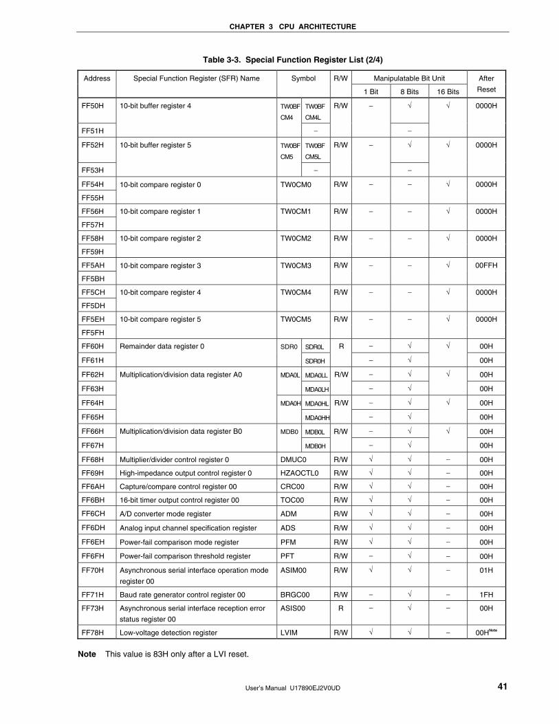
CHAPTER 3 CPU ARCHITECTURE
User’s Manual U17890EJ2V0UD 41
Table 3-3. Special Function Register List (2/4)
Manipulatable Bit Unit Address Special Function Register (SFR) Name Symbol R/W
1 Bit 8 Bits 16 Bits
After
Reset
FF50H TW0BF
CM4L
√
FF51H
10-bit buffer register 4 TW0BF
CM4
−
R/W −
−
√ 0000H
FF52H TW0BF
CM5L
√
FF53H
10-bit buffer register 5 TW0BF
CM5
−
R/W −
−
√ 0000H
FF54H
FF55H
10-bit compare register 0 TW0CM0 R/W − − √ 0000H
FF56H
FF57H
10-bit compare register 1 TW0CM1 R/W − − √ 0000H
FF58H
FF59H
10-bit compare register 2 TW0CM2 R/W − − √ 0000H
FF5AH
FF5BH
10-bit compare register 3 TW0CM3 R/W − − √ 00FFH
FF5CH
FF5DH
10-bit compare register 4 TW0CM4 R/W − − √ 0000H
FF5EH
FF5FH
10-bit compare register 5 TW0CM5 R/W − − √ 0000H
FF60H SDR0 SDR0L R − √ √ 00H
FF61H
Remainder data register 0
SDR0H − √ 00H
FF62H Multiplication/division data register A0 MDA0L MDA0LL R/W − √ √ 00H
FF63H MDA0LH − √ 00H
FF64H MDA0H MDA0HL R/W − √ √ 00H
FF65H MDA0HH − √ 00H
FF66H Multiplication/division data register B0 MDB0 MDB0L R/W − √ √ 00H
FF67H MDB0H − √ 00H
FF68H Multiplier/divider control register 0 DMUC0 R/W √ √ − 00H
FF69H High-impedance output control register 0 HZAOCTL0 R/W √ √ − 00H
FF6AH Capture/compare control register 00 CRC00 R/W √ √ − 00H
FF6BH 16-bit timer output control register 00 TOC00 R/W √ √ − 00H
FF6CH A/D converter mode register ADM R/W √ √ − 00H
FF6DH Analog input channel specification register ADS R/W √ √ − 00H
FF6EH Power-fail comparison mode register PFM R/W √ √ − 00H
FF6FH Power-fail comparison threshold register PFT R/W − √ − 00H
FF70H Asynchronous serial interface operation mode
register 00
ASIM00 R/W √ √ − 01H
FF71H Baud rate generator control register 00 BRGC00 R/W − √ − 1FH
FF73H Asynchronous serial interface reception error
status register 00
ASIS00 R − √ − 00H
FF78H Low-voltage detection register LVIM R/W √ √ − 00HNote
Note This value is 83H only after a LVI reset.
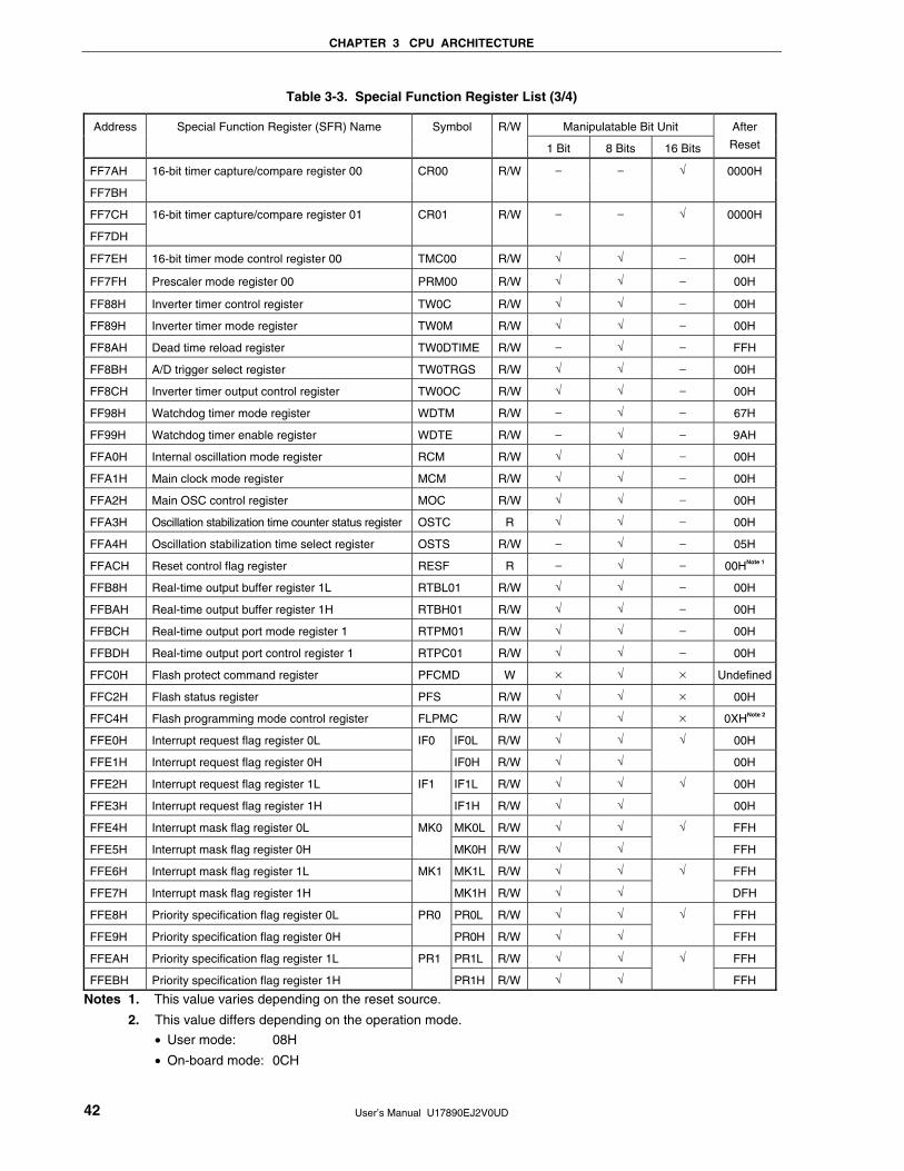
CHAPTER 3 CPU ARCHITECTURE
User’s Manual U17890EJ2V0UD 42
Table 3-3. Special Function Register List (3/4)
Manipulatable Bit Unit Address Special Function Register (SFR) Name Symbol R/W
1 Bit 8 Bits 16 Bits
After
Reset
FF7AH 16-bit timer capture/compare register 00 CR00 R/W − − √ 0000H
FF7BH
FF7CH 16-bit timer capture/compare register 01 CR01 R/W − − √ 0000H
FF7DH
FF7EH 16-bit timer mode control register 00 TMC00 R/W √ √ − 00H
FF7FH Prescaler mode register 00 PRM00 R/W √ √ − 00H
FF88H Inverter timer control register TW0C R/W √ √ − 00H
FF89H Inverter timer mode register TW0M R/W √ √ − 00H
FF8AH Dead time reload register TW0DTIME R/W − √ − FFH
FF8BH A/D trigger select register TW0TRGS R/W √ √ − 00H
FF8CH Inverter timer output control register TW0OC R/W √ √ − 00H
FF98H Watchdog timer mode register WDTM R/W − √ − 67H
FF99H Watchdog timer enable register WDTE R/W − √ − 9AH
FFA0H Internal oscillation mode register RCM R/W √ √ − 00H
FFA1H Main clock mode register MCM R/W √ √ − 00H
FFA2H Main OSC control register MOC R/W √ √ − 00H
FFA3H Oscillation stabilization time counter status register OSTC R √ √ − 00H
FFA4H Oscillation stabilization time select register OSTS R/W − √ − 05H
FFACH Reset control flag register RESF R − √ − 00HNote 1
FFB8H Real-time output buffer register 1L RTBL01 R/W √ √ − 00H
FFBAH Real-time output buffer register 1H RTBH01 R/W √ √ − 00H
FFBCH Real-time output port mode register 1 RTPM01 R/W √ √ − 00H
FFBDH Real-time output port control register 1 RTPC01 R/W √ √ − 00H
FFC0H Flash protect command register PFCMD W × √ × Undefined
FFC2H Flash status register PFS R/W √ √ × 00H
FFC4H Flash programming mode control register FLPMC R/W √ √ × 0XHNote 2
FFE0H Interrupt request flag register 0L IF0 IF0L R/W √ √ √ 00H
FFE1H Interrupt request flag register 0H IF0H R/W √ √ 00H
FFE2H Interrupt request flag register 1L IF1 IF1L R/W √ √ √ 00H
FFE3H Interrupt request flag register 1H IF1H R/W √ √ 00H
FFE4H Interrupt mask flag register 0L MK0 MK0L R/W √ √ √ FFH
FFE5H Interrupt mask flag register 0H MK0H R/W √ √ FFH
FFE6H Interrupt mask flag register 1L MK1 MK1L R/W √ √ √ FFH
FFE7H Interrupt mask flag register 1H MK1H R/W √ √ DFH
FFE8H Priority specification flag register 0L PR0L R/W √ √ FFH
FFE9H Priority specification flag register 0H
PR0
PR0H R/W √ √
√
FFH
FFEAH Priority specification flag register 1L PR1L R/W √ √ FFH
FFEBH Priority specification flag register 1H
PR1
PR1H R/W √ √
√
FFH
Notes 1. This value varies depending on the reset source.
2. This value differs depending on the operation mode.
• User mode: 08H
• On-board mode: 0CH

CHAPTER 3 CPU ARCHITECTURE
User’s Manual U17890EJ2V0UD 43
Table 3-3. Special Function Register List (4/4)
Manipulatable Bit Unit Address Special Function Register (SFR) Name Symbol R/W
1 Bit 8 Bits 16 Bits
After
Reset
FFF0H Internal memory size switching register Note IMS R/W − √ − CFH
FFFBH Processor clock control register PCC R/W √ √ − 00H
FFFDH System wait control register VSWC R/W √ √ − 00H
Note Because the initial value of the internal memory size switching register (IMS) is CFH, set IMS to 02H
(μPD78F0711) or 04H (μPD78F0712) by initialization.
<R>

CHAPTER 3 CPU ARCHITECTURE
User’s Manual U17890EJ2V0UD 44
3.3 Instruction Address Addressing
An instruction address is determined by program counter (PC) contents and is normally incremented (+1 for each
byte) automatically according to the number of bytes of an instruction to be fetched each time another instruction is
executed. When a branch instruction is executed, the branch destination information is set to the PC and branched by
the following addressing (for details of instructions, refer to 78K/0 Series Instructions User’s Manual (U12326E)).
3.3.1 Relative addressing
[Function]
The value obtained by adding 8-bit immediate data (displacement value: jdisp8) of an instruction code to the
start address of the following instruction is transferred to the program counter (PC) and branched. The
displacement value is treated as signed two’s complement data (−128 to +127) and bit 7 becomes a sign bit.
In other words, relative addressing consists of relative branching from the start address of the following
instruction to the −128 to +127 range.
This function is carried out when the BR $addr16 instruction or a conditional branch instruction is executed.
[Illustration]
15 0
PC
+
15 08 7 6
S
15 0
PC
α
jdisp8
When S = 0, all bits of are 0.When S = 1, all bits of are 1.
PC indicates the start addressof the instruction after the BR instruction.
...
αα

CHAPTER 3 CPU ARCHITECTURE
User’s Manual U17890EJ2V0UD 45
3.3.2 Immediate addressing
[Function]
Immediate data in the instruction word is transferred to the program counter (PC) and branched.
This function is carried out when the CALL !addr16 or BR !addr16 or CALLF !addr11 instruction is executed.
CALL !addr16 and BR !addr16 instructions can be branched to the entire memory space. The CALLF !addr11
instruction is branched to the 0800H to 0FFFH area.
[Illustration]
In the case of CALL !addr16 and BR !addr16 instructions
15 0
PC
8 7
7 0
CALL or BR
Low Addr.
High Addr.
In the case of CALLF !addr11 instruction
15 0
PC
8 7
7 0
fa10–8
11 10
0 0 0 0 1
6 4 3
CALLF
fa7–0

CHAPTER 3 CPU ARCHITECTURE
User’s Manual U17890EJ2V0UD 46
3.3.3 Table indirect addressing
[Function]
Table contents (branch destination address) of the particular location to be addressed by bits 1 to 5 of the
immediate data of an operation code are transferred to the program counter (PC) and branched.
This function is carried out when the CALLT [addr5] instruction is executed.
This instruction references the address stored in the memory table from 0040H to 007FH, which is indicated by
addr5, and allows branching to the entire memory space.
[Illustration]
15 1
15 0
PC
7 0
Low Addr.
High Addr.
Memory (Table)
Effective address+1
Effective address 0 10 0 0 0 0 0 0 0
8 7
8 7
6 5 0
0
11 1
7 6 5 1 0
ta4-0Operation code
15 1
addr5 0 10 0 0 0 0 0 0 0
8 7 6 5 0
0ta4-0
The effective address and addr5have the same value
...
3.3.4 Register addressing
[Function]
Register pair (AX) contents to be specified with an instruction word are transferred to the program counter (PC)
and branched.
This function is carried out when the BR AX instruction is executed.
[Illustration]
7 0
rp
0 7
A X
15 0
PC
8 7
<R>

CHAPTER 3 CPU ARCHITECTURE
User’s Manual U17890EJ2V0UD 47
3.4 Operand Address Addressing
The following methods are available to specify the register and memory (addressing) to undergo manipulation
during instruction execution.
3.4.1 Implied addressing
[Function]
The register that functions as an accumulator (A and AX) among the general-purpose registers is automatically
(implicitly) addressed.
Of the μPD78F0711 and 78F0712 instruction words, the following instructions employ implied addressing.
Instruction Register to Be Specified by Implied Addressing
MULU A register for multiplicand and AX register for product storage
DIVUW AX register for dividend and quotient storage
ADJBA/ADJBS A register for storage of numeric values that become decimal correction targets
ROR4/ROL4 A register for storage of digit data that undergoes digit rotation
[Operand format]
Because implied addressing can be automatically employed with an instruction, no particular operand format is
necessary.
[Description example]
In the case of MULU X
With an 8-bit × 8-bit multiply instruction, the product of A register and X register is stored in AX. In this example,
the A and AX registers are specified by implied addressing.

CHAPTER 3 CPU ARCHITECTURE
User’s Manual U17890EJ2V0UD 48
3.4.2 Register addressing
[Function]
The general-purpose register to be specified is accessed as an operand with the register bank select flags
(RBS0 to RBS1) and the register specify codes (Rn and RPn) of an operation code.
Register addressing is carried out when an instruction with the following operand format is executed. When an
8-bit register is specified, one of the eight registers is specified with 3 bits in the operation code.
[Operand format]
Identifier Description
r X, A, C, B, E, D, L, H
rp AX, BC, DE, HL
‘r’ and ‘rp’ can be described by absolute names (R0 to R7 and RP0 to RP3) as well as function names (X, A, C,
B, E, D, L, H, AX, BC, DE, and HL).
[Description example]
MOV A, C; when selecting C register as r
Operation code 0 1 1 0 0 0 1 0
Register specify code
INCW DE; when selecting DE register pair as rp
Operation code 1 0 0 0 0 1 0 0
Register specify code

CHAPTER 3 CPU ARCHITECTURE
User’s Manual U17890EJ2V0UD 49
3.4.3 Direct addressing
[Function]
The memory to be manipulated is directly addressed with immediate data in an instruction word becoming an
operand address.
[Operand format]
Identifier Description
addr16 Label or 16-bit immediate data
[Description example]
MOV A, !0FE00H; when setting !addr16 to FE00H
Operation code 1 0 0 0 1 1 1 0 OP code
0 0 0 0 0 0 0 0 00H
1 1 1 1 1 1 1 0 FEH
[Illustration]
Memory
07
addr16 (lower)
addr16 (upper)
OP code
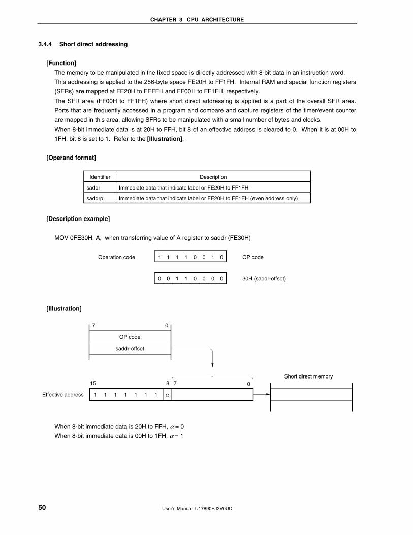
CHAPTER 3 CPU ARCHITECTURE
User’s Manual U17890EJ2V0UD 50
3.4.4 Short direct addressing
[Function]
The memory to be manipulated in the fixed space is directly addressed with 8-bit data in an instruction word.
This addressing is applied to the 256-byte space FE20H to FF1FH. Internal RAM and special function registers
(SFRs) are mapped at FE20H to FEFFH and FF00H to FF1FH, respectively.
The SFR area (FF00H to FF1FH) where short direct addressing is applied is a part of the overall SFR area.
Ports that are frequently accessed in a program and compare and capture registers of the timer/event counter
are mapped in this area, allowing SFRs to be manipulated with a small number of bytes and clocks.
When 8-bit immediate data is at 20H to FFH, bit 8 of an effective address is cleared to 0. When it is at 00H to
1FH, bit 8 is set to 1. Refer to the [Illustration].
[Operand format]
Identifier Description
saddr Immediate data that indicate label or FE20H to FF1FH
saddrp Immediate data that indicate label or FE20H to FF1EH (even address only)
[Description example]
MOV 0FE30H, A; when transferring value of A register to saddr (FE30H)
Operation code 1 1 1 1 0 0 1 0 OP code
0 0 1 1 0 0 0 0 30H (saddr-offset)
[Illustration]
15 0Short direct memory
Effective address 1 1 1 1 1 1 1
8 7
07
OP code
saddr-offset
α
When 8-bit immediate data is 20H to FFH, α = 0
When 8-bit immediate data is 00H to 1FH, α = 1

CHAPTER 3 CPU ARCHITECTURE
User’s Manual U17890EJ2V0UD 51
3.4.5 Special function register (SFR) addressing
[Function]
A memory-mapped special function register (SFR) is addressed with 8-bit immediate data in an instruction word.
This addressing is applied to the 240-byte spaces FF00H to FFCFH and FFE0H to FFFFH. However, the SFRs
mapped at FF00H to FF1FH can be accessed with short direct addressing.
[Operand format]
Identifier Description
sfr Special function register name
sfrp 16-bit manipulatable special function register name (even address only)
[Description example]
MOV PM0, A; when selecting PM0 (FF20H) as sfr
Operation code 1 1 1 1 0 1 1 0 OP code
0 0 1 0 0 0 0 0 20H (sfr-offset)
[Illustration]
15 0SFR
Effective address 1 1 1 1 1 1 1
8 7
07
OP code
sfr-offset
1
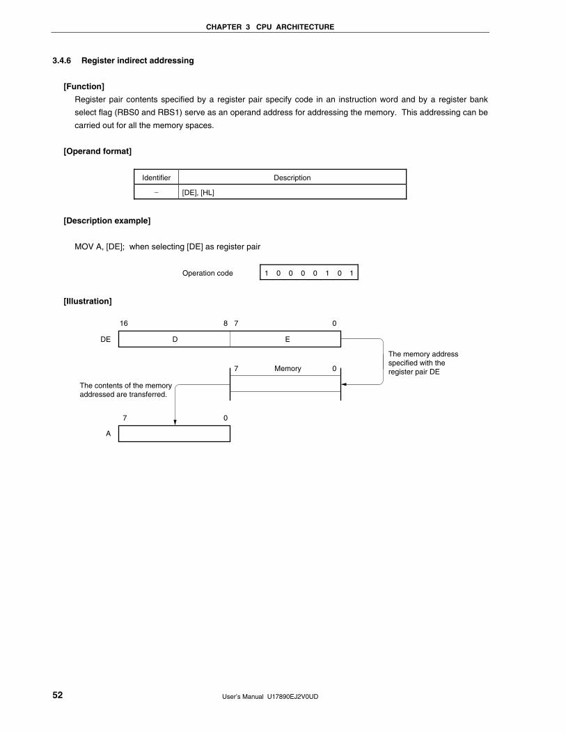
CHAPTER 3 CPU ARCHITECTURE
User’s Manual U17890EJ2V0UD 52
3.4.6 Register indirect addressing
[Function]
Register pair contents specified by a register pair specify code in an instruction word and by a register bank
select flag (RBS0 and RBS1) serve as an operand address for addressing the memory. This addressing can be
carried out for all the memory spaces.
[Operand format]
Identifier Description
− [DE], [HL]
[Description example]
MOV A, [DE]; when selecting [DE] as register pair
Operation code 1 0 0 0 0 1 0 1
[Illustration]
16 08
D
7
E
07
7 0
A
DE
The contents of the memoryaddressed are transferred.
Memory
The memory addressspecified with theregister pair DE

CHAPTER 3 CPU ARCHITECTURE
User’s Manual U17890EJ2V0UD 53
3.4.7 Based addressing
[Function]
8-bit immediate data is added as offset data to the contents of the base register, that is, the HL register pair in
the register bank specified by the register bank select flag (RBS0 and RBS1), and the sum is used to address
the memory. Addition is performed by expanding the offset data as a positive number to 16 bits. A carry from
the 16th bit is ignored. This addressing can be carried out for all the memory spaces.
[Operand format]
Identifier Description
− [HL + byte]
[Description example]
MOV A, [HL + 10H]; when setting byte to 10H
Operation code 1 0 1 0 1 1 1 0
0 0 0 1 0 0 0 0
[Illustration]
16 08
H
7
L
07
7 0
A
HL
The contents of the memoryaddressed are transferred.
Memory+10H

CHAPTER 3 CPU ARCHITECTURE
User’s Manual U17890EJ2V0UD 54
3.4.8 Based indexed addressing
[Function]
The B or C register contents specified in an instruction word are added to the contents of the base register, that
is, the HL register pair in the register bank specified by the register bank select flag (RBS0 and RBS1), and the
sum is used to address the memory. Addition is performed by expanding the B or C register contents as a
positive number to 16 bits. A carry from the 16th bit is ignored. This addressing can be carried out for all the
memory spaces.
[Operand format]
Identifier Description
− [HL + B], [HL + C]
[Description example]
In the case of MOV A, [HL + B] (selecting B register)
Operation code 1 0 1 0 1 0 1 1
[Illustration]
16 0
H
78
L
07
B
+
07
7 0
A
HL
The contents of the memoryaddressed are transferred.
Memory

CHAPTER 3 CPU ARCHITECTURE
User’s Manual U17890EJ2V0UD 55
3.4.9 Stack addressing
[Function]
The stack area is indirectly addressed with the stack pointer (SP) contents.
This addressing method is automatically employed when the PUSH, POP, subroutine call and return
instructions are executed or the register is saved/reset upon generation of an interrupt request.
With stack addressing, only the internal high-speed RAM area can be accessed.
[Description example]
In the case of PUSH DE (saving DE register)
Operation code 1 0 1 1 0 1 0 1
[Illustration]
E
FEE0HSP
SP
FEE0H
FEDFH
FEDEH
D
Memory 07
FEDEH

User’s Manual U17890EJ2V0UD 56
CHAPTER 4 PORT FUNCTIONS
4.1 Port Functions
There are two types of pin I/O buffer power supplies: AVREF and VDD. The relationship between these power
supplies and the pins is shown below.
Table 4-1. Pin I/O Buffer Power Supplies
Power Supply Corresponding Pins
AVREF P20 to P23 Note
VDD Port pins other than P20 to P23
Note Connect AVREF to VDD when port 2 is used as a digital port.
μPD78F0711 and 78F0712 products are provided with the ports shown in Figure 4-1, which enable variety of control
operations. The functions of each port are shown in Table 4-2.
In addition to the function as digital I/O ports, these ports have several alternate functions. For details of the
alternate functions, see CHAPTER 2 PIN FUNCTIONS.
Figure 4-1. Port Types
Port 2
P20
P23
Port 5P50P53
Port 0
P00
P03
Port 1
P13
P17
P54
P14P16
<R>

CHAPTER 4 PORT FUNCTIONS
User’s Manual U17890EJ2V0UD 57
Table 4-2. Port Functions
Pin Name I/O Function After Reset Alternate Function
P00 INTP0/TW0TOFFP
P01 INTP1
P02 INTP2
P03
I/O Port 0.
4-bit I/O port.
Input/output can be specified in 1-bit units.
Use of an on-chip pull-up resistor can be specified by a
software setting.
Input
INTP3/ADTRG
P13 RxD00
P14 TxD00
P16 −
P17
I/O Port 1.
4-bit I/O port.
Input/output can be specified in 1-bit units.
Use of an on-chip pull-up resistor can be specified by a
software setting.
Input
FLMD1
P20 to P23 Input Port 2.
4-bit input-only port.
Input ANI0 to ANI3
P50 TI50/TO50
P53 TI000/INTP5
P54
I/O Port 5.
3-bit I/O port.
Input/output can be specified in 1-bit units.
Use of an on-chip pull-up resistor can be specified by a
software setting.
Input
TI001/TO00

CHAPTER 4 PORT FUNCTIONS
User’s Manual U17890EJ2V0UD 58
4.2 Port Configuration
Ports consist of the following hardware.
Table 4-3. Port Configuration
Item Configuration
Control registers Port mode register (PM0, PM1, PM5)
Port register (P0, P1, P2, P5)
Pull-up resistor option register (PU0, PU1, PU5)
Port Total: 15 (CMOS I/O: 11, CMOS input: 4)
Pull-up resistor Total: 11 (software control: 11)
4.2.1 Port 0
Port 0 is a 4-bit I/O port with an output latch. Port 0 can be set to the input mode or output mode in 1-bit units
using port mode register 0 (PM0). When the P00 to P03 pins are used as an input port, use of an on-chip pull-up
resistor can be specified by pull-up resistor option register 0 (PU0).
This port can also be used for external interrupt request input, timer output stop external signal, and A/D converter
trigger input.
RESET input sets port 0 to input mode.
Figure 4-2 shows a block diagram of port 0.
Figure 4-2. Block Diagram of P00 to P03
WRPU
RD
PU0
WRPORT
WRPM
EVDD
P-ch
PM0
PM00 to PM03
PU00 to PU03
P00/INTP0/TW0TOFFP,P01/INTP1,P02/INTP2,P03/INTP3/ADTRG
Inte
rnal
bus
Output latch(P00 to P03)
Alternatefunction
Sel
ecto
r
PU0: Pull-up resistor option register 0
PM0: Port mode register 0
RD: Read signal
WR××: Write signal

CHAPTER 4 PORT FUNCTIONS
User’s Manual U17890EJ2V0UD 59
4.2.2 Port 1
Port 1 is an 4-bit I/O port with an output latch. Port 1 can be set to the input mode or output mode in 1-bit units
using port mode register 1 (PM1). When the P13, P14, P16, and P17 pins are used as an input port, use of an on-
chip pull-up resistor can be specified by pull-up resistor option register 1 (PU1).
This port can also be used for serial interface data I/O and flash memory programming mode setting.
RESET input sets port 1 to input mode.
Figures 4-3 to 4-6 show block diagrams of port 1.
Figure 4-3. Block Diagram of P13
P13/RxD00
WRPU
RD
WRPORT
WRPM
PU13
Alternatefunction
Output latch(P13)
EVDD
P-ch
Sel
ecto
r
Inte
rnal
bus
PU1
PM1
PM13
PU1: Pull-up resistor option register 1
PM1: Port mode register 1
RD: Read signal
WR××: Write signal
<R>

CHAPTER 4 PORT FUNCTIONS
User’s Manual U17890EJ2V0UD 60
Figure 4-4. Block Diagram of P14
P14/TxD00
WRPU
RD
WRPORT
WRPM
PU14
Output latch(P14)
PM14
Alternatefunction
EVDD
P-ch
Inte
rnal
bus
Sel
ecto
r
PU1
PM1
PU1: Pull-up resistor option register 1
PM1: Port mode register 1
RD: Read signal
WR××: Write signal

CHAPTER 4 PORT FUNCTIONS
User’s Manual U17890EJ2V0UD 61
Figure 4-5. Block Diagram of P16
P16
WRPU
RD
WRPORT
WRPM
PU16
Output latch(P16)
PM16
EVDD
P-ch
PU1
PM1S
elec
tor
Inte
rnal
bus
PU1: Pull-up resistor option register 1
PM1: Port mode register 1
RD: Read signal
WR××: Write signal

CHAPTER 4 PORT FUNCTIONS
User’s Manual U17890EJ2V0UD 62
Figure 4-6. Block Diagram of P17
P17/FLMD1
WRPU
RD
WRPORT
WRPM
PU17
PM17
EVDD
P-ch
PU1
PM1
Inte
rnal
bus
Alternatefunction
Output latch(P17)
Sel
ecto
r
PU1: Pull-up resistor option register 1
PM1: Port mode register 1
RD: Read signal
WR××: Write signal

CHAPTER 4 PORT FUNCTIONS
User’s Manual U17890EJ2V0UD 63
4.2.3 Port 2
Port 2 is an 4-bit input-only port.
This port can also be used for A/D converter analog input.
Figure 4-7 shows a block diagram of port 2.
Figure 4-7. Block Diagram of P20 to P23
RD
A/D converter P20/ANI0 to P23/ANI3Inte
rnal
bus
RD: Read signal
Caution Connect AVREF to VDD when P20 to P23 is used as a digital port.
<R>

CHAPTER 4 PORT FUNCTIONS
User’s Manual U17890EJ2V0UD 64
4.2.4 Port 5
Port 5 is an 3-bit I/O port with an output latch. Port 5 can be set to the input mode or output mode in 1-bit units
using port mode register 5 (PM5). Use of an on-chip pull-up resistor can be specified in 1-bit units using pull-up
resistor option register 5 (PU5).
This port can also be used as external interrupt request input, timer I/O.
RESET input sets port 5 to input mode.
Figures 4-8 and 4-9 show block diagrams of port 5.
Figure 4-8. Block Diagram of P50 and P54
P50/TI50/TO50, P54/TI001/TO00
WRPU
RD
WRPORT
WRPM
PU50, PU54
EVDD
P-ch
PU5
PM5
PM50, PM54
Output latch(P50, P54)
Alternatefunction
Sel
ecto
r
Inte
rnal
bus
Alternatefunction
PU5: Pull-up resistor option register 5
PM5: Port mode register 5
RD: Read signal
WR××: Write signal

CHAPTER 4 PORT FUNCTIONS
User’s Manual U17890EJ2V0UD 65
Figure 4-9. Block Diagram of P53
P53/TI000/INTP5
WRPU
RD
WRPORT
WRPM
PM53
EVDD
P-ch
PU5
PM5
PU53
Sel
ecto
r
Alternatefunction
Output latch(P53)
Inte
rnal
bus
PU5: Pull-up resistor option register 5
PM5: Port mode register 5
RD: Read signal
WR××: Write signal

CHAPTER 4 PORT FUNCTIONS
User’s Manual U17890EJ2V0UD 66
4.3 Registers Controlling Port Function
Port functions are controlled by the following three types of registers.
• Port mode registers (PM0, PM1, PM5)
• Port registers (P0, P1, P2, P5)
• Pull-up resistor option registers (PU0, PU1, PU5)
(1) Port mode registers (PM0, PM1, PM5)
These registers specify input or output mode for the port in 1-bit units.
These registers can be set by a 1-bit or 8-bit memory manipulation instruction.
RESET input sets these registers to FFH.
When port pins are used as alternate-function pins, set the port mode register and output latch as shown in Table
4-4.
Figure 4-10. Format of Port Mode Register
7
1
Symbol
PM0
6
1
5
1
4
1
3
PM03
2
PM02
1
PM01
0
PM00
Address
FF20H
After reset
FFH
R/W
R/W
7
PM17PM1
6
PM16
5
1
4
PM14
3
PM13
2
1
1
1
0
1 FF21H FFH R/W
7
1PM5
6
1
5
1
4
PM54
3
PM53
2
1
1
1
0
PM50 FF25H FFH R/W
PMmn Pmn pin I/O mode selection
(m = 0, 1, 5; n = 0 to 7)
0 Output mode (output buffer on)
1 Input mode (output buffer off)

CHAPTER 4 PORT FUNCTIONS
User’s Manual U17890EJ2V0UD 67
Table 4-4. Settings of Port Mode Register and Output Latch When Using Alternate Function
Alternate Function Pin Name
Function Name I/O
PM×× P××
INTP0 Input 1 × P00
TW0TOFFP Input 1 ×
P01 INTP1 Input 1 ×
P02 INTP2 Input 1 ×
INTP3 Input 1 × P03
ADTRG Input 1 ×
P13 RxD00 Input 1 ×
P14 TxD00 Output 0 1
P17 FLMD1 Input 1 ×
P20-P23 ANI0-ANI3 Input 1 ×
TI50 Input 1 × P50
TO50 Output 0 0
INTP5 Input 1 × P53
TI000 Input 1 ×
TI001 Input 1 × P54
TO00 Output 0 0
Remark ×: Don’t care
PM××: Port mode register
P××: Port output latch

CHAPTER 4 PORT FUNCTIONS
User’s Manual U17890EJ2V0UD 68
(2) Port registers (P0, P1, P2, P5)
These registers write the data that is output from the chip when data is output from a port.
If the data is read in the input mode, the pin level is read. If it is read in the output mode, the value of the output
latch is read.
These registers can be set by a 1-bit or 8-bit memory manipulation instruction.
RESET input clears these registers to 00H (but P2 is undefined).
Figure 4-11. Format of Port Register
7
0
Symbol
P0
6
0
5
0
4
0
3
P03
2
P02
1
P01
0
P00
Address
FF00H
After reset
00H (output latch)
R/W
R/W
7
P17P1
6
P16
5
0
4
P14
3
P13
2
0
1
0
0
0 FF01H 00H (output latch) R/W
R
7
0P2
6
0
5
0
4
0
3
P23
2
P22
1
P21
0
P20 FF02H Undefined
7
0P5
6
0
5
0
4
P54
3
P53
2
0
1
0
0
P50 FF05H 00H (output latch) R/W
m = 0 to 2, 5; n = 0 to 7
Pmn
Output data control (in output mode) Input data read (in input mode)
0 Output 0 Input low level
1 Output 1 Input high level

CHAPTER 4 PORT FUNCTIONS
User’s Manual U17890EJ2V0UD 69
(3) Pull-up resistor option registers (PU0, PU1, and PU5)
These registers specify whether the on-chip pull-up resistors of P00 to P03, P13, P14, P16, P17, P50, P53, P54
are to be used or not. On-chip pull-up resistors can be used in 1-bit units only for the bits set to input mode of the
pins to which the use of an on-chip pull-up resistor has been specified. On-chip pull-up resistors cannot be
connected for bits set to output mode and bits used as alternate-function output pins, regardless of the settings of
PU0, PU1, and PU5.
These registers can be set by a 1-bit or 8-bit memory manipulation instruction.
RESET input clears these registers to 00H.
Figure 4-12. Format of Pull-up Resistor Option Register
7
0
Symbol
PU0
6
0
5
0
4
0
3
PU03
2
PU02
1
PU01
0
PU00
Address
FF30H
After reset
00H
R/W
R/W
7
PU17PU1
6
PU16
5
0
4
PU14
3
PU13
2
0
1
0
0
0 FF31H 00H R/W
7
0PU5
6
0
5
0
4
PU54
3
PU53
2
0
1
0
0
PU50 FF35H 00H R/W
PUmn Pmn pin on-chip pull-up resistor selection
(m = 0, 1, 5; n = 0 to 7)
0 On-chip pull-up resistor not connected
1 On-chip pull-up resistor connected

CHAPTER 4 PORT FUNCTIONS
User’s Manual U17890EJ2V0UD 70
4.4 Port Function Operations
Port operations differ depending on whether the input or output mode is set, as shown below.
Caution In the case of a 1-bit memory manipulation instruction, although a single bit is manipulated, the
port is accessed as an 8-bit unit. Therefore, on a port with a mixture of input and output pins,
the output latch contents for pins specified as input are undefined, even for bits other than the
manipulated bit.
4.4.1 Writing to I/O port
(1) Output mode
A value is written to the output latch by a transfer instruction, and the output latch contents are output from the pin.
Once data is written to the output latch, it is retained until data is written to the output latch again.
The data of the output latch is cleared by reset.
(2) Input mode
A value is written to the output latch by a transfer instruction, but since the output buffer is off, the pin status does
not change.
Once data is written to the output latch, it is retained until data is written to the output latch again.
4.4.2 Reading from I/O port
(1) Output mode
The output latch contents are read by a transfer instruction. The output latch contents do not change.
(2) Input mode
The pin status is read by a transfer instruction. The output latch contents do not change.
4.4.3 Operations on I/O port
(1) Output mode
An operation is performed on the output latch contents, and the result is written to the output latch. The output
latch contents are output from the pins.
Once data is written to the output latch, it is retained until data is written to the output latch again.
The data of the output latch is cleared by reset.
(2) Input mode
The pin level is read and an operation is performed on its contents. The result of the operation is written to the
output latch, but since the output buffer is off, the pin status does not change.

CHAPTER 4 PORT FUNCTIONS
User’s Manual U17890EJ2V0UD 71
4.5 Cautions on 1-Bit Manipulation Instruction for Port Register n (Pn)
When a 1-bit manipulation instruction is executed on a port that provides both input and output functions, the
output latch value of an input port that is not subject to manipulation may be written in addition to the targeted bit.
Therefore, it is recommended to rewrite the output latch when switching a port from input mode to output mode.
<Example> When P13 is an output port, P14, P16, and P17 are input ports (all pin statuses are high level), and
the port latch value of port 1 is 00H, if the output of output port P13 is changed from low level to
high level via a 1-bit manipulation instruction, the output latch value of port 1 is D8H.
Explanation: The targets of writing to and reading from the Pn register of a port whose PMnm bit is 1 are the
output latch and pin status, respectively.
A 1-bit manipulation instruction is executed in the following order in the μPD78F0711 and 78F0712.
<1> The Pn register is read in 8-bit units.
<2> The targeted one bit is manipulated.
<3> The Pn register is written in 8-bit units.
In step <1>, the output latch value (0) of P13, which is an output port, is read, while the pin statuses
of P14, P16, and P17, which are input ports, are read. If the pin statuses of P14, P16, and P17 are
high level at this time, the read value is D0H.
The value is changed to D8H by the manipulation in <2>.
D8H is written to the output latch by the manipulation in <3>.
Figure 4-13. Bit Manipulation Instruction (P13)
Low-level output
1-bit manipulationinstruction (set1 P1.3)is executed for P13bit.
Pin status: High-level
P13
P14, P16, P17
Port 1 output latch
0 0 0 0 0 0 0 0
High-level output
Pin status: High-level
P13
P14, P16, P17
Port 1 output latch
1 1 0 1 1 0 0 0
1-bit manipulation instruction for P10 bit
<1> Port register 1 (P1) is read in 8-bit units.• In the case of P13, an output port, the value of the port output latch (0) is read.• In the case of P14, P16, P17, input ports, the pin status (1) is read.
<2> Set the P13 bit to 1.<3> Write the results of <2> to the output latch of port register 1 (P1)
in 8-bit units.
<R>

User’s Manual U17890EJ2V0UD 72
CHAPTER 5 CLOCK GENERATOR
5.1 Functions of Clock Generator
The clock generator generates the clock to be supplied to the CPU and peripheral hardware.
The following kind of system clock and clock oscillator are selectable.
(1) High-speed system clock
<1> X1 oscillator
This circuit oscillates a clock of fX = 5 to 20 MHz by connecting a resonator to X1 and X2. An external
main system clock (5 to 20 MHz) can also be supplied from the X1 and X2 pin. Oscillation can be
stopped by executing the STOP instruction or setting the main OSC control register (MOC).
<2> Internal high-speed oscillator
The internal high-speed oscillator oscillates a clock of fRH = 8 MHz (TYP.). Oscillation can be stopped by
executing the STOP instruction or setting the main OSC control register (MOC).
The X1 clock or the internal high-speed oscillation clock can be selected as the high-speed system clock by
using the option byte.
The operation of the oscillator stops when the oscillator is not selected by using the option byte.
(2) Internal low-speed oscillation clock
• Internal low-speed oscillator
The internal low-speed oscillator oscillates a clock of fRL = 240 kHz (TYP.). After a reset release, the
internal low-speed oscillation clock always starts operating.
Oscillation can be stopped by setting the internal oscillation mode register (RCM) when “internal low-
speed oscillator can be stopped by software” is set by the option byte.
The internal low-speed oscillation clock can be used as the CPU clock. The following hardware operates
with the internal low-speed oscillation clock.
• CPU (when internal low-speed oscillation clock is selected)
• Watchdog timer (when internal low-speed oscillation clock is selected)
• 8-bit timer 51 (when fRL/27 is selected)
Remarks 1. fX: X1 clock oscillation frequency
2. fRH: Internal high-speed oscillation clock frequency
3. fRL: Internal low-speed oscillation clock frequency

CHAPTER 5 CLOCK GENERATOR
User’s Manual U17890EJ2V0UD 73
5.2 Configuration of Clock Generator
The clock generator consists of the following hardware.
Table 5-1. Configuration of Clock Generator
Item Configuration
Control registers Processor clock control register (PCC)
Internal oscillation mode register (RCM)
Main OSC control register (MOC)
Main clock mode register (MCM)
Oscillation stabilization time counter status register (OSTC)
Oscillation stabilization time select register (OSTS)
System wait control register (VSWC)
Oscillator X1 oscillator
Internal high-speed oscillator
Internal low-speed oscillator
<R>

CH
AP
TE
R 5 C
LO
CK
GE
NE
RA
TO
R
User’s M
anual U17890E
J2V0U
D
74 Figure 5-1. Block Diagram of Clock Generator
Option byte1: Cannot be stopped0: Can be stopped
Intrenal oscillationmode register (RCM)
RSTOP
Internal high-speed oscillator(8 MHz (TYP.))
Internal low-speed oscillator(240 kHz(TYP.))
fRL
Peripheral hardware clock (fPRS)
Watchdog timer, 8-bit timer 51
CPU clock(fCPU)
Processor clock control register (PCC)
PCC2 PCC1 PCC0
PrescalerMain systemclock switch
fXP
X1 oscillationstabilization time counter
OSTS1 OSTS0OSTS2
Oscillation stabilization time select register (OSTS)
3
MOST16
MOST15
MOST14
MOST13
MOST11
Oscillation stabilization time counter status register (OSTC)
Controller
MCM0MCSMSTOP
STOP
3
fXP
2fXP
22fXP
23fXP
24
Main clock mode register (MCM)
Main OSCcontrol register
(MOC)
fRH
Internal bus
Internal bus
High-speedsystem clock
Crystal/ceramicoscillation
External inputclock
X1
X2 fX
Option byte 1: Internal high-speed oscillation clock 0: X1 clock
X1 oscillator
fXH
Sel
ecto
r
Sel
ecto
r

CHAPTER 5 CLOCK GENERATOR
User’s Manual U17890EJ2V0UD 75
Remarks 1. fX: X1 clock oscillation frequency
2. fRH: Internal high-speed oscillation clock frequency
3. fXH: High-speed system clock oscillation frequency
4. fXP: Main system clock oscillation frequency
5. fPRS: Peripheral hardware clock oscillation frequency
6. fCPU: CPU clock oscillation frequency
7. fRL: Internal low-speed oscillation clock frequency
5.3 Registers Controlling Clock Generator
The following seven registers are used to control the clock generator.
• Processor clock control register (PCC)
• Internal oscillation mode register (RCM)
• Main OSC control register (MOC)
• Main clock mode register (MCM)
• Oscillation stabilization time counter status register (OSTC)
• Oscillation stabilization time select register (OSTS)
• System wait control register (VSWC)
<R>

CHAPTER 5 CLOCK GENERATOR
User’s Manual U17890EJ2V0UD 76
(1) Processor clock control register (PCC)
The PCC register is used to set the CPU clock division ratio.
The PCC is set by a 1-bit or 8-bit memory manipulation instruction.
Reset signal generation clears this register to 00H.
Figure 5-2. Format of Processor Clock Control Register (PCC)
Address: FFFBH After reset: 00H R/W
Symbol 7 6 5 4 3 2 1 0
PCC 0 0 0 0 0 PCC2 PCC1 PCC0
Caution Be sure to set bit 3 to 7 to 0.
Remark fXP: Main system clock oscillation frequency
The fastest instruction can be executed in 2 clocks of the CPU clock in the 78K0 series. Therefore, the
relationship between the CPU clock (fCPU) and minimum instruction execution time is as shown in the Table 5-2.
Table 5-2. Relationship Between CPU Clock and Minimum Instruction Execution Time
Minimum Instruction Execution Time: 2/fCPU
High-speed System ClockNote 1
X1 ClockNote 2 Internal High-speed
Oscillation ClockNote 2
Internal Low-speed
Oscillation ClockNote 1
CPU Clock (fCPU)
At 20 MHz Operation At 16 MHz Operation At 8 MHz (TYP.)
Operation
At 240 kHz (TYP.)
Operation
fXP 0.1 μs 0.125 μs 0.25 μs 8.3 μs
fXP/2 0.2 μs 0.25 μs 0.5 μs 16.6 μs
fXP/22 0.4 μs 0.5 μs 1.0 μs −Note 3
fXP/23 0.8 μs 1.0 μs 2.0 μs −Note 3
fXP/24 1.6 μs 2.0 μs 4.0 μs −Note 3
Notes 1. The main clock mode register (MCM) is used to set the main system clock supplied to CPU clock
(high-speed system clock or internal low-speed oscillation clock) (see Figure 5-5).
2. The option byte is used to select the high-speed system clock (X1 clock or internal high-speed
oscillation clock).
3. Setting prohibited.
CPU clock (fCPU) selection
PCC2 PCC1 PCC0
MCM0 = 1 MCM0 = 0
0 0 0 fXP fX or fRH fRL
0 0 1 fXP/2 fX/2 or fRH/2 fRL/2
0 1 0 fXP/22 fX/22 or fRH/22 Setting prohibited
0 1 1 fXP/23 fX/23 or fRH/23 Setting prohibited
1 0 0 fXP/24 fX/24 or fRH/24 Setting prohibited
Other than above Setting prohibited
<R>

CHAPTER 5 CLOCK GENERATOR
User’s Manual U17890EJ2V0UD 77
(2) Internal oscillation mode register (RCM)
This register sets the operation mode of internal low-speed oscillator.
RCM can be set by a 1-bit or 8-bit memory manipulation instruction.
Reset signal generation clears this register to 00H.
Figure 5-3. Format of Internal Oscillation Mode Register (RCM)
Address: FFA0H After reset: 00H R/WNote
Symbol 7 6 5 4 3 2 1 <0>
RCM 0 0 0 0 0 0 0 RSTOP
RSTOP Internal low-speed oscillator oscillating/stopped
0 Internal low-speed oscillator oscillating
1 Internal low-speed oscillator stopped
Note Bit 1 to 7 are read-only.
Caution When setting RSTOP to 1, be sure to confirm that the CPU operates with the high-
speed system clock (when MCS = 1).
In addition, stop peripheral hardware that is operating on the internal low-speed
oscillation clock before setting RSTOP to 1.

CHAPTER 5 CLOCK GENERATOR
User’s Manual U17890EJ2V0UD 78
(3) Main OSC control register (MOC)
MOC is the register that controls the operation of the X1 oscillator or the internal high-speed oscillator which
generates the high-speed system clock.
This register is used to stop the high-speed system clock when the CPU is operating with the internal low-speed
oscillation clock.
MOC can be set by a 1-bit or 8-bit memory manipulation instruction.
Reset signal generation clears this register to 00H.
Figure 5-4. Format of Main OSC Control Register (MOC)
Address: FFA2H After reset: 00H R/W
Symbol <7> 6 5 4 3 2 1 0
MOC MSTOP 0 0 0 0 0 0 0
MSTOP High-speed system clock (X1 oscillator, Internal high-speed oscillator) operation control
0 Oscillator oscillating
1 Oscillator stopped
Cautions 1. When setting MSTOP to 1, be sure to confirm that the CPU operates with the
internal low-speed oscillation clock (When MCS = 0).
In addition, stop peripheral hardware that is operating on the high-speed system
clock before setting MSTOP to 1.
2. The peripheral hardware cannot operate if the high-speed system clock is
stopped when the high-speed system clock is selected as the peripheral
hardware clock. To resume the operation of the peripheral hardware after the
peripheral hardware clock has been stopped, initialize the peripheral hardware.

CHAPTER 5 CLOCK GENERATOR
User’s Manual U17890EJ2V0UD 79
(4) Main clock mode register (MCM)
This register selects the main system clock (fXP).
The main system clock becomes a source clock to the CPU and the peripheral hardware.
MCM can be set by a 1-bit or 8-bit memory manipulation instruction.
Reset signal generation clears this register to 00H.
Figure 5-5. Format of Main Clock Mode Register (MCM)
Address: FFA1H After reset: 00H R/WNote
Symbol 7 6 5 4 3 2 <1> <0>
MCM 0 0 0 0 0 0 MCS MCM0
MCS Status of source clock to CPU (main system clock (fXP) )
0 Operates with internal low-speed oscillation clock
1 Operates with high-speed system clock
MCM0 Selection of source clock to CPU (main system clock (fXP))
0 Internal low-speed oscillation clock (fRL)
1 High-speed system clock (fXH)
Note Bit 1 is read-only.
Caution When internal low-speed oscillation clock is selected as the source clock to the
CPU, the divided clock of the internal low-speed oscillation clock (fRL) is supplied to
the peripheral hardware (fRL = 240 kHz (TYP.)).
However, operation of the peripheral hardware with the internal low-speed
oscillation clock cannot be guaranteed. Therefore, when the internal low-speed
oscillation clock is selected as the source clock to the CPU, do not use the
peripheral hardware. In addition, stop the peripheral hardware before switching the
source clock to the CPU from the high-speed system clock to the internal low-speed
oscillation clock. Note, however, that the following peripheral hardware can be used
when the CPU operates on the internal low-speed oscillation clock.
• Watchdog timer (when internal low-speed oscillation is selected)
• 8-bit timer 51 (when fRL/27 is selected as count clock)
• Peripheral hardware selecting external clock as the clock source
(Except 16-bit timer/event counter 00)

CHAPTER 5 CLOCK GENERATOR
User’s Manual U17890EJ2V0UD 80
(5) Oscillation stabilization time counter status register (OSTC)
This is the register that indicates the count status of the X1 clock oscillation stabilization time counter. When X1
clock oscillation starts with the internal low-speed oscillation clock used as the CPU clock, the X1 clock oscillation
stabilization time can be checked.
OSTC can be read by a 1-bit or 8-bit memory manipulation instruction.
When reset is released (reset by RESET input, POC, LVI, and WDT), the STOP instruction and MSTOP (bit 7 of
MOC register) = 1 clear OSTC to 00H.
Figure 5-6. Format of Oscillation Stabilization Time Counter Status Register (OSTC)
Address: FFA3H After reset: 00H R
Symbol 7 6 5 4 3 2 1 0
OSTC 0 0 0 MOST11 MOST13 MOST14 MOST15 MOST16
Oscillation stabilization time status
MOST11 MOST13 MOST14 MOST15 MOST16
fX = 20 MHz fX = 16 MHz
1 0 0 0 0 211/fX min. 102.4 μs min. 128 μs min.
1 1 0 0 0 213/fX min. 409.6 μs min. 512 μs min.
1 1 1 0 0 214/fX min. 819.2 μs min. 1.02 ms min.
1 1 1 1 0 215/fX min. 1.64 ms min. 2.04 ms min.
1 1 1 1 1 216/fX min. 3.27 ms min. 4.09 ms min.
Cautions 1. After the above time has elapsed, the bits are set to 1 in order from MOST11 and
remain 1.
2. The oscillation stabilization time counter counts up to the oscillation stabilization
time set by OSTS.
If the STOP mode is entered and then released while the internal low-speed
oscillation clock is being used as the CPU clock, set the oscillation stabilization
time as follows. • Desired OSTC oscillation stabilization time ≤ Oscillation stabilization time
set by OSTS
Note, therefore, that only the status up to the oscillation stabilization time set by
OSTS is set to OSTC after STOP mode is released.
3. The X1 clock oscillation stabilization wait time does not include the time until
clock oscillation starts (“a” below).
STOP mode release
X1 pin voltage waveform
a
4. OSTC cannot be used when the internal high-speed oscillation clock is selected
as the high-speed system clock by using the option byte.
Secure wait time (350 μs) by software.
Remark fX: X1 clock oscillation frequency

CHAPTER 5 CLOCK GENERATOR
User’s Manual U17890EJ2V0UD 81
(6) Oscillation stabilization time select register (OSTS)
This register is used to select the X1 clock oscillation stabilization wait time when the STOP mode is released.
When the X1 clock is selected as the CPU clock, the operation waits for the time set using OSTS after the STOP
mode is released.
When the internal low-speed oscillation clock is selected as the CPU clock, confirm with OSTC that the desired
oscillation stabilization time has elapsed after the STOP mode is released. The oscillation stabilization time can
be checked up to the time set using OSTC.
When the internal high-speed oscillation clock is selected as the CPU clock, wait for 350 μs after the STOP mode
is released. (OSTC cannot be used.)
OSTS can be set by an 8-bit memory manipulation instruction.
Reset signal generation sets this register to 05H.
Figure 5-7. Format of Oscillation Stabilization Time Select Register (OSTS)
Address: FFA4H After reset: 05H R/W
Symbol 7 6 5 4 3 2 1 0
OSTS 0 0 0 0 0 OSTS2 OSTS1 OSTS0
Oscillation stabilization time selection
OSTS2 OSTS1 OSTS0
fX = 20 MHz fX = 16 MHz
0 0 1 211/fX 102.4 μs 128 μs
0 1 0 213/fX 409.6 μs 512 μs
0 1 1 214/fX 819.2 μs 1.02 ms
1 0 0 215/fX 1.64 ms 2.04 ms
1 0 1 216/fX 3.27 ms 4.09 ms
Other than above Setting prohibited
Cautions 1. To set the STOP mode when the X1 clock is used as the CPU clock, set OSTS
before executing the STOP instruction.
2. Do not change the value of the OSTS register during the X1 clock oscillation
stabilization time.
3. The oscillation stabilization time counter counts up to the oscillation
stabilization time set by OSTS. If the STOP mode is entered and then released
while the internal low-speed oscillation clock is being used as the CPU clock,
set the oscillation stabilization time as follows. • Desired OSTC oscillation stabilization time ≤ Oscillation stabilization time
set by OSTS
Note, therefore, that only the status up to the oscillation stabilization time set by
OSTS is set to OSTC after STOP mode is released.
4. The X1 clock oscillation stabilization wait time does not include the time until
clock oscillation starts (“a” below).
STOP mode release
X1 pin voltage waveform
a
Remark fX: X1 clock oscillation frequency

CHAPTER 5 CLOCK GENERATOR
User’s Manual U17890EJ2V0UD 82
(7) System wait control register (VSWC)
This register is used to control wait states when a high-speed CPU and a low-speed peripheral I/O are connected.
VSWC can be set by a 1-bit or 8-bit memory manipulation instruction.
RESET input clears this register to 00H.
Figure 5-8. Format of System Wait Control Register (VSWC)
Address: FFFDH After reset: 00H R/W
Symbol 7 6 5 4 3 2 1 0
VSWC 0 0 0 0 0 0 PDW1 0
PDW1 Control of system clock data wait
0 No wait
1 Two wait states inserted
Cautions 1. Be sure to insert two wait states if the minimum instruction execution time is 0.125 μs or less (fXP = 16 MHz or more).
2. Be sure to clear bits 0 and 2 to 7 to 0.
<R>
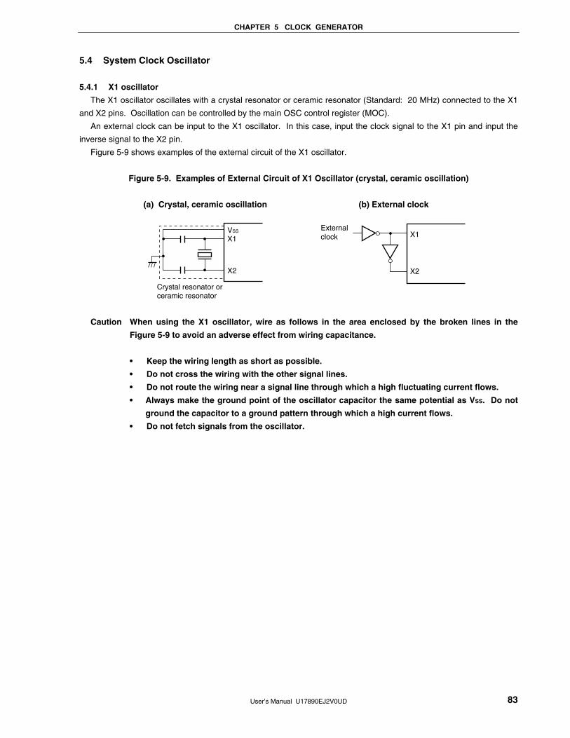
CHAPTER 5 CLOCK GENERATOR
User’s Manual U17890EJ2V0UD 83
5.4 System Clock Oscillator
5.4.1 X1 oscillator
The X1 oscillator oscillates with a crystal resonator or ceramic resonator (Standard: 20 MHz) connected to the X1
and X2 pins. Oscillation can be controlled by the main OSC control register (MOC).
An external clock can be input to the X1 oscillator. In this case, input the clock signal to the X1 pin and input the
inverse signal to the X2 pin.
Figure 5-9 shows examples of the external circuit of the X1 oscillator.
Figure 5-9. Examples of External Circuit of X1 Oscillator (crystal, ceramic oscillation)
(a) Crystal, ceramic oscillation
(b) External clock
VSS
X1
X2
Crystal resonator or ceramic resonator
Externalclock X1
X2
Caution When using the X1 oscillator, wire as follows in the area enclosed by the broken lines in the
Figure 5-9 to avoid an adverse effect from wiring capacitance.
• Keep the wiring length as short as possible.
• Do not cross the wiring with the other signal lines.
• Do not route the wiring near a signal line through which a high fluctuating current flows.
• Always make the ground point of the oscillator capacitor the same potential as VSS. Do not
ground the capacitor to a ground pattern through which a high current flows.
• Do not fetch signals from the oscillator.

CHAPTER 5 CLOCK GENERATOR
User’s Manual U17890EJ2V0UD 84
5.4.2 Examples of Incorrect Resonator Connection
Figure 5-10 shows examples of incorrect resonator connection.
Figure 5-10. Examples of Incorrect Resonator Connection (1/2)
(a) Too long wiring (b) Crossed signal line
X2VSS X1 X1VSS X2
PORT
(c) Wiring near high alternating current (d) Current flowing through ground line of oscillator
(potential at points A, B, and C fluctuates)
VSS X1 X2
VSS X1 X2
A B C
Pmn
VDD
High current
Hig
h cu
rren
t

CHAPTER 5 CLOCK GENERATOR
User’s Manual U17890EJ2V0UD 85
Figure 5-10. Examples of Incorrect Resonator Connection (2/2)
(e) Signals are fetched
VSS X1 X2
5.4.3 Internal high-speed oscillator Internal high-speed oscillator is incorporated in the μPD78F0711 and 78F0712. Oscillation can be controlled by
the main OSC control register (MOC).
When the internal high-speed oscillation clock is selected as the high-speed system clock by using the option byte,
the internal high-speed oscillator automatically starts oscillating (8 MHz (TYP.)), after a reset release.
5.4.4 Internal low-speed oscillator Internal low-speed oscillator is incorporated in the μPD78F0711 and 78F0712. Oscillation can be controlled by the
internal oscillation mode register (RCM).
The internal low-speed oscillation clock is used as the clock of the CPU, the watchdog timer, and 8-bit timer H1.
“Can be stopped by software” or “Cannot be stopped” can be selected by the option byte. When “Can be stopped
by software” is set, oscillation can be controlled by the internal oscillation mode register (RCM).
After a reset release, the internal low-speed oscillator automatically starts oscillation (240 kHz (TYP.))
5.4.5 Prescaler
The prescaler generates various clocks to be supplied to the CPU by dividing the main system clock.

CHAPTER 5 CLOCK GENERATOR
User’s Manual U17890EJ2V0UD 86
5.5 Clock Generator Operation
The clock generator generates the following clocks and controls the operation modes of the CPU, such as standby
mode (see Figure 5-1).
• Main system clock fXP
• High-speed system clock fXH
X1 clock fX
Internal high-speed oscillation clock fRH
• Internal low-speed oscillation clock fRL
• CPU clock fCPU
• Peripheral hardware clock fPRS
The CPU starts operation when the internal low-speed oscillator starts outputting after reset release in the
μPD78F0711 and 78F0712, thus enabling the following.
(1) Enhancement of security function
When the X1 input clock is set as the CPU clock by the default setting, the device cannot operate if the X1 input
clock is damaged or badly connected and therefore does not operate after reset is released. However, the start
clock of the CPU is the on-chip internal low-speed oscillation clock, so the device can be started by the internal
low-speed oscillation clock after reset release. Consequently, the system can be safely shut down by performing
a minimum operation, such as acknowledging a reset source by software or performing safety processing when
there is a malfunction.
(2) Improvement of performance
Because the CPU can be started without waiting for the X1 input clock oscillation stabilization time, the total
performance can be improved.
When the power supply voltage is turned on, the clock generator operation is shown in Figure 5-11.

CHAPTER 5 CLOCK GENERATOR
User’s Manual U17890EJ2V0UD 87
Figure 5-11. Timing Diagram of CPU Default Start Using Internal Low-speed Oscillator
(a) When X1 clock is selected as high-speed system clock
Internal low-speedclock (fRL)
CPU clock
X1 clock (fX)
Operation stopped: 17/fRL
X1 clock oscillation stabilization time: 211/fXP to 216/fXPNote
RESET
Internal low-speed oscillation clock High-speed system clock (X1 clock)
Switched by software
Note Check using the oscillation stabilization time counter status register (OSTC).
(b) When internal high-speed oscillation clock is selected as high-speed system clock
Internal low-speedclock (fRL)
CPU clock
Operation stopped: 17/fRL
RESET
Internal low-speed oscillation clockHigh-speed system clock
(Internal high-speed oscillation clock)
Switched by software
350 sμ
Internal high-speedclock (fRH)

CHAPTER 5 CLOCK GENERATOR
User’s Manual U17890EJ2V0UD 88
(a) When the RESET signal is generated, bit 0 of the main clock mode register (MCM) is cleared to 0 and the
internal low-speed oscillation clock is set as the CPU clock. However, a clock is supplied to the CPU after 17
clocks of the internal low-speed oscillation clock have elapsed after RESET release (or clock supply to the
CPU stops for 17 clocks). During the RESET period, oscillation of the high-speed system clock and internal
low-speed oscillation clock is stopped.
(b) After RESET release, the CPU clock can be switched from the internal low-speed oscillation clock to the
high-speed system clock using bit 0 (MCM0) of the main clock mode register (MCM) after the high-speed
system clock oscillation stabilization time has elapsed. At this time, in the case of an X1 clock, check the
oscillation stabilization time using the oscillation stabilization time counter status register (OSTC) before
switching the CPU clock. In the case of an internal high-speed oscillation clock, secure wait time (350 μs) by
software before switching the CPU clock. The CPU clock status can be checked using bit 1 (MCS) of MCM.
(c) Internal low-speed oscillator can be set to stopped/oscillating using the internal oscillation mode register
(RCM) when “Can be stopped by software” is selected for the internal low-speed oscillator by an option byte,
if the high-speed system clock is used as the CPU clock. Make sure that MCS is 1 at this time.
(d) When the internal low-speed oscillation clock is used as the CPU clock, the high-speed system clock can be
set to stopped/oscillating using the main OSC control register (MOC). Make sure that MCS is 0 at this time.
(e) The oscillation stabilization time (211/fXP, 213/fXP, 214/fXP, 215/fXP, 216/fXP) selected by the oscillation stabilization
time select register (OSTS) is secured when releasing STOP mode while the high-speed system clock is
being used as the CPU clock.
In addition, when RESET is released, and when the STOP mode is released while the internal low-speed
oscillation clock is being used as the CPU clock, there is no oscillation stabilization time wait.
When switching to the high-speed system clock as the CPU clock, in the case of an X1 clock, check the
oscillation stabilization time by using the oscillation stabilization time counter status register (OSTC). In the
case of an internal high-speed oscillation clock, secure wait time (350 μs) by software.

CHAPTER 5 CLOCK GENERATOR
User’s Manual U17890EJ2V0UD 89
A status transition diagram of this product is shown in Figure 5-12, and the relationship between the operation
clocks in each operation status and between the oscillation control flag and oscillation status of each clock are shown
in Tables 5-3 and 5-4, respectively.
Figure 5-12. Status Transition Diagram (1/2)
(1) When “Internal low-speed oscillator can be stopped by software” is selected by option byte
Status 4CPU clock: fXP fXP: Oscillating
fRL: Oscillation stopped
Status 3CPU clock: fXP
fXP: OscillatingfRL: Oscillating
Status 1CPU clock: fRL
fXP: Oscillation stoppedfRL: Oscillating
Status 2CPU clock: fRL
fXP: OscillatingfRL: Oscillating
HALTNote 4
Interrupt
Interrupt
Interrupt Interrupt
InterruptInterrupt
Reset release
InterruptInterruptHALT
instruction
STOPinstruction
STOPinstruction
STOPinstruction
STOPinstruction
RSTOP = 0
RSTOP = 1Note 1
MCM0 = 0
MCM0 = 1Note 2
MSTOP = 1Note 3
MSTOP = 0
HALTinstruction
HALT instruction
HALTinstruction
STOPNote 4
ResetNote 5
Notes 1. When shifting from status 3 to status 4, make sure that bit 1 (MCS) of the main clock mode register
(MCM) is 1.
2. In the case of the X1 clock, check the oscillation stabilization time status using the oscillation
stabilization time counter status register (OSTC) before shifting from status 2 to status 3 after reset
and STOP are released. In the case of the internal high-speed oscillation clock, secure wait time
(350 μs) by software.
3. When shifting from status 2 to status 1, make sure that MCS is 0.
4. When “Internal low-speed oscillator can be stopped by software” is selected by an option byte, the
watchdog timer stops operating in the HALT and STOP modes, regardless of the source clock of the
watchdog timer. However, oscillation of internal low-speed oscillator does not stop even in the HALT
and STOP modes if RSTOP = 0.
5. All reset sources (RESET input, POC, LVI, and WDT)

CHAPTER 5 CLOCK GENERATOR
User’s Manual U17890EJ2V0UD 90
Figure 5-12. Status Transition Diagram (2/2)
(2) When “Internal low-speed oscillator cannot be stopped” is selected by option byte
Status 3CPU clock: fXP fXP: OscillatingfRL: Oscillating
HALT
Interrupt Interrupt
InterruptSTOP
instruction
MCM0 = 0
MCM0 = 1Note 1
HALT instruction
HALT instruction
STOPNote 3
ResetNote 4
Status 2CPU clock: fRL
fXP: OscillatingfRL: Oscillating
Status 1CPU clock: fRL
fXP: Oscillation stoppedfRL: Oscillating
InterruptSTOPinstruction
Interrupt
Interrupt
STOPinstruction
MSTOP = 1Note 2
MSTOP = 0
HALT instruction
Reset release
Notes 1. In the case of the X1 clock, check the oscillation stabilization time status using the oscillation
stabilization time counter status register (OSTC) before shifting from status 2 to status 3 after reset
and STOP are released. In the case of the internal high-speed oscillation clock, secure wait time
(350 μs) by software.
2. When shifting from status 2 to status 1, make sure that MCS is 0.
3. The watchdog timer operates using internal low-speed oscillation clock even in STOP mode if
“Internal low-speed oscillator cannot be stopped” is selected by an option byte. Internal low-speed
oscillation clock division can be selected as the count source of 8-bit timer 51 (TM51), so clear the
watchdog timer using the TM51 interrupt request before watchdog timer overflow. If this processing
is not performed, an internal reset signal is generated at watchdog timer overflow after STOP
instruction execution.
4. All reset sources (RESET input, POC, LVI, and WDT)

CHAPTER 5 CLOCK GENERATOR
User’s Manual U17890EJ2V0UD 91
Table 5-3. Relationship Between Operation Clocks in Each Operation Status
High-speed System
Clock Oscillator
Internal Low-speed Oscillator
Note 2
Prescaler Clock
Supplied to Peripherals
Status
Operation
Mode MSTOP = 0
MSTOP = 1
Note 1
RSTOP = 0 RSTOP = 1
CPU Clock After
Release
MCM0 = 0 MCM0 = 1
Reset Stopped Internal low-speed
oscillation clock
Stopped
STOP
Stopped
Note 3 Stopped
HALT Oscillating Stopped
Oscillating Oscillating Stopped
Note 4 Internal
low-speed
oscillation
clock
High-
speed
system
clock
Notes 1. When “Cannot be stopped” is selected for internal low-speed oscillator by an option byte.
2. When “Can be stopped by software” is selected for internal low-speed oscillator by an option byte.
3. Operates using the CPU clock at STOP instruction execution.
4. Operates using the CPU clock at HALT instruction execution.
Caution The RSTOP setting is valid only when “Can be stopped by software” is set for internal low-speed
oscillator by an option byte.
Remark MSTOP: Bit 7 of the main OSC control register (MOC)
RSTOP: Bit 0 of the internal oscillation mode register (RCM)
MCM0: Bit 0 of the main clock mode register (MCM)
Table 5-4. Oscillation Control Flags and Clock Oscillation Status
High-speed System Clock Oscillator Internal Low-speed Oscillator
RSTOP = 0 Stopped Oscillating MSTOP = 1
RSTOP = 1 Setting prohibited
RSTOP = 0 Oscillating MSTOP = 0
RSTOP = 1
Oscillating
Stopped
Caution The RSTOP setting is valid only when “Can be stopped by software” is set for internal
low-speed oscillator by an option byte.
Remark MSTOP: Bit 7 of the main OSC control register (MOC)
RSTOP: Bit 0 of the internal oscillation mode register (RCM)

CHAPTER 5 CLOCK GENERATOR
User’s Manual U17890EJ2V0UD 92
5.6 Time Required to Switch Between Internal Low-speed Oscillation Clock and High-speed System Clock
Bit 0 (MCM0) of the main clock mode register (MCM) is used to switch between the internal low-speed oscillation
clock and high-speed system clock.
In the actual switching operation, switching does not occur immediately after MCM0 rewrite; several instructions
are executed using the pre-switch clock after switching MCM0 (see Table 5-5).
Bit 1 (MCS) of MCM is used to judge that operation is performed using either the internal low-speed oscillation
clock or high-speed system clock.
To stop the original clock after switching the clock, wait for the number of clocks shown in Table 5-5.
Table 5-5. Maximum Time Required to Switch Between Internal Low-speed Oscillation Clock and High-speed
System Clock
PCC Time Required for Switching
PCC2 PCC1 PCC0 High-speed System Clock
→ Internal Low-speed Oscillation Clock
Internal Low-speed Oscillation Clock
→ High-speed System Clock
0 0 0 fXP/fRL + 1 clock
0 0 1 fXP/2fRL + 1 clock
2 clocks
Caution To calculate the maximum time, set fRL = 120 kHz.
Remarks 1. PCC: Processor clock control register
2. fXP: High-speed system clock oscillation frequency
3. fRL: Internal low-speed oscillation clock oscillation frequency
4. The maximum time is the number of clocks of the CPU clock before switching.

CHAPTER 5 CLOCK GENERATOR
User’s Manual U17890EJ2V0UD 93
5.7 Time Required for CPU Clock Switchover
The CPU clock can be switched using bits 0 to 2 (PCC0 to PCC2) of the processor clock control register (PCC).
The actual switchover operation is not performed immediately after rewriting to the PCC; operation continues on
the pre-switchover clock for several instructions (see Table 5-6).
Table 5-6. Maximum Time Required for CPU Clock Switchover
Set Value Before
Switchover
Set Value After Switchover
PCC2 PCC1 PCC0 PCC2 PCC1 PCC0 PCC2 PCC1 PCC0 PCC2 PCC1 PCC0 PCC2 PCC1 PCC0 PCC2 PCC1 PCC0
0 0 0 0 0 1 0 1 0 0 1 1 1 0 0
0 0 0 16 clocks 16 clocks 16 clocks 16 clocks
0 0 1 8 clocks 8 clocks 8 clocks 8 clocks
0 1 0 4 clocks 4 clocks 4 clocks 4 clocks
0 1 1 2 clocks 2 clocks 2 clocks 2 clocks
1 0 0 1 clock 1 clock 1 clock 1 clock
Caution Setting the following values is prohibited when the CPU operates on the internal low-speed
oscillation clock. • PCC2, PCC1, PCC0 = 0, 1, 0
• PCC2, PCC1, PCC0 = 0, 1, 1
• PCC2, PCC1, PCC0 = 1, 0, 0
Remark The maximum time is the number of clocks of the CPU clock before switching.
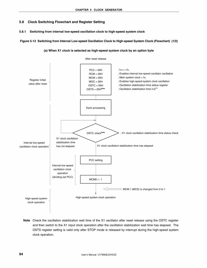
CHAPTER 5 CLOCK GENERATOR
User’s Manual U17890EJ2V0UD 94
5.8 Clock Switching Flowchart and Register Setting
5.8.1 Switching from internal low-speed oscillation clock to high-speed system clock
Figure 5-13 Switching from Internal Low-speed Oscillation Clock to High-speed System Clock (Flowchart) (1/2)
(a) When X1 clock is selected as high-speed system clock by an option byte
; fCPU = fRL
; Enables internal low-speed oscillator oscillation
; Main system clock = fRL
; Enables high-speed system clock oscillation
; Oscillation stabilization time status register
; Oscillation stabilization time fX/216
MCM.1 (MCS) is changed from 0 to 1
; X1 clock oscillation stabilization time status check
X1 clock oscillation stabilization time has elapsed
X1 clock oscillation
stabilization time
has not elapsed
PCC = 00H
RCM = 00H
MCM = 00H
MOC = 00H
OSTC = 00H
OSTS = 05HNote
OSTC checkNote
Each processing
After reset release
PCC setting
MCM0 ← 1
High-speed system clock operation
Internal low-speed
oscillation clock
operation
(dividing set PCC)
Register initial
value after reset
Internal low-speed
oscillation clock operation
High-speed system
clock operation
Note Check the oscillation stabilization wait time of the X1 oscillator after reset release using the OSTC register
and then switch to the X1 input clock operation after the oscillation stabilization wait time has elapsed. The
OSTS register setting is valid only after STOP mode is released by interrupt during the high-speed system
clock operation.

CHAPTER 5 CLOCK GENERATOR
User’s Manual U17890EJ2V0UD 95
Figure 5-13 Switching from Internal Low-speed Oscillation Clock to High-speed System Clock (Flowchart) (2/2)
(b) When internal high-speed oscillation clock is selected as high-speed system clock by an option byte
; fCPU = fRL
; Internal low-speed oscillator oscillation
; Main system clock = fRL
; High-speed system clock oscillation
; Oscillation stabilization time status register
MCM.1 (MCS) is changed from 0 to 1
; Internal low-speed oscillation clock
(@ fRL = 480 kHz(max.))
: 168 clock
168/0.48 = 350 s
PCC = 00H
RCM = 00H
MCM = 00H
MOC = 00H
OSTC = 00H
Each processing
After reset release
PCC setting
MCM0 ← 1
High-speed system clock operation
Internal low-speed
oscillation clock
operation
(dividing set PCC)
Register initial
value after reset
Internal low-speed
oscillation clock operation
High-speed system
clock operation
μOscillation stabilization
time wait of the internal
high-speed oscillator
(NOP processing)
Remark Secure the oscillation stabilization wait time (350 μs) after reset release using by software.

CHAPTER 5 CLOCK GENERATOR
User’s Manual U17890EJ2V0UD 96
5.8.2 Switching from high-speed system clock to internal low-speed oscillation clock
Figure 5-14 Switching from High-speed System Clock to Internal Low-speed Oscillation Clock (Flowchart)
MCM.1 (MCS) is changed from 1 to 0
; Internal low-speed oscillation clock operation
; Internal low-speed oscillator stopped?
Internal low-speed oscillation clock operation
; High-speed system clock operation
No: RSTOP = 0
Yes: RSTOP = 1
MCM = 03H
RCM.0Note
(RSTOP) = 1?
RSTOP = 0
MCM0 ← 0
Register setting inHigh-speed system
clock operation
High-speed systemclock operation
Internal low-speedoscillation clock operation
Note Required only when “Can be stopped by software” is selected for internal low-speed oscillator by an option
byte.

CHAPTER 5 CLOCK GENERATOR
User’s Manual U17890EJ2V0UD 97
5.8.3 Register settings
The table below shows the statuses of the setting flags and status flags when each mode is set.
Table 5-7. Clock and Register Setting
Setting Flag Status Flag
MCM Register MOC Register RCM Register MCM Register
fCPU Mode
MCM0 MSTOP RSTOPNote 1 MCS
Internal low-speed oscillator oscillating 1 0 0 1 High-speed system
clockNote 2 Internal low-speed oscillator stopped 1 0 1 1
High-speed system clock oscillating 0 0 0 0 Internal low-speed
oscillation clock Note 3 High-speed system clock stopped 0 1 0 0
Notes 1. Valid only when “Can be stopped by software” is selected for the internal low-speed oscillator by an option
byte.
2. Do not set MSTOP = 1 while the CPU is operating with the high-speed system clock (even if MSTOP = 1
is set, the high-speed system clock oscillation will not stop).
3. Do not set RSTOP = 1 during CPU operates on the internal low-speed oscillation clock (even if RSTOP =
1 is set, the internal low-speed oscillation clock oscillation does not stop).

User’s Manual U17890EJ2V0UD 98
CHAPTER 6 10-BIT INVERTER CONTROL TIMER 6.1 Outline of 10-Bit Inverter Control Timer
The 10-bit inverter control timer makes inverter control possible. It consists of an 8-bit dead-time generation timer,
and allows non-overlapping active-level output. 6.2 Function of 10-Bit Inverter Control Timer
The 10-bit inverter control timer realizes inverter control. It incorporates an 8-bit timer for dead time generation and
can output waveforms that do not overlap active levels. A total of six positive phase and negative phase channels are
output. In addition, an active level change function and output off function by external input (TW0TOFFP) are
provided.
6.3 Configuration of 10-Bit Inverter Control Timer
The 10-bit inverter control timer includes the following hardware.
Table 6-1. Configuration of 10-Bit Inverter Control Timer
Item Function
Timer counter 10-bit up/down counter × 1 (TW0UDC)
Dead-time timers × 3 (DTM0, DTM1, DTM2)
Buffer transfer control timer × 1 (RTM0)
Register 10-bit compare registers × 6 (TW0CM0 to TW0CM5)
10-bit buffer registers × 6 (TW0BFCM0 to TW0BFCM5)
Dead-time reload register × 1 (TW0DTIME)
Timer output 6 (TW0TO0, TW0TO1, TW0TO2, TW0TO3, TW0TO4, TW0TO5)
Control registers Inverter timer control register (TW0C)
Inverter timer mode register (TW0M)
A/D trigger selection register (TW0TRGS)
Inverter timer output control register (TW0OC)

CHAPTER 6 10-BIT INVERTER CONTROL TIMER
User’s Manual U17890EJ2V0UD 99
Figure 6-1. Block Diagram of 10-Bit Inverter Control Timer
fX/25
fX/24
fX/23
fX/22
fX/2fX
TW0UDC
INTTW0UD
10
TW0CM3
TW0BFCM3
TW0CM0TW0BFCM0
TW0CM1TW0BFCM1
TW0CM2TW0BFCM2
TW0DTIME
DTM0
DTM1
DTM2
8
fX
TW0TO0(U phase)
TW0TO1(U phase)
TW0TO2(V phase)
TW0TO3(V phase)
TW0TO4(W phase)
TW0TO5(W phase)
RTM0
Out
put
cont
rolle
r
A/D trigger selection register (TW0TRGS)
Internal bus
IDEV02 IDEV01 IDEV00CE0 TCL02 TCL01 TCL00 PNOFFB0 ALV0
Inverter timer control register (TW0C)
Internal bus
INTTW0CM3
TOSP01
TRSW0TRSW1
Inverter timer mode register (TW0M)
Hi-Z Output Circuit
Inverter timer outputcontrol register (TW0OC)
TW0CM4TW0BFCM4
TW0CM5TW0BFCM5
INTTW0CM4
INTTW0CM5
A/D convertertrigger signal(INTADTR)
Sel
ecto
r
Sel
ecto
r
Timercounter
Compare registerBuffer register
under-flow
Match
Buffer transfer control timer
Dead-time reload register
Dead-time timer
INTTW0UDgeneration
TOSP00
Real-timeoutput port
Pulsegenerator
<R>

CHAPTER 6 10-BIT INVERTER CONTROL TIMER
User’s Manual U17890EJ2V0UD 100
(1) 10-bit up/down counter (TW0UDC) TW0UDC is a 10-bit up/down counter that counts count pulses in synchronization with the rising edge of the count clock. When the timer starts, the number of count pulse count is incremented from 0, and when the value preset to compare register 3 (TW0CM3) and TW0UDC count value match, it is switched to the count down operation. An underflow signal is generated if the value becomes 000H during the count down operation and interrupt request signal INTTW0UD is generated. When an underflow occurs, it is switched from the count down operation to the count up operation. INTTW0UD is normally generated at every underflow but the number of occurrences can be divided by the IDEV00 to IDEV02 bits of inverter timer control register (TW0C). TW0UDC cannot be read/written. The cycle of TW0UDC is controlled by TM0CM3. The count clock can be selected from 6 types: fX, fX/2, fX/4, fX/8, fX/16, fX/32. RESET input or clearing the CE0 bit of TW0C7 sets TW0UDC to 000H.
(2) 10-bit compare registers 0 to 2 (TW0CM0 to TW0CM2) TW0CM0 to TW0CM2 are 10-bit compare registers that always compare their own value with that of TW0UDC, and if they match, the contents of the flip-flops are changed. Each of TW0CM0 to TW0CM2 are provided with a buffer register (TW0BFCM0 to TW0BFCM2), so that the contents of the buffer can be transferred to TW0CM0 to TW0CM2 at the timing of interrupt request signal INTTW0UD generation. A write operation to TW0CM0 to TW0CM2 is possible only while TW0UDC is stopped. To set the output timing, write data to TW0BFCM0 to TW0BFCM2. RESET input or clearing the CE0 bit of TW0C sets these registers to 000H.
(3) 10-bit compare register 3 (TW0CM3) TW0CM3 is a 10-bit compare register that controls the high limit value of TW0UDC. If the count value of TW0UDC matches the value of TW0CM3 or 0, count up/down is switched at the next count clock. TW0CM3 provides a buffer register (TW0BFCM3) whose contents are transferred to TW0CM3 at the timing of interrupt request signal INTTW0UD generation. TW0CM3 can be written to only while TW0UDC is stopped. To set the cycle to TW0UDC, write data to TW0BFCM3. RESET input sets TW0CM3 to 0FFH. Do not set TW0CM3 to 000H.
(4) 10-bit compare registers 4, 5 (TW0CM4, TW0CM5) TW0CM4 and TW0CM5 are 10-bit compare registers that always compare their own value with that of TW0UDC, and if they match, interrupt request signal is generated. Each of TW0CM4 and TW0CM5 are provided with a buffer register (TW0BFCM4, TW0BFCM5), so that the contents of the buffer can be transferred to TW0CM4 to TW0CM5 at the timing of interrupt request signal INTTW0UD generation. A write operation to TW0CM4 and TW0CM5 is possible only while TW0UDC is stopped. To set the output timing, write data to TW0BFCM4 and TW0BFCM5. RESET input or clearing the CE0 bit of TW0C sets these registers to 000H.

CHAPTER 6 10-BIT INVERTER CONTROL TIMER
User’s Manual U17890EJ2V0UD 101
(5) 10-bit buffer registers 0 to 5 (TW0BFCM0 to TW0BFCM5) TW0BFCM0 to TW0BFCM5 are 10-bit registers. They transfer data to the compare register (TW0CM0 to TW0CM5) corresponding to each buffer register at the timing of interrupt request signal INTTW0UD generation. TW0BFCM0 to TW0BFCM5 can be read/written irrespective of whether TW0UDC count is stopped or operating. RESET input sets TW0BFCM0 to TW0BFCM2, TW0BFCM4 and TW0BFCM5 to 000H, and TW0BFCM3 to 0FFH. These registers can be read/written in word and byte units. For read/write operations of less than 8 bits, TW0BFCM0L to TW0BFCM5L are used.
(6) Dead-time reload register (TW0DTIME) TW0DTIME is an 8-bit register to set dead time and is common to three dead-time timers (DTM0 to DTM2). However, the data load timing from TW0DTIME to DTM0, DTM1 and DTM2 is independent. TW0DTIME can be written only while TW0UDC counting is stopped. Data does not change even if an instruction to rewrite TW0DTIME is executed during timer operation. RESET input sets TW0DTIME to FFH. Even if TW0DTIME is set to 00H, an output with the dead time of 1/fX is performed.
(7) Dead-time timers 0 to 2 (DTM0 to DTM2) DTM0 to DTM2 are 8-bit down counters that generate dead time. Count down is performed after the value of the dead-time reload register (TW0DTIME) is reloaded with the timing of a compare match between TW0CM0 to TW0CM2 and TW0UDC. DTM0 to DTM2 generate an underflow signal when 00H changes to FFH and stop with FFH. The count clock is fX. DTM0 to DTM2 cannot be read/written. RESET input or clearing the CE0 bit of TW0C sets these registers to FFH.
(8) Buffer transfer control timer (RTM0) RTM0 is a 3-bit up counter. It has the function of dividing interrupt request signal INTTW0UD. Incrementing is performed with the TW0UDC underflow signal and INTTW0UD is generated when the value matches the number of divisions set with bits IDEV00 to IDEV02 of TW0C. RTM0 cannot be read/written. RESET input sets RTM0 to 7H. Generating INTTW0UD and clearing the CE0 bit of TW0C also sets RTM0 to 7H.

CHAPTER 6 10-BIT INVERTER CONTROL TIMER
User’s Manual U17890EJ2V0UD 102
6.4 Registers Controlling 10-Bit Inverter Control Timer
The following four registers control the 10-bit inverter control timer. • Inverter timer control register (TW0C) • Inverter timer mode register (TW0M) • A/D trigger selection register (TW0TRGS) • Inverter timer output control register (TW0OC)
(1) Inverter timer control register (TW0C) TW0C controls the operation of TW0UDC, dead-time timers 0 to 2 (DTM0 to DTM2), and the buffer transfer control timer (RTM0), specifies the count clock of TW0UDC, and selects the compare register transfer cycle. TW0C is set by a 1-bit or 8-bit memory manipulation instruction. RESET input clears TW0C to 00H.

CHAPTER 6 10-BIT INVERTER CONTROL TIMER
User’s Manual U17890EJ2V0UD 103
Figure 6-2. Format of Inverter Timer Control Register
Address: FF88H After reset: 00H R/W
Symbol <7> 6 5 4 3 2 1 0
TW0C CE0 0 TCL02 TCL01 TCL00 IDEV02 IDEV01 IDEV00
CE0 TW0UDC, DTM0 to DTM2, RTM0 operation control
0 Clear and stop (TW0TO0 to TW0TO5 are Hi-Z)
1 Count enable
Count clock selection TCL02 TCL01 TCL00
At fX = 20 MHz At fX = 16 MHz
0 0 0 fX 20 MHz 16 MHz
0 0 1 fX/2 10 MHz 8 MHz
0 1 0 fX/22 5 MHz 4 MHz
0 1 1 fX/23 2.5 MHz 2 MHz
1 0 0 fX/24 1.25 MHz 1 MHz
1 0 1 fX/25 625 kHz 500 kHz
Other than above Setting prohibited
IDEV02 IDEV01 IDEV00 INTTW0UD occurrence frequency selection
0 0 0 Occurs once every TW0UDC underflow.
0 0 1 Occurs once every two TW0UDC underflows.
0 1 0 Occurs once every three TW0UDC underflows.
0 1 1 Occurs once every four TW0UDC underflows.
1 0 0 Occurs once every five TW0UDC underflows.
1 0 1 Occurs once every six TW0UDC underflows.
1 1 0 Occurs once every seven TW0UDC underflows.
1 1 1 Occurs once every eight TW0UDC underflows.
Remark fX: System clock oscillation frequency

CHAPTER 6 10-BIT INVERTER CONTROL TIMER
User’s Manual U17890EJ2V0UD 104
(2) Inverter timer mode register (TW0M) TW0M controls the operation of and specifies the active level of the TW0TO0 to TW0TO5 outputs. TW0M is set by a 1-bit or 8-bit memory manipulation instruction. RESET input clears TW0M to 00H.
Figure 6-3. Format of Inverter Timer Mode Register
Address: FF89H After reset: 00H R/W
Symbol 7 6 5 4 3 2 1 0
TW0M 0 0 0 PNOFFB0Note ALV0 0 0 0
PNOFFB0Note Control status flag output to TW0TO0 to TW0TO5
0 Output disabled status (TW0TO0 to TW0TO5 are Hi-Z)
1 Output enabled status
ALV0 TW0TO0 to TW0TO5 output active level specification
0 Low level
1 High level
Note The PNOFFB0 bit is a read-only flag. This bit cannot be set or reset by software.
The PNOFFB0 bit is reset in following cases. • When TW0UDC is stopped (CE0 = 0) • When an output stop is generated by TW0TOFFP while TW0UDC is operating
(CE0 = 1).
Caution Always set bits 0 to 2, 5 to 7 of TW0M to 0.

CHAPTER 6 10-BIT INVERTER CONTROL TIMER
User’s Manual U17890EJ2V0UD 105
Remarks 1. TW0TO0 to TW0TO5 become Hi-Z state in the following cases. However, the TW0UDC, DTM0 to DTM2, and RTM0 timers do not stop if CE0 = 1 is set.
• A valid edge is input to the TW0TOFFP pin while TOSPP0 = 1.
To restore the output of TW0TO0 to TW0TO5, perform the procedure below.
<1> Write 0 to CE0 and stop the timer. <2> Write 0 to the output stop function flag that is used. <3> Reset the registers to their default values.
2. PNOFFB0, ALV0, CE0, and TW0TO0 to TW0TO5 are related as follows.
PNOFFB0 ALV0 CE0 TW0TO0, TW0TO2, TW0TO4 TW0TO1, TW0TO3, TW0TO5
0 0 0 Hi-Z Hi-Z
0 1 0 Hi-Z Hi-Z
0 0/1 1 Hi-Z Hi-Z
1 0/1 1 PWM wave output PWM wave output

CHAPTER 6 10-BIT INVERTER CONTROL TIMER
User’s Manual U17890EJ2V0UD 106
(3) A/D trigger selection register (TW0TRGS) TW0TRGS is a register used to select the A/D converter trigger signal from INTTW0CM4 and INTTW0CM5, which are generated upon a match between the compare register (TW0CM4, TW0CM5) and timer counter (TW0UDC). TW0TRGS can be set by a 1-bit or 8-bit memory manipulation instruction. RESET input sets TW0TRGS to 00H.
Figure 6-4. Format of A/D Trigger Selection Register
Address: FF8BH After reset: 00H R/W
Symbol 7 6 5 4 3 2 1 0
TW0TRGS 0 0 0 0 0 0 TRSW1 TRSW0
TRSW1 TRSW0 Selection of A/D trigger
0 0 No output (INTADTR is kept "Low" level)
0 1 INTTW0CM4
1 0 INTTW0CM5
1 1 INTTW0CM4 or INTTW0CM5
(4) Inverter timer output control register (TW0OC)
TW0OC sets timer output stop in phase (U-phase/V-phase/W-phase) units. TW0OC can be set by a 1-bit or 8-bit memory manipulation instruction. RESET input sets TW0OC to 00H.
Figure 6-5. Format of Inverter Timer Output Control Register
Address: FF8CH After reset: 00H R/W
Symbol 7 6 5 4 3 2 1 0
TW0OC 0 0 0 0 0 0 TOSP01 TOSP00
TOSP01 TOSP00 Output control for PWM output
0 0 TW0TO0 to TW0TO5 output are permited
0 1 TW0TO0 and TW0TO1 output are prohibited (U phase off)
1 0 TW0TO2 and TW0TO3 output are prohibited (V phase off)
1 1 TW0TO4 and TW0TO5 output are prohibited (W phase off)
<R>
<R>
CHAPTER 6 10-BIT INVERTER CONTROL TIMER
User’s Manual U17890EJ2V0UD 107
6.5 Registers Controlling 10-Bit Inverter Control Timer (1) Setting procedure
(a) The TW0UDC count clock is set with the TCL00 to TCL02 bits of inverter timer control register (TW0C) and the occurrence frequency of interrupt request signal INTTW0UD is set with the IDEV00 to IDEV02 bits.
(b) The active level of the TW0TO0 to TW0TO5 pins is set with the ALV0 bit of inverter timer mode register (TW0M).
(c) Set the half width of the first PWM cycle to 10-bit compare register 3 (TW0CM3).
• PWM cycle = TW0CM3 value × 2 × TW0UDC clock rate (The clock rate of TW0UDC is set with the TW0C)
(d) Set the half width of the second PWM cycle to 10-bit buffer register 3 (TW0BFCM3). (e) Set the dead time width to the dead time reload register (TW0DTIME).
• Dead time width = (TW0DTIME + 1) × 1/fX
fX: Internal system clock
(f) Set the F/F set/reset timing that is used during the first cycle to 10-bit compare registers 0 to 2 (TW0CM0 to TW0CM2).
(g) Set the F/F set/reset timing that is used during the second cycle to TW0BFCM3. (h) After the CE0 bit of TW0C is set (1), the operation of TW0UDC, dead-time timers 0 to 2 (DTM0 to DTM2),
and buffer transfer control timer (RTM0) is enabled.
Caution Always use a bit manipulation instruction to set the CE0 bit.
(i) Set the F/F set/reset timing that is used for the next cycle to TW0BFCM0 to TW0BFCM5 during TW0UDC operation.
(j) To stop the TW0UDC operation, set the CE0 bit of the TW0C to 0.
Caution Another bit cannot be rewritten at the same time that the CE0 bit is being rewritten.

CHAPTER 6 10-BIT INVERTER CONTROL TIMER
User’s Manual U17890EJ2V0UD 108
(2) Output waveform widths corresponding to set values
• PWM cycle = TW0CM3 × 2 × TTW0 • Dead-time width = TDTM = (TW0DTIME + 1) × 1/fX • Active width of positive phase (TW0TO0, TW0TO2, TW0TO4 pin)
= {(TW0CM3 – TW0CMup) + (TW0CM3 – TW0CMdown)} × TTW0 – TDTM • Active width of negative phase (TW0TO1, TW0TO3, TW0TO5 pin)
= (TW0CMdown + TW0CMup) × TTW0 – TDTM fX: System clock oscillation frequency TTW0: TW0UDC count clock TW0CMup: Set value of TW0CM0 to TW0CM2 during TW0UDC count up TW0CMdown: Set value of TW0CM0 to TW0CM2 during TW0UDC count down
Caution If a value whose active width in the positive phase or negative phase becomes 0 or negative via the above calculation, TW0TO0 to TW0TO5 output a waveform fixed at the inactive level with an active width of 0 (refer to Figure 6-7). However, if TW0CMn = 0 and TW0BFCMn ≥ TW0CM3 are set, TW0TO0 to TW0TO5 output a waveform at the active level.

CHAPTER 6 10-BIT INVERTER CONTROL TIMER
User’s Manual U17890EJ2V0UD 109
(3) Operation timing
Figure 6-6. TW0UDC Operation Timing (Basic Operation)
Remarks 1. n = 0 to 2 2. t: Dead time = (TW0DTIME + 1) × 1/fX
(fX: System clock oscillation frequency) 3. The above figure assumes an active high and undivided INTTW0UD occurrence.
X
0
b
a a
Y
c
ba c
Y Z
X
t t
b b
t t
Y Z
INTTW0UD INTTW0UD
TW0UDC
TW0BFCMn
TW0CMn
TW0BFCM3
TW0CM3
F/F
DTMn
TW0TO0, TW0TO2, TW0TO4
TW0TO1, TW0TO3, TW0TO5

CHAPTER 6 10-BIT INVERTER CONTROL TIMER
User’s Manual U17890EJ2V0UD 110
Figure 6-7. TW0UDC Operation Timing (TW0CMn (TW0BFCMn) ≥ TW0CM3 (TW0BFCM3))
Remarks 1. n = 0 to 2 2. t: Dead time = (TW0DTIME + 1) ) × 1/fx
(fX: System clock oscillation frequency) 3. The above figure assumes an active high and undivided INTTW0UD occurrence.
If a value higher than TW0CM3 is set to TW0BFCMn, low-level output in the positive phases (TW0TO0, TW0TO2, TW0TO4 pins), and high-level output in the negative phases (TW0TO1, TW0TO3, TW0TO5 pins) are continued. This setting is effective to output signals whose low and high widths are longer than the PWM cycle when controlling an inverter, etc.
X
0
b
a a
Y
c
b ( Y)a c
Y Z
X
t t
Y Z
INTTW0UD INTTW0UD
TW0UDC
TW0BFCMn
TW0CMn
TW0BFCM3
TW0CM3
F/F
DTMn
TW0TO0, TW0TO2, TW0TO4
TW0TO1, TW0TO3, TW0TO5
≥

CHAPTER 6 10-BIT INVERTER CONTROL TIMER
User’s Manual U17890EJ2V0UD 111
Figure 6-8. TW0UDC Operation Timing (TW0CMn (TW0BFCMn) = 000H)
Remarks 1. n = 0 to 2 2. t: Dead time = (TW0DTIME + 1) ) × 1/fx
(fX: System clock oscillation frequency) 3. The above figure assumes an active high and undivided INTTW0UD occurrence.
X
0
b
a a
Z
c c
Y
c (> 0) d
a b = 00H c d
Y Z
X
t tt t
Y Z Z
INTTW0UD INTTW0UD INTTW0UD
TW0UDC
TW0BFCMn
TW0CMn
TW0BFCM3
TW0CM3
F/F
DTMn
TW0TO0, TW0TO2,TW0TO4
TW0TO1, TW0TO3, TW0TO5

CHAPTER 6 10-BIT INVERTER CONTROL TIMER
User’s Manual U17890EJ2V0UD 112
Figure 6-9. TW0UDC Operation Timing (TW0CMn (TW0BFCMn) = TW0CM3 – 1/2DTM, TW0CMn (TW0BFCMn) > TW0CM3 – 1/2DTM)
Remarks 1. n = 0 to 2
2. The above figure assumes an active high and undivided INTTW0UD occurrence.
X
0
b
a a
b b
Y
c
a (= X – —DTM) b (> Y – —DTM) c
Y Z
X Y Z
INTTW0UD INTTW0UD
TW0UDC
TW0BFCMn
TW0CMn
TW0BFCM3
TW0CM3
F/F
DTMn
TW0TO0, TW0TO2, TW0TO4
TW0TO1, TW0TO3, TW0TO5
12
12

CHAPTER 6 10-BIT INVERTER CONTROL TIMER
User’s Manual U17890EJ2V0UD 113
Figure 6-10. TW0UDC Operation Timing (IDEV02 to IDEV00 = 000B, TW0TRGS = 03H)
TW0BFCM5
TW0CM4
TW0BFCM4
TW0CM3
TW0BFCM3
TW0CM5
INTTW0CM3
INTTW0ADTR
INTTW0CM5
INTTW0CM4
TW0UDa
c
g
Z
e
a
f
b
f
Y
X b
e
c
b
g
f
Z
Y
b
a
f
e
Y
X
INTTW0UDINTTW0UD

User’s Manual U17890EJ2V0UD 114
CHAPTER 7 16-BIT TIMER/EVENT COUNTER 00
7.1 Functions of 16-Bit Timer/Event Counter 00
16-bit timer/event counter 00 has the following functions.
• Interval timer
• PPG output
• Pulse width measurement
• External event counter
• Square-wave output
• One-shot pulse output
(1) Interval timer
16-bit timer/event counter 00 generates an interrupt request at the preset time interval.
(2) PPG output
16-bit timer/event counter 00 can output a rectangular wave whose frequency and output pulse width can be set
freely.
(3) Pulse width measurement
16-bit timer/event counter 00 can measure the pulse width of an externally input signal.
(4) External event counter
16-bit timer/event counter 00 can measure the number of pulses of an externally input signal.
(5) Square-wave output
16-bit timer/event counter 00 can output a square wave with any selected frequency.
(6) One-shot pulse output
16-bit timer/event counter 00 can output a one-shot pulse whose output pulse width can be set freely.
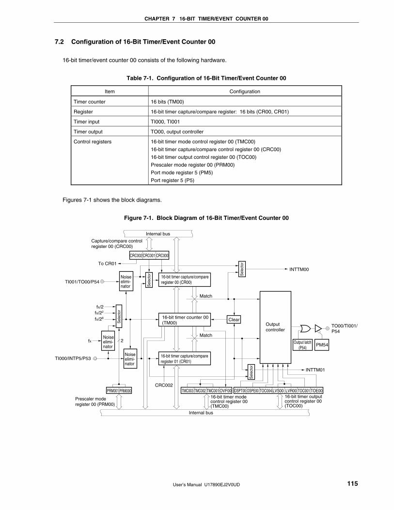
CHAPTER 7 16-BIT TIMER/EVENT COUNTER 00
User’s Manual U17890EJ2V0UD 115
7.2 Configuration of 16-Bit Timer/Event Counter 00
16-bit timer/event counter 00 consists of the following hardware.
Table 7-1. Configuration of 16-Bit Timer/Event Counter 00
Item Configuration
Timer counter 16 bits (TM00)
Register 16-bit timer capture/compare register: 16 bits (CR00, CR01)
Timer input TI000, TI001
Timer output TO00, output controller
Control registers 16-bit timer mode control register 00 (TMC00)
16-bit timer capture/compare control register 00 (CRC00)
16-bit timer output control register 00 (TOC00)
Prescaler mode register 00 (PRM00)
Port mode register 5 (PM5)
Port register 5 (P5)
Figures 7-1 shows the block diagrams.
Figure 7-1. Block Diagram of 16-Bit Timer/Event Counter 00
Internal bus
Capture/compare controlregister 00 (CRC00)
TI001/TO00/P54
fX/2fX/22
fX/28
fX
TI000/INTP5/P53
Prescaler moderegister 00 (PRM00)
2
PRM001 PRM000CRC002
16-bit timer capture/compareregister 01 (CR01)
Match
Match
16-bit timer counter 00(TM00)
Clear
Noiseelimi-nator
CRC002CRC001 CRC000
INTTM00
TO00/TI001/P54
INTTM01
16-bit timer output control register 00 (TOC00)
16-bit timer modecontrol register 00(TMC00)
Internal bus
TMC003 TMC002 TMC001 OVF00 TOC004 LVS00 LVR00 TOC001 TOE00
Sel
ecto
r
16-bit timer capture/compareregister 00 (CR00)
Sel
ecto
r
Sel
ecto
r
Sel
ecto
r
Noiseelimi-nator
Noiseelimi-nator
Outputcontroller
OSPE00OSPT00
Output latch(P54)
PM54
To CR01

CHAPTER 7 16-BIT TIMER/EVENT COUNTER 00
User’s Manual U17890EJ2V0UD 116
(1) 16-bit timer counter 00 (TM00)
TM00 is a 16-bit read-only register that counts count pulses.
The counter is incremented in synchronization with the rising edge of the input clock.
Figure 7-2. Format of 16-Bit Timer Counter 00 (TM00)
TM00
SymbolFF17H FF16H
Address: FF16H, FF17H After reset: 0000H R
The count value is reset to 0000H in the following cases.
<1> At RESET input
<2> If TMC003 and TMC002 are cleared
<3> If the valid edge of the TI000 pin is input in the mode in which clear & start occurs upon input of the valid
edge of the TI000 pin
<4> If TM00 and CR00 match in the mode in which clear & start occurs on a match of TM00 and CR00
<5> OSPT00 is set in one-shot pulse output mode
(2) 16-bit timer capture/compare register 00 (CR00)
CR00 is a 16-bit register that has the functions of both a capture register and a compare register. Whether it is
used as a capture register or as a compare register is set by bit 0 (CRC000) of capture/compare control register
00 (CRC00).
CR00 can be set by a 16-bit memory manipulation instruction.
RESET input clears this register to 0000H.
Figure 7-3. Format of 16-Bit Timer Capture/Compare Register 00 (CR00)
CR00
SymbolFF7BH FF7AH
Address: FF7AH, FF7BH After reset: 0000H R/W
• When CR00 is used as a compare register
The value set in CR00 is constantly compared with 16-bit timer counter 00 (TM00) count value, and an
interrupt request (INTTM00) is generated if they match. The set value is held until CR00 is rewritten.
• When CR00 is used as a capture register
It is possible to select the valid edge of the TI000 pin or the TI001 pin as the capture trigger. The TI000 or
TI001 pin valid edge is set using prescaler mode register 00 (PRM00) (see Table 7-2).

CHAPTER 7 16-BIT TIMER/EVENT COUNTER 00
User’s Manual U17890EJ2V0UD 117
Table 7-2. CR00 Capture Trigger and Valid Edges of TI000 and TI001 Pins
(1) TI000 pin valid edge selected as capture trigger (CRC001 = 1, CRC000 = 1)
TI000 Pin Valid Edge CR00 Capture Trigger
ES001 ES000
Falling edge Rising edge 0 1
Rising edge Falling edge 0 0
No capture operation Both rising and falling edges 1 1
(2) TI001 pin valid edge selected as capture trigger (CRC001 = 0, CRC000 = 1)
TI001 Pin Valid Edge CR00 Capture Trigger
ES101 ES100
Falling edge Falling edge 0 0
Rising edge Rising edge 0 1
Both rising and falling edges Both rising and falling edges 1 1
Remarks 1. Setting ES001, ES000 = 1, 0 and ES101, ES100 = 1, 0 is prohibited.
2. ES001, ES000: Bits 5 and 4 of prescaler mode register 00 (PRM00)
ES101, ES100: Bits 7 and 6 of prescaler mode register 00 (PRM00)
CRC001, CRC000: Bits 1 and 0 of capture/compare control register 00 (CRC00)
Cautions 1. Set a value other than 0000H in CR00 in the mode in which clear & start occurs on a match
of TM00 and CR00.
2. In the free-running mode and in the clear mode using the valid edge of the TI000 pin, if CR00
is cleared to 0000H, an interrupt request (INTTM00) is generated when the value of CR00
changes from 0000H to 0001H following overflow (FFFFH). INTTM00 is generated after TM00
and CR00 match, after the valid edge of the TI000 pin is detected, or after the timer is
cleared by a one-shot trigger.
3. When P54 is used as the valid edge input of the TI001 pin, it cannot be used as the timer
output (TO00). Moreover, when P54 is used as TO00, it cannot be used as the valid edge
input of the TI001 pin.
4. When CR00 is used as a capture register, read data is undefined if the register read time
and capture trigger input conflict (the capture data itself is the correct value).
If count stop input and capture trigger input conflict, the captured data is undefined.
5. Do not rewrite CR00 during TM00 operation.
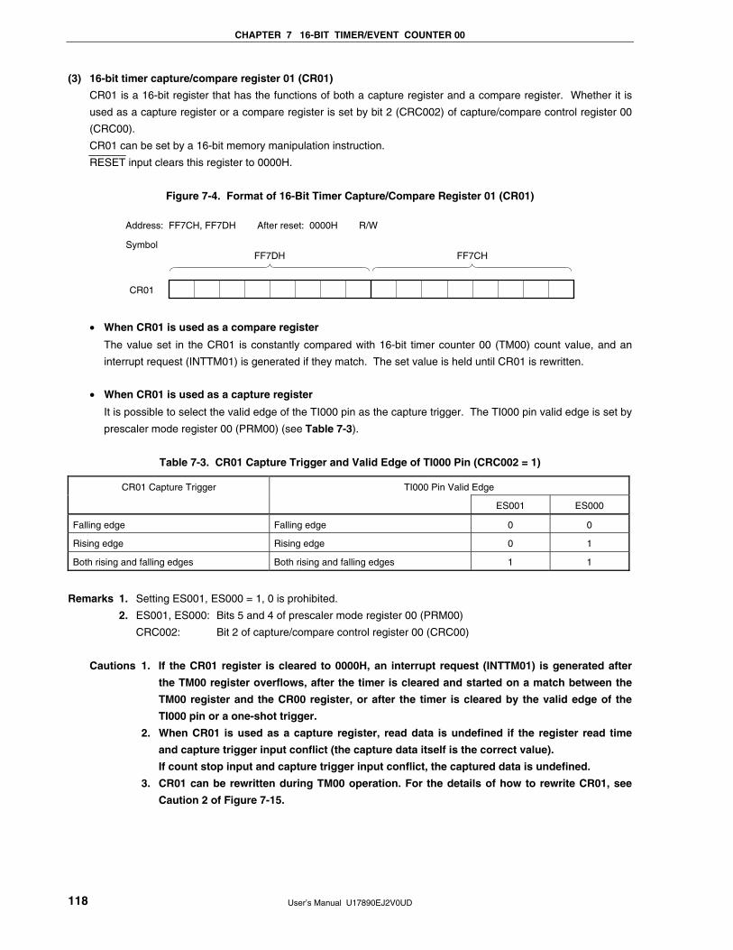
CHAPTER 7 16-BIT TIMER/EVENT COUNTER 00
User’s Manual U17890EJ2V0UD 118
(3) 16-bit timer capture/compare register 01 (CR01)
CR01 is a 16-bit register that has the functions of both a capture register and a compare register. Whether it is
used as a capture register or a compare register is set by bit 2 (CRC002) of capture/compare control register 00
(CRC00).
CR01 can be set by a 16-bit memory manipulation instruction.
RESET input clears this register to 0000H.
Figure 7-4. Format of 16-Bit Timer Capture/Compare Register 01 (CR01)
CR01
SymbolFF7DH FF7CH
Address: FF7CH, FF7DH After reset: 0000H R/W
• When CR01 is used as a compare register
The value set in the CR01 is constantly compared with 16-bit timer counter 00 (TM00) count value, and an
interrupt request (INTTM01) is generated if they match. The set value is held until CR01 is rewritten.
• When CR01 is used as a capture register
It is possible to select the valid edge of the TI000 pin as the capture trigger. The TI000 pin valid edge is set by
prescaler mode register 00 (PRM00) (see Table 7-3).
Table 7-3. CR01 Capture Trigger and Valid Edge of TI000 Pin (CRC002 = 1)
TI000 Pin Valid Edge CR01 Capture Trigger
ES001 ES000
Falling edge Falling edge 0 0
Rising edge Rising edge 0 1
Both rising and falling edges Both rising and falling edges 1 1
Remarks 1. Setting ES001, ES000 = 1, 0 is prohibited.
2. ES001, ES000: Bits 5 and 4 of prescaler mode register 00 (PRM00)
CRC002: Bit 2 of capture/compare control register 00 (CRC00)
Cautions 1. If the CR01 register is cleared to 0000H, an interrupt request (INTTM01) is generated after
the TM00 register overflows, after the timer is cleared and started on a match between the
TM00 register and the CR00 register, or after the timer is cleared by the valid edge of the
TI000 pin or a one-shot trigger.
2. When CR01 is used as a capture register, read data is undefined if the register read time
and capture trigger input conflict (the capture data itself is the correct value).
If count stop input and capture trigger input conflict, the captured data is undefined.
3. CR01 can be rewritten during TM00 operation. For the details of how to rewrite CR01, see
Caution 2 of Figure 7-15.

CHAPTER 7 16-BIT TIMER/EVENT COUNTER 00
User’s Manual U17890EJ2V0UD 119
7.3 Registers Controlling 16-Bit Timer/Event Counter 00
The following six registers are used to control 16-bit timer/event counter 00.
• 16-bit timer mode control register 00 (TMC00)
• Capture/compare control register 00 (CRC00)
• 16-bit timer output control register 00 (TOC00)
• Prescaler mode register 00 (PRM00)
• Port mode register 5 (PM5)
• Port register 5 (P5)
(1) 16-bit timer mode control register 00 (TMC00)
This register sets the 16-bit timer operating mode, 16-bit timer counter 00 (TM00) clear mode, and output timing,
and detects an overflow.
TMC00 can be set by a 1-bit or 8-bit memory manipulation instruction.
RESET input clears TMC00 to 00H.
Caution 16-bit timer counter 00 (TM00) starts operation at the moment TMC002 and TMC003 are set to
values other than 0, 0 (operation stop mode), respectively. Clear TMC002 and TMC003 to 0, 0 to
stop the operation.
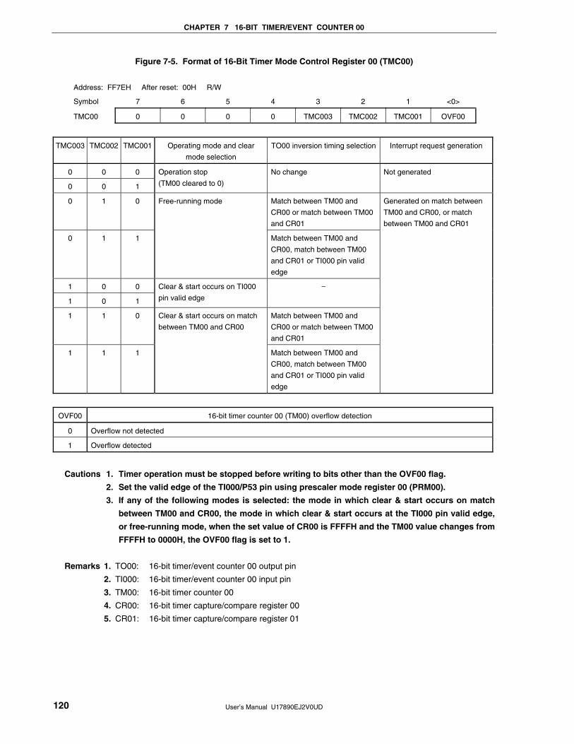
CHAPTER 7 16-BIT TIMER/EVENT COUNTER 00
User’s Manual U17890EJ2V0UD 120
Figure 7-5. Format of 16-Bit Timer Mode Control Register 00 (TMC00)
Address: FF7EH After reset: 00H R/W
Symbol 7 6 5 4 3 2 1 <0>
TMC00 0 0 0 0 TMC003 TMC002 TMC001 OVF00
OVF00 16-bit timer counter 00 (TM00) overflow detection
0 Overflow not detected
1 Overflow detected
Cautions 1. Timer operation must be stopped before writing to bits other than the OVF00 flag.
2. Set the valid edge of the TI000/P53 pin using prescaler mode register 00 (PRM00).
3. If any of the following modes is selected: the mode in which clear & start occurs on match
between TM00 and CR00, the mode in which clear & start occurs at the TI000 pin valid edge,
or free-running mode, when the set value of CR00 is FFFFH and the TM00 value changes from
FFFFH to 0000H, the OVF00 flag is set to 1.
Remarks 1. TO00: 16-bit timer/event counter 00 output pin
2. TI000: 16-bit timer/event counter 00 input pin
3. TM00: 16-bit timer counter 00
4. CR00: 16-bit timer capture/compare register 00
5. CR01: 16-bit timer capture/compare register 01
TMC003 TMC002 TMC001 Operating mode and clear
mode selection
TO00 inversion timing selection Interrupt request generation
0 0 0
0 0 1
Operation stop
(TM00 cleared to 0)
No change Not generated
0 1 0 Free-running mode Match between TM00 and
CR00 or match between TM00
and CR01
0 1 1 Match between TM00 and
CR00, match between TM00
and CR01 or TI000 pin valid
edge
1 0 0
1 0 1
Clear & start occurs on TI000
pin valid edge
−
1 1 0 Clear & start occurs on match
between TM00 and CR00
Match between TM00 and
CR00 or match between TM00
and CR01
1 1 1 Match between TM00 and
CR00, match between TM00
and CR01 or TI000 pin valid
edge
Generated on match between
TM00 and CR00, or match
between TM00 and CR01

CHAPTER 7 16-BIT TIMER/EVENT COUNTER 00
User’s Manual U17890EJ2V0UD 121
(2) Capture/compare control register 00 (CRC00)
This register controls the operation of the 16-bit timer capture/compare registers (CR00, CR01).
CRC00 can be set by a 1-bit or 8-bit memory manipulation instruction.
RESET input clears CRC00 to 00H.
Figure 7-6. Format of Capture/Compare Control Register 00 (CRC00)
Address: FF6AH After reset: 00H R/W
Symbol 7 6 5 4 3 2 1 0
CRC00 0 0 0 0 0 CRC002 CRC001 CRC000
CRC002 CR01 operating mode selection
0 Operates as compare register
1 Operates as capture register
CRC001 CR00 capture trigger selection
0 Captures on valid edge of TI001 pin
1 Captures on valid edge of TI000 pin by reverse phase
CRC000 CR00 operating mode selection
0 Operates as compare register
1 Operates as capture register
Cautions 1. Timer operation must be stopped before setting CRC00.
2. When the mode in which clear & start occurs on a match between TM00 and CR00 is selected
with 16-bit timer mode control register 00 (TMC00), CR00 should not be specified as a capture
register.
3. The capture operation is not performed if both the rising and falling edges are specified as
the valid edge of the TI000 pin.
4. To ensure that the capture operation is performed properly, the capture trigger requires a
pulse two cycles longer than the count clock selected by prescaler mode register 00
(PRM00).
(3) 16-bit timer output control register 00 (TOC00)
This register controls the operation of 16-bit timer/event counter 00 output controller. It sets/resets the timer
output F/F, enables/disables output inversion and 16-bit timer/event counter 00 timer output, enables/disables the
one-shot pulse output operation, and sets the one-shot pulse output trigger via software.
TOC00 can be set by a 1-bit or 8-bit memory manipulation instruction.
RESET input clears TOC00 to 00H.

CHAPTER 7 16-BIT TIMER/EVENT COUNTER 00
User’s Manual U17890EJ2V0UD 122
Figure 7-7. Format of 16-Bit Timer Output Control Register 00 (TOC00)
Address: FF6BH After reset: 00H R/W
Symbol 7 <6> <5> 4 <3> <2> 1 <0>
TOC00 0 OSPT00 OSPE00 TOC004 LVS00 LVR00 TOC001 TOE00
OSPT00 One-shot pulse output trigger control via software
0 No one-shot pulse trigger
1 One-shot pulse trigger
OSPE00 One-shot pulse output operation control
0 Successive pulse output mode
1 One-shot pulse output modeNote
TOC004 Timer output F/F control using match of CR01 and TM00
0 Disables inversion operation
1 Enables inversion operation
LVS00 LVR00 Timer output F/F status setting
0 0 No change
0 1 Timer output F/F reset (0)
1 0 Timer output F/F set (1)
1 1 Setting prohibited
TOC001 Timer output F/F control using match of CR00 and TM00
0 Disables inversion operation
1 Enables inversion operation
TOE00 Timer output control
0 Disables output (output fixed to level 0)
1 Enables output
Note The one-shot pulse output mode operates correctly only in the free-running mode and the mode in which
clear & start occurs at the TI000 pin valid edge. In the mode in which clear & start occurs on a match
between the TM00 register and CR00 register, one-shot pulse output is not possible because an overflow
does not occur.
Cautions 1. Timer operation must be stopped before setting other than TOC004.
2. If LVS00 and LVR00 are read, 0 is read.
3. OSPT00 is automatically cleared after data is set, so 0 is read.
4. Do not set OSPT00 to 1 other than in one-shot pulse output mode.
5. A write interval of two cycles or more of the count clock selected by prescaler mode register
00 (PRM00) is required to write to OSPT00 successively.
6. Do not set LVS00 to 1 before TOE00, and do not set LVS00 and TOE00 to 1 simultaneously.

CHAPTER 7 16-BIT TIMER/EVENT COUNTER 00
User’s Manual U17890EJ2V0UD 123
(4) Prescaler mode register 00 (PRM00)
This register is used to set the 16-bit timer counter 00 (TM00) count clock and valid edges of the TI000 and TI001
pin inputs.
PRM00 can be set by a 1-bit or 8-bit memory manipulation instruction.
RESET input clears PRM00 to 00H.
Figure 7-8. Format of Prescaler Mode Register 00 (PRM00)
Address: FF7FH After reset: 00H R/W
Symbol 7 6 5 4 3 2 1 0
PRM00 ES101 ES100 ES001 ES000 0 0 PRM001 PRM000
ES101 ES100 TI001 pin valid edge selection
0 0 Falling edge
0 1 Rising edge
1 0 Setting prohibited
1 1 Both falling and rising edges
ES001 ES000 TI000 pin valid edge selection
0 0 Falling edge
0 1 Rising edge
1 0 Setting prohibited
1 1 Both falling and rising edges
Count clock selectionNote 1 PRM001 PRM000
At fX = 20 MHz At fX = 16 MHz
0 0 fX/2 10 MHz 8 MHz
0 1 fX/22 5 MHz 4 MHz
1 0 fX/28 78.125 kHz 62.5 kHz
1 1 TI000 pin valid edgeNote 2
Notes 1. Be sure to set the count clock so that the following condition is satisfied.
• VDD = 4.0 to 5.5 V: Count clock ≤ 10 MHz
2. The external clock requires a pulse two cycles longer than internal clock (fX).
Remarks 1. fX: X1 input clock oscillation frequency
2. TI000, TI001: 16-bit timer/event counter 00 input pin

CHAPTER 7 16-BIT TIMER/EVENT COUNTER 00
User’s Manual U17890EJ2V0UD 124
Cautions 1. When the internal low-speed oscillation clock is selected as the source clock to the CPU, the
clock of the internal low-speed oscillator is divided and supplied as the count clock. If the
count clock is the internal low-speed oscillation clock, the operation of 16-bit timer/event
counter 00 is not guaranteed. When an external clock is used and when the internal low-
speed oscillation clock is selected as the source clock to the CPU, the operation of 16-bit
timer/event counter 00 is not guaranteed, either, because the internal low-speed oscillation
clock is supplied as the sampling clock to eliminate noise.
2. Always set data to PRM00 after stopping the timer operation.
3. If the valid edge of the TI000 pin is to be set for the count clock, do not set the clear & start
mode using the valid edge of the TI000 pin and the capture trigger.
4. If the TI000 or TI001 pin is high level immediately after system reset, the rising edge is
immediately detected after the rising edge or both the rising and falling edges are set as the
valid edge(s) of the TI000 pin or TI001 pin to enable the operation of 16-bit timer counter 00
(TM00). Care is therefore required when pulling up the TI000 or TI001 pin. However, when re-
enabling operation after the operation has been stopped once, the rising edge is not
detected.
5. When P54 is used as the TI001 pin valid edge, it cannot be used as the timer output (TO00),
and when used as TO00, it cannot be used as the TI001 pin valid edge.
(5) Port mode register 5 (PM5)
This register sets port 5 input/output in 1-bit units.
When using the P54/TO00/TI001 pin for timer output, clear PM54 and the output latch of P54 to 0.
When using the P54/TO00/TI001 and P53/TI000/INTP5 pins for timer input, clear PM54 and PM53 to 1. At this
time, the output latches of P54 and P53 may be 0 or 1.
PM5 can be set by a 1-bit or 8-bit memory manipulation instruction.
RESET input sets PM5 to FFH.
Figure 7-9. Format of Port Mode Register 5 (PM5)
Address: FF25H After reset: FFH R/W
Symbol 7 6 5 4 3 2 1 0
PM5 PM57 PM56 PM55 PM54 PM53 PM52 PM51 PM50
PM5n P5n pin I/O mode selection (n = 0 to 7)
0 Output mode (output buffer on)
1 Input mode (output buffer off)

CHAPTER 7 16-BIT TIMER/EVENT COUNTER 00
User’s Manual U17890EJ2V0UD 125
7.4 Operation of 16-Bit Timer/Event Counter 00
7.4.1 Interval timer operation
Setting 16-bit timer mode control register 00 (TMC00) and capture/compare control register 00 (CRC00) as shown
in Figure 7-10 allows operation as an interval timer.
Setting
The basic operation setting procedure is as follows.
<1> Set the CRC00 register (see Figure 7-10 for the set value).
<2> Set any value to the CR00 register.
<3> Set the count clock by using the PRM00 register.
<4> Set the TMC00 register to start the operation (see Figure 7-10 for the set value).
Caution CR00 cannot be rewritten during TM00 operation.
Remark For how to enable the INTTM00 interrupt, see CHAPTER 16 INTERRUPT FUNCTIONS.
Interrupt requests are generated repeatedly using the count value preset in 16-bit timer capture/compare register
00 (CR00) as the interval.
When the count value of 16-bit timer counter 00 (TM00) matches the value set in CR00, counting continues with
the TM00 value cleared to 0 and the interrupt request signal (INTTM00) is generated.
The count clock of 16-bit timer/event counter 00 can be selected with bits 0 and 1 (PRM000, PRM001) of prescaler
mode register 00 (PRM00).

CHAPTER 7 16-BIT TIMER/EVENT COUNTER 00
User’s Manual U17890EJ2V0UD 126
Figure 7-10. Control Register Settings for Interval Timer Operation
(a) 16-bit timer mode control register 00 (TMC00)
7
0
6
0
5
0
4
0
TMC003
1
TMC002
1
TMC001
0/1
OVF00
0TMC00
Clears and starts on match between TM00 and CR00.
(b) Capture/compare control register 00 (CRC00)
7
0
6
0
5
0
4
0
3
0
CRC002
0/1
CRC001
0/1
CRC000
0CRC00
CR00 used as compare register
(c) Prescaler mode register 00 (PRM00)
ES101
0/1
ES100
0/1
ES001
0/1
ES000
0/1
3
0
2
0
PRM001
0/1
PRM000
0/1PRM00
Selects count clock.
Setting invalid (setting “10” is prohibited.)
Setting invalid (setting “10” is prohibited.)
Remark 0/1: Setting 0 or 1 allows another function to be used simultaneously with the interval timer.
See the description of the respective control registers for details.

CHAPTER 7 16-BIT TIMER/EVENT COUNTER 00
User’s Manual U17890EJ2V0UD 127
Figure 7-11. Interval Timer Configuration Diagram
16-bit timer capture/compareregister 00 (CR00)
16-bit timer counter 00(TM00)
OVF00
Clearcircuit
INTTM00
fX/2
fX/22
fX/28
TI000/P53
Sel
ecto
r
Noiseeliminator
fX
Note
Note OVF00 is set to 1 only when 16-bit timer capture/compare register 00 is set to FFFFH.
Figure 7-12. Timing of Interval Timer Operation
Count clock
t
TM00 count value
CR00
INTTM00
0000H 0001H N 0000H 0001H N 0000H 0001H N
NNNN
Timer operation enabled Clear Clear
Interrupt acknowledged Interrupt acknowledged
Remark Interval time = (N + 1) × t
N = 0001H to FFFFH

CHAPTER 7 16-BIT TIMER/EVENT COUNTER 00
User’s Manual U17890EJ2V0UD 128
7.4.2 PPG output operations
Setting 16-bit timer mode control register 00 (TMC00) and capture/compare control register 00 (CRC00) as shown
in Figure 7-13 allows operation as PPG (Programmable Pulse Generator) output.
Setting
The basic operation setting procedure is as follows.
<1> Set the CRC00 register (see Figure 7-13 for the set value).
<2> Set any value to the CR00 register as the cycle.
<3> Set any value to the CR01 register as the duty factor.
<4> Set the TOC00 register (see Figure 7-13 for the set value).
<5> Set the count clock by using the PRM00 register.
<6> Set the TMC00 register to start the operation (see Figure 7-13 for the set value).
Caution To change the value of the duty factor (the value of the CR01 register) during operation, see
Caution 2 in Figure 7-15 PPG Output Operation Timing.
Remarks 1. For the setting of the TO00 pin, see 7.3 (5) Port mode register 5 (PM5).
2. For how to enable the INTTM00 interrupt, see CHAPTER 16 INTERRUPT FUNCTIONS.
In the PPG output operation, rectangular waves are output from the TO00 pin with the pulse width and the cycle
that correspond to the count values preset in 16-bit timer capture/compare register 01 (CR01) and in 16-bit timer
capture/compare register 00 (CR00), respectively.

CHAPTER 7 16-BIT TIMER/EVENT COUNTER 00
User’s Manual U17890EJ2V0UD 129
Figure 7-13. Control Register Settings for PPG Output Operation
(a) 16-bit timer mode control register 00 (TMC00)
7
0
6
0
5
0
4
0
TMC003
1
TMC002
1
TMC001
0
OVF00
0TMC00
Clears and starts on match between TM00 and CR00.
(b) Capture/compare control register 00 (CRC00)
7
0
6
0
5
0
4
0
3
0
CRC002
0
CRC001
×
CRC000
0CRC00
CR00 used as compare register
CR01 used as compare register
(c) 16-bit timer output control register 00 (TOC00)
7
0
OSPT00
0
OSPE00
0
TOC004
1
LVS00
0/1
LVR00
0/1
TOC001
1
TOE00
1TOC00
Enables TO00 output.
Inverts output on match between TM00 and CR00.
Specifies initial value of TO00 output F/F (setting “11” is prohibited).
Inverts output on match between TM00 and CR01.
Disables one-shot pulse output.
(d) Prescaler mode register 00 (PRM00)
ES101
0/1
ES100
0/1
ES001
0/1
ES000
0/1
3
0
2
0
PRM001
0/1
PRM000
0/1PRM00
Selects count clock.
Setting invalid (setting “10” is prohibited.)
Setting invalid (setting “10” is prohibited.)
Cautions 1. Values in the following range should be set in CR00 and CR01: 0000H ≤ CR01 < CR00 ≤ FFFFH
2. The cycle of the pulse generated through PPG output (CR00 setting value + 1) has a duty of
(CR01 setting value + 1)/(CR00 setting value + 1).
Remark ×: Don’t care

CHAPTER 7 16-BIT TIMER/EVENT COUNTER 00
User’s Manual U17890EJ2V0UD 130
Figure 7-14. Configuration Diagram of PPG Output
16-bit timer capture/compareregister 00 (CR00)
16-bit timer counter 00(TM00)
Clearcircuit
Noise eliminator
fX
fX/2
fX/22
fX/28
TI000/P53
16-bit timer capture/compare register 01 (CR01)
TO00/TI001/P54
Sel
ecto
r
Out
put c
ontr
olle
r
Figure 7-15. PPG Output Operation Timing
t
0000H 0000H 0001H0001H M − 1
Count clock
TM00 count value
TO00
Pulse width: (M + 1) × t
1 cycle: (N + 1) × t
NCR00 capture value
CR01 capture value M
M N − 1 NN
ClearClear
Cautions 1. CR00 cannot be rewritten during TM00 operation.
2. In the PPG output operation, change the pulse width (rewrite CR01) during TM00 operation
using the following procedure.
<1> Disable the timer output inversion operation by match of TM00 and CR01 (TOC004 = 0)
<2> Disable the INTTM01 interrupt (TMMK01 = 1)
<3> Rewrite CR01
<4> Wait for 1 cycle of the TM00 count clock
<5> Enable the timer output inversion operation by match of TM00 and CR01 (TOC004 = 1)
<6> Clear the interrupt request flag of INTTM01 (TMIF01 = 0)
<7> Enable the INTTM01 interrupt (TMMK01 = 0)
Remark 0000H ≤ M < N ≤ FFFFH

CHAPTER 7 16-BIT TIMER/EVENT COUNTER 00
User’s Manual U17890EJ2V0UD 131
7.4.3 Pulse width measurement operations
It is possible to measure the pulse width of the signals input to the TI000 pin and TI001 pin using 16-bit timer
counter 00 (TM00).
There are two measurement methods: measuring with TM00 used in free-running mode, and measuring by
restarting the timer in synchronization with the edge of the signal input to the TI000 pin.
When an interrupt occurs, read the valid value of the capture register, check the overflow flag, and then calculate
the necessary pulse width. Clear the overflow flag after checking it.
The capture operation is not performed until the signal pulse width is sampled in the count clock cycle selected by
prescaler mode register 00 (PRM00) and the valid level of the TI000 or TI001 pin is detected twice, thus eliminating
noise with a short pulse width.
Figure 7-16. CR01 Capture Operation with Rising Edge Specified
Count clock
TM00
TI000
Rising edge detection
CR01
INTTM01
N − 3 N − 2 N − 1 N N + 1
N
Setting
The basic operation setting procedure is as follows.
<1> Set the CRC00 register (see Figures 7-17, 7-20, 7-22, and 7-24 for the set value).
<2> Set the count clock by using the PRM00 register.
<3> Set the TMC00 register to start the operation (see Figures 7-17, 7-20, 7-22, and 7-24 for the set value).
Caution To use two capture registers, set the TI000 and TI001 pins.
Remarks 1. For the setting of the TI000 (or TI001) pin, see 7.3 (5) Port mode register 5 (PM5).
2. For how to enable the INTTM00 (or INTTM01) interrupt, see CHAPTER 16 INTERRUPT
FUNCTIONS.

CHAPTER 7 16-BIT TIMER/EVENT COUNTER 00
User’s Manual U17890EJ2V0UD 132
(1) Pulse width measurement with free-running counter and one capture register
When 16-bit timer counter 00 (TM00) is operated in free-running mode, and the edge specified by prescaler mode
register 00 (PRM00) is input to the TI000 pin, the value of TM00 is taken into 16-bit timer capture/compare
register 01 (CR01) and an external interrupt request signal (INTTM01) is set.
Specify both the rising and falling edges of the TI000 pin by using bits 4 and 5 (ES000 and ES001) of PRM00.
Sampling is performed using the count clock selected by PRM00, and a capture operation is only performed
when a valid level of the TI000 pin is detected twice, thus eliminating noise with a short pulse width.
Figure 7-17. Control Register Settings for Pulse Width Measurement with Free-Running Counter
and One Capture Register (When TI000 and CR01 Are Used)
(a) 16-bit timer mode control register 00 (TMC00)
7
0
6
0
5
0
4
0
TMC003
0
TMC002
1
TMC001
0/1
OVF00
0TMC00
Free-running mode
(b) Capture/compare control register 00 (CRC00)
7
0
6
0
5
0
4
0
3
0
CRC002
1
CRC001
0/1
CRC000
0CRC00
CR00 used as compare register
CR01 used as capture register
(c) Prescaler mode register 00 (PRM00)
ES101
0/1
ES100
0/1
ES001
1
ES000
1
3
0
2
0
PRM001
0/1
PRM000
0/1PRM00
Selects count clock (setting “11” is prohibited).
Specifies both edges for pulse width detection.
Setting invalid (setting “10” is prohibited.)
Remark 0/1: Setting 0 or 1 allows another function to be used simultaneously with pulse width measurement.
See the description of the respective control registers for details.

CHAPTER 7 16-BIT TIMER/EVENT COUNTER 00
User’s Manual U17890EJ2V0UD 133
Figure 7-18. Configuration Diagram for Pulse Width Measurement with Free-Running Counter
fX/2
fX/22
fX/28
TI000
16-bit timer counter 00(TM00)
OVF00
16-bit timer capture/compareregister 01 (CR01)
Internal bus
INTTM01
Sel
ecto
r
Figure 7-19. Timing of Pulse Width Measurement Operation with Free-Running Counter
and One Capture Register (with Both Edges Specified)
t
0000H 0000HFFFFH0001H D0
D0
Count clock
TM00 count value
TI000 pin input
CR01 capture value
INTTM01
OVF00
(D1 − D0) × t (D3 − D2) × t(10000H − D1 + D2) × t
D1 D2 D3
D2 D3D0 + 1 D1 D1 + 1
Note
Note Clear OVF00 by software.

CHAPTER 7 16-BIT TIMER/EVENT COUNTER 00
User’s Manual U17890EJ2V0UD 134
(2) Measurement of two pulse widths with free-running counter
When 16-bit timer counter 00 (TM00) is operated in free-running mode, it is possible to simultaneously measure
the pulse widths of the two signals input to the TI000 pin and the TI001 pin.
When the edge specified by bits 4 and 5 (ES000 and ES001) of prescaler mode register 00 (PRM00) is input to
the TI000 pin, the value of TM00 is taken into 16-bit timer capture/compare register 01 (CR01) and an interrupt
request signal (INTTM01) is set.
Also, when the edge specified by bits 6 and 7 (ES100 and ES101) of PRM00 is input to the TI001 pin, the value
of TM00 is taken into 16-bit timer capture/compare register 00 (CR00) and an interrupt request signal (INTTM00)
is set.
Specify both the rising and falling edges as the edges of the TI000 and TI001 pins, by using bits 4 and 5 (ES000
and ES001) and bits 6 and 7 (ES100 and ES101) of PRM00.
Sampling is performed using the count clock cycle selected by prescaler mode register 00 (PRM00), and a
capture operation is only performed when a valid level of the TI000 or TI001 pin is detected twice, thus
eliminating noise with a short pulse width.
Figure 7-20. Control Register Settings for Measurement of Two Pulse Widths with Free-Running Counter
(a) 16-bit timer mode control register 00 (TMC00)
7
0
6
0
5
0
4
0
TMC003
0
TMC002
1
TMC001
0/1
OVF00
0TMC00
Free-running mode
(b) Capture/compare control register 00 (CRC00)
7
0
6
0
5
0
4
0
3
0
CRC002
1
CRC001
0
CRC000
1CRC00
CR00 used as capture register
Captures valid edge of TI001 pin to CR00.
CR01 used as capture register
(c) Prescaler mode register 00 (PRM00)
ES101
1
ES100
1
ES001
1
ES000
1
3
0
2
0
PRM001
0/1
PRM000
0/1PRM00
Selects count clock (setting “11” is prohibited).
Specifies both edges for pulse width detection.
Specifies both edges for pulse width detection.
Remark 0/1: Setting 0 or 1 allows another function to be used simultaneously with pulse width measurement.
See the description of the respective control registers for details.

CHAPTER 7 16-BIT TIMER/EVENT COUNTER 00
User’s Manual U17890EJ2V0UD 135
Figure 7-21. Timing of Pulse Width Measurement Operation with Free-Running Counter
(with Both Edges Specified)
t
0000H 0000HFFFFH0001H D0
D0
TI001 pin input
CR00 capture value
INTTM01
INTTM00
OVF00
(D1 − D0) × t (D3 − D2) × t(10000H − D1 + D2) × t
(10000H − D1 + (D2 + 1)) × t
D1
D2 + 1D1
D2
D2 D3D0 + 1 D1 D1 + 1 D2 + 1 D2 + 2
Count clock
TM00 count value
TI000 pin input
CR01 capture value
Note
Note Clear OVF00 by software.

CHAPTER 7 16-BIT TIMER/EVENT COUNTER 00
User’s Manual U17890EJ2V0UD 136
(3) Pulse width measurement with free-running counter and two capture registers
When 16-bit timer counter 00 (TM00) is operated in free-running mode, it is possible to measure the pulse width
of the signal input to the TI000 pin.
When the rising or falling edge specified by bits 4 and 5 (ES000 and ES001) of prescaler mode register 00
(PRM00) is input to the TI000 pin, the value of TM00 is taken into 16-bit timer capture/compare register 01
(CR01) and an interrupt request signal (INTTM01) is set.
Also, when the inverse edge to that of the capture operation is input into CR01, the value of TM00 is taken into
16-bit timer capture/compare register 00 (CR00).
Sampling is performed using the count clock cycle selected by prescaler mode register 00 (PRM00), and a
capture operation is only performed when a valid level of the TI000 pin is detected twice, thus eliminating noise
with a short pulse width.
Figure 7-22. Control Register Settings for Pulse Width Measurement with Free-Running Counter and
Two Capture Registers (with Rising Edge Specified)
(a) 16-bit timer mode control register 00 (TMC00)
7
0
6
0
5
0
4
0
TMC003
0
TMC002
1
TMC001
0/1
OVF00
0TMC00
Free-running mode
(b) Capture/compare control register 00 (CRC00)
7
0
6
0
5
0
4
0
3
0
CRC002
1
CRC001
1
CRC000
1CRC00
CR00 used as capture register
Captures to CR00 at inverse edge to valid edge of TI000.
CR01 used as capture register
(c) Prescaler mode register 00 (PRM00)
ES101
0/1
ES100
0/1
ES001
0
ES000
1
3
0
2
0
PRM001
0/1
PRM000
0/1PRM00
Selects count clock (setting “11” is prohibited).
Specifies rising edge for pulse width detection.
Setting invalid (setting “10” is prohibited.)
Remark 0/1: Setting 0 or 1 allows another function to be used simultaneously with pulse width measurement.
See the description of the respective control registers for details.

CHAPTER 7 16-BIT TIMER/EVENT COUNTER 00
User’s Manual U17890EJ2V0UD 137
Figure 7-23. Timing of Pulse Width Measurement Operation with Free-Running Counter
and Two Capture Registers (with Rising Edge Specified)
t
0000H 0000HFFFFH0001H D0
D0
INTTM01
OVF00
D2
D1 D3
D2 D3D0 + 1 D2 + 1D1 D1 + 1
CR00 capture value
Count clock
TM00 count value
TI000 pin input
CR01 capture value
(D1 − D0) × t (D3 − D2) × t(10000H − D1 + D2) × t
Note
Note Clear OVF00 by software.
(4) Pulse width measurement by means of restart
When input of a valid edge to the TI000 pin is detected, the count value of 16-bit timer counter 00 (TM00) is taken
into 16-bit timer capture/compare register 01 (CR01), and then the pulse width of the signal input to the TI000 pin
is measured by clearing TM00 and restarting the count operation.
Either of two edges⎯rising or falling⎯can be selected using bits 4 and 5 (ES000 and ES001) of prescaler mode
register 00 (PRM00).
Sampling is performed using the count clock cycle selected by prescaler mode register 00 (PRM00) and a
capture operation is only performed when a valid level of the TI000 pin is detected twice, thus eliminating noise
with a short pulse width.

CHAPTER 7 16-BIT TIMER/EVENT COUNTER 00
User’s Manual U17890EJ2V0UD 138
Figure 7-24. Control Register Settings for Pulse Width Measurement by Means of Restart
(with Rising Edge Specified)
(a) 16-bit timer mode control register 00 (TMC00)
7
0
6
0
5
0
4
0
TMC003
1
TMC002
0
TMC001
0/1
OVF00
0TMC00
Clears and starts at valid edge of TI000 pin.
(b) Capture/compare control register 00 (CRC00)
7
0
6
0
5
0
4
0
3
0
CRC002
1
CRC001
1
CRC000
1CRC00
CR00 used as capture register
Captures to CR00 at inverse edge to valid edge of TI000.
CR01 used as capture register
(c) Prescaler mode register 00 (PRM00)
ES101
0/1
ES100
0/1
ES001
0
ES000
1
3
0
2
0
PRM001
0/1
PRM000
0/1PRM00
Selects count clock (setting “11” is prohibited).
Specifies rising edge for pulse width detection.
Setting invalid (setting “10” is prohibited.)
Figure 7-25. Timing of Pulse Width Measurement Operation by Means of Restart
(with Rising Edge Specified)
t
0000H 0001H0000H0001H 0000H 0001HD0
D0
INTTM01
D1 × t
D2 × t
D2
D1
D2D1
CR00 capture value
Count clock
TM00 count value
TI000 pin input
CR01 capture value

CHAPTER 7 16-BIT TIMER/EVENT COUNTER 00
User’s Manual U17890EJ2V0UD 139
7.4.4 External event counter operation
Setting
The basic operation setting procedure is as follows.
<1> Set the CRC00 register (see Figure 7-26 for the set value).
<2> Set the count clock by using the PRM00 register.
<3> Set any value to the CR00 register (0000H cannot be set).
<4> Set the TMC00 register to start the operation (see Figure 7-26 for the set value).
Remarks 1. For the setting of the TI000 pin, see 7.3 (5) Port mode register 5 (PM5).
2. For how to enable the INTTM00 interrupt, see CHAPTER 16 INTERRUPT FUNCTIONS.
The external event counter counts the number of external clock pulses input to the TI000 pin using 16-bit timer
counter 00 (TM00).
TM00 is incremented each time the valid edge specified by prescaler mode register 00 (PRM00) is input.
When the TM00 count value matches the 16-bit timer capture/compare register 00 (CR00) value, TM00 is cleared
to 0 and the interrupt request signal (INTTM00) is generated.
Input a value other than 0000H to CR00 (a count operation with 1-bit pulse cannot be carried out).
Any of three edges⎯rising, falling, or both edges⎯can be selected using bits 4 and 5 (ES000 and ES001) of
prescaler mode register 00 (PRM00).
Sampling is performed using the internal clock (fX) and an operation is only performed when a valid level of the
TI000 pin is detected twice, thus eliminating noise with a short pulse width.

CHAPTER 7 16-BIT TIMER/EVENT COUNTER 00
User’s Manual U17890EJ2V0UD 140
Figure 7-26. Control Register Settings in External Event Counter Mode
(with Rising Edge Specified)
(a) 16-bit timer mode control register 00 (TMC00)
7
0
6
0
5
0
4
0
TMC003
1
TMC002
1
TMC001
0/1
OVF00
0TMC00
Clears and starts on match between TM00 and CR00.
(b) Capture/compare control register 00 (CRC00)
7
0
6
0
5
0
4
0
3
0
CRC002
0/1
CRC001
0/1
CRC000
0CRC00
CR00 used as compare register
(c) Prescaler mode register 00 (PRM00)
ES101
0/1
ES100
0/1
ES001
0
ES000
1
3
0
2
0
PRM001
1
PRM000
1PRM00
Selects external clock.
Specifies rising edge for pulse width detection.
Setting invalid (setting “10” is prohibited.)
Remark 0/1: Setting 0 or 1 allows another function to be used simultaneously with the external event counter.
See the description of the respective control registers for details.
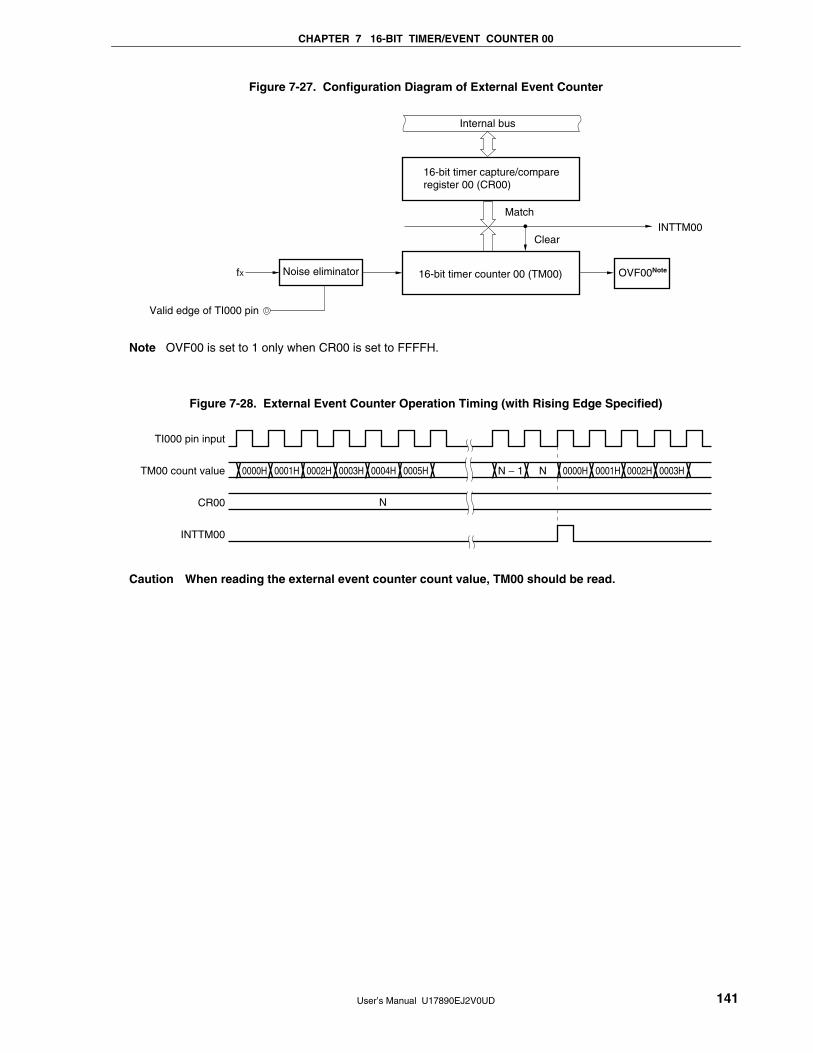
CHAPTER 7 16-BIT TIMER/EVENT COUNTER 00
User’s Manual U17890EJ2V0UD 141
Figure 7-27. Configuration Diagram of External Event Counter
fX
Internal bus
16-bit timer capture/compare register 00 (CR00)
Match
Clear
OVF00NoteNoise eliminator 16-bit timer counter 00 (TM00)
Valid edge of TI000 pin
INTTM00
Note OVF00 is set to 1 only when CR00 is set to FFFFH.
Figure 7-28. External Event Counter Operation Timing (with Rising Edge Specified)
TI000 pin input
TM00 count value
CR00
INTTM00
0000H 0001H 0002H 0003H 0004H 0005H N − 1 N 0000H 0001H 0002H 0003H
N
Caution When reading the external event counter count value, TM00 should be read.

CHAPTER 7 16-BIT TIMER/EVENT COUNTER 00
User’s Manual U17890EJ2V0UD 142
7.4.5 Square-wave output operation
Setting
The basic operation setting procedure is as follows.
<1> Set the count clock by using the PRM00 register.
<2> Set the CRC00 register (see Figure 7-29 for the set value).
<3> Set the TOC00 register (see Figure 7-29 for the set value).
<4> Set any value to the CR00 register (0000H cannot be set).
<5> Set the TMC00 register to start the operation (see Figure 7-29 for the set value).
Caution CR00 cannot be rewritten during TM00 operation.
Remarks 1. For the setting of the TO00 pin, see 7.3 (5) Port mode register 5 (PM5).
2. For how to enable the INTTM00 interrupt, see CHAPTER 16 INTERRUPT FUNCTIONS.
A square wave with any selected frequency can be output at intervals determined by the count value preset to 16-
bit timer capture/compare register 00 (CR00).
The TO00 pin output status is reversed at intervals determined by the count value preset to CR00 + 1 by setting bit
0 (TOE00) and bit 1 (TOC001) of 16-bit timer output control register 00 (TOC00) to 1. This enables a square wave
with any selected frequency to be output.
Figure 7-29. Control Register Settings in Square-Wave Output Mode (1/2)
(a) 16-bit timer mode control register 00 (TMC00)
7
0
6
0
5
0
4
0
TMC003
1
TMC002
1
TMC001
0
OVF00
0TMC00
Clears and starts on match between TM00 and CR00.
(b) Capture/compare control register 00 (CRC00)
7
0
6
0
5
0
4
0
3
0
CRC002
0/1
CRC001
0/1
CRC000
0CRC00
CR00 used as compare register

CHAPTER 7 16-BIT TIMER/EVENT COUNTER 00
User’s Manual U17890EJ2V0UD 143
Figure 7-29. Control Register Settings in Square-Wave Output Mode (2/2)
(c) 16-bit timer output control register 00 (TOC00)
7
0
OSPT00
0
OSPE00
0
TOC004
0
LVS00
0/1
LVR00
0/1
TOC001
1
TOE00
1TOC00
Enables TO00 output.
Inverts output on match between TM00 and CR00.
Specifies initial value of TO00 output F/F (setting “11” is prohibited).
Does not invert output on match between TM00 and CR01.
Disables one-shot pulse output.
(d) Prescaler mode register 00 (PRM00)
ES101
0/1
ES100
0/1
ES001
0/1
ES000
0/1
3
0
2
0
PRM001
0/1
PRM000
0/1PRM00
Selects count clock.
Setting invalid (setting “10” is prohibited.)
Setting invalid (setting “10” is prohibited.)
Remark 0/1: Setting 0 or 1 allows another function to be used simultaneously with square-wave output. See the
description of the respective control registers for details.
Figure 7-30. Square-Wave Output Operation Timing
Count clock
TM00 count value
CR00
INTTM00
TO00 pin output
0000H 0001H 0002H N − 1 N 0000H 0001H 0002H N − 1 N 0000H
N

CHAPTER 7 16-BIT TIMER/EVENT COUNTER 00
User’s Manual U17890EJ2V0UD 144
7.4.6 One-shot pulse output operation
16-bit timer/event counter 00 can output a one-shot pulse in synchronization with a software trigger or an external
trigger (TI000 pin input).
Setting
The basic operation setting procedure is as follows.
<1> Set the count clock by using the PRM00 register.
<2> Set the CRC00 register (see Figures 7-31 and 7-33 for the set value).
<3> Set the TOC00 register (see Figures 7-31 and 7-33 for the set value).
<4> Set any value to the CR00 and CR01 registers (0000H cannot be set).
<5> Set the TMC00 register to start the operation (see Figures 7-31 and 7-33 for the set value).
Remarks 1. For the setting of the TO00 pin, see 7.3 (5) Port mode register 5 (PM5).
2. For how to enable the INTTM00 (if necessary, INTTM01) interrupt, see CHAPTER 16 INTERRUPT
FUNCTIONS.
(1) One-shot pulse output with software trigger
A one-shot pulse can be output from the TO00 pin by setting 16-bit timer mode control register 00 (TMC00),
capture/compare control register 00 (CRC00), and 16-bit timer output control register 00 (TOC00) as shown in
Figure 7-31, and by setting bit 6 (OSPT00) of the TOC00 register to 1 by software.
By setting the OSPT00 bit to 1, 16-bit timer/event counter 00 is cleared and started, and its output becomes
active at the count value (N) set in advance to 16-bit timer capture/compare register 01 (CR01). After that, the
output becomes inactive at the count value (M) set in advance to 16-bit timer capture/compare register 00
(CR00)Note.
Even after the one-shot pulse has been output, the TM00 register continues its operation. To stop the TM00
register, the TMC003 and TMC002 bits of the TMC00 register must be cleared to 00.
Note The case where N < M is described here. When N > M, the output becomes active with the CR00 register
and inactive with the CR01 register. Do not set N to M.
Cautions 1. Do not set the OSPT00 bit to 1 again while the one-shot pulse is being output. To output the
one-shot pulse again, wait until the current one-shot pulse output is completed.
2. When using the one-shot pulse output of 16-bit timer/event counter 00 with a software
trigger, do not change the level of the TI000 pin or its alternate-function port pin.
Because the external trigger is valid even in this case, the timer is cleared and started even
at the level of the TI000 pin or its alternate-function port pin, resulting in the output of a
pulse at an undesired timing.

CHAPTER 7 16-BIT TIMER/EVENT COUNTER 00
User’s Manual U17890EJ2V0UD 145
Figure 7-31. Control Register Settings for One-Shot Pulse Output with Software Trigger
(a) 16-bit timer mode control register 00 (TMC00)
0 0 0 0
7 6 5 4
0
TMC003
TMC00
TMC002 TMC001 OVF00
Free-running mode
1 0 0
(b) Capture/compare control register 00 (CRC00)
0 0 0 0 0
7 6 5 4 3
CRC00
CRC002 CRC001 CRC000
CR00 as compare register
CR01 as compare register
0 0/1 0
(c) 16-bit timer output control register 00 (TOC00)
0
7
0 1 1 0/1TOC00
LVR00LVS00TOC004OSPE00OSPT00 TOC001 TOE00
Enables TO00 output.
Inverts output upon match between TM00 and CR00.
Specifies initial value of TO00 output F/F (setting “11” is prohibited.)
Inverts output upon match between TM00 and CR01.
Sets one-shot pulse output mode.
Set to 1 for output.
0/1 1 1
(d) Prescaler mode register 00 (PRM00)
0/1 0/1 0/1 0/1 0 PRM00
PRM001 PRM000
Selects count clock.
Setting invalid (setting “10” is prohibited.)
0 0/1 0/1
ES101 ES100 ES001 ES000
Setting invalid (setting “10” is prohibited.)
3 2
Caution Do not set 0000H to the CR00 and CR01 registers.

CHAPTER 7 16-BIT TIMER/EVENT COUNTER 00
User’s Manual U17890EJ2V0UD 146
Figure 7-32. Timing of One-Shot Pulse Output Operation with Software Trigger
0000H N
N N N N
M M M M
N MN + 1 N − 1 M − 10001H M + 1 M + 20000H
Count clock
TM00 count
CR01 set value
CR00 set value
OSPT00
INTTM01
INTTM00
TO00 pin output
Set TMC00 to 04H(TM00 count starts)
Caution 16-bit timer counter 00 starts operating as soon as a value other than 00 (operation stop mode) is
set to the TMC003 and TMC002 bits.
Remark N < M
(2) One-shot pulse output with external trigger
A one-shot pulse can be output from the TO00 pin by setting 16-bit timer mode control register 00 (TMC00),
capture/compare control register 00 (CRC00), and 16-bit timer output control register 00 (TOC00) as shown in
Figure 7-33, and by using the valid edge of the TI000 pin as an external trigger.
The valid edge of the TI000 pin is specified by bits 4 and 5 (ES000, ES001) of prescaler mode register 00
(PRM00). The rising, falling, or both the rising and falling edges can be specified.
When the valid edge of the TI000 pin is detected, the 16-bit timer/event counter is cleared and started, and the
output becomes active at the count value set in advance to 16-bit timer capture/compare register 01 (CR01).
After that, the output becomes inactive at the count value set in advance to 16-bit timer capture/compare register
00 (CR00)Note.
Note The case where N < M is described here. When N > M, the output becomes active with the CR00 register
and inactive with the CR01 register. Do not set N to M.
Caution Do not input the external trigger again while the one-shot pulse is being output.
To output the one-shot pulse again, wait until the current one-shot pulse output is completed.

CHAPTER 7 16-BIT TIMER/EVENT COUNTER 00
User’s Manual U17890EJ2V0UD 147
Figure 7-33. Control Register Settings for One-Shot Pulse Output with External Trigger
(with Rising Edge Specified)
(a) 16-bit timer mode control register 00 (TMC00)
0 0 0 0
7 6 5 4
1
TMC003
TMC00
TMC002 TMC001 OVF00
Clears and starts at valid edge of TI000 pin.
0 0 0
(b) Capture/compare control register 00 (CRC00)
0 0 0 0 0
7 6 5 4 3
CRC00
CRC002 CRC001 CRC000
CR00 used as compare register
CR01 used as compare register
0 0/1 0
(c) 16-bit timer output control register 00 (TOC00)
0
7
0 11 0/1TOC00
LVR00 TOC001 TOE00OSPE00OSPT00 TOC004 LVS00
Enables TO00 output.
Inverts output upon match between TM00 and CR00.
Specifies initial value of TO00 output F/F (setting “11” is prohibited.)
Inverts output upon match between TM00 and CR01.
Sets one-shot pulse output mode.
0/1 1 1
(d) Prescaler mode register 00 (PRM00)
0/1 0/1 0 1 PRM00
PRM001 PRM000
Selects count clock(setting “11” is prohibited).
Specifies the rising edge for pulse width detection.
0/1 0/1
ES101 ES100 ES001 ES000
Setting invalid (setting “10” is prohibited.)
0 0
3 2
Caution Do not set 0000H to the CR00 and CR01 registers.
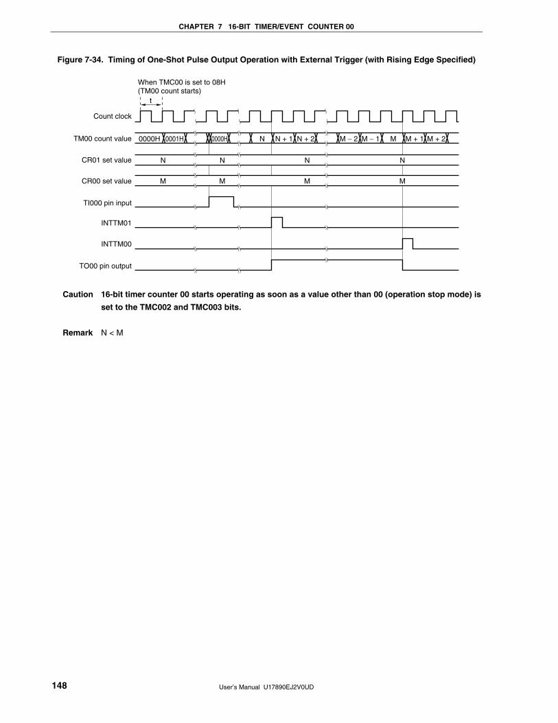
CHAPTER 7 16-BIT TIMER/EVENT COUNTER 00
User’s Manual U17890EJ2V0UD 148
Figure 7-34. Timing of One-Shot Pulse Output Operation with External Trigger (with Rising Edge Specified)
0000H N
N N N N
M M M M
MN + 1 N + 2 M + 1 M + 2M − 2 M − 10001H 0000H
Count clock
TM00 count value
CR01 set value
CR00 set value
TI000 pin input
INTTM01
INTTM00
TO00 pin output
When TMC00 is set to 08H(TM00 count starts)
t
Caution 16-bit timer counter 00 starts operating as soon as a value other than 00 (operation stop mode) is
set to the TMC002 and TMC003 bits.
Remark N < M

CHAPTER 7 16-BIT TIMER/EVENT COUNTER 00
User’s Manual U17890EJ2V0UD 149
7.5 Cautions for 16-Bit Timer/Event Counter 00
(1) Timer start errors
An error of up to one clock may occur in the time required for a match signal to be generated after timer start.
This is because 16-bit timer counter 00 (TM00) is started asynchronously to the count clock.
Figure 7-35. Start Timing of 16-Bit Timer Counter 00 (TM00)
TM00 count value 0000H 0001H 0002H 0004H
Count clock
Timer start
0003H
(2) 16-bit timer capture/compare register 00 setting
In the mode in which clear & start occurs on match between TM00 and CR00, set 16-bit timer capture/compare
register 00 (CR00) to other than 0000H. This means a 1-pulse count operation cannot be performed when 16-bit
timer/event counter 00 is used as an external event counter.
(3) Capture register data retention timing
The values of 16-bit timer capture/compare registers 00 and 01 (CR00 and CR01) are not guaranteed after 16-bit
timer/event counter 00 has been stopped.
(4) Valid edge setting
Set the valid edge of the TI000 pin after clearing bits 2 and 3 (TMC002 and TMC003) of 16-bit timer mode control
register 00 (TMC00) to 0, 0, respectively, and then stopping timer operation. The valid edge is set using bits 4
and 5 (ES000 and ES001) of prescaler mode register 00 (PRM00).
(5) Re-triggering one-shot pulse
(a) One-shot pulse output by software
Do not set the OSPT00 bit to 1 again while the one-shot pulse is being output. To output the one-shot pulse
again, wait until the current one-shot pulse output is completed.
(b) One-shot pulse output with external trigger
Do not input the external trigger again while the one-shot pulse is being output.
To output the one-shot pulse again, wait until the current one-shot pulse output is completed.
(c) One-shot pulse output function
When using the one-shot pulse output of 16-bit timer/event counter 00 with a software trigger, do not change
the level of the TI000 pin or its alternate function port pin.
Because the external trigger is valid even in this case, the timer is cleared and started even at the level of the
TI000 pin or its alternate function port pin, resulting in the output of a pulse at an undesired timing.

CHAPTER 7 16-BIT TIMER/EVENT COUNTER 00
User’s Manual U17890EJ2V0UD 150
(6) Operation of OVF00 flag
<1> The OVF00 flag is also set to 1 in the following case.
When any of the following modes is selected: the mode in which clear & start occurs on a match between
TM00 and CR00, the mode in which clear & start occurs at the TI000 pin valid edge, or the free-running
mode
↓
CR00 is set to FFFFH
↓
TM00 is counted up from FFFFH to 0000H.
Figure 7-36. Operation Timing of OVF00 Flag
Count clock
CR00
TM00
OVF00
INTTM00
FFFFH
FFFEH FFFFH 0000H 0001H
<2> Even if the OVF00 flag is cleared before the next count clock (before TM00 becomes 0001H) after the
occurrence of TM00 overflow, the OVF00 flag is re-set newly and clear is disabled.
(7) Conflicting operations
Conflict between the read period of the 16-bit timer capture/compare register (CR00/CR01) and capture trigger
input (CR00/CR01 used as capture register)
Capture trigger input has priority. The data read from CR00/CR01 is undefined.
Figure 7-37. Capture Register Data Retention Timing
Count clock
TM00 count value
Edge input
INTTM01
Capture read signal
CR01 capture value
N N + 1 N + 2 M M + 1 M + 2
X N + 2
Capture, butread value is not guaranteed
Capture
M + 1

CHAPTER 7 16-BIT TIMER/EVENT COUNTER 00
User’s Manual U17890EJ2V0UD 151
(8) Timer operation
<1> Even if 16-bit timer counter 00 (TM00) is read, the value is not captured by 16-bit timer capture/compare
register 01 (CR01).
<2> Regardless of the CPU’s operation mode, when the timer stops, the input signals to the TI000/TI001 pins
are not acknowledged.
<3> The one-shot pulse output mode operates correctly only in the free-running mode and the mode in which
clear & start occurs at the TI000 valid edge. In the mode in which clear & start occurs on a match between
the TM00 register and CR00 register, one-shot pulse output is not possible because an overflow does not
occur.
(9) Capture operation
<1> If the TI000 pin valid edge is specified as the count clock, a capture operation by the capture register
specified as the trigger for TI000 is not possible.
<2> To ensure the reliability of the capture operation, the capture trigger requires a pulse two cycles longer than
the count clock selected by prescaler mode register 00 (PRM00).
<3> The capture operation is performed at the falling edge of the count clock. An interrupt request input
(INTTM00/INTTM01), however, is generated at the rise of the next count clock.
(10) Compare operation
A capture operation may not be performed for CR00/CR01 set in compare mode even if a capture trigger has
been input.
(11) Edge detection
<1> If the TI000 or TI001 pin is high level immediately after system reset and the rising edge or both the rising
and falling edges are specified as the valid edge of the TI000 or TI001 pin to enable the 16-bit timer counter
00 (TM00) operation, a rising edge is detected immediately after the operation is enabled. Be careful
therefore when pulling up the TI000 or TI001 pin. However, the rising edge is not detected at restart after
the operation has been stopped once.
<2> The sampling clock used to remove noise differs when the TI000 pin valid edge is used as the count clock
and when it is used as a capture trigger. In the former case, the count clock is fX, and in the latter case the
count clock is selected by prescaler mode register 00 (PRM00). The capture operation is only performed
when a valid level is detected twice by sampling the valid edge, thus eliminating noise with a short pulse
width.
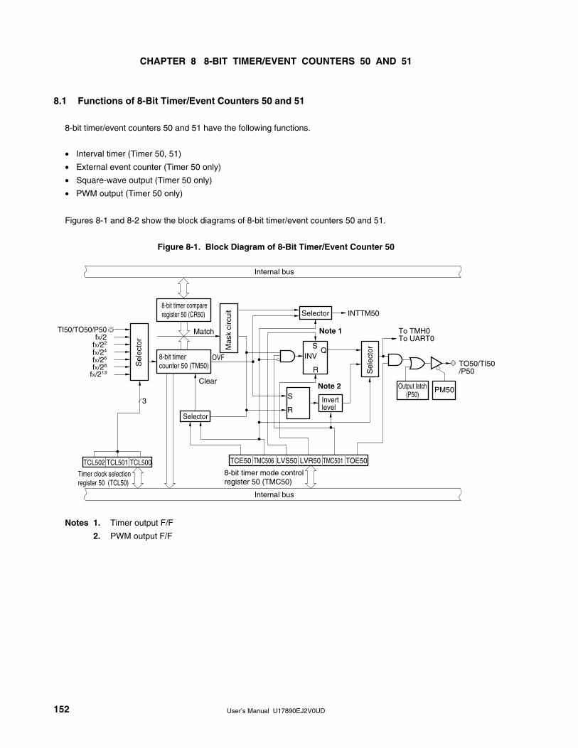
User’s Manual U17890EJ2V0UD 152
CHAPTER 8 8-BIT TIMER/EVENT COUNTERS 50 AND 51
8.1 Functions of 8-Bit Timer/Event Counters 50 and 51
8-bit timer/event counters 50 and 51 have the following functions.
• Interval timer (Timer 50, 51)
• External event counter (Timer 50 only)
• Square-wave output (Timer 50 only)
• PWM output (Timer 50 only)
Figures 8-1 and 8-2 show the block diagrams of 8-bit timer/event counters 50 and 51.
Figure 8-1. Block Diagram of 8-Bit Timer/Event Counter 50
Internal bus
8-bit timer compareregister 50 (CR50)
TI50/TO50/P50
fX/24
fX/26
fX/28
fX/213
fX/2fX/22
Match
Mas
k ci
rcui
t
OVF
Clear
3
Selector
TCL502 TCL501 TCL500
Timer clock selectionregister 50 (TCL50)
Internal bus
TCE50 TMC506 LVS50 LVR50 TMC501 TOE50
Invertlevel
8-bit timer mode control register 50 (TMC50)
S
R
SQ
R
INV
Selector
To TMH0To UART0
INTTM50
TO50/TI50/P50
Note 1
Note 2
Sel
ecto
r
8-bit timercounter 50 (TM50)S
elec
tor
Output latch(P50)
PM50
Notes 1. Timer output F/F
2. PWM output F/F

CHAPTER 8 8-BIT TIMER/EVENT COUNTERS 50 AND 51
User’s Manual U17890EJ2V0UD 153
Figure 8-2. Block Diagram of 8-Bit Timer/Event Counter 51
Internal bus
8-bit timer compareregister 51 (CR51)
fX/213
fRL/27
fX/2fX/25
Match
Mas
k ci
rcui
t
OVF
Clear
3
Selector
TCL512 TCL511 TCL510
Timer clock selectionregister 51 (TCL51)
Internal bus
TCE51 TMC516
8-bit timer mode control register 51 (TMC51)
Selector INTTM51
8-bit timercounter 51 (TM51)S
elec
tor
fX/210fX/27

CHAPTER 8 8-BIT TIMER/EVENT COUNTERS 50 AND 51
User’s Manual U17890EJ2V0UD 154
8.2 Configuration of 8-Bit Timer/Event Counters 50 and 51
8-bit timer/event counters 50 and 51 consist of the following hardware.
Table 8-1. Configuration of 8-Bit Timer/Event Counters 50 and 51
Item Configuration
Timer register 8-bit timer counter 5n (TM5n)
Register 8-bit timer compare register 5n (CR5n)
Timer input TI50
Timer output TO50
Control registers Timer clock selection register 5n (TCL5n)
8-bit timer mode control register 5n (TMC5n)
Port mode register 5 (PM5)
Port register 5 (P5)
(1) 8-bit timer counter 5n (TM5n)
TM5n is an 8-bit register that counts the count pulses and is read-only.
The counter is incremented in synchronization with the rising edge of the count clock.
Figure 8-3. Format of 8-Bit Timer Counter 5n (TM5n)
Symbol
TM5n(n = 0, 1)
Address: FF2CH (TM50), FF3CH (TM51) After reset: 00H R
In the following situations, the count value is cleared to 00H.
<1> RESET input
<2> When TCE5n is cleared
<3> When TM5n and CR5n match in the mode in which clear & start occurs upon a match of the TM5n and
CR5n.

CHAPTER 8 8-BIT TIMER/EVENT COUNTERS 50 AND 51
User’s Manual U17890EJ2V0UD 155
(2) 8-bit timer compare register 5n (CR5n)
CR5n can be read and written by an 8-bit memory manipulation instruction.
Except in PWM mode, the value set in CR5n is constantly compared with the 8-bit timer counter 5n (TM5n) count
value, and an interrupt request (INTTM5n) is generated if they match.
In PWM mode, when the TO50 pin becomes active due to a TM5n overflow and the values of TM5n and CR5n
match, the TO50 pin becomes inactive.
The value of CR5n can be set within 00H to FFH.
RESET input clears CR5n to 00H.
Figure 8-4. Format of 8-Bit Timer Compare Register 5n (CR5n)
Symbol
CR5n(n = 0, 1)
Address: FF2DH (CR50), FF3DH (CR51) After reset: 00H R/W
Cautions 1. In the mode in which clear & start occurs on a match of TM5n and CR5n (TMC5n6 = 0), do
not write other values to CR5n during operation.
2. In PWM mode, make the CR5n rewrite period 3 count clocks of the count clock (clock
selected by TCL5n) or more.
Remark n = 0, 1

CHAPTER 8 8-BIT TIMER/EVENT COUNTERS 50 AND 51
User’s Manual U17890EJ2V0UD 156
8.3 Registers Controlling 8-Bit Timer/Event Counters 50 and 51
The following four registers are used to control 8-bit timer/event counters 50 and 51.
• Timer clock selection register 5n (TCL5n)
• 8-bit timer mode control register 5n (TMC5n)
• Port mode register 5 (PM5)
• Port register 5 (P5)
(1) Timer clock selection register 5n (TCL5n)
This register sets the count clock of 8-bit timer/event counter 5n and the valid edge of the TI50 pin input.
TCL5n can be set by an 8-bit memory manipulation instruction.
RESET input clears TCL5n to 00H.
Remark n = 0, 1
Figure 8-5. Format of Timer Clock Selection Register 50 (TCL50)
Address: FF2EH After reset: 00H R/W
Symbol 7 6 5 4 3 2 1 0
TCL50 0 0 0 0 0 TCL502 TCL501 TCL500
Count clock selection Note TCL502 TCL501 TCL500
At fX = 20 MHz At fX = 16 MHz
0 0 0 TI50 pin falling edge
0 0 1 TI50 pin rising edge
0 1 0 fX/2 10 MHz 8 MHz
0 1 1 fX/22 5 MHz 4 MHz
1 0 0 fX/24 1.25 MHz 1 MHz
1 0 1 fX/26 312.5 kHz 250 kHz
1 1 0 fX/28 78.125 kHz 62.5 kHz
1 1 1 fX/213 2.44 kHz 1.953 kHz
Note Be sure to set the count clock so that the following condition is satisfied.
• VDD = 4.0 to 5.5 V: Count clock ≤ 10 MHz
Cautions 1. When the internal low-speed oscillation clock is selected as the source clock to the CPU, the
clock of the internal low-speed oscillator is divided and supplied as the count clock. If the
count clock is the internal low-speed oscillation clock, the operation of 8-bit timer/event
counter 50 is not guaranteed.
2. When rewriting TCL50 to other data, stop the timer operation beforehand.
3. Be sure to clear bits 3 to 7 to 0.
Remark fX: X1 input clock oscillation frequency

CHAPTER 8 8-BIT TIMER/EVENT COUNTERS 50 AND 51
User’s Manual U17890EJ2V0UD 157
Figure 8-6. Format of Timer Clock Selection Register 51 (TCL51)
Address: FF3EH After reset: 00H R/W
Symbol 7 6 5 4 3 2 1 0
TCL51 0 0 0 0 0 TCL512 TCL511 TCL510
Count clock selection Note 1 TCL512 TCL511 TCL510
At fX = 20 MHz At fX = 16 MHz
0 1 0 fX/2 10 MHz 8 MHz
0 1 1 fX/25 625 kHz 500 kHz
1 0 0 fX/27 156.25 kHz 125 kHz
1 0 1 fX/210 19.53 kHz 15.625 kHz
1 1 0 fX/213 2.44 kHz 1.953 kHz
1 1 1 fRL/27 1.88 kHz Note 2
Other than above Setting prohibited
Notes 1. Be sure to set the count clock so that the following condition is satisfied.
• VDD = 4.0 to 5.5 V: Count clock ≤ 10 MHz
2. At fRL = 240 kHz (typ.)
Cautions 1. When the internal low-speed oscillation clock is selected as the source clock to the CPU, the
clock of the internal low-speed oscillator is divided and supplied as the count clock. If the
count clock is the internal low-speed oscillation clock, the operation of 8-bit timer/event
counter 51 is not guaranteed.
2. When rewriting TCL51 to other data, stop the timer operation beforehand.
3. Be sure to clear bits 3 to 7 to 0.
Remarks 1. fX: X1 input clock oscillation frequency
2. fRL: Internal low-speed oscillation clock oscillation frequency

CHAPTER 8 8-BIT TIMER/EVENT COUNTERS 50 AND 51
User’s Manual U17890EJ2V0UD 158
(2) 8-bit timer mode control register 5n (TMC5n)
TMC5n is a register that performs the following five types of settings.
<1> 8-bit timer counter 5n (TM5n) count operation control
<2> 8-bit timer counter 5n (TM5n) operating mode selection
<3> Timer output F/F (flip-flop) status setting
<4> Active level selection in timer F/F control or PWM (free-running) mode
<5> Timer output control
TMC5n can be set by a 1-bit or 8-bit memory manipulation instruction.
RESET input clears this register to 00H.
Remark n = 0, 1
Figure 8-7. Format of 8-Bit Timer Mode Control Register 50 (TMC50)
Address: FF2FH After reset: 00H R/W
Symbol <7> 6 5 4 <3> <2> 1 <0>
TMC50 TCE50 TMC506 0 0 LVS50 LVR50 TMC501 TOE50
TCE50 TM50 count operation control
0 After clearing to 0, count operation disabled (counter stopped)
1 Count operation start
TMC506 TM50 operating mode selection
0 Mode in which clear & start occurs on a match between TM50 and CR50
1 PWM (free-running) mode
LVS50 LVR50 Timer output F/F status setting
0 0 No change
0 1 Timer output F/F reset (0)
1 0 Timer output F/F set (1)
1 1 Setting prohibited
In other modes (TMC506 = 0) In PWM mode (TMC506 = 1) TMC501
Timer F/F control Active level selection
0 Inversion operation disabled Active-high
1 Inversion operation enabled Active-low
TOE50 Timer output control
0 Output disabled (TM50 output is low level)
1 Output enabled

CHAPTER 8 8-BIT TIMER/EVENT COUNTERS 50 AND 51
User’s Manual U17890EJ2V0UD 159
Cautions 1. The settings of LVS50 and LVR50 are valid in other than PWM mode.
2. Perform <1> to <4> below in the following order, not at the same time.
<1> Set TMC501, TMC506: Operation mode setting
<2> Set TOE50 to enable output: Timer output enable
<3> Set LVS50, LVR50 (see Caution 1): Timer F/F setting
<4> Set TCE50
3. Stop operation before rewriting TMC506.
Remarks 1. In PWM mode, PWM output is made inactive by clearing TCE50 to 0.
2. If LVS50 and LVR50 are read, the value is 0.
3. The values of the TMC506, LVS50, LVR50, TMC501, and TOE50 bits are reflected at the TO50 pin
regardless of the value of TCE50.
Figure 8-8. Format of 8-Bit Timer Mode Control Register 51 (TMC51)
Address: FF3FH After reset: 00H R/W
Symbol <7> 6 5 4 3 2 1 0
TMC51 TCE51 TMC516 0 0 0 0 0 0
TCE51 TM51 count operation control
0 After clearing to 0, count operation disabled (counter stopped)
1 Count operation start
TMC516 TM51 operating mode selection
0 Mode in which clear & start occurs on a match between TM51 and CR51
1 PWM (free-running) mode
Cautions 1. Be sure to clear bits 0 to 5 to 0.
2. Stop operation before rewriting TMC516.
Remarks In PWM mode, PWM output is made inactive by clearing TCE51 to 0.
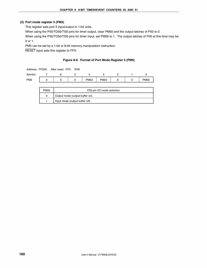
CHAPTER 8 8-BIT TIMER/EVENT COUNTERS 50 AND 51
User’s Manual U17890EJ2V0UD 160
(3) Port mode register 5 (PM5)
This register sets port 5 input/output in 1-bit units.
When using the P50/TO50/TI50 pins for timer output, clear PM50 and the output latches of P50 to 0.
When using the P50/TO50/TI50 pins for timer input, set PM50 to 1. The output latches of P50 at this time may be
0 or 1.
PM5 can be set by a 1-bit or 8-bit memory manipulation instruction.
RESET input sets this register to FFH.
Figure 8-9. Format of Port Mode Register 5 (PM5)
Address: FF25H After reset: FFH R/W
Symbol 7 6 5 4 3 2 1 0
PM5 0 0 0 PM54 PM53 0 0 PM50
PM50 P50 pin I/O mode selection
0 Output mode (output buffer on)
1 Input mode (output buffer off)

CHAPTER 8 8-BIT TIMER/EVENT COUNTERS 50 AND 51
User’s Manual U17890EJ2V0UD 161
8.4 Operations of 8-Bit Timer/Event Counters 50 and 51
8.4.1 Operation as interval timer
8-bit timer/event counter 5n operates as an interval timer that generates interrupt requests repeatedly at intervals
of the count value preset to 8-bit timer compare register 5n (CR5n).
When the count value of 8-bit timer counter 5n (TM5n) matches the value set to CR5n, counting continues with the
TM5n value cleared to 0 and an interrupt request signal (INTTM5n) is generated.
The count clock of TM5n can be selected with bits 0 to 2 (TCL50n to TCL52n) of timer clock selection register 5n
(TCL5n).
Setting
<1> Set the registers.
• TCL5n: Select the count clock.
• CR5n: Compare value
• TMC5n: Stop the count operation, select the mode in which clear & start occurs on a match of TM5n
and CR5n.
(TMC5n = 0000×××0B × = Don’t care)
<2> After TCE5n = 1 is set, the count operation starts.
<3> If the values of TM5n and CR5n match, INTTM5n is generated (TM5n is cleared to 00H).
<4> INTTM5n is generated repeatedly at the same interval.
Clear TCE5n to 0 to stop the count operation.
Caution Do not write other values to CR5n during operation.
Remark n = 0, 1
Figure 8-10. Interval Timer Operation Timing (1/2)
(a) Basic operation
t
Count clock
TM5n count value
CR5n
TCE5n
INTTM5n
Count start Clear Clear
00H 01H N 00H 01H N 00H 01H N
NNNN
Interrupt acknowledged Interrupt acknowledged
Interval timeInterval time
Remark Interval time = (N + 1) × t
N = 00H to FFH
n = 0, 1

CHAPTER 8 8-BIT TIMER/EVENT COUNTERS 50 AND 51
User’s Manual U17890EJ2V0UD 162
Figure 8-10. Interval Timer Operation Timing (2/2)
(b) When CR5n = 00H
t
Interval time
Count clock
TM5n
CR5n
TCE5n
INTTM5n
00H 00H 00H
00H 00H
(c) When CR5n = FFH
t
Count clock
TM5n
CR5n
TCE5n
INTTM5n
01 FE FF 00 FE FF 00
FFFFFF
Interval time
Interrupt acknowledged
Interrupt acknowledged
Remark n = 0, 1

CHAPTER 8 8-BIT TIMER/EVENT COUNTERS 50 AND 51
User’s Manual U17890EJ2V0UD 163
8.4.2 Operation as external event counter (Timer 50 only)
The external event counter counts the number of external clock pulses to be input to the TI50 pin by 8-bit timer
counter 50 (TM50).
TM5n is incremented each time the valid edge specified by timer clock selection register 50 (TCL50) is input.
Either the rising or falling edge can be selected.
When the TM50 count value matches the value of 8-bit timer compare register 50 (CR50), TM50 is cleared to 0
and an interrupt request signal (INTTM50) is generated.
Whenever the TM50 value matches the value of CR50, INTTM50 is generated.
Setting
<1> Set each register.
• Set the port mode register (PM50) to 1.
• TCL50: Select TI50 pin input edge.
TI50 pin falling edge → TCL50 = 00H
TI50 pin rising edge → TCL50 = 01H
• CR50: Compare value
• TMC50: Stop the count operation, select the mode in which clear & start occurs on match of TM50 and
CR50, disable the timer F/F inversion operation, disable timer output.
(TMC50 = 0000××00B × = Don’t care)
<2> When TCE50 = 1 is set, the number of pulses input from the TI50 pin is counted.
<3> When the values of TM50 and CR50 match, INTTM50 is generated (TM50 is cleared to 00H).
<4> After these settings, INTTM50 is generated each time the values of TM50 and CR50 match.
Figure 8-11. External Event Counter Operation Timing (with Rising Edge Specified)
TI50
TM50 count value
CR50
INTTM50
00 01 02 03 04 05 N − 1 N 00 01 02 03
N
Count start
Remark N = 00H to FFH

CHAPTER 8 8-BIT TIMER/EVENT COUNTERS 50 AND 51
User’s Manual U17890EJ2V0UD 164
8.4.3 Square-wave output operation (Timer 50 only)
A square wave with any selected frequency is output at intervals determined by the value preset to 8-bit timer
compare register 50 (CR50).
The TO50 pin output status is inverted at intervals determined by the count value preset to CR50 by setting bit 0
(TOE50) of 8-bit timer mode control register 50 (TMC50) to 1. This enables a square wave with any selected
frequency to be output (duty = 50%).
Setting
<1> Set each register.
• Clear the port output latch (P50) and port mode register (PM50) to 0.
• TCL50: Select the count clock.
• CR50: Compare value
• TMC50: Stop the count operation, select the mode in which clear & start occurs on a match of TM50 and
CR50.
LVS50 LVR50 Timer Output F/F Status Setting
1 0 High-level output
0 1 Low-level output
Timer output F/F inversion enabled
Timer output enabled
(TMC50 = 00001011B or 00000111B)
<2> After TCE50 = 1 is set, the count operation starts.
<3> The timer output F/F is inverted by a match of TM50 and CR50. After INTTM5n is generated, TM50 is
cleared to 00H.
<4> After these settings, the timer output F/F is inverted at the same interval and a square wave is output from
TO50.
The frequency is as follows.
Frequency = 1/2t (N + 1)
(N: 00H to FFH)
Caution Do not write other values to CR50 during operation.

CHAPTER 8 8-BIT TIMER/EVENT COUNTERS 50 AND 51
User’s Manual U17890EJ2V0UD 165
Figure 8-12. Square-Wave Output Operation Timing
Count clock
TM50 count value 00H 01H 02H N − 1 N
N
00H N − 1 N 00H01H 02H
CR50
TO50Note
t
Count start
Note The initial value of TO50 output can be set by bits 2 and 3 (LVR50, LVS50) of 8-bit timer mode control
register 50 (TMC50).
8.4.4 PWM output operation (Timer 50 only)
8-bit timer/event counter 50 operates as a PWM output when bit 6 (TMC506) of 8-bit timer mode control register 50
(TMC50) is set to 1.
The duty pulse determined by the value set to 8-bit timer compare register 50 (CR50) is output from TO50.
Set the active level width of the PWM pulse to CR50; the active level can be selected with bit 1 (TMC501) of
TMC50.
The count clock can be selected with bits 0 to 2 (TCL500 to TCL502) of timer clock selection register 50 (TCL50).
PWM output can be enabled/disabled with bit 0 (TOE50) of TMC50.
Caution In PWM mode, make the CR50 rewrite period 3 count clocks of the count clock (clock selected by
TCL50) or more.

CHAPTER 8 8-BIT TIMER/EVENT COUNTERS 50 AND 51
User’s Manual U17890EJ2V0UD 166
(1) PWM output basic operation
Setting
<1> Set each register.
• Clear the port output latch (P50) and port mode register (PM50) to 0.
• TCL50: Select the count clock.
• CR50: Compare value
• TMC50: Stop the count operation, select PWM mode.
The timer output F/F is not changed.
TMC501 Active Level Selection
0 Active-high
1 Active-low
Timer output enabled
(TMC50 = 01000001B or 01000011B)
<2> The count operation starts when TCE50 = 1.
Clear TCE50 to 0 to stop the count operation.
PWM output operation
<1> PWM output (output from TO50) outputs an inactive level until an overflow occurs.
<2> When an overflow occurs, the active level is output. The active level is output until CR50 matches the
count value of 8-bit timer counter 50 (TM50).
<3> After the CR50 matches the count value, the inactive level is output until an overflow occurs again.
<4> Operations <2> and <3> are repeated until the count operation stops.
<5> When the count operation is stopped with TCE50 = 0, PWM output becomes inactive.
For details of timing, see Figures 8-13 and 8-14.
The cycle, active-level width, and duty are as follows.
• Cycle = 28t
• Active-level width = Nt
• Duty = N/28
(N = 00H to FFH)

CHAPTER 8 8-BIT TIMER/EVENT COUNTERS 50 AND 51
User’s Manual U17890EJ2V0UD 167
Figure 8-13. PWM Output Operation Timing
(a) Basic operation (active level = H)
Count clock
TM50
CR50
TCE50
INTTM50
TO50
00H 01H FFH 00H 01H 02H N N + 1 FFH 00H 01H 02H M 00H
N
<2> Active level<1>
<3> Inactive level Active level<5>
t
(b) CR50 = 00H
Count clock
TM50
CR50
TCE50
INTTM50
TO50
Inactive level Inactive level
01H00H FFH 00H 01H 02H N N + 1 FFH 00H 01H 02H M 00H
00H
N + 2
L
t
(c) CR50 = FFH
TM50
CR50
TCE50
INTTM50
TO50
01H00H FFH 00H 01H 02H N N + 1 FFH 00H 01H 02H M 00H
FFH
N + 2
Inactive level Active levelInactive level
Active level Inactive level
t
Count clock
Remark <1> to <3> and <5> in Figure 8-13 (a) correspond to <1> to <3> and <5> in PWM output operation in
8.4.4 (1) PWM output basic operation.

CHAPTER 8 8-BIT TIMER/EVENT COUNTERS 50 AND 51
User’s Manual U17890EJ2V0UD 168
(2) Operation with CR50 changed
Figure 8-14. Timing of Operation with CR50 Changed
(a) CR50 value is changed from N to M before clock rising edge of FFH
→ Value is transferred to CR50 at overflow immediately after change.
Count clock
TM50
CR50
TCE50INTTM50
TO50
<1> CR50 change (N → M)
N N + 1 N + 2 FFH 00H 01H M M + 1 M + 2 FFH 00H 01H 02H M M + 1 M + 2
N
02H
M
H
<2>
t
(b) CR50 value is changed from N to M after clock rising edge of FFH
→ Value is transferred to CR50 at second overflow.
Count clock
TM50
CR50
TCE50INTTM50
TO50
N N + 1 N + 2 FFH 00H 01H N N + 1 N + 2 FFH 00H 01H 02H
N
02H
N
H
M
M M + 1 M + 2
<1> CR50 change (N → M) <2>
t
Caution When reading from CR50 between <1> and <2> in Figure 8-14, the value read differs from the
actual value (read value: M, actual value of CR50: N).

CHAPTER 8 8-BIT TIMER/EVENT COUNTERS 50 AND 51
User’s Manual U17890EJ2V0UD 169
8.5 Cautions for 8-Bit Timer/Event Counters 50 and 51
(1) Timer start error
An error of up to one clock may occur in the time required for a match signal to be generated after timer start.
This is because 8-bit timer counters 50 and 51 (TM50, TM51) are started asynchronously to the count clock.
Figure 8-15. 8-Bit Timer Counter 5n Start Timing
Count clock
TM5n count value 00H 01H 02H 03H 04H
Timer start
Remark n = 0, 1
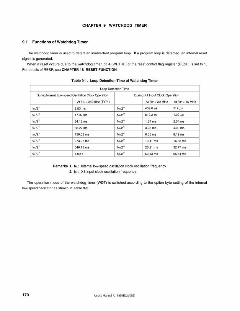
User’s Manual U17890EJ2V0UD 170
CHAPTER 9 WATCHDOG TIMER
9.1 Functions of Watchdog Timer
The watchdog timer is used to detect an inadvertent program loop. If a program loop is detected, an internal reset
signal is generated.
When a reset occurs due to the watchdog timer, bit 4 (WDTRF) of the reset control flag register (RESF) is set to 1.
For details of RESF, see CHAPTER 18 RESET FUNCTION.
Table 9-1. Loop Detection Time of Watchdog Timer
Loop Detection Time
During Internal Low-speed Oscillation Clock Operation During X1 Input Clock Operation
At fRL = 240 kHz (TYP.) At fXP = 20 MHz At fXP = 16 MHz
fRL/211 8.53 ms fXP/213 409.6 μs 512 μs
fRL/212 17.07 ms fXP/214 819.2 μs 1.02 μs
fRL/213 34.13 ms fXP/215 1.64 ms 2.04 ms
fRL/214 68.27 ms fXP/216 3.28 ms 4.09 ms
fRL/215 136.53 ms fXP/217 6.55 ms 8.19 ms
fRL/216 273.07 ms fXP/218 13.11 ms 16.38 ms
fRL/217 546.13 ms fXP/219 26.21 ms 32.77 ms
fRL/218 1.09 s fXP/220 52.43 ms 65.54 ms
Remarks 1. fRL: Internal low-speed oscillation clock oscillation frequency
2. fXP: X1 input clock oscillation frequency
The operation mode of the watchdog timer (WDT) is switched according to the option byte setting of the internal
low-speed oscillator as shown in Table 9-2.

CHAPTER 9 WATCHDOG TIMER
User’s Manual U17890EJ2V0UD 171
Table 9-2. Option Byte Setting and Watchdog Timer Operation Mode
Option Byte
Internal Low-speed Oscillator Cannot Be Stopped Internal Low-speed Oscillator Can Be Stopped by
Software
Watchdog timer clock
source
Fixed to fRLNote 1. • Selectable by software (fXP, fRL or stopped)
• When reset is released: fRL
Operation after reset Operation starts with the maximum interval
(fRL/218).
Operation starts with maximum interval (fRL/218).
Operation mode selection The overflow time can be changed only once. The clock selection/overflow time can be
changed only once.
Features The watchdog timer cannot be stopped. The watchdog timer can be stopped Note 2.
Notes 1. As long as power is being supplied, internal low-speed oscillator cannot be stopped (except in the
reset period).
2. The conditions under which clock supply to the watchdog timer is stopped differ depending on
the clock source of the watchdog timer.
<1> If the clock source is fXP, clock supply to the watchdog timer is stopped under the following
conditions.
• When fXP is stopped
• In HALT/STOP mode
• During oscillation stabilization time
<2> If the clock source is fRL, clock supply to the watchdog timer is stopped under the following
conditions.
• If the CPU clock is fXP and if fRL is stopped by software before execution of the STOP
instruction
• In HALT/STOP mode
Remarks 1. fRL: Internal low-speed oscillation clock oscillation frequency
2. fXP: X1 input clock oscillation frequency

CHAPTER 9 WATCHDOG TIMER
User’s Manual U17890EJ2V0UD 172
9.2 Configuration of Watchdog Timer
The watchdog timer consists of the following hardware.
Table 9-3. Configuration of Watchdog Timer
Item Configuration
Control registers Watchdog timer mode register (WDTM)
Watchdog timer enable register (WDTE)
Figure 9-1. Block Diagram of Watchdog Timer
fRL/22 Clock input
controller
Outputcontroller
Internal reset signal
WDCS2
Internal bus
WDCS1 WDCS0
fXP/24
WDCS3WDCS40 1 1
Selector16-bitcounter or
fXP/213 to fXP/220
fRL/211 tofRL/218
Watchdog timer enableregister (WDTE) Watchdog timer mode
register (WDTM)
3 32
Clear
Option byte (to set “internal low-speed oscillator cannot be stopped” or “internal low-speed oscillator can be stopped by software”)

CHAPTER 9 WATCHDOG TIMER
User’s Manual U17890EJ2V0UD 173
9.3 Registers Controlling Watchdog Timer
The watchdog timer is controlled by the following two registers.
• Watchdog timer mode register (WDTM)
• Watchdog timer enable register (WDTE)
(1) Watchdog timer mode register (WDTM)
This register sets the overflow time and operation clock of the watchdog timer.
This register can be set by an 8-bit memory manipulation instruction and can be read many times, but can be
written only once after reset is released.
RESET input sets this register to 67H.
Figure 9-2. Format of Watchdog Timer Mode Register (WDTM)
0
WDCS0
1
WDCS1
2
WDCS2
3
WDCS3
4
WDCS4
5
1
6
1
7
0
Symbol
WDTM
Address: FF98H After reset: 67H R/W
WDCS4Note 1 WDCS3Note 1 Operation clock selection
0 0 Internal low-speed oscillation clock (fRL)
0 1 X1 input clock (fXP)
1 × Watchdog timer operation stopped
Overflow time setting WDCS2Note 2 WDCS1Note 2 WDCS0Note 2
During Internal Low-speed
Oscillation clock operation
During X1 input clock operation
0 0 0 fRL/211 (8.53 ms) fXP/213 (409.6 μs)
0 0 1 fRL/212 (17.07 ms) fXP/214 (819.2 μs)
0 1 0 fRL/213 (34.13 ms) fXP/215 (1.64 ms)
0 1 1 fRL/214 (68.27 ms) fXP/216 (3.28 ms)
1 0 0 fRL/215 (136.53 ms) fXP/217 (6.55 ms)
1 0 1 fRL/216 (273.07 ms) fXP/218 (13.11 ms)
1 1 0 fRL/217 (546.13 ms) fXP/219 (26.21 ms)
1 1 1 fRL/218 (1.09 s) fXP/220 (52.43 ms)
Notes 1. If “Internal low-speed oscillator cannot be stopped” is specified by an option byte, this cannot
be set. The internal low-speed oscillation clock will be selected no matter what value is written.
2. Reset is released at the maximum cycle (WDCS2, 1, 0 = 1, 1, 1).

CHAPTER 9 WATCHDOG TIMER
User’s Manual U17890EJ2V0UD 174
Cautions 1. If data is written to WDTM, a wait cycle is generated. For details, see CHAPTER 27
CAUTIONS FOR WAIT.
2. Set bits 7, 6, and 5 to 0, 1, and 1, respectively (when “Internal low-speed oscillator
cannot be stopped” is selected by an option byte, other values are ignored).
3. After reset is released, WDTM can be written only once by an 8-bit memory
manipulation instruction. If writing attempted a second time, an internal reset signal
is generated.
4. WDTM cannot be set by a 1-bit memory manipulation instruction.
Remarks 1. fRL: Internal low-speed oscillation clock oscillation frequency
2. fXP: X1 input clock oscillation frequency
3. ×: Don’t care
4. Figures in parentheses apply to operation at fRL = 240 kHz (TYP.), fXP = 20 MHz
(2) Watchdog timer enable register (WDTE)
Writing ACH to WDTE clears the watchdog timer counter and starts counting again.
This register can be set by an 8-bit memory manipulation instruction.
RESET input sets this register to 9AH.
Figure 9-3. Format of Watchdog Timer Enable Register (WDTE)
01234567Symbol
WDTE
Address: FF99H After reset: 9AH R/W
Cautions 1. If a value other than ACH is written to WDTE, an internal reset signal is generated.
2. If a 1-bit memory manipulation instruction is executed for WDTE, an internal reset
signal is generated.
3. The value read from WDTE is 9AH (this differs from the written value (ACH)).

CHAPTER 9 WATCHDOG TIMER
User’s Manual U17890EJ2V0UD 175
9.4 Operation of Watchdog Timer
9.4.1 Watchdog timer operation when “Internal low-speed oscillator cannot be stopped” is selected by
option byte
The operation clock of watchdog timer is fixed to the internal low-speed oscillation clock.
After reset is released, operation is started at the maximum cycle (bits 2, 1, and 0 (WDCS2, WDCS1, WDCS0) of
the watchdog timer mode register (WDTM) = 1, 1, 1). The watchdog timer operation cannot be stopped.
The following shows the watchdog timer operation after reset release.
1. The status after reset release is as follows.
• Operation clock: Internal low-speed oscillation clock
• Cycle: fRL/218 (1.09 seconds: At operation with fRL = 240 kHz (TYP.))
• Counting starts
2. The following should be set in the watchdog timer mode register (WDTM) by an 8-bit memory manipulation
instructionNotes 1, 2.
• Cycle: Set using bits 2 to 0 (WDCS2 to WDCS0)
3. After the above procedures are executed, writing ACH to WDTE clears the count to 0, enabling recounting.
Notes 1. The operation clock (internal low-speed oscillation clock) cannot be changed. If any value is written to
bits 3 and 4 (WDCS3, WDCS4) of WDTM, it is ignored.
2. As soon as WDTM is written, the counter of the watchdog timer is cleared.
Caution In this mode, operation of the watchdog timer absolutely cannot be stopped even during STOP
instruction execution. For 8-bit timer 51 (TM51), a division of the internal low-speed oscillation
clock can be selected as the count source, so clear the watchdog timer using the interrupt
request of TM51 before the watchdog timer overflows after STOP instruction execution. If this
processing is not performed, an internal reset signal is generated when the watchdog timer
overflows after STOP instruction execution.
CHAPTER 9 WATCHDOG TIMER
User’s Manual U17890EJ2V0UD 176
9.4.2 Watchdog timer operation when “Internal low-speed oscillator can be stopped by software” is selected
by option byte
The operation clock of the watchdog timer can be selected as either the internal low-speed oscillation clock or the X1
input clock.
After reset is released, operation is started at the maximum cycle (bits 2, 1, and 0 (WDCS2, WDCS1, WDCS0) of
the watchdog timer mode register (WDTM) = 1, 1, 1).
The following shows the watchdog timer operation after reset release.
1. The status after reset release is as follows.
• Operation clock: Internal low-speed oscillation clock (fRL)
• Cycle: fRL/218 (1.09 seconds: At operation with fRL = 240 kHz (TYP.))
• Counting starts
2. The following should be set in the watchdog timer mode register (WDTM) by an 8-bit memory manipulation
instructionNotes 1, 2, 3.
• Operation clock: Any of the following can be selected using bits 3 and 4 (WDCS3 and WDCS4).
Internal low-speed oscillation clock (fRL)
X1 input clock (fXP)
Watchdog timer operation stopped
• Cycle: Set using bits 2 to 0 (WDCS2 to WDCS0)
3. After the above procedures are executed, writing ACH to WDTE clears the count to 0, enabling recounting.
Notes 1. As soon as WDTM is written, the counter of the watchdog timer is cleared.
2. Set bits 7, 6, and 5 to 0, 1, 1, respectively. Do not set the other values.
3. If the watchdog timer is stopped by setting WDCS4 and WDCS3 to 1 and ×, respectively, an internal
reset signal is not generated even if the following processing is performed.
• WDTM is written a second time.
• A 1-bit memory manipulation instruction is executed to WDTE.
• A value other than ACH is written to WDTE.
Caution In this mode, watchdog timer operation is stopped during HALT/STOP instruction execution.
After HALT/STOP mode is released, counting is started again using the operation clock of the
watchdog timer set before HALT/STOP instruction execution by WDTM. At this time, the counter
is not cleared to 0 but holds its value.
For the watchdog timer operation during STOP mode and HALT mode in each status, see 9.4.3 Watchdog timer
operation in STOP mode and 9.4.4 Watchdog timer operation in HALT mode.

CHAPTER 9 WATCHDOG TIMER
User’s Manual U17890EJ2V0UD 177
9.4.3 Watchdog timer operation in STOP mode (when “Internal low-speed oscillation can be stopped by
software” is selected by option byte)
The watchdog timer stops counting during STOP instruction execution regardless of whether the X1 input clock or
internal low-speed oscillation clock is being used.
(1) When the CPU clock and the watchdog timer operation clock are the X1 input clock (fXP) when the STOP
instruction is executed
When STOP instruction is executed, operation of the watchdog timer is stopped. After STOP mode is released,
counting stops for the oscillation stabilization time set by the oscillation stabilization time select register (OSTS)
and then counting is started again using the operation clock before the operation was stopped. At this time, the
counter is not cleared to 0 but holds its value.
Figure 9-4. Operation in STOP Mode (CPU Clock and WDT Operation Clock: X1 Input Clock)
Watchdog timerOperating Operation stopped Operating
fRL
fXP
CPU operationNormal
operation STOP Oscillation stabilization time Normal operation
Oscillation stopped
Oscillation stabilization time(set by OSTS register)
(2) When the CPU clock is the X1 input clock (fXP) and the watchdog timer operation clock is the internal low-
speed oscillation clock (fRL) when the STOP instruction is executed
When the STOP instruction is executed, operation of the watchdog timer is stopped. After STOP mode is
released, counting is started again using the operation clock before the operation was stopped. At this time, the
counter is not cleared to 0 but holds its value.
Figure 9-5. Operation in STOP Mode
(CPU Clock: X1 Input Clock, WDT Operation Clock: Internal Low-speed Oscillation Clock)
Watchdog timerOperating
fRL
fXP
CPU operationNormal
operation STOP Oscillation stabilization time Normal operation
Oscillationstopped
Oscillation stabilization time(set by OSTS register)
Operating Operation stopped

CHAPTER 9 WATCHDOG TIMER
User’s Manual U17890EJ2V0UD 178
(3) When the CPU clock is the internal low-speed oscillation clock (fRL) and the watchdog timer operation
clock is the X1 input clock (fXP) when the STOP instruction is executed
When the STOP instruction is executed, operation of the watchdog timer is stopped. After STOP mode is
released, counting is stopped until the timing of <1> or <2>, whichever is earlier, and then counting is started
using the operation clock before the operation was stopped. At this time, the counter is not cleared to 0 but holds
its value.
<1> The oscillation stabilization time set by the oscillation stabilization time select register (OSTS) elapses.
<2> The CPU clock is switched to the X1 input clock (fXP).
Figure 9-6. Operation in STOP Mode
(CPU Clock: Internal Low-speed Oscillation Clock, WDT Operation Clock: X1 Input Clock)
<1> Timing when counting is started after the oscillation stabilization time set by the oscillation stabilization time
select register (OSTS) has elapsed
Watchdog timerOperating Operation stopped Operating
fRL
fXP
CPU operation
17 clocks
Normal operation(Internal low-speed
oscillation clock) Clock supply stopped Normal operation (Internal low-speed oscillation clock)
Oscillation stopped
STOP
Oscillation stabilization time(set by OSTS register)
<2> Timing when counting is started after the CPU clock is switched to the X1 input clock (fXP)
Operating Operation stopped Operating
fRL
fXP
fRL → fXPNote
CPU operation
17 clocks
Normal operation(internal low-speed oscillation clock)
Clock supplystopped
Normal operation (internal low-speed
oscillation clock)
Normal operation (X1 input clock)
CPU clock
Oscillationstopped
STOP
Oscillation stabilization time(set by OSTS register)
Watchdog timer
Note Confirm the oscillation stabilization time of fXP using the oscillation stabilization time counter status register
(OSTC).

CHAPTER 9 WATCHDOG TIMER
User’s Manual U17890EJ2V0UD 179
(4) When CPU clock and watchdog timer operation clock are the internal low-speed oscillation clocks (fRL)
during STOP instruction execution
When the STOP instruction is executed, operation of the watchdog timer is stopped. After STOP mode is
released, counting is started again using the operation clock before the operation was stopped. At this time, the
counter is not cleared to 0 but holds its value.
Figure 9-7. Operation in STOP Mode
(CPU Clock and WDT Operation Clock: Internal Low-speed Oscillation Clock)
Watchdog timerOperating
fRL
fXP
CPU operation
17 clocks
Normal operation(internal low-speed oscillation clock) Clock supply stopped
Normal operation (internal low-speed oscillation clock)
Oscillation stopped
STOP
Oscillation stabilization time(set by OSTS register)
Operating Operation stopped
9.4.4 Watchdog timer operation in HALT mode (when “Internal low-speed oscillation can be stopped by
software” is selected by option byte)
The watchdog timer stops counting during HALT instruction execution regardless of whether the CPU clock is the
X1 input clock (fXP) or internal low-speed oscillation clock (fRL), or whether the operation clock of the watchdog timer is
the X1 input clock (fXP) or internal low-speed oscillation clock (fRL). After HALT mode is released, counting is started
again using the operation clock before the operation was stopped. At this time, the counter is not cleared to 0 but
holds its value.
Figure 9-8. Operation in HALT Mode
Watchdog timerOperating
fRL
fXP
CPU operation Normal operation
Operating
HALT
Operation stopped
Normal operation

User’s Manual U17890EJ2V0UD 180
CHAPTER 10 REAL-TIME OUTPUT PORT
10.1 Function of Real-Time Output Port
Data set previously in the real-time output buffer register can be transferred to the output latch by hardware
concurrently with timer interrupts request generation, then output externally. This is called the real-time output
function. The pins that output data externally are called real-time output ports.
By using the real-time output port, it is possible to output a signal with no jitter. Therefore, this is most suitable for
applications where an arbitrary pattern is output at an arbitrary interval (open-loop control of a stepper motor, etc.).
Also, it is possible to perform PWM modulation at a specified pin for the output pattern.
The μPD78F0711 and 78F0712 have the following real-time output ports on chip. It is possible to specify the real-
time output port in 1-bit units.
• 6 bits × 1, or 4 bits × 1 … Real-time output port 1
10.2 Configuration of Real-Time Output Port
A real-time output port includes the following hardware.
Table 10-1. Configuration of Real-Time Output Port
Item Configuration
Register Real-time output buffer register 1 (RTBL01, RTBH01)
Control registers Real-time output port mode register 1 (RTPM01)
Real-time output port control register 1 (RTPC01)
DC control register 01 (DCCTL01)
PWM select register (DCCTL02)

CHAPTER 10 REAL-TIME OUTPUT PORT
User’s Manual U17890EJ2V0UD 181
Figure 10-1. Block Diagram of Real-Time Output Port
Real-time output port 1 (6 bits × 1, or 4 bits × 1)
Internal bus
RTPOE01 BYTE01
Output triggercontroller
Real-time output port 1output latch
PWM modulationTW0TOn
(from 10-bit inverter control timer)
Real-time output port control register 1 (RTPC01)
Real-time outputbuffer register 1
Higher 4 bits(RTBH01)
Real-time outputbuffer register 1
Lower 4 bits(RTBL01)
Real-time outputport moderegister 1(RTPM01)
DC controlregister 01(DCCTL01)
2
TW0TO5/ · · · · · · · · · · · TW0TO0/RTP15 RTP10
PWM selectregister
(DCCTL02)
INTTM01 (from TM00)
Remark n = 0 to 5
<R>

CHAPTER 10 REAL-TIME OUTPUT PORT
User’s Manual U17890EJ2V0UD 182
(1) Real-time output buffer register 1 (RTBL01, RTBH01)
This register consists of two 4-bit Note registers that hold output data in advance.
The addresses of RTBL01 and RTBH01 are mapped individually in the special function register (SFR) area as
shown in Figure 10-2.
When specifying 4 bits × 1 channel as the operation mode, data is set in RTBL01.
When specifying 6 bits × 1 channel as the operation mode, data is set to both RTBL01 and RTBH01 by writing
6-bit data to either RTBL01 or RTBH01. The data of both RTBL01 and RTBH01 can be read all at once
regardless of which address is specified.
Figure 10-2 shows the configuration of RTBL01 and RTBH01, and Table 10-2 shows operations during
manipulation of RTBL01 and RTBH01.
Note For RTBH01, only 2 of the 4 bits are valid.
Figure 10-2. Configuration of Real-Time Output Buffer Register 1
Higher 2 bits Lower 4 bits
RTBL01
RTBH01
FFB8H
FFB9H
FFBAH
Table 10-2. Operation During Manipulation of Real-Time Output Buffer Register 1
Reading WritingNote Operating Mode Register to Be
Manipulated Higher 2 Bits Lower 4 Bits Higher 2 Bits Lower 4 Bits
4 bits × 1 channel RTBL01 Invalid RTBL01 Invalid RTBL01
RTBL01 RTBH01 RTBL01 RTBH01 RTBL01 6 bits × 1 channel
RTBH01 RTBH01 RTBL01 RTBH01 RTBL01
Note Output data should be set in RTBL01 and RTBH01 by the time a real-time output trigger is generated.

CHAPTER 10 REAL-TIME OUTPUT PORT
User’s Manual U17890EJ2V0UD 183
10.3 Registers Controlling Real-Time Output Port
The following four types of registers control the real-time output ports.
• Real-time output port mode register 1(RTPM01)
• Real-time output port control register 1 (RTPC01)
• DC control register 01 (DCCTL01)
• PWM select register (DCCTL02)
(1) Real-time output port mode register 1 (RTPM01)
This register sets the real-time output port mode in 1-bit units at the preset.
The outputs to be set are RTP10 to RTP15.
RTPM01 is set by a 1-bit or 8-bit memory manipulation instruction.
RESET input clears this register to 00H.
Figure 10-3. Format of Real-Time Output Port Mode Register 1
0 0 RTPM015 RTPM014 RTPM012 RTPM011 RTPM010RTPM01
RTPM01n Real-time output port selection (n = 0 to 5)
0
1
Real-time output buffer is disabled
Real-time output buffer is enabled
FFBCH 00H R/W
5 4Symbol Address After reset R/W
RTPM013
7 6 3 2 01
Caution Be sure to set bit 6 and 7 of RTPM01 to 0.
Remark When using as a real-time output port, RTP10 to RTP15 become the outputs.
< Cautions for development tools>
The actual μPD78F0711 and 78F0712 devices synchronize the RTPM01 value with the real-time output
trigger, when RTPOE01 is 1.
IECUBE® (in-circuit emulator) does not support this function which synchronizes with the real-time output
trigger. Use MINICUBE® (on-chip debug emulator) for testing this function.
<R>

CHAPTER 10 REAL-TIME OUTPUT PORT
User’s Manual U17890EJ2V0UD 184
(2) Real-time output port control register 1 (RTPC01)
This register is used to set the operation mode, and enabling or disabling operation of the real-time output
port.
The outputs to be set are RTP10 to RTP15.
The relationship between the operation mode of the real-time output port and output trigger is as shown in
Table 10-3.
RTPC01 is set by a 1-bit or 8-bit memory manipulation instruction.
RESET input clears this register to 00H.
Figure 10-4. Format of Real-Time Output Port Control Register 1
RTPOE01 0 BYTE01 0 0 0 0RTPC01
RTPOE01 Real-time output port operation control
0
1
Disables operationNote
Enables operation
BYTE01 Real-time output port operation mode
0
1
4 bits × 1 channel
6 bits × 1 channel
FFBDH 00H R/W
5 4Symbol Address After reset R/W
0
7 6 3 2 01
Note When RTPM01n (bit n (n = 0 to 5) of real-time output port mode register 1 (RTPM01)) is 1, INV01 (bit 4
of DC control register 01 (DCCTL01)) is 0, and real-time output operation is disabled (RTPOE01 = 0),
RTP10 to RTP15 output “0”.
Table 10-3. Real-Time Output Port Operation Mode and Output Trigger
BYTE01 Operation Mode RTBH01 → Port Output RTBL01 → Port Output
0 4 bits × 1 channel − INTTM01
1 6 bits × 1 channel INTTM01

CHAPTER 10 REAL-TIME OUTPUT PORT
User’s Manual U17890EJ2V0UD 185
(3) DC control register 01 (DCCTL01)
This register is used to enable/disable PWM modulation, and enable/disable inversion of the output waveform
of the real-time output port.
The outputs to be set are RTP10 to RTP15.
DCCTL01 is set by a 1-bit or 8-bit memory manipulation instruction.
RESET input clears this register to 00H.
Figure 10-5. Format of DC Control Register 01
DCEN01 PWMCH01 PWMCL01 INV01 0 0 0DCCTL01
DCEN01 Output operation specification
0
1
Inverter timer output (TW0TO0 to TW0TO5)
Modulated RTP output (RTP10-RTP15)
PWMCH01 PWM modulation specification(RTP10, RTP12, RTP14 output specification)
0
1
PWM modulation disabled
PWM modulation enabledNote
PWMCL01 PWM modulation specification(RTP11, RTP13, RTP15 output specification)
0
1
PWM modulation disabled
PWM modulation enabledNote
INV01 Output waveform specification
0
1
Inversion disabled
Inversion enabled
5 4Symbol
0
7 6 3 2 01
Address: FF38H After reset: 00H R/W
Note The PWM signal uses the inverter timer outputs (TW0TO0 or TW0TO0 to TW0TO5).
Remarks 1. The outputs to be set are RTP10 to RTP15.
2. The PWMCH01, PWMCL01, and INV01 settings are valid only when DCEN01 = 1.

CHAPTER 10 REAL-TIME OUTPUT PORT
User’s Manual U17890EJ2V0UD 186
(4) PWM select register (DCCTL02)
This register selects the PWM signal during the PWM modulation operation.
DCCTL02 is set by a 1-bit or 8-bit memory manipulation instruction.
RESET input clears this register to 00H.
Figure 10-6. Format of PWM Select Register
0 0 0 0 0 0 PWMSELDCCTL02
PWMSEL Selects signal for PWM modulation
0
1
TW0TO0
TW0TO0 to TW0TO5Note
5 4Symbol
0
7 6 3 2 01
Address: FF39H After reset: 00H R/W
Note IECUBE does not support this setting. Use MINICUBE for testing this function.

CHAPTER 10 REAL-TIME OUTPUT PORT
User’s Manual U17890EJ2V0UD 187
10.4 Operation of Real-Time Output Port
(1) Using RTP10 to RTP15 as a real-time output port ..... Real-time output port 1 (6 bits × 1, or 4 bits × 1)
If real-time output is enabled when bit 7 (RTPOE01) of real-time output port control register 1 (RTPC01) is 1,
the data of real-time output buffer register 1 (RTBH01, RTBL01) is transferred to the output latch in
synchronization with the generation of INTTM01. Of the transferred data, only the data of the bit specified as
the real-time output port by setting real-time output port mode register 1 (RTPM01) is output from bits RTP10
to RTP15. It is possible to use RTP10 to RTP15 as inverter timer output when inverter timer output is specified
by DCEN01.
The operation mode can be selected as 6 bits × 1, or 4 bits × 1, by setting BYTE01.
By setting INV01, it is possible to invert the output waveform. Also, by setting PWMCL01 and PWMCH01, it is
possible to perform PWM modulation of the output pattern.
If real-time output was disabled (RTPOE01 = 0) when RTPM01n = 1 and INV01 = 0, then RTP10 to RTP15
output TW0TO0 or TW0TO0 to TW0TO5.
The relationship between the settings for each bit of the control register and the real-time output is shown in
Table 10-4, and an example of the operation timing is shown in Figure 10-7.
Remark BYTE01: Bit 5 of real-time output port control register 1 (RTPC01)
DCEN01: Bit 7 of DC control register 1 (DCCTL1)
INV01: Bit 4 of DC control register 1 (DCCTL1)
PWMCL01: Bit 5 of DC control register 1 (DCCTL1)
PWMCH01: Bit 6 of DC control register 1 (DCCTL1)
RTPM01n: Bit n (n = 0 to 5) of real-time output port mode register 1 (RTPM01).

CHAPTER 10 REAL-TIME OUTPUT PORT
User’s Manual U17890EJ2V0UD 188
Table 10-4. Relationship Between Settings of Each Bit of Control Register and Real-Time Output
Pin TW0TOn Status CE0 DCEN01 INV01 PWMCH01/
PWMCL01
RTPOE01 RTPM01n RTBH01m/
RTBL01m PWMSEL = 0 PWMSEL = 1
Note
0 × × × × × × Hi-Z Hi-Z
0 × × × × × TW0TO0 TW0TOn
0 × × “low” output “low” output
0 × “low” output “low” output
0 “low” output “low” output
0
1
1
1 “high” output “high” output
0 × “low” output Note
“low” output 0
1 × TW0TO0 TW0TOn
0 × “low” output Note
“low” output
0 TW0TO0 TW0TOn
0
1
1
1
1 “high” output “high” output
0 × × “high” output “high” output
0 × “high” output “high” output
0 “high” output “high” output
0
1
1
1 “low” output “low” output
0 × “high” output Note
“high” output 0
1 × TW0TO0 TW0TOn
0 × “high” output Note
“high” output
0 TW0TO0 TW0TOn
1
1
1
1
1
1
1 “low” output “low” output
CE0: Bit 7 of inverter timer control register (TW0C)
DCEN01: Bit 7 of DC control register 01 (DCCTL01)
INV01: Bit 4 of DCCTL01
PWMCH01: Bit 6 of DCCTL01
PWMCL01: Bit 5 of DCCTL01
RTPOE01: Bit 7 of real-time output port control register 1 (RTPC01)
RTPM01n: Bit n of real-time output port mode register 1 (RTPM01)
RTBH01m: Bit m of real-time output buffer register 1H (RTBH01)
RTBL01m: Bit m of real-time output buffer register 1L (RTBL01)
n = 0 to 5
m = 0 to 3
×: don’t care.
Note IECUBE is not supported.
<R>
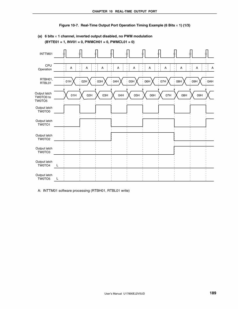
CHAPTER 10 REAL-TIME OUTPUT PORT
User’s Manual U17890EJ2V0UD 189
Figure 10-7. Real-Time Output Port Operation Timing Example (6 Bits × 1) (1/3)
(a) 6 bits × 1 channel, inverted output disabled, no PWM modulation
(BYTE01 = 1, INV01 = 0, PWMCH01 = 0, PWMCL01 = 0)
A
01H 02H 03H 04H 05H 06H 07H 08H 09H
01H
L
L
02H 03H 04H 05H 06H 07H 08H 09H
0AH
A A A A A A A A A
INTTM01
CPUOperation
RTBH01, RTBL01
Output latchTW0TO0
Output latchTW0TO1
Output latchTW0TO2
Output latchTW0TO3
Output latchTW0TO4
Output latchTW0TO5
Output latchTW0TO0 toTW0TO5
A: INTTM01 software processing (RTBH01, RTBL01 write)

CHAPTER 10 REAL-TIME OUTPUT PORT
User’s Manual U17890EJ2V0UD 190
Figure 10-7. Real-Time Output Port Operation Timing Example (6 Bits × 1) (2/3)
(b) 6 bits × 1 channel, inverted output enabled, no PWM modulation
(BYTE01 = 1, INV01 = 1, PWMCH01 = 0, PWMCL01 = 0)
A
01H 02H 03H 04H 05H 06H 07H 08H 09H
01H
H
H
02H 03H 04H 05H 06H 07H 08H 09H
0AH
A A A A A A A A A
INTTM01
CPUOperation
RTBH01, RTBL01
Output latchTW0TO0
Output latchTW0TO1
Output latchTW0TO2
Output latchTW0TO3
Output latchTW0TO4
Output latchTW0TO5
Output latchTW0TO0 toTW0TO5
A: INTTM01 software processing (RTBH01, RTBL01 write)

CHAPTER 10 REAL-TIME OUTPUT PORT
User’s Manual U17890EJ2V0UD 191
Figure 10-7. Real-Time Output Port Operation Timing Example (6 Bits × 1) (3/3)
(c) 6 bits × 1 channel, inverted output enabled, PWM modulation
(BYTE01 = 1, INV01 = 1, PWMCH01 = 1, PWMCL01 = 1)
A
01H 02H 03H 04H 05H 06H 07H 08H 09H
01H
H
H
02H 03H 04H 05H 06H 07H 08H 09H
0AH
A A A A A A A A A
INTTM01
CPUOperation
RTBH01, RTBL01
Output latchTW0TO0
Output latchTW0TO1
Output latchTW0TO2
Output latchTW0TO3
Output latchTW0TO4
Output latchTW0TO5
Output latchTW0TO0 toTW0TO5
A: INTTM01 software processing (RTBH01, RTBL01 write)

CHAPTER 10 REAL-TIME OUTPUT PORT
User’s Manual U17890EJ2V0UD 192
10.5 Using Real-Time Output Port
When using the real-time output port, perform the following steps.
(1) Disable real-time output operation.
Clear bit 7 (RTPOE01) of real-time output port control register 1 (RTPC01) to 0.
(2) Initial setting
• Specify the real-time output port mode in 1-bit units.
Set real-time output port mode register 1 (RTPM01).
• Select the operation mode (trigger and a valid edge).
Set bit 5 (BYTE01) of RTPC01.
• Set an initial value in real-time output buffer register 1 (RTBH01, RTBL01).
• Set DC control register 01 (DCCTL01).
(3) Enable the real-time output operation.
RTPOE01 = 1
(4) Set the next output to RTBH01 and RTBL01 before the selected transfer trigger is generated.
(5) Sequentially set the next real-time output value to RTBH01 and RTBL01 by using the interrupt
servicing corresponding to the selected trigger.

CHAPTER 10 REAL-TIME OUTPUT PORT
User’s Manual U17890EJ2V0UD 193
10.6 Notes on Real-Time Output Port
(1) Before performing the initial setting, disable the real-time output operation by clearing bit 7 (RTPOE01) of real-
time output port control register 1 (RTPC01) to 0.
(2) Once the real-time output operation has been disabled (RTPOE01 = 0), be sure to set the same initial value as
the output latch to real-time output buffer register 1 (RTBH01 and RTBL01) before enabling the real-time
output operation (RTPOE01 = 0 → 1).

User’s Manual U17890EJ2V0UD 194
CHAPTER 11 DC INVERTER CONTROL FUNCTION
The μPD78F0711 and 78F0712 realize a 3-phase PWM DC inverter control by combination of 10-bit inverter
control timer and real-time output port.
See the following chapters.
CHAPTER 6 10-BIT INVERTER CONTROL TIMER
CHAPTER10 REAL-TIME OUTPUT PORT

User’s Manual U17890EJ2V0UD 195
CHAPTER 12 Hi-Z OUTPUT CONTROLLER
12.1 Hi-Z Output Controller Functions
The Hi-Z output controller can forcibly stop all output signals of the three-phase inverter control timer, if it detects
an abnormality in the motor, by inputting an abnormality detection signal to the TW0TOFFP pin.
• Function to forcibly stop output (to stop output of the TW0TO0 to TW0TO5 pins by inputting a valid edge to the
TW0TOFFP pin)
• Function to cancel forced output stop status
12.2 Configuration of Hi-Z Output Controller
Figure 12-1. Block Diagram of Hi-Z Output Controller
HZA0CTL0Port control
10-bit inverter control timer
(TMW0)
TW0TOFFP(Abnormality detection)
TW0TO0/RTP10
TW0TO1/RTP11
TW0TO2/RTP12
TW0TO3/RTP13
TW0TO4/RTP14
TW0TO5/RTP15
Real-timeoutput port
The Hi-Z output controller consists of the following hardware.
Item Configuration
Control register High-impedance output control register 0 (HZA0CTL0)
< Cautions for development tools>
IECUBE (in-circuit emulator) does not support the Hi-Z output controller function. Use MINICUBE (on-chip
debug emulator) for testing this function.
<R>

CHAPTER 12 Hi-Z OUTPUT CONTROLLER
User’s Manual U17890EJ2V0UD 196
12.3 Register for Controlling Hi-Z Output Controller
(1) High-impedance output control register 0 (HZA0CTL0)
The HZA0CTL0 register is an 8-bit register that controls the high-impedance state of the output buffer of the
TW0TO0 to TW0TO5 pins.
This register is set by using a 1-bit or 8-bit manipulation instruction. The HZA0DCF0 bit, however, is a read-
only bit and nothing can be written to it even if the write operation is performed.
Reset input sets this register to 00H.
The same value can always be written to the HZA0CTL0 register by using software.
Figure 12-2. Format of High-impedance Output Control Register 0 (1/2)
HZA0DCE0
HZA0DCE0
0
1
High-impedance output control
Disables high-impedance output control operation. Target pins can output their signals.
Enables high-impedance output control operation.
HZA0CTL0 HZA0DCM0 HZA0DCN0 HZA0DCP0 HZA0DCT0 HZA0DCC0 0 HZA0DCF0
6 5 4 3 2 1
HZA0DCN0
0
0
1
1
HZA0DCP0
0
1
0
1
Specification of input edge of TW0TOFFP pin
No valid edge
(Setting the HZA0DCF0 bit by the TW0TOFFP pin input is disabled.)
The rising edge of the TW0TOFFP pin input is valid.
(Abnormality is detected when the high level is input.)
The falling edge of the TW0TOFFP pin input is valid.
(Abnormality is detected when the low level is input.)
Setting prohibited
HZA0DCM0
0
1
Condition of clearing high-impedance state by HZA0DCC0 bit
Setting of the HZA0DCC0 bit is valid regardless of the TW0TOFFP pin input.
Setting of the HZA0DCC0 bit is invalid while the TW0TOFFP holds a level
at which an abnormality has been detected (active level).
After reset: 00H R/W Address: FF69H
7 0
Clear the HZA0DCE0 bit to 0 when rewriting the HZA0DCM0 bit.
HZA0DCT0
0
1
High-impedance output trigger bit
No operation
Software makes a target pin go into a high-impedance state and the
HZA0DCF0 bit is set to 1.
• Setting the HZA0DCT0 bit to 1 is invalid if a level indicating an abnormality
(detected according to the setting of the HZA0DCN0 and HZA0DCP0 bits)
is input to the TW0TOFFP pin.
• The HZA0DCT0 bit is a software trigger bit and is always 0 when it is read.
• Setting the HZA0DCT0 bit to 1 is invalid when the HZA0DCE0 bit = 0.
• Setting the HZA0DCT0 and HZA0DCC0 bits simultaneously to 1 is prohibited.
Clear the HZA0DCE0 bit to 0 when rewriting the HZA0DCN0 and HZA0DCP0 bits.
<R>
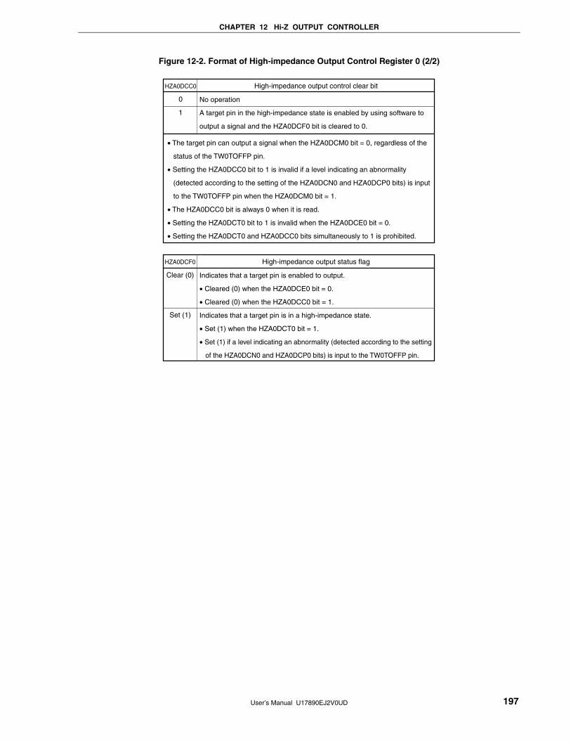
CHAPTER 12 Hi-Z OUTPUT CONTROLLER
User’s Manual U17890EJ2V0UD 197
Figure 12-2. Format of High-impedance Output Control Register 0 (2/2)
HZA0DCC0
0
1
High-impedance output control clear bit
No operation
A target pin in the high-impedance state is enabled by using software to
output a signal and the HZA0DCF0 bit is cleared to 0.
• The target pin can output a signal when the HZA0DCM0 bit = 0, regardless of the
status of the TW0TOFFP pin.
• Setting the HZA0DCC0 bit to 1 is invalid if a level indicating an abnormality
(detected according to the setting of the HZA0DCN0 and HZA0DCP0 bits) is input
to the TW0TOFFP pin when the HZA0DCM0 bit = 1.
• The HZA0DCC0 bit is always 0 when it is read.
• Setting the HZA0DCT0 bit to 1 is invalid when the HZA0DCE0 bit = 0.
• Setting the HZA0DCT0 and HZA0DCC0 bits simultaneously to 1 is prohibited.
HZA0DCF0
Clear (0)
Set (1)
High-impedance output status flag
Indicates that a target pin is enabled to output.
• Cleared (0) when the HZA0DCE0 bit = 0.
• Cleared (0) when the HZA0DCC0 bit = 1.
Indicates that a target pin is in a high-impedance state.
• Set (1) when the HZA0DCT0 bit = 1.
• Set (1) if a level indicating an abnormality (detected according to the setting
of the HZA0DCN0 and HZA0DCP0 bits) is input to the TW0TOFFP pin.

CHAPTER 12 Hi-Z OUTPUT CONTROLLER
User’s Manual U17890EJ2V0UD 198
12.4 Operation of Hi-Z Output Controller
(1) To set high-impedance control operation
<Procedure>
<1> Set the HZA0DCM0, HZA0DCN0, and HZA0DCP0 bits.
<2> Set the HZA0DCE0 bit to 1 (to enable high-impedance control).
(2) To change setting after enabling high-impedance control
<Procedure>
<1> Clear the HZA0DCE0 bit to 0 (to disable the high-impedance control operation).
<2> Change the setting of the HZA0DCM0, HZA0DCN0, and HZA0DCP0 bits.
<3> Set the HZA0DCE0 bit to 1 (to enable high-impedance control again).
(3) To resume output when a pin is in high-impedance state
When the HZA0DCM0 bit is 1, the HZA0DCC0 bit is set to 1 to cancel the high-impedance state after the valid
edge of the TW0TOFFP pin is detected, but the high-impedance state will not be canceled unless the bit is set
while the input level of the TW0TOFFP pin is inactive.
<Procedure>
<1> Set the HZA0DCC0 bit to 1 (signal to cancel the high-impedance state).
<2> Read the HZA0DCF0 bit to check the status of the flag.
<3> Return to <1> if the HZA0DCF0 bit = 1. The input level of the TW0TOFFP pin must be checked. If
the HZA0DCF0 bit = 0, the pin can output its signal.
(4) To make pin go into a high-impedance state by using software
To make a pin go into a high-impedance state by setting the HZA0DCT0 bit to 1 via software, the bit must be
set while the input level of the TW0TOFFP pin is inactive. An example of a setting procedure that is
independent of the setting of the HZA0DCM0 bit is given below.
<Procedure>
<1> Set the HZA0DCT0 bit to 1 (high-impedance output instruction).
<2> Read the HZA0DCF0 bit to check the status of the flag.
<3> Return to <1> if the HZA0DCF0 bit is 0. The input level of the TW0TOFFP pin must be checked.
The pin is in the high-impedance state if the HZA0DCF0 bit = 1.
If the TW0TOFFP pin input is not used when the HZA0DCP0 bit = 0 and HZA0DCN0 bit = 0, the target pin
goes into a high-impedance when the HZA0DCT0 bit is set to 1.

User’s Manual U17890EJ2V0UD 199
CHAPTER 13 A/D CONVERTER
13.1 Functions of A/D Converter
The A/D converter converts an analog input signal into a digital value, and consists of up to four channels (ANI0 to
ANI3) with a resolution of 10 bits.
The A/D converter has the following two functions.
(1) 10-bit resolution A/D conversion
10-bit resolution A/D conversion is carried out repeatedly for one channel selected from analog inputs ANI0 to
ANI3. Each time an A/D conversion operation ends, an interrupt request (INTAD) is generated.
(2) Power-fail detection function
This function is used to detect a voltage drop in a battery. The A/D conversion result (ADCR register value) and
power-fail comparison threshold register (PFT) value are compared. INTAD is generated only when a
comparative condition has been matched.
Figure 13-1. Block Diagram of A/D Converter
ANI0/P20ANI1/P21ANI2/P22ANI3/P23
AVREF
AVSS
INTAD
3
ADS2 ADS1 ADS0EGA1 EGA0 TRG ADTMD FR0 ADHS1ADHS0ADCS2ADCS ADMD FR2 FR1
AVSS
ADTRG
INTADTR
PFEN PFCM
ADCS bit
Sample & hold circuit
Voltage comparator
Controller
A/D conversion resultregister (ADCR)
Power-failcomparisonthreshold
register (PFT)
Analog input channelspecification register (ADS)
A/D converter mode register (ADM)
Power-fail comparison mode register (PFM)
Internal bus
Comparator
Successive approximationregister (SAR)
Sel
ecto
r
Tap
sel
ecto
r
Sel
ecto
r
Edgedetector

CHAPTER 13 A/D CONVERTER
User’s Manual U17890EJ2V0UD 200
13.2 Configuration of A/D Converter
The A/D converter consists of the following hardware.
Table 13-1. Registers of A/D Converter Used on Software
Item Configuration
Registers Successive approximation register (SAR)
A/D conversion result register (ADCR)
A/D converter mode register (ADM)
Analog input channel specification register (ADS)
Power-fail comparison mode register (PFM)
Power-fail comparison threshold register (PFT)
(1) ANI0 to ANI3 pins
These are the analog input pins of the 4-channel A/D converter. They input analog signals to be converted into
digital signals. Pins other than the one selected as the analog input pin by the analog input channel specification
register (ADS) can be used as input port pins.
(2) Sample & hold circuit
The sample & hold circuit samples the input signal of the analog input pin selected by the selector when A/D
conversion is started, and holds the sampled analog input voltage value during A/D conversion.
(3) Series resistor string
The series resistor string is connected between AVREF and AVSS, and generates a voltage to be compared with
the analog input signal.
Figure 13-2. Circuit Configuration of Series Resistor String
AVREF
AVSS
P-ch
Series resistor string
ADCS
(4) Voltage comparator
The voltage comparator compares the sampled analog input voltage and the output voltage of the series resistor
string.
(5) Successive approximation register (SAR)
This register compares the sampled analog voltage and the voltage of the series resistor string, and converts the
result, starting from the most significant bit (MSB).
When the voltage value is converted into a digital value down to the least significant bit (LSB) (end of A/D
conversion), the contents of the SAR register are transferred to the A/D conversion result register (ADCR).

CHAPTER 13 A/D CONVERTER
User’s Manual U17890EJ2V0UD 201
(6) A/D conversion result register (ADCR)
The result of A/D conversion is loaded from the successive approximation register (SAR) to this register each
time A/D conversion is completed, and the ADCR register holds the result of A/D conversion in its higher 10 bits
(the lower 6 bits are fixed to 0).
(7) Controller
When A/D conversion has been completed or when the power-fail detection function is used, this controller
compares the result of A/D conversion (value of the ADCR register) and the value of the power-fail comparison
threshold register (PFT). It generates the interrupt INTAD only if a specified comparison condition is satisfied as
a result.
(8) AVREF pin
This pin inputs an analog power/reference voltage to the A/D converter. Always use this pin at the same potential
as that of the VDD pin even when the A/D converter is not used.
The signal input to ANI0 to ANI3 is converted into a digital signal, based on the voltage applied across AVREF and
AVSS.
(9) AVSS pin
This is the ground potential pin of the A/D converter. Always use this pin at the same potential as that of the VSS
pin even when the A/D converter is not used.
(10) A/D converter mode register (ADM)
This register is used to set the conversion time of the analog input signal to be converted, and to start or stop the
conversion operation.
(11) Analog input channel specification register (ADS)
This register is used to specify the port that inputs the analog voltage to be converted into a digital signal.
(12) Power-fail comparison mode register (PFM)
This register is used to set the power-fail monitor mode.
(13) Power-fail comparison threshold register (PFT)
This register is used to set the threshold value that is to be compared with the value of the A/D conversion result
register (ADCR).

CHAPTER 13 A/D CONVERTER
User’s Manual U17890EJ2V0UD 202
13.3 Registers Used in A/D Converter
The A/D converter uses the following five registers.
• A/D converter mode register (ADM)
• Analog input channel specification register (ADS)
• A/D conversion result register (ADCR)
• Power-fail comparison mode register (PFM)
• Power-fail comparison threshold register (PFT)

CHAPTER 13 A/D CONVERTER
User’s Manual U17890EJ2V0UD 203
(1) A/D converter mode register (ADM)
This register sets the conversion time for analog input to be A/D converted, and starts/stops conversion.
ADM can be set by a 1-bit or 8-bit memory manipulation instruction.
RESET input clears this register to 00H.
Figure 13-3. Format of A/D Converter Mode Register (ADM)
ADCS
ADCS
0
1
Stops conversion operation
Enables conversion operation
A/D conversion operation control
ADM ADMD FR2Note 1 FR1Note 1 FR0Note 1 ADHS1Note 1 ADHS0Note 1 ADCS2
ADMD
0
1
Select mode
Scan mode
Operation mode control
ADHS1
0
0
0
0
0
0
0
0
0
1
1
1
1
1
1
A/D conversion time selection
96/fX
72/fX
48/fX
24/fX
224/fX
168/fX
112/fX
56/fX
72/fX
54/fX
36/fX
18/fX
Address: FF6CH After reset: 00H R/W
ADCS2
0
1
Stops operation of reference voltage generator
Enables operation of reference voltage generator
Boost reference voltage generator operation controlNote 2
ADHS0
0
1
1
1
1
1
1
1
1
0
0
0
0
1
1
FR2
×
0
0
0
0
1
1
1
1
0
0
0
0
1
×
FR1
×
0
0
1
1
0
0
1
1
0
0
1
1
×
×
FR0
×
0
1
0
1
0
1
0
1
0
1
0
1
×
×
Symbol
Setting prohibited
Setting prohibited
Setting prohibited
Notes 1. Select the A/D conversion time in the combination of FR2 to FR0, ADHS1, and ADHS0.
For details of A/D conversion time, see Table 13-3.
2. A booster circuit is incorporated to realize low-voltage operation. The operation of the circuit that
generates the reference voltage for boosting is controlled by ADCS2, and it takes 1 μs from operation
start to operation stabilization. Therefore, when ADCS is set to 1 after 1 μs or more has elapsed from
the time ADCS2 is set to 1, the conversion result at that time has priority over the first conversion
result.
Remark fX: X1 input clock oscillation frequency
<R>

CHAPTER 13 A/D CONVERTER
User’s Manual U17890EJ2V0UD 204
(a) Controlling reference voltage generator for boosting When the ADCS2 bit = 0, power to the A/D converter drops. The converter requires a setup time of 1 μs or
more after the ADCS2 bit has been set to 1.
Therefore, the result of A/D conversion becomes valid from the first result by setting the ADCS bit to 1 at
least 1 μs after the ADCS2 bit has been set to 1.
Table 13-2. Settings of ADCS and ADCS2
ADCS ADCS2 A/D Conversion Operation
0 0 Stop status (DC power consumption path does not exist)
0 1 Conversion waiting mode (only reference voltage generator consumes power)
1 0 Conversion mode (reference voltage generator operation stoppedNote 1)
1 1 Conversion mode (reference voltage generator operatesNote 2)
Notes 1. If the ADCS and ADCS2 bits are changed from 00B to 10B, the reference voltage generator for
boosting automatically turns on. If the ADCS bit is cleared to 0 while the ADCS2 bit is 0, the
voltage generator automatically turns off. In the software trigger mode (ADS.TRG bit = 0), use of
the first A/D conversion result is prohibited.
In the hardware trigger mode (TRG bit = 1), use the A/D conversion result only if A/D conversion is
started after the lapse of the oscillation stabilization time of the reference voltage generator for
boosting.
2. If the ADCS and ADCS2 bits are changed from 00B to 11B, the reference voltage generator for
boosting automatically turns on. If the ADCS bit is cleared to 0 while the ADCS2 bit is 1, the
voltage generator stays on. In the software trigger mode (TRG bit = 0), use of the first A/D
conversion result is prohibited.
In the hardware trigger mode (TRG bit = 1), use the A/D conversion result only if A/D conversion is
started after the lapse of the oscillation stabilization time of the reference voltage generator for
boosting.
Figure 13-4. Timing Chart When Boost Reference Voltage Generator Is Used
ADCS2
Boost reference voltage
ADCS
Conversion operation
Conversion operation
Conversion stoppedConversionwaiting
Boost reference voltage generator: operating
Note
Note The time from the rising of the ADCS2 bit to the falling of the ADCS bit must be 1 μs or longer to
stabilize the reference voltage.
Cautions 1. A/D conversion must be stopped before rewriting bits FR0 to FR2, ADHS0, and ADHS1
to values other than the identical data.
2. If data is written to ADM, a wait cycle is generated. For details, see CHAPTER 27
CAUTIONS FOR WAIT.
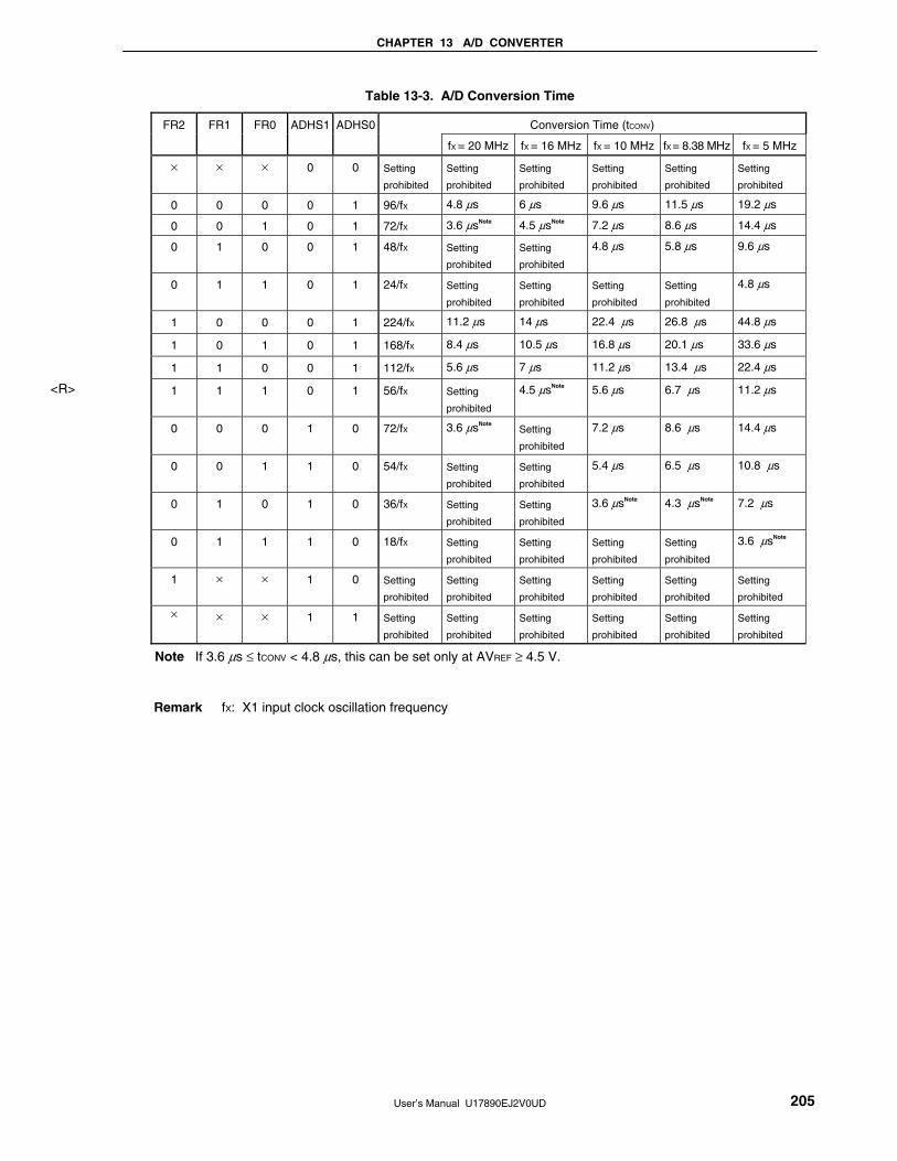
CHAPTER 13 A/D CONVERTER
User’s Manual U17890EJ2V0UD 205
Table 13-3. A/D Conversion Time
Conversion Time (tCONV) FR2 FR1 FR0 ADHS1 ADHS0
fX = 20 MHz fX = 16 MHz fX = 10 MHz fX = 8.38 MHz fX = 5 MHz
× × × 0 0 Setting
prohibited
Setting
prohibited Setting
prohibited Setting
prohibited Setting
prohibited Setting
prohibited
0 0 0 0 1 96/fX 4.8 μs 6 μs 9.6 μs 11.5 μs 19.2 μs
0 0 1 0 1 72/fX 3.6 μsNote 4.5 μsNote 7.2 μs 8.6 μs 14.4 μs
0 1 0 0 1 48/fX Setting
prohibited Setting
prohibited
4.8 μs 5.8 μs 9.6 μs
0 1 1 0 1 24/fX Setting
prohibited Setting
prohibited Setting
prohibited Setting
prohibited
4.8 μs
1 0 0 0 1 224/fX 11.2 μs 14 μs 22.4 μs 26.8 μs 44.8 μs
1 0 1 0 1 168/fX 8.4 μs 10.5 μs 16.8 μs 20.1 μs 33.6 μs
1 1 0 0 1 112/fX 5.6 μs 7 μs 11.2 μs 13.4 μs 22.4 μs
1 1 1 0 1 56/fX Setting
prohibited
4.5 μsNote 5.6 μs 6.7 μs 11.2 μs
0 0 0 1 0 72/fX 3.6 μsNote Setting
prohibited
7.2 μs 8.6 μs 14.4 μs
0 0 1 1 0 54/fX Setting
prohibited Setting
prohibited
5.4 μs 6.5 μs 10.8 μs
0 1 0 1 0 36/fX Setting
prohibited Setting
prohibited
3.6 μsNote 4.3 μsNote 7.2 μs
0 1 1 1 0 18/fX Setting
prohibited Setting
prohibited Setting
prohibited Setting
prohibited
3.6 μsNote
1 × × 1 0 Setting
prohibited Setting
prohibited Setting
prohibited Setting
prohibited Setting
prohibited Setting
prohibited
× × × 1 1 Setting
prohibited Setting
prohibited Setting
prohibited Setting
prohibited Setting
prohibited Setting
prohibited
Note If 3.6 μs ≤ tCONV < 4.8 μs, this can be set only at AVREF ≥ 4.5 V.
Remark fX: X1 input clock oscillation frequency
<R>

CHAPTER 13 A/D CONVERTER
User’s Manual U17890EJ2V0UD 206
(2) Analog input channel specification register (ADS)
This register specifies the input port of the analog voltage to be A/D converted.
ADS can be set by a 1-bit or 8-bit memory manipulation instruction.
RESET input clears this register to 00H.
Figure 13-5. Format of Analog Input Channel Specification Register (ADS)
ADS0ADS1ADS20ADTMDTRGEGA0EGA1
Analog input channel specification
ANI0
ANI1
ANI2
ANI3
Setting prohibited
ADS0
0
1
0
1
×
ADS1
0
0
1
1
×
ADS2
0
0
0
0
1
01234567
ADS
Address: FF6DH After reset: 00H R/W
Symbol
No edge detection
Falling edge
Rising edge
Both rising and falling edges
EGA1Note 1
0
0
1
1
EGA0Note 1
0
1
0
1
Specification of external trigger signal (ADTRG) edge
TRG
0
1
Software trigger mode
Hardware trigger mode
Trigger mode selection
ADTMDNote 2
0
1
External trigger (ADTRG pin input)
Timer trigger (INTADTR signal generated)
Specification of hardware trigger mode
ANI0
ANI0, ANI1
ANI0 to ANI2
ANI0 to ANI3
Setting prohibited
Select mode Scan mode
Notes 1. The EGA1 and EGA0 bits are valid only when the hardware trigger mode (TRG bit = 1) and external
trigger mode (ADTRG pin input: ADTMD bit = 1) are selected.
2. The ADTMD bit is valid only when the hardware trigger mode (TRG bit = 1) is selected.
Cautions 1. Be sure to clear bit 2 and 3 of ADS to 0.
2. If data is written to ADS, a wait cycle is generated. For details, see CHAPTER 27 CAUTIONS
FOR WAIT.

CHAPTER 13 A/D CONVERTER
User’s Manual U17890EJ2V0UD 207
(3) A/D conversion result register (ADCR)
This register is a 16-bit register that stores the A/D conversion result. Each time A/D conversion ends, the
conversion result is loaded from the successive approximation register.
The lower 6 bits are fixed to 0. The conversion result bits are stored in ADCR in order from the MSB. The higher
8 bits of the conversion result are stored in FF1BH and the lower 2 bits in FF1AH.
ADCR can be read by a 16-bit memory manipulation instruction.
RESET input makes ADCR undefined.
Figure 13-6. Format of A/D Conversion Result Register (ADCR)
Symbol
Address: FF1AH, FF1BH After reset: Undefined R
FF1BH FF1AH
000000ADCR
Cautions 1. When writing to the A/D converter mode register (ADM) and analog input channel
specification register (ADS), the contents of ADCR may become undefined. Read the
conversion result following conversion completion before writing to ADM and ADS. Using
timing other than the above may cause an incorrect conversion result to be read.
2. If data is read from ADCR, a wait cycle is generated. For details, see CHAPTER 27
CAUTIONS FOR WAIT.

CHAPTER 13 A/D CONVERTER
User’s Manual U17890EJ2V0UD 208
(4) Power-fail comparison mode register (PFM)
The power-fail comparison mode register (PFM) is used to compare the A/D conversion result (value of the
ADCR register) and the value of the power-fail comparison threshold register (PFT).
PFM can be set by a 1-bit or 8-bit memory manipulation instruction.
RESET input clears this register to 00H.
Figure 13-7. Format of Power-Fail Comparison Mode Register (PFM)
000000PFCMPFEN
Power-fail comparison enable
Stops power-fail comparison (used as a normal A/D converter)
Enables power-fail comparison (used for power-fail detection)
PFEN
0
1
Power-fail comparison mode selection
Interrupt request signal (INTAD) generation
No INTAD generation
INTAD generation
No INTAD generation
Higher 8 bits ofADCR ≥ PFT
Higher 8 bits ofADCR < PFTHigher 8 bits ofADCR ≥ PFT
Higher 8 bits ofADCR < PFT
PFCM
0
1
01234567
PFM
Address: FF6EH After reset: 00H R/W
Symbol
Caution If data is written to PFM, a wait cycle is generated. For details, see CHAPTER 27 CAUTIONS
FOR WAIT.
(5) Power-fail comparison threshold register (PFT)
The power-fail comparison threshold register (PFT) is a register that sets the threshold value when comparing the
values with the A/D conversion result.
8-bit data in PFT is compared to the higher 8 bits (FF1BH) of the 10-bit A/D conversion result.
PFT can be set by an 8-bit memory manipulation instruction.
RESET input clears this register to 00H.
Figure 13-8. Format of Power-Fail Comparison Threshold Register (PFT)
PFT0PFT1PFT2PFT3PFT4PFT5PFT6PFT7
01234567
PFT
Address: FF6FH After reset: 00H R/W
Symbol
Caution If data is written to PFT, a wait cycle is generated. For details, see CHAPTER 27 CAUTIONS FOR
WAIT.

CHAPTER 13 A/D CONVERTER
User’s Manual U17890EJ2V0UD 209
13.4 Relationship Between Input Voltage and A/D Conversion Results The relationship between the analog input voltage input to the analog input pins (ANI0 to ANI3) and the theoretical
A/D conversion result (stored in the A/D conversion result register (ADCR)) is shown by the following expression.
SAR = INT ( × 1024 + 0.5)
ADCR = SAR × 64
or
(ADCR − 0.5) × ≤ VAIN < (ADCR + 0.5) ×
where, INT( ): Function which returns integer part of value in parentheses
VAIN: Analog input voltage
AVREF: AVREF pin voltage
ADCR: A/D conversion result register (ADCR) value
SAR: Successive approximation register
Figure 13-9 shows the relationship between the analog input voltage and the A/D conversion result.
Figure 13-9. Relationship Between Analog Input Voltage and A/D Conversion Result
1023
1022
1021
3
2
1
0
FFC0H
FF80H
FF40H
00C0H
0080H
0040H
0000H
A/D conversion result(ADCR)
SAR ADCR
12048
11024
32048
21024
52048
Input voltage/AVREF
31024
20432048
10221024
20452048
10231024
20472048
1
VAIN
AVREF
AVREF
1024
AVREF
1024

CHAPTER 13 A/D CONVERTER
User’s Manual U17890EJ2V0UD 210
13.5 A/D Converter Operations
13.5.1 Basic operations of A/D converter
<1> Select one channel for A/D conversion using the analog input channel specification register (ADS).
Select the conversion time by using the FR2 to FR0, ADHS1, and ADSH0 bits of the A/D converter mode
register (ADM).
<2> Set ADCS2 to 1 and wait for 1 μs or longer.
<3> Set ADCS to 1 and start the conversion operation.
(<4> to <10> are operations performed by hardware.)
<4> The voltage input to the selected analog input channel is sampled by the sample & hold circuit.
<5> When sampling has been done for a certain time, the sample & hold circuit is placed in the hold state and the
input analog voltage is held until the A/D conversion operation has ended.
<6> Bit 9 of the successive approximation register (SAR) is set. The series resistor string voltage tap is set to
(1/2) AVREF by the tap selector.
<7> The voltage difference between the series resistor string voltage tap and analog input is compared by the
voltage comparator. If the analog input is greater than (1/2) AVREF, the MSB of SAR remains set to 1. If the
analog input is smaller than (1/2) AVREF, the MSB is reset to 0.
<8> Next, bit 8 of SAR is automatically set to 1, and the operation proceeds to the next comparison. The series
resistor string voltage tap is selected according to the preset value of bit 9, as described below.
• Bit 9 = 1: (3/4) AVREF
• Bit 9 = 0: (1/4) AVREF
The voltage tap and analog input voltage are compared and bit 8 of SAR is manipulated as follows.
• Analog input voltage ≥ Voltage tap: Bit 8 = 1
• Analog input voltage < Voltage tap: Bit 8 = 0
<9> Comparison is continued in this way up to bit 0 of SAR.
<10> Upon completion of the comparison of 10 bits, an effective digital result value remains in SAR, and the result
value is transferred to the A/D conversion result register (ADCR) and then latched.
At the same time, the A/D conversion end interrupt request (INTAD) can also be generated.
<11> Repeat steps <4> to <10>, until ADCS is cleared to 0.
To stop the A/D converter, clear ADCS to 0.
To restart A/D conversion from the status of ADCS2 = 1, start from <3>. To restart A/D conversion from the
status of ADCS2 = 0, however, start from <2>.

CHAPTER 13 A/D CONVERTER
User’s Manual U17890EJ2V0UD 211
Figure 13-10. Basic Operation of A/D Converter
Conversion time
Sampling time
Sampling A/D conversion
Undefined Conversion result
A/D converteroperation
SAR
ADCR
INTAD
Conversion result
A/D conversion operations are performed continuously until bit 7 (ADCS) of the A/D converter mode register (ADM)
is reset (0) by software.
If a write operation is performed to one of the ADM, analog input channel specification register (ADS), power-fail
comparison mode register (PFM), or power-fail comparison threshold register (PFT) during an A/D conversion
operation, the conversion operation is initialized, and if the ADCS bit is set (1), conversion starts again from the
beginning.
RESET input makes the A/D conversion result register (ADCR) undefined.

CHAPTER 13 A/D CONVERTER
User’s Manual U17890EJ2V0UD 212
13.5.2 Trigger modes The μPD78F0711 and 78F0712 have the following three trigger modes that set the A/D conversion start timing.
These trigger modes are set by the ADS register.
• Software trigger mode
• External trigger mode (hardware trigger mode)
• Timer trigger mode (hardware trigger mode)
(1) Software trigger mode
This mode is used to start A/D conversion by setting the ADM.ADCS bit to 1 while the ADS.TRG bit is 0.
Conversion is repeatedly performed as long as the ADCS bit is not cleared to 0 after completion of A/D
conversion.
If the ADM, ADS, PFM, or PFT register is written during conversion, A/D conversion is aborted and started again
from the beginning.
(2) External trigger mode (hardware trigger mode)
This is the status in which the ADS.TRG bit is set to 1 and ADS.ADTMD bit is cleared to 0. This mode is used to
start A/D conversion by detecting an external trigger (ADTRG) after the ADCS bit has been set to 1.
The A/D converter waits for the external trigger (ADTRG) after the ADCS bit is set to 1.
The valid edge of the signal input to the ADTRG pin is specified by using the ADS.EGA1 and ADS.EGA0 bits.
When the specified valid edge is detected, A/D conversion is started.
When A/D conversion is completed, the A/D converter waits for the external trigger (ADTRG) again.
If a valid edge is input to the ADTRG pin during A/D conversion, A/D conversion continues without detecting the
trigger.
If the ADM, ADS, PFM, or PFT register is written during conversion, A/D conversion is aborted and the A/D
converter waits for an external trigger (ADTRG).
(3) Timer trigger mode (hardware trigger mode)
This mode is used to start A/D conversion by detecting a timer trigger (INTADTR) after the ADCS bit has been set
to 1 with the TRG bit = 1 and ADTMD bit = 1.
The A/D converter waits for the timer trigger (INTADTR) after the ADCS bit is set to 1.
When the INTADTR signal is generated, A/D conversion is started.
When A/D conversion is completed, the A/D converter waits for the timer trigger (INTADTR) again.
If the INTADTR signal is generated during A/D conversion, A/D conversion is aborted and started again from the
beginning.
If the ADM, ADS, PFM, or PFT register is written during conversion, A/D conversion is aborted and the A/D
converter waits for a timer trigger (INTADTR).

CHAPTER 13 A/D CONVERTER
User’s Manual U17890EJ2V0UD 213
13.5.3 Operation modes
The following two operation modes are available. These operation modes are set by the ADM register.
• Select mode
• Scan mode
(1) Select mode
One input analog signal specified by the ADS register while the ADM.ADMD bit = 0 is converted. When
conversion is complete, the result of conversion is stored in the ADCR register.
At the same time, the A/D conversion end interrupt request signal (INTAD) is generated. However, the INTAD
signal may or may not be generated depending on setting of the PFM and PFT registers. For details, refer to
13.5.4 Power fail detection function.
If anything is written to the ADM, ADS, PFM, and PFT registers during conversion, A/D conversion is aborted. In
the software trigger mode, A/D conversion is started from the beginning again. In the hardware trigger mode, the
A/D converter waits for a trigger.
If the trigger is detected during conversion in hardware trigger mode, A/D conversion is aborted and started again
from the beginning.
Figure 13-11. Example of Select Mode Operation Timing (ADS.ADS2 to ADS.ADS0 Bits = 001B)
ANI1
A/D conversion Data 1(ANI1)
Data 2(ANI1)
Data 1 Data 2
Data 1(ANI1)
Data 2(ANI1)
ADCR
INTAD
Conversion startSet ADCS bit = 1
Conversion startSet ADCS bit = 1
Conversion endConversion end

CHAPTER 13 A/D CONVERTER
User’s Manual U17890EJ2V0UD 214
(2) Scan mode
In this mode, the analog signals specified by the ADS register and input from the ANI0 pin while the ADM.ADMD
bit = 1 are sequentially selected and converted.
When conversion of one analog input signal is complete, the conversion result is stored in the ADCR register and,
at the same time, the A/D conversion end interrupt request signal (INTAD) is generated.
The A/D conversion results of all the analog input signals are stored in the ADCR register. It is therefore
recommended to save the contents of the ADCR register to RAM once A/D conversion of one analog input signal
has been completed.
In the hardware trigger mode (ADS.TRG bit = 1), the A/D converter waits for a trigger after it has completed A/D
conversion of the analog signals specified by the ADS register and input from the ANI0 pin.
If anything is written to the ADM, ADS, PFM, and PFT registers during conversion, A/D conversion is aborted. In
the software trigger mode, A/D conversion is started from the beginning again. In the hardware trigger mode, the
A/D converter waits for a trigger. Conversion starts again from the ANI0 pin.
If the trigger is detected during conversion in hardware trigger mode, A/D conversion is aborted and started again
from the beginning (ANI0 pin).

CHAPTER 13 A/D CONVERTER
User’s Manual U17890EJ2V0UD 215
Figure 13-12. Example of Scan Mode Operation Timing (ADS.ADS2 to ADS.ADS0 Bits = 011B)
(a) Timing example
A/D conversion Data 1(ANI0)
Data 2(ANI1)
Data 3(ANI2)
Data 4(ANI3)
Data 1(ANI0)
Data 2(ANI1)
Data 3(ANI2)
Data 4(ANI3)
ADCR
INTAD
Conversion startSet ADCS bit = 1
Conversion end
ANI3
ANI0
ANI1
ANI2
Data 1
Data 2
Data 3
Data 4
Data 6
Data 5
Data 7
(b) Block diagram
A/D converter
ADCR register
Analog input pin
ANI0
ANI1
ANI2
ANI3 ADCR

CHAPTER 13 A/D CONVERTER
User’s Manual U17890EJ2V0UD 216
13.5.4 Power-fail monitoring function
The following two functions can be selected by setting of bit 7 (PFEN) of the power-fail comparison mode register
(PFM).
• Normal 10-bit A/D converter (PFEN = 0)
• Power-fail detection function (PFEN = 1)
(1) Normal A/D conversion operation (when PFEN = 0)
By setting bit 7 (ADCS) of the A/D converter mode register (ADM) to 1 and bit 7 (PFEN) of the power-fail
comparison mode register (PFM) to 0, the A/D conversion operation of the voltage, which is applied to the analog
input pin specified by the analog input channel specification register (ADS), is started.
When A/D conversion has been completed, the result of the A/D conversion is stored in the A/D conversion result
register (ADCR), and an interrupt request signal (INTAD) is generated. Once the A/D conversion has started and
when one A/D conversion has been completed, the next A/D conversion operation is immediately started. The
A/D conversion operations are repeated until new data is written to ADS.
If ADM, ADS, the power-fail comparison mode register (PFM), and the power-fail comparison threshold register
(PFT) are rewritten during A/D conversion, the A/D conversion operation under execution is stopped and
restarted from the beginning.
If 0 is written to ADCS during A/D conversion, A/D conversion is immediately stopped. At this time, the
conversion result is undefined.
Figure 13-13. A/D Conversion Operation
ANIn
Rewriting ADMADCS = 1 Rewriting ADS ADCS = 0
ANIn
ANIn ANIn ANIm
ANIn ANIm ANIm
Stopped
A/D conversion
ADCR
INTAD (PFEN = 0)
Conversion is stoppedConversion result is not retained
Remarks 1. n = 0 to 3
2. m = 0 to 3

CHAPTER 13 A/D CONVERTER
User’s Manual U17890EJ2V0UD 217
(2) Power-fail detection function (when PFEN = 1)
By setting bit 7 (ADCS) of the A/D converter mode register (ADM) to 1 and bit 7 (PFEN) of the power-fail
comparison mode register (PFM) to 1, the A/D conversion operation of the voltage applied to the analog input pin
specified by the analog input channel specification register (ADS) is started.
When the A/D conversion has been completed, the result of the A/D conversion is stored in the A/D conversion
result register (ADCR), the values are compared with power-fail comparison threshold register (PFT), and an
interrupt request signal (INTAD) is generated under the condition specified by bit 6 (PFCM) of PFM.
<1> When PFEN = 1 and PFCM = 0
The higher 8 bits of ADCR and PFT values are compared when A/D conversion ends and INTAD is only
generated when the higher 8 bits of ADCR ≥ PFT.
<2> When PFEN = 1 and PFCM = 1
The higher 8 bits of ADCR and PFT values are compared when A/D conversion ends and INTAD is only
generated when the higher 8 bits of ADCR < PFT.
Figure 13-14. Power-Fail Detection (When PFEN = 1 and PFCM = 0)
A/D conversion
Higher 8 bitsof ADCR
PFT
INTAD(PFEN = 1)
ANIn ANIn
80H
80H
Condition matchFirst conversion
Note
7FH 80H
ANIn ANIn
Note If the conversion result is not read before the end of the next conversion after INTAD is output, the result is
replaced by the next conversion result.
Remark n = 0 to 3

CHAPTER 13 A/D CONVERTER
User’s Manual U17890EJ2V0UD 218
(3) Setting
The setting methods are described below.
• When used as normal A/D conversion operation
<1> Set bit 0 (ADCS2) of the A/D converter mode register (ADM) to 1.
<2> Select the channel and conversion time using bits 2 to 0 (ADS2 to ADS0) of the analog input channel
specification register (ADS) and bits 5 to 1 (FR2 to FR0, ADHS1, ADHS0) of ADM.
<3> Set bit 7 (ADCS) of ADM to 1 to start the A/D conversion.
<4> An interrupt request signal (INTAD) is generated.
<5> Transfer the A/D conversion data to the A/D conversion result register (ADCR).
<Change the channel>
<6> Change the channel using bits 2 to 0 (ADS2 to ADS0) of ADS to start the A/D conversion.
<7> An interrupt request signal (INTAD) is generated.
<8> Transfer the A/D conversion data to the A/D conversion result register (ADCR).
<Complete A/D conversion>
<9> Clear ADCS to 0.
<10> Clear ADCS2 to 0.
Cautions 1. Make sure the period of <1> to <3> is 1 μs or more.
2. It is no problem if the order of <1> and <2> is reversed.
3. <1> can be omitted. However, do not use the first conversion result after <3> in this
case.
4. The period from <4> to <7> differs from the conversion time set using bits 5 to 1 (FR2 to
FR0, ADHS1, ADHS0) of ADM. The period from <6> to <7> is the conversion time set
using FR2 to FR0, ADHS1, and ADHS0.

CHAPTER 13 A/D CONVERTER
User’s Manual U17890EJ2V0UD 219
• When used as power-fail detection function
<1> Set bit 7 (PFEN) of the power-fail comparison mode register (PFM).
<2> Set power-fail comparison condition using bit 6 (PFCM) of PFM.
<3> Set bit 0 (ADCS2) of the A/D converter mode register (ADM) to 1.
<4> Select the channel and conversion time using bits 2 to 0 (ADS2 to ADS0) of the analog input channel
specification register (ADS) and bits 5 to 1 (FR2 to FR0, ADHS1, ADHS0) of ADM.
<5> Set a threshold value to the power-fail comparison threshold register (PFT).
<6> Set bit 7 (ADCS) of ADM to 1.
<7> Transfer the A/D conversion data to the A/D conversion result register (ADCR).
<8> The higher 8 bits of ADCR and PFT are compared and an interrupt request signal (INTAD) is generated
if the conditions match.
<Change the channel>
<9> Change the channel using bits 2 to 0 (ADS2 to ADS0) of ADS.
<10> Transfer the A/D conversion data to the A/D conversion result register (ADCR).
<11> The higher 8 bits of ADCR and the power-fail comparison threshold register (PFT) are compared and an
interrupt request signal (INTAD) is generated if the conditions match.
<Complete A/D conversion>
<12> Clear ADCS to 0.
<13> Clear ADCS2 to 0.
Cautions 1. Make sure the period of <3> to <6> is 1 μs or more.
2. It is no problem if the order of <3>, <4>, and <5> is changed.
3. <3> must not be omitted if the power-fail detection function is used.
4. The period from <7> to <11> differs from the conversion time set using bits 5 to 1 (FR2 to
FR0, ADHS1, ADHS0) of ADM. The period from <9> to <11> is the conversion time set
using FR2 to FR0, ADHS1, and ADHS0.
Remark Regardless of the select mode and scan mode, a compare operation is always performed for all the
A/D conversion results when the power fail detection function is enabled.

CHAPTER 13 A/D CONVERTER
User’s Manual U17890EJ2V0UD 220
13.6 How to Read A/D Converter Characteristics Table
Here, special terms unique to the A/D converter are explained.
(1) Resolution
This is the minimum analog input voltage that can be identified. That is, the percentage of the analog input
voltage per bit of digital output is called 1LSB (Least Significant Bit). The percentage of 1LSB with respect to the
full scale is expressed by %FSR (Full Scale Range).
1LSB is as follows when the resolution is 10 bits.
1LSB = 1/210 = 1/1024
= 0.098%FSR
Accuracy has no relation to resolution, but is determined by overall error.
(2) Overall error
This shows the maximum error value between the actual measured value and the theoretical value.
Zero-scale error, full-scale error, integral linearity error, and differential linearity errors that are combinations of
these express the overall error.
Note that the quantization error is not included in the overall error in the characteristics table.
(3) Quantization error When analog values are converted to digital values, a ±1/2LSB error naturally occurs. In an A/D converter, an
analog input voltage in a range of ±1/2LSB is converted to the same digital code, so a quantization error cannot
be avoided.
Note that the quantization error is not included in the overall error, zero-scale error, full-scale error, integral
linearity error, and differential linearity error in the characteristics table.
Figure 13-15. Overall Error Figure 13-16. Quantization Error
Ideal line
0……0
1……1
Dig
ital o
utpu
t
Overallerror
Analog inputAVREF0
0……0
1……1
Dig
ital o
utpu
t
Quantization error1/2LSB
1/2LSB
Analog input0 AVREF
(4) Zero-scale error
This shows the difference between the actual measurement value of the analog input voltage and the theoretical
value (1/2LSB) when the digital output changes from 0......000 to 0......001.
If the actual measurement value is greater than the theoretical value, it shows the difference between the actual
measurement value of the analog input voltage and the theoretical value (3/2LSB) when the digital output
changes from 0……001 to 0……010.

CHAPTER 13 A/D CONVERTER
User’s Manual U17890EJ2V0UD 221
(5) Full-scale error
This shows the difference between the actual measurement value of the analog input voltage and the theoretical
value (Full-scale − 3/2LSB) when the digital output changes from 1......110 to 1......111.
(6) Integral linearity error
This shows the degree to which the conversion characteristics deviate from the ideal linear relationship. It
expresses the maximum value of the difference between the actual measurement value and the ideal straight line
when the zero-scale error and full-scale error are 0.
(7) Differential linearity error
While the ideal width of code output is 1LSB, this indicates the difference between the actual measurement value
and the ideal value.
Figure 13-17. Zero-Scale Error Figure 13-18. Full-Scale Error
111
011
010
001Zero-scale error
Ideal line
0000 1 2 3 AVREF
Dig
ital o
utpu
t (Lo
wer
3 b
its)
Analog input (LSB)
111
110
101
0000 AVREF−3
Full-scale error
Ideal line
Analog input (LSB)
Dig
ital o
utpu
t (Lo
wer
3 b
its)
AVREF−2 AVREF−1 AVREF
Figure 13-19. Integral Linearity Error Figure 13-20. Differential Linearity Error
0 AVREF
Dig
ital o
utpu
t
Analog input
Integral linearityerror
Ideal line
1……1
0……0
0 AVREF
Dig
ital o
utpu
t
Analog input
Differential linearity error
1……1
0……0
Ideal 1LSB width
(8) Conversion time
This expresses the time from the start of sampling to when the digital output is obtained.
The sampling time is included in the conversion time in the characteristics table.
(9) Sampling time
This is the time the analog switch is turned on for the analog voltage to be sampled by the sample & hold circuit.
Samplingtime
Conversion time

CHAPTER 13 A/D CONVERTER
User’s Manual U17890EJ2V0UD 222
13.7 Cautions for A/D Converter
(1) Operating current in standby mode
The A/D converter stops operating in the standby mode. At this time, the operating current can be reduced by
clearing bit 7 (ADCS) of the A/D converter mode register (ADM) to 0 (see Figure 13-2).
(2) Input range of ANI0 to ANI3
Observe the rated range of the ANI0 to ANI3 input voltage. If a voltage of AVREF or higher and AVSS or lower
(even in the range of absolute maximum ratings) is input to an analog input channel, the converted value of that
channel becomes undefined. In addition, the converted values of the other channels may also be affected.
(3) Conflicting operations
<1> Conflict between A/D conversion result register (ADCR) write and ADCR read by instruction upon the end
of conversion
ADCR read has priority. After the read operation, the new conversion result is written to ADCR.
<2> Conflict between ADCR write and A/D converter mode register (ADM) write or analog input channel
specification register (ADS) write upon the end of conversion
ADM or ADS write has priority. ADCR write is not performed, nor is the conversion end interrupt signal
(INTAD) generated.
(4) Noise countermeasures
To maintain the 10-bit resolution, attention must be paid to noise input to the AVREF pin and pins ANI0 to ANI3.
Because the effect increases in proportion to the output impedance of the analog input source, it is recommended
that a capacitor be connected externally, as shown in Figure 13-21, to reduce noise.
Figure 13-21. Analog Input Pin Connection
Reference voltage
input
C = 100 to 1,000 pF
If there is a possibility that noise equal to or higher than AVREF or equal to or lower than AVSS may enter, clamp with a diode with a small VF value (0.3 V or lower).
AVREF
AVSS
VSS
ANI0 to ANI3

CHAPTER 13 A/D CONVERTER
User’s Manual U17890EJ2V0UD 223
(5) ANI0/P20 to ANI3/P23
<1> The analog input pins (ANI0 to ANI3) are also used as input port pins (P20 to P23).
When A/D conversion is performed with any of ANI0 to ANI3 selected, do not access port 2 while
conversion is in progress; otherwise the conversion resolution may be degraded.
<2> If a digital pulse is applied to the pins adjacent to the pins currently used for A/D conversion, the expected
value of the A/D conversion may not be obtained due to coupling noise. Therefore, do not apply a pulse to
the pins adjacent to the pin undergoing A/D conversion.
(6) Input impedance of ANI0 to ANI3 pins
In this A/D converter, the internal sampling capacitor is charged and sampling is performed.
Since only the leakage current flows other than during sampling and the current for charging the capacitor also
flows during sampling, the input impedance fluctuates and has no meaning.
To perform sufficient sampling, however, it is recommended to make the output impedance of the analog input
source 10 kΩ or lower, or attach a capacitor of around 100 pF to the ANI0 to ANI3 pins (see Figure 13-21).
(7) AVREF pin input impedance A series resistor string of several tens of 10 kΩ is connected between the AVREF and AVSS pins.
Therefore, if the output impedance of the reference voltage source is high, this will result in a series connection to
the series resistor string between the AVREF and AVSS pins, resulting in a large reference voltage error.
(8) Interrupt request flag (ADIF)
The interrupt request flag (ADIF) is not cleared even if the analog input channel specification register (ADS) is
changed.
Therefore, if an analog input pin is changed during A/D conversion, the A/D conversion result and ADIF for the
pre-change analog input may be set just before the ADS rewrite. Caution is therefore required since, at this time,
when ADIF is read immediately after the ADS rewrite, ADIF is set despite the fact A/D conversion for the post-
change analog input has not ended.
When A/D conversion is stopped and then resumed, clear ADIF before the A/D conversion operation is resumed.
Figure 13-22. Timing of A/D Conversion End Interrupt Request Generation
ADS rewrite (start of ANIn conversion)
A/D conversion
ADCR
ADIF
ANIn ANIn ANIm ANIm
ANIn ANIn ANIm ANIm
ADS rewrite (start of ANIm conversion)
ADIF is set but ANIm conversion has not ended.
Remarks 1. n = 0 to 3
2. m = 0 to 3
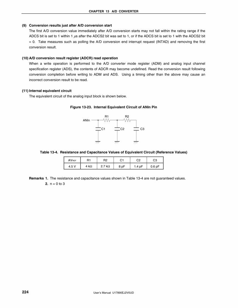
CHAPTER 13 A/D CONVERTER
User’s Manual U17890EJ2V0UD 224
(9) Conversion results just after A/D conversion start
The first A/D conversion value immediately after A/D conversion starts may not fall within the rating range if the
ADCS bit is set to 1 within 1 μs after the ADCS2 bit was set to 1, or if the ADCS bit is set to 1 with the ADCS2 bit
= 0. Take measures such as polling the A/D conversion end interrupt request (INTAD) and removing the first
conversion result.
(10) A/D conversion result register (ADCR) read operation
When a write operation is performed to the A/D converter mode register (ADM) and analog input channel
specification register (ADS), the contents of ADCR may become undefined. Read the conversion result following
conversion completion before writing to ADM and ADS. Using a timing other than the above may cause an
incorrect conversion result to be read.
(11) Internal equivalent circuit
The equivalent circuit of the analog input block is shown below.
Figure 13-23. Internal Equivalent Circuit of ANIn Pin
ANIn
C1 C2 C3
R1 R2
Table 13-4. Resistance and Capacitance Values of Equivalent Circuit (Reference Values)
AVREF R1 R2 C1 C2 C3
4.5 V 4 kΩ 2.7 kΩ 8 pF 1.4 pF 0.6 pF
Remarks 1. The resistance and capacitance values shown in Table 13-4 are not guaranteed values.
2. n = 0 to 3

User’s Manual U17890EJ2V0UD 225
CHAPTER 14 SERIAL INTERFACE UART00
14.1 Functions of Serial Interface UART00
Serial interface UART00 has the following two modes.
(1) Operation stop mode
This mode is used when serial communication is not executed and can enable a reduction in the power
consumption.
For details, see 14.4.1 Operation stop mode.
(2) Asynchronous serial interface (UART) mode
The functions of this mode are outlined below.
For details, see 14.4.2 Asynchronous serial interface (UART) mode and 14.4.3 Dedicated baud rate
generator.
• Two-pin configuration TXD00: Transmit data output pin
RxD00: Receive data input pin
• Length of communication data can be selected from 7 or 8 bits.
• Dedicated on-chip 5-bit baud rate generator allowing any baud rate to be set
• Transmission and reception can be performed independently.
• Four operating clock inputs selectable
• Fixed to LSB-first communication
Cautions 1. If source clock to serial interface UART00 is not stopped (e.g., in the HALT mode), normal
operation continues. If source clock to serial interface UART00 is stopped (e.g., in the
STOP mode), each register stops operating, and holds the value immediately before clock
supply was stopped. The TXD00 pin also holds the value immediately before clock supply
was stopped and outputs it. However, the operation is not guaranteed after clock supply is
resumed. Therefore, reset the circuit so that POWER00 = 0, RXE00 = 0, and TXE00 = 0.
2. Set POWER00 = 1 and then set TXE00 = 1 (transmission) or RXE00 = 1 (reception) to start
communication.
3. TXE00 and RXE00 are synchronized by the base clock (fXCLK0) set by BRGC00. To enable
transmission or reception again, set TXE00 or RXE00 to 1 at least two clocks of base clock
after TXE00 or RXE00 has been cleared to 0. If TXE00 or RXE00 is set within two clocks of
base clock, the transmission circuit or reception circuit may not be initialized.
4. Set transmit data to TXS00 at least two base clock (fXCLK0) after setting TXE00 = 1.
<R>

CHAPTER 14 SERIAL INTERFACE UART00
User’s Manual U17890EJ2V0UD 226
14.2 Configuration of Serial Interface UART00
Serial interface UART00 consists of the following hardware.
Table 14-1. Configuration of Serial Interface UART00
Item Configuration
Registers Receive buffer register 00 (RXB00)
Receive shift register 00 (RXS00)
Transmit shift register 00 (TXS00)
Control registers Asynchronous serial interface operation mode register 00 (ASIM00)
Asynchronous serial interface reception error status register 00 (ASIS00)
Baud rate generator control register 00 (BRGC00)
Port mode register 1 (PM1)
Port register 1 (P1)

CH
AP
TE
R 14 S
ER
IAL
INT
ER
FA
CE
UA
RT
00
User’s M
anual U17890E
J2V0U
D
227
Figure 14-1. Block Diagram of Serial Interface UART00
TxD00/P14INTST00
RxD00/P13
INTSRE00
fX/26
fX/24
fX/22
Transmit shift register 00 (TXS00)
Receive shift register 00 (RXS00)
Receive buffer register 00(RXB00)
Asynchronous serial interface reception error
status register 00 (ASIS00)
Asynchronous serial interface operation mode
register 00 (ASIM00)
Baud rate generator control register 00
(BRGC00)
8-bit timer/event counter50 output
Registers
Sel
ecto
r
Baud rate generator
Baud rate generator
Reception unit
Reception control
Filter
Internal bus
Transmission control
Transmission unit
Output latch(P14)
PM14
7 7
INTSR00

CHAPTER 14 SERIAL INTERFACE UART00
User’s Manual U17890EJ2V0UD 228
(1) Receive buffer register 00 (RXB00)
This 8-bit register stores parallel data converted by receive shift register 00 (RXS00).
Each time 1 byte of data has been received, new receive data is transferred to this register from receive shift
register 00 (RXS00).
If the data length is set to 7 bits the receive data is transferred to bits 0 to 6 of RXB00 and the MSB of RXB00 is
always 0.
If an overrun error (OVE00) occurs, the receive data is not transferred to RXB00.
RXB00 can be read by an 8-bit memory manipulation instruction. No data can be written to this register.
RESET input or POWER00 = 0 sets this register to FFH.
(2) Receive shift register 00 (RXS00)
This register converts the serial data input to the RxD00 pin into parallel data.
RXS00 cannot be directly manipulated by a program.
(3) Transmit shift register 00 (TXS00)
This register is used to set transmit data. Transmission is started when data is written to TXS00, and serial data
is transmitted from the TXD00 pin.
TXS00 can be written by an 8-bit memory manipulation instruction. This register cannot be read.
RESET input, POWER00 = 0, or TXE00 = 0 sets this register to FFH.
Cautions 1. Set transmit data to TXS00 at least two base clock (fXCLK0) after setting TXE00 = 1.
2. Do not write the next transmit data to TXS00 before the transmission completion interrupt
signal (INTST00) is generated.
<R>

CHAPTER 14 SERIAL INTERFACE UART00
User’s Manual U17890EJ2V0UD 229
14.3 Registers Controlling Serial Interface UART00
Serial interface UART00 is controlled by the following five registers.
• Asynchronous serial interface operation mode register 00 (ASIM00)
• Asynchronous serial interface reception error status register 00 (ASIS00)
• Baud rate generator control register 00 (BRGC00)
• Port mode register 1 (PM1)
• Port register 1 (P1)
(1) Asynchronous serial interface operation mode register 00 (ASIM00)
This 8-bit register controls the serial communication operations of serial interface UART00.
This register can be set by a 1-bit or 8-bit memory manipulation instruction.
RESET input sets this register to 01H.
Figure 14-2. Format of Asynchronous Serial Interface Operation Mode Register 00 (ASIM00) (1/2)
Address: FF70H After reset: 01H R/W
Symbol <7> <6> <5> 4 3 2 1 0
ASIM00 POWER00 TXE00 RXE00 PS001 PS000 CL00 SL00 1
POWER00 Enables/disables operation of internal operation clock
0Note 1 Disables operation of the internal operation clock (fixes the clock to low level) and asynchronously
resets the internal circuit Note 2.
1 Enables operation of the internal operation clock.
TXE00 Enables/disables transmission
0 Disables transmission (synchronously resets the transmission circuit).
1 Enables transmission.
RXE00 Enables/disables reception
0 Disables reception (synchronously resets the reception circuit).
1 Enables reception.
Notes 1. The input from the RxD00 pin is fixed to high level when POWER00 = 0.
2. Asynchronous serial interface reception error status register 00 (ASIS00), transmit shift register 00
(TXS00), and receive buffer register 00 (RXB00) are reset.

CHAPTER 14 SERIAL INTERFACE UART00
User’s Manual U17890EJ2V0UD 230
Figure 14-2. Format of Asynchronous Serial Interface Operation Mode Register 00 (ASIM00) (2/2)
PS001 PS000 Transmission operation Reception operation
0 0 Does not output parity bit. Reception without parity
0 1 Outputs 0 parity. Reception as 0 parityNote
1 0 Outputs odd parity. Judges as odd parity.
1 1 Outputs even parity. Judges as even parity.
CL00 Specifies character length of transmit/receive data
0 Character length of data = 7 bits
1 Character length of data = 8 bits
SL00 Specifies number of stop bits of transmit data
0 Number of stop bits = 1
1 Number of stop bits = 2
Note If “reception as 0 parity” is selected, the parity is not judged. Therefore, bit 2 (PE00) of asynchronous serial
interface reception error status register 00 (ASIS00) is not set and the error interrupt does not occur.
Cautions 1. At startup, set POWER00 to 1 and then set TXE00 to 1. To stop the operation, clear TXE00 to
0, and then clear POWER00 to 0.
2. At startup, set POWER00 to 1 and then set RXE00 to 1. To stop the operation, clear RXE00 to
0, and then clear POWER00 to 0.
3. Set POWER00 to 1 and then set RXE00 to 1 while a high level is input to the RxD00 pin. If
POWER00 is set to 1 and RXE00 is set to 1 while a low level is input, reception is started.
4. TXE00 and RXE00 are synchronized by the base clock (fXCLK0) set by BRGC00. To enable
transmission or reception again, set TXE00 or RXE00 to 1 at least two clocks of base clock
after TXE00 or RXE00 has been cleared to 0. If TXE00 or RXE00 is set within two clocks of
base clock, the transmission circuit or reception circuit may not be initialized.
5. Set transmit data to TXS00 at least two base clock (fXCLK0) after setting TXE00 = 1.
6. Clear the TXE00 and RXE00 bits to 0 before rewriting the PS001, PS000, and CL00 bits.
7. Make sure that TXE00 = 0 when rewriting the SL00 bit. Reception is always performed with
“number of stop bits = 1”, and therefore, is not affected by the set value of the SL00 bit.
8. Be sure to set bit 0 to 1.
<R>

CHAPTER 14 SERIAL INTERFACE UART00
User’s Manual U17890EJ2V0UD 231
(2) Asynchronous serial interface reception error status register 00 (ASIS00)
This register indicates an error status on completion of reception by serial interface UART00. It includes three
error flag bits (PE00, FE00, OVE00).
This register is read-only by an 8-bit memory manipulation instruction.
RESET input, bit 7 (POWER00) of ASIM00 = 0, or bit 5 (RXE00) of ASIM00 = 0 clears this register to 00H. And
reading of this register also clears this register to 00H.
Figure 14-3. Format of Asynchronous Serial Interface Reception Error Status Register 00 (ASIS00)
Address: FF73H After reset: 00H R
Symbol 7 6 5 4 3 2 1 0
ASIS00 0 0 0 0 0 PE00 FE00 OVE00
PE00 Status flag indicating parity error
0 If POWER00 = 0 and RXE00 = 0, or if ASIS00 register is read.
1 If the parity of transmit data does not match the parity bit on completion of reception.
FE00 Status flag indicating framing error
0 If POWER00 = 0 and RXE00 = 0, or if ASIS00 register is read.
1 If the stop bit is not detected on completion of reception.
OVE00 Status flag indicating overrun error
0 If POWER00 = 0 and RXE00 = 0, or if ASIS00 register is read.
1 If receive data is set to the RXB00 register and the next reception operation is completed before the
data is read.
Cautions 1. The operation of the PE00 bit differs depending on the set values of the PS001 and PS000
bits of asynchronous serial interface operation mode register 00 (ASIM00).
2. Only the first bit of the receive data is checked as the stop bit, regardless of the number of
stop bits.
3. If an overrun error occurs, the next receive data is not written to receive buffer register 00
(RXB00) but discarded.
4. If data is read from ASIS00, a wait cycle is generated. For details, see CHAPTER 27
CAUTIONS FOR WAIT.

CHAPTER 14 SERIAL INTERFACE UART00
User’s Manual U17890EJ2V0UD 232
(3) Baud rate generator control register 00 (BRGC00)
This register selects the base clock of serial interface UART00 and the division value of the 5-bit counter.
BRGC00 can be set by an 8-bit memory manipulation instruction.
RESET input sets this register to 1FH.
Figure 14-4. Format of Baud Rate Generator Control Register 00 (BRGC00)
Address: FF71H After reset: 1FH R/W
Symbol 7 6 5 4 3 2 1 0
BRGC00 TPS001 TPS000 0 MDL004 MDL003 MDL002 MDL001 MDL000
Base clock (fXCLK0) selection Note 1
TPS001 TPS000
At fXP = 20 MHz At fXP = 16 MHz
0 0 TM50 output Note 2
0 1 fX/22 5 MHz 4MHz
1 0 fX/24 1.25 MHz 1 MHz
1 1 fX/26 312.5 kHz 250 kHz
MDL004 MDL003 MDL002 MDL001 MDL000 k Selection of 5-bit counter
output clock
0 0 × × × × Setting prohibited
0 1 0 0 0 8 fXCLK0/8
0 1 0 0 1 9 fXCLK0/9
0 1 0 1 0 10 fXCLK0/10
•
•
•
•
•
•
•
•
•
•
•
•
•
•
•
•
•
•
•
•
•
•
•
•
•
•
•
•
•
•
•
•
•
•
•
1 1 0 1 1 27 fXCLK0/27
1 1 1 0 0 28 fXCLK0/28
1 1 1 0 1 29 fXCLK0/29
1 1 1 1 0 30 fXCLK0/30
1 1 1 1 1 31 fXCLK0/31
Notes 1. Be sure to set the base clock so that the following condition is satisfied.
• VDD = 4.0 to 5.5 V: Base clock ≤ 10 MHz
2. When the TM50 output is selected as the count clock, observe the following. • PWM mode (TMC506 = 1)
Set the clock so that the duty will be 50% and start the operation of 8-bit timer/event counter 50 in
advance.
• Clear & start mode entered on match of TM50 and CR50 (TMC506 = 0)
Enable the timer F/F inversion operation (TMC501 = 1) and start the operation of 8-bit timer/event
counter 50 in advance.
It is not necessary to enable the TO50 pin as a timer output pin (bit 00 (TOE50) of the TMC register
may be 0 or 1), regardless which mode.

CHAPTER 14 SERIAL INTERFACE UART00
User’s Manual U17890EJ2V0UD 233
Cautions 1. When the internal low-speed oscillation clock is selected as the source clock to the CPU, the
clock of the internal low-speed oscillator is divided and supplied as the count clock. If the
base clock is the internal low-speed oscillation clock, the operation of serial interface UART00
is not guaranteed.
2. Make sure that bit 6 (TXE00) and bit 5 (RXE00) of the ASIM00 register = 0 when rewriting the
MDL004 to MDL000 bits.
3. The baud rate value is the output clock of the 5-bit counter divided by 2.
Remarks 1. fXCLK0: Frequency of base clock selected by the TPS001 and TPS000 bits
2. fX: X1 input clock oscillation frequency
3. k: Value set by the MDL004 to MDL000 bits (k = 8, 9, 10, ..., 31)
4. ×: Don’t care
5. TMC506: Bit 6 of 8-bit timer mode control register 50 (TMC50)
TMC501: Bit 1 of TMC50
(4) Port mode register 1 (PM1)
This register sets port 1 input/output in 1-bit units.
When using the P14/TxD00 pin for serial interface data output, clear PM14 to 0 and set the output latch of P14 to
1.
When using the P13/RxD00 pin for serial interface data input, set PM13 to 1. The output latch of P13 at this time
may be 0 or 1.
PM1 can be set by a 1-bit or 8-bit memory manipulation instruction.
RESET input sets this register to FFH.
Figure 14-5. Format of Port Mode Register 1 (PM1)
Address: FF21H After reset: FFH R/W
Symbol 7 6 5 4 3 2 1 0
PM1 PM17 PM16 PM15 PM14 PM13 PM12 PM11 PM10
PM1n P1n pin I/O mode selection (n = 0 to 7)
0 Output mode (output buffer on)
1 Input mode (output buffer off)

CHAPTER 14 SERIAL INTERFACE UART00
User’s Manual U17890EJ2V0UD 234
14.4 Operation of Serial Interface UART00
Serial interface UART00 has the following two modes.
• Operation stop mode
• Asynchronous serial interface (UART) mode
14.4.1 Operation stop mode
In this mode, serial communication cannot be executed, thus reducing the power consumption. In addition, the
pins can be used as ordinary port pins in this mode. To set the operation stop mode, clear bits 7, 6, and 5
(POWER00, TXE00, and RXE00) of ASIM00 to 0.
(1) Register used
The operation stop mode is set by asynchronous serial interface operation mode register 00 (ASIM00).
ASIM00 can be set by a 1-bit or 8-bit memory manipulation instruction.
RESET input sets this register to 01H.
Address: FF70H After reset: 01H R/W
Symbol <7> <6> <5> 4 3 2 1 0
ASIM00 POWER00 TXE00 RXE00 PS001 PS000 CL00 SL00 1
POWER00 Enables/disables operation of internal operation clock
0Note 1 Disables operation of the internal operation clock (fixes the clock to low level) and asynchronously
resets the internal circuitNote 2.
TXE00 Enables/disables transmission
0 Disables transmission (synchronously resets the transmission circuit).
RXE00 Enables/disables reception
0 Disables reception (synchronously resets the reception circuit).
Notes 1. The input from the RxD00 pin is fixed to high level when POWER00 = 0.
2. Asynchronous serial interface reception error status register 00 (ASIS00), transmit shift register 00
(TXS00), and receive buffer register 00 (RXB00) are reset.
Caution Clear POWER00 to 0 after clearing TXE00 and RXE00 to 0 to set the operation stop mode.
To start the operation, set POWER00 to 1, and then set TXE00 and RXE00 to 1.
Remark To use the RxD00/P13 and TxD00/P14 pins as general-purpose port pins, see CHAPTER 4 PORT
FUNCTIONS.

CHAPTER 14 SERIAL INTERFACE UART00
User’s Manual U17890EJ2V0UD 235
14.4.2 Asynchronous serial interface (UART) mode
In this mode, 1-byte data is transmitted/received following a start bit, and a full-duplex operation can be performed.
A dedicated UART baud rate generator is incorporated, so that communication can be executed at a wide range of
baud rates.
(1) Registers used
• Asynchronous serial interface operation mode register 00 (ASIM00)
• Asynchronous serial interface reception error status register 00 (ASIS00)
• Baud rate generator control register 00 (BRGC00)
• Port mode register 1 (PM1)
• Port register 1 (P1)
The basic procedure of setting an operation in the UART mode is as follows.
<1> Set the BRGC00 register (see Figure 14-4).
<2> Set bits 1 to 4 (SL00, CL00, PS000, and PS001) of the ASIM00 register (see Figure 14-2).
<3> Set bit 7 (POWER00) of the ASIM00 register to 1.
<4> Set bit 6 (TXE00) of the ASIM00 register to 1. → Transmission is enabled.
Set bit 5 (RXE00) of the ASIM00 register to 1. → Reception is enabled.
<5> Write data to the TXS00 register at least two clock after setting <4>. → Data transmission is started.
Caution Take relationship with the other party of communication when setting the port mode register
and port register.
The relationship between the register settings and pins is shown below.
Table 14-2. Relationship Between Register Settings and Pins
Pin Function POWER00 TXE00 RXE00 PM14 P14 PM13 P13 UART00
Operation TxD00/ P14 RxD00/P13
0 0 0 ×Note ×Note ×Note ×Note Stop P14 P13
0 1 ×Note ×Note 1 × Reception P14 RxD00
1 0 0 1 ×Note ×Note Transmission TxD00 P13
1
1 1 0 1 1 × Transmission/
reception
TxD00 RxD00
Note Can be set as port function.
Remark ×: don’t care
POWER00: Bit 7 of asynchronous serial interface operation mode register 00 (ASIM00)
TXE00: Bit 6 of ASIM00
RXE00: Bit 5 of ASIM00
PM1×: Port mode register
P1×: Port output latch
<R>

CHAPTER 14 SERIAL INTERFACE UART00
User’s Manual U17890EJ2V0UD 236
(2) Communication operation
(a) Format and waveform example of normal transmit/receive data
Figures 14-6 and 14-7 show the format and waveform example of the normal transmit/receive data.
Figure 14-6. Format of Normal UART Transmit/Receive Data
Start bit
Parity bit
D0 D1 D2 D3 D4
1 data frame
Character bits
D5 D6 D7 Stop bit
One data frame consists of the following bits.
• Start bit ... 1 bit
• Character bits ... 7 or 8 bits (LSB first)
• Parity bit ... Even parity, odd parity, 0 parity, or no parity
• Stop bit ... 1 or 2 bits
The character bit length, parity, and stop bit length in one data frame are specified by asynchronous serial
interface operation mode register 00 (ASIM00).
Figure 14-7. Example of Normal UART Transmit/Receive Data Waveform
1. Data length: 8 bits, Parity: Even parity, Stop bit: 1 bit, Communication data: 55H
1 data frame
Start D0 D1 D2 D3 D4 D5 D6 D7 Parity Stop
2. Data length: 7 bits, Parity: Odd parity, Stop bit: 2 bits, Communication data: 36H
1 data frame
Start D0 D1 D2 D3 D4 D5 D6 Parity StopStop
3. Data length: 8 bits, Parity: None, Stop bit: 1 bit, Communication data: 87H
1 data frame
Start D0 D1 D2 D3 D4 D5 D6 D7 Stop

CHAPTER 14 SERIAL INTERFACE UART00
User’s Manual U17890EJ2V0UD 237
(b) Parity types and operation
The parity bit is used to detect a bit error in communication data. Usually, the same type of parity bit is used
on both the transmission and reception sides. With even parity and odd parity, a 1-bit (odd number) error
can be detected. With zero parity and no parity, an error cannot be detected.
(i) Even parity • Transmission
Transmit data, including the parity bit, is controlled so that the number of bits that are “1” is even.
The value of the parity bit is as follows.
If transmit data has an odd number of bits that are “1”: 1
If transmit data has an even number of bits that are “1”: 0
• Reception
The number of bits that are “1” in the receive data, including the parity bit, is counted. If it is odd, a
parity error occurs.
(ii) Odd parity • Transmission
Unlike even parity, transmit data, including the parity bit, is controlled so that the number of bits that
are “1” is odd.
If transmit data has an odd number of bits that are “1”: 0
If transmit data has an even number of bits that are “1”: 1
• Reception
The number of bits that are “1” in the receive data, including the parity bit, is counted. If it is even, a
parity error occurs.
(iii) 0 parity
The parity bit is cleared to 0 when data is transmitted, regardless of the transmit data.
The parity bit is not detected when the data is received. Therefore, a parity error does not occur
regardless of whether the parity bit is “0” or “1”.
(iv) No parity
No parity bit is appended to the transmit data.
Reception is performed assuming that there is no parity bit when data is received. Because there is no
parity bit, a parity error does not occur.

CHAPTER 14 SERIAL INTERFACE UART00
User’s Manual U17890EJ2V0UD 238
(c) Transmission
The TXD00 pin outputs a high level when bit 7 (POWER00) of asynchronous serial interface operation mode
register 00 (ASIM00) is set to 1. If bit 6 (TXE00) of ASIM00 is then set to 1, transmission is enabled.
Transmission can be started by writing transmit data to transmit shift register 00 (TXS00). The start bit,
parity bit, and stop bit are automatically appended to the data.
If bit 6 (TXE00) of ASIM00 is then set to 1, transmission is enabled.
Transmission can be started by writing transmit data to transmit shift register 00 (TXS00) at least two base
clock (fXCLK0) after setting TXE00 = 1. The start bit, parity bit, and stop bit are automatically appended to the
data.
When transmission is started, the start bit is output from the TXD00 pin, followed by the rest of the data in
order starting from the LSB. When transmission is completed, the parity and stop bits set by ASIM00 are
appended and a transmission completion interrupt request (INTST00) is generated.
Transmission is stopped until the data to be transmitted next is written to TXS00.
Figure 14-8 shows the timing of the transmission completion interrupt request (INTST00). This interrupt
occurs as soon as the last stop bit has been output.
Caution After transmit data is written to TXS00, do not write the next transmit data before the
transmission completion interrupt signal (INTST00) is generated.
Figure 14-8. Transmission Completion Interrupt Request Timing
1. Stop bit length: 1
INTST00
D0Start D1 D2 D6 D7 StopTXD00 (output) Parity
2. Stop bit length: 2
TXD00 (output)
INTST00
D0Start D1 D2 D6 D7 Parity Stop
<R>

CHAPTER 14 SERIAL INTERFACE UART00
User’s Manual U17890EJ2V0UD 239
(d) Reception
Reception is enabled and the RXD00 pin input is sampled when bit 7 (POWER00) of asynchronous serial
interface operation mode register 00 (ASIM00) is set to 1 and then bit 5 (RXE00) of ASIM00 is set to 1.
The 5-bit counter of the baud rate generator starts counting when the falling edge of the RXD00 pin input is
detected. When the set value of baud rate generator control register 00 (BRGC00) has been counted, the
RXD00 pin input is sampled again ( in Figure 14-9). If the RXD00 pin is low level at this time, it is
recognized as a start bit.
When the start bit is detected, reception is started, and serial data is sequentially stored in receive shift
register 00 (RXS00) at the set baud rate. When the stop bit has been received, the reception completion
interrupt (INTSR00) is generated and the data of RXS00 is written to receive buffer register 00 (RXB00). If
an overrun error (OVE00) occurs, however, the receive data is not written to RXB00.
Even if a parity error (PE00) occurs while reception is in progress, reception continues to the reception
position of the stop bit, and an error interrupt (INTSRE00) is generated after completion of reception.
Figure 14-9. Reception Completion Interrupt Request Timing
RXD00 (input)
INTSR00
Start D0 D1 D2 D3 D4 D5 D6 D7 Parity Stop
RXB00
Cautions 1. Be sure to read receive buffer register 00 (RXB00) even if a reception error occurs.
Otherwise, an overrun error will occur when the next data is received, and the reception
error status will persist.
2. Reception is always performed with the “number of stop bits = 1”. The second stop bit
is ignored.
3. Be sure to read asynchronous serial interface reception error status register 00
(ASIS00) before reading RXB00.

CHAPTER 14 SERIAL INTERFACE UART00
User’s Manual U17890EJ2V0UD 240
(e) Reception error
Three types of errors may occur during reception: a parity error, framing error, or overrun error. If the error
flag of asynchronous serial interface reception error status register 00 (ASIS00) is set as a result of data
reception, a reception error interrupt request (INTSRE00) is generated.
Which error has occurred during reception can be identified by reading the contents of ASIS00 in the
reception error interrupt servicing (INTSRE00) (see Figure 14-3).
The contents of ASIS00 are reset to 0 when ASIS00 is read.
Table 14-3. Cause of Reception Error
Reception Error Cause
Parity error The parity specified for transmission does not match the parity of the receive data.
Framing error Stop bit is not detected.
Overrun error Reception of the next data is completed before data is read from receive buffer
register 00 (RXB00).
(f) Noise filter of receive data
The RXD00 signal is sampled using the base clock output by the prescaler block.
If two sampled values are the same, the output of the match detector changes, and the data is sampled as
input data.
Because the circuit is configured as shown in Figure 14-10, the internal processing of the reception operation
is delayed by two clocks from the external signal status.
Figure 14-10. Noise Filter Circuit
Internal signal BInternal signal A
Match detector
In
Base clock
RXD00/P13 Q In
LD_EN
Q

CHAPTER 14 SERIAL INTERFACE UART00
User’s Manual U17890EJ2V0UD 241
14.4.3 Dedicated baud rate generator
The dedicated baud rate generator consists of a source clock selector and a 5-bit programmable counter, and
generates a serial clock for transmission/reception of UART00.
Separate 5-bit counters are provided for transmission and reception.
(1) Configuration of baud rate generator
• Base clock
The clock selected by bits 7 and 6 (TPS001 and TPS000) of baud rate generator control register 00
(BRGC00) is supplied to each module when bit 7 (POWER00) of asynchronous serial interface operation
mode register 00 (ASIM00) is 1. This clock is called the base clock and its frequency is called fXCLK0. The
base clock is fixed to low level when POWER00 = 0.
• Transmission counter
This counter stops operation, cleared to 0, when bit 7 (POWER00) or bit 6 (TXE00) of asynchronous serial
interface operation mode register 00 (ASIM00) is 0.
It starts counting when POWER00 = 1 and TXE00 = 1.
The counter is cleared to 0 when the first data transmitted is written to transmit shift register 00 (TXS00).
• Reception counter
This counter stops operation, cleared to 0, when bit 7 (POWER00) or bit 5 (RXE00) of asynchronous serial
interface operation mode register 00 (ASIM00) is 0.
It starts counting when the start bit has been detected.
The counter stops operation after one frame has been received, until the next start bit is detected.
Figure 14-11. Configuration of Baud Rate Generator
fXCLK0
Selector
POWER00
5-bit counter
Match detector Baud rate
BRGC00: MDL004 to MDL000
1/2
POWER00, TXE00 (or RXE00)
BRGC00: TPS001, TPS000
8-bit timer/event counter
50 output
fX/26
fX/22
fX/24
Baud rate generator
Remark POWER00: Bit 7 of asynchronous serial interface operation mode register 00 (ASIM00)
TXE00: Bit 6 of ASIM00
RXE00: Bit 5 of ASIM00
BRGC00: Baud rate generator control register 00

CHAPTER 14 SERIAL INTERFACE UART00
User’s Manual U17890EJ2V0UD 242
(2) Generation of serial clock
A serial clock can be generated by using baud rate generator control register 00 (BRGC00).
Select the clock to be input to the 5-bit counter by using bits 7 and 6 (TPS001 and TPS000) of BRGC00.
Bits 4 to 0 (MDL004 to MDL000) of BRGC00 can be used to select the division value of the 5-bit counter.
(a) Baud rate
The baud rate can be calculated by the following expression.
• Baud rate = [bps]
fXCLK0: Frequency of base clock selected by the TPS001 and TPS000 bits of the BRGC00 register
k: Value set by the MDL004 to MDL000 bits of the BRGC00 register (k = 8, 9, 10, ..., 31)
(b) Error of baud rate
The baud rate error can be calculated by the following expression.
• Error (%) = − 1 × 100 [%]
Cautions 1. Keep the baud rate error during transmission to within the permissible error range at
the reception destination.
2. Make sure that the baud rate error during reception satisfies the range shown in (4)
Permissible baud rate range during reception.
Example: Frequency of base clock = 2.5 MHz = 2,500,000 Hz
Set value of MDL004 to MDL000 bits of BRGC00 register = 10000B (k = 16)
Target baud rate = 76,800 bps
Baud rate = 2.5 M/(2 × 16)
= 2,500,000/(2 × 16) = 78,125 [bps]
Error = (78,125/76,800 − 1) × 100
= 1.725 [%]
fXCLK0
2 × k
Actual baud rate (baud rate with error)
Desired baud rate (correct baud rate)

CHAPTER 14 SERIAL INTERFACE UART00
User’s Manual U17890EJ2V0UD 243
(3) Example of setting baud rate
Table 14-4. Set Data of Baud Rate Generator
fX = 20.0 MHz fX = 16.0 MHz Baud Rate
[bps] TPS001,
TPS000
k Calculated
Value
ERR[%] TPS001,
TPS000
k Calculated
Value
ERR[%]
2400 − − − − − − − −
4800 − − − − 3 26 4808 0.16
9600 3 16 9766 1.73 3 13 9615 0.16
10400 3 15 10417 0.16 3 12 10417 0.16
19200 3 8 19531 1.73 2 26 19231 0.16
31250 2 20 31250 0 2 16 31250 0
38400 2 16 39063 1.73 2 13 38462 0.16
76800 2 8 78125 1.73 1 26 76923 0.16
115200 1 22 113636 −1.36 1 17 117647 2.12
153600 1 16 156250 1.73 1 13 153846 0.16
230400 1 11 227273 −1.36 − − − −
Remark TPS001, TPS000: Bits 7 and 6 of baud rate generator control register 00 (BRGC00) (setting of base
clock (fXCLK0))
k: Value set by the MDL004 to MDL000 bits of BRGC00 (k = 8, 9, 10, ..., 31)
fX: X1 input clock oscillation frequency
ERR: Baud rate error
<R>

CHAPTER 14 SERIAL INTERFACE UART00
User’s Manual U17890EJ2V0UD 244
(4) Permissible baud rate range during reception
The permissible error from the baud rate at the transmission destination during reception is shown below.
Caution Make sure that the baud rate error during reception is within the permissible error range, by
using the calculation expression shown below.
Figure 14-12. Permissible Baud Rate Range During Reception
FL
1 data frame (11 × FL)
FLmin
FLmax
Data frame lengthof UART00
Start bit Bit 0 Bit 1 Bit 7 Parity bit
Minimum permissibledata frame length
Maximum permissibledata frame length
Stop bit
Start bit Bit 0 Bit 1 Bit 7 Parity bit
Latch timing
Stop bit
Start bit Bit 0 Bit 1 Bit 7 Parity bit Stop bit

CHAPTER 14 SERIAL INTERFACE UART00
User’s Manual U17890EJ2V0UD 245
As shown in Figure 14-12, the latch timing of the receive data is determined by the counter set by baud rate
generator control register 00 (BRGC00) after the start bit has been detected. If the last data (stop bit) meets this
latch timing, the data can be correctly received.
Assuming that 11-bit data is received, the theoretical values can be calculated as follows.
FL = (Brate)−1
Brate: Baud rate of UART00
k: Set value of BRGC00
FL: 1-bit data length
Margin of latch timing: 2 clocks
Minimum permissible data frame length: FLmin = 11 × FL − × FL = FL
Therefore, the maximum receivable baud rate at the transmission destination is as follows.
BRmax = (FLmin/11)−1 = Brate
Similarly, the maximum permissible data frame length can be calculated as follows.
10 k + 2 21k − 2
11 2 × k 2 × k
FLmax = FL × 11
Therefore, the minimum receivable baud rate at the transmission destination is as follows.
BRmin = (FLmax/11)−1 = Brate
The permissible baud rate error between UART00 and the transmission destination can be calculated from the
above minimum and maximum baud rate expressions, as follows.
Table 14-5. Maximum/Minimum Permissible Baud Rate Error
Division Ratio (k) Maximum Permissible Baud Rate Error Minimum Permissible Baud Rate Error
8 +3.53% −3.61%
16 +4.14% −4.19%
24 +4.34% −4.38%
31 +4.44% −4.47%
Remarks 1. The permissible error of reception depends on the number of bits in one frame, input clock
frequency, and division ratio (k). The higher the input clock frequency and the higher the division
ratio (k), the higher the permissible error.
2. k: Set value of BRGC00
k − 2
2k
21k + 2
2k
22k
21k + 2
× FLmax = 11 × FL − × FL = FL
21k – 2
20k
20k
21k − 2

User’s Manual U17890EJ2V0UD 246
CHAPTER 15 MULTIPLIER/DIVIDER
15.1 Functions of Multiplier/Divider
The multiplier/divider has the following functions.
• 16 bits × 16 bits = 32 bits (multiplication)
• 32 bits ÷ 16 bits = 32 bits, 16-bit remainder (division)
15.2 Configuration of Multiplier/Divider
The multiplier/divider consists of the following hardware.
Table 15-1. Configuration of Multiplier/Divider
Item Configuration
Registers Remainder data register 0 (SDR0)
Multiplication/division data registers A0 (MDA0H, MDA0L)
Multiplication/division data registers B0 (MDB0)
Control register Multiplier/divider control register 0 (DMUC0)
Figure 15-1 shows the block diagram of the multiplier/divider.

CH
AP
TE
R 15 M
UL
TIP
LIE
R/D
IVID
ER
User’s M
anual U17890E
J2V0U
D
247
Figure 15-1. Block Diagram of Multiplier/Divider
Internal bus
CPU clock
Start
Clear
17-bitadder
Controller
Multiplication/division data register B0(MDB0 (MDB0H+MDB0L)
Remainder data register 0(SDR0 (SDR0H+SDR0L)
6-bitcounter
DMUSEL0
Multiplier/divider control register 0 (DMUC0)
Controller
Multiplication/division data register A0(MDA0H (MDA0HH + MDA0HL) + MDA0L (MDA0LH + MDA0LL))
Controller
DMUE
MDA000 INTDMU

CHAPTER 15 MULTIPLIER/DIVIDER
User’s Manual U17890EJ2V0UD 248
(1) Remainder data register 0 (SDR0)
SDR0 is a 16-bit register that stores a remainder. This register stores 0 in the multiplication mode and the
remainder of an operation result in the division mode.
This register can be read by an 8-bit or 16-bit memory manipulation instruction.
RESET input clears this register to 0000H.
Figure 15-2. Format of Remainder Data Register 0 (SDR0)
Address: FF60H, FF61H After reset: 0000H R
Symbol FF61H (SDR0H) FF60H (SDR0L)
SDR0 SDR
015
SDR
014
SDR
013
SDR
012
SDR
011
SDR
010
SDR
009
SDR
008
SDR
007
SDR
006
SDR
005
SDR
004
SDR
003
SDR
002
SDR
001
SDR
000
Cautions 1. The value read from SDR0 during operation processing (while bit 7 (DMUE) of
multiplier/divider control register 0 (DMUC0) is 1) is not guaranteed.
2. SDR0 is reset when the operation is started (when DMUE is set to 1).

CHAPTER 15 MULTIPLIER/DIVIDER
User’s Manual U17890EJ2V0UD 249
(2) Multiplication/division data register A0 (MDA0H, MDA0L)
MDA0 is a 32-bit register that sets a 16-bit multiplier A in the multiplication mode and a 32-bit dividend in the
division mode, and stores the 32-bit result of the operation (higher 16 bits: MDA0H, lower 16 bits: MDA0L).
Figure 15-3. Format of Multiplication/Division Data Register A0 (MDA0H, MDA0L)
Address: FF62H, FF63H, FF64H, FF65H After reset: 0000H, 0000H R/W
Symbol FF65H (MDA0HH) FF64H (MDA0HL)
MDA0H MDA
031
MDA
030
MDA
029
MDA
028
MDA
027
MDA
026
MDA
025
MDA
024
MDA
023
MDA
022
MDA
021
MDA
020
MDA
019
MDA
018
MDA
017
MDA
016
Symbol FF63H (MDA0LH) FF62H (MDA0LL)
MDA0L MDA
015
MDA
014
MDA
013
MDA
012
MDA
011
MDA
010
MDA
009
MDA
008
MDA
007
MDA
006
MDA
005
MDA
004
MDA
003
MDA
002
MDA
001
MDA
000
Cautions 1. MDA0H is cleared to 0 when an operation is started in the multiplication mode (when
multiplier/divider control register 0 (DMUC0) is set to 81H).
2. Do not change the value of MDA0 during operation processing (while bit 7 (DMUE) of
multiplier/divider control register 0 (DMUC0) is 1). Even in this case, the operation is
executed, but the result is undefined.
3. The value read from MDA0 during operation processing (while DMUE is 1) is not
guaranteed.

CHAPTER 15 MULTIPLIER/DIVIDER
User’s Manual U17890EJ2V0UD 250
The functions of MDA0 when an operation is executed are shown in the table below.
Table 15-2. Functions of MDA0 During Operation Execution
DMUSEL0 Operation Mode Setting Operation Result
0 Division mode Dividend Division result (quotient)
1 Multiplication mode Higher 16 bits: 0, Lower 16
bits: Multiplier A
Multiplication result
(product)
The register configuration differs between when multiplication is executed and when division is executed, as
follows.
• Register configuration during multiplication
<Multiplier A> <Multiplier B> <Product>
MDA0 (bits 15 to 0) × MDB0 (bits 15 to 0) = MDA0 (bits 31 to 0)
• Register configuration during division
<Dividend> <Divisor> <Quotient> <Remainder>
MDA0 (bits 31 to 0) ÷ MDB0 (bits 15 to 0) = MDA0 (bits 31 to 0) … SDR0 (bits 15 to 0)
MDA0 fetches the calculation result as soon as the clock is input, when bit 7 (DMUE) of multiplier/divider
control register 0 (DMUC0) is set to 1.
MDA0H and MDA0L can be set by an 8-bit or 16-bit memory manipulation instruction.
RESET input clears this register to 0000H.
(3) Multiplication/division data register B0 (MDB0)
MDB0 is a register that stores a 16-bit multiplier B in the multiplication mode and a 16-bit divisor in the
division mode.
This register can be set by an 8-bit or 16-bit memory manipulation instruction.
RESET input clears this register to 0000H.
Figure 15-4. Format of Multiplication/Division Data Register B0 (MDB0)
Address: FF66H, FF67H After reset: 0000H R/W
Symbol FF67H (MDB0H) FF66H (MDB0L)
MDB0 MDB
015
MDB
014
MDB
013
MDB
012
MDB
011
MDB
010
MDB
009
MDB
008
MDB
007
MDB
006
MDB
005
MDB
004
MDB
003
MDB
002
MDB
001
MDB
000
Cautions 1. Do not change the value of MDB0 during operation processing (while bit 7 (DMUE) of
multiplier/divider control register 0 (DMUC0) is 1). Even in this case, the operation is
executed, but the result is undefined.
2. Do not clear MDB0 to 0000H in the division mode. If set, undefined operation results are
stored in MDA0 and SDR0.

CHAPTER 15 MULTIPLIER/DIVIDER
User’s Manual U17890EJ2V0UD 251
15.3 Register Controlling Multiplier/Divider
The multiplier/divider is controlled by multiplier/divider control register 0 (DMUC0).
(1) Multiplier/divider control register 0 (DMUC0)
DMUC0 is an 8-bit register that controls the operation of the multiplier/divider.
This register can be set by a 1-bit or 8-bit memory manipulation instruction.
RESET input clears this register to 00H.
Figure 15-5. Format of Multiplier/Divider Control Register 0 (DMUC0)
DMUEDMUC0 0 0 0 0 0 0 DMUSEL0
Stops operation
Starts operation
DMUENote
0
1
Operation start/stop
Division mode
Multiplication mode
DMUSEL0
0
1
Operation mode (multiplication/division) selection
Address: FF68H After reset: 00H R/W
Symbol 4 3 2 1 06<7> 5
Note When DMUE is set to 1, the operation is started. DMUE is automatically cleared to 0 after the operation is
complete.
Cautions 1. If DMUE is cleared to 0 during operation processing (when DMUE is 1), the operation result
is not guaranteed. If the operation is completed while the clearing instruction is being
executed, the operation result is guaranteed, provided that the interrupt flag is set.
2. Do not change the value of DMUSEL0 during operation processing (while DMUE is 1). If it is
changed, undefined operation results are stored in multiplication/division data register A0
(MDA0) and remainder data register 0 (SDR0).
3. If DMUE is cleared to 0 during operation processing (while DMUE is 1), the operation
processing is stopped. To execute the operation again, set multiplication/division data
register A0 (MDA0), multiplication/division data register B0 (MDB0), and multiplier/divider
control register 0 (DMUC0), and start the operation (by setting DMUE to 1).

CHAPTER 15 MULTIPLIER/DIVIDER
User’s Manual U17890EJ2V0UD 252
15.4 Operations of Multiplier/Divider
15.4.1 Multiplication operation
• Initial setting
1. Set operation data to multiplication/division data register A0L (MDA0L) and multiplication/division data
register B0 (MDB0).
2. Set bits 0 (DMUSEL0) and 7 (DMUE) of multiplier/divider control register 0 (DMUC0) to 1. Operation
will start.
• During operation
3. The operation will be completed when 16 internal clocks have been issued after the start of the
operation (intermediate data is stored in the MDA0L and MDA0H registers during operation, and
therefore the read values of these registers are not guaranteed).
• End of operation
4. The operation result data is stored in the MDA0L and MDA0H registers.
5. DMUE is cleared to 0 (end of operation).
6. After the operation, an interrupt request signal (INTDMU) is generated.
• Next operation
7. To execute multiplication next, start from the initial setting in 15.4.1 Multiplication operation.
8. To execute division next, start from the initial setting in 15.4.2 Division operation.

CH
AP
TE
R 15 M
UL
TIP
LIE
R/D
IVID
ER
User’s M
anual U17890E
J2V0U
D
253
Figure 15-6. Timing Chart of Multiplication Operation (00DAH × 0093H)
Operation clock
MDA0
SDR0
MDB0
1 2 3 4 5 6 7 8 9 A B C D E F 100 0
0000 0000 0000 0000 0000 0000 0000 0000 0000 0000 0000 0000 0000 0000 0000 0000 0000
0000006D
000000DA
XXXX00DA
XXXX
XXXXXXXX
00498036
0024C01B
005BE00D
00777006
003BB803
00675C01
007D2E00
003E9700
001F4B80
000FA5C0
0007D2E0
0003E970
0001F4B8
0000FA5C
00007D2E
0093XXXX
Internal clock
DMUE
DMUSEL0
Counter
INTDMU

CHAPTER 15 MULTIPLIER/DIVIDER
User’s Manual U17890EJ2V0UD 254
15.4.2 Division operation
• Initial setting
1. Set operation data to multiplication/division data register A0 (MDA0L and MDA0H) and
multiplication/division data register B0 (MDB0).
2. Set bits 0 (DMUSEL0) and 7 (DMUE) of multiplier/divider control register 0 (DMUC0) to 0 and 1,
respectively. Operation will start.
• During operation
3. The operation will be completed when 32 internal clocks have been issued after the start of the
operation (intermediate data is stored in the MDA0L and MDA0H registers and remainder data register
0 (SDR0) during operation, and therefore the read values of these registers are not guaranteed).
• End of operation
4. The result data is stored in the MDA0L, MDA0H, and SDR0 registers.
5. DMUE is cleared to 0 (end of operation).
6. After the operation, an interrupt request signal (INTDMU) is generated.
• Next operation
7. To execute multiplication next, start from the initial setting in 15.4.1 Multiplication operation.
8. To execute division next, start from the initial setting in 15.4.2 Division operation.

CH
AP
TE
R 15 M
UL
TIP
LIE
R/D
IVID
ER
User’s M
anual U17890E
J2V0U
D
255
Figure 15-7. Timing Chart of Division Operation (DCBA2586H ÷ 0018H)
Operation clock
MDA0
SDR0
MDB0
1 2 3 4 5 6 7 8 19 1A 1B 1C 1D 1E 1F 200 0
0000 0001 0003 0006 000D 0003 0007 000E 0004 000B 0016 0014 0010 0008 0011 000B 0016
B9744B0C
DCBA2586
XXXX
XXXXXXXX
72E89618
E5D12C30
CBA25860
9744B0C1
2E896182
5D12C304
BA258609
0C1264D8
1824C9B0
30499361
609326C3
C1264D87
824C9B0E
0499361D
09326C3A
0018XXXX
Internal clock
DMUE
DMUSEL0
Counter
INTDMU
“0”

User’s Manual U17890EJ2V0UD 256
CHAPTER 16 INTERRUPT FUNCTIONS
16.1 Interrupt Function Types
The following two types of interrupt functions are used.
(1) Maskable interrupts
These interrupts undergo mask control. Maskable interrupts can be divided into a high interrupt priority group
and a low interrupt priority group by setting the priority specification flag registers (PR0L, PR0H, PR1L, PR1H).
Multiple interrupt servicing can be applied to low-priority interrupts when high-priority interrupts are generated. If
two or more interrupts with the same priority are generated simultaneously, each interrupt is serviced according to
its predetermined priority (see Table 16-1).
A standby release signal is generated and STOP and HALT modes are released.
Five external interrupt requests and 14 internal interrupt requests are provided as maskable interrupts.
(2) Software interrupt
This is a vectored interrupt generated by executing the BRK instruction. It is acknowledged even when interrupts
are disabled. The software interrupt does not undergo interrupt priority control.
16.2 Interrupt Sources and Configuration
A total of 20 interrupt sources exist for maskable and software interrupts (see Table 16-1).

CHAPTER 16 INTERRUPT FUNCTIONS
User’s Manual U17890EJ2V0UD 257
Table 16-1. Interrupt Source List (1/2)
Interrupt Source Interrupt
Type
Default
PriorityNote 1 Name Trigger
Internal/
External
Vector
Table
Address
Basic
Configuration
TypeNote 2
0 INTLVI Low-voltage detection Note 3 Internal 0004H (A)
1 INTP0 0006H
2 INTP1 0008H
3 INTP2 000AH
4 INTP3
Pin input edge detection
000CH
− − − 000EHNote 4
5 INTP5 Pin input edge detection 0010H
− − 0012HNote 4
− −
−
External
0014HNote 4
(B)
6 INTTW0UD TW0UDC underflow 0016H
7 INTTW0CM3 Match between TW0UDC and TW0CM3 0018H
8 INTTW0CM4 Match between TW0UDC and TW0CM4 001AH
9 INTTW0CM5 Match between TW0UDC and TW0CM5 001CH
− − − 001EHNote 4
− − − 0020HNote 4
− − − 0022HNote 4
− − − 0024HNote 4
− − − 0026HNote 4
10 INTTM00 Match between TM00 and CR00
(when compare register is specified),
TI001 pin valid edge detection
(when capture register is specified)
0028H
11 INTTM01 Match between TM00 and CR01
(when compare register is specified),
TI000 pin valid edge detection
(when capture register is specified)
002AH
12 INTSRE00 UART00 reception error occurrence 002CH
13 INTSR00 End of UART00 reception 002EH
14 INTST00 End of UART00 transmission 0030H
15 INTTM50 Match between TM50 and CR50 0032H
16 INTTM51 Match between TM51 and CR51 0034H
− − − 0036HNote 4
− − − 0038HNote 4
17 INTDMU End of multiply/divide operation 003AH
Maskable
18 INTAD End of A/D conversion
Internal
003CH
(A)
Notes 1. The default priority is the priority applicable when two or more maskable interrupts are generated simultaneously. 0 is the highest priority, and 18 is the lowest.
2. Basic configuration types (A) to (C) correspond to (A) to (C) in Figure 16-1.
3. When bit 1 (LVIMD) of the low-voltage detection register (LVIM) is set to 1. 4. There is no interrupt request corresponding to vector table address 000EH, 0012H-0014H, 001EH-
0026H, and 0036H-0038H.
<R>

CHAPTER 16 INTERRUPT FUNCTIONS
User’s Manual U17890EJ2V0UD 258
Table 16-1. Interrupt Source List (2/2)
Interrupt Source Interrupt
Type
Default
PriorityNote 1 Name Trigger
Internal/
External
Vector
Table
Address
Basic
Configuration
TypeNote 2
Software − BRK BRK instruction execution − 003EH (C)
RESET Reset input
POC Power-on-clear
LVI Low-voltage detection Note 3
Reset −
WDT WDT overflow
− 0000H −
Notes 1. The default priority is the priority applicable when two or more maskable interrupts are generated
simultaneously. 0 is the highest priority, and 18 is the lowest.
2. Basic configuration types (A) to (C) correspond to (A) to (C) in Figure 16-1.
3. When bit 1 (LVIMD) of the low-voltage detection register (LVIM) is set to 1.
Figure 16-1. Basic Configuration of Interrupt Function (1/2)
(A) Internal maskable interrupt
Internal bus
Interrupt request
IF
MK IE PR ISP
Priority controllerVector table address generator
Standby release signal
IF: Interrupt request flag
IE: Interrupt enable flag
ISP: In-service priority flag
MK: Interrupt mask flag
PR: Priority specification flag

CHAPTER 16 INTERRUPT FUNCTIONS
User’s Manual U17890EJ2V0UD 259
Figure 16-1. Basic Configuration of Interrupt Function (2/2)
(B) External maskable interrupt (INTP0 to INTP3, INTP5)
Internal bus
Interrupt request
IF
MK IE PR ISP
Priority controllerVector table address generator
Standby release signal
External interrupt edge enable register (EGP, EGN)
Edge detector
(C) Software interrupt
Internal bus
Interrupt request
Priority controller Vector table address generator
IF: Interrupt request flag
IE: Interrupt enable flag
ISP: In-service priority flag
MK: Interrupt mask flag
PR: Priority specification flag
CHAPTER 16 INTERRUPT FUNCTIONS
User’s Manual U17890EJ2V0UD 260
16.3 Registers Controlling Interrupt Functions
The following 6 types of registers are used to control the interrupt functions.
• Interrupt request flag register (IF0L, IF0H, IF1L, IF1H)
• Interrupt mask flag register (MK0L, MK0H, MK1L, MK1H)
• Priority specification flag register (PR0L, PR0H, PR1L, PR1H)
• External interrupt rising edge enable register (EGP)
• External interrupt falling edge enable register (EGN)
• Program status word (PSW)
Table 16-2 shows a list of interrupt request flags, interrupt mask flags, and priority specification flags corresponding
to interrupt request sources.
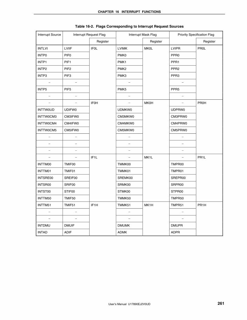
CHAPTER 16 INTERRUPT FUNCTIONS
User’s Manual U17890EJ2V0UD 261
Table 16-2. Flags Corresponding to Interrupt Request Sources
Interrupt Request Flag Interrupt Mask Flag Priority Specification Flag Interrupt Source
Register Register Register
INTLVI LVIIF IF0L LVIMK MK0L LVIPR PR0L
INTP0 PIF0 PMK0 PPR0
INTP1 PIF1 PMK1 PPR1
INTP2 PIF2 PMK2 PPR2
INTP3 PIF3 PMK3 PPR3
− − − −
INTP5 PIF5 PMK5 PPR5
− − − −
− − IF0H − MK0H − PR0H
INTTW0UD UDIFW0 UDMKW0 UDPRW0
INTTW0CM3 CM3IFW0 CM3MKW0 CM3PRW0
INTTW0CM4 CM4IFW0 CM4MKW0 CM4PRW0
INTTW0CM5 CM5IFW0 CM5MKW0 CM5PRW0
− − − −
− − − −
− − − −
− − IF1L − MK1L − PR1L
INTTM00 TMIF00 TMMK00 TMPR00
INTTM01 TMIF01 TMMK01 TMPR01
INTSRE00 SREIF00 SREMK00 SREPR00
INTSR00 SRIF00 SRMK00 SRPR00
INTST00 STIF00 STMK00 STPR00
INTTM50 TMIF50 TMMK50 TMPR50
INTTM51 TMIF51 IF1H TMMK51 MK1H TMPR51 PR1H
− − − −
− − − −
INTDMU DMUIF DMUMK DMUPR
INTAD ADIF ADMK ADPR

CHAPTER 16 INTERRUPT FUNCTIONS
User’s Manual U17890EJ2V0UD 262
(1) Interrupt request flag registers (IF0L, IF0H, IF1L, IF1H)
The interrupt request flags are set to 1 when the corresponding interrupt request is generated or an instruction is
executed. They are cleared to 0 when an instruction is executed upon acknowledgment of an interrupt request or
upon RESET input.
When an interrupt is acknowledged, the interrupt request flag is automatically cleared and then the interrupt
routine is entered.
IF0L, IF0H, IF1L, and IF1H are set by a 1-bit or 8-bit memory manipulation instruction. When IF0L and IF0H, and
IF1L and IF1H are combined to form 16-bit registers IF0 and IF1, they are set by a 16-bit memory manipulation
instruction.
RESET input clears these registers to 00H.

CHAPTER 16 INTERRUPT FUNCTIONS
User’s Manual U17890EJ2V0UD 263
Figure 16-2. Format of Interrupt Request Flag Registers (IF0L, IF0H, IF1L, IF1H)
Address: FFE0H After reset: 00H R/W
Symbol 7 <6> 5 <4> <3> <2> <1> <0>
IF0L 0Note PIF5 0Note PIF3 PIF2 PIF1 PIF0 LVIIF
Address: FFE1H After reset: 00H R/W
Symbol 7 6 5 <4> <3> <2> <1> 0
IF0H 0Note 0Note 0Note CM5IFW0 CM4IFW0 CM3IFW0 UDIFW0 0Note
Address: FFE2H After reset: 00H R/W
Symbol <7> <6> <5> <4> <3> <2> 1 0
IF1L TMIF50 STIF00 SRIF00 SREIF00 TMIF01 TMIF00 0Note 0Note
Address: FFE3H After reset: 00H R/W
Symbol 7 6 5 <4> <3> 2 1 <0>
IF1H 0Note 0Note 0Note ADIF DMUIF 0Note 0Note TMIF51
XXIFX Interrupt request flag
0 No interrupt request signal is generated
1 Interrupt request is generated, interrupt request status
Note Be sure to clear bits 5 and 7 of IF0L to 0.
Be sure to clear bits 0 and 5 to 7 of IF0H to 0.
Be sure to clear bits 0 and 1 of IF1L to 0.
Be sure to clear bits 1 and 2 and 5 to 7 of IF1H to 0.
Cautions 1. When operating a timer, serial interface, or A/D converter after standby release, operate it
once after clearing the interrupt request flag. An interrupt request flag may be set by noise.
2. When manipulating a flag of the interrupt request flag register, use a 1-bit memory
manipulation instruction (CLR1). When describing in C language, use a bit manipulation
instruction such as “IF0L.0 = 0;” or “_asm(“clr1 IF0L, 0”);” because the compiled
assemblermust be a 1-bit memory manipulation instruction (CLR1). If a program is
described in C language using an 8-bit memory manipulation instruction such as “IF0L &=
0xfe;” and compiled, it becomes the assembler of three instructions.
mov a, IF0L
and a, #0FEH
mov IF0L, a
In this case, even if the request flag of another bit of the same interrupt request flag register
(IF0L) is set to 1 at the timing between “mov a, IF0L” and “mov IF0L, a”, the flag is cleared
to 0 at “mov IF0L, a”. Therefore, care must be exercised when using an 8-bit memory
manipulation instruction in C language.
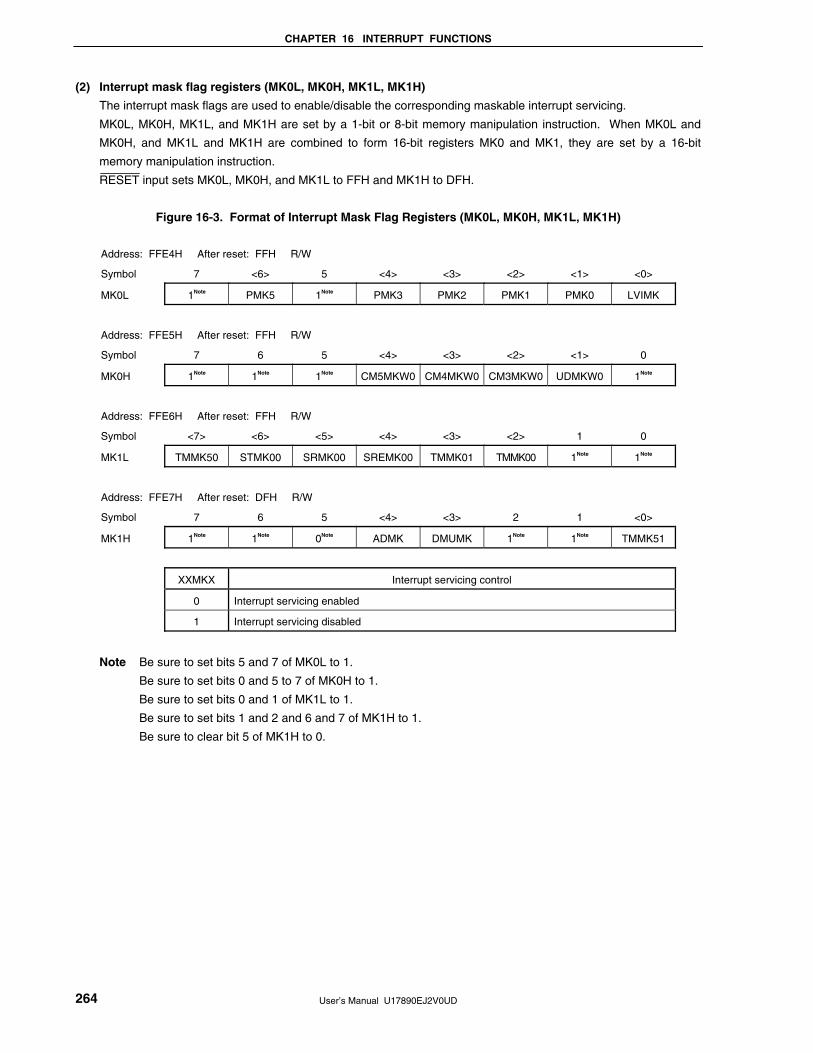
CHAPTER 16 INTERRUPT FUNCTIONS
User’s Manual U17890EJ2V0UD 264
(2) Interrupt mask flag registers (MK0L, MK0H, MK1L, MK1H)
The interrupt mask flags are used to enable/disable the corresponding maskable interrupt servicing.
MK0L, MK0H, MK1L, and MK1H are set by a 1-bit or 8-bit memory manipulation instruction. When MK0L and
MK0H, and MK1L and MK1H are combined to form 16-bit registers MK0 and MK1, they are set by a 16-bit
memory manipulation instruction.
RESET input sets MK0L, MK0H, and MK1L to FFH and MK1H to DFH.
Figure 16-3. Format of Interrupt Mask Flag Registers (MK0L, MK0H, MK1L, MK1H)
Address: FFE4H After reset: FFH R/W
Symbol 7 <6> 5 <4> <3> <2> <1> <0>
MK0L 1Note PMK5 1Note PMK3 PMK2 PMK1 PMK0 LVIMK
Address: FFE5H After reset: FFH R/W
Symbol 7 6 5 <4> <3> <2> <1> 0
MK0H 1Note 1Note 1Note CM5MKW0 CM4MKW0 CM3MKW0 UDMKW0 1Note
Address: FFE6H After reset: FFH R/W
Symbol <7> <6> <5> <4> <3> <2> 1 0
MK1L TMMK50 STMK00 SRMK00 SREMK00 TMMK01 TMMK00 1Note 1Note
Address: FFE7H After reset: DFH R/W
Symbol 7 6 5 <4> <3> 2 1 <0>
MK1H 1Note 1Note 0Note ADMK DMUMK 1Note 1Note TMMK51
XXMKX Interrupt servicing control
0 Interrupt servicing enabled
1 Interrupt servicing disabled
Note Be sure to set bits 5 and 7 of MK0L to 1.
Be sure to set bits 0 and 5 to 7 of MK0H to 1.
Be sure to set bits 0 and 1 of MK1L to 1.
Be sure to set bits 1 and 2 and 6 and 7 of MK1H to 1.
Be sure to clear bit 5 of MK1H to 0.

CHAPTER 16 INTERRUPT FUNCTIONS
User’s Manual U17890EJ2V0UD 265
(3) Priority specification flag registers (PR0L, PR0H, PR1L, PR1H)
The priority specification flag registers are used to set the corresponding maskable interrupt priority order.
PR0L, PR0H, PR1L, and PR1H are set by a 1-bit or 8-bit memory manipulation instruction. If PR0L and PR0H,
and PR1L and PR1H are combined to form 16-bit registers PR0 and PR1, they are set by a 16-bit memory
manipulation instruction.
RESET input sets these registers to FFH.
Figure 16-4. Format of Priority Specification Flag Registers (PR0L, PR0H, PR1L, PR1H)
Address: FFE8H After reset: FFH R/W
Symbol 7 <6> 5 <4> <3> <2> <1> <0>
PR0L 1Note PPR5 1Note PPR3 PPR2 PPR1 PPR0 LVIPR
Address: FFE9H After reset: FFH R/W
Symbol 7 6 5 <4> <3> <2> <1> 0
PR0H 1Note 1Note 1Note CM5PRW0 CM4PRW0 CM3PRW0 UDPRW0 1Note
Address: FFEAH After reset: FFH R/W
Symbol <7> <6> <5> <4> <3> <2> 1 0
PR1L TMPR50 STPR00 SRPR00 SREPR00 TMPR01 TMPR00 1Note 1Note
Address: FFEBH After reset: FFH R/W
Symbol 7 6 5 <4> <3> 2 1 <0>
PR1H 1Note 1Note 1Note ADPR DMUPR 1Note 1Note TMPR51
XXPRX Priority level selection
0 High priority level
1 Low priority level
Note Be sure to set bits 5 and 7 of PR0L to 1.
Be sure to set bits 0 and 5 to 7 of PR0H to 1.
Be sure to set bits 0 and 1 of PR1L to 1.
Be sure to set bits 1 and 2 and 5 to 7 of PR1H to 1.

CHAPTER 16 INTERRUPT FUNCTIONS
User’s Manual U17890EJ2V0UD 266
(4) External interrupt rising edge enable register (EGP), external interrupt falling edge enable register (EGN)
These registers specify the valid edge for INTP0 to INTP3, and INTP5.
EGP and EGN are set by a 1-bit or 8-bit memory manipulation instruction.
RESET input clears these registers to 00H.
Figure 16-5. Format of External Interrupt Rising Edge Enable Register (EGP)
and External Interrupt Falling Edge Enable Register (EGN)
Address: FF48H After reset: 00H R/W
Symbol 7 6 5 4 3 2 1 0
EGP 0 0 EGP5 0 EGP3 EGP2 EGP1 EGP0
Address: FF49H After reset: 00H R/W
Symbol 7 6 5 4 3 2 1 0
EGN 0 0 EGN5 0 EGN3 EGN2 EGN1 EGN0
EGPn EGNn INTPn pin valid edge selection (n = 0 to 3, 5)
0 0 Edge detection disabled
0 1 Falling edge
1 0 Rising edge
1 1 Both rising and falling edges
Table 16-3 shows the ports corresponding to EGPn and EGNn.
Table 16-3. Ports Corresponding to EGPn and EGNn
Detection Enable Register Edge Detection Port Interrupt Request Signal
EGP0 EGN0 P00 INTP0
EGP1 EGN1 P01 INTP1
EGP2 EGN2 P02 INTP2
EGP3 EGN3 P03 INTP3
EGP5 EGN5 P53 INTP5
Caution Select the port mode by clearing EGPn and EGNn to 0 because an edge may be detected when
the external interrupt function is switched to the port function.
Remark n = 0 to 3, 5

CHAPTER 16 INTERRUPT FUNCTIONS
User’s Manual U17890EJ2V0UD 267
(5) Program status word (PSW)
The program status word is a register used to hold the instruction execution result and the current status for an
interrupt request. The IE flag that sets maskable interrupt enable/disable and the ISP flag that controls multiple
interrupt servicing are mapped to the PSW.
Besides 8-bit read/write, this register can carry out operations using bit manipulation instructions and dedicated
instructions (EI and DI). When a vectored interrupt request is acknowledged, if the BRK instruction is executed,
the contents of the PSW are automatically saved into a stack and the IE flag is reset to 0. If a maskable interrupt
request is acknowledged, the contents of the priority specification flag of the acknowledged interrupt are
transferred to the ISP flag. The PSW contents are also saved into the stack with the PUSH PSW instruction.
They are restored from the stack with the RETI, RETB, and POP PSW instructions.
RESET input sets PSW to 02H.
Figure 16-6. Format of Program Status Word
<7>
IE
<6>
Z
<5>
RBS1
<4>
AC
<3>
RBS0
2
0
<1>
ISP
0
CYPSW
After reset
02H
ISP
High-priority interrupt servicing (low-priority interrupt disabled)
IE
0
1
Disabled
Priority of interrupt currently being serviced
Interrupt request acknowledgment enable/disable
Used when normal instruction is executed
Enabled
Interrupt request not acknowledged, or low-priority interrupt servicing (all maskable interrupts enabled)
0
1

CHAPTER 16 INTERRUPT FUNCTIONS
User’s Manual U17890EJ2V0UD 268
16.4 Interrupt Servicing Operations
16.4.1 Maskable interrupt request acknowledgement
A maskable interrupt request becomes acknowledgeable when the interrupt request flag is set to 1 and the mask
(MK) flag corresponding to that interrupt request is cleared to 0. A vectored interrupt request is acknowledged if
interrupts are in the interrupt enabled state (when the IE flag is set to 1). However, a low-priority interrupt request is
not acknowledged during servicing of a higher priority interrupt request (when the ISP flag is reset to 0).
The times from generation of a maskable interrupt request until interrupt servicing is performed are listed in Table
16-4 below.
For the interrupt request acknowledgment timing, see Figures 16-8 and 16-9.
Table 16-4. Time from Generation of Maskable Interrupt Request Until Servicing
Minimum Time Maximum TimeNote
When ××PR = 0 7 clocks 32 clocks
When ××PR = 1 8 clocks 33 clocks
Note If an interrupt request is generated just before a divide instruction, the wait time becomes longer.
Remark 1 clock: 1/fCPU (fCPU: CPU clock)
If two or more maskable interrupt requests are generated simultaneously, the request with a higher priority level
specified in the priority specification flag is acknowledged first. If two or more interrupt requests have the same
priority level, the request with the highest default priority is acknowledged first.
An interrupt request that is held pending is acknowledged when it becomes acknowledgeable.
Figure 16-7 shows the interrupt request acknowledgment algorithm.
If a maskable interrupt request is acknowledged, the contents are saved into the stacks in the order of PSW, then
PC, the IE flag is reset (0), and the contents of the priority specification flag corresponding to the acknowledged
interrupt are transferred to the ISP flag. The vector table data determined for each interrupt request is loaded into the
PC and branched.
Restoring from an interrupt is possible by using the RETI instruction.

CHAPTER 16 INTERRUPT FUNCTIONS
User’s Manual U17890EJ2V0UD 269
Figure 16-7. Interrupt Request Acknowledgment Processing Algorithm
Start
××IF = 1?
××MK = 0?
××PR = 0?
IE = 1?
ISP = 1?
Interrupt request held pending
Yes
Yes
No
No
Yes (interrupt request generation)
Yes
No (Low priority)
No
No
Yes
Yes
No
IE = 1?
No
Any high-priority interrupt request among those
simultaneously generated with ××PR = 0?
Yes (High priority)
No
Yes
Yes
No
Vectored interrupt servicing
Interrupt request held pending
Interrupt request held pending
Interrupt request held pending
Interrupt request held pending
Interrupt request held pending
Interrupt request held pending
Vectored interrupt servicing
Any high-priority interrupt request among
those simultaneously generated?
Any high-priority interrupt request among
those simultaneously generated with ××PR = 0?
××IF: Interrupt request flag
××MK: Interrupt mask flag
××PR: Priority specification flag
IE: Flag that controls acknowledgment of maskable interrupt request (1 = Enable, 0 = Disable)
ISP: Flag that indicates the priority level of the interrupt currently being serviced (0 = high-priority interrupt
servicing, 1 = No interrupt request acknowledged, or low-priority interrupt servicing)

CHAPTER 16 INTERRUPT FUNCTIONS
User’s Manual U17890EJ2V0UD 270
Figure 16-8. Interrupt Request Acknowledgment Timing (Minimum Time)
8 clocks
7 clocks
Instruction InstructionPSW and PC saved, jump to interrupt servicing
Interrupt servicing program
CPU processing
××IF(××PR = 1)
××IF(××PR = 0)
6 clocks
Remark 1 clock: 1/fCPU (fCPU: CPU clock)
Figure 16-9. Interrupt Request Acknowledgment Timing (Maximum Time)
33 clocks
32 clocks
Instruction Divide instructionPSW and PC saved, jump to interrupt servicing
Interrupt servicing program
CPU processing
××IF(××PR = 1)
××IF(××PR = 0)
6 clocks25 clocks
Remark 1 clock: 1/fCPU (fCPU: CPU clock)
16.4.2 Software interrupt request acknowledgment
A software interrupt request is acknowledged by BRK instruction execution. Software interrupts cannot be
disabled.
If a software interrupt request is acknowledged, the contents are saved into the stacks in the order of the program
status word (PSW), then program counter (PC), the IE flag is reset (0), and the contents of the vector table (003EH,
003FH) are loaded into the PC and branched.
Restoring from a software interrupt is possible by using the RETB instruction.
Caution Do not use the RETI instruction for restoring from the software interrupt.

CHAPTER 16 INTERRUPT FUNCTIONS
User’s Manual U17890EJ2V0UD 271
16.4.3 Multiple interrupt servicing
Multiple interrupt servicing occurs when another interrupt request is acknowledged during execution of an interrupt.
Multiple interrupt servicing does not occur unless the interrupt request acknowledgment enabled state is selected
(IE = 1). Also, when an interrupt request is acknowledged, interrupt request acknowledgment becomes disabled (IE =
0). Therefore, to enable multiple interrupt servicing, it is necessary to set (1) the IE flag with the EI instruction during
interrupt servicing to enable interrupt acknowledgment.
Moreover, even if interrupts are enabled, multiple interrupt servicing may not be enabled, this being subject to
interrupt priority control. Two types of priority control are available: default priority control and programmable priority
control. Programmable priority control is used for multiple interrupt servicing.
In the interrupt enabled state, if an interrupt request with a priority equal to or higher than that of the interrupt
currently being serviced is generated, it is acknowledged for multiple interrupt servicing. If an interrupt with a priority
lower than that of the interrupt currently being serviced is generated during interrupt servicing, it is not acknowledged
for multiple interrupt servicing. Interrupt requests that are not enabled because interrupts are in the interrupt disabled
state or because they have a lower priority are held pending. When servicing of the current interrupt ends, the
pending interrupt request is acknowledged following execution of one main processing instruction execution.
Table 16-5 shows relationship between interrupt requests enabled for multiple interrupt servicing and Figure 16-10
shows multiple interrupt servicing examples.
Table 16-5. Relationship Between Interrupt Requests Enabled for Multiple Interrupt Servicing
During Interrupt Servicing
Maskable Interrupt Request
PR = 0 PR = 1
Multiple Interrupt Request
Interrupt Being Serviced IE = 1 IE = 0 IE = 1 IE = 0
Software
Interrupt
Request
ISP = 0 × × × Maskable interrupt
ISP = 1 × ×
Software interrupt × ×
Remarks 1. : Multiple interrupt servicing enabled
2. ×: Multiple interrupt servicing disabled
3. ISP and IE are flags contained in the PSW.
ISP = 0: An interrupt with higher priority is being serviced.
ISP = 1: No interrupt request has been acknowledged, or an interrupt with a lower
priority is being serviced.
IE = 0: Interrupt request acknowledgment is disabled.
IE = 1: Interrupt request acknowledgment is enabled.
4. PR is a flag contained in PR0L, PR0H, PR1L, and PR1H.
PR = 0: Higher priority level
PR = 1: Lower priority level

CHAPTER 16 INTERRUPT FUNCTIONS
User’s Manual U17890EJ2V0UD 272
Figure 16-10. Examples of Multiple Interrupt Servicing (1/2)
Example 1. Multiple interrupt servicing occurs twice
Main processing INTxx servicing INTyy servicing INTzz servicing
EIEI EI
RETI RETI
RETI
INTxx(PR = 1)
INTyy(PR = 0)
INTzz(PR = 0)
IE = 0 IE = 0 IE = 0
IE = 1 IE = 1IE = 1
During servicing of interrupt INTxx, two interrupt requests, INTyy and INTzz, are acknowledged, and multiple
interrupt servicing takes place. Before each interrupt request is acknowledged, the EI instruction must always be
issued to enable interrupt request acknowledgment.
Example 2. Multiple interrupt servicing does not occur due to priority control
Main processing INTxx servicing INTyy servicing
INTxx(PR = 0)
INTyy(PR = 1)
EI
RETI
IE = 0
IE = 0EI
1 instruction execution
RETIIE = 1
IE = 1
Interrupt request INTyy issued during servicing of interrupt INTxx is not acknowledged because its priority is lower
than that of INTxx, and multiple interrupt servicing does not take place. The INTyy interrupt request is held pending,
and is acknowledged following execution of one main processing instruction.
PR = 0: Higher priority level
PR = 1: Lower priority level
IE = 0: Interrupt request acknowledgment disabled

CHAPTER 16 INTERRUPT FUNCTIONS
User’s Manual U17890EJ2V0UD 273
Figure 16-10. Examples of Multiple Interrupt Servicing (2/2)
Example 3. Multiple interrupt servicing does not occur because interrupts are not enabled
Main processing INTxx servicing INTyy servicing
EI
1 instruction execution
RETI
RETI
INTxx(PR = 0)
INTyy(PR = 0)
IE = 0
IE = 0
IE = 1
IE = 1
Interrupts are not enabled during servicing of interrupt INTxx (EI instruction is not issued), therefore, interrupt
request INTyy is not acknowledged and multiple interrupt servicing does not take place. The INTyy interrupt request
is held pending, and is acknowledged following execution of one main processing instruction.
PR = 0: Higher priority level
IE = 0: Interrupt request acknowledgment disabled
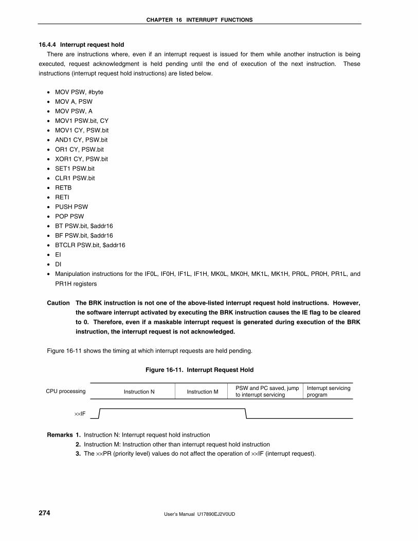
CHAPTER 16 INTERRUPT FUNCTIONS
User’s Manual U17890EJ2V0UD 274
16.4.4 Interrupt request hold
There are instructions where, even if an interrupt request is issued for them while another instruction is being
executed, request acknowledgment is held pending until the end of execution of the next instruction. These
instructions (interrupt request hold instructions) are listed below.
• MOV PSW, #byte
• MOV A, PSW
• MOV PSW, A
• MOV1 PSW.bit, CY
• MOV1 CY, PSW.bit
• AND1 CY, PSW.bit
• OR1 CY, PSW.bit
• XOR1 CY, PSW.bit
• SET1 PSW.bit
• CLR1 PSW.bit
• RETB
• RETI
• PUSH PSW
• POP PSW
• BT PSW.bit, $addr16
• BF PSW.bit, $addr16
• BTCLR PSW.bit, $addr16
• EI
• DI
• Manipulation instructions for the IF0L, IF0H, IF1L, IF1H, MK0L, MK0H, MK1L, MK1H, PR0L, PR0H, PR1L, and
PR1H registers
Caution The BRK instruction is not one of the above-listed interrupt request hold instructions. However,
the software interrupt activated by executing the BRK instruction causes the IE flag to be cleared
to 0. Therefore, even if a maskable interrupt request is generated during execution of the BRK
instruction, the interrupt request is not acknowledged.
Figure 16-11 shows the timing at which interrupt requests are held pending.
Figure 16-11. Interrupt Request Hold
Instruction N Instruction MPSW and PC saved, jump to interrupt servicing
Interrupt servicingprogram
CPU processing
××IF
Remarks 1. Instruction N: Interrupt request hold instruction
2. Instruction M: Instruction other than interrupt request hold instruction
3. The ××PR (priority level) values do not affect the operation of ××IF (interrupt request).

User’s Manual U17890EJ2V0UD 275
CHAPTER 17 STANDBY FUNCTION
17.1 Standby Function and Configuration
17.1.1 Standby function
Table 17-1. Relationship Between Operation Clocks in Each Operation Status
High-speed System Clock Note 1 Internal Low-speed Oscillator Prescaler Clock
Supplied to Peripherals
Note 3
Status
Operation Mode
MSTOP = 0
MSTOP = 1
Note 2
RSTOP = 0 RSTOP = 1
CPU Clock
After
Release MCM0 = 0 MCM0 = 1
Reset Stopped Internal
low-speed
oscillation
clock
Stopped
STOP
Stopped
Note 6 Stopped
HALT Oscillating Stopped Note 4
Oscillating Oscillating Stopped Note 5
Note 7 Internal
low-speed
oscillation
clock
High-
speed
system
clock
Notes 1. The high-speed system clock is selected (X1 clock or internal high-speed oscillation clock) by using the
option byte.
2. When “Cannot be stopped” is selected for internal low-speed oscillator by an option byte.
3. When “Can be stopped by software” is selected for internal low-speed oscillator by an option byte.
4. Only when internal low-speed oscillator is Oscillating.
5. Only when X1 or internal high-speed oscillation clock is Oscillating.
6. Operates using the CPU clock at STOP instruction execution.
7. Operates using the CPU clock at HALT instruction execution.
Caution The RSTOP setting is valid only when “Can be stopped by software” is set for internal low-speed
oscillator by an option byte.
Remark MSTOP: Bit 7 of the main OSC control register (MOC)
RSTOP: Bit 0 of the internal oscillation mode register (RCM)
MCM0: Bit 0 of the main clock mode register (MCM)
The standby function is designed to reduce the operating current of the system. The following two modes are
available.
(1) HALT mode
HALT instruction execution sets the HALT mode. In the HALT mode, the CPU operation clock is stopped. If the
X1 oscillator, internal high-speed oscillator, or internal low-speed oscillator is operating before the HALT mode is
set, oscillation of each clock continues. In this mode, the operating current is not decreased as much as in the
STOP mode, but the HALT mode is effective for restarting operation immediately upon interrupt request
generation and carrying out intermittent operations.
<R>

CHAPTER 17 STANDBY FUNCTION
User’s Manual U17890EJ2V0UD 276
(2) STOP mode
STOP instruction execution sets the STOP mode. In the STOP mode, the high-speed system clock stops,
stopping the whole system, thereby considerably reducing the CPU operating current.
Because this mode can be cleared by an interrupt request, it enables intermittent operations to be carried out.
However, because a wait time is required to secure the oscillation stabilization time after the STOP mode is
released, select the HALT mode if it is necessary to start processing immediately upon interrupt request
generation.
In either of these two modes, all the contents of registers, flags and data memory just before the standby mode is
set are held. The I/O port output latches and output buffer statuses are also held.
Cautions 1. STOP and HALT mode can be used when CPU is operating on the high-speed system clock
or internal low-speed oscillation clock. However, when the STOP instruction is executed
during internal low-speed oscillation clock operation, the X1 or internal high-speed oscillator
stops, but internal low-speed oscillator does not stop.
2. Setting in the STOP mode is prohibited when the internal high-speed oscillation clock is
operating. In this case, switch to the internal low-speed oscillation clock before setting in the
STOP mode.
3. When shifting to the STOP mode, be sure to stop the peripheral hardware operation before
executing STOP instruction.
4. The following sequence is recommended for operating current reduction of the A/D converter
when the standby function is used: First clear bit 7 (ADCS) of the A/D converter mode
register (ADM) to 0 to stop the A/D conversion operation, and then execute the HALT or STOP
instruction.
5. If the internal low-speed oscillator is operating before the STOP mode is set, oscillation of the
internal low-speed oscillation clock cannot be stopped in the STOP mode. However, when
the internal low-speed oscillation clock is used as the CPU clock, the CPU operation is
stopped for 21/fRL (s) after STOP mode is released.

CHAPTER 17 STANDBY FUNCTION
User’s Manual U17890EJ2V0UD 277
17.1.2 Registers controlling standby function
The standby function is controlled by the following two registers.
• Oscillation stabilization time counter status register (OSTC)
• Oscillation stabilization time select register (OSTS)
Remark For the registers that start, stop, or select the clock, see CHAPTER 5 CLOCK GENERATOR.
(1) Oscillation stabilization time counter status register (OSTC)
This is the status register of the X1 input clock oscillation stabilization time counter. If the internal low-speed
oscillation clock is used as the CPU clock, the X1 input clock oscillation stabilization time can be checked.
OSTC can be read by a 1-bit or 8-bit memory manipulation instruction.
Reset release (reset by RESET input, POC, LVI, and WDT), the STOP instruction, and MSTOP (bit 7 of MOC
register) = 1 clear OSTC to 00H.
Figure 17-1. Format of Oscillation Stabilization Time Counter Status Register (OSTC)
Address: FFA3H After reset: 00H R
Symbol 7 6 5 4 3 2 1 0
OSTC 0 0 0 MOST11 MOST13 MOST14 MOST15 MOST16
Oscillation stabilization time status
MOST11 MOST13 MOST14 MOST15 MOST16
fX = 20 MHz fX = 16 MHz
1 0 0 0 0 211/fX min. 102.4 μs min. 128 μs min.
1 1 0 0 0 213/fX min. 409.6 μs min. 512 μs min.
1 1 1 0 0 214/fX min. 819.2 μs min. 1.02 ms min.
1 1 1 1 0 215/fX min. 1.64 ms min. 2.04 ms min.
1 1 1 1 1 216/fX min. 3.27 ms min. 4.09 ms min.
Cautions 1. After the above time has elapsed, the bits are set to 1 in order from MOST11 and remain 1.
2. The oscillation stabilization time counter counts only during the oscillation stabilization time set by OSTS. If the STOP mode is entered and then released while the internal low-speed oscillation clock is being used as the CPU clock, set the oscillation stabilization time as follows.
• Desired OSTC oscillation stabilization time ≤ Oscillation stabilization time set by OSTS
Note, therefore that only the statuses during the oscillation stabilization time set by OSTS is set to OSTC after STOP mode is released.
3. The wait time when STOP mode is released does not include the time after STOP mode release until clock oscillation starts (“a” below) regardless of whether STOP mode is released by RESET input or interrupt generation.
a
STOP mode release
X1 pin voltagewaveform
4. OSTC cannot be used when the internal high-speed oscillation clock is selected
as the high-speed system clock by using the option byte. Secure wait time (350 μs) by software. Remark fX: X1 input clock oscillation frequency
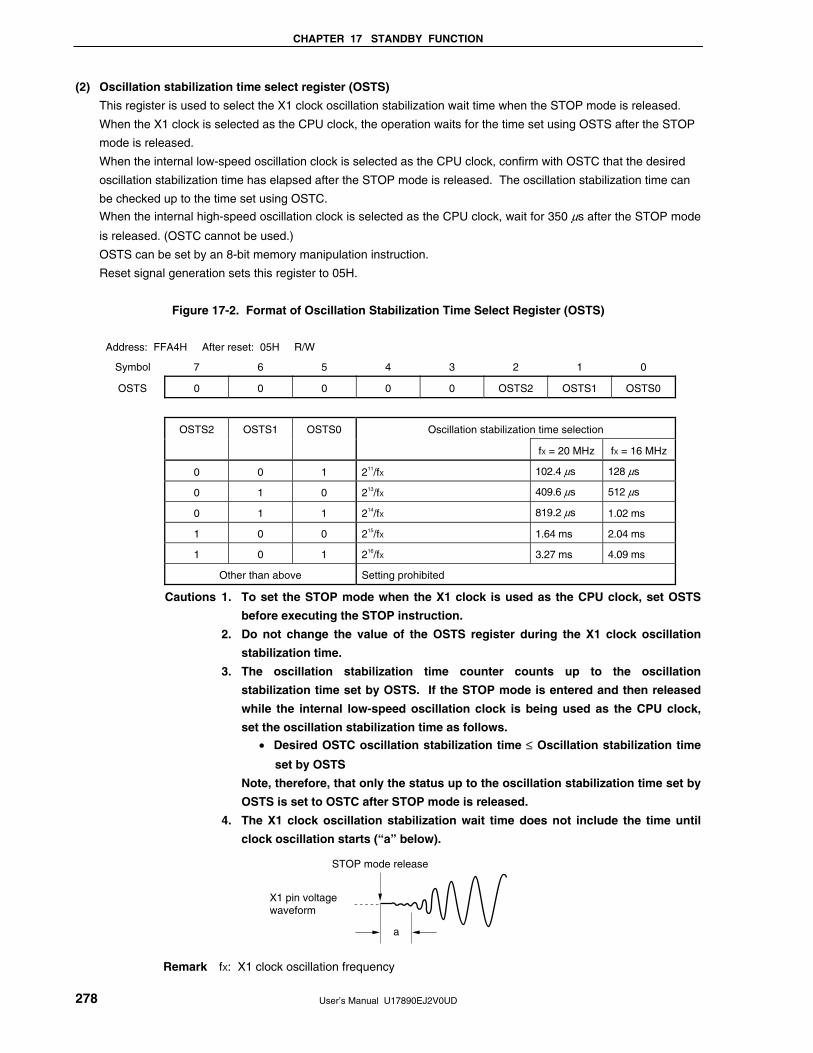
CHAPTER 17 STANDBY FUNCTION
User’s Manual U17890EJ2V0UD 278
(2) Oscillation stabilization time select register (OSTS)
This register is used to select the X1 clock oscillation stabilization wait time when the STOP mode is released.
When the X1 clock is selected as the CPU clock, the operation waits for the time set using OSTS after the STOP
mode is released.
When the internal low-speed oscillation clock is selected as the CPU clock, confirm with OSTC that the desired
oscillation stabilization time has elapsed after the STOP mode is released. The oscillation stabilization time can
be checked up to the time set using OSTC.
When the internal high-speed oscillation clock is selected as the CPU clock, wait for 350 μs after the STOP mode
is released. (OSTC cannot be used.)
OSTS can be set by an 8-bit memory manipulation instruction.
Reset signal generation sets this register to 05H.
Figure 17-2. Format of Oscillation Stabilization Time Select Register (OSTS)
Address: FFA4H After reset: 05H R/W
Symbol 7 6 5 4 3 2 1 0
OSTS 0 0 0 0 0 OSTS2 OSTS1 OSTS0
Oscillation stabilization time selection
OSTS2 OSTS1 OSTS0
fX = 20 MHz fX = 16 MHz
0 0 1 211/fX 102.4 μs 128 μs
0 1 0 213/fX 409.6 μs 512 μs
0 1 1 214/fX 819.2 μs 1.02 ms
1 0 0 215/fX 1.64 ms 2.04 ms
1 0 1 216/fX 3.27 ms 4.09 ms
Other than above Setting prohibited
Cautions 1. To set the STOP mode when the X1 clock is used as the CPU clock, set OSTS
before executing the STOP instruction.
2. Do not change the value of the OSTS register during the X1 clock oscillation
stabilization time.
3. The oscillation stabilization time counter counts up to the oscillation
stabilization time set by OSTS. If the STOP mode is entered and then released
while the internal low-speed oscillation clock is being used as the CPU clock,
set the oscillation stabilization time as follows. • Desired OSTC oscillation stabilization time ≤ Oscillation stabilization time
set by OSTS
Note, therefore, that only the status up to the oscillation stabilization time set by
OSTS is set to OSTC after STOP mode is released.
4. The X1 clock oscillation stabilization wait time does not include the time until
clock oscillation starts (“a” below).
STOP mode release
X1 pin voltage waveform
a
Remark fX: X1 clock oscillation frequency

CHAPTER 17 STANDBY FUNCTION
User’s Manual U17890EJ2V0UD 279
17.2 Standby Function Operation
17.2.1 HALT mode
(1) HALT mode
The HALT mode is set by executing the HALT instruction. HALT mode can be set regardless of whether the CPU
clock before the setting was the high-speed system clock or internal low-speed oscillation clock.
The operating statuses in the HALT mode are shown below.
Table 17-2. Operating Statuses in HALT Mode
When HALT Instruction Is Executed While CPU Is Operating on High-speed System Clock
When HALT Instruction Is Executed While CPU Is Operating on Internal Low-speed Oscillation Clock
HALT Mode Setting
Item
When Internal Low-speed Oscillation Clock
Continues
When Internal Low-speed Oscillation Clock
StoppedNote 1
When High-speed System Clock Oscillation
Continues
When High-speed System Clock Oscillation Stopped
System clock Clock supply to the CPU is stopped.
CPU Operation stopped
Port (latch) Status before HALT mode was set is retained
10-bit inverter control timer Operable Operation not guaranteed
16-bit timer/event counter 00 Operable Operation not guaranteed
8-bit timer/event counter 50 Operable Operation not guaranteed when count clock other than TI50 is selected
8-bit timer/event counter 51 Operable Operation not guaranteed when count clock other than fRL/27 is selected
Internal low-speed oscillator cannot be stoppedNote 2
Operable − Operable Watchdog timer
Internal low-speed oscillator can be stoppedNote 2
Operation stopped
Hi-Z output controller Operable
Real-time output ports Operable Operation not guaranteed
A/D converter Operable Operation not guaranteed
Serial interface
UART00 Operable Operation not guaranteed when serial clock other than TM50 output is selected during 8-bit timer/event counter 50 operation
Multiplier/divider Operable Operation not guaranteed
Power-on-clear function Operable
Low-voltage detection function Operable
External interrupt Operable
Notes 1. When “Stopped by software” is selected for internal low-speed oscillator by an option byte and internal low-speed oscillator is stopped by software (for option bytes, see CHAPTER 21 OPTION BYTES).
2. “Internal low-speed oscillator cannot be stopped” or “Internal low-speed oscillator can be stopped by software” can be selected by an option byte.

CHAPTER 17 STANDBY FUNCTION
User’s Manual U17890EJ2V0UD 280
(2) HALT mode release
The HALT mode can be released by the following two sources.
(a) Release by unmasked interrupt request
When an unmasked interrupt request is generated, the HALT mode is released. If interrupt
acknowledgement is enabled, vectored interrupt servicing is carried out. If interrupt acknowledgement is
disabled, the next address instruction is executed.
Figure 17-3. HALT Mode Release by Interrupt Request Generation
HALTinstruction Wait
Wait Operating modeHALT modeOperating mode
OscillationHigh-speed system clock or internal
low-speed oscillation clock
Status of CPU
Standbyrelease signal
Interruptrequest
Remarks 1. The broken lines indicate the case when the interrupt request which has released the standby
mode is acknowledged.
2. The wait time is as follows:
• When vectored interrupt servicing is carried out: 8 or 9 clocks
• When vectored interrupt servicing is not carried out: 2 or 3 clocks

CHAPTER 17 STANDBY FUNCTION
User’s Manual U17890EJ2V0UD 281
(b) Release by RESET input
When the RESET signal is input, HALT mode is released, and then, as in the case with a normal reset
operation, the program is executed after branching to the reset vector address.
Figure 17-4. HALT Mode Release by RESET Input (1/2)
(1) When X1 input clock is used as CPU clock
HALT
instruction
RESET signal
X1 input clock
Operating mode HALT modeResetperiod
Operationstopped Operating mode
OscillatesOscillationstopped Oscillates
Status of CPU
(X1 input clock)
Oscillation stabilization time(211/fX to 216/fX) Note
(Internal low-speed oscillation clock)(21/fRL)
Note No oscillation stabilization time wait is required when an external input clock is used. The CPU clock,
therefore, may be switched without reading the OSTC value.
(2) When internal high-speed oscillation clock is used as CPU clock
HALT
instruction
RESET signal
Internal high-speed oscillation clock
Operating mode HALT modeResetperiod
Operationstopped Operating mode
OscillatesOscillationstopped Oscillates
Status of CPU
(Internal high-speed oscillation clock)
Oscillation stabilization wait Note
(Internal low-speed oscillation clock)(21/fRL)
Note When the internal high-speed oscillation clock is selected as the high-speed system clock, the CPU
clock can be switched from the internal low-speed oscillation clock to the high-speed system clock by
using the MCM0 bit of MCM, after waiting for the reference voltage stabilization time (300 μs (MAX.))
and the oscillation stabilization time (50 μs (MAX.)) by using software, after a reset release. At this time,
since OSTC cannot be used, execute the NOP instruction 85 times according to the maximum value of
the internal low-speed oscillation clock oscillation frequency (480 kHz), secure a stabilization time, and
then switch the CPU clock.
Remarks 1. fX: X1 clock oscillation frequency
2. fRL: Internal low-speed oscillation clock frequency

CHAPTER 17 STANDBY FUNCTION
User’s Manual U17890EJ2V0UD 282
Figure 17-4. HALT Mode Release by RESET Input (2/2)
(3) When internal low-speed oscillation clock is used as CPU clock
HALT
instruction
RESET signal
Internal low-speed oscillation clock
Operating mode HALT modeResetperiod
Operationstopped Operating mode
OscillatesOscillationstopped Oscillates
Status of CPU
(Internal low-speed oscillation clock)(21/fRL)(Internal low-speed oscillation clock)
Remark fRL: Internal low-speed oscillation clock oscillation frequency
Table 17-3. Operation in Response to Interrupt Request in HALT Mode
Release Source MK×× PR×× IE ISP Operation
0 0 0 × Next address
instruction execution
0 0 1 × Interrupt servicing
execution
0 1 0 1
0 1 × 0
Next address
instruction execution
0 1 1 1 Interrupt servicing
execution
Maskable interrupt
request
1 × × × HALT mode held
RESET input − − × × Reset processing
×: don’t care

CHAPTER 17 STANDBY FUNCTION
User’s Manual U17890EJ2V0UD 283
17.2.2 STOP mode
(1) STOP mode setting and operating statuses The STOP mode is set by executing the STOP instruction, and it can be set regardless of whether the CPU clock
before the setting was the high-speed system clock or internal low-speed oscillation clock.
Caution Because the interrupt request signal is used to clear the standby mode, if there is an interrupt source with the interrupt request flag set and the interrupt mask flag reset, the standby mode is immediately cleared if set. Thus, the STOP mode is reset to the HALT mode immediately after execution of the STOP instruction and the system returns to the operating mode as soon as the wait time set using the oscillation stabilization time select register (OSTS) has elapsed.
The operating statuses in the STOP mode are shown below.
Table 17-4. Operating Statuses in STOP Mode
When STOP Instruction Is Executed While CPU Is Operating on High-speed System Clock
STOP Mode Setting
Item When Internal Low-speed
Oscillation Clock Continues When Internal Low-speed Oscillation
Clock StoppedNote 1
When STOP Instruction Is Executed While CPU Is Operating on Internal
Low-speed Oscillation Clock
System clock Only X1 oscillator or internal high-speed oscillator oscillation is stopped. Clock supply to the CPU is stopped.
CPU Operation stopped
Port (latch) Status before STOP mode was set is retained
10-bit inverter control timer Operation stopped
16-bit timer/event counter 00 Operation stopped
8-bit timer/event counter 50 Operable only when TI50 is selected as the count clock
8-bit timer/event counter 51 Operation stopped
Internal low-speed oscillator cannot be stoppedNote 2
Operable − Operable Watchdog timer
Internal low-speed oscillator can be stoppedNote 2
Operation stopped
Hi-Z output controller Operable
Real-time output ports Operation stopped
A/D converter Operation stopped
Serial interface UART00 Operable only when TM51 output is selected as the count clock during TM51 operation
Multiplier/divider Operation stopped
Power-on-clear function Operable
Low-voltage detection function Operable
External interrupt Operable
Notes 1. When “Stopped by software” is selected for internal low-speed oscillator by an option byte and internal low-
speed oscillator is stopped by software (for option bytes, see CHAPTER 21 OPTION BYTES).
2. “Internal low-speed oscillator cannot be stopped” or “Internal low-speed oscillator can be stopped by
software” can be selected by an option byte.
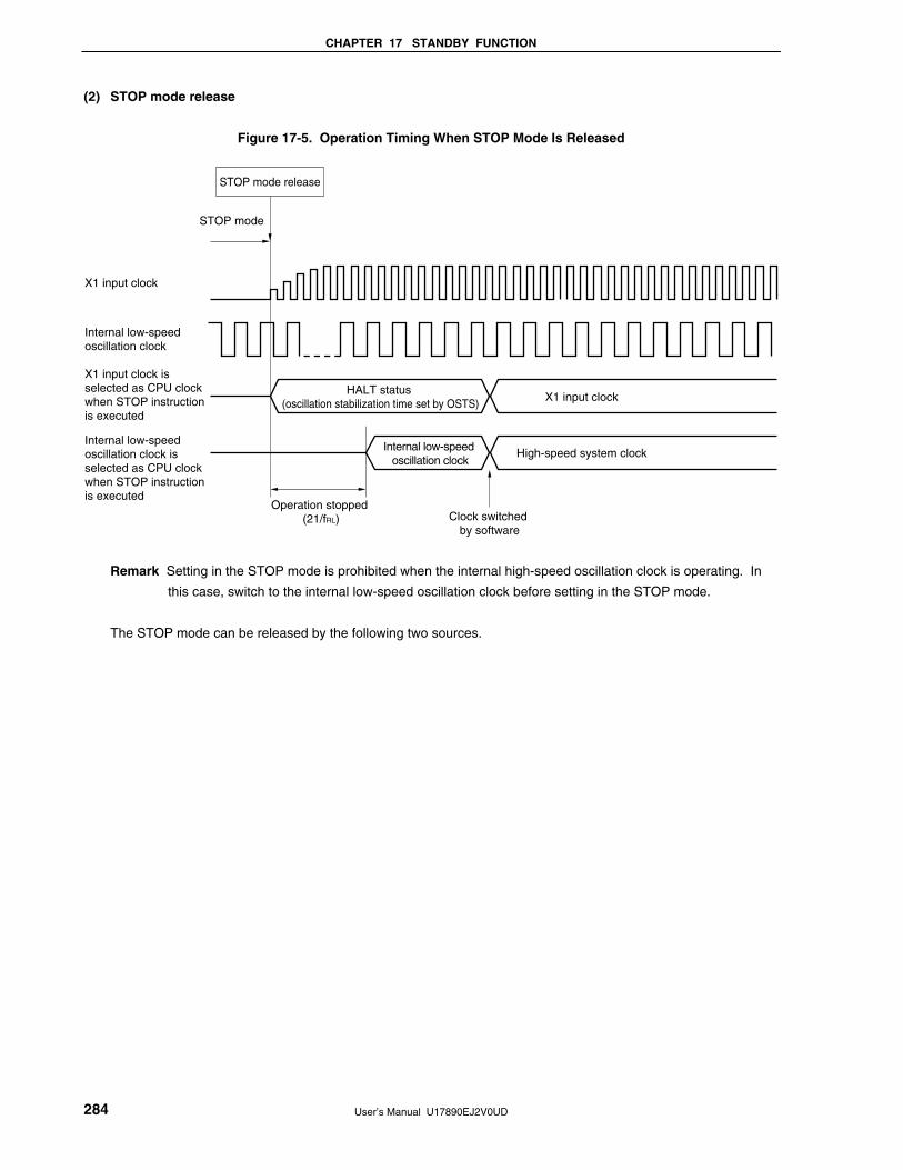
CHAPTER 17 STANDBY FUNCTION
User’s Manual U17890EJ2V0UD 284
(2) STOP mode release
Figure 17-5. Operation Timing When STOP Mode Is Released
Internal low-speed oscillation clock is selected as CPU clock when STOP instruction is executed
Internal low-speed oscillation clock
X1 input clock
X1 input clock is selected as CPU clock when STOP instruction is executed
STOP mode release
STOP mode
Operation stopped (21/fRL) Clock switched
by software
Internal low-speed oscillation clock
High-speed system clock
HALT status (oscillation stabilization time set by OSTS)
X1 input clock
Remark Setting in the STOP mode is prohibited when the internal high-speed oscillation clock is operating. In
this case, switch to the internal low-speed oscillation clock before setting in the STOP mode.
The STOP mode can be released by the following two sources.

CHAPTER 17 STANDBY FUNCTION
User’s Manual U17890EJ2V0UD 285
(a) Release by unmasked interrupt request
When an unmasked interrupt request is generated, the STOP mode is released. After the oscillation
stabilization time has elapsed, if interrupt acknowledgment is enabled, vectored interrupt servicing is carried
out. If interrupt acknowledgment is disabled, the next address instruction is executed.
Figure 17-6. STOP Mode Release by Interrupt Request Generation
(1) When X1 input clock is used as CPU clock
Operating mode Operating mode
OscillatesOscillates
STOPinstruction
STOP mode
Wait(set by OSTS)
Standby release signal
Oscillation stabilization wait
(HALT mode status)Oscillation stopped
X1 input clock
Status of CPU
Oscillation stabilization time (set by OSTS)
(X1 input clock)(X1 input clock)
(2) When internal low-speed oscillation clock is used as CPU clock
Operating mode Operating mode
Oscillates
STOPinstruction
STOP mode
Standby release signal
Internal low-speed oscillation clock
Status of CPU(Internal low-speed
oscillation clock)
Operationstopped
(21/fRL) (Internal low-speed oscillation clock)
Remarks 1. The broken lines indicate the case when the interrupt request that has released the standby
mode is acknowledged.
2. When the STOP instruction is executed while the internal low-speed oscillation clock is stopped
(RSTOP = 1), the internal low-speed oscillation clock is kept stopped after the STOP mode is
released.
3. fRL: Internal low-speed oscillation clock oscillation frequency
<R>

CHAPTER 17 STANDBY FUNCTION
User’s Manual U17890EJ2V0UD 286
(b) Release by RESET input
When the RESET signal is input, STOP mode is released and a reset operation is performed after the
oscillation stabilization time has elapsed.
Figure 17-7. STOP Mode Release by RESET Input (1/2)
(1) When X1 input clock is used as CPU clock
STOP
instruction
RESET signal
X1 input clock
Operating mode STOP modeResetperiod
Operationstopped Operating mode
OscillatesOscillationstopped Oscillates
Status of CPU
(X1 input clock)
Oscillation stabilization time (211/fX to 216/fX) Note
(Internal low-speed oscillation clock)(21/fRL)Oscillation stopped
Note No oscillation stabilization time wait is required when an external input clock is used. The CPU clock,
therefore, may be switched without reading the OSTC value.
(2) When Internal high-speed Oscillation clock is used as CPU clock
STOP
instruction
RESET signal
Internal high-speed oscillation clock
Operating mode STOP modeResetperiod
Operationstopped Operating mode
OscillatesOscillationstopped Oscillates
Status of CPU
(Internal high-speed oscillation clock)
Oscillation stabilization wait Note
(Internal low-speed oscillation clock)(21/fRL)
Oscillation stopped
(Internal low-speed oscillation clock)
Note When the internal high-speed oscillation clock is selected as the high-speed system clock, the CPU
clock can be switched from the internal low-speed oscillation clock to the high-speed system clock by
using the MCM0 bit of MCM, after waiting for the reference voltage stabilization time (300 μs (MAX.))
and the oscillation stabilization time (50 μs (MAX.)) by using software, after a reset release. At this time,
since OSTC cannot be used, execute the NOP instruction 85 times according to the maximum value of
the internal low-speed oscillation clock oscillation frequency (480 kHz), secure a stabilization time, and
then switch the CPU clock.
Remarks 1. fX: X1 clock oscillation frequency
2. fRL: Internal low-speed oscillation clock frequency

CHAPTER 17 STANDBY FUNCTION
User’s Manual U17890EJ2V0UD 287
Figure 17-7. STOP Mode Release by RESET Input (2/2)
(3) When internal low-speed oscillation clock is used as CPU clock
STOP
instruction
RESET signal
Internal low-speed oscillation clock
Operating mode STOP modeResetperiod
Operationstopped Operating mode
OscillatesOscillationstopped Oscillates
Status of CPU
(Internal low-speed oscillation clock)(21/fRL)(Internal low-speed oscillation clock)
Remark fRL: Internal low-speed oscillation clock oscillation frequency
Table 17-5. Operation in Response to Interrupt Request in STOP Mode
Release Source MK×× PR×× IE ISP Operation
0 0 0 × Next address
instruction execution
0 0 1 × Interrupt servicing
execution
0 1 0 1
0 1 × 0
Next address
instruction execution
0 1 1 1 Interrupt servicing
execution
Maskable interrupt
request
1 × × × STOP mode held
RESET input − − × × Reset processing
×: don’t care

User’s Manual U17890EJ2V0UD 288
CHAPTER 18 RESET FUNCTION
The following four operations are available to generate a reset signal.
(1) External reset input via RESET pin
(2) Internal reset by watchdog timer program loop detection
(3) Internal reset by comparison of supply voltage and detection voltage of power-on-clear (POC) circuit
(4) Internal reset by comparison of supply voltage and detection voltage of low-power-supply detector (LVI)
External and internal resets have no functional differences. In both cases, program execution starts at the address
at 0000H and 0001H when the reset signal is input.
A reset is applied when a low level is input to the RESET pin, the watchdog timer overflows, or by POC and LVI
circuit voltage detection, and each item of hardware is set to the status shown in Table 18-1. Each port pin is high
impedance during reset input or during the oscillation stabilization time just after reset release.
When a high level is input to the RESET pin, the reset is released and program execution starts using the internal
low-speed oscillation clock after the CPU clock operation has stopped for 21/fRL (s). A reset generated by the
watchdog timer is automatically released after the reset, and program execution starts using the internal low-speed
oscillation clock after the CPU clock operation has stopped for 21/fRL (s) (see Figures 18-2 to 18-4). Reset by POC
and LVI circuit power supply detection is automatically released when VDD > VPOC or VDD > VLVI after the reset, and
program execution starts using the internal low-speed oscillation clock after the CPU clock operation has stopped for
21/fRL (s) (see CHAPTER 19 POWER-ON-CLEAR CIRCUIT and CHAPTER 20 LOW-VOLTAGE DETECTOR).
Cautions 1. For an external reset, input a low level for 10 μs or more to the RESET pin.
2. During reset input, the X1 input clock and internal low-speed oscillation clock stop
oscillating.
3. When the STOP mode is released by a reset, the STOP mode contents are held during reset
input. However, the port pins become high-impedance.

CH
AP
TE
R 18 R
ES
ET
FU
NC
TIO
N
User’s M
anual U17890E
J2V0U
D
289
Figure 18-1. Block Diagram of Reset Function
LVIRFWDTRF
Reset control flag register (RESF)
Internal bus
Watchdog timer reset signal
RESET
Power-on-clear circuit reset signal
Low-voltage detector reset signal
Reset signal
Reset signal
Reset signal to LVIM register
clear
set
clear
set
Caution An LVI circuit internal reset does not reset the LVI circuit.
Remark LVIM: Low-voltage detection register

CHAPTER 18 RESET FUNCTION
User’s Manual U17890EJ2V0UD 290
Figure 18-2. Timing of Reset by RESET Input
Delay Delay
Hi-Z
Normal operationCPU clockReset period
(Oscillation stop)Operation stop
(21/fRL)Normal operation (Reset processing, internal low-speed oscillation clock)
RESET
Internalreset signal
Port pin
X1 input clock
Internal low-speed oscillation clock
Figure 18-3. Timing of Reset Due to Watchdog Timer Overflow
Hi-Z
Normal operationReset period
(Oscillation stop)CPU clock
Watchdog timeroverflow
Internalreset signal
Port pin
Operation stop(21/fRL)
Normal operation (Reset processing, internal low-speed oscillation clock)
X1 input clock
Internal low-speed oscillation clock
Caution A watchdog timer internal reset resets the watchdog timer.

CHAPTER 18 RESET FUNCTION
User’s Manual U17890EJ2V0UD 291
Figure 18-4. Timing of Reset in STOP Mode by RESET Input
Delay Delay
Hi-Z
NormaloperationCPU clock Reset period
(Oscillation stop)
RESET
Internalreset signal
Port pin
STOP instruction execution
Stop status (Oscillation stop)
Operation stop(21/fRL)
Normal operation (Reset processing, internal low-speed oscillation clock)
X1 input clock
Internal low-speed oscillation clock
Remark For the reset timing of the power-on-clear circuit and low-voltage detector, see CHAPTER 19 POWER-
ON-CLEAR CIRCUIT and CHAPTER 20 LOW-VOLTAGE DETECTOR.

CHAPTER 18 RESET FUNCTION
User’s Manual U17890EJ2V0UD 292
Table 18-1. Hardware Statuses after Reset Acknowledgment (1/2)
Hardware Status After Reset
AcknowledgmentNote 1
Program counter (PC) The contents of the
reset vector table
(0000H, 0001H) are
set.
Stack pointer (SP) Undefined
Program status word (PSW) 02H
Data memory UndefinedNote 2 RAM
General-purpose registers UndefinedNote 2
Port registers (P0, P1, P2, P5) (output latches) 00H (undefined only
for P2)
Port mode registers (PM0, PM1, PM5) FFH
Pull-up resistor option registers (PU0, PU1, PU5) 00H
Internal memory size switching register (IMS) CFH
Processor clock control register (PCC) 00H
Internal oscillation mode register (RCM) 00H
Main clock mode register (MCM) 00H
Main OSC control register (MOC) 00H
Oscillation stabilization time select register (OSTS) 05H
Oscillation stabilization time counter status register (OSTC) 00H
Compare registers (TW0CM0 to TW0CM2, TW0CM4, TW0CM5) 000H
Compare register (TW0CM3) 0FFH
Buffer registers (TW0BFCM0 to TW0BFCM2, TW0BFCM4, TW0BFCM5) 000H
Buffer register (TW0BFCM3) 0FFH
Dead time reload register (TW0DTIME) FFH
Control register (TW0C) 00H
Mode register (TW0M) 00H
A/D trigger select register (TW0TRGS) 00H
10-bit inverter control
timer
Output control register (TW0OC) 00H
Timer counter 00 (TM00) 0000H
Capture/compare registers 00, 01 (CR00, CR01) 0000H
Mode control register 00 (TMC00) 00H
Prescaler mode register 00 (PRM00) 00H
Capture/compare control register 00 (CRC00) 00H
16-bit timer/event
counter 00
Timer output control register 00 (TOC00) 00H
Timer counters 50, 51 (TM50, TM51) 00H
Compare registers 50, 51 (CR50, CR51) 00H
Timer clock selection registers 50, 51 (TCL50, TCL51) 00H
8-bit timer/event
counters 50, 51
Mode control registers 50, 51 (TMC50, TMC51) 00H
Notes 1. During reset input or oscillation stabilization time wait, only the PC contents among the hardware statuses
become undefined. All other hardware statuses remain unchanged after reset.
2. When a reset is executed in the standby mode, the pre-reset status is held even after reset.

CHAPTER 18 RESET FUNCTION
User’s Manual U17890EJ2V0UD 293
Table 18-1. Hardware Statuses after Reset Acknowledgment (2/2)
Hardware Status After Reset
Acknowledgment
Mode register (WDTM) 67H Watchdog timer
Enable register (WDTE) 9AH
Buffer registers (RTBL01, RTBH01) 00H
Mode registers (RTPM01) 00H
Control registers (RTPC01) 00H
DC control registers (DCCTL01) 00H
Real-time output ports
PWM selection register (DCCTL02) 00H
Hi-Z output controller High-impedance output control register (HZAOCTL0) 00H
Conversion result register (ADCR) Undefined
Mode register (ADM) 00H
Analog input channel specification register (ADS) 00H
Power-fail comparison mode register (PFM) 00H
A/D converter
Power-fail comparison threshold register (PFT) 00H
Receive buffer register 00 (RXB00) FFH
Transmit shift register 00 (TXS00) FFH
Asynchronous serial interface operation mode register 00 (ASIM00) 01H
Asynchronous serial interface reception error status register 00 (ASIS00) 00H
Serial interface UART00
Baud rate generator control register 00 (BRGC00) 1FH
Remainder data register 0 (SDR0) 0000H
Multiplication/division data register A0 (MDA0H, MDA0L) 0000H
Multiplication/division data register B0 (MDB0) 0000H
Multiplier/divider
Multiplier/divider control register 0 (DMUC0) 00H
Reset function Reset control flag register (RESF) 00HNote
Low-voltage detector Low-voltage detection register (LVIM) 00HNote
Request flag registers 0L, 0H, 1L, 1H (IF0L, IF0H, IF1L, IF1H) 00H
Mask flag registers 0L, 0H, 1L (MK0L, MK0H, MK1L) FFH
Mask flag register 1H (MK1H) DFH
Priority specification flag registers 0L, 0H, 1L, 1H (PR0L, PR0H, PR1L, PR1H)
FFH
External interrupt rising edge enable register (EGP) 00H
Interrupt
External interrupt falling edge enable register (EGN) 00H
Notes 1. These values vary depending on the reset source.
Reset Source
Register
RESET Input Reset by POC Reset by WDT Reset by LVI
RESF See Table 18-2.
LVIM Cleared (00H) Cleared (00H) Cleared (00H) Held
2. Differs depending on the operation mode.
• User mode: 08H
• On-board mode: 0CH

CHAPTER 18 RESET FUNCTION
User’s Manual U17890EJ2V0UD 294
18.1 Register for Confirming Reset Source
Many internal reset generation sources exist in the μPD78F0711 and 78F0712. The reset control flag register
(RESF) is used to store which source has generated the reset request.
RESF can be read by an 8-bit memory manipulation instruction.
RESET input, reset input by power-on-clear (POC) circuit, and reading RESF clear RESF to 00H.
Figure 18-5. Format of Reset Control Flag Register (RESF)
Address: FFACH After reset: 00HNote R
Symbol 7 6 5 4 3 2 1 0
RESF 0 0 0 WDTRF 0 0 0 LVIRF
WDTRF Internal reset request by watchdog timer (WDT)
0 Internal reset request is not generated, or RESF is cleared.
1 Internal reset request is generated.
LVIRF Internal reset request by low-voltage detector (LVI)
0 Internal reset request is not generated, or RESF is cleared.
1 Internal reset request is generated.
Note The value after reset varies depending on the reset source.
Caution Do not read data by a 1-bit memory manipulation instruction.
The status of RESF when a reset request is generated is shown in Table 18-2.
Table 18-2. RESF Status When Reset Request Is Generated
Reset Source
Flag
RESET Input Reset by POC Reset by WDT Reset by LVI
WDTRF Set (1) Held
LVIRF
Cleared (0) Cleared (0)
Held Set (1)

User’s Manual U17890EJ2V0UD 295
CHAPTER 19 POWER-ON-CLEAR CIRCUIT
19.1 Functions of Power-on-Clear Circuit
The power-on-clear circuit (POC) has the following functions.
• Generates internal reset signal at power on.
• Compares supply voltage (VDD) and detection voltage (VPOC = 3.5 V ±0.2 VNote), and generates internal reset
signal when VDD < VPOC.
Note This value may change after evaluation.
Caution If an internal reset signal is generated in the POC circuit, the reset control flag register (RESF) is
cleared to 00H.
Remark This product incorporates multiple hardware functions that generate an internal reset signal. A flag that
indicates the reset cause is located in the reset control flag register (RESF) for when an internal reset
signal is generated by the watchdog timer (WDT), or low-voltage-detection (LVI) circuit. RESF is not
cleared to 00H and the flag is set to 1 when an internal reset signal is generated by WDT, or LVI.
For details of the RESF, see CHAPTER 18 RESET FUNCTION.
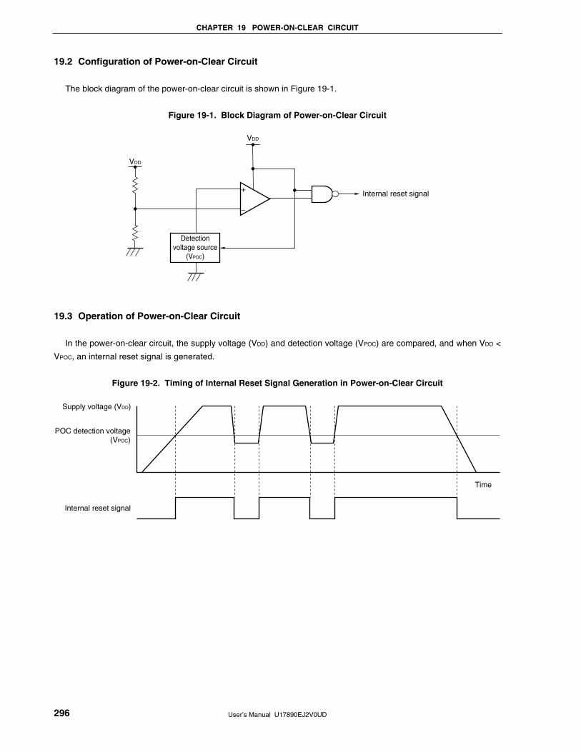
CHAPTER 19 POWER-ON-CLEAR CIRCUIT
User’s Manual U17890EJ2V0UD 296
19.2 Configuration of Power-on-Clear Circuit
The block diagram of the power-on-clear circuit is shown in Figure 19-1.
Figure 19-1. Block Diagram of Power-on-Clear Circuit
−
+
Detectionvoltage source
(VPOC)
Internal reset signal
VDD
VDD
19.3 Operation of Power-on-Clear Circuit
In the power-on-clear circuit, the supply voltage (VDD) and detection voltage (VPOC) are compared, and when VDD <
VPOC, an internal reset signal is generated.
Figure 19-2. Timing of Internal Reset Signal Generation in Power-on-Clear Circuit
Time
Supply voltage (VDD)
POC detection voltage(VPOC)
Internal reset signal

CHAPTER 19 POWER-ON-CLEAR CIRCUIT
User’s Manual U17890EJ2V0UD 297
19.4 Cautions for Power-on-Clear Circuit
In a system where the supply voltage (VDD) fluctuates for a certain period in the vicinity of the POC detection
voltage (VPOC), the system may be repeatedly reset and released from the reset status. In this case, the time from
release of reset to the start of the operation of the microcontroller can be arbitrarily set by taking the following action.
<Action>
After releasing the reset signal, wait for the supply voltage fluctuation period of each system by means of a
software counter that uses a timer, and then initialize the ports.
Figure 19-3. Example of Software Processing After Release of Reset (1/2)
• If supply voltage fluctuation is 50 ms or less in vicinity of POC detection voltage
Yes
Power-on-clear
; The internal low-speed oscillation clock is set as the CPU clock when the reset signal is generated
; The cause of reset (power-on-clear, WDT, or LVI) can be identified by the RESF register.
; Change the CPU clock from the internal low-speed oscillation clock to the X1 input clock.
; Check the stabilization of oscillation of the X1 input clock by using the OSTC register.
; TMIF51 = 1: Interrupt request is generated.
; Initialization of ports
; 8-bit timer 51 can operate with the internal low-speed oscillation clock.Source: fRL (480 kHz (MAX.))/27 × compare value 200 = 53 ms(fRL: Internal low-speed oscillation clock oscillation frequency)
No
Note 1
Reset
Checking causeof resetNote 2
Check stabilizationof oscillation
Change CPU clock
50 ms has passed?(TMIF51 = 1?)
Initializationprocessing
Start timer(set to 50 ms)
Notes 1. If reset is generated again during this period, initialization processing is not started.
2. A flowchart is shown on the next page.

CHAPTER 19 POWER-ON-CLEAR CIRCUIT
User’s Manual U17890EJ2V0UD 298
Figure 19-3. Example of Software Processing After Release of Reset (2/2)
• Checking reset cause
Yes
No
Check reset cause
Power-on-clear/externalreset generated
Reset processing bywatchdog timer
Reset processing bylow-voltage detector
No
WDTRF of RESFregister = 1?
LVIRF of RESFregister = 1?
Yes

User’s Manual U17890EJ2V0UD 299
CHAPTER 20 LOW-VOLTAGE DETECTOR
20.1 Functions of Low-Voltage Detector
The low-voltage detector (LVI) has following functions.
• Compares supply voltage (VDD) and detection voltage (VLVI = 4.3 V ±0.2 V), and generates an internal interrupt
signal or internal reset signal when VDD < VLVI.
• Interrupt or reset function can be selected by software.
• Operable in STOP mode.
When the low-voltage detector is used to reset, bit 0 (LVIRF) of the reset control flag register (RESF) is set to 1 if
reset occurs. For details of RESF, see CHAPTER 18 RESET FUNCTION.
20.2 Configuration of Low-Voltage Detector
A block diagram of the low-voltage detector is shown below.
Figure 20-1. Block Diagram of Low-Voltage Detector
LVION
−
+
Detection voltage source
(VLVI)
VDD
Internal bus
N-ch
Low-voltage detection register(LVIM)
LVIMD LVIF
INTLVI
Internal reset signalS
elec
tor
VDD

CHAPTER 20 LOW-VOLTAGE DETECTOR
User’s Manual U17890EJ2V0UD 300
20.3 Registers Controlling Low-Voltage Detector
The low-voltage detector is controlled by the following register.
• Low-voltage detection register (LVIM)
(1) Low-voltage detection register (LVIM)
This register sets low-voltage detection and the operation mode.
This register can be set by a 1-bit or 8-bit memory manipulation instruction.
Figure 20-2. Format of Low-Voltage Detection Register (LVIM)
0
LVIF
1
LVIMD
2
0
3
0
4
0
5
0
6
0
7
LVION
Symbol
LVIM
Address: FF78H After reset: 00H R/WNote 1
LVIONNotes 2, 3 Enables low-voltage detection operation
0 Disables operation
1 Enables operation
LVIMDNote 2 Low-voltage detection operation mode selection
0 Generates interrupt signal when supply voltage (VDD) < detection voltage (VLVI)
1 Generates internal reset signal when supply voltage (VDD) < detection voltage (VLVI)
LVIFNote 4 Low-voltage detection flag
0 Supply voltage (VDD) > detection voltage (VLVI), or when operation is disabled
1 Supply voltage (VDD) < detection voltage (VLVI)
Notes 1. Bit 0 is read-only.
2. LVION and LVIMD are cleared to 0 in the case of a reset other than an LVI reset. These are
not cleared to 0 in the case of an LVI reset.
3. When LVION is set to 1, operation of the comparator in the LVI circuit is started. Use
software to instigate a wait of at least 0.2 ms from when LVION is set to 1 until the voltage is
confirmed at LVIF.
4. The value of LVIF is output as the interrupt request signal INTLVI when LVION = 1 and
LVIMD = 0.
Caution To stop LVI, follow either of the procedures below. • When using 8-bit memory manipulation instruction: Write 00H to LVIM.
• When using 1-bit memory manipulation instruction: Clear LVIMD to 0 first, and then
clear LVION to 0.

CHAPTER 20 LOW-VOLTAGE DETECTOR
User’s Manual U17890EJ2V0UD 301
20.4 Operation of Low-Voltage Detector
The low-voltage detector can be used in the following two modes.
• Used as reset
Compares the supply voltage (VDD) and detection voltage (VLVI), and generates an internal reset signal when
VDD < VLVI.
• Used as interrupt
Compares the supply voltage (VDD) and detection voltage (VLVI), and generates an interrupt signal (INTLVI)
when VDD < VLVI.
The operation is set as follows.
(1) When used as reset
• When starting operation
<1> Mask the LVI interrupt (LVIMK = 1).
<2> Set bit 7 (LVION) of LVIM to 1 (enables LVI operation).
<3> Use software to instigate a wait of at least 0.2 ms.
<4> Wait until it is checked that “supply voltage (VDD) > detection voltage (VLVI)” by bit 0 (LVIF) of LVIM.
<5> Set bit 1 (LVIMD) of LVIM to 1 (generates internal reset signal when supply voltage (VDD) < detection
voltage (VLVI)).
Figure 20-4 shows the timing of the internal reset signal generated by the low-voltage detector. The numbers
in this timing chart correspond to <1> to <5> above.
Cautions 1. <1> must always be executed. When LVIMK = 0, an interrupt may occur immediately
after the processing in <2>.
2. If supply voltage (VDD) > detection voltage (VLVI) when LVIM is set to 1, an internal reset
signal is not generated.
• When stopping operation
Either of the following procedures must be executed.
• When using 8-bit memory manipulation instruction:
Write 00H to LVIM.
• When using 1-bit memory manipulation instruction:
Clear LVIMD to 0 first, and then clear LVION to 0.

CHAPTER 20 LOW-VOLTAGE DETECTOR
User’s Manual U17890EJ2V0UD 302
Figure 20-3. Timing of Low-Voltage Detector Internal Reset Signal Generation
Supply voltage (VDD)
LVI detection voltage(VLVI)
POC detection voltage(VPOC)
Time
LVIMK flag(set by software)
LVIF flag
LVIRF flagNote 3
Note 2
LVI reset signal
POC reset signal
Internal reset signal
Cleared bysoftware
Not cleared Not cleared
Not cleared Not cleared
Cleared bysoftware
<4>
<5>
Clear
Clear
Clear
<3> 0.2 ms or longer
LVION flag(set by software)
LVIMD flag(set by software)
H<1>Note 1
<2>
Notes 1. The LVIMK flag is set to “1” by RESET input.
2. The LVIF flag may be set (1).
3. LVIRF is bit 0 of the reset control flag register (RESF). For details of RESF, see CHAPTER 18
RESET FUNCTION.
Remark <1> to <5> in Figure 20-3 above correspond to <1> to <5> in the description of “when starting operation”
in 20.4 (1) When used as reset.

CHAPTER 20 LOW-VOLTAGE DETECTOR
User’s Manual U17890EJ2V0UD 303
(2) When used as interrupt • When starting operation
<1> Mask the LVI interrupt (LVIMK = 1).
<2> Set bit 7 (LVION) of LVIM to 1 (enables LVI operation).
<3> Use software to instigate a wait of at least 0.2 ms.
<4> Wait until it is checked that “supply voltage (VDD) > detection voltage (VLVI)” by bit 0 (LVIF) of LVIM.
<5> Clear the interrupt request flag of LVI (LVIIF) to 0.
<6> Release the interrupt mask flag of LVI (LVIMK).
<7> Execute the EI instruction (when vectored interrupts are used).
Figure 20-4 shows the timing of the interrupt signal generated by the low-voltage detector. The numbers in
this timing chart correspond to <1> to <6> above.
• When stopping operation
Either of the following procedures must be executed.
• When using 8-bit memory manipulation instruction:
Write 00H to LVIM.
• When using 1-bit memory manipulation instruction:
Clear LVION to 0.
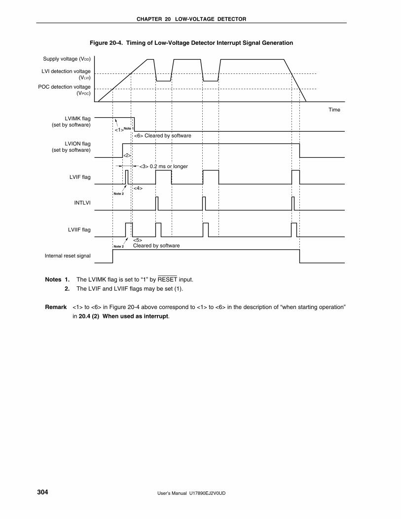
CHAPTER 20 LOW-VOLTAGE DETECTOR
User’s Manual U17890EJ2V0UD 304
Figure 20-4. Timing of Low-Voltage Detector Interrupt Signal Generation
Supply voltage (VDD)
LVI detection voltage(VLVI)
POC detection voltage(VPOC)
Time
<6> Cleared by software
LVIMK flag(set by software)
LVIF flag
INTLVI
LVIIF flag
Internal reset signal
<2>
<4>
<5>Cleared by software
<3> 0.2 ms or longer
LVION flag(set by software)
Note 2
Note 2
<1>Note 1
Notes 1. The LVIMK flag is set to “1” by RESET input.
2. The LVIF and LVIIF flags may be set (1).
Remark <1> to <6> in Figure 20-4 above correspond to <1> to <6> in the description of “when starting operation”
in 20.4 (2) When used as interrupt.

CHAPTER 20 LOW-VOLTAGE DETECTOR
User’s Manual U17890EJ2V0UD 305
20.5 Cautions for Low-Voltage Detector
In a system where the supply voltage (VDD) fluctuates for a certain period in the vicinity of the LVI detection voltage
(VLVI), the operation is as follows depending on how the low-voltage detector is used.
(1) When used as reset
The system may be repeatedly reset and released from the reset status.
In this case, the time from release of reset to the start of the operation of the microcontroller can be arbitrarily set
by taking action (1) below.
(2) When used as interrupt
Interrupt requests may be frequently generated. Take action (2) below.
In this system, take the following actions.
<Action>
(1) When used as reset
After releasing the reset signal, wait for the supply voltage fluctuation period of each system by means of a
software counter that uses a timer, and then initialize the ports.

CHAPTER 20 LOW-VOLTAGE DETECTOR
User’s Manual U17890EJ2V0UD 306
Figure 20-5. Example of Software Processing After Release of Reset (1/2)
• If supply voltage fluctuation is 50 ms or less in vicinity of LVI detection voltage
Yes
LVI
; The internal low-speed oscillation clock is set as the CPU clock when the reset signal is generated
; The cause of reset (power-on-clear, WDT, or LVI) can be identified by the RESF register.
; Change the CPU clock from the internal low-speed oscillation clock to the X1 input clock.
; Check the stabilization of oscillation of the X1 input clock by using the OSTC register.
; TMIF51 = 1: Interrupt request is generated.
; Initialization of ports
; 8-bit timer 51 can operate with the internal low-speed oscillation clock.Source: fRL (480 kHz (MAX.))/27 × compare value 200 = 53 ms(fRL: Internal low-speed oscillation clock oscillation frequency)
No
Note 1
Reset
Checking causeof resetNote 2
Check stabilizationof oscillation
Change CPU clock
50 ms has passed?(TMIF51 = 1?)
Initializationprocessing
Start timer(set to 50 ms)
Notes 1. If reset is generated again during this period, initialization processing is not started.
2. A flowchart is shown on the next page.

CHAPTER 20 LOW-VOLTAGE DETECTOR
User’s Manual U17890EJ2V0UD 307
Figure 20-5. Example of Software Processing After Release of Reset (2/2)
• Checking reset cause
Yes
No
Check reset cause
Power-on-clear/externalreset generated
Reset processing bywatchdog timer
Reset processing bylow-voltage detector
Yes
WDTRF of RESFregister = 1?
LVIRF of RESFregister = 1?
No

CHAPTER 20 LOW-VOLTAGE DETECTOR
User’s Manual U17890EJ2V0UD 308
(2) When used as interrupt
Check that “supply voltage (VDD) > detection voltage (VLVI)” in the servicing routine of the LVI interrupt by using bit
0 (LVIF) of the low-voltage detection register (LVIM). Clear bit 0 (LVIIF) of interrupt request flag register 0L (IF0L)
to 0 and enable interrupts (EI).
In a system where the supply voltage fluctuation period is long in the vicinity of the LVI detection voltage, wait for
the supply voltage fluctuation period, check that “supply voltage (VDD) > detection voltage (VLVI)” using the LVIF
flag, and then enable interrupts (EI).

User’s Manual U17890EJ2V0UD 309
CHAPTER 21 OPTION BYTES
The μPD78F0711 and 78F0712 can realize selection to stop or enable internal low-speed oscillator with an option
byte.
Option bytes are prepared at address 0080H in the flash memory.
When using flash memory version products, be sure to set to enable/disable to stop internal low-speed oscillator to
the option bytes.
Figure 21-1. Allocation of Option Bytes
Option bytes
––
Flash memory
–––– OSCSEL LSROSC0000H
0080H
Figure 21-2. Format of Option Bytes
Address: 0080H
7 6 5 4 3 2 1 0
− − − − − − OSCSEL LSROSC
OSCSEL High-speed system clock sellection
0 X1 clock (crystal/ceramic oscillation clock)
1 Internal high-speed oscillation clock
LSROSC Internal low-speed oscillator operation
0 Can be stopped by software
1 Cannot be stopped
Caution Be sure to clear bits 2 to 7 to 0.
Remark An example of software coding for setting the option bytes is shown below.
OPT CSEG AT 0080H
OPTION: DB 01H ; Set to option byte
(Internal low-speed oscillator cannot be stopped, and
X1 clock is selected as high-speed system clock)

User’s Manual U17890EJ2V0UD 310
CHAPTER 22 FLASH MEMORY
The μPD78F0711 and 78F0712 with flash memory to which a program can be written, erased, and overwritten
while mounted on the board.
22.1 Internal Memory Size Switching Register
The internal memory capacity set by using the internal memory size.
IMS is set by an 8-bit memory manipulation instruction.
RESET input sets IMS to CFH.
Caution Because the initial value of the memory size switching register (IMS) is CFH, set to 02H (μPD78F0711) or 04H (μPD78F0712) by initialization.
Figure 22-1. Format of Internal Memory Size Switching Register (IMS)
Address: FFF0H After reset: CFH R/W
Symbol 7 6 5 4 3 2 1 0
IMS RAM2 RAM1 RAM0 0 ROM3 ROM2 ROM1 ROM0
RAM2 RAM1 RAM0 Internal high-speed RAM capacity selection
0 0 0 768 bytes
Other than above Setting prohibited
ROM3 ROM2 ROM1 ROM0 Internal ROM capacity selection
0 0 1 0 8 KB
0 1 0 0 16 KB
Other than above Setting prohibited

CHAPTER 22 FLASH MEMORY
User’s Manual U17890EJ2V0UD 311
22.2 Writing with Flash Memory Programmer
Data can be written to the flash memory on-board or off-board, by using a dedicated flash memory programmer.
(1) On-board programming
The contents of the flash memory can be rewritten after the μPD78F0711 and 78F0712 have been mounted on
the target system. The connectors that connect the dedicated flash memory programmer must be mounted on
the target system.
(2) Off-board programming Data can be written to the flash memory with a dedicated program adapter (FA series) before the μPD78F0711
and 78F0712 are mounted on the target system.
Remark The FA series is a product of Naito Densei Machida Mfg. Co., Ltd.
Table 22-1. Wiring Between μPD78F0711, 78F0712, and Dedicated Flash Memory Programmer
Pin Configuration of Dedicated Flash Memory Programmer With UART00
Signal Name I/O Pin Function Pin Name Pin No.
SI/RxD Input Receive signal TxD00/P14 20
SO/TxD Output Transmit signal RxD00/P13 19
SCK Output Transfer clock Not needed Not needed
X1 9 CLK Output Clock to μPD78F0711 and 78F0712
X2Note 8
/RESET Output Reset signal RESET 6
FLMD0 Output Mode signal FLMD0 7
FLMD1 Output Mode signal FLMD1/P17 22
H/S Input Handshake signal Not needed Not needed
VDD 10, 12 VDD I/O VDD voltage generation
AVREF 27
VSS 11 GND − Ground
AVSS 28
Note When using the clock out of the flash memory programmer, connect CLK of the programmer to
X1, and connect its inverse signal to X2.
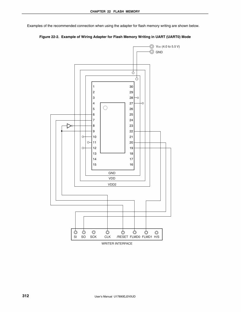
CHAPTER 22 FLASH MEMORY
User’s Manual U17890EJ2V0UD 312
Examples of the recommended connection when using the adapter for flash memory writing are shown below.
Figure 22-2. Example of Wiring Adapter for Flash Memory Writing in UART (UART0) Mode
28
27
26
30
29
25
24
23
22
21
20
19
18
16
1
2
3
4
5
6
7
8
9
10
11
12
13
1714
15
VDD2
VDD
GND
SI SO SCK CLK /RESET FLMD0 FLMD1 H/S
WRITER INTERFACE
VDD (4.0 to 5.5 V)
GND

CHAPTER 22 FLASH MEMORY
User’s Manual U17890EJ2V0UD 313
22.3 Programming Environment
The environment required for writing a program to the flash memory of the μPD78F0711 and 78F0712 are
illustrated below.
Figure 22-3. Environment for Writing Program to Flash Memory
RS-232C
Host machine
PD78F0711, 78F0712
VSS
RESET
FLMD0
FLMD1
UART00Dedicated flashmemory programmer
USB
PG-FP4 (Flash Pro4)
Cxxxxxx
Bxxxxx
Axxxx
XXX
YYY
XXXX
XXX
XXXX
XXXXXX
XX Y
YYY
STATVE
μ
A host machine that controls the dedicated flash memory programmer is necessary.
UART00 is used to interface between the dedicated flash memory programmer and the μPD78F0711 and 78F0712
for manipulation such as writing and erasing. To write the flash memory off-board, a dedicated program adapter (FA
series) is necessary.
22.4 Communication Mode
Communication between the dedicated flash memory programmer and the μPD78F0711 and 78F0712 are
established by serial communication via UART00 of the μPD78F0711 and 78F0712.
(1) UART00
Transfer rate: 4800 to 76800 bps
Figure 22-4. Communication with Dedicated Flash Memory Programmer (UART00)
PD78F0711, 78F0712
FLMD0
VDD
VSS
RESET
TxD00
RxD00
FLMD0
FLMD1FLMD1
VDD
GND
/RESET
SI/RxD
SO/TxD
X1CLK
X2
Dedicated flashmemory programmer
PG-FP4 (Flash Pro4)
Cxxxxxx
Bxxxxx
Axxxx
XXX
YYY
XXXX
XXX
XXXX
XXXXXX
XX Y
YYY
STATVE
μ
If Flashpro IV is used as the dedicated flash memory programmer, Flashpro IV generates the following signal for
the μPD78F0711 and 78F0712. For details, refer to the Flashpro IV Manual.

CHAPTER 22 FLASH MEMORY
User’s Manual U17890EJ2V0UD 314
Table 22-2. Pin Connection
Flashpro IV μPD78F0711,
μPD78F0712 Connection
Signal Name I/O Pin Function Pin Name UART00
FLMD0 Output Mode signal FLMD0
FLMD1 Output Mode signal FLMD1
VDD I/O VDD voltage generation VDD, AVREF
GND − Ground VSS, AVSS
CLK Output Clock output to μPD78F0711 and 78F0712 X1, X2Note 1 Note 2
/RESET Output Reset signal RESET
SI/RxD Input Receive signal TxD00
SO/TxD Output Transmit signal RxD00
SCK Output Transfer clock − ×
H/S Input Handshake signal − ×
Notes 1. When using the clock out of the flash memory programmer, connect CLK of the programmer to X1, and
connect its inverse signal to X2.
2. When using the internal high-speed oscillation clock, be sure to connect CLK of the programmer to X1, and
connect its inverse signal to X2.
Remark : Be sure to connect the pin.
: The pin does not have to be connected if the signal is generated on the target board.
×: The pin does not have to be connected.

CHAPTER 22 FLASH MEMORY
User’s Manual U17890EJ2V0UD 315
22.5 Processing of Pins on Board
To write the flash memory on-board, connectors that connect the dedicated flash memory programmer must be
provided on the target system. First provide a function that selects the normal operation mode or flash memory
programming mode on the board.
When the flash memory programming mode is set, all the pins not used for programming the flash memory are in
the same status as immediately after reset. Therefore, if the external device does not recognize the state immediately
after reset, the pins must be processed as described below.
22.5.1 FLMD0 pin
In the normal operation mode, 0 V is input to the FLMD0 pin. In the flash memory programming mode, the VDD
write voltage is supplied to the FLMD0 pin. The following shows an example of the connection of the FLMD0 pin.
Figure 22-5. FLMD0 Pin Connection Example
FLMD0Dedicated flash memory programmer connection pin
PD78F0711,PD78F0712
μμ
22.5.2 FLMD1 pin
When 0 V is input to the FLMD0 pin, the FLMD1 pin does not function. When VDD is supplied to the FLMD0 pin,
the flash memory programming mode is entered, so FLMD1 must be input to the same as voltage VSS. An FLMD1 pin
connection example is shown below.
Figure 22-6. FLMD1 Pin Connection Example
FLMD1Signal collision
Dedicated flash memory programmer connection pin
Other device
Output pin
If the VDD signal is input to the FLMD1 pin from another deviceduring on-board writing and immediately after reset, isolate this signal.
PD78F0711,PD78F0712
μμ

CHAPTER 22 FLASH MEMORY
User’s Manual U17890EJ2V0UD 316
22.5.3 Serial interface pins
The pins used by each serial interface are listed below.
Table 22-3. Pins Used by Each Serial Interface
Serial Interface Pins Used
UART00 TxD00, RxD00
To connect the dedicated flash memory programmer to the pins of a serial interface that is connected to another
device on the board, care must be exercised so that signals do not collide or that the other device does not
malfunction.
(1) Signal collision
If the dedicated flash memory programmer (output) is connected to a pin (input) of a serial interface connected to
another device (output), signal collision takes place. To avoid this collision, either isolate the connection with the
other device, or make the other device go into an output high-impedance state.
Figure 22-7. Signal Collision (Input Pin of Serial Interface)
Input pinSignal collision
Dedicated flash memory programmer connection pin
Other device
Output pin
In the flash memory programming mode, the signal output by the device collides with the signal sent from the dedicated flash memory programmer. Therefore, isolate the signal of the other device.
PD78F0711,PD78F0712
μμ

CHAPTER 22 FLASH MEMORY
User’s Manual U17890EJ2V0UD 317
(2) Malfunction of other device
If the dedicated flash memory programmer (output or input) is connected to a pin (input or output) of a serial
interface connected to another device (input), a signal may be output to the other device, causing the device to
malfunction. To avoid this malfunction, isolate the connection with the other device.
Figure 22-8. Malfunction of Other Device
Pin
Dedicated flash memory programmer connection pin
Other device
Input pin
If the signal output by the PD78F0711 and 78F0712 in the flash memory programming mode affects the other device, isolate the signal of the other device.
Pin
Dedicated flash memory programmer connection pin
Other device
Input pin
If the signal output by the dedicated flash memory programmer in the flash memory programming mode affects the other device, isolate the signal of the other device.
μ
PD78F0711,PD78F0712
μμ
PD78F0711,PD78F0712
μμ

CHAPTER 22 FLASH MEMORY
User’s Manual U17890EJ2V0UD 318
22.5.4 RESET pin
If the reset signal of the dedicated flash memory programmer is connected to the RESET pin that is connected to
the reset signal generator on the board, signal collision takes place. To prevent this collision, isolate the connection
with the reset signal generator.
If the reset signal is input from the user system while the flash memory programming mode is set, the flash
memory will not be correctly programmed. Do not input any signal other than the reset signal of the dedicated flash
memory programmer.
Figure 22-9. Signal Collision (RESET Pin)
RESET
Dedicated flash memory programmer connection signal
Reset signal generator
Signal collision
Output pin
In the flash memory programming mode, the signal output by the reset signal generator collides with the signal output by the dedicated flash memory programmer. Therefore, isolate the signal of the reset signal generator.
PD78F0711,PD78F0712
μμ
22.5.5 Port pins
When the flash memory programming mode is set, all the pins not used for flash memory programming enter the
same status as that immediately after reset. If external devices connected to the ports do not recognize the port
status immediately after reset, the port pin must be connected to VDD or VSS via a resistor.
22.5.6 Other signal pins
Connect X1 and X2 in the same status as in the normal operation mode when using the on-board clock.
To input the operating clock from the programmer, however, connect the clock out (CLK) of the programmer to X1,
and its inverse signal to X2.
Caution When using the internal high-speed oscillation clock, be sure to input the operating clock from the
programmer.
22.5.7 Power supply
To use the supply voltage output of the flash memory programmer, connect the VDD pin to VDD of the flash memory
programmer, and the VSS pin to VSS of the flash memory programmer.
To use the on-board supply voltage, connect in compliance with the normal operation mode.
Supply the same other power supplies (AVREF and AVSS) as those in the normal operation mode.

CHAPTER 22 FLASH MEMORY
User’s Manual U17890EJ2V0UD 319
22.6 Programming Method
22.6.1 Controlling flash memory
The following figure illustrates the procedure to manipulate the flash memory.
Figure 22-10. Flash Memory Manipulation Procedure
Start
Selecting communication mode
Manipulate flash memory
End?
Yes
FLMD0 pulse supply
No
End
Flash memory programming mode is set
22.6.2 Flash memory programming mode
To rewrite the contents of the flash memory by using the dedicated flash memory programmer, set the
μPD78F0711 and 78F0712 in the flash memory programming mode. To set the mode, set the FLMD0 pin to VDD and
clear the reset signal.
Change the mode by using a jumper when writing the flash memory on-board.
Figure 22-11. Flash Memory Programming Mode
VDD
RESET
5.5 V
0 V
VDD
0 V
Flash memory programming mode
VDD
0 V
FLMD0
FLMD0 pulse
Hi-Z
VDD
0 V
FLMD1

CHAPTER 22 FLASH MEMORY
User’s Manual U17890EJ2V0UD 320
Table 22-4. Relationship of Operation Mode of FLMD0 and FLMD1 Pins
FLMD0 FLMD1 Operation Mode
0 × Normal operation mode
VDD 0 Flash memory programming mode
VDD VDD Setting prohibited
22.6.3 Selecting communication mode In the μPD78F0711 and 78F0712 a communication mode is selected by inputting pulses (up to 11 pulses) to the
FLMD0 pin after the dedicated flash memory programming mode is entered. These FLMD0 pulses are generated by
the flash memory programmer.
The following table shows the relationship between the number of pulses and communication modes.
Table 22-5. Communication Modes
Standard SettingNote 1 Communication Mode
Port Speed On Target Frequency Multiply Rate
Pins Used Number of
FLMD0
Pulses
UART
(UART00)
UART-ch0 9600, 19200, 31250,
38400, 76800, 153600 Notes 3
bpsNotes 4
Optional 5 M to 20 MHz
Note 2
1.0 TxD00,
RxD00
0
Notes 1. Selection items for Standard settings on Flashpro IV.
2. The possible setting range differs depending on the voltage. For details, refer to the electrical
specifications chapter. 3. This value cannot be selected when the peripheral hardware clock frequency is 2.5 MHz or less.
4. Because factors other than the baud rate error, such as the signal waveform slew, also affect UART
communication, thoroughly evaluate the slew as well as the baud rate error.
Caution When UART00 is selected, the receive clock is calculated based on the reset command sent from
the dedicated flash memory programmer after the FLMD0 pulse has been received.

CHAPTER 22 FLASH MEMORY
User’s Manual U17890EJ2V0UD 321
22.6.4 Communication commands The μPD78F0711 and 78F0712 communicate with the dedicated flash memory programmer by using commands.
The signals sent from the flash memory programmer to the μPD78F0711 and 78F0712 are called commands, and the
commands sent from the μPD78F0711 and 78F0712 to the dedicated flash memory programmer are called response
commands.
Figure 22-12. Communication Commands
PD78F0711,PD78F0712
Command
Response commandDedicated flashmemory programmer
PG-FP4 (Flash Pro4)
Cxxxxxx
Bxxxxx
Axxxx
XXX
YYY
XXXX
XXX
XXXX
XXXXXX
XX Y
YYY
STATVE
μμ
The flash memory control commands of the μPD78F0711 and 78F0712 are listed in the table below. All these
commands are issued from the programmer and the μPD78F0711 and 78F0712 perform processing corresponding to
the respective commands.
Table 22-6. Flash Memory Control Commands
Classification Command Name Function
Verify Batch verify command Compares the contents of the entire memory
with the input data.
Erase Batch erase command Erases the contents of the entire memory.
Blank check Batch blank check command Checks the erasure status of the entire memory.
High-speed write command Writes data by specifying the write address and
number of bytes to be written, and executes a
verify check.
Data write
Successive write command Writes data from the address following that of
the high-speed write command executed
immediately before, and executes a verify
check.
Status read command Obtains the operation status
Oscillation frequency setting command Sets the oscillation frequency
Erase time setting command Sets the erase time for batch erase
Write time setting command Sets the write time for writing data
Baud rate setting command Sets the baud rate when UART is used
Silicon signature command Reads the silicon signature information
System setting, control
Reset command Escapes from each status
The μPD78F0711 and 78F0712 return a response command for the command issued by the dedicated flash
memory programmer. The response commands sent from the μPD78F0711 and 78F0712 are listed below.
Table 22-7. Response Commands
Command Name Function
ACK Acknowledges command/data.
NAK Acknowledges illegal command/data.

CHAPTER 22 FLASH MEMORY
User’s Manual U17890EJ2V0UD 322
22.7 Flash Memory Programming by Self-Writing
The μPD78F0711 and 78F0712 support a self-programming function that can be used to rewrite the flash memory
via a user program, so that the program can be upgraded in the field.
The programming mode is selected by bits 0 and 1 (FLSPM0 and FLSPM1) of the flash programming mode control
register (FLPMC).
The procedure of self-programming is illustrated below.
Remark For details of the self programming function, refer to a separate document to be published soon
(document name: μPD78F0711, 78F0712, 78F0714 Flash Memory Self Programming User’s Manual
(U18886E)).
Figure 22-13. Self-Programming Procedure
Mask interrupts again
FLSPM1, FLSPM0 = 0, 1
Secure entry RAM area
Mask all interrupts
FLMD0 pin = High level
CALL #8100H
Set parametersto entry RAM
Start self-programming
Read parameters on RAMand access flash memory
according to parameter contents
FLMD0 pin = Low level
FLSPM1, FLSPM0 = 0, 0
End of self-programming
Entry program (user program)
Firmware
Entry program (user program)
<R>

CHAPTER 22 FLASH MEMORY
User’s Manual U17890EJ2V0UD 323
22.7.1 Registers used for self-programming function
The following three registers are used for the self-programming function.
• Flash-programming mode control register (FLPMC)
• Flash protect command register (PFCMD)
• Flash status register (PFS)
(1) Flash-programming mode control register (FLPMC)
This register is used to enable or disable writing or erasing of the flash memory and to set the operation mode
during self-programming.
The FLPMC can be written only in a specific sequence (see 22.7.1 (2) Flash protect command register) so
that the application system does not stop inadvertently due to malfunction caused by noise or program hang-up.
FLPMC can be set by a 1-bit or 8-bit memory manipulation instruction.
RESET input sets this register to 0xHNote.
Note Differs depending on the operation mode.
• User mode: 08H
• On-board mode: 0CH

CHAPTER 22 FLASH MEMORY
User’s Manual U17890EJ2V0UD 324
Figure 22-14. Format of Flash-Programming Mode Control Register (FLPMC)
0
Symbol
FLPMC 0 0 0 FWEDIS FWEPR FLSPM1 FLSPM0
Address: FFC4H After reset: 0×HNote 1 R/WNote 2
Selection of operation mode during self-programming
Normal modeInstructions of flash memory can be fetched from all addresses.
Self-programming mode A1Firmware can be called (CALL #8100H).
Self-programming mode A2Instructions are fetched from firmware ROM.This mode is set in firmware and cannot be set by the user.
Setting prohibited
FLSPM1Note 4
0
0
1
1
FLSPM0Note 4
0
1
1
0
FWEDIS
0
Control of flash memory writing/erasing
Writing/erasing enabledNote 3
Writing/erasing disabled1
Status of FLMD0 pin
Low level
High levelNote 3
FWEPR
0
1
Notes 1. Differs depending on the operation mode.
• User mode: 08H
• On-board mode: 0CH
2. Bit 2 (FWEPR) is read-only.
3. For actual writing/erasing, the FLMPD0 pin must be high (FWEPR = 1), as well
as FWEDIS = 0.
FWEDIS FWEPR Enable or disable of flash memory writing/erasing
0 1 Writing/erasing enabled
Other than above Writing/erasing disabled
4. The user ROM (flash memory) or firmware ROM can be selected by FLSPM1
and FLSPM0, and the operation mode set on the application system by the
mode pin or the self-programming mode can be selected.
Cautions 1. Be sure to keep FWEDIS at 0 until writing or erasing of the flash memory
is completed.
2. Make sure that FWEDIS = 1 in the normal mode.
3. Manipulate FLSPM1 and FLSPM0 after execution branches to the
internal RAM. The address of the flash memory is specified by an
address signal from the CPU when FLSPM1 = 0 or the set value of the
firmware written when FLSPM1 = 1. In the on-board mode, the
specifications of FLSPM1 and FLSPM0 are ignored.

CHAPTER 22 FLASH MEMORY
User’s Manual U17890EJ2V0UD 325
(2) Flash protect command register (PFCMD)
If the application system stops inadvertently due to malfunction caused by noise or program hang-up, an
operation to write the flash programming mode control register (FLPMC) may have a serious effect on the system.
PFCMD is used to protect FLPMC from being written, so that the application system does not stop inadvertently.
Writing FLMPC is enabled only when a write operation is performed in the following specific sequence.
<1> Write a specific value to PFCMD (PFCMD = A5H)
<2> Write the value to be set to FLPMC (writing in this step is invalid)
<3> Write the inverted value of the value to be set to FLPMC (writing in this step is invalid)
<4> Write the value to be set to FLPMC (writing in this step is valid)
This rewrites the value of the register, so that the register cannot be written illegally.
Occurrence of an illegal store operation can be checked by bit 0 (FPRERR) of the flash status register (PFS).
A5H must be written to PFCMD each time the value of FLPMC is changed.
PFCMD can be set by an 8-bit memory manipulation instruction.
RESET input makes this register undefined.
Figure 22-15. Format of Flash Protect Command Register (PFCMD)
REG7
Symbol
PFCMD REG6 REG5 REG4 REG3 REG2 REG1 REG0
Address: FFC0H After reset: Undefined W
(3) Flash status register (PFS)
If data is not written to the flash programming mode control register (FLPMC), which is protected, in the correct
sequence (writing the flash protect command register (PFCMD)), FLPMC is not written and a protection error
occurs. If this happens, bit 0 of PFS (FPRERR) is set to 1.
This bit is a cumulative flag. After checking FPRERR, clear it by writing 0 to it.
PFS can be set by a 1-bit or 8-bit memory manipulation instruction.
RESET input clears this register to 00H.
Figure 22-16. Format of Flash Status Register (PFS)
0
Symbol
PFS 0 0 0 0 0 0 FPRERR
Address: FFC2H After reset: 00H R/W

CHAPTER 22 FLASH MEMORY
User’s Manual U17890EJ2V0UD 326
The operating conditions of the FPRERR flag are as follows.
<Setting conditions>
• If PFCMD is written when the store instruction operation recently performed on a peripheral register is not to
write a specific value (A5H) to PFCMD
• If the first store instruction operation after <1> is on a peripheral register other than FLPMC
• If the first store instruction operation after <2> is on a peripheral register other than FLPMC
• If a value other than the inverted value of the value to be set to FLPMC is written by the first store instruction
after <2>
• If the first store instruction operation after <3> is on a peripheral register other than FLPMC
• If a value other than the value to be set to FLPMC (value written in <2>) is written by the first store instruction
after <3>
Remark The numbers in angle brackets above correspond to the those in (2) Flash protect command
register (PFCMD).
<Reset conditions>
• If 0 is written to the FPRERR flag
• If RESET is input
<Example of description in specific sequence
To write 05H to FLPMC
MOV PFCMD, #0A5H ; Writes A5H to PFCMD.
MOV FLPMC, #05H ; Writes 05H to FLPMC.
MOV FLPMC, #0FAH ; Writes 0FAH (inverted value of 05H) to FLPMC.
MOV FLPMC, #05H ; Writes 05H to FLPMC.

User’s Manual U17890EJ2V0UD 327
CHAPTER 23 ON-CHIP DEBUG FUNCTION
The μPD78F0711 and 78F0712 use the VDD, FLMD0, RESET, X1, X2, and VSS pins to communicate with the host
machine via an on-chip debug emulator (QB-78K0MINI or QB-MINI2) for on-chip debugging.
Remark For details of the on-chip debug function, refer to QB-78K0MINI User’s Manual (U17029E) or QB-MINI2
User’s Manual (U18371E).
Figure 23-1. Timing Chart of Setting On-Chip Debug Mode
FLMD0
RESET
X1
X2
H
1 pluse
5 pulses
Setting ofon-chip mode
<R>
<R>
User’s Manual U17890EJ2V0UD 328
CHAPTER 24 INSTRUCTION SET
This chapter lists each instruction set of the μPD78F0711 and 78F0712 in table form. For details of each operation
and operation code, refer to the separate document 78K/0 Series Instructions User’s Manual (U12326E).
24.1 Conventions Used in Operation List
24.1.1 Operand identifiers and specification methods
Operands are written in the “Operand” column of each instruction in accordance with the specification method of
the instruction operand identifier (refer to the assembler specifications for details). When there are two or more
methods, select one of them. Uppercase letters and the symbols #, !, $ and [ ] are keywords and must be written as
they are. Each symbol has the following meaning.
• #: Immediate data specification
• !: Absolute address specification
• $: Relative address specification
• [ ]: Indirect address specification
In the case of immediate data, describe an appropriate numeric value or a label. When using a label, be sure to
write the #, !, $, and [ ] symbols.
For operand register identifiers r and rp, either function names (X, A, C, etc.) or absolute names (names in
parentheses in the table below, R0, R1, R2, etc.) can be used for specification.
Table 24-1. Operand Identifiers and Specification Methods
Identifier Specification Method
r
rp
sfr
sfrp
X (R0), A (R1), C (R2), B (R3), E (R4), D (R5), L (R6), H (R7)
AX (RP0), BC (RP1), DE (RP2), HL (RP3)
Special function register symbolNote
Special function register symbol (16-bit manipulatable register even addresses only)Note
saddr
saddrp
FE20H to FF1FH Immediate data or labels
FE20H to FF1EH Immediate data or labels (even address only)
addr16
addr11
addr5
0000H to FFFFH Immediate data or labels
(Only even addresses for 16-bit data transfer instructions)
0800H to 0FFFH Immediate data or labels
0040H to 007EH Immediate data or labels (even address only)
word
byte
bit
16-bit immediate data or label
8-bit immediate data or label
3-bit immediate data or label
RBn RB0 to RB3
Note Addresses from FFD0H to FFDFH cannot be accessed with these operands.
Remark For special function register symbols, see Table 3-3 Special Function Register List.

CHAPTER 24 INSTRUCTION SET
User’s Manual U17890EJ2V0UD 329
24.1.2 Description of operation column
A: A register; 8-bit accumulator
X: X register
B: B register
C: C register
D: D register
E: E register
H: H register
L: L register
AX: AX register pair; 16-bit accumulator
BC: BC register pair
DE: DE register pair
HL: HL register pair
PC: Program counter
SP: Stack pointer
PSW: Program status word
CY: Carry flag
AC: Auxiliary carry flag
Z: Zero flag
RBS: Register bank select flag
IE: Interrupt request enable flag
NMIS: Non-maskable interrupt servicing flag
( ): Memory contents indicated by address or register contents in parentheses
XH, XL: Higher 8 bits and lower 8 bits of 16-bit register
∧: Logical product (AND)
∨: Logical sum (OR)
∨: Exclusive logical sum (exclusive OR) ⎯⎯: Inverted data
addr16: 16-bit immediate data or label
addr11: Immediate data or label
addr5: Immediate data or label (even address only)
jdisp8: Signed 8-bit data (displacement value)
24.1.3 Description of flag operation column
(Blank): Not affected
0: Cleared to 0
1: Set to 1
×: Set/cleared according to the result
R: Previously saved value is restored

CHAPTER 24 INSTRUCTION SET
User’s Manual U17890EJ2V0UD 330
24.2 Operation List
Clocks Flag Instruction
Group Mnemonic Operands Bytes
Note 1 Note 2 Operation
Z AC CY
r, #byte 2 4 − r ← byte
saddr, #byte 3 6 7 (saddr) ← byte
sfr, #byte 3 − 7 sfr ← byte
A, r Note 3 1 2 − A ← r
r, A Note 3 1 2 − r ← A
A, saddr 2 4 5 A ← (saddr)
saddr, A 2 4 5 (saddr) ← A
A, sfr 2 − 5 A ← sfr
sfr, A 2 − 5 sfr ← A
A, !addr16 3 8 9 A ← (addr16)
!addr16, A 3 8 9 (addr16) ← A
PSW, #byte 3 − 7 PSW ← byte × × ×
A, PSW 2 − 5 A ← PSW
PSW, A 2 − 5 PSW ← A × × ×
A, [DE] 1 4 5 A ← (DE)
[DE], A 1 4 5 (DE) ← A
A, [HL] 1 4 5 A ← (HL)
[HL], A 1 4 5 (HL) ← A
A, [HL + byte] 2 8 9 A ← (HL + byte)
[HL + byte], A 2 8 9 (HL + byte) ← A
A, [HL + B] 1 6 7 A ← (HL + B)
[HL + B], A 1 6 7 (HL + B) ← A
A, [HL + C] 1 6 7 A ← (HL + C)
MOV
[HL + C], A 1 6 7 (HL + C) ← A
A, r Note 3 1 2 − A ↔ r
A, saddr 2 4 6 A ↔ (saddr)
A, sfr 2 − 6 A ↔ (sfr)
A, !addr16 3 8 10 A ↔ (addr16)
A, [DE] 1 4 6 A ↔ (DE)
A, [HL] 1 4 6 A ↔ (HL)
A, [HL + byte] 2 8 10 A ↔ (HL + byte)
A, [HL + B] 2 8 10 A ↔ (HL + B)
8-bit data
transfer
XCH
A, [HL + C] 2 8 10 A ↔ (HL + C)
Notes 1. When the internal high-speed RAM area is accessed or for an instruction with no data access
2. When an area except the internal high-speed RAM area is accessed
3. Except “r = A”
Remarks 1. One instruction clock cycle is one cycle of the CPU clock (fCPU) selected by the processor clock
control register (PCC).
2. This clock cycle applies to the internal ROM program.

CHAPTER 24 INSTRUCTION SET
User’s Manual U17890EJ2V0UD 331
Clocks Flag Instruction
Group Mnemonic Operands Bytes
Note 1 Note 2 Operation
Z AC CY
rp, #word 3 6 − rp ← word
saddrp, #word 4 8 10 (saddrp) ← word
sfrp, #word 4 − 10 sfrp ← word
AX, saddrp 2 6 8 AX ← (saddrp)
saddrp, AX 2 6 8 (saddrp) ← AX
AX, sfrp 2 − 8 AX ← sfrp
sfrp, AX 2 − 8 sfrp ← AX
AX, rp Note 3 1 4 − AX ← rp
rp, AX Note 3 1 4 − rp ← AX
AX, !addr16 3 10 12 AX ← (addr16)
MOVW
!addr16, AX 3 10 12 (addr16) ← AX
16-bit data
transfer
XCHW AX, rp Note 3 1 4 − AX ↔ rp
A, #byte 2 4 − A, CY ← A + byte × × ×
saddr, #byte 3 6 8 (saddr), CY ← (saddr) + byte × × ×
A, r Note 4 2 4 − A, CY ← A + r × × ×
r, A 2 4 − r, CY ← r + A × × ×
A, saddr 2 4 5 A, CY ← A + (saddr) × × ×
A, !addr16 3 8 9 A, CY ← A + (addr16) × × ×
A, [HL] 1 4 5 A, CY ← A + (HL) × × ×
A, [HL + byte] 2 8 9 A, CY ← A + (HL + byte) × × ×
A, [HL + B] 2 8 9 A, CY ← A + (HL + B) × × ×
ADD
A, [HL + C] 2 8 9 A, CY ← A + (HL + C) × × ×
A, #byte 2 4 − A, CY ← A + byte + CY × × ×
saddr, #byte 3 6 8 (saddr), CY ← (saddr) + byte + CY × × ×
A, r Note 4 2 4 − A, CY ← A + r + CY × × ×
r, A 2 4 − r, CY ← r + A + CY × × ×
A, saddr 2 4 5 A, CY ← A + (saddr) + CY × × ×
A, !addr16 3 8 9 A, CY ← A + (addr16) + CY × × ×
A, [HL] 1 4 5 A, CY ← A + (HL) + CY × × ×
A, [HL + byte] 2 8 9 A, CY ← A + (HL + byte) + CY × × ×
A, [HL + B] 2 8 9 A, CY ← A + (HL + B) + CY × × ×
8-bit
operation
ADDC
A, [HL + C] 2 8 9 A, CY ← A + (HL + C) + CY × × ×
Notes 1. When the internal high-speed RAM area is accessed or for an instruction with no data access
2. When an area except the internal high-speed RAM area is accessed
3. Only when rp = BC, DE or HL
4. Except “r = A”
Remarks 1. One instruction clock cycle is one cycle of the CPU clock (fCPU) selected by the processor clock
control register (PCC).
2. This clock cycle applies to the internal ROM program.

CHAPTER 24 INSTRUCTION SET
User’s Manual U17890EJ2V0UD 332
Clocks Flag Instruction
Group Mnemonic Operands Bytes
Note 1 Note 2 Operation
Z AC CY
A, #byte 2 4 − A, CY ← A − byte × × ×
saddr, #byte 3 6 8 (saddr), CY ← (saddr) − byte × × ×
A, r Note 3 2 4 − A, CY ← A − r × × ×
r, A 2 4 − r, CY ← r − A × × ×
A, saddr 2 4 5 A, CY ← A − (saddr) × × ×
A, !addr16 3 8 9 A, CY ← A − (addr16) × × ×
A, [HL] 1 4 5 A, CY ← A − (HL) × × ×
A, [HL + byte] 2 8 9 A, CY ← A − (HL + byte) × × ×
A, [HL + B] 2 8 9 A, CY ← A − (HL + B) × × ×
SUB
A, [HL + C] 2 8 9 A, CY ← A − (HL + C) × × ×
A, #byte 2 4 − A, CY ← A − byte − CY × × ×
saddr, #byte 3 6 8 (saddr), CY ← (saddr) − byte − CY × × ×
A, r Note 3 2 4 − A, CY ← A − r − CY × × ×
r, A 2 4 − r, CY ← r − A − CY × × ×
A, saddr 2 4 5 A, CY ← A − (saddr) − CY × × ×
A, !addr16 3 8 9 A, CY ← A − (addr16) − CY × × ×
A, [HL] 1 4 5 A, CY ← A − (HL) − CY × × ×
A, [HL + byte] 2 8 9 A, CY ← A − (HL + byte) − CY × × ×
A, [HL + B] 2 8 9 A, CY ← A − (HL + B) − CY × × ×
SUBC
A, [HL + C] 2 8 9 A, CY ← A − (HL + C) − CY × × ×
A, #byte 2 4 − A ← A ∧ byte ×
saddr, #byte 3 6 8 (saddr) ← (saddr) ∧ byte ×
A, r Note 3 2 4 − A ← A ∧ r ×
r, A 2 4 − r ← r ∧ A ×
A, saddr 2 4 5 A ← A ∧ (saddr) ×
A, !addr16 3 8 9 A ← A ∧ (addr16) ×
A, [HL] 1 4 5 A ← A ∧ (HL) ×
A, [HL + byte] 2 8 9 A ← A ∧ (HL + byte) ×
A, [HL + B] 2 8 9 A ← A ∧ (HL + B) ×
8-bit
operation
AND
A, [HL + C] 2 8 9 A ← A ∧ (HL + C) ×
Notes 1. When the internal high-speed RAM area is accessed or for an instruction with no data access
2. When an area except the internal high-speed RAM area is accessed
3. Except “r = A”
Remarks 1. One instruction clock cycle is one cycle of the CPU clock (fCPU) selected by the processor clock
control register (PCC).
2. This clock cycle applies to the internal ROM program.

CHAPTER 24 INSTRUCTION SET
User’s Manual U17890EJ2V0UD 333
Clocks Flag Instruction
Group Mnemonic Operands Bytes
Note 1 Note 2 Operation
Z AC CY
A, #byte 2 4 − A ← A ∨ byte ×
saddr, #byte 3 6 8 (saddr) ← (saddr) ∨ byte ×
A, r Note 3 2 4 − A ← A ∨ r ×
r, A 2 4 − r ← r ∨ A ×
A, saddr 2 4 5 A ← A ∨ (saddr) ×
A, !addr16 3 8 9 A ← A ∨ (addr16) ×
A, [HL] 1 4 5 A ← A ∨ (HL) ×
A, [HL + byte] 2 8 9 A ← A ∨ (HL + byte) ×
A, [HL + B] 2 8 9 A ← A ∨ (HL + B) ×
OR
A, [HL + C] 2 8 9 A ← A ∨ (HL + C) ×
A, #byte 2 4 − A ← A ∨ byte ×
saddr, #byte 3 6 8 (saddr) ← (saddr) ∨ byte ×
A, r Note 3 2 4 − A ← A ∨ r ×
r, A 2 4 − r ← r ∨ A ×
A, saddr 2 4 5 A ← A ∨ (saddr) ×
A, !addr16 3 8 9 A ← A ∨ (addr16) ×
A, [HL] 1 4 5 A ← A ∨ (HL) ×
A, [HL + byte] 2 8 9 A ← A ∨ (HL + byte) ×
A, [HL + B] 2 8 9 A ← A ∨ (HL + B) ×
XOR
A, [HL + C] 2 8 9 A ← A ∨ (HL + C) ×
A, #byte 2 4 − A − byte × × ×
saddr, #byte 3 6 8 (saddr) − byte × × ×
A, r Note 3 2 4 − A − r × × ×
r, A 2 4 − r − A × × ×
A, saddr 2 4 5 A − (saddr) × × ×
A, !addr16 3 8 9 A − (addr16) × × ×
A, [HL] 1 4 5 A − (HL) × × ×
A, [HL + byte] 2 8 9 A − (HL + byte) × × ×
A, [HL + B] 2 8 9 A − (HL + B) × × ×
8-bit
operation
CMP
A, [HL + C] 2 8 9 A − (HL + C) × × ×
Notes 1. When the internal high-speed RAM area is accessed or for an instruction with no data access
2. When an area except the internal high-speed RAM area is accessed
3. Except “r = A”
Remarks 1. One instruction clock cycle is one cycle of the CPU clock (fCPU) selected by the processor clock
control register (PCC).
2. This clock cycle applies to the internal ROM program.

CHAPTER 24 INSTRUCTION SET
User’s Manual U17890EJ2V0UD 334
Clocks Flag Instruction
Group Mnemonic Operands Bytes
Note 1 Note 2 Operation
Z AC CY
ADDW AX, #word 3 6 − AX, CY ← AX + word × × ×
SUBW AX, #word 3 6 − AX, CY ← AX − word × × ×
16-bit
operation
CMPW AX, #word 3 6 − AX − word × × ×
MULU X 2 16 − AX ← A × X Multiply/
divide DIVUW C 2 25 − AX (Quotient), C (Remainder) ← AX ÷ C
r 1 2 − r ← r + 1 × × INC
saddr 2 4 6 (saddr) ← (saddr) + 1 × ×
r 1 2 − r ← r − 1 × × DEC
saddr 2 4 6 (saddr) ← (saddr) − 1 × ×
INCW rp 1 4 − rp ← rp + 1
Increment/
decrement
DECW rp 1 4 − rp ← rp − 1
ROR A, 1 1 2 − (CY, A7 ← A0, Am − 1 ← Am) × 1 time ×
ROL A, 1 1 2 − (CY, A0 ← A7, Am + 1 ← Am) × 1 time ×
RORC A, 1 1 2 − (CY ← A0, A7 ← CY, Am − 1 ← Am) × 1 time ×
ROLC A, 1 1 2 − (CY ← A7, A0 ← CY, Am + 1 ← Am) × 1 time ×
ROR4 [HL] 2 10 12 A3 − 0 ← (HL)3 − 0, (HL)7 − 4 ← A3 − 0,
(HL)3 − 0 ← (HL)7 − 4
Rotate
ROL4 [HL] 2 10 12 A3 − 0 ← (HL)7 − 4, (HL)3 − 0 ← A3 − 0,
(HL)7 − 4 ← (HL)3 − 0
ADJBA 2 4 − Decimal Adjust Accumulator after Addition × × ×BCD
adjustment ADJBS 2 4 − Decimal Adjust Accumulator after Subtract × × ×
CY, saddr.bit 3 6 7 CY ← (saddr.bit) ×
CY, sfr.bit 3 − 7 CY ← sfr.bit ×
CY, A.bit 2 4 − CY ← A.bit ×
CY, PSW.bit 3 − 7 CY ← PSW.bit ×
CY, [HL].bit 2 6 7 CY ← (HL).bit ×
saddr.bit, CY 3 6 8 (saddr.bit) ← CY
sfr.bit, CY 3 − 8 sfr.bit ← CY
A.bit, CY 2 4 − A.bit ← CY
PSW.bit, CY 3 − 8 PSW.bit ← CY × ×
Bit
manipulate
MOV1
[HL].bit, CY 2 6 8 (HL).bit ← CY
Notes 1. When the internal high-speed RAM area is accessed or for an instruction with no data access
2. When an area except the internal high-speed RAM area is accessed
Remarks 1. One instruction clock cycle is one cycle of the CPU clock (fCPU) selected by the processor clock
control register (PCC).
2. This clock cycle applies to the internal ROM program.

CHAPTER 24 INSTRUCTION SET
User’s Manual U17890EJ2V0UD 335
Clocks Flag Instruction
Group Mnemonic Operands Bytes
Note 1 Note 2 Operation
Z AC CY
CY, saddr.bit 3 6 7 CY ← CY ∧ (saddr.bit) ×
CY, sfr.bit 3 − 7 CY ← CY ∧ sfr.bit ×
CY, A.bit 2 4 − CY ← CY ∧ A.bit ×
CY, PSW.bit 3 − 7 CY ← CY ∧ PSW.bit ×
AND1
CY, [HL].bit 2 6 7 CY ← CY ∧ (HL).bit ×
CY, saddr.bit 3 6 7 CY ← CY ∨ (saddr.bit) ×
CY, sfr.bit 3 − 7 CY ← CY ∨ sfr.bit ×
CY, A.bit 2 4 − CY ← CY ∨ A.bit ×
CY, PSW.bit 3 − 7 CY ← CY ∨ PSW.bit ×
OR1
CY, [HL].bit 2 6 7 CY ← CY ∨ (HL).bit ×
CY, saddr.bit 3 6 7 CY ← CY ∨ (saddr.bit) ×
CY, sfr.bit 3 − 7 CY ← CY ∨ sfr.bit ×
CY, A.bit 2 4 − CY ← CY ∨ A.bit ×
CY, PSW.bit 3 − 7 CY ← CY ∨ PSW.bit ×
XOR1
CY, [HL].bit 2 6 7 CY ← CY ∨ (HL).bit ×
saddr.bit 2 4 6 (saddr.bit) ← 1
sfr.bit 3 − 8 sfr.bit ← 1
A.bit 2 4 − A.bit ← 1
PSW.bit 2 − 6 PSW.bit ← 1 × × ×
SET1
[HL].bit 2 6 8 (HL).bit ← 1
saddr.bit 2 4 6 (saddr.bit) ← 0
sfr.bit 3 − 8 sfr.bit ← 0
A.bit 2 4 − A.bit ← 0
PSW.bit 2 − 6 PSW.bit ← 0 × × ×
CLR1
[HL].bit 2 6 8 (HL).bit ← 0
SET1 CY 1 2 − CY ← 1 1
CLR1 CY 1 2 − CY ← 0 0
Bit
manipulate
NOT1 CY 1 2 − CY ← CY ×
Notes 1. When the internal high-speed RAM area is accessed or for an instruction with no data access
2. When an area except the internal high-speed RAM area is accessed
Remarks 1. One instruction clock cycle is one cycle of the CPU clock (fCPU) selected by the processor clock
control register (PCC).
2. This clock cycle applies to the internal ROM program.

CHAPTER 24 INSTRUCTION SET
User’s Manual U17890EJ2V0UD 336
Clocks Flag Instruction
Group Mnemonic Operands Bytes
Note 1 Note 2 Operation
Z AC CY
CALL !addr16 3 7 − (SP − 1) ← (PC + 3)H, (SP − 2) ← (PC + 3)L,
PC ← addr16, SP ← SP − 2
CALLF !addr11 2 5 − (SP − 1) ← (PC + 2)H, (SP − 2) ← (PC + 2)L,
PC15 − 11 ← 00001, PC10 − 0 ← addr11,
SP ← SP − 2
CALLT [addr5] 1 6 − (SP − 1) ← (PC + 1)H, (SP − 2) ← (PC + 1)L,
PCH ← (addr5 + 1),
PCL ← (addr5),
SP ← SP − 2
BRK 1 6 − (SP − 1) ← PSW, (SP − 2) ← (PC + 1)H,
(SP − 3) ← (PC + 1)L, PCH ← (003FH),
PCL ← (003EH), SP ← SP − 3, IE ← 0
RET 1 6 − PCH ← (SP + 1), PCL ← (SP),
SP ← SP + 2
RETI 1 6 − PCH ← (SP + 1), PCL ← (SP),
PSW ← (SP + 2), SP ← SP + 3 R R R
Call/return
RETB 1 6 − PCH ← (SP + 1), PCL ← (SP),
PSW ← (SP + 2), SP ← SP + 3 R R R
PSW 1 2 − (SP − 1) ← PSW, SP ← SP − 1 PUSH
rp 1 4 − (SP − 1) ← rpH, (SP − 2) ← rpL,
SP ← SP − 2
PSW 1 2 − PSW ← (SP), SP ← SP + 1 R R RPOP
rp 1 4 − rpH ← (SP + 1), rpL ← (SP),
SP ← SP + 2
SP, #word 4 − 10 SP ← word
SP, AX 2 − 8 SP ← AX
Stack
manipulate
MOVW
AX, SP 2 − 8 AX ← SP
!addr16 3 6 − PC ← addr16
$addr16 2 6 − PC ← PC + 2 + jdisp8
Unconditional
branch
BR
AX 2 8 − PCH ← A, PCL ← X
BC $addr16 2 6 − PC ← PC + 2 + jdisp8 if CY = 1
BNC $addr16 2 6 − PC ← PC + 2 + jdisp8 if CY = 0
BZ $addr16 2 6 − PC ← PC + 2 + jdisp8 if Z = 1
Conditional
branch
BNZ $addr16 2 6 − PC ← PC + 2 + jdisp8 if Z = 0
Notes 1. When the internal high-speed RAM area is accessed or for an instruction with no data access
2. When an area except the internal high-speed RAM area is accessed
Remarks 1. One instruction clock cycle is one cycle of the CPU clock (fCPU) selected by the processor clock
control register (PCC).
2. This clock cycle applies to the internal ROM program.
<R>

CHAPTER 24 INSTRUCTION SET
User’s Manual U17890EJ2V0UD 337
Clocks Flag Instruction
Group Mnemonic Operands Bytes
Note 1 Note 2 Operation
Z AC CY
saddr.bit, $addr16 3 8 9 PC ← PC + 3 + jdisp8 if (saddr.bit) = 1
sfr.bit, $addr16 4 − 11 PC ← PC + 4 + jdisp8 if sfr.bit = 1
A.bit, $addr16 3 8 − PC ← PC + 3 + jdisp8 if A.bit = 1
PSW.bit, $addr16 3 − 9 PC ← PC + 3 + jdisp8 if PSW.bit = 1
BT
[HL].bit, $addr16 3 10 11 PC ← PC + 3 + jdisp8 if (HL).bit = 1
saddr.bit, $addr16 4 10 11 PC ← PC + 4 + jdisp8 if (saddr.bit) = 0
sfr.bit, $addr16 4 − 11 PC ← PC + 4 + jdisp8 if sfr.bit = 0
A.bit, $addr16 3 8 − PC ← PC + 3 + jdisp8 if A.bit = 0
PSW.bit, $addr16 4 − 11 PC ← PC + 4 + jdisp8 if PSW. bit = 0
BF
[HL].bit, $addr16 3 10 11 PC ← PC + 3 + jdisp8 if (HL).bit = 0
saddr.bit, $addr16 4 10 12 PC ← PC + 4 + jdisp8 if (saddr.bit) = 1
then reset (saddr.bit)
sfr.bit, $addr16 4 − 12 PC ← PC + 4 + jdisp8 if sfr.bit = 1
then reset sfr.bit
A.bit, $addr16 3 8 − PC ← PC + 3 + jdisp8 if A.bit = 1
then reset A.bit
PSW.bit, $addr16 4 − 12 PC ← PC + 4 + jdisp8 if PSW.bit = 1
then reset PSW.bit
× × ×
BTCLR
[HL].bit, $addr16 3 10 12 PC ← PC + 3 + jdisp8 if (HL).bit = 1
then reset (HL).bit
B, $addr16 2 6 − B ← B − 1, then
PC ← PC + 2 + jdisp8 if B ≠ 0
C, $addr16 2 6 − C ← C −1, then
PC ← PC + 2 + jdisp8 if C ≠ 0
Conditional
branch
DBNZ
saddr, $addr16 3 8 10 (saddr) ← (saddr) − 1, then
PC ← PC + 3 + jdisp8 if (saddr) ≠ 0
SEL RBn 2 4 − RBS1, 0 ← n
NOP 1 2 − No Operation
EI 2 − 6 IE ← 1 (Enable Interrupt)
DI 2 − 6 IE ← 0 (Disable Interrupt)
HALT 2 6 − Set HALT Mode
CPU
control
STOP 2 6 − Set STOP Mode
Notes 1. When the internal high-speed RAM area is accessed or for an instruction with no data access
2. When an area except the internal high-speed RAM area is accessed
Remarks 1. One instruction clock cycle is one cycle of the CPU clock (fCPU) selected by the processor clock
control register (PCC).
2. This clock cycle applies to the internal ROM program.

CHAPTER 24 INSTRUCTION SET
User’s Manual U17890EJ2V0UD 338
24.3 Instructions Listed by Addressing Type
(1) 8-bit instructions
MOV, XCH, ADD, ADDC, SUB, SUBC, AND, OR, XOR, CMP, MULU, DIVUW, INC, DEC, ROR, ROL, RORC,
ROLC, ROR4, ROL4, PUSH, POP, DBNZ
Second Operand
First Operand
#byte A rNote sfr saddr !addr16 PSW [DE] [HL] [HL + byte]
[HL + B]
[HL + C]
$addr16 1 None
A ADD
ADDC
SUB
SUBC
AND
OR
XOR
CMP
MOV
XCH
ADD
ADDC
SUB
SUBC
AND
OR
XOR
CMP
MOV
XCH
MOV
XCH
ADD
ADDC
SUB
SUBC
AND
OR
XOR
CMP
MOV
XCH
ADD
ADDC
SUB
SUBC
AND
OR
XOR
CMP
MOV MOV
XCH
MOV
XCH
ADD
ADDC
SUB
SUBC
AND
OR
XOR
CMP
MOV
XCH
ADD
ADDC
SUB
SUBC
AND
OR
XOR
CMP
ROR
ROL
RORC
ROLC
r MOV MOV
ADD
ADDC
SUB
SUBC
AND
OR
XOR
CMP
INC
DEC
B, C DBNZ
sfr MOV MOV
saddr MOV
ADD
ADDC
SUB
SUBC
AND
OR
XOR
CMP
MOV DBNZ INC
DEC
!addr16 MOV
PSW MOV MOV PUSH
POP
[DE] MOV
[HL] MOV ROR4
ROL4
[HL + byte]
[HL + B]
[HL + C]
MOV
X MULU
C DIVUW
Note Except r = A

CHAPTER 24 INSTRUCTION SET
User’s Manual U17890EJ2V0UD 339
(2) 16-bit instructions
MOVW, XCHW, ADDW, SUBW, CMPW, PUSH, POP, INCW, DECW
Second Operand
First Operand
#word AX rpNote sfrp saddrp !addr16 SP None
AX ADDW
SUBW
CMPW
MOVW
XCHW
MOVW MOVW MOVW MOVW
rp MOVW MOVWNote INCW
DECW
PUSH
POP
sfrp MOVW MOVW
saddrp MOVW MOVW
!addr16 MOVW
SP MOVW MOVW
Note Only when rp = BC, DE, HL
(3) Bit manipulation instructions
MOV1, AND1, OR1, XOR1, SET1, CLR1, NOT1, BT, BF, BTCLR
Second Operand
First Operand
A.bit sfr.bit saddr.bit PSW.bit [HL].bit CY $addr16 None
A.bit MOV1 BT
BF
BTCLR
SET1
CLR1
sfr.bit MOV1 BT
BF
BTCLR
SET1
CLR1
saddr.bit MOV1 BT
BF
BTCLR
SET1
CLR1
PSW.bit MOV1 BT
BF
BTCLR
SET1
CLR1
[HL].bit MOV1 BT
BF
BTCLR
SET1
CLR1
CY MOV1
AND1
OR1
XOR1
MOV1
AND1
OR1
XOR1
MOV1
AND1
OR1
XOR1
MOV1
AND1
OR1
XOR1
MOV1
AND1
OR1
XOR1
SET1
CLR1
NOT1
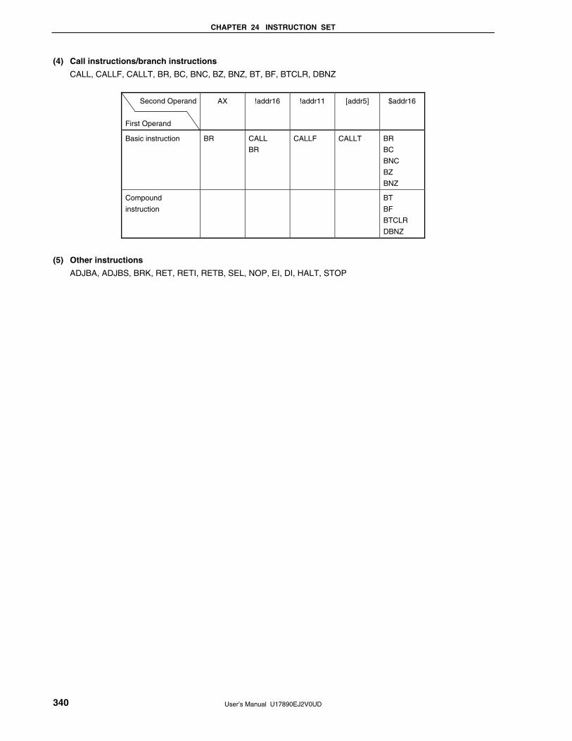
CHAPTER 24 INSTRUCTION SET
User’s Manual U17890EJ2V0UD 340
(4) Call instructions/branch instructions
CALL, CALLF, CALLT, BR, BC, BNC, BZ, BNZ, BT, BF, BTCLR, DBNZ
Second Operand
First Operand
AX !addr16 !addr11 [addr5] $addr16
Basic instruction BR CALL
BR
CALLF CALLT BR
BC
BNC
BZ
BNZ
Compound
instruction
BT
BF
BTCLR
DBNZ
(5) Other instructions
ADJBA, ADJBS, BRK, RET, RETI, RETB, SEL, NOP, EI, DI, HALT, STOP

User’s Manual U17890EJ2V0UD 341
CHAPTER 25 ELECTRICAL SPECIFICATIONS
Caution The μPD78F0711 and 78F0712 have an on-chip debug function. Do not use this product for mass
production because its reliability cannot be guaranteed after the on-chip debug function has
been used, given the issue of the number of times the flash memory can be rewritten. NEC
Electronics does not accept complaints concerning this product.
Absolute Maximum Ratings (TA = 25°C)
Parameter Symbol Conditions Ratings Unit
VDD −0.3 to +6.5 V
VSS −0.3 to +0.3 V
AVREF −0.3 to VDD + 0.3Note V
Supply voltage
AVSS −0.3 to +0.3 V
Input voltage VI P00 to P03, P13, P14, P16, P17, P20 to
P23, P50, P53, P54, X1, X2, RESET
−0.3 to VDD + 0.3Note V
Output voltage VO −0.3 to VDD + 0.3Note V
Analog input voltage VAN AVSS − 0.3 to AVREF + 0.3Note
and −0.3 to VDD + 0.3Note V
Per pin −10 mA
P00 to P03, P50, P53, P54 −30 mA
Output current, high IOH
Total of
all pins−60 mA
P13, P14, P16, P17, TW0TO0
to TW0TO5
−30 mA
P00 to P03, P13, P14, P16,
P17
20 mA Per pin
P50, P53, P54, TW0TO0 to
TW0TO5
30 mA
P00 to P03 30 mA
P13, P14, P16, P17 50 mA
TW0TO0 to TW0TO5 100 mA
Output current, low IOL
Total of
all pins
280 mA
P50, P53, P54 100 mA
In normal operation mode −40 to +85 Operating ambient
temperature
TA
In flash memory programming mode −10 to +85
°C
Storage temperature Tstg −40 to +125 °C
Note Must be 6.5 V or lower.
Caution Product quality may suffer if the absolute maximum rating is exceeded even momentarily for any
parameter. That is, the absolute maximum ratings are rated values at which the product is on the
verge of suffering physical damage, and therefore the product must be used under conditions that
ensure that the absolute maximum ratings are not exceeded.
Remark Unless specified otherwise, the characteristics of alternate-function pins are the same as those of port pins.
<R>

CHAPTER 25 ELECTRICAL SPECIFICATIONS
User’s Manual U17890EJ2V0UD 342
X1 Oscillator Characteristics (TA = −40 to +85°C, 4.0 V ≤ VDD ≤ 5.5 V, 4.0 V ≤ AVREF ≤ VDD, VSS = AVSS = 0 V)
Resonator Recommended Circuit Parameter Conditions MIN. TYP. MAX. Unit
Ceramic
resonator
C1
X2X1VSS
C2
Oscillation frequency (fXP)Note 4.0 V ≤ VDD ≤ 5.5 V 5.0 20 MHz
Crystal
resonator
C1
X2X1VSS
C2
Oscillation frequency (fXP)Note 4.0 V ≤ VDD ≤ 5.5 V 5.0 20 MHz
X1 input frequency (fXP)Note 4.0 V ≤ VDD ≤ 5.5 V 5.0 20 MHz External
clock X2X1
X1 input high-/low-level
width (tXPH, tXPL)
4.0 V ≤ VDD ≤ 5.5 V 24 100 ns
Note Indicates only oscillator characteristics. Refer to AC Characteristics for instruction execution time.
Cautions 1. When using the X1 oscillator, wire as follows in the area enclosed by the broken lines in the
above figures to avoid an adverse effect from wiring capacitance.
• Keep the wiring length as short as possible.
• Do not cross the wiring with the other signal lines.
• Do not route the wiring near a signal line through which a high fluctuating current flows.
• Always make the ground point of the oscillator capacitor the same potential as VSS.
• Do not ground the capacitor to a ground pattern through which a high current flows.
• Do not fetch signals from the oscillator.
2. Since the CPU is started by the internal low-speed oscillation clock after reset is released, check
the oscillation stabilization time of the X1 input clock using the oscillation stabilization time
status register (OSTC). Determine the oscillation stabilization time of the OSTC register and
oscillation stabilization time select register (OSTS) after sufficiently evaluating the oscillation
stabilization time with the resonator to be used.
Remark For the resonator selection and oscillator constant, customers are requested to either evaluate the
oscillation themselves or apply to the resonator manufacturer for evaluation.
Internal Oscillator Characteristics (TA = −40 to +85°C, 4.0 V ≤ VDD ≤ 5.5 V, 4.0 V ≤ AVREF ≤ VDD, VSS = AVSS = 0 V)
Resonator Parameter Conditions MIN. TYP. MAX. Unit
Internal low-speed oscillator Oscillation frequency (fRL) 120 240 480 kHz
Internal high-speed oscillator Oscillation frequency (fRH) 7.6 8.0 8.4 MHz <R>

CHAPTER 25 ELECTRICAL SPECIFICATIONS
User’s Manual U17890EJ2V0UD 343
DC Characteristics (1/2) (TA = −40 to +85°C, 4.0 V ≤ VDD ≤ 5.5 V, 4.0 V ≤ AVREF ≤ VDD, VSS = AVSS = 0 V)
Parameter Symbol Conditions MIN. TYP. MAX. Unit
Per pin 4.0 V ≤ VDD ≤ 5.5 V −5 mA
Total of P00 to P03, P50, P53, P54
4.0 V ≤ VDD ≤ 5.5 V −25 mA
Output current, high IOH
Total of P13, P14, P16, P17, TW0TO0 to TW0TO5
4.0 V ≤ VDD ≤ 5.5 V −25 mA
Per pin for P00 to P03, P13,P14, P16, P17
4.0 V ≤ VDD ≤ 5.5 V 10 mA
Per pin for P50, P53, P54, TW0TO0 to TW0TO5
4.0 V ≤ VDD ≤ 5.5 V 15 mA
Total of P00 to P03 4.0 V ≤ VDD ≤ 5.5 V 15 mA
Total of P13, P14, P16, P17 4.0 V ≤ VDD ≤ 5.5 V 25 mA
Total of TW0TO0 to TW0TO5
4.0 V ≤ VDD ≤ 5.5 V 70 mA
Output current, low IOL
Total of P50, P53, P54 4.0 V ≤ VDD ≤ 5.5 V 70 mA
VIH1 P14, P16, P17 4.0 V ≤ VDD ≤ 5.5 V 0.7VDD VDD V
VIH2 P00 to P03, P13, P50, P53, P54, RESET
4.0 V ≤ VDD ≤ 5.5 V 0.8VDD VDD V
Input voltage, high
VIH3 P20 to P23Note 4.0 V ≤ VDD ≤ 5.5 V 0.7AVREF AVREF V
VIH4 X1, X2 4.0 V ≤ VDD ≤ 5.5 V VDD − 0.5 VDD V
VIL1 P14, P16, P17 4.0 V ≤ VDD ≤ 5.5 V 0 0.3VDD V
VIL2 P00 to P03, P13, P50, P53, P54, RESET
4.0 V ≤ VDD ≤ 5.5 V 0 0.2VDD V
Input voltage, low
VIL3 P20 to P23Note 4.0 V ≤ VDD ≤ 5.5 V 0 0.3AVREF V
VIL4 X1, X2 4.0 V ≤ VDD ≤ 5.5 V 0 0.4 V
P00 to P03, P13, P14, P16, P17
4.0 V ≤ VDD ≤ 5.5 V,IOH = −5 mA
VDD − 1.0 V
P50, P53, P54, TW0TO0 to TW0TO5
4.0 V ≤ VDD ≤ 5.5 V,IOH = −1 mA
VDD − 1.0 V
Output voltage, high VOH
IOH = −100 μA 4.0 V ≤ VDD ≤ 5.5 V VDD − 0.5 V
P50, P53, p54, TW0TO0 to TW0TO5
4.0 V ≤ VDD ≤ 5.5 V,IOL = 15 mA
0.4 2.0 V
P00 to P03, P13, P14, P16, P17
Total IOL = 20 mA
4.0 V ≤ VDD ≤ 5.5 V,IOL = 10 mA
1.5 V
Output voltage, low VOL
IOL = 400 μA 4.0 V ≤ VDD ≤ 5.5 V 0.5 V
Note When used as digital input ports, set AVREF = VDD.
Remark Unless specified otherwise, the characteristics of alternate-function pins are the same as those of port pins.

CHAPTER 25 ELECTRICAL SPECIFICATIONS
User’s Manual U17890EJ2V0UD 344
DC Characteristics (2/2) (TA = −40 to +85°C, 4.0 V ≤ VDD ≤ 5.5 V, 4.0 V ≤ AVREF ≤ VDD, VSS = AVSS = 0 V)
Parameter Symbol Conditions MIN. TYP. MAX. Unit
VI = VDD P00 to P03, P13, P14, P16, P17, P50, P53, P54, RESET
3 μA ILIH1
VI = AVREF P20 to P23 3 μA
Input leakage current, high
ILIH2 VI = VDD X1, X2Note 1 20 μA
ILIL1 P00 to P03, P13, P14, P16, P17, P20 to P23, P50, P53, P54, RESET
−3 μA Input leakage current, low
ILIL2
VI = 0 V
X1, X2Note 1 −20 μA
Output leakage current, high ILOH VO = VDD 3 μA
Output leakage current, low ILOL VO = 0 V −3 μA
Pull-up resistance value RL VI = 0 V 10 30 100 kΩ
FLMD0 supply voltage Flmd In normal operation mode 0 0.2VDD V
When A/D converter is stopped
17 34 mA Supply currentNote 2
IDD1 X1 crystal oscillation clock operating Note 3
fXP = 20 MHz VDD = 5.0 V ±10%Note 4 When A/D converter is
operatingNote 5 18 36 mA
When peripheral functions are
stopped
4.0 7 mA IDD2 X1 crystal oscillation clock HALT mode
fXP = 20 MHz VDD = 5.0 V ±10%
When peripheral functions are
operating
14 mA
IDD3 Internal low-speed oscillation clock operating modeNote 6
VDD = 5.0 V ±10% 2 4 mA
When A/D converter is stopped
8 20 mA IDD4 Internal high-speed oscillation clock operation mode
VDD = 5.0 V ±10%
Note 3
When A/D converter is operatingNote 5
9 22 mA
When peripheral functions are
stopped
3 6.3 mA IDD5 Internal high-speed oscillation clock HALT mode
VDD = 5.0 V ±10%
When peripheral functions are
operating
9.7 mA
Internal low-speed oscillator: OFF
4 20 μA IDD6 STOP mode VDD = 5.0 V ±10%
Internal low-speed oscillator: ON
16 40 μA
Notes 1. When the inverse level of X1 is input to X2.
2. Total current flowing through the internal power supply (VDD). Peripheral operation current is included
(however, the current that flows through the pull-up resistors of ports is not included).
3. IDD1 includes peripheral operation current.
4. When PCC = 00H.
5. Including the current that flows through the AVREF pin.
6. When X1 oscillation is stopped.
Remark Unless specified otherwise, the characteristics of alternate-function pins are the same as those of port pins.
<R>

CHAPTER 25 ELECTRICAL SPECIFICATIONS
User’s Manual U17890EJ2V0UD 345
AC Characteristics
(1) Basic operation (TA = −40 to +85°C, 4.0 V ≤ VDD ≤ 5.5 V, 4.0 V ≤ AVREF ≤ VDD, VSS = AVSS = 0 V)
Parameter Symbol Conditions MIN. TYP. MAX. Unit
X1 input clock 4.0 V ≤ VDD ≤ 5.5 V 0.1 6.4 μs Instruction cycle (minimum
instruction execution time)
TCY Main system
clock operation Internal low-
speed
oscillation
clock
3.3 V ≤ VDD ≤ 5.5 V 4.17 8.33 16.67 μs
TI000, TI001 input high-level
width, low-level width
tTIH0,
tTIL0
4.0 V ≤ VDD ≤ 5.5 V 2/fsam1 +
0.1Note
μs
TI50 input frequency fTI5 4.0 V ≤ VDD ≤ 5.5 V 10 MHz
TI50 input high-level width, low-
level width
tTIH5,
tTIL5
4.0 V ≤ VDD ≤ 5.5 V 50 ns
Interrupt input high-level width,
low-level width
tINTH,
tINTL
4.0 V ≤ VDD ≤ 5.5 V 1 μs
ADTRG input high-level width,
low-level width
tADTIH,
tADTIL
4.0 V ≤ VDD ≤ 5.5 V 1 μs
RESET low-level width tRSL 4.0 V ≤ VDD ≤ 5.5 V 10 μs
Note Selection of fsam1 = fXP/2, fXP/4, or fXP/256 is possible using bits 0 and 1 (PRM000, PRM001) of prescaler mode
register 00 (PRM00). Note that when selecting the TI000 valid edge as the count clock, fsam1 = fXP.

CHAPTER 25 ELECTRICAL SPECIFICATIONS
User’s Manual U17890EJ2V0UD 346
TCY vs. VDD (Main System Clock Operation)
5.0
1.0
2.0
0.4
0.2
0.1
Supply voltage VDD [V]
Cyc
le ti
me
TC
Y [
μs]
0
10.0
1.0 2.0 3.0 4.0 5.0 6.05.5
20.0
16.67
6.4
Guaranteed operation range
Remark The values indicated by the shaded section are only when the internal low-speed oscillation clock is
selected.

CHAPTER 25 ELECTRICAL SPECIFICATIONS
User’s Manual U17890EJ2V0UD 347
(2) Serial interface (TA = −40 to +85°C, 4.0≤ VDD ≤ 5.5 V, 4.0≤ AVREF ≤ VDD, VSS = AVSS = 0 V)
(a) UART mode (UART0, dedicated baud rate generator output)
Parameter Symbol Conditions MIN. TYP. MAX. Unit
Transfer rate 312.5 kbps
AC Timing Test Points (Excluding X1 Input)
0.8VDD
0.2VDD
Test points0.8VDD
0.2VDD
Clock Timing
X1VIH4 (MIN.)
VIL4 (MAX.)
1/fXP
tXPL tXPH
TI Timing
TI000, TI001
tTIL0 tTIH0
TI50
tTIL5
1/fTI5
tTIH5
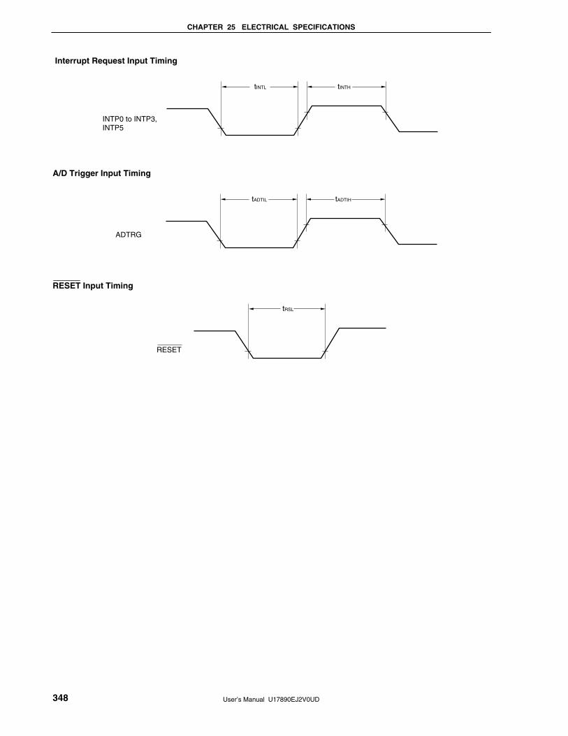
CHAPTER 25 ELECTRICAL SPECIFICATIONS
User’s Manual U17890EJ2V0UD 348
Interrupt Request Input Timing
INTP0 to INTP3, INTP5
tINTL tINTH
A/D Trigger Input Timing
ADTRG
tADTIL tADTIH
RESET Input Timing
RESET
tRSL

CHAPTER 25 ELECTRICAL SPECIFICATIONS
User’s Manual U17890EJ2V0UD 349
A/D Converter Characteristics (TA = −40 to +85°C, 4.0 V ≤ VDD ≤ 5.5 V, 4.0 V ≤ AVREF ≤ VDD, VSS = AVSS = 0 V)
Parameter Symbol Conditions MIN. TYP. MAX. Unit
Resolution 10 10 10 bit
Overall errorNotes 1, 2 4.0 V ≤ AVREF ≤ 5.5 V ±0.2 ±0.4 %FSR
4.5 V ≤ AVREF ≤ 5.5 V 3.6 100 μs Conversion time tCONV
4.0 V ≤ AVREF ≤ 5.5 V 4.8 100 μs
Zero-scale errorNotes 1, 2 4.0 V ≤ AVREF ≤ 5.5 V ±0.4 %FSR
Full-scale errorNotes 1, 2 4.0 V ≤ AVREF ≤ 5.5 V ±0.4 %FSR
Integral non-linearity errorNote 1 4.0 V ≤ AVREF ≤ 5.5 V ±2.5 LSB
Differential non-linearity error Note 1 4.0 V ≤ AVREF ≤ 5.5 V ±1.5 LSB
Analog input voltage VIAN AVSS AVREF V
Notes 1. Excludes quantization error (±1/2 LSB).
2. This value is indicated as a ratio (%FSR) to the full-scale value.
POC Circuit Characteristics (TA = −40 to +85°C)
Parameter Symbol Conditions MIN. TYP. MAX. Unit
Detection voltage VPOC 3.3 3.5 3.7 V
Power supply rise time tPTH VDD: 0 V → 3.3 V 0.002 ms
Response delay time 1Note tPTHD When power supply rises, after reaching
detection voltage (MAX.)
3.0 ms
Response delay time 2Note tPD When VDD falls 1.0 ms
Minimum pulse width tPW 0.2 ms
Note Time required from voltage detection to reset release.
POC Circuit Timing
Supply voltage
(VDD)
Time
Detection voltage (MIN.)
Detection voltage (TYP.)
Detection voltage (MAX.)
tPTH tPTHD
tPW
tPD

CHAPTER 25 ELECTRICAL SPECIFICATIONS
User’s Manual U17890EJ2V0UD 350
LVI Circuit Characteristics (TA = −40 to +85°C)
Parameter Symbol Conditions MIN. TYP. MAX. Unit
Detection voltage VLVI 4.1 4.3 4.5 V
Response timeNote 1 tLD 0.2 2.0 ms
Minimum pulse width tLW 0.2 ms
Operation stabilization wait time Note 2 tLWAIT1 0.1 0.2 ms
Notes 1. Time required from voltage detection to interrupt output or internal reset output.
2. Time required from setting LVION to 1 to operation stabilization.
LVI Circuit Timing
Supply voltage
(VDD)
Time
Detection voltage (MIN.)
Detection voltage (TYP.)
Detection voltage (MAX.)
tLW
tLDtLWAIT1
LVION ← 1
Data Memory STOP Mode Low Supply Voltage Data Retention Characteristics (TA = −40 to +85°C)
Parameter Symbol Conditions MIN. TYP. MAX. Unit
Data retention supply voltage VDDDR 2.0 5.5 V
Release signal set time tSREL 0 μs

CHAPTER 25 ELECTRICAL SPECIFICATIONS
User’s Manual U17890EJ2V0UD 351
Flash Memory Programming Characteristics (TA = +10 to +85°C, 4.0 V ≤ VDD ≤ 5.5 V, 4.0 V ≤ AVREF ≤ VDD, VSS = 0 V)
(1) Basic characteristics
Parameter Symbol Conditions MIN. TYP. MAX. Unit
VDD supply current IDD fX = 20 MHz, VDD = 5.0 V 42 mA
Step erase time Terass 10 ms
Chip unit Teraca 0.01 2.55 ms Erase timeNote 1
Sector unit Terasa 0.01 2.55 ms
Write time Twrwa 50 500 μs
Number of rewrites per chip Cerwr 1 erase + 1 write after erase = 1 rewriteNote 2 100 Times
Notes 1. The erase verify time (writeback time) is not included.
2. If a sector (2 KB) is erased after it was written in 512 operations, in word units, the number of rewrite
operations is 1. Writing to the same address more than once for one erase is prohibited.
(2) Serial write operation characteristics
Parameter Symbol Conditions MIN. TYP. MAX. Unit
Time from RESET↑ to FLMD0
count start
TRFCF 219/fX + α μs
Count execution time TCOUNT 10 ms
FLMD0 counter high-/low-level
width
TCH/TCL 10 100 μs
Serial Write Operation
RESET
FLMD0VDD
0 V
VDD
0 V
TRFCF TCL
TCOUNT
TCH
FLMD1VDD
0 V
<R>

User’s Manual U17890EJ2V0UD 352
CHAPTER 26 PACKAGE DRAWINGS
S
S
H
J
T
I
G
D
E
F
C B
K
PL
U
N
ITEM
B
C
I
L
M
N
30-PIN PLASTIC SSOP (7.62 mm (300))
A
K
D
E
F
G
H
J
P
30 16
1 1 5
A
detail of lead end
MM
T
MILLIMETERS
0.65 (T.P.)
0.45 MAX.
0.13
0.5
6.1±0.2
0.10
9.85±0.15
0.17±0.03
0.1±0.05
0.24
1.3±0.1
8.1±0.2
1.2
+0.08−0.07
1.0±0.2
3°+5°−3°
0.25
0.6±0.15U
NOTE
Each lead centerline is located within 0.13 mm ofits true position (T.P.) at maximum material condition.
S30MC-65-5A4-2

User’s Manual U17890EJ2V0UD 353
CHAPTER 27 CAUTIONS FOR WAIT
27.1 Cautions for Wait
This product has two internal system buses.
One is a CPU bus and the other is a peripheral bus that interfaces with the low-speed peripheral hardware.
Because the clock of the CPU bus and the clock of the peripheral bus are asynchronous, unexpected illegal data
may be passed if an access to the CPU conflicts with an access to the peripheral hardware.
When accessing the peripheral hardware that may cause a conflict, therefore, the CPU repeatedly executes
processing, until the correct data is passed.
As a result, the CPU does not start the next instruction processing but waits. If this happens, the number of
execution clocks of an instruction increases by the number of wait clocks (for the number of wait clocks, see Table 27-
1). This must be noted when real-time processing is performed.

CHAPTER 27 CAUTIONS FOR WAIT
User’s Manual U17890EJ2V0UD 354
27.2 Peripheral Hardware That Generates Wait
Table 27-1 shows the registers that generate a wait request when an access from the CPU is made, and the
number of wait clocks of the CPU.
Table 27-1. Registers That Generate Wait and Number of CPU Wait Clocks (When VSWC = 0)
Peripheral Hardware Register Access Number of Wait Clocks
Watchdog timer WDTM Write 3 clocks (fixed)
Serial interface UART00 ASIS00 Read 1 clock (fixed)
ADM Write
ADS Write
PFM Write
PFT Write
1 to 5 clocksNote
(when ADM.5 flag = “1”)
1 to 9 clocksNote
(when ADM.5 flag = “0”)
ADCR Read 1 to 5 clocks
(when ADM.5 flag = “1”)
1 to 9 clocks
(when ADM.5 flag = “0”)
A/D converter
<Calculating maximum number of wait clocks>
{(1/fMACRO) × 2/(1/fCPU)} + 1
* The result after the decimal point is truncated if it is less than tCPUL after it has been multiplied by
(1/fCPU), and is rounded up if it exceeds tCPUL.
fMACRO: Macro operating frequency
(When bit 5 (FR2) of ADM = “1”: fX/2, when bit 5 (FR2) of ADM = “0”: fX/22)
fCPU: CPU clock frequency
tCPUL: Low-level width of CPU clock
Note No wait cycle is generated for the CPU if the number of wait clocks calculated by the above expression is 1.
Remark The clock is the CPU clock (fCPU).

CHAPTER 27 CAUTIONS FOR WAIT
User’s Manual U17890EJ2V0UD 355
27.3 Example of Wait Occurrence
<1> Watchdog timer
<On execution of MOV WDTM, A>
Number of execution clocks: 8
(5 clocks when data is written to a register that does not issue a wait (MOV sfr, A).)
<On execution of MOV WDTM, #byte>
Number of execution clocks: 10
(7 clocks when data is written to a register that does not issue a wait (MOV sfr, #byte).)
<2> Serial interface UART00
<On execution of MOV A, ASIS00>
Number of execution clocks: 6
(5 clocks when data is read from a register that does not issue a wait (MOV A, sfr).)
<3> A/D converter
Table 27-2. Number of Wait Clocks and Number of Execution Clocks on Occurrence of Wait (A/D Converter)
<On execution of MOV ADM, A; MOV ADS, A; or MOV A, ADCR>
• When fX = 10 MHz, tCPUL = 50 ns
Value of Bit 5 (FR2)
of ADM Register fCPU Number of Wait Clocks Number of Execution Clocks
fX 9 clocks 14 clocks
fX/2 5 clocks 10 clocks
fX/22 3 clocks 8 clocks
fX/23 2 clocks 7 clocks
0
fX/24 0 clocks (1 clockNote) 5 clocks (6 clocksNote)
fX 5 clocks 10 clocks
fX/2 3 clocks 8 clocks
fX/22 2 clocks 7 clocks
fX/23 0 clocks (1 clockNote) 5 clocks (6 clocksNote)
1
fX/24 0 clocks (1 clockNote) 5 clocks (6 clocksNote)
Note On execution of MOV A, ADCR
Remark The clock is the CPU clock (fCPU).
fX: X1 input clock frequency
tCPUL: Low-level width of CPU clock

User’s Manual U17890EJ2V0UD 356
APPENDIX A DEVELOPMENT TOOLS
The following development tools are available for the development of systems that employ the μ PD78F0711 and
78F0712.
Figure A-1 shows the development tool configuration.
• Support for PC98-NX series
Unless otherwise specified, products supported by IBM PC/ATTM compatibles are compatible with PC98-NX
series computers. When using PC98-NX series computers, refer to the explanation for IBM PC/AT compatibles.
• WindowsTM
Unless otherwise specified, “Windows” means the following OSs.
• Windows 3.1
• Windows 95, Windows 98, Windows 2000, Windows XP
• Windows NTTM Ver 4.0
Caution For the development tools of the μ PD78F0711 and 78F0712, contact an NEC Electronics sales
representative.
<R>

APPENDIX A DEVELOPMENT TOOLS
User’s Manual U17890EJ2V0UD 357
Figure A-1. Development Tool Configuration (1/3)
(1) When using the in-circuit emulator QB-780714
Language processing software
• Assembler package
• C compiler package
• Device fileNote 1
• C library source fileNote 2
Debugging software
• Integrated debugger
Host machine (PC or EWS)
Interface adapter
QB-780714Note 4
Emulation probe
Target system
Flash memory programmer
Flash memorywrite adapter
Flash memory
• Software package
• Project manager (Windows only)Note 3
Software package
Flash memorywrite environment
Control software
Embedded software
• Real-time OS
Power supply unit
Notes 1. Download the device file for μPD78F0711 and 78F0712 (DF780714) from the download site for
development tools (http://www.necel.com/micro/ods/eng/index.html).
2. The C library source file is not included in the software package.
3. The project manager PM+ is included in the assembler package.
The PM+ is only used for Windows.
4. In-circuit emulator QB-780714 is supplied with integrated debugger ID78K0-QB, flash memory programmer PG-FPL (or QB-MINI2), power supply unit, and USB interface cable. Any other products
are sold separately. In addition, download the software for operating the QB-MINI2 from the download
site for MINICUBE2 (http://www.necel.com/micro/en/development/asia/minicube2/minicube2.html).

APPENDIX A DEVELOPMENT TOOLS
User’s Manual U17890EJ2V0UD 358
Figure A-1. Development Tool Configuration (2/3)
(2) When using the on-chip debug emulator QB-78K0MINI
Language processing software
• Assembler package
• C compiler package
• Device fileNote 1
• C library source fileNote 2
Debugging software
• Integrated debuggerNote 4
• System simulator
Host machine(PC or EWS)
QB-78K0MININote 4
Flash memory programmer
Flash memorywrite adapter
Flash memory
• Software package
• Project manager
Software package
Flash memorywrite environment
Control software
(Windows only)Note 3
USB interface cableNote 4
Target connector
Target system
Connection cableNote 4
Notes 1. Download the device file for μPD78F0711 and 78F0712 (DF780714) from the download site for
development tools (http://www.necel.com/micro/ods/eng/index.html).
2. The C library source file is not included in the software package.
3. The project manager PM+ is included in the assembler package.
The PM+ is only used for Windows.
4. QB-78K0MINI is supplied with integrated debugger ID78K0-QB, USB interface cable, and connection
cable. Any other products are sold separately.

APPENDIX A DEVELOPMENT TOOLS
User’s Manual U17890EJ2V0UD 359
Figure A-1. Development Tool Configuration (3/3)
(3) When using the on-chip debug emulator with programming function QB-MINI2
Language processing software
• Assembler package
• C compiler package
• Device fileNote 1
• C library source fileNote 2
Debugging software
• Integrated debuggerNote 1
• System simulator
Host machine(PC or EWS)
USB interface cableNote 4
QB-MINI2Note 4
78K0-OCD boardNote 4
Target connector
Target system
• Software package
• Project manager
Software package
<When using QB-MINI2 as a flash memory programmer>
Control software
(Windows only)Note 3
<When using QB-MINI2 as an on-chip degug emulator>
Connection cable
(10-pin/16-pin cable)Note 4
QB-MINI2Note 4
Connection cable
(16-pin cable)Note 4
Notes 1. Download the device file for μPD78F0711 and 78F0712 (DF780714) and the integrated debugger
(ID78K0-QB) from the download site for development tools (http://www.necel.com/micro/ods/eng/index.html).
2. The C library source file is not included in the software package. 3. The project manager PM+ is included in the assembler package. The PM+ is only used for Windows. 4. On-chip debug emulator QB-MINI2 is supplied with USB interface cable, connection cables (10-pin
cable and 16-pin cable), and 78K0-OCD board. Any other products are sold separately. In addition, download the software for operating the QB-MINI2 from the download site for MINICUBE2 (http://www.necel.com/micro/en/development/asia/minicube2/minicube2.html).

APPENDIX A DEVELOPMENT TOOLS
User’s Manual U17890EJ2V0UD 360
A.1 Software Package
Development tools (software) common to the 78K/0 Series are combined in this package.SP78K0
78K/0 Series software package Part number: μS××××SP78K0
Remark ×××× in the part number differs depending on the host machine and OS used.
μS××××SP78K0
×××× Host Machine OS Supply Medium
AB17 Windows (Japanese version)
BB17
PC-9800 series,
IBM PC/AT compatibles Windows (English version)
CD-ROM

APPENDIX A DEVELOPMENT TOOLS
User’s Manual U17890EJ2V0UD 361
A.2 Language Processing Software
This assembler converts programs written in mnemonics into object codes executable
with a microcontroller.
This assembler is also provided with functions capable of automatically creating symbol
tables and branch instruction optimization.
This assembler should be used in combination with a device file (DF780714) (sold
separately).
<Precaution when using RA78K0 in PC environment>
This assembler package is a DOS-based application. It can also be used in Windows,
however, by using the Project Manager (included in assembler package) on Windows.
RA78K0
Assembler package
Part number: μS××××RA78K0
This compiler converts programs written in C language into object codes executable with
a microcontroller.
This compiler should be used in combination with an assembler package and device file
(both sold separately).
<Precaution when using CC78K0 in PC environment>
This C compiler package is a DOS-based application. It can also be used in Windows,
however, by using the Project Manager (included in assembler package) on Windows.
CC78K0
C compiler package
Part number: μS××××CC78K0
This file contains information peculiar to the device.
This device file should be used in combination with a tool (RA78K0, CC78K0, SM78K0,
ID78K0-QB) (all sold separately).
The corresponding OS and host machine differ depending on the tool to be used.
DF780714 Note 1
Device file
Part number: μS××××DF780714
This is a source file of the functions that configure the object library included in the C
compiler package.
This file is required to match the object library included in the C compiler package to the
user’s specifications.
Since this is a source file, its working environment does not depend on any particular
operating system.
CC78K0-LNote 2
C library source file
Part number: μS××××CC78K0-L
Notes 1. The DF780714 can be used in common with the RA78K0, CC78K0, and ID78K0-QB. Download the
DF780714 from the download site for development tools
(http://www.necel.com/micro/ods/eng/index.html).
2. The CC78K0-L is not included in the software package (SP78K0).

APPENDIX A DEVELOPMENT TOOLS
User’s Manual U17890EJ2V0UD 362
Remark ×××× in the part number differs depending on the host machine and OS used.
μS××××RA78K0
μS××××CC78K0
μS××××CC78K0-L
×××× Host Machine OS Supply Medium
AB17 Windows (Japanese version)
BB17
PC-9800 series,
IBM PC/AT compatibles Windows (English version)
3P17 HP9000 series 700TM HP-UXTM (Rel. 10.10)
3K17 SPARCstationTM SunOSTM (Rel. 4.1.4),
SolarisTM (Rel. 2.5.1)
CD-ROM
μS××××DF780714
×××× Host Machine OS Supply Medium
AB13 Windows (Japanese version)
BB13
PC-9800 series,
IBM PC/AT compatibles Windows (English version)
3.5-inch 2HD FD
A.3 Control Software
PM+
Project manager
This is control software designed to enable efficient user program development in the
Windows environment. All operations used in development of a user program, such as
starting the editor, building, and starting the debugger, can be performed from the project
manager.
<Caution>
The project manager is included in the assembler package (RA78K0).
It can only be used in Windows.
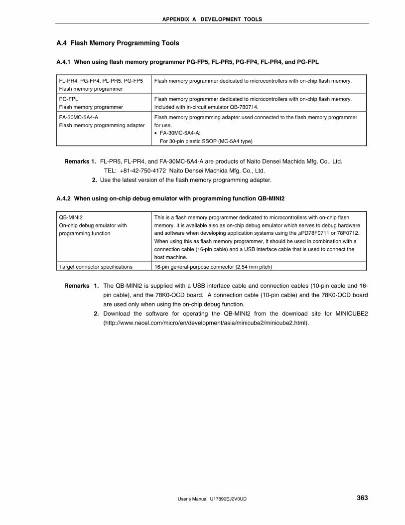
APPENDIX A DEVELOPMENT TOOLS
User’s Manual U17890EJ2V0UD 363
A.4 Flash Memory Programming Tools
A.4.1 When using flash memory programmer PG-FP5, FL-PR5, PG-FP4, FL-PR4, and PG-FPL
FL-PR4, PG-FP4, PL-PR5, PG-FP5
Flash memory programmer
Flash memory programmer dedicated to microcontrollers with on-chip flash memory.
PG-FPL
Flash memory programmer
Flash memory programmer dedicated to microcontrollers with on-chip flash memory.
Included with in-circuit emulator QB-780714.
FA-30MC-5A4-A
Flash memory programming adapter
Flash memory programming adapter used connected to the flash memory programmer
for use. • FA-30MC-5A4-A:
For 30-pin plastic SSOP (MC-5A4 type)
Remarks 1. FL-PR5, FL-PR4, and FA-30MC-5A4-A are products of Naito Densei Machida Mfg. Co., Ltd.
TEL: +81-42-750-4172 Naito Densei Machida Mfg. Co., Ltd.
2. Use the latest version of the flash memory programming adapter.
A.4.2 When using on-chip debug emulator with programming function QB-MINI2
QB-MINI2
On-chip debug emulator with
programming function
This is a flash memory programmer dedicated to microcontrollers with on-chip flash
memory. It is available also as on-chip debug emulator which serves to debug hardware and software when developing application systems using the μPD78F0711 or 78F0712.
When using this as flash memory programmer, it should be used in combination with a
connection cable (16-pin cable) and a USB interface cable that is used to connect the
host machine.
Target connector specifications 16-pin general-purpose connector (2.54 mm pitch)
Remarks 1. The QB-MINI2 is supplied with a USB interface cable and connection cables (10-pin cable and 16-
pin cable), and the 78K0-OCD board. A connection cable (10-pin cable) and the 78K0-OCD board
are used only when using the on-chip debug function.
2. Download the software for operating the QB-MINI2 from the download site for MINICUBE2
(http://www.necel.com/micro/en/development/asia/minicube2/minicube2.html).

APPENDIX A DEVELOPMENT TOOLS
User’s Manual U17890EJ2V0UD 364
A.5 Debugging Tools (Hardware)
A.5.1 When using in-circuit emulator QB-780714
QB-780714Note
In-circuit emulator
The in-circuit emulator serves to debug hardware and software when developing application systems using the μPD78F0711 and 78F0712. It supports the integrated debugger (ID78K0-
QB). This emulator should be used in combination with a power supply unit and emulation
probe. USB is used to connect this emulator to the host machine.
QB-144-CA-01
Check pin adapter
This adapter is used in waveform monitoring using the oscilloscope, etc.
QB-80-EP-01T
Emulation probe
This is a flexible type probe used to connect the in-circuit emulator to the target system.
QB-30MC-EA-03T
Exchange adapter
This adapter is used to perform the pin conversion from the in-circuit emulator to the target
connector. • QB-30MC-EA-03T: For 30-pin plastic SSOP (MC-5A4 type)
QB-30MC-YS-01T
Space adapter
This adapter is used to adjust the height between the target system and in-circuit emulator if
required. • QB-30MC-YS-01T: For 30-pin plastic SSOP (MC-5A4 type)
QB-30MC-YQ-01T
YQ connector
This connector is used to connect the target connector to the exchange adapter. • QB-30MC-YQ-01T: For 30-pin plastic SSOP (MC-5A4 type)
QB-30MC-HQ-01T
Mount adapter
This adapter is used to mount the target device onto the target device with socket. • QB-30MC-HQ-01T: For 30-pin plastic SSOP (MC-5A4 type) with on-chip debug function
QB-30MC-NQ-01T
Target connector
This connector is used to mount the in-circuit emulator onto the target system. • QB-30MC-NQ-01T: For 30-pin plastic SSOP (MC-5A4 type)
Note The QB-780714 is supplied with a power supply unit, USB interface cable, and flash memory programmer PG-
FPL. It is also supplied with integrated debugger ID78K0-QB as control software.
Remark The package contents differ depending on the part number.
Package Contents
Part Number
In-Circuit Emulator Emulation Probe Exchange Adapter YQ Connector Target Connector
QB-780714-ZZZ Not included
QB-780714-T30MC
QB-780714
QB-80-EP-01T QB-30MC-EA-03T QB-30MC-YQ-01T QB-30MC-NQ-01T
A.5.2 When using on-chip debug emulator QB-78K0MINI
QB-78K0MINI Note
On-chip debug emulator
The on-chip debug emulator serves to debug hardware and software when developing application systems using the μPD78F0711 and 78F0712. It supports the integrated
debugger (ID78K0-QB) supplied with the QB-78K0MINI. This emulator uses a connection
cable and a USB interface cable that is used to connect the host machine.
Target connector specifications 10-pin general-purpose connector (2.54 mm pitch)
Note The QB-78K0MINI is supplied with a USB interface cable and a connection cable. It is also supplied with
integrated debugger ID78K0-QB as control software.

APPENDIX A DEVELOPMENT TOOLS
User’s Manual U17890EJ2V0UD 365
A.5.3 When using on-chip debug emulator with programming function QB-MINI2
QB-MINI2
On-chip debug emulator with
programming function
This on-chip debug emulator serves to debug hardware and software when developing application systems using the μPD78F0711 or 78F0712. It is available also as flash
memory programmer dedicated to microcontrollers with on-chip flash memory. When
using this as on-chip debug emulator, it should be used in combination with a connection
cable (10-pin cable or 16-pin cable), a USB interface cable that is used to connect the
host machine, and the 78K0-OCD board.
Target connector specifications 10-pin general-purpose connector (2.54 mm pitch) or 16-pin general-purpose connector
(2.54 mm pitch)
Remarks 1. The QB-MINI2 is supplied with a USB interface cable and connection cables (10-pin cable and 16-
pin cable), and the 78K0-OCD board. A connection cable (10-pin cable) and the 78K0-OCD board
are used only when using the on-chip debug function.
2. Download the software for operating the QB-MINI2 from the download site for MINICUBE2
(http://www.necel.com/micro/en/development/asia/minicube2/minicube2.html).
A.6 Debugging Tools (Software)
This debugger supports the in-circuit emulators for the μPD78F0711 and 78F0712. The
ID78K0-QB is Windows-based software.
It has improved C-compatible debugging functions and can display the results of tracing
with the source program using an integrating window function that associates the source
program, disassemble display, and memory display with the trace result. It should be
used in combination with the device file (sold separately).
ID78K0-QB
Integrated debugger
Part number: μS××××ID78K0-QB
Remark ×××× in the part number differs depending on the host machine and OS used.
μS××××ID78K0-QB
×××× Host Machine OS Supply Medium
AB17 Windows (Japanese version)
BB17
PC-9800 series,
IBM PC/AT compatibles Windows (English version)
CD-ROM

User’s Manual U17890EJ2V0UD 366
APPENDIX B REGISTER INDEX
B.1 Register Index (In Alphabetical Order with Respect to Register Names)
[A]
A/D conversion result register (ADCR)........................................................................................................................207
A/D converter mode register (ADM) ............................................................................................................................203
A/D trigger selection register (TW0TRGS) ..................................................................................................................106
Analog input channel specification register (ADS) ......................................................................................................206
Asynchronous serial interface operation mode register 00 (ASIM00) .........................................................................229
Asynchronous serial interface reception error status register 00 (ASIS00) .................................................................231
[B]
Baud rate generator control register 00 (BRGC00) .....................................................................................................232
Buffer transfer control timer (RTM0)............................................................................................................................101
[C]
Capture/compare control register 00 (CRC00)............................................................................................................121
[D]
DC control register 01 (DCCTL01) ..............................................................................................................................185
Dead time reload register (TW0DTIME)......................................................................................................................101
Dead time timer 0 (DTM0)...........................................................................................................................................101
Dead time timer 1 (DTM1)...........................................................................................................................................101
Dead time timer 2 (DTM2)...........................................................................................................................................101
[E]
8-bit timer compare register 50 (CR50) .......................................................................................................................155
8-bit timer compare register 51 (CR51) .......................................................................................................................155
8-bit timer counter 50 (TM50)......................................................................................................................................154
8-bit timer counter 51 (TM51)......................................................................................................................................154
8-bit timer mode control register 50 (TMC50)..............................................................................................................158
8-bit timer mode control register 51 (TMC51)..............................................................................................................158
External interrupt falling edge enable register (EGN)..................................................................................................266
External interrupt rising edge enable register (EGP)...................................................................................................266
[F]
Flash programming mode control register (FLPMC) ...................................................................................................323
Flash protect command register (PFCMD)..................................................................................................................325
Flash status register (PFS)..........................................................................................................................................325
[H]
High-impedance output control register (HZA0CTL0) ................................................................................................196
[I]
Internal memory size switching register (IMS).............................................................................................................310

APPENDIX B REGISTER INDEX
User’s Manual U17890EJ2V0UD 367
Internal oscillation mode register (RCM).......................................................................................................................77
Interrupt mask flag register 0H (MK0H) ......................................................................................................................264
Interrupt mask flag register 0L (MK0L)........................................................................................................................264
Interrupt mask flag register 1H (MK1H) ......................................................................................................................264
Interrupt mask flag register 1L (MK1L)........................................................................................................................264
Interrupt request flag register 0H (IF0H) .....................................................................................................................262
Interrupt request flag register 0L (IF0L) ......................................................................................................................262
Interrupt request flag register 1H (IF1H) .....................................................................................................................262
Interrupt request flag register 1L (IF1L) ......................................................................................................................262
Inverter timer control register (TW0C).........................................................................................................................102
Inverter timer mode register (TW0M) ..........................................................................................................................104
Inverter timer output control register (TW0OC)...........................................................................................................106
[L]
Low-voltage detection register (LVIM) ........................................................................................................................300
[M]
Main clock mode register (MCM) ..................................................................................................................................79
Main OSC control register (MOC) .................................................................................................................................78
Multiplication/division data register A0 (MDA0H, MDA0L) ..........................................................................................249
Multiplication/division data register B0 (MDB0)...........................................................................................................250
Multiplier/divider control register 0 (DMUC0) ..............................................................................................................251
[O]
Oscillation stabilization time counter status register (OSTC) ................................................................................80, 277
Oscillation stabilization time select register (OSTS)..............................................................................................81, 278
[P]
Port mode register 0 (PM0)...........................................................................................................................................66
Port mode register 1 (PM1)...........................................................................................................................................66
Port mode register 5 (PM5)...........................................................................................................................................66
Port register 0 (P0)..................................................................................................................................................58, 68
Port register 1 (P1)..................................................................................................................................................59, 68
Port register 2 (P2)..................................................................................................................................................63, 68
Port register 5 (P5)..................................................................................................................................................64, 68
Power-fail comparison mode register (PFM)...............................................................................................................208
Power-fail comparison threshold register (PFT)..........................................................................................................208
Prescaler mode register 00 (PRM00)..........................................................................................................................123
Priority specification flag register 0H (PR0H) ..............................................................................................................265
Priority specification flag register 0L (PR0L) ...............................................................................................................265
Priority specification flag register 1H (PR1H) ..............................................................................................................265
Priority specification flag register 1L (PR1L) ...............................................................................................................265
Processor clock control register (PCC) .........................................................................................................................76
Pull-up resistor option register 0 (PU0) .........................................................................................................................69
Pull-up resistor option register 1 (PU1) .........................................................................................................................69
Pull-up resistor option register 5 (PU5) .........................................................................................................................69
PWM select register (DCCTL02).................................................................................................................................186

APPENDIX B REGISTER INDEX
User’s Manual U17890EJ2V0UD 368
[R]
Real-Time output buffer register 1H (RTBH01) ...........................................................................................................182
Real-Time output buffer register 1L (RTBL01) ............................................................................................................182
Real-Time output port control register 1 (RTPC01).....................................................................................................184
Real-Time output port mode register 1 (RTPM01) ......................................................................................................183
Receive buffer register 00 (RXB00) ............................................................................................................................228
Remainder data register 0 (SDR0)..............................................................................................................................248
Reset control flag register (RESF) ..............................................................................................................................294
[S]
16-bit timer capture/compare register 00 (CR00) ........................................................................................................116
16-bit timer capture/compare register 01 (CR01) ........................................................................................................118
16-bit timer counter 00 (TM00)....................................................................................................................................116
16-bit timer mode control register 00 (TMC00)............................................................................................................119
16-bit timer output control register 00 (TOC00)...........................................................................................................121
System wait control register (VSWC) ............................................................................................................................82
[T]
10-bit buffer register 0 (TW0BFCM0) ..........................................................................................................................101
10-bit buffer register 1 (TW0BFCM1) ..........................................................................................................................101
10-bit buffer register 2 (TW0BFCM2) ..........................................................................................................................101
10-bit buffer register 3 (TW0BFCM3) ..........................................................................................................................101
10-bit buffer register 4 (TW0BFCM4) ..........................................................................................................................101
10-bit buffer register 5 (TW0BFCM5) ..........................................................................................................................101
10-bit compare register 0 (TW0CM0)..........................................................................................................................100
10-bit compare register 1 (TW0CM1)..........................................................................................................................100
10-bit compare register 2 (TW0CM2)..........................................................................................................................100
10-bit compare register 3 (TW0CM3)..........................................................................................................................100
10-bit compare register 4 (TW0CM4)..........................................................................................................................100
10-bit compare register 5 (TW0CM5)..........................................................................................................................100
10-bit up/down counter (TW0UDC) .............................................................................................................................100
Timer clock selection register 50 (TCL50)...................................................................................................................156
Timer clock selection register 51 (TCL51)...................................................................................................................156
Transmit shift register 00 (TXS00) ..............................................................................................................................228
[W]
Watchdog timer enable register (WDTE).....................................................................................................................174
Watchdog timer mode register (WDTM)......................................................................................................................173

APPENDIX B REGISTER INDEX
User’s Manual U17890EJ2V0UD 369
B.2 Register Index (In Alphabetical Order with Respect to Register Symbol)
[A]
ADCR: A/D conversion result register ..............................................................................................................207
ADM: A/D converter mode register.................................................................................................................203
ADS: Analog input channel specification register ..........................................................................................206
ASIM00: Asynchronous serial interface operation mode register 00...................................................................229
ASIS00: Asynchronous serial interface reception error status register 00..........................................................231
[B]
BRGC00: Baud rate generator control register 00................................................................................................232
[C]
CR00: 16-bit timer capture/compare register 00..............................................................................................116
CR01: 16-bit timer capture/compare register 01..............................................................................................118
CR50: 8-bit timer compare register 50.............................................................................................................155
CR51: 8-bit timer compare register 51.............................................................................................................155
CRC00: Capture/compare control register 00 ....................................................................................................121
[D]
DCCTL01: DC control register 01...........................................................................................................................185
DCCTL02: PWM select register .............................................................................................................................186
DMUC0: Multiplier/divider control register 0........................................................................................................251
DTM0: Dead time timer 0 .................................................................................................................................101
DTM1: Dead time timer 1 .................................................................................................................................101
DTM2: Dead time timer 2 .................................................................................................................................101
[E]
EGN: External interrupt falling edge enable register ......................................................................................266
EGP: External interrupt rising edge enable register .......................................................................................266
[F]
FLPMC: Flash programming mode control register ............................................................................................323
[H]
HZA0CTL0: High-impedance output control register................................................................................................196
[I]
IF0H: Interrupt request flag register 0H..........................................................................................................262
IF0L: Interrupt request flag register 0L ..........................................................................................................262
IF1H: Interrupt request flag register 1H..........................................................................................................262
IF1L: Interrupt request flag register 1L ..........................................................................................................262
IMS: Internal memory size switching register................................................................................................310
[L]
LVIM: Low-voltage detection register..............................................................................................................300

APPENDIX B REGISTER INDEX
User’s Manual U17890EJ2V0UD 370
[M]
MCM: Main clock mode register........................................................................................................................79
MDA0H: Multiplication/division data register A0..................................................................................................249
MDA0L: Multiplication/division data register A0..................................................................................................249
MDB0: Multiplication/division data register B0..................................................................................................250
MK0H: Interrupt mask flag register 0H .............................................................................................................264
MK0L: Interrupt mask flag register 0L ..............................................................................................................264
MK1H: Interrupt mask flag register 1H .............................................................................................................264
MK1L: Interrupt mask flag register 1L ..............................................................................................................264
MOC: Main OSC control register ......................................................................................................................78
[O]
OSTC: Oscillation stabilization time counter status register .......................................................................80, 277
OSTS: Oscillation stabilization time select register ....................................................................................81, 278
[P]
P0: Port register 0 ...................................................................................................................................58, 68
P1: Port register 1 ...................................................................................................................................59, 68
P2: Port register 2 ...................................................................................................................................63, 68
P5: Port register 5 ...................................................................................................................................64, 68
PCC: Processor clock control register..............................................................................................................76
PFCMD: Flash protect command register ...........................................................................................................325
PFM: Power-fail comparison mode register ...................................................................................................208
PFS: Flash status register .............................................................................................................................325
PFT: Power-fail comparison threshold register..............................................................................................208
PM0: Port mode register 0 ...............................................................................................................................66
PM1: Port mode register 1 ...............................................................................................................................66
PM5: Port mode register 5 ...............................................................................................................................66
PR0H: Priority specification flag register 0H.....................................................................................................265
PR0L: Priority specification flag register 0L .....................................................................................................265
PR1H: Priority specification flag register 1H.....................................................................................................265
PR1L: Priority specification flag register 1L .....................................................................................................265
PRM00: Prescaler mode register 00...................................................................................................................123
PU0: Pull-up resistor option register 0 .............................................................................................................69
PU1: Pull-up resistor option register 1 .............................................................................................................69
PU5: Pull-up resistor option register 5 .............................................................................................................69
[R]
RCM: Internal oscillation mode register ............................................................................................................77
RESF: Reset control flag register.....................................................................................................................294
RTBH01: Real-Time output buffer register 1H......................................................................................................182
RTBL01: Real-Time output buffer register 1L ......................................................................................................182
RTM0: Buffer transfer control timer ..................................................................................................................101
RTPC01: Real-Time output port control register 1 ...............................................................................................184
RTPM01: Real-Time output port mode register1 ..................................................................................................183
RXB00: Receive buffer register 00.....................................................................................................................228

APPENDIX B REGISTER INDEX
User’s Manual U17890EJ2V0UD 371
[S]
SDR0: Remainder data register 0 ....................................................................................................................248
[T]
TCL50: Timer clock selection register 50 ..........................................................................................................156
TCL51: Timer clock selection register 51 ..........................................................................................................156
TM00: 16-bit timer counter 00..........................................................................................................................116
TM50: 8-bit timer counter 50............................................................................................................................154
TM51: 8-bit timer counter 51............................................................................................................................154
TMC00: 16-bit timer mode control register 00....................................................................................................119
TMC50: 8-bit timer mode control register 50......................................................................................................158
TMC51: 8-bit timer mode control register 51......................................................................................................158
TOC00: 16-bit timer output control register 00...................................................................................................121
TW0BFCM0: 10-bit buffer register 0 ..........................................................................................................................101
TW0BFCM1: 10-bit buffer register 1 ..........................................................................................................................101
TW0BFCM2: 10-bit buffer register 2 ..........................................................................................................................101
TW0BFCM3: 10-bit buffer register 3 ..........................................................................................................................101
TW0BFCM4: 10-bit buffer register 4 ..........................................................................................................................101
TW0BFCM5: 10-bit buffer register 5 ..........................................................................................................................101
TW0C: Inverter timer control register................................................................................................................102
TW0CM0: 10-bit compare register 0......................................................................................................................100
TW0CM1: 10-bit compare register 1......................................................................................................................100
TW0CM2: 10-bit compare register 2......................................................................................................................100
TW0CM3: 10-bit compare register 3......................................................................................................................100
TW0CM4: 10-bit compare register 4......................................................................................................................100
TW0CM5: 10-bit compare register 5......................................................................................................................100
TW0DTIME: Dead time reload register .....................................................................................................................101
TW0M: Inverter timer mode register .................................................................................................................104
TW0OC: Inverter timer output control register.....................................................................................................106
TW0TRGS: A/D trigger selection register ................................................................................................................106
TW0UDC: 10-bit up/down counter .........................................................................................................................100
TXS00: Transmit shift register 00 ......................................................................................................................228
[V]
VSWC: System wait control register ...................................................................................................................82
[W]
WDTE: Watchdog timer enable register............................................................................................................174
WDTM: Watchdog timer mode register .............................................................................................................173

User’s Manual U17890EJ2V0UD 372
APPENDIX C REVISION HISTORY
C.1 Major Revisions in This Edition (1/2)
Page Description Classification
INTRODUCTION
p.6 Change of Documents Related to Development Tools (Hardware) (User’s Manuals) (e)
CHAPTER 1 OUTLINE
p.14 Addition of description (c)
CHAPTER 2 PIN FUNCTIONS
p.21 Addition of Note to Table 2-1 Pin I/O Buffer Power Supplies (c)
p.24 Addition of Note to 2.2.3 (1) Port mode (c)
CHAPTER 3 CPU ARCHITECTURE
p.43 Addition of register to Table 3-3 Special Function Register List (4/4) (b)
p.46 Change of 3.3.3 Table indirect addressing (b)
CHAPTER 4 PORT FUNCTIONS
p.56 Addition of Note to Table 4-1 Pin I/O Buffer Power Supplies (c)
p.59 Change of Figure 4-3 Block Diagram of P13 (a)
p.63 Addition of Caution to 4.2.3 Port 2 (c)
p.71 Addition of 4.5 Cautions on 1-Bit Manipulation Instruction for Port Register n (Pn) (c)
CHAPTER 5 CLOCK GENERATOR
pp.73, 75, 82 Addition of VSWC register to the next points
Table 5-1 Configuration of Clock Generator
5.3 Registers Controlling Clock Generator
(b)
p.76 Change of Figure 5-2 Format of Processor Clock Control Register (PCC) (a)
CHAPTER 6 10-BIT INVERTER CONTROL TIMER
p.99 Change of Figure 6-1 Block Diagram of 10-Bit Inverter Control Timer (a)
p.106 Change of Figure 6-5 Format of Inverter Timer Output Control Register (a)
CHAPTER 10 REAL-TIME OUTPUT PORT
p.181 Change of Figure 10-1 Block Diagram of Real-Time Output Port (a)
p.183 Addition of description to < Cautions for development tools> in 10. 3 (1) Real-time output port mode register 1 (RTPM01)
(c)
p.188 Change of Table 10-4 Relationship Between Settings of Each Bit of Control Register and Real-Time Output
(a)
CHAPTER 12 Hi-Z OUTPUT CONTROLLER
p.195 Change of Figure 12-1 Block Diagram of Hi-Z Output Controller (a)
p.196 Change of address in Figure 12-2 Format of High-impedance Output Control Register 0 (a)
CHAPTER 13 A/D CONVERTER
p.203 Change of Figure 13-3 Format of A/D Converter Mode Register (ADM) (a)
p.205 Change of Table 13-3 A/D Conversion Time (a)
Remark “Classification” in the above table classifies revisions as follows. (a): Error correction, (b): Addition/change of specifications, (c): Addition/change of description or note,
(d): Addition/change of package, part number, or management division, (e): Addition/change of related
documents
<R>

APPENDIX C REVISION HISTORY
User’s Manual U17890EJ2V0UD 373
(2/2)
Page Description Classification
CHAPTER 14 SERIAL INTERFACE UART00
p.225 Addition of Caution to 14.1 (2) Asynchronous serial interface (UART) mode (c)
p.228 Addition of Caution to 14.2 (3) Transmit shift register 00 (TXS00) (c)
p.230 Addition of Caution to Figure 14-2 Format of Asynchronous Serial Interface Operation Mode Register 00 (ASIM00)
(c)
p.235 Change of procedure of setting an operation in 14.4.2 (1) Registers used (c)
p.238 Addition of description to 14. 4. 2 (1) (c) Transmission (c)
p.243 Change of Table 14-4 Set Data of Baud Rate Generator (a)
CHAPTER 16 INTERRUPT FUNCTIONS
p.257 Change of Table 16-1 Interrupt Source List (1/2) (a)
CHAPTER 17 STANDBY FUNCTION
p.275 Addition of description of internal high-speed oscillator (c)
p.285 Change of (2) When internal low-speed oscillation clock is used as CPU clock in Figure 17-6 STOP Mode Release by Interrupt Request Generation
(a)
CHAPTER 22 FLASH MEMORY
p.322 Change of Remark in 22.7 Flash Memory Programming by Self-Writing (e)
CHAPTER 23 ON-CHIP DEBUG FUNCTION
p.327 Change of description and Remark (c, e)
CHAPTER 24 INSTRUCTION SET
p.336 Change of CALLT in 24.2 Operation List (c)
CHAPTER 25 ELECTRICAL SPECIFICATIONS
p.341 Change of Caution (c)
p.342 Change of Internal Oscillator Characteristics (b)
p.344 Change of Supply current in DC Characteristics (2/2) (b)
p.351 Change of (1) Basic characteristics in Flash Memory Programming Characteristics (b)
APPENDIX A DEVELOPMENT TOOLS
Throughout Revision of chapter (c)
APPENDIX C REVISION HISTORY
p.372 Addition of chapter (c)
Remark “Classification” in the above table classifies revisions as follows.
(a): Error correction, (b): Addition/change of specifications, (c): Addition/change of description or note,
(d): Addition/change of package, part number, or management division, (e): Addition/change of related
documents
NEC Electronics Corporation1753, Shimonumabe, Nakahara-ku,Kawasaki, Kanagawa 211-8668, JapanTel: 044-435-5111http://www.necel.com/
[America]
NEC Electronics America, Inc.2880 Scott Blvd.Santa Clara, CA 95050-2554, U.S.A.Tel: 408-588-6000 800-366-9782http://www.am.necel.com/
[Asia & Oceania]
NEC Electronics (China) Co., Ltd7th Floor, Quantum Plaza, No. 27 ZhiChunLu HaidianDistrict, Beijing 100083, P.R.ChinaTel: 010-8235-1155http://www.cn.necel.com/
Shanghai BranchRoom 2509-2510, Bank of China Tower,200 Yincheng Road Central,Pudong New Area, Shanghai, P.R.China P.C:200120Tel:021-5888-5400http://www.cn.necel.com/
Shenzhen BranchUnit 01, 39/F, Excellence Times Square Building,No. 4068 Yi Tian Road, Futian District, Shenzhen,P.R.China P.C:518048Tel:0755-8282-9800http://www.cn.necel.com/
NEC Electronics Hong Kong Ltd.Unit 1601-1613, 16/F., Tower 2, Grand Century Place,193 Prince Edward Road West, Mongkok, Kowloon, Hong KongTel: 2886-9318http://www.hk.necel.com/
NEC Electronics Taiwan Ltd.7F, No. 363 Fu Shing North RoadTaipei, Taiwan, R. O. C.Tel: 02-8175-9600http://www.tw.necel.com/
NEC Electronics Singapore Pte. Ltd.238A Thomson Road, #12-08 Novena Square, Singapore 307684Tel: 6253-8311http://www.sg.necel.com/
NEC Electronics Korea Ltd.11F., Samik Lavied’or Bldg., 720-2,Yeoksam-Dong, Kangnam-Ku,Seoul, 135-080, KoreaTel: 02-558-3737http://www.kr.necel.com/
For further information, please contact:
G0706
[Europe]
NEC Electronics (Europe) GmbHArcadiastrasse 1040472 Düsseldorf, GermanyTel: 0211-65030http://www.eu.necel.com/
Hanover OfficePodbielskistrasse 166 B30177 HannoverTel: 0 511 33 40 2-0
Munich OfficeWerner-Eckert-Strasse 981829 MünchenTel: 0 89 92 10 03-0
Stuttgart OfficeIndustriestrasse 370565 StuttgartTel: 0 711 99 01 0-0
United Kingdom BranchCygnus House, Sunrise ParkwayLinford Wood, Milton KeynesMK14 6NP, U.K.Tel: 01908-691-133
Succursale Française9, rue Paul Dautier, B.P. 5278142 Velizy-Villacoublay CédexFranceTel: 01-3067-5800
Sucursal en EspañaJuan Esplandiu, 1528007 Madrid, SpainTel: 091-504-2787
Tyskland FilialTäby CentrumEntrance S (7th floor)18322 Täby, SwedenTel: 08 638 72 00
Filiale ItalianaVia Fabio Filzi, 25/A20124 Milano, ItalyTel: 02-667541
Branch The NetherlandsSteijgerweg 65616 HS EindhovenThe NetherlandsTel: 040 265 40 10
Copyright © 2022 FDOKUMEN