Mixed-Signal and DSP Design Techniques
424
MIXED-SIGNAL AND DSP DESIGN TECHNIQUES INTRODUCTION SECTION 1 SAMPLED DATA SYSTEMS SECTION 2 ADCs FOR DSP APPLICATIONS SECTION 3 DACs FOR DSP APPLICATIONS SECTION 4 FAST FOURIER TRANSFORMS SECTION 5 DIGITAL FILTERS SECTION 6 DSP HARDWARE SECTION 7 INTERFACING TO DSPs SECTION 8 DSP APPLICATIONS SECTION 9 HARDWARE DESIGN SECTION 10 TECHNIQUES INDEX
-
Upload
khangminh22 -
Category
Documents
-
view
3 -
download
0
Transcript of Mixed-Signal and DSP Design Techniques

MIXED-SIGNAL AND DSPDESIGN TECHNIQUES
INTRODUCTION SECTION 1
SAMPLED DATA SYSTEMS SECTION 2
ADCs FOR DSP APPLICATIONS SECTION 3
DACs FOR DSP APPLICATIONS SECTION 4
FAST FOURIER TRANSFORMS SECTION 5
DIGITAL FILTERS SECTION 6
DSP HARDWARE SECTION 7
INTERFACING TO DSPs SECTION 8
DSP APPLICATIONS SECTION 9
HARDWARE DESIGN SECTION 10TECHNIQUES
INDEX

ANALOG DEVICES TECHNICAL REFERENCE BOOKS
PUBLISHED BY PRENTICE HALL
Analog-Digital Conversion HandbookDigital Signal Processing Applications Using the ADSP-2100 Family
(Volume 1:1992, Volume 2:1994)Digital Signal Processing in VLSIDSP Laboratory Experiments Using the ADSP-2101ADSP-2100 Family User's Manual
PUBLISHED BY ANALOG DEVICES
Practical Design Techniques for Sensor Signal ConditioningPractical Design Techniques for Power and Thermal ManagementHigh Speed Design TechniquesPractical Analog Design TechniquesLinear Design SeminarADSP-21000 Family Applications HandbookSystem Applications GuideAmplifier Applications GuideNonlinear Circuits HandbookTransducer Interfacing HandbookSynchro & Resolver ConversionTHE BEST OF Analog Dialogue, 1967-1991

HOW TO GET INFORMATION FROM ANALOG DEVICESAnalog Devices publishes data sheets and a host of other technical literaturesupporting our products and technologies. Follow the instructions below forworldwide access to this information.
FOR DATA SHEETS
U.S.A. and Canada
Fax Retrieval. Telephone number 800-446-6212. Call this numberand use a faxcode corresponding to the data sheet of your choicefor a fax-on-demand through our automated AnalogFax™ system.Data sheets are available 7 days a week, 24 hours a day.Product/faxcode cross reference listings are available by callingthe above number and following the prompts. There is a shortindex with just part numbers, faxcodes, page count and revisionfor each data sheet (Prompt # 28). There is also a longer index sorted byproduct type with short descriptions (Prompt #29).
World Wide Web and Internet. Our address is http://www.analog.com.Use the browser of your choice and follow the prompts. We alsoprovide extensive DSP literature support on an Internet FTP site. Typeftp:// ftp.analog.com or ftp 137.71.23.11. Log in as anonymous using youre-mail address for your password.
Analog Devices Literature Distribution Center. Call 800-262-5643 andselect option two from the voice prompts, or call 781-329-4700 fordirect access, or fax your request to 508-894-5114.
Analog Devices Southeast Asia Literature Distribution Centre. Faxrequests to 65-746-9115. Email address [email protected].
Europe and Israel
World Wide Web. Our address is http://www.analog.com. use thebrowser of your choice and follow the prompts.
Analog Devices Sales Offices. Call your local sales office and requesta data sheet. A Worldwide Sales Directory including telephone listingsis on pp. 347-348 of the 1999 Winter Short Form Designers' Guide.
DSP Support Center. Fax requests to **49-89-76903-307 or [email protected].

India
Call 91-80-526-3606 or fax 91-80-526-3713 and request the datasheet of interest.
Other Locations
World Wide Web. Our address is http://www.analog.com. Use thebrowser of your choice and follow the prompts.
Analog Devices Sales Offices. Call your local sales office and requesta data sheet. A Worldwide Sales Directory including telephone numbersis listed on the back cover of the 1997 Short Form Designers' Guide.
TECHNICAL SUPPORT AND CUSTOMER SERVICE
In the U.S.A. and Canada, call 800-ANALOGD, (800-262-5643).For technical support on all products, select option one, then selectthe product area of interest. For price and delivery, select option three.For literature and samples, select option two.Non-800 Number: 781-937-1428.

MIXED-SIGNAL AND DSPDESIGN TECHNIQUES
a

ACKNOWLEDGMENTSThanks are due the many technical staff members of Analog Devices in Engineeringand Marketing who provided invaluable inputs during this project. Particular credit is duethe individual authors whose names appear at the beginning of their material.
Special thanks go to Wes Freeman, Ed Grokulsky, Bill Chestnut, Dan King, GregGeerling, Ken Waurin, Steve Cox, and Colin Duggan for reviewing the material forcontent and accuracy.
Judith Douville compiled the index.
Walt Kester2000
Copyright 2000 by Analog Devices, Inc.Printed in the United States of America
All rights reserved. This book, or parts thereof, must not be reproduced in any formwithout permission of the copyright owner.
Information furnished by Analog Devices, Inc., is believed to be accurate and reliable.However, no responsibility is assumed by Analog Devices, Inc., for its use.
Analog Devices, Inc., makes no representation that the interconnections of its circuits asdescribed herein will not infringe on existing or future patent rights, nor do thedescriptions contained herein imply the granting of licenses to make, use, or sellequipment constructed in accordance therewith.
Specifications are subject to change without notice.
ISBN-0-916550-23-0

MIXED-SIGNAL AND DSPDESIGN TECHNIQUES
SECTION 1INTRODUCTION
SECTION 2SAMPLED DATA SYSTEMS
Discrete Time Sampling of Analog Signals
ADC and DAC Static Transfer Functions and DC Errors
AC Errors in Data Converters
DAC Dynamic Performance
SECTION 3ADCs FOR DSP APPLICATIONS
Successive Approximation ADCs
Sigma-Delta ADCs
Flash Converters
Subranging (Pipelined) ADCs
Bit-Per-Stage (Serial, or Ripple) ADCs
SECTION 4DACs FOR DSP APPLICATIONS
DAC Structures
Low Distortion DAC Architectures
DAC Logic
Sigma-Delta DACs
Direct Digital Synthesis (DDS)
SECTION 5FAST FOURIER TRANSFORMS
The Discrete Fourier Transform
The Fast Fourier Transform
FFT Hardware Implementation and Benchmarks
DSP Requirements for Real Time FFT Applications
Spectral Leakage and Windowing
SECTION 6DIGITAL FILTERS
Finite Impulse Response (FIR) Filters
Infinite Impulse Response (IIR) Filters
Multirate Filters
Adaptive Filters
SECTION 7DSP HARDWARE
Microcontrollers, Microprocessors, and Digital SignalProcessors (DSPs)
DSP Requirements
ADSP-21xx 16-Bit Fixed-Point DSP Core
Fixed-Point Versus Floating Point
ADI SHARC® Floating Point DSPs
ADSP-2116x Single-Instruction, Multiple Data (SIMD)Core Architecture
TigerSHARC™: The ADSP-TS001 Static SuperscalarDSP
DSP Benchmarks
DSP Evaluation and Development Tools

SECTION 8INTERFACING TO DSPs
Parallel Interfacing to DSP Processors: Reading DataFrom Memory-Mapped Peripheral ADCs
Parallel Interfacing to DSP Processors: Writing Data toMemory-Mapped DACs
Serial Interfacing to DSP Processors
Interfacing I/O Ports, Analog Front Ends, and Codecs toDSPs
DSP System Interface
SECTION 9DSP APPLICATIONS
High Performance Modems for Plain Old TelephoneService (POTS)
Remote Access Server (RAS) Modems
ADSL (Assymetric Digital Subscriber Line)
Digital Cellular Telephones
GSM Handset Using SoftFone™ Baseband Processorand Othello™ Radio
Analog Cellular Basestations
Digital Cellular Basestations

Motor Control
Codecs and DSPs in Voiceband and Audio Applications
A Sigma-Delta ADC with Programmable Digital Filter
SECTION 10HARDWARE DESIGN TECHNIQUES
Low Voltage Interfaces
Grounding in Mixed Signal Systems
Digital Isolation Techniques
Power Supply Noise Reduction and Filtering
Dealing with High Speed Logic
INDEX


MIXED-SIGNAL AND DSPDESIGN TECHNIQUES
INTRODUCTION SECTION 1
SAMPLED DATA SYSTEMS SECTION 2
ADCs FOR DSP APPLICATIONS SECTION 3
DACs FOR DSP APPLICATIONS SECTION 4
FAST FOURIER TRANSFORMS SECTION 5
DIGITAL FILTERS SECTION 6
DSP HARDWARE SECTION 7
INTERFACING TO DSPs SECTION 8
DSP APPLICATIONS SECTION 9
HARDWARE DESIGN SECTION 10TECHNIQUES
INDEX


INTRODUCTION
1.a
SECTION 1
INTRODUCTION

INTRODUCTION
1.b

INTRODUCTION
1.1
SECTION 1
INTRODUCTIONWalt Kester
ORIGINS OF REAL-WORLD SIGNALS AND THEIR UNITSOF MEASUREMENT
In this book, we will primarily be dealing with the processing of real-world signalsusing both analog and digital techniques. Before starting, however, let's look at afew key concepts and definitions required to lay the groundwork for things to come.
Webster's New Collegiate Dictionary defines a signal as "A detectable (ormeasurable) physical quantity or impulse (as voltage, current, or magnetic fieldstrength) by which messages or information can be transmitted." Key to thisdefinition are the words: detectable, physical quantity, and information.
Figure 1.1
By their very nature, signals are analog , whether DC, AC, digital levels, or pulses.It is customary, however, to differentiate between analog and digital signals in thefollowing manner: Analog (or real-world) variables in nature include all measurablephysical quantities. In this book, analog signals are generally limited to electricalvariables, their rates of change, and their associated energy or power levels. Sensorsare used to convert other physical quantities (temperature, pressure, etc.) toelectrical signals. The entire subject of signal conditioning deals with preparingreal-world signals for processing and includes such topics as sensors (temperature
SIGNAL CHARACTERISTICS
Signal Characteristics Signals are Physical Quantities Signals are Measurable Signals Contain Information All Signals are Analog
Units of Measurement Temperature: °C Pressure: Newtons/m2
Mass: kg Voltage: Volts Current: Amps Power: Watts

INTRODUCTION
1.2
and pressure, for example), isolation and instrumentation amplifiers, etc. (seeReference 1).
Some signals result in response to other signals. A good example is the returnedsignal from a radar or ultrasound imaging system, both of which result from aknown transmitted signal.
On the other hand, there is another classification of signals, called digital, wherethe actual signal has been conditioned and formatted into a digit. These digitalsignals may or may not be related to real-world analog variables. Examples includethe data transmitted over local area networks (LANs) or other high speed networks.
In the specific case of Digital Signal Processing (DSP), the analog signal isconverted into binary form by a device known as an analog-to-digital converter(ADC). The output of the ADC is a binary representation of the analog signal and ismanipulated arithmetically by the Digital Signal Processor. After processing, theinformation obtained from the signal may be converted back into analog form usinga digital-to-analog converter (DAC).
Another key concept embodied in the definition of signal is that there is some kindof information contained in the signal. This leads us to the key reason for processingreal-world analog signals: the extraction of information.
REASONS FOR PROCESSING REAL-WORLD SIGNALS
The primary reason for processing real-world signals is to extract information fromthem. This information normally exists in the form of signal amplitude (absolute orrelative), frequency or spectral content, phase, or timing relationships with respectto other signals. Once the desired information is extracted from the signal, it may beused in a number of ways.
In some cases, it may be desirable to reformat the information contained in a signal.This would be the case in the transmission of a voice signal over a frequencydivision multiple access (FDMA) telephone system. In this case, analog techniquesare used to "stack" voice channels in the frequency spectrum for transmission viamicrowave relay, coaxial cable, or fiber. In the case of a digital transmission link,the analog voice information is first converted into digital using an ADC. The digitalinformation representing the individual voice channels is multiplexed in time (timedivision multiple access, or TDMA) and transmitted over a serial digitaltransmission link (as in the T-Carrier system).
Another requirement for signal processing is to compress the frequency content ofthe signal (without losing significant information) then format and transmit theinformation at lower data rates, thereby achieving a reduction in required channelbandwidth. High speed modems and adaptive pulse code modulation systems(ADPCM) make extensive use of data reduction algorithms, as do digital mobileradio systems, MPEG recording and playback, and High Definition Television(HDTV).

INTRODUCTION
1.3
Industrial data acquisition and control systems make use of information extractedfrom sensors to develop appropriate feedback signals which in turn control theprocess itself. Note that these systems require both ADCs and DACs as well assensors, signal conditioners, and the DSP (or microcontroller). Analog Devices offersa family of MicroConverters™ which include precision analog conditioning circuitry,ADCs, DACs, microcontroller, and FLASH memory all on a single chip.
In some cases, the signal containing the information is buried in noise, and theprimary objective is signal recovery. Techniques such as filtering, auto-correlation,convolution, etc. are often used to accomplish this task in both the analog anddigital domains.
Figure 1.2
GENERATION OF REAL-WORLD SIGNALS
In most of the above examples (the ones requiring DSP techniques), both ADCs andDACs are required. In some cases, however, only DACs are required where real-world analog signals may be generated directly using DSP and DACs. Video rasterscan display systems are a good example. The digitally generated signal drives avideo or RAMDAC. Another example is artificially synthesized music and speech.In reality, however, the real-world analog signals generated using purely digitaltechniques do rely on information previously derived from the real-world equivalentanalog signals. In display systems, the data from the display must convey theappropriate information to the operator. In synthesized audio systems, thestatistical properties of the sounds being generated have been previously derivedusing extensive DSP analysis (i.e.,sound source, microphone, preamp, ADC, etc.).
REASONS FOR SIGNAL PROCESSING
Extract Information About The Signal (Amplitude, Phase,Frequency, Spectral Content, Timing Relationships)
Reformat the Signal (FDMA, TDMA, CDMA Telephony) Compress Data (Modems, Cellular Telephone, HDTV, MPEG) Generate Feedback Control Signal (Industrial Process Control) Extract Signal From Noise (Filtering, Autocorrelation,
Convolution) Capture and Store Signal in Digital Format for Analysis (FFT
Techniques)

INTRODUCTION
1.4
METHODS AND TECHNOLOGIES AVAILABLE FORPROCESSING REAL-WORLD SIGNALS
Signals may be processed using analog techniques (analog signal processing, orASP), digital techniques (digital signal processing, or DSP), or a combination ofanalog and digital techniques (mixed signal processing, or MSP). In some cases, thechoice of techniques is clear; in others, there is no clear cut choice, and second-orderconsiderations may be used to make the final decision.
With respect to DSP, the factor that distinguishes it from traditional computeranalysis of data is its speed and efficiency in performing sophisticated digitalprocessing functions such as filtering, FFT analysis, and data compression in realtime.
The term mixed signal processing implies that both analog and digital processing isdone as part of the system. The system may be implemented in the form of a printedcircuit board, hybrid microcircuit, or a single integrated circuit chip. In the contextof this broad definition, ADCs and DACs are considered to be mixed signalprocessors, since both analog and digital functions are implemented in each. Recentadvances in Very Large Scale Integration (VLSI) processing technology allowcomplex digital processing as well as analog processing to be performed on the samechip. The very nature of DSP itself implies that these functions can be performed inreal-time.
ANALOG VERSUS DIGITAL SIGNAL PROCESSING
Today's engineer faces a challenge in selecting the proper mix of analog and digitaltechniques to solve the signal processing task at hand. It is impossible to processreal-world analog signals using purely digital techniques, since all sensors(microphones, thermocouples, strain gages, microphones, piezoelectric crystals, diskdrive heads, etc.) are analog sensors. Therefore, some sort of signal conditioningcircuitry is required in order to prepare the sensor output for further signalprocessing, whether it be analog or digital. Signal conditioning circuits are, inreality, analog signal processors, performing such functions as multiplication (gain),isolation (instrumentation amplifiers and isolation amplifiers), detection in thepresence of noise (high common-mode instrumentation amplifiers, line drivers, andline receivers), dynamic range compression (log amps, LOGDACs, andprogrammable gain amplifiers), and filtering (both passive and active).
Several methods of accomplishing signal processing are shown in Figure 1.3. Thetop portion of the figure shows the purely analog approach. The latter parts of thefigure show the DSP approach. Note that once the decision has been made to useDSP techniques, the next decision must be where to place the ADC in the signalpath.

INTRODUCTION
1.5
Figure 1.3
In general, as the ADC is moved closer to the actual sensor, more of the analogsignal conditioning burden is now placed on the ADC. The added ADC complexitymay take the form of increased sampling rate, wider dynamic range, higherresolution, input noise rejection, input filtering and programmable gain amplifiers(PGAs), on-chip voltage references, etc., all of which add functionality and simplifythe system. With today’s high-resolution/high sampling rate data convertertechnology, significant progress has been made in integrating more and more of theconditioning circuitry within the ADC/DAC itself. In the measurement area, forinstance, 24-bit ADCs are available with built-in programmable gain amplifiers(PGAs) which allow fullscale bridge signals of 10mV to be digitized directly with nofurther conditioning (e.g. AD773x-series). At voiceband and audio frequencies,complete coder-decoders (Codecs – or Analog Front Ends) are available which havesufficient on-chip analog circuitry to minimize the requirements for externalconditioning components (AD1819B and AD73322). At video speeds, analog frontends are also available for such applications as CCD image processing and others(e.g., AD9814, AD9816, and the AD984x series).
A PRACTICAL EXAMPLE
As a practical example of the power of DSP, consider the comparison between ananalog and a digital lowpass filter, each with a cutoff frequency of 1kHz. The digitalfilter is implemented in a typical sampled data system shown in Figure 1.4. Notethat there are several implicit requirements in the diagram. First, it is assumedthat an ADC/DAC combination is available with sufficient sampling frequency,
ANALOG AND DIGITAL SIGNAL PROCESSING OPTIONS
SENSOR ANALOGCONDITIONING
ANALOGSIGNAL
PROCESSING
SENSOR ANALOGCONDITIONING ADC DSP DAC
SENSOR ADC ANDCONDITIONING DSP DAC
SENSORCODEC OR AFE
(ANALOG FRONT END)
DSP
REAL WORLD SIGNAL PROCESSING
ADC DAC

INTRODUCTION
1.6
resolution, and dynamic range to accurately process the signal. Second, the DSPmust be fast enough to complete all its calculations within the sampling interval,1/fs. Third, analog filters are still required at the ADC input and DAC output forantialiasing and anti-imaging, but the performance demands are not as great.Assuming these conditions have been met, the following offers a comparisonbetween the digital and analog filters.
Figure 1.4
The required cutoff frequency of both filters is 1kHz. The analog filter is realized asa 6-pole Chebyshev Type 1 filter (ripple in passband, no ripple in stopband), and theresponse is shown in Figure 1.5. In practice, this filter would probably be realizedusing three 2-pole stages, each of which requires an op amp, and several resistorsand capacitors. Modern filter design CAD packages make the 6-pole designrelatively straightforward, but maintaining the 0.5dB ripple specification requiresaccurate component selection and matching.
On the other hand, the 129-tap digital FIR filter shown has only 0.002dB passbandripple, linear phase, and a much sharper roll off. In fact, it could not be realizedusing analog techniques! Another obvious advantage is that the digital filterrequires no component matching, and it is not sensitive to drift since the clockfrequencies are crystal controlled. The 129-tap filter requires 129 multiply-accumulates (MAC) in order to compute an output sample. This processing must becompleted within the sampling interval, 1/fs, in order to maintain real-timeoperation. In this example, the sampling frequency is 10kSPS, therefore 100µs isavailable for processing, assuming no significant additional overhead requirement.The ADSP-21xx-family of DSPs can complete the entire multiply-accumulate
DIGITAL FILTER
ADCDIGITAL
LOWPASSFILTER
ANALOGANTIALIASING
FILTERDAC
t t
H(f)
f
fs = 10kSPS
ANALOGANTI-IMAGING
FILTER
x(n) y(n)
1kHz
y(n) MUST BE COMPUTEDDURING THE SAMPLINGINTERVAL, 1 / fs

INTRODUCTION
1.7
process (and other functions necessary for the filter) in a single instruction cycle.Therefore, a 129-tap filter requires that the instruction rate be greater than129/100µs = 1.3 million instructions per second (MIPS). DSPs are available withinstruction rates much greater than this, so the DSP certainly is not the limitingfactor in this application. The ADSP-218x 16-bit fixed point series offers instructionrates up to 75MIPS.
The assembly language code to implement the filter on the ADSP-21xx-family ofDSPs is shown in Figure 1.6. Note that the actual lines of operating code have beenmarked with arrows; the rest are comments.
Figure 1.5
In a practical application, there are certainly many other factors to consider whenevaluating analog versus digital filters, or analog versus digital signal processing ingeneral. Most modern signal processing systems use a combination of analog anddigital techniques in order to accomplish the desired function and take advantage ofthe best of both the analog and the digital world.
ANALOG VERSUS DIGITAL FILTERFREQUENCY RESPONSE COMPARISON
0
–40
–20
–60
–80
–100
0
–40
–20
–60
–80
–1000 1 2 3 4 50 1 2 3 4 5
ANALOG FILTER
Chebyshev Type 1 6 Pole, 0.5dB Ripple
DIGITAL FILTER
FIR, 129-Tap, 0.002dB Ripple,Linear Phase, fs = 10kSPSdB dB
FREQUENCY (kHz) FREQUENCY (kHz)

INTRODUCTION
1.8
Figure 1.6
Figure 1.7
REAL-TIME SIGNAL PROCESSING
Digital Signal Processing; ADC / DAC Sampling Frequency Limits Signal Bandwidth
(Don't forget Nyquist!) ADC / DAC Resolution / Performance Limits Signal Dynamic
Range DSP Processor Speed Limits Amount of Digital Processing
Available, Because: All DSP Computations Must Be Completed During the
Sampling Interval, 1 / fs, for Real-Time Operation!
Don't Forget Analog Signal Processing High Frequency / RF Filtering, Modulation, Demodulation Analog Anti-Aliasing and Reconstruction Filters with ADCs
and DACs Where COMMON SENSE and Economics Dictate!
ADSP-21XX FIR FILTER ASSEMBLY CODE(SINGLE PRECISION)
.MODULE fir_sub; FIR Filter Subroutine
Calling ParametersI0 --> Oldest input data value in delay lineI4 --> Beginning of filter coefficient tableL0 = Filter length (N)L4 = Filter length (N)M1,M5 = 1CNTR = Filter length - 1 (N-1)
Return ValuesMR1 = Sum of products (rounded and saturated)I0 --> Oldest input data value in delay lineI4 --> Beginning of filter coefficient table
Altered RegistersMX0,MY0,MR
Computation Time(N - 1) + 6 cycles = N + 5 cycles
All coefficients are assumed to be in 1.15 format.
.ENTRY fir;fir: MR=0, MX0=DM(I0,M1), MY0=PM(I4,M5);
CNTR = N-1;DO convolution UNTIL CE;
convolution: MR=MR+MX0*MY0(SS), MX0=DM(I0,M1), MY0=PM(I4,M5);MR=MR+MX0*MY0(RND);IF MV SAT MR;RTS;
.ENDMOD;

INTRODUCTION
1.9
REFERENCES1. Practical Design Techniques for Sensor Signal Conditioning,
Analog Devices, 1998.
2. Daniel H. Sheingold, Editor, Transducer Interfacing Handbook,Analog Devices, Inc., 1972.
3. Richard J. Higgins, Digital Signal Processing in VLSI, Prentice-Hall,1990.

INTRODUCTION
1.10

SAMPLED DATA SYSTEMS
2.a
SECTION 2
SAMPLED DATA SYSTEMS
Discrete Time Sampling of Analog Signals
ADC and DAC Static Transfer Functions and DC Errors
AC Errors in Data Converters
DAC Dynamic Performance

SAMPLED DATA SYSTEMS
2.b

SAMPLED DATA SYSTEMS
2.1
SECTION 2SAMPLED DATA SYSTEMSWalt Kester, James Bryant
INTRODUCTION
A block diagram of a typical sampled data DSP system is shown in Figure 2.1. Priorto the actual analog-to-digital conversion, the analog signal usually passes throughsome sort of signal conditioning circuitry which performs such functions asamplification, attenuation, and filtering. The lowpass/bandpass filter is required toremove unwanted signals outside the bandwidth of interest and prevent aliasing.
Figure 2.1
The system shown in Figure 2.1 is a real-time system, i.e., the signal to the ADC iscontinuously sampled at a rate equal to fs, and the ADC presents a new sample tothe DSP at this rate. In order to maintain real-time operation, the DSP mustperform all its required computation within the sampling interval, 1/fs, and presentan output sample to the DAC before arrival of the next sample from the ADC. Anexample of a typical DSP function would be a digital filter.
In the case of FFT analysis, a block of data is first transferred to the DSP memory.The FFT is calculated at the same time a new block of data is transferred into thememory, in order to maintain real-time operation. The DSP must calculate the FFTduring the data transfer interval so it will be ready to process the next block of data.
FUNDAMENTAL SAMPLED DATA SYSTEM
LPFORBPF
N-BITADC DSP N-BIT
DAC
LPFORBPF
fa
t
fs fs
AMPLITUDEQUANTIZATION
DISCRETETIME SAMPLING
fa
1fs
ts=

SAMPLED DATA SYSTEMS
2.2
Note that the DAC is required only if the DSP data must be converted back into ananalog signal (as would be the case in a voiceband or audio application, forexample). There are many applications where the signal remains entirely in digitalformat after the initial A/D conversion. Similarly, there are applications where theDSP is solely responsible for generating the signal to the DAC, such as in CD playerelectronics. If a DAC is used, it must be followed by an analog anti-imaging filter toremove the image frequencies.
There are two key concepts involved in the actual analog-to-digital and digital-to-analog conversion process: discrete time sampling and finite amplitude resolutiondue to quantization. An understanding of these concepts is vital to DSPapplications.
DISCRETE TIME SAMPLING OF ANALOG SIGNALS
The concepts of discrete time sampling and quantization of an analog signal areshown in Figure 2.1. The continuous analog data must is sampled at discreteintervals, ts = 1/fs which must be carefully chosen to insure an accuraterepresentation of the original analog signal. It is clear that the more samplestaken (faster sampling rates), the more accurate the digital representation, but iffewer samples are taken (lower sampling rates), a point is reached where criticalinformation about the signal is actually lost. This leads us to the statement ofNyquist's criteria given in Figure 2.2.
Figure 2.2
Simply stated, the Nyquist Criteria requires that the sampling frequency be at leasttwice the signal bandwidth, or information about the signal will be lost. If thesampling frequency is less than twice the analog signal bandwidth, a phenomenaknown as aliasing will occur.
In order to understand the implications of aliasing in both the time and frequencydomain, first consider case of a time domain representation of a single tonesinewave sampled as shown in Figure 2.3. In this example, the sampling frequencyfs is only slightly more than the analog input frequency fa, and the Nyquist criteriais violated. Notice that the pattern of the actual samples produces an aliasedsinewave at a lower frequency equal to fs – fa.
NYQUIST'S CRITERIA
A signal with a bandwidth fa must be sampled at a rate fs > 2fa orinformation about the signal will be lost.
Aliasing occurs whenever fs < 2fa
The concept of aliasing is widely used in communicationsapplications such as direct IF-to-digital conversion.

SAMPLED DATA SYSTEMS
2.3
The corresponding frequency domain representation of this scenario is shown inFigure 2.4B. Now consider the case of a single frequency sinewave of frequency fasampled at a frequency fs by an ideal impulse sampler (see Figure 2.4A). Alsoassume that fs > 2fa as shown. The frequency-domain output of the sampler showsaliases or images of the original signal around every multiple of fs, i.e. atfrequencies equal to |± Kfs ± fa|, K = 1, 2, 3, 4, .....
Figure 2.3
Figure 2.4
ALIASING IN THE TIME DOMAIN
1fs
INPUT = faALIASED SIGNAL = fs – fa
NOTE: fa IS SLIGHTLY LESS THAN fs
t
ANALOG SIGNAL fa SAMPLED @ fs USING IDEAL SAMPLERHAS IMAGES (ALIASES) AT |±Kfs ±fa|, K = 1, 2, 3, . . .
0.5fs
0.5fs
fs
fs
1.5fs
1.5fs
2fs
2fs
ZONE 1 ZONE 2 ZONE 3 ZONE 4
fa I I I
I III
I
faA
B
SAMPLED DATA SYSTEMS
2.4
The Nyquist bandwidth is defined to be the frequency spectrum from DC to fs/2. Thefrequency spectrum is divided into an infinite number of Nyquist zones, each havinga width equal to 0.5fs as shown. In practice, the ideal sampler is replaced by anADC followed by an FFT processor. The FFT processor only provides an output fromDC to fs/2, i.e., the signals or aliases which appear in the first Nyquist zone.
Now consider the case of a signal which is outside the first Nyquist zone (Figure2.4B). The signal frequency is only slightly less than the sampling frequency,corresponding to the condition shown in the time domain representation in Figure2.3. Notice that even though the signal is outside the first Nyquist zone, its image(or alias), fs–fa, falls inside. Returning to Figure 2.4A, it is clear that if anunwanted signal appears at any of the image frequencies of fa, it will also occur atfa, thereby producing a spurious frequency component in the first Nyquist zone.
This is similar to the analog mixing process and implies that some filtering ahead ofthe sampler (or ADC) is required to remove frequency components which are outsidethe Nyquist bandwidth, but whose aliased components fall inside it. The filterperformance will depend on how close the out-of-band signal is to fs/2 and theamount of attenuation required.
Baseband Antialiasing Filters
Baseband sampling implies that the signal to be sampled lies in the first Nyquistzone. It is important to note that with no input filtering at the input of the idealsampler, any frequency component (either signal or noise) that falls outside theNyquist bandwidth in any Nyquist zone will be aliased back into the first Nyquistzone. For this reason, an antialiasing filter is used in almost all sampling ADCapplications to remove these unwanted signals.
Properly specifying the antialiasing filter is important. The first step is to know thecharacteristics of the signal being sampled. Assume that the highest frequency ofinterest is fa. The antialiasing filter passes signals from DC to fa while attenuatingsignals above fa.
Assume that the corner frequency of the filter is chosen to be equal to fa. The effectof the finite transition from minimum to maximum attenuation on system dynamicrange is illustrated in Figure 2.5A.
Assume that the input signal has fullscale components well above the maximumfrequency of interest, fa. The diagram shows how fullscale frequency componentsabove fs – fa are aliased back into the bandwidth DC to fa. These aliasedcomponents are indistinguishable from actual signals and therefore limit thedynamic range to the value on the diagram which is shown as DR.
Some texts recommend specifying the antialiasing filter with respect to the Nyquistfrequency, fs/2, but this assumes that the signal bandwidth of interest extends fromDC to fs/2 which is rarely the case. In the example shown in Figure 2.5A, thealiased components between fa and fs/2 are not of interest and do not limit thedynamic range.

SAMPLED DATA SYSTEMS
2.5
The antialiasing filter transition band is therefore determined by the cornerfrequency fa, the stopband frequency fs – fa, and the desired stopband attenuation,DR. The required system dynamic range is chosen based on the requirement forsignal fidelity.
Figure 2.5
Filters become more complex as the transition band becomes sharper, all otherthings being equal. For instance, a Butterworth filter gives 6dB attenuation peroctave for each filter pole. Achieving 60dB attenuation in a transition regionbetween 1MHz and 2MHz (1 octave) requires a minimum of 10 poles - not a trivialfilter, and definitely a design challenge.
Therefore, other filter types are generally more suited to high speed applicationswhere the requirement is for a sharp transition band and in-band flatness coupledwith linear phase response. Elliptic filters meet these criteria and are a popularchoice. There are a number of companies which specialize in supplying customanalog filters. TTE is an example of such a company (Reference 1).
From this discussion, we can see how the sharpness of the antialiasing transitionband can be traded off against the ADC sampling frequency. Choosing a highersampling rate (oversampling) reduces the requirement on transition band sharpness(hence, the filter complexity) at the expense of using a faster ADC and processingdata at a faster rate. This is illustrated in Figure 2.5B which shows the effects ofincreasing the sampling frequency by a factor of K, while maintaining the sameanalog corner frequency, fa, and the same dynamic range, DR, requirement. Thewider transition band (fa to Kfs – fa) makes this filter easier to design than for thecase of Figure 2.5A.
OVERSAMPLING RELAXES REQUIREMENTSON BASEBAND ANTIALIASING FILTER
BA
DR
fs
fa fs - fa Kfs - fafa
fs2
KfsKfs2
STOPBAND ATTENUATION = DRTRANSITION BAND: fa to fs - faCORNER FREQUENCY: fa
STOPBAND ATTENUATION = DRTRANSITION BAND: fa to Kfs - faCORNER FREQUENCY: fa

SAMPLED DATA SYSTEMS
2.6
The antialiasing filter design process is started by choosing an initial sampling rateof 2.5 to 4 times fa. Determine the filter specifications based on the requireddynamic range and see if such a filter is realizable within the constraints of thesystem cost and performance. If not, consider a higher sampling rate which mayrequire using a faster ADC. It should be mentioned that sigma-delta ADCs areinherently oversampling converters, and the resulting relaxation in the analog anti-aliasing filter requirements is therefore an added benefit of this architecture.
The antialiasing filter requirements can also be relaxed somewhat if it is certainthat there will never be a fullscale signal at the stopband frequency fs – fa. In manyapplications, it is improbable that fullscale signals will occur at this frequency. Ifthe maximum signal at the frequency fs – fa will never exceed XdB below fullscale,then the filter stopband attenuation requirement is reduced by that same amount.The new requirement for stopband attenuation at fs – fa based on this knowledge ofthe signal is now only DR – XdB. When making this type of assumption, be carefulto treat any noise signals which may occur above the maximum signal frequency faas unwanted signals which will also alias back into the signal bandwidth.
Undersampling (Harmonic Sampling, Bandpass Sampling, IF Sampling,Direct IF to Digital Conversion)
Thus far we have considered the case of baseband sampling, i.e., all the signals ofinterest lie within the first Nyquist zone. Figure 2.6A shows such a case, where theband of sampled signals is limited to the first Nyquist zone, and images of theoriginal band of frequencies appear in each of the other Nyquist zones.
UNDERSAMPLING
A
B
C
ZONE 1
ZONE 2
ZONE 3
I
I
0.5fs
0.5fs
0.5fs
fs
fs
fs
1.5fs
1.5fs
1.5fs
2fs
2fs
2fs 2.5fs
2.5fs
2.5fs 3fs
3fs
3fs 3.5fs
3.5fs
3.5fs
I I I I I I
I
I I II I
IIII
Figure 2.6

SAMPLED DATA SYSTEMS
2.7
Consider the case shown in Figure 2.6B, where the sampled signal band lies entirelywithin the second Nyquist zone. The process of sampling a signal outside the firstNyquist zone is often referred to as undersampling, or harmonic sampling. Notethat the first Nyquist zone image contains all the information in the original signal,with the exception of its original location (the order of the frequency componentswithin the spectrum is reversed, but this is easily corrected by re-ordering theoutput of the FFT).
Figure 2.6C shows the sampled signal restricted to the third Nyquist zone. Notethat the first Nyquist zone image has no frequency reversal. In fact, the sampledsignal frequencies may lie in any unique Nyquist zone, and the first Nyquist zoneimage is still an accurate representation (with the exception of the frequencyreversal which occurs when the signals are located in even Nyquist zones). At thispoint we can clearly restate the Nyquist criteria:
A signal must be sampled at a rate equal to or greater than twice its bandwidth inorder to preserve all the signal information.
Notice that there is no mention of the absolute location of the band of sampledsignals within the frequency spectrum relative to the sampling frequency. The onlyconstraint is that the band of sampled signals be restricted to a single Nyquist zone,i.e., the signals must not overlap any multiple of fs/2 (this, in fact, is the primaryfunction of the antialiasing filter).
Sampling signals above the first Nyquist zone has become popular incommunications because the process is equivalent to analog demodulation. It isbecoming common practice to sample IF signals directly and then use digitaltechniques to process the signal, thereby eliminating the need for the IFdemodulator. Clearly, however, as the IF frequencies become higher, the dynamicperformance requirements on the ADC become more critical. The ADC inputbandwidth and distortion performance must be adequate at the IF frequency, ratherthan only baseband. This presents a problem for most ADCs designed to processsignals in the first Nyquist zone, therefore an ADC suitable for undersamplingapplications must maintain dynamic performance into the higher order Nyquistzones.
ADC AND DAC STATIC TRANSFER FUNCTIONS AND DC ERRORS
The most important thing to remember about both DACs and ADCs is that eitherthe input or output is digital, and therefore the signal is quantized. That is, an N-bitword represents one of 2N possible states, and therefore an N-bit DAC (with a fixedreference) can have only 2N possible analog outputs, and an N-bit ADC can haveonly 2N possible digital outputs. The analog signals will generally be voltages orcurrents.
The resolution of data converters may be expressed in several different ways: theweight of the Least Significant Bit (LSB), parts per million of full scale (ppm FS),millivolts (mV), etc. Different devices (even from the same manufacturer) will bespecified differently, so converter users must learn to translate between thedifferent types of specifications if they are to compare devices successfully. The sizeof the least significant bit for various resolutions is shown in Figure 2.7.

SAMPLED DATA SYSTEMS
2.8
Figure 2.7
Before we can consider the various architectures used in data converters, it isnecessary to consider the performance to be expected, and the specifications whichare important. The following sections will consider the definition of errors andspecifications used for data converters. This is important in understanding thestrengths and weaknesses of different ADC/DAC archectures.
The first applications of data converters were in measurement and control wherethe exact timing of the conversion was usually unimportant, and the data rate wasslow. In such applications, the DC specifications of converters are important, buttiming and AC specifications are not. Today many, if not most, converters are usedin sampling and reconstruction systems where AC specifications are critical (andDC ones may not be) - these will be considered in the next part of this section.
Figure 2.8 shows the ideal transfer characteristics for a 3-bit unipolar DAC, andFigure 2.9 a 3-bit unipolar ADC. In a DAC, both the input and the output arequantized, and the graph consists of eight points - while it is reasonable to discussthe line through these points, it is very important to remember that the actualtransfer characteristic is not a line, but a number of discrete points.
QUANTIZATION:THE SIZE OF A LEAST SIGNIFICANT BIT (LSB)
RESOLUTIONN
2-bit
4-bit
6-bit
8-bit
10-bit
12-bit
14-bit
16-bit
18-bit
20-bit
22-bit
24-bit
2N
4
16
64
256
1,024
4,096
16,384
65,536
262,144
1,048,576
4,194,304
16,777,216
VOLTAGE(10V FS)
2.5 V
625 mV
156 mV
39.1 mV
9.77 mV (10 mV)
2.44 mV
610 µµµµV
153 µµµµV
38 µµµµV
9.54 µµµµV (10 µµµµV)
2.38 µµµµV596 nV*
ppm FS
250,000
62,500
15,625
3,906
977
244
61
15
4
1
0.24
0.06
% FS
25
6.25
1.56
0.39
0.098
0.024
0.0061
0.0015
0.0004
0.0001
0.000024
0.000006
dB FS
-12
-24
-36
-48
-60
-72
-84
-96
-108
-120
-132
-144
*600nV is the Johnson Noise in a 10kHz BW of a 2.2kΩΩΩΩ Resistor @ 25°C
Remember: 10-bits and 10V FS yields an LSB of 10mV, 1000ppm, or 0.1%.All other values may be calculated by powers of 2.

SAMPLED DATA SYSTEMS
2.9
Figure 2.8
Figure 2.9
TRANSFER FUNCTION FOR IDEAL 3-BIT DAC
DIGITAL INPUT
ANALOGOUTPUT
FS
000 001 010 011 100 101 110 111
TRANSFER FUNCTION FOR IDEAL 3-BIT ADC
ANALOG INPUT
DIGITALOUTPUT
FS000
001
010
011
100
101
110
111
QUANTIZATIONUNCERTAINTY

SAMPLED DATA SYSTEMS
2.10
The input to an ADC is analog and is not quantized, but its output is quantized. Thetransfer characteristic therefore consists of eight horizontal steps (when consideringthe offset, gain and linearity of an ADC we consider the line joining the midpoints ofthese steps).
In both cases, digital full scale (all "1"s) corresponds to 1 LSB below the analog fullscale (the reference, or some multiple thereof). This is because, as mentioned above,the digital code represents the normalized ratio of the analog signal to thereference.
The (ideal) ADC transitions take place at ½ LSB above zero, and thereafter everyLSB, until 1½ LSB below analog full scale. Since the analog input to an ADC cantake any value, but the digital output is quantized, there may be a difference of upto ½ LSB between the actual analog input and the exact value of the digital output.This is known as the quantization error or quantization uncertainty as shown inFigure 2.9. In AC (sampling) applications this quantization error gives rise toquantization noise which will be discussed in the next section.
There are many possible digital coding schemes for data converters: binary, offsetbinary, 1's complement, 2's complement, gray code, BCD and others. This section,being devoted mainly to the analog issues surrounding data converters, will usesimple binary and offset binary in its examples and will not consider the merits anddisadvantages of these, or any other forms of digital code.
The examples in Figures 2.8 and 2.9 use unipolar converters, whose analog port hasonly a single polarity. These are the simplest type, but bipolar converters aregenerally more useful in real-world applications. There are two types of bipolarconverters: the simpler is merely a unipolar converter with an accurate 1 MSB ofnegative offset (and many converters are arranged so that this offset may beswitched in and out so that they can be used as either unipolar or bipolar convertersat will), but the other, known as a sign-magnitude converter is more complex, andhas N bits of magnitude information and an additional bit which corresponds to thesign of the analog signal. Sign-magnitude DACs are quite rare, and sign-magnitudeADCs are found mostly in digital voltmeters (DVMs).
The four DC errors in a data converter are offset error, gain error, and two types oflinearity error. Offset and gain errors are analogous to offset and gain errors inamplifiers as shown in Figure 2.10 for a bipolar input range. (Though offset errorand zero error, which are identical in amplifiers and unipolar data converters, arenot identical in bipolar converters and should be carefully distinguished.) Thetransfer characteristics of both DACs and ADCs may be expressed as D = K + GA,where D is the digital code, A is the analog signal, and K and G are constants. In aunipolar converter, K is zero, and in an offset bipolar converter, it is –1 MSB. Theoffset error is the amount by which the actual value of K differs from its ideal value.The gain error is the amount by which G differs from its ideal value, and isgenerally expressed as the percentage difference between the two, although it maybe defined as the gain error contribution (in mV or LSB) to the total error at fullscale. These errors can usually be trimmed by the data converter user. Note,however, that amplifier offset is trimmed at zero input, and then the gain istrimmed near to full scale. The trim algorithm for a bipolar data converter is not sostraightforward.

SAMPLED DATA SYSTEMS
2.11
Figure 2.10
The integral linearity error of a converter is also analogous to the linearity error ofan amplifier, and is defined as the maximum deviation of the actual transfercharacteristic of the converter from a straight line, and is generally expressed as apercentage of full scale (but may be given in LSBs). There are two common ways ofchoosing the straight line: end point and best straight line (see Figure 2.11).
Figure 2.11
CONVERTER OFFSET AND GAIN ERROR
ACTUAL
OFFSETERROR
WITH GAIN ERROR:OFFSET ERROR = 0ZERO ERROR RESULTSFROM GAIN ERROR
ACTUAL
IDEAL IDEAL
ZERO ERROR ZERO ERROR
NO GAIN ERROR:ZERO ERROR = OFFSET ERROR
0 0
–FS –FS
+FS +FS
METHOD OF MEASURING INTEGRAL LINEARITY ERRORS(SAME CONVERTER ON BOTH GRAPHS)
END POINT METHOD BEST STRAIGHT LINE METHOD
OUTPUT
LINEARITYERROR = X
INPUT
LINEARITYERROR ≈≈≈≈ X/2
INPUT

SAMPLED DATA SYSTEMS
2.12
In the end point system, the deviation is measured from the straight line throughthe origin and the full scale point (after gain adjustment). This is the most usefulintegral linearity measurement for measurement and control applications of dataconverters (since error budgets depend on deviation from the ideal transfercharacteristic, not from some arbitrary "best fit"), and is the one normally adoptedby Analog Devices, Inc.
The best straight line, however, does give a better prediction of distortion in ACapplications, and also gives a lower value of "linearity error" on a data sheet. Thebest fit straight line is drawn through the transfer characteristic of the device usingstandard curve fitting techniques, and the maximum deviation is measured fromthis line. In general, the integral linearity error measured in this way is only 50% ofthe value measured by end point methods. This makes the method good forproducing impressive data sheets, but it is less useful for error budget analysis. ForAC applications, it is even better to specify distortion than DC linearity, so it israrely necessary to use the best straight line method to define converter linearity.
The other type of converter non-linearity is differential non-linearity (DNL). Thisrelates to the linearity of the code transitions of the converter. In the ideal case, achange of 1 LSB in digital code corresponds to a change of exactly 1 LSB of analogsignal. In a DAC, a change of 1 LSB in digital code produces exactly 1 LSB changeof analog output, while in an ADC there should be exactly 1 LSB change of analoginput to move from one digital transition to the next.
Where the change in analog signal corresponding to 1 LSB digital change is more orless than 1 LSB, there is said to be a DNL error. The DNL error of a converter isnormally defined as the maximum value of DNL to be found at any transition.
If the DNL of a DAC is less than –1 LSB at any transition (see Figure 2.12), theDAC is non-monotonic i.e., its transfer characteristic contains one or more localizedmaxima or minima. A DNL greater than +1 LSB does not cause non-monotonicity,but is still undesirable. In many DAC applications (especially closed-loop systemswhere non-monotonicity can change negative feedback to positive feedback), it iscritically important that DACs are monotonic. DAC monotonicity is often explicitlyspecified on data sheets, although if the DNL is guaranteed to be less than 1 LSB(i.e., |DNL| ≤ 1LSB) then the device must be monotonic, even without an explicitguarantee.
ADCs can be non-monotonic, but a more common result of excess DNL in ADCs ismissing codes (see Figure 2.13). Missing codes (or non-monotonicity) in an ADC areas objectionable as non-monotonicity in a DAC. Again, they result from DNL >1 LSB.

SAMPLED DATA SYSTEMS
2.13
Figure 2.12
Figure 2.13
TRANSFER FUNCTION OF NON-IDEAL 3-BIT DAC
DIGITAL INPUT
ANALOGOUTPUT
FS
000 001 010 011 100 101 110 111
NON-MONOTONIC
TRANSFER FUNCTION OF NON-IDEAL 3-BIT ADC
ANALOG INPUT
DIGITALOUTPUT
FS000
001
010
011
100
101
110
111
MISSING CODE

SAMPLED DATA SYSTEMS
2.14
Defining missing codes is more difficult than defining non-monotonicity. All ADCssuffer from some transition noise as shown in Figure 2.14 (think of it as the flickerbetween adjacent values of the last digit of a DVM). As resolutions become higher,the range of input over which transition noise occurs may approach, or even exceed,1 LSB. In such a case, especially if combined with a negative DNL error, it may bethat there are some (or even all) codes where transition noise is present for thewhole range of inputs. There are therefore some codes for which there is no inputwhich will guarantee that code as an output, although there may be a range ofinputs which will sometimes produce that code.
Figure 2.14
For lower resolution ADCs, it may be reasonable to define no missing codes as acombination of transition noise and DNL which guarantees some level (perhaps0.2 LSB) of noise-free code for all codes. However, this is impossible to achieve atthe very high resolutions achieved by modern sigma-delta ADCs, or even at lowerresolutions in wide bandwidth sampling ADCs. In these cases, the manufacturermust define noise levels and resolution in some other way. Which method is used isless important, but the data sheet should contain a clear definition of the methodused and the performance to be expected.
AC ERRORS IN DATA CONVERTERS
Over the last decade, a major application of data converters is in AC sampling andreconstruction. In very simple terms, a sampled data system is a system where theinstantaneous value of an AC waveform is sampled at regular intervals. Theresulting digital codes may be used to store the waveform (as in CDs and DATs), orintensive computation on the samples (Digital Signal Processing, or DSP) may beused to perform filtering, compression, and other operations. The inverse operation,reconstruction, occurs when a series of digital codes are fed to a DAC to reconstruct
COMBINED EFFECTS OF ADCCODE TRANSITION NOISE AND DNL
ADC INPUT ADC INPUT ADC INPUT
CODE TRANSITION NOISE DNL TRANSITION NOISEAND DNL
ADCOUTPUT
CODE

SAMPLED DATA SYSTEMS
2.15
an AC waveform - an obvious example of this is a CD or DAT player, but thetechnique is very widely used indeed in telecommunications, radio, synthesizers,and many other applications.
The data converters used in these applications must have good performance withAC signals, but may not require good DC specifications. The first high performanceconverters to be designed for such applications were often manufactured with goodAC specifications but poor, or unspecified, DC performance. Today the designtradeoffs are better understood, and most converters will have good, andguaranteed, AC and DC specifications. DACs for digital audio, however, which mustbe extremely competitive in price, are generally sold with comparatively poor DCspecifications - not because their DC performance is poor, but because it is nottested during manufacture.
While it is easier to discuss the DC parameters of both DACs and ADCs together,their AC specifications are sufficiently different to deserve separate consideration.
Distortion and Noise in an Ideal N-Bit ADC
Thus far we have looked at the implications of the sampling process withoutconsidering the effects of ADC quantization. We will now treat the ADC as an idealsampler, but include the effects of quantization.
The only errors (DC or AC) associated with an ideal N-bit ADC are those related tothe sampling and quantization processes. The maximum error an ideal ADC makeswhen digitizing a DC input signal is ±1/2LSB. Any AC signal applied to an ideal N-bit ADC will produce quantization noise whose rms value (measured over theNyquist bandwidth, DC to fs/2) is approximately equal to the weight of the leastsignificant bit (LSB), q, divided by √12. (See Reference 2). This assumes that thesignal is at least a few LSBs in amplitude so that the ADC output always changesstate. The quantization error signal from a linear ramp input is approximated as asawtooth waveform with a peak-to-peak amplitude equal to q, and its rms value istherefore q/√12 (see Figure 2.15).
It can be shown that the ratio of the rms value of a full scale sinewave to the rmsvalue of the quantization noise (expressed in dB) is:
SNR = 6.02N + 1.76dB,
where N is the number of bits in the ideal ADC. This equation is only valid if thenoise is measured over the entire Nyquist bandwidth from DC to fs/2 as shown inFigure 2.16. If the signal bandwidth, BW, is less than fs/2, then the SNR within thesignal bandwidth BW is increased because the amount of quantization noise withinthe signal bandwidth is smaller. The correct expression for this condition is givenby:
SNR N dB fsBW
= + +⋅
6 02 176 102
. . log .

SAMPLED DATA SYSTEMS
2.16
Figure 2.15
Figure 2.16
IDEAL N-BIT ADC QUANTIZATION NOISE
DIGITALCODEOUTPUT
ANALOGINPUT
ERRORq = 1LSB
SNR = 6.02N + 1.76dB + 10log FOR FS SINEWAVEfs2•BW
RMS ERROR = q/√√√√12
QUANTIZATION NOISE SPECTRUM
DC fs fs2
RMS QUANTIZATION NOISE = q / 12,q = WEIGHT OF LSB
SNR (FS RMS INPUT) = (6.02N + 1.76)dB, OVER fs/2 BANDWIDTHWHERE N = NUMBER OF BITS
ASSUME QUANTIZATION NOISE IS UNIFORMLYDISTRIBUTED: DC TO f /2(SPECIAL CASES OCCUR WHERE THIS IS NOT TRUE)
s
BW
SNR = 6.02N + 1.76dB + 10log FOR FS SINEWAVEfs2•BW
IF BW < fs2 THEN:

SAMPLED DATA SYSTEMS
2.17
The above equation reflects the condition called oversampling, where the samplingfrequency is higher than twice the signal bandwidth. The correction term is oftencalled processing gain. Notice that for a given signal bandwidth, doubling thesampling frequency increases the SNR by 3dB.
Although the rms value of the noise is accurately approximated by q/√12, itsfrequency domain content may be highly correlated to the AC input signal. Forinstance, there is greater correlation for low amplitude periodic signals than forlarge amplitude random signals. Quite often, the assumption is made that thetheoretical quantization noise appears as white noise, spread uniformly over theNyquist bandwidth DC to fs/2. Unfortunately, this is not true. In the case of strongcorrelation, the quantization noise appears concentrated at the various harmonics ofthe input signal, just where you don't want them.
In most applications, the input to the ADC is a band of frequencies (usuallysummed with some noise), so the quantization noise tends to be random. In spectralanalysis applications (or in performing FFTs on ADCs using spectrally puresinewaves - see Figure 2.17), however, the correlation between the quantizationnoise and the signal depends upon the ratio of the sampling frequency to the inputsignal. This is demonstrated in Figure 2.18, where an ideal 12-bit ADCs output isanalyzed using a 4096-point FFT. In the left-hand FFT plot, the ratio of thesampling frequency to the input frequency was chosen to be exactly 32, and theworst harmonic is about 76dB below the fundamental. The right hand diagramshows the effects of slightly offsetting the ratio, showing a relatively random noisespectrum, where the SFDR is now about 92dBc. In both cases, the rms value of allthe noise components is q/√12, but in the first case, the noise is concentrated atharmonics of the fundamental.
Figure 2.17
DYNAMIC PERFORMANCE ANALYSISOF AN IDEAL N-BIT ADC
ANALOGINPUTfa
fs
N M2 POINT
SPECTRALOUTPUT
IDEALN-BITADC
BUFFERMEMORYM-WORDS
M-POINTFFT
PROCESSOR

SAMPLED DATA SYSTEMS
2.18
Figure 2.18
Note that this variation in the apparent harmonic distortion of the ADC is anartifact of the sampling process and the correlation of the quantization error withthe input frequency. In a practical ADC application, the quantization errorgenerally appears as random noise because of the random nature of the widebandinput signal and the additional fact that there is a usually a small amount of systemnoise which acts as a dither signal to further randomize the quantization errorspectrum.
It is important to understand the above point, because single-tone sinewave FFTtesting of ADCs is a universally accepted method of performance evaluation. Inorder to accurately measure the harmonic distortion of an ADC, steps must betaken to ensure that the test setup truly measures the ADC distortion, not theartifacts due to quantization noise correlation. This is done by properly choosing thefrequency ratio and sometimes by injecting a small amount of noise (dither) withthe input signal.
Now, return to Figure 2.18, and note that the average value of the noise floor of theFFT is approximately 100dB below full scale, but the theoretical SNR of a 12-bitADC is 74dB. The FFT noise floor is not the SNR of the ADC, because the FFT actslike an analog spectrum analyzer with a bandwidth of fs/M, where M is the numberof points in the FFT. The theoretical FFT noise floor is therefore 10log10(M/2)dBbelow the quantization noise floor due to the so-called processing gain of the FFT(see Figure 2.19). In the case of an ideal 12-bit ADC with an SNR of 74dB, a 4096-point FFT would result in a processing gain of 10log10(4096/2) = 33dB, thereby
EFFECT OF RATIO OF SAMPLING CLOCK TO INPUTFREQUENCY ON SFDR FOR IDEAL 12-BIT ADC
fs / fa = 32
0 500 1000 1500 2000
0-10-20-30-40-50-60-70-80-90
-100-110-120
0 500 1000 1500 2000
M = 4096 fs / fa = 32.25196850394
SFDR = 76dBc SFDR = 92dBc

SAMPLED DATA SYSTEMS
2.19
resulting in an overall FFT noise floor of 74+33=107dBc. In fact, the FFT noise floorcan be reduced even further by going to larger and larger FFTs; just as an analogspectrum analyzer's noise floor can be reduced by narrowing the bandwidth. Whentesting ADCs using FFTs, it is important to ensure that the FFT size is largeenough so that the distortion products can be distinguished from the FFT noise flooritself.
Figure 2.19
Distortion and Noise in Practical ADCs
A practical sampling ADC (one that has an integral sample-and-hold), regardless ofarchitecture, has a number of noise and distortion sources as shown in Figure 2.20.The wideband analog front-end buffer has wideband noise, non-linearity, and alsofinite bandwidth. The SHA introduces further non-linearity, bandlimiting, andaperture jitter. The actual quantizer portion of the ADC introduces quantizationnoise, and both integral and differential non-linearity. In this discussion, assumethat sequential outputs of the ADC are loaded into a buffer memory of length M andthat the FFT processor provides the spectral output. Also assume that the FFTarithmetic operations themselves introduce no significant errors relative to theADC. However, when examining the output noise floor, the FFT processing gain(dependent on M) must be considered.
NOISE FLOOR FOR AN IDEAL 12-BIT ADCUSING 4096-POINT FFT
RMS QUANTIZATION NOISE LEVEL
FFT NOISE FLOOR
BIN SPACING =
ADC FULLSCALE(dB) 0
20
40
60
80
100
120
74dB = 6.02N + 1.76dB
33dB = 10log
N = 12-BITSM = 4096
fs4096
fs2
74dB
107dB
M2( )

SAMPLED DATA SYSTEMS
2.20
Figure 2.20
Equivalent Input Referred Noise (Thermal Noise)
The wideband ADC internal circuits produce a certain amount of wideband rmsnoise due to thermal and kT/C effects. This noise is present even for DC inputsignals, and accounts for the fact that the output of most wideband (or highresolution) ADCs is a distribution of codes, centered around the nominal value of aDC input (see Figure 2.21). To measure its value, the input of the ADC is grounded,and a large number of output samples are collected and plotted as a histogram(sometimes referred to as a grounded-input histogram). Since the noise isapproximately Gaussian, the standard deviation of the histogram is easilycalculated (see Reference 3), corresponding to the effective input rms noise. It iscommon practice to express this rms noise in terms of LSBs, although it can beexpressed as an rms voltage.
There are various ways to characterize the AC performance of ADCs. In the earlyyears of ADC technology (over 30 years ago) there was little standardization withrespect to AC specifications, and measurement equipment and techniques were notwell understood or available. Over nearly a 30 year period, manufacturers andcustomers have learned more about measuring the dynamic performance ofconverters, and the specifications shown in Figure 2.22 represent the most popularones used today. Practically all the specifications represent the converter’sperformance in the frequency domain. The FFT is the heart of practically all thesemeasurements and is discussed in detail in Section 5 of this book.
ADC MODEL SHOWING NOISE ANDDISTORTION SOURCES
M2PROCESSING GAIN = 10log
ROUND OFF ERROR (NEGLIGIBLE)
( )
fs
ADC
N
N-BITS
TESTSYSTEM
ANALOGINPUT
NOISEDISTORTIONBAND LIMITING
NOISEDISTORTIONBAND LIMITINGAPERTURE JITTER
QUANTIZATION NOISEDIFFERENTIAL NON-LINEARITYINTEGRAL NON-LINEARITY
TO MEMORYBUFFER
SAMPLEAND
HOLDENCODER
M-POINTFFT
PROCESSOR
BUFFERMEMORYM- WORDS
M2 POINT
SPECTRALOUTPUT

SAMPLED DATA SYSTEMS
2.21
Figure 2.21
Figure 2.22
QUANTIFYING ADC DYNAMIC PERFORMANCE
Harmonic Distortion Worst Harmonic Total Harmonic Distortion (THD) Total Harmonic Distortion Plus Noise (THD + N) Signal-to-Noise-and-Distortion Ratio (SINAD, or S/N +D) Effective Number of Bits (ENOB) Signal-to-Noise Ratio (SNR) Analog Bandwidth (Full-Power, Small-Signal) Spurious Free Dynamic Range (SFDR) Two-Tone Intermodulation Distortion Multi-tone Intermodulation Distortion
EFFECT OF INPUT-REFERRED NOISEON ADC "GROUNDED INPUT" HISTOGRAM
n n+1 n+2 n+3 n+4n–1n–2n–3n–4
NUMBER OFOCCURANCES
RMS NOISE
P-P INPUT NOISE
≈ 6.6 × RMS NOISE
OUTPUT CODE

SAMPLED DATA SYSTEMS
2.22
Integral and Differential Non-Linearity Distortion Effects
One of the first things to realize when examining the nonlinearities of dataconverters is that the transfer function of a data converter has artifacts which donot occur in conventional linear devices such as op amps or gain blocks. The overallintegral non-linearity of an ADC is due to the integral non-linearity of the front-endand SHA as well as the overall integral non-linearity in the ADC transfer function.However, differential non-linearity is due exclusively to the encoding process andmay vary considerably dependent on the ADC encoding architecture. Overallintegral non-linearity produces distortion products whose amplitude varies as afunction of the input signal amplitude. For instance, second-order intermodulationproducts increase 2dB for every 1dB increase in signal level, and third-orderproducts increase 3dB for every 1dB increase in signal level.
The differential non-linearity in the ADC transfer function produces distortionproducts which not only depend on the amplitude of the signal but the positioning ofthe differential non-linearity along the ADC transfer function. Figure 2.23 showstwo ADC transfer functions having differential non-linearity. The left-hand diagramshows an error which occurs at midscale. Therefore, for both large and smallsignals, the signal crosses through this point producing a distortion product whichis relatively independent of the signal amplitude. The right-hand diagram showsanother ADC transfer function which has differential non-linearity errors at 1/4 and3/4 full scale. Signals which are above 1/2 scale peak-to-peak will exercise thesecodes and produce distortion, while those less than 1/2 scale peak-to-peak will not.
Figure 2.23
Most high-speed ADCs are designed so that differential non-linearity is spreadacross the entire ADC range. Therefore, for signals which are within a few dB of fullscale, the overall integral non-linearity of the transfer function determines thedistortion products. For lower level signals, however, the harmonic content becomes
TYPICAL ADC / DAC DNL ERRORS
OUT OUT
IN IN
MIDSCALE DNL 1/4FS, 3/4FS DNL

SAMPLED DATA SYSTEMS
2.23
dominated by the differential non-linearities and does not generally decreaseproportionally with decreases in signal amplitude.
Harmonic Distortion, Worst Harmonic, Total Harmonic Distortion (THD),Total Harmonic Distortion Plus Noise (THD + N)
There are a number of ways to quantify the distortion of an ADC. An FFT analysiscan be used to measure the amplitude of the various harmonics of a signal. Theharmonics of the input signal can be distinguished from other distortion products bytheir location in the frequency spectrum. Figure 2.24 shows a 7MHz input signalsampled at 20MSPS and the location of the first 9 harmonics. Aliased harmonics offa fall at frequencies equal to |±Kfs±nfa|, where n is the order of the harmonic, andK = 0, 1, 2, 3,.... The second and third harmonics are generally the only onesspecified on a data sheet because they tend to be the largest, although some datasheets may specify the value of the worst harmonic. Harmonic distortion is normallyspecified in dBc (decibels below carrier), although at audio frequencies it may bespecified as a percentage. Harmonic distortion is generally specified with an inputsignal near full scale (generally 0.5 to 1dB below full scale to prevent clipping), butit can be specified at any level. For signals much lower than full scale, otherdistortion products due to the DNL of the converter (not direct harmonics) may limitperformance.
Figure 2.24
LOCATION OF HARMONIC DISTORTION PRODUCTS:INPUT SIGNAL = 7MHz, SAMPLING RATE = 20MSPS
RELATIVEAMPLITUDE
FREQUENCY (MHz)
fa
1 2 3 4 5 6 7 8 9 10
3
69 8 5 7
HARMONICS AT: |±Kfs±nfa|n = ORDER OF HARMONIC, K = 0, 1, 2, 3, . . .
2
4
= 7MHz
fs = 20MSPS

SAMPLED DATA SYSTEMS
2.24
Total harmonic distortion (THD) is the ratio of the rms value of the fundamentalsignal to the mean value of the root-sum-square of its harmonics (generally, only thefirst 5 are significant). THD of an ADC is also generally specified with the inputsignal close to full scale, although it can be specified at any level.
Total harmonic distortion plus noise (THD+ N) is the ratio of the rms value of thefundamental signal to the mean value of the root-sum-square of its harmonics plusall noise components (excluding DC). The bandwidth over which the noise ismeasured must be specified. In the case of an FFT, the bandwidth is DC to fs/2. (Ifthe bandwidth of the measurement is DC to fs/2, THD+N is equal to SINAD - seebelow).
Signal-to-Noise-and-Distortion Ratio (SINAD), Signal-to-Noise Ratio (SNR),and Effective Number of Bits (ENOB)
SINAD and SNR deserve careful attention, because there is still some variationbetween ADC manufacturers as to their precise meaning. Signal-to-noise-andDistortion (SINAD, or S/N+D) is the ratio of the rms signal amplitude to the meanvalue of the root-sum-square (RSS) of all other spectral components, includingharmonics, but excluding DC. SINAD is a good indication of the overall dynamicperformance of an ADC as a function of input frequency because it includes allcomponents which make up noise (including thermal noise) and distortion. It isoften plotted for various input amplitudes. SINAD is equal to THD+N if thebandwidth for the noise measurement is the same. A typical plot for the AD9220 12-bit, 10MSPS ADC is shown in Figure 2.26.
Figure 2.25
SINAD, ENOB, AND SNR
SINAD (Signal-to-Noise-and-Distortion Ratio): The ratio of the rms signal amplitude to the mean value of the
root-sum-squares (RSS) of all other spectral components,including harmonics, but excluding DC.
ENOB (Effective Number of Bits):
SNR (Signal-to-Noise Ratio, or Signal-to-Noise Ratio WithoutHarmonics: The ratio of the rms signal amplitude to the mean value of the
root-sum-squares (RSS) of all other spectral components,excluding the first 5 harmonics and DC
ENOB = SINAD – 1.76dB
6.02

SAMPLED DATA SYSTEMS
2.25
Figure 2.26
The SINAD plot shows where the AC performance of the ADC degrades due to high-frequency distortion and is usually plotted for frequencies well above the Nyquistfrequency so that performance in undersampling applications can be evaluated.SINAD is often converted to effective-number-of-bits (ENOB) using the relationshipfor the theoretical SNR of an ideal N-bit ADC: SNR = 6.02N + 1.76dB. The equationis solved for N, and the value of SINAD is substituted for SNR:
ENOB SINAD dB= − 1766 02
..
.
Signal-to-noise ratio (SNR, or SNR-without-harmonics) is calculated the same asSINAD except that the signal harmonics are excluded from the calculation, leavingonly the noise terms. In practice, it is only necessary to exclude the first 5harmonics since they dominate. The SNR plot will degrade at high frequencies, butnot as rapidly as SINAD because of the exclusion of the harmonic terms.
Many current ADC data sheets somewhat loosely refer to SINAD as SNR, so theengineer must be careful when interpreting these specifications.
Analog Bandwidth
The analog bandwidth of an ADC is that frequency at which the spectral output ofthe fundamental swept frequency (as determined by the FFT analysis) is reduced by3dB. It may be specified for either a small signal (SSBW- small signal bandwidth),
AD9220 12-BIT, 10MSPS ADC SINAD AND ENOBFOR VARIOUS INPUT SIGNAL LEVELS
13.0
12.2
11.3
10.5
9.7
8.8
8.0
7.2
6.3
ENOBSINAD(dB)
ANALOG INPUT FREQUENCY (MHz)

SAMPLED DATA SYSTEMS
2.26
or a full scale signal (FPBW- full power bandwidth), so there can be a wide variationin specifications between manufacturers.
Like an amplifier, the analog bandwidth specification of a converter does not implythat the ADC maintains good distortion performance up to its bandwidth frequency.In fact, the SINAD (or ENOB) of most ADCs will begin to degrade considerablybefore the input frequency approaches the actual 3dB bandwidth frequency. Figure2.27 shows ENOB and full scale frequency response of an ADC with a FPBW of1MHz, however, the ENOB begins to drop rapidly above 100kHz.
Figure 2.27
Spurious Free Dynamic Range (SFDR)
Probably the most significant specification for an ADC used in a communicationsapplication is its spurious free dynamic range (SFDR). The SFDR specification is toADCs what the third order intercept specification is to mixers and LNAs. SFDR ofan ADC is defined as the ratio of the rms signal amplitude to the rms value of thepeak spurious spectral content (measured over the entire first Nyquist zone, DC tofs/2). SFDR is generally plotted as a function of signal amplitude and may beexpressed relative to the signal amplitude (dBc) or the ADC full scale (dBFS) asshown in Figure 2.28.
ADC GAIN (BANDWIDTH) AND ENOB VERSUS FREQUENCYSHOWS IMPORTANCE OF ENOB SPECIFICATION
ADC INPUT FREQUENCY (Hz)
ENOB
GAIN (FS INPUT)
ENOB (FS INPUT)
ENOB (-20dB INPUT)
FPBW = 1MHz
10 100 1k 10k 100k 1M 10M
GAIN

SAMPLED DATA SYSTEMS
2.27
Figure 2.28
For a signal near full scale, the peak spectral spur is generally determined by one ofthe first few harmonics of the fundamental. However, as the signal falls several dBbelow full scale, other spurs generally occur which are not direct harmonics of theinput signal. This is because of the differential non-linearity of the ADC transferfunction as discussed earlier. Therefore, SFDR considers all sources of distortion,regardless of their origin.
The AD9042 is a 12-bit, 41MSPS wideband ADC designed for communicationsapplications where high SFDR is important. The SFDR for a 19.5MHz input and asampling frequency of 41MSPS is shown in Figure 2.29. Note that a minimum of80dBc SFDR is obtained over the entire first Nyquist zone (DC to 20MHz). The plotalso shows SFDR expressed as dBFS.
SFDR is generally much greater than the ADCs theoretical N-bit SNR (6.02N +1.76dB). For example, the AD9042 is a 12-bit ADC with an SFDR of 80dBc and atypical SNR of 65dBc (theoretical SNR is 74dB). This is because there is afundamental distinction between noise and distortion measurements. The processgain of the FFT (33dB for a 4096-point FFT) allows frequency spurs well below thenoise floor to be observed. Adding extra resolution to an ADC may serve to increaseits SNR but may or may not increase its SFDR.
SPURIOUS FREE DYNAMIC RANGE (SFDR)
FULL SCALE (FS)
dBSFDR (dBc)
fs2
INPUT SIGNAL LEVEL (CARRIER)
WORST SPUR LEVEL
SFDR (dBFS)
FREQUENCY

SAMPLED DATA SYSTEMS
2.28
Figure 2.29
Two Tone Intermodulation Distortion (IMD)
Two tone IMD is measured by applying two spectrally pure sinewaves to the ADC atfrequencies f1 and f2, usually relatively close together. The amplitude of each toneis set slightly more than 6dB below full scale so that the ADC does not clip when thetwo tones add in-phase. The location of the second and third-order products areshown in Figure 2.30. Notice that the second-order products fall at frequencieswhich can be removed by digital filters. However, the third-order products 2f2–f1and 2f1–f2 are close to the original signals and are more difficult to filter. Unlessotherwise specified, two-tone IMD refers to these third-order products. The value ofthe IMD product is expressed in dBc relative to the value of either of the twooriginal tones, and not to their sum.
Note, however, that if the two tones are close to fs/4, then the aliased thirdharmonics of the fundamentals can make the identification of the actual 2f2–f1 and2f1–f2 products difficult. This is because the third harmonic of fs/4 is 3fs/4, and thealias occurs at fs – 3fs/4 = fs/4. Similarly, if the two tones are close to fs/3, thealiased second harmonics may interfere with the measurement. The same reasoningapplies here; the second harmonic of fs/3 is 2 fs/3, and its alias occurs at fs – 2 fs/3 =fs/3.
AD9042 12-BIT, 41MSPS ADCSFDR VS. INPUT POWER LEVEL
100
0-80 0-70 -60 -50 -40 -30 -20 -10
90
60
40
20
10
80
70
50
30
dBc
SAMPLING FREQUENCY = 41MSPSINPUT FREQUENCY = 19.5MHz
dBFS
SFDR = 80dBREFERENCE LINE
SFDR(dB)
ANALOG INPUT POWER LEVEL (dBFS)

SAMPLED DATA SYSTEMS
2.29
Figure 2.30
The concept of second and third-order intercept points is not valid for an ADC,because the distortion products do not vary in a predictable manner (as a functionof signal amplitude). The ADC does not gradually begin to compress signalsapproaching full scale (there is no 1dB compression point); it acts as a hard limiteras soon as the signal exceeds the ADC input range, thereby suddenly producingextreme amounts of distortion because of clipping. On the other hand, for signalsmuch below full scale, the distortion floor remains relatively constant and isindependent of signal level.
Multi-tone SFDR is often measured in communications applications. The largernumber of tones more closely simulates the wideband frequency spectrum of cellulartelephone systems such as AMPS or GSM. Figure 2.31 shows the 4-toneintermodulation performance of the AD6640 12-bit, 65MSPS ADC. High SFDRincreases the receiver’s ability to capture small signals in the presence of large ones,and prevent the small signals from being masked by the intermodulation productsof the larger ones.
SECOND AND THIRD-ORDER INTERMODULATIONPRODUCTS FOR f1 = 5MHz, f2 = 6MHz
FREQUENCY: MHz
2 = SECOND ORDER IMD PRODUCTS
3 = THIRD ORDER IMD PRODUCTS
NOTE: f1 = 5MHz, f2 = 6MHz
f2 - f1
2f1 - f2 2f2 - f1
f1 f2
2f1 2f2f2 + f1
2f1 + f2
3f1 2f2 + f1
3f2
2
3 3
2
33
1 4 5 6 7 10 11 12 15 16 17 18

SAMPLED DATA SYSTEMS
2.30
Figure 2.31
Noise Power Ratio (NPR)
Noise power ratio testing has been used extensively to measure the transmissioncharacteristics of Frequency Division Multiple Access (FDMA) communicationslinks (see Reference 4). In a typical FDMA system, 4kHz wide voice channels are"stacked" in frequency bins for transmission over coaxial, microwave, or satelliteequipment. At the receiving end, the FDMA data is demultiplexed and returned to4kHz individual baseband channels. In an FDMA system having more thanapproximately 100 channels, the FDMA signal can be approximated by Gaussiannoise with the appropriate bandwidth. An individual 4kHz channel can bemeasured for "quietness" using a narrow-band notch (bandstop) filter and aspecially tuned receiver which measures the noise power inside the 4kHz notch (seeFigure 2.32).
Noise Power Ratio (NPR) measurements are straightforward. With the notch filterout, the rms noise power of the signal inside the notch is measured by thenarrowband receiver. The notch filter is then switched in, and the residual noiseinside the slot is measured. The ratio of these two readings expressed in dB is theNPR. Several slot frequencies across the noise bandwidth (low, midband, and high)are tested to characterize the system adequately. NPR measurements on ADCs aremade in a similar manner except the analog receiver is replaced by a buffer memoryand an FFT processor.
MULTITONE TESTING:AD6640 12-BIT, 65MSPS ADC

SAMPLED DATA SYSTEMS
2.31
Figure 2.32
NPR is usually plotted on an NPR curve. The NPR is plotted as a function of rmsnoise level referred to the peak range of the system. For very low noise loading level,the undesired noise (in non-digital systems) is primarily thermal noise and isindependent of the input noise level. Over this region of the curve, a 1dB increase innoise loading level causes a 1dB increase in NPR. As the noise loading level isincreased, the amplifiers in the system begin to overload, creating intermodulationproducts which cause the noise floor of the system to increase. As the input noiseincreases further, the effects of "overload" noise predominate, and the NPR isreduced dramatically. FDMA systems are usually operated at a noise loading level afew dB below the point of maximum NPR.
In a digital system containing an ADC, the noise within the slot is primarilyquantization noise when low levels of noise input are applied. The NPR curve islinear in this region. As the noise level increases, there is a one-for-onecorrespondence between the noise level and the NPR. At some level, however,"clipping" noise caused by the hard-limiting action of the ADC begins to dominate. Atheoretical curve for 10, 11, and 12-bit ADCs is shown in Figure 2.33 (see Reference5).
In multi-channel high frequency communication systems, NPR can also be used tosimulate the distortion caused by a large number of individual channels, similar toan FDMA system. A notch filter is placed between the noise source and the ADC,and an FFT output is used in place of the analog receiver. The width of the notchfilter is set for several MHz as shown in Figure 2.34 for the AD9042. NPR is the"depth" of the notch. An ideal ADC will only generate quantization noise inside thenotch, however a practical one has additional noise components due to
NOISE POWER RATIO (NPR) MEASUREMENTS
fs
GAUSSIANNOISE
SOURCE
GAUSSIANNOISE
SOURCELPF
LPF NOTCHFILTER
NOTCHFILTER
NADC
TRANSMISSIONSYSTEM
NARROWBANDRECEIVER
BUFFERMEMORYAND FFT
PROCESSOR
0.5fs
RMSNOISELEVEL
(dB)NPR
FREQUENCY

SAMPLED DATA SYSTEMS
2.32
intermodulation distortion caused by ADC non-linearity. Notice that the NPR isabout 60dB compared to 62.7dB theoretical.
Figure 2.33
Figure 2.34
THEORETICAL NPR FOR 10, 11, 12-BIT ADCs
VOσσσσ
NPR(dB) 62.7dB
RMS NOISE LOADING LEVEL = -20log(k) dB
57.1dB
51.6dB
60
55
50
45
ADC RANGE = ±VO
k =
σσσσ = RMS NOISE LEVEL
12-B
ITS
11-B
ITS
10-B
ITS
–30 –25 –20 –15 –10
AD9042 12-BIT, 41MSPS ADC NPRMEASURES 60dB (62.7dB THEORETICAL)
POW
ER R
ELA
TIVE
TO
AD
C FU
LL S
CALE
- dB
0
-80
-120
-40
-100
-20
-60
ENCODE = 41 MSPS AIN = BROADBAND_NOISE
FREQUENCY (MHz)
dc 4.1 8.2 12.3 16.4 20.5

SAMPLED DATA SYSTEMS
2.33
Aperture Jitter and Aperture Delay
Another reason that the SNR of an ADC decreases with input frequency may bededuced from Figure 2.35, which shows the effects of phase jitter (or aperture timejitter) on the sampling clock of an ADC (or internal in the sample-and-hold). Thephase jitter causes a voltage error which is a function of slew rate and results in anoverall degradation in SNR as shown in Figure 2.36. This is quite serious, especiallyat higher input/output frequencies. Therefore, extreme care must be taken tominimize phase noise in the sampling/reconstruction clock of any sampled datasystem. This care must extend to all aspects of the clock signal: the oscillator itself(for example, a 555 timer is absolutely inadequate, but even a quartz crystaloscillator can give problems if it uses an active device which shares a chip withnoisy logic); the transmission path (these clocks are very vulnerable to interferenceof all sorts), and phase noise introduced in the ADC or DAC. A very common sourceof phase noise in converter circuitry is aperture jitter in the integralsample-and-hold (SHA) circuitry.
Figure 2.35
Two decades or so ago, sampling ADCs were built up from a separate SHA andADC. Interface design was difficult, and a key parameter was aperture jitter in theSHA. Today, most sampled data systems use sampling ADCs which contain anintegral SHA. The aperture jitter of the SHA may not be specified as such, but this
EFFECTS OF APERTURE AND SAMPLING CLOCK JITTER
ANALOGINPUT
TRACK
HOLD
∆∆∆∆
dvdt
v dvdt
t RMS = APERTURE JITTER
vRMS
NOMINALHELDOUTPUT
= t
= SLOPE = APERTURE JITTER ERROR∆∆∆∆
∆∆∆∆
∆∆∆∆

SAMPLED DATA SYSTEMS
2.34
is not a cause of concern if the SNR or ENOB is clearly specified, since a guaranteeof a specific SNR is an implicit guarantee of an adequate aperture jitterspecification. However, the use of an additional high-performance SHA willsometimes improve the high-frequency ENOB of a even the best sampling ADC bypresenting "DC" to the ADC, and may be more cost-effective than replacing the ADCwith a more expensive one.
It should be noted that there is also a fixed component which makes up the ADCaperture time. This component, usually called effective aperture delay time, does notproduce an error. It simply results in a time offset between the time the ADC isasked to sample and when the actual sample takes place (see Figure 2.37), and maybe positive or negative. The variation or tolerance placed on this parameter frompart to part is important in simultaneous sampling applications or otherapplications such as I and Q demodulation where two ADCs are required to trackeach other.
Figure 2.36
SNR DUE TO APERTURE AND SAMPLING CLOCK JITTER
SNR(dB)
ENOB
FULLSCALE SINEWAVE INPUT FREQUENCY (MHz)
100
80
60
40
20
0
16
14
12
10
8
6
4
1 3 10 30 100
SNR = 20log 101
2ππππ ftj
tj = 1ns
tj = 100ps
tj = 10ps
tj = 1ps

SAMPLED DATA SYSTEMS
2.35
Figure 2.37
DAC DYNAMIC PERFORMANCE
The AC specifications which are most likely to be important with DACs are settlingtime, glitch, distortion, and Spurious Free Dynamic Range (SFDR).
The settling time of a DAC is the time from a change of digital code to when theoutput comes within and remains within some error band as shown in Figure 2.38.With amplifiers, it is hard to make comparisons of settling time, since their errorbands may differ from amplifier to amplifier, but with DACs the error band willalmost invariably be ±1 or ±½ LSB.
The settling time of a DAC is made up of four different periods: the switching timeor dead time (during which the digital switching, but not the output, is changing),the slewing time (during which the rate of change of output is limited by the slewrate of the DAC output), the recovery time (when the DAC is recovering from its fastslew and may overshoot), and the linear settling time (when the DAC outputapproaches its final value in an exponential or near-exponential manner). If theslew time is short compared to the other three (as is usually the case with currentoutput DACs), then the settling time will be largely independent of the output stepsize. On the other hand, if the slew time is a significant part of the total, then thelarger the step, the longer the settling time.
EFFECTIVE APERTURE DELAY TIME
SAMPLINGCLOCK
ANALOG INPUTSINEWAVE
ZERO CROSSING
+FS
-FS
0V
+te -te
te

SAMPLED DATA SYSTEMS
2.36
Figure 2.38
Ideally, when a DAC output changes it should move from one value to its new onemonotonically. In practice, the output is likely to overshoot, undershoot, or both (seeFigure 2.39). This uncontrolled movement of the DAC output during a transition isknown as glitch. It can arise from two mechanisms: capacitive coupling of digitaltransitions to the analog output, and the effects of some switches in the DACoperating more quickly than others and producing temporary spurious outputs.
Figure 2.39
DAC SETTLING TIME
DEADTIME
RECOVERYTIME
LINEARSETTLING
SLEWTIME
T = 0
ERROR BAND
DAC TRANSITIONS (SHOWING GLITCH)
IDEAL TRANSITION TRANSITION WITHDOUBLET GLITCH
TRANSITION WITHUNIPOLAR (SKEW)
GLITCH
t t t

SAMPLED DATA SYSTEMS
2.37
Capacitive coupling frequently produces roughly equal positive and negative spikes(sometimes called a doublet glitch) which more or less cancel in the longer term. Theglitch produced by switch timing differences is generally unipolar, much larger andof greater concern.
Glitches can be characterized by measuring the glitch impulse area, sometimesinaccurately called glitch energy. The term glitch energy is a misnomer, since theunit for glitch impulse area is Volt-seconds (or more probably µV-sec or pV-sec. Thepeak glitch area is the area of the largest of the positive or negative glitch areas.The glitch impulse area is the net area under the voltage-versus-time curve and canbe estimated by approximating the waveforms by triangles, computing the areas,and subtracting the negative area from the positive area. The midscale glitchproduced by the transition between the codes 0111...111 and 1000...000 is usuallythe worst glitch. Glitches at other code transition points (such as 1/4 and 3/4 fullscale) are generally less. Figure 2.40 shows the midscale glitch for a fast low-glitchDAC. The peak and net glitch areas are estimated using triangles as describedabove. Settling time is measured from the time the waveform leaves the initial1LSB error band until it enters and remains within the final 1LSB error band. Thestep size between the transition regions is also 1LSB.
Figure 2.40
DAC MIDSCALE GLITCH SHOWS 1.34pV-sNET IMPULSE AREA AND SETTLING TIME OF 4.5ns
5 ns/DIVISION
2 mV/DIVISION
SETTLING TIME = 4.5nsNET GLITCH AREA = 1.34 pV-sPEAK GLITCH AREA = 1.36 pV-s
1 LSB
≈≈≈≈ 4.5ns
1 LSB
1 LSB
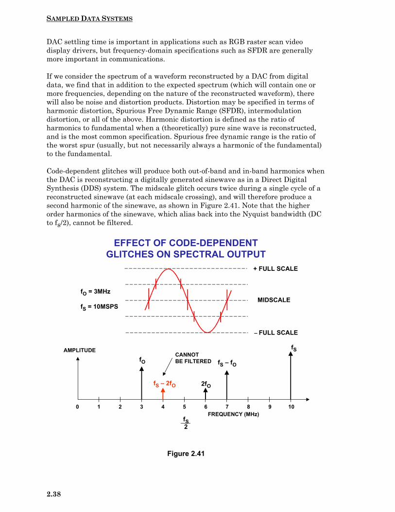
SAMPLED DATA SYSTEMS
2.38
DAC settling time is important in applications such as RGB raster scan videodisplay drivers, but frequency-domain specifications such as SFDR are generallymore important in communications.
If we consider the spectrum of a waveform reconstructed by a DAC from digitaldata, we find that in addition to the expected spectrum (which will contain one ormore frequencies, depending on the nature of the reconstructed waveform), therewill also be noise and distortion products. Distortion may be specified in terms ofharmonic distortion, Spurious Free Dynamic Range (SFDR), intermodulationdistortion, or all of the above. Harmonic distortion is defined as the ratio ofharmonics to fundamental when a (theoretically) pure sine wave is reconstructed,and is the most common specification. Spurious free dynamic range is the ratio ofthe worst spur (usually, but not necessarily always a harmonic of the fundamental)to the fundamental.
Code-dependent glitches will produce both out-of-band and in-band harmonics whenthe DAC is reconstructing a digitally generated sinewave as in a Direct DigitalSynthesis (DDS) system. The midscale glitch occurs twice during a single cycle of areconstructed sinewave (at each midscale crossing), and will therefore produce asecond harmonic of the sinewave, as shown in Figure 2.41. Note that the higherorder harmonics of the sinewave, which alias back into the Nyquist bandwidth (DCto fs/2), cannot be filtered.
Figure 2.41
EFFECT OF CODE-DEPENDENTGLITCHES ON SPECTRAL OUTPUT
+ FULL SCALE
MIDSCALE
– FULL SCALE
fO = 3MHz
fS = 10MSPS
0 1 2 3 4 5 6 7 8 9 10
fS2
fSfO fS – fO
2fOfS – 2fO
CANNOTBE FILTERED
AMPLITUDE
FREQUENCY (MHz)

SAMPLED DATA SYSTEMS
2.39
It is difficult to predict the harmonic distortion or SFDR from the glitch areaspecification alone. Other factors, such as the overall linearity of the DAC, alsocontribute to distortion. It is therefore customary to test reconstruction DACs in thefrequency domain (using a spectrum analyzer) at various clock rates and outputfrequencies as shown in Figure 2.43. Typical SFDR for the 14-bit AD9772 TransmitDAC is shown in Figure 2.44. The clock rate is 65MSPS, and the output frequency isswept to 25MHz. As in the case of ADCs, quantization noise will appear asincreased harmonic distortion if the ratio between the clock frequency and the DACoutput frequency is an integer number. These ratios should be avoided whenmaking the SFDR measurements.
Figure 2.42
CONTRIBUTORS TO DDS DAC DISTORTION
Resolution
Integral Non-Linearity
Differential Non-Linearity
Code-Dependent Glitches
Ratio of Clock Frequency to Output Frequency (Even in an IdealDAC)
Mathematical Analysis is Difficult !

SAMPLED DATA SYSTEMS
2.40
Figure 2.43
Figure 2.44
TEST SETUP FOR MEASURING DAC SFDR
fc
PC
STABLEFREQUENCYREFERENCE
DDSSYSTEM LATCH DAC
SPECTRUMANALYZER
fo
N N
PARALLEL ORSERIAL PORT
AD9772 14-BIT TxDAC™ SFDR,DATA UPDATE RATE = 65MSPS
SFDR(dBc)
DAC OUTPUT FREQUENCY (MHz)

SAMPLED DATA SYSTEMS
2.41
DAC sin (x)/x Frequency Rolloff
The output of a reconstruction DAC can be visualized as a series of rectangularpulses whose width is equal to the reciprocal of the clock rate as shown in Figure2.45. Note that the reconstructed signal amplitude is down 3.92dB at the Nyquistfrequency, fc/2. An inverse sin(x)/x filter can be used to compensate for this effect inmost cases. The images of the fundamental signal are also attenuated by thesin(x)/x function.
Figure 2.45
DAC SIN X/X ROLL OFF(AMPLITUDE NORMALIZED)
0.5fc fc 1.5fc 2fc 2.5fc 3fc
A = sin ππππ f
fcππππ ffc
1
f
A
t
t
–3.92dB
SAMPLEDSIGNAL
RECONSTRUCTED SIGNAL
0
1fc
IMAGESIMAGES
IMAGES

SAMPLED DATA SYSTEMS
2.42
REFERENCES
1. Active and Passive Electrical Wave Filter Catalog, Vol. 34, TTE,Incorporated, 2251 Barry Avenue, Los Angeles, CA 90064.
2. W. R. Bennett, “Spectra of Quantized Signals”, Bell System TechnicalJournal, No. 27, July 1948, pp. 446-472.
3. Steve Ruscak and Larry Singer, Using Histogram Techniques toMeasure A/D Converter Noise, Analog Dialogue, Vol. 29-2, 1995.
4. M.J. Tant, The White Noise Book, Marconi Instruments, July 1974.
5. G.A. Gray and G.W. Zeoli, Quantization and Saturation Noise dueto A/D Conversion, IEEE Trans. Aerospace and ElectronicSystems, Jan. 1971, pp. 222-223.
6. Chuck Lane, A 10-bit 60MSPS Flash ADC, Proceedings of the 1989Bipolar Circuits and Technology Meeting, IEEE Catalog No.89CH2771-4, September 1989, pp. 44-47.
7. F.D. Waldhauer, Analog to Digital Converter, U.S. Patent3-187-325, 1965.
8. J.O. Edson and H.H. Henning, Broadband Codecs for an Experimental224Mb/s PCM Terminal, Bell System Technical Journal, 44,November 1965, pp. 1887-1940.
9. J.S. Mayo, Experimental 224Mb/s PCM Terminals, Bell SystemTechnical Journal, 44, November 1965, pp. 1813-1941.
10. Hermann Schmid, Electronic Analog/Digital Conversions,Van Nostrand Reinhold Company, New York, 1970.
11. Carl Moreland, An 8-bit 150MSPS Serial ADC, 1995 ISSCC Digestof Technical Papers, Vol. 38, p. 272.
12. Roy Gosser and Frank Murden, A 12-bit 50MSPS Two-Stage A/DConverter, 1995 ISSCC Digest of Technical Papers, p. 278.
13. Carl Moreland, An Analog-to-Digital Converter Using Serial-Ripple Architecture, Masters' Thesis, Florida State UniversityCollege of Engineering, Department of Electrical Engineering, 1995.
14. Practical Analog Design Techniques, Analog Devices, 1995, Chapter4, 5, and 8.
15. Linear Design Seminar, Analog Devices, 1995, Chapter 4, 5.

SAMPLED DATA SYSTEMS
2.43
16. System Applications Guide, Analog Devices, 1993, Chapter 12, 13,15,16.
17. Amplifier Applications Guide, Analog Devices, 1992, Chapter 7.
18. Walt Kester, Drive Circuitry is Critical to High-Speed Sampling ADCs,Electronic Design Special Analog Issue, Nov. 7, 1994, pp. 43-50.
19. Walt Kester, Basic Characteristics Distinguish Sampling A/D Converters,EDN, Sept. 3, 1992, pp. 135-144.
20. Walt Kester, Peripheral Circuits Can Make or Break Sampling ADCSystems, EDN, Oct. 1, 1992, pp. 97-105.
21. Walt Kester, Layout, Grounding, and Filtering Complete SamplingADC System, EDN, Oct. 15, 1992, pp. 127-134.
22. Robert A. Witte, Distortion Measurements Using a Spectrum Analyzer,RF Design, September, 1992, pp. 75-84.
23. Walt Kester, Confused About Amplifier Distortion Specs?, AnalogDialogue, 27-1, 1993, pp. 27-29.
24. System Applications Guide, Analog Devices, 1993, Chapter 16.
25. Frederick J. Harris, On the Use of Windows for Harmonic Analysiswith the Discrete Fourier Transform, IEEE Proceedings, Vol. 66, No. 1,Jan. 1978, pp. 51-83.
26. Joey Doernberg, Hae-Seung Lee, David A. Hodges, Full Speed Testingof A/D Converters, IEEE Journal of Solid State Circuits, Vol. SC-19,No. 6, Dec. 1984, pp. 820-827.
27. Brendan Coleman, Pat Meehan, John Reidy and Pat Weeks, CoherentSampling Helps When Specifying DSP A/D Converters, EDN, October 15,1987, pp. 145-152.
28. Robert W. Ramierez, The FFT: Fundamentals and Concepts,Prentice-Hall, 1985.
29. R. B. Blackman and J. W. Tukey, The Measurement of PowerSpectra, Dover Publications, New York, 1958.
30. James J. Colotti, Digital Dynamic Analysis of A/D ConversionSystems Through Evaluation Software Based on FFT/DFT Analysis,RF Expo East 1987 Proceedings, Cardiff Publishing Co., pp. 245-272.
31. HP Journal, Nov. 1982, Vol. 33, No. 11.
32. HP Product Note 5180A-2.

SAMPLED DATA SYSTEMS
2.44
33. HP Journal, April 1988, Vol. 39, No. 2.
34. HP Journal, June 1988, Vol. 39, No. 3.
35. Dan Sheingold, Editor, Analog-to-Digital Conversion Handbook,Third Edition, Prentice-Hall, 1986.
36. Lawrence Rabiner and Bernard Gold, Theory and Application ofDigital Signal Processing, Prentice-Hall, 1975.
37. Matthew Mahoney, DSP-Based Testing of Analog and Mixed-SignalCircuits, IEEE Computer Society Press, Washington, D.C., 1987.
38. IEEE Trial-Use Standard for Digitizing Waveform Recorders,No. 1057-1988.
39. Richard J. Higgins, Digital Signal Processing in VSLI, Prentice-Hall,1990.
40. M. S. Ghausi and K. R. Laker, Modern Filter Design: Active RC andSwitched Capacitors, Prentice Hall, 1981.
41. Mathcad™ 4.0 software package available from MathSoft, Inc.,201 Broadway, Cambridge MA, 02139.
42. Howard E. Hilton, A 10MHz Analog-to-Digital Converter with 110dBLinearity, H.P. Journal, October 1993, pp. 105-112.

ADCS FOR DSP APPLICATIONS
3.a
SECTION 3
ADCs FOR DSP APPLICATIONS
Successive Approximation ADCs
Sigma-Delta ADCs
Flash Converters
Subranging (Pipelined) ADCs
Bit-Per-Stage (Serial, or Ripple) ADCs

ADCS FOR DSP APPLICATIONS
3.b

ADCS FOR DSP APPLICATIONS
3.1
SECTION 3
ADCs FOR DSP APPLICATIONSWalt Kester, James BryantThe trend in ADCs and DACs is toward higher speeds and higher resolutions atreduced power levels and supply voltages. Modern data converters generally operateon ±5V (dual supply), +5V or +3V (single supply). In fact, the number of +3V devicesis rapidly increasing because of many new markets such as digital cameras,camcorders, and cellular telephones. This trend has created a number of design andapplications problems which were much less important in earlier data converters,where ±15V supplies and ±10V input ranges were the standard.
Lower supply voltages imply smaller input voltage ranges, and hence moresusceptibility to noise from all potential sources: power supplies, references, digitalsignals, EMI/RFI, and probably most important, improper layout, grounding, anddecoupling techniques. Single-supply ADCs often have an input range which is notreferenced to ground. Finding compatible single-supply drive amplifiers and dealingwith level shifting of the input signal in direct-coupled applications also becomes achallenge.
In spite of these issues, components are now available which allow extremely highresolutions at low supply voltages and low power. This section discusses theapplications problems associated with such components and shows techniques forsuccessfully designing them into systems.
The most popular ADCs for DSP applications are based on five fundamentalarchitectures: successive approximation, sigma-delta, flash, subranging (orpipelined), and bit-per-stage (or ripple).
Figure 3.1
LOW POWER, LOW VOLTAGE ADC DESIGN ISSUES
Typical Supply Voltages: ±5V, +5V, +5/+3V, +3V
Lower Signal Swings Increase Sensitivity to
All Types of Noise (Device, Power Supply, Logic, etc.)
Device Noise Increases at Low Currents
Common Mode Input Voltage Restrictions
Input Buffer Amplifier Selection Critical
Auto-Calibration Modes Desirable at High Resolutions

ADCS FOR DSP APPLICATIONS
3.2
Figure 3.2
SUCCESSIVE APPROXIMATION ADCS
The successive approximation ADC has been the mainstay of signal conditioning formany years. Recent design improvements have extended the sampling frequency ofthese ADCs into the megahertz region. The use of internal switched capacitortechniques along with auto calibration techniques extend the resolution of theseADCs to 16-bits on standard CMOS processes without the need for expensive thin-film laser trimming.
The basic successive approximation ADC is shown in Figure 3.3. It performsconversions on command. On the assertion of the CONVERT START command, thesample-and-hold (SHA) is placed in the hold mode, and all the bits of the successiveapproximation register (SAR) are reset to "0" except the MSB which is set to "1".The SAR output drives the internal DAC. If the DAC output is greater than theanalog input, this bit in the SAR is reset, otherwise it is left set. The next mostsignificant bit is then set to "1". If the DAC output is greater than the analog input,this bit in the SAR is reset, otherwise it is left set. The process is repeated with eachbit in turn. When all the bits have been set, tested, and reset or not as appropriate,the contents of the SAR correspond to the value of the analog input, and theconversion is complete. These bit “tests” can form the basis of a serial outputversion SAR-based ADC.
ADCs FOR DSP APPLICATIONS
Successive Approximation Resolutions to 16-bits Minimal Throughput Delay Time (No Output Latency,
"Single-Shot" Operation Possible Used in Multiplexed Data Acquisition Systems
Sigma-Delta Resolutions to 24-bits Excellent Differential Linearity Internal Digital Filter (Can be Linear Phase) Long Throughput Delay Time (Output Latency) Difficult to Multiplex Inputs Due to Digital Filter Settling Time
High Speed Architectures: Flash Converter Subranging or Pipelined Bit-Per-Stage (Ripple)

ADCS FOR DSP APPLICATIONS
3.3
The end of conversion is generally indicated by an end-of-convert (EOC), data-ready(DRDY), or a busy signal (actually, not-BUSY indicates end of conversion). Thepolarities and name of this signal may be different for different SAR ADCs, but thefundamental concept is the same. At the beginning of the conversion interval, thesignal goes high (or low) and remains in that state until the conversion iscompleted, at which time it goes low (or high). The trailing edge is generally anindication of valid output data.
Figure 3.3
An N-bit conversion takes N steps. It would seem on superficial examination that a16-bit converter would have twice the conversion time of an 8-bit one, but this is notthe case. In an 8-bit converter, the DAC must settle to 8-bit accuracy before the bitdecision is made, whereas in a 16-bit converter, it must settle to 16-bit accuracy,which takes a lot longer. In practice, 8-bit successive approximation ADCs canconvert in a few hundred nanoseconds, while 16-bit ones will generally take severalmicroseconds.
Notice that the overall accuracy and linearity of the SAR ADC is determinedprimarily by the internal DAC. Until recently, most precision SAR ADCs used laser-trimmed thin-film DACs to achieve the desired accuracy and linearity. The thin-filmresistor trimming process adds cost, and the thin-film resistor values may beaffected when subjected to the mechanical stresses of packaging.
For these reasons, switched capacitor (or charge-redistribution) DACs have becomepopular in newer SAR ADCs. The advantage of the switched capacitor DAC is thatthe accuracy and linearity is primarily determined by photolithography, which inturn controls the capacitor plate area and the capacitance as well as matching. In
SUCCESSIVE APPROXIMATION ADC
SHA
SUCCESSIVEAPPROXIMATION
REGISTER(SAR)
DAC
TIMING
CONVERTSTART
EOC,DRDY,
OR BUSY
OUTPUT
ANALOGINPUT COMPARATOR

ADCS FOR DSP APPLICATIONS
3.4
addition, small capacitors can be placed in parallel with the main capacitors whichcan be switched in and out under control of autocalibration routines to achieve highaccuracy and linearity without the need for thin-film laser trimming. Temperaturetracking between the switched capacitors can be better than 1ppm/ºC, therebyoffering a high degree of temperature stability.
A simple 3-bit capacitor DAC is shown in Figure 3.4. The switches are shown in thetrack, or sample mode where the analog input voltage, AIN, is constantly chargingand discharging the parallel combination of all the capacitors. The hold mode isinitiated by opening SIN, leaving the sampled analog input voltage on the capacitorarray. Switch SC is then opened allowing the voltage at node A to move as the bitswitches are manipulated. If S1, S2, S3, and S4 are all connected to ground, avoltage equal to –AIN appears at node A. Connecting S1 to VREF adds a voltageequal to VREF/2 to –AIN. The comparator then makes the MSB bit decision, andthe SAR either leaves S1 connected to VREF or connects it to ground depending onthe comparator output (which is high or low depending on whether the voltage atnode A is negative or positive, respectively). A similar process is followed for theremaining two bits. At the end of the conversion interval, S1, S2, S3, S4, and SINare connected to AIN, SC is connected to ground, and the converter is ready foranother cycle.
Figure 3.4
Note that the extra LSB capacitor (C/4 in the case of the 3-bit DAC) is required tomake the total value of the capacitor array equal to 2C so that binary division isaccomplished when the individual bit capacitors are manipulated.
3-BIT SWITCHED CAPACITOR DAC
_
+C/ 4C/ 2C C/ 4
AIN
VREF
SIN
SC
S1 S2 S3 S4
BIT1(MSB)
BIT2 BIT3(LSB)
SWITCHES SHOWN IN TRACK (SAMPLE) MODE
A
CTOTAL = 2C

ADCS FOR DSP APPLICATIONS
3.5
The operation of the capacitor DAC (cap DAC) is similar to an R/2R resistive DAC.When a particular bit capacitor is switched to VREF, the voltage divider created bythe bit capacitor and the total array capacitance (2C) adds a voltage to node A equalto the weight of that bit. When the bit capacitor is switched to ground, the samevoltage is subtracted from node A.
Because of their popularity, successive approximation ADCs are available in a widevariety of resolutions, sampling rates, input and output options, package styles, andcosts. It would be impossible to attempt to list all types, but Figure 3.5 shows anumber of recent Analog Devices' SAR ADCs which are representative. Note thatmany devices are complete data acquisition systems with input multiplexers whichallow a single ADC core to process multiple analog channels.
Figure 3.5
While there are some variations, the fundamental timing of most SAR ADCs issimilar and relatively straightforward (see Figure 3.6). The conversion process isinitiated by asserting a CONVERT START signal. The CONVST signal is anegative-going pulse whose positive-going edge actually initiates the conversion.The internal sample-and-hold (SHA) amplifier is placed in the hold mode on thisedge, and the various bits are determined using the SAR algorithm. The negative-going edge of the CONVST pulse causes the EOC or BUSY line to go high. Whenthe conversion is complete, the BUSY line goes low, indicating the completion of theconversion process. In most cases the trailing edge of the BUSY line can be used asan indication that the output data is valid and can be used to strobe the output datainto an external register. However, because of the many variations in terminology
RESOLUTION / CONVERSION TIME COMPARISONFOR REPRESENTATIVE SINGLE-SUPPLY SAR ADCs
AD7472
AD7891
AD7858/59
AD7887/88
AD7856/57
AD7660
AD974
AD7664
RESOLUTION
12-BITS
12-BITS
12-BITS
12-BITS
14-BITS
16-BITS
16-BITS
16-BITS
SAMPLINGRATE
1.5MSPS
500kSPS
200kSPS
125kSPS
285kSPS
100kSPS
200kSPS
570kSPS
POWER
9mW
85mW
20mW
3.5mW
60mW
15mW
120mW
150mW
CHANNELS
1
8
8
8
8
1
4
1

ADCS FOR DSP APPLICATIONS
3.6
and design, the individual data sheet should always be consulted when using aspecific ADC.
Figure 3.6
It should also be noted that some SAR ADCs require an external high frequencyclock in addition to the CONVERT START command. In most cases, there is noneed to synchronize the two. The frequency of the external clock, if required,generally falls in the range of 1MHz to 30MHz depending on the conversion timeand resolution of the ADC. Other SAR ADCs have an internal oscillator which isused to perform the conversions and only require the CONVERT START command.Because of their architecture, SAR ADCs allow single-shot conversion at anyrepetition rate from DC to the converter's maximum conversion rate.
In a SAR ADC, the output data for a sampled input is valid at the end of theconversion interval for that sampled input. In other ADC architectures, such assigma-delta or the two-stage subranging architecture shown in Figure 3.7, this isnot the case. The subranging ADC shown in the figure is a two-stage pipelined orsubranging 12-bit converter. The first conversion is done by the 6-bit ADC whichdrives a 6-bit DAC. The output of the 6-bit DAC represents a 6-bit approximation tothe analog input. Note that SHA2 delays the analog signal while the 6-bit ADCmakes its decision and the 6-bit DAC settles. The DAC approximation is thensubtracted from the analog signal from SHA2, amplified, and digitized by a 7-bitADC. The outputs of the two conversions are combined, and the extra bit used tocorrect errors made in the first conversion. The typical timing associated with thistype of converter is shown in Figure 3.8. Note that the output data presentedimmediately after sample X actually corresponds to sample X–2, i.e., there is a twoclock-cycle "pipeline" delay. The pipelined ADC architecture is generally associatedwith high speed ADCs, and in most cases the pipeline delay, or latency, is not amajor system problem in most applications where this type of converter is used.
TYPICAL SAR ADC TIMING
CONVST
CONVERSIONTIME
SAMPLE X SAMPLE X+1 SAMPLE X+2
DATAX
DATAX+1
OUTPUTDATA
EOC,BUSY
TRACK/ACQUIRE
CONVERSIONTIME
TRACK/ACQUIRE

ADCS FOR DSP APPLICATIONS
3.7
Figure 3.7
Figure 3.8
12-BIT TWO-STAGE PIPELINED ADC ARCHITECTURE
SHA1
SHA2
TIMING 6-BITADC
6-BITDAC
BUFFERREGISTER
+
_
7-BITADC
ERROR CORRECTION LOGIC
OUTPUT REGISTERS
6
6 7
12
12
ANALOGINPUT
SAMPLINGCLOCK
OUTPUT DATA
TYPICAL PIPELINED ADC TIMING
SAMPLINGCLOCK
SAMPLE X SAMPLE X+1 SAMPLE X+2
DATAX–2
DATAX–1
DATAX
OUTPUTDATA
ABOVE SHOWS TWO CLOCK-CYCLES PIPELINE DELAY

ADCS FOR DSP APPLICATIONS
3.8
Pipelined ADCs may have more than two clock-cycles latency depending on theparticular architecture. For instance, the conversion could be done in three, or four,or perhaps even more pipelined stages causing additional latency in the outputdata.
Therefore, if the ADC is to be used in an event-triggered (or single-shot) modewhere there must be a one-to-one time correspondence between each sample and thecorresponding data, then the pipeline delay can be troublesome, and the SARarchitecture is advantageous. Pipeline delay or latency can also be a problem inhigh speed servo-loop control systems or multiplexed applications. In addition, somepipelined converters have a minimum allowable conversion rate and must be keptrunning to prevent saturation of internal nodes.
Switched capacitor SAR ADCs generally have unbuffered input circuits similar tothe circuit shown in Figure 3.9 for the AD7858/59 ADC. During the acquisition time,the analog input must charge the 20pF equivalent input capacitance to the correctvalue. If the input is a DC signal, then the source resistance, RS, in series with the125Ω internal switch resistance creates a time constant. In order to settle to 12-bitaccuracy, approximately 9 time constants must be allowed for settling, and thisdefines the minimum allowable acquisition time. (Settling to 14-bits requires about10 time constants, and 16-bits requires about 11).
tACQ > 9 × (RS + 125)Ω × 20pF.
For example, if RS = 50Ω, the acquisition time per the above formula must be atleast 310ns.
For AC applications, a low impedance source should be used to prevent distortiondue to the non-linear ADC input circuit. In a single supply application, a fastsettling rail-to-rail op amp such as the AD820 should be used. Fast settling allowsthe op amp to settle quickly from the transient currents induced on its input by theinternal ADC switches. In Figure 3.9, the AD820 drives a lowpass filter consistingof the 50Ω series resistor and the 10nF capacitor (cutoff frequency approximately320kHz). This filter removes high frequency components which could result inaliasing and decreases the noise.
Using a single supply op amp in this application requires special consideration ofsignal levels. The AD820 is connected in the inverting mode and has a signal gain of–1. The noninverting input is biased at a common mode voltage of +1.3V with the10.7kΩ/10kΩ divider, resulting in an output voltage of +2.6V for VIN= 0V, and+0.1V for VIN = +2.5V. This offset is provided because the AD820 output cannot goall the way to ground, but is limited to the VCESAT of the output stage NPNtransistor, which under these loading conditions is about 50mV. The input range ofthe ADC is also offset by +100mV by applying the +100mV offset from the412Ω/10kΩ divider to the AIN– input.

ADCS FOR DSP APPLICATIONS
3.9
Figure 3.9
SIGMA-DELTA (ΣΣΣΣ∆∆∆∆) ADCSJames M. BryantSigma-Delta Analog-Digital Converters (Σ∆ ADCs) have been known for nearlythirty years, but only recently has the technology (high-density digital VLSI) existedto manufacture them as inexpensive monolithic integrated circuits. They are nowused in many applications where a low-cost, low-bandwidth, low-power,high-resolution ADC is required.
There have been innumerable descriptions of the architecture and theory of Σ∆ADCs, but most commence with a maze of integrals and deteriorate from there. Inthe Applications Department at Analog Devices, we frequently encounter engineerswho do not understand the theory of operation of Σ∆ ADCs and are convinced, fromstudy of a typical published article, that it is too complex to comprehend easily.
There is nothing particularly difficult to understand about Σ∆ ADCs, as long as youavoid the detailed mathematics, and this section has been written in an attempt toclarify the subject. A Σ∆ ADC contains very simple analog electronics (a comparator,voltage reference, a switch, and one or more integrators and analog summingcircuits), and quite complex digital computational circuitry. This circuitry consists ofa digital signal processor (DSP) which acts as a filter (generally, but not invariably,
DRIVING SWITCHED CAPACITOR INPUTSOF AD7858/59 12-BIT, 200kSPS ADC
AD820
_
+
+
_
CAPDAC
10kΩΩΩΩ
10kΩΩΩΩ
10.7kΩΩΩΩ10kΩΩΩΩ
50ΩΩΩΩ
10nF
125ΩΩΩΩ
125ΩΩΩΩ
20pFT
H
H TVREF
AIN+
AIN–
DGND AGND
AVDD DVDD
0.1µF
0.1µF
+2.5V+1.30V
+3V TO +5V
VIN
VIN : 0V TO +2.5V
AIN+ : +2.6V TO +0.1VAD7858/59
CUTOFF= 320kHz
0.1µF
VCM =
NOTE: ONLY ONE INPUT SHOWN
T = TRACKH = HOLD
10kΩΩΩΩ
412ΩΩΩΩ +100mV
0.1µF
0.1µF
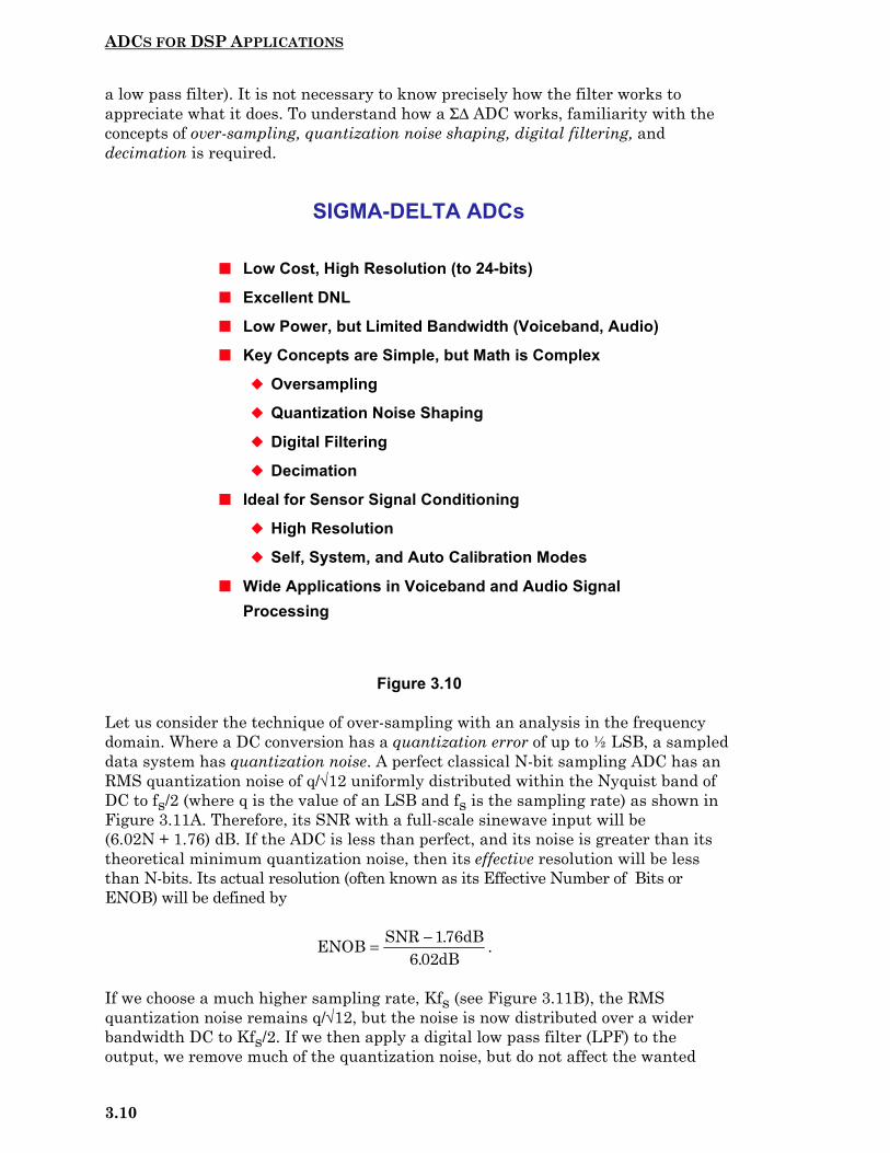
ADCS FOR DSP APPLICATIONS
3.10
a low pass filter). It is not necessary to know precisely how the filter works toappreciate what it does. To understand how a Σ∆ ADC works, familiarity with theconcepts of over-sampling, quantization noise shaping, digital filtering, anddecimation is required.
Figure 3.10
Let us consider the technique of over-sampling with an analysis in the frequencydomain. Where a DC conversion has a quantization error of up to ½ LSB, a sampleddata system has quantization noise. A perfect classical N-bit sampling ADC has anRMS quantization noise of q/√12 uniformly distributed within the Nyquist band ofDC to fs/2 (where q is the value of an LSB and fs is the sampling rate) as shown inFigure 3.11A. Therefore, its SNR with a full-scale sinewave input will be(6.02N + 1.76) dB. If the ADC is less than perfect, and its noise is greater than itstheoretical minimum quantization noise, then its effective resolution will be lessthan N-bits. Its actual resolution (often known as its Effective Number of Bits orENOB) will be defined by
ENOB SNR dBdB
= − 1766 02
..
.
If we choose a much higher sampling rate, Kfs (see Figure 3.11B), the RMSquantization noise remains q/√12, but the noise is now distributed over a widerbandwidth DC to Kfs/2. If we then apply a digital low pass filter (LPF) to theoutput, we remove much of the quantization noise, but do not affect the wanted
SIGMA-DELTA ADCs
Low Cost, High Resolution (to 24-bits)
Excellent DNL
Low Power, but Limited Bandwidth (Voiceband, Audio)
Key Concepts are Simple, but Math is Complex
Oversampling
Quantization Noise Shaping
Digital Filtering
Decimation
Ideal for Sensor Signal Conditioning
High Resolution
Self, System, and Auto Calibration Modes
Wide Applications in Voiceband and Audio SignalProcessing

ADCS FOR DSP APPLICATIONS
3.11
signal - so the ENOB is improved. We have accomplished a high resolution A/Dconversion with a low resolution ADC. The factor K is generally referred to as theoversampling ratio. It should be noted at this point that oversampling has an addedbenefit in that it relaxes the requirements on the analog antialiasing filter.
Figure 3.11
Since the bandwidth is reduced by the digital output filter, the output data rate maybe lower than the original sampling rate (Kfs) and still satisfy the Nyquist criterion.This may be achieved by passing every Mth result to the output and discarding theremainder. The process is known as "decimation" by a factor of M. Despite theorigins of the term (decem is Latin for ten), M can have any integer value, providedthat the output data rate is more than twice the signal bandwidth. Decimation doesnot cause any loss of information (see Figure 3.11B).
If we simply use over-sampling to improve resolution, we must over-sample by afactor of 22N to obtain an N-bit increase in resolution. The Σ∆ converter does notneed such a high over-sampling ratio because it not only limits the signal passband,but also shapes the quantization noise so that most of it falls outside this passbandas shown in Figure 3.11C.
If we take a 1-bit ADC (generally known as a comparator), drive it with the outputof an integrator, and feed the integrator with an input signal summed with theoutput of a 1-bit DAC fed from the ADC output, we have a first-order Σ∆ modulatoras shown in Figure 3.12. Add a digital low pass filter (LPF) and decimator at thedigital output, and we have a Σ∆ ADC: the Σ∆ modulator shapes the quantization
OVERSAMPLING, DIGITAL FILTERING,NOISE SHAPING, AND DECIMATION
fs2
fs
Kfs2
Kfs
KfsKfs2
fs2
fs2
DIGITAL FILTERREMOVED NOISE
REMOVED NOISE
QUANTIZATIONNOISE = q / 12 q = 1 LSBADC
ADC DIGITALFILTER
Σ∆Σ∆Σ∆Σ∆MOD
DIGITALFILTER
fs
Kfs
Kfs
DEC
fs
NyquistOperation
Oversampling+ Digital Filter+ Decimation
Oversampling+ Noise Shaping+ Digital Filter+ Decimation
A
B
C
DEC
fs

ADCS FOR DSP APPLICATIONS
3.12
noise so that it lies above the passband of the digital output filter, and the ENOB istherefore much larger than would otherwise be expected from the over-samplingratio.
Figure 3.12
Intuitively, a Σ∆ ADC operates as follows. Assume a DC input at VIN. Theintegrator is constantly ramping up or down at node A. The output of thecomparator is fed back through a 1-bit DAC to the summing input at node B. Thenegative feedback loop from the comparator output through the 1-bit DAC back tothe summing point will force the average DC voltage at node B to be equal to VIN.This implies that the average DAC output voltage must equal to the input voltageVIN. The average DAC output voltage is controlled by the ones-density in the 1-bitdata stream from the comparator output. As the input signal increases towards+VREF, the number of "ones" in the serial bit stream increases, and the number of"zeros" decreases. Similarly, as the signal goes negative towards –VREF, thenumber of "ones" in the serial bit stream decreases, and the number of "zeros"increases. From a very simplistic standpoint, this analysis shows that the averagevalue of the input voltage is contained in the serial bit stream out of thecomparator. The digital filter and decimator process the serial bit stream andproduce the final output data.
The concept of noise shaping is best explained in the frequency domain byconsidering the simple Σ∆ modulator model in Figure 3.13.
FIRST-ORDER SIGMA-DELTA ADC
∑ ∫ +
_
+VREF
–VREF
DIGITALFILTER
ANDDECIMATOR
+
_
CLOCKKfs
VINN-BITS
fs
fs
A
B
1-BIT DATASTREAM1-BIT
DAC
LATCHEDCOMPARATOR(1-BIT ADC)
1-BIT,Kfs
SIGMA-DELTA MODULATOR
INTEGRATOR

ADCS FOR DSP APPLICATIONS
3.13
Figure 3.13
The integrator in the modulator is represented as an analog lowpass filter with atransfer function equal to H(f) = 1/f. This transfer function has an amplituderesponse which is inversely proportional to the input frequency. The 1-bit quantizergenerates quantization noise, Q, which is injected into the output summing block. Ifwe let the input signal be X, and the output Y, the signal coming out of the inputsummer must be X – Y. This is multiplied by the filter transfer function, 1/f, and theresult goes to one input to the output summer. By inspection, we can then write theexpression for the output voltage Y as:
Yf
X Y Q= − +1 ( ) .
This expression can easily be rearranged and solved for Y in terms of X, f, and Q:
Y Xf
Q ff
=+
+ ⋅+1 1
.
Note that as the frequency f approaches zero, the output voltage Y approaches Xwith no noise component. At higher frequencies, the amplitude of the signalcomponent approaches zero, and the noise component approaches Q. At highfrequency, the output consists primarily of quantization noise. In essence, theanalog filter has a lowpass effect on the signal, and a highpass effect on thequantization noise. Thus the analog filter performs the noise shaping function in theΣ∆ modulator model.
SIMPLIFIED FREQUENCY DOMAIN LINEARIZED MODEL OFA SIGMA-DELTA MODULATOR
∑ ANALOG FILTERH(f) = 1
f∑
X Y
+
_
X – Y1f
( X – Y )Q = QUANTIZATIONNOISE
Y = 1f
( X – Y ) + Q
REARRANGING, SOLVING FOR Y:
Y = X
f + 1 + Q ff + 1
SIGNAL TERM NOISE TERM
Y

ADCS FOR DSP APPLICATIONS
3.14
For a given input frequency, higher order analog filters offer more attenuation. Thesame is true of Σ∆ modulators, provided certain precautions are taken.
By using more than one integration and summing stage in the Σ∆ modulator, we canachieve higher orders of quantization noise shaping and even better ENOB for agiven over-sampling ratio as is shown in Figure 3.14 for both a first and second-order Σ∆ modulator. The block diagram for the second-order Σ∆ modulator is shownin Figure 3.15. Third, and higher, order Σ∆ ADCs were once thought to bepotentially unstable at some values of input - recent analyses using finite ratherthan infinite gains in the comparator have shown that this is not necessarily so, buteven if instability does start to occur, it is not important, since the DSP in thedigital filter and decimator can be made to recognize incipient instability and reactto prevent it.
Figure 3.16 shows the relationship between the order of the Σ∆ modulator and theamount of over-sampling necessary to achieve a particular SNR. For instance, if theoversampling ratio is 64, an ideal second-order system is capable of providing anSNR of about 80dB. This implies approximately 13 effective number of bits (ENOB).Although the filtering done by the digital filter and decimator can be done to anydegree of precision desirable, it would be pointless to carry more than 13 binary bitsto the outside world. Additional bits would carry no useful signal information, andwould be buried in the quantization noise unless post-filtering techniques wereemployed. Additional resolution can be obtained by increasing the oversamplingratio and/or by using a higher-order modulator.
Figure 3.14
SIGMA-DELTA MODULATORSSHAPE QUANTIZATION NOISE
fs2
Kfs2
2ND ORDER
1ST ORDER
DIGITALFILTER

ADCS FOR DSP APPLICATIONS
3.15
Figure 3.15
Figure 3.16
SECOND-ORDER SIGMA-DELTA ADC
∑ ∫+
_
VIN
INTEGRATOR
∑ ∫ +
_
CLOCKKfs
1-BITDAC
INTEGRATOR
DIGITAL FILTERAND
DECIMATOR
N-BITSfs
+
_
1-BITDATASTREAM
SNR VERSUS OVERSAMPLING RATIO FOR FIRST,SECOND, AND THIRD-ORDER LOOPS
FIRST-ORDER LOOP9dB / OCTAVE
SECOND-ORDER LOOP15dB / OCTAVE
THIRD-ORDER LOOP*21dB / OCTAVE
* > 2nd ORDER LOOPS DO NOTOBEY LINEAR MODEL
4 8 16 32 64 128 2560
20
40
60
80
100
120
SNR(dB)
OVERSAMPLING RATIO, K

ADCS FOR DSP APPLICATIONS
3.16
The AD1877 is a 16-bit 48kSPS stereo sigma-delta DAC suitable for demandingaudio applications. Key specifications are summarized in Figure 3.17. This devicehas a 64X oversampling ratio, and a fourth-order modulator. The internal digitalfilter is a linear phase FIR filter whose response is shown in Figure 3.18. Thepassband ripple is 0.006dB, and the attenuation is greater than 90dB in thestopband. The width of the transition region from passband to stopband is only0.1fs, where fs is the effective sampling frequency of the AD1877 (maximum of48kSPS). Such a filter would obviously be impossible to implement in analog form.
Figure 3.17
All sigma-delta ADCs have a settling time associated with the internal digital filter,and there is no way to remove it. In multiplexed applications the input to the ADCis a step function if there are different input voltages on adjacent channels. In fact,the multiplexer output can represent a fullscale step voltage to the sigma-delta ADCwhen channels are switched. Adequate filter settling time must be allowed,therefore, in such applications. This does not mean that sigma-delta ADCsshouldn’t be used in multiplexed applications, just that the settling time of thedigital filter must be considered.
For example, the group delay through the AD1877 FIR filter is 36/fs, andrepresents the time it takes for a step function input to propagate through one-halfthe number of taps in the digital filter. The total time required for settling istherefore 72fs, or approximately 1.5ms when sampling at 48kSPS with a 64Xoversampling rate.
AD1877 16-BIT, 48kSPS STEREO SIGMA-DELTA ADC
Single +5 V Power Supply Single-Ended Dual-Channel Analog Inputs 92 dB (typ) Dynamic Range 90 dB (typ) S/(THD+N) 0.006 dB Decimator Passband Ripple Fourth-Order, 64-Times Oversampling Σ∆Σ∆Σ∆Σ∆ Modulator Three-Stage, Linear-Phase Decimator Less than 100 mW (typ) Power-Down Mode Input Overrange Indication On-Chip Voltage Reference Flexible Serial Output Interface 28-Pin SOIC Package

ADCS FOR DSP APPLICATIONS
3.17
Figure 3.18
In other applications, such as low frequency, high resolution 24-bit measurementsigma-delta ADCs (such as the AD77xx-series), other types of digital filters may beused. For instance, the SINC3 response is popular because it has zeros at multiplesof the throughput rate. For instance a 10Hz throughput rate produces zeros at50Hz and 60Hz which aid in AC power line rejection.
So far we have considered only sigma-delta converters which contain a single-bitADC (comparator) and a single-bit DAC (switch). The block diagram of Figure 3.19shows a multi-bit sigma-delta ADC which uses an n-bit flash ADC and an n-bitDAC. Obviously, this architecture will give a higher dynamic range for a givenoversampling ratio and order of loop filter. Stabilization is easier, since second-orderand higher loops can be used. Idling patterns tend to be more random therebyminimizing tonal effects.
The real disadvantage of this technique is that the linearity depends on the DAClinearity, and thin film laser trimming is generally required to approach 16-bitperformance levels. This makes the multi-bit architecture extremely difficult toimplement on sigma-delta ADCs. It is, however, currently used in sigma-delta audioDACs (AD1852, AD1853, AD1854) where special “bit scrambling” techniques areused to ensure linearity and eliminate idle tones.
AD1877 16-BIT, 48kSPS STEREO SIGMA-DELTA ADCFIR FILTER CHARACTERISTICS
fs = OUTPUT WORD RATE, 32kSPS, 44.1kSPS, OR 48kSPS TYPICAL PASSBAND TO STOPBAND TRANSITION REGION: 0.45fs TO 0.55fs SETTLING TIME = 72 / fs = 1.5ms FOR fs = 48kSPS GROUP DELAY = 36 / fs = 0.75ms FOR fs = 48kSPS
NORMALIZED fs

ADCS FOR DSP APPLICATIONS
3.18
Figure 3.19
The Σ∆ ADCs that we have described so far contain integrators, which are low passfilters, whose passband extends from DC. Thus, their quantization noise is pushedup in frequency. At present, most commercially available Σ∆ ADCs are of this type(although some which are intended for use in audio or telecommunicationsapplications contain bandpass rather than lowpass digital filters to eliminate anysystem DC offsets). But there is no particular reason why the filters of the Σ∆modulator should be LPFs, except that traditionally ADCs have been thought of asbeing baseband devices, and that integrators are somewhat easier to construct thanbandpass filters. If we replace the integrators in a Σ∆ ADC with bandpass filters(BPFs) as shown in Figure 3.20, the quantization noise is moved up and down infrequency to leave a virtually noise-free region in the pass-band (see Reference 1). Ifthe digital filter is then programmed to have its pass-band in this region, we have aΣ∆ ADC with a bandpass, rather than a lowpass characteristic. Such devices wouldappear to be useful in direct IF-to-digital conversion, digital radios, ultrasound, andother undersampling applications. However, the modulator and the digital BPFmust be designed for the specific set of frequencies required by the systemapplication, thereby somewhat limiting the flexibility of this approach.
In an undersampling application of a bandpass Σ∆ ADC, the minimum samplingfrequency must be at least twice the signal bandwidth, BW. The signal is centeredaround a carrier frequency, fc. A typical digital radio application using a 455kHzcenter frequency and a signal bandwidth of 10kHz is described in Reference 1. Anoversampling frequency Kfs = 2MSPS and an output rate fs = 20kSPS yielded adynamic range of 70dB within the signal bandwidth.
MULTI-BIT SIGMA-DELTA ADC
∑ ∫DIGITALFILTER
ANDDECIMATOR
+
_
CLOCKKfs
VIN N-BITS
fs
fs
n-BIT DATASTREAM
n-BITS,Kfs
INTEGRATOR
FLASHADC
n-BITS
n-BITDAC

ADCS FOR DSP APPLICATIONS
3.19
Figure 3.20
Most sigma-delta ADCs generally have a fixed internal digital filter. The filter’scutoff frequency and the ADC output data rate scales with the master clockfrequency. The AD7725 is a 16-bit sigma-delta ADC with a programmable internaldigital filter. The modulator operates at a maximum oversampling rate of19.2MSPS. The modulator is followed by a preset FIR filter which decimates themodulator output by a factor of 8, yielding an output data rate of 2.4MSPS. Theoutput of the preset filter drives a programmable FIR filter. By loading the ROMwith suitable coefficient values, this filter can be programmed for the desiredfrequency response.
The programmable filter is flexible with respect to number of taps and decimationrate. The filter can have up to 108 taps, up to 5 decimation stages, and a decimationfactor between 2 and 256. Coefficient precision is 24-bits, and arithmetic precision is30-bits.
The AD7725 contains Systolix’s PuldeDSP™ (trademark of Systolix) post processorwhich permits the filter characteristics to be programmed through the parallel orserial microprocessor interface. Or, it may boot at power-on-reset from its internalROM or from an external EPROM.
REPLACING INTEGRATORS WITH RESONATORSGIVES A BANDPASS SIGMA-DELTA ADC
ΣΣΣΣ ΣΣΣΣ+
-
+
-
1-BITDAC
ANALOGBPF
ANALOGBPF DIGITAL
BPF ANDDECIMATOR
CLOCK Kfs
fs
SHAPEDQUANTIZATION
NOISE
DIGITAL BPFRESPONSEfc
f
BW fs > 2 BW

ADCS FOR DSP APPLICATIONS
3.20
The post processor is a fully programmable core which provides processing power ofup to 130 million multiply-accumulates (MAC) per second. To program the postprocessor, the user must produce a configuration file which contains theprogramming data for the filter function. This file is generated by a compiler whichis available from Analog Devices. The AD7725 compiler accepts filter coefficientdata as an input and automatically generates the required device programmingdata.
The coefficient file for the FIR filter response can be generated using a digital filterdesign package such as QEDesign from Momentum Data Systems. The response ofthe filter can be plotted so the user knows the response before generating the filtercoefficients. The data is available to the processor at a 2.4MSPS rate. Whendecimation is employed in a multistage filter, the first filter will be operated at2.4MSPS, and the user can then decimate between stages. The number of tapswhich can be contained in the processor is 108. Therefore, a single filter with 108taps can be generated, or a multistage filter can be designed whereby the totalnumber of taps adds up to 108. The filter characteristic can be lowpass, highpass,bandstop, or bandpass.
The AD7725 operates on a single +5V supply, has an on-chip 2.5V reference, and ispackaged in a 44-pin PQFP. Power dissipation is approximately 350mW whenoperating at full power. A half-power mode is available with a master clockfrequency of 10MSPS maximum. Power consumption in the standby mode is 200mWmaximum. More details of the AD7725 operation can be found in Section 9.
Summary
A Σ∆ ADC works by over-sampling, where simple analog filters in the Σ∆ modulatorshape the quantization noise so that the SNR in the bandwidth of interest is muchgreater than would otherwise be the case, and by using high performance digitalfilters and decimation to eliminate noise outside the required passband.Oversampling has the added benefit of relaxing the requirements on theantialiasing filter. Because the analog circuitry is relatively undemanding, it may bebuilt with the same digital VLSI process that is used to fabricate the DSP circuitryof the digital filter. Because the basic ADC is 1-bit (a comparator), the technique isinherently linear.
Although the detailed analysis of Σ∆ ADCs involves quite complex mathematics,their basic design can be understood without the necessity of any mathematics atall. For further discussion on Σ∆ ADCs, refer to References 1 through 18 at the endof this section.

ADCS FOR DSP APPLICATIONS
3.21
Figure 3.21
FLASH CONVERTERS
Flash ADCs (sometimes called parallel ADCs) are the fastest type of ADC and uselarge numbers of comparators. An N-bit flash ADC consists of 2N resistors and 2N–1comparators arranged as in Figure 3.22. Each comparator has a reference voltagewhich is 1 LSB higher than that of the one below it in the chain. For a given inputvoltage, all the comparators below a certain point will have their input voltagelarger than their reference voltage and a "1" logic output, and all the comparatorsabove that point will have a reference voltage larger than the input voltage and a"0" logic output. The 2N–1 comparator outputs therefore behave in a way analogousto a mercury thermometer, and the output code at this point is sometimes called athermometer code. Since 2N–1 data outputs are not really practical, they areprocessed by a decoder to an N-bit binary output.
The input signal is applied to all the comparators at once, so the thermometeroutput is delayed by only one comparator delay from the input, and the encoderN-bit output by only a few gate delays on top of that, so the process is very fast.However, the architecture uses large numbers of resistors and comparators and islimited to low resolutions, and if it is to be fast, each comparator must run atrelatively high power levels. Hence, the problems of flash ADCs include limitedresolution, high power dissipation because of the large number of high speedcomparators (especially at sampling rates greater than 50MSPS), and relativelylarge (and therefore expensive) chip sizes. In addition, the resistance of thereference resistor chain must be kept low to supply adequate bias current to the fastcomparators, so the voltage reference has to source quite large currents (>10 mA).
SIGMA-DELTA SUMMARY
Inherently Excellent Linearity Oversampling Relaxes Analog Antialiasing Filter Requirements Ideal for Mixed-Signal IC Processes, no Trimming No SHA Required Added Functionality: On-Chip PGAs, Analog Filters,
Autocalibration On-Chip Programmable Digital Filters (AD7725: Lowpass,
Highpass, Bandpass, Bandstop) Upper Sampling Rate Currently Limits Applications to
Measurement, Voiceband, and Audio, but Bandpass Sigma-DeltaTechniques May Change This
Analog Multiplexer Switching Speed Limited by Internal FilterSettling Time. Consider One Sigma-Delta ADC per Channel.

ADCS FOR DSP APPLICATIONS
3.22
In practice, flash converters are available up to 10-bits, but more commonly theyhave 8-bits of resolution. Their maximum sampling rate can be as high as 1GHz,with input full-power bandwidths in excess of 300 MHz.
Figure 3.22
But as mentioned earlier, full-power bandwidths are not necessarily full-resolutionbandwidths. Ideally, the comparators in a flash converter are well matched both forDC and AC characteristics. Because the strobe is applied to all the comparatorssimultaneously, the flash converter is inherently a sampling converter. In practice,there are delay variations between the comparators and other AC mismatcheswhich cause a degradation in ENOB at high input frequencies. This is because theinputs are slewing at a rate comparable to the comparator conversion time.
The input to a flash ADC is applied in parallel to a large number of comparators.Each has a voltage-variable junction capacitance, and this signal-dependentcapacitance results in most flash ADCs having reduced ENOB and higher distortionat high input frequencies.
Adding 1 bit to the total resolution of a flash converter requires doubling thenumber of comparators! This limits the practical resolution of high speed flashconverters to 8-bits because of excessive power dissipation.
FLASH OR PARALLEL ADC
N
R
PRIORITYENCODER
AND LATCH
ANALOGINPUT
DIGITALOUTPUT
+VREF
R
R
R
R
R
0.5R
STROBE
1.5R

ADCS FOR DSP APPLICATIONS
3.23
However, in the AD9410 10-bit, 200MSPS ADC, a technique called interpolation isused to minimize the number of preamplifiers in the flash converter comparatorsand also reduce the power (1.8W). The method is shown in Figure 3.23.
Figure 3.23
The preamplifiers (labeled “A1”, “A2”, etc.) are low-gain gm stages whose bandwidthis proportional to the tail currents of the differential pairs. Consider the case for apositive-going ramp input which is initially below the reference to AMP A1, V1. Asthe input signal approaches V1, the differential output of A1 approaches zero (i.e., A= A ), and the decision point is reached. The output of A1 drives the differentialinput of LATCH 1. As the input signals continues to go positive, A continues to gopositive, and B begins to go negative. The interpolated decision point is determinedwhen A = B . As the input continues positive, the third decision point is reachedwhen B = B . This novel architecture reduces the ADC input capacitance andthereby minimizes its change with signal level and the associated distortion. TheAD9410 also uses an input sample-and-hold circuit for improved AC linearity.
SUBRANGING (PIPELINED) ADCS
Although it is not practical to make flash ADCs with high resolution (greater than10-bits), flash ADCs are often used as subsystems in "subranging" ADCs (sometimesknown as "half-flash ADCs"), which are capable of much higher resolutions (up to16-bits).
“INTERPOLATING” FLASH REDUCES THE NUMBEROF PREAMPLIFIERS BY FACTOR OF TWO
B
V1A =
A2
LATCHSTROBE
ANALOGINPUT ANALOG
INPUT
DECODE
LATCH2
LATCH1A
LATCH1
A
B
V2
V1 AA1
+
+
-
-
B
B
B
B
V1A
V1
A
A
A
A
V2
V1 + V22
AD9410: 10-Bits, 200MSPS

ADCS FOR DSP APPLICATIONS
3.24
A block diagram of an 8-bit subranging ADC based upon two 4-bit flash convertersis shown in Figure 3.24. Although 8-bit flash converters are readily available athigh sampling rates, this example will be used to illustrate the theory. Theconversion process is done in two steps. The first four significant bits (MSBs) aredigitized by the first flash (to better than 8-bits accuracy), and the 4-bit binaryoutput is applied to a 4-bit DAC (again, better than 8-bit accurate). The DAC outputis subtracted from the held analog input, and the resulting residue signal isamplified and applied to the second 4-bit flash. The outputs of the two 4-bit flashconverters are then combined into a single 8-bit binary output word. If the residuesignal range does not exactly fill the range of the second flash converter, non-linearities and perhaps missing codes will result.
Figure 3.24
Modern subranging ADCs use a technique called digital correction to eliminateproblems associated with the architecture of Figure 3.24. A simplified block diagramof a 12-bit digitally corrected subranging (DCS) ADC is shown in Figure 3.25. Thearchitecture is similar to that used in the AD6640 12-bit, 65MSPS ADC. Note that a6-bit and an 7-bit ADC have been used to achieve an overall 12-bit output. Theseare not flash ADCs, but utilize a magnitude-amplifier (MagAmp™) architecturewhich will be described shortly.
If there were no errors in the first-stage conversion, the 6-bit "residue" signalapplied to the 7-bit ADC by the summing amplifier would never exceed one-half ofthe range of the 7-bit ADC. The extra range in the second ADC is used inconjunction with the error correction logic (usually just a full adder) to correct theoutput data for most of the errors inherent in the traditional uncorrectedsubranging converter architecture. It is important to note that the 6-bit DAC must
8-BIT SUBRANGING ADC
ANALOGINPUT
4
8
SHA
4-BITFLASH
4-BITDAC
4-BITFLASH
GAIN
4
+
-RESIDUESIGNAL
OUTPUT REGISTER
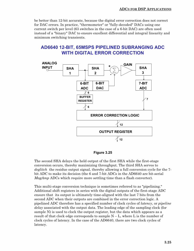
ADCS FOR DSP APPLICATIONS
3.25
be better than 12-bit accurate, because the digital error correction does not correctfor DAC errors. In practice, "thermometer" or "fully-decoded" DACs using onecurrent switch per level (63 switches in the case of a 6-bit DAC) are often usedinstead of a "binary" DAC to ensure excellent differential and integral linearity andminimum switching transients.
Figure 3.25
The second SHA delays the held output of the first SHA while the first-stageconversion occurs, thereby maximizing throughput. The third SHA serves todeglitch the residue output signal, thereby allowing a full conversion cycle for the 7-bit ADC to make its decision (the 6 and 7-bit ADCs in the AD6640 are bit-serialMagAmp ADCs which require more settling time than a flash converter).
This multi-stage conversion technique is sometimes referred to as "pipelining."Additional shift registers in series with the digital outputs of the first-stage ADCensure that its output is ultimately time-aligned with the last 7 bits from thesecond ADC when their outputs are combined in the error correction logic. Apipelined ADC therefore has a specified number of clock cycles of latency, or pipelinedelay associated with the output data. The leading edge of the sampling clock (forsample N) is used to clock the output register, but the data which appears as aresult of that clock edge corresponds to sample N – L, where L is the number ofclock cycles of latency. In the case of the AD6640, there are two clock cycles oflatency.
AD6640 12-BIT, 65MSPS PIPELINED SUBRANGING ADCWITH DIGITAL ERROR CORRECTION
ANALOGINPUT
7
12
SHA1
6-BITADC
7-BITADC
GAIN
6
+
-
ERROR CORRECTION LOGIC
6-BITDAC
SHA2
SHA3
OUTPUT REGISTER
12
BUFFERREGISTER
6

ADCS FOR DSP APPLICATIONS
3.26
The error correction scheme described above is designed to correct for errors madein the first conversion. Internal ADC gain, offset, and linearity errors are correctedas long as the residue signal falls within the range of the second-stage ADC. Theseerrors will not affect the linearity of the overall ADC transfer characteristic. Errorsmade in the final conversion, however, do translate directly as errors in the overalltransfer function. Also, linearity errors or gain errors either in the DAC or theresidue amplifier will not be corrected and will show up as nonlinearities or non-monotonic behavior in the overall ADC transfer function.
So far, we have considered only two-stage subranging ADCs, as these are easiest toanalyze. There is no reason to stop at two stages, however. Three-pass and four-passsubranging pipelined ADCs are quite common, and can be made in many differentways, usually with digital error correction.
A simplified block diagram of the AD9220 12-bit, 10MSPS single-supply, 250mWCMOS ADC is shown in Figure 3.26. The AD9221 (1.25MSPS, 60mW) and theAD9223 (3MSPS, 100mW) ADCs use the identical architecture but operate at lowerpower and lower sampling rates. This is a four-stage pipelined architecture with anadditional bit in the second, third, and fourth stage for error correction. Because ofthe pipelined architecture, these ADCs have a 3 clock-cycle latency (see Figure3.27).
Figure 3.26
AD9220/9221/9223 12-BIT PIPELINED CMOS ADC
ANALOGINPUT + + +
- - -
5 4 3 3
12
12
BUFFER REGISTERS ANDERROR CORRECTION LOGIC
OUTPUT REGISTERS
SHA1
SHA2
SHA3
SHA4
5-BITADC
5-BITDAC
4-BITADC
4-BITDAC
3-BITADC
3-BITDAC
3-BITADC
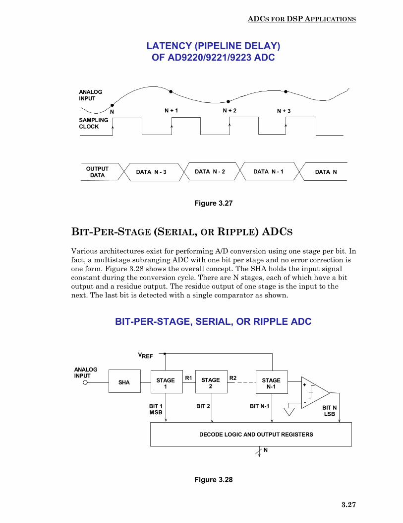
ADCS FOR DSP APPLICATIONS
3.27
Figure 3.27
BIT-PER-STAGE (SERIAL, OR RIPPLE) ADCS
Various architectures exist for performing A/D conversion using one stage per bit. Infact, a multistage subranging ADC with one bit per stage and no error correction isone form. Figure 3.28 shows the overall concept. The SHA holds the input signalconstant during the conversion cycle. There are N stages, each of which have a bitoutput and a residue output. The residue output of one stage is the input to thenext. The last bit is detected with a single comparator as shown.
Figure 3.28
LATENCY (PIPELINE DELAY)OF AD9220/9221/9223 ADC
ANALOGINPUT
SAMPLINGCLOCK
OUTPUTDATA DATA N - 3 DATA N - 2 DATA N - 1 DATA N
N N + 1 N + 2 N + 3
BIT-PER-STAGE, SERIAL, OR RIPPLE ADC
ANALOGINPUT
SHA STAGE1
STAGE2
DECODE LOGIC AND OUTPUT REGISTERS
+
-BIT 1MSB
BIT 2
VREF
N
R1 R2 STAGEN-1
BIT N-1 BIT NLSB

ADCS FOR DSP APPLICATIONS
3.28
The basic stage for performing a single binary bit conversion is shown in Figure3.29. It consists of a gain-of-two amplifier, a comparator, and a 1-bit DAC. Assumethat this is the first stage of the ADC. The MSB is simply the polarity of the input,and that is detected with the comparator which also controls the 1-bit DAC. The 1-bit DAC output is summed with the output of the gain-of-two amplifier. Theresulting residue output is then applied to the next stage. In order to betterunderstand how the circuit works, the diagram shows the residue output for thecase of a linear ramp input voltage which traverses the entire ADC range, –VR to+VR. Notice that the polarity of the residue output determines the binary bit outputof the next stage.
Figure 3.29
A simplified 3-bit serial-binary ADC is shown in Figure 3.30, and the residueoutputs are shown in Figure 3.31. Again, the case is shown for a linear ramp inputvoltage whose range is between –VR and +VR. Each residue output signal hasdiscontinuities which correspond to the point where the comparator changes stateand causes the DAC to switch. The fundamental problem with this architecture isthe discontinuity in the residue output waveforms. Adequate settling time must beallowed for these transients to propagate through all the stages and settle at thefinal comparator input. The prospects of making this architecture operate at highspeed are therefore dismal.
SINGLE-STAGE OF BINARY ADC
INPUT INPUTRESIDUE
+VR
+VR
-VR
-VR
0
0
RESIDUE+VR -VR
G = 2
+
-
Σ
BIT OUTPUT(BINARY CODE)
SWITCH POSITIONSHOWN FOR
NEGATIVE INPUT
t
t

ADCS FOR DSP APPLICATIONS
3.29
Figure 3.30
Figure 3.31
A much better bit-per-stage architecture was developed by F.D. Waldhauer(Reference 21) based on absolute value amplifiers (magnitude amplifiers, or simplyMagAmps™). This scheme has often been referred to as serial-Gray (since theoutput coding is in Gray code), or folding converter (References 22, 23, 24). Thebasic stage is shown functionally in Figure 3.32 along with its transfer function. Theinput to the stage is assumed to be a linear ramp voltage whose range is between
3-BIT SERIAL ADC WITH BINARY OUTPUT
ANALOGINPUT
SHA STAGE1
STAGE2
OUTPUT REGISTER
+
-BIT 1 BIT 2 BIT 3
±VR
3
R1 R2
INPUT AND RESIDUE WAVEFORMS OF3-BIT BINARY RIPPLE ADC
INPUT
R1
R2
BINARYCODE
-VR
-VR
-VR
+VR
+VR
+VR
000 001 010 011 100 101 110 111
0
0
0
t
t
t

ADCS FOR DSP APPLICATIONS
3.30
–VR and +VR. The comparator detects the polarity of the input signal and providesthe Gray bit output for the stage. It also determines whether the overall stage gainis +2 or –2. The reference voltage VR is summed with the switch output to generatethe residue signal which is applied to the next stage. The polarity of the residuesignal determines the Gray bit for the next stage. The transfer function for thefolding stage is also shown in Figure 3.32.
Figure 3.32
A 3-bit MagAmp folding ADC is shown in Figure 3.33, and the correspondingresidue waveforms in Figure 3.34. As in the case of the binary ripple ADC, thepolarity of the residue output signal of a stage determines the value of the Gray bitfor the next stage. The polarity of the input to the first stage determines the GrayMSB; the polarity of R1 output determines the Gray bit-2; and the polarity of R2output determines the Gray bit-3. Notice that unlike the binary ripple ADC, there isno abrupt transition in any of the folding stage residue output waveforms. Thismakes operation at high speeds quite feasible.
The key to operating this architecture at high speeds is the folding stage. Earlydesigns (see References 22, 23, 24) used discrete op amps with diodes inside thefeedback loop to generate the folding transfer function. Modern IC circuit designsimplement the transfer function using current-steering open-loop gain techniqueswhich can be made to operate much faster. Fully differential stages (including theSHA) also provide speed, lower distortion, and yield 8-bit accurate folding stageswith no requirement for thin film resistor laser trimming (see References 25, 26,27).
MagAmp STAGE FUNCTIONAL EQUIVALENT CIRCUIT
INPUT
G = +2 INPUTRESIDUE
+VR
+VR
-VR
-VR
0
0
RESIDUE
VR
+
-
BIT OUTPUT(GRAY CODE)
G = -2
Σ
SWITCH POSITIONSHOWN FORNEGATIVE INPUT
t
t

ADCS FOR DSP APPLICATIONS
3.31
Figure 3.33
Figure 3.34
3-BIT MagAmp™ (FOLDING) ADC BLOCK DIAGRAM
ANALOGINPUT
SHA MAGAMP1
MAGAMP2
GRAY-TO-BINARY CONVERTER
OUTPUT REGISTER
GRAY CODE REGISTER
+
-BIT 1 BIT 2 BIT 3
±VR
3
3
3
INPUT AND RESIDUE WAVEFORMSFOR 3-BIT MagAmp ADC
INPUT
R1
R2
GRAYCODE
-VR
-VR
-VR
+VR
+VR
+VR
000 001 011 010 110 111 101 100
0
0
0
t
t
t

ADCS FOR DSP APPLICATIONS
3.32
The MagAmp architecture can be extended to sampling rates previously dominatedby flash converters. The AD9288-100 8-bit, 100MSPS dual ADC is shown in Figure3.35. The first five bits (Gray code) are derived from five differential MagAmpstages. The differential residue output of the fifth MagAmp stage drives a 3-bitflash converter, rather than a single comparator. The Gray-code output of the fiveMagAmps and the binary-code output of the 3-bit flash are latched, all convertedinto binary, and latched again in the output data register.
Figure 3.35
AD9288-100 DUAL 8-BIT,100MSPS ADC FUNCTIONAL DIAGRAM
5
5
8
ANALOGINPUT
SHA MAGAMP1
MAGAMP2
MAGAMP3
MAGAMP4
MAGAMP5
3-BITFLASH
ADC
BIT1
GRAY
BIT2
GRAY
BIT3
GRAY
BIT4
GRAY
BIT5
GRAY
3
REGISTER
GRAY-TO-BINARY CONVERTER
OUTPUT REGISTER
BINARYDIFFERENTIALOUTPUTS ONBITS 1 - 5
3

ADCS FOR DSP APPLICATIONS
3.33
REFERENCES
1. S. A. Jantzi, M. Snelgrove & P. F. Ferguson Jr., A 4th-Order BandpassSigma-Delta Modulator, IEEE Journal of Solid State Circuits,Vol. 38, No. 3, March 1993, pp.282-291.
2. System Applications Guide, Analog Devices, Inc., 1993, Section 14.
3. Mixed Signal Design Seminar, Analog Devices, Inc., 1991, Section 6.
4. AD77XX-Series Data Sheets, Analog Devices, http://www.analog.com.
5. Linear Design Seminar, Analog Devices, Inc., 1995, Section 8.
6. J. Dattorro, A. Charpentier, D. Andreas, The Implementation of a One-Stage Multirate 64:1 FIR Decimator for use in One-Bit Sigma-Delta A/DApplications, AES 7th International Conference, May 1989.
7. W.L. Lee and C.G. Sodini, A Topology for Higher-Order InterpolativeCoders, ISCAS PROC. 1987.
8. P.F. Ferguson, Jr., A. Ganesan and R. W. Adams, One Bit Higher OrderSigma-Delta A/D Converters, ISCAS PROC. 1990, Vol. 2, pp. 890-893.
9. R. Koch, B. Heise, F. Eckbauer, E. Engelhardt, J. Fisher, and F. Parzefall,A 12-bit Sigma-Delta Analog-to-Digital Converter with a 15MHz ClockRate, IEEE Journal of Solid-State Circuits, Vol. SC-21, No. 6,December 1986.
10. Wai Laing Lee, A Novel Higher Order Interpolative Modulator Topologyfor High Resolution Oversampling A/D Converters, MIT MastersThesis, June 1987.
11. D. R. Welland, B. P. Del Signore and E. J. Swanson, A Stereo 16-BitDelta-Sigma A/D Converter for Digital Audio, J. Audio EngineeringSociety, Vol. 37, No. 6, June 1989, pp. 476-485.
12. R. W. Adams, Design and Implementation of an Audio 18-Bit Analog-to-Digital Converter Using Oversampling Techniques, J. AudioEngineering Society, Vol. 34, March 1986, pp. 153-166.
13. B. Boser and Bruce Wooley, The Design of Sigma-Delta ModulationAnalog-to-Digital Converters, IEEE Journal of Solid-State Circuits,Vol. 23, No. 6, December 1988, pp. 1298-1308.
14. Y. Matsuya, et. al., A 16-Bit Oversampling A/D Conversion TechnologyUsing Triple-Integration Noise Shaping, IEEE Journal of Solid-StateCircuits, Vol. SC-22, No. 6, December 1987, pp. 921-929.

ADCS FOR DSP APPLICATIONS
3.34
15. Y. Matsuya, et. al., A 17-Bit Oversampling D/A Conversion TechnologyUsing Multistage Noise Shaping, IEEE Journal of Solid-State Circuits,Vol. 24, No. 4, August 1989, pp. 969-975.
16. P. Ferguson, Jr., A. Ganesan, R. Adams, et. al., An 18-Bit 20-kHz DualSigma-Delta A/D Converter, ISSCC Digest of Technical Papers,February 1991.
17. Steven Harris, The Effects of Sampling Clock Jitter on Nyquist Sampling Analog-to-Digital Converters and on Oversampling Delta Sigma ADCs,Audio Engineering Society Reprint 2844 (F-4), October, 1989.
18. Max W. Hauser, Principles of Oversampling A/D Conversion, JournalAudio Engineering Society, Vol. 39, No. 1/2, January/February 1991,pp. 3-26.
19. Daniel H. Sheingold, Analog-Digital Conversion Handbook,Third Edition, Prentice-Hall, 1986.
20. Chuck Lane, A 10-bit 60MSPS Flash ADC, Proceedings of the 1989Bipolar Circuits and Technology Meeting, IEEE Catalog No.89CH2771-4, September 1989, pp. 44-47.
21. F.D. Waldhauer, Analog to Digital Converter, U.S. Patent3-187-325, 1965.
22. J.O. Edson and H.H. Henning, Broadband Codecs for an Experimental224Mb/s PCM Terminal, Bell System Technical Journal, 44,November 1965, pp. 1887-1940.
23. J.S. Mayo, Experimental 224Mb/s PCM Terminals, Bell SystemTechnical Journal, 44, November 1965, pp. 1813-1941.
24. Hermann Schmid, Electronic Analog/Digital Conversions,Van Nostrand Reinhold Company, New York, 1970.
25. Carl Moreland, An 8-bit 150MSPS Serial ADC, 1995 ISSCC Digestof Technical Papers, Vol. 38, p. 272.
26. Roy Gosser and Frank Murden, A 12-bit 50MSPS Two-Stage A/DConverter, 1995 ISSCC Digest of Technical Papers, p. 278.
27. Carl Moreland, An Analog-to-Digital Converter Using Serial-Ripple Architecture, Masters' Thesis, Florida State UniversityCollege of Engineering, Department of Electrical Engineering, 1995.
28. Practical Analog Design Techniques, Analog Devices, 1995, Chapter4, 5, and 8.
29. Linear Design Seminar, Analog Devices, 1995, Chapter 4, 5.

ADCS FOR DSP APPLICATIONS
3.35
30. System Applications Guide, Analog Devices, 1993, Chapter 12, 13,15,16.
31. Amplifier Applications Guide, Analog Devices, 1992, Chapter 7.
32. Walt Kester, Drive Circuitry is Critical to High-Speed Sampling ADCs,Electronic Design Special Analog Issue, Nov. 7, 1994, pp. 43-50.
33. Walt Kester, Basic Characteristics Distinguish Sampling A/D Converters,EDN, Sept. 3, 1992, pp. 135-144.
34. Walt Kester, Peripheral Circuits Can Make or Break Sampling ADCSystems, EDN, Oct. 1, 1992, pp. 97-105.
35. Walt Kester, Layout, Grounding, and Filtering Complete SamplingADC System, EDN, Oct. 15, 1992, pp. 127-134.
36. High Speed Design Techniques, Analog Devices, 1996, Chapter 4, 5.

ADCS FOR DSP APPLICATIONS
3.36

DACS FOR DSP APPLICATIONS
4.a
SECTION 4
DACs FOR DSP APPLICATIONS
DAC Structures
Low Distortion DAC Architectures
DAC Logic
Sigma-Delta DACs
Direct Digital Synthesis (DDS)

DACS FOR DSP APPLICATIONS
4.b
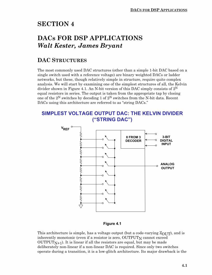
DACS FOR DSP APPLICATIONS
4.1
SECTION 4
DACs FOR DSP APPLICATIONSWalt Kester, James Bryant
DAC STRUCTURES
The most commonly used DAC structures (other than a simple 1-bit DAC based on asingle switch used with a reference voltage) are binary weighted DACs or laddernetworks, but these, though relatively simple in structure, require quite complexanalysis. We will start by examining one of the simplest structures of all, the Kelvindivider shown in Figure 4.1. An N-bit version of this DAC simply consists of 2Nequal resistors in series. The output is taken from the appropriate tap by closingone of the 2N switches by decoding 1 of 2N switches from the N-bit data. RecentDACs using this architecture are referred to as “string DACs.”
Figure 4.1
This architecture is simple, has a voltage output (but a code-varying ZOUT), and isinherently monotonic (even if a resistor is zero, OUTPUTN cannot exceedOUTPUTN+1). It is linear if all the resistors are equal, but may be madedeliberately non-linear if a non-linear DAC is required. Since only two switchesoperate during a transition, it is a low-glitch architecture. Its major drawback is the
SIMPLEST VOLTAGE OUTPUT DAC: THE KELVIN DIVIDER(“STRING DAC”)
8 FROM 3DECODER
3-BITDIGITALINPUT
ANALOGOUTPUT
VREF

DACS FOR DSP APPLICATIONS
4.2
large number of resistors required for high resolution, and as a result it is notcommonly used - but, as we shall see later, it is used as a component in morecomplex DAC structures.
There is an analogous current output DAC which consists, again, of 2N resistors (orcurrent sources), but in this case they are all connected in parallel between thereference voltage input and the virtual ground output (see Figure 4.2).
Figure 4.2
In this DAC, once a resistor is switched into circuit by increasing digital code, anyfurther increases do not switch it out again. The structure is thus inherentlymonotonic, irrespective of inaccuracies in the resistors, and like the previous case,may be made intentionally non-linear where a specific non-linearity is required.Again, as in the previous case, the architecture is rarely, if ever, used to fabricate acomplete DAC because of the large numbers of resistors and switches required.However, it is often used as a component in a more complex DAC structure.
Unlike the Kelvin divider, this type of DAC does not have a unique name, althoughboth types are referred to as fully decoded DACs or thermometer DACs or stringDACs.
Fully-decoded DACs are often used as components of more complex DACs. The mostcommon are "segmented DACs" where part of the output of a fully decoded DAC isfurther subdivided. The structure is used because the fully decoded DAC isinherently monotonic, so if the subdivision is also monotonic, the whole resultingDAC is also monotonic.
THE SIMPLEST CURRENT OUTPUT DAC
3-BITDIGITALINPUT
CURRENTOUTPUT INTO
VIRTUALGROUND
(USUALLY ANOP-AMP I-V
CONVERTER)
VREF
7 FROM 3DECODER

DACS FOR DSP APPLICATIONS
4.3
A voltage segmented DAC (see Figure 4.3) works by further sub-dividing the voltageacross one resistor of a Kelvin divider. The sub-division may be done with a furtherKelvin divider (in which case the whole structure is known as a "Kelvin-Varleydivider", or with some other DAC structure.
Figure 4.3
In all DACs, the output is the product of the reference voltage and the digital code,so in that sense, all DACs are multiplying DACs, but many DACs operate well onlyover a limited range of Vref. True MDACs, however, are designed to operate over awide range of Vref. A strict definition of a multiplying DAC demands that itsreference voltage range includes 0V, and many, especially current mode laddernetworks with CMOS switches, permit positive, negative, and AC Vref. DACs whichdo not work down to 0V Vref are still useful, however, and types where Vref canvary by 10:1 or so are often called MDACs, although a more accurate descriptionmight be "semi-multiplying" DACs.
LOW DISTORTION DAC ARCHITECTURES
Because of the emphasis in communications systems on DDS DACs with highSFDR, much effort has been placed on determining optimum DAC architectures.Practically all low distortion high speed DACs make use of some form of non-saturating current-mode switching. A straight binary DAC with one current switchper bit produces code-dependent glitches as discussed above and is certainly not themost optimum architecture (Figure 4.4). A DAC with one current source per codelevel can be shown not to have code-dependent glitches, but it is not practical toimplement for high resolutions. However, this performance can be approached by
SEGMENTED VOLTAGE DACsKELVIN-VARLEY DIVIDER
(“STRING DAC”)VREF
VREF
OUTPUT
KELVIN DIVIDER ANDR-2R LADDER NETWORK
NOTE:MSB OF LADDER
ON RIGHT
IF THE LADDER NETWORKIS MONOTONIC, THE
WHOLE DAC ISMONOTONIC
OUTPUT

DACS FOR DSP APPLICATIONS
4.4
decoding the first few MSBs into a "thermometer" code and have one current switchper level. For example, a 5-bit thermometer DAC would have an architecturesimilar to that shown in Figure 4.5.
Figure 4.4
Figure 4.5
5-BIT BINARY DAC ARCHITECTURES
R (CAN BE EXTERNAL)
I I I I I I I/2 I/4 I/8 I/16
OUTPUTOUTPUT
MSB MSB
R R RR
R2R 2R 2R
5-BIT “THERMOMETER” OR “FULLY-DECODED” DACMINIMIZES CODE-DEPENDENT GLITCHES
CLOCK
CURRENTOUTPUT
31-BITLATCH
31EQUAL
CURRENTSWITCHES
5-TO-31DECODE
LOGIC
5-BITLATCH
MSB
LSB
31LINES
31LINES

DACS FOR DSP APPLICATIONS
4.5
The input binary word is latched and then decoded into 31 outputs which drive asecond latch. The output of the second latch drives 31 equally weighted currentswitches whose outputs are summed together. This scheme effectively removesnearly all the code-dependence of the output glitch. The residual glitch that doesoccur at the output is equal regardless of the output code change (it is code-independent) and can be filtered because it occurs at the DAC update frequency andits harmonics. The distortion mechanisms associated with the full-decodedarchitecture are primarily asymmetrical output slewing, finite switch turn-on andturn-off times, and integral nonlinearity.
The obvious disadvantage of this type of thermometer DAC is the large number oflatches and switches required to make a 14, 12, 10, or even 8-bit DAC. However, ifthis technique is used on the 5 MSBs of an 8, 10, 12, or 14-bit DAC, a significantreduction in the code-dependent glitch is possible. This process is calledsegmentation and is quite common in low distortion DACs.
Figure 4.6 shows a scheme whereby the first 5 bits of a 10-bit DAC are decoded asdescribed above and drive 31 equally weighted switches. The last 5 bits are derivedfrom binarily weighted current sources. Equally weighted current sources drivingan R/2R resistor ladder could be used to derive the LSBs, however, this approachrequires thin film resistors which are not generally available on a low-cost CMOSprocess. Also, the use of R/2R networks lowers the DAC output impedance, therebyrequiring more drive current to develop the same voltage across a fixed loadresistance.
Figure 4.6
10-BIT SEGMENTED DAC
CURRENTOUTPUT
CLOCK
10-BITLATCH
36-BITLATCH
FULLYDECODED
MSBDAC
MSBDECODE
5
31 315
10
BINARYLSBDAC
5

DACS FOR DSP APPLICATIONS
4.6
The AD9772 14-bit, 150MSPS TxDAC™ uses three sections of segmentation asshown in Figure 4.7. Other members of the AD977x-family and the AD985x-familyalso use this same core.
The first 5 bits (MSBs) are fully decoded and drive 31 equally weighted currentswitches, each supplying 512 LSBs of current. The next 4 bits are decoded into 15lines which drive 15 current switches, each supplying 32 LSBs of current. The 5LSBs are latched and drive a traditional binary weighted DAC which supplies 1LSB per output level. A total of 51 current switches and latches are required toimplement this architecture.
Figure 4.7
The basic current switching cell is made up of a differential PMOS transistor pairas shown in Figure 4.8. The differential pairs are driven with low-level logic tominimize switching transients and time skew. The DAC outputs are symmetricaldifferential currents which help to minimize even-order distortion products(especially which driving a differential output such as a transformer or an op ampdifferential I/V converter).
The overall architecture of the AD977x TxDAC™ family and the AD985x-DDSfamily is an excellent tradeoff between power/performance and allows the entireDAC function to be implemented on a standard CMOS process with no thin filmresistors. Single-supply operation on +3.3V or +5V make the devices extremelyattractive for portable and low power applications.
AD9772 TxDAC™ 14-BIT CMOS DAC CORE
CLOCK
14-BITLATCH
51-BITLATCH
31CURRENTSWITCHES
15CURRENT
5 BINARYCURRENTSWITCHES
BITS 1-5DECODE
5-TO-31
BITS 6-9DECODE
4-TO-15
5 5
15154
31 315
14CURRENTOUTPUT
FS =2mA-20mA
SWITCHES
I = 512 LSB
I = 32 LSB
I = 1 LSB
5

DACS FOR DSP APPLICATIONS
4.7
Figure 4.8
DAC LOGIC
The earliest monolithic DACs contained little, if any, logic circuitry, and paralleldata had to be maintained on the digital input to maintain the digital output. Todayalmost all DACs have input latches, and data need only be written once, notmaintained.
There are innumerable variations of DAC input structure which will not bediscussed here, but the majority today are "double-buffered". A double-buffered DAChas two sets of latches. Data is initially latched in the first rank and subsequentlytransferred to the second as shown in Figure 4.9. There are three reasons why thisarrangement is useful.
The first is that it allows data to enter the DAC in many different ways. A DACwithout a latch, or with a single latch, must be loaded with all bits at once, inparallel, since otherwise its output during loading may be totally different fromwhat it was or what it is to become. A double-buffered DAC, on the other hand, maybe loaded with parallel data, serial data, or with 4-bit or 8-bit words, or whatever,and the output will be unaffected until the new data is completely loaded and theDAC receives its update instruction.
PMOS TRANSISTOR CURRENT SWITCHES
RL
+VS
RL

DACS FOR DSP APPLICATIONS
4.8
Figure 4.9
The second feature of this type of input structure is that the output clock canoperate at a fixed frequency (the DAC update rate), while the input latch can beloaded asynchronously. This is useful in real-time signal reconstructionapplications.
The third convenience of the double-buffered structure is that many DACs may beupdated simultaneously: data is loaded into the first rank of each DAC in turn, andwhen all is ready, the output buffers of all DACs are updated at once. There aremany DAC applications where the output of several DACs must changesimultaneously, and the double-buffered structure allows this to be done very easily.
Most early monolithic high resolution DACs had parallel or byte-wide data portsand tended to be connected to parallel data buses and address decoders andaddressed by microprocessors as if they were very small write-only memories (someDACs are not write-only, but can have their contents read as well - this isconvenient for some applications but is not very common). A DAC connected to adata bus is vulnerable to capacitive coupling of logic noise from the bus to theanalog output, and many DACs today have serial data structures. These are lessvulnerable to such noise (since fewer noisy pins are involved), use fewer pins andtherefore take less space, and are frequently more convenient for use with modernmicro-processors, many of which have serial data ports. Some, but not all, of suchserial DACs have data outputs as well as data inputs so that several DACs may beconnected in series and data clocked to them all from a single serial port. Thearrangement is referred to as "daisy-chaining".
Another development in DACs is the ability to make several on a single chip, whichis useful to reduce PCB sizes and assembly costs. Today (2000) it is possible to buysixteen 8-bit, eight 12-bit, four 14-bit, or two 16-/18/20/22/24-bit DACs in a singlepackage. In the future, even higher densities are probable.
DOUBLE-BUFFERED DAC PERMITS COMPLEXINPUT STRUCTURES AND SIMULTANEOUS UPDATE
OUTPUTDIGITALINPUT INPUT STRUCTURE:
MAY BE SERIAL,PARALLEL, BYTE-WIDE,
ETC.
OUTPUT LATCHTRANSFERS DATA
TO DAC -TIMING IS
INDEPENDENT OFINPUT
DAC
OUTPUT STROBE -MAY GO TO MANY DACs
fc = SAMPLING FREQUENCY
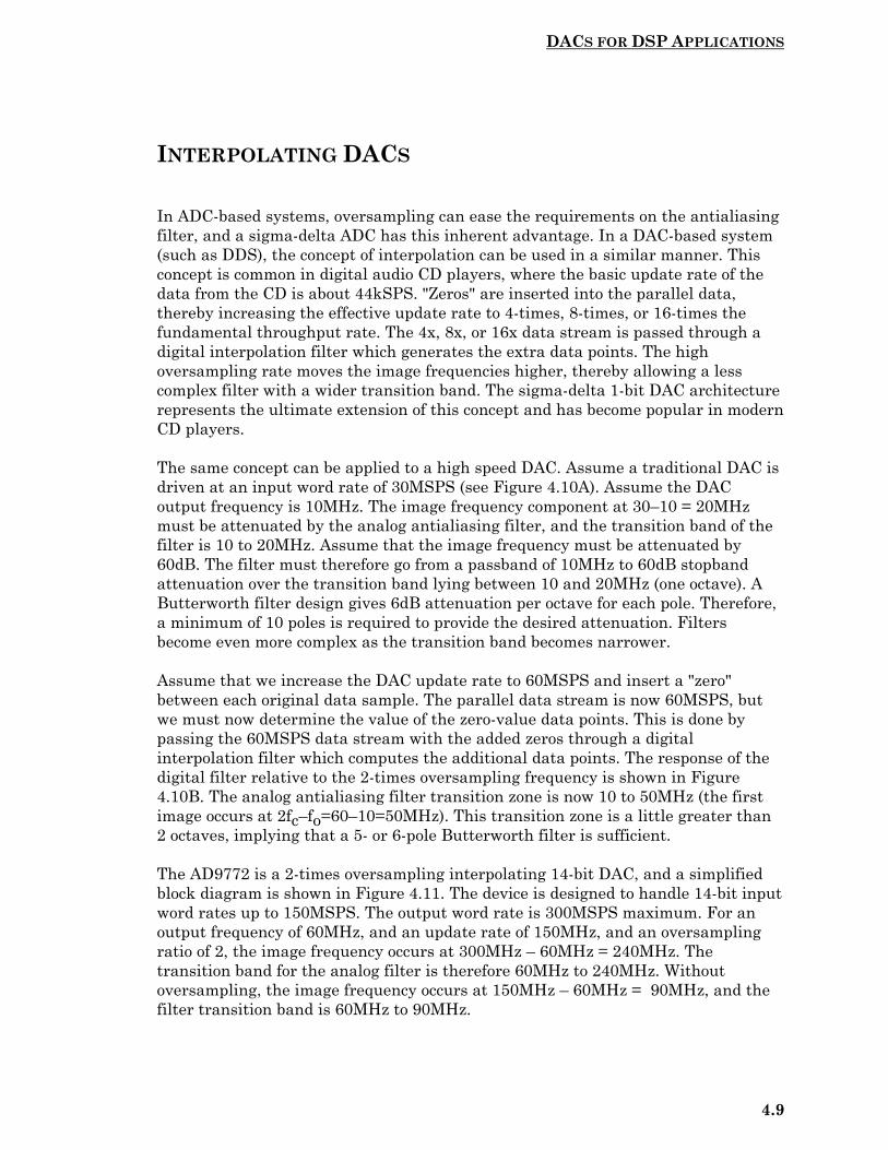
DACS FOR DSP APPLICATIONS
4.9
INTERPOLATING DACS
In ADC-based systems, oversampling can ease the requirements on the antialiasingfilter, and a sigma-delta ADC has this inherent advantage. In a DAC-based system(such as DDS), the concept of interpolation can be used in a similar manner. Thisconcept is common in digital audio CD players, where the basic update rate of thedata from the CD is about 44kSPS. "Zeros" are inserted into the parallel data,thereby increasing the effective update rate to 4-times, 8-times, or 16-times thefundamental throughput rate. The 4x, 8x, or 16x data stream is passed through adigital interpolation filter which generates the extra data points. The highoversampling rate moves the image frequencies higher, thereby allowing a lesscomplex filter with a wider transition band. The sigma-delta 1-bit DAC architecturerepresents the ultimate extension of this concept and has become popular in modernCD players.
The same concept can be applied to a high speed DAC. Assume a traditional DAC isdriven at an input word rate of 30MSPS (see Figure 4.10A). Assume the DACoutput frequency is 10MHz. The image frequency component at 30–10 = 20MHzmust be attenuated by the analog antialiasing filter, and the transition band of thefilter is 10 to 20MHz. Assume that the image frequency must be attenuated by60dB. The filter must therefore go from a passband of 10MHz to 60dB stopbandattenuation over the transition band lying between 10 and 20MHz (one octave). AButterworth filter design gives 6dB attenuation per octave for each pole. Therefore,a minimum of 10 poles is required to provide the desired attenuation. Filtersbecome even more complex as the transition band becomes narrower.
Assume that we increase the DAC update rate to 60MSPS and insert a "zero"between each original data sample. The parallel data stream is now 60MSPS, butwe must now determine the value of the zero-value data points. This is done bypassing the 60MSPS data stream with the added zeros through a digitalinterpolation filter which computes the additional data points. The response of thedigital filter relative to the 2-times oversampling frequency is shown in Figure4.10B. The analog antialiasing filter transition zone is now 10 to 50MHz (the firstimage occurs at 2fc–fo=60–10=50MHz). This transition zone is a little greater than2 octaves, implying that a 5- or 6-pole Butterworth filter is sufficient.
The AD9772 is a 2-times oversampling interpolating 14-bit DAC, and a simplifiedblock diagram is shown in Figure 4.11. The device is designed to handle 14-bit inputword rates up to 150MSPS. The output word rate is 300MSPS maximum. For anoutput frequency of 60MHz, and an update rate of 150MHz, and an oversamplingratio of 2, the image frequency occurs at 300MHz – 60MHz = 240MHz. Thetransition band for the analog filter is therefore 60MHz to 240MHz. Withoutoversampling, the image frequency occurs at 150MHz – 60MHz = 90MHz, and thefilter transition band is 60MHz to 90MHz.
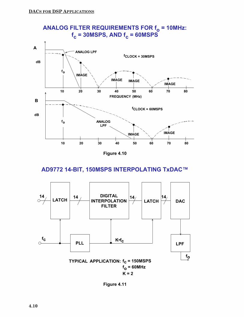
DACS FOR DSP APPLICATIONS
4.10
Figure 4.10
Figure 4.11
ANALOG FILTER REQUIREMENTS FOR fo = 10MHz:fc = 30MSPS, AND fc = 60MSPS
fCLOCK = 30MSPS
dB
IMAGE
10 20 30 40 50 60 70 80
fo
ANALOG LPF
10 20 30 40 50 60 70 80
IMAGE
ANALOGLPF
FREQUENCY (MHz)
IMAGEIMAGEIMAGE
IMAGE
fo
fCLOCK = 60MSPS
dB
A
B
fo
K•fcfc
LATCH LATCH DAC
LPF
DIGITALINTERPOLATION
FILTER
PLL
14 14 14 14
TYPICAL APPLICATION: fc = 150MSPSfo = 60MHzK = 2
AD9772 14-BIT, 150MSPS INTERPOLATING TxDAC™
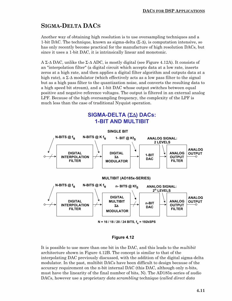
DACS FOR DSP APPLICATIONS
4.11
SIGMA-DELTA DACS
Another way of obtaining high resolution is to use oversampling techniques and a1-bit DAC. The technique, known as sigma-delta (Σ-∆), is computation intensive, sohas only recently become practical for the manufacture of high resolution DACs, butsince it uses a 1-bit DAC, it is intrinsically linear and monotonic.
A Σ-∆ DAC, unlike the Σ-∆ ADC, is mostly digital (see Figure 4.12A). It consists ofan "interpolation filter" (a digital circuit which accepts data at a low rate, insertszeros at a high rate, and then applies a digital filter algorithm and outputs data at ahigh rate), a Σ-∆ modulator (which effectively acts as a low pass filter to the signalbut as a high pass filter to the quantization noise, and converts the resulting data toa high speed bit stream), and a 1-bit DAC whose output switches between equalpositive and negative reference voltages. The output is filtered in an external analogLPF. Because of the high oversampling frequency, the complexity of the LPF ismuch less than the case of traditional Nyquist operation.
Figure 4.12
It is possible to use more than one bit in the DAC, and this leads to the multibitarchitecture shown in Figure 4.12B. The concept is similar to that of theinterpolating DAC previously discussed, with the addition of the digital sigma-deltamodulator. In the past, multibit DACs have been difficult to design because of theaccuracy requirement on the n-bit internal DAC (this DAC, although only n-bits,must have the linearity of the final number of bits, N). The AD185x-series of audioDACs, however use a proprietary data scrambling technique (called direct data
SIGMA-DELTA (Σ∆Σ∆Σ∆Σ∆) DACs:1-BIT AND MULTIBIT
N-BITS @ fs N-BITS @ K fs ANALOG SIGNAL:2 LEVELS
ANALOGOUTPUTDIGITAL
INTERPOLATIONFILTER
DIGITALΣ∆Σ∆Σ∆Σ∆
MODULATOR
1-BITDAC
ANALOGOUTPUTFILTER
1- BIT @ KfS
N-BITS @ fs N-BITS @ K fs ANALOG SIGNAL:2n LEVELS
ANALOGOUTPUTDIGITAL
INTERPOLATIONFILTER
DIGITAL
Σ∆Σ∆Σ∆Σ∆
MODULATOR
n-BITDAC
ANALOGOUTPUTFILTER
n- BITS @ KfS
SINGLE BIT
MULTIBIT (AD185x-SERIES)
N = 16 / 18 / 20 / 24 BITS, fs = 192kSPS
MULTIBIT

DACS FOR DSP APPLICATIONS
4.12
scrambling, or D2S) which overcomes this problem and produces excellentperformance with respect to THD + N. For instance, the AD1853 dual 24-bit,192kSPS DAC has greater than 115dB THD + N at a 48kSPS sampling rate.
DIRECT DIGITAL SYNTHESIS (DDS)A frequency synthesizer generates multiple frequencies from one or more frequencyreferences. These devices have been used for decades, especially in communicationssystems. Many are based upon switching and mixing frequency outputs from a bankof crystal oscillators. Others have been based upon well understood techniquesutilizing phase-locked loops (PLLs). This mature technology is illustrated in Figure4.13. A fixed-frequency reference drives one input of the phase comparator. Theother phase comparator input is driven from a divide-by-N counter which is in turndriven by a voltage-controlled-oscillator (VCO). Negative feedback forces the outputof the internal loop filter to a value which makes the VCO output frequency N-timesthe reference frequency. The time constant of the loop is controlled by the loop filter.There are many tradeoffs in designing a PLL, such a phase noise, tuning speed,frequency resolution, etc., and there are many good references on the subject (seeReferences 1, 2, and 3).
Figure 4.13
With the widespread use of digital techniques in instrumentation andcommunications systems, a digitally-controlled method of generating multiplefrequencies from a reference frequency source has evolved called Direct DigitalSynthesis (DDS). The basic architecture is shown in Figure 4.14. In this simplified
FREQUENCY SYNTHESIS USINGOSCILLATORS AND PHASE-LOCKED LOOPS
OSCILLATOR BANKMIXER
MIXER
XO1
XO2
XO3
XOn
SW
fout
PHASE-LOCKED LOOP
fcfout
FIXEDFREQUENCYREFERENCE
LOOPFILTER
÷ ÷ ÷ ÷ N
fout
PHASECOMPARATOR VCO
= N • fc

DACS FOR DSP APPLICATIONS
4.13
model, a stable clock drives a programmable-read-only-memory (PROM) whichstores one or more integral number of cycles of a sinewave (or other arbitrarywaveform, for that matter). As the address counter steps through each memorylocation, the corresponding digital amplitude of the signal at each location drives aDAC which in turn generates the analog output signal. The spectral purity of thefinal analog output signal is determined primarily by the DAC. The phase noise isbasically that of the reference clock.
Figure 4.14
The DDS system differs from the PLL in several ways. Because a DDS system is asampled data system, all the issues involved in sampling must be considered:quantization noise, aliasing, filtering, etc. For instance, the higher order harmonicsof the DAC output frequencies fold back into the Nyquist bandwidth, making themunfilterable, whereas, the higher order harmonics of the output of PLL-basedsynthesizers can be filtered. There are other considerations which will be discussedshortly.
A fundamental problem with this simple DDS system is that the final outputfrequency can be changed only by changing the reference clock frequency or byreprogramming the PROM, making it rather inflexible. A practical DDS systemimplements this basic function in a much more flexible and efficient manner usingdigital hardware called a Numerically Controlled Oscillator (NCO). A block diagramof such a system is shown in Figure 4.15.
FUNDAMENTAL DIRECT DIGITAL SYNTHESIS SYSTEM
fc
ADDRESSCOUNTER
N-BITSCLOCK REGISTER
LPF
DAC
fout
LOOKUP TABLE CONTAINS SINDATA FOR INTEGRAL NUMBEROF CYCLES
N-BITS
PROMSIN
LOOKUPTABLE

DACS FOR DSP APPLICATIONS
4.14
Figure 4.15
The heart of the system is the phase accumulator whose contents is updated onceeach clock cycle. Each time the phase accumulator is updated, the digital number,M, stored in the delta phase register is added to the number in the phaseaccumulator register. Assume that the number in the delta phase register is 00...01and that the initial contents of the phase accumulator is 00...00. The phaseaccumulator is updated by 00...01 on each clock cycle. If the accumulator is 32-bitswide, 232 clock cycles (over 4 billion) are required before the phase accumulatorreturns to 00...00, and the cycle repeats.
The truncated output of the phase accumulator serves as the address to a sine (orcosine) lookup table. Each address in the lookup table corresponds to a phase pointon the sinewave from 0° to 360°. The lookup table contains the corresponding digitalamplitude information for one complete cycle of a sinewave. (Actually, only data for90° is required because the quadrature data is contained in the two MSBs). Thelookup table therefore maps the phase information from the phase accumulator intoa digital amplitude word, which in turn drives the DAC.
Consider the case for n=32, and M=1. The phase accumulator steps through each of232 possible outputs before it overflows. The corresponding output sinewavefrequency is equal to the clock frequency divided by 232. If M=2, then the phaseaccumulator register "rolls over" twice as fast, and the output frequency is doubled.This can be generalized as follows.
A FLEXIBLE DDS SYSTEM
fc
SERIALOR BYTE
LOADREGISTER
nn
FREQUENCY CONTROL
PHASEREGISTER
LPF
DAC
PARALLELDELTAPHASE
REGISTERM CLOCK
n n SIN ROMLOOKUPTABLE
PHASE ACCUMULATOR
n
PHASETRUNCATION12-16 BITS
AMPLITUDETRUNCATION
2n=foM • fc
n = 24-32 BITS
N-BITS

DACS FOR DSP APPLICATIONS
4.15
For an n-bit phase accumulator (n generally ranges from 24 to 32 in most DDSsystems), there are 2n possible phase points. The digital word in the delta phaseregister, M, represents the amount the phase accumulator is incremented each clockcycle. If fc is the clock frequency, then the frequency of the output sinewave is equalto:
foM fc
n=⋅
2.
This equation is known as the DDS "tuning equation." Note that the frequencyresolution of the system is equal to fc/2n. For n=32, the resolution is greater thanone part in four billion! In a practical DDS system, all the bits out of the phaseaccumulator are not passed on to the lookup table, but are truncated, leaving onlythe first 12 to 16 MSBs. This reduces the size of the lookup table and does not affectthe frequency resolution. The phase truncation only adds a small but acceptableamount of phase noise to the final output; the bulk of the output distortion comesfrom the DAC itself.
The basic DDS system described above is extremely flexible and has high resolution.The frequency can be changed instantaneously with no phase discontinuity bysimply changing the contents of the M-register. However, practical DDS systemsfirst require the execution of a serial, or byte-loading sequence to get the newfrequency word into an internal buffer register which precedes the parallel-outputM-register. This is done to minimize package pin count. After the new word isloaded into the buffer register, the parallel-output delta phase register is clocked,thereby changing all the bits simultaneously. The number of clock cycles required toload the delta-phase buffer register determines the maximum rate at which theoutput frequency can be changed.
The AD9850 125MSPS DDS system (Figure 4.16) uses a 32-bit phase accumulatorwhich is truncated to 14-bits (MSBs) before being passed to the lookup table. Thefinal digital output is 10-bits to the internal DAC. The AD9850 allows the outputphase to be modulated using an additional register and an adder placed between theoutput of the phase accumulator register and the input to the lookup table. TheAD9850 uses a 5-bit word to control the phase which allows shifting the phase inincrements of 180°, 90°, 45°, 22.5°, 11.25°, and any combination thereof. The devicealso contains an internal high speed comparator which can be configured to acceptthe (externally) filtered output of the DAC to generate a low-jitter output pulsesuitable for driving the sampling clock input of an ADC. The full scale outputcurrent can be adjusted from 10 to 20mA using a single external resistor, and theoutput voltage compliance is +1V.
The frequency tuning (delta-phase register input word) and phase modulation wordsare loaded into the AD9850 via a parallel or serial loading format. The parallel loadformat consists of five consecutive loads of an 8-bit control word (byte). The first 8-bit byte controls phase modulation (5-bits), power-down enable (1-bit), and loadingformat (2-bits). Bytes 2-5 comprise the 32-bit frequency tuning word. The maximumcontrol register update frequency is 23MHz. Serial loading of the AD9850 isaccomplished via a 40-bit serial data stream on a single pin. Maximum update rateof the control register in the serial-load mode is 3MHz.

DACS FOR DSP APPLICATIONS
4.16
The AD9850 consumes only 380mW of power on a single +5V supply at a maximum125MSPS clock rate. The device is available in a 28-pin surface mount SSOP(Shrink Small Outline Package).
Figure 4.16
Analog Devices offers a number of DDS systems for a variety of applications. TheAD983x family are low-cost 10-bit systems with clock frequencies up to 50MSPS.The AD985x-family offers 10-bit and 12-bit systems with clock frequencies up to300MSPS and additional functions such as quadrature and phase modulation,chirp-mode capability, and programmable on- chip reference clock multipliers.
AD9850 CMOS 125MSPS DDS/DAC SYNTHESIZER
SINLOOKUPTABLE
10
10-BITDAC
PHASECONTROL
PHASEACCUMULATOR
DATA ANDCONTROL
INPUTREGISTER
+
-HIGH SPEED
COMPARATOR
1432
55
32
ANALOG OUT
RSET
BYTE LOAD
8 BITS X 5
SERIAL LOAD
1 BIT X 40
WORD LOAD CLOCK
REFERENCE CLOCK IN

DACS FOR DSP APPLICATIONS
4.17
REFERENCES
1. R.E. Best, Phase-Locked Loops, McGraw-Hill, New York, 1984.
2. F.M. Gardner, Phaselock Techniques, 2nd Edition, John Wiley,New York, 1979.
3. Phase-Locked Loop Design Fundamentals, Applications Note AN-535,Motorola, Inc.
4. The ARRL Handbook for Radio Amateurs, American RadioRelay League, Newington, CT, 1992.
5. Richard J. Kerr and Lindsay A. Weaver, Pseudorandom Dither forFrequency Synthesis Noise, United States Patent Number 4,901,265,February 13, 1990.
6. Henry T. Nicholas, III and Henry Samueli, An Analysis of the OutputSpectrum of Direct Digital Frequency Synthesizers in the Presence ofPhase-Accumulator Truncation, IEEE 41st Annual Frequency ControlSymposium Digest of Papers, 1987, pp. 495-502, IEEE Publication No.CH2427-3/87/0000-495.
7. Henry T. Nicholas, III and Henry Samueli, The Optimization of DirectDigital Frequency Synthesizer Performance in the Presence of Finite WordLength Effects, IEEE 42nd Annual Frequency Control SymposiumDigest of Papers, 1988, pp. 357-363, IEEE Publication No. CH2588-2/88/0000-357.

DACS FOR DSP APPLICATIONS
4.18
FAST FOURIER TRANSFORMS
5.a
SECTION 5
FAST FOURIER TRANSFORMS
The Discrete Fourier Transform
The Fast Fourier Transform
FFT Hardware Implementation and Benchmarks
DSP Requirements for Real Time FFT Applications
Spectral Leakage and Windowing

FAST FOURIER TRANSFORMS
5.b

FAST FOURIER TRANSFORMS
5.1
SECTION 5FAST FOURIER TRANSFORMSWalt Kester
THE DISCRETE FOURIER TRANSFORM
In 1807 the French mathematician and physicist Jean Baptiste Joseph Fourierpresented a paper to the Institut de France on the use of sinusoids to representtemperature distributions. The paper made the controversial claim that anycontinuous periodic signal could be represented by the sum of properly chosensinusoidal waves. Among the publication review committee were two famousmathematicians: Joseph Louis Lagrange, and Pierre Simon de Laplace. Lagrangeobjected strongly to publication on the basis that Fourier’s approach would not workwith signals having discontinuous slopes, such as square waves. Fourier’s work wasrejected, primarily because of Lagrange’s objection, and was not published until thedeath of Lagrange, some 15 years later. In the meantime, Fourier’s time wasoccupied with political activities, expeditions to Egypt with Napoleon, and trying toavoid the guillotine after the French Revolution! (This bit of history extracted fromReference 1, p.141).
It turns out that both Fourier and Lagrange were at least partially correct.Lagrange was correct that a summation of sinusoids cannot exactly form a signalwith a corner. However, you can get very close if enough sinusoids are used. (This isdescribed by the Gibbs effect, and is well understood by scientists, engineers, andmathematicians today).
Fourier analysis forms the basis for much of digital signal processing. Simplystated, the Fourier transform (there are actually several members of this family)allows a time domain signal to be converted into its equivalent representation in thefrequency domain. Conversely, if the frequency response of a signal is known, theinverse Fourier transform allows the corresponding time domain signal to bedetermined.
In addition to frequency analysis, these transforms are useful in filter design, sincethe frequency response of a filter can be obtained by taking the Fourier transform ofits impulse response. Conversely, if the frequency response is specified, then therequired impulse response can be obtained by taking the inverse Fourier transformof the frequency response. Digital filters can be constructed based on their impulseresponse, because the coefficients of an FIR filter and its impulse response areidentical.
The Fourier transform family (Fourier Transform, Fourier Series, Discrete TimeFourier Series, and Discrete Fourier Transform) is shown in Figure 5.2. Theseaccepted definitions have evolved (not necessarily logically) over the years anddepend upon whether the signal is continuous–aperiodic, continuous–periodic,sampled–aperiodic, or sampled–periodic. In this context, the term sampled is thesame as discrete (i.e., a discrete number of time samples).

FAST FOURIER TRANSFORMS
5.2
Figure 5.1
Figure 5.2
APPLICATIONS OF THE DISCRETEFOURIER TRANSFORM (DFT)
Digital Spectral Analysis Spectrum Analyzers Speech Processing Imaging Pattern Recognition
Filter Design Calculating Impulse Response from Frequency Response Calculating Frequency Response from Impulse Response
The Fast Fourier Transform (FFT) is Simply an Algorithmfor Efficiently Calculating the DFT
SampledTime Domain
SampledFrequency Domain
Discrete Fourier Transform (DFT)Inverse DFT (IDFT)
FOURIER TRANSFORM FAMILYAS A FUNCTION OF TIME DOMAIN SIGNAL TYPE
FOURIER TRANSFORM:Signal is Continuous and Aperiodic
FOURIER SERIES:Signal is Continuous and Periodic
DISCRETE TIME FOURIER SERIES:Signal is Sampled and Aperiodic
DISCRETE FOURIER TRANSFORM:(Discrete Fourier Series)Signal is Sampledand Periodic
Sample 0 Sample N – 1
N = 8
t
t
t
t

FAST FOURIER TRANSFORMS
5.3
The only member of this family which is relevant to digital signal processing is theDiscrete Fourier Transform (DFT) which operates on a sampled time domain signalwhich is periodic. The signal must be periodic in order to be decomposed into thesummation of sinusoids. However, only a finite number of samples (N) are availablefor inputting into the DFT. This dilemma is overcome by placing an infinite numberof groups of the same N samples “end-to-end,” thereby forcing mathematical (butnot real-world) periodicity as shown in Figure 5.2.
The fundamental analysis equation for obtaining the N-point DFT is as follows:
[ ]∑∑−
=π−π=
−
=
π−=1N
0n)N/nk2sin(j)N/nk2cos()n(x
N11N
0nN/nk2je)n(x
N1)k(X
At this point, some terminology clarifications are in order regarding the aboveequation (also see Figure 5.3). X(k) (capital letter X) represents the DFT frequencyoutput at the kth spectral point, where k ranges from 0 to N–1. The quantity Nrepresents the number of sample points in the DFT data frame.
Note that “N” should not be confused with ADC or DAC resolution, which is alsogiven by the quantity N in other places in this book.
The quantity x(n) (lower case letter x) represents the nth time sample, where n alsoranges from 0 to N – 1. In the general equation, x(n) can be real or complex.
Notice that the cosine and sine terms in the equation can be expressed in eitherpolar or rectangular coordinates using Euler’s equation:
θ+θ=θ sinjcosje
The DFT output spectrum, X(k), is the correlation between the input time samplesand N cosine and N sine waves. The concept is best illustrated in Figure 5.4. In thisfigure, the real part of the first four output frequency points is calculated, therefore,only the cosine waves are shown. A similar procedure is used with sine waves inorder to calculate the imaginary part of the output spectrum.
The first point, X(0), is simply the sum of the input time samples, because cos(0) =1. The scaling factor, 1/N, is not shown, but must be present in the final result. Notethat X(0) is the average value of the time samples, or simply the DC offset. Thesecond point, ReX(1), is obtained by multiplying each time sample by eachcorresponding point on a cosine wave which makes one complete cycle in theinterval N and summing the results. The third point, ReX(2), is obtained bymultiplying each time sample by each corresponding point of a cosine wave whichhas two complete cycles in the interval N and then summing the results. Similarly,the fourth point, ReX(3), is obtained by multiplying each time sample by thecorresponding point of a cosine wave which has three complete cycles in the intervalN and summing the results. This process continues until all N outputs have beencomputed. A similar procedure is followed using sine waves in order to calculate theimaginary part of the frequency spectrum. The cosine and sine waves are referred toas basis functions.
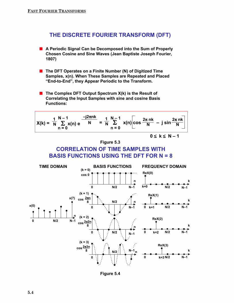
FAST FOURIER TRANSFORMS
5.4
Figure 5.3
Figure 5.4
A Periodic Signal Can be Decomposed into the Sum of ProperlyChosen Cosine and Sine Waves (Jean Baptiste Joseph Fourier,1807)
The DFT Operates on a Finite Number (N) of Digitized TimeSamples, x(n). When These Samples are Repeated and Placed“End-to-End”, they Appear Periodic to the Transform.
The Complex DFT Output Spectrum X(k) is the Result ofCorrelating the Input Samples with sine and cosine BasisFunctions:
THE DISCRETE FOURIER TRANSFORM (DFT)
X(k) =–j2ππππnk
Nx(n) eΣΣΣΣn = 0
N – 1= x(n) cos – j sin ΣΣΣΣ
n = 0
N – 1 2ππππ nkN
2ππππ nkN
0 ≤≤≤≤ k ≤≤≤≤ N – 1
1N
1N
CORRELATION OF TIME SAMPLES WITHBASIS FUNCTIONS USING THE DFT FOR N = 8
0 N–1N/2
0 N/2
0N/2
0 N–1N/2
0 N–1N/2
k=0 N–1N/2
0 N–1N/2
0 N–1N/2
0 N–1N/2
x(0)
x(7)
ReX(0)
ReX(1)
ReX(2)
ReX(3)
N–1
N–1
TIME DOMAIN FREQUENCY DOMAIN
cos 0
cos 2ππππn8
cos 2ππππ2n8
cos 2ππππ3n8
BASIS FUNCTIONS(k = 0)
(k = 1)
(k = 2)
(k = 3)
n
n
n
n
n
k=1
k=2
k=3
k
k
k
k

FAST FOURIER TRANSFORMS
5.5
Assume that the input signal is a cosine wave having a period of N, i.e., it makesone complete cycle during the data window. Also assume its amplitude and phase isidentical to the first cosine wave of the basis functions, cos(2πn/8). The outputReX(1) contains a single point, and all the other ReX(k) outputs are zero. Assumethat the input cosine wave is now shifted to the right by 90º. The correlationbetween it and the corresponding basis function is zero. However, there is anadditional correlation required with the basis function sin(2πn/8) to yield ImX(1).This shows why both real and imaginary parts of the frequency spectrum need to becalculated in order to determine both the amplitude and phase of the frequencyspectrum.
Notice that the correlation of a sine/cosine wave of any frequency other than that ofthe basis function produces a zero value for both ReX(1) and ImX(1).
A similar procedure is followed when using the inverse DFT (IDFT) to reconstructthe time domain samples, x(n), from the frequency domain samples X(k). Thesynthesis equation is given by:
[ ]∑∑−
=π+π=
−
=
π=1N
0k)N/nk2sin(j)N/nk2cos()k(X
1N
0kN/nk2je)k(X)n(x
There are two basic types of DFTs: real, and complex. The equations shown inFigure 5.5 are for the complex DFT, where the input and output are both complexnumbers. Since time domain input samples are real and have no imaginary part,the imaginary part of the input is always set to zero. The output of the DFT, X(k),contains a real and imaginary component which can be converted into ampltude andphase.
The real DFT, although somewhat simpler, is basically a simplification of thecomplex DFT. Most FFT routines are written using the complex DFT format,therefore understanding the complex DFT and how it relates to the real DFT isimportant. For instance, if you know the real DFT frequency outputs and want touse a complex inverse DFT to calculate the time samples, you need to know how toplace the real DFT oututs points into the complex DFT format before taking thecomplex inverse DFT.
Figure 5.6 shows the input and output of a real and a complex FFT. Notice that theoutput of the real DFT yields real and imaginary X(k) values, where k ranges fromonly 0 to N/2. Note that the imaginary points ImX(0) and ImX(N/2) are always zerobecause sin(0) and sin(nπ) are both always zero.
The frequency domain output X(N/2) corresponds to the frequency output at one-half the sampling frequency, fs. The width of each frequency bin is equal to fs/N.

FAST FOURIER TRANSFORMS
5.6
Figure 5.5
Figure 5.6
THE COMPLEX DFT
Time Domain ←←←← ←←←← INVERSE DFT ←←←← ←←←← Frequency Domain
x(n) =j2ππππnk
NX(k) eΣΣΣΣk = 0
N – 1= X(k) cos + j sin ΣΣΣΣ
k = 0
N – 1 2ππππ nkN
2ππππ nkN
= X(k) WN–nkΣΣΣΣ
k = 0
N – 10 ≤≤≤≤ n ≤≤≤≤ N – 1
Frequency Domain ←←←← ←←←← DFT ←←←← ←←←← Time Domain
,
X(k) =–j2ππππnk
Nx(n) e
WN = e–j2ππππ
N= x(n) WN
nk
ΣΣΣΣn = 0
N – 1
ΣΣΣΣn = 0
N – 1
= x(n) cos – j sin ΣΣΣΣn = 0
N – 1 2ππππ nkN
2ππππ nkN
0 ≤≤≤≤ k ≤≤≤≤ N – 1,
1N
1N
1N
DFT INPUT/OUTPUT SPECTRUM
0 N–1 0 N/2
0 N/2
0 N–1
0 N–1
0 N–1
0 N–1
Real Real
Imaginary
Real Real
ImaginaryImaginary
zero zero
DC OffsetREAL DFT
COMPLEX DFT
Time Domain, x(n) Frequency Domain, X(k)
N Points0 ≤≤≤≤ n ≤≤≤≤ N–1
N Points+ Two Zero
Points
2N Points 2N Points
0 ≤≤≤≤ k ≤≤≤≤ N/2
0 ≤≤≤≤ n ≤≤≤≤ N–1 0 ≤≤≤≤ k ≤≤≤≤ N–1
N/2
N/2
N/2
N/2
N/2
fsN
⇒⇒⇒⇒ fs/2
fsN
zero zero

FAST FOURIER TRANSFORMS
5.7
The complex DFT has real and imaginary values both at its input and output. Inpractice, the imaginary parts of the time domain samples are set to zero. If you aregiven the output spectrum for a complex DFT, it is useful to know how to relatethem to the real DFT output and vice versa. The crosshatched areas in the diagramcorrespond to points which are common to both the real and complex DFT.
Figure 5.7 shows the relationship between the real and complex DFT in more detail.The real DFT output points are from 0 to N/2, with ImX(0) and ImX(N/2) alwayszero. The points between N/2 and N – 1 contain the negative frequencies in thecomplex DFT. Note that ReX(N/2 + 1) has the same value as Re(N/2 – 1). Similarly,ReX(N/2 + 2) has the same value as ReX(N/2 – 2), etc. Also, note that ImX(N/2 + 1)is the negative of ImX(N/2 – 1), and ImX(N/2 + 2) is the negative of ImX(N/2 – 2),etc. In other words, ReX(k) has even symmetry about N/2 and ImX(k) has oddsymmetry about N/2. In this way, the negative frequency components for thecomplex FFT can be generated if you are only given the real DFT components.
The equations for the complex and the real DFT are summarized in Figure 5.8. Notethat the equations for the complex DFT work nearly the same whether taking theDFT, X(k) or the IDFT, x(n). The real DFT does not use complex numbers, and theequations for X(k) and x(n) are significantly different. Also, before using the x(n)equation, ReX(0) and ReX(N/2) must be divided by two. These details are explainedin Chapter 31 of Reference 1, and the reader should study this chapter beforeattemping to use these equations.
Figure 5.7
CONSTRUCTING THE COMPLEX DFT NEGATIVEFREQUENCY COMPONENTS FROM THE REAL DFT
0 N–1
0 N–1
0 N–1
0N–1
Real Part Real Part
Imaginary PartImaginary Part
N/2N/2
N/2 N/2
Time Domain Frequency Domain
(All Zeros)
Axis ofSymmetry
“Negative” Frequency
EvenSymmetryAbout N/2
OddSymmetryAbout N/2
(fs/2)
(fs/2)

FAST FOURIER TRANSFORMS
5.8
The DFT output spectrum can be represented in either polar form (magnitude andphase) or rectangular form (real and imaginary) as shown in Figure 5.9. Theconversion between the two forms is straightforward.
Figure 5.8
Figure 5.9
COMPLEX AND REAL DFT EQUATIONS
COMPLEX TRANSFORM
X(k) =–j2ππππnk
Nx(n) eΣΣΣΣn = 0
N – 11N
x(n) =j2ππππnk
NX(k) eΣΣΣΣk = 0
N – 1
REAL TRANSFORM
ReX(k) = ΣΣΣΣn = 0
N – 12N x(n) cos(2ππππnk/N)
ImX(k) = ΣΣΣΣn = 0
N – 1–2N x(n) sin(2ππππnk/N)
x(n) = ΣΣΣΣk = 0
N/2ReX(k) cos(2ππππnk/N)
– ImX(k) cos(2ππππnk/N)
Time Domain: x(n) is complex, discrete,and periodic. n runs from 0 to N– 1
Frequency Domain: X(k) is complex,discrete, and periodic. k runs from 0 to N–1k = 0 to N/2 are positive frequencies.k = N/2 to N–1 are negative frequencies
Time Domain: x(n) is real, discrete, and periodic.n runs from 0 to N – 1
Frequency domain:ReX(k) is real, discrete, and periodic.ImX(k) is real, discrete, and periodic.k runs from 0 to N/2
Before using x(n) equation, ReX(0) andReX(N/2) must be divided by two.
CONVERTING REAL AND IMAGINARY DFTOUTPUTS INTO MAGNITUDE AND PHASE
X(k) = ReX(k) + j ImX(k)
MAG [X(k)] = ReX(k) 2 + ImX(k) 2
ϕϕϕϕ [X(k)] = tan–1 ImX(k)ReX(k)
ϕϕϕϕ
X(k)Im X(k)
Re X(k)
MAG[X(k)]

FAST FOURIER TRANSFORMS
5.9
THE FAST FOURIER TRANSFORM
In order to understand the development of the FFT, consider first the 8-point DFTexpansion shown in Figure 5.10. In order to simplify the diagram, note that thequantity WN is defined as:
N/2jeNW π−= .
This leads to the definition of the twiddle factors as:
N/nk2jenkNW π−= .
The twiddle factors are simply the sine and cosine basis functions written in polarform. Note that the 8-point DFT shown in the diagram requires 64 complexmultiplications. In general, an N-point DFT requires N2 complex multiplications.The number of multiplications required is significant because the multiplicationfunction requires a relatively large amount of DSP processing time. In fact, the totaltime required to compute the DFT is directly proportional to the number ofmultiplications plus the required amount of overhead.
Figure 5.10
THE 8-POINT DFT (N = 8)
X(0) = x(0)W80 + x(1)W8
0 + x(2)W80 + x(3)W8
0 + x(4)W80 + x(5)W8
0 + x(6)W80 + x(7)W8
0
X(1) = x(0)W80 + x(1)W8
1 + x(2)W82 + x(3)W8
3 + x(4)W84 + x(5)W8
5 + x(6)W86 + x(7)W8
7
X(2) = x(0)W80 + x(1)W8
2 + x(2)W84 + x(3)W8
6 + x(4)W88 + x(5)W8
10 + x(6)W812 + x(7)W8
14
X(3) = x(0)W80 + x(1)W8
3 + x(2)W86 + x(3)W8
9 + x(4)W812 + x(5)W8
15 + x(6)W818 + x(7)W8
21
X(4) = x(0)W80 + x(1)W8
4 + x(2)W88 + x(3)W8
12 + x(4)W816 + x(5)W8
20 + x(6)W824 + x(7)W8
28
X(5) = x(0)W80 + x(1)W8
5 + x(2)W810 + x(3)W8
15 + x(4)W820 + x(5)W8
25 + x(6)W830 + x(7)W8
35
X(6) = x(0)W80 + x(1)W8
6 + x(2)W812 + x(3)W8
18 + x(4)W824 + x(5)W8
30 + x(6)W836 + x(7)W8
42
X(7) = x(0)W80 + x(1)W8
7 + x(2)W814 + x(3)W8
21 + x(4)W828 + x(5)W8
35 + x(6)W842 + x(7)W8
49
X(k) =–j2ππππnk
Nx(n) e WN = e–j2ππππ
N= x(n) WNnkΣΣΣΣ
n = 0
N – 1ΣΣΣΣ
n = 0
N – 1
N2 Complex Multiplications
1N
1N
Scaling Factor Omitted1N

FAST FOURIER TRANSFORMS
5.10
The FFT is simply an algorithm to speed up the DFT calculation by reducing thenumber of multiplications and additions required. It was popularized by J. W.Cooley and J. W. Tukey in the 1960s and was actually a rediscovery of an idea ofRunge (1903) and Danielson and Lanczos (1942), first occurring prior to theavailability of computers and calculators – when numerical calculation could takemany man hours. In addition, the German mathematician Karl Friedrich Gauss(1777 – 1855) had used the method more than a century earlier.
In order to understand the basic concepts of the FFT and its derivation, note thatthe DFT expansion shown in Figure 5.10 can be greatly simplified by takingadvantage of the symmetry and periodicity of the twiddle factors as shown in Figure5.11. If the equations are rearranged and factored, the result is the Fast FourierTransform (FFT) which requires only (N/2) log2(N) complex multiplications. Thecomputational efficiency of the FFT versus the DFT becomes highly significantwhen the FFT point size increases to several thousand as shown in Figure 5.12.However, notice that the FFT computes all the output frequency components (eitherall or none!). If only a few spectral points need to be calculated, the DFT mayactually be more efficient. Calculation of a single spectral output using the DFTrequires only N complex multiplications.
Figure 5.11
APPLYING THE PROPERTIES OFSYMMETRY AND PERIODICITY TO WN
r FOR N = 8
Symmetry: WN r+ N/2 = – WN
r , Periodicity: WN r+ N = WN
r
W84 = W8
0+4 = – W80 = – 1
W85 = W8
1+4 = – W81
W86 = W8
2+4 = – W82
W87 = W8
3+4 = – W83
W88 = W8
0+8 = + W80 = + 1
W89 = W8
1+8 = + W81
W810 = W8
2+8 = + W82
W811 = W8
3+8 = + W83
N = 8

FAST FOURIER TRANSFORMS
5.11
Figure 5.12
The radix-2 FFT algorithm breaks the entire DFT calculation down into a number of2-point DFTs. Each 2-point DFT consists of a multiply-and-accumulate operationcalled a butterfly, as shown in Figure 5.13. Two representations of the butterfly areshown in the diagram: the top diagram is the actual functional representation of thebutterfly showing the digital multipliers and adders. In the simplified bottomdiagram, the multiplications are indicated by placing the multiplier over an arrow,and addition is indicated whenever two arrows converge at a dot.
The 8-point decimation-in-time (DIT) FFT algorithm computes the final output inthree stages as shown in Figure 5.14. The eight input time samples are first divided(or decimated) into four groups of 2-point DFTs. The four 2-point DFTs are thencombined into two 4-point DFTs. The two 4-point DFTs are then combined toproduce the final output X(k). The detailed process is shown in Figure 5.15, whereall the multiplications and additions are shown. Note that the basic two-point DFTbutterfly operation forms the basis for all computation. The computation is done inthree stages. After the first stage computation is complete, there is no need to storeany previous results. The first stage outputs can be stored in the same registerswhich originally held the time samples x(n). Similarly, when the second stagecomputation is completed, the results of the first stage computation can be deleted.In this way, in-place computation proceeds to the final stage. Note that in order forthe algorithm to work properly, the order of the input time samples, x(n), must beproperly re-ordered using a bit reversal algorithm.
THE FAST FOURIER TRANSFORM (FFT) VS.THE DISCRETE FOURIER TRANSFORM (DFT)
The FFT is Simply an Algorithm for Efficiently Calculating the DFT Computational Efficiency of an N-Point FFT:
DFT: N2 Complex Multiplications FFT: (N/2) log2(N) Complex Multiplications
N
256
512
1,024
2,048
4,096
DFT Multiplications
65,536
262,144
1,048,576
4,194,304
16,777,216
FFT Multiplications
1,024
2,304
5,120
11,264
24,576
FFT Efficiency
64 : 1
114 : 1
205 : 1
372 : 1
683 : 1

FAST FOURIER TRANSFORMS
5.12
Figure 5.13
Figure 5.14
THE BASIC BUTTERFLY COMPUTATION INTHE DECIMATION-IN-TIME FFT ALGORITHM
–
b
A = a + bWNr
B = a – bWNr
WNr
–1
a A = a + bWNr
B = a – bWNr
SIMPLIFIED REPRESENTATION
WNr
+
+b
a ΣΣΣΣ
ΣΣΣΣ
+
COMPUTATION OF AN 8-POINT DFT IN THREE STAGESUSING DECIMATION-IN-TIME
x(0)
x(4)
x(2)
x(6)
x(1)
x(5)
x(3)
x(7)
X(0)
X(1)
X(2)
X(3)
X(4)
X(5)
X(6)
X(7)
2-POINTDFT
2-POINTDFT
2-POINTDFT
2-POINTDFT
COMBINE2-POINT
DFTs
COMBINE2-POINT
DFTs
COMBINE4-POINT
DFTs

FAST FOURIER TRANSFORMS
5.13
Figure 5.15
The bit reversal algorithm used to perform this re-ordering is shown in Figure 5.16.The decimal index, n, is converted to its binary equivalent. The binary bits are thenplaced in reverse order, and converted back to a decimal number. Bit reversing isoften performed in DSP hardware in the data address generator (DAG), therebysimplifying the software, reducing overhead, and speeding up the computations.
The computation of the FFT using decimation-in-frequency (DIF) is shown inFigures 5.17 and 5.18. This method requires that the bit reversal algorithm beapplied to the output X(k). Note that the butterfly for the DIF algorithm differsslightly from the decimation-in-time butterfly as shown in Figure 5.19.
The use of decimation-in-time versus decimation-in-frequency algorithms is largelya matter of preference, as either yields the same result. System constraints maymake one of the two a more optimal solution.
It should be noted that the algorithms required to compute the inverse FFT arenearly identical to those required to compute the FFT, assuming complex FFTs areused. In fact, a useful method for verifying a complex FFT algorithm consists of firsttaking the FFT of the x(n) time samples and then taking the inverse FFT of theX(k). At the end of this process, the original time samples, Re x(n), should beobtained and the imaginary part, Im x(n), should be zero (within the limits of themathematical round off errors).
EIGHT-POINT DECIMATION-IN-TIME FFT ALGORITHM
W80
W80
W80
W80
–1
–1
–1
–1
–1
–1
–1
–1
–1
–1
–1
–1
W80
W82
W80
W82
W80
W81
W82
W83
x(0)
x(4)
x(2)
x(6)
x(1)
x(5)
x(3)
x(7)
X(0)
X(1)
X(2)
X(3)
X(4)
X(5)
X(6)
X(7)
STAGE 1 STAGE 2 STAGE 3
Bit-ReversedInputs
N2 log2N Complex
Multiplications

FAST FOURIER TRANSFORMS
5.14
Figure 5.16
Figure 5.17
BIT REVERSAL EXAMPLE FOR N = 8
Decimal Number :
Binary Equivalent :
Bit-Reversed Binary :
Decimal Equivalent :
0
000
1
001
2
010
3
011
4
100
5
101
6
110
7
111
000
0
100
4
010
2
110
6
001
1
101
5
011
3
111
7
COMPUTATION OF AN 8-POINT DFT IN THREE STAGESUSING DECIMATION-IN-FREQUENCY
x(0)
x(1)
x(2)
x(3)
x(4)
x(5)
x(6)
x(7)
X(0)
X(4)
X(2)
X(6)
X(1)
X(5)
X(3)
X(7)
REDUCETO 2-POINT
DFTs
REDUCETO 2-POINT
DFTs
REDUCETO 4-POINT
DFTs
2-POINTDFT
2-POINTDFT
2-POINTDFT
2-POINTDFT

FAST FOURIER TRANSFORMS
5.15
Figure 5.18
Figure 5.19
EIGHT-POINT DECIMATION-IN-FREQUENCYFFT ALGORITHM
W80
W80
W80
W80
–1
–1
–1
–1
–1
–1
–1
–1
W80
W82
W82
W83
W80
W81
W80
W82
x(0)
x(1)
x(2)
x(3)
x(4)
x(5)
x(6)
x(7)
X(0)
X(4)
X(2)
X(6)
X(1)
X(5)
X(3)
X(7)
STAGE 1 STAGE 2 STAGE 3
–1
–1
–1
–1
Bit-Reversed Outputs
THE BASIC BUTTERFLY COMPUTATION INTHE DECIMATION-IN-FREQUENCY FFT ALGORITHM
–
b
A = a + b
B = (a – b)WNr
WNr
–1
aSIMPLIFIED REPRESENTATION
WNr
+
+b
a ΣΣΣΣ
ΣΣΣΣ
+
A = a + b
B = (a – b)WNr

FAST FOURIER TRANSFORMS
5.16
The FFTs discussed up to this point are radix-2 FFTs, i.e., the computations arebased on 2-point butterflies. This implies that the number of points in the FFT mustbe a power of 2. If the number of points in an FFT is a power of 4, however, the FFTcan be broken down into a number of 4-point DFTs as shown in Figure 5.20. This iscalled a radix-4 FFT. The fundamental decimation-in-time butterfly for the radix-4FFT is shown in Figure 5.21.
The radix-4 FFT requires fewer complex multiplications but more additions thanthe radix-2 FFT for the same number of points. Compared to the radix-2 FFT, theradix-4 FFT trades more complex data addressing and twiddle factors with lesscomputation. The resulting savings in computation time varies between differentDSPs but a radix-4 FFT can be as much as twice as fast as a radix-2 FFT for DSPswith optimal architectures.
Figure 5.20
COMPUTATION OF A 16-POINT DFT IN THREE STAGESUSING RADIX-4 DECIMATION-IN-TIME ALGORITHM
x(0)x(4) 4-POINT
DFT
4-POINTDFT
4-POINTDFT
4-POINTDFT
COMBINE4-POINT
DFTs
COMBINE4-POINT
DFTs
COMBINE8-POINT
DFTs
x(8)x(12)x(1)x(5)x(9)x(13)x(2)x(6)x(10)x(14)x(3)x(7)x(11)x(15)
X(0)X(1)X(2)X(3)X(4)X(5)X(6)X(7)X(8)X(9)X(10)X(11)X(12)X13)X(14)X(15)

FAST FOURIER TRANSFORMS
5.17
Figure 5.21
FFT HARDWARE IMPLEMENTATION ANDBENCHMARKS
In general terms, the memory requirements for an N-point FFT are N locations forthe real data, N locations for the imaginary data, and N locations for the sinusoiddata (sometimes referred to as twiddle factors). Additional memory locations will berequired if windowing is used. Assuming the memory requirements are met, theDSP must perform the necessary calculations in the required time. Many DSPvendors will either give a performance benchmark for a specified FFT size orcalculation time for a butterfly. When comparing FFT specifications, it is importantto make sure that the same type of FFT is used in all cases. For example, the 1024-point FFT benchmark on one DSP derived from a radix-2 FFT should not becompared with the radix-4 benchmark from another DSP.
Another consideration regarding FFTs is whether to use a fixed-point or a floating-point processor. The results of a butterfly calculation can be larger than the inputsto the butterfly. This data growth can pose a potential problem in a DSP with afixed number of bits. To prevent data overflow, the data needs to be scaledbeforehand leaving enough extra bits for growth. Alternatively, the data can bescaled after each stage of the FFT computation. The technique of scaling data aftereach pass of the FFT is known as block floating point. It is called this because a fullarray of data is scaled as a block regardless of whether or not each element in theblock needs to be scaled. The complete block is scaled so that the relativerelationship of each data word remains the same. For example, if each data word isshifted right by one bit (divided by 2), the absolute values have been changed, butrelative to each other, the data stays the same.
RADIX-4 FFT DECIMATION-IN-TIME BUTTERFLY
–j–1
j
–1
–11
j–1–j
WN0
WNq
WN2q
WN3q

FAST FOURIER TRANSFORMS
5.18
In a 16-bit fixed-point DSP, a 32-bit word is obtained after multiplication. TheAnalog Device’s 21xx-series DSPs have extended dynamic range by providing a 40-bit internal register in the multiply-accumulator (MAC).
The use of a floating-point DSP eliminates the need for data scaling and thereforeresults in a simpler FFT routine, however the tradeoff is the increased processingtime required for the complex floating-point arithmetic. In addition, a 32-bitfloating-point DSP will obviously have less round off noise than a 16-bit fixed-pointDSP. Figure 5.22 summarizes the FFT benchmarks for popular Analog Devices’DSPs. Notice in particular that the ADSP-TS001 TigerSHARC™ DSP offers bothfixed-point and floating-point modes, thereby providing an exceptional degree ofprogramming flexibility.
Figure 5.22
DSP REQUIREMENTS FOR REAL TIME FFTAPPLICATIONS
There are two basic ways to acquire data from a real-world signal, either onesample at a time (continuous processing), or one frame at a time (batch processing).Sample-based systems, like a digital filter, acquire data one sample at a time. Foreach sample clock, a sample comes into the system, and a processed sample is sentto the output. Frame-based systems, like an FFT-based digital spectrum analyzer,acquire a frame (or block of samples). Processing occurs on the entire frame of dataand results in a frame of transformed output data.
In order to maintain real time operation, the entire FFT must therefore becalculated during the frame period. This assumes that the DSP is collecting thedata for the next frame while it is calculating the FFT for the current frame of data.Acquiring the data is one area where special architectural features of DSPs comeinto play. Seamless data acquisition is facilitated by the DSP’s flexible data
RADIX-2 COMPLEX FFTHARDWARE BENCHMARK COMPARISONS
ADSP-2189M, 16-bit, Fixed-Point @ 75MHz 453µs (1024-Point)
ADSP-21160 SHARC™, 32-bit, Floating-Point @ 100MHz 180µs (1024-Point), 2 channels, SIMD Mode 115µs (1024-Point), 1 channel, SIMD Mode
ADSP-TS001 TigerSHARC™ @ 150MHz, 16-bit, Fixed-Point Mode
7.3µs (256-Point FFT) 32-bit, Floating-Point Mode
69µs (1024-Point)
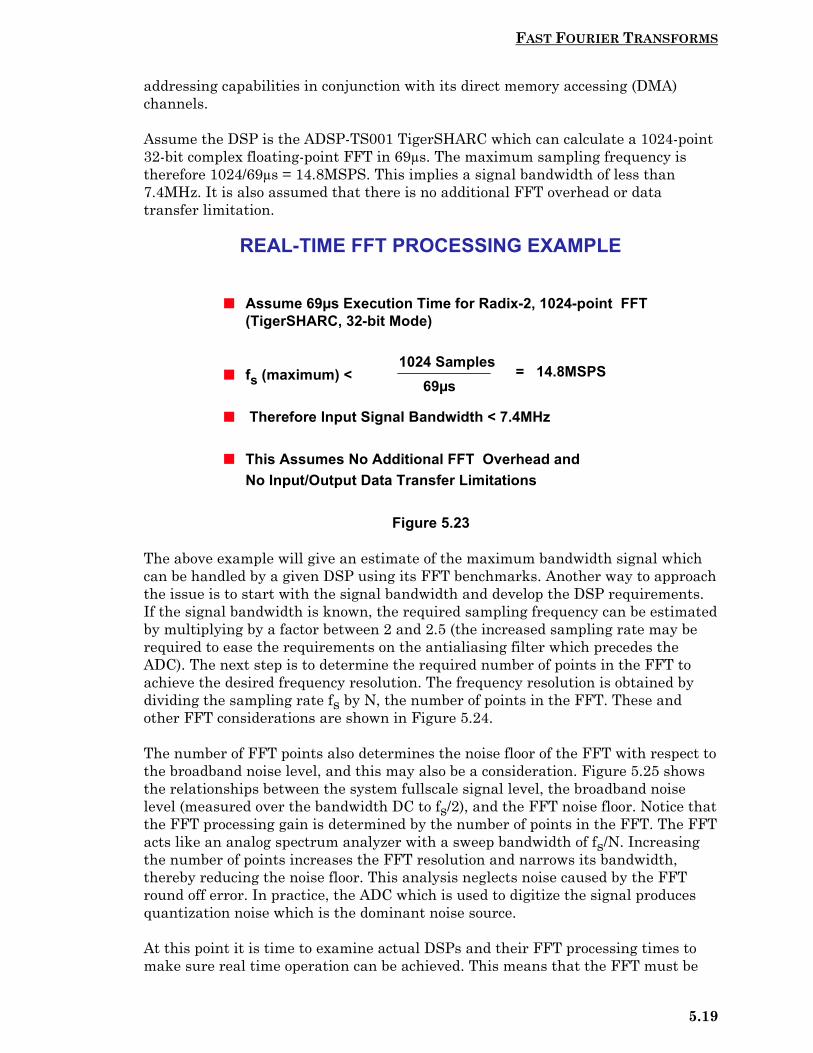
FAST FOURIER TRANSFORMS
5.19
addressing capabilities in conjunction with its direct memory accessing (DMA)channels.
Assume the DSP is the ADSP-TS001 TigerSHARC which can calculate a 1024-point32-bit complex floating-point FFT in 69µs. The maximum sampling frequency istherefore 1024/69µs = 14.8MSPS. This implies a signal bandwidth of less than7.4MHz. It is also assumed that there is no additional FFT overhead or datatransfer limitation.
Figure 5.23
The above example will give an estimate of the maximum bandwidth signal whichcan be handled by a given DSP using its FFT benchmarks. Another way to approachthe issue is to start with the signal bandwidth and develop the DSP requirements.If the signal bandwidth is known, the required sampling frequency can be estimatedby multiplying by a factor between 2 and 2.5 (the increased sampling rate may berequired to ease the requirements on the antialiasing filter which precedes theADC). The next step is to determine the required number of points in the FFT toachieve the desired frequency resolution. The frequency resolution is obtained bydividing the sampling rate fs by N, the number of points in the FFT. These andother FFT considerations are shown in Figure 5.24.
The number of FFT points also determines the noise floor of the FFT with respect tothe broadband noise level, and this may also be a consideration. Figure 5.25 showsthe relationships between the system fullscale signal level, the broadband noiselevel (measured over the bandwidth DC to fs/2), and the FFT noise floor. Notice thatthe FFT processing gain is determined by the number of points in the FFT. The FFTacts like an analog spectrum analyzer with a sweep bandwidth of fs/N. Increasingthe number of points increases the FFT resolution and narrows its bandwidth,thereby reducing the noise floor. This analysis neglects noise caused by the FFTround off error. In practice, the ADC which is used to digitize the signal producesquantization noise which is the dominant noise source.
At this point it is time to examine actual DSPs and their FFT processing times tomake sure real time operation can be achieved. This means that the FFT must be
Assume 69µs Execution Time for Radix-2, 1024-point FFT(TigerSHARC, 32-bit Mode)
fs (maximum) <
Therefore Input Signal Bandwidth < 7.4MHz
This Assumes No Additional FFT Overhead andNo Input/Output Data Transfer Limitations
REAL-TIME FFT PROCESSING EXAMPLE
1024 Samples69µs
= 14.8MSPS

FAST FOURIER TRANSFORMS
5.20
calculated during the acquisition time for one frame of data which is N/fs. Otherconsiderations such as fixed-point vs. floating-point, radix-2 vs. radix-4, andprocessor power dissipation and cost may be other considerations.
Figure 5.24
Figure 5.25
REAL TIME FFT CONSIDERATIONS
Signal Bandwidth
Sampling Frequency, fs Number of Points in FFT, N
Frequency Resolution = fs / N
Maximum Time to Calculate N-Point FFT = N / fs Fixed-Point vs. Floating Point DSP
Radix-2 vs. Radix-4 Execution Time
FFT Processing Gain = 10 log10(N / 2)
Windowing Requirements
FFT PROCESSING GAINNEGLECTING ROUND OFF ERROR
fs2
fsN
SIGNALLEVEL
(dB)
Fullscale RMS Signal Level
RMS Noise Level (DC to fs / 2)
FFT Processing Gain = 10 log10N2
= 27dB for N = 1024= 30dB for N = 2048= 33dB for N = 4096
SNR
FFT Noise Floor
f

FAST FOURIER TRANSFORMS
5.21
SPECTRAL LEAKAGE AND WINDOWING
Spectral leakage in FFT processing can best be understood by considering the caseof performing an N-point FFT on a pure sinusoidal input. Two conditions will beconsidered. In Figure 5.26, the ratio between the sampling frequency and the inputsinewave frequency is such that precisely an integral number of cycles are containedwithin the data window (frame, or record). Recall that the DFT assumes that aninfinite number of these windows are placed end-to-end to form a periodic waveformas shown in the diagram as the periodic extensions. Under these conditions, thewaveform appears continuous (no discontinuities), and the DFT or FFT output willbe a single tone located at the input signal frequency.
Figure 5.26
Figure 5.27 shows the condition where there are not an integral number of sinewavecycles within the data window. The discontinuities which occur at the endpoints ofthe data window result in leakage in the frequency domain because of theharmonics which are generated. In addition to the sidelobes, the main lobe of thesinewave is smeared over several frequency bins. This process is equivalent tomultiplying the input sinewave by a rectangular window pulse which has thefamiliar sin(x)/x frequency response and associated smearing and sidelobes.
FFT OF SINEWAVE HAVING INTEGRALNUMBER OF CYCLES IN DATA WINDOW
0 N-1 0 N-10 N-1Data
WindowPeriodic
ExtensionPeriodic
Extension
fin
f
fin
finfs
NCN= N = Record Length
NC = Number of Cycles in Data Window
t
fs/N

FAST FOURIER TRANSFORMS
5.22
Figure 5.27
Notice that the first sidelobe is only 12dB below the fundamental, and that thesidelobes roll off at only 6dB/octave. This situation would be unsuitable for mostspectral analysis applications. Since in practical FFT spectral analysis applicationsthe exact input frequencies are unknown, something must be done to minimizethese sidelobes. This is done by choosing a window function other than therectangular window. The input time samples are multiplied by an appropriatewindow function which brings the signal to zero at the edges of the window asshown in Figure 5.28. The selection of a window function is primarily a tradeoffbetween main lobe spreading and sidelobe roll off. Reference 7 is highlyrecommended for an in-depth treatment of windows.
The mathematical functions which describe four popular window functions(Hamming, Blackman, Hanning, and Minimum 4-term Blackman-Harris) areshown in Figure 5.29. The computations are straightforward, and the windowfunction data points are usually precalculated and stored in the DSP memory tominimize their impact on FFT processing time. The frequency response of therectangular, Hamming, and Blackman windows are shown in Figure 5.30. Figure5.31 shows the tradeoff between main lobe spreading and sidelobe amplitude androll off for the popular window functions.
FFT OF SINEWAVE HAVING NON-INTEGRALNUMBER OF CYCLES IN DATA WINDOW
fin
f
finfs
NCN≠≠≠≠
N = Record LengthNC = Number of Cycles in Data Window
0 N-1 0 N-1N-10Data
WindowPeriodic
ExtensionPeriodic
Extension
fin
t
fs/N
0dB
–12dB6dB/OCT

FAST FOURIER TRANSFORMS
5.23
Figure 5.28
Figure 5.29
WINDOWING TO REDUCE SPECTRAL LEAKAGE
Input Datax(n)
WindowFunction
w(n)
WindowedInput Dataw(n)•x(n)
t
t
t
DataWindow
n = 0 n = N – 1
SOME POPULAR WINDOW FUNCTIONS
Hamming: w(n) = 0.54 2ππππ nN– 0.46 cos
0 ≤≤≤≤ n ≤≤≤≤ N – 1
Blackman: w(n) = 0.42 2ππππ nN– 0.5 cos + 0.08 cos 4ππππ n
N
Hanning: w(n) = 0.5 2ππππ nN – 0.5 cos
Minimum4-TermBlackmanHarris
w(n) = 0.35875 – 0.48829 cos 2ππππ nN
+ 0.14128 cos 4ππππ nN
– 0.01168 cos 6ππππ nN
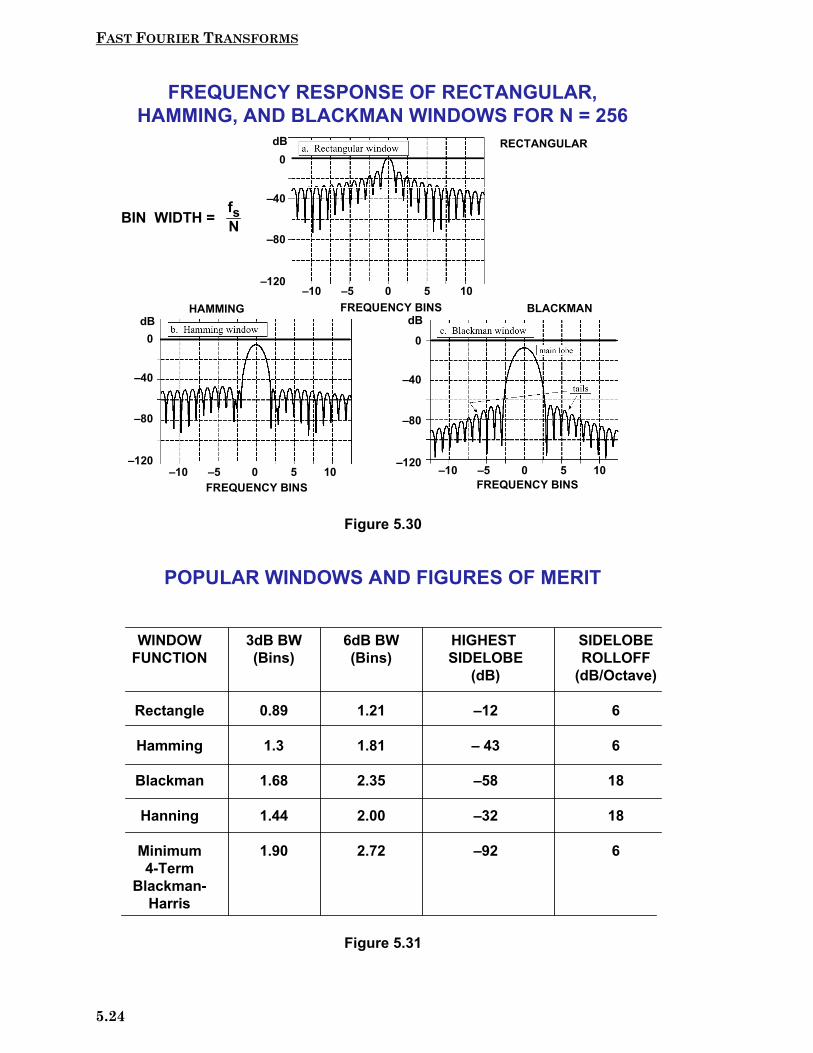
FAST FOURIER TRANSFORMS
5.24
Figure 5.30
Figure 5.31
FREQUENCY RESPONSE OF RECTANGULAR,HAMMING, AND BLACKMAN WINDOWS FOR N = 256
0 5 10–5–10
0 5 10–5–10 0 5 10–5–10
0
–40
–80
–120
0
–40
–80
–120
0
–40
–80
–120
RECTANGULAR
HAMMING BLACKMANFREQUENCY BINS
FREQUENCY BINS FREQUENCY BINS
dB
dB dB
BIN WIDTH = fsN
POPULAR WINDOWS AND FIGURES OF MERIT
WINDOWFUNCTION
Rectangle
Hamming
Blackman
Hanning
Minimum4-Term
Blackman-Harris
3dB BW(Bins)
0.89
1.3
1.68
1.44
1.90
6dB BW(Bins)
1.21
1.81
2.35
2.00
2.72
HIGHEST SIDELOBE
(dB)
–12
– 43
–58
–32
–92
SIDELOBEROLLOFF
(dB/Octave)
6
6
18
18
6

FAST FOURIER TRANSFORMS
5.25
REFERENCES
1. Steven W. Smith, The Scientist and Engineer’s Guide to Digital SignalProcessing, Second Edition, 1999, California Technical Publishing,P.O. Box 502407, San Diego, CA 92150. Also available for free download at: http://www.dspguide.com or http://www.analog.com
2. C. Britton Rorabaugh, DSP Primer, McGraw-Hill, 1999.
3. Richard J. Higgins, Digital Signal Processing in VLSI, Prentice-Hall,1990.
4. A. V. Oppenheim and R. W. Schafer, Digital Signal Processing, Prentice-Hall, 1975.
5. L. R. Rabiner and B. Gold, Theory and Application of Digital SignalProcessing, Prentice-Hall, 1975.
6. John G. Proakis and Dimitris G. Manolakis, Introduction to DigitalSignal Processing, MacMillian, 1988.
7. Fredrick J. Harris, On the Use of Windows for Harmonic Analysis withthe Discrete Fourier Transform, Proc. IEEE, Vol. 66, No. 1, 1978 pp. 51-83.
8. R. W. Ramirez, The FFT: Fundamentals and Concepts,Prentice-Hall, 1985.
9. J. W. Cooley and J. W. Tukey, An Algorithm for the Machine Computationof Complex Fourier Series, Mathematics Computation, Vol. 19,pp. 297-301, April 1965.
10. Digital Signal Processing Applications Using the ADSP-2100Family, Vol. 1 and Vol. 2, Analog Devices, Free Download at:http://www.analog.com
11. ADSP-21000 Family Application Handbook, Vol. 1, Analog Devices,Free Download at: http://www.analog.com

FAST FOURIER TRANSFORMS
5.26

DIGITAL FILTERS
6.a
SECTION 6
DIGITAL FILTERS
Finite Impulse Response (FIR) Filters
Infinite Impulse Response (IIR) Filters
Multirate Filters
Adaptive Filters

DIGITAL FILTERS
6.b

DIGITAL FILTERS
6.1
SECTION 6DIGITAL FILTERSWalt Kester
INTRODUCTION
Digital filtering is one of the most powerful tools of DSP. Apart from the obviousadvantages of virtually eliminating errors in the filter associated with passivecomponent fluctuations over time and temperature, op amp drift (active filters), etc.,digital filters are capable of performance specifications that would, at best, beextremely difficult, if not impossible, to achieve with an analog implementation. Inaddition, the characteristics of a digital filter can be easily changed under softwarecontrol. Therefore, they are widely used in adaptive filtering applications incommunications such as echo cancellation in modems, noise cancellation, andspeech recognition.
The actual procedure for designing digital filters has the same fundamentalelements as that for analog filters. First, the desired filter responses arecharacterized, and the filter parameters are then calculated. Characteristics such asamplitude and phase response are derived in the same way. The key differencebetween analog and digital filters is that instead of calculating resistor, capacitor,and inductor values for an analog filter, coefficient values are calculated for a digitalfilter. So for the digital filter, numbers replace the physical resistor and capacitorcomponents of the analog filter. These numbers reside in a memory as filtercoefficients and are used with the sampled data values from the ADC to perform thefilter calculations.
The real-time digital filter, because it is a discrete time function, works withdigitized data as opposed to a continuous waveform, and a new data point isacquired each sampling period. Because of this discrete nature, data samples arereferenced as numbers such as sample 1, sample 2, sample 3, etc. Figure 6.1 showsa low frequency signal containing higher frequency noise which must be filtered out.This waveform must be digitized with an ADC to produce samples x(n). These datavalues are fed to the digital filter, which in this case is a lowpass filter. The outputdata samples, y(n), are used to reconstruct an analog waveform using a low glitchDAC.
Digital filters, however, are not the answer to all signal processing filteringrequirements. In order to maintain real-time operation, the DSP processor must beable to execute all the steps in the filter routine within one sampling clock period,1/fs. A fast general purpose fixed-point DSP such as the ADSP-2189M at 75MIPScan execute a complete filter tap multiply-accumulate instruction in 13.3ns. TheADSP-2189M requires N+5 instructions for an N-tap filter. For a 100-tap filter, thetotal execution time is approximately 1.4µs. This corresponds to a maximumpossible sampling frequency of 714kHz, thereby limiting the upper signalbandwidth to a few hundred kHz.

DIGITAL FILTERS
6.2
Figure 6.1
However, it is possible to replace a general purpose DSP chip and design specialhardware digital filters which will operate at video-speed sampling rates. In othercases, the speed limitations can be overcome by first storing the high speed ADCdata in a buffer memory. The buffer memory is then read at a rate which iscompatible with the speed of the DSP-based digital filter. In this manner, pseudo-realtime operation can be maintained as in a radar system, where signal processingis typically done on bursts of data collected after each transmitted pulse.
Another option is to use a third-party dedicated DSP filter engine like the SystolixPulseDSP™ filter core. The AD7725 16-bit sigma-delta ADC has an on-chipPulseDSP filter which can do 125 million multiply-accumulates per second.
Even in highly oversampled sampled data systems, an analog antialiasing filter isstill required ahead of the ADC and a reconstruction (anti-imaging) filter after theDAC. Finally, as signal frequencies increase sufficiently, they surpass thecapabilities of available ADCs, and digital filtering then becomes impossible. Activeanalog filtering is not possible at extremely high frequencies because of op ampbandwidth and distortion limitations, and filtering requirements must then be metusing purely passive components. The primary focus of the following discussionswill be on filters which can run in real-time under DSP program control.
As an example, consider the comparison between an analog and a digital filtershown in Figure 6.3. The cutoff frequency of the both filters is 1kHz. The analogfilter is realized as a 6-pole Chebyshev Type 1 filter (ripple in passband, no ripple instopband). In practice, this filter would probably be realized using three 2-polestages, each of which requires an op amp, and several resistors and capacitors. The6-pole design is certainly not trivial, and maintaining the 0.5dB ripple specificationrequires accurate component selection and matching.
DIGITAL FILTERING
ADCDIGITAL
LOWPASSFILTER
ANALOGANTIALIASING
FILTERDAC
t t
H(f)
f
fs fs
ANALOGANTI-IMAGING
FILTER
x(n) y(n)

DIGITAL FILTERS
6.3
On the other hand, the digital FIR filter shown has only 0.002dB passband ripple,linear phase, and a much sharper roll off. In fact, it could not be realized usinganalog techniques! In a practical application, there are many other factors toconsider when evaluating analog versus digital filters. Most modern signalprocessing systems use a combination of analog and digital techniques in order toaccomplish the desired function and take advantage of the best of both the analogand the digital world.
Figure 6.2
There are many applications where digital filters must operate in real-time. Thisplaces specific requirements on the DSP depending upon the sampling frequencyand the filter complexity. The key point is that the DSP must finish allcomputations during the sampling period so it will be ready to process the next datasample. Assume that the analog signal bandwidth to be processed is fa. Thisrequires the ADC sampling frequency fs to be at least 2fa. The sampling period is1/fs. All DSP filter computations (including overhead) must be completed duringthis interval. The computation time depends on the number of taps in the filter andthe speed and efficiency of the DSP. Each tap on the filter requires onemultiplication and one addition (multiply-accumulate). DSPs are generallyoptimized to perform fast multiply-accumulates, and many DSPs have additionalfeatures such as circular buffering and zero-overhead looping minimize the“overhead” instructions that otherwise would be needed.
DIGITAL VERSUS ANALOG FILTERING
DIGITAL FILTERS
High Accuracy
Linear Phase (FIR Filters)
No Drift Due to ComponentVariations
Flexible, Adaptive Filtering Possible
Easy to Simulate and Design
Computation Must be Completed inSampling Period - Limits Real Time
Operation
Requires High Performance ADC,DAC & DSP
ANALOG FILTERS
Less Accuracy - Component Tolerances
Non-Linear Phase
Drift Due to ComponentVariations
Adaptive Filters Difficult
Difficult to Simulate and Design
Analog Filters Required atHigh Frequencies and for
Anti-Aliasing Filters
No ADC, DAC, or DSP Required

DIGITAL FILTERS
6.4
Figure 6.3
Figure 6.4
ANALOG VERSUS DIGITAL FILTERFREQUENCY RESPONSE COMPARISON
0
–40
–20
–60
–80
–100
0
–40
–20
–60
–80
–1000 1 2 3 4 50 1 2 3 4 5
ANALOG FILTER
Chebyshev Type 1 6 Pole, 0.5dB Ripple
DIGITAL FILTER
FIR, 129-Tap, 0.002dB Ripple,Linear Phase, fs = 10kSPSdB dB
FREQUENCY (kHz) FREQUENCY (kHz)
PROCESSING REQUIREMENTSFOR REAL TIME DIGITAL FILTERING
Signal Bandwidth = fa Sampling Frequency fs > 2fa Sampling Period = 1 / fs Filter Computational Time + Overhead < Sampling Period
Depends on Number of Taps Speed of DSP Multiplication-Accumulates (MACs) Efficiency of DSP
Circular Buffering Zero Overhead Looping etc.
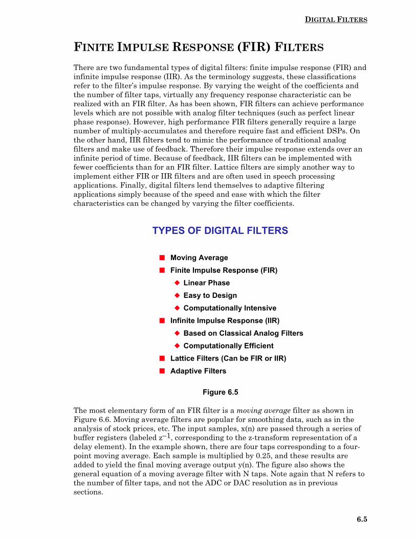
DIGITAL FILTERS
6.5
FINITE IMPULSE RESPONSE (FIR) FILTERS
There are two fundamental types of digital filters: finite impulse response (FIR) andinfinite impulse response (IIR). As the terminology suggests, these classificationsrefer to the filter’s impulse response. By varying the weight of the coefficients andthe number of filter taps, virtually any frequency response characteristic can berealized with an FIR filter. As has been shown, FIR filters can achieve performancelevels which are not possible with analog filter techniques (such as perfect linearphase response). However, high performance FIR filters generally require a largenumber of multiply-accumulates and therefore require fast and efficient DSPs. Onthe other hand, IIR filters tend to mimic the performance of traditional analogfilters and make use of feedback. Therefore their impulse response extends over aninfinite period of time. Because of feedback, IIR filters can be implemented withfewer coefficients than for an FIR filter. Lattice filters are simply another way toimplement either FIR or IIR filters and are often used in speech processingapplications. Finally, digital filters lend themselves to adaptive filteringapplications simply because of the speed and ease with which the filtercharacteristics can be changed by varying the filter coefficients.
Figure 6.5
The most elementary form of an FIR filter is a moving average filter as shown inFigure 6.6. Moving average filters are popular for smoothing data, such as in theanalysis of stock prices, etc. The input samples, x(n) are passed through a series ofbuffer registers (labeled z–1, corresponding to the z-transform representation of adelay element). In the example shown, there are four taps corresponding to a four-point moving average. Each sample is multiplied by 0.25, and these results areadded to yield the final moving average output y(n). The figure also shows thegeneral equation of a moving average filter with N taps. Note again that N refers tothe number of filter taps, and not the ADC or DAC resolution as in previoussections.
TYPES OF DIGITAL FILTERS
Moving Average Finite Impulse Response (FIR)
Linear Phase Easy to Design Computationally Intensive
Infinite Impulse Response (IIR) Based on Classical Analog Filters Computationally Efficient
Lattice Filters (Can be FIR or IIR) Adaptive Filters

DIGITAL FILTERS
6.6
Figure 6.6
Since the coefficients are equal, an easier way to perform a moving average filter isshown in Figure 6.7. Note that the first step is store the first four samples, x(0),x(1), x(2), x(3) in a register. These quantities are added and then multiplied by 0.25to yield the first output, y(3). Note that the initial outputs y(0), y(1), and y(2) are notvalid because all registers are not full until sample x(3) is received.
When sample x(4) is received, it is added to the result, and sample x(0) is subtractedfrom the result. The new result must then be multiplied by 0.25. Therefore, thecalculations required to produce a new output consist of one addition, onesubtraction, and one multiplication, regardless of the length of the moving averagefilter.
The step function response of a 4-point moving average filter is shown in Figure 6.8.Notice that the moving average filter has no overshoot. This makes it useful insignal processing applications where random white noise must be filtered but pulseresponse preserved. Of all the possible linear filters that could be used, the movingaverage produces the lowest noise for a given edge sharpness. This is illustrated inFigure 6.9, where the noise level becomes lower as the number of taps areincreased. Notice that the 0% to 100% risetime of the pulse response is equal to thetotal number of taps in the filter multiplied by the sampling period.
h(3)h(2)h(1)h(0)
4-POINT MOVING AVERAGE FILTER
Z–1 Z–1 Z–1
ΣΣΣΣ= 1
4 = 14 = 1
4 = 14
x(n) x(n–1) x(n–2) x(n–3)
y(n)
y(n) = h(0) x(n) + h(1) x(n – 1) + h(2) x(n – 2) + h(3) x(n – 3)
= x(n) + x(n – 1) + x(n – 2) + x(n – 3)14
14
14
14
14= x(n) + x(n – 1) + x(n – 2) + x(n – 3)
For N-PointMoving Average Filter: y(n) = ΣΣΣΣ1
N k = 0
N–1x(n – k)

DIGITAL FILTERS
6.7
Figure 6.7
Figure 6.8
CALCULATING OUTPUT OF4-POINT MOVING AVERAGE FILTER
y(3) = x(3) + x(2) + x(1) + x(0)
y(4) = x(4) + x(3) + x(2) + x(1)
y(5) = x(5) + x(4) + x(3) + x(2)
y(6) = x(6) + x(5) + x(4) + x(3)
y(7) = x(7) + x(6) + x(5) + x(4)
Each Output Requires:1 multiplication, 1 addition, 1 subtraction
0.25
0.25
0.25
0.25
0.25
4-TAP MOVING AVERAGE FILTER STEP RESPONSE
= Input x(n)
= Output y(n)
0 1 2 3 4 5 6 7 8 9 10 11 12
n
y(n) = ΣΣΣΣ1N k = 0
N–1x(n – k)
y(n) = ΣΣΣΣ14 k = 0
3x(n – k)For N = 4:
General:

DIGITAL FILTERS
6.8
Figure 6.9
The frequency response of the simple moving average filter is sin(x)/x and is shownon a linear amplitude scale in Figure 6.10. Adding more taps to the filter sharpensthe rolloff, but does not significantly reduce the amplitude of the sidelobes whichare approximately 14dB down for the 11 and 31-tap filter. These filters aredefinitely not suitable where high stopband attenuation is required.
Figure 6.10
MOVING AVERAGE FILTER FREQUENCY RESPONSE
0 0.1 0.2 0.3 0.4 0.50
0.2
0.4
0.6
0.8
1.0
3 point
11 point
31 point
Frequency (fraction of fs)
Amplitude
MOVING AVERAGE FILTER RESPONSETO NOISE SUPERIMPOSED ON STEP INPUT
0 500Sample Number
0 500Sample Number 0 500Sample Number
Note:Latency not shown
Note:Latency not shown

DIGITAL FILTERS
6.9
It is possible to dramatically improve the performance of the simple FIR movingaverage filter by properly selecting the individual weights or coefficients rather thangiving them equal weight. The sharpness of the rolloff can be improved by addingmore stages (taps), and the stopband attenuation characteristics can be improved byproperly selecting the filter coefficients. Note that unlike the moving average filter,one multiply-accumulate cycle is now required per tap for the generalized FIR filter.The essence of FIR filter design is the appropriate selection of the filter coefficientsand the number of taps to realize the desired transfer function H(f). Variousalgorithms are available to translate the frequency response H(f) into a set of FIRcoefficients. Most of this software is commercially available and can be run on PCs.The key theorem of FIR filter design is that the coefficients h(n) of the FIR filter aresimply the quantized values of the impulse response of the frequency transferfunction H(f). Conversely, the impulse response is the discrete Fourier transform ofH(f).
Figure 6.11
The generalized form of an N-tap FIR filter is shown in Figure 6.11. As has beendiscussed, an FIR filter must perform the following convolution equation:
y(n) = h(k)*x(n) = ∑−
=−
1N
0k)kn(x)k(h .
where h(k) is the filter coefficient array and x(n-k) is the input data array to thefilter. The number N, in the equation, represents the number of taps of the filterand relates to the filter performance as has been discussed above. An N-tap FIRfilter requires N multiply-accumulate cycles.
N-TAP FINITE IMPULSE RESPONSE (FIR) FILTER
h(N–1)h(N–2)h(1)h(0)
Z–1 Z–1 Z–1
ΣΣΣΣ
x(n) x(n–1) x(n–N+2) x(n–N+1)
y(n)
y(n) = h(n) x(n) = ΣΣΣΣk = 0
N–1h(k) x(n – k)
= Symbol for Convolution
Requires N multiply-accumulates for each output

DIGITAL FILTERS
6.10
FIR filter diagrams are often simplified as shown in Figure 6.12. The summationsare represented by arrows pointing into the dots, and the multiplications areindicated by placing the h(k) coefficients next to the arrows on the lines. The z–1delay element is often shown by placing the label above or next to the appropriateline.
Figure 6.12
FIR FILTER IMPLEMENTATION IN DSP HARDWARE USINGCIRCULAR BUFFERING
In the series of FIR filter equations, the N coefficient locations are always accessedsequentially from h(0) to h(N–1). The associated data points circulate through thememory; new samples are added replacing the oldest each time a filter output iscomputed. A fixed boundary RAM can be used to achieve this circulating buffereffect as shown in Figure 6.13 for a 4 tap FIR filter. The oldest data sample isreplaced by the newest after each convolution. A "time history" of the four mostrecent data samples is always stored in RAM.
To facilitate memory addressing, old data values are read from memory startingwith the value one location after the value that was just written. For example, x(4)is written into memory location 0, and data values are then read from locations 1, 2,3, and 0. This example can be expanded to accommodate any number of taps. Byaddressing data memory locations in this manner, the address generator need onlysupply sequential addresses, regardless of whether the operation is a memory reador write. This data memory buffer is called circular because when the last locationis reached, the memory pointer is reset to the beginning of the buffer.
SIMPLIFIED FILTER NOTATIONS
h(N–1)h(N–2)h(1)h(0)
Z–1 Z–1 Z–1x(n) x(n–1) x(n–N+2) x(n–N+1)
y(n)
h(N–1)h(N–2)h(1)h(0)
x(n) x(n–1) x(n–N+2) x(n–N+1)
y(n)
ΣΣΣΣ ΣΣΣΣ ΣΣΣΣ
Z–1 Z–1 Z–1
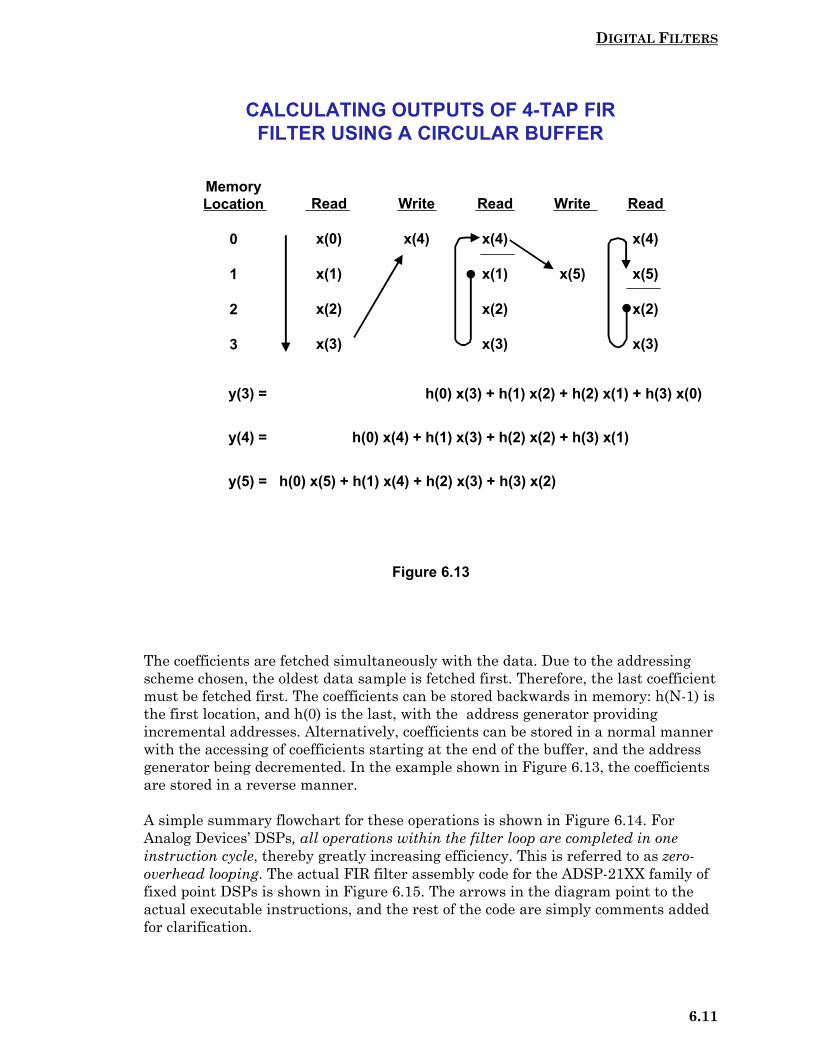
DIGITAL FILTERS
6.11
Figure 6.13
The coefficients are fetched simultaneously with the data. Due to the addressingscheme chosen, the oldest data sample is fetched first. Therefore, the last coefficientmust be fetched first. The coefficients can be stored backwards in memory: h(N-1) isthe first location, and h(0) is the last, with the address generator providingincremental addresses. Alternatively, coefficients can be stored in a normal mannerwith the accessing of coefficients starting at the end of the buffer, and the addressgenerator being decremented. In the example shown in Figure 6.13, the coefficientsare stored in a reverse manner.
A simple summary flowchart for these operations is shown in Figure 6.14. ForAnalog Devices’ DSPs, all operations within the filter loop are completed in oneinstruction cycle, thereby greatly increasing efficiency. This is referred to as zero-overhead looping. The actual FIR filter assembly code for the ADSP-21XX family offixed point DSPs is shown in Figure 6.15. The arrows in the diagram point to theactual executable instructions, and the rest of the code are simply comments addedfor clarification.
CALCULATING OUTPUTS OF 4-TAP FIRFILTER USING A CIRCULAR BUFFER
y(3) = h(0) x(3) + h(1) x(2) + h(2) x(1) + h(3) x(0)
y(4) = h(0) x(4) + h(1) x(3) + h(2) x(2) + h(3) x(1)
y(5) = h(0) x(5) + h(1) x(4) + h(2) x(3) + h(3) x(2)
MemoryLocation
0
1
2
3
Read
x(0)
x(1)
x(2)
x(3)
Write
x(4)
Read
x(4)
x(1)
x(2)
x(3)
Write
x(5)
Read
x(4)
x(5)
x(2)
x(3)

DIGITAL FILTERS
6.12
The first instruction (labeled fir:) sets up the computation by clearing the MRregister and loading the MX0 and MY0 registers with the first data and coefficientvalues from data and program memory. The multiply-accumulate with dual datafetch in the convolution loop is then executed N–1 times in N cycles to compute thesum of the first N–1 products. The final multiply-accumulate instruction isperformed with the rounding mode enabled to round the result to the upper 24 bitsof the MR register. The MR1 register is then conditionally saturated to its mostpositive or negative value based on the status of the overflow flag contained in theMV register. In this manner, results are accumulated to the full 40-bit precision ofthe MR register, with saturation of the output only if the final result overflowedbeyond the least significant 32 bits of the MR register.
The limit on the number of filter taps attainable for a real-time implementation ofthe FIR filter subroutine is determined primarily by the processor cycle time, thesampling rate, and the number of other computations required. The FIR subroutinepresented here requires a total of N+5 cycles for a filter of length N. For the ADSP-2189M 75MIPS DSP, one instruction cycle is 13.3ns, so a 100-tap filter wouldrequire 13.3ns×100 + 5×13.3ns = 1330ns + 66.5ns = 1396.5ns = 1.4µs.
Figure 6.14
PSEUDOCODE FOR FIR FILTER PROGRAMUSING A DSP WITH CIRCULAR BUFFERING
1. Obtain sample from ADC (typically interrupt driven)2. Move sample into input signal’s circular buffer3. Update the pointer for the input signal’s circular buffer4. Zero the accumulator5. Implement filter (control the loop through each of the coefficients)
6. Fetch the coefficient from the coefficient’s circular buffer 7. Update the pointer for the coefficient’s circular buffer 8. Fetch the sample from the input signal’s circular buffer 9. Update the pointer for the input signal’s circular buffer10. Multiply the coefficient by the sample11. Add the product to the accumulator
12. Move the filtered sample to the DACADSP-21xx Example code:
CNTR = N-1;DO convolution UNTIL CE;convolution: MR = MR + MX0 * MY0(SS), MX0 = DM(I0,M1), MY0 = PM(I4,M5);

DIGITAL FILTERS
6.13
Figure 6.15
DESIGNING FIR FILTERS
FIR filters are relatively easy to design using modern CAD tools. Figure 6.16summarizes the characteristics of FIR filters as well as the most popular designtechniques. The fundamental concept of FIR filter design is that the filter frequencyresponse is determined by the impulse response, and the quantized impulse responseand the filter coefficients are identical. This can be understood by examining Figure6.17. The input to the FIR filter is an impulse, and as the impulse propagatesthrough the delay elements, the filter output is identical to the filter coefficients.The FIR filter design process therefore consists of determining the impulse responsefrom the desired frequency response, and then quantizing the impulse response togenerate the filter coefficients.
It is useful to digress for a moment and examine the relationship between the timedomain and the frequency domain to better understand the principles behind digitalfilters such as the FIR filter. In a sampled data system, a convolution operation canbe carried out by performing a series of multiply-accumulates. The convolutionoperation in the time or frequency domain is equivalent to point-by-pointmultiplication in the opposite domain. For example, convolution in the time domainis equivalent to multiplication in the frequency domain. This is shown graphically inFigure 6.18. It can be seen that filtering in the frequency domain can beaccomplished by multiplying all frequency components in the passband by a 1 andall frequencies in the stopband by 0. Conversely, convolution in the frequencydomain is equivalent to point by point multiplication in the time domain.
ADSP-21XX FIR FILTER ASSEMBLY CODE(SINGLE PRECISION)
.MODULE fir_sub; FIR Filter Subroutine
Calling ParametersI0 --> Oldest input data value in delay lineI4 --> Beginning of filter coefficient tableL0 = Filter length (N)L4 = Filter length (N)M1,M5 = 1CNTR = Filter length - 1 (N-1)
Return ValuesMR1 = Sum of products (rounded and saturated)I0 --> Oldest input data value in delay lineI4 --> Beginning of filter coefficient table
Altered RegistersMX0,MY0,MR
Computation Time(N - 1) + 6 cycles = N + 5 cycles
All coefficients are assumed to be in 1.15 format.
.ENTRY fir;fir: MR=0, MX0=DM(I0,M1), MY0=PM(I4,M5);
CNTR = N-1;DO convolution UNTIL CE;
convolution: MR=MR+MX0*MY0(SS), MX0=DM(I0,M1), MY0=PM(I4,M5);MR=MR+MX0*MY0(RND);IF MV SAT MR;RTS;
.ENDMOD;

DIGITAL FILTERS
6.14
Figure 6.16
Figure 6.17
CHARACTERISTICS OF FIR FILTERS
Impulse Response has a Finite Duration (N Cycles)
Linear Phase, Constant Group Delay (N Must be Odd)
No Analog Equivalent
Unconditionally Stable
Can be Adaptive
Computational Advantages when Decimating Output
Easy to Understand and Design
Windowed-Sinc Method
Fourier Series Expansion with Windowing
Frequency Sampling Using Inverse FFT - Arbitrary FrequencyResponse
Parks-McClellan Program with Remez Exchange Algorithm
FIR FILTER IMPULSE RESPONSEDETERMINES THE FILTER COEFFICIENTS
h(8)h(7)h(1)h(0)
Z–1 Z–1 Z–1
ΣΣΣΣ
x(n) x(n–1) x(n–7) x(n–8)
y(n)
1
h(0)
h(1)
h(2)
h(3)
h(4)
h(5)
h(6)
h(7)
h(8)
x(n)
N = 9
n n
y(n)
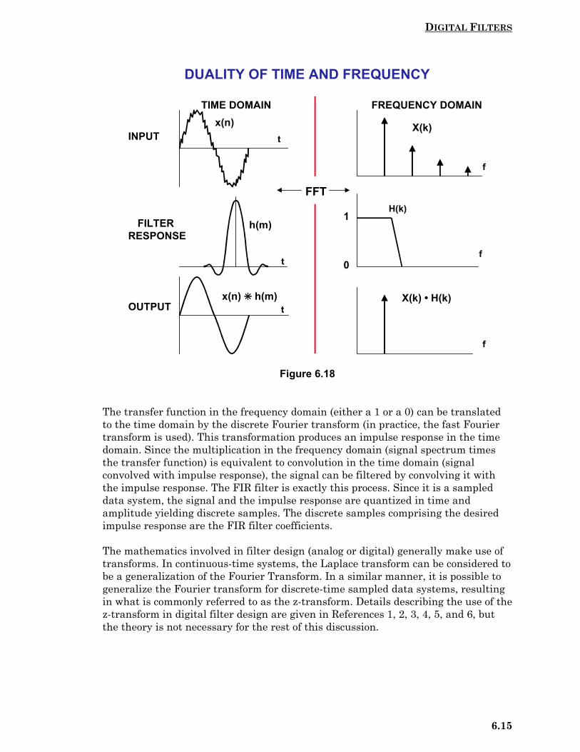
DIGITAL FILTERS
6.15
Figure 6.18
The transfer function in the frequency domain (either a 1 or a 0) can be translatedto the time domain by the discrete Fourier transform (in practice, the fast Fouriertransform is used). This transformation produces an impulse response in the timedomain. Since the multiplication in the frequency domain (signal spectrum timesthe transfer function) is equivalent to convolution in the time domain (signalconvolved with impulse response), the signal can be filtered by convolving it withthe impulse response. The FIR filter is exactly this process. Since it is a sampleddata system, the signal and the impulse response are quantized in time andamplitude yielding discrete samples. The discrete samples comprising the desiredimpulse response are the FIR filter coefficients.
The mathematics involved in filter design (analog or digital) generally make use oftransforms. In continuous-time systems, the Laplace transform can be considered tobe a generalization of the Fourier Transform. In a similar manner, it is possible togeneralize the Fourier transform for discrete-time sampled data systems, resultingin what is commonly referred to as the z-transform. Details describing the use of thez-transform in digital filter design are given in References 1, 2, 3, 4, 5, and 6, butthe theory is not necessary for the rest of this discussion.
DUALITY OF TIME AND FREQUENCY
t
t
H(k)
ft
f
f
FFT
INPUT
FILTER RESPONSE
OUTPUT
TIME DOMAIN FREQUENCY DOMAINx(n)
h(m)
x(n) h(m)
X(k)
X(k) • H(k)
1
0

DIGITAL FILTERS
6.16
FIR Filter Design Using the Windowed-Sinc Method
An ideal lowpass filter frequency response is shown in Figure 6.19A. Thecorresponding impulse response in the time domain is shown in Figure 6.19B, andfollows the sin(x)/x (sinc) function. If an FIR filter is used to implement thisfrequency response, an infinite number of taps are required. The windowed-sincmethod is used to implement the filter as follows. First, the impulse response istruncated to a reasonable number of N taps as in Figure 6.19C. As has beendiscussed in Section 5, the frequency response corresponding to Figure 6.19C hasrelatively poor sidelobe performance because of the end-point discontinuities in thetruncated impulse response. The next step in the design process is to apply anappropriate window function as shown in Figure 6.19D to the truncated impulse.This forces the endpoints to zero. The particular window function chosen determinesthe rolloff and sidelobe performance of the filter. Window functions have beendiscussed in detail in Section 5, and there are several good choices depending uponthe desired frequency response. The frequency response of the truncated andwindowed-sinc impulse response of Figure 6.19E is shown in Figure 6.19F.
Figure 6.19
FIR FILTER DESIGN USINGTHE WINDOWED-SINC METHOD
N
NN
f t t
t t f
Ideal Lowpass FilterFrequency Response
fc
Ideal Lowpass Filter Impulse Response
Truncated Impulse Response
WindowFunction
WindowedImpulse Response
Final FilterFrequency Response
(A) (B) (C)
(D) (E) (F)
sin xx
(sinc function)
fc
1
0
1
0

DIGITAL FILTERS
6.17
FIR Filter Design Using the Fourier Series Method with Windowing
The Fourier series with windowing method (Figure 6.20) starts by defining thetransfer function H(f) mathematically and expanding it in a Fourier series. TheFourier series coefficients define the impulse response and therefore the coefficientsof the FIR filter. However, the impulse response must be truncated and windowedas in the previous method. After truncation and windowing, an FFT is used togenerate the corresponding frequency response. The frequency response can bemodified by choosing different window functions, although precise control of thestopband characteristics is difficult in any method which uses windowing.
Figure 6.20
FIR Filter Design Using the Frequency Sampling Method
This method is extremely useful in generating an FIR filter with an arbitraryfrequency response. H(f) is specified as a series of amplitude and phase points in thefrequency domain. The points are then converted into real and imaginarycomponents. Next, the impulse response is obtained by taking the complex inverseFFT of the frequency response. The impulse response is then truncated to N points,and a window function is applied to minimize the effects of truncation. The filterdesign should then be tested by taking its FFT and evaluating the frequencyresponse. Several iterations may be required to achieve the desired response.
FIR FILTER DESIGN USINGFOURIER SERIES METHOD WITH WINDOWING
Specify H(f) Expand H(f) in a Fourier series: The Fourier series coefficients are
the coefficients of the FIR filter, h(m), and its Impulse Response Truncate the Impulse Response to N points (taps) Apply a suitable Window function to h(m) to smooth the effects of
truncation Lacks precise control of cutoff frequency; Highly dependent
on Window function
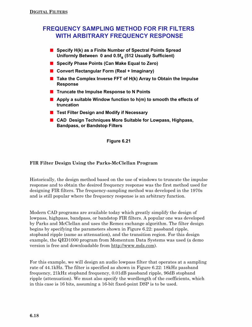
DIGITAL FILTERS
6.18
Figure 6.21
FIR Filter Design Using the Parks-McClellan Program
Historically, the design method based on the use of windows to truncate the impulseresponse and to obtain the desired frequency response was the first method used fordesigning FIR filters. The frequency-sampling method was developed in the 1970sand is still popular where the frequency response is an arbitrary function.
Modern CAD programs are available today which greatly simplify the design oflowpass, highpass, bandpass, or bandstop FIR filters. A popular one was developedby Parks and McClellan and uses the Remez exchange algorithm. The filter designbegins by specifying the parameters shown in Figure 6.22: passband ripple,stopband ripple (same as attenuation), and the transition region. For this designexample, the QED1000 program from Momentum Data Systems was used (a demoversion is free and downloadable from http://www.mds.com).
For this example, we will design an audio lowpass filter that operates at a samplingrate of 44.1kHz. The filter is specified as shown in Figure 6.22: 18kHz passbandfrequency, 21kHz stopband frequency, 0.01dB passband ripple, 96dB stopbandripple (attenuation). We must also specify the wordlength of the coefficients, whichin this case is 16 bits, assuming a 16-bit fixed-point DSP is to be used.
FREQUENCY SAMPLING METHOD FOR FIR FILTERS WITH ARBITRARY FREQUENCY RESPONSE
Specify H(k) as a Finite Number of Spectral Points SpreadUniformly Between 0 and 0.5fs (512 Usually Sufficient)
Specify Phase Points (Can Make Equal to Zero) Convert Rectangular Form (Real + Imaginary) Take the Complex Inverse FFT of H(k) Array to Obtain the Impulse
Response Truncate the Impulse Response to N Points Apply a suitable Window function to h(m) to smooth the effects of
truncation Test Filter Design and Modify if Necessary CAD Design Techniques More Suitable for Lowpass, Highpass,
Bandpass, or Bandstop Filters

DIGITAL FILTERS
6.19
Figure 6.22
Figure 6.23
PARKS McCLELLAN EQUIRIPPLE FIRFILTER DESIGN: PROGRAM INPUTS
Filter Type: Lowpass Highpass Bandpass Bandstop Differentiator Multiband
Sampling Frequency: 44,100Hz Passband Frequency: 18,000Hz Stopband Frequency: 21,000Hz Passband Ripple: 0.01dB Stopband Ripple (Attenuation): 96dB Wordlength: 16-bits
FIR CAD TECHNIQUES: PARKS McCLELLAN PROGRAMWITH REMEZ EXCHANGE ALGORITHM
Passband EndingFrequency
1
0FREQUENCY
δδδδ1 = Passband Ripple
δδδδ2 = Stopband Ripple (Attenuation)
Stopband BeginningFrequency
Ripple Ratio = δδδδ2δδδδ1
GAIN
fp
fc

DIGITAL FILTERS
6.20
The program allows us to choose between a window-based design or the equirippleParks-McClellan program. We will choose the latter. The program now estimatesthe number of taps required to implement the filter based on the abovespecifications. In this case, it is 69 taps. At this point, we can accept this andproceed with the design or decrease the number of taps and see what degradation isspecifications occur.
We will accept this number and let the program complete the calculations. Theprogram outputs the frequency response (Figure 6.25), step function response(Figure 6.26), s and z-plane analysis data, and the impulse response (Figure 6.27).The QED1000 program then outputs the quantized filter coefficients to a programwhich generates the actual DSP assembly code for a number of popular DSPs,including Analog Devices’. The program is quite flexible and allows the user toperform a number of scenarios to optimize the filter design.
Figure 6.24
The 69-tap FIR filter requires 69 + 5 = 74 instruction cycles using the ADSP-2189M75MIPS processor, which yields a total computation time per sample of 74×13.3ns =984ns. The sampling interval is 1/44.1kHz, or 22.7µs. This allows 22.7µs – 0.984µs =21.7µs for overhead and other operations.
Other options are to use a slower processor for this application (3.3MIPS), a morecomplex filter which takes more computation time (up to N = 1700), or increase thesampling frequency to about 1MSPS.
FIR FILTER PROGRAM OUTPUTS
Estimated Number of Taps Required: 69 Accept? Change? Accept
Frequency Response (Linear and Log Scales) Step Response S - and Z - Plane Analysis Impulse Response: Filter Coefficients (Quantized) DSP FIR Filter Assembly Code

DIGITAL FILTERS
6.21
Figure 6.25
Figure 6.26
FIR DESIGN EXAMPLE: FREQUENCY RESPONSE
GAIN
FREQUENCY (Hz),
Courtesy Momentum Data Systems
18kHz
21kHz
Passband Ripple < 0.01dB
96dB
fs = 44.1kSPS fs2
FIR FILTER DESIGN EXAMPLE: STEP RESPONSE
TIME (MILLISECONDS)
AMPLITUDE
Courtesy Momentum Data Systems

DIGITAL FILTERS
6.22
Figure 6.27
Figure 6.28
FIR DESIGN EXAMPLE: IMPULSE RESPONSE(FILTER COEFFICIENTS)
AMPLITUDE
TIME (MILLISECONDS)
N = 69
Courtesy Momentum Data Systems
DESIGN EXAMPLE USING ADSP-2189M:PROCESSOR TIME FOR 69-TAP FIR FILTER
Sampling Frequency fs = 44.1kSPS
Sampling Interval = 1 / fs = 22.7µs
Number of Filter Taps, N = 69
Number of Required Instructions = N + 5 = 74
Processing Time / Instruction = 13.3ns (75MIPS)
(ADSP-2189M)
Total Processing Time = 74×13.3ns = 984ns
Total Processing Time < Sampling Interval with22.7µs – 0.984µs = 21.7µs for Other Operations Increase Sampling Frequency to 1MHz Use Slower DSP (3.3MIPS) Add More Filter Taps (Up to N = 1700)
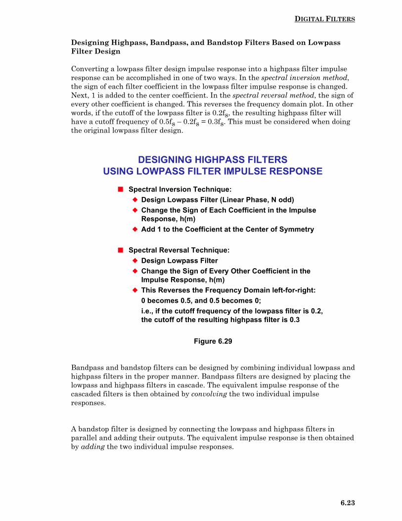
DIGITAL FILTERS
6.23
Designing Highpass, Bandpass, and Bandstop Filters Based on LowpassFilter Design
Converting a lowpass filter design impulse response into a highpass filter impulseresponse can be accomplished in one of two ways. In the spectral inversion method,the sign of each filter coefficient in the lowpass filter impulse response is changed.Next, 1 is added to the center coefficient. In the spectral reversal method, the sign ofevery other coefficient is changed. This reverses the frequency domain plot. In otherwords, if the cutoff of the lowpass filter is 0.2fs, the resulting highpass filter willhave a cutoff frequency of 0.5fs – 0.2fs = 0.3fs. This must be considered when doingthe original lowpass filter design.
Figure 6.29
Bandpass and bandstop filters can be designed by combining individual lowpass andhighpass filters in the proper manner. Bandpass filters are designed by placing thelowpass and highpass filters in cascade. The equivalent impulse response of thecascaded filters is then obtained by convolving the two individual impulseresponses.
A bandstop filter is designed by connecting the lowpass and highpass filters inparallel and adding their outputs. The equivalent impulse response is then obtainedby adding the two individual impulse responses.
DESIGNING HIGHPASS FILTERSUSING LOWPASS FILTER IMPULSE RESPONSE
Spectral Inversion Technique: Design Lowpass Filter (Linear Phase, N odd) Change the Sign of Each Coefficient in the Impulse
Response, h(m) Add 1 to the Coefficient at the Center of Symmetry
Spectral Reversal Technique: Design Lowpass Filter Change the Sign of Every Other Coefficient in the
Impulse Response, h(m) This Reverses the Frequency Domain left-for-right:
0 becomes 0.5, and 0.5 becomes 0;i.e., if the cutoff frequency of the lowpass filter is 0.2,the cutoff of the resulting highpass filter is 0.3

DIGITAL FILTERS
6.24
Figure 6.30
INFINITE IMPULSE RESPONSE (IIR) FILTERS
As was mentioned previously, FIR filters have no real analog counterparts, theclosest analogy being the weighted moving average. In addition, FIR filters haveonly zeros and no poles. On the other hand, IIR filters have traditional analogcounterparts (Butterworth, Chebyshev, Elliptic, and Bessel) and can be analyzedand synthesized using more familiar traditional filter design techniques.
Infinite impulse response filters get their name because their impulse responseextends for an infinite period of time. This is because they are recursive, i.e., theyutilize feedback. Although they can be implemented with fewer computations thanFIR filters, IIR filters do not match the performance achievable with FIR filters, anddo not have linear phase. Also, there is no computational advantage achieved whenthe output of an IIR filter is decimated because each output value must always becalculated.
BANDPASS AND BANDSTOP FILTERSDESIGNED FROM LOWPASS AND HIGHPASS FILTERS
h1(k) h2(k)x(n) y(n)
h1(k) h2(k)x(n) y(n)
h1(k)
h2(k)ΣΣΣΣ
x(n)h1(k) + h2(k)
x(n) y(n)y(n)
= Convolution
Lowpass Highpass Bandpass
Highpass
Lowpass Bandstop

DIGITAL FILTERS
6.25
Figure 6.31
IIR filters are generally implemented in two-pole sections called biquads becausethey are described with a biquadratic equation in the z-domain. Higher order filtersare designed using cascaded biquad sections, i.e., a 6-pole filter requires 3 biquadsections.
The basic IIR biquad is shown in Figure 6.32. The zeros are formed by thefeedforward coefficients b0, b1, and b2; the poles are formed by the feedbackcoefficients a1, and a2.
Figure 6.32
INFINITE IMPULSE RESPONSE (IIR) FILTERS
Uses Feedback (Recursion) Impulse Response has an Infinite Duration Potentially Unstable Non-Linear Phase More Efficient than FIR Filters No Computational Advantage when Decimating
Output Usually Designed to Duplicate Analog Filter Response Usually Implemented as Cascaded Second-Order
Sections (Biquads)
HARDWARE IMPLEMENTATION OFSECOND-ORDER IIR FILTER (BIQUAD) DIRECT FORM 1
z–1
z–1
z–1
z–1
b0
b1
b2
–a1
–a2
x(n) y(n)ΣΣΣΣ
y(n) = b0x(n) + b1x(n–1) + b2x(n–2) – a1y(n–1) – a2y(n–2)
y(n) = ΣΣΣΣ bkx(n–k) – ΣΣΣΣ aky(n–k)k=0
M
k=1
NH(z) =
ΣΣΣΣ bkz–kk=0
M
1 + ΣΣΣΣ akz–k
k=1
N
(Zeros)
(Poles)

DIGITAL FILTERS
6.26
The general digital filter equation is shown in Figure 6.32 which gives rise to thegeneral transfer function H(z) which contains polynomials in both the numeratorand the denominator. The roots of the denominator determine the pole locations ofthe filter, and the roots of the numerator determine the zero locations. Although itis possible to construct a high order IIR filter directly from this equation (called thedirect form implementation), accumulation errors due to quantization errors (finitewordlength arithmetic) may give rise to instability and large errors. For this reason,it is common to cascade several biquad sections with appropriate coefficients ratherthan use the direct form implementation. The biquads can be scaled separately andthen cascaded in order to minimize the coefficient quantization and the recursiveaccumulation errors. Cascaded biquads execute more slowly than their direct formcounterparts, but are more stable and minimize the effects of errors due to finitearithmetic errors.
The Direct Form 1 biquad section shown in Figure 6.32 requires four registers. Thisconfiguration can be changed into an equivalent circuit shown in Figure 6.33 whichis called the Direct Form 2 which requires only two registers. It can be shown thatthe equations describing the Direct Form 2 IIR biquad filter are the same as thosefor Direct Form 1. As in the case of FIR filters, the notation for an IIR filter is oftensimplified as shown in Figure 6.34.
Figure 6.33
IIR BIQUAD FILTER DIRECT FORM 2
z–1
z–1
–a1
–a2
b1
b2
x(n) y(n)ΣΣΣΣΣΣΣΣb0
y(n) = b0x(n) + b1x(n–1) + b2x(n–2) – a1y(n–1) – a2y(n–2)
Reduces to the same equation as Direct Form 1:
Requires Only 2 Delay Elements (Registers)

DIGITAL FILTERS
6.27
Figure 6.34
IIR FILTER DESIGN TECHNIQUES
A popular method for IIR filter design is to first design the analog-equivalent filterand then mathematically transform the transfer function H(s) into the z-domain,H(z). Multiple pole designs are implemented using cascaded biquad sections. Themost popular analog filters are the Butterworth, Chebyshev, Elliptical, and Bessel(see Figure 6.35). There are many CAD programs available to generate the Laplacetransform, H(s), for these filters.
The all-pole Butterworth (also called maximally flat) has no ripple in the passbandor stopband and has monotonic response in both regions. The all-pole Type 1Chebyshev filter has a faster rolloff than the Butterworth (for the same number ofpoles) and has ripple in the passband. The Type 2 Chebyschev filter is rarely used,but has ripple in the stopband rather than the passband.
The Elliptical (Cauer) filter has poles and zeros and ripple in both the passband andstopband. This filter has even faster rolloff than the Chebyshev for the samenumber of poles. The Elliptical filter is often used where degraded phase responsecan be tolerated.
Finally, the Bessel (Thompson) filter is an all-pole filter which is optimized for pulseresponse and linear phase but has the poorest rolloff of any of the types discussedfor the same number of poles.
IIR BIQUAD FILTER SIMPLIFIED NOTATIONS
z–1
z–1
–a1
–a2
b1
b2
x(n) y(n)b0
–a1
–a2
b1
b2
x(n) y(n)b0
z–1
z–1

DIGITAL FILTERS
6.28
Figure 6.35
All of the above types of analog filters are covered in the literature, and theirLaplace transforms, H(s), are readily available – either from tables or CADprograms. There are three methods used to convert the Laplace transform into thez-transform: impulse invariant transformation, bilinear transformation, and thematched z-transform. The resulting z-transforms can be converted into thecoefficients of the IIR biquad. These techniques are highly mathematically intensiveand will not be discussed further.
A CAD approach for IIR filter design is similar to the Parks-McClellan programused for FIR filters. This technique uses the Fletcher-Powell algorithm.
In calculating the throughput time of a particular DSP IIR filter, one shouldexamine the benchmark performance specification for a biquad filter section. Forthe ADSP-21xx-family, seven instruction cycles are required to execute a biquadfilter output sample. For the ADSP-2189M, 75MIPS DSP, this corresponds to 7 ×13.3ns = 93ns, corresponding to a maximum possible sampling frequency of10MSPS (neglecting overhead).
REVIEW OF POPULAR ANALOG FILTERS
Butterworth All Pole, No Ripples in Passband or Stopband Maximally Flat Response (Fastest Roll-off with No Ripple)
Chebyshev (Type 1) All Pole, Ripple in Passband, No Ripple in Stopband Shorter Transition Region than Butterworth for Given Number
of Poles Type 2 has Ripple in Stopband, No Ripple in Passband
Elliptical (Cauer) Has Poles and Zeros, Ripple in Both Passband and Stopband Shorter Transition Region than Chebyshev for Given Number
of Poles Degraded Phase Response
Bessel (Thompson) All Pole, No Ripples in Passband or Stopband Optimized for Linear Phase and Pulse Response Longest Transition Region of All for Given Number of Poles

DIGITAL FILTERS
6.29
Figure 6.36
Figure 6.37
IIR FILTER DESIGN TECHNIQUES
Impulse Invarient Transformation Method Start with H(s) for Analog Filter Take Inverse Laplace Transform to get Impulse Response Obtain z-Transform H(z) from Sampled Impulse Response z-Transform Yields Filter Coefficients Aliasing Effects Must be Considered
Bilinear Transformation Method Another Method for Transforming H(s) into H(z) Performance Determined by the Analog System’s
Differential Equation Aliasing Effects do not Occur
Matched z-Transform Method Maps H(s) into H(z) for filters with both poles and zeros
CAD Methods Fletcher-Powell Algorithm Implements Cascaded Biquad Sections
THROUGHPUT CONSIDERATIONS FOR IIR FILTERS
Determine How Many Biquad Sections (N) are Required toRealize the Desired Frequency Response
Multiply this by the number of instruction cycles per Biquadfor the DSP and add overhead cycles (5N + 2 cycles for theADSP-21xx series, for example).
The Result (plus overhead) is the Minimum AllowableSampling Period (1 / fs) for Real-Time Operation
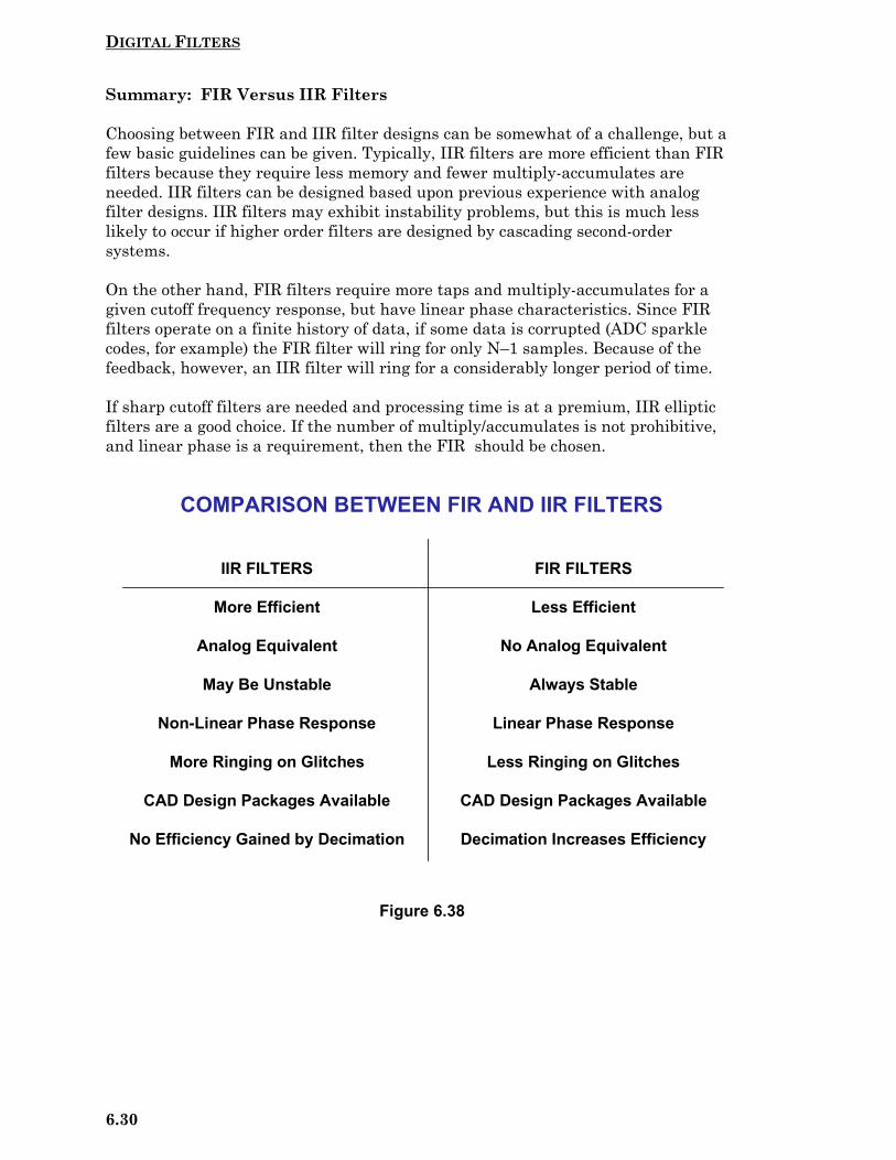
DIGITAL FILTERS
6.30
Summary: FIR Versus IIR Filters
Choosing between FIR and IIR filter designs can be somewhat of a challenge, but afew basic guidelines can be given. Typically, IIR filters are more efficient than FIRfilters because they require less memory and fewer multiply-accumulates areneeded. IIR filters can be designed based upon previous experience with analogfilter designs. IIR filters may exhibit instability problems, but this is much lesslikely to occur if higher order filters are designed by cascading second-ordersystems.
On the other hand, FIR filters require more taps and multiply-accumulates for agiven cutoff frequency response, but have linear phase characteristics. Since FIRfilters operate on a finite history of data, if some data is corrupted (ADC sparklecodes, for example) the FIR filter will ring for only N–1 samples. Because of thefeedback, however, an IIR filter will ring for a considerably longer period of time.
If sharp cutoff filters are needed and processing time is at a premium, IIR ellipticfilters are a good choice. If the number of multiply/accumulates is not prohibitive,and linear phase is a requirement, then the FIR should be chosen.
Figure 6.38
COMPARISON BETWEEN FIR AND IIR FILTERS
IIR FILTERS
More Efficient
Analog Equivalent
May Be Unstable
Non-Linear Phase Response
More Ringing on Glitches
CAD Design Packages Available
No Efficiency Gained by Decimation
FIR FILTERS
Less Efficient
No Analog Equivalent
Always Stable
Linear Phase Response
Less Ringing on Glitches
CAD Design Packages Available
Decimation Increases Efficiency

DIGITAL FILTERS
6.31
MULTIRATE FILTERS
There are many applications where it is desirable to change the effective samplingrate in a sampled data system. In many cases, this can be accomplished simply bychanging the sampling frequency to the ADC or DAC. However, it is often desirableto accomplish the sample rate conversion after the signal has been digitized. Themost common techniques used are decimation (reducing the sampling rate by afactor of M), and interpolation (increasing the sampling rate by a factor of L). Thedecimation and interpolation factors (M and L) are normally integer numbers. In ageneralized sample-rate converter, it may be desirable to change the samplingfrequency by a non-integer number. In the case of converting the CD samplingfrequency of 44.1kHz to the digital audio tape (DAT) sampling rate of 48kHz,interpolating by L =160 followed by decimation by M = 147 accomplishes the desiredresult.
The concept of decimation is illustrated in Figure 6.39. The top diagram shows theoriginal signal, fa, which is sampled at a frequency fs. The corresponding frequencyspectrum shows that the sampling frequency is much higher than required topreserve information contained in fa, i.e., fa is oversampled. Notice that there is noinformation contained between the frequencies fa and fs – fa. The bottom diagramshows the same signal where the sampling frequency has been reduced (decimated)by a factor of M. Notice that even though the sampling rate has been reduced, thereis no aliasing and loss of information. Decimation by a larger factor than shown inFigure 6.39 will cause aliasing.
Figure 6.39
DECIMATION OF ASAMPLED SIGNAL BY A FACTOR OF M
fsfs2
fs2M
fsM
t
t
f
f
1fs
Mfs
A: ORIGINAL OVERSAMPLED SIGNAL
B: SIGNAL DECIMATED BY M
fa fs–fa
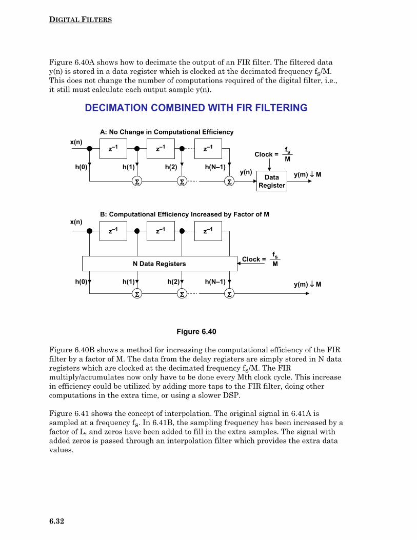
DIGITAL FILTERS
6.32
Figure 6.40A shows how to decimate the output of an FIR filter. The filtered datay(n) is stored in a data register which is clocked at the decimated frequency fs/M.This does not change the number of computations required of the digital filter, i.e.,it still must calculate each output sample y(n).
Figure 6.40
Figure 6.40B shows a method for increasing the computational efficiency of the FIRfilter by a factor of M. The data from the delay registers are simply stored in N dataregisters which are clocked at the decimated frequency fs/M. The FIRmultiply/accumulates now only have to be done every Mth clock cycle. This increasein efficiency could be utilized by adding more taps to the FIR filter, doing othercomputations in the extra time, or using a slower DSP.
Figure 6.41 shows the concept of interpolation. The original signal in 6.41A issampled at a frequency fs. In 6.41B, the sampling frequency has been increased by afactor of L, and zeros have been added to fill in the extra samples. The signal withadded zeros is passed through an interpolation filter which provides the extra datavalues.
DECIMATION COMBINED WITH FIR FILTERING
z–1 z–1 z–1
DataRegisterΣΣΣΣ ΣΣΣΣ ΣΣΣΣ
h(0) h(1) h(2) h(N–1)
z–1 z–1 z–1
N Data Registers
ΣΣΣΣ ΣΣΣΣ ΣΣΣΣ
h(0) h(1) h(2) h(N–1)
fsMClock =
Clock =fsM
x(n)
x(n)
A: No Change in Computational Efficiency
B: Computational Efficiency Increased by Factor of M
y(n) y(m) ↓↓↓↓ M
y(m) ↓↓↓↓ M

DIGITAL FILTERS
6.33
Figure 6.41
The frequency domain effects of interpolation are shown in Figure 6.42. The originalsignal is sampled at a frequency fs and is shown in 6.42A. The interpolated signal in6.42B is sampled at a frequency Lfs. An example of interpolation is a CD playerDAC, where the CD data is generated at a frequency of 44.1kHz. If this data ispassed directly to a DAC, the frequency spectrum shown in Figure 6.42A results,and the requirements on the anti-imaging filter which precedes the DAC areextremely stringent to overcome this. An oversampling interpolating DAC isnormally used, and the spectrum shown in Figure 6.42B results. Notice that therequirements on the analog anti-imaging filter are now easier to realize. This isimportant in maintaining relatively linear phase and also reducing the cost of thefilter.
The digital implementation of interpolation is shown in Figure 6.43. The originalsignal x(n) is first passed through a rate expander which increases the samplingfrequency by a factor of L and inserts the extra zeros. The data then passes throughan interpolation filter which smoothes the data and interpolates between theoriginal data points. The efficiency of this filter can be improved by using a filteralgorithm which takes advantage of the fact that the zero-value input samples donot require multiply-accumulates. Using a DSP which allows circular buffering andzero-overhead looping also improves efficiency.
INTERPOLATION BY A FACTOR OF L
t
1fs
t1Lfs
1Lfs
ORIGINAL SAMPLED SIGNAL
SIGNAL WITH ADDED ZEROS
SIGNAL AFTERINTERPOLATING
FILTER
SAMPLING RATE = fs
SAMPLING RATE = Lfs
A:
B:
C:
t

DIGITAL FILTERS
6.34
Figure 6.42
Figure 6.43
EFFECTS OF INTERPOLATIONON FREQUENCY SPECTRUM
fs2
fs f
ORIGINAL SIGNAL
LfsLfs2
f1Lfs
SIGNAL INTERPOLATED BY L
2fs 3fs 4fst1fs
t
TYPICAL INTERPOLATION IMPLEMENTATION
z–1 z–1 z–1↑↑↑↑ L
ΣΣΣΣ ΣΣΣΣ ΣΣΣΣ
h(0) h(1) h(2) h(N–1)
Clock = Lfs
x(n)
y(m) ↑↑↑↑ L
Rate Expander Increases Sample Rateand Inserts Zeros
Interpolation Filter
Efficient DSP algorithms take advantage of: Multiplications by zeroCircular BuffersZero-Overhead Looping

DIGITAL FILTERS
6.35
Interpolators and decimators can be combined to perform fractional sample rateconversion as shown in Figure 6.44. The input signal x(n) is first interpolated by afactor of L and then decimated by a factor of M. The resulting output sample rate isLfs/M. To maintain the maximum possible bandwidth in the intermediate signal,the interpolation must come before the decimation; otherwise, some of the desiredfrequency content in the original signal would be filtered out by the decimator.
An example is converting from the CD sampling rate of 44.1kHz to the digital audiotape (DAT) sampling rate of 48.0kHz. The interpolation factor is 160, and thedecimation factor of 147. In practice, the interpolating filter h΄(k) and thedecimating filter h"(k) are combined into a single filter, h(k).
The entire sample-rate conversion function is integrated into the AD1890, AD1891,AD1892, and AD1893-family which operates at frequencies between 8kHz and56kHz (48kHz for the AD1892). The new AD1896 operates up to 196kHz.
Figure 6.44
ADAPTIVE FILTERS
Unlike analog filters, the characteristics of digital filters can easily be changedsimply by modifying the filter coefficients. This makes digital filters attractive incommunications applications such as adaptive equalization, echo cancellation, noisereduction, speech analysis and synthesis, etc. The basic concept of an adaptive filteris shown in Figure 6.45. The objective is to filter the input signal, x(n), with anadaptive filter in such a manner that it matches the desired signal, d(n). The
SAMPLE RATE CONVERTERS
↑↑↑↑ L h'(k) ↓↓↓↓ Mh"(k)x(n) y(m)
INTERPOLATOR DECIMATOR
↑↑↑↑ Lx(n)
h(k) ↓↓↓↓ My(m)
Output Sample Rate = fs fsLM
Example: Convert CD Sampling Rate = 44.1kHz to DAT Sampling Rate = 48.0kHz
Use L = 160, M = 147
fout = fsLM = 160
147 × 44.1kHz = 48.0kHz

DIGITAL FILTERS
6.36
desired signal, d(n), is subtracted from the filtered signal, y(n), to generate an errorsignal. The error signal drives an adaptive algorithm which generates the filtercoefficients in a manner which minimizes the error signal. The least-mean-square(LMS) or recursive-least-squares (RLS) algorithms are two of the most popular.
Figure 6.45
Adaptive filters are widely used in communications to perform such functions asequalization, echo cancellation, noise cancellation, and speech compression. Figure6.46 shows an application of an adaptive filter used to compensate for the effects ofamplitude and phase distortion in the transmission channel. The filter coefficientsare determined during a training sequence where a known data pattern istransmitted. The adaptive algorithm adjusts the filter coefficients to force thereceive data to match the training sequence data. In a modem application, thetraining sequence occurs after the initial connection is made. After the trainingsequence is completed, the switches are put in the other position, and the actualdata is transmitted. During this time, the error signal is generated by subtractingthe input from the output of the adaptive filter.
Speech compression and synthesis also makes extensive use of adaptive filtering toreduce data rates. The linear predictive coding (LPC) model shown in Figure 6.47models the vocal tract as a variable frequency impulse generator (for voiced portionsof speech) and a random noise generator (for unvoiced portions of speech such asconsonant sounds). These these two generators drive a digital filter which in turngenerates the actual voice signal.
ADAPTIVE FILTER
ADAPTIVEN-TAP
FIR FlLTER∑∑∑∑
ADAPTIVEALGORITHM
h(k),Filter Coefficients
N
x(n)
Input Signal
d(n)
Desired Signal
–
ErrorSignal
(LMS, RLS)
y(n)
+
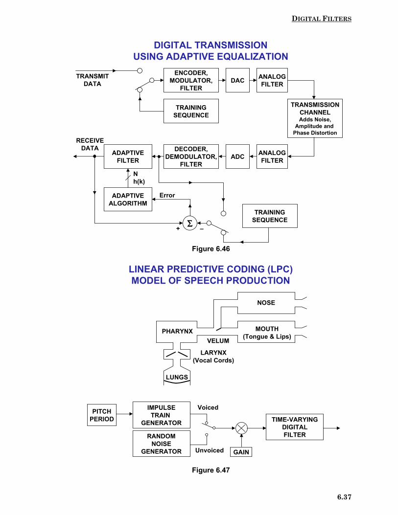
DIGITAL FILTERS
6.37
Figure 6.46
Figure 6.47
DIGITAL TRANSMISSIONUSING ADAPTIVE EQUALIZATION
ENCODER,MODULATOR,
FILTER
TRAININGSEQUENCE
DAC ANALOGFILTER
TRANSMISSIONCHANNELAdds Noise,
Amplitude and Phase Distortion
ANALOGFILTERADC
DECODER,DEMODULATOR,
FILTER
ADAPTIVEFILTER
ADAPTIVEALGORITHM
∑∑∑∑TRAINING
SEQUENCE
Error
Nh(k)
TRANSMITDATA
RECEIVEDATA
+ –
LINEAR PREDICTIVE CODING (LPC)MODEL OF SPEECH PRODUCTION
LUNGS
PHARYNX MOUTH(Tongue & Lips)
NOSE
LARYNX(Vocal Cords)
VELUM
IMPULSETRAIN
GENERATOR
RANDOMNOISE
GENERATOR
TIME-VARYINGDIGITALFILTER
Voiced
GAIN
PITCHPERIOD
Unvoiced
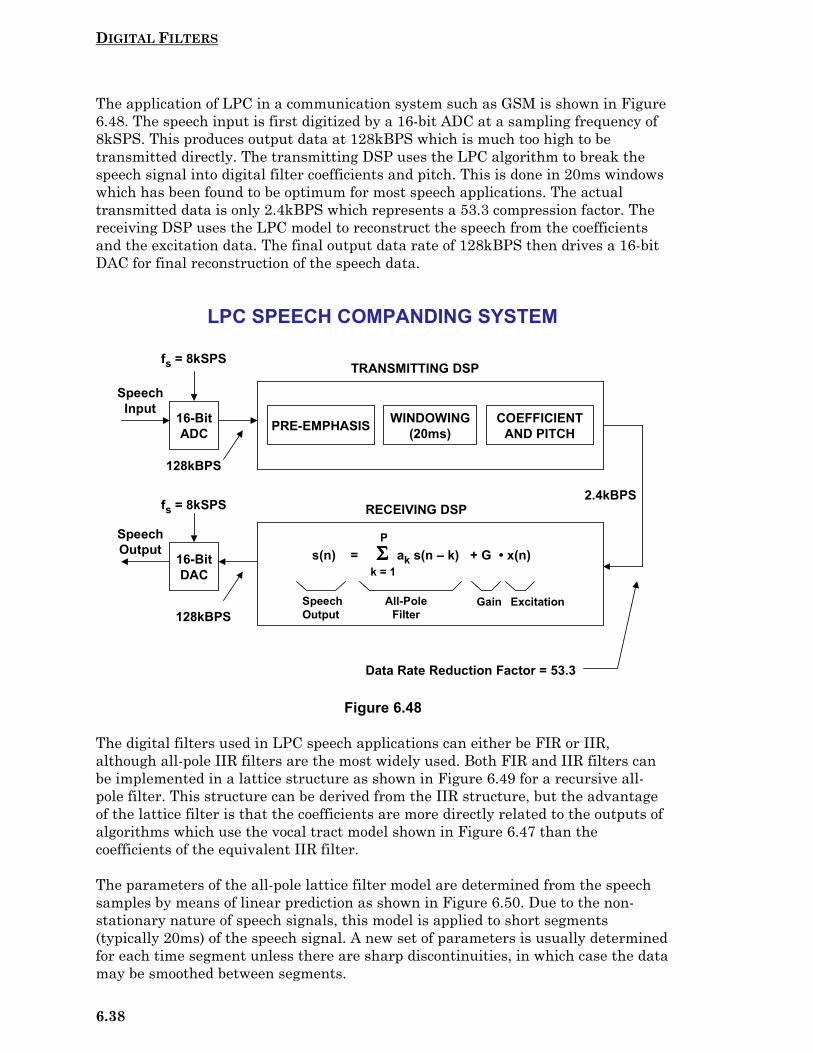
DIGITAL FILTERS
6.38
The application of LPC in a communication system such as GSM is shown in Figure6.48. The speech input is first digitized by a 16-bit ADC at a sampling frequency of8kSPS. This produces output data at 128kBPS which is much too high to betransmitted directly. The transmitting DSP uses the LPC algorithm to break thespeech signal into digital filter coefficients and pitch. This is done in 20ms windowswhich has been found to be optimum for most speech applications. The actualtransmitted data is only 2.4kBPS which represents a 53.3 compression factor. Thereceiving DSP uses the LPC model to reconstruct the speech from the coefficientsand the excitation data. The final output data rate of 128kBPS then drives a 16-bitDAC for final reconstruction of the speech data.
Figure 6.48
The digital filters used in LPC speech applications can either be FIR or IIR,although all-pole IIR filters are the most widely used. Both FIR and IIR filters canbe implemented in a lattice structure as shown in Figure 6.49 for a recursive all-pole filter. This structure can be derived from the IIR structure, but the advantageof the lattice filter is that the coefficients are more directly related to the outputs ofalgorithms which use the vocal tract model shown in Figure 6.47 than thecoefficients of the equivalent IIR filter.
The parameters of the all-pole lattice filter model are determined from the speechsamples by means of linear prediction as shown in Figure 6.50. Due to the non-stationary nature of speech signals, this model is applied to short segments(typically 20ms) of the speech signal. A new set of parameters is usually determinedfor each time segment unless there are sharp discontinuities, in which case the datamay be smoothed between segments.
LPC SPEECH COMPANDING SYSTEM
16-BitADC PRE-EMPHASIS COEFFICIENT
AND PITCHWINDOWING
(20ms)
fs = 8kSPS
SpeechInput
128kBPS
2.4kBPS
s(n) = ΣΣΣΣ ak s(n – k) + G • x(n)k = 1
P
16-BitDAC
SpeechOutput
128kBPSSpeechOutput
All-PoleFilter
Gain Excitation
TRANSMITTING DSP
RECEIVING DSP
Data Rate Reduction Factor = 53.3
fs = 8kSPS

DIGITAL FILTERS
6.39
Figure 6.49
Figure 6.50
ALL POLE LATTICE FILTER
z–1 z–1 z–1
k1–k1k2–k2kM–kM
XM(n)
uM(n) u2(n) u1(n)
y(n)
EXCITATIONINPUT
SPEECHOUTPUT
ESTIMATION OF LATTICE FILTERCOEFFICIENTS IN TRANSMITTING DSP
ΣΣΣΣ
ADAPTIVEALGORITHM
ADAPTIVEFIR
PREDICTORZ–1
+
–
COEFFICIENTS
SPEECHSAMPLES
ERRORSIGNAL
DIGITAL FILTERS
6.40
REFERENCES
1. Steven W. Smith, The Scientist and Engineer’s Guide to Digital SignalProcessing, Second Edition, 1999, California Technical Publishing,P.O. Box 502407, San Diego, CA 92150. Also available for free download at:http://www.dspguide.com or http://www.analog.com
2. C. Britton Rorabaugh, DSP Primer, McGraw-Hill, 1999.
3. Richard J. Higgins, Digital Signal Processing in VLSI, Prentice-Hall,1990.
4. A. V. Oppenheim and R. W. Schafer, Digital Signal Processing, Prentice-Hall, 1975.
5. L. R. Rabiner and B. Gold, Theory and Application of Digital SignalProcessing, Prentice-Hall, 1975.
6. John G. Proakis and Dimitris G. Manolakis, Introduction to DigitalSignal Processing, MacMillian, 1988.
7. J.H. McClellan, T.W. Parks, and L.R. Rabiner, A Computer Programfor Designing Optimum FIR Linear Phase Digital Filters, IEEETrasactions on Audio and Electroacoustics, Vol. AU-21, No. 6,December, 1973.
8. Fredrick J. Harris, On the Use of Windows for Harmonic Analysis withthe Discrete Fourier Transform, Proc. IEEE, Vol. 66, No. 1, 1978 pp. 51-83.
9. Momentum Data Systems, Inc., 17330 Brookhurst St., Suite 140,Fountain Valley, CA 92708, http://www.mds.com
10. Digital Signal Processing Applications Using the ADSP-2100Family, Vol. 1 and Vol. 2, Analog Devices, Free Download at:http://www.analog.com
11. ADSP-21000 Family Application Handbook, Vol. 1, Analog Devices,Free Download at: http://www.analog.com
12. B. Widrow and S.D. Stearns, Adaptive Signal Processing, Prentice-Hall,1985.
13. S. Haykin, Adaptive Filter Theory, 3rd Edition, Prentice-Hall, 1996.
14. Michael L. Honig and David G. Messerschmitt, Adaptive Filters -Structures, Algorithms, and Applications, Kluwer Academic Publishers,Hingham, MA 1984.
15. J.D. Markel and A.H. Gray, Jr., Linear Prediction of Speech, Springer-Verlag, New York, NY, 1976.

DIGITAL FILTERS
6.41
16. L.R. Rabiner and R.W. Schafer, Digital Processing of SpeechSignals, Prentice-Hall, 1978.

DIGITAL FILTERS
6.42

DSP HARDWARE
7.a
SECTION 7
DSP HARDWARE
Microcontrollers, Microprocessors, and Digital SignalProcessors (DSPs)
DSP Requirements
ADSP-21xx 16-Bit Fixed-Point DSP Core
Fixed-Point Versus Floating Point
ADI SHARC® Floating Point DSPs
ADSP-2116x Single-Instruction, Multiple Data (SIMD)Core Architecture
TigerSHARC™: The ADSP-TS001Static Superscalar DSP
DSP Benchmarks
DSP Evaluation and Development Tools

DSP HARDWARE
7.b

DSP HARDWARE
7.1
SECTION 7DSP HARDWAREDan King, Greg Geerling, Ken Waurin, NoamLevine, Jesse Morris, Walt Kester
MICROCONTROLLERS, MICROPROCESSORS, ANDDIGITAL SIGNAL PROCESSORS (DSPS)Computers are extremely capable in two broad areas: (1) data manipulation, suchas word processing and database management, and (2) mathematical calculation,used in science, engineering, and Digital Signal Processing. However, mostcomputers are not optimized to perform both functions. In computing applicationssuch as word processing, data must be stored, sorted, compared, moved, etc., andthe time to execute a particular instruction is not critical, as long as the program’soverall response time to various commands and operations is adequate enough tosatisfy the end user. Occasionally, mathematical operations may also be performed,as in a spreadsheet or database program, but speed of execution is generally not thegoverning factor. In most general purpose computing applications there is noconcentrated attempt by software companies to make the code efficient. Applicationprograms are loaded with “features” which require more memory and fasterprocessors with every new release or upgrade.
Figure 7.1
On the other hand, digital signal processing applications require that mathematicaloperations be performed quickly, and the time to execute a given instruction mustbe known precisely, and it must be predictable. Both code and hardware must beextremely efficient to accomplish this. As has been shown in the last two sections ofthis book, the most fundamental mathematical operation or kernel in all of DSP is
GENERAL COMPUTING APPLICATIONS
DATA MANIPULATION MATH CALCULATION
Word Processing Database Management Spread Sheets Operating Systems
Digital Signal Processing Motion Control Engineering Simulations Real-Time Signal Processing
Data Movement (A→→→→ B) Value Testing (If A = B, then…)
Time to Execute not Critical, not Predictable
Addition (C = A + B) Multiplication (C = A × B)
Time to Execute Critical and Predictable

DSP HARDWARE
7.2
the sum-of-products (or dot-product). Fast execution of the dot product is critical tofast Fourier transforms (FFTs), real time digital filters, matrix multiplications,graphics pixel manipulation, etc.
Based on this introductory discussion of DSP requirements, it is important tounderstand the differences between microcontrollers, microprocessors, and DSPs.While microcontrollers used in industrial process control applications can performfunctions such as multiplication, addition, and division, they are much more suitedto applications where I/O capability and control is more important than speed.Microcontrollers such as the 8051-family typically contain a CPU, RAM, ROM,serial/parallel interfaces, timers, and interrupt circuitry. The MicroConverter™series from Analog Devices contains not only the 8051 core but also highperformance ADC and DAC functions along with flash memory.
Figure 7.2
Microprocessors, such as the Pentium-series from Intel, are basically single-chipCPUs which require additional circuitry to make up the total computing function.Microprocessor instruction sets can be either complex-instruction-set computer(CISC) or reduced-instruction-set computer (RISC). The complex-instruction-setcomputer (CISC) includes instructions for basic processor operations, plus singleinstructions that are highly sophisticated; for example, to evaluate a high-orderpolynomial. But CISC has a price: many of the instructions execute via microcodein the CPU and require numerous clock cycles plus silicon real estate for codestorage memory.
MICROCONTROLLERS, MICROPROCESSORS,AND DIGITAL SIGNAL PROCESSORS (DSPs)
Microcontrollers: CPU, RAM, ROM, Serial/Parallel Interface, Timer, Interrupt Circuitry Well Suited for Toasters as well Industrial Process Control Speed is not Generally a Requirement! Compact Instruction Sets Example: 8051, 68HC11, PIC
Microprocessors: Single Chip CPU - Requires Additional External Circuitry RISC: Reduced Instruction Set Computer CISC: Complex Instruction Set Computer Example: Pentium-Series, PowerPC, MIPS
Digital Signal Processors (DSPs): RAM, ROM, Serial/Parallel Interface, Interrupt Circuitry CPU Optimized for Fast Repetitive Math for Real Time Processing Example: ADSP-21XX, ADSP-21K

DSP HARDWARE
7.3
In contrast, the reduced-instruction-set computer (RISC) recognizes that, in manyapplications, basic instructions such as LOAD and STORE - with simple addressingschemes - are used much more frequently than the advanced instructions, andshould not incur an execution penalty. These simpler instructions are hardwired inthe CPU logic to execute in a single clock cycle, reducing execution time and CPUcomplexity.
Although the RISC approach offers many advantages in general purpose computing,it is not well suited to DSP. For example, most RISCs do not support single-instruction multiplication, a very common and repetitive operation in DSP. TheDSP is optimized to accomplish these tasks fast enough to maintain real-timeoperation in the context of the application. This requires single-cycle arithmeticoperations and accumulations.
DSP REQUIREMENTS
The most fundamental mathematical operation in DSP is shown in Figure 7.3: thesum of products (dot product). It is common to digital filters, FFTs, and many otherDSP applications. A Digital Signal Processor (DSP) is optimized to performrepetitive mathematical operations such as the dot product. There are five basicrequirements of a DSP to optimize this performance: fast arithmetic, extendedprecision, dual operand fetch, circular buffering, and zero-overhead looping.
Figure 7.3
THE MOST FUNDAMENTAL MATHEMATICALOPERATION IN DSP: THE SUM OF PRODUCTS
For Example: Digital Filtering Multiply Data Sample Times Filter Coefficient (Twiddle
Factor for FFTs) Add Contents to Accumulator Repeat N times
DSP Requirements: Fast Multiply-Accumulates Extended Precision (Accumulator Register) Dual Operand Fetch Circular Buffering Zero-Overhead Looping
In One Instruction Cycle Using ADSP-21XX Core : Fetch Data Sample from Data Memory Fetch Coefficient from Program Memory Perform Multiply-Accumulate Update Pointers
y(n) = h(0) • x(n) + h(1) • x(n–1) + ... + h(N–1) • x(n–N)

DSP HARDWARE
7.4
FAST ARITHMETIC
Fast arithmetic is the simplest of these requirements to understand. Since real-timeDSP applications are driven by performance, the multiply-accumulate or MAC timeis a basic requirement; faster MACs mean potentially higher bandwidth. It iscritical to remember that MAC time alone does not define DSP performance. Thisoften forgotten fact leads to an inadequate measure of processor performance bysimply examining its MIPS (million instructions per second) rating. Since most DSPand DSP-like architectures feature MACs that can execute an instruction everycycle, most processors are given a MIPS rating equal to its MAC throughput. Thisdoes not necessarily account for the other factors that can degrade a processorsoverall performance in real-world applications. The other four criteria can wipe outMAC gains if they are not satisfied.
In addition to the requirement for fast arithmetic, a DSP should be able to supportother general purpose math functions and should therefore have an appropriatearithmetic logic unit (ALU) and a programmable shifter function for bitmanipulation.
EXTENDED PRECISION
Apart from the obvious need for fast multiplication and addition (MAC), there isalso a requirement for extended precision in the accumulator register. For example,when two 16-bit words are multiplied, the result is a 32-bit word. The AnalogDevices ADSP-21xx 16-bit fixed-point core architecture has an internal 40-bitaccumulator which provides a high degree of overflow protection. While floating-point DSPs eliminate most of the problems associated with precision and overflow,fixed-point processors are still popular for many applications, and thereforeoverflow, underflow, and data scaling issues must be dealt with properly.
DUAL OPERAND FETCH
Regardless of the nature of a processor, performance limitations are generally basedon bus bandwidth. In the case of general purpose microprocessors ormicrocontrollers, code is dominated by single memory fetch instructions, usuallyaddressed as a base plus offset value. This leads architects to embed fixed data intothe instruction set so that this class of memory access is fast and memory efficient.DSPs, on the other hand, are dominated by instructions requiring two independentmemory fetches. This is driven by the basic form of the convolution (kernel or dotproduct) Σh(i)x(i). The goal of fast dual operand fetches is to keep the MAC fullyloaded. We saw in the discussion on MACs that the performance of a DSP is firstlimited by MAC time. Assuming an adequate MAC cycle time, two data values needto be supplied at the same rate; increases in operand fetch cycle time will result incorresponding increases in MAC cycle time. Ideally, the operand fetches occursimultaneously with the MAC instruction so that the combination of the MAC andmemory addressing occurs in one cycle.
Dual operand fetch is implemented in DSPs by providing separate buses forprogram memory data and data memory data. In addition, separate programmemory address and data memory address buses are also provided. The MAC can
DSP HARDWARE
7.5
therefore receive inputs from each data bus simultaneously. This architecture isoften referred to as the Harvard Architecture.
CIRCULAR BUFFERING
If we examine the kernel equation more carefully, the advantages of circularbuffering in DSP applications become apparent. A Finite Impulse Response (FIR)filter is used to demonstrate the point. First, coefficients or tap values for FIR filtersare periodic in nature. Second, the FIR filter uses the newest real-world signalvalue and discards the oldest value when calculating each output.
In the series of FIR filter equations, the N coefficient locations are always accessedsequentially from h(0) to h(N–1). The associated data points circulate through thememory as follows: new samples are stored replacing the oldest data each time afilter output is computed. A fixed boundary RAM can be used to achieve thiscirculating buffer effect. The oldest data sample is replaced by the newest with eachconvolution. A "time history" of the N most recent samples is kept in RAM.
This delay line can be implemented in fixed boundary RAM in a DSP chip if newdata values are written into memory, overwriting the oldest value. To facilitatememory addressing, old data values are read from memory starting with the valueone location after the value that was just written. In a 4-tap FIR filter, for example,x(4) is written into memory location 0, and data values are then read from locations1, 2, 3, and 0. This example can be expanded to accommodate any number of taps.By addressing data memory locations in this manner, the address generator needonly supply sequential addresses regardless of whether the operation is a memoryread or write. This data memory buffer is called circular because when the lastlocation is reached, the memory pointer must be reset to the beginning of the buffer.
The coefficients are fetched simultaneously with the data. Due to the addressingscheme chosen, the oldest data sample is fetched first. Therefore, the last coefficientmust be fetched first. The coefficients can be stored backwards in memory: h(N–1) isthe first location, and h(0) is the last, with the address generator providingincremental addresses. Alternatively, coefficients can be stored in a normal mannerwith the accessing of coefficients starting at the end of the buffer, and the addressgenerator being decremented.
This allows direct support of the FIR filter unit delay taps without softwareoverhead. These data characteristics are DSP algorithm-specific and must besupported in hardware to achieve the best DSP performance. Implementing circularbuffers in hardware allows buffer parameters (i.e. start, length, etc.) to be set upoutside of the core instruction loop. This eliminates the need for extra instructionswithin the loop body. Lack of a hardware implementation for circular buffering cansignificantly impact MAC performance.
ZERO OVERHEAD LOOPING
Zero overhead looping is required by the repetitive nature of the kernel equation.The multiply-accumulate function and the data fetches required are repeated Ntimes every time the kernel function is calculated. Traditional microprocessors
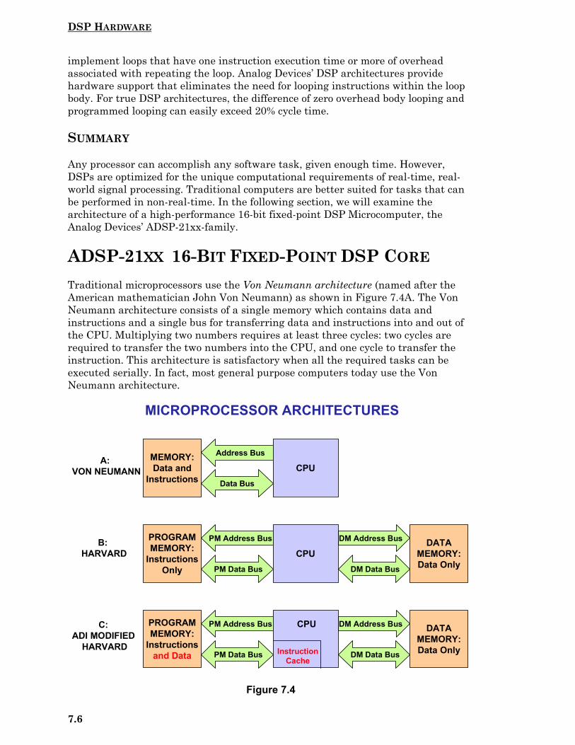
DSP HARDWARE
7.6
implement loops that have one instruction execution time or more of overheadassociated with repeating the loop. Analog Devices’ DSP architectures providehardware support that eliminates the need for looping instructions within the loopbody. For true DSP architectures, the difference of zero overhead body looping andprogrammed looping can easily exceed 20% cycle time.
SUMMARY
Any processor can accomplish any software task, given enough time. However,DSPs are optimized for the unique computational requirements of real-time, real-world signal processing. Traditional computers are better suited for tasks that canbe performed in non-real-time. In the following section, we will examine thearchitecture of a high-performance 16-bit fixed-point DSP Microcomputer, theAnalog Devices’ ADSP-21xx-family.
ADSP-21XX 16-BIT FIXED-POINT DSP CORE
Traditional microprocessors use the Von Neumann architecture (named after theAmerican mathematician John Von Neumann) as shown in Figure 7.4A. The VonNeumann architecture consists of a single memory which contains data andinstructions and a single bus for transferring data and instructions into and out ofthe CPU. Multiplying two numbers requires at least three cycles: two cycles arerequired to transfer the two numbers into the CPU, and one cycle to transfer theinstruction. This architecture is satisfactory when all the required tasks can beexecuted serially. In fact, most general purpose computers today use the VonNeumann architecture.
Figure 7.4
MICROPROCESSOR ARCHITECTURES
MEMORY:Data and
Instructions Data Bus
Address Bus
CPU
PM Data Bus
PM Address Bus
DM Data Bus
DM Address BusPROGRAMMEMORY:
InstructionsOnly
CPUDATA
MEMORY:Data Only
PM Data Bus
PM Address Bus
DM Data Bus
DM Address BusPROGRAMMEMORY:
Instructionsand Data
DATAMEMORY:Data OnlyInstruction
Cache
CPU
A: VON NEUMANN
B: HARVARD
C: ADI MODIFIED
HARVARD

DSP HARDWARE
7.7
For faster processing, however, the Harvard architecture shown in Figure 7.4B ismore suitable. This is named for the work done at Harvard University under theleadership of Howard Aiken. Data and program instructions each have separatememories and buses as shown. Since the buses operate independently, programinstructions and data can be fetched at the same time, thereby improving the speedover the single bus Von Neumann design. In order to perform a single FIR filtermultiply-accumulate, an instruction is fetched from the program memory, andduring the same cycle, a coefficient can be fetched from data memory. A second cycleis required to fetch the data word from the data memory.
Figure 7.4C illustrates Analog Devices’ modified Harvard architecture whereinstructions and data are allowed in the program memory. For example, in the caseof a digital filter, the coefficients are stored in the program memory, and the datasamples in the data memory. A coefficient and a data sample can thus be fetched ina single cycle. In addition to fetching the coefficient from program memory and adata sample from data memory, an instruction must also be fetched from programmemory. Analog Devices’ DSPs handle this in one of two ways. In the first method,the program memory is accessed twice (double pumped) in an instruction cycle. TheADSP-218x series uses this method. In the second method, a program memorycache is provided. If an algorithm requires dual data fetches, the programmer placesone buffer in program memory and the other in data memory. The first time theprocessor executes an instruction, there is a one-cycle stall because it must fetch theinstruction and the coefficient over the program memory data bus. However,whenever this conflict occurs, the DSP “caches” the instruction in a cache memory.The next time this instruction is required, the program sequencer obtains it fromthe cache, while the coefficient is obtained over the program memory data bus. Thecache method if used in the ADSP-219x family as well as in the SHARC family.
DIGITAL FILTER EXAMPLE
Now that the fundamental architecture of the ADSP-21xx family has beenpresented, a simple FIR filter design will illustrate the ease of programming thefamily. Pseudocode for an FIR filter design is shown in Figure 7.5. For AnalogDevices’ DSPs, all operations within the filter loop are completed in one instructioncycle, thereby greatly increasing efficiency. Extra instructions are not required torepeat the loop. This is referred to as zero-overhead looping. The actual FIR filterassembly code for the ADSP-21xx family of fixed point DSPs is shown in Figure 7.6.The arrows in the diagram point to the actual executable instructions (7 lines), therest of the code are simply comments added for clarification. The first instruction(labeled fir:) sets up the computation by clearing the MR register and loading theMX0 and MY0 registers with the first data and coefficient values from data andprogram memory. The multiply-accumulate with dual data fetch in the convolutionloop is then executed N–1 times in N–1 cycles to compute the sum of the first N–1products. The final multiply-accumulate instruction is performed with the roundingmode enabled to round the result to the upper 24 bits of the MR register. The MR1register is then conditionally saturated to its most positive or negative value basedon the status of the overflow flag contained in the MV register. In this manner,results are accumulated to the full 40-bit precision of the MR register, withsaturation of the output only if the final result overflowed beyond the leastsignificant 32 bits of the MR register.

DSP HARDWARE
7.8
Figure 7.5
Figure 7.6
PSEUDOCODE FOR FIR FILTER PROGRAMUSING A DSP WITH CIRCULAR BUFFERING
1. Obtain sample from ADC (typically interrupt driven)2. Move sample into input signal’s circular buffer3. Update the pointer for the input signal’s circular buffer4. Zero the accumulator5. Implement filter (control the loop through each of the coefficients)
6. Fetch the coefficient from the coefficient’s circular buffer 7. Update the pointer for the coefficient’s circular buffer 8. Fetch the sample from the input signal’s circular buffer 9. Update the pointer for the input signal’s circular buffer10. Multiply the coefficient by the sample11. Add the product to the accumulator
12. Move the filtered sample to the DACADSP21xx Example code:
CNTR = N-1;DO convolution UNTIL CE;convolution: MR = MR + MX0 * MY0(SS), MX0 = DM(I0,M1), MY0 = PM(I4,M5);
ADSP-21XX FIR FILTER ASSEMBLY CODE(SINGLE PRECISION)
.MODULE fir_sub; FIR Filter Subroutine
Calling ParametersI0 --> Oldest input data value in delay lineI4 --> Beginning of filter coefficient tableL0 = Filter length (N)L4 = Filter length (N)M1,M5 = 1CNTR = Filter length - 1 (N-1)
Return ValuesMR1 = Sum of products (rounded and saturated)I0 --> Oldest input data value in delay lineI4 --> Beginning of filter coefficient table
Altered RegistersMX0,MY0,MR
Computation Time(N - 1) + 6 cycles = N + 5 cycles
All coefficients are assumed to be in 1.15 format.
.ENTRY fir;fir: MR=0, MX0=DM(I0,M1), MY0=PM(I4,M5);
CNTR = N-1;DO convolution UNTIL CE;
convolution: MR=MR+MX0*MY0(SS), MX0=DM(I0,M1), MY0=PM(I4,M5);MR=MR+MX0*MY0(RND);IF MV SAT MR;RTS;
.ENDMOD;

DSP HARDWARE
7.9
The ADSP-21xx family architecture (Figure 7.7) is optimized for digital signalprocessing and other high-speed numeric processing applications. This family ofDSPs combine the complete ADSP-2100 core architecture (three computationalunits, data address generators, and a program sequencer) with two serial ports, aprogrammable timer, extensive interrupt capabilities and on-board program anddata memory RAM. ROM-based versions are also available.
Figure 7.7
The ADSP-21xx's flexible architecture and comprehensive instruction set support ahigh degree of operational parallelism. In one cycle the ADSP-21xx can generate thenext program address, fetch the next instruction, perform one or two data moves,update one or two data address pointers, perform a computational operation, receiveand transmit data via the two serial ports, and update a timer.
ADSP-21XX CORE ARCHITECTURE
DataAddress
Generator 1
DataAddress
Generator 2
InstructionRegisterProgram
Sequencer
ALU
Input Regs
Output Regs
MAC
Input Regs
Output Regs
Shifter
Input Regs
Output Regs
BusExchange
PMA BUS
DMA BUS
PMD BUS
DMD BUS
R BUS
CacheMemory

DSP HARDWARE
7.10
Figure 7.8
BUSES
The ADSP-21xx processors have five internal buses to ensure efficient data transfer.The program memory address (PMA) and data memory address (DMA) buses areused internally for the addresses associated with program and data memory. Theprogram memory data (PMD) and data memory data (DMD) buses are used for thedata associated with the memory spaces. Off chip, the buses are multiplexed into asingle external address bus and a single external data bus; the address spaces areselected by the appropriate control signals. The result (R) bus transfersintermediate results directly between the various computational units.
The PMA bus is 14-bits wide allowing direct access of up to 16K words of data. Thedata memory data (DMD) bus is 16-bits wide. The DMD bus provides a path for thecontents of any register in the processor to be transferred to any other register or toany data memory location in a single cycle. The data memory address comes fromtwo sources: an absolute value specified in the instruction code (direct addressing)or the output of a data address generator (indirect addressing). Only indirectaddressing is supported for data fetches from program memory.
The program memory data (PMD) bus can also be used to transfer data to and fromthe computational units through direct paths or via the PMD-DMD bus exchangeunit. The PMD-DMD bus exchange unit permits data to be passed from one bus tothe other. It contains hardware to overcome the 8-bit width discrepancy between thetwo buses, when necessary.
ADSP-21XX CORE ARCHITECTURE
Buses Program Memory Address (PMA) Data Memory Address (DMA) Program Memory Data (PMD) Data Memory Data (DMD) Result (R)
Computational Units Arithmetic Logic Unit (ALU) Multiply-Accumulator (MAC) Shifter
Data Address Generators Program Sequencer On-Chip Peripheral Options
Program Memory RAM or ROM Data Memory RAM Serial Ports Timer Host Interface Port DMA Port

DSP HARDWARE
7.11
Program memory can store both instructions and data, permitting the ADSP-21xxto fetch two data operands in a single cycle, one from program memory and onefrom data memory. The corresponding instruction is obtained directly from programmemory by “double pumping” (ADSP-218x series) or from a cache memory (ADSP-219x and SHARC series).
COMPUTATIONAL UNITS (ALU, MAC, SHIFTER)
The processor contains three independent computational units: the arithmetic logicunit (ALU), the multiplier-accumulator (MAC), and the barrel shifter. Thecomputational units process 16-bit data directly and have provisions to supportmultiprecision computations. The ALU has a carry-in (CI) bit which allows it tosupport 32-bit arithmetic.
The ALU provides a standard set of arithmetic and logic functions: add, subtract,negate, increment, decrement, absolute value, AND, OR, EXCLUSIVE OR andNOT. Two divide primitives are also provided.
Figure 7.9
The MAC performs single-cycle multiply, multiply/add, and multiply/subtractoperations. It also contains a 40-bit accumulator which provides 8-bits of overflow insuccessive additions to ensure that no loss of data occurs; 256 overflows would haveto occur before any data is lost. Special instructions are provided for implementingblock floating-point scaling of data. A set of background registers is also available inthe MAC for interrupt service routines. If after a DSP routine is finished and theMV flag has been set, this means that the register contains a word greater than 32bits. The register can be “saturated” using the saturation routine which normalizesthe 40-bit word to either a negative fullscale or positive fullscale 32-bit word in 1.32format.
ARITHMETIC LOGIC UNIT (ALU) FEATURES
Add, Subtract, Negate, Increment, Decrement, AbsoluteValue, AND, OR, Exclusive OR, NOT
Bitwise Operators, Constant Operators
Multi-Precision Math Capabilites
Divide Primitives
Saturation Mode for Overflow Support
Background Registers for Single-Cycle Context Switch
Example Instructions: IF EQ AR = AX0 + AY0;
AF = MR1 XOR AY1;
AR = TGLBIT 7 OF AX1;

DSP HARDWARE
7.12
Figure 7.10
The shifter performs logical and arithmetic shifts, normalization, denormalization,and derive-exponent operations. The shifter can be used to efficiently implementnumeric format control including multiword floating-point representations.
Figure 7.11
MULTIPLY-ACCUMULATOR (MAC) FEATURES
Single-Cycle Multiply, Multiply-Add, Multiply-Subtract
40-Bit Accumulator for Overflow Protection (219x AddsSecond 40-Bit Accumulator)
Saturation Instruction Performs Single Cycle OverflowCleanup
Background Registers for Single-Cycle Context Switch
Example MAC Instructions: MR = MX0 * MY0(US);
IF MV SAT MR;
MR = MR - AR * MY1(SS);
MR = MR + MX1 * MY0(RND);
IF LT MR = MX0 * MX0(UU);
SHIFTER FEATURES
Normalize (Fixed-Point to Floating-Point Conversion) Denormalize (Floating-Point to Fixed-Point Conversion) Arithmetic and Logical Shifts Block Floating Point Support Derive Exponent Background Registers for Single-Cycle Context Switch Example Shifter Instructions:
SR = ASHIFT SI BY –6(LO); Arithmetic Shift
SR = SR OR LSHIFT SI BY 3(HI); Logical Shift
SR = NORM MR1(LO); Normalization

DSP HARDWARE
7.13
The computational units are arranged side-by-side instead of serially so that theoutput of any unit may be the input of any unit on the next cycle. The internalresult (R) bus directly connects the computational units to make this possible.
DATA ADDRESS GENERATORS AND PROGRAM SEQUENCER
Two dedicated data address generators and a powerful program sequencer ensureefficient use of the computational units. The data address generators (DAGs)provide memory addresses when memory data is transferred to or from the input oroutput registers. Each DAG keeps track of up to four address pointers. Wheneverthe pointer is used to access data (indirect addressing), it is post-modified by thevalue of a specified modify register. A length value may be associated with eachpointer to implement automatic modulo addressing for circular buffers. With twoindependent DAGs, the processor can generate two addresses simultaneously fordual operand fetches.
DAG1 can supply addresses to data memory only; DAG2 can supply addresses toeither data memory or program memory. When the appropriate mode bit is set inthe mode status register (MSTAT), the output address of DAG1 is bit-reversedbefore being driven onto the address bus. This feature facilitates addressing inradix-2 FFT algorithms.
Figure 7.12
DATA ADDRESS GENERATOR FEATURES
Automatic Linear Addressing and Circular Buffering Each DAG Manages Four Pointers Supports Dual Operand Fetch Bit-Reverser (DAG1) For FFTs Background Registers in ADSP-219x Example DAG Instructions:
AX0 = DM(I0,M3);
MODIFY(I1,M2);
MR = MR + MX0 * MY0, MX0 = DM(I0,M1), MY0 = PM(I4,M4);
Fetch Data Memory Data Word Located at Address I0, Increment Pointer by M1
Fetch Program Memory Data Word Located at Address I4, Increment Pointer by M4

DSP HARDWARE
7.14
The program sequencer supplies instruction addresses to the program memory. Thesequencer is driven by the instruction register which holds the currently executinginstruction. The instruction register introduces a single level of pipelining into theprogram flow. Instructions are fetched and loaded into the instruction registerduring one processor cycle, and executed during the following cycle while the nextinstruction is prefetched. To minimize overhead cycles, the sequencer supportsconditional jumps, subroutine calls and returns in a single cycle. With an internalloop counter and loop stack, the processor executes looped code with zero overhead.No explicit jump instructions are required to loop. The sequencer also efficientlyprocesses interrupts with its interrupt controller for fast interrupt response withminimum latency. When an interrupt occurs, it causes a jump to a known specifiedlocation in memory. Short interrupt service routines can be coded in place. Forinterrupt service routines with more than four instructions, program control istransferred to the service routine by means of a JUMP instruction placed at theinterrupt vector location.
Figure 7.13
ADSP-21XX-FAMILY ON-CHIP PERIPHERALS
The discussion so far has involved the core architecture of the fixed-point ADSP-21xx DSPs which is common to all members of the family. This section discusses theon-chip peripherals which have different configurations and options depending onthe particular processor in the family. The ADSP-218x architecture is shown inFigure 7.14.
PROGRAM SEQUENCER FEATURES
Generates Next Instruction Address Low-Latency Interrupt Handling Hardware Stacks Single-Cycle Conditional Branch (218x) Supports Zero-Overhead Looping
ADSP21xx Example code:
CNTR = 10;DO endloop UNTIL CE; IO(DACCONTROL) = AX0; MR = MR + MX0 * MY0(SS), MX0 = DM(I0,M1), MY0 = PM(I4,M5);endloop: IF MV SET FL1; IF EQ CALL mysubroutine;

DSP HARDWARE
7.15
Figure 7.14
Figure 7.15
EXTERNALADDRESS
BUS
ADSP-218x FAMILY ARCHITECTURE
PROGRAMSEQUENCER
DATA ADDRESSGENERATORS
ARITHMETIC UNITS
POWERDOWNCONTROL
MEMORY
BYTE DMACONTROLLER
SERIAL PORTS
PROGRAMMABLEEXTERNAL I / Oand FLAG PINS
EXTERNALDATA BUS
TIMERINTERNALDMA PORT
EXTERNALDATA BUS
External bus features are multiplexed for 100-pin parts. All are available on 128-pin parts
• Code Compatibility• Pin-for-Pin Compatibility
DAG1 DAG2
ALU MAC SHIFTER SPORT 0 SPORT 1
PROGRAMMEMORY
DATAMEMORY
PMA
DMA
PMD
DMD
ADSP-2100 CORE
FULL MEMORYMODE
OR
HOST MODE
ADSP-21xx ON-CHIP PERIPHERALS:MEMORY INTERFACE
All Family Members use an Enhanced Harvard Architecture Separate Program Memory and Data Memory Spaces Can access Data Values in Program Memory
Different Family Members Have Different Memory Configurations
External Memory Interface Supports Both Fast and Slow Memories
with Programmable Wait States
Supports DSP Boot Loading from Byte Memory Space or from a
Host Processor
Supports Memory-Mapped Peripherals Through I / O Space
Bus Request / Grant Mechanism for Shared External Bus

DSP HARDWARE
7.16
The 21xx-family comes with a variety of on-chip memory options, and the newer218x family has up to 48K words of program memory and 56K words of datamemory. All family members use the modified Harvard architecture which providesseparate program and data memory and allows data to be stored in programmemory. The external memory interface supports both fast and slow memories withprogrammable wait states. The ADSP-218x family also supports memory-mappedperipherals through I/O space.
All 21xx parts (except the ADSP-2105) have two double-buffered serial ports(SPORTs) for transmitting or receiving serial data. Each SPORT is bi-directional,full duplex, double-buffered, and has its own programmable serial clock. TheSPORT word length can be configured from 3 to 16 bits. Data can be framed orunframed. Each SPORT generates an interrupt and supports A-law and u-lawcompanding.
Figure 7.16
The ADSP-218x-family internal direct-memory-access (IDMA) port supports bootingfrom and runtime access by a host processor. This feature allows data to betransferred to and from internal memory in the background while continuingforeground processing. The IDMA port allows a host processor to access all of theDSPs internal memory without using mailbox registers. The IDMA port supports 16and 24-bit words, and 24-bit transfers take two cycles to complete.
ADSP-21xx ON-CHIP PERIPHERALS:SERIAL PORTS (SPORTs)
ADSP-21xx SPORTs Are Used For Synchronous Communication
Full Duplex
Fully Programmable
Autobuffer/DMA Capability
TDM Multi-Channel Capability
A-law and u-law Companding
Data Rates of 25 Mbits/sec and Above
Glueless Interface to a Wide Range of Serial Peripherals or
Processors
219x DSPs Add SPI and UART Serial Ports (With Boot Capability)

DSP HARDWARE
7.17
Figure 7.17
The ADSP-218x-family also has a byte memory interface which supports bootingfrom and runtime access to 8-bit memories. It can access up to 4MB. This memoryspace takes the place of the boot memory space found on other ADSP-21xx familyprocessors. Byte memory consists of 256 pages of 16K x 8 locations. This memorycan be written and read in 24-bit, 16-bit, or 8-bit left or right justified transfers.Transfers happen in the background to the DSP internal memory by stealing cycles.
Figure 7.18
ADSP-21xx ON-CHIP PERIPHERALS:INTERNAL DMA (IDMA)
Allows an External System to Access DSP Internal Memory
External Device or DSP Can Specify Internal Starting Address
Address Automatically Increments to Speed Throughput
16-Bit Bus Supports Both Data and Instruction Transfers (219x
has 8-Bit Bus Support)
Single DSP Processor-Cycle Transfers
Supports Power-On Booting
ADSP-21xx ON-CHIP PERIPHERALS:BYTE DMA PORT (BDMA)
Provides Bulk Storage for Both Data and Program Code Can Access up to 4 Mbytes of External Code & Data Supports Multiple Data Formats
Automatic Data Packing/Unpacking to 16 and 24 bits 8-Bit Transfers, Left- or Right-Justified
Background Transfer to DSP Internal Memory One Cycle per Word DSP Specifies Destination/Source and Word Count
Supports Power-On Booting Allows Multiple Code Segments
DSP Can Overlay Code Sections Processor Can Run During Transfer, or Halt and Restart

DSP HARDWARE
7.18
The ADSP-217x, ADSP-218x, and ADSP-21msp5x devices provide a powerdownfeature that allows the processor to enter a very low power state (less than 1mW)through hardware or software control. This feature is extremely useful for battery-powered applications. During some of the powerdown modes, the internal clocks aredisabled, but the processor registers and memory are maintained.
Figure 7.19
From the above discussions it should be obvious that the ADI DSPs are designed formaximum efficiency when performing typical DSP functions such as FFTs or digitalfiltering. ADI DSPs can perform several operations in an instruction cycle as hasbeen shown in the above filter example. DSPs are often rated in terms of Millions ofInstructions per Second, or MIPS. However, the MIPS rating does not tell the entirestory. For example if processor A has a instruction rate of 50 MIPS and can perform1 operation per instruction, it can perform 50 Million Operations per Second, or 50MOPS. Now assume that processor B has an instruction rate of 20 MIPS, but canperform 4 operations per instruction. Processor B can therefore perform 80 MillionOperations per Second, or 80 MOPS, and is actually more efficient than processor A.A better way to evaluate DSP performance is to use well defined benchmarks suchan FIR filter with a prescribed number of taps or an FFT of known size. Benchmarkcomparisons eliminate the confusion often associated with MIPS or MOPS ratingsalone and are discussed later in this section. Even this form of benchmarking doesnot give a true comparison of performance between two processors. Analysis of thetarget system requirements, processor architecture, memory needs and otherfactors must be considered.
ADSP-21xx INTERNAL PERIPHERALS:POWERDOWN
Non-Maskable Interrupt Hardware Pin (PWD), or Software Forced
Holds Processor in CMOS Standby
Rapid CLKIN-Cycle Recovery
Acknowledge Handshake (PWDACK)
Ideal for Battery-Powered Applications
219x is Fully Static

DSP HARDWARE
7.19
The ADSP-219x family maintains code compatibility with the ADSP-218x.Streamlined for faster processing and improved C-compiler efficiency, this newfamily will include DSPs with speeds between 100 and 300MIPS and powerconsumption as low as 0.4mA/MIP. JTAG support is also included to provide a morerobust software emulation and test capability. A block diagram of the family isshown in Figure 7.20.
Figure 7.20
The address reach of the ADSP-219x series has been extended from the ADSP-218x’s 14-bit reach to a 24-bit reach. This supports 64K word direct memoryaddressing or 16M word paged memory addressing. All existing addressing modesare supported, and five new DAG addressing modes have been added.
Many of the enhancements in the ADSP-219x are designed to improve compilerefficiency. A global register allocator and support for register file-like operandaccess reduces spills and reduces reliance on the local stack. The compiler featuresDSP intrinsic support including fractional and complex. On-chip cache memory hasalso been added.
The ADSP-219x core will serve as a key DSP technology for ADI’s 16-bit generalpurpose DSP offerings, and embedded DSP solutions, where application-specificcircuitry and software are custom-designed to a customer’s precise requirements.For performance-driven applications, multiple cores will be integrated together on asingle die. In the future, four cores will be combined in a family of devices capable ofdelivering 1.2 billion MACs per second per square inch. Power-conscious designerswill appreciate operating currents of 0.15mA/MIPS.
ADSP-219x SERIES ARCHITECTURE
PER
IPH
ERA
L A
ND
DM
A IN
TER
FAC
EDATA REGISTERS
Computational Units
ALU MAC Shift
InternalMemory System
DAG1 DAG2Program
Sequencer PM DM
PMADMAPMDDMD
2424
2416
JTAG &EMULATION
EXTERNALMEMORY
INTERFACE
ADSP-219xProcessor Core CacheInstr.
RegisterSeq.
Improved addressing (14-bit reach increased to 24-bit reach) Compiler-efficient data register design Program sequencer with Cache for fast code execution JTAG support for easy development

DSP HARDWARE
7.20
Figure 7.21
The history of the Analog Devices 16-bit fixed-point DSP family is shown in Figure7.22. Notice the migration in performance as well as improvements in powerdissipation and packaging while maintaining code compatibility between thevarious devices. The newer families offer 3.3V (L-series) and 2.5V (M-series)operation for further efficiency. Earlier DSPs were packaged in expensive pin-grid-array (PGA) packages or plastic-leaded-chip-carriers (PLCCs), but these have beenlargely replaced by plastic-quad-flat-packs (PQFPs), and more recently by thin(1.6mm) quad-flat-packs (TQFPs). Note: In 1998, JEDEC changed the specificationsfor the TQFP package designation, assigning it to packages 1.0mm thick. Previouslylabeled TQFP packages (1.6mm thick) are now designated as LQFP per the JEDECspecification.
The 144-ball miniBGA package (see Figure 7.23) from ADI represents innovativepackaging combined with low power consumption (0.4mA per MIP), and allows75MIPS operation and more than 2M bits of SRAM in a 1cm2 package which is1.35mm thick. For example, the 75MIPS ADSP-2188M has 48K of 24-bit programmemory and 56K of 16-bit data memory for a total of 48K×24 + 56K×16 = 2028Kbits with a power dissipation of less than 100mW.
ADSP-219x FAMILY KEY SPECIFICATIONS
Code Compatible Compatible with ADSP-218x Series Single Cycle Instruction Execution, Zero-Over Head Looping,
Single Cycle Context Switch Performance
Architectural Performance Beyond 300 MIPs. Fully Transparent Instruction Cache
Compiler-Friendly and Tool-Friendly 64K Word Direct and 16 Mword Paged Memory Support 5 New DAG Addressing Modes Register File-Like Operand Access JTAG Interface Support

DSP HARDWARE
7.21
Figure 7.22
Figure 7.23
‘M’ SERIES OFFERS THE LARGESTMIPS/MEMORY DENSITY WITH miniBGA PACKAGING!!!
miniBGA package144-ball grid array (BGA)
10mm10mm
0.8mmPitch
75 MIPS and >2Mbit in 1cm2
Small size with no compromises inperformance: 144-balls
Up to 2 Mbits on-chip SRAM
Innovative packaging for highlyportable applications
Small package size and 0.4mA per MIPtargets power-sensitive applications
Includes ALL ‘M’ series members plusthe popular 2183, 2185L, 2186, & 2186Lderivatives
10mm10mm
1.35mm Thick
2181/3
16-BIT DSP FAMILY TREE: HISTORY OF IMPROVEMENTSIN PACKAGING - POWER - PERFORMANCE
2184/L
210x
211120 MIPS
2K/1K RAM
21msp5x
33 MIPS2K/2K RAM
216x
150-300 MIPS0.4 mA/MIPs
2186/L/M 2185/L/M
P i n C o m p a t i b l e
100 Pin LQFP & 144Ball Mini-BGA 2189M
219x
33 - 75 MIPS0.4 mA/MIPS
2188M
miniBGAminiBGA
LQFP
PLCC
PQFP
Code Compatible
Performance
“L” = 3.3V“M” = 2.5V“N” = 1.8V
1.6mm thick
4.45mm thick
2.45mm thick

DSP HARDWARE
7.22
Figure 7.24
Figure 7.25
10 - 33 MIPS32K - 80KBits
ADI 16-Bit DSP ROADMAP16 Years of Code Compatibility & Beyond
500
1000
1985 2000+
MM
AC
s
29-80 MIPS160K - 2MBits
150-300 MIPS640K - 32MBits
312 - 600 MIPS8M - 16MBits
600 - 1200 MIPS16M - 128MBits
Complete Code Compatibility
• As Low as 6mW/MIPS• As High as 0.1MIP/mm2
• As Low as 0.5mW/MIPS• As High as 8MIPs/mm2
• As Low as 0.7mW/MIPS• As High as 0.5MIP/mm2
• As Low as 0.6mW/MIPS• As High as 0.8MIP/mm2
• As Low as 0.4mW/MIPS• As High as 3MIPs/mm2
Single Core Devices
Multiple CoreDevices
100
2100 Core
219x Core
218x Core
29-52 MIPS160K- 1.2MBits
SRAM
500
1994 2000+
MM
AC
s
75 MIPS320K - 2MBits
SRAM
80 MIPS640K -2MBits
SRAM
600 MIPS16MBits SRAM
600 MIPS16MBits SRAM
Code & Pin Compatible Options
• As Low as 2.6mW/MIPS• As High as 0.5MIP/mm2
• 0.7mW/MIPS• 0.5MIPs/mm2
• 1mW/MIPS• 0.5MIP/mm2
•As Low as 1mW/MIPS•As High as 0.75MIP/mm2
•As Low as 0.7mW/MIPS•As High as 0.8MIPs/mm2
Single CoreDevices
MultipleCoreDevices
100
5/3.3V
1.8V
2.5V
1.5V
312 MIPS8MBits SRAM
• 2.6mW/MIPS• 0.3MIP/mm2
40 MIPS640K -2MBits
SRAM
•As Low as 0.6mW/MIPS•As High as 0.4MIPs/mm2
ADSP-218x ROADMAP
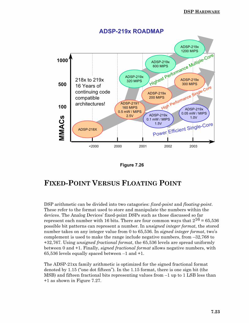
DSP HARDWARE
7.23
Figure 7.26
FIXED-POINT VERSUS FLOATING POINT
DSP arithmetic can be divided into two catagories: fixed-point and floating-point.These refer to the format used to store and manipulate the numbers within thedevices. The Analog Devices’ fixed-point DSPs such as those discussed so farrepresent each number with 16 bits. There are four common ways that 216 = 65,536possible bit patterns can represent a number. In unsigned integer format, the storednumber takes on any integer value from 0 to 65,536. In signed integer format, two’scomplement is used to make the range include negative numbers, from –32,768 to+32,767. Using unsigned fractional format, the 65,536 levels are spread uniformlybetween 0 and +1. Finally, signed fractional format allows negative numbers, with65,536 levels equally spaced between –1 and +1.
The ADSP-21xx family arithmetic is optimized for the signed fractional formatdenoted by 1.15 (“one dot fifteen”). In the 1.15 format, there is one sign bit (theMSB) and fifteen fractional bits representing values from –1 up to 1 LSB less than+1 as shown in Figure 7.27.
ADSP-219x ROADMAP
<2000 2000 2001 2002 2003
ADSP-219x300 MIPS
ADSP-2191160 MIPS
0.5 mW / MIPS2.5V
ADSP-219x320 MIPS
ADSP-219x600 MIPS
ADSP-219x1200 MIPS
ADSP-219x200 MIPS
ADSP-218X
High Performance Single-Core
100
500
1000
218x to 219x16 Years of continuing codecompatible architectures!
MM
AC
s ADSP-219x0.1 mW / MIPS
1.5V
ADSP-219x0.05 mW / MIPS
1.0V
Power Efficient Single-Core
Highest Performance Multiple-Core

DSP HARDWARE
7.24
Figure 7.27
This convention can be generalized as “I.Q”, in which I is the number of bits to theleft of the radix point, and Q is the number of bits to the right. For example, fullunsigned integer number representation is 16.0 format. For most signal processingapplications, however, fractional numbers (1.15) are assumed. Fractional numbershave the advantage that the product of two fractional numbers is smaller thaneither of the numbers.
By comparison, floating point DSPs typically use a minimum of 32 bits to representeach number. This results in many more possible numbers than for 16-bit fixedpoint, 232 = 4,294,967,296 to be exact. More importantly, floating point greatlyincreases the range of values that can be expressed. The most common floatingpoint standard is ANSI/IEEE Standard 754-1985, where the largest and smallestnumbers allowed by the standard are ±3.4×1038 and ±1.2×10–38, respectively. Notethat the 754 standard reserves some of the possible range to free up bit patternswhich allow other special classes of numbers such as ±0 and ±∞, for example.
The IEEE-754 floating point standard is described in more detail in Figure 7.28.The 32-bit word is divided into a sign bit, S, an 8-bit exponent, E, and a 23-bitmantissa, M. The relationship between the decimal and binary IEEE-754 floatingpoint equivalent is given by the equation:
)127E(2M.1S)1(10NUMBER −××−= .
Notice that the “1.” is assumed to precede the “M”, and that a “bias” of 127 issubtracted from the exponent “E” so that “E” is always a positive number.
16-BIT FIXED POINT ARITHMETICFRACTIONAL 1.15 FORMAT
–20 2–1 2–2 2–3 2–4 2–5 2–6 2–7 2–8 2–9 2–10 2–11 2–12 2–13 2–14 2–15
HEX BINARY DECIMAL
7FFF
0001
0000
FFFF
8000
0111
0000
0000
1111
1000
1111
0000
0000
1111
0000
1111
0000
0000
1111
0000
1111
0001
0000
1111
0000
+0.999969
+0.000031
+0.000000
–0.000031
–1.000000
BIT WEIGHTMSB LSB

DSP HARDWARE
7.25
Figure 7.28
In the case of extended precision floating point arithmetic, there is one sign bit, themantissa is 31-bits, the exponent is 11-bits, and the total word length is 43-bits.
Extended precision thus adds 8 bits of dynamic range to the mantissa and canexecute almost as fast as single precision, since accumulators can readily beextended beyond 32 bits. On the other hand, true 64-bit double precision (52-bitmantissa, 11-bit exponent, and 1 sign bit) requires extra processor cycles.Requirements for double precision are rare in most DSP applications.
Many DSP applications can benefit from the extra dynamic range provided by 32-bitfloating point arithmetic. In addition, programming floating point processors isgenerally easier, because fixed-point problems such as overflow, underflow, datascaling, and round-off error are minimized, if not completely eliminated. Althoughthe floating point DSP may cost slightly more than the fixed point DSP,development time may well be shorter with floating point.
While all floating point DSPs can also handle fixed point numbers (required toimplement counters, loops, and ADC/DAC signals), this doesn’t necessarily meanthat fixed point math will be carried out as quickly as the floating point operations;it depends on the internal DSP architectures. For instance, the SHARC DSPs fromAnalog Devices are optimized for both floating point and fixed point operations, andexecute them with equal efficiency. For this reason, the SHARC devices are oftenreferred to as “32-bit DSPs” rather than just “Floating Point.”
EXPONENT = E8-BITS
SINGLE PRECISION IEEE-75432-BIT FLOATING POINT FORMAT,
0/1 27 26 25 24 23 22 21 20 2–1 2–2 2–3 2–4 2–22 2–23LSBMSBLSBMSB
MANTISSA = M23-BITS
SIGNBIT = S
0 00000111 1100…00
1 10000001 0110…00
+ 7 0.75 + 1.75 × 2(7–127) = + 1.316554 × 10–36
– 129 0.375 – 1.375 × 2(129–127) = – 5.500000
Bias
Bias
Assumed
Assumed
NUMBER10 = (–1)S × 1.M × 2(E–127)
Assumed
Bias

DSP HARDWARE
7.26
Figure 7.29
ADI SHARC® FLOATING POINT DSPS
The ADSP-2106x Super Harvard Architecture SHARC is a high performance 32-bitDSP. The SHARC builds on the ADSP-21000 family DSP core to form a completesystem-on-a-chip, adding a dual-ported on-chip SRAM and integrated I/Operipherals supported by a dedicated I/O bus. With its on-chip instruction cache, theprocessor can execute every instruction in a single cycle. Four independent buses fordual data, instructions, and I/O plus crossbar switch memory connections comprisethe Super Harvard Architecture of the ADSP-2106x shown in Figure 7.30.
A general purpose data register file is used for transferring data between thecomputation units and the data buses, and for storing intermediate results. Theregister file has two sets (primary and alternate) of 16 registers each, for fastcontext switching. All of the registers are 40 bits wide. The register file, combinedwith the core processor’s super Harvard architecture, allows unconstrained dataflow between computation units and internal memory.
The ADSP-2106x SHARC processors address the five central requirements for DSPsestablished in the ADSP-21xx family of 16-bit fixed point DSPs: (1) fast, flexiblearithmetic computation units, (2) unconstrained data flow to and from thecomputation units, (3) extended precision and dynamic range in the computationunits, (4) dual address generators, and (5) efficient program sequencing with zero-overhead looping.
The program sequencer includes a 32-word instruction cache that enables three-busoperation for fetching an instruction and two data values. The cache is selective –only instructions whose fetches conflict with program memory data accesses arecached. This allows full-speed multiply-accumulates and FFT butterfly processing.
FIXED POINT VS. FLOATING POINT ARITHMETIC
16-Bit Fixed-Point: 216 = 65,536 Possible Numbers
32-Bit Floating Point: Biggest Number: ±6.8 × 1038 754 Std: ±3.4 × 1038
Smallest Number: ±5.9 × 10–39 754 Std: ±1.2 × 10–38
Extended-Precision (40-Bits: Sign + 8-Bit Exponent + 31-Bit Mantissa) Double-Precision (64-Bits: Sign + 11-Bit Exponent + 52-Bit Mantissa) 32-Bit Floating Point
More Precision Much Larger Dynamic Range Easier to Program

DSP HARDWARE
7.27
Figure 7.30
Figure 7.31
SHARC KEY FEATURES
100MHz Core / 300 MFLOPS Peak Parallel Operation of: Multiplier, ALU, 2 Address Generators &
Sequencer No Arithmetic Pipeline; All Computations Are Single-Cycle
High Precision and Extended Dynamic Range 32/40-Bit IEEE Floating-Point Math 32-Bit Fixed-Point MAC’s with 64-Bit Product & 80-Bit
Accumulation Single-Cycle Transfers with Dual-Ported Memory Structures
Supported by Cache Memory and Enhanced HarvardArchitecture
Glueless Multiprocessing Features JTAG Test and Emulation Port DMA Controller, Serial Ports, Link Ports, External Bus, SDRAM
Controller, Timers
ADI SUPER HARVARD ARCHITECTURE (SHARC®) 32-BIT DSP ARCHITECTURE FOR ADSP-2106x FAMILY
TIMER INSTRUCTIONCACHE
32x48 BIT
PROGRAMSEQUENCER
DAG18x4x32
BUSConnect
(PX)
DATAREGISTER
FILE16x40BITMULTIPLIER BARREL
SHIFTER ALU
DAG28x4x24
DMACONTROLLER
SERIAL PORTS(2)
LINK PORTS(6)
IOP REGISTERS(Memory Mapped)Control, Status,and Data Buffers
PMD
DMD
EPD
IOD
ADDR BUSMUX
MULTIPROCESSORINTERFACE
DATA BUSMUX
HOST PORT
JTAGTEST &
EMULATION
TWO INDEPENDENTDUAL-PORTED BLOCKS
PROCESSOR PORT I/O PORTADDR DATA DATA ADDR
DATAADDR DATA ADDR
COREPROCESSOR
BLO
CK
0
BLO
CK
1
DUAL PORTED SRAM
EXTERNAL PORT
I/O PROCESSOR
PMA
DMA
PMDDMD
24
32
4840
7
32
48
4
66
36
IOD48
IOA17

DSP HARDWARE
7.28
Figure 7.32
The ADSP-2106x family execute all instructions in a single cycle. They handle 32-bitIEEE floating point format, 32-bit integer and fractional fixed point formats (twos-complement and unsigned), and extended precision 40-bit IEEE floating pointformat. The processors carry extended precision throughout their computationunits, minimizing intermediate data truncation errors. When working with data on-chip, the extended precision 32-bit mantissa can be transferred to and from allcomputation units. The 40-bit data bus may be extended off-chip if desired. Thefixed point formats have an 80-bit accumulator for true 32-bit fixed pointcomputations.
The ADSP-2106x has a super Harvard architecture combined with a 10-port dataregister file. In every cycle, (1) two operands can be read or written to or from theregister file, (2) two operands can be supplied to the ALU, (3) two operands can besupplied to the multiplier, and (4) two results can be received from the ALU andmultiplier.
The ADSP-2106x family instruction set provides a wide variety of programmingcapabilities. Multifunction instructions enable computations in parallel with datatransfers, as well as simultaneous multiplier and ALU operations.
SHARC® THE LEADER IN FLOATING POINT DSP
SHARC is the de facto standard in multiprocessing ADSP-21160 continues SHARC leadership in multiprocessing ADSP-21065L is the right choice for low-cost floating point
SUPER HARVARD ARCHITECTURE:Balancing Memory, I/O and Computational
Power... High Performance Computation Unit Four Bus Performance
Fetch Next Instruction Access 2 data values Perform DMA for I/O
Memory Architecture Non Intrusive DMA

DSP HARDWARE
7.29
The ADSP-21060 contains 4 Mbits of on-chip SRAM, organized as two blocks of 2Mbits each, which can be configured for different combinations of code and datastorage. The ADSP-21062, ADSP-21061 and ADSP-21065 each include 2 Mbit,1Mbit and 544Kbits of on-chip SRAM, respectively. Each memory block is dual-ported for single-cycle, independent accesses by the core processor and I/O processoror DMA controller. The dual-ported memory and separate on-chip buses allow twodata transfers from the core and one from I/O, all in a single cycle.
While each memory block can store combinations of code and data, accesses aremost efficient when one block stores instructions and data, using the DM bus fortransfers, and the other block stores instructions and data, using the PM bus fortransfers. Using the DM bus and PM bus in this way, with one dedicated to eachmemory block, assures single-cycle execution with two data transfers. In this case,the instruction must be available in the cache. Single-cycle execution is alsomaintained when one of the data operands is transferred to or from off-chip, via theADSP-2106x’s external port.
The ADSP-2106x’s external port provides the processor’s interface to off-chipmemory and peripherals. The 4 Gword off-chip address space is included in theADSP-2106x’s unified address space. The separate on-chip buses – for PMaddresses, PM data, and DM addresses, DM data, I/O addresses, and I/O data – aremultiplexed at the external port to create an external system bus with a single 32-bit address bus and a single 48-bit data bus. The ADSP-2106x providesprogrammable memory wait states and external memory acknowledge controls toallow interfacing to DRAM and peripherals with variable access, hold, and disabletime requirements.
The ADSP-2106x’s host interface allows easy connection to standard microprocessorbuses, both 16-bit and 32-bit, with little additional hardware required. Fourchannels of DMA are available for the host interface; code and data transfers areaccomplished with low software overhead. The host can directly read and write theinternal memory of the ADSP-2106x, and can access the DMA channel setup andmailbox registers. Vector interrupt support is provided for efficient execution of hostcommands.
The ADS-2106x offers powerful features tailored to multiprocessing DSP systems.The unified address space allows direct interprocessor accesses of each ADSP-2106x’s internal memory. Distributed bus arbitration logic is included on-chip forsimple, glueless connection of systems containing up to six ADSP-2106xs and a hostprocessor. Master processor changeover incurs only one cycle of overhead. Busarbitration is selectable as either fixed or rotating priority. Maximum throughputfor interprocessor data transfer is 240 Mbytes/second (with a 40MHz clock) over thelink ports or external port.
The ADSP-2106x’s I/O Processor (IOP) includes two serial ports, six 4-bit link ports,and a DMA controller. The ADSP-2106x features two synchronous serial ports thatprovide an inexpensive interface to a wide variety of digital and mixed-signalperipheral devices. The serial ports can operate at the full external clock rate of theprocessor, providing each with a maximum data rate of 50 Mbit/second.Independent transmit and receive functions provide greater flexibility for serialcommunications. Serial port data can be automatically transferred to and from on-

DSP HARDWARE
7.30
chip memory via DMA. Each of the serial ports offers a TDM multichannel mode.They offer optional µ-law or A-law companding. Serial port clocks and frame syncscan be internally or externally generated.
The ADSP-21060 and ADSP-21062 feature six 4-bit link ports that provideadditional I/O capabilities. The link ports can be clocked twice per cycle, allowingeach to transfer 8 bits per cycle. Link port I/O is especially useful for point-to-pointinterprocessor communication in multiprocessing systems. The link ports canoperate independently and simultaneously, with a maximum data throughput of240 Mbytes/second. Link port data is packed into 32-bit or 48-bit words, and can bedirectly read by the core processor or DMA-transferred to on-chip memory. Eachlink port has its own double-buffered input and output registers. Clock/acknowledgehandshaking controls link port transfers. Transfers are programmable as eithertransmit or receive. There are no link ports on the ADSP-21061 or ADSP-21065devices.
The ADSP-2106x’s on-chip DMA controller allows zero-overhead data transferswithout processor intervention. The DMA controller operates independently andinvisibly to the processor core, allowing DMA operations to occur while the core issimultaneously executing its program. Both code and data can be downloaded to theADSP-2106x using DMA transfers. DMA transfers can occur between the ADSP-2106x’s internal memory and external memory, external peripherals, or a hostprocessor. DMA transfers can also occur between the ADSP-2106x’s internalmemory and its serial ports or link ports. DMA transfers between external memoryand external peripheral devices are another option.
The internal memory of the ADSP-2106x can be booted at system powerup from an8-bit EPROM or a host processor. Additionally, the ADSP-21060 and the ADSP-21062 can also be booted through one of the link ports. Both 32-bit and 16-bit hostprocessors can be used for booting.
The ADSP-2106x supports the IEEE standard P1149.1 Joint Test Action Group(JTAG) standard for system test. This standard defines a method for seriallyscanning the I/O status of each component in a system. In-circuit emulators also usethe JTAG serial port to access the processor’s on-chip emulation features. EZ-ICEEmulators use the JTAG test access port to monitor and control the target boardprocessor during emulation. The EZ-ICE in-circuit emulator provides full-speedemulation to enable inspection and modification of memory, registers, and processorstacks. Use of the processor’s JTAG interface assures non-intrusive in-circuitemulation – the emulator does not affect target system loading or timing.
The SHARC architecture avoids processor bottlenecks by balancing core, memory,I/O processor, and peripherals as shown in Figure 7.30. The core supports 32-bitfixed and floating point data. The memory contributes to the balance by offeringlarge size and dual ports. The core can access data from one port, and the other portis used to move data to and from the I/O processor. The I/O processor moves data toand from the peripherals to the internal memory using zero overhead DMAs. Theseoperations run simultaneously to the core operation.

DSP HARDWARE
7.31
ADSP-2116X SINGLE-INSTRUCTION, MULTIPLE-DATA (SIMD) CORE ARCHITECTURE
The ADSP-21160 is the first member of the second-generation ADI 32-bit DSPs. Itscore architecture is shown in Figure 7.33. Notice that the core is similar to theADSP-2106x core except for the width of the buses and the addition of a secondcomputational unit complete with its own multiplier, ALU, shifter, and register file.This architecture is called single-instruction, multiple-data (SIMD) as opposed tosingle-instruction, single-data (SISD). The second computational unit allows theDSP to process multiple data streams in parallel. The core operates at up to 100MIPS. At 100MHz clock operation the core is capable of 400 MFLOPS (millions offloating point operations per second) sustained and 600 MFLOPS peak operation.SIMD is a natural next step in increasing performance for ADI DSPs. Because theirbasic architecture already allows single instruction and multiple data access, addinganother computational unit lets the architecture process the multiple data. TheSIMD architectural extension allows code-compatible higher performance parts.
Figure 7.33
ADSP-2116x CORE PROCESSOR FEATURINGSINGLE-INSTRUCTION, MULTIPLE-DATA (SIMD)
TIMER INSTRUCTIONCACHE
32x48 BIT
PROGRAMSEQUENCER
DAG18x4x32
BUSConnect
(PX)
DATAREGISTER
FILE(PEx)16x40
BITMULTIPLIER BARRELSHIFTER ALU
DAG28x4x32
PMA
DMA
PMD
DMD
32
32
16/32/40/48/64
32/40/64
DATAREGISTER
FILE(PEy)16x40
BITMULTIPLIER BARRELSHIFTER ALU
ADSP-2116xCORE PROCESSOR

DSP HARDWARE
7.32
The SIMD features of the ADSP-2116x include two computational units (PEx, PEy)and double data-word size buses (DMD and PMD). The primary processing element,PEx, is always enabled. The secondary processing element, PEy, is mode controlenabled. The double wide data buses provide each computational unit with its owndata set in each cycle. With SIMD enabled, both processing elements execute thesame instruction each cycle (that’s the Single-Instruction), but they execute thatinstruction using different data (that’s the Multiple-Data). The SIMD-basedperformance increase appears in algorithms that can be optimized by splitting theprocessing of data between the two computational units. By taking advantage of thesecond computational unit the cycle time can be cut in half compared to the SISDapproach for many algorithms.
The ADSP-21160 has a complete set of integrated peripherals: I/O Processor, 4Mbyte on-chip dual-ported SRAM, glueless multiprocessing features, and ports(serial, link, external bus, host, and JTAG). Power dissipation is approximately 2Wat 100MHz in a 400-ball 27 × 27mm PBGA package. The complete SHARC familyroadmap is shown in Figure 7.35.
Figure 7.34
Figure 7.36 shows some typical coding using the SHARC family of DSPs. Note thealgebraic syntax of the assembly language which facilitates coding of algorithmsand reading the code after it is written. In a single cycle, the SHARC performsmultiplication, addition, subtraction, memory read, memory write, and addresspointer updates. In the same cycle, the I/O processor can transfer data to and fromthe serial port, the link ports, memory or DMA, and update the DMA pointer.
ADSP-21160 32-BIT SHARC KEY FEATURES
SIMD (Single-Instruction, Multiple-Data) Architecture
Code Compatible with ADSP-2106x Family
100 MHz Core / 600 MFLOPS Peak
On-Chip Peripherals Similar to ADSP-2106x Family
Dual-Ported 4Mbit SRAM
Glueless Multiprocessing Features
400-Ball, PBGA 27×27mm Package

DSP HARDWARE
7.33
Figure 7.35
Figure 7.36
SHARC ROADMAPCommitment to Code Compatibility Into Tomorrow
• 120-198 MFLOPS• 0.5 - 4 Mbits Memory
MP HP SHARC
Low CostHP SHARC
ADSP-21161N• 1200 MFLOPs• <<$10 SHARC
• 10 GFLOPs• 64 Mbits
MULTIPROCESSING
MASS MARKET
ADSP-21060
ADSP-21062
ADSP-21065ADSP-21061
ADSP-21160M
EXAMPLE: SHARC MULTI-FUNCTION INSTRUCTION
f11 = f1 * f7, f3 = f9 + f14, f9 = f9 – f14, dm (i2, m0) = f13, f7 = pm (i8, m8); In this Single-Cycle Instruction the SHARC Performs:
1 (2) Multiply 1 (2) Addition 1 (2) Subtraction 1 (2) Memory Read 1 (2) Memory Write 2 Address Pointer Updates
Plus the I/O Processor Performs: Active Serial Port Channels: Transmit and Receive on all Ports 6 Active Link Ports if Present Memory DMA 2 (4) DMA Pointer Updates
The Algebraic Syntax of the Assembly Language Facilitates Coding ofDSP Algorithms
( ) = ADSP-2116x SIMD DSP

DSP HARDWARE
7.34
MULTIPROCESSING USING SHARCS
Analog Devices’ SHARC DSPs such as the ADSP-21160 are optimized formultiprocessing applications such as telephony, medical imaging, radar/sonar,communications, 3D graphics and imaging. Figure 7.37 shows SHARC benchmarkperformance on common DSP algorithms.
Figure 7.37
Multiprocessor systems typically use one or both of two methods to communicatebetween processor nodes. One method uses dedicated point-to-point communicationchannels. This method is often called data-flow multiprocessing. In the othermethod, nodes communicate through a single shared global memory via a parallelbus. The SHARC family supports the implementation of point-to-pointcommunication through its six link ports called link port multiprocessing. It alsosupports an enhanced version of shared parallel bus communication called clustermultiprocessing.
For applications that require high computational bandwidth, but only limitedflexibility, data flow multiprocessing is the best solution. The DSP algorithm ispartitioned sequentially across several processors and data is passed directly acrossthem as shown on the right side of Figure 7.38. The SHARC is ideally suited fordata flow multiprocessing applications because it elminates the need forinterprocessor data FIFOs and external memory. Each SHARC has six link portsallowing 2D and 3D arrays as well as traditional data flow. The internal memory ofthe SHARC is usually large enough to contain both code and data for mostapplications using this topology. All a data flow system requires are a number ofSHARC processors and point-to-point signals connecting them.
DSP BENCHMARKS FOR SHARC FAMILY
ADSP-21065LSHARC
ADSP-21160SISD
ADSP-21160 SIMD/multiple channels
Clock Cycle 66 MHz 100 MHz 100 MHzInstruction Cycle Time 15 ns 10 ns 10 nsMFLOPS Sustained 132 MFLOPS 200 MFLOPS 400 MFLOPSMFLOPS Peak 198 MFLOPS 300 MFLOPS 600 MFLOPS1024 Point Complex FFT(Radix 4, with reversal)
274 µs 180 µs 90 µs
FIR Filter (per tap) 15 ns 10 ns 5 nsIIR Filter (per biquad) 60 ns 40 ns 20 nsMatrix Multiply(pipelined)[3x3] * [3x1][4x4] * [4x1]
135 ns240 ns
90 ns160 ns
45 ns80 ns
Divide (y/x) 90 ns 60 ns 30 nsSquare Root 135 ns 90 ns 45 ns

DSP HARDWARE
7.35
Figure 7.38
Figure 7.39
MULTIPROCESSOR COMMUNICATIONEXAMPLES FOR SHARC
EP EP EP
Links Links Links
SHARC Cluster
EP EP EP
Links Links Links
SHARC Cluster Links Links
Links Links
Links Links Links
Links
Links
2D Array
Dataflow
Expanding Clusters Link Ports for point-to-point communication Cluster Bus for high bandwidth parallel
communication On-chip Bus Arbitration Unified Memory Map
EXTERNAL PORT VERSUSLINK PORT COMMUNICATIONS
Advantages of External Ports (EP) Communications through the EP has the Highest Bandwidth
between two SHARCs (400 Mbytes/s) Allows up to 6 SHARCs and a Host to share the EP The EP offers flexible communication of data and control
information The Shared Memory model allows a simple software structure
Advantage of Link Ports Each Link Port provides independent, 100 MBytes/s
communication between two SHARCs Up to 6 Link Ports (600 MBytes/s) Easily scalable to any number of SHARCs
Both Link Port and EP communications can be usedsimultaneously

DSP HARDWARE
7.36
Cluster multiprocessing is best suited for applications where a fair amount offlexibility is required. This is especially true when a system must be able to supporta variety of different tasks, some of which may be running concurrently. SHARCprocessors also have an on-chip host interface that allows a cluster to be easilyinterfaced to a host processor or even to another cluster.
Cluster multiprocessing systems include multiple SHARC processors connected by aparallel bus that allows interprocessor access of on-chip memory as well as access toshared global memory. In a typical cluster of SHARCs, up to six ADSP-21160processors and a host can arbitrate for the bus. The on-chip bus arbitration logicallows these processors to share the common bus. The SHARC’s other on-chipfeatures help eliminate the need for any extra glue hardware in the clustermultiprocessor configuration. External memory, both local and global, canfrequently be eliminated in this type of system.
TIGERSHARC™: THE ADSP-TS001 STATICSUPERSCALAR DSPThe ADSP-TS001 is the first DSP from Analog Devices to use the newTigerSHARC™ static superscalar architecture. The TigerSHARC targetstelecommunications infrastructure equipment with a new level of integration andthe unique ability to process 8-, 16-, 32-bit fixed and floating-point data types on asingle chip. Each of these data types is critical to the next generation oftelecommunications protocols currently under development, including IMT-2000(also known as 3G wireless) and xDSL (digital subscriber line). Unlike any otherDSP, the ADSP-TS001 has the unique ability to accelerate processing speed basedon the data type. Moreover, the chip delivers the highest performance floating-pointprocessing.
In telecommunications infrastructure equipment, voice coder and channel coderprotocols are developed around 16-bit data types. To improve signal quality, manytelecom applications employ line equalization and echo cancellation techniques thatboost overall signal quality and system performance. These algorithms benefit fromthe added precision of 32-bit and floating-point data processing. The 8-bit nativesupport is well suited to the commonly used Viterbi channel decoder algorithm, aswell as image processing where it is more straightforward and cost-effective torepresent red, green, and blue components of the signal with 8-bit data types. Manyof these applications require high levels of performance and may require algorithmsto be executed consecutively or even concurrently. The end application determinesthe exact requirements. The flexibility of the TigerSHARC architecture enables thesoftware engineer to match the application precision requirements without any lossof system performance. In the TigerSHARC, performance is traded directly againstnumerical precision.
The TigerSHARC architecture uses key elements from multiple microprocessortypes – RISC (reduced instruction set computer), VLIW (very long instruction word),and DSP in order to provide the highest performance digital signal processingengine. The new architecture leverages existing DSP product attributes such as fastand deterministic execution cycles, highly responsive interrupts, and an excellentperipheral interface to support large core computation rates and a high data rate

DSP HARDWARE
7.37
I/O. To achieve excellent core performance, RISC-like features such as load/storeoperations, a deeply pipelined sequencer with branch prediction, and largeinterlocked register files are introduced. Additionally, the VLIW (very longinstruction word) attributes offer more efficient use of code space, especially forcontrol code.
Figure 7.40
Figure 7.41
DSP
VLIWRISC
TigerSHARC®: ANALOG DEVICES’ NEWSTATIC SUPERSCALER DSP ARCHITECTURE
• Instruction level parallelismdetermined prior to run time inmulti-instruction lines
• Load / store architecture• Deeply pipelined for highclock rates• Branch prediction• Large interlocked registerfile
• Determinism and real-time execution• Fast and responsive interrupt system• I/O and internal memory capable ofsustaining core rates• Fast multiply accumulates, HW support forcircular buffers, bit reverse, zero overheadlooping
TigerSHARC KEY ARCHITECTURAL FEATURES
Core 1200 MMACs/s @ 150 MHz -- 16-Bit Fixed Point 300 MMACs/s @150 MHz -- 32-Bit Floating Point 900 MFLOPS -- 32-Bit Floating Point
Memory 6 Mbits of on-chip SRAM organized in a unified memory map as
opposed to the traditional Harvard architecture.
I/O, Peripherals, & Package 600 Mbytes/s transfer rate through external bus. 600 Mbytes/s aggregate transfer rate through 4 Link Ports Glueless multiprocessor cluster support for up to 8 ADSP-TS001s 4 General Purpose I/O Ports SDRAM Controller 360 Ball, SBGA Package 35×35mm

DSP HARDWARE
7.38
Finally, to supply all functional blocks with instructions, clever management of theinstruction word is necessary. Specifically, multiple instructions must be dispatchedto processing units simultaneously, and functional parallelism must be calculatedprior to runtime.
By incorporating the best of all worlds, the TigerSHARC architecture will provide astate of the art platform for the most demanding signal processing applications.
The TigerSHARC core shown in Figure 7.42 consists of multiple functional blocks:computation blocks, memory, integer ALUs, and a sequencer. There are twocomputational blocks (X and Y) in the TigerSHARC architecture, each containing amultiplier, ALU, and 64-bit shifter. With the resources in these blocks, it is possibleto execute eight 40-bit MACs on 16-bit data, two 40-bit MACs on 16-bit complexdata, or two 80-bit MACs on 32-bit data – all in a single cycle. TigerSHARC is aregister-based load/store architecture, where each computational block has access toa fully orthogonal 32-word register file.
Figure 7.42
ADSP-TS001 TigerSHARC® ARCHITECTURE
M02Mbit
128
J ALU
J-RF0
31
128-entryBTB
128128
Comp Block X
EXTERNALPORT
DMA
PERIPHERALS
SEQUENCER K ALU
K-RF0
31
ALU
Mult
Shift
RF
0
31
128 128
128 128 128
128128128
128128
Comp Block Y
ALU
Mult
Shift
RF
0
31
M12Mbit
M22Mbit
MD0MD1
MD2
ON-CHIP SRAM

DSP HARDWARE
7.39
The TigerSHARC DSP features a short-vector memory architecture organized inthree 128-bit wide banks. Quad, long, and normal word accesses move data from thememory banks to the register files for operations. In a given cycle, four 32-bitinstruction words can be fetched, and 256 bits of data can be loaded to the registerfiles or stored into memory. Data in 8-, 16-, or 32-bit words can be stored incontiguous, packed memory. Internal and external memories are organized in aunified memory map which leaves specific partitioning to the programmer. Theinternal memory bandwidth for data and instructions is 7.2 Gbytes/second whenoperating on a 150MHz clock.
Two integer ALUs are available for data addressing and pointer updates. Theysupport circular buffering and bit reversal, and each has its own 32-word registerfile. More than simple data address generations units, both integer ALUs supportgeneral purpose integer computations. The general purpose nature of the integerALUs benefits the compiler efficiency and increases programming flexibility.
The TigerSHARC architecture is designated static superscalar, as it executes up tofour 32-bit instructions per clock cycle, and the programmer has the flexibility toissue individual instructions to each of the computational units. The sequencersupports predicted execution, where any individual instruction executes accordingto the result of a previously defined condition. The same instruction can be executedby the two computation blocks concurrently using different data values (this iscalled SIMD – single-instruction multiple-data operation).
The TigerSHARC architecture enables native operation using 8-, 16-, or 32-bit datavalues. The overall processor performance increases as the level of data precisiondecreases.
The inclusion of a branch target buffer (BTB) and static branch prediction logiceliminates the programming task of filling the instruction pipeline after branchinstructions. If seen before, the branch is taken in a single cycle.
Three internal 128-bit wide busses ensure a large data bandwidth between internalfunctional blocks and external peripherals. The three-bus structure matches typicalmathematical instructions which require two inputs and compute one output. Theprogramming model is orthogonal and provides for deterministic interrupts.
The TigerSHARC architecture is free of hardware modes. This eliminates wastedcycles and simplifies compiler operation. The instruction set directly supports allDSP, image, and video processing arithmetic types including signed, unsigned,fractional, and integer data types. There is optional saturation (clipping) arithmeticfor all cases.
At 150MHz, the ADSP-TS001 offers the highest integer and floating pointperformance of any SHARC product. Additionally, at 6 Mbits of on-chip SRAM,Analog Devices has increased its level of memory integration by 50% over previousSHARC family members. The migration to smaller process geometries will enableADI to increase clock frequencies and integrate additional memory for futureproduct derivatives.
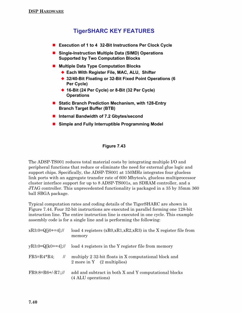
DSP HARDWARE
7.40
Figure 7.43
The ADSP-TS001 reduces total material costs by integrating multiple I/O andperipheral functions that reduce or eliminate the need for external glue logic andsupport chips. Specifically, the ADSP-TS001 at 150MHz integrates four gluelesslink ports with an aggregate transfer rate of 600 Mbytes/s, glueless multiprocessorcluster interface support for up to 8 ADSP-TS001s, an SDRAM controller, and aJTAG controller. This unprecedented functionality is packaged in a 35 by 35mm 360ball SBGA package.
Typical computation rates and coding details of the TigerSHARC are shown inFigure 7.44. Four 32-bit instructions are executed in parallel forming one 128-bitinstruction line. The entire instruction line is executed in one cycle. This exampleassembly code is for a single line and is performing the following:
xR3:0=Q[j0+=4];// load 4 registers (xR0,xR1,xR2,xR3) in the X register file frommemory
yR3:0=Q[k0+=4];// load 4 registers in the Y register file from memory
FR5=R4*R4; // multiply 2 32-bit floats in X computational block and2 more in Y (2 multiplies)
FR9:8=R6+/-R7;;// add and subtract in both X and Y computational blocks(4 ALU operations)
TigerSHARC KEY FEATURES
Execution of 1 to 4 32-Bit Instructions Per Clock Cycle
Single-Instruction Multiple Data (SIMD) OperationsSupported by Two Computation Blocks
Multiple Data Type Computation Blocks Each With Register File, MAC, ALU, Shifter 32/40-Bit Floating or 32-Bit Fixed Point Operations (6
Per Cycle) 16-Bit (24 Per Cycle) or 8-Bit (32 Per Cycle)
Operations
Static Branch Prediction Mechanism, with 128-EntryBranch Target Buffer (BTB)
Internal Bandwidth of 7.2 Gbytes/second
Simple and Fully Interruptible Programming Model
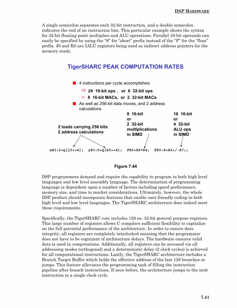
DSP HARDWARE
7.41
A single semicolon separates each 32-bit instruction, and a double semicolonindicates the end of an instruction line. This particular example shows the syntaxfor 32-bit floating point multiplies and ALU operations. Parallel 16-bit operands caneasily be specified by using the “S” for “short” prefix instead of the “F” for the “float”prefix. J0 and K0 are IALU registers being used as indirect address pointers for thememory reads.
Figure 7.44
DSP programmers demand and require the capability to program in both high levellanguages and low level assembly language. The determination of programminglanguage is dependent upon a number of factors including speed performance,memory size, and time to market considerations. Ultimately, however, the wholeDSP product should incorporate features that enable user friendly coding in bothhigh level and low level languages. The TigerSHARC architecture does indeed meetthese requirements.
Specifically, the TigerSHARC core includes 128 ea. 32-bit general purpose registers.This large number of registers allows C compilers sufficient flexibility to capitalizeon the full potential performance of the architecture. In order to ensure dataintegrity, all registers are completely interlocked meaning that the programmerdoes not have to be cognizant of architecture delays. The hardware ensures validdata is used in computations. Additionally, all registers can be accessed via alladdressing modes (orthogonal) and a deterministic delay (2 clock cycles) is achievedfor all computational instructions. Lastly, the TigerSHARC architecture includes aBranch Target Buffer which holds the effective address of the last 128 branches orjumps. This feature alleviates the programming task of filling the instructionpipeline after branch instructions. If seen before, the architecture jumps to the nextinstruction in a single clock cycle.
TigerSHARC PEAK COMPUTATION RATES
xR3:0=Q[j0+=4]; yR3:0=Q[k0+=4]; FR5=R4*R4; FR9:8=R6+/-R7;;
2 loads carrying 256 bits2 address calculations
8 16-bit or2 32-bit multiplicationsin SIMD
16 16-bitor4 32-bitALU opsin SIMD
4 instructions per cycle accomplishes:
24 16-bit ops , or 6 32-bit ops 8 16-bit MACs, or 2 32-bit MACs
As well as 256-bit data moves, and 2 addresscalculations

DSP HARDWARE
7.42
Figure 7.45
Figure 7.46 depicts one possible configuration of a TigerSHARC design in amultiprocessing implementation. Up to 8 ADSP-TS001 processors can communicatedirectly via the high speed 64-bit wide external bus interface. In this type ofcommunication, a commonly used master-slave protocol is implemented whichenables any two processors to communicate directly at any one time.
In addition to the primary external bus, a limitless number of processors can beconnected via the ADSP-TS001 link ports. While offering more flexibility, link portconnectivity provides lower per port bandwidth than the primary external businterface. Again, all data transfers via the link ports are managed by a dedicatedI/O processor and require no CPU intervention.
To summarize, the data I/O bandwidth of the link port (600MBytes/s) and externalport (600MBytes/s) can be aggregated yielding an overall individual processor databandwidth of 1200 Mbytes/s with 150MHz clock operation. Additionally, both thelink port interface and the multiprocessor cluster interface are both completelyglueless.
The ADSP-TS001 is the first member of a planned family of TigerSHARC-basedproducts. Specifically, future members of the TigerSHARC family will containoptimized mixes of memory and peripherals to meet the requirements of specifictarget markets. These markets include third generation cellular base stations andVOIP (Voice Over the Internet Protocol) servers/concentrators. Additionally, processand design improvements will double the baseline performance of the generalpurpose TigerSHARC family members.
ARCHITECTURAL FEATURES FOR HIGH-LEVELLANGUAGE SUPPORT
128 General Purpose Registers
All Registers Fully Interlocked
General Purpose Integer ALUs for Addressing
Branch Prediction
No Hardware Modes
Orthogonal Addressing Modes
Assembly Language Support

DSP HARDWARE
7.43
Figure 7.46
Figure 7.47
MULTIPROCESSING COMMUNICATION VIALINK PORTS AND CLUSTER BUS
SRAM
I/O
Host Interface
ADSP-TS001TigerSHARC
ADSP-TS001TigerSHARC
ADSP-TS001TigerSHARC
ADSP-TS001TigerSHARC
Bus connections
Link Port connections
DRAMSDRAM
TigerSHARC ROADMAP
ADSP-TS001
2 Mbit/secchannel on a chip
Highest DensityVoice OverThe Internet
2.4 BillionMACs perSecond
150 MHz
250 MHz

DSP HARDWARE
7.44
Comparing DSPs based solely on MIPS, MOPS, or MFLOPS does not tell the entireperformance story. It is much more useful to compare DSPs based on theirperformance with respect to specific algorithms. The FFT and the FIR filter arepopular benchmarks as well as the IIR biquad filter, matrix multiplications,division, and square root.
Figure 7.48 shows the benchmark performance of the ADSP-TS001 TigerSHARCoperating on 16-bit fixed point data. Figure 7.49 shows its benchmark performanceoperating on 32-bit floating point data.
Figure 7.48
Figure 7.49
ADSP-TS001 TigerSHARC BENCHMARKS @ 150MHz16-BIT PERFORMANCE
256 Point Complex FFT (Radix 2)50 Tap FIR on 1024 inputsSingle FIR MACSingle Complex FIR MACSingle FFT Butterfly
7.3 µs48 µs
0.93 ns3.80 ns6.7 ns
110072000.140.571.0
AlgorithmExecutionTime
Cycles to Execute
16-Bit performance -- 1200 MMACs/s peak performance
ADSP-TS001 TigerSHARC BENCHMARKS @ 150MHz32-BIT PERFORMANCE
32-Bit performance -- 300 MMACs/s peak performance
1024 Point Complex FFT (Radix 2)50 Tap FIR on 1024 InputSingle FIR MACSingle FFT ButterflySingle Complex FIR MACDivideSquare RootViterbi Decode(per Add/Compare/Select)
69 µs184 µs3.7 ns
13.3 ns13.3 ns
20 ns33.3 ns
3.3 ns
1030027500
0.552.02.03.05.00.5
AlgorithmExecutionTime
Cycles to Execute

DSP HARDWARE
7.45
DSP EVALUATION AND DEVELOPMENT TOOLS
The availability of a complete set of hardware and software development tools isessential to any DSP-based design. A typical DSP system design cycle is describedbelow.
The first step in the process is to describe the system architecture. This wouldinclude such things as the type of processor, the peripherals (external memory,codecs, host processor, links), the configuration, etc. This information is placed in afile known as the Link Descriptor File (or LDF).
The next step in the process is to generate the actual DSP code. This can be doneusing a higher level language (usually C or C++), the DSP assembly language, or acombination of both. DSP code developed in C must be compiled and assembled inorder to generate the assembly language code. While programming in C is easier,the resulting assembly code which results after compiling is not as efficient as if thecoding had been done in assembly language originally. For this reason, many DSPprogrammers do most of the programming in C, but use assembly language for thecritical loops in the program. The Analog Devices’ DSP assembly language is basedon algebraic syntax and is relatively easy to use directly. The linker then generatesan executable file.
The software must then be debugged using the software simulator in conjunctionwith an evaluation board such as the EZ-LAB evaluation board or perhaps a third-party card which plugs into a slot in the PC.
After the software is debugged using the evaluation board, it must be tested withthe actual system target board (this is the board that you design with the DSP inyour system). An in-circuit emulator, such as the EZ-ICE, interfaces with the targetboard, usually via a PCI or a JTAG interface port and connector.
The final step in the process is to generate the code required for booting the systemusing the prom splitter.
A summary of the tools available from Analog Devices is shown in Figure 7.50. Eachone will be discussed in detail.
EZ-KIT Lites are basically DSP starter kit evaluation boards. In addition to theprocessor itself, these boards contain an ADC and a DAC (codec) which interfaces tothe DSP over the DSP serial port. All necessary analog and digital support circuitryis contained on the boards. The options on the board are controlled over an RS-232port connection to a PC as well as jumpers on the board. Windows 95/98/NTcompatible software is supplied with the board. The software includes limited codegeneration tools including a limited feature set compiler, assembler, linker, promsplitter (loader), and Visual DSP debugger. Application examples such as DTMFgenerator, echo cancellation, FFT, simple digital filters, etc., are included as part ofthe software. The EZ-KIT Lite boards are primarily starter kit evaluation systems(and “lite” on the wallet!).

DSP HARDWARE
7.46
Figure 7.50
Figure 7.51
EZ-KIT LITE’S™ FOR ANALOG DEVICES’ DSPS
The EZ-KIT Lite is a stand-alone (desktop) system that connectsto a PC running on Windows
The EZ-KIT Lites provide: A cost effective method for initial evaluation of the capabilities
of ADSP-series DSPs. A powerful development environment for a variety of general
purpose applications. Target market:
First time DSP users First time ADI DSP users Existing ADI DSP users implementing new designs Existing ADI DSP users upgrading to faster devices for current
designs
ADI DSP DEVELOPMENT TOOLS
EZ-KIT Lite Evaluation Boards Emulators Integrated Development Environment (IDE) Software, VisualDSP®
and VisualDSP++ Assembler, Linker, PROM Splitter, HIP Splitter, Simulator,
Compiler, Debugger Extensive Algorithm Libraries Factory, Field, and WWW Support Seminars ADI and Third Party DSP Workshops ADI DSP Collaborative™ Third Party Support

DSP HARDWARE
7.47
Figure 7.52
Figure 7.53
ADSP-2189M EZ-KIT LITE™
Hardware Features ADSP-2189M 75 Mips processor AD73322L Stereo codec DSP-programmable CODEC gain 2 Mbit or greater boot protected Flash EPROM. RS-232 PC to EZ-Kit Lite interface Selectable Host vs. Full Memory mode implemented via dip switch ADSP-218x EZ-ICE emulator port connector Expansion connector includes all signal I/O plus 5V, 3.3V, 2.5V, and
GND connections LED indicators for master power, RS-232 interface, and one PF I/O
Software Features Windows 95/98/NT-4.0 PC host support VisualDSP: Limited feature set compiler, assembler, linker, prom
splitter (loader), VisualDSP debugger interface Application Examples: DTMF Generator, Echo Cancellation, FFT,
etc.(similar to 2181 EZ-KIT Lite) Email Support
ADSP-21160M EZ-KIT LITE™
Hardware Features ADSP-21160M SHARC processor AD1881 16-bit Stereo AC’97 SoundMAX Codec EPROM flash memory (2 Mbit) JTAG header Support for ADSP-2116x family of processors 64K x 64 bit SBSRAM Enhanced parallel port CE compliant
Software Features Support for Win95, Win98 and WinNT Evaluation suite of VisualDSP++ : compiler, assembler,
linker, prom splitter (loader), VisualDSP debuggerinterface. VisualDSP limited to use with EZ-KIT Litehardware
DEMONSTRATIONS: DFT.dxe, BP.dxe, Pluck.dxe,Primes.dxe, Tt.dxe

DSP HARDWARE
7.48
Figure 7.54
The final step in the DSP system development is the debugging of the actualsystem, or “target” board. The Analog Devices’ in-circuit emulator, EZ-ICE,interfaces with a connector on the target board for use in final system hardware andsoftware debugging. Examples are shown in Figures 7.55 through 7.58. Figure 7.56shows the Apex-ICE which interfaces to the target board via a JTAG connectorwhich in turn interfaces to the SHARC DSP. A USB port connector is used tointerface the emulator to a PC. Other in-circuit emulators are available whichinterface to ISA, PCI, RS232, and Ethernet ports.
ADSP-21065L EZ-KIT LITE™
Hardware Features ADSP-21065L SHARC DSP running at 60MHz Full Duplex, 16-Bit Audio Codec RS-232 Interface with UART JTAG Emulation Connector Expansion via MAFE+ Connector
Software Features
Support for Win95, Win98 and WinNT
Evaluation suite of VisualDSP++ : compiler, assembler, linker,prom splitter (loader), VisualDSP debugger interface.VisualDSP limited to use with EZ-KIT Lite hardware
Demonstrations: Fast Fourier Transform (FFT), DiscreteFourier Transform (DFT), Band Pass Filter, Pluck StringThemes, Talk Through

DSP HARDWARE
7.49
Figure 7.55
Figure 7.56
EZ-ICE® FOR THE ADSP-218x DSP FAMILY
Serial port interface, printed circuit board and 14-pin header Controls equipment for testing, observing, and debugging a
target system 6 foot cable Hardware switch to accommodate
of 2.5V, 3.3V, and 5V Shielded enclosure to cover bare
circuit board Performance increase via faster
data transfer
APEX-ICE™ USB EMULATOR
Universal Serial Bus (USB)-based emulator for AnalogDevices JTAG DSPs
First portable solution forAnalog Devices JTAG DSPs
Small hand-held unit Small diameter cable, 5
meters in length, for hardto reach targets
Power provided externally
JTAG CONNECTOR
USB PORTCONNECTOR

DSP HARDWARE
7.50
Figure 7.57
Figure 7.58
TREK-ICE™ ETHERNET EMULATOR
Network hosted mini-tower emulator with 10-Base-T port Installs to a LAN as easy as a laser printer Remote debugging between either PC or SUN workstation debug
host (client) and the target DSP system Rugged high-speed 3V/5V pod Flexible emulator cable (1.5m)
SUMMIT-ICE™ PCI EMULATOR
32-bit PCI interface add-in card Four inch, flexible shielded target board cable for easy access to
a 14-pin JTAG header Embedded ICEPAC technology provides a rugged and reliable
solution Remote 3V/5V JTAG Pod with
extended, shielded cable (1.5 m) Windows 95 & NT PNP

DSP HARDWARE
7.51
VISUALDSP® AND VISUALDSP++
New development software for Analog Devices’ DSPs is written in easy to useVisualDSP® and VisualDSP ++ which is Windows 95/98/NT compatible. VisualDSPis a completely integrated development environment which uses an algebraic syntaxassembler and an optimized C compiler. Multiprocessor environments can besimulated and debugged as well. VisualDSP++ provides C++ language support.
VisualDSP versions currently exist for the ADSP-218x and ADSP-219x families aswell as the SHARC family of DSPs.
A “test drive” CDROM is available with a limited license for evaluation purposes.
In addition to the tools and support functions described thus far, Analog Devices’DSP Collaborative consists of over 80 companies who provide a range of productsand services to make the DSP design task easier. Over 30 companies support the16-bit ADSP-21xx family, and over 50 companies support the SHARC DSP family. Adirectory of the collaborative can be found at:
http://www.analog.com/industry/dsp/3rdparty/index.html
Further information about Analog Devices’ DSP tools can be found at:
http://www.analog.com/dsp/tools
Figure 7.59
SOFTWARE DEVELOPMENT ENVIRONMENT
VisualDSP® and VisualDSP++ Debugger front-end Integrated development
environment (IDE) Algebraic syntax assembler Cycle-accurate instruction
level simulator Optimizing ANSI C compiler
with inline assembly Math, DSP, and C runtime libraries Sophisticated multiprocessor linker Intelligent loader ADSP-218x, 219x: Windows 95, 98, NT, 2000 Compatible SHARC: Windows 95, 98, NT, 2000 Compatible

DSP HARDWARE
7.52
Figure 7.60
Figure 7.61
VisualDSP® 7.0 FOR ADSP-218x AND ADSP-219x
Hosted on Windows 95, Windows 98, Windows NT 4.0 with SP3 or later
ADSP-219x simulator target supports the 219x core
ELF/DWARF toolset, including compiler with classical andprocessor-specific optimizations
Tcl command line scripting language
Support automated test of DSP system
21xx Object Translator
Peripheral Code Wizard supporting 218x and 219x peripherals
VisualDSP++™ FOR SHARC® DSPs
Supports Windows 95, 98, NT, 2000
ELF/Dwarf-2 file format enables effective debug operation
Pre-processor for linker/assembler separate from compiler
Fast ICE stepping - 0.9 sec. per step
MultiProcessor (MP) support
Synchronous run, step, and halt
Tcl command line scripting language
Support automated test of DSP system
Statistical Profiling
C++ capabilities
Graphical Plotting

DSP HARDWARE
7.53
Figure 7.62
Figure 7.63
TigerSHARC® DEVELOPMENT TOOLS
The TigerSHARC architecture is supported by a robust set ofsimulation, code generation, and debug tools that includes: VisualDSP Integrated Development Environment
Simulator, Assembler, Loader, Debugger, and Compiler DSP & Math Libraries
Emulators – All present ADI JTAG emulators support theTigerSHARC DSP family
EZ-KIT Lite Successive VisualDSP revisions will continuously increase
functionality.
VisualDSP TEST DRIVE
The test drive is a 30-day evaluation of VisualDSP's full package. Itdoes not include a tutorial. The new test drive is a full version ofVisualDSP and contains pdf.'s of the VisualDSP manuals.
The customer is presented with the test drive CD. The customerthan proceeds to the Analog Devices DSP Tools website, clicks onTest Drive Registrationwww.analog.com/industry/dsp/tools/test_drive.html and registersonline. After they complete the registration process they willreceive a serial number immediately that will allow them to use thetest drive. The test drive will expire 30-days from the install andthey will not be able to register the test drive again.
The SHARC VisualDSP test drive is now available, SAP part #VDSP-SHARC-PC-TEST.
The VisualDSP TigerSHARC test drive will be availableSummer 2000
The VisualDSP ADSP-218x/219x test drive will be available inSeptember 2000
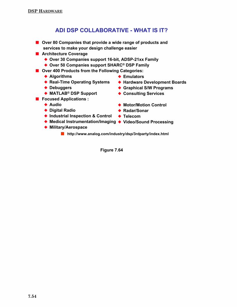
DSP HARDWARE
7.54
Figure 7.64
ADI DSP COLLABORATIVE - WHAT IS IT?
Over 80 Companies that provide a wide range of products and services to make your design challenge easier
Architecture Coverage Over 30 Companies support 16-bit, ADSP-21xx Family Over 50 Companies support SHARC® DSP Family
Over 400 Products from the Following Categories: Algorithms Real-Time Operating Systems Debuggers MATLAB® DSP Support
Focused Applications : Audio Digital Radio Industrial Inspection & Control Medical Instrumentation/Imaging Military/Aerospace
Motor/Motion Control Radar/Sonar Telecom Video/Sound Processing
Emulators Hardware Development Boards Graphical S/W Programs Consulting Services
http://www.analog.com/industry/dsp/3rdparty/index.html

DSP HARDWARE
7.55
REFERENCES
1. Steven W. Smith, The Scientist and Engineer’s Guide to Digital SignalProcessing, Second Edition, 1999, California Technical Publishing,P.O. Box 502407, San Diego, CA 92150. Also available for free download at:http://www.dspguide.com or http://www.analog.com/industry/dsp/dsp_book
2. C. Britton Rorabaugh, DSP Primer, McGraw-Hill, 1999.
3. Richard J. Higgins, Digital Signal Processing in VLSI, Prentice-Hall,1990.
4. Ethan Bordeaux, Advanced DSP Performance Complicates MemoryArchitecures in Wireless Designs, Wireless Systems Design, April 2000.
5. DSP Designer’s Reference (DSP Solutions) CDROM, Analog Devices,1999.
6. DSP Navigators: Interactive Tutorials about Analog Devices’ DSPArchitectures (Available for ADSP-218x family and SHARC family):http://www.analog.com/industry/dsp/training/index.html#Navigator
7. General DSP Training and Workshops:http://www.analog.com/industry/dsp/training
The following DSP Reference Manuals and documentation are availablefor free download from: http://www.analog.com/industry/dsp/tech_docs.html
8. ADSP-2100 Family Users Manual, 3rd Edition, Sept., 1995.
9. ADSP-2100 Family EZ Tools Manual.
10. ADSP-2100 EZ-KIT Lite Reference Manual.
11. Using the ADSP-2100 Family, Vol. 1, Vol. 2.
12. ADSP-2106x SHARC User’s Manual, 2nd Edition, July, 1996.
13. ADSP-2106x SHARC EZ-KIT Lite Manual.
14. ADSP-21065L SHARC User’s Manual, Sept. 1, 1998.
15. ADSP-21065L SHARC EZ-LAB User’s Manual.
16. ADSP-21160 SHARC DSP Hardware Reference.

DSP HARDWARE
7.56

INTERFACING TO DSPS
8.a
SECTION 8
INTERFACING TO DSPs
Parallel Interfacing to DSP Processors: Reading DataFrom Memory-Mapped Peripheral ADCs
Parallel Interfacing to DSP Processors: Writing Data toMemory-Mapped DACs
Serial Interfacing to DSP Processors
Interfacing I/O Ports, Analog Front Ends, and Codecsto DSPs
DSP System Interface

INTERFACING TO DSPS
8.b

INTERFACING TO DSPS
8.1
SECTION 8INTERFACING TO DSPsWalt Kester, Dan King
INTRODUCTION
As the technology in the rapidly growing field of mixed signal processing evolves,more highly integrated DSP products are being introduced (such as the ADSP-21ESP202) which contain on-chip ADCs and DACs as well as the DSP, therebyeliminating most component-level interface problems. Stand-alone ADCs and DACsare now available with interfaces especially designed for DSP chips, therebyminimizing or eliminating external interface support or glue logic. Highperformance sigma-delta ADCs and DACs are currently available in the samepackage (called a CODEC or COder/DECcoder) such as the AD73311 and AD73322.These products are also designed to require minimum glue logic when interfacing tothe most common DSP chips. This section discusses the various data transfer andtiming issues associated with the various interfaces.
PARALLEL INTERFACING TO DSP PROCESSORS:READING DATA FROM MEMORY-MAPPED PERIPHERALADCSInterfacing an ADC or a DAC to a fast DSP parallel requires an understanding ofhow the DSP processor reads data from a memory-mapped peripheral (the ADC)and how the DSP processor writes data to a memory-mapped peripheral (the DAC).We will first consider some general timing requirements for reading and writingdata. It should be noted that the same concepts presented here regarding ADCs andDACs apply equally when reading and writing from/to external memory.
A block diagram of a typical parallel DSP interface to an external ADC is shown inFigure 8.1. This diagram has been greatly simplified to show only those signalsassociated with reading data from an external memory-mapped peripheral device.The timing diagram for the ADSP-21xx read-cycle is shown in Figure 8.2.
In this example it is assumed that the ADC is sampling at a continuous rate whichis controlled by the external sampling clock, not the internal DSP clock. Using aseparate clock for the ADC is the preferred method, since the DSP clock may benoisy and introduce jitter in the ADC sampling process, thereby increasing the noiselevel.
Assertion of the sampling clock at the ADC convert start input initiates theconversion process (step 1). The leading (or trailing) edge of this pulse causes theinternal ADC sample-and-hold to switch from the sampling mode to the hold modeso that the conversion process can take place. When the conversion is complete, theconversion complete output of the ADC is asserted (step 2). The read process thusbegins when this signal is applied to the processor interrupt request line ( IRQ ) ofthe DSP. The processor then places the address of the peripheral initiating the

INTERFACING TO DSPS
8.2
interrupt request (the ADC) on the memory address bus (A0 - A13) (step 3). At thesame time, the processor asserts a memory select line ( DMS is shown here) (step 4).The two internal address buses of the ADSP-21xx (program memory address busand data memory address bus) share a single external address bus, and the twointernal data buses (program memory data bus and data memory data bus) share asingle external data bus. The boot memory select ( BMS ), data memory select( DMS ), program memory select ( PMS ) and input/output memory select ( IOMS )signals indicate which memory space the external buses are being used for. Thesesignals are typically used to enable an external address decoder as shown in Figure8.1. The output of the address decoder drives the chip select input of the peripheraldevice (step 5).
The memory read ( RD ) is asserted tASR ns after the DMS line is asserted (step 6).The sum of the address decode delay plus the peripheral chip select setup timeshould be less than tASR in order to take full advantage of the RD low-time. The RDline remains low for tRP ns. The memory read signal is used to enable the three-stateparallel data outputs of the peripheral device (step 7). The RD line is connected tothe appropriate pin on the peripheral device usually called output enable or read.The rising edge of the RD signal is used to clock the data on the data bus into theDSP processor (step 8). After the rising edge of the RD signal, the data on the databus must remain valid for tRDH ns, the data hold time. In the case of most membersof the ADSP-21xx family, this specification value is 0ns.
The key timing requirements for the peripheral device are shown in Figure 8.3.Values are given for the ADSP-2189M DSP operating at 75MHz.
Figure 8.1
RD
IRQ
DMS
ADC TO ADSP-21xx-FAMILY PARALLEL INTERFACE
ADDRESSDECODE
SAMPLINGCLOCK
1
2
3
4 5
6 8
7
MEMORYADDRESS BUS
DATA MEMORYSELECT
PROCESSORINTERRUPTREQUEST
MEMORY READ
MEMORY DATABUS
A0- A13
D
ADSP-21xx ADC
CONVERT START
CHIP SELECT
CONVERSIONCOMPLETE
OUTPUT ENABLE
OUTPUT DATA

INTERFACING TO DSPS
8.3
Figure 8.2
Figure 8.3
ADSP-21xx FAMILY MEMORY READ TIMING
DSPCLKOUT
A0- A13
DMS, PMS,IOMS, CMS
RD
D
tASRtCRD
tRP
tRDAtRWR
tAA
tRDD
tRDH
PARALLEL PERIPHERAL DEVICE READ INTERFACEKEY REQUIREMENTS
Peripheral Device Data Outputs Must Be Three-State Compatible Address Decode Delay + Peripheral Chip Select Setup Time Must Be
Less Than Address and Memory Select Setup Time tASR (0.325ns minfor ADSP-2189M)
For Zero Wait-State Access, the Time from a Negative-Going Edge ofRead Signal (RD) to Output Data Valid Must be Less than tRDD (1.65nsmax for ADSP-2189M Operating at 75MHz) or Software Wait-StatesMust be Added, or Processor Clock Frequency Reduced
Output Data from Peripheral must Remain Valid for tRDH from theRising Edge of Read Signal (RD) (0ns for ADSP-2189M)
Peripheral Device Must Accept Minimum Output Enable Pulse Width oftRP (3.65ns for ADSP-2189M Operating at 75MHz) or Software Wait-States Must be Added, or Processor Clock Frequency Reduced

INTERFACING TO DSPS
8.4
The DSP tRDD specification determines the peripheral device data access timerequirement. In the case of the ADSP-2189M, tRDD = 1.65ns minimum at 75MHz. Ifthe access time of the peripheral is greater than this, wait states must be added orthe processor speed reduced. This is a relatively common situation when interfacingexternal memory or ADCs to fast DSPs. The relationship between these timingparameters for the ADSP-2189M is given by the equations shown in Figure 8.4.Note that these specifications are dependent on the DSP clock frequency.
Figure 8.4
The ADSP-2189M can easily be interfaced to slow peripheral devices using itsprogrammable wait state generation capability. Three registers control wait stategeneration for boot, program, data and I/O memory spaces. You can specify 0 to 15wait states for each parallel memory interface. Each wait state added increases theallowable external data memory access time by an amount equal to the processorclock period (13.3ns for the ADSP-2189M operating at 75MHz). In this example, thedata memory address, DMS , and RD lines are all held stable for an additionalamount of time equal to the duration of the wait states.
The AD7854/AD7854L is a 12 bit, 200/100kSPS ADC which operates in the parallelmode. It operates on a single +3V to +5.5V supply and dissipates only 5.5mW (+3Vsupply, AD7854L). An automatic power-down after conversion feature reduces thisto 650µW.
ADSP-2189M PARALLEL READ TIMING AT 75MHz
tCK = Processor Clock Period (13.3ns)
tASR = Address and Memory Select Setup Before Read Low
= 0.25tCK – 3ns Minimum
tRDD = Read Low to Data Valid = 0.5tCK – 5ns + # wait states
× tCK Maximum
tRDH = Data Hold from Read High = 0ns Minimum
tRP = Read Pulse Width = 0.5tCK – 3ns + # wait states × tCKMinimum
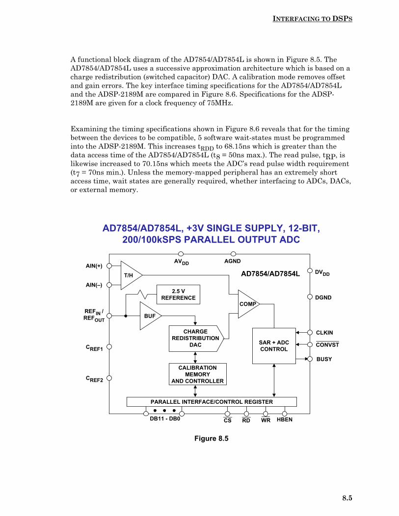
INTERFACING TO DSPS
8.5
A functional block diagram of the AD7854/AD7854L is shown in Figure 8.5. TheAD7854/AD7854L uses a successive approximation architecture which is based on acharge redistribution (switched capacitor) DAC. A calibration mode removes offsetand gain errors. The key interface timing specifications for the AD7854/AD7854Land the ADSP-2189M are compared in Figure 8.6. Specifications for the ADSP-2189M are given for a clock frequency of 75MHz.
Examining the timing specifications shown in Figure 8.6 reveals that for the timingbetween the devices to be compatible, 5 software wait-states must be programmedinto the ADSP-2189M. This increases tRDD to 68.15ns which is greater than thedata access time of the AD7854/AD7854L (t8 = 50ns max.). The read pulse, tRP, islikewise increased to 70.15ns which meets the ADC’s read pulse width requirement(t7 = 70ns min.). Unless the memory-mapped peripheral has an extremely shortaccess time, wait states are generally required, whether interfacing to ADCs, DACs,or external memory.
Figure 8.5
AD7854/AD7854L, +3V SINGLE SUPPLY, 12-BIT,200/100kSPS PARALLEL OUTPUT ADC
T/H
COMP
2.5 VREFERENCE
CHARGEREDISTRIBUTION
DAC SAR + ADCCONTROL
PARALLEL INTERFACE/CONTROL REGISTER
CALIBRATIONMEMORY
AND CONTROLLER
AVDD AGNDAIN(+)
AIN(–)
REFIN /REFOUT
CREF1
CREF2
DB11 - DB0 CS RD WR HBEN
DVDD
DGND
CLKIN
CONVST
BUSY
AD7854/AD7854L
BUF

INTERFACING TO DSPS
8.6
Figure 8.6
A simplified interface diagram for the two devices is shown in Figure 8.7. Theconversion complete signal from the AD7854/AD7854L corresponds to the BUSYoutput pin. Notice that the configuration allows the DSP to write data to theAD7854/AD7854L parallel interface control register. This is needed in order to setvarious options in the AD7854/AD7854L and perform the calibration routines. Innormal operation, however, data is read from the AD7854/AD7854L as describedabove. Writing to external parallel memory-mapped peripherals is discussed later inthis section.
Parallel interfaces between other DSP processors and external peripherals can bedesigned in a similar manner by carefully examining the timing specifications for allappropriate signals for each device. The data sheets for most ADCs containsufficient information in the application section to interface them to the DSPs.
ADSP-2189M AND AD7854/AD7854L PARALLEL READINTERFACE TIMING SPECIFICATION COMPARISON
ADSP-2189M Processor (75MHz)
tASR (Data Address, MemorySelect Setup Time Before RD Low)
= 0.325ns min
tRP (RD Pulse Width) =3.65ns + # wait states × 13.3ns min
= 70.15ns min
tRDD (RD Low to Data Valid) = 1.65ns + # wait states × 13.3ns min
= 68.15ns min
tRDH (Data Hold from RD High) =0ns min
AD7854/AD7854L ADC
t5 (CS to RD Setup Time =0ns min (Must Add AddressDecode Time to this Value)
t7 (RD Pulse Width) = 70ns min
t8 (Data Access Time After RD) = 50ns max
t9 (Bus Relinquish Time After RD) = 5ns min / 40ns max
NOTES:(1) Adding 5 wait-states to the ADSP-2189M increases tRP to 70.15ns which is greater than t7 (70ns) and meets the t8 (50ns) requirement.(2) t9 max (40ns) may cause bus contention if a write cycle immediately followsthe read cycle.

INTERFACING TO DSPS
8.7
Figure 8.7
PARALLEL INTERFACING TO DSP PROCESSORS:WRITING DATA TO MEMORY-MAPPED DACS
A simplified block diagram of a typical DSP interface to a parallel peripheral device(such as a DAC is shown in Figure 8.8. The memory-write cycle timing diagram forthe ADSP-21xx-family is shown in Figure 8.9.
In most real-time applications, the DAC is operated continuously from a stablesampling clock. Most DACs for these applications have double buffering: an inputlatch to handle the asynchronous DSP interface, followed by a second latch (calledthe DAC latch) which drives the DAC current switches. The DAC latch strobe isderived from an external stable sampling clock. In addition to clocking the DAClatch, the DAC latch strobe is also used to generate a processor interrupt to the DSPwhich indicates that the DAC is ready for a new input data word.
AD7854/AD7854L ADC PARALLEL INTERFACETO ADSP-2189M
RD
IRQ
DMS
SAMPLINGCLOCK
D23 - D8
ADSP-2189M 75MHz
AD7854/AD7854LADC
CONVST
CS
BUSY
RD
DB11 - DB0
A0 HBEN
WRWR
Notes: 5 Software Wait-StatesHBEN and WR required for writing to ADCSampling clock may come from DSP
(LOW = READ DB11 - DB0)
DATA

INTERFACING TO DSPS
8.8
Figure 8.8
Figure 8.9
ADSP-21xx FAMILY MEMORY WRITE TIMING
DSPCLKOUT
A0- A13
DMS, PMS,BMS, CMS
WR
D
tASWtCWR
tWP
tWRAtWWR
tDH tDDR
tDW
tAW
tWDE
DAC TO ADSP-21xx-FAMILY PARALLEL INTERFACE
WR
IRQ
DMS ADDRESSDECODE
SAMPLINGCLOCK
1
1
2
3 5
4 7
6
MEMORYADDRESS BUS
DATA MEMORYSELECT
PROCESSORINTERRUPTREQUEST
MEMORY WRITE
MEMORY DATABUS
A0- A13
D
ADSP-21xx DACDAC LATCHSTROBE
CHIP SELECT
INPUT LATCHSTROBE
PARALLEL DATAINPUT

INTERFACING TO DSPS
8.9
The write process is thus initiated by the peripheral device asserting the DSPinterrupt request line indicating that the peripheral is ready to accept a new paralleldata word (step 1). The DSP then places the address of the peripheral device on theaddress bus (step 2) and asserts a memory select line ( DMS is shown here) (step 3).This causes the output of the address decoder to assert the chip select input to theperipheral (step 5). The write ( WR ) output of the DSP is asserted tASW ns after thenegative-going edge of the DMS signal (step 4). The width of the WR pulse is tWPns. Data is placed on the data bus (D) and is valid tDW ns before the WR line goeshigh (step 6). The positive-going transition of the WR line is used to clock the dataon the data bus (D) into the external parallel memory (step 7). The data on the databus remains valid for tDH ns after the positive-going edge of the WR signal.
The key timing requirements for writing to the peripheral device are shown inFigure 8.10. The key specification is tWP , the write pulse width. All but the fastestperipheral devices will require wait states to be added due to their longer dataaccess times. Figure 8.11 shows the key timing specifications for the ADSP-2189M.Note that they are all related to the processor clock frequency.
Figure 8.10
PARALLEL PERIPHERAL DEVICES WRITE INTERFACEKEY REQUIREMENTS
Address Decode Delay + Peripheral Chip Select Setup Time MustBe Less Than Address and Memory Select Setup Time tASW
(0.325ns for ADSP-2189M Operating at 75MHz)
For Zero Wait-State Access, Input Data Setup Time Must be LessThan tDW (2.65ns for ADSP-2189M Operating at 75MHz) or SoftwareWait-States Must be Added, or Processor Clock FrequencyReduced
Input Data Hold Time Must be Less Than tDH (2.325ns for ADSP-2189M Operating at 75MHz)
Peripheral Device Must Accept Input Write Clock Pulse of WidthtWP (3.65ns min for ADSP-2189M Operating at 75MHz) or Software-Wait States Must be Added, or Processor Clock FrequencyReduced

INTERFACING TO DSPS
8.10
Figure 8.11
The AD5340 is a 12 bit 100kSPS DAC which has a parallel data interface. Itoperates on a single +2.5V to +5.5V supply and dissipates only 345µW (+3V supply).A power-down mode further reduces the power to 0.24µW. The part incorporates anon-chip output buffer which can drive the output to both supply rails. The AD5340allows the choice of a buffered or unbuffered reference input. The device has apower-on reset circuit that ensures that the DAC output powers on at 0V andremains there until valid data is written to the part. A block diagram is shown inFigure 8.12. The input is double buffered. The key interface timing specifications forthe two devices are compared in Figure 8.13. Specifications for the ADSP-2189M aregiven for a clock frequency of 75MHz.
Figure 8.12
ADSP-2189M PARALLEL WRITE TIMING
tCK = Processor Clock Period (13.3ns)
tASW = Address and Memory Select Before WR Low
= 0.25tCK – 3ns Minimum
tDW = Data Setup Before WR High = 0.5tCK – 4ns + # Wait States × tCK
tDH = Data Hold After WR High = 0.25tCK – 1ns
tWP = WR Pulse Width = 0.5tCK – 3ns + # Wait States × tCK Minimum
AD5340 12-BIT, 100kSPS PARALLEL INPUT DAC
INPUTREGISTER
DACREGISTER
12-BITDAC
POWER-DOWNLOGIC
INTE
RFA
CE
LOG
IC
DB11
DB0
BUF
GAIN
CS
WR
CLR
LDAC
VREF
VOUT
PD GND
RESET
BUF
POWER-ONRESET
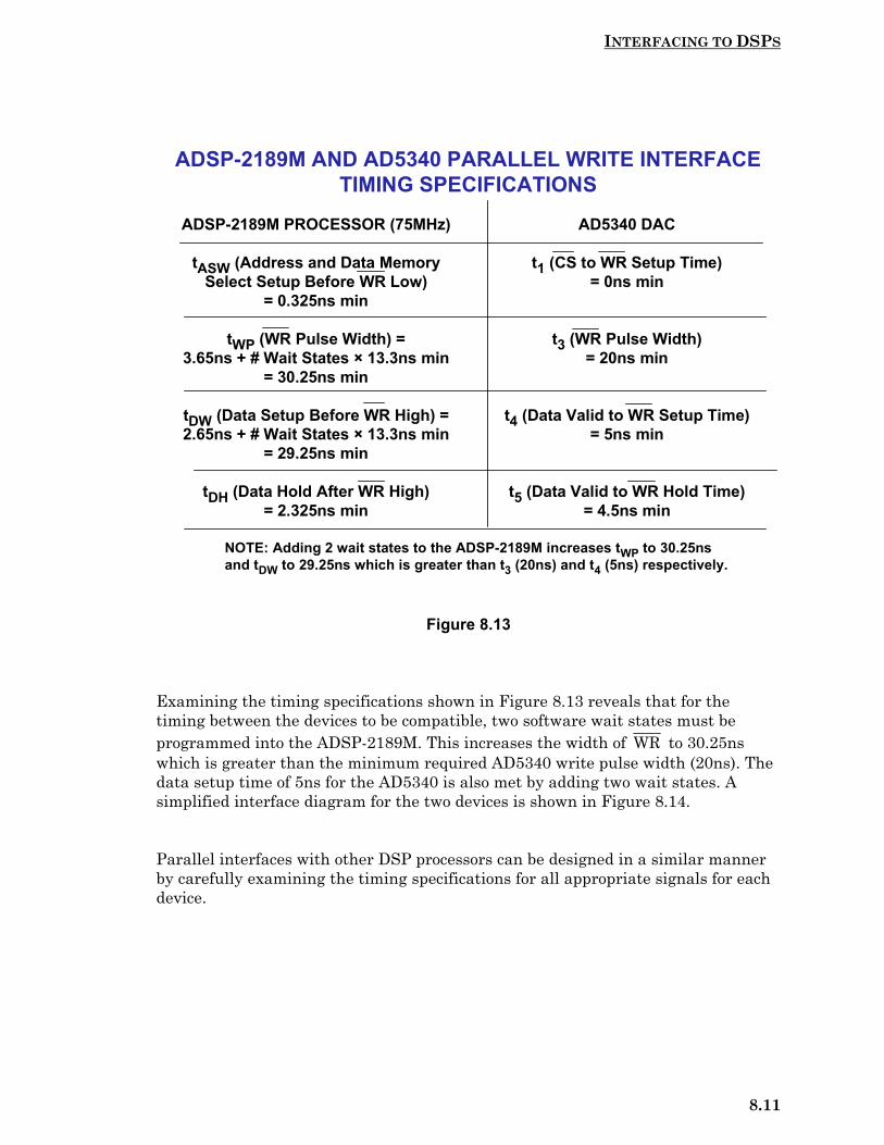
INTERFACING TO DSPS
8.11
Figure 8.13
Examining the timing specifications shown in Figure 8.13 reveals that for thetiming between the devices to be compatible, two software wait states must beprogrammed into the ADSP-2189M. This increases the width of WR to 30.25nswhich is greater than the minimum required AD5340 write pulse width (20ns). Thedata setup time of 5ns for the AD5340 is also met by adding two wait states. Asimplified interface diagram for the two devices is shown in Figure 8.14.
Parallel interfaces with other DSP processors can be designed in a similar mannerby carefully examining the timing specifications for all appropriate signals for eachdevice.
ADSP-2189M AND AD5340 PARALLEL WRITE INTERFACETIMING SPECIFICATIONS
ADSP-2189M PROCESSOR (75MHz)
tASW (Address and Data MemorySelect Setup Before WR Low)
= 0.325ns min
tWP (WR Pulse Width) =3.65ns + # Wait States × 13.3ns min
= 30.25ns min
tDW (Data Setup Before WR High) =2.65ns + # Wait States × 13.3ns min
= 29.25ns min
tDH (Data Hold After WR High)= 2.325ns min
AD5340 DAC
t1 (CS to WR Setup Time)= 0ns min
t3 (WR Pulse Width)= 20ns min
t4 (Data Valid to WR Setup Time)= 5ns min
t5 (Data Valid to WR Hold Time)= 4.5ns min
NOTE: Adding 2 wait states to the ADSP-2189M increases tWP to 30.25ns and tDW to 29.25ns which is greater than t3 (20ns) and t4 (5ns) respectively.

INTERFACING TO DSPS
8.12
Figure 8.14
SERIAL INTERFACING TO DSP PROCESSORS
DSP processors which have serial ports (such as the ADSP-21xx family) provide asimple interface to peripheral ADCs and DACs. Use of the serial port eliminates theneed for using large parallel buses to connect the ADCs and DACs to the DSP. Inorder to understand serial data transfer better, we will first examine the serial portoperation of the ADSP-21xx series.
A block diagram of one of the two serial ports of the ADSP-21xx is shown in Figure8.15. The Transmit (TX) and Receive (RX) registers are identified by name in theADSP-21xx assembly language, and are not memory mapped.
AD5340 DAC PARALLEL INTERFACE TO ADSP-2189M
WR
IRQ
DMS
SAMPLINGCLOCK
D
ADSP-2189M75MHz
LDAC
CS
DB0 - DB11
WR
AD5340DAC
Notes: 2 Software Wait-StatesSampling clock may come from DSP

INTERFACING TO DSPS
8.13
Figure 8.15
Figure 8.16
ADSP-21xx FAMILY SERIAL PORT BLOCK DIAGRAM
TXnTRANSMIT DATA
REGISTER
TRANSMIT SHIFTREGISTER
COMPANDINGHARDWARE
(µ-LAW or A-LAW)
RXnRECEIVE DATA
REGISTER
SERIALCONTROL
INTERNALSERIALCLOCKGEN.
RECEIVE SHIFTREGISTER
DT TFS SCLK RFS DR
DMD BUS16
16
16
16
16
Polarity of TFS and RFSis software programmable
ADSP-21xx FAMILY SERIAL PORT FEATURES
Separate Transmit and Receive Sections for Each Port
Double-Buffered Transmit and Receive Registers
Serial Clock Can be Internally or Externally Generated
Transmit and Receive Frame Sync Signals Can be Internally orExternally Generated
Serial Data Words of 3 to 16 Bits Supported
Automatically Generated Processor Interrupts
Hardware Companding Requires no Software Overhead

INTERFACING TO DSPS
8.14
In the receiving portion of the serial port, the receive frame sync (RFS) signalinitiates reception. The serial receive data (DR) from the external device (ADC) istransferred into the receive shift register one bit at a time. The negative-going edgeof the serial clock (SCLK) is used to clock the serial data from the external deviceinto the receive shift register. When a complete word has been received, it is writtento the receive data register (RX), and the receive interrupt for that serial port isgenerated. The receive data register is then read by the processor.
Writing to the transmit data register readies the serial port for transmission. Thetransmit frame sync (TFS) signal initiates transmission. The value in the transmitdata register (TX) is then written to the internal transmit shift register. The data inthe transmit shift register is sent to the peripheral device (DAC) one bit at a time,and the positive-going edge of the serial clock (SCLK) is used to clock the serialtransmit data (DT) into the external device. When the first bit has been transferred,the serial port generates the transmit interrupt. The transmit data register can thenbe written with new data, even though the transmission of the previous data is notcomplete.
In the normal framing mode, the frame sync signal (RFS or TFS) is checked at thefalling edge of SCLK. If the framing signal is asserted, data is available (transmitmode) or latched (receive mode) on the next falling edge of SCLK. The framingsignal is not checked again until the word has been transmitted or received. In thealternate framing mode, the framing signal is asserted in the same SCLK cycle asthe first bit of a word. The data bits are latched on the falling edge of SCLK, but theframing signal is checked only on the first bit. Internally-generated framing signalsremain asserted for the length of the serial word. The alternate framing mode of theserial port in the ADSP-21xx is normally used to receive data from ADCs andtransmit data to DACs.
The serial ports of the ADSP-21xx family are extremely versatile. The TFS, RFS, orSCLK signals can be generated from the ADSP-21xx clock (master mode) orgenerated externally (slave mode). The polarity of these signals can be reversedwith software, thereby allowing more interface flexibility. The port also contains µ-law and A-law companding hardware for voiceband telecommunicationsapplications.
SERIAL ADC TO DSP INTERFACE
A timing diagram of the ADSP-2189M serial port operating in the receive mode(alternate framing) is shown in Figure 8.17. The first negative-going edge of theSCLK to occur after the negative-going edge of the RFS , clocks the MSB data fromthe ADC into the serial input latch. The process continues until all serial bits havebeen transferred into the serial input latch. The key timing specifications of concernare the serial data setup (tSCS) and hold times (tSCH) with respect to the negative-going edge of the SCLK. In the case of the ADSP-2189M, these values are 4ns and7ns, respectively . The latest generation ADCs with high speed serial clocks willhave no trouble meeting these specifications, even at the maximum serial datatransfer rate.

INTERFACING TO DSPS
8.15
Figure 8.17
The AD7853/AD7853L is a 12 bit, 200/100kSPS ADC which operates on a single+3V to +5.5V supply and dissipates only 4.5mW (+3V supply, AD7853L). After eachconversion, the device automatically powers down to 25µW. The AD7853/AD7853Lis based on a successive approximation architecture and uses a chargeredistribution (switched capacitor) DAC. A calibration feature removes gain andoffset errors. A block diagram of the device is shown in Figure 8.18.
The AD7853 operates on a 4MHz maximum external clock frequency. The AD7853Loperates on a 1.8MHz maximum external clock frequency. The timing diagram forAD7853L is shown in Figure 8.19. The AD7853/AD7853L has modes whichconfigure the SYNC and SCLK as inputs or outputs. In the example shown herethey are generated by the AD7853L. The AD7853L serial clock operates at amaximum frequency of 1.8MHz (556ns period). The data bits are valid 330ns afterthe positive-going edges of SCLK. This allows a setup time of approximately 330nsminimum before the negative-going edges of SCLK, easily meeting the ADSP-2189M 4ns tSCS requirement. The hold-time after the negative-going edge of SCLKis approximately 226ns, again easily meeting the ADSP-2189M 7ns tSCH timingrequirement. These simple calculations show that the data and RFS setup and holdrequirements of the ADSP-2189M are met with considerable margin.
ADSP-2189M SERIAL PORT RECEIVE TIMING
MSB BIT n LSB
ADCSCLK
RFS IN
DR IN
tSCS≥≥≥≥ 4ns
tSCH≥≥≥≥ 7ns
tSCS
ALTERNATE FRAMING MODE, ADC IS MASTER

INTERFACING TO DSPS
8.16
Figure 8.18
Figure 8.19
AD7853/AD7853L +3V SINGLE-SUPPLY 12-BIT200/100kSPS SERIAL OUTPUT ADC
T/H
COMP
2.5 VREFERENCE
CHARGEREDISTRIBUTION
DACSAR + ADCCONTROL
SERIAL INTERFACE/CONTROL REGISTER
CALIBRATIONMEMORY
AND CONTROLLER
AVDD AGNDAIN(+)
AIN(–)
REFIN /REFOUT
CREF1
CREF2
DVDD
DGND
CLKIN
CONVST
BUSY
AD7853L
BUF
CAL
AGND
SLEEP
SM1 SM2 SYNC DIN DOUT SCLK POLARITY
AD7853L SERIAL ADC OUTPUT TIMING+3V SUPPLY, SCLK = 1.8MHz
DB15 DB0
SCLK(O/P)
SYNC (O/P)
DOUT (O/P)DB11
1 5 6 16
556ns
330ns min
226ns
THREE-STATE THREE-STATE

INTERFACING TO DSPS
8.17
Figure 8.20 shows the AD7853L interfaced to the ADSP-2189M connected in a modeto transmit data from the ADC to the DSP (alternate/master mode). TheAD7853/AD7853L contains internal registers which can be accessed by writing fromthe DSP to the ADC via the serial port. These registers are used to set variousmodes in the AD7853/AD7853L as well as to initiate the calibration routines. Theseconnections are not shown in the diagram.
Figure 8.20
SERIAL DAC TO DSP INTERFACE
Interfacing serial input DACs to the serial ports of DSPs such as the ADSP-21xxfamily is also relatively straightforward and similar to the previous discussionregarding serial output ADCs. The details will not be repeated here, but a simpleinterface example will be shown.
The AD5322 is a 12-bit, 100kSPS dual DAC with a serial input interface. It operateson a single +2.5V to +5.5V supply, and a block diagram is shown in Figure 8.21.Power dissipation on a +3V supply is 690µW. A power-down feature reduces this to0.15µW. Total harmonic distortion is greater than 70dB below full scale for a 10kHzoutput. The references for the two DACs are derived from two reference pins (oneper DAC). The reference inputs may be configured as buffered or unbuffered inputs.The outputs of both DACs may be updated simultaneously using the asynchronousLDAC input. The device contains a power-on reset circuit that ensures that theDAC outputs power up to 0V and remain there until a valid write takes place to thedevice.
AD7853/AD7853L SERIAL ADCINTERFACE TO ADSP-2189M
DR
RFS
SCLK
CLOCKINPUT
4MHz / 1.8MHz maxADSP-2189M
75MHzDSP
CLKIN
SCLK
DOUT
AD7853/AD7853L
ADC
SYNC
SERIALPORT
SAMPLINGCLOCK
(OPTIONAL)CONVST

INTERFACING TO DSPS
8.18
Figure 8.21
Data is normally input to the AD5322 via the SCLK, DIN, and SYNC pins from theserial port of the DSP. When the SYNC signal goes low, the input shift register isenabled. Data is transferred into the AD5322 on the falling edges of the following 16clocks. A typical interface between the ADSP-2189M and the AD5322 is shown inFigure 8.22. Notice that the clocks to the AD5322 are generated from the ADSP-2189M clock. It is also possible to generate the SCLK and SYNC signals externallyto the AD5322 and use them to drive the ADSP-2189M. The serial interface of theAD5322 is not fast enough to handle the ADSP-2189M maximum master clockfrequency. However, the serial interface clocks are programmable and can be set togenerate the proper timing for fast or slow DACs.
The input shift register in the AD5322 is 16-bits wide. The 16-bit word consists offour control bits followed by 12 bits of DAC data. The first bit loaded determineswhether the data is for DAC A or DAC B. The second bit determines if the referenceinput will be buffered or unbuffered. The next two bits control the operating modesof the DAC (normal, power-down with 1kΩ to ground, power-down with 100kΩ toground, or power-down with a high impedance output).
AD5322 12-BIT, 100kSPS DUAL DAC
INTE
RFA
CE
LO
GIC
INPUTREGISTER A
DACREGISTER A
STRINGDAC A
RESISTORNETWORK
INPUTREGISTER B
DACREGISTER B
STRINGDAC B
RESISTORNETWORK
POWER-DOWNLOGIC
SYNC
SCLK
DIN
VDDVREFAPOWER-
ONRESET
LDAC VREFBGND
AD5322
VOUTA
VOUTB

INTERFACING TO DSPS
8.19
Figure 8.22
INTERFACING I/O PORTS, ANALOG FRONT ENDS,AND CODECS TO DSPS
Since most DSP applications require both an ADC and a DAC, I/O Ports andCODECs have been developed which integrate the two functions on a single chip aswell as provide easy-to-use interfaces to standard DSPs. These devices also go bythe name of analog front ends.
A functional block diagram of the AD73322 is shown in Figure 8.23. This device is adual analog front end (AFE) with two 16-bit ADCs and two 16-bit DACs capable ofsampling at 64KSPS. It is designed for general purpose applications includingspeech and telephony using sigma-delta ADCs and sigma-delta DACs. Each channelprovides 77dB signal-to-noise ratio over a voiceband signal bandwidth.
The ADC and DAC channels feature programmable input/output gains with rangesof 38dB and 21dB, respectively. An on-chip voltage reference is included to allowsingle supply operation on +2.7V to +5.5V. Power dissipation is 73mW with a +3Vsupply.
AD5322 DAC SERIAL INTERFACE TO ADSP-2189M
DT
TFS
SCLK
ADSP-2189M75MHz
SCLK
DIN
AD5322DAC
SYNC
SERIALPORT

INTERFACING TO DSPS
8.20
Figure 8.23
The sampling rate of the CODECs is programmable with four separate settings of64kHz, 32kHz, 16kHz, and 8kHz when operating from a master clock of16.384MHz. The serial port allows easy interfacing of single or cascaded devices toindustry standard DSP engines, such as the ADSP-21xx family. The SPORTtransfer rate is programmable to allow interfacing to both fast and slow DSPengines. The interface to the ADSP-218x family is shown in Figure 8.24. The SE pin(SPORT enable) may be controlled from a parallel output pin or a flag pin such asFL1, or where SPORT power down is not required, it can be permanently strappedhigh using a suitable pull-up resistor. The RESET pin may be connected to thesystem hardware reset, or it may be controlled with another flag bit.
In the program mode, data is transferred from the DSP to the AD73322 controlregisters to set up the device for desired operation. Once the device has beenconfigured by programming the correct settings to the various control registers, thedevice may exit the program mode and enter the data mode. The dual ADC data istransmitted to the DSP in two blocks of 16-bit words. Similarly, the dual DAC datais transmitted from the DSP to the AD73322 in two blocks of 16-bit words.Simplified interface timing is also shown in Figure 8.24.
AD73322 SINGLE SUPPLY 16-BIT, 64kSPSCODEC WITH SERIAL INTERFACE
Σ∆Σ∆Σ∆Σ∆ ADCCHANNEL 1
Σ∆Σ∆Σ∆Σ∆ DACCHANNEL 1
Σ∆Σ∆Σ∆Σ∆ ADCCHANNEL 2
Σ∆Σ∆Σ∆Σ∆ DACCHANNEL 2
REFERENCE SERIALPORT
VFBP1VINP1VINN1
VFBN1
VFBP2VINP2VINN2
VFBN2
REFOUTREFCAP
VOUTP1
VOUTN1
VOUTP2
VOUTN2
SDI
SDIFS
SCLK
SE
RESET
MCLK
SDOFS
SDO
AVDD1 AVDD2 DVDD
AGND1 AGND2 DGND

INTERFACING TO DSPS
8.21
Figure 8.24
The AD73422 is the first product in the dspConverter™ family of products whichintegrate a dual analog front end (AD73322) and a DSP (52MIPS ADSP-2185L/86L).The entire functionality of the dual-channel CODEC and the DSP fits into a small,119-ball 14mm by 22mm plastic ball grid array (PBGA) package. The obviousadvantage is the saving of circuit board real estate. ADC and DAC signal-to-noiseratios are approximately 77dB over voiceband frequencies.
The AD74222-80 integrates 80K bytes of on-chip memory configured as 16K words(24-bit) of program RAM, and 16K words (16-bit) of data RAM. The AD73422-40integrates 40K bytes of on-chip memory configured as 8K words (24-bit) of programRAM, and 8K words (16-bit) of data RAM. Power-down circuitry is also provided tomeet the low power needs of battery operated portable equipment. The AD73422operates on a +3V supply and dissipates approximately 120mW with all functionsoperational.
DAC DATA WORD, DEVICE 1
ADC SAMPLE WORD, DEVICE 1
AD73322 INTERFACE TO ADSP-218x SERIES(DATA TRANSFER MODE)
SDIFS
SDI
SCLK
SDO
SDOFS
RESET
SE
TFS
DT
SCLK
DR
RFS
FL0
FL1
ADSP-218xDSP
AD73322CODEC
SE
SCLK
SDOFS
SDO
SDIFS
SDI
ADC SAMPLE WORD, DEVICE 2
DAC DATA WORD, DEVICE 2
CLOCK16.384MHz

INTERFACING TO DSPS
8.22
Figure 8.25
HIGH-SPEED INTERFACING
With the advent of ever faster DSP clock rates and newer architectures it hasbecome possible to acquire and process high speed signals. The programmability ofDSPs makes it possible to run different algorithms on the same hardware, whileproviding different system functionality. Figure 8.26 shows a simplified ADSP-21065L system connected to a high-speed ADC and high-speed DAC. The ADC andDAC both have parallel interfaces connected to the External Port of the DSP. Withthe SHARC family of DSPs there are several ways of connecting the converters tothis port. The access to the converters can be done using the direct memory access(DMA) controller of the DSP or it can be done under program control using the coreof the DSP. Using the DMA places no load on the DSP core so it can continueprocessing (executing program instructions) while the data is transferred to fromthe on-chip memory.
The AD9201 is a dual-channel, 10-bit, 20MSPS ADC which operates on a single+2.7V to +5.5V supply and dissipates only 215mW (+3V supply). The AD9201 offersclosely matched ADCs needed for many applications such as I/Q communications.Input buffers, an internal voltage reference and multiplexed digital outputs buffersmake interfacing to the AD9201 very simple.
The companion part to the AD9201 ADC is the AD9761 DAC. The AD9761 is a dual10-bit, 20MSPS per channel DAC operating on a single +2.7V to +5.5V supply anddissipating only 200mW (+3V supply). A voltage reference, digital latches and 2xinterpolation make the AD9761 useful for I/Q transmitter applications.
AD73422 dspConverter™
Complete Dual CODEC (AD73322) and DSP (ADSP-2185L/86L) 14mm by 22mm BGA package +3V Single-Supply Operation, 73mW Power Dissipation Power-Down Mode CODEC:
Dual 16-bit Sigma-Delta ADCs and DACs Data Rates: 8, 16, 32, and 64KSPS 77dB SNR
DSP: 52MIPS ADSP-218x Code Compatible 80K Byte and 40K Byte On-Chip Memory Options

INTERFACING TO DSPS
8.23
Figure 8.26
DSP SYSTEM INTERFACE
Figure 8.26 shows a simplified ADSP-2189M system using the full memory modeconfiguration with two serial devices, a byte-wide EPROM, and optional externalprogram and data overlay memories. Programmable wait state generation allowsthe fast processor to connect easily to slower peripheral devices. The ADSP-2189Malso provides four external interrupts, seven general-purpose input/output pins andtwo serial ports. One of the serial ports can be configured as two additionalinterrupts, a general-purpose input and a general-purpose output pin for a total ofsix external interrupts, 9 IOs and one serial port. The ADSP-2189M can also beoperated in the host memory mode which allows access to the full external data bus,but limits addressing to a single address bit. Additional system peripherals can beadded in the host memory mode through the use of external hardware to generateand latch address signals.
AD9201 ADC AND AD9761 DACINTERFACE TO ADSP-21065L
AD9201ADC
D0 - D9CLOCK
SELECTCHIP-SELECT
ADSP-21065L
D0 - D9
TCLK
A0
RD
WR
AD9761DAC
D0 - D9
CLOCK
WRITE
SELECT
DUAL 10-BIT 20MSPS ADCs
DUAL 10-BIT20MSPS DACs

INTERFACING TO DSPS
8.24
Figure 8.27
ADSP-2189M SYSTEM INTERFACE:FULL MEMORY MODE
ADDR
DATA
BMS
WR
RD
IOMS
PMSDMSCMS
14
24
2214
8 ADDR
DATA
CS
8
11
16ADDRDATA
CS
14
24ADDR
DATA
BYTEMEMORY
I/O SPACE(PERIPHERALS)
2048 LOCATIONS
OVERLAYMEMORY
TWO 8K PM SEGMENTSTWO 8K DM SEGMENTS
1/2 X CLOCKOR
CRYSTAL
CLKIN
XTAL
SERIALDEVICE
5
SERIALDEVICE
5
SPORT1
SPORT0
ADSP-2189M
IRQ x4
7MODE x
BRBG
BGHPWD
PWDACK
INTERRUPTS
GENERALPURPOSE IO
BUS REQUEST/GRANT/HUNG
POWER DOWN INPUTPOWER DOWN OUTPUT
INTERFACING TO DSPS
8.25
REFERENCES
1. Steven W. Smith, The Scientist and Engineer’s Guide to Digital SignalProcessing, Second Edition, 1999, California Technical Publishing,P.O. Box 502407, San Diego, CA 92150. Also available for free download at:http://www.dspguide.com or http://www.analog.com
2. C. Britton Rorabaugh, DSP Primer, McGraw-Hill, 1999.
3. Richard J. Higgins, Digital Signal Processing in VLSI, Prentice-Hall,1990.
4. DSP Designer’s Reference (DSP Solutions) CDROM, Analog Devices,1999.
5. DSP Navigators: Interactive Tutorials about Analog Devices’ DSPArchitectures (Available for ADSP-218x family and SHARC family):http://www.analog.com/industry/dsp/training/index.html#Navigator
6. General DSP Training and Workshops:http://www.analog.com/industry/dsp/training
The following DSP Reference Manuals and documentation are availablefor free download from: http://www.analog.com/industry/dsp/tech_docs.html
7. ADSP-2100 Family Users Manual, 3rd Edition, Sept., 1995.
8. ADSP-2100 Family EZ Tools Manual.
9. ADSP-2100 EZ-KIT Lite Reference Manual.
10. Using the ADSP-2100 Family, Vol. 1, Vol. 2.
11. ADSP-2106x SHARC User’s Manual, 2nd Edition, July, 1996.
12. ADSP-2106x SHARC EZ-KIT Lite Manual.
13. ADSP-21065L SHARC User’s Manual, Sept. 1, 1998.
14. ADSP-21065L SHARC EZ-LAB User’s Manual.
15. ADSP-21160 SHARC DSP Hardware Reference.

INTERFACING TO DSPS
8.26

DSP APPLICATIONS
9.a
SECTION 9
DSP APPLICATIONS
High Performance Modems for Plain Old TelephoneService (POTS)
Remote Access Server (RAS) Modems
ADSL (Assymetric Digital Subscriber Line)
Digital Cellular Telephones
GSM Handset Using SoftFone™ Baseband Processorand Othello™ Radio
Analog Cellular Basestations
Digital Cellular Basestations
Motor Control
Codecs and DSPs in Voiceband and Audio Applications
A Sigma-Delta ADC with Programmable Digital Filter

DSP APPLICATIONS
9.b
DSP APPLICATIONS
9.1
SECTION 9DSP APPLICATIONSWalt Kester
HIGH PERFORMANCE MODEMS FOR PLAIN OLDTELEPHONE SERVICE (POTS)Modems (Modulator/Demodulator) are widely used to transmit and receive digitaldata using analog modulation over the Plain Old Telephone Service (POTS) networkas well as private lines. Although the data to be transmitted is digital, the telephonechannel is designed to carry voice signals having a bandwidth of approximately 300to 3300Hz. The telephone transmission channel suffers from delay distortion, noise,crosstalk, impedance mismatches, near-end and far-end echoes, and otherimperfections. While certain levels of these signal degradations are perfectlyacceptable for voice communication, they can cause high error rates in digital datatransmission. The fundamental purpose of the transmitter portion of the modem isto prepare the digital data for transmission over the analog voice line. The purposeof the receiver portion of the modem is to receive the signal which contains theanalog representation of the data , and reconstruct the original digital data at anacceptable error rate. High performance modems make use of digital techniques toperform such functions as modulation, demodulation, error detection and correction,equalization, and echo cancellation.
A block diagram of an ordinary telephone channel (often referred to as plain oldtelephone service – or POTS) is shown in Figure 9.1. Most voiceband telephoneconnections involve several connections through the telephone network. The 2-wiretwisted pair subscriber line available at most sites is generally converted to a 4-wiresignal at the telephone central office: two wires for transmit, and two wires forreceive. The signal is converted back to a 2-wire signal at the far-end subscriberline. The 2- to 4-wire interface is implemented with a circuit called a hybrid. Thehybrid intentionally inserts impedance mismatches to prevent oscillations on the 4-wire trunk line. The mismatch forces a portion of the transmitted signal to bereflected or echoed back to the transmitter. This echo can corrupt data thetransmitter receives from the far-end modem.
Half-duplex modems are capable of passing signals in either direction on a 2-wireline, but not simultaneously. Full-duplex modems operate on a 2-wire line and cantransmit and receive data simultaneously. Full-duplex operation requires the abilityto separate a receive signal from the reflection (echo) of the transmitted signal. Thisis accomplished by assigning the signals in the two directions different frequencybands separated by filtering, or by echo cancelling in which a locally synthesizedreplica of the reflected transmitted signal is subtracted from the composite receivesignal.

DSP APPLICATIONS
9.2
Figure 9.1
There are two types of echo in a typical voiceband telephone connection. The firstecho is the reflection from the near-end hybrid, and the second echo is from the far-end hybrid. In long distance telephone transmissions, the transmitted signal ishetrodyned to and from a carrier frequency. Since local oscillators in the networkare not exactly matched, the carrier frequency of the far-end echo may be offsetfrom the frequency of the transmitted carrier signal. In modern applications thisshift can affect the degree to which the echo signal can be canceled. It is thereforedesirable for the echo canceller to compensate for this frequency offset.
For transmission over the telephone voice network, the digital signal is modulatedonto an audio sinewave carrier, producing a modulated tone signal. The frequency ofthe carrier is chosen to be well within the telephone band. The transmitting modemmodulates the audio carrier with the transmit data signal, and the receiving modemdemodulates the tone to recover the receive data signal.
The baseband data signal may be used to modulate the amplitude, the frequency, orthe phase of the audio carrier, depending on the data rate required. These threetypes of modulation are known as amplitude shift keying (ASK), frequency shiftkeying (FSK), and phase shift keying (PSK). In its simplest form the modulatedcarrier takes on one of two states - that is, one of two amplitudes, one of twofrequencies, or one of two phases. The two states represent a logic 0 or a logic 1.
Low- to medium-speed data links usually use FSK up to 1,200 bits/s. MultiphasePSK are used for 2,400 bits/s and 4,800 bits/s links. PSK utilizes bandwidth moreefficiently than FSK but is more costly to implement. ASK is least efficient and is
ANALOG MODEM USING PLAIN OLD TELEPHONESERVICE (POTS) ANALOG CHANNEL
HYBRID HYBRID
+ × TRANSMITCHANNEL
RECEIVECHANNEL × +
TRANSMITTER
RECEIVER
RECEIVER
TRANSMITTER
NOISE FREQUENCYSHIFT
NOISEFREQUENCYSHIFT
FAR-ENDECHO
NEAR-ENDECHO
FAR-ENDMODEM
NEAR-ENDMODEM
FOUR-WIRE TRUNK
2 2
2
2
2
2

DSP APPLICATIONS
9.3
used only for very low speed links (less than 100 bits/s). For 9,600 bits/s up to33,600 bits/s a combination of PSK and ASK is used, known as QuadratureAmplitude Modulation (QAM).
The International Telegraph and Telephone Consultative Committee (CCITT inFrance) has established standards and recommendations for modems which aregiven in Figure 9.2.
Figure 9.2
The goal in designing high performance modems is to achieve the highest datatransfer rate possible over the POTS network and avoid the expense of usingdedicated conditioned private telephone lines. The V.90 recommendation describes afull-duplex (simultaneous transmission and reception) modem that operates on thePOTS network. The V.90 modem communicates downstream from the central officeto the subscriber modem at a rate of 56,000 bits/s using Pulse Code Modulation(PCM). Upstream communication from the subscriber to the central office is at theV.34 rate of up to 33,600 bits/s (QAM).
A simplified block diagram for a V.90 analog modem is shown in Figure 9.3. Thediagram shows that the bulk of the signal processing is done digitally. Both thetransmit and receive portions of the modem subject the digital signals to a numberof DSP algorithms which can be efficiently run on modern processors.
SOME MODEM STANDARDS
CCITTRec.
ApproximateDate
Speed (bits/s)
maximum
Half Duplex/Full Duplex/
EchoCancel
ModulationMethod
V.21 1964 300 FDX FSKV.22 1200 FDX PSKV.22bis 2400 FDX 16QAMV.23 1200 HDX FSKV.26 bis 2400 HDX PSKV.26 ter 2400 FDX(EC) PSKV.27 ter 4800 HDX 8PSKV.32 9600 FDX(EC) 32QAMV.32 bis 14400 FDX(EC) QAMV.34 33600 FDX(EC) QAMV.90 1998 56000* FDX(EC) PCMV.92 2001 56000** FDX(EC) PCM
* DOWNSTREAM ONLY, UPSTREAM IS V.34** UPSTREAM AND DOWNSTREAM

DSP APPLICATIONS
9.4
Figure 9.3
The TX input serial bit stream is first scrambled and encoded. Scrambling takes theinput bit stream and produces a pseudo-random sequence. The purpose of thescrambler is to whiten the spectrum of the transmitted data. Without thescrambler, a long series of identical symbols could cause the receiver to lose carrierlock. Scrambling makes the transmitted spectrum resemble white noise, to utilizethe bandwidth of the channel more efficiently, makes carrier recovery and timingsynchronization easy, and makes adaptive equalization and echo cancellationpossible.
The scrambled bit stream is divided into groups of bits, and the groups of bits arefirst differentially encoded and then convolutionally encoded.
The symbols are then mapped into the signal space using QAM as defined in theV.34 standard. The signal space mapping produces two coordinates, one for the realpart of the QAM modulator and one for the imaginary part. As an example, adiagram of a 16-QAM signal constellation is shown in Figure 9.4. Largerconstellations are used in V.90 modems, and the actual size of the constellation isadaptive and determined during the training, or “handshake” interval when themodems synchronize with each other for upstream or downstream signaling.
V.90 ANALOG MODEM SIMPLIFIED BLOCK DIAGRAM
SIGNALENCODING
MODULATIONAND
FILTERING
×
ΣΣΣΣ
×
SIGNALENCODING DAC
HYBRID
ANALOGLPF
ANALOGLPFADCSIGNAL
DECODING
×
ΣΣΣΣ
×DE-
MODULATIONAND
FILTERING
SIGNALDECODING
ECHO CANCELLINGADAPTIVE
FILTER
ΣΣΣΣ
sinωωωωt
cosωωωωt
sinωωωωt
cosωωωωt
POTSLINE
TXDATA
RXDATA
–
fs
fs
MIXED-SIGNAL FUNCTIONS
DSP FUNCTIONS

DSP APPLICATIONS
9.5
Figure 9.4
Used prior to modulation, digital pulse shaping filters attenuate frequencies abovethe Nyquist frequency that are generated in the signal mapping process. Thesefilters are designed to have zero crossings at the appropriate frequencies to cancelintersymbol interference.
QAM is easily implemented in modern DSP processors. The process of modulationrequires the access of a sine or cosine value, the access of an input symbol (x or ycoordinate) and a multiplication. The parallel architecture of the ADSP-21xx-familypermits all three operations to be performed in a single instruction cycle.
The output of the digital modulator drives a DAC. The output of the DAC is passedthrough an analog lowpass filter and to the 2-wire telephone line for transmissionover the POTS network.
The receiver is made up of several functional blocks: the input antialiasing filterand ADC, a demodulator, an adaptive equalizer, a Viterbi decoder, an echocanceller, a differential decoder, and a descrambler. The receiver DSP algorithmsare both memory-intensive and computation-intensive. The ADSP-218x-familyaddresses both needs, providing sufficient program memory RAM (for both code anddata) on chip, data memory RAM on chip, and an instruction execution rate of up to75MIPS.
The antialiasing filter and ADC in the receiver need to have a dynamic range fromthe largest echo signal to the smallest. The received signal can be as low as -40dBm,
QUADRATURE AMPLITUDE MODULATED (QAM) SIGNALTRANSMITS 4 BITS PER SYMBOL (16-QAM)
0000
1111Q
I
4-BITS/SYMBOL
I OR Q CHANNEL
SAMPLINGCLOCK
t

DSP APPLICATIONS
9.6
while the near-end echo can be as high as -6dBm. In order to ensure that the analogfront end of the receiver does not contribute any significant impairment to thechannel under these conditions, an instantaneous dynamic range of 84dB and anSNR of 72dB is required.
In order to compensate for amplitude and phase distortion in the telephone channel,equalization is required to recover the transmitted data at an acceptably low biterror rate. In order to respond to rapidly changing conditions on the telephone line,adaptive equalization is required for the V.90 modem receiver. An adaptiveequalizer can be implemented digitally in an FIR filter whose coefficients arecontinuously updated based on current line conditions.
Separation between the transmit and receive signal in the V.90 modem isaccomplished using echo cancellation. Both near-end and far-end echo must becancelled in order to yield reliable communication. Echo cancellation is achieved bysubtracting an estimate of the echo return signal from the actual received signal.The predicted echo is determined by feeding the transmitted signal into an adaptivefilter with a transfer function that approximates the telephone channel. Theadaptive filter commonly used in echo cancellers is the FIR filter (chosen for itsstability and linear phase response). The taps are determined using the least-mean-square (LMS) algorithm during a training sequence executed prior to full-duplexcommunications.
The most common technique for decoding the received data is Viterbi decoding.Named after its inventor, the Viterbi algorithm is a general-purpose technique formaking an error-corrected decision. Viterbi decoding provides a certain degree oferror correction by examining the received bit pattern over time to deduce the valuethat was the most likely to have been transmitted at a particular time. Viterbidecoding is computation-intensive. A history for each of the possible symbols sent ateach symbol interval has to be maintained. At each symbol interval, the length ofthe path backward in time from each possible received symbol to a symbol sentsome time ago is calculated. The symbol that has the shortest path back to theoriginal signal is chosen to be the current decoded symbol. A complete description ofViterbi decoding and its implementation on the ADSP-21xx- family of processors isgiven in documentation available from Analog Devices (Reference 2).
Figure 9.5 shows a comparison between V.34 and V.90 modems. Note that in thecase of V.34 (Figure 9.5A), the communication is between two analog modems. Thisrequires and ADC/DAC in both the transmit and receive path as shown in thediagram. The V.90 system requires an all digital network and a V.90 digital modemas shown in Figure 9.5B. Note that the second ADC/DAC combination is eliminated,thereby allowing the faster downstream data rate of 56Kbits/s. Downstreamcommunication to the V.90 analog modem uses 64Kbits/s PCM data, which isstandard for all digital telephone networks. This serial data is converted into apulse amplitude modulated (PAM) signal (8-bits, 8kSPS) using an 8-bit DAC. Thesignal from the DAC to the analog modem is therefore a 256K constellation with noimaginary component, i.e., the analog modem receiver must detect which one of the256 levels is being sent during the symbol interval.
DSP APPLICATIONS
9.7
The V.90 standard allows downstream data rates of up to slightly less than56Kbits/s, and upstream data rates of up to 33.6Kbits/s (V.34). The V.92 standardwill allow 56Kbits/s transmission in both directions.
Figure 9.5
REMOTE ACCESS SERVER (RAS) MODEMS
Rapid growth and use of the Internet has created a problem in that there are moreusers trying to get on the Internet than there is equipment to accommodate allthese users. Internet Service Providers (ISPs) like America On Line purchasemodem equipment so their customers (referred to as subscribers) can remotelyaccess a network (like the Internet from home). This application of accessing anetwork from a remote location is called Remote Network Access. The equipmentused in this application is called a Remote Access Server (RAS) as shown in Figure9.6. The Remote Access Server is made up of many modem ports; each modem portcan connect to a different user. The RAS can use analog modems, which connects toa POTS line, or digital modems which are compatible with T1, E1, PRI, or BRI lines.Digital modems are used in most RAS systems since they are more efficient for 8ports or more.
Network access equipment enables individuals, small offices, and travelingemployees to connect to corporate networks (Intranets) and the Internet. InternetService Providers use devices called concentrators to connect their telephone accesslines to their networks. These concentrators are also referred to as Remote AccessServers. The rapid growth in the use of the Internet and Intranets has created atremendous demand for modem equipment.
V.34 VERSUS V.90 MODEMS
V.34ANALOGMODEM
DAC
ADC
PSTN-ANALOG OR
DIGITAL
ADC
DAC
V.34ANALOGMODEM
33.6K bps
33.6K bps
V.90ANALOGMODEM
DAC
ADC
PSTN-DIGITAL
56K bps
33.6K bps
V.90DIGITALMODEM
8-BIT, 8KSPSPAM DATA
QAMDATA
QAMDATA(V.34)
8-BIT, 8KSPS PCM = 64K bps
QAMDATA
A
B
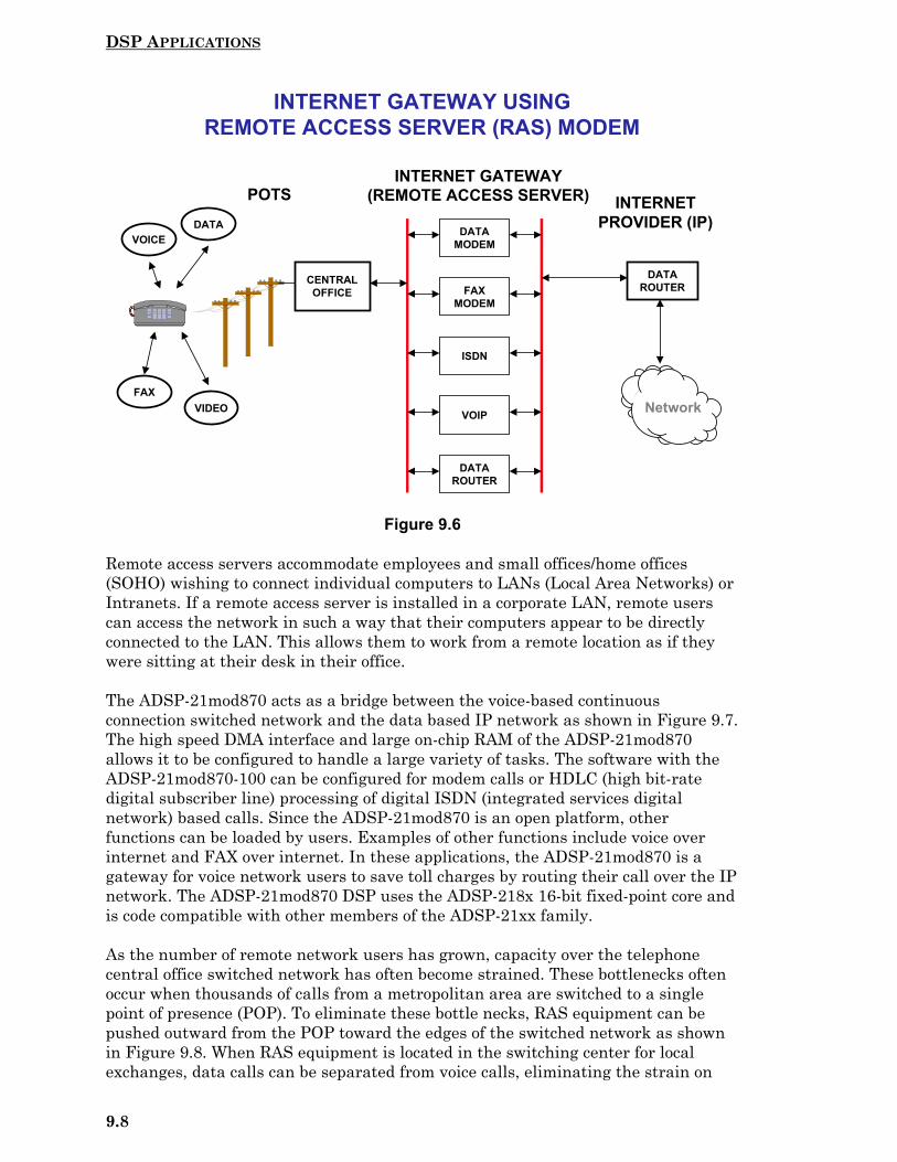
DSP APPLICATIONS
9.8
Figure 9.6
Remote access servers accommodate employees and small offices/home offices(SOHO) wishing to connect individual computers to LANs (Local Area Networks) orIntranets. If a remote access server is installed in a corporate LAN, remote userscan access the network in such a way that their computers appear to be directlyconnected to the LAN. This allows them to work from a remote location as if theywere sitting at their desk in their office.
The ADSP-21mod870 acts as a bridge between the voice-based continuousconnection switched network and the data based IP network as shown in Figure 9.7.The high speed DMA interface and large on-chip RAM of the ADSP-21mod870allows it to be configured to handle a large variety of tasks. The software with theADSP-21mod870-100 can be configured for modem calls or HDLC (high bit-ratedigital subscriber line) processing of digital ISDN (integrated services digitalnetwork) based calls. Since the ADSP-21mod870 is an open platform, otherfunctions can be loaded by users. Examples of other functions include voice overinternet and FAX over internet. In these applications, the ADSP-21mod870 is agateway for voice network users to save toll charges by routing their call over the IPnetwork. The ADSP-21mod870 DSP uses the ADSP-218x 16-bit fixed-point core andis code compatible with other members of the ADSP-21xx family.
As the number of remote network users has grown, capacity over the telephonecentral office switched network has often become strained. These bottlenecks oftenoccur when thousands of calls from a metropolitan area are switched to a singlepoint of presence (POP). To eliminate these bottle necks, RAS equipment can bepushed outward from the POP toward the edges of the switched network as shownin Figure 9.8. When RAS equipment is located in the switching center for localexchanges, data calls can be separated from voice calls, eliminating the strain on
INTERNET GATEWAY USINGREMOTE ACCESS SERVER (RAS) MODEM
Network
CENTRALOFFICE
DATAMODEM
FAXMODEM
ISDN
VOIP
DATAROUTER
DATAROUTER
VOICEDATA
FAXVIDEO
POTSINTERNET GATEWAY
(REMOTE ACCESS SERVER) INTERNETPROVIDER (IP)

DSP APPLICATIONS
9.9
the voice based switched network. RAS equipment integrated into switchingequipment is referred to on-switch based RAS. This differs for standalone RASsystems in that on-switch RAS can separate data calls before they are connected totrunk lines exiting the switch.
Figure 9.7
Figure 9.8
DATA MODEMFAX MODEM,
ISDN, VOIP
DSP-BASED RAS MODEM USING THEADSP-21modXXX - FAMILY
DATAMODEM
FAXMODEM
ISDN
VoIP
DATAROUTER
DATAROUTER
TRADITIONAL RAS MODEM DSP-BASED RAS MODEM
ADSP-21modXXX FAMILY
DATA MODEMFAX MODEM,
ISDN, VOIP
EXPANDING CENTRAL OFFICECAPABILITY WITH ADSP-21modXXX FAMILY
IPNetworkADSP-21modXXX
Modem Pool
LINE CARD
LINE CARD
LINE CARD
DATAROUTER
VOICEDATA
FAXVIDEO
LINE CARDS
VOICESWITCH
VoiceNetwork
DATA
VOICE
CENTRAL OFFICE SWITCH

DSP APPLICATIONS
9.10
Several types of RAS equipment have evolved to satisfy the needs of the differentremote network access users. RAS equipment can take several forms. RASconcentrators combine a modem pool with a router in a standalone chassis. NTserver RAS uses off the shelf Windows NT PCs to perform routing functions with amodem pool connected to its PCI or ISA expansion bus. On-switch RAS integratesmodem pools into the line card chassis in switching systems. These various forms ofRAS equipment serve the different needs of end users. Local Exchange Companies(LECs) or the new Competing Local Exchange Companies (CLECs) can takeadvantage of On-switch RAS equipment to eliminate bottle necks in their switchednetworks. ISPs (Internet Service Providers) use RAS concentrators to collect callsfrom a large area for connection to the Internet. Large business users also use RASconcentrators to connect their employees to their LAN or Intranets. Small office andhome office (SOHO) users can use low-cost NT Server based RAS to support all oftheir RAS, LAN, and other telecommunication needs.
The ADSP-21mod870 digital modem processor is the first complete digital RASmodem on a single chip. The device is V.34/56K and V.42/V.42bis compatible, has a16-bit DMA port for software downloads, provides TDM serial port interfacesdirectly to T1/E1, has 160Kbytes on-chip SRAM, dissipates 140mW at +3.3V, and ispackaged in a 16mm TQFP package. The ADSP-21mod870’s small footprint andpower efficiency will enable Internet Service Providers (ISPs) and central officeaccess providers to quadruple the number of ports within the existing modem bankchassis. Moreover, the chip’s unique capability to support any protocol on any portwill improve ISP customer service and reduce business operating costs.
Part of a family of digital modem solutions from ADI, the ADSP-21mod870 includessilicon, software and service. ADI is singular in its ability to provide the completesolution. Also available are the ADSP-21mod970 (six modem channels, 31mm BGA)and the ADSP-21mod980 (eight modem channels, 35mm BGA).
MULTI-CHANNEL VOICE-OVER-INTERNET-PROVIDER(VOIP) SERVER
The ADSP-218x family of devices can efficiently implement multi-channel telephonyapplications (such as RAS/VOIP servers and gateways) due to their highperformance and large on-chip memories. A typical system is shown in Figure 9.9.The programmable nature of the DSP architecture gives the system architect theflexibility to implement various speech coding algorithms in addition to baselinetelephony functionality.
The ADSP-2188M is the most highly integrated member of the 218x family (withover 2MBit of on-chip SRAM). This high level of integration combined with 75MIPSperformance can support up to 6 voice channels per DSP (depending on the voicecoder chosen).

DSP APPLICATIONS
9.11
Figure 9.9
ADSL (ASYMMETRIC DIGITAL SUBSCRIBER LINE)Thanks to the widespread popularity of the World Wide Web, Internet traffic is atan all-time high. A study recently conducted by the Wall Street Journal reported 58million Internet users in the United States and Canada alone. Research firms allpredict heavier Internet traffic as more and more people buy PCs and use theInternet for business, academia and recreational purposes.
Unless something is done to improve the way we access the Internet, user trafficwill ultimately burden the public switched telephone network (PSTN) beyond itsoriginal design limits. Internet users are frustrated by the amount of time it takesto view simple text-based Web sites, especially from 8:00 am to 6:00 pm on businessdays when congestion and bottlenecks are most prevalent. The problem will only getworse as users attempt to view graphically complex sites, download new video andaudio clips, and access other types of multimedia services becoming available overthe Internet.
Today's analog modem and telephone switch technology is simply inadequate.Assuming little or no network delays, a 10 Megabyte data transmission - theequivalent of a four-minute audio/video clip - takes about 95 minutes to downloadwhen using a 14.4 Kbps analog modem, 45 minutes when using a 28.8 Kbps modem,and 25 minutes when using a 56Kbps modem. Lengthy on-line calls are tying uptelephone systems originally designed to handle short (three-minute) voice calls and
ADSP-218x IMPLEMENTATION OF AMULTI-CHANNEL VOIP SERVER
Multi-Channel VoIP Server MIPS Program Memory Data MemoryG.723 annex A 18 8192 12288G.728 28 7200 2000G.729B 11.4 10240 5120G.711 .4 512 512DTMF Gen & Detect 1.9 300 400Call Discrimination 1.3 1536 300G.165 8 800 1024OS Kernal .2 512
Total N/A 29292 21644Source: ADI EstimatesBased on ADSP-218x
ADSP-2188M48K PM56K DM
That’s Supportfrom 4 to 6channels withroom to grow!
SRAM
T1/E1(PCM)
Interface
PowerManagement
10,100,10/100Base T/Ethernetand/orATM/
Frame Relay
RISCProcessor> 50MIPS
DRAM
SRAM
ADCDAC
TelephonyInterface
ADSP-218xDSP
PCM
or
POTS
or

DSP APPLICATIONS
9.12
switches built to accommodate approximately nine minutes per line during peakhours. How often do you browse the Internet for 10 minutes or less? It now appearsthat relief, in the form of ADSL (asymmetric digital subscriber line) technology, ison the way.
ADSL is a new high-speed digital switching/routing and signal processingtechnology. It promises to relieve network bottlenecks and provide enough userbandwidth for the Internet explosion. Originally conceived in 1994, ADSL deliversthe huge amounts of bandwidth needed for interactive gaming, multimedia servicesand video-on-demand. These applications, along with videoconferencing, remoteschooling and home shopping are still attractive applications. As more and morepeople use the Internet for electronic commerce in homes around the world, theneed for high-speed network access becomes ever more paramount.
ADSL can transfer data over ordinary telephone lines nearly 200 times faster thantoday's contemporary modems and 90 times faster than ISDN. Early tests and trialshave shown promising results all over the world. And while GTE and other largetelephone companies begin to deploy ADSL systems in select regions of the US andabroad, others seek to deploy ADSL-based equipment in 1999 as standards-basedsystems and modems become commercially available.
Due to ADSL's technical complexity, only a few semiconductor manufacturers arepresently developing ADSL silicon chips. Analog Devices is one of them, and isconsidered a pioneer in ADSL after having produced the first complete ADSLchipset back in 1997. Early adopters of ADSL rallied behind the AD20msp910chipset after having successfully evaluated its high-speed, long reach capability.Soon thereafter, the world's most influential industry standards committees (ANSI,ETSI and ITU) approved an advanced discrete multi-tone (DMT) signal processingtechnique used by the AD20msp910. Today, Analog Devices enjoys the advantagesof having the industry's first standards-based solution, the largest installedcustomer base, and the most design wins of any semiconductor manufacturer todate.
ADSL is attractive for the following reasons:
• ADSL is fast. The same 10 MB video clip that takes 90 minutes to downloadusing a conventional modem would be downloaded in just 10 seconds usingan ADSL modem. Superfast ADSL modems can transmit data at rates ashigh as 8 megabits per second.
• ADSL is easy to install. It uses existing copper twisted-pair telephone linesfrom a local exchange carrier (central office) to the subscriber's home oroffice. Little or no rewiring is necessary.
• ADSL is cost-effective. It requires no major upgrades in the existingtelephone network infrastructure.
• ADSL is viable. Issues that have slowed the deployment of high-speed fibernetworks to the home (e.g., prohibitive cost and installation) do not apply.ADSL works with existing POTS (plain-old telephone service). High-speeddata transport can occur simultaneously with voice calls and faxtransmissions.

DSP APPLICATIONS
9.13
Unlike other high-speed data transmission technologies, ADSL requires no rewiringover the "last mile" of the network. Although commonly referred to as the last mile,transmission length is typically 12,000 to 18,000 feet. That "last mile" (the leg fromthe central office to a user's home or office) operates over existing copper loops oftwisted-pair telephone wires. But ADSL does require the installation of newequipment at local exchange central offices and major switch offices. However, thetechnology developed for central office equipment is the same as that used in PCmodems and home splitter boxes, thus ensuring interoperability throughout theentire network. A simplified block diagram of an ADSL system is shown in Figure9.10.
Figure 9.10
Using sophisticated digital signal processing techniques, ADSL modems push asmuch data as possible across copper wires by making the best use of availablebandwidth. Many perceived the telephone network is as having only 4 kHz ofbandwidth, but 4 kHz only represents the band used for the analog (voice)transmission. Using ADSL, the physical connection between the home and localexchange carrier (LEC) over conventional copper wire is capable of carrying 1 MHz.ADSL takes advantage of the portion of the bandwidth not used for voice calls.Essentially, it splits the 1 MHz bandwidth into three information channels: onehigh-speed downstream channel, one medium-speed duplex (upstream/downstream)channel, and one conventional voice channel. (Downstream refers to datatransmitted from the telephone network to the customer's premises; upstream isdata routed from the customer to the network.)
In addition to providing high bandwidth data transmission, ADSL preserves"lifeline" services (i.e., the voice network that people depend upon for day-to-daycommunications and emergency situations). This three-channel approach allows
ASYMMETRIC DIGITAL SUBSCRIBER LINE (ADSL)SYSTEM CHARACTERISTICS
PC ORNETWORKCOMPUTER
TELEPHONE FAX
ADSL MODEM
POTSSPLITTER
POTSSPLITTER
VOICESWITCH
ADSLMODEMBANK
VoiceNetwork
DATAROUTER
Internet
Single PairTwisted Wiree.g. 12,000 ft
HOME CENTRAL OFFICE
8 Mbps
640 Kbps
THE“LAST MILE”
8Mbps Downstream Channel 640Kbps Upstream/Downstream Channel 1 Telephone Channel
1MHz BANDWIDTH
DSP APPLICATIONS
9.14
subscribers to send an email, download a video for viewing, and talk on thetelephone-all at the same time. Telecommuters can access their corporate local areanetwork, and simultaneously videoconference with a customer. In fact, usingADSL's full capability provides enough bandwidth for running four channels ofMPEG compressed video with no interruption to normal telephone service.
Most Internet applications require uneven amounts of upstream and downstreambandwidth. In other words, users tend to move greater amounts of data in onedirection than they do in the other direction. Generally speaking, Internet usersaccess more information and receive more data than they transmit. That's thenature of the Internet. They read more electronic mail than they send...theydownload more video information than they produce. A user's upstream capacity istypically limited to sending commands or transmitting small data files to a server.Much more information travels downstream. ADSL was designed to take advantageof this trend in uneven bandwidth. It provides data rates in excess of 8 Mbps fromthe network to the subscriber (downstream), and up to 640 Kbps from thesubscriber to the network (upstream).
For telephone companies, ADSL may be the key to overcoming the congestioncreated by explosive Internet growth. If telephone companies hope to capture theInternet data carrier market, they can't use equipment designed for short voicetraffic. The average voice call lasts about three minutes. According to a 1997 studyby Bellcore, the research laboratory funded by US local telephone companies, (one offive submitted to the Federal Communications Commission) the average length oftime for a typical Internet call is now in excess of 20 minutes. Telephony magazinereported as early as 1994 that nearly 20 percent of all on-line data serviceconnections lasted more than an hour. Cable companies like MediaOne, based in theNortheast, charge one flat rate for Internet use. "Broadband" subscribers can stayon line 24-hours a day for roughly $40 a month.
ADSL was designed to take advantage of this natural unevenness in bandwidthrequirements and make the most of available bandwidth, a limited resource. Itprovides for rates in excess of 8 Mbps from the network to the subscriber, and up to640 Kbps from the subscriber to the network.
While some other telephony-based technologies offer relief for the PSTN, manycarry high price tags and long-term implementation time frames. Replacing thecopper network with fiber to the curb, for example, is a costly proposition. Industryexperts estimate that creating a fiber-to-the-curb network will cost about $1,500 pertelephone customer. Replacing the existing 560 million copper subscriber linesworldwide would cost more than three-quarters of a trillion dollars.
ADSL, by contrast, is easily installed. To complete an ADSL circuit, two modemsare required, one at each end of a twisted-pair telephone line. One modem is locatedat the subscriber's premise; the other modem (usually a rack of modems with linecards) is located at the local telephone company's central office. Figure 9.10 shows asimplified connection.
At the customer premise, an ADSL modem is inside a PC or connected to thenetwork computer, as well as the telephone and/or facsimile machine. A coppertwisted pair telephone line links the POTS splitter to the central office. At the
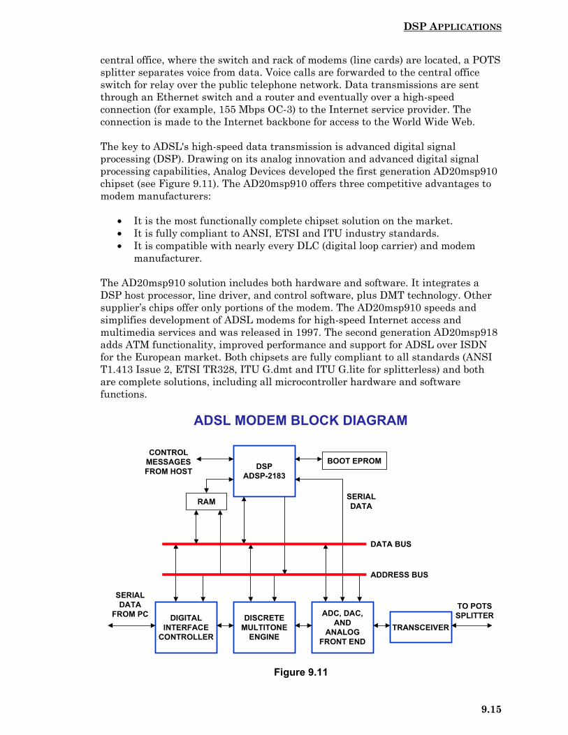
DSP APPLICATIONS
9.15
central office, where the switch and rack of modems (line cards) are located, a POTSsplitter separates voice from data. Voice calls are forwarded to the central officeswitch for relay over the public telephone network. Data transmissions are sentthrough an Ethernet switch and a router and eventually over a high-speedconnection (for example, 155 Mbps OC-3) to the Internet service provider. Theconnection is made to the Internet backbone for access to the World Wide Web.
The key to ADSL's high-speed data transmission is advanced digital signalprocessing (DSP). Drawing on its analog innovation and advanced digital signalprocessing capabilities, Analog Devices developed the first generation AD20msp910chipset (see Figure 9.11). The AD20msp910 offers three competitive advantages tomodem manufacturers:
• It is the most functionally complete chipset solution on the market.• It is fully compliant to ANSI, ETSI and ITU industry standards.• It is compatible with nearly every DLC (digital loop carrier) and modem
manufacturer.
The AD20msp910 solution includes both hardware and software. It integrates aDSP host processor, line driver, and control software, plus DMT technology. Othersupplier’s chips offer only portions of the modem. The AD20msp910 speeds andsimplifies development of ADSL modems for high-speed Internet access andmultimedia services and was released in 1997. The second generation AD20msp918adds ATM functionality, improved performance and support for ADSL over ISDNfor the European market. Both chipsets are fully compliant to all standards (ANSIT1.413 Issue 2, ETSI TR328, ITU G.dmt and ITU G.lite for splitterless) and bothare complete solutions, including all microcontroller hardware and softwarefunctions.
Figure 9.11
ADSL MODEM BLOCK DIAGRAM
DIGITALINTERFACE
CONTROLLER
DISCRETEMULTITONE
ENGINE
ADC, DAC,AND
ANALOGFRONT END
TRANSCEIVER
SERIALDATA
FROM PC
DSPADSP-2183
ADDRESS BUS
DATA BUS
SERIALDATA
CONTROLMESSAGESFROM HOST
RAM
BOOT EPROM
TO POTSSPLITTER

DSP APPLICATIONS
9.16
Now on our third generation chipset, the AD20msp930, Analog Devices enablesmodem manufacturers to reduce their development time and costs. To further speedand streamline design efforts, Analog Devices will also provide a PC board layout,schematics, and a reference design. As a result, modem manufacturers can focustheir development efforts on adding value to the core ADSL modem technology.
DIGITAL CELLULAR TELEPHONESIn the early 1990s, the GSM (Global System for Mobile Communications akaGroupe Speciale Mobile) was introduced in Europe heralding the introduction ofdigital cellular radio. Out of necessity, other countries, including the US, haveadopted various digital standards in order to relieve the congestion and otherproblems faced by analog cellular systems such as AMPS (Advanced Mobile PhoneService). The limitations of analog cellular radio are well known and include callblocking during busy hours, misconnects and disconnects due to rapidly fadingsignals, lack or privacy and security, and limited data transmission rates.
The basic cellular system is shown in Figure 9.12. A region is broken up into cells,with each cell having its own base station and its own group of assignedfrequencies. Because the radius of each cell is small (10 miles, for example) lowpower transmitters and receivers can be used.
Figure 9.12
CELLULAR PHONE FREQUENCY REUSE
FREQGROUP
B
FREQGROUP
C
FREQGROUP
DFREQGROUP
E
FREQGROUP
B
FREQGROUP
A
FREQGROUP
G
FREQGROUP
C
FREQGROUP
G
FREQGROUP
F FREQGROUP
F
FREQGROUP
E
FREQGROUP
G
FREQGROUP
C
FREQGROUP
E
FREQGROUP
B
FREQGROUP
A
Each Cell Covers a Radius of 5 to 10 miles Each Cell Requires its own Basestation for Reception and Re-Transmission Each Cell Must Handle Multiple Callers Simultaneously Callers May Be Handed Off from One Cell to Another

DSP APPLICATIONS
9.17
The cellular system lends itself to frequency reuse, since cells which are far enoughapart can utilize the same band of frequencies without interference. The basestations must be linked together with an elaborate central control network so that acall may be handed-off to another cell when the signal strength from the mobile unitbecomes too low for the current cell to handle.
The frequency spectrum allocation for analog cellular radio (AMPS) in the UnitedStates is approximately 825 to 850MHz and 870 to 895MHz. Conventionalarchitectures (both analog and digital) are channelized. The total spectrum isdivided up into a large number of relatively narrow channels, defined by a carrierfrequency. The carrier frequency is frequency-modulated with the voice signal usinganalog techniques. Each full-duplex channel requires a pair of frequencies, eachwith a bandwidth of approximately 30kHz. A user is assigned both frequencies forthe duration of the call. The forward and reverse channel are widely separated, tohelp the radio keep the transmit and receive functions separated. The signalbandwidth for the “A” or “B” carriers serving a particular geographical area is12.5MHz (416 channels, each 30kHz wide). There can only be one caller at a timeper channel.
Time Division Multiple Access (TDMA) allocates bandwidth on a time-slot basis. Inthe United States TDMA system, the entire 30kHz channel is assigned to aparticular transmission, but only for a short period of time. A 3:1 multiplexingscheme means that three conversations can take place with TDMA using the sameamount of bandwidth as one analog cellular conversation does. Eachtransmit/receive sequence occurs on time slots lasting 6.7ms. The TDMA systemrelies on an extensive amount of DSP technology to reduce the coded speech bit-rateas well as to prepare the digital data for transmission over the analog medium. TheTDMA approach was chosen for the GSM system and will be discussed later in moredetail.
The second digital approach used in the United States is called Code DivisionMultiple Access (CDMA). This technique has been used in secure militarycommunications for a number of years under the name of spread spectrum. Inspread spectrum, the transmitter transmits in a pseudo-random sequence offrequency hops over a relatively wide frequency range. The receiver has access tothe same random sequence and can decode the transmission. The effect of addingadditional users on the system is to decrease the overall signal to noise ratio for allthe users. With this technique, the effect of allowing more calls than the normalcapacity is to increase the bit-error rate for all users. New callers can keep comingin, interference levels will rise gradually, until at some point the process willbecome self-regulating: the quality of the voice link will become so bad that userswill cut short or refrain from making additional calls. No one is ever blocked in theconventional sense, as they are in FDMA or TDMA systems when all channels orslots are full.
Both TDMA and CDMA digital systems make extensive use of DSP algorithms inboth speech encoding and in preparing the signal for transmission. In the receiver,DSP techniques are used for demodulation and decoding the speech signal.
At the present time, both the analog and digital systems are in use in the US. Inmany cases, analog and digital systems must co-exist in the same geographical area

DSP APPLICATIONS
9.18
and within the same service area. This implies that the cellular basestations musthandle both analog and digital formats, and therefore there is extensive use ofdigital techniques in basestation design to simplify the hardware.
The remainder of this section will concentrate on speech processing and channelcoding as they relate to the GSM system. This will serve to illustrate thefundamental principles which are applicable to all digital mobile radio systems.
Figure 9.13
The GSM System
Figure 9.14 shows a simplified block diagram of the GSM Digital Cellular TelephoneSystem. The speech encoder and decoder and discontinuous transmission functionwill be described in detail. Up conversion and downconversion portions of thesystem contain a digital modem similar to the ones previously discussed. Similarfunctions are performed digitally such as equalization, convolutional coding, Viterbidecoding, modulation and demodulation.
The standard for encoding voice has been set in the T-Carrier digital transmissionsystem. In this system, speech is logarithmically encoded to 8 bits at a samplingrate of 8kSPS. The logarithmic encoding and decoding to 8 bits is equivalent tolinear encoding and decoding to 13 bits of resolution. This produces a bit-rate of104kb/s. In most handsets, a 16-bit sigma-delta ADC is used, so the effective bit-rate is 128kb/s. The Speech Encoder portion of the GSM system compresses thespeech signal to 13kb/s, and the decoder expands the compressed signal at thereceiver. The speech encoder is based on an enhanced version of linear predictivecoding (LPC). The LPC algorithm uses a model of the human vocal tract thatrepresents the throat as a series of concentric cylinders of various diameters. Anexcitation (breath) is forced into the cylinders. This model can be mathematicallyrepresented by a series of simultaneous equations which describe the cylinders.
DIGITAL MOBILE RADIO STANDARDS
Frequency Division Multiple Access (FDMA) - User Allocationbased on Frequency Slots (AMPS System)
Time Division Multiple Access (TDMA) - User Allocation Based onTime Slots (At least 3X More Capacity than FDMA) GSM is anExample of TDMA
Code Division Multiple Access (CDMA) - Based on SpreadSpectrum Technology - More Users Cause Graceful Degradationin Bit-Error Rate
Both TDMA and CDMA make Extensive Use of DSP in SpeechEncoding and Channel Coding for Transmission and Reception

DSP APPLICATIONS
9.19
Figure 9.14
The excitation signal is passed through the cylinders, producing an output signal. Inthe human body, the excitation signal is air moving over the vocal cords or througha constriction in the vocal tract. In a digital system, the excitation signal is a seriesof pulses for vocal excitation, or noise for a constriction. The signal is input to adigital lattice filter. Each filter coefficient represents the size of a cylinder.
An LPC system is characterized by the number of cylinders it uses in the model.Eight cylinders are used in the GSM system, and eight reflection coefficients mustbe generated.
Early LPC systems worked well enough to understand the encoded speech, but oftenthe quality was too poor to recognize the voice of the speaker. The GSM LPC systememploys two advanced techniques that improve the quality of the encoded speech.These techniques are regular pulse excitation (RPE) and long term prediction (LTP).When these techniques are used, the resulting quality of encoded speech is nearlyequal to that of logarithmic pulse code modulation (companded PCM as in the T-Carrier system).
GSM HANDSET BLOCK DIAGRAM
ADCLPC AND
SHORT TERMANALYSIS
LONG TERMPREDICTION
COEFFICIENT AVERAGING FORCOMFORT NOISE INSERTION
VOICE ACTIVITYDETECTOR
DISCONTINUOUSTRANSMISSION
CONTROL
ADD ERRORCORRECTION &
REDUNDANCY BITS
UPCONVERT
RF AMP
×
RFINPUT
DOWNCONVERT
REMOVE ERRORCORRECTION &
REDUNDANCY BITS
DISCONTINUOUSTRANSMISSION
CONTROL
COMFORT NOISE INSERTION PSEUDO RANDOM EXCITATION
SHORT TERMSYNTHESIS
LONG TERMPREDICTION
DAC
DTMFDIALING
PHONE NUMBERDISPLAY
13Kbits/s
13Kbits/s
128Kbits/s
128Kbits/s
SPEECH ENCODER
SPEECH DECODER
TRANSMIT FUNCTIONS
RECEIVE FUNCTIONS
VOICEFLAG
MICROPHONE
SPEAKER
DSP APPLICATIONS
9.20
The actual input to the speech encoder is a series of 16-bit samples of uniform PCMspeech data. The sampling rate is 8kHz. The speech encoder operates on a 20mswindow (160 samples) and reduces it to 76 coefficients (260 bits total), resulting inan encoded data rate of 13kb/s.
Discontinuous transmission (DTX) allows the system to shut off transmissionduring the pauses between words. This reduces transmitter power consumption andincreases the overall GSM system's capacity.
Low power consumption prolongs battery life in the handset and is an importantconsideration for hand-held portable phones. Call capacity is increased by reducingthe interference between channels, leading to better spectral efficiency. In a typicalconversation each speaker talks for less than 40% of the time, and it has beenestimated that DTX can approximately double the call capacity of the radio system.
The voice activity detector (VAD) is located at the transmitter. Its job is todistinguish between speech superimposed on the background noise and noise withno speech present. The input to the voice activity detector is a set of parameterscomputed by the speech encoder. The VAD uses this information to decide whetheror not each 20ms frame of the encoder contains speech.
Comfort noise insertion (CNI) is performed at the receiver. The comfort noise isgenerated when the DTX has switched off the transmitter; it is similar in amplitudeand spectrum to the background noise at the transmitter. The purpose of the CNI isto eliminate the unpleasant effect of switching between speech with noise, andsilence. If you were listening to a transmission without CNI, you would hear rapidalternating between speech in a high-noise background (i.e. in a car), and silence.This effect greatly reduces the intelligibility of the conversation.
When DTX is in operation, each burst of speech is transmitted followed by a silencedescriptor (SID) frame before the transmission is switched off. The SID serves as anend of speech marker for the receive side. It contains characteristic parameters ofthe background noise at the transmitter, such as spectrum information derivedthrough the use of linear predictive coding.
The SID frame is used by the receiver's comfort noise generator to obtain a digitalfilter which, when excited by pseudo-random noise, will produce noise similar to thebackground noise at the transmitter. This comfort noise is inserted into the gapsbetween received speech bursts. The comfort noise characteristics are updated atregular intervals by the transmission of SID frames during speech pauses.
Redundant bits are then added by the processor for error detection and correction atthe receiver, increasing the final encoded bit rate to 22.8kb/s. The bits within onewindow, and their redundant bits, are interleaved and spread across severalwindows for robustness.

DSP APPLICATIONS
9.21
GSM HANDSET USING SOFTFONE™ BASEBANDPROCESSOR AND OTHELLO™ RADIO
Analog Devices recently announced two chipsets which comprise the majority of aGSM handset. The SoftFone™ chipset performs the baseband and DSP functions,while the Othello™ radio chipset handles the RF functions.
The frequency bands originally allocated to GSM were 890MHz to 915MHz formobile transmitting and 935MHz to 960MHz for mobile receiving. Anotherfrequency allocation was made to further expand GSM capacity. This band,allocated to digital communications services (DCS), was 1710MHz to 1785MHz and1805MHz to 1880MHz. All countries adopting GSM use one of these two pairs offrequencies. In the United States, these bands were already allocated by the FCC.In the mid-1990s, a set of bands were made available for GSM in the United States:1850MHz to 1910MHz, and 1930MHz to 1990MHz.
Because of the frequency allocations in GSM countries (other than the U.S.), mostGSM handsets must be dual-band: capable of handling both GSM and DCSfrequencies. The SoftFone and Othello chipsets supply the main functions necessaryfor implementing dual- or triple-band radios for GSM cellular phones. TheAD20msp430 SoftFone™ chipset comprises the baseband portion of the GSMhandset. The AD20msp430 baseband processing chipset uses a combination of GSMsystem knowledge and advanced analog and digital signal processing technology toprovide a new benchmark in GSM/GPRS terminal design.
The SoftFone architecture is entirely RAM-based. The software is loaded fromFLASH memory and is executed from the on-chip RAM. This allows fastdevelopment cycles since no ROM-code turns are required. Furthermore, thehandset software can be updated in the field to enable new features. Combined withthe Analog Devices “Othello” RF chipset, a complete multiband handset designcontains less than 200 components, fits in a 20 cm2 single sided PCB layout, andhas a total bill-of-materials cost 20-30% lower than previous solutions. A simplifiedblock diagram of the handset is shown in Figure 9.15.
The AD20msp430 chipset is comprised of two chips, the AD6522 DSP-basedbaseband processor and the AD6521 voiceband/baseband mixed-signal codec.Together with the “Othello ” radio chipset, the AD20msp430 allows a significantreduction in the component count and bill-of-materials (BOM) cost of GSM voicehandsets and data terminals. The software and hardware foundations of theAD20msp430 chipset enjoy a long history of successful integration into GSMhandsets.

DSP APPLICATIONS
9.22
Figure 9.15
This is Analog Devices’ 4th generation of GSM chipsets, each of which has passednumerous type- approvals and network operator approvals in OEM handsets. Ineach generation, additional features have been added, while cost and power havebeen reduced. Numerous power-saving features have been included in theAD20msp430 chipset to reduce the total power consumption. A programmable statemachine allows events to be controlled with a resolution of one-quarter of a bitperiod. This reduces current in standby mode to 1mA. This allows a handset tooperate in standby mode for up to 1000 hours on a battery charge. The AD20msp430chipset uses the SoftFone™ architecture, where all software resides in RAM orFLASH memory. Since ROM is not used, development time is reduced andadditional features can be field-installed easily. A basic dual-band GSM terminaltypically requires a single 8Mb FLASH memory chip.
There are two processors in the AD20msp430 chipset. The DSP processor is theADSP-218x core, proven in previous generations of GSM chipsets, and operated at65MIPS in the AD20msp430. This DSP performs the voiceband and channel codingfunctions previously discussed. The AD6521 voiceband/baseband codec chip containsall analog and mixed-signal functions. These include the I/Q channel ADCs andDACs, high performance multichannel voiceband codec, and several auxiliary ADCsand DACs for AGC (automatic gain control), AFC (automatic frequency control),andpower- amplifier ramp control. The microcontroller is an ARM7 TDMI, running at39MIPS. The ARM7 handles the protocol stack and the man-machine interfacefunctions. Both processors are field-proven in digital wireless applications.
OTHELLO™ RADIO AND SOFTPHONE™ CHIPSETSMAKE COMPLETE GSM/DCS HANDSET
DSPMEMORY
DMA
1 MbitSRAM
ADSP-218xDSP
I/O
ARM7®CONTROLLER
AUXILIARYADC, DAC
BASEBAND I/QADC, DAC
VOICEBANDCODEC
DIRECTCONVERSION
RADIO
MULTIBANDSYNTHESIZER
PA
POWERCONTROL
AD6522 AD6521
FLA
SHM
EMO
RY
AD6523
AD6524
ADP33xxADP34xx
POWER MANAGEMENTBATTERY CHARGING
AD20msp430 SOFTFONE™ CHIPSET OTHELLO™ RADIO
DISPLAY SIM KEYPAD
900MHz/1.8GHz
MICSPEAKER

DSP APPLICATIONS
9.23
The AD20msp430 chipset is fully supported by a suite of development tools andsoftware. The development tools allow easy customization of the DSP and/or ARM®controller software to allow handset and terminal manufacturers to optimize thefeature set and user interface of the end equipment. Software is available fromAnalog Devices’ software partner TTPCom for all layers, including both voice anddata applications, and is updated as new features become available. The systemDMA and interrupt controllers are designed to allow easy upgrades to futuregenerations of DSP and controller cores. The display interface can be used witheither parallel or serial-interface displays. System development can be shortened bythe use of the debugging features in the AD20msp430. Most critical signals can berouted under software control to the Universal System Connector. This allowssystem debugging to take place in the final form factor. In addition, the architectureincludes high speed logger and address trace functions in the DSP and single-wiretrace/debug in the ARM controller.
Analog Devices recently announced the revolutionary Othello™ direct-conversionradio for mobile applications. By eliminating intermediate-frequency (IF) stages,this chip set will permit the mobile electronics industry to reduce the size and costof radio sections and enable flexible, multi-standard, multi-mode operation. Theradio consists of two integrated circuits, the AD6523 Zero-IF Transceiver and theAD6524 Multi-Band Synthesizer.
The AD6523 contains the main functions necessary for both a direct-conversionreceiver and a direct VCO transmitter, known as the Virtual-IF™ transmitter. Italso includes the local-oscillator generation block and a complete on-chip regulatorthat supplies power to all active circuitry for the radio. The AD6524 is a fractional-N synthesizer that features extremely fast lock times to enable advanced dataservices over cellular telephones-such as high-speed circuit-switched data (HSCSD)and general packet radio services (GPRS).
Most digital cellular phones today include at least one "downconversion" in theirsignal chain. This frequency conversion shifts the desired signal from the allocatedRF band for the standard (say, at 900 MHz) to some lower intermediate frequency(IF), where channel selection is performed with a narrow channel-select filter(usually a surface acoustic-wave (SAW) or a ceramic type). The now-filtered signalis then further down-converted to either a second IF or directly to baseband, whereit is digitized and demodulated in a digital signal processor (DSP). Figure 9.16shows the comparison between this superheterodyne architecture and thesuperhomodyne™ architecture of the Othello radio receiver.
The idea of using direct-conversion for receivers has long been of interest in RFdesign. The reason is obvious: in consumer equipment conversion stages add cost,bulk, and weight. Each conversion stage requires a local oscillator, (often includinga frequency synthesizer to lock the LO onto a given frequency), a mixer, a filter, and(possibly) an amplifier. No wonder, then, that direct conversion receivers would beattractive. All intermediate stages are eliminated, reducing the cost, volume, andweight of the receiver.

DSP APPLICATIONS
9.24
Figure 9.16
The Othello™ radio reduces the component count even more by integrating thefront-end GSM low-noise amplifier (LNA). This eliminates an RF filter (the "image"filter) that is necessary to eliminate the image, or unwanted mixing product of amixer and the off chip LNA. This stage, normally implemented with a discretetransistor, plus biasing and matching networks, accounts for a total of about 12components. Integrating the LNA saves a total of about 15 to 17 components,depending on the amount of matching called for by the (now-eliminated) filter.
A functional block diagram of the Othello™ dual band GSM radio's architecture isshown in Figure 9.17. The receive section is at the top of the figure. From theantenna connector, the desired signal enters the transmit/receive switch and exitson the appropriate path, either 925-960 MHz for the GSM band or 1805-1880 MHzfor DCS. The signal then passes through an RF band filter (a so-called "roofingfilter") that serves to pass the entire desired frequency band while attenuating allother out-of-band frequencies (blockers-including frequencies in the transmissionband) to prevent them from saturating the active components in the radio front end.The roofing filter is followed by the low-noise amplifier (LNA). This is the first gainelement in the system, effectively reducing the contribution of all following stages tosystem noise. After the LNA, the direct-conversion mixer translates the desiredsignal from radio frequency (RF) all the way to baseband by multiplying the desiredsignal with a local oscillator (LO) output at the same frequency.
DIRECT CONVERSION RECEIVERARCHITECTURE ELIMINATES COMPONENTS
BPF BPF
VCO
PLL
BPF
VCO
PLL
IADC
QADC
sin
cosCERAMIC CERAMIC
SAW
BPF
VCO PLL
IADC
QADC
sin
cos
SAW
GSM900MHz
DCS1.8
GHz
BPF BPF
CERAMIC CERAMIC
GSM900MHz
DCS1.8
GHz
BPF
SAW
SW
SW
IF
SUPERHETERODYNE
DIRECT CONVERSION (SUPERHOMODYNE™)
LNA
LNA
LNA
LNA

DSP APPLICATIONS
9.25
Figure 9.17
The output of the mixer stage is then sent in quadrature (I and Q channels) to thevariable-gain baseband amplifier stage. The VGA also provides some filtering ofadjacent channels, and attenuation of in-band blockers. These blocking signals areother GSM channels that are some distance from the desired channel, say 3 MHzand beyond. The baseband amplifiers filter these signals so that they will notsaturate the Receive ADCs. After the amplifier stage, the desired signal is digitizedby the Receive ADCs.
The Transmit section begins on the right, at the multiplexed I and Qinputs/outputs. Because the GSM system is a time division duplex (TDD) system,the transmitter and receiver are never on at the same time. The Othello™ radioarchitecture takes advantage of this fact to save four pins on the transceiver IC'spackage. The quadrature transmit signals enter the transmitter through themultiplexed I/Os. These I and Q signals are then modulated onto a carrier at anintermediate frequency greater than 100 MHz.
The output of the modulator goes to a phase-frequency detector (PFD), where it iscompared to a reference frequency that is generated from the external channelselecting LO. The output of the PFD is a charge pump, operating at above 100 MHz,whose output is filtered by a fairly wide (1MHz) loop filter. The output of the loopfilter drives the tuning port of a voltage-controlled oscillator (VCO), with frequencyranges that cover the GSM and DCS transmit bands.
SUPERHOMODYNE™ DIRECT CONVERSION DUAL-BANDTRANSCEIVER USING THE AD6523/AD6524 CHIPSET
BPF(SAW)
BPF(SAW)
LOGENERATOR
DIV N
PHASEDETECTVCO DIV M
TX/RXSWITCH
VCO
PLLAD6524
IADC
QADC
IDAC
QDAC
PAΣΣΣΣ
GSM/DCS
AD6523
SW
BPF
BPF
LNA
VGA
VGA

DSP APPLICATIONS
9.26
The output of the transmit VCO is sent to two places. The main path is to thetransmit power amplifier (PA), which amplifies the transmit signal from about+3dBm to +35dBm, sending it to the transmit/receive switch and low pass filter(which attenuates power-amplifier harmonics). The power amplifiers are dual band,with a simple CMOS control voltage for the band switch. The VCO output also goesto the transmit feedback mixer by means of a coupler, which is either a printedcircuit, built with discrete inductors and capacitors, or a monolithic (normallyceramic) coupling device. The feedback mixer downconverts the transmit signal tothe transmit IF, and uses it as the local oscillator signal for the transmit modulator.This type of modulator has several names, but the most descriptive is probably"translation loop". The translation loop modulator takes advantage of one keyaspect of the GSM standard: the modulation scheme is Gaussian-filtered minimum-shift keying (GMSK). This type of modulation does not affect the envelopeamplitude, which means that a power amplifier can be saturated and still notdistort the GMSK signal sent through it.
GMSK can be generated in several different ways. In another European standard(for cordless telephones), GMSK is created by directly modulating a free running-VCO with the Gaussian filtered data stream. In GSM, the method of choice hasbeen quadrature modulation. Quadrature modulation creates accurate phaseGMSK, but imperfections in the modulator circuit (or up-conversion stages) canproduce envelope fluctuations, which can in turn degrade the phase trajectory whenamplified by a saturated power amplifier. To avoid such degradations, GSM phonemakers have been forced to use amplifiers with somewhat higher linearity, at thecost of reduced efficiency and talk time per battery charge cycle.
The translation loop modulator combines the advantages of directly modulating theVCO and the inherently more accurate quadrature modulation. In effect, thescheme creates a phase locked loop (PLL), comprising the modulator, the LO signal,and the VCO output and feedback mixer. The result is a directly modulated VCOoutput with a perfectly constant envelope and almost perfect phase trajectory.Phase trajectory errors as low as 1.5 degrees have been measured in the AD6523transceiver IC, using a signal generator as the LO signal to provide a reference forthe loop.
Because Othello™ radios can be so compact, they enable GSM radio technology tobe incorporated in many products from which it has been excluded, such as verycompact phones or PCMCIA cards. However, the real power of direct conversion willbe seen when versatile third-generation phones are designed to handle multiplestandards. With direct-conversion, hardware channel-selection filters will beunnecessary, because channel selection is performed in the digital signal-processingsection, which can be programmed to handle multiple standards. Contrast this withthe superheterodyne architecture, where multiple radio circuits are required tohandle the different standards (because each will require different channel-selectionfilters), and all the circuits will have to be crowded into a small space. With directconversion, the same radio chain could in concept be used for several differentstandards, bandwidths, and modulation types. Thus, Web-browsing and voiceservices could, in concept, occur over the GSM network using the same radio in thehandset.

DSP APPLICATIONS
9.27
ANALOG CELLULAR BASESTATIONS
Consider the analog superheterodyne receiver invented in 1917 by Major Edwin H.Armstrong (see Figure 9.18). This architecture represented a significantimprovement over single-stage direct conversion (homodyne) analog receivers whichhad previously been constructed using tuned RF amplifiers, a single detector, andan audio gain stage. (Note that the homodyne technique has now gained favor inDSP-based receivers as explained above). A significant advantage of thesuperhetrodyne analog receiver is that it is much easier and more economical tohave the gain and selectivity of a receiver at fixed intermediate frequencies (IF)than to have the gain and frequency-selective circuits "tune" over a band offrequencies.
Figure 9.18
The frequencies shown in Figure 9.18 correspond to the AMPS (Advanced MobilePhone Service) analog cellular phone system currently used in the U.S. The receiveris designed for AMPS signals at 900MHz RF. The signal bandwidth for the "A" or"B" carriers serving a particular geographical area is 12.5MHz (416 channels, each30kHz wide). The receiver shown uses triple conversion, with a first IF frequency of70MHz, a second IF of 10.7MHz, and a third of 455kHz. The image frequency at thereceiver input is separated from the RF carrier frequency by an amount equal totwice the first IF frequency (illustrating the point that using relatively high first IFfrequencies makes the design of the image rejection filter easier).
The output of the third IF stage is demodulated using analog techniques(discriminators, envelope detectors, synchronous detectors, etc.). In the case ofAMPS the modulation is FM. An important point to notice about the above scheme
U.S. ADVANCED MOBILE PHONE SERVICE (AMPS)SUPERHETERODYNE ANALOG BASESTATION RECEIVER
SAME AS ABOVECHANNEL n
RF
BPF
LNA LO1TUNED 70MHz
1ST IF 2ND IF 3RD IF
10.7MHz 455kHzLO2
FIXEDLO3
FIXED ANALOG
DEMOD,FILTER
AMPS: 416 CHANNELS ("A" OR "B" CARRIER)30kHz WIDE, FM12.5MHz TOTAL BANDWIDTH1 CALLER/CHANNEL
CHANNEL 1
30 kHz
30 kHz
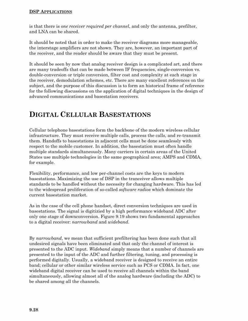
DSP APPLICATIONS
9.28
is that there is one receiver required per channel, and only the antenna, prefilter,and LNA can be shared.
It should be noted that in order to make the receiver diagrams more manageable,the interstage amplifiers are not shown. They are, however, an important part ofthe receiver, and the reader should be aware that they must be present.
It should be seen by now that analog receiver design is a complicated art, and thereare many tradeoffs that can be made between IF frequencies, single-conversion vs.double-conversion or triple conversion, filter cost and complexity at each stage inthe receiver, demodulation schemes, etc. There are many excellent references on thesubject, and the purpose of this discussion is to form an historical frame of referencefor the following discussions on the application of digital techniques in the design ofadvanced communications and basestation receivers.
DIGITAL CELLULAR BASESTATIONS
Cellular telephone basestations form the backbone of the modern wireless cellularinfrastructure. They must receive multiple calls, process the calls, and re-transmitthem. Handoffs to basestations in adjacent cells must be done seamlessly withrespect to the mobile customer. In addition, the basestation must often handlemultiple standards simultaneously. Many carriers in certain areas of the UnitedStates use multiple technologies in the same geographical area; AMPS and CDMA,for example.
Flexibility, performance, and low per-channel costs are the keys to modernbasestations. Maximizing the use of DSP in the tranceiver allows multiplestandards to be handled without the necessity for changing hardware. This has ledto the widespread proliferation of so-called software radios which dominate thecurrent basestation market.
As in the case of the cell phone handset, direct conversion techniques are used inbasestations. The signal is digitizied by a high performance wideband ADC afteronly one stage of downconversion. Figure 9.19 shows two fundamental approachesto a digital receiver: narrowband and wideband.
By narrowband, we mean that sufficient prefiltering has been done such that allundesired signals have been eliminated and that only the channel of interest ispresented to the ADC input. Wideband simply means that a number of channels arepresented to the input of the ADC and further filtering, tuning, and processing isperformed digitally. Usually, a wideband receiver is designed to receive an entireband; cellular or other similar wireless service such as PCS or CDMA. In fact, onewideband digital receiver can be used to receive all channels within the bandsimultaneously, allowing almost all of the analog hardware (including the ADC) tobe shared among all the channels.

DSP APPLICATIONS
9.29
Figure 9.19
The wideband approach places severe constraints on the ADC and requires highspurious free dynamic range (SFDR) and signal-to-noise ratio (SNR), especially incellular applications where signal strengths of channels can differ by more than100dB. This requires ADCs with bandwidths of greater than 100MHz and samplingfrequencies greater than 50MSPS (required to handle a multicarrier bandwidth of25MHz, for example). On the other hand, the narrowband approach provides moreprocessing gain because each channel is highly oversampled, but this approach alsorequires more ADCs to process the same number of channels.
ADI's SoftCell™ chipset addresses key issues for wireless operators including thecost of coverage, flexibility and size, as well as quality of service. Basestationscontaining the SoftCell chip set are easy to modify in terms of adding services,additional channels, and changing wireless standards incrementally. In effect,operators will have the ability to use and move between any air interface standard(e.g., GSM, PHS, D-AMPS), deploy a higher number of channels, and offerfrequency plans with greater efficiency. The new architecture also eliminatesredundant channel radios for both transmitters and receivers.
The SoftCell chip set is optimized for four RF carrier channels and is easilyexpandable. This solution enables equipment manufacturers to create highlyscalable multicarrier, multimode base stations at a fraction of the cost of traditionalmultichannel base stations using analog techniques. A block diagram of a systemusing the SoftCell chipset is shown in Figure 9.20.
NARROWBAND AND WIDEBAND DIGITAL RECEIVERSFOR CELLULAR BASESTATIONS
CHANNEL1
TUNEDLO
IF
BW: 30-200kHZ
CHANNELn
ADC
DIGITALDECIMATION
FILTER
NARROWBAND
CHANNEL1
CHANNELn
DIGITALDECIMATION
FILTER
RFFRONT
END
RFFRONT
END
BW: 5-25MHz
TUNEDLO
IF
ADC
ADC
DSP
WIDEBAND
DSP
DSP
FIXEDLO
BPF
BPF
BPF
DIGITALCHANNELIZER
DIGITALCHANNELIZER
DSP

DSP APPLICATIONS
9.30
Figure 9.20
The decrease in size and cost savings associated with SoftCell means basestationscan be deployed in higher numbers and in tighter locations. The result is bettercoverage, better quality, and fewer busy signals for users. The deploymentcapability also makes the SoftCell chip set well-suited for wireless officeapplications. In addition, the software radio technology implemented in the chipsetenables new applications such as Smart Antenna or phased-array antenna servicesthat enable power efficiencies and cost savings, and small picocell installations foradditional coverage capacity and in-building wireless systems.
The SoftCell chip set consists of ADI's AD6644 14-bit ADC, AD6624 quad digitalreceive signal processor (RSP), AD9772 TxDAC® 14-bit DAC, and the AD6622 quaddigital transmit signal processor (TSP). The solution leverages the benefits of digitalsignal processors to enable channel separation, equalization, error correction anddecoding with greater flexibility and efficiencies. This new chip set is optimized towork with ADI's TigerSharc™ multiprocessor digital signal processor (DSP).
The TigerSHARC DSP is a ground breaking processor optimized forcommunications applications capable of performing approximately 1 billion 16-bitmultiply/accumulates per second at 150 MHz. Additionally, the TigerSHARC isunique in its ability to support 8-, 16-, and 32-bit word sizes on a single chip.Modulation/demodulation, channel encode/decoding, and other radio functions canbe multiplexed to support multiple carriers in a single DSP.
SoftCell complements ADI's recently introduced AD6600 diversity receiver ADC.The AD6600 addresses narrowband applications where a multicarrier architectureis still not feasible but allows direct IF sampling of signals at frequencies up to250MHz. Configured with the appropriate digital receiver signal processor, theAD6600 can address a variety of air interface standards, including GSM Macrocell.
BASESTATION BLOCK DIAGRAMUSING SoftCell™ MULTICARRIER WIDEBAND CHIPSET
RFFRONT
ENDBPF WIDEBAND
14-BIT ADC
4 CHANNELRX DIGITAL
PROCESSOR
TigerSHARCDSPs
RFOUTPUT BPF WIDEBAND
14-BIT DAC
4 CHANNELTX DIGITAL
PROCESSOR
LO
LO
RX
TX
AD6644 AD6624
AD6622AD9772
CHANNELS
fs = 65MSPSSFDR = 100dBBW = 200MHzSNR = 77dB
fs = 65MSPSSFDR = 80dB

DSP APPLICATIONS
9.31
Classic basestation architectures require a complete transceiver for every RF carrierprocessed (from 4 to 80 channels for digital and analog systems respectively). Theseradios must be duplicated for diversity and sectorized antennas as well. It is easy tosee why base station electronics consume so much space, power, and cost. Theadvantage of a multicarrier software radio is the elimination of redundant radios infavor of a single, high-performance radio per antenna, where each RF carrier isprocessed in the digital domain. Deployment of true software radios has beenlimited by the performance of analog-to-digital converters (ADC) which mustdigitize the enormous dynamic range demanded in a spectrum composed of multiplecarriers, blockers, and adjacent channel interference.
Multicarrier transmitters have similar challenges to meet the performancedemands of the newest air interface specifications. Digital-to-analog converters(DAC) and multicarrier-power-amplifiers (MCPAs) must preserve the spectrum ofseveral digitally generated carriers without corruption or spurious signal generationin adjacent channels. The AD9772 is a 14-bit interpolating DAC optimized toaccurately convert multiple carriers to a single IF frequency. The AD9772 is thelatest in ADI's TxDAC® family of high-performance converters.
The heart of ADI's SoftCell chip set is the AD6644, a 14-bit, 65-MSPS ADC thatprovides up to 100dB of spurious-free-dynamic-range (SFDR) and 77dB signal-to-noise ratio (SNR). This provides the receiver performance needed to implement amulticarrier digitizing radio for many applications. Shifting the channel tuning,filtering, and demodulation to the digital domain allows the flexibility to supportdifferent air interface standards, number of channels, and frequency plans with asingle radio design.
Following the ADC, a digital receive signal processor (RSP) performs the channeltuning, filtering, and decimation required to provide baseband I and Q signals to adigital signal processor (DSP). The AD6624 is an 65MSPS Quad Digital RSPdeveloped to support GSM, IS136, and other narrowband standards. The AD6624'sfour channels are independently programmable to change air interfacecharacteristics on demand. It is a simple matter to add AD6624s in parallel foradditional channel capacity. The AD6624 can also be configured to support EDGEextensions of GSM and IS136.
The AD6622 is a four channel Digital Transmit Signal Processor that takesbaseband I and Q inputs from a DSP and provides all the signal processingfunctions required to drive the AD9772 DAC. Each independent channel can beprogrammed to provide the desired channel filtering for most air interfacestandards. The AD6622 supports IS95 and WCDMA standards and can be daisy-chained to combine an arbitrary number of channels onto a single 18-bit digitaloutput.
DSP APPLICATIONS
9.32
MOTOR CONTROL
Long known for its simplicity of construction, low-cost, high efficiency and long-termdependability, the AC induction motor has been limited by the inability to controlits dynamic performance in all but the crudest fashion. This has severely restrictedthe application of AC induction motors where dynamic control of speed, torque andresponse to changing load is required. However, recent advances in digital signalprocessing (DSP) and mixed-signal integrated circuit technology are providing theAC induction motor with performance never before thought possible. Manufacturersanxious to harness the power and economy of Vector Control can reduce R&D costsand time to market for applications ranging from industrial drives to electricautomobiles and locomotives by utilizing a standard chipset/development system.
It is unlikely that Nikola Tesla (1856-1943), the inventor of the induction motor,could have envisaged that this workhorse of industry could be rejuvenated into anew class of motor that is competitive in most industrial applications.
Before discussing the advantages of Vector Control it is necessary to have a basicunderstanding of the fundamental operation of the different types of electric motorsin common use.
Until recently, motor applications requiring servo-control tasks such as tunedresponse to dynamic loads, constant torque and speed control over a wide rangewere almost exclusively the domain of DC brush and DC permanent magnetsynchronous motors. The fundamental reason for this preference was theavailability of well understood and proven control schemes. Although easilycontrolled, DC brush motors suffer from several disadvantages; brushes wear andmust be replaced at regular intervals, commutators wear and can be permanentlydamaged by inadequate brush maintenance, brush/commutator assemblies are asource of particulate contaminants, and the arcing of mechanical commutation canbe a serious fire hazard is some environments.
The availability of power inverters capable of controlling high-horsepower motorsallowed practical implementation of alternate motor architectures such as the DCpermanent magnet synchronous motor (PMSM) in servo control applications.Although eliminating many of the mechanical problems associated with DC brushmotors, these motors required more complex control schemes and suffered fromseveral drawbacks of their own. Aside from being costly, DC PMSMs in larger, high-horsepower configurations suffer from high rotor moment-of-inertia as well aslimited use in high speed applications due to mechanical constraints of rotorconstruction and the need to implement field weakening to exceed baseplate speed.
In the 1960's, advances in control theory, in particular the development of indirectfield-oriented control, provided the theoretical basis for dynamic control of ACinduction motors. Indirect field-oriented control makes use of reference frametheory. Using these techniques, it is possible to transform the phase variablemachine description of a motor to another reference frame. By judicious choice ofthe reference frame, it is possible to simplify considerably the complexity of themathematical machine model. While these techniques were initially developed forthe analysis and simulation of AC motors, they are now invaluable tools in the

DSP APPLICATIONS
9.33
digital control of such machines. As digital control techniques are extended to thecontrol of the currents, torque, and flux of such machines, the need for compact,accurate motor models is obvious.
Fortunately, the theory of reference frames is equally applicable to the synchronousmachines, such as the Permanent Magnet Synchronous Machine (PMSM). Thismotor is sometimes known as the sinusoidal brushless motor or the brushless ACmachine, and is very popular as a high performance servo drive.
Because of the intensive mathematical computations required by indirect field-oriented control, now commonly referred to as vector control or reference frametheory, practical implementation was not possible for many years. Availablehardware could not perform the high-speed precision sensing of rotor position andnear real-time computation of dynamic flux vectors. The current availability ofprecision optical encoders, isolated gate bipolar transistors (IGBTs), high-speedresolver-to-digital converters and high-speed digital signal processors (DSPs) haspushed vector control to the forefront of motor development due to the advantagesinherent in the AC induction motor.
A simplified block diagram of an AC induction motor control system is shown inFigure 9.21. The inputs to the controller are the motor currents (normally three-phase) and the motor rotor position and velocity. Hall-effect sensors are often usedto monitor the currents, and a resolver and a resolver-to-digital converter (RDC)monitor the rotor position and velocity. The DSP is used to perform the real timevector-type calculations necessary to generate the control outputs to the inverterprocessors. The transformations required for reference frame transformations andvector control are also accomplished with the DSP.
Figure 9.21
MOTOR CONTROL BLOCK DIAGRAM
PWMADMC200/ADMC201
POWERSTAGE
(INVERTER)AC
MOTOR
RESOLVERRESOLVER TO
DIGITALCONVERTER
ADCsAD7861/2/3/4/5
VECTORTRANSFORMPROCESSOR
ADSP-21xx DSP
HOSTCOMPUTER
POSITION, VELOCITY
MOTOR CURRENTS
AD2S80A/82A/83/90
CONTROLLER

DSP APPLICATIONS
9.34
The functions in the controller block have been integrated into the Analog Devices’ADMC300, ADMC331, ADMC401, and the ROM-based ADMC326 and ADMC328DSP motor controller chips. These devices include the peripheral circuitry such asADCs, voltage references, PWM controllers, timers, etc., required to perform all thefunctions shown in Figure 9.21.
The latest members of the family are the ADMCF326 and ADMCF328 motorcontrollers, referred to as DashDSP™, meaning digital plus analog plus flashmemory (see Figure 9.22). The use of flash memory allows the devices to be fieldprogrammable, thereby providing greater flexibility and shortening developmenttime. These controllers include a 20MIPS 16-bit fixed-point core based on the ADSP-217x family architecture. The memory consists of a 512 x 24-bit program memoryRAM, a 512 x 16-bit data memory RAM, 4K x 24-bit program memory ROM, and a4K x 24-bit programmable flash memory. A completely integrated ADC analogsubsystem allows the three-phase motor currents to be monitored. A 16-bit 3-phasePWM generates the control signals to the external inverter power stage. The partsare packaged in a 28-pin SOIC or PDIP package. A block diagram of the ADMCF328is shown in Figure 9.23.
Figure 9.22
FULLY INTEGRATED MOTOR CONTROLWITH DashDSP™
POWERSTAGE
(INVERTER)AC
MOTOR
RESOLVERRESOLVER TO
DIGITALCONVERTER
HOSTCOMPUTER
POSITION, VELOCITY
MOTOR CURRENTS
AD2S80A/82A/83/90
ADSP-217xFAMILY
DSP CORE
FLASHMEMORY
OtherPeripherals
POR
PIO
PWM
VREF
ADCs
DashDSP™

DSP APPLICATIONS
9.35
Figure 9.23
Third-party DSP software, reference designs, and evaluation systems are availableto facilitate motor control system development using these chips.
Analog Devices recently announced a new ADMCF5xx DashDSP family based onthe ADSP-219x, 150MIPS 16-bit fixed point core. At 0.4mA/MIP, this solutionprovides engineers a low power and wide ranging speed device. The integration ofup to 128KBytes of embedded flash memory eases development and enables flexiblesystem software modifications and system upgrades. This also allows users to bootdirectly from flash memory into RAM. With 10-, 12-, and 14-bit ADCs, customerscan select a device that matches their system sensing specifications and costrequirements. The family is supported by ADI’s VisualDSP tools, which incorporatethe industry’s first C++ compiler. The ADMCF5xx series is augmented by a widerange of high performance peripherals, such as 3 to 6 phase 16-bit PWMs withsingle or dual encoder interfaces for multi axis motor control. Motor currentsampling can be achieved through the use of DC link or inverter shunt techniques,with user programmable converter sampling times. A precision voltage reference, apower-on reset circuit, and auxiliary PWMs capable of implementing power factorcorrection are also included. Additionally, various communication peripherals suchas a full CAN bus, UARTs, SPORTs, and a JTAG interface have been integratedinto the family.
ADMCF328 DSP MOTOR CONTROLLERWITH FLASH MEMORY
DATAADDRESS
GENERATORSDAG 1 DAG 2
PROGRAMSEQUENCER
ARITHMETIC UNITS
ALU MAC SHIFTER
PROGRAMFLASH4K X 24
PROGRAMRAM
512 X 24
DATAMEMORY512 X 16
VREF2.5V
5ANALOGINPUTS
ISENSEAMP
& TRIP
16-BIT3-PHASE
PWM
SERIAL PORTSPORT 1
9-BITPIO
2 X 8-BITAUXPWM
WATCH-DOG
TIMERPOR
PMA
DMA
PMD
DMD
TIMER
MEMORY BLOCK
ADSP-217x20 MIPSCORE
PROGRAMROM
4K X 24
New ADMCF5xx Family Based on ADSP-219x 150 MIPS Core with 128K Bytes Flash Memory

DSP APPLICATIONS
9.36
CODECS AND DSPS IN VOICEBAND AND AUDIOAPPLICATIONS
In voiceband and audio applications such as hands-free car telephone kits andmodems, analog front ends (AFEs), also called codecs, make excellent systembuilding blocks along with DSPs.
Analog Devices recently announced the ADSP-21ESP202-series specificallydesigned for embedded speech processing applications such as hands-free car kits.This part is based on the AD73322 dual AFE and the ADSP-218x 16-bit fixed pointcore. 40KBytes of on-chip RAM is configured as 8K x 24-bit program memory RAM,and 8K x 24-bit data memory RAM. 24KBytes of on-chip ROM is configured as 8K x24-bit program memory ROM.
A full-duplex hands-free car kit can be implemented with the ADSP-21ESP202 asshown in Figure 9.24. This series represents a breakthrough in both the level anddiversity of functional integration.
Figure 9.24
Specifically, the ADSP-21ESP202-series is the first general purpose ADSP-218x-based product to include analog functionality (see Figure 9.25). All members of theseries contain two 16-bit sigma-delta voiceband codecs which are fullyprogrammable in sampling rate (up to 64kSPS), input gain, and output gain. Thereare two analog comparators which can be used to implement voice detectionalgorithms and detect cable insertion/de-insertion events as well as generateprocessor interrupts. Dual current sources with switches are included which can be
Dual Voice Band Codecs
Fully ProgrammableInput Gain & Output
Attenuation
ADSP-21ESP202 SINGLE-CHIPHANDS-FREE CAR KIT SOLUTION
Non-volatile Memory
Speech PromptsVocabularies
ADSP-218x 49MIPs Core Microphone
AMP
Speaker
Cellular Handset
DigitalConnection
AnalogConnection
BDMA Boot
Serial Port 1
Serial Port 0
ADSP-21ESP202decreases Hands-free ICcount from 4 to 1!!!

DSP APPLICATIONS
9.37
configured to be driven by the PWM functionality of the enhanced timer. They haveboth trickle and rapid charge settings. The current switches can also be used inautomatic gain control (AGC) algorithms and also for input clock frequency/phaseadjustments.
Figure 9.25
The ADSP-21ESP202 also contains a programmable block of 8K words programmemory ROM. Analog Devices will offer multiple versions of the series withapplication specific algorithms embedded into this space. Analog Devices will alsoaccept customer defined ROM codes.
The system shown in Figure 9.24 provides a DSP engine for noise/echo cancellationand speech recognition, codecs to interface to the speaker/microphone and cellularterminal, and non-volatile memory for program storage and speech recognitionvocabularies and prompts. The ADSP-21ESP202 series integrates all thesecomponents in a single package providing a single-chip solution for full-duplexhands-free car kits. This represents a 75% reduction in IC count over the previousgeneration solutions.
PC applications such as voice processing and modems also require high performancecodecs. Figure 9.26 shows a generalized audio/modem application based on theAD1819B SoundPort® codec.
This codec is fully compliant with the AC’97 specification (Audio Codec ’97,Component Specification, Revision 1.03, © 1996, Intel Corporation). In addition, theAD1819 supports multiple codec configurations (up to three per AC Link), a DSP
ADSP-21ESP202 OFFERSGENERAL PURPOSE ADSP-218x 'FIRSTS'
First Integration of analog circuitry Dual programmable (to 64KSPS)
voice band codecs -- 75dB SNR Dual analog comparators Dual current sources
First integration of late stageprogrammable ROM
Customer defined, or Standard functions
Additional features include 49MHZ operation @ 3.3 Volts 8K PM RAM, 8K DM RAM 8K PM ROM Extended Interrupts & Flags Enhanced Timer
128 Pin LQFP package3.3V
Operation!
ADSP-218x16-Bit DSP
Core
8Kx24Program Memory
SRAM
8Kx16Data Memory
SRAM
Byte DMAController
Internal DMAPort
Dual Analog Comparators
Voice Band Codec #1
High SpeedSerial Port
#1
High SpeedSerial Port
#2
8Kx24 Program Memory
ROM
Voice Band Codec #2
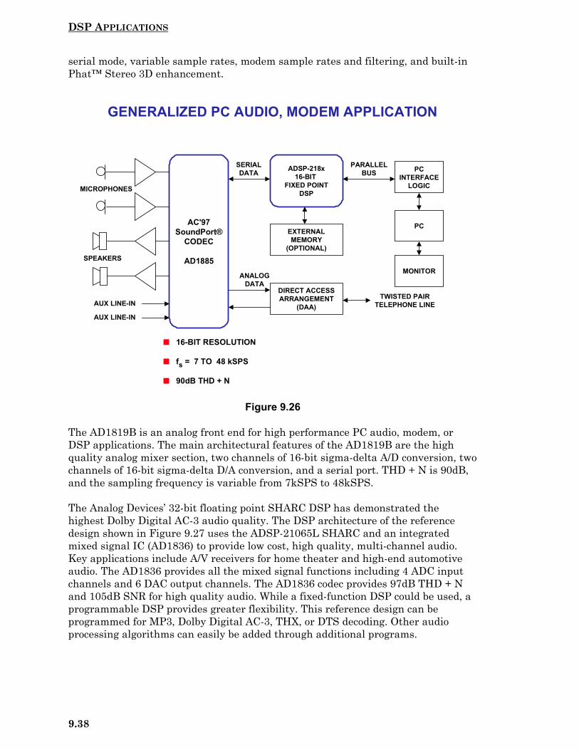
DSP APPLICATIONS
9.38
serial mode, variable sample rates, modem sample rates and filtering, and built-inPhat™ Stereo 3D enhancement.
Figure 9.26
The AD1819B is an analog front end for high performance PC audio, modem, orDSP applications. The main architectural features of the AD1819B are the highquality analog mixer section, two channels of 16-bit sigma-delta A/D conversion, twochannels of 16-bit sigma-delta D/A conversion, and a serial port. THD + N is 90dB,and the sampling frequency is variable from 7kSPS to 48kSPS.
The Analog Devices’ 32-bit floating point SHARC DSP has demonstrated thehighest Dolby Digital AC-3 audio quality. The DSP architecture of the referencedesign shown in Figure 9.27 uses the ADSP-21065L SHARC and an integratedmixed signal IC (AD1836) to provide low cost, high quality, multi-channel audio.Key applications include A/V receivers for home theater and high-end automotiveaudio. The AD1836 provides all the mixed signal functions including 4 ADC inputchannels and 6 DAC output channels. The AD1836 codec provides 97dB THD + Nand 105dB SNR for high quality audio. While a fixed-function DSP could be used, aprogrammable DSP provides greater flexibility. This reference design can beprogrammed for MP3, Dolby Digital AC-3, THX, or DTS decoding. Other audioprocessing algorithms can easily be added through additional programs.
GENERALIZED PC AUDIO, MODEM APPLICATION
AC'97SoundPort®
CODEC
AD1885
ADSP-218x16-BIT
FIXED POINTDSP
EXTERNALMEMORY
(OPTIONAL)
DIRECT ACCESSARRANGEMENT
(DAA)
PCINTERFACE
LOGIC
PC
MONITOR
MICROPHONES
SPEAKERS
AUX LINE-IN
AUX LINE-IN
TWISTED PAIRTELEPHONE LINE
ANALOGDATA
SERIALDATA
PARALLELBUS
16-BIT RESOLUTION
fs = 7 TO 48 kSPS
90dB THD + N

DSP APPLICATIONS
9.39
Figure 9.27
In large digital audio systems it is often necessary to distribute the signalprocessing tasks between multiple processors. Figure 9.28 shows a 16-channelmixer that uses two ADSP-21160s. The data comes from sixteen 24-bit ADCs and ispassed to the FPGA. This FPGA converts the serial ADC data into parallel data andsends it to the two ADSP-21160’s external ports. The external port on each DSP hashardware support to enable the FPGA to write to both DSPs at once. DMA enginesinside the DSP receive this data and move it to desired locations in internalmemory. The hardware support and DMA engines reduce the complexity of theFPGA design, because the FPGA is simply required to drive the data onto the bus.No arbitration logic or address generation is necessary in the FPGA.
The DSPs perform various algorithms, such as mixing, left/right panning,equalization, and additional effects processing, such as reverberation orcompression/expansion. The audio output samples are then transmitted to a 24-bitstereo DAC. These algorithms could be mapped in such a way that one of the DSPsdoes the mixing and effects, while the other does the equalization. Anotherpossibility is to give each DSP the task of processing half of the data channels. Theoptimal algorithmic mapping depends on what type of processing is required.
For this example, it is estimated that the two ADSP-21160s have enoughcomputation power to perform various algorithms on 16 channels of data sampled at48kSPS. In a 20µs period each DSP is capable of executing 2000 instructions in thecore. If each DSP is responsible for half of the channels of data (8 channels), thatmeans that the DSP can allocate 250 instructions to each channel.
AUTOMOTIVE AND HOME THEATERREFERENCE DESIGN USING 32-BIT SHARC
RAM ROM HOST
ADSP-21065LSHARC™
I/F
DAC
DAC
DAC
ADC
ADC
AD1836
AUDIO IN
THD + N = 97dB SNR = 105dB Up to 96kSPS Sampling Rate
(AUDIO)

DSP APPLICATIONS
9.40
With the ADSP-21160 SIMD architecture, there are roughly enough instructions fora 3-band (high, mid, and low) equalizer, mixing, delay effects, and compression foreach channel. The movement of data into the memory does not enter into theprocessing loading calculation since it is a zero-overhead task.
Figure 9.28
A SIGMA-DELTA ADC WITH PROGRAMMABLE DIGITALFILTER
Most sigma-delta ADCs have a fixed internal digital filter. The filter’s cutofffrequency (and the ADC output data rate) scales with the master clock frequency.The AD7725 is a 16-bit sigma-delta ADC with a programmable internal digitalfilter. The block diagram in Figure 9.29 shows that the modulator operates at amaximum oversampling rate of 19.2MSPS. The modulator is followed by a presetFIR filter which decimates the modulator output by a factor of 8, yielding an outputdata rate of 2.4MSPS. The response of the preset FIR filter is shown in Figure 9.29.The output of the preset filter drives a programmable digital filter. The diagramshows typical response for a 300kHz lowpass FIR filter.
16 CHANNEL AUDIO MIXERUSING ADSP-21160 SHARC PROCESSORS
INPUT DATA
.
.
.
.
.
.
.
.
.
.
.
.
.
ADC #1
ADC #16
SERIAL DATATO
PARALLELDATA
(FPGA)
ADSP-21160 ADSP-21160
DAC
AUDIO OUTPUT
TDM SERIAL PORT
3
64PARALLEL DATA BUS
2 LINK PORTS
All 16 channels are broadcast to each ADSP-21160 ADSP-21160s perform mixing, equalization, and audio effects Link ports pass shared data between ADSP-21160s Processed data sent to DAC via time division multiplexing on serial ports

DSP APPLICATIONS
9.41
Figure 9.29
The programmable filter is flexible with respect to number of taps and decimationrate. The filter can have up to 108 taps, up to 5 decimation stages, and a decimationfactor between 2 and 256. Coefficient precision is 24-bits, and arithmetic precision is30-bits.
The AD7725 contains Systolix’s PulseDSP™ (trademark of Systolix) post processorwhich permits the filter characteristics to be programmed through the parallel orserial microprocessor interface.
The post processor is a fully programmable core which provides processing power ofup to 130 million multiply-accumulates (MAC) per second. To program the postprocessor, the user must produce a configuration file which contains theprogramming data for the filter function. This file is generated by the FilterWizardcompiler which is available from Analog Devices. The AD7725 compiler acceptsfilter coefficient data as an input and automatically generates the required deviceprogramming data.
The coefficient file for the filter response can be generated using a digital filterdesign package such as Systolix FilterExpress™ (http://www.systolix.co.uk) orQEDesign™ from Momentum Data Systems (http://www.mds.com). The response ofthe filter can be plotted so the user knows the response before generating the filtercoefficients. The data is available to the processor at a 2.4MSPS rate. Whendecimation is employed in a multistage filter, the first filter will be operated at2.4MSPS, and the user can then decimate between stages. The number of tapswhich can be contained in the processor is 108. Therefore, a single filter with 108
AD7725 16-BIT SIGMA-DELTA ADCWITH PROGRAMMABLE DIGITAL FILTER
16-BITSIGMA-DELTA
MODULATOR
PRESETFIR FILTER
PROGRAMMABLEFILTER
PARALLEL/SERIAL
INTERFACE
CLKIN = 19.2MSPS2.4MSPS 1.2MSPS (MAX)
2.5VREFERENCE
INPUT
2.41.2 0.60.30 0
0
–70
0
–90
FREQUENCY (MHz) FREQUENCY (MHz)
TYPICALFIR
FILTERRESPONSE
PRESETFIR
FILTER
SFDR = 90dBSNR = 84dB
PROGRAMMABLE FILTER:
INPUT DATA RATE = CLKIN/8 COEFFICIENT PRECISION = 24 BITS ARITHMETIC PRECISION = 30 BITS MAXIMUM NUMBER OF TAPS = 108 DECIMATION FACTOR = 2 MIN, 256 MAX NUMBER OF DECIMATION STAGES = 5 MAX OUTPUT DATA RATE = CLKIN/16 MAX
dB dB

DSP APPLICATIONS
9.42
taps can be generated, or a multistage filter can be designed whereby the totalnumber of taps adds up to 108. The filter characteristic can be lowpass, highpass,bandstop, or bandpass and can be either FIR or IIR.
The AD7725 operates on a single +5V supply, has an on-chip 2.5V reference, and ispackaged in a 44-pin PQFP. Power dissipation is approximately 350mW whenoperating at full power. A half-power mode is available with a master clockfrequency of 10MSPS maximum. Power consumption in the standby mode is 200mWmaximum.
SUMMARY
More examples of DSP applications are summarized in Figure 9.30. There are manyother practical applications of DSP in today’s rapidly expanding industrial,communication, medical, military, and consumer markets. A discussion of eachwould constitute a book in itself. It has been the purpose of this section to highlightjust a few of the more common applications and give the reader a sense of how DSPaffects practically every aspect of modern life.
Figure 9.30
OTHER DSP APPLICATIONS
Hands-Free Car Telephone Kits Digital Answering Machines Voice Recognition Systems Cable Modems Computer Sound Cards Digital Audio: Professional and Consumer Digital Video Signal Processing High Definition Television (HDTV) Computer Generated Graphics Digital Special Effects Direct Broadcast Satellite (DBS) Global Positioning Systems (GPS) Medical: Ultrasound, MRI, CT Scanners Military: Radar, Missile Guidance

DSP APPLICATIONS
9.43
REFERENCES
1. John Bingham, The Theory and Practice of Modem Design,John-Wiley, 1988.
2. Digital Signal Processing Applications Using the ADSP-2100Family, Vol. 1 and Vol. 2, Analog Devices, Free download at:http://www.analog.com
3. George Calhoun, Digital Cellular Radio, Artech House, Norwood MA,1988.
4. Nick Morley, New Cellular Scheme Muscles In, EDN News, November 15, 1990, p. 1.
5. P. Vary, K. Hellwig, R. Hofmann, R. J. Sluyter, C. Galand, M. Rosso, SpeechCodec for the European Mobile Radio System, ICASSP 1988 Proceedings,p. 227.
6. D. K. Freeman, G. Cosier, C. B. Southcott, I. Boyd, The Voice ActivityDetector for the Pan-European Digital Cellular System, ICASSP 1989Proceedings, p. 369.
7. Brad Brannon, Using Wide Dynamic Range Converters for WideBand Radios, RF Design, May 1995, pp.50-65.
8. Joe Mitola, The Software Radio Architecture, IEEE CommunicationsMagazine, Vol. 33, No.5, May 1995, pp. 26-38.
9. Jeffery Wepman, Analog-to-Digital Converters and Their Applicationsin Radio Receivers, IEEE Communications Magazine,Vol. 33, No.5, May 1995, pp. 39-45.
10. Rupert Baines, The DSP Bottleneck, IEEE CommunicationsMagazine, Vol. 33, No.5, May 1995, pp. 46-54.
11. Brad Brannon, Overcoming Converter Nonlinearities with Dither,Application Note AN-410, Analog Devices, 1995.
12. P.J.M. Coussens, et al, Three Phase Measurements with Vector RotationBlocks in Mains and Motion Control, PCIM Conference, IntelligentMotion, April 1992 Proceedings, Available from Analog Devices.
13. Dennis Fu, Digital to Synchro and Resolver Conversion with the AC VectorProcessor AD2S100, Available from Analog Devices.
14. Dennis Fu, Circuit Applications of the AD2S90 Resolver-to-Digital Converter,AN-230, Analog Devices.

DSP APPLICATIONS
9.44
15. Aengus Murray and P. Kettle, Towards a Single Chip DSP Based MotorControl Solution, Proceedings PCIM - Intelligent Motion, May 1996,Nurnberg Germany, pp. 315-326. Also available at http://www.analog.com.
16. D. J. Lucey, P. J. Roche, M. B. Harrington, and J. R. Scannell,Comparison of Various Space Vector Modulation Strategies,Proceedings Irish DSP and Control Colloquium, July 1994, Dublin,Ireland, pp. 169-175.
17. Niall Lyne, ADCs Lend Flexibility to Vector Motor Control Applications,Electronic Design, May 1, 1998, pp. 93-100.
18. Motor Control Products, Application Notes, and Tools, CDROM,Analog Devices, Spring 2000.
19. Application of Digital Signal Processing in Motion Control Seminar,Analog Devices, Spring 2000.
20. Analog Devices’ Motor Control Website:http://www.analog.com/motorcontrol

HARDWARE DESIGN TECHNIQUES
10.a
SECTION 10
HARDWARE DESIGN TECHNIQUES
Low Voltage Interfaces
Grounding in Mixed Signal Systems
Digital Isolation Techniques
Power Supply Noise Reduction and Filtering
Dealing with High Speed Logic

HARDWARE DESIGN TECHNIQUES
10.b

HARDWARE DESIGN TECHNIQUES
10.1
SECTION 10HARDWARE DESIGN TECHNIQUESWalt Kester
LOW VOLTAGE INTERFACESEthan Bordeaux, Johannes Horvath, Walt Kester
For the past 30 years, the standard VDD for digital circuits has been 5V. This voltagelevel was used because bipolar transistor technology required 5V to allow headroomfor proper operation. However, in the late 1980s, Complimentary Metal OxideSemiconductor (CMOS) became the standard for digital IC design. This process didnot necessarily require the same voltage levels as TTL circuits, but the industryadopted the 5V TTL standard logic threshold levels to maintain backwardcompatibility with older systems (Reference 1).
The current revolution in supply voltage reduction has been driven by demand forfaster and smaller products at lower costs. This push has caused silicon geometriesto drop from 2µm in the early 1980s to 0.25µm that is used in today’s latestmicroprocessor and IC designs. As feature sizes have become increasingly smaller,the voltage for optimum device performance has also dropped below the 5V level.This is illustrated in the current microprocessors for PCs, where the optimum coreoperating voltage is programmed externally using voltage identification (VID) pins,and can be as low as 1.3V.
The strong interest in lower voltage DSPs is clearly visible in the shifting salespercentages for 5V and 3.3V parts. Sales growth for 3.3V DSPs has increased atmore than twice the rate of the rest of the DSP market (30% for all DSPs versusmore than 70% for 3.3V devices). This trend will continue as the high volume/highgrowth portable markets demand signal processors that contain all of the traits ofthe lower voltage DSPs.
On the one hand, the lower voltage ICs operate at lower power, allow smaller chipareas, and higher speeds. On the other hand, the lower voltage ICs must ofteninterface to other ICs which operate at larger VDD supply voltages thereby causinginterface compatibility problems. Although lower operating voltages mean smallersignal swings, and hence less switching noise, noise margins are lower for lowsupply voltage ICs.
The popularity of 2.5V devices can be partially explained by their ability to operatefrom two AA alkaline cells. Figure 10.2 shows the typical discharge characteristicsfor a AA cell under various load conditions (Reference 2). Note that at a load currentof 15mA, the voltage remains above +1.25V (2.5V for two cells in series) for nearly100 hours. Therefore, an IC that can operate effectively at low currents with asupply voltage of 2.5V ±10% (2.25V - 2.75V) is very useful in portable designs. Also,DSPs that have low mA/MIPS ratings and can integrate peripherals onto a singlechip, such as the ADSP-218x L or M-series, are useful in portable applications.
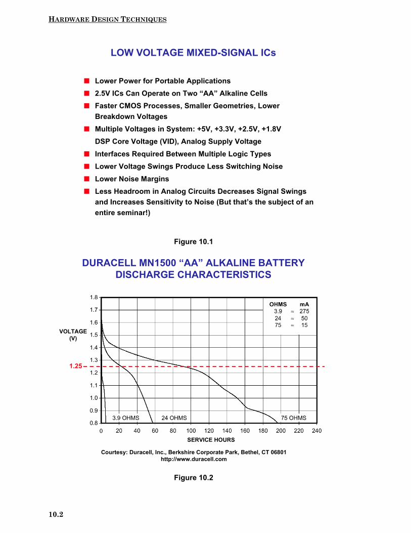
HARDWARE DESIGN TECHNIQUES
10.2
Figure 10.1
Figure 10.2
LOW VOLTAGE MIXED-SIGNAL ICs
Lower Power for Portable Applications 2.5V ICs Can Operate on Two “AA” Alkaline Cells Faster CMOS Processes, Smaller Geometries, Lower
Breakdown Voltages Multiple Voltages in System: +5V, +3.3V, +2.5V, +1.8V
DSP Core Voltage (VID), Analog Supply Voltage Interfaces Required Between Multiple Logic Types Lower Voltage Swings Produce Less Switching Noise Lower Noise Margins Less Headroom in Analog Circuits Decreases Signal Swings
and Increases Sensitivity to Noise (But that’s the subject of anentire seminar!)
DURACELL MN1500 “AA” ALKALINE BATTERYDISCHARGE CHARACTERISTICS
Courtesy: Duracell, Inc., Berkshire Corporate Park, Bethel, CT 06801http://www.duracell.com
SERVICE HOURS
VOLTAGE(V)
1.25

HARDWARE DESIGN TECHNIQUES
10.3
In order to understand the compatibility issues relating to interfacing ICs operatedat different VDD supplies, it is useful to first look at the structure of a typical CMOSlogic stage as shown in Figure 10.3.
Figure 10.3
Note that the output driver stage consists of a PMOS and an NMOS transistor.When the output is high, the PMOS transistor connects the output to the +VDDsupply through its low on-resistance (RON), and the NMOS transistor is off. Whenthe output is low, the NMOS transistor connects the output to ground through itson-resistance, and the PMOS transistor is off. The RON of a CMOS output stage canvary between 5Ω and 50Ω depending on the size of the transistors, which in turn,determines the output current drive capability.
A typical logic IC has its power supplies and grounds separated between the outputdrivers and the rest of the circuitry (including the pre-driver). This is done tomaintain a clean power supply, which reduces the effect of noise and ground bounceon the I/O levels. This is increasingly important, since added tolerance andcompliance are critical in I/O driver specifications, especially at low voltages.
Figure 10.3 also shows “bars” which define the minimum and maximum requiredinput and output voltages to produce a valid high or low logic level. Note that forCMOS logic, the actual output logic levels are determined by the drive current andthe RON of the transistors. For light loads, the output logic levels are very close to 0Vand +VDD. The input logic thresholds, on the other hand, are determined by theinput circuit of the IC.
There are three sections in the “input” bar. The bottom section shows the inputrange that is interpreted as a logic low. In the case of 5V TTL, this range would be
TYPICAL CMOS IC OUTPUT DRIVER CONFIGURATION
PREDRIVERLOGIC
PMOS
NMOS
VDD VDD
INPUT OUTPUT
VIL MAX
VIH MIN
0V
VDD VDD
VOH MIN
VOL MAX0V
VIL MAX = Maximum Allowable Input Low Logic LevelVIH MIN = Minimum Allowable Input High Logic Level
VOL MAX = Maximum Allowable Output Low Logic LevelVOH MIN = Minimum Allowable Output High Logic Level
High = “1”
Low = “0”
High = “1”
Low = “0”

HARDWARE DESIGN TECHNIQUES
10.4
between 0V and 0.8V. The middle section shows the input voltage range where it isinterpreted as neither a logic low nor a logic high. The upper section shows wherean input is interpreted as a logic high. In the case of 5V TTL, this would be between2V and 5V.
Similarly, there are three sections in the “output” bar. The bottom range shows theallowable voltage for a logic low output. In the case of 5V TTL, the IC must output avoltage between 0V and 0.4V. The middle section shows the voltage range that isnot a valid high or low - the device should never transmit a voltage level in thisregion except when transitioning from one level to the other. The upper sectionshows the allowable voltage range for a logic high output signal. For 5V TTL, thisvoltage is between 2.4V and 5V. The chart does not reflect a 10%overshoot/undershoot also allowed on the inputs of the logic standard.
A summary of the existing logic standards using these definitions is shown inFigure 10.4. Note that the input thresholds of classic CMOS logic (series-4000, forexample) are defined as 0.3VDD and 0.7VDD. However, most CMOS logic circuits inuse today are compatible with TTL and LVTTL levels which are the dominant 5Vand 3.3V operating standards for DSPs. Note that 5V TTL and 3.3V LVTTL inputand output threshold voltages are identical. The difference is the upper range forthe allowable high levels.
Figure 10.4
LOW VOLTAGE LOGIC LEVEL STANDARDS
0
0.5
1.0
1.5
2.0
2.5
3.0
3.5
4.04.5
5.0
5V C
MO
S in
put
5V C
MO
S ou
tput
(20u
A)
5V T
TL in
put
5V T
TL o
utpu
t(-2
mA)
3.3V
LVT
TL in
put
3.3V
LVT
TL o
utpu
t (-
2mA)
2.5V
VC
X in
put
2.5V
VC
X ou
tput
(-12
mA)
2.5V
JED
EC in
put
2.5V
JED
EC o
utpu
t (-
1mA)
5V CMOS 5V TTL
3.3V LVTTL 2.5V VCX
2.5V JEDEC
I O I O
I O
I O I O
VOLTS
I = INPUT
O = OUTPUT

HARDWARE DESIGN TECHNIQUES
10.5
The international standards bureau JEDEC (Joint Electron Device EngineeringCouncil) has created a 2.5V standard (JEDEC standard 8-5) which will most likelybecome the minimum requirement for 2.5V operation (Reference 3). However, thereis no current (2000) dominant 2.5V standard for IC transmission and reception,because few manufacturers are making products that operate at this voltage. Thereis one proposed 2.5V standard created by a consortium of IC manufacturers, titledthe Low Voltage Logic Alliance. Their specification provides a guideline forsemiconductor operation between 1.8V and 3.6V. A standard covering this voltagerange is useful because it ensures present and future compatibility. As an example,the 74VCX164245, a bus translator/transceiver from Fairchild Semiconductor, isdesigned to be operated anywhere between 1.8V - 3.6V and has different input andoutput characteristics depending upon the supplied VDD. This standard, namedVCX, was formed by Motorola, Toshiba and Fairchild Semiconductor. It currentlyconsists primarily of bus transceivers, translators, FIFOs and other building blocklogic. There are also a wide range of other low voltage standards, such as GTL(Gunning Transceiver Logic), BTL (Backplane Transceiver Logic), and PECL(PseudoECL Logic). However, most of these standards are aimed at applicationspecific markets and not for general purpose semiconductor systems.
The VCX devices can be operated on a very wide range of voltage levels (1.8V -3.6V). The I/O characteristics of this standard are dependent upon the VDD voltageand the load on each pin. In Figure 10.4, one voltage (2.5V) was chosen to show thegeneral I/O behavior of a VCX device. Each of the device’s output voltages is listedfor a specific current. As the current requirements increase, the output high voltagedecreases while the output low voltage increases. Please refer to the appropriatedata sheets for more specific I/O information.
From this chart, it is possible to visualize some of the possible problems inconnecting together two ICs operating on different standards. One example wouldbe connecting a 5V CMOS device to a 3.3V LVTTL IC. The 5V CMOS high level istoo high for the LVTTL to handle ( > 3.3V). This could cause permanent damage tothe LVTTL chip. Another possible problem would be a system with a 2.5V JEDECIC driving a 5V CMOS device. The logic high level from the 2.5V device is not highenough for it to register as a logic high on the 5V CMOS input (VIH MIN = 3.5V).These examples illustrate two possible types of logic level incompatibilities - eithera device being driven with too high a voltage or a device not driving a voltage highenough for it to register a valid high logic level with the receiving IC. Theseinterfacing problems introduce two important concepts: voltage tolerance andvoltage compliance.
VOLTAGE TOLERANCE AND VOLTAGE COMPLIANCE
A device that is voltage tolerant can withstand a voltage greater than its VDD on itsI/O pins. For example, if a device has a VDD of 2.5V and can accept inputs equal to3.3V and can withstand 3.3V on its outputs, the 2.5V device is called 3.3V tolerant.The meaning of input voltage tolerance is fairly obvious, but the meaning of outputvoltage tolerance requires some explanation. The output of a 2.5V CMOS driver inthe high state appears like a small resistor (RON of the PMOS FET) connected to2.5V. Obviously, connecting its output directly to 3.3V is likely to destroy the devicedue to excessive current. However, if the 2.5V device has a three-state output whichis connected to a bus which is also driven by a 3.3V IC, then the meaning becomes

HARDWARE DESIGN TECHNIQUES
10.6
clearer. Even though the 2.5V IC is in the off (third-state) condition, the 3.3V IC candrive the bus voltage higher than 2.5V, potentially causing damage to the 2.5V ICoutput.
A device which is voltage compliant can receive signals from and transmit signals toa device which is operated at a voltage greater than its own VDD. For example, if adevice has a 2.5V VDD and can transmit and receive signals to and from a 3.3Vdevice, the 2.5V device is said to be 3.3V compliant.
The interface between the 5V CMOS and 3.3V LVTTL parts illustrates a lack ofvoltage tolerance; the LVTTL IC input is overdriven by the 5V CMOS device output.The interface between the 2.5V JEDEC and the 5V CMOS part demonstrates a lackof voltage compliance; the output high level of the JEDEC IC does not comply to theinput level requirement of a the 5V CMOS device.
Figure 10.5
INTERFACING 5V TO 3.3V SYSTEMS USING NMOS FET BUSSWITCHES
When combining ICs that operate on different voltage standards, one is often forcedto add additional discrete elements to ensure voltage tolerance and compliance. Inorder to achieve voltage tolerance between 5V and 3.3V logic, for instance, a busswitch voltage translator, or QuickSwitch™ can be used (Reference 4, 5). The busswitch limits the voltage applied to an IC. This is done to avoid applying a largerinput high voltage than the receiving device can tolerate.
As an example, it is possible to place a bus switch between a 5V CMOS and 3.3VLVTTL IC, and the two devices can then transmit data properly as shown in Figure10.6. The bus switch is basically an NMOS FET. If 4.3V is placed on the gate of theFET, the maximum passable signal is 3.3V (approximately 1V less than the gate
LOGIC VOLTAGE TOLERANCEAND COMPATIBILITY DEFINITIONS
Voltage Tolerance: A device that is Voltage Tolerant can withstand a voltage
greater than its VDD on its input and output pins. If a devicehas a VDD of 2.5V and can accept inputs of 3.3V (±10%), the2.5V device is 3.3V tolerant on its input. Input and outputtolerance should be examined and specified separately.
Voltage Compliance: A device that is Voltage Compliant can transmit and receive
signals to and from logic which is operated at a voltagegreater than its own VDD. If a device has a 2.5V VDD and canproperly transmit signals to and from 3.3V logic, the 2.5Vdevice is 3.3V compliant. Input and output compliance shouldbe examined and specified separately.

HARDWARE DESIGN TECHNIQUES
10.7
voltage). If both input and output are below 3.3V, the NMOS FET acts as a lowresistance (RON ≈ 5Ω). As the input approaches 3.3V, the FET on-resistanceincreases, thereby limiting the signal output. The QuickSwitch contains 10 bi-directional FETs with a gate drive enable as shown in Figure 10.6. The VCC of theQuickSwitch sets the high level for the gate drive.
One way of creating a 4.3V supply on a 5V/3.3V system board is to place a diodebetween the 5V supply and VCC on the QuickSwitch. In Figure 10.6, the 4.3V isgenerated by a silicon diode in series with a Schottky diode connected to the 3.3Vsupply. With 10% tolerances on both 5V and 3.3V supplies, this method produces amore stable gate bias voltage. Some bus switches are designed to operate on either3.3V or 5V directly and generate the internal gate bias level internally.
A QuickSwitch removes voltage tolerance concerns in this mixed logic design. Oneconvenient feature of bus switches is that they are bi-directional; this allows thedesigner to place a bus translator between two ICs and not have to create additionalrouting logic for input and output signals.
Figure 10.6
A bus switch increases the total power dissipation along with the total arearequired to layout a system. Since voltage bus switches are typically CMOS circuits,they have very low power dissipation ratings. An average value for addedcontinuous power dissipation is 5mW per package (10 switches), and this isindependent of the frequency of signals which pass through the circuit. Busswitches typically have 8 - 20 I/O pins per package and take up approximately 25 to50mm2 of board space.
+3.3V / +5V BIDIRECTIONAL INTERFACE USINGNMOS FET ACHIEVES VOLTAGE TOLERANCE
5V ± 10%LOGIC
3.3V ± 10%LOGIC
470 kΩΩΩΩ
0.1µFSi
+ 3.3V BUS + 5V BUS+ 4.3V
SCHOTTKY
NMOS
RON = 5 ΩΩΩΩ
QS3384 QuickSwitch ®10 SWITCHES/PACKAGE
OPERATE WITH QS3384 VCC = +4.3V
≈≈≈≈ 1V
“1” = DISABLE“0” = ENABLE
0V / VCC
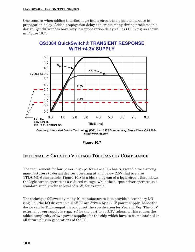
HARDWARE DESIGN TECHNIQUES
10.8
One concern when adding interface logic into a circuit is a possible increase inpropagation delay. Added propagation delay can create many timing problems in adesign. QuickSwitches have very low propagation delay values (< 0.25ns) as shownin Figure 10.7.
Figure 10.7
INTERNALLY CREATED VOLTAGE TOLERANCE / COMPLIANCE
The requirement for low power, high performance ICs has triggered a race amongmanufacturers to design devices operating at and below 2.5V that are alsoTTL/CMOS compatible. Figure 10.8 is a block diagram of a logic circuit that allowsthe logic core to operate at a reduced voltage, while the output driver operates at astandard supply voltage level of 3.3V, for example.
The technique followed by many IC manufacturers is to provide a secondary I/Oring, i.e., the I/O drivers in a 2.5V IC are driven by a 3.3V power supply, hence thedevice can be TTL compatible and meet the specification for VOH and VOL. The 3.3Vexternal power supply is required for the part to be 3.3V tolerant. This causes theadded complexity of two power supplies for the chip which have to be maintained inall future plug-in generations of the IC.
QS3384 QuickSwitch® TRANSIENT RESPONSEWITH +4.3V SUPPLY
TIME (ns)
(VOLTS)
VINVOUT
Courtesy: Integrated Device Technology (IDT), Inc., 2975 Stender Way, Santa Clara, CA 95054http://www.idt.com
2.0V
0.8V
5V TTL, 3.3V LVTTL INPUT THRESHOLDS

HARDWARE DESIGN TECHNIQUES
10.9
A more flexible technique (used in the ADSP-218xM series DSPs) is to provide aseparate I/O ring with an external voltage with the option of setting that voltageequal to the core’s operating voltage, if desired. This design can provide tolerance to3.3V with the external voltage set to 2.5V, or 3.3V tolerance and compliance to 3.3Vwith the external voltage set to 3.3V. There are vendors today that use this optionpartially, i.e., the VCX devices are 3.3V tolerant at 2.5V internal and externalvoltages, but do not have the option of 3.3V compliance. Other existing designs andpatents that address this issue do not support complete tolerance and complianceand the low standby current specification. This approach is complicated, since thecircuits must meet the noise and power requirements with the external voltages at3.3V or 2.5V.
Figure 10.8
There are several issues to consider in a dual-supply logic IC design:
• Power-Up Sequencing: If two power supplies are required to give an ICadditional tolerance / compliance, what is the power-up sequence? Is it arequirement that the power supplies are switched on simultaneously or can thedevice only have a voltage supplied on the core or only on the I/O ring?
CMOS IC WITH SECONDARY I/O RING
CORELOGIC
PMOS
NMOS
SECONDARYI/O RING
VDD INTERNAL(CORE) VDD EXTERNAL
OUTPUTINPUT
VDD EXTERNAL = +3.3V OR +2.5VVDD CORE = +2.5V
INPUT +3.3V TOLERANT
INTERNAL GND EXTERNAL GND
ADSP-21xx M-SERIES

HARDWARE DESIGN TECHNIQUES
10.10
• Process Support and Electro-Static Discharge (ESD) Protection: The transistorscreated in the IC’s fabrication process must be able to both withstand and drivehigh voltages. The high voltage transistors create additional fabrication costssince they require more processing steps to build in high voltage tolerance.Designs with standard transistors require additional circuitry. The I/O driversmust also provide ESD protection for the device. Most current designs limit theovervoltage to below one diode drop (0.7V) above the power supply. Protectionfor larger overvoltage requires more diodes in series.
• Internal High Voltage Generation: The PMOS transistors need to be placed in asubstrate well which is tied to the highest on-chip voltage to prevent lateraldiodes from turning on and drawing excessive current. This high voltage caneither be generated on chip using charge pumps or from an external supply. Thisrequirement can make the design complex, since one cannot efficiently usecharge pumps to generate higher voltages and also achieve low standby current.
• Chip Area: Die size is a primary factor in reducing costs and increasing yields.Tolerance and compliance circuitry may require either more or larger I/O devicesto achieve the desired performance levels.
• Testing: Since the core and the I/O can be at different voltages, testing thedevice for all possible combinations of voltages can be complicated, adding to thetotal cost of the IC.
3.3V / 2.5V INTERFACES
The Fairchild 74VCX164245-series are low voltage 16-bit dual supply logictranslators/transceivers with three-state outputs. A simplified block diagram isshown in Figure 10.9. These devices use the VCX low voltage standard previouslydiscussed. The output driver circuit is supplied from the VDDB power supply bus,ensuring VDDB compliant and tolerant outputs. The input circuit is supplied from theVDDA supply, and the input logic threshold adjust circuits optimize the input logicthresholds for the particular value of VDDA. Figure 10.10 shows the VCX voltagestandards for 3.3V, 2.5V, and 1.8V supply voltages. Note that the input voltage is3.3V tolerant for all three supply voltages.
These devices dissipate about 2mW per input/output and are packaged in a 48-leadTSSOP with a 2.5V supply. Propagation delay is about 3.2ns.
Figure 10.11 shows two possibilities for a 3.3V to 2.5V logic interface. The topdiagram (A) shows a direct connection. This will work provided the 2.5V IC is 3.3Vtolerant on its input. If the 2.5V IC is not 3.3V tolerant, the VCX translator can beused as shown in Figure 10.11B.

HARDWARE DESIGN TECHNIQUES
10.11
Figure 10.9
Figure 10.10
LOGIC TRANSLATING TRANSCEIVER(FAIRCHILD 74VCX164245)
PMOS
NMOS
VDDA VDDB
OUTPUTINPUT
PREDRIVERLOGIC
VDDA BUS VDDB BUS
LOGICLOGIC
INPUTLOGIC
THRESHOLDADJUST
CIRCUITS
74VCX164245 CHARACTERISTICS: Power Dissipation = 2mW / Input or Output 16-bits per 48-lead TSSOP 100mm2 package 3.2ns Propagation Delay at +2.5V
VOLTAGE COMPLIANCE FOR VCX STANDARD(FAIRCHILD 74VCX164245 TRANSLATOR)
3.3V 2.5V 1.8V
–12mA –12mA –6mA0
0.5
1.0
1.5
2.0
2.5
3.0
3.5
VOLTS
I O
I O
I O
I = INPUT
O = OUTPUT

HARDWARE DESIGN TECHNIQUES
10.12
Figure 10.11
Figure 10.12A shows a direct connection between 2.5V and 3.3V logic. In order forthis to work, the 2.5V output must be at least 2V minimum. With no loading on the2.5V output, the 3.3V IC input is connected directly to +2.5V through the on-resistance of the PMOS transistor driver. This provides 0.5V noise margin for thenominal supply voltage of 2.5V. However, the 10% tolerance on the 2.5V bus allowsit to drop to a minimum of 2.25V, and the noise margin is reduced to 0.25V. Thismay still work in a relatively quiet environment, but could be marginal if there isnoise on the supply voltages.
Adding a 1.6kΩ pull-up resistor as shown in Figure 10.12B ensures the 2.5V outputwill not drop below 2.5V due to the input current of the 3.3V device, but thedegraded noise margin still exists for a 2.25V supply. With a 50% duty cycle, theresistor adds about 3.4mW power dissipation per output.
A more reliable interface between 2.5V and 3.3V logic is shown in Figure 10.12C,where a VCX translator is used. This solves all noise margin problems associatedwith (A) and (B) and requires about 2mW per output.
+3.3V TO +2.5V INTERFACE
+3.3V ± 10%LOGIC
+2.5V ± 10%LOGIC
+3.3V BUS +2.5V BUS
OK IF 2.5V LOGICIS 3.3V TOLERANT
(3.6V MAX.)
+3.3V ± 10%LOGIC
+2.5V ± 10%LOGIC
+3.3V BUS +2.5V BUS
DIRECTCONNECTION
TRANSLATOR
A
B

HARDWARE DESIGN TECHNIQUES
10.13
Figure 10.12
+2.5V TO +3.3V INTERFACE
+2.5V ± 10%LOGIC
(+2.25V MIN.)
+3.3V ± 10%LOGIC
+2.5V BUS +3.3V BUSDIRECT
CONNECTION
NEEDS+2V MIN.
+2.5V ± 10%LOGIC
(+2.25V MIN.)
+3.3V ± 10%LOGIC
+2.5V BUS +3.3V BUS
+2.5V ± 10%LOGIC
(+2.25V MIN.)
+3.3V ± 10%LOGIC
+2.5V BUS +3.3V BUS
1.6kΩΩΩΩ
3.4mW50% D.C.
2mW
TRANSLATOR
PULL UP RESISTOR
A
B
C
HARDWARE DESIGN TECHNIQUES
10.14
REFERENCES ON LOW VOLTAGE INTERFACES
1. P. Alfke, Low-Voltage FPGAs Allow 3.3V/5V System Design,Electronic Design, p. 70-76, August 18, 1997.
2. AA Alkaline Battery Discharge Characteristics, Duracell Inc.,Berkshire Corporate Park, Bethel, CT 06801, http://www.duracell.com
3. Joint Electron Device Engineering Council (JEDEC),Standard 8-5, October 1995.
4. QS3384 Data Sheet, Integrated Device Technology (IDT), Inc.,2975 Stender Way, Santa Clara, CA 95054, http://www.idt.com
5. Pericom Semiconductor Corporation, 2380 Bering Drive,San Jose, CA 95131, http://www.pericom.com
6. 74VCX164245 Data Sheet, Fairchild Semiconductor, 1997.http://www.fairchildsemi.com
7. H. Johnson, M. Graham, High Speed Digital Design, Prentice Hall, 1993.

HARDWARE DESIGN TECHNIQUES
10.15
GROUNDING IN MIXED SIGNAL SYSTEMSWalt Kester, James Bryant, Mike ByrneToday's signal processing systems generally require mixed-signal devices such asanalog-to-digital converters (ADCs) and digital-to-analog converters (DACs) as wellas fast digital signal processors (DSPs). Requirements for processing analog signalshaving wide dynamic ranges increases the importance of high performance ADCsand DACs. Maintaining wide dynamic range with low noise in hostile digitalenvironments is dependent upon using good high-speed circuit design techniquesincluding proper signal routing, decoupling, and grounding.
In the past, "high precision, low-speed" circuits have generally been vieweddifferently than so-called "high-speed" circuits. With respect to ADCs and DACs, thesampling (or update) frequency has generally been used as the distinguishing speedcriteria. However, the following two examples show that in practice, most of today'ssignal processing ICs are really "high-speed," and must therefore be treated as suchin order to maintain high performance. This is certainly true of DSPs, and also trueof ADCs and DACs.
All sampling ADCs (ADCs with an internal sample-and-hold circuit) suitable forsignal processing applications operate with relatively high speed clocks with fastrise and fall times (generally a few nanoseconds) and must be treated as high speeddevices, even though throughput rates may appear low. For example, the 12-bitAD7892 successive approximation (SAR) ADC operates on an 8MHz internal clock,while the sampling rate is only 600kSPS.
Sigma-delta (Σ-∆) ADCs also require high speed clocks because of their highoversampling ratios. The AD7722 16-bit ADC has an output data rate (effectivesampling rate) of 195kSPS, but actually samples the input signal at 12.5MSPS (64-times oversampling). Even high resolution, so-called "low frequency" Σ-∆ industrialmeasurement ADCs (having throughputs of 10Hz to 7.5kHz) operate on 5MHz orhigher clocks and offer resolution to 24-bits (for example, the Analog DevicesAD7730 and AD7731).
To further complicate the issue, mixed-signal ICs have both analog and digitalports, and because of this, much confusion has resulted with respect to propergrounding techniques. In addition, some mixed-signal ICs have relatively low digitalcurrents, while others have high digital currents. In many cases, these two typesmust be treated differently with respect to optimum grounding.
Digital and analog design engineers tend to view mixed-signal devices fromdifferent perspectives, and the purpose of this section is to develop a generalgrounding philosophy that will work for most mixed signal devices, without havingto know the specific details of their internal circuits.
GROUND AND POWER PLANES
The importance of maintaining a low impedance large area ground plane is criticalto all analog circuits today. The ground plane not only acts as a low impedancereturn path for decoupling high frequency currents (caused by fast digital logic) but

HARDWARE DESIGN TECHNIQUES
10.16
also minimizes EMI/RFI emissions. Because of the shielding action of the groundplane, the circuit’s susceptibility to external EMI/RFI is also reduced.
Ground planes also allow the transmission of high speed digital or analog signalsusing transmission line techniques (microstrip or stripline) where controlledimpedances are required.
The use of "buss wire" is totally unacceptable as a "ground" because of itsimpedance at the equivalent frequency of most logic transitions. For instance, #22gauge wire has about 20nH/inch inductance. A transient current having a slew rateof 10mA/ns created by a logic signal would develop an unwanted voltage drop of200mV at this frequency flowing through 1 inch of this wire:
∆ ∆∆
v L it
nH mAns
mV= = × =20 10 200 .
For a signal having a 2V peak-to-peak range, this translates into an error of about200mV, or 10% (approximate 3.5-bit accuracy). Even in all-digital circuits, this errorwould result in considerable degradation of logic noise margins.
Figure 10.13 shows an illustration of a situation where the digital return currentmodulates the analog return current (top figure). The ground return wireinductance and resistance is shared between the analog and digital circuits, andthis is what causes the interaction and resulting error. A possible solution is tomake the digital return current path flow directly to the GND REF as shown in thebottom figure. This is the fundamental concept of a "star," or single-point groundsystem. Implementing the true single-point ground in a system which containsmultiple high frequency return paths is difficult because the physical length of theindividual return current wires will introduce parasitic resistance and inductancewhich can make obtaining a low impedance high frequency ground difficult. Inpractice, the current returns must consist of large area ground planes for lowimpedance to high frequency currents. Without a low-impedance ground plane, it istherefore almost impossible to avoid these shared impedances, especially at highfrequencies.
All integrated circuit ground pins should be soldered directly to the low-impedanceground plane to minimize series inductance and resistance. The use of traditionalIC sockets is not recommended with high-speed devices. The extra inductance andcapacitance of even "low profile" sockets may corrupt the device performance byintroducing unwanted shared paths. If sockets must be used with DIP packages, asin prototyping, individual "pin sockets" or "cage jacks" may be acceptable. Bothcapped and uncapped versions of these pin sockets are available (AMP partnumbers 5-330808-3, and 5-330808-6). They have spring-loaded gold contacts whichmake good electrical and mechanical connection to the IC pins. Multiple insertions,however, may degrade their performance.
Power supply pins should be decoupled directly to the ground plane using lowinductance ceramic surface mount capacitors. If through-hole mounted ceramiccapacitors must be used, their leads should be less than 1mm. The ceramiccapacitors should be located as close as possible to the IC power pins. Ferrite beadsmay be also required for additional decoupling.

HARDWARE DESIGN TECHNIQUES
10.17
Figure 10.13
DOUBLE-SIDED VS. MULTILAYER PRINTED CIRCUIT BOARDS
Each PCB in the system should have at least one complete layer dedicated to theground plane. Ideally, a double-sided board should have one side completelydedicated to ground and the other side for interconnections. In practice, this is notpossible, since some of the ground plane will certainly have to be removed to allowfor signal and power crossovers, vias, and through-holes. Nevertheless, as mucharea as possible should be preserved, and at least 75% should remain. Aftercompleting an initial layout, the ground layer should be checked carefully to makesure there are no isolated ground "islands," because IC ground pins located in aground "island" have no current return path to the ground plane. Also, the groundplane should be checked for "skinny" connections between adjacent large areaswhich may significantly reduce the effectiveness of the ground plane. Needless tosay, auto-routing board layout techniques will generally lead to a layout disaster ona mixed-signal board, so manual intervention is highly recommended.
Systems that are densely packed with surface mount ICs will have a large numberof interconnections; therefore multilayer boards are mandatory. This allows at leastone complete layer to be dedicated to ground. A simple 4-layer board would haveinternal ground and power plane layers with the outer two layers used for
DIGITAL CURRENTS FLOWING IN ANALOGRETURN PATH CREATE ERROR VOLTAGES
ANALOGCIRCUITS
DIGITALCIRCUITS
ANALOGCIRCUITS
DIGITALCIRCUITS
VD
VD
VA
VA
+ +
+ +
ID
IA
IDIA + ID
VIN
VIN
ID
IA
ID
IA
GNDREF
GNDREF
INCORRECT
CORRECT

HARDWARE DESIGN TECHNIQUES
10.18
interconnections between the surface mount components. Placing the power andground planes adjacent to each other provides additional inter-plane capacitancewhich helps high frequency decoupling of the power supply. In most systems, 4-layers are not enough, and additional layers are required for routing signals as wellas power.
Figure 10.14
MULTICARD MIXED-SIGNAL SYSTEMS
The best way of minimizing ground impedance in a multicard system is to use a"motherboard" PCB as a backplane for interconnections between cards, thusproviding a continuous ground plane to the backplane. The PCB connector shouldhave at least 30-40% of its pins devoted to ground, and these pins should beconnected to the ground plane on the backplane mother card. To complete theoverall system grounding scheme there are two possibilities:
1. The backplane ground plane can be connected to chassis ground at numerouspoints, thereby diffusing the various ground current return paths. This is commonlyreferred to as a "multipoint" grounding system and is shown in Figure 10.15.
2. The ground plane can be connected to a single system "star ground" point(generally at the power supply).
GROUND PLANES ARE MANDATORY!
Use Large Area Ground (and Power) Planes for Low ImpedanceCurrent Return Paths (Must Use at Least a Double-Sided Board!)
Double-Sided Boards:
Avoid High-Density Interconnection Crossovers and ViasWhich Reduce Ground Plane Area
Keep > 75% Board Area on One Side for Ground Plane
Multilayer Boards: Mandatory for Dense Systems
Dedicate at Least One Layer for the Ground Plane
Dedicate at Least One Layer for the Power Plane
Use at Least 30% to 40% of PCB Connector Pins for Ground
Continue the Ground Plane on the Backplane Motherboard toPower Supply Return

HARDWARE DESIGN TECHNIQUES
10.19
Figure 10.15
The first approach is most often used in all-digital systems, but can be used inmixed-signal systems provided the ground currents due to digital circuits aresufficiently low and diffused over a large area. The low ground impedance ismaintained all the way through the PC boards, the backplane, and ultimately thechassis. However, it is critical that good electrical contact be made where thegrounds are connected to the sheet metal chassis. This requires self-tapping sheetmetal screws or "biting" washers. Special care must be taken where anodizedaluminum is used for the chassis material, since its surface acts as an insulator.
The second approach ("star ground") is often used in high speed mixed-signalsystems having separate analog and digital ground systems and warrants furtherdiscussion.
SEPARATING ANALOG AND DIGITAL GROUNDS
In mixed-signal systems with large amounts of digital circuitry, it is highlydesirable to physically separate sensitive analog components from noisy digitalcomponents. It may also be beneficial to use separate ground planes for the analogand the digital circuitry. These planes should not overlap in order to minimizecapacitive coupling between the two. The separate analog and digital ground planesare continued on the backplane using either motherboard ground planes or "groundscreens" which are made up of a series of wired interconnections between the
MULTIPOINT GROUND CONCEPT
POWERSUPPLIES
GROUND PLANE
VA
VD
VA VD
GROUND PLANE BACKPLANE
PCB
GROUND PLANE
VA VDPCB
CHASSISGROUND

HARDWARE DESIGN TECHNIQUES
10.20
connector ground pins. The arrangement shown in Figure 10.16 illustrates that thetwo planes are kept separate all the way back to a common system "star" ground,generally located at the power supplies. The connections between the ground planes,the power supplies, and the "star" should be made up of multiple bus bars or widecopper braids for minimum resistance and inductance. The back-to-back Schottkydiodes on each PCB are inserted to prevent accidental DC voltage from developingbetween the two ground systems when cards are plugged and unplugged. Thisvoltage should be kept less than 300mV to prevent damage to ICs which haveconnections to both the analog and digital ground planes. Schottky diodes arepreferable because of their low capacitance and low forward voltage drop. The lowcapacitance prevents AC coupling between the analog and digital ground planes.Schottky diodes begin to conduct at about 300mV, and several parallel diodes inparallel may be required if high currents are expected. In some cases, ferrite beadscan be used instead of Schottky diodes, however they introduce DC ground loopswhich can be troublesome in precision systems.
Figure 10.16
It is mandatory that the impedance of the ground planes be kept as low as possible,all the way back to the system star ground. DC or AC voltages of more than 300mVbetween the two ground planes can not only damage ICs but cause false triggeringof logic gates and possible latchup.
SEPARATING ANALOG AND DIGITAL GROUND PLANES
POWERSUPPLIES
ANALOGGROUNDPLANE
DIGITALGROUNDPLANE
A D
ANALOGGROUNDPLANE
DIGITALGROUNDPLANE
A D
VA
VD
VA VAVD VD
ANALOG GROUND PLANE
DIGITAL GROUND PLANE
BACKPLANE
PCB PCB
SYSTEMSTAR
GROUND

HARDWARE DESIGN TECHNIQUES
10.21
GROUNDING AND DECOUPLING MIXED-SIGNAL ICS WITH LOW DIGITALCURRENTS
Sensitive analog components such as amplifiers and voltage references are alwaysreferenced and decoupled to the analog ground plane. The ADCs and DACs (andother mixed-signal ICs) with low digital currents should generally be treated asanalog components and also grounded and decoupled to the analog ground plane. Atfirst glance, this may seem somewhat contradictory, since a converter has an analogand digital interface and usually has pins designated as analog ground (AGND) anddigital ground (DGND). The diagram shown in Figure 10.17 will help to explain thisseeming dilemma.
Figure 10.17
PROPER GROUNDING OF MIXED-SIGNAL ICsWITH LOW INTERNAL DIGITAL CURRENTS
ANALOGCIRCUITS
DIGITALCIRCUITS
BUFFERGATE ORREGISTER
VA
A B
VD
CSTRAY
CSTRAY
R
A
A A D
D
VNOISE
VA
AIN/OUT
AGND DGND
DATABUS
FERRITE BEAD
DATA
VD
A = ANALOG GROUND PLANE D = DIGITAL GROUND PLANE
CIN ≈≈≈≈ 10pF
LP LP
LP LP
RP
RP RP
RP
SHORTCONNECTIONS
IA ID
SEETEXT

HARDWARE DESIGN TECHNIQUES
10.22
Inside an IC that has both analog and digital circuits, such as an ADC or a DAC,the grounds are usually kept separate to avoid coupling digital signals into theanalog circuits. Figure 10.17 shows a simple model of a converter. There is nothingthe IC designer can do about the wirebond inductance and resistance associatedwith connecting the bond pads on the chip to the package pins except to realize it'sthere. The rapidly changing digital currents produce a voltage at point B which willinevitably couple into point A of the analog circuits through the stray capacitance,CSTRAY. In addition, there is approximately 0.2pF unavoidable stray capacitancebetween every pin of the IC package! It's the IC designer's job to make the chipwork in spite of this. However, in order to prevent further coupling, the AGND andDGND pins should be joined together externally to the analog ground plane withminimum lead lengths. Any extra impedance in the DGND connection will causemore digital noise to be developed at point B; it will, in turn, couple more digitalnoise into the analog circuit through the stray capacitance. Note that connectingDGND to the digital ground plane applies VNOISE across the AGND and DGNDpins and invites disaster!
The name "DGND" on an IC tells us that this pin connects to the digital ground ofthe IC. This does not imply that this pin must be connected to the digital ground ofthe system.
It is true that this arrangement may inject a small amount of digital noise onto theanalog ground plane. These currents should be quite small, and can be minimizedby ensuring that the converter output does not drive a large fanout (they normallycan't, by design). Minimizing the fanout on the converter's digital port will also keepthe converter logic transitions relatively free from ringing and minimize digitalswitching currents, and thereby reducing any potential coupling into the analog portof the converter. The logic supply pin (VD) can be further isolated from the analogsupply by the insertion of a small lossy ferrite bead as shown in Figure 10.17. Theinternal transient digital currents of the converter will flow in the small loop fromVD through the decoupling capacitor and to DGND (this path is shown with a heavyline on the diagram). The transient digital currents will therefore not appear on theexternal analog ground plane, but are confined to the loop. The VD pin decouplingcapacitor should be mounted as close to the converter as possible to minimizeparasitic inductance. These decoupling capacitors should be low inductance ceramictypes, typically between 0.01µF and 0.1µF.
TREAT THE ADC DIGITAL OUTPUTS WITH CARE
It is always a good idea (as shown in Figure 10.17) to place a buffer registeradjacent to the converter to isolate the converter's digital lines from noise on thedata bus. The register also serves to minimize loading on the digital outputs of theconverter and acts as a Faraday shield between the digital outputs and the databus. Even though many converters have three-state outputs/inputs, this isolationregister still represents good design practice. In some cases it may be desirable to

HARDWARE DESIGN TECHNIQUES
10.23
add an additional buffer register on the analog ground plane next to the converteroutput to provide greater isolation.
The series resistors (labeled "R" in Figure 10.17) between the ADC output and thebuffer register input help to minimize the digital transient currents which mayaffect converter performance. The resistors isolate the digital output drivers fromthe capacitance of the buffer register inputs. In addition, the RC network formed bythe series resistor and the buffer register input capacitance acts as a lowpass filterto slow down the fast edges.
A typical CMOS gate combined with PCB trace and a through-hole will create a loadof approximately 10pF. A logic output slew rate of 1V/ns will produce 10mA ofdynamic current if there is no isolation resistor:
∆ ∆∆
I C vt
pF Vns
mA= = × =10 1 10 .
A 500Ω series resistors will minimize this output current and result in a rise andfall time of approximately 11ns when driving the 10pF input capacitance of theregister:
tr R C pF ns= × = × ⋅ = × × =2 2 2 2 2 2 500 10 11. . . .τ Ω
TTL registers should be avoided, since they can appreciably add to the dynamicswitching currents because of their higher input capacitance.
The buffer register and other digital circuits should be grounded and decoupled tothe digital ground plane of the PC board. Notice that any noise between the analogand digital ground plane reduces the noise margin at the converter digital interface.Since digital noise immunity is of the orders of hundreds or thousands of millivolts,this is unlikely to matter. The analog ground plane will generally not be very noisy,but if the noise on the digital ground plane (relative to the analog ground plane)exceeds a few hundred millivolts, then steps should be taken to reduce the digitalground plane impedance, thereby maintaining the digital noise margins at anacceptable level. Under no circumstances should the voltage between the twoground planes exceed 300mV, or the ICs may be damaged.
Separate power supplies for analog and digital circuits are also highly desirable.The analog supply should be used to power the converter. If the converter has a pindesignated as a digital supply pin (VD), it should either be powered from a separateanalog supply, or filtered as shown in the diagram. All converter power pins shouldbe decoupled to the analog ground plane, and all logic circuit power pins should bedecoupled to the digital ground plane as shown in Figure 10.18. If the digital powersupply is relatively quiet, it may be possible to use it to supply analog circuits aswell, but be very cautious.
In some cases it may not be possible to connect VD to the analog supply. Some of thenewer, high speed ICs may have their analog circuits powered by +5V, but thedigital interface powered by +3V to interface to 3V logic. In this case, the +3V pin ofthe IC should be decoupled directly to the analog ground plane. It is also advisableto connect a ferrite bead in series with the power trace that connects the pin to the+3V digital logic supply.
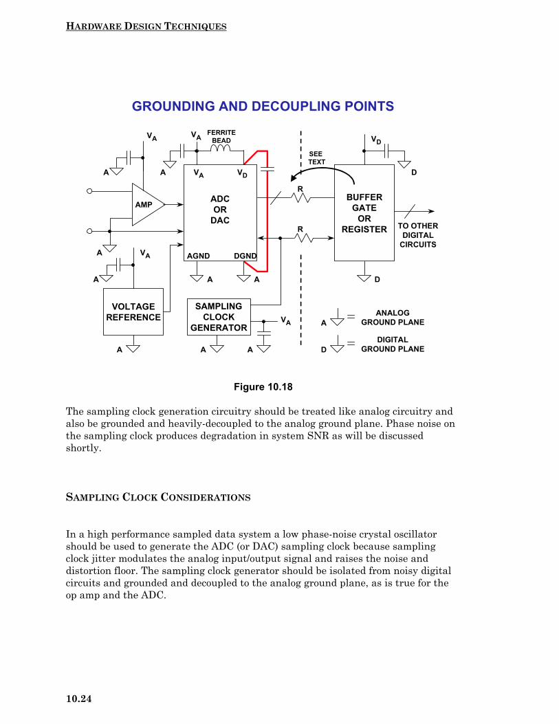
HARDWARE DESIGN TECHNIQUES
10.24
Figure 10.18
The sampling clock generation circuitry should be treated like analog circuitry andalso be grounded and heavily-decoupled to the analog ground plane. Phase noise onthe sampling clock produces degradation in system SNR as will be discussedshortly.
SAMPLING CLOCK CONSIDERATIONS
In a high performance sampled data system a low phase-noise crystal oscillatorshould be used to generate the ADC (or DAC) sampling clock because samplingclock jitter modulates the analog input/output signal and raises the noise anddistortion floor. The sampling clock generator should be isolated from noisy digitalcircuits and grounded and decoupled to the analog ground plane, as is true for theop amp and the ADC.
GROUNDING AND DECOUPLING POINTS
AMP
VA VD
VA
A
A
AGND DGND
ADCOR
DAC
VA
A
VOLTAGEREFERENCE
VA
A
SAMPLINGCLOCK
GENERATOR
A A
VA
A
BUFFERGATE
ORREGISTER
VD
D
D
A A
R
R
AANALOG
GROUND PLANE
DDIGITAL
GROUND PLANE
TO OTHERDIGITAL
CIRCUITS
FERRITEBEAD
SEE TEXT

HARDWARE DESIGN TECHNIQUES
10.25
The effect of sampling clock jitter on ADC Signal-to-Noise Ratio (SNR) is givenapproximately by the equation:
SNRft j
=
20 101
2log ,
π
where SNR is the SNR of a perfect ADC of infinite resolution where the only sourceof noise is that caused by the RMS sampling clock jitter, tj. Note that f in the aboveequation is the analog input frequency. Just working through a simple example, if tj= 50ps RMS, f = 100kHz, then SNR = 90dB, equivalent to about 15-bits dynamicrange.
It should be noted that tj in the above example is the root-sum-square (RSS) valueof the external clock jitter and the internal ADC clock jitter (called aperture jitter).However, in most high performance ADCs, the internal aperture jitter is negligiblecompared to the jitter on the sampling clock.
Since degradation in SNR is primarily due to external clock jitter, steps must betaken to ensure the sampling clock is as noise-free as possible and has the lowestpossible phase jitter. This requires that a crystal oscillator be used. There areseveral manufacturers of small crystal oscillators with low jitter (less than 5psRMS) CMOS compatible outputs. (For example, MF Electronics, 10 Commerce Dr.,New Rochelle, NY 10801, Tel. 914-576-6570.)
Ideally, the sampling clock crystal oscillator should be referenced to the analogground plane in a split-ground system. However, this is not always possible becauseof system constraints. In many cases, the sampling clock must be derived from ahigher frequency multi-purpose system clock which is generated on the digitalground plane. It must then pass from its origin on the digital ground plane to theADC on the analog ground plane. Ground noise between the two planes addsdirectly to the clock signal and will produce excess jitter. The jitter can causedegradation in the signal-to-noise ratio and also produce unwanted harmonics. Thiscan be remedied somewhat by transmitting the sampling clock signal as adifferential signal using either a small RF transformer as shown in Figure 10.19 ora high speed differential driver and receiver IC. If an active differential driver andreceiver are used, they should be ECL to minimize phase jitter. In a single +5Vsupply system, ECL logic can be connected between ground and +5V (PECL), andthe outputs AC coupled into the ADC sampling clock input. In either case, theoriginal master system clock must be generated from a low phase noise crystaloscillator.

HARDWARE DESIGN TECHNIQUES
10.26
Figure 10.19
THE ORIGINS OF THE CONFUSION ABOUT MIXED-SIGNAL GROUNDING:APPLYING SINGLE-CARD GROUNDING CONCEPTS TO MULTICARD SYSTEMS
Most ADC, DAC, and other mixed-signal device data sheets discuss groundingrelative to a single PCB, usually the manufacturer's own evaluation board. This hasbeen a source of confusion when trying to apply these principles to multicard ormulti-ADC/DAC systems. The recommendation is usually to split the PCB groundplane into an analog plane and a digital plane. It is then further recommended thatthe AGND and DGND pins of a converter be tied together and that the analogground plane and digital ground planes be connected at that same point as shown inFigure 10.20. This essentially creates the system "star" ground at the mixed-signaldevice.
All noisy digital currents flow through the digital power supply to the digital groundplane and back to the digital supply; they are isolated from the sensitive analogportion of the board. The system star ground occurs where the analog and digitalground planes are joined together at the mixed signal device. While this approachwill generally work in a simple system with a single PCB and single ADC/DAC, it isnot optimum for multicard mixed-signal systems. In systems having several ADCsor DACs on different PCBs (or on the same PCB, for that matter), the analog anddigital ground planes become connected at several points, creating the possibility ofground loops and making a single-point "star" ground system impossible. For thesereasons, this grounding approach is not recommended for multicard systems, and
SAMPLING CLOCK DISTRIBUTION FROMDIGITAL TO ANALOG GROUND PLANES
LOW PHASENOISE
MASTER CLOCK
SYSTEM CLOCKGENERATORS
DSP OR MICROPROCESSOR
D A
D A
VD VA
VD VD
VD
D
D D
+
_
SAMPLINGCLOCK
SAMPLINGCLOCK
METHOD 1
METHOD 2
DIGITAL GROUND PLANE ANALOG GROUND PLANE
12π π π π f tj
SNR = 20 log10tj = Sampling Clock Jitterf = Analog Input Frequency

HARDWARE DESIGN TECHNIQUES
10.27
the approach previously discussed should be used for mixed signal ICs with lowdigital currents.
Figure 10.20
SUMMARY: GROUNDING MIXED SIGNAL DEVICES WITH LOW DIGITALCURRENTS IN A MULTICARD SYSTEM
Figure 10.21 summarizes the approach previously described for grounding a mixedsignal device which has low digital currents. The analog ground plane is notcorrupted because the small digital transient currents flow in the small loopbetween VD, the decoupling capacitor, and DGND (shown as a heavy line). Themixed signal device is for all intents and purposes treated as an analog component.The noise VN between the ground planes reduces the noise margin at the digitalinterface but is generally not harmful if kept less than 300mV by using a lowimpedance digital ground plane all the way back to the system star ground.
However, mixed signal devices such as sigma-delta ADCs, codecs, and DSPs withon-chip analog functions are becoming more and more digitally intensive. Alongwith the additional digital circuitry come larger digital currents and noise. Forexample, a sigma-delta ADC or DAC contains a complex digital filter which addsconsiderably to the digital current in the device. The method previously discusseddepends on the decoupling capacitor between VD and DGND to keep the digitaltransient currents and isolated in a small loop. However, if the digital currents are
GROUNDING MIXED SIGNAL ICs : SINGLE PC BOARD(TYPICAL EVALUATION/TEST BOARD)
ANALOGCIRCUITS
DIGITALCIRCUITS
A A D D
D
VA VD
ANALOGGROUND PLANE
DIGITALGROUND PLANE
AGND DGND
MIXEDSIGNALDEVICE
A
DIGITALSUPPLY
ANALOGSUPPLY
SYSTEMSTAR
GROUND
VA VD
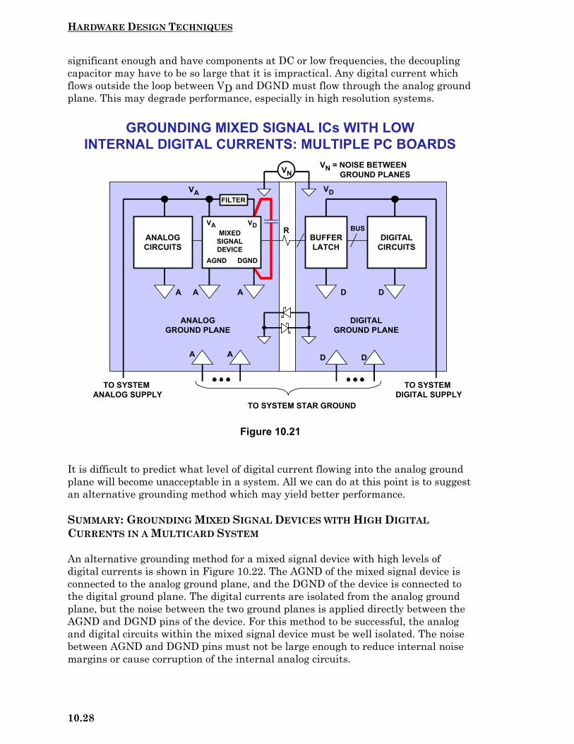
HARDWARE DESIGN TECHNIQUES
10.28
significant enough and have components at DC or low frequencies, the decouplingcapacitor may have to be so large that it is impractical. Any digital current whichflows outside the loop between VD and DGND must flow through the analog groundplane. This may degrade performance, especially in high resolution systems.
Figure 10.21
It is difficult to predict what level of digital current flowing into the analog groundplane will become unacceptable in a system. All we can do at this point is to suggestan alternative grounding method which may yield better performance.
SUMMARY: GROUNDING MIXED SIGNAL DEVICES WITH HIGH DIGITALCURRENTS IN A MULTICARD SYSTEM
An alternative grounding method for a mixed signal device with high levels ofdigital currents is shown in Figure 10.22. The AGND of the mixed signal device isconnected to the analog ground plane, and the DGND of the device is connected tothe digital ground plane. The digital currents are isolated from the analog groundplane, but the noise between the two ground planes is applied directly between theAGND and DGND pins of the device. For this method to be successful, the analogand digital circuits within the mixed signal device must be well isolated. The noisebetween AGND and DGND pins must not be large enough to reduce internal noisemargins or cause corruption of the internal analog circuits.
GROUNDING MIXED SIGNAL ICs WITH LOWINTERNAL DIGITAL CURRENTS: MULTIPLE PC BOARDS
ANALOGCIRCUITS
DIGITALCIRCUITS
A A D D
VA VD
ANALOGGROUND PLANE
DIGITALGROUND PLANE
MIXEDSIGNALDEVICE
AGND DGND
A A D D
TO SYSTEM STAR GROUND
TO SYSTEM DIGITAL SUPPLY
TO SYSTEM ANALOG SUPPLY
A
VA VD
BUFFERLATCH
FILTER
VN
BUSR
VN = NOISE BETWEEN GROUND PLANES
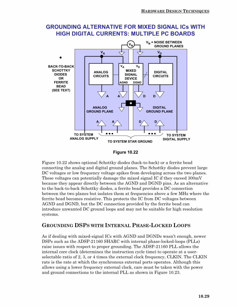
HARDWARE DESIGN TECHNIQUES
10.29
Figure 10.22
Figure 10.22 shows optional Schottky diodes (back-to-back) or a ferrite beadconnecting the analog and digital ground planes. The Schottky diodes prevent largeDC voltages or low frequency voltage spikes from developing across the two planes.These voltages can potentially damage the mixed signal IC if they exceed 300mVbecause they appear directly between the AGND and DGND pins. As an alternativeto the back-to-back Schottky diodes, a ferrite bead provides a DC connectionbetween the two planes but isolates them at frequencies above a few MHz where theferrite bead becomes resistive. This protects the IC from DC voltages betweenAGND and DGND, but the DC connection provided by the ferrite bead canintroduce unwanted DC ground loops and may not be suitable for high resolutionsystems.
GROUNDING DSPS WITH INTERNAL PHASE-LOCKED LOOPS
As if dealing with mixed-signal ICs with AGND and DGNDs wasn’t enough, newerDSPs such as the ADSP-21160 SHARC with internal phase-locked-loops (PLLs)raise issues with respect to proper grounding. The ADSP-21160 PLL allows theinternal core clock (determines the instruction cycle time) to operate at a user-selectable ratio of 2, 3, or 4 times the external clock frequency, CLKIN. The CLKINrate is the rate at which the synchronous external ports operates. Although thisallows using a lower frequency external clock, care must be taken with the powerand ground connections to the internal PLL as shown in Figure 10.23.
ANALOGCIRCUITS
DIGITALCIRCUITS
A A D D
VA VD
ANALOGGROUND PLANE
DIGITALGROUND PLANE
MIXEDSIGNALDEVICE
AGND
GROUNDING ALTERNATIVE FOR MIXED SIGNAL ICs WITHHIGH DIGITAL CURRENTS: MULTIPLE PC BOARDS
DGND
A A D D
BACK-TO-BACKSCHOTTKY
DIODES OR
FERRITEBEAD
(SEE TEXT)
TO SYSTEM STAR GROUND
TO SYSTEM DIGITAL SUPPLY
TO SYSTEM ANALOG SUPPLY
VA VD
VNVN = NOISE BETWEEN GROUND PLANES

HARDWARE DESIGN TECHNIQUES
10.30
Figure 10.23
In order to prevent internal coupling between digital currents and the PLL, thepower and ground connections to the PLL are brought out separately on pins labeledAVDD and AGND, respectively. The AVDD +2.5V supply should be derived from theVDD INT +2.5V supply using the filter network as shown. This ensures a relativelynoise-free supply for the internal PLL. The AGND pin of the PLL should beconnected to the digital ground plane of the PC board using a short trace. Thedecoupling capacitors should be routed between the AVDD pin and AGND pin usingshort traces.
GROUNDING SUMMARY
There is no single grounding method which will guarantee optimum performance100% of the time! This section has presented a number of possible optionsdepending upon the characteristics of the particular mixed signal devices inquestion. It is helpful, however to provide for as many options as possible whenlaying out the initial PC board.
It is mandatory that at least one layer of the PC board be dedicated to ground plane!The initial board layout should provide for non-overlapping analog and digitalground planes, but pads and vias should be provided at several locations for theinstallation of back-to-back Schottky diodes or ferrite beads, if required. Pads andvias should also be provided so that the analog and digital ground planes can beconnected together with jumpers if required.
GROUNDING DSPs WITH INTERNALPHASE-LOCKED-LOOPS (PLLs)
DSP(ADSP-21160)
PLLVDD INT VDD EXTAVDD
AGND GND
+2.5V+3.3V
40 46
10ΩΩΩΩ
0.01µF0.1µF
83
SHORT TRACES
SHORT TRACES
DIGITAL GROUND PLANE
CLKIN
X1, X2,X3, X4

HARDWARE DESIGN TECHNIQUES
10.31
The AGND pins of mixed-signal devices should in general always be connected tothe analog ground plane. An exception to this are DSPs which have internal phase-locked-loops (PLLs), such as the ADSP-21160 SHARC. The ground pin for the PLLis labeled AGND, but should be connected directly to the digital ground plane forthe DSP.
Figure 10.24
SOME GENERAL PC BOARD LAYOUT GUIDELINES FOR MIXED-SIGNALSYSTEMS
It is evident that noise can be minimized by paying attention to the system layoutand preventing different signals from interfering with each other. High level analogsignals should be separated from low level analog signals, and both should be keptaway from digital signals. We have seen elsewhere that in waveform sampling andreconstruction systems the sampling clock (which is a digital signal) is asvulnerable to noise as any analog signal, but is as liable to cause noise as any digitalsignal, and so must be kept isolated from both analog and digital systems. If clockdriver packages are used in clock distribution, only one frequency clock should bepassed through a single package. Sharing drivers between clocks of differentfrequencies in the same package will produce excess jitter and crosstalk anddegrade performance.
The ground plane can act as a shield where sensitive signals cross. Figure 10.25shows a good layout for a data acquisition board where all sensitive areas areisolated from each other and signal paths are kept as short as possible. While reallife is rarely as tidy as this, the principle remains a valid one.
GROUNDING PHILOSOPHY SUMMARY
There is no single grounding method which is guaranteed to work100% of the time!
Different methods may or may not give the same levels ofperformance.
At least one layer on each PC board MUST be dedicated to groundplane!
Do initial layout with split analog and digital ground planes. Provide pads and vias on each PC board for back-to-back
Schottky diodes and optional ferrite beads to connect the twoplanes.
Provide "jumpers" so that DGND pins of mixed-signal devices canbe connected to AGND pins (analog ground plane) or to digitalground plane. (AGND of PLLs in DSPs should be connected todigital ground plane).
Provide pads and vias for "jumpers" so that analog and digitalground planes can be joined together at several points on eachPC board.
Follow recommendations on mixed signal device data sheet.

HARDWARE DESIGN TECHNIQUES
10.32
Figure 10.25
There are a number of important points to be considered when making signal andpower connections. First of all a connector is one of the few places in the systemwhere all signal conductors must run in parallel - it is therefore imperative toseparate them with ground pins (creating a faraday shield) to reduce couplingbetween them.
Multiple ground pins are important for another reason: they keep down the groundimpedance at the junction between the board and the backplane. The contactresistance of a single pin of a PCB connector is quite low (of the order of 10mΩ)when the board is new - as the board gets older the contact resistance is likely torise, and the board's performance may be compromised. It is therefore wellworthwhile to allocate extra PCB connector pins so that there are many groundconnections (perhaps 30-40% of all the pins on the PCB connector should be groundpins). For similar reasons there should be several pins for each power connection,although there is no need to have as many as there are ground pins.
Manufacturers of high performance mixed-signal ICs like Analog Devices offerevaluation boards to assist customers in their initial evaluations and layout. ADCevaluation boards generally contain an on-board low-jitter sampling clock oscillator,output registers, and appropriate power and signal connectors. They also may haveadditional support circuitry such as the ADC input buffer amplifier and externalreference.
ANALOG AND DIGITAL CIRCUITSSHOULD BE PARTITIONED ON PCB LAYOUT
REFERENCE ADC
FILTER
AMPLIFIER
SAMPLINGCLOCK GENERATOR
TIMINGCIRCUITS
BUFFERREGISTER
DSPORµP
CONTROLLOGIC
DEMULTIPLEXER
BUFFERMEMORY
POWERANALOG
INPUT
MULTIPLEGROUNDS DATA
BUS
ADDRESSBUS
MULTIPLEGROUNDS
ANALOG DIGITAL

HARDWARE DESIGN TECHNIQUES
10.33
The layout of the evaluation board is optimized in terms of grounding, decoupling,and signal routing and can be used as a model when laying out the ADC PC boardin the system. The actual evaluation board layout is usually available from the ADCmanufacturer in the form of computer CAD files (Gerber files). In many cases, thelayout of the various layers appears on the data sheet for the device.
HARDWARE DESIGN TECHNIQUES
10.34
REFERENCES ON GROUNDING:
1. William C. Rempfer, Get All the Fast ADC Bits You Pay For,Electronic Design, Special Analog Issue, June 24, 1996, p.44.
2. Mark Sauerwald, Keeping Analog Signals Pure in a Hostile DigitalWorld, Electronic Design, Special Analog Issue, June 24, 1996, p.57.
3. Jerald Grame and Bonnie Baker, Design Equations Help OptimizeSupply Bypassing for Op Amps, Electronic Design, Special AnalogIssue, June 24, 1996, p.9.
4. Jerald Grame and Bonnie Baker, Fast Op Amps Demand More Thana Single-Capacitor Bypass, Electronic Design, Special Analog Issue,November 18, 1996, p.9.
5. Walt Kester and James Bryant, Grounding in High Speed Systems,High Speed Design Techniques, Analog Devices, 1996, Chapter 7, p. 7-27.
6. Jeffrey S. Pattavina, Bypassing PC Boards: Thumb Your Nose at Rulesof Thumb, EDN, Oct. 22, 1998, p.149.
7. Henry Ott, Noise Reduction Techniques in Electronic Systems,Second Edition, New York, John Wiley and Sons, 1988.
8. Howard W. Johnson and Martin Graham, High-Speed Digital Design,PTR Prentice Hall, 1993.
9. Paul Brokaw, An I.C. Amplifier User's Guide to Decoupling, Groundingand Making Things Go Right for a Change, Application Note, Analog Devices, Inc., http://www.analog.com.
10. Walt Kester, A Grounding Philosophy for Mixed-Signal Systems,Electronic Design Analog Applications Issue, June 23, 1997, p. 29.
11. Ralph Morrison, Grounding and Shielding Techniques, Fourth Edition,John Wiley, 1998.
12. Ralph Morrison, Solving Interference Problems in Electronics,John Wiley, 1995.
13. C. D. Motchenbacher and J. A. Connelly, Low Noise Electronic SystemDesign, John Wiley, 1993.
14. Crystal Oscillators: MF Electronics, 10 Commerce Drive, New Rochelle,NY, 10801, 914-576-6570.
15. Mark Montrose, EMC and the Printed Circuit Board, IEEE Press,1999 (IEEE Order Number PC5756).

HARDWARE DESIGN TECHNIQUES
10.35
DIGITAL ISOLATION TECHNIQUESWalt KesterOne way to break ground loops is to use isolation techniques. Analog isolationamplifiers find many applications where a high degree of isolation is required, suchas in medical instrumentation. Digital isolation techniques offer a reliable methodof transmitting digital signals over interfaces without introducing ground noise.
Optocouplers (also called optoisolators) are useful and available in a wide variety ofstyles and packages. A typical optocoupler based on an LED and a phototransitor isshown in Figure 10.26. A current of approximately 10mA is applied to an LEDtransmitter, and the light output is received by a phototransistor. The lightproduced by the LED is sufficient to saturate the phototransistor. Isolation of 5000VRMS to 7000V RMS is common. Although excellent for digital signals, optocouplersare too nonlinear for most analog applications. One should also realize that sincethe phototransistor is operated in a saturated mode, rise and fall-times can rangefrom 10µs to 20µs in slower devices, thereby limiting applications at high speeds.
Figure 10.26
A faster optocoupler architecture is shown in Figure 10.27 and is based on an LEDand a photodiode. The LED is again driven with a current of approximately 10mA.This produces a light output sufficient generate enough current in the receivingphotodiode to develop a valid high logic level at the output of the transimpedanceamplifier. Speed can vary widely between optocouplers, and the fastest ones havepropagation delays of 20ns typical, and 40ns maximum, and can handle data rates
DIGITAL ISOLATION USINGLED / PHOTOTRANSISTOR OPTOCOUPLERS
IOUT
HIGH VOLTAGEISOLATION BARRIER
Uses Light for Transmission Over a High Voltage Barrier
The LED is the Transmitter, and the Phototransistor is the Receiver
High Voltage Isolation: 5000V to 7000V RMS
Non-Linear -- Best for Digital or Frequency Information
Rise and Fall-times can be 10 to 20µs in Slower Devices
Example: Siemens ILQ-1 Quad (http://www.siemens.com)
VDD2 (5V)10kΩΩΩΩ
IIN
VDD1 (5V) 425ΩΩΩΩ
GND1GND2
CMOSGATE
VOUT
VIN

HARDWARE DESIGN TECHNIQUES
10.36
up to 25MBd for NRZ data. This corresponds to a maximum square wave operatingfrequency of 12.5MHz, and a minimum allowable passable pulse width of 40ns.
Figure 10.27
The ADuM1100A and ADuM1100B are digital isolators based on Analog Devices’µmIsolation™ (micromachined isolation) technology. Combining high speed CMOSand monolithic air core transformer technology, these isolation components provideoutstanding performance characteristics superior to the traditional optocouplerspreviously described.
Configured as pin-compatible replacements for existing high speed optocouplers, theADuM1100A and ADuM1100B support data rates as high as 25MBd and 100MBb,respectively. A functional diagram of the devices is shown in Figure 10.28.
Both the ADuM1100A and ADuM1100B operate at either 3.3V or 5V supplyvoltages, have propagation delays < 10ns, edge asymmetry of <2ns, and rise andfall-times < 2ns. They operate at very low power, less than 600µA of quiescentcurrent (sum of both sides) and a dynamic current of less than 230µA per MBd ofdata rate. Unlike common transformer implementations, the parts provide DCcorrectness with a patented refresh feature which continuously updates the outputsignal.
DIGITAL ISOLATION USINGLED / PHOTODIODE OPTOCOUPLERS
VDD1 VDD2
GND1 GND2
VIN VOUT
(Data In) (Data Out)
+5V Supply Voltage 2500V RMS I/O Withstand Voltage Logic Signal Frequency: 12.5MHz Maximum 25MBd Maximum Data Rate 40ns Maximum Propagation Delay 9ns Typical Rise/Fall Time Example: Agilent HCPL-7720 (http://www.semiconductor.agilent.com)

HARDWARE DESIGN TECHNIQUES
10.37
Figure 10.28
The AD260/AD261 family of digital isolators isolates five digital control signalsto/from high speed DSPs, microcontrollers, or microprocessors. The AD260 also hasa 1.5W transformer for a 3.5kV RMS isolated external DC/DC power supply circuit.
Each line of the AD260 can handle digital signals up to 20MHz (40MBd) with apropagation delay of only 14ns which allows for extremely fast data transmission.Output waveform symmetry is maintained to within ±1ns of the input so the AD260can be used to accurately isolate time-based pulse width modulator (PWM) signals.
A simplified schematic of one channel of the AD260/AD261 is shown in Figure10.29. The data input is passed through a schmitt trigger circuit, through a latch,and a special transmitter circuit which differentiates the edges of the digital inputsignal and drives the primary winding of a proprietary transformer with a "set-high/set-low" signal. The secondary of the isolation transformer drives a receiverwith the same "set-hi/set-low" data which regenerates the original logic waveform.An internal circuit operates in the background which interrogates all inputs aboutevery 5µs and in the absence of logic transitions, sends appropriate "set-hi/set-low"data across the interface. Recovery time from a fault condition or at power-up isthus between 5µs and 10µs.
The power transformer (available on the AD260) is designed to operate between150kHz and 250kHz and will easily deliver more than 1W of isolated power whendriven push-pull (5V) on the transmitter side. Different transformer taps, rectifier
ADuM1100A/ADuM1100B DIGITAL ISOLATORS
VDD1 VDD2
GND1 GND2
VIN VOUT
(Data In) (Data Out)
+5V/+3.3V Supply Voltage 2500V RMS I/O Withstand Voltage 25MBd Maximum Data Rate (ADuM1100A) 100 MBd Maximum Data Rate (ADuM1100B) 10ns Maximum Propagation Delay 2ns Typical Rise/Fall Time Pin Compatible with Popular Optocouplers
UPDATE
ENCODE DECODE
WATCH

HARDWARE DESIGN TECHNIQUES
10.38
and regulator schemes will provide combinations of ±5V, 15V, 24V, or even 30V orhigher. The output voltage when driven with a low voltage-drop drive will be37V p-p across the entire secondary with a 5V push-pull drive.
Figure 10.29
Figure 10.30
AD260/AD261 DIGITAL ISOLATORS
D
CONTINUOUSUPDATECIRCUIT
E
SCHMITTTRIGGER LATCH
XMTR RCVR
TRI STATE
ENABLEENABLE
ISOLATED POWERXFMR (AD260)
37V p-p, 1.5W
NOTE: SINGLE DATA CHANNEL SHOWN
3500V RMS ISOLATION BARRIER(AD260B/AD261B)
DATAIN DATA
OUT
AD260/AD261 DIGITAL ISOLATOR KEY SPECIFICATIONS
Isolation Test Voltage to 3500V RMS (AD260B/AD261B)
Five Isolated Digital Lines Available in 6 Input/Output Configurations
Logic Signal Frequency: 20MHz Max.
Data Rate: 40MBd Max.
Isolated Power Transformer: 37V p-p, 1.5W (AD260)
Waveform Edge Transmission Symmetry: ±1ns
Propagation Delay: 14ns
Rise and Fall-Times < 5ns

HARDWARE DESIGN TECHNIQUES
10.39
POWER SUPPLY NOISE REDUCTION ANDFILTERINGWalt Jung, Walt Kester, Bill Chestnut
Precision analog circuitry has traditionally been powered from well regulated, lownoise linear power supplies. During the last decade however, switching powersupplies have become much more common in electronic systems. As a consequence,they also are being used for analog supplies. Good reasons for the general popularityinclude their high efficiency, low temperature rise, small size, and light weight.
In spite of these benefits, switchers do have drawbacks, most notably high outputnoise. This noise generally extends over a broad band of frequencies, resulting inboth conducted and radiated noise, as well as unwanted electric and magneticfields. Voltage output noise of switching supplies are short-duration voltagetransients, or spikes. Although the fundamental switching frequency can rangefrom 20kHz to 1MHz, the spikes can contain frequency components extending to100MHz or more. While specifying switching supplies in terms of RMS noise iscommon vendor practice, as a user you should also specify the peak (or p-p)amplitudes of the switching spikes, at the output loading of your system.
The following section discusses filter techniques for rendering a switching regulatoroutput analog ready, that is sufficiently quiet to power precision analog circuitrywith relatively small loss of DC terminal voltage. The filter solutions presented aregenerally applicable to all power supply types incorporating switching element(s) intheir energy path. This includes various DC-DC converters as well as popular 5V(PC type) supplies.
An understanding of the EMI process is necessary to understand the effects ofsupply noise on analog circuits and systems. Every interference problem has asource, a path, and a receptor [Reference 1]. In general, there are three methods fordealing with interference. First, source emissions can be minimized by properlayout, pulse-edge rise time control/reduction, filtering, and proper grounding.Second, radiation and conduction paths should be reduced through shielding andphysical separation. Third, receptor immunity to interference can be improved, viasupply and signal line filtering, impedance level control, impedance balancing, andutilizing differential techniques to reject undesired common-mode signals. Thissection focuses on reducing switching power supply noise with external post filters.
Tools useful for combating high frequency switcher noise are shown by Figure 10.31.They differ in electrical characteristics as well as their practicality towards noisereduction, and are listed roughly in an order of priorities. Of these tools, L and Care the most powerful filter elements, and are the most cost-effective, as well assmall in size.

HARDWARE DESIGN TECHNIQUES
10.40
Figure 10.31
Capacitors are probably the single most important filter component for switchers.There are many different types of capacitors, and an understanding of theirindividual characteristics is absolutely mandatory in the design of effective practicalsupply filters. There are generally three classes of capacitors useful in 10kHz-100MHz filters, broadly distinguished as the generic dielectric types; electrolytic,organic, film, and ceramic. These can in turn can be further sub-divided. Athumbnail sketch of capacitor characteristics is shown in the chart of Figure 10.32.
Figure 10.32
SWITCHING REGULATOR NOISE REDUCTION TOOLS
Capacitors
Inductors
Ferrites
Resistors
Linear Post Regulation
Proper Layout and Grounding Techniques
PHYSICAL SEPARATION FROM SENSITIVE
ANALOG CIRCUITS!!
TYPES OF CAPACITORS
(*) Upper frequency strongly size and package dependent
AluminumElectrolytic
(GeneralPurpose)
AluminumElectrolytic(Switching
Type)
TantalumElectrolytic
OS-CONElectrolytic
Polyester(Stacked
Film)
Ceramic(Multilayer)
Size 100 µF 120 µF 120 µF 100 µF 1 µF 0.1 µF
RatedVoltage
25 V 25 V 20 V 20 V 400 V 50 V
ESR0.6 ΩΩΩΩ @100 kHz
0.18 ΩΩΩΩ @100 kHz
0.12 ΩΩΩΩ @100 kHz
0.02 ΩΩΩΩ @100 kHz
0.11 ΩΩΩΩ @1 MHz
0.12 ΩΩΩΩ @1 MHz
OperatingFrequency
(*)
≅≅≅≅ 100 kHz ≅≅≅≅ 500 kHz ≅≅≅≅ 1 MHz ≅≅≅≅ 1 MHz ≅≅≅≅ 10 MHz ≅≅≅≅ 1 GHz

HARDWARE DESIGN TECHNIQUES
10.41
With any dielectric, a major potential filter loss element is ESR (equivalent seriesresistance), the net parasitic resistance of the capacitor. ESR provides an ultimatelimit to filter performance, and requires more than casual consideration, because itcan vary both with frequency and temperature in some types. Another capacitor losselement is ESL (equivalent series inductance). ESL determines the frequency wherethe net impedance characteristic switches from capacitive to inductive. This variesfrom as low as 10kHz in some electrolytics to as high as 100MHz or more in chipceramic types. Both ESR and ESL are minimized when a leadless package is used.All capacitor types mentioned are available in surface mount packages, preferablefor high speed uses.
The electrolytic family provides an excellent, cost-effective low-frequency filtercomponent, because of the wide range of values, a high capacitance-to-volume ratio,and a broad range of working voltages. It includes general purpose aluminumelectrolytic types, available in working voltages from below 10V up to about 500V,and in size from 1 to several thousand µF (with proportional case sizes). Allelectrolytic capacitors are polarized, and thus cannot withstand more than a volt orso of reverse bias without damage. They also have relatively high leakage currents(up to tens of µA, and strongly dependent upon design specifics).
A subset of the general electrolytic family includes tantalum types, generallylimited to voltages of 100V or less, with capacitance of up to 500µF [Reference 3]. Ina given size, tantalums exhibit a higher capacitance-to-volume ratios than dogeneral purpose electrolytics, and have both a higher frequency range and lowerESR. They are generally more expensive than standard electrolytics, and must becarefully applied with respect to surge and ripple currents.
A subset of aluminum electrolytic capacitors is the switching type, designed forhandling high pulse currents at frequencies up to several hundred kHz with lowlosses [Reference 4]. This capacitor type competes directly with tantalums in highfrequency filtering applications, with the advantage of a broader range of values.
A more specialized high performance aluminum electrolytic capacitor type uses anorganic semiconductor electrolyte [Reference 5]. The OS-CON capacitors featureappreciably lower ESR and higher frequency range than do other electrolytic types,with an additional feature of low low-temperature ESR degradation.
Film capacitors are available in a very broad range of values and an array ofdielectrics, including polyester, polycarbonate, polypropylene, and polystyrene.Because of the low dielectric constant of these films, their volumetric efficiency isquite low, and a 10µF/50V polyester capacitor (for example) is actually the size ofyour hand. Metalized (as opposed to foil) electrodes do help to reduce size, but eventhe highest dielectric constant units among film types (polyester, polycarbonate) arestill larger than any electrolytic, even using the thinnest films with the lowest

HARDWARE DESIGN TECHNIQUES
10.42
voltage ratings (50V). Where film types excel is in their low dielectric losses, a factorwhich may not necessarily be a practical advantage for filtering switchers. Forexample, ESR in film capacitors can be as low as 10mΩ or less, and the behavior offilms generally is very high in terms of Q. In fact, this can cause problems ofspurious resonance in filters, requiring damping components.
Film capacitors using a wound layer-type construction can be inductive. This canlimit their effectiveness for high frequency filtering. Obviously, only non-inductivelymade film caps are useful for switching regulator filters. One specific style which isnon-inductive is the stacked-film type, where the capacitor plates are cut as smalloverlapping linear sheet sections from a much larger wound drum of dielectric/platematerial. This technique offers the low inductance attractiveness of a plate sheetstyle capacitor with conventional leads [see References 4, 5, 6]. Obviously, minimallead length should be used for best high frequency effectiveness. Very high currentpolycarbonate film types are also available, specifically designed for switchingpower supplies, with a variety of low inductance terminations to minimize ESL[Reference 7].
Dependent upon their electrical and physical size, film capacitors can be useful atfrequencies to well above 10MHz. At the highest frequencies, only stacked filmtypes should be considered. Some manufacturers are now supplying film types inleadless surface mount packages, which eliminates the lead length inductance.
Ceramic is often the capacitor material of choice above a few MHz, due to itscompact size, low loss, and availability up to several µF in the high-K dielectricformulations (X7R and Z5U), at voltage ratings up to 200V [see ceramic families ofReference 3]. NP0 (also called COG) types use a lower dielectric constantformulation, and have nominally zero TC, plus a low voltage coefficient (unlike theless stable high-K types). NP0 types are limited to values of 0.1µF or less, with0.01µF representing a more practical upper limit.
Multilayer ceramic “chip caps” are very popular for bypassing/ filtering at 10MHz orhigher, simply because their very low inductance design allows near optimum RFbypassing. For smaller values, ceramic chip caps have an operating frequency rangeto 1GHz. For high frequency applications, a useful selection can be ensured byselecting a value which has a self-resonant frequency above the highest frequency ofinterest.
All capacitors have some finite ESR. In some cases, the ESR may actually be helpfulin reducing resonance peaks in filters, by supplying “free” damping. For example, inmost electrolytic types, a nominally flat broad series resonance region can be notedby the impedance vs. frequency plot. This occurs where |Z| falls to a minimumlevel, nominally equal to the capacitor’s ESR at that frequency. This low Qresonance can generally cover a relatively wide frequency range of several octaves.

HARDWARE DESIGN TECHNIQUES
10.43
Contrasted to the very high Q sharp resonances of film and ceramic caps, the low Qbehavior of electrolytics can be useful in controlling resonant peaks.
In most electrolytic capacitors, ESR degrades noticeably at low temperature, by asmuch as a factor of 4-6 times at –55°C vs. the room temperature value. For circuitswhere ESR is critical to performance, this can lead to problems. Some specificelectrolytic types do address this problem, for example within the HFQ switchingtypes, the –10°C ESR at 100kHz is no more than 2× that at room temperature. TheOSCON electrolytics have a ESR vs. temperature characteristic which is relativelyflat.
As noted, all real capacitors have parasitic elements which limit their performance.The equivalent electrical network representing a real capacitor models both ESRand ESL as well as the basic capacitance, plus some shunt resistance (see Figure10.33). In such a practical capacitor, at low frequencies the net impedance is almostpurely capacitive. At intermediate frequencies, the net impedance is determined byESR, for example about 0.12Ω to 0.4Ω at 125kHz, for several types. Above about1MHz these capacitor types become inductive, with impedance dominated by theeffect of ESL. All electrolytics will display impedance curves similar in generalshape to that of Figure 10.34. The minimum impedance will vary with the ESR, andthe inductive region will vary with ESL (which in turn is strongly affected bypackage style).
Figure 10.33
CAPACITOR EQUIVALENT CIRCUITAND PULSE RESPONSE
0
IPEAK = 1A
Equivalent f = 3.5MHz
0
ESL = 20nH
ESR = 0.2ΩΩΩΩ
C = 100µFXC = 0.0005Ω Ω Ω Ω @ 3.5MHz
INPUTCURRENT
OUTPUTVOLTAGE
v
i
ESR • IPEAK = 200mV
didt = 1A
100ns
VPEAK = ESL • didt + ESR • IPEAK
= 400mV
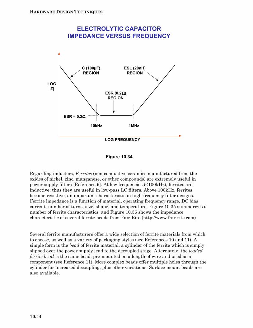
HARDWARE DESIGN TECHNIQUES
10.44
Figure 10.34
Regarding inductors, Ferrites (non-conductive ceramics manufactured from theoxides of nickel, zinc, manganese, or other compounds) are extremely useful inpower supply filters [Reference 9]. At low frequencies (<100kHz), ferrites areinductive; thus they are useful in low-pass LC filters. Above 100kHz, ferritesbecome resistive, an important characteristic in high-frequency filter designs.Ferrite impedance is a function of material, operating frequency range, DC biascurrent, number of turns, size, shape, and temperature. Figure 10.35 summarizes anumber of ferrite characteristics, and Figure 10.36 shows the impedancecharacteristic of several ferrite beads from Fair-Rite (http://www.fair-rite.com).
Several ferrite manufacturers offer a wide selection of ferrite materials from whichto choose, as well as a variety of packaging styles (see References 10 and 11). Asimple form is the bead of ferrite material, a cylinder of the ferrite which is simplyslipped over the power supply lead to the decoupled stage. Alternately, the leadedferrite bead is the same bead, pre-mounted on a length of wire and used as acomponent (see Reference 11). More complex beads offer multiple holes through thecylinder for increased decoupling, plus other variations. Surface mount beads arealso available.
ELECTROLYTIC CAPACITORIMPEDANCE VERSUS FREQUENCY
ESR = 0.2ΩΩΩΩ
10kHz 1MHz
LOG FREQUENCY
LOG|Z|
C (100µF)REGION
ESL (20nH)REGION
ESR (0.2Ω)Ω)Ω)Ω)REGION

HARDWARE DESIGN TECHNIQUES
10.45
Figure 10.35
Figure 10.36
FERRITES SUITABLE FOR HIGH FREQUENCY FILTERS
Ferrites Good for Frequencies Above 25kHz Many Sizes and Shapes Available Including Leaded "Resistor
Style" Ferrite Impedance at High Frequencies Primarily Resistive --
Ideal for HF Filtering Low DC Loss: Resistance of Wire Passing Through Ferrite is
Very Low High Saturation Current Versions Available Choice Depends Upon:
Source and Frequency of Interference Impedance Required at Interference Frequency Environmental: Temperature, AC and DC Field Strength,
Size / Space Available Always Test the Design!
IMPEDANCE OF FERRITE BEADS
#73MATERIAL
#43MATERIAL
#64MATERIAL
1 10 100 1000
FREQUENCY (MHz)
Z
ΩΩΩΩ
0
20
40
60
80
Courtesy: Fair-Rite Products Corp, Wallkill, NY(http://www.fair-rite.com)

HARDWARE DESIGN TECHNIQUES
10.46
PSpice ferrite models for Fair-Rite materials are available, and allow ferriteimpedance to be estimated [see Reference 12]. These models have been designed tomatch measured impedances rather than theoretical impedances.
A ferrite’s impedance is dependent upon a number of inter-dependent variables, andis difficult to quantify analytically, thus selecting the proper ferrite is notstraightforward. However, knowing the following system characteristics will makeselection easier. First, determine the frequency range of the noise to be filtered.Second, the expected temperature range of the filter should be known, as ferriteimpedance varies with temperature. Third, the peak DC current flowing throughthe ferrite must be known, to ensure that the ferrite does not saturate. Althoughmodels and other analytical tools may prove useful, the general guidelines givenabove, coupled with some experimentation with the actual filter connected to thesupply output under system load conditions, should lead to a proper ferriteselection.
Using proper component selection, low and high frequency band filters can bedesigned to smooth a noisy switcher’s DC output to produce an analog ready 5Vsupply. It is most practical to do this over two (and sometimes more) stages, eachstage optimized for a range of frequencies. A basic stage can be used to carry all ofthe DC load current, and filter noise by 60dB or more up to a 1-10MHz range. Thislarger filter is used as a card entry filter providing broadband filtering for all powerentering a PC card. Smaller, more simple local filter stages are also used to providehigher frequency decoupling right at the power pins of individual stages.
SWITCHING REGULATOR EXPERIMENTS
In order to better understand the challenge of filtering switching regulators, a seriesof experiments were conducted with a representative device, the ADP1148synchronous buck regulator with a 9V input and a 3.3V/1A output.
In addition to observing typical input and output waveforms, the objective of theseexperiments was to reduce the output ripple to less than 10mV peak-to-peak, avalue suitable for driving most analog circuits.
Measurements were made using a Tektronix wideband digitizing oscilloscope withthe input bandwidth limited to 20MHz so that the ripple generated by the switchingregulators could be more readily observed. In a system, power supply ripplefrequencies above 20MHz are best filtered locally at each IC power pin with a lowinductance ceramic capacitor and perhaps a series-connected ferrite bead.
Probing techniques are critical for accurate ripple measurements. A standardpassive 10X probe was used with a "bayonet" probe tip adapter for making theground connection as short as possible (see Figure 10.37). Use of the "ground cliplead" is not recommended in making this type of measurement because the leadlength in the ground connection forms an unwanted inductive loop which picks uphigh frequency switching noise, thereby corrupting the signal being measured.

HARDWARE DESIGN TECHNIQUES
10.47
Figure 10.37
Note: Schematic representation of proper physical grounding is almost impossible. Inall the following circuit schematics, the connections to ground are made to theground plane using the shortest possible connecting path, regardless of how they areindicated in the actual circuit schematic diagram.
The circuit for the ADP1148 9V to 3.3V/1A buck regulator is shown in Figure 10.38.The output waveform of the ADP1148 buck regulator is shown in Figure 10.39. Thefundamental switching frequency is approximately 150kHz, and the output ripple isapproximately 40mV.
Adding an output filter consisting of a 50µH inductor and a 100µF leaded tantalumcapacitor reduced the ripple to approximately 3mV as shown in Figure 10.40.
Linear regulators are often used following switching regulators for better regulationand lower noise. Low dropout (LDO) regulators such as the ADP3310 are desirablein these applications because they require only a small input-to-output seriesvoltage to maintain regulation. This minimizes power dissipation in the pass deviceand may eliminate the need for a heat sink. Figure 10.41 shows the ADP1148 buckregulator configured for a 9V input and a 3.75V/1A output. The output drives anADP3310 linear LDO regulator configured for 3.75V input and 3.3V/1A output. Theinput and output of the ADP3310 is shown in Figure 10.42. Notice that theregulator reduces the ripple from 40mV to approximately 5mV.
PROPER PROBING TECHNIQUES
GROUND PLANE CONTACT
SIGNALCONTACT
IC
SLIP-ON"BAYONET"
GROUNDADAPTER
"GROUND CLIP"CONNECTOR
"GROUND CLIP"LEAD
(DO NOT USE!!)
PROBE

HARDWARE DESIGN TECHNIQUES
10.48
Figure 10.38
Figure 10.39
ADP1148 BUCK REGULATOR CIRCUIT
P-DRIVE
SENSE (+)
SENSE (–)
ITH
CT
INT VCC
N-DRIVESGND PGND
P-CH
N-CH
IRF7403
IRF7204
10BQ040
VIN
ADP1148-3.3SHUTDOWN
RC, 1kΩΩΩΩ
CC
L, 50µHRSENSE
0.1ΩΩΩΩ
3300pFCT
470pF
1000pF
10nF
1µF220µF/25V
+
100µF20V
VIN, 9V
VOUT3.3V/1A
L=COILTRONICS CTX-50-4
+
C1
C2
C1 = 220µF/25V GEN PURPOSE AL ELECTROLYTIC + 1µF CERAMIC
C2 = 100µF/20V LEADED TANTALUM, KEMET T356-SERIES, ESR = 0.6ΩΩΩΩ
ADP1148 BUCK OUTPUT WAVEFORM
VERTICAL SCALE: 10mV / DIVHORIZ. SCALE: 5µs / DIV
ADP1148BUCKREG
CIRCUIT
+
VIN9V
VOUT3.3V1A
C1 = 220 µF +1 µF
C2 = 100µF/20V
1µF 220µF25V
+
100µF20V
C1 = 1µF CERAMIC + 220µF/25V GENERAL PURPOSE AL ELECTROLYTICC2 = 100µF/20V LEADED TANTALUM, KEMET T356-SERIES (ESR = 0.6ΩΩΩΩ)
40mV p-p

HARDWARE DESIGN TECHNIQUES
10.49
Figure 10.40
Figure 10.41
ADP1148 BUCK FILTERED OUTPUT
VERTICAL SCALE: 10mV / DIVHORIZ. SCALE: 5µs / DIV
ADP1148BUCKREG
CIRCUIT
+
VIN9V
VOUT3.3V1A
C1 = 220 µF +1 µF
C2 = 100µF/20V
1µF 220µF25V
+
100µF20V
+
CF100µF20V
LF 50µH
OUTPUT FILTERLF=COILTRONICS CTX-50-4CF = 100µF/20V LEADED TANTALUM, KEMET T356-SERIES
C1 = 1µF CERAMIC + 220µF/25V GENERAL PURPOSE AL ELECTROLYTICC2 = 100µF/20V LEADED TANTALUM, KEMET T356-SERIES (ESR = 0.6ΩΩΩΩ)
3mV p-p
ADP1148 BUCK REGULATOR DRIVINGADP3310 LOW DROPOUT REGULATOR
P-DRIVE
SENSE (+)
SENSE (–)
ITH
CT
INT VCC
N-DRIVESGND PGND
P-CH
N-CH
IRF7403
IRF7204
10BQ040
VIN
ADP1148SD
RC, 1kΩΩΩΩ
CC
L, 68µHRSENSE
0.1ΩΩΩΩ
2200pFCT
470pF
1000pF
10nF
1µF 220µF35V
+
100µF20V
VIN, 9V
3.75V
+
C1
C2
FB
GATEIN OUT
GND
IFR7404
R120kΩΩΩΩ
R210kΩΩΩΩ
3.3V1A
ADP3310-3.3 C310µF35V
WAVEFORMS

HARDWARE DESIGN TECHNIQUES
10.50
Figure 10.42
There are many tradeoffs in designing power supply filters. The success of anyfilter circuit is highly dependent upon a compact layout and the use of a large areaground plane. As has been stated earlier, all connections to the ground plane shouldbe made as short as possible to minimize parasitic resistance and inductance.
Output ripple can be reduced by the addition of low ESL/ESR capacitors to theoutput. However, it may be more efficient to use an LC filter to accomplish theripple reduction. In any case, proper component selection is critical. The inductorshould not saturate under the maximum load current, and its DC resistance shouldbe low enough as not to induce significant voltage drop. The capacitors should havelow ESL and ESR and be rated to handle the required ripple current.
Low dropout linear post regulators provide both ripple reduction as well as betterregulation and can be effective, provided the sacrifice in efficiency is not excessive.
Finally, it is difficult to predict the output ripple current analytically, and there isno substitute for a prototype using the real-world components. Once the filter isproven to provide the desired ripple attenuation (with some added safety margin),care must be taken that parts substitutions or vendor changes are not made in thefinal production units without first testing them in the circuit for equivalentperformance.
WAVEFORMS FOR ADP1148 BUCK REGULATORDRIVING ADP3310 LOW DROPOUT REGULATOR
ADP1148 OUTPUT(ADP3310 INPUT) ADP3310 OUTPUT
VERTICAL SCALE: 10mV/DIVHORIZ. SCALE: 5µs/DIV
VERTICAL SCALE: 10mV/DIVHORIZ. SCALE: 5µs/DIV
5mV p-p40mV p-p

HARDWARE DESIGN TECHNIQUES
10.51
Figure 10.43
LOCALIZED HIGH FREQUENCY POWER SUPPLY FILTERING
The LC filters described in the previous section are useful in filtering switchingregulator outputs. However, it may be desirable to place similar filters on theindividual PC boards where the power first enters the board. Of course, if theswitching regulator is placed on the PC board, then the LC filter should be anintegral part of the regulator design.
Localized high frequency filters may also be required at each IC power pin (seeFigure 10.44). Surface mount ceramic capacitors are ideal choices because of theirlow ESL. It is important to make the connections to the power pin and the groundplane as short as possible. In the case of the ground connection, a via directly to theground plane is the shortest path. Routing the capacitor ground connection toanother ground pin on the IC is not recommended due to the added inductance ofthe trace. In some cases, a ferrite bead in series with the power connection may alsobe desirable.
SWITCHING SUPPLY FILTER SUMMARY
Proper Layout and Grounding (using Ground Plane) Mandatory Low ESL/ESR Capacitors Give Best Results Parallel Capacitors Lower ESR/ESL and Increase Capacitance External LC Filters Very Effective in Reducing Ripple Linear Post Regulation Effective for Noise Reduction and Best
Regulation Completely Analytical Approach Difficult, Prototyping is
Required for Optimum Results Once Design is Finalized, Do Not Switch Vendors or Use Parts
Substitutions Without First Verifying Their Performance inCircuit
High Frequency Localized Decoupling at IC Power Pins is StillRequired

HARDWARE DESIGN TECHNIQUES
10.52
Figure 10.44
The following list summarizes the switching power supply filter layout/constructionguidelines which will help ensure that the filter does the best possible job:
(1) Pick the highest electrical value and voltage rating for filter capacitors which isconsistent with budget and space limits. This minimizes ESR, and maximizes filterperformance. Pick chokes for low ∆L at the rated DC current, as well as low DCR.
(2) Use short and wide PCB tracks to decrease voltage drops and minimizeinductance. Make track widths at least 200 mils for every inch of track length forlowest DCR, and use 1 oz or 2 oz copper PCB traces to further reduce IR drops andinductance.
(3) Use short leads or better yet, leadless components, to minimize lead inductance.This minimizes the tendency to add excessive ESL and/or ESR. Surface mountpackages are preferred. Make all connections to the ground plane as short aspossible.
(4) Use a large-area ground plane for minimum impedance.
(5) Know what your components do over frequency, current and temperaturevariations! Make use of vendor component models for the simulation of prototypedesigns, and make sure that lab measurements correspond reasonably with the
LOCALIZED DECOUPLING TO GROUND PLANEUSING SHORTEST PATH
V+
GND
VIAS TOGROUNDPLANE
DECOUPLINGCAPACITOR
V+
GND
DECOUPLINGCAPACITOR
VIA TOGROUNDPLANE
PCBTRACE
IC IC
POWERSUPPLYTRACE
POWERSUPPLYTRACE
CORRECT INCORRECTOPTIONALFERRITE BEADS

HARDWARE DESIGN TECHNIQUES
10.53
simulation. While simulation is not absolutely necessary, it does instill confidence ina design when correlation is achieved (see Reference 15).
HIGH DENSITY DSP LOCALIZED DECOUPLING CONSIDERATIONS
High pin-count DSP packages require special consideration with respect to localizeddecoupling due to their high digital transient currents. Typical decouplingarrangements are shown in Figure 10.45. The surface mount capacitors are placedon the top side of the PC board in Figure 10.45A. For the SHARC-family, eight0.02µF ceramic capacitors are recommended. They should be placed as close to thepackage as possible. The connections to the VDD pins should be as short as possibleusing wide traces. The connections to ground should be made directly to the groundplane with vias. A less desirable method is shown in Figure 10.45B, where thecapacitors are mounted on the back side of the PC board underneath the footprint ofthe package. If the ground plane underneath the package footprint is perforatedwith many signal vias, the capacitor return transient current must flow to theoutside ground plane, which may be poorly connected to the inside ground plane dueto the vias.
Figure 10.45
DECOUPLING HIGH PIN-COUNT DSPsIN PQFP PACKAGES
TOP VIEWOF PACKAGE
TOP VIEWOF PACKAGE
CAPACITORS ON TOP SIDE OF PC BOARD
CAPACITORS ON BACK SIDE OF PC BOARD
A B

HARDWARE DESIGN TECHNIQUES
10.54
The PC board for a ball grid array (BGA) package is shown in Figure 10.46. Notethat all connections to the balls must be made using vias to other layers of theboard. The “dogbone” pattern shown is often used for the BGA packages. Theshaded area indicates the location of the solder mask. As in the case of PQFPpackages, the localized decoupling capacitors should be placed as close as possible tothe package with short connections to the VDD pins and direct connections to vias tothe ground plane layer.
Figure 10.46
The ADSP-21160 400-ball BGA 27mm by 27mm package approximate power andground assignments are shown in Figure 10.47. The ball pitch is 1.27mm.Approximately 84 balls are used in the center of the pattern for ground connections.The connections to the core voltage (40 balls) and the external voltage (46 balls)surround the ground balls. The remaining outer balls are used for the varioussignals.
The centrally located ground balls serve a dual function. Their primary function ismake a low impedance connection directly to the ground plane layer. Theirsecondary function is to conduct the package heat to the ground plane layer whichalso acts as a heat sink, since the device must dissipate about 2.5W under averageoperating conditions. The addition of an external heatsink as shown lowers thejunction-to-ambient thermal resistance even further.
DECOUPLING HIGH PIN-COUNT DSPsIN BALL GRID ARRAY (BGA) PACKAGES
TOP VIEWOF PC BOARD
WITHOUTPACKAGE
BGA PACKAGE
MULTILAYERPC BOARD
"DOGBONE" PAD
VIA
SOLDER MASK
SOLDER BALLS
VIAS
CROSS SECTION VIEW

HARDWARE DESIGN TECHNIQUES
10.55
Figure 10.47
ADSP-21160 DSP 400-PINPBGA PACKAGE BALL LOCATIONS
GROUND AND HEATSINK
GROUND BALLS(84)
VOLTAGE BALLS(86)
MULTILAYERPC BOARD
BALL LOCATIONS ARE APPROXIMATE, ALL BALLS NOT SHOWN
SIGNAL BALLS
PACKAGE SIZE:27mm X 27mm
BALL PITCH: 1.27mm
HARDWARE DESIGN TECHNIQUES
10.56
REFERENCES: NOISE REDUCTION AND FILTERING
1. EMC Design Workshop Notes, Kimmel-Gerke Associates, Ltd.,St. Paul, MN. 55108, (612) 330-3728.
2. Walt Jung, Dick Marsh, Picking Capacitors, Parts 1 & 2, Audio,February, March, 1980.
3. Tantalum Electrolytic and Ceramic Capacitor Families, KemetElectronics, Box 5928, Greenville, SC, 29606, (803) 963-6300.
4. Type HFQ Aluminum Electrolytic Capacitor and type V StackedPolyester Film Capacitor, Panasonic, 2 Panasonic Way, Secaucus,NJ, 07094, (201) 348-7000.
5. OS-CON Aluminum Electrolytic Capacitor 93/94 Technical Book,Sanyo, 3333 Sanyo Road, Forrest City, AK, 72335, (501) 633-6634.
6. Ian Clelland, Metalized Polyester Film Capacitor Fills High FrequencySwitcher Needs, PCIM, June 1992.
7. Type 5MC Metallized Polycarbonate Capacitor, Electronic Concepts, Inc.,Box 1278, Eatontown, NJ, 07724, (908) 542-7880.
8. Walt Jung, Regulators for High-Performance Audio, Parts 1 and 2,The Audio Amateur, issues 1 and 2, 1995.
9. Henry Ott, Noise Reduction Techniques in Electronic Systems,2d Ed., 1988, Wiley.
10. Fair-Rite Linear Ferrites Catalog, Fair-Rite Products, Box J, Wallkill,NY, 12886, (914) 895-2055, http://www.fair-rite.com.
11. Type EXCEL leaded ferrite bead EMI filter, and type EXC L leadlessferrite bead, Panasonic, 2 Panasonic Way, Secaucus, NJ, 07094,(201) 348-7000.
12. Steve Hageman, Use Ferrite Bead Models to Analyze EMI Suppression,The Design Center Source, MicroSim Newsletter, January, 1995.
13. Type 5250 and 6000-101K chokes, J. W. Miller, 306 E. Alondra Blvd.,Gardena, CA, 90247, (310) 515-1720.
14. DIGI-KEY, PO Box 677, Thief River Falls, MN, 56701-0677,(800) 344-4539.

HARDWARE DESIGN TECHNIQUES
10.57
15. Tantalum Electrolytic Capacitor SPICE Models, Kemet Electronics,Box 5928, Greenville, SC, 29606, (803) 963-6300.
16. Eichhoff Electronics, Inc., 205 Hallene Road, Warwick, RI., 02886,(401) 738-1440, http://www.eichhoff.com.
17. Practical Design Techniques for Power and Thermal Management,Analog Devices, 1998, Chapter 8.

HARDWARE DESIGN TECHNIQUES
10.58
DEALING WITH HIGH SPEED LOGIC
Much has been written about terminating printed circuit board traces in theircharacteristic impedance to avoid reflections. A good rule-of-thumb to determinewhen this is necessary is as follows: Terminate the line in its characteristicimpedance when the one-way propagation delay of the PCB track is equal to orgreater than one-half the applied signal rise/fall time (whichever edge is faster). Aconservative approach is to use a 2 inch (PCB track length)/nanosecond (rise-, fall-time) criterion. For example, PCB tracks for high-speed logic with rise/fall time of1ns should be terminated in their characteristic impedance if the track length isequal to or greater than 2 inches (including any meanders). Figure 10.48 shows thetypical rise/fall times of several logic families including the SHARC DSPs operatingon +3.3V supplies. As would be expected, the rise/fall times are a function of loadcapacitance.
Figure 10.48
This same 2 inch/nanosecond rule of thumb should be used with analog circuits indetermining the need for transmission line techniques. For instance, if an amplifiermust output a maximum frequency of fmax, then the equivalent risetime, tr, can becalculated using the equation tr = 0.35/fmax. The maximum PCB track length isthen calculated by multiplying the risetime by 2 inch/nanosecond. For example, amaximum output frequency of 100MHz corresponds to a risetime of 3.5ns, and atrack carrying this signal greater than 7 inches should be treated as a transmissionline.
TYPICAL DSP OUTPUT RISE TIMES AND FALL TIMES
GaAs: 0.1ns ECL: 0.75ns ADI SHARC DSPs: 0.5 ns to 1 ns (Operating on +3.3V Supply)
ADSP-21060LSHARC:

HARDWARE DESIGN TECHNIQUES
10.59
Equation 10.1 can be used to determine the characteristic impedance of a PCB trackseparated from a power/ground plane by the board’s dielectric (microstriptransmission line):
( )Zor +1.41
5.98d0.89w + t
Ω =
87ε
ln Eq. 10.1
where εr = dielectric constant of printed circuit board material;d = thickness of the board between metal layers, in mils;w = width of metal trace, in mils; andt = thickness of metal trace, in mils.
The one-way transit time for a single metal trace over a power/ground plane can bedetermined from Eq.10.2:
( )tpd ns / ft 1.017 0.475 r 0.67 = +ε Eq. 10.2
For example, a standard 4-layer PCB board might use 8-mil wide, 1 ounce (1.4 mils)copper traces separated by 0.021" FR-4 (εr=4.7) dielectric material. Thecharacteristic impedance and one-way transit time of such a signal trace would be88Ω and 1.7ns/ft (7"/ns), respectively.
The best ways to keep sensitive analog circuits from being affected by fast logic areto physically separate the two and to use no faster logic family than is dictated bysystem requirements. In some cases, this may require the use of several logicfamilies in a system. An alternative is to use series resistance or ferrite beads toslow down the logic transitions where the speed is not required. Figure 10.49 showstwo methods. In the first, the series resistance and the input capacitance of the gateform a lowpass filter. Typical CMOS input capacitance is 5pF to10pF. Locate theseries resistor close to the driving gate. The resistor minimizes transient currentsand may eliminate the necessity of using transmission line techniques. The value ofthe resistor should be chosen such that the rise and fall times at the receiving gateare fast enough to meet system requirement, but no faster. Also, make sure that theresistor is not so large that the logic levels at the receiver are out of specificationbecause of the voltage drop caused by the source and sink current which flowthrough the resistor. The second method is suitable for longer distances (>2 inches),where additional capacitance is added to slow down the edge speed. Notice thateither one of these techniques increases delay and increases the rise/fall time of theoriginal signal. This must be considered with respect to the overall timing budget,and the additional delay may not be acceptable.
Figure 10.50 shows a situation where several DSPs must connect to a single point,as would be the case when using read or write strobes bidirectionally connectedfrom several DSPs. Small damping resistors shown in Figure 10.50A can minimizeringing provided the length of separation is less than about 2 inches. This methodwill also increase rise/fall times and propagation delay. If two groups of processorsmust be connected, a single resistor between the pairs of processors as shown inFigure 10.50B can serve to damp out ringing.
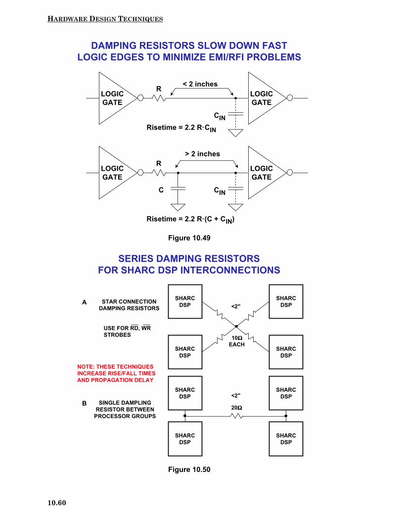
HARDWARE DESIGN TECHNIQUES
10.60
Figure 10.49
Figure 10.50
DAMPING RESISTORS SLOW DOWN FASTLOGIC EDGES TO MINIMIZE EMI/RFI PROBLEMS
LOGICGATE
LOGICGATE
R
C CIN
LOGICGATE
LOGICGATE
R
CINRisetime = 2.2 R·CIN
Risetime = 2.2 R·(C + CIN)
< 2 inches
> 2 inches
SERIES DAMPING RESISTORSFOR SHARC DSP INTERCONNECTIONS
SHARCDSP
SHARCDSP
SHARCDSP
SHARCDSP
SHARCDSP
SHARCDSP
10ΩΩΩΩEACH
SHARCDSP
SHARCDSP
20ΩΩΩΩ
STAR CONNECTIONDAMPING RESISTORS
SINGLE DAMPLINGRESISTOR BETWEEN
PROCESSOR GROUPS
USE FOR RD, WRSTROBES
<2"
<2"
NOTE: THESE TECHNIQUESINCREASE RISE/FALL TIMESAND PROPAGATION DELAY
A
B

HARDWARE DESIGN TECHNIQUES
10.61
The only way to preserve 1ns or less rise/fall times over distances greater thanabout 2 inches without ringing is to use transmission line techniques. Figure 10.51shows two popular methods of termination: end termination, and sourcetermination. The end termination method (Figure 10.51A) terminates the cable atits terminating point in the characteristic impedance of the microstrip transmissionline. Although higher impedances can be used, 50Ω is popular because it minimizesthe effects of the termination impedance mismatch due to the input capacitance ofthe terminating gate (usually 5pF to 10pF). In Figure 10.51A, the cable isterminated in a Thevenin impedance of 50Ω terminated to +1.4V (the midpoint ofthe input logic threshold of 0.8V and 2.0V). This requires two resistors (91Ω and120Ω), which add about 50mW to the total quiescent power dissipation to thecircuit. Figure 10.51A also shows the resistor values for terminating with a +5Vsupply (68Ω and 180Ω). Note that 3.3V logic is much more desirable in line driverapplications because of its symmetrical voltage swing, faster speed, and lowerpower. Drivers are available with less than 0.5ns time skew, source and sinkcurrent capability greater than 25mA, and rise/fall times of about 1ns. Switchingnoise generated by 3.3V logic is generally less than 5V logic because of the reducedsignal swings and lower transient currents.
Figure 10.51
The source termination method, shown in Figure 10.51B, absorbs the reflectedwaveform with an impedance equal to that of the transmission line. This requiresabout 39Ω in series with the internal output impedance of the driver, which isgenerally about 10Ω. This technique requires that the end of the transmission linebe terminated in an open circuit, therefore no additional fanout is allowed. The
TERMINATION TECHNIQUES FOR CONTROLLEDIMPEDANCE MICROSTRIP TRANSMISSION LINES
+3.3V
120ΩΩΩΩ30mW
91ΩΩΩΩ22mW
+1.4V
39ΩΩΩΩ
TYPICAL DRIVERS: 74FCT3807/A (IDT) 74ACTQ240 (Fairchild)
ZO = 50ΩΩΩΩ
ZO = 50ΩΩΩΩ
ZO ≈≈≈≈ 10ΩΩΩΩ
END TERMINATION
SOURCE TERMINATION
RULE OF THUMB: USE TRANSMISSION LINE IF DISTANCE ISMORE THAN 2"/ns OF LOGIC RISE/FALL TIME
GROUND PLANE
A
B
50ΩΩΩΩ PC BOARD TRANSMISSION LINE DELAY ≈≈≈≈ 1ns / 7"
+5.0V
180ΩΩΩΩ72mW
68ΩΩΩΩ29mW
+1.4V

HARDWARE DESIGN TECHNIQUES
10.62
source termination method adds no additional quiescent power dissipation to thecircuit.
Figure 10.52 shows a method for distributing a high speed clock to several devices.The problem with this approach is that there is a small amount of time skewbetween the clocks because of the propagation delay of the microstrip line(approximately 1ns /7"). This time skew may be critical in some applications. It isimportant to keep the stub length to each device less than 0.5" in order to preventmismatchs along the transmission line.
Figure 10.52
The clock distribution method shown in Figure 10.53 minimizes the clock skew tothe receiving devices by using source terminations and making certain the length ofeach microstrip line is equal. There is no extra quiescent power dissipation as wouldbe the case using end termination resistors.
Figure 10.54 shows how source terminations can be used in bi-directional link porttransmissions between SHARC DSPs. The output impedance of the SHARC driveris approximately 17Ω, and therefore a 33Ω series is required on each end of thetransmission line for proper source termination.
The method shown in Figure 10.55 can be used for bi-directional transmission ofsignals from several sources over a relatively long transmission line. In this case,the line is terminated at both ends, resulting in a DC load impedance of 25Ω.SHARC drivers are capable of driving this load to valid logic levels.
CLOCK DISTRIBUTION USINGEND-OF-LINE TERMINATION
SHARCDSP
SHARCDSP
SHARCDSP
+3.3V
120ΩΩΩΩ30mW
91ΩΩΩΩ22mW
+1.4VTRANSMISSION LINE ZO = 50ΩΩΩΩ
50ΩΩΩΩ PC BOARD TRANSMISSION LINE DELAY ≈≈≈≈ 1ns / 7"
CLOCK
NOTE: KEEP STUB LENGTH < 0.5"NOT RECOMMENDED FOR SYNCHRONIZED SHARC OPERATION!

HARDWARE DESIGN TECHNIQUES
10.63
Figure 10.53
Figure 10.54
SOURCE TERMINATION FOR BI-DIRECTIONALTRANSMISSION BETWEEN SHARC DSPs
33ΩΩΩΩ 33ΩΩΩΩ
ON
OFF
ZO ≈≈≈≈ 17ΩΩΩΩ
ADSP-2106x ADSP-2106x
LINK PORTTRANSMITTER
LINK PORTRECEIVER
LENGTH > 6"
ZO = 50ΩΩΩΩ
PREFERRED METHOD OF CLOCK DISTRIBUTIONUSING SOURCE TERMINATED TRANSMISSION LINES
*39ΩΩΩΩ ZO = 50ΩΩΩΩ
ZO ≈≈≈≈ 10ΩΩΩΩ
*39ΩΩΩΩ ZO = 50ΩΩΩΩ
ZO ≈≈≈≈ 10ΩΩΩΩ
*39ΩΩΩΩ ZO = 50ΩΩΩΩ
ZO ≈≈≈≈ 10ΩΩΩΩ
SHARCDSP
SHARCDSP
SHARCDSP
CLOCK
> 4"
* SamePackage

HARDWARE DESIGN TECHNIQUES
10.64
Figure 10.55
SINGLE TRANSMISSION LINETERMINATED AT BOTH ENDS
SHARCDSP
SHARCDSP
SHARCDSP
SHARCDSP
SHARCDSP
SHARCDSP
+3.3V
120ΩΩΩΩ30mW
91ΩΩΩΩ22mW
+3.3V
120ΩΩΩΩ30mW
91ΩΩΩΩ22mW
+1.4VZO = 50ΩΩΩΩ LENGTH > 10"
NOTE: KEEP STUB LENGTH < 0.5"NOT RECOMMENDED FOR CLOCKS IN SYNCHRONIZED SHARC OPERATION!

HARDWARE DESIGN TECHNIQUES
10.65
REFERENCES ON DEALING WITH HIGH SPEEDLOGIC:1. Howard W. Johnson and Martin Graham, High-Speed Digital Design,
PTR Prentice Hall, 1993.
2. EDN’s Designer’s Guide to Electromagnetic Compatibility, EDN,January, 20, 1994, material reprinted by permission of Cahners Publishing Company, 1995.
3. Designing for EMC (Workshop Notes), Kimmel Gerke Associates, Ltd., 1994.
4. Mark Montrose, EMC and the Printed Circuit Board, IEEE Press,1999 (IEEE Order Number PC5756).

HARDWARE DESIGN TECHNIQUES
10.66

INDEX
Index-a
INDEX
SUBJECT INDEX
ANALOG DEVICES PARTS INDEX

INDEX
Index-b

INDEX
Index-1
Subject IndexAAA Alkaline Battery DischargeCharacteristics, 10.14Absolute value amplifier, 3.29Active and Passive Electrical Wave Catalog,2.42AD185x, multibit sigma-delta DAC, 4.11AD260/AD261: digital isolators key specifications, 10.38 schematic, 10.38AD820, op amp, 3.8-9AD1819B SoundPort, codec, foraudio/modem, 9.37-38AD1836, mixed-signal IC, codec, 9.38-39AD1852, sigma-delta audio DAC, 3.17AD1853: dual 24-bit DAC, 4.12 sigma-delta audio DAC, 3.17AD1854, sigma-delta audio DAC, 3.17AD1877: 16-bit sigma-delta ADC characteristics, 3.16 FIR filter characteristics, 3.17AD189x, sample rate converters, 6.35AD77xx, 24-bit sigma-delta ADC, lowfrequency/high resolution, filters, 3.17AD77XX-Series Data Sheets, 3.33AD773x, 24-bit ADC, with PGA, 1.5AD977x, 14-bit TxDAC, 4.6AD983x, 10-bit DDS system, 4.16AD985x, 14-bit TxDAC, 4.6AD5322: 12-bit dual DAC block diagram, 8.18 power-down feature, 8.17 serial interface, 8.18-19AD5340: 12-bit parallel input DAC block diagram, 8.10 interface diagram, 8.12 wait states, 8.11AD6521, voiceband/baseband mixed-signalCODEC, 9.21-22AD6522, DSP-based baseband processor,9.21-22AD6523, Zero-IF Transceiver, 9.23AD6524, Multi-Band Synthesizer, 9.23AD6600, diversity receiver ADC, 9.30AD6622, quad digital TSP, 9.30-31AD6624, quad digital RSP, 9.30-31AD6640: 12-bit ADC
with MagAmps, 3.24-25 multitone testing, diagram, 2.30AD6644, 14-bit ADC, 9.30-31AD7722, 16-bit ADC, 10.15AD7725: 16-bit sigma-delta ADC with on-chip PulseDSP filter, 6.2 programmable digital filter, 9.40-42 block diagram, 9.41 Systolix PulseDSP, 9.41 sigma-delta ADC, with Systolix PulseDSPprocessor, 3.19-20AD7730, sigma-delta ADC, 10.15AD7731, sigma-delta ADC, 10.15AD7853/7853L: 12-bit ADC, block diagram, 8.16 serial ADC interface, 8.17AD7853L: serial clock, 8.15-17 output timing, 8.16AD7854/AD7854L: 12-bit ADC block diagram, 8.5 interface diagram, 8.6-7 key interface timing comparisons, 8.5-6AD7858/59: 12-bit ADC, 3.8-9 SAR ADC, circuit, 3.8-9AD7892, 12-bit SAR ADC, 10.15AD9042: 12-bit ADC, NPR, diagram, 2.32 12-bit wideband ADC, high SFDR,2.27-28AD9201, 10-bit, dual-channel ADC, 8.22-23AD9220: 12-bit ADC, SINAD and ENOB, diagram,2.25 12-bit CMOS ADC, latency or pipelinedelay, 3.27AD9221, 12-bit CMOS ADC, latency orpipeline delay, 3.27AD9223, 12-bit CMOS ADC, latency orpipeline delay, 3.27AD9288-100, 8-bit dual ADC, functionaldiagram, 3.32AD9410, 10-bit flash ADC, interpolation,diagram, 3.23AD9761, 10-bit, dual channel DAC, 8.22-23AD9772: 14-bit interpolating DAC, 9.31 14-bit oversampling interpolatingTxDAC, 4.9-10 block diagram, 4.10 14-bit TxDAC, 4.6

INDEX
Index-2
diagram, 4.6 SFDR, 2.39-40 TxDAC 14-bit DAC, 9.30-31AD9850, DDS/DAC synthesizer system,diagram, 4.16AD73322: block diagram, 8.19-20 simplified interface timing, 8.21AD73422, dspConverter, specifications, 8.22AD20msp430: baseband processing chipset, 9.21-23 components, 9.22-23 construction, 9.21Adams, R.W., 3.33, 3.34Adaptive filter, 6.35-39 basic concept, 6.35-36 speech compression and synthesis, 6.36ADC, 1.2 1-bit, comparator, 3.11 3-bit unipolar, transfer characteristics,2.8-9 10-bit, theoretical NPR, 2.32 11-bit, theoretical NPR, 2.32 12-bit pipelined architecture, diagram, 3.7 theoretical NPR, 2.32 24-bit, with PGAs, 1.5 analog bandwidth, 2.25-26 analog input, 2.10 bit-per-stage, 3.1 boot memory select, 8.2 communications application, SFDR, 2.26 conversion complete output, 8.1-2 conversion process, 2.2 convert start, 8.1-2 data memory address, 8.4 data memory select, 8.2 digital output, grounding, 10.22-24 DNL errors, 2.22 DSP applications, 3.1-35 high speed architectures, 3.2 sigma-delta, 3.2 successive approximation, 3.1-9 types, 3.1 dynamic performance, quantification,2.21 ENOB versus frequency, diagram, 2.26 equivalent input referred noise, 2.20-21 excess DNL, and missing codes, 2.12-13 flash, 3.1 high speed, pipelined, latency, 3.6, 3.8 ideal 12-bit FFT, noise floor, 2.19 SFDR sampling clock to inputfrequency ratio, 2.18 ideal, distortion and noise, 2.15-19 ideal N-bit
dynamic performance analysis,diagram, 2.17 errors, 2.15 quantization noise, diagram, 2.16 input/output memory select, 8.2 low power/low voltage, design issues, 3.1 memory address bus, 8.2 memory read, 8.2 memory select line, 8.2 non-ideal 3-bit, transfer function,diagram, 2.13 non-monotonic, 2.12 normalized signal to reference, 2.10 output, quantization, 2.7 output enable/read, 8.2 oversampling ratio, 3.11 pipelined, 3.1 latency or pipeline delay, 3.25 timing, diagram, 3.7 practical distortion and noise, 2.19-20 noise and distortion sources, 2.20 processor interrupt request line, 8.1-2 program memory select, 8.2 quantization error, 2.9-10 quantization uncertainty, 2.9-10 quantized output, 2.9, 2.10 ripple, 3.1 sampling clock jitter, 2.33 sampling frequency, versus antialiasingcharacteristics, 2.5 SAR, 3.3 external high frequency clock, 3.6 fundamental timing, 3.5 resolutions, table, 3.5 typical timing, 3.5 sigma-delta, 3.1-2, 3.9-21 circuitry, 3.9-10 as oversampling converter, 2.6 programmable digital filter, 9.40-42 VLSI technology, 3.9 see also Sigma-delta ADC sign-magnitude, use, 2.10 single-tone sinewave FFT testing, 2.18 SNR decrease with input frequency, 2.33 static transfer functions, DC errors,2.7-14 subranging, 3.1 pipelined converter, 3.6 successive approximation, 3.1-9 basic, 3.3 resolutions, table, 3.5 see also SAR ADC thermal noise, 2.20-21Address bus, DAC, 8.9ADI DSP collaborative, 7.54

INDEX
Index-3
ADI modified Harvard architecture, inmicroprocessor, 7.6-7ADI SHARC floating point DSPs, 7.26-30ADMC300, motor controller, 9.34ADMC331, motor controller, 9.34ADMC401, motor controller, 9.34ADMCF326, motor controller, 9.34ADMCF328: motor controller, 9.34 block diagram, 9.35ADP1148: synchronous buck regulator, 10.46-50 circuit, 10.47-48 driving ADP3310 circuit diagram, 10.49 waveforms, 10.50 filtered output, 10.49 output waveform, 10.47-48ADP3310, linear LDO regulator, 10.47,10.49-50ADPCM, adaptive pulse code modulation,1.2ADSL, 9.11-16 advantages, 9.12-13 block diagram, 9.13 data transmission capability, 9.15 definition, 9.12 installation advantages, 9.14 modem, block diagram, 9.15 modems, three-channel approach, 9.13-14ADSP-21ESP202, codec, embedded speechprocessing, 9.36-37ADSP-21mod870: digital modem processor, 9.10 expanding central office capability, 9.9 in voice-based RAS modem, 9.8-9ADSP-21xx: 16-bit fixed point DSP core, 7.6-23 arithmetic, signed fractional format,7.23-24 assembly code for FIR filter, 1.8 buses, 7.10-11, 7.11 computational units, 7.11-13 core architecture diagram, 7.9 summary, 7.10 data address generators and programsequencer, 7.13-14 digital filter example, 7.7-10 DSP optimized, 7.9 FIR filter assembly code, 7.8 fixed-point DSP, 7.7-8 FIR filter, 6.11-12 assembly code, 6.13 internal buses, 7.10-11 internal peripherals, powerdown, 7.18 memory-write cycle timing diagram, 8.7-8
on-chip peripherals, 7.14-23 byte DMA port, 7.17 internal DMA, 7.17 SPORTs, 7.16 read-cycle, timing diagram, 8.3 serial ports block diagram, 8.13 features, 8.13 operation, 8.12-14 SPORTs, 7.16ADSP-218x: architecture, 7.15 byte memory interface, 7.17 DSP, EZ-ICE, 7.49 implementation, multi-channel VOIPserver, diagram, 9.11 interface with CODEC, 8.20-22 internal direct-memory-access port, 7.16 memory-mapped peripherals, 7.16 modified Harvard architecture, 7.16 multiple core devices, 7.22 on-chip peripherals, memory interface,7.15 roadmap, 7.22 VisualDSP software, 7.52ADSP-219x: architecture, 7.19 code compatibility with ADSP-218x, 7.19 key specifications, 7.20 roadmap, 7.23 VisualDSP software, 7.52ADSP-2100, core in ADSP-218xarchitecture, 7.15ADSP-2100 EZ-KIT Lite Reference Manual,7.55, 8.25ADSP-2100 Family EZ Tools Manual, 7.55,8.25ADSP-2100 Family Users Manual, 3rdEdition, 7.55, 8.25ADSP-2106x: characteristics, 7.28 external ports, 7.29 host interface, 7.29 I/O processor, 7.29 IEEE Standard P1149.1 Joint Test ActionGroup standard, 7.30 instruction set, 7.28 internal memory, 7.30 multiprocessing systems, 7.29 on-chip DMA, 7.30 SHARC processors, 7.26-27 Super Harvard Architecture, 7.26-28ADSP-2106x SHARC EZ-KIT Lite Manual,7.55, 8.25ADSP-2106x SHARC User's Manual, 2ndEdition, July 1996, 7.55, 8.25ADSP-2116x:

INDEX
Index-4
32-bit DSP, second-generation, 7.31 SIMD core architecture, 7.31-36 diagram, 7.31 SIMD DSP, 7.33 SIMD features, 7.32ADSP-2189M: 69-tap FIR filter, design example, 6.22 75 MIPS DSP filter subroutine, 6.12 throughput time, 6.28 75 MIPS processor, 6.20 EZ-KIT Lite, 7.47 fixed-point DSP, 6.1 key timing specifications, 8.9-10 parallel read timing, 8.4, 8.7 parallel write interface, timingspecifications, 8.11 serial port, receive timing diagram,8.14-15 system interface, full memory mode,diagram, 8.24ADSP-21000 Family Application Handbook,5.25, 6.40ADSP-21060L SHARC, DSP output rise andfall times, 10.58ADSP-21065L: connected to ADC and DAC, 8.22-23 EZ-KIT Lite, 7.48 SHARC, DSP benchmarks, 7.34ADSP-21065L SHARC EZ-LAB User'sManual, 7.55, 8.25ADSP-21065L SHARC User's Manual, Sept.1, 1998, 7.55, 8.25ADSP-21160: 16-channel audio mixer, SIMDarchitecture, 9.40 32-bit SHARC, key features, 7.32 DSP, BGA package locations, 10.54-55 integrated peripherals, 7.32 SIMD/multiple channels, DSPbenchmarks, 7.34 SISD, DSP benchmarks, 7.34ADSP-21160 SHARC DSP HardwareReference, 7.55, 8.25ADSP-21160M, EZ-KIT Lite, 7.47ADSP-TS001: features, 7.40 TigerSHARC 16-bit fixed-point DSP, 5.18-19 architecture, 7.36-44 benchmarks, 7.44 diagram, 7.38ADuM1100A, digital isolator, 10.36-37Advanced mobile phone service see AMPSAgilent HCPL-7720, 10.36Aiken, Howard, 7.7Alfke, P., 10.14
Aliasing, 2.2-3 frequency domain, representation, 2.3All-pole lattice filter, parameters, fromspeech samples, 6.38-39Alternate framing mode, 8.14Aluminum electrolytic capacitor, 10.40-41Amplifier Applications Guide (1992), 2.43,3.35Amplitude shift keying, POTS, 9.2Analog bandwidth, ADC, 2.25-26Analog cellular basestation, 9.27-28Analog Devices Inc., 16-bit DSP, roadmap,7.22Analog Devices' Motor Control Website, 9.44Analog filter: frequency response, 6.4 popular types, 6.24, 6.27-28 requirements, 6.3 for oversampling, 4.10 versus digital, 6.3Analog front end, 8.19-22Analog receiver design, 9.26-27Analog return current, 10.16-17Analog signal: characteristics, 1.1-2 discrete time sampling, 2.2-7 diagram, 2.1 normalized ratio, 2.9 quantization, 2.2 diagram, 2.1 sampling, aliasing, 2.3Analog superheterodyne receiver, 9.27Andreas, D., 3.33ANSI/IEEE Standard 754-1985, floatingpoint arithmetic, 7.24-25Anti-imaging filter, 6.2Antialiasing filter, 6.2 baseband sampling, oversampling, 2.5 requirements, relaxing, 2.6 specifications, 2.4-5Aperture delay, 2.33-35Aperture jitter, 2.33-35, 10.25Apex-ICE, 7.48-49 USB simulator, 7.49Application of Digital Signal Processing inMotion Control Seminar (2000), 9.44Architecture: computer ADI modified Harvard, 7.6 Harvard, 7.6-7 Von Neumann, 7.6Arithmetic logic unit: in DSP, 7.4 features, 7.11Armstrong, Edwin H., Major, 9.27

INDEX
Index-5
The ARRL Handbook for Radio Amateurs,4.17Asymmetric digital subscriber line seeADSLAudio system, synthesized, 1.3Auto-correlation, 1.3Automotive/home theater, using 32-bitSHARC, 9.39
BBackplane ground plane, 10.18Baines, Rupert, 9.43Baker, Bonnie, 10.34Ball grid array, 10.54Band filter, 10.46Bandpass filter: design, 6.23-24 from lowpass and highpass filters, 6.24Bandpass sampling, 2.6-7Bandpass sigma-delta ADC, undersampling,3.18Bandstop filter: design, 6.23-24 equivalent impulse response, 6.23 from lowpass and highpass filters, 6.24Baseband data signal, POTS, 9.2Baseband sampling: antialiasing filter, 2.4-6 oversampling, 2.5 Nyquist zone, 2.6Basestation, block diagram, 9.30Basis function, 5.3 correlation, DFT, 5.4BDC binary coding, data converters, 2.10Bennett, W.R., 2.42Bessel filter, 6.24, 6.27-28Best straight line, 2.11-12Best, R.E., 4.17Bilinear transformation, 6.28Binary ADC: 3-bit diagram, 3.29 input and residue waveforms, 3.29 single-stage, diagram, 3.28Binary coding, data converters, 2.10Binary DAC, 5-bit, architectures, diagram,4.4Bingham, John, 9.43Bipolar converter, types, 2.10Biquad, in IIR filter, 6.25Bit reversal: for 8-point DFT, 5.14 algorithm, 5.11-14Bit-per-stage ADC, 3.27-32 diagram, 3.27Blackman window function, 5.22-23Blackman, R.B., 2.43
Block floating point, in FFT, 5.17Boot memory select, ADC, 8.2Bordeaux, Ethan, 7.55, 10.1Boser, B., 3.33Boyd, I., 9.43Branch target buffer, 7.39, 7.41Brannon, Brad, 9.43Brokaw, Paul, 10.34Bryant, James, 2.1, 3.1, 3.9, 4.1, 10.15,10.34Buck regulator, 10.46-50Buffer register, 10.22-23Bus: data memory address, 7.10 data memory data, 7.10 data transfer, 7.10-11 internal result, 7.10-13 program memory address, 7.10 program memory data, 7.10Buss wire, 10.16Butterfly, 5.11-12 DIF FFT, 5.15 DIT FFT, 5.12Butterworth filter, 4.9, 6.24, 6.27-28 characteristics, 2.5Byrne, Mike, 10.15
CCage jack, 10.16Calhoun, George, 9.43Capacitive coupling, doublet glitch, 2.37Capacitor: equivalent circuit, pulse response, 10.43 finite ESR, 10.42-43 parasitic elements, 10.43 types, 10.40-42Card entry filter, 10.46Carrier, 2.23Cascaded biquads, 6.25Cauer filter, 6.27-28CCD image processing, 1.5CDMA, digital telephone system, 9.17Cellular phone: basic system, diagram, 9.16 frequency reuse, diagram, 9.16Ceramic, capacitor, 10.40-42Charpentier, A., 3.33Chebyshev filter, 1.6, 6.2-3, 6.24, 6.27-28Chestnut, Bill, 10.39Chip select, DAC, 8.9Circular buffering: DSP application, 7.5 DSP requirement, 7.5 in FIR filter, 6.10 FIR filter, 7.5 in FIR filter, output calculation, 6.11 FIR filter pseudocode, in DSP, 7.8

INDEX
Index-6
Clelland, Ian, 10.56Clock distribution: end-of-line termination, diagram, 10.62 source terminated transmission lines,diagram, 10.63Cluster multiprocessing, 7.34 SHARC family, 7.36CMOS IC, secondary I/O ring, diagram, 10.9CMOS IC output driver, configuration,10.3-4Code division multiple access see CDMACode transition noise, and DNL, effects,2.14Codec, 1.5, 8.1 interfacing, 8.19-22 sampling rate, 8.20 voiceband/audio applications, 9.36-40CODEC and DSP, in voiceband and audio,9.36-40COder/DECoder, 8.1Coding, types, 2.10Coleman, Brendan, 2.43Colotti, James J., 2.43Comfort noise insertion, 9.20Communications, external port, versus linkport, 7.35Computational unit: arithmetic logic, 7.11 multiplier-accumulator, 7.11-12 shifter, 7.11-12Computer, general purpose, Von Neumannarchitecture, 7.6Computing applications: CISC, 7.2 data manipulation, 7.1 mathematical calculation, 7.1 RISC, 7.2-3 tabular summary, 7.1Concentrator, 9.7Connelly, J.A., 10.34Convert start, ADC, 8.1-2Convolution, 1.3 loop, 6.12Convolving, filter responses, 6.23Cooley, J.W., 5.10, 5.25Cosier, G., 9.43Coussens, P.J.M., 9.43Crystal Oscillators, 10.34
DDAC, 1.2 3-bit switched capacitor, diagram, 3.4 3-bit unipolar, transfer characteristics,2.8-9 address bus, 8.9 binary weighted, 4.1 in CD player, use of interpolation, 6.33
chip select, 8.9 conversion process, 2.2 current output, diagram, 4.2 in direct digital synthesis, 4.9 distortion, specification, 2.38 DNL errors, 2.22 double-buffered, latches, 4.7 DSP applications, 4.1-17 dynamic performance, 2.35-41 high-speed, 4.9 interpolating, 4.9-10 interrupt request, 8.9 ladder networks, 4.1 logic, 4.7-8 low distortion, architectures, 4.3-7 memory select, 8.9 midscale glitch, diagram, 2.37 monotonicity, 2.12 non-ideal 3-bit, transfer function,diagram, 2.13 non-monotonic, and DNL, 2.12 output, quantization, 2.7 reconstruction, output, 2.41 segmented voltage, diagram, 4.3 settling time, applications, 2.38 sigma-delta, 4.11-12 1-bit, in CD players, 4.9 sin(x)/x frequency rolloff, 2.41 static transfer functions, DC errors,2.7-14 structures, 4.1-3 transitions, with glitch, 2.36 voltage output, Kelvin divider, 4.1 write, 8.9Damping resistor: EMI/RFI minimization, 10.60 series, for SHARC DSP interconnections,10.60DashDSP, motor controllers, 9.34-35Data address generator: features, 7.13 mode status register, 7.13Data converter: analog bandwidth specification, 2.26 applications, 2.8 DC errors, 2.10, 2.10-11 DC performance, 2.15 gain error, diagram, 2.11 integral and differential non-linearitydistortion effects, 2.22-23 offset error, diagram, 2.11 sampling and reconstruction systems, 2.8Data manipulation, by computer, 7.1Data memory address, ADC, 8.4Data memory address bus, 7.10Data memory buffer, circular, 7.5Data memory data bus, 7.10

INDEX
Index-7
Data memory select, ADC, 8.2Data reduction algorithms, in signalprocessing, 1.2Data sampling, 2.1-44 block diagram, 2.1 distortion and noise, 2.15-19 FFT, 2.1-2 quantization error, 3.10 quantization noise, 3.10 real-time system, 2.1Data scrambling, in sigma-delta DAC, 4.11Data-flow multiprocessing, 7.34Dattorro, J., 3.33DC error, types, 2.10DDS, 4.12-16 basic architecture, 4.13 code-dependent glitches, 2.38 DAC, 4.3 distortion, contributors, 2.39 problems, 4.13 system, flexible, diagram, 4.14 tuning equation, 4.15Dead time, DAC settling time, 2.35Decimation, 3.10, 3.11 multirate filter, diagram, 6.31Decimation-in-frequency, DIF, 5.13-14Decimation-in-time, DIT, 5.11Decoupling, localized, diagram, 10.52Decoupling points, diagram, 10.24Deglitching, 3.25Del Signore, B.P., 3.33Delta phase register, 4.14Designing for EMC (Workshop Notes), 10.65DFT, 5.1-8 8-point, 5.9, 5.12 using DIT, 5.12-13 applications, 5.2 basis functions, 5.3 butterfly operation, 5.11-12 characteristics, 5.4 complex, 5.5 equations, 5.6 from real, 5.7 input/output, 5.6 real/imaginary values, 5.7 equations, real versus imaginary, 5.8 expansion, 5.9-10 FIR filter, 6.15 fundamental analysis equation, 5.3 inverse, 5.5 output spectrum, 5.3 real, 5.5 input/output, 5.6 real versus imaginary equations, 5.7-8 output conversion, 5.8 relationship, 5.7-8
sampled time domain signal, 5.3 versus FFT, 5.11DIF: butterfly, 5.13-14 decimation-in-frequency, 5.13-14Differential non-linearity: DNL, 2.12 from encoding process, 2.22DIGI-KEY, 10.56Digital cellular basestation, 9.28-31Digital cellular basestations, advantages,9.28Digital cellular telephone, 9.16-20 GSM system, 9.18-20Digital communications services see DCSDigital correction, for subranging ADC, 3.24Digital filter, 6.1-39 coefficient values, 6.1 design procedure, 6.1 diagram, 6.2 filter coefficient modification, 6.35 frequency response, 6.4 general equation, 6.25-26 lattice, 6.5 moving average, 6.5-10 programming ease in ADSP-21xx, 7.7-8 real-time, 6.1, 6.3 processing requirements, 6.4 requirements, 6.3 types, 6.5 versus analog, 6.3Digital filtering, 3.10Digital FIR filter, 1.6Digital isolation: by LED/photodiode optocouplers, 10.36 by LED/phototransistor optocouplers,10.35Digital isolation technique, 10.35-38Digital isolator, 10.36-38Digital mobile radio, standards, 9.18Digital receiver, characteristics, 9.27-28Digital return current, 10.16-17Digital signal, characteristics, 1.1-2Digital Signal Processing ApplicationsUsing the ADSP-2100 Family, 5.25, 6.40, 9.43Digital signal processor see DSPDigital system, with ADC, quantizationnoise, 2.31Digital telephone system, CDMA andTDMA, 9.17Digital transmission, using adaptiveequalization, 6.37Direct data scrambling, in sigma-deltaDAC, 4.11-12Direct digital synthesis see DDSDirect form 1 biquad filter, diagram, 6.26

INDEX
Index-8
Direct IF to digital conversion, 2.6-7Direct memory access, DSP controller, 8.22Direct-memory-access see DMADiscontinuous transmission, 9.18-19, 9.20Discrete Fourier transform see DFTDiscrete time Fourier series, 5.1Discrete time sampling, 2.2 analog signal, 2.2-7Distortion, DAC performance, 2.35-41Distortion and noise, practical ADCs,2.19-20DIT: decimation-in-time, 5.11 FFT, algorithm, 5.11, 5.13Dither signal, 2.18DMA, internal, in ADSP-21xx, 7.17DNL: ADC and DAc errors, 2.22 converter error, definition, 2.12 differential non-linearity, 2.12Doernberg, Joey, 2.43Double precision, 64-bit, floating pointarithmetic, 7.25Double-buffered DAC: advantages, 4.7-8 diagram, 4.8 latches, 4.7Doublet glitch, 2.37DSP, 1.2, 7.1-3 16-bit, fixed-point family, history, 7.20-22 32-bit, second-generation, 7.31 ADSP-21xx, characteristics, 1.6-8 analog versus digital, 1.4-5 options, diagram, 1.5 applications, 9.1-44 summary, 9.42 arithmetic fixed-point versus floating point,7.23-26 fixed-point versus floating-point,7.23-26 characteristics, 7.2 code, compilation, 7.45 and computer applications, 7.1 core voltage, 10.2 development tools, 7.46 dot-product, 7.2 efficiency, 7.18 evaluation and development tools,7.45-54 VisualDSP and VisualDSP++, 7.51-54 fundamental mathematical operation, 7.3 grounding, 10.29-30 hardware, 7.1-55 high density, localized decoupling,10.53-55 interfacing, 8.1-25
interfacing I/O ports, analog front ends,and CODECS, 19-22 internal phase-locked loops, grounding,10.29-30 kernel, 7.1-2 optimization, 7.6 output rise and fall times, diagram, 10.58 parallel interfacing, 8.1-12 block diagram, 8.8 reading data from memory-mappedperipheral ADCs, 8.1-7 to external ADC, block diagram, 8.2 writing data to memory-mapped DACs,8.7-12 practical example, 1.5-8 requirements, 7.3-6 circular buffering, 7.5 dual operand fetch, 7.4-5 extended precision, 7.4 fast arithmetic, 7.4 summary, 7.6 zero overhead looping, 7.5-6 sampled data, block diagram, 2.1 serial interfacing, 8.12-19 serial ADC, 8.14-19 serial DAC, 8.17-19 system interface, 8.23-24 using VLSI, 1.4 voiceband/audio applications, 9.36-40DSP Designer's Reference (DSP Solutions),7.55, 8.25DSP Navigators: Interactive Tutorials aboutAnalog Devices' DSP Architectures, 7.55DSP Navigators: Interactive Tutorials aboutAnalog Device's DSP Architectures, 8.25Dual operand fetch: DSP application, 7.4-5 DSP requirement, 7.4-5Duracell MN1500 "AA" alkaline battery,discharge characteristics, 10.2Dynamic performance analysis, ideal N-bitADC, 2.17Dynamic range compression, 1.4
EEcho, voiceband telephone connection, 9.2Eckbauer, F., 3.33EDN's Designer's Guide to ElectromagneticCompatibility, 10.65Edson, J.O., 2.42, 3.34Effective aperture delay time, 2.34 diagram, 2.35Effective number of bits see ENOBEichhoff Electronics, Inc., 10.57Electrolytic capacitor:

INDEX
Index-9
characteristics, 10.40-41 impedance versus frequency, diagram,10.44Elliptic filter, 6.24, 6.27-28 characteristics, 2.5Embedded speech processing, 9.36-37EMC Design Workshop Notes, 10.56End point, 2.11-12Engelhardt, E., 3.33ENOB, 2.21, 2.24-25, 3.10 ADC, effective resolution, 3.10 definition, 3.10Equiripple FIR filter design, programinputs, 6.19-20Equivalent input referred noise, thermalnoise, 2.20-21Error voltage, 10.17Euler's equation, 5.3Extended precision: DSP application, 7.4 DSP requirement, 7.4 floating point arithmetic, 7.25External clock jitter, 10.25External port, versus link port, incommunications, 7.35EZ-ICE, in-circuit simulator, 7.48EZ-KIT Lite, 7.45-46, 7.53EZ-LAB, evaluation board, 7.45
FFair-Rite, 10.44-46Fair10.Rite Linear Ferrites Catalog, 10.56Fairchild 74VCX164245, 16-bit low voltagedual logic translators/transceivers, 10.10-13Faraday shield, 10.22Fast arithmetic: DSP application, arithmetic logic unit, 7.4 DSP requirement, 7.4Fast Fourier transform see FFTFast logic, and analog circuits, 10.59FDMA: frequency division multiple access, 1.2 telephone system, 1.2FDMA communications link, NPR testing,2.30Ferguson, P. Jr., 3.34Ferguson, P.F. Jr., 3.33Ferrite, 10.44 beads, 10.16, 10.20, 10.29, 10.30 impedance, 10.45-46 suitable for high-frequency filters, 10.45FFT, 2.1, 5.1-25, 5.9-17 8-point DIF, 5.15 8-point DIT algorithm, 5.13 and DFT, 5.10 DIF, 5.13-14
FIR filter, 6.15 first Nyquist zone aliases, 2.4 floating point DSP, 5.18 frame-based systems, 5.18 hardware implementation andbenchmarks, 5.17-18 noise floor determination, 5.19 processing gain, 2.18-19, 5.20 processor, 5.17 radix-2, 5.16 radix-2 complex, hardware benchmarkcomparisons, 5.18 radix-4, DIT butterfly, 5.16-17 real-time considerations, 5.20 DSP requirements, 5.18-20 processing, 5.19 sinewave integral number of cycles, 5.21 nonintegral number of cycles, 5.22 spectral leakage and windowing, 5.21-24 twiddle factors, 5.9-10 versus DFT, 5.11Film capacitor, 10.40-42Filter: analog, for oversampling, 4.10 analog versus digital, 6.2-4 frequency response comparison, 1.7 antialiasing, specifications, 2.4-5 band, 10.46 bandpass, design, 6.23-24 bandstop, design, 6.23-24 baseband antialiasing, 2.4-6 Butterworth, characteristics, 2.5 capacitor, types, 10.40 Chebyshev, 1.6 corner frequency, 2.4 design, and FFT, 5.1 digital, diagram, 1.6 digital FIR, 1.6 elliptic, characteristics, 2.5 FIR versus IIR, comparisons, 6.30 high frequency, 10.51 high-frequency, ferrites, 10.45 highpass, design, 6.23-24 impulse convolving, 6.23 lowpass, analog versus digital, insampled data system, 1.5-6 power supply, 10.39-57 rolloff, sharpness, 6.9 switching supply, summary, 10.51 transfer function, 3.13Filtering, 1.3, 1.4FilterWizard, compiler, 9.41Finite amplitude resolution due toquantization, 2.2Finite impulse response see FIR

INDEX
Index-10
FIR filter, 6.5-30 4-tap, output calculation, via circularbuffer, 6.11 arbitrary frequency response, design,6.17-18 CAD design programs, 6.18-19 characteristics, 6.14 circular buffering, 6.10-13 in circular buffering, 7.5 circular buffering, fixed boundary RAM,6.10 coefficients, 6.15 compared with IIR filter, 6.30 computational efficiency increase, 6.32 design Fourier series method, withwindowing, 6.17 frequency sampling method, 6.17-18 fundamental concepts, 6.13 Parks-McClellan program, 6.18-22 programming ease in ADSP-21xx, 7.7-8 windowed-sinc method, 6.16 designing, 6.13-24 implementation, circular buffering,6.10-13 impulse response, and coefficients, 6.14 Momentum Data Systems design frequency response, 6.21 impulse response, 6.22 step response, 6.21 N-tap, general form, 6.9-10 output decimation, 6.32 program outputs, 6.20 pseudocode, 6.12, 7.7-8 simplified diagram, 6.10 transfer function frequency domain, 6.15 time domain, 6.15 versus IIR filter, 6.30First-order sigma-delta ADC, 3.12Fisher, J., 3.33Fixed-point: 16-bit, fractional format, 7.24 DSP arithmetic, 7.23-26 versus floating point, DSP arithmetic,7.23-26Flash ADC: 10-bit, diagram, 3.23 limited to 8-bits, 3.22 parallel ADCs, 3.21 diagram, 3.22 problems, 3.21Flash converter, 3.21-23Floating-point: DSP arithmetic, 7.23-26 versus fixed point arithmetic, 7.26Folding converter, 3.29
Fourier series, 5.1 FIR filter design, windowing, 6.17Fourier transform, 5.1, 6.15 and time domain signal, 5.2Fourier, Jean Baptiste Joseph, 5.1FPBW, full power bandwidth, 2.26Framing mode, 8.14Freeman, D.K., 9.43Frequency division multiple access, FDMA,1.2Frequency domain, versus time domain,6.13, 6.15Frequency sampling method, FIR filterdesign, 6.17-18Frequency synthesis, using PLLs andoscillators, diagram, 4.12Fu, Dennis, 9.43Full memory mode, 8.23Full power bandwidth, FPBW, 2.26Full-duplex hands-free car kit, diagram,9.36Fully decoded DAC: 5-bit, diagram, 4.4 diagram, 4.2
GGain error, 2.10Galand, C., 9.43Ganesan, A., 3.33, 3.34Gardner, F.M., 4.17Gaussian noise, 2.20-21, 2.30Gaussian-filtered minimum-shift keying,9.26Geerling, Greg, 7.1General DSP Training and Workshops,7.55, 8.25General purpose aluminum electrolyticcapacitor, 10.40-41Gerber files, 10.33Ghausi, M.S., 2.44Gibbs effect, 5.1Glitch: code-dependent, effects, 2.38 DAC performance, 2.35-41 definition, 2.36 energy, 2.37 and harmonic distortion and SFDR,prediction, 2.39 impulse area, 2.37Global System for Mobile Communicationsee GSMGlue logic, 8.1Gold, B., 5.25, 6.40Gold, Bernard, 2.44Gosser, Roy, 2.42, 3.34Graham, M., 10.14Graham, Martin, 10.34, 10.65

INDEX
Index-11
Grame, Jerald, 10.34Gray bit, 3.30Gray code binary coding, data converters,2.10Gray, A.H., Jr., 6.40Gray, G.A., 2.42Ground loop, 10.20, 10.35Ground plane, 10.30 decoupling high frequency current, 10.15 impedance, 10.20 low-impedance return path, 10.15-16 printed circuit board, 10.17-18Ground screen, 10.19Grounded-input histogram, 2.20-21Grounding: DSP, internal phase-locked loops,diagram, 10.30 mixed signal devices, in multicardsystem, 10.27-29 mixed signal systems, 10.15-34 mixed-signal ICs, 10.15 multiple ground pins, 10.32 philosophy, summary, 10.31 points, diagram, 10.24 separate analog and digital grounds,10.19-20 single-card versus multicard, concepts,10.26-27Groupe Speciale Mobile see GSMGSM, block diagram, 9.18-19GSM handset: components, 9.21-26 using SoftFone baseband processor, andOthello radio, 9.21-26
HHageman, Steve, 10.56Half-flash ADC, 3.23Hamming window function, 5.22-23Hanning window function, 5.22-23Hard limiter, 2.29Hardware design, techniques, 10.1-65Harmonic distortion, 2.23-24 DAC, 2.38 definition, 2.23 products, location, diagram, 2.23Harmonic sampling, 2.6-7Harmonic undersampling, 2.7Harrington, M.B., 9.44Harris, Fredrick J., 2.43, 5.25, 6.40Harris, Steven, 3.34Harvard architecture: in DSP, 7.5 in microprocessor, 7.6-7Hauser, Max W., 3.34Haykin, S., 6.40HDTV, high definition television, 1.2
Heise, B., 3.33Hellwig, K., 9.43Henning, H.H., 2.42, 3.34Higgins, Richard J., 1.9, 2.44, 5.25, 6.40,7.55, 8.25High definition television, HDTV, 1.2High density DSP: localized decoupling diagram, 10.53 using BGA packages, 10.54High Speed Design Techniques (1996), 3.35High speed logic, 10.58-65High-level language support, architecturalfeatures, 7.42High-speed interfacing, 8.22-23Highpass filter: design, 6.23-24 using lowpass FIR, 6.23Hilton, Howard E., 2.44Hodges, David A., 2.43Hofmann, R., 9.43Honig, Michael L., 6.40Horvath, Johannes, 10.1Host memory mode, 8.23HP Journal, 2.43-44HP Product Note, 2.43
IIC, low-voltage mixed signal, 10.2IEEE Trial-Use Standard for DigitizingWaveform Recorders, 2.44IF sampling, 2.6-7IIR biquad filter: basic, 6.25 simplified notations, 6.27IIR elliptic filter, 6.30IIR filter, 6.24-27 analog counterparts, 6.24 CAD design, using Fletcher-Powellalgorithm, 6.28 characteristics, 6.25 compared with FIR filter, 6.30 design techniques, 6.27-29, 6.29 direct form implementation, 6.26 feedback, 6.5 IIR filter, 6.24-27 implementation, 6.25 throughput considerations, 6.29 versus FIR filter, 6.30IMD: measurement, 2.28 second- and third-order, diagram, 2.29 two tone intermodulation distortion,2.28-30Impulse invariant transformation, 6.28IMT-2000 protocol, 7.36In-circuit simulator, 7.48

INDEX
Index-12
Indirect field-oriented control, 9.32Induction motor: control, 9.32-35 block diagram, 9.33Infinite impulse response see IIRInformation, in signal, 1.2Input filtering, 1.5Input noise rejection, 1.5Input/output memory select, ADC, 8.2Instruction register, data addressgenerator, 7.14Integral linearity error, measurement,2.11-12Integral sample-and-hold, 2.19Interface: 2.5V/3.3V, diagram, 10.13 3.3V/2.5V, 10.10-13 diagram, 10.11-12Interfacing, high-speed, 8.22-23Interference, components, 10.39Intermodulation distortion, DAC, 2.38Internal aperture jitter, 10.25Internal result bus, 7.10-13Interpolation: frequency domain effects, 6.33-34 implementation example, 6.33-34 multirate filter, 6.32-33Interrupt request, DAC, 8.9Intranet, 9.7I.Q. convention, 7.24IRQ, 8.1
JJantzi, S.A., 3.33JEDEC, 10.14 specification, for packaging, 7.20 standards bureau, 10.5Jitter: aperture, 10.25 effects, 2.33 external clock, 10.25 internal apeture, 10.25 sampling clock, 10.25Johnson noise, 2.8Johnson, H., 10.14Johnson, Howard W., 10.34, 10.65Joint Electron Device Engineering Councilsee JEDECJung, Walt, 10.39, 10.56
KKelvin divider, 4.1 disadvantages, 4.1-2 ladder network, 4.3Kelvin-Varley divider, string DAC, 4.3Kerr, Richard J., 4.17
Kester, Walt, 1.1, 2.1, 2.43, 3.1, 3.35, 4.1,5.1, 6.1, 7.1, 8.1, 9.1, 10.1, 10.15, 10.34-35, 10.39Kettle, P., 9.44King, Dan, 7.1, 8.1Koch, R., 3.33
LLagrange, Joseph Louis, 5.1Laker, K.R., 2.44Lane, Chuck, 2.42, 3.34Laplace transform, 6.15 conversion to z-transform, 6.28Laplace, Pierre Simon de, 5.1Latency, 3.25Lattice filter, 6.5Leaded ferrite bead, 10.44Least significant bit: definition, 2.7 quantization, chart, 2.8 size, 2.8Least-mean-square algorithm, for filtercoefficients, 6.36Lee, Hae-Seung, 2.43Lee, Wai Laing, 3.33Lee, W.L., 3.33Levine, Noam, 7.1Linear Design Seminar (1995), 2.42, 3.33,3.34Linear integrity error, 2.11Linear predictive coding see LPCLinear settling time, DAC settling time,2.35Linearity errors, 2.10Link descriptor file see LDFLink port, versus external port, incommunications, 7.35Link port multiprocessing, 7.34LMS, least-mean-square, 6.36Logarithmic pulse code modulation, 9.19Logic: CMOS IC output driver, configuration,10.3-4 high speed, 10.58-65Logic translating transceiver: diagram, 10.11 voltage compliance, 10.11Long term prediction see LTPLow voltage interface, 10.1-14Low Voltage Logic Alliance, standards, 10.5Low voltage logic level, standards, 10.4-5Low voltage mixed-signal IC, 10.2Low-pass filter, LPF, 3.11Lowpass filter, design of other filters, 6.23LPC, 6.36-37 in all-pole lattice filter, 6.38-39 model of speech production, 6.37

INDEX
Index-13
speech companding system, 6.38 speech processing system, 9.19 speech system, digital filters, 6.38LPF: analog, in sigma-delta ADC, 3.13 low-pass filter, 3.11LQFP, new package designation, 7.20Lucey, D.J., 9.44LVTTL, logic level, 10.4Lyne, Niall, 9.44
MMcClellan, J.H., 6.40MagAmp, 3.29 3-bit folding ADC block diagram, 3.31 functional equivalent circuit, 3.30 input and residue waveforms, 3.31Magnitude amplifier, 3.29Magnitude-amplifier architecture,MagAmp, 3.24Mahoney, Matthew, 2.44Main lobe spreading, 5.22Manolakis, Dimitris G., 5.25, 6.40Markel, J.D., 6.40Marsh, Dick, 10.56Matched z-transform, 6.28MathCad 4.0 software package, 2.44Mathematical calculation, by computer, 7.1Matsuya, Y., 3.33, 3.34Maximally flat filter, 6.27Mayo, J.S., 2.42, 3.34Meehan, Pat, 2.43Memory address bus, ADC, 8.2Memory read, ADC, 8.2Memory select: ADC, 8.2 DAC, 8.9Messerschmitt, David G., 6.40Microcontroller, 7.1-3 characteristics, 7.2MicroConverter, precision analog circuitry,1.3Microprocessor, 7.1-3 architectures, comparison, 7.6 characteristics, 7.2Million operations per second see MOPSMillions of instructions per second see MIPSminiBGA package, 7.20-21Minimum 4-term Blackman-Harris windowfunction, 5.22-23MIPS, 7.2, 7.18Missing codes: in ADC, 2.12-13 defining, 2.14Mitola, Joe, 9.43Mixed Signal Design Seminar (1991), 3.33
Mixed signal processing, 1.4Mixed-signal device: grounding, 10.26-27 diagram, 10.27Mixed-signal IC: grounding, multiple printed circuitboards, 10.28-29 high digital currents, grounding, 10.28-29 low digital current, grounding anddecoupling, 10.21-22 low digital currents, grounding, 10.27-28Mobile telephone service, superheterodynereceiver, diagram, 9.27Mode status register, data addressgenerator, 7.13Modem: full-duplex, 9.1 half-duplex, 9.1 high performance, telephone service,9.1-7 high speed, 1.2 RAS, 9.7-10 standards, chart, 9.3 V.90 analog block diagram, 9.4 details, 9.6 V.90 analog versus V.34, diagram, 9.7Momentum Data Systems, QED1000program, for FIR filter design, 6.18Momentum Data Systems, Inc., 6.40Montrose, Mark, 10.34, 10.65MOPS, 7.18Moreland, Carl, 2.42, 3.34Morley, Nick, 9.43Morris, Jesse, 7.1Morrison, Ralph, 10.34Motchenbacher, C.D., 10.34Motherboard, grounding, 10.18-19Motor control, 9.32-35 fully integrated, DashDSP, 9.35Motor Control Products, Application Notes,and Tools, 9.44Moving average filter, 6.5-10 calculating output, 6.7 diagram, 6.6 frequency response, 6.8 noise, 6.6-8 step function response, 6.6-7MSP, 1.4Multi-channel high frequencycommunication system, NPR, 2.31Multi-channel VOIP server, 9.10-11Multi-tone SFDR, measurement, 2.29Multicard mixed-signal system, grounding,10.18-19Multilayer ceramic chip caps, 10.42Multiplier-accumulator unit, features, 7.12

INDEX
Index-14
Multiplying DACs, 4.3Multipoint ground, diagram, 10.19Multiprocessing, using SHARCs, 7.34-36Multirate filter, 6.31-35 decimation, 6.31 interpolation, 6.31Murden, Frank, 2.42, 3.34Murray, Aengus, 9.44
NNarrowband, 9.27Network: LAN, 1.2 local area, 1.2Nicholas, Henry T. III, 4.17NMOS FET, bus switches, interfacing,10.6-8Noise: and grounding, 10.22 power supply, 10.39-57Noise power ratio see NPRNoise shaping, using analog filter, 3.13Non-ideal ADC, 3-bit, transfer function,diagram, 2.13Non-ideal DAC, 3-bit, transfer function,diagram, 2.13Normal framing mode, 8.14NPR, 2.30-32 measurement, diagram, 2.31 NPR, 2.30-32 theoretical, for various ADCs, 2.32Numerically controlled oscillator, 4.13 block diagram, 4.14Nyquist band, 3.10Nyquist bandwidth, 2.15, 2.17 aliasing, 2.4 definition, 2.4Nyquist criteria, 2.2Nyquist frequency, 2.41, 9.5Nyquist zone, 2.4, 2.26-27 baseband sampling, 2.6 spurious frequency component, 2.4
OOffset binary coding, data converters, 2.10Offset error, 2.101's complement binary coding, dataconverters, 2.10Oppenheim, A.V., 5.25, 6.40Optocoupler, 10.35Optoisolator, 10.35OS-CON Aluminum Electrolytic Capacitor93/94 Technical Book, 10.56OS-CON electrolytic capacitor, 10.40-41,10.43Othello: radio, chipset, 9.21
radio receiver advantages, 9.24 block diagram, 9.24-25 compactness, advantages, 9.26 superhomodyne architecture, 9.23-24Ott, Henry, 10.34, 10.56Output enable/read, ADC, 8.2Output ripple, reduction, 10.50Oversampling, 3.10 and baseband antialiasing filter, 2.5 definition, 2.16-17 ratio, 3.11
PParallel ADC, diagram, 3.22Parallel peripheral device: read interface, key requirements, 8.3 write interface, key requirements, 8.9Parasitic capacitance, 10.43Parasitic inductance, 10.22Parks-McClellan program: equiripple FIR filter design, programinputs, 6.19-20 FIR filter, 6.28 design, 6.18-22Parks, T.W., 6.40Parzefall, F., 3.33Passband ripple, 6.2 in filter, 1.6Pattavina, Jeffrey S., 10.34Peak glitch area, 2.37Peak spurious spectral content, ADC, 2.26Pentium-Series, 7.2Pericom Semiconductor Corporation, 10.14Permanent magnet synchronous machine,9.33PGA, programmable gain amplifier, 1.5Phase accumulator, 4.14Phase jitter, 2.33Phase-locked loop, PLL, 4.12Phase-Locked Loop Design Fundamentals,4.17PIC, 7.2Picocell, 9.30Pin socket, 10.16Pipeline delay, 3.25Pipelined ADC, 3.23-27 12-bit CMOS ADC, block diagram, 3.26 error correction, 3.25-26Pipelined subranging ADC, 12-bit, digitalerror correction, block diagram, 3.25Plain Old Telephone Service see POTSPMOS transistor current switch, diagram,4.7Point of presence see POPPolyester, capacitor, 10.40-41

INDEX
Index-15
POP, 9.8POTS: block diagram, 9.2 hybrid curcuit, 9.1Power inverter, 9.32Power plane, 10.15-17Power supply: filtering, 10.39-57 localized high frequency filter, 10.51-53 construction guidelines, 10.52-53 noise reduction, 10.39-57 pins, decoupling, 10.16 separate for analog and digital circuits,10.23PowerPC, 7.2Practical Analog Design Techniques (1995),2.42, 3.34Practical Design Techniques for Power andThermal Management, 10.57Practical Design Techniques for SensorSignal Conditioning, 1.9Printed circuit board: double-sided versus multilayer, 10.17-18 ground plane, 10.17 impedance, calculation, 10.59 mixed-signal system, layout guidelines,10.31-33 "motherboard", grounding, 10.18-19 trace termination, 10.58Proakis, John G., 5.25, 6.40Processing gain: definition, 2.16-17 FFT, 2.18-19Processor interrupt request line, ADC, 8.1-2Program memory address bus, 7.10Program memory data bus, 7.10Program memory select, ADC, 8.2Program sequencer: data address generator, 7.14 features, 7.14Programmable gain amplifier, PGA, 1.5Prom splitter, 7.45Pseudocode, FIR filter, using DSP withcircular buffering, 7.8Pulse code modulation, 9.3
QQEDesign, 9.41 filter package, 3.20QS3384 Data Sheet, 10.14QS3384 QuickSwitch, 10.7-8 transient response, diagram, 10.8Quadrature amplitude modulation, 9.26 diagram, 9.5 POTS, 9.3Quantization:
effects on ideal ADC, 2.15 size of LSB, chart, 2.8Quantization error, 2.9-10 signal, 2.15Quantization noise: in digital system with ADC, 2.31 for ideal N-bit ADC, diagram, 2.16 shaping, 3.10 in sigma-delta ADC, 3.14 spectrum, diagram, 2.16Quantization uncertainty, 2.9-10QuickSwitch, in bidirectional interface,10.6-8
RRabiner, Lawrence, 2.44Rabiner, L.R., 5.25, 6.40, 6.41RAMDAC, 1.3Ramierez, Robert W., 2.43Ramirez, R.W., 5.25RAS: equipment, 9.10 modem, 9.7-10 as Internet gateway, diagram, 9.8 on-switch based, 9.9RAS/VOIP servers, 9.10Receive data register, 8.14Receive frame sync, 8.14Receive shift register, 8.14Reconstruction, definition, 2.14Reconstruction filter, 6.2Recovery time, DAC settling time, 2.35Recursive filter, 6.24Recursive-least-squares algorithm, for filtercoefficients, 6.36Reference frame theory, 9.33Regular pulse excitation see RPEReidy, John, 2.43Remez exchange algorithm, 6.18-19Remote access server see RASRemote network access, 9.7Rempfer, William C., 10.34Ripple, passband, in filter, 1.6Ripple ADC, 3.27-32 diagram, 3.27RISC, and DSP, 7.3RLS, recursive-least-squares, 6.36Roche, P.J., 9.44Rolloff: sharpness, 6.9 sidelobe, 5.22Root-sum-square, RSS, 2.24Rorabaugh, C. Britton, 5.25, 6.40, 7.55, 8.25Rosso, M., 9.43Ruscak, Steve, 2.42

INDEX
Index-16
SSample rate converter, using interpolatorand decimator, 6.35Sample-and-hold see SHASampled data system, definition, 2.14Sampling: above first Nyquist zone, 2.7 bandpass, 2.6-7 harmonic, 2.6-7 IF, 2.6-7 rate versus bandwidth, 2.7Sampling clock, 10.24-26 ground planes, diagram, 10.26 jitter, effect on SNR, 10.25Sampling rate, increased, 1.5Samueli, Henry, 4.17SAR, 3.2SAR ADC, 3.3 external high frequency clock, 3.6 fundamental timing, 3.5 resolutions, table, 3.5 switched capacitor, 3.8 with switched capacitor DAC, 3.3 typical timing, 3.6Sauerwald, Mark, 10.34Scannell, J.R., 9.44Schafer, R.W., 5.25, 6.40, 6.41Schmid, Hermann, 2.42, 3.34Schmitt trigger, 10.38Schottky diode, 10.7, 10.20, 10.29, 10.30Segmentation, in thermometer DAC, 4.5Segmented DAC, 4.2-3 10-bit, diagram, 4.5Segmented voltage DAC, segmentedvoltage, 4.3Sensor: as analog device, 1.4 in industrial data acquisition and controlsystems, 1.3 uses, 1.1-2Serial ADC, 3.27-32 diagram, 3.27 to DSP interface, 8.14-17Serial clock, 8.14Serial DAC, to DSP interface, 8.17-19Serial ports, in ADSP-21xx, 7.16Serial-Gray, ADC architecture, 3.29Settling time: DAC performance, 2.35-41 diagram, 2.36 periods, 2.35SFDR, 2.17, 2.21, 2.26-28, 2.35-41 ADC, definition, 2.26 DAC distortion, 2.38 performance, 2.35-41 test setup, 2.40
diagram, 2.27 sampling clock to input frequency ratio,for ideal 12-bit ADC, 2.18SHA, 2.19-20 and aperture jitter, 2.33SHARC: 32-bit, key features, 7.32 architecture, 7.27 coding, 7.33 decoupling, 10.53 DSP evaluation device, 7.48-49 floating and fixed point arithmetic,7.25 DSP benchmarks, 7.34 family roadmap, 7.33 FFT butterfly processing, 7.26 floating point DSP, 7.26-30 floating-point DSP, 7.26-30 key features, 7.27 multi-function instruction, 7.33 multiprocessing, 7.34-36 multiprocessor communication, examples,7.35 program sequencer, 7.26 VisualDSP++ software, 7.52SHARC DSP: 32-bit floating point, 9.38-39 bi-directional transmission, sourcetermination, diagram, 10.63Sheingold, Dan, 2.44Sheingold, Daniel H., 1.9, 3.34Shifter unit, features, 7.12Shunt resistance, 10.43Sidelobe, 5.22Sigma-delta ADC: bandpass filters, 3.18-19 characteristics, table, 3.10 first-order, diagram, 3.12 fixed internal digital filter, 3.19 and missing codes, 2.14 multi-bit diagram, 3.18 flash ADC with DAC, 3.17-18 noise shaping, 3.12-13 order versus oversampling, 3.14-15 oversampling, 3.20 converter, 2.6 programmable digital filter, 9.40-42 quantization noise shaping, 3.14 second-order, block diagram, 3.15 settling time, and digital filter, 3.16 SNR, 3.20 summary, 3.21Sigma-delta audio DAC, 3.17Sigma-delta DAC, 4.11-12 architecture, diagrams, 4.11

INDEX
Index-17
high resolution, oversampling, 4.11Sign-magnitude bipolar converter, 2.10Signal: amplitude, 1.2 analog, 1.1 bandwidth aliasing, 2.2 Nyquist criteria, 2.2 characteristics, table, 1.1 conditioning, 1.1 analog signal processor, 1.4 sensors, 1.1-2 successive approximation ADCs, 3.2 continuous aperiodic, 5.1 continuous periodic, 5.1 sinusoidal waves, 5.1 definition, 1.1, 1.2 digital, 1.1-2 frequency, 1.2 processing frequency compression, 1.2 information extraction, 1.2 methods, 1.4-5 mixed, 1.4 real-time, comparison chart, 1.8 reasons, 1.3 real-world generation, 1.3 origins, 1.1-2 processing, 1.2-3 units of measurement, 1.1-2 recovery, 1.3 sampled aperiodic, 5.1 sampled periodic, 5.1 spectral content, 1.2 timing, 1.2 units of measurement, table, 1.1Signal-to-noise ratio see SNRSignal-to-noise-and-distortion ratio, SINAD,2.21, 2.24-25Signed fractional format, DSP arithmetic,7.23Signed integer format, DSP arithmetic, 7.23Silence descriptor, 9.20SINAD, 2.21, 2.24-25 conversion to ENOB, equation, 2.25Singer, Larry, 2.42Single precision, floating point arithmetic,standard, 7.25single-instruction, multiple data see SIMDSingle-instruction, single-data see SISDSinusoidal wave, continuous periodic signal,5.1SISD, older DSP architecture, 7.31Sluyter, R.J., 9.43Small signal bandwidth, 2.25Smith, Steven W., 5.25, 6.40, 7.55, 8.25
Snelgrove, M., 3.33SNR, 2.15, 2.21, 2.24-25 decrease with input frequency in ADC,2.33 definition, 2.15 degradation, from external clock jitter,10.25 due to aperture and sampling clock jitter,diagram, 2.34SNR-without-harmonics, calculation, 2.25Sodini, C.G., 3.33SoftCell: chipset block diagram, 9.30 for digital phone receivers, 9.29SoftFone, baseband processor, chipset, 9.21Software development environment, 7.51Software simulator, for debugging, 7.45Southcott, C.B., 9.43Spectral inversion, in filter design, 6.23Spectral leakage: FFT, 5.21 windowing, 5.23Spectral reversal, in filter design, 6.23Speech: compression, adaptive filter use, 6.36 encoder/decoder, 9.18-19 processing, standards, 9.18-19 synthesis, adaptive filter use, 6.36 synthesized, 1.3SPORT: in ADSP-21xx, 7.16 transfer rate, 8.20Spurious free dynamic range see SFDRSSBW, small signal bandwidth, 2.25Stacked-film capacitor, 10.40, 10.42Star ground, 10.16, 10.19, 10.26Static branch prediction logic, 7.39Static superscalar, 7.39Stearns, S.D., 6.40Stopband ripple, 6.2String DAC: diagram, 4.2 disadvantages, 4.1-2 Kelvin divider, 4.1Subranging ADC, 3.23-27 8-bit, diagram, 3.24 12-bit, digitally corrected, block diagram,3.25 digital correction, 3.24Successive approximation ADC, 3.1-9 basic, 3.3Successive approximation register see SARSUMMIT-ICE, PCI emulator, 7.50Super Harvard Architecture, for 32-bit DSP,7.27-28Superheterodyne architecture, 9.23-24
INDEX
Index-18
Superhomodyne architecture: diagram, 9.24-25 operation, 9.25-26Supply voltage reduction, 10.1Surface mount ferrite bead, 10.44Swanson, E.J., 3.33Switching capacitor, characteristics,10.40-41Switching regulator, 10.46-51 filtering, experiment, 10.46-50 noise, reduction tools, 10.40Switching supply, filter, summary, 10.51Switching time, DAC settling time, 2.35System Applications Guide (1993), 2.43,3.33, 3.35Systolix FilterExpress, 9.41Systolix PulseDSP, 9.41 filter core, 6.2 processor, 3.19-20
TT-Carrier system, 1.2Tantalum electrolytic capacitor, 10.40-41Tantalum Electrolytic Capacitor SPICEModels, 10.57Tantalum Electrolytic and CeramicCapacitor Families, 10.56Tant, M.J., 2.42TDMA, 1.2Telephone, FDMA, 1.2Tesla, Nikola, 9.32THD+N, 2.23-24 definition, 2.24THD, 2.21, 2.23-24 definition, 2.24Thermal noise, equivalent input referrednoise, 2.20-21Thermometer code, 3.21Thermometer DAC: 5-bit, diagram, 4.4 diagram, 4.2 disadvantage, 4.5 segmentation, 4.5Thevenin impedance, 10.61Thompson filter, 6.27-28TigerSHARC: ADSP-TS001 static superscalar DSP,7.36-44 architecture, 7.38 branch target buffer, 7.39, 7.41 features, 7.39 flexibility, 7.36 key features, 7.37 multiprocessor key elements, 7.36-37 static branch prediction logic, 7.39 static superscalar, 7.39 development tools, 7.53
DSP, 9.30-31 key features, 7.40 multiprocessing implementation, sampleconfiguration, 7.42-43 peak computation rates, 7.41 roadmap, 7.43Time division multiple access see TDMATime domain, versus frequency domain,6.13, 6.15Time sampling, analog signal, 2.2-7Total harmonic distortion see THDTotal harmonic distortion plus noise seeTHD+NTQFP package designation, newdesignations, 7.20Transmission line: controlled impedance microstrip,termination, 10.61 termination at both ends, 10.64Transmit data register, 8.14Transmit shift register, 8.14TREK-ICE, Ethernet emulator, 7.50TTL, logic level, 10.4Tukey, J.W., 2.43, 5.10, 5.25Twiddle factors, 5.9-10Two tone intermodulation distortion, IMD,2.28-302's complement binary coding, dataconverters, 2.10Type 1 Chebyshev filter, 6.27-28Type 2 Chebyshev filter, 6.27Type 5MC Metallized PolycarbonateCapacitor, 10.56Type 5250 and 6000-101K chokes, 10.56Type EXCEL leaded ferrite bead EMI filter,and type EXC L leadless ferrite ead, 10.56Type HFQ Aluminum Electrolytic Capacitorand type V Stacked Polyester Film Capacitor, 10.56
UUndersampling, 2.6-7 diagram, 2.6 harmonic sampling, 2.7 Nyquist zone, 2.6Unipolar converter, 2.9-10Unsigned fractional format, DSParithmetic, 7.23Unsigned integer format, DSP arithmetic,7.23Using the ADSP-2100 Family, 7.55, 8.25
VVary, P., 9.43VCX device, 10.974VCX164245 Data Sheet, 10.14

INDEX
Index-19
Vector control, 9.32-33Very Large Scale Integration, VLSI, 1.4Very long instruction word, in SHARCarchitecture, 7.37Video raster scan display system, 1.3Virtual-IF transmitter, in AD6523, 9.23VisualDSP++, DSP development software,7.51VisualDSP: DSP development software, 7.51 test drive, 7.53Viterbi algorithm, 9.6Viterbi decoder, 9.5Voice activity detector, 9.20Voice over the Internet protocol, 7.42Voice-over-Internet-provider see VOIPVoltage: identification pin, 10.1 low, interfaces, 10.1-14 supply, reduction, 10.1Voltage compliance, 10.5-6 definition, 10.6 internally created, 10.8-10 considerations, 10.9-10Voltage tolerance, 10.5-6 definition, 10.5-6
internally created, 10.8-10Voltage-controlled-oscillator, 4.12Von Neumann architecture, 7.6
WWaldhauer, F.D., 2.42, 3.29, 3.34Waurin, Ken, 7.1Weaver, Lindsay A., 4.17Weeks, Pat, 2.43Welland, D.R., 3.33Wepman, Jeffery, 9.43Wideband, 9.27Widrow, B., 6.40Window function, 5.22-23, 5.23, 6.16 characteristics, 5.24 frequency responses, 5.24Windowed-sinc method: FIR filter design, 6.16 responses, diagrams, 6.16Witte, Robert A., 2.43Wooley, Bruce, 3.33Worst harmonic, 2.23-24Write, DAC, 8.9
XxDSL protocol, 7.36
Analog Devices Parts IndexAD260/AD261, 10.36-38AD820, 3.8-9AD974, 3.5AD2S80A, 9.33-34AD2S82A, 9.33-34AD2S83A, 9.33-34AD2S90A, 9.33-34AD185x, 4.11AD189x, 6.35AD1819B, 1.5, 9.37-38AD1836, 9.38-39AD1852, 3.17AD1853, 3.17, 4.12AD1854, 3.17AD1877, 3.16-17AD1890, 6.35AD1891, 6.35AD1892, 6.35AD1893, 6.35AD1896, 6.35AD5322, 8.17-19AD5340, 8.10-12AD6521, 9.21-22AD6522, 9.21-22AD6523, 9.22-23, 9.25AD6524, 9.22-23, 9.25
AD6600, 9.30AD6622, 9.30-31AD6624, 9.30-31AD6640, 2.29-30, 3.24-25AD6644, 9.30-31AD7472, 3.5AD77xx, 3.17AD773x, 1.5AD977x, 4.6AD983x, 4.16AD984x, 1.5AD985x, 4.6AD7660, 3.5AD7664, 3.5AD7722, 10.15AD7725, 3.19, 6.2, 9.40-42AD7730, 10.15AD7731, 10.15AD7853/7853L, 8.15-18AD7853L, 8.15-17AD7854/AD7854L, 8.4-7AD7856/67, 3.5AD7858/59, 3.5, 3.8-9AD7861, 9.33AD7862, 9.33AD7863, 9.33

INDEX
Index-20
AD7864, 9.33AD7865, 9.33AD7887/88, 3.5AD7891, 3.5AD7892, 10.15AD9042, 2.27, 2.31-32AD9201, 8.22-23AD9220, 2.24-25, 3.26AD9221, 3.26AD9223, 3.26AD9288-100, 3.32AD9410, 3.23AD9761, 8.22-23AD9772, 2.39, 4.6, 4.9-10, 9.30-31AD9814, 1.5AD9815, 1.5AD9850, 4.15-16AD73311, 8.1AD73322, 1.5, 8.1, 8.19-22, 9.36AD73422, 8.21-22AD74222-80, 8.21-22AD20msp430, 9.21-23AD20msp910, 9.12, 9.15AD20msp918, 9.15ADMC200/ADMC201, 9.33ADMC300, 9.34ADMC326, 9.34ADMC328, 9.34ADMC331, 9.34ADMC401, 9.34ADMCF5xx, 9.35ADMCF326, 9.34ADMCF328, 9.34ADP1148, 10.46ADP3310, 10.47, 10.49-50ADP33xx, 9.22ADP34xx, 9.22ADSP-21ESP202, 9.36-37ADSP-21mod870, 9.8-10ADSP-21mod970, 9.10ADSP-21mod980, 9.10ADSP-21modxxx, 9.9ADSP-21msp5x, 7.21ADSP-21xx, 1.6-8, 6.11-13, 6.28, 7.2, 7.4,7.6-24, 8.1-3, 8.7-8, 8.12-
14, 9.5, 9.8, 9.33, 10.9ADSP-210x, 7.21ADSP-216x, 7.21ADSP-217x, 7.18, 9.34-35ADSP-218x, 7.7, 7.11, 7.15, 7.18, 7.22, 7.49,7.51-53, 8.20-22, 9.5, 9.8, 9.10-11, 9.22, 9.36-38ADSP-218xL/M, 10.1ADSP-219x, 7.7, 7.11, 7.19-21, 7.23, 7.51-53,9.35ADSP-2100, 7.9, 7.15ADSP-2105, 7.16ADSP-2106x, 7.26-30ADSP-2111, 7.21ADSP-2116x, 7.31-36ADSP-2181/3, 7.21ADSP-2183, 9.15ADSP-2184/L, 7.21ADSP-2185/L/M, 7.21ADSP-2185L/86L, 8.21-22ADSP-2186/L, 7.21ADSP-2187L/M, 7.21ADSP-2188M, 7.20, 7.21, 9.10-11ADSP-2189M, 5.18, 6.1, 6.12, 6.20, 6.22,6.28, 7.21, 7.47, 8.2-7, 8.9- 12, 8.14-15, 8.23-24ADSP-21000, 7.26-27ADSP-21060, 7.29-30, 7.33ADSP-21060L, 10.58ADSP-21061, 7.29-30, 7.33ADSP-21062, 7.29-30, 7.33ADSP-21065, 7.29-30, 7.33ADSP-21065L, 7.27, 7.34, 7.48, 8.22-23,9.38-39ADSP-21160, 5.18, 7.27, 7.31-32, 7.34, 7.36,9.39-40, 10.29-31, 10.54-55ADSP-21160M, 7.33, 7.47ADSP-21161N, 7.33ADSP-TS001 TigerSHARC, 5.18-19,7.36-44, 9.30-31ADuM1100A, 10.36-37ADuM1100B, 10.36-37EZ-ICE, 7.48EZ-KIT Lite, 7.45-48EZ-LAB, 7.45