VERILOG DESIGN AND FPGA PROTOTYPE OF A ...
57
University of Kentucky University of Kentucky UKnowledge UKnowledge University of Kentucky Master's Theses Graduate School 2010 VERILOG DESIGN AND FPGA PROTOTYPE OF A VERILOG DESIGN AND FPGA PROTOTYPE OF A NANOCONTROLLER SYSTEM NANOCONTROLLER SYSTEM Akshay Vummannagari University of Kentucky, [email protected] Right click to open a feedback form in a new tab to let us know how this document benefits you. Right click to open a feedback form in a new tab to let us know how this document benefits you. Recommended Citation Recommended Citation Vummannagari, Akshay, "VERILOG DESIGN AND FPGA PROTOTYPE OF A NANOCONTROLLER SYSTEM" (2010). University of Kentucky Master's Theses. 20. https://uknowledge.uky.edu/gradschool_theses/20 This Thesis is brought to you for free and open access by the Graduate School at UKnowledge. It has been accepted for inclusion in University of Kentucky Master's Theses by an authorized administrator of UKnowledge. For more information, please contact [email protected].
-
Upload
khangminh22 -
Category
Documents
-
view
0 -
download
0
Transcript of VERILOG DESIGN AND FPGA PROTOTYPE OF A ...
University of Kentucky University of Kentucky
UKnowledge UKnowledge
University of Kentucky Master's Theses Graduate School
2010
VERILOG DESIGN AND FPGA PROTOTYPE OF A VERILOG DESIGN AND FPGA PROTOTYPE OF A
NANOCONTROLLER SYSTEM NANOCONTROLLER SYSTEM
Akshay Vummannagari University of Kentucky, [email protected]
Right click to open a feedback form in a new tab to let us know how this document benefits you. Right click to open a feedback form in a new tab to let us know how this document benefits you.
Recommended Citation Recommended Citation Vummannagari, Akshay, "VERILOG DESIGN AND FPGA PROTOTYPE OF A NANOCONTROLLER SYSTEM" (2010). University of Kentucky Master's Theses. 20. https://uknowledge.uky.edu/gradschool_theses/20
This Thesis is brought to you for free and open access by the Graduate School at UKnowledge. It has been accepted for inclusion in University of Kentucky Master's Theses by an authorized administrator of UKnowledge. For more information, please contact [email protected].

ABSTRACT OF THESIS
VERILOG DESIGN AND FPGA PROTOTYPE OF A NANOCONTROLLER SYSTEM
Many new fabrication technologies, from nanotechnology and MEMS to printed
organic semiconductors, center on constructing arrays of large numbers of sensors,
actuators, or other devices on a single substrate. The utility of such an array could be
greatly enhanced if each device could be managed by a programmable controller and all
of these controllers could coordinate their actions as a massively-parallel computer.
Kentucky Architecture nanocontroller array with very low per controller circuit
complexity can provide efficient control of nanotechnology devices.
This thesis provides a detailed description of the control hierarchy of a digital
system needed to build "nanocontrollers" suitable for controlling millions of devices on a
single chip. A Verilog design and FPGA prototype of a nanocontroller system is provided
to meet the constraints associated with a massively-parallel programmable controller
system.
KEYWORDS: Nanocontroller, Control hierarchy, KITE, Verilog Design,
Hierarchical clock.
Akshay Vummannagari
5/3/2010
VERILOG DESIGN AND FPGA PROTOTYPE OF A NANOCONTROLLER SYSTEM
By
Akshay Vummannagari
Henry G. Dietz, Ph.D. (Director of Thesis) Ingrid St. Omer, Ph.D (Co-Advisor) Stephen D. Gedney, Ph.D. (Director of Graduate Studies)

RULES FOR THE USE OF THESIS
Unpublished theses submitted for the Master’s degree and deposited in the University of Kentucky Library are as a rule open for inspection, but are to be used only with due regard to the rights of the authors. Bibliographical references may be noted, but quotations or summaries of parts may be published only with the permission of the author, and with the usual scholarly acknowledgments. Extensive copying or publication of the thesis in whole or in part also requires the consent of the Dean of the Graduate School of the University of Kentucky. A library that borrows this thesis for use by its patrons is expected to secure the signature of each user. Name Date

THESIS
By
Akshay Vummannagari
The Graduate School
University of Kentucky
2010
VERILOG DESIGN AND FPGA PROTOTYPE OF A NANOCONTROLLER SYSTEM
------------------------------------
THESIS
------------------------------------
A thesis submitted in partial fulfillment of the requirements of the
Degree of Master of Science in Electrical Engineering in the College of Engineering
at the University of Kentucky
By
Akshay Vummannagari
Lexington, Kentucky
Director: Dr. Henry G. Dietz, Department of Electrical and Computer Engineering
Lexington, Kentucky
2010
Copyright © Akshay Vummannagari 2010

iii
Acknowledgements
I would like to thank my mentor and Thesis Chair Dr. Hank Dietz for igniting an
interest in computer architecture and nanocontrollers. His timely guidance and
encouragement at every stage of the thesis process, allowed the successful completion of
this project. Next, I would like to thank my Co-Advisor Dr. Ingrid St. Omer for her
insights and guidance throughout my masters program. Further, I would like to thank Dr.
Robert Heath for providing Xilinx software and prototyping board without which the
project would have been incomplete.
I would also like to thank my friends at University of Kentucky and KAOS group
members for their valuable inputs. Above all, I would like to thank my parents and
family members for their never ending support and motivation.

iv
Table of Contents Acknowledgements ........................................................................................................ iii
Table of Contents ........................................................................................................... iv
List of Figures ................................................................................................................ vi
List of Tables ................................................................................................................ vii
Chapter 1 ......................................................................................................................... 1
1.1 Introduction ............................................................................................................... 1
1.2 Contribution of Thesis .............................................................................................. 1
1.3 Organization of Thesis .............................................................................................. 2
Chapter 2 ......................................................................................................................... 3
2.1 Motivation and Background ..................................................................................... 3
2.2 Constraints on Nanocontroller Architecture ............................................................. 5
2.2.1 Minimal Circuit Size .......................................................................................... 5
2.2.2 Predictable Real-Time Behavior ........................................................................ 6
2.2.3 Localized Input/Output ....................................................................................... 6
2.2.4 Coordination as a Parallel Computer .................................................................. 6
2.2.5 Each Nanocontroller Independently Programmable ........................................... 7
2.2.6. Reprogrammability ............................................................................................ 7
2.3 Nanocontroller System Architecture ........................................................................ 7
2.3.1 SIMD (Single-Instruction Multiple-Data) .......................................................... 8
2.3.2 MIMD (Multiple Instructions Multiple Data) .................................................... 9
2.3.3 Meta-State Conversion ..................................................................................... 10
2.3.4 CSI (Common Sub-Expression Induction) ....................................................... 10
2.3.5 KITE (Kentucky If Then Else) ......................................................................... 10
2.4 Related Work .......................................................................................................... 11
Chapter 3 ....................................................................................................................... 13
3.1 Processing Element Architecture ............................................................................ 13
3.2 Processing Element Implementation Architecture ................................................. 14
3.3 Control Hierarchy ................................................................................................... 15
3.4 Control Flow ........................................................................................................... 17
3.5 Sequencer ................................................................................................................ 18

v
3.6 Interconnection Network ........................................................................................ 20
3.7 ASIC vs. FPGA ....................................................................................................... 21
Chapter 4 ....................................................................................................................... 24
4.1 Virtual Prototyping and Validation ......................................................................... 24
4.2 Design Entry ........................................................................................................... 24
4.3 Functional Unit Description .................................................................................... 25
4.3.1 Memory Controller ........................................................................................... 25
4.3.2 Block RAM: ..................................................................................................... 27
4.3.3 Prefetch Unit: .................................................................................................... 27
4.3.4 Branch Evaluation Unit (BEU): ....................................................................... 28
4.3.5 Generic Sequencer Unit: ................................................................................... 29
4.3.5 Global-Or: ......................................................................................................... 29
4.4 Behavioral Simulation ............................................................................................ 29
4.4.1 Testing Methodology: ...................................................................................... 29
4.4.2.1 Control hierarchy features ............................................................................. 30
4.4.2.2 Initialization ................................................................................................... 30
4.4.2.3 Control Flow Handling .................................................................................. 31
4.4.2.3.1 Load interrupt: ............................................................................................ 33
4.4.2.3.2 Jump interrupt ............................................................................................. 34
4.4.2.3.3 Global or interrupt ...................................................................................... 35
4.6 Testing Using JTAG ............................................................................................... 36
Chapter 5 ....................................................................................................................... 37
5.1 Device Utilization ................................................................................................... 37
5.2 Scalability of Nanocontrollers ................................................................................ 38
5.3 Timing analysis ....................................................................................................... 40
Chapter 6 ....................................................................................................................... 42
6.1 Conclusion .............................................................................................................. 42
6.2 Future work ............................................................................................................. 42
Bibliography ................................................................................................................. 44
Vita ................................................................................................................................ 46

vi
List of Figures Figure 2.1: Block diagram of nanocontrollers ................................................................................ 3
Figure 2.2: Block diagram of a SIMD system ................................................................................ 8
Figure 2.3: Block diagram of MIMD system.................................................................................. 9
Figure 3.1. Abstarct architecture of the Processing Elements ...................................................... 13
Figure 3.2: NPE implementation Architecture ............................................................................. 14
Figure 3.3: NPE implementation Signal Timing Chart ................................................................ 14
Figure 3.4: Block Diagram showing Control Hierarchy ............................................................... 16
Figure 3.5: 204 bit microcode and Control SITE ......................................................................... 17
Figure 3.6: Sequencer Block Diagram .......................................................................................... 19
Figure 4.1: FPGA Design flow ..................................................................................................... 24
Figure 4.2: Organization of functional units within nanocontroller architecture ......................... 25
Figure 4.3: Block diagram of memory controller ......................................................................... 26
Figure 4.4: State diagram of memory controller ........................................................................... 26
Figure 4.5: Block diagram of prefetch unit ................................................................................... 28
Figure 4.6: Block diagram of branch evaluation Unit .................................................................. 28
Figure 4.7: Initialization of Nanoprocessing Elements ................................................................. 31
Figure 4.8: Load Instruction Simulation ....................................................................................... 33
Figure 4.9: Jump Instruction Simulation ...................................................................................... 34
Figure 4.10: Global or interrupt simulation .................................................................................. 35
Figure 4.11: JTAG Boundary scan architecture [14] .................................................................... 36
Figure 5.1: Functional Density metric .......................................................................................... 37
Figure 5.2: Normalized Cost/Performance of Processing Element Architectures ........................ 38
Figure 5.3: Performance of nanocontroller system with increasing NPEs ................................... 39
vii
List of Tables Table 1: Device Utilization of processing element architectures ................................................. 37
Table 2: Device utilization Scaling for nanocontroller system ..................................................... 39
Table 3: Post Place and Route Timing analysis ............................................................................ 40
1
Chapter 1
1.1 Introduction Developments in nanotechnology have made it possible to assemble a large
number of nanostructures such as sensors and actuators to be fabricated on a single chip.
Conventionally, these sensors and actuators are controlled by an off-chip microcontroller
or microprocessor. With an ever increasing number of sensors per chip it is not practical
to route thousands of signals off-chip to an external controller. An I/O bottleneck restricts
the rate at which data can be transferred in and out of the nanostructure array. Integrating
the sensors and processors on a single chip can solve the I/O bottleneck. The modern day
microcontroller/microprocessor designs are not small enough to be paired with each of
the thousands of sensing devices on-chip.
The nanocontrollers aim to integrate sensors, actuators with processing elements
on the same chip using existing fabrication techniques currently employed by companies
like Intel in producing their high-end microprocessors. A single chip “nanocontroller
array” with a comparable die size could implement a massively parallel programmable
control system with several million nanocontrollers. These independently programmable
nanocontrollers have their own local input and output paths potentially providing millions
of digital and analog I/O lines. The majority of these I/O lines will not be headed off chip
in the conventional way, but would be connected to the millions of tiny devices that
require intelligent control.
The sensors and processing elements are controlled by a Control unit and an
instruction sequencer. The control system acts as an interface between the host (typically
a desktop PC) and the sensor-processor array. The number of sensors per chip is limited
by the number of signals that can be sent off-chip. To observe the advantages of a single
chip system the controller has to be on chip occupying minimum circuitry.
1.2 Contribution of Thesis Earlier work on nanocontrollers focused on the minimization of circuit size, KITE
architecture, compiler technology and BitC programming language. A detailed

2
Processing Element implementation and instruction set architecture had been provided.
Current work provides detailed architectural features of digital control hierarchy required
to control a nanocontroller system along with an interface mechanism to boot the
nanocontrollers from a host system.
A complete Verilog description and FPGA (Field Programmable Gate Array)
prototype of a nanocontroller system from the processing element and its driving
hardware, to the host controlling system has been built. Interconnection network,
initialization and clock hierarchy features have been tested. Timing analysis, device
utilization and scalability of nanocontrollers have been observed.
1.3 Organization of Thesis Chapter 2 provides background for nanocontrollers. The constraints on
nanocontroller architecture along with possible applications of a nanocontroller system
are described. For a clear understanding of the nanocontroller system, background
concepts of Meta-State conversion, Common Sub-expression Induction, KITE
architecture and BitC compiler have been described.
Previous work on nanocontrollers focused on processing element implementation
with few suggestions about the control hierarchy. Chapter 3 gives a detailed description
of the control hierarchy along with details of interconnection network, clock hierarchy
and initialization process.
Chapter 4 describes the HDL implementation and FPGA prototype of
nanocontroller architecture. The various modules and their HDL implementation have
been described. Simulations for understanding of initialization and control flow process
are provided.
Chapter 5 compares the performance of nanocontroller implementation with
other processor cores. Scalability and timing analysis of nanocontrollers is discussed.
Chapter 6 presents the conclusion and future work.
3
Chapter 2
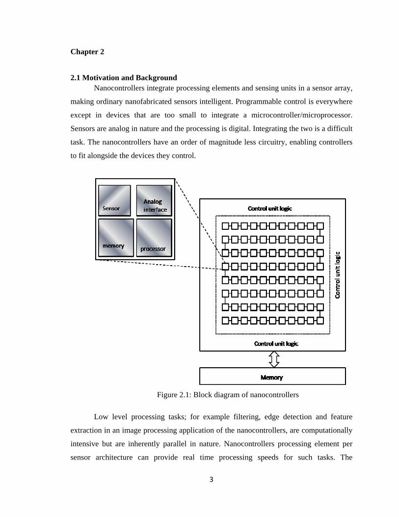
2.1 Motivation and Background Nanocontrollers integrate processing elements and sensing units in a sensor array,
making ordinary nanofabricated sensors intelligent. Programmable control is everywhere
except in devices that are too small to integrate a microcontroller/microprocessor.
Sensors are analog in nature and the processing is digital. Integrating the two is a difficult
task. The nanocontrollers have an order of magnitude less circuitry, enabling controllers
to fit alongside the devices they control.
Figure 2.1: Block diagram of nanocontrollers
Low level processing tasks; for example filtering, edge detection and feature
extraction in an image processing application of the nanocontrollers, are computationally
intensive but are inherently parallel in nature. Nanocontrollers processing element per
sensor architecture can provide real time processing speeds for such tasks. The

4
processing takes place adjacent to the pixels from which it originated eliminating long
distance data transfers and the I/O bottleneck between the sensor and the processing
elements reducing power dissipation, size and cost of the system.
It is well known that a carbon nanotube (CNT), or clump of CNTs, can be used as
a chemical sensor that distinguishes compounds by the way the electrical resistance
changes over time. In order to build a sensor array, a wafer is first created that contains a
pattern of exposed contacts. Low temperature nanofabrication methods, such as inkjet
printing of a suspension of CNTs, are used to deposit clumps of nanotubes over the metal
contacts.
The number of sensors per chip is limited primarily by the difficulty of sending
huge numbers of sensitive analog signals off-chip for precise measurement of resistance.
Suppose that an array of millions of the proposed nanocontrollers could be constructed on
the die using conventional VLSI fabrication technology. Each nanocontroller would have
a small number of I/O lines connected to metal pads on the top layer of the die. Each
nanocontroller directly measuring the resistance of the sensor above it, the problem of
routing sensitive analog signals off-chip is eliminated. Further, by working together as a
massively-parallel computer, the nanocontrollers can reduce the data to a smaller, higher
level, summary. Rather than sending raw sensor data to be processed elsewhere, it could
be processed by the massively parallel on-chip nanocontroller system so that the chip
would directly output the parts-per-million (PPM) concentration of each compound
sensed as digital data.
The nanocontrollers are not only restricted to the above application but can be
used for other sensor applications such as:
Imaging sensors used in digital cameras loose image quality due to applying the same
gain and integration time settings to all pixels. With a nanocontroller under each pixel,
each pixel can be adjusted independently and calibrated corrections for defects applied,
yielding much greater dynamic range and lower noise. Smart Pixels, Integration of photo
detector arrays and nanocontrollers on a single chip with real time processing capability
can reduce a complex image into a manageable stream of signals.hereby reducing the
number of signals sent off chip.
5
DLP (Digital Light Processor) video projectors use DMD (Digital Micro-mirror Device)
technology. DMD chip is made of several hundred thousand mirrors arranged in a
rectangular array. Each mirror corresponds to a pixel in the image to be displayed. Each
individual mirror can be rotated 10-12˚ to an on/off state. Light from the projector bulb is
reflected into the lens making the pixel appear bright in the on-state and dark in the off-
state. Intermediate shades are obtained by controlling the on/off times using PWM (Pulse
Width Modulation). With a nanocontroller device located on the same chip to control the
modulation, DMD chips can yield smoother shades. Nanocontrollers would be
appropriate as embedded controllers for Micro-ElectroMechanical Devices (MEMS) and
other larger devices.
2.2 Constraints on Nanocontroller Architecture The idea of nanocontrollers embedded with nanofabricated devices cannot be
implemented using conventional microcontroller architectures and compilation
technology as conventional microcontrollers occupy lot of circuitry. A new set of
architectural and compilation technologies have to be developed that satisfy the basic
requirements for such a system. There are six primary requirements, outlined in the
following subsections.
2.2.1 Minimal Circuit Size
The circuit complexity per nanocontroller must be small enough to be comparable
in physical size to sensors, actuators, and other devices implemented using
nanotechnology. Even the simplest microcontrollers generally require thousands of
transistors; the goal is to reduce that number to no more than a few hundred transistors.
This is far less than the estimated 10,000 transistors per SIMD processing element
proposed for SOSA (Self-Organizing nano-scale SIMD Architecture) [1]. This extremely
low complexity is the primary characteristic of a nanocontroller. Due to its low
complexity nanocontrollers built with current CMOS technology can be physically small
enough to control devices fabricated by very aggressive nanotechnology processes.

6
2.2.2 Predictable Real-Time Behavior
From a programmer’s point of view, a nanocontroller must have predictable real-
time execution timing characteristics. In order to monitor or control the real-time
behavior of a device, it will often be necessary for the nanocontroller to perform
particular operations at precise times relative to other operations. Although some
nanotechnology devices can tolerate very slow controller time bases, the required timing
precision varies greatly depending on the type of device with which the nanocontroller
must interact. The small physical scale of some devices results in relatively small time
constants. As an initial goal, a nanocontroller should be able to handle real-time
constraints with accuracies no worse than a microsecond.
2.2.3 Localized Input/Output
Each nanocontroller must be able to perform appropriate digital and/or analog
input/output (I/O) operations to interact with the sensing unit it is associated. Digital I/O
may be as simple as having some memory cells or registers be input/output devices.
Analog I/O is substantially more complex. Many nanotechnology devices have
inherently analog interfaces, and the space required for separate Analog-to-Digital
Converter (ADC) or Digital-to-Analog Converter (DAC) units would be too great. Thus,
an analog input would most likely be implemented by measuring the time taken for a
digital threshold voltage to be crossed in charging a capacitor. An analog output can be
accomplished by a similar process, essentially using Pulse-Width Modulation (PWM)
software to drive a simple filter circuit. These approaches also help in that using a
separate ADC/DAC unit tends to fix the precision of conversion, whereas the method
discussed permits precision to be traded for sample speed under program control. Of
course, this type of analog I/O is possible only with a fast enough processor that also has
the predictable timing described in 2.2.2.
2.2.4 Coordination as a Parallel Computer
Each nanocontroller must coordinate to act as a single nanocontroller system.
With thousands of sensors on a single chip, each with its own nanocontroller, it often is
necessary to coordinate the actions of all the devices or to reduce thousands of sensor
inputs to their single higher-level meaning. For example, a chip with a variety of types of
7
analog sensors that are together able to detect or deduce levels of thousands of different
chemical compounds might only need to report the action that the user should take to
counter the set of chemical or biological agents currently sensed. Thus, the
nanocontrollers must be able to act together as a parallel computing system. Acting
together requires both a mechanism for synchronization and a communication network.
2.2.5 Each Nanocontroller Independently Programmable
Each nanocontroller must be fully programmable as an independent processor.
Although nanocontrollers may need to work together, control and sensing algorithms
often require different constants or even different code paths depending on the state of the
device with which each nanocontroller interacts.
2.2.6. Reprogrammability
Nanocontroller programs must be able to be changed easily. The nanocontrollers
may have their program upgraded or changed under various conditions. Similarly, as a
control system rather than a general-purpose computer, it is likely that submission of a
new program from outside the system will be infrequent.
2.3 Nanocontroller System Architecture The primary architectural concern in nanocontroller design is minimization of
circuit size. This issue has been a concern for the parallel supercomputing world with a
desire to have many parallel processing elements as possible without exceeding the total
system complexity budget. The SIMD (Single Instruction Multiple Data) model is the
best fit.

8
2.3.1 SIMD (Single-Instruction Multiple-Data)
The basic idea behind SIMD is to operate the same instruction sequence
simultaneously on a large number of discrete data sets. SIMD targets machines that
exhibit massive amounts of data parallelism without complicated control flow or
excessive amounts of inter-processor communication.
SIMD consists of fine grained computational units called Processing Elements
(PE). An array of PEs is connected together by a simple network topology. This
processor array is connected to a control unit, which is responsible for fetching and
interpreting instructions. The control unit issues arithmetic and data processing
instructions to the array of processors, and handles any control flow or serial computation
that cannot be parallelized. For flexibility in implementing algorithms, processing
elements can usually be individually disabled for conditional execution. The instructions
issued by the control processor are executed by the processor array in lockstep operation.
Thus, control for a SIMD machine is vastly simplified, and synchronization issues can be
avoided.
Figure 2.2: Block diagram of a SIMD system
9
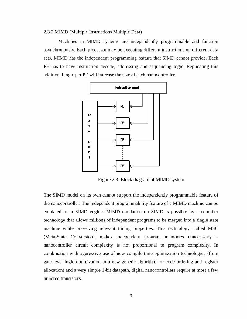
2.3.2 MIMD (Multiple Instructions Multiple Data)
Machines in MIMD systems are independently programmable and function
asynchronously. Each processor may be executing different instructions on different data
sets. MIMD has the independent programming feature that SIMD cannot provide. Each
PE has to have instruction decode, addressing and sequencing logic. Replicating this
additional logic per PE will increase the size of each nanocontroller.
Figure 2.3: Block diagram of MIMD system
The SIMD model on its own cannot support the independently programmable feature of
the nanocontroller. The independent programmability feature of a MIMD machine can be
emulated on a SIMD engine. MIMD emulation on SIMD is possible by a compiler
technology that allows millions of independent programs to be merged into a single state
machine while preserving relevant timing properties. This technology, called MSC
(Meta-State Conversion), makes independent program memories unnecessary –
nanocontroller circuit complexity is not proportional to program complexity. In
combination with aggressive use of new compile-time optimization technologies (from
gate-level logic optimization to a new genetic algorithm for code ordering and register
allocation) and a very simple 1-bit datapath, digital nanocontrollers require at most a few
hundred transistors.
10
2.3.3 Meta-State Conversion
In the nanocontrollers, the simplicity of SIMD processors and the independent
programmability of MIMD processors are desired at the same time. While there are
several techniques available for MIMD emulation on SIMD hardware ([2] [3] [4]), they
all require that each PE must have a copy of the MIMD program in their local memory
which adds a lot of hardware to a traditional SIMD processor.
Meta-State Conversion [5] is a compiler technique which considers the set of
processor states at a particular time as a single meta-state. Using static scheduling
techniques [6], MSC converts a MIMD program into a SIMD-executable finite
automaton based on meta-states. The next meta-state is decided based on the global OR
of votes from all participant processors. The generated meta-state automaton is held by
the SIMD control unit, thereby removing the necessity of a separate instruction memory
for each processing element.
2.3.4 CSI (Common Sub-Expression Induction)
After MSC, many meta-states in the meta-state graph contain more than one
MIMD state. These MIMD states contain many instructions that in true MIMD execution
would have been executed in parallel. Execution of these instructions on SIMD hardware
serializes the instructions, with each PE enabled only for the MIMD code it would have
executed. Nanocontrollers simulate disable of PEs by masking operations. Efficiency of
execution can be improved by factoring the operations that are common between
different MIMD states, which allow them to be executed in parallel by the SIMD PEs.
Common Sub-expression Induction [7] is the technique which develops a code schedule
for the SIMD PEs by factoring common operations between different threads in a meta-
state.
2.3.5 KITE (Kentucky If Then Else)
The “Kentucky If Then Else” nanocontroller array is essentially a massively-
parallel bit-serial SIMD with very low per-nanocontroller circuit complexity despite
incorporating a variety of special attributes that enable the system to meet all the
constraints of a nanocontroller. KITE efficiently implements a MIMD programming
11
model on simple SIMD hardware. There is only one instruction ITE (If Then Else) in the
Kentucky architecture. The Kentucky Architecture differs from traditional SIMD in that
it implements control by selection and not by decoding each instruction and
implementing the control necessary to make the processing element implement each
instruction.
The BitC compiler converts the control code in high level language into a meta-
state automaton. Each meta-state in the automaton is composed of ITE DAGs (Directed
Acyclic Graph) representing the MIMD states composing that state and ends in k-way
branches to k possible meta-states. The next meta-state to transition to, is determined
using a Global OR (GOR) of votes from all participant processors. The KITE architecture
consists of 3 components Control Unit, Instruction Sequencer and the Nanoprocessing
Element. Each component and their architectural details are discussed in detail in Chapter
3.
2.4 Related Work Attempts to integrate sensors and processing elements on the same chip started in
the late 80’s with LAPP (Linear Array Picture Processor). Second generation chip PASIC
[8] (Processor, A/D-converter, Sensor Integrated Chip) consists of a 256 by 256 sensor
array. Two hundred and fifty six 8-bit serial A/D converters and shift registers, 256 bit
serial ALUs and 256x 128 RAM all on the same chip. Both chips target image processing
applications. Both LAPP and PASIC are not single chip systems. They had off chip
control logic. The processing elements had limited functionality. The PASIC proved the
viability of a general purpose smart image sensor.
“SCAMP” [9] (SIMD Current mode Analog Matrix Processor) is a processor per
pixel fine grained SIMD (Single instruction Multiple Data) architecture intended for
image processing applications. The processing element is completely analog and is
embedded with the sensor. The resulting system retains some of the advantages of analog
signal processing, while being a fully programmable general purpose massively parallel
processor array. The analog processing elements execute a software program, performing
consecutive instructions issued by a digital controller, similar to the digital

12
microprocessor. The SCAMP chip can execute many image processing algorithms in real
time.
The SCAMP control unit [10] acts as an interface between the SCAMP chip and
the host computer. The control unit consists of an Instruction Sequencer and a System
Controller. Instruction sequencer controls program execution and provides an interface to
transfer processed data from the SCAMP array to the host. The system controller is an
8bit microcontroller responsible for maintaining the communications interface,
configuring analog hardware, controlling the SCAMP sequencer and providing additional
control over the SCAMP chip. Unlike the SCAMP system, nanocontrollers have digital
processing unit along with analog sensors making the nanocontroller more versatile and
easily reprogrammable for other applications.
“A Defect Tolerant Self-organizing Nano-scale SIMD Architecture” also known
as SOSA (self organizing SIMD structures) consists of millions of limited capability
nodes with high defect rates to self-organize into a set of SIMD processing elements.
SOSA has two types of control logic. Configuration logic used to configure a node and
real time control logic used to decode and execute instructions. Using a familiar data
parallel programming model SOSA architecture can execute a variety of programs.
Details of the control logic have not been clearly outlined. This research runs parallel to
the nanocontrollers digital controller with similar placement and timing issues.

13
Chapter 3
To execute a program on a nanocontroller system the user will have to construct
and simulate the program in software on the host computer using BitC. Compiled code is
stored in the controller memory (Flash memory, EEPROM, or SRAM). Controller
initiates an initialization process required to identify each processing element. The
control unit controls the program memory interface, instruction fetch and branch
evaluation. Instruction sequencer is responsible for generating necessary signals for
instruction execution. This chapter provides a detailed description of the control
hierarchy required to control a nanocontroller system.
3.1 Processing Element Architecture The abstract architecture of the Nanocontroller Processing Element (NPE) is
shown in figure 3.1. As a SIMD like hardware system, there is no need for each
nanocontroller to have its own program memory.
Figure 3.1. Abstarct architecture of the Processing Elements
A simple 1-of-2 multiplexor shown in Figure 3.1 directly implements masking
and also is able to implement any logic function efficiently. The instruction set contains
just a single instruction called SITE (Store-If-Then-Else). With only one type of
instruction, there is no op-code field; thus, a SITE can be represented by a tuple of four
numbers. A SITE tuple (1,2,3,4) would be equivalent to the C language assignment
reg1=(reg2?reg3:reg4) where reg1, reg2, reg3, and reg4 are all single-bit registers.
14
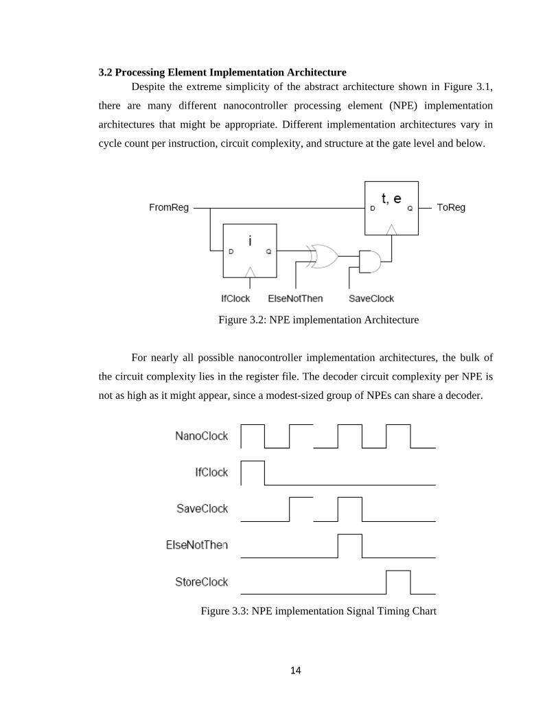
3.2 Processing Element Implementation Architecture Despite the extreme simplicity of the abstract architecture shown in Figure 3.1,
there are many different nanocontroller processing element (NPE) implementation
architectures that might be appropriate. Different implementation architectures vary in
cycle count per instruction, circuit complexity, and structure at the gate level and below.
Figure 3.2: NPE implementation Architecture
For nearly all possible nanocontroller implementation architectures, the bulk of
the circuit complexity lies in the register file. The decoder circuit complexity per NPE is
not as high as it might appear, since a modest-sized group of NPEs can share a decoder.
Figure 3.3: NPE implementation Signal Timing Chart

15
Given this four-cycle constraint, a more efficient NPE implementation
architecture is shown in Figure 3.2. Note that there is no multiplexor in the design. In
fact, there is no hardware structure that corresponds to an ALU of any kind. In the
abstract architecture of Figure 3.1, one of the two values held in the t (then) or e (else)
staging registers is always ignored. Since i (If) value can be known before the values
would be loaded into t or e, we can logically move the multiplexor to an earlier position
in the circuit and can eliminate one register by only saving the value that is selected. The
timing diagram in Figure 3.3 shows how the behavior is controlled through a four-cycle
SITE execution.
3.3 Control Hierarchy Just as a conventional SIMD system uses a Control Unit (CU) to control the
program memory interface, fetch instructions, evaluate branch instructions, etc.,
nanocontrollers are dependent on Nanocontroller Control Unit (NCU) for this highest
level functionality. However, whereas a traditional CU decodes each instruction and
implements the controls necessary to make the processing elements implement each
instruction, the NCU performs neither of these functions. Those lower level functions are
delegated to sequencers that reside nearer to the nanocontrollers, both physically and in
the logical level hierarchy.
The NCU shown in Figure 3.4 consists of a smart block prefetch unit, Branch
evaluation unit and SITE buffer. The primary task of the NCU is to dispatch chunks of
microcode to the sequencer at a sufficient rate to permit continuous operations of the
NPEs. The NPEs are targeted to operate at 1.5 to 2 GHz speed, which is clearly much
faster than the NCU could fetch instructions from conventional off-chip memory.
However, the SITEs are controlled by sequencers that implement control within each
SITE instruction and thus, they are able to be fed 24-bit SITE instructions at a slower
clock rate, about 500 MHz. By fetching 240-bit blocks of SITEs, The NCU gains the
ability to fetch yet another order of magnitude slower than it needs to feed SITEs to the
sequencer. The result is that about a 50 MHz NCU clock should be sufficient to support
NPEs running at a clock rate as high as 2 GHz. It had earlier been assumed that an
instruction block compression scheme would be needed to achieve sufficient instruction
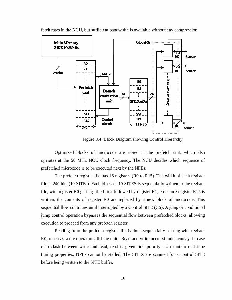
16
fetch rates in the NCU, but sufficient bandwidth is available without any compression.
Figure 3.4: Block Diagram showing Control Hierarchy
Optimized blocks of microcode are stored in the prefetch unit, which also
operates at the 50 MHz NCU clock frequency. The NCU decides which sequence of
prefetched microcode is to be executed next by the NPEs.
The prefetch register file has 16 registers (R0 to R15). The width of each register
file is 240 bits (10 SITEs). Each block of 10 SITES is sequentially written to the register
file, with register R0 getting filled first followed by register R1, etc. Once register R15 is
written, the contents of register R0 are replaced by a new block of microcode. This
sequential flow continues until interrupted by a Control SITE (CS). A jump or conditional
jump control operation bypasses the sequential flow between prefetched blocks, allowing
execution to proceed from any prefetch register.
Reading from the prefetch register file is done sequentially starting with register
R0, much as write operations fill the unit. Read and write occur simultaneously. In case
of a clash between write and read, read is given first priority –to maintain real time
timing properties, NPEs cannot be stalled. The SITEs are scanned for a control SITE
before being written to the SITE buffer.
17
3.4 Control Flow The nanocontrollers as mentioned earlier are single instruction set architecture
and ITES being the only instruction. Control flow is handled by interrupting the normal
sequential flow of the SITEs in the prefetch register file by embedding a Control SITE
(CS) along with the regular SITEs. The detection, evaluation and necessary control
signals are handled in the Branch Evaluation Unit (BEU). The BEU consists of a
modified 240 bit shift register that shifts 24 bits at a time and some simple logic
decoders. The BEU decode logic identifies the type of control SITE and generates the
appropriate control signals.
The control SITE (CS) is formatted much like an ordinary SITE, and is
represented in 24 bits as shown in the figure. The control SITE is detected when there is
6’b000000 in the “S” (Save) position of the SITE. This encoding is possible because the
NPE memory registers 0 and 1 are hardwired to have the values 0 and 1. Thus, it never
makes sense to store into these two NPE memory registers, and a CS would act as a null
operation if it were to be attempted by a NPE.
Figure 3.5: 204 bit microcode and Control SITE
The control instructions indicated by the bit fields [17:16] of the control SITE are: 1. Load register
00 => LD r, offset
This control instruction needs memory access. Program counter is interrupted and with
the help of offset, next block of code to be obtained is determined. The offset is 12 bits
and can point to 4096 memory locations. The new microcode from memory is written to
prefetch register file. The 4-bit register pointer from the CS will point to the register
where the new microcode has to be written in the prefetch register file.
2. Jump register
01=> JMP r //offset bits are ignored

18
A simple jump operation in the prefetch register file interrupts sequential read operation.
The register pointed by the CS will be read from prefetch register file.
3. Jump on global OR
10=> JMP or r //offset bits are ignored
This instruction is serviced when global-OR bit goes high. The global-OR signal is the
result of OR-ing together a one bit output from each NPE. Interestingly, the NPE clocks
are not synchronized in order to create this output; instead the NPEs each make their
contribution when their local clock sees fit, but the NCU sampling of the global-OR is
scheduled sufficiently later so as to make the clock skew and OR propagation delay
invisible. This scheduling is simply a matter of having enough SITEs between the setting
and reading of global-OR; it is implemented entirely by compile-time scheduling of the
SITEs. When the branch evaluation unit sees “10” op-code it stores the register pointer
value. When the global-OR signal becomes 1, the sequencing switches to read from the
register whose index was saved.
4. NOP
11=> NOP
This code is used for future use.
Fetching of microcode, detection of CS and interrupt servicing takes place in the
smart branch evaluation unit. The SITEs from the prefetch unit are not directly sent to the
sequencer. They are stored in a buffer called SITE Buffer (SB). The SB consists of thirty
24 bit registers and works on the principle of FIFO (first in first out). The buffer is
needed to increase the performance of the control unit. When the load interrupt is being
serviced, a single cycle of prefetch delay is introduced. Normally we nullify this delay by
making NPEs execute instructions that do not alter their states until valid new
instructions arrive. By having a buffer of 30 SITEs we can perform a jump of 10 SITEs in
the SB whenever a “Load” interrupt occurs.
3.5 Sequencer The purpose of a sequencer shown in Figure 3.6 is to prevent a slow broadcast
rate from slowing down the NPEs. The current design limits four NPEs per sequencer. By
sharing the decode logic among more NPEs, The transistor count per NPE can be reduced

19
dramatically. However there is a classical engineer tradeoff. Clearly, 16-32 NPEs sharing
a sequencer will reduce circuit complexity per NPE with negligible ill effects. Huge
degree of sharing would require high fan-out, thus limiting the NPE clock rate.
Figure 3.6: Sequencer Block Diagram
As mentioned earlier the SITE must be executed over a sequence of four clock
cycles. The sequencer generates four consecutive clock cycles worth of control
information for the NPEs as If, Then, Else and Save sequence. The sequencer reads from
the SB one SITE at a time. A mutated shift register circuit accepts the 24bit SITE and
shifts 6 bits-position per cycle to specify the register number for the register file decoder.
A state machine is used to generate the appropriate signals for the SITE execution. It is
observed that simple four bit circular left shifter with initial inputs as “1001” can act as
the state machine.
Each of the NPEs has a 64 bit register file called nanoprocessor memory (NPM).
The NPM contains the bulk of the circuit complexity associated with the nanocontrollers.

20
This again leads to engineering tradeoffs between sharing design logic and NPE
operation speed. Registers 0 and 1 are hardwired to ground and Vcc respectively. With
only a single bit datapath, 0 and 1 are the only constants possible, so any of the register
sources in a SITE can essentially be a constant instead. Register 2 is hardwired to the
input and register 3 is hardwired to the global-or input. Register 62 and register 63 are
hardwired to the global-or out and output pin respectively. The global OR registers are
used by control unit to manage conditional branching. The input and output pins are used
for interconnection and initialization of NPEs.
3.6 Interconnection Network The nanocontroller system has two types of interconnection network. Each
processing element is connected to its neighbor in a ring network. The ring network has a
special purpose of identifying individual processing elements. The second
interconnection network is the Global-Or network and is used for control flow operations.
Four of the 64 NPM address locations in each NPE are used as ports on two
separate networks. Two addresses interface the global-OR network that, provide the only
mechanism for conditional control flow. The NPEs are not capable of directly altering the
instruction sequence they will execute, but sending a value to the NCU via the global-OR
network provides a traditional SIMD CU conditional branching mechanism based on
“any” processing element wanting an alternative path taken. This mechanism is necessary
in order to implement constructs such as SIMD “while” loops that can iterate for a
dynamically determined number of iterations-which may be very rare in real-time control
code, but is necessary in order to make the system capable of fully general computation.
The global-OR signal also can be used as a bit-serial external output from the NPE array.
The other two addresses are used to connect the NPEs in a simple “wormhole
routed” ring topology. Although one would expect this network to be intended primarily
for communicating data between nearby NPEs, and it can be used that way, but is not its
primary function. Fundamentally, in order for different NPEs to behave differently, each
needs to have a notion of its identity. Parallel systems typically accomplish this by having
a dedicated hardware register in each processor that holds “IPROC”, the unique number
identifying that processor within that system. However with a million NPEs storing

21
IPROC would take 20 bits-nearly 1/3 of the entire address space available to each NPE.
The ring network offers a better alternative.
Rather than dedicating multiple 1-bit registers, the ring network can be used to sequentially initialize the NPEs. The process is:
1. Initially, all NPEs initialize a 20-bit counter to 0 and output a 0 to the next NPE.
This takes 21 SITEs.
2. Repeat as many times as there are processors:
a. A 1 is generated by the NCU as a initial input to the ring.
b. Each processor copies its ring input to its ring output. If that input was 0, the
NPE also increments its 20-bit counter. This software counter takes ~140
SITESs plus the additional time, if any needed to cover clock skew between
neighboring NPEs.
For a million-NPE system, we would expect a total initialization time of about 1M
x 140 x 4 clock cycles, or about half a second at a 1 GHz NPE clock. However this
initialization only happens once, and from that time onwards it is not necessary that all 20
bits of IPROC values is maintained. The IPROC values can be used to create appropriate
initial states and then be discarded.
Nanocontroller architecture features and functionality can be modeled using
software emulation. An accurate timing analysis, device utilization and sensor integration
can be tested using a hardware prototype. Full custom CMOS ASIC or high end FPGA
can be used for hardware prototyping. Some of the advantages and disadvantages of both
prototyping methods have been listed in the following section.
3.7 ASIC vs. FPGA The advantages of full custom CMOS ASIC implementation are:
Lower unit costs: For very high volume designs costs comes out to be very less.
Larger volume of ASIC design proves to be cheaper than implementing design
using FPGA.
Speeds of ASICs are faster than FPGAs: ASICs provide more design flexibility.
This gives enormous opportunity for speed optimizations.

22
Low power: There are several low power techniques such as power gating, clock
gating are available to achieve the power target.
In ASIC you can implement analog circuit, mixed signal designs. This is
generally not possible in FPGA.
The advantages of FPGA implementation are:
Faster time-to-market: No layout, masks or other manufacturing steps are needed
for FPGA design. Readymade FPGA is available to burn your HDL code to
FPGA.
No NRE (Non Recurring Expenses): This cost is typically associated with an
ASIC design. For FPGA this is not there. FPGA tools are cheap, ASIC are
expensive.
Simpler design cycle: This is due to software that handles much of the routing,
placement, and timing. Manual intervention is less. The FPGA design flow
eliminates the complex and time-consuming floor planning, place and route,
timing analysis.
More predictable project cycle: The FPGA design flow eliminates potential re-
spins, wafer capacities, etc of the project since the design logic is already
synthesized and verified in FPGA device.
Field Reprogramability: A new bit-stream can be uploaded remotely, instantly.
FPGA can be reprogrammed in a snap while an ASIC can take $50,000 and more
than 4-6 weeks to make the same changes. FPGA costs start from a couple of
dollars to several hundred or more depending on the hardware features.
Reusability: Reusability of FPGA is its main advantage. Prototype of the design
can be implemented on FPGA which could be verified for almost accurate results
so that it can be implemented on an ASIC. If design has faults change the HDL
code, generate bit stream, program to FPGA and test again. Modern FPGAs are
reconfigurable both partially and dynamically.
ASIC chips can be embedded along with Analog sensors. FPGAs do not come
with sensor elements as of now. Full custom ASIC provides a better hardware modal
23
for nanocontroller implementation. The initial cost of designing the proposed ASIC
chip is several tens of thousands of dollars. Due to the low cost, ease of
reprogramability and faster design time FPGA implementation has been opted. The
next chapter provides the implementation details of nanocontrollers using a Xilinx
FPGA chip.

24
Chapter 4
4.1 Virtual Prototyping and Validation This chapter describes high level Design Entry, Synthesis, Implementation and
Device programming of a nanocontroller system. The design has been described in
Verilog, synthesized with Xilinx ISE 10.1 synthesis tool, simulated using Modelsim 6.4a
and implemented on a Xilinx virtex-2xcv3000 FPGA. Before a hardware prototype was
built, behavioral simulation has been done to validate the functionality and performance
of the design. Design implementation followed by Functional simulation and Static
Timing analysis was done for a complete design verification. The FPGA design flow is
illustrated in the flow diagram shown in Figure 4.1.
Figure 4.1: FPGA Design flow
4.2 Design Entry Modular and bottom up hierarchical design approaches have been employed
during the design capture process. The modular design approach partitions the entire
system into smaller modules or functional units that can be independently designed and
described in Verilog. Besides, identical modules with the same functionalities can share

25
the same Verilog code or reuse the previously designed module. In addition, the bottom
up hierarchical design approach allows a multilevel view of the entire system for design
ease. Hence, by employing these approaches the smaller modules or functional units can
be tested and validated before they are integrated to form a larger system.
Figure 4.2: Organization of functional units within nanocontroller architecture
The Figure 4.2 shows the organization of functional units within the
nanocontroller system. For simplicity the main modules are shown and other sub-
modules within the main modules have been omitted. Behavioral, RTL (Register Transfer
Level) and structural coding styles have been used during the design process. The
advantage of behavioral coding is that only the behaviors of the modules are described in
the code and the CAD software implicitly generates the internal logic blocks.
4.3 Functional Unit Description 4.3.1 Memory Controller:
This module oversees all the digital I/O operations, acting as an interface to the
Block RAM (BRAM) and the prefetch unit. The memory controller runs at twice the
Nanocontroller architecture
Memory controller
Controller
Program Memory Unit
Program Counter Prefetch Unit
Prefetch RAM
Read Pointer
Write Pointer
Branch Evaluation Unit
240 Bit Shifting Unit
Instruction cache
Generic Sequencer
Sequencer
Nano‐Processing Unit
Nano Processor Memory
Processing Element Controller
24 Bit Shifter
Global ‐OrMod 10/Mod 4
counters

26
frequency of the global clock to increase the system speed and efficiency. The controller
is a simple mealy state machine with 4 states as shown in the Figure 4.4. Memory
controller operates in 3 modes namely Write, Read and simultaneous Read/Write.
Figure 4.3: Block diagram of memory controller
Figure 4.4: State diagram of memory controller
Block RAM (BRAM) modules provided in the Virtex-2 chip store the program to
be executed by the nanocontroller system. Block RAMs can be instantiated with help of a
Verilog HDL template or by using the Block RAM IP cores provided by Xilinx [11].
The size of the block RAM instantiated is 120KB. The current design has a maximum
27
capability of addressing 4096X240 bits. The size of the memory is restricted by the bits
allocated for offset (12 bits) from section 3.4. There is provision for increasing the
number of offset bits but a majority of the programs intended to run on a nanocontroller
system require less than 120KB of memory.
4.3.2 Block RAM:
Xilinx provides configurable memory modules on the virtex-2 chip called
BRAMs. BRAMs come in different sizes like RAMB4 (4KB) and RAMB16 (16KB)
blocks. Multiple blocks can be combined to form a larger memory block. For the
nanocontroller program memory, a 240 bits wide 4K addressable space block RAM is
configured.
Data2MEM [12] tool is used to enter the compiled program code from the BitC
complier to the BRAM blocks. Data2MEM is a data translation tool. It translates
contiguous blocks of data across multiple Block RAMs (BRAMs) that constitute a
contiguous logical address space. A BMM file (.bmm) defines the organization of Block
RAM memory. MEM file (.mem) is used to define the contents of the defined BRAM.
4.3.3 Prefetch Unit:
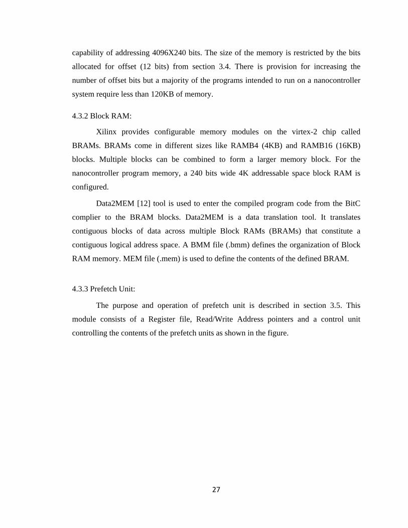
The purpose and operation of prefetch unit is described in section 3.5. This
module consists of a Register file, Read/Write Address pointers and a control unit
controlling the contents of the prefetch units as shown in the figure.
28
Figure 4.5: Block diagram of prefetch unit
The Register file can read and write simultaneously as pointed by the Read/Write
address pointers. Initially the prefetch unit is programmed to write 10 registers after
which reading is enabled. When read and write pointers point to the same register then
read operation is given first priority over write. Write to that register occurs on the next
cycle.
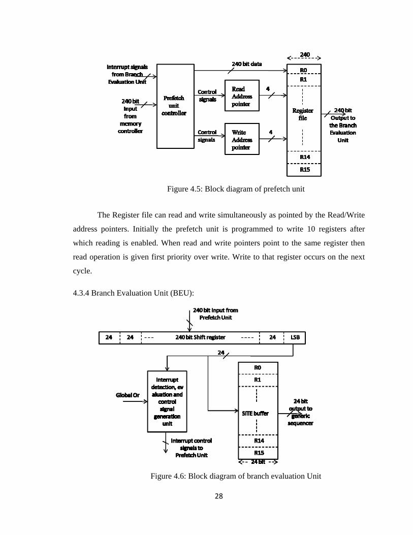
4.3.4 Branch Evaluation Unit (BEU):
Figure 4.6: Block diagram of branch evaluation Unit

29
The BEU module receives 240 bits of microcode at a time from prefetch unit and
broadcasts 24 bit SITEs to the sequencer array. 240 bit shifter shifts 24 bits (one SITE) at
a time. The BEU unit operates on 2 clocks, an input clock running 10 times slower than
an output clock. Each SITE is scanned for Control SITE before storing in the SITE
Buffer. The SITE buffer is a FIFO (First In First Out) unit. Like the prefetch register file
the SITE buffer can read and write simultaneously. Reading from this register file is
enabled after 10 write operations.
4.3.5 Generic Sequencer Unit:
The sequencer consists of 4 NPEs sharing the same decode logic. The generic
coding style enables the user to increment the NPE count in multiples of four. Each
sequencer executes the SITE instruction in 4 clock cycles with the help of a controller
that sends the appropriate control signals to the NPEs. The current design under test
(DUT) contains 4 such SIMD blocks (16 NPEs).
Each sequencer unit along with 4 NPEs utilizes ~300 CLB (Configurable Logic
Blocks). Major portion of these CLBs is taken up by NPE memory. This happens because
Xilinx synthesis tool uses distributed RAM instead of block ram for NPE memory.
Distributed RAM is made up of the LUT (look up tables) in CLBs.
4.3.5 Global-Or: The global-or module is a huge or-gate used for looping and iterative
operations. This large or-gate is built as a network of smaller or-gates to reduce the fan
out on each gate. MOD 10/MOD 4 counters are used to generate control signals. The
Program Counter keeps track of the memory location to be read next from the main
memory.
4.4 Behavioral Simulation
4.4.1 Testing Methodology:
The testing methodology employed in this project uses the bottom up approach.
Lower level functional components such as nanoprocessing elements, sequencer, etc were
tested before combining them to form higher level functional units. Bottom up approach
in is an efficient testing approach. When the lower level components are combined into

30
higher level functional units, one can be more assured that the lower level components
will not be at fault if errors are detected.
4.4.2.1 Control hierarchy features
The nanocontroller has a few unique operations like initialization and control
flow. This section demonstrates these featured operations by running a simple test
program. The program has been written in a way that it exhibits all the above mentioned
operations.
4.4.2.2 Initialization
As discussed in section 3.6, each nanocontroller has to be identified to behave as
an independent processing element. To act independently each NPE has to be given a
unique identification number. This is achieved by the “Iproc” instruction and takes
approximately 140 SITEs per nanocontroller for a million NPE system. The number of
SITEs required for initialization increases with the increase in number of NPEs. The test
program takes lesser SITES as we have 16 NPEs in the current test module. All the NPEs
initialize a 4 bit counter (registers 20 to 23) to 0. At the end of the initialization process
the first NPE stores 0000 and the last NPE has 1111. This can be seen in the simulation
shown in figure 4.7.

31
Figure 4.7: Initialization of Nanoprocessing Elements
The ability to identify NPEs facilitates independent programmability to the
nanocontroller system.
4.4.2.3 Control Flow Handling
Control flow is handled by interrupting the normal sequential flow of SITEs in the
prefetch register file. As discussed in section 3.4 there are 3 types of interrupts load, jump

32
and global-or. This section provides simulations to observe the operation of these
interrupts.
The signals to observe:
Mem_addr_in_sig is the address pointer to the block RAM.
C_out_sig is the feedback from the branch evaluation unit. The MSB 4 bits point to the
register in prefetch unit to which the jump must occur and the last 12 bits point to offset.
branch, ld_op_sig tell the control unit that a valid control SITE was detected. Branch
signal goes high when a control site is detected. ld_op_sig indicate that a load interrupt
has occurred.
M_out points to the register to be written in prefetch unit.
MARsr points to the register to be read in prefetch unit.
gout_sig is high when global or is set.
33
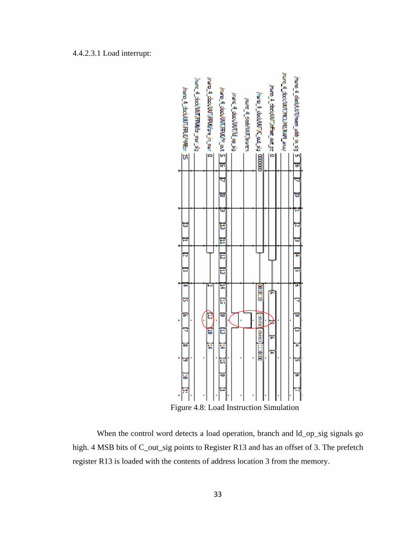
4.4.2.3.1 Load interrupt:
Figure 4.8: Load Instruction Simulation
When the control word detects a load operation, branch and ld_op_sig signals go
high. 4 MSB bits of C_out_sig points to Register R13 and has an offset of 3. The prefetch
register R13 is loaded with the contents of address location 3 from the memory.
34
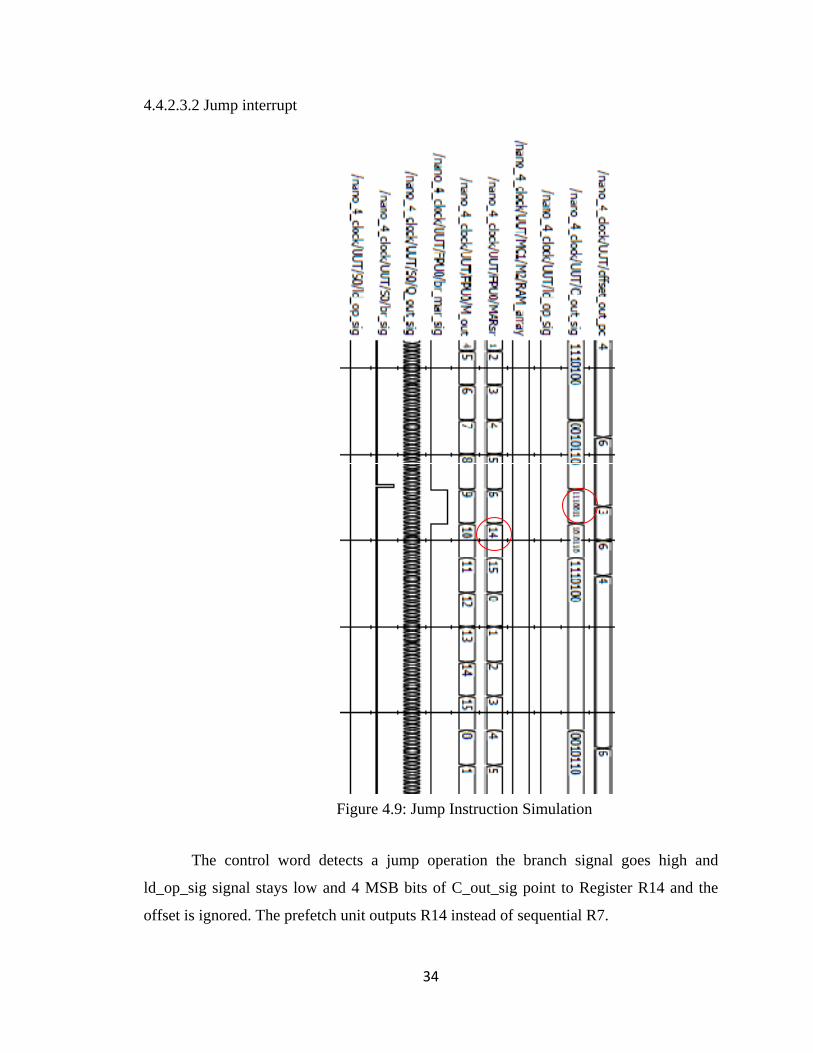
4.4.2.3.2 Jump interrupt
Figure 4.9: Jump Instruction Simulation
The control word detects a jump operation the branch signal goes high and
ld_op_sig signal stays low and 4 MSB bits of C_out_sig point to Register R14 and the
offset is ignored. The prefetch unit outputs R14 instead of sequential R7.

35
4.4.2.3.3 Global or interrupt
Figure 4.10: Global or interrupt simulation
We know that the Register 62 of all nanocontrollers is hardwired to the global-or
out pin. When RAM_array[62] of all the registers become high the global or bit is set as
indicated by the gout_sig signal. C_out_sig points to register R0 of prefetch unit ignoring
the offset.
4.5 Hardware prototype using iMPACT
After the nanocontroller architecture design is synthesized and implemented using
CAD packages, a bit stream file (that contains proprietary header information as well as
configuration data) for a specific FPGA chip is generated. In this case, the bit stream file
contains the configuration bit file for the Xilinx XCV3000 FPGA chip. Next, the bit
stream file is programmed into the FPGA through the parallel port of a computer using
the Xilinx iMPACT [13], a file generation and device programming tool. iMPACT tool
uses JTAG (Joint Test Action Group) ports to configure the devices and automatically
identify the size and composition of the boundary scan chain. Any supported Xilinx
device will be recognized and labeled in iMPACT.
As discussed in section 4.3.2 the program code is also configured along with the
device in the block RAM module. A fully configured FPGA functionality is tested by
observing its outputs with the help of a logic analyzer. An easier method for testing the

36
device functionality is by IEEE 1149.1 Standard Test Access Port and Boundary-Scan
Architecture.
4.6 Testing Using JTAG Xilinx XCV devices use a standard 4 wire Test Access Port (TAP) for In-System
programming and Boundary scan (JTAG) testing. Boundary scan is a methodology
allowing complete controllability and observability of boundary pins of a JTAG
compatible device via software control. This capability enables in-circuit testing without
the need of bed-of-nail in-circuit test equipment. The TAP controller is a state machine
(16 possible states) controlling operations associated with boundary scan cells. The basic
operation is controlled through four pins: Test Clock (TCK), Test Mode Select (TMS),
Test Data In (TDI), and Test Data Out (TDO). The Xilinx boundary scan architecture is
shown in figure 4.11.
Figure 4.11: JTAG Boundary scan architecture [14] The Xilinx iMPACT automatically generates a Serial Vector Format (SVF) file
describing the programming and test algorithms required by the XCV devices [14]. Most
ATE platforms and Boundary Scan based development tools accept SVF as a test vector
input format. By sending test vectors in the SVF file to the input boundary pins and
observing the output boundary pins we can test the functionality of the DUT (Device
Under Test).

37
Chapter 5
This chapter observes the performance of nanocontroller system. Minimum circuit
size is the primary objective for a nanocontroller system. To compare the circuit
utilization of the nanocontroller system we make use of its FPGA implementation
described in chapter 4. The current implementation is compared with processor cores
obtained from opencores.org. Device utilization, operating time and functional density
parameters have been used for comparison. The scalability of nanocontrollers with
logarithmically increasing NPEs is discussed along with the timing analysis.
5.1 Device Utilization
The primary objective of a nanocontroller system is to have minimum circuit
complexity. The performance of nanocontrollers can be evaluated by comparing other
processor systems designed using Verilog/VHDL and implemented on an FPGA.
Processor cores used for comparison have been taken from opencores.org [15], [16], [17],
[18]. All cores are FPGA proven and synthesized using Xilinx 10.1 ISE tool on a virtex-2
xcv3000 chip. The hardware utilization i.e. slices (CLBs) and 4 input LUTs have been
tabulated as shown in the Table 1. The Maximum frequency data tabulated is obtained
from the Post-synthesis delay (FF delay + data delay).
Table 1: Devive Utilization of processing element architectures
Figure 5.1: Functional Density metric

38
Functional Density metric [19] is used to compare the performance of processor
cores. Functional density is a composite area-time metric used to identify the
computational throughput (operations per second) of unit hardware resources. Functional
Density depends on the Area measured in the FPGA “cell count” and operating time
which is the optimal “cycle time” of the mapped FPGA circuit.
A Normalized Cost/Performance for different processing element architectures
graph is shown in figure 5.2. 16-bit Microcontroller and T-48 cores have lower device
utilization (slices and LUTs) but their clock period and Area/throughput go up when
compared to the nanocontroller. Nanocontroller system exhibits the highest functional
density among the compared cores.
Figure 5.2: Normalized Cost/Performance of Processing Element Architectures
5.2 Scalability of Nanocontrollers
Scalability of nanocontrollers can be observed from the device utilization,
maximum frequency and Functional Density data from the table 2. The nanocontroller
system was implemented by logarithmically increasing the number of processing
elements to the maximum possible on the virtex-2 chip.
39
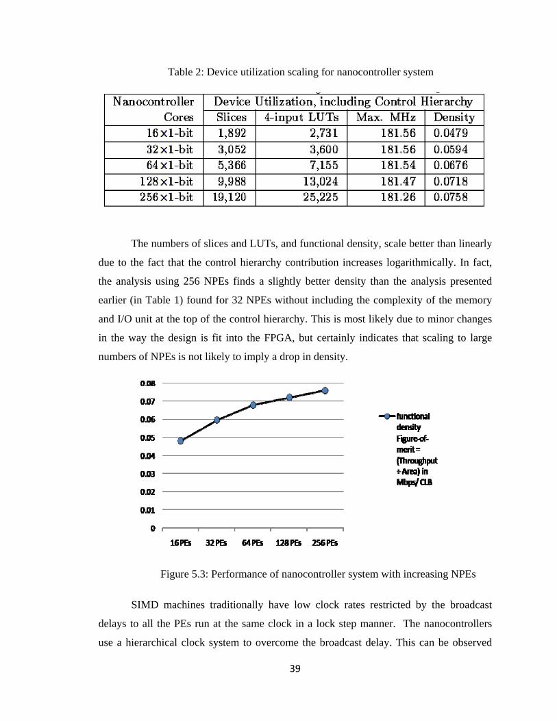
Table 2: Device utilization scaling for nanocontroller system
The numbers of slices and LUTs, and functional density, scale better than linearly
due to the fact that the control hierarchy contribution increases logarithmically. In fact,
the analysis using 256 NPEs finds a slightly better density than the analysis presented
earlier (in Table 1) found for 32 NPEs without including the complexity of the memory
and I/O unit at the top of the control hierarchy. This is most likely due to minor changes
in the way the design is fit into the FPGA, but certainly indicates that scaling to large
numbers of NPEs is not likely to imply a drop in density.
Figure 5.3: Performance of nanocontroller system with increasing NPEs
SIMD machines traditionally have low clock rates restricted by the broadcast
delays to all the PEs run at the same clock in a lock step manner. The nanocontrollers
use a hierarchical clock system to overcome the broadcast delay. This can be observed

40
from the Maximum frequency numbers from table 2. The maximum clock speeds do
suffer a reduction as the number of nanoprocessors is increased, but the reduction going
from 16 to 256 cores is less than 0.2%. Even this small reduction in clock speed is likely
an artifact of routing issues within the FPGA implementation. A custom chip
implementation is not expected to suffer this much reduction in clock rate as the number
of cores are increased.
5.3 Timing analysis Timing analysis helps in verifying that the design meets the timing constraints of
the nanocontroller architecture. Timing simulation uses the timing and design layout
information that is available after place and route to give a more accurate assessment of
the behavior of the circuit under worst-case conditions. This enables simulation of the
design to closely match the actual device operation.
The clock frequency of a digital circuit is heavily dependent on circuit delay (hold
time and setup time). To calculate the delay associated with the hierarchical clock
mechanism of the nanocontroller we start by determining the delay associated with the
smallest clock. The Post-Route simulation takes into account all the delays associated
with the circuit. The delay associated with all the clocks has been and tabulated as shown
in Table 3.
Table 3: Post Place and Route Timing analysis
The timing analysis was performed using the Xilinx Timing Analyzer tool. The
clock cycle delay data provided is the Post-Place and route delay which includes 7 types
of delays (Clock to setup + Clock to pad + Clock pad to output pad + pad to pad + Pad to
Setup + Setup to Clock at Pad + paths ending at clock pin of flip flops).
Connection of all signals to I/O pads has a leveling effect on the delays, so that
the changes in clock rate at the different control levels are smaller than they would be in a

41
custom-made chip. The post-synthesis delay of nanocontrollers is 5.6008ns The PEs are
connected to I/O pins which is introducing 4.34ns additional delay making the total delay
9.94ns.
Total delay is the sum of logic delay and route delay. For a sequencer clock: Total delay=
(1.089ns logic, 11.176ns route) =12.316ns. It is to be noted that delay of a circuit
implementation in an FPGA is mostly due to routing delay (91.1% route delay). A full
custom CMOS ASIC implementation will have much less routing delay and higher
operating frequency.
42
Chapter 6
6.1 Conclusion Using existing CMOS fabrication technology an array of programmable
controllers can be fabricated on a single chip with all controllers coordinating as one
massively parallel computer. A control unit is an essential part of nanocontroller system
responsible for instruction execution and program memory interface.
The current thesis provided details of control hierarchy required for a
nanocontroller system. To validate the design, a complete Verilog description along with
an FPGA prototype has been presented. Hardware constraints associated with
nanocontroller system like minimal circuit complexity, predictable real time behavior,
coordination as a parallel computer, digital I/O, reprogramability and independently
programmable NPEs have been addressed.
6.2 Future work Current thesis provides digital control to a nanocontroller system. ADC (analog to
digital converters) and pulse width modulation (PWM) circuit along with analog sensors
complete the system. Integration of analog circuit and digital system will be the next step
in building a nanocontroller array. The current FPGA implementation can be tested with
the help of a bidirectional LED array, [20] simple control system in which the ambient
light is sensed by LEDs (reversed biased) is read by the NPEs with the help of ADC. The
input from ADC is stored in memory. The sensed data can be manipulated and sent to the
LED array in emitter (forward biased) mode. The system can be tested with other sensors
like temperature, capacitive, CCD etc.
Although an FPGA implementation helps understand the performance, timing
constraints and functionality of a nanocontroller system, inherently nanocontrollers have
to be embedded alongside nanotechnology devices. Such a system can only be achieved
with a full custom CMOS ASIC implementation. MOSIS (a low cost prototyping and
small volume production service for VLSI development) prototype will provide the most
accurate model for a nanocontroller system.

43
As the number of NPEs approach a million the size of the die increases
introducing clock skew. Clock skew is a phenomenon that occurs in synchronous circuits
in which the clock signal arrives at different components at different times. In a SIMD
system clock skew is a major concern as the system works in a lock step mechanism. The
clock skew associated broadcast of SITEs to the sequencer limits the number of
processing elements. The current FPGA implementation due to the restriction in the
number of processing elements could not model the effects of clock skew in a
nanocontroller system. This has to be addressed in the future implementations.

44
Bibliography [1] J. P. Patwardhan, V. Johri, C. Dwyer, and A. R. Lebeck, “A defect tolerant self-organizing nanoscale simd architecture,” in ASPLOS-XII: Proceedings of the 12th international conference on Architectural support for programming languages and operating systems, (New York, NY, USA), pp. 241–251, ACM, 2006. [2] M. Nilsson and H.Tanaka, “MIMD Execution by SIMD Computers,” in Journal of
Information Processing- Information Processing Society of Japan, vol. 13, no. 1, pp. 58–61, 1990.
[3] H. G. Dietz and W. E. Cohen, “A Control-Parallel Programming Model Implemented On SIMD Hardware,” in Languages and Compilers for Parallel Computing, Lecture Notes in Computer Science (LNCS), pp. 311–325, Springer-Verlag (New York), 1993.
[4] P. Sanders, “Emulating MIMD Behavior on SIMD Machines,” in International Conference on Massively Parallel Processing, Elsevier, 1994. [5] H. G. Dietz and G. Krishnamurthy, “Meta-state conversion,” 1993 International Conference on Parallel Processing, Saint Charles, Illinois, vol. II, August 1993.
[6] M.T.O’Keefe, H.G.Dietz and A.Zaafrani, “An Introduction to Static Scheduling for MIMD Architectures,” in Advances in Languages and Compilers for Parallel Processing, pages 452–444, The MIT Press, Cambridge, Massachusetts, 1991.
[7] Henry G. Dietz, “Common Subexpression Induction”, in ICPP (2), pp 174–182, 1992. [8] K. Chen, et al., "PASIC: A Processor--A/D Converter—Sensor Integrated Circuit" Proceedings of International Symposium on Circuits and Systems, 1990, pp. 1705-1708. [9] P.Dudek and P.J.Hicks, "A General-Purpose Processor-per-Pixel Analog SIMD Vision Chip", in IEEE Transactions on Circuits and Systems - I, vol. 52, no. 1, pp. 13-20, January 2005. [10] David R. W. Barr, Stephen J. Carey, Alexey Lopich and Piotr Dudek, “A Control System for a Cellular Processor Array,” in 10th International Workshop on Cellular Neural Networks and Their Applications, Istanbul, Turkey, August 2006. [11] Xilinx documentation, “CORE Generator Guide,” [Online]. Available: http://www.xilinx.com/itp/xilinx6/books/docs/cgn/cgn.pdf [Accessed: April 27, 2010]. [12] Xilinx Software manuals, “Data2MEM User Guide,” Available: http://www.xilinx.com/itp/xilinx10/books/docs/d2m/d2m.pdf [last accessed: April 27, 2010].

45
[13] Xilinx software manuals, “ISE In-Depth Tutorial,” Available: http://download.xilinx.com/direct/ise9_tutorials/ise9tut.pdf [last accessed: April 27, 2010] [14] Xilinx application notes, “Using serial Vector Format Files to program XC9500/Xl/XV Devices In- System,” available: http://www.xilinx.com/support/documentation/application_notes/xapp067.pdf [last accessed April 27, 2010]. [15] Erlandsson, Marcus, Unneback, Michael, D'Addio, Rich, Baxter, Julius, Bennett, Jeremy, Fielding, Steve, “OpenRISC,” opencores.org, Sep 25, 2001. Available: http://opencores.org/project,or1k [last accessed April 27, 2010].
[16] Fazzino, Fabrizio , “M1 Core”, opencores.org, Jan 3, 2007. Available: http://opencores.org/project,m1_core [last accessed April 27, 2010].
[17]Laeuger, Arnim , “T48 µController”, opencores.org, Mar 23, 2004. Available: http://opencores.org/project,t48 [last accessed April 27, 2010].
[18] “16 Bit Microcontroller”, opencores.org, Sep 29, 2003. Available: http://opencores.org/project,c16 [last accessed April 27, 2010].
[19] Michael J. Wirthlin and Brad L. Hutchings, “Improving Functional Density Through Run-Time Constant propagation,” Brigham Young University, Provo. UT.
[20] Paul Dietz, William Yerazunis and Darren Leigh, “Very Low-Cost Sensing and Communication Using Bidirectional LEDs,” TR2003-35, July 2003.

46
Vita Author's Name: Akshay Vummannagari Birthplace: Hyderabad, India Birthdate : April 25, 1984 Education: Bachelor of Engineeering in Electrical Engineering Osmania University May-2006. Research Experience: University of Kentucky Lexington, KY Graduate Research Assistant (12/08 - 8/09).