
FPGA designs with Verilog and SystemVerilog - Read the Docs
183
FPGA designs with Verilog and SystemVerilog Meher Krishna Patel Created on : Octorber, 2017 Last updated : May, 2020 More documents are freely available at PythonDSP
-
Upload
khangminh22 -
Category
Documents
-
view
3 -
download
0
Transcript of FPGA designs with Verilog and SystemVerilog - Read the Docs

FPGA designs with Verilog andSystemVerilog
Meher Krishna PatelCreated on : Octorber, 2017
Last updated : May, 2020
More documents are freely available at PythonDSP

Table of contents
Table of contents i
1 First project 11.1 Introduction . . . . . . . . . . . . . . . . . . . . . . . . . . . . . . . . . . . . . . . . . . . . . . . . . 11.2 Creating the project . . . . . . . . . . . . . . . . . . . . . . . . . . . . . . . . . . . . . . . . . . . . 11.3 Digital design using ‘block schematics’ . . . . . . . . . . . . . . . . . . . . . . . . . . . . . . . . . . 11.4 Manual pin assignment and compilation . . . . . . . . . . . . . . . . . . . . . . . . . . . . . . . . . 81.5 Load the design on FPGA . . . . . . . . . . . . . . . . . . . . . . . . . . . . . . . . . . . . . . . . . 81.6 Digital design using ‘Verilog codes’ . . . . . . . . . . . . . . . . . . . . . . . . . . . . . . . . . . . . 101.7 Pin assignments using ‘.csv’ file . . . . . . . . . . . . . . . . . . . . . . . . . . . . . . . . . . . . . . 111.8 Converting the Verilog design to symbol . . . . . . . . . . . . . . . . . . . . . . . . . . . . . . . . . 111.9 Convert Block schematic to ‘Verilog code’ and ‘Symbol’ . . . . . . . . . . . . . . . . . . . . . . . . 141.10 Conclusion . . . . . . . . . . . . . . . . . . . . . . . . . . . . . . . . . . . . . . . . . . . . . . . . . 17
2 Overview 182.1 Introduction . . . . . . . . . . . . . . . . . . . . . . . . . . . . . . . . . . . . . . . . . . . . . . . . . 182.2 Modeling styles . . . . . . . . . . . . . . . . . . . . . . . . . . . . . . . . . . . . . . . . . . . . . . . 18
2.2.1 Continuous assignment statements . . . . . . . . . . . . . . . . . . . . . . . . . . . . . . . . 182.2.2 Comparators using Continuous assignment statements . . . . . . . . . . . . . . . . . . . . . 192.2.3 Structural modeling . . . . . . . . . . . . . . . . . . . . . . . . . . . . . . . . . . . . . . . . 222.2.4 Procedural assignment statements . . . . . . . . . . . . . . . . . . . . . . . . . . . . . . . . 242.2.5 Mixed modeling . . . . . . . . . . . . . . . . . . . . . . . . . . . . . . . . . . . . . . . . . . 25
2.3 Conclusion . . . . . . . . . . . . . . . . . . . . . . . . . . . . . . . . . . . . . . . . . . . . . . . . . 26
3 Data types 273.1 Introduction . . . . . . . . . . . . . . . . . . . . . . . . . . . . . . . . . . . . . . . . . . . . . . . . . 273.2 Lexical rules . . . . . . . . . . . . . . . . . . . . . . . . . . . . . . . . . . . . . . . . . . . . . . . . . 273.3 Data types . . . . . . . . . . . . . . . . . . . . . . . . . . . . . . . . . . . . . . . . . . . . . . . . . 273.4 Logic values . . . . . . . . . . . . . . . . . . . . . . . . . . . . . . . . . . . . . . . . . . . . . . . . . 273.5 Number representation . . . . . . . . . . . . . . . . . . . . . . . . . . . . . . . . . . . . . . . . . . . 283.6 Signed numbers . . . . . . . . . . . . . . . . . . . . . . . . . . . . . . . . . . . . . . . . . . . . . . . 283.7 Operators . . . . . . . . . . . . . . . . . . . . . . . . . . . . . . . . . . . . . . . . . . . . . . . . . . 293.8 Arithmetic operator . . . . . . . . . . . . . . . . . . . . . . . . . . . . . . . . . . . . . . . . . . . . 29
3.8.1 Bitwise operators . . . . . . . . . . . . . . . . . . . . . . . . . . . . . . . . . . . . . . . . . . 293.8.2 Relational operators . . . . . . . . . . . . . . . . . . . . . . . . . . . . . . . . . . . . . . . . 303.8.3 Logical operators . . . . . . . . . . . . . . . . . . . . . . . . . . . . . . . . . . . . . . . . . . 303.8.4 Shift operators . . . . . . . . . . . . . . . . . . . . . . . . . . . . . . . . . . . . . . . . . . . 303.8.5 Concatenation and replication operators . . . . . . . . . . . . . . . . . . . . . . . . . . . . . 303.8.6 Conditional operator . . . . . . . . . . . . . . . . . . . . . . . . . . . . . . . . . . . . . . . . 303.8.7 Parameter and localparam . . . . . . . . . . . . . . . . . . . . . . . . . . . . . . . . . . . . . 313.8.8 localparam . . . . . . . . . . . . . . . . . . . . . . . . . . . . . . . . . . . . . . . . . . . . . 323.8.9 Parameter and defparam . . . . . . . . . . . . . . . . . . . . . . . . . . . . . . . . . . . . . 32
3.9 Conclusion . . . . . . . . . . . . . . . . . . . . . . . . . . . . . . . . . . . . . . . . . . . . . . . . . 34
i

4 Procedural assignments 354.1 Introduction . . . . . . . . . . . . . . . . . . . . . . . . . . . . . . . . . . . . . . . . . . . . . . . . . 354.2 Combinational circuit and sequential circuit . . . . . . . . . . . . . . . . . . . . . . . . . . . . . . . 354.3 Concurrent statements and sequential statements . . . . . . . . . . . . . . . . . . . . . . . . . . . . 364.4 ‘always’ block . . . . . . . . . . . . . . . . . . . . . . . . . . . . . . . . . . . . . . . . . . . . . . . . 364.5 Blocking and Non-blocking assignment . . . . . . . . . . . . . . . . . . . . . . . . . . . . . . . . . . 364.6 Guidelines for using ‘always’ block . . . . . . . . . . . . . . . . . . . . . . . . . . . . . . . . . . . . 38
4.6.1 ‘always’ block for ‘combinational designs’ . . . . . . . . . . . . . . . . . . . . . . . . . . . . 384.6.2 ‘always’ block for ‘latched designs’ . . . . . . . . . . . . . . . . . . . . . . . . . . . . . . . . 384.6.3 ‘always’ block for ‘sequential designs’ . . . . . . . . . . . . . . . . . . . . . . . . . . . . . . . 38
4.7 If-else statement . . . . . . . . . . . . . . . . . . . . . . . . . . . . . . . . . . . . . . . . . . . . . . 394.8 Case statement . . . . . . . . . . . . . . . . . . . . . . . . . . . . . . . . . . . . . . . . . . . . . . . 404.9 Problem with Loops . . . . . . . . . . . . . . . . . . . . . . . . . . . . . . . . . . . . . . . . . . . . 414.10 Loop using ‘if’ statement . . . . . . . . . . . . . . . . . . . . . . . . . . . . . . . . . . . . . . . . . 414.11 Conclusion . . . . . . . . . . . . . . . . . . . . . . . . . . . . . . . . . . . . . . . . . . . . . . . . . 43
5 VHDL designs in Verilog 445.1 Introduction . . . . . . . . . . . . . . . . . . . . . . . . . . . . . . . . . . . . . . . . . . . . . . . . . 445.2 VHDL designs in Verilog . . . . . . . . . . . . . . . . . . . . . . . . . . . . . . . . . . . . . . . . . . 445.3 Conclusion . . . . . . . . . . . . . . . . . . . . . . . . . . . . . . . . . . . . . . . . . . . . . . . . . 45
6 Visual verifications of designs 466.1 Introduction . . . . . . . . . . . . . . . . . . . . . . . . . . . . . . . . . . . . . . . . . . . . . . . . . 466.2 Flip flops . . . . . . . . . . . . . . . . . . . . . . . . . . . . . . . . . . . . . . . . . . . . . . . . . . 46
6.2.1 D flip flop . . . . . . . . . . . . . . . . . . . . . . . . . . . . . . . . . . . . . . . . . . . . . . 466.2.2 D flip flop with Enable port . . . . . . . . . . . . . . . . . . . . . . . . . . . . . . . . . . . . 47
6.3 Counters . . . . . . . . . . . . . . . . . . . . . . . . . . . . . . . . . . . . . . . . . . . . . . . . . . . 476.3.1 Binary counter . . . . . . . . . . . . . . . . . . . . . . . . . . . . . . . . . . . . . . . . . . . 486.3.2 Mod-m counter . . . . . . . . . . . . . . . . . . . . . . . . . . . . . . . . . . . . . . . . . . . 49
6.4 Clock ticks . . . . . . . . . . . . . . . . . . . . . . . . . . . . . . . . . . . . . . . . . . . . . . . . . 516.5 Seven segment display . . . . . . . . . . . . . . . . . . . . . . . . . . . . . . . . . . . . . . . . . . . 51
6.5.1 Implementation . . . . . . . . . . . . . . . . . . . . . . . . . . . . . . . . . . . . . . . . . . . 526.5.2 Test design for 7 segment display . . . . . . . . . . . . . . . . . . . . . . . . . . . . . . . . . 53
6.6 Visual verification of Mod-m counter . . . . . . . . . . . . . . . . . . . . . . . . . . . . . . . . . . . 556.7 Conclusion . . . . . . . . . . . . . . . . . . . . . . . . . . . . . . . . . . . . . . . . . . . . . . . . . 56
7 Finite state machine 577.1 Introduction . . . . . . . . . . . . . . . . . . . . . . . . . . . . . . . . . . . . . . . . . . . . . . . . . 577.2 Comparison: Mealy and Moore designs . . . . . . . . . . . . . . . . . . . . . . . . . . . . . . . . . . 577.3 Example: Rising edge detector . . . . . . . . . . . . . . . . . . . . . . . . . . . . . . . . . . . . . . 57
7.3.1 State diagrams: Mealy and Moore design . . . . . . . . . . . . . . . . . . . . . . . . . . . . 587.3.2 Implementation . . . . . . . . . . . . . . . . . . . . . . . . . . . . . . . . . . . . . . . . . . . 587.3.3 Outputs comparison . . . . . . . . . . . . . . . . . . . . . . . . . . . . . . . . . . . . . . . . 607.3.4 Visual verification . . . . . . . . . . . . . . . . . . . . . . . . . . . . . . . . . . . . . . . . . 60
7.4 Glitches . . . . . . . . . . . . . . . . . . . . . . . . . . . . . . . . . . . . . . . . . . . . . . . . . . . 617.4.1 Combinational design in asynchronous circuit . . . . . . . . . . . . . . . . . . . . . . . . . . 617.4.2 Unfixable Glitch . . . . . . . . . . . . . . . . . . . . . . . . . . . . . . . . . . . . . . . . . . 627.4.3 Combinational design in synchronous circuit . . . . . . . . . . . . . . . . . . . . . . . . . . . 62
7.5 Moore architecture and Verilog templates . . . . . . . . . . . . . . . . . . . . . . . . . . . . . . . . 637.5.1 Regular machine . . . . . . . . . . . . . . . . . . . . . . . . . . . . . . . . . . . . . . . . . . 637.5.2 Timed machine . . . . . . . . . . . . . . . . . . . . . . . . . . . . . . . . . . . . . . . . . . . 677.5.3 Recursive machine . . . . . . . . . . . . . . . . . . . . . . . . . . . . . . . . . . . . . . . . . 70
7.6 Mealy architecture and Verilog templates . . . . . . . . . . . . . . . . . . . . . . . . . . . . . . . . 737.6.1 Regular machine . . . . . . . . . . . . . . . . . . . . . . . . . . . . . . . . . . . . . . . . . . 747.6.2 Timed machine . . . . . . . . . . . . . . . . . . . . . . . . . . . . . . . . . . . . . . . . . . . 757.6.3 Recursive machine . . . . . . . . . . . . . . . . . . . . . . . . . . . . . . . . . . . . . . . . . 77
7.7 Examples . . . . . . . . . . . . . . . . . . . . . . . . . . . . . . . . . . . . . . . . . . . . . . . . . . 797.7.1 Regular Machine : Glitch-free Mealy and Moore design . . . . . . . . . . . . . . . . . . . . 797.7.2 Timed machine: programmable square wave . . . . . . . . . . . . . . . . . . . . . . . . . . . 84
7.7.3 Recursive Machine : Mod-m counter . . . . . . . . . . . . . . . . . . . . . . . . . . . . . . . 857.8 When to use FSM design . . . . . . . . . . . . . . . . . . . . . . . . . . . . . . . . . . . . . . . . . 867.9 Conclusion . . . . . . . . . . . . . . . . . . . . . . . . . . . . . . . . . . . . . . . . . . . . . . . . . 87
8 Design Examples 888.1 Introduction . . . . . . . . . . . . . . . . . . . . . . . . . . . . . . . . . . . . . . . . . . . . . . . . . 888.2 Random number generator . . . . . . . . . . . . . . . . . . . . . . . . . . . . . . . . . . . . . . . . 88
8.2.1 Linear feedback shift register (LFSR) . . . . . . . . . . . . . . . . . . . . . . . . . . . . . . 888.2.2 Visual test . . . . . . . . . . . . . . . . . . . . . . . . . . . . . . . . . . . . . . . . . . . . . 91
8.3 Shift register . . . . . . . . . . . . . . . . . . . . . . . . . . . . . . . . . . . . . . . . . . . . . . . . 918.3.1 Bidirectional shift register . . . . . . . . . . . . . . . . . . . . . . . . . . . . . . . . . . . . . 928.3.2 Parallel to serial converter . . . . . . . . . . . . . . . . . . . . . . . . . . . . . . . . . . . . . 948.3.3 Serial to parallel converter . . . . . . . . . . . . . . . . . . . . . . . . . . . . . . . . . . . . . 958.3.4 Test for Parallel/Serial converters . . . . . . . . . . . . . . . . . . . . . . . . . . . . . . . . . 96
8.4 Random access memory (RAM) . . . . . . . . . . . . . . . . . . . . . . . . . . . . . . . . . . . . . . 988.4.1 Single port RAM . . . . . . . . . . . . . . . . . . . . . . . . . . . . . . . . . . . . . . . . . . 988.4.2 Visual test : single port RAM . . . . . . . . . . . . . . . . . . . . . . . . . . . . . . . . . . . 1008.4.3 Dual port RAM . . . . . . . . . . . . . . . . . . . . . . . . . . . . . . . . . . . . . . . . . . 1018.4.4 Visual test : dual port RAM . . . . . . . . . . . . . . . . . . . . . . . . . . . . . . . . . . . 102
8.5 Read only memory (ROM) . . . . . . . . . . . . . . . . . . . . . . . . . . . . . . . . . . . . . . . . 1038.5.1 ROM implementation using RAM (block ROM) . . . . . . . . . . . . . . . . . . . . . . . . 1038.5.2 Visual test . . . . . . . . . . . . . . . . . . . . . . . . . . . . . . . . . . . . . . . . . . . . . 104
8.6 Queue with first-in first-out functionality . . . . . . . . . . . . . . . . . . . . . . . . . . . . . . . . 1058.6.1 Queue design . . . . . . . . . . . . . . . . . . . . . . . . . . . . . . . . . . . . . . . . . . . . 1058.6.2 Visual test . . . . . . . . . . . . . . . . . . . . . . . . . . . . . . . . . . . . . . . . . . . . . 106
9 Testbenches 1099.1 Introduction . . . . . . . . . . . . . . . . . . . . . . . . . . . . . . . . . . . . . . . . . . . . . . . . . 1099.2 Testbench for combinational circuits . . . . . . . . . . . . . . . . . . . . . . . . . . . . . . . . . . . 109
9.2.1 Half adder . . . . . . . . . . . . . . . . . . . . . . . . . . . . . . . . . . . . . . . . . . . . . . 1099.3 Testbench with ‘initial block’ . . . . . . . . . . . . . . . . . . . . . . . . . . . . . . . . . . . . . . . 110
9.3.1 Read data from file . . . . . . . . . . . . . . . . . . . . . . . . . . . . . . . . . . . . . . . . . 1139.3.2 Write data to file . . . . . . . . . . . . . . . . . . . . . . . . . . . . . . . . . . . . . . . . . . 114
9.4 Testbench for sequential designs . . . . . . . . . . . . . . . . . . . . . . . . . . . . . . . . . . . . . . 1159.5 Conclusion . . . . . . . . . . . . . . . . . . . . . . . . . . . . . . . . . . . . . . . . . . . . . . . . . 120
10 SystemVerilog for synthesis 12110.1 Introduction . . . . . . . . . . . . . . . . . . . . . . . . . . . . . . . . . . . . . . . . . . . . . . . . . 12110.2 Verilog, VHDL and SystemVerilog . . . . . . . . . . . . . . . . . . . . . . . . . . . . . . . . . . . . 12110.3 ‘logic’ data type . . . . . . . . . . . . . . . . . . . . . . . . . . . . . . . . . . . . . . . . . . . . . . . 12210.4 Specialized ‘always’ blocks . . . . . . . . . . . . . . . . . . . . . . . . . . . . . . . . . . . . . . . . . 123
10.4.1 ‘always_comb’ . . . . . . . . . . . . . . . . . . . . . . . . . . . . . . . . . . . . . . . . . . . 12310.4.2 ‘always_latch’ . . . . . . . . . . . . . . . . . . . . . . . . . . . . . . . . . . . . . . . . . . . 12410.4.3 ‘always_ff’ . . . . . . . . . . . . . . . . . . . . . . . . . . . . . . . . . . . . . . . . . . . . . 125
10.5 User define types . . . . . . . . . . . . . . . . . . . . . . . . . . . . . . . . . . . . . . . . . . . . . . 12610.5.1 ‘typedef’ . . . . . . . . . . . . . . . . . . . . . . . . . . . . . . . . . . . . . . . . . . . . . . . 12610.5.2 ‘enum’ . . . . . . . . . . . . . . . . . . . . . . . . . . . . . . . . . . . . . . . . . . . . . . . . 12610.5.3 Example . . . . . . . . . . . . . . . . . . . . . . . . . . . . . . . . . . . . . . . . . . . . . . . 126
10.6 Conclusion . . . . . . . . . . . . . . . . . . . . . . . . . . . . . . . . . . . . . . . . . . . . . . . . . 127
11 Packages 12811.1 Introduction . . . . . . . . . . . . . . . . . . . . . . . . . . . . . . . . . . . . . . . . . . . . . . . . . 12811.2 Creating packages . . . . . . . . . . . . . . . . . . . . . . . . . . . . . . . . . . . . . . . . . . . . . 12811.3 Import package . . . . . . . . . . . . . . . . . . . . . . . . . . . . . . . . . . . . . . . . . . . . . . . 12911.4 Package with conditional compilation . . . . . . . . . . . . . . . . . . . . . . . . . . . . . . . . . . . 130
11.4.1 Modify my_package.sv . . . . . . . . . . . . . . . . . . . . . . . . . . . . . . . . . . . . . . 13011.4.2 Testbench . . . . . . . . . . . . . . . . . . . . . . . . . . . . . . . . . . . . . . . . . . . . . . 130
12 Interface 132

12.1 Introduction . . . . . . . . . . . . . . . . . . . . . . . . . . . . . . . . . . . . . . . . . . . . . . . . . 13212.2 Define and use interface . . . . . . . . . . . . . . . . . . . . . . . . . . . . . . . . . . . . . . . . . . 132
13 Simulate and implement SoPC design 13413.1 Introduction . . . . . . . . . . . . . . . . . . . . . . . . . . . . . . . . . . . . . . . . . . . . . . . . . 13413.2 Creating Quartus project . . . . . . . . . . . . . . . . . . . . . . . . . . . . . . . . . . . . . . . . . 13413.3 Create custom peripherals . . . . . . . . . . . . . . . . . . . . . . . . . . . . . . . . . . . . . . . . . 13613.4 Create and Generate SoPC using Qsys . . . . . . . . . . . . . . . . . . . . . . . . . . . . . . . . . . 13713.5 Create Nios system . . . . . . . . . . . . . . . . . . . . . . . . . . . . . . . . . . . . . . . . . . . . . 14013.6 Add and Modify BSP . . . . . . . . . . . . . . . . . . . . . . . . . . . . . . . . . . . . . . . . . . . 142
13.6.1 Add BSP . . . . . . . . . . . . . . . . . . . . . . . . . . . . . . . . . . . . . . . . . . . . . . 14213.6.2 Modify BSP (required for using onchip memory) . . . . . . . . . . . . . . . . . . . . . . . . 143
13.7 Create application using C/C++ . . . . . . . . . . . . . . . . . . . . . . . . . . . . . . . . . . . . . 14313.8 Simulate the Nios application . . . . . . . . . . . . . . . . . . . . . . . . . . . . . . . . . . . . . . . 14513.9 Adding the top level Verilog design . . . . . . . . . . . . . . . . . . . . . . . . . . . . . . . . . . . . 14713.10Load the Quartus design (i.e. .sof/.pof file) . . . . . . . . . . . . . . . . . . . . . . . . . . . . . . . 14713.11Load the Nios design (i.e. ‘.elf’ file) . . . . . . . . . . . . . . . . . . . . . . . . . . . . . . . . . . . . 14813.12Saving NIOS-console’s data to file . . . . . . . . . . . . . . . . . . . . . . . . . . . . . . . . . . . . 15013.13Conclusion . . . . . . . . . . . . . . . . . . . . . . . . . . . . . . . . . . . . . . . . . . . . . . . . . 150
14 Reading data from peripherals 15114.1 Introduction . . . . . . . . . . . . . . . . . . . . . . . . . . . . . . . . . . . . . . . . . . . . . . . . . 15114.2 Modify Qsys file . . . . . . . . . . . . . . . . . . . . . . . . . . . . . . . . . . . . . . . . . . . . . . 15114.3 Modify top level design in Quartus . . . . . . . . . . . . . . . . . . . . . . . . . . . . . . . . . . . . 15214.4 Modify Nios project . . . . . . . . . . . . . . . . . . . . . . . . . . . . . . . . . . . . . . . . . . . . 152
14.4.1 Adding Nios project to workspace . . . . . . . . . . . . . . . . . . . . . . . . . . . . . . . . 15214.5 Add ‘C’ file for reading switches . . . . . . . . . . . . . . . . . . . . . . . . . . . . . . . . . . . . . . 15414.6 Simulation and Implementation . . . . . . . . . . . . . . . . . . . . . . . . . . . . . . . . . . . . . . 15514.7 Conclusion . . . . . . . . . . . . . . . . . . . . . . . . . . . . . . . . . . . . . . . . . . . . . . . . . 156
15 UART, SDRAM and Python 15715.1 Introduction . . . . . . . . . . . . . . . . . . . . . . . . . . . . . . . . . . . . . . . . . . . . . . . . . 15715.2 UART interface . . . . . . . . . . . . . . . . . . . . . . . . . . . . . . . . . . . . . . . . . . . . . . . 15715.3 NIOS design . . . . . . . . . . . . . . . . . . . . . . . . . . . . . . . . . . . . . . . . . . . . . . . . . 15715.4 Communication through UART . . . . . . . . . . . . . . . . . . . . . . . . . . . . . . . . . . . . . . 16015.5 SDRAM Interface . . . . . . . . . . . . . . . . . . . . . . . . . . . . . . . . . . . . . . . . . . . . . . 162
15.5.1 Modify QSys . . . . . . . . . . . . . . . . . . . . . . . . . . . . . . . . . . . . . . . . . . . . 16215.5.2 Modify Top level Quartus design . . . . . . . . . . . . . . . . . . . . . . . . . . . . . . . . . 16315.5.3 Updating NIOS design . . . . . . . . . . . . . . . . . . . . . . . . . . . . . . . . . . . . . . . 163
15.6 Live plotting the data . . . . . . . . . . . . . . . . . . . . . . . . . . . . . . . . . . . . . . . . . . . 16815.7 Conclusion . . . . . . . . . . . . . . . . . . . . . . . . . . . . . . . . . . . . . . . . . . . . . . . . . 169
A Script execution in Quartus and Modelsim 170A.1 Quartus . . . . . . . . . . . . . . . . . . . . . . . . . . . . . . . . . . . . . . . . . . . . . . . . . . . 170
A.1.1 Generating the RTL view . . . . . . . . . . . . . . . . . . . . . . . . . . . . . . . . . . . . . 170A.1.2 Loading design on FPGA board . . . . . . . . . . . . . . . . . . . . . . . . . . . . . . . . . 170
A.2 Modelsim . . . . . . . . . . . . . . . . . . . . . . . . . . . . . . . . . . . . . . . . . . . . . . . . . . 171
B How to implement NIOS-designs 173B.1 Create project . . . . . . . . . . . . . . . . . . . . . . . . . . . . . . . . . . . . . . . . . . . . . . . . 173B.2 Add all files from VerilogCodes folder . . . . . . . . . . . . . . . . . . . . . . . . . . . . . . . . . . 173B.3 Generate and Add QSys system . . . . . . . . . . . . . . . . . . . . . . . . . . . . . . . . . . . . . . 175B.4 Nios system . . . . . . . . . . . . . . . . . . . . . . . . . . . . . . . . . . . . . . . . . . . . . . . . . 177

Real happiness lies in making others happy.
–Meher Baba
Chapter 1
First project
1.1 Introduction
In this tutorial, full adder is designed with the help of half adders. Here we will learn following methods tocreate/implement the digital designs using Altera-Quartus software,
• Digital design using ‘block schematics’,• Digital design using ‘Verilog codes’,• Manual pin assignment for implementation,• Pin assignments using ‘.csv’ file,• Loading the design on FPGA.• Converting the ‘Verilog design’ to ‘Symbols’• Converting the ‘Block schematic’ to ‘Verilog code’ and ‘Symbols’.
If you do not have the FPGA-board, then skip the last part i.e. ‘loading the design on FPGA’. Simulation of thedesigns using ‘Modelsim’ is discussed in Chapter 2.
Quartus II 11.1sp2 Web Edition and ModelSim-Altera Starter software are used for this tutorial, which are freelyavailable and can be downloaded from the Altera website. All the codes can be downloaded from the website.First line of each listing in the tutorial, is the name of the Verilog file in the downloaded zip-folder.
1.2 Creating the project
• To create a new project, first open the Quartus and go to File–>New Project Wizard, as shown in Fig. 1.1.
• ‘Introduction’ window will appear after this, click ‘next’ and fill the project details as shown in Fig. 1.2.
• After this, ‘Add files’ window will appear, click on ‘next’ here as we do not have any file to add to thisproject.
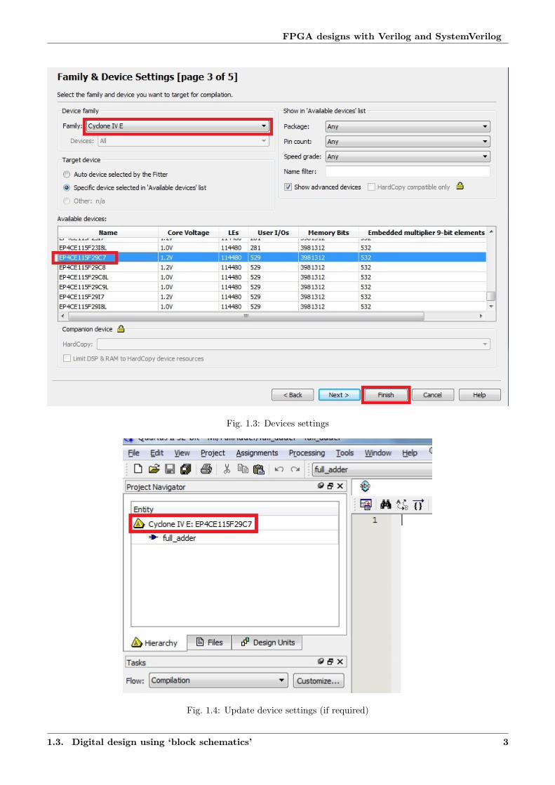
• Next, ‘Family and Device settings’ page will appear, select the proper device setting based on your FPGAboard and click ‘Finish’ as shown in Fig. 1.3. If you don’t have FPGA board, then simply click ‘Finish’.
• After clicking on finish, the project will be created as shown in Fig. 1.4. Note that, the tutorials aretested on DE2-115, DE2 (cyclone-II family) or DE0-Nano boards, therefore project settingsmay be different for different chapters. You need to select the correct device while runningthe code on your system. This can be done by double-clicking on the device name, as shown in Fig. 1.4.
1.3 Digital design using ‘block schematics’
Digitals design can be create using two methods i.e. using ‘block-schematics’ and with ‘programming languagee.g. VHDL or Verilog’ etc. Both have their own advantages in the design-process, as we will observe in the later
1

FPGA designs with Verilog and SystemVerilog
Fig. 1.1: Create new project
Fig. 1.2: Name and location of project
1.3. Digital design using ‘block schematics’ 2
FPGA designs with Verilog and SystemVerilog
Fig. 1.3: Devices settings
Fig. 1.4: Update device settings (if required)
1.3. Digital design using ‘block schematics’ 3
FPGA designs with Verilog and SystemVerilog
chapters of the tutorial.
In this section, we will create a half_adder using block-schematics method, as shown below,
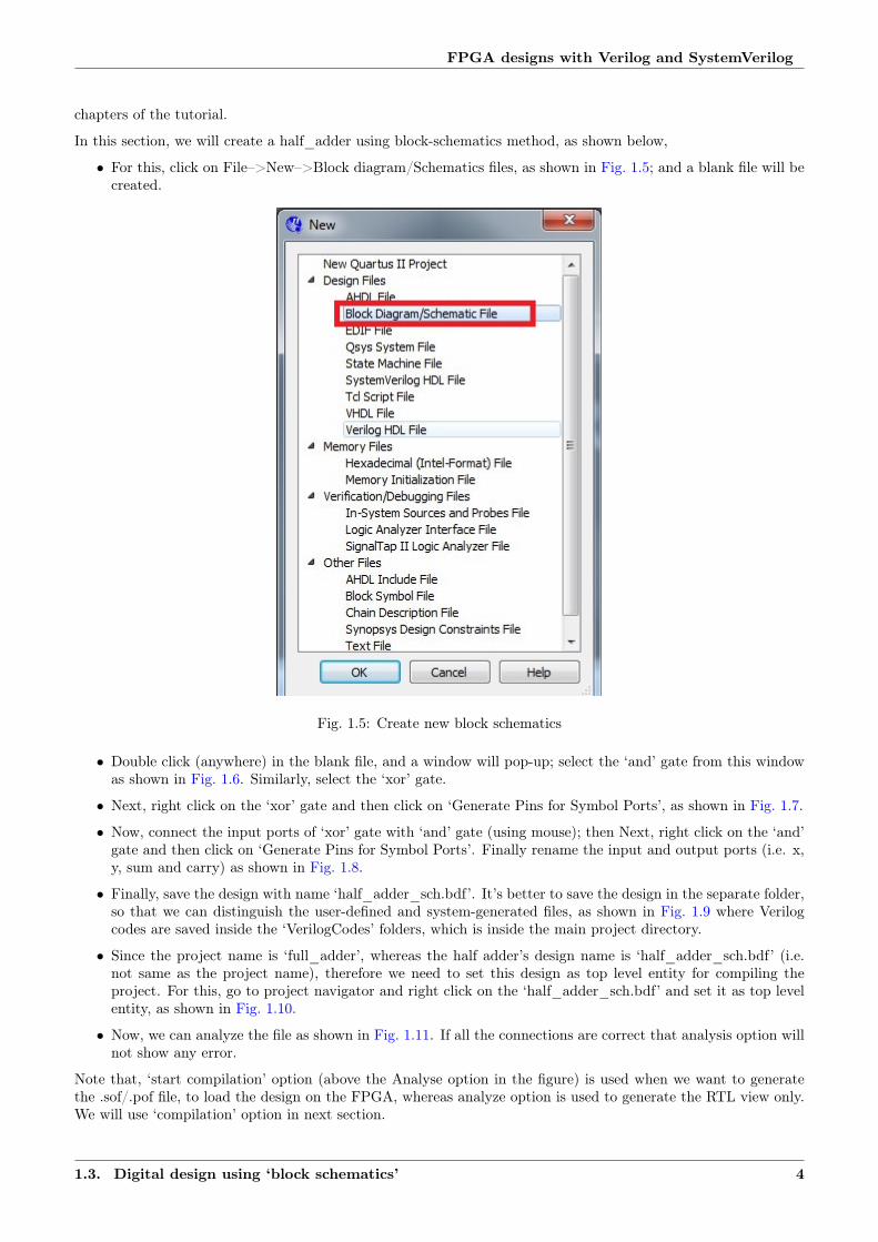
• For this, click on File–>New–>Block diagram/Schematics files, as shown in Fig. 1.5; and a blank file will becreated.
Fig. 1.5: Create new block schematics
• Double click (anywhere) in the blank file, and a window will pop-up; select the ‘and’ gate from this windowas shown in Fig. 1.6. Similarly, select the ‘xor’ gate.
• Next, right click on the ‘xor’ gate and then click on ‘Generate Pins for Symbol Ports’, as shown in Fig. 1.7.
• Now, connect the input ports of ‘xor’ gate with ‘and’ gate (using mouse); then Next, right click on the ‘and’gate and then click on ‘Generate Pins for Symbol Ports’. Finally rename the input and output ports (i.e. x,y, sum and carry) as shown in Fig. 1.8.
• Finally, save the design with name ‘half_adder_sch.bdf’. It’s better to save the design in the separate folder,so that we can distinguish the user-defined and system-generated files, as shown in Fig. 1.9 where Verilogcodes are saved inside the ‘VerilogCodes’ folders, which is inside the main project directory.
• Since the project name is ‘full_adder’, whereas the half adder’s design name is ‘half_adder_sch.bdf’ (i.e.not same as the project name), therefore we need to set this design as top level entity for compiling theproject. For this, go to project navigator and right click on the ‘half_adder_sch.bdf’ and set it as top levelentity, as shown in Fig. 1.10.
• Now, we can analyze the file as shown in Fig. 1.11. If all the connections are correct that analysis option willnot show any error.
Note that, ‘start compilation’ option (above the Analyse option in the figure) is used when we want to generatethe .sof/.pof file, to load the design on the FPGA, whereas analyze option is used to generate the RTL view only.We will use ‘compilation’ option in next section.
1.3. Digital design using ‘block schematics’ 4

FPGA designs with Verilog and SystemVerilog
Fig. 1.6: Select ‘and’ gate
Fig. 1.7: Add ports
1.3. Digital design using ‘block schematics’ 5

FPGA designs with Verilog and SystemVerilog
Fig. 1.8: Make connections
Fig. 1.9: Save project in separate directory i.e. VerilogCodes here
1.3. Digital design using ‘block schematics’ 6

FPGA designs with Verilog and SystemVerilog
Fig. 1.10: Select top level entity for the project
Fig. 1.11: Analyze the design
1.3. Digital design using ‘block schematics’ 7

FPGA designs with Verilog and SystemVerilog
1.4 Manual pin assignment and compilation
Please enter correct pin location according to your FPGA board, as shown in this section. If you do not have theboard, then skip this section and go to Section 1.6.
Once design is analyzed, then next step is to assign the correct pin location to input and output ports. This canbe done manually or using .csv file. In this section, we will assign pin manually. Follow the below steps for pinassignments,
• First open the ‘Pin-planner’ by clicking Assignments–>Pin Planner as shown in Fig. 1.12.
Fig. 1.12: Pin planner
• Next, type the names of the input and output ports along with the pin-locations on the board, as shown inFig. 1.13. Details of the Pin-locations are provided with the manual of the FPGA-boards e.g. in DE2-115board, pin ‘PIN_AB28’ is connected with switch SW0. By assign this pin to ‘x’, we are connecting the port‘x’ with switch SW0.
• After assigning the pin, analyze the design again (see Fig. 1.11). After this, we can see the pin numbers inthe ‘.bdf’ file, as shown in Fig. 1.14.
• Finally, compile the design using ‘ctrl+L’ button (or by clicking processing–>Start compilation, as shown inFig. 1.15).
• After successful compilation, if we see the pin-assignment again, then we will find that direction of the pinare assigned now, as shown in Fig. 1.16 (which were set to ‘unknown’ during analysis as in Fig. 1.13)
1.5 Load the design on FPGA
Follow the below, steps to load the design on FPGA,
• Connect the FPGA to computer and turn it on.• Full compilation process generates the .sof/.pof files, which can be loaded on the FPGA board. To load the
design on FPGA board, go to Tools–>Programmer. And a programmer window will pop up.• In the programmer window (see Fig. 1.17), look for two things i.e. position ‘1’ should display ‘USB-
BLASTER’ and position ‘6’ should display the ‘.sof’ file. If any of this mission then follow below steps,
1.4. Manual pin assignment and compilation 8

FPGA designs with Verilog and SystemVerilog
Fig. 1.13: Pin assignment
Fig. 1.14: Assigned pins to ports
Fig. 1.15: Start compilation
1.5. Load the design on FPGA 9

FPGA designs with Verilog and SystemVerilog
Fig. 1.16: Direction of the ports
– If USB-BLASTER is missing, then click on ‘Hardware setup (location 2 in Fig. 1.17)’ and then doubleclick on USB-BLASTER in the pop-up window (location 3). This will display the USB-BLASTER atlocation 4. Finally close the pop-up window.
– If ‘.sof’ file is not displayed at location 6, then click on ‘Add file. . . ’ (location 7) and select the ‘.sof’file from main project directory (or in output_files folder in main project directory).
• Finally click on the ‘start’ button in Fig. 1.17 and check the operation of ‘half adder’ using switches SW0and SW1; output will be displayed on green LEDs i.e. LEDG0 and LEDG1.
1.6 Digital design using ‘Verilog codes’
In this section, half adder is implemented using Verilog codes. For this, click on File–>New–>Verilog files, asshown in Fig. 1.5; and a blank file will be created. Type the Listing Listing 1.1 in this file and save it as‘half_adder_verilog.v’.
Now, set this design as ‘top level entity’ (Fig. 1.10). We can analyze the design now, but we will do it afterassigning the pins using .csv file in next section.
Listing 1.1: Verilog code for half adder
1 // half_adder_verilog.v2
3 module half_adder_verilog(4 input wire a, b,5 output wire sum, carry6 );7
8 assign sum = a ^ b;9 assign carry = a & b;
10
11 endmodule
1.6. Digital design using ‘Verilog codes’ 10

FPGA designs with Verilog and SystemVerilog
Fig. 1.17: Load the design on FPGA
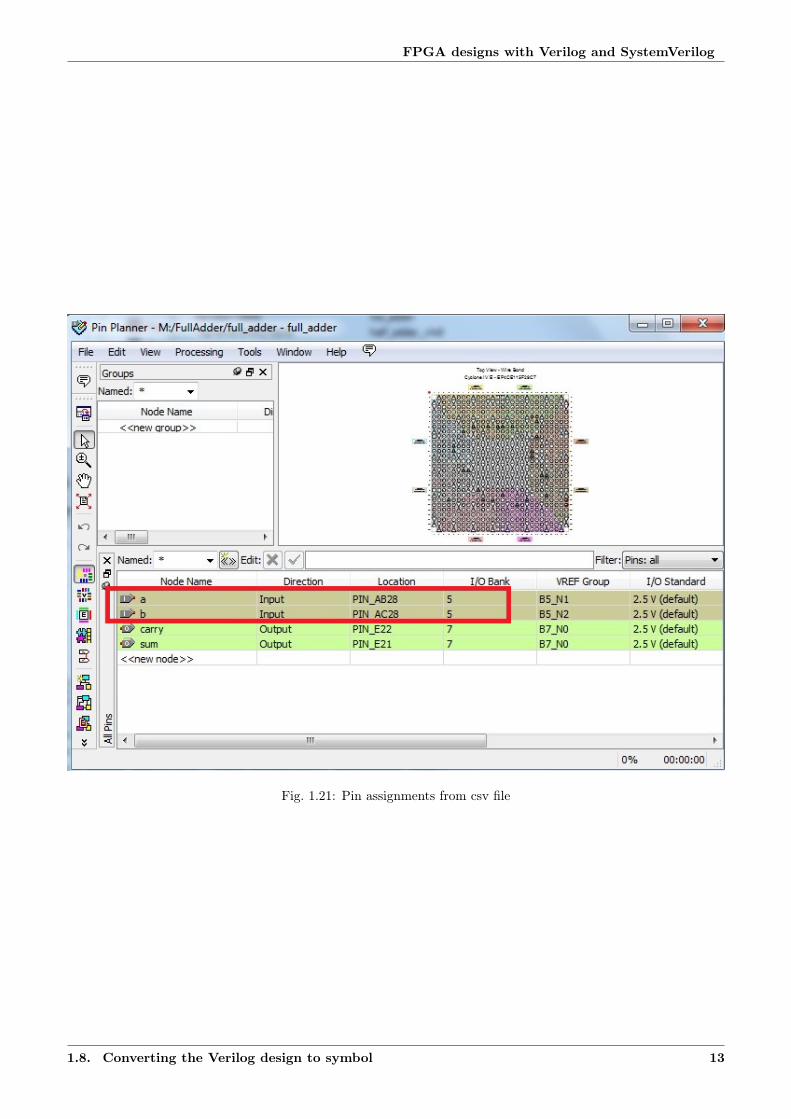
1.7 Pin assignments using ‘.csv’ file
In this section, we will learn to assign the pins using .csv files. Note that, we used input port as ‘a’ and ‘b’ inVerilog design (instead of ‘x’ and ‘y’ as in Fig. 1.8), so that we can observe the changes in the pin assignments.
To assign the pins using csv file, follow the below steps,
• First type the content in Fig. 1.18 in a text-file and save it as ‘pin_assg_file.csv’.
Fig. 1.18: Content of pin_assg_file.csv
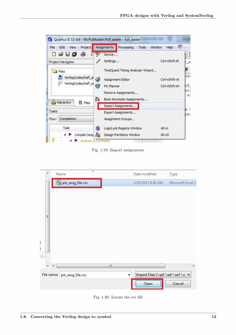
• Next, click on the Assignments–>Import Assignments as shown in Fig. 1.19. And locate the filepin_assg_file.csv by clicking on the cdots button, in the popped-up window, as shown in Fig. 1.20.
• Now, analyze the design (Fig. 1.11) and then open the pin planner (Fig. 1.12). We can see the new pinassignments as shown in Fig. 1.21 (If proper assignments do not happen, then check whether the Verilogdesign is set as top level or not and import assignments again and analyze the design).
• Finally, compile and load and check the design as discussed in Section 1.5.
1.8 Converting the Verilog design to symbol
Verilog code can be converted into block schematic format, which is quite useful for connecting various modulestogether. In this section, half adder’s Verilog file is converted into schematic and then two half adder is connected
1.7. Pin assignments using ‘.csv’ file 11
FPGA designs with Verilog and SystemVerilog
Fig. 1.19: Import assignments
Fig. 1.20: Locate the csv file
1.8. Converting the Verilog design to symbol 12
FPGA designs with Verilog and SystemVerilog
Fig. 1.21: Pin assignments from csv file
1.8. Converting the Verilog design to symbol 13

FPGA designs with Verilog and SystemVerilog
to make a full adder. Note that, this connection can be made using Verilog code as well, which is discussed inChapter 2.
Follow the below steps to create a full adder using this method,
• Right click on the ‘half_adder_verilog.v’ and click on ‘Create symbol file for current file’ as shown in Fig.1.22. It will create a symbol for half adder design.
Fig. 1.22: Convert Verilog code to symbol
• Now, create a new ‘block schematic file’ (Fig. 1.5).• Next, double click on this file and add the half adder symbol as shown in Fig. 1.23.
• Again add one more ‘half adder symbol’ along with ‘or’ gate and connect these components as shown in Fig.1.24.
• Since, one more port (i.e. c) is added to the design, therefore modify the ‘pin_assg_file.csv’ as shown in Fig.1.25.
• Save the design as ‘full_adder_sch.bdf’.• Import the assignment again; and compile the design (see pin assignments as well for 5 ports i.e. a, b, c,
sum and carry). Finally load the design on FGPA.
1.9 Convert Block schematic to ‘Verilog code’ and ‘Symbol’
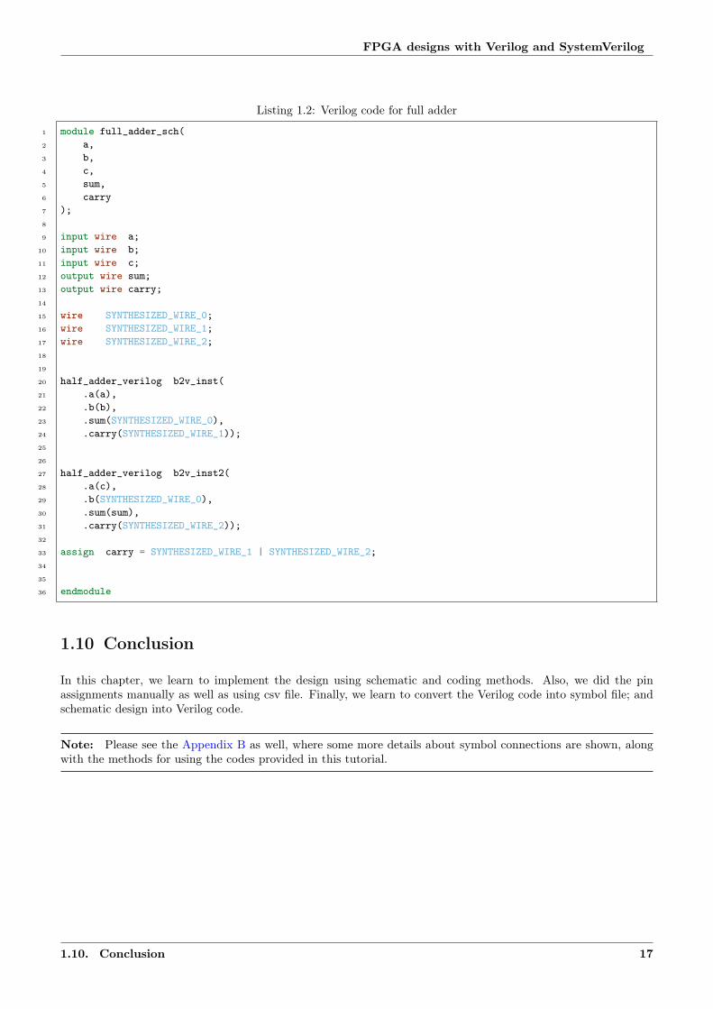
We can convert the ‘.bdf’ file to Verilog code as well. In this section, full adder design is converted to Verilogcode. For this open the file ‘full_adder_sch.bdf’. Then go to File–>Create/Update–>Create HDL Design File. . .as shown in Fig. 1.26 and select the file type as ‘Verilog’ and press OK; the file will be saved in the VerilogCodesfolder (see Fig. 1.27). The content of the generated ‘Verilog’ file are shown in Listing 1.2.
Now, we can convert this Verilog code into symbol as shown in Section 1.8.
Note: Note that, if we want to convert the ‘.bdf’ file into symbol, then we need to convert it into Verilog codefirst, and then we can convert the Verilog code into symbol file.
1.9. Convert Block schematic to ‘Verilog code’ and ‘Symbol’ 14

FPGA designs with Verilog and SystemVerilog
Fig. 1.23: Add half adder symbol
Fig. 1.24: Full adder using half adders
Fig. 1.25: Update pin assignments
1.9. Convert Block schematic to ‘Verilog code’ and ‘Symbol’ 15

FPGA designs with Verilog and SystemVerilog
Fig. 1.26: Convert schematic to Verilog
Fig. 1.27: Select Verilog
1.9. Convert Block schematic to ‘Verilog code’ and ‘Symbol’ 16
FPGA designs with Verilog and SystemVerilog
Listing 1.2: Verilog code for full adder
1 module full_adder_sch(2 a,3 b,4 c,5 sum,6 carry7 );8
9 input wire a;10 input wire b;11 input wire c;12 output wire sum;13 output wire carry;14
15 wire SYNTHESIZED_WIRE_0;16 wire SYNTHESIZED_WIRE_1;17 wire SYNTHESIZED_WIRE_2;18
19
20 half_adder_verilog b2v_inst(21 .a(a),22 .b(b),23 .sum(SYNTHESIZED_WIRE_0),24 .carry(SYNTHESIZED_WIRE_1));25
26
27 half_adder_verilog b2v_inst2(28 .a(c),29 .b(SYNTHESIZED_WIRE_0),30 .sum(sum),31 .carry(SYNTHESIZED_WIRE_2));32
33 assign carry = SYNTHESIZED_WIRE_1 | SYNTHESIZED_WIRE_2;34
35
36 endmodule
1.10 Conclusion
In this chapter, we learn to implement the design using schematic and coding methods. Also, we did the pinassignments manually as well as using csv file. Finally, we learn to convert the Verilog code into symbol file; andschematic design into Verilog code.
Note: Please see the Appendix B as well, where some more details about symbol connections are shown, alongwith the methods for using the codes provided in this tutorial.
1.10. Conclusion 17

Anything beyond your capacity will necessarily change yourcapacity, because so long as everything is within your limits, youdon’t know what is beyond them.
–Meher Baba
Chapter 2
Overview
2.1 Introduction
Verilog is the hardware description language which is used to model the digital systems. In this tutorial, following4 elements of Verilog designs are discussed briefly, which are used for modeling the digital system.
• Design with Continuous assignment statements• Structural design• Design with Procedural assignment statements• Mixed design
The 2-bit comparators are implemented using various methods and corresponding designs are illustrated, to showthe differences in these methods. Note that, all the features of Verilog can not be synthesized i.e. these featurescan not be converted into designs. Only, those features of Verilog are discussed in this tutorial, which can besynthesized.
2.2 Modeling styles
In Verilog, the model can be designed in four ways as shown in this section. Two bit comparator is designed withdifferent styles; which generates the output ‘1’ if the numbers are equal, otherwise output is set to ‘0’.
2.2.1 Continuous assignment statements
In this modeling style, the relation between input and outputs are defined using signal assignments. ‘assign’keyword is used for this purpose. In the other words, we do not define the structure of the design explicitly; weonly define the relationships between the signals; and structure is implicitly created during synthesis process.
Explanation Listing 2.1:
Listing 2.1 is the example of ‘Continuous assignment statements’ design, where relationship betweeninputs and output are given in line 8. In verilog, ‘&’ sign is used for ‘and’ operation (line 8), and ‘//’is used for comments (line 1). The ‘and gate (i.e. RTL view)’ generated by Listing 2.1 is shown in Fig.2.1.
Note: To see the RTL view of the design, go to Tools–>Netlist Viewers–>RTL viewer
Note that, in lines 4 and 5, ‘wire’ keyword is used which is the ‘data type’. For continuous assignmentstatements ‘wire’ keyword is used; whereas ‘reg’ keyword is used for procedural assignment statement.Further, input ports can not be defined as ‘reg’. Note that, these keyword are not interchangeable and
18

FPGA designs with Verilog and SystemVerilog
the differences between these ‘data types’ are discussed in Section 2.2.4. Further, more operators e.g.‘and’, ‘not’ and ‘nand’ etc. are discussed in Chapter 3.
Listing 2.1: And gate
1 // andEx.v2
3 module andEx(4 input wire x, y,5 output wire z6 );7
8 assign z = x & y; // x and y9 endmodule
Fig. 2.1: And gate, Listing 2.1
• Listing 2.1 can be written as Listing 2.2, where module-definition contains name of ports only (Line 3); andtypes of ports are defined outside the module (Lines 5-6).
Listing 2.2: And gate
1 // andEx2.v2
3 module andEx2(x, y, z);4
5 input wire x, y;6 output wire z;7
8 assign z = x & y;9
10 endmodule
2.2.2 Comparators using Continuous assignment statements
In this section, two more examples of Continuous assignment statements are shown i.e. ‘1 bit’ and ‘2 bit’ compara-tors; which are used to demonstrate the differences between various modeling styles in the tutorial. Fig. 2.2 andFig. 2.3 show the truth tables of ‘1 bit’ and ‘2 bit’ comparators. As the name suggests, the comparator comparethe two values and sets the output ‘eq’ to 1, when both the input values are equal; otherwise ‘eq’ is set to zero.The corresponding boolean expressions are shown below,
For 1 bit comparator:
𝑒𝑞 = 𝑥′𝑦′ + 𝑥𝑦 (2.1)
For 2 bit comparator:
𝑒𝑞 = 𝑎′[1]𝑎′[0]𝑏′[1]𝑏′[0] + 𝑎′[1]𝑎[0]𝑏′[1]𝑏[0] + 𝑎[1]𝑎′[0]𝑏[1]𝑏′[0] + 𝑎[1]𝑎[0]𝑏[1]𝑏[0] (2.2)
Above two expressions are implemented using verilog in Listing 2.3 and Listing 2.4, which are explained below.
Explanation Listing 2.3:
2.2. Modeling styles 19

FPGA designs with Verilog and SystemVerilog
Fig. 2.2: 1 bit comparator, Listing 2.3
Fig. 2.3: 2 bit comparator, Listing 2.4
2.2. Modeling styles 20

FPGA designs with Verilog and SystemVerilog
Listing 2.3 implements the 1 bit comparator based on (2.1). Two intermediate signals are defined inLine 8. These two signals (s0 and s1) are defined to store the values of x’y’ and xy respectively. Valuesto these signals are assigned at Lines 10 and 11. In verilog, ‘not’ and ‘or’ operations are implementedusing ‘~’ and ‘|’ signs as shown in Line 10 and 12 respectively. Finally (2.1) performs ‘or’ operation onthese two signals, which is done at Line 12. When we compile this code using ‘Quartus software’, itimplements the code into hardware design as shown in Fig. 2.4.
The compilation process to generate the design is shown in Appendix B. Also, we can check the input-output relationships of this design using Modelsim, which is also discussed briefly in Appendix B.
Listing 2.3: Comparator 1 Bit
1 // comparator1Bit.v2
3 module comparator1Bit(4 input wire x, y,5 output wire eq6 );7
8 wire s0, s1;9
10 assign s0 = ~x & ~y;11 assign s1 = x & y;12 assign eq = s0 | s1;13
14 endmodule
Note: Note that, the statements in ‘Continuous assignment statements’ and ‘structural modeling’ (described inSection 2.2.3) are the concurrent statements, i.e. these statements execute in parallel. In the other words, orderof statements do not affect the behavior of the circuit; e.g. if we exchange the Lines 10, 11 and 12 in Listing 2.3,again we will get the Fig. 2.4 as implementation.
On the other hand, statements in ‘Procedural assignment statements’ (described in Section 2.2.4) executes sequen-tially and any changes in the order of statements will change the behavior of circuit.
Explanation :numref: Fig. 2.4
Fig. 2.4 is generated by Quartus software according to the verilog code shown in Listing 2.3. Here, s0is the ‘and’ gate with inverted inputs x and y, which are generated according to Line 10 in Listing 2.3.Similarly, s1 ‘and’ gate is generated according to Line 11. Finally output of these two gates are appliedto ‘or’ gate (named as ‘eq’) which is defined at Line 12 of the Listing 2.3.
Fig. 2.4: 1 bit comparator, Listing 2.3
Explanation Listing 2.4
This listing implements the equation (2.2). Here, we are using two bit input, therefore ‘wire[1:0]’ isused at line 4. ‘1:0’ sets the 1 as MSB (most significant bit) and 0 as LSB(least significant bit) i.e. thea[1] and b[1] are the MSB, whereas a[0] and b[0] are the LSB. Since we need to store four signals (lines
2.2. Modeling styles 21

FPGA designs with Verilog and SystemVerilog
10-13), therefore ‘s’ is defined as 4-bit vector in line 8. Rest of the working is same as Listing 2.3. Theimplementation of this listing is shown in Fig. 2.5.
Listing 2.4: Comparator 2 Bit
1 // comparator2Bit.v2
3 module comparator2Bit(4 input wire[1:0] a, b,5 output wire eq6 );7
8 wire[3:0] s;9
10 assign s[0] = ~a[1] & ~a[0] & ~b[1] & ~b[0];11 assign s[1] = ~a[1] & a[0] & ~b[1] & b[0];12 assign s[2] = a[1] & ~a[0] & b[1] & ~b[0];13 assign s[3] = a[1] & a[0] & b[1] & b[0];14
15 assign eq = s[0] | s[1] | s[2] | s[3];16 endmodule
Fig. 2.5: 2 bit comparator, Listing 2.4
2.2.3 Structural modeling
In previous section, we designed the 2 bit comparator based on equation (2.2) . Further, we can design the 2 bitcomparator using 1-bit comparator as well, with following steps,
• First compare each bit of 2-bit numbers using 1-bit comparator; i.e. compare a[0] with b[0] and a[1] withb[1] using 1-bit comparator (as shown in Fig. 2.3).
• If both the values are equal, then set the output ‘eq’ as 1, otherwise set it to zero.
This method is known as ‘structural’ modeling, where we use the pre-defined designs to create the new designs(instead of implementing the ‘boolean’ expression). This method is quite useful, because most of the large-systems
2.2. Modeling styles 22

FPGA designs with Verilog and SystemVerilog
are made up of various small design units. Also, it is easy to create, simulate and check the various small unitsinstead of one large-system. Listing 2.5 is the example of structural designs, where 1-bit comparator is used tocreated a 2-bit comparator.
Explanation Listing 2.5
In this listing, Lines 4-5 define the two input ports of 2-bit size and one 1-bit output port. Then twosignals are defined (Line 8) to store the outputs of two 1-bit comparators, as discussed below.
‘eq_bit0’ and ‘eq_bit1’ in Lines 10 and 11 are the names of the two 1-bit comparator, which are usedin this design. We can see these names in the resulted design, which is shown in Listing 2.5.
Next, ‘comparator1Bit’ in Lines 10 and 11 is the name of the 1-bit comparator (defined in Listing 2.3).With this declaration, i.e. comparator1bit, we are calling the design of 1-bit comparator to currentdesign.
Then, mapping statements e.g. .x(a[0]) in Lines 10 and 11, are assigning the values to the input andoutput port of 1-bit comparator. For example, in Line 10, input ports of 1-bit comparator i.e. x andy, are assigned the values of a[0] and b[0] respectively from this design; and the output y of 1-bitcomparator is stored in the signal s0. Further, in Line 13, if signals s0 and s1 are 1 then ‘eq’ is set to 1using ‘and’ gate, otherwise it will be set to 0. Final design generated by Quartus software for Listing2.5 is shown in Fig. 2.6.
Listing 2.5: Structure modeling using work directory
1 // comparator2BitStruct.v2
3 module comparator2BitStruct(4 input wire[1:0] a, b,5 output wire eq6 );7
8 wire s0, s1;9
10 comparator1Bit eq_bit0 (.x(a[0]), .y(b[0]), .eq(s0));11 comparator1Bit eq_bit1 (.x(a[1]), .y(b[1]), .eq(s1));12
13 assign eq = s0 & s1;14 endmodule
Fig. 2.6: 2 bit comparator, Listing 2.5
Explanation Fig. 2.6
In this figure, a[1..0] and b[1..0] are the input bits whereas ‘eq’ is the output bit. Thick Lines aftera[1..0] and b[1..0] show that there are more than 1 bits e.g. in this case these Lines have two bits.These thick Lines are changed to thin Lines before going to comparators; which indicates that only 1bit is sent as input to comparator.
2.2. Modeling styles 23

FPGA designs with Verilog and SystemVerilog
In ‘comparator1Bit: eq_bit0’, ‘comparator1Bit’ is the name of the module defined for 1-bit comparator(Listing 2.3); whereas the ‘eq_bit0’ is the name of this module defined in Line 10 of listing Listing 2.5.Lastly outputs of two 1-bit comparator are sent to ‘and’ gate according to Line 13 in listing Listing 2.5.
Hence, from this figure we can see that the 2-bit comparator can be designed by using two 1-bitcomparator.
2.2.4 Procedural assignment statements
In Procedural assignment statements, the ‘always’ keyword is used and all the statements inside the always state-ment execute sequentially. Various conditional and loop statements can be used inside the process block as shownin Listing 2.6. Further, always blocks are concurrent blocks, i.e. if the design has multiple always blocks (seeListing 2.7), then all the always blocks will execute in parallel.
Explanation Listing 2.6:
The ‘always’ block is declared in Line 8, which begins and ends at Line 9 and 14 respectively. Thereforeall the statements between Line 9 to 14 will execute sequentially and Quartus Software will generate thedesign based on the sequences of the statements. Any changes in the sequences will result in differentdesign.
Note that, the output port ‘eq’ is declared as reg at Line 5. If we assign value to the signal inside the‘always’ block then that signal must be declared as ‘reg’ e.g. value of ‘eq’ is assigned in Line 11 and13, which are inside the ‘always’ block; hence ‘eq’ is declared as reg.
The ‘always’ keyword takes two arguments in Line 8 (known as ‘sensitivity list’), which indicates thatthe process block will be executed if and only if there are some changes in ‘a’ and ‘b’. ‘@’ is used after‘always’ for defining the sensitivity list. In Line 10-13, the ‘if’ statement is declared which sets thevalue of ‘eq’ to 1 if both the bits are equal (Line 10-11), otherwise ‘eq’ will be set to 0 (Line 12-13).Fig. 2.7 shows the design generated by the Quartus Software for this listing. ‘==’ in Line 10 is one ofthe condition operators; whereas && is the logical operator, which are discussed in detail in Chapter3.
Listing 2.6: Procedural assignment statement
1 // comparator2BitProcedure.v2
3 module comparator2BitProcedure(4 input wire[1:0] a, b,5 output reg eq6 );7
8 always @(a,b)9 begin
10 if (a[0]==b[0] && a[1]==b[1])11 eq = 1;12 else13 eq = 0;14 end15 endmodule
Fig. 2.7: 2 bit comparator, Listing 2.6
2.2. Modeling styles 24

FPGA designs with Verilog and SystemVerilog
2.2.5 Mixed modeling
We can mixed all the modeling styles together as shown in Listing 2.7. Here two always blocks are used in Line10 and 18, which is the ‘procedural assignment statements’. Then in Line 26, ‘continuous assignment statement’is used for assigning the value to output variable ‘eq’.
Explanation Listing 2.7
Note that, output ‘eq’ is defined as ‘wire’ (as value to ‘eq’ is assigned using continuous assignmentstatement), whereas signals ‘s0’ and ‘s1’ is defined as ‘reg’ (as values are assigned using proceduralassignment statement i.e. inside the ‘always’ block). Two always blocks are used here. Always blockat Line 10 checks whether the LSB of two numbers are equal or not; if equal then signal ‘s0’ is set to1 otherwise it is set to 0. Similarly, the always block at Line 18, sets the value of ‘s1’ based on MSBvalues. Lastly, Line 16 sets the output ‘eq’ to 1 if both ‘s0’ and ‘s1’ are 1, otherwise it is set to 0. Thedesign generated for this listing is shown in Fig. 2.8.
Listing 2.7: Multiple procedural assignment statements
1 // comparator2BitMixed.v2
3 module comparator2BitMixed(4 input wire[1:0] a, b,5 output wire eq6 );7
8 reg[1:0] s0, s1;9
10 always @(a,b)11 begin12 if (a[0]==b[0])13 s0 = 1;14 else15 s0 = 0;16 end17
18 always @(a,b)19 begin20 if (a[1]==b[1])21 s1 = 1;22 else23 s1 = 0;24 end25
26 assign eq = s0 & s1;27 endmodule
Fig. 2.8: 2 bit comparator, Listing 2.7
2.2. Modeling styles 25

FPGA designs with Verilog and SystemVerilog
2.3 Conclusion
In this tutorial, various features of Verilog designs are discussed briefly. We designed the two bit comparator withfour modeling styles i.e. Continuous assignment statement, Structural design, Procedural assignment statementand Mixed styles. Also, differences between the generated-designs with these four methods are shown.
2.3. Conclusion 26

What matters is to live in the present, live now, for every momentis now. It is your thoughts and acts of the moment that create yourfuture. The outline of your future path already exists, for youcreated its pattern by your past.
–Sai Baba
Chapter 3
Data types
3.1 Introduction
In the Chapter 2, we used the data-types i.e. ‘wire’ and ‘reg’ to define ‘1-bit’ & ‘2-bit’ input and output portsand signals. Also, some operators e.g. ‘and (&)’ and ‘or (|)’ etc. were discussed. In this chapter, some moreinformation is provided on these topics.
3.2 Lexical rules
Verilog is case sensitive language i.e. upper and lower case letters have different meanings. Also, Verilog is freeformatting language (i.e. spaces can be added freely), but we use the python like approach to write the codes, asit is clear and readable. Lastly in Verilog, ‘//’ is used for comments; also, multiline comments can written between/* and */.
3.3 Data types
Data types can be divided into two groups as follows,
• Net group: Net group represents the physical connection between components e.g. wire, wand and woretc. In the tutorials, we will use only one net data type i.e. ‘wire’, which is sufficient to create all types ofdesigns.
• Variable group: Variable group represents the storage of values in the design. It is always used for thevariables, whose values are assigned inside the ‘always’ block. Also, input port can not be defined as variablegroup. ‘reg’ and ‘integer’ are the example of variable group, which can be synthesized. We will use only ‘reg’for designing purpose.
3.4 Logic values
Verilog has four logic values i.e. 0, 1, z and x as shown in Table 3.1,
Table 3.1: Logic valuesLogic Description0 logic ‘0’ or false condition1 logic ‘1’ or true conditionz high impedance state (used for tri-state buffer)x don’t care or unknown value
27

FPGA designs with Verilog and SystemVerilog
3.5 Number representation
The number can be represented in various format as follows, which are listed in Table 3.2. Note that, ‘reg’ can bereplaced with ‘wire’ in the table.
• Binary Format
reg [1:0] a = 2'b01; // number = 1; size = 2 bit;reg [2:0] a = -3'b1; // unsigned number= -1 (in 2's complement form); size = 3 bit;
• Decimal Format
reg [3:0] a = 3'd1; // number = 1; size =3 bit;reg [3:0] a = -3'd1; // unsigned number = -1 (in 2's complement form); size =3 bit;
reg [3:0] a = 1; // unsigned number = 1; size = 4 bit;reg [3:0] a = -1; // unsigned number = -1; size = 4 bit in 2's complement form;
• Signed Decimal Form
integer a = 1; // signed number = 1; size = 32 bit;integer a = -1; // signed number = -1; size = 32 bit in 2's complement form;
• For hexadecimal and octal representations use ‘h’ and ‘o’ instead of ‘b’ in binary format.
Table 3.2: Number representationNumber Value Commentreg [1:0] a = 2’b01; 01 b is for binaryreg [1:0] a = 2’b0001_1111; 00011111 _ is ignoredreg [2:0] a = -3’b1; 111 -1 in 2’s complement with 3 bit (unsigned)reg [3:0] a = 4’d1; 0001 d is for decimalreg [3:0] a = -4’d1; 1111 -1 in 2’s complement with 4 bit (unsigned)reg [5:0] a = 6’o12; 001_010 o is for octalreg [5:0] b = 6’h1f; 0001_1111 h is for hexadecimalreg [3:0] a = 1; 0001 unsigned formatreg [3:0] a = -1; 1111 -1 in 2’s complement with 4 bit (unsigned)reg signed [3:0] a = 1; 0001 signed formatreg signed [3:0] a = -1; 1111 -1 in 2’s complement with 4 bit (signed)integer a = 1; 0000_0000_. . . _0001 32 bit i.e. 31-zeros and one-1 (signed)integer a = -1; 1111_1111_. . . _1111 -1 in 2’s complement with 32 bit i.e. all 1 (signed)reg [4:0] a = 5’bx xxxxx x is don’t carereg [4:0] a = 5’bz zzzzz z is high impedancereg [4:0] a = 5’bx01 xxx01 z is high impedance
Note:
• ‘wire’ and ‘reg’ are in unsigned-format by default. These can be used for synthesis and simulation.• ‘integer’ is in signed-format by default. This should be used for simulation.
3.6 Signed numbers
By default, ‘reg’ and ‘wire’ data type are ‘unsigned number, whereas ‘integer’ is signed number. Signed numbercan be defined for ‘reg’ and ‘wire’ by using ‘signed’ keywords i.e. ‘reg signed’ and ‘wire signed’ respectively asshown in Table 3.2.
3.5. Number representation 28

FPGA designs with Verilog and SystemVerilog
Also, ‘signed numbers’ can be converted into ‘unsigned numbers’ using ‘$unsigned()’ keyword e.g. if ‘a = -3 (i.e.101 in 2’s complement notation)’, then ‘$unsigned(a)’ will be ‘5 (i.e. value of 101)’. Similarly, ‘unsigned numbers’can be converted into ‘signed numbers’ using ‘signed()’ keyword.
Warning: Although, numbers can be converted from one form to another, but it should be avoided as it mayresults in errors which are difficult to find.
3.7 Operators
In this section, various synthesizable operators of Verilog are discussed, which are shown in Table 3.3.
Table 3.3: Verilog operatorsType Symbol Description NoteArithmetic + add
- subtract* multiply/ divide may not synthesize% modulus (remainder) may not synthesize** power may not synthesize
Bitwise ~ not| or& and^ xor~& or &~ nand mix two operators
Relational > greater than< less than>= greater than or equal<= less than or equal== equal!= not equal
Logical ! negation|| logical OR&& logical AND
Shift operator >> right shift<< left shift>>> right shift with MSB shifted to right<<< same as <<
Concatenation { } Concatenation{ { } } Replication “e.g. { 2{3} } = {3 3}”
Conditional ? : conditional e.g. (2>3) ? 1 : 0Sign-format $unsigned() signed to unsigned conversion $unsigned(-3)
$signed() unsigned to signed conversion $signed(3)
3.8 Arithmetic operator
Three arithmetic operators i.e. +, -, and * can be synthesized in verilog.
3.8.1 Bitwise operators
Four bitwise operator are available in verilog i.e. ‘&’ (and), ‘|’ (or), ‘ ^ ‘ (xor) and ‘~’ (not). Further, we cancombine these operators to define new operators e.g. ‘~&’ or ‘&~’ can be used as ‘nand’ operations etc.
3.7. Operators 29

FPGA designs with Verilog and SystemVerilog
3.8.2 Relational operators
We already see the equality relational operation i.e. ‘==’ in section Section 2.2.4. Further, five relational operatorsare defined in verilog i.e. ‘>’, ‘>=’, ‘<’, ‘<=’ and ‘ !=’(not equal to).
3.8.3 Logical operators
We already see the ‘and’ relational operation i.e. ‘&&’ in section Section 2.2.4. Further, three relational operatorsare defined in verilog i.e. ‘||’ (or), ‘&&’ and ‘ !’(negation).
3.8.4 Shift operators
Verilog provides 4 types of shif operators i.e. >>, <<, >>>, <<<. Let ‘a = 1011-0011’, then we will havefollowing results with these operators,
• a >>3 = 0001-0110 i.e. shift 3 bits to right and fill the MSB with zeros.• a << 3 = 1001-1000 i.e. shift 3 bits to left and fill the LSB with zeros.• a >>>3 = 1111-0110 i.e. shift 3 bits to right and fill the MSB with sign bit i.e. original MSB.• a <<<3 = 1111-0110 i.e. same as a<<3.
3.8.5 Concatenation and replication operators
Concatenation operation ‘{ }’ is used to combine smaller arrays to create a large array as shown below,
wire[1:0] a = 2b'01;wire[2:0] b = 3b'001;wire[3:0] c ;assign c = {a, b} // c = 01001 is created using a and b;
Replication operator is used to repeat certain bits as shown below,
assign c = { 2{a}, 1'b0 } // c = 01010 i.e. a is repeated two times i.e. 01-01
3.8.6 Conditional operator
Conditional operator (?:) can be defined as follows,
assign c = (a>b) ? a : b; // i.e. c=a if a>b; else c=b;
Also, conditional expression can be cascaded as shown in Listing 3.1, where 4x1 multiplexer is designed. Multiplexeris a combinational circuit which selects one of the many inputs with selection-lines and direct it to output. Fig. 3.1illustrates the truth table for 4x1 multiplexer. Here ‘i0 - i3’ the input lines, whereas ‘s0’ and ‘s1’ are the selectionline. Base on the values of ‘s0’ and ‘s1’, the input is sent to output line, e.g. if s0 and s1 are 0 then i0 will be sentto the output of the multiplexer.
Listing 3.1: Cascaded conditional operator
1 // conditionalEx.v2
3 module conditionalEx(4 input wire[1:0] s,5 input wire i0, i1, i2, i3,6 output wire y7 );8
9 assign y = (s == 2'b00) ? i0 : // y = i0 if s=00(continues on next page)
3.8. Arithmetic operator 30

FPGA designs with Verilog and SystemVerilog
Fig. 3.1: Truth table of 4x1 multiplexer
(continued from previous page)
10 (s == 2'b01) ? i1 : // y = i1 if s=0111 (s == 2'b10) ? i2 : // y = i2 if s=1012 (s == 2'b11) ? i3 : // y = i3 if s=1113 y; // else y = y i.e. no change14 endmodule
The design generated in Fig. 3.2 is exactly same as the design generated by ‘if-else statement’ which is discussedin Section 4.7. Therefore, Fig. 3.2 is described and compared with other designs in Section 4.7. Further, Fig. 3.3shows the output waveform of the multiplexer which is generated by Listing 3.1.
Fig. 3.2: Multiplexer generated by Listing 3.1
3.8.7 Parameter and localparam
Parameter and localparam are used to create reusable codes along with avoiding the ‘hard literals’ from the codeas shown in following section.
3.8. Arithmetic operator 31

FPGA designs with Verilog and SystemVerilog
Fig. 3.3: Waveforms of Listing 3.1
3.8.8 localparam
‘localparam’ keyword is used to defined the constants in verilog. In Listing 3.2, N is defined in line 8 with value3. Then this value is used in line 10 and 11. Suppose we want to change the constant value to 4. Now, we needto change it only at one place i.e. line 8 (instead of changing everywhere in the code e.g. line 10 and 11 in thisexample). In this way, we can remove the hard literals from the codes.
Listing 3.2: Localparam
1 // constantEx.v2
3 module constantEx(4 input wire [3:0] a, b,5 output wire [3:0] z6 );7
8 localparam N = 3, M = 2; //localparam9
10 wire [N:0] x;11 wire [2**N:0] y;12
13 // use x and y here14 assign z = a & b;15
16 endmodule
• It is better to define the size of the local-parameters otherwise 32-bit signed-format will be used for the localparameters, as shown below
// 32-bit signed-formatlocalparam N = 3, M = 2;
// N & M are 5 bit and 3 bit unsigned numbers respectivelylocalparam N = 5'd3, M = 3'd2;
3.8.9 Parameter and defparam
‘localparam’ can not be modified after declaration. But we can define the parameter in the module, which can bemodified during component instantiation in structural modeling style as shown below.
Explanation Listing 3.3
In line 5, two parameters are defined i.e. ‘N’ and ‘M’. Then ports ‘a’ and ‘b’ are defined using parameter‘N’. The always block (lines 13-19) compares ‘a’ and ‘b’ and set the value of ‘z’ to 1 if these inputs areequal, otherwise set ‘z’ to 0.
3.8. Arithmetic operator 32

FPGA designs with Verilog and SystemVerilog
Listing 3.3: Parameter
1 // parameterEx.v2
3 module parameterEx4 #(5 parameter N = 2, M = 3 //parameter6 )7
8 (9 input wire [N-1:0] a, b,
10 output reg [N-1:0] z11 );12
13 always @(a,b)14 begin15 if (a==b)16 z = 1;17 else18 z = 0;19 end20 endmodule
Explanation Listing 3.4 and Listing 3.5
In line 5, ‘a’ and ‘b’ are defined as 4-bit vector. Structural modeling is used in Line 9, where parametermapping and port mapping is performed. Note that, in line 16, ‘.N(5)’ will override the default valueof N i.e. N=2 in Listing 3.3. Also, parameter ‘M’ is not mapped, therefore default value of M will beused, which is defined in Listing 3.3. In this way, we can remove ‘hard literals’ from the codes, whichenhances the reusability of the designs. Value of the parameter ‘N’ can also be set using ‘defparam’keyword, as shown in Listing 3.5.
Listing 3.4: Parameter instantiation
1 // parameterInstantEx.v2
3 module parameterInstantEx4 (5 input wire [4:0] a, b,6 output wire [4:0] z7 );8
9 parameterEx #(.N(5)) compare4bit ( .a(a), .b(b), .z(z));10
11 endmodule
Listing 3.5: Parameter instantiation using ‘defparam’
1 // parameterInstantEx2.v2
3 module parameterInstantEx24 (5 input wire [4:0] a, b,6 output wire [4:0] z7 );8
9 parameterEx compare4bit ( .a(a), .b(b), .z(z));10 defparam compare4bit.N = 5; // 'defparam' to set the value of parameter11
12 endmodule
• It is better to define the size of the parameters otherwise 32-bit signed-format will be used for the parameters,
3.8. Arithmetic operator 33

FPGA designs with Verilog and SystemVerilog
as shown below
// 32-bit signed-formatparameter N = 2, M = 3
// N & M are 5 bit and 4 bit unsigned numbers respectivelyparameter N = 5'd2, M = 4'd3;
3.9 Conclusion
In this chapter, we saw various data types and operators. Further Parameters and localparam are shown whichcan be useful in creating the reusable designs.
3.9. Conclusion 34

That knowledge which purifies the mind and heart alone is trueKnowledge, all else is only a negation of Knowledge.
–Ramakrishna Paramahansa
Chapter 4
Procedural assignments
4.1 Introduction
In Chapter 2, a 2-bit comparator is designed using ‘procedural assignments’. In that chapter, ‘if’ keyword was usedin the ‘always’ statement block. This chapter presents some more such keywords which can be used in proceduralassignments.
4.2 Combinational circuit and sequential circuit
Digital design can be broadly categorized in two ways i.e. combinational designs and sequential designs. It isvery important to understand the differences between these two designs and see the relation between these designswith various elements of Verilog.
• Combinational designs : Combinational designs are the designs in which the output of the system dependson present value of the inputs only. Since, the outputs depends on current inputs only, therefore ‘no memory’is required for these designs. Further, memories are nothing but the ‘flip flops’ in the digital designs, thereforethere is no need of ‘flip flops’ in combination designs. In the other words, only ‘logic gates (i.e. and, notand xor etc.)’ are required to implement the combinational designs.
• Sequential designs : Sequential designs are the designs in which the output depends on current inputs andprevious states of the system. Since output depends on previous states, therefore ‘memories’ are requiredfor these systems. Hence, in the sequential designs the ‘flip flops’ are needed along with the logic gates.
Fig. 4.1: Block diagram of ‘combinational’ and ‘sequential’ designs
35
FPGA designs with Verilog and SystemVerilog
4.3 Concurrent statements and sequential statements
In Listing 2.3, we saw that the concurrent statements execute in parallel, i.e. the order of the statement does notmatter. Whereas Listing 2.6 shows the example of ‘sequential statements’ where the statements execute one byone. Following are the relationship between ‘statements’ and ‘design-type’,
• Please note that ‘sequential statements’ and ‘sequential designs’ are two different things. Do not mix thesetogether.
• Combinational designs can be implemented using both ‘sequential statements’ and ‘concurrent statements’.• Sequential designs can be implemented using ‘sequential statements’ only.• Sequential statements can be defined inside ‘always’ block only. Further, these blocks executes concurrently
e.g. if we have more than one always block then these block will execute in parallel, but statements insideeach block will execute sequentially.
• Sequential designs are implemented using various constructs e.g. ‘if’, ‘case’ and ‘for’ etc., which are discussedin this chapter.
• Conditional operator (?:) can be used for combinational designs.
Note: Remember : (see the words ‘design’, ‘logic’ and ‘statement’ carefully)
• Only ‘logic gates (i.e. and, not and xor etc.)’ are required to implement the combinational designs.• Both ‘logic gates’ and ‘flip flops’ are required for implementing the sequential designs.• Lastly, the ‘sequential design’ contains both ‘combinational logics’ and ‘sequential logics’, but the combina-
tional logic can be implement using ‘sequential statements’ only as shown in Fig. 4.1; whereas the ‘combinationlogic’ in the combinational designs can be implemented using both ‘concurrent’ and ‘sequential’ statements.
4.4 ‘always’ block
All the statements inside the always block execute sequentially. Further, if the module contains more than onealways block, then all the always blocks execute in parallel, i.e. always blocks are the concurrent blocks.
Note: Note that, we can write the complete design using sequential programming (similar to C, C++ and Pythoncodes). But that may result in very complex hardware design, or to a design which can not be synthesized atall. The best way of designing is to make small units using ‘continuous assignment statements’ and ‘proceduralassignment statements’, and then use the structural modeling style to create the large system.
4.5 Blocking and Non-blocking assignment
There are two kinds of assignments which can be used inside the always block i.e. blocking and non-blockingassignments. The ‘=’ sign is used in blocking assignment; whereas the ‘<=’ is used for non-blocking assignmentas shown in Listing 4.1 and Listing 4.2. Both the listings are exactly same expect the assignment signs at lines13-14. Due to different in assignment signs, the design generated by these listings are different as shown in Fig.4.2 and Fig. 4.3, which are explained below.
Explanation Listing 4.1
In line 10, value of input port ‘x’ is assigned to output ‘z’. Since, the value of ‘z’ is equal to ‘x’, thereforeline 11 will be equivalent to ‘z = x + y’; due to this reason, the design is generated as ‘and’ gate withinputs ‘x’ and ‘y’ as shown in Fig. 4.2.
4.3. Concurrent statements and sequential statements 36

FPGA designs with Verilog and SystemVerilog
Listing 4.1: Blocking assignment, Fig. 4.2
1 // blockAssignment.v2
3 module blockAssignment(4 input wire x, y,5 output reg z6 );7
8 always @(x,y)9 begin
10 z = x; // since z = x11 z = z & y; // therefore, z = x + y;12 end13 endmodule
Fig. 4.2: Blocking assignment, Listing 4.1
Fig. 4.3: Non-blocking assignment, Listing 4.2
Explanation Listing 4.2:
In non-blocking assignment, updated values inside the block are not used for assignment.} In line 10,value of input port ‘x’ is assigned to the ‘z’. Since updated value inside the block are not used in non-blocking assignment, therefore in line 11, ‘z = z & y;’, the old value of ‘z’ will be used for assignments(instead of z=x); hence a feedback path is used in Fig. 4.3. Also, ‘x’ has no effect on the design as itis updating ‘z’ inside the block, which will not be used by non-blocking assignment; hence ‘x’ is notconnected (i.e. connected to ground) in the design as shown in Fig. 4.3.
Listing 4.2: Non-blocking assignment, Fig. 4.3
1 // nonblockAssignment.v2
3 module nonblockAssignment(4 input wire x, y,5 output reg z6 );7
8 always @(x,y)9 begin
10 z <= x; // z_new = x11 z <= z & y; // z_new = z_entry + y (not z = z_new + y)12 end13 endmodule
Note: The block and non-blocking assignments can not be used together for a signal. For example, the belowassignment will generate error as both ‘blocking’ and ‘non-blocking’ assignments are used for ‘z’,
4.5. Blocking and Non-blocking assignment 37

FPGA designs with Verilog and SystemVerilog
z = x; // blocking assignmentz <= z & y; // non-blocking assignment
4.6 Guidelines for using ‘always’ block
The general purpose ‘always’ block of Verilog can be misused very easily. And the misuse of this block will resultin different ‘simulation’ and ‘synthesis’ results. In this section, the general guidelines are provided for using the‘always’ block in different conditions.
Further, we can use the specilialized ‘always’ blocks of SystemVerilog to avoid the ambiguities in synthesis andsimulation results, which are discussed in Section 10.4.
Note: Note that, the ‘always’ block is used for ‘synthesis (i.e. with sensitive list)’ as well as ‘simulation (i.e. withand without sensitive list)’, which have different set of semantic rules. If we do not follow the below guidelines inthe designs, then simulation and synthesis tools will infer different set of rules, which will result in differences insynthesis and simulation results.
Further, SystemVerilog has specialized ‘always blocks’ for different types of designs (see Section 10.4), which cancatch the errors when the designs are not created according to below rules.
4.6.1 ‘always’ block for ‘combinational designs’
Follow the below rules for combinational designs,
• Do not use the ‘posedge’ and ‘negedge’ in sensitive list.• Sensitive list should contain all the signals which are read inside the block.• No variable should be updated outside the ‘always’ block.• Use blocking assignment (i.e. = ) for assigning values.• All the variables should be updated for all the possible input conditions i.e. if-else and case statements should
include all the possible conditions; and all the variables must be updated inside all the conditions.
4.6.2 ‘always’ block for ‘latched designs’
Follow the below rules for latched designs,
• Do not use the ‘posedge’ and ‘negedge’ in sensitive list.• Sensitive list should contain all the signals which are read inside the block.• No variable should be updated outside the ‘always’ block.• Use blocking assignment (i.e. = ) for assigning values.• At least one the variables should not be updated for some of the possible input conditions.
4.6.3 ‘always’ block for ‘sequential designs’
Follow the below rules for sequential designs,
• Use either ‘posedge’ or ‘negedge’ (not both) in sensitive list for all the elements.• No variable should be updated outside the ‘always’ block.• Use non-blocking assignment (i.e. <= ) for assigning values.
4.6. Guidelines for using ‘always’ block 38

FPGA designs with Verilog and SystemVerilog
4.7 If-else statement
In this section, a 4x1 multiplexed is designed using If-else statement. We already see the working of ‘if’ statementin the Chapter 2. In lines 11-24 of Listing 4.3, ‘else if’ and ‘else’ are added to ‘if’ statement. Note that, If-elseblock can contain multiple ‘else if’ statements between one ‘if’ and one ‘else’ statement. Further, ‘begin - end’ isadded in line 12-15 of Listing 4.3, which is used to define multiple statements inside ‘if’, ‘else if’ or ‘else’ block.Fig. 4.5 shows the waveform generated by Modelsim for Listing 4.3.
Note that, we are generating the exact designs as the VHDL tutorials, therefore line 22-23 are used. Also, we canremove the line 22-23, and change line 20 with ‘else’, which will also work correctly.
Fig. 4.4: Multiplexer using if statement, Listing 4.3
Listing 4.3: Multiplexer using if statement
1 // ifEx.v2
3 module ifEx(4 input wire[1:0] s,5 input wire i0, i1, i2, i3,6 output reg y7 );8
9 always @(s)10 begin11 if (s==2'b00)12 begin //begin-end is required for more than one statements13 y = i0;14 // more statements15 end16 else if (s==2'b01)17 y = i1;18 else if (s==2'b10)19 y = i2;20 else if (s==2'b11)21 y = i3;22 else23 y = y; // no change24 end25
(continues on next page)
4.7. If-else statement 39
FPGA designs with Verilog and SystemVerilog
(continued from previous page)
26 endmodule
Fig. 4.5: Waveforms of Listing 4.3 and Listing 4.4
4.8 Case statement
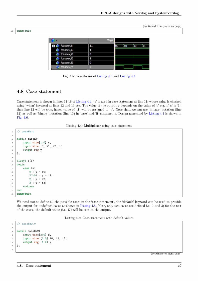
Case statement is shown in lines 11-16 of Listing 4.4. ‘s’ is used in case statement at line 11; whose value is checkedusing ‘when’ keyword at lines 12 and 13 etc. The value of the output y depends on the value of ‘s’ e.g. if ‘s’ is ‘1’,then line 12 will be true, hence value of ‘i1’ will be assigned to ‘y’. Note that, we can use ‘integer’ notation (line12) as well as ‘binary’ notation (line 13) in ‘case’ and ‘if’ statements. Design generated by Listing 4.4 is shown inFig. 4.6.
Listing 4.4: Multiplexer using case statement
1 // caseEx.v2
3 module caseEx(4 input wire[1:0] s,5 input wire i0, i1, i2, i3,6 output reg y7 );8
9 always @(s)10 begin11 case (s)12 0 : y = i0;13 2'b01 : y = i1;14 2 : y = i2;15 3 : y = i3;16 endcase17 end18 endmodule
We need not to define all the possible cases in the ‘case-statement’, the ‘default’ keyword can be used to providethe output for undefined-cases as shown in Listing 4.5. Here, only two cases are defined i.e. 7 and 3; for the restof the cases, the default value (i.e. i2) will be sent to the output.
Listing 4.5: Case-statement with default values
1 // caseEx2.v2
3 module caseEx2(4 input wire[2:0] s,5 input wire [1:0] i0, i1, i2,6 output reg [1:0] y7 );8
(continues on next page)
4.8. Case statement 40

FPGA designs with Verilog and SystemVerilog
Fig. 4.6: Multiplexer using case statement, Listing 4.4
(continued from previous page)
9 always @(s)10 begin11 case (s)12 7 : y = i0; // 713 3 : y = i1; // 314 default : y = i2; // 0, 1, 3, 4, 515 endcase16 end17 endmodule
4.9 Problem with Loops
Verilog provides two loop statements i.e. ‘for’ loop and ‘while’ loop’. These loops are very different from softwareloops. Suppose ‘for i = 1 to N’ is a loop’, then, in software ‘i’ will be assigned one value at time i.e. first i=1,then next cycle i=2 and so on. Whereas in Verilog, N logics will be implement for this loop, which will execute inparallel. Also, in software, ‘N’ cycles are required to complete the loop, whereas in Verilog the loop will executein one cycle.
Note: As loops implement the design-units multiple times, therefore design may become large and sometimescan not be synthesized as well. If we do not want to execute everything in one cycle (which is almost always thecase), then loops can be replaced by ‘case’ statements and ‘conditional’ statements as shown in section Section4.10. Further, due to these reasons, we do not use loops in the design, and hence these are not discussed in thetutorial.
4.10 Loop using ‘if’ statement
In Listing 4.6, a loop is created using ‘if’ statement, which counts the number upto input ‘x’.
Explanation Listing 4.6
In the listing, two ‘always’ blocks are used i.e. at lines 20 and 33. The process at line 20 checkswhether the signal ‘count’ value is ‘less or equal’ to input x (line 22), and sets the currentState to‘continueState’; otherwise if count is greater than the input x, then currentState is set to ‘stopState’.
Then next ‘always’ statement (line 33), increase the ‘count’ by 1, if currentState is ‘continueState’;otherwise count is set to 0 for stopState. Finally count is displayed at the output through line 41. Inthis way, we can implement the loops using the ‘always’ statements.
4.9. Problem with Loops 41

FPGA designs with Verilog and SystemVerilog
Fig. 4.7 shows the loop generated by the listing with parameter N=1. Further, Fig. 4.8 shows thecount-waveforms generated by the listing with parameter N = 3.
Warning: Sensitivity list is still not correct in the Listing 4.6 e.g. we do not put the ‘x’ in the sensitive listat Line 20 which is used inside the ‘always’ block. Further, the ‘clk’ is unnecessarily used at Line 33.
Although the results are correct, but such practice leads to undetectable errors in large designs. We will seethe correct style of coding in Chapter 7.
Listing 4.6: Loop using ‘if’ statement
1 // ifLoop.v (-- This code is for simulation purpose only)2 // ideally positive or negative clock edge must be used; which will be discussed later.3 module ifLoop4 #(5 parameter N = 3,6 M = 2 //not used7 )8 (9 input wire clk,
10 input wire[N:0] x,11 output wire[N:0] z12 );13 localparam14 continueState = 1'b0,15 stopState = 1'b1;16
17 reg currentState;18 reg [N:0] count = 0;19
20 always @(clk, currentState, count)21 begin22 if(count<=x)23 currentState = continueState;24 else25 currentState = stopState;26 end27
28 // simulation and synthesis difference in verilog:29 // if count is added to sensitivity list i.e. always @(clk, currentState, count)30 // then always block must create an infinite loop (see exaplation)31 // but this simulator will work fine for this case32 // such error can not be detected in verilog.33 always @(clk, currentState)34 begin35 if(currentState==continueState)36 count = count+1;37 else38 count = 0;39 end40
41 assign z = count;42 endmodule
Note: Sensitivity list of the always block should be implemented carefully. For example, if we add ‘count’ in thesensitivity list at line 33 of Listing Listing 4.6, then the always block will execute infinite times. This will occurbecause the always block execute whenever there is any event in the signals in the sensitivity list; therefore anychange in ‘count’ will execute the block, and then this block will change the ‘count’ value through line 36. Since‘count’ value is changed, therefore always block will execute again, and the loop will never exit.
4.10. Loop using ‘if ’ statement 42

FPGA designs with Verilog and SystemVerilog
Fig. 4.7: Loop using ‘if’ statement, Listing 4.6 with N = 1
Fig. 4.8: Loop using ‘if’ statement, Listing 4.6 with N = 3
Another problem is that, above error can not be detected during simulation phase, i.e. simulation will show thecorrect results. Such errors are very difficult to find in Verilog. Further, such errors can be identified in VHDLcode, as shown in VHDL tutorials. To avoid such errors in Verilog, please follow the guidelines for using the‘always’ block as described in Section 4.6.
4.11 Conclusion
In this chapter, various statements for procedural assignments are discussed. Problem with loops are discussedand finally loop is implemented using ‘if’ statement. Lastly, it is shown that, Verilog designs can have differencesin simulation results and implementation results.
4.11. Conclusion 43

Let what comes come. Let what goes go. Find out what remains.
–Ramana Maharshi
Chapter 5
VHDL designs in Verilog
5.1 Introduction
Since, both VHDL and Verilog are widely used in FPGA designs, therefore it be beneficial to combine both thedesigns together; rather than transforming the Verilog code to VHDL and vice versa. This chapter presents theuse of VHDL design in the Verilog codes.
5.2 VHDL designs in Verilog
For using VHDL in verilog designs, only proper component instantiation is required as shown in this section.Design of 1 bit comparator in Listing 5.1 (which is written using VHDL) is same as the design of Listing 2.3.Design generated by Listing 5.1 is shown in Fig. 5.1.
Listing 5.1: 1 bit comparator in Verilog
1 --comparator1BitVHDL.vhd2
3 library ieee;4 use ieee.std_logic_1164.all;5
6 entity comparator1BitVHDL is7 port(8 x, y : in std_logic;9 eq : out std_logic
10 );11 end comparator1BitVHDL;12
13 architecture dataflow1Bit of comparator1BitVHDL is14 signal s0, s1: std_logic;15 begin16 s0 <= (not x) and (not y);17 s1 <= x and y;18
19 eq <= s0 or s1;20 end dataflow1Bit;
Explanation Listing 5.2
This listing is exactly same as Listing 2.5. To design the 2 bit comparator, two 1 bit comparators areinstantiated in line 10 and 11. The final design generated for the two bit comparator is shown Fig. 5.2.In this way, we can use the VHDL designs in Verilog codes.
44

FPGA designs with Verilog and SystemVerilog
Fig. 5.1: 1 bit comparator using VHDL
Listing 5.2: VHDL design in Verilog
1 // comparator2BitWithVHDL.v2 module comparator2BitWithVHDL(3 input wire[1:0] a, b,4 output wire eq5 );6
7 wire s0, s1;8
9 // instantiate 1 bit comparator10 comparator1BitVHDL eq_bit0 (.x(a[0]), .y(b[0]), .eq(s0));11 comparator1BitVHDL eq_bit1 (.x(a[1]), .y(b[1]), .eq(s1));12
13 assign eq = s0 & s1;14 endmodule
Fig. 5.2: 2 bit comparator using VHDL and Verilog
5.3 Conclusion
In this chapter, VHDL files are used in Verilog designs. From the examples shown in this chapter, it is clear that weneed not to do anything special to using VHDL files in Verilog designs; only proper port mapping i.e. componentinstantiation is required.
5.3. Conclusion 45

When divine vision is attained, all appear equal; and there remainsno distinction of good and bad, or of high and low.
–Ramakrishna Paramahansa
Chapter 6
Visual verifications of designs
6.1 Introduction
In previous chapters, we saw various elements of Verilog language with some design examples, which were verifiedusing simulations. In this chapter, various smaller units are designed and then combined together to make thelarge systems. Further, visual verification is performed in this chapter i.e. the designs are verified using LEDdisplays. Finally, in Section 6.6, output of mod-m is displayed on various LEDs using smaller designs i.e. counters,clock-ticks and seven segment displays.
6.2 Flip flops
Flip flops are the sequential circuits which are used to store 1-bit. In this section, D flip flop is designed withvarious functionalities in it.
6.2.1 D flip flop
In Listing 6.1, the basic D flip flop is designed with reset button. Output of the flip flop is set to zero if reset valueis ‘1’, otherwise output has the same value as input. Further, change in the output value occurs during ‘positiveedge’ of the clock. Design generated by Listing 6.1 is shown in Fig. 6.1.
Explanation Listing 6.1
In the listing, ‘d’ and ‘q’ are the input and output respectively of the D flip flop. In Line 12, output ofthe D flip flop is set to zero when reset is ‘1’. In Line 9, ‘posedge’ is used for checking the ‘rising edge’of the clock in Verilog i.e. all the statements inside the ‘always’ block will be executed during risingedge of the clock. Next in Line 14, input value is sent to the output during the rising edge of the clock.
Listing 6.1: Basic D flip flop
1 // BasicDFF.v2
3 module BasicDFF(4 input wire clk, reset,5 input wire d,6 output reg q7 );8
9 always @(posedge clk, posedge reset)10 begin11 if (reset == 1)12 q = 0;
(continues on next page)
46

FPGA designs with Verilog and SystemVerilog
(continued from previous page)
13 else14 q = d;15 end16
17 endmodule
Fig. 6.1: Basic D flip flop, Listing 6.1
6.2.2 D flip flop with Enable port
Note that, in Fig. 6.1, the enable button i.e. ‘ENA’ is still not connected. Enable button can be used for allowingthe change in the output at desired time instant; e.g. if we want to change the output of the D flip flop on every10𝑡ℎ clock, then we can set the enable to ‘1’ for every 10𝑡ℎ clock and ‘0’ for rest of the clocks. We call this as ‘tick’at every 10 clock cycle; and we will see various examples of ‘ticks’ in this chapter. In this way, we can control theoutput of the D flip flop. To add the enable functionality in the flip flop, ‘en == 1’ is added in Line 14 of Listing6.2. The design generated by the listing is shown in Fig. 6.2
Listing 6.2: D flip flop with enable
1 // D_FF.v2
3 module D_FF(4 input wire clk, reset, en, //en: enable5 input wire d,6 output reg q7 );8
9 // check for positive edge of clock and reset10 always @(posedge clk, posedge reset)11 begin12 if (reset == 1)13 q <= 0;14 else if (en == 1)15 q <= d;16 end17
18 endmodule
6.3 Counters
In this section, two types of counters are designed i.e. binary counter and mod-m counter.
6.3. Counters 47

FPGA designs with Verilog and SystemVerilog
Fig. 6.2: D flip flop with enable, Listing 6.2
6.3.1 Binary counter
In Listing 6.3, N-bit binary counter is designed which counts the number from 0 to 2𝑁 − 1. After reaching tomaximum count i.e. 2𝑁 − 1, it again starts the count from 0.
Explanation Listing 6.3
In the listing, two output ports are defined i.e. ‘count’ and ‘complete_tick’, where ‘complete_tick’ isused to generate tick when the ‘count’ reached to it’s maximum value. In Line 13, ‘MAX_COUNT’ isused to define the maximum count for ‘N’ bit counter; where ‘N’ is defined as parameter in Line 5.
Signal ‘count_reg’ is defined in Line 15 and assigned to output at Line 31. Value of ‘count_reg’ isincreased by one and assigned to ‘count_next’ in Line 26. Then in next clock cycle, this increasedvalue of ‘count_reg’ (which is store in ‘count_next’) is assigned to ‘count_reg’ again through Line 23.Design generated by the listing is shown in Fig. 6.3.
Listing 6.3: N-bit binary counter
1 // binaryCounter.v2
3 module binaryCounter4 #(5 parameter N = 3 //N bit binary counter6 )7 (8 input wire clk, reset,9 output wire complete_tick,
10 output wire[N-1:0] count11 );12
13 localparam MAX_COUNT = 2**N-1; // maximum value for N-bit14
15 reg[N-1:0] count_reg;16 wire[N-1:0] count_next;17
18 always @(posedge clk, posedge reset)19 begin20 if (reset == 1)21 count_reg <= 0; // set count to 0 if reset22 else23 count_reg <= count_next; // assign next value of count24 end25
26 assign count_next = count_reg + 1; // increase the count27
(continues on next page)
6.3. Counters 48
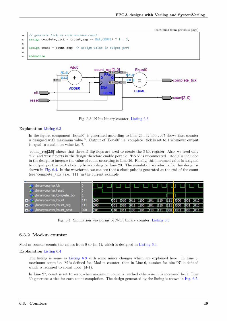
FPGA designs with Verilog and SystemVerilog
(continued from previous page)
28 // generate tick on each maximum count29 assign complete_tick = (count_reg == MAX_COUNT) ? 1 : 0;30
31 assign count = count_reg; // assign value to output port32
33 endmodule
Fig. 6.3: N-bit binary counter, Listing 6.3
Explanation Listing 6.3
In the figure, component ‘Equal0’ is generated according to Line 29. 32’h00. . . 07 shows that counteris designed with maximum value 7. Output of ‘Equal0’ i.e. complete_tick is set to 1 whenever outputis equal to maximum value i.e. 7.
‘count_reg[2:0]’ shows that three D flip flops are used to create the 3 bit register. Also, we used only‘clk’ and ‘reset’ ports in the design therefore enable port i.e. ‘ENA’ is unconnected. ‘Add0’ is includedin the design to increase the value of count according to Line 26. Finally, this increased value is assignedto output port in next clock cycle according to Line 23. The simulation waveforms for this design isshown in Fig. 6.4. In the waveforms, we can see that a clock pulse is generated at the end of the count(see ‘complete_tick’) i.e. ‘111’ in the current example.
Fig. 6.4: Simulation waveforms of N-bit binary counter, Listing 6.3
6.3.2 Mod-m counter
Mod-m counter counts the values from 0 to (m-1), which is designed in Listing 6.4.
Explanation Listing 6.4
The listing is same as Listing 6.3 with some minor changes which are explained here. In Line 5,maximum count i.e. M is defined for ‘Mod-m counter, then in Line 6, number for bits ‘N’ is definedwhich is required to count upto (M-1).
In Line 27, count is set to zero, when maximum count is reached otherwise it is increased by 1. Line30 generates a tick for each count completion. The design generated by the listing is shown in Fig. 6.5.
6.3. Counters 49
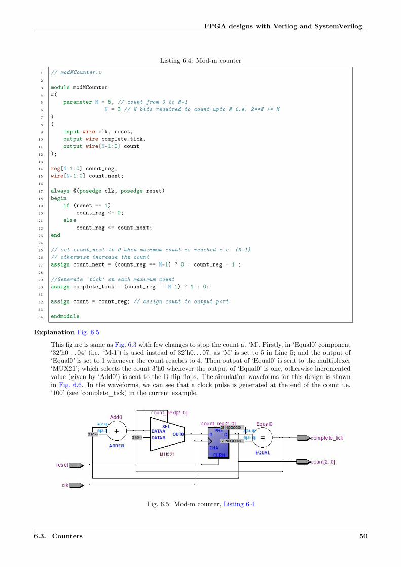
FPGA designs with Verilog and SystemVerilog
Listing 6.4: Mod-m counter
1 // modMCounter.v2
3 module modMCounter4 #(5 parameter M = 5, // count from 0 to M-16 N = 3 // N bits required to count upto M i.e. 2**N >= M7 )8 (9 input wire clk, reset,
10 output wire complete_tick,11 output wire[N-1:0] count12 );13
14 reg[N-1:0] count_reg;15 wire[N-1:0] count_next;16
17 always @(posedge clk, posedge reset)18 begin19 if (reset == 1)20 count_reg <= 0;21 else22 count_reg <= count_next;23 end24
25 // set count_next to 0 when maximum count is reached i.e. (M-1)26 // otherwise increase the count27 assign count_next = (count_reg == M-1) ? 0 : count_reg + 1 ;28
29 //Generate 'tick' on each maximum count30 assign complete_tick = (count_reg == M-1) ? 1 : 0;31
32 assign count = count_reg; // assign count to output port33
34 endmodule
Explanation Fig. 6.5
This figure is same as Fig. 6.3 with few changes to stop the count at ‘M’. Firstly, in ‘Equal0’ component‘32’h0. . . 04’ (i.e. ‘M-1’) is used instead of 32’h0. . . 07, as ‘M’ is set to 5 in Line 5; and the output of‘Equal0’ is set to 1 whenever the count reaches to 4. Then output of ‘Equal0’ is sent to the multiplexer‘MUX21’; which selects the count 3’h0 whenever the output of ‘Equal0’ is one, otherwise incrementedvalue (given by ‘Add0’) is sent to the D flip flops. The simulation waveforms for this design is shownin Fig. 6.6. In the waveforms, we can see that a clock pulse is generated at the end of the count i.e.‘100’ (see ‘complete_tick) in the current example.
Fig. 6.5: Mod-m counter, Listing 6.4
6.3. Counters 50
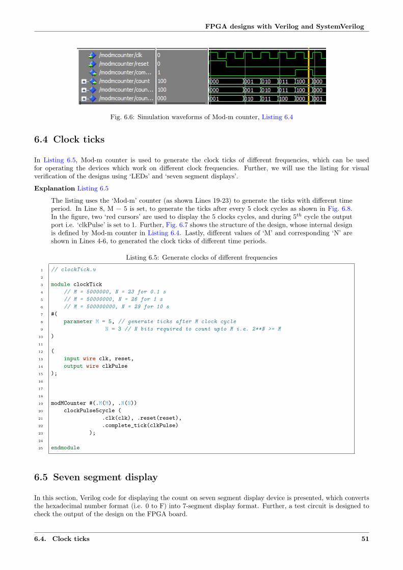
FPGA designs with Verilog and SystemVerilog
Fig. 6.6: Simulation waveforms of Mod-m counter, Listing 6.4
6.4 Clock ticks
In Listing 6.5, Mod-m counter is used to generate the clock ticks of different frequencies, which can be usedfor operating the devices which work on different clock frequencies. Further, we will use the listing for visualverification of the designs using ‘LEDs’ and ‘seven segment displays’.
Explanation Listing 6.5
The listing uses the ‘Mod-m’ counter (as shown Lines 19-23) to generate the ticks with different timeperiod. In Line 8, M = 5 is set, to generate the ticks after every 5 clock cycles as shown in Fig. 6.8.In the figure, two ‘red cursors’ are used to display the 5 clocks cycles, and during 5𝑡ℎ cycle the outputport i.e. ‘clkPulse’ is set to 1. Further, Fig. 6.7 shows the structure of the design, whose internal designis defined by Mod-m counter in Listing 6.4. Lastly, different values of ‘M’ and corresponding ‘N’ areshown in Lines 4-6, to generated the clock ticks of different time periods.
Listing 6.5: Generate clocks of different frequencies
1 // clockTick.v2
3 module clockTick4 // M = 5000000, N = 23 for 0.1 s5 // M = 50000000, N = 26 for 1 s6 // M = 500000000, N = 29 for 10 s7 #(8 parameter M = 5, // generate ticks after M clock cycle9 N = 3 // N bits required to count upto M i.e. 2**N >= M
10 )11
12 (13 input wire clk, reset,14 output wire clkPulse15 );16
17
18
19 modMCounter #(.M(M), .N(N))20 clockPulse5cycle (21 .clk(clk), .reset(reset),22 .complete_tick(clkPulse)23 );24
25 endmodule
6.5 Seven segment display
In this section, Verilog code for displaying the count on seven segment display device is presented, which convertsthe hexadecimal number format (i.e. 0 to F) into 7-segment display format. Further, a test circuit is designed tocheck the output of the design on the FPGA board.
6.4. Clock ticks 51
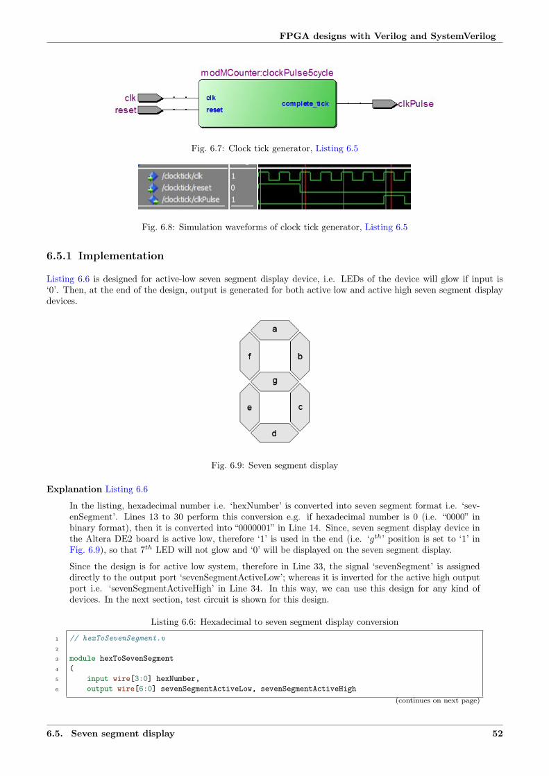
FPGA designs with Verilog and SystemVerilog
Fig. 6.7: Clock tick generator, Listing 6.5
Fig. 6.8: Simulation waveforms of clock tick generator, Listing 6.5
6.5.1 Implementation
Listing 6.6 is designed for active-low seven segment display device, i.e. LEDs of the device will glow if input is‘0’. Then, at the end of the design, output is generated for both active low and active high seven segment displaydevices.
Fig. 6.9: Seven segment display
Explanation Listing 6.6
In the listing, hexadecimal number i.e. ‘hexNumber’ is converted into seven segment format i.e. ‘sev-enSegment’. Lines 13 to 30 perform this conversion e.g. if hexadecimal number is 0 (i.e. “0000” inbinary format), then it is converted into “0000001” in Line 14. Since, seven segment display device inthe Altera DE2 board is active low, therefore ‘1’ is used in the end (i.e. ‘𝑔𝑡ℎ’ position is set to ‘1’ inFig. 6.9), so that 7𝑡ℎ LED will not glow and ‘0’ will be displayed on the seven segment display.
Since the design is for active low system, therefore in Line 33, the signal ‘sevenSegment’ is assigneddirectly to the output port ‘sevenSegmentActiveLow’; whereas it is inverted for the active high outputport i.e. ‘sevenSegmentActiveHigh’ in Line 34. In this way, we can use this design for any kind ofdevices. In the next section, test circuit is shown for this design.
Listing 6.6: Hexadecimal to seven segment display conversion
1 // hexToSevenSegment.v2
3 module hexToSevenSegment4 (5 input wire[3:0] hexNumber,6 output wire[6:0] sevenSegmentActiveLow, sevenSegmentActiveHigh
(continues on next page)
6.5. Seven segment display 52

FPGA designs with Verilog and SystemVerilog
(continued from previous page)
7 );8
9 reg[6:0] sevenSegment;10
11 always @*12 begin13 case(hexNumber)14 4'b0000 : sevenSegment = 7'b1000000; // 015 4'b0001 : sevenSegment = 7'b1111001; // 116 4'b0010 : sevenSegment = 7'b0100100; // 217 4'b0011 : sevenSegment = 7'b0110000; // 318 4'b0100 : sevenSegment = 7'b0011001; // 419 4'b0101 : sevenSegment = 7'b0010010; // 520 4'b0110 : sevenSegment = 7'b0000010; // 621 4'b0111 : sevenSegment = 7'b1111000; // 722 4'b1000 : sevenSegment = 7'b0000000; // 823 4'b1001 : sevenSegment = 7'b0010000; // 924 4'b1010 : sevenSegment = 7'b0001000; // a25 4'b1011 : sevenSegment = 7'b0000011; // b26 4'b1100 : sevenSegment = 7'b1000110; // c27 4'b1101 : sevenSegment = 7'b0100001; // d28 4'b1110 : sevenSegment = 7'b0000110; // e29 default : sevenSegment = 7'b0001110; // f30 endcase;31 end32
33 assign sevenSegmentActiveLow = sevenSegment;34 assign sevenSegmentActiveHigh = ~sevenSegment;35
36 endmodule
6.5.2 Test design for 7 segment display
Till now, we checked the outputs of the circuits using simulation. In this section, output of the code is displayedon the Seven segment devices which is available on the DE2 FPGA board. Further, we can use the design withother boards as well; for this purpose, the only change required is the pin-assignments, which are board specific.
Verilog code for testing the design is presented in Listing 6.6. Note that, in this listing, we use the names ‘SW’and ‘HEX0’ etc., which are defined in ‘DE2_PinAssg_PythonDSP.csv’ file. Partial view of this file is shown inFig. 6.10, which is provided in the zip folder along with the codes and can be downloaded from the website. Thisfile is used for ‘pin assignment’ in Altera DE2 board. DE2 board provides the 18 switches i.e. SW0 to SW17. Pinnumber for SW0 is ‘PIN_N25’, therefore in the ‘.csv file’, we used the name SW[0] for (SW0) and assign the pinnumber ‘PIN_N25’ in location column. Note that, we can not change the header names i.e. ‘To’ and ‘Location’for using the ‘.csv file’. Further, we can change the names to any other desired names e.g. SW17 is named as‘reset’, which will be used for resetting the system in later designs.
For pin assignments with ‘.csv file’, go to Assignments–>Import Assignments and then select the file‘DE2_PinAssg_PythonDSP.csv’. Next, to see the pin assignments, go to Assignments–>Pin Planner, whichwill display the pin assignments as shown in Fig. 6.11. Further, we can manually change the pin location byclicking on the ‘Location’ column in the figure.
Note: Names ‘SW’ and ‘HEX0’ etc. are used along with ‘std_logic_vector’ in the testing circuits, so that pinnumbers are automatically assigned to these ports according to ‘.csv file’. Otherwise we need to manually assignthe pin numbers to the ports.
Explanation Listing 6.7
In Line 6 of the listing, 4 bit input port ‘SW’ is defined. Therefore, pin number will be assigned to
6.5. Seven segment display 53

FPGA designs with Verilog and SystemVerilog
Fig. 6.10: Partial display of ‘Pin assignments file’ i.e. DE2_PinAssg_PythonDSP.csv
Fig. 6.11: Partial display of Pin Assignments
6.5. Seven segment display 54

FPGA designs with Verilog and SystemVerilog
these switches according to name ‘SW[0]’ to ‘SW[3]’ etc. in the ‘.csv file’. In Line 7, two output portsare defined i.e. HEX0 and HEX1. Next, in Line 10 and 13, HEX0 and HEX1 are mapped to activelow and active high outputs of the Listing 6.6 respectively. Note that, it is optional to define all theoutput ports in the port mapping, e.g. output port ‘sevenSegmentActiveHigh’ is not declared in Line11; whereas all the input ports must be declared in port mapping.
Now this design can be loaded on the FPGA board. Then, change the switch patterns to see theoutputs on the seven segment display devices. Since, HEX0 and HEX1 are set for active low and activehigh respectively, therefore HEX1 will display the LEDs which are not glowing on the HEX0 e.g. whenHEX0 displays the number ‘8’, then HEX1 will not glow any LED as all the LEDs of HEX0 are in the‘on’ condition.
Listing 6.7: Test design for seven segment display
1 // hexToSevenSegment_testCircuit2 // testing circuit for hexToSevenSegment.vhd3
4 module hexToSevenSegment_testCircuit5 (6 input wire[3:0] SW,7 output wire[6:0] HEX0, HEX18 );9
10 hexToSevenSegment hexToSevenSegment0 (11 .hexNumber(SW), .sevenSegmentActiveLow(HEX0));12
13 hexToSevenSegment hexToSevenSegment1 (14 .hexNumber(SW), .sevenSegmentActiveHigh(HEX1));15
16 endmodule
6.6 Visual verification of Mod-m counter
In previous section, we displayed the outputs on 7 segment display devices, but clocks are not used in the system.In this section, we will verify the designs with clocks, by visualizing the outputs on LEDs and seven segmentdisplays. Since, 50 MHz clock is too fast to visualize the change in the output with eyes, therefore Listing 6.8 usesthe 1 Hz clock frequency for mod-m counter, so that we can see the changes in the outputs.
Explanation Listing 6.8
Since, DE2 provides clock with 50 MHz frequency, therefore it should count upto 5 × 10⁷ to elapse 1sec time i.e. 50𝑀𝐻𝑧
5×107 = 50×106𝐻𝑧5×107 = 1𝐻𝑧 = 1 sec . Therefore M=50000000 is used in Line 20.
In the listing, three component are instantiated i.e. ‘clockGenerator’, ‘modMCounter’ and ‘hexToSev-enSegment’ for the visual verification of mod-m counter. Further, counts are verified using both LEDsand seven segment display. In Line 20, ‘clockGenerator’ is instantiated which generates the clock of 1second i.e. ‘clk_Pulse1s’. Then this 1 second clock is used by second instantiation i.e. mod-m counteras shown in Line 27. This can be seen in Fig. 6.12 where output of ‘clockGenerator’ is connect withinput clock of mod-m counter. Lastly, all these signals are sent to output port i.e. 1 second clock isdisplayed by LEDR[0] (Line 24), whereas ‘completed-count-tick’ is displayed by LEDR[1] (Line 29).Also, counts are displayed by green LEDs i.e. LEDG (Line 31). Further, seven segment display is alsoinstantiated at Line 34, to display the count on seven segment display as well.
Listing 6.8: Mod-m counter verification with 1 second clock
1 // modMCounter_VisualTest.v2
3
4 module modMCounter_VisualTest(continues on next page)
6.6. Visual verification of Mod-m counter 55
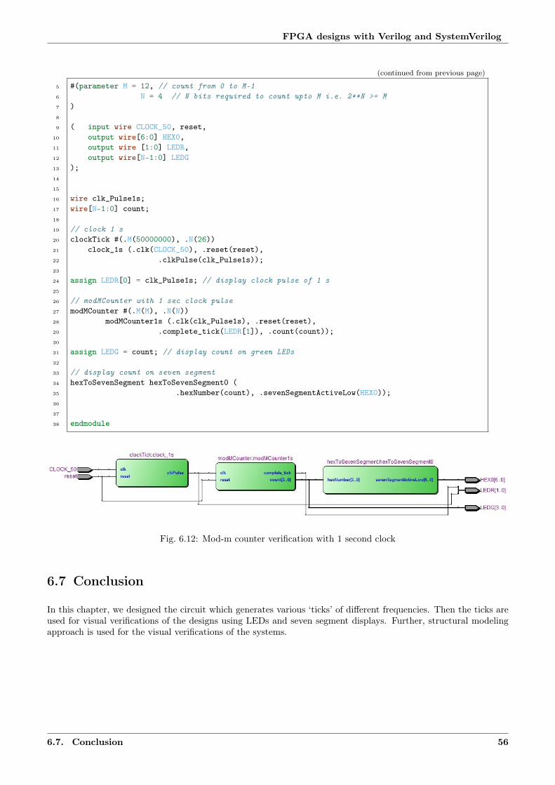
FPGA designs with Verilog and SystemVerilog
(continued from previous page)
5 #(parameter M = 12, // count from 0 to M-16 N = 4 // N bits required to count upto M i.e. 2**N >= M7 )8
9 ( input wire CLOCK_50, reset,10 output wire[6:0] HEX0,11 output wire [1:0] LEDR,12 output wire[N-1:0] LEDG13 );14
15
16 wire clk_Pulse1s;17 wire[N-1:0] count;18
19 // clock 1 s20 clockTick #(.M(50000000), .N(26))21 clock_1s (.clk(CLOCK_50), .reset(reset),22 .clkPulse(clk_Pulse1s));23
24 assign LEDR[0] = clk_Pulse1s; // display clock pulse of 1 s25
26 // modMCounter with 1 sec clock pulse27 modMCounter #(.M(M), .N(N))28 modMCounter1s (.clk(clk_Pulse1s), .reset(reset),29 .complete_tick(LEDR[1]), .count(count));30
31 assign LEDG = count; // display count on green LEDs32
33 // display count on seven segment34 hexToSevenSegment hexToSevenSegment0 (35 .hexNumber(count), .sevenSegmentActiveLow(HEX0));36
37
38 endmodule
Fig. 6.12: Mod-m counter verification with 1 second clock
6.7 Conclusion
In this chapter, we designed the circuit which generates various ‘ticks’ of different frequencies. Then the ticks areused for visual verifications of the designs using LEDs and seven segment displays. Further, structural modelingapproach is used for the visual verifications of the systems.
6.7. Conclusion 56

Darkness can not be dispelled by darkness, but by brightness. Hatredcan not be overcome by hatred, but by loving kindness.
–Buddha
Chapter 7
Finite state machine
7.1 Introduction
In previous chapters, we saw various examples of the combinational circuits and sequential circuits. In combina-tional circuits, the output depends on the current values of inputs only; whereas in sequential circuits, the outputdepends on the current values of the inputs along with the previously stored information. In the other words,storage elements, e.g. flip flogs or registers, are required for sequential circuits.
The information stored in the these elements can be seen as the states of the system. If a system transits betweenfinite number of such internal states, then finite state machines (FSM) can be used to design the system. In thischapter, various finite state machines along with the examples are discussed. Further, please see the SystemVerilog-designs in Chapter 10, which provides the better ways for creating the FSM designs as compared to Verilog.
7.2 Comparison: Mealy and Moore designs
section{}label{} FMS design is known as Moore design if the output of the system depends only on the states (seeFig. 7.1); whereas it is known as Mealy design if the output depends on the states and external inputs (see Fig.7.2). Further, a system may contain both types of designs simultaneously.
Note: Following are the differences in Mealy and Moore design,
• In Moore machine, the outputs depend on states only, therefore it is ‘synchronous machine’ and theoutput is available after 1 clock cycle as shown in Fig. 7.3. Whereas, in Mealy machine output depends onstates along with external inputs; and the output is available as soon as the input is changed therefore it is‘asynchronous machine’ (See Fig. 7.16 for more details).
• Mealy machine requires fewer number of states as compared to Moore machine as shown in Section 7.3.1.• Moore machine should be preferred for the designs, where glitches (see Section 7.4) are not the problem in
the systems.• Mealy machines are good for synchronous systems which requires ‘delay-free and glitch-free’ system (See
example in Section Section 7.7.1), but careful design is required for asynchronous systems. Therefore, Mealymachine can be complex as compare to Moore machine.
7.3 Example: Rising edge detector
Rising edge detector generates a tick for the duration of one clock cycle, whenever input signal changes from 0 to1. In this section, state diagrams of rising edge detector for Mealy and Moore designs are shown. Then rising edgedetector is implemented using Verilog code. Also, outputs of these two designs are compared.
57

FPGA designs with Verilog and SystemVerilog
7.3.1 State diagrams: Mealy and Moore design
Fig. 7.2 and Fig. 7.1 are the state diagrams for Mealy and Moore designs respectively. In Fig. 7.2, the outputof the system is set to 1, whenever the system is in the state ‘zero’ and value of the input signal ‘level’ is 1; i.e.output depends on both the state and the input. Whereas in Fig. 7.1, the output is set to 1 whenever the systemis in the state ‘edge’ i.e. output depends only on the state of the system.
Fig. 7.1: State diagrams for Edge detector : Moore Design
Fig. 7.2: State diagrams for Edge detector : Mealy Design
7.3.2 Implementation
Both Mealy and Moore designs are implemented in Listing 7.1. The listing can be seen as two parts i.e. Mealydesign (Lines 37-55) and Moore design (Lines 57-80). Please read the comments for complete understanding of thecode. The simulation waveforms i.e. Fig. 7.3 are discussed in next section.
Listing 7.1: Edge detector: Mealy and Moore designs
1 // edgeDetector.v2 // Moore and Mealy Implementation3
4 module edgeDetector5 (6 input wire clk, reset,7 input wire level,8 output reg Mealy_tick, Moore_tick9 );
10
11 localparam // 2 states are required for Mealy12 zeroMealy = 1'b0,13 oneMealy = 1'b1;14
(continues on next page)
7.3. Example: Rising edge detector 58

FPGA designs with Verilog and SystemVerilog
(continued from previous page)
15 localparam [1:0] // 3 states are required for Moore16 zeroMoore = 2'b00,17 edgeMoore = 2'b01,18 oneMoore = 2'b10;19
20 reg stateMealy_reg, stateMealy_next;21 reg[1:0] stateMoore_reg, stateMoore_next;22
23 always @(posedge clk, posedge reset)24 begin25 if(reset) // go to state zero if rese26 begin27 stateMealy_reg <= zeroMealy;28 stateMoore_reg <= zeroMoore;29 end30 else // otherwise update the states31 begin32 stateMealy_reg <= stateMealy_next;33 stateMoore_reg <= stateMoore_next;34 end35 end36
37 // Mealy Design38 always @(stateMealy_reg, level)39 begin40 // store current state as next41 stateMealy_next = stateMealy_reg; // required: when no case statement is satisfied42
43 Mealy_tick = 1'b0; // set tick to zero (so that 'tick = 1' is available for 1 cycle only)44 case(stateMealy_reg)45 zeroMealy: // set 'tick = 1' if state = zero and level = '1'46 if(level)47 begin // if level is 1, then go to state one,48 stateMealy_next = oneMealy; // otherwise remain in same state.49 Mealy_tick = 1'b1;50 end51 oneMealy:52 if(~level) // if level is 0, then go to zero state,53 stateMealy_next = zeroMealy; // otherwise remain in one state.54 endcase55 end56
57 // Moore Design58 always @(stateMoore_reg, level)59 begin60 // store current state as next61 stateMoore_next = stateMoore_reg; // required: when no case statement is satisfied62
63 Moore_tick = 1'b0; // set tick to zero (so that 'tick = 1' is available for 1 cycle only)64 case(stateMoore_reg)65 zeroMoore: // if state is zero,66 if(level) // and level is 167 stateMoore_next = edgeMoore; // then go to state edge.68 edgeMoore:69 begin70 Moore_tick = 1'b1; // set the tick to 1.71 if(level) // if level is 1,72 stateMoore_next = oneMoore; // go to state one,73 else74 stateMoore_next = zeroMoore; // else go to state zero.75 end
(continues on next page)
7.3. Example: Rising edge detector 59

FPGA designs with Verilog and SystemVerilog
(continued from previous page)
76 oneMoore:77 if(~level) // if level is 0,78 stateMoore_next = zeroMoore; // then go to state zero.79 endcase80 end81 endmodule
7.3.3 Outputs comparison
In Fig. 7.3, it can be seen that output-tick of Mealy detector is generated as soon as the ‘level’ goes to 1, whereasMoore design generate the tick after 1 clock cycle. These two ticks are shown with the help of the two red cursors inthe figure. Since, output of Mealy design is immediately available therefore it is preferred for synchronous designs.
Fig. 7.3: Simulation waveforms of rising edge detector in Listing 7.1
7.3.4 Visual verification
Listing 7.2 can be used to verify the results on the FPGA board. Here, clock with 1 Hz frequency is used in line19, which is defined in Listing 6.5. After loading the design on FPGA board, we can observe on LEDs that theoutput of Moore design displayed after Mealy design, with a delay of 1 second.
Listing 7.2: Visual verification of edge detector
1 // edgeDetector_VisualTest.v2
3 module edgeDetector_VisualTest4 (5 input wire CLOCK_50, reset,6 input wire[1:0] SW,7 output wire[1:0] LEDR8 );9
10 wire clk_Pulse1s;11
12 // clock 1 s13 clockTick #(.M(50000000), .N(26))14 clock_1s (.clk(CLOCK_50), .reset(reset),15 .clkPulse(clk_Pulse1s));16
17
18 // edge detector19 edgeDetector edgeDetector_VisualTest(.clk(clk_Pulse1s), .reset(reset),20 .level(SW[1]), .Moore_tick(LEDR[0]) , .Mealy_tick(LEDR[1]));21
22 endmodule
7.3. Example: Rising edge detector 60

FPGA designs with Verilog and SystemVerilog
7.4 Glitches
Glitches are the short duration pulses which are generated in the combinational circuits. These are generatedwhen more than two inputs change their values simultaneously. Glitches can be categorized as ‘static glitches’ and‘dynamic glitches’. Static glitches are further divided into two groups i.e. ‘static-0’ and ‘static-1’. ‘Static-0’ glitchis the glitch which occurs in logic ‘0’ signal i.e. one short pulse i.e. ‘high-pulse (logic-1)’ appears in logic-0 signal(and the signal settles down). Dynamic glitch is the glitch in which multiple short pulses appear before thesignal settles down.
Note: Most of the times, the glitches are not the problem in the design. Glitches create problem when it occurin the outputs, which are used as clock for the other circuits. In this case, glitches will trigger the next circuits,which will result in incorrect outputs. In such cases, it is very important to remove these glitches. In this section,the glitches are shown for three cases. Since, clocks are used in synchronous designs, therefore Section Section7.4.3 is of our main interest.
7.4.1 Combinational design in asynchronous circuit
Fig. 7.4 shows the truth-table for 2× 1 multiplexer and corresponding Karnaugh map is shown in Fig. 7.5. Notethat, the glitches occurs in the circuit, when we exclude the ‘red part’ of the solution from the Fig. 7.5, whichresults in minimum-gate solution, but at the same time the solution is disjoint. To remove the glitch, we can addthe prime-implicant in red-part as well. This solution is good, if there are few such gates are required; however ifthe number of inputs are very high, whose values are changing simultaneously then this solution is not practical,as we need to add large number of gates.
Fig. 7.4: Truth table of 2× 1 Multiplexer
Fig. 7.5: Reason for glitches and solution
Fig. 7.6: Glitches (see disjoint lines in ‘z’) in design in Listing 7.3
7.4. Glitches 61
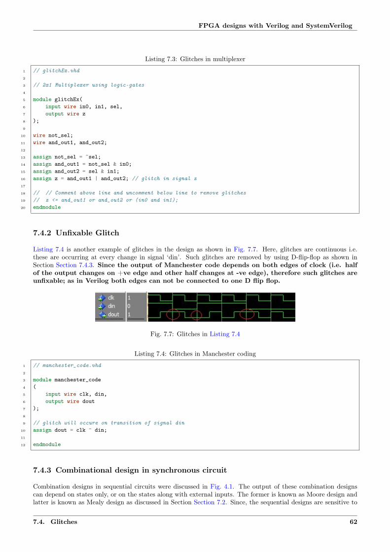
FPGA designs with Verilog and SystemVerilog
Listing 7.3: Glitches in multiplexer
1 // glitchEx.vhd2
3 // 2x1 Multiplexer using logic-gates4
5 module glitchEx(6 input wire in0, in1, sel,7 output wire z8 );9
10 wire not_sel;11 wire and_out1, and_out2;12
13 assign not_sel = ~sel;14 assign and_out1 = not_sel & in0;15 assign and_out2 = sel & in1;16 assign z = and_out1 | and_out2; // glitch in signal z17
18 // // Comment above line and uncomment below line to remove glitches19 // z <= and_out1 or and_out2 or (in0 and in1);20 endmodule
7.4.2 Unfixable Glitch
Listing 7.4 is another example of glitches in the design as shown in Fig. 7.7. Here, glitches are continuous i.e.these are occurring at every change in signal ‘din’. Such glitches are removed by using D-flip-flop as shown inSection Section 7.4.3. Since the output of Manchester code depends on both edges of clock (i.e. halfof the output changes on +ve edge and other half changes at -ve edge), therefore such glitches areunfixable; as in Verilog both edges can not be connected to one D flip flop.
Fig. 7.7: Glitches in Listing 7.4
Listing 7.4: Glitches in Manchester coding
1 // manchester_code.vhd2
3 module manchester_code4 (5 input wire clk, din,6 output wire dout7 );8
9 // glitch will occure on transition of signal din10 assign dout = clk ^ din;11
12 endmodule
7.4.3 Combinational design in synchronous circuit
Combination designs in sequential circuits were discussed in Fig. 4.1. The output of these combination designscan depend on states only, or on the states along with external inputs. The former is known as Moore design andlatter is known as Mealy design as discussed in Section Section 7.2. Since, the sequential designs are sensitive to
7.4. Glitches 62

FPGA designs with Verilog and SystemVerilog
edge of the clock, therefore the glitches can occur only at the edge of the clock. Hence, the glitches at the edge canbe removed by sending the output signal through the D flip flop, as shown in Fig. 7.8. Various Verilog templatesfor sequential designs are shown in Section Section 7.5 and Section 7.6.
Fig. 7.8: Glitch-free sequential design using D flip flop
7.5 Moore architecture and Verilog templates
Fig. 7.8 shows the different block for the sequential design. In this figure, we have three blocks i.e. ‘sequentiallogic’, ‘combinational logic’ and ‘glitch removal block’. In this section, we will define three process-statements toimplemented these blocks (see Listing 7.6). Further, ‘combinational logic block’ contains two different logics i.e.‘next-state’ and ‘output’. Therefore, this block can be implemented using two different block, which will result infour process-statements (see Listing 7.5).
Moore and Mealy machines can be divided into three categories i.e. ‘regular’, ‘timed’ and ‘recursive’. The dif-ferences in these categories are shown in Fig. 7.9, Fig. 7.10 and Fig. 7.11 for Moore machine. In this section, wewill see different Verilog templates for these categories. Note that, the design may be the combinations of thesethree categories, and we need to select the correct template according to the need. Further, the examples of thesetemplates are shown in Section Section 7.7.
Fig. 7.9: Regular Moore machine
Fig. 7.10: Timed Moore machine : next state depends on time as well
7.5.1 Regular machine
Please see the Fig. 7.9 and note the following points about regular Moore machine,
• Output depends only on the states, therefore no ‘if statement’ is required in the process-statement. Forexample, in Lines 85-87 of Listing 7.5, the outputs (Lines 86-87) are defined inside the ‘s0’ (Line 86).
• Next-state depends on current-state and and current external inputs. For example, the ‘state_next’ atLine 49 of Listing 7.5 is defined inside ‘if statement’ (Line 48) which depends on current input. Further, this‘if statement’ is defined inside the state ‘s0’ (Line 47). Hence the next state depends on current state andcurrent external input.
7.5. Moore architecture and Verilog templates 63
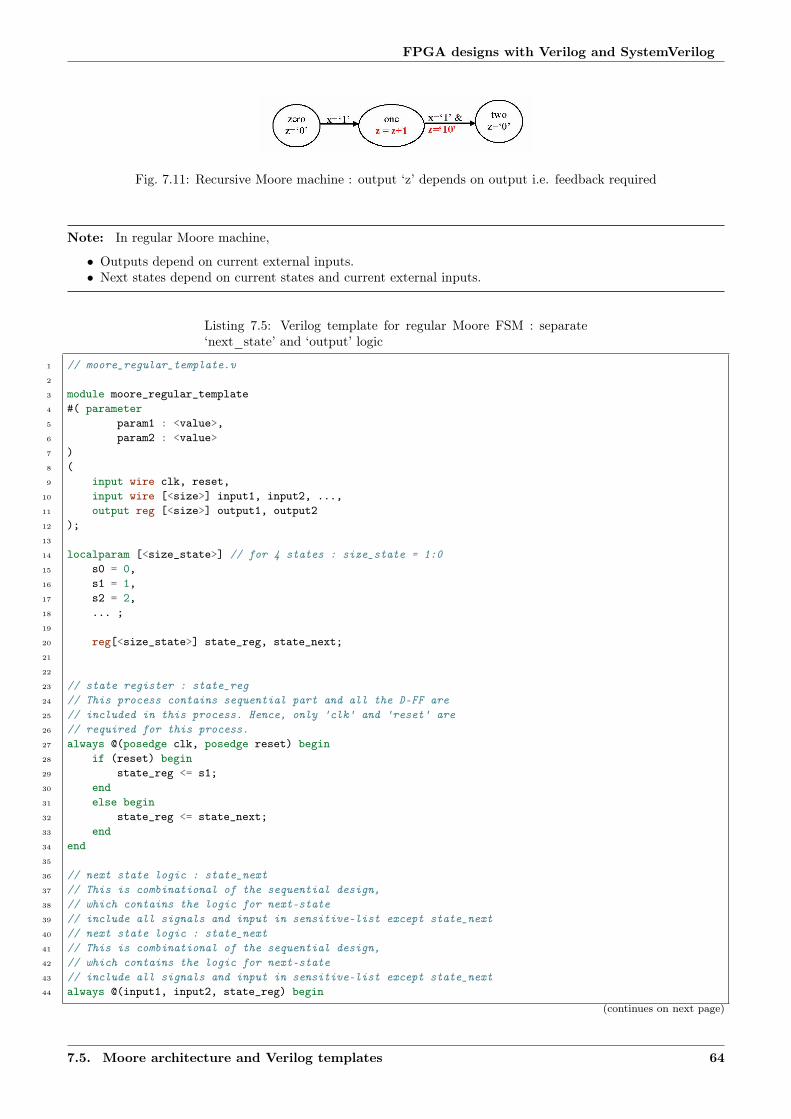
FPGA designs with Verilog and SystemVerilog
Fig. 7.11: Recursive Moore machine : output ‘z’ depends on output i.e. feedback required
Note: In regular Moore machine,
• Outputs depend on current external inputs.• Next states depend on current states and current external inputs.
Listing 7.5: Verilog template for regular Moore FSM : separate‘next_state’ and ‘output’ logic
1 // moore_regular_template.v2
3 module moore_regular_template4 #( parameter5 param1 : <value>,6 param2 : <value>7 )8 (9 input wire clk, reset,
10 input wire [<size>] input1, input2, ...,11 output reg [<size>] output1, output212 );13
14 localparam [<size_state>] // for 4 states : size_state = 1:015 s0 = 0,16 s1 = 1,17 s2 = 2,18 ... ;19
20 reg[<size_state>] state_reg, state_next;21
22
23 // state register : state_reg24 // This process contains sequential part and all the D-FF are25 // included in this process. Hence, only 'clk' and 'reset' are26 // required for this process.27 always @(posedge clk, posedge reset) begin28 if (reset) begin29 state_reg <= s1;30 end31 else begin32 state_reg <= state_next;33 end34 end35
36 // next state logic : state_next37 // This is combinational of the sequential design,38 // which contains the logic for next-state39 // include all signals and input in sensitive-list except state_next40 // next state logic : state_next41 // This is combinational of the sequential design,42 // which contains the logic for next-state43 // include all signals and input in sensitive-list except state_next44 always @(input1, input2, state_reg) begin
(continues on next page)
7.5. Moore architecture and Verilog templates 64

FPGA designs with Verilog and SystemVerilog
(continued from previous page)
45 state_next = state_reg; // default state_next46 case (state_reg)47 s0 : begin48 if (<condition>) begin // if (input1 = 2'b01) then49 state_next = s1;50 end51 else if (<condition>) begin // add all the required conditionstion52 state_next = ...;53 end54 else begin // remain in current state55 state_next = s0;56 end57 end58 s1 : begin59 if (<condition>) begin // if (input1 = 2'b10) then60 state_next = s2;61 end62 else if (<condition>) begin // add all the required conditionstions63 state_next = ...;64 end65 else begin// remain in current state66 state_next = s1;67 end68 end69 s2 : begin70 ...71 end72 endcase73 end74
75 // combination output logic76 // This part contains the output of the design77 // no if-else statement is used in this part78 // include all signals and input in sensitive-list except state_next79 always @(input1, input2, ..., state_reg) begin80 // default outputs81 output1 = <value>;82 output2 = <value>;83 ...84 case (state_reg)85 s0 : begin86 output1 = <value>;87 output2 = <value>;88 ...89 end90 s1 : begin91 output1 = <value>;92 output2 = <value>;93 ...94 end95 s2 : begin96 ...97 end98 endcase99 end
100
101 // optional D-FF to remove glitches102 always @(posedge clk, posedge reset)103 begin104 if (reset) begin105 new_output1 <= ... ;
(continues on next page)
7.5. Moore architecture and Verilog templates 65

FPGA designs with Verilog and SystemVerilog
(continued from previous page)
106 new_output2 <= ... ;107 end108 else begin109 new_output1 <= output1;110 new_output2 <= output2;111 end112 end113
114 endmodule
Listing 7.6 is same as Listing 7.5, but the ouput-logic and next-state logic are combined in one process block.
Listing 7.6: Verilog template for regular Moore FSM : combined‘next_state’ and ‘output’ logic
1 // moore_regular_template2.v2
3 module moore_regular_template24 #( parameter5 param1 : <value>,6 param2 : <value>7 )8 (9 input wire clk, reset,
10 input wire [<size>] input1, input2, ...,11 output reg [<size>] output1, output212 );13
14 localparam [<size_state>] // for 4 states : size_state = 1:015 s0 = 0,16 s1 = 1,17 s2 = 2,18 ... ;19
20 reg[<size_state>] state_reg, state_next;21
22
23 // state register : state_reg24 // This process contains sequential part and all the D-FF are25 // included in this process. Hence, only 'clk' and 'reset' are26 // required for this process.27 always @(posedge clk, posedge reset) begin28 if (reset) begin29 state_reg <= s1;30 end31 else begin32 state_reg <= state_next;33 end34 end35
36 // next state logic : state_next37 // This is combinational of the sequential design,38 // which contains the logic for next-state39 // include all signals and input in sensitive-list except state_next40 // next state logic : state_next41 // This is combinational of the sequential design,42 // which contains the logic for next-state43 // include all signals and input in sensitive-list except state_next44 always @(input1, input2, state_reg) begin45 state_next = state_reg; // default state_next46 case (state_reg)
(continues on next page)
7.5. Moore architecture and Verilog templates 66
FPGA designs with Verilog and SystemVerilog
(continued from previous page)
47 s0 : begin48 output1 = <value>;49 output2 = <value>;50 ...51 if (<condition>) begin // if (input1 = 2'b01) then52 state_next = s1;53 end54 else if (<condition>) begin // add all the required conditionstion55 state_next = ...;56 end57 else begin // remain in current state58 state_next = s0;59 end60 end61 s1 : begin62 output1 = <value>;63 output2 = <value>;64 ...65 if (<condition>) begin // if (input1 = 2'b10) then66 state_next = s2;67 end68 else if (<condition>) begin // add all the required conditionstions69 state_next = ...;70 end71 else begin// remain in current state72 state_next = s1;73 end74 end75 s2 : begin76 ...77 end78 endcase79 end80
81 // optional D-FF to remove glitches82 always @(posedge clk, posedge reset)83 begin84 if (reset) begin85 new_output1 <= ... ;86 new_output2 <= ... ;87 end88 else begin89 new_output1 <= output1;90 new_output2 <= output2;91 end92 end93
94 endmodule
7.5.2 Timed machine
If the state of the design changes after certain duration (see Fig. 7.10), then we need to add the timer in the Verilogdesign which are created in Listing 7.5 and Listing 7.5. For this, we need to add one more process-block whichperforms following actions,
• Zero the timer : The value of the timer is set to zero, whenever the state of the system changes.• Stop the timer : Value of the timer is incremented till the predefined ‘maximum value’ is reached and then
it should be stopped incrementing. Further, it’s value should not be set to zero until state is changed.
7.5. Moore architecture and Verilog templates 67

FPGA designs with Verilog and SystemVerilog
Note: In timed Moore machine,
• Outputs depend on current external inputs.• Next states depend on time along with current states and current external inputs.
Template for timed Moore machine is shown in Listing 7.7, which is exactly same as Listing 7.6 except withfollowing changes,
• Timer related constants are added at Line 22-27.• An ‘always’ block is added to stop and zero the timer (Lines 44-54).• Finally, timer related conditions are included for next-state logic e.g. Lines 64 and 67 etc.
Listing 7.7: Verilog template timed Moore FSM : separate‘next_state’ and ‘output’ logic
1 // moore_timed_template.vhd2
3 module moore_timed_template4 #( parameter5 param1 : <value>,6 param2 : <value>7 )8 (9 input wire clk, reset,
10 input wire [<size>] input1, input2, ...,11 output reg [<size>] output1, output212 );13
14 localparam [<size_state>] // for 4 states : size_state = 1:015 s0 = 0,16 s1 = 1,17 s2 = 2,18 ... ;19
20 reg[<size_state>] state_reg, state_next;21
22 // timer23 localparam T1 = <value>;24 localparam T2 = <value>;25 localparam T3 = <value>;26 ...27 reg [<size>] t; //<size> should be able to store max(T1, T2, T3)28
29
30 // state register : state_reg31 // This process contains sequential part and all the D-FF are32 // included in this process. Hence, only 'clk' and 'reset' are33 // required for this process.34 always @(posedge clk, posedge reset) begin35 if (reset) begin36 state_reg <= s1;37 end38 else begin39 state_reg <= state_next;40 end41 end42
43 // timer44 always @(posedge clk, posedge reset) begin45 if (reset) begin46 t <= 0;
(continues on next page)
7.5. Moore architecture and Verilog templates 68

FPGA designs with Verilog and SystemVerilog
(continued from previous page)
47 end48 else begin49 if state_reg != state_next then // state is changing50 t <= 0;51 else52 t <= t + 1;53 end54 end55
56 // next state logic : state_next57 // This is combinational of the sequential design,58 // which contains the logic for next-state59 // include all signals and input in sensitive-list except state_next60 always @(input1, input2, state_reg) begin61 state_next = state_reg; // default state_next62 case (state_reg)63 s0 : begin64 if (<condition> & t >= T1-1) begin // if (input1 = 2'b01) then65 state_next = s1;66 end67 else if (<condition> & t >= T2-1) begin // add all the required conditionstion68 state_next = ...;69 end70 else begin // remain in current state71 state_next = s0;72 end73 end74 s1 : begin75 if (<condition> & t >= T3-1) begin // if (input1 = 2'b10) then76 state_next = s2;77 end78 else if (<condition> & t >= T2-1) begin // add all the required conditionstions79 state_next = ...;80 end81 else begin// remain in current state82 state_next = s1;83 end84 end85 s2 : begin86 ...87 end88 endcase89 end90
91 // combination output logic92 // This part contains the output of the design93 // no if-else statement is used in this part94 // include all signals and input in sensitive-list except state_next95 always @(input1, input2, ..., state_reg) begin96 // default outputs97 output1 = <value>;98 output2 = <value>;99 ...
100 case (state_reg)101 s0 : begin102 output1 = <value>;103 output2 = <value>;104 ...105 end106 s1 : begin107 output1 = <value>;
(continues on next page)
7.5. Moore architecture and Verilog templates 69

FPGA designs with Verilog and SystemVerilog
(continued from previous page)
108 output2 = <value>;109 ...110 end111 s2 : begin112 ...113 end114 endcase115 end116
117 // optional D-FF to remove glitches118 always @(posedge clk, posedge reset)119 begin120 if (reset) begin121 new_output1 <= ... ;122 new_output2 <= ... ;123 end124 else begin125 new_output1 <= output1;126 new_output2 <= output2;127 end128 end129
130 endmodule
7.5.3 Recursive machine
In recursive machine, the outputs are fed back as input to the system (see Fig. 7.11). Hence, we need additionalprocess-statement which can store the outputs which are fed back to combinational block of sequential design,as shown in Listing 7.8. The listing is same as Listing 7.7 except certain signals and process block are definedto feedback the output to combination logic; i.e. Lines 29-31 contain the signals (feedback registers) which arerequired to be feedback the outputs. Here, ‘_next’ and ‘_reg’ are used in these lines, where ‘next’ value is fedback as ‘reg’ in the next clock cycle inside the ‘always’ statement which is defined in Lines 63-75. Lastly, ‘feedbackregisters’ are also used to calculate the next-state inside the ‘if statement’ e.g. Lines 91 and 96. Also, the value offeedback registers are updated inside these ‘if statements’ e.g. Lines 93 and 102.
Note: In recursive Moore machine,
• Outputs depend on current external inputs. Also, values in the feedback registers are used as outputs.• Next states depend current states, current external input, current internal inputs (i.e. previous outputs
feedback as inputs to system) and time (optional).
Listing 7.8: Verilog template recursive Moore FSM : separate‘next_state’ and ‘output’ logic
1 // moore_recursive_template.v2
3 module moore_recursive_template4 #( parameter5 param1 : <value>,6 param2 : <value>7 )8 (9 input wire clk, reset,
10 input wire [<size>] input1, input2, ...,11 output reg [<size>] output1, output2, new_output1, new_output212 );13
(continues on next page)
7.5. Moore architecture and Verilog templates 70
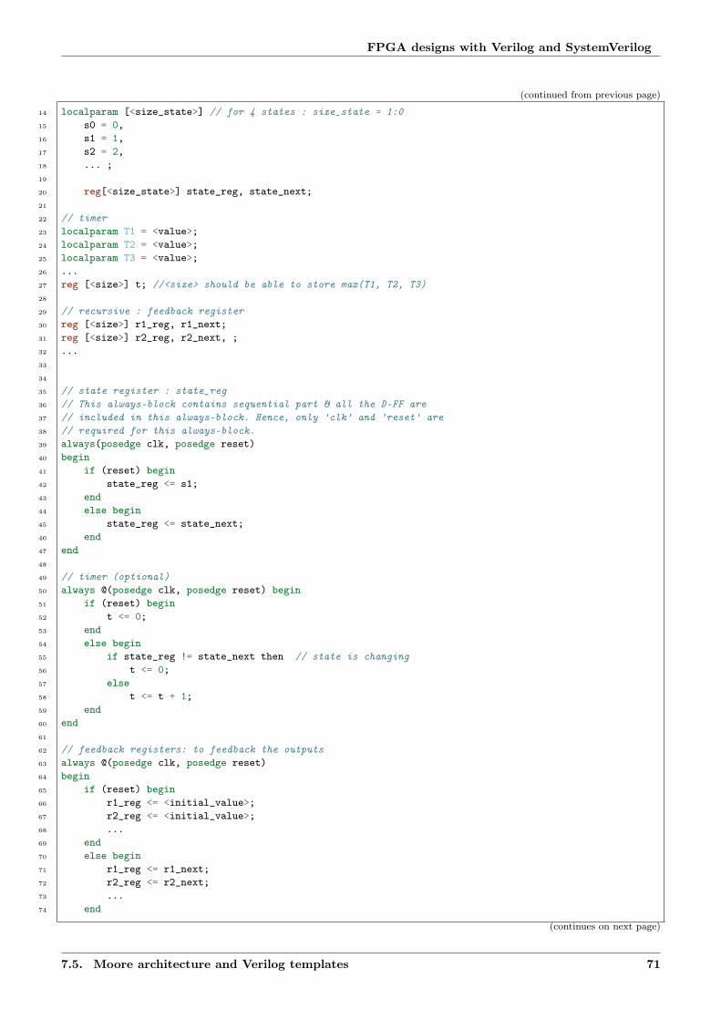
FPGA designs with Verilog and SystemVerilog
(continued from previous page)
14 localparam [<size_state>] // for 4 states : size_state = 1:015 s0 = 0,16 s1 = 1,17 s2 = 2,18 ... ;19
20 reg[<size_state>] state_reg, state_next;21
22 // timer23 localparam T1 = <value>;24 localparam T2 = <value>;25 localparam T3 = <value>;26 ...27 reg [<size>] t; //<size> should be able to store max(T1, T2, T3)28
29 // recursive : feedback register30 reg [<size>] r1_reg, r1_next;31 reg [<size>] r2_reg, r2_next, ;32 ...33
34
35 // state register : state_reg36 // This always-block contains sequential part & all the D-FF are37 // included in this always-block. Hence, only 'clk' and 'reset' are38 // required for this always-block.39 always(posedge clk, posedge reset)40 begin41 if (reset) begin42 state_reg <= s1;43 end44 else begin45 state_reg <= state_next;46 end47 end48
49 // timer (optional)50 always @(posedge clk, posedge reset) begin51 if (reset) begin52 t <= 0;53 end54 else begin55 if state_reg != state_next then // state is changing56 t <= 0;57 else58 t <= t + 1;59 end60 end61
62 // feedback registers: to feedback the outputs63 always @(posedge clk, posedge reset)64 begin65 if (reset) begin66 r1_reg <= <initial_value>;67 r2_reg <= <initial_value>;68 ...69 end70 else begin71 r1_reg <= r1_next;72 r2_reg <= r2_next;73 ...74 end
(continues on next page)
7.5. Moore architecture and Verilog templates 71

FPGA designs with Verilog and SystemVerilog
(continued from previous page)
75 end76
77
78
79 // next state logic : state_next80 // This is combinational of the sequential design,81 // which contains the logic for next-state82 // include all signals and input in sensitive-list except state_next83 always @(input1, input2, state_reg) begin84 state_next = state_reg; // default state_next85 r1_next = r1_reg; // default next-states86 r2_next = r2_reg;87 ...88 case (state_reg)89 s0 : begin90 if <condition> & r1_reg == <value> & t >= T1-1 begin // if (input1 = '01') then91 state_next = s1;92 r1_next = <value>;93 r2_next = <value>;94 ...95 end96 elsif <condition> & r2_reg == <value> & t >= T2-1 begin // add all the required conditions97 state_next = <value>;98 r1_next = <value>;99 ...
100 end101 else begin // remain in current state102 state_next = s0;103 r2_next = <value>;104 ...105 end106 end107 s1 : begin108 ...109 end case;110 end process;111
112 // next state logic and outputs113 // This is combinational of the sequential design,114 // which contains the logic for next-state and outputs115 // include all signals and input in sensitive-list except state_next116 always @(input1, input2, ..., state_reg) begin117 state_next = state_reg; // default state_next118 // default outputs119 output1 = <value>;120 output2 = <value>;121 ...122 // default next-states123 r1_next = r1_reg;124 r2_next = r2_reg;125 ...126 case (state_reg)127 s0 : begin128 output1 = <value>;129 output2 = <value>;130 if (<condition> & r1_reg = <value> & t >= T1-1) begin // if (input1 = 2'b01) then131 ...132 r1_next = <value>;133 r2_next = <value>;134 ...135 state_next = s1;
(continues on next page)
7.5. Moore architecture and Verilog templates 72
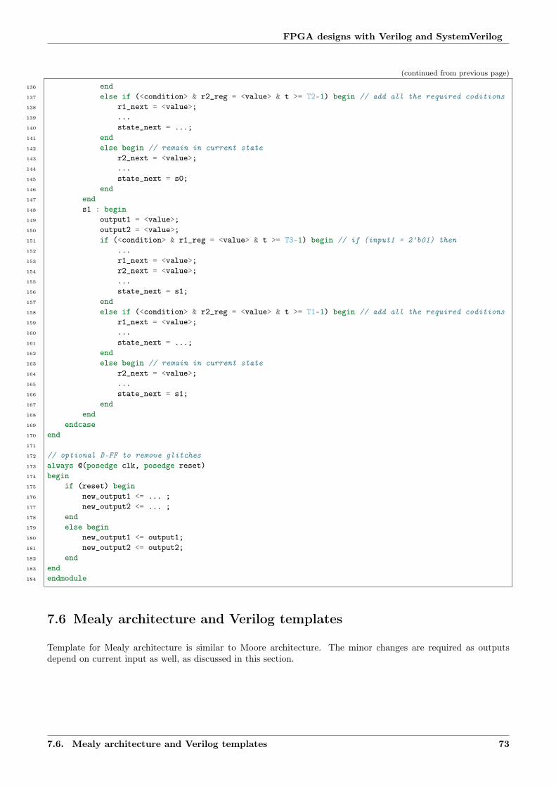
FPGA designs with Verilog and SystemVerilog
(continued from previous page)
136 end137 else if (<condition> & r2_reg = <value> & t >= T2-1) begin // add all the required coditions138 r1_next = <value>;139 ...140 state_next = ...;141 end142 else begin // remain in current state143 r2_next = <value>;144 ...145 state_next = s0;146 end147 end148 s1 : begin149 output1 = <value>;150 output2 = <value>;151 if (<condition> & r1_reg = <value> & t >= T3-1) begin // if (input1 = 2'b01) then152 ...153 r1_next = <value>;154 r2_next = <value>;155 ...156 state_next = s1;157 end158 else if (<condition> & r2_reg = <value> & t >= T1-1) begin // add all the required coditions159 r1_next = <value>;160 ...161 state_next = ...;162 end163 else begin // remain in current state164 r2_next = <value>;165 ...166 state_next = s1;167 end168 end169 endcase170 end171
172 // optional D-FF to remove glitches173 always @(posedge clk, posedge reset)174 begin175 if (reset) begin176 new_output1 <= ... ;177 new_output2 <= ... ;178 end179 else begin180 new_output1 <= output1;181 new_output2 <= output2;182 end183 end184 endmodule
7.6 Mealy architecture and Verilog templates
Template for Mealy architecture is similar to Moore architecture. The minor changes are required as outputsdepend on current input as well, as discussed in this section.
7.6. Mealy architecture and Verilog templates 73

FPGA designs with Verilog and SystemVerilog
7.6.1 Regular machine
In Mealy machines, the output is the function of current input and states, therefore the output will also definedinside the if-statements (Lines 49-50 etc.). Rest of the code is same as Listing 7.6.
Listing 7.9: Verilog template for regular Mealy FSM : combined‘next_state’ and ‘output’ logic
1 // mealy_regular_template.v2
3 module mealy_regular_template4 #( parameter5 param1 = <value>,6 param2 = <value>,7 )8 (9 input wire clk, reset,
10 input wire [<size>] input1, input2, ...,11 output reg [<size>] output1, output212 );13
14 localparam [<size_state>] // for 4 states : size_state = 1:015 s0 = 0,16 s1 = 1,17 s2 = 2,18 ... ;19
20 reg[<size_state>] state_reg, state_next;21
22 // state register : state_reg23 // This `always block' contains sequential part and all the D-FF are24 // included in this process. Hence, only 'clk' and 'reset' are25 // required for this process.26 always(posedge clk, posedge reset)27 begin28 if (reset) begin29 state_reg <= s1;30 end31 else begin32 state_reg <= state_next;33 end34 end35
36 // next state logic and outputs37 // This is combinational part of the sequential design,38 // which contains the logic for next-state and outputs39 // include all signals and input in sensitive-list except state_next40 always @(input1, input2, ..., state_reg) begin41 state_next = state_reg; // default state_next42 // default outputs43 output1 = <value>;44 output2 = <value>;45 ...46 case (state_reg)47 s0 : begin48 if (<condition>) begin // if (input1 == 2'b01) then49 output1 = <value>;50 output2 = <value>;51 ...52 state_next = s1;53 end54 else if <condition> begin // add all the required conditionstions
(continues on next page)
7.6. Mealy architecture and Verilog templates 74

FPGA designs with Verilog and SystemVerilog
(continued from previous page)
55 output1 = <value>;56 output2 = <value>;57 ...58 state_next = ...;59 end60 else begin // remain in current state61 output1 = <value>;62 output2 = <value>;63 ...64 state_next = s0;65 end66 end67 s1 : begin68 ...69 end70 endcase71 end72
73 // optional D-FF to remove glitches74 always(posedge clk, posedge reset) begin75 if (reset) begin76 new_output1 <= ... ;77 new_output2 <= ... ;78 else begin79 new_output1 <= output1;80 new_output2 <= output2;81 end82 end83 endmodule
7.6.2 Timed machine
Listing 7.10 contains timer related changes in Listing 7.9. See description of Listing 7.7 for more details.
Listing 7.10: Verilog template for timed Mealy FSM : combined‘next_state’ and ‘output’ logic
1 // mealy_timed_template.v2
3 module mealy_timed_template4 #( parameter5 param1 : <value>,6 param2 : <value>7 )8 (9 input wire clk, reset,
10 input wire [<size>] input1, input2, ...,11 output reg [<size>] output1, output212 );13
14
15 localparam [<size_state>] // for 4 states : size_state = 1:016 s0 = 0,17 s1 = 1,18 s2 = 2,19 ... ;20
21 reg[<size_state>] state_reg, state_next;22
(continues on next page)
7.6. Mealy architecture and Verilog templates 75

FPGA designs with Verilog and SystemVerilog
(continued from previous page)
23 // timer24 localparam T1 = <value>;25 localparam T2 = <value>;26 localparam T3 = <value>;27 ...28 reg [<size>] t; //<size> should be able to store max(T1, T2, T3)29
30 // state register : state_reg31 // This always-block contains sequential part and all the D-FF are32 // included in this always-block. Hence, only 'clk' and 'reset' are33 // required for this always-block.34 always @(posedge clk, posedge reset) begin35 if (reset) begin36 state_reg <= s1;37 end38 else begin39 state_reg <= state_next;40 end41 end42
43 // timer44 always @(posedge clk, posedge reset) begin45 if (reset) begin46 t <= 0;47 end48 else begin49 if state_reg != state_next then // state is changing50 t <= 0;51 else52 t <= t + 1;53 end54 end55
56 // next state logic and outputs57 // This is combinational of the sequential design,58 // which contains the logic for next-state and outputs59 // include all signals and input in sensitive-list except state_next60 always @(input1, input2, ..., state_reg) begin61 state_next = state_reg; // default state_next62 // default outputs63 output1 = <value>;64 output2 = <value>;65 ...66 case (state_reg )67 s0 : begin68 if (<condition> & t >= T1-1) begin // if (input1 = '01') then69 output1 = <value>;70 output2 = <value>;71 ...72 state_next = s1;73 end74 else if (<condition> & t >= T2-1) begin // add all the required conditionstions75 output1 = <value>;76 output2 = <value>;77 ...78 state_next = ...;79 end80 else begin // remain in current state81 output1 = <value>;82 output2 = <value>;83 ...
(continues on next page)
7.6. Mealy architecture and Verilog templates 76
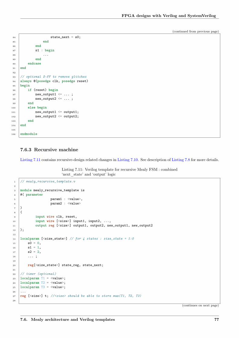
FPGA designs with Verilog and SystemVerilog
(continued from previous page)
84 state_next = s0;85 end86 end87 s1 : begin88 ...89 end90 endcase91 end92
93 // optional D-FF to remove glitches94 always @(posedge clk, posedge reset)95 begin96 if (reset) begin97 new_output1 <= ... ;98 new_output2 <= ... ;99 end
100 else begin101 new_output1 <= output1;102 new_output2 <= output2;103 end104 end105
106 endmodule
7.6.3 Recursive machine
Listing 7.11 contains recursive-design related changes in Listing 7.10. See description of Listing 7.8 for more details.
Listing 7.11: Verilog template for recursive Mealy FSM : combined‘next_state’ and ‘output’ logic
1 // mealy_recursive_template.v2
3 module mealy_recursive_template is4 #( parameter5 param1 : <value>,6 param2 : <value>7 )8 (9 input wire clk, reset,
10 input wire [<size>] input1, input2, ...,11 output reg [<size>] output1, output2, new_output1, new_output212 );13
14 localparam [<size_state>] // for 4 states : size_state = 1:015 s0 = 0,16 s1 = 1,17 s2 = 2,18 ... ;19
20 reg[<size_state>] state_reg, state_next;21
22 // timer (optional)23 localparam T1 = <value>;24 localparam T2 = <value>;25 localparam T3 = <value>;26 ...27 reg [<size>] t; //<size> should be able to store max(T1, T2, T3)28
(continues on next page)
7.6. Mealy architecture and Verilog templates 77

FPGA designs with Verilog and SystemVerilog
(continued from previous page)
29 // recursive : feedback register30 reg [<size>] r1_reg, r1_next;31 reg [<size>] r2_reg, r2_next;32 ...33
34 // state register : state_reg35 // This process contains sequential part & all the D-FF are36 // included in this process. Hence, only 'clk' and 'reset' are37 // required for this process.38 always(posedge clk, posedge reset)39 begin40 if (reset) begin41 state_reg <= s1;42 end43 else begin44 state_reg <= state_next;45 end46 end47
48 // timer (optional)49 always @(posedge clk, posedge reset) begin50 if (reset) begin51 t <= 0;52 end53 else begin54 if state_reg != state_next then // state is changing55 t <= 0;56 else57 t <= t + 1;58 end59 end60
61 // feedback registers: to feedback the outputs62 always @(posedge clk, posedge reset)63 begin64 if (reset) begin65 r1_reg <= <initial_value>;66 r2_reg <= <initial_value>;67 ...68 end69 else begin70 r1_reg <= r1_next;71 r2_reg <= r2_next;72 ...73 end74 end75
76 // next state logic and outputs77 // This is combinational of the sequential design,78 // which contains the logic for next-state and outputs79 // include all signals and input in sensitive-list except state_next80 always @(input1, input2, ..., state_reg) begin81 state_next = state_reg; // default state_next82 // default outputs83 output1 = <value>;84 output2 = <value>;85 ...86 // default next-states87 r1_next = r1_reg;88 r2_next = r2_reg;89 ...
(continues on next page)
7.6. Mealy architecture and Verilog templates 78

FPGA designs with Verilog and SystemVerilog
(continued from previous page)
90 case (state_reg)91 s0 : begin92 if (<condition> & r1_reg == <value> & t >= T1-1) begin // if (input1 = 2'b01) then93 output1 = <value>;94 output2 = <value>;95 ...96 r1_next = <value>;97 r2_next = <value>;98 ...99 state_next = s1;
100 end101 else if (<condition> & r2_reg == <value> & t >= T2-1) begin // add all the required␣
→˓coditions102 output1 = <value>;103 output2 = <value>;104 ...105 r1_next = <value>;106 ...107 state_next = ...;108 end109 else begin // remain in current state110 output1 = <value>;111 output2 = <value>;112 ...113 r2_next = <value>;114 ...115 state_next = s0;116 end117 end118 s1 : begin119 ...120 end121 endcase122 end123
124 // optional D-FF to remove glitches125 always @(posedge clk, posedge reset)126 begin127 if (reset) begin128 new_output1 <= ... ;129 new_output2 <= ... ;130 end131 else begin132 new_output1 <= output1;133 new_output2 <= output2;134 end135 end136
137 endmodule
7.7 Examples
7.7.1 Regular Machine : Glitch-free Mealy and Moore design
In this section, a non-overlapping sequence detector is implemented to show the differences between Mealy andMoore machines. Listing 7.12 implements the ‘sequence detector’ which detects the sequence ‘110’; and corre-sponding state-diagrams are shown in Fig. 7.12 and Fig. 7.13. The RTL view generated by the listing is shown inFig. 7.15, where two D-FF are added to remove the glitches from Moore and Mealy model. Also, in the figure, if we
7.7. Examples 79

FPGA designs with Verilog and SystemVerilog
click on the state machines, then we can see the implemented state-diagrams e.g. if we click on ‘state_reg_mealy’then the state-diagram in Fig. 7.14 will be displayed, which is exactly same as Fig. 7.13.
Further, the testbench for the listing is shown in Listing 7.13, whose results are illustrated in Fig. 7.16. Pleasenote the following points in Fig. 7.16,
• Mealy machines are asynchronous as the output changes as soon as the input changes. It does not wait forthe next cycle.
• If the output of the Mealy machine is delayed, then glitch will be removed and the output will be same asthe Moore output (Note that, there is no glitch in this system. This example shows how to implement theD-FF to remove glitch in the system (if exists)).
• Glitch-free Moore output is delayed by one clock cycle.• If glitch is not a problem, then we should use Moore machine, because it is synchronous in nature. But, if
glitch is problem and we do not want to delay the output then Mealy machines should be used.
Fig. 7.12: Non-overlap sequence detector ‘110’ : Moore design
Fig. 7.13: Non-overlap sequence detector ‘110’ : Mealy design
Fig. 7.14: State diagram generated by Quartus for Mealy machine in Listing 7.12
Listing 7.12: Glitch removal using D-FF
1 // sequence_detector.v2 // non-overlap detection : 1103
4 module sequence_detector5 (6 input wire clk, reset,7 input wire x,8 output wire z_mealy_glitch, z_moore_glitch,9 output reg z_mealy_glitch_free, z_moore_glitch_free
10 );11
12 // Moore(continues on next page)
7.7. Examples 80

FPGA designs with Verilog and SystemVerilog
Fig. 7.15: RTL view generated by Listing 7.12
Fig. 7.16: Mealy and Moore machine output for Listing 7.13
7.7. Examples 81

FPGA designs with Verilog and SystemVerilog
(continued from previous page)
13 localparam [1:0]14 zero_moore = 0,15 one_moore = 1,16 two_moore = 2,17 three_moore = 3;18
19 // size is [1:0] to store 4 states20 reg[1:0] state_reg_moore, state_next_moore;21
22 // Mealy23 localparam [1:0]24 zero_mealy = 0,25 one_mealy = 1,26 two_mealy = 2,27 three_mealy = 3;28
29 // size is [1:0] to store 4 states30 reg[1:0] state_reg_mealy, state_next_mealy;31
32 reg z_moore, z_mealy;33
34 always @(posedge clk, posedge reset) begin35 if (reset) begin36 state_reg_moore <= zero_moore;37 state_reg_mealy <= zero_mealy;38 end39 else begin40 state_reg_moore <= state_next_moore;41 state_reg_mealy <= state_next_mealy;42 end43 end44
45 // Moore46 always @(state_reg_moore, x) begin47 z_moore = 1'b0;48 state_next_moore = state_reg_moore; // default 'next state' is 'current state'49 case(state_reg_moore)50 zero_moore :51 if (x == 1'b1 )52 state_next_moore = one_moore;53 one_moore : begin54 if (x == 1'b1)55 state_next_moore = two_moore;56 else57 state_next_moore = zero_moore;58 end59 two_moore :60 if (x == 1'b0)61 state_next_moore = three_moore;62 three_moore : begin63 z_moore = 1'b1;64 if (x == 1'b0)65 state_next_moore = zero_moore;66 else67 state_next_moore = one_moore;68 end69 endcase70 end71
72 // Mealy73 always @(state_reg_mealy, x) begin
(continues on next page)
7.7. Examples 82

FPGA designs with Verilog and SystemVerilog
(continued from previous page)
74 z_mealy = 1'b0;75 state_next_mealy = state_reg_mealy; // default 'next state' is 'current state'76 case (state_reg_mealy)77 zero_mealy :78 if (x == 1'b1)79 state_next_mealy = one_mealy;80 one_mealy :81 if (x == 1'b1)82 state_next_mealy = two_mealy;83 else84 state_next_mealy = zero_mealy;85 two_mealy : begin86 state_next_mealy = zero_mealy;87 if (x == 1'b0)88 z_mealy <= 1'b1;89 else90 state_next_mealy = two_mealy;91 end92 endcase93 end94
95 // D-FF to remove glitches96 always @(posedge clk, posedge reset) begin97 if (reset == 1'b1) begin98 z_mealy_glitch_free <= 1'b0;99 z_moore_glitch_free <= 1'b0;
100 end101 else begin102 z_mealy_glitch_free <= z_mealy;103 z_moore_glitch_free <= z_moore;104 end105 end106
107 assign z_mealy_glitch = z_mealy;108 assign z_moore_glitch = z_moore;109
110 endmodule111
112
Listing 7.13: Testbench for Listing 7.12
1 -- sequence_detector_tb.vhd2
3 library ieee;4 use ieee.std_logic_1164.all;5
6 entity sequence_detector_tb is7 end sequence_detector_tb;8
9 architecture arch of sequence_detector_tb is10 constant T : time := 20 ps;11 signal clk, reset : std_logic; -- input12 signal x : std_logic;13 signal z_moore_glitch, z_moore_glitch_free : std_logic;14 signal z_mealy_glitch, z_mealy_glitch_free : std_logic;15 begin16 sequence_detector_unit : entity work.sequence_detector17 port map (clk=>clk, reset=>reset, x=>x,18 z_moore_glitch=>z_moore_glitch, z_moore_glitch_free => z_moore_glitch_free,19 z_mealy_glitch=>z_mealy_glitch, z_mealy_glitch_free => z_mealy_glitch_free
(continues on next page)
7.7. Examples 83

FPGA designs with Verilog and SystemVerilog
(continued from previous page)
20 );21
22 -- continuous clock23 process24 begin25 clk <= '0';26 wait for T/2;27 clk <= '1';28 wait for T/2;29 end process;30
31 -- reset = 1 for first clock cycle and then 032 reset <= '1', '0' after T/2;33
34 x <= '0', '1' after T, '1' after 2*T, '0' after 3*T;35 end;
7.7.2 Timed machine: programmable square wave
Listing 7.14 generates the square wave using Moore machine, whose ‘on’ and ‘off’ time is programmable (see Lines6 and 7) according to state-diagram in Fig. 7.17. The simulation waveform of the listing are shown in Fig. 7.18.
Fig. 7.17: State diagram for programmable square-wave generator
Fig. 7.18: Simulation waveform of Listing 7.14
Listing 7.14: Square wave generator
1 // square_wave_ex.vhd2
3 module square_wave_ex4 #( parameter5 N = 4, // Number of bits to represent the time6 on_time = 3'd5,7 off_time = 3'd38 )9 (
10 input wire clk, reset,11 output reg s_wave12 );13
14 localparam15 onState = 0,16 offState = 1;17 reg state_reg, state_next;18 reg[N-1:0] t = 0;19
20 always @(posedge clk, posedge reset) begin(continues on next page)
7.7. Examples 84

FPGA designs with Verilog and SystemVerilog
(continued from previous page)
21 if (reset == 1'b1)22 state_reg <= offState;23 else24 state_reg <= state_next;25 end26
27 always @(posedge clk, posedge reset) begin28 if (state_reg != state_next)29 t <= 0;30 else31 t <= t + 1;32 end33
34 always @(state_reg, t) begin35 case (state_reg)36 offState : begin37 s_wave = 1'b0;38 if (t == off_time - 1)39 state_next = onState;40 else41 state_next = offState;42 end43 onState : begin44 s_wave = 1'b1;45 if (t == on_time - 1)46 state_next = offState;47 else48 state_next = onState;49 end50 endcase51 end52 endmodule
7.7.3 Recursive Machine : Mod-m counter
Listing 7.15 implements the Mod-m counter using Moore machine, whose state-diagram is shown in Fig. 7.19.Machine is recursive because the output signal ‘count_moore_reg’ (Line 50) is used as input to the system (Line32). The simulation waveform of the listing are shown in Fig. 7.20
Fig. 7.19: State diagram for Mod-m counter
Fig. 7.20: Simulation waveform of Listing 7.15
Note: It is not good to implement every design using FSM e.g. Listing 7.15 can be easily implement withoutFSM as shown in Listing 6.4. Please see the Section Section 7.8 for understading the correct usage of FSM design.
7.7. Examples 85

FPGA designs with Verilog and SystemVerilog
Listing 7.15: Mod-m Counter
1 // counterEx.v2 // count upto M3
4 module counterEx5 #( parameter6 M = 6,7 N = 4 // N bits are required for M8 )9 (
10 input wire clk, reset,11 output wire out_moore12 );13
14 localparam15 start_moore = 0,16 count_moore = 1;17
18 reg state_moore_reg, state_moore_next;19 reg[N-1:0] count_moore_reg, count_moore_next;20
21 always @(posedge clk, posedge reset) begin22 if (reset == 1'b1) begin23 state_moore_reg <= start_moore;24 count_moore_reg <= 0;25 end26 else begin27 state_moore_reg <= state_moore_next;28 count_moore_reg <= count_moore_next;29 end30 end31
32 always @(count_moore_reg, state_moore_reg)33 begin34 case (state_moore_reg)35 start_moore : begin36 count_moore_next = 0;37 state_moore_next = count_moore;38 end39 count_moore : begin40 count_moore_next = count_moore_reg + 1;41 if ((count_moore_reg + 1) == M - 1)42 state_moore_next = start_moore;43 else44 state_moore_next = count_moore;45 end46 endcase47 end48
49
50 assign out_moore = count_moore_reg;51
52 endmodule
7.8 When to use FSM design
We saw in previous sections that, once we have the state diagram for the FSM design, then the Verilog design isa straightforward process. But, it is important to understand the correct conditions for using the FSM, otherwise
7.8. When to use FSM design 86

FPGA designs with Verilog and SystemVerilog
the circuit will become complicated unnecessary.
• We should not use the FSM diagram, if there is only ‘one loop’ with ‘zero or one control input’. ‘Counter’ isa good example for this. A 10-bit counter has 10 states with no control input (i.e. it is free running counter).This can be easily implemented without using FSM as shown in Listing 6.3. If we implement it with FSM,then we need 10 states; and the code and corresponding design will become very large.
• If required, then FSM can be use for ‘one loop’ with ‘two or more control inputs’.• FSM design should be used in the cases where there are very large number of loops (especially connected
loops) along with two or more controlling inputs.
7.9 Conclusion
In this chapter, Mealy and Moore designs are discussed. Also, ‘edge detector’ is implemented using Mealy andMoore designs. This example shows that Mealy design requires fewer states than Moore design. Further, Mealydesign generates the output tick as soon as the rising edge is detected; whereas Moore design generates the outputtick after a delay of one clock cycle. Therefore, Mealy designs are preferred for synchronous designs.
7.9. Conclusion 87

Love does not grown on trees or brought in the market, but if onewants to be “Loved” one must first know how to give unconditionalLove.
–Kabeer
Chapter 8
Design Examples
8.1 Introduction
In previous chapters, some simple designs were introduces e.g. mod-m counter and flip-flops etc. to introduce theVerilog programming. In this chapter various examples are added, which can be used to implement or emulate asystem on the FPGA board.
All the design files are provided inside the ‘VerilogCodes’ folder inside the main project directory; which can beused to implement the design using some other software as well. Each section shows the list of Verilog-files requireto implement the design in that section. Lastly, all designs are tested using Modelsim and on Altera-DE2FPGA board. Set the desired design as ‘top-level entity’ to implement or simulate it.
8.2 Random number generator
In this section, random number generator is implemented using linear feedback shift register. Verilog files requiredfor this example are listed below,
• rand_num_generator.v• rand_num_generator_visualTest.v• clockTick.v• modMCounter.v
Note that, ‘clockTick.v’ and ‘modMCounter.v’ are discussed in Chapter Section 6.
8.2.1 Linear feedback shift register (LFSR)
Long LFSR can be used as ‘pseudo-random number generator’. These random numbers are generated basedon initial values to LFSR. The sequences of random number can be predicted if the initial value is known. However,if LFSR is quite long (i.e. large number of initial values are possible), then the generated numbers can be consideredas random numbers for practical purposes.
LFSR polynomial are written as 𝑥3+𝑥2+1, which indicates that the feedback is provided through output of ‘xor’gate whose inputs are connected to positions 3, 2 and 0 of LFSR. Some of the polynomials are listed in Table 8.1.
88
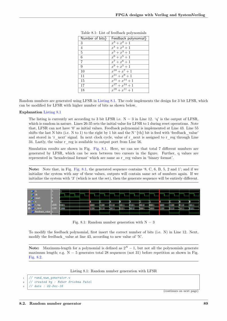
FPGA designs with Verilog and SystemVerilog
Table 8.1: List of feedback polynomialsNumber of bits} Feedback polynomial}3 𝑥3 + 𝑥2 + 14 𝑥4 + 𝑥3 + 15 𝑥5 + 𝑥3 + 16 𝑥6 + 𝑥5 + 17 𝑥7 + 𝑥6 + 19 𝑥9 + 𝑥5 + 110 𝑥10 + 𝑥7 + 111 𝑥11 + 𝑥9 + 115 𝑥15 + 𝑥14 + 117 𝑥17 + 𝑥14 + 118 𝑥18 + 𝑥11 + 1
Random numbers are generated using LFSR in Listing 8.1. The code implements the design for 3 bit LFSR, whichcan be modified for LFSR with higher number of bits as shown below,
Explanation Listing 8.1
The listing is currently set according to 3 bit LFSR i.e. N = 3 in Line 12. ‘q’ is the output of LFSR,which is random in nature. Lines 26-35 sets the initial value for LFSR to 1 during reset operations. Notethat, LFSR can not have ‘0’ as initial values. Feedback polynomial is implemented at Line 43. Line 55shifts the last N bits (i.e. N to 1) to the right by 1 bit and the N^{th} bit is feed with ‘feedback_value’and stored in ‘r_next’ signal. In next clock cycle, value of r_next is assigned to r_reg through Line34. Lastly, the value r_reg is available to output port from Line 56.
Simulation results are shown in Fig. Fig. 8.1. Here, we can see that total 7 different numbers aregenerated by LFSR, which can be seen between two cursors in the figure. Further, q values arerepresented in ‘hexadecimal format’ which are same as r_reg values in ‘binary format’.
Note: Note that, in Fig. Fig. 8.1, the generated sequence contains ‘8, C, 6, B, 5, 2 and 1’; and if weinitialize the system with any of these values, outputs will contain same set of numbers again. If weinitialize the system with ‘3’ (which is not the set), then the generate sequence will be entirely different.
Fig. 8.1: Random number generation with N = 3
To modify the feedback polynomial, first insert the correct number of bits (i.e. N) in Line 12. Next,modify the feedback_value at line 43, according to new value of ‘N’.
Note: Maximum-length for a polynomial is defined as 2𝑁 − 1, but not all the polynomials generatemaximum length; e.g. N = 5 generates total 28 sequences (not 31) before repetition as shown in Fig.Fig. 8.2.
Listing 8.1: Random number generation with LFSR
1 // rand_num_generator.v2 // created by : Meher Krishna Patel3 // date : 22-Dec-16
(continues on next page)
8.2. Random number generator 89

FPGA designs with Verilog and SystemVerilog
Fig. 8.2: Total sequences are 28 (not 31) for N = 5}
(continued from previous page)
4 // Feedback polynomial : x^3 + x^2 + 15 // maximum length : 2^3 - 1 = 76 // if parameter value is changed,7 // then choose the correct Feedback polynomial i.e. change 'feedback_value' pattern8
9
10 module rand_num_generator11 #(12 parameter N = 313 )14
15 (16 input wire clk, reset,17 output wire [N:0] q18 );19
20 reg [N:0] r_reg;21 wire [N:0] r_next;22 wire feedback_value;23
24 always @(posedge clk, posedge reset)25 begin26 if (reset)27 begin28 // set initial value to 129 r_reg <= 1; // use this or uncomment below two line30
31 // r_reg[0] <= 1'b1; // 0th bit = 132 // r_reg[N:1] <= 0; // other bits are zero33
34
35 end36 else if (clk == 1'b1)37 r_reg <= r_next;38 end39
40 //// N = 341 //// Feedback polynomial : x^3 + x^2 + 142 ////total sequences (maximum) : 2^3 - 1 = 743 assign feedback_value = r_reg[3] ^ r_reg[2] ^ r_reg[0];44
45 //// N = 446 //assign feedback_value = r_reg[4] ^ r_reg[3] ^ r_reg[0];47
48 // N = 5, maximum length = 28 (not 31)49 //assign feedback_value = r_reg[5] ^ r_reg[3] ^ r_reg[0];50
51 //// N = 952 //assign feedback_value = r_reg[9] ^ r_reg[5] ^ r_reg[0];53
54
(continues on next page)
8.2. Random number generator 90

FPGA designs with Verilog and SystemVerilog
(continued from previous page)
55 assign r_next = {feedback_value, r_reg[N:1]};56 assign q = r_reg;57 endmodule
8.2.2 Visual test
Listing 8.2 can be used to test the Listing 8.1 on the FPGA board. Here, 1 second clock pulse is used to visualizethe output patterns. Please read Chapter Section 6 for better understanding of the listing. Note that, N = 3 isset in Line 13 according to Listing 8.1.
For displaying outputs on FPGA board, set reset to 1 and then to 0. Then LEDs will blink to display the generatedbit patterns by LFSR; which are shown in Fig. Fig. 8.1.
Listing 8.2: Visual test : Random number generation with LFSR
1 // rand_num_generator_visualTest.v2 // created by : Meher Krishna Patel3 // date : 22-Dec-164 // if parameter value is changed e.g. N = 55 // then go to rand_num_generator for further modification6
7 module rand_num_generator_visualTest8 #(9 parameter N = 3
10 )11 (12 input wire CLOCK_50, reset,13 output wire [N:0] LEDR14 );15
16 wire clk_Pulse1s;17
18 // clock 1 s19 clockTick #(.M(50000000), .N(26))20 clock_1s (.clk(CLOCK_50), .reset(reset), .clkPulse(clk_Pulse1s));21
22
23 // rand_num_generator testing with 1 sec clock pulse24 rand_num_generator rand_num_generator_1s25 ( .clk(clk_Pulse1s),26 .reset(reset),27 .q(LEDR)28 );29
30 endmodule
8.3 Shift register
Shift register are the registers which are used to shift the stored bit in one or both directions. In this section, shiftregister is implemented which can be used for shifting data in both direction. Further it can be used as parallel toserial converter or serial to parallel converter. Verilog files required for this example are listed below,
• shift_register.v• shift_register_visualTest.v• clockTick.v• modMCounter.v• parallel_to_serial.v
8.3. Shift register 91
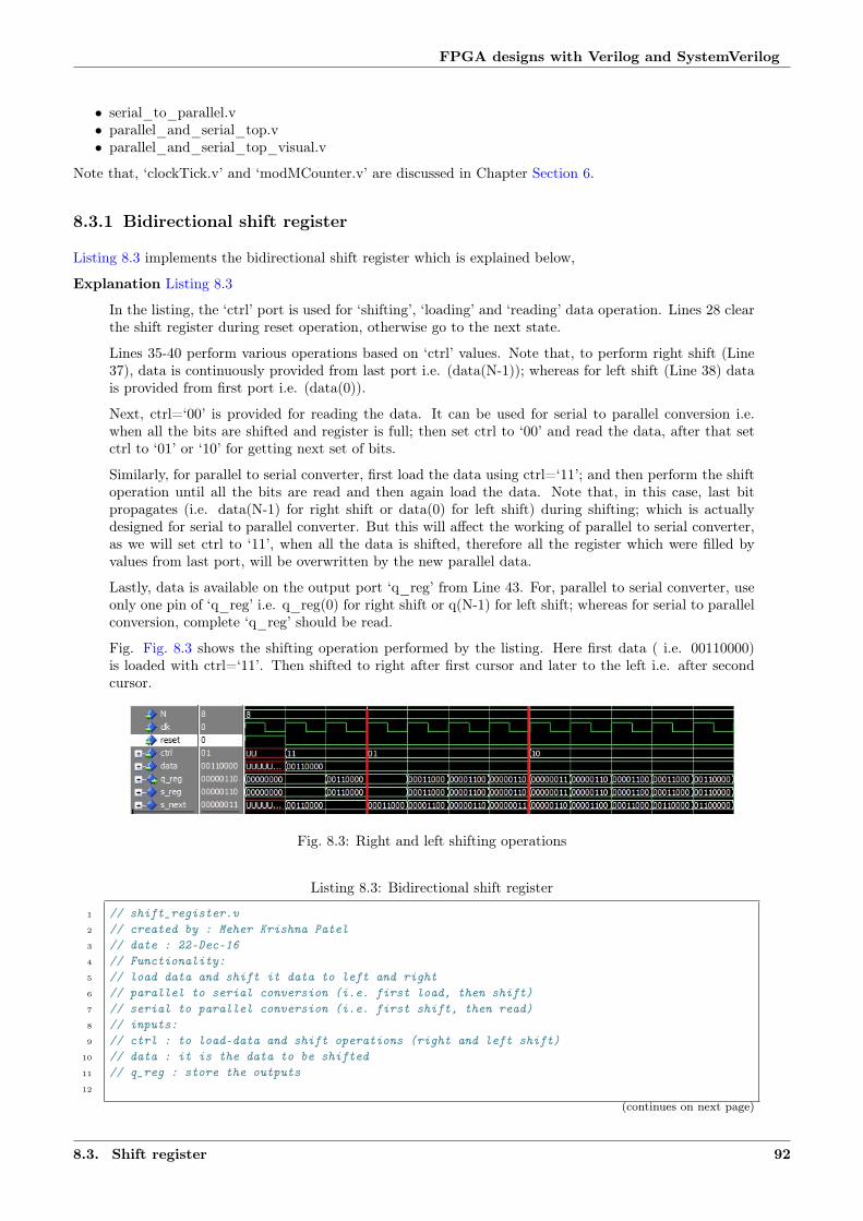
FPGA designs with Verilog and SystemVerilog
• serial_to_parallel.v• parallel_and_serial_top.v• parallel_and_serial_top_visual.v
Note that, ‘clockTick.v’ and ‘modMCounter.v’ are discussed in Chapter Section 6.
8.3.1 Bidirectional shift register
Listing 8.3 implements the bidirectional shift register which is explained below,
Explanation Listing 8.3
In the listing, the ‘ctrl’ port is used for ‘shifting’, ‘loading’ and ‘reading’ data operation. Lines 28 clearthe shift register during reset operation, otherwise go to the next state.
Lines 35-40 perform various operations based on ‘ctrl’ values. Note that, to perform right shift (Line37), data is continuously provided from last port i.e. (data(N-1)); whereas for left shift (Line 38) datais provided from first port i.e. (data(0)).
Next, ctrl=‘00’ is provided for reading the data. It can be used for serial to parallel conversion i.e.when all the bits are shifted and register is full; then set ctrl to ‘00’ and read the data, after that setctrl to ‘01’ or ‘10’ for getting next set of bits.
Similarly, for parallel to serial converter, first load the data using ctrl=‘11’; and then perform the shiftoperation until all the bits are read and then again load the data. Note that, in this case, last bitpropagates (i.e. data(N-1) for right shift or data(0) for left shift) during shifting; which is actuallydesigned for serial to parallel converter. But this will affect the working of parallel to serial converter,as we will set ctrl to ‘11’, when all the data is shifted, therefore all the register which were filled byvalues from last port, will be overwritten by the new parallel data.
Lastly, data is available on the output port ‘q_reg’ from Line 43. For, parallel to serial converter, useonly one pin of ‘q_reg’ i.e. q_reg(0) for right shift or q(N-1) for left shift; whereas for serial to parallelconversion, complete ‘q_reg’ should be read.
Fig. Fig. 8.3 shows the shifting operation performed by the listing. Here first data ( i.e. 00110000)is loaded with ctrl=‘11’. Then shifted to right after first cursor and later to the left i.e. after secondcursor.
Fig. 8.3: Right and left shifting operations
Listing 8.3: Bidirectional shift register
1 // shift_register.v2 // created by : Meher Krishna Patel3 // date : 22-Dec-164 // Functionality:5 // load data and shift it data to left and right6 // parallel to serial conversion (i.e. first load, then shift)7 // serial to parallel conversion (i.e. first shift, then read)8 // inputs:9 // ctrl : to load-data and shift operations (right and left shift)
10 // data : it is the data to be shifted11 // q_reg : store the outputs12
(continues on next page)
8.3. Shift register 92

FPGA designs with Verilog and SystemVerilog
(continued from previous page)
13 module shift_register14 #(15 parameter N = 816 )17 (18 input wire clk, reset,19 input wire [1:0] ctrl,20 input wire [N-1:0] data,21 output wire [N-1:0] q_reg22 );23
24 reg [N-1:0] s_reg, s_next;25 always @(posedge clk, posedge reset)26 begin27 if(reset)28 s_reg <= 0; // clear the content29 else if (clk == 1'b1)30 s_reg <= s_next; // otherwise save the next state31 end32
33 always @(ctrl, s_reg)34 begin35 case (ctrl)36 0 : s_next = s_reg; // no operation (to read data for serial to parallel)37 1 : s_next = {data[N-1], s_reg[N-1:1]}; // right shift38 2 : s_next = {s_reg[N-2:0], data[0]}; // left shift39 3 : s_next = data; // load data (for parallel to serial)40 endcase41 end42
43 assign q_reg = s_reg;44 endmodule
Visual test
Listing 8.4 can be used to test the Listing 8.3 on the FPGA board. Here, 1 second clock pulse is used to visualizethe output patterns. Here, outputs (i.e. q_reg) are displayed on LEDR; whereas ‘shifting-control (i.e. ctrl)’ anddata-load (i.e. data) operations are performed using SW[16:15] and SW[7:0] respectively. Here, we can see theshifting of LEDR pattern twoards right or left based on SW[16:15] combination. Please read Chapter Section 6for better understanding of the listing.
Listing 8.4: Visual test : bidirectional shift register
1 // shift_register_visualTest.v2 // created by : Meher Krishna Patel3 // date : 22-Dec-164 // SW[16:15] : used for control5
6 module shift_register_visualTest7 #(8 parameter N =89 )
10 (11 input wire CLOCK_50, reset,12 input wire [16:0] SW,13 output wire [N-1:0] LEDR14 );15
16 wire clk_Pulse1s;17
18 // clock 1 s(continues on next page)
8.3. Shift register 93

FPGA designs with Verilog and SystemVerilog
(continued from previous page)
19 clockTick #(.M(50000000), .N(26))20 clock_1s (.clk(CLOCK_50), .reset(reset), .clkPulse(clk_Pulse1s));21
22 // shift_register testing with 1 sec clock pulse23 shift_register #(.N(N))24 shift_register_1s (25 .clk(clk_Pulse1s), .reset(reset),26 .data(SW[N-1:0]), .ctrl(SW[16:15]),27 .q_reg(LEDR)28 );29
30 endmodule
8.3.2 Parallel to serial converter
If data is loaded first (i.e. ctrl = ‘11’), and later shift operation is performed (i.e.. ctrl = ‘01’ or ‘10’); then Listing8.3 will work as ‘parallel to serial converter’. Listing 8.5 performs the conversion operation, which is tested inSection Section 8.3.4. Please read comments for further details.
Listing 8.5: Parallel to serial conversion
1 // parallel_to_serial.v2 // Meher Krishna Patel3 // Date : 26-July-174
5 // converts parallel data into serial6
7 module parallel_to_serial8 #(9 parameter N = 8
10 )11 (12 input wire clk, reset,13 input wire [ N-1:0] data_in, // parallel data14 output reg empty_tick, // for external control15 output reg data_out // serial data16 );17
18 reg [N-1:0] data_reg, data_next;19 reg [N-1:0] count_reg, count_next;20 reg empty_reg, empty_next;21
22 // conversion completed and ready for next data in register23 always @(posedge clk)24 empty_tick = empty_reg;25
26 // save initial and next value in register27 always @(posedge clk, posedge reset) begin28 if(reset) begin29 count_reg <= 0;30 empty_reg <= 1;31 data_reg <= 0;32 end33 else begin34 count_reg <= count_next;35 empty_reg <= empty_next;36 data_reg <= data_next;37 end38 end
(continues on next page)
8.3. Shift register 94

FPGA designs with Verilog and SystemVerilog
(continued from previous page)
39
40 always @* begin41 count_next = count_reg;42 empty_next = empty_reg;43 data_next = data_reg;44 // parallel_to_serial data45 data_out = data_reg[count_reg];46
47 // coversion completed , load the next data48 if (count_reg == N-1) begin49 count_next = 0; // restart count50 empty_next = 1;51 data_next = data_in; // load next data52
53 end54 else begin // else continue counting55 count_next = count_reg + 1;56 empty_next = 0;57 end58 end59
60 endmodule
8.3.3 Serial to parallel converter
If shifting is performed first (i.e.. ctrl = ‘01’ or ‘10’), and later data is read (i.e. ctrl = ‘00’); then Listing 8.6will work as ‘serial to parallel converter’. Listing 8.5 performs the conversion operation, which is tested in SectionSection 8.3.4. Please read comments for further details.
Listing 8.6: Serial to parallel conversion
1 // serial_to_parallel.v2
3 // converts serial data to parallel4
5 module serial_to_parallel6 #(7 parameter N = 88 )9 (
10 input wire clk, reset,11 input wire data_in, // serial data12 output wire full_tick, // for external control13 output reg [N-1:0] data_out // parallel data14 );15
16 reg [N-1:0] data_reg, data_next;17 reg [N-1:0] count_reg, count_next;18 reg full_reg, full_next;19
20 // register is full i.e. parallel data is ready to read21 assign full_tick = full_reg;22
23 // save initial and next value in register24 always @(posedge clk, posedge reset) begin25 if(reset) begin26 count_reg <= 0;27 full_reg <= 0;28 data_reg <= 0;
(continues on next page)
8.3. Shift register 95

FPGA designs with Verilog and SystemVerilog
(continued from previous page)
29 end30 else begin31 count_reg <= count_next;32 full_reg <= full_next;33 data_reg <= data_next;34 end35 end36
37 always @* begin38 count_next = count_reg;39 full_next = full_reg;40 data_next = data_reg;41 data_next[count_reg] = data_in;42
43 // coversion completed , send data to output44 if (count_reg == N-1) begin45 count_next = 0;46 full_next = 1;47 // conversion completed, send data to output48 data_out = data_reg;49 end50 else begin // else continue count51 count_next = count_reg + 1;52 full_next = 0;53 end54 end55 endmodule
8.3.4 Test for Parallel/Serial converters
Here, 4-bit count (i.e. parallel data) is generated using Mod-12 counter. This data is converted into serial data byListing 8.5; and sent to Listing 8.6, where data is again converted into parallel and the result (i.e. count) is displayedat output as shown in Listing 8.7. The simulation results are shown in Fig. Fig. 8.5. Lastly, visual verificationcircuit is shown in Listing 8.8. Note that, empty_tick signal is used as clock for modMCounter (see redline in Fig. :numref:‘fig_parallel_and_serial_design‘), so that next count will be available whenprevious conversion is completed. Please read comments for further details.
Fig. 8.4: RTL view of Listing 8.7
Listing 8.7: Test for Parallel/Serial converters (results are in Fig.Fig. 8.5)
1 // parallel_and_serial_top.v2
3 // test parallel_to_serial.v and serial_to_parallel.v4 // parallel data (i.e. count from modMCounter) is converted into5 // serial data using parallel_to_serial.v then tranmitted.6 // Next, transmitted data is received at serial_to_parallel.v and
(continues on next page)
8.3. Shift register 96

FPGA designs with Verilog and SystemVerilog
(continued from previous page)
7 // converted back to parallel. If everything is working properly then8 // count should be displayed on 'out_count'.9
10 module parallel_and_serial_top(11 reset,12 clk,13 out_count14 );15
16 input wire reset;17 input wire clk;18 output wire [3:0] out_count;19
20 wire eclk;21 wire [3:0] parallel_count;22 wire serial_count;23
24 // count from modMCounter25 modMCounter unit_counter(26 .clk(eclk),27 .reset(reset),28
29 .count(parallel_count));30 defparam unit_counter.M = 12;31 defparam unit_counter.N = 4;32
33
34 // count converted into serial data35 parallel_to_serial unit_p_s(36 .clk(clk),37 .reset(reset),38 .data_in(parallel_count),39 .empty_tick(eclk),40 .data_out(serial_count));41 defparam unit_p_s.N = 4;42
43
44 // serial data converted back to parallel data45 serial_to_parallel unit_s_p(46 .clk(clk),47 .reset(reset),48 .data_in(serial_count),49
50 .data_out(out_count));51 defparam unit_s_p.N = 4;52
53
54 endmodule
Fig. 8.5: Simulation results of Listing 8.7
8.3. Shift register 97

FPGA designs with Verilog and SystemVerilog
Listing 8.8: Visual test for Parallel/Serial converters
1 // parallel_and_serial_top_visual.v2
3 // visual test for parallel_and_serial_top.v4
5 module parallel_and_serial_top_visual(6 reset,7 CLOCK_50,8 LEDG9 );
10
11 input wire reset;12 input wire CLOCK_50;13 output wire[3:0] LEDG;14
15 wire clk1ms;16
17 // parallel_and_serial_top18 parallel_and_serial_top unit_p_s_top(19 .reset(reset),20 .clk(clk1ms),21 .out_count(LEDG));22
23 // 1 ms clock24 clockTick unit_clk1ms(25 .clk(CLOCK_50),26 .reset(reset),27 .clkPulse(clk1ms));28 defparam unit_clk1ms.M = 5000000;29 defparam unit_clk1ms.N = 23;30
31 endmodule
8.4 Random access memory (RAM)
RAM is memory cells which are used to store or retrieve the data. Further, FPGA chips have separate RAMmodules which can be used to design memories of different sizes and types, as shown in this section. Verilog filesrequired for this example are listed below,
• single_port_RAM.v• single_port_RAM_visualTest.v• dual_port_RAM.v• dual_port_RAM_visualTest.v
8.4.1 Single port RAM
Single port RAM has one input port (i.e. address line) which is used for both storing and retrieving the data, asshown in Fig. Fig. 8.6. Here ‘addr[1:0]’ port is used for both ‘read’ and ‘write’ operations. Listing 8.9 is used togenerate this design.
Explanation Listing 8.9
In the listing port ‘addr’ (Line 23) is 2 bit wide as ‘addr_width’ is set to 2 (Line 17). Therefore,total ‘4 elements (i.e. 2^2)’ can be stored in the RAM. Further, ‘din’ port (Line 24) is 3 bit wide as‘data_width’ is set to 3 (Line 18); which means the data should be 3 bit wide. In summary, currentRAM-designs can store ‘4 elements’ in it and each elements should be 3-bit wide (seedeclaration at Line 28 as well).
8.4. Random access memory (RAM) 98

FPGA designs with Verilog and SystemVerilog
Fig. 8.6: RTL view : Single port RAM (Listing 8.9)
Write enable (we) port should be high and low for storing and retrieving the data respectively. ‘din’port is used to write the data in the memory; whereas ‘dout’ port is used for reading the data fromthe memory. In Lines 32-33, the write operation is performed on rising edge of the clock; whereas readoperation is performed at Line 37.
Lastly, Fig. Fig. 8.7 shows the simulation results for the design. Here, ‘we’ is set to 1 after first cursorand the data is written at three different addresses (not 4). Next, ‘we’ is set to 0 after second cursorand read operations are performed for all addresses. Since, no values is stored for address ‘10’, thereforedout is displayed as ‘UUU’ for this address as shown after third cursor.
Fig. 8.7: Simulation results : Single port RAM (Listing 8.9)
Listing 8.9: Single port RAM
1 // single_port_RAM.v2 // created by : Meher Krishna Patel3 // date : 26-Dec-164 // Functionality:5 // store and retrieve data from single port RAM6 // ports:7 // we : write enable8 // addr : input port for getting address9 // din : input data to be stored in RAM
10 // data : output data read from RAM11 // addr_width : total number of elements to store (put exact number)12 // addr_bits : bits requires to store elements specified by addr_width13 // data_width : number of bits in each elements14
15 module single_port_RAM16 #(17 parameter addr_width = 2,18 data_width = 319 )20 (21 input wire clk,22 input wire we,23 input wire [addr_width-1:0] addr,24 input wire [data_width-1:0] din,25 output wire [data_width-1:0] dout
(continues on next page)
8.4. Random access memory (RAM) 99

FPGA designs with Verilog and SystemVerilog
(continued from previous page)
26 );27
28 reg [data_width-1:0] ram_single_port[2**addr_width-1:0];29
30 always @(posedge clk)31 begin32 if (we == 1) // write data to address 'addr'33 ram_single_port[addr] <= din;34 end35
36 // read data from address 'addr'37 assign dout = ram_single_port[addr];38
39 endmodule
8.4.2 Visual test : single port RAM
Listing 8.10 can be use to test the Listing 8.9 on FPGA board. Different combination of switches can be used tostore and retrieve the data from RAM. These data will be displayed on LEDs during read operations.
Listing 8.10: Visual test : single port RAM
1 // single_port_RAM_visualTest.v2 // created by : Meher Krishna Patel3 // date : 26-Dec-164
5 // Functionality:6 // store and retrieve data from single port RAM7 // ports:8 // Write Enable (we) : SW[16]9 // Address (addr) : SW[15-14]
10 // din : SW[2:0]11 // dout : LEDR12
13 module single_port_RAM_visualTest14 #(15 parameter ADDR_WIDTH = 2,16 parameter DATA_WIDTH = 317 )18 (19 input wire CLOCK_50,20 input wire [16:0] SW,21 output wire [DATA_WIDTH-1:0] LEDR22 );23
24 single_port_RAM single_port_RAM_test(25 .clk(CLOCK_50),26 .we(SW[16]),27 .addr(SW[15:14]),28 .din(SW[2:0]),29 .dout(LEDR)30 );31
32 endmodule
8.4. Random access memory (RAM) 100

FPGA designs with Verilog and SystemVerilog
8.4.3 Dual port RAM
In single port RAM, the same ‘addr’ port is used for read and write operations; whereas in dual port RAMdedicated address lines are provided for read and write operations i.e. ‘addr_rd’ and ‘addr_wr’ respectively, asshown in Fig. Fig. 8.8. Also, the listing can be further modified to allow read and write operation through boththe ports.
Fig. 8.8: Dual port RAM
Listing 8.11 is used to implement Fig. Fig. 8.8, which is same as Listing 8.9 with three changes. First, two addressports are used at Line 25 (i.e. ‘addr_rd’ and ‘addr_wr’) instead of one. Next, ‘addr_wr’ is used to write the dataat Line 35; whereas ‘addr_rd’ data is used to retrieve the data at Line 39. Hence, read and write operation canbe performed simultaneously using these two address lines.
Fig. Fig. 8.9 shows the simulation results for dual port RAM. Here, on the first cursor, ‘011’ is written at address‘01’. On next cursor, this value is read along with writing operation as location ‘10’. Lastly, last two cursorshows that if read and write operation is performed simultaneously on one address e.g. ‘01’, then new data willbe available at ‘dout’ port after one clock cycle.
Fig. 8.9: Simulation results : Dual port RAM (Listing 8.11)
Listing 8.11: Dual port RAM
1 // dual_port_RAM.v2 // created by : Meher Krishna Patel3 // date : 26-Dec-164
5 // Functionality:6 // store and retrieve data from dual port RAM7 // ports:8 // we : write enable9 // addr_wr : address for writing data
10 // addr_rd : address for reading11 // din : input data to be stored in RAM12 // data : output data read from RAM13 // addr_width : total number of elements to store (put exact number)14 // addr_bits : bits requires to store elements specified by addr_width15 // data_width : number of bits in each elements16
17 module dual_port_RAM18 #(19 parameter addr_width = 2,
(continues on next page)
8.4. Random access memory (RAM) 101

FPGA designs with Verilog and SystemVerilog
(continued from previous page)
20 data_width = 321 )22 (23 input wire clk,24 input wire we,25 input wire [addr_width-1:0] addr_wr, addr_rd,26 input wire [data_width-1:0] din,27 output wire [data_width-1:0] dout28 );29
30 reg [data_width-1:0] ram_dual_port[2**addr_width-1:0];31
32 always @(posedge clk)33 begin34 if (we == 1) // write data to address 'addr_wr'35 ram_dual_port[addr_wr] <= din;36 end37
38 // read data from address 'addr_rd'39 assign dout = ram_dual_port[addr_rd];40
41 endmodule
8.4.4 Visual test : dual port RAM
Listing 8.12 can be use to test the Listing 8.11 on FPGA board. Different combination of switches can be used tostore and retrieve the data from RAM. These data will be displayed on LEDs during read operations.
Listing 8.12: Visual test : dual port RAM
1 // dual_port_RAM_visualTest.v2 // created by : Meher Krishna Patel3 // date : 26-Dec-164
5 // Functionality:6 // store and retrieve data from single port RAM7 // ports:8 // Write Enable (we) : SW[16]9 // Address (addr_wr) : SW[15-14]
10 // Address (addr_rd) : SW[13-12]11 // din : SW[2:0]12 // dout : LEDR13
14 module dual_port_RAM_visualTest15 #(16 parameter ADDR_WIDTH = 2,17 parameter DATA_WIDTH = 318 )19 (20 input wire CLOCK_50,21 input wire [16:0] SW,22 output wire [DATA_WIDTH-1:0] LEDR23 );24
25 dual_port_RAM dual_port_RAM_test(26 .clk(CLOCK_50),27 .we(SW[16]),28 .addr_wr(SW[15:14]),29 .addr_rd(SW[13:12]),
(continues on next page)
8.4. Random access memory (RAM) 102

FPGA designs with Verilog and SystemVerilog
(continued from previous page)
30 .din(SW[2:0]),31 .dout(LEDR)32 );33
34 endmodule
8.5 Read only memory (ROM)
ROMs are the devices which are used to store information permanently. In this section, ROM is implemented onFPGA to store the display-pattern for seven-segment device, which is explained in Section Section 6.5. Verilogfiles required for this example are listed below,
• ROM_sevenSegment.v• ROM_sevenSegment_visualTest.v
8.5.1 ROM implementation using RAM (block ROM)
Listing 8.13 implements the ROM (Lines 27-47), which stores the seven-segment display pattern in it (Lines 30-45).Since the address width is 16 (Line 16), therefore total 16 values can be stored with different addresses (Lines30-45). Further, 16 addresses can be represented by 4-bits, therefore ‘addr_bit’ is set to 4 at Line 17. Lastly, total7 bits are required to represent the number in 7-segment-display, therefore ‘data_width’ is set to 7 at Line 18.
Listing 8.13: Seven segment display pattern stored in ROM
1 //ROM_sevenSegment.v2 // created by : Meher Krishna Patel3 // date : 25-Dec-164
5 // Functionality:6 // seven-segment display format for Hexadecimal values (i.e. 0-F) are stored in ROM7 // ports:8 // addr : input port for getting address9 // data : ouput data at location 'addr'
10 // addr_width : total number of elements to store (put exact number)11 // addr_bits : bits requires to store elements specified by addr_width12 // data_width : number of bits in each elements13
14 module ROM_sevenSegment15 #(16 parameter addr_width = 16, // store 16 elements17 addr_bits = 4, // required bits to store 16 elements18 data_width = 7 // each element has 7-bits19 )20 (21 input wire clk,22 input wire [addr_bits-1:0] addr,23 output reg [data_width-1:0] data // reg (not wire)24 );25
26
27 always @*28 begin29 case(addr)30 4'b0000 : data = 7'b1000000; // 031 4'b0001 : data = 7'b1111001; // 132 4'b0010 : data = 7'b0100100; // 233 4'b0011 : data = 7'b0110000; // 3
(continues on next page)
8.5. Read only memory (ROM) 103
FPGA designs with Verilog and SystemVerilog
(continued from previous page)
34 4'b0100 : data = 7'b0011001; // 435 4'b0101 : data = 7'b0010010; // 536 4'b0110 : data = 7'b0000010; // 637 4'b0111 : data = 7'b1111000; // 738 4'b1000 : data = 7'b0000000; // 839 4'b1001 : data = 7'b0010000; // 940 4'b1010 : data = 7'b0001000; // a41 4'b1011 : data = 7'b0000011; // b42 4'b1100 : data = 7'b1000110; // c43 4'b1101 : data = 7'b0100001; // d44 4'b1110 : data = 7'b0000110; // e45 default : data = 7'b0001110; // f46 endcase47 end48
49 endmodule
8.5.2 Visual test
Listing 8.14 is provided the input ‘addr’ through switches ‘SW’ (Line 20) and then output from Listing 8.13 isreceived to signal ‘data’ (Lines 22-23); which is finally displayed on seven segment display devices (Line 27) andLEDs (Line 28). Here, we can see the switch value on the seven-segment display devices along with the ROMcontent on LEDs; e.g. if SW value is ‘011’ then ‘3’ will be displayed on seven-segment display and ‘0000110’ willbe displayed on LEDs.
Listing 8.14: Display ROM data on seven segment display andLEDs
1 // ROM_sevenSegment_visualTest.v2 // created by : Meher Krishna Patel3 // date : 25-Dec-164
5 // Functionality:6 // retrieve data from ROM and display on seven-segment device and LEDs7 // ports:8 // SW : address in binary format9 // HEX0 : display data on seven segment device
10 // LEDR : display data on LEDs11
12 module ROM_sevenSegment_visualTest13 (14 input wire [3:0] SW,15 output wire [6:0] HEX0,16 output wire [6:0] LEDR17 );18
19 // signal to store received data, so that it can be displayed on20 // two devices i.e. seven segment display and LEDs21 wire [6:0] data;22
23 ROM_sevenSegment seven_segment_ROM(24 .addr(SW), .data(data)25 );26
27 assign HEX0 = data; // display on seven segment devices28 assign LEDR = data; // display on LEDs29
30 endmodule
8.5. Read only memory (ROM) 104
FPGA designs with Verilog and SystemVerilog
8.6 Queue with first-in first-out functionality
In this section, Queue is designed with first-in first-out functionality. Verilog files required for this example arelisted below,
• queue.v• queue_top.v• clockTick.v• modMCounter.v
Note that, ‘clockTick.v’ and ‘modMCounter.v’ are discussed in Chapter Section 6.
8.6.1 Queue design
Listing 8.15 is the Queue design, which is an example of circular queue. Here, two pointers i.e. Front and rear areused to track the status of the queue i.e. Full or Empty. If read-operation is performed and Front & Rear pointersare at same location, then queue is empty; whereas if write-operation is performed and Front & Rear pointers areat same location, then queue is full. Please read the comments for further details.
Listing 8.15: Queue design
1 // queue.v2
3 // queue with first-in first-out operation.4
5 module queue6 #(parameter data_width = 4, // number of bits in each data7 address_width = 4, // total addresses = 2^48 max_data = 2**address_width // max_data = total_addresses9 )
10 (11 input wire clk, reset,12 input wire read_cmd, write_cmd, // read and write command13 input wire [data_width-1:0] write_data, // write data to FIFO14 output reg [data_width-1:0] read_data, // read data from FIFO15 output wire full, // no space to write in FIFO16 output wire empty // nothing to read from FIFO17 );18
19 reg [data_width-1:0] queue_reg [max_data-1:0];20 reg [address_width-1:0] front_reg, front_next; // pointer-front is for reading21 reg [address_width-1:0] rear_reg, rear_next; // pointer-rear is for writing22 reg full_reg, full_next;23 reg empty_reg, empty_next;24
25
26 assign full = full_reg;27 assign empty = empty_reg;28
29 wire write_enable; // enable if queue is not full30
31 assign write_enable = write_cmd & ~full_reg;32
33 always @(posedge clk) begin34 // if queue_reg is full, then data will not be written35 if (write_enable)36 queue_reg[rear_reg] <= write_data;37 if (read_cmd)38 read_data <= queue_reg[front_reg];39 end
(continues on next page)
8.6. Queue with first-in first-out functionality 105
FPGA designs with Verilog and SystemVerilog
(continued from previous page)
40
41 // status of the queue and location of pointers i.e. front and rear42 always @(posedge clk, posedge reset) begin43 if (reset) begin44 empty_reg <= 1'b1; // empty : nothing to read45 full_reg <= 1'b0; // not full : data can be written46 front_reg <= 0;47 rear_reg <= 0;48 end49 else begin50 front_reg <= front_next;51 rear_reg <= rear_next;52 full_reg <= full_next;53 empty_reg <= empty_next;54 end55 end56
57 // read and write operation58 always @* begin59 front_next = front_reg;60 rear_next = rear_reg;61 full_next = full_reg;62 empty_next = empty_reg;63
64 // no operation for {write_cmd, read_cmd} = 0065
66 // only read operation67 if({write_cmd, read_cmd} == 2'b01) begin // write = 0, read = 168 if(~empty_reg) begin // not empty69 full_next = 1'b0; // not full as data is read70 front_next = front_reg + 1;71 if (front_next == rear_reg) // empty72 empty_next = 1'b1;73 end74 end75 // only write operation76 else if ({write_cmd, read_cmd} == 2'b10) begin // write = 1, read = 077 if(~full_reg) begin // not full78 empty_next = 1'b0;79 rear_next = rear_reg + 1;80 if(rear_next == front_reg)81 full_next = 1'b1;82 end83 end84
85 // both read and write operation86 else if ({write_cmd, read_cmd} == 2'b11) begin // write = 1, read = 187 front_next = front_reg + 1;88 rear_next = rear_next + 1;89 end90 end91
92 endmodule
8.6.2 Visual test
Listing 8.16 is the test circuit for Listing 8.15. Please read the comments for further details.
8.6. Queue with first-in first-out functionality 106

FPGA designs with Verilog and SystemVerilog
Listing 8.16: Visual test of Queue design
1 // queue_top.v2
3 // write the 'count' from 'modMCounter' to the queue.4 // SW[0] : read operation5 // LEDR[0] : queue empty6 // SW[1] : write operation7 // LEDR [1] : queue full8
9 // Test :10 // 1. Keep reset high, SW[1] low and SW[0] high till LEDR[0] glow, i.e.11 // queue is empty now.12 // 2. Now, keep SW[1] high, SW[0] low, then bring reset to low.13 // Now count will start and will be stored in the queue.14 // 3. Bring the SW[1] to low again and see the count at15 // that time (as count will continue to inrease).16 // 4. Now, set SW[0] high, and it will start the count from 0, to the count which was17 // displayed in step 3; and after that LEDR[0] will glow again.18 // 5. Next, bring SW[0] to low and SW[1] to high, and let it run.19 // after 16 count (i.e. 2^address_width), the queue will be full and20 // LED[1] will glow.21
22 module queue_top(23 reset,24 CLOCK_50,25 SW,26 LEDG,27 LEDR28 );29
30
31 input wire reset;32 input wire CLOCK_50;33 input wire [1:0] SW;34 output wire [3:0] LEDG;35 output wire [17:0] LEDR;36
37 wire clk1s;38 wire [3:0] count;39
40 assign LEDR[17:14] = count[3:0];41
42 // clock 1 sec43 clockTick unit_clkTick(44 .clk(CLOCK_50),45 .reset(reset),46 .clkPulse(clk1s));47 defparam unit_clkTick.M = 50000000;48 defparam unit_clkTick.N = 26;49
50 // queue.v51 queue unit_queue(52 .clk(clk1s),53 .reset(reset),54 .read_cmd(SW[0]),55 .write_cmd(SW[1]),56 .write_data(count),57 .full(LEDR[1]),58 .empty(LEDR[0]),59
60 .read_data(LEDG));(continues on next page)
8.6. Queue with first-in first-out functionality 107
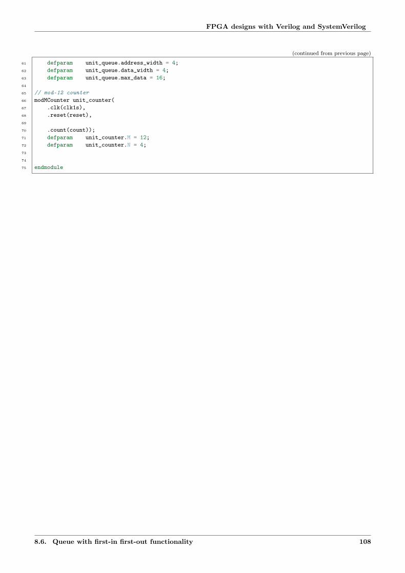
FPGA designs with Verilog and SystemVerilog
(continued from previous page)
61 defparam unit_queue.address_width = 4;62 defparam unit_queue.data_width = 4;63 defparam unit_queue.max_data = 16;64
65 // mod-12 counter66 modMCounter unit_counter(67 .clk(clk1s),68 .reset(reset),69
70 .count(count));71 defparam unit_counter.M = 12;72 defparam unit_counter.N = 4;73
74
75 endmodule
8.6. Queue with first-in first-out functionality 108

Nothing inside me belongs to me, all is Yours. In returning thatwhich belongs to You, what does it cost to me?
–Kabeer
Chapter 9
Testbenches
9.1 Introduction
In previous chapters, we generated the simulation waveforms using modelsim, by providing the input signal valuesmanually; if the number of input signals are very large and/or we have to perform simulation several times, thenthis process can be quite complex, time consuming and irritating. Suppose input is of 10 bit, and we want to testall the possible values of input i.e. 210 − 1, then it is impossible to do it manually. In such cases, testbenchesare very useful; also, the tested designs are more reliable and prefer by the clients as well. Further, with the helpof testbenches, we can generate results in the form of csv (comma separated file), which can be used by othersoftwares for further analysis e.g. Python, Excel and Matlab etc.
Since testbenches are used for simulation purpose only (not for synthesis), therefore full range ofVerilog constructs can be used e.g. keywords ‘for’, ‘display’ and ‘monitor’ etc. can be used forwriting testbenches.
Important: Modelsim-project is created in this chapter for simulations, which allows the relative path to the fileswith respect to project directory as shown in Section 9.3.1. Simulation can be run without creating the project,but we need to provide the full path of the files as shown in Line 25 of Listing 9.4.
Lastly, mixed modeling is not supported by Altera-Modelsim-starter version, i.e. Verilog designs with VHDL andvice-versa can not be compiled in this version of Modelsim. For mixed modeling, we can use Active-HDL softwareas discussed in Chapter Section 2.
9.2 Testbench for combinational circuits
In this section, various testbenches for combinational circuits are shown, whereas testbenches for sequential circuitsare discussed in next section. For simplicity of the codes and better understanding, a simple half adder circuit istested using various simulation methods.
9.2.1 Half adder
Listing 9.1 shows the Verilog code for the half adder which is tested using different methods,
Listing 9.1: Half adder
1 // half_adder.v2
3 module half_adder4 (
(continues on next page)
109
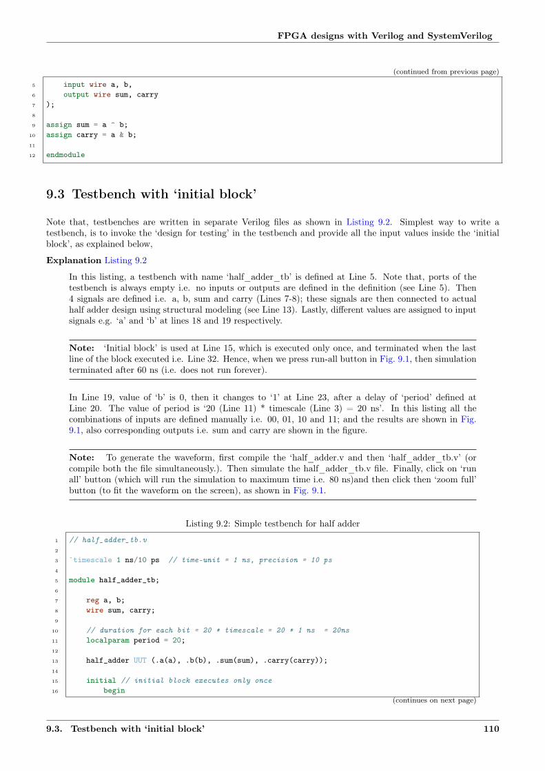
FPGA designs with Verilog and SystemVerilog
(continued from previous page)
5 input wire a, b,6 output wire sum, carry7 );8
9 assign sum = a ^ b;10 assign carry = a & b;11
12 endmodule
9.3 Testbench with ‘initial block’
Note that, testbenches are written in separate Verilog files as shown in Listing 9.2. Simplest way to write atestbench, is to invoke the ‘design for testing’ in the testbench and provide all the input values inside the ‘initialblock’, as explained below,
Explanation Listing 9.2
In this listing, a testbench with name ‘half_adder_tb’ is defined at Line 5. Note that, ports of thetestbench is always empty i.e. no inputs or outputs are defined in the definition (see Line 5). Then4 signals are defined i.e. a, b, sum and carry (Lines 7-8); these signals are then connected to actualhalf adder design using structural modeling (see Line 13). Lastly, different values are assigned to inputsignals e.g. ‘a’ and ‘b’ at lines 18 and 19 respectively.
Note: ‘Initial block’ is used at Line 15, which is executed only once, and terminated when the lastline of the block executed i.e. Line 32. Hence, when we press run-all button in Fig. 9.1, then simulationterminated after 60 ns (i.e. does not run forever).
In Line 19, value of ‘b’ is 0, then it changes to ‘1’ at Line 23, after a delay of ‘period’ defined atLine 20. The value of period is ‘20 (Line 11) * timescale (Line 3) = 20 ns’. In this listing all thecombinations of inputs are defined manually i.e. 00, 01, 10 and 11; and the results are shown in Fig.9.1, also corresponding outputs i.e. sum and carry are shown in the figure.
Note: To generate the waveform, first compile the ‘half_adder.v and then ‘half_adder_tb.v’ (orcompile both the file simultaneously.). Then simulate the half_adder_tb.v file. Finally, click on ‘runall’ button (which will run the simulation to maximum time i.e. 80 ns)and then click then ‘zoom full’button (to fit the waveform on the screen), as shown in Fig. 9.1.
Listing 9.2: Simple testbench for half adder
1 // half_adder_tb.v2
3 `timescale 1 ns/10 ps // time-unit = 1 ns, precision = 10 ps4
5 module half_adder_tb;6
7 reg a, b;8 wire sum, carry;9
10 // duration for each bit = 20 * timescale = 20 * 1 ns = 20ns11 localparam period = 20;12
13 half_adder UUT (.a(a), .b(b), .sum(sum), .carry(carry));14
15 initial // initial block executes only once16 begin
(continues on next page)
9.3. Testbench with ‘initial block’ 110
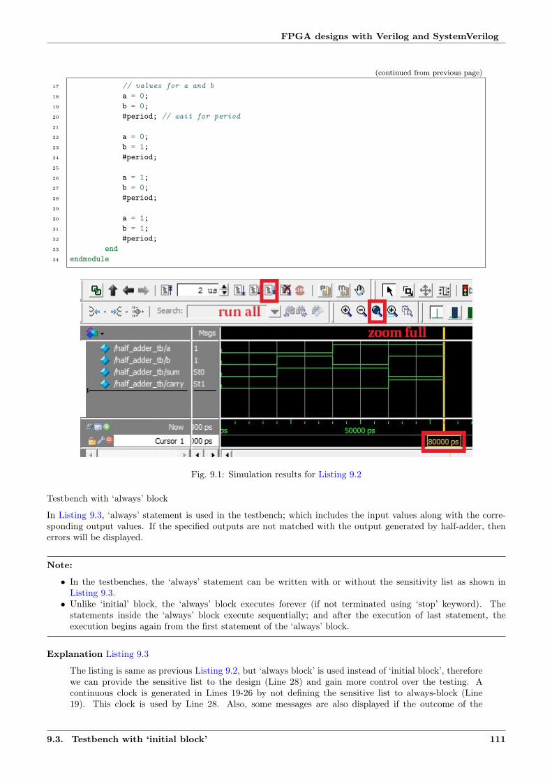
FPGA designs with Verilog and SystemVerilog
(continued from previous page)
17 // values for a and b18 a = 0;19 b = 0;20 #period; // wait for period21
22 a = 0;23 b = 1;24 #period;25
26 a = 1;27 b = 0;28 #period;29
30 a = 1;31 b = 1;32 #period;33 end34 endmodule
Fig. 9.1: Simulation results for Listing 9.2
Testbench with ‘always’ block
In Listing 9.3, ‘always’ statement is used in the testbench; which includes the input values along with the corre-sponding output values. If the specified outputs are not matched with the output generated by half-adder, thenerrors will be displayed.
Note:
• In the testbenches, the ‘always’ statement can be written with or without the sensitivity list as shown inListing 9.3.
• Unlike ‘initial’ block, the ‘always’ block executes forever (if not terminated using ‘stop’ keyword). Thestatements inside the ‘always’ block execute sequentially; and after the execution of last statement, theexecution begins again from the first statement of the ‘always’ block.
Explanation Listing 9.3
The listing is same as previous Listing 9.2, but ‘always block’ is used instead of ‘initial block’, thereforewe can provide the sensitive list to the design (Line 28) and gain more control over the testing. Acontinuous clock is generated in Lines 19-26 by not defining the sensitive list to always-block (Line19). This clock is used by Line 28. Also, some messages are also displayed if the outcome of the
9.3. Testbench with ‘initial block’ 111

FPGA designs with Verilog and SystemVerilog
design does not match with the desire outcomes (Lines 35-36). In this way, we can find errors justby reading the terminal (see Fig. 9.2), instead of visualizing the whole waveform, which can be verydifficult if the results are too long (see Fig. 9.3). Also, Lines 35-36 can be added in ‘initial-block’of :numref:‘verilog_half_adder_tb_v‘ as well.
Listing 9.3: Testbench with procedural statement
1 // half_adder_procedural_tb.v2
3 `timescale 1 ns/10 ps // time-unit = 1 ns, precision = 10 ps4
5 module half_adder_procedural_tb;6
7 reg a, b;8 wire sum, carry;9
10 // duration for each bit = 20 * timescale = 20 * 1 ns = 20ns11 localparam period = 20;12
13 half_adder UUT (.a(a), .b(b), .sum(sum), .carry(carry));14 reg clk;15
16 // note that sensitive list is omitted in always block17 // therefore always-block run forever18 // clock period = 2 ns19 always20 begin21 clk = 1'b1;22 #20; // high for 20 * timescale = 20 ns23
24 clk = 1'b0;25 #20; // low for 20 * timescale = 20 ns26 end27
28 always @(posedge clk)29 begin30 // values for a and b31 a = 0;32 b = 0;33 #period; // wait for period34 // display message if output not matched35 if(sum != 0 || carry != 0)36 $display("test failed for input combination 00");37
38 a = 0;39 b = 1;40 #period; // wait for period41 if(sum != 1 || carry != 0)42 $display("test failed for input combination 01");43
44 a = 1;45 b = 0;46 #period; // wait for period47 if(sum != 1 || carry != 0)48 $display("test failed for input combination 10");49
50 a = 1;51 b = 1;52 #period; // wait for period53 if(sum != 0 || carry != 1)54 $display("test failed for input combination 11");55
(continues on next page)
9.3. Testbench with ‘initial block’ 112
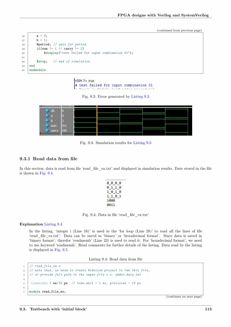
FPGA designs with Verilog and SystemVerilog
(continued from previous page)
56 a = 0;57 b = 1;58 #period; // wait for period59 if(sum != 1 || carry != 1)60 $display("test failed for input combination 01");61
62 $stop; // end of simulation63 end64 endmodule
Fig. 9.2: Error generated by Listing 9.3
Fig. 9.3: Simulation results for Listing 9.3
9.3.1 Read data from file
In this section, data is read from file ‘read_file_ex.txt’ and displayed in simulation results. Date stored in the fileis shown in Fig. 9.4.
Fig. 9.4: Data in file ‘read_file_ex.txt’
Explanation Listing 9.4
In the listing, ‘integer i (Line 16)’ is used in the ‘for loop (Line 28)’ to read all the lines of file‘read_file_ex.txt’. Data can be saved in ‘binary’ or ‘hexadecimal format’. Since data is saved in‘binary format’, therefor ‘readmemb’ (Line 23) is used to read it. For ‘hexadecimal format’, we needto use keyword ‘readmemh’. Read comments for further details of the listing. Data read by the listingis displayed in Fig. 9.5.
Listing 9.4: Read data from file
1 // read_file_ex.v2 // note that, we need to create Modelsim project to run this file,3 // or provide full path to the input-file i.e. adder_data.txt4
5 `timescale 1 ns/10 ps // time-unit = 1 ns, precision = 10 ps6
7 module read_file_ex;(continues on next page)
9.3. Testbench with ‘initial block’ 113
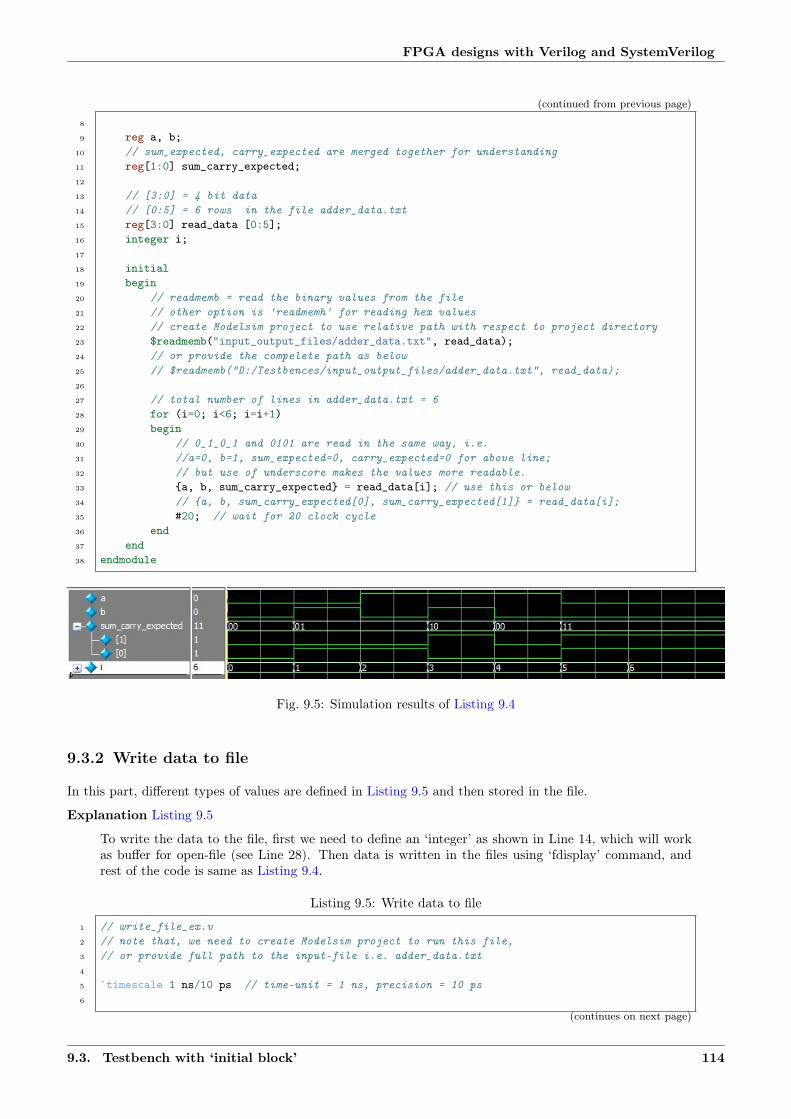
FPGA designs with Verilog and SystemVerilog
(continued from previous page)
8
9 reg a, b;10 // sum_expected, carry_expected are merged together for understanding11 reg[1:0] sum_carry_expected;12
13 // [3:0] = 4 bit data14 // [0:5] = 6 rows in the file adder_data.txt15 reg[3:0] read_data [0:5];16 integer i;17
18 initial19 begin20 // readmemb = read the binary values from the file21 // other option is 'readmemh' for reading hex values22 // create Modelsim project to use relative path with respect to project directory23 $readmemb("input_output_files/adder_data.txt", read_data);24 // or provide the compelete path as below25 // $readmemb("D:/Testbences/input_output_files/adder_data.txt", read_data);26
27 // total number of lines in adder_data.txt = 628 for (i=0; i<6; i=i+1)29 begin30 // 0_1_0_1 and 0101 are read in the same way, i.e.31 //a=0, b=1, sum_expected=0, carry_expected=0 for above line;32 // but use of underscore makes the values more readable.33 {a, b, sum_carry_expected} = read_data[i]; // use this or below34 // {a, b, sum_carry_expected[0], sum_carry_expected[1]} = read_data[i];35 #20; // wait for 20 clock cycle36 end37 end38 endmodule
Fig. 9.5: Simulation results of Listing 9.4
9.3.2 Write data to file
In this part, different types of values are defined in Listing 9.5 and then stored in the file.
Explanation Listing 9.5
To write the data to the file, first we need to define an ‘integer’ as shown in Line 14, which will workas buffer for open-file (see Line 28). Then data is written in the files using ‘fdisplay’ command, andrest of the code is same as Listing 9.4.
Listing 9.5: Write data to file
1 // write_file_ex.v2 // note that, we need to create Modelsim project to run this file,3 // or provide full path to the input-file i.e. adder_data.txt4
5 `timescale 1 ns/10 ps // time-unit = 1 ns, precision = 10 ps6
(continues on next page)
9.3. Testbench with ‘initial block’ 114

FPGA designs with Verilog and SystemVerilog
(continued from previous page)
7 module write_file_ex;8
9 reg a, b, sum_expected, carry_expected;10 // [3:0] = 4 bit data11 // [0:5] = 6 rows in the file adder_data.txt12 reg[3:0] read_data [0:5];13
14 integer write_data;15 integer i;16
17 initial18 begin19
20 // readmemb = read the binary values from the file21 // other option is 'readmemh' for reading hex values22 // create Modelsim project to use relative path with respect to project directory23 $readmemb("input_output_files/adder_data.txt", read_data);24 // or provide the compelete path as below25 // $readmemb("D:/Testbences/input_output_files/adder_data.txt", read_data);26
27 // write data : provide full path or create project as above28 write_data = $fopen("input_output_files/write_file_ex.txt");29
30 for (i=0; i<6; i=i+1)31 begin32 {a, b, sum_expected, carry_expected} = read_data[i];33 #20;34
35 // write data to file using 'fdisplay'36 $fdisplay(write_data, "%b_%b_%b_%b", a, b, sum_expected, carry_expected);37 end38
39 $fclose(write_data); // close the file40 end41
42
43 endmodule
Fig. 9.6: Data in file ‘write_file_ex.txt’
9.4 Testbench for sequential designs
In previous sections, we read the lines from one file and then saved those line in other file using ‘for loop’. Also,we saw use of ‘initial’ and ‘always’ blocks. In this section, we will combine all the techniques together to save theresults of Mod-M counter, which is an example of ‘sequential design’. The Mod-m counter is discussed in Listing6.4. Testbench for this listing is shown in Listing 9.6 and the waveforms are illustrated in Fig. 9.7.
Explanation Listing 9.6
In the testbench following operations are performed,
• Simulation data is saved on the terminal and saved in a file. Note that, ‘monitor/fmonitor’
9.4. Testbench for sequential designs 115

FPGA designs with Verilog and SystemVerilog
keyword can be used in the ‘initial’ block, which can track the changes in the signals as shown inLines 98-108 and the output is shown in Fig. 9.8. In the figure we can see that the ‘error’ messageis displayed two time (but the error is at one place only), as ‘monitor’ command checks for thetransition in the signal as well.
• If we want to track only final results, then ‘display/fdisplay’ command can be used inside thealways block as shown in Lines 110-124 (Uncomment these lines and comment Lines 98-108).Output is show in Fig. 9.9. Note that, it is very easy to look for errors in the terminal/csvfile as compare to finding it in the waveforms.
• Simulation is stopped after a fixed number of clock-cycle using ‘if statement’ at Line 76-84. Thismethod can be extended to stop the simulation after certain condition is reached.
Note: Notice the use of ‘negedge’ in the code at Lines 89 and 117, to compare the result saved in file‘mod_m_counter_desired.txt’ (Fig. 9.10) with result obtained by ‘modMCounter.v’ (Line 32). Formore details, please read the comments in the code.
Fig. 9.7: Waveform for Listing 9.6
Fig. 9.8: Data displayed using ‘initial block’ and ‘monitor’ (Lines 98-108 of Listing 9.6)
9.4. Testbench for sequential designs 116
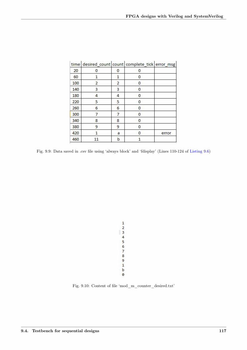
FPGA designs with Verilog and SystemVerilog
Fig. 9.9: Data saved in .csv file using ‘always block’ and ‘fdisplay’ (Lines 110-124 of Listing 9.6)
Fig. 9.10: Content of file ‘mod_m_counter_desired.txt’
9.4. Testbench for sequential designs 117

FPGA designs with Verilog and SystemVerilog
Listing 9.6: Save data of simulation
1 // modMCounter_tb.v2
3 // note that the counter starts the count from 1 after reset (not from 0),4 // therefore file "mod_m_counter_desired.txt" starts with 1 (not from 0),5 // also one entry in the file is incorrect i.e. Line 10, where '1' is written6 // instead of 'a'.7
8 `timescale 1 ns/10 ps // time-unit = 1 ns, precision = 10 ps9
10 module modMCounter_tb;11
12 localparam M = 12, N=4, period=20;13
14 reg clk, reset;15 wire complete_tick;16
17 // desired_count is read from file18 // count is count provided by modMCounter.v19 wire[N-1:0] count;20 reg[N-1:0] desired_count;21
22 reg[39:0] error_msg; // message = error23
24 // [3:0] = 4 bit data25 // [0:M-1] = 12 rows in the file mod_m_counter_desired.txt26 reg[3:0] read_data [0:M-1];27
28 integer counter_data; // for saving counter-data on file29 integer i = 0, j = 0, total_cycle = M; // used for ending the simulation after M cycle30
31 // unit under test32 modMCounter #(.M(M), .N(N)) UUT (.clk(clk), .reset(reset), .complete_tick(complete_tick), .
→˓count(count));33
34 // read the data from file35 always @(posedge clk)36 begin37 $readmemh("input_output_files/mod_m_counter_desired.txt", read_data);38 if (reset)39 desired_count = 0;40 else41 begin42 desired_count = read_data[j];43 j = j+1;44 end45 end46
47 // open csv-file for writing48 initial49 begin50 counter_data = $fopen("input_output_files/counter_output.csv"); // open file51 end52
53 // note that sensitive list is omitted in always block54 // therefore always-block run forever55 // clock period = 2 ns56 always57 begin58 clk = 1'b1;
(continues on next page)
9.4. Testbench for sequential designs 118
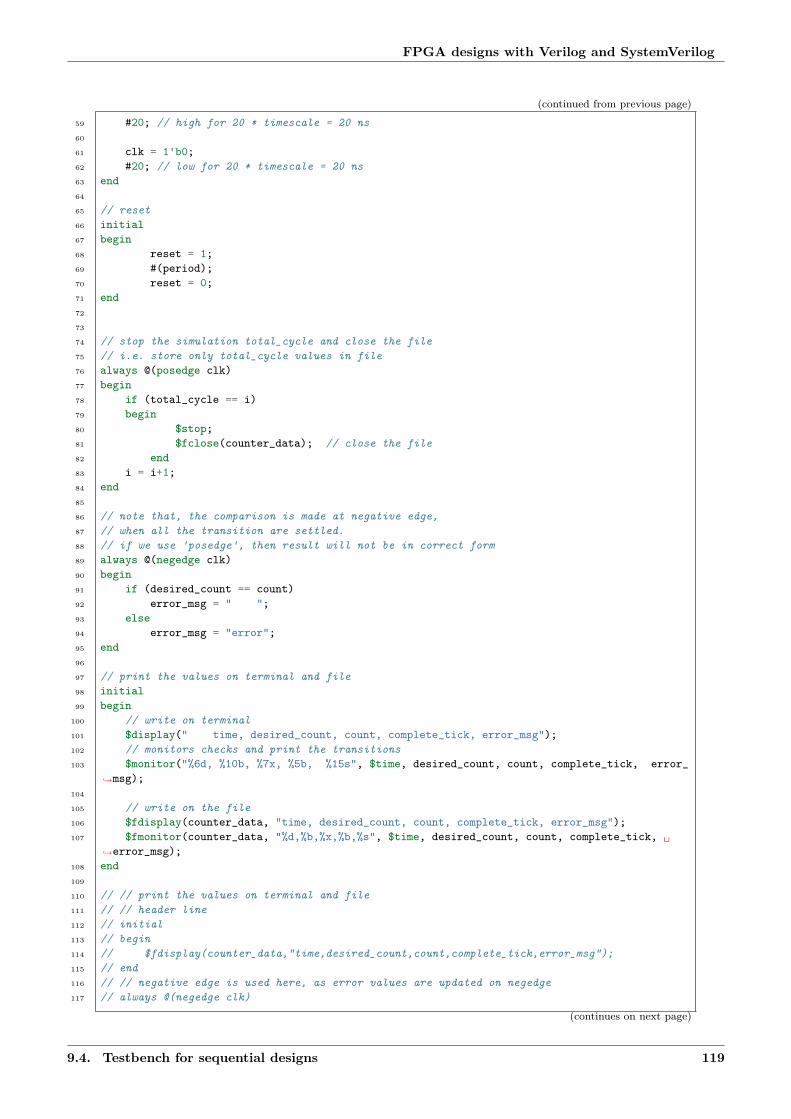
FPGA designs with Verilog and SystemVerilog
(continued from previous page)
59 #20; // high for 20 * timescale = 20 ns60
61 clk = 1'b0;62 #20; // low for 20 * timescale = 20 ns63 end64
65 // reset66 initial67 begin68 reset = 1;69 #(period);70 reset = 0;71 end72
73
74 // stop the simulation total_cycle and close the file75 // i.e. store only total_cycle values in file76 always @(posedge clk)77 begin78 if (total_cycle == i)79 begin80 $stop;81 $fclose(counter_data); // close the file82 end83 i = i+1;84 end85
86 // note that, the comparison is made at negative edge,87 // when all the transition are settled.88 // if we use 'posedge', then result will not be in correct form89 always @(negedge clk)90 begin91 if (desired_count == count)92 error_msg = " ";93 else94 error_msg = "error";95 end96
97 // print the values on terminal and file98 initial99 begin
100 // write on terminal101 $display(" time, desired_count, count, complete_tick, error_msg");102 // monitors checks and print the transitions103 $monitor("%6d, %10b, %7x, %5b, %15s", $time, desired_count, count, complete_tick, error_
→˓msg);104
105 // write on the file106 $fdisplay(counter_data, "time, desired_count, count, complete_tick, error_msg");107 $fmonitor(counter_data, "%d,%b,%x,%b,%s", $time, desired_count, count, complete_tick, ␣
→˓error_msg);108 end109
110 // // print the values on terminal and file111 // // header line112 // initial113 // begin114 // $fdisplay(counter_data,"time,desired_count,count,complete_tick,error_msg");115 // end116 // // negative edge is used here, as error values are updated on negedge117 // always @(negedge clk)
(continues on next page)
9.4. Testbench for sequential designs 119

FPGA designs with Verilog and SystemVerilog
(continued from previous page)
118 // begin119 // // write on terminal120 // $display("%6d, %10b, %7x, %5b, %15s", $time, desired_count, count, complete_tick, ␣
→˓error_msg);121
122 // // write on the file123 // $fdisplay(counter_data, "%d, %d, %x, %b, %s", $time, desired_count, count, complete_
→˓tick, error_msg);124 // end125
126 endmodule
9.5 Conclusion
In this chapter, we learn to write testbenches with different styles for combinational circuits and sequential circuits.We saw the methods by which inputs can be read from the file and the outputs can be written in the file. Simulationresults and expected results are compared and saved in the csv file and displayed as simulation waveforms; whichdemonstrated that locating the errors in csv files is easier than the simulation waveforms.
9.5. Conclusion 120

Mental suffering is worse than physical suffering. Physical sufferingsometimes comes as a blessing because it serves the purpose ofeasing mental suffering by weaning away man’s attention from themental suffering.
–Meher Baba
Chapter 10
SystemVerilog for synthesis
10.1 Introduction
In this chapter, we will convert some of the Verilog code into SystemVerilog code. Then, from next chapter, wewill see various features of SystemVerilog.
Warning:
• We used Vivado for simulation of SystemVerilog codes, as free version of Modelsim (which is availablewith Quartus) can not simulate all the SystemVerilog features.
In Vivado, do following after making the changes in the code (otherwise changes may not be shown in thesimulation),
• Close the previous simulation• Then, right click on the ‘Run simulation->Reset Behaviour simulation’• Then, run the Behaviour-simulation again
10.2 Verilog, VHDL and SystemVerilog
Both Verilog and VHDL languages have their own advantages. Note that, the codes of this tutorial are implementedusing VHDL in the other tutorial ‘FPGA designs with VHDL’ which is available on the website. If we comparethe Verilog language with the VHDL language, we can observe the following things,
• Verilog has a very limited set of keywords; but we can implement all the VHDL designs using Verilog.• Verilog codes are smaller as compare to VHDL codes.• VHDL is strongly typed language, therefore lots of conversions may require in it, which make the codes more
complex than the Verilog codes. Also due to this reason, it may take more time to write the VHDL codesthan the Verilog codes.
• The general purpose ‘always’ block’ of Verilog needs to be used very carefully. It is the designer’s responsibilityto use it correctly, as Verilog does not provide any option to check the rules. Any misuse of ‘always’ blockwill result in different ‘simulation’ and ‘synthesis’ results, which is very hard to debug. Whereas the behaviorof VHDL is accurate, i.e. there is no ambiguity between the simulation and synthesize results.
• The user-defined type (enumerated type) can not be defined in Verilog, which is a very handy tool in VHDLfor designing the FSM.
The SystemVerilog language is the superset of Verilog and contains various features of other programming languagei.e. C (structure, and typedef), C++ (class and object) and VHDL (enumerated data type, continue and breakstatements). Most importantly, it replaces the general purpose ‘always’ block with three different blocks i.e.‘always_ff’, ‘always_comb’ and ‘always_latch’, which remove the Verilog’s ambiguity between simulation andsynthesis results. Also, the compiler can catch the error if these new always-blocks are not implemented according
121

FPGA designs with Verilog and SystemVerilog
to predefined rules. In this chapter, we will reimplement the some of the designs of previous chapters usingSystemVerilog to learn and compare the SystemVerilog with Verilog.
Note: SystemVerilog is a vast language with several complex features. For example, it has the object orientedprogramming features (i.e. class and objects), interfaces and structures etc. Similar to other programming lan-guages (e.g. C, C++ and Python), usage of these features requires proper planning and methodology, otherwisethese features can harm more than their advantages.
In this tutorial, we have the following aims regarding the use of SystemVerilog to enhance the capabilities of Veriloglanguage,
• Use of new ‘always blocks’ of SystemVerilog to remove the ambiguities between the simulation and thesynthesis results.
• Use of ‘enumerated data type’ to write more readable and manageable FSM designs.• In this tutorial, we will not use the various important SystemVerilog features like packages, interface and
structure etc. in the designs, which are related to managing the large designs and require proper planningfor implementation.
10.3 ‘logic’ data type
In previous chapters, we saw that the ‘reg’ data type (i.e. variable type) can not used outside the ‘always’ block,whereas the ‘wire’ data type (i.e. net type) can not be used inside the ‘always’ block. This problem can be resolvedby using the new data type provided by the SystemVerilog i.e. ‘logic’.
Note: Please note the following point regarding ‘logic’,
• ‘logic’ and ‘reg’ can be used interchangeably.• Multiple drivers can not be assigned to ‘logic’ data type i.e. values to a variable can not be assigned through
two different places.• Multiple-driver logic need to be implemented using net type e.g. ‘wire’, ‘wand’ and ‘wor’, which has the
capability of resolving the multiple drivers. Since, we did not use the ‘wire’ to drive the multiple-driver logicin this tutorial, therefore ‘wire’ can also be replace by ‘logic’.
• Listing 2.6 is reimplemented in Listing 10.1, where both ‘wire’ and ‘reg’ are replaced with ‘logic’ keyword.
Listing 10.1: Two bit comparator
1 // comparator2BitProcedure.sv2 // Meher Krishna Patel3 // Date : 04-Sep-174
5 module comparator2BitProcedure6 ( input logic[1:0] a, b,7 output logic eq8 );9
10 always @(a,b) begin11 if (a[0]==b[0] && a[1]==b[1])12 eq = 1;13 else14 eq = 0;15 end16
17 endmodule18
10.3. ‘logic’ data type 122

FPGA designs with Verilog and SystemVerilog
10.4 Specialized ‘always’ blocks
In Section 4.2, we saw that a sequential design contains two parts i.e. ‘combination logic’ and ‘sequential logic’.The general purpose ‘always’ block is not intuitive enough to understand the type of logic implemented by it. Also,the synthesis tool has to spend the time to infer the type of logic the design intended to implement. Further, if weforgot to define all the outputs inside all the states of a combination logic, then a latch will be inferred and there isno way to detect this type of errors in Verilog. To remove these problems, three different types of ‘always’ blocksare introduced in SystemVerilog, i.e. ‘always_ff’, ‘always_comb’ and ‘always_latch’, which are discussed below,
10.4.1 ‘always_comb’
The ‘always_comb’ block represents that the block should be implemented by using ‘combinational logic’; andthere is no need to define the sensitivity list for this block, as it will be done by the software itself. In thisway SystemVerilog ensures that all the software tools will infer the same sensitivity list. The example of the‘always_comb’ block is shown in Listing 10.2.
Listing 10.2: ‘always_comb’ example
1 // always_comb_ex.sv2
3 module always_comb_ex4 (5 input logic a, b,6 output logic y, z7 );8
9 always_comb begin10 if (a > b) begin11 y = 1;12 z = 0;13 end14 else if (a < b) begin15 y = 0;16 z = 1;17 end18 else begin19 y = 1;20 z = 1;21 end22 end23
24 endmodule
Further, if the design can not be implemented by ‘pure combinational’ logic, then the compiler will generate theerror as shown in Listing 10.3. In this listing, we commented the Line 18 and Lines 21-24. In this case, a latch willbe inferred (see comments), therefore error will be reported as shown in Lines 8-9. Also, the information aboutthe latch will be displayed by the software as shown in Lines 10-11.
Listing 10.3: Error for incomplete list of outputs in ‘always_comb’block
1 // always_comb_error_ex.sv2 module always_comb_error_ex3 (4 input logic a, b,5 output logic y, z6 );7
8 // Error (10166): SystemVerilog RTL Coding error at always_comb_error_ex.sv(13): always_comb(continues on next page)
10.4. Specialized ‘always’ blocks 123
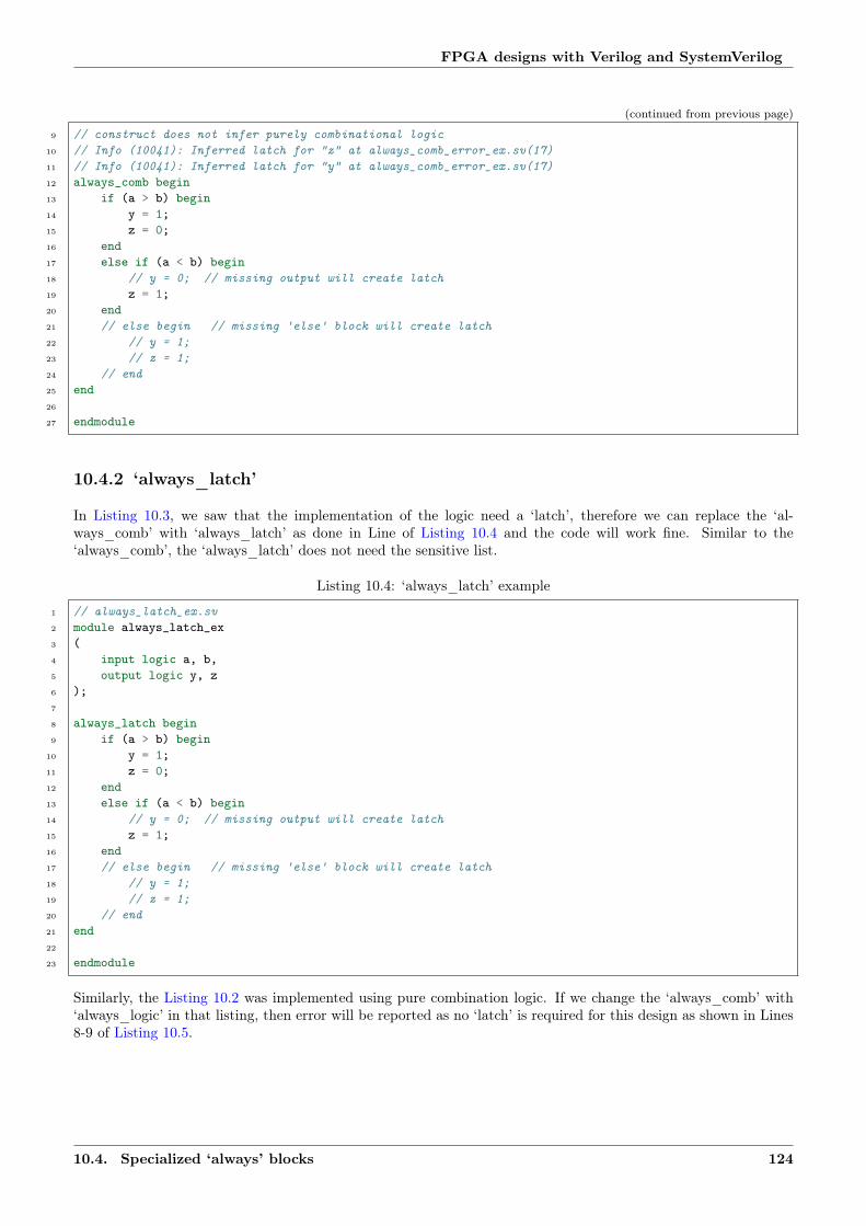
FPGA designs with Verilog and SystemVerilog
(continued from previous page)
9 // construct does not infer purely combinational logic10 // Info (10041): Inferred latch for "z" at always_comb_error_ex.sv(17)11 // Info (10041): Inferred latch for "y" at always_comb_error_ex.sv(17)12 always_comb begin13 if (a > b) begin14 y = 1;15 z = 0;16 end17 else if (a < b) begin18 // y = 0; // missing output will create latch19 z = 1;20 end21 // else begin // missing 'else' block will create latch22 // y = 1;23 // z = 1;24 // end25 end26
27 endmodule
10.4.2 ‘always_latch’
In Listing 10.3, we saw that the implementation of the logic need a ‘latch’, therefore we can replace the ‘al-ways_comb’ with ‘always_latch’ as done in Line of Listing 10.4 and the code will work fine. Similar to the‘always_comb’, the ‘always_latch’ does not need the sensitive list.
Listing 10.4: ‘always_latch’ example
1 // always_latch_ex.sv2 module always_latch_ex3 (4 input logic a, b,5 output logic y, z6 );7
8 always_latch begin9 if (a > b) begin
10 y = 1;11 z = 0;12 end13 else if (a < b) begin14 // y = 0; // missing output will create latch15 z = 1;16 end17 // else begin // missing 'else' block will create latch18 // y = 1;19 // z = 1;20 // end21 end22
23 endmodule
Similarly, the Listing 10.2 was implemented using pure combination logic. If we change the ‘always_comb’ with‘always_logic’ in that listing, then error will be reported as no ‘latch’ is required for this design as shown in Lines8-9 of Listing 10.5.
10.4. Specialized ‘always’ blocks 124
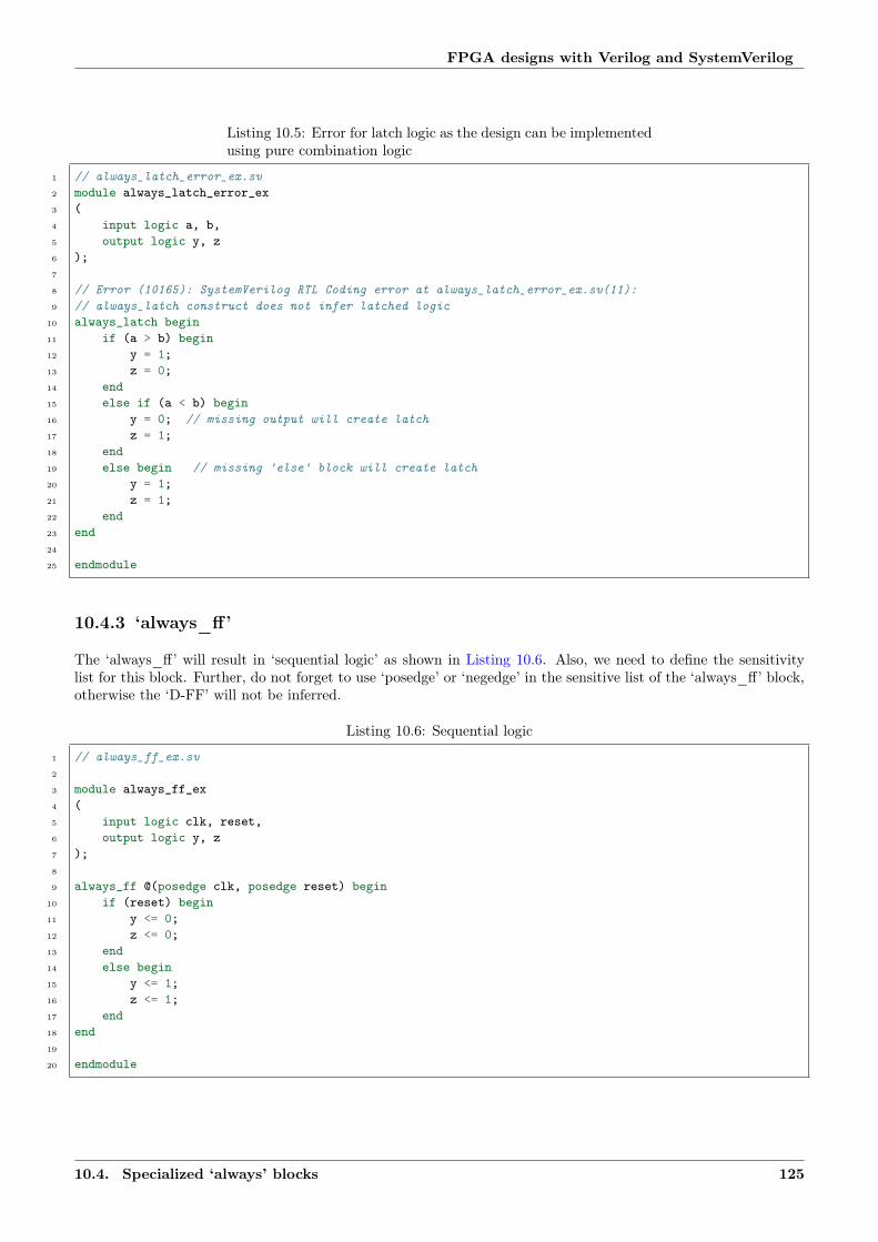
FPGA designs with Verilog and SystemVerilog
Listing 10.5: Error for latch logic as the design can be implementedusing pure combination logic
1 // always_latch_error_ex.sv2 module always_latch_error_ex3 (4 input logic a, b,5 output logic y, z6 );7
8 // Error (10165): SystemVerilog RTL Coding error at always_latch_error_ex.sv(11):9 // always_latch construct does not infer latched logic
10 always_latch begin11 if (a > b) begin12 y = 1;13 z = 0;14 end15 else if (a < b) begin16 y = 0; // missing output will create latch17 z = 1;18 end19 else begin // missing 'else' block will create latch20 y = 1;21 z = 1;22 end23 end24
25 endmodule
10.4.3 ‘always_ff’
The ‘always_ff’ will result in ‘sequential logic’ as shown in Listing 10.6. Also, we need to define the sensitivitylist for this block. Further, do not forget to use ‘posedge’ or ‘negedge’ in the sensitive list of the ‘always_ff’ block,otherwise the ‘D-FF’ will not be inferred.
Listing 10.6: Sequential logic
1 // always_ff_ex.sv2
3 module always_ff_ex4 (5 input logic clk, reset,6 output logic y, z7 );8
9 always_ff @(posedge clk, posedge reset) begin10 if (reset) begin11 y <= 0;12 z <= 0;13 end14 else begin15 y <= 1;16 z <= 1;17 end18 end19
20 endmodule
10.4. Specialized ‘always’ blocks 125

FPGA designs with Verilog and SystemVerilog
10.5 User define types
Unlike VHDL, the Verilog does not have the userdefined variables, which is a very handy tool in VHDL. Hence, weneed to define states-types and states as ‘localparam’ and ‘reg’ respectively, as shown in Listing 7.12. SystemVerilogadds two more functionalities, i.e. ‘enum’ and ‘typedef’, which can be used to define the ‘user-defined (i.e.typedef) enumerated (i.e. enum) type’. In this section, we will learn these two keywords with an example.
10.5.1 ‘typedef’
The keyword ‘typedef’ is similar to typedef-keyword in C. The ‘typedef’ is used to create the ‘user-defined datatype’,as shown in Listing 10.7.
Listing 10.7: ‘typedef’ example
typedef logic [31:0] new_bus; // create a new variable 'new_bus' of size 32new_bus data_bus, address_bus; // two variables of new data type 'new_bus'
10.5.2 ‘enum’
The ‘enum’ is used to define the ‘abstract variable’ which can have a specific set of values, as shown below. Notethat if the type is not defined in ‘enum’ then the type will be set as ‘integer’ by default, which may use extramemory unnecessarily. For example in Listing 10.8, the variable ‘num_word1’ has only 3 possible values, but it sizeis 32 bit (by default); therefore it is wise to define the type of enum as well, as done for the variable ‘new_word2’in the listing.
Listing 10.8: ‘enum’ example
// default type is integer i.e. new_word1 will have the size of 32 bitenum {one, two, three} num_word1; // variable num_word1 can have only three types of valuesnum_word1 = one; // assign one to num_word1
// size of new_word2 is 2-bitsenum logic [1:0] {seven, eight, nine} new_word2new_word2 = seven
10.5.3 Example
In this tutorial, we will use the user-defined type for creating the states of the FSM. For this, we have to useboth the keywords together, i.e. ‘typedef’ and ‘enum’ as shown in Listing 10.9. In this listing, the Listing 7.14 isreimplemented using SystemVerilog. The simulation result of the listing is the same as the Fig. Fig. 7.18.
Listing 10.9: FSM using ‘typedef’ and ‘enum’
1 // enum_typedef_example.sv2
3 module enum_typedef_example4 #( parameter5 N = 4, // Number of bits to represent the time6 on_time = 3'd5,7 off_time = 3'd38 )9 (
10 input logic clk, reset,11 output logic s_wave12 );13
(continues on next page)
10.5. User define types 126

FPGA designs with Verilog and SystemVerilog
(continued from previous page)
14
15 // use below line for more than two states, and change16 // [1:0] to desired size e.g if state_t has 12 values then17 // use [3:0] etc.18 // typedef enum logic[1:0] {onState, offState} state_t;19 typedef enum logic {onState, offState} state_t;20 state_t state_reg, state_next;21
22 logic [N-1:0] t = 0;23
24 always_ff @(posedge clk, posedge reset) begin25 if (reset == 1'b1)26 state_reg <= offState;27 else28 state_reg <= state_next;29 end30
31 always_ff @(posedge clk, posedge reset) begin32 if (state_reg != state_next)33 t <= 0;34 else35 t <= t + 1;36 end37
38 always_comb begin39 case (state_reg)40 offState : begin41 s_wave = 1'b0;42 if (t == off_time - 1)43 state_next = onState;44 else45 state_next = offState;46 end47 onState : begin48 s_wave = 1'b1;49 if (t == on_time - 1)50 state_next = offState;51 else52 state_next = onState;53 end54 endcase55 end56 endmodule
10.6 Conclusion
In this chapter, we discussed of the synthesis-related-features of SystemVerilog which can be used to remove therisk of errors in Verilog. Further, we learn the user-defined types which makes the SystemVerilog codes morereadable than the Verilog codes. Also, we learn the ‘logic’ datatype which can used in place of ‘reg’ and ‘wire’.Further, we did not use the various features of SystemVerilog like packages, interface and structure etc. in thedesigns, which are related to managing the large designs.
10.6. Conclusion 127
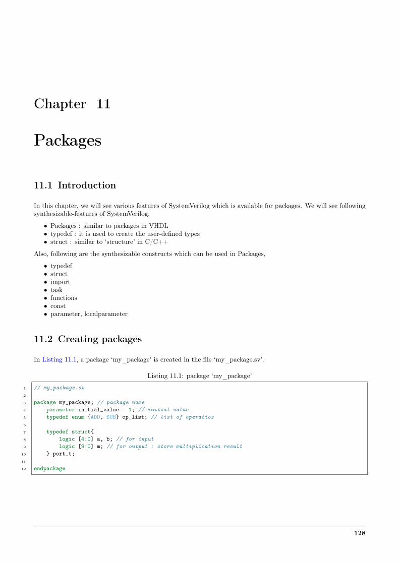
Chapter 11
Packages
11.1 Introduction
In this chapter, we will see various features of SystemVerilog which is available for packages. We will see followingsynthesizable-features of SystemVerilog,
• Packages : similar to packages in VHDL• typedef : it is used to create the user-defined types• struct : similar to ‘structure’ in C/C++
Also, following are the synthesizable constructs which can be used in Packages,
• typedef• struct• import• task• functions• const• parameter, localparameter
11.2 Creating packages
In Listing 11.1, a package ‘my_package’ is created in the file ‘my_package.sv’.
Listing 11.1: package ‘my_package’
1 // my_package.sv2
3 package my_package; // package name4 parameter initial_value = 1; // initial value5 typedef enum {ADD, SUB} op_list; // list of operatios6
7 typedef struct{8 logic [4:0] a, b; // for input9 logic [9:0] m; // for output : store multiplication result
10 } port_t;11
12 endpackage
128

FPGA designs with Verilog and SystemVerilog
11.3 Import package
Package can be imported in following ways. The first three methods of import are shown in Listing 11.2 and thesimulation results are shown in Fig. 11.1.
• Wild card import using * (Line 4)• Import specific item using ‘import’ and ‘scope-resolution-operator ::’ (Line 7)• Direct import using :: (Line 11)• Inport using ‘include (discussed in Section 11.4)
Note:
• Wildcard import does not import items but adds the package into the path.• Importing the ‘enum-definition’ will not import it’s labels e.g. ‘import op_list’ will not import ‘ADD’ and
‘SUB’.
Listing 11.2: import package ‘my_package’
1 // use_package.sv2
3 // // import method 1 : import everything from my_package4 // import my_package::*;5
6 // // import method 2 : import individual value from package7 import my_package::initial_value; // import 'initial_value' from my_package8
9 module use_package(10 input logic clk,11 input my_package::port_t D, // import port_t from my_package12 output logic[5:0] s13 );14
15 always_ff @(posedge clk) begin16 s = D.a + D.b + initial_value;17 D.m = D.a * D.b;18 end19
20 endmodule
Fig. 11.1: Simulation results of Listing 11.2
11.3. Import package 129

FPGA designs with Verilog and SystemVerilog
11.4 Package with conditional compilation
In this section, we will create a testbench for ‘my_package.sv’ file; and use the keyword ‘include’ to use the packagein it.
11.4.1 Modify my_package.sv
• In Listing 11.3, the wildcard import statement is added at the Line 17, which is not the part of the package‘my_package’.
• To import the Line 17, we need to use ‘include’ directive in the code as shown in Line 3 of Listing 11.4.• Lines 3-4 and 19 are the statement for conditional compilation. In the other words, if the ‘my_package.sv’
is not compiled/imported, then it will be complied/imported.
Note: Since, directive ‘include’ is not used in Listing 11.2 therefore Line 17 of Listing 11.3 will not be executedin Listing 11.2, therefore we need to use the package-name to import items e.g. my_package::port_t etc.
Listing 11.3: Contditional compilation using ‘ifndef’
1 // my_package.sv2
3 `ifndef MYPACKAGE_DONE4 `define MYPACKAGE_DONE5 package my_package; // package name6 parameter initial_value = 1; // initial value7 typedef enum {ADD, SUB} op_list; // list of operatios8
9 typedef struct{10 logic [4:0] a, b; // for input11 logic [9:0] m; // for output : store multiplication result12 } port_t;13
14 endpackage15
16 // import package in the design17 import my_package::*;18
19 `endif
11.4.2 Testbench
Listing 11.4 is the testbench for Listing 11.2. The results are shown in Fig. 11.2.
Note:
• ‘timescale 1ns/10ps directive can be used in SystemVerilog.• Also, we can further split ‘timescale directive in SystemVerilog as below,
timeunit 1ns;timeprecision 10ps;
• Lastly, if we defined the time-parameters in ‘package’ and ‘design-file’, then ‘design-file parameters’ willoverride the ‘package-parameters’.
11.4. Package with conditional compilation 130

FPGA designs with Verilog and SystemVerilog
Listing 11.4: Testbench
1 // use_package_tb.sv2
3 `include "my_package.sv"4
5 module use_package_tb;6
7 logic clk = 0; // initialize clock with 08 port_t D; // import port_t from my_package9 logic[5:0] sum;
10
11 use_package uut (12 .clk(clk),13 .D(D),14 .s(sum)15 );16
17 always #1018 clk = ~clk;19
20 initial begin21 @(negedge clk)22 D.a = 6;23 D.b = 5;24 end25 endmodule
Fig. 11.2: Simulation results of Listing 11.4
11.4. Package with conditional compilation 131

Chapter 12
Interface
12.1 Introduction
The interface allows to create a group of signals, which can be used as ports in designs.
12.2 Define and use interface
• In Listing 12.1, an interface is defined in Lines 3-9, which contains signals a, b, c and c_2 in it. Then, inmodule or_ex, these signals are used as shown in Lines 19-20 and 22. The simulation results are shown inFig. 12.1.
Listing 12.1: Define and use interface
1 // interface_ex.sv2
3 interface logic_gate_if;4
5 logic[3:0] a, b;6 logic[5:0] c;7 logic[5:0] c_2; // increment c by 28
9 endinterface10
11
12 module or_ex(13 input logic[3:0] a, b,14 output logic[5:0] sum, sum_new15 );16
17 logic_gate_if lg (); // import all signals from interface18
19 assign lg.a = a;20 assign lg.b = b;21 assign sum = a+b;22 assign sum_new = lg.a + lg.b + 2; // increment sum by 223
24 endmodule
• Also, we can perform some assigments in the the interfaces as shown in Lines 9-10 of Listing 12.2. Also, thesenewly assigned values are assigned to output at Lines 23-24. The simulation results are same as in Fig. 12.1.
132

FPGA designs with Verilog and SystemVerilog
Fig. 12.1: Simulation results for Listing 12.1
Warning: Do following, after making the changes in the code (otherwise changes will not be shown in thesimulation),
• Close the previous simulation• Then, right click on the ‘Run simulation->Reset Behaviour simulation’• Then, run the Behaviour-simulation again
Listing 12.2: Assigment in interface
1 // interface_ex.sv2
3 interface logic_gate_if;4
5 logic[3:0] a, b;6 logic[5:0] c;7 logic[5:0] c_2; // increment c by 28
9 assign c = a + b;10 assign c_2 = c + 2;11 endinterface12
13
14 module or_ex(15 input logic[3:0] a, b,16 output logic[5:0] sum, sum_217 );18
19 logic_gate_if lg (); // import all signals from interface20
21 assign lg.a = a;22 assign lg.b = b;23 assign sum = lg.c;24 assign sum_2 = lg.c_2; // increment sum by 225
26 endmodule
12.2. Define and use interface 133

Do not be angry with him who backbites you, but be pleased, forthereby he serves you by diminishing the load of your sanskaras;also pity him because he increases his own load of sanskaras.
–Meher Baba
Chapter 13
Simulate and implement SoPC design
13.1 Introduction
In this tutorial, we will learn to design embedded system on FPGA board using Nios-II processor, which isoften known as ‘System on Programmable chip (SoPC)’. Before beginning the SoPC design, let’s understand thedifference between ‘computer system’, ‘embedded system’ and ‘SoPC system’. Computer systems, e.g. personalcomputers (PCs), support various end user applications. Selection of these computer systems for few specificapplications, e.g. timers settings, displays and buzzers in microwave-ovens or washing machines etc., is not a costeffective choice. The Embedded systems are cost effective solution for such cases, where only few functionalitiesare required in the system. Since, embedded systems are designed for specific tasks, therefore the designs can beoptimized based on the applications. Further, SoPC systems are the programmable embedded systems i.e. wecan design the embedded systems using VHDL/Verilog codes and implement them on the FPGA board.
Nios II is a 32-bit embedded-processor architecture designed for Altera-FPGA board. In Fig. 13.1, various stepsare shown to design the SoPC system on the FPGA board using Nios-II processor. In this chapter, these stepsare discussed and a system is designed which displays the message on the computer and blinks one LED usingFPGA board. Further, the outputs of this system is verified using Modelsim. It is recommended to read firsttwo chapters before practicing the codes, as various issues related to the use of Nios software arediscussed in these chapters.
Note: Note that, the NIOS-projects can not be run directly on the system, after downloading it from the website;therefore only ‘necessary files are provided on the website. Please see Appendix B to compile and synthesize theprovided codes.
Note: Also, if you change the location of the project in your system (after creating it) or change the FPGA-board,then you need to follow the instructions in the Appendix B again.
13.2 Creating Quartus project
First, we need to create the project at desired location, with following steps,
• Path to project directory should not contain any spaces in the names of folder as shown in Fig. 13.2, as pathwill not be detected by the Nios-II software in later part of the tutorial.
• Choose the correct FPGA device as shown in Fig. 13.3. If you do not have any, then select correct devicefamily and use it for rest of the tutorial. Note that, ‘simulation’ is the most important process ofthe design, and FPGA board is not required for creating and simulating the embedded design.Hence, if you don’t have FPGA board, you can still use the tutorial. Implementation of the design on theFPGA board requires the loading the ‘.sof’ and ‘.elf’ files on the board, which is not a big deal.
134
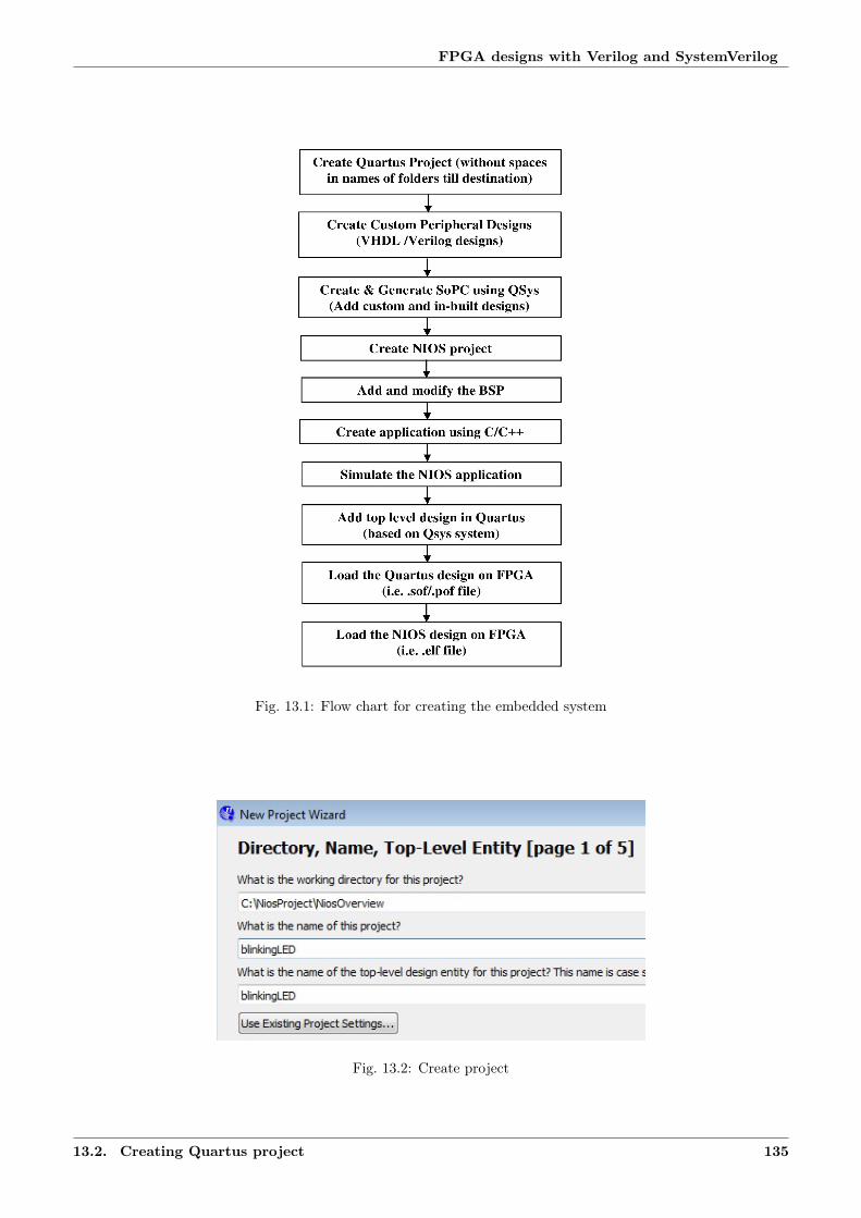
FPGA designs with Verilog and SystemVerilog
Fig. 13.1: Flow chart for creating the embedded system
Fig. 13.2: Create project
13.2. Creating Quartus project 135
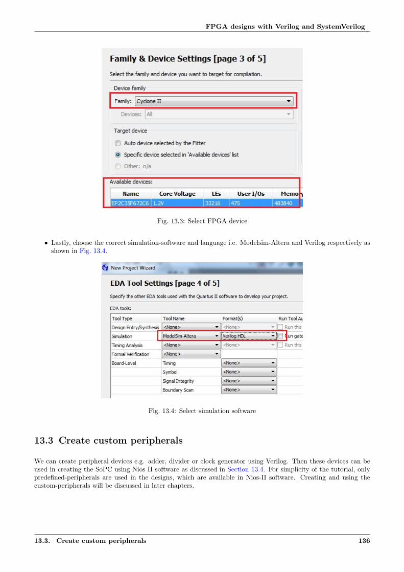
FPGA designs with Verilog and SystemVerilog
Fig. 13.3: Select FPGA device
• Lastly, choose the correct simulation-software and language i.e. Modelsim-Altera and Verilog respectively asshown in Fig. 13.4.
Fig. 13.4: Select simulation software
13.3 Create custom peripherals
We can create peripheral devices e.g. adder, divider or clock generator using Verilog. Then these devices can beused in creating the SoPC using Nios-II software as discussed in Section 13.4. For simplicity of the tutorial, onlypredefined-peripherals are used in the designs, which are available in Nios-II software. Creating and using thecustom-peripherals will be discussed in later chapters.
13.3. Create custom peripherals 136

FPGA designs with Verilog and SystemVerilog
13.4 Create and Generate SoPC using Qsys
SoPC can be created using two tools in Quartus software i.e. ‘SOPC builder’ and ‘Qsys’ tools. Since Qsys is therecommended tool by the Altera, therefore we will use this tool for generating the SoPC system. To open the Qsystool, go to Tools–>Qsys in Quartus software. Next, follow the below steps to create the SoPC system,
• Rename ‘clk_0’ to ‘clk’ by right clicking the name (optional step). Note that, renaming steps are optional;but assigning appropriate names to the components is good practice as we need to identify these componentsin later tutorial.
• In component library, search for Nios processor as shown in Fig. 13.5 and select the Nios II/e (i.e. economyversion) for this tutorial. Note that various errors are displayed in the figure, which will be removed in laterpart of this section. Next, rename the processor to ‘nios_blinkingLED’ and connect the clock and reset portto ‘clk’ device, by clicking on the circles as shown in Fig. 13.6.
Fig. 13.5: Add Nios processor
Fig. 13.6: Rename Nios processor and connect the ports
• Next add the ‘onchip memory’ to the system with 20480 (i.e. 20k) bytes as shown in Fig. 13.7 and rename
13.4. Create and Generate SoPC using Qsys 137

FPGA designs with Verilog and SystemVerilog
it to RAM. For different FPGA boards, we may need to reduce the memory size, if the ‘memory-overflow’error is displayed during ‘generation’ process in Fig. 13.14.
Fig. 13.7: Add onchip memory to the system
• After that, search for ‘JTAG UART’ and add it with default settings. It is used for the communication of theFPGA device to Nios software. More specifically, it is required display the outputs of the ‘printf’ commandson the Nios software.
• Next, add a PIO device for blinking the LED. Search for PIO device and add it as ‘1 bit’ PIO device (see Fig.13.8), because we will use only one blinking LED. Since, the PIO device, i.e. ‘LED’, is available as externalport, therefore name of the ‘external_connection’ must be defined as shown in Fig. 13.9.
Fig. 13.8: Add 1 bit PIO for one blinking LED
• Then, add all the connections as shown in the Fig. 13.9. Also, add the JTAG slave to the data master ofNios processors i.e. IRQ in Fig. 13.10
• Next, double click on the to the Nios processor i.e. ‘nios_blinkingLED’ in the Fig. 13.9; and set RAM asreset and exception vectors as shown in Fig. 13.11.
13.4. Create and Generate SoPC using Qsys 138

FPGA designs with Verilog and SystemVerilog
Fig. 13.9: Settings for PIO and other device
Fig. 13.10: Connect IRQ
13.4. Create and Generate SoPC using Qsys 139

FPGA designs with Verilog and SystemVerilog
Fig. 13.11: Setting Reset and Exception vector for Nios processor
• Then, go to Systems–>Assign Base Address. This will assign the unique addresses for all the devices. Withthe help of these address, the devices can be accessed by C/C++ codes in Nios-II software. If everything iscorrect till this point, we will get the ‘0 Errors, 0 Warnings’ message as shown in Fig. 13.12.
• Finally, to allow the simulation of the designs, go to ‘generation’ tab and set the tab as shown in the Fig.13.13. Note that, VHDL can not be used as simulation language, as this version of Quartus doesnot support it. Since, generated verilog files are used for the simulation settings settings only, thereforewe need not to look at these files. Hence it does not matter, whether these files are created using VHDL orVerilog.
• Save the system with desired name e.g. ‘nios_blinkingLED.qsys’ and click on generate button. If system isgenerated successfully, we will get the message as shown in Fig. 13.14
• After this process, a ‘nios_blinkingLED.sopcinfo’ file will be generated, which is used by Nios-II softwareto create the embedded design. This file contains all the information about the components along withtheir base addresses etc. Further, two more folders will be created inside the ‘nios_blinkingLED’ folderi.e. ‘synthesis’ and ‘testbench’. These folders are generated as we select the ‘synthesis’ and ‘simulation’options in Fig. 13.13, and contains various information about synthesis (e.g. ‘nios_blinkingLED.qip’ file) andsimulation (e.g. ‘nios_blinkingLED_tb.qsys’ file). The ‘nios_blinkingLED.qip’ file will be used for thecreating the top module for the design i.e. LEDs will be connected to FPGA board using this file; whereas‘nios_blinkingLED_tb.qsys’ contains the information about simulation waveforms for the testbenches.Lastly, ‘nios_blinkingLED_tb.spd’ is generated which is used by Nios software to start the simulationprocess.
• In this way, SoPC system can be generated. Finally, close the Qsys tool. In next section, Nios software willbe used to create the blinking-LED system using ‘nios_blinkingLED.sopcinfo’ file.
13.5 Create Nios system
In previous section, we have created the SoPC system and corresponding .sopcinfo file was generated. In thissection, we will use the .sopcinfo file to create a system with blinking LED functionality.
To open the Nios software from Quarturs software, click on Tools–>Nios II software Build Tools for Eclipse. Ifyou are using it first time, then it will ask for work space location; you can select any location for this.
13.5. Create Nios system 140

FPGA designs with Verilog and SystemVerilog
Fig. 13.12: 0 errors and 0 warnings
Fig. 13.13: Simulation settings
13.5. Create Nios system 141

FPGA designs with Verilog and SystemVerilog
Fig. 13.14: System generated successfully
13.6 Add and Modify BSP
To use the .sopcinfo file, we need to create a ‘board support package (BSP)’. Further, BSP should be modify forsimulation purpose, as discussed in this section.
13.6.1 Add BSP
To add BSP, go to File–>New–>Nios II Board Support Package. Fill the project name field and select the .sopcinfofile as shown in Fig. 13.15. Rest of the field will be filled automatically.
Fig. 13.15: Add board support package (BSP)
After clicking on finish, BSP_blinkingLED folder will be created which contains various files e.g. system.h, io.hand drivers etc. These files are generated based on the information in the .sopcfile e.g. in Fig. 13.16, which showsthe partial view of system.h file, contains the information about LED along with the base address (note that, thisLED was added along with base address in Section 13.4). Note that, address location is defined as ‘LED_BASE’in the system.h file; and we will use this name in the tutorial instead of using the actual base address. In this way,
13.6. Add and Modify BSP 142
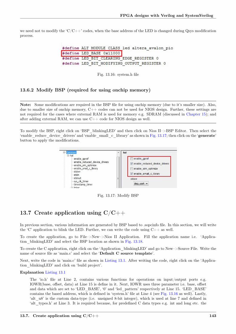
FPGA designs with Verilog and SystemVerilog
we need not to modify the ‘C/C++’ codes, when the base address of the LED is changed during Qsys modificationprocess.
Fig. 13.16: system.h file
13.6.2 Modify BSP (required for using onchip memory)
Note: Some modifications are required in the BSP file for using onchip memory (due to it’s smaller size). Also,due to smaller size of onchip memory, C++ codes can not be used for NIOS design. Further, these settings arenot required for the cases where external RAM is used for memory e.g. SDRAM (discussed in Chapter 15); andafter adding external RAM, we can use C++ code for NIOS design as well.
To modify the BSP, right click on ‘BSP_blinkingLED’ and then click on Nios II–>BSP Editor. Then select the‘enable_reduce_device_drivers’ and ‘enable_small_c_library’ as shown in Fig. 13.17; then click on the ‘generate’button to apply the modifications.
Fig. 13.17: Modify BSP
13.7 Create application using C/C++
In previous section, various information are generated by BSP based to .sopcinfo file. In this section, we will writethe ‘C’ application to blink the LED. Further, we can write the code using C++ as well.
To create the application, go to File–>New–>Nios II Application. Fill the application name i.e. ‘Applica-tion_blinkingLED’ and select the BSP location as shown in Fig. 13.18.
To create the C application, right click on the ‘Application_blinkingLED’ and go to New–>Source File. Write thename of source file as ‘main.c’ and select the ‘Default C source template’.
Next, write the code in ‘main.c’ file as shown in Listing 13.1. After writing the code, right click on the ‘Applica-tion_blinkingLED’ and click on ‘build project’.
Explanation Listing 13.1
The ‘io.h’ file at Line 2, contains various functions for operations on input/output ports e.g.IOWR(base, offset, data) at Line 15 is define in it. Next, IOWR uses three parameter i.e. base, offsetand data which are set to ‘LED_BASE’, ‘0’ and ‘led_pattern’ respectively at Line 15. ‘LED_BASE’contains the based address, which is defined in ‘system.h’ file at Line 4 (see Fig. 13.16 as well). Lastly,‘alt_u8’ is the custom data-type (i.e. unsigned 8-bit integer), which is used at line 7 and defined in‘alt_types.h’ at Line 3. It is required because, for predefined C data types e.g. int and long etc. the
13.7. Create application using C/C++ 143

FPGA designs with Verilog and SystemVerilog
Fig. 13.18: Create Application
size of the data type is defined by the compiler; but using ‘alt_types.h’ we can define the exact size forthe data.
Since ‘alt_u8’ is 8 bit wide, therefore led_pattern is initialized as ‘0$times$01’ (i.e. 0000-0001) at Line7. Then this value is inverted at Line 14 (for blinking LED). Lastly, this pattern is written on the LEDaddress at Line 15. Second parameter, i.e. offset is set to 0, because we want to write the pattern onLED_BASE (not to other location with respect of LED_BASE). Also, dummy loop is used at Line 19is commented, which will be required for visual verification of the blinking LED in Section 13.11.
Listing 13.1: Blinking LED with C application
1 //main.c2 # include "io.h" // required for IOWR3 # include "alt_types.h" // required for alt_u84 # include "system.h" // contains address of LED_BASE5
6 int main(){7 alt_u8 led_pattern = 0x01; // on the LED8
9 //uncomment below line for visual verification of blinking LED10 //int i, itr=250000;11
12 printf("Blinking LED\n");13 while(1){14 led_pattern = ~led_pattern; // not the led_pattern15 IOWR(LED_BASE, 0, led_pattern); // write the led_pattern on LED16
17 //uncomment 'for loop' in below line for visual verification of blinking LED18 // dummy for loop to add delay in blinking, so that we can see the bliking.19 //for (i=0; i<itr; i ++){}20 }21 }
13.7. Create application using C/C++ 144

FPGA designs with Verilog and SystemVerilog
13.8 Simulate the Nios application
In previous section, we built the Nios application. To simulate this system, right click on ‘Applica-tion_blinkingLED’ and go to Run as–>NOIS II Modelsim. Then select the location of Modelsim software i.e.‘win32aloem’ or ‘win64aloem’ folder as shown in Fig. 13.19; this can be found inside the folders where Alterasoftware is installed.
Fig. 13.19: Search for Modelsim location
Next, click on the advance button in Fig. 13.19 and a new window will pop-up. Fill the project location as shownin Fig. 13.20 and close the pop-up window. This location contains the ‘.spd’ file, which is required for simulation.
Fig. 13.20: Search for Project Location
After above step, ‘Qsys testbench simulation package descriptor file name’ column will be filled with ‘.spd’ fileautomatically as shown in Fig. 13.21. If not, do it manually by searching the file, which is available in the projectfolder. If everything is correct, then apply and run buttons will be activated. Click on apply and then run buttonto start the simulation.
Modelsim window will pop-up after clicking the run button, which will display all the external ports as shownin Fig. 13.22. Right click on the external signals and click on ‘add to wave’. Next go to transcript section atthe bottom of the modelsim and type ‘run 3 ms’. The simulator will be run for 3 ms and we will get outputsas shown in Fig. 13.23. In the figure, there are 3 signals i.e. clock, reset and LED, where last waveform i.e.‘nios_blinkingled_inst_led_external_connection_export’ is the output waveform, which will be displayed on theLEDs.
13.8. Simulate the Nios application 145
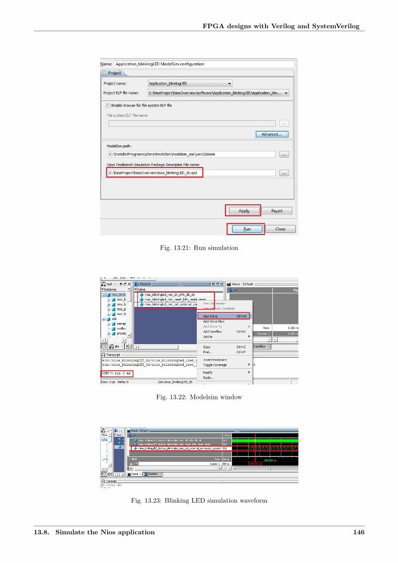
FPGA designs with Verilog and SystemVerilog
Fig. 13.21: Run simulation
Fig. 13.22: Modelsim window
Fig. 13.23: Blinking LED simulation waveform
13.8. Simulate the Nios application 146
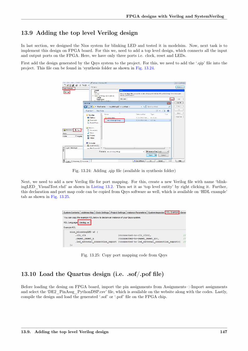
FPGA designs with Verilog and SystemVerilog
13.9 Adding the top level Verilog design
In last section, we designed the Nios system for blinking LED and tested it in modelsim. Now, next task is toimplement this design on FPGA board. For this we, need to add a top level design, which connects all the inputand output ports on the FPGA. Here, we have only three ports i.e. clock, reset and LEDs.
First add the design generated by the Qsys system to the project. For this, we need to add the ‘.qip’ file into theproject. This file can be found in ‘synthesis folder as shown in Fig. 13.24.
Fig. 13.24: Adding .qip file (available in synthesis folder)
Next, we need to add a new Verilog file for port mapping. For this, create a new Verilog file with name ‘blink-ingLED_VisualTest.vhd’ as shown in Listing 13.2. Then set it as ‘top level entity’ by right clicking it. Further,this declaration and port map code can be copied from Qsys software as well, which is available on ‘HDL example’tab as shown in Fig. 13.25.
Fig. 13.25: Copy port mapping code from Qsys
13.10 Load the Quartus design (i.e. .sof/.pof file)
Before loading the desing on FPGA board, import the pin assignments from Assignments–>Import assignmentsand select the ‘DE2_PinAssg_PythonDSP.csv’ file, which is available on the website along with the codes. Lastly,compile the design and load the generated ‘.sof’ or ‘.pof’ file on the FPGA chip.
13.9. Adding the top level Verilog design 147
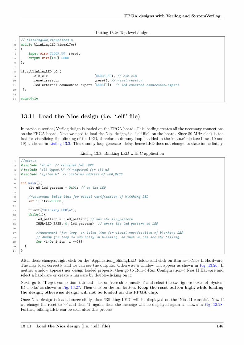
FPGA designs with Verilog and SystemVerilog
Listing 13.2: Top level design
1 // blinkingLED_VisualTest.v2 module blinkingLED_VisualTest3 (4 input wire CLOCK_50, reset,5 output wire[1:0] LEDR6 );7
8 nios_blinkingLED u0 (9 .clk_clk (CLOCK_50), // clk.clk
10 .reset_reset_n (reset), // reset.reset_n11 .led_external_connection_export (LEDR[0]) // led_external_connection.export12 );13
14 endmodule
13.11 Load the Nios design (i.e. ‘.elf’ file)
In previous section, Verilog design is loaded on the FPGA board. This loading creates all the necessary connectionson the FPGA board. Next we need to load the Nios design, i.e. ‘.elf file’, on the board. Since 50 MHz clock is toofast for visualizing the blinking of the LED, therefore a dummy loop is added in the ‘main.c’ file (see Lines 10 and19) as shown in Listing 13.3. This dummy loop generates delay, hence LED does not change its state immediately.
Listing 13.3: Blinking LED with C application
1 //main.c2 # include "io.h" // required for IOWR3 # include "alt_types.h" // required for alt_u84 # include "system.h" // contains address of LED_BASE5
6 int main(){7 alt_u8 led_pattern = 0x01; // on the LED8
9 //uncomment below line for visual verification of blinking LED10 int i, itr=250000;11
12 printf("Blinking LED\n");13 while(1){14 led_pattern = ~led_pattern; // not the led_pattern15 IOWR(LED_BASE, 0, led_pattern); // write the led_pattern on LED16
17 //uncomment 'for loop' in below line for visual verification of blinking LED18 // dummy for loop to add delay in blinking, so that we can see the bliking.19 for (i=0; i<itr; i ++){}20 }21 }
After these changes, right click on the ‘Application_blikingLED’ folder and click on Run as–>Nios II Hardware.The may load correctly and we can see the outputs. Otherwise a window will appear as shown in Fig. 13.26. Ifneither window appears nor design loaded properly, then go to Run–>Run Configuration–>Nios II Harware andselect a hardware or create a harware by double-clicking on it.
Next, go to ‘Target connection’ tab and click on ‘refresh connection’ and select the two ignore-boxes of ‘SystemID checks’ as shown in Fig. 13.27. Then click on the run button. Keep the reset button high, while loadingthe design, otherwise design will not be loaded on the FPGA chip.
Once Nios design is loaded successfully, then ‘Blinking LED’ will be displayed on the ‘Nios II console’. Now ifwe change the reset to ‘0’ and then ‘1’ again; then the message will be displayed again as shown in Fig. 13.28.Further, bilking LED can be seen after this process.
13.11. Load the Nios design (i.e. ‘.elf ’ file) 148
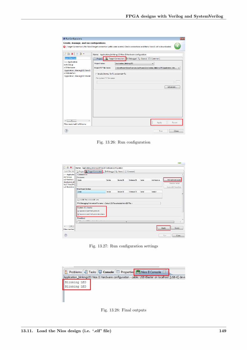
FPGA designs with Verilog and SystemVerilog
Fig. 13.26: Run configuration
Fig. 13.27: Run configuration settings
Fig. 13.28: Final outputs
13.11. Load the Nios design (i.e. ‘.elf ’ file) 149

FPGA designs with Verilog and SystemVerilog
13.12 Saving NIOS-console’s data to file
In Section 13.11, the message ‘Blinking LED’ is displayed on the NIOS console. Most of the time, we need tostore the data in a file for further processing e.g. in Chapter 15, sine waveforms are generated using NIOS, andthe resulted data is saved in a file and then plotted using Python; note that this plotting operation can not beperformed when data in displayed on the NIOS console.
Please see the video: NIOS II - Save data to the file using JTAG-UART if you have problem with this part oftutorial.
To save the data on a file, first build the project as discussed in the Section 13.7. Next, right click on the‘Application_BlinkingLED’ and go to ‘NIOS II–>NIOS II Command Shell’. Then, in the command prompt,execute the following two commands,
• nios2-download -g Application_BlinkingLED.elf} : This will load the NIOS design on the FPGAboard.
• nios2-terminal.exe -q –quiet > blinkOut.txt: This will save the messages in the file ‘blinkOut.txt’,which will be saved in the ‘Application_BlinkingLED’ folder. We can now, reset the system and ‘BlinkingLED’ message will be displayed twice as shown in Fig. 13.28.
• ‘-q –quiet’ options is used to suppress the NIOS-generated message in the file. For more options, we canuse ‘–help’ option e.g. nios2-terminal –help.
• Lastly, ‘> sign’ erases the contents of existing file before writing in it. To append the current outputs at theend of the existing file, use ‘>>’ option, instead of ‘>’.
• We can run these two commands in one step using ‘&&’ operators i.e.
nios2-download -g Application\_BlinkingLED.elf && nios2-terminal.exe -q --quiet > ../../python/data/→˓blinkOut.txt}.
In this case, ‘../../python/data/blinkOut.txt’ command will save the ‘blinkOut.txt’ file by going two folders-back i.e. ‘../../’, then it will save the file in ‘data’ folder which is inside the ‘python’ folder. In this way, we cansave the results at any location.
13.13 Conclusion
In this tutorial, we saw various steps to create a embedded Nios processor design. We design the system for blinkingthe LED and displaying the message on the ‘Nios II console’ window. Also, we learn the simulation methods forNios-II designs. In next chapter, we will learn about adding components to the ‘Qsys’ file. Also, we will see theprocess of updating the BSP according to new ‘.sopcinfo’ file.
13.12. Saving NIOS-console’s data to file 150

The greatest error of a man is to think that he is weak by nature,evil by nature. Every man is divine and strong in his real nature.What are weak and evil are his habits, his desires and thoughts, butnot himself.
–Ramana Maharshi
Chapter 14
Reading data from peripherals
14.1 Introduction
In Chapter 13, the values of the variables in the code i.e. ‘led_pattern’ were sent to PIO (peripheral input/output)device i.e. LED. In this chapter, we will learn to read the values from the PIO. More specifically, the values will beread from the external switches. These values will decide the blinking rate of the LED. Further, we will not createa new ‘.qsys’ file, but modify the previous ‘.qsys’ file to generate the new system. Also, we will see the proceduresto modify the existing Nios project i.e. BSP and Application files (instead of creating the new project).
14.2 Modify Qsys file
First create or open a Quartus project as discussed in Chapter 13. Then open the ‘Qsys’ file, which we havecreated in the previous chapter and modify the file as below,
• Modify LED port: Double click on the ‘led’ and change the ‘Width’ column to ‘2’ from ‘1’; because in thischapter, we will use two LEDs which will blink alternatively.
• Add Switch Port: Next, add a new PIO device and set it to ‘output’ port with width ‘8’ as shown in Fig.14.1. Next, rename it to ‘switch’ and modify it’s clock, reset and external connections as shown in Fig. 14.2.
Fig. 14.1: Add switch of width 8
• Next, assign base address by clicking on System–>Assign base addresses.• Finally, generate the system, by clicking on the ‘Generate button’ with correct simulation settings, as shown
in Fig. 13.14.
151

FPGA designs with Verilog and SystemVerilog
Fig. 14.2: Rename and Modify the port for Switch
14.3 Modify top level design in Quartus
Since, LED port is modified and the ‘switch’ port is added to the system, therefore top level module should bemodified to assign proper connections to the FPGA chip. Top level design for this purpose is shown in Listing14.1.
Listing 14.1: Modify top level design in Quartus
1 // blinkingLED_VisualTest.v2 module blinkingLED_VisualTest3 (4 input wire CLOCK_50, reset,5 input wire [7:0] SW,6 output wire[1:0] LEDR7 );8
9 nios_blinkingLED u0 (10 .clk_clk (CLOCK_50), // clk.clk11 .reset_reset_n (reset), // reset.reset_n12 .switch_external_connection_export (SW), // switch_external_connection_export.export13 .led_external_connection_export (LEDR) // led_external_connection.export14 );15
16 endmodule
14.4 Modify Nios project
Since ‘Qsys’ system is modified, therefore corresponding ‘.sopcinfo’ file is modified also. Now, we need to updatethe system according to the new ‘.sopcinfo’ file.
14.4.1 Adding Nios project to workspace
If ‘workspace is changed’ or ‘BSP/Application files are removed’ from the current workspace, then we need to addthese files again in the project, as discussed below,
Note: If the location of the project is changed, then we need to created the NIOS project again, as shown inAppendix B.
• First go to Files–>Import–>’Import Nios II software. . . ’ as shown in Fig. 14.3; and select the ‘application’from the ‘software’ folder (see Fig. 14.4) inside the main directory. Finally, give it the correct name i.e.‘Application_blinkingLED’ as shown in Fig. 14.5
• Similarly, add the BSP folder in the current workspace.
14.3. Modify top level design in Quartus 152

FPGA designs with Verilog and SystemVerilog
Fig. 14.3: Import Application and BSP files
Fig. 14.4: Application and BSP files are in software folder
14.4. Modify Nios project 153

FPGA designs with Verilog and SystemVerilog
Fig. 14.5: Add application Name i.e. Application_blinkingLED
• Now, open the ‘system.h’ file in the BSP. Here, we can see that LED data width is still ‘1’ as shown in Fig.14.6. Also, we can not find the ‘switch’ entries in the system.h file.
Fig. 14.6: LED data width is not updated to ‘2’
• To update the BSP, right click on the BSP folder and go to Nios–>Generate BSP. It will update the BSPfiles.
• Sometimes, proper addresses are not assigned during generation in ‘Qsys’ system as shown in Fig. 14.7. Here,SWITCH_BASE is set to ‘0$times$0’. To remove this problem, assign base addresses again and regeneratethe system as discussed in Section 14.2.
Fig. 14.7: Base address is not assigned to switch
14.5 Add ‘C’ file for reading switches
Next, modify the ‘main.c’ file as shown in Listing 14.2. Finally, build the system by pressing ‘ctrl+B’.
Explanation Listing 14.2
‘IORD(base, offset)’ command is used the read the values form I/O ports as shown at Line 19 of thelisting. Line 19 reads the values of the switches; which is multiply by variable ‘itr’ (see Line 22),to set the delay value base on switch patterns. Also, ‘iter ‘value is set to ‘1000’ at Line 11, so thatmultiplication can produce sufficient delay to observe the blinking LEDs.
14.5. Add ‘C’ file for reading switches 154

FPGA designs with Verilog and SystemVerilog
Listing 14.2: Blinking LED with C application
1 //main.c2 # include "io.h"3 # include "alt_types.h"4 # include "system.h"5
6 int main(){7 static alt_u8 led_pattern = 0x01; // on the LED8
9 // swValue : to store the value of switch10 // swDelay = swValue * iter, is the overall delay11 int i, swDelay, swValue, itr=1000;12
13 printf("Blinking LED\n");14 while(1){15 led_pattern = ~led_pattern; // not the led_pattern16 IOWR(LED_BASE, 0, led_pattern); // write the led_pattern on LED17
18 // read the value of switch19 swValue = IORD(SWITCH_BASE, 0);20
21 // calculate delay i.e. multiply switch value by 100022 swDelay = swValue * itr;23
24 // dummy loop for delay25 for (i=0; i<swDelay; i ++){}26 }27 }
14.6 Simulation and Implementation
If build is successful, then we can simulate and implement the system as discussed in Chapter 13. Fig. 14.8 andFig. 14.9 illustrate the simulation results for switch patterns ‘0000-0000’ and ‘0000-0001’ respectively. Note that,blinking patterns are shown by ‘01’ and ‘10’, which indicates that LEDs will blink alternatively. Also, blinking-time-periods for patterns ‘0000-0000’ and ‘0000-0001’ are ‘4420 ns’ and ‘1057091 ns’ respectively (see square boxesin the figures), which show that blinking periods depend on the switch patterns.
Fig. 14.8: Simulation waveforms with switch pattern ‘0000-0000’
To implement the design, compile the top level design in Quartus and load the ‘.sof’ file on the FPGA chip. Thenload the ‘.elf’ file from Nios software to FPGA chip. After this, we can see the alternatively blinking LEDs on theboard.
14.6. Simulation and Implementation 155

FPGA designs with Verilog and SystemVerilog
Fig. 14.9: Simulation waveforms with switch pattern ‘0000-0001’
14.7 Conclusion
In this chapter, values from the PIO device i.e. switch patterns are read using IORD command. These switchpatterns are used to decide the blinking rate of the LEDs. Further, we discussed the procedure to modify theexisting Qsys, Quartus and Nios to extend the functionalities of the system.
14.7. Conclusion 156
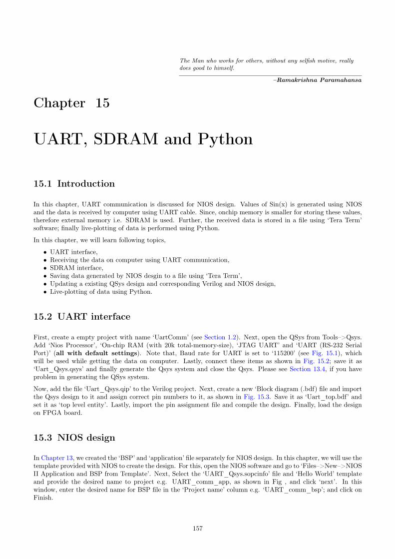
The Man who works for others, without any selfish motive, reallydoes good to himself.
–Ramakrishna Paramahansa
Chapter 15
UART, SDRAM and Python
15.1 Introduction
In this chapter, UART communication is discussed for NIOS design. Values of Sin(x) is generated using NIOSand the data is received by computer using UART cable. Since, onchip memory is smaller for storing these values,therefore external memory i.e. SDRAM is used. Further, the received data is stored in a file using ‘Tera Term’software; finally live-plotting of data is performed using Python.
In this chapter, we will learn following topics,
• UART interface,• Receiving the data on computer using UART communication,• SDRAM interface,• Saving data generated by NIOS desgin to a file using ‘Tera Term’,• Updating a existing QSys design and corresponding Verilog and NIOS design,• Live-plotting of data using Python.
15.2 UART interface
First, create a empty project with name ‘UartComm’ (see Section 1.2). Next, open the QSys from Tools–>Qsys.Add ‘Nios Processor’, ‘On-chip RAM (with 20k total-memory-size), ‘JTAG UART’ and ‘UART (RS-232 SerialPort)’ (all with default settings). Note that, Baud rate for UART is set to ‘115200’ (see Fig. 15.1), whichwill be used while getting the data on computer. Lastly, connect these items as shown in Fig. 15.2; save it as‘Uart_Qsys.qsys’ and finally generate the Qsys system and close the Qsys. Please see Section 13.4, if you haveproblem in generating the QSys system.
Now, add the file ‘Uart_Qsys.qip’ to the Verilog project. Next, create a new ‘Block diagram (.bdf) file and importthe Qsys design to it and assign correct pin numbers to it, as shown in Fig. 15.3. Save it as ‘Uart_top.bdf’ andset it as ‘top level entity’. Lastly, import the pin assignment file and compile the design. Finally, load the designon FPGA board.
15.3 NIOS design
In Chapter 13, we created the ‘BSP’ and ‘application’ file separately for NIOS design. In this chapter, we will use thetemplate provided with NIOS to create the design. For this, open the NIOS software and go to ‘Files–>New–>NIOSII Application and BSP from Template’. Next, Select the ‘UART_Qsys.sopcinfo’ file and ‘Hello World’ templateand provide the desired name to project e.g. UART_comm_app, as shown in Fig , and click ‘next’. In thiswindow, enter the desired name for BSP file in the ‘Project name’ column e.g. ‘UART_comm_bsp’; and click onFinish.
157

FPGA designs with Verilog and SystemVerilog
Fig. 15.1: UART settings
Fig. 15.2: Qsys connections
15.3. NIOS design 158
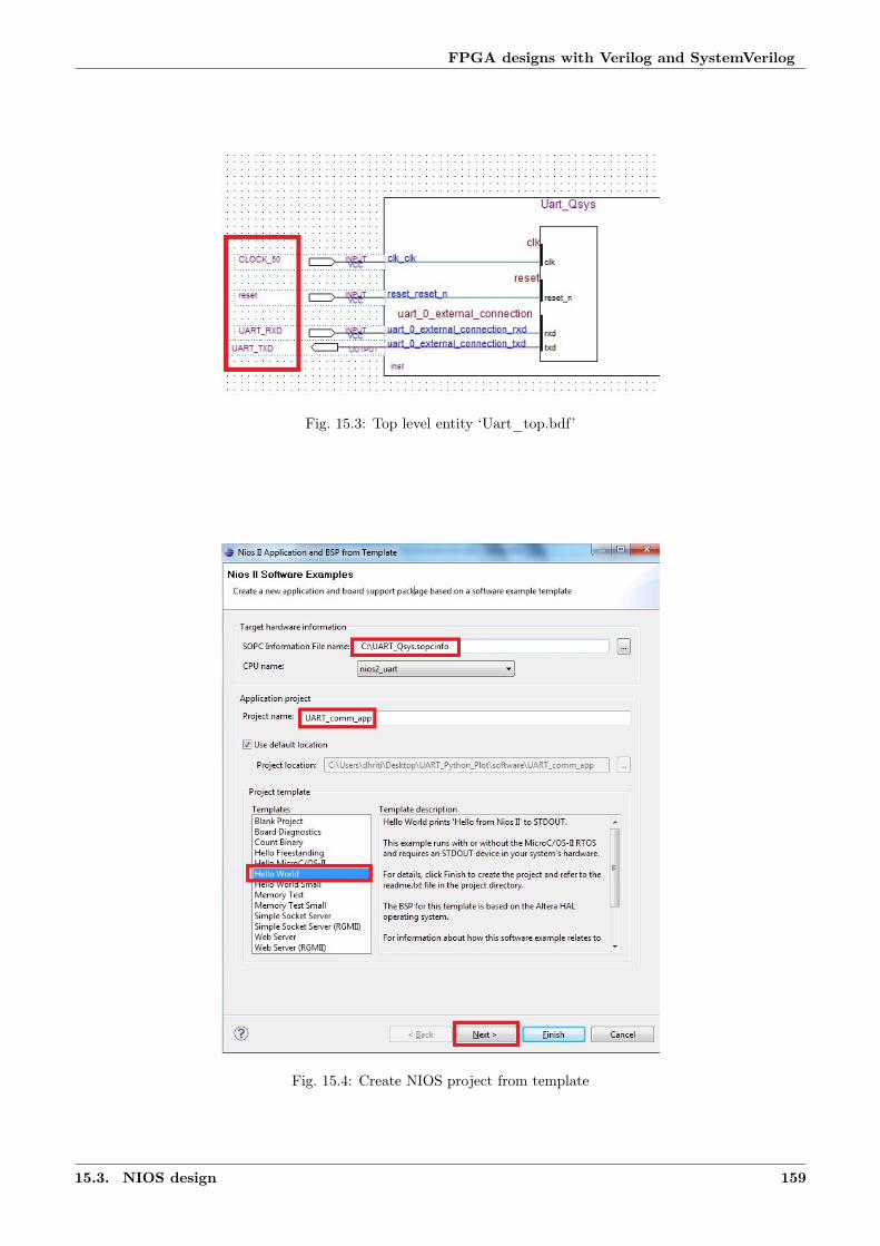
FPGA designs with Verilog and SystemVerilog
Fig. 15.3: Top level entity ‘Uart_top.bdf’
Fig. 15.4: Create NIOS project from template
15.3. NIOS design 159
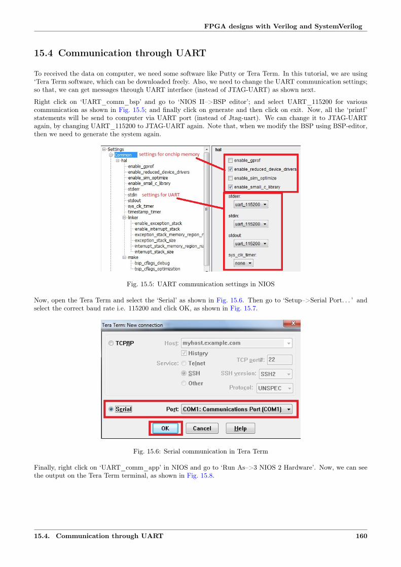
FPGA designs with Verilog and SystemVerilog
15.4 Communication through UART
To received the data on computer, we need some software like Putty or Tera Term. In this tutorial, we are using‘Tera Term software, which can be downloaded freely. Also, we need to change the UART communication settings;so that, we can get messages through UART interface (instead of JTAG-UART) as shown next.
Right click on ‘UART_comm_bsp’ and go to ‘NIOS II–>BSP editor’; and select UART_115200 for variouscommunication as shown in Fig. 15.5; and finally click on generate and then click on exit. Now, all the ‘printf’statements will be send to computer via UART port (instead of Jtag-uart). We can change it to JTAG-UARTagain, by changing UART_115200 to JTAG-UART again. Note that, when we modify the BSP using BSP-editor,then we need to generate the system again.
Fig. 15.5: UART communication settings in NIOS
Now, open the Tera Term and select the ‘Serial’ as shown in Fig. 15.6. Then go to ‘Setup–>Serial Port. . . ’ andselect the correct baud rate i.e. 115200 and click OK, as shown in Fig. 15.7.
Fig. 15.6: Serial communication in Tera Term
Finally, right click on ‘UART_comm_app’ in NIOS and go to ‘Run As–>3 NIOS 2 Hardware’. Now, we can seethe output on the Tera Term terminal, as shown in Fig. 15.8.
15.4. Communication through UART 160
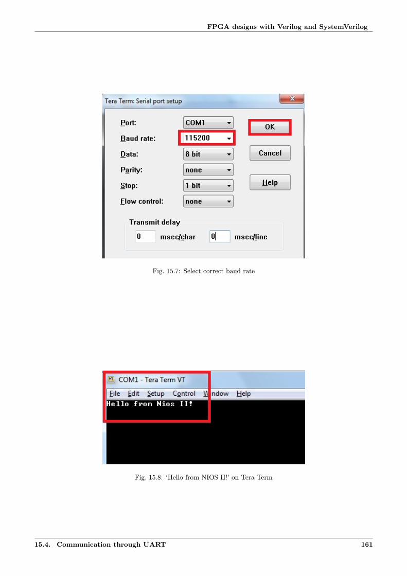
FPGA designs with Verilog and SystemVerilog
Fig. 15.7: Select correct baud rate
Fig. 15.8: ‘Hello from NIOS II!’ on Tera Term
15.4. Communication through UART 161

FPGA designs with Verilog and SystemVerilog
15.5 SDRAM Interface
Our next aim is to generate the Sine waves using NIOS and then plot the waveforms using python. If we write theC-code in current design, then our system will report the memory issue as onchip memory is too small; thereforewe need to use external memory. In this section, first, we will update the Qsys design with SDRAM interface,then we will update the Quartus design and finally add the C-code to generate the Sine waves.
15.5.1 Modify QSys
First, Open the UART_Qsys.qsys file in QSys software. Now, add SDRAM controller with default settings, asshown in Fig. 15.9. Next, connect all the ports of SDRMA as shown in Fig. 15.10. Then, double click the‘nios2_qsys_0’ and select ‘SDRAM’ as reset and exception vector memory, as shown in Fig. 15.11.
Fig. 15.9: SDRAM controller
Fig. 15.10: SDRAM connections
Fig. 15.11: Select SDRAM as vector memories
Next, we will add ‘Switches’ to control the amplitude of the sine waves. For this add the PIO device of ‘8 bit with
15.5. SDRAM Interface 162

FPGA designs with Verilog and SystemVerilog
type input’, and rename it as ‘switch’, as shown in Fig. 15.12 . Finally, go to System–>Assign base addresses, andgenerate the system.
Fig. 15.12: Add switches for controlling the amplitude of sine waves
15.5.2 Modify Top level Quartus design
Now, open the ‘Uart_top.bdf’ file in Quartus. Right click on the ‘Uart_Qsys’ block and select ‘Update symbolor block’; then select the option ‘Selected symbol(s) or block(s)’ and press OK. It will display all the ports for‘SDRAM’ and switches. Next, we need to assign the correct ‘pin names’ to these ports, as shown in Fig. 15.13.
Fig. 15.13: Assigning Pins to SDRAM and Switches
Note that, there should be ‘-3 ns clock delay’ for SDRAM as compare to FPGA clock, therefore we need to add theclock with ‘-3 ns delay’. For this, double click on the Uart_top.bdf (anywhere in the file), and select ‘MegaWizardPlug-In Manager’. Then select ‘Create a new custom megafunction variation’ in the popped-up window and clicknext. Now, select ALTPLL from IO in Installed Plug-Ins option, as shown in Fig. 15.14, and click next. Then,follow the figures from Fig. 15.15 to Fig. 15.20 to add the ALTPLL to current design i.e. ‘Uart_top.bdf’. Finally,connect the ports of this design as shown in Fig. 15.21. Note that, in these connections, output of ATLPLL designis connected to ‘DRAM_CLK’, which is clock-port for DRAM. Lastly, compile and load the design on FPGAboard.
15.5.3 Updating NIOS design
Since, we have udpated the QSys design, therefore the corresponding .sopcinfo file is also updated. Further,BSP files depends on the .sopcinfo file, therefore we need to update the BSP as well. For this, right click on‘Uart_comm_bsp’ and go to ‘NIOS II–>BSP Editor; and update the BSP as shown in Fig. 15.22 and click on
15.5. SDRAM Interface 163
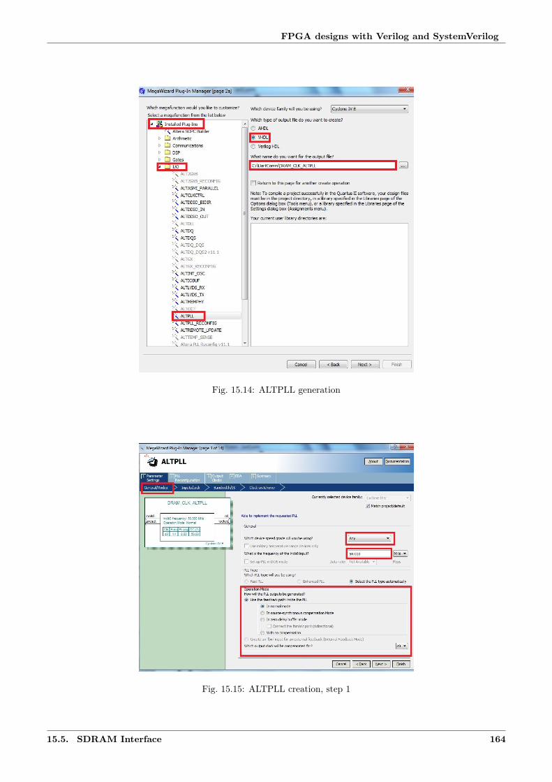
FPGA designs with Verilog and SystemVerilog
Fig. 15.14: ALTPLL generation
Fig. 15.15: ALTPLL creation, step 1
15.5. SDRAM Interface 164

FPGA designs with Verilog and SystemVerilog
Fig. 15.16: ALTPLL creation, step 2
Fig. 15.17: ALTPLL creation, step 3
15.5. SDRAM Interface 165

FPGA designs with Verilog and SystemVerilog
Fig. 15.18: ALTPLL creation, step 4
Fig. 15.19: ALTPLL creation, step 5
Fig. 15.20: ALTPLL creation, step 6
15.5. SDRAM Interface 166
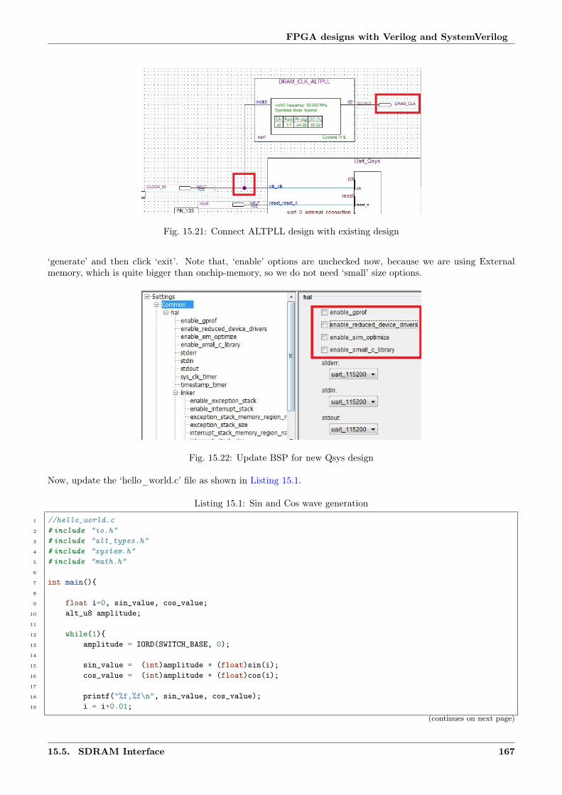
FPGA designs with Verilog and SystemVerilog
Fig. 15.21: Connect ALTPLL design with existing design
‘generate’ and then click ‘exit’. Note that, ‘enable’ options are unchecked now, because we are using Externalmemory, which is quite bigger than onchip-memory, so we do not need ‘small’ size options.
Fig. 15.22: Update BSP for new Qsys design
Now, update the ‘hello_world.c’ file as shown in Listing 15.1.
Listing 15.1: Sin and Cos wave generation
1 //hello_world.c2 # include "io.h"3 # include "alt_types.h"4 # include "system.h"5 # include "math.h"6
7 int main(){8
9 float i=0, sin_value, cos_value;10 alt_u8 amplitude;11
12 while(1){13 amplitude = IORD(SWITCH_BASE, 0);14
15 sin_value = (int)amplitude * (float)sin(i);16 cos_value = (int)amplitude * (float)cos(i);17
18 printf("%f,%f\n", sin_value, cos_value);19 i = i+0.01;
(continues on next page)
15.5. SDRAM Interface 167

FPGA designs with Verilog and SystemVerilog
(continued from previous page)
20
21 }22 }
In Tera Term, we can save the received values in text file as well. Next, go Files–>Log and select the filename atdesired location to save the data e.g. ‘sineData.txt’.
Finally, right click on ‘UART_comm_app’ in NIOS and go to ‘Run As–>3 NIOS 2 Hardware’. Now, we can seethe decimal values on the screen. If all the switches are at ‘0’ position, then values will be ‘0.000’ as amplitude iszero. Further, we can use any combination of 8 Switches to increase the amplitude of the sine and cosine waves.Also, result will be stored in the ‘sineData.txt’ file. Content of this file is shown in Fig. 15.23
Fig. 15.23: Content of ‘sineData.txt’ file
15.6 Live plotting the data
In the previous section, we store the sine and cosine wave data on the ‘sineData.txt’ using UART communication.Now, our last task is to plot this data continuously, so that it look line animation. For this save the Listing 15.2,in the location where ‘sineData.txt’ is saved. Now, open the command prompt and go to the location of pythonfile. Finally, type ‘python main.py’ and press enter. This will start plotting the waveform continuously basedon the data received and stored on the ‘sineData.txt’ file. The corresponding plots are shown in Fig. 15.24.
Listing 15.2: Code for live plotting of logged data
1 import matplotlib.pyplot as plt2 import matplotlib.animation as animation3
4 fig = plt.figure()5 ax1 = fig.add_subplot(2,1,1)6 ax2 = fig.add_subplot(2,1,2)7
8 def animate(i):9 readData = open("sineData.txt","r").read()
10 data = readData.split('\n')11 sin_array = []12 cos_array = []13 for d in data:14 if len(d)>1:15 sin, cos = d.split(',')16 sin_array.append(sin)17 cos_array.append(cos)18 ax1.clear()19 ax1.plot(sin_array)20
21 ax2.clear()22 ax2.plot(cos_array)23
24 def main():(continues on next page)
15.6. Live plotting the data 168
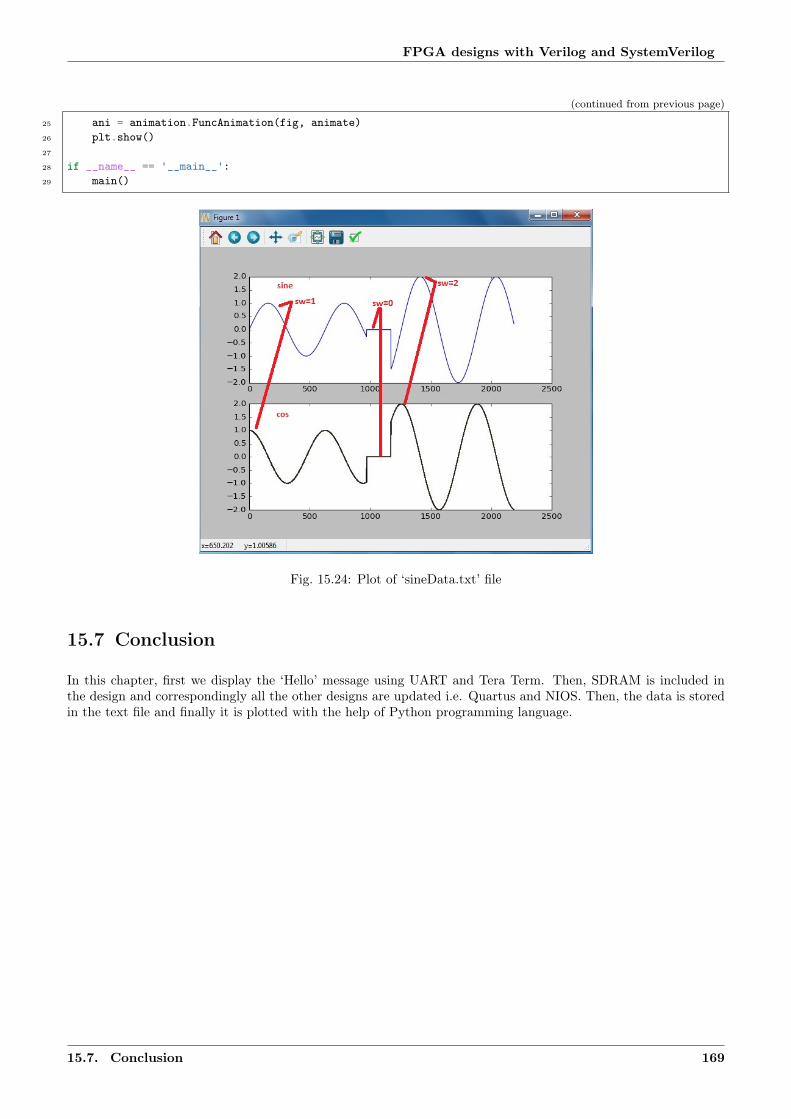
FPGA designs with Verilog and SystemVerilog
(continued from previous page)
25 ani = animation.FuncAnimation(fig, animate)26 plt.show()27
28 if __name__ == '__main__':29 main()
Fig. 15.24: Plot of ‘sineData.txt’ file
15.7 Conclusion
In this chapter, first we display the ‘Hello’ message using UART and Tera Term. Then, SDRAM is included inthe design and correspondingly all the other designs are updated i.e. Quartus and NIOS. Then, the data is storedin the text file and finally it is plotted with the help of Python programming language.
15.7. Conclusion 169

Who says God has created this world? We have created it by ourown imagination. God is supreme, independent. When we say hehas created this illusion, we lower him and his infinity. He is beyondall this.Only when we find him in ourselves, and even in our day today life, do all doubts vanish.
–Meher Baba
Appendix A
Script execution in Quartus and Modelsim
To use the codes of the tutorial, Quartus and Modelsim softwares are discussed here. Please see the video: Createand simulate projects using Quartus and Modelsim, if you have problem in using Quartus or Modelsim software.
Note: Note that, this appendix uses the VHDL file, but same procedure is applicable for Verilog projects as well.
A.1 Quartus
In this section, ‘RTL view generation’ and ‘loading the design on FPGA board’ are discussed.
A.1.1 Generating the RTL view
The execute the codes, open the ‘overview.qpf’ using Quartus software. Then go to the files and right-click on theVerilog file to which you want to execute and click on ‘Set as Top-Level Entity’ as shown in Fig. 1.1. Then press‘ctrl+L’ to start the compilation.
To generate the designs, go to Tools–>Netlist Viewer–>RTL Viewer; and it will display the design.
A.1.2 Loading design on FPGA board
Quartus software generates two types of files after compilation i.e. ‘.sof’ and ‘.pof’ file. These files are used to loadthe designs on the FPGA board. Note that ‘.sof’ file are erased once we turn off the FPGA device; whereas ‘.pof’files are permanently loaded (unless removed or overwrite manually). For loading the design on the FPGA board,we need to make following two changes which are board specific,
• First, we need to select the board by clicking on Assignments–>Device, and then select the correct boardfrom the list.
• Next, connect the input/output ports of the design to FPGA board by clicking on Assignments–>PinPlanner. It will show all the input and output ports of the design and we need to fill ‘location’ column forthese ports.
• To load the design on FPGA board, go to Tools–>Programmer.• Then select JTAG mode to load the ‘.sof’ file; or ‘Active Serial Programming’ mode for loading the ‘.pof’
file. Then click on ‘add file’ and select the ‘.sof/.pof’ file and click on ‘start’. In this way, the design will beloaded on FGPA board.
170
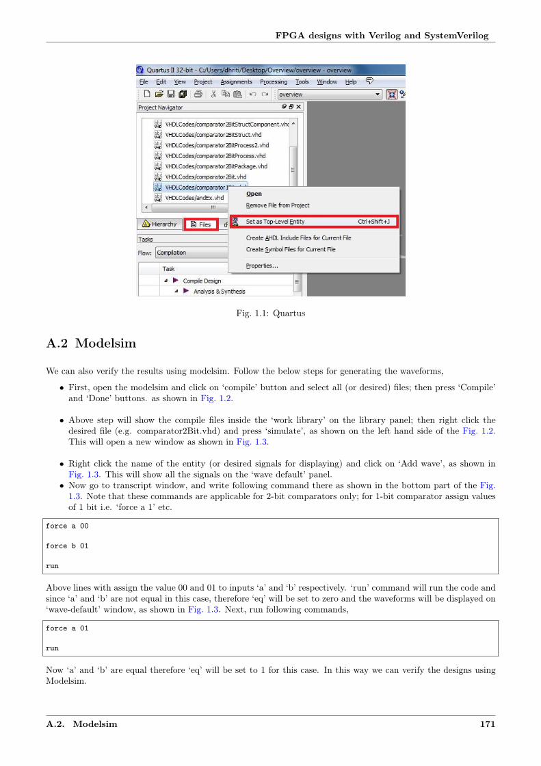
FPGA designs with Verilog and SystemVerilog
Fig. 1.1: Quartus
A.2 Modelsim
We can also verify the results using modelsim. Follow the below steps for generating the waveforms,
• First, open the modelsim and click on ‘compile’ button and select all (or desired) files; then press ‘Compile’and ‘Done’ buttons. as shown in Fig. 1.2.
• Above step will show the compile files inside the ‘work library’ on the library panel; then right click thedesired file (e.g. comparator2Bit.vhd) and press ‘simulate’, as shown on the left hand side of the Fig. 1.2.This will open a new window as shown in Fig. 1.3.
• Right click the name of the entity (or desired signals for displaying) and click on ‘Add wave’, as shown inFig. 1.3. This will show all the signals on the ‘wave default’ panel.
• Now go to transcript window, and write following command there as shown in the bottom part of the Fig.1.3. Note that these commands are applicable for 2-bit comparators only; for 1-bit comparator assign valuesof 1 bit i.e. ‘force a 1’ etc.
force a 00
force b 01
run
Above lines with assign the value 00 and 01 to inputs ‘a’ and ‘b’ respectively. ‘run’ command will run the code andsince ‘a’ and ‘b’ are not equal in this case, therefore ‘eq’ will be set to zero and the waveforms will be displayed on‘wave-default’ window, as shown in Fig. 1.3. Next, run following commands,
force a 01
run
Now ‘a’ and ‘b’ are equal therefore ‘eq’ will be set to 1 for this case. In this way we can verify the designs usingModelsim.
A.2. Modelsim 171
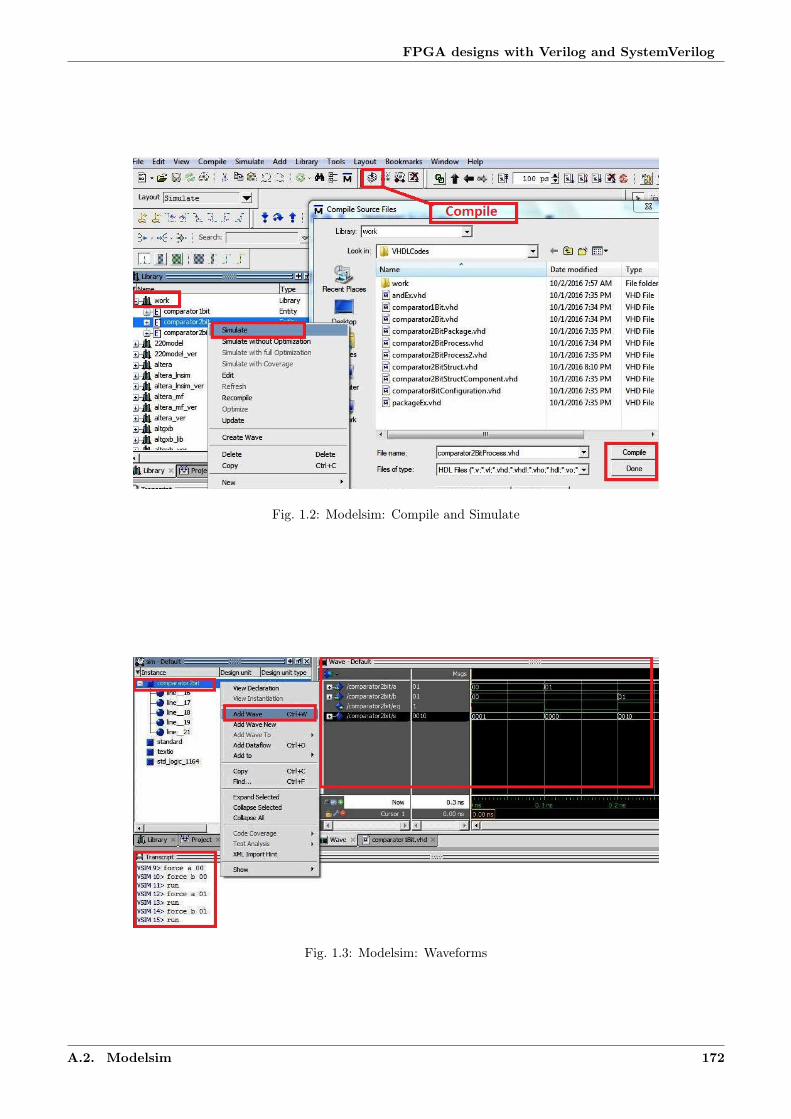
FPGA designs with Verilog and SystemVerilog
Fig. 1.2: Modelsim: Compile and Simulate
Fig. 1.3: Modelsim: Waveforms
A.2. Modelsim 172
The most important is, the Lord is one, and you shall love the Lordyour God with all your heart and with all your soul and with allyour mind and with all your strength. The second is this, you shouldlove your neighbor as yourself.
–Jesus Christ
Appendix B
How to implement NIOS-designs
Please implement the designs of Chapter 1 (i.e. Verilog design) and Chapter 13 (i.e. NIOS design), before followingthis section.
Unlike Verilog designs, NIOS designs can not be run directly on a system just by downloading it. Therefore, onlyrequired design-files are provided (instead of complete project) for NIOS systems. We need to follow the stepsprovided in this section, to implement the NIOS design on the FPGA.
Note that Verilog codes and C/C++ codes of the tutorials are available on the website; these codes are providedinside the folders with name VerilogCodes (or Verilog) and CppCodes (or c, or software/ApplicationName_app)respectively. Along with these codes, .qsys files are also provided, which are used to generated the .sopc and.sopcinfo files. Lastly, pin assignments files for various Altera-boards are also provided in the zip folders.
Please follow the below step, to compile the NIOS design on new system. Further, if you change the location ofthe project in the computer (after compiling it successfully), then NIOS design must be implemented again byfollowing the instruction in Section B.4
Note: Note that, this appendix uses the VHDL file, but same procedure is applicable for Verilog projects as well.
Codes files used in this section, are available in the folder ‘Appendix-How_to_implement_Nios_design’, whichcan be ‘downloaded from the website.
B.1 Create project
First create a new Quartus project (with any name) as shown in Section 1.2; and copy all the downloaded files(i.e. VerilogCodes, CppCodes, Pin-assignments and .qsys files) inside the main project directory.
B.2 Add all files from VerilogCodes folder
• Next, add all the files inside the folder ‘VerilogCodes’, to project as shown in Fig. 2.1. Do not forget to select‘All files’ option while adding the files as shown in Fig. 2.1.
• In Chapter 1, we created ‘Verilog codes’ from the ‘Block schematic design’. These two designs are same,therefore while compilation the multiple-design error will be reported. Therefore we need to remove theduplicate designs as shown in Fig. 2.2. Note that, there are two duplicate designs i.e. one for half_adderand other is for full_adder as shown in the figure.
• In this project, ‘full_adder_nios_test.bdf’ is the top-level design, which is shown in Fig. 2.3. Note that,here ‘name method’ is used to connect the ‘addr_input[2..0] with port ‘a’, ‘b’ and ‘c’. The method for givingname to a wire is shown in figure (see on the bottom-left side).
173

FPGA designs with Verilog and SystemVerilog
Fig. 2.1: Add all files from VerilogCodes folder
Fig. 2.2: Add all files from VerilogCodes folder
B.2. Add all files from VerilogCodes folder 174
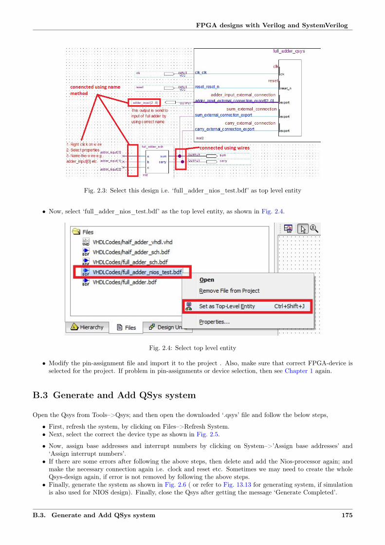
FPGA designs with Verilog and SystemVerilog
Fig. 2.3: Select this design i.e. ‘full_adder_nios_test.bdf’ as top level entity
• Now, select ‘full_adder_nios_test.bdf’ as the top level entity, as shown in Fig. 2.4.
Fig. 2.4: Select top level entity
• Modify the pin-assignment file and import it to the project . Also, make sure that correct FPGA-device isselected for the project. If problem in pin-assignments or device selection, then see Chapter 1 again.
B.3 Generate and Add QSys system
Open the Qsys from Tools–>Qsys; and then open the downloaded ‘.qsys’ file and follow the below steps,
• First, refresh the system, by clicking on Files–>Refresh System.• Next, select the correct the device type as shown in Fig. 2.5.
• Now, assign base addresses and interrupt numbers by clicking on System–>’Assign base addresses’ and‘Assign interrupt numbers’.
• If there are some errors after following the above steps, then delete and add the Nios-processor again; andmake the necessary connection again i.e. clock and reset etc. Sometimes we may need to create the wholeQsys-design again, if error is not removed by following the above steps.
• Finally, generate the system as shown in Fig. 2.6 ( or refer to Fig. 13.13 for generating system, if simulationis also used for NIOS design). Finally, close the Qsys after getting the message ‘Generate Completed’.
B.3. Generate and Add QSys system 175

FPGA designs with Verilog and SystemVerilog
Fig. 2.5: Change device family
Fig. 2.6: Generate QSys system
B.3. Generate and Add QSys system 176
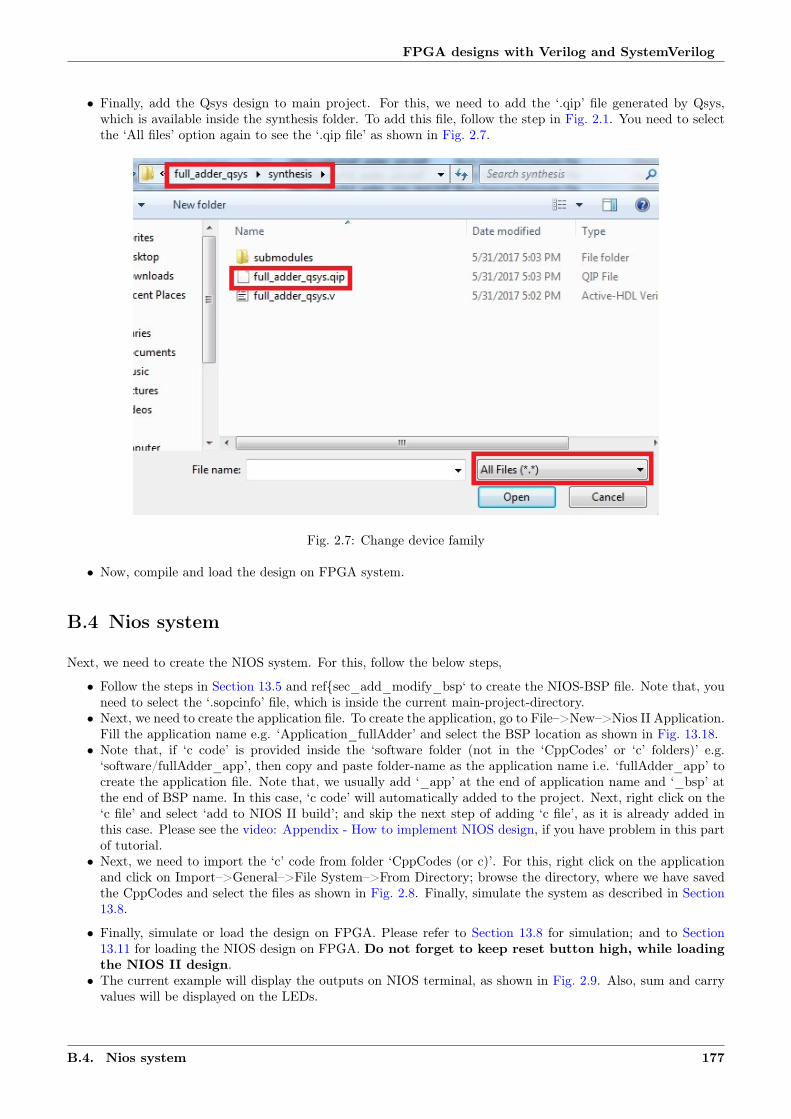
FPGA designs with Verilog and SystemVerilog
• Finally, add the Qsys design to main project. For this, we need to add the ‘.qip’ file generated by Qsys,which is available inside the synthesis folder. To add this file, follow the step in Fig. 2.1. You need to selectthe ‘All files’ option again to see the ‘.qip file’ as shown in Fig. 2.7.
Fig. 2.7: Change device family
• Now, compile and load the design on FPGA system.
B.4 Nios system
Next, we need to create the NIOS system. For this, follow the below steps,
• Follow the steps in Section 13.5 and ref{sec_add_modify_bsp‘ to create the NIOS-BSP file. Note that, youneed to select the ‘.sopcinfo’ file, which is inside the current main-project-directory.
• Next, we need to create the application file. To create the application, go to File–>New–>Nios II Application.Fill the application name e.g. ‘Application_fullAdder’ and select the BSP location as shown in Fig. 13.18.
• Note that, if ‘c code’ is provided inside the ‘software folder (not in the ‘CppCodes’ or ‘c’ folders)’ e.g.‘software/fullAdder_app’, then copy and paste folder-name as the application name i.e. ‘fullAdder_app’ tocreate the application file. Note that, we usually add ‘_app’ at the end of application name and ‘_bsp’ atthe end of BSP name. In this case, ‘c code’ will automatically added to the project. Next, right click on the‘c file’ and select ‘add to NIOS II build’; and skip the next step of adding ‘c file’, as it is already added inthis case. Please see the video: Appendix - How to implement NIOS design, if you have problem in this partof tutorial.
• Next, we need to import the ‘c’ code from folder ‘CppCodes (or c)’. For this, right click on the applicationand click on Import–>General–>File System–>From Directory; browse the directory, where we have savedthe CppCodes and select the files as shown in Fig. 2.8. Finally, simulate the system as described in Section13.8.
• Finally, simulate or load the design on FPGA. Please refer to Section 13.8 for simulation; and to Section13.11 for loading the NIOS design on FPGA. Do not forget to keep reset button high, while loadingthe NIOS II design.
• The current example will display the outputs on NIOS terminal, as shown in Fig. 2.9. Also, sum and carryvalues will be displayed on the LEDs.
B.4. Nios system 177

FPGA designs with Verilog and SystemVerilog
Fig. 2.8: Adding C files
Fig. 2.9: Nios Output of current design
B.4. Nios system 178