Word-Level Predicate-Abstraction and Refinement Techniques for Verifying RTL Verilog
Upload
independentCategory
view
1download
0
Switching Circuit
& Logic Design
Basic Logic Design Practicing
- Quartus Schematic to Verilog
1

Introduction to Gate Level Verilog HDL--Convert Quartus II Schematic to Verilog
Lecturer: TA 謝明倫 (BL-421)[email protected]
交換電路與邏輯設計課程四班共同教學Professors: 吳安宇簡韶逸盧奕璋江介宏
2
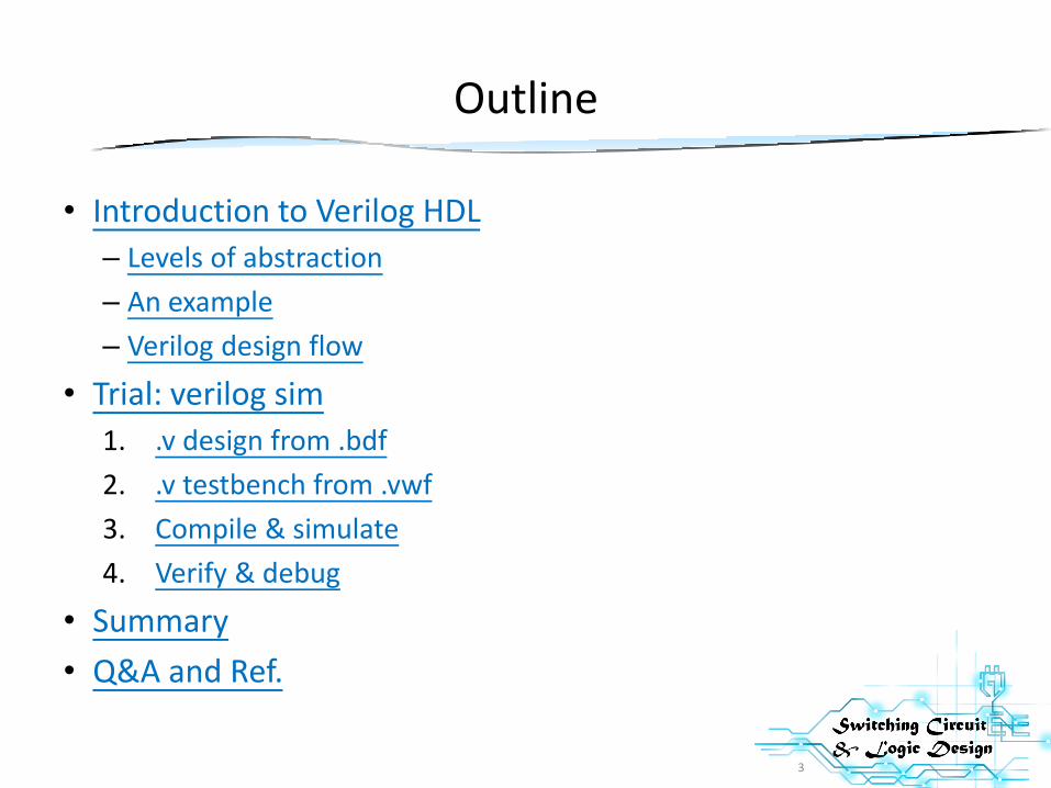
Outline
• Introduction to Verilog HDL
– Levels of abstraction
– An example
– Verilog design flow
• Trial: verilog sim
1. .v design from .bdf
2. .v testbench from .vwf
3. Compile & simulate
4. Verify & debug
• Summary
• Q&A and Ref.
3
Verilog HDL - Comb. Gate Level design
For Combinational & Gate-level only
4
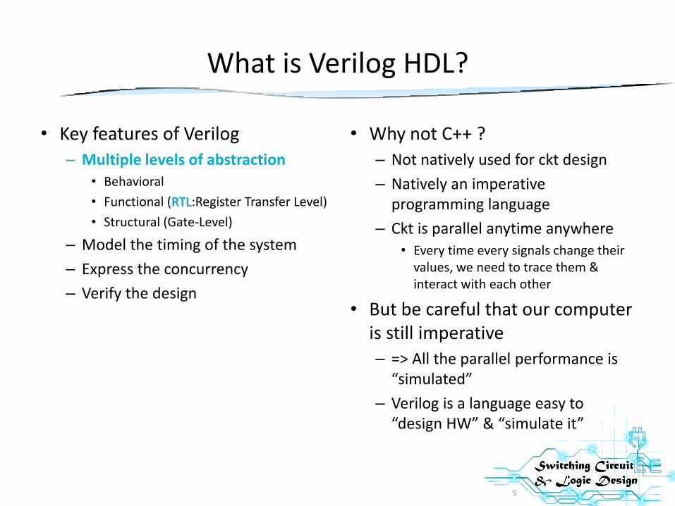
What is Verilog HDL?
• Key features of Verilog
– Multiple levels of abstraction • Behavioral
• Functional (RTL:Register Transfer Level)
• Structural (Gate-Level)
– Model the timing of the system
– Express the concurrency
– Verify the design
• Why not C++ ?
– Not natively used for ckt design
– Natively an imperative programming language
– Ckt is parallel anytime anywhere• Every time every signals change their
values, we need to trace them & interact with each other
• But be careful that our computer is still imperative
– => All the parallel performance is “simulated”
– Verilog is a language easy to “design HW” & “simulate it”
5
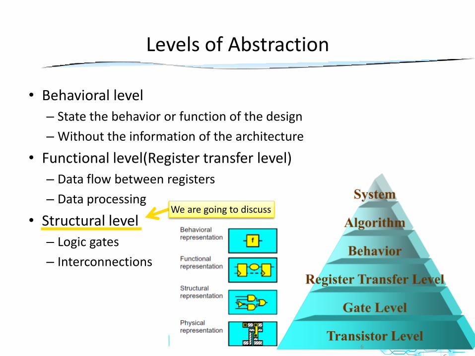
Levels of Abstraction
• Behavioral level
– State the behavior or function of the design
– Without the information of the architecture
• Functional level(Register transfer level)
– Data flow between registers
– Data processing
• Structural level
– Logic gates
– Interconnections
We are going to discuss
6
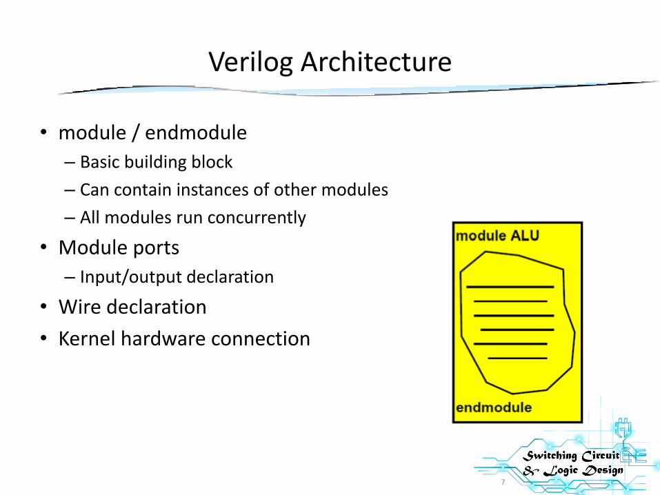
Verilog Architecture
• module / endmodule
– Basic building block
– Can contain instances of other modules
– All modules run concurrently
• Module ports
– Input/output declaration
• Wire declaration
• Kernel hardware connection
7
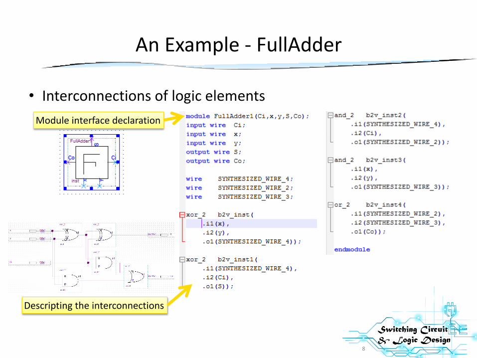
An Example - FullAdder
• Interconnections of logic elements
Module interface declaration
Descripting the interconnections
8
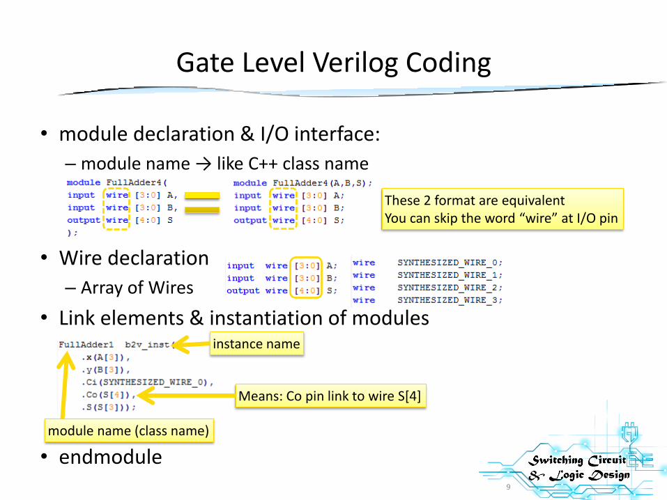
Gate Level Verilog Coding
• module declaration & I/O interface:
– module name → like C++ class name
• Wire declaration
– Array of Wires
• Link elements & instantiation of modules
These 2 format are equivalentYou can skip the word “wire” at I/O pin
module name (class name)
instance name
Means: Co pin link to wire S[4]
• endmodule9
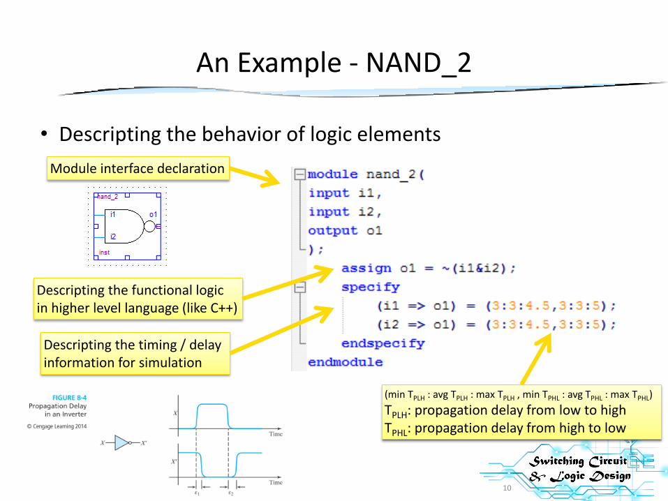
An Example - NAND_2
• Descripting the behavior of logic elements
Module interface declaration
Descripting the functional logicin higher level language (like C++)
Descripting the timing / delayinformation for simulation
(min TPLH : avg TPLH : max TPLH , min TPHL : avg TPHL : max TPHL)
TPLH: propagation delay from low to highTPHL: propagation delay from high to low
10

Verilog Coding - Comb.
• Operators
Arithmetic Operators
Relational Operators
Equality Operators
Logical Operators
Bit-wise Operators
Unary Reduction
Shift Operators
Conditional Operators
Concatenations
+, -, *, /, %
<, <=, >, >=
==, !=, ===, !==
!, &&, ||
~, &, |, ^, ~^
&, ~&, |, ~|, ^, ~^
>>, <<
?:
{}
11
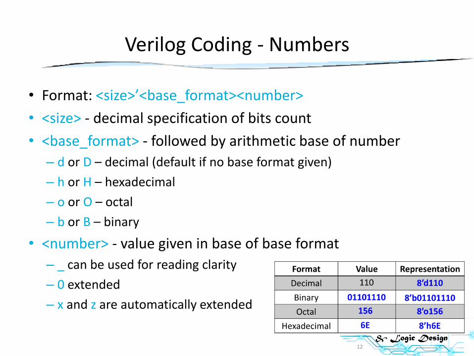
Verilog Coding - Numbers
• Format: <size>’<base_format><number>
• <size> - decimal specification of bits count
• <base_format> - followed by arithmetic base of number
– d or D – decimal (default if no base format given)
– h or H – hexadecimal
– o or O – octal
– b or B – binary
• <number> - value given in base of base format
– _ can be used for reading clarity
– 0 extended
– x and z are automatically extended
12
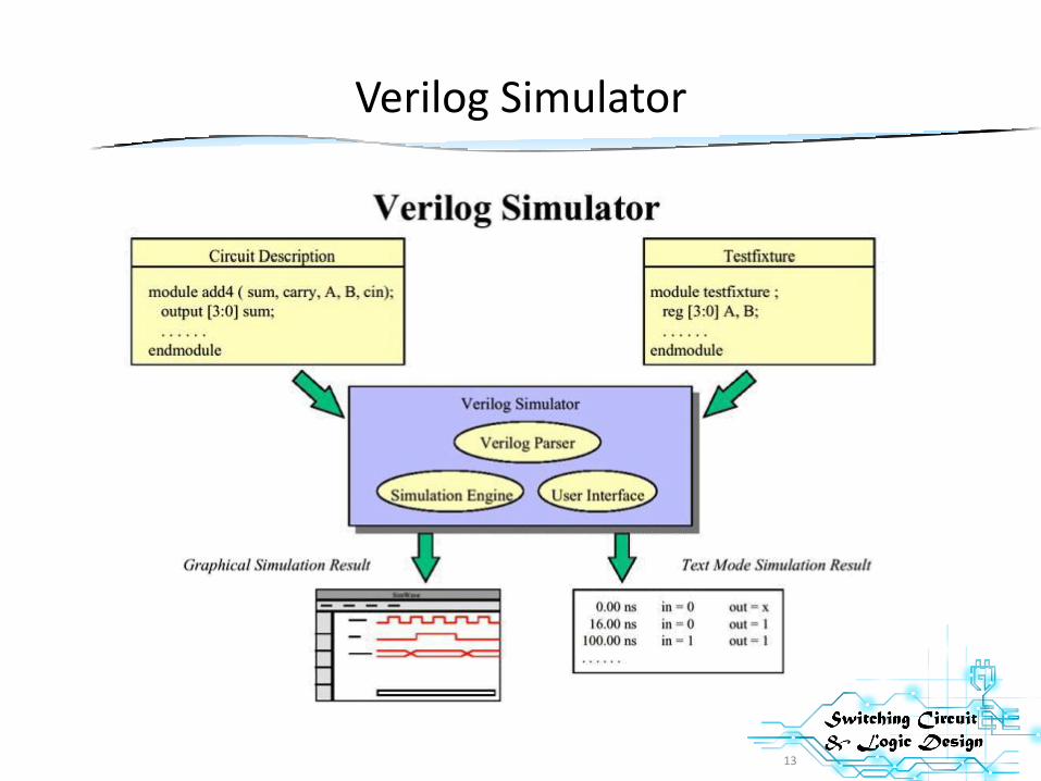
Verilog Simulator
13
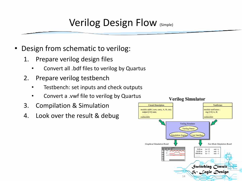
Verilog Design Flow (Simple)
• Design from schematic to verilog:
1. Prepare verilog design files
• Convert all .bdf files to verilog by Quartus
2. Prepare verilog testbench
• Testbench: set inputs and check outputs
• Convert a .vwf file to verilog by Quartus
3. Compilation & Simulation
4. Look over the result & debug
14
Verilog Simulation by Ourselves
15
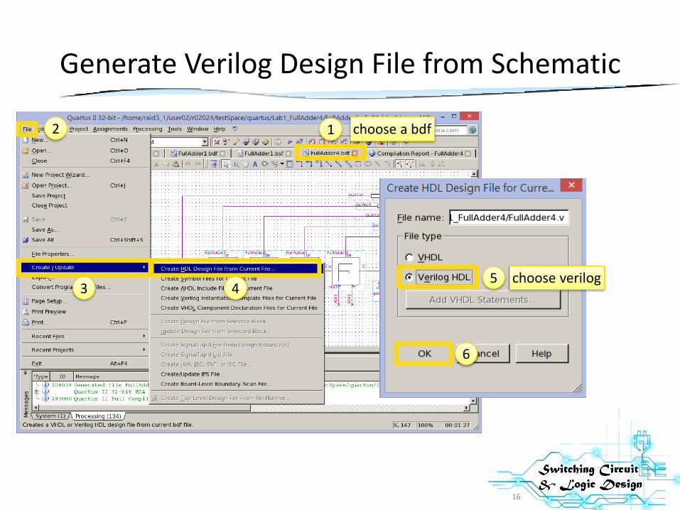
Generate Verilog Design File from Schematic
1 choose a bdf2
3 4choose verilog5
6
16
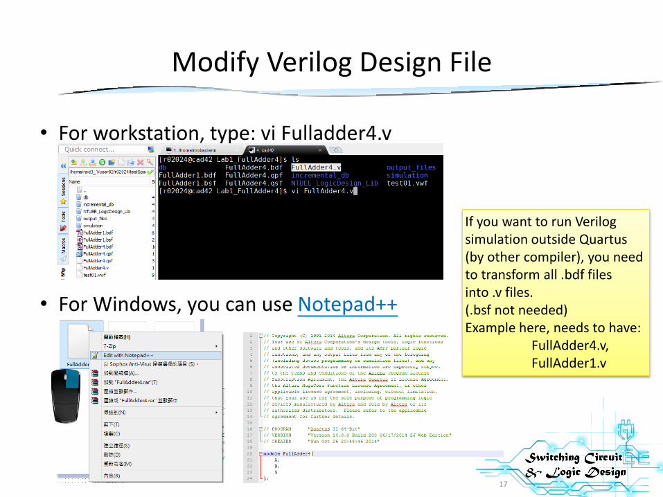
Modify Verilog Design File
• For workstation, type: vi Fulladder4.v
• For Windows, you can use Notepad++
If you want to run Verilog simulation outside Quartus(by other compiler), you need to transform all .bdf files into .v files.(.bsf not needed)Example here, needs to have:
FullAdder4.v,FullAdder1.v
17
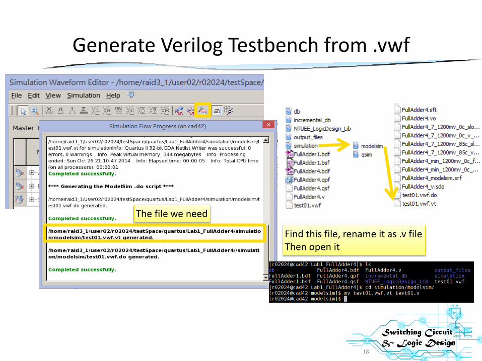
Generate Verilog Testbench from .vwf
The file we need
Find this file, rename it as .v fileThen open it
18
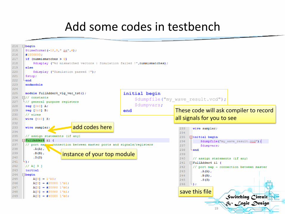
Add some codes in testbench
instance of your top module
add codes here
initial begin
$dumpfile("my_wave_result.vcd");
$dumpvars;
end These code will ask compiler to recordall signals for you to see
save this file
19

Simulation by Verilog Compiler
20
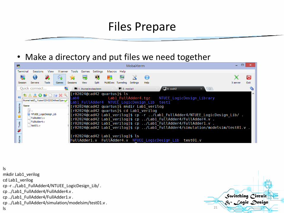
Files Prepare
• Make a directory and put files we need together
lsmkdir Lab1_verilogcd Lab1_verilogcp -r ../Lab1_FullAdder4/NTUEE_LogicDesign_Lib/ .cp ../Lab1_FullAdder4/FullAdder4.v .cp ../Lab1_FullAdder4/FullAdder1.v .cp ../Lab1_FullAdder4/simulation/modelsim/test01.v .ls 21

Run Simulation
• source some tool:
• Run:
source ~cvsd/cvsd.cshrc
source ~cvsd/verdi.cshrc
ncverilog test01.v FullAdder4.v FullAdder1.v
NTUEE_LogicDesign_Lib/verilog/elements.v +access+r
in one line, no “\n”
If you have problem sourcing verdi, please try:source /usr/spring_soft/CIC/verdi.cshrc
22
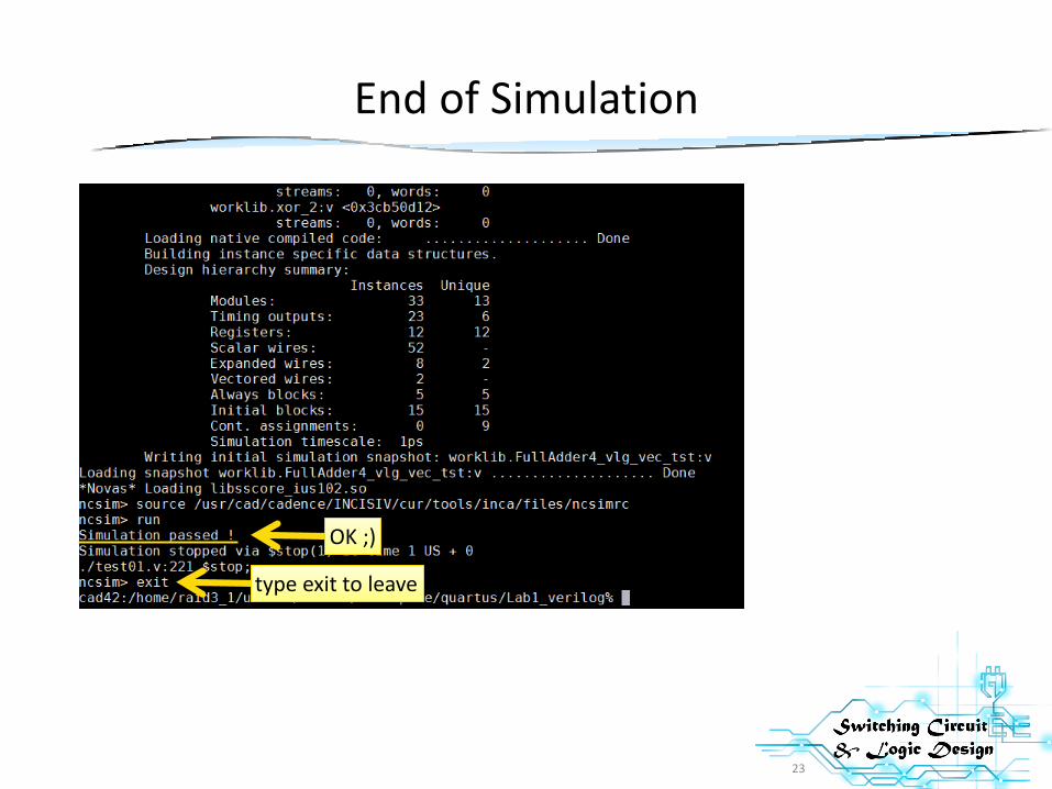
End of Simulation
type exit to leave
OK ;)
23
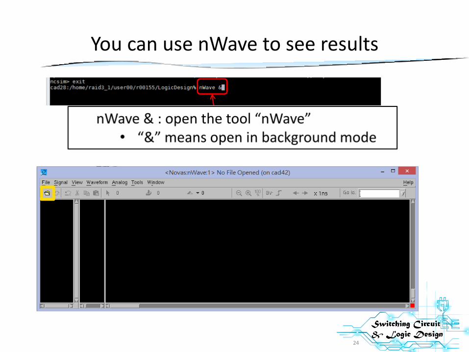
You can use nWave to see results
24
nWave
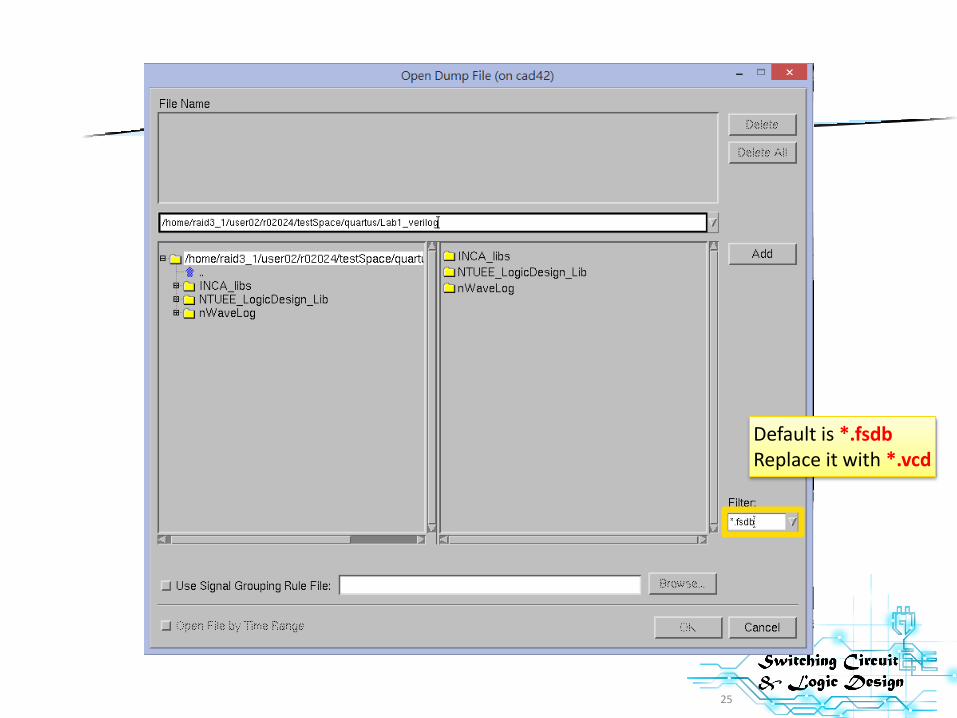
Default is *.fsdbReplace it with *.vcd
25
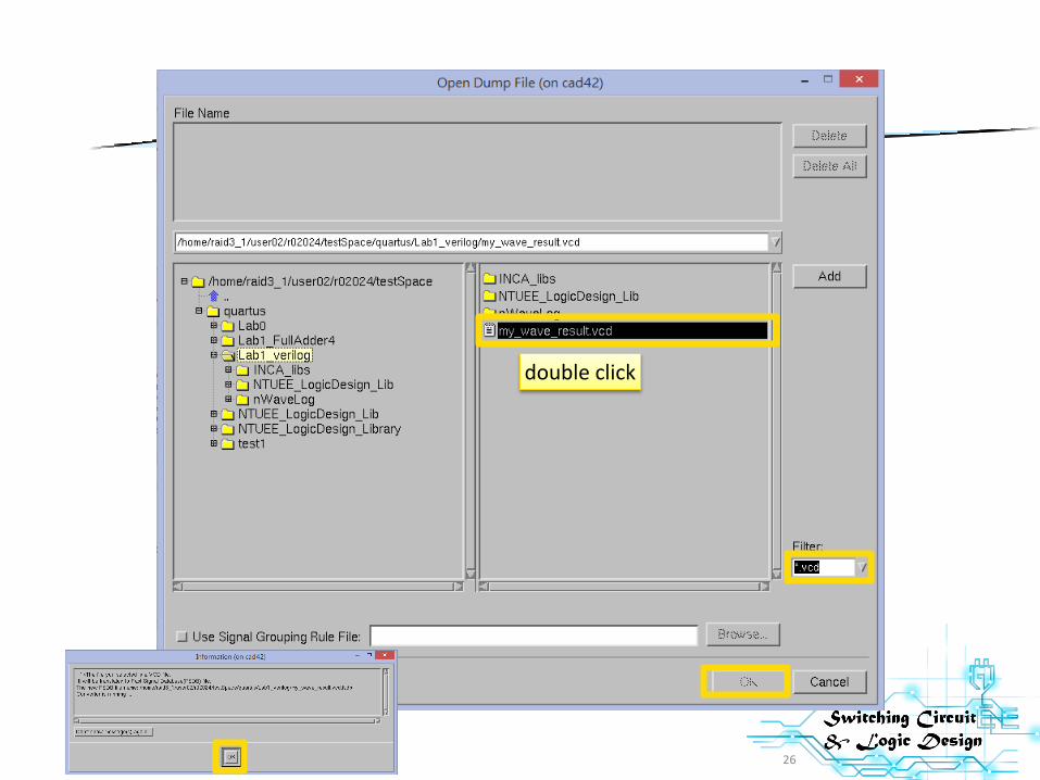
nWave
double click
26
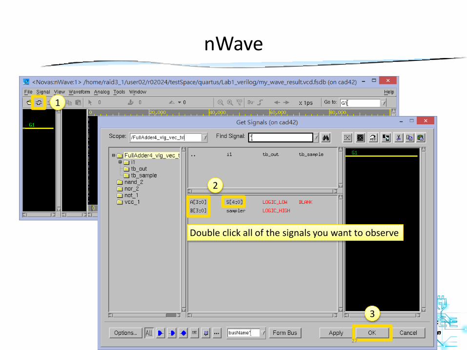
nWave
Double click all of the signals you want to observe
1
2
3
27

nWave
Pretty like simulation result as .vwf doesBut this time, the logic gates have it’s own delay (Not functional simulation only)So there are hazards & latency
Correct result with some latency
[Hint] Default format: Hex,you can change format at:Waveform→Signal Value Radix→[You want]
hazards
28
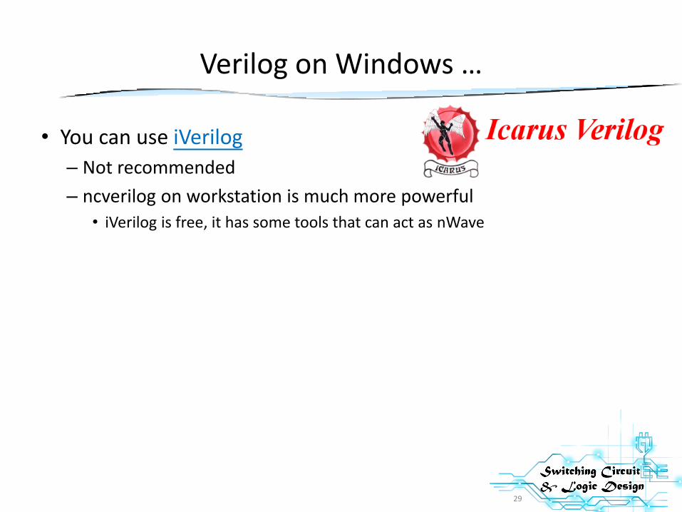
Verilog on Windows …
• You can use iVerilog
– Not recommended
– ncverilog on workstation is much more powerful
• iVerilog is free, it has some tools that can act as nWave
29

Summary
30
Summary
Design module
• From .bdf
• Divide-and-Conquer
• Partition the whole design into several parts – Derive the architecture of each sub-
module
• Make architecture figures before you write Verilog codes – Create hardware design in gate level
– Connection of sub-modules
Test-bench
• From .vwf
• Feed input data and compare output values at right timing slots
• Usually describe in behavioral level
• Not real hardware, just like software programming (e.g. C/C++)
31
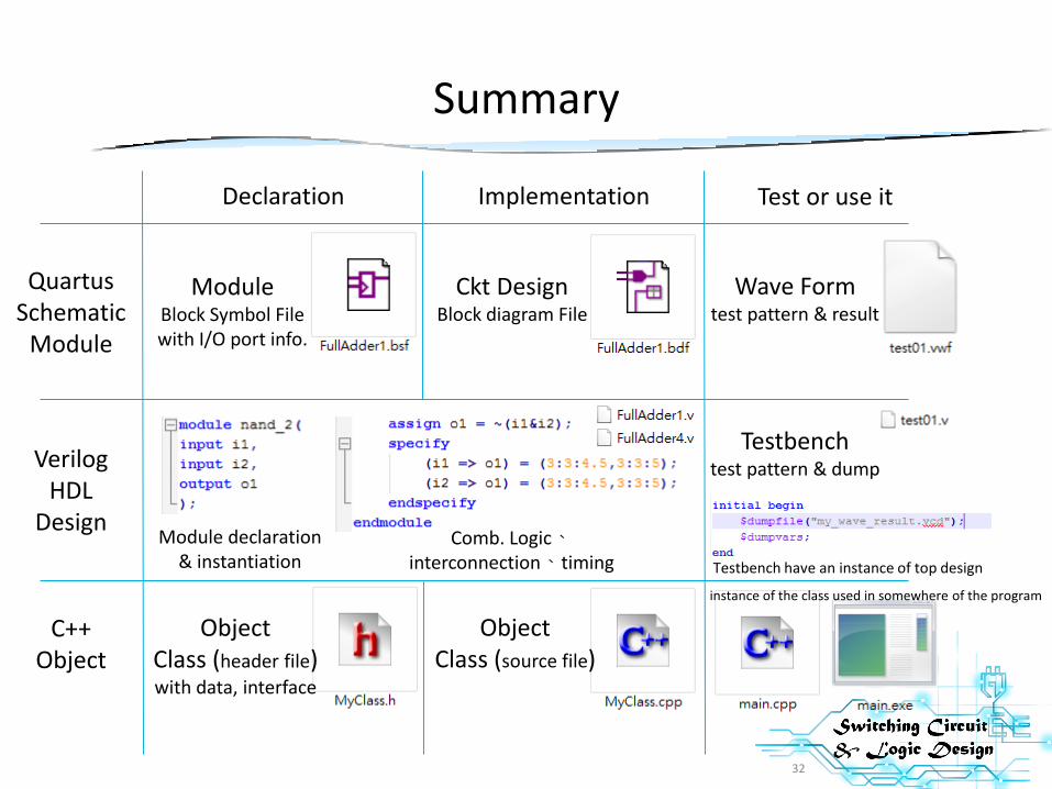
Summary
ImplementationDeclaration Test or use it
QuartusSchematic
Module
C++Object
ObjectClass (header file)with data, interface
ModuleBlock Symbol Filewith I/O port info.
Ckt DesignBlock diagram File
ObjectClass (source file)
Wave Formtest pattern & result
VerilogHDL
DesignModule declaration
& instantiationComb. Logic、
interconnection、timing
Testbenchtest pattern & dump
Testbench have an instance of top design
instance of the class used in somewhere of the program
32
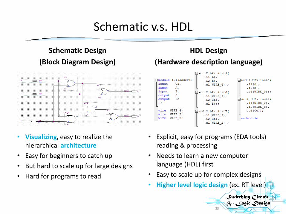
Schematic v.s. HDL
Schematic Design
(Block Diagram Design)
• Visualizing, easy to realize the hierarchical architecture
• Easy for beginners to catch up
• But hard to scale up for large designs
• Hard for programs to read
HDL Design
(Hardware description language)
• Explicit, easy for programs (EDA tools) reading & processing
• Needs to learn a new computer language (HDL) first
• Easy to scale up for complex designs
• Higher level logic design (ex. RT level)
33

Q&A
Better ask twice than lose you way once.
34

Reference
35
Acknowledgement
• Authors of Basic Logic Design via Verilog HDL
– Ver. 1: Chen-han Tsai
– Ver. 2: Chih-hao Chao
– Ver. 3: Xin-Yu Shi
– Ver. 4: Bo-Yuan Peng
– Ver. 5: Chieh-Chuan Chiu & Chieh-Chi Kao
– Ver. 6: Yu-Hao Chen & Ming-Chun Hsiao
– Ver. 7: Yu-Hao Chen & Cheng-Rung Tsai
36
Reference
• Textbook
– Fundamentals of Logic Design, Charles H. Roth, Jr., Larry L. Kinney
• Dclab lecture:
– Verilog Coding Guideline, 吳柏辰
– My First FPGA for Altera DE2-115 Board, 吳柏辰
• CVSD lecture:
– Computer-aided VLSI System Design Linux / Unix Tutorial, 陳滿蓉
37
Copyright © 2022 FDOKUMEN