The GBT-SerDes ASIC prototype
9
The GBT-SerDes ASIC prototype This article has been downloaded from IOPscience. Please scroll down to see the full text article. 2010 JINST 5 C11022 (http://iopscience.iop.org/1748-0221/5/11/C11022) Download details: IP Address: 92.105.250.130 The article was downloaded on 01/12/2010 at 17:06 Please note that terms and conditions apply. View the table of contents for this issue, or go to the journal homepage for more Home Search Collections Journals About Contact us My IOPscience
Transcript of The GBT-SerDes ASIC prototype

The GBT-SerDes ASIC prototype
This article has been downloaded from IOPscience. Please scroll down to see the full text article.
2010 JINST 5 C11022
(http://iopscience.iop.org/1748-0221/5/11/C11022)
Download details:
IP Address: 92.105.250.130
The article was downloaded on 01/12/2010 at 17:06
Please note that terms and conditions apply.
View the table of contents for this issue, or go to the journal homepage for more
Home Search Collections Journals About Contact us My IOPscience

2010 JINST 5 C11022
PUBLISHED BY IOP PUBLISHING FOR SISSA
RECEIVED: October 13, 2010ACCEPTED: November 8, 2010
PUBLISHED: November 29, 2010
TOPICAL WORKSHOP ON ELECTRONICS FOR PARTICLE PHYSICS 2010,20–24 SEPTEMBER 2010,AACHEN, GERMANY
The GBT-SerDes ASIC prototype
P. Moreira,a,1 S. Baron,a S. Bonacini,a O. Cobanoglu,a F. Faccio,a S. Feger,a
R. Francisco,a P. Gui,b J. Li,b A. Marchioro,a C. Paillard,a D. Porreta and K. Wylliea
aCERN,1211 Geneva 23, Switzerland
bSMU,Dallas TX 75275-0338, U.S.A.
E-mail: [email protected]
ABSTRACT: In the framework of the GigaBit Transceiver project (GBT), a prototype, the GBT-SerDes ASIC, was developed, fabricated and tested. To sustain high radiation doses while oper-ating at 4.8Gb/s, the ASIC was fabricated in a commercial 130 nm CMOS technology employingradiation tolerant techniques and circuits. The transceiver serializes-deserializes the data, Reed-Solomon encodes and decodes the data and scrambles and descrambles the data for transmissionover optical fibre links. This paper describes the GBT-SerDes architecture, and presents the testresults.
KEYWORDS: VLSI circuits; Radiation-hard electronics; Analogue electronic circuits; Digital elec-tronic circuits
1Corresponding author.
c© 2010 IOP Publishing Ltd and SISSA doi:10.1088/1748-0221/5/11/C11022
2010 JINST 5 C11022
Contents
1 Introduction 1
2 GBT-SerDes architecture 22.1 Serializer 32.2 De-serializer 42.3 Phase-shifter 42.4 Test-setup 5
3 Summary 6
1 Introduction
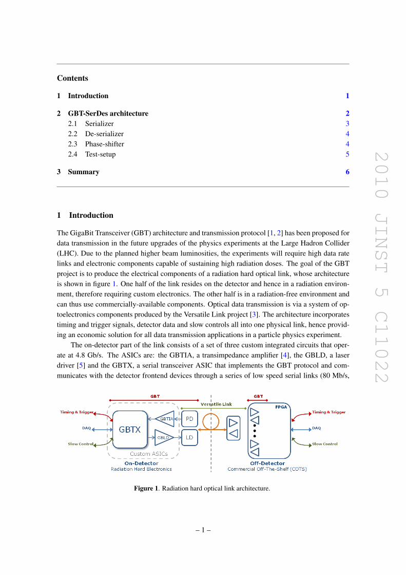
The GigaBit Transceiver (GBT) architecture and transmission protocol [1, 2] has been proposed fordata transmission in the future upgrades of the physics experiments at the Large Hadron Collider(LHC). Due to the planned higher beam luminosities, the experiments will require high data ratelinks and electronic components capable of sustaining high radiation doses. The goal of the GBTproject is to produce the electrical components of a radiation hard optical link, whose architectureis shown in figure 1. One half of the link resides on the detector and hence in a radiation environ-ment, therefore requiring custom electronics. The other half is in a radiation-free environment andcan thus use commercially-available components. Optical data transmission is via a system of op-toelectronics components produced by the Versatile Link project [3]. The architecture incorporatestiming and trigger signals, detector data and slow controls all into one physical link, hence provid-ing an economic solution for all data transmission applications in a particle physics experiment.
The on-detector part of the link consists of a set of three custom integrated circuits that oper-ate at 4.8 Gb/s. The ASICs are: the GBTIA, a transimpedance amplifier [4], the GBLD, a laserdriver [5] and the GBTX, a serial transceiver ASIC that implements the GBT protocol and com-municates with the detector frontend devices through a series of low speed serial links (80 Mb/s,
Figure 1. Radiation hard optical link architecture.
– 1 –

2010 JINST 5 C11022
160 Mb/s or 320 Mb/s) [1]. In order to be radiation hard to total dose effects, the ASICs will bemanufactured in a commercial 130 nm CMOS technology to benefit from its inherent resistance toionizing radiation. Details of the off-detector part of the GBT link can be found in [6].
Part of the radiation tolerance of the link is achieved through the transmission of a ForwardError Correction (FEC) code that allows the recovery from errors induced by Single Event Upsets(SEUs) in the photo-diode (PD), the GBTIA and the transceiver data-path. The implementation ofthe FEC code uses Reed-Solomon code (RS(15,11)) resulting in an error correction capability ofup to 16 consecutive bits in error [7]. To achieve DC balanced data transmission over the opticalfibre the transmitted data is scrambled and descrambled before and after encoding and decodingrespectively [7]. The GBT transmits a 120-bit frame, with 32 bits reserved for the FEC code and4 for a header. The link efficiency is therefore 84/120 = 70% and the available user bandwidth is3.36 Gb/s (including 4 bits of slow-control data).
This paper describes the GBT-SerDes in which a subset of the GBTX functionality is imple-mented, namely the Serializer circuit (SER) the Clock and Data Recovery (CDR) circuits of theDe-serializer (DES), the Reed-Solomon Encoder/Decoder (CODEC), the Scrambler/Descrambler(SCR/DSCR) and three phase shifters with 50 ps resolution. Further robustness against SEUs isprovided by the use of Triple Modular Redundancy (TMR) for the low-speed digital logic and themost critical high-speed digital functions. The GBT-SerDes was thus built in the same technologyforeseen for the fabrication of the GBTX in order to study the feasibility of the high speed seri-alizer and clock recovery circuits. The following sections describe the details of the GBT-SerDesarchitecture and present the test results.
2 GBT-SerDes architecture
The architecture of the GBT-SERDES is shown in figure 2. It is broadly composed of a transmitter(TX) and a receiver (RX) section. The TX receives parallel data through the Parallel Input (ParallelIn) interface. This data is then scrambled and RS encoded before it is fed to the SER where it isconverted into a 4.8 Gb/s serial stream with the frame format described above. On the RX side,after serial to parallel conversion in the DES, the data is fed to the frame aligner, then RS decodedand de-scrambled before it is sent to the external parallel bus through the parallel output interface.To minimise prototyping costs, a time-division multiplexed 30-bit parallel bus was adopted for theinput and output buses thus significantly reducing the silicon area since the ASIC is pad limited.
In the receiver and transmitter data paths, switches have been inserted between the functionalblocks. These switches allow routing the data, at different levels of depth down the data path, fromeither the RX into the TX or vice-versa. This functionality can be used for evaluation testing of theASIC but it also aims at providing a diagnostic tool for field tests of the optical link that will use theGBTX. Further self testing features are a Pseudo Random Bit Sequence (PRBS) generator in theTX. The PRBS generator can also be programmed to produce constant data or a simple bit count.The critical high-speed blocks (shaded regions in figure 2) are implemented using full-customdesign techniques while the remaining circuits are based on the standard library cells provided bythe foundry.
– 2 –

2010 JINST 5 C11022
Figure 2. GBT-SerDes block diagram.
Figure 3. Serializer block diagram (left) and eye-diagram (right).
2.1 Serializer
Figure 3 (left) shows the block diagram of the serializer. It consists of a 120-bit input register,three 40-bit shift registers, a frequency synthesizer consisting of a Phase-Lock Loop (PLL) with an120-bit feedback divider (composed of two stages, the first dividing by 3 and the second dividingby 40), and a 3:1 high speed multiplexer.
The SER operation is based on the division of the 120-bit frame into three 40-bit words whichare serialized at 1.6 Gb/s and then time division multiplexed to form the final 4.8 Gb/s serial bitstream. This architecture minimises the number of components operating at full speed.
The PLL is designed to be tolerant to SEUs by using large transistor sizes on the VCO ring-oscillator and consequently large currents are used on each stage of the VCO making the VCOsignal phase less sensitive to the charge perturbations deposited by ionizing particles [8]. TripleModular Redundancy (TMR) is used in the feed-back divider of the PLL to mitigate SEUs. To
– 3 –

2010 JINST 5 C11022
Figure 4. De-serializer block diagram (left), recovered clock jitter (right).
obtain 4.8 GHz divider operation it was necessary to use dynamic logic on the feedback divider.However, even in the case of the dynamic logic, standard TMR circuits imposed too high a penaltyon the operation frequency. To overcome this problem a new TMR flip-flop was developed [8].
Figure 3 (right) shows the serializer eye-diagram diagram at 4.8 Gb/s displaying a total jittermeasured is 52.4 ps.
2.2 De-serializer
The de-serializer block diagram is represented in figure 4 (left). Its main features are: a Half-Rate Phase/Frequency-Detector (HRPFD), frequency aided lock acquisition and a constant-latency“barrel-shifter” [1].
In the CDR the HRPFD is used since it allows the operation of the CDR circuits at half thefrequency and hence safer timing margins. Although the phase detector also detects frequency,its detection range is insufficient to cover all the process, voltage and temperature variations. Toensure that the CDR can always lock to the data it is thus necessary to pre-calibrate the VCO “free-running” oscillation frequency. For that, the VCO has two control inputs: a coarse control inputthat allows the centring of the VCO oscillation frequency and a fine control input that is under theregulation action of the CDR HRPFD and charge pump, and allows the CDR circuit to lock to theserial data. The CDR VCO coarse voltage is derived from that of a reference PLL that is locked tothe reference clock (figure 4, left). The VCOs in both PLLs are replicas of each other so that for thesame control voltage they should have the same oscillation frequency. Due to statistical variationson the fabrication process this is however not exact, leading to a slight difference between the VCOfrequencies. The CDR VCO fine control voltage is under control of the CDR loop and, due to thefrequency detecting ability of the HRPFD, will be able to pull the CDR VCO frequency to that ofthe incoming serial data. Figure 4 on the right displays the jitter histogram for the recovered 40MHz clock that displays a total jitter of 63.2 ps.
2.3 Phase-shifter
The purpose of the phase shifter is to generate multiple clocks as local timing references that aresynchronous with the accelerator clock. The frequency and phase of the output clocks are digitally
– 4 –

2010 JINST 5 C11022
Figure 5. Phase shifter block diagram.
programmable. The output clock frequency can be 40 MHz, 80 MHz, or 160 MHz and the phaseresolution is 50 ps independent of the frequency.
To handle multiple output frequencies and a phase resolution of 50 ps in a range of 25 ns (forthe 40 MHz clock), the phase shifter consists of three components: a PLL, Coarse De-skewingLogic (CDL), and Fine De-skewing Logic (FDL). Figure 5 depicts the overall system block dia-gram.
From the 40 MHz reference, the PLL generates a 1.28 GHz clock (with a period of 781 ps)for both the CDL and FDL blocks. The divider in the PLL is made of a 5-bit binary counter whoseoutputs are used by the CDL to produce the right output clock frequency. Since the output clocksare synchronized with the 1.28 GHz clock, the PLL guarantees the synchronization of the outputclocks with the reference clock.
In addition to perform frequency selection, the CDL shifts the clock by multiple periods of the1.28 GHz clock. The output of the CDL block is therefore a clock of the specified frequency withthe phase shifted by multiples of 781 ps.
The FDL is designed to phase shift the clock by a fraction of 781 ps. It is based on a modifiedDLL structure with a 16-stage voltage controlled delay line (VCDL). The 16 delay stages eachcreate a phase-shift of 1/16 of 781ps (∼ 50 ps). This is achieved by feeding the CDL clock tothe VCDL and connecting a delayed version of the CDL clock, delayed by one clock cycle of the1.28 GHz clock, to the phase detector (PD). The other input of the PD is the VCDL output. Thisarchitecture sets the delay through the VCDL to be exactly one period of 1.28 GHz clock, thus thedelay through each stage is ∼ 50 ps. A 16:1 MUX is used to select the desired phase. To generatemultiple clock outputs simultaneously using this architecture, replicas of the CDL and FDL canbe employed whereas one PLL can be shared among different channels. In the GBT-SerDes, threephase-shifting channels were implemented.
For the samples tested, the measured value of the differential non-linearity is 4.7 ps rms(21.5 ps PP) and that of the integral non-linearity is 4.3 ps rms (21.9 ps PP).
2.4 Test-setup
To fully test and characterize the GBT-SerDes, a test bench was built, based on a custom board (inblue in figure 6) hosting the GBT chip, an SFP+ module, a Cyclone III FPGA to generate, analyzeor translate the two 30-bits busses into LVDS, and two high-density connectors to transfer these30-bits busses to a Stratix II Gx Development Kit provided by Altera (in grey in figure 6). Thisboard allows testing the GBT-SerDes in either transmitter or receiver mode, using the 4.8 Gb/s
– 5 –

2010 JINST 5 C11022
Figure 6. GBT-SerDes Testing configurations.
serial link available in the Stratix II Gx and an SFP+. A Bit Error Rate Tester is implemented ineither the Stratix or the Cyclone depending on the type of test to be performed, referred as a), b)and c) in figure 6. For the loopback test, the Stratix board is not required, and the custom board canbe used standalone. These tests are controlled either via Ethernet UDP or I2C, and managed by aGraphical User Interface written in Java.
3 Summary
A serializer/de-serializer ASIC operating at 4.8 Gb/s has been designed and tested. The ASIC iscustom made for the experiments of the future upgrade of the LHC accelerator. The ASIC archi-tecture and circuits were designed to be tolerant to single event upsets and the ASIC is fabricatedin an 130 nm CMOS technology in order to be hard to the effects of ionizing radiation.
References
[1] P. Moreira et al., The GBT, a Proposed Architecture for Multi-Gb/s Data Transmission in High EnergyPhysics, in proceedings of the Topical workshop on electronics for particle physics, Prague, CzechRepublic, 3–7 Sept. 2007, pp. 332-336
[2] P. Moreira et al, The GBT Project, in proceedings of the Topical workshop on electronics for particlephysics, Paris, France, September 21–25 (2009), pp. 342–346.
[3] J. Troska et al., The Versatile Transceiver Proof of Concept, in proceedings of the Topical workshop onelectronics for particle physics, Paris, France, September 21–25 (2009), pp. 347–349.
[4] M. Menouni et al., The GBTIA, a 5 Gbit/s radiation-hard optical receiver for the SLHC upgrades, inproceedings of the Topical workshop on electronics for particle physics, Paris, France, September21–25 (2009), pp. 326–330.
[5] G. Mazza et al., A 5 Gb/s Radiation Tolerant Laser Driver in 0.13 um CMOS technology, inproceedings of the Topical workshop on electronics for particle physics, Paris, France, September21–25 (2009), pp. 321–325.
[6] F. Marin et al., Implementing the GBT data transmission protocol in FPGAs, in proceedings of theTopical workshop on electronics for particle physics, Paris, France, September 21–25 (2009), pp.631–635.
– 6 –

2010 JINST 5 C11022
[7] G. Papotti et al., An Error-Correcting Line Code for a HEP Rad-Hard Multi-GigaBit Optical Link, inproceedings of the 12th Workshop on Electronics for LHC and Future Experiments, Valencia, Spain,25-29 Sept 2006, CERN-LHCC-2007-006.
[8] O. Cobanoglu, A Radiation tolerant 4.8 Gb/s serializer for the Giga-bit transceiver, in proceedings ofthe Topical workshop on electronics for particle physics, Paris, France, September 21–25 (2009), pp.570–574.
– 7 –


![nokia morph phone]s prototype - 123seminarsonly.com](https://static.fdokumen.com/doc/165x107/63322002ba79697da5101deb/nokia-morph-phones-prototype-123seminarsonlycom.jpg)