An ASIC for multichannel data acquisition systems
20
-
Upload
triestearchitettura -
Category
Documents
-
view
1 -
download
0
Transcript of An ASIC for multichannel data acquisition systems
AN ASIC FOR MULTICHANNELDATA ACQUISITION SYSTEMSAndrea Aizza, Giuseppe Bernacchia, Sergio Carrato, Stefano MarsiD.E.E.I. { University of Trieste, via Valerio, 10 { 34100 Trieste, ItalyGiuseppe Cautero, Riccardo TommasiniElettra Synchrotron Light Source, 34012 Basovizza, Trieste, ItalyCorresponding author:Sergio CarratoD.E.E.I., University of Trieste, via Valerio 10, 34100 Trieste, Italytel.: +39.040.6767147; fax: +39.040.6763460; e-mail: [email protected] | In this paper we describe the realization of an ASIC whichmay signi�cantly simplify the instrumental apparatus for measures in UHV(ultra-high vacuum, p � 10�9 mbar) while permitting very fast acquisitions. Thechip will �rst be used in ESCA experiments; however, its parallel architectureand the fast serial protocol for data transmission may increase the e�ciency ofthe measure process in any experiment where multichannel acquisition is a keyissue.Classi�cation codes and keywords07.05.Hd; 07.85.Qe; 39.30.+w; 07.50.-eASIC, parallel readout detectors, multichannel acquisition systems, UHV environ-ment, synchrotron light sources, ESCA. 1

IntroductionThe recent availability of third generation synchrotron radiation sources is openingmany new opportunities in the �eld of experimental physics. These opportunities,however, can be exploited only if suitable new acquisition hardware is developed[1]. A fundamental acquisition improvement is given by the use of parallel readoutarchitectures, which strongly increase the e�ciency of detection systems in many kindof spectroscopies [2]. As an example, in photoelectron spectroscopy experiments suchas ESCA (Electron Spectroscopy for Chemical Analysis), one of the most popularsurface science techniques [3], an electrostatic energy analyser is used to dispersephoto-emitted electrons with di�erent kinetic energy; recently, multichannel readoutshave been developed to speed up the acquisition and to exploit the possibilities o�eredby third generation synchrotron radiation sources. Unfortunately, the number ofchannels in these detectors is generally limited to less than about 40 [1]; recently,a system with 96 channels has been presented [4], which seems to be close to theupper bound for an approach based on conventional electronics equipment. Thisis due to practical limitations related to the interface between the detector, whichis under ultra-high vacuum conditions, and the acquisition electronics outside theexperimental chamber; in particular, ultra-high vacuum compatible feed-throughs arevery large and expensive, so that their use is not practical for a number of channelslarger that about one hundred, and the mobility of the analyser is prevented by thesti�ness of the bunch of cables which connects the output of the analyser itself to thefeed-throughs.In this paper we describe an ASIC (Application Speci�c Integrated Circuit) whichhas been speci�cally designed to overcome these limitations. The idea is to movepart of the data acquisition process from the outside to the inside of the acquisitionchamber. In this way, already pre-processed data are transmitted outside, instead ofraw data, thus signi�cantly simplifying the interface between ultra-high vacuum and2

air. In particular, our IC is composed of a set of counters, which collect data comingfrom the multichannel detector, and some circuitry which is able to transmit thecumulated data onto a fast serial link; consequently, a very simple feed-through canbe used, independently on the number of channels. Moreover, the number of cablesconnecting the detector output to the feed-through is very low, and independent onthe number of channel, thus permitting the motion of the detector itself with respectto the experimental chamber; this can be useful e.g.. in angle-resolved experiments.It has to be noted that it has been necessary to design an ASIC, instead of usingprogrammable logic (e.g., FPGA's, Field Programmable Gate Arrays); in fact, it isimportant both to avoid packages which may degas in UHV conditions, and to beable to keep power consumption low, due to the impossibility to cool the IC usingconvection.In the �rst section we describe, as an application example, the use of the ASICin an ESCA experiment. In Sec. 2, we analyse the IC in more detail, describing itsinternal structure and some measures which have been carried out; in Sec. 3 we drawsome conclusions and give the directions of our future work.It is important to notice that the IC, although it will be �rst used in the ESCAexperiment, may be fruitfully exploited in any experiment where parallel readout,fast acquisitions, or the mobility of the detector are key issues.Even more importantly, this IC may be considered a �rst step towards the useof two-dimensional detectors, where the use of one connection per sensor element issimply prohibitive. The integration of some pre-processing power in an ASIC withinthe vacuum chamber, together with a fast serial connection with the outside, canmake the use of two-dimensional UHV detectors feasible even with a large number ofelements. 3

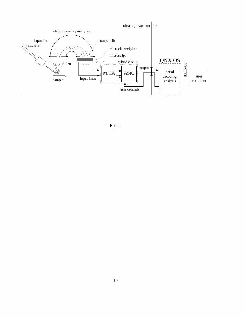
1 An ESCA experiment using the proposed ASICAs already mentioned, in this section we brie y describe the environment where thedeveloped ASIC will be �rst tested and then utilised, in order to obtain a systemcharacterised by a much simpler hardware setup (with respect to the standard solutionwith all the electronics outside vacuum) and consequently a lower cost and higherreliability. It has to be remembered, however, that the key issue in our approach isthe capability to embed some preprocessing power into an ASIC which can be putinside the experimental chamber, very close to the detector, in order to obtain highercommunication speed, much simpler connection with the outside, and possibility ofmovement of the detector itself.In Fig. 1, the data acquisition system using the proposed IC for an ESCA experi-ment is shown. The system, which is currently under development, is used to measurethe kinetic energy of the electrons released by a sample.The experiment takes place under ultra high vacuum. The X-ray radiation issupplied by a synchrotron light source. The photo-emitted electrons are separatedaccording to their energy by a hemispherical electron analyser [5, 6] and collected bya detector which consists of two microchannel plates (MCPs) in chevron assembly,proximity focused onto 96 discrete gold anodes evaporated on an Al2O3 substrate.A hybrid circuit (ADHC, Analog/Digital Hybrid Circuit) is put in close proximityof the detector. It consists of a preampli�er (the MICA chip [7]), which ampli�es thepulses of each anode of the detector, and of the proposed ASIC; the latter countsthe pulses and transmits the cumulated data outside the experimental chamber usinga fast serial link. The ADHC ground voltage is biased at the same potential of theanodes, so that there is no need to use one High Voltage (HV) capacitor per channelto decouple the bias voltage of the anodes themselves; the connection between theADHC and the external electronic equipment is made using photocouplers in orderto provide HV isolation. 4

The external unit is an embedded control system [4] which supervises the wholeexperimental apparatus, provides a few control signals to the ASIC (e.g., the clock forthe serial transmission), and acquires the data coming from it. It is interfaced withthe user computer via a standard interface protocol card (IEEE 488), using which thescientist can specify the experiment parameters (number of channels, time windowlength, energy range : : :). After being suitably programmed, the system is able tocontrol the experiment autonomously, without further user intervention, and retainsthe acquired data until the user downloads them.2 IC descriptionAs already mentioned, the IC has been realized in order to exploit all the featuresprovided by parallel readout detectors. It includes 16 counters, and may be easilycascaded in case of systems with larger number of counters. By transmitting dataonto a fast serial link, it makes the number of lines required to bring the informationoutside the vacuum chamber independent on the number of counters.Particular care has been given to reduce the noise generated by the counters, inorder to avoid spurious signals; this has been achieved by implementing the countersusing Gray code, which is known to minimise the number of simultaneous commuta-tions of the ip- ops in each counter, so reducing current spikes in the power supplylines and electromagnetic interferences.As already mentioned, the aim of the IC is to count the pulses, which have PECL(Positive Emitter Coupled Logic) levels, coming from the MICA chip via several inputlines, and to transmit the readouts in serial mode. This is achieved with a circuitwhich is composed of two parts. The analog one, at the input, converts the PECLlevel signals into CMOS compatible ones. The digital one, implemented in standardcells technology, counts the pulses using 16 32-bit latched counters, and transmits thecumulated counts in serial mode. 5

The fundamental blocks of the ASIC are shown in Fig. 2. The analog input stageconverts 16 balanced PECL signals into unbalanced CMOS ones1. This is done usinga full custom block, ECL2CMOS, for each channel, and two Wilson current sources,each being shared by 8 channels. The ECL2CMOS block is composed of a di�erentialcomparator (see Fig. 3) with a cascode structure for each branch in order to reducethe Miller e�ect, and consequently to provide very good frequency response; thesymmetrical structure yields good supply common mode rejection ratio. This stageoccupies a very small part (0:1 %) of the whole IC.Each CMOS line at the output of the analog stage is connected to the input of thecorresponding 32-bit Gray code synchronous counter. The counters may be enabledusing a control signal provided by the user.As in any synchronous counter, the input line of each counter is connected to theclock of its 32 internal ip- ops. It has to be noted that the input pulses, comingfrom the MICA chip, have �xed amplitude but arbitrary length. In these conditionsa very short pulse may cause some ip- ops to commutate and some others not to,with the consequent loss of the current count. To avoid this, at each counter inputa monostable has been added which sets a minimum pulse duration, so that for eachpulse all the ip- ops of the counter are guaranteed to commutate. The monostablelimits the upper working frequency of each counter to 100 MHz.Each counter is latched, so that it is possible to start a new count while the valuerelating to the previous time window is being transmitted. The 32 bits of each counterare memorised by a user signal that forces the latch to store the data.The control logic implements an asynchronous serial transmission, together with1This version of the chip has been designed with PECL inputs in order to make it compatiblewith the presently available preampli�er, the MICA chip, which has balanced PECL outputs. Weare also designing a new preampli�er with unbalanced outputs, which will allow to implement asimpler comparator input stage for the counting section.6
other ancillary functions described later. A multiplexer, in the output section, collectsall the bits coming out from the memories in groups of 8. The multiplexer is followedand controlled by a synchronous Finite State Machine (FSM) that, starting from theselected 8 bits coming from the multiplexer, generates the output serial frames. AnRS-232 like format has been chosen, in order to allow the use of a common PC toread the data if no speed constraints are present (e.g. for test purposes). The FSMis synchronised with an external clock and is enabled to transmission by a signalprovided by the user. A parity check is used to point out incidental transmissionerrors. In this case the FSM may be forced to re-send the data by simply disablingand enabling it again.The FSM also allows the system to be expanded for what concerns the numberof channels. It is possible, in fact, to connect several ICs in daisy chain obtaining adevice with higher number of channels and the same functionality. When data haveto be downloaded, all the ICs of the chain, starting from the �rst one, are sequentiallyenabled to transmission. This is achieved using three extra lines, one for actual datatransmission and two for the synchronisation of each IC with the previous/followingone.It is also possible to con�gure the FSM to transmit only 15 bits for each counter.This operation mode allows to halve the transmission time in case of very shortacquisition times2.The ASIC can be operated in test mode; in this case the input of each counteris switched from its ECL2CMOS to the clock of the FSM, in order to verify thebehaviour of the counters. It has to be noted that in this working mode the clockplays two di�erent roles: it both provides the pulses to be counted, and synchronisesthe FSM during transmission.2Of course, the acquisition time must be short enough to avoid counters over ow at 215, accordingto the maximum pulse input rate. 7

2.1 Realization and bench measuresThe IC was developed with Cadence 97A using the 0:6 �m CMOS technology of theAMS HITKit 3.00 (Austria Mikro Systeme Mixed Signal High Performance InterfaceTool Kit) libraries. Fig. 4 shows a photograph of the �nal prototype. The analogconversion stage is located in the upper left part, while most of the area is occupiedby the standard cells for the digital part (in the centre) and the pads (along theperimeter). Overall die size is 3:0� 4:4 mm2.The prototype has been tested using an HP16500C mainframe, with a patterngenerator to provide the input signals and a logic state analyser to verify the outputs.Fig. 5 illustrates an example of operation of the IC, with a 5 KHz square wave signal3fed to the �rst counter. In particular, the top �gure shows the counters being enabledto count, and the start of the transmission; the bottom one shows the end of thetransmission. At the beginning the IC is reset, then it is enabled to count for a 3:5 msgate time. Data are then latched and transmitted with a 2:4 KHz clock, in order toallow a PC to read the output data with a standard RS-232 port. The signal Lab 5is the transmitted serial output, which is 110011 in Gray code, i.e. 10010bin = 17dec,which corresponds to counting 5 KHz pulses in a 3:5 ms gate time.Further tests have been carried out to measure both the highest working frequencyand the noise generated by the IC. In particular, we determined that the IC countspulses at a frequency up to 50 MHz and may transmit the readouts at up to 10 MBaud,i.e. a minimum of 4:4 �s for each 32 bit count. Using this transmission frequencyand 6 ICs connected in daisy chain, it is possible to read the counts of all 96 inputlines in just 0:42 ms.The noise generated by the IC on the supply lines was also analysed. To thispurpose, we performed a set of tests in which we simulated, for what concerns the3The input frequency has been set to a low value for the sake of clarity. The same applies to theBaud rate below. 8
supply lines, the use of the IC inside the UHV chamber. It has to be noted, in fact,that in these conditions it may not be possible to install large capacitors near the IC;consequently, the power sources and the capacitors required to stabilise the voltagelevels are located outside the chamber, and a 30 cm long wire carries the ground andsupply voltages to the IC. In these conditions, the measures showed that the noisegenerated by the counters is quite small (spikes of about �0:3 V on the 5 V CMOSsupply lines). Moreover, the noise generated in these conditions does not a�ect anyof the functionalities of the IC, which counts and transmits data without errors.Some measured parameters of the IC are reported in Tab. 1.2.2 Preliminary results on an ESCA experimental chamberThe ASIC has been also tested on an ESCA experimental chamber provided with a16 channel electron analyser. In order to check the daisy chain con�guration, twoIC's have been connected together, using 8 channels each. In Fig. 6, the spectrum ofelastically scattered electrons (FWHM around 800 meV) of an electron gun is shown.Energy separation between channels is 100 meV, acquisition time is 1 ms.Of course, for 16 channels the simpli�cation in the hardware of the experimentalchamber with respect to the classical solution with a 16 channel UHV compatiblefeed-through is negligible. However, for a larger number of channels, e.g. 96, the pro-posed system permits to leave the vacuum-to-air interface unchanged, with signi�cantreduction in both complexity and possibility of failure with respect to the standardsolution.3 ConclusionsAn ASIC developed for multichannel data acquisition systems using parallel readoutdetectors has been presented. The possibility to put some preprocessing circuitry veryclose to the detectors, in a ultra-high vacuum environment, allows both to increase the9
acquisition speed and to signi�cantly simplify the interface between the experimentalapparatus and the user computer. The IC, which has been designed for an ESCAmeasurement apparatus, may be useful in any experiment where fast acquisition,parallel readout, or detector mobility are key issues.Our ASIC, which has been designed using 0.6 �m CMOS technology, includes a setof 16 comparators and counters, and some circuitry to transmit the data over a fastserial line. Both preliminary bench tests and measurements in an ESCA experimentalsetup have been successfully completed. Our ASIC will now be integrated, togetherwith a preampli�er IC, on an hybrid circuit which will be put inside the experimentalchamber, in ultra-high vacuum conditions.Future developments of this work are in the direction of using two-dimensionaldetectors closely coupled with an ASIC for pre-processing and data compres-sion/formatting.References[1] P. P. Manning, N. J. Clague, I. W. Kirkman, F. M. Quinn, and P. J. Hicks, \A fastand exible multichannel electron detector with parallel readout for photoelectronspectroscopy," Nuclear Instruments and Methods in Physics Research, A, vol. 392,pp. 345{348, 1997.[2] J. L. Richter and W. Ho Rev. Sci. Instrum., vol. 57, p. 1469, 1986.[3] G. Hertl and J. Kuppers, Electron Spectroscopy for surface analysis. Weinheim:Verlag Chemie, 1974.[4] L. Gori, R. Tommasini, G. Cautero, D. Giuressi, M. Barnaba, A. Accardo, S. Car-rato, and G. Paolucci, \An embedded control and acquisition system for multi-channel detectors," Nuclear Instruments and Methods in Physics Research, A,vol. 431, pp. 338{346, 1999. 10

[5] A. Baraldi and V. R. Dhanak Journal of electron spectroscopy and related phenom.,vol. 67, no. 1, p. 211, 1994.[6] A.Mann and F. Linder J. Phys. E: Sci. Instrum., vol. 21, p. 805, 1988.[7] C. C. Enz, F. Krummenacher, and R. Bellazzini, \MICA: a multichannel in-tegrated charge ampli�er for the read-out of multielectrode detectors," NuclearInstruments and Methods in Physics Research, A, vol. 332, pp. 543{553, 1993.
11

Table and �gure captionsTable 1: Measured parameters of the ASICFigure 1: Scheme of the data acquisition system for an ESCA experiment using ourASIC. Figure 2: Block structure of the developed ASIC.Figure 3: Schematic diagram of the full custom part of the IC which implements acomparator stage for one channel.Figure 4: Photograph of the IC �nal prototype.
12
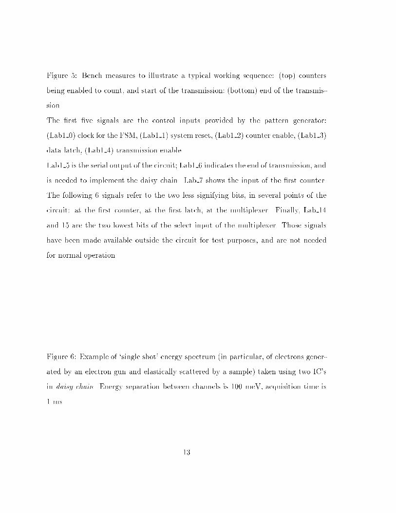
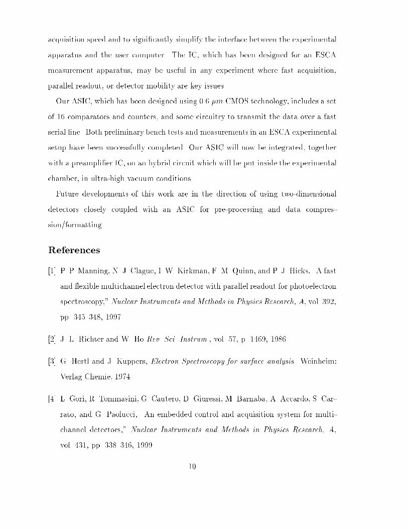
Figure 5: Bench measures to illustrate a typical working sequence: (top) countersbeing enabled to count, and start of the transmission; (bottom) end of the transmis-sion.The �rst �ve signals are the control inputs provided by the pattern generator:(Lab1 0) clock for the FSM, (Lab1 1) system reset, (Lab1 2) counter enable, (Lab1 3)data latch, (Lab1 4) transmission enable.Lab1 5 is the serial output of the circuit; Lab1 6 indicates the end of transmission, andis needed to implement the daisy chain. Lab 7 shows the input of the �rst counter.The following 6 signals refer to the two less signifying bits, in several points of thecircuit: at the �rst counter, at the �rst latch, at the multiplexer. Finally, Lab 14and 15 are the two lowest bits of the select input of the multiplexer. Those signalshave been made available outside the circuit for test purposes, and are not neededfor normal operation.Figure 6: Example of `single shot' energy spectrum (in particular, of electrons gener-ated by an electron gun and elastically scattered by a sample) taken using two IC'sin daisy chain. Energy separation between channels is 100 meV, acquisition time is1 ms. 13

die size 3:0� 4:4 mm2number of counters 16counters depth 32 bitdaisy chain expansibility yessupply voltage 5 V (min 3.2 V)power consumption 100 mWmax input frequency 50 MHzinput sensitivity 100 mVmax output rate 10 MBaudoutput rise time (470 load) 10 nsoutput fall time (470 load) 4 nsTab:1
14
serialdecoding,analysis
QNX OSlens
electron energy analyzer
beamlinemicrochannelplate
input slit
sample
output slit
output
user controls
input lines
. . . . .
ultra high vacuum air
computer
IEE
E-4
88
microstrips
userMICA ASIC
hybrid circuit
Fig. 1
15

Machine)
FSM(Finite State
CMOSserialoutput
ECL2CMOS counter memory
MUX....... ....... .......
counters and memories32 32
8
analog digital
Integrated Circuit
I0
I1
I15
user controls
conversion
PECLinputs
balanced
control logic
Fig. 2
16

V-
V+
Vdd
Gnd
Iref
Vout
Fig. 317

Fig. 418

Fig. 519

18x103
16
14
12
10
8
6
4
2
Counts
1514131211109876543210
ChannelFig. 620