Section 6 ASIC Technology Trends - Smithsonian Chip ...
56
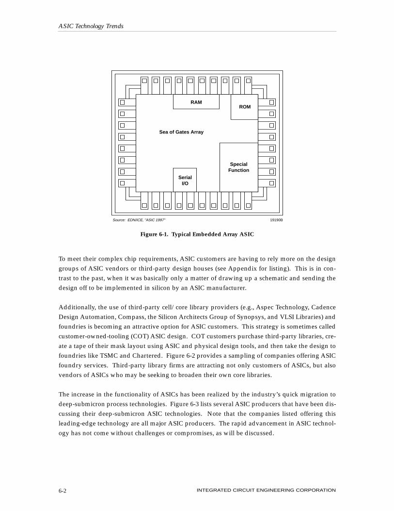
OVERVIEW This section will discuss three general trends associated with today’s ASIC industry: the rapid advancement of process technologies, the move toward specialization, and a blurring of the dis- tinctions between each of the ASIC product categories. There is also an underlying trend linking these all together: each new ASIC generation requires greater cooperation between ASIC vendors and customers. Distinguishing between each of the ASIC product categories is becoming increasingly difficult. Until recently, the ASIC industry could be divided up into the three well-defined product groups defined in Section 1: semicustom ICs (gate arrays and linear arrays), custom ICs (standard cells and full custom devices), and programmable logic devices (simple and complex PLDs, FPGAs, and EPACs). However, the lines separating those three categories are getting blurry. The best fea- tures of products from one category are increasingly showing up in products of other categories. Take, for example, embedded arrays, which are based on a gate array structure but have large megacells such as compiled memories or microprocessor cores embedded in them (Figure 6-1). The cells/cores provide a higher level of integration than a pure gate-array structure, but can lead to longer prototype leadtimes, though, still shorter than the leadtimes for pure cell-based ASICs. Then, there are Motorola’s customizable standard products (CSPs), which have been described as a blend of hand-packed cells, standard cells, gate arrays, and/or embedded arrays. One thing that’s true for all types of ASIC devices is that they are becoming more specialized to serve the needs of systems companies. The ASIC industry is moving away from a one-size-fits-all approach, toward a tighter market focus—one that places greater emphasis on performance, power, functionality, and cost considerations on a per customer basis. ASICs are no longer just on the periphery of a system (i.e., glue logic), they are being designed as the core of the system. As a result, ASIC vendors are becoming more segmented or specialized in what they have to offer, including such devices as digital video, networking, telecommunications, or audio ASICs. INTEGRATED CIRCUIT ENGINEERING CORPORATION 6-1 6 ASIC TECHNOLOGY TRENDS
-
Upload
khangminh22 -
Category
Documents
-
view
0 -
download
0
Transcript of Section 6 ASIC Technology Trends - Smithsonian Chip ...

OVERVIEW
This section will discuss three general trends associated with today’s ASIC industry: the rapidadvancement of process technologies, the move toward specialization, and a blurring of the dis-tinctions between each of the ASIC product categories. There is also an underlying trend linkingthese all together: each new ASIC generation requires greater cooperation between ASIC vendorsand customers.
Distinguishing between each of the ASIC product categories is becoming increasingly difficult.Until recently, the ASIC industry could be divided up into the three well-defined product groupsdefined in Section 1: semicustom ICs (gate arrays and linear arrays), custom ICs (standard cellsand full custom devices), and programmable logic devices (simple and complex PLDs, FPGAs,and EPACs). However, the lines separating those three categories are getting blurry. The best fea-tures of products from one category are increasingly showing up in products of other categories.
Take, for example, embedded arrays, which are based on a gate array structure but have largemegacells such as compiled memories or microprocessor cores embedded in them (Figure 6-1).The cells/cores provide a higher level of integration than a pure gate-array structure, but can leadto longer prototype leadtimes, though, still shorter than the leadtimes for pure cell-based ASICs.
Then, there are Motorola’s customizable standard products (CSPs), which have been described asa blend of hand-packed cells, standard cells, gate arrays, and/or embedded arrays.
One thing that’s true for all types of ASIC devices is that they are becoming more specialized toserve the needs of systems companies. The ASIC industry is moving away from a one-size-fits-allapproach, toward a tighter market focus—one that places greater emphasis on performance,power, functionality, and cost considerations on a per customer basis. ASICs are no longer just onthe periphery of a system (i.e., glue logic), they are being designed as the core of the system. Asa result, ASIC vendors are becoming more segmented or specialized in what they have to offer,including such devices as digital video, networking, telecommunications, or audio ASICs.
INTEGRATED CIRCUIT ENGINEERING CORPORATION 6-1
6 ASIC TECHNOLOGY TRENDS
To meet their complex chip requirements, ASIC customers are having to rely more on the designgroups of ASIC vendors or third-party design houses (see Appendix for listing). This is in con-trast to the past, when it was basically only a matter of drawing up a schematic and sending thedesign off to be implemented in silicon by an ASIC manufacturer.
Additionally, the use of third-party cell/core library providers (e.g., Aspec Technology, CadenceDesign Automation, Compass, the Silicon Architects Group of Synopsys, and VLSI Libraries) andfoundries is becoming an attractive option for ASIC customers. This strategy is sometimes calledcustomer-owned-tooling (COT) ASIC design. COT customers purchase third-party libraries, cre-ate a tape of their mask layout using ASIC and physical design tools, and then take the design tofoundries like TSMC and Chartered. Figure 6-2 provides a sampling of companies offering ASICfoundry services. Third-party library firms are attracting not only customers of ASICs, but alsovendors of ASICs who may be seeking to broaden their own core libraries.
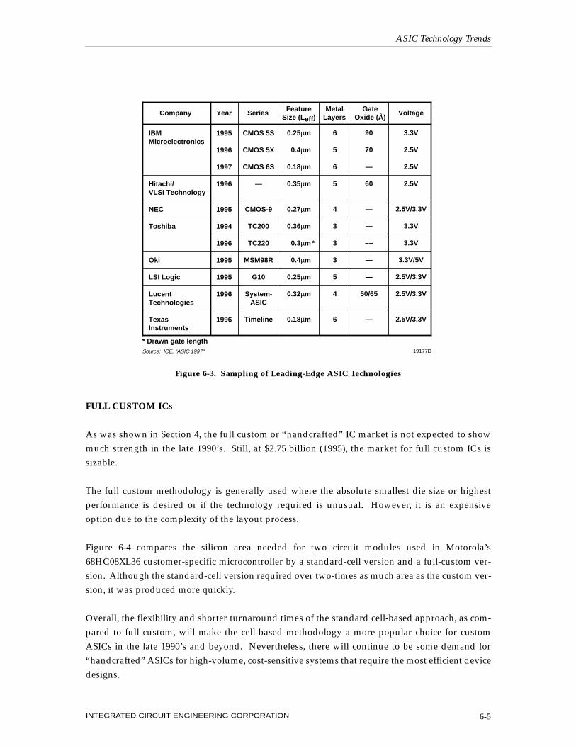
The increase in the functionality of ASICs has been realized by the industry’s quick migration todeep-submicron process technologies. Figure 6-3 lists several ASIC producers that have been dis-cussing their deep-submicron ASIC technologies. Note that the companies listed offering thisleading-edge technology are all major ASIC producers. The rapid advancement in ASIC technol-ogy has not come without challenges or compromises, as will be discussed.
ASIC Technology Trends
INTEGRATED CIRCUIT ENGINEERING CORPORATION6-2
RAMROM
Serial I/O
Special Function
Sea of Gates Array
19190BSource: EDN/ICE, "ASIC 1997"
Figure 6-1. Typical Embedded Array ASIC

ASIC Technology Trends
INTEGRATED CIRCUIT ENGINEERING CORPORATION 6-3
AMCC Bipolar 1.0 3 metal; 2 poly Varies No typical San Diego, CA (drawn) AMI Digital and mixed-signal 0.6 2 & 3 metal no fixed $30,000 - $55,000 Pocatello, ID ASIC, CMOS requirements Digital and mixed-signal 0.8 2 & 3 metal no fixed $30,000 - $55,000 ASIC, CMOS requirements Digital and mixed-signal 1.0 2 & 3 metal no fixed $30,000 - $55,000 ASIC, CMOS requirements Digital and mixed-signal 1.25 2 & 3 metal no fixed $30,000 - $55,000 ASIC, CMOS requirements Digital and mixed-signal 1.4 2 & 3 metal no fixed $30,000 - $55,000 ASIC, CMOS requirements Digital and mixed-signal 1.4 2 metal no fixed $30,000 - $55,000 ASIC, CMOS requirements Digital and mixed-signal 1.5 2 & 3 metal no fixed $30,000 - $55,000 ASIC, CMOS requirements Digital and mixed-signal 1.5 2 metal no fixed $30,000 - $55,000 ASIC, CMOS requirements Digital and mixed-signal 2.0 2 & 3 metal no fixed $30,000 - $55,000 ASIC, CMOS requirements Digital and mixed-signal 3.0 2 & 3 metal no fixed $30,000 - $55,000 ASIC, CMOS requirements Digital and mixed-signal 5.0 2 & 3 metal no fixed $30,000 - $55,000 ASIC, CMOS requirements California Micro Devices CMOS & BiCMOS 1.5 2 metal; 2 poly 12,000 over Depends on process/ Milpitas, CA 1 year layers and production commitment Honeywell Solid State Linear Bipolar 4.0 1 & 2 metal Negotiable $50,000 - $90,000 Advanced Linear 4.0 2 metal Negotiable $50,000 - $90,000 Bipolar W/TFR CMOS (SOI) IV 0.8 3 metal; 1 poly Negotiable $50,000 - $90,000 5V/3.3V IC Works CMOS 0.8 3 metal; 1 poly Varies Varies by technology CMOS 0.6 3 metal; 1 poly Varies Varies by technology BiCMOS 0.7 2 metal; 2 poly Varies Varies by technology BiCMOS 0.8 2 metal; 2 poly Varies Varies by technology IMP CMOS, BiCMOS, EECMOS 0.8, 1.0, 2 metal; 2 poly Yes $30,000 - $40,000 San Jose, CA 1.2, 2.0, 3.0, 5.0 LG Semicon CMOS 0.8 2 metal 50,000 units No typical San Jose, CA per month CMOS 0.6 1 poly 50,000 units No typical per month Micrel CMOS, PMOS, NMOS, 1.5 - 5.0 2 metal; 2 poly N/A $15,000 San Jose, CA BiCMOS, Bipolar Mitel Semiconductor CMOS Silicon Gate 1.2 2 metal; 1 & 2 poly 100 wafers/year $390 U.S. (per wafer). Bromont, Quebec, Canada NRE cost (including masks): $15,000 US per device. Chip Fin- ishing: $2,000 U.S. Masks (typical 11): $13,500 US CMOS Silicon Gate 1.5 2 & 3 metal; 2 poly 100 wafers/year Same as above CMOS Silicon Gate 2.0 2 metal; 2 poly 100 wafers/year Same as above CMOS Silicon Gate 3.0 2 & 3 metal; 2 poly 100 wafers/year Same as above CMOS Silicon Gate 4.0 2 metal; 1 & 2 poly 100 wafers/year Same as above CMOS Silicon Gate 5.0 2 metal; 1 & 2 poly 100 wafers/year Same as above CMOS Metal Gate 9.0 3 metal; 3 poly 100 wafers/year Same as above 9.0 (15V)
Company and Location
Technologies Offered
Number of Layers
Production Commitment
Required
Fabrication/ NRE Cost
Feature Size (µm)
21248Source: Integrated System Design/ICE, "ASIC 1997"
Electronic Center (SSEC) Plymouth, MN
San Jose, CA
Figure 6-2. ASIC Foundries

ASIC Technology Trends
INTEGRATED CIRCUIT ENGINEERING CORPORATION6-4
Company and Location
Technologies Offered
Number of Layers
Production Commitment
Required
Fabrication/ NRE Cost
Feature Size (µm)
21249Source: Integrated System Design/ICE, "ASIC 1997"
Australia* Homebush, NSW, 2140 Australia
National Semiconductor CMOS + Capacitor 1.0 2 metal; 1, 2 with Design $55,000 - $80,000 Santa Clara, CA Module drawn module poly dependent CMOS + Capacitor Bipolar 0.8 3 metal; 1, 2 with Design $60,000 - $85,000 Module drawn module poly dependent CMOS 0.72 3 metal; 1 poly Design $65,000 - $90,000 drawn dependent ABiC BiCMOS Ft = 12GHz 0.8 4 metal; 1 poly Design $100,000 - $200,000 drawn dependent Orbit Semiconductor Digital CMOS, Mixed 1.0 2 metal; 3 poly No Conversion $10,000 Sunnyvale, CA Analog Digital CMOS, drawn Manufacturing service Charge Coupled Device tooling plus fabrica- (CCD) tion approximately $50,000 Quality Semiconductor CMOS 12SPTW 1.0/1.2 2 metal; 1 poly N/A $20,000 - $50,000 CMOS 12DPTW 1.2 2 metal; 2 poly N/A $20,000 - $50,000 CMOS DVTW 1.5 2 metal; 2 poly N/A $20,000 - $50,000 CMPS LVCMOS 1.5 2 metal; 1 poly N/A $20,000 - $50,000 CMOS EEPROM 1.5 2 metal; 1 poly N/A $20,000 - $50,000 Bipolar 5.0 2 metal N/A $20,000 - $50,000 Raytheon Electronics, Bipolar process with 5.0 1 or 2 metal N/A To be determined Semiconductor Division precision thin film Mountain View, CA resistors Linear B2 Process 4.0 1 or 2 metal N/A To be determined J12 Process (12V) 3.0 2 metal N/A To be determined High performance compli- 2.0 2 metal N/A To be determined mentary BiCMOS process High performance compli- 2.0 2 metal N/A To be determined mentary BiCMOS process Ricoh Corporation, CMOS 1.2, 0.8 2 metal; 1 poly Yes Call Electronic Devices Division San Jose, CA S-MOS Systems CMOS 0.6, 0.65, 2 metal (2 & 3 for N/A $10,000 - $40,000 San Jose, CA 0.8, 1.0 0.65); 1 poly Semtech** 20V Bipolar, 40V Bipolar, 4.0 1 & 2 metal 200 a month No typical Santa Clara, CA Metal Gate CMOS minimum Standard Microsystems RC/Thin Film, sensors 2.0 2 metal; 1 poly Varies Process dependent Corporation (SMC) Hauppauge, NY Thesys Microelectronics HCN08, HCP08 0.8 2 metal; 1 poly No On request BIC12 (BiCMOS) 1.2 2 metal; 1 poly No On request HCN15 modular process 1.5 2 metal; 2 poly No On request concept modular TriQuint Semiconductor GaAs MESFET: 0.5, 0.6, 4 layer gold metal No As low as $7,900 for Beaverton, OR Enhancement, Depletion, 1.0 prototype chips, and Power $51,000 for prototype run. Aditional NRE for package and test development TSMC Logic, memory, mixed- 0.5 logic Varies up to 3 Varies Varies by technology, Hsinchu, Taiwan signal process & mixed- metal; 3 poly feature size, process, signal wafer size�� Logic, memory, 0.45 Varies up to 3 Varies Varies by technology mixed-signal process memory metal; 3 poly feature size, process, wafer size Logic, memory, 0.35 4 metal Varies Varies by technology, mixed-signal process feature size, process, wafer size
* Formerly AWA MicroElectronics ** Formerly ECI Semiconductor
Erfurt, Germany
Figure 6-2. ASIC Foundries (continued)
FULL CUSTOM ICs
As was shown in Section 4, the full custom or “handcrafted” IC market is not expected to showmuch strength in the late 1990’s. Still, at $2.75 billion (1995), the market for full custom ICs issizable.
The full custom methodology is generally used where the absolute smallest die size or highestperformance is desired or if the technology required is unusual. However, it is an expensiveoption due to the complexity of the layout process.
Figure 6-4 compares the silicon area needed for two circuit modules used in Motorola’s68HC08XL36 customer-specific microcontroller by a standard-cell version and a full-custom ver-sion. Although the standard-cell version required over two-times as much area as the custom ver-sion, it was produced more quickly.
Overall, the flexibility and shorter turnaround times of the standard cell-based approach, as com-pared to full custom, will make the cell-based methodology a more popular choice for customASICs in the late 1990’s and beyond. Nevertheless, there will continue to be some demand for“handcrafted” ASICs for high-volume, cost-sensitive systems that require the most efficient devicedesigns.
ASIC Technology Trends
INTEGRATED CIRCUIT ENGINEERING CORPORATION 6-5
1995
1996
1997
1996
1995
1994
1996��
1995
1995��
1996
1996
IBM Microelectronics Hitachi/ VLSI Technology NEC Toshiba Oki LSI Logic Lucent Technologies Texas Instruments
CMOS 5S
CMOS 5X
CMOS 6S
—
CMOS-9
TC200
TC220��
MSM98R��
G10��
System- ASIC
Timeline
0.25µm
0.4µm
0.18µm
0.35µm
0.27µm
0.36µm
0.3µm��
0.4µm
0.25µm��
0.32µm
0.18µm
6
5
6��
5
4
3
3��
3��
5��
4
6
90
70
—��
60
—
—
––��
—��
—��
50/65
—
3.3V
2.5V
2.5V�
2.5V
2.5V/3.3V
3.3V
3.3V��
3.3V/5V
2.5V/3.3V��
2.5V/3.3V
2.5V/3.3V
Year Series Feature Size (Leff)
Metal Layers
Gate Oxide (Å)
VoltageCompany
19177DSource: ICE, "ASIC 1997"
*
* Drawn gate length
Figure 6-3. Sampling of Leading-Edge ASIC Technologies

GATE ARRAY, EMBEDDED ARRAY, AND CELL-BASED ASICs
The primary ASIC methodologies in use today are CMOS gate array, embedded array, and stan-dard cell. Which methodology to use depends on the particular application. Figure 6-5 shows acomparison of the three techniques.
ASIC Technology Trends
INTEGRATED CIRCUIT ENGINEERING CORPORATION6-6
STANDARD-CELL VERSION
FULL-CUSTOM VERSION
SCI08
SIM08130mils
48mils
SIM08 SCI08 48mils
48mils
Source: EBN/Motorola/ICE, "ASIC 1997" 21256
Figure 6-4. Comparison of Silicon Requirements for Standard Cell and Full Custom Layouts (Based on Motorola’s 68HC08XL36 MCU)
21257Source: Computer Design/ICE, "ASIC 1997"
Design Flexibility
Number of Standard Die
Sizes (Typical)
Prototype Manufacturing
TimeDesign Changes Core Availability Memory Density NRE Cost
Factor Determining Use
Design cost, time to market Megacell performance/ density; standard masters for customized variations (i.e., µP-based print engines) Maximum customization ability; need for high percentage of customized design (i.e., data paths with little standard logic)
Lowest Needs to cover full mask set and processing Needs to cover full mask set and processing
Low (metal limited) High (diffused) + very high (DRAM) High (diffused) + very high (DRAM)
Metallized RAM/ROM; controllers; standard functions, etc. Microcontrollers; microprocessors; DSP; SRAM; DRAM Microcontrollers; microprocessors; DSP; SRAM; DRAM
Fast (only metal layers) (QTAT = 3 days) Fast (if only metal change required) Usually needs all mask stages
Fast (only metal layers); typical TAT* = 1-2 weeks; QuickTAT = 3 days Needs all mask stages (base layers can be signed off early, reducing TAT); typical TAT = 1-12 weeks Needs all mask stages; typical TAT = 6-12 weeks
14�����30�������30
Medium�����High�������High
Gate Array Embedded Array Standard Cell
* Turn-around time
Figure 6-5. Gate Array, Embedded Array, and Cell-Based ASIC Comparison
As already mentioned, ASICs are increasingly being used to build systems on a chip, whichrequires blocks (or cores) of high-performance memory, processor, and special I/O functions. Thisrise in complexity is the reason behind the prediction that standard cell and embedded arrayASICs will dominate over gate arrays before the end of the decade. The transistors in gate arraysare generally not laid out conveniently for some of the more-complex logic functions, resulting ina mess of wires (and a large chip).
Cores may be selected from a vendor’s core library and ordered, like a product off the shelf, fordesign into a standard cell or embedded array ASIC. Advanced cores featured in some corelibraries include high-performance RISC or CISC microprocessors, MPEG coder/decoders, net-work communications controllers, high-density memories, and high-performance analog functions.
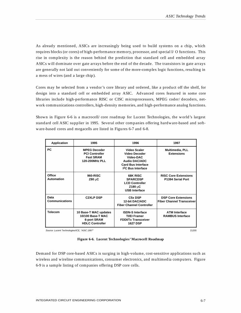
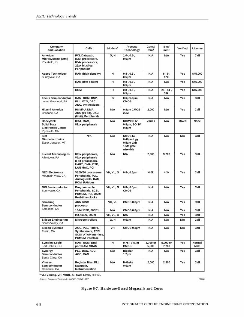
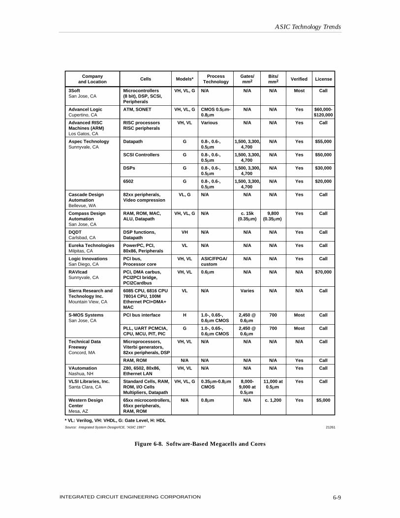
Shown in Figure 6-6 is a macrocell/core roadmap for Lucent Technologies, the world’s largeststandard cell ASIC supplier in 1995. Several other companies offering hardware-based and soft-ware-based cores and megacells are listed in Figures 6-7 and 6-8.
Demand for DSP core-based ASICs is surging in high-volume, cost-sensitive applications such aswireless and wireline communications, consumer electronics, and multimedia computers. Figure6-9 is a sample listing of companies offering DSP core cells.
ASIC Technology Trends
INTEGRATED CIRCUIT ENGINEERING CORPORATION 6-7
Video Scaler Video Decoder
Video-DAC Audio DAC/ADC
Card Bus Interface I2C Bus Interface
68K RISC
SPARCDSP LCD Controller
Z180 µC USB Interface
C5x DSP
12-bit DAC/ADC Fiber Channel Controller
ISDN-S Interface
TI/EI Framer FDDI/Tx Transceiver
1627 DSP
Multimedia, PLL Extensions
RISC Core Extensions P1394 Serial Port
DSP Core Extensions Fiber Channel Transceiver
ATM Interface RAMBUS Interface
MPEG Decoder PCI Controller
Fast SRAM 120-200MHz PLL
960-RISC Z80 µC
C2XLP DSP
10 Base-T MAC updates 10/100 Base-T MAC
6-port SRAM HDLC Controller
PC Office Automation Data Communications Telecom
Application 1995 1996 1997
21200Source: Lucent Technologies/ICE, "ASIC 1997"
Figure 6-6. Lucent Technologies’ Macrocell Roadmap
ASIC Technology Trends
INTEGRATED CIRCUIT ENGINEERING CORPORATION6-8
American PCI, Datapath, G, H 1.0-, 0.8-, N/A N/A Yes Call Microsystems (AMI) 805x processors, 0.6µm Pocatello, ID 804x processors, 29xx bit slice, Peripherals Aspec Technology RAM (high-density) H 0.8-, 0.6-, N/A 6-, 9-, Yes $45,000 Sunnyvale, CA 0.5µm 12k RAM (low-power) H 0.8-, 0.6-, N/A N/A Yes $45,000 0.5µm ROM H 0.8-, 0.6-, N/A 21-, 41-, Yes $45,000 0.5µm 53k Focus Semiconductor RAM, ROM, DSP, G 0.6µm-3µm N/A N/A Yes Call Lower Gwynedd, PA PLL, VCO, DAC, CMOS ADC, synthesizers Hitachi America H8 MPU, DMA, N/A 0.8µm CMOS 2,000 N/A Yes Call Brisbane, CA ADC (10 bit), DAC 2LM (8 bit), Peripherals Honeywell 8051, RAM, N/A RICMOS IV Varies N/A Mixed None Solid State 82xx peripherals 0.8µm, SOI IV Electronics Center 0.8µm Plymouth, MN IBM N/A N/A CMOS 5L N/A N/A N/A Call Microelectronics 0.46µm Leff Essex Junction, VT 0.5µm Lith 1.5M gate wireable Lucent Technologies 82xx peripherals, N/A N/A 2,300 9,200 Yes Call Allentown, PA 85xx peripherals 8-bit processors, UART, DMA, DSP, LAN MAC, PCI NEC Electronics V20/V30 processors, VH, VL, G 0.8-, 0.5µm 4.0k 4.3k Yes Call Mountain View, CA Peripherals, PLL, Analog cells, RAM, ROM, RAMbus OKI Semiconductor Programmable VH, VL, G 0.8-, 0.5µm N/A N/A Yes Call Sunnyvale, CA Peripherals, SCSI, CMOS PCMCIA, PCI, UART, Real-time clocks Samsung ARM RISC VH, VL CMOS 0.8µm N/A N/A Yes Call Semiconductor processor San Jose, CA 16-bit DSP, 80C51 N/A CMOS 0.8µm N/A N/A Yes Call I/O, timer, UART VH, VL, G N/A N/A N/A Yes Call Silicon Engineering Microcontrollers G, H 0.6µm N/A N/A N/A Call Scotts Valley, CA Silicon Systems AGC, PLL, Filters, VH CMOS 0.8µm N/A N/A N/A Call Tustin, CA Synthesizers, ECC, SCSI, ATAP interface, PCMCIA interface Symbios Logic RAM, ROM, Dual H 0.75-, 0.5µm 3,700 or 5,000 or Yes Normal Fort Collins, CO port RAM, SRAM CMOS 5,800 7,700 NRE Synergy PLL, DAC, ADC, N/A Bipolar N/A N/A Yes Call Semiconductor AGC, RAM 1.2µm Santa Clara, CA Vitesse Register files, PLL, N/A H-GaAs 2,000 2,300 Yes Call Semiconductor Datapath, 0.6µm Camarillo, CA Instrumentation
Company and Location
Cells Models*Process
TechnologyGates/ mm2
Bits/ mm2 Verified License
* VL: Verilog, VH: VHDL, G: Gate Level, H: HDLSource: Integrated System Design/ICE, "ASIC 1997" 21260
Figure 6-7. Hardware-Based Megacells and Cores
ASIC Technology Trends
INTEGRATED CIRCUIT ENGINEERING CORPORATION 6-9
Figure 6-8. Software-Based Megacells and Cores
3Soft Microcontrollers VH, VL, G N/A N/A N/A Most Call San Jose, CA (8 bit), DSP, SCSI, Peripherals Advancel Logic ATM, SONET VH, VL, G CMOS 0.5µm- N/A N/A Yes $60,000- Cupertino, CA 0.8µm $120,000 Advanced RISC RISC processors VH, VL Various N/A N/A Yes Call Machines (ARM) RISC peripherals Los Gatos, CA Aspec Technology Datapath G 0.8-, 0.6-, 1,500, 3,300, N/A Yes $55,000 Sunnyvale, CA 0.5µm 4,700 SCSI Controllers G 0.8-, 0.6-, 1,500, 3,300, N/A Yes $50,000 0.5µm 4,700 DSPs G 0.8-, 0.6-, 1,500, 3,300, N/A Yes $30,000 0.5µm 4,700 6502 G 0.8-, 0.6-, 1,500, 3,300, N/A Yes $20,000 0.5µm 4,700 Cascade Design 82xx peripherals, VL, G N/A N/A N/A Yes Call Automation Video compression Bellevue, WA Compass Design RAM, ROM, MAC, VH, VL, G N/A c. 15k 9,800 Yes Call Automation ALU, Datapath (0.35µm) (0.35µm) San Jose, CA DQDT DSP functions, VH N/A N/A N/A Yes Call Carlsbad, CA Datapath Eureka Technologies PowerPC, PCI, VL N/A N/A N/A Yes Call Milpitas, CA 80x86, Peripherals Logic Innovations PCI bus, VH, VL ASIC/FPGA/ N/A N/A Yes Call San Diego, CA Processor core custom RAVIcad PCI, DMA carbus, VH, VL 0.6µm N/A N/A N/A $70,000 Sunnyvale, CA PCI2PCI bridge, PCI2Cardbus Sierra Research and 6085 CPU, 6816 CPU VL N/A Varies N/A N/A Call Technology Inc. 78014 CPU, 100M Mountain View, CA Ethernet PCI+DMA+ MAC S-MOS Systems PCI bus interface H 1.0-, 0.65-, 2,450 @ 700 Most Call San Jose, CA 0.6µm CMOS 0.6µm PLL, UART PCMCIA, G 1.0-, 0.65-, 2,450 @ 700 Most Call CPU, MCU, PIT, PIC 0.6µm CMOS 0.6µm Technical Data Microprocessors, VH, VL N/A N/A N/A N/A Call Freeway Viterbi generators, Concord, MA 82xx peripherals, DSP RAM, ROM N/A N/A N/A N/A Yes Call VAutomation Z80, 6502, 80x86, VH, VL N/A N/A N/A Yes Call Nashua, NH Ethernet LAN VLSI Libraries, Inc. Standard Cells, RAM, VH, VL, G 0.35µm-0.8µm 8,000- 11,000 at Yes Call Santa Clara, CA ROM, I/O Cells CMOS 9,000 at 0.5 µm Multipliers, Datapath 0.5µm Western Design 65xx microcontrollers, N/A 0.8µm N/A c. 1,200 Yes $5,000 Center 65xx peripherals, Mesa, AZ RAM, ROM
Company and Location
Cells Models*Process
TechnologyGates/ mm2
Bits/ mm2 Verified License
* VL: Verilog, VH: VHDL, G: Gate Level, H: HDLSource: Integrated System Design/ICE, "ASIC 1997" 21261

ASIC Technology Trends
INTEGRATED CIRCUIT ENGINEERING CORPORATION6-10
3Soft Corporation M320C25 16 bits 16 bits 15 MIPS Provided as synthesizable HDL San Jose, CA Adaptive Solutions CNAPS 16 bits 64 bits 1,280 MIPS Scalable 2-chip SIMD Beaverton, OR multiprocessor Analog Devices ADSP-21xx 16 bits 24 bits 20 MIPS No visible pipeline effects Norwood, MA ADSP-216x 16 bits 24 bits 25 MIPS Two serial ports, timer, power- down mode ADSP-217x 16 bits 24 bits 33 MIPS Host port, two serial ports, power-down mode ADSP-2181 16 bits 24 bits 33 MIPS Host port, two serial ports, DMA ADSP-21msp5x 16 bits 24 bits 26 MIPS Integrated 16-bit A/D and D/A ADSP-21020 32 bits 48 bits 33 MIPS Two off-chip memory buses ADSP-2106x 32 bits 48 bits 40 MIPS Strong support for multi- processor designs Clarkspur Design CD2400 16 bits 16 bits 30 MIPS Simple, very compact Saratoga, CA architecture CD2450 16-24 16 bits 50 MIPS Adjustable data word width bits DSP Group PINE 16 bits 16 bits 30 MIPS Provided as synthesizable HDL Santa Clara, CA and layout OAK 16 bits 16 bits 40 MIPS Provided as synthesizable HDL and layout IBM Microelectronics MDSPxxxx 16 bits 24 bits 25 MIPS Intended for PC multimedia Hopewell Junction, NY applications Lucent Technologies DSP16xx 16 bits 16 bits 50 MIPS Flash memory versions Allentown, PA available for prototyping DSP32xx 32bits 32 bits 20 MIPS Intended for PC multimedia applications Motorola DSP561xx 16 bits 16 bits 30 MIPS Integrated 16-bit A/D and D/A Austin, TX DSP5600x 24 bits 24 bits 33 MIPS 24-bit data word DSP9600x 32 bits 32 bits 20 MIPS Dual external memory buses NEC µPD7701x 16 bits 32 bits 33 MIPS Two serial ports, one parallel Mountain View, CA port, 4-bit I/O lines SGS-Thomson D950-CORE 16 bits 16 bits 40 MIPS Coprocessor interface Carrollton, TX provided Tensleep Design A/DSC321 16 bits 16 bits 12.5 MIPS Similar to TMS320C25 Austin, TX A/DSC421 16 bits 16 bits 25 MIPS Similar to TMS320C25 A/DSC521 16 bits 16 bits 30 MIPS Similar to TMS320C25 Texas Instruments TMS320C1x 16 bits 16 bits 8.8 MIPS First commercially successful Dallas, TX DSP TMS320C2x 16 bits 16 bits 12.5 MIPS TI's second-generation fixed- point DSP TMS320C3x 32 bits 32 bits 30 MIPS Low-cost versions compete with fixed-point DSPs TMS320C4x 32 bits 32 bits 30 MIPS Intended for multiprocessor applications TMS320C5x 16 bits 16 bits 50 MIPS TI's latest fixed-point family TMS320C80 32/64 8/16/31 250 MIPS Contains four fixed-point DSPs bits bits plus a RISC CPU Zilog Z89Cxx 16 bits 16 bits 20 MIPS Available with a microcontroller Campbell, CA on one chip Zoran ZR3800x 20 bits 32 bits 33 MIPS 20-bit data word is unique, Santa Clara, CA intended for audio
* Native MIPS for fastest member of family.
Company and Location
FamilyData
WidthProgram
WidthNative MIPS*
Notes
Source: Integrated System Design/ICE, "ASIC 1997" 21262
Figure 6-9. Digital Signal Processors and Cores
Although a DSP core can be used to process analog functions, it may or may not be the most effec-tive solution, depending on the application. As a result, demand for ASICs incorporating analogcircuitry continues to be strong. Furthermore, functions like audio, imaging, temperature sensing,and frequency modulation will always require at least an analog, or “real world” interface.Applications such as HDTV, cellular communications, multimedia, teleconferencing, voice syn-thesis/recognition, modems, etc., are pressuring standard cell vendors to offer state-of-the-artmixed-signal capabilities. Unfortunately, the sophisticated design, manufacturing, and testing ofmixed-signal devices continues to pose formidable challenges.
As evidence to the significance of the mixed-signal ASIC industry, NEC has said that about one-third of its standard cell customers desire analog circuitry in their chip designs. SGS-Thomson isone example of a large standard analog IC supplier using its analog expertise and experience toenhance the mixed-signal capabilities of its standard cell product line. National, Harris, andLucent Technologies are other examples of this trend.
Demand for high-density gate arrays continues to be high, due to a considerable number ofadvanced ASIC designs being pad-limited. Pad limited means the die size is determined by thenumber of I/O pads needed rather than the number of gates used. For non-pad-limited designs,the leading manufacturers of high-density (greater than 50,000 gates) CMOS gate arrays areimplementing at least three-layer metal processes in order to increase the efficiency of gate usage(and also increase performance). Three layers of metal interconnection provide up to 70 percentgate utilization as opposed to about 35-45 percent for double-layer metal arrays.
The performance limits of gate arrays are being extended by several developments not only inCMOS technology, but also in GaAs and BiCMOS technologies. Examples are provided below.
• Sunnyvale, California-based Silicon Architects (acquired by Synposys in 1995) is promotingits cell-based array (CBA) technology, which the company says combines standard cell den-sity, performance, and power with gate array time-to-market and portability. The CBAarchitecture utilizes a small compute cell and a larger adjustable-size drive cell. The basiccompute cell is optimized for memory and data path operations, while the drive cells areoptimized for performance in critical paths. This structure allows for the implementation ofthe more-complex logic functions, including, eventually, functions such as an MPEG chip.
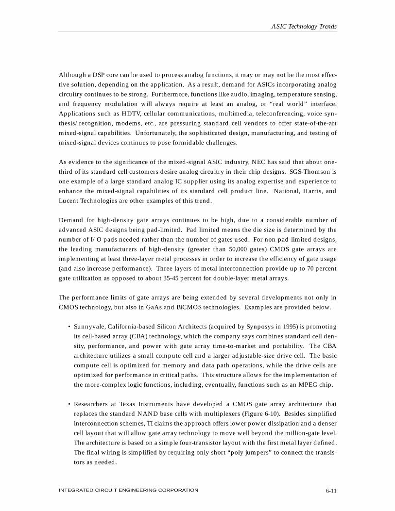
• Researchers at Texas Instruments have developed a CMOS gate array architecture thatreplaces the standard NAND base cells with multiplexers (Figure 6-10). Besides simplifiedinterconnection schemes, TI claims the approach offers lower power dissipation and a densercell layout that will allow gate array technology to move well beyond the million-gate level.The architecture is based on a simple four-transistor layout with the first metal layer defined.The final wiring is simplified by requiring only short “poly jumpers” to connect the transis-tors as needed.
ASIC Technology Trends
INTEGRATED CIRCUIT ENGINEERING CORPORATION 6-11
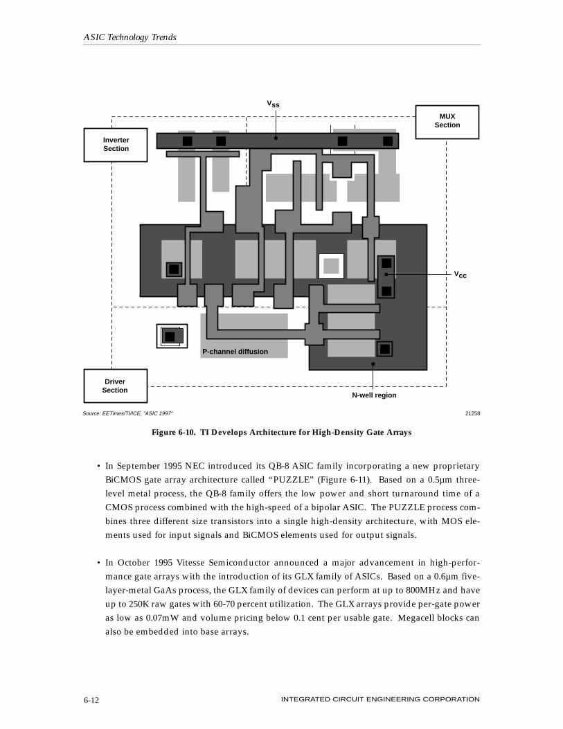
• In September 1995 NEC introduced its QB-8 ASIC family incorporating a new proprietaryBiCMOS gate array architecture called “PUZZLE” (Figure 6-11). Based on a 0.5µm three-level metal process, the QB-8 family offers the low power and short turnaround time of aCMOS process combined with the high-speed of a bipolar ASIC. The PUZZLE process com-bines three different size transistors into a single high-density architecture, with MOS ele-ments used for input signals and BiCMOS elements used for output signals.
• In October 1995 Vitesse Semiconductor announced a major advancement in high-perfor-mance gate arrays with the introduction of its GLX family of ASICs. Based on a 0.6µm five-layer-metal GaAs process, the GLX family of devices can perform at up to 800MHz and haveup to 250K raw gates with 60-70 percent utilization. The GLX arrays provide per-gate poweras low as 0.07mW and volume pricing below 0.1 cent per usable gate. Megacell blocks canalso be embedded into base arrays.
ASIC Technology Trends
INTEGRATED CIRCUIT ENGINEERING CORPORATION6-12
Vcc
Vss
N-well region
P-channel diffusion
Inverter Section
Driver Section
MUX Section
21258Source: EETimes/TI/ICE, "ASIC 1997"
Figure 6-10. TI Develops Architecture for High-Density Gate Arrays
Demand for high-density ECL arrays has been lessened by advances in CMOS, BiCMOS, andGaAs gate arrays. Moreover, because of the inherent problems encountered with high-densityECL devices (e.g., high heat dissipation), most ECL array manufacturers will not pursue the tech-nology beyond the 50K density level. Likewise, ICE does not expect to see a recognizable marketfor greater than 50K-gate ECL gate arrays.
Analog and mixed-signal arrays continue to represent a niche ASIC technology. Most of the ana-log array companies do less than 25-50 designs per year, quite small when compared to the largenumber of digital gate array designs realized each year. Overall, very high-end analog and mixed-signal ASIC requirements are still best handled by standard cell or full custom approaches.
Recent notable announcements regarding gate arrays, embedded arrays, and standard cells areprovided below.
• In 4Q95 Hitachi began offering its SH-1 32-bit RISC controllers as part of its 0.5µm ASIC celllibrary. The company also added to its cell library, an MPEG decompression core licensedfrom CompCore Multimedia Inc.
• Hitachi began taking orders for its HG73G gate array and HG73E embedded array 0.35µmCMOS ASICs in April 1996. The triple-metal process enables designs of up to 1.5 milliongates.
ASIC Technology Trends
INTEGRATED CIRCUIT ENGINEERING CORPORATION 6-13
Physical Description
Device Size
Process
Metal Options
Raw Gates
Usable Gates
Pad Counts
Voltage Level
Performance
Power Dissipation
I/O Capabilities
LVTTL
pECL
PCI (spec 2.1)
GTL
HSTL
Packaging
PQFP
PGA
BGA
0.5µm (0.35µm Leff)
CMOS-based epi-less BiCMOS
3 Layers
32,000 to 379,000
19,000 to 223,000
156 to 672
3.3V ±5%
139ps (F/O = 2, L = 0.5mm)
0.26µW/MHz/gate
100MHz, std. buffers, fail-safe function
High speed clock input (250MHz)
3.3V or 5V
Interface for processor buses (75MHz)
Interface for VR10000 processor bus (250MHz)
Up to 376 pins
Up to 524 pins
Up to 524 solder balls
21259Source: NEC/ICE, "ASIC 1997"
Figure 6-11. NEC’s “PUZZLE” BiCMOS Gate Array Specs
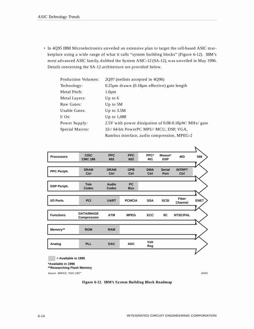
• In 4Q95 IBM Microelectronics unveiled an extensive plan to target the cell-based ASIC mar-ketplace using a wide range of what it calls “system building blocks” (Figure 6-12). IBM’smost advanced ASIC family, dubbed the System ASIC-12 (SA-12), was unveiled in May 1996.Details concerning the SA-12 architecture are provided below.
Production Volumes: 2Q97 (netlists accepted in 4Q96)Technology: 0.25µm drawn (0.18µm effective) gate lengthMetal Pitch: 1.0µmMetal Layers: Up to 6Raw Gates: Up to 5MUsable Gates: Up to 3.5MI/Os: Up to 1,088Power Supply: 2.5V with power dissipation of 0.08-0.18µW/MHz/gateSpecial Macros: 32-/64-bit PowerPC MPU/MCU, DSP, VGA,
Rambus interface, audio compression, MPEG-2
ASIC Technology Trends
INTEGRATED CIRCUIT ENGINEERING CORPORATION6-14
Processors
PPC Periph.
DSP Periph.
I/O Ports
Functions
Memory**
Analog
CISC CMC 186
PPC 602
PPC 603
PPC* 401
Mwave* DSP
403 586
SRAM Ctrl
DRAM Ctrl
OPB Ctrl
DMA Ctrl
Serial Port
INTRPT Ctrl
Tele Codec
Audio Codec
PC Bus
PCI UART PCMCIA SSA SCSI Fiber Channel
ENET
DATA/IMAGE Compression
ATM MPEG ECC IIC NTSC/PAL
ROM RAM
PLL DAC ADC Volt Reg
Source: IBM/ICE, "ASIC 1997" 20403
= Available in 1995
*Available in 1996 **Researching Flash Memory
Figure 6-12. IBM’s System Building Block Roadmap

• In early 1996, IBM Microelectronics began accepting netlists for its CMOS 5X process—thethird and final derivative of the company’s 0.5µm ASIC process. The process uses 0.25µmeffective gate lengths (0.35µm drawn) and offers up to 1.6 million usable gates and as manyas 748 I/O pins. Other features of the architecture include 1.2µm metal pitch and 70Å oxidethickness.
• IBM rolled out its PowerPC 401GF core, which is targeted at low-cost battery-operated sys-tems. Initially offered in 25MHz and 50MHz versions, the 401GF consumes as little as 40mW(typical, @25MHz) from a 2.5V power supply. The chip, measuring 4.5mm2, is manufacturedusing IBM’s 0.5µm three-layer metal CMOS-5S process technology. 75MHz and 100MHzversions are expected to follow before the end of 1996.
• LG Semicon added the ARM7 microprocessor and ARM710 microcontroller cores, licensedfrom Advanced RISC Machines Limited, to its cell library.
• In 2Q96 LSI Logic added the new Gigabit SeriaLink™ interface core to its CoreWare celllibrary. The CMOS-based Gigabit SeriaLink supports the Fibre Channel data transmissionprotocol, which allows for the transmission of up to 1.0625 billion bits of data per second, theequivalent of several 350-page novels a second.
• LSI Logic introduced its G10™ ASIC process technology in 3Q95. Figure 6-13 offers a lookat some of the new G10 characteristics along with a history of previous LSI Logic ASIC tech-nologies. Figure 6-14 shows the various sub-families of the G10 technology and their tar-geted applications. Volume production of G10 ASICs began in 1Q96.
ASIC Technology Trends
INTEGRATED CIRCUIT ENGINEERING CORPORATION 6-15
0.35µm
0.25µm
Cell Based Embedded Array Gate Array
2, 3, 4, & 5 Layer
3.3 & 2.5 Volts
GTL/NTL/HSTL PECL to 622 MHz PCI Impedance Controlled LVTTL LVDS to 1.2GHz Mixed Signal
5,000,000
100K to 2,500K
0.4-0.7µW/Gate/MHz
Drawn
Effective
Architectures
Metal Interconnect
Operating Voltages
I/O Options
Gate Capacities
Usable (max)
Typical (used)
Power Dissipation
0.5µm
0.38µm
Cell Based Embedded Array Gate Array
2, 3, & 4 Layer
3.3 Volts
GTL/NTL/HSTL PECL to 622MHz PCI Mixed Signal
1,500,000
60 to 500K
1.0µW/Gate/MHz
0.6µm
0.45µm
Cell Based
2 & 3 Layer
3.3 Volts
GTL/NTL PECL to 155MHz PCI Mixed Signal
1,200,000
40 to 400K
1.5µW/Gate/MHz
0.7µm
0.55µm
Gate Array
2 Layer
3.3 Volts
GTL/NTL Universal PCI Mixed Signal
165,000
20 to 75K
1.4µW/Gate/MHz
0.8µm
0.65µm
Cell Based Embedded Array Gate Array
2 Layer
5.0 Volts
GTL/NTL PCI Mixed Signal
250,000
20 to 100,000K
5.0µW/Gate/MHz
0.6µm
0.45µm
Cell Based Embedded Array Gate Array
2 & 3 Layer
5.0 Volts
GTL/NTL PECL to 155MHz PCI Mixed Signal
600,000
40 to 300K
3.2µW/Gate/MHz
Source: LSI Logic/ICE, "ASIC 1997" 20405
LSI CMOS Process G10™ Family 500K 600K 400K 405K 300K
Figure 6-13. LSI Logic ASIC Technology Trends
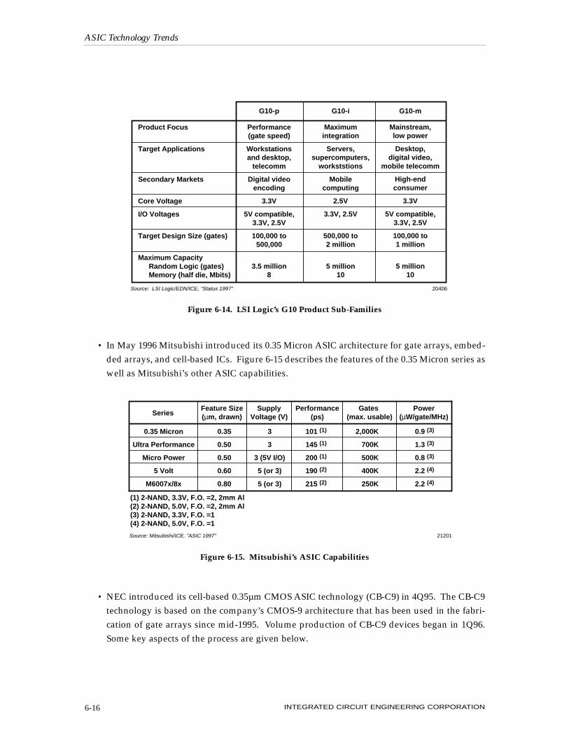
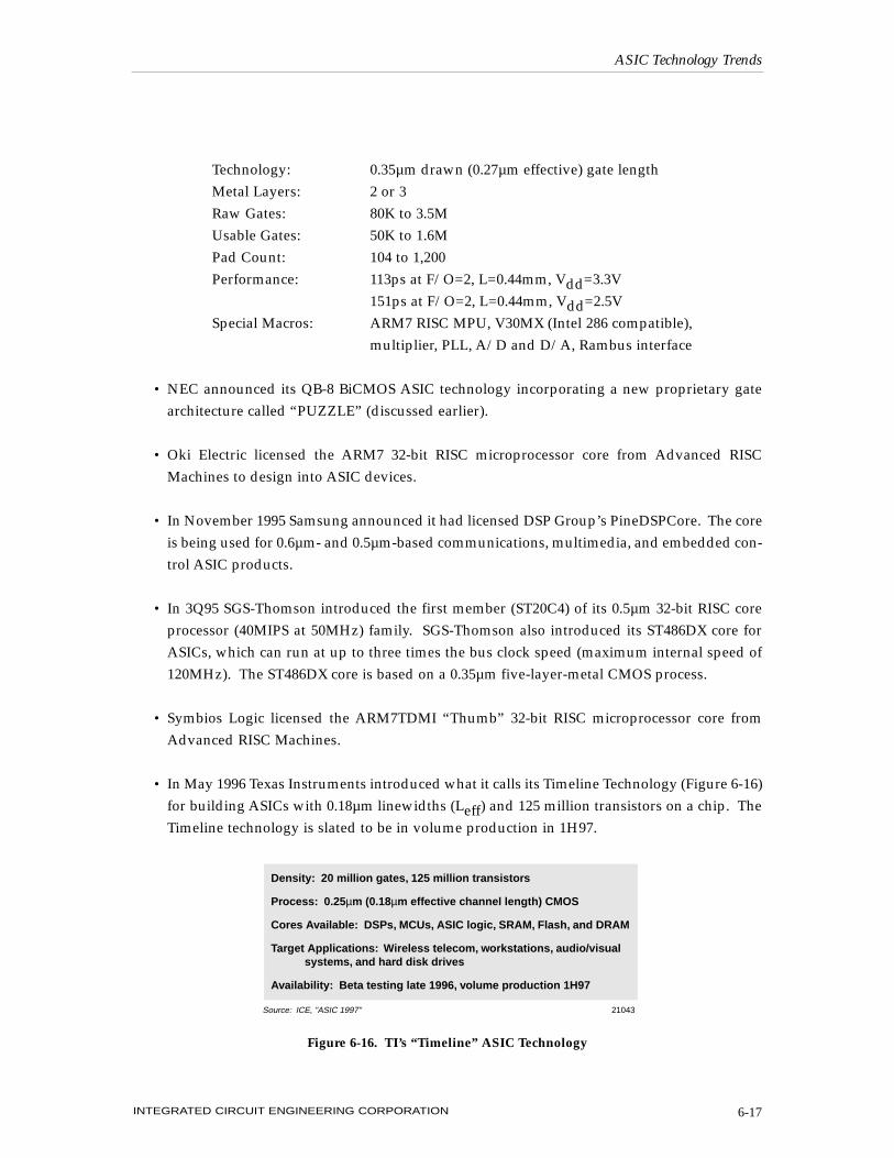
• In May 1996 Mitsubishi introduced its 0.35 Micron ASIC architecture for gate arrays, embed-ded arrays, and cell-based ICs. Figure 6-15 describes the features of the 0.35 Micron series aswell as Mitsubishi’s other ASIC capabilities.
• NEC introduced its cell-based 0.35µm CMOS ASIC technology (CB-C9) in 4Q95. The CB-C9technology is based on the company’s CMOS-9 architecture that has been used in the fabri-cation of gate arrays since mid-1995. Volume production of CB-C9 devices began in 1Q96.Some key aspects of the process are given below.
ASIC Technology Trends
INTEGRATED CIRCUIT ENGINEERING CORPORATION6-16
Product Focus
Target Applications
Secondary Markets
Core Voltage
I/O Voltages
Target Design Size (gates)
Maximum Capacity Random Logic (gates) Memory (half die, Mbits)
Performance (gate speed)
Workstations and desktop,
telecomm
Digital video encoding
3.3V
5V compatible, 3.3V, 2.5V
100,000 to 500,000
3.5 million
8
Maximum integration
Servers, supercomputers,
workststions
Mobile computing
2.5V
3.3V, 2.5V
500,000 to 2 million
5 million
10
Mainstream, low power
Desktop, digital video,
mobile telecomm
High-end consumer
3.3V
5V compatible, 3.3V, 2.5V
100,000 to 1 million
5 million
10
G10-p G10-i G10-m
Source: LSI Logic/EDN/ICE, "Status 1997" 20406
Figure 6-14. LSI Logic’s G10 Product Sub-Families
0.35 Micron
Ultra Performance
Micro Power
5 Volt
M6007x/8x
0.35
0.50
0.50
0.60
0.80
3
3
3 (5V I/O)
5 (or 3)
5 (or 3)
101 (1)
145 (1)
200 (1)
190 (2)
215 (2)
2,000K
700K
500K
400K
250K
0.9 (3)
1.3 (3)
0.8 (3)
2.2 (4)
2.2 (4)
SeriesFeature Size (µm, drawn)
Supply Voltage (V)
Performance (ps)
Gates (max. usable)
Power (µW/gate/MHz)
(1) 2-NAND, 3.3V, F.O. =2, 2mm Al (2) 2-NAND, 5.0V, F.O. =2, 2mm Al (3) 2-NAND, 3.3V, F.O. =1 (4) 2-NAND, 5.0V, F.O. =1
Source: Mitsubishi/ICE, "ASIC 1997" 21201
Figure 6-15. Mitsubishi’s ASIC Capabilities
Technology: 0.35µm drawn (0.27µm effective) gate lengthMetal Layers: 2 or 3Raw Gates: 80K to 3.5MUsable Gates: 50K to 1.6MPad Count: 104 to 1,200Performance: 113ps at F/O=2, L=0.44mm, Vdd=3.3V
151ps at F/O=2, L=0.44mm, Vdd=2.5VSpecial Macros: ARM7 RISC MPU, V30MX (Intel 286 compatible),
multiplier, PLL, A/D and D/A, Rambus interface
• NEC announced its QB-8 BiCMOS ASIC technology incorporating a new proprietary gatearchitecture called “PUZZLE” (discussed earlier).
• Oki Electric licensed the ARM7 32-bit RISC microprocessor core from Advanced RISCMachines to design into ASIC devices.
• In November 1995 Samsung announced it had licensed DSP Group’s PineDSPCore. The coreis being used for 0.6µm- and 0.5µm-based communications, multimedia, and embedded con-trol ASIC products.
• In 3Q95 SGS-Thomson introduced the first member (ST20C4) of its 0.5µm 32-bit RISC coreprocessor (40MIPS at 50MHz) family. SGS-Thomson also introduced its ST486DX core forASICs, which can run at up to three times the bus clock speed (maximum internal speed of120MHz). The ST486DX core is based on a 0.35µm five-layer-metal CMOS process.
• Symbios Logic licensed the ARM7TDMI “Thumb” 32-bit RISC microprocessor core fromAdvanced RISC Machines.
• In May 1996 Texas Instruments introduced what it calls its Timeline Technology (Figure 6-16)for building ASICs with 0.18µm linewidths (Leff) and 125 million transistors on a chip. TheTimeline technology is slated to be in volume production in 1H97.
ASIC Technology Trends
INTEGRATED CIRCUIT ENGINEERING CORPORATION 6-17
Figure 6-16. TI’s “Timeline” ASIC Technology
Density: 20 million gates, 125 million transistors
Process: 0.25µm (0.18µm effective channel length) CMOS
Cores Available: DSPs, MCUs, ASIC logic, SRAM, Flash, and DRAM
Target Applications: Wireless telecom, workstations, audio/visual systems, and hard disk drives
Availability: Beta testing late 1996, volume production 1H97
Source: ICE, "ASIC 1997" 21043
• Texas Instruments added to its TCG Series of ASICs, the TCG4000 series of gate arrays andthe TEG4000 series of embedded arrays. The arrays are manufactured using a four-level-metal 0.35µm CMOS process and offer up to 1.7 million usable gates.
• Toshiba described its new TC220 0.3µm drawn CMOS ASIC process in 4Q95. Some charac-teristics of this technology are shown below.
Production volumes: 3Q96Technology: 0.35µm drawn CMOSMetal Layers: Two or threeRaw Gates: Up to 3MUsable Gates: 1.9M on a 17.5mm x 17.5mm die
• In 3Q95 Toshiba introduced its TC203 0.4µm CMOS family of ASICs for mixed 3V/5V oper-ation. The family offers up to 690K usable gates.
• Vitesse unveiled its new GLX™ family of 0.5µm GaAs-based gate arrays (discussed earlier).
A noticeable trend in the preceding announcements is that ASIC technology is definitely enteringthe deep-submicron realm (issues concerning deep-submicron technologies are covered later inthis section).
While 0.35µm ASICs will represent only a small portion of the total ASIC market through 1996,VLSI Technology and Hitachi envision fast rising demand for the technology, from many differ-ent system segments (Figure 6-17). As shown in Figure 6-18, the average gate density of the fivesystem categories included is forecast to rise from about 35K gates in 1993 to 1.4M gates in 1997.Moreover, average performance of these five segments is forecast to surge from 35MHz to150MHz over the same timeperiod. There is little doubt that million-plus gate devices operatingat 150MHz or higher will demand 0.35µm technology.
ASIC Technology Trends
INTEGRATED CIRCUIT ENGINEERING CORPORATION6-18
•Computers with workstation compute power and 3D graphics offered in the form factor and price points of a laptop •Switches and Routers with more bandwidth and capacity, reducing cost per connection •Wireless communicators that handle voice and data, and eventually run for months on two AA batteries •Fully interactive digital video devices priced at VCR levels
Source: Hitachi/VLSI Technology, "ASIC 1997" 20055
Figure 6-17. Market Impact of 0.35µm Cell-Based ASICs

As shown in Figure 6-19, the rapid increase in gate density and clock frequency in advanced ASICdevices is driving the need for new packages, like the ball grid array (BGA), that can support therequirements for higher pin counts and improved heat dissipation.
ASIC Technology Trends
INTEGRATED CIRCUIT ENGINEERING CORPORATION 6-19
0.01 0.1 1.0 100
50
100
150
200
250
Network Computing Systems
Mobile PC
Consumer
Wireless
CY '97CY '95
CY '93
Per
form
ance
(M
Hz)
Integration (millions of gates)
20056Source: Hitachi/VLSI Technology/ICE, "ASIC 1997"
Figure 6-18. New Digital Markets for Advanced Cell-Based ASICs
Figure 6-19. Advanced ASICs Need Advanced Packages
1,000
800
600
400
200
0
10 50 100 200 300 400 500
Bare Chip Issues:
• Test/Burn In • HandlingBGAPGA
Issues: • Cost
• Bump Pitch ReductionTCP
Issues:• Cost • Fine Pitch Soldering • Electrical Performance
P-SMPIssues:
• Fine Pitch Soldering • Electrical Performance
Clock Frequency (MHz)
Pac
kag
e P
in C
ou
nts
21253Source: Hitachi/ICE, "ASIC 1997"

PLDs AND FPGAs
The first field programmable logic devices were introduced almost 25 years ago. Figure 6-20 showsa programmable logic device timeline with product introduction highlights labeled. Basically, thebenefits of using programmable logic have been shortening time to market and risk reduction.This has been true for over 20 years and will continue to be true in the foreseeable future.
Figure 6-21 shows how PLDs fit in an overall logic alternative comparison. As was mentioned,“development lead time” and “ease of design changes” are where PLD technology shines.
Over the twenty years of programmable logic offerings, the term PLD has evolved to encompassmore than just low-density bipolar products. The PLD industry has gone from using strictly bipo-lar technology and simple architecture to using CMOS EPROM, EEPROM, SRAM, flash, and anti-fuse processing with very elaborate circuit designs.
In an industry as dynamic as the IC industry, the natural trend has been toward high-density andhigh-performance technologies. In the PLD market this is very obvious as simple bipolar PLDsare now steadily losing marketshare to the more flexible and higher density CMOS PLD tech-nologies.
ASIC Technology Trends
INTEGRATED CIRCUIT ENGINEERING CORPORATION6-20
1972 First FPLA
Introduced
1979 National Second Sources
PAL
1978 MMI's PAL
Debuts
1980 PAL
Device Becomes Standard
1984 Altera's EPLD
Introduced
1989 AMD Replaces UV with Second Source GAL Device GAL Device Becomes Standard
1995 Multiple High-Density (>10KGates) PLDs Emerge
1991 High-Density Competitors
Enter Market
1982-3 Others Enter PAL
Market
1985 First E2CMOS PLD GAL Device Xilinx SRAM FPGA
18556ASource: Lattice, "ASIC 1997"
1970 1980 1990
Figure 6-20. Programmable Logic History

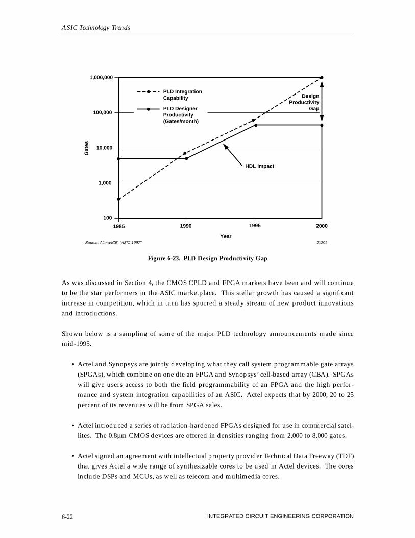
Provided in Figure 6-22 is a representative selection of high-density PLDs and FPGAs available onthe market. Figure 6-23 shows the PLD gate densities expected to be achieved by the end of thedecade. The figure also shows that along with the large increases in PLD gate density come someof the same “design productivity” issues that the gate array and cell-based ASIC suppliers mustdeal with. Luckily, the programmable logic design tool industry can pull some productivityenhancement strategies from existing gate array and cell-based tools.
ASIC Technology Trends
INTEGRATED CIRCUIT ENGINEERING CORPORATION 6-21
Time to market Development lead time Development cost Availability Available sources Volume independence (sensitivity) Application support Architectural flexibility Ease of design changes Performance Density Cost of design changes
Solution efficiency
Short/medium
Immediate
None
High
Many
Low
Much
Low
Medium
Low/medium
Low
Low/medium
Low
Short
Immediate
Low
High
Many
Low
Much
Medium/high
High
Medium
Medium
Low
Medium
Medium
Weeks/months
Medium/high
Medium
Few
High
Some
High
Low
High
Very high
High
High
Medium
Weeks/months
Medium/high
Medium
Few
High
Some
Higher
Lower
High
Very high
High
High
Long
Years
Very high
Low
Few
High
None
Highest
Lowest
Very high
Very high
Very high
Very high
18557ASource: AMD / ICE, "ASIC 1997"
Standard Components PLDs Gate Arrays Standard Cells Full
CustomCriterion
Figure 6-21. Selection Criteria for Different Logic Alternatives
Figure 6-22. High-Density PLD/FPGA Offerings
Company
Actel
Altera
Atmel
Cypress
Gatefield
IBM
Lattice
Lucent Technologies
Motorola
QuickLogic
Xilinx
Device Family
3200DX
FLEX 10K
AT6000
Ultra38000
GF100K
Series 10000
ispLSI 6000
ORCA Series
MPA1000
pASIC2
XC4000
Density Range (usable gates)
6,500 - 40,000�
10,000 - 100,000�
2,000 - 20,000�
7,000 - 20,000�
9,000 - 100,000�
8,000 - 42,000�
up to 25,000�
4,000 - 60,000�
3,500 - 22,000�
3,000 - 20,000�
28,000 - 125,000
Highest Density Available (as of mid-1996)
32200DX (20,000)
EPF10K100 (100,000)
AT6010 (20,000)
CY7C38012 (12,000)
GF51K (51,000)
IBM10016 (16,000)
ispLSI 6192 (25,000)
ATT2C40 (40,000)
MPA1100 (22,000)
Q12020 (20,000)
XC4052EX (52,000)
21254Source: ICE, "ASIC 1997"
As was discussed in Section 4, the CMOS CPLD and FPGA markets have been and will continueto be the star performers in the ASIC marketplace. This stellar growth has caused a significantincrease in competition, which in turn has spurred a steady stream of new product innovationsand introductions.
Shown below is a sampling of some of the major PLD technology announcements made sincemid-1995.
• Actel and Synopsys are jointly developing what they call system programmable gate arrays(SPGAs), which combine on one die an FPGA and Synopsys’ cell-based array (CBA). SPGAswill give users access to both the field programmability of an FPGA and the high perfor-mance and system integration capabilities of an ASIC. Actel expects that by 2000, 20 to 25percent of its revenues will be from SPGA sales.
• Actel introduced a series of radiation-hardened FPGAs designed for use in commercial satel-lites. The 0.8µm CMOS devices are offered in densities ranging from 2,000 to 8,000 gates.
• Actel signed an agreement with intellectual property provider Technical Data Freeway (TDF)that gives Actel a wide range of synthesizable cores to be used in Actel devices. The coresinclude DSPs and MCUs, as well as telecom and multimedia cores.
ASIC Technology Trends
INTEGRATED CIRCUIT ENGINEERING CORPORATION6-22
Year
1985 1990 1995 2000
100
1,000
10,000
100,000
1,000,000
Design Productivity
Gap
HDL Impact
Gat
esPLD Integration Capability
PLD Designer Productivity (Gates/month)
Source: Altera/ICE, "ASIC 1997" 21202
Figure 6-23. PLD Design Productivity Gap
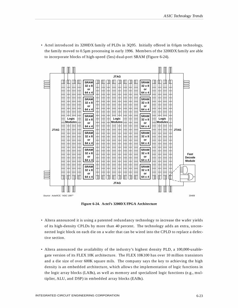
• Actel introduced its 3200DX family of PLDs in 3Q95. Initially offered in 0.6µm technology,the family moved to 0.5µm processing in early 1996. Members of the 3200DX family are ableto incorporate blocks of high-speed (5ns) dual-port SRAM (Figure 6-24).
• Altera announced it is using a patented redundancy technology to increase the wafer yieldsof its high-density CPLDs by more than 40 percent. The technology adds an extra, uncon-nected logic block on each die on a wafer that can be wired into the CPLD to replace a defec-tive section.
• Altera announced the availability of the industry’s highest density PLD, a 100,000-usable-gate version of its FLEX 10K architecture. The FLEX 10K100 has over 10 million transistorsand a die size of over 600K square mils. The company says the key to achieving the highdensity is an embedded architecture, which allows the implementation of logic functions inthe logic array blocks (LABs), as well as memory and specialized logic functions (e.g., mul-tiplier, ALU, and DSP) in embedded array blocks (EABs).
ASIC Technology Trends
INTEGRATED CIRCUIT ENGINEERING CORPORATION 6-23
SRAM 32 x 8
or 64 x 4
SRAM 32 x 8
or 64 x 4
SRAM 32 x 8
or 64 x 4
SRAM 32 x 8
or 64 x 4
SRAM 32 x 8
or 64 x 4
SRAM 32 x 8
or 64 x 4
SRAM 32 x 8
or 64 x 4
SRAM 32 x 8
or 64 x 4
SRAM 32 x 8
or 64 x 4
SRAM 32 x 8
or 64 x 4
SRAM 32 x 8
or 64 x 4
SRAM 32 x 8
or 64 x 4
JTAG
JTAG
JTAGJTAG
Fast Decode Module
Source: Actel/ICE, "ASIC 1997" 20409
Logic Modules
Logic Modules
Logic Modules
Figure 6-24. Actel’s 3200DX FPGA Architecture
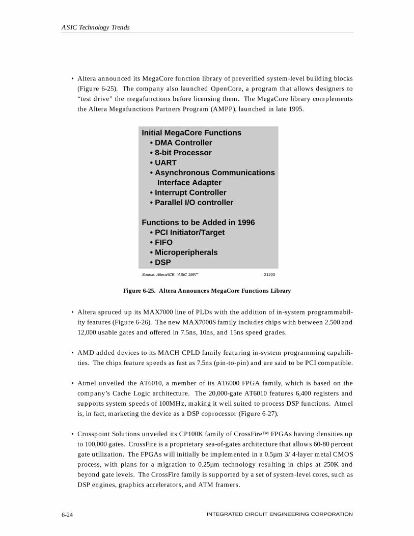
• Altera announced its MegaCore function library of preverified system-level building blocks(Figure 6-25). The company also launched OpenCore, a program that allows designers to“test drive” the megafunctions before licensing them. The MegaCore library complementsthe Altera Megafunctions Partners Program (AMPP), launched in late 1995.
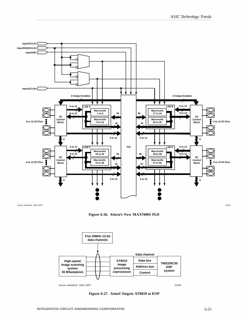
• Altera spruced up its MAX7000 line of PLDs with the addition of in-system programmabil-ity features (Figure 6-26). The new MAX7000S family includes chips with between 2,500 and12,000 usable gates and offered in 7.5ns, 10ns, and 15ns speed grades.
• AMD added devices to its MACH CPLD family featuring in-system programming capabili-ties. The chips feature speeds as fast as 7.5ns (pin-to-pin) and are said to be PCI compatible.
• Atmel unveiled the AT6010, a member of its AT6000 FPGA family, which is based on thecompany’s Cache Logic architecture. The 20,000-gate AT6010 features 6,400 registers andsupports system speeds of 100MHz, making it well suited to process DSP functions. Atmelis, in fact, marketing the device as a DSP coprocessor (Figure 6-27).
• Crosspoint Solutions unveiled its CP100K family of CrossFire™ FPGAs having densities upto 100,000 gates. CrossFire is a proprietary sea-of-gates architecture that allows 60-80 percentgate utilization. The FPGAs will initially be implemented in a 0.5µm 3/4-layer metal CMOSprocess, with plans for a migration to 0.25µm technology resulting in chips at 250K andbeyond gate levels. The CrossFire family is supported by a set of system-level cores, such asDSP engines, graphics accelerators, and ATM framers.
ASIC Technology Trends
INTEGRATED CIRCUIT ENGINEERING CORPORATION6-24
Initial MegaCore Functions • DMA Controller • 8-bit Processor • UART • Asynchronous Communications Interface Adapter • Interrupt Controller • Parallel I/O controller Functions to be Added in 1996 • PCI Initiator/Target • FIFO • Microperipherals • DSPSource: Altera/ICE, "ASIC 1997" 21203
Figure 6-25. Altera Announces MegaCore Functions Library
ASIC Technology Trends
INTEGRATED CIRCUIT ENGINEERING CORPORATION 6-25
PIA
Macrocells 25 to 32
Macrocells 17 to 24
Macrocells 9 to 16
Macrocells 1 to 8
LAB BLAB A
LAB C
I/O Control Block 6 to 12 I/O Pins
Macrocells 57 to 64
Macrocells 49 to 56
Macrocells 41 to 48
Macrocells 33 to 40
LAB D
I/O Control Block
I/O Control Block
I/O Control Block 6 to 12 I/O Pins6 to 12 I/O Pins
6 to 12 I/O Pins
6 to 12
6 to 12
6 to 12
6 to 12
6 to 12
6 to 12
6 to 12
6 to 12
6 to 126 to 12
6 to 12 6 to 12
1616
36
16
36
16
36
36
6
6
6
6
6 Output Enables 6 Output Enables
Input/GCLK1
Input/OE2/GCLK2
Input/OE1
Input/GCLRn
21255Source: Altera/ICE, "ASIC 1997"
Figure 6-26. Altera’s New MAX7000S PLD
Data channel
Data bus
Address bus
Control
High-speed image scanning
system 30 MSamples/s
AT6010 image
processing coprocessor
TMS320C30 DSP
system
Five 30MHz 12-bit data channels
21250Source: Atmel/ICE, "ASIC 1997"
Figure 6-27. Atmel Targets AT6010 at DSP

• Cypress entered the PLD core business with the introduction of a synthesizable VHDL PCItarget core in July 1996. The company’s core program has been named UltraCore.
• Cypress enhanced its Flash370 CPLD product line to create the new Flash370i family. The370i chips add in-system reprogrammability, a new technique for controlling noise in bus-oriented I/Os, PCI-compliant outputs, and automatic power reduction.
• Cypress introduced the PALCE20V8, a flash erasable and reprogrammable device manufac-tured using the company’s 0.65µm flash CMOS technology.
• Cypress introduced a new generation of its advanced UltraLogic™ FPGAs, the Ultra38000family. The antifuse-programmed devices are fabricated using a 0.65µm three-layer metalCMOS process and are available with up to 20,000 usable gates in 1,440 logic cells with 336I/Os. QuickLogic is Cypress’s antifuse FPGA second-source partner.
• IMP introduced the second member of its electrically programmable analog circuit (EPAC™)family. The new chip integrates the functions of over 18 discrete analog and digital CMOSIC components, providing user-configurable monitoring, diagnostic, and data acquisitionfeatures.
• Lattice Semiconductor extended its ispLSI 2000 line of CPLDs to include 3.3V devices. Thefamily of low-voltage parts offer gate densities from 1,000 up to 6,000 and operating speedsas fast as 10ns (80MHz). Device specifications also feature 100,000 erase/write cycles.
• Lattice added three members to its ispLSI family that feature integrated predefined, func-tion-specific memory and counter-timer megacells (Figure 6-28). The three versions includeeither a single-port SRAM, a dual-port SRAM, or a FIFO.
• Lattice announced a pair of very fast GAL PLDs, both operating at 3.3V. The GAL22LV10Dis rated at a 4ns propagation delay and 3ns clock-to-out time, making possible 182MHz statemachines. The GAL22LV8D features a 3.5ns propagation delay, a 2.5ns clock-to-out delay,and a 200MHz frequency.
• Lucent Technologies unveiled its 0.35µm CMOS process technology, which is optimized forASICs and FPGAs. The new technology will support designs of 2.5 million usable gates,200MHz system frequencies, and 1G/sec. I/O interfaces. The first product implementationis a series of ORCA™ FPGAs with gate counts ranging from 4,000 up to 60,000 (Figure 6-29).
ASIC Technology Trends
INTEGRATED CIRCUIT ENGINEERING CORPORATION6-26

• Microcontroller and nonvolatile memory manufacturer Microchip Technology entered theprogrammable logic market through the acquisition of ASIC Technical Solutions (ATS) of SanJose, California. ATS provides its QuickASIC array family which replaces FPGAs andCPLDs with a masked ASIC at a reduced price.
ASIC Technology Trends
INTEGRATED CIRCUIT ENGINEERING CORPORATION 6-27
Figure 6-28. Lattice ispLSI Family Turns Application-Specific
General-purpose I/O (96)
Memory I/O (31)
Register/ counter
I/O (24)
3192 core
Memory module 512 x 9
or 256 x 18
Register/ counter module
8 x 16 bits
Global routing
pool
Output routing pools
General- purpose
PLD module
(192 registers)
21251Source: Lattice Semiconductor/ICE, "ASIC 1997"
0.1
0.2
0.3
0.4
0.5
0.6
0.7
0.8
0.9
1.0
1.1
1.2
1.3
1.4
1.5
1.6
1.7
1.8
05,00010,00015,00020,00025,00030,00035,00040,00045,00050,00055,00060,00065,00070,00075,00080,00085,00090,00095,000100,000+
199719961995199419931992
Year
Min
imu
m G
eom
etry
(µm
)
Usa
ble
Gat
es/C
hip
Geometry
Gates
Source: Lucent Technologies/ICE, "ASIC 1997" 20431
4,000 gates 7,000 gates
26,000 gates
40,000 gates
60,000 gates
0.8µm
0.6µm
0.5µm 0.35µm
Figure 6-29. Lucent Technologies’ FPGA Density and Feature Size Trends
• Motorola announced its long-anticipated entry into the programmable logic market in April1996, with the introduction of new FPGAs based on technology licensed from PilkingtonMicro-Electronics in the U.K. The first devices in the Motorola Programmable Array (MPA)family are available with as many as 14,200 gates. They are reprogrammable SRAM-basedproducts manufactured on a standard 0.6µm triple-layer metal CMOS process. In late 1995,Motorola announced it had also licensed Pilkington’s field-programmable analog array(FPAA) technology.
• Long-time simple PLD player, Philips Semiconductors announced its entrance into the com-plex PLD market in April 1996 by forming a new CPLD business unit to sell its new high-performance, low-power 3.3V devices. The new “CoolRunner” CPLDs are an extension ofthe PLA architecture called eXtended Programmable Logic Array (XPLA). The devices fea-ture a design technique called Fast Zero Power (FZP), which provides low static (≤100µA)and dynamic power (50mA @>100MHz).
• Space Electronics Inc. (SEI) introduced a radiation-hardened FPGA for space-borne applica-tions, such as satellites, space craft, rockets, and probes. SEI’s device is based on a 0.65µmCMOS antifuse process and is available with densities ranging from 2,000 to 9,000 gates. Italso features chip-to-chip operating speeds of up to 135MHz with output delays of 3ns.
• Citing the strong market acceptance of SRAM and flash technologies, Xilinx announced inlate July, 1996 that it would discontinue its XC8100 family of one-time programmable anti-fuse FPGAs.
• Xilinx inaugurated its LogiCore program, which offers a PCI bus controller module as wellas third party software including DSP filters, bus interfaces, UARTs, and DMAs for variousXilinx PLDs.
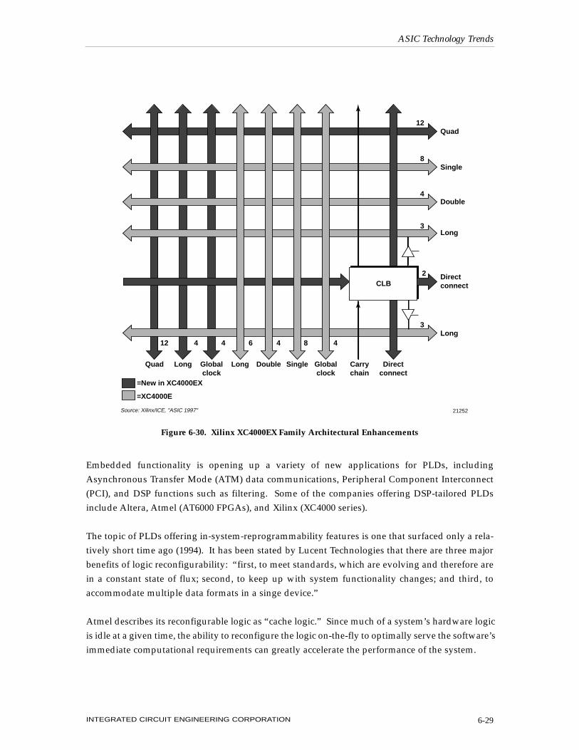
• Xilinx unveiled its XC4000EX family of FPGAs, which feature between 28,000 and 62,000nominal gates. The high density is accomplished through the use of a 0.5µm process and sig-nificant architectural changes. As shown in Figure 6-30, the major architectural differencebetween the XC4000EX and the older XC4000E is the approximate two-fold increase of rout-ing resources available to the logic cells. The density of the 4000EX FPGAs will increase to125,000 gates in 1997 when Xilinx moves to a 0.35µm process.
There is an increasing number of PLDs that are being tailored for specific applications. In fact,nearly every major PLD/FPGA supplier has recently announced the availability of a library ofsystem-level cores/megacells that can be embedded in their device designs, thereby allowingPLDs to be used as system-level chips. Blocks of circuitry that can be embedded in some oftoday’s PLDs include SRAMs, ROMs, ALUs, DSP filters, and even MPU and MCU functions.
ASIC Technology Trends
INTEGRATED CIRCUIT ENGINEERING CORPORATION6-28
Embedded functionality is opening up a variety of new applications for PLDs, includingAsynchronous Transfer Mode (ATM) data communications, Peripheral Component Interconnect(PCI), and DSP functions such as filtering. Some of the companies offering DSP-tailored PLDsinclude Altera, Atmel (AT6000 FPGAs), and Xilinx (XC4000 series).
The topic of PLDs offering in-system-reprogrammability features is one that surfaced only a rela-tively short time ago (1994). It has been stated by Lucent Technologies that there are three majorbenefits of logic reconfigurability: “first, to meet standards, which are evolving and therefore arein a constant state of flux; second, to keep up with system functionality changes; and third, toaccommodate multiple data formats in a singe device.”
Atmel describes its reconfigurable logic as “cache logic.” Since much of a system’s hardware logicis idle at a given time, the ability to reconfigure the logic on-the-fly to optimally serve the software’simmediate computational requirements can greatly accelerate the performance of the system.
ASIC Technology Trends
INTEGRATED CIRCUIT ENGINEERING CORPORATION 6-29
Figure 6-30. Xilinx XC4000EX Family Architectural Enhancements
CLB
12
12
8
86
4
4 4 4 4
3
2
3
Quad
Quad
Single
Single
Double
Double
Long
Long Long Direct connect
Direct connect
Long
Global clock
Global clock
Carry chain
=New in XC4000EX
=XC4000E
Source: Xilinx/ICE, "ASIC 1997" 21252

Some possible early system applications for reprogrammable logic include telecommunications,geophysical information processing, medical imaging, and computer architecture simulation. Inthe telecommunications area one can easily envision the need for a PLD device to dynamicallyreconfigure itself to accommodate multiple interface or telecommunications protocols and stan-dards (Figure 6-31).
As another example of a reconfigurable application, Altera states that its reprogrammable PLDscan be configured as a display accelerator or circuit simulator as needed. Altera says “that byusing reprogrammable logic the potential exists to configure the hardware for more direct pro-cessing of the data.”
Xilinx has stated that it believes the reconfigurable systems market will grow to more than $1 bil-lion in sales by the end of the decade with the FPGA chip portion estimated at approximately $200million.
ASIC Technology Trends
INTEGRATED CIRCUIT ENGINEERING CORPORATION6-30
(a) Telecom T1/T1E
(b) Sonet/Synchronous Networks
(c) Algorithm Engine
(d) ATM
(e) Graphics-Accelerator Card
DSP Algorithm Engine Line Interface Card
Line Interface Card
Line Interface Card
Synchronizer
DSP Algorithm Engine
Fixed Algorithm Engine
Dual-Port RAM DSP Core Microcontroller
ATM Switch Fabric
Hard Disk Compression/Decompression FPGA Video Engine
Synchronizer
2.048 Mbits/s (Europe) 1.544 Mbits/s (U.S.)
Extract timing from T1/T1E source
Extract timing from T1/T1E source or bits
DS3: 45 Mbits/s STS1E: 52 Mbits/s
Overhead channels Framing
Source: Lucent Technologies/ICE, "ASIC 1997" 20180
Figure 6-31. FPGA Can Reconfigure to Meet Various Standards
There is little doubt that reconfigurability will be a powerful tool to enhance a system’s efficiency.Still, it should be noted that in-system-reconfigurable PLD logic is still in its infancy. Currentdesign tools and programs are still not sufficient to manage dynamically reconfigurable hardwareefficiently. However, as system designers continue to explore ways to increase system perfor-mance, ICE expects that reconfigurable PLDs will find an increasing market to serve.
In general, the MOS PLD market will continue to be one of the most dynamic in the entire ICindustry. As PLD technology and capabilities increase, ICE expects the PLD logic segment to bea cornerstone of the ASIC industry. Some key PLD developments to watch for throughout theremainder of 1996 and into 1997 include:
– Implementation of 0.35µm feature size technology.
– Increased offerings of high-gate-count devices.
– Migration of PLD propagation delays to as low as 3.5ns (or lower) and operating frequenciesas high as 200MHz.
– Further offerings of specialized core cells for PLDs.
– Additional development of in-system-reprogrammable infrastructure (hardware and soft-ware).
ASIC PROCESS TECHNOLOGY ISSUES
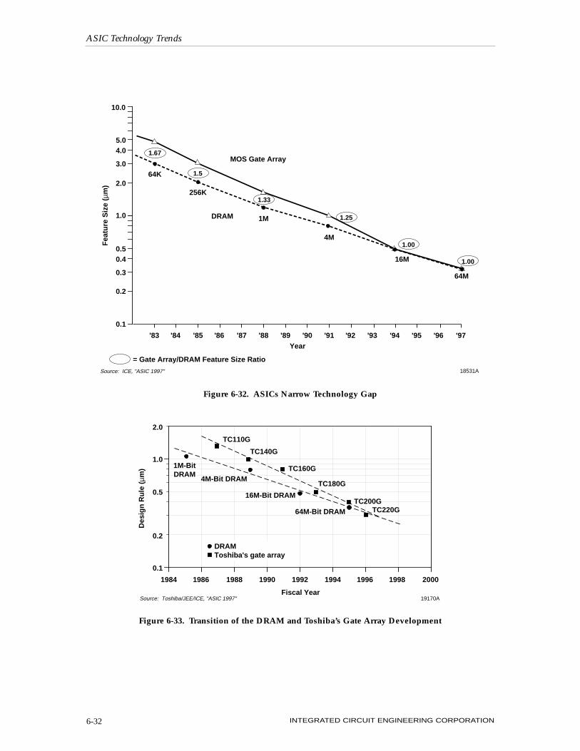
In the mid-1980’s, ASIC devices were typically using process technology that was 2-3 years behindhigh-volume memory part types (Figure 6-32). Today, however, processes rivaling the technolog-ical advancement of state-of-the-art memory devices are being developed specifically for ASICs.As an example, Figure 6-33 shows Toshiba’s DRAM and ASIC technology convergence. Noticealso in Figure 6-34 how Mitsubishi’s ASIC process roadmap parallels its DRAM development.
While deep submicron integration has allowed for unprecedented performance and economies ofscale, it has also brought with it a new set of design challenges. With larger geometry chips, cir-cuit timing is limited primarily by gate delays. However, as geometries shrink, delay from theresistance and capacitance of the wiring interconnect between transistors begins to dominate(Figure 6-35). Interconnect delays have increased, as a percent of total delay, from 15-30 percentat the 1.0µm level to 50-75 percent at the 0.35µm level.
ASIC Technology Trends
INTEGRATED CIRCUIT ENGINEERING CORPORATION 6-31
ASIC Technology Trends
INTEGRATED CIRCUIT ENGINEERING CORPORATION6-32
0.1
0.2
0.5
1.0
2.0
1984 1986 1988 1990 1992 1994 1996 1998 2000
Fiscal Year19170ASource: Toshiba/JEE/ICE, "ASIC 1997"
Des
ign
Ru
le (
µm)
DRAM Toshiba's gate array
1M-Bit DRAM
4M-Bit DRAM
16M-Bit DRAM
64M-Bit DRAM
TC110G
TC140G
TC160G
TC180G
TC200GTC220G
Figure 6-33. Transition of the DRAM and Toshiba’s Gate Array Development
1.67
1.5
1.33
1.25
1.00
MOS Gate Array
DRAM
64K
256K
1M
4M
16M
'83 '84 '85 '86 '87 '88 '89 '90 '91 '92 '93Year
= Gate Array/DRAM Feature Size Ratio
Fea
ture
Siz
e (µ
m)
0.1
0.2
0.3
0.40.5
2.0
3.0
4.05.0
18531ASource: ICE, "ASIC 1997"
1.00
64M
1.0
10.0
'94 '95 '96 '97
Figure 6-32. ASICs Narrow Technology Gap

In battling the effects of increased resistance and capacitance associated with increasingly thinner,narrower, and more closely spaced interconnects, ASIC designers are having to spend more andmore design iterations identifying and solving timing errors; or else, settle for a design that does-n’t use the full speed potential of the silicon to get a functional chip. Design issues are discussedlater in this section.
ASIC Technology Trends
INTEGRATED CIRCUIT ENGINEERING CORPORATION 6-33
Figure 6-34. Mitsubishi’s ASIC Roadmap
0.8µm drawn, 5V
250K usable gates 215ps
0.8µm, 3V
250K usable gates 370ps
Micro Power 0.5µm drawn, 3V
500K usable gates 200ps
5 Volt 0.6µm, 5V
400K usable gates 190ps
0.35µm, 3V
2000K usable gates 4 layer metal
101ps
0.25µm, 2.5V
4 Meg DRAM 16 Meg DRAM 64 Meg DRAM 256 Meg DRAM
Ultra Performance 0.5µm, 3V
700K usable gates 145ps
0.30µm, 2.5V
3000K usable gates 82ps
21199Source: Mitsubishi/ICE, "ASIC 1997"
Del
ay, n
s
1.5µm
20
1.2µm
30
1.0µm
60
0.8µm
150
0.5µm
500
0.3µm
1,000
Feature Size:
Circuit Size: (thousands of gates)
0.1
1
Average Wiring Delay
Typical Gate Delay
Source: OKI Semiconductor/ICE, "ASIC 1997" 20407A
Figure 6-35. Wiring (Interconnect) Delay Versus Gate Delay
Other challenges intensified by shrinking circuit geometries include limiting crosstalk betweeninterlayer and adjacent wires, managing I/O issues like simultaneously switched outputs, andminimizing clock skews.
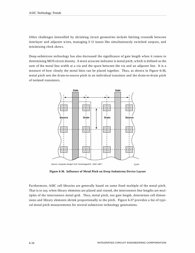
Deep-submicron technology has also decreased the significance of gate length when it comes todetermining MOS circuit density. A more accurate indicator is metal pitch, which is defined as thesum of the metal line width at a via and the space between the via and an adjacent line. It is ameasure of how closely the metal lines can be placed together. Thus, as shown in Figure 6-36,metal pitch sets the drain-to-source pitch in an individual transistor and the drain-to-drain pitchof isolated transistors.
Furthermore, ASIC cell libraries are generally based on some fixed multiple of the metal pitch.That is to say, when library elements are placed and routed, the interconnect line lengths are mul-tiples of the interconnect metal grid. Thus, metal pitch, not gate length, determines cell dimen-sions and library elements shrink proportionally to the pitch. Figure 6-37 provides a list of typi-cal metal pitch measurements for several submicron technology generations.
ASIC Technology Trends
INTEGRATED CIRCUIT ENGINEERING CORPORATION6-34
Gate Gate
Source: Computer Design/ VLSI Technology/ICE, "ASIC 1997" 21244
Drain Drain SourceSource
Figure 6-36. Influence of Metal Pitch on Deep-Submicron Device Layout

The following bullets are summaries of several advanced ASIC process technologies that were dis-cussed at the IEEE 1996 Custom Integrated Circuits Conference (CICC).
• Hitachi discussed the development of a 1.86-million-gate CMOS gate array with high-speedGTL I/O circuitry. Based on a 0.35µm process, the device is said to be capable of transmit-ting synchronous data through a 30cm line at a rate of 300MHz. The features of the chan-nelless gate array are shown below.
Raw Gates: 1.86MUsable Gates: 1.0MMetal Layers: 5Metal Pitch: 1.4µm (metal 1 to metal 3)Gate Oxide: 80ÅDie Size: 14.75 x 14.75mmPower Supply: 3.3VPackage: 400-pin PGA
• Lucent Technologies’ Bell Laboratories presented a paper describing a manufacturable andhigh-performance 0.35µm CMOS ASIC technology optimized for 3.3V operation. The com-pany claims the technology provides an improvement of 1.6X in circuit performance and1.56X in packing density over Lucent’s previous generation 0.5µm 3.3V CMOS technology.A comparison of the device parameters for the two technology generations is provided inFigure 6-38. Circuits that have been fabricated using the 0.35µm architecture include gatearrays, internal AT&T standard cell designs, a 256K SRAM development vehicle, and thecompany’s ORCA FPGA.
ASIC Technology Trends
INTEGRATED CIRCUIT ENGINEERING CORPORATION 6-35
Figure 6-37. Typical Metal Pitch Measurements
Technology Generation (µm)
0.6�
0.5�
0.35�
0.25
Metal Pitch (µm)
3.0 - 2.4�
2.4 - 1.8�
1.8 - 1.2�
1.2 - 0.8
Number of Layers
3�
3 - 4�
3 - 5�
3 - 5
Source: Computer Design/ VLSI Technology/ICE, "ASIC 1997" 21245

• Motorola described a thin-film silicon-on-insulator (TFSOI) complementary BiCMOS tech-nology for low-power RF mixed-mode applications, such as portable wireless communica-tions equipment. The technology is based on a manufacturable, near-fully-depleted 0.5µmCMOS process with integrated lateral bipolar circuitry. Some of the device parameters aregiven below.
Bipolar Transistors NPN PNPSOI Thickness: 0.1µm 0.1µmEmitter Size: 0.72µm2 0.72µm2Peak Current Gain: 65 40Peak fT: 14GHz 9GHz
CMOS Transistors NMOS PMOSSOI Thickness: 0.1µm 0.1µmGate Oxide: 105Å 105ÅGate Length (eff.): 0.44µm 0.45µmThreshold Voltage: 0.51V 0.45VSat. Current (@3.0V): 310µA/µm 140µA/µmPeak fT: 16GHz
• NTT LSI Laboratories, Kanagawa, Japan, described a 0.25µm SIMOX-CMOS gate arrayarchitecture with an LVTTL interface (2.0V-1.2V). Figure 6-39 shows that at low voltages,SIMOX (separation-by-implantation-of-oxygen) silicon substrates offer a speed advantageover bulk silicon substrates. Some of the device features are provided below.
ASIC Technology Trends
INTEGRATED CIRCUIT ENGINEERING CORPORATION6-36
Parameter 0.35µm CMOS 0.5µm CMOS
VDD
tox
Vth (NMOS)
Vth (PMOS)
ION (NMOS)
ION (PMOS)
Lpoly (NMOS)
Lpoly (PMOS)
Ioff at 125°C
Ring Oscillator
2–NAND FO = 2
3.3V�
65�
0.6V�
0.85V�
600µA/µm�
300µA/µm
0.36µm�
0.40µm�
< 1nA/µm�
50ps�
94ps
3.3V�
90�
0.6V�
0.9V�
425µA/µm�
180µA/µm�
0.5µm�
0.6µm�
< 1nA/µm�
82ps�
144ps
Source: Lucent Technologies/ICE, "ASIC 1997" 21246
Figure 6-38. Comparison of Lucent’s 0.35µm and 0.5µm Processes

Gate Length: 0.25µmThreshold Voltage: 0.2V (NMOS), 0.3V (PMOS)Gate Oxide: 50ÅSaturation Current: 359µA/µm (NMOS), 203µA/µm (PMOS)Metal Pitch: 1.4µm (metal 1 to metal 4)Die Size: 100mm2Gate Count: 300KI/O Count: 340 (105µm I/O pitch)Power Supply: 3.3V, VDD (≤2.0V)
ASIC DESIGN TOOLS
With the increase in complexity and density of ASICs has come the need for higher levels ofabstraction in circuit simulation in order to meet time-to-market requirements. The use of hard-ware-description languages (HDLs)—Verilog and VHDL—and the synthesis of these languages,has significantly improved the productivity of ASIC designers. It has been estimated that the pro-ductivity of HDL users is 3 to 10 times that of users of schematic capture when measured in termsof the number of gates created in a given timeframe.
ASIC Technology Trends
INTEGRATED CIRCUIT ENGINEERING CORPORATION 6-37
0
200
400
600
800
1,000
1 1.5 2 2.5
SIMOX
BULK
* 2-input NAND, FO = 3, AL = 1mm
Supply Voltage (V)
Gat
e D
elay
(p
s)*
21247Source: CICC/NTT LSI Laboratories/ICE, " ASIC 1997"
Figure 6-39. SIMOX Offers Speed Advantage at Low Voltage
The three primary levels of abstraction in HDL simulators are the gate (or logic) level, the regis-ter-transfer level (RTL), and the most abstract—behavioral level (Figure 6-40). While HDL toolsare being readily used at each of the three levels, most are focused on the RTL level of abstraction.Provided in Figure 6-41 is a listing of companies offering HDL and other types of circuit simula-tion tools.
ASIC Technology Trends
INTEGRATED CIRCUIT ENGINEERING CORPORATION6-38
Partitioning
Pipelining
Scheduling
Register Allocation
Resource Allocation
Register Inferencing
State Machine Synthesis
Multi-Level Logic Opto
Two-Level Logic Opto
Redundancy Removal
Technology Mapping
Technology Translation
Physical SynthesisPhysical
Logic
RTL
Behavioral
System
Synthesis Level Synthesis Tasks
Source: Synopsys/ICE, "ASIC 1997" 18581A
Figure 6-40. Levels of Abstraction

ASIC Technology Trends
INTEGRATED CIRCUIT ENGINEERING CORPORATION 6-39
Alta Group/ HDS (Hardware Design Verilog, VHDL HDS features a fast, data flow simulator that offers Cadence Design System) cycle-based simulation with a unified system-level Automation design environment. Co-simulates with existing Foster City, CA HDLs and generates HDL output for implementations. HDS also supports structural and behavioral design ANACAD ELdo SPICE The Eldo simulator uses an innovative Unix architec- Electrical ture which combines architecture which combines Engineering multiple solution algorithms for fast circuit-level Software simulation of mixed analog and digital designs Milpitas, CA ELdoHDL SPICE, VHDL-A The EldoHDL simulator combines the simulator with a VHDL-based analog behavioral language for fast analog simulation from circuit through system level MixVHDL VHDL The MixVHDL integrates EldoHDL with a complete VHDL simulator for fast circuit through system simulation in both analog and digital domains Analogy Saber Simulator Mast Saber can analyze complete systems from system Beaverton, OR through circuit-level implementations. This can include analog, digital, mixed-signal, mechanical, hydraulic, thermal or mechatronics Saber/Verilog Mast, Verilog Links Saber with Cadence Verilog for an all mixed- Mixed-Signal Simulation signal simulation system. Simulate mixed analog and digital systems using all the models of each simulator. Model and simulate behavioral, functional and primitive devices in both analog and digital domains QVS MAST, VHDL Links Saber to Mentor's QuickSim II for mixed-signal simulation system. Simulate mixed analog and digi- tal systems using all the models of each simulator. Model and simulate behavioral, functional and primitive devices in both analog and digital domains Saber/ViewSim MAST, VHDL, Links Saber to Viewlogic's ViewSim for mixed-signal Mixed-Signal Simulation Verilog simulation system. Simulate mixed analog and digital systems using all the models of each simulator. Model and simulate behavioral, functional and primi- tive devices in both analog and digital domains Avista Design Spectre/XL Spectre, SPICE The first spreadsheet tool for analog design. Avista Systems Visual Basic for Spectre/XL's instant "what if" analysis gives you an Folsom, CA Applications accurate, flexible tool for evaluating, developing and optimizing circuit designs. Uses proven SPICE models. Requires Microsoft Excel for Windows v5.0 Cadence Design Leapfrog VHDL Leapfrog is a native compiled code based VHDL Automation simulator. It supports Verilog and Vital libraries San Jose, CA and is integrated with Cadence products for IC/ASIC/FPGA/Board design solutions Verilog-XL Verilog High performance simulation tools integrated into full featured design environment. Supports multiple design methodologies for the design of IC/ASIC/FPGA/PLD and PCB's Chronologic VCS Verilog Fastest Verilog Simulator on the market VCS offers Simulation full capabilities for model development, interactive Los Altos, CA debugging, regression testing, and ASIC sign-off. OVI and IEEE compliant VCSi Verilog Easy to use interactive Verilog simulation VMC Verilog Modeling technology for secure, accurate, efficient simulation models. Protects model suppliers' intellectual property. Reduces model consumers' time-to-market Compass Design QSIM Proprietary, QSIM performs high-speed, full timing RC structural Automation Interfaces to simulation of complex ASICs, utilizing ASIC vendor- San Jose, CA VHDL, Verilog, specific delay models or the COMPASS input slope EDIF and RC tree delay models for accurate deep submicron gate and interconnect delays
21276Source: Integrated System Design/ICE, "ASIC 1997"
Company and Location
Product Name Language Functionality
Figure 6-41. Circuit Simulation Tools

ASIC Technology Trends
INTEGRATED CIRCUIT ENGINEERING CORPORATION6-40
Data I/O Synario VHDL, Verilog Synario 2.1 is a Windows-based system for PLD, Corporation ABEL-HDL FPGA and board-level design. It provides mixed- Redmond, CA entry (schematic and HDL descriptions) and HDL simulation support Exemplar Logic Galileo V-System VHDL Fully integrated VHDL simulator with source level Alameda, CA debugger, extensive design browsers, waveform trace, C language interface, VHDL '93 support and VITAL accelerated gate level simulation Frontline Design PureSpeed Developer Verilog The PureSpeed family of fully compliant in Verilog Automation simulators incorporates three high-performance San Jose, CA simulation engines–complied, interpreted and gate-level (XL) in a single kernel architecture PureSpeed OverDrive Verilog PureSpeed Developer and PureSpeed OverDrive provide complete support for PLI routines and SDF data and full command language support. All ASIC/FPGA libraries run unmodified in PureSpeed IKOS Systems Voyager VHDL High-performance mixed-level simulation in software Cupertino, CA and mixed-level accelerations. Includes a software solution for mixed-level fault simulation Gemini Verilog Mixed-level acceleration through a tight integration of the Cadence Verilog XL simulator with the IKOS NSIM hardware accelerator InterHDL Verilint Verilog Verilint is a semantics, synthesis, and coding-style Los Altos, CA checker for designs written in Verilog HDL Viper Verilog Viper is a Verilog HDL simulator which supports a powerful graphical debugging environment, and is compatible with the Verilog XL 1.6 and OVI Verinet Toolkit Verilog Verinet Toolkit is a front-end for the structural (gate-level) subset of the Verilog HDL Veribase Toolkit Verilog Veribase Toolkit is a Full Language Verilog front-end that is used to develop Electronic Design Automa- tion applications for processing Verilog HDL designs V to V Verilog, VHDL V to V reads hierarchical designs and translates them into functionally equivalent designs covering the synthesizable Verilog Intusoft ICAP/4 XDL Analog/mixed-signal circiut design, with IsSpice4 San Pedro, CA native mixed-mode simulator. Runs analog, digital, non-electrical, sampled-data and HDL models Mentor Graphics Continuum VHDL, HDL-A Continuum, including QuickSim II and AccuSim II, Wilsonville, OR is a mixed-signal simulator offering behavioral modeling for digital and analog devices and systems based on VHDL, and boundary model library for translation between analog and digital domain AccuSim II HDL-A Multi-level analog simulator to many different designs that require non-linear equation solving QuickVHDL VHDL Provides high-performance VHDL simulation, fully supporting VHDL '87 and 93 and VITAL 2.2b standards. Supports point tool and integrated design environments QuickVHDL Pro System VHDL Provides high-performance VHDL simulation, supports VHDL '87 and '93, VITAL 2.2b standards, point tool and integrated design environments. Provides co-simulation with QuickSim II QuickSim II Proprietary High-speed logic simulator permitting explortion of design functionality and performance QuickHDL VHDL, Verilog Provides mixed VHDL and Verilog simulation, supports VHDL '87 and '93, VITAL 2.2b and IEEE 1364 standards Meta Software HSPICE HSPICE HSPICE is a cicuit simulation and analysis tool, Campbell, CA which uses advanced transistor models to provide the optimum combination of accuracy, convergence and transistor modeling for IC designers. HSPICE is integrated into all commonly used design environments
21277Source: Integrated System Design/ICE, "ASIC 1997"
( )
Company and Location
Product Name Language Functionality
Figure 6-41. Circuit Simulation Tools (continued)

There has been much debate over whether VHDL (VHSIC [very high speed integrated circuit]HDL) or Verilog will become the dominant HDL tool in the industry. According to market statis-tics from the Electronic Design Automation Companies Association (EDAC), shipments of toolsusing Verilog HDL produced $73.4 million in revenue in 1995, up from $66.8 million in 1994.Meanwhile, VHDL revenues in 1995 were $52.5 million, down from 1994’s $59.2 million. Thedecline in VHDL revenue has been attributed to steep price cuts. In terms of units, the EDAC sta-tistics show that VHDL tools barely outshipped Verilog tools 4,235 to 4,188 in 1995.
Many view Verilog HDL as best at supporting logic simulation from the gate level to the RTL leveland VHDL as more efficient operating at more abstract levels (Figure 6-42). More than likely,Verilog and VHDL will coexist for quite some time.
Synthesis technology has had a profound impact on the ASIC industry. In less than ten years, ithas grown from merely a research topic to an essential part of high-level ASIC design. Synthesisis quickly becoming essential for CPLD and FPGA designs as well. Synthesis tools translateabstract designs (generally starting from HDL descriptions) into actual logic that can be imple-mented in silicon, as well as optimize the logic given a set of circuit design constraints such as tim-ing, power, loading, area, and testability. Figure 6-43 provides a listing of synthesis tool vendors.
Over the past few years, synthesis tools have struggled to keep pace with deep submicron designmethodology shifts, especially in the case of timing. As discussed earlier, interconnect delay hasbecome as much, or more, of a concern as gate delay in the design of advanced ICs. And, sinceactual interconnect delay is dependent upon the layout of the IC itself, physical layout informa-tion is needed very early in the design cycle in order to accurately estimate timing conditions. Asa result, the traditional ASIC design flow has evolved into a more complex, “top-down” flow(Figure 6-44).
ASIC Technology Trends
INTEGRATED CIRCUIT ENGINEERING CORPORATION 6-41
Abstract System Design Hardware/Software Codesign
Architectural System Design
Behavioral Design
RTL Design
Gate-level Design
VHDL
Verilog HDL
Need for experimentation
Need for standard practices and elimination of duplication of effort
Source: Cadence/ICE, "ASIC 1997" 18586
Figure 6-42. VHDL, Verilog Capabilities Overlap

The required tighter link between logic and physical chip design has put the pressure on design toolvendors to create more sophisticated tools that use “floorplanning” (or “design planning”) tech-niques to constrain variability in delay estimation and to manage the rapidly growing amount offunctionality in silicon. The modern design flow involves an iteration between synthesis and floor-planning, with final routing performed only when the floorplanning netlist meets all requirements.
As previously discussed, the use of library elements (e.g., microprocessor cores) in ASIC design ison the rise. However, until recently, core libraries have tended to lock designers into a singlefoundry. There is now a trend to offer libraries that are crafted to support multiple foundries (i.e.,
ASIC Technology Trends
INTEGRATED CIRCUIT ENGINEERING CORPORATION6-42
Cadence Design Synergy Synthesis Verilog, VHDL Complete family of top-down design tools for Automation the synthesis and optimization of RTL-level San Jose, CA and gate-level designs for Verilog and VHDL Compass Design ASIC Synthesizer Verilog, VHDL, EDIF HDL based synthesis logic optimization. Timing/ Automation area driven synthesis/logic optimization. State San Jose, CA machines synthesis/optimization. Interfaces to physical tools Mentor Graphics Mistral 1 DFL (in); VHDL & Behavioral synthesis tools for digital filters and Wilsonville, OR Verilog (output) low-throughput linear systems. Synthesizes a compete bit-serial architecture directly from a behavioral algorithmic description Mistral 2 DFL (in); VHDL & Behavioral synthesis tools for DSP design. Verilog (output) Synthesizes a complete RTL design (datapath, memory, microcode) directly from a behavioral algorithmic description MINC PLDesigner-XL (and VHDL, Design Universal tool offering a variety of device- Colorado Springs, CO PLDesigner-XL for Synthesis Language independent input methods, optimization, Windows) automatic device selection, and automatic multiple-device partitioning Silerity PathBlazer — PathBlazer is a synthesis tool for complex, high- Pasadena, CA speed datapath design and optimization. It contains placement algorithms that ensure optimal timing of submicron ASICs and automatically explores architectural trade-offs and optimizes submicron placement Synopsys Design Compiler Family- VHDL Creates optimized, gate-level design based on Mountain View, Calif. DC Expert; DC Professional; IC design specifications and constraints to improve FPGA Compiler area and performance while reducing design time Behavioral Compiler VHDL Synthesizes datapath, memory, and control logic from a behavioral specification for a broad range of algorithmic applications Synplicity Synplify Verilog, VHDL Synplify is an extremely fast, easy-to-use FPGA Mountain View, CA and CPLD synthesis tool, that compiles, optimizes and technology maps Verilog and VHDL designs into small, high-performance device netlists Synplify-Lite Verilog, VHDL Same as above for one architecture of your choice Viewlogic PathBlazer Verilog Synthesizes and optimizes complex datapaths in Marlboro, MA minutes. Explores and displays all architectural trade-offs. Generates datapath floorplan for timing accuracy. 100x faster than other tools ViewSynthesis VHDL Logic synthesis and optimization for ASIC and FPGAs. Includes FPGA specific optimization including XBlock and LPM infrencing
21279Source: Integrated System Design/ICE, "ASIC 1997"
Company and Location
Product Name Language Functionality
Figure 6-43. Architecture Synthesis Tools
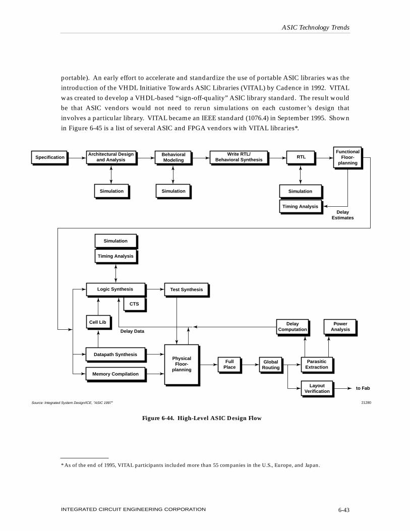
portable). An early effort to accelerate and standardize the use of portable ASIC libraries was theintroduction of the VHDL Initiative Towards ASIC Libraries (VITAL) by Cadence in 1992. VITALwas created to develop a VHDL-based “sign-off-quality” ASIC library standard. The result wouldbe that ASIC vendors would not need to rerun simulations on each customer’s design thatinvolves a particular library. VITAL became an IEEE standard (1076.4) in September 1995. Shownin Figure 6-45 is a list of several ASIC and FPGA vendors with VITAL libraries*.
ASIC Technology Trends
INTEGRATED CIRCUIT ENGINEERING CORPORATION 6-43
Delay Estimates
SimulationSimulation Simulation
Timing Analysis
Behavioral Modeling
Write RTL/ Behavioral Synthesis
RTLFunctional
Floor- planning
SpecificationArchitectural Design
and Analysis
Delay Data
Physical Floor-
planning
Full Place
Global Routing
Delay Computation
Power Analysis
Parasitic Extraction
Layout Verification
to Fab
Datapath Synthesis
Memory Compilation
Cell Lib
Simulation
Timing Analysis
Logic Synthesis Test Synthesis
21280Source: Integrated System Design/ICE, "ASIC 1997"
CTS
Figure 6-44. High-Level ASIC Design Flow
* As of the end of 1995, VITAL participants included more than 55 companies in the U.S., Europe, and Japan.

The tools for analog and mixed-signal ASIC design are recognized to be several generationsbehind those for digital. So far, a way to synthesize analog circuits has not been developed. Theprecise control of voltage and current levels just doesn’t easily lend itself to a structured designmethodology. However, the industry’s move toward mixed-signal “systems on a chip” is drivingprogress in efforts to develop standard analog HDLs (sometimes called AHDLs). Listed in Figure6-46 are several vendors of analog/mixed-signal design tools.
The IEEE P1076.1 group has been working for several years on extending VHDL for both analogand mixed-signal modeling capability—referred to as VHDL-AMS. A language reference manu-al (LRM) for the VHDL-AMS tool is being prepared for IEEE balloting in December 1996.Meanwhile, the Open Verilog International (OVI) organization started working in 1995 on devel-oping an analog-only Verilog tool (Verilog-A) based on Cadence’s Spectre-HDL product. TheVerilog-A effort was granted IEEE Study Group status in March 1996. A separate effort to addressmixed-signal needs (Verilog-MS) has been proposed.
Some companies believe that working toward establishing an analog VHDL standard (VHDL-A)is not necessary since SPICE models and Analogy’s proprietary MAST language* are alreadyeffective as analog HDLs. Figure 6-47 shows some of the differences between 1076.1 (VHDL-A)and Analogy’s MAST HDL.
ASIC Technology Trends
INTEGRATED CIRCUIT ENGINEERING CORPORATION6-44
Company Devices Supported
Actel
Altera
AMI
Honeywell SSEC
IBM Microelectronics
LSI Logic
Lucent Technologies
Oki
Orbit Semiconductor
Sharp
Symbios Logic
TI
Toshiba
UTMC
VLSI Technology
Xilinx
FPGAs
PLDs
Gate Arrays and Standard Cells
Gate Arrays
Gate Arrays and Standard Cells
Standard Cells
Standard Cells
Gate Arrays and Standard Cells
Gate Arrays
Standard Cells
Gate Arrays and Standard Cells
Gate Arrays
Gate Arrays and Standard Cells
Gate Arrays
Gate Arrays and Standard Cells
FPGAs and PLDs
21281Source: Computer Design/ICE, "ASIC 1997"
Figure 6-45. Listing of ASIC Vendors with VITAL Libraries
* Part of the Saber simulator package from Analogy.
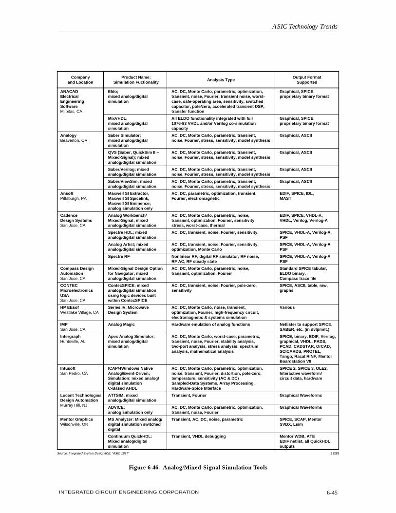
ASIC Technology Trends
INTEGRATED CIRCUIT ENGINEERING CORPORATION 6-45
ANACAD Eldo; AC, DC, Monte Carlo, parametric, optimization, Graphical, SPICE, Electrical mixed analog/digital transient, noise, Fourier, transient noise, worst- proprietary binary format Engineering simulation case, safe-operating area, sensitivity, switched Software capacitor, pole/zero, accelerated transient DSP, Milpitas, CA transfer function MixVHDL; All ELDO functionality integrated with full Graphical, SPICE, mixed analog/digital 1076-93 VHDL and/or Verilog co-simulation proprietary binary format simulation capacity Analogy Saber Simulator; AC, DC, Monte Carlo, parametric, transient, Graphical, ASCII Beaverton, OR mixed analog/digital noise, Fourier, stress, sensitivity, model synthesis simulation QVS (Saber, QuickSim II – AC, DC, Monte Carlo, parametric, transient, Graphical, ASCII Mixed-Signal); mixed noise, Fourier, stress, sensitivity, model synthesis analog/digital simulation Saber/Verilog; mixed AC, DC, Monte Carlo, parametric, transient, Graphical, ASCII analog/digital simulation noise, Fourier, stress, sensitivity, model synthesis Saber/ViewSim; mixed AC, DC, Monte Carlo, parametric, transient, Graphical, ASCII analog/digital simulation noise, Fourier, stress, sensitivity, model synthesis Ansoft Maxwell SI Extractor, AC, DC, parametric, optimization, transient, EDIF, SPICE, IDL, Pittsburgh, PA Maxwell SI Spicelink, Fourier, electromagnetic MAST Maxwell SI Eminence; analog simulation only Cadence Analog Workbench/ AC, DC, Monte Carlo, parametric, noise, EDIF, SPICE, VHDL-A, Design Systems Mixed-Signal; mixed transient, optimization, Fourier, sensitivity VHDL, Verilog, Verilog-A San Jose, CA analog/digital simulation stress, worst-case, thermal Spectre HDL; mixed AC, DC, transient, noise, Fourier, sensitivity, SPICE, VHDL-A, Verilog-A, analog/digital simulation PSF Analog Artist; mixed AC, DC, transient, noise, Fourier, sensitivity, SPICE, VHDL-A, Verilog-A analog/digital simulation optimization, Monte Carlo PSF Spectre RF Nonlinear RF, digital RF simulator; RF noise, SPICE, VHDL-A, Verilog-A RF AC, RF steady state PSF Compass Design Mixed-Signal Design Option AC, DC, Monte Carlo, parametric, noise, Standard SPICE tabular, Automation for Navigator; mixed transient, optimization, Fourier ELDO binary, San Jose, CA analog/digital simulation Compass trace file CONTEC ContecSPICE; mixed AC, DC, transient, noise, Fourier, pole-zero, SPICE, ASCII, table, raw, Microelectronics analog/digital simulation sensitivity graphs USA using logic devices built San Jose, CA within ContecSPICE HP EEsof Series IV, Microwave AC, DC, Monte Carlo, noise, transient, Various Westlake Village, CA Design System optimization, Fourier, high-frequency circuit, electromagnetic & systems simulation IMP Analog Magic Hardware emulation of analog functions Netlister to support SPICE, San Jose, CA SABER, etc. (in dvlpmnt.) Intergraph Apex Analog Simulator; AC, DC, Monte Carlo, worst-case, parametric, SPICE, binary, EDIF, Verilog, Huntsville, AL mixed analog/digital transient, noise, Fourier, stability analysis, graphical, VHDL, PADS, simulation two-port analysis, stress analysis; spectrum PCAD, CADSTAR, OrCAD, analysis, mathematical analysis SCICARDS, PROTEL, Tango, Racal RINF, Mentor Boardstation V8 Intusoft ICAP/4Windows Native AC, DC, Monte Carlo, parametric, optimization, SPICE 2, SPICE 3, OLE2, San Pedro, CA Analog/Event-Driven; noise, transient, Fourier, distortion, pole-zero, Interactive waveform/ Simulation; mixed analog/ temperature, sensitivity (AC & DC) circuit data, hardware digital simulation Sampled-Data Systems, Array Processing, C-Based AHDL Hardware-Spice Interface Lucent Technologies ATTSIM; mixed Transient, Fourier Graphical Waveforms Design Automation analog/digital simulation Murray Hill, NJ ADVICE; AC, DC, Monte Carlo, parametric, optimization, Graphical Waveforms analog simulation only transient, noise, Fourier Mentor Graphics MS Analyzer: Mixed analog/ Transient, AC, DC, noise, parametric SPICE, SCAP, Mentor Wilsonville, OR digital simulation switched SVDX, Lsim digital Continuum QuickHDL: Transient, VHDL debugging Mentor WDB, ATE Mixed analog/digital EDIF netlist, all QuickHDL simulation outputs
21283Source: Integrated System Design/ICE, "ASIC 1997"
Company and Location
Product Name; Simulation Fuctionality
Analysis TypeOutput Format
Supported
Figure 6-46. Analog/Mixed-Signal Simulation Tools

ASIC Technology Trends
INTEGRATED CIRCUIT ENGINEERING CORPORATION6-46
Meta-Software HSPICE, GSI; AC, DC, Monte Carlo, parametric, optimization, SPICE data, text Campbell, CA analog only and mixed transient, noise, Fourier waveforms analog/digital simulation MicroSim MicroSim PSpice AC, DC, Monte Carlo, parametric, transient, SPICE, EDIF, Probe Irvine, CA analog simulation only noise, Fourier, worst-case, sensitivity, graphical waveform performance analysis analyzer MicroSim PSpice A/D; mixed AC, DC, Monte Carlo, parametric, transient, SPICE, EDIF, Probe analog/digital simulation noise, Fourier, worst-case sensitivity, digital graphical waveform worst-case timing, performance analysis analyzer MicroSim PSpice Basics AC, DC, Monte Carlo, parametric, transient, SPICE, EDIF, Probe analog simulation noise, Fourier, worst-case sensitivity, graphical waveform only for small circuits performance analysis analyzer MicroSim PSpice Optimization for analog circuits Probe graphical waveform Optimizer; analyzer analog simulation only MicroSim Polaris, Signal integrity analysis Probe graphical waveform mixed analog/digital analyzer simulation signal integrity analysis Quad Design XTK (Crosstalk Tool Kit); Transmission Line Quad propriety, Technology and Crosstalk Post Script Camarillo, CA Quantic Laboratories PCB Greenfield; mixed Transient SPICE Winnipeg, analog/digital simulation Manitoba, Canada Compliance; mixed Transient SPICE analog/digital simulation BoardScan; mixed Transient SPICE analog/digital simulation SANCAD Mobius; mixed DC, parametric, optimization, transient, SPICE + interactive X- San Diego, CA analog/digital simulation Fourier, perturbation, timing, margin Windows marching wave- form display w/selectable waveform compression Cell Designer; mixed DC, parametic, optimization, transient, SPICE + interactive X- analog/digital simulation Fourier, timing, margin Windows marching wave- form display w/selectable waveform compression Tanner T-Spice; mixed AC, DC, transient, transfer ASCII, W-edit waveform Research analog/digital simulation Pasadena, CA Tatum Labs ECA-2; AC, DC, Monte Carlo, transient, Fourier, Tabular or on-line graphics Ann Arbor, MI analog simulation only worst-case, temperature sweep, component sweep, AC & DC sensitivity SpiceAge for Windows; AC, DC, Monte Carlo, transient, Fourier, Tabular or on-line graphics mixed analog/digital worst-case, temperature sweep, component simulation sweep, noise ALLTED; mixed AC, DC, Monte Carlo, optimization, transient, Tabular or on-line graphics; analog/digital simulation, Fourier, AC & DC sensitivity, optimal tolerance real time or manipulated by and mixed technologies assignment, statistical, multivariant post-processor (electronic, hydraulic, pneumatic, etc.) TESOFT TESLA Block Diagram Monte Carlo, transient, noise, Fourier, distortion Graphical waveforms, Roswell, GA Simulator; mixed analog/ spectra & logic, binary and digital simulation and RF ASCII data formats Viewlogic Saber – ViewSim VHDL, AC, DC, Monte Carlo, parametric, transient, Saber, waveforms, EDIF, Systems Chronologic Simulation's; noise, Fourier PWL, binary, ASCII Marlboro, MA VCS Verilog; mixed analog/ digital simulation Mixed Signal Designer with AC, DC, Monte Carlo, parametric, transient, Streaming waveforms, ViewSpice; mixed analog/ noise, Fourier, worst-case, distortion, SPICE, EDIF, PWL, digital simulation binary, ASCII Mixed Signal Designer with AC, DC, Monte Carlo, parametric, transient, Streaming waveforms, HSPICE; mixed analog/ noise, Fourier, distortion, optimization, SPICE, EDIF, PWL, digital simulation pole-zero, sensitivity, small-signal transfer, binary, ASCII sampling noise, small-signal network
21284Source: Integrated System Design/ICE, "ASIC 1997"
Company and Location
Product Name; Simulation Fuctionality
Analysis TypeOutput Format
Supported
Figure 6-46. Analog/Mixed-Signal Simulation Tools (continued)

Several ASIC design tool highlights from 1995 and 1996 are described below.
• Numerous alliances were announced between ASIC vendors and design tool suppliers, pro-viding proof that the increasingly complex nature of ASIC design is requiring greater coop-eration at both ends of the process. Pacts announced in 1996 include those between Toshibaand Cadence; LSI Logic and High Level Design Systems; Toshiba and Synopsys; LSI Logicand Viewlogic; IBM and Synopsys; and Symbios Logic and Compass.
• A new development group called Rapid—Reusable Application-Specific Intellectual PropertyDevelopers—was announced in June 1996. Members of Rapid (3Soft, Advance1 Logic,Integrated Silicon Systems, iReady, Object Oriented Hardware, Virtual Chips, the DesignReuse Group of Synopsys, and Mentor’s ICTC group) joined together to bolster the visibilityof companies who offer chips and circuit designs in the form of intellectual property.
ASIC Technology Trends
INTEGRATED CIRCUIT ENGINEERING CORPORATION 6-47
Transient Analysis
Dc Operating Point Analysis
Dc Transfer Analysis
Ac Analysis
Noise Analysis
Stress Analysis
Small-Signal Parameter Analysis
Sensitivity Analysis
Distortion Analysis
Monte Carlo
Mixed Analog/Digital Model
Non-Electrical Modeling
Interaction With Simulator
Transfer Function Modeling
IEEE Standardization
Models Portable Between Vendors
Availability
Yes
Yes
Yes
Yes*
No
No
No
Yes
Yes
Limited**
Yes
Yes
Limited
Limited
Pending
Yes
1996
Yes
Yes
Yes
Yes
Yes
Yes
Yes
Yes
Yes
Yes
Yes
Yes
Yes
Yes
No
No
Now
* While 1076.1 will support enough frequency-domain modeling to allow a simulator to run an ac small-signal analysis, support beyond simple ordinary differential equations is not clearly defined at present. 1076.1 will probably not support frequency- domain modeling based on distributed partial differential equations, or large-signal frequency simulation. ** 1076.1 offers the ability to specify a distribution on a para- meter, but not to control when and how that distribution is evaluated.
Source: Analogy Inc., EE Times/ICE, "ASIC 1997" 20063A
1076.1 MAST
Figure 6-47. Analog VHDL 1076.1 (VHDL-A) Versus Analogy’s “MAST”
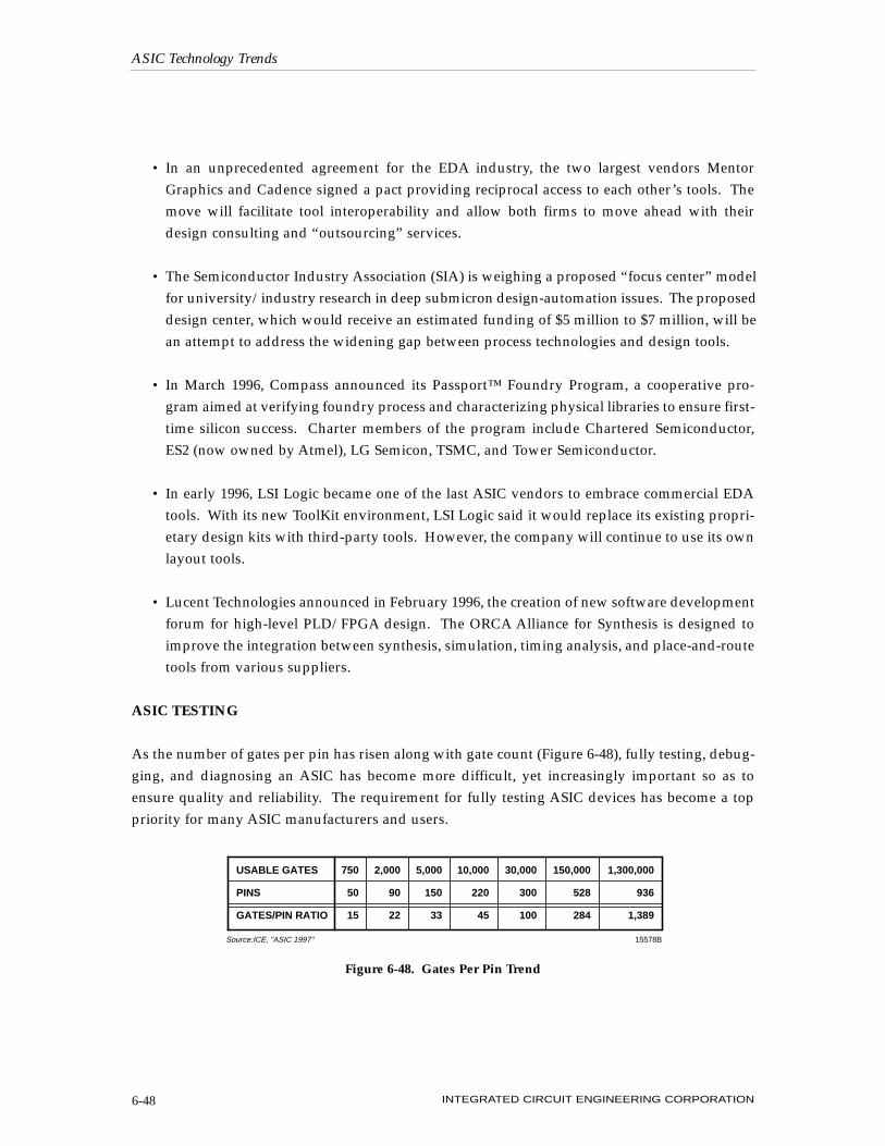
• In an unprecedented agreement for the EDA industry, the two largest vendors MentorGraphics and Cadence signed a pact providing reciprocal access to each other’s tools. Themove will facilitate tool interoperability and allow both firms to move ahead with theirdesign consulting and “outsourcing” services.
• The Semiconductor Industry Association (SIA) is weighing a proposed “focus center” modelfor university/industry research in deep submicron design-automation issues. The proposeddesign center, which would receive an estimated funding of $5 million to $7 million, will bean attempt to address the widening gap between process technologies and design tools.
• In March 1996, Compass announced its Passport™ Foundry Program, a cooperative pro-gram aimed at verifying foundry process and characterizing physical libraries to ensure first-time silicon success. Charter members of the program include Chartered Semiconductor,ES2 (now owned by Atmel), LG Semicon, TSMC, and Tower Semiconductor.
• In early 1996, LSI Logic became one of the last ASIC vendors to embrace commercial EDAtools. With its new ToolKit environment, LSI Logic said it would replace its existing propri-etary design kits with third-party tools. However, the company will continue to use its ownlayout tools.
• Lucent Technologies announced in February 1996, the creation of new software developmentforum for high-level PLD/FPGA design. The ORCA Alliance for Synthesis is designed toimprove the integration between synthesis, simulation, timing analysis, and place-and-routetools from various suppliers.
ASIC TESTING
As the number of gates per pin has risen along with gate count (Figure 6-48), fully testing, debug-ging, and diagnosing an ASIC has become more difficult, yet increasingly important so as toensure quality and reliability. The requirement for fully testing ASIC devices has become a toppriority for many ASIC manufacturers and users.
ASIC Technology Trends
INTEGRATED CIRCUIT ENGINEERING CORPORATION6-48
USABLE GATES
PINS
GATES/PIN RATIO
750
50
15
2,000
90
22
5,000
150
33
10,000
220
45
30,000
300
100
150,000
528
284
15578BSource:ICE, "ASIC 1997"
1,300,000
936
1,389
Figure 6-48. Gates Per Pin Trend

Similar to the movement toward the “top-down” design approach for ASICs, the ASIC industryis moving quickly toward incorporating DFT (design-for-test) methods early on in the designflow. At the 20,000-gate and greater densities, most ASIC vendors highly recommend that theusers incorporate design-for-testability techniques into their design flow. Some high-densityASIC libraries are even making some DFT circuitry mandatory.
Design-for-test methods range from those that are simple, use no overhead (i.e., silicon area), andprovide low effectivity to those that are complex and costly but provide thorough testability.Figure 6-49 shows a sampling of some of the DFT software tools available to the ASIC industry.
A factor driving greater use of DFT methods that move external testing functions on-chip (e.g.,built-in self-scan [BIST] or boundary scan) is the soaring costs of the test equipment itself (Figure6-50). In the early 1990’s, the cost of systems needed to test ICs with 256 pins and clock rates of40MHz was approximately $2 million. The SIA has expressed concern that if test technology con-tinues to follow its current trends as chip speeds push 500MHz and pin counts climb to 4,000, theprice of test systems could approach $50 million by the year 2010.
As is generally accepted, on-chip test structures typically cause a 5-20 percent overhead penalty.However, as shown in Figure 6-51, even a 20 percent silicon area penalty paid for a 30K usable-gate array with on-chip test capability is only about $2.60 per chip. The $2.60 penalty may be jus-tified when compared to the possible $10 or more savings that can be realized at the system level(because of fewer very expensive field failures) if fault coverage* is significantly improved.Moreover, as ASIC densities continue to soar, die area penalty will eventually become insignifi-cant compared to the benefits. This will become especially apparent for ASICs that have hundredsof thousands of gates!
The DFT method enjoying the most press coverage lately has been BIST. Though it is not a new,untried technology, BIST has only recently been commercialized for general use during the front-end, HDL-based design process. BIST supporters say the technique offers benefits such as theability to run at intended chip operating speeds, the potential to significantly cut costs in testequipment hardware and software development, and the ability to carry test programs through tosystems and field testing. In addition, the integration of a larger number of cores in ASICs in thefuture will require that BIST structures be designed into each core to prevent the need to add sig-nificant unwanted routing and logic overhead to the chip.
ASIC Technology Trends
INTEGRATED CIRCUIT ENGINEERING CORPORATION 6-49
* Fault coverage is measured as a percentage of the possible defects a test program can detect. The defect rate is the per-centage of devices passing a test. Thus, the higher the fault coverage, the lower the defect rate. A high level of fault cov-erage is very important for advanced ASIC devices.

ASIC Technology Trends
INTEGRATED CIRCUIT ENGINEERING CORPORATION6-50
Company Location
Name of Tool Tool FunctionFault
Simulator Included
SHARPEYE software automatically analyzes digital logic designs and reports testability problems in an easy-to-read format. Verifies 1149.1 testability during logic simulation. Uses simulator as an 1149.1 ATPG. Verifies the accuracy of the BSDL file for an IC by comparing to hardware operation. DFT checking tools and ATPG. Testability analysis. Identifies controllability and observability problems by analyzing ATPG and fault simulation progress and difficulties. Integrated set of test synthesis, ATPG, and fault simulation tools. Test synthesizer opens a single-step approach to test synthesis, scan insertion. Test Generator is a high-performance ATPG tool, and Verifault is a concurrent fault simulator. High-performance Verilog simulator. Synthesis and ATPG support of boundary scan, internal scan, built-in self-test, and core isolation. Integration of all architectures with standard or custom TAP controller. Test pattern generation and fault simulation for stuck-at, IDDQ, and delay fault test including scan insertion, test rule checks, and vector post-processing. Automatic test vector generation for PLDs, FPGAs, and EPLDs. BSDLMaker! creates BSDL (boundary scan description language) files from silicon. Mixed-level concurrent fault simulator with support for VHDL, LMG software and hardware models, and C models.
Acugen Software Nashua, NH Alpine Image Systems Mountain View, CA Altium/IBM EDA Charlotte, NC Attest Software Santa Clara, CA Cadence Design Systems Chelmsford, MA Chronologic Simulation Los Altos, CA Compass Design Automation San Jose, CA CrossCheck Technology San Jose, CA Flynn Systems Nashua, NH Intellitech Meredith, NH Intergraph Electronics Huntsville, AL
SHARPEYE AVLsim BSDL Verifier Test Bench Tdx step Test-intelligent design series Verilog Compiled Simulator (VCS) Test Synthesis Solution Aide II FS-ATG Version 3.0 BSDLMaker! Concurrent Fault Simulator (CFS)
No
No
No
Yes
Yes
Yes
No
No
Yes
Yes
No
Yes
Source: Integrated System Design/ICE, "ASIC 1997" 20275A /20276A
Figure 6-49. Design-For-Test Tools
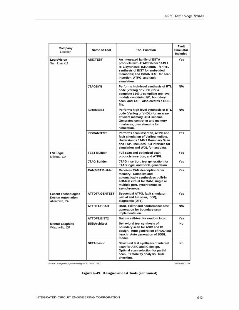
ASIC Technology Trends
INTEGRATED CIRCUIT ENGINEERING CORPORATION 6-51
Company Location
Name of Tool Tool FunctionFault
Simulator Included
An integrated family of ESTA products with JTAGSYN for 1149.1 RTL synthesis; ICRAMBIST for RTL synthesis of BIST for embedded memories; and ISCANTEST for scan insertion, ATPG, and fault simulation. Performs high-level synthesis of RTL code (Verilog or VHDL) for a complete 1149.1-compliant top-level module containing I/O, boundary scan, and TAP. Also creates a BSDL file. Performs high-level synthesis of RTL code (Verilog or VHDL) for an area-efficient memory BIST scheme. Generates controller and memory interfaces, plus stimulus for simulation. Performs scan insertion, ATPG and fault simulation of Verilog netlists. Understands 1149.1 Boundary Scan and TAP. Includes PL/I interface for simulation and WGL for test data. Full scan and optimized scan products insertion, and ATPG. JTAG insertion, test generation for JTAG logic, and BSDL generation Receives RAM description from memory. Compiles and automatically synthesizes built-in self-test circuit for RAM; single or multiple port, synchronous or asynchronous. Sequential ATPG, fault simulator; partial and full scan, IDDQ, diagnostic (DFT). BSDL-Editor and conformance test generation for boundary scan implementation. Built-in self-test for random logic. Behavioral test synthesis of boundary scan for ASIC and IC design. Auto generation of HDL test bench. Auto generation of BSDL model. Structural test synthesis of internal scan for ASIC and IC design. Optimal scan selection for partial scan. Testability analysis. Rule checking.
LogicVision San Jose, CA LSI Logic Milpitas, CA Lucent Technologies Design Automation Allentown, PA Mentor Graphics Wilsonville, OR
ASICTEST JTAGSYN ICRAMBIST ICSCANTEST TEST Builder JTAG Builder RAMBIST Builder ATTDTF/GENTEST ATTDFT/BCAD ATTDFT/BIST2 BSDArchitect DFTAdvisor
Yes
N/A
N/A
Yes
Yes
Yes
Yes
Yes
N/A
Yes No
No
Source: Integrated System Design/ICE, "ASIC 1997" 20276A/20277A
Figure 6-49. Design-For-Test Tools (continued)
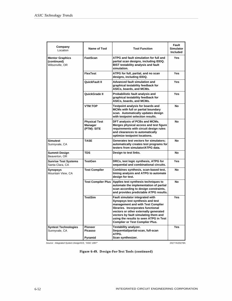
ASIC Technology Trends
INTEGRATED CIRCUIT ENGINEERING CORPORATION6-52
Company Location
Name of Tool Tool FunctionFault
Simulator Included
ATPG and fault simulation for full and partial scan designs, including IDDQ. BIST testability analysis and fault simulation. ATPG for full, partial, and no scan designs, including IDDQ. Advanced fault simulation and graphical testability feedback for ASICs, boards, and MCMs. Probabilistic fault analysis and graphical testability feedback for ASICs, boards, and MCMs. Testpoint analysis for boards and MCMs with full or partial boundary scan. Automatically updates design with testpoint selection results. DFT analysis of PCBs and MCMs. Merges physical access and test figure requirements with circuit design rules and clearances to automatically optimize testpoint locations. Generates test vectors for simulators; automatically creates test programs for testers from simulator/ATPG data. Design to test links. DRCs, test logic synthesis, ATPG for sequential and combinational circuits. Combines synthesis, scan-based test, timing analysis and ATPG to automate design for test. Applies test synthesis techniques to automate the implementation of partial scan according to design constraints, and provides predictable ATPG results. Fault simulator integrated with Synopsys test synthesis and test management and with Test Complier libraries. Incorporates functional vectors or other externally generated vectors by fault simulating them and using the results to seen ATPG in Test Complier or Test Complier Plus. Testability analyzer. Sequential/partial-scan, full-scan ATPG. Scan synthesizer.
Mentor Graphics (continued) Wilsonville, OR Simutest Sunnyvale, CA Summit Design Beaverton, OR Sunrise Test Systems Santa Clara, CA Synopsys Mountain View, CA Syntest Technologies Sunnyvale, CA
FastScan FlexTest QuickFault II QuickGrade II VTM:TOP Physical Test Manager (PTM): SITE TASE TDS TestGen Test Compiler Test Compiler Plus TestSim Pioneer Picasso Pyramid
Yes
Yes
Yes
Yes
No
No
No
No
Yes
No
No
Yes
Yes
Source: Integrated System Design/ICE, "ASIC 1997" 20277A/20278A
Figure 6-49. Design-For-Test Tools (continued)
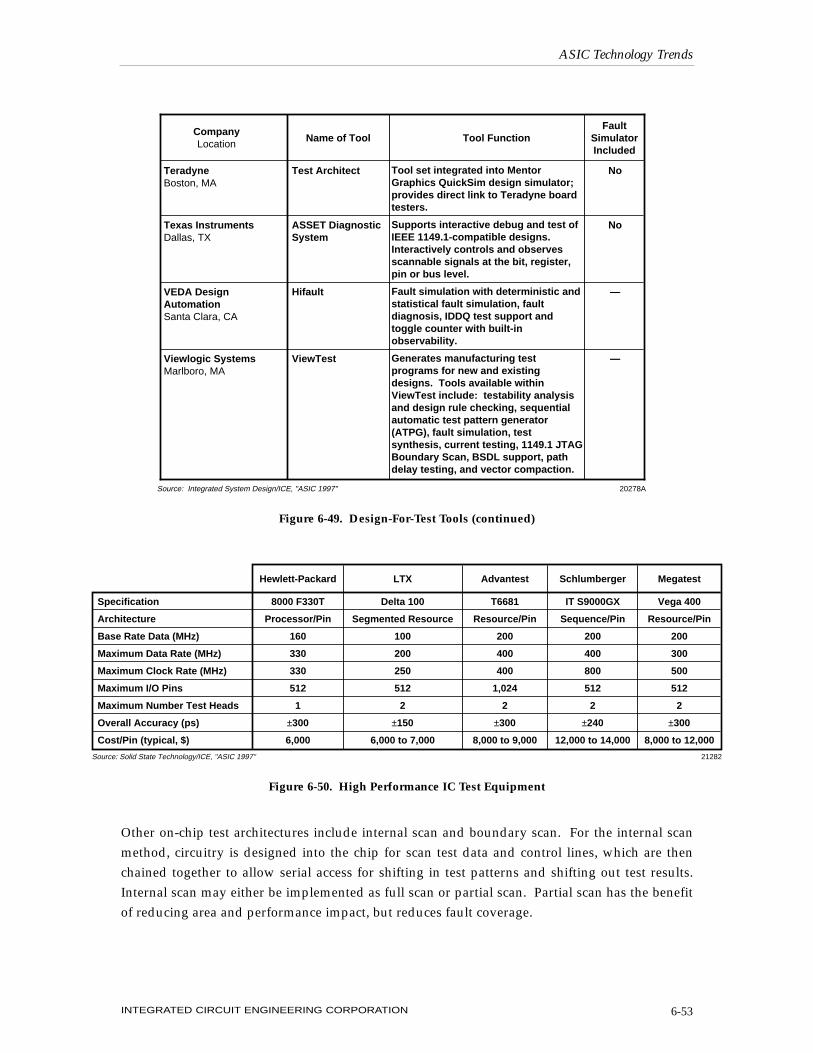
Other on-chip test architectures include internal scan and boundary scan. For the internal scanmethod, circuitry is designed into the chip for scan test data and control lines, which are thenchained together to allow serial access for shifting in test patterns and shifting out test results.Internal scan may either be implemented as full scan or partial scan. Partial scan has the benefitof reducing area and performance impact, but reduces fault coverage.
ASIC Technology Trends
INTEGRATED CIRCUIT ENGINEERING CORPORATION 6-53
Company Location
Name of Tool Tool FunctionFault
Simulator Included
Tool set integrated into Mentor Graphics QuickSim design simulator; provides direct link to Teradyne board testers. Supports interactive debug and test of IEEE 1149.1-compatible designs. Interactively controls and observes scannable signals at the bit, register, pin or bus level. Fault simulation with deterministic and statistical fault simulation, fault diagnosis, IDDQ test support and toggle counter with built-in observability. Generates manufacturing test programs for new and existing designs. Tools available within ViewTest include: testability analysis and design rule checking, sequential automatic test pattern generator (ATPG), fault simulation, test synthesis, current testing, 1149.1 JTAG Boundary Scan, BSDL support, path delay testing, and vector compaction.
Teradyne Boston, MA Texas Instruments Dallas, TX VEDA Design Automation Santa Clara, CA Viewlogic Systems Marlboro, MA
Test Architect ASSET Diagnostic System Hifault ViewTest
No
No
—
—
Source: Integrated System Design/ICE, "ASIC 1997" 20278A
Figure 6-49. Design-For-Test Tools (continued)
Specification
Architecture
Base Rate Data (MHz)
Maximum Data Rate (MHz)
Maximum Clock Rate (MHz)
Maximum I/O Pins
Maximum Number Test Heads
Overall Accuracy (ps)
Cost/Pin (typical, $)
8000 F330T
Processor/Pin
160
330
330
512
1
±300
6,000
Delta 100
Segmented Resource
100
200
250
512
2
±150
6,000 to 7,000
T6681
Resource/Pin
200
400
400
1,024
2
±300
8,000 to 9,000
IT S9000GX
Sequence/Pin
200
400
800
512
2
±240
12,000 to 14,000
Vega 400
Resource/Pin
200
300
500
512
2
±300
8,000 to 12,000
Hewlett-Packard LTX Advantest Schlumberger Megatest
21282Source: Solid State Technology/ICE, "ASIC 1997"
Figure 6-50. High Performance IC Test Equipment
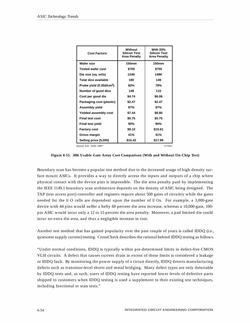
Boundary scan has become a popular test method due to the increased usage of high-density sur-face mount ASICs. It provides a way to directly access the inputs and outputs of a chip wherephysical contact with the device pins is impossible. The die area penalty paid by implementingthe IEEE 1149.1 boundary scan architecture depends on the density of ASIC being designed. TheTAP (test access port) controller and registers require about 500 gates of circuitry while the gatesneeded for the I/O cells are dependent upon the number of I/Os. For example, a 3,000-gatedevice with 44 pins would suffer a hefty 60 percent die area increase, whereas a 10,000-gate, 100-pin ASIC would incur only a 12 to 15 percent die area penalty. Moreover, a pad limited die couldincur no extra die area, and thus a negligible increase in cost.
Another test method that has gained popularity over the past couple of years is called IDDQ (i.e.,quiescent supply current) testing. CrossCheck describes the rational behind IDDQ testing as follows.
“Under normal conditions, IDDQ is typically within pre-determined limits in defect-free CMOSVLSI circuits. A defect that causes current drain in excess of those limits is considered a leakageor IDDQ fault. By monitoring the power supply of a circuit directly, IDDQ detects manufacturingdefects such as transistor-level shorts and metal bridging. Many defect types are only detectableby IDDQ tests and, as such, users of IDDQ testing have reported lower levels of defective partsshipped to customers when IDDQ testing is used a supplement to their existing test techniques,including functional or scan tests.”
ASIC Technology Trends
INTEGRATED CIRCUIT ENGINEERING CORPORATION6-54
Figure 6-51. 30K Usable Gate Array Cost Comparison (With and Without On-Chip Test)
Cost Factors
Wafer size
Tested wafer cost
Die size (sq. mils)
Total dice available
Probe yield (0.35d/cm2)
Number of good dice
Cost per good die
Packaging cost (plastic)
Assembly yield
Yielded assembly cost
Final test cost
Final test yield
Factory cost
Gross margin
Selling price (5,000)
150mm
$700
124K
180
82%
148
$4.74
$2.47
97%
$7.44
$0.75
90%
$9.10
41%
$15.42
Without Silicon Test Area Penalty
17737CSource: ICE, "ASIC 1997"
With 20% Silicon Test Area Penalty
150mm
$700
149K
148
78%
115
$6.06
$2.47
97%
$8.80
$0.75
90%
$10.61
41%
$17.99

As even CrossCheck recommends when discussing IDDQ testing, it is most beneficial when usedas a supplement to other test procedures. It has been suggested that a combination of test strate-gies are necessary for obtaining the best results. For example, using full scan on random logic por-tions of the IC, partial scan elsewhere, boundary scan on I/O lines, BIST (built-in self-test) on reg-ular structures (e.g., memory), as well as IDDQ and delay fault tests, may be appropriate.
As one can see, those looking for an easy “cure-all” ASIC test solution will quickly be disap-pointed. Not only do different system applications require individualized test program strategies(Figure 6-52), but each IC may also need to implement numerous external and on-chip testmethodologies in order to attain a high-level (99-100 percent) of fault coverage (Figure 6-53).
ASIC Technology Trends
INTEGRATED CIRCUIT ENGINEERING CORPORATION 6-55
Design Methodology: Synchronous
Test Methodology: Optimized Scan
Partial Scan Delay Fault Testing
Design Methodology: Asynchronous &
SynchronousTest Methodology:
Optimized Scan Partial Scan Test Grids
Design Methodology: Asynchronous &
SynchronousTest Methodology:
Optimized Scan Partial Scan Test Grids
Consumer
High-End Telecom
High-End EDP
Design Methodology: Synchronous
Test Methodology: Full Scan Delay
Fault Testing Test Grids
Design Methodology: Asynchronous &
SynchronousTest Methodology:
Optimized Scan Partial Scan Test Grids
Design Methodology: Synchronous
Test Methodology: Optimized Scan
Partial Scan Ad-Hoc Test Grids/BIST
Military & Aerospace
LAN & WAN
File Server
19201Source: LSI Logic/ICE, "ASIC 1997"
Figure 6-52. Providing Test Strategies for Different Target Markets
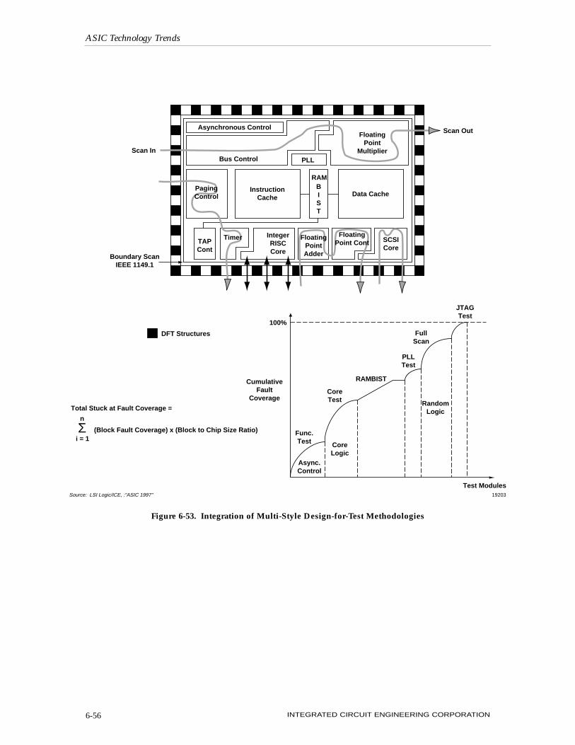
ASIC Technology Trends
INTEGRATED CIRCUIT ENGINEERING CORPORATION6-56
Asynchronous Control
Bus Control
Instruction Cache
PLL
Floating Point
Multiplier
Data CacheB I S T
RAM
SCSI Core
Integer RISC Core
TAP Cont
Paging Control
Floating Point Cont
Floating Point Adder
Timer
100%
Func. Test Core
Logic
RAMBIST
Full Scan
JTAG Test
PLL Test
Random Logic
Test Modules
Async. Control
Core Test
Cumulative Fault
Coverage
DFT Structures
Total Stuck at Fault Coverage =
(Block Fault Coverage) x (Block to Chip Size Ratio)i = 1
n
Σ
Scan In
Scan Out
Boundary Scan IEEE 1149.1
19203Source: LSI Logic/ICE, :"ASIC 1997"
Figure 6-53. Integration of Multi-Style Design-for-Test Methodologies