Metrology Challenges for 45-nm Strained-Si Device Technology
10
IEEE TRANSACTIONS ON SEMICONDUCTOR MANUFACTURING, VOL. 19, NO. 4, NOVEMBER 2006 381 Metrology Challenges for 45-nm Strained-Si Device Technology Victor Vartanian, Member, IEEE, Stefan Zollner, A.V.-Y. Thean, T. White, B.-Y. Nguyen, L. Prabhu, D. Eades, S. Parsons, H. Desjardins, K. Kim, Z.-X. Jiang, V. Dhandapani, J. Hildreth, R. Powers, G. Spencer, N. Ramani, M. Kottke, M. Canonico, X.-D. Wang, L. Contreras, D. Theodore, R. Gregory,and S. Venkatesan Abstract—The semiconductor industry has maintained its his- torical exponential improvement in performance by aggressively scaling transistor dimensions. However, as devices approach sub-100-nm dimensions, scaling becomes more challenging and new materials are required to overcome the fundamental physical limitations imposed by existing materials. For example, as power supply voltages continue to decrease with successive scaling, enhancing carrier mobility using biaxially tensile-stressed Si on relaxed SiGe on SOI and on bulk substrates has become a viable option to sustain continual drive current increase without tradi- tional scaling. Although the addition of strained-Si to conventional MOSFET devices is compatible with existing mainstream CMOS process technology, there are new device and process integration challenges, wafer quality monitoring demands, and stringent re- quirements for film morphology and strain uniformity, imposing new demands on material characterization. Material require- ments for strained-Si CMOS devices include having uniform SiGe thickness, Ge composition, and strain distribution. These are required to maintain uniform device performance as well as low defect density for high minority carrier lifetimes and transcon- ductance, as well as low surface roughness to minimize the impact of interface scattering on carrier mobilities. The parameters of interest in strained-Si CMOS technology include SiGe and Si channel thickness, Ge composition, strain, dislocation density, interface quality, and roughness. Nondestructive inline metrology techniques include spectroscopic ellipsometry for film thickness and Ge composition, X-ray reflectivity for thickness, density, and roughness measurements, X-ray fluorescence for Ge composition, UV-Raman spectroscopy for channel strain characterization, IR photoluminescence for defect detection, and X-ray diffraction for both Ge content and strain measurement. While most of these techniques are well established in the semiconductor industry, some will require development for application to volume manu- facturing. This paper will focus on various metrology approaches used in strained-Si CMOS devices. Index Terms—CMOS integrated circuits, metrology, strain mea- surement. I. INTRODUCTION T HE semiconductor industry has achieved exponential growth over the last 40 years largely due to the ability to scale CMOS transistor dimensions to meet continued demand for increased device density and performance. As device dimen- sions approach the sub–50-nm regime, serious challenges exist in the ability to scale the gate length of conventional bulk silicon Manuscript received May 16, 2006; revised August 24, 2006. V. Vartanian, S. Zollner, A. V.-Y. Thean, T. White, B.-Y. Nguyen, L. Prabhu, D. Eades, S. Parsons, H. Desjardins, K. Kim, Z.-X. Jiang, V. Dhandapani, J. Hildreth, R. Powers, G. Spencer, N. Ramani, and S. Venkatesan are with Austin Silicon Technology Solutions (ASTS), Freescale Semiconductor, Inc., Austin, TX 78721 USA (e-mail: [email protected]). M. Kottke, M. Canonico, X.-D. Wang, L. Contreras, D. Theodore, and R. Gregory are with the Microwave and Mixed-Signals Technologies Labora- tory, Freescale Semiconductor, Inc., Tempe, AZ 85284 USA. Digital Object Identifier 10.1109/TSM.2006.884603 Fig. 1. Thin Si layer grown pseudomorphically on relaxed SiGe alloy buffer having larger lattice spacing than that of Si, achieved either by growing (a) a graded SiGe buffer layer or (b) using a layer transfer approach as an SGOI wafer. transistors below 30 nm, yet still maintain high drive currents while simultaneously reducing supply voltage to prevent increased electric fields to avoid reliability issues. Threshold voltage and gate oxide thickness cannot be scaled at the same rate as without leakage currents exceeding stand-by power requirements. Thus, transistor scaling rapidly reduces the maximum gate overdrive factor [1]. At the same time, higher channel doping concentrations and more abrupt, shallower source-drain junctions have been used to control short channel effects (SCE) at very short gate lengths. These factors cause detrimental effects to the transistor, such as degraded carrier mobility, higher dopant fluctuations, and increased series resistance. In order to circumvent some of the scaling issues, new mate- rials and device architectures are being integrated into CMOS devices in order to maintain the historic CMOS performance trend. These include enhancing carrier mobility using biaxially strained-Si or relaxed SiGe virtual substrates [2], or uniaxially strained Si using tensile or compressive stressors [3]. Although the strained-Si (sSi) augmentation of conventional MOSFETs seems minimally disruptive, the use of SiGe virtual substrates in CMOS devices introduces new process, device, and integra- tion issues that need to be addressed in order to prove successful manufacturability. II. STRAINED-Si/SiGe INTEGRATION AND DEVICE PERFORMANCE When a thin Si layer is grown pseudomorphically on a re- laxed SiGe alloy buffer having larger lattice spacing than that of Si, the Si layer conforms to the SiGe template by expanding laterally and contracting vertically. This can be achieved either by starting with the SiGe grown epitaxially on a thick, graded SiGe buffer layer [Fig. 1(a)] or as a silicon germanium on insu- lator wafer (SGOI) by a layer transfer approach [Fig. 1(b)]. The 0894-6507/$20.00 © 2006 IEEE www.DownloadPaper.ir www.DownloadPaper.ir
-
Upload
independent -
Category
Documents
-
view
0 -
download
0
Transcript of Metrology Challenges for 45-nm Strained-Si Device Technology
IEEE TRANSACTIONS ON SEMICONDUCTOR MANUFACTURING, VOL. 19, NO. 4, NOVEMBER 2006 381
Metrology Challenges for 45-nm Strained-SiDevice Technology
Victor Vartanian, Member, IEEE, Stefan Zollner, A. V.-Y. Thean, T. White, B.-Y. Nguyen, L. Prabhu, D. Eades,S. Parsons, H. Desjardins, K. Kim, Z.-X. Jiang, V. Dhandapani, J. Hildreth, R. Powers, G. Spencer, N. Ramani,
M. Kottke, M. Canonico, X.-D. Wang, L. Contreras, D. Theodore, R. Gregory, and S. Venkatesan
Abstract—The semiconductor industry has maintained its his-torical exponential improvement in performance by aggressivelyscaling transistor dimensions. However, as devices approachsub-100-nm dimensions, scaling becomes more challenging andnew materials are required to overcome the fundamental physicallimitations imposed by existing materials. For example, as powersupply voltages continue to decrease with successive scaling,enhancing carrier mobility using biaxially tensile-stressed Si onrelaxed SiGe on SOI and on bulk substrates has become a viableoption to sustain continual drive current increase without tradi-tional scaling. Although the addition of strained-Si to conventionalMOSFET devices is compatible with existing mainstream CMOSprocess technology, there are new device and process integrationchallenges, wafer quality monitoring demands, and stringent re-quirements for film morphology and strain uniformity, imposingnew demands on material characterization. Material require-ments for strained-Si CMOS devices include having uniform SiGethickness, Ge composition, and strain distribution. These arerequired to maintain uniform device performance as well as lowdefect density for high minority carrier lifetimes and transcon-ductance, as well as low surface roughness to minimize the impactof interface scattering on carrier mobilities. The parameters ofinterest in strained-Si CMOS technology include SiGe and Sichannel thickness, Ge composition, strain, dislocation density,interface quality, and roughness. Nondestructive inline metrologytechniques include spectroscopic ellipsometry for film thicknessand Ge composition, X-ray reflectivity for thickness, density, androughness measurements, X-ray fluorescence for Ge composition,UV-Raman spectroscopy for channel strain characterization, IRphotoluminescence for defect detection, and X-ray diffraction forboth Ge content and strain measurement. While most of thesetechniques are well established in the semiconductor industry,some will require development for application to volume manu-facturing. This paper will focus on various metrology approachesused in strained-Si CMOS devices.
Index Terms—CMOS integrated circuits, metrology, strain mea-surement.
I. INTRODUCTION
THE semiconductor industry has achieved exponentialgrowth over the last 40 years largely due to the ability to
scale CMOS transistor dimensions to meet continued demandfor increased device density and performance. As device dimen-sions approach the sub–50-nm regime, serious challenges existin the ability to scale the gate length of conventional bulk silicon
Manuscript received May 16, 2006; revised August 24, 2006.V. Vartanian, S. Zollner, A. V.-Y. Thean, T. White, B.-Y. Nguyen, L. Prabhu,
D. Eades, S. Parsons, H. Desjardins, K. Kim, Z.-X. Jiang, V. Dhandapani,J. Hildreth, R. Powers, G. Spencer, N. Ramani, and S. Venkatesan are withAustin Silicon Technology Solutions (ASTS), Freescale Semiconductor, Inc.,Austin, TX 78721 USA (e-mail: [email protected]).
M. Kottke, M. Canonico, X.-D. Wang, L. Contreras, D. Theodore, andR. Gregory are with the Microwave and Mixed-Signals Technologies Labora-tory, Freescale Semiconductor, Inc., Tempe, AZ 85284 USA.
Digital Object Identifier 10.1109/TSM.2006.884603
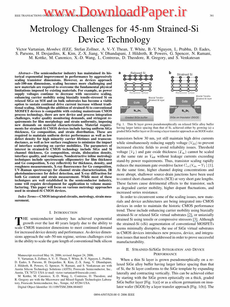
Fig. 1. Thin Si layer grown pseudomorphically on relaxed SiGe alloy bufferhaving larger lattice spacing than that of Si, achieved either by growing (a) agraded SiGe buffer layer or (b) using a layer transfer approach as an SGOI wafer.
transistors below 30 nm, yet still maintain high drive currentswhile simultaneously reducing supply voltage to preventincreased electric fields to avoid reliability issues. Thresholdvoltage and gate oxide thickness cannot be scaledat the same rate as without leakage currents exceedingstand-by power requirements. Thus, transistor scaling rapidlyreduces the maximum gate overdrive factor [1].At the same time, higher channel doping concentrations andmore abrupt, shallower source-drain junctions have been usedto control short channel effects (SCE) at very short gate lengths.These factors cause detrimental effects to the transistor, suchas degraded carrier mobility, higher dopant fluctuations, andincreased series resistance.
In order to circumvent some of the scaling issues, new mate-rials and device architectures are being integrated into CMOSdevices in order to maintain the historic CMOS performancetrend. These include enhancing carrier mobility using biaxiallystrained-Si or relaxed SiGe virtual substrates [2], or uniaxiallystrained Si using tensile or compressive stressors [3]. Althoughthe strained-Si (sSi) augmentation of conventional MOSFETsseems minimally disruptive, the use of SiGe virtual substratesin CMOS devices introduces new process, device, and integra-tion issues that need to be addressed in order to prove successfulmanufacturability.
II. STRAINED-Si/SiGe INTEGRATION AND DEVICE
PERFORMANCE
When a thin Si layer is grown pseudomorphically on a re-laxed SiGe alloy buffer having larger lattice spacing than thatof Si, the Si layer conforms to the SiGe template by expandinglaterally and contracting vertically. This can be achieved eitherby starting with the SiGe grown epitaxially on a thick, gradedSiGe buffer layer [Fig. 1(a)] or as a silicon germanium on insu-lator wafer (SGOI) by a layer transfer approach [Fig. 1(b)]. The
0894-6507/$20.00 © 2006 IEEE
Authorized licensed use limited to: IEEE Xplore. Downloaded on May 10,2010 at 19:05:49 UTC from IEEE Xplore. Restrictions apply.
www.DownloadPaper.irwww.DownloadPaper.ir
382 IEEE TRANSACTIONS ON SEMICONDUCTOR MANUFACTURING, VOL. 19, NO. 4, NOVEMBER 2006
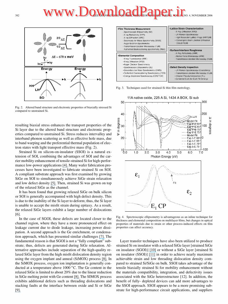
Fig. 2. Altered band structure and electronic properties of biaxially stressed Sicompared to unstrained Si.
resulting biaxial stress enhances the transport properties of theSi layer due to the altered band structure and electronic prop-erties compared to unstrained Si. Stress reduces intervalley andinterband phonon scattering as well as effective hole mass, dueto band warping and the preferential thermal population of elec-tron states with light transport effective mass (Fig. 2).
Strained Si on silicon-on-insulator (SSOI) is a natural ex-tension of SOI, combining the advantages of SOI and the car-rier mobility enhancement of tensile-strained Si for high-perfor-mance low-power applications [4]. Many wafer fabrication pro-cesses have been investigated to fabricate strained Si on SOI.A compliant substrate approach was first examined by growingSiGe on SOI to simultaneously achieve SiGe strain relaxationand low defect density [5]. Then, strained Si was grown on topof the relaxed SiGe as the channel.
It has been found that growing relaxed SiGe on bulk siliconor SOI is generally accompanied with high defect density. Thisis due to the inability of the Si layer to deform; thus, the Si layeris unable to accept the misfit strain during epitaxy. As a result,the relaxed SiGe layers exhibit a large number of dislocations[6].
In the case of SGOI, these defects are located closer to thechannel region, where they have a more pronounced effect onleakage current due to diode leakage, increasing power dissi-pation. A second approach is the Ge enrichment, or condensa-tion approach, which has presented similar challenges [7]. Thefundamental reason is that SGOI is not a “fully compliant” sub-strate; thus, defects are generated during SiGe relaxation. Al-ternative approaches include separation of the high-quality re-laxed SiGe layer from the high misfit dislocation density regionusing the oxygen implant and anneal (SiMOX) process [8]. Inthe SiMOX process, oxygen ion implantation is generally con-ducted at a temperature above 1000 C. The Ge content in therelaxed SiGe is limited to about 20% due to the linear reductionin SiGe melting point with Ge content [8]. The SIMOX processexhibits additional defects such as threading dislocations andstacking faults at the interface between oxide and Si or SiGe[9].
Fig. 3. Techniques used for strained-Si thin film metrology.
Fig. 4. Spectroscopic ellipsometry is advantageous as an inline technique forthickness and elemental composition on multilayer films, but changes in opticalproperties of materials due to strain or other process-induced effects on filmproperties can affect accuracy.
Layer transfer techniques have also been utilized to producestrained Si on insulator with a relaxed SiGe layer [strained SiGeon insulator (SGOI)] [10] or without a SiGe layer [strained Sion insulator (SSOI)] [11] in order to achieve nearly maximumachievable strain and low threading dislocation density com-pared to strained Si/SiGe on bulk. SSOI takes advantage of thetensile biaxially strained Si for mobility enhancement withoutthe materials compatibility, integration, and defectivity issuesassociated with the SiGe heterostructure [12]. In addition, thebenefit of fully- depleted devices can add more advantages tothe SSOI approach. SSOI appears to be a more promising sub-strate for high-performance circuit applications, and suppliers
Authorized licensed use limited to: IEEE Xplore. Downloaded on May 10,2010 at 19:05:49 UTC from IEEE Xplore. Restrictions apply.
www.DownloadPaper.irwww.DownloadPaper.ir

VARTANIAN et al.: METROLOGY CHALLENGES FOR 45-nm STRAINED-Si DEVICE TECHNOLOGY 383
Fig. 5. XRR film thickness measurement, Raman strain plot, and TEM cross section of oxide on Si on SiGe.
have made major advances in reducing pileups (potential yieldkillers) and threading dislocation densities, while improvingfilm thickness uniformity and increasing strain. Misfit disloca-tions that arise from sSi relaxation can pose serious reliabilityproblems [13]. The likelihood that a misfit dislocation inter-cepts the source and drain across the channel is high. Dopantdiffusion from the source and drain can be further enhancedalong the defect, creating a weak buried channel.
III. METROLOGY REQUIREMENTS AND TECHNIQUES FOR
STRAINED Si/SiGe DEVICES
In addition to Si CMOS manufacturing integration chal-
lenges, the introduction of new materials poses significant
metrology challenges, requiring new techniques or improve-
ments to established methods. This is especially true for SOI
and strained Si substrates, with or without SiGe alloy buffers.
Parameters to be measured include film thickness, composi-
tion (Ge content), dislocation density, interface conditions,
roughness, and strain. To characterize the impact of fabrication
processes on strained-Si film properties and to achieve uniform
optimal films for subsequent device fabrication, a variety of
techniques is currently used to determine film thickness, ele-
mental composition and profile (e.g., Ge), lattice strain, surface
and interface roughness, and defect density (Fig. 3).
A. Spectroscopic Ellipsometry
Spectroscopic ellipsometry (SE), X-ray reflectivity (XRR)
spectroscopy, secondary ion mass spectrometry (SIMS), Auger,
and tunneling electron microscopy (TEM) are extensively used
to determine film thickness. However, only SE and XRR are
nondestructive.
Material parameters such as refractive index often depend on
processing conditions, crystallinity, or strain, which may influ-
ence the measurement. Traditionally, SE has been the method
of choice for measuring film thickness. Capabilities and limi-
tations of this technique have been described elsewhere [14].
Spectroscopic ellipsometry is particularly advantageous as an
in-line technique for thickness and elemental composition on
multilayer films (Fig. 4).
Given accurate model substrates, spectroscopic ellipsometry
can yield accurate film thickness and elemental composition in-
formation because of the predictable effect of varying film thick-
Authorized licensed use limited to: IEEE Xplore. Downloaded on May 10,2010 at 19:05:49 UTC from IEEE Xplore. Restrictions apply.
www.DownloadPaper.irwww.DownloadPaper.ir
384 IEEE TRANSACTIONS ON SEMICONDUCTOR MANUFACTURING, VOL. 19, NO. 4, NOVEMBER 2006
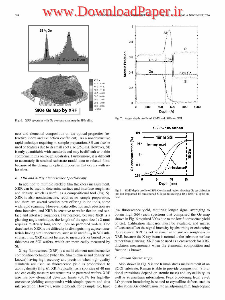
Fig. 6. XRF spectrum with Ge concentration map in SiGe film.
ness and elemental composition on the optical properties (re-
fractive index and extinction coefficient). As a nondestructive
rapid technique requiring no sample preparation, SE can also be
used on features due to its small spot size (25 m). However, SE
is only quantifiable with standards and may be difficult with thin
conformal films on rough substrates. Furthermore, it is difficult
to accurately fit strained substrate model data to relaxed films
because of the change in optical properties that occurs with re-
laxation.
B. XRR and X-Ray Fluorescence Spectroscopy
In addition to multiple stacked film thickness measurement,XRR can be used to determine surface and interface roughnessand density, which is useful as a compositional tool (Fig. 5).XRR is also nondestructive, requires no sample preparation,and there are several vendors now offering inline tools, somewith rapid scanning. However, data collection and reduction aretime intensive, and XRR is sensitive to wafer flexion and sur-face and interface roughness. Furthermore, because XRR is aglancing angle technique, the length of the spot size ( 2 mm)requires relatively long scribe lines on patterned wafers. Onedrawback to XRR is the difficulty in distinguishing adjacent ma-terials having similar densities, such as Si and SiO in SOI sub-strates; thus, XRR cannot be used to measure Si or buried oxidethickness on SOI wafers, which are more easily measured bySE.
X-ray fluorescence (XRF) is a multi-element nondestructivecomposition technique (when the film thickness and density areknown) having high accuracy and precision when high-qualitystandards are used, as fluorescence yield is proportional toatomic density (Fig. 6). XRF typically has a spot size of 40 mand can easily measure test structures on patterned wafers. XRFalso has low elemental detection limits (0.01% for high-flu-orescence yielding compounds) with simple spectra and datainterpretation. However, some elements, for example Ge, have
Fig. 7. Auger depth profile of SIMS pad: SiGe on SOI.
Fig. 8. SIMS depth profile of Si/SiGe channel region showing Ge up-diffusioninto ion-implanted 15-nm strained-Si layer following a 10-s 1025 C spike an-neal.
low fluorescence yield, requiring longer signal averaging toobtain high S/N (each spectrum that comprised the Ge mapshown in Fig. 6 required 300 s due to the low fluorescence yieldof Ge). Calibration standards must be available, and matrixeffects can affect the signal intensity by absorbing or enhancingfluorescence. XRF is not as sensitive to surface roughness asXRR, because the X-ray beam is normal to the substrate surfacerather than glancing. XRF can be used as a crosscheck for XRRthickness measurement when the elemental composition andfraction is known.
C. Raman Spectroscopy
Also shown in Fig. 5 is the Raman stress measurement of anSGOI substrate. Raman is able to provide composition (vibra-tional transitions depend on atomic mass) and crystallinity, aswell as stress/strain information. Peak broadening from Si–SiLO phonon broadening is related to crystalline defects such asdislocations, Ge outdiffusion into an adjoining film, high dopant
Authorized licensed use limited to: IEEE Xplore. Downloaded on May 10,2010 at 19:05:49 UTC from IEEE Xplore. Restrictions apply.
www.DownloadPaper.irwww.DownloadPaper.ir
VARTANIAN et al.: METROLOGY CHALLENGES FOR 45-nm STRAINED-Si DEVICE TECHNOLOGY 385
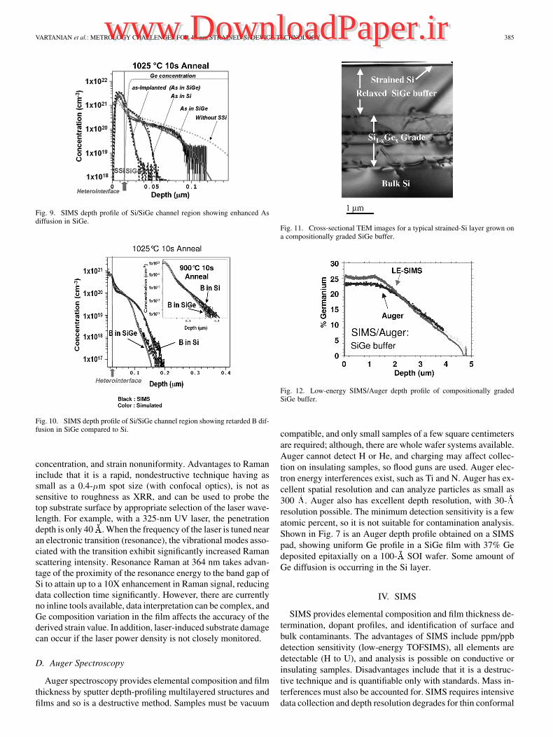
Fig. 9. SIMS depth profile of Si/SiGe channel region showing enhanced Asdiffusion in SiGe.
Fig. 10. SIMS depth profile of Si/SiGe channel region showing retarded B dif-fusion in SiGe compared to Si.
concentration, and strain nonuniformity. Advantages to Ramaninclude that it is a rapid, nondestructive technique having assmall as a 0.4- m spot size (with confocal optics), is not assensitive to roughness as XRR, and can be used to probe thetop substrate surface by appropriate selection of the laser wave-length. For example, with a 325-nm UV laser, the penetrationdepth is only 40 . When the frequency of the laser is tuned nearan electronic transition (resonance), the vibrational modes asso-ciated with the transition exhibit significantly increased Ramanscattering intensity. Resonance Raman at 364 nm takes advan-tage of the proximity of the resonance energy to the band gap ofSi to attain up to a 10X enhancement in Raman signal, reducingdata collection time significantly. However, there are currentlyno inline tools available, data interpretation can be complex, andGe composition variation in the film affects the accuracy of thederived strain value. In addition, laser-induced substrate damagecan occur if the laser power density is not closely monitored.
D. Auger Spectroscopy
Auger spectroscopy provides elemental composition and film
thickness by sputter depth-profiling multilayered structures and
films and so is a destructive method. Samples must be vacuum
Fig. 11. Cross-sectional TEM images for a typical strained-Si layer grown ona compositionally graded SiGe buffer.
Fig. 12. Low-energy SIMS/Auger depth profile of compositionally gradedSiGe buffer.
compatible, and only small samples of a few square centimeters
are required; although, there are whole wafer systems available.
Auger cannot detect H or He, and charging may affect collec-
tion on insulating samples, so flood guns are used. Auger elec-
tron energy interferences exist, such as Ti and N. Auger has ex-
cellent spatial resolution and can analyze particles as small as
300 . Auger also has excellent depth resolution, with 30-
resolution possible. The minimum detection sensitivity is a few
atomic percent, so it is not suitable for contamination analysis.
Shown in Fig. 7 is an Auger depth profile obtained on a SIMS
pad, showing uniform Ge profile in a SiGe film with 37% Ge
deposited epitaxially on a 100- SOI wafer. Some amount of
Ge diffusion is occurring in the Si layer.
IV. SIMS
SIMS provides elemental composition and film thickness de-
termination, dopant profiles, and identification of surface and
bulk contaminants. The advantages of SIMS include ppm/ppb
detection sensitivity (low-energy TOFSIMS), all elements are
detectable (H to U), and analysis is possible on conductive or
insulating samples. Disadvantages include that it is a destruc-
tive technique and is quantifiable only with standards. Mass in-
terferences must also be accounted for. SIMS requires intensive
data collection and depth resolution degrades for thin conformal
Authorized licensed use limited to: IEEE Xplore. Downloaded on May 10,2010 at 19:05:49 UTC from IEEE Xplore. Restrictions apply.
www.DownloadPaper.irwww.DownloadPaper.ir
386 IEEE TRANSACTIONS ON SEMICONDUCTOR MANUFACTURING, VOL. 19, NO. 4, NOVEMBER 2006
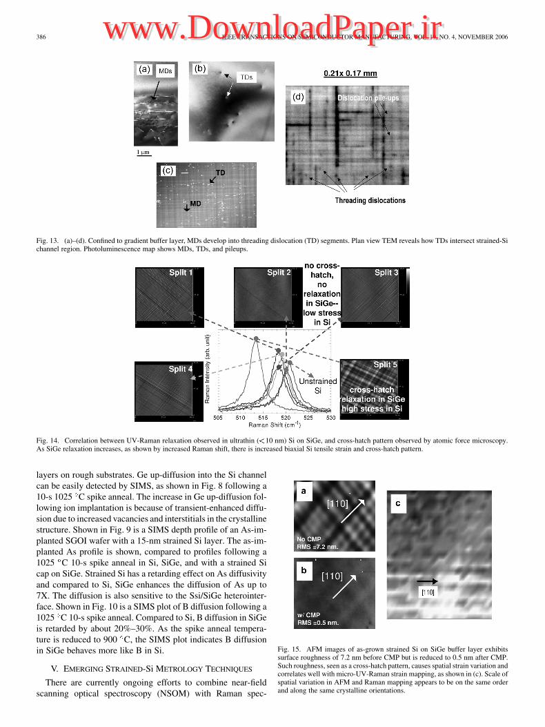
Fig. 13. (a)–(d). Confined to gradient buffer layer, MDs develop into threading dislocation (TD) segments. Plan view TEM reveals how TDs intersect strained-Sichannel region. Photoluminescence map shows MDs, TDs, and pileups.
Fig. 14. Correlation between UV-Raman relaxation observed in ultrathin (<10 nm) Si on SiGe, and cross-hatch pattern observed by atomic force microscopy.As SiGe relaxation increases, as shown by increased Raman shift, there is increased biaxial Si tensile strain and cross-hatch pattern.
layers on rough substrates. Ge up-diffusion into the Si channel
can be easily detected by SIMS, as shown in Fig. 8 following a
10-s 1025 C spike anneal. The increase in Ge up-diffusion fol-
lowing ion implantation is because of transient-enhanced diffu-
sion due to increased vacancies and interstitials in the crystalline
structure. Shown in Fig. 9 is a SIMS depth profile of an As-im-
planted SGOI wafer with a 15-nm strained Si layer. The as-im-
planted As profile is shown, compared to profiles following a
1025 C 10-s spike anneal in Si, SiGe, and with a strained Si
cap on SiGe. Strained Si has a retarding effect on As diffusivity
and compared to Si, SiGe enhances the diffusion of As up to
7X. The diffusion is also sensitive to the Ssi/SiGe heterointer-
face. Shown in Fig. 10 is a SIMS plot of B diffusion following a
1025 C 10-s spike anneal. Compared to Si, B diffusion in SiGe
is retarded by about 20%–30%. As the spike anneal tempera-
ture is reduced to 900 C, the SIMS plot indicates B diffusion
in SiGe behaves more like B in Si.
V. EMERGING STRAINED-Si METROLOGY TECHNIQUES
There are currently ongoing efforts to combine near-field
scanning optical spectroscopy (NSOM) with Raman spec-
Fig. 15. AFM images of as-grown strained Si on SiGe buffer layer exhibitssurface roughness of 7.2 nm before CMP but is reduced to 0.5 nm after CMP.Such roughness, seen as a cross-hatch pattern, causes spatial strain variation andcorrelates well with micro-UV-Raman strain mapping, as shown in (c). Scale ofspatial variation in AFM and Raman mapping appears to be on the same orderand along the same crystalline orientations.
Authorized licensed use limited to: IEEE Xplore. Downloaded on May 10,2010 at 19:05:49 UTC from IEEE Xplore. Restrictions apply.
www.DownloadPaper.irwww.DownloadPaper.ir
VARTANIAN et al.: METROLOGY CHALLENGES FOR 45-nm STRAINED-Si DEVICE TECHNOLOGY 387
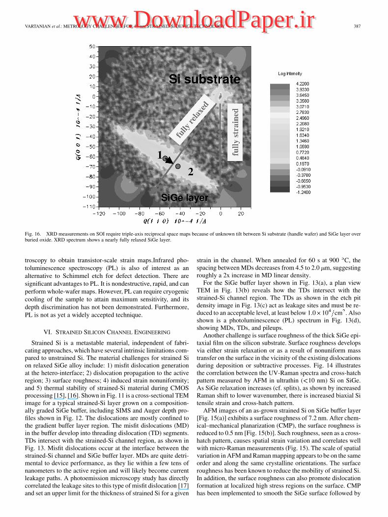
Fig. 16. XRD measurements on SOI require triple-axis reciprocal space maps because of unknown tilt between Si substrate (handle wafer) and SiGe layer overburied oxide. XRD spectrum shows a nearly fully relaxed SiGe layer.
troscopy to obtain transistor-scale strain maps.Infrared pho-
toluminescence spectroscopy (PL) is also of interest as an
alternative to Schimmel etch for defect detection. There are
significant advantages to PL. It is nondestructive, rapid, and can
perform whole-wafer maps. However, PL can require cryogenic
cooling of the sample to attain maximum sensitivity, and its
depth discrimination has not been demonstrated. Furthermore,
PL is not as yet a widely accepted technique.
VI. STRAINED SILICON CHANNEL ENGINEERING
Strained Si is a metastable material, independent of fabri-cating approaches, which have several intrinsic limitations com-pared to unstrained Si. The material challenges for strained Sion relaxed SiGe alloy include: 1) misfit dislocation generationat the hetero-interface; 2) dislocation propagation to the activeregion; 3) surface roughness; 4) induced strain nonuniformity;and 5) thermal stability of strained-Si material during CMOSprocessing [15], [16]. Shown in Fig. 11 is a cross-sectional TEMimage for a typical strained-Si layer grown on a composition-ally graded SiGe buffer, including SIMS and Auger depth pro-files shown in Fig. 12. The dislocations are mostly confined tothe gradient buffer layer region. The misfit dislocations (MD)in the buffer develop into threading dislocation (TD) segments.TDs intersect with the strained-Si channel region, as shown inFig. 13. Misfit dislocations occur at the interface between thestrained-Si channel and SiGe buffer layer. MDs are quite detri-mental to device performance, as they lie within a few tens ofnanometers to the active region and will likely become currentleakage paths. A photoemission microscopy study has directlycorrelated the leakage sites to this type of misfit dislocation [17]and set an upper limit for the thickness of strained Si for a given
strain in the channel. When annealed for 60 s at 900 C, thespacing between MDs decreases from 4.5 to 2.0 m, suggestingroughly a 2x increase in MD linear density.
For the SiGe buffer layer shown in Fig. 13(a), a plan viewTEM in Fig. 13(b) reveals how the TDs intersect with thestrained-Si channel region. The TDs as shown in the etch pitdensity image in Fig. 13(c) act as leakage sites and must be re-duced to an acceptable level, at least below 1.0 10 cm . Alsoshown is a photoluminescence (PL) spectrum in Fig. 13(d),showing MDs, TDs, and pileups.
Another challenge is surface roughness of the thick SiGe epi-taxial film on the silicon substrate. Surface roughness developsvia either strain relaxation or as a result of nonuniform masstransfer on the surface in the vicinity of the existing dislocationsduring deposition or subtractive processes. Fig. 14 illustratesthe correlation between the UV-Raman spectra and cross-hatchpattern measured by AFM in ultrathin ( 10 nm) Si on SiGe.As SiGe relaxation increases (cf. splits), as shown by increasedRaman shift to lower wavenumber, there is increased biaxial Sitensile strain and cross-hatch pattern.
AFM images of an as-grown strained Si on SiGe buffer layer[Fig. 15(a)] exhibits a surface roughness of 7.2 nm. After chem-ical–mechanical planarization (CMP), the surface roughness isreduced to 0.5 nm [Fig. 15(b)]. Such roughness, seen as a cross-hatch pattern, causes spatial strain variation and correlates wellwith micro-Raman measurements (Fig. 15). The scale of spatialvariation in AFM and Raman mapping appears to be on the sameorder and along the same crystalline orientations. The surfaceroughness has been known to reduce the mobility of strained Si.In addition, the surface roughness can also promote dislocationformation at localized high stress regions on the surface. CMPhas been implemented to smooth the SiGe surface followed by
Authorized licensed use limited to: IEEE Xplore. Downloaded on May 10,2010 at 19:05:49 UTC from IEEE Xplore. Restrictions apply.
www.DownloadPaper.irwww.DownloadPaper.ir
388 IEEE TRANSACTIONS ON SEMICONDUCTOR MANUFACTURING, VOL. 19, NO. 4, NOVEMBER 2006
additional SiGe growth and then strained-Si growth. Enhancedelectron mobility has been demonstrated for strained-Si tran-sistors using CMP [18]. Surface roughness was reduced by anorder of magnitude to about 0.5 nm or better.
XRD can also be used for strain mapping of SSOI or SGOIsubstrates. In addition to strain, XRD can measure film thick-ness and composition nondestructively and with high accuracy.However, XRD measurements on SOI require lengthy triple-axis reciprocal space maps because of the uncertainty in thetilt between the Si substrates in the donor wafer and the handlewafer. Thus, XRD is straightforward only on bulk Si samples.Shown in Fig. 16 is a reciprocal space map showing the tilt be-tween the Si substrate and the SiGe layer and the differencein strain between a fully relaxed SiGe substrate and the fullystrained Si substrate. The XRD spectrum indicates a nearly fullyrelaxed SiGe layer.
VII. CONCLUSION
Significant progress in the development and improvementin quality of strained Si on bulk and on insulator substrateshas been achieved. Biaxially strained Si devices meetingITRS high performance targets have been demonstrated. Yet,some metrology challenges that will be needed on the ITRSmetrology roadmap have only begun to be addressed, forexample, measurement of composition and strain at the deepsubmicron device length scale.
Strained-Si/SiGe CMOS technology has been implementedat the 90- and 65-nm technology nodes and likely will continueto do so at 45 nm and beyond. However, the semiconductorindustry’s evolution toward strained Si is not merely a sub-strate change having new defectivity issues. The transition to-ward strained Si requires more extensive metrology monitoringcompared to traditional transistor node changes.
Material and integration issues relying on accurate control offilm thickness, Ge composition, strain, roughness, and threadingand misfit dislocations remain challenges that will require ap-plication of traditional, yet enhanced, techniques such as SE, aswell as application of less traditional techniques such as XRR,XRF, XRD, Raman, and PL. It is apparent, however, that as ma-terial, device, and process challenges increase, new, nondestruc-tive, inline metrology techniques will be needed. Further analyt-ical method development is required, as inline metrology toolsusing some of these techniques are just becoming available.
ACKNOWLEDGMENT
The authors would like to thank Austin Technology and Man-
ufacturing Center (ATMC), ASTS, Physical Analysis Laborato-
ries, Austin, TX (PALTX) and Tempe, AZ (PALAZ), as well as
M. Sadaka at ColdWatt, Austin.
REFERENCES
[1] Y. Taur, D. A. Buchanan, W. Chen, D. J. Frank, K. E. Ismail, S.-H.Lo, G. A. Sai-Halaz,, R. G. Viswanathan, H.-J. C. Wann, S. J. Wind,and H.-S. Wong, “CMOS scaling into the nanometer regime,” in Proc.IEEE, 1997, vol. 85, no. 4, pp. 486–504.
[2] K. Rim, L. Hoyt, and J. F. Gibbons, “Transconductance enhancement indeep submicron strained-Si 12-MOSFETs,” in IEDM Tech. Dig., 1998,p. 707.
[3] T. Ghani, M. Armstrong, C. Auth, M. Bost, P. Charvat, G. Glass, T.Hoffmann, K. Johnson, C. Kenyon, J. Klaus, B. McIntyre, K. Mistry,A. Murthy, J. Sandford, M. Silberstein, S. Sivakumar, P. Smith, K. Za-wadzki, S. Thompson, and M. Bohr, “A 90 nm high volume manu-facturing logic technology featuring novel 45 nm gate length strainedsilicon CMOS transistors,” in IEDM Tech. Dig., 2003, p. 978.
[4] H. S. P. Wong, “Beyond the conventional transistor,” IBM J. Res. Dev.,vol. 46, p. 133, 2002.
[5] Y. H. Lou, J. L. Liu, G. Jin, J. Wan, K. L. Wang, C. D. Moore, M. S.Goorsky, C. Chih, and K. N. Tu, “Effective compliant substrate for low-dislocation relaxed SiGe growth,” Appl. Phys. Lett., vol. 78, p. 1219,2001.
[6] M. A. Chu, M. O. Tanner, F. Huang, K. L. Wang, G. G. Chu, and M.S. Goorsky, “Photoluminescence and x-ray characterization of relaxedSi1-xGex alloys grown on silicon on insulator (SOI) and implanted SOIsubstrates,” J. Cryst. Growth, vol. 175–176, p. 1278, 1997.
[7] T. Tezuka, N. Sugiyama, and S. Takagi, “Fabrication of strained Si onan ultrathin SiGe-on-insulator virtual substrate with a high-Ge frac-tion,” Appl. Phys. Lett., vol. 79, p. 1798, 2001.
[8] T. Mizuno, N. Sugiyama, A. Kurobe, and S. Takagi, “Advanced SOIp-MOSFETs with strained-Si channel on SiGe-on-insulator substratefabricated by SIMOX technology,” IEEE Trans. Electron Devices, vol.48, no. 8, pp. 1612–1618, Aug. 2001.
[9] P. Roitman, M. Edelstein, and S. J. Krause, “Electrical detection ofdefects in SIMOX buried oxides: Pipes and precipitates,” in Proc. IEEEInt. SOI Conf., 1998, pp. 167–168.
[10] Z.-Y. Cheng, M. T. Currie, C. W. Leitz, G. Taraschi, E. A. Fitzgerald,J. L. Hoyt, and D. A. Antoniadas, “Electron mobility enhancement instrained-Si n-MOSFETs fabricated on SiGe-on-insulator (SGOI) sub-strates,” IEEE Electron Device Lett., vol. 22, no. 7, pp. 321–323, Jul.2001.
[11] L. Huang, J. O. Chu, S. A. Goma, C. P. D’Emic, S. J. Koester, D.F. Canaperi, P. M. Mooney, S. A. Cordes, J. L. Speidell, R. M. An-derson, and H.-S. P. Wong, “Electron and hole mobility enhancementin strained SOI by wafer bonding,” IEEE Trans. Electron Device, vol.49, no. 12, pp. 1566–1571, 2002.
[12] K. Rim, K. Chan, L. Shi, D. Boyd, J. Ott, N. Klymko, F. Cardone,L. Tai, S. Koester, M. Cobb, D. Canaperi, B. To, E. Duch, I. Babich,R. Carruthers, P. Saunders, G. Walker, Y. Zhang, M. Steen, and M.Ieong, “Fabrication and mobility characteristics of ultra-thin strained Sidirectly on insulator (SSDOI) MOSFETs,” in IEDM Tech. Dig., 2003,p. 49.
[13] H. C.-H. Wang, Y.-P. Wang, S.-J. Chen, C.-H. Ge, S. M. Ting, J.-Y.Kung, R.-L. Hwang, H.-K. Chiu, L. C. Sheu, P.-Y. Tsai, L.-G. Yao,S.-C. Chen, H.-J. Tao, Y.-C. Yeo, W.-C. Lee, and C. Hu, “Substrate-strained silicon technology: Process integration,” in Tech. Dig., 2003,p. 61.
[14] S. Zollner, R. Liu, A. A. Volinsky, T. White, B.-Y. Nguyen, and C.S. Cook, “Gate oxide metrology and silicon piezooptics,” Thin SolidFilms, vol. 455–456, p. 261, 2004.
[15] E. A. Fitzgerald, S. B. Samavedam, Y. H. Xie, and L. M. Giovane,“Influence of strain on semiconductor thin film epitaxy,” J. Vac. Sci.Technol., vol. 15, p. 1048, 1997.
[16] Y. B. Bolkhovityanov, O. P. Pchelyakov, and S. I. Chikichev, “Silicon- germanium epilayers: Physical fundamentals of growing strained andfully relaxed heterostructures,” Physics-Uspekhi, vol. 44, p. 655, 2001.
[17] J. G. Fiorenza, F. Braithwaite, C. Leitz, T. Curie, Z. Y. Cheng, V. K.Yang, T. Langdo, I. Carlin, M. Sornerville, A. Lochtefeld, H. Badawi,and M. T. Bulsara, “Investigation of misfit dislocation leakage in su-percritical strained silicon MOSFETs,” in Proc. IEEE Int. ReliabilityPhysics Symp., 2004, pp. 493–497.
[18] N. Sugii, D. Hisamoto, K. Washio, N. Yokoyama, and S. Kimura, “En-hanced performance of strained-Si MOSFETs on CMP SiGe virtualsubstrate,” in IEDM Tech. Dig., 2001, p. 737.
Victor Vartanian (M’06) received the B.S. andPh.D. degrees in chemistry from the University ofTexas, Austin, in 1990 and 1995, respectively.
Following a two-year Postdoctoral appointment,he joined Motorola in the Advanced ProductsResearch and Development Laboratory (APRDL),Austin, TX, working on analytical applicationsof FTIR and mass spectrometry to environmentalissues in semiconductor manufacturing and inprocess development. He is a Device Engineer in theNovel Devices Group, Austin Silicon Technology
Solutions (ASTS) Laboratory, Freescale Semiconductor, Austin, workingon applications of strained silicon to advanced transistor design and X-raymetrology applications. He has two issued patents in the semiconductor field.
Authorized licensed use limited to: IEEE Xplore. Downloaded on May 10,2010 at 19:05:49 UTC from IEEE Xplore. Restrictions apply.
www.DownloadPaper.irwww.DownloadPaper.ir
VARTANIAN et al.: METROLOGY CHALLENGES FOR 45-nm STRAINED-Si DEVICE TECHNOLOGY 389
Dr. Vartanian is a member of the American Society for Mass Spectrometry,the American Chemical Society, the Electrochemical Society, the AmericanVacuum Society, and the American Physical Society.
Stefan Zollner received the Ph.D. degree in semiconductor physics at theMax-Planck-Institute for Solid-State Research, Stuttgart, Germany, in 1991.
He is a Device Engineer in the Austin Silicon Technology Solutions Labo-ratory, Freescale Semiconductor, Inc., Austin, TX. Before joining Freescale in1997, he was an Assistant Professor of Physics at Iowa State University andthe Ames Laboratory (US-DOE), Ames, and a Postdoctoral Researcher at theIBM T. J. Watson Research Center, Yorktown Heights, NY. He has coeditedSilicon-Germanium-Carbon Alloys: Growth, Properties, and Applications, withS. Pantelides. He is an author of about 140 journal and proceedings papers, onepatent, and approximately 100 conference presentations. His research includesfront-end silicon processing (especially high-mobility materials, metal oxides,and silicide contacts) for future CMOS platforms and measurements in the semi-conductor industry (especially ellipsometry and X-ray techniques).
Dr. Zollner is a Fellow of the American Physical Society and a former Chairof the Forum on Industrial and Applied Physics (FIAP).
A. V.-Y. Thean received the B.S. (Highest Honors), M.S., and Ph.D. degreesin electrical engineering from the University of Illinois at Urbana–Champaign,Urbana.
He is presently the Manager of Freescale’s Novel Device Group, Austin,TX. He leads the advanced process and device teams responsible for nonclas-sical transistor development base on novel substrates, process-induced stressors,and new transistor architectures for Freescale’s logic technology. In addition tofront-end process integration and transistor design, he has experience in CMOSdevice/process simulations, as well as quantum transport modeling of nanoelec-tronic devices. He is author and coauthor of over 40 journal and conference pub-lications and holds eight U.S. patents in the areas of advanced semiconductortechnology.
Dr. Thean was a recipient of the 2001 Gregory Stillman Semiconductor Re-search Award from the University of Illinois at Urbana–Champaign.
T. White received the Ph.D. degree in chemistry from Arizona State Univer-sity, Tempe, in 1982. Postdoctoral work there focused on physical-chemical andmagnetic properties of metal-ammonia and mixed-metal-oxide systems.
In 1984, he joined Motorola’s Advanced Products Research and Develop-ment Laboratory, working in LPCVD development. He managed yield enhance-ment, defect metrology and defect reduction groups in 1997, 2000, and 2001,respectively. He joined the Novel Structures Group in 2001 focusing on ex-treme scaling of CMOS devices such as strained Si, FDSOI, and FinFETs. He iscurrently working on NVM processes and devices at Freescale Semiconductor,Austin, TX.
B.-Y. Nguyen received the Degree in chemical engineering from the Universityof Texas, Austin and the Degree in developing Freescale/Motorola’s CMOStechnology for advanced integrated circuit products from the University ofVermont (UVM), Burlington.
She is a Senior Manager at Freescale Semiconductor, Tempe, AZ, and aFreescale/Motorola Dan Noble Fellow. She is a Senior Device EngineeringTechnician at the Austin Silicon Technology Solutions Laboratory, FreescaleSemiconductor, Inc., Austin, TX. She has been working in the semiconductorindustry for the last 22 years, providing analytical support in physical analysissuch as TEM, SEM, and other characterization techniques, such as FIB,ellipsometry, and defect review. Projects supported in the industry includeFINFET, SSOI, S/D recess, high-k dielectrics, etc. Prior to joining Motorolain 1996, she worked as a Process Technician at IBM, E. Fishkill, NY, andSEMATECH, Austin, TX. She currently leads a group of technologists todevelop the new materials/device architecture for sub-130 nanometer integratedcircuits application. She has given invited talks, key note and panel discussionsat several technical conferences and workshops. She also served as a committeemember for IEDM, SISC Conferences and currently serves as a Steering andTechnical Committee Member of the International Conference on IntegratedCircuit Design and Technology (ICICDT) and Electrochemical Society (ECS).She holds more than 50 issued patents and has authored more than 70 technicalpapers on IC process and device technologies.
L. Prabhu received the Degree from the University of Vermont (UVM),Burlington.
She is a Senior Device Engineering Technician at the Austin Silicon Tech-nology Solutions Laboratory, Freescale Semiconductor, Inc., Austin, TX. Shehas been working in the semiconductor industry for the last 22 years, providinganalytical support in physical analysis such as TEM, SEM, and other character-ization techniques, such as FIB, ellipsometry, and defect review. Projects sup-ported in the industry include FINFET, SSOI, S/D recess, high-k dielectrics, etc.Prior to joining Motorola in 1996, she worked as a Process Technician at IBM,E. Fishkill, NY, and SEMATECH, Austin, TX.
D. Eades is a Device Technician at the Austin Silicon Technology SolutionsLaboratory, Freescale Semiconductor, Inc., Austin, TX. Her work includes in-tegration of new modules for C45 and C65 processes.
S. Parsons, photograph and biography not available at the time of publication.
H. Desjardins, photograph and biography not available at the time of publica-tion.
K. Kim received the B.S. degree in engineering physics from the Universityof California at Berkeley, and the M.S. degrees in electrical engineering andengineering management from the University of Texas, Austin.
He has a broad spectrum of experience from tactile sensor design and remotesensing methodology, semiconductor process development, material analysis,and circuit design. He is currently working at Freescale Semiconductor, Inc.,Austin, TX, working on secondary ion mass spectroscopy analysis and test arraydesign for device variability.
Z.-X. Jiang received the B.S. degree in electronic engineering and the Ph.D.degree in electrical engineering from Tsinghua University, Beijing, China, in1989 and 1995, respectively.
He Joined Motorola/Freescale Semiconductor, Inc., Austin, TX, in 2000,where he has been working in the areas of surface science and characterizationof semiconductor materials and devices with surface analysis techniques.
V. Dhandapani, photograph and biography not available at the time of publi-cation.
J. Hildreth, photograph and biography not available at the time of publication.
R. Powers, photograph and biography not available at the time of publication.
G. Spencer received the Ph.D. degree in solid-state physics from Arizona StateUniversity, Tempe, in 1994. His dissertation is entitled “Investigation of In-terface Disorder in Gallium Arsenide-Aluminum Arsenide Superlattices UsingRaman Spectroscopy.”
He is a Process Engineer at the Austin Technology and Manufacturing Center,Freescale Semiconductor, Inc., Austin, TX. He is author of over 20 journal arti-cles and proceedings papers, and has two issued patents. His current work is inthe development of advanced anneal techniques and epitaxy processes for usein future CMOS platforms and specialty technologies.
Authorized licensed use limited to: IEEE Xplore. Downloaded on May 10,2010 at 19:05:49 UTC from IEEE Xplore. Restrictions apply.
www.DownloadPaper.irwww.DownloadPaper.ir

390 IEEE TRANSACTIONS ON SEMICONDUCTOR MANUFACTURING, VOL. 19, NO. 4, NOVEMBER 2006
N. Ramani received the Ph.D. degree from the University of Texas, Austin, in1997.
He is currently the Dielectrics and Diffusion Process Development Managerat the Austin Silicon Technology Solutions Laboratory, Freescale Semicon-ductor, Inc., Austin, TX.
M. Kottke, photograph and biography not available at the time of publication.
M. Canonico, photograph and biography not available at the time of publica-tion.
X.-D. Wang received the B.S. and Ph.D. degrees in solid-state physics fromFudan University, Shanghai, China, in 1985 and 1991, respectively.
From 1991 to 1994, he was a Research Associate at the Institute for MaterialsResearch, Tohoku University, Japan, studying atomic structures of fullereneson silicon surfaces using scanning tunneling microscopy. From 1994 to 2000,he was a Research Associate at the University of Texas, Austin, working onnanofabrication and advanced 2D dopant profiling with scanning probe mi-croscopy (SPM) techniques. He joined Freescale Semiconductor, Inc., Tempe,TX (then Motorola’s Semiconductor Products Sector) in 2000. He has authoredor coauthored over 70 refereed publications. His current work is to investigatematerial issues in semiconductor R&D and manufacturing with scanning probemicroscopy techniques.
L. Contreras, photograph and biography not available at the time of publica-tion.
D. Theodore received the Ph.D. degree in materials science and engineeringwith a Minor in electrical engineering from Cornell University, Ithaca, NY, in1991.
He is a Scientist/Analytical Laboratory Manager in the Wireless and Pack-aging Systems Laboratory, Freescale Semiconductor, Inc., Tempe, AZ. His re-search interests include defects in semiconductors, structure property correla-tions, advanced materials and processing for future CMOS and compound semi-conductor platforms. He has been at Freescale since 1991, working in both R&Dand manufacturing environments. He is a coauthor of over 100 journal and pro-ceedings papers and several patents.
R. Gregory, photograph and biography not available at the time of publication.
S. Venkatesan, photograph and biography not available at the time of publica-tion.
Authorized licensed use limited to: IEEE Xplore. Downloaded on May 10,2010 at 19:05:49 UTC from IEEE Xplore. Restrictions apply.
www.DownloadPaper.irwww.DownloadPaper.ir