TXZ Family Reference Manual ADC-A - Toshiba Electronic ...
46
TXZ Family 12-bit Analog to Digital Converter 2018/06/19 1 / 46 Rev. 2.1 © 2017-2018 Toshiba Electronic Devices & Storage Corporation 32-bit RISC Microcontroller TXZ Family Reference Manual 12-bit Analog to Digital Converter (ADC-A) Revision 2.1 2018-06
-
Upload
khangminh22 -
Category
Documents
-
view
0 -
download
0
Transcript of TXZ Family Reference Manual ADC-A - Toshiba Electronic ...

TXZ Family
12-bit Analog to Digital Converter
2018/06/19 1 / 46 Rev. 2.1
© 2017-2018 Toshiba Electronic Devices & Storage Corporation
32-bit RISC Microcontroller
TXZ Family
Reference Manual 12-bit Analog to Digital Converter
(ADC-A)
Revision 2.1
2018-06

TXZ Family
12-bit Analog to Digital Converter
2018/06/19 2 / 46 Rev. 2.1
Contents Preface ................................................................................................................................................................. 5
Related document ..................................................................................................................................................... 5
Conventions .............................................................................................................................................................. 6
Terms and Abbreviations .......................................................................................................................................... 8
1. Outlines ......................................................................................................................................................... 9
2. Configuration ............................................................................................................................................... 11
3. Function and Operation .............................................................................................................................. 12
3.1. Clock Supply .................................................................................................................................................... 12
3.2. Conversion Operation by General Purpose Start-up Factor ............................................................................ 12 3.2.1. Operation .................................................................................................................................................................... 13 3.2.2. Control Registers ........................................................................................................................................................ 14
3.3. Conversion Operation by PMD Trigger ............................................................................................................ 16 3.3.1. Operation .................................................................................................................................................................... 16 3.3.2. Control Registers ........................................................................................................................................................ 17
3.4. Conversion Stop .............................................................................................................................................. 18
3.5. Start-up Priority ................................................................................................................................................ 19
3.6. AD Monitor Function ........................................................................................................................................ 20
3.7. Analog Reference Voltage ............................................................................................................................... 22
3.8. Conversion Time .............................................................................................................................................. 23 3.8.1. Conversion timing ....................................................................................................................................................... 23 3.8.2. Sampling time ............................................................................................................................................................. 23 3.8.3. Setting of Conversion time ......................................................................................................................................... 25
4. Registers ..................................................................................................................................................... 27
4.1. List of Registers ............................................................................................................................................... 27
4.2. Details of Registers .......................................................................................................................................... 29 4.2.1. [ADxCR0] (Control Register0) .................................................................................................................................... 29 4.2.2. [ADxCR1] (Control Register1) .................................................................................................................................... 29 4.2.3. [ADxST] (Status Register) .......................................................................................................................................... 30 4.2.4. [ADxCLK] (Conversion Clock Setting Register) .......................................................................................................... 31 4.2.5. [ADxMOD0] (Mode Setting Register0) ........................................................................................................................ 31 4.2.6. [ADxMOD1] (Mode Setting Register1) ........................................................................................................................ 32 4.2.7. [ADxMOD2] (Mode Setting Register2) ........................................................................................................................ 32 4.2.8. [ADxCMPEN] (Monitor function Enable Register) ....................................................................................................... 33 4.2.9. [ADxCMPCR0] (Monitor function Setting Register0) .................................................................................................. 33 4.2.10. [ADxCMPCR1] (Monitor function Setting Register1) ................................................................................................ 34 4.2.11. [ADxCMP0] (Conversion Result Comparison Register0) .......................................................................................... 34 4.2.12. [ADxCMP1] (Conversion Result Comparison Register1) .......................................................................................... 34 4.2.13. PMD Trigger Control Registers................................................................................................................................. 35
4.2.13.1. [ADxPSEL0] (PMD Trigger Program Number Selection Register0) ............................................................................. 35 4.2.13.2. [ADxPINTS0] (PMD Trigger Interrupt Selection Register0) ......................................................................................... 35 4.2.13.3. [ADxPREGS] (PMD Trigger Storage Selection Register) ............................................................................................ 36

TXZ Family
12-bit Analog to Digital Converter
2018/06/19 3 / 46 Rev. 2.1
4.2.13.4. [ADxPSET0] (PMD Trigger Program Register0) .......................................................................................................... 37 4.2.14. [ADxTSET0] (General Purpose Start-up Factor Program Register0) ....................................................................... 38 4.2.15. [ADxREG0] (Conversion Result Storage Register0) ................................................................................................. 39
5. Usage example ........................................................................................................................................... 40
5.1. Single conversion ............................................................................................................................................. 40
5.2. PMD trigger conversion ................................................................................................................................... 41 5.2.1. PMD (3-shunt), ADC × 1 ............................................................................................................................................. 41 5.2.2. PMD (1-shunt), ADC × 1 ............................................................................................................................................. 42
6. Precaution ................................................................................................................................................... 43
7. Revision History .......................................................................................................................................... 44
RESTRICTIONS ON PRODUCT USE ............................................................................................................... 46

TXZ Family
12-bit Analog to Digital Converter
2018/06/19 4 / 46 Rev. 2.1
List of Figures
Figure 1.1 Related figure of ADC and another peripheral function ......................................................... 10 Figure 2.1 ADC block diagram ................................................................................................................. 11 Figure 3.1 General purpose start-up factor and its corresponding operation .......................................... 13 Figure 3.2 PMD start-up factor and its operation ..................................................................................... 16 Figure 3.3 AD monitor function (Determination condition: Continuous count) ........................................ 21 Figure 3.4 AD monitor function (Determination condition: Accumulated count) ...................................... 21 Figure 3.5 Configuration of Analog reference voltage ............................................................................. 22 Figure 3.6 Example of Conversion time ................................................................................................... 23 Figure 5.1 3-shunt example ..................................................................................................................... 41 Figure 5.2 1-shunt example ..................................................................................................................... 42
List of Tables
Table 2.1 List of Signals ........................................................................................................................... 11 Table 3.1 Factor and interrupt / DMA request ......................................................................................... 14 Table 3.2 Operation when the start-up factor occurs during the conversion ........................................... 19 Table 3.3 Monitor function and interrupt ..................................................................................................... 20 Table 3.4 Example of setting of sampling time (1) (SCLK=40[MHz], 4.5[V] ≤ AVDD5 ≤ 5.5[V],Unit: μs) 24 Table 3.5 Example of setting of sampling time (2) (SCLK=40[MHz],2.7[V] ≤ AVDD5 < 4.5[V],Unit: μs) 24 Table 3.6 Example of setting of conversion time (1) (SCLK=40[MHz], 4.5[V] ≤ AVDD5 ≤ 5.5[V],Unit: μs)
............................................................................................................................................................. 25 Table 3.7 Example of setting of conversion time (2) (SCLK=40[MHz],2.7[V] ≤ AVDD5 < 4.5[V],Unit: μs)
............................................................................................................................................................. 26 Table 5.1 ADC setting in 3-shunt ............................................................................................................. 41 Table 5.2 ADC unit A in 1-shunt............................................................................................................... 42 Table 7.1 Revision History ....................................................................................................................... 44

TXZ Family
12-bit Analog to Digital Converter
2018/06/19 5 / 46 Rev. 2.1
Preface Related document
Document name
Exception
Clock Control and Operation Mode
Product Information
Advanced Programmable Motor Control Circuit
Programmable Motor Control Circuit Plus

TXZ Family
12-bit Analog to Digital Converter
2018/06/19 6 / 46 Rev. 2.1
Conventions Numeric formats follow the rules as shown below:
Hexadecimal: 0xABC Decimal: 123 or 0d123 – Only when it needs to be explicitly shown that they are decimal numbers. Binary: 0b111 – It is possible to omit the "0b" when the number of bit can be distinctly understood from a sentence.
"_N" is added to the end of signal names to indicate low active signals. It is called "assert" that a signal moves to its active level, "deassert" to its inactive level. When two or more signal names are referred, they are described like as [m: n].
Example: S[3: 0] shows four signal names S3, S2, S1 and S0 together. The characters surrounded by [ ] defines the register.
Example: [ABCD] "n" substitutes suffix number of two or more same kind of registers, fields, and bit names.
Example: [XYZ1], [XYZ2], [XYZ3] [XYZn] "x" substitutes suffix number or character of units and channels in the Register List.
In case of unit, "x" means A, B, and C ... Example: [ADACR0], [ADBCR0], [ADCCR0] [ADxCR0] In case of channel, "x" means 0, 1, and 2 ... Example: [T32A0RUNA], [T32A1RUNA], [T32A2RUNA] [T32AxRUNA]
The bit range of a register is written like as [m: n]. Example: Bit[3: 0] expresses the range of bit 3 to 0.
The configuration value of a register is expressed by either the hexadecimal number or the binary number. Example: [ABCD]<EFG> =0x01 (hexadecimal), [XYZn]<VW> =1 (binary)
Word and Byte represent the following bit length. Byte: 8 bits Half word: 16 bits Word: 32 bits Double word: 64 bits
Properties of each bit in a register are expressed as follows: R: Read only W: Write only R/W: Read and Write are possible
Unless otherwise specified, register access supports only word access. The register defined as reserved must not be rewritten. Moreover, do not use the read value. The value read from the bit having default value of "-" is unknown. When a register containing both of writable bits and read-only bits is written, read-only bits should be
written with their default value, In the cases that default is "-", follow the definition of each register. Reserved bits of the Write-only register should be written with their default value.
In the cases that default is "-", follow the definition of each register. Do not use read-modified-write processing to the register of a definition which is different by writing and
read out.
TXZ Family
12-bit Analog to Digital Converter
2018/06/19 7 / 46 Rev. 2.1
The Flash memory uses the Super Flash® technology under the license of Silicon Storage Technology, Inc. Super Flash® is registered trademark of Silicon Storage Technology, Inc. All other company names, product names, and service names mentioned herein may be trademarks of their respective companies.
*********************************************************************************************************************** Arm, Cortex and Thumb are registered trademarks of Arm Limited (or its subsidiaries) in the US and/or elsewhere. All rights reserved. ***********************************************************************************************************************

TXZ Family
12-bit Analog to Digital Converter
2018/06/19 8 / 46 Rev. 2.1
Terms and Abbreviations Some of abbreviations used in this document are as follows: ADC Analog to Digital Converter A-PMD Advanced Programmable Motor Control Circuit PMD+ Programmable Motor Control Circuit Plus TRGSEL Trigger Selection circuit

TXZ Family
12-bit Analog to Digital Converter
2018/06/19 9 / 46 Rev. 2.1
1. Outlines The 12-bit analog to digital converter (ADC) can convert multiple analog inputs(AINx00 to AINxn) to digital in each unit. The function list is shown as follows.
Function classification Function Operation explanation
AD conversion
Conversion resolution 12bits
Conversion time 4.5[V] ≤ AVDD5 ≤ 5.5[V]: 1.5[μs] at ADCLK=40[MHz] 2.7[V] ≤ AVDD5 < 4.5[V]: 2.95[μs] at ADCLK=40[MHz]
Store conversion result 24 conversion result storage registers.
Start conversion
Start-up by General Purpose Factor
Start-up factor can select software start-up (Continuous conversion, Single conversion) and general purpose trigger. There is a conversion program (Note) that can convert general purpose factors up to 24 times.
Start-up by PMD trigger
Each of the twelve PMD triggers can select and execute one of eight PMD trigger programs (Note). Each PMD trigger program can perform up to 4 AD conversions at each conversion program.
Conversion status Status flags
Flag showing that the AD conversion is executing. Flag showing that the program is executing (for each trigger). Conversion result storage flag (for each conversion result storage register). Conversion result overrun flag (for each conversion result storage register).
Interrupt -
PMD trigger program completion (2 signals). General purpose trigger program completion. Software single conversion program completion. Software continuous conversion program completion. Monitor function interrupt (2 signals).
Monitor conversion result AD monitor function
Each ADC unit has 2 channels of monitor function. Selectable conversion result storage register to be monitored. Selectable detection method: Whether the target register value is larger or smaller than the comparison register. Selectable number of detections. Continuous count and accumulated count can be selected.
Note: Conversion program can specify conversion channel (analog input) and enable / disable of interrupt. There are multiple programs. Each is started with the start-up factor / trigger.
TXZ Family
12-bit Analog to Digital Converter
2018/06/19 10 / 46 Rev. 2.1
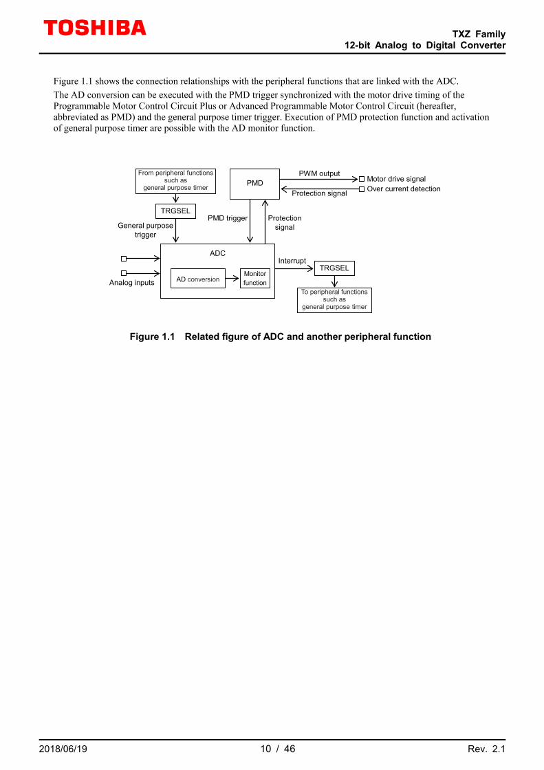
Figure 1.1 shows the connection relationships with the peripheral functions that are linked with the ADC. The AD conversion can be executed with the PMD trigger synchronized with the motor drive timing of the Programmable Motor Control Circuit Plus or Advanced Programmable Motor Control Circuit (hereafter, abbreviated as PMD) and the general purpose timer trigger. Execution of PMD protection function and activation of general purpose timer are possible with the AD monitor function.
Monitor function AD conversion
PMD Motor drive signal
Over current detection
ADC Interrupt
TRGSEL
TRGSEL
From peripheral functions such as
general purpose timer
Analog inputs
PWM output
PMD trigger
Protection signal
General purpose trigger
Protection signal
To peripheral functions such as
general purpose timer
Figure 1.1 Related figure of ADC and another peripheral function
TXZ Family
12-bit Analog to Digital Converter
2018/06/19 11 / 46 Rev. 2.1
2. Configuration
Conversion Result
INTADxPDA/INTADxPDB INTADxSGL/INTADxCNT INTADxTRG
Conversion control
General purpose trigger
conversion control
PMD trigger conversion control
PMD Trigger Control Registers
[ADxPREGS] [ADxPSEL0] to [ADxPSEL11]
[ADxPINTS0] to [ADxPINTS7]
[ADxPSET0] to [ADxPSET7]
AD converter Analog circuit
General Purpose Start-up Factor Program Registers
[ADxTSET0] to [ADxTSET23]
Monitor function registers
AD monitor function control
[ADxCMPCR0] [ADxCMPCR1]
[ADxCMP0] [ADxCMP1]
[ADxREG0] to [ADxREG23]
General purpose Trigger
AINx00
[ADxCLK]
[ADxCMPEN]
[ADxMOD0] [ADxMOD1] [ADxMOD2]
[ADxCR0] [ADxCR1]
VREFHx VREFLx
AINxn
ADCLK SCLK
DMA request
INTADxCP0/INTADxCP1 PMD protect signal
Trigger from peripheral function
via TRGSEL
Prescaler
ADxTRG_DMAREQ ADxSGL_DMAREQ ADxCNT_DMAREQ
ADxCP0L_N/ADxCP1L_N
PMDTRG0 to 5
ADxTRGIN
PMDTRG6 to11
Interrupt request Trigger to peripheral function via TRGSEL
Interrupt request Trigger to peripheral function via TRGSEL
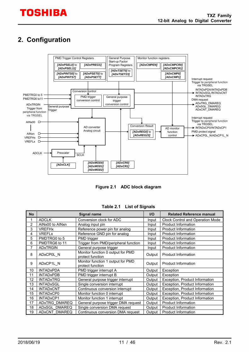
Figure 2.1 ADC block diagram
Table 2.1 List of Signals No Signal name I/O Related Reference manual 1 ADCLK Conversion clock for ADC Input Clock Control and Operation Mode 2 AINx00 to AINxn Analog input pin Input Product Information 3 VREFHx Reference power pin for analog Input Product Information 4 VREFLx Reference GND pin for analog Input Product Information 5 PMDTRG0 to 5 PMD trigger Input Product Information 6 PMDTRG6 to 11 Trigger from PMD/peripheral function Input Product Information 7 ADxTRGIN General purpose trigger Input Product Information
8 ADxCP0L_N Monitor function 0 output for PMD protect function Output Product Information
9 ADxCP1L_N Monitor function 1 output for PMD protect function Output Product Information
10 INTADxPDA PMD trigger interrupt A Output Exception 11 INTADxPDB PMD trigger interrupt B Output Exception 12 INTADxTRG General purpose trigger interrupt Output Exception, Product Information 13 INTADxSGL Single conversion interrupt Output Exception, Product Information 14 INTADxCNT Continuous conversion interrupt Output Exception, Product Information 15 INTADxCP0 Monitor function 0 interrupt Output Exception, Product Information 16 INTADxCP1 Monitor function 1 interrupt Output Exception, Product Information 17 ADxTRG_DMAREQ General purpose trigger DMA request Output Product Information 18 ADxSGL_DMAREQ Single conversion DMA request Output Product Information 19 ADxCNT_DMAREQ Continuous conversion DMA request Output Product Information

TXZ Family
12-bit Analog to Digital Converter
2018/06/19 12 / 46 Rev. 2.1
3. Function and Operation The ADC is triggered to start the conversion by the software start-up (Software trigger) or the trigger signal from PMD, a timer, and others.
3.1. Clock Supply When you use ADC, please set an applicable clock enable bit to "1" (clock supply) in Clock supply and stop register A or B for fsys ([CGFSYSENA], [CGFSYSENB]), Clock supply and stop register for fc ([CGFCEN]), and Clock supply and stop register for ADC and TRACE ([CGSPCLKEN]). Please refer to "Clock Control and Operation Mode" of the reference manual for the clock enable bit. When attempting to stop supplying the clock, make sure to check whether the AD conversion is stopping. Note that when the MCU enters STOP mode, make sure to check whether the AD conversion is stopping as well.
3.2. Conversion Operation by General Purpose Start-up Factor The factor of the general purpose start-up is the general purpose trigger input or the software start-up factor. The software starts up the single conversion or the continuous conversion.

TXZ Family
12-bit Analog to Digital Converter
2018/06/19 13 / 46 Rev. 2.1
3.2.1. Operation When the conversion is triggered by the general purpose start-up factor, the conversion executes according to the setting in the general purpose start-up factor program register which is prepared for each conversion result register.
Conversion Result Storage Register
Interrupt control
General Purpose Start-up Factor Program Register
AIN select
Conversion control
Continuous conversion
Enable
Disable AINx00
Single conversion
General purpose trigger conversion
Conversion inhibit
AINx02
AINx01
AINx03
-
Continuous conversion start-up
Single conversion start-up
General purpose trigger input
INTADxCNT
INTADxCNT
INTADxTRG
INTADxSGL
AINx00
AINx00
AINx00
AINx00 conversion
AINx00 conversion
AINx00 conversion
AINx00 conversion
AINx01 conversion
AINx02 conversion
AINx03 conversion
Single conversion
Continuous conversion
Continuous conversion
Continuous conversion
Disable
Disable
Disable
Enable
Enable
Enable
Conversion inhibit
- Disable
[ADxREG1]
[ADxREG0]
[ADxREG2]
[ADxREG3]
[ADxREG5]
[ADxREG4]
[ADxREG6]
[ADxREG7]
[ADxREG23]
[ADxTSET0]
[ADxTSET23]
[ADxTSET1]
[ADxTSET2]
[ADxTSET3]
[ADxTSET4]
[ADxTSET5]
[ADxTSET6]
[ADxTSET7]
Figure 3.1 General purpose start-up factor and its corresponding operation The general purpose start-up factor select (Conversion control)<TRGSn>, the AIN select<AINSTn>, and the interrupt enable or disable (Interrupt control)<ENINTn> are programmed to the general purpose start-up factor program register([ADxTSETn]). When the start-up factor occurs, the specified conversions are executed from the smallest number of the register. The continuous conversion repeats the specified conversion. The single conversion executes the specified conversion only once. The general purpose trigger conversion executes the specified conversion once when the general purpose trigger is received. When the interrupt is enabled ([ADxTSETn]<ENINTn>=1), the interrupt is generated at the conversion completion for any trigger causes (General purpose trigger, Single conversion, Continuous conversion). The interrupt request of each start-up factor(INTADxTRG, INTADxSGL, INTADxCNT) is different from others. The general purpose start-up factor can generate a DMA request per cause. When a DMA request is enabled ([ADxCR1]<CNTDMEN>,<SGLDMEN>,<TRGDMEN>=1), a DMA request and an interrupt request are generated simultaneously.

TXZ Family
12-bit Analog to Digital Converter
2018/06/19 14 / 46 Rev. 2.1
Table 3.1 Factor and interrupt / DMA request
Factor Interrupt DMA request General purpose trigger conversion
General purpose trigger program completion (INTADxTRG)
General purpose trigger DMA request (ADxTRG_DMAREQ)
Single conversion operation (software)
Software single conversion program completion (INTADxSGL)
Single conversion DMA request (ADxSGL_DMAREQ)
Continuous conversion operation (software)
Software continuous conversion program completion (INTADxCNT)
Continuous conversion DMA request (ADxCNT_DMAREQ)
3.2.2. Control Registers
General purpose start-up factor program register ([ADxTSET0] to [ADxTSET23]) The general purpose start-up factor program register is prepared for each conversion result storage register. The AIN select <AINSTn>, the conversion control <TRGSn>, and the interrupt control <ENINTn> are set to [ADxTSETn].
Mode setting register0 ([ADxMOD0]) When using the ADC, set "1" to [ADxMOD0]<DACON>. And the interval of 3[μs] are necessary for the stabilization.
Control register0 ([ADxCR0]) When the AD conversion can be started, after setting, [ADxCR0]<ADEN> should be set to "1". The software single conversion or the software continuous conversion is enabled by setting [ADxCR0] <SGL> or <CNT> to "1", respectively. When the continuous conversion should be stopped, <CNT> is set to "0".
Control register1 ([ADxCR1]) [ADxCR1]<TRGEN> enables the trigger, and then the program start-up is done by the general purpose trigger. The conversion starts when a trigger is received. [ADxCR1]<SGLDMEN><CNTDMEN><TRGDMEN> are set to "1" to enable the DMA request generation.
Note: [ADxCR1] register must be set while [ADxCR0]<ADEN>=0. For start AD conversion by the general purpose start up factor, please set up as below sequence. ● Single conversion
(1) Set interrupt to use INTADxSGL. (2) Set "1" to [ADxMOD0]<DACON>. (3) Wait at least 3[μs]. (4) Set [ADxTSETn]. AIN selection <AINSTn>= arbitrary, conversion control <TRGSn>=10, interrupt
control <ENINTn>=1. (5) To perform the Single conversion using multiple channels, change the AIN selection and set (4) again. (6) Set "1" to [ADxCR0]<ADEN>. (7) Set "1" to [ADxCR0]<SGL>, starts the conversion. (8) When conversion is complete, INTADxSGL will be generated. Read [ADxREGn] in the interrupt
service routine. (9) Repeat steps (7) to (8).

TXZ Family
12-bit Analog to Digital Converter
2018/06/19 15 / 46 Rev. 2.1
● Continuous conversion
(1) Set interrupt to use INTADxCNT. (2) Set "1" to [ADxMOD0]<DACON>. (3) Wait at least 3[μs]. (4) Set [ADxTSETn]. AIN selection <AINSTn>= arbitrary, conversion control <TRGSn>=01, interrupt
control <ENINTn>=1. (5) To perform the continuous conversion using multiple channels, change the AIN selection and set (4)
again. (6) Set "1" to [ADxCR0]<ADEN>. (7) Set "1" to [ADxCR0]<CNT>, starts the conversion. (8) When conversion is complete, INTADxCNT will be generated. Read [ADxREGn] in the interrupt
service routine. (9) Repeat steps (8).
● General purpose trigger conversion
(1) Set interrupt to use INTADxTRG. (2) Set "1" to [ADxMOD0]<DACON>. (3) Wait at least 3[μs]. (4) Set "1" to [ADxCR1]<TRGEN>. (5) Sets which trigger to use for the general purpose trigger (ADxTRGIN). (Note) (6) Set [ADxTSETn]. AIN selection <AINSTn>= arbitrary, conversion control <TRGSn>=11, interrupt
control <ENINTn>=1. (7) To activate the general purpose trigger using multiple channels, change the AIN selection and set (6)
again. (8) Set "1" to [ADxCR0]<ADEN>. (9) When you input a trigger, conversion starts. (10) When conversion is complete, INTADxTRG will be generated. Read [ADxREGn] in the interrupt
service routine. (11) Repeat steps (9) to (10).
Note: For details of the signal connected to the general purpose trigger (ADxTRGIN), refer to the
reference manual "Product Information".

TXZ Family
12-bit Analog to Digital Converter
2018/06/19 16 / 46 Rev. 2.1
3.3. Conversion Operation by PMD Trigger 3.3.1. Operation
The conversion is started by the PMDTRGn (n=0 to 11). PMDTRGn are triggered from the PMD and the other peripheral function. (Note1)(Note2) The programmed conversion operation is executed by the PMDTRGn. Each PMDTRGn selects one program from among 8 programs available. One program can execute 4-time conversions at maximum. The conversion result is stored to the selected register group in units of 4 registers. Either the INTADxPDA interrupt or the INTADxPDB interrupt can be generated at the program completion. Note1: For details of the PMD, refer to "Advanced Programmable Motor Control Circuit" or "Programmable
Motor Control Circuit Plus" of the reference manual. Note2: For the connections of each product, refer to "Product Information" of the reference manual.
Program 1
Program 0
Program 2
Program 7
[ADxPINTS0]
PMD Trigger Program Number Selection Register [ADxPSEL0] to [ADxPSEL11]
[ADxPINTS1] [ADxPINTS2] [ADxPINTS7]
PMD Trigger Storage Selection Register [ADxPREGS]
PMD Trigger Interrupt Selection Register [ADxPINTS0] to [ADxPINTS7]
PMD Trigger Program Register [ADxPSET0] to [ADxPSET7]
PM
DTR
G0
PM
DTR
G1
PM
DTR
G2
PM
DTR
G3
PM
DTR
G4
PM
DTR
G5
PM
DTR
G6
PM
DTR
G7
PM
DTR
G8
PM
DTR
G9
PM
DTR
G10
PM
DTR
G11
Trigger Signal from the PMD and other peripheral function (ADC Start-up factor signal)
Start-up program
[ADxPSET0] [ADxPSET1] [ADxPSET2] [ADxPSET7] Each program has four conversion settings. Setting includes enable / disable and AINx selection.
Select storage registers by each program < REGSEL7> < REGSEL2> < REGSEL0> < REGSEL1>
Storage conversion result
Conversion0 Conversion1 Conversion2 Conversion3
0 1 2 3 4 5 6 7 Storage register selection
[AD
xPSEL0]
[AD
xPSEL1]
[AD
xPSEL2 ]
[AD
xPSEL3]
[AD
xPSEL4]
[AD
xPSEL5]
[AD
xPSEL6]
[AD
xPSEL7]
[AD
xPSEL8]
[AD
xPSEL9]
[AD
xPSEL10]
[AD
xPSEL11]
- -
- -
- -
- -
21 20
22 23
17 16
18 19
13 12
14 15
9 8
10 11
5 4
6 7
1 0
2 3
Storage location [ADxREGn]
Register number: n
Conversion1 setting
Conversion0 setting
Conversion2 setting Conversion3 setting
Conversion1 setting
Conversion0 setting
Conversion2 setting Conversion3 setting
Conversion1 setting
Conversion0 setting
Conversion2 setting Conversion3 setting
Conversion1 setting
Conversion0 setting
Conversion2 setting Conversion3 setting
Figure 3.2 PMD start-up factor and its operation

TXZ Family
12-bit Analog to Digital Converter
2018/06/19 17 / 46 Rev. 2.1
3.3.2. Control Registers The following registers should be set for the conversion started by the PMD trigger.
Mode setting register0 ([ADxMOD0]) When using the ADC, set "1" to [ADxMOD0]<DACON>. And the interval of 3[μs] are necessary for the stabilization.
PMD trigger program number selection register ([ADxPSEL0] to [ADxPSEL11])
Each register sets the trigger enable/disable and the number of the specified program (0 to 7) for one corresponding trigger out of 12 triggers. 12 registers ([ADxPSEL0] to [ADxPSEL11]) are prepared for the 12 PMD triggers (PMDTRG0 to PMDTRG11), respectively.
PMD trigger interrupt selection register ([ADxPINTS0] to [ADxPINTS7]) An interrupt can be generated at the program completion. The PMD trigger interrupt selection register selects the interrupt enable or disable, and the interrupt INTADxPDA or INTADxPDB. 8 registers ([ADxPINTS0] to [ADxPINTS7]) are prepared for the 8 programs, respectively.
PMD trigger storage selection register ([ADxPREGS]) The storage destination of the conversion result of each program can be selected. The storage destination is selected from among the group of the conversion result storage register 0 to 3, 4 to 7, 8 to 11, 12 to 15, 16 to 19, and 20 to 23.
PMD trigger program register ([ADxPSET0] to [ADxPSET7]) This register sets the corresponding program enable or disable, the converted analog input channel. Each program can be set to 4-time conversions at maximum.
Control register0 ([ADxCR0]) When the AD conversion can be started, after setting, [ADxCR0]<ADEN> should be set to "1".
For Start AD conversion by PMD trigger, please set up as below sequence.
(1) Set interrupt to use INTADxPDA or INTADxPDB (2) Set "1" to [ADxMOD0]<DACON>. (3) Wait at least 3[μs]. (4) Set [ADxPSELn]. Trigger control <PENSn>=1, Program number <PMDSn>= arbitrary. (5) Set [ADxPSETn]. AIN selection <AINSPm>= arbitrary, conversion control <ENSPn>=1. (6) Set [ADxPINTSn]. Interrupt selection <INTSELn>= INTADxPDA or INTADxPDB. (7) Set [ADxPREGS]. Register selection <REGSELn>= arbitrary. (8) Set "1" to [ADxCR0]<ADEN>. (9) Conversion starts by the trigger(PMDTRGn) that is PMD generated. (10) When conversion program is complete, INTADxPDA or INTADxPDB will be generated. Read
[ADxREGn] to [ADxREGn+3]in the interrupt service routine. (11) Repeat steps (9) to (10).

TXZ Family
12-bit Analog to Digital Converter
2018/06/19 18 / 46 Rev. 2.1
3.4. Conversion Stop When [ADxCR0]<ADEN> is set to "0", the conversion stops immediately. If the continuous conversion is enabled, [ADxCR0]<CNT> should be also set to "0". When the conversion stops completely after "0" is set, all bits in [ADxST] become "0". The registers other than [ADxST] keep their data, as well as the conversion result registers. Before the next conversion is enabled, the conversion result registers should be read to clear the corresponding flags. Before ADCLK is stopped, [ADxST]<ADBF>=0 should be confirmed.

TXZ Family
12-bit Analog to Digital Converter
2018/06/19 19 / 46 Rev. 2.1
3.5. Start-up Priority The start-up factors are prioritized as follows:
Priority:High Priority:Low
PMDTRG0 PMDTRG11 > ・・・ > General purpose trigger
Single conversion
Continuous conversion > > >
PMD trigger start-up Software start-up
General purpose start-up If multiple start-up factors occur at the same time, the conversion program with the highest priority start-up factor is executed and other start-up factors are suspended. Once a PMD trigger conversion program starts to execute, it is never suspended. Even though a higher priority PMD trigger is generated, it can execute after the currently executed conversion program completes. The situation is different for the conversion programs of the general purpose trigger, the single conversion, and continuous conversion. When a higher priority start-up factor occurs, the current conversion program execution is suspended and the conversion program of the higher priority start-up factor executes. When a lower priority start-up factor occurs, it waits for execution. The conversion programs of suspended general purpose trigger, single conversion, continuous conversion re-starts from suspended conversion when they become executable. When the start-up factor occurs again during execution of the conversion program of the same start-up factor, the factor is ignored. The status of the conversion program can be checked by [ADxST]<CNTF><SNGF> <TRGF><PMDF>. For the software start-up factors, it should be confirmed whether the corresponding flags are "0". Then, the start-up is certainly executed.
Table 3.2 Operation when the start-up factor occurs during the conversion
Later start-up factor
PMDTRGn (Note1)
General purpose trigger
Software Single
conversion
Software Continuous conversion
Current start-up factor
during conversion
PMDTRGm (Note1)
Continue current factor
(Note2)
Continue current factor
(Note3)
Continue current factor
(Note3)
Continue current factor
(Note3) General purpose trigger
Start later factor
(Note5)
Continue current factor
(Note4)
Continue current factor
(Note3)
Continue current factor
(Note3) Software
Single conversion
Start later factor
(Note5)
Start later factor
(Note5)
Continue current factor
(Note4)
Continue current factor
(Note3) Software
Continuous conversion
Start later factor
(Note5)
Start later factor
(Note5)
Start later factor
(Note5)
Continue current factor
(Note4) Note1: m,n = 0 to 11 Note2: In the case of m = n, the later factor is ignored.
In the case of m<>n, the later factor is performed after the current factor is completed. Note3: The later factor is performed after the current factor is completed. Note4: The later factor is ignored. Note5: The current factor is suspended, and later factor is executed. After the later factor completed, the
current factor is re-started.

TXZ Family
12-bit Analog to Digital Converter
2018/06/19 20 / 46 Rev. 2.1
3.6. AD Monitor Function The AD monitor function generates an interrupt if the AD conversion result is larger than the set value or smaller. It is possible to detect whether the AD conversion result is within the range of two set values or to detect whether the AD conversion result is out of the range by using this function simultaneously in two channels. When [ADxCMPEN]<CMP0EN> or <CMP1EN> is set to "1", the corresponding AD monitor function is enabled. The two monitor functions can be enabled simultaneously. The following description is for [ADxCMPCR0] (The same for [ADxCMPCR1]). [ADxCMPCR0]<REGS0[4:0]> sets the conversion result storage register which value should be compared. <ADBIG0> sets the determination condition (larger or smaller). <CMPCND0> sets the determination count condition. And <CMPCNT0[3:0]> sets the determination count value. Whenever a conversion result is stored to the target conversion result storage register, the result is compared (bigger or smaller). If the comparison result is the same as the <ADBIG0> setting, the determination counter increments. The determination count condition is either the continuous count or the accumulated count. The continuous count condition is as follows: when the status set in <ADBIG0> continues the count times set in <CMPCNT0[3:0]>, the AD monitor function interrupt (INTADxCP0) and the protect signal for the PMD are generated. When it continues exceeding the set-up count number, nothing occurs. If the status is different from the <ADBIG0> status, the counter is cleared. The accumulated count condition is as follows: when the count of the status set in <ADBIG0> is accumulated and the accumulated value reaches the value set in <CMPCNT0[3:0]>, the AD monitor function interrupt (INTADxCP0) and the protect signal for the PMD are generated, and the counter is cleared. Even when the status is different from the status set in <ADBIG0>, the counter value is maintained. When the value in the conversion result storage register specified by the [ADxCMPCR0] register is equal to the value in the conversion result comparison register, the counter does not increment and the AD monitor function interrupt and the trigger are not generated.
Table 3.3 Monitor function and interrupt
Monitor function Interrupt
Monitor function Setting Register0 ([ADxCMPCR0]) Monitor function 0 Interrupt (INTADxCP0)
Monitor function Setting Register1 ([ADxCMPCR1]) Monitor function 1 Interrupt (INTADxCP1)
When the AD monitor function is used, the overrun flag [ADxREGn]<ADOVRFn> and the conversion result storage flag [ADxREGn]<ADRFn> are set because the storage register is not read by the software. So, when the AD monitor function is executing, the flags of the corresponding conversion result storage registers should not be used.
Note: The monitor function registers must be set while [ADxCR0]<ADEN>=0.
TXZ Family
12-bit Analog to Digital Converter
2018/06/19 21 / 46 Rev. 2.1
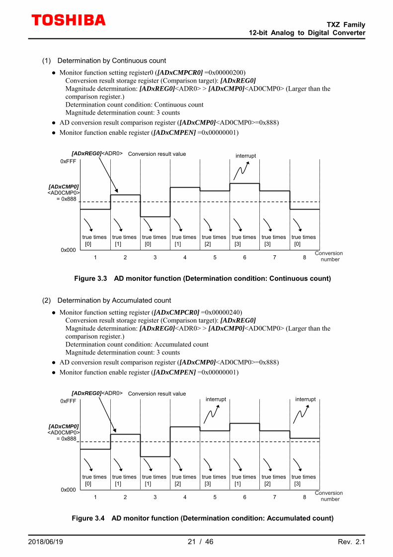
(1) Determination by Continuous count
Monitor function setting register0 ([ADxCMPCR0] =0x00000200) Conversion result storage register (Comparison target): [ADxREG0] Magnitude determination: [ADxREG0]<ADR0> > [ADxCMP0]<AD0CMP0> (Larger than the comparison register.) Determination count condition: Continuous count Magnitude determination count: 3 counts
AD conversion result comparison register ([ADxCMP0]<AD0CMP0>=0x888) Monitor function enable register ([ADxCMPEN] =0x00000001)
[ADxCMP0] <AD0CMP0>
= 0x888
0xFFF
0x000 Conversion number
Conversion result value
1 2 3 4 5 6 7 8
interrupt
true times [0]
true times [1]
true times [0]
true times [1]
true times [2]
true times [3]
true times [3]
true times [0]
[ADxREG0]<ADR0>
Figure 3.3 AD monitor function (Determination condition: Continuous count)
(2) Determination by Accumulated count
Monitor function setting register ([ADxCMPCR0] =0x00000240) Conversion result storage register (Comparison target): [ADxREG0] Magnitude determination: [ADxREG0]<ADR0> > [ADxCMP0]<AD0CMP0> (Larger than the comparison register.) Determination count condition: Accumulated count Magnitude determination count: 3 counts
AD conversion result comparison register ([ADxCMP0]<AD0CMP0>=0x888) Monitor function enable register ([ADxCMPEN] =0x00000001)
0xFFF
0x000 Conversion number 1 2 3 4 5 6 7 8
interrupt
true times [0]
true times [1]
true times [1]
true times [2]
true times [3]
true times [1]
true times [2]
true times [3]
interrupt Conversion result value [ADxREG0]<ADR0>
[ADxCMP0] <AD0CMP0>
= 0x888
Figure 3.4 AD monitor function (Determination condition: Accumulated count)

TXZ Family
12-bit Analog to Digital Converter
2018/06/19 22 / 46 Rev. 2.1
3.7. Analog Reference Voltage Analog reference pins VREFHx and VREFLx in the ADC unit are connected to a High level and a Low level, respectively. When [ADxMOD0]<RCUT> is set to "1", the switch between VREFHx and VREFLx is turned on only during the conversion to reduce the power consumption.
VREFLx
[ADxMOD0]<RCUT> VREFHx
power consumption reduction control
AD conversion reference voltage
Figure 3.5 Configuration of Analog reference voltage

TXZ Family
12-bit Analog to Digital Converter
2018/06/19 23 / 46 Rev. 2.1
3.8. Conversion Time 3.8.1. Conversion timing
Conversion time is shown Figure 3.6.
Figure 3.6 Example of Conversion time
3.8.2. Sampling time The sampling time is set with [ADxCLK]<EXAZ>, <VADCLK>, and [ADxMOD1]<MOD1>.
Sampling time = [ADxMOD1]<MOD1> × n = SCLK period × m × n (n: <EXAZ>, m: <MOD1>)
The sampling time varies depending on the power supply voltage to be used.
4.5[V] ≤ AVDD5 ≤ 5.5[V]: 0.4[μs] to 15.2[μs] (SCLK=40MHz) 2.7[V] ≤ AVDD5 < 4.5[V]: 1.5[μs] to 15.2 [μs] (SCLK=40MHz)
Sampling time Comparison time
Sampling signal
Internal state signal
SCLK
Conversion time

TXZ Family
12-bit Analog to Digital Converter
2018/06/19 24 / 46 Rev. 2.1
Example of setting of sampling time is shown below table.
Table 3.4 Example of setting of sampling time (1) (SCLK=40[MHz], 4.5[V] ≤ AVDD5 ≤ 5.5[V],Unit: μs)
[ADxMOD1] <MOD1[31:0]>
[ADxCLK]<EXAZ[3:0]> 0000 0001 0010 0011 0101
0x00000000 - 0.4 0.6 0.8 3.2 0x00001000 - 0.5 0.75 1.0 4.0 0x00002000 - 0.6 0.9 1.2 4.8 0x00003000 - 0.7 1.05 1.4 5.6
0x00004000 0.4 0.8 1.2 1.6 6.4 0x00005000 0.45 0.9 1.35 1.8 7.2 0x00006000 0.5 1.0 1.5 2.0 8.0 0x00007000 0.55 1.1 1.65 2.2 8.8 0x00008000 0.6 1.2 1.8 2.4 9.6 0x00009000 0.65 1.3 1.95 2.6 10.4 0x0000A000 0.7 1.4 2.1 2.8 11.2 0x0000B000 0.75 1.5 2.25 3.0 12.0 0x0000C000 0.8 1.6 2.4 3.2 12.8 0x0000D000 0.85 1.7 2.55 3.4 13.6 0x0000E000 0.9 1.8 2.7 3.6 14.4 0x0000F000 0.95 1.9 2.85 3.8 15.2
Note: "-" setting can not be used.
Table 3.5 Example of setting of sampling time (2) (SCLK=40[MHz],2.7[V] ≤ AVDD5 < 4.5[V],Unit: μs)
[ADxMOD1] <MOD1[31:0]>
[ADxCLK]<EXAZ[3:0]> 0000 0001 0010 0011 0101
0x00000001 - - - - 3.2 0x00001001 - - - - 4.0 0x00002001 - - - - 4.8 0x00003001 - - - - 5.6
0x00004001 - - - 1.6 6.4 0x00005001 - - - 1.8 7.2 0x00006001 - - 1.5 2.0 8.0 0x00007001 - - 1.65 2.2 8.8 0x00008001 - - 1.8 2.4 9.6 0x00009001 - - 1.95 2.6 10.4 0x0000A001 - - 2.1 2.8 11.2 0x0000B001 - 1.5 2.25 3.0 12.0 0x0000C001 - 1.6 2.4 3.2 12.8 0x0000D001 - 1.7 2.55 3.4 13.6 0x0000E001 - 1.8 2.7 3.6 14.4 0x0000F001 - 1.9 2.85 3.8 15.2
Note: "-" setting can not be used.
TXZ Family
12-bit Analog to Digital Converter
2018/06/19 25 / 46 Rev. 2.1
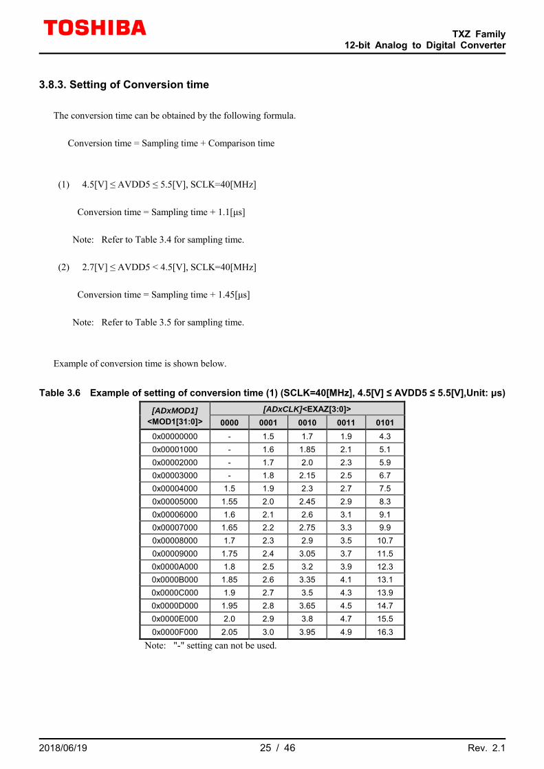
3.8.3. Setting of Conversion time The conversion time can be obtained by the following formula.
Conversion time = Sampling time + Comparison time (1) 4.5[V] ≤ AVDD5 ≤ 5.5[V], SCLK=40[MHz]
Conversion time = Sampling time + 1.1[μs]
Note: Refer to Table 3.4 for sampling time.
(2) 2.7[V] ≤ AVDD5 < 4.5[V], SCLK=40[MHz]
Conversion time = Sampling time + 1.45[μs]
Note: Refer to Table 3.5 for sampling time.
Example of conversion time is shown below.
Table 3.6 Example of setting of conversion time (1) (SCLK=40[MHz], 4.5[V] ≤ AVDD5 ≤ 5.5[V],Unit: μs)
[ADxMOD1] <MOD1[31:0]>
[ADxCLK]<EXAZ[3:0]> 0000 0001 0010 0011 0101
0x00000000 - 1.5 1.7 1.9 4.3 0x00001000 - 1.6 1.85 2.1 5.1 0x00002000 - 1.7 2.0 2.3 5.9 0x00003000 - 1.8 2.15 2.5 6.7 0x00004000 1.5 1.9 2.3 2.7 7.5 0x00005000 1.55 2.0 2.45 2.9 8.3 0x00006000 1.6 2.1 2.6 3.1 9.1 0x00007000 1.65 2.2 2.75 3.3 9.9 0x00008000 1.7 2.3 2.9 3.5 10.7 0x00009000 1.75 2.4 3.05 3.7 11.5 0x0000A000 1.8 2.5 3.2 3.9 12.3 0x0000B000 1.85 2.6 3.35 4.1 13.1 0x0000C000 1.9 2.7 3.5 4.3 13.9 0x0000D000 1.95 2.8 3.65 4.5 14.7 0x0000E000 2.0 2.9 3.8 4.7 15.5 0x0000F000 2.05 3.0 3.95 4.9 16.3
Note: "-" setting can not be used.

TXZ Family
12-bit Analog to Digital Converter
2018/06/19 26 / 46 Rev. 2.1
Table 3.7 Example of setting of conversion time (2) (SCLK=40[MHz],2.7[V] ≤ AVDD5 < 4.5[V],Unit: μs)
[ADxMOD1] <MOD1[31:0]>
[ADxCLK]<EXAZ[3:0]> 0000 0001 0010 0011 0101
0x00000001 - - - - 4.65 0x00001001 - - - - 5.45 0x00002001 - - - - 6.25 0x00003001 - - - - 7.05 0x00004001 - - - 3.05 7.85 0x00005001 - - - 3.25 8.65 0x00006001 - - 2.95 3.45 9.45 0x00007001 - - 3.1 3.65 10.25 0x00008001 - - 3.25 3.85 11.05 0x00009001 - - 3.4 4.05 11.85 0x0000A001 - - 3.55 4.25 12.65 0x0000B001 - 2.95 3.7 4.45 13.45 0x0000C001 - 3.05 3.85 4.65 14.25 0x0000D001 - 3.15 4.0 4.85 15.05 0x0000E001 - 3.25 4.15 5.05 15.85 0x0000F001 - 3.35 4.3 5.25 16.65
Note: "-" setting can not be used.

TXZ Family
12-bit Analog to Digital Converter
2018/06/19 27 / 46 Rev. 2.1
4. Registers 4.1. List of Registers
The control registers and their addresses are shown as follows.
Function name Channel/Unit Base address
12-bit Analog to Digital Converter ADC Unit A 0x400B8800 Unit B 0x400B8C00
Register Name Address (Base+) Control Register0 [ADxCR0] 0x0000 Control Register1 [ADxCR1] 0x0004 Status Register [ADxST] 0x0008 Conversion Clock Setting Register [ADxCLK] 0x000C Mode Setting Register0 [ADxMOD0] 0x0010 Mode Setting Register1 [ADxMOD1] 0x0014 Mode Setting Register2 [ADxMOD2] 0x0018 Monitor function Enable Register [ADxCMPEN] 0x0020 Monitor function Setting Register0 [ADxCMPCR0] 0x0024 Monitor function Setting Register1 [ADxCMPCR1] 0x0028 Conversion Result Comparison Register0 [ADxCMP0] 0x002C Conversion Result Comparison Register1 [ADxCMP1] 0x0030 PMD Trigger Program Number Selection Register0 [ADxPSEL0] 0x0040 PMD Trigger Program Number Selection Register1 [ADxPSEL1] 0x0044 PMD Trigger Program Number Selection Register2 [ADxPSEL2] 0x0048 PMD Trigger Program Number Selection Register3 [ADxPSEL3] 0x004C PMD Trigger Program Number Selection Register4 [ADxPSEL4] 0x0050 PMD Trigger Program Number Selection Register5 [ADxPSEL5] 0x0054 PMD Trigger Program Number Selection Register6 [ADxPSEL6] 0x0058 PMD Trigger Program Number Selection Register7 [ADxPSEL7] 0x005C PMD Trigger Program Number Selection Register8 [ADxPSEL8] 0x0060 PMD Trigger Program Number Selection Register9 [ADxPSEL9] 0x0064 PMD Trigger Program Number Selection Register10 [ADxPSEL10] 0x0068 PMD Trigger Program Number Selection Register11 [ADxPSEL11] 0x006C PMD Trigger Interrupt Selection Register0 [ADxPINTS0] 0x0070 PMD Trigger Interrupt Selection Register1 [ADxPINTS1] 0x0074 PMD Trigger Interrupt Selection Register2 [ADxPINTS2] 0x0078 PMD Trigger Interrupt Selection Register3 [ADxPINTS3] 0x007C PMD Trigger Interrupt Selection Register4 [ADxPINTS4] 0x0080 PMD Trigger Interrupt Selection Register5 [ADxPINTS5] 0x0084 PMD Trigger Interrupt Selection Register6 [ADxPINTS6] 0x0088 PMD Trigger Interrupt Selection Register7 [ADxPINTS7] 0x008C PMD Trigger Storage Selection Register [ADxPREGS] 0x0090 PMD Trigger Program Register0 [ADxPSET0] 0x00A0 PMD Trigger Program Register1 [ADxPSET1] 0x00A4 PMD Trigger Program Register2 [ADxPSET2] 0x00A8 PMD Trigger Program Register3 [ADxPSET3] 0x00AC PMD Trigger Program Register4 [ADxPSET4] 0x00B0 PMD Trigger Program Register5 [ADxPSET5] 0x00B4 PMD Trigger Program Register6 [ADxPSET6] 0x00B8 PMD Trigger Program Register7 [ADxPSET7] 0x00BC General Purpose Start-up Factor Program Register0 [ADxTSET0] 0x00C0 General Purpose Start-up Factor Program Register1 [ADxTSET1] 0x00C4 General Purpose Start-up Factor Program Register2 [ADxTSET2] 0x00C8 General Purpose Start-up Factor Program Register3 [ADxTSET3] 0x00CC General Purpose Start-up Factor Program Register4 [ADxTSET4] 0x00D0

TXZ Family
12-bit Analog to Digital Converter
2018/06/19 28 / 46 Rev. 2.1
Register Name Address (Base+) General Purpose Start-up Factor Program Register5 [ADxTSET5] 0x00D4 General Purpose Start-up Factor Program Register6 [ADxTSET6] 0x00D8 General Purpose Start-up Factor Program Register7 [ADxTSET7] 0x00DC General Purpose Start-up Factor Program Register8 [ADxTSET8] 0x00E0 General Purpose Start-up Factor Program Register9 [ADxTSET9] 0x00E4 General Purpose Start-up Factor Program Register10 [ADxTSET10] 0x00E8 General Purpose Start-up Factor Program Register11 [ADxTSET11] 0x00EC General Purpose Start-up Factor Program Register12 [ADxTSET12] 0x00F0 General Purpose Start-up Factor Program Register13 [ADxTSET13] 0x00F4 General Purpose Start-up Factor Program Register14 [ADxTSET14] 0x00F8 General Purpose Start-up Factor Program Register15 [ADxTSET15] 0x00FC General Purpose Start-up Factor Program Register16 [ADxTSET16] 0x0100 General Purpose Start-up Factor Program Register17 [ADxTSET17] 0x0104 General Purpose Start-up Factor Program Register18 [ADxTSET18] 0x0108 General Purpose Start-up Factor Program Register19 [ADxTSET19] 0x010C General Purpose Start-up Factor Program Register20 [ADxTSET20] 0x0110 General Purpose Start-up Factor Program Register21 [ADxTSET21] 0x0114 General Purpose Start-up Factor Program Register22 [ADxTSET22] 0x0118 General Purpose Start-up Factor Program Register23 [ADxTSET23] 0x011C Conversion Result Storage Register0 [ADxREG0] 0x0140 Conversion Result Storage Register1 [ADxREG1] 0x0144 Conversion Result Storage Register2 [ADxREG2] 0x0148 Conversion Result Storage Register3 [ADxREG3] 0x014C Conversion Result Storage Register4 [ADxREG4] 0x0150 Conversion Result Storage Register5 [ADxREG5] 0x0154 Conversion Result Storage Register6 [ADxREG6] 0x0158 Conversion Result Storage Register7 [ADxREG7] 0x015C Conversion Result Storage Register8 [ADxREG8] 0x0160 Conversion Result Storage Register9 [ADxREG9] 0x0164 Conversion Result Storage Register10 [ADxREG10] 0x0168 Conversion Result Storage Register11 [ADxREG11] 0x016C Conversion Result Storage Register12 [ADxREG12] 0x0170 Conversion Result Storage Register13 [ADxREG13] 0x0174 Conversion Result Storage Register14 [ADxREG14] 0x0178 Conversion Result Storage Register15 [ADxREG15] 0x017C Conversion Result Storage Register16 [ADxREG16] 0x0180 Conversion Result Storage Register17 [ADxREG17] 0x0184 Conversion Result Storage Register18 [ADxREG18] 0x0188 Conversion Result Storage Register19 [ADxREG19] 0x018C Conversion Result Storage Register20 [ADxREG20] 0x0190 Conversion Result Storage Register21 [ADxREG21] 0x0194 Conversion Result Storage Register22 [ADxREG22] 0x0198 Conversion Result Storage Register23 [ADxREG23] 0x019C

TXZ Family
12-bit Analog to Digital Converter
2018/06/19 29 / 46 Rev. 2.1
4.2. Details of Registers 4.2.1. [ADxCR0] (Control Register0)
Bit Bit Symbol After Reset Type Function
31:8 - 0 R Reads as "0".
7 ADEN 0 R/W
ADC control. 0: Disabled. 1: Enabled. When "1" is set, the conversion is enabled. When "0" is set, the conversion stops.
6:2 - 0 R Reads as "0".
1 SGL 0 W
Single conversion control 0: Don’t care 1: Conversion start. When "1" is set, the single conversion program starts to execute. If this bit is read, "0" is returned.
0 CNT 0 R/W
Continuous conversion control 0: Disabled. 1: Enabled. When "1" is set, the continuous conversion starts to execute. This bit should be set to "1" when [ADxST]<CNTF> is "0" (a continuous conversion program does not execute).
4.2.2. [ADxCR1] (Control Register1)
Bit Bit Symbol After Reset Type Function
31:7 - 0 R Reads as "0".
6 CNTDMEN 0 R/W Continuous conversion DMA request control 0: Disabled. 1: Enabled.
5 SGLDMEN 0 R/W Single conversion DMA request control 0: Disabled. 1: Enabled.
4 TRGDMEN 0 R/W General purpose trigger DMA request control 0: Disabled. 1: Enabled.
3:1 - 0 R Reads as "0".
0 TRGEN 0 R/W General purpose trigger start-up control 0: Disabled. 1: Enabled.
Note: This register must be set while [ADxCR0]<ADEN>=0.

TXZ Family
12-bit Analog to Digital Converter
2018/06/19 30 / 46 Rev. 2.1
4.2.3. [ADxST] (Status Register)
Bit Bit Symbol After Reset Type Function
31:8 - 0 R Reads as "0".
7 ADBF 0 R
AD operation flag 0: Stop (ADCLK can be stopped.) 1: Executing (ADCLK cannot be stopped.) Before ADCLK is stopped, this bit should be confirmed to be "0".
6:4 - 0 R Reads as "0".
3 CNTF 0 R
Continuous conversion program flag 0: Stop 1: Executing When the request is received, this bit becomes "1". When the last conversion result is stored, this bit becomes "0".
2 SNGF 0 R
Single conversion program flag 0: Stop 1: Executing When the request is received, this bit becomes "1". When the last conversion result is stored, this bit becomes "0".
1 TRGF 0 R
General purpose trigger program flag 0: Stop 1: Executing When the request is received, this bit becomes "1". When the last conversion result is stored, this bit becomes "0".
0 PMDF 0 R
PMD trigger program flag 0: Stop 1: Executing When the request is received, this bit becomes "1". When the last conversion result is stored, this bit becomes "0".

TXZ Family
12-bit Analog to Digital Converter
2018/06/19 31 / 46 Rev. 2.1
4.2.4. [ADxCLK] (Conversion Clock Setting Register)
Bit Bit Symbol After Reset Type Function
31:7 - 0 R Reads as "0".
6:3 EXAZ[3:0] 0000 R/W
AIN sampling period selection (Note2) 0000: [ADxMOD1]<MOD1> × 1 0001: [ADxMOD1]<MOD1> × 2 0010: [ADxMOD1]<MOD1> × 3 0011: [ADxMOD1]<MOD1> × 4 0101: [ADxMOD1]<MOD1> × 16 Others: Reserved. Please refer to ”3.7.2. Sampling time” for setting range of sampling time.
2:0 VADCLK[2:0] 000 R/W
AD prescaler output (SCLK) selection 000: ADCLK/1 001: ADCLK/2 010 to 111:Reserved This bit should be set so that SCLK is 40[MHz].
Note1: This register must be set while [ADxCR0]<ADEN>=0. Note2: In the case of SCLK=40[MHz]
4.2.5. [ADxMOD0] (Mode Setting Register0)
Bit Bit Symbol After Reset Type Function
31:2 - 0 R Reads as "0".
1 RCUT 1 R/W
Low power mode selection 0: Normal operation 1: Low power operation (Energized between VREFHx and VREFLx only during the conversion)
0 DACON 0 R/W
DAC control (Note2) 0: OFF 1: ON When the ADC is used, <DACON> should be set to "1".
Note1: This register must be set while [ADxCR0]<ADEN>=0. Note2: After [ADxMOD0]<DACON> is set to "1", the interval of 3[μs] are necessary for the stabilization.

TXZ Family
12-bit Analog to Digital Converter
2018/06/19 32 / 46 Rev. 2.1
4.2.6. [ADxMOD1] (Mode Setting Register1)
Bit Bit Symbol After Reset Type Function
31:0 MOD1[31:0] 0x00004000 R/W
4.5[V] ≤ AVDD5 ≤5.5[V] 0x00000000: SCLK period × 8 0x00001000: SCLK period × 10 0x00002000: SCLK period × 12 0x00003000: SCLK period × 14 0x00004000: SCLK period × 16 0x00005000: SCLK period × 18 0x00006000: SCLK period × 20 0x00007000: SCLK period × 22 0x00008000: SCLK period × 24 0x00009000: SCLK period × 26 0x0000A000: SCLK period × 28 0x0000B000: SCLK period × 30 0x0000C000: SCLK period × 32 0x0000D000: SCLK period × 34 0x0000E000: SCLK period × 36 0x0000F000: SCLK period × 38 2.7[V] ≤ AVDD5 < 4.5[V] 0x00000001: SCLK period × 8 0x00001001: SCLK period × 10 0x00002001: SCLK period × 12 0x00003001: SCLK period × 14 0x00004001: SCLK period × 16 0x00005001: SCLK period × 18 0x00006001: SCLK period × 20 0x00007001: SCLK period × 22 0x00008001: SCLK period × 24 0x00009001: SCLK period × 26 0x0000A001: SCLK period × 28 0x0000B001: SCLK period × 30 0x0000C001: SCLK period × 32 0x0000D001: SCLK period × 34 0x0000E001: SCLK period × 36 0x0000F001: SCLK period × 38 Please refer to “3.7.2. Sampling time” for setting range of sampling time.
Note: This register must be set while [ADxCR0]<ADEN>=0.
4.2.7. [ADxMOD2] (Mode Setting Register2)
Bit Bit Symbol After Reset Type Function
31:0 MOD2[31:0] 0x00000000 R/W The setting value of this register varies depending on the product. For the setting value, refer to "Product Information" of the reference manual.
Note: This register must be set while [ADxCR0]<ADEN>=0.

TXZ Family
12-bit Analog to Digital Converter
2018/06/19 33 / 46 Rev. 2.1
4.2.8. [ADxCMPEN] (Monitor function Enable Register)
Bit Bit Symbol After Reset Type Function
31:2 - 0 R Reads as "0".
1 CMP1EN 0 R/W AD monitor function1 0: Disabled. 1: Enabled.
0 CMP0EN 0 R/W AD monitor function0 0: Disabled. 1: Enabled.
4.2.9. [ADxCMPCR0] (Monitor function Setting Register0)
Bit Bit Symbol After Reset Type Function
31:12 - 0 R Reads as "0".
11:8 CMPCNT0[3:0] 0000 R/W
Comparison count 0000: 1 1000: 9 0001: 2 1001: 10 0010: 3 1010: 11 0011: 4 1011: 12 0100: 5 1100: 13 0101: 6 1101: 14 0110: 7 1110: 15 0111: 8 1111: 16
7 - 0 R Reads as "0".
6 CMPCND0 0 R/W Determination condition 0: Continuous count 1: Accumulated count
5 ADBIG0 0 R/W
Magnitude determination setting 0: Conversion result specified by <REGS0> > [ADxCMP0] (Larger than the comparison register) 1: Conversion result specified by <REGS0> < [ADxCMP0] (Smaller than the comparison register)
4:0 REGS0[4:0] 00000 R/W
Compared conversion result storage register 00000: ADxREG0 01000: ADxREG8 10000: ADxREG16 00001: ADxREG1 01001: ADxREG9 10001: ADxREG17 00010: ADxREG2 01010: ADxREG10 10010: ADxREG18 00011: ADxREG3 01011: ADxREG11 10011: ADxREG19 00100: ADxREG4 01100: ADxREG12 10100: ADxREG20 00101: ADxREG5 01101: ADxREG13 10101: ADxREG21 00110: ADxREG6 01110: ADxREG14 10110: ADxREG22 00111: ADxREG7 01111: ADxREG15 10111: ADxREG23 11000 to 11111: Inhibited setting
Note: This register must be set while [ADxCMPEN]<CMP0EN>=0.
TXZ Family
12-bit Analog to Digital Converter
2018/06/19 34 / 46 Rev. 2.1
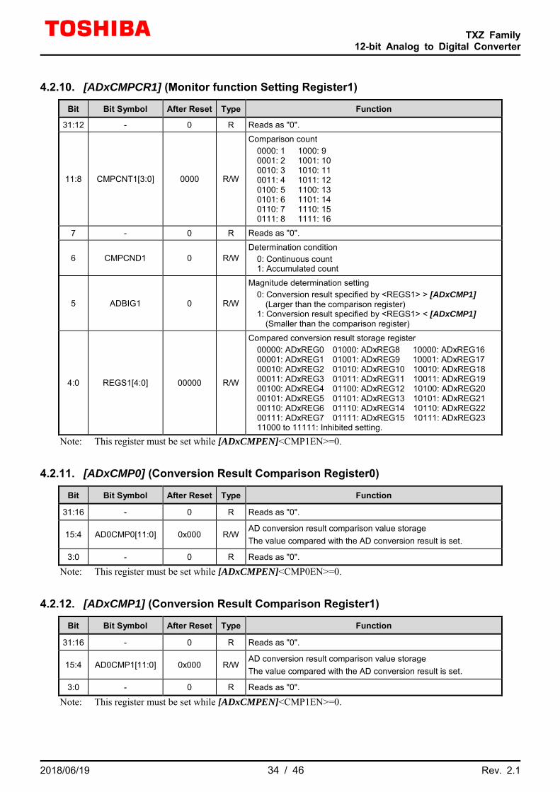
4.2.10. [ADxCMPCR1] (Monitor function Setting Register1)
Bit Bit Symbol After Reset Type Function
31:12 - 0 R Reads as "0".
11:8 CMPCNT1[3:0] 0000 R/W
Comparison count 0000: 1 1000: 9 0001: 2 1001: 10 0010: 3 1010: 11 0011: 4 1011: 12 0100: 5 1100: 13 0101: 6 1101: 14 0110: 7 1110: 15 0111: 8 1111: 16
7 - 0 R Reads as "0".
6 CMPCND1 0 R/W Determination condition 0: Continuous count 1: Accumulated count
5 ADBIG1 0 R/W
Magnitude determination setting 0: Conversion result specified by <REGS1> > [ADxCMP1] (Larger than the comparison register) 1: Conversion result specified by <REGS1> < [ADxCMP1] (Smaller than the comparison register)
4:0 REGS1[4:0] 00000 R/W
Compared conversion result storage register 00000: ADxREG0 01000: ADxREG8 10000: ADxREG16 00001: ADxREG1 01001: ADxREG9 10001: ADxREG17 00010: ADxREG2 01010: ADxREG10 10010: ADxREG18 00011: ADxREG3 01011: ADxREG11 10011: ADxREG19 00100: ADxREG4 01100: ADxREG12 10100: ADxREG20 00101: ADxREG5 01101: ADxREG13 10101: ADxREG21 00110: ADxREG6 01110: ADxREG14 10110: ADxREG22 00111: ADxREG7 01111: ADxREG15 10111: ADxREG23 11000 to 11111: Inhibited setting.
Note: This register must be set while [ADxCMPEN]<CMP1EN>=0.
4.2.11. [ADxCMP0] (Conversion Result Comparison Register0)
Bit Bit Symbol After Reset Type Function
31:16 - 0 R Reads as "0".
15:4 AD0CMP0[11:0] 0x000 R/W AD conversion result comparison value storage The value compared with the AD conversion result is set.
3:0 - 0 R Reads as "0".
Note: This register must be set while [ADxCMPEN]<CMP0EN>=0.
4.2.12. [ADxCMP1] (Conversion Result Comparison Register1)
Bit Bit Symbol After Reset Type Function
31:16 - 0 R Reads as "0".
15:4 AD0CMP1[11:0] 0x000 R/W AD conversion result comparison value storage The value compared with the AD conversion result is set.
3:0 - 0 R Reads as "0".
Note: This register must be set while [ADxCMPEN]<CMP1EN>=0.

TXZ Family
12-bit Analog to Digital Converter
2018/06/19 35 / 46 Rev. 2.1
4.2.13. PMD Trigger Control Registers 4.2.13.1. [ADxPSEL0] (PMD Trigger Program Number Selection Register0)
The following is an example of [ADxPSEL0]. [ADxPSEL1] to [ADxPSEL11] have the same configuration.
Bit Bit Symbol After Reset Type Function
31:8 - 0 R Reads as "0".
7 PENS0 0 R/W PMDTRG0 trigger control (Note2) 0: Disabled. 1: Enabled.
6:3 - 0 R Reads as "0".
2:0 PMDS0[2:0] 000 R/W
Program number selection 000: Program 0 001: Program 1 010: Program 2 011: Program 3 100: Program 4 101: Program 5 110: Program 6 111: Program 7
Note1: This register must be set while [ADxCR0]<ADEN>=0. Note2: For details of the PMD, refer to "Advanced Programmable Motor Control Circuit" or "Programmable
Motor Control Circuit Plus" of the reference manual.
4.2.13.2. [ADxPINTS0] (PMD Trigger Interrupt Selection Register0) The following is an example of [ADxPINTS0]. [ADxPINTS1] to [ADxPINTS7] have the same configuration.
Bit Bit Symbol After Reset Type Function
31:2 - 0 R Reads as "0".
1:0 INTSEL0[1:0] 00 R/W
Interrupt selection 00: No interrupts. 01: INTADxPDA 10: INTADxPDB 11: Reserved. This field selects an interrupt for the program 0.
Note: This register must be set while [ADxCR0]<ADEN>=0.

TXZ Family
12-bit Analog to Digital Converter
2018/06/19 36 / 46 Rev. 2.1
4.2.13.3. [ADxPREGS] (PMD Trigger Storage Selection Register)
Bit Bit Symbol After Reset Type Function
31 - 0 R Reads as "0".
30:28 REGSEL7[2:0] 000 R/W
Program 7 conversion result storage register selection 000: ADxREG0 to 3 100: ADxREG16 to 19 001: ADxREG4 to 7 101: ADxREG20 to 23 010: ADxREG8 to 11 110: Inhibited setting. 011: ADxREG12 to 15 111: Inhibited setting.
27 - 0 R Reads as "0".
26:24 REGSEL6[2:0] 000 R/W
Program 6 conversion result storage register selection 000: ADxREG0 to 3 100: ADxREG16 to 19 001: ADxREG4 to 7 101: ADxREG20 to 23 010: ADxREG8 to 11 110: Inhibited setting. 011: ADxREG12 to 15 111: Inhibited setting.
23 - 0 R Reads as "0".
22:20 REGSEL5[2:0] 000 R/W
Program 5 conversion result storage register selection 000: ADxREG0 to 3 100: ADxREG16 to 19 001: ADxREG4 to 7 101: ADxREG20 to 23 010: ADxREG8 to 11 110: Inhibited setting. 011: ADxREG12 to 15 111: Inhibited setting.
19 - 0 R Reads as "0".
18:16 REGSEL4[2:0] 000 R/W
Program 4 conversion result storage register selection 000: ADxREG0 to 3 100: ADxREG16 to 19 001: ADxREG4 to 7 101: ADxREG20 to 23 010: ADxREG8 to 11 110: Inhibited setting. 011: ADxREG12 to 15 111: Inhibited setting.
15 - 0 R Reads as "0".
14:12 REGSEL3[2:0] 000 R/W
Program 3 conversion result storage register selection 000: ADxREG0 to 3 100: ADxREG16 to 19 001: ADxREG4 to 7 101: ADxREG20 to 23 010: ADxREG8 to 11 110: Inhibited setting. 011: ADxREG12 to 15 111: Inhibited setting.
11 - 0 R Reads as "0".
10:8 REGSEL2[2:0] 000 R/W
Program 2 conversion result storage register selection 000: ADxREG0 to 3 100: ADxREG16 to 19 001: ADxREG4 to 7 101: ADxREG20 to 23 010: ADxREG8 to 11 110: Inhibited setting. 011: ADxREG12 to 15 111: Inhibited setting.
7 - 0 R Reads as "0".
6:4 REGSEL1[2:0] 000 R/W
Program 1 conversion result storage register selection 000: ADxREG0 to 3 100: ADxREG16 to 19 001: ADxREG4 to 7 101: ADxREG20 to 23 010: ADxREG8 to 11 110: Inhibited setting. 011: ADxREG12 to 15 111: Inhibited setting.
3 - 0 R Reads as "0".
2:0 REGSEL0[2:0] 000 R/W
Program 0 conversion result storage register selection 000: ADxREG0 to 3 100: ADxREG16 to 19 001: ADxREG4 to 7 101: ADxREG20 to 23 010: ADxREG8 to 11 110: Inhibited setting. 011: ADxREG12 to 15 111: Inhibited setting.
Note: This register must be set while [ADxCR0]<ADEN>=0.

TXZ Family
12-bit Analog to Digital Converter
2018/06/19 37 / 46 Rev. 2.1
4.2.13.4. [ADxPSET0] (PMD Trigger Program Register0) The following is an example of [ADxPSET0]. [ADxPSET1] to [ADxPSET7] have the same configuration.
Bit Bit Symbol After Reset Type Function
31 ENSP03 0 R/W Conversion 3 setting: Conversion control 0: Disabled. 1: Enabled.
30:29 - 00 R/W Write as "00".
28:24 AINSP03[4:0] 00000 R/W
Conversion 3 setting: AIN selection (Note2) 00000: AINx00 01000: AINx08 10000: AINx16 00001: AINx01 01001: AINx09 10001: AINx17 00010: AINx02 01010: AINx10 10010: AINx18 00011: AINx03 01011: AINx11 10011: AINx19 00100: AINx04 01100: AINx12 10100: AINx20 00101: AINx05 01101: AINx13 10101: AINx21 00110: AINx06 01110: AINx14 10110: AINx22 00111: AINx07 01111: AINx15 10111: AINx23 11000 to 11111: Inhibited setting
23 ENSP02 0 R/W Conversion 2 setting: Conversion control 0: Disabled. 1: Enabled.
22:21 - 00 R/W Write as "00".
20:16 AINSP02[4:0] 00000 R/W
Conversion 2 setting: AIN selection (Note2) 00000: AINx00 01000: AINx08 10000: AINx16 00001: AINx01 01001: AINx09 10001: AINx17 00010: AINx02 01010: AINx10 10010: AINx18 00011: AINx03 01011: AINx11 10011: AINx19 00100: AINx04 01100: AINx12 10100: AINx20 00101: AINx05 01101: AINx13 10101: AINx21 00110: AINx06 01110: AINx14 10110: AINx22 00111: AINx07 01111: AINx15 10111: AINx23 11000 to 11111: Inhibited setting
15 ENSP01 0 R/W Conversion 1 setting: Conversion control 0: Disabled. 1: Enabled.
14:13 - 00 R/W Write as "00".
12:8 AINSP01[4:0] 00000 R/W
Conversion 1 setting: AIN selection (Note2) 00000: AINx00 01000: AINx08 10000: AINx16 00001: AINx01 01001: AINx09 10001: AINx17 00010: AINx02 01010: AINx10 10010: AINx18 00011: AINx03 01011: AINx11 10011: AINx19 00100: AINx04 01100: AINx12 10100: AINx20 00101: AINx05 01101: AINx13 10101: AINx21 00110: AINx06 01110: AINx14 10110: AINx22 00111: AINx07 01111: AINx15 10111: AINx23 11000 to 11111: Inhibited setting
7 ENSP00 0 R/W Conversion 0 setting: Conversion control 0: Disabled. 1: Enabled.
6:5 - 00 R/W Write as "00".

TXZ Family
12-bit Analog to Digital Converter
2018/06/19 38 / 46 Rev. 2.1
Bit Bit Symbol After Reset Type Function
4:0 AINSP00[4:0] 00000 R/W
Conversion 0 setting: AIN selection (Note2) 00000: AINx00 01000: AINx08 10000: AINx16 00001: AINx01 01001: AINx09 10001: AINx17 00010: AINx02 01010: AINx10 10010: AINx18 00011: AINx03 01011: AINx11 10011: AINx19 00100: AINx04 01100: AINx12 10100: AINx20 00101: AINx05 01101: AINx13 10101: AINx21 00110: AINx06 01110: AINx14 10110: AINx22 00111: AINx07 01111: AINx15 10111: AINx23 11000 to 11111: Inhibited setting
Note1: This register must be set while [ADxCR0]<ADEN>=0. Note2: The AIN which the product does not have is inhibited to be set (Refer to "Product Information" of the
reference manual).
4.2.14. [ADxTSET0] (General Purpose Start-up Factor Program Register0) The following is an example of [ADxTSET0]. [ADxTSET1] to [ADxTSET23] have the same configuration.
Bit Bit Symbol After Reset Type Function
31:8 - 0 R Reads as "0".
7 ENINT0 0 R/W Conversion Result Storage Register0 setting: Interrupt control 0: Disabled. 1: Enabled.
6:5 TRGS0[1:0] 00 R/W
Conversion Result Storage Register0 setting: Conversion control 00: Conversion is inhibited. 01: Continuous conversion. 10: Single conversion. 11: General purpose trigger conversion.
4:0 AINST0[4:0] 00000 R/W
Conversion Result Storage Register0 setting: AIN selection (Note2) 00000: AINx00 01000: AINx08 10000: AINx16 00001: AINx01 01001: AINx09 10001: AINx17 00010: AINx02 01010: AINx10 10010: AINx18 00011: AINx03 01011: AINx11 10011: AINx19 00100: AINx04 01100: AINx12 10100: AINx20 00101: AINx05 01101: AINx13 10101: AINx21 00110: AINx06 01110: AINx14 10110: AINx22 00111: AINx07 01111: AINx15 10111: AINx23 11000 to 11111: Inhibited setting
Note1: This register must be set while [ADxCR0]<ADEN>=0. Note2: The AIN which the product does not have is inhibited to be set (Refer to "Product Information" of the
reference manual).
TXZ Family
12-bit Analog to Digital Converter
2018/06/19 39 / 46 Rev. 2.1
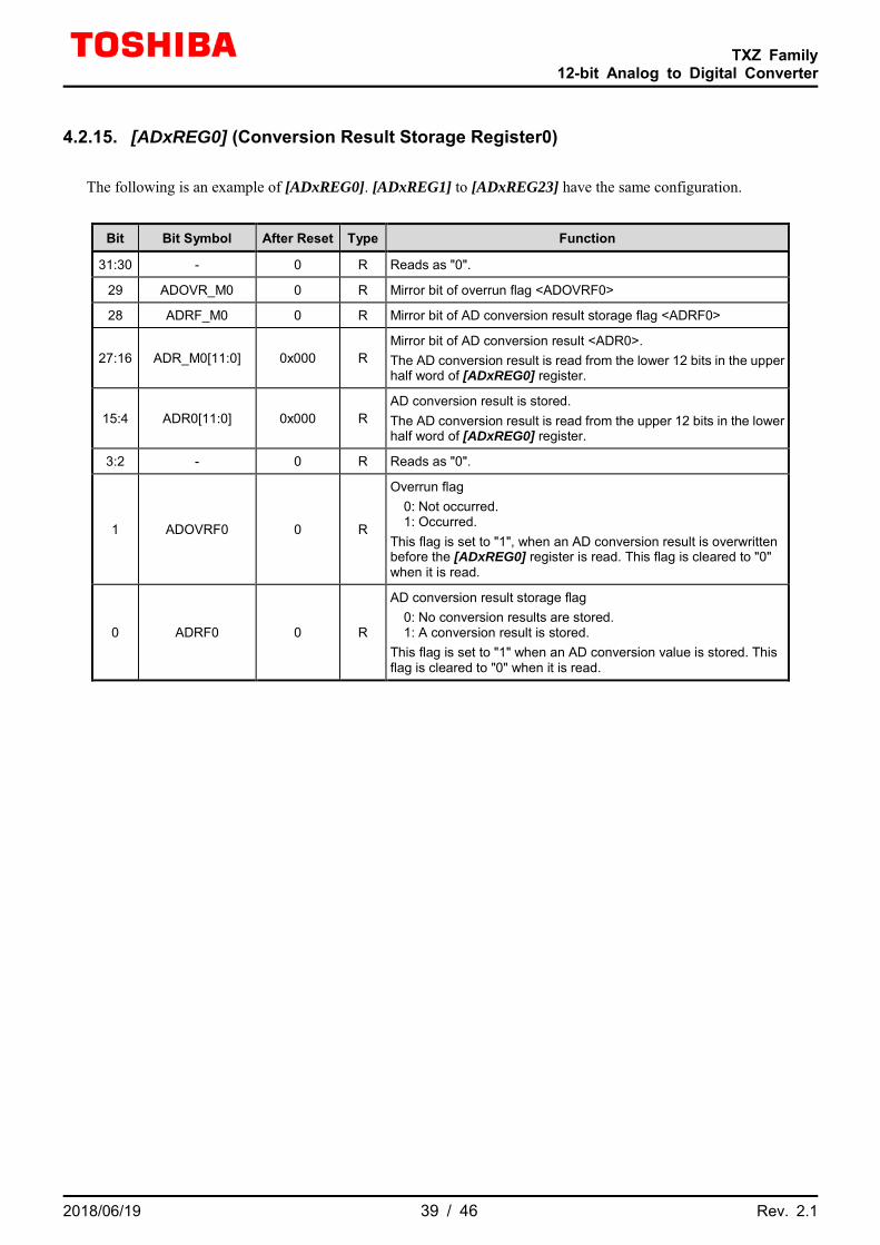
4.2.15. [ADxREG0] (Conversion Result Storage Register0) The following is an example of [ADxREG0]. [ADxREG1] to [ADxREG23] have the same configuration.
Bit Bit Symbol After Reset Type Function
31:30 - 0 R Reads as "0".
29 ADOVR_M0 0 R Mirror bit of overrun flag <ADOVRF0>
28 ADRF_M0 0 R Mirror bit of AD conversion result storage flag <ADRF0>
27:16 ADR_M0[11:0] 0x000 R Mirror bit of AD conversion result <ADR0>. The AD conversion result is read from the lower 12 bits in the upper half word of [ADxREG0] register.
15:4 ADR0[11:0] 0x000 R AD conversion result is stored. The AD conversion result is read from the upper 12 bits in the lower half word of [ADxREG0] register.
3:2 - 0 R Reads as "0".
1 ADOVRF0 0 R
Overrun flag 0: Not occurred. 1: Occurred. This flag is set to "1", when an AD conversion result is overwritten before the [ADxREG0] register is read. This flag is cleared to "0" when it is read.
0 ADRF0 0 R
AD conversion result storage flag 0: No conversion results are stored. 1: A conversion result is stored. This flag is set to "1" when an AD conversion value is stored. This flag is cleared to "0" when it is read.
TXZ Family
12-bit Analog to Digital Converter
2018/06/19 40 / 46 Rev. 2.1
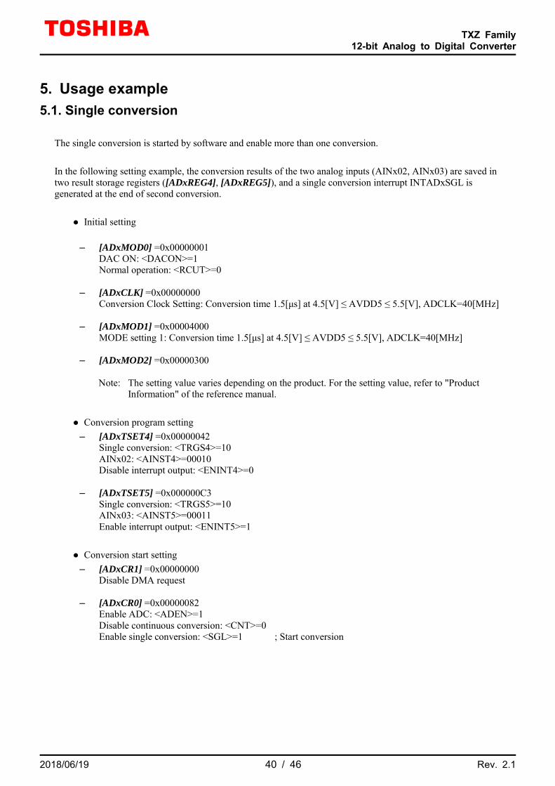
5. Usage example 5.1. Single conversion
The single conversion is started by software and enable more than one conversion. In the following setting example, the conversion results of the two analog inputs (AINx02, AINx03) are saved in two result storage registers ([ADxREG4], [ADxREG5]), and a single conversion interrupt INTADxSGL is generated at the end of second conversion.
Initial setting
‒ [ADxMOD0] =0x00000001 DAC ON: <DACON>=1 Normal operation: <RCUT>=0
‒ [ADxCLK] =0x00000000 Conversion Clock Setting: Conversion time 1.5[μs] at 4.5[V] ≤ AVDD5 ≤ 5.5[V], ADCLK=40[MHz]
‒ [ADxMOD1] =0x00004000 MODE setting 1: Conversion time 1.5[μs] at 4.5[V] ≤ AVDD5 ≤ 5.5[V], ADCLK=40[MHz]
‒ [ADxMOD2] =0x00000300 Note: The setting value varies depending on the product. For the setting value, refer to "Product
Information" of the reference manual.
Conversion program setting ‒ [ADxTSET4] =0x00000042
Single conversion: <TRGS4>=10 AINx02: <AINST4>=00010 Disable interrupt output: <ENINT4>=0
‒ [ADxTSET5] =0x000000C3 Single conversion: <TRGS5>=10 AINx03: <AINST5>=00011 Enable interrupt output: <ENINT5>=1
Conversion start setting ‒ [ADxCR1] =0x00000000
Disable DMA request
‒ [ADxCR0] =0x00000082 Enable ADC: <ADEN>=1 Disable continuous conversion: <CNT>=0 Enable single conversion: <SGL>=1 ; Start conversion

TXZ Family
12-bit Analog to Digital Converter
2018/06/19 41 / 46 Rev. 2.1
5.2. PMD trigger conversion 5.2.1. PMD (3-shunt), ADC × 1
The following shows the connection diagram in which PMD channel 0 and ADC unit A are used in 3-shunt.
ADC A
PMD 0
AINA00 AINA01 AINA02
U V W
PMD0TRGn (n=0 to 5)
6
INTADAPDA
Figure 5.1 3-shunt example The setting example for the ADC is as follows in this case:
Table 5.1 ADC setting in 3-shunt Program 0 1 2 3 4 5
Reg0 U V W V W U Reg1 V W U U V W
INT INTADAPDA INTADAPDA INTADAPDA INTADAPDA INTADAPDA INTADAPDA
The 6 trigger inputs PMD0TRG0 to 5 are assigned to the programs 0 to 5 by [ADAPSEL0] to [ADAPSEL5]. Reg0 and Reg1 in the table represent [ADAPSETn][7:0] and [ADAPSETn][15:8] (n: Program number), respectively. U, V, and W in the table are the motor phases. The corresponding AIN input should be selected for each phase. When the trigger is received, the AD conversion starts and the execution is done in the order of Reg0 and Reg1. Each conversion result is stored to the conversion result storage register, and the INTADAPDA interrupt is generated.

TXZ Family
12-bit Analog to Digital Converter
2018/06/19 42 / 46 Rev. 2.1
5.2.2. PMD (1-shunt), ADC × 1 The following shows the connection diagram in which PMD channel 0 and ADC unit A are used in 1-shunt.
ADC A
PMD 0
AINA00 R PMD0TRGn (n=0,1)
2
INTADAPDA
Figure 5.2 1-shunt example The setting example for the ADC is as follows in this case:
Table 5.2 ADC unit A in 1-shunt
Trigger PMD0 PMD0
0 1 Program 0 1
Reg0 R -
Reg1 - R INT - INTADAPDA
The two trigger signals from PMD0 are assigned to the program numbers, respectively. Reg0 and Reg1 in the table represent [ADAPSETn][7:0] and [ADAPSETn][15:8] (n: Program number), respectively. R in the table is a resistor. It is connected to the corresponding AIN. When the trigger is received, ADC unit A starts and the conversion result is stored to the conversion result storage register0 and 1. The conversion executes in the order of the program0 and 1. The INTADAPDA interrupt is generated at the conversion completion.

TXZ Family
12-bit Analog to Digital Converter
2018/06/19 43 / 46 Rev. 2.1
6. Precaution
The AD conversion result may have some variation due to the fluctuation of the power supply and surrounding noises. The data of the output pins should not be changed during AD conversion to prevent from degrading the AD conversion accuracy. The AD conversion accuracy may degrade if the signal on the shared pin with the AD input/output changes or other output pin changes its output during the AD conversion. In the above case, the AD conversion result should be acquired with the mean value of multiple conversion results and other countermeasures.
Measures should be taken to prevent digital noise from mixing into the analog power supply pins(AVDD5,
AVSS) and the reference voltage pins(VREFHx, VREFLx) of the ADC. ‒ Insert a bypass capacitor between AVDD5 and AVSS pins, the VREFHx and VREFLx pins. Place the
capacitor as close to the terminal as possible.
TXZ Family
12-bit Analog to Digital Converter
2018/06/19 44 / 46 Rev. 2.1
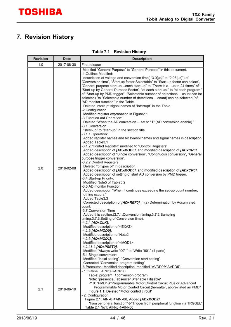
7. Revision History
Table 7.1 Revision History Revision Date Description
1.0 2017-08-30 First release
2.0 2018-02-08
-Modified “General-Purpose” to “General Purpose” in this document. -1.Outline: Modified: description of voltage and conversion time( “3.0[μs]” to “2.95[μs]”) of “Conversion time”, “Start-up factor Selectable” to “Start-up factor can select”, “General purpose start-up…each start-up” to “There is a…up to 24 times” of “Start-up by General Purpose Factor”, “at each start-up.” to “at each program.” of “Start-up by PMD trigger”, “Selectable number of detections …count can be selected).”to “Selectable number of detections …count) can be selected.”of “AD monitor function” in the Table. Deleted Interrupt signal names of “Interrupt” in the Table. -2.Configuration Modified register expranation in Figure2.1 -3.Function anf Operation: Deleted “When the AD conversion …set to "1" (AD conversion enable).” -3.1.Conversion…. “strar-up” to “start-up” in the section title. -3.1.1.Operation: Added register names and bit symbol names and signal names in description. Added Table3.1 -3.1.2.“Control Register” modified to “Control Registers” Added description of [ADxMOD0], and modified description of [ADxCR0]. Added description of “Single conversion”, “Continuous conversion”, “General purpose trigger conversion”. -3.2.2.Control Registers: Deleted “5 types of” in description. Added description of [ADxMOD0], and modified description of [ADxCR0]. Added description of setting of start AD conversion by PMD trigger. -3.4.Start-up Priority: Modified Note5 of Table3.2 -3.5.AD monitor Function: Added description “When it continues exceeding the set-up count number, nothing occurs.” Added Table3.3 Corrected description of [ADxREF0] in (2) Determination by Accumlated count. -3.7.Conversion Time Added this section,(3.7.1.Conversion timing,3.7.2.Sampling timing,3.7.3.Setting of Conversion time). -4.2.4.[ADxCLK]: Modified description of <EXAZ>. -4.2.5.[ADxMOD0]: Modifide description of Note2 -4.2.6.[ADxMOD1]: Modified description of <MOD1>. -4.2.13.4.[ADxPSET0]: Modified “Always write "00".” to “Write "00".” (4 parts) -5.1.Single conversion: Modified “Initial setting”, “Conversion start setting”. Corrected “Conversion program setting” -6.Precauton: Modified description, modified “AVDD”“AVDD5”.
2.1 2018-06-19
- 1.Outline AINx0AINx00 Table: program conversion program Note: "presence / absence""enable / disable" P10: "PMD""Programmable Motor Control Circuit Plus or Advanced Programmable Motor Control Circuit (hereafter, abbreviated as PMD" Figure 1.1: Deleted "Motor control circuit" - 2. Configuration Figure 2.1: AINx0AINx00, Added [ADxMOD2] "from peripheral function""Trigger from peripheral function via TRGSEL" Table 2.1 No1: AINx0AINx00

TXZ Family
12-bit Analog to Digital Converter
2018/06/19 45 / 46 Rev. 2.1
No8: Monitor function output0 Monitor function 0 output No9: Monitor function output1 Monitor function 1 output No.15: Monitor function interrupt0 Monitor function 0 interrupt No.16: Monitor function interrupt1 Monitor function 1 interrupt - 3. Function and Operation 2nd and subsequent: Separated into "3.1.Clock Supply" Modified register name ADCAD conversion - 3.2.1.Operation Modified 2nd line “general start-up” “general purpose start-up” Modified 2nd term 1st line “start-up” “general purpose start-up” Figure 3.1 "General-purpose""General purpose" AINx0 to AINx3 AINx00 to AINx03 1st stage: <AINSn> <AINSTn> - 3.2.2.Control Registers 1st term: "[ADxTSETn] n=0 to 23""[ADxTSET0] to [ADxTSET23]" "general start-up factor""general purpose start-up factor" 3rd term: IfWhen Added "For start AD conversion by the general purpose start up factor, ..." General purpose trigger conversion term (8): [ADxCR0 [ADxCR0] Note: "highest-priority" "general purpose" - 3.3.2. Control Registers 2nd term: PMD trigger program selection register PMD trigger program number selection register Added (PMDTRG0 to PMDTRG11) (6): [ADxPINSn] [ADxPINTSn] (8): [ADxCR0 [ADxCR0] (10): conversion "conversion program" - 3.5. Start-up Priority Figure: "General-purpose""General purpose" Added 2nd stage: " If multiple start-up factors occur at the same time, ..." 3rd to 6th stage: program conversion program, factorstart-up factor IfWhen, "is generated""occurs" 4th stage: "its program execution is not done and waits" "it waits for execution" 5th stage: Replace text. Table 3.2 Note5: haltedsuspended, facterfactor - 3.6. AD Monitor Function 3rd stage: whose which, (bigger or smaller) (larger or smaller) (1)Determination by Continuous.. , (2)Determination by Accumulated ...: [ADxCMP0] [ADxCMP0]<AD0CMP0>, <ADxCMP0> <AD0CMP0> Figure 3.3, Figure 3.4: <ADxCMP0> <AD0CMP0> - 4.1.List of Registers Deleted Function cell Function name: Analog to Digital 12-bit Analog to Digital - 4.2.5. DACON/Function: Added "(Note2)" - 4.2.6. Function: "x× 36" "× 36", Deleted Note2 - 4.2.11., 4.2.12. Bit Symbol: ADxCMPAD0CMP - 4.2.13. RegisterRegisters - 4.2.13.1. Note2: "Motor control circuit" "Programmable Motor Control Circuit" - 4.2.13.2. Function: "11: No interrupts" "11: Reserved" - 4.2.13.4. Function: Write "00". Write as "00". - 4.2.14. AINST0/Function: Added "(Note2)" - 4.2.15. Bit Symbol: ADOVRF_M0 ADOVR_M0 - 5.1.: "end of two conversion" "end of second conversion" - 5.2.1. Title: 3-Shunt3-shunt Figure 5.1: AINA0 to AINA2 AINA00 to AINA02 - 5.2.2. Title: 1-Shunt1-shunt Figure 5.2: AINA0 AINA00

TXZ Family
12-bit Analog to Digital Converter
2018/06/19 46 / 46 Rev. 2.1
RESTRICTIONS ON PRODUCT USE Toshiba Corporation and its subsidiaries and affiliates are collectively referred to as “TOSHIBA”. Hardware, software and systems described in this document are collectively referred to as “Product”.
• TOSHIBA reserves the right to make changes to the information in this document and related Product without notice.
• This document and any information herein may not be reproduced without prior written permission from TOSHIBA. Even with TOSHIBA's written permission, reproduction is permissible only if reproduction is without alteration/omission.
• Though TOSHIBA works continually to improve Product's quality and reliability, Product can malfunction or fail. Customers are responsible for complying with safety standards and for providing adequate designs and safeguards for their hardware, software and systems which minimize risk and avoid situations in which a malfunction or failure of Product could cause loss of human life, bodily injury or damage to property, including data loss or corruption. Before customers use the Product, create designs including the Product, or incorporate the Product into their own applications, customers must also refer to and comply with (a) the latest versions of all relevant TOSHIBA information, including without limitation, this document, the specifications, the data sheets and application notes for Product and the precautions and conditions set forth in the "TOSHIBA Semiconductor Reliability Handbook" and (b) the instructions for the application with which the Product will be used with or for. Customers are solely responsible for all aspects of their own product design or applications, including but not limited to (a) determining the appropriateness of the use of this Product in such design or applications; (b) evaluating and determining the applicability of any information contained in this document, or in charts, diagrams, programs, algorithms, sample application circuits, or any other referenced documents; and (c) validating all operating parameters for such designs and applications. TOSHIBA ASSUMES NO LIABILITY FOR CUSTOMERS' PRODUCT DESIGN OR APPLICATIONS.
• PRODUCT IS NEITHER INTENDED NOR WARRANTED FOR USE IN EQUIPMENTS OR SYSTEMS THAT REQUIRE EXTRAORDINARILY HIGH LEVELS OF QUALITY AND/OR RELIABILITY, AND/OR A MALFUNCTION OR FAILURE OF WHICH MAY CAUSE LOSS OF HUMAN LIFE, BODILY INJURY, SERIOUS PROPERTY DAMAGE AND/OR SERIOUS PUBLIC IMPACT ("UNINTENDED USE"). Except for specific applications as expressly stated in this document, Unintended Use includes, without limitation, equipment used in nuclear facilities, equipment used in the aerospace industry, medical equipment, equipment used for automobiles, trains, ships and other transportation, traffic signaling equipment, equipment used to control combustions or explosions, safety devices, elevators and escalators, devices related to electric power, and equipment used in finance-related fields. IF YOU USE PRODUCT FOR UNINTENDED USE, TOSHIBA ASSUMES NO LIABILITY FOR PRODUCT. For details, please contact your TOSHIBA sales representative.
• Do not disassemble, analyze, reverse-engineer, alter, modify, translate or copy Product, whether in whole or in part.
• Product shall not be used for or incorporated into any products or systems whose manufacture, use, or sale is prohibited under any applicable laws or regulations.
• The information contained herein is presented only as guidance for Product use. No responsibility is assumed by TOSHIBA for any infringement of patents or any other intellectual property rights of third parties that may result from the use of Product. No license to any intellectual property right is granted by this document, whether express or implied, by estoppel or otherwise.
• ABSENT A WRITTEN SIGNED AGREEMENT, EXCEPT AS PROVIDED IN THE RELEVANT TERMS AND CONDITIONS OF SALE FOR PRODUCT, AND TO THE MAXIMUM EXTENT ALLOWABLE BY LAW, TOSHIBA (1) ASSUMES NO LIABILITY WHATSOEVER, INCLUDING WITHOUT LIMITATION, INDIRECT, CONSEQUENTIAL, SPECIAL, OR INCIDENTAL DAMAGES OR LOSS, INCLUDING WITHOUT LIMITATION, LOSS OF PROFITS, LOSS OF OPPORTUNITIES, BUSINESS INTERRUPTION AND LOSS OF DATA, AND (2) DISCLAIMS ANY AND ALL EXPRESS OR IMPLIED WARRANTIES AND CONDITIONS RELATED TO SALE, USE OF PRODUCT, OR INFORMATION, INCLUDING WARRANTIES OR CONDITIONS OF MERCHANTABILITY, FITNESS FOR A PARTICULAR PURPOSE, ACCURACY OF INFORMATION, OR NONINFRINGEMENT.
• Do not use or otherwise make available Product or related software or technology for any military purposes, including without limitation, for the design, development, use, stockpiling or manufacturing of nuclear, chemical, or biological weapons or missile technology products (mass destruction weapons). Product and related software and technology may be controlled under the applicable export laws and regulations including, without limitation, the Japanese Foreign Exchange and Foreign Trade Law and the U.S. Export Administration Regulations. Export and re-export of Product or related software or technology are strictly prohibited except in compliance with all applicable export laws and regulations.
• Please contact your TOSHIBA sales representative for details as to environmental matters such as the RoHS compatibility of Product. Please use Product in compliance with all applicable laws and regulations that regulate the inclusion or use of controlled substances, including without limitation, the EU RoHS Directive. TOSHIBA ASSUMES NO LIABILITY FOR DAMAGES OR LOSSES OCCURRING AS A RESULT OF NONCOMPLIANCE WITH APPLICABLE LAWS AND REGULATIONS.