TOSHIBA W602-Service Manual.pdf
92
W-602 Videograbadoras Contenido Guía de servicio Precauciones Información de referencia Especificaciones del producto Desemsamble y reensamble Ajuste y alineamiento Vista explotada Lista de partes de reemplazo Diagrama a bloques Diagramas PCB (Placa de Circuito Impreso) Diagramas esquemáticos
-
Upload
khangminh22 -
Category
Documents
-
view
0 -
download
0
Transcript of TOSHIBA W602-Service Manual.pdf

W-602
Videograbadoras
Contenido
Guía de servicio
Precauciones
Información de referencia
Especificaciones del producto
Desemsamble y reensamble
Ajuste y alineamiento
Vista explotada
Lista de partes de reemplazo
Diagrama a bloques
Diagramas PCB (Placa de Circuito Impreso)
Diagramas esquemáticos

SERVICE MANUAL
FILE NO. 120-200013
VIDEO CASSETTE RECORDER
W-602
PRINTED IN KOREA. APR, 2000
W-602 4/22/00 10:49 AM Page 1

TOTAL CONTENTS
◆ Service Guide
1. Precautions
2. Reference Information
3. Product Specifications
4. Disassembly and Reassembly
5. Alignment and Adjustment
6. Exploded View
7. Replacement Parts List
8. Block Diagram
9. PCB Diagrams
10. Schematic Diagrams
Toshiba I
SERVICE GUIDE
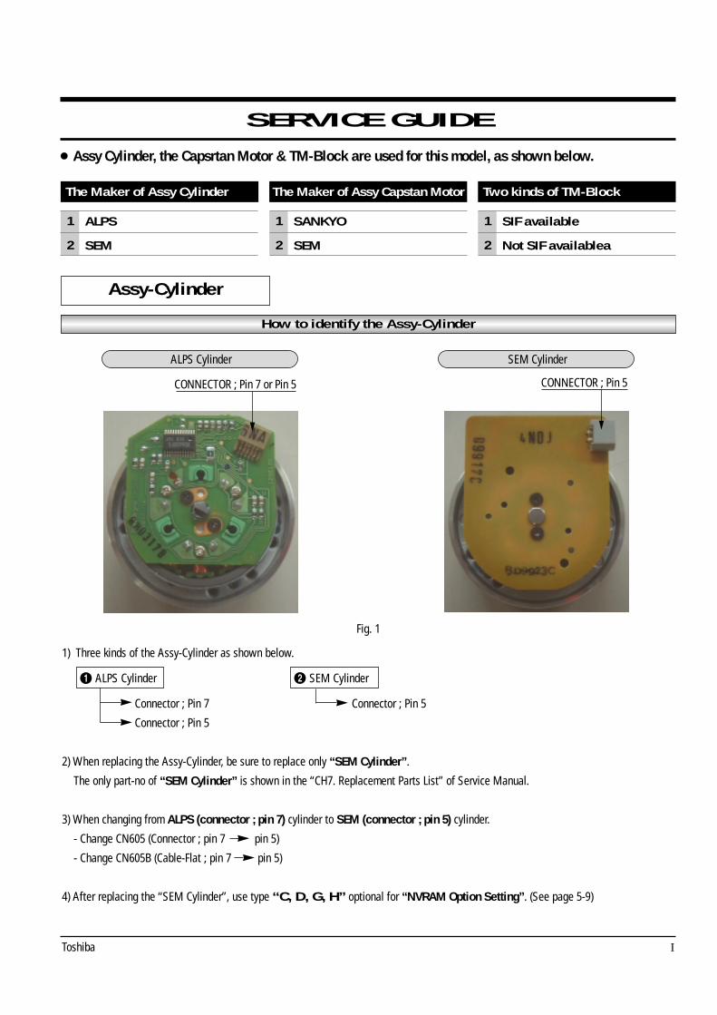
Assy Cylinder, the Capsrtan Motor & TM-Block are used for this model, as shown below.
Assy-Cylinder
How to identify the Assy-Cylinder
ALPS Cylinder SEM Cylinder
CONNECTOR ; Pin 7 or Pin 5 CONNECTOR ; Pin 5
Fig. 1
1) Three kinds of the Assy-Cylinder as shown below.
Œ ALPS Cylinder ´ SEM Cylinder
Connector ; Pin 7 Connector ; Pin 5
Connector ; Pin 5
2) When replacing the Assy-Cylinder, be sure to replace only “SEM Cylinder”.
The only part-no of “SEM Cylinder” is shown in the “CH7. Replacement Parts List” of Service Manual.
3) When changing from ALPS (connector ; pin 7) cylinder to SEM (connector ; pin 5) cylinder.
- Change CN605 (Connector ; pin 7 pin 5)
- Change CN605B (Cable-Flat ; pin 7 pin 5)
4) After replacing the “SEM Cylinder”, use type “C, D, G, H” optional for “NVRAM Option Setting”. (See page 5-9)
The Maker of Assy Cylinder
1
2
ALPS
SEM
The Maker of Assy Capstan Motor
1
2
SANKYO
SEM
Two kinds of TM-Block
1
2
SIF available
Not SIF availablea

II Toshiba
How to identify the Capstan Motor
TOP VIEW
SANKYO CAPSTAN MOTOR SEM CAPSTAN MOTOR
CAPSTAN SHAFT CAPSTAN SHAFT
Fig. 2
1) Two kinds of the Capstan Motor ΠSankyo Capstan Motor
´ SEM Capstan Motor
2) When replacing the Capstan Motor, be sure to replace only “SEM Capstan Motor”.
The only part-no of “SEM Capstan Motor” is shown in the “CH7. Replacement Parts List” of Service Manual.
3) After replacing the “SEM Capstan Motor”, use type “E, F, G, H” optional for “NVRAM Option Setting”. (See page 5-9)
Capstam Motor
TM-BLOCK
1) Two kinds of the TM-Blovk ΠSIF available
´ Not SIF available
2) How to identify TM-Block ; See page 5-11 (Fig. 5-21)
- In case there is VR501 ; Not SIF available
- In case there is no VR501 ; SIF available
3) When replacing the TM-Block as a service parts, be sure to replace only the TM-Block which is SIF available.
The only part-no of “SIF available” is shown in the “CH7. Replacement Parts List” of Service Manual.
4) After replacing “TM-Block”, use type “B, D, F, H” optional for “NVRAM Option Setting” regardless of VR501. (See page 5-9)

Toshiba 1-1
1. Precautions
1. Be sure that all of the built-in protective devices arereplaced. Restore any missing protective shields.
2. When reinstalling the chassis and its assemblies, be sure to restore all pretective devices, including :control knobs and compartment covers.
3. Make sure that there are no cabinet openings through which people--particularly children--might insert fingers and contact dangerousvoltages. Such openings include the spacing between the picture tube and the cabinet mask, excessively wide cabinet ventilation slots, and improperly fitted back covers.
If the measured resistance is less than 1.0 megohmor greater than 5.2 megohms, an abnormality existsthat must be corrected before the unit is returned to the customer.
4. Leakage Current Hot Check (See Fig. 1-1) :Warning : Do not use an isolation transformer during this test. Use a leakage current tester or a metering system that complies with American National Standards Institute (ANSI C101.1, Leakage Current for Appliances), and Underwriters Laboratories (UL Publication UL1410, 59.7).
5. With the unit completely reassembled, plug the ACline cord directly the power outlet. With the unit’sAC switch first in the ON position and then OFF, measure the current between a known erath ground (metal water pipe, conduit, etc.) and all exposed metal parts, including : antennas, handlebrackets, metal cabinets, screwheads and controlshafts. The current measured should not exceed0.5 milliamp. Reverse the power-plug prongs in theAC outlet and repeat the test.
6. X-ray Limits :The picture tube is designed to prohibit X-ray emissions. To ensure continued X-ray protection,replace the picture tube only with one that is the same type as the original.
Fig. 1-1 AC Leakage Test
7. Antenna Cold Check :With the unit’s AC plug disconnected from theAC source, connect an electrical jumper across thetwo AC prongs. Connect one lead of the ohmmeterto an AC prong.Connect the other lead to the coaxial connector.
8. High Voltage Limit :High voltage must be measured each time servicing is done on the B+, horizontal deflectionor high voltage circuits.
Heed the high voltage limits. These include theX-ray protection Specifications Label, and theProduct Safety and X-ray Warning Note on theservice data schematic.
9. Some semiconductor (“solid state”) devices areeasily damaged by static electricity.Such components are called ElectrostaticallySensitive Devices (ESDs); examples includeintegrated circuits and some field-effect transistors.The following techniques will reduce the occurrence of component damage caused by staticelectricity.
10. Immediately before handling any semiconductorcomponents or assemblies, drain the electrostaticcharge from your body by touching a known earth ground. Alternatively, wear a dischargingWrist-strap device. (Be sure to remove it prior to applying power--this is an electric shock precaution.)
DEVICEUNDERTEST
(READING SHOULDNOT BE ABOVE
0.5mA)LEAKAGECURRENTTESTER
EARTHGROUND
TEST ALLEXPOSED METER
SURFACES
ALSO TEST WITHPLUG REVERSED
(USING AC ADAPTERPLUG AS REQUIRED)
2-WIRE CORD

Precautions
1-2 Toshiba
11. High voltage is maintained within specified limitsby close-tolerance, safety-related components andadjustments. If the high voltage exceeds the specified limits, check each of the special components.
12. Design Alteration Warning :Never alter or add to the mechanical or electrical design of this unit. Example : Do not add auxiliary audio or video connectors. Such alterations might create a safety hazard. Also, any design changes or additions will void the manufacturer’s warranty.
13. Hot Chassis Warning : Some TV receiver chassis are electricallyconnected directly to one conductor of the AC power cord. If an isolation transformer is not used, these units may be safely serviced only if the AC power plug is inserted so that the chassis is connected to the ground side of the AC source.
To confirm that the AC power plug is inserted correctly, do the following : Using an AC voltmeter, measure the voltage between thechassis and a known earth ground. If the readingis greater than 1.0V, remove the AC power plug, reverse its polarity and reinsert. Re-measure the voltage between the chassis and ground.
14. Some TV chassis are designed to operate with 85 volts AC between chassis and ground, regardless of the AC plug polarity. These units can be safelyserviced only if an isolation transformer inserted between the receiver and the power source.
15. Never defeat any of the B+ voltage interlocks. Do not apply AC power to the unit (or any of itsassemblies) unless all solid-state heat sinks are correctly installed.
16. Always connect a test instrument’s ground lead tothe instrument chassis ground before connecting the positive lead; always remove the instrument’sground lead last.
17. Observe the original lead dress, especially near the following areas : Antenna wiring, sharp edges, and especially the AC and high voltage power supplies. Always inspect for pinched, out-of-place, or frayed wiring. Do not change the spacing between components and the printedcircuit board. Check the AC power cord for damage. Make sure that leads and components do not touch thermally hot parts.
18. Picture Tube Implosion Warning : The picture tube in this receiver employs “integral implosion” protection. To ensure continued implosion protection, make sure that the replacement picture tube is the same as the original.
19. Do not remove, install or handle the picture tube without first putting on shatterproof goggles equipped with side shields. Never handle the picture tube by its neck. Some “in-line” picturetubes are equipped with a permanently attached deflection yoke; do not try to remove such “permanently attached” yokes from the picture tube.
20. Product Safety Notice :Some electrical and mechanical parts have specialsafety-related characteristics which might not be obvious from visual inspection. These safety features and the protection they give might be lost if the replacement component differs from theoriginal--even if the replacement is rated for higher voltage, wattage, etc.
Components that are critical for safety are indicated in the circuit diagram by shading, ( or ).Use replacement components that have the same ratings, especially for flame resistance anddielectric strength specifications. A replacement part that does not have the same safety characteristics as the original might create shock, fire or other hazards.

Toshiba 2-1
9
Rea
r Panel
LIN
E IN
1 A
UD
IO (
Rea
r), 2
(F
ron
t) ja
cks
If th
e co
nnec
ted
equi
pmen
t is
mon
aura
l (ha
s on
e au
dio
outp
ut ja
ck),
con
nect
the
L (M
ON
O)
side
, the
sam
eso
und
is r
ecor
ded
on b
oth
L an
d R
on
the
Hi-F
i tra
ck.
Mul
tifun
ctio
nal
indi
cato
r
RE
C (
Rec
ordi
ng)
indi
cato
rV
CR
indi
cato
rT
ape
spee
d in
dica
tor
(SP
/SLP
)
Cas
sette
indi
cato
r
Tim
er r
ecor
ding
indi
cato
rS
TE
RE
O in
dica
tor
Hi-F
i ind
icat
or
SA
P in
dica
tor
Hi-F
i (L/
R)
indi
cato
rsL:
Lef
t cha
nnel
R:R
ight
cha
nnel
off:
Nor
mal
trac
k
VCR D
ispla
y
Hi-F
i
STER
EOS
LP
SAP
VC
RR
ECL
R
TIM
ER
INTRODUCTION
LR
CH
sele
ctor
(3/4
)
LIN
E O
UT
AU
DIO
jack
s (L
, R
)
LIN
E O
UT
VID
EO
jack
RF
IN
(F
RO
M A
NT
.) term
inal
LIN
E IN
1 A
UD
IO ja
cks
(L, R
)
RF
OU
T (
TO
TV
) te
rmin
al
LIN
E IN
1 V
IDE
O ja
ck
CH
OU
T(T
O T
V)
IN(F
ROM
ANT
.)
LIN
EO
UT
LIN
EIN
1
VID
EO
AU
DIO 3
4
RF
8
CH
AN
NE
LP
LA
YS
TO
P
FF
EJE
CT
PO
WE
RR
EW
2419
1919
1914
18
109
18
VID
EO
L/M
ON
O A
UD
IO R
LIN
E IN
2
RE
C 24
Front
Panel
Rem
ote
Contr
ol
* T
hese
but
tons
are
use
d to
con
trol
the
curs
or o
n th
e sc
reen
.
INT
RO
DU
CT
ION
Iden
tific
atio
n of
Con
trol
sS
ee th
e pa
ge in
fo
r de
tails
.T
his
man
ual s
how
s th
e na
mes
of b
utto
ns in
ital
ics.
To
oper
ate
this
VC
R.
To
oper
ate
your
TV
.
CH
AN
NE
L Rem
ote
Sen
sor
VC
R D
ispl
ay
ST
OP
PL
AY
FF
Cas
sete
com
partm
ent
RE
WE
JEC
TP
OW
ER
LIN
E IN
2 V
IDE
O ja
ckLI
NE
IN 2
AU
DIO
(L/M
ON
O, R
) ja
cks
RE
C
78 0
10096
523
41
ST
OP
PL
AY
FF
RE
W
SL
OW
PAU
SE/S
TILL
CA
NC
EL
A.S
ELEC
T
EJE
CT
PR
OG
.E
NT
ER
TIM
ER
TV
VO
L
CH
/TR
K
RE
CS
P/S
LP
DIS
PLA
YT
V/V
CR
COUN
T RE
SET
RE
MA
IN/
CO
UN
TER
I.SE
LEC
T
PO
WE
RV
CR
TV
TV
Nu
mb
er b
utt
on
s
I. S
EL
EC
T
DIS
PL
AY
RE
MA
IN/C
OU
NT
ER
SP
/SL
P
RE
C
19 21 14 18
RE
W *
SL
OW
VC
RP
OW
ER
CH
/TR
K
TV
VO
L
TV
/VC
R
CO
UN
T R
ES
ET
TIM
ER
PL
AY
*
FF
*
100
PA
US
E/S
TIL
L
EN
TE
R
ST
OP
*P
RO
G.
EJE
CT
CA
NC
EL
A.S
EL
EC
T
14 29 24 24 22 22 24 27 2824
14 17 29 24 22 26 19 19 20 19 14
CU
RS
OR
19
VC-6
02
2. Reference Information
2-1 Operation of Controls

Reference Information
2-2 Toshiba
11PREPARATION
VH
F U
HF
VH
F/U
HF
LR
CH
OUT
(TO
TV)
IN(FR
OM A
NT.)
LINE
OUT
LINE IN 1
VIDE
O
AUDI
O 34
RF
OUT
(TO
TV)
IN(FR
OM A
NT.) RF
Ante
nna/V
CR/T
V C
onnec
tion
1D
isco
nnec
t the
ant
enna
cab
le fr
om y
our
TV
and
con
nect
it to
the
RF
IN te
rmin
al o
n th
eV
CR
.
2C
onne
ct th
e R
F O
UT
term
inal
to th
e T
V.
AU
DIO
/VID
EO C
onnec
tions
The
AU
DIO
/VID
EO
jack
s ar
e al
so a
vaila
ble
to c
onne
ct y
our
TV.
When
connec
ted y
our
TV u
sing t
he
AU
DIO
/VID
EO O
UT
jack
sTo
wat
ch v
ideo
pic
ture
s, s
et th
e vi
deo
inpu
t mod
eon
you
r T
V.
For
the
vide
o in
put m
ode,
ref
er to
the
man
ual o
f you
r T
V.
Set
tin
g t
he
VC
R O
utp
ut
Ch
ann
elW
hen
the
VC
R is
con
nect
ed in
this
way
, the
VC
R s
ends
the
outp
utsi
gnal
s to
cha
nnel
3 o
r 4
on y
our
TV
. S
et th
e ou
tput
cha
nnel
sele
ctor
(C
H s
elec
tor)
of t
he V
CR
to “
3” o
r “4
”, w
hich
ever
is v
acan
tin
you
r ar
ea.
VH
F/U
HF
com
bina
ion
ante
nna
VH
F a
nten
naon
lyU
HF
ant
enna
only
Ant
enna
spl
itter
(not
sup
plie
d)
1 2
Con
nect
ions
Bef
ore
you
use
this
VC
R, i
t is
nece
ssar
y to
con
nect
it to
you
r T
V.
Sev
eral
way
s of
con
nect
ing
are
avai
labl
e de
pend
ing
on y
our
use
of T
V o
r ca
ble
box.
Sel
ect o
ne w
hich
is a
pplic
able
to y
our
equi
pmen
t.
PR
EP
AR
AT
ION
LR
CH
OUT
(TO
TV)
IN(FR
OM A
NT.)
LINE
OUT
LINE IN 1
VIDE
O
AUDI
O 34
RF
LIN
E O
UT
VID
EO
VID
EO
IN
AU
DIO
INLI
NE
OU
T A
UD
IO
Cable
Connec
tion
Cho
ose
one
of th
e be
low
acc
ordi
ng to
you
r us
age
of th
e ca
ble
box.
This
set
-up w
ill e
nable
you t
o:
–re
cord
an
unsc
ram
bled
cha
nnel
.–
wat
ch a
n un
scra
mbl
ed c
hann
el w
hile
rec
ordi
ng it
.–
reco
rd a
n un
scra
mbl
ed c
hann
el w
hile
wat
chin
gan
othe
r (o
nly
whe
n yo
u co
nnec
t a c
able
-co
mpa
tible
TV
).
You w
ill n
eed t
o:
•se
lect
TV
cha
nnel
3 o
r 4
to r
ecei
ve v
ideo
sig
nals
.•
to r
ecor
d a
chan
nel w
hile
wat
chin
g an
othe
r, pr
ess
TV
/VC
R o
n th
e re
mot
e co
ntro
l to
turn
off
the
“VC
R”
indi
cato
r in
the
VC
R d
ispl
ay a
nd s
elec
t ade
sire
d ch
anne
l on
the
TV
(on
ly w
hen
you
conn
ect
a ca
ble-
com
patib
le T
V).
LR
CH
OUT
(TO
TV)
IN(FR
OM A
NT.)
LINE
OUT
LINE IN 1
VIDE
O
AUDI
O 34
RF
Inco
min
g ca
ble
10
Sett
ing u
p t
he
Rem
ote
Contr
ol
1O
pen
the
batte
ry c
ompa
rtm
ent l
id o
n th
ere
ar p
anel
.
2In
stal
l 2 b
atte
ries
(“A
AA
” si
ze)
follo
win
gth
e po
larit
y di
agra
ms.
3C
lose
the
batte
ry c
ompa
rtm
ent l
id.
4P
oint
the
rem
ote
cont
rol a
t the
VC
R a
nd p
ress
the
butto
ns w
ithin
the
oper
atin
g ra
nge.
Dis
tanc
e: w
ithin
abo
ut 7
m fr
om th
e fr
ont o
f the
rem
ote
sens
orA
ngle
s: w
ithin
abo
ut 3
0˚ in
eve
ry d
irect
ion
Note
s on b
att
erie
s•
The
life
of t
he b
atte
ries
is a
bout
1 y
ear
depe
ndin
g on
the
cond
ition
s of
use
.•
If th
e re
mot
e co
ntro
l doe
s no
t ope
rate
corr
ectly
, rep
lace
all
batte
ries
with
new
one
s.•
If th
e re
mot
e co
ntro
l is
not t
o be
use
d fo
r a
long
per
iod
of ti
me,
rem
ove
the
batte
ries
toav
oid
poss
ible
dam
age
from
bat
tery
cor
rosi
on.
Cari
ng f
or
the
rem
ote
contr
ol
•D
o no
t exp
ose
the
rem
ote
sens
or o
f the
VC
Rto
a s
tron
g lig
ht s
ourc
e su
ch a
s di
rect
sun
light
or il
lum
inat
ion
(esp
ecia
lly h
igh-
freq
uenc
ylig
htin
g) w
hen
usin
g th
e re
mot
e co
ntro
l.•
Be
care
ful n
ot to
spi
ll w
ater
on
the
rem
ote
cont
rol o
r to
pla
ce it
on
anyt
hing
wet
, and
avo
idsh
arp
impa
cts.
How
to U
se th
e R
emot
e C
ontr
olT
his
sect
ion
expl
ains
how
to g
et r
eady
for
rem
ote
cont
rol o
pera
tion.
PR
EP
AR
AT
ION
++

Reference Information
Toshiba 2-3
13PREPARATION
Auto
Set
Up
The
VC
R’s
clo
ck a
nd tu
ner
chan
nels
are
set
aut
omat
ical
ly w
hen
the
VC
R is
plu
gged
into
the
AC
out
let.
PR
EP
AR
AT
ION
Auto
Set
up
1P
lug
the
VC
R in
to th
e A
C o
utle
t
2“A
UT
O”
blin
k w
hile
the
VC
R a
utom
atic
ally
set
s th
e cl
ock
usin
g th
e da
ta b
road
cast
by
the
loca
l TV
sta
tions
.W
hile
“A
UT
O”
is b
linki
ng, c
hann
el m
emor
y is
als
o se
tau
tom
atic
ally
.
3W
hen
Aut
o se
t up
has
been
com
plet
ed, t
he V
CR
is o
nst
andb
y m
ode.
No
tes
•It
may
take
s se
vera
l min
utes
dur
ing
the
Aut
o se
t-up
•P
ress
CA
NC
EL
on
the
rem
ote
cont
rol t
o ca
ncel
the
auto
set
-up.
78 0
10096
523
41
ST
OP
PL
AY
FF
RE
W
CA
NC
EL
12
This
set
-up w
ill e
nable
you t
o:
–w
atch
an
unsc
ram
bled
or
scra
mbl
ed c
hann
elw
hile
rec
ordi
ng it
.–
reco
rd a
ny c
hann
els
thro
ugh
the
cabl
e bo
x.
You w
ill n
eed t
o:
•se
t TV
cha
nnel
3 o
r 4
to r
ecei
ve v
ideo
sig
nals
.(S
ee p
age
11.)
•se
t VC
R c
hann
el to
the
outp
ut c
hann
el o
f the
cabl
e bo
x, a
nd s
elec
t a d
esire
d ca
ble
chan
nel
on th
e ca
ble
box.
•w
hile
the
VC
R is
turn
ed o
ff or
the
“VC
R”
indi
cato
r is
not
lit i
n th
e V
CR
dis
play
, set
TV
chan
nel t
o th
e ou
tput
cha
nnel
of t
he c
able
box
.
This
set
-up w
ill e
nable
you t
o:
–w
atch
an
unsc
ram
bled
or
scra
mbl
ed c
hann
elw
hile
rec
ordi
ng it
.–
reco
rd a
n un
scra
mbl
ed c
hann
el w
hile
wat
chin
gan
othe
r un
scra
mbl
ed c
hann
el (
only
whe
n yo
uco
nnec
t a c
able
-com
patib
le T
V).
•A
/B s
witc
h “A
”:re
cord
and
wat
ch a
nun
scra
mbl
ed c
hann
el w
hich
com
es b
ypas
sing
the
cabl
ebo
x.•
A/B
sw
itch
“B”:
reco
rd a
nd w
atch
a s
cram
bled
or u
nscr
ambl
ed c
hann
el c
omin
gth
roug
h th
e ca
ble
box.
Inco
min
g ca
ble
Cab
le b
ox
OU
TIN
A/B
sw
itch
LR
CH
OUT
(TO
TV)
IN(FR
OM A
NT.)
LINE
OUT
LINE IN 1
VIDE
O
AUDI
O 34
RF
Cab
le b
ox
LR
CH
OUT
(TO
TV)
IN(FR
OM A
NT.)
LINE
OUT
LINE IN 1
VIDE
O
AUDI
O 34
RF
A BA BA B
This
set
-up w
ill e
nable
you t
o:
–re
cord
an
unsc
ram
bled
cha
nnel
.–
wat
ch a
n un
scra
mbl
ed c
hann
el w
hile
rec
ordi
ng it
.–
reco
rd a
n un
scra
mbl
ed c
hann
el w
hile
wat
chin
gan
othe
r (s
cram
bled
or
unsc
ram
bled
).
You w
ill n
eed t
o:
•se
t TV
cha
nnel
to th
e ou
tput
cha
nnel
of t
he c
able
box.
•tu
rn o
n th
e ca
ble
box
and
sele
ct c
able
cha
nnel
3or
4 a
ccor
ding
to th
e ou
tput
cha
nnel
of t
he V
CR
.•
to r
ecor
d a
chan
nel w
hile
wat
chin
g an
othe
r,pr
ess
TV
/VC
R o
n th
e re
mot
e co
ntro
l to
turn
off
the
“VC
R”
indi
cato
r in
the
VC
R d
ispl
ay a
nd s
elec
ta
desi
red
cabl
e ch
anne
l on
the
cabl
e bo
x.
Con
nect
ions
(co
ntin
ued)
LR
CH
OUT
(TO
TV)
IN(FR
OM A
NT.)
LINE
OUT
LINE IN 1
VIDE
O
AUDI
O 34
RF
LR
CH
OUT
(TO
TV)
IN(FR
OM A
NT.)
LINE
OUT
LINE IN 1
VIDE
O
AUDI
O 34
RF
This
set
-up w
ill e
nable
you t
o:
–w
atch
or
reco
rd a
cha
nnel
thro
ugh
the
cabl
ebo
x vi
a th
e LI
NE
IN 1
(A
UD
IO/V
IDE
O)
jack
s.
You w
ill n
eed t
o:
•pr
ess
I.SE
LE
CT
so
that
the
VC
R d
ispl
aysh
ows
“L1”
.
Cab
le b
ox
Inco
min
g ca
ble
Cab
le b
ox
OU
TIN

Reference Information
2-4 Toshiba
15PREPARATION
8P
ress
EN
TE
R to
sta
rt th
e “A
UT
O”
cloc
kse
t fea
ture
.A
fter
the
VC
R is
turn
ed o
ff, it
aut
omat
ical
lyup
date
s th
e cl
ock
usin
g th
e da
ta b
road
cast
by th
e lo
cal T
V s
tatio
ns.
*The
clo
ck is
rev
ised
by
bro
adca
stin
g s
igna
l at 8
:00
A.M
eve
ry m
orni
ng.
9S
elec
t the
opt
ions
usi
ng F
F o
r R
EW
.C
hang
e th
e da
ta u
sing
PL
AY
or
ST
OP
.1)
Set
“S
UM
ME
R T
IME
(Day
light
-Sav
ing
Tim
e)”.
DS
T s
tart
: Day
light
-sav
ing
time
begi
ns o
nth
e fir
st S
unda
y in
Apr
il. B
ecau
se th
ecl
ock
auto
mat
ical
ly c
hang
es fr
om 2
:00
AM
to 3
:00
AM
(fo
rwar
d on
e ho
ur).
DS
T e
nd
: Day
light
-sav
ing
time
ends
on
the
last
Sun
day
in O
ctob
er. T
he V
CR
cloc
k au
tom
atic
ally
cha
nges
from
2:0
0 A
Mto
1:0
0 A
M (
back
one
hou
r).
r
emem
ber
that
any
par
t of a
sch
edul
ed
Tim
er R
ecor
ding
that
falls
bet
wee
n th
ese
t
wo
times
will
not
be
reco
rded
.
AU
TO
: th
e V
CR
is u
sing
the
cloc
k da
taB
road
cast
by
the
loca
l TV
sta
tions
.
IN
: You
wan
t to
use
the
DS
T fu
nctio
n, a
nd
you
are
leav
ing
in th
e ar
ea th
at a
pply
D
aylig
ht-s
avin
g tim
e.
OU
T: Y
ou a
re n
ot le
avin
g in
the
area
that
a
pply
Day
light
-sav
ing
time
and
you
do n
ot
wan
t to
use
DS
T fu
nctio
n.
2)S
et “
TIM
E Z
ON
E”.
If yo
u se
lect
“A
UT
O”
for
your
tim
e zo
ne,
the
VC
R s
ets
the
cloc
k us
ing
the
first
Coo
rdin
ated
Uni
vers
al T
ime
info
rmat
ion
itfin
ds. I
f the
tim
e is
not
cor
rect
, sel
ect
anot
her
time
zone
or
use
the
“MA
NU
”op
tion.
3)S
et “
CLO
CK
DA
TA C
H”.
If yo
u do
n't k
now
the
cloc
k da
ta c
hann
el,
sele
ct “
AU
TO
”. T
he V
CR
will
sca
nau
tom
atic
ally
to tu
ne th
e ch
anne
l car
ryin
gth
e cl
ock
data
.If
AU
TO
CLO
CK
SE
T is
uns
ucce
ssfu
l, se
t the
time
and
date
thro
ugh
the
“MA
NU
” cl
ock
set m
enu
sele
ctio
n.
10P
ress
PR
OG
..N
ow th
e cl
ock
star
ts.
Sett
ing t
he
Clo
ckE
xam
ple:
To
set t
he c
lock
to 2
:30
p.m
. on
Aug
ust 2
5 (s
umm
er ti
me)
200
0.
1P
ress
PR
OG
..T
he M
EN
U s
cree
n ap
pear
s on
the
TV.
2S
elec
t “P
RE
SE
T”
usin
g F
F o
r R
EW
, and
pres
s E
NT
ER
.
3P
ress
EN
TE
R to
sel
ect “
CLO
CK
SE
T”.
4S
elec
t “A
UT
O”
or “
MA
NU
” us
ing
PL
AY
or
STO
P.
AU
TO
: T
he V
CR
aut
omat
ical
ly s
ets
orad
just
s th
e cl
ock.
If yo
u se
lect
“A
UTO
” m
ode,
pro
ceed
to s
tep
8.M
AN
U:
You
can
set
the
cloc
k m
anua
lly.
If yo
u se
lect
“M
AN
U”
mod
e, p
roce
ed to
nex
tst
ep.
5V
ary
the
digi
ts to
set
the
hour
.P
LA
Y :
To
incr
ease
.S
TOP
: T
o de
crea
se.
6M
ove
to th
e ne
xt u
sing
FF
(To
mov
e ba
ck, p
ress
RE
W.)
7R
epea
t ste
p 5
and
6 to
set
the
min
utes
,m
onth
, day
, and
the
year
(by
the
last
two
digi
ts).
Pro
ceed
to s
tep
10 to
sta
rt th
e cl
ock.
E n
D :
PR
OG
SET
UP
PRES
ETPR
OGRA
M
ENTE
R
CLO
CK
SET
SU
MM
ER
TI
ME
T
IME Z
On
E C
HAU
TOAU
TOAU
TOAU
TO2
SC
AN
NIN
G N
OW
EnD
: P
RO
G
SET
UP
PRES
ETPR
OGRA
M
ENTE
R
CLO
CK
SET
CH
M
EM
OR
Y
E n
D :
PR
OG
SET
UP
PRES
ETPR
OGRA
M
ENTE
R
CLO
CK
SET
SU
MM
ER
TI
ME
TIM
E Z
ON
E C
HAU
TOAU
TOAU
TOAU
TOP
RE
SS
EnT
ER
TO S
TAR
T S
ETT
InG
14
E n
D :
PR
OG
SET
UP
PRES
ETPR
OGRA
M
TAP
E L
En
GTH
1
20
1
60
1
80
SA
P SET
o
n o
ff
CO
Un
TER
MEM
o
n o
ff
LAn
GU
AG
E En
G FR
A E
SP
Sett
ing t
he
Language
1P
ress
PO
WE
R to
turn
on
the
VC
R.
2P
ress
PR
OG
..T
he fo
llow
ing
scre
en a
ppea
rs o
n th
e T
V.
PR
EP
AR
AT
ION
Initi
al S
ettin
gs U
sing
On-
scre
en D
ispl
ayT
he la
ngua
ge s
elec
tion
and
cloc
k se
tting
mus
t be
set f
irst w
hen
VC
R is
firs
t plu
gged
in o
r af
ter
iten
coun
ters
a p
ower
failu
re.
Pre
par
atio
n•
Tur
n on
the
TV
, and
sel
ect t
he v
ideo
cha
nnel
(3
or 4
), o
r th
e vi
deo
inpu
t mod
e if
you
mad
e th
e A
udio
/Vid
eoco
nnec
tion
(pag
e 11
).•
Pre
ss V
CR
to
set
th
e re
mo
te c
on
tro
l op
erat
ing
th
e V
CR
.
3S
elec
t the
lang
uage
usi
ng P
LA
Y(C
UR
SO
R
) o
r S
TO
P(C
UR
SO
R
) ,
and
pres
s P
RO
G..
The
scr
een
turn
s to
the
ME
NU
scr
een.
4P
ress
PR
OG
. to
retu
rn to
the
norm
al T
V s
cree
n.MEn
U
SET
UP
PRES
ET
EnD
: P
RO
GEN
TER
PROG
RAM
EnD
: P
RO
G
SET
UP
PRES
ETPR
OGRA
M
En
glis
hF
ran
çais
Esp
año
l
Optional s
ettings
on t
he
SET
UP s
cree
nO
ther
opt
iona
l set
tings
can
be
mad
e. P
ress
EN
TE
R w
hile
“S
ET
UP
” is
sel
ecte
d on
the
ME
NU
scr
een.
The
scr
een
turn
s to
the
SE
T U
P s
cree
n.
To e
xit,
pres
s P
RO
G. t
wic
e.
Pag
e 22
Pag
e 28
Pag
e 23
78 0
10096
523
41
ST
OP
PL
AY
FF
RE
W
PO
WE
RV
CR
FF
PL
AY
, ST
OP
EN
TE
RP
RO
G.
RE
W
To
chan
ge th
e la
ngua
ge, m
ove
dow
n he
re a
nd s
et to
the
desi
red
one.

Reference Information
Toshiba 2-5
17PREPARATION
To
add
chan
nels
To
eras
e ch
anne
ls
Channel
ref
eren
ce c
hart
Num
ber
on th
e V
CR
Cor
resp
ondi
ng c
hann
el n
umbe
rT
VC
AT
V S
TD
(H
RC
/IRC
)
CH
NU
MB
ER
12
34
56
78
9–
23
45
67
89
1(A-
8)2
34
5(A-
7)6(
A-6)
78
9
1011
1213
1415
1617
1819
2021
2223
2425
2627
2829
3010
1112
1314
1516
1718
1920
2122
2324
2526
2728
2930
1011
1213
AB
CD
EF
GH
IJ
KL
MN
OP
Q
3132
3334
3536
3738
3940
4142
4344
4546
4748
4950
5131
3233
3435
3637
3839
4041
4243
4445
4647
4849
5051
RS
TU
VW
AA
BB
CC
DD
EE
FF
GG
HH
IIJJ
KK
LLM
MN
NO
O
5253
5455
5657
5859
6061
6263
6465
6667
6869
7071
…52
5354
5556
5758
5960
6162
6364
6566
6768
69–
–…
PP
RR
SS
TT
UU
VV
WW
XX
YY
ZZ
AA
AB
BB
6566
6768
6970
71…
9394
9596
9798
9910
010
110
210
3…
121
122
123
124
125
––
––
––
––
––
–…
––
––
–93
94A
-5A
-4A
-3A
-2A
-110
010
110
210
3…
121
122
123
124
125
3)E
nter
a c
hann
el n
umbe
r of
1 to
125
usi
ngn
um
ber
bu
tto
ns.
For
mor
e th
an 1
00 n
umbe
r, fir
st p
ress
100
.F
or C
AT
V c
hann
els,
ref
er to
the
char
t bel
ow.
(For
oth
er o
rder
s, c
heck
with
you
r ca
ble
com
pany
.)4)
Rep
eat s
teps
2)
and
3) to
add
or
eras
ech
anne
ls a
s ne
cess
ary.
5)P
ress
PR
OG
. thr
ee ti
mes
to e
xit.
Sele
ctin
g s
tore
d c
hannel
sO
nce
the
activ
e ch
anne
ls h
ave
been
sto
red,
you
can
sele
ct th
e ch
anne
ls in
two
way
s be
low
.N
um
ber
bu
tto
ns
To e
nter
dig
its o
f the
cha
nnel
num
ber.
•F
or o
ne-d
igit
num
ber,
ente
r 0
befo
re.
•F
or m
ore
than
100
num
ber,
first
pre
ss 1
00.
•E
ach
num
ber
butto
n ne
eds
to b
e pr
esse
dw
ithin
2 s
econ
ds.
CH
/TR
K b
utt
on
sTo
shi
ft up
or
dow
n th
e st
ored
cha
nnel
num
bers
.
CA
TV
sig
nal
s•
ST
D (
stan
dard
) ca
ble
TV
sig
nals
•H
RC
(H
arm
onic
Rel
ated
Car
riers
) ca
ble
TV
sig
nals
•IR
C (
Incr
emen
tal R
elat
ed C
arrie
rs)
cabl
e T
V s
igna
lsIR
C is
als
o ca
lled
ICC
(In
crem
enta
l Coh
eren
t Car
riers
)
Addin
g o
r er
asi
ng c
hannel
sA
dd
ing
ch
ann
els
If a
desi
red
chan
nel c
anno
t be
scan
ned
auto
mat
ical
ly b
ecau
se o
f a w
eak
sign
al, i
t can
be
adde
d to
the
mem
ory.
Era
sin
g c
han
nel
sY
ou c
an e
rase
a s
tore
d ch
anne
l fro
m th
e m
emor
yif
it is
unn
eces
sary
.
1)F
ollo
w s
teps
1 to
3 o
f “In
com
ing
Ant
enna
/C
AT
V S
igna
ls”.
2)S
elec
t “A
DD
CH
” or
“E
RA
SE
CH
” us
ing
PL
AY
or S
TOP
.
E n
D :
PR
OG
SET
UP
PRES
ETPR
OGRA
M
TV/C
ATV
T
V
C
ATV
AU
TO
SC
An
O
FF
On
AD
D
CH
- -
CH
ER
ASE
CH
-
- C
H
TO
SET
CH
P
USH
0
~9
K
EY
S
E n
D :
PR
OG
SET
UP
PRES
ETPR
OGRA
M
TV/C
ATV
T
V
C
ATV
AU
TO
SC
An
O
FF
On
AD
D
CH
- -
CH
ER
ASE
CH
-
- C
H
TO
SET
CH
P
USH
0
~9
K
EY
S
16
Inco
min
g A
nte
nna/C
able
(CA
TV)
Signals
The
VC
R s
cans
thro
ugh
all r
ecei
vabl
e T
V a
nd C
AT
V c
hann
els
and
stor
es o
nly
the
activ
eon
es in
you
r ar
ea in
to th
e m
emor
y. O
nce
the
stor
ing
is fi
nish
ed, y
ou c
an s
elec
t a d
esire
dch
anne
l usi
ng C
H/T
RK
.
Pre
par
atio
n•
Tur
n on
the
TV
, and
sel
ect t
he v
ideo
cha
nnel
(3
or 4
), o
r th
e vi
deo
inpu
t mod
e if
you
mad
e th
e A
udio
/Vid
eoco
nnec
tion
(pag
e 11
).•
Pre
ss I.
SE
LE
CT
so
that
the
chan
nel n
umbe
r w
ill a
ppea
r if
“L1”
or
“L2”
is d
ispl
ayed
in th
e V
CR
dis
play
.
Inco
min
g A
nte
nna/C
able
(CA
TV)
Signals
1P
ress
PR
OG
. to
disp
lay
the
ME
NU
scr
een.
2S
elec
t “P
RE
SE
T”
usin
g F
F o
r R
EW
,an
d pr
ess
EN
TE
R.
3S
elec
t “C
H M
EM
OR
Y”
usin
g P
LA
Yor
ST
OP
, and
pre
ss E
NT
ER
.
4S
et “
TV
/CA
TV
“ to
“T
V”
or “
CA
TV
” us
ing
FF
or
RE
W.
TV
: To
stor
e ch
anne
ls r
ecei
ved
via
the
ante
nna.
CA
TV
: To
sto
re c
hann
els
rece
ived
via
the
inco
min
g ca
ble.
5S
elec
t “A
UT
O S
CA
N”
usin
g P
LA
Y o
rS
TO
P, a
nd p
ress
FF
to s
et to
“O
N”.
The
VC
R s
tart
s sc
anni
ng a
nd th
ech
anne
ls a
re s
tore
d in
the
VC
R in
asce
ndin
g or
der.
Whe
n th
e sc
anni
ng is
finis
hed,
the
scre
en a
utom
atic
ally
retu
rns.
6P
ress
PR
OG
. thr
ee ti
mes
to e
xit.
PR
EP
AR
AT
ION
Stor
ing
Cha
nnel
s on
the V
CR
Thi
s se
ctio
n is
req
uire
d if
you
rece
ive
only
nor
mal
TV
or
unsc
ram
bled
cab
le c
hann
els,
or
use
a ca
ble
box
betw
een
your
TV
and
the
VC
R.
E n
D :
PR
OG
SET
UP
PRES
ETPR
OGRA
M
TV/C
ATV
T
V
C
ATV
AU
TO
SC
AN
O
FF
O
nA
DD
CH
-
- C
HER
ASE
CH
- -
CH
E n
D :
PR
OG
SET
UP
PRES
ETPR
OGRA
M
AU
TO SC
An
2
C
H o
n
EnD
: P
RO
G
SET
UP
PRES
ETPR
OGRA
M
ENTE
R
CLO
CK
SET
CH
M
EM
OR
Y
1, 6
78 0
10096
523
41
ST
OP
PL
AY
FF
RE
W
100
FF
PL
AY
, ST
OP
EN
TE
R
RE
W
I.SE
LE
CT
Nu
mb
erb
utt
on
s

Reference Information
2-6 Toshiba
19PLAYBACK
Adju
stin
g t
he
track
ing
Whe
n pl
ayba
ck s
tart
s, th
e V
CR
aut
omat
ical
ly a
djus
ts th
e tr
acki
ng fo
r cl
ear
pict
ures
and
sou
nd(D
igita
l Aut
o Tr
acki
ng).
If th
e V
CR
can
not l
ocat
e th
e be
st p
ossi
ble
trac
king
poi
nt, h
old
dow
n on
e of
CH
/TR
K to
adj
ust t
hetr
acki
ng m
anua
lly.
No
tes
•D
urin
g th
e ad
just
ing,
the
play
back
pic
ture
and
sou
nd m
ay b
e di
stor
ted.
•T
he d
igita
l aut
o tr
acki
ng is
act
ivat
ed o
nly
in th
e pl
ayba
ck m
ode.
•T
he n
oise
on
the
scre
en m
ay n
ot b
e co
mpl
etel
y el
imin
ated
dep
endi
ng o
n th
e ta
pe u
sed,
esp
ecia
lly w
hen
the
tape
was
rec
orde
d on
ano
ther
VC
R.
Basi
c Pla
yback
1Lo
ad a
rec
orde
d ca
sset
te.
Pow
er is
turn
ed o
n.If
the
cass
ette
has
no
safe
ty ta
b,pl
ayba
ck s
tart
s au
tom
atic
ally
.
2P
ress
PL
AY
to s
tart
pla
ybac
k.
3To
sto
p pl
ayba
ck, p
ress
STO
P.
Rew
indin
g /
Fast
-forw
ard
ing
Pre
ss R
EW
or
FF
in th
e st
op m
ode.
SS
LP
VC
RR
ECL
TIM
ER
SS
LP
VC
RR
ECL
TIM
ER
PL
AY
BA
CK
Play
back
Thi
s se
ctio
n ex
plai
ns th
e ba
sic
play
back
ope
ratio
n.
Pre
par
atio
n•
Sel
ect t
he v
ideo
cha
nnel
(3
or 4
) or
vid
eo in
put m
ode
on th
e T
V.
•P
ress
VC
R to
set
the
rem
ote
cont
rol o
pera
ting
the
VC
R.
SS
LP
VC
RR
ECL
TIM
ER
78 0
10096
523
41
ST
OP
PL
AY
FF
RE
W
32 FF
CH
/TR
K
RE
W
1P
ress
PL
AY
dur
ing
play
back
.A
tape
run
s at
dou
ble
spee
dpl
ayba
ck.
Double
Spee
d P
layback
18
Vid
eo C
ass
ette
Use
Loadin
g a
cass
ette
Pus
h th
e ca
sset
te in
to th
e ca
sset
te c
ompa
rtm
ent w
ith th
e w
indo
w s
ide
faci
ng u
p an
d th
ela
bel s
ide
tow
ards
the
fron
t. T
he V
CR
is a
utom
atic
ally
turn
ed o
n. T
he
in
dica
tor
will
appe
ar in
the
VC
R d
ispl
ay.
Ejec
ting a
cass
ette
Pre
ss E
JEC
T. T
he c
asse
tte is
eje
cted
from
the
cass
ette
com
part
men
t.
War
nin
gD
o no
t ins
ert y
our
hand
s or
any
fore
ign
obje
cts
into
the
com
part
men
t. T
his
may
res
ult
in in
jury
or
dam
age.
Tak
e sp
ecia
l car
e w
ith c
hild
ren
to a
void
acc
iden
ts.
Pre
cautions
when
usi
ng v
ideo
cass
ette
sV
ideo
cas
sette
s ha
ve a
saf
ety
tab
to p
reve
nt a
ccid
enta
l era
sure
. If
the
tab
has
alre
ady
been
rem
oved
,re
cord
ing
cann
ot b
e pe
rfor
med
.
To p
reve
nt
acci
den
tal e
rasu
reR
emov
e th
is s
afet
y ta
b w
ith a
scr
ewdr
iver
.To
rec
ord
ag
ain
Cov
er th
e ta
b ho
le w
ith a
dhes
ive
tape
.
•A
void
exp
osin
g ca
sset
tes
to d
irect
sun
light
. K
eep
them
aw
ay fr
om h
eate
rs.
Avo
id e
xtre
me
hum
idity
, vib
ratio
ns o
r sh
ock,
str
ong
mag
netic
fiel
ds (
near
a m
otor
, tra
nsfo
rmer
or
mag
net)
and
dus
ty p
lace
.
PR
EP
AR
AT
ION
Vide
o C
asse
tte U
se

Reference Information
Toshiba 2-7
21PLAYBACK
Fram
e A
dva
nce
A p
ictu
re a
dvan
ces
fram
e by
fram
e.
1P
ress
PL
AY
dur
ing
still
pla
ybac
k.E
ach
time
you
pres
s P
LA
Y, t
he p
ictu
re a
dvan
ces
one
fram
e.
Slow
-motion P
ictu
reT
he ta
pe r
uns
at 1
/7th
or
1/15
th th
e no
rmal
pla
ybac
k sp
eed.
1P
ress
SL
OW
dur
ing
play
back
.T
he ta
pe r
uns
at a
bout
1/7
th th
e no
rmal
pla
ybac
k sp
eed.
Eac
h tim
e yo
u pr
ess
SL
OW
, the
spe
ed a
ltern
ates
bet
wee
n 1/
7th
and
1/15
th.
To r
esum
e norm
al p
layback
Pre
ss P
LA
Y.
No
tes
•T
he s
low
-mot
ion
pict
ure
mod
e is
aut
omat
ical
ly c
ance
lled
afte
r ab
out 5
min
utes
and
ret
urns
to n
orm
al p
layb
ack.
•T
he s
low
-mot
ion
pict
ure
may
flic
ker
up a
nd d
own.
Thi
s is
not
a d
efec
t in
the
unit.
Adju
stin
g t
he
Track
ing M
anually
If th
e sl
ow-m
otio
n pi
ctur
e is
noi
sy, h
old
dow
n on
e of
CH
/TR
K u
ntil
the
best
pic
ture
is o
btai
ned.
No
teT
he n
oise
in th
e sl
ow-m
otio
n pi
ctur
e m
ay n
ot b
e el
imin
ated
com
plet
ely.
To r
esum
e norm
al p
layback
Pre
ss P
AU
SE
/ST
ILL
.
20
PL
AY
BA
CK
Vari
able
Spe
ed P
layb
ack
You
can
pla
y ba
ck a
tape
at v
ario
us ta
pe s
peed
s.
Pic
ture
Sea
rch
A ta
pe r
uns
at 5
tim
es o
r 7
times
the
norm
al p
layb
ack
spee
d so
that
you
can
qui
ckly
loca
te a
par
ticul
ar s
cene
.
1P
ress
FF
or
RE
W d
urin
g pl
ayba
ck.
The
tape
run
s at
5 ti
mes
the
norm
al p
layb
ack
spee
d.
2To
cha
nge
the
tape
spe
ed to
7 ti
mes
the
norm
al p
layb
ack
spee
d, p
ress
and
hol
d F
F o
r R
EW
.If
you
rele
ase
it, th
e ta
pe s
peed
ret
urns
to 5
tim
es.
No
teIf
you
pres
s F
F o
r R
EW
dur
ing
pict
ure
sear
ch, t
he m
ode
chan
ges
to fa
st-
forw
ardi
ng o
r re
win
ding
.
To r
esum
e norm
al p
layback
Pre
ss P
LA
Y.
Still
Pic
ture
A p
ictu
re fr
eeze
s so
that
you
can
wat
ch c
lose
r.
1P
ress
PA
US
E/S
TIL
L d
urin
g pl
ayba
ck.
The
pic
ture
free
zes.
To r
esum
e norm
al p
layback
Pre
ss P
AU
SE
/ST
ILL
agai
n.
No
tes
•T
he s
till m
ode
is a
utom
atic
ally
can
celle
d af
ter
abou
t 5 m
inut
es a
nd r
etur
ns to
norm
al p
layb
ack.
•T
he s
till p
ictu
re m
ay s
hake
if a
pic
ture
of a
fast
-mov
ing
obje
ct o
r sc
ene
isfr
ozen
. Thi
s is
not
a d
efec
t in
the
unit.
Adju
stin
g S
till
Pic
ture
Sta
bili
tyIf
the
still
pic
ture
is d
isto
rted
or
flick
ers,
hol
d do
wn
one
of C
H/T
RK
unt
ilth
e pi
ctur
e be
com
es s
tabl
e.N
ote
The
dis
tort
ion
of th
e st
ill p
ictu
re m
ay n
ot b
e el
imin
ated
com
plet
ely.
78 0
10096
523
41
ST
OP
PL
AY
FF
RE
W
FF
PA
US
E/S
TILL
PL
AY
RE
W
SL
OW

Reference Information
2-8 Toshiba
23PLAYBACK
1O
n th
e S
ET
UP
scr
een,
sel
ect
“CO
UN
TE
R M
EM
.” u
sing
PL
AY
or
ST
OP
, and
set
to “
ON
” us
ing
RE
W o
r FF
.
2P
ress
PR
OG
. tw
ice
to e
xit.
The
mem
ory-
stop
feat
ure
allo
ws
you
to q
uick
ly r
etur
n to
aco
unte
r re
adin
g of
“0H
00M
00S
” fr
om a
ny p
oint
on
the
tape
.M
emor
y st
op is
aut
omat
ical
ly tu
rned
on
whe
neve
r th
e tim
eco
unte
r w
ith m
emor
y is
dis
play
ed o
n th
e T
V s
cree
n. T
his
isco
nven
ient
whe
n yo
u w
ant t
o w
atch
a s
egm
ent o
f the
tape
repe
ated
ly. Y
ou m
ay a
lso
disc
over
oth
er u
sefu
l app
licat
ion
for
this
feat
ure.
No
tes:
If y
ou a
re r
ewin
ding
the
tape
and
the
VC
R s
tops
at
“
0H00
M00
S M
”, p
ress
RE
W a
gain
to c
ontin
ue
rew
indi
ng.
If yo
u pr
ess
the
FF
(fa
st-f
orw
ard)
but
ton
and
the
time
coun
ter
neve
r re
ache
s “0
H00
M00
S M
” be
twee
n th
atpo
int a
nd th
e en
d of
the
tape
, the
VC
R w
ill c
ontin
ue to
fast
forw
ard
to th
e en
d of
the
tape
.
Mem
ory
Sto
p F
eatu
re (
Zer
o R
eturn
)
E n
D :
PR
OG
SET
UP
PRES
ETPR
OGRA
M
TAP
E L
En
GTH
12
0
1
60
18
0
SA
P SET
o
n
o
ff
LAn
GU
AG
E
En
G
FR
A
E
SP
CO
Un
TER
MEM
o
n
o
ff
78 0
10096
523
41
ST
OP
PL
AY
FF
RE
W
REM
AIN/
COUN
TER
EN
TE
R
ST
OP
PR
OG
.
PL
AY
DIS
PL
AY
COUN
T RE
SET
RE
WF
F
22
PL
AY
BA
CK
Use
ful F
unct
ions
in T
ape
Ope
ratio
nT
hese
func
tions
will
hel
p yo
ur p
layb
ack.
Tape
Rem
ain
ing T
ime
To v
iew
the
tape
rem
aini
ng ti
me
in th
e V
CR
dis
play
, sel
ect t
heta
pe le
ngth
bef
oreh
and.
1Tu
rn o
n th
e V
CR
and
load
a c
asse
tte.
2P
ress
PR
OG
. to
disp
lay
the
ME
NU
scr
een.
3S
elec
t “S
ET
UP
” us
ing
FF
or
RE
W, a
nd p
ress
EN
TE
R.
4S
elec
t the
leng
th o
f the
tape
, usi
ngF
F o
r R
EW
.T
120:
for
a T-
120
tape
or
shor
ter
T16
0: fo
r a
T-14
0 or
T-1
60 ta
peT
180:
for
a T-
180
tape
5P
ress
PR
OG
. tw
ice
to e
xit.
6P
ress
RE
MA
IN/C
OU
NT
ER
.T
he r
emai
ning
tim
e (“
RT
- :
- -”
) ap
pear
s in
the
VC
R d
ispl
ay.
No
tes
•T
he d
ispl
ayed
rem
aini
ng ti
me
is a
n ap
prox
imat
ion.
•T
he r
emai
ning
tim
e is
cal
cula
ted
acco
rdin
g to
the
tape
spe
ed (
SP
or
SLP
)an
d th
e ca
sset
te ty
pe.
Counte
r Fu
nct
ion
You
can
view
the
cloc
k, li
near
tim
e co
unte
r or
tape
rem
aini
ngtim
e in
the
VC
R d
ispl
ay o
r on
the
TV
scr
een.
Eac
h tim
e yo
u pr
ess
RE
MA
IN/C
OU
NT
ER
, the
VC
R d
ispl
aych
ange
s in
seq
uenc
e as
follo
ws:
The
indi
catio
n ab
ove
will
als
o ap
pear
on
the
TV
scr
een
by p
ress
ing
DIS
PL
AY
. The
y ar
e sw
itcha
ble
with
RE
MA
IN/C
OU
NT
ER
.
To r
eset
the
linea
r tim
e co
unte
r to
“0
:00
:00
”T
he c
ount
er is
aut
omat
ical
ly r
eset
to “
0:00
:00”
whe
n a
cass
ette
isej
ecte
d. I
f you
wan
t to
rese
t at a
noth
er p
oint
, suc
h as
the
begi
nnin
g of
ane
w r
ecor
ding
, jus
t pre
ss C
OU
NT
RE
SE
T.
No
tes
•T
he li
near
tim
e co
unte
r do
es n
ot w
ork
on n
on-r
ecor
ded
port
ions
on
the
tape
.•
Whe
n th
e ta
pe is
eje
cted
or
the
VC
R is
turn
ed o
ff, th
e di
spla
y ch
ange
s to
cloc
k.•
If th
e ta
pe r
ewin
ds b
ack
over
“0:
00:0
0”, “
–” a
ppea
rs in
the
VC
R d
ispl
ay.
•T
he d
ispl
ayed
tim
e of
the
linea
r tim
e co
unte
r is
onl
y an
app
roxi
mat
ion.
→ L
inea
r tim
e co
unte
r →
Tap
e re
mai
ning
tim
e (R
T)
→ C
lock
E n
D :
PR
OG
SET
UP
PRES
ETPR
OGRA
M
TAP
E L
En
GTH
12
0
1
60
18
0
SA
P SET
o
n
o
ff
CO
Un
TER
MEM
o
n
o
ff
LAn
GU
AG
E
En
G
FR
A
E
SP
78 0
10096
523
41
ST
OP
PL
AY
FF
RE
W
REM
AIN/
COUN
TER
EN
TE
R
ST
OP
PR
OG
.
PL
AY
DIS
PL
AY
COUN
T RE
SET
RE
WF
F

Reference Information
Toshiba 2-9
25RECORDING
Tim
er P
rogra
mm
ing P
roce
dure
Exa
mp
le: T
o re
cord
cab
le c
hann
el 2
5 in
the
SP
tape
spe
ed fr
om9:
30 p
.m. u
ntil
10:0
0 p.
m. o
n A
ugus
t 30.
Tod
ay is
Aug
ust 2
5.
1Lo
ad a
cas
sette
with
the
safe
ty ta
b at
tach
ed.
2P
ress
PR
OG
. to
disp
lay
the
ME
NU
scr
een.
3S
elec
t “P
RO
GR
AM
” us
ing
FF
or
RE
W, a
nd p
ress
EN
TE
R.
4M
ove
to th
e ne
xt u
sing
FF
, and
sele
ct th
e ch
anne
l num
ber
25 b
ypr
essi
ng n
um
ber
bu
tto
ns
2 an
d 5,
PL
AY
or
ST
OP.
•To
rec
ord
a ca
ble
prog
ram
from
the
conn
ecte
d ca
ble
box:
Ent
er th
e ca
ble
chan
nel n
umbe
r by
nu
mb
er b
utt
on
s, P
LA
Y o
rS
TOP.
If yo
ur c
able
box
is n
ot r
emot
e-co
ntro
llabl
e, c
hoos
e th
e de
sire
dch
anne
l (1
to 1
25)
on th
e ca
ble
box.
To m
ake
corr
ecti
on
s:P
ress
RE
W to
mov
e ba
ck to
the
item
, or
FF
to fo
rwar
d.
(Con
tinue
d)
Tim
er P
rogr
am R
ecor
ding
The
pro
gram
mab
le ti
mer
allo
ws
you
to r
ecor
d up
to 6
diff
eren
t pro
gram
s ov
er o
ne m
onth
.
Pre
par
atio
n•
Sel
ect t
he v
ideo
cha
nnel
(3
or 4
) or
vid
eo in
put m
ode
on th
e T
V.
•M
ake
sure
that
the
cloc
k is
set
cor
rect
ly (
page
15)
.•
Sto
re th
e ch
anne
ls o
n th
e V
CR
(pa
ges
16 a
nd 1
7).
•If
you
reco
rd c
able
cha
nnel
s, fi
nish
the
cabl
e bo
x se
t-up
(pa
ges
12),
and
turn
on
the
cabl
e bo
x.
RE
CO
RD
ING
E n
D :
PR
OG
SET
UP
PRES
ETPR
OGRA
MC
H
DA
TE
On
OFF
SP
D
- -
-/--
-:-
-
-
:- -
-- -
-/--
-:-
-
-
:- -
-
- -
-/--
-:-
-
-
:- -
-
- -
-/--
-:-
-
-
:- -
-
- -
-/--
-:-
-
-
:- -
-
- -
-/--
-:-
-
-
:- -
-
EnD
: P
RO
G
SET
UP
PRES
ETPR
OGRA
MC
H
DA
TE
On
OFF
SP
D
- -
-/--
-:-
-
-
:- -
-- -
-/--
-:-
-
-
:- -
-
- -
-/--
-:-
-
-
:- -
-- -
-/--
-:-
-
-
:- -
-
- -
-/--
-:-
-
-
:- -
-
2 5
-/--
-:-
-
-
:- -
SLP
78 0
10096
523
41
ST
OP
PL
AY
FF
RE
W
CA
NC
EL
4 2,
9
33-8
10
24
Watc
hin
g a
TV
pro
gra
m w
hile
reco
rdin
g a
noth
er1)
Whi
le r
ecor
ding
, pre
ss T
V/V
CR
to tu
rn o
ff“V
CR
” in
dica
tor.
2) C
hoos
e an
othe
r ch
anne
l usi
ng th
e ch
anne
lse
lect
or o
n th
e T
V.
Skip
pin
g u
nnec
essa
ry s
cenes
while
reco
rdin
gP
ress
PA
US
E/S
TIL
L to
sto
p re
cord
ing
mom
enta
rily.
To
resu
me
reco
rdin
g, p
ress
PA
US
E/S
TIL
L a
gain
.N
ote
The
VC
R a
utom
atic
ally
shi
fts to
the
stop
mod
e if
the
reco
rdin
g pa
use
mod
e co
ntin
ues
for
10 m
inut
es.
Basi
c Rec
ord
ing
1Lo
ad a
cas
sette
with
the
safe
ty ta
b at
tach
ed.
2P
ress
TV
/VC
R s
o th
at th
e “V
CR
”in
dica
tor
appe
ars
in th
e V
CR
dis
play
.
3S
elec
t a c
hann
el to
rec
ord
with
CH
AN
NE
L o
n th
e V
CR
, or
CH
/TR
Kor
nu
mb
er b
utt
on
s on
the
rem
ote
cont
rol.
If yo
u se
e “L
1” o
r “L
2” in
the
VC
R d
ispl
ay, p
ress
I.S
EL
EC
T s
o th
at th
ech
anne
l num
ber
appe
ars.
•If
you
reco
rd c
able
cha
nnel
s vi
a th
e ca
ble
box,
mak
e th
e ou
tput
chan
nel n
umbe
r of
the
cabl
e bo
x or
“L1
” ap
pear
, dep
endi
ng o
n yo
urco
nnec
tion.
(S
ee p
ages
11
– 12
.)
4P
ress
SP
/SL
P to
sel
ect t
here
cord
ing
tape
spe
ed.
SP
:S
uita
ble
for
gene
ral r
ecor
ding
with
bette
r pi
ctur
e an
d so
und
qual
ity.
SL
P:
Sui
tabl
e fo
r tr
iplin
g re
cord
ing
time,
but
with
less
pic
ture
and
soun
d qu
ality
than
usi
ng th
e S
P ta
pe s
peed
.
5P
ress
RE
C o
n th
e V
CR
, or
sim
ulta
neou
sly
pres
s bo
th R
EC
on
the
rem
ote
cont
rol.
Rec
ordi
ng s
tart
s.
6P
ress
ST
OP
to s
top
reco
rdin
g.
Rec
ord
ing o
ff t
ime
sett
ing
By
setti
ng th
e re
cord
ing
off t
ime,
the
reco
rdin
gst
ops
and
the
VC
R is
turn
ed o
ff au
tom
atic
ally
.W
hile
rec
ordi
ng, p
ress
sim
ulta
neou
sly
both
RE
Con
the
rem
ote
repe
ated
ly to
set
the
desi
red
off
time.
Eac
h tim
e yo
u pr
ess
RE
C, e
ach
half-
hour
up
toab
out 4
hou
rs a
ppea
r cy
clic
ally
.
No
tes
•T
o ca
ncel
the
reco
rdin
g in
pro
gres
s, p
ress
PO
WE
R o
n th
e V
CR
.
SL
P
VC
RR
ECTIM
ER
H
STS
LP
SV
CR
REC
L
TIM
ER
SS
LP
VC
RR
ECL
TIM
ER
SS
LP
VC
RR
ECL
TIM
ER
Hi-F
i
STER
EOS
LP
SAP
VC
RR
ECL
R
TIM
ER
RE
CO
RD
ING
Rec
ordi
ng a
TV
Pro
gram
Thi
s se
ctio
n ex
plai
ns th
e ba
sic
reco
rdin
g op
erat
ion.
Pre
par
atio
n•
Sel
ect t
he v
ideo
cha
nnel
(3
or 4
) or
vid
eo in
put m
ode
on th
e T
V.
•If
you
reco
rd c
able
cha
nnel
s vi
a th
e ca
ble
box,
fini
sh th
e ca
ble
box
set-
up (
page
s 12
), a
nd tu
rn o
n th
e ca
ble
box.
To r
eco
rd f
rom
oth
erco
nn
ecte
d e
qu
ipm
ent
In s
tep
3, p
ress
I.S
EL
EC
T to
switc
h th
e di
spla
y as
follo
ws:
L1:
To
reco
rd v
ia th
e LI
NE
IN1
jack
s on
the
rear
pan
el.
L2:
To
reco
rd v
ia th
e LI
NE
IN2
jack
s on
the
fron
t pan
el.
TIM
ER
RE
C
78 0
10096
523
41
ST
OP
PL
AY
FF
RE
W
63 2 45 I.SE
LE
CT

Reference Information
2-10 Toshiba
27RECORDING
If a
pow
er f
ailu
re o
ccurs
duri
ng t
he
tim
er p
rogra
m r
ecord
ing
•W
hen
a po
wer
failu
re h
as o
ccur
red,
“-
-:-
-”ap
pear
s in
the
VC
R d
ispl
ay.
Sin
ce th
epr
ogra
mm
ed c
onte
nts
have
bee
n cl
eare
d,re
set t
he c
lock
and
tim
er p
rogr
amm
ing.
•W
hen
pow
er h
as fa
iled
for
a sh
ort t
ime,
the
colo
n of
the
curr
ent t
ime
disp
lay
blin
ks. T
hepr
ogra
mm
ed c
onte
nts
are
not a
ffect
ed. R
eset
the
cloc
k.
Ove
rlaps
of
the
pro
gra
ms
If tw
o tim
er p
rogr
ams
over
lap,
the
reco
rdin
g st
art
time
of p
rogr
am 1
has
prio
rity
over
the
reco
rdin
gof
f tim
e of
pro
gram
2.
Pro
gram
1(S
tart
tim
e)P
rogr
am 2
(Sta
rt ti
me)
Ove
rlapp
ed p
ortio
n(n
ot r
ecor
ded)
Confi
rmin
g t
he
tim
er p
rogra
ms
Pre
ss P
RO
G w
hile
tim
er r
ecor
ding
.
The
scr
een
for
conf
irmin
g w
ill a
ppea
r.
Thi
s sc
reen
can
be
sure
onl
y in
the
Tim
erR
ecor
ding
mod
e.
Changin
g/c
ance
lling t
he
tim
erpro
gra
ms
1)If
the
TIM
ER
indi
cato
r is
lit,
turn
the
VC
R o
n by
pres
sing
PO
WE
R.
2)W
ith s
teps
2 to
9, c
hang
e th
e ite
ms.
To c
ance
l a p
rogr
am, s
elec
t the
pro
gram
you
wan
t to
canc
el in
ste
p 4,
and
pre
ss C
AN
CE
L.
The
line
is th
en c
lear
ed.
3)P
ress
PO
WE
R to
ret
urn
to th
e tim
er s
tand
bym
ode.
Erro
r in
dic
ation
The
blin
king
“T
IME
R”
indi
cato
r ap
pear
s in
the
VC
R d
ispl
ay if
you
pre
ss b
oth
TIM
ER
whe
n:––
a c
asse
tte is
not
load
ed.
–– th
e lo
aded
cas
sette
has
no
safe
ty ta
b.In
thes
e ca
ses,
a r
ecor
ding
can
not
be
mad
e.
E n
D :
PR
OG
SET
UP
PRES
ETPR
OGRA
MC
H
DA
TE
On
OFF
SP
D
- -
-/--
-:-
-
-
:- -
-- -
-/--
-:-
-
-
:- -
-
- -
-/--
-:-
-
-
:- -
-- -
-/--
-:-
-
-
:- -
-
- -
-/--
-:-
-
-
:- -
-
2 5
8/3
0
9:3
0
1
0:0
0
S
P
P MP M
26
5M
ove
to th
e ne
xt u
sing
FF
, and
set
the
reco
rdin
g da
te u
sing
PL
AY
or
STO
P.T
he d
ate
chan
ges
as fo
llow
s:
[WK
LYS
U]…
[WK
LYS
A]:
You
can
rec
ord
TV
pro
gram
s on
the
sam
ech
anne
l on
the
day
and
time
ever
y w
eek.
[MO
~FR
]: Y
ou c
an r
ecor
d T
V p
rogr
ams
on th
e sa
me
chan
nel o
n th
eda
y an
d tim
e M
onda
y th
roug
h F
riday
.
6M
ove
to th
e ne
xt u
sing
FF
, and
set
the
hour
and
min
utes
of t
here
cord
ing
star
t tim
e.
7M
ove
to th
e ne
xt, a
nd s
et th
ere
cord
ing
off t
ime.
8M
ove
to th
e ne
xt, a
nd s
elec
t the
tape
spe
ed (
SP
) us
ing
PL
AY
or
STO
P.
For
the
tape
spe
ed “
AU
TO
(A
uto
Spe
edS
elec
t)”,
see
bel
ow.
To s
et a
noth
er p
rogr
am, p
ress
FF
, and
sele
ct th
e ne
xt li
ne p
ress
ing
ST
OP.
Rep
eat s
teps
4 to
8.
9P
ress
PR
OG
..N
ow p
rogr
amm
ing
is c
ompl
eted
.
10P
ress
bot
h T
IME
R s
imul
tane
ousl
y.T
he p
ower
turn
s of
f and
the
VC
R e
nter
sth
e tim
er s
tand
by m
ode.
Auto
Spee
d S
elec
tIf
you
are
not s
ure
the
tape
is lo
ng e
noug
h fo
rtim
er p
rogr
am r
ecor
ding
in th
e S
P ta
pe s
peed
,se
t the
rec
ordi
ng ta
pe s
peed
to “
AU
TO
”.R
ecor
ding
sta
rts
in th
e S
P ta
pe s
peed
and
the
VC
R a
utom
atic
ally
sel
ects
the
tape
spe
ed to
reco
rd th
e pr
ogra
m to
the
end.
If t
he ta
pe le
ngth
is n
ot lo
ng e
noug
h, th
e ta
pe s
peed
aut
omat
ical
lych
ange
s fr
om S
P to
SLP
.
No
tes
•M
ake
sure
that
the
tape
leng
th is
sel
ecte
d co
rrec
tlyac
cord
ing
to th
e ta
pe u
sed
on th
e S
ET
UP
scr
een
(pag
e 22
).•
Whe
n th
e S
LP ta
pe s
peed
is s
elec
ted
and
the
tape
leng
th is
not
suf
ficie
nt to
rec
ord
the
prog
ram
to th
een
d, th
e pr
ogra
m c
anno
t be
reco
rded
to th
e en
d.•
The
pic
ture
will
be
dist
orte
d w
hen
play
ing
the
part
whe
re th
e re
cord
ing
tape
spe
ed is
sw
itche
d fr
omS
P to
SLP
with
the
Aut
o S
peed
Sel
ect f
eatu
re.
Hi-F
i
STER
EO
SAP
L
TIM
ER
Tim
er P
rogr
am R
ecor
ding
(con
tinue
d)
→ 8
/25
→ 9
/25
→ …
→ 7
/25
→ W
KLYS
U →
…
M
O~
FR
← W
KLYS
A ←
TIM
ER
RE
C
E n
D :
PR
OG
SET
UP
PRES
ETPR
OGRA
MC
H
DA
TE
On
OFF
SP
D
- -
-/--
-:-
-
-
:- -
-- -
-/--
-:-
-
-
:- -
-
- -
-/--
-:-
-
-
:- -
-
- -
-/--
-:-
-
-
:- -
-
- -
-/--
-:-
-
-
:- -
-
2 5
8/3
0
-:-
-
-
:- -
SLP
E n
D :
PR
OG
SET
UP
PRES
ETPR
OGRA
MC
H
DA
TE
On
OFF
SP
D
- -
-/--
-:-
-
-
:- -
-- -
-/--
-:-
-
-
:- -
-
- -
-/--
-:-
-
-
:- -
-- -
-/--
-:-
-
-
:- -
-
- -
-/--
-:-
-
-
:- -
-
2 5
8/3
0
9:3
0
-
:- -
S
LP
P M
E n
D :
PR
OG
SET
UP
PRES
ETPR
OGRA
MC
H
DA
TE
On
OFF
SP
D
- -
-/--
-:-
-
-
:- -
-- -
-/--
-:-
-
-
:- -
-
- -
-/--
-:-
-
-
:- -
-- -
-/--
-:-
-
-
:- -
-
- -
-/--
-:-
-
-
:- -
-
2 5
8/3
0
9:3
0
1
0:0
0
SLP
P M
P M
EnD
: P
RO
G
SET
UP
PRES
ETPR
OGRA
MC
H
DA
TE
On
OFF
SP
D
- -
-/--
-:-
-
-
:- -
-- -
-/--
-:-
-
-
:- -
-
- -
-/--
-:-
-
-
:- -
-- -
-/--
-:-
-
-
:- -
-
- -
-/--
-:-
-
-
:- -
-
2 5
8/3
0
9:3
0
1
0:0
0
S
P
P MP M

Reference Information
Toshiba 2-11
29
Sett
ing C
ontr
ol C
odes
1P
ress
TV
to s
et th
e re
mot
e co
ntro
l ope
ratin
g yo
ur T
V.
2 3R
elea
se P
RO
G.
4P
oint
the
rem
ote
cont
rol a
t you
r T
V a
nd u
se e
ach
butto
nlis
ted
belo
w to
mak
e su
re th
at y
our
TV
is o
pera
ted
corr
ectly
.
PO
WE
RTo
turn
the
TV
on
or o
ff.C
H/T
RK
To s
elec
t TV
cha
nnel
s in
the
uppe
r or
low
erdi
rect
ion.
TV
VO
LTo
adj
ust T
V s
ound
leve
l.I.S
ELE
CT
To s
elec
t an
exte
rnal
sou
rce
such
as
a V
CR
.N
umbe
r bu
ttons
To s
elec
t TV
cha
nnel
s. W
hen
sele
ctin
g ch
anne
ls1
to 9
, firs
t ent
er 0
and
then
the
desi
red
num
ber.
100
To s
ubst
itute
for
100
chan
nel k
ey.
DIS
PLA
YTo
turn
on
or o
ff T
V’s
scr
een
disp
lay.
EN
TE
RTo
use
for
the
TV
’s E
NT
ER
key
.
Imp
ort
ant
Som
e T
Vs
may
not
res
pond
to a
ll th
e op
erat
ions
abo
ve, o
rm
ay n
ot b
e op
erat
ed a
t all
with
this
rem
ote
cont
rol.
In th
isca
se, o
pera
te y
our
TV
with
its
own
rem
ote
cont
rol.
No
tes
•F
or s
ome
bran
ds, s
ever
al c
ontr
ol c
odes
(br
and
code
s) a
re a
lloca
ted.
Try
each
of t
hem
unt
il th
e bu
ttons
wor
k on
you
r T
V.
•If
you
repl
ace
the
rem
ote
cont
rol’s
bat
terie
s, s
et th
e br
and
code
aga
in.
Mul
ti B
rand
Rem
ote
Con
trol
The
rem
ote
cont
rol c
an b
e co
mpa
tible
with
var
ious
bra
nds
of T
V b
y se
tting
thei
r co
ntro
l cod
es.
The
TO
SH
IBA
cod
e ha
s in
itial
ly b
een
set t
o co
ntro
l TO
SH
IBA
TV
s.
AD
DIT
ION
AL
INF
OR
MA
TIO
N
Whi
le h
oldi
ng d
own
PR
OG
. ent
er th
e tw
o di
gits
of y
our
TV
’sbr
and
code
(lis
ted
on p
age
30)
usin
g n
um
ber
bu
tto
ns.
78 0
10096
523
41
ST
OP
PL
AY
FF
RE
W
100
EN
TE
R
PO
WE
R
CH
/TR
K
TV
VO
L
DIS
PL
AY
I.SE
LE
CT
1 2, 3
Nu
mb
erb
utt
on
s
ADDITIONAL INFORMATION
28
MTS
Bro
adca
st C
ompa
tibili
tyT
his
VC
R c
an r
ecei
ve o
r re
cord
MT
S (
Mul
ticha
nnel
TV
Sou
nd)
broa
dcas
ts.
By
conn
ectin
g th
e V
CR
toyo
ur s
tere
o sy
stem
or
ster
eo T
V, y
ou w
ill e
xper
ienc
e th
e S
AP
or
ster
eo s
ound
.
Pre
par
atio
nC
onne
ct a
ste
reo
TV
or
ster
eo s
yste
m to
the
AU
DIO
OU
T ja
cks
of th
e V
CR
.
Rec
ord
ing t
he
SAP/S
tere
o B
roadca
st
1O
n th
e S
ET
UP
scr
een
(pag
e 14
),se
lect
“S
AP
SE
T”
usin
g P
LA
Y o
rS
TOP
, and
set
to “
ON
” us
ing
RE
Wor
FF
.
2P
ress
PR
OG
. tw
ice
to e
xit.
3P
erfo
rm a
rec
ordi
ng.
SA
P (
Sec
on
d A
ud
io P
rog
ram
bro
adca
st):
A s
epar
ate
audi
o pr
ogra
m, u
sual
ly b
road
cast
in a
sec
ond
lang
uage
with
the
mai
n la
ngua
ge.
Sele
ctin
g a
sound
So
un
ds
reco
rded
on
th
e ta
pe
Acc
ordi
ng to
you
r se
tting
of “
SA
P S
ET
” on
the
SE
T U
P s
cree
n, th
e so
und
is r
ecor
ded
onto
diff
eren
ttr
acks
of t
he ta
pe a
s be
low
. Set
“S
AP
SE
T”
to “
ON
” or
“O
FF
” ap
prop
riate
ly.
Hi-F
i sou
nd tr
ack
Con
tent
s of
rec
orde
d so
und
On-
Scr
een
Dis
play
(Pre
ss D
ISP
LA
Y.)
Set
ting
of “
SA
P S
ET
”on
the
SE
T U
Psc
reen
Typ
e of
rec
eivi
ngbr
oadc
ast
Nor
mal
sou
ndtr
ack
(Mon
o)L
R“S
AP
”“S
TE
RE
O”
“ON
” or
“O
FF
”no
t lit
not l
itM
ON
OM
ON
OM
ON
O
“ON
” or
“O
FF
”no
t lit
litM
ON
O (
MIX
ED
)
“ON
”lit
not l
itM
ON
OM
ON
OS
AP
“OF
F”
litno
t lit
MO
NO
MO
NO
MO
NO
“ON
”lit
litM
ON
OM
ON
OS
AP
“OF
F”
litlit
MO
NO
(M
IXE
D)
ST
ER
EO
ST
ER
EO
Reg
ular
(mon
aura
l aud
io)
Ste
reo
Reg
ular
+S
AP
Ste
reo+
SA
P
So
un
ds
in p
layb
ack
You
can
play
SA
P a
nd/o
r st
ereo
bro
adca
sts
with
this
VC
R. P
ress
A.S
EL
EC
T to
sel
ect a
des
ired
soun
d.
No
teW
hen
the
TV
is c
onne
cted
to th
e R
F O
UT
term
inal
of t
he V
CR
, the
out
put s
ound
is m
onau
ral.
Des
ired
soun
d
SA
P s
ound
Ste
reo
soun
d
L ,
R in
dica
tors
in th
e V
CR
dis
play
R (
right
) is
on.
Bot
h R
(rig
ht)
and
L (le
ft) a
re o
n.
Sou
nd o
utpu
t
SA
P
Ste
reo
RE
CO
RD
ING
EnD
: P
RO
G
SET
UP
PRES
ETPR
OGRA
M
TAP
E L
En
GTH
12
0
1
60
18
0
SA
P SET
o
n
o
ff
CO
Un
TER
MEM
o
n
o
ff
LAn
GU
AG
E
En
G
FR
A
E
SP
78 0
10096
523
41
ST
OP
PL
AY
FF
RE
W
1 1,
21 A
.SE
LE
CT
DIS
PL
AY

Reference Information
2-12 Toshiba
30
Tos
hiba
01
Bel
l & H
owel
l09
Car
ver
10
Cel
ebrit
y03
Citi
zen
12
Cur
tis M
athe
s09
, 12
Dum
ont
14
Ele
ctro
ban
d03
Em
erso
n09
, 11
Fis
her
09
GE
02, 0
7, 1
1
Gib
ralte
r14
Gol
dsta
r11
Hal
lmar
k11
Hita
chi
06
Infin
ity10
JBL
10
JCB
03
JVC
05
LXI
01, 0
2, 0
9, 1
0, 1
1
Mag
navo
x10
Mar
antz
10
Meg
atro
n06
, 11
Mem
orex
04, 0
9, 1
1
MG
A04
, 11
Mid
land
02, 0
7, 1
4
Mits
ubis
hi04
, 11
Mot
orol
a08
MT
C12
NA
D01
, 11
Nik
ko11
Opt
imus
09
Opt
onic
a08
Pan
ason
ic07
, 10,
15
Pen
ney
01, 0
2, 0
7, 1
1, 1
2
Phi
lco
10
Phi
lips
10
Prin
cecl
ub12
Pris
m07
Pro
scan
02
Pro
ton
11
Table
of
Bra
nd C
odes
Pul
ser
14
Qua
sar
07, 1
5
Rad
io S
hack
13
RC
A02
Rea
listic
09, 1
1, 1
3
Run
co (
NE
C)
14
Sam
sung
11, 1
2
San
yo09
Sco
tch
11
Sco
tt11
Sea
rs01
, 02,
09,
10,
11
Sha
rp08
, 13
Son
y03
Sou
ndes
ign
11
Sup
rem
e03
Syl
vani
a10
Tan
dy08
Tec
hnic
s07
, 15
Tec
hwoo
d07
Tek
nika
04, 1
0, 1
2
TM
K11
Vic
tor
05
Vid
ikro
n10
Vid
tech
11
War
ds10
, 11,
13
Zen
ith14
Bra
nd C
ode
Bra
nd n
ame
of y
our
TV
Bra
nd C
ode
Bra
nd n
ame
of y
our
TV

Reference Information
Toshiba 2-13
2-2-1 IC301 (LA71072M)
2-2 IC Blocks

Reference Information
2-14 Toshiba
2-2-2 IC501 (AN3662)

Reference Information
Toshiba 2-15
2-2-3 IC601 (MN101D02X)

Reference Information
2-16 Toshiba
MEMO

OPERATION DESCRIPTION
Toshiba 3-1
3. Product Specifications
Specifications and features are subject to change without notice.
Power supply
Power consumption
External dimensions
Mass
Channels received
Antenna input/output terminals
Signal system
Recording/Playback system
Cassette
Tape speed
Video recording/Playback time
Fast forward/Rewind time
Video input
Video output
Audio input
Audio output
Audio frequency range(Hi-Fi)
Audio dynamic range(Hi-Fi)
Utilization conditions
120V AC, 60Hz
18W
430 x 94 x 252 mm (W.H.D)
3.0 kg
VHF : Channels 2-13UHF : Channels 14-69 CATV : Channels A7-A1, A-CC, 66-125
UHF/VHF : 75ohm F type connector
Standard NTSC
Recording : VHS format (SP, SLP)Playback : VHS format (SP, LP, SLP)
Video cassette with VHS mark
SLP : 11.1 mm/s, SP : 33.4 mm/s
SLP : 480 minutes, SP : 160 minutes (When T-160 video cassette is used.)
Within approx. 120 s (When T-120 video cassette is used.)
1V(p-p), 75 ohm, unbalanced, negative sync., pin jack
1V(p-p), 75 ohm, unbalanced, negative sync., pin jack
Line input : 308 mV(rms), more than 47 Kohm, pin jack
Line input : 308 mV(rms), more than 47 Kohm, pin jack
20Hz - 20KHz
68dB
Temperature : 5°C to 40°CHumidity : less than RH 80%

Product Specifications
3-2 Toshiba
MEMO

Toshiba 4-1
4. Disassembly and Reassembly
4-1 Cabinet Assembly
4-1-1 Cabinet Top Removal
ΠREMOVE 2 SCREWS
´ Lift up the Cabinet Top in the direction of arrow by releasing the Hook.
Fig. 4-1 Cabinet Top Removal
4-1-2 Ass’y Front Panel Removal
Disconnect the CN701 from the Main PCB and then lift the Jack PCB up.
CN701
CN703
Disconnect the CN703 from the Main PCB and then lift the Key PCB up.
Fig. 4-2 Ass’y Front Panel Removal
4-1-3 Jack PCB/Key PCB Removal
Fig. 4-3 Jack PCB/Key PCB Removal
ΠRELEASE 4 HOOKS
´ RELEASE 2 HOOKS
(Top View)
(Bottom View)

4-2 Toshiba
Disassembly and Reassembly
4-1-4 Chassis Removal
¨ REMOVE 3 SCREWS
ˆ LIFT THE ASS'Y FULL DECK UP.
ΠREMOVE 2 SCREWS
´ REMOVE BRACKET-FRAME
ˇ REMOVE 2 SCREWS
Ø LIFT THE ASS'Y MAIN PCB UP TO REMOVE.
MODE SWITCH
ASSEMBLY POINT
When installing the ass'y full deck on the Main PCB, be sure to align the assembly point of mode switch.
Fig. 4-4 Chassis Removal

Toshiba 4-3
4-2 Deck Parts Locations
4-2-1 Top View
Œ ´ ˇ
¨ ˆ Ø ∏
Fig. 4-5 Top parts Location-1
Œ BRACKET FL TOP (Optional)´ GEAR FL CAMˇ MOTOR LOADING ASS’Y¨ LEVER FL ARM ASS’Yˆ HOLDER FL CASSETTE ASS’YØ LEVER FL DOOR∏ SLIDER FL DRIVE

4-4 Toshiba
Disassembly and Reassembly
Œ ´ ˇ ¨ ˆ Ø ∏ ”
’ ˝ Ô Ò Ú Æ ıÒ
Fig. 4-6 Top Parts Location-2
Œ FE HEAD´ PLATE CYLINDER Cˇ CYLINDER ASS’Y¨ PLATE CYLINDER Bˆ PLATE CYLINDER AØ ACE HEAD ASS’Y∏ UNIT PINCH ASS’Y” LEVER #9 GUIDE ASS’Y’ LEVER TENSION ASS’Y
˝ BAND BRAKE ASS’YÔ DISK S REEL LEVER S BRAKE ASS’YÒ GEAR IDLEÚ LEVER IDLEÆ LEVER T BRAKE ASS’Yı DISK T REEL

Disassembly and Reassembly
Toshiba 4-5
4-2-2 Bottom View
Œ ´ ˇ ¨ ˆ Ø ∏
” ’ ˝ Ô
Fig. 4-7 Bottom Parts Location
Œ GEAR JOINT 1´ GEAR JOINT 2ˇ BRAKET GEAR¨ MOTOR CAPSTAN ASS’Yˆ LEVER T LOAD ASS’YØ GEAR LOADING DRIVE∏ LEVER S LOAD ASS’Y” HOLDER CLUTCH ASS’Y’ BELT PULLEY˝ SLIDER CAMÔ SLEEVE TENSION

4-6 Toshiba
Disassembly and Reassembly
4-3-1 Braket FL Top Removal (Optional)
1) Remove 2 screws Œ.2) Remove the Bracket FL Top ´.
Note : Take care not to change assembly direction.
Π2 SCREWS
´ BRACKET FL TOP
4-3-2 Lever FL Door Removal
1) Rotate the Lever FL Door Œ in the direction of arrow “A”.
2) Release the Hook ´, remove the Lever FL Door Œin the direction of arrow “B”.
´ HOOK
ΠLEVER FL DOOR"A"
"B"
4-3 Main Deck
Fig. 4-8 Braket FL Top Removal
Fig. 4-9 Lever FL Door Removal

Disassembly and Reassembly
Toshiba 4-7
4-3-3 Holder FL Cassette Ass’y Removal
1) Remove the Lever FL Door. (Refer to Fig. 4-9)2) Pull the Holder FL Cassette Ass’y Œ to the eject
position.3) Pull the Holder FL Cassette Ass’y Œ as grasping
the Holder FL Cassette Ass’y Œ and Lever FLCassette-R ´ in the same time to release hooking from Main Base until the Boss [A], [B] of Holder FL Cassette Ass’y Œ is taken out from the Rail [C], [D].
4) Lift the Holder FL Cassette Ass’y Œ in the direc-tion of arrow “B” in this time, you have to grasp the Lever FL Cassette-R ´ continuously until the Holder FL Cassette Ass’y Œ is taken out completely.
Note : Be sure to insert Lever FL Cassette-R ´ in thedirection of “A” to prevent seperation and breakageof the Lever FL Cassette-R ´ at disassembling andreassembling.
ΠHOLDER FL CASSETTE ASS'Y
´ LEVER FL CASSETTE-R
BOSS [A]
BOSS [B]RAIL [C]
RAIL [D]
"A"
"B"
4-3-4 Lever FL Arm Ass’y Removal
1) Remove the Lever FL Door. (Refer to Fig. 4-9)2) Remove the Holder FL Cassette Ass’y.
(Refer to Fig. 4-10)3) Release the Hook Πin the direction of arreow
“A”, pull out the Lever FL Arm Ass’y ¨ from the Boss of Main Base.
4) Remove the Lever FL Arm Ass’y ¨ in the direc-tion of arrow “B”.
Assembly : When reinstalling, be sure to reassembleLever FL Arm Ass’y ¨ after you insert the Boss ´ inGroove [A] of Slider FL Drive ˇ.
ΠHOOK
´ BOSS
¨ LEVER FL ARM ASS'Y
ˇ SLIDER FL DRIVE
GROOVE [A]
"A"
"B"
Fig. 4-10 Holder FL Cassette Ass’y Removal
Fig. 4-11 Lever FL Arm Ass’y Removal

4-8 Toshiba
Disassembly and Reassembly
4-3-5 Slider FL Drive Removal
1) Pull the Slider FL Drive Πto the front direction.2) Remove the Slider FL Drive Πin the direction of
arrow. (Refer ti Fig. 4-12)
ΠSLIDER FL DRIVE
4-3-6 Bracket Gear, Gear FL Cam, Gear Joint 1, 2 Removal
1) Remove screw Œ.2) Lift the Bracket Gear ´.3) Remove the Gear FL Cam ˇ.4) Lift the Gear Joint 2 ¨, Gear Joint 1 ˆ.
ΠSCREW
´ BRACKET GEAR
ˇ GEAR FL CAM
ˆ GEAR JOINT 1
¨ GEAR JOINT 2
Fig. 4-12 Slider FL Drive RemovalFig. 4-13 Bracket Gear, Gear FL Cam, Gear Joint 1, 2 Removal

Disassembly and Reassembly
Toshiba 4-9
4-3-7 Assembly of Gear FL Cam, Gear Joint 1, 2
1) Be sure to align dot mark of Gear Joint 1 Œ with dot mark of Gear Joint 2 ´ as shown Fig. 4-14(Refer to Timing Point 1), confirm the Timing Point 2 of the Gear Joint 2 ´ and Slider Cam ˇ.
2) Align the Gear FL Cam ¨ with the Gear Worm Wheel Post as shown detail drawing. (Refer to Timing Point 3)
ΠGEAR JOINT 1
´ GEAR JOINT 2
ˇ SLIDER CAM
TIMING POINT 1
¨ GEAR FL CAM
GEAR WORM WHEEL
POST
TIMING POINT 2
TIMING POINT 3
4-3-8 Holder Worm, Gear Worm, Gear Worm Wheel Removal
1) Release the Hook [A] in the direction of arrow and, remove the Holder Worm Œ.
2) Remove the Gear Worm ´.3) Remove the Gear Worm Wheel ˇ. (After remov-
ing the Gear FL Cam as shown Fig. 4-13)
Note : Secure the Hook [A] after installing the HolderWorm Œ.
ΠHOLDER WORM
´ GEAR WORM
HOOK [A]
ˇ GEAR WORM WHEEL
Fig. 4-14 Assembly of Gear FL Cam, Gear Joint 1, 2
Fig. 4-15 Holder Worm, Gear Worm, Gear Worm Wheel Removal

4-10 Toshiba
Disassembly and Reassembly
4-3-9 Motor Loading Ass’y Removal
1) Remove the screw Œ.2) Remove the Motor Loading Ass’y ´.
ΠSCREW
´ MOTOR LOADING ASS'Y
4-3-10 Gear Loading Drive, Slider Cam, Lever T, S Load Ass’y Removal
1) Remove the Belt Pulley. (Refer to Fig. 4-33)2) Remove the Gear Loading Drive Πafter releasing
Hook [A] in the direction arrow as shown in detail drawing.
3) Remove the Slider Cam ´.4) Remove the Lever T, S Load Ass’y ˇ, ¨.
ΠGEAR LOADING DRIVE
ˇ LEVER T LOAD ASS'Y
HOOK [A]
´ SLIDER CAM
¨ LEVER S LOAD ASS'Y
Fig. 4-16 Motor Loading Ass’y Removal
Fig. 4-17 Gear Loading Drive, Slider Cam, Lever T, S Load Ass’yRemoval

Disassembly and Reassembly
Toshiba 4-11
4-3-11 Assembly of Gear Loading Drive, Slider Cam, Lever T, S Load Ass’y
1) When reinstalling, be sure to align dot of Lever T Load Ass’y Œ with dot of Lever S Load Ass’y ´
as shown in drawing. (Refer to Timing Point 1) 2) Insert the Pin A, B, C, D into the Slider Cam ˇ
hole.3) Be sure to align dot of Lever T Load Ass’y and dot
of Gear Loading Drive ¨. (Refer to Timing Point 2)4) Align dot of Gear Loading Drive with mark of
Slider Cam as shown in drawing. (Refer to Timing Point 3)
´ LEVER S LOAD ASS'Y Œ LEVER T LOAD ASS'Y
PIN A PIN C PIN BPIN D
LEVER T LOAD ASS'Y
LEVER S LOAD ASS'Y
ˇ SLIDER CAM
¨ GEAR LOADING DRIVE
TIMING POINT 1
TIMING POINT 2
TIMING POINT 3
4-3-12 Lever Tension Ass’y, Band Brake Ass’y,Sleeve Tension Removal
1) Remove the Spring Tension Œ.2) In bottom side of Deck, remove the Sleeve Tension
´ after rotating it right or left as liftinig locking edge of Sleeve Tension.
3) Remove the side “a” of the Band Brake Ass’y ¨ in the direction of arrow “A” from the Lever Tension Ass’y ˇ.
4) Remove the side “b” of the Band Brake Ass’y ¨ in the direction of arrow “B” from the Main Base.
Note : 1) When replacing the Lever Tension Ass’y, be sure to
apply oil in the Sleeve Tension.2) Take care not to touch stain on the felt side, and
not to be folded and broken Band Brake Ass’y.
¨ BAND BRAKE ASS'Y
´ SLEEVE TENSION
ˇ LEVER TENSION ASS'Y
ΠSPRING TENSION
"A""B"ab
Fig. 4-18 Assembly of Gear Loading Drive, Slider Cam, Lever T, S Load Ass’y
Fig. 4-19 Lever Tension Ass’y, Band Brake Ass’y, Sleeve TensionRemoval
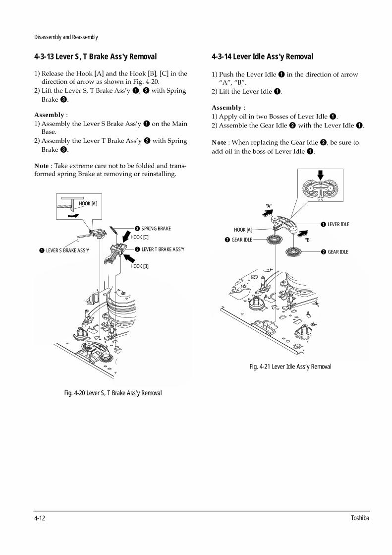
4-12 Toshiba
Disassembly and Reassembly
4-3-13 Lever S, T Brake Ass’y Removal
1) Release the Hook [A] and the Hook [B], [C] in the direction of arrow as shown in Fig. 4-20.
2) Lift the Lever S, T Brake Ass’y Œ, ´ with Spring Brake ˇ.
Assembly : 1) Assembly the Lever S Brake Ass’y Œ on the Main
Base.2) Assembly the Lever T Brake Ass’y ´ with Spring
Brake ˇ.
Note : Take extreme care not to be folded and trans-formed spring Brake at removing or reinstalling.
ˇ SPRING BRAKE
´ LEVER T BRAKE ASS'YŒ LEVER S BRAKE ASS'Y
HOOK [A]
HOOK [C]
HOOK [B]
4-3-14 Lever Idle Ass’y Removal
1) Push the Lever Idle Œ in the direction of arrow “A”, “B”.
2) Lift the Lever Idle Œ.
Assembly : 1) Apply oil in two Bosses of Lever Idle Œ. 2) Assemble the Gear Idle ´ with the Lever Idle Œ.
Note : When replacing the Gear Idle ´, be sure toadd oil in the boss of Lever Idle Œ.
ΠLEVER IDLE
´ GEAR IDLE
´ GEAR IDLE
HOOK [A]
"A"
"B"
Fig. 4-20 Lever S, T Brake Ass’y Removal
Fig. 4-21 Lever Idle Ass’y Removal

Disassembly and Reassembly
Toshiba 4-13
4-3-15 Disk S, T Reel Removal
1) Lift the Disk S, T Reel Œ, ´.
´ DISK T REEL
ΠDISK S REEL
4-3-16 Holder Clutch Ass’y Removal
1) Remove the Washer Slit Œ.2) Lift the Holder Clutch Ass’y ´.
Note : When you reinstall Holder Clutch Ass’y ´.1) Check the condition of spring as shown in
detail A.2) Don’t push Holder Clutch Ass’y down with exces-
sive force. Just insert Holder Clutch Ass’y into post center with dead force and rotate it smoothly. Be sure to confirm that spring is in the slit of Gear Center Ass’y as shown in detail B.
´ HOLDER CLUTCH ASS'Y
ΠWASHER SLIT
<BAD> <GOOD>
<BAD> <GOOD>
SPRING
SPRING
DETAIL A
DETAIL B
Fig. 4-22 Disk S, T Reel Removal
Fig. 4-23 Holder Clutch Ass’y Removal

4-14 Toshiba
Disassembly and Reassembly
4-3-17 Lever Up Down Ass’y, Gear Center Ass’y Removal
1) Remove the 2 hooks in the direction of arrow as shown Fig. 4-24 and lift the Lever Up Down Ass’y Œ.
2) Lift the Gear Center Ass’y ´.
´ GEAR CENTER ASS'Y
ΠLEVER UP DOWN ASS'Y
4-3-18 Assembly of Lever Up Down Ass’y, Gear Center Ass’y
1) Insert the Lever Up Down Ass’y Œ in the 2 rectan-gular holes on Main Base.
2) Lift the Lever Up Down Ass’y Œ about 35 degree. (Refer to Fig. 4-25)
3) Insert Ring ¨ of the Gear Center Ass’y ´ in the Guide ˆ of the Lever Up Down Ass’y Œ.
4) Insert the Gear Center Ass’y ´ in the post Ø on Main Base.
5) Push down the Lever Up Down Ass’y Œ for lock-ing of the Hook ∏.
Note : 1) Take care not to separate and loose the Spring Up
Down.2) When assembling the Gear Center Ass’y, don’t
push down too much.
MAIN BASE
ΠLEVER UP DOWN ASS'Y
ˆ GUDIE
´ GEAR CENTER ASS'Y
¨ RING
ˇ GEARØ POST ∏ HOOK 35˚
Fig. 4-24 Lever Up Down Ass’y, Gear Center Ass’y RemovalFig. 4-25 Assembly of Lever Up Down Ass’y, Gear Center Ass’y

Disassembly and Reassembly
Toshiba 4-15
4-3-19 Guide Cassette Door Removal
1) Lift the Hook [A].2) Rotate the Guide Cassette Door Πin the direction
of arrow.
Note : After reinstalling the Guide Cassette Door Œsecure the Hook [A].
ΠGUIDE CASSETTE DOOR
HOOK [A]
4-3-20 Unit Pinch Ass’y, Plate Joint, Spring Pinch Drive Removal
1) Lift the Unit Pinch Ass’y Œ.2) Remove the Plate Joint ´ from Lever Pinch Drive.3) Remove the Spring Pinch Drive ˇ.
Note : 1) Take extreme care not to touch the grease on the
Roller Pinch.2) When reinstalling, be sure to apply grease on the
post pinch roller.
ΠUNIT PINCH ASS'Y
´ PLATE JOINT
ˇ SPRING PINCH DRIVE
Fig. 4-26 Guide Cassette Door Removal
Fig. 4-27 Unit Pinch Ass’y, Plate Joint, Spring Pinch DriveRemoval

4-16 Toshiba
Disassembly and Reassembly
4-3-21 Lever #9 Guide Ass’y Removal
1) Remove the Spring #9 Guide Œ.2) Lift the Lever #9 Guide Ass’y ´ in the direction of
arrow.
Note : 1) Take extreme care not to touch the grease on the
tape Guide Post.2) After reinstalling, check the bottom side of the Post
#9 Guide to stick to the top side of Main Base.
´ LEVER #9 GUIDE ASS'Y
ΠSPRING #9 GUIDE
4-3-22 FE Head Removal
1) Remove the screw Œ.2) Lift the FE Head ´.
ΠSCREW
´ FE HEAD
Fig. 4-28 Lever #9 Guide Ass’y Removal
Fig. 4-29 FE Head Removal

Disassembly and Reassembly
Toshiba 4-17
4-3-23 ACE Head Removal
1) Pull out the FPC from connector of ACE Head Ass’y ´.
2) Remove the screw Œ.3) Lift the ACE Head Ass’y ´.
ΠSCREW
´ ACE HEAD ASS'Y
4-3-24 Slider S, T Ass’y Removal
1) Move the Slider S, T Ass’y Œ, ´ to slot, and then lift it to remove. (Refer to arrow)
´ SLIDER T ASS'Y
ΠSLIDER S ASS'Y
Fig. 4-30 ACE Head RemovalFig. 4-31 Slider S, T Ass’y Removal

4-18 Toshiba
Disassembly and Reassembly
4-3-25 Cylinder Ass’y Removal
1) Remove the 3 Screws Œ, ˇ, ˆ.2) Remove the Plate Cylinder A, B, C ´, ¨, Ø in the
direction of arrow.3) Lift the Cylinder Ass’y ∏.
Note : 1) When reinstalling, push the Plate Cylinder A, B ¨,
Ø in the reverse of arrow and then, tighten the 2 Screws ˇ, ˆ.
2) Take care not to touch the Cylinder Ass’y and the tape guide post at reinstalling Plate Cylinder C ´.
3) Take care not to touch the Cylinder Ass’y with screw driver at reinstalling the Plate Cylinder C ´.
ˆ SCREW
∏ CYLINDER ASS'Y
Œ SCREW´ PLATE CYLINDER Cˇ SCREW
¨ PLATE CYLINDER BØ PLATE CYLINDER A
4-3-26 Belt Pulley Removal
1) Remove the Belt Pulley Œ.
Note : Take extreme care not to touch the grease onBelt Pulley Πat assembling or reassembling.
ΠBELT PULLEY
Fig. 4-32 Cylinder Ass’y Removal
Fig. 4-33 Belt Pulley Removal

Disassembly and Reassembly
Toshiba 4-19
4-3-27 Motor Capstan Ass’y Removal
1) Remove the 3 Screws Œ.2) Remove the Motor Capstan Ass’y ´.
Assembly : 1) Match the 3 holes of Motor Capstan Ass’y ´ to the
3 holes of Main Base as attending not to drop or knock the Motor Capstan Ass’y.
2) Tighten the 3 Screws in the direction of arrow as shown detail drawing.
Note : 1) Don’t reuse the removed screws from Motor
Capstan Ass’y.2) After tightening screws, check if there is gap
between the head of screws and the top side of Main Base. There should have no gap between the head of screws and the top side of Main Base.
3) After reinstalling, adjusting the tape transport system again.
Π3 SCREWS
´ MOTOR CAPSTAN ASS'Y
B
C
A
<DETAIL>
4-3-28 How to Eject the Cassette Tape(If the unit does not oprate on condition that isinserted into housing ass’y)
1) Remove the Holder worm Œ and the Gear Worm ´.
2) Turn the Gear Worm Wheel ˇ counterclockwise with screw driver. (Refer to arrow)
ΠHOLDER WORM
´ GEAR WORM
SCREW DRIVER
ˇ GEAR WORM WHEEL
Fig. 4-34 Motor Capstan Ass’y Removal
Fig. 4-35
3) When Slider S, T are approched in the position of unloading, rotate holder Clutch counterclockwise after inserting screw driver in the hole of frame’s bottom in order to wind the unwinded tape. (Refer to Fig. 4-36)(If you rotate Gear Worm Wheel continuously when tape is in state of unwinding, you may cause a tape contamination by grease and tape damage. Be sure to wind the unwinded tape in the state of set horizently.)
4) Rotate Gear Worm Wheel ˇ counterclockwise using screw driver again up to the state of eject mode and then pick out the tape. (Refer to Fig. 4-35)
FRAME
Fig. 4-36

4-20 Toshiba
Disassembly and Reassembly
4-4 The table of clearing, Lubrication and replacement time about principal parts
1) The replacement time of parts is not life of parts.2) The table 4-1 is that the VCR Set is in normal condition (normal temperature, normal humidity).
The checking period may be changed owing to the condition of use, runtime and environmental conditions.3) Life of the Cylinder Ass’y is depend on the condition of use.4) See exploded view for location of each parts.
<Tbale 4-1>
∆ : Cleaning O : Check and replacement in necessary ◆ : Add Oil
TAPE
PATH
SYSTEM
DRIVING
* Parts NameChecking Period
Remark500 1000 1500 2000 2500 3000 3500 4000 4500 5000
POST TENSION ∆ ∆ ∆ ∆ ∆ ∆ ∆ ∆ ∆ ∆SLANT POST S, T ∆ ∆ ∆ ∆ ∆ ∆ ∆ ∆ ∆ ∆#8 GUIDE SHAFT ∆ ∆ ∆ ∆ ∆ ∆ ∆ ∆ ∆ ∆CAPSTAN SHAFT ∆ ∆ ∆ ∆ ∆ ∆ ∆ ∆ ∆ ∆#9 GUIDE POST ∆ ∆ ∆ ∆ ∆ ∆ ∆ ∆ ∆ ∆#3 GUIDE POST ∆ ∆ ∆ ∆ ∆ ∆ ∆ ∆ ∆ ∆
GUIDE ROLLER S, T ∆ ∆ ∆ O O O O O O OCYLINDER ASS’Y ∆ O O O O O O O O O
FE HEAD ∆ ∆ ∆ O O O O O O OACE HEAD ∆ O O O O O O O O O
PINCH ROLLER ∆ O O O O O O O O OPOST REEL S, T ◆ ◆ ◆ ◆ ◆
SLEEVE TENSION ◆ ◆ ◆ ◆ ◆POST CENTER ◆ ◆ ◆ ◆ ◆
LEVER IDLE BOSS (2Point) ◆ ◆ ◆ ◆ ◆CAPSTAN MOTOR PULLEY ∆ ∆ ∆ ∆ ∆ O O O O O
BELT PULLEY O O O O O O OHOLDER CLUTCH ASS’Y ∆ O O O O O O O O OGEAR CENTER ASS’Y O O O O O O O O O
GEAR IDLE (2Point) O O O O O O O O OLOADING MOTOR O O O O O O O O O
BAND BRAKE ASS’Y O O O O O O O O OBRAKE T ASS’Y O O O O O O O O O
SYSTEM
- Periodic time of applying oil(Apply oil after cleaning)
- The excessive applying oil may bethe cause of malfunction.
- To clean the parts, use patch andalcohol (solvent).
- After cleaning, use the video tapeafter alcohol is gone awny completely.
- We recomnend to use oil [EP-56] or solvent.
- One or two drops of oil should be applied after cleaning with alcohol.
BRAKE
SYSTEM

Toshiba 5-1
5. Alignment and Adjustment
5-1 Reference
1) X-Point (Tracking center) adjustment, “Head switching adjustment” and “NVRAM option setting” can be adjusted with remote control.2) When replacing the micom (IC601) be sure to adjust the “Head switching adjustment” and “NVRAM option setting”.3) When replacing the cylinder ass’y, be sure to adjust the “X-Point” and “Head switching adjustment”.4) Remote control used for same chassis as a accessory is available for all adjustments.5) How to adjustment.
- Intermittently short-circuit the test point on Main PCB with pincets to set the adjustment mode.- If the corresponding adjustment button is pressed, the adjustment is preformed automatically.- If the adjustment is completed, be sure to turn the power off.
5-1-1 Location of adjustment button of remote control
Fig. 5-1
7 8
0 100
9
65
2 3
4
1
STOP
PLAY
FFREW
SLOW PAUSE/STILL
CANCEL
A.SELECT
EJECT
PROG. ENTER
TIMER
TV VOL
CH/TRK
RECSP/SLP
DISPLAY TV/VCRCOUNT RESETREMAIN/
COUNTER
I.SELECT
POWERVCR TV
CURSOR
X-Point (Tracking Center)Adjustment
Head Switching Adjustment
NVRAM Option Setting
VC-602

5-2 Toshiba
Alignment and Adjustment
5-1-2 Test point location for adjustment mode setting
Fig. 5-2 Main PCB (Top View)
Short-Circuit

Alignment and Adjustment
Toshiba 5-3
5-2 Mechanical Adjustment
5-2-1 Tape Transport System and Adjustment Locations
The tape transport system has been adjusted precisely in the factory. Alignment is not necessary except for the following : 1) Noise observed on the screen.2) Tape damage.3) Parts replacement in the tape transport system.
Lower flange height of tape guide is used as the reference for the transport adjustment.To maintain the height of the tape guide and prevent damage, do not apply excessive force onto the main base.
Fig. 5-3 Location of Tape Transport Adjustment
Fig. 5-4 Tape Travel Diagram
CYLINDER ASS'Y
TAKE UP REEL DISK
#8 GUIDE POST
#9 GUIDE POST
SUPPLY REEL DISK
CAPSTAN
PINCH ROLLER
GUIDE ROLLER "T"
GUIDE ROLLER "S"
FULL ERASE HEAD
#3 GUIDE POST
TENSION POST
HEIGHT SCREW
TILT SCREWX - POSITIONADJUST SILT
AZIMUTH SCREW
POST TENSION
MAIN BASE
FE HEAD CYLINDER ASS'Y PINCH ROLLER
GUIDE ROLLER "S" GUIDE ROLLER "T"#8 GUIDE POST #9 GUIDE POST
CAPSTAN SHAFTACE HEAD
#3 GUIDE POST

5-4 Toshiba
Alignment and Adjustment
5-2-2 Tape Transport System Adjustment
When parts are replaced, perform the required adjustments by referring to precedures for the tape transportsystem. If there are any changes to the tape path, first run a T-120 tape and make sure excessive tape wrinkle doesnot occur at the tape guides.
1) If tape wrinkle is observed at the guide roller S, T, turn the guide roller S, T until wrinkle disappears.2) If the tape wrinkle is still observed at the tape guide, perform the tilt adjustment of the ACE head.
(1) ACE Head Assembly Adjustment
Test point : TP601 (Control Pulse)
TP602 (H’D S/W -Trigger)
TP301 (Envelope)
TP302 (Audio output)
TP303 (Video output)
Test tape : ST-N1
BLANK TAPE : T-160
Fig. 5-5 Location of Test point (Main PCB-Top View)
AUDIO OUTPUT
HEAD SWITCHING
ENVELOPE
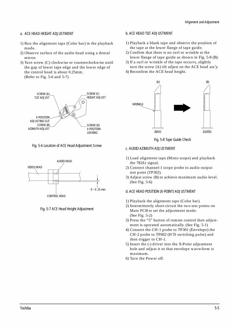
Alignment and Adjustment
Toshiba 5-5
a. ACE HEAD HEIGHT ADJUSTMENT
1) Run the alignment tape (Color bar) in the playback mode.
2) Observe surface of the audio head using a dental mirror.
3) Turn screw (C) clockwise or counterclockwise until the gap of lower tape edge and the lower edge of the control head is about 0.25mm. (Refer to Fig. 5-6 and 5-7)
Fig. 5-6 Location of ACE Head Adjustment Screw
Fig. 5-7 ACE Head Height Adjustment
SCREW (A)TLIT ADJUST
X-POSITIONADJUSTING SLIT
SCREW (C)HEIGHT ADJUST
SCREW (D)X-POSITION LOCKING
SCREW (B)AZIMUTH ADJUST
0 ~ 0 .25 mm
AUDIO HEAD
VIDEO HEAD
CONTROL HEAD
b. ACE HEAD TILT ADJUSTMENT
1) Playback a blank tape and observe the position of the tape at the lower flange of tape guide.
2) Confirm that there is no curl or wrinkle at the lower flange of tape guide as shown in Fig. 5-8 (B).
3) If a curl or wrinkle of the tape occurrs, slightly turn the screw (A) tilt adjust on the ACE head ass’y.
4) Reconfirm the ACE head height.
Fig. 5-8 Tape Guide Check
c. AUDIO AZIMUTH ADJUSTMENT
1) Load alignment tape (Mono scope) and playback the 7KHz signal.
2) Connect channel-1 scope probe to audio output test point (TP302).
3) Adjust screw (B) to achieve maximum audio level. (See Fig. 5-6)
d. ACE HEAD POSITION (X-POINT) ADJUSTMENT
1) Playback the alignment tape (Color bar).2) Intermittently short-circuit the two test points on
Main PCB to set the adjustment mode. (See Fig. 5-2)
3) Press the “5” button of remote control then adjust-ment is operated automatically. (See Fig. 5-1)
4) Connect the CH-1 probe to TP301 (Envelope) the CH-2 probe to TP602 (H’D switching pulse) and then trigger to CH-1.
5) Insert the (-) driver into the X-Point adjustment hole and adjust it so that envelope wavwform is maximum.
6) Turn the Power off.
(A) (B)
(BAD)
WRINKLE
(GOOD)

5-6 Toshiba
Alignment and Adjustment
(2) Linearity adjustment (Guide roller S, T adjustment)
1) Playback the Mono Scope alignment tape (SP mode).2) Observe the video envelope signal on an oscillo-
scope (triggered by the video switching pulse).3) Make sure the video envelope waveform (at its
minimum) meets the specification shown in Fig. 5-9.If it does not, adjust as follows :
Note : a=Maximum output of the video RF envelope.b=Minimum output of the video RF envelope at the
entrance side.c=Minimum output of the video RF envelope at the
center point.d=Maximum output of the video RF envelope at the
exit side.
4) If the section A in Fig. 5-10 does not meet the spec-ification, adjust the guide roller S up or down.
5) If the section B in Fig. 5-10 does not meet the speci-fication, adjust the guide roller T up or down.
Fig. 5-09 Envelope Waveform Adjustment
a
a b c dc,b,d/a 63%
b c d
Fig. 5-10 Adjustment Points
A B
A B
H'D SWITCHINGPULSE
ENVELOPE
6) Play back the Mono Scope alignment tape (SP mode).7) Connect an oscilloscope CH-1 to the Envelope and CH-2 to the H’D SW Pulse for triggering.8) Turn the guide roller heads with a flat head ( ) driver to obtain a flat video RF envelope as shown in Fig. 5-11.
Fig. 5-11 Guide Roller S, T Height Adjustment
IDEAL ENVELOPE
S HEIGHTTOO HIGH
S HEIGHTTOO LOW
T HEIGHTTOO LOW
T HEIGHTTOO HIGH
GUIDE ROLLER S GUIDE ROLLER T

Alignment and Adjustment
Toshiba 5-7
(3) Check Transitional Operation from RPS to Play
Check transition from RPS mode to play mode :Using a pre-recorded SP tape, make sure the entryside of envelope comes to an appropriate steady statewithin 3 seconds (as shown in Fig. 5-12). If the envelope waveform does not reach specifiedpeak-to peak amplitude within 3 seconds, adjust asfollows :
1) Make sure there is no gap between the supply roller lower flange and the tape.If there is a gap, adjust the supply guide roller again.
2) Change operation mode from the RPS to the play mode (again) and make sure the entry side of envelope rises within 3 second.
ENTRANCE SIDE ENVELOPE
Fig. 5-12 Video Envelope Rising when Operation mode Changesfrom RPS to Play Mode
(4) Envelope Check
1) Make recordings on T-120 (E-120) and T-160 (E-180) tape. Make sure the playback output envelope meets the specification as shown in Fig. 5-13.
2) Play back a self recorded tape (recording made on the unit using with T-120 (E-120). The video envelope should meet the specification as shown in Fig. 5-13. In SP mode, (A) should equal (B).If the head gap is wide, upper cylinder should be checked.
AB
Fig. 5-13 Envelope Output and Output Level
(5) Tape Wrinkle Check
1) Run the T-160 (E-180) tape in the playback, FPS, RPS and Pause modes and observe tape wrinkle at each guide.
2) If excessive tape wrinkle is observed, perform the following adjustments in Playback mode :
◆ Tape wrinkle at the guide roller S, T section : Linearity adjustment.
◆ Tape wrinkle at tape guide flange : ACE head assembly coarse adjustment.

5-8 Toshiba
Alignment and Adjustment
5-2-3 Reel Torque
1) The rotation of the capstan motor causes the holder clutch ass’y to rotat through the belt pulley.
2) The spring wrap PLAY/REV of holder clutch ass’y drives the disk reel S, T through gear idle by rota-tion of gear center ass’y.
3) Brake is operated by slider cam at FF/REW mode.4) Transportation of accurate driving force is done by
gears. (Gear Center Ass’y)
Note : If the spec. does not meet the followings speci-fications, replace the holder clutch ass’y and thenrecheck.
4) As rotating Disk S Reel Œ clockwise and the region of adjusting in the Main Base (in shape of slit) clockwise or counterclockwise after inserting screw driver in the slit on Main Base. Adjust the left end edge of Lever Tension Ass’y ˇ to 1.3 +1.5/-0.5mm from the location of mark in the Main Base.
5) As rotating Disk S Reel Œ, double-check the loca-tion of the left end edge of Lever Tension Ass’y and the quanity of crossing from mark on Main Base. (+1.0/-0.5mm)
Counterclockwise : Torque UPClockwise : Torque DOWN
Back Tension should be 56 ± 15g.cm at inspecting itwith Back Tension Meter.
1.0mm0.5mm
ˇ LEVER TENSION ASS'Y
ΠDISK S REEL
´ ADJUSTING
ADJUSTING SLIT
1.3
Fig. 5-16 Tension Pole and Back Tension Adjustment
5-2-4 Location adjustment and Confirmation of Tension Post
1) Remove the holder cassette ass’y and then push the lever FL Arm-R to the direction of loading.
2) Push the lever tension drive Πin the direction of arrow. (See Fig. 5-14)
3) Turn the gear worm wheel ´ clockwise so that “Timing Point” of the slider FL drive ˇ and gear FL cam ¨ can be aligned (See Fig. 5-14)
Fig. 5-14
Fig. 5-15
¨ GEAR FL CAM
´ GEAR WORM WHEELˇ SLIDER FL DRIVE
P
TIMING POINT
ΠLEVER TENSION DRIVELEVER TENSION
<Table 5-1>
Note :1) Mark on Main Base is located in about 1.3mm
from inside of bending line.2) Be careful not to deform the region of adjusting on
Main Base up and down at adjusting.
MODE TORQUE g/cm GAUGE
PBNTSC 82.5 ± 27.5
Cassette TorquemeterPAL 79 ± 27
RPS 145 ± 30 Cassette Torquemeter

Alignment and Adjustment
Toshiba 5-9
5-3 Head Switching Point Adjustment
1) Playback the alignment tape.2) Intermittently short-circuit the two test points on Main PCB to set the adjustment mode. (See Fig. 5-2)3) Press the “SP/SLP” button of remote control then adjustment is operated automatically. (See Fig. 5-1)4) Turn the Power off.
5-4 NVRAM Option Setting
1) Intermittently short-circuit the two test points on Main PCB to set the adjustment mode. (See Fig. 5-2)2) Press the “PROG.” button of remote control about 5 seconds then option setting display is appeared.
(See Fig. 5-17)3) Select the option number (See Table 5-2) of corresponding model with “FF” and “REW” button of remote
control.4) If selecting the option number is completed, press the “PLAY” button of remote control.
(If “PLAY” button is pressed, the selected number is changes reversed color. ; See Fig. 5-17)5) Press the “ENTER” button of remote control again to store the option number.
(“SAVE” is displayed for a second as shown Fig. 5-18 this setting is completed.)6) Turn the Power off.
1) NVRAM Option is adjusted at production line basically. 2) In case Micom (IC601) and NVRAM (IC603 ; EEPROM) is replaced, be sure to set the corresponding ooption number of the repaired
model. (If the option is not set, the unit is not operated.)
ENTER : SAVE
01 02 03 04 05 06 07 08
09 10 11 12 13 14 15 16
Fig. 5-17
ENTER : SAVE
01 02 03 04 05 06 07 08
09 10 11 12 13 14 15 16
Fig. 5-18
How to identify the Type
TypeAssy-Cylinder Capstan Motor VR501ALPS SEM Sankyo SEM Be None
A • • •B • • •C • • •D • • •E • • •F • • •G • • •H • • •
MODEL TYPE OPTION NUMBERW-602 A 2, 3, 6, 8, 9, 11, 16
B 2, 3, 6, 8, 9, 11C 2, 3, 6, 8, 11, 16D 2, 3, 6, 8, 11E 2, 3, 6, 9, 11, 16F 2, 3, 6, 9, 11G 2, 3, 6, 11, 16H 2, 3, 6, 11
<Table 5-2>

5-10 Toshiba
Alignment and Adjustment
How to identify the Assy-Cylinder
Fig. 5-19
ALPS Cylinder SEM Cylinder
CONNECTOR ; Pin 7 or Pin 5 CONNECTOR ; Pin 5
TOP VIEW
SANKYO CAPSTAN MOTOR SEM CAPSTAN MOTOR
CAPSTAN SHAFT CAPSTAN SHAFT
Fig. 5-20
How to identify the Capstan Motor

Alignment and Adjustment
Toshiba 5-11
Fig. 5-21 Main PCB (Top View)
VR501
Location for VR501

5-12 Toshiba
Alignment and Adjustment
MEMO

Toshiba 6-1
6. Exploded View
6-1 Packing Assembly - - - - - - - - - - - - - - - - - - - - - - - - - - - - - -
6-2 Instrument Assembly - - - - - - - - - - - - - - - - - - - - - - - - - - - -
6-3 Mechanical Parts (Top Side) - - - - - - - - - - - - - - - - - - - - - - -
6-4 Mechanical Parts (Bottom Side) - - - - - - - - - - - - - - - - - - - -
6-2
6-3
6-4
6-5

Exploded View
6-2 Toshiba
6-1 Packing Assembly
A702
A701
A702
Y101
Y102
UT01

Exploded View
Toshiba 6-3
6-2 Instrument Assembly15
3
FULL
DEC
K (S
.N.A
)
BRAC
KET-
FRAM
E(S
.N.A
)
157
701
702
157
101
155
TM40
1B
601
S601
A
LD60
1A
S602
A
200
CN60
5B
CN30
3B BOTT
OM-C
OVER
(S.N
.A)
S.N
.A :
Serv
ice
Not
Ava
ilabl
e
21
221
31

Exploded View
6-4 Toshiba
6-3 Mechanical Parts (Top Side)
G001
K250
K248
K110
K502
K350
K330
K182
K140
K490
K530
K240
G532
G450
K546
G510
B410
B440
B444
B446
B448
B452
G527 G5
20
G480
G680
(OPT
ION
AL)
S.N
.AS.
N.A
K470
B474
S.N
.AG5
30
K180
K340
B473
K188
G555
G546
S.N
.A :
Serv
ice
Not
Ava
ilabl
e
K544
K542
B239
G428
G420
G458
(OPT
ION
AL)

Exploded View
Toshiba 6-5
6-4 Mechanical Parts (Bottom Side)G5
42
B560
B484 B2
57
B458
B500
B488
B257
B478
B462
B460
(OPT
ION
AL)
B456
B468
B464
B258
K222
K200
K225
K221
B570
B238
S.N
.A :
Serv
ice
Not
Ava
ilabl
e

Exploded View
6-6 Toshiba
MEMO

- PACKING PARTS -A701 BY730588 AC69-00055M PACKING CASE;W-602/TSB,-,326,505,150,-,-A702 BY730463 AC69-00040A CUSHION-F/B;M-686,EPS,-,-,-,-,-UT01 BY730474 AC59-10426D REMOCON-ASSY;-,VC-604T,-,-,W-602/TSB,TSBY101 BY634263 AC68-00701A MANUAL USERS;W-602/TSB,MOJO100,L185,W260Y102 BY634274 AC39-42001J CABLE-RF ASSY;#1365,-,1.2MT,75-75OHM,-,-
- INSTRUMENT PARTS -1 BY730477 AC97-00518G ASSY-PANEL FRONT;W-602/TSB,HIPS94V2,D/GR21 BY730475 AC64-00127G DOOR-CASSETTE;-,ABS94HB,-,T2.5,-,BLK,-,W22 BY730093 AC61-62032A SPRING-MASK;X-9,-,SUS,-,4.4,-,SV-C13031 BY730459 AC64-00133A DOOR-FRONT;-,ABS94HBGRY,-,-,-,G3019,-,W-101 BY730457 AC64-00124A CABINET-TOP;-,PCM(SECC),-,T0.5,-,TM6524,153 70790218 AC60-12126A SCREW-BH;-,BH,-,4*12,FE,FZY,-,-,-155 70790082 AC60-12134A SCREW-TAP BH;-,BH,-,2-4X16,-,FE157 70790002 AC60-10063A SCREW-TAPTITE;BH,+,-,M3,L12,ZPC3,SWRCH18200 BY634046 AC39-10200N POWER-CORD;EP2,SPT-2,AWG#18,1.8MT,WAFER,CN303B BY634042 3809-001110 CABLE-FLAT;30V,80C,150mm,7P,1.25mm,UL289CN605B BY634043 3809-001112 CABLE-FLAT;30V,80C,130mm,5P,1.25mm,UL289LD601A BY730082 AC61-21009A HOLDER-LED;-,POM(M90-44),-,BLK,-,X-9S601A BY730080 AC61-21008A HOLDER-SENSOR;-,POM(M90-44),-,BLK,-,X-9S602A BY730080 AC61-21008A HOLDER-SENSOR;-,POM(M90-44),-,BLK,-,X-9TM401B BY730499 AC61-00058A CONNECTOR-BOARD-ASSY;-,HIPS,-,T2,61,-,BL
- MECHANICAL PARTS -B238 BY730087 AC61-50660A SLEEVE-TENSION;-,POM M90-44,-,-,ID3,-,-,B239 BY730234 AC61-21004A CAP-#8 GUIDE;-,POM M90-44,-,NTR,-,X-9B257 BY730247 AC61-50661A POST-MAIN PCB;-,POM M90-44,-,-,NTR,-,X-9B258 BY730266 AC61-50684A GUIDE-MAIN PCB;-,POM,OD7,L20,-,BLACK,X-9B410 BY730456 AC31-12016D MOTOR-LOADING ASSY;-,SNHNE,-,-B440 BY730072 AC60-10515A SCREW-MACHINE;-,PH,+,-,M3,L3,ZPC,-,YELB444 BY730104 AC66-20571A GEAR-WORM;-,POM SW-01,0.5,2,-,4.5,X-9B446 BY730079 AC61-21005A HOLDER-WORM;-,POM M90-44,-,-,-,X-9B448 BY730105 AC66-20573A GEAR-WORM WHEEL;-,POM SW-01,0.6,11,-,6.6B452 BY730107 AC66-20575A GEAR-FL CAM;-,POM SW-01,M0.6,Z88,-,PCD58B456 BY730108 AC66-20576A GEAR-JOINT 1;-,POM SW-01,M1.0,Z22,-,PCD2B458 BY730106 AC66-20574A GEAR-JOINT 2;-,POM SW-01,M1.0,Z14,-,PCD1B460 BY730447 AC61-11045A BRACKET-GEAR;-,SECC20/20,-,T1.2,-,-,X-9B462 BY730073 AC60-10517A SCREW-TAP TITE;-,PH,+,-,M2.6,L5,ZPC,-,YEB464 BY730381 AC66-80140A SLIDER-CAM;-,SECC20/20,T1.2,-,-,X-9B468 BY730450 AC66-30541A LEVER-PINCH DR ASSY;-,-,-,-,-,X-9B473 BY730090 AC61-60559A SPRING-PINCH DRIVE;-,TS,SUS304,PI0.5,OD4B474 BY730244 AC61-30180A PLATE-JOINT;-,SECC20/20,T0.8,-,X-9B478 BY730449 AC66-30540A LEVER-TENS DR ASSY;-,-,-,-,-,X-9B484 BY730110 AC66-20580A GEAR-LOADING DRIVE;-,POM SW-01,M1.0,Z32,B488 BY730117 AC66-30543A LEVER-S LOAD ASSY;-,-,-,-,-,X-9B500 BY730116 AC66-30542A LEVER-T LOAD ASSY;-,-,-,-,-,X-9B560 BY730654 AC31-00006A MOTOR-CAPSTAN;-,DMVCMC07JR,-,-B570 BY730071 AC60-10514A SCREW-CAPSTAN;-,PH,+,M2.6,L6,-G001 BY730655 AC97-00550A ASSY-CYLINDER;CX-9TA,NTSC,6HDG420 BY730124 AC66-80142A SLIDER-SUPPLY ASSY;-,X-9(TS),-,-,-,X-9G428 BY730451 AC66-40153A ROLLER-SUPPLY ASSY;-,VW-32,OD7,-,X-9G450 BY730123 AC66-80141A SLIDER-TAKE UP ASSY;-,X-9(TS),-,-,-,X-9G458 BY730452 AC66-40154A ROLLER-TAKE UP ASSY;-,VW-32,OD7,-,X-9G480 BY730052 AC33-00003A HEAD-ACE-ASSY;SHINHEUNG,-,-,-,-,X-9G510 BY730479 6006-001075 SCREW-ASS’Y TAPT;WSP,PH,+,M2.6,L5.0,ZPC(G520 BY730115 AC66-30539A LEVER-#9 GUIDE ASSY;-,X-9(TS),-,-,-,X-9G527 BY730088 AC61-60553A SPRING-#9 GUIDE;-,ES,SUS304-WPB,OD3.1,0.G530 BY730053 AC33-00002A HEAD-FE;-,HVFHP0038A,-,-,-,X-9G532 BY730075 AC60-10519A SCREW-TAP TITE;-,PH,+,-,M2.6,L8,ZPCG542 BY730122 AC66-60051A BELT-PULLEY;-,5CM-70,2 * 2,-,71.3,-,X-9G546 BY730113 AC66-30535A LEVER-FL DOOR;-,POM M90-44,-,-,BLK,X-9G555 BY730070 AC59-90403A UNIT-PINCH ASSY;X-9,-G680 BY730372 AC66-30557A LEVER-H/CLEANER ASSY;-,POM+URETHANE,-,-,K110 BY730102 AC66-10267A REEL-DISK S;-,POM M90-44,-,-,X-9K140 BY730103 AC66-10268A REEL-DISK T;-,POM M90-44,-,-,X-9K180 BY730369 AC66-30548A LEVER-IDLER ASSY;-,POM+NYLON,-,-,-,X-9K182 BY730112 AC66-30524A LEVER-IDLER;-,POM9044,-,-,-,-K188 BY730109 AC66-20577A GEAR-IDLER;-,PEBAX 7033,-,-,-,-,X-9K200 BY730084 AC61-21012A HOLDER-CLUTCH ASSY;-,-,-,-,-,X-9K221 BY730111 AC66-20581A GEAR-CENTER ASSY;-,POM,M=O.5,-,HIGHT T.,K222 BY730076 AC60-30306A WASHER-SLIT;-,-,ID2.1,OD5.0,T0.5,-,POLYS
Toshiba 7-1
7. Replacement Parts List
Loc.No. TSB Parts No. Reference No. Description ; Specification Remark

K225 BY730119 AC66-30547A LEVER-UP DOWN ASSY;-,POM+SUS,-,-,-,X-9K240 BY730114 AC66-30538A LEVER-TENSION ASSY;-,X-9(TS),-,-,-,X-9K248 BY730089 AC61-60554A SPRING-TENSION LEVER;-,ES,SUS304-WPB,OD3K250 BY730094 AC63-12029A BAND-BRAKE ASSY;-,X-9(TS),-,-,-,X-9K330 BY730121 AC66-30550A LEVER-S.BRAKE ASSY;-,POM+SUS,-,-,-,X-9K340 BY730120 AC66-30549A LEVER-T.BRAKE ASSY;-,POM+SUS,-,-,-,X-9K350 BY730092 AC61-60564A SPRING-BRAKE;-,TENSION,SWP-A,0.25,3,-,X-K470 BY730454 AC66-80139A SLIDER-FL DRIVE;-,SECC E20/20,T1.2,-,-,XK490 BY730083 AC61-21010B HOLDER-CASS ASSY;-,SECC+POM+SUS,-,-,SEINK502 BY730091 AC61-60561A SPRING-FL.LEVER-LR;-,ES,SUS304 WPB,PI2.7K530 BY730118 AC66-30546A LEVER-FL.ARM ASS’Y;-,SECC+POM+SUS,-,-,-,K546 BY730086 AC61-50658A GUIDE-CASS. DOOR;-,POM M90-44,-,-,NTR,-,
- ELECTRICAL PARTS -601 BY630105 AC92-00492A ASSY-PCB-MAIN;W-605/TSB,MAIN701 BY630093 AC94-00037B ASSY-FUNCTION;W-607/TSB,TWIN,HI-FI,20 TS702 BY630094 AC94-00038B ASSY-TIMER-VFD;W-609/TSB,TWIN,HI-FI,20 T
<INTERGRATED CIRCUIT>IC1SS1 BY530004 0604-001028 PHOTO-COUPLER;TR,50-600%,250mW,DIP-4,STIC1SS2 BY631008 AC14-12006D IC;KA431Z,TO-92,TAPINGIC301 BY631088 1204-001644 IC-VIDEO PROCESS;LA71069M,QFP,100P,-,PLAIC501 BY631089 1209-001264 IC-ETC, LINEAR;AN3662FBP,QFP,64P,551MIL,IC601 BY631101 AC09-00098A IC-MICOM;MN101D02D-CC1,MN101D02D-CC1,10IC602 BY631022 1003-001162 IC-MOTOR DRIVER;KA3082,SIP,10PIN,25MIL,DIC603 BY631045 1103-001148 IC-EEPROM;24C021,2KBIT,DIP,8P,300MIL,10MIC6B1 70795269 AC14-12006C IC;KA7533,DIP,-
<TRANSISTORS>Q1P101 70693265 0501-000616 TR-SMALL SIGNAL;KSC2328A-Y,NPN,1W,TO-92LQ1P102 70693265 0501-000616 TR-SMALL SIGNAL;KSC2328A-Y,NPN,1W,TO-92LQ1P103 70693084 0504-000142 TR-DIGITAL;KSR2001,PNP,300MW,4.7K/4.7K,TQ1P104 70795136 0501-000398 TR-SMALL SIGNAL;KSC945,NPN,250mW,TO-92,TQ1P105 70795136 0501-000398 TR-SMALL SIGNAL;KSC945,NPN,250mW,TO-92,TQ1P107 70693265 0501-000616 TR-SMALL SIGNAL;KSC2328A-Y,NPN,1W,TO-92LQ1P108 70693084 0504-000142 TR-DIGITAL;KSR2001,PNP,300MW,4.7K/4.7K,TQ1P109 70795136 0501-000398 TR-SMALL SIGNAL;KSC945,NPN,250mW,TO-92,TQ1SR01 70795142 0501-000442 TR-SMALL SIGNAL;KTC3203-Y,NPN,400MW,T0-9Q1SR02 BY530002 0502-001123 TR-POWER;KTC4419,NPN,30W,TO-220,ST,10-4Q302 70795134 0501-000303 TR-SMALL SIGNAL;KSA733,PNP,250mW,TO-92,TQ303 70795136 0501-000398 TR-SMALL SIGNAL;KSC945,NPN,250mW,TO-92,TQ304 70795134 0501-000303 TR-SMALL SIGNAL;KSA733,PNP,250mW,TO-92,TQ305 70795142 0501-000442 TR-SMALL SIGNAL;KTC3203-Y,NPN,400MW,T0-9Q306 70795134 0501-000303 TR-SMALL SIGNAL;KSA733,PNP,250mW,TO-92,TQ307 70795142 0501-000442 TR-SMALL SIGNAL;KTC3203-Y,NPN,400MW,T0-9Q308 70795142 0501-000442 TR-SMALL SIGNAL;KTC3203-Y,NPN,400MW,T0-9Q311 70795136 0501-000398 TR-SMALL SIGNAL;KSC945,NPN,250mW,TO-92,TQ501 70795142 0501-000442 TR-SMALL SIGNAL;KTC3203-Y,NPN,400MW,T0-9Q6H01 70693410 0501-000610 TR-SMALL SIGNAL;KSA928A-Y,PNP,1W,TO-92L,Q6H02 70795137 0504-000116 TR-DIGITAL;KSR1001,NPN,300MW,4.7K/4.7K,TQ701 70795134 0501-000303 TR-SMALL SIGNAL;KSA733,PNP,250mW,TO-92,TQ702 70795134 0501-000303 TR-SMALL SIGNAL;KSA733,PNP,250mW,TO-92,TQ703 70795134 0501-000303 TR-SMALL SIGNAL;KSA733,PNP,250mW,TO-92,TQ704 70795134 0501-000303 TR-SMALL SIGNAL;KSA733,PNP,250mW,TO-92,TQ705 70795134 0501-000303 TR-SMALL SIGNAL;KSA733,PNP,250mW,TO-92,TQ706 70795134 0501-000303 TR-SMALL SIGNAL;KSA733,PNP,250mW,TO-92,TQ707 70795134 0501-000303 TR-SMALL SIGNAL;KSA733,PNP,250mW,TO-92,TQ708 70795134 0501-000303 TR-SMALL SIGNAL;KSA733,PNP,250mW,TO-92,TQ709 70795134 0501-000303 TR-SMALL SIGNAL;KSA733,PNP,250mW,TO-92,TQ710 70795134 0501-000303 TR-SMALL SIGNAL;KSA733,PNP,250mW,TO-92,TQ711 70795134 0501-000303 TR-SMALL SIGNAL;KSA733,PNP,250mW,TO-92,TQ712 70795134 0501-000303 TR-SMALL SIGNAL;KSA733,PNP,250mW,TO-92,TQ713 70795134 0501-000303 TR-SMALL SIGNAL;KSA733,PNP,250mW,TO-92,TQ714 70795134 0501-000303 TR-SMALL SIGNAL;KSA733,PNP,250mW,TO-92,TQ715 70795134 0501-000303 TR-SMALL SIGNAL;KSA733,PNP,250mW,TO-92,TQ716 70795134 0501-000303 TR-SMALL SIGNAL;KSA733,PNP,250mW,TO-92,TQ801 70795134 0501-000303 TR-SMALL SIGNAL;KSA733,PNP,250mW,TO-92,T
<DIODES>D1P101 BY430003 0402-000132 DIODE-RECTIFIER;1N4004,400V,1A,DO-41,TPD1P102 70796385 0402-000127 DIODE-RECTIFIER;1N4002,100V,1A,DO-41,TPD1P104 BY430003 0402-000132 DIODE-RECTIFIER;1N4004,400V,1A,DO-41,TPD1P107 BY430003 0402-000132 DIODE-RECTIFIER;1N4004,400V,1A,DO-41,TPD1P108 70795150 0401-000101 DIODE-SWITCHING;1N4148,100V,200mA,DO-35,D1P109 70795150 0401-000101 DIODE-SWITCHING;1N4148,100V,200mA,DO-35,D1SD01 70795150 0401-000101 DIODE-SWITCHING;1N4148,100V,200mA,DO-35,D1SD02 70795150 0401-000101 DIODE-SWITCHING;1N4148,100V,200mA,DO-35,D1SR01 70795150 0401-000101 DIODE-SWITCHING;1N4148,100V,200mA,DO-35,D1SR02 70795150 0401-000101 DIODE-SWITCHING;1N4148,100V,200mA,DO-35,
Replacement Parts List
7-2 Toshiba
Loc.No. TSB Parts No. Reference No. Description ; Specification Remark

D1SS01 BY430012 0402-001196 DIODE-RECTIFIER;1T5,600V,1A,TS-1,TPD1SS02 BY430012 0402-001196 DIODE-RECTIFIER;1T5,600V,1A,TS-1,TPD1SS03 BY430012 0402-001196 DIODE-RECTIFIER;1T5,600V,1A,TS-1,TPD1SS04 BY430012 0402-001196 DIODE-RECTIFIER;1T5,600V,1A,TS-1,TPD1SS05 BY430008 0402-000276 DIODE-RECTIFIER;UF4007,1KV,1A,DO-41,TPD1SS06 BY430010 0402-001194 DIODE-RECTIFIER;UG2D,200V,2A,DO-204AC,TPD1SS07 BY430009 0402-000431 DIODE-RECTIFIER;FML-M02S,200V,2.5A,TO-22D304 70795150 0401-000101 DIODE-SWITCHING;1N4148,100V,200mA,DO-35,D503 70795150 0401-000101 DIODE-SWITCHING;1N4148,100V,200mA,DO-35,D601 70795150 0401-000101 DIODE-SWITCHING;1N4148,100V,200mA,DO-35,D603 BY430003 0402-000132 DIODE-RECTIFIER;1N4004,400V,1A,DO-41,TPD604 BY430003 0402-000132 DIODE-RECTIFIER;1N4004,400V,1A,DO-41,TPD605 70795150 0401-000101 DIODE-SWITCHING;1N4148,100V,200mA,DO-35,D607 BY430003 0402-000132 DIODE-RECTIFIER;1N4004,400V,1A,DO-41,TPD6H01 BY430011 0402-001195 DIODE-RECTIFIER;F1T4,400V,1.0A,TS-1,TPD702 70795150 0401-000101 DIODE-SWITCHING;1N4148,100V,200mA,DO-35,D703 70795150 0401-000101 DIODE-SWITCHING;1N4148,100V,200mA,DO-35,D704 70795150 0401-000101 DIODE-SWITCHING;1N4148,100V,200mA,DO-35,D705 70795150 0401-000101 DIODE-SWITCHING;1N4148,100V,200mA,DO-35,D707 70795150 0401-000101 DIODE-SWITCHING;1N4148,100V,200mA,DO-35,D708 70795150 0401-000101 DIODE-SWITCHING;1N4148,100V,200mA,DO-35,D7F01 BY430011 0402-001195 DIODE-RECTIFIER;F1T4,400V,1.0A,TS-1,TPD7FR01 70795150 0401-000101 DIODE-SWITCHING;1N4148,100V,200mA,DO-35,D7FR02 70795150 0401-000101 DIODE-SWITCHING;1N4148,100V,200mA,DO-35,LD601 BY430016 0601-000517 LED-IR;RECTANGULA,4x6.0mm,75mW,6V,950W038 70796385 0402-000127 DIODE-RECTIFIER;1N4002,100V,1A,DO-41,TPZD1P01 70795272 0403-000390 DIODE-ZENER;UZP33B,33V,31.4-34.6V,1W,DO-ZD1P03 BY430013 0403-000720 DIODE-ZENER;MTZJ9.1B,9.1V,8.57-9.01V,500ZD1P05 BY430015 0403-001211 DIODE-ZENER;MTZJ12B,11.44-12.03V,500MW,DZD1SR1 70795438 0403-000571 DIODE-ZENER;UZP43B,43V,40-46V,1W,DO-41,TZD7FT1 BY430004 0403-000509 DIODE-ZENER;MTZJ5.6B,5.6V,5.45-5.73V,500ZD7FT2 BY430014 0403-001141 DIODE-ZENER;MTZJ24D,24V,23.63-24.85V,500
<INDUCTORS>BD1SR1 BY330019 3301-000297 CORE-FERRITE BEAD;AA,3.6x1.2x5.7mm,1400,BD1SS1 70795644 AC27-92001M INDUCTOR;70UH-M RT BFS3565R2F,-,-,-,-BD6H01 70795644 AC27-92001M INDUCTOR;70UH-M RT BFS3565R2F,-,-,-,-FL301 BY330006 AC27-80100C COIL-OSC;7mm,2.4mH,-L1P101 BY330009 2701-000002 INDUCTOR-AXIAL;100uH,10%,4.2x9.8mmL1P102 BY330009 2701-000002 INDUCTOR-AXIAL;100uH,10%,4.2x9.8mmL1SS01 BY330008 AC29-30050C FILTER-LINE NOISE;-,25MH,0.35A,AC250V,BSL1SS02 70796213 AC27-12001N COIL-CHOKE;10UH-15%,RA,K-30,Q80,150KHZ,-L1SS03 70796213 AC27-12001N COIL-CHOKE;10UH-15%,RA,K-30,Q80,150KHZ,-L301 BY330019 3301-000297 CORE-FERRITE BEAD;AA,3.6x1.2x5.7mm,1400,L302 BY330019 3301-000297 CORE-FERRITE BEAD;AA,3.6x1.2x5.7mm,1400,L303 BY330019 3301-000297 CORE-FERRITE BEAD;AA,3.6x1.2x5.7mm,1400,L304 BY330019 3301-000297 CORE-FERRITE BEAD;AA,3.6x1.2x5.7mm,1400,L305 BY330019 3301-000297 CORE-FERRITE BEAD;AA,3.6x1.2x5.7mm,1400,L306 70795171 2702-000120 INDUCTOR-RADIAL;15mH,5%,6.2x7.4mmL307 70795168 2702-000108 INDUCTOR-RADIAL;100uH,5%,6x6.4mmL501 70795168 2702-000108 INDUCTOR-RADIAL;100uH,5%,6x6.4mmL502 BY330019 3301-000297 CORE-FERRITE BEAD;AA,3.6x1.2x5.7mm,1400,L503 BY330019 3301-000297 CORE-FERRITE BEAD;AA,3.6x1.2x5.7mm,1400,L504 BY330046 2701-000126 INDUCTOR-AXIAL;150uH,5%,2.4x3.4mmL601 BY330019 3301-000297 CORE-FERRITE BEAD;AA,3.6x1.2x5.7mm,1400,L801 70796362 2701-000168 INDUCTOR-AXIAL;3.3uH,5%,2.5x3.4mmL802 BY330019 3301-000297 CORE-FERRITE BEAD;AA,3.6x1.2x5.7mm,1400,
<CAPACITROS>C1P101 BY130017 2401-001730 C-AL;10uF,20%,50V,GP,TP,5x11,2.5C1P103 BY130136 2401-002299 C-AL;4.7uF,20%,50V,GP,TP,5x7,5C1P104 BY130136 2401-002299 C-AL;4.7uF,20%,50V,GP,TP,5x7,5C1P105 BY130042 2401-000598 C-AL;1uF,20%,50V,GP,TP,4x7,5C1P106 BY130249 2401-002008 C-AL;100uF,20%,16V,GP,TP,6.3x11,2.5C1P108 BY130009 2401-001545 C-AL;47uF,20%,25V,GP,TP,6.3x7mm,2.5C1P112 BY130136 2401-002299 C-AL;4.7uF,20%,50V,GP,TP,5x7,5C1SD01 BY130218 2201-000445 C-CERAMIC,DISC;3.3nF,20%,400V,Y5P,TP,-,1C1SD06 BY130270 2301-000423 C-FILM,PEF;3.3NF,5%,100V,TP,7X10X4.5MM,5C1SR01 70795578 2401-001681 C-AL;82uF,20%,200V,GP,TP,16x26,7.5mC1SR02 70795430 2401-000905 C-AL;22uF,20%,16V,BP,-,6x11,2.5mmC1SR03 BY130046 2401-001235 C-AL;4.7uF,20%,250V,WT,TP,10x12.5,5C1SR04 70795586 2301-000417 C-FILM,PEF;24nF,5%,50V,TP,6.5x10.5x4mm,5C1SR05 70796231 2301-000176 C-FILM,PEF;18nF,5%,100V,TP,10X9X4.3X5,5mC1SR06 70795088 2201-000930 C-CERAMIC,DISC;0.22nF,10%,500V,Y5P,TP,5.C1SR07 70795239 2201-000795 C-CERAMIC,DISC;10nF,10%,400V,Y5P,TP,15x1C1SS04 70795404 2201-000916 C-CERAMIC,DISC;100pF,10%,400V,Y5U,TP,10xC1SS06 70795431 2401-000385 C-AL;10uF,20%,100V,GP,TP,6.3x11,5C1SS07 70796014 2401-002162 C-AL;1000uF,20%,25V,WT,TP,10x20,5mmC1SS08 BY130045 2401-001126 C-AL;330uF,20%,25V,WT,TP,10x12.5,5
Replacement Parts List
Toshiba 7-3
Loc.No. TSB Parts No. Reference No. Description ; Specification Remark

C1SS10 70796210 2401-000118 C-AL;1000uF,20%,10V,GP,TP,10x12.5,5C1SS11 70796098 2301-000129 C-FILM,PEF;100nF,5%,50V,TP,10X9X4.3X5,5mC1SS35 BY130050 2401-003059 C-AL;1000UF,20%,16V,WT,TP,10X16,5C301 BY130191 2203-000476 C-CERAMIC,CHIP;1000nF,+80-20%,16V,Y5V,TPC302 BY130009 2401-001545 C-AL;47uF,20%,25V,GP,TP,6.3x7mm,2.5C303 70796207 2203-001557 C-CERAMIC,CHIP;100nF,+80-20%,25V,Y5V,TP,C304 BY130031 2203-001721 C-CERAMIC,CHIP;360pF,5%,50V,NPO,TP,2012,C305 BY130042 2401-000598 C-AL;1uF,20%,50V,GP,TP,4x7,5C306 70795462 2203-001584 C-CERAMIC,CHIP MELF;180PF,10%,50V,Y5E,TPC307 70795253 2203-001637 C-CERAMIC,CHIP MELF;33PF,5%,50V,SL,TP,20C309 70699092 2401-000918 C-AL;22uF,20%,16V,GP,-,6.3x7,5C310 BY130273 2401-000414 C-AL;10uF,20%,16V,GP,TP,4x7,5C311 BY130039 2203-005549 C-CERAMIC,CHIP MELF;10nF,+80-20%,16V,Y5VC312 BY130042 2401-000598 C-AL;1uF,20%,50V,GP,TP,4x7,5C313 BY130037 2203-005547 C-CERAMIC,CHIP MELF;22nF,+80-20%,16V,Y5VC314 BY130273 2401-000414 C-AL;10uF,20%,16V,GP,TP,4x7,5C315 BY130191 2203-000476 C-CERAMIC,CHIP;1000nF,+80-20%,16V,Y5V,TPC316 BY130042 2401-000598 C-AL;1uF,20%,50V,GP,TP,4x7,5C317 BY130042 2401-000598 C-AL;1uF,20%,50V,GP,TP,4x7,5C318 BY130042 2401-000598 C-AL;1uF,20%,50V,GP,TP,4x7,5C319 70795075 2202-000797 C-CERAMIC,MLC-AXIAL;10NF,30%,16V,Y5S,TP,C320 70795075 2202-000797 C-CERAMIC,MLC-AXIAL;10NF,30%,16V,Y5S,TP,C321 BY130027 2202-002037 C-CERAMIC,MLC-AXIAL;100nF,80-20%,50V,Y5VC322 BY130009 2401-001545 C-AL;47uF,20%,25V,GP,TP,6.3x7mm,2.5C323 BY130027 2202-002037 C-CERAMIC,MLC-AXIAL;100nF,80-20%,50V,Y5VC324 BY130280 2401-002165 C-AL;100uF,20%,16V,GP,TP,6.3x7,5C325 BY130191 2203-000476 C-CERAMIC,CHIP;1000nF,+80-20%,16V,Y5V,TPC326 BY130042 2401-000598 C-AL;1uF,20%,50V,GP,TP,4x7,5C327 BY130020 2203-000989 C-CERAMIC,CHIP;47nF,10%,50V,X7R,TP,2012C328 70796207 2203-001557 C-CERAMIC,CHIP;100nF,+80-20%,25V,Y5V,TP,C329 BY130042 2401-000598 C-AL;1uF,20%,50V,GP,TP,4x7,5C330 BY130039 2203-005549 C-CERAMIC,CHIP MELF;10nF,+80-20%,16V,Y5VC331 BY130042 2401-000598 C-AL;1uF,20%,50V,GP,TP,4x7,5C332 BY130273 2401-000414 C-AL;10uF,20%,16V,GP,TP,4x7,5C333 70796207 2203-001557 C-CERAMIC,CHIP;100nF,+80-20%,25V,Y5V,TP,C334 BY130020 2203-000989 C-CERAMIC,CHIP;47nF,10%,50V,X7R,TP,2012C335 BY130020 2203-000989 C-CERAMIC,CHIP;47nF,10%,50V,X7R,TP,2012C336 70796207 2203-001557 C-CERAMIC,CHIP;100nF,+80-20%,25V,Y5V,TP,C337 BY130049 2401-002144 C-AL;47uF,20%,16V,GP,TP,5x11,5C338 70699092 2401-000918 C-AL;22uF,20%,16V,GP,-,6.3x7,5C339 BY130049 2401-002144 C-AL;47uF,20%,16V,GP,TP,5x11,5C340 BY130027 2202-002037 C-CERAMIC,MLC-AXIAL;100nF,80-20%,50V,Y5VC341 70796207 2203-001557 C-CERAMIC,CHIP;100nF,+80-20%,25V,Y5V,TP,C342 BY130009 2401-001545 C-AL;47uF,20%,25V,GP,TP,6.3x7mm,2.5C343 BY130136 2401-002299 C-AL;4.7uF,20%,50V,GP,TP,5x7,5C344 70796286 2203-001689 C-CERAMIC,CHIP MELF;8.2NF,30%,16V,Y5S,BKC345 BY130041 2301-001014 C-FILM,PEF;6.8nF,5%,50V,TP,7x3x6,5mmC346 70796281 2203-000260 C-CERAMIC,CHIP;10nF,10%,50V,X7R,TP,2012C349 70795254 2203-001671 C-CERAMIC,CHIP MELF;56PF,5%,50V,Y5E,TP,2C350 BY130049 2401-002144 C-AL;47uF,20%,16V,GP,TP,5x11,5C351 70795075 2202-000797 C-CERAMIC,MLC-AXIAL;10NF,30%,16V,Y5S,TP,C352 BY130145 2301-000253 C-FILM,PEF;39NF,5%,100V,TP,7.5X4.5X12.5MC353 70796207 2203-001557 C-CERAMIC,CHIP;100nF,+80-20%,25V,Y5V,TP,C356 BY130039 2203-005549 C-CERAMIC,CHIP MELF;10nF,+80-20%,16V,Y5VC357 BY130017 2401-001730 C-AL;10uF,20%,50V,GP,TP,5x11,2.5C358 BY130147 2203-000170 C-CERAMIC,CHIP;1.8nF,10%,50V,X7R,TP,2012C359 70795753 2203-001058 C-CERAMIC,CHIP;0.56nF,5%,50V,NP0,TP,2012C360 BY130136 2401-002299 C-AL;4.7uF,20%,50V,GP,TP,5x7,5C361 BY130191 2203-000476 C-CERAMIC,CHIP;1000nF,+80-20%,16V,Y5V,TPC362 BY130039 2203-005549 C-CERAMIC,CHIP MELF;10nF,+80-20%,16V,Y5VC363 BY130039 2203-005549 C-CERAMIC,CHIP MELF;10nF,+80-20%,16V,Y5VC364 BY130039 2203-005549 C-CERAMIC,CHIP MELF;10nF,+80-20%,16V,Y5VC365 70795075 2202-000797 C-CERAMIC,MLC-AXIAL;10NF,30%,16V,Y5S,TP,C366 BY130027 2202-002037 C-CERAMIC,MLC-AXIAL;100nF,80-20%,50V,Y5VC371 BY130039 2203-005549 C-CERAMIC,CHIP MELF;10nF,+80-20%,16V,Y5VC401 BY130039 2203-005549 C-CERAMIC,CHIP MELF;10nF,+80-20%,16V,Y5VC403 70795075 2202-000797 C-CERAMIC,MLC-AXIAL;10NF,30%,16V,Y5S,TP,C405 BY130049 2401-002144 C-AL;47uF,20%,16V,GP,TP,5x11,5C406 70795075 2202-000797 C-CERAMIC,MLC-AXIAL;10NF,30%,16V,Y5S,TP,C407 BY130037 2203-005547 C-CERAMIC,CHIP MELF;22nF,+80-20%,16V,Y5VC409 BY130027 2202-002037 C-CERAMIC,MLC-AXIAL;100nF,80-20%,50V,Y5VC410 70693249 2202-000807 C-CERAMIC,MLC-AXIAL;22nF,+80-20%,25V,Y5VC501 70796207 2203-001557 C-CERAMIC,CHIP;100nF,+80-20%,25V,Y5V,TP,C502 BY130273 2401-000414 C-AL;10uF,20%,16V,GP,TP,4x7,5C503 BY130136 2401-002299 C-AL;4.7uF,20%,50V,GP,TP,5x7,5C504 BY130273 2401-000414 C-AL;10uF,20%,16V,GP,TP,4x7,5C505 BY130136 2401-002299 C-AL;4.7uF,20%,50V,GP,TP,5x7,5C506 BY130042 2401-000598 C-AL;1uF,20%,50V,GP,TP,4x7,5C507 BY130250 2401-002068 C-AL;33uF,20%,16V,GP,TP,5x11,5
Replacement Parts List
7-4 Toshiba
Loc.No. TSB Parts No. Reference No. Description ; Specification Remark
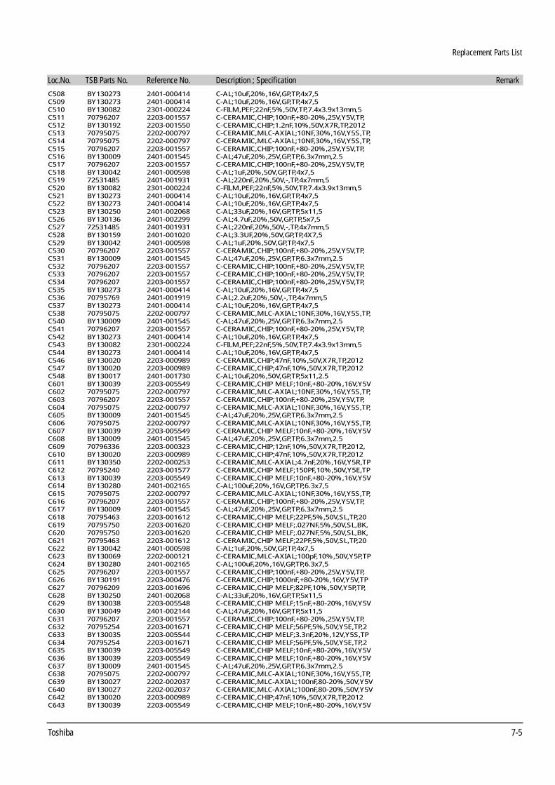
C508 BY130273 2401-000414 C-AL;10uF,20%,16V,GP,TP,4x7,5C509 BY130273 2401-000414 C-AL;10uF,20%,16V,GP,TP,4x7,5C510 BY130082 2301-000224 C-FILM,PEF;22nF,5%,50V,TP,7.4x3.9x13mm,5C511 70796207 2203-001557 C-CERAMIC,CHIP;100nF,+80-20%,25V,Y5V,TP,C512 BY130192 2203-001550 C-CERAMIC,CHIP;1.2nF,10%,50V,X7R,TP,2012C513 70795075 2202-000797 C-CERAMIC,MLC-AXIAL;10NF,30%,16V,Y5S,TP,C514 70795075 2202-000797 C-CERAMIC,MLC-AXIAL;10NF,30%,16V,Y5S,TP,C515 70796207 2203-001557 C-CERAMIC,CHIP;100nF,+80-20%,25V,Y5V,TP,C516 BY130009 2401-001545 C-AL;47uF,20%,25V,GP,TP,6.3x7mm,2.5C517 70796207 2203-001557 C-CERAMIC,CHIP;100nF,+80-20%,25V,Y5V,TP,C518 BY130042 2401-000598 C-AL;1uF,20%,50V,GP,TP,4x7,5C519 72531485 2401-001931 C-AL;220nF,20%,50V,-,TP,4x7mm,5C520 BY130082 2301-000224 C-FILM,PEF;22nF,5%,50V,TP,7.4x3.9x13mm,5C521 BY130273 2401-000414 C-AL;10uF,20%,16V,GP,TP,4x7,5C522 BY130273 2401-000414 C-AL;10uF,20%,16V,GP,TP,4x7,5C523 BY130250 2401-002068 C-AL;33uF,20%,16V,GP,TP,5x11,5C526 BY130136 2401-002299 C-AL;4.7uF,20%,50V,GP,TP,5x7,5C527 72531485 2401-001931 C-AL;220nF,20%,50V,-,TP,4x7mm,5C528 BY130159 2401-001020 C-AL;3.3UF,20%,50V,GP,TP,4X7,5C529 BY130042 2401-000598 C-AL;1uF,20%,50V,GP,TP,4x7,5C530 70796207 2203-001557 C-CERAMIC,CHIP;100nF,+80-20%,25V,Y5V,TP,C531 BY130009 2401-001545 C-AL;47uF,20%,25V,GP,TP,6.3x7mm,2.5C532 70796207 2203-001557 C-CERAMIC,CHIP;100nF,+80-20%,25V,Y5V,TP,C533 70796207 2203-001557 C-CERAMIC,CHIP;100nF,+80-20%,25V,Y5V,TP,C534 70796207 2203-001557 C-CERAMIC,CHIP;100nF,+80-20%,25V,Y5V,TP,C535 BY130273 2401-000414 C-AL;10uF,20%,16V,GP,TP,4x7,5C536 70795769 2401-001919 C-AL;2.2uF,20%,50V,-,TP,4x7mm,5C537 BY130273 2401-000414 C-AL;10uF,20%,16V,GP,TP,4x7,5C538 70795075 2202-000797 C-CERAMIC,MLC-AXIAL;10NF,30%,16V,Y5S,TP,C540 BY130009 2401-001545 C-AL;47uF,20%,25V,GP,TP,6.3x7mm,2.5C541 70796207 2203-001557 C-CERAMIC,CHIP;100nF,+80-20%,25V,Y5V,TP,C542 BY130273 2401-000414 C-AL;10uF,20%,16V,GP,TP,4x7,5C543 BY130082 2301-000224 C-FILM,PEF;22nF,5%,50V,TP,7.4x3.9x13mm,5C544 BY130273 2401-000414 C-AL;10uF,20%,16V,GP,TP,4x7,5C546 BY130020 2203-000989 C-CERAMIC,CHIP;47nF,10%,50V,X7R,TP,2012C547 BY130020 2203-000989 C-CERAMIC,CHIP;47nF,10%,50V,X7R,TP,2012C548 BY130017 2401-001730 C-AL;10uF,20%,50V,GP,TP,5x11,2.5C601 BY130039 2203-005549 C-CERAMIC,CHIP MELF;10nF,+80-20%,16V,Y5VC602 70795075 2202-000797 C-CERAMIC,MLC-AXIAL;10NF,30%,16V,Y5S,TP,C603 70796207 2203-001557 C-CERAMIC,CHIP;100nF,+80-20%,25V,Y5V,TP,C604 70795075 2202-000797 C-CERAMIC,MLC-AXIAL;10NF,30%,16V,Y5S,TP,C605 BY130009 2401-001545 C-AL;47uF,20%,25V,GP,TP,6.3x7mm,2.5C606 70795075 2202-000797 C-CERAMIC,MLC-AXIAL;10NF,30%,16V,Y5S,TP,C607 BY130039 2203-005549 C-CERAMIC,CHIP MELF;10nF,+80-20%,16V,Y5VC608 BY130009 2401-001545 C-AL;47uF,20%,25V,GP,TP,6.3x7mm,2.5C609 70796336 2203-000323 C-CERAMIC,CHIP;12nF,10%,50V,X7R,TP,2012,C610 BY130020 2203-000989 C-CERAMIC,CHIP;47nF,10%,50V,X7R,TP,2012C611 BY130350 2202-000253 C-CERAMIC,MLC-AXIAL;4.7nF,20%,16V,Y5R,TPC612 70795240 2203-001577 C-CERAMIC,CHIP MELF;150PF,10%,50V,Y5E,TPC613 BY130039 2203-005549 C-CERAMIC,CHIP MELF;10nF,+80-20%,16V,Y5VC614 BY130280 2401-002165 C-AL;100uF,20%,16V,GP,TP,6.3x7,5C615 70795075 2202-000797 C-CERAMIC,MLC-AXIAL;10NF,30%,16V,Y5S,TP,C616 70796207 2203-001557 C-CERAMIC,CHIP;100nF,+80-20%,25V,Y5V,TP,C617 BY130009 2401-001545 C-AL;47uF,20%,25V,GP,TP,6.3x7mm,2.5C618 70795463 2203-001612 C-CERAMIC,CHIP MELF;22PF,5%,50V,SL,TP,20C619 70795750 2203-001620 C-CERAMIC,CHIP MELF;.027NF,5%,50V,SL,BK,C620 70795750 2203-001620 C-CERAMIC,CHIP MELF;.027NF,5%,50V,SL,BK,C621 70795463 2203-001612 C-CERAMIC,CHIP MELF;22PF,5%,50V,SL,TP,20C622 BY130042 2401-000598 C-AL;1uF,20%,50V,GP,TP,4x7,5C623 BY130069 2202-000121 C-CERAMIC,MLC-AXIAL;100pF,10%,50V,Y5P,TPC624 BY130280 2401-002165 C-AL;100uF,20%,16V,GP,TP,6.3x7,5C625 70796207 2203-001557 C-CERAMIC,CHIP;100nF,+80-20%,25V,Y5V,TP,C626 BY130191 2203-000476 C-CERAMIC,CHIP;1000nF,+80-20%,16V,Y5V,TPC627 70796209 2203-001696 C-CERAMIC,CHIP MELF;82PF,10%,50V,Y5P,TP,C628 BY130250 2401-002068 C-AL;33uF,20%,16V,GP,TP,5x11,5C629 BY130038 2203-005548 C-CERAMIC,CHIP MELF;15nF,+80-20%,16V,Y5VC630 BY130049 2401-002144 C-AL;47uF,20%,16V,GP,TP,5x11,5C631 70796207 2203-001557 C-CERAMIC,CHIP;100nF,+80-20%,25V,Y5V,TP,C632 70795254 2203-001671 C-CERAMIC,CHIP MELF;56PF,5%,50V,Y5E,TP,2C633 BY130035 2203-005544 C-CERAMIC,CHIP MELF;3.3nF,20%,12V,Y5S,TPC634 70795254 2203-001671 C-CERAMIC,CHIP MELF;56PF,5%,50V,Y5E,TP,2C635 BY130039 2203-005549 C-CERAMIC,CHIP MELF;10nF,+80-20%,16V,Y5VC636 BY130039 2203-005549 C-CERAMIC,CHIP MELF;10nF,+80-20%,16V,Y5VC637 BY130009 2401-001545 C-AL;47uF,20%,25V,GP,TP,6.3x7mm,2.5C638 70795075 2202-000797 C-CERAMIC,MLC-AXIAL;10NF,30%,16V,Y5S,TP,C639 BY130027 2202-002037 C-CERAMIC,MLC-AXIAL;100nF,80-20%,50V,Y5VC640 BY130027 2202-002037 C-CERAMIC,MLC-AXIAL;100nF,80-20%,50V,Y5VC642 BY130020 2203-000989 C-CERAMIC,CHIP;47nF,10%,50V,X7R,TP,2012C643 BY130039 2203-005549 C-CERAMIC,CHIP MELF;10nF,+80-20%,16V,Y5V
Replacement Parts List
Toshiba 7-5
Loc.No. TSB Parts No. Reference No. Description ; Specification Remark

C644 BY130039 2203-005549 C-CERAMIC,CHIP MELF;10nF,+80-20%,16V,Y5VC6B01 70699061 2401-000199 C-AL;1000uF,20%,6.3V,GP,TP,10x12.5,C6H01 BY130187 2401-003137 C-AL;330UF,20%,50V,WT,TP,10X16MM,5C6H02 BY130042 2401-000598 C-AL;1uF,20%,50V,GP,TP,4x7,5C7F01 BY130225 2401-001353 C-AL;470uF,20%,10V,GP,TP,8x11.5,5C7F02 BY130281 2401-003046 C-AL;47uF,20%,50V,WT,TP,6.3x11,2.5C7F03 70795585 2301-000383 C-FILM,PEF;10nF,5%,50V,TP,6x7x3.2mm,5mmC7FT01 70795075 2202-000797 C-CERAMIC,MLC-AXIAL;10NF,30%,16V,Y5S,TP,C7FT02 BY130262 2202-000173 C-CERAMIC,MLC-AXIAL;1nF,10%,50V,Y5P,TP,1C7FT03 BY130280 2401-002165 C-AL;100uF,20%,16V,GP,TP,6.3x7,5C7FT04 70795075 2202-000797 C-CERAMIC,MLC-AXIAL;10NF,30%,16V,Y5S,TP,C7FT05 BY130136 2401-002299 C-AL;4.7uF,20%,50V,GP,TP,5x7,5C801 BY130049 2401-002144 C-AL;47uF,20%,16V,GP,TP,5x11,5C802 BY130225 2401-001353 C-AL;470uF,20%,10V,GP,TP,8x11.5,5C803 BY130217 2401-002042 C-AL;220uF,20%,10V,GP,TP,6.3x11,5C804 70693215 2202-000787 C-CERAMIC,MLC-AXIAL;10PF,5%,50V,Y5P,TP,3C805 BY130017 2401-001730 C-AL;10uF,20%,50V,GP,TP,5x11,2.5C8F1 BY130027 2202-002037 C-CERAMIC,MLC-AXIAL;100nF,80-20%,50V,Y5VC8F2 BY130273 2401-000414 C-AL;10uF,20%,16V,GP,TP,4x7,5W1SR04 BY130216 2201-000812 C-CERAMIC,DISC;2.2nF,20%,400V,Y5U,BK,12.
<RESISTORS>R1P101 70795358 2001-000857 R-CARBON;560OHM,5%,1/8W,AA,TP,1.8X3.2MMR1P102 70795210 2007-001584 R-CHIP,MELF;2.2Kohm,5%,1/8W,DB,BK,2012R1P104 70795025 2001-000554 R-CARBON;270OHM,5%,1/8W,AA,TP,1.8X3.2MMR1P110 70796067 2001-000362 R-CARBON;150OHM,5%,1/8W,AA,TP,1.8X3.2MMR1SD01 70796356 2001-000490 R-CARBON;200OHM,5%,1/8W,AA,TP,1.8X3.2MMR1SD02 70795019 2001-000515 R-CARBON;220OHM,5%,1/8W,AA,TP,1.8X3.2MMR1SD03 70795005 2001-000429 R-CARBON;1KOHM,5%,1/8W,AA,TP,1.8X3.2MMR1SR01 70795002 2002-000320 R-COMPOSITION;1.8Mohm,10%,1/2W,AA,TP,3.5R1SR02 BY230018 2003-002117 R-METAL OXIDE(S);330Kohm,5%,1W,AA,TP,3.3R1SR03 BY230016 2003-000314 R-METAL OXIDE;47ohm,5%,2W,AE,TP,6x16mmR1SR04 BY230016 2003-000314 R-METAL OXIDE;47ohm,5%,2W,AE,TP,6x16mmR1SR05 70795030 2001-000003 R-CARBON;330ohm,5%,1/8W,AA,TP,1.8x3.2mmR1SR06 70796275 2003-000119 R-METAL OXIDE;0.68ohm,5%,2W,AE,TP,6x16mmR1SR07 70795040 2001-000734 R-CARBON;4.7KOHM,5%,1/8W,AA,TP,1.8X3.2MR1SS01 BY230027 2003-000994 R-METAL OXIDE(S);33Kohm,5%,2W,AF,TP,3.9xR1SS02 BY230027 2003-000994 R-METAL OXIDE(S);33Kohm,5%,2W,AF,TP,3.9xR1SS04 70795005 2001-000429 R-CARBON;1KOHM,5%,1/8W,AA,TP,1.8X3.2MMR1SS05 70795640 2004-000869 R-METAL;3Kohm,1%,1/8W,AA,TP,1.8x3.2mmR1SS06 70795638 2004-000459 R-METAL;2.2Kohm,1%,1/8W,AA,TP,1.8x3.2mR301 70796181 2007-001553 R-CHIP,MELF;2Kohm,5%,1/8W,DB,BK,2012R302 70795221 2007-001513 R-CHIP,MELF;4.7KOHM,5%,1/8W,DB,BK,2012R303 70795520 2007-000241 R-CHIP;1.5KOHM,5%,1/10W,DA,TP,2012R303 70796179 2007-001633 R-CHIP,MELF;1.5Kohm,5%,1/8W,DB,BK,2012R304 70796191 2007-001555 R-CHIP,MELF;27Kohm,5%,1/8W,DB,BK,2012R308 BY230006 2007-001561 R-CHIP,MELF;24Kohm,5%,1/8W,DB,BK,2012R309 70795232 2007-001568 R-CHIP,MELF;22Kohm,5%,1/8W,DB,BK,2012R310 70795225 2007-001458 R-CHIP,MELF;8.2KOHM,5%,1/8W,DB,BK,2012R311 70795221 2007-001513 R-CHIP,MELF;4.7KOHM,5%,1/8W,DB,BK,2012R313 70795020 2001-000449 R-CARBON;2.2KOHM,5%,1/8W,AA,TP,1.8X3.2MR314 BY230028 2007-001456 R-CHIP,MELF;820KOHM,5%,1/8W,DB,BK,2012R315 70796179 2007-001633 R-CHIP,MELF;1.5Kohm,5%,1/8W,DB,BK,2012R316 70795213 2007-001629 R-CHIP,MELF;1.8Kohm,5%,1/8W,DB,BK,2012R317 70796179 2007-001633 R-CHIP,MELF;1.5Kohm,5%,1/8W,DB,BK,2012R318 70795225 2007-001458 R-CHIP,MELF;8.2KOHM,5%,1/8W,DB,BK,2012R320 70795233 2007-001623 R-CHIP,MELF;10Kohm,5%,1/8W,DB,BK,2012R326 70795023 2001-000454 R-CARBON;2.2MOHM,5%,1/8W,AA,TP,1.8X3.2MR327 70795205 2007-001546 R-CHIP,MELF;3.9Kohm,5%,1/8W,DB,BK,2012R329 70795238 2007-001517 R-CHIP,MELF;3KOHM,5%,1/8W,DB,BK,2012R330 BY230019 2001-000221 R-CARBON;1.2KOHM,5%,1/8W,AA,TP,1.8X3.2MR331 70795447 2001-000878 R-CARBON;6.2KOHM,5%,1/8W,AA,TP,1.8X3.2MR332 70796194 2007-001448 R-CHIP,MELF;9.1KOHM,5%,1/8W,DB,BK,2012R334 70795232 2007-001568 R-CHIP,MELF;22Kohm,5%,1/8W,DB,BK,2012R335 70796198 2007-001505 R-CHIP,MELF;470OHM,5%,1/8W,DB,BK,2012R336 70795213 2007-001629 R-CHIP,MELF;1.8Kohm,5%,1/8W,DB,BK,2012R337 70796373 2007-001582 R-CHIP,MELF;2.2ohm,5%,1/8W,DB,BK,2012R338 70795607 2001-000405 R-CARBON;180OHM,5%,1/8W,AA,TP,1.8X3.2MMR339 70795005 2001-000429 R-CARBON;1KOHM,5%,1/8W,AA,TP,1.8X3.2MMR340 70795005 2001-000429 R-CARBON;1KOHM,5%,1/8W,AA,TP,1.8X3.2MMR341 70795232 2007-001568 R-CHIP,MELF;22Kohm,5%,1/8W,DB,BK,2012R342 70795233 2007-001623 R-CHIP,MELF;10Kohm,5%,1/8W,DB,BK,2012R344 70795011 2001-000331 R-CARBON;12KOHM,5%,1/8W,AA,TP,1.8X3.2MMR345 70795019 2001-000515 R-CARBON;220OHM,5%,1/8W,AA,TP,1.8X3.2MMR346 70795209 2007-001534 R-CHIP,MELF;33KOHM,5%,1/8W,DB,BK,2012R347 70795208 2007-001589 R-CHIP,MELF;1Kohm,5%,1/8W,DB,BK,2012R348 70795221 2007-001513 R-CHIP,MELF;4.7KOHM,5%,1/8W,DB,BK,2012R349 70795224 2007-001495 R-CHIP,MELF;510OHM,5%,1/8W,DB,BK,2012R350 70795224 2007-001495 R-CHIP,MELF;510OHM,5%,1/8W,DB,BK,2012
Replacement Parts List
7-6 Toshiba
Loc.No. TSB Parts No. Reference No. Description ; Specification Remark

R352 70795215 2007-001497 R-CHIP,MELF;5.6KOHM,5%,1/8W,DB,BK,2012R353 70795233 2007-001623 R-CHIP,MELF;10Kohm,5%,1/8W,DB,BK,2012R354 70796278 2007-001538 R-CHIP,MELF;330KOHM,5%,1/8W,DB,BK,2012R355 70795208 2007-001589 R-CHIP,MELF;1Kohm,5%,1/8W,DB,BK,2012R356 70795234 2007-001572 R-CHIP,MELF;220Kohm,5%,1/8W,DB,BK,2012R357 70795234 2007-001572 R-CHIP,MELF;220Kohm,5%,1/8W,DB,BK,2012R358 70795216 2007-001601 R-CHIP,MELF;15Kohm,5%,1/8W,DB,BK,2012R359 70795029 2001-000633 R-CARBON;30KOHM,5%,1/8W,AA,TP,1.8X3.2MMR360 70795058 2001-000977 R-CARBON;8.2KOHM,5%,1/8W,AA,TP,1.8X3.2MR361 BY230020 2007-001499 R-CHIP,MELF;5.1Kohm,5%,1/8W,DB,BK,2012R362 70795041 2001-000786 R-CARBON;47KOHM,5%,1/8W,AA,TP,1.8X3.2MMR363 70795213 2007-001629 R-CHIP,MELF;1.8Kohm,5%,1/8W,DB,BK,2012R364 70796199 2007-001503 R-CHIP,MELF;47KOHM,5%,1/8W,DB,BK,2012R367 BY230179 2001-000595 R-CARBON;3.3MOHM,5%,1/8W,AA,TP,1.8X3.2MMR397 70795233 2007-001623 R-CHIP,MELF;10Kohm,5%,1/8W,DB,BK,2012R401 70796198 2007-001505 R-CHIP,MELF;470OHM,5%,1/8W,DB,BK,2012R402 70796198 2007-001505 R-CHIP,MELF;470OHM,5%,1/8W,DB,BK,2012R501 70795215 2007-001497 R-CHIP,MELF;5.6KOHM,5%,1/8W,DB,BK,2012R502 70795215 2007-001497 R-CHIP,MELF;5.6KOHM,5%,1/8W,DB,BK,2012R503 70795215 2007-001497 R-CHIP,MELF;5.6KOHM,5%,1/8W,DB,BK,2012R504 70795215 2007-001497 R-CHIP,MELF;5.6KOHM,5%,1/8W,DB,BK,2012R506 70795209 2007-001534 R-CHIP,MELF;33KOHM,5%,1/8W,DB,BK,2012R507 70795227 2007-001550 R-CHIP,MELF;3.3Kohm,5%,1/8W,DB,BK,2012R510 70795004 2001-000281 R-CARBON;100OHM,5%,1/8W,AA,TP,1.8X3.2MMR511 70796199 2007-001503 R-CHIP,MELF;47KOHM,5%,1/8W,DB,BK,2012R512 70795004 2001-000281 R-CARBON;100OHM,5%,1/8W,AA,TP,1.8X3.2MMR513 70796199 2007-001503 R-CHIP,MELF;47KOHM,5%,1/8W,DB,BK,2012R514 70795039 2001-000780 R-CARBON;470OHM,5%,1/8W,AA,TP,1.8X3.2MMR515 70795447 2001-000878 R-CARBON;6.2KOHM,5%,1/8W,AA,TP,1.8X3.2MR516 70795039 2001-000780 R-CARBON;470OHM,5%,1/8W,AA,TP,1.8X3.2MMR517 70796329 2007-001526 R-CHIP,MELF;36KOHM,5%,1/8W,DB,BK,2012R518 70796194 2007-001448 R-CHIP,MELF;9.1KOHM,5%,1/8W,DB,BK,2012R519 70795041 2001-000786 R-CARBON;47KOHM,5%,1/8W,AA,TP,1.8X3.2MMR520 70795041 2001-000786 R-CARBON;47KOHM,5%,1/8W,AA,TP,1.8X3.2MMR521 70699144 2001-000472 R-CARBON;2.7KOHM,5%,1/8W,AA,TP,1.8X3.2MR522 70795211 2007-001578 R-CHIP,MELF;2.7Kohm,5%,1/8W,DB,BK,2012R524 70795011 2001-000331 R-CARBON;12KOHM,5%,1/8W,AA,TP,1.8X3.2MMR525 70699144 2001-000472 R-CARBON;2.7KOHM,5%,1/8W,AA,TP,1.8X3.2MR527 70795233 2007-001623 R-CHIP,MELF;10Kohm,5%,1/8W,DB,BK,2012R530 70796183 2007-001612 R-CHIP,MELF;12Kohm,5%,1/8W,DB,BK,2012R531 70795507 2001-000679 R-CARBON;36KOHM,5%,1/8W,AA,TP,1.8X3.2MMR601 70795232 2007-001568 R-CHIP,MELF;22Kohm,5%,1/8W,DB,BK,2012R602 70795218 2007-001570 R-CHIP,MELF;220ohm,5%,1/8W,DB,BK,2012R603 70795232 2007-001568 R-CHIP,MELF;22Kohm,5%,1/8W,DB,BK,2012R604 70795218 2007-001570 R-CHIP,MELF;220ohm,5%,1/8W,DB,BK,2012R605 BY230144 2001-000111 R-CARBON;150OHM,5%,1/4W,AA,TP,2.4X6.4MMR606 70795021 2001-000522 R-CARBON;22KOHM,5%,1/8W,AA,TP,1.8X3.2MMR607 70796196 2007-001540 R-CHIP,MELF;30KOHM,5%,1/8W,DB,BK,2012R608 70795005 2001-000429 R-CARBON;1KOHM,5%,1/8W,AA,TP,1.8X3.2MMR609 70795005 2001-000429 R-CARBON;1KOHM,5%,1/8W,AA,TP,1.8X3.2MMR610 70795005 2001-000429 R-CARBON;1KOHM,5%,1/8W,AA,TP,1.8X3.2MMR611 70796182 2007-001627 R-CHIP,MELF;100Kohm,5%,1/8W,DB,BK,2012R613 70795040 2001-000734 R-CARBON;4.7KOHM,5%,1/8W,AA,TP,1.8X3.2MR614 70795005 2001-000429 R-CARBON;1KOHM,5%,1/8W,AA,TP,1.8X3.2MMR615 70795215 2007-001497 R-CHIP,MELF;5.6KOHM,5%,1/8W,DB,BK,2012R616 70795005 2001-000429 R-CARBON;1KOHM,5%,1/8W,AA,TP,1.8X3.2MMR617 70795230 2007-001637 R-CHIP,MELF;1.2Kohm,5%,1/8W,DB,BK,2012R618 70795029 2001-000633 R-CARBON;30KOHM,5%,1/8W,AA,TP,1.8X3.2MMR619 70795005 2001-000429 R-CARBON;1KOHM,5%,1/8W,AA,TP,1.8X3.2MMR620 70795005 2001-000429 R-CARBON;1KOHM,5%,1/8W,AA,TP,1.8X3.2MMR621 70796198 2007-001505 R-CHIP,MELF;470OHM,5%,1/8W,DB,BK,2012R622 70796198 2007-001505 R-CHIP,MELF;470OHM,5%,1/8W,DB,BK,2012R623 70795233 2007-001623 R-CHIP,MELF;10Kohm,5%,1/8W,DB,BK,2012R624 70795233 2007-001623 R-CHIP,MELF;10Kohm,5%,1/8W,DB,BK,2012R625 70795233 2007-001623 R-CHIP,MELF;10Kohm,5%,1/8W,DB,BK,2012R626 70795237 2007-001607 R-CHIP,MELF;13Kohm,5%,1/8W,DB,BK,2012R627 70795005 2001-000429 R-CARBON;1KOHM,5%,1/8W,AA,TP,1.8X3.2MMR629 70795030 2001-000003 R-CARBON;330ohm,5%,1/8W,AA,TP,1.8x3.2mmR630 70795047 2001-000864 R-CARBON;56KOHM,5%,1/8W,AA,TP,1.8X3.2MMR631 70795047 2001-000864 R-CARBON;56KOHM,5%,1/8W,AA,TP,1.8X3.2MMR632 70795041 2001-000786 R-CARBON;47KOHM,5%,1/8W,AA,TP,1.8X3.2MMR633 70795234 2007-001572 R-CHIP,MELF;220Kohm,5%,1/8W,DB,BK,2012R634 70796331 2007-001507 R-CHIP,MELF;470KOHM,5%,1/8W,DB,BK,2012R635 70795005 2001-000429 R-CARBON;1KOHM,5%,1/8W,AA,TP,1.8X3.2MMR637 70795005 2001-000429 R-CARBON;1KOHM,5%,1/8W,AA,TP,1.8X3.2MMR638 70795227 2007-001550 R-CHIP,MELF;3.3Kohm,5%,1/8W,DB,BK,2012R639 70795523 2007-000267 R-CHIP;1.8KOHM,5%,1/10W,DA,TP,2012R641 70795208 2007-001589 R-CHIP,MELF;1Kohm,5%,1/8W,DB,BK,2012R642 70795208 2007-001589 R-CHIP,MELF;1Kohm,5%,1/8W,DB,BK,2012
Replacement Parts List
Toshiba 7-7
Loc.No. TSB Parts No. Reference No. Description ; Specification Remark

R643 70795233 2007-001623 R-CHIP,MELF;10Kohm,5%,1/8W,DB,BK,2012R644 70795233 2007-001623 R-CHIP,MELF;10Kohm,5%,1/8W,DB,BK,2012R645 70795233 2007-001623 R-CHIP,MELF;10Kohm,5%,1/8W,DB,BK,2012R646 70795215 2007-001497 R-CHIP,MELF;5.6KOHM,5%,1/8W,DB,BK,2012R647 70795030 2001-000003 R-CARBON;330ohm,5%,1/8W,AA,TP,1.8x3.2mmR648 70795030 2001-000003 R-CARBON;330ohm,5%,1/8W,AA,TP,1.8x3.2mmR649 70795221 2007-001513 R-CHIP,MELF;4.7KOHM,5%,1/8W,DB,BK,2012R650 70795221 2007-001513 R-CHIP,MELF;4.7KOHM,5%,1/8W,DB,BK,2012R651 70795221 2007-001513 R-CHIP,MELF;4.7KOHM,5%,1/8W,DB,BK,2012R652 70795233 2007-001623 R-CHIP,MELF;10Kohm,5%,1/8W,DB,BK,2012R656 70795208 2007-001589 R-CHIP,MELF;1Kohm,5%,1/8W,DB,BK,2012R657 70795045 2001-000837 R-CARBON;51KOHM,5%,1/8W,AA,TP,1.8X3.2MMR658 70796192 2007-001493 R-CHIP,MELF;51KOHM,5%,1/8W,DB,BK,2012R659 70796369 2003-000259 R-METAL OXIDE;3.9OHM,5%,2W,AE,TP,6X16MMR660 BY230030 2007-001472 R-CHIP,MELF;68KOHM,5%,1/8W,DB,BK,2012R6B01 70796025 2001-000458 R-CARBON;2.2OHM,5%,1/8W,AA,TP,1.8X3.2MMR6F2 70796199 2007-001503 R-CHIP,MELF;47KOHM,5%,1/8W,DB,BK,2012R6H01 70795007 2001-000273 R-CARBON;100KOHM,5%,1/8W,AA,TP,1.8X3.2MR6H02 BY230024 2001-000611 R-CARBON;3.9KOHM,5%,1/4W,AA,TP,2.4X6.4MR6H03 70795005 2001-000429 R-CARBON;1KOHM,5%,1/8W,AA,TP,1.8X3.2MMR701 70795233 2007-001623 R-CHIP,MELF;10Kohm,5%,1/8W,DB,BK,2012R702 70795233 2007-001623 R-CHIP,MELF;10Kohm,5%,1/8W,DB,BK,2012R704 70795233 2007-001623 R-CHIP,MELF;10Kohm,5%,1/8W,DB,BK,2012R705 70795233 2007-001623 R-CHIP,MELF;10Kohm,5%,1/8W,DB,BK,2012R706 70795233 2007-001623 R-CHIP,MELF;10Kohm,5%,1/8W,DB,BK,2012R707 70795233 2007-001623 R-CHIP,MELF;10Kohm,5%,1/8W,DB,BK,2012R708 70795006 2001-000290 R-CARBON;10KOHM,5%,1/8W,AA,TP,1.8X3.2MMR709 70795006 2001-000290 R-CARBON;10KOHM,5%,1/8W,AA,TP,1.8X3.2MMR712 70795006 2001-000290 R-CARBON;10KOHM,5%,1/8W,AA,TP,1.8X3.2MMR714 70795006 2001-000290 R-CARBON;10KOHM,5%,1/8W,AA,TP,1.8X3.2MMR716 70795006 2001-000290 R-CARBON;10KOHM,5%,1/8W,AA,TP,1.8X3.2MMR718 70795006 2001-000290 R-CARBON;10KOHM,5%,1/8W,AA,TP,1.8X3.2MMR720 70795006 2001-000290 R-CARBON;10KOHM,5%,1/8W,AA,TP,1.8X3.2MMR722 70795006 2001-000290 R-CARBON;10KOHM,5%,1/8W,AA,TP,1.8X3.2MMR724 70795233 2007-001623 R-CHIP,MELF;10Kohm,5%,1/8W,DB,BK,2012R733 70795006 2001-000290 R-CARBON;10KOHM,5%,1/8W,AA,TP,1.8X3.2MMR741 70795040 2001-000734 R-CARBON;4.7KOHM,5%,1/8W,AA,TP,1.8X3.2MR743 70795040 2001-000734 R-CARBON;4.7KOHM,5%,1/8W,AA,TP,1.8X3.2MR744 70795040 2001-000734 R-CARBON;4.7KOHM,5%,1/8W,AA,TP,1.8X3.2MR745 70795054 2001-000969 R-CARBON;75OHM,5%,1/8W,AA,TP,1.8X3.2MMR7F01 70795009 2001-000440 R-CARBON;1OHM,5%,1/8W,AA,TP,1.8X3.2MMR7F02 BY230023 2001-000036 R-CARBON;330OHM,5%,1/4W,AA,TP,2.4X6.4MMR7FT01 BY230026 2001-000982 R-CARBON;8.2OHM,5%,1/4W,AA,TP,2.4X6.4MMR7FT02 BY230026 2001-000982 R-CARBON;8.2OHM,5%,1/4W,AA,TP,2.4X6.4MMR7FT03 70795007 2001-000273 R-CARBON;100KOHM,5%,1/8W,AA,TP,1.8X3.2MR7FT04 70795007 2001-000273 R-CARBON;100KOHM,5%,1/8W,AA,TP,1.8X3.2MR7FT05 70795007 2001-000273 R-CARBON;100KOHM,5%,1/8W,AA,TP,1.8X3.2MR7FT06 70795007 2001-000273 R-CARBON;100KOHM,5%,1/8W,AA,TP,1.8X3.2MR7FT07 70795007 2001-000273 R-CARBON;100KOHM,5%,1/8W,AA,TP,1.8X3.2MR7FT08 70795007 2001-000273 R-CARBON;100KOHM,5%,1/8W,AA,TP,1.8X3.2MR7FT09 70795007 2001-000273 R-CARBON;100KOHM,5%,1/8W,AA,TP,1.8X3.2MR7FT10 70795007 2001-000273 R-CARBON;100KOHM,5%,1/8W,AA,TP,1.8X3.2MR7FT11 70795007 2001-000273 R-CARBON;100KOHM,5%,1/8W,AA,TP,1.8X3.2MR7FT12 70795007 2001-000273 R-CARBON;100KOHM,5%,1/8W,AA,TP,1.8X3.2MR7FT13 70795007 2001-000273 R-CARBON;100KOHM,5%,1/8W,AA,TP,1.8X3.2MR7FT14 70795007 2001-000273 R-CARBON;100KOHM,5%,1/8W,AA,TP,1.8X3.2MR7FT15 70795007 2001-000273 R-CARBON;100KOHM,5%,1/8W,AA,TP,1.8X3.2MR7FT16 70795007 2001-000273 R-CARBON;100KOHM,5%,1/8W,AA,TP,1.8X3.2MR7FT17 70795007 2001-000273 R-CARBON;100KOHM,5%,1/8W,AA,TP,1.8X3.2MR7FT18 70795007 2001-000273 R-CARBON;100KOHM,5%,1/8W,AA,TP,1.8X3.2MR7FT19 70795029 2001-000633 R-CARBON;30KOHM,5%,1/8W,AA,TP,1.8X3.2MMR7FT20 70795006 2001-000290 R-CARBON;10KOHM,5%,1/8W,AA,TP,1.8X3.2MMR801 70795713 2007-001460 R-CHIP,MELF;75OHM,5%,1/8W,DB,BK,2012R802 BY230021 2001-000025 R-CARBON;75OHM,5%,1/4W,AA,TP,2.4X6.4MMR803 70795353 2001-001026 R-CARBON;910OHM,5%,1/8W,AA,TP,1.8X3.2MMR804 70795713 2007-001460 R-CHIP,MELF;75OHM,5%,1/8W,DB,BK,2012R8F1 70795208 2007-001589 R-CHIP,MELF;1Kohm,5%,1/8W,DB,BK,2012R8F2 70795041 2001-000786 R-CARBON;47KOHM,5%,1/8W,AA,TP,1.8X3.2MM
<MISCELLANEOUS>CN1SS1 70796223 3711-000178 CONNECTOR-HEADER;1WALL,2P,1R,3.96mm,STRACN301 70796387 3708-000391 CONNECTOR-FPC/FC/PIC;10P,1.25MM,STRAIGHTCN302 70796246 3711-002445 CONNECTOR-HEADER;BOX,2P,2R,1.5MM,STRAIGHCN303 BY634038 3708-001302 CONNECTOR-FPC/FC/PIC;7P,1.25mm,STRAIGHT,CN601 BY634047 AC39-20817S LEAD CONNECTOR-ASSY;DP,SMH200-02,YBH200-CN604 BY634026 3711-003749 CONNECTOR-HEADER;BOX,8P,2R,2mm,STRAIGHT,CN605 BY634003 3708-001163 CONNECTOR-FPC/FC/PIC;5P,1.25mm,STRAIGHT,CN701 BY634040 3711-004013 CONNECTOR-HEADER;3WALL,10P,1R,2mm,STRAIGCN703 BY634040 3711-004013 CONNECTOR-HEADER;3WALL,10P,1R,2mm,STRAIG
Replacement Parts List
7-8 Toshiba
Loc.No. TSB Parts No. Reference No. Description ; Specification Remark

CN705 BY634064 3711-004191 CONNECTOR-HEADER;1WALL,2P,1R,5MM,ANGLE,SCN7FT1 BY634039 3710-001385 CONNECTOR-SOCKET;10P,1R,2mm,ANGLE,SNCN7FT1 BY634041 3711-004051 CONNECTOR-HEADER;NOWALL,24P,1R,2.5MM,ANGCN7FT2 BY634269 3710-001564 CONNECTOR-SOCKET;11P,1R,2mm,ANGLE,SNDT701 BY634044 AC07-20051B VF-DISPLAY;SVV-07SS26,9SEG,20.5x75.0,M68F1SD01 70795420 3601-001122 FUSE-CARTRIDGE;250V,1.6A,FAST-ACTING,GLAJK7W01 BY634273 AC37-00013A JACK—PIN;-,-,3P,BLK,DPSE-9946JK801 BY634001 AC37-20001G JACK-RCA;DPAE-,6P,HIFI,PI3.3PT1SD1 BY634270 AC26-00001E TRANS-SWITCHING;-,230V,DEMCO,EE2821,1.3MPT601 BY530005 0604-001122 PHOTO-INTERRUPTER;TR,0.065%,150mW,DIP-4,PT602 BY530005 0604-001122 PHOTO-INTERRUPTER;TR,0.065%,150mW,DIP-4,S601 BY530003 0603-001011 PHOTO-TR;NPN,35V,6V,50mA,75mW,BKS602 BY530003 0603-001011 PHOTO-TR;NPN,35V,6V,50mA,75mW,BKSW401 BY632003 3408-001042 SWITCH-SLIDE;DC 12V,100mA,-,OFF-ON,-SW602 BY632005 AC34-20100B SWITCH-REC;-,-,X-9,-SW603 BY632004 AC34-20100A SWITCH-MODE;-,-,X-9,-SW7W01 BY632001 3404-000165 SWITCH-TACT;12V,50mA,160gf,6x6mm,SPSTSW7W02 BY632001 3404-000165 SWITCH-TACT;12V,50mA,160gf,6x6mm,SPSTSW7W03 BY632001 3404-000165 SWITCH-TACT;12V,50mA,160gf,6x6mm,SPSTSW7W04 BY632001 3404-000165 SWITCH-TACT;12V,50mA,160gf,6x6mm,SPSTSW7W06 BY632001 3404-000165 SWITCH-TACT;12V,50mA,160gf,6x6mm,SPSTSW7W07 BY632001 3404-000165 SWITCH-TACT;12V,50mA,160gf,6x6mm,SPSTSW7W08 BY632001 3404-000165 SWITCH-TACT;12V,50mA,160gf,6x6mm,SPSTSW7W09 BY632001 3404-000165 SWITCH-TACT;12V,50mA,160gf,6x6mm,SPSTSWTW05 BY632001 3404-000165 SWITCH-TACT;12V,50mA,160gf,6x6mm,SPSTTM401 BY634275 AC40-00007A TM-BLOCK;115VD025AP,NTSC-M,115VD025AP,YVA1SS1 BY634022 1405-001026 VARISTOR;470V,600A,9x7mm,TPVR501 70795065 2103-000171 VR-SEMI;10Kohm,30%,1/10W,TOPXT301 BY633004 2801-003610 CRYSTAL-UNIT;3.579545MHz,8ppm,28-AAA,S,1XT601 70796216 2801-001384 CRYSTAL-UNIT;14.31818MHz,30ppm,28-AAA,16XT602 BY633003 2801-003318 CRYSTAL-UNIT;32.768KHz,20ppm,28-AAP,12.5
Replacement Parts List
Toshiba 7-9
Loc.No. TSB Parts No. Reference No. Description ; Specification Remark

Replacement Parts List
7-10 Toshiba
MEMO
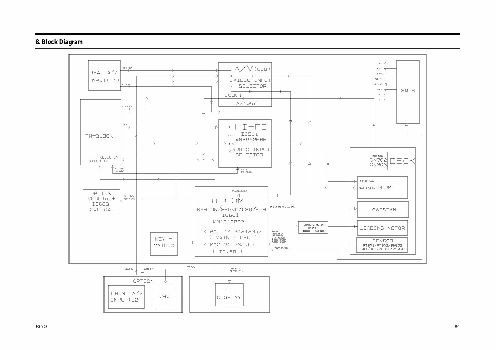
Toshiba 8-1
8. Block Diagram

Block Diagram
8-2 Toshiba
MEMO

Toshiba 9-1
9. PCB Diagrams
9-2
9-3
9-3
9-3
9-1 Main - - - - - - - - - - - - - - - - - - - - - - - - - - - - - - - - - - - - - - - - - - - - - - - - - -
9-2 VFD - - - - - - - - - - - - - - - - - - - - - - - - - - - - - - - - - - - - - - - - - - - - - - - - - - -
9-3 Jack - - - - - - - - - - - - - - - - - - - - - - - - - - - - - - - - - - - - - - - - - - - - - - - - - -
9-4 Key - - - - - - - - - - - - - - - - - - - - - - - - - - - - - - - - - - - - - - - - - - - - - - - - - - -

PCB Diagrams
9-2 Toshiba
9-1 Main

PCB Diagrams
Toshiba 9-3
9-2 VFD
9-3 Jack 9-4 Key

PCB Diagrams
9-4 Toshiba
MEMO

Toshiba 10-1
10. Schematic Diagrams
10-2
10-3
10-4
10-6
10-8
10-10
10-11
10-12
◆ Block Identification of Main PCB - - - - - - - - - - - - - - - - - - - - - - - - - - - - - - -
10-1 S.M.P.S./Power - - - - - - - - - - - - - - - - - - - - - - - - - - - - - - - - - - - - - - - - -
10-2 Logic - - - - - - - - - - - - - - - - - - - - - - - - - - - - - - - - - - - - - - - - - - - - - - - -
10-3 A/V - - - - - - - - - - - - - - - - - - - - - - - - - - - - - - - - - - - - - - - - - - - - - - - - -
10-4 Hi-Fi/MTS - - - - - - - - - - - - - - - - - - - - - - - - - - - - - - - - - - - - - - - - - - - - -
10-5 TM-Block/Input-Output - - - - - - - - - - - - - - - - - - - - - - - - - - - - - - - - - - - -
10-6 VFD - - - - - - - - - - - - - - - - - - - - - - - - - - - - - - - - - - - - - - - - - - - - - - - - -
10-7 Remote-Control - - - - - - - - - - - - - - - - - - - - - - - - - - - - - - - - - - - - - - - - -

Schematic Diagrams
10-2 Toshiba
For schematic Diagram- Resistors are in ohms, 1/8W unless otherwise noted.
Note
Special note : Most semiconductor devices are electrostatically sensitive and therefore require the special handling techniques described under the “electrostatically sensitive (ES) devices” section of this service manual.
Note : Do not use the part number shown on this drawing for ordering. The correct part number is shown in the parts list (may be slightly different or amended since this drawing was prepared).
Important safety notices : Components identified with the mark have the special characteristics for safety. When replacing any of these components. Use only the same type.
◆ Block Identification of Main PCB

Schematic Diagrams
Toshiba 10-3
10-1 S.M.P.S./Power

Schematic Diagrams
10-4 Toshiba
IC601
VFD
10-2 Logic

Schematic Diagrams
Toshiba 10-5
* These values are measured with a Hi-Fi standard tape.
* 5p-p means 5 volts peak to peak. It’s a kind of data or clock wave form.
* The value under 0.5 volt is regarded as 0 volt.
Unit : Volt
Pin No. Power Off Stop(EE) Play Pin No. Power Off Stop(EE) Play Pin No. Power Off Stop(EE) Play Pin No. Power Off Stop(EE) Play
1 0 5 or 0 5p-p 26 5 5 5p-p 51 5 5 5 76 2.5 2.5 0
2 0 5 or 0 5p-p 27 0 0 0 52 2.8 2.8 2.8 77 0 2.5 0
3 0 0 0 28 0 0 0 53 2.5 2.5 2.5 78 0 0 0
4 0 0 0 29 PB:1.3, EE:2.2, REC:5 54 0 0 0 79 0 5 2.5
5 30 SP:0, LP:0, SLP:0 55 0 0 0 80 0 0 3
6 31 0 0 0 56 0 0 0 81 0 2.2p-p 2.2p-p
7 32 2 5 0 57 5 5 5 82 5 5 5
8 33 5 5 5p-p 58 5 5 5 83 0 0 0
9 34 0 5p-p 5p-p 59 5 5 5 84 0 0 0
10 35 0 0 5p-p 60 0 0 0 85 0 0 0
11 36 5 5 5 61 0 0 0 86 0 0 0
12 37Clock data
62 0 0 0 87 5 5 5
13 0 0 0 38 63 0 5 5 88 5 5 5
14 39 0 0 0 64 0 0 0 89
15 5 VCR:5, TV:0 40Clock data
65 0 5p-p 5p-p 90
16 Safety Tab, YES:5, NO:0 41 66 0 5p-p 5p-p 91
17 42 5 5 5 67 0 5 5p-p 92
18 43 0 0 5p-p 68 0 0 0 93 5p-p data for LED display
19 0 0 0 44 0 0 5p-p 69 2.5 2.5 2.5 94
20 0 0 0 45 5 5 0 70 2.5 2.5 2.5 95
21 0 0 0 46 5 5 0 71 0 0 0 96
22 0 0 0 47 Video out signal 72 2.5 2.5 2.5 97
23 0 5p-p 5p-p 48 0 0 0 73 5 5 5 98 0 5p-p 5p-p
24 0 0 0 49Video input signal
74 2.5 2.5 2.5 99 0 5 0
25 5 5 5 50 75 2.5 2.5 2.5 100 0 1 0
IC601 VOLTAGE TABLE
None input : 5, Any input : 5p-p
5p-p data for LED display
5V when the front video jack is inerted
5p-p for Hi-Fi/EEPROM/PLL data,clock

Schematic Diagrams
10-6 Toshiba
10-3 A/V

Schematic Diagrams
Toshiba 10-7
Unit : Volt
Pin No. Power Off Stop(EE) Play Pin No. Power Off Stop(EE) Play Pin No. Power Off Stop(EE) Play Pin No. Power Off Stop(EE) Play
1 2.5 2.5 2.5 25 3 3 3 51 0 0.8 0.8 76 Audio from TM-block
2 2.5 2.5 2.5 26 2.2 2 2.2 52 0.8 2.3 2.3 77 0 0 0
3 2.5 2.5 2.5 27 0 0 0 53 0 0 0 78 Audio from L2(front)
4 2.5 2.5 2.5 28 1.2 1.6 1.6 54 1 5 5 79 0 2.4 2.4
5 0 0 0 29 0 1 1 55 0 0.3 0.3 80 Audio from L1(rear)
6 2.5 2.5 2.5 30 0 0 0 56 1 5 5 81 0 0 0
7 2.5 2.5 2.5 32 0 0 0 57 1 5 5 82 0 0.7 0.7
8 1.8 1.8 1.8 33 0.4 5p-p 5p-p 58 1 3.6 3.6 83 0 0.7 0.7
9 0 0 0 34 0 5p-p 5p-p 59 0 0 0 84 0 0.7 0.7
10 5 5 5 35 0.8 Video Out Video Out 60 0.9 3.8 3.8 85 0 0.7 0.7
11 2.2 3.1 0 36 0 1 1 61 0.5 4 4 86 0 0 0
12 5 5 0 37 1.3 1.3 1.3 62 0 2.7 2.7 87 0 5 5
13 0 0.8p-p 0.8p-p 38 Video from L1(rear) 63 0 2 2 88 0 4.4 1.8
14 0 0.8p-p 0.8p-p 39 0 3.5 3.5 64 0.7 2.2 2.2 89 0 4.4 1.8
15 0 0.8 0 40 Video from L2(front) 65 0 4 4 90 0 4.4 1.8
16 5 5 0.3 41 0 0.2 5 66 0 2 0 91 0 4.4 1.8
17 2.2 2.2 0 42 Video from TM-block 67 0 0 0 92 0.4 1.7 0.3
18 1.8 1.8 1.8 43 0.9 3.7 3.3 68 0.4 2.4 2.4 93 0 0 2.7
19 0 0 0 44 0.5 2.8 2.8 69 0 3.1 2 94 0 1.2 0
20 1.6 1.6 1.6 45 1 2.9 3 70 0.3 2.4 1.8 95 0 0 0
21 5 5 5 46 0.4 3 2.7 71 0.3 2.4 2.4 96 0 2.4 2.4
22 0.8 0.8 0.8 47 0.4 2.8 2.4 72 0.1 2.8 2.8 97 0 0 0
23 0.3 0.3 0.3 48 0 0 0 73 0.4 2.4 2.4 98 0 0 0
24 2.3 2.3 1.4 49 0.6 1.8 1.8 74 0 0 2 99 1 5 5
25 3 3 3 50 0 0 0 75 1 5 5 100 0 2.5 2.5
IC301 VOLTAGE TABLE

Schematic Diagrams
10-8 Toshiba
10-4 Hi-Fi/MTS

Schematic Diagrams
Toshiba 10-9
Unit : Volt
Pin No. Power Off Stop(EE) Play Pin No. Power Off Stop(EE) Play Pin No. Power Off Stop(EE) Play Pin No. Power Off Stop(EE) Play
1 0.3 2.5 2.5 17 0.7 0.4 0.7 33 0.3 2.5 2.5 49 0 3.5 3.5
2 0 0 0 18 0.3 2.5 2.5 34 0.7 0.5 0.7 50 0 3 3
3 0.3 2.5 2.5 19 0.3 2.5 2.5 35 0.7 2.5 2.5 51 0 5 5
4 0 0 0 20 0 2.5 0 36 1.9 5 0 52 0 3.1 3.1
5 0.3 2.2 2.2 21 0 2.5 0 37 0 1.7 1.7 53 0 4.6 4.6
6 0.3 2.5 2.5 22 0 2.5 0.6 38 0 0 0 54 0.3 2.5 2.5
7 0.7 2.2 2.2 23 0 0 0 39 0 0 0 55 0 0 0
8 0.6 0.7 0.7 24 0 2.5 0.6 40 1 5 5 56 0 2p-p 2.2p-p
9 Audio R from rear jack (L1) 25 0 5 5 41 0 0 0 57 0 4.6 4.6
10 26 0 2.5 0 425p-p for Hi-Fi data,clock
58 0.3 9 9
11 0 0 0 27 5 5p-p 5p-p 43 59 Audio to TM-block
12 0.7 2 2 28 0 4.4 4.4 44 0.4 2.4 2.4 60 0 0 0
13 0.3 2.3 2.3 29 0.7 1.9 1.9 45 0 0 0 61 0 2.5 2.5
14 Audio R from rear jack (L1) 30 0.3 0.9 0.9 46 0 3.7 3.7 62 0.3 2.5 2.5
15 31 0.1 0.1 0 47 0.7 1.6 1.6 63 0.3 2.3 2.3
16 0.7 2.5 2.5 32 0.3 2.5 2.5 48 Audio from TM-block 64 0.6 0.7 0.7
IC501 VOLTAGE TABLE
Audio R from front jack (option)
Audio L from front jack (option)

Schematic Diagrams
10-10 Toshiba
10-5 TM-Block/Input-Ouput

Schematic Diagrams
Toshiba 10-11
10-6 VFD

Schematic Diagrams
10-12 Toshiba
10-7 Remote-Control

438B ALEXANDRA ROAD BLOCK B #06-01ALEXANDRA TECHNOPARKSINGAPORE 119968
TOSHIBA VIDEO PRODUCTS PTE LTD
W-602 4/22/00 10:49 AM Page 2