
Micro-light-emitting diodes with quantum dots in ... - Nature
23
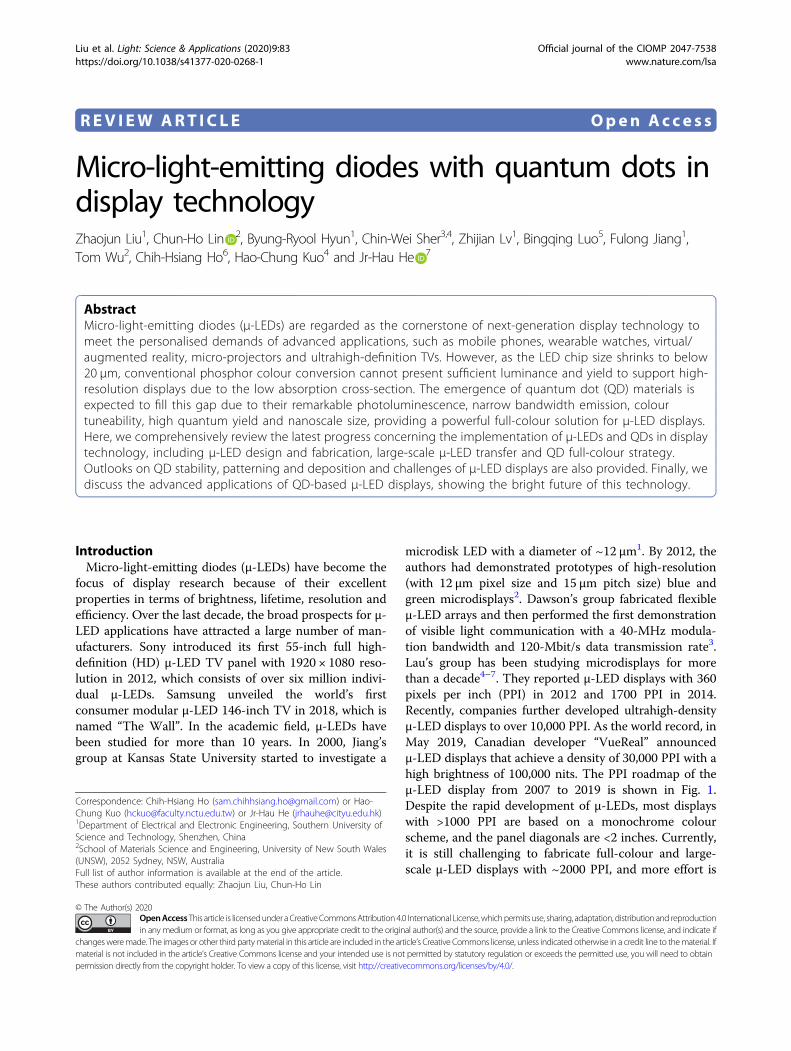
Liu et al. Light: Science & Applications (2020)9:83 Official journal of the CIOMP 2047-7538 https://doi.org/10.1038/s41377-020-0268-1 www.nature.com/lsa REVIEW ARTICLE Open Access Micro-light-emitting diodes with quantum dots in display technology Zhaojun Liu 1 , Chun-Ho Lin 2 , Byung-Ryool Hyun 1 , Chin-Wei Sher 3,4 , Zhijian Lv 1 , Bingqing Luo 5 , Fulong Jiang 1 , Tom Wu 2 , Chih-Hsiang Ho 6 , Hao-Chung Kuo 4 and Jr-Hau He 7 Abstract Micro-light-emitting diodes (μ-LEDs) are regarded as the cornerstone of next-generation display technology to meet the personalised demands of advanced applications, such as mobile phones, wearable watches, virtual/ augmented reality, micro-projectors and ultrahigh-definition TVs. However, as the LED chip size shrinks to below 20 μm, conventional phosphor colour conversion cannot present sufficient luminance and yield to support high- resolution displays due to the low absorption cross-section. The emergence of quantum dot (QD) materials is expected to fill this gap due to their remarkable photoluminescence, narrow bandwidth emission, colour tuneability, high quantum yield and nanoscale size, providing a powerful full-colour solution for μ-LED displays. Here, we comprehensively review the latest progress concerning the implementation of μ-LEDs and QDs in display technology, including μ-LED design and fabrication, large-scale μ-LED transfer and QD full-colour strategy. Outlooks on QD stability, patterning and deposition and challenges of μ-LED displays are also provided. Finally, we discuss the advanced applications of QD-based μ-LED displays, showing the bright future of this technology. Introduction Micro-light-emitting diodes (μ-LEDs) have become the focus of display research because of their excellent properties in terms of brightness, lifetime, resolution and efficiency. Over the last decade, the broad prospects for μ- LED applications have attracted a large number of man- ufacturers. Sony introduced its first 55-inch full high- definition (HD) μ-LED TV panel with 1920 × 1080 reso- lution in 2012, which consists of over six million indivi- dual μ-LEDs. Samsung unveiled the world’s first consumer modular μ-LED 146-inch TV in 2018, which is named “The Wall”. In the academic field, μ-LEDs have been studied for more than 10 years. In 2000, Jiang’s group at Kansas State University started to investigate a microdisk LED with a diameter of ~12 μm 1 . By 2012, the authors had demonstrated prototypes of high-resolution (with 12 μm pixel size and 15 μm pitch size) blue and green microdisplays 2 . Dawson’s group fabricated flexible μ-LED arrays and then performed the first demonstration of visible light communication with a 40-MHz modula- tion bandwidth and 120-Mbit/s data transmission rate 3 . Lau’s group has been studying microdisplays for more than a decade 4–7 . They reported μ-LED displays with 360 pixels per inch (PPI) in 2012 and 1700 PPI in 2014. Recently, companies further developed ultrahigh-density μ-LED displays to over 10,000 PPI. As the world record, in May 2019, Canadian developer “VueReal” announced μ-LED displays that achieve a density of 30,000 PPI with a high brightness of 100,000 nits. The PPI roadmap of the μ-LED display from 2007 to 2019 is shown in Fig. 1. Despite the rapid development of μ-LEDs, most displays with >1000 PPI are based on a monochrome colour scheme, and the panel diagonals are <2 inches. Currently, it is still challenging to fabricate full-colour and large- scale μ-LED displays with ~2000 PPI, and more effort is © The Author(s) 2020 Open Access This article is licensed under a Creative Commons Attribution 4.0 International License, which permits use, sharing, adaptation, distribution and reproduction in any medium or format, as long as you give appropriate credit to the original author(s) and the source, provide a link to the Creative Commons license, and indicate if changes were made. The images or other third party material in this article are included in the article’ s Creative Commons license, unless indicated otherwise in a credit line to the material. If material is not included in the article’s Creative Commons license and your intended use is not permitted by statutory regulation or exceeds the permitted use, you will need to obtain permission directly from the copyright holder. To view a copy of this license, visit http://creativecommons.org/licenses/by/4.0/. Correspondence: Chih-Hsiang Ho ([email protected]) or Hao- Chung Kuo ([email protected]) or Jr-Hau He ([email protected]) 1 Department of Electrical and Electronic Engineering, Southern University of Science and Technology, Shenzhen, China 2 School of Materials Science and Engineering, University of New South Wales (UNSW), 2052 Sydney, NSW, Australia Full list of author information is available at the end of the article. These authors contributed equally: Zhaojun Liu, Chun-Ho Lin 1234567890():,; 1234567890():,; 1234567890():,; 1234567890():,;
-
Upload
khangminh22 -
Category
Documents
-
view
2 -
download
0
Transcript of Micro-light-emitting diodes with quantum dots in ... - Nature
Liu et al. Light: Science & Applications (2020) 9:83 Official journal of the CIOMP 2047-7538https://doi.org/10.1038/s41377-020-0268-1 www.nature.com/lsa
REV I EW ART ICLE Open Ac ce s s
Micro-light-emitting diodes with quantum dots indisplay technologyZhaojun Liu1, Chun-Ho Lin 2, Byung-Ryool Hyun1, Chin-Wei Sher3,4, Zhijian Lv1, Bingqing Luo5, Fulong Jiang1,Tom Wu2, Chih-Hsiang Ho6, Hao-Chung Kuo4 and Jr-Hau He 7
AbstractMicro-light-emitting diodes (μ-LEDs) are regarded as the cornerstone of next-generation display technology tomeet the personalised demands of advanced applications, such as mobile phones, wearable watches, virtual/augmented reality, micro-projectors and ultrahigh-definition TVs. However, as the LED chip size shrinks to below20 μm, conventional phosphor colour conversion cannot present sufficient luminance and yield to support high-resolution displays due to the low absorption cross-section. The emergence of quantum dot (QD) materials isexpected to fill this gap due to their remarkable photoluminescence, narrow bandwidth emission, colourtuneability, high quantum yield and nanoscale size, providing a powerful full-colour solution for μ-LED displays.Here, we comprehensively review the latest progress concerning the implementation of μ-LEDs and QDs in displaytechnology, including μ-LED design and fabrication, large-scale μ-LED transfer and QD full-colour strategy.Outlooks on QD stability, patterning and deposition and challenges of μ-LED displays are also provided. Finally, wediscuss the advanced applications of QD-based μ-LED displays, showing the bright future of this technology.
IntroductionMicro-light-emitting diodes (μ-LEDs) have become the
focus of display research because of their excellentproperties in terms of brightness, lifetime, resolution andefficiency. Over the last decade, the broad prospects for μ-LED applications have attracted a large number of man-ufacturers. Sony introduced its first 55-inch full high-definition (HD) μ-LED TV panel with 1920 × 1080 reso-lution in 2012, which consists of over six million indivi-dual μ-LEDs. Samsung unveiled the world’s firstconsumer modular µ-LED 146-inch TV in 2018, which isnamed “The Wall”. In the academic field, μ-LEDs havebeen studied for more than 10 years. In 2000, Jiang’sgroup at Kansas State University started to investigate a
microdisk LED with a diameter of ~12 μm1. By 2012, theauthors had demonstrated prototypes of high-resolution(with 12 μm pixel size and 15 μm pitch size) blue andgreen microdisplays2. Dawson’s group fabricated flexibleμ-LED arrays and then performed the first demonstrationof visible light communication with a 40-MHz modula-tion bandwidth and 120-Mbit/s data transmission rate3.Lau’s group has been studying microdisplays for morethan a decade4–7. They reported μ-LED displays with 360pixels per inch (PPI) in 2012 and 1700 PPI in 2014.Recently, companies further developed ultrahigh-densityμ-LED displays to over 10,000 PPI. As the world record, inMay 2019, Canadian developer “VueReal” announcedμ-LED displays that achieve a density of 30,000 PPI with ahigh brightness of 100,000 nits. The PPI roadmap of theμ-LED display from 2007 to 2019 is shown in Fig. 1.Despite the rapid development of μ-LEDs, most displayswith >1000 PPI are based on a monochrome colourscheme, and the panel diagonals are <2 inches. Currently,it is still challenging to fabricate full-colour and large-scale μ-LED displays with ~2000 PPI, and more effort is
© The Author(s) 2020OpenAccessThis article is licensedunder aCreativeCommonsAttribution 4.0 International License,whichpermits use, sharing, adaptation, distribution and reproductionin any medium or format, as long as you give appropriate credit to the original author(s) and the source, provide a link to the Creative Commons license, and indicate if
changesweremade. The images or other third partymaterial in this article are included in the article’s Creative Commons license, unless indicated otherwise in a credit line to thematerial. Ifmaterial is not included in the article’s Creative Commons license and your intended use is not permitted by statutory regulation or exceeds the permitted use, you will need to obtainpermission directly from the copyright holder. To view a copy of this license, visit http://creativecommons.org/licenses/by/4.0/.
Correspondence: Chih-Hsiang Ho ([email protected]) or Hao-Chung Kuo ([email protected]) or Jr-Hau He ([email protected])1Department of Electrical and Electronic Engineering, Southern University ofScience and Technology, Shenzhen, China2School of Materials Science and Engineering, University of New South Wales(UNSW), 2052 Sydney, NSW, AustraliaFull list of author information is available at the end of the article.These authors contributed equally: Zhaojun Liu, Chun-Ho Lin
1234
5678
90():,;
1234
5678
90():,;
1234567890():,;
1234
5678
90():,;
necessary to develop mature fabrication for future com-mercial applications.Briefly, µ-LEDs are developed based on established
solid-state techniques but with more meticulous fabrica-tion processes at a higher resolution than those of regularLEDs. In solid-state LEDs, blue and green LEDs are basedon InGaN semiconductors, while AlGaInP semi-conductors are used for red LEDs8,9. To date, the mostefficient violet and blue LEDs based on wide bandgapGaN or InGaN alloys reveal several advantages, such ashigh efficiency, self-emission (i.e., no extra backlight isrequired), long lifetime and super-high reliability underharsh environments including high/low temperature,humidity, sunlight and outer space radiation10. InGaN-based blue LEDs have reached >80% external quantumefficiency (EQE)11, which is the most representative per-formance indicator of LEDs and is defined as the ratio ofextracted photons over injected carriers. Thus, thepotential efficiency for a display system that utilisesphosphor down-conversion of InGaN LEDs to generategreen and red motivates the development of phosphor-converted LEDs (pc-LEDs).Another commonly used full-colour strategy is
employing the combination of red–green–blue (RGB)µ-LED devices in a display. However, compared with thedown-conversion technique, this approach has manydisadvantages. The first limitation is the low efficiency ofgreen LEDs, which is called the “green gap”. For greenLEDs, the active region needs a high fraction of indium,which requires a relatively lower growth temperature(~700 °C), thereby leading to poor crystal quality of theLED epilayer. Furthermore, a high fraction of indiumgives rise to a strong polarisation field in the InGaN/GaNmultiple quantum wells (MQWs) and results in a strongquantum-confined Stark effect, which decreases therecombination efficiency12. Red LEDs are also proble-matic. The active region of the red LED is composed ofAlGaInP material, which possesses a high surfacerecombination velocity (~106 cm/s)13 and, together with along carrier diffusion length of approximately a few
microns, makes the nonradiative surface recombinationmore significant14. Consequently, as the device dimensionshrinks to a few microns, the reduced EQE in red µ-LEDsis more serious than that in blue and green µ-LEDs.Another issue in the RGB µ-LED strategy is the drivevoltage mismatch between the RGB pixels. The thresholdvoltage of the blue LED is ~3.3 V, while that of the red andgreen counterparts is 1.7 V and 2.2 V, which complicatesthe drive circuit design. In contrast, using blue µ-LEDswith a down-conversion phosphor not only simplifies thedriving circuitry but also reduces the number of assemblycycles since the µ-LED arrays can be transferred at thesame time. To date, there has been extensive research anddevelopment on phosphor materials for pc-LEDs12.However, organic or inorganic phosphors are generallynot suitable for µ-LED displays due to their spectralbroadness and asymmetry, inherent instability, and thefact that the red phosphors suffer from low efficiency,down-conversion energy loss, and low absorption cross-sections in the blue/UV wavelength region15. Moreover,the particle size of conventional phosphors may becomparable to or larger than the µ-LED chip, which isproblematic.Recently, colloidal quantum dots (QDs) have appeared
as promising emissive materials for replacing organic ormolecular phosphors in pc-LEDs16,17. QDs are smallsemiconductor crystals with properties that are vastlydifferent from those of bulk semiconductors as a result oftheir nanoscale size. The most compelling characteristicsof these materials are the tuneability of the semiconductorbandgap by varying their size and discrete energy levels,the so-called quantum confinement effect18. The benefitsprovided by colloidal QDs for LEDs are their narrowemission linewidth (full width at half maximum (FWHM)~20–30 nm for CdSe- and InP-based QDs, which are themain QD materials in industry and academia), highphotoluminescence quantum yield (PLQY > 90%), highphotostability, solution processability and low fabricationcost19. Intense and saturated colours are obtained atthe extrema by narrow spectra, which cover >90% of thestrictest Rec. 2020 colour gamut standard20. Further,the narrow linewidths of QDs enable them to form viableactive elements of LEDs in high-resolution displays.The optical properties of typical phosphors and QDs aresummarised in Table 121–29, showing the superiority ofQD materials for next-generation display technology.Currently, liquid crystal displays (LCDs) and organic
light-emitting diodes (OLEDs) are the mainstream tech-nologies30. LCDs require a backlight source or reflector togenerate light propagating through a liquid crystal matrixand colour filters to produce images in colour, but thesedisplays suffer from a low contrast ratio, narrow viewingangle, long response time and high power consumption31.In contrast, OLED displays are self-emissive, using a thin
2007 2011 2015 2019
102
103
104
Pix
el p
er in
ch (
PP
I)
Year
VueReal, 2019 (30,000 PPI)
HKUST, 2007 (73 PPI)
Fig. 1 Pixels per inch roadmap of µ-LED displays from 2007 to 2019
Liu et al. Light: Science & Applications (2020) 9:83 Page 2 of 23

film transistor (TFT) backplane to drive each pixel ONand OFF. However, owing to their organic nature, OLEDdisplays have issues in brightness and stability32. Addi-tionally, the lower carrier mobilities of organic materialslead to response times in the range of µs33. μ-LED dis-plays, as a new promising display technology, offer manypotential advantages such as high contrast, wide colourgamut, high speed (~ns) and wide viewing angles34. LikeOLED, the LED chip in µ-LED displays is no longer just alight source for the backlight module; it plays a role in thedirect display of pixel colour and active illumination,achieving the goal of full colour. Incorporation of QDsinto µ-LEDs can lead to higher colour rendering andsaturation to achieve wide colour gamut requirementsand different levels of mixed colour by independentlycontrolling different RGB pixels. In addition, colourcompensation can be performed on individual colourpixels (temperature, colour shift, ageing failure, etc.) toachieve a more comprehensive and intelligent high-quality display. Therefore, QD-based µ-LEDs for displayapplications have recently attracted growing interestowing to their potential advantages over other competi-tors such as LCDs and OLED displays due to highbrightness, low power consumption and favourable costscaling for large-size displays35.The comparison of different display technologies is
summarised in Table 2. In particular, the technologicalbenefits of QD-based µ-LED displays include better col-our accuracy, higher colour saturation, higher contrastratio and higher peak brightness than those of conven-tional LCDs36. Further, compared to OLED displays, QD-based µ-LED technologies have better colour purity
(∼100 nm FWHM for OLEDs), higher dynamics range,faster response time, and enhanced lifetime and durabilityof displays due to higher thermal and air stabilities. Suchadvantages have made QD-based µ-LED technology idealfor producing displays capable of ultrahigh definition. Thesuperior property of QD materials also makes themattractive to use in other display techniques to improvecolour conversion performance. As a result, QD-baseddisplays receive considerable attention in the globalmarket, which was valued at ~1.7 billion USD in 2018 andis projected to increase significantly to 197 billion USD by2023, with an ~24% compound annual growth rate37.QD-based display technologies have been mainly
developed in two fundamental ways: (i) PL-based LEDs(so-called phosphor-converted LEDs) evolving towardsQD-LCD or QD-µ-LED displays; i.e., the QDs are a formof colour-converting film in LCD backlight units, where
Table 1 Comparison of conventional phosphors and QD materials
Material Peak emission (nm) FWHM (nm) EQE at RT (%) PL drop at 150 °C relative to RT (%) References
K2SiF6:Mn (KSF) 613, 631, 636, 648 4, 4, 3, 3 54.5 ≥5 21,22
SrLiAl3N4:Eu 655 52 70 4 21,23
SrxCa1-xAlSiN3:Eu (SCASN:Eu) 626 86 72 11 24,25
CaS:Eu 650 65 53 13 26,27
β-SiAlON:Eu 525 45 54 15 22,28
SrGa2S4:Eu 538 46 45 23 27,29
Red QD (generation 1) Tunable ≤35 ≥95 30 21
Red QD (generation 2) Tunable ≤35 >95 15 21
Red QD (generation 3) Tunable <30 ≥95 ≥1 21
Green QD (generation 1) Tunable ≤35 ≥95 30 21
Green QD (generation 2) Tunable ≤35 >95 10 21
Green QD (generation 3) Tunable <30 >95 4 21
FWHM full width at half maximum, EQE external quantum efficiency, RT room temperature, PL photoluminescenceReproduced from ref. 21 with permission from John Wiley and Sons
Table 2 Comparison of different display technologies
Display Technology LCD OLED µ-LED
Mechanism Backlight Self-emissive Self-emissive
Contrast ratio 5000 : 1 ∞ ∞
Lifespan Medium Medium Long
Response time Ms µs ns
Operating temperature −40 to 100 °C −30 to 85 °C −100 to 120 °C
Power consumption High Medium Low
View angle Low Medium High
Cost Low Medium High
Liu et al. Light: Science & Applications (2020) 9:83 Page 3 of 23
QDs are physically embedded in polymer matrices sand-wiched between two protecting layers or on blue µ-LEDs;and (ii) electroluminescence (EL)-based LEDs leading toQD EL-LED displays. QD EL-(µ-) LEDs have been one ofthe hot research topics in the QD community and havebeen extensively explored in recent decades even thoughtheir full-scale display commercialisation is not yet in themarket. The performance of EL-LEDs is usually bench-marked by EQE. CdSe QD-based EL-LEDs have alreadyexhibited EQE values of 19.8% for blue, 21% for green and20.5% for red38–40, catching up with phosphorescentOLEDs, which exhibit EQE values of ~30%41,42. QD EL-LEDs are supposed to outperform all display competitorsincluding OLED displays and even their cousin, QD PL-LED displays. However, QD EL-LEDs are still underdevelopment and are not yet in the market. One of themain reasons is the much shorter lifetimes of QD EL-LEDs than of QD PL-based LEDs43. With superior per-formance in terms of extraordinary luminous efficiency,high electro-optical conversion efficiency, and longoperation lifetime, QDPL-based displays are the main-stream in the current markets represented by tech giantssuch as Samsung, Apple, BOE, and TCL. In this review,we focus on the technologies of QD PL-based µ-LEDs andtheir advanced applications for large-area displays andvirtual/augmented reality displays.
Design and fabrication of µ-LED displaysLED epitaxy and chip processingIn typical LED fabrication, GaN and InGaN epilayers
are usually grown on a c-plane (0001) sapphire substrateor (111) Si substrate by metal-organic chemical vapourdeposition (MOCVD)2,5. After MOCVD growth, indiumtin oxide (ITO) with a thickness of ~100 nm is depositedas a transparent current spreading layer and as an ohmicp-contact. Afterwards, the LED mesa is defined throughthe etching process and is etched down to the n-GaN
layer. Then, P and N electrodes are deposited by electron-beam evaporation. In traditional solid-state lighting, thesize of LED chips is a few hundred microns, or evenmillimetres. The manufacturing processes of μ-LEDs aresimilar to those of traditional LEDs described before,except for the smaller size of the LED mesa. As the size ofthe LED mesa is reduced to tens of microns, it poses aserious challenge to the LED epitaxy.Defectivity is a key parameter for μ-LEDs and sig-
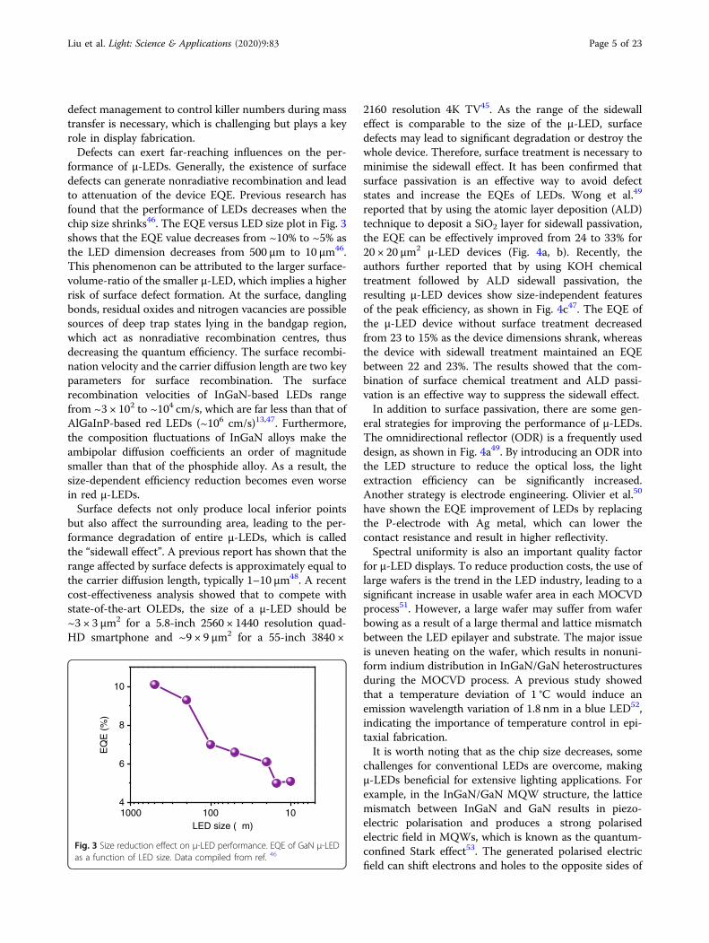
nificantly affects the display quality and product cost. Inthe past, the defectivity of the LED mesa was not a con-cern in the fabrication of conventional LEDs. For exam-ple, blue or green LEDs using InGaN/GaN MQWs as theactive layers can exhibit high EQE, even with a defectdensity of ~108 cm−2 in the LED epilayer44. However, thesituation is different for μ-LEDs. Since the defect sizes areusually on the order of μm, when the LED size shrinks,the defects could seriously impact the performance of thedevice and even dominate the device operation char-acteristics. It has been confirmed that during epitaxyfabrication, unexpected defects such as dislocations oretch pits cause reverse leakage paths in vertical GaN p-ndiodes10. As shown in Fig. 2, etch pits (~1 μm size) at thesurface of the GaN p-n diode dominantly contribute tothe surface leakage current, significantly harming deviceperformance10.Defects with large sizes may even kill the μ-LED devices,
resulting in dead or defective pixels, which is not accep-table in μ-LED displays. The control of dead pixels is amajor issue for large-scale mass transfer, a typical processin the fabrication of μ-LED displays to assemble a largenumber of μ-LED units onto a backplane substrate.During the mass transfer process, the transfer block sizes(donor field) for the quad-HD smartphone and 4K TV are0.92 cm2 and 10 cm2, respectively, while the killer defectsizes are only ~1 μm and 3 μm, respectively45, whichmeans that the defect rate should be <0.1%. Therefore,
20 µm20 µma b
Fig. 2 Positional relation between leakage spots and defect states. The emission microscopy measurement shows a strong relation between aleakage spots and b etch pits (~1 μm size), confirming the importance of defect control during epitaxy. The dashed line and circles indicate the mesaedge and leakage spots, respectively. Reproduced from ref. 10 with permission from AIP Publishing
Liu et al. Light: Science & Applications (2020) 9:83 Page 4 of 23
defect management to control killer numbers during masstransfer is necessary, which is challenging but plays a keyrole in display fabrication.Defects can exert far-reaching influences on the per-
formance of μ-LEDs. Generally, the existence of surfacedefects can generate nonradiative recombination and leadto attenuation of the device EQE. Previous research hasfound that the performance of LEDs decreases when thechip size shrinks46. The EQE versus LED size plot in Fig. 3shows that the EQE value decreases from ~10% to ~5% asthe LED dimension decreases from 500 μm to 10 μm46.This phenomenon can be attributed to the larger surface-volume-ratio of the smaller μ-LED, which implies a higherrisk of surface defect formation. At the surface, danglingbonds, residual oxides and nitrogen vacancies are possiblesources of deep trap states lying in the bandgap region,which act as nonradiative recombination centres, thusdecreasing the quantum efficiency. The surface recombi-nation velocity and the carrier diffusion length are two keyparameters for surface recombination. The surfacerecombination velocities of InGaN-based LEDs rangefrom ~3 × 10² to ~104 cm/s, which are far less than that ofAlGaInP-based red LEDs (~106 cm/s)13,47. Furthermore,the composition fluctuations of InGaN alloys make theambipolar diffusion coefficients an order of magnitudesmaller than that of the phosphide alloy. As a result, thesize-dependent efficiency reduction becomes even worsein red μ-LEDs.Surface defects not only produce local inferior points
but also affect the surrounding area, leading to the per-formance degradation of entire μ-LEDs, which is calledthe “sidewall effect”. A previous report has shown that therange affected by surface defects is approximately equal tothe carrier diffusion length, typically 1–10 μm48. A recentcost-effectiveness analysis showed that to compete withstate-of-the-art OLEDs, the size of a μ-LED should be~3 × 3 μm2 for a 5.8-inch 2560 × 1440 resolution quad-HD smartphone and ~9 × 9 μm2 for a 55-inch 3840 ×
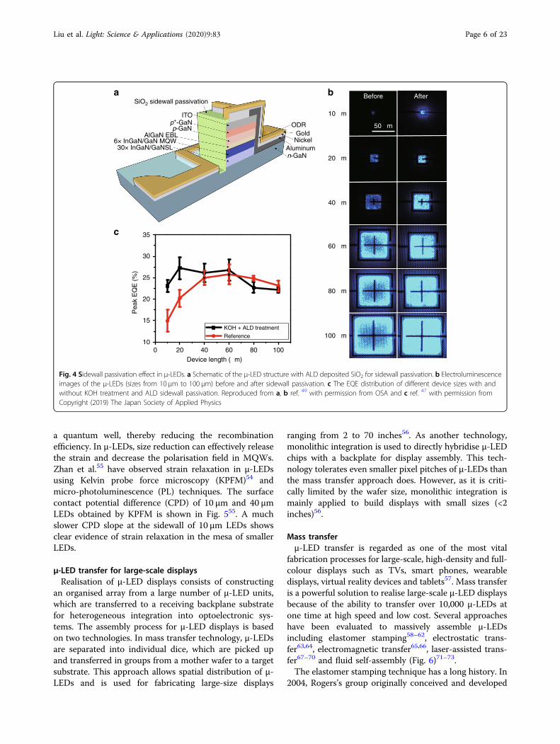
2160 resolution 4K TV45. As the range of the sidewalleffect is comparable to the size of the μ-LED, surfacedefects may lead to significant degradation or destroy thewhole device. Therefore, surface treatment is necessary tominimise the sidewall effect. It has been confirmed thatsurface passivation is an effective way to avoid defectstates and increase the EQEs of LEDs. Wong et al.49
reported that by using the atomic layer deposition (ALD)technique to deposit a SiO2 layer for sidewall passivation,the EQE can be effectively improved from 24 to 33% for20 × 20 μm2 μ-LED devices (Fig. 4a, b). Recently, theauthors further reported that by using KOH chemicaltreatment followed by ALD sidewall passivation, theresulting µ-LED devices show size-independent featuresof the peak efficiency, as shown in Fig. 4c47. The EQE ofthe µ-LED device without surface treatment decreasedfrom 23 to 15% as the device dimensions shrank, whereasthe device with sidewall treatment maintained an EQEbetween 22 and 23%. The results showed that the com-bination of surface chemical treatment and ALD passi-vation is an effective way to suppress the sidewall effect.In addition to surface passivation, there are some gen-
eral strategies for improving the performance of μ-LEDs.The omnidirectional reflector (ODR) is a frequently useddesign, as shown in Fig. 4a49. By introducing an ODR intothe LED structure to reduce the optical loss, the lightextraction efficiency can be significantly increased.Another strategy is electrode engineering. Olivier et al.50
have shown the EQE improvement of LEDs by replacingthe P-electrode with Ag metal, which can lower thecontact resistance and result in higher reflectivity.Spectral uniformity is also an important quality factor
for μ-LED displays. To reduce production costs, the use oflarge wafers is the trend in the LED industry, leading to asignificant increase in usable wafer area in each MOCVDprocess51. However, a large wafer may suffer from waferbowing as a result of a large thermal and lattice mismatchbetween the LED epilayer and substrate. The major issueis uneven heating on the wafer, which results in nonuni-form indium distribution in InGaN/GaN heterostructuresduring the MOCVD process. A previous study showedthat a temperature deviation of 1 °C would induce anemission wavelength variation of 1.8 nm in a blue LED52,indicating the importance of temperature control in epi-taxial fabrication.It is worth noting that as the chip size decreases, some
challenges for conventional LEDs are overcome, makingμ-LEDs beneficial for extensive lighting applications. Forexample, in the InGaN/GaN MQW structure, the latticemismatch between InGaN and GaN results in piezo-electric polarisation and produces a strong polarisedelectric field in MQWs, which is known as the quantum-confined Stark effect53. The generated polarised electricfield can shift electrons and holes to the opposite sides of
1000 100 104
6
8
10
EQ
E (
%)
LED size (µm)
Fig. 3 Size reduction effect on μ-LED performance. EQE of GaN μ-LEDas a function of LED size. Data compiled from ref. 46
Liu et al. Light: Science & Applications (2020) 9:83 Page 5 of 23
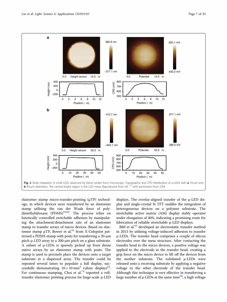
a quantum well, thereby reducing the recombinationefficiency. In μ-LEDs, size reduction can effectively releasethe strain and decrease the polarisation field in MQWs.Zhan et al.55 have observed strain relaxation in μ-LEDsusing Kelvin probe force microscopy (KPFM)54 andmicro-photoluminescence (PL) techniques. The surfacecontact potential difference (CPD) of 10 μm and 40 μmLEDs obtained by KPFM is shown in Fig. 555. A muchslower CPD slope at the sidewall of 10 μm LEDs showsclear evidence of strain relaxation in the mesa of smallerLEDs.
µ-LED transfer for large-scale displaysRealisation of µ-LED displays consists of constructing
an organised array from a large number of µ-LED units,which are transferred to a receiving backplane substratefor heterogeneous integration into optoelectronic sys-tems. The assembly process for µ-LED displays is basedon two technologies. In mass transfer technology, µ-LEDsare separated into individual dice, which are picked upand transferred in groups from a mother wafer to a targetsubstrate. This approach allows spatial distribution of µ-LEDs and is used for fabricating large-size displays
ranging from 2 to 70 inches56. As another technology,monolithic integration is used to directly hybridise µ-LEDchips with a backplate for display assembly. This tech-nology tolerates even smaller pixel pitches of µ-LEDs thanthe mass transfer approach does. However, as it is criti-cally limited by the wafer size, monolithic integration ismainly applied to build displays with small sizes (<2inches)56.
Mass transferµ-LED transfer is regarded as one of the most vital
fabrication processes for large-scale, high-density and full-colour displays such as TVs, smart phones, wearabledisplays, virtual reality devices and tablets57. Mass transferis a powerful solution to realise large-scale µ-LED displaysbecause of the ability to transfer over 10,000 µ-LEDs atone time at high speed and low cost. Several approacheshave been evaluated to massively assemble µ-LEDsincluding elastomer stamping58–62, electrostatic trans-fer63,64, electromagnetic transfer65,66, laser-assisted trans-fer67–70 and fluid self-assembly (Fig. 6)71–73.The elastomer stamping technique has a long history. In
2004, Rogers’s group originally conceived and developed
ba AfterBefore
50 µm
10 µm
20 µm
40 µm
30× InGaN/GaNSL6× InGaN/GaN MQW
AlGaN EBLp-GaNp+-GaN
ITO
ODRGoldNickel
Aluminumn-GaN
SiO2 sidewall passivation
60 µm
80 µm
100 µm
c 35
30
25
Pea
k E
QE
(%
)
20
15
100 20 40 60
KOH + ALD treatment
Reference
Device length (µm)80 100
Fig. 4 Sidewall passivation effect in μ-LEDs. a Schematic of the μ-LED structure with ALD deposited SiO2 for sidewall passivation. b Electroluminescenceimages of the μ-LEDs (sizes from 10 μm to 100 μm) before and after sidewall passivation. c The EQE distribution of different device sizes with andwithout KOH treatment and ALD sidewall passivation. Reproduced from a, b ref. 49 with permission from OSA and c ref. 47 with permission fromCopyright (2019) The Japan Society of Applied Physics
Liu et al. Light: Science & Applications (2020) 9:83 Page 6 of 23
elastomer stamp micro-transfer-printing (μTP) technol-ogy, in which devices were transferred by an elastomerstamp utilising the van der Waals force of poly-dimethylsiloxane (PDMS)59,60. The process relies onkinetically controlled switchable adhesion by manipulat-ing the attachment/detachment rate of an elastomerstamp to transfer arrays of micro devices. Based on elas-tomer stamp μTP, Bower et al.61 from X-Celeprint pat-terned a PDMS stamp with posts for transferring a 20-μmpitch µ-LED array to a 200-μm pitch on a glass substrate.A subset of µ-LEDs is sparsely picked up from densenative arrays by an elastomer stamp with posts. Thestamp is used to precisely place the devices onto a targetsubstrate in a dispersed array. The transfer could berepeated several times to populate a full display, suc-cessfully demonstrating 10 × 10mm2 colour displays62.For continuous stamping, Choi et al.74 reported a roll-transfer elastomer printing process for large-scale µ-LED
displays. The overlay-aligned transfer of the µ-LED dis-play and single-crystal Si TFT enables the integration ofheterogeneous devices on a polymer substrate. Thestretchable active matrix (AM) display stably operatesunder elongation of 40%, indicating a promising route forfabrication of reliable stretchable µ-LED displays.Bibl et al.63 developed an electrostatic transfer method
in 2013 by utilising voltage-induced adhesion to transferµ-LEDs. The transfer head comprises a couple of siliconelectrodes over the mesa structure. After contacting thetransfer head to the micro devices, a positive voltage wasapplied to the electrode in the transfer head, creating agrip force on the micro device to lift off the devices fromthe mother substrate. The exfoliated µ-LEDs werereleased onto a receiving substrate by applying a negativevoltage to the other electrode of the transfer head.Although this technique is very effective in transferring alarge number of µ-LEDs at the same time64, a high voltage
380.9 nm 832.1 mV
430.2 mV
971.1 mV
385.5 mV
0.0
a
400 800
700
600
500
200
–200
0 2 4 6
Position (µm)
8 10 0 2 4 6
Position (µm)
8 10 1212
0 10 20 30 40 50Position (µm)
0 10 20 30 40 50Position (µm)
0
12.0 µm 0.0 Potential 12.0 µm
0.0 Potential 50.0 µm
Height sensor
0.0 50.0 µmHeight sensor
Hei
ght (
nm)
400
200
–200
0
Hei
ght (
nm)
CP
D (
mV
)
800900
700600500
CP
D (
mV
)
–377.1 nm
–403.1 nm
415.7 nm
b
Fig. 5 Strain relaxation in small LEDs observed by Kelvin probe force microscopy. Topographic and CPD distribution of μ-LEDs with a 10-μm andb 40-μm diameters. The central bright region is the LED mesa. Reproduced from ref. 55 with permission from OSA
Liu et al. Light: Science & Applications (2020) 9:83 Page 7 of 23

might cause LED breakdown. Therefore, careful controlof the voltage is necessary during electrostatic transfer.In 2016, Wu et al.65,66 reported an electromagnetic
transfer method that picks up and releases μ-LEDs byvarying the magnetic attraction between a transfer headand ferromagnetic layers on μ-LEDs. This process con-sists of detaching µ-LEDs from the mother wafer withelectromagnetic transfer heads, applying an electrical
signal to generate a magnetic attraction, and then trans-ferring the µ-LEDs to the receiving substrate. Individualmagnetic attraction control of each element enablesselective and large-scale µ-LED transfer without anycompression process.Holmes et al.67 reported for the first time the use of a
laser for the transfer and placement of discrete micropartsonto a receiving substrate in 1998. However, laser-assisted
70°C
Donor
Stamp
Receiver
Elastomer stamping:
Electrostatic/electromagnetic transfer: Fluid self-assembly:
Empty binding site
Plastic template
Circular microcomponents
Self-assembledcomponent
Ethylene glycol&HCl
Mother substrate
Target substrate
Thin film
Donor substrate
Receiver substrate
Lasersource
Beamshaping
a
b d
c Laser-assisted transfer:
Transfer head
Forward bias or magnetization
Reverse bias or magnetization
NS
NS
Transfer head
Free-standingLED
Metal padson LED
Molten alloyin receptorsite well
Assembledcomponentson template
Fig. 6 μ-LED mass transfer techniques. Schematics of a elastomer stamping, b electrostatic/electromagnetic transfer, c laser-assisted transfer andd fluid self-assembly. Reproduced from a ref. 60 with permission from Springer Nature, c ref. 70 with permission from MDPI and d ref. 73 withpermission from IOP Publishing
Liu et al. Light: Science & Applications (2020) 9:83 Page 8 of 23

transfer did not receive much attention for display fabri-cation until 2012, when Marinov et al.68 developed thistechnique for selective µ-LED patterning upon laserirradiation on light reactive films. The µ-LED releaseprocess is driven by the thermo-mechanical response ofthe dynamic release layer under laser irradiation. Using alaser, 50 × 50 × 6 μm µ-LEDs were successfully trans-ferred, with an average placement error of 1.8 μm at ahigh transfer rate exceeding 100M units/h69. The highaccuracy and fast transfer features have made this methodplay a key role in µ-LED commercialisation.Sasaki et al.72 demonstrated fluidic self-assembly
methods for massive parallel assembly of µ-LEDs in2017. In the proposed method, µ-LEDs are suspended in afluid (isopropanol, acetone or distilled water) flowingacross an emissive substrate that is designed with wells inthe top surface. Due to gravity and capillary forces, themicro devices are driven to move across the surface of thesubstrate until they are captured in the wells. Preciseposition and assembly could be achieved during theflowing process, with a transfer rate of over 50 millionunits per hour72.The aforementioned transfer techniques are sum-
marised in Table 3. The typical elastomer stampingtechnique could manipulate µ-LEDs at a high transferyield of 99.99%, while it typically delivers a processingspeed of 10,000 to 25,000 devices per hour61,62. Thismeans that it would take more than 1 month to assemblea 4K display that is made up of 25 million µ-LEDs. Roll-transfer elastomer printing could be a promising solutionto the slow rate74. However, the stamp deformation pro-blem compromises the elastomer stamping techniques,leading to poor control and inaccurate registration.Electrostatic and electromagnetic transfer techniquesenable large-scale µ-LED transfer, but they may causeLED breakdown due to the application of high voltage andrequire an additional ferromagnetic layer, respectively.The laser-assisted transfer technique could reach a rate ofapproximately 100 million per hour with a 1.8-µm pla-cement error yet a low transfer yield of 90%69. Fluid self-assembly achieved a high transfer rate of 56 million perhour at low cost72, but it still needs further improvementfor manufacturing, as modern displays can barely toleratedefective pixels across a screen. To achieve a perfect
image of a µ-LED display, some groups have proposedperforming individual chip replacements for dead pixels62.The other approach is to transfer dual µ-LEDs into eachdisplay pixel for illuminance backup75. These methodswill be either time-consuming or high-cost approachesand thus are insufficient for commercial purposes.
Monolithic integration technologiesHigh-resolution µ-LED displays with a panel diagonal
< 2 inches are referred to as “µ-LED microdisplays”76.µ-LED microdisplays aim to address applications thatprimarily require small panels and high luminance, suchas see-through glasses, compact hand-held projectors andaugmented reality/mix reality devices. For high-brightnessmicrodisplays, the <20-μm small pixel pitch requirementof µ-LEDs cannot be satisfied by mass transfer techni-ques77. Instead, the scaling of µ-LEDs for microdisplaysutilises direct integration of µ-LED chips with a siliconbackplane at the chip level. To achieve microdisplays withhigh resolution, µ-LEDs are fabricated on sapphire withthe desired small pitch and integrated with the activematrix driving circuit compatible with this pitch. Inte-gration technology relates to the electrical connection ofeach individual µ-LED pixel to the corresponding pad ofthe active matrix. Alignment and assembly are importantfactors for the integration of these two separate parts.Various integration technologies have been investigated,including metal wiring78,79, flip chip bonding80, microtubebonding81 and adhesive bonding82,83 (Fig. 7).Conventional integration techniques such as wiring are
simple but limited by low resolution and wire fragility78.Jiang and colleagues80 used flip chip bonding for displayapplication at a 15-μm pitch. Flip chip bonding isfavourable due to reliable integration and high yield but isnot compatible with a pixel pitch of 10 μm or less. Bothwiring and flip-chip bonding require the assistance ofheat, ultrasonic vibration or pressure for the integration,causing device damage and thermal mismatch due to thedifference in the thermal expansion coefficient of sub-strates (sapphire versus silicon). Templier et al.81 havealready demonstrated the use of microtube technology tointegrate heterogeneous devices at a pixel pitch of 10 μm.The microtubes are created on the pads of the circuit andthen inserted into the µ-LED pads after alignment. This
Table 3 Summary of µ-LED mass transfer techniques
Elastomer stamping Electrostatic transfer Electromagnetic transfer Laser-assisted transfer Fluid self-assembly
•Transfer yield 99.99%
•10–25K units/h
•Small area
•Stamp deformation
•Large area
•Device break down by high voltage
•Large area
•Ferromagnetic layer required
•Transfer yield 90%
•100M units/h
•1.8 μm placement error
•56M units/h
•Low cost
Liu et al. Light: Science & Applications (2020) 9:83 Page 9 of 23
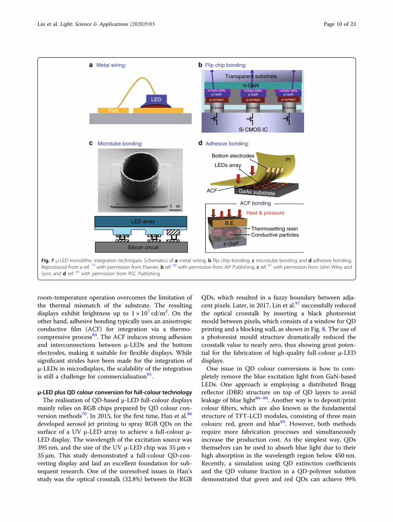
room-temperature operation overcomes the limitation ofthe thermal mismatch of the substrate. The resultingdisplays exhibit brightness up to 1 × 10⁷ cd/m2. On theother hand, adhesive bonding typically uses an anisotropicconductive film (ACF) for integration via a thermo-compressive process84. The ACF induces strong adhesionand interconnections between µ-LEDs and the bottomelectrodes, making it suitable for flexible displays. Whilesignificant strides have been made for the integration ofµ-LEDs in microdisplays, the scalability of the integrationis still a challenge for commercialisation85.
µ-LED plus QD colour conversion for full-colour technologyThe realisation of QD-based µ-LED full-colour displays
mainly relies on RGB chips prepared by QD colour con-version methods70. In 2015, for the first time, Han et al.86
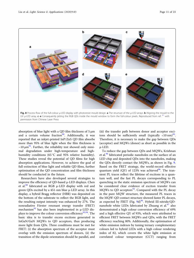
developed aerosol jet printing to spray RGB QDs on thesurface of a UV µ-LED array to achieve a full-colour µ-LED display. The wavelength of the excitation source was395 nm, and the size of the UV µ-LED chip was 35 µm ×35 µm. This study demonstrated a full-colour QD-con-verting display and laid an excellent foundation for sub-sequent research. One of the unresolved issues in Han’sstudy was the optical crosstalk (32.8%) between the RGB
QDs, which resulted in a fuzzy boundary between adja-cent pixels. Later, in 2017, Lin et al.87 successfully reducedthe optical crosstalk by inserting a black photoresistmould between pixels, which consists of a window for QDprinting and a blocking wall, as shown in Fig. 8. The use ofa photoresist mould structure dramatically reduced thecrosstalk value to nearly zero, thus showing great poten-tial for the fabrication of high-quality full-colour µ-LEDdisplays.One issue in QD colour conversions is how to com-
pletely remove the blue excitation light from GaN-basedLEDs. One approach is employing a distributed Braggreflector (DBR) structure on top of QD layers to avoidleakage of blue light86–88. Another way is to deposit/printcolour filters, which are also known as the fundamentalstructure of TFT-LCD modules, consisting of three maincolours: red, green and blue89. However, both methodsrequire more fabrication processes and simultaneouslyincrease the production cost. As the simplest way, QDsthemselves can be used to absorb blue light due to theirhigh absorption in the wavelength region below 450 nm.Recently, a simulation using QD extinction coefficientsand the QD volume fraction in a QD-polymer solutiondemonstrated that green and red QDs can achieve 99%
a b
dc Adhesive bonding:Microtube bonding:
Metal wiring: Flip chip bonding:
LED
Pad
1 µm
LEDs arrayPI
LED array
Silicon circuit
Transparent substrate
n-GaN
Si CMOS IC
In-bump In-bumpIn-bump
p-contactp-contactp-contact
p-GaNp-GaNp-GaNInGaN QWs InGaN QWs InGaN QWs
Bottom electrodes
ACF
B.E.Thermosetting resinConductive particles
p-GaP
ACF bonding
Heat & pressure
GaAs substrate
Fig. 7 μ-LED monolithic integration techniques. Schematics of a metal wiring, b flip chip bonding, c microtube bonding and d adhesive bonding.Reproduced from a ref. 79 with permission from Elsevier, b ref. 80 with permission from AIP Publishing, c ref. 81 with permission from John Wiley andSons and d ref. 83 with permission from RSC Publishing
Liu et al. Light: Science & Applications (2020) 9:83 Page 10 of 23
absorption of blue light with a QD film thickness of 5 µmand a certain volume fraction90. Additionally, it wasreported that an inkjet-printed InP/ZnS QD film absorbsmore than 95% of blue light when the film thickness is~10 µm91. Further, the reliability test showed only mini-mal degradation under high-temperature and high-humidity conditions (65 °C and 95% relative humidity).These studies reveal the potential of QD films for highabsorption applications. However, to achieve the goal offull extinction of blue light and reliable QD films, furtheroptimisation of the QD concentration and film thicknessshould be conducted in the future.Researchers have also developed several strategies to
improve the efficiency of QD-based µ-LED displays. Chenet al.88 fabricated an RGB µ-LED display with red andgreen QDs excited by a 451-nm blue µ-LED array. In thisdisplay, a hybrid Bragg reflector (HBR) was deposited onthe bottom of the substrate to reflect the RGB light, andthe resulting output intensity was enhanced by 27%. Thenonradiative Förster resonant energy transfer (FRET)mechanism92 has also been implemented in µ-LED dis-plays to improve the colour conversion efficiency93,94. Thebasic idea is to transfer excess excitons generated inInGaN/GaN MQWs to QD acceptors, thus producingmore light from QDs. Three conditions must be met forFRET: (i) the absorption spectrum of the acceptor mustoverlap with the emission spectrum of donors, (ii) thetransition of the dipole orientation should be parallel, and
(iii) the transfer path between donor and acceptor exci-tons should be sufficiently small (typically <10 nm)95.Therefore, it is necessary to make the gap between QDs(acceptor) and MQWs (donor) as short as possible in theµ-LED.To reduce the gap between QDs and MQWs, Krishnan
et al.96 fabricated periodic nanoholes on the surface of anLED chip and deposited QDs into the nanoholes, makingthe QDs directly contact the MQWs, as shown in Fig. 9.Based on the FRET strategy, the world-record effectivequantum yield (QY) of 123% was achieved96. The tran-sient PL traces reflect the lifetime of excitons in a quan-tum well, and the fast PL decays corresponding to PLquenching in the static emission spectrum of MQWs canbe considered clear evidence of exciton transfer fromMQWs to QD acceptors92. Compared with the PL decayin the pure MQW structure, the measured PL traces inthe MQW-QD contact structure showed faster PL decays,as expected by FRET (Fig. 9d)96. Hybrid III-nitride/QD-nanohole white LEDs fabricated by Zhuang et al.97 alsodemonstrated a high colour conversion efficiency of 69%and a high effective QY of 93%, which were attributed toefficient FRET between MQWs and QDs, with the FRETefficiency reaching 80%. Additionally, the optimisation ofwhite emission indexes by tuning ternary complementarycolours led to hybrid LEDs with a high colour renderingindex of 82, which covers the white light emission atcorrelated colour temperature (CCT) ranging from
a
b c
d e
Sapphire
MQW
p-GaN
n-GaN
CSL
u-GaN
p-Pads
n-Pads
Fig. 8 Process flow of the full-colour µ-LED display with photoresist mould design. a The structure of the µ-LED arrays. b Aligning the mould to theUV µ-LED array. c–e Consequently jetting the RGB QDs inside the mould window to form the full-colour pixels. Reproduced from ref. 87 withpermission from Chinese Laser Press
Liu et al. Light: Science & Applications (2020) 9:83 Page 11 of 23

2629 K to 6636 K. Instead of the nanohole structure, Liuet al.98 demonstrated a colour conversion efficiencyenhancement by depositing QDs on nanorod-shapedMQWs. Compared with its unstructured counterpart,the resulting LED exhibited a 32.4% enhancement ofcolour conversion efficiency, demonstrating the super-iority of FRET design.A novel nanoring (NR) structure was also proposed in
2017 to improve the FRET effect99. For nanohole andnanorod structures, either the inner or outer sidewall isexposed to contact with QDs. However, for the NRstructure, both sidewalls contact QDs, which can sig-nificantly improve the colour conversion efficiency. Wanget al.99 have shown NR-LED arrays with a diameter of<1 μm on a green epitaxial wafer, and the emissionwavelength of the NRs can be tuned from green (535 nm)to blue (480 nm) by changing the NR wall width. Inaddition, due to nanoscale strain relaxation100, thequantum-confined Stark effect is reduced in GaN-basedLEDs with the NR structure. Figure 10a–f shows thefabrication of a full-colour hybrid QD-NR μ-LED displayby Chen et al.101. Intriguingly, ternary complementarycolours were achieved based on different mechanisms.The display used a green LED epitaxial wafer as the base
to emit bright green light. Then, the NR structures wereconstructed on the green LED, and the colour of NR μ-LEDs was adjusted from green to blue by controlling thewall width of the NRs. Using the ALD technique, a 1-nmAl2O3 layer was deposited on the sidewall of blue NR μ-LEDs for total internal reflection, improving the emissionintensity of NR μ-LEDs by 143.1%. Finally, the red QDscoupled with MQWs were sprayed onto blue NR μ-LEDsfor the full-colour display. To further enhance thebrightness of the red emission, a DBR in blue wavelengthwas employed to reuse the excitation blue light. The LEDchip size was 10 μm× 10 μm, while the RGB subpixelswere 3 μm× 10 μm. For such small subpixels, the afore-mentioned aerosol jet printing would no longer beapplicable. Thus, red QD spraying on NR μ-LEDs wasimplemented using a super-inkjet printing system toaccurately spray the QDs on the subpixel area, giving alinewidth of 1.65 μm and a thickness of 56.3 nm for theQD patterns. The emission spectrum and CIE gamut ofthe QD-NR μ-LED display are shown in Fig. 10g, h,respectively101. The colour gamut of the display canachieve 104.8% NTSC and 78.2% Rec. 2020, which issufficient to support full-colour performance for practicalapplications.
QDs
MQ
W
Saphire
p-GaN
n-GaN
u-GaN
ITO
Au
200.0 nm
n-GaN
ITO
p-GaNInGaN
QDs
1.0 µm
a b
c d
5×10–943210Time (s)
2
3
4
567
1In
tens
ity (
norm
.)
MQWs-QDs
MQWs w/o QDs
Fig. 9 Förster resonant energy transfer nanohole design in LEDs. a Schematic representation, b cross-sectional, and c top scanning electronmicroscope images of a photonic nanohole LED hybridised with QD colour converters. d Time-resolved photoluminescence decays of LED with pureMQW (black line) and MQW-QD contact (red line) structures. Reproduced with minor editing from ref. 96 the Optical Society under the terms of theCreative Commons Attribution 4.0 License
Liu et al. Light: Science & Applications (2020) 9:83 Page 12 of 23

Outlook of µ-LEDs and QDsQDs for µ-LED and their stabilityFor full-colour display solutions, conventional RGB
colour conversion chips have inadequate luminance andlow yield issues when the LED chip size is <20 μm15. Theemergence of QD materials is expected to fill this gap.Many colloidal QD materials have been studied over thepast few decades for their potential use in display appli-cations. However, only CdSe- and InP-based QDs haveachieved sufficient display performance for translation to
industrial manufacturing102. InP QDs are considered themost promising candidates for heavy metal-free QDs,with emission colours covering most of the visible andnear-infra-red window103. Their weaknesses such as lowerQY and broader FWHM are typically attributed to thesurface defects caused by incomplete shell coverage orinterfacial strain because of lattice mismatch between theInP core and the conventional shell material102,104.Nevertheless, the qualities of InP QDs have been steadilyimproved by growing thicker shells, reducing lattice
g
n electrode
Red QDMQWs
MQWs
n-GaN
SapphireBuffer
p-GaN
TCO film p electrode
DBR filter
a
c d
h
b e
f
0.00.0 0.1 0.2 0.3 0.4
x0.5 0.6 0.7 0.8
1.2
0.9
0.8
520530
540
550
560
570
580
590
490
480
470460450440
600
610620
630640650
510
0.7
0.6
0.5
0.4
y
0.3
0.2
0.1
500
Blue NR-µLED
QD-NR-µLEDs
NTSC
Rec. 2020
Green LED
Red QD1.0
0.8
0.6
0.4
0.2
0.0
300 400 500 600
Wavelength (nm)
Nor
mal
ized
inte
nsity
(a.
u.)
700 800
Fig. 10 Full-colour QD-NR μ-LED display design and performance. a Epitaxial wafer. b Three subpixels of a green μ-LED, a blue NR μ-LED, and a redQD-NR μ-LED. c Deposition of transparent conducting oxide film and p-n electrodes. d Covering DBR filter. e Full-colour QD-NR μ-LED display.f Cross-sectional view of a single RGB pixel. g EL spectra of a QD-NR μ-LED display. h Colour gamut of a QD-NR μ-LED display, NTSC, and Rec. 2020.Reproduced from ref. 101 with permission from Chinese Laser Press
Liu et al. Light: Science & Applications (2020) 9:83 Page 13 of 23

strain102. In contrast, recent progress in QD synthesis hasled to CdSe-based QDs (core/shell or alloyed QDs) withfavourable properties, including a high QY of >90%,narrow FWHM of ~20 nm, and thick shell with a thick-ness of >10 nm, yielding dramatically improved stability,while the state-of-the-art InP-based QDs have not yetreached such high quality19,36,102.Recently, halide perovskites with the general formula of
APbX3 (A=CH3NH3+, Cs+, FA+, or mixture; X= I−,
Br−, Cl−) have become an emerging class of colloidal QDsfor next-generation displays105. The popularity of per-ovskites originates from their ultrahigh photovoltaic effi-ciencies of up to 25.2%106, which is attributed to theirexceptional optical and transport properties, such as highabsorption over the visible spectrum107, low excitonbinding energy108, charge carrier diffusion lengths in theµm range109, and high defect tolerance110. The rapidadvances in bulk halide perovskites have in turn broughtsignificant attention to perovskite quantum dots(PQDs)111–113. PQDs possess many favourable featuresfor LED applications, including near-unity PLQYs (>90%)without a shell layer, narrow-band PL (FWHM~12–40 nm), and easily tuneable emission wavelengthsfrom ultraviolet to near-infra-red by either controlling thehalide composition or QD size114–116. Additionally, theirnarrow spectral bandwidths lead to a wider colour gamutencompassing 140% of the NTSC standard (correspond-ing to 93% coverage of the Rec. 2020 colour gamutstandard) and covering the CIE 1931 colour spaces (Fig.11)112. Inspired by this result, researchers incorporatedRGB PQD films into an LCD backlight, and an ultrahighcolour gamut of over 100% of Rec. 2020 standard wasachieved117,118. The excellent luminescence and charge
transport properties have invigorated enormous researchefforts on PQD-based light-emitting devices in displayand solid-state lighting applications. In the academic field,PQDs have been mostly applied as active layer compo-nents in EL-based light-emitting devices. The initial lowefficiency of EL-based PQD-LEDs arises from multiplephysical mechanisms, such as poor optimisations ofdevice structure, high leakage current due to poor mor-phology, significant nonradiative recombination at theinterface, and charge injection imbalance. These problemshave been quickly solved. In 2018 and 2019, tremendousprogress in the efficiency of EL-based PQD-LEDs hasbeen reported, with EQE values of over 20% for green andred colours119–121.Now, we divert our attention to PL-based PQD-LEDs,
which are closer to commercial applications than are EL-based devices. PQDs are very attractive materials forQDPL-based µ-LEDs because of their excellent opticaland physical properties as mentioned above. Withsuperior colour conversion capability to generate RGBlights, PQDs have been utilised in PL-based white LEDs,and ultrahigh luminous efficiency >100 lm/W (the stan-dard for practical use in room lighting)122 has beenachieved. For example, Zhou et al.123 developed PQD-embedded polymer composite films for colour conver-sion, and the resulting white LEDs revealed a luminousefficiency of 109 lm/W and a wide gamut of 121% NTSC.Yoon et al.124 also demonstrated the encapsulation ofPQD powder with a mixed silicon nitride for white LEDs,which showed a luminous efficiency of 138 lm/W (EQE=51.4%), colour gamut of 128% NTSC and CCT of 6762 K.Due to their impressive performance, PQD-based displayswere further developed by manufacturers. At the
400
a
b
c
CsPbCI3 CsPbBr3 CsPbl3
FWHM12 nm–42 nm
CsPb(CI/Br)3 CsPb(I/Br)3
Nor
m. P
L
450 500 550
Wavelength (nm)
600 650 700 750
0.9
0.8520 nm
540 nm
560 nm
580 nm
600 nm
620 nm
700 nm
380 nm460 nm
480 nm
490 nm
500 nm
0.7
0.6
0.5
0.4
NT
SC
TV
col
or s
tand
ard
Con
vent
iona
l LC
D T
V c
olor
y
x
0.3
0.2
0.1
00 0.1 0.2 0.3 0.4
Color gamut of CsPbX3 NCs(black dots)
0.5 0.6 0.7 0.8
Fig. 11 Perovskite QDs for wide colour gamut conversion. a Colloidal CsPbX3 (X= Cl, Br, I) QD solutions in toluene under a UV lamp and b theirrepresentative PL spectra. c CIE chromaticity coordinates (dark points) from the emissions of CsPbX3 QDs compared with those of commercialisedLCD TVs (dashed white line), reaching 140% of the NTSC colour standard (solid white line). Reproduced from ref. 112 with permission from ACSPublications
Liu et al. Light: Science & Applications (2020) 9:83 Page 14 of 23

exhibition of SID Display Week 2019, a display manu-facturer CSOT demonstrated a 6.6-inch 384 × 300 LEDdisplay that uses PQDs for colour conversion, confirmingthe potential of PQDs for next-generation lightingapplications.However, the most serious concern for any QD colour
conversion films, including CdSe, InP, and perovskiteQDs, in commercialisation is their instability, which leadsto PL quenching arising from the degraded QD materials(in colour conversion film). Therefore, understanding thedegradation mechanism and improving the stability ofQDs have become hot topics in the QD materials com-munity. Many degradation mechanisms in PQDs andtheir LED devices are similar to those of CdSe-/InP-basedQDs43. The QD degradation mechanisms have beencategorised into structural stability, interfacial stability,atmospheric stability (by light, oxygen and moisture) andthermal stability125. Enormous efforts have recently beenmade to overcome the instability of perovskite materialsincluding PQDs in solar cells and LEDs126–129. In parti-cular, there are four general strategies that can be appliedto all QD materials to improve their stability: (i)
increasing the mechanical stability of the crystal structureby ion doping, (ii) performing surface engineering bycontrolling ligands, which passivate defect states andproduce strong binding motifs on the QD surfaces, (iii)encapsulating QD layers with polymers and oxide mate-rials, and (iv) performing more efficient packaging ofdevices125.Taking PQD as an example, A-site (Cs+, FA+, PEA+,
etc.) and B-site (Mn2+, Ni2+, Ln3+, Sn4+, etc.) doping onperovskites has been carried out to improve the materialstability (Fig. 12a)130–132. The appropriate doping cangenerate suitable host–guest interfaces to passivateunwanted trap states and inhibit nonradiative recombi-nation, leading to enhanced stability under ambient con-ditions133. Surface engineering can significantly improvethe stability of PQDs (Fig. 12b)134. Generally, during PQDsynthesis, the PQD is capped by long alkyl oleic acid (OA)and oleylamine (OLA), which are not tightly bound to thePQD surface and make PQD unstable135. Using control-ling ligands to construct strong binding motifs on thePQD surface can be a good solution. For example, Liet al.136 utilised stearic acid and octadecylamine to replace
A siteB site
Encapsulant
Encapsulant
QD colorconverter
QD colorconverter
LED chips
LED chips
Prototype QD-LED
Remote-type QD-LED
Perovskite QDs
Polymer chains
Perovskitediffusion direction Monomersdiffusion direction
PbX2-DMSO + FAX+ Monomer + Initiator in DMF
Semi-transparentTransparentUV exposure
a
c
b dSurface engineering
Fig. 12 Strategies for improving the stability of perovskite QDs. a A-site or B-site doping. b Surface engineering. c Encapsulation with a polymer oroxide matrix. d More efficient device packaging (i.e., remote-type design can enhance the stability of QDs compared with the prototype structure).Reproduced from a ref. 132 with permission from RSC Publishing, b ref. 134 with permission from AAAS, c ref. 137 with permission from John Wiley andSons, and d ref. 125 with permission from RSC Publishing
Liu et al. Light: Science & Applications (2020) 9:83 Page 15 of 23
OA and OLA, and the degradation of PQDs was sup-pressed from 60 to 20% after 30 days. Polymer or oxideencapsulation is a very straightforward method thatdirectly protects PQDs from oxygen and moisture in theair (Fig. 12c)123,124,137. However, due to the highly ionicproperties of PQDs, the use of nonpolar encapsulationmaterials is important to avoid undesired interactionsbetween PQDs and the encapsulation matrix138. Efficientpackaging of LEDs also plays a key role (Fig. 12d)125. Forexample, it was reported that by using remote-type design(i.e., QDs are dispensed on top of the LED package)139,the stability of PQDs can be notably improved comparedwith that using the conventional prototype structure (i.e.,QDs are dispensed inside the LED package)140. Althoughmany strategies have been utilised, PQDs have not metthe stability requirement for practical use, and moreresearch efforts are still necessary.Currently, the combination of ligand cross-linking and
polymeric encapsulation has been widely used to protectCdSe-/InP-based QDs in commercial QD displays.Moreover, it is well known that QD shell layers are verycritical to enhance the QD stability as well as the deviceperformance, such as colour purity, quantum yield, andefficiency roll-off. Type I core/shell QDs are commonlyused in QD-based LEDs, in which the core QDs areovercoated with wide bandgap shell materials that passi-vate surface defects and confine excitons to the core, thusincreasing the PLQY of the QDs39,141. However, theincreased PLQY does not guarantee improved LED per-formance. In particular, the efficiency drop by the roll-offeffect is the main bottleneck to most types of QD-basedLEDs. The physical origin of the roll-off effect in QD-based devices is still controversial. Generally, it is believedthat this effect comes from nonradiative Auger recombi-nation by charged and neutral multicarrier states inQDs142,143. In particular, when the pixel size of PL-basedQD µ-LEDs decreases to a few tens of microns, the illu-mination from µ-LEDs should increase accordingly toobtain enough brightness, which makes the PL quenchingfrom Auger recombination of multicarrier states moreserious. To suppress Auger recombination, core/shellQDs with thick shells or graded alloyed shells have beensuccessfully used by Klimov’s group to demonstrate thehigh thermal stability, droop-free efficiency, and colourpurity of QD-based LEDs144,145. Further, for µ-LEDs usingon-chip design (i.e., QDs are directly dispensed on top ofµ-LEDs), the thermal stability and lifetime of QDs couldbe a major concern due to the high flux and high LEDcontact temperature (∼150 °C)146. Currently, in state-of-the-art CdSe-based QDs, shell layers can protect the coreQDs and maintain their high PLQYs (>95%), even attemperatures > 150 °C147. In a recent work, Shimizu et al.demonstrated a performance improvement (~10%) ofwhite LEDs by combining Cd-based QDs with a
conventional phosphor material148. The reliability testunder high temperature (95 °C for 3000 h) and highhumidity (90% relative humidity for 1000 h) showed thatthe white LEDs meet the commercial market require-ments. Compared with that of CdSe-based QDs, thedevelopment of PQDs is still in the infancy stage, andtheir stability is not sufficient. Thus, more research oncore/shell PQDs with a thick shell or a graded alloyedshell is urgent for PQD-based µ-LEDs. To date, the sta-bility of QDs engineered by various approaches rangesfrom a few hours to several months under ambient con-ditions or UV exposure43,125. However, the generalrequirement for commercialised displays is >10,000 h,which means that there is still a long way to go toincorporate QDs in extensive commercial applications.Finally, we briefly discuss the toxicity of QDs. It has
been reported that heavy metal-containing QDs havebeen shown to be toxic in human and environmentalmodels149. One of the major obstacles to the commer-cialisation of QD-based optoelectronic devices arises fromproduct legislation such as the Restriction of HazardousSubstances (RoHS), which is a directive regulating themanufacture, import and distribution of electronics andelectrical equipment within a country. After the firstRoHS (Directive 2002/95/EC) was published by the Eur-opean Union (EU) in 2002, many countries started toenact their own versions of legislation RoHS. For example,EU RoHS specifies maximum levels of substances such as<100 ppm Cd and <1000 ppm Pb (by weight). The higherlimit of Pb makes PQDs appealing candidates for repla-cing Cd-based QDs in display applications. Ultimately, theuse of heavy metal-free QDs could be the best option inany QD application. However, the performance of heavymetal-free QDs does not reach the levels of Cd-containingQDs or PQDs for display applications, and further study isneeded to improve the QD quality.
QD patterning and depositionTypical QD-converted µ-LED displays require the
deposition of red and green QDs on blue µ-LED chips.Conventional QD deposition methods, including spin-coating, phase-separation, self-assembly, dip-coating, andlayer-by-layer deposition, have many limitations for fab-rication, such as complicated and multiple steps, lowresolution, and difficult patterning control. Additionally,these techniques usually need a large amount of QDs insolution form but actually transfer a very limited amount,thereby considerably increasing the production cost.Therefore, advanced techniques for patterning QDs on µ-LEDs have been proposed, such as photolithography150,electron-beam lithography151, jet printing86, 3D print-ing152, microcontact printing153, and dip-pen nanolitho-graphy154 methods. To select a suitable QD patterningtechnique, the resolution, throughput, and defect
Liu et al. Light: Science & Applications (2020) 9:83 Page 16 of 23

tolerance of the desired display should be considered. Forexample, in 55-inch 4K (3840 × 2160 resolution) TV, thesize of the µ-LED chip is ~10 µm × 10 µm, which consistsof small-size RGB subpixels ~3 µm, and a total subpixelnumber of 24,883,200 is required to construct the entireTV display. Further, high-resolution displays such as 8KTV or virtual reality (VR)/augmented reality (AR) displaysdemand even smaller subpixel sizes (<3 µm) and muchhigher subpixel numbers.Generally, using electron-beam lithography, QD films
with patterns scaled down to sub-µm can be achieved151,which is good enough for normal µ-LEDs. In addition,using hydrogen silsesquioxane resist with precise para-meter control, Manfrinato et al.155 reported nanometre-resolution patterning based on electron-beam litho-graphy. The reported sizes of QD patterns by photo-lithography are 2–5 µm in width and ~50 µm inthickness150. With printing techniques, 250 nm QD pixelresolution was demonstrated by Richner et al.156. Thedimension characteristics of various deposition methodsare summarised in Table 4. Thus, the pixel and pitchresolution is not an issue for QD film deposition on µ-LEDs by using any techniques mentioned as long as theLED size is in the range of µm. However, each techniquehas its own limitations. The microcontact and transferprinting approaches need a template, making the proce-dure more complicated. Inkjet printing has problems suchas easy clog of the jagged nozzle, the coffee ring effect, andnonuniform film thickness and rough surface of theprinted film, even though it is the most desirable manu-facturing process in the display industry. In the QDdeposition process with photolithography and electron-beam lithography techniques, QD films could be easilydamaged, and the production costs are high.So far, printing technology can satisfy most of the
demands because the pixel sizes of displays are still abovemicrons in the current market. From the viewpoint ofsimple and rapid fabrication, printing techniques shouldbe mainstream in the future display industry. However,the problem of nonuniform printing should be furtheraddressed. Developing a stable, high-resolution, and cost-
effective process that can directly print uniform QD layerswith diverse sub-micron patterns is important forultrahigh-resolution QD-converted µ-LED displays,although this remains a challenge.
µ-LED displaysCurrently, many critical issues in µ-LED displays
including the quantum-confined Stark effect, displayresolution, pixel pitch, device EQE, colour conversionefficiency, and optical crosstalk have been relieved alongwith the development of nanofabrication capability andnew structural design, such as super-inkjet printing, high-resolution lithography, advanced QD encapsulation,mould architecture design, and FRET nanostructure pat-terning. However, there are still some remaining obstaclesfor the high-throughput manufacturing of µ-LED displays.Mass transfer is regarded as the greatest technical
challenge in µ-LED display manufacturing. Damageshould be avoided when the µ-LED is transferred from themother wafer to the target substrate. However, rapidtransfer can significantly increase the dead pixel number,resulting in a low manufacturing yield. The elastomerstamping approach can be applied to products of ~10 μm,with a high transfer yield of 99.99%;61,62 however, it takesa very long time to assemble a display (10 K µ-LED unitsper hour). Laser-assisted transfer can be applied to pro-ducts of ~1 μm, with a high transfer speed (100M µ-LEDunits per hour); however, the yield is only 90%69. There-fore, developing a stable and rapid mass transfer solutionis the most pressing task to overcome the trade-offbetween production speed and pixel yield. For commer-cialisation of µ-LED displays, the target pixel yield isabove 99.9999%. Thus, the dead pixel number can becontrolled to less than 25 for a 4K display. However, it isstill challenging to achieve such a high transfer yield.Another straightforward solution for pixel yield is trans-ferring dual µ-LEDs into each pixel for illuminancebackup75. However, the production cost of displays wouldbe dramatically increased. Alternatively, individual pixelrepair methods have been proposed to rescue dead pixels,such as laser welding, UV irradiation repair, selectiverescue techniques, and redundant circuit design70. How-ever, these approaches are also costly and not applicablefor displays fabricated by monolithic integration.Because the µ-LED display uses self-emission technol-
ogy, a TFT matrix drive array is required to switch eachpixel ON and OFF separately. The adoption of the TFTcontrol matrix can significantly reduce the power con-sumption by ceasing unnecessary pixels and maintainingthe operation of the display at low power. However, thesmall feature of µ-LEDs leads to the high spatial density ofthe TFT array and makes the circuit design more com-plicated. The bonding between the TFT matrix and µ-LED array is also problematic. Large-scale bonding with
Table 4 Comparison of different patterning techniquesfor QD deposition
Patterning technique Pattern linewidth QD film thickness
Photolithography Several µm Several µm
Electron-beam lithography Several nm ~10 nm
Inkjet printing 250 nm Several µm
Microcontact printing Several dozens nm Monolayer
3D printing A few µm N/A
Liu et al. Light: Science & Applications (2020) 9:83 Page 17 of 23
very small chip elements may cause short circuits due tothe use of a large amount of metal in the solder paste.Although obstacles exist, the current progress on µ-LED
displays still provides an optimistic perspective for next-generation applications. According to UBI Research’sforecast, the market size of µ-LED displays will grow fromaround $100 million as of 2019 to over $6 billion by 2025,and the new emerging displays will widely be used inwearables, smartphones, TVs, and other applications157.
Visible light communication using QD-converted µ-LEDdisplaysCurrently, the wireless network is in the era of a change
driven by big data. Enormous growth in data-drivenapplications is triggering unprecedented demands oncommunication networks. However, the current wirelesstechnology is primarily limited to the radio frequency (RF)band. Thus, the technology is no longer sufficient tosupport big data communications. Visible light commu-nications (VLC) has become a promising technology tomitigate the RF spectrum crisis158. Different concepts forVLC are specified in standard IEEE 802.15.7. An inter-esting feature is the application of existing infrastructuressuch as LED displays to perform data transmission astransmitters. This approach supports a faster, safer, andmore reliable wireless network for next-generation com-munications. As a result, VLC has been increasinglyadapted for indoor optical wireless communication,underwater/seaside communication, in-vehicle data ser-vices, and the Internet of Things due to the outstandingadvantages such as unregulated 260 THz modulationbandwidth in the wavelength range of 380–780 nm, highsecurity and privacy by line-of-sight, lower cost and lowerenergy consumption159. Additionally, for the VLC usingLED displays, due to multi-parallel transmission based onindividual modulation of all pixels of the display, high datarates can be achieved. In VLC systems, conventionalcommercial LEDs with modulation bandwidths on theorder of 10–20MHz have been implemented for illumi-nation, and the use of blue GaN µ-LEDs dramaticallyincreases the bandwidth to several 100MHz, with a datatransfer rate of >1 Gbit/s. For example, Ferreira et al.160
demonstrated ultrahigh electrical-to-optical modulationbandwidths over 800MHz with a blue GaN µ-LED. Thetransmission of data over free space at data rates of 1.7,3.4, and 5 Gbit/s was demonstrated. Further, Islim et al.presented a data transmission rate of 11.95 Gbit/s with aGaN violet µ-LED by using a modulation scheme. Theviolet µ-LEDs were reported to have electrical-to-opticalmodulation bandwidths of 655 MHz161.Recent demands of high-speed data transmission in
VLC have motivated the adaptation of white lighting µ-LED arrays with pixel size approximately 100 µm, pro-viding a peak data rate of >1 Gbit/s without complicated
signal processing160. Thus, a white light source capable ofwavelength multiplexing for VLC has become a vital issue,and enormous efforts have been devoted to increasing themodulation bandwidth by using phosphor-converted µ-LEDs. The white light produced by a blue GaN µ-LED anda yellow fluorescent polymer can be used to demonstratea 1.68-Gb/s data transmission162. A commercial red RC-LED and custom green and blue µ-LEDs were used toachieve the aggregate highest data transmission of11.28 Gb/s in white VLC light162. Recently, the generatedwhite light from QDs on a blue GaN µ-LED has beenexplored for VLCs. As one example, the initial VLC wasdemonstrated with perovskite QD-converting µ-LEDs,and the results were ~160 MHz bandwidth at an emissionwavelength of 445 nm and data rates of 300Mbit/s163,which shows their great potential in the applications ofhigh-speed and wide-bandwidth VLCs. Finally, we canexpect to have cross-industry cooperation for the systemintegration of QD-converting µ-LED displays and VLCsto create a new commercial services value chain and anew wave of industry.
Ultrahigh-definition displays and virtual reality/augmentedreality displaysµ-LEDs are suitable for advanced display applications
such as smartphones, wearable watches, micro-projectors,AR/VR, automotive heads-up displays, and ultra HD (>4Kresolution) televisions due to their advantages such asbetter colour accuracy, higher colour saturation, highcontrast ratio, high peak brightness, low power consump-tion, and longer lifespan. Figure 13 shows the requirementsfor µ-LEDs in advanced display applications35.In particular, QD-based µ-LED displays make a strong
appeal to 8K ultra HD displays and AR/VR displays; 8Kdisplays have a very high resolution of 7680 × 4320 andemploy the Rec. 2020 system as a colour gamut standard.The most important feature of the Rec. 2020 standard is99.9% reproducibility of colours in nature, and it leads to adrastically wider colour gamut than that of the HDTVstandard (Rec. 709). Ultra HD displays require LEDs withbetter chromaticity in order to achieve a wider colourgamut as well as high efficiency and a long lifetime.Moreover, displays for VR/AR applications require a
light weight, small form factor, high pixel density, widefield-of-view (FoV), and high refresh rate to satisfy thehuman visual system. Generally, the FoV for each humaneye is ~160° (horizontal) × 150° (vertical)164. Covering thefull FoV with normal visual acuity (i.e., 60 pixels perdegree) requires 9600 × 9600 pixels per eye, which is closeto the resolution of ultra HD displays, and in 2018, Googledemonstrated the highest resolution VR/AR OLED dis-play, with 4800 × 3840 pixels per eye and an FoV of 120° ×96°165. In addition, avoiding screen flicker and reducingmotion-to-photon latency requires the use of high refresh
Liu et al. Light: Science & Applications (2020) 9:83 Page 18 of 23

rates (>500 Hz) in displays, though it is quite impracticalin current technologies (at present, 60–120 Hz). The highrefresh rates and high resolution require a very fast pixelclock. For example, for the 9600 × 9000-pixel theoreticaldisplay with a 120-Hz refresh rate, the pixel clock is93 GHz, corresponding to 10 ps. Of course, these condi-tions should be lowered to be realistic. Such a highresolution requires the pixel size to shrink down to thescale of a few µm, which results in a major challenge tohave enough brightness on each colour because a singlepixel has to be sub-divided into red, green and blue. Thelow optical efficiency of current AR/VR imaging opticscannot meet the bar for the minimum peak brightness.Specifically, for waveguide AR display, the overall effi-ciency can be <20%166. In such a case, the current OLEDswith a maximum luminance over 5000 nits (demonstratedby two research labs) cannot achieve an ambient contrastratio of 5:1 (the contrast threshold of a recognisableimage) in normal ambient lighting conditions31,167. Thus,the consensus is that QDs can provide the enoughbrightness under these conditions due to their highabsorption cross-section and near-unity PLQY. µ-LEDsprovide the device platform owing to their high efficiency,simple optics, and small form factor. Therefore, QD-basedµ-LEDs (i.e., QD-converted or QD-EL µ-LEDs) could bethe only viable technology for VR/AR displays.Finally, µ-LEDs with flexible substrates represent a vital
application, attracting enormous attention in the fields ofdisplays, wearable electronics, lighting and biomedicine,and light guide plates because of their high efficiency,small form factor, and low power consumption. In par-ticular, flexible and wearable µ-LED displays have thin,lightweight, and nonbreakable features, thus enabling theapplication of displays on curvilinear surfaces. Impressivecolour purity and high brightness with low power
consumption, high-resolution QD array patterning andultrathin/ultrasmall form factors make QD-based µ-LEDspromising for flexible/wearable electronics.
ConclusionsColloidal QDs featuring narrow bandwidth emission
and high PLQY provide promising advantages for theirutilisation in display applications to create a wide colourgamut. The improved photostability of these QDs opensan opportunity for their utilisation in displays usingoptical excitation. Thus, a combination of rapid progressin device fabrication and performance of solid-state µ-LEDs and superior optical properties of QDs along withinnovative fine-controlled QD synthesis and the devel-opment of favourable QD film deposition techniques canyield the most promising technology for next-generationdisplays. Of course, a fundamental understanding of theeffects of the QD characteristics on their µ-LED displayperformance is necessary to reach this goal. Research intothe stability and protection methods of QD films on µ-LEDs is still required to meet the strict stability require-ments of commercial displays. Enormous efforts havebeen made in terms of the conversion efficiency andstability of QDs, especially considering their compara-tively brief history in display applications. However, sub-stantial further research into their encapsulation andlarge-scale patterning is imperative to enable commercialproducts. Nevertheless, the current progress on both µ-LEDs and QDs offers an optimistic perspective forpotential implementation in next-generation displays.
AcknowledgementsZ.Liu acknowledges the financial support of Shenzhen Peacock Team funding(KQTD20170810110313773). C.H.L. and T.W. acknowledge financial supportfrom the Australian Research Council (ARC) (DP190103316). H.C.K.acknowledges financial support from the Taiwan science and technology
Application
Auto display TV Digital display
Panel size (inch) 6 ~ 12 32 ~ 100 150 ~ 220PPI 150 ~ 250 40 ~ 80 20 ~ 30
Chip volume (M) 4.1 24.9 24.9Chip size (µm) 50 ~ 100 50 ~ 80 80 ~ 100
Application
AR Watch Mobile
Panel size (inch) 0.5 ~ 1 1 ~ 1.5 4 ~ 6PPI 450 ~ 2000 200 ~ 300 300 ~ 800
Chip volume (M) 49.8 0.4 6.2Chip size (µm) 1 ~ 5 10 ~ 30 30 ~ 50
Fig. 13 Requirements for µ-LEDs in typical applications. Reproduced from ref. 35 with permission from MDPI
Liu et al. Light: Science & Applications (2020) 9:83 Page 19 of 23

authority, China (107-2221-E-009-113-MY3). J.H.H. acknowledges financialsupport from the startup funding of City University of Hong Kong. All authorsacknowledge Prof. Kei May Lau of Hong Kong University of Science andTechnology and Prof. Nakamura Shuji of University of California, Santa Barbara,for the fruitful discussion.
Author details1Department of Electrical and Electronic Engineering, Southern University ofScience and Technology, Shenzhen, China. 2School of Materials Science andEngineering, University of New South Wales (UNSW), 2052 Sydney, NSW,Australia. 3Department of Electronic and Computer Engineering, Hong KongUniversity of Science and Technology, Hong Kong, China. 4Department ofPhotonics and Institute of Electro-Optical Engineering, College of Electrical andComputer Engineering, Chiao Tung University, 30010 Hsinchu, Taiwan, China.5School of Innovation and Entrepreneurship, Southern University of Scienceand Technology, Shenzhen, China. 6Raysolution LLC, San Jose, CA 95129, USA.7Department of Materials Science and Engineering, City University of HongKong, Hong Kong, China
Author contributionsZhaojun Liu and Chun-Ho Lin contributed equally and finalised themanuscript. Hao-Chung Kuo and Jr-Hau He proposed the framework of themanuscript and supervised the progress. All authors contributed to the writingand commented on the manuscript.
Conflict of interestThe authors declare that they have no conflict of interest.
Received: 8 September 2019 Revised: 4 February 2020 Accepted: 19February 2020
References1. Jin, S. X. et al. GaN microdisk light emitting diodes. Appl. Phys. Lett. 76,
631–633 (2000).2. Day, J. et al. Full-scale self-emissive blue and green microdisplays based on
GaN micro-LED arrays. In Proc. SPIE 8268, Quantum Sensing and Nanopho-tonic Devices IX (SPIE, San Francisco, CA, USA, 2012).
3. Tian, P. F. et al. Fabrication, characterization and applications of flexiblevertical InGaN micro-light emitting diode arrays. Opt. Express 24, 699–707(2016).
4. Liu, Z. J. et al. Monolithic LED microdisplay on active matrix substrate usingflip-chip technology. IEEE J. Sel. Top. Quantum Electron. 15, 1298–1302 (2009).
5. Liu, Z. J. et al. Fully multi-functional GaN-based micro-LEDs for 2500 PPImicro-displays, temperature sensing, light energy harvesting, and lightdetection. In Proc. 2018 IEEE International Electron Devices Meeting pp.38.1.1–38.1.4. (IEEE, San Francisco, CA, USA, 2018).
6. Zhang, K. et al. Fully-integrated active matrix programmable UV and bluemicro-LED display system-on-panel (SoP). J. Soc. Inf. Disp. 25, 240–248 (2017).
7. Zhang, X. et al. Active matrix monolithic LED micro-display using GaN-on-Siepilayers. IEEE Photon. Technol. Lett. 31, 865–868 (2019).
8. Phillips, J. M. et al. Research challenges to ultra-efficient inorganic solid-statelighting. Laser Photon. Rev. 1, 307–333 (2007).
9. Krames, M. R. et al. Status and future of high-power light-emitting diodes forsolid-state lighting. J. Disp. Technol. 3, 160–175 (2007).
10. Usami, S. et al. Correlation between dislocations and leakage current of p-ndiodes on a free-standing GaN substrate. Appl. Phys. Lett. 112, 182106 (2018).
11. Jiang, Y. et al. Realization of high-luminous-efficiency InGaN light-emittingdiodes in the “green gap” range. Sci. Rep. 5, 10883 (2015).
12. Cho, J. et al. White light-emitting diodes: history, progress, and future. LaserPhoton. Rev. 11, 1600147 (2017).
13. Bulashevich, K. A. & Karpov, S. Y. Impact of surface recombination on effi-ciency of III-nitride light-emitting diodes. Phys. Status Solidi RRL 10, 480–484(2016).
14. Hwang, D. et al. Sustained high external quantum efficiency in ultrasmallblue III-nitride micro-LEDs. Appl. Phys. Express 10, 032101 (2017).
15. Lin, C. C. & Liu, R. S. Advances in phosphors for light-emitting diodes. J. Phys.Chem. Lett. 2, 1268–1277 (2011).
16. Abe, S. et al. Hybrid remote quantum dot/powder phosphor designs fordisplay backlights. Light. Sci. Appl. 6, e16271 (2017).
17. Supran, G. J. et al. High-performance shortwave-infrared light-emittingdevices using core-shell (PbS-CdS) colloidal quantum dots. Adv. Mater. 27,1437–1442 (2015).
18. Zhu, S. J. et al. Photoluminescence mechanism in graphene quantum dots:quantum confinement effect and surface/edge state. Nano Today 13, 10–14(2017).
19. Shirasaki, Y. et al. Emergence of colloidal quantum-dot light-emitting tech-nologies. Nat. Photon. 7, 13–23 (2013).
20. Zhu, R. D. et al. Realizing Rec. 2020 color gamut with quantum dot displays.Opt. Express 23, 23680–23693 (2015).
21. Steckel, J. S. et al. Quantum dots: the ultimate down-conversion material forLCD displays. J. Soc. Inf. Disp. 23, 294–305 (2015).
22. Wang, L. et al. Highly efficient narrow-band green and red phosphorsenabling wider color-gamut LED backlight for more brilliant displays. Opt.Express 23, 28707–28717 (2015).
23. Tsai, Y. T. et al. Improvement of the water resistance of a narrow-band red-emitting SrLiAl3N4: Eu
2+ phosphor synthesized under high isostatic pressurethrough coating with an organosilica layer. Angew. Chem. Int. Ed. 55,9652–9656 (2016).
24. Luo, D. et al. Realizing superior white LEDs with both high R9 and luminousefficacy by using dual red phosphors. RSC Adv. 7, 25964–25968 (2017).
25. Kim, Y. S. et al. Red-emitting (Sr,Ca)AlSiN3: Eu2+ phosphors synthesized by
spark plasma sintering. ECS J. Solid State Sci. Technol. 2, R3021–R3025 (2013).26. Xia, Q. et al. Quantum yield of Eu2+ emission in (Ca1-xSrx)S: Eu light emitting
diode converter at 20-420 K. Radiat. Meas. 45, 350–352 (2010).27. Ito, Y. et al. A backlight system with a phosphor sheet providing both wider
color gamut and higher efficiency. SID Symp. Dig. Tech. Pap. 44, 816–819(2013).
28. Kim, D. H., Ryu, J. H. & Cho, S. Y. Light emitting properties of SiAlON: Eu2+
green phosphor. Appl. Phys. A 102, 79–83 (2011).29. Martin, L. I. D. J. et al. Microscopic study of dopant distribution in europium
doped SrGa2S4: impact on thermal quenching and phosphor performance.ECS J. Solid State Sci. Technol. 7, R3052–R3056 (2018).
30. Krotkus, S. et al. Adjustable white-light emission from a photo-structuredmicro-OLED array. Light. Sci. Appl. 5, e16121 (2016).
31. Chen, H. W. et al. Liquid crystal display and organic light-emitting diodedisplay: present status and future perspectives. Light. Sci. Appl. 7, 17168 (2018).
32. Kim, S. et al. Degradation of blue-phosphorescent organic light-emittingdevices involves exciton-induced generation of polaron pair within emittinglayers. Nat. Commun. 9, 1211 (2018).
33. Kawabe, Y. & Abe, J. Electron mobility measurement using exciplex-typeorganic light-emitting diodes. Appl. Phys. Lett. 81, 493–495 (2002).
34. Le Minh, H. et al. 100-Mb/s NRZ visible light communications using apostequalized white LED. IEEE Photon. Technol. Lett. 21, 1063–1065 (2009).
35. Wu, T. Z. et al. Mini-LED and micro-LED: promising candidates for the nextgeneration display technology. Appl. Sci. 8, 1557 (2018).
36. Kim, T. H. et al. Bright and stable quantum dots and their applications in full-color displays. MRS Bull. 38, 712–720 (2013).
37. Global quantum dot display market analysis & forecast 2017 to 2023. https://www.kennethresearch.com/report-details/global-quantum-dot-display-market/10043101 (2019).
38. Wang, L. S. et al. Blue quantum dot light-emitting diodes with high elec-troluminescent efficiency. ACS Appl. Mater. Interfaces 9, 38755–38760 (2017).
39. Dai, X. L. et al. Solution-processed, high-performance light-emitting diodesbased on quantum dots. Nature 515, 96–99 (2014).
40. Manders, J. R. et al. High efficiency and ultra-wide color gamut quantum dotLEDs for next generation displays. J. Soc. Inf. Disp. 23, 523–528 (2015).
41. Zeng, W. X. et al. Achieving nearly 30% external quantum efficiency fororange–red organic light emitting diodes by employing thermally activateddelayed fluorescence emitters composed of 1,8-naphthalimide-acridinehybrids. Adv. Mater. 30, 1704961 (2018).
42. Tsai, K. W. et al. Solution-processed thermally activated delayed fluorescentOLED with high EQE as 31% using high triplet energy crosslinkable holetransport materials. Adv. Funct. Mater. 29, 1901025 (2019).
43. Moon, H. et al. Stability of quantum dots, quantum dot films, and quantum dotlight-emitting diodes for display applications. Adv. Mater. 31, 1804294 (2019).
Liu et al. Light: Science & Applications (2020) 9:83 Page 20 of 23

44. Chichibu, S. F. et al. Origin of defect-insensitive emission probability inIn-containing (Al,In,Ga)N alloy semiconductors. Nat. Mater. 5, 810–816(2006).
45. Paranjpe, A. et al. Micro-LED displays: key manufacturing challenges andsolutions. SID Symp. Dig. Tech. Pap. 49, 597–600 (2018).
46. Olivier, F. et al. Influence of size-reduction on the performances ofGaN-based micro-LEDs for display application. J. Lumin. 191, 112–116(2017).
47. Wong, M. S. et al. Size-independent peak efficiency of III-nitride micro-light-emitting-diodes using chemical treatment and sidewall passivation. Appl.Phys. Express 12, 097004 (2019).
48. Virey, E. H. & Baron, N. Status and prospects of microLED displays. SID Symp.Dig. Tech. Pap. 49, 593–596 (2018).
49. Wong, M. S. et al. High efficiency of III-nitride micro-light-emitting diodes bysidewall passivation using atomic layer deposition. Opt. Express 26,21324–21331 (2018).
50. Olivier, F. et al. Investigation and improvement of 10 μm pixel-pitch GaN-based micro-LED arrays with very high brightness. SID Symp. Dig. Tech. Pap.48, 353–356 (2017).
51. Zhu, D., Wallis, D. J. & Humphreys, C. J. Prospects of III-nitride optoelectronicsgrown on Si. Rep. Prog. Phys. 76, 106501 (2013).
52. Aida, H. et al. Effect of initial bow of sapphire substrate on substrate curvatureduring ingan growth stage of light emitting diode epitaxy. Jpn J. Appl. Phys.51, 012102 (2012).
53. Lim, S. H. et al. Electrically driven, phosphor-free, white light-emitting diodesusing gallium nitride-based double concentric truncated pyramid structures.Light Sci. Appl. 5, e16030 (2016).
54. Fu, H. C. et al. MXene-contacted silicon solar cells with 11.5% efficiency. Adv.Energy Mater. 9, 1900180 (2019).
55. Zhan, J. L. et al. Investigation on strain relaxation distribution in GaN-basedμLEDs by Kelvin probe force microscopy and micro-photoluminescence.Opt. Express 26, 5265–5274 (2018).
56. Chaji, R., Fathi, E. & Zamani, A. Low-cost micro-LED displays for all applica-tions. SID Symp. Dig. Tech. Pap. 48, 264–267 (2017).
57. Zhang, H. & Rogers, J. A. Recent advances in flexible inorganic light emittingdiodes: from materials design to integrated optoelectronic platforms. Adv.Optical Mater. 7, 1800936 (2019).
58. Kim, H. S. et al. Unusual strategies for using indium gallium nitride grown onsilicon (111) for solid-state lighting. Proc. Natl Acad. Sci. USA 108,10072–10077 (2011).
59. Menard, E. et al. A printable form of silicon for high performance thin filmtransistors on plastic substrates. Appl. Phys. Lett. 84, 5398–5400 (2004).
60. Meitl, M. A. et al. Transfer printing by kinetic control of adhesion to anelastomeric stamp. Nat. Mater. 5, 33–38 (2006).
61. Bower, C. A. et al. Heterogeneous integration of microscale compoundsemiconductor devices by micro-transfer-printing. In Proc. 2015 IEEE 65thElectronic Components and Technology Conference. p. 963–967 (IEEE, SanDiego, CA, USA, 2015).
62. Meitl, M. et al. Passive matrix displays with transfer-printed microscale inor-ganic LEDs. SID Symp. Dig. Tech. Pap. 47, 743–746 (2016).
63. Bibl, A. et al. Method of forming a micro light emitting diode array. 8426227.(2013).
64. Golda, D. & Bibl, A. Micro device transfer head array. 9548233. (2017).65. Wu, M. H., Fang, Y. H. & Chao, C. H. Electric-programmable magnetic module.
10147622. (2017).66. Wu, M. H., Fang, Y. H. & Chao, C. H. Electric-programmable magnetic module
and picking-up and placement process for electronic devices. 20160172253.(2016).
67. Holmes, A. S. & Saidam, S. M. Sacrificial layer process with laser-driven releasefor batch assembly operations. J. Microelectromech. Syst. 7, 416–422 (1998).
68. Marinov, V. et al. Laser-enabled advanced packaging of ultrathin bare dice inflexible substrates. IEEE Trans. Compon. Packag. Manuf. Technol. 2, 569–577(2012).
69. Marinov, V. R. Laser-enabled extremely-high rate technology for µLEDassembly. SID Symp. Dig. Tech. Pap. 49, 692–695 (2018).
70. Ding, K. et al. Micro-LEDs, a manufacturability perspective. Appl. Sci. 9, 1206(2019).
71. Yeh, H. J. J. & Smith, J. S. Fluidic self-assembly for the integration of gaas light-emitting diodes on Si substrates. IEEE Photon. Technol. Lett. 6, 706–708 (1994).
72. Sasaki, K. et al. System and method for the fluidic assembly of emissivedisplays. 20170133558. (2017).
73. Saeedi, E., Kim, S. & Parviz, B. A. Self-assembled crystalline semiconductoroptoelectronics on glass and plastic. J. Micromech. Microeng. 18, 075019(2008).
74. Choi, M. et al. Stretchable active matrix inorganic light-emitting diode displayenabled by overlay-aligned roll-transfer printing. Adv. Funct. Mater. 27,1606005 (2017).
75. Henry, W. & Percival, C. ILED displays: next generation display technology. SIDSymp. Dig. Tech. Pap. 47, 747–750 (2016).
76. Jiang, H. X. et al. III-nitride blue microdisplays. Appl. Phys. Lett. 78, 1303–1305(2001).
77. Lee, V. W., Twu, N. & Kymissis, I. Micro-LED technologies and applications. Inf.Disp. 32, 16–23 (2016).
78. Peng, D., Zhang, K. & Liu, Z. J. Design and fabrication of fine-pitch pixelated-addressed micro-LED arrays on printed circuit board for display and com-munication applications. IEEE J. Electron Devices Soc. 5, 90–94 (2017).
79. Kim, H. H. et al. Thermal transient characteristics of die attach in high powerLED PKG. Microelectron. Reliab. 48, 445–454 (2008).
80. Day, J. et al. III-Nitride full-scale high-resolution microdisplays. Appl. Phys. Lett.99, 031116 (2011).
81. Templier, F. et al. GaN-based emissive microdisplays: a very promisingtechnology for compact, ultra‐high brightness display systems. SID Symp. Dig.Tech. Pap. 47, 1013–1016 (2016).
82. Kang, C. M. et al. Monolithic integration of AlGaInP-based red and InGaN-based green LEDs via adhesive bonding for multicolor emission. Sci. Rep. 7,10333 (2017).
83. Jeong, C. K. et al. Self-powered fully-flexible light-emitting system enabled byflexible energy harvester. Energy Environ. Sci. 7, 4035–4043 (2014).
84. Lee, S. H. et al. Optogenetic control of body movements via flexible verticallight-emitting diodes on brain surface. Nano Energy 44, 447–455 (2018).
85. Kang, C. M. et al. Hybrid full-color inorganic light-emitting diodes integratedon a single wafer using selective area growth and adhesive bonding. ACSPhoton. 5, 4413–4422 (2018).
86. Han, H. V. et al. Resonant-enhanced full-color emission of quantum-dot-based micro LED display technology. Opt. Express 23, 32504–32515 (2015).
87. Lin, H. Y. et al. Optical cross-talk reduction in a quantum-dot-based full-colormicro-light-emitting-diode display by a lithographic-fabricated photoresistmold. Photon. Res. 5, 411–416 (2017).
88. Chen, G. S. et al. Monolithic red/green/blue micro-LEDs with HBR and DBRstructures. IEEE Photon. Technol. Lett. 30, 262–265 (2018).
89. Sabnis, R. W. Color filter technology for liquid crystal displays. Displays 20,119–129 (1999).
90. Osinski, J. & Palomaki, P. Quantum dot design criteria for color conversion inmicroLED displays. SID Symp. Dig. Tech. Pap. 50, 34–37 (2019).
91. Lee, E. et al. Quantum dot conversion layers through inkjet printing. SIDSymp. Dig. Tech. Pap. 49, 525–527 (2018).
92. Clapp, A. R., Medintz, I. L. & Mattoussi, H. Förster resonance energy transferinvestigations using quantum-dot fluorophores. ChemPhysChem 7, 47–57(2006).
93. Chanyawadee, S. et al. Increased color-conversion efficiency in hybrid light-emitting diodes utilizing non-radiative energy transfer. Adv. Mater. 22,602–606 (2010).
94. Zhao, C. et al. Droop-free, reliable, and high-power InGaN/GaN nanowirelight-emitting diodes for monolithic metal-optoelectronics. Nano Lett. 16,4616–4623 (2016).
95. Achermann, M. et al. Energy-transfer pumping of semiconductor nanocrys-tals using an epitaxial quantum well. Nature 429, 642–646 (2004).
96. Krishnan, C. et al. Hybrid photonic crystal light-emitting diode renders 123%color conversion effective quantum yield. Optica 3, 503–509 (2016).
97. Zhuang, Z. et al. High color rendering index hybrid III-nitride/nanocrystalswhite light-emitting diodes. Adv. Funct. Mater. 26, 36–43 (2016).
98. Liu, C. Y. et al. Color-conversion efficiency enhancement of quantum dots viaselective area nano-rods light-emitting diodes. Opt. Express 24, 19978–19987(2016).
99. Wang, S. W. et al. Wavelength tunable InGaN/GaN nano-ring LEDs via nano-sphere lithography. Sci. Rep. 7, 42962 (2017).
100. Ryou, J. H. et al. Control of quantum-confined stark effect in InGaN-basedquantum wells. IEEE J. Sel. Top. Quant. Electron. 15, 1080–1091 (2009).
101. Huang Chen, S. W. et al. Full-color monolithic hybrid quantum dot nanoringmicro light-emitting diodes with improved efficiency using atomic layerdeposition and nonradiative resonant energy transfer. Photon. Res. 7,416–422 (2019).
Liu et al. Light: Science & Applications (2020) 9:83 Page 21 of 23
102. Ippen, C. et al. High efficiency heavy metal free QD-LEDs for next generationdisplays. J. Soc. Inf. Disp. 27, 338–346 (2019).
103. Reiss, P. et al. Synthesis of semiconductor nanocrystals, focusing on nontoxicand earth-abundant materials. Chem. Rev. 116, 10731–10819 (2016).
104. Li, Y. et al. Stoichiometry-controlled InP-based quantum dots: synthesis,photoluminescence, and electroluminescence. J. Am. Chem. Soc. 141,6448–6452 (2019).
105. Wang, H. C. et al. Perovskite quantum dots and their application in light-emitting diodes. Small 14, 1702433 (2018).
106. NREL. Research cell record efficiency chart. https://www.nrel.gov/pv/assets/pdfs/best-research-cell-efficiencies.20190802.pdf (2019).
107. Wei, T. C. et al. Nonlinear absorption applications of CH3NH3PbBr3 perovskitecrystals. Adv. Funct. Mater. 28, 1707175 (2018).
108. Cheng, B. et al. Extremely reduced dielectric confinement in two-dimensional hybrid perovskites with large polar organics. Commun. Phys.1, 80 (2018).
109. Dong, Q. F. et al. Electron-hole diffusion lengths >175 μm in solution-grownCH3NH3PbI3 single crystals. Science 347, 967–970 (2015).
110. Kang, J. & Wang, L. W. High defect tolerance in lead halide perovskiteCsPbBr3. J. Phys. Chem. Lett. 8, 489–493 (2017).
111. Schmidt, L. C. et al. Nontemplate synthesis of CH3NH3PbBr3 perovskitenanoparticles. J. Am. Chem. Soc. 136, 850–853 (2014).
112. Protesescu, L. et al. Nanocrystals of cesium lead halide perovskites (CsPbX3, X= Cl, Br, and I): novel optoelectronic materials showing bright emission withwide color gamut. Nano Lett. 15, 3692–3696 (2015).
113. Shamsi, J. et al. Metal halide perovskite nanocrystals: synthesis, post-synthesismodifications, and their optical properties. Chem. Rev. 119, 3296–3348 (2019).
114. Liu, F. et al. Highly luminescent phase-stable CsPbI3 perovskite quantum dotsachieving near 100% absolute photoluminescence quantum yield. ACS Nano11, 10373–10383 (2017).
115. Swarnkar, A. et al. Colloidal CsPbBr3 perovskite nanocrystals: luminescencebeyond traditional quantum dots. Angew. Chem. 127, 15644–15648 (2015).
116. Mondal, N., De, A. & Samanta, A. Achieving near-unity photoluminescenceefficiency for blue-violet-emitting perovskite nanocrystals. ACS Energy Lett. 4,32–39 (2019).
117. Ko, Y. H. et al. Super ultra-high resolution liquid-crystal-display using per-ovskite quantum-dot functional color-filters. Sci. Rep. 8, 12881 (2018).
118. Ko, Y. H. & Park, J. G. Novel quantum dot enhancement film with a super-wide color gamut for LCD displays. J. Korean Phys. Soc. 72, 45–51 (2018).
119. Lin, K. B. et al. Perovskite light-emitting diodes with external quantum effi-ciency exceeding 20 per cent. Nature 562, 245–248 (2018).
120. Cao, Y. et al. Perovskite light-emitting diodes based on spontaneouslyformed submicrometre-scale structures. Nature 562, 249–253 (2018).
121. Xu, W. D. et al. Rational molecular passivation for high-performance per-ovskite light-emitting diodes. Nat. Photon. 13, 418–424 (2019).
122. Kang, C. Y. et al. Highly efficient and stable white light‐emitting diodes usingperovskite quantum dot paper. Adv. Sci. 6, 1902230 (2019).
123. Zhou, Q. C. et al. In situ fabrication of halide perovskite nanocrystal-embedded polymer composite films with enhanced photoluminescence fordisplay backlights. Adv. Mater. 28, 9163–9168 (2016).
124. Yoon, H. C. et al. Efficient and stable CsPbBr3 quantum-dot powders passi-vated and encapsulated with a mixed silicon nitride and silicon oxide inor-ganic polymer matrix. ACS Appl. Mater. Interfaces 10, 11756–11767 (2018).
125. Wei, Y., Cheng, Z. Y. & Lin, J. An overview on enhancing the stability of leadhalide perovskite quantum dots and their applications in phosphor-converted LEDs. Chem. Soc. Rev. 48, 310–350 (2019).
126. Zhou, Y. Y. & Zhao, Y. X. Chemical stability and instability of inorganic halideperovskites. Energy Environ. Sci. 12, 1495–1511 (2019).
127. Cho, H. et al. Improving the stability of metal halide perovskite materials andlight-emitting diodes. Adv. Mater. 30, 1704587 (2018).
128. Wang, R. et al. A review of perovskites solar cell stability. Adv. Funct. Mater. 29,1808843 (2019).
129. Lv, W. Z. et al. Improving the stability of metal halide perovskite quantumdots by encapsulation. Adv. Mater. 31, 1900682 (2019).
130. Xu, L. et al. A comprehensive review of doping in perovskite nanocrystals/quantum dots: evolution of structure, electronics, optics, and light-emittingdiodes. Mater. Today Nano 6, 100036 (2019).
131. Zhou, Y. et al. Metal-doped lead halide perovskites: synthesis, properties, andoptoelectronic applications. Chem. Mater. 30, 6589–6613 (2018).
132. Hasegawa, H. et al. Effective band gap tuning by foreign metal doping inhybrid tin iodide perovskites. J. Mater. Chem. C 5, 4048–4052 (2017).
133. Wang, X. et al. Could nanocomposites continue the success of halide per-ovskites? ACS Energy Lett. 4, 1446–1454 (2019).
134. Wang, Y. B. et al. Stabilizing heterostructures of soft perovskite semi-conductors. Science 365, 687–691 (2019).
135. De Roo, J. et al. Highly dynamic ligand binding and light absorption coef-ficient of cesium lead bromide perovskite nanocrystals. ACS Nano 10,2071–2081 (2016).
136. Li, Q. H. et al. Solid ligand-assisted storage of air-stable formamidiniumlead halide quantum dots via restraining the highly dynamic surfacetoward brightly luminescent light-emitting diodes. ACS Photon. 4,2504–2512 (2017).
137. Minh, D. N. et al. Perovskite nanoparticle composite films by size exclusionlithography. Adv. Mater. 30, 1802555 (2018).
138. Lin, C. H. et al. Orthogonal lithography for halide perovskite optoelectronicnanodevices. ACS Nano 13, 1168–1176 (2019).
139. Lin, C. H. et al. Hybrid-type white LEDs based on inorganic halide perovskiteQDs: candidates for wide color gamut display backlights. Photon. Res. 7,579–585 (2019).
140. Zhou, J. C. et al. Inorganic halide perovskite quantum dot modified YAG-based white LEDs with superior performance. J. Mater. Chem. C 4, 7601–7606(2016).
141. Mashford, B. S. et al. High-efficiency quantum-dot light-emitting devices withenhanced charge injection. Nat. Photon. 7, 407–412 (2013).
142. Castañeda, J. A. et al. Efficient biexciton interaction in perovskite quantumdots under weak and strong confinement. ACS Nano 10, 8603–8609(2016).
143. Yan, F. et al. Highly efficient visible colloidal lead-halide perovskite nanocrystallight-emitting diodes. Nano Lett. 18, 3157–3164 (2018).
144. Lim, J. et al. Droop-free colloidal quantum dot light-emitting diodes. NanoLett. 18, 6645–6653 (2018).
145. Bae, W. K. et al. Controlling the influence of Auger recombination on theperformance of quantum-dot light-emitting diodes. Nat. Commun. 4, 2661(2013).
146. Zhao, Y. M. et al. High-temperature luminescence quenching of colloidalquantum dots. ACS Nano 6, 9058–9067 (2012).
147. Breen, C. & Liu, W. H. Methods for coating semiconductor nanocrystals.10096678. (2018).
148. Shimizu, K. T. et al. Toward commercial realization of quantum dot basedwhite light-emitting diodes for general illumination. Photon. Res. 5, A1–A6(2017).
149. Bottrill, M. & Green, M. Some aspects of quantum dot toxicity. Chem. Com-mun. 47, 7039–7050 (2011).
150. Kang, H. L. et al. Spatial light patterning of full color quantum dot displaysenabled by locally controlled surface tailoring. Adv. Opt. Mater. 6, 1701335(2018).
151. Palankar, R. et al. Fabrication of quantum dot microarrays using electronbeam lithography for applications in analyte sensing and cellular dynamics.ACS Nano 7, 4617–4628 (2013).
152. Kong, Y. L. et al. 3D printed quantum dot light-emitting diodes. Nano Lett. 14,7017–7023 (2014).
153. Kim, T. H. et al. Full-colour quantum dot displays fabricated by transferprinting. Nat. Photon. 5, 176–182 (2011).
154. Salaita, K., Wang, Y. H. & Mirkin, C. A. Applications of dip-pen nanolithography.Nat. Nanotechnol. 2, 145–155 (2007).
155. Manfrinato, V. R. et al. Resolution limits of electron-beam lithography towardthe atomic scale. Nano Lett. 13, 1555–1558 (2013).
156. Richner, P. et al. Full-spectrum flexible color printing at the diffraction limit.ACS Photon. 3, 754–757 (2016).
157. Microled-info. UBI sees Micro-LED revenues reaching $6 billion by 2025.https://www.microled-info.com/ubi-sees-micro-led-revenues-reaching-6-billion-2025. (2019).
158. Burchardt, H. et al. VLC: beyond point-to-point communication. IEEE Com-mun. Mag. 52, 98–105 (2014).
159. Rajagopal, S., Roberts, R. D. & Lim, S. K. IEEE 802.15.7 visible light commu-nication: modulation schemes and dimming support. IEEE Commun. Mag.50, 72–82 (2012).
160. Ferreira, R. X. G. et al. High bandwidth GaN-based micro-LEDs formulti-Gb/s visible light communications. IEEE Photon. Technol. Lett. 28,2023–2026 (2016).
161. Li, X. et al. μLED-based single-wavelength bi-directional POF link with 10 Gb/saggregate data rate. J. Lightwave Technol. 33, 3571–3576 (2015).
Liu et al. Light: Science & Applications (2020) 9:83 Page 22 of 23
162. Chun, H. et al. Visible light communication using a blue GaN μ LED andfluorescent polymer color converter. IEEE Photon. Technol. Lett. 26, 2035–2038(2014).
163. Mei, S. L. et al. High-bandwidth white-light system combining a micro-LEDwith perovskite quantum dots for visible light communication. ACS Appl.Mater. Interfaces 10, 5641–5648 (2018).
164. Traquair, H. M. An Introduction to Clinical Perimetry (Henry Kimpton, London,1938).
165. Vieri, C. et al. An 18 megapixel 4.3″ 1443 ppi 120 Hz OLED display for widefield of view high acuity head mounted displays. J. Soc. Inf. Disp. 26, 314–324(2018).
166. Lee, Y. H., Zhan, T. & Wu, S. T. Prospects and challenges in augmented realitydisplays. Virtual Real. Intell. Hardw. 1, 10–20 (2019).
167. Ghosh, A. et al. Ultra-high-brightness 2K x 2K full-color OLED microdisplayusing direct patterning of OLED emitters. SID Symp. Dig. Tech. Pap. 48,226–229 (2017).
Liu et al. Light: Science & Applications (2020) 9:83 Page 23 of 23


![Highly Air‐Stable Thieno [3, 2‐b] thiophene‐Thiophene‐Thiazolo [5, 4‐d] thiazole‐Based Polymers for Light‐Emitting Diodes](https://static.fdokumen.com/doc/165x107/63314f6cc1adb6fc8c0f4a46/highly-airstable-thieno-3-2b-thiophenethiophenethiazolo-5-4d.jpg)


![IJCBS RESEARCH PAPER VOL. 1 [ISSUE 3] JUNE, 2014 ISSN:-2349–2724 Light Emitting Diodes (LEDs) Reduce Vertimec, Resistance in Tetranychus urticae (Koch](https://static.fdokumen.com/doc/165x107/631ba468a906b217b9069031/ijcbs-research-paper-vol-1-issue-3-june-2014-issn-23492724-light-emitting.jpg)


