An improved technology of 6H-SiC power diodes
8
An improved technology of 6H-SiC power diodes M. Badila a , G. Brezeanu b, * , G. Dilimot b , J. Millan c , P. Godignon c , J.P. Chante d , M.L. Locatelli d , N. Mestres e , A. Lebedev f a IMT, Bucharest, Romania b University Politehnica Bucharest, (Electronic Faculty), Splaiul Inderendentei, 313 sec.6, 77206, Bucharest, Romania c CNM, Barcelona, Spain d CEGELY-INSA, Lyon, France e ICMAB, Barcelona, Spain f IOFFE Institute, St. Petersburg, Russia Abstract A refined technology of SiC p–n junctions is proposed. Usage of boron to compensate the high doping of n layers on structures with different continuous areas is primarily experimentally demonstrated. A comparison between the electrical characteristics of boron compen- sated and uncompensated diodes is presented. Then a technology using cellular structure for 6H-SiC large area p–n devices is designed and optimized. For these split area structures the micropipes effect is avoided. Based on a matrix structure with 0.16 mm 2 cell area a medium power (600 V breakdown voltage and 1 A at forward voltage of 5 V) p–n diode has been fabricated and tested. q 2000 Elsevier Science Ltd. All rights reserved. Keywords: 6H-SiC; Power diodes; Boron compensation 1. Introduction Unique potential of silicon carbide (SiC) has been demonstrated in prototype devices for high power, high frequency and high temperature applications [1–8]. This includes a higher breakdown field (.10 times that of Si) with the much smaller drift regions benefit, a higher thermal conductivity (.3 times that of Si) that assures better heat dissipation, and a wide bandgap energy (2.9 eV for 6H-SiC) that enables higher junction operating temperatures and lower leakage currents [1–3,8]. Regarding the SiC p–n junction, high breakdown voltages in the range from 1 to 4.5 kV have been reported for small area diodes [3,8]. In these bipolar devices, the major enigmas include large leakage current (at least several orders of magnitude higher than simple theoretical predic- tion) and fast switching characteristics (short minority carrier lifetime). The high densities of crystallographic defects in SiC wafers prohibits the achievement of SiC devices with the very high operating currents (.50 A) that are commonly obtainable in silicon-based high power electronics. Micropipe defects have been claimed to severely degrade electrical device performance. Commercial 4H- and 6H-SiC polytypes wafers and epilayers also contain elementary screw dislocations in densities of the order of thousands per cm 2 , nearly 100 times the micropipes densities [1–3]. In spite of the recent progress in reduction of the various kinds of defects existing in the material itself or being induced during device proces- sing, there still exist many remaining issues to be solved for wide commercial success of SiC technology. In this paper, an improved mesa technology of 6H-SiC the p–n junction is presented. Primarily a rectangular continuous area diode technology is investigated. Then a cellular structure designed to avoid the micropipes effects for large area diodes is discussed. A special technique to encapsulate good cells connection is proposed. Raman Scat- tering and Reflexivity Infrared spectroscopy and SEM microscopy are used for optical characterization of the different technological steps. 2. Device fabrication The double epitaxial mesa insulated 6H-SiC p–n junction cross section is depicted in Fig. 1. The diodes were fabricated on a 1 cm 2 n 1 6H-SiC Microelectronics Journal 31 (2000) 955–962 Microelectronics Journal 0026-2692/00/$ - see front matter q 2000 Elsevier Science Ltd. All rights reserved. PII: S0026-2692(00)00091-4 www.elsevier.com/locate/mejo * Corresponding author. Tel.: 140-1-410-5400/152; fax: 140-1-410- 4740. E-mail address: [email protected] (G. Brezeanu).
-
Upload
independent -
Category
Documents
-
view
1 -
download
0
Transcript of An improved technology of 6H-SiC power diodes
An improved technology of 6H-SiC power diodes
M. Badilaa, G. Brezeanub,* , G. Dilimotb, J. Millanc, P. Godignonc, J.P. Chanted, M.L. Locatellid,N. Mestrese, A. Lebedevf
aIMT, Bucharest, RomaniabUniversity Politehnica Bucharest, (Electronic Faculty), Splaiul Inderendentei, 313 sec.6, 77206, Bucharest, Romania
cCNM, Barcelona, SpaindCEGELY-INSA, Lyon, France
eICMAB, Barcelona, SpainfIOFFE Institute, St. Petersburg, Russia
Abstract
A refined technology of SiC p–n junctions is proposed. Usage of boron to compensate the high doping of n layers on structures withdifferent continuous areas is primarily experimentally demonstrated. A comparison between the electrical characteristics of boron compen-sated and uncompensated diodes is presented. Then a technology using cellular structure for 6H-SiC large area p–n devices is designed andoptimized. For these split area structures the micropipes effect is avoided. Based on a matrix structure with 0.16 mm2 cell area a mediumpower (600 V breakdown voltage and 1 A at forward voltage of 5 V) p–n diode has been fabricated and tested.q 2000 Elsevier Science Ltd.All rights reserved.
Keywords: 6H-SiC; Power diodes; Boron compensation
1. Introduction
Unique potential of silicon carbide (SiC) has beendemonstrated in prototype devices for high power, highfrequency and high temperature applications [1–8]. Thisincludes a higher breakdown field (.10 times that of Si)with the much smaller drift regions benefit, a higher thermalconductivity (.3 times that of Si) that assures better heatdissipation, and a wide bandgap energy (2.9 eV for 6H-SiC)that enables higher junction operating temperatures andlower leakage currents [1–3,8].
Regarding the SiC p–n junction, high breakdownvoltages in the range from 1 to 4.5 kV have been reportedfor small area diodes [3,8]. In these bipolar devices, themajor enigmas include large leakage current (at least severalorders of magnitude higher than simple theoretical predic-tion) and fast switching characteristics (short minoritycarrier lifetime).
The high densities of crystallographic defects in SiCwafers prohibits the achievement of SiC devices with thevery high operating currents (.50 A) that are commonlyobtainable in silicon-based high power electronics.
Micropipe defects have been claimed to severely degradeelectrical device performance.
Commercial 4H- and 6H-SiC polytypes wafers andepilayers also contain elementary screw dislocations indensities of the order of thousands per cm2, nearly 100times the micropipes densities [1–3]. In spite of the recentprogress in reduction of the various kinds of defects existingin the material itself or being induced during device proces-sing, there still exist many remaining issues to be solved forwide commercial success of SiC technology.
In this paper, an improved mesa technology of 6H-SiCthe p–n junction is presented. Primarily a rectangularcontinuous area diode technology is investigated. Then acellular structure designed to avoid the micropipes effectsfor large area diodes is discussed. A special technique toencapsulate good cells connection is proposed. Raman Scat-tering and Reflexivity Infrared spectroscopy and SEMmicroscopy are used for optical characterization of thedifferent technological steps.
2. Device fabrication
The double epitaxial mesa insulated 6H-SiC p–n junctioncross section is depicted in Fig. 1.
The diodes were fabricated on a 1 cm2 n1 6H-SiC
Microelectronics Journal 31 (2000) 955–962
MicroelectronicsJournal
0026-2692/00/$ - see front matterq 2000 Elsevier Science Ltd. All rights reserved.PII: S0026-2692(00)00091-4
www.elsevier.com/locate/mejo
* Corresponding author. Tel.:140-1-410-5400/152; fax:140-1-410-4740.
E-mail address:[email protected] (G. Brezeanu).
composit modified substrate. An n type nitrogen doped layer(base) ranging in doping from 4× 10¹⁵ to 2× 1017 cm23
with a thickness of about 5mm, followed by a 2mm Al-high doped p1 type layer were grown by sublimationepitaxy on the substrate.
The diodes were defined by: (i) mesa etching to a typicaldepth of 7mm; (ii) passivation of the mesa etched surface;(iii) contact window definition; (iv) metallization with Al/Ti/Al on the p1 layer and with Ni on the n1 substratereverse; and (v) post-metallization annealing.
Mesa grooves for diode separation were formed by CF4
reactive ion etching (RIE) using a metal mask. To passivatethe mesa-etched surface some oxidation methods (APCVD,LPCVD, etc.) and different oxide thicknesses were tested.An optimum thickness of SiO2 layer of 1.5mm deposited byLPCVD-TEOS was found (Fig. 1). This oxide, which is veryconformal for filling in micropipes up to 3mm diameter,eliminates the short-circuit that could appear during thepost-metallization annealing. The contact window in SiO2
is made with a minimum over-etching. On the p1 layer,ohmic contact is obtained with sequential evaporation ofAl, Ti and Al, with each layer about 2000 A˚ . Ni (5000 A)was employed to form a large area reverse contact on thesubstrate. Good ohmic contacts were obtained by 11008C ther-mal annealing for 2 min. Finally, the metallization wascompleted on the top and bottom with other Al (2mm) andNi (5000 A) layers, respectively. The quality of the successivefabrication steps was evaluated all along the diode processing.
In the beginning, the diodes with different continuousrectangular areas (0.00785–1.44 mm2) were defined. Aboron diffusion was performed to compensate the highdoping level�2 × 1017 cm23� of the n base epilayer. Boronis used as the p type doping impurity in SiC due to its highdiffusion coefficient. This compensation improves thebreakdown voltage capability of the diodes but increasesthe series resistance too [4–5].
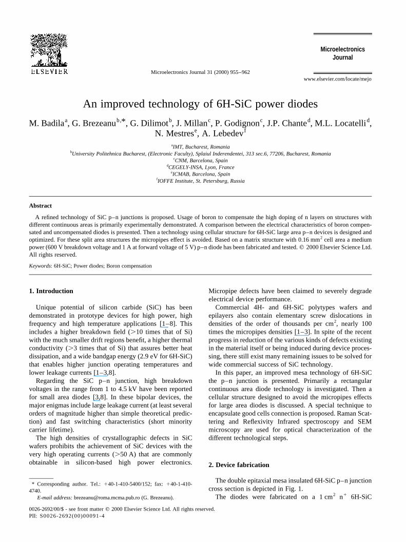
Then progress of sublimation epitaxy allowed obtainingan n epilayer with a concentration lower than 1016 cm23 andconsequently the boron diffusion process was removed. Toobtain large area devices with reduced micropipe influence,a cellular device structure was designed (Fig. 2). More cellsshould be connected in parallel to improve current capabil-ity. Our statistical investigations showed an optimum areaof 400× 400mm2 for the elementary cell and nine cells forone diode structure [6].
An especially designed method for power SiC deviceencapsulation has been used for mounting the diodes. Thistechnique is illustrated in Fig. 2. The DO-5 case includes a
M. Badila et al. / Microelectronics Journal 31 (2000) 955–962956
Fig. 1. Schematic cross-section of a mesa isolated p–n junction structure.
Fig. 2. Packaging method for a cellular encapsulated p–n power diode.
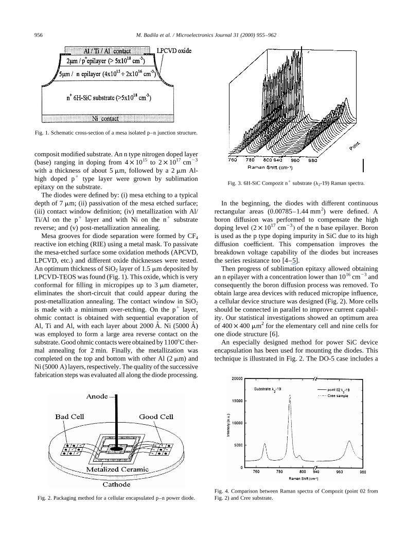
Fig. 3. 6H-SiC Compozit n1 substrate (l2-19) Raman spectra.
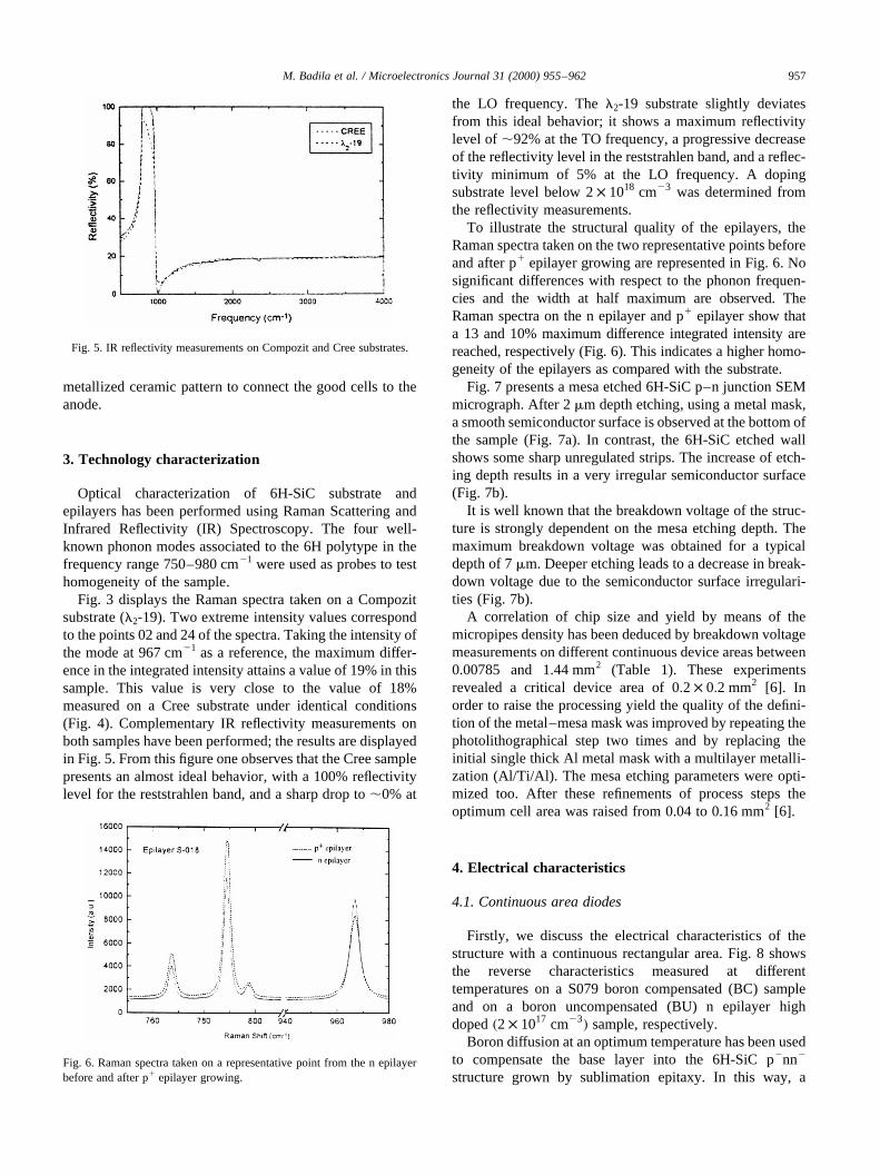
Fig. 4. Comparison between Raman spectra of Compozit (point 02 fromFig. 2) and Cree substrate.
metallized ceramic pattern to connect the good cells to theanode.
3. Technology characterization
Optical characterization of 6H-SiC substrate andepilayers has been performed using Raman Scattering andInfrared Reflectivity (IR) Spectroscopy. The four well-known phonon modes associated to the 6H polytype in thefrequency range 750–980 cm21 were used as probes to testhomogeneity of the sample.
Fig. 3 displays the Raman spectra taken on a Compozitsubstrate (l2-19). Two extreme intensity values correspondto the points 02 and 24 of the spectra. Taking the intensity ofthe mode at 967 cm21 as a reference, the maximum differ-ence in the integrated intensity attains a value of 19% in thissample. This value is very close to the value of 18%measured on a Cree substrate under identical conditions(Fig. 4). Complementary IR reflectivity measurements onboth samples have been performed; the results are displayedin Fig. 5. From this figure one observes that the Cree samplepresents an almost ideal behavior, with a 100% reflectivitylevel for the reststrahlen band, and a sharp drop to,0% at
the LO frequency. Thel2-19 substrate slightly deviatesfrom this ideal behavior; it shows a maximum reflectivitylevel of ,92% at the TO frequency, a progressive decreaseof the reflectivity level in the reststrahlen band, and a reflec-tivity minimum of 5% at the LO frequency. A dopingsubstrate level below 2× 1018 cm23 was determined fromthe reflectivity measurements.
To illustrate the structural quality of the epilayers, theRaman spectra taken on the two representative points beforeand after p1 epilayer growing are represented in Fig. 6. Nosignificant differences with respect to the phonon frequen-cies and the width at half maximum are observed. TheRaman spectra on the n epilayer and p1 epilayer show thata 13 and 10% maximum difference integrated intensity arereached, respectively (Fig. 6). This indicates a higher homo-geneity of the epilayers as compared with the substrate.
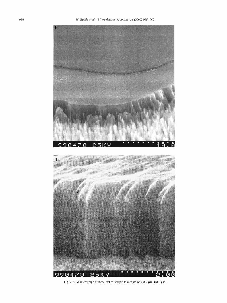
Fig. 7 presents a mesa etched 6H-SiC p–n junction SEMmicrograph. After 2mm depth etching, using a metal mask,a smooth semiconductor surface is observed at the bottom ofthe sample (Fig. 7a). In contrast, the 6H-SiC etched wallshows some sharp unregulated strips. The increase of etch-ing depth results in a very irregular semiconductor surface(Fig. 7b).
It is well known that the breakdown voltage of the struc-ture is strongly dependent on the mesa etching depth. Themaximum breakdown voltage was obtained for a typicaldepth of 7mm. Deeper etching leads to a decrease in break-down voltage due to the semiconductor surface irregulari-ties (Fig. 7b).
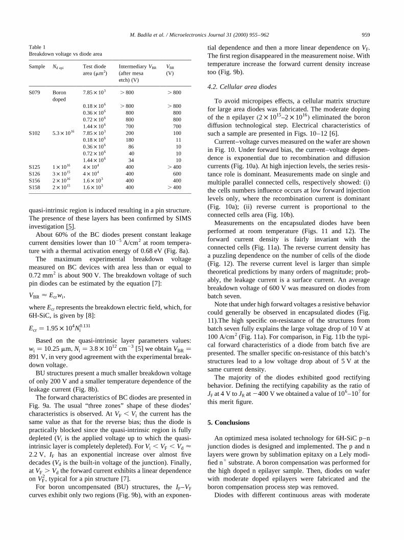
A correlation of chip size and yield by means of themicropipes density has been deduced by breakdown voltagemeasurements on different continuous device areas between0.00785 and 1.44 mm2 (Table 1). These experimentsrevealed a critical device area of 0:2 × 0:2 mm2 [6]. Inorder to raise the processing yield the quality of the defini-tion of the metal–mesa mask was improved by repeating thephotolithographical step two times and by replacing theinitial single thick Al metal mask with a multilayer metalli-zation (Al/Ti/Al). The mesa etching parameters were opti-mized too. After these refinements of process steps theoptimum cell area was raised from 0.04 to 0.16 mm2 [6].
4. Electrical characteristics
4.1. Continuous area diodes
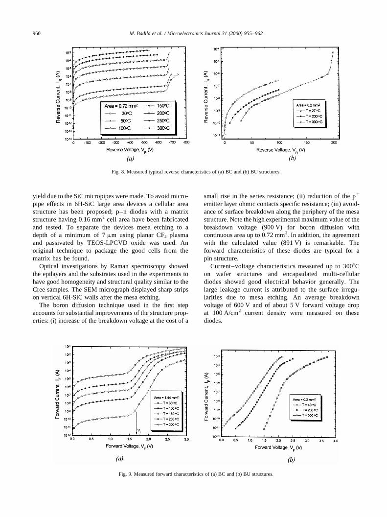
Firstly, we discuss the electrical characteristics of thestructure with a continuous rectangular area. Fig. 8 showsthe reverse characteristics measured at differenttemperatures on a S079 boron compensated (BC) sampleand on a boron uncompensated (BU) n epilayer highdoped�2 × 1017 cm23� sample, respectively.
Boron diffusion at an optimum temperature has been usedto compensate the base layer into the 6H-SiC p2nn2
structure grown by sublimation epitaxy. In this way, a
M. Badila et al. / Microelectronics Journal 31 (2000) 955–962 957
Fig. 5. IR reflectivity measurements on Compozit and Cree substrates.
Fig. 6. Raman spectra taken on a representative point from the n epilayerbefore and after p1 epilayer growing.
M. Badila et al. / Microelectronics Journal 31 (2000) 955–962958
Fig. 7. SEM micrograph of mesa etched sample to a depth of: (a) 2mm; (b) 8mm.
quasi-intrinsic region is induced resulting in a pin structure.The presence of these layers has been confirmed by SIMSinvestigation [5].
About 60% of the BC diodes present constant leakagecurrent densities lower than 1025 A/cm2 at room tempera-ture with a thermal activation energy of 0.68 eV (Fig. 8a).
The maximum experimental breakdown voltagemeasured on BC devices with area less than or equal to0.72 mm2 is about 900 V. The breakdown voltage of suchpin diodes can be estimated by the equation [7]:
VBR < Ecrwi ;
whereEcr represents the breakdown electric field, which, for6H-SiC, is given by [8]:
Ecr � 1:95× 104N0:131i
Based on the quasi-intrinsic layer parameters values:wi � 10:25mm; Ni � 3:8 × 1012 cm23 [5] we obtainVBR �891 V; in very good agreement with the experimental break-down voltage.
BU structures present a much smaller breakdown voltageof only 200 V and a smaller temperature dependence of theleakage current (Fig. 8b).
The forward characteristics of BC diodes are presented inFig. 9a. The usual “three zones” shape of these diodes’characteristics is observed. AtVF , Vi the current has thesame value as that for the reverse bias; thus the diode ispractically blocked since the quasi-intrinsic region is fullydepleted (Vi is the applied voltage up to which the quasi-intrinsic layer is completely depleted). ForVi , VF , Vd <2:2 V; IF has an exponential increase over almost fivedecades (Vd is the built-in voltage of the junction). Finally,atVF . Vd the forward current exhibits a linear dependenceon V2
F; typical for a pin structure [7].For boron uncompensated (BU) structures, theIF–VF
curves exhibit only two regions (Fig. 9b), with an exponen-
tial dependence and then a more linear dependence onVF.The first region disappeared in the measurement noise. Withtemperature increase the forward current density increasetoo (Fig. 9b).
4.2. Cellular area diodes
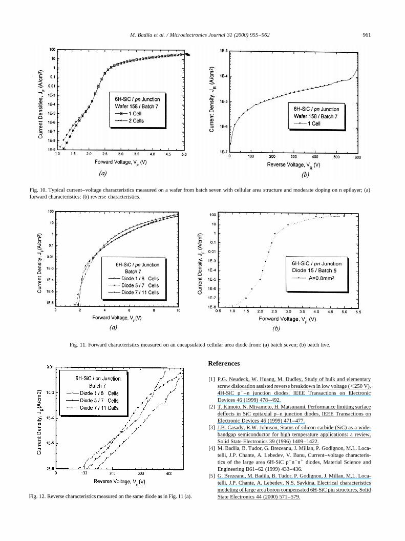
To avoid micropipes effects, a cellular matrix structurefor large area diodes was fabricated. The moderate dopingof the n epilayer�2 × 10¹⁵–2 × 10¹⁶� eliminated the borondiffusion technological step. Electrical characteristics ofsuch a sample are presented in Figs. 10–12 [6].
Current–voltage curves measured on the wafer are shownin Fig. 10. Under forward bias, the current–voltage depen-dence is exponential due to recombination and diffusioncurrents (Fig. 10a). At high injection levels, the series resis-tance role is dominant. Measurements made on single andmultiple parallel connected cells, respectively showed: (i)the cells numbers influence occurs at low forward injectionlevels only, where the recombination current is dominant(Fig. 10a); (ii) reverse current is proportional to theconnected cells area (Fig. 10b).
Measurements on the encapsulated diodes have beenperformed at room temperature (Figs. 11 and 12). Theforward current density is fairly invariant with theconnected cells (Fig. 11a). The reverse current density hasa puzzling dependence on the number of cells of the diode(Fig. 12). The reverse current level is larger than simpletheoretical predictions by many orders of magnitude; prob-ably, the leakage current is a surface current. An averagebreakdown voltage of 600 V was measured on diodes frombatch seven.
Note that under high forward voltages a resistive behaviorcould generally be observed in encapsulated diodes (Fig.11).The high specific on-resistance of the structures frombatch seven fully explains the large voltage drop of 10 V at100 A/cm2 (Fig. 11a). For comparison, in Fig. 11b the typi-cal forward characteristics of a diode from batch five arepresented. The smaller specific on-resistance of this batch’sstructures lead to a low voltage drop about of 5 V at thesame current density.
The majority of the diodes exhibited good rectifyingbehavior. Defining the rectifying capability as the ratio ofJF at 4 V toJR at2400 V we obtained a value of 106–107 forthis merit figure.
5. Conclusions
An optimized mesa isolated technology for 6H-SiC p–njunction diodes is designed and implemented. The p and nlayers were grown by sublimation epitaxy on a Lely modi-fied n1 substrate. A boron compensation was performed forthe high doped n epilayer sample. Then, diodes on waferwith moderate doped epilayers were fabricated and theboron compensation process step was removed.
Diodes with different continuous areas with moderate
M. Badila et al. / Microelectronics Journal 31 (2000) 955–962 959
Table 1Breakdown voltage vs diode area
Sample Nd epi Test diodearea (mm2)
IntermediaryVBR
(after mesaetch) (V)
VBR
(V)
S079 Borondoped
7.85× 10³ . 800 . 800
0.18× 10⁶ . 800 . 8000.36× 106 800 8000.72× 106 800 8001.44× 106 700 700
S102 5.3× 10¹⁶ 7.85× 10³ 200 1000.18× 106 180 110.36× 10⁶ 86 100.72× 10⁶ 40 101.44× 10⁶ 34 10
S125 1× 10¹⁶ 4 × 10⁴ 400 . 400S126 3× 10¹⁵ 4 × 10⁴ 400 600S156 2× 10¹⁶ 1.6× 10³ 400 400S158 2× 10¹⁵ 1.6× 10³ 400 . 400
yield due to the SiC micropipes were made. To avoid micro-pipe effects in 6H-SiC large area devices a cellular areastructure has been proposed; p–n diodes with a matrixstructure having 0.16 mm2 cell area have been fabricatedand tested. To separate the devices mesa etching to adepth of a minimum of 7mm using planar CF4 plasmaand passivated by TEOS-LPCVD oxide was used. Anoriginal technique to package the good cells from thematrix has be found.
Optical investigations by Raman spectroscopy showedthe epilayers and the substrates used in the experiments tohave good homogeneity and structural quality similar to theCree samples. The SEM micrograph displayed sharp stripson vertical 6H-SiC walls after the mesa etching.
The boron diffusion technique used in the first stepaccounts for substantial improvements of the structure prop-erties: (i) increase of the breakdown voltage at the cost of a
small rise in the series resistance; (ii) reduction of the p1
emitter layer ohmic contacts specific resistance; (iii) avoid-ance of surface breakdown along the periphery of the mesastructure. Note the high experimental maximum value of thebreakdown voltage (900 V) for boron diffusion withcontinuous area up to 0.72 mm2. In addition, the agreementwith the calculated value (891 V) is remarkable. Theforward characteristics of these diodes are typical for apin structure.
Current–voltage characteristics measured up to 3008Con wafer structures and encapsulated multi-cellulardiodes showed good electrical behavior generally. Thelarge leakage current is attributed to the surface irregu-larities due to mesa etching. An average breakdownvoltage of 600 V and of about 5 V forward voltage dropat 100 A/cm2 current density were measured on thesediodes.
M. Badila et al. / Microelectronics Journal 31 (2000) 955–962960
Fig. 8. Measured typical reverse characteristics of (a) BC and (b) BU structures.
Fig. 9. Measured forward characteristics of (a) BC and (b) BU structures.
References
[1] P.G. Neudeck, W. Huang, M. Dudley, Study of bulk and elementaryscrew dislocation assisted reverse breakdown in low voltage (,250 V),4H-SiC p1–n junction diodes, IEEE Transactions on ElectronicDevices 46 (1999) 478–492.
[2] T. Kimoto, N. Miyamoto, H. Matsunami, Performance limiting surfacedeffects in SiC epitaxial p–n junction diodes, IEEE Transactions onElectronic Devices 46 (1999) 471–477.
[3] J.B. Casady, R.W. Johnson, Status of silicon carbide (SiC) as a wide-bandgap semiconductor for high temperature applications: a review,Solid State Electronics 39 (1996) 1409–1422.
[4] M. Badila, B. Tudor, G. Brezeanu, J. Millan, P. Godignon, M.L. Loca-telli, J.P. Chante, A. Lebedev, V. Banu, Current–voltage characteris-tics of the large area 6H-SiC p2n2n1 diodes, Material Science andEngineering B61–62 (1999) 433–436.
[5] G. Brezeanu, M. Badila, B. Tudor, P. Godignon, J. Millan, M.L. Loca-telli, J.P. Chante, A. Lebedev, N.S. Savkina, Electrical characteristicsmodeling of large area boron compensated 6H-SiC pin structures, SolidState Electronics 44 (2000) 571–579.
M. Badila et al. / Microelectronics Journal 31 (2000) 955–962 961
Fig. 10. Typical current–voltage characteristics measured on a wafer from batch seven with cellular area structure and moderate doping on n epilayer; (a)forward characteristics; (b) reverse characteristics.
Fig. 11. Forward characteristics measured on an encapsulated cellular area diode from: (a) batch seven; (b) batch five.
Fig. 12. Reverse characteristics measured on the same diode as in Fig. 11 (a).

[6] M. Badila, G. Brezeanu, J.P. Chante, M.-L. Locatelli, J. Millan, P.Godignon, A. Lebedev, P. Lungu, V. Banu, 6H-SiC diodes withcellular structure to avoid micropipes effects, in: Proceedings of the2nd International Silicon Carbide and Related Materials Conference,1999.
[7] S.K. Ghandhi, Semiconductor Power Devices, Wiley, New York, 1977.[8] M. Bhatnagar, B.J. Baliga, Comparison of 6H-SiC, 3C-SiC and Si for
power devices, IEEE Transactions on Electronic Devices 40 (1993)645–655.
M. Badila et al. / Microelectronics Journal 31 (2000) 955–962962