
First-principles investigation of an epitaxial silicon oxynitride layer on a 6H-SiC(0001) surface
16
First-Principles Investigation of an Epitaxial Silicon Oxynitride Layer on a 6H -SiC(0001) Surface Peter Kr¨ uger, Bj¨orn Baumeier, and Johannes Pollmann Institut f¨ ur Festk¨ orpertheorie, Universit¨ at M¨ unster, 48149 M¨ unster, Germany (Dated: January 8, 2008) Abstract In a recent publication, Shirasawa et al. [Phys. Rev. Lett. 98, 136105 (2007)] have experimen- tally shown that incorporation of nitrogen at the interface of a silicate adlayer on 6H -SiC(0001) leads to the formation of a well ordered, highly stable epitaxial silicon oxynitride (SiON) layer with- out dangling bond states. We investigate the structural and electronic properties of this intriguing novel system by employing density functional theory with self-interaction-corrected pseudopoten- tials. Our results corroborate the structural model infered from low-energy electron diffraction (LEED). In addition, our calculated filled- and empty-state scanning tunneling microscopy (STM) images are in excellent agreement with the experimental data clearly revealing that O and Si surface states of the silicate double-layer on top of the system, respectively, give rise to the ob- served images. The calculated surface band structure exhibits a surface band gap of 9 eV in very good agreement with the scanning tunneling spectrocopy (STS) data. The physical origin of this amazingly large gap is clarified. PACS numbers: 73.20.-r, 68.47.Fg, 68.35.-p 1
-
Upload
independent -
Category
Documents
-
view
1 -
download
0
Transcript of First-principles investigation of an epitaxial silicon oxynitride layer on a 6H-SiC(0001) surface

First-Principles Investigation of an Epitaxial Silicon Oxynitride
Layer
on a 6H-SiC(0001) Surface
Peter Kruger, Bjorn Baumeier, and Johannes Pollmann
Institut fur Festkorpertheorie, Universitat Munster, 48149 Munster, Germany
(Dated: January 8, 2008)
Abstract
In a recent publication, Shirasawa et al. [Phys. Rev. Lett. 98, 136105 (2007)] have experimen-
tally shown that incorporation of nitrogen at the interface of a silicate adlayer on 6H-SiC(0001)
leads to the formation of a well ordered, highly stable epitaxial silicon oxynitride (SiON) layer with-
out dangling bond states. We investigate the structural and electronic properties of this intriguing
novel system by employing density functional theory with self-interaction-corrected pseudopoten-
tials. Our results corroborate the structural model infered from low-energy electron diffraction
(LEED). In addition, our calculated filled- and empty-state scanning tunneling microscopy (STM)
images are in excellent agreement with the experimental data clearly revealing that O and Si
surface states of the silicate double-layer on top of the system, respectively, give rise to the ob-
served images. The calculated surface band structure exhibits a surface band gap of 9 eV in very
good agreement with the scanning tunneling spectrocopy (STS) data. The physical origin of this
amazingly large gap is clarified.
PACS numbers: 73.20.-r, 68.47.Fg, 68.35.-p
1

Silicon carbide (SiC) is a material of considerable interest in experimental, as well as theo-
retical research. Due to its large band gap and high thermal conductivity, SiC has paramount
technological potential for power electronics operating at high voltage, high temperature and
high frequencies1,2. Concerning metal-oxide-semiconductor devices, ordered oxide layers on
SiC surfaces have attracted particular attention. While standard preparation techniques
from Si processing technology lead to interfaces with high defect densities3, the preparation
of hexagonal SiC surfaces by hydrogen plasma or etching in hydrogen flow produces4,5 well
ordered monolayers of SiO2. These structures, however, have one Si [C] dangling bond per
unit cell at the silicate/SiC(0001) [SiC(0001)] interface giving rise to undesirable interface
states within the band gap6,7.
Very recently, Shirasawa et al.8 have reported the formation of an epitaxial SiON layer
on a 6H-SiC(0001) surface. After etching the surface in hydrogen gas and subsequent
annealing at 1350 ◦C in nitrogen atmosphere a (√
3 ×√
3) R30◦ structure emerges which is
unusually robust and highly stable even over a long time in air. Based on their LEED and
STM measurements, the authors worked out a hetero-double-layer structure model for the
system consisting of a silicate double-layer bound to a silicon nitride double-layer by straight
Si−O−Si bridge bonds. The SiON layer contains five individual layers of O, Si, O, Si, and
N atoms from top to bottom. This way an atomically abrupt interface without dangling
bonds is formed. The absence of dangling-bond-induced gap states is consistent with the
STS data8. Amazingly, the measured STS current-voltage characteristics shows a band gap
of about 9 eV which is mainly comparable to the bulk band gap of SiO2 but much larger than
the bulk gap (3.0 eV) of the underlying 6H-SiC substrate. Shirasawa et al.8 refer the bright
protrusions in their filled- and empty-state STM images to O and Si atoms, respectively,
in the SiON layer. This interpretation was based on the density of states of bulk SiO2 and
Si2N2O due to the lack of theoretical data for the actual SiON-SiC(0001) adsorption system
at hand.
In this paper, we first confirm the structural model of the system suggested in Ref. 8
and then show that the resulting electronic properties of the model explain all experimental
STM and STS data8 quantitatively. We employ density functional theory in local density
approximation (DFT-LDA) to investigate the structural properties of the system. We use
norm-conserving ab initio pseudopotentials and a basis set of atom-centered Gaussian or-
bitals with several shells of s, p, d, and s∗ symmetry with appropriately determined decay
2

constants9. The calculational method employed has been described in detail previously10.
Here we give only some additional information that is of particular relevance to the present
system. A supercell including the SiON adlayer, nine SiC double layers, one saturating H
layer and seven vacuum layers is employed to describe the adsorption system. So the su-
percell contains 24 atomic layers in total. Surface Brillouin zone sums are carried out using
43 k-points to obtain converged results. To overcome the well-known DFT-LDA limitations
of Kohn-Sham eigenvalues in describing the electronic structure, we include self-interaction-
corrections in the pseudopotentials yielding electronic band structures of ionic systems, in
particular, in very good agreement with experiment, as shown previously11,12.
Most recently, a complementary theoretical study of the silicon oxynitride system has been
reported by Devynck et al.13. The authors employ a plane-wave pseudopotential scheme
using Troullier-Martins norm-conserving pseudopotentials in separable form and describe
the epitaxial SiON overlayer on SiC(0001) by periodic 3×4 supercells containing 18 atomic
layers. For the Brillouin zone sums they use Γ-point sampling (i.e., 1 k-point per 3×4
zone). The structural properties of the system are calculated within the generalized gradient
approximation14 of density functional theory (DFT-GGA). For an improved description of
the electronic structure the authors employ the numerically much more demanding hybrid
density functional approach proposed by Perdew, Ernzerhof, and Burke15, in which 25%
of the GGA exchange energy are replaced by the respective fraction of the Hartree-Fock
exchange energy which has to be evaluated explicitly, therefore.
We optimize the atomic structure of the (√
3 ×√
3) R30◦ model of the SiON layer on
SiC(0001) without imposing any symmetry restrictions. The final lattice configuration has
C3v symmetry. The calculated atomic coordinates are listed in Table I together with the
LEED data from Ref. 8. The corresponding bond lengths and bond angles resulting from
the calculated atomic positions are given in Table II for convenience, as well16. Fig. 1 shows
a top and a side view of the calculated structure. The adsorbed SiON film consists of five
individual layers. In each (√
3 ×√
3) R30◦ unit cell there are three O atoms (1-3) in the
topmost, two Si atoms (4,5) in the second, two O atoms (6,7) in the third, two Si atoms (8,9)
in the fourth, and three N atoms (10-12) in the fifth layer. Each O atom in the first and third
layer is bound to two Si atoms. All Si atoms in the SiON layer are fourfold coordinated.
Each N atom binds to two Si atoms on the fourth layer and one Si atom on the top layer
of the SiC substrate. These threefold coordinated N atoms are completely saturated as
3

TABLE I: Atomic coordinates (in A) of the structure shown in Fig. 1 as resulting from the present
calculations in comparison with experimental data from Ref.8. The x, y, and z directions correspond
to the [1120], [1100], and [0001] axes as indicated in Fig. 1. Atoms are labeled according to Fig. 1.
Theory Experiment
atom type x y z x y z
2 O 0.00 2.66 0.00 0.00 2.66 0.00
4 Si -3.07 0.00 -0.53 -3.09 0.00 -0.50
5 Si 3.07 0.00 -0.53 3.09 0.00 -0.54
6 O -3.07 0.00 -2.13 -3.09 0.00 -2.14
7 O 3.07 0.00 -2.13 3.09 0.00 -2.16
8 Si -3.07 0.00 -3.74 -3.09 0.00 -3.74
9 Si 3.07 0.00 -3.74 3.09 0.00 -3.74
10 N 0.00 2.13 -4.32 0.00 2.15 -4.35
all other atoms in the system. Therefore, no dangling bonds exist. The calculated atomic
structure is in excellent agreement with the structural model worked out by Shirasawa et
al.8 from their best fit to the LEED data. The latter shows only marginal deviations from
the C3v symmetry of the system (see Table I).
In the top silicate double-layer, all Si-O pairs have the same bond length of 1.62 A which
is close to the mean Si-O bond length of 1.61 A in α−quartz. The same holds for the Si-O-Si
bond angle which is 142 ◦ in the SiON layer and 144 ◦ in α−quartz. Linear Si-O-Si bridges
TABLE II: Calculated bond lengths (in A) an bond angles (in ◦) of the SiON layer. Atoms are
labeled according to Fig. 1.
straight bonds bond length angular bonds bond angle
4-1 Si−O 1.62 4-2-5 Si-O-Si 142
4-6 Si−O 1.60 4-6-8 Si-O-Si 180
8-6 Si−O 1.61 8-10-9 Si-N-Si 126
8-10 Si−N 1.73 8-10-13 Si-N-Si 113
13-10 Si−N 1.76
4

top view
side view
O
Si
O
Si
N
Si
C
1 3
2
1 2 3
4 5
6 78 910
11 1213
"""""""
bbbbbbb
bbbbbbb
"""""""
-
6
[1120]
[1100]
-
6
[1120]
[0001]
FIG. 1: (Color online). Top and side view of the SiON layer on 6H-SiC(0001), as calculated. The
(√
3 ×√
3)R30◦ surface unit cell is indicated by the red (black) diamond in the top view. O, N,
and C atoms are shown by small red (black), yellow (light gray), and brown (dark gray) balls,
respectively. Si atoms are depicted by large blue (light gray) balls. The numbers label the atoms
on the first five layers of the unit cell and one Si atom on the sixth layer.
5

per unit cell with bond lengths of 1.60 A and 1.61 A connects the silicate double-layer with
the silicon nitride double-layer. This way, the Si atoms in the second as well as in the
fourth layer of the SiON overlayer are tetrahedrally coordinated with O-Si-O and O-Si-N
bond angles of about 109 ◦, respectively. The angular Si-N-Si bonds in the silicon nitride
double-layer have an angle of 126 ◦ and a bond length of 1.73 A. These values differ only
slightly from those of the Si-N bonds with Si atoms on the sixth layer having a bond angle
of 113 ◦ and a bond length of 1.76 A. The Si-N-Si bond angle of 119 ◦, reported in Ref. 8,
corresponds to the average of the two above angles. For further reference we note that the
mean Si-N-Si bond angle and the mean Si-N bond length in bulk α−Si3N4 are 119 ◦ and
1.74 A, respectively.
Interestingly, the three topmost layers of this structural model have the same Si2O5
configuration in each unit cell as found previously for the silicate-covered SiC(0001) surface
in experiment4,5 and theory7. In the latter model, however, there are three Si atoms in the
fourth and three C atoms in the fifth layer per unit cell so that one of the three Si atoms is
not fully saturated and one dangling bond per unit cell occurs.
The surface electronic spectrum of the epitaxial SiON layer on SiC(0001), as measured by
STS8, exhibits a very large band gap of about 9 eV. In order to shed light on its physical origin
we calculate the surface band structure and local densities of states. To overcome the DFT-
LDA band gap problem we employ our self-interaction-corrected pseudopotentials12. Within
this framework we obtain a band gap of 3.1 eV for 6H-SiC, very close to the experimental
value of 3.0 eV. For α−SiO2 our calculated band gap is 8.9 eV comparing favorably with the
experimental value of 8.9 eV reported for polycrystalline17 SiO2.
The calculated surface band structure for the SiON layer on SiC(0001) is shown in Fig. 2.
All bands plotted in the figure as dotted lines are related to surface bound states or reso-
nances that stem from the SiON layer. Oxygen- and nitrogen-derived bands are shown in
blue (black) and green (gray), respectively. We have labeled groups of bands according to
the composition of their wave functions as O2s, N2s, O2p, and N2p, respectively. Most of
these bands have also contributions from Si states localized on the second, fourth, or sixth
layer. The 2s states of the five O atoms per unit cell give rise to the five O2s bands between
-21 and -24 eV. At the bottom of the projected SiC bulk bands between -16 and -19 eV,
there exist three bands derived from N 2s states. The bound states in the ionic gap, as well
as the resonances between -3 and -13 eV stem from Si 3s and 3p, as well as O 2p and N 2p
6

B3
B2
B1
N2p
O2p
N2s
O2s
��
�
6
Eg
FIG. 2: (Color online). Surface band structure of a SiON layer on 6H-SiC(0001)-(√
3×√
3)R30◦.
The shaded area represents the (0001) projected bulk-band structure of 6H-SiC. Blue (black) dotted
lines indicate oxygen-derived bands, while green (gray) dotted lines indicate nitrogen-derived bands.
Eg labels the surface gap of 9 eV (see text).
orbitals in the SiON layer.
As noted above, all bonds in the SiON layer as well as all former dangling bonds on the
clean SiC(0001) surface are fully saturated in the optimized lattice configuration. There-
7
[0001]
[1120][1100]
[0001]
B1 B3
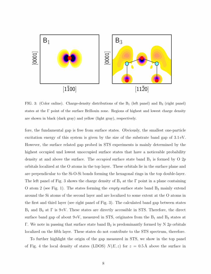
FIG. 3: (Color online). Charge-density distributions of the B1 (left panel) and B3 (right panel)
states at the Γ point of the surface Brillouin zone. Regions of highest and lowest charge density
are shown in black (dark gray) and yellow (light gray), respectively.
fore, the fundamental gap is free from surface states. Obviously, the smallest one-particle
excitation energy of this system is given by the size of the substrate band gap of 3.1 eV.
However, the surface related gap probed in STS experiments is mainly determined by the
highest occupied und lowest unoccupied surface states that have a noticeable probability
density at and above the surface. The occupied surface state band B1 is formed by O 2p
orbitals localized at the O atoms in the top layer. These orbitals lie in the surface plane and
are perpendicular to the Si-O-Si bonds forming the hexagonal rings in the top double-layer.
The left panel of Fig. 3 shows the charge density of B1 at the Γ point in a plane containing
O atom 2 (see Fig. 1). The states forming the empty surface state band B3 mainly extend
around the Si atoms of the second layer and are localized to some extent at the O atoms in
the first and third layer (see right panel of Fig. 3). The calculated band gap between states
B1 and B3 at Γ is 9 eV. These states are directly accessible in STS. Therefore, the direct
surface band gap of about 9 eV, measured in STS, originates from the B1 and B3 states at
Γ. We note in passing that surface state band B2 is predominantly formed by N 2p orbitals
localized on the fifth layer. These states do not contribute to the STS spectrum, therefore.
To further highlight the origin of the gap measured in STS, we show in the top panel
of Fig. 4 the local density of states (LDOS) N(E, z) for z = 0.5 A above the surface in
8

comparison with the bulk-like LDOS for a z value in the middle of the slab18. Between -3
and +6 eV there are practically no contributions to N(E, z = 0.5 A) due to the fact that
all states in this energy region have almost vanishing wave functions above the top of the
SiON layer. In light of these results the appearence of a gap of about 9 eV in the STS
data8 becomes immediately intelligible. In particular, our calculations reveal that the thin
siloxane film consisting of the topmost four layers in the SiON layer gives rise to virtually the
same gap as a SiO2 crystal. This is further corroborated by a calculation for a freestanding
siloxane double-layer (Si4O8) for which we obtain a band gap of 8.6 eV.
Shirasawa et al.8 have attributed the bright protrusions in their filled-state STM image to
O and those in the empty-state image to Si atoms. This interpretation is fully confirmed by
our results. Employing the Tersoff-Hamann approach19, we have calculated constant current
mode filled- and empty-state STM images at -3 and +6 eV, respectively, which are shown
in the middle and bottom panel of Fig. 4. The intensity maxima in the filled-state image
mainly result from B1 states whose wave functions are localized at the top layer O atoms
(see left panel of Fig. 3). The spots of high intensity in the empty-state image stem from B3
states whose wave functions are more extended above the Si than above the O atoms of the
top silicate double-layer (see right panel of Fig. 3). As a result, for distances z larger than
1 A above the surface the contributions of the Si atoms dominate the empty-state image.
Comparing the calculated STM images in Fig. 4 with the respective measured images (Fig. 4
in Ref. 8) reveals that our results describe the measured topograms quantitatively.
Comparing the results of Devynck et al.13 with our results and with experiment8 reveals
that both calculations yield bond lengths and bond angles of the SiON overlayer on SiC(0001)
in very good mutual accord and in excellent agreement with the experimental values. Thus
the two independent ab initio calculations fully confirm the structural model worked out
by Shirasawa et al.8 on the basis of their experimental data. The different methodologies
employed in our work and in Ref. 13 to evaluate the electronic structure, on the other
hand, give rise to some differences. For bulk 6H-SiC and SiO2 we obtain band gaps of
3.1 eV (3.0 eV) and 8.9 eV (8.9 eV), respectively, in good accord with the experimental values
given in parantheses. The more demanding hybrid functional DFT-GGA calculations13
yield 3.8 and 7.9 eV for these gaps, respectively. Likewise, our calculated surface gap of the
silicon oxynitride system of 9.0 eV is in agreement with the observed8 gap energy of about
9 eV. Devynck et al.13 inferred a surface band gap of 8.1 eV for the system from the LDOS
9

z = 0.5 A
z in the bulk
FIG. 4: (Color online). Local density of states N(E, z) for z = 0.5 A above the topmost O atoms
of the SiON layer shown by the full black line (top panel). The red dashed line shows the bulk-like
LDOS for z in the middle of the slab. The filled- (middle panel) and empty-state (bottom panel)
STM images are calculated in constant current mode at -3 and 6 eV, respectively. A ball and stick
model for the O (filled circles) and Si (open circles) atoms in the silicate double-layer is overlaid
for comparison. 10

projected onto the Si and O atoms of the outermost silicate double-layer. Considering the
above gap values for bulk 6H-SiC and the overlayer system, we note that the band gap
opening of 5.9 eV following from our results closely agrees with the experimental value of
6.0 eV while it results as 4.3 eV from the earlier calculation13. A surface band structure
or charge densities of the SiON-SiC(0001) system, to which we could further compare our
results, are not presented in Ref. 13. Finally, we note that the filled- and empty-state STM
images reported previously13 and our results shown in Fig. 4 are both in excellent agreement
with experiment8.
In summary, we have shown that DFT-LDA calculations including self-interaction-
corrected pseudopotentials allow for a quantitative description of structural and electronic
properties of an epitaxial SiON layer on 6H-SiC(0001). Also theory yields the amazingly
large surface band gap of 9 eV, as observed in STS. We have clarified its physical origin. In
addition, we have revealed which particular electronic states give rise to the observed filled-
and empty-state STM images. Our calculated images are in very nice agreement with exper-
iment. Future direct and inverse photoelectron spectroscopy investigations of the electronic
structure reported in this work could experimentally complete the physical picture of this
novel and highly intriguing system which might well turn out to be of great technological
interest for device applications.
We acknowledge a grant of computer time on the JUMP computer of the John von
Neumann Institute for Computing (NIC) at the Forschungszentrum Julich (Germany) under
Contract No. HMS08/2587.
1 W.J. Choyke, H. Matsunami, and G. Pensl, Silicon Carbide Resent Major Advances (Springer,
Germany, 2004).
2 V. M. Bermudez, Phys. Status Solidi B 202, 421 (1997).
3 M. Schurmann, S. Dreiner, U. Berges, and C. Westphal, Phys. Rev. B 74, 035309 (2006), and
references therein.
4 J. Berhardt, J. Schardt, U. Starke, and K. Heinz, Appl. Phys. Lett. 74, 1084 (1999).
5 U. Starke, J. Schardt, J. Bernhardt, and K. Heinz, J. Vac. Sci. Technol. A 17, 1688 (1999).
6 M. Hollering, F. Maier, N. Sieber, M. Stammler, J. Ristein, L. Ley, A.P.J. Stampfl, J. C. Riley,
11

R.C.G. Leckey, F.P. Leisenberger, and F.P. Netzer, Surf. Sci. 442, 531 (1999).
7 W. Lu, P. Kruger, and J. Pollmann, Phys. Rev. B 61, 13737 (2000).
8 T. Shirasawa, K. Hayashi, S. Mizuno, S. Tanaka, K. Nakatsuji, F. Komori, and H. Tochihara,
Phys. Rev. Lett. 98, 136105 (2007).
9 Decay constants of 0.18, 0.50, 1.00 for Si, 0.18, 0.34, 0.95, 2.71 for O and 0.26, 1.00, 2.40 for N
atoms in the SiON layer and 0.20, 0.60 for Si, 0.35, 1.70 for C, and 0.35 for H substrate atoms
(in atomic units) are used.
10 W. Lu, P. Kruger, and J. Pollmann, Phys. Rev. B 60, 2495 (1999).
11 D. Vogel, P. Kruger, and J. Pollmann, Phys. Rev. B 52, R14316 (1995), ibid. 54, 5495 (1996).
12 B. Baumeier, P. Kruger, and J. Pollmann, Phys. Rev. B 73, 195205 (2006), ibid. 75, 045323
(2007).
13 F. Devynck, Z. Sljivancanin, A. Pasquarello, Appl. Phys. Lett. 91, 061930 (2007).
14 J. P. Perdew, K. Burke, and M. Ernzerhof, Phys. Rev. Lett. 77, 3865 (1996).
15 J. P. Perdew, M. Ernzerhof, and K. Burke, J. Chem. Phys. 105, 9982 (1996).
16 Note that the atoms in the SiON layer in Fig. 1 are labeled differently from Ref. 8 for better
readability.
17 T. H. DiStefano and D.E. Eastman, Solid State Comm. 9, 2259 (1970).
18 The LDOS, Gaussian-broadened by 0.1 eV, is calculated as N(E, z) =∑
nk‖
∫
|Ψnk‖(r)|2d2r‖ δ(E−
Enk‖).
19 J. Tersoff and D.R. Hamann, Phys. Rev. B 31, 805 (1985).
12

top view
side view
O
Si
O
Si
N
Si
C
1 3
2
1 2 3
4 5
6 78 910
11 1213
"""""""
bbbbbbb
bbbbbbb
"""""""
-
6
[1120]
[1100]
-
6
[1120]
[0001]
Figure 1

B3
B2
B1
N2p
O2p
N2s
O2s
��
�
6
Eg
Figure 2

[0001]
[1120][1100]
[0001]
B1 B3
Figure 3

z = 0.5 A
z in the bulk
Figure 4