Self-organized metal-semiconductor epitaxial graphene layer on off-axis 4H-SiC(0001)
12
Self-organized metal–semiconductor epitaxial graphene layer on off-axis 4H-SiC(0001) Debora Pierucci 1 , Haikel Sediri 1 , Mahdi Hajlaoui 1,2 , Emilio Velez-Fort 1,3 , Yannick J. Dappe 4 , Mathieu G. Silly 2 , Rachid Belkhou 2 , Abhay Shukla 3 , Fausto Sirotti 2 , Noelle Gogneau 1 , and Abdelkarim Ouerghi 1 ( ) 1 CNRS- Laboratoire de Photonique et de Nanostructures, Route de Nozay, 91460 Marcoussis, France 2 Synchrotron-SOLEIL, Saint-Aubin, BP48, F91192 Gif sur Yvette Cedex, France 3 Université Pierre et Marie Curie (CNRS – IMPMC), 4 Pl. Jussieu, 75005 Paris, France 4 Service de Physique de l'Etat Condensé (CNRS URA2464), IRAMIS, CEA Saclay, 91191 Gif-Sur-Yvette, France Received: 26 June 2014 Revised: 13 August 2014 Accepted: 15 September 2014 © Tsinghua University Press and Springer-Verlag Berlin Heidelberg 2014 KEYWORDS epitaxial graphene layer, monolayer, bilayer, band gap opening, Bernal stacking, off-axis silicon carbide, electronic properties ABSTRACT The remarkable properties of graphene have shown promise for new perspectives in future electronics, notably for nanometer scale devices. Here we grow graphene epitaxially on an off-axis 4H-SiC(0001) substrate and demonstrate the formation of periodic arrangement of monolayer graphene on planar (0001) terraces and Bernal bilayer graphene on (112 — 0) nanofacets of SiC. We investigate these lateral superlattices using Raman spectroscopy, atomic force microscopy/ electrostatic force microscopy (AFM/EFM) and X-ray and angle resolved photoemission spectroscopy (XPS/ARPES). The correlation of EFM and ARPES reveals the appearance of permanent electronic band gaps in AB-stacked bilayer graphene on (112 — 0) SiC nanofacets of 150 meV. This feature is confirmed by density functional theory (DFT) calculations. The charge transfer between the substrate and graphene bilayer results in an asymmetric charge distribution between the top and the bottom graphene layers opening an energy gap. This surface organization can be thus defined as self-organized metal–semiconductor graphene. 1 Introduction Graphene exhibits unique properties, making it the material of choice for the observation of novel quantum phenomena and the development of future nanodevices. However, the use of graphene in nanoscale electronics devices requires a modification of its intrinsic semi-metallic nature in order to open an energy gap [1–5]. Among the different techniques used, the synthesis of graphene through thermal decomposition of a SiC substrate is one of the most attractive approaches. In fact, epitaxial graphene shows electronic properties similar to the isolated graphene sheets. In addition epitaxial graphene Nano Research DOI 10.1007/s12274-014-0584-y Address correspondence to [email protected]
-
Upload
independent -
Category
Documents
-
view
0 -
download
0
Transcript of Self-organized metal-semiconductor epitaxial graphene layer on off-axis 4H-SiC(0001)

Self-organized metal–semiconductor epitaxial graphenelayer on off-axis 4H-SiC(0001)
Debora Pierucci1, Haikel Sediri1, Mahdi Hajlaoui1,2, Emilio Velez-Fort1,3, Yannick J. Dappe4, Mathieu G. Silly2,
Rachid Belkhou2, Abhay Shukla3, Fausto Sirotti2, Noelle Gogneau1, and Abdelkarim Ouerghi1 ()
1 CNRS- Laboratoire de Photonique et de Nanostructures, Route de Nozay, 91460 Marcoussis, France 2 Synchrotron-SOLEIL, Saint-Aubin, BP48, F91192 Gif sur Yvette Cedex, France 3 Université Pierre et Marie Curie (CNRS – IMPMC), 4 Pl. Jussieu, 75005 Paris, France 4 Service de Physique de l'Etat Condensé (CNRS URA2464), IRAMIS, CEA Saclay, 91191 Gif-Sur-Yvette, France
Received: 26 June 2014
Revised: 13 August 2014
Accepted: 15 September 2014
© Tsinghua University Press
and Springer-Verlag Berlin
Heidelberg 2014
KEYWORDS
epitaxial graphene layer,
monolayer,
bilayer,
band gap opening,
Bernal stacking,
off-axis silicon carbide,
electronic properties
ABSTRACT
The remarkable properties of graphene have shown promise for new perspectives
in future electronics, notably for nanometer scale devices. Here we grow
graphene epitaxially on an off-axis 4H-SiC(0001) substrate and demonstrate the
formation of periodic arrangement of monolayer graphene on planar (0001)
terraces and Bernal bilayer graphene on (112—
0) nanofacets of SiC. We investigate
these lateral superlattices using Raman spectroscopy, atomic force microscopy/
electrostatic force microscopy (AFM/EFM) and X-ray and angle resolved
photoemission spectroscopy (XPS/ARPES). The correlation of EFM and ARPES
reveals the appearance of permanent electronic band gaps in AB-stacked bilayer
graphene on (112—
0) SiC nanofacets of 150 meV. This feature is confirmed by
density functional theory (DFT) calculations. The charge transfer between the
substrate and graphene bilayer results in an asymmetric charge distribution
between the top and the bottom graphene layers opening an energy gap. This
surface organization can be thus defined as self-organized metal–semiconductor
graphene.
1 Introduction
Graphene exhibits unique properties, making it the
material of choice for the observation of novel
quantum phenomena and the development of future
nanodevices. However, the use of graphene in
nanoscale electronics devices requires a modification
of its intrinsic semi-metallic nature in order to open
an energy gap [1–5]. Among the different techniques
used, the synthesis of graphene through thermal
decomposition of a SiC substrate is one of the most
attractive approaches. In fact, epitaxial graphene
shows electronic properties similar to the isolated
graphene sheets. In addition epitaxial graphene
Nano Research
DOI 10.1007/s12274-014-0584-y
Address correspondence to [email protected]
| www.editorialmanager.com/nare/default.asp
2 Nano Res.
presents the advantage of a SiC substrate allowing
direct device processing, without any transfer steps
as in the case of exfoliation [6–10] or metal catalyst
chemical vapor deposition (CVD) techniques [11–15].
Many of the desirable properties of graphene are
related to its electronic structure with conical , *
bands (Dirac cone) of vertices touching in a single
point at the Fermi level. This makes graphene a gapless
semiconductor which is a limiting factor for some
applications of graphene in electronics where a sizeable
band gap at the Fermi energy is required. Among
promising techniques for achieving this goal, the
synthesis of nanometer scale ribbons with a band gap
induced by quantum confinement [16–18] has been
studied in recent years. The common approach to
form graphene ribbons is the patterning of preexisting
graphene layers [19–21]. However, the different pattern
steps induce defects and can degrade electronic
properties [22–24]. An alternative consists of directly
growing graphene ribbons by thermal decomposition
of SiC substrate under specific conditions. This
approach has already been demonstrated by performing
selective epitaxial growth of few-layer graphene (FLG)
on patterned SiC substrates [25, 26] or by controlling
the sublimation of Si atoms from non-patterned SiC
substrates [27]. Recently Hicks and co-workers [28]
have shown that using a patterned SiC(0001) substrate,
it is possible to obtain semiconducting graphene
ribbons having a band gap energy greater than 0.5 eV.
Nevertheless the formation of controlled nanoribbons
using this approach requires high-level technological
steps. Another possible route relies on laterally
altering the graphene band structure by means of an
additional periodic potential. In fact, calculations
indicate that the lateral superlattice structures may
lead to unexpected and potentially useful charge
carrier behavior, e.g. gap openings or Fermi velocity
anisotropy [3, 28, 29]. To favor this specific lateral
graphene band gap structure modulation, the use of
off-axis SiC(0001) surfaces appears as a suitable
solution. The periodic arrays of atomic steps spaced
by flat terraces, as successfully demonstrated on
SiC(0001) [30–33], can be considered as a natural
“lateral superlattice substrate” for quasi-periodic
modulations, with well-defined width hence exhibiting
size limited effects.
In this work, we demonstrate the formation of lateral
periodic arrangement of bilayer graphene on (112—
0)
nanofacets and monolayer graphene (0001) terraces on
off-axis 4H-SiC(0001) using complementary charac-
terization techniques, namely atomic and electrostatic
force microscopy (AFM and EFM), Raman spectroscopy,
X-ray and angle resolved photoemission spectroscopy
(XPS and ARPES). The EFM and ARPES measurement
show features due to single and Bernal bilayer
graphene. The density functional theory (DFT) study
reveals that a SiC facet like (112—
0) allows the com-
plete decoupling of the bilayer graphene, leading to a
gap opening in the bilayer graphene band structure.
While the monolayer exhibits a linear dispersion, the
AB-stacked bilayer is characterized by two sets of
bands due to interlayer interaction and band gap
opening and their specific configuration in a lateral
metal–semiconductor epitaxial graphene layer is self-
organized.
2 Methods
Off-axis 4H-SiC(0001) wafers from NovaSiC with
atomically flat surfaces were used to grow high quality
epitaxial graphene films by solid state graphitization.
The substrate was hydrogen etched (100% H2) at
1,550 °C to produce well-ordered atomic terraces of
SiC. The Si-face SiC(0001) surfaces were deoxidized
at 820 °C under semi-vacuum conditions in order to
remove the native oxide and any possible surface
contamination. Following this surface preparation,
the bilayer ribbons graphene were synthesized in
atmospheric conditions by radio frequency (RF)
heating of the SiC substrate then inducing sublimation
of Si atoms and thus carbon enrichment of the
surface [34, 35].
The sample was cooled down to room temperature
(RT) and transferred ex situ to perform different
measurements. The surface morphology was studied
by AFM, in tapping mode. EFM images of the surface
were achieved in lift mode (with a lift scan height of
20 nm) with a Cr/Pt-coated tip characterized with a
tip radius of 10 nm.
The graphitization level of the substrate was
assessed by micro-Raman spectroscopy performed
at RT with a Renishaw spectrometer using a 532 nm
www.theNanoResearch.com∣www.Springer.com/journal/12274 | Nano Research
3 Nano Res.
laser focused on the sample by a DMLM Leica
microscope with a 50× (NA = 0.75) objective. The
Rayleigh diffusion was eliminated by edge filters.
XPS/ARPES experiments were carried out on the
TEMPO beamline [36] at the SOLEIL French synch-
rotron facility. The photon source was a HU80 Apple
II undulator set to deliver linearly polarized light. The
photon energy was selected using a high-resolution
plane grating monochromator, with a resolving power
E/ΔE that can reach 15,000 on the whole energy range
(45–1,500 eV). The end-station chamber (base pressure =
10–10 mbar) is equipped with a modified 200 nm
hemispheric electron analyzer (Scienta 200) equipped
with a delay line detector [37]. In order to remove
contaminants (physisorbed hydrocarbons and water)
arising from long exposure to air the sample was first
annealed in vacuum (P = 2 10–10 mbar) at around
600 °C for 30 min. During the XPS measurements, the
photoelectrons were detected at 0° from the sample
surface normal n and at 46° from the polarization
vector E. The C 1s spectra were measured at hν =
340 eV (overall resolution ~100 meV) and hν = 540 eV
(overall resolution ~140 meV). For the ARPES
measurements, the orientation of the sample and the
photon energy of hν = 60 eV were chosen in order to
explore the k-space region around the K point along
the K direction of the Brillouin zone.
Ab initio calculations were performed using a very
efficient DFT localized orbital molecular dynamic
technique (FIREBALL) [38–41]. Basis sets of sp3 for C
and Si, and s for H were used with cutoff radii (in
atomic units) s = 4.5, p = 4.5 (C), s = 4.8, p = 5.4 (Si) and
s = 4.1 (H). In this study we considered supercells
of 5 monolayer (ML) SiC(0001) with 2 ML SiC(112—
0).
The lateral size roughly corresponds to a 4 × 4 unit
cell of graphene. The bottom layer is saturated with
hydrogen atoms. On top of the supercell, we set a 4 × 4
AB stacked bilayer of graphene and we performed
DFT molecular dynamics at 1,775 K, following the
experimental conditions. Once the graphene bilayer
left the surface, we relaxed the whole system using
a sample of 32 k-points in the Brillouin zone, main-
taining the last three bottom layers in bulk positions.
The final distance between the graphene planes and
the SiC surface was determined using the LCAO-S2 +
vdW formalism [42–44]. A set of 300 special k-points
along the –K-M path has been used for the band
structure calculations on the relaxed positions.
3 Results and discussions
The important parameters governing the formation
of graphene by solid state graphitization from SiC
substrates are the annealing temperature at which
the sublimation of Si atoms occurs, and the duration
of this annealing [45]. On the Si-face SiC substrate it
is known that the graphitization takes place prefer-
entially from the step edge and progresses towards
the terraces [30, 32]. However, the atomic-step
arrangement of the substrate surface is also crucial.
In order to optimize the surface morphology of the
substrate, the 4H-SiC(0001) substrate was annealed
under an argon flux at temperatures higher than
those normally used for graphitization so as to favor
atomic diffusion and rearrangement [46]. This leads
to minimization of the surface energy in well-defined
steps and the growth of the specific self-organized
lateral graphene layers. By controlling the step-terrace
structure and by finely adjusting the temperature
and duration of SiC thermal annealing, it is possible
to regulate the graphitization level of the surface.
Figure 1 shows an AFM image performed in tapping
mode and Raman analysis of the surface morphology
of off-axis 4H-SiC(0001) after epitaxial graphene growth
at 1,500 °C during 10 min and in a 800 mbar Ar
atmosphere. The topographic-AFM image (Fig. 1(a))
and the phase-AFM image, (Fig. 1(b)) recorded
simultaneously, show a self-ordered stepped surface.
The step direction and the terrace width are directly
determined by the initial misorientation of the
substrate with respect to the crystallographic (0001)
plane. The self-ordered surface is described with
(0001) terraces spaced by (112—
0) nanofacets [30, 31, 47]
at large scale of the sample. The (0001) terraces are
characterized by a width of 700 nm, while the (112—
0)
nanofacets are characterized by a width of 50–70 nm
and height of 30 nm. They are both aligned along
the <11—
00> SiC axis. The contrast observed on the AFM
phase image, which is directly related to the surface
topography and/or material hardness clearly establishes
that graphene covers the terraces and that the nano-
facets do not have the same thickness. This lateral

| www.editorialmanager.com/nare/default.asp
4 Nano Res.
Figure 1 AFM cartography and Raman spectra for epitaxial graphene on off-axis 4H-SiC(0001). (a) AFM image of epitaxial graphene; (b) AFM phase image showing two phase contrasts, at (0001) and (112̄0) SiC facets. Image dimensions are 9 μm × 9 μm; (c) micro-Raman spectra of the D, G and 2D bands collected on the terrace (green and black spectra) and on the step edge (red spectrum), with a 532 nm wavelength excitation and a spatial resolution better than 1 m.
arrangement of bilayer graphene on (112—
0) nanofacets
and monolayer graphene (0001) terraces on a large
scale can be considered as a self-organization induced
by the stepped SiC substrate. Due to its electronic
properties, graphene creates an electron gas, with a
significant one-dimensional (1D) or tow-dimensional
(2D) lateral modulation. Micro-Raman measurements
were carried out under ambient conditions using a
Renishaw system with a 532 nm excitation wavelength.
A representative Raman spectrum performed on
three positions of the sample is presented in Fig. 1(c).
The green and black Raman spectra were measured
by aligning the incident beam on the widest terraces
of the sample while the red spectrum was measured
in coincidence with a higher density of step edges.
The most prominent Raman features, D, G and 2D
bands characterizing a graphene layer are clearly
visible. The D peak is a A1g symmetry breathing
mode involving phonons near the K point zone
boundary, normally not Raman active in defect-less
graphene [48, 49]. Its appearance at 1,356 cm–1 indicates
the presence of defects or structural disorder and step
edges. The G peak, corresponding to the in-plane
vibration of sp2 carbon atoms, is a doubly degenerated
E2g phonon mode at the Brillouin zone center [49].
The 2D peak, centered at 2,714 cm–1, originates from
the double resonant Raman process of the two
phonons near the K point zone boundary. The
Lorentzian shape of the 2D feature, with a full width
at half maximum of around 50 cm–1 is the signature
of a system with single-band electronic dispersion. It
is known that the positions of G and 2D peaks
depend on both strain and carrier density (terraces
and step edges). The range of values measured for
these, shown by two characteristic spectra in Fig. 1(c),
indicates the presence of both possibilities and is not
surprising given the specific topography of the
sample. On the step edges, the blue-shift of the 2D
band is correlated with the blue-shift of the G band.
It reveals that there is a difference in strain, charge
carrier density and/or the number of graphene layers
between two surface regions.
For precise local electronic characterization of the
graphene surface we use EFM. In particular we seek
to determine the relation between the terrace/nanofacet
topology as revealed by AFM and the number of
graphene layers. EFM (a specific AFM mode) has
been demonstrated as a powerful tool for measuring
the electric potential distribution with nanometer
resolution which allows the variations in the electric
field gradient above a sample to be directly measured
[50]. EFM images of the surface were achieved in lift
mode (with a lift scan height of 20 nm) with a Cr/Pt-
coated tip characterized by a tip radius of 10 nm. The
macroscale electrical characterization of the epitaxial
graphene layers is reported in Fig. 2. The surface
morphology (Fig. 2(a)) and the corresponding phase
shift (Fig. 2(b)) measured simultaneously for a tip bias
voltage of V = –4 V under EFM mode are represented.
The corresponding profiles performed perpendicular
to the steps are presented in Fig. 2(c). A correlation
between the localisation of the (0001) terraces and
the (112—
0) nanofacets with the variation of the EFM
profile is evident. This EFM phase shift , due to
the electrostatic interaction between the tip and the
sample, evolves with the bias voltage applied. It can
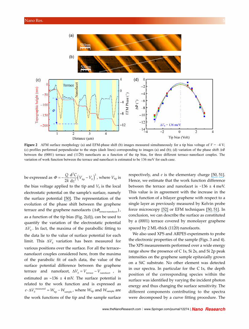
www.theNanoResearch.com∣www.Springer.com/journal/12274 | Nano Research
5 Nano Res.
be expressed as 2 2
tip 02
d
2 d
Q CV V
k z, where Vtip is
the bias voltage applied to the tip and V0 is the local
electrostatic potential on the sample’s surface, namely
the surface potential [50]. The representation of the
evolution of the phase shift between the graphene
terrace and the graphene nanofacets terrace-nanofacet
( ) ,
as a function of the tip bias (Fig. 2(d)), can be used to
quantify the variation of the electrostatic potential
0
V . In fact, the maxima of the parabollic fitting to
the data lie to the value of surface potential for each
limit. This 0
V variation has been measured for
various positions over the surface. For all the terrace–
nanofacet couples considered here, from the maxima
of the parabolic fit of each data, the value of the
surface potential difference between the graphene
terrace and nanofacet, 0 terrace nanofacet
V V V , is
estimated as 136 ± 4 mV. The surface potential is
related to the work function and is expressed as
measured
0 tip samplee V W W , where Wtip and Wsample are
the work functions of the tip and the sample surface
respectively, and e is the elementary charge [50, 51].
Hence, we estimate that the work function difference
between the terrace and nanofacet is ~136 ± 4 meV.
This value is in agreement with the increase in the
work function of a bilayer graphene with respect to a
single layer as previously measured by Kelvin probe
force microscopy [52] or EFM techniques [50, 51]. In
conclusion, we can describe the surface as constituted
by a (0001) terrace covered by monolayer graphene
spaced by 2 ML-thick (112—
0) nanofacets.
We also used XPS and ARPES experiments to probe
the electronic properties of the sample (Figs. 3 and 4).
The XPS measurements performed over a wide energy
range show the presence of C 1s, Si 2s, and Si 2p peak
intensities on the graphene sample epitaxially grown
on a SiC substrate. No other element was detected
in our spectra. In particular for the C 1s, the depth
position of the corresponding species within the
surface was identified by varying the incident photon
energy and thus changing the surface sensitivity. The
different components contributing to the spectra
were decomposed by a curve fitting procedure. The
Figure 2 AFM surface morphology (a) and EFM-phase shift (b) images measured simultaneously for a tip bias voltage of V = –4 V;(c) profiles performed perpendicular to the steps (dash lines) corresponding to images (a) and (b); (d) variation of the phase shift between the (0001) terrace and (112̄0) nanofacets as a function of the tip bias, for three different terrace–nanofacet couples. The variation of work function between the terrace and nanofacet is estimated to be 136 meV for each case.

| www.editorialmanager.com/nare/default.asp
6 Nano Res.
Figure 3 (a) XPS spectra of the graphene layer on off-axis 4H- SiC(0001); (b) C 1s XPS spectra for epitaxial graphene at hv= 340 (left) and 530 eV (right). The take off angle of the electron with respect to the surface normal is 0°. The bottom spectra were fitted using a Doniach–Sunjic line shape analysis.
experimental data points are displayed with dots
while the solid line is the envelope of the fitted com-
ponents. The C 1s core level spectra for two different
photon energy (hν = 340 and 540 eV), are compared
in Fig. 3(b). In both cases the C 1s spectrum shows
three components at 283.4, 284.4, and 284.9 eV in
binding energy. The ratio between components at
284.4 and 283.4 eV increases with the photon energy.
These components are attributed to the SiC bulk
(noted SiC), the graphene layer (noted G), and the
interface layer (noted I), respectively [30, 53, 54]. The
sharp C 1s peak, labeled G, located at 284.4 eV in
binding energy, indicates the presence of sp2 hybridized
C–C bonds. This component has been fitted using a
Doniach–Sunjic line shape with an asymmetry factor
of 0.1 and a FWHM of 0.45 eV. Assuming that the
graphene–SiC sample can be modeled as a semi-
infinite SiC substrate with a uniform graphene
overlayer, the thickness can be calculated from the
ratio between the intensity of the G and SiC com-
ponents [55] extracted from XPS data. This ratio fits
well with an exponential decay of roughly 1.3 ML of
carbon covering. This value is in agreement with a
mixed situation between monolayer graphene and
bilayer graphene on off-axis 4H-SiC confirming the
interpretation of AFM/EFM images in terms of local
film thickness and structure. We further make an
average evaluation of the surface electronic structure
by ARPES. ARPES provides a means to identify the
thickness of the majority species in the film, not only
through a method that gives lateral resolution, but
also by the thickness sensitivity in a “fingerprint”
manner. A single linearly dispersing π band at the K
point of the Brillouin zone, near the so-called Dirac
point ED, is characteristic of the single layer, while the
bilayer spectrum has an extra set of bands due to the
interlayer splitting brought about by the close pro-
ximity of the layers. ARPES and the second derivative
of the ARPES data as a function of energy and
electron wave vector, shown in Fig. 4, were recorded
at photon energy of 60 eV, near the K point of the
Brillouin zone, along the MKΓ direction. Three separate
bands are observed in the measured photoemission
pattern, one from the monolayer band, and two from
the branches of the bilayer bands. While the single
layer is characterized by a linear dispersion as indicated
by the pink arrow in Figs. 4(a) and 4(b), the double
layer exhibits two sets of bands due to interlayer
interaction (green arrows). ARPES data show features
due to both single and bilayer graphene regions [56].
The band structure is in perfect agreement with the
presence of monolayer graphene on the planar (0001)
face of SiC and bilayer graphene ribbons on the (112—
0)
facets of the steps[31, 47].
Figure 4(c) shows the energy distribution curves
(EDCs) along the ΓK direction for the graphene in
off-axis SiC. This figure reveals broad line-shapes,
which cause an overlap of the intensity tails from the
top of the valence band and the bottom of the
conduction band. Nevertheless, the dispersion of the
bands and the electronic gap between the π and π*
states are well resolved. In particular from the fitting
of the π and π* peaks positions taken at the K point
(Fig. 4(d)) in the EDCs, we obtain an energy gap
value Δ for 2 ML graphene nanofacet of about 150 meV.
The position of the Dirac point at 0.5 and 0.3 eV
below the Fermi energy indicates an n-type doping

www.theNanoResearch.com∣www.Springer.com/journal/12274 | Nano Research
7 Nano Res.
(n ≈ 1013 and 5 × 1012 cm−2) for monolayer and bilayer
graphene respectively. These inhomogeneities of the
band structure are reflected in the macroscopic work
function variation measured by EFM.
We have also performed DFT calculations that
confirm these results. In Fig. 5(a), we represent the
equilibrium configuration of the decoupled AB stacked
bilayer graphene on the 2 ML SiC(112—
0)/5 ML SiC(0001).
The system was first allowed to evolve freely in
molecular dynamics at 1,775 K, and then the geometry
was optimized at room temperature to reproduce the
conditions of the experimental measurements. We
observed that the bilayer graphene is totally decoupled
from the surface and the interaction is now ruled by
van der Waals interactions. In Fig. 5(b) we represent
the corresponding partial band structure for the
bilayer graphene along the ΓKM direction. This band
structure shows a band gap opening of around 115 meV.
This value is slightly smaller than the experimental
one, as expected in DFT where the electronic gaps are
always underestimated. The doping is unfortunately
not so well reproduced since we find an almost
Figure 4 (a) and (b) 2D band structure map and second derivative along the ΓK direction, obtained by ARPES (hv = 60 eV) at room temperature, on epitaxial graphene on off-axis 4H-SiC(0001). The inset of (a) shows the Brillouin zone of graphene and the horizontal line in the ΓK direction presents the measurement geometry in the k-space. (c) and (d) ARPES intensity integrated spectra as a function of the binding energy, extracted from the 2D ARPES map.

| www.editorialmanager.com/nare/default.asp
8 Nano Res.
Figure 5 (a) Geometric representation of the equilibrium con-figuration of the bilayer graphene on SiC(112̄0)/SiC(0001) obtained by DFT calculations; (b) bilayer graphene band structure around the K point showing the gap opening of the graphitic layers.
electronically neutral bilayer graphene band structure.
This is due to a well-known problem within the DFT
formalism, where the doping is highly dependent on
the choice of the exchange-correlation potential.
Therefore, a quantitative evaluation of the doping
remains a difficult challenge in this frame [57, 58].
Nevertheless, these calculations give the correct
tendency of the underlying physical processes, such
as the decoupling of the bilayer graphene and the
asymmetric charge transfer. Indeed, looking at the
electronic charges at each graphene plane, we can
estimate the electronic transfer from the substrate to
the graphene bilayer. This transfer, through its resulting
electric field is responsible for the gap opening in the
structure. From our calculations, this electric field can
be estimated to be around 0.13 V·Å–1. This value is
probably underestimated in the same manner as the
doping, but is sufficient to semi-quantitatively explain
the gap opening.
Our results show two features: (i) An epitaxial
monolayer graphene on a buffer layer on the (0001)
terraces and (ii) bilayer graphene on (112—
0) facets of
SiC [47]. This structure is of crucial importance because
it consists of electronically dissimilar polymorphs,
which are lattice matched such that they form
chemically homogeneous atomic and electronic hetero-
structures between mono- and bilayer graphene
(Fig. 6). In fact, this offers two distinct advantages:
First, the bilayer locally alters the electrical properties
of a monolayer grown on off-axis SiC(0001), opening
up the possibility of producing electron gases with a
significant 1D or 2D lateral potential modulation along
the SiC step edges [34]. Secondly, this bilayer induces
local modification of the electrical characteristics of
epitaxial graphene on SiC steps, since it should
trigger intrinsic scattering mechanisms that are related
to areas of unequal doping and unequal number of
graphene layers [34].
Another attractive aspect is the presence of self-
organized semiconductor bilayer graphene, generated
Figure 6 Schematic 2D heterostructure of epitaxial graphene on off-axis 4H-SiC(0001) and the band structure of monolayer graphene on (0001) SiC and bilayer graphene on (112̄0) SiC facets.

www.theNanoResearch.com∣www.Springer.com/journal/12274 | Nano Research
9 Nano Res.
at the nanofacets (Fig. 6). The presence of bilayer
graphene at nanofacets is of crucial importance since
it introduces the possibility of an electronic band gap
[29, 59], making it a semiconductor, due to the intrinsic
charge asymmetry between the layers from the SiC
substrate. In our case, we have a band gap of about
150 meV. Two hypotheses can explain the development
of this band gap opening:
(i) Lateral quantum confinement of bilayer graphene
on SiC nanofacets. AFM measurements show that the
size of these ribbons is about 50 nm. However,
numerous studies of graphene nanostructures have
demonstrated that a sizeable band gap can be
expected only if their sizes are less than 10 nm in at
least one dimension [19], to reproduce quantum
confinement, which is not the case here.
(ii) Breaking of the inversion symmetry in bilayer
graphene. By applying an external electric field normal
to the bilayer graphene plane, a band gap can be
opened in the Bernal stacking (AB-stacking) bilayer
graphene. It has been shown that charge transfer in
bilayer graphene on SiC(0001) can induce a band gap
opening [29]. Our ARPES study shows a band gap and
a charge transfer between the (112—
0) nanofacet and
bilayer graphene. This charge transfer is in agreement
with a recent study of monolayer graphene on non
polar SiC(112—
0) [31, 57]. These results are confirmed
by our DFT calculations, which provide an estimate
of the electric field value. Consequently, inversion
symmetry breaking in bilayer graphene by charge
transfer doping is at the origin of the band gap opening
in our case.
The organization of monolayer and bilayer graphene
planar structure on a large scale is of particular
interest: (i) The two different electronic structures
related to the monolayer and bilayer graphene, such
as the charge carriers and strain at the step edges,
may act as wide reaction sites to obtain selected
patterned molecular adsorption even when graphene
binds only weakly to them, and (ii) the two structures
with different Landau level sequences (and different
Berry’s phases for charge carriers) may be used in
tuning transport properties, of particular interest
being a planar heterostructure with no analog in
conventional 2DEG III/V.
4 Conclusions
We have developed a methodology to synthesize a
new 2D heterostructure based on a self organized
monolayer–bilayer graphene on off-axis 4H-SiC(0001).
The epitaxial monolayer and bilayer graphene layers
were evidenced by AFM/EFM, Raman measurements
and XPS spectroscopy. Our ARPES measurements
reveal that the graphene layer consists of micrometer-
sized domains of semiconducting and metallic phases
that form coherent interfaces with one another. DFT
calculations confirm the decoupling of the bilayer
graphene from the SiC surface, leading to a gap
opening in the upper graphene sheet. This gap
opening is mainly attributed to the charge transfer
between the SiC substrate and the bilayer graphene
structure, with an estimated resulting electric field of
around 0.13 V·Å–1. Such a modification of the intrin-
sically semi-metallic nature of graphene to introduce
a band gap is essential for the use of graphene in
nanoscale electronics applications working at room
temperature, such as field-effect transistors. The two
polymorphs of monolayer and bilayer graphene which
allow formation of coherent electronic heterostructures
represent a unique characteristic of this material that
may be exploited for novel molecular functionalities.
Acknowledgements
The authors thank the French National Research
Agency (ANR) SUPERTRAMP project and LABEX
NanoSaclay for funding.
References
[1] Costa Girão, E.; Liang, L. B.; Cruz-Silva, E.; Filho, A. G. S.;
Meunier, V. Emergence of a typical properties in assembled
graphene nanoribbons. Phys. Rev. Lett. 2011, 107, 135501.
[2] Sprinkle, M.; Ruan, M.; Hu, Y.; Hankinson, J.; Rubio-Roy,
M.; Zhang, B.; Wu, X.; Berger, C.; de Heer, W. A. Scalable
templated growth of graphene nanoribbons on SiC. Nat.
Nanotechnol. 2010, 5, 727–731.
[3] Zhou, S. Y.; Gweon, G. H.; Fedorov, A. V.; First, P. N.; de
Heer, W. A.; Lee, D. H.; Guinea, F.; Castro Neto, A. H.;
Lanzara, A. Substrate-induced bandgap opening in epitaxial
graphene. Nat. Mater. 2007, 6, 770–775.

| www.editorialmanager.com/nare/default.asp
10 Nano Res.
[4] Son, Y. W.; Cohen, M. L.; Louie, S. G. Energy gaps in
graphene nanoribbons. Phys. Rev. Lett. 2006, 97, 216803.
[5] Chen, Z. H.; Lin, Y. M.; Rooks, M. J.; Avouris, P.
Graphene nano-ribbon electronics. Physica E Lowdimens
Syst. Nanostruct. 2007, 40, 228–232.
[6] Novoselov, K. S.; Geim, A. K.; Morozov, S. V.; Jiang, D.;
Zhang, Y.; Dubonos, S. V.; Grigorieva, I. V.; Firsov, A. A.
Electric field effect in atomically thin carbon films. Science
2004, 306, 666–669.
[7] Stankovich, S.; Dikin, D. A.; Dommett, G. H. B.; Kohlhaas,
K. M.; Zimney, E. J.; Stach, E. A.; Piner, R. D.; Nguyen, S.
T.; Ruoff, R. S. Graphene-based composite materials. Nature
2006, 442, 282–286.
[8] Hass, J.; de Heer, W. A.; Conrad, E. H. The growth and
morphology of epitaxial multilayer graphene. J. Phys.:
Condens. Matter 2008, 20, 323202.
[9] Varchon, F.; Feng, R.; Hass, J.; Li, X.; Nguyen, B. N.; Naud,
C.; Mallet, P.; Veuillen, J. Y.; Berger, C.; Conrad, E. H. et
al. Electronic structure of epitaxial graphene layers on SiC:
Effect of the substrate. Phys. Rev. Lett. 2007, 99, 126805.
[10] Forbeaux, I.; Themlin, J. M.; Debever, J. M. Heteroepitaxial
graphite on 6H-SiC (0001): Interface formation through
conduction-band electronic structure. Phys. Rev. B 1998, 58,
396–406.
[11] Somani, P. R.; Somani, S. P.; Umeno, M. Planer nano-
graphenes from camphor by CVD. Chem. Phys. Lett. 2006,
430, 56–59.
[12] Sutter, P. W.; Flege, J. I.; Sutter, E. A. Epitaxial graphene
on ruthenium. Nat. Mater. 2008, 7, 406–411.
[13] Reina, A.; Jia, X. T.; Ho, J.; Nezich, D.; Son, H.; Bulovic,
V.; Dresselhaus, M. S.; Kong, J. Large area, few-layer
graphene films on arbitrary substrates by chemical vapor
deposition. Nano Lett. 2009, 9, 30–35.
[14] Wang, J. J.; Zhu, M. Y.; Outlaw, R. A.; Zhao, X.; Manos, D.
M.; Holloway, B. C. Synthesis of carbon nanosheets
by inductively coupled radio-frequency plasma enhanced
chemical vapor deposition. Carbon 2004, 42, 2867–2872.
[15] Wang, J. J.; Zhu, M. Y.; Outlaw, R. A.; Zhao, X.; Manos, D.
M.; Holloway, B. C.; Mammana, V. P. Free-standing
subnanometer graphite sheets. Appl. Phys. Lett. 2004, 85,
1265.
[16] Berger, C.; Song, Z. M.; Li, X. B.; Wu, X. S.; Brown, N.;
Naud, C.; Mayou, D.; Li, T. B.; Hass, J.; Marchenkov, A. N.
et al. Electronic confinement and coherence in patterned
epitaxial graphene. Science 2006, 312, 1191–1196.
[17] Brey, L.; Fertig, H. Electronic states of graphene nanoribbons
studied with the Dirac equation. Phys. Rev. B 2006, 73,
235411.
[18] Nakada, K.; Fujita, M.; Dresselhaus, G.; Dresselhaus, M. S.
Edge state in graphene ribbons: Nanometer size effect and
edge shape dependence. Phys. Rev. B 1996, 5417954.
[19] Han, M. Y.; Özyilmaz, B.; Zhang, Y. B.; Kim, P. Energy
band-gap engineering of graphene nanoribbons. Phys. Rev.
Lett. 2007, 98, 206805.
[20] Tapasztó, L.; Dobrik, G.; Lambin, P.; Biró, L. P. Tailoring
the atomic structure of graphene nanoribbons by STM
lithography. Nat. Nanotechnol. 2008, 3, 397–401.
[21] Han, M. Y.; Brant, J. C.; Kim, P. Electron transport in
disordered graphene nanoribbons. Phys. Rev. Lett. 2010, 104,
056801.
[22] Bolotin, K. I.; Sikes, K. J.; Jiang, Z.; Klima, M.; Fudenberg,
G.; Hone, J.; Kim, P.; Stormer, H. L. Ultrahigh electron
mobility in suspended graphene. Solid State Commun. 2008,
146, 351–355.
[23] Hwang, E. H.; Adam, S.; Das Sarma, S. Transport in
chemically doped graphene in the presence of adsorbed
molecules. Phys. Rev. B 2007, 76, 195421.
[24] Moser, J.; Barreiro, A.; Bachtold, A. Current-induced cleaning
of graphene. Appl. Phys. Lett. 2007, 91 163513.
[25] Camara, N.; Rius, G.; Huntzinger, J. R.; Tiberj, A.; Mestres,
N.; Godignon, P.; Camassel, J. Selective epitaxial growth of
graphene on SiC. Appl. Phys. Lett. 2008, 93, 123503.
[26] Rubio-Roy, M.; Zaman, F.; Hu, Y.; Berger, C.; Moseley, M.
W.; Meindl, J. D.; de Heer, W. A. Structured epitaxial
graphene growth on SiC by selective graphitization using a
patterned AlN cap. Appl. Phys. Lett. 2010, 96, 082112.
[27] Camara, N.; Huntzinger, J. R.; Rius, G.; Tiberj, A.; Mestres,
N.; Pérez-Murano, F.; Godignon, P.; Camassel, J. Anisotropic
growth of long isolated graphene ribbons on the C face of
graphite-capped 6H-SiC. Phys. Rev. B 2009, 80, 125410.
[28] Hicks, J.; Tejeda, A.; Taleb-Ibrahimi, A.; Nevius, M. S.;
Wang, F.; Shepperd, K.; Palmer, J.; Bertran, F.; Le Fèvre,
P.; Kunc, J. et al. A wide-bandgap metal–semiconductor–
metal nanostructure made entirely from graphene. Nat. Phys.
2013, 9, 49–54.
[29] Ohta, T.; Bostwick, A.; Seyller, T.; Horn, K.; Rotenberg, E.
Controlling the electronic structure of bilayer graphene.
Science 2006, 313, 951–954.
[30] Ouerghi, A.; Silly, M. G.; Marangolo, M.; Mathieu, C.;
Eddrief, M.; Picher, M.; Sirotti, F.; EI Moussaoui, S.;
Belkhou, R. Large-area and high-quality epitaxial graphene
on off-axis SiC wafers. ACS Nano 2012, 6, 6075–6082.
[31] Nicotra, G.; Ramasse, Q. M.; Deretzis, I.; La Magna, A.;
Spinella, C.; Giannazzo, F. Delaminated graphene at silicon
carbide facets: Atomic scale imaging and spectroscopy.
ACS Nano 2013, 7, 3045–3052.
www.theNanoResearch.com∣www.Springer.com/journal/12274 | Nano Research
11 Nano Res.
[32] Tanaka, S.; Morita, K.; Hibino, H. Anisotropic layer-by-
layer growth of graphene on vicinal SiC(0001) surfaces.
Phys. Rev. B 2010, 81, 041406.
[33] Vecchio, C.; Sonde, S.; Bongiorno, C.; Rambach, M.;
Yakimova, R.; Raineri, V.; Giannazzo, F. Nanoscale structural
characterization of epitaxial graphene grown on off-axis
4H-SiC (0001). Nanoscale Res. Lett. 2011, 6, 269.
[34] Lalmi, B.; Girard, J. C.; Pallecchi, E.; Silly, M.; David, C.;
Latil, S.; Sirotti, F.; Ouerghi, A. Flower-shaped domains
and wrinkles in trilayer epitaxial graphene on silicon carbide.
Sci. Rep. 2014, 4, 4066.
[35] Pallecchi, E.; Lafont, F.; Cavaliere, V.; Schopfer, F.; Mailly,
D.; Poirier, W.; Ouerghi, A. High electron mobility in
epitaxial graphene on 4H-SiC(0001) via post-growth annealing
under hydrogen. Sci. Rep. 2014, 4, 4558.
[36] Polack, F.; Silly, M.; Chauvet, C.; Lagarde, B.; Bergeard,
N.; Izquierdo, M.; Chubar, O.; Krizmancic, D.; Ribbens, M.;
Duval, J. P. et al. TEMPO: A new insertion device beamline
at SOLEIL for time resolved photoelectron spectroscopy
experiments on solids and interfaces. AIP Conf. Proc. 2010,
1234, 185–188.
[37] Bergeard, N.; Silly, M. G.; Krizmancic, D.; Chauvet, C.;
Guzzo, M.; Ricaud, J. P.; Izquierdo, M.; Stebel, L.; Pittana,
P.; Sergo, R. et al. Time-resolved photoelectron spectroscopy
using synchrotron radiation time structure. J. Synchrotron
Radiat. 2011, 18, 245–250.
[38] Lewis, J. P.; Glaesemann, K. R.; Voth, G. A.; Fritsch, J.;
Demkov, A. A.; Ortega, J.; Sankey, O. F. Further
developments in the local-orbital density-functional-theory
tight-binding method. Phys. Rev. B 2001, 64, 195103.
[39] Lewis, J. P.; Jelínek, P.; Ortega, J.; Demkov, A. A.; Trabada,
D. G.; Haycock, B.; Wang, H.; Adams, G.; Tomfohr, J. K.;
Abad, E. et al. Advances and applications in the FIREBALL
ab initio tight-binding molecular-dynamics formalism. Phys.
Status Solidi B 2011, 248, 1989–2007.
[40] Jelínek, P.; Wang, H.; Lewis, J. P.; Sankey, O. F.; Ortega, J.
Multicenter approach to the exchange-correlation interactions
in ab initio tight-binding methods. Phys. Rev. B 2005, 71,
235101.
[41] Sankey, O. F.; Niklewski, D. J. Ab initio multicenter
tight-binding for molecular-dynamics simulations and other
applications in covalent systems. Phys. Rev. B 1989, 40,
3979–3995.
[42] Basanta, M. A.; Dappe, Y. J.; Jelínek, P.; Ortega, J.
Optimized atomic-like orbitals for first-principles tight-
binding molecular dynamics. Comp. Mater. Sci. 2007, 39,
759–766.
[43] Dappe, Y. J.; Ortega, J.; Flores, F. Intermolecular interaction
in density functional theory: Application to carbon nanotubes
and fullerenes. Phys. Rev. B 2009, 79, 165409.
[44] Švec, M.; Merino, P.; Dappe, Y. J.; González, C.; Abad, E.;
Jelínek, P.; Martin-Gago, J. A. van der Waals interactions
mediating the cohesion of fullerenes on graphene. Phys. Rev.
B 2012, 86, 121407.
[45] Ouerghi, A.; Balan, A.; Castelli, C.; Picher, M.; Belkhou, R.;
Eddrief, M.; Silly, M. G.; Marangolo, M.; Shukla, A.;
Sirotti, F. Epitaxial graphene on single domain 3C-SiC (100)
thin films grown on off-axis. Appl. Phys. Lett. 2012, 101,
021603.
[46] Michon, A.; Vézian, S.; Ouerghi, A.; Zielinski, M.; Chassagne,
T.; Portail, M. Direct growth of few-layer graphene on 6H-SiC
and 3C-SiC/Si via propane chemical vapor deposition. Appl.
Phys. Lett. 2010, 97, 171909.
[47] Giannazzo, F.; Deretzis, I.; Nicotra, G.; Fisichella, G.;
Spinella, C.; Roccaforte, F.; La Magna, A. Electronic pro-
perties of epitaxial graphene residing on SiC facets probed by
conductive atomic force microscopy. Appl. Surf. Sci. 2014,
291, 53–57.
[48] Huang, H.; Wong, S. L.; Tin, C. C.; Luo, Z. Q.; Shen, Z. X.;
Chen, W.; Wee, A. T. S. Epitaxial growth and characterization
of graphene on free-standing polycrystalline 3C-SiC. J. Appl.
Phys. 2011, 110, 014308.
[49] Pimenta, M. A.; Dresselhaus, G.; Dresselhaus, M. S.;
Cançado, L. G.; Jorio, A.; Saito, R. Studying disorder in
graphite-based systems by Raman spectroscopy. Phys. Chem.
Chem. Phys. 2007, 9, 1276–1291.
[50] Burnett, T.; Yakimova, R.; Kazakova, O. Mapping of local
electrical properties in epitaxial graphene using electrostatic
force microscopy. Nano Lett. 2011, 11, 2324–2328.
[51] Gogneau, N.; Balan, A.; Ridene, M.; Shukla, A.; Ouerghi,
A. Control of the degree of surface graphitization on
3C-SiC(100)/Si(100). Surf. Sci. 2012, 606, 217–220.
[52] Filleter, T.; Emtsev, K. V.; Seyller, T.; Bennewitz, R. Local
work function measurements of epitaxial graphene. Appl.
Phys. Lett. 2008, 93, 133117.
[53] Coletti, C.; Emtsev, K. V.; Zakharov, A. A.; Ouisse, T.;
Chaussende, D.; Starke, U. Large area quasi-free standing
monolayer graphene on 3C-SiC(111). Appl. Phys. Lett. 2011,
99, 081904.
[54] Emtsev, K. V.; Speck, F.; Seyller, T.; Ley, L.; Riley, J. D.
Interaction, growth, and ordering of epitaxial graphene
on SiC{0001} surfaces: A comparative photoelectron
spectroscopy study. Phys. Rev. B 2008, 77, 155303.
[55] Penuelas, J.; Ouerghi, A.; Lucot, D.; David, C.; Gierak, J.;
Estrade-Szwarckopf, H.; Andreazza-Vignolle, C. Surface
morphology and characterization of thin graphene films on

| www.editorialmanager.com/nare/default.asp
12 Nano Res.
SiC vicinal substrate. Phys. Rev. B 2009, 79, 033408.
[56] Jabakhanji, B.; Michon, A.; Consejo, C.; Desrat, W.; Portail,
M.; Tiberj, A.; Paillet, M.; Zahab, A.; Cheynis, F.; Lafont,
F. et al. Tuning the transport properties of graphene films
grown by CVD on SiC(0001): Effect of in situ hydrogenation
and annealing. Phys. Rev. B 2014, 89, 085422.
[57] Ostler, M.; Deretzis, I.; Mammadov, S.; Giannazzo, F.;
Nicotra, G.; Spinella, C.; Seyller, T.; La Magna, A. Direct
growth of quasi-free-standing epitaxial graphene on nonpolar
SiC surfaces. Phys. Rev. B 2013, 88, 085408.
[58] Jayasekera, T.; Xu, S.; Kim, K. W.; Nardelli, M. B.
Electronic properties of the graphene/6H-SiC(000-1) interface:
A first-principles study. Phys. Rev. B 2011, 84, 035442.
[59] Ohta, T.; Bostwick, A.; Mcchesney, J. L.; Seyller, T.; Horn,
K.; Rotenberg, E. Interlayer interaction and electronic
screening in multilayer graphene investigated with angle-
resolved photoemission spectroscopy. Phys. Rev. Lett. 2007,
98, 206802.