
Study of epitaxial Fe\Cr multilayers: structural and magnetic ...
229
UNIVERSITÉ DE STRASBOURG ÉCOLE DOCTORALE 182 [URM 7504 ] THÈSE présentée par : Gladice Claire MAGNIFOUET TCHINDA soutenue le : 28 septembre 2020 pour obtenir le grade de : Docteur de l’université de Strasbourg Discipline/ Spécialité: PHYSIQUE Study of epitaxial Fe\Cr multilayers: structural and magnetic properties, interdiffusion mechanisms THÈSE dirigée par : PIERRON-BOHNES Véronique Directrice de recherche, CNRS RAPPORTEURS : NASTAR Maylise MARTY Alain Directrice de Recherche, CEA Ingénieur Chercheur, CEA AUTRES MEMBRES DU JURY : MICHEL Anny BAILLLEUL Matthieu Maître de Conférence, Université de Poitiers Chargé de recherche, CNRS PRESIDENT DU JURY : Ovidiu Ersen Professeur, Université de Strasbourg
-
Upload
khangminh22 -
Category
Documents
-
view
4 -
download
0
Transcript of Study of epitaxial Fe\Cr multilayers: structural and magnetic ...

UNIVERSITÉ DE STRASBOURG
ÉCOLE DOCTORALE 182
[URM 7504 ]
THÈSE présentée par :
Gladice Claire MAGNIFOUET TCHINDA
soutenue le : 28 septembre 2020
pour obtenir le grade de : Docteur de l’université de Strasbourg
Discipline/ Spécialité: PHYSIQUE
Study of epitaxial Fe\Cr multilayers: structural and magnetic properties,
interdiffusion mechanisms
THÈSE dirigée par : PIERRON-BOHNES Véronique Directrice de recherche, CNRS
RAPPORTEURS : NASTAR Maylise
MARTY Alain Directrice de Recherche, CEA
Ingénieur Chercheur, CEA
AUTRES MEMBRES DU JURY : MICHEL Anny BAILLLEUL Matthieu
Maître de Conférence, Université de Poitiers Chargé de recherche, CNRS
PRESIDENT DU JURY : Ovidiu Ersen Professeur, Université de Strasbourg


« Le savoir scientifique fait partie du fond idéal de la vie humaine. »
Erwin Schrödinger
« La problématique de l'inégalité des chances et des mesures correctives qu'elle appelle, chacun sait bien qu'elle va très au-delà de la question de la parité entre les hommes et les femmes. Elle est évidemment au coeur des questions d'intégration et de cohésion sociale. »
Simone Veil
« Un peuple, pour vivre, doit toujours pouvoir connaître son passé, le juger, l'assumer. »
Simone Veil
« Je fais partie d’un des pays les plus riches de la planète et pourtant le peuple de mon pays fait partie des plus pauvres du monde »
Denis Mukwege, prix Nobel de la paix 2018


Acknowledgements
My thesis project has been realized in the “Institut de Physique et Chimie des Matériaux de Strasbourg” (IPCMS), managed by Mr Pierre Rabu to whom I am very grateful for welcoming me to this laboratory. My gratitude also goes to Yves Henry, the leader of DMONS department.
My deep appreciation goes to my supervisor, Ms Véronique Pierron-Bohnes for sharing her experience with me, for the advices, the guidance, the patience, the tremendous help and the feedback throughout the project. Her support went beyond academic life and boosted the quality of my efforts. Once again I would like to show my appreciation by thanking you for this long PhD thesis. Moreover, including me as a member of “Association Femmes et Sciences”, you gave me the opportunity to participate to many school’s conferences whose aim was to sensitize students on stereotypes between women and men. That’s a worthwhile and noble fight.
I would like to warmly thank Ms. Maylise Nastar, Ms. Anny Michel, Mr. Alain Marty, Mr. Mathieu Bailleul and Prof. Ovidiu Ersen who have agreed to judge this work and to be its referees or examiners.
My special words of appreciation go to you to Mr Serges Zekeng (my L1, L2, L3 and L4 physics teacher in Cameroon) for the trigger that he has created in me and in many other of his students. He is a model.
I express my gratitude to Corinne Bouillet for the TEM measurements, for the many fruitful meetings, for her involvement in reading the articles and for her scrutiny of the manuscript even under pressure.
The work of this thesis could not have been completed without the contribution of Jacek Arabski, Manu Acosta, Guy Schmerber, Marc Lenertz, Dris Ihiawakrim, Jacques Faerber, Cedric Leuvrey, Mircea-Vasile Rastei and I thank them. I particularly thank Jacek who always had a great adventure to tell during the sample growth sessions. Going out and having dinner with him and my friends in DMONS was very relaxing. I wish to say thanks to Manu for teaching me how to use and letting me use the Sputtering machine for the growth of the sample.
I would like to thank especially all the members of the "interdiffusion" project:
- Pamela Camilos (supervised by Maylise Nastar) and Fredéric Soisson for the Monte Carlo simulations,
- Estelle Meslin and Maxime Vallet for APT and TEM analyses.
It was an intellectual pleasure to take part in our meetings because there was a total commitment of everyone.

I n t r o d u c t i o n - 2
I would also like to thank especially all of my colleagues for their friendship and the good atmosphere they brought to the lab. They accompanied me throughout these three years. They are called Donald, Garen, Bhavishya, Franc, Brice, Khaled, Ulrich, Sambit, Lalit and all those whose names may have been omitted.
I am extremely grateful for the continuous support I receive from all of my friends Nathalie, Joel, Pulcherie, Vanessa, Annick, who always help me to keep my academic life in perspective. Thanks to my colleagues from the University of Yaoundé 1 (Cameroon) living in France.
I would also like to thank each member of my family, especially my brothers and sisters for understanding and encouraging me. I am extremely grateful for the permanent support I received from my elder sister Mapi Tchinda Carine. For all the time she spent reading my manuscript. It is unthinkable not to have a special though for my late father Tchinda Timothée who instilled in me true values and the taste for hard work. My warmest words of appreciation go to my mothers to whom I owe everything and to my husband, Armand Nicheu, who is my rock.

I n t r o d u c t i o n - 3
Introduction

I n t r o d u c t i o n - 4
CONTENT Introduction
General context: Why FeCr systems are studied again? Goal of the MAGIKID Project and my work in the project
State of art of experimental studies in Fe\Cr multilayers.
Theoretical results on Fe\Cr multilayers Diffusion data in FeCr system
Plan of the thesis

I n t r o d u c t i o n - 5
Introduction
General context: Why FeCr systems are studied again?
The FeCr alloys have been used for a long time as structural materials in the core of nuclear
fission reactors. Thanks to an operating temperature above 875K [1], the Fe-Cr alloys can resist under the intense irradiation present in the core of nuclear plants. Since some decades, Fe-Cr systems are studied again for future fusion nuclear power plants which will require more drastic irradiation and temperature conditions than fission reactors. According to Zinkle et al, the ideal structural materials for nuclear reactors must withstand 4 times more irradiation and 3 times higher temperature, compared to generation-2 nuclear reactors used in France [2]. For these reasons, structural materials are still studied and have to be optimized to accelerate the development of fusion reactors such as ITER (International Thermonuclear Experimental Reactor). The ideal high-performance structural material should exhibit a high and uniform density of nanoscale particles that simultaneously serve as obstacles to the dislocation motion (providing high strength) and point defect recombination centers (providing good radiation damage resistance) [2], [3], [4], [5], [6]. The main materials of interest are special steels containing Cr, tungsten-based materials and lithium ceramics [2]. The FeCr alloys remain good candidates for fusion reactors because it is known for self-healing properties from irradiation defects at high temperature, which allows [7]: (a) to keep good dimensional stability (no deformation and swelling) under irradiation of neutrons, (b) mechanical properties (tensile strength, ductility, creep resistance) to remain acceptable under ageing and (c) to preserve these mechanical properties in corrosive environments such as cooling liquids of reactors.
Another feature of Fe-Cr alloys related to these mechanical properties is a concentration change of the sign of atomic order at short range. Indeed, the equilibrium phase diagram of the iron – chromium system presents two bcc phases ( and ’ phases) and a miscibility gap (Figure 0-1). The presence of this gap usually means that the short-range order parameter is positive (repulsive interaction between Fe and Cr atoms) at any Cr concentration in the alloy. However, the experimental measurements of diffuse neutron scattering carried out by Isabelle Mirebeau (Figure 0-2a) have shown that in the Fe-rich phase, this order parameter is negative for low concentrations of Cr (below 11 at.%), indicating a tendency to short-range ordering (attractive interaction between Fe and Cr atoms). To understand this singular behavior, local magnetic measurements were carried out using polarized neutron diffuse scattering. The Figure 0- 2b shows a large relative variation of the Cr moment in the diluted alloy range whereas that of Fe atoms varies much less in the same concentration range. It is therefore possible that the change in the chemical short-range order parameter in these alloys is related to the magnetic behavior of Cr, which justifies studying it more deeply in the FeCr system.

I n t r o d u c t i o n - 6
Figure 0- 1: Phase diagram of Fe-Cr binary system [8].
Figure 0- 2: Variation of short-range order parameter [9] (at the left) and Cr and Fe magnetic moments μCr,Fe [10] (at the right) as a function of the Cr concentration “x”.
Goal of the MAGIKID Project and my work in the project
My thesis work took place within the Franco-German MAGIKID (Magnetism in iron based systems: thermodynamics, kinetics and defects) project. The goal of this project is to bring together theoreticians (from Saclay and Chatillon, Bochum and Düsseldorf) and experimentalists (from IPCMS and Münster) with the purpose of studying the effects of magnetism and defects in Fe-M systems, with M = Cr, Co and Mn. In this project, my work is to elaborate model samples of the Fe\Cr multilayers in order to study the atomic diffusion and the effects of extended defects on magnetic properties.
Historically, these Fe\Cr multilayers were studied for their giant magnetoresistance as I recall in the state of the next paragraphs. Until now, most attention has been paid to polycrystalline Fe/Cr multilayers. However, the questions asked in the MAGIKID project: the influence of magnetic interactions (a) on the thermodynamic and kinetic properties, (b) on the evolution of point defects and extended defects in Fe\Cr multilayers, as well as, reciprocally, the effect of

I n t r o d u c t i o n - 7
the presence of extended defects as interfaces on the local magnetic properties have not been discussed in detail yet.
In my PhD work, epitaxial Fe\Cr multilayers have been prepared, using dc-magnetron sputtering and molecular beam epitaxy as growth techniques. We have studied the structural and the magnetic properties in order to make a correlation between these properties. The ambitious goal of this work is to determine the global variation of the magnetic moment at Fe\Cr interfaces. It is essential to have perfect epitaxial multilayers in order to measure this global variation of the magnetic moments at Fe\Cr interfaces.
The second part of my work consists in studying the interdiffusion mechanisms in epitaxial Fe\Cr multilayers. We performed isothermal and isochronal annealing series on a single multilayer to obtain information on the mechanisms in presence.
State of art of experimental studies in Fe\Cr multilayers. Fe/Cr ferromagnetic superlattices attracted a very high interest for the magnetoresistance behavior that was discovered for the first time by the teams of Peter Grünberg [11] and Albert Fert [12]. They have shown that, in Fe\ Cr multilayers, it is possible to control the magnetization of the different layers of iron by the application of an external magnetic field. This induces a sudden variation of the electrical resistance of the system called giant magnetoresistance effect (see the Figure 0-3). The perfect device should exhibit, among other characteristics, high epitaxial quality and produce sufficient magnetoresistance effect at room temperature. The magnetoresistance amplitude depends on the deposition temperature [13], [14], the thickness of Cr layer [11], the magnetic interlayer exchange coupling in single-crystals [15].
However, one of the aspects is still not understood clearly. It is the role of the interface structure on the GMR evolution. A number of experimental studies have been done to answer this question. Some works have shown that in Fe\Cr multilayers, the GMR response has a tendency to increase with the roughness. Fullerton et al prepared a series of Fe\Cr multilayers with various roughness (changing the sputtering gas pressure and varying the sputtering power). They observed an enhancement of the GMR signal for the rough interfaces. Later, Schad et al deposited a series of highly epitaxial Fe\Cr multilayers on single-crystalline MgO(100) substrates using molecular beam epitaxy. The vacuum pressure was 4×10⁻¹⁰ mbar; the deposition rate was 1 Å/s for both Fe and Cr; the first layer was Fe and the sequence of the multilayers was substrate\[Fe(2.8 nm)\Cr(1.1 nm)]×10\Cr(2 nm). The interface roughness was induced by annealing the samples for 1 hour at an annealing temperature from 50°C up to 460°C. They showed that both the interfacial roughness and the GMR ratio increase when increasing the annealing temperature. This indicates an enhancement of GMR with the interfacial roughness which is in contradiction with earlier results obtained on polycrystalline Fe\Cr multilayers [17]. In reference [17], the authors explained that the presence of defects as grains boundaries in polycrystalline samples act as diffusion channels. Therefore, the annealing facilitates the appearance of interdiffused interfaces along these grains boundaries, which tends to reduce the GMR ratio [18].

I n t r o d u c t i o n - 8
Figure 0-3: Illustration of the GMR effect. (a): Change in the resistance of the magnetic multilayer as a function of the applied magnetic field. (b): The magnetization configurations (indicated by the arrows) of the multilayer (tri-layer) at various magnetic fields: the magnetizations are aligned
antiparallel at zero field; the magnetizations are aligned parallel when the external magnetic field H is larger than the saturation field HS. (c): The magnetization curve of the multilayer. Taken from [16].
The effect of interface roughness on the GMR ratio was also studied by Gupta et al on Fe\Cr multilayers deposited by MBE on a glass substrate. During the growth, the pressure of the chamber was 8×10⁻¹⁰ mbar and the deposition rate for both Fe and Cr was 0.1 Å/s; they started the growth with a Cr seed layer and the architecture of the multilayer was substrate\Cr(10 nm)\[Fe(3 nm)\Cr(1.2 nm)]×20\Fe(5 nm)]. They observed that the GMR ratio decreases non-linearly with the increase of the interface roughness and tends to saturate at large interfacial roughness. This result was attributed to the polycrystalline structure of Fe\Cr multilayers, as attested by Atomic Force Microscopy (AFM) and XRD characterizations.
To conclude, the experimental results on Fe\Cr multilayers, showed that the increase of the roughness at Fe\Cr interface of highly epitaxial Fe\Cr multilayers enhances the GMR ratio. For polycrystalline Fe\Cr multilayers, both the interface roughness region and the defect density as grain boundaries contribute to reduce the GMR. Nevertheless, the magnetic properties at the interfaces were not studied in details as they were not crucial for the GMR properties.
Theoretical results on Fe\Cr multilayers Few theoretician works on Fe\Cr multilayers give information on the variation of the global moment at Fe\Cr interfaces. Daniel Stoeffler and M. Freyss [19] used the tight binding approximation to understand the influence of atomic steps on interfaces on the magnetic

I n t r o d u c t i o n - 9
properties of Fe induced by the antiferromagnetic nature of Cr. They determined also the values of Cr and Fe moments as a function of their position relative to a perfect Fe\Cr interface (Figure 0-4). From the plots of the variation of the Fe and Cr moment as a function of the interface distance, we can deduce the global contribution of Cr and Fe moments to the moment variation per interface atom (Figure 0-4). The total moment change at the Fe\Cr interface is small and negative ((∆𝜇)= -0.065 µB) (Figures 0-5 and 0-6).
Figure 0-4: (a) Magnetic moments in a Fe5/Cr10.5 superlattice. 5 and 10.5 are the number of Fe and Cr monolayers respectively. (b)Magnetization profile of a 6-monolayer Cr film on Fe(100).
Figure 0-5: Cr magnetic moment (at the left), algebraic moment change (center) and cumulative algebraic moment (at the right) deduced from Fig. 0-4 (a) as a function of their position relative to the
Fe\Cr interface. The bulk moment has been taken as 0.6 µB. The moment amplitude has been extrapolated exponentially towards 0.6 µB at large distance to expand the sum at infinite. The sum is done starting from the interface. The interface position is chosen to be in the middle, between the Fe
and Cr planes.
Recently Chu-Chun et al [20] have calculated the moments on the different atoms near the interface using DFT methods (Figure 0-7). Summing the individual contributions, we obtain a positive value of the global moment change at the Fe\Cr interface of about 0.21 µB per interface atom (Figure 0-8).

I n t r o d u c t i o n - 10
Figure 0-6: Integral algebraic Fe moment change as a function of the position relative to the Fe\Cr interface. The bulk moment has been taken as 2.23 µB
These results show that the variation of the global moment at Fe\Cr interfaces is relatively small. In order to obtain this variation experimentally, one must elaborate model samples of Fe\Cr multilayers with a “perfect” epitaxial quality.
Figure 0-7: Variation of the magnitude of Cr and Fe DFT moments in the vicinity of the (100) interface. The green symbols correspond to the non-collinear (NColl) magnetic structure and AF
means antiferromagnetic coupling.
Figure 0-8: Sum of Cr and Fe moment changes as a function of their position relative to the Fe\Cr interface (deduced from Figure 0-7), summed starting from the interface.
0 5 10
-0,50
-0,25
0,00
0,25
Fe (µ
B)
Number of Fe layer
0.165

I n t r o d u c t i o n - 11
Diffusion data in FeCr systems
Recent works have been carried out on FeCr alloys by our CEA partners in order to determine the parameters influencing interdiffusion [8]. They obtained by Monte Carlo (MC) simulations the interdiffusion coefficients for the temperature range between 850K to 1700K (Figure 0-9). They have also shown that the interdiffusion coefficient decreases considerably with the Cr concentration in the alloy, confirming the experimental results obtained using radiotracers [21], [22]. Furthermore, the diffusion measurements using radiotracers are not possible for temperatures below 900K. To answer this problem, we have realized Fe\Cr multilayers with excellent epitaxial quality to follow the interdiffusion and deduce the interdiffusion coefficients for the observed diffusion processes.
Figure 0-9: Interdiffusion coefficients versus Cr concentration in the FeCr alloy. The lines correspond to the radiotracer experimental results.
Plan of the manuscript
In Chapter I, I present some overviews on the parameters that govern epitaxy, stresses, magnetism and diffusion mechanisms in thin films and multilayers. The second Chapter of this manuscript is dedicated to the review of the different methods of elaboration of Fe\Cr layers and multilayers and in particular the experimental device used in our study. Then, we describe the study and characterization techniques. We carried out X-ray diffraction and transmission electron microscope measurements to study the texture, crystalline and epitaxial quality. To analyze the stresses in the layers, we used the sin²( method. Magnetic measurements were carried out by Alternative Gradient Force Magnetometer (AGFM) and Superconducting QUantum Interference Devices (SQUID). The interest of all these experimental characterizations is to correlate all the results obtained on tri-layers and multi-layers.

I n t r o d u c t i o n - 12
Chapter III concerns the results of the Cr\Fe\Cr tri-layers deposited using dc-magnetron sputtering. In this part, we played on the substrate’s nature and on the Fe deposition temperature, expecting to have the layers with acceptable epitaxial qualities. The tri-layers are of very good structural quality and present the expected ferromagnetic response when the Fe deposition temperature is low, but the diffusion of oxygen inside the layers makes it difficult to estimate the global moment from Fe\C interfaces.
To carry out this study, we performed three different Fe\Cr deposition series by Molecular Beam Epitaxy (MBE). The results are presented in Chapter IV. Chapter V deals with the mechanism of interdiffusion in MBE-grown Fe\Cr multilayers by combining the results of x-ray diffraction, Monte Carlo simulation, Transmission Electron Microscopy (TEM) and Atomic Probe Tomography (APT).

I n t r o d u c t i o n - 13
Bibliography [1] M. Levesque, “Démixtion et ségrégation superficielle dans les alliages fer-chrome: de la
structure électronique aux modèles thermodynamiques,” p. 187. [2] S. J. Zinkle, “Advanced materials for fusion technology,” Fusion Engineering and
Design, vol. 74, no. 1, pp. 31–40, Nov. 2005, doi: 10.1016/j.fusengdes.2005.08.008. [3] R. Lindau et al., “Present development status of EUROFER and ODS-EUROFER for
application in blanket concepts,” Fusion Engineering and Design, vol. 75–79, pp. 989–996, Nov. 2005, doi: 10.1016/j.fusengdes.2005.06.186.
[4] G. R. Odette, M. J. Alinger, and B. D. Wirth, “Recent Developments in Irradiation-Resistant Steels,” Annu. Rev. Mater. Res., vol. 38, no. 1, pp. 471–503, Aug. 2008, doi: 10.1146/annurev.matsci.38.060407.130315.
[5] S. Ukai and M. Fujiwara, “Perspective of ODS alloys application in nuclear environments,” Journal of Nuclear Materials, vol. 307–311, pp. 749–757, Dec. 2002, doi: 10.1016/S0022-3115(02)01043-7.
[6] R. L. Klueh, “Elevated temperature ferritic and martensitic steels and their application to future nuclear reactors,” International Materials Reviews, vol. 50, no. 5, pp. 287–310, Oct. 2005, doi: 10.1179/174328005X41140.
[7] P. Yvon and F. Carré, “Structural materials challenges for advanced reactor systems,” Journal of Nuclear Materials, vol. 385, no. 2, pp. 217–222, Mar. 2009, doi: 10.1016/j.jnucmat.2008.11.026.
[8] O. Senninger, E. Martínez, F. Soisson, M. Nastar, and Y. Bréchet, “Atomistic simulations of the decomposition kinetics in Fe–Cr alloys: Influence of magnetism,” Acta Materialia, vol. 73, pp. 97–106, Jul. 2014, doi: 10.1016/j.actamat.2014.03.019.
[9] I. Mirebeau and G. Parette, “Neutron study of the short range order inversion in ${\text{Fe}}_{1\ensuremath{-}x}{\text{Cr}}_{x}$,” Phys. Rev. B, vol. 82, no. 10, p. 104203, Sep. 2010, doi: 10.1103/PhysRevB.82.104203.
[10] I. Mirebeau et al., “Magnetic and atomic short range order in alloys,” Phys. Rev. B, vol. 100, no. 22, p. 224406, Dec. 2019, doi: 10.1103/PhysRevB.100.224406.
[11] P. Grünberg, R. Schreiber, Y. Pang, M. B. Brodsky, and H. Sowers, “Layered Magnetic Structures: Evidence for Antiferromagnetic Coupling of Fe Layers across Cr Interlayers,” Phys. Rev. Lett., vol. 57, no. 19, pp. 2442–2445, Nov. 1986, doi: 10.1103/PhysRevLett.57.2442.
[12] M. N. Baibich et al., “Giant Magnetoresistance of (001)Fe/(001)Cr Magnetic Superlattices,” Phys. Rev. Lett., vol. 61, no. 21, pp. 2472–2475, Nov. 1988, doi: 10.1103/PhysRevLett.61.2472.
[13] J. E. Mattson, M. E. Brubaker, C. H. Sowers, M. Conover, Z. Qiu, and S. D. Bader, “Temperature dependence of the magnetoresistance of sputtered Fe/Cr superlattices,” Phys. Rev. B, vol. 44, no. 17, pp. 9378–9384, Nov. 1991, doi: 10.1103/PhysRevB.44.9378.
[14] S. S. P. Parkin and B. R. York, “Influence of deposition temperature on giant magnetoresistance of Fe/Cr multilayers,” Appl. Phys. Lett., vol. 62, no. 15, pp. 1842–1844, Apr. 1993, doi: 10.1063/1.109542.
[15] X. Bian, H. T. Hardner, and S. S. P. Parkin, “Investigation of magnetic coupling in sputtered epitaxial Fe/Cr and Co/Cu wedged structures,” Journal of Applied Physics, vol. 79, no. 8, pp. 4980–4982, Apr. 1996, doi: 10.1063/1.361610.
[16] E. E. Fullerton, D. M. Kelly, J. Guimpel, I. K. Schuller, and Y. Bruynseraede, “Roughness and giant magnetoresistance in Fe/Cr superlattices,” Phys. Rev. Lett., vol. 68, no. 6, pp. 859–862, Feb. 1992, doi: 10.1103/PhysRevLett.68.859.
[17] R. Schad et al., “Quantitative study of the interdependence OF interface structure and giant magnetoresistance in polycrystalline Fe/Cr superlattices,” Phys. Rev. B, vol. 57, no.

I n t r o d u c t i o n - 14
21, pp. 13692–13697, Jun. 1998, doi: 10.1103/PhysRevB.57.13692. [18] R. Schad et al., “Interplay between interface properties and giant magnetoresistance in
epitaxial Fe/Cr superlattices,” Journal of Magnetism and Magnetic Materials, vol. 148, no. 1, pp. 331–332, Jul. 1995, doi: 10.1016/0304-8853(95)00259-6.
[19] M. Freyss, “Proprietes magnetiques de systemes de basse dimensionnalite : determination de la structure electronique,” These de doctorat, Strasbourg 1, 1999.
[20] M. Yu. Lavrentiev, R. Soulairol, C.-C. Fu, D. Nguyen-Manh, and S. L. Dudarev, “Noncollinear magnetism at interfaces in iron-chromium alloys: The ground states and finite-temperature configurations,” Phys. Rev. B, vol. 84, no. 14, p. 144203, Oct. 2011, doi: 10.1103/PhysRevB.84.144203.
[21] R. Braun and M. Feller-Kniepmeier, “Diffusion of chromium in α-iron,” phys. stat. sol. (a), vol. 90, no. 2, pp. 553–561, Aug. 1985, doi: 10.1002/pssa.2210900219.
[22] B. Jönsson, “Assessment of the Mobilities of Cr, Fe and Ni in bcc Cr-Fe-Ni Alloys.,” ISIJ International, vol. 35, no. 11, pp. 1415–1421, 1995, doi: 10.2355/isijinternational.35.1415.

Chapter I
Generalities on epitaxial growth, magnetism, and
interdiffusion

I-2
Chapter I: Epitaxial growth, magnetism and interdiffusion
I.1 Epitaxy and hetero‐epitaxy growth of thin films ..................................................................... 3 I.1.1 Chemical homogeneity .................................................................................................................... 4 I.1.2 Crystallographic compatibility ......................................................................................................... 4 I.1.3 Dislocations in crystal ...................................................................................................................... 5
I.2 Mechanism of atom deposition and growth mode .............................................................. 6 I.2.1 Growth mechanism on the substrate surface ....................................................................................... 6 I.2.1 Growth mode at the microscopic scale ........................................................................................... 7
I.3 Origin of residual stress in epitaxial layers .............................................................................. 8 I.3.1 Thermal stresses .................................................................................................................................... 8 I.3.2 Intrinsic stresses .................................................................................................................................... 8 I.3.3 Other sources of stress .......................................................................................................................... 9
I.4 Correlation of stresses with structures ................................................................................... 9
I.5 Magnetism in materials ........................................................................................................ 11 I.5.1 Atomic origin of magnetism ................................................................................................................ 11 I.5.2 Different magnetic behaviors .............................................................................................................. 11 I.5.3 Origin of ferromagnetism: From atomic to macroscopic scale ........................................................... 12 I.5.4 Molecular field, domains & domain walls in ferromagnetic materials ................................................ 13 I.5.5 Hysteresis cycles and energy of a structure in magnetic domains ...................................................... 14
I.5.5.1 Hysteresis cycles .......................................................................................................................... 14 I.5.5.2 Energy of a structure in magnetic domains ................................................................................. 16
I.5.6 Magnetic properties from M‐H curve of Fe films. ............................................................................... 17
I.6 Reviews on the interdiffusion mechanisms ........................................................................... 18 I.6.1 Mechanisms of diffusion ..................................................................................................................... 18 I.6.2 Fick's laws ............................................................................................................................................ 19 I.6.3 Effective interdiffusion coefficients in multilayers .............................................................................. 20
Bibliography .............................................................................................................................. 22

I-3
Chapter I:
General reviews on the epitaxial growth, magnetism,
and interdiffusion
I.1 Epitaxy and hetero-epitaxy growth of thin films
Epitaxy refers to the formation of a single-crystal film on a single-crystal substrate in the way that atoms of the deposited film continue the crystal of the substrate. During the epitaxy of the film on the substrate, it is mostly the thin film that undergoes the required deformations for lattice accommodation since the substrate is thick enough to be considered as semi-infinite. There are two types of epitaxy: homo-epitaxy and hetero-epitaxy. The homo-epitaxy is obtained when both the film and the substrate have the same chemical nature. The hetero-epitaxy corresponds to different film and substrate with very similar crystal structures and lattice parameters in the interface plane.
In practice, hetero-epitaxy is the most frequent form for technological applications in magnetic, electronic, optoelectronic devices... It is also the most difficult to realize since the matching between the film and the substrate (Figure I-1) is complex.
Figure I-1: Illustration of the biaxial deformation of the film on the substrate during the epitaxy.
The concept of epitaxy has been introduced by Louis Royer in 1928 to formalize the description of the spontaneous growth of crystals. According to his criteria [1], the epitaxial growth of a material on the substrate depends on two conditions:

I-4
I.1.1 Chemical homogeneity
The chemical homogeneity between two materials is based on the minimization of the total energy of the global system, containing the surface and interface energies (Figure I-2). Indeed, during the growth of one crystal on another one, the system will always tend to return to the equilibrium state by minimizing its global energy.
Bauer [2] has predicted that the growth mode of one crystal on another one depends on the sign of the expression f + s -sf , where sf, f, ands are respectively the interface energy and the film and substrate surface energies.
Figure I- 2: Surface and interface energies resulting to the deposition of the film on the substrate.
I.1.2 Crystallographic compatibility
The crystallographic compatibility is characterized by the difference of lattice parameters between the substrate and the film during the epitaxy of the film. This difference of the lattice parameters is called the misfit “m” and is given by the expression:
"𝑚" Equation I- 1
where 𝑎 and 𝑎 are respectively the lattice parameters of the film and of the substrate.
A difference between the lattice parameters causes the strains inside the film during the hetero-epitaxial growth (Figure I-1). The strains of the film are either in tension when the lattice parameter in the plane of the film is lower than the one of the substrate or in compression when it is higher. This distorts the unit cell of the film: a formerly cubic unit cell becomes tetragonal and the strain magnitude can be high or low as a function of the value of the misfit.
The analysis of the interface between a monolayer grown in epitaxy on a single-crystal substrate with a misfit was introduced by Frank and Van der Merwe in 1949 [3]. Using a one dimensional model, they calculated the energy gained when the misfit is concentrated in narrow regions. Based on this result, they concluded that if the misfit is small (depending on the author: < 9% [3] or < 5% [4]) and the interfacial bonding are strong, there will be a small elastic and uniform distortion of the film lattice during a first step. The misfit is compensated by the elastic strains up to a maximum thickness: it is the pseudomorphic growth step (Figure I-3a).
Above a critical thickness, a fraction of the misfit is accommodated by interfacial dislocations, which are energetically favorable as explained by Van der Merwe while extending the 1D model to 2D [3]. The dislocations are produced by adding or removing

I-5
atomic planes perpendicularly to the surface within the top layers (Figure I-3b). The misfit dislocation can be also governed by the migration of dislocation along the growth direction of the layer [4].
Figure I- 3: Pseudomorphic growth due to small mismatch below (a) and above the critical thickness (b). For a strong misfit (c), interface dislocations are formed to relieve lattice strain between the film
and the substrate.
For a larger misfit, the magnitude of stress developed within the film is so large that the coherency of the growth cannot be achieved from the beginning. The film will release the stress by a relaxation of its lateral lattice parameters from the first plane in order to reduce the global energy of the system. This relaxation mechanism is characterized by the creation of dislocations at the interface as illustrated on the Figure I-3c.
I.1.3 Dislocations in crystal
In crystals, a dislocation is defined by the dislocation line and its Burger vector. The closing domain is called the Burger vector. There are three types of dislocations: edge, screw and mixed dislocations. In an edge dislocation, the gliding plane contains the Burgers vector and the dislocation line with a conservative dislocations motion (without material displacement). Edge dislocations are located at the substrate\film or film\film interfaces. This corresponds to misfit dislocations in epitaxial layers. For the screw dislocation, the Burgers vector and the dislocation line are parallel but the gliding plane is undefined. The displacement of screw dislocations is non-conservative (with material displacement) and the dislocation can glide easily in the layers. Mixed dislocations are the combination of edge dislocations and screw dislocations. The gliding planes and the direction of the edge dislocations for bcc and fcc materials are reported in table I-1 [5]. As one can see in the table, the gliding planes are generally high density planes and the directions are dense directions.

I-6
Table I -1: Glide directions and plane for edge dislocations in fcc and bcc structure.
I.2 Mechanism of atom deposition and growth mode
I.2.1 Growth mechanism on the substrate surface
An atom which arrives on the substrate surface will first lose its kinetic energy and become attached to the substrate by physisorption (ad-atom). Then, the ad-atom diffuses on the surface until it finds an energetically stable site to fix itself. This ad-atom can adjust its position thanks to the kinetic energy transmitted by other incoming atoms.
Figure I- 4: Mechanism of atom deposition on the substrate surface (left image): from the atom diffusion processes to the cluster nucleation. Nucleation, growth and coalescence to form continuous
films (right image) [6]. We also see the evolution of the grain morphology during the growth of polycrystalline films.
Ad-atoms diffuse to produce islands (groups of ad-atoms) that can grow either by the incorporation of other diffusing atoms or by the direct deposition of the new-arrival atoms. Isolated islands nucleate and grow. Generally, islands of more than one atom do not migrate at the surface. Their coalescence allows the development of a continuous film (Figure I-4(left image)). The nucleation step is very important because it governs the crystallinity and microstructure of the film (Figure I-4 (right image)).
Structure
Glide directions
Gliding planes for edge dislocations
bcc
⟨111⟩, ⟨100⟩
110 112 123
fcc
⟨110⟩
111

I-7
I.2.1 Growth mode at the microscopic scale
Assuming that the mechanism of the growth of the film occurs in the thermodynamic equilibrium state, three different growth modes describe the growth at the microscopic scale:
Franck Van der Merwe growth or the layer by layer growth
This mode of growth forms continuous, complete and single layer of atoms (Figure I- 5a). This condition is possible if the expression 𝛾 𝛾 𝛾 is satisfied. Again, 𝛾 ,
𝛾 𝑎𝑛𝑑 𝛾 are the interface energy, and the film and substrate surface energies.
Volmer-Weber growth or 3D nucleation
Volmer-Weber mechanism occurs when the smallest stable clusters nucleate on the substrate and grow into three-dimensional island features (Figure I- 5b). This process takes place through the surface diffusion of atoms at active sites (atomic steps, impurities or crystal defects). This situation occurs when the film and the substrate are dissimilar materials. It is typically observed for the growth of metal films on oxide substrates. To improve the condition of epitaxy within thin films, 3D growth mode should be avoided since its leads to the roughness of the interface and increases the density of local stress within the film.
Stranski-Krastanov growth or mixed mode
In this mode, the growth changes from the layer by layer to islands (growth of nuclei) after the formation of one or few monolayers as shown in Figure I- 5c. This mechanism could be due to the relaxation process occurring inside the film when the thickness of the film increases. This mechanism is sometimes observed for the film elaborated by phase vapor deposition (PVD) due to the fact that the optimal conditions of elaboration that favor the epitaxy are not easy to achieve although the film and the substrate are well chosen (good crystallographic and chemical compatibilities). The Stranski-Krastanov growth mode is generally observed in metal/metal or metal/insulator systems.
In reality, thin films grow in conditions that are far away from the thermodynamic equilibrium. Therefore, some factors as the rate of deposition, impurities and defects in the films and substrate material have to be taken into account.
Figure I- 5: Illustration of different growth modes [2]: Franck-Van der Merwe (a); Volmer-Weber (b); and Stranski-Krastanov (c).

I-8
I.3 Origin of residual stress in epitaxial layers
During the epitaxy, the residual stresses that develop in the epitaxial layer grown on the substrate can be due to: (a) the difference of the lattice parameter between the substrate and the film (called intrinsic stress), (b) a difference between the growth temperature and the measurement temperature (called thermal stress). These two stresses are called residual stresses. In the case of thin films and multilayers, the stresses are also called bi-axial stresses because it is assumed that stress only occurs in the plane of the film and not along the z-direction.
I.3.1 Thermal stresses
Thermal stresses arise during temperature changes if the film and the substrate have different thermal expansion coefficients. A bi-axial stress is induced inside the film:
𝜎 𝛼 𝛼 𝑑𝑇 Equation I- 2
𝐸 , 𝑣 and 𝛼 are respectively the Young modulus, Poisson ratio and dilatation coefficient of
the film. 𝛼 is the dilatation coefficient of the substrate. 𝑇 is the temperature at which the
layer is deposited. 𝑇 is the temperature at which the stress is measured. Generally, the measurements are performed at room temperature.
It is important to keep in mind that for the “nanometric systems” (150 nm-thick film on a 0.5mm-thick substrate), these values of the stresses are approximate since the Young modulus, the Poisson ratio and the dilatation coefficients are known in the literature only for macroscopic systems (bulk).
I.3.2 Intrinsic stresses
Intrinsic stresses are those present at the deposition temperature [7]. They arise during the deposition due to the lack of perfect in-plane coherence growth between the substrate and the film (Figure I-6).
𝝈𝟎 𝟎 𝟎𝟎 𝝈𝟐𝟐 𝟎𝟎 𝟎 𝝈𝟐𝟐
𝜺𝜺𝟏𝟏 𝟎 𝟎𝟎 𝜺𝟐𝟐 𝟎𝟎 𝟎 𝜺𝟐𝟐
Assuming that the substrate is thick and not strained, the film in-plane strain 𝜀⫽ is given by the expression:
Figure I- 6: Sample framework (on the left) and expressions of stress and strain tensors (on the right).
x1
x3
film
x2
substrate

I-9
𝜀⫽ 𝜀 𝜀 Equation I- 3
Assuming that the medium is isotropic, the resulting in-plane stress of the film is given by the Hooke law:
𝜎 𝜎 𝜎 = M. 𝜀⫽ 𝜀⫽ Equation I- 4
where M is the bi-axial modulus in the (OX1X2) framework.
The in-plane strain only depends on the lattice accommodation. The out-of-plane (or perpendicular) strain is deduced from the Poisson law:
𝜀┴ 𝜀 . 𝜀⫽ Equation I- 5
I.3.3 Other sources of stress
The presence of impurities can induce additional stress inside the epitaxial layer. Up to now, their effect is not very well understood. Several authors have observed that for metal films, the presence of oxygen inside the film has a significant effect on the stress and tends to reduce tensile stress. D’Heurle et al observed a strong compressive stress in the films [8] deposited by physical vapor deposition instead of the expected tensile stress. They have attributed this anomaly to the presence of the oxygen impurities that can either diffuse on the interstitial sites or adsorb at the grain boundaries (in case of poly-crystalline materials).
I.4 Correlation of stresses with structures
The mechanism of stress evolution within the film depends on its structure. In polycrystalline samples, the mechanism of grains boundaries relaxation was proposed by Hoffman [9] and later by Nix [10] to explain tensile stress generation in the film. As the grains grow, they become closer to each other. When they reach a critical separation distance Δ (Figure I-7), they coalesce. This coalescence involves some forces of tension associated with the formation of grain boundaries that generate elastic deformations (due to the modification of film dimensions): a tensile stress contribution appears in the film. So the densification of a single-crystal film constrained by a substrate leads to tensile stresses in the film.
Figure I- 7: Illustration of grain-boundary relaxation model used by Hoffman and Nix.

I-10
Compressive stresses can also be generated in the polycrystalline samples: a mechanism of atoms insertion in grain boundaries was proposed by Chason to explain the presence of compressive stress [11].
Many researchers have studied the evolution of stress in polycrystalline sample as Fe, Au, Cu, Ni and Ag on mica (001) substrate or on SiO2 substrate prepared by thermal evaporation and sputtering. Chason et al showed that the magnitude of stress depends on the nature of the material and the growth conditions like the temperature and the thickness of the deposited layers [12]. In another paper, they have demonstrated that the type of stress changes with the thickness of an Ag film deposited on a SiO2 substrate: tensile stress is present in the early stage of the growth and changes to compressive stress as the film becomes thicker (Figure I-8). However, in single-crystalline layers, both mechanisms (grain-boundary formation and grain-boundary insertion) cannot be invoked to explain the presence of stress in the film. This shows that stress evolution depends on the crystalline and chemical structure of the film. For the epitaxial growth of Fe(100) on MgO(100) substrate by thermal evaporation, the magnitude of the stress depends strongly on the Fe deposition temperature [12]: Tensile misfit stress of about 6.8 GPa expected for the growth of Fe on MgO(100) can be reduced by playing on the growth temperature when the film becomes thicker (above 2 – 3 nm).
According to the authors, the contribution of tensile misfit stress is conserved up to high thicknesses of the Fe film and this is due to a strong stress at the interface of Fe on MgO(100) substrate. Some other authors showed that in thin films prepared by sputtering, the stress changes rapidly from tensile (in the earliest stage of the growth) to compressive stress after finishing the deposition (Figure I-8b) [13]. This behavior is not yet understood.
Figure I- 8: Evolution of wafer curvature during a) the growth of Ag evaporated on SiO2 at roomtemperature and b) the interruption of the growth flux. The arrows on the inset schematicallyrepresent the stress distribution σ(z) through the film. c) Schematic of multi-beam optical stresssensor technique for measuring curvature [11].

I-11
I.5 Magnetism in materials
I.5.1 Atomic origin of magnetism
The magnetic moment of atoms thus originates from electrons in partly filled electron shells, and is determined by a fundamental property known as the angular momentum. Each individual electron has an angular momentum associated with its orbital motion and a spin angular momentum (or the intrinsic angular momentum corresponding to the rotation – or spinning – of each electron around an internal axis) [14]. The states of electrons are characterized by four quantum numbers: the principal quantum number n which determines the size of the orbit and defines its energy, the orbital angular momentum quantum number l describes the angular momentum of the orbital motion, the magnetic quantum number ml describes the component of the orbital angular momentum l along the direction of the applied field and, the spin quantum number ms describes the component of the electron spin s along the direction of the applied field. According to the Pauli’s exclusion principle, only one electron in an atom can have a given combination of the four quantum numbers n, l, ml and ms. n, l and ml specify the electron energy state. Each state can be occupied with 2 electrons. ms is the spin quantum number can only take the values ±1/2. If only one electron is present, a double occupancy of an orbital is possible for antiparallel spins (↑↓) but forbidden for parallel spins (↑↑). The two spins will cancel out, giving no net moment. Strong magnetic properties are associated with elements which have a large number of unpaired spins.
Due to the Hund rule (the ground state of an atom is obtained placing the maximum of electrons with the same spin in the different orbitals starting by the lowest shell), many atoms and ions have some electrons whose moment is not compensated by the spin of another electron, inducing a net spin moment.
In solid specimen, there is a strong interaction of the orbital moment with the crystal structure through the electrostatic field inducing an energy change when the direction of the orbital moment is changed. This crystal-field interaction leads to a quenching of the orbital magnetic moment indicating [15] that the magnetic moments originate mainly from the spins.
I.5.2 Different magnetic behaviors
Most materials can be classified in the five following groups:
Diamagnetism is a weak form of magnetism that occurs in any atom, but is visible mainly in those with filled shells. It is attributed to the orbital motion of electrons viewed classically as a “current loop,” creating a magnetic moment in the direction opposite to the direction of the field as expected from the Lenz rule.
Paramagnetism is attributed to unpaired electron spins with random orientations at a certain temperature which is the consequence of thermal agitation.
Ferromagnetism is characterized by a spontaneous domain magnetization which is the result of unpaired electron spins from partially filled shells, aligned parallel to each other due to a strong exchange interaction that will be discussed later. Above the so-called Curie

I-12
temperature, the spins have random orientations and ferromagnetic material exhibit paramagnetic behavior [16], [17].
Antiferromagnetism is when, below the “so-called” Néel-temperature, the atomic spins are arranged antiparallel so that they cancel each other. An external magnetic field has not a huge effect as the rotation of the moments is difficult due to the absence of net moment and the interaction between these spins. Above the Néel temperature the spins become randomly oriented (paramagnetic state).
Ferrimagnetism was first observed in Ferrites materials. Magnetic ions are placed on two different types of lattice sites, inducing a different length of the moments. So, even if the spins on one site type are oppositely oriented to the spins on the other lattice site type, a total non-zero spontaneous magnetization is observed. A complete random orientation of spins above the Curie temperature is also observed in ferrimagnetic materials.
I.5.3 Origin of ferromagnetism: From atomic to macroscopic scale
In ferromagnetic materials, the tendency of individual atomic magnetic moment to be aligned parallel to each other is caused by the exchange interactions pairing electrons of adjacent atoms in the crystal lattice [18]. Heisenberg explains that between atoms with atomic moment of µi and µj, there is a short-range interaction with the exchange energy
𝐸 ∑ 𝐽 µ µ, Equation I- 6
𝐽 is the exchange coefficient, usually non-zero only for nearest neighbor pairs.
If 𝐽 > 0, the energy is lowest when the atomic moments are aligned parallel to each other, so
that the ferromagnetic order is stable. In the contrary case (𝐽 < 0 and µ ↑↓ µ ), the antiferromagnetic coupling is stable.
The evolution of Jij is known as the Bethe–Slater curve (Figure I-9). This curve has been most successful in separating the ferromagnetic 3d elements like Ni, Co, and Fe (parallel moment arrangements) from the antiferromagnetic elements like Mn and Cr (antiparallel moment arrangements).

I-13
Figure I- 9: Bethe-Slater curve showing the variation of Jexch (or 𝐽 ) versus the ratio rab/ rd where rab is the interatomic distance and rd is the radius of the incompletely filled d shell [19].
One should note that besides the Heisenberg model which is localized model (it is based on the picture of local magnetic moments comes from each electron that is localized in an atom), the band theory of electrons in solids were introduced by Bloch, then by Slater [19] and by Stoner [21] to explain the origin of the ferromagnetic behavior. In the band theory model, unpaired electrons are considered to be delocalized. Magnetic moments come from the difference in the number of up and down spins that are unbalanced. The exchange interactions between these moments occur thanks to the overlap between the 3d wave functions of the neighboring sites, thus giving rise to ferromagnetism. For more details concerning the Heisenberg and the band theory models, one can read the paper of Moriya [22].
In some cases, the interaction is mediated through intermediate atoms. This type of interaction is called the indirect exchange interaction. It is observed in ionic solids as MnO magnetic oxide (superexchange interaction), in rare earth metal atoms with their localized 4f electrons interaction (RKKY1 exchange interaction). In this thesis, we will focus on the ferromagnetic behavior of the material.
I.5.4 Molecular field, domains & domain walls in ferromagnetic materials
The molecular field was introduced by Pierre Weiss in 1907 in order to describe the ferromagnetic behavior in some specimens at macroscopic scale [23]. He explained that a specimen exhibits a ferromagnetic behavior when the molecular field and domain structures are present in the specimen. The material with the zero molecular field is paramagnetic.
To minimize its global energy, a bulk ferromagnetic body is subdivided into many small magnetic regions called domains [23]. Each domain is spontaneously magnetized to saturation Ms even in the absence of applied magnetic field. The magnetization directions of different domains are different. The adjacent domains are separated by a finite thick domain wall.
The magnetization of a ferromagnetic body proceeds mainly by the variation of the volume of the domains through domain wall movement and coherent rotation of the magnetization vector of each domain toward the field direction, called magnetic rotation process [24]. These processes give rise to the hysteresis curve or hysteresis loop.
1 RKKY: Ruderman, Kittel, Kasuya, Yosida

I-14
At the equilibrium state, the structure of magnetic domains corresponds to a zero total magnetic moment. When the external field is applied on the specimen, the global magnetic moment increases with the external field until the saturation is achieved. In the saturation regime, magnetic moments of each atom of the crystal lattice are all aligned along the direction of the applied field.
The susceptibility at zero field (for the first magnetization from demagnetized state) is large and positive (102~106) for ferromagnetic samples [20]. Transitions metals as 3d (cobalt, iron, nickel), 4f (Nd and Sm) and MO oxides (M= Co, Fe, Ni, Mn), alloys compound (FexCoy, FexCry, FexMny) or multilayers systems (Fe\Cr, Fe\Ni) are ferromagnetic below the Curie temperature. In opposition, for antiferromagnetic materials as chromium, the susceptibility is small and positive (10-5~10-2) as for paramagnets [20]. For diamagnets, it is small and negative (~10-5).
I.5.5 Hysteresis cycles and energy of a structure in magnetic domains
I.5.5.1 Hysteresis cycles The curve of magnetization of ferromagnetic materials as a function of the external field is shown on the Figure I-10. On the hysteresis loop, one can determine the coercive field or the coercivity Hc, the remanent magnetisation Mr, the saturation magnetization Ms, the saturation field Hs and the hysteresis loss (red hatched area).
Figure I- 10: Hysteresis cycle of a ferromagnetic material.
Coercive field and coercivity
The coercive field is the field necessary to reduce the magnetic moment to zero: Hc = H(M=0). It can be used to distinguish between hard and soft materials. The hard magnetic materials are classified arbitrarily to have coercive field above 125×10-4 T. Below this value, the material is considered as a soft magnetic material. The coercive field is an extrinsic property. For a film, the change in microstructure as the texture, crystalline quality, epitaxy, inhomogeneous internal strains [15], roughness or interdiffusion may change the hysteresis properties by introducing more pinning sites that impede domain-wall motion and thereby lead to an increase in the coercive field and hysteresis loss.

I-15
Remanence
The remanence is the ability for a ferromagnetic sample to retain some magnetization after the magnetic field is decreased to 0 T: Mr = M(H=0). The reason of this phenomenon is that all the magnetic domain walls do not return to their initial positions and the average magnetization still points in the direction of the previous non-zero magnetic field. The remanence corresponds to the maximum residual magnetization which can be obtained after the saturation. It is an extrinsic property as the coercive field and thus the domain wall motion can vary due to defects in the sample. A high remanence combined to a large coercive field is essential in materials for data storage.
Saturation
The saturation field is the field above which the magnetization remains constant (this value is called the saturation magnetization Ms = max(M)) as the magnetic field strength continues to increase (when magnetic moments in all the domains of the ferromagnetic sample are perfectly aligned): Hs = min(H’/M(H’)= Ms).
The saturation field depends on different anisotropy energies. Along the easy magnetization axis, the field needed to saturate the sample is smaller than along the hard axis (but in thin films the shape anisotropy is the most significant effect, see below).
Hysteresis loss
The hysteresis loss is the energy supply to describe the hysteresis loop. This energy generated in the specimen is partially stored as potential energy (enclosure area of the hysteresis curve) and partially dissipated as heat (area over the hysteresis curve) [25]. For a cubic system, the magneto-crystalline anisotropy energy EA is quantified by the difference of area over the hysteresis loop in the easy direction and in the hard direction of the specimen. Assuming a vertical hysteresis loop along the easy axis, EA is approximately equal to:
𝐸 𝑀 𝑀 𝐻 . Equation I- 7
with Ms and Mr in A/m and Hs in Tesla (T).
The magneto-crystalline anisotropy field is:
𝐻 1 𝐻 Equation I- 8
where Ha is in T.
For a given single-crystal, the magneto-crystalline anisotropy energy may drastically change because of the local variations in internal strains, impurities, crystallite sizes, roughness and interdiffusion.

I-16
I.5.5.2 Energy of a structure in magnetic domains
The structure of the magnetic domains is a compromise between different terms of energy as the magnetostatic energy (or the shape anisotropy) and other anisotropies (the magneto-crystalline and the magneto-elastic).
Magneto-static energy
The magneto-static energy arises from the interaction of the magnetization M and the total magnetic field Ht [26]. The expression of the magneto-static energy is given by:
𝐸 µ 𝐻 𝑑𝑀 µ 𝐻 𝐻 𝑑𝑀 µ 𝐻 𝑁 𝑀 𝑑𝑀
Equation I- 9
where 𝐻 represents the applied field, 𝐻 , the demagnetizing field which can be seen as the reaction of the material to the application of the external field, 𝑀 the magnetization and 𝑁 the demagnetizing factor which depends only on the geometry of the specimen.
In the absence of the applied field, Ems is only related to the shape of the material and its
expression becomes: 𝐸µ
𝑁 𝑀 Equation I- 10
A minimum value of Ems is obtained when M is equal to zero. So to achieve this condition, the demagnetizing fields tend to minimize the trajectory of magnetic line, field of a saturated material (Figure I-11a), by the creation of many new domains (Figures I-11b and I-11c).
Figure I- 11: Illustration of domains’ subdivision into cubic materials with positive anisotropy. (a) a saturated sample with a high demagnetizing energy (Ed), (b) splitting into two domains or (c) more
domains to reduce Ed. A domain wall is formed between domains.
Magneto-crystalline anisotropy energy
The phenomenon that makes atomic magnetic moments align along some preferred crystallographic direction is the magneto-crystalline energy. The required energy to saturate the specimen along an axis may considerably depend on the axis. The preferential alignment direction is called the easy magnetization axis. The most unfavorable axis is called the hard

I-17
axis. These axes are determined by magnetometry. In Fe, which has a bcc structure, the easy axes are along the cube edges. In fcc nickel, the easy axes are along the cube diagonals. In cobalt, which is hc, the hexagonal axis of the crystal is the only easy axis.
The origin of this anisotropy of the magnetization is the coupling between the spin and orbital moments [27]. The directions of orbital moments are fixed by the crystal lattice. The crystal symmetry influences the behavior of the spins through the spin-orbit coupling.
In the first order approximation, the anisotropy energy Ea per unit volume for a material with cubic symmetry is given by the expression:
𝐸 𝐾 𝛼 𝛼 𝛼 𝛼 𝛼 𝛼 Equation I- 11
where K1 is the anisotropy constant and α1, α2 and α3 are the cosines of the angles made by the magnetization vector with the crystal axes x, y and z.
For the case of bcc iron, K1 is equal to 0.048 MJ/m3 or to 4.8x10⁵ erg/cm3, and the <100> are the easy directions ([100], [010] and [001] are equivalent and form the <100> direction family) [15], <110> the intermediate axes and <111> the hard axes To minimize the magneto-crystalline energy, domains form with individual magnetizations pointing along an easy axis.
Magneto-elastic energy
The magneto-elastic coupling energy arises from the interaction between the magnetization and the mechanical strain of the lattice, which is responsible for the strain-dependent magnetic properties [28], [29], [30], [31]. For cubic systems, the standard expression of magneto-elastic energy is given by the expression:
𝑬𝝈 = 𝑩𝟏 (𝝐𝟏𝜶𝟏𝟐 𝝐𝟐𝜶𝟐
𝟐 𝝐𝟑𝜶𝟑𝟐) + 𝟐𝑩𝟐 (𝝐𝟒𝜶𝟐𝜶𝟑 𝝐𝟓𝜶𝟑𝜶𝟏 𝝐𝟔𝜶𝟏𝜶𝟐 ⋯ Equation I- 12
where 𝜖 are the strains measured along the cubic axes. 𝐵 and 𝐵 are the so-called magneto-elastic coupling coefficients.
In a strained system, the spin-orbit coupling is modified, and this modification in the magnetic anisotropy is called magneto-elastic anisotropy. The magneto-elastic strains of the 3d-ferromagnetic elements Fe, Co, and Ni are rather small and reach only minute values of the order of 10-5 for Fe [27], [29]. This value is two orders of magnitude smaller than the magneto-crystalline contribution which is the highest contribution.
I.5.6 Magnetic properties from M-H curve of Fe films.
In bulk iron, the easy magnetization axis is along [100] direction whereas [111] is the hardest magnetization axis and [110] is intermediate. As reported on the Figure I-12, we can measure the hysteresis cycles with the field along the sample edge i.e. the [100] direction of the substrate and the [110] direction of Fe using magnetometers as SQUID or AGFM.

I-18
-600 -300 0 300 600
-1600
-800
0
800
1600
-100 0 100
M (x
103 A
/m)
H(x10-4 T)
+ms
+mr
-Hs +Hs
-ms
[110]
[100]
-mr+Hs-Hs
-Hc +Hc
Figure I- 12: M-H curves for (100)-oriented single crystalline Fe films.
For a platelet geometry, the demagnetizing field (Hdm=4Ms, also called shape anisotropy field) is about 2.16 T when the M-H curve of Fe is measured in the perpendicular configuration. The value of Ms can be deduced from the demagnetizing field Hdm and is the same as that measured in the parallel configuration.
I.6 Reviews on the interdiffusion mechanisms
I.6.1 Mechanisms of diffusion
Diffusion in solids results from the migration of atoms from one lattice or interstitial site to another site. Atoms are in constant motion, rapidly changing position. The migration of atoms mediated by point defects depends on two conditions: the presence of point defects on a neighboring site [32], and the fact that the temperature is high enough so that the system has locally sufficient energy to break the bonds of the migrating atom with its neighbor atoms and to cause the lattice distortion associated to the diffusion mechanism. The vacancy-atom exchange mechanism is the most favorable mechanism by which the migration of atoms can take place, compared to the direct interchange mechanism and ring mechanism (Figure I-13). Kirkendall was the first to show that the diffusion process in metals occurs by a vacancy mediated mechanism [33], [34]. However, when a small interstitial atom as oxygen is present in the crystal structure, it moves from one interstitial site to another more easily than via vacancies because its lowest configuration energy is the interstitial configuration.
In the diffusion mechanism, the driving force is the gradient of chemical potential which governs the stability of the lattice and the tendency of chemical species to migrate by diffusion.

I-19
Figure I- 13: Illustration of atomic diffusion mechanisms: Direct exchange mechanism (a), (b) Ring mechanism, (c) Vacancy mechanism [35].
I.6.2 Fick's laws
First law describing diffusion phenomena were formulated by Fick: The flux of a species is proportional and opposite to its gradient of concentration
𝚥 𝐷𝑔𝑟𝑎�⃗� 𝑐 Equation I- 13
where 𝚥 is the flux of atoms (number of atoms crossing unit area per time unit and has the unit m-2s-1), 𝑐 is the concentration of the diffusing atoms which the number of atoms per
volume unit (unit m-3). 𝐷 is the 2nd order tensor of the diffusion coefficient and has the unit m²/s. The negative sign shows that diffusion tends to homogenize the concentration in the case of diffusion in a stable solid solution.
For isotropic medium, 𝐷 is reduced to a scalar. The first Fick’s law becomes:
𝚥 𝐷𝑔𝑟𝑎�⃗� 𝑐 Equation I- 14
For diffusion along one dimension (𝑥 -direction), the Equation I-14 is simplified in:
𝐽 𝐽 𝐷 𝜕𝑐𝜕𝑥 Equation I- 15
From the continuity equation for mass: 𝑑𝑖𝑣𝚥 = 0, replacing the flux by the
expression given in the Equation 1-14 and assuming that D is constant in space, we obtain:
= 𝑑𝑖𝑣 𝐷𝑔𝑟𝑎�⃗� 𝑐 = D∆c Equation I- 16
In one dimension, the second Fick’s law is:
𝐷 ²
² Equation I- 17
The equation can be solved under specific boundary conditions as shown by Crank in her book [36].
Note that the Fick’s laws are not valid when considering the diffusion at interfaces between two different phases. According to Fick, the diffusion driving force of a given species is

I-20
proportional to its concentration gradient. This is not always true. For example, Darken experiments on ternary Fe-Si-C showed that though the carbon concentration gradient was zero in the diffusion couple Fe-3.8%Si-C/Fe-C, upon annealing at 1050°C, the carbon migrates towards the poor silicon region. This indicates that the presence of Si (silicon) increases the activity and therefore the chemical potential of carbon in the solid solution in a Fe matrix [37]. This experiment clearly proves that we can have the diffusion of an element even if its concentration gradient is zero. To be able to model the interaction of C with Si in a Fe matrix, a formulation of the fluxes within the framework of the thermodynamics of irreversible processes is needed, where the fluxes are linear combinations of the gradients of chemical potentials.
Another example for which Fick’s laws does not apply, is the interface between two phases. At equilibrium, the concentration gradients are non-zero at the interface while the corresponding chemical potential gradients are equal to zero. A Fick’s law predicting a non-zero diffusion flux is then totally wrong here. Therefore, in our system including multiple interfaces, though the system has not reached its equilibrium state, we expect the Fick’s laws to be not valid. The Fick’s laws are only valid inside the Fe-rich or Cr-rich layers, where the compositions of the respective solid solutions tend to their equilibrium concentrations respectively xCr,max,(T) and xCr,min,’(T).
Considering the diffusion at the interfaces of Fe/Cr multilayers, due to the phase separation in and ’ phases (Figure 0-1). The flux is not opposite to the gradient but leads to an increase of the species concentration gradients, in order to lead the system towards a quasi-equilibrium state corresponding to a multilayer of Fe-rich and Cr-rich layers with chemical compositions very close to the equilibrium ones. Note that the theoretical final equilibrium of this system corresponds to a single Fe-rich layer in contact with a single Cr-rich layer. For kinetic reasons, such a final state is not reached.
I.6.3 Effective interdiffusion coefficients in multilayers
In the case of a periodic composition modulation with amplitude decaying with time, the kinetics of this modulation can be treated analytically.
For isotropic and continuous medium, we may relate the decay of the peaks intensities of a multilayer to effective interdiffusion coefficients by an analytical expression proposed by Liu and Barmak [38]:
𝑙𝑛
𝐷 Equation I- 18
where 𝐼 𝑡 and 𝐼 0 are respectively the integral intensities for the nth order peak at the
time t and at the time 0, is the period of the multilayer and 𝐷 is an effective interdiffusion
coefficient at the annealing temperature T. Note that if the initial modulation producing the peak intensity is a sinusoidal composition modulation decaying toward a binary solid solution
with a uniform composition, 𝐷 exactly correspond to the interdiffusion coefficient of the system associated with the composition of the uniform solid solution. In other cases, it is not

I-21
obvious to relate the measured effective interdiffusion coefficients to the interdiffusion coefficient and its variation with local composition.
The effective interdiffusion coefficient can be obtained using x-ray diffraction (XRD) techniques for a material in which the lattice parameter and\or the concentration present a one-dimension modulation which gives rise to Bragg peak surrounded with satellites. In a periodic compositional modulation, the decay of the intensity is due to interdiffusion.
As illustrated by the case of Fe\Ni multilayers (Figure I-14), the effective diffusivity coefficient is extracted from the slope of each plot, and the Arrhenius plots are used to determine the activation energy and the pre-exponential diffusivity coefficients.
Figure I- 14: (a) plot of the intensities ratio as a function of the annealing times and Arrhenius plot (from [39]).
In composition gradient binary systems, Cooks and Hilliard have proposed to include in the 2nd Fick’s law another term that allows to take into account the energy gradient [40]. The role of this additional term is to correct the effect of steep composition gradients on the thermodynamic driving force which is the chemical potential.
To conclude this introduction to interdiffusion, no analytical description of our type of system (multilayers with an average concentration in the middle of a miscibility gap) is yet available and we will test different phenomenological laws to find the best adapted in our case. Following the x-ray pattern, we will deduce some characteristic relaxation times for the kinetics and the activation energy corresponding to the different phenomena from an Arrhenius law. This will be an indication of the type of process involved but will be only qualitative.
Arrhenius law

I-22
Bibliography
[1] L. Royer, “Recherches expérimentales sur l’épitaxie ou orientation mutuelle de cristaux d’espèces différentes,” Bulletin de Minéralogie, vol. 51, no. 1, pp. 7–159, 1928, doi: 10.3406/bulmi.1928.4034.
[2] E. Bauer, “Epitaxy of metals on metals,” Applications of Surface Science, vol. 11–12, pp. 479–494, Jul. 1982, doi: 10.1016/0378-5963(82)90094-0.
[3] F. C. Frank, J. H. Van Der Merwe, and N. F. Mott, “One-dimensional dislocations. II. Misfitting monolayers and oriented overgrowth,” Proceedings of the Royal Society of London. Series A. Mathematical and Physical Sciences, vol. 198, no. 1053, pp. 216–225, Aug. 1949, doi: 10.1098/rspa.1949.0096.
[4] J. W. Matthews and J. L. Crawford, “Accomodation of misfit between single-crystal films of nickel and copper,” Thin Solid Films, vol. 5, no. 3, pp. 187–198, Mar. 1970, doi: 10.1016/0040-6090(70)90076-3.
[5] F. R. N. Nabarro and M. S. Duesbery, Dislocations in Solids. Elsevier, 2002. [6] C. V. Thompson, “Structure Evolution During Processing of Polycrystalline Films,”
Annual Review of Materials Science, vol. 30, no. 1, pp. 159–190, 2000, doi: 10.1146/annurev.matsci.30.1.159.
[7] F. Spaepen, “Interfaces and stresses in thin films,” Acta Materialia, vol. 48, no. 1, pp. 31–42, Jan. 2000, doi: 10.1016/S1359-6454(99)00286-4.
[8] F. M. D’Heurle and J. M. E. Harper, “Note on the origin of intrinsic stresses in films deposited via evaporation and sputtering,” Thin Solid Films, vol. 171, no. 1, pp. 81–92, Apr. 1989, doi: 10.1016/0040-6090(89)90035-7.
[9] D. W. Hoffman and J. A. Thornton, “Internal stresses in sputtered chromium,” Thin Solid Films, vol. 40, pp. 355–363, Jan. 1977, doi: 10.1016/0040-6090(77)90137-7.
[10] W. D. Nix and B. M. Clemens, “Crystallite coalescence: A mechanism for intrinsic tensile stresses in thin films,” Journal of Materials Research, vol. 14, no. 8, pp. 3467–3473, Aug. 1999, doi: 10.1557/JMR.1999.0468.
[11] E. Chason, “A kinetic analysis of residual stress evolution in polycrystalline thin films,” Thin Solid Films, vol. 526, pp. 1–14, Dec. 2012, doi: 10.1016/j.tsf.2012.11.001.
[12] A. M. Engwall, Z. Rao, and E. Chason, “Origins of residual stress in thin films: Interaction between microstructure and growth kinetics,” Materials & Design, vol. 110, pp. 616–623, Nov. 2016, doi: 10.1016/j.matdes.2016.07.089.
[13] R. Koch, “Stress in Evaporated and Sputtered Thin Films – A Comparison,” Surface and Coatings Technology, vol. 204, no. 12, pp. 1973–1982, Mar. 2010, doi: 10.1016/j.surfcoat.2009.09.047.
[14] K. Shintaku, “Highly Oriented High-$B_s$Fe-Co Soft Underlayer for High-Density Perpendicular Recording Media,” IEEE Transactions on Magnetics, vol. 42, no. 10, pp. 2339–2341, Oct. 2006, doi: 10.1109/TMAG.2006.878690.
[15] C. Kittel, “Physical Theory of Ferromagnetic Domains,” Rev. Mod. Phys., vol. 21, no. 4, pp. 541–583, Oct. 1949, doi: 10.1103/RevModPhys.21.541.
[16] G. Choe, A. Roy, Z. Yang, B. R. Acharya, and E. N. Abarra, “Magnetic and Recording Characteristics of Reactively Sputtered CoPtCr-(Si-O, Ti-O, and Cr-O) Perpendicular Media,” IEEE Transactions on Magnetics, vol. 42, no. 10, pp. 2327–2329, Oct. 2006, doi: 10.1109/TMAG.2006.878671.
[17] U. Kwon et al, “Effect of Magnetic Recording Layer Thickness on Media Performance in CoCrPt-Oxide Perpendicular Media,” IEEE Transactions on Magnetics, vol. 42, no. 10, pp. 2330–2332, Oct. 2006, doi: 10.1109/TMAG.2006.878697.
[18] R. Kikuchi, “Heisenberg’s model of ferro- and antiferromagnetism,” Annals of Physics,

I-23
vol. 4, no. 1, pp. 1–28, May 1958, doi: 10.1016/0003-4916(58)90035-6. [19] J. C. Slater, “The Ferromagnetism of Nickel,” Phys. Rev., vol. 49, no. 7, pp. 537–545,
Apr. 1936, doi: 10.1103/PhysRev.49.537. [20] S. Chikazumi and C. D. Graham, Physics of Ferromagnetism 2e. OUP Oxford, 2009. [21] G. G. Stoney and C. A. Parsons, “The tension of metallic films deposited by
electrolysis,” Proceedings of the Royal Society of London. Series A, Containing Papers of a Mathematical and Physical Character, vol. 82, no. 553, pp. 172–175, May 1909, doi: 10.1098/rspa.1909.0021.
[22] T. Moriya, “Recent progress in the theory of itinerant electron magnetism,” Journal of Magnetism and Magnetic Materials, vol. 14, no. 1, pp. 1–46, Dec. 1979, doi: 10.1016/0304-8853(79)90201-4.
[23] P. Weiss, “L’hypothèse du champ moléculaire et la propriété ferromagnétique,” J. Phys. Theor. Appl., vol. 6, no. 1, pp. 661–690, 1907, doi: 10.1051/jphystap:019070060066100.
[24] C.-G. Stefanita, From Bulk to Nano: The Many Sides of Magnetism. Springer Science & Business Media, 2008.
[25] F. Brailsford, “Domain-wall energy and hysteresis loss in ferromagnetic material,” Proceedings of the Institution of Electrical Engineers, vol. 117, no. 5, pp. 1052–1055, May 1970, doi: 10.1049/piee.1970.0204.
[26] C. Kittel and J. K. Galt, “Ferromagnetic Domain Theory,” in Solid State Physics, vol. 3, F. Seitz and D. Turnbull, Eds. Academic Press, 1956, pp. 437–564.
[27] D. Sander, “The correlation between mechanical stress and magnetic anisotropy in ultrathin films,” Rep. Prog. Phys., vol. 62, no. 5, pp. 809–858, Jan. 1999, doi: 10.1088/0034-4885/62/5/204.
[28] E. W. Lee, “Magnetostriction and Magnetomechanical Effects,” Rep. Prog. Phys., vol. 18, no. 1, pp. 184–229, Jan. 1955, doi: 10.1088/0034-4885/18/1/305.
[29] E. R. Callen and H. B. Callen, “Static Magnetoelastic Coupling in Cubic Crystals,” Phys. Rev., vol. 129, no. 2, pp. 578–593, Jan. 1963, doi: 10.1103/PhysRev.129.578.
[30] E. Callen and H. B. Callen, “Magnetostriction, Forced Magnetostriction, and Anomalous Thermal Expansion in Ferromagnets,” Phys. Rev., vol. 139, no. 2A, pp. A455–A471, Jul. 1965, doi: 10.1103/PhysRev.139.A455.
[31] A. Hubert, W. Unger, and J. Kranz, “Messung der Magnetostriktionskonstanten des Kobalts als Funktion der Temperatur,” Z. Physik, vol. 224, no. 1, pp. 148–155, Feb. 1969, doi: 10.1007/BF01392243.
[32] J. Philibert, “Atom movements - diffusion and mass transport in solids,” p. 22. [33] A. Paul, T. Laurila, V. Vuorinen, and S. V. Divinski, “Atomic Mechanism of Diffusion,”
in Thermodynamics, Diffusion and the Kirkendall Effect in Solids, A. Paul, T. Laurila, V. Vuorinen, and S. V. Divinski, Eds. Cham: Springer International Publishing, 2014, pp. 167–238.
[34] C. A. C. Sequeira and L. Amaral, “Role of Kirkendall effect in diffusion processes in solids,” Transactions of Nonferrous Metals Society of China, vol. 24, no. 1, pp. 1–11, Jan. 2014, doi: 10.1016/S1003-6326(14)63021-1.
[35] H. Nakajima, “The discovery and acceptance of the Kirkendall Effect: The result of a short research career,” JOM, vol. 49, no. 6, pp. 15–19, Jun. 1997, doi: 10.1007/BF02914706.
[36] J. Crank and E. P. J. Crank, The Mathematics of Diffusion. Clarendon Press, 1979. [37] L. S. DARKEN, “Diffusion, mobility and their interrelation through free energy in
binary metallic systems,” Trans. AIME, vol. 175, pp. 184–201, 1948. [38] A. L. Greer, “Interdiffusion in Amorphous Multilayered Materials,” Annual Review of
Materials Science, vol. 17, no. 1, pp. 219–233, 1987, doi: 10.1146/annurev.ms.17.080187.001251.

I-24
[39] J. Liu and K. Barmak, “Interdiffusion in nanometric Fe/Ni multilayer films,” Journal of Vacuum Science & Technology A, vol. 33, no. 2, p. 021510, Jan. 2015, doi: 10.1116/1.4905465.
[40] H. E. Cook and J. E. Hilliard, “Effect of Gradient Energy on Diffusion in Gold-Silver Alloys,” Journal of Applied Physics, vol. 40, no. 5, pp. 2191–2198, Apr. 1969, doi: 10.1063/1.1657957.

Chapter II:
Techniques of elaboration and characterization

P a g e I I - 2
Chapter II:Techniques of elaboration and characterization
II.1 Techniques of elaboration ..................................................................................................... 3II.1.1 Sputtering and influence of growth parameters .................................................................................. 3
II.1.1.1 Sputtering ..................................................................................................................................... 3 II.1.1.2 Magnetron sputtering ................................................................................................................... 4 II.1.1.3 Influence of growth parameters ................................................................................................... 5
II.1.2 Molecular beam epitaxy and the influence of growth parameters ...................................................... 6
II.1.2.1 Molecular beam epitaxy system ................................................................................................... 6 II.1.2.2 Influence of some growth parameters ......................................................................................... 8
II.1.3 Sputtering versus MBE ......................................................................................................................... 8
II.2 X‐ray diffraction techniques for characterization and structural study ................................... 9 II.2.1 Reviews on the x‐ray diffraction ........................................................................................................... 9
II.2.1.1 Interaction of x‐rays with matter .................................................................................................. 9 II.2.1.2 Theory of x‐ray diffraction ............................................................................................................ 9 II.2.1.3 Scattering and diffraction ........................................................................................................... 10 II.2.1.4 Structure factors of the multilayers ............................................................................................ 13
II.2.2 Techniques of study and characterization .......................................................................................... 14 II.2.2.1 Small angle diffraction for x–rays reflectometry ........................................................................ 14 II.2.2.2 High angle X‐rays diffraction to study the structure. .................................................................. 15
II.2.3 Experimental x‐ray diffractometer and scan modes .......................................................................... 16 II.2.3.1 The Rigaku diffractometer .......................................................................................................... 16 II.2.3.2 Different scan modes .................................................................................................................. 17
II.3 Transmission Electron Microscope (TEM) characterizations ................................................. 26II.3.1 Electron‐matter interaction ................................................................................................................ 26 II.3.2 TEM methods...................................................................................................................................... 26 II.3.3 TEM samples preparation ................................................................................................................... 27
II.4 Magnetometry: principles and operated modes .................................................................. 29II.4.1 SQUID ................................................................................................................................................. 29 II.4.2 AGFM .................................................................................................................................................. 31
Bibliography .............................................................................................................................. 33

P a g e I I - 3
Chapter II:
Techniques of elaboration and characterization
In this chapter, we describe the techniques of elaboration first, then the x-ray diffraction principles and techniques. We continue with the techniques based on TEM and we finish by the magnetometry characterization techniques.
II.1 Techniques of elaboration
The growth of epitaxial layers can be achieved either by chemical or physical methods of deposition. Chemicals vapors deposition techniques regroup the chemical reduction method based on polyol process, liquid phase epitaxy, sol-gel and spin coating. Physicals vapor methods include evaporation, pulsed laser ablation, sputtering with its variants and molecular beam epitaxy (MBE). Magnetron sputtering and molecular beam epitaxy processes were used in this thesis for the epitaxy of the layers.
II.1.1 Sputtering and influence of growth parameters
II.1.1.1 Sputtering The sputtering system is formed of 2 parallel plates with the target at the cathode and the substrate at the anode.
For the sputtering process, a pumping system is used to create a vacuum (10-6-10-8 mbar) and argon (Ar) inert gas is introduced inside the chamber. A low Ar gas working pressure is used to avoid the collision of Ar atoms with the sputtered elements that traverse the discharge space [15]. By applying a negative potential to the target, Ar ions are created (Ar Ar++e-) and a plasma is generated. Ar+ ions are accelerated to the target. With proper kinetic energy, Ar+ ions sputter off atoms from the target and some of the ejected atoms are then transported to the substrate through the plasma. These atoms randomly land on the substrate and condense to form a layer. The Figure II-1 is a simplified principle of the sputtering.
In sputtering, apart from target atoms, there are also secondary electrons emitted from the target (cathode) by ion bombardment [15]. This phenomenon is very important because it helps in sustaining the plasma by causing the ionization as the ionized gas atoms in turn may bombard the target producing the secondary electrons. The emission of secondary electrons mainly depends on the chemical nature of the target surface, the kinetic energy of the incident ions and the type of target material [16].

P a g e I I - 4
Figure II- 1: Principle of diode sputtering
II.1.1.2 Magnetron sputtering Magnetron sputtering techniques is one of the most used variants of sputtering. In this technique, a transverse magnetic field is provided by magnets placed behind the target to trap secondary electrons and the ions near the cathode in order to increase the probability of Ar+ ionization in the plasma (Figure II-2).
Figure II- 2: Geometry of the sputtering diode system (left) and of the magnetron system (right).
This effect will increase the yield of sputtering because the proportion and the energy of the sputtered atoms increase: neutral atoms have enough energy to reach the substrate and fix on the most energetically favorable sites.
Magnetron sputtering technique can operate in two modes: direct current magnetron which is more suitable to deposit metal materials and radiofrequency (alternative current) magnetron mode which can be used for the growth of all types of materials, especially for the insulators.

P a g e I I - 5
The RF mode is also suitable for the growth of the film at low rate of atoms deposition and can be also beneficial for the good epitaxy of the film. However, the main inconvenient of this RF mode is the instability of the generated plasma during the growth process. In this study, we have used the magnetron sputtering in DC mode to deposit Cr\Fe\Cr tri-layers.
II.1.1.3 Influence of growth parameters Many parameters influence the process of sputtering and have a direct effect on the final quality of the films. Some examples are the nature of the substrate, the substrate temperature, the base vacuum, the sputter gas pressure during deposition (here argon), the sputter power (for radiofrequency mode), the processing current (for direct current mode) and the rate of deposition.
Effect of buffer layer
To achieve a good epitaxy of the film, a buffer layer with crystallographic and chemical properties close to that of the film is sometimes needed. Its role is to smooth the surface of the substrate before the growth of the film. The buffer layer is also used as a barrier to avoid the diffusion of contaminants that may remain on the substrate after the outgassing. In some cases as it will be discussed in the chapter III, the use of a buffer layer on the substrate is essential for the good epitaxy of the layer.
Effect of substrate temperature and the deposition rate
The growth temperature of the epitaxial layer is also an important parameter. Depending on the nature of the material to be deposited, a high growth temperature is sometimes needed to increase the diffusion rate of ad-atoms. For most transition metals, the growth temperature should be neither too low nor too high for the epitaxial growth of the multilayers. Parkin and al., when studying the influence of deposition temperature on giant magnetoresistance of Fe/Cr multilayers deposited on Si(100) substrate by sputtering [17], showed that if the deposition temperature is high or very low, the epitaxy can be deteriorated. Furthermore, high temperature can induce interdiffusion of different materials of the multilayer whereas rough layer can be obtained when the growth temperature is very low.
It is also important to note that the epitaxial growth of the film on the substrate strongly depends on its pre-treatment. Generally, this pre-treatment step consists of a chemical cleaning followed by an outgassing at high temperature inside the sputtering chamber.
The optimization of the deposition rate and the temperature of the growth can lead to the desired structure. The Figure II-3 illustrates the effect of the temperature and the rate of deposition on the structure of (100)-Ge epitaxial layer on (111)-Ge substrate. As expected, the epitaxy is possible when the (111)-Ge substrate temperature is high and the deposition rate of Ge atom is low.

P a g e I I - 6
Figure II- 3: Effect of the temperature and the deposition rate on the epitaxy of (100)-Ge on a (111)-Ge substrate [18].
II.1.2 Molecular beam epitaxy and the influence of growth parameters
II.1.2.1 Molecular beam epitaxy system Molecular Beam Epitaxy (MBE) is a versatile technique for growing thin epitaxial structures made of semiconductors, metals or insulators.
As sputtering, it is a vacuum evaporation technique but with two important differences: (a) the vacuum is an ultrahigh vacuum (UHV) (total pressure <10-7 mbar) and (b) the growth rate is low (at least 10 times lower than that of sputtering). In this paragraph, I describe briefly the MBE system that we have used in this thesis for the growth of the MBE samples. More details and precise explanations about the evolution of MBE techniques, the technological equipment, the high vacuum growth and processing system, the characterization techniques and the MBE growth process can be found in the book of M.A. Herman and H. Sitter [19],[20].
Our MBE system is composed of 3 mains parts: the pumping system, the deposition chamber and the RHEED set-up (Figure II-4).
Process Environment
Four pumps are used to obtain and then maintain the UHV conditions inside the MBE chamber: a turbo-molecular pump, an ion pump, a titanium sublimation pump and a liquid nitrogen (LN2) cooled shroud. First, the turbo-molecular pump is used for quickly producing a vacuum 10-8 ~10-9 mbar starting from atmosphere. However, it cannot reach pressures as low as 10-10 mbar and, as it exhausts to the ambient pressure, it can cause a potential leak if it fails. Then ion pumps which are only effective at pressures lower than 10-6 mbar are used to

P a g e I I - 7
reach pressures as low as 10-10 mbar. The UHV in the chamber is maintained during the growth by an ion pump and liquid nitrogen cryo-panels to minimize the impurities incorporation.
Figure II- 4: MBE Deposition chamber with: 1= electron gun evaporators containing Fe and Cr targets, 2= electron gun evaporator containing Au target used as capping layer, 4= substrate, 5=
Turbomolecular pump, 6= Ionic pump, 7= shutters, 8= epitaxial thin film, and 9 and 10 = RHEED system.
The LN2 is used to cool down the chamber walls in order to trap evaporated molecules or atoms. Titanium Sublimation Pump is used as the final step of the vacuum generation. The working principle is as follows: a filament of Ti (titanium), generally alloyed with e.g. Mo, sublimates Ti when a high current is passed through it. The evaporated Ti coats the walls of the chamber in the neighborhood and reacts with active gas molecules. Hereby compounds with low vapor pressure that are formed can be easily pumped away by the other systems. Our MBE system has a base pressure of ~110-10 mbar after being baked to ~400C for one night.
Deposition Chamber
In the deposition chamber, there are two electron beam evaporators with four crucibles each, with the elements to deposit. Electron beam evaporators are used to generate molecular beams by thermal heating with a high energy electron bombardment. A mechanical shutter, between

P a g e I I - 8
each crucible and the substrate is opened to allow the molecular beam to deposit and to form a thin film on the substrate. It is important to note that, since the flow of components from the target is in the molecular regime, and not hydrodynamic flow regime, as it is the case in sputtering, a mechanical shutter can be used to effectively stop the beam from reaching the substrate. This will also allow depositing layers from different crucibles simultaneously or successively.
The homogeneity of the final layer is improved by rotation of the substrate and the good vacuum condition. The final structure of the film will depend on the nature of the substrate, the substrate surface preparation, temperature and the deposition rate.
RHEED system
The MBE system also includes a reflected high energy electron diffraction (RHEED) system to characterize the samples in-situ during growth. Electrons emitted from the RHEED gun with the energy range 5-50 keV [19], incident at a very low angle with respect to the sample surface, are diffracted. The glancing angle is generally between 1-2° in order to ensure that the penetration depth is 1-2 atomic layers. The resulting diffraction pattern is observed on the screen due to the constructive interference of the scattered vector on the Ewald circle in the reciprocal space. Since the interaction of the electron beam with the surface of the sample is essentially within a two-dimensional atomic lattice, and not in three-dimension as for XRD, the diffraction pattern from RHEED is composed of rods in the normal direction to the real surface, which is the signature of the surface quality of a monocrystalline film. If the surface of the atomic layer is rough or if there are some particles on the crystal surface, the electron beam is diffracted by a three dimensional atomic arrangements and the diffraction pattern observed on the screen is composed of spots. In this study, we have used the RHEED technique to control the thermal cleaning of the substrate surface prior to the growth and the surface quality at each stage of the epitaxial growth.
II.1.2.2 Influence of some growth parameters As in the case of the growth by sputtering, the factors as the deposition rates, the nature of the substrate (the chemical reactivity between substrate elements and deposited atoms that depends on the stability of the substrate), the growth temperature, the presence of a buffer layer influence the final structure and the magnetic properties of the layer.
II.1.3 Sputtering versus MBE
In this thesis, both sputtering and MBE were used to grow epitaxial Fe\Cr tri-layers and multilayers. The essential growth parameters are the pressure of the growth chamber and the rates of deposition. The MBE technique allow to deposit layers with a very good epitaxial quality thanks to its ultrahigh vacuum which is 3 orders of magnitude lower than in our sputtering chamber and its very slow rate of deposition. However, by reducing the deposition rates, one can obtain layers with a sufficient or an acceptable epitaxial quality by magnetron sputtering. The main inconvenient of the MBE is that it is more complicated to manage than sputtering.

P a g e I I - 9
Table II- 1:Parameters that affect the epitaxy of the layers and complexity for the multilayers.
II.2 X-ray diffraction techniques for characterization and structural study
X-ray diffraction is used a lot to study the crystalline structure and the stress state of materials because their wavelength (~ 1 Å) is in the same order of magnitude or smaller than the atomic spacing in crystals. In this chapter, we start with a general overview on XRD followed by the description of different scan modes that are used in this thesis.
II.2.1 Reviews on the x-ray diffraction
II.2.1.1 Interaction of x-rays with matter X-rays are high-energy electromagnetic radiation with the wavelength ranging from 0.1 to 10 nm. The interaction of the wave with the matter gives rise to the absorption and diffusion phenomena. The diffusion can be either inelastic or elastic. In inelastic or Compton diffusion, there is a partial energy loss of the photon during the interaction with the core electron of the matter and the scattered beam wavelength is larger than the incident one, λ0. In elastic diffusion, the scattered beam has the same wavelength as the incident beam. Only the elastic scattering is considered in x-ray diffraction.
II.2.1.2 Theory of x-ray diffraction Two approximations can be used to describe the interaction of the x-ray beam with a material:
The kinematic approximation is based on four assumptions [21]: (a) the scattering of the wave by atoms of the crystal is elastic and coherent, (b) the interaction of x-ray with nuclei is not taken into account (only electrons are considered), (c) both incident and scattered waves are assumed to be plane waves, (d) multi-scattering effects are neglected (negligible scattered wave amplitude as compared to the scattered one). The kinematic theory is valid in XRD at large angles in most crystals.
The dynamical approximation takes into account the multiple interactions of the radiation with matter. It is also necessary to describe wide angle diffractions in perfect or nearly perfect crystals [22]. This theory has to be used for x-ray reflectometry measurements.

P a g e I I - 10
II.2.1.3 Scattering and diffraction
Scattering by a single electron
The principle of x-ray scattering by electrons was described by Thompson [23], [24]. When an x-ray wave, propagating along the X-axis (see Figure II-5), interacts with an electron located at the origin O, the scattered wave detected in the (XOZ) plane at a point M with polar coordinates (r,2) has an intensity given by the Thomson equation:
𝐼 𝐼 𝑠𝑖𝑛 𝛼, Equation II- 1
with 𝐼 the intensity of incident x-rays, 𝛼 the angle between the scattering direction (along OM) and that of the acceleration of the electron (the polarization of the beam), 𝑚 and 𝑒 the mass and the charge of electron, and 𝑟 the electron radius in the classical electromagnetic theory. For a beam with the electric field along OY, we have sin²() = 1 and for a beam polarized in the diffraction plane, sin²() = cos²(2). For non-polarized beams, we get:
𝐼 𝐼 𝐼 𝑃, Equation II- 2
where 2𝜃 is the angle between OM and the direction of the incident x-ray beam (X-axis) and 𝑃 the polarization factor.
Figure II- 5: Relation between the electric vector components of the unpolarized incident wave at the origin O and those of the scattered wave at an observation point M.
The transfer momentum is defined as the vector that is required to add to the propagation vector of the incident wave to get the propagation vector of the exit wave with an angleIts expression is:
�⃗� 𝑘 𝑘 Equation II- 3
The modulus of the scattered vector is deduced from Figure II-6:
sin 𝜃| |
→ |𝑞|= 𝑞 =2𝑘 sin 𝜃

P a g e I I - 11
𝑞 𝑠𝑖𝑛 𝜃 with 𝑘 Equation II- 4
Figure II- 6: Representation of the diffusion vector for elastic scattering with |𝒌𝒊 |𝒌𝒇 |𝒌| at a scattered angle
Scattering by a single atom
Atoms of the crystal are composed with electrons and nucleus. During the interaction of x-ray radiations with atoms, each electron produces a coherent scattering with the intensity given by the Thomson equation. Because the mass of neutrons and protons are about 2000 times heavier than the mass of an electron, the scattering intensity from the nucleus according to Thompson equation is negligible, meaning that the x-ray beam cannot let the nucleus oscillate to any appreciable extent. Besides, in a crystal, the charge of electrons is distributed in a space generally called the electronic cloud. Thus, the scattering amplitude of a single atom with Z electrons is equal to the sum of the scattered amplitude of the electrons. As the scattering is coherent, the amplitudes are summed and not the intensities. It gives rise to interferences between all the diffracted waves.
The total diffused amplitude of a single atom along the 𝑘 direction can then be expressed as:
𝐴 �⃗� 𝐴 𝜌 𝑟 𝑒 ⃗ ⃗ 𝑑 𝑟 Equation II- 5
with 𝜌 𝑟 the electron density function and Ao= Io1/2 (re/r) P1/2
. The atomic scattering factor
𝑓 𝑞 𝜌 𝑟 𝑒 ⃗ ⃗ 𝑑 𝑟 only depends on the electron distribution.
Scattering by a crystal with 1 atom per unit cell
The diffused amplitude is obtained by summing over all the unit cells. For simplicity, we can assume that the crystal has a parallelepiped shape with the edges N1a1, N2a2 and N3a3 parallel to the crystal axes a1, a2 and a3.
The diffused amplitude is expressed as:
𝐴 �⃗� 𝐴 𝑞 ∑ ∑ ∑ 𝑒 ⃗ ⃗ ⃗ ⃗
Equation II- 6
with N1, N2 and N3 the unit cells along the crystal axes defined by the base vectors a1, a2 and a3 of the real space.

P a g e I I - 12
To determine the diffracted intensity, the scattering amplitude in one dimension of the crystal is defined by the function [25]:
𝑆 𝑥 𝑒
with 𝑥 𝑞𝑎 Equation II- 7
The intensity is related to the square:
𝑆 𝑥
Equation II- 8
The expression can be rewritten as:
𝑆 𝑥 /
/, Equation II- 9
The expression of the function corresponds to the slit function in optic. It also called the Laue function.
For all the unit cells in the crystal, the expression of scattering intensity is:
𝐼 𝐼 𝑓 𝑞 ² 𝑆 𝑥 = 𝐼 𝑓 𝑞 ² /
/
/
/
/
/
Equation II- 10
The Laue conditions to have an appreciable and measurable scattering intensity can be
written: 𝑞𝑎 = 2𝜋ℎ, 𝑞𝑎 = 2𝜋𝑘 𝑎𝑛𝑑 𝑞𝑎 = 2𝜋𝑙 Equation II- 11
or the vector q can be written as: q=hb1+kb2+lb3.
h, k and l integers are called Miller indices and bn the base vectors of the reciprocal space. These positions of the reciprocal space around which the intensity is non zero are called the Bragg peaks.
Scattering by a crystal with N atoms per unit cell
In the crystal, the diffused amplitude is obtained by summing over N to include all the atoms in the unit cell and summing over m1m2m3 to include all the unit cells.
We consider that N is the total number of atoms involved in the unit cell, r⃗ = m1a⃗ + m2a⃗ + m3a⃗ the position of a single atom in the unit cell.
The electron density function becomes:
𝜌 𝑟 𝜌 𝑟 𝑟 Equation II- 12
and the total intensity diffused by the unit cell is given by:
𝐴 𝐴 𝑒 ⃗ ⃗ 𝜌 𝑟 𝑒 ⃗ ⃗ 𝑑 𝑟 Equation II- 13 The structure factor in the unit cell is written:
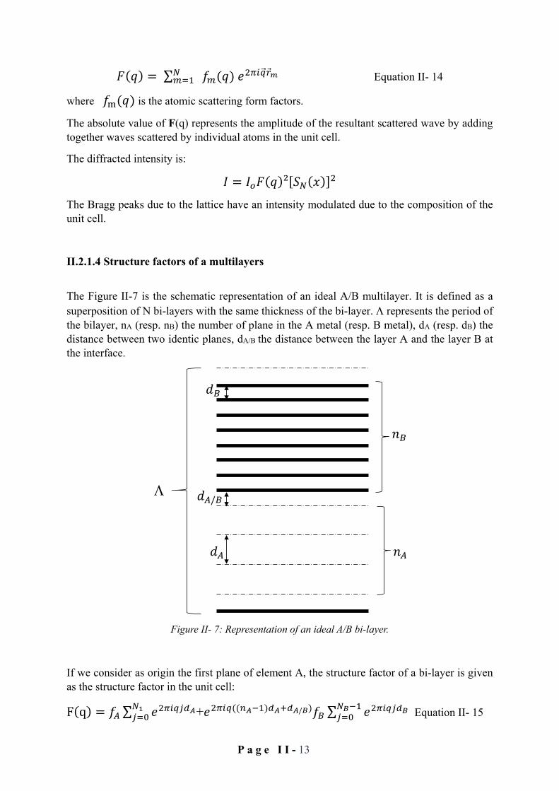
P a g e I I - 13
𝐹 𝑞 ∑ 𝑓 𝑞 𝑒 ⃗ ⃗ Equation II- 14
where 𝑓 𝑞 is the atomic scattering form factors.
The absolute value of F(q) represents the amplitude of the resultant scattered wave by adding together waves scattered by individual atoms in the unit cell.
The diffracted intensity is:
𝐼 𝐼 𝐹 𝑞 ² 𝑆 𝑥
The Bragg peaks due to the lattice have an intensity modulated due to the composition of the unit cell.
II.2.1.4 Structure factors of a multilayers
The Figure II-7 is the schematic representation of an ideal A/B multilayer. It is defined as a superposition of N bi-layers with the same thickness of the bi-layer. represents the period of the bilayer, nA (resp. nB) the number of plane in the A metal (resp. B metal), dA (resp. dB) the distance between two identic planes, dA/B the distance between the layer A and the layer B at the interface.
Figure II- 7: Representation of an ideal A/B bi-layer.
If we consider as origin the first plane of element A, the structure factor of a bi-layer is given as the structure factor in the unit cell:
F q 𝑓 ∑ 𝑒 +𝑒 / 𝑓 ∑ 𝑒 Equation II- 15

P a g e I I - 14
For a multilayer, the diffracted intensity by N-bilayers is:
𝐼 𝐼 𝐹 𝑞 𝑒 𝐹 𝑞 ⋯ 𝑒 𝐹 𝑞 Equation II- 16
with 𝑛 1 𝑑 𝑛 1 𝑑 2𝑑 /
The peaks related to the multilayer appear at an angle much smaller than those related to the average lattice parameter, usually in the small angle range where the reflectometry curves are measured.
II.2.2 Techniques of study and characterization
II.2.2.1 Small angle diffraction for x–rays reflectometry The principle of x-ray reflectometry of a thin film on the substrate is based on laws of classical optic. On the Figure II-8, 𝑛 represents the index of refraction for x-ray radiation. Since our XRD measurements are performed in air, one can consider that the value of 𝑛 is equal to 1.
As one can see on the Figure II-8, when an x-ray incident wave passes through a boundary between two homogeneous media of different optical properties (the index of refraction of the incident x-ray radiation is the first medium with 𝑛 =1 and the index of refraction of the film which is the second medium with 𝑛 ), it is split into two waves: a transmitted wave and a reflected wave. The transmitted wave propagates into the second medium whereas the reflected wave returns into the first medium. Above the critical angle αc, the resulting interference produces oscillations called Kiessig fringes. For more than one layer, the inteferences are complicated and a simulation program can provide the thickness, density and rugosity of the different layers (if the contrast is sufficient).
Figure II- 8: X-ray reflectometry for a thin film on a substrate. The incident wave is reflected and transmitted at each interface where the density changes. Some interference of two beams (reflected at
the film/vacuum interface and reflected at the substrate/film interface) is obtained when the transmitted beam exists (i.e. 𝜶𝒊𝜶𝒄

P a g e I I - 15
II.2.2.2 High angle X-rays diffraction to study the structure.
The principle of diffraction is based on the elastic scattering of the incoming electromagnetic wave by the atomic planes within the crystal.
In the Bragg method, incident electromagnetic waves with the wave vector K⃗ and the
amplitude A 𝐫 A e 𝐤𝐫 is scattered by the atoms of crystal planes in the direct space. Thanks to the fact that atoms are ordered in a periodic pattern, the two waves from different
planes are diffused along the direction K⃗f (Figure II-9). The incoming and the outgoing waves of two adjacent planes have different phases due to the path difference 𝛿 𝑑ℎ𝑘𝑙 sin 𝜃. If the deviation 𝛿 gives an interger multiple of the wavelength, the waves from the two planes interfere constructively. This means that the two waves will combine to form one wave that is similar to the incoming wave, and its amplitude is double. The Bragg equation is thus satisfied and Bragg’s peaks in the reciprocal space are observed in the plane normal to the surface with the scattered vector q .
The Bragg law is:
2 𝑑 𝑠𝑖𝑛 𝜃 𝑛 𝜆 Equation II- 17
In this equation, λ is the wavelength of the incident x-ray beam that strikes a crystal where all atoms are placed in a regular periodic array with interplanar distance dhkl at an incident angle that allows the diffraction of the h k l Bragg’s peaks at the angles 2in the reciprocal space. n is an integer and it is called the order of the reflection.
In general, the Bragg equation is simplified to 2 𝑑 sin 𝜃 λ as n =1 is the most used because the 1st order reflection gives strongest intensities.

P a g e I I - 16
Figure II- 9: Illustration of Bragg law principle.
II.2.3 Experimental x-ray diffractometer and scan modes
II.2.3.1 The Rigaku diffractometer Two diffractometers (Bruker and smartlab Rigaku) are used in the IPCMS for the structural characterizations. The Bruker is a two axes diffractometer (mostly used to whereas the Rigaku is a four axes diffractometer. In order to study the structure of the samples in details, we have used the Rigaku diffractometer in this work. The Figure II-10 shows the construction of the Rigaku diffractometer which consists of three basic elements: an x-ray tube, a sample holder and an x-ray detector. A rotating copper anode is used to generate an x-ray beam which is composed of Cu (𝐾 ) and Cu (𝐾 ) radiations. A germanium Ge [220] crystal monochromator
is used to select the monochromatic Cu-𝐾 radiation. The beam is then collimated and directed on the sample. Slits are used near the sample (incident slit) and the detector (receiving slit) to select the homogeneous part of the incident and scattered beam from the sample. A single crystal analyzer can be mounted between the detector and the sample to remove the contribution of the sample fluorescence in the background. In this thesis, we have not used a crystal analyzer because the fluorescence of Fe and Cr thin films by Cu radiation is very low.
The Rigaku diffractometer working conditions are I=200 mA and U=45 kV. The beam divergence is 0.03°. The beam divergence, the poly-chromaticity of the incident beam and some instrumental errors can be reduced by a good sample centering prior to the data acquisition. We used the Rigaku diffractometer for the reflectometry measurements, the epitaxial quality study and the analysis of the residual stresses. A goniometer is fixed under the sample holder to choose the sample angles. The x-ray source and the detector are on piloted arms to choose the incident and diffraction angles. We measure samples in different scans modes: , rocking curve (scans), pole figures, and reciprocal space mappings.

P a g e I I - 17
Figure II- 10: Illustration of the IPCMS 4-axes Rigaku diffractometer. IS and RS are the incident and the receiving slits.
II.2.3.2 Different scan modes
X-ray reflectivity
The experimental approach to study the reflectivity consists of measuring the intensity of an x-ray beam reflected from a surface relative to the intensity of the incident beam as a function of the scattering transfer vector 𝑞 [26]. On the reflectivity spectrum (Figure II-11), two mains part are observed along the specular direction: a plateau of total reflection R = 1 when c and the Kiessig fringes of the film when c. The exponential decrease of the intensity is the signature of the roughness of the substrate. A fast decay of the fringes is due to the increase of the roughness of the film. The period of oscillations is related to the thickness of the film. The amplitude of the oscillations is proportional to the density difference [27].
The range of thickness that can be analyzed depends on [28]: the instrumental resolution which depends on the monochromaticity of the incident beam (width in energy), its degree of divergence and on the angular acceptance of the detector.
Typically, films with the thickness up to 100 nm can be measured by XRR. Note that factors as the roughness, presence of unwanted oxide layer at the interface and at the surface, degree of interdiffusion at the interface may act as a “damping” on the extension of reflectometry oscillations.
Ge [220] crystal monochromator Diffracting crystallites
of the thin film
Detector
x-ray tube
Diffracted x-ray
Incident x-ray
RS
IS

P a g e I I - 18
Figure II- 11: Reflectivity curve for a Cr layer on MgO (100) substrate. We observe the plateau of the total reflection followed by the oscillations that are due to the interference of the beams reflected at the
film/vacuum interface and the substrate/film interface.
Many fitting programs can be used to estimate the thickness, the roughness and the density of the films from the reflectivity data. Two of them are “Global fit” and “GenX” software. These programs are based on the systematic variations of the parameters of the model, such as layer thickness, density or interfacial width (roughness) in order to match to the experimental data. The matching is done by a fitting routine of the program that minimizes the mean squared error. In this thesis, we used the “Global fit” fitting program, available on the computer of the Rigaku machine for the analysis of the reflectivity data.
Since the thickness, the density and the roughness have correlated effects on the reflectometry spectrum, we fit the data “step-by-step” in order to keep the number of automatically adjusted parameters to a minimum. This will provide the most accurate result. These steps are as follows:
a) Determine the total thickness of the layers using the analytical method which is obtained by a least square regression of:
𝜃.
𝑚² 𝑐𝑜𝑛𝑠𝑡𝑎𝑛𝑡 Equation II- 18
where 𝜆 𝑖𝑠 the x-ray wavelength, m the minimal position of each fringe at a specific angle 𝜃 and 𝑑 the total thickness of the layers
b) Perform the fitting on “Global fit” by fixing the thickness to the obtained values and the densities of the layers to the bulk values. The refinement will be done only on the roughness. The first estimation of the roughness is achieved when the amplitude of the Kiessig fringes is similar to the experimental one.
c) A phase shift between the experiment and the fitting means an underestimation (the fitting pattern is shifted at the left of 2angle relative to the experiment) or an overestimation of the thickness. In that case, we did a small adjustment on the thickness.

P a g e I I - 19
d) A damping of the amplitude of the oscillations can be due to a decrease of the film density or to the formation of an oxide layer at the interface (as in the case of Fe or Cr layers deposited on Silicon substrate - see the result part). In this work, a thin oxide layer is sometimes introduced at the corresponding interface to have a good reproduction of the x-ray reflectivity pattern. The contribution of some oxide layers modulates the basis of the oscillations.
For the XRR reflectivity acquisition on Fe\Cr epitaxial layers and multilayers, we used narrow slits (incident slit (IS) is open to 0.03 mm and the 2 receiving slits (RS) have a width of 0.1 mm each) and a long data accumulation time in order to obtain sufficient resolution and signal to noise ratio allowing the observation of Kiessig fringes. The determination of individual Fe and Cr thicknesses may be difficult due to the small density difference between Fe and Cr layers, which is about 9% (with Fe) = 7.86 g/cm3 andCr) = 7.15 g/cm3).
θ-2θ scans
In the θ-2θ geometry, the sample is kept fixed whereas the x-ray source and the detector move symmetrically. The incident wave makes an angle θ with the sample surface (Figure II-12). The diffracted beam is collected by the moving detector at the angle 2θ from the incident beam and from the sample surface. For a range of angle, the signal received by the detector at is then amplified and recorded to produce a diffraction patternThe used incident and receiving slits have a width of 1 mm and are placed near the [220] Ge monochromator and the detector. Some 0.5° Soller slits can be placed close to these slits.
Figure II- 12: θ-2θ scan geometry
When we perform a θ-2θ scan, we obtain diffraction peaks corresponding to the family of planes that are parallel to the surface. To index the θ-2θ diffraction pattern, the international Center for Diffraction Data (ICDD) makes available a database of diffraction patterns for more than one hundred thousand inorganic and organic materials. For each material, beside the chemical composition, crystal structure, and common name of the material, the database also includes the interplanar spacings for all observed diffraction peaks (for a chosen beam wavelength), their corresponding intensities, and (hkl) indexing.
scans provide information about the degree of preferential orientation of the film. Thin films are textured when the diffraction pattern shows strong diffraction peaks of a particular (hkl) plane family of the films having all the same orientation (often the same as substrate

P a g e I I - 20
peaks). From the position of the Bragg peaks, the average out-of-plane lattice parameter of the film is deduced using the Bragg law. Comparing this value to the bulk value, one can know if there is some strain within the film leading to a perpendicular distortion of the lattice. The shape of the peak and the peak broadening can also be signs of strains of the films. The width of the Bragg peak, commonly called the full width at half maximum (FWHM), can be extracted by fitting theBragg peak of the films with the appropriate fitting function.
Once the peak width is known, Scherrer equation can be used to determine the average size of
the crystallites D: 𝐷 𝐾 ……. Equation II- 19
where 𝐷 is the size of the crystallites detected at the angle with a peak of width FWHM. 𝜆 is the wavelength of the x-rays and K is a factor that depends on the shape of the grains and is usually fix at 0.9 or 1.
The size of the crystallites is also called the out-of-plane coherence length of the film which represents the number of planes that diffract in a coherent manner. A high value of the out-of-plane coherence length indicates a good crystalline quality of the film. However, in the case of strained epitaxial films, the out-of-plane coherence length deduced from the peak width is approximate since the width of the peak can be modified by a lattice parameter gradient.
Laue oscillations or Pendellösung oscillations form an interesting pattern that is sometimes present around strong Bragg peaks as a sign of the smoothness at the interface or surface of the films. The absence of these fringes can imply that the surfaces are rough. From clear Laue oscillations, one can also extract the film thickness.
In the case of multilayers, the diffraction pattern reveals the main peak of the multilayer surrounded by some satellites due to the modulation of the lattice parameters and the concentration of elements. The regularity of the positions of the satellites depends on the period of the bi-layers:
Equation II- 20
where 𝜃 and 𝜃 are the satellite positions. 𝜃 is the main peak position are the period of the multilayer and the wavelength of the x-rays.
The equation (II-20) is deduced from (c) and (d):
(a) 𝑞 sin 𝜃 (b) 𝑞 sin 𝜃 c ∆𝑞 sin 𝜃 sin 𝜃
and (d) ∆𝑞
.
Rocking curve geometry
In scan mode (Figure II-13), the detector is kept at a fixed 2 Bragg angle from the incident beam (this means at a diffraction position). The rocking curve is measured scanning the incident angle around Rocking Curve measurement is an interesting method to get information about the mis-orientations or the angular fluctuations of crystallites within a

P a g e I I - 21
textured film when the planes are not strictly parallel. By conserving the value of the 2θ at the position of the peak of a plane family, we can scan different orientations of those planes by moving the sample.
Figure II- 13: scan geometryA perfect crystal will produce a very sharp peak (Figure II-14). Small value of the FWHM indicates a small mosaicity of the film, which means the “perfect” parallelism of the atomic planes within the whole film. Crystal imperfections cause a broadening of the rocking curve.
Figure II- 14: scan measurements on samples with sharp and large peaks.
Since the scan of a (hkl) peak is only sensitive to the crystallites that have their (hkl) planes parallel to the surface of the sample, we performed the pole-Figure maps to further study the epitaxial quality of the samples.
Pole Figure mapping
The principle of the pole Figure mapping is to determine all the orientations of (hkl) planes of a chosen structure. The experimental approach consists in fixing the diffraction angle to the value corresponding to the dhkl inter-reticular distance in this structure (Figure II-15(a)) and collecting the diffracted intensity at different (0° < and (0° < angles, where is the rotation angle of the sample around its normal and the tilt angle of the sample perpendicularly to the diffraction plane. This angular distribution of the diffracted intensity is measured in the reciprocal space (Figure II-15(b)).

P a g e I I - 22
Figure II- 15: Left: Configuration and different and parameters that are used during pole Figure acquisition. Right: the pole Figure on the (110) Fe reflection of Fe layers deposited on
STO(100). is read on the radius of the disc (center = sample normal) and on the azimuthal angle.
An epitaxial layer gives intense and narrow (hkl) spots at specific and angles corresponding to the symmetry of the crystal. If the growth is only textured (all the crystals have the same growth direction but no common direction in the sample plane), a ring is observed at a specific . If the growth is polycrystalline, the intensity is spread on the whole solid angle. For the indexation of the diffraction spot on the pole Figure, a Wulff abacus is generally used.
The sin2() method
To analyze stress in the film using the x-ray diffractometer, we need to define three different coordinate systems (Figure II-16):
pof the structure of the material that will be studied. For the cubic systems, the base vectors are a1=[100], a2=[010] and a3=[001].
The sample coordinate system is defined by three basic vectors bi such that b1 is along the normal to the sample. This direction corresponds to the growth direction of the films. For Fe films grown on MgO(100), the reference of Fe film is b1=[100], b2=[011], and b3=[011].
The laboratory reference frame Li is obtained by turning the reference frame of the sample around its normal axis b1 by an angle and then tilting this new system by an angle Ψ also with respect to the axis b1 so that the direction of the diffraction vector coincides with the axis L1.

P a g e I I - 23
Figure II- 16: Schematic representation of the sample reference bi and the laboratory reference Li. n is the direction of a (hkl) plane family in the Li reference.
The theoretical approach of the method is to consider that in the epitaxial layer, stresses are assumed to be only in the sample plane (bi-axial) and the stress tensor is modeled as:
𝟎 𝟎 𝟎𝟎 𝝈// 𝟎𝟎 𝟎 𝝈//
whereas the strain tensor is: 𝜺 𝟎 𝟎𝟎 𝜺// 𝟎𝟎 𝟎 𝜺//
The average strain 𝜀 of the diffracting volume of the film along 𝑛 direction (Figure II-16)
is deduced using the framework transformation relations:
𝜀 =𝜀 = 𝜀 = 𝜀⫽ 𝑠𝑖𝑛 () + 𝜀┴𝑐𝑜𝑠 () = (𝜀⫽ 𝜀┴) 𝑠𝑖𝑛 () + 𝜀┴ Equation II- 21
where is the rotation of the goniometer around the sample normal and is the angle between (hkl) vector and the sample normal.
Knowing that strains are defined as: ε =
, 𝜀⫽= ⫽ and 𝜀┴=
,
we can rewrite the previous expression: 𝑎 𝑎┴ 𝑠𝑖𝑛 ) Equation II- 22 with = (𝑎⫽ 𝑎┴) and 𝑎 the lattice parameter corresponding to the position of the (hkl)
Bragg reflection (a = d h² k² l² / ), where 𝑎 is the distance given by the Bragg
law, and 𝑎 an unknown relaxed parameter of the epitaxial film.
This relation shows that the lattice parameter 𝑎 is linearly dependent on the 𝑠𝑖𝑛 () and
does not depend on the angle.
In practice, the so-called sin2() technique is a combination of: (a) the XRD technique to determine the Bragg peaks position for different plane families and (b) the linear elasticity law to observe and quantify the stress and the swelling in a textured or polycrystalline films [28], [29]. The sin2() is a non-destructive and more flexible technique than the curvature method which is limited by the thickness rule: the film thickness should be very small in comparison to the substrate thickness [30] + the substrate should be very thin (generally 0.1 mm). The thicknesses of the samples studied in this work are between 5 to 100 nm and the substrates are MgO and STO with a thickness of 0.5-1 mm.

P a g e I I - 24
In the sin2() method, we measure a set of (khl) peaks with different and deduce the in-plane and out-of-plane lattice parameters from the variation of d = dhkl with . A goniometer with 3 axes is used in order to reach the specific angles (Figure II-17 (a)).
Figure II- 17: Procedure of the sin²() method: the angles of the goniometer at which a (hkl) peak is accessible are calculated (a) and (b). The mapping is made at the chosen around the chosen (c).
For each 𝜙 value (Figure II-17(b)), the sample is rotated around the goniometer axis
(called on our goniometer) with the angle so that the sample normal scans the diffraction plane (containing the incident and the diffracted x-ray beams) [31]. Doing so, we produce a map as illustrated by the Figure II-17(c).
From the position of each peak, we have used the Bragg’s Law to deduce the lattice parameters 𝑎 :
𝑎 𝜆√
Equation II- 23
where 𝜆 is the x-ray wavelength and 𝜃 the peak position.
When plotting 𝑎 𝑑 ℎ 𝑘 𝑙 as a function of 𝑠𝑖𝑛
a linear
variation is obtained in the case of a uniaxial strain (Figure II-18). The out-of-plane lattice parameter 𝑎⟘ is the 𝑎 value at = 0° and the in-plane lattice parameter 𝑎⫽ is the 𝑎 value
at = 90°. Assuming that the strains of the films follow the Poisson’s law, the relaxed (free-of-stress) lattice parameter a0 is calculated from the expression:
𝑎 = (2 𝑎⫽𝑎⟘Equation II- 24
where is the Poisson coefficient of the film.
A difference between the relaxed lattice parameter and the bulk value corresponds to a swelling Sa:
Sa = 1 Equation II- 25

P a g e I I - 25
Figure II- 18: ahkl versus sin²() for Cr epitaxial layer on (100)-oriented MgO substrate.
The distortion of the lattice corresponds to a residual stress
//𝑬
𝒂𝟎 𝟏 𝒗 𝒂⫽ 𝒂⟘ Equation II- 26
where E is the Young modulus. Thus, a slope of the line 𝑎 𝑓 𝑠𝑖𝑛 indicates the presence of a bi-axial stresses. A compressive residual stress is characterized by a negative slope and a tensile residual stress by a positive slope.
In this work, we have chosen to perform the measurements for the (hk0) plane families i.e. (110), (200), (310), (220) and (130) and the (hkk) plane families corresponding to (211) and (222). This provides precise values of 𝑎⟘and 𝑎⫽ from the 𝑠𝑖𝑛𝟐 measurement.
We assume that stresses are bi-axial. Strictly speaking, this hypothesis is not always adequate to precisely determine the relaxed lattice parameter a0, because the volume expansion may arise in the film due to other stress factors as insertion of defects.
A. Michel team has introduced in the bi-axial stress model a hydrostatic component to describe the tri-axial stress field in polycrystalline films deposited by assisted ion beam sputtering [32]. The hydrostatic component takes into consideration the isotropic distortion of the volume due to the point defects. This is in a way an internal hydrostatic stress. The resultant stress tensor is written as:
𝜎 0 00 𝜎// 𝜎 00 0 𝜎// 𝜎
2,88
2,92
0,0 0,2 0,4 0,6 0,8 1,0
a hkl
a
a
(200)
(211)
(220)(222)
(130)
sin²(
Sa

P a g e I I - 26
II.3 Transmission Electron Microscope (TEM) characterizations
II.3.1 Electron-matter interaction
Despite the fact that the diffraction patterns measured by x-ray methods are more quantitative than electron diffraction patterns, electron diffraction has the unique advantage over XRD that different properties like morphological, crystallographic, and chemical information can be collected simultaneously using a single instrument. This information comes from the multitude of signals that arise from the interaction of an electron beam with the matter. As illustrated by the Figure II-19, the interaction of electron with matter produces different types of electrons after either an elastic scattering or an inelastic scattering (with emission of x-rays, Auger or secondary electrons). Elastic scattered beam is used for conventional TEM and electron diffraction imaging, whereas the inelastic electron-matter interactions are exploited for analytical electron microscopy.
Figure II- 19: Electron-matter interaction arising from the impact of electron beam on a sample.
II.3.2 TEM methods
In this work, we used TEM microscopy for electron diffraction imaging, High Resolution Electron Microscopy (HRTEM) and Electron Energy Loss Spectroscopy (EELS).
HRTEM
The HRTEM image is an interference pattern between the transmitted electron wave and the wave elastically diffracted by the specimen [33]. HRTEM provides structural information in two dimensions of the arrangements of atoms at solid-solid interfaces such as grain boundaries, point defects and dislocations. In most cases, the white dots in the images represent projections of the atomic columns in the structures.
Sample
Incident electron
beamX-ray EDXS
Backscattering electrons
Auger electrons
Secondaryelectrons
Direct beam
Inelastically scattered electrons
Elastically scattered electrons

P a g e I I - 27
EELS
In EEL spectroscopy, an elemental composition analysis is based on the signal arising from the ionization of atoms by the electron beam. For more details on the physical principle of Electron Microscopy, read the springer book of Egerton [34]. Briefly, the EELS spectrum is divided in three different regions:
The zero loss (ZL) peak is the peak of the electrons that passed through the specimen without any inelastic interaction. The width of the zero loss peak is due to the energy dispersion of the spectrometer. A sharp peak indicates a good energy resolution. For Fe or Cr, an energy dispersion of 1.8 eV is enough for the chemical analysis.
The low loss region contains non-elastically scattered electrons with an energy loss below 100 eV. Here, the scattering induces a collective oscillation of many outer-shell electrons, known as a plasmon or surface electron excitations. The intensity of the plasmon peak relative to the ZL peak can be used to deduce the local thickness at the scanned area in the specimen.
The high loss region begins when the energy loss of electron is higher than 100 eV inducing a fast decrease of the transmitted beam intensity (at ionization edges). This energy loss corresponds to an inner-shell ionization energy. Above the background of the EELS spectrum, additional peaks, at well-defined ionization edge energies, are characteristic of a particular chemical element.
We used a JEOL 2100F microscope, operated at 200 kV, equipped with a cold FEG, a Cs-corrected probe, STEM bright-field and high-angle annular dark-field (HAADF) detectors, as well as an electron energy loss spectrometer (EELS) with a 1 nm spatial resolution and a 1 eV energy dispersion of the zero loss peak, which was sufficient to resolve the spectral features of interest in the sample.
The acquisition of images was realized in HAADF-STEM mode, necessary to increase the contrast between the Cr and Fe (Z = 24 and 26) as the scattered intensity increases with Z2 [35] instead of Z for classical TEM. Note that although Z²-contrast imaging offers atomic resolution [36], it is fundamentally different from HRTEM because it is based on incoherent elastically-scattered electrons, rather than coherent scattering. All the EELS-spectra were recorded in STEM mode along different lines perpendicular to the interfaces and on rectangles inside the layers (to efficiently reduce statistical noise). We used the L3 edges for Cr (575 eV), Fe (710 eV) and Ar (245 eV) as well as the K-edge of O (532 eV). Ar and O are indeed impurities that may incorporate the Fe and Cr layers during the growth process and induce a swelling. To quantify the concentration of each element, we used the Gatan-Digital-Micrograph software.
II.3.3 TEM samples preparation
In solid specimen, electrons are strongly scattered due to the large forces acting on an electron when it passes through the electrostatic field of the atoms. Thus, the thickness of a TEM specimen must be very small (in the range of few 10 nm or less). Cross-sectional samples were prepared by either focused ion beam (FIB) or mechanical polishing (impossible for samples on MgO that is too brittle) in order to get large electron transparent regions. For

P a g e I I - 28
electron energy loss spectral investigations, a very thin sample is necessary to avoid multiple scatterings.
For the mechanical polishing technique, samples were cut, glued and polished by following these steps as reported on the Figure II-20:
Sample preparation: cutting and gluing
The initial sample is divided into slabs of ∼0.3×1 cm² and then two pieces of sample are glued face-to-face.
We used a Gatan Epoxy G2 glue to glue two slabs together; with film sides facing each other (see the Figure II-20(b)). This glue will also prevent the sandwich plates from taking off during the polishing. A diamond wire saw is used to provide a relatively clean cut of the sandwich in thin slices (between 500 and 800 μm thick) along the [100] direction.
Polishing
An Allied Multiprep System was used to mechanically polish the face 1 (parallel polishing (Figure II-20(c))) and then the face 2 (angle polishing (Figure II-20(d))) down to about 1μm thick (or less). The observation of fringes at the edge of the sample (area of interest) using an optical microscope indicates that the sample is ready for TEM analysis (Figure II-20(e)).
Figure II- 20: Geometry of the different steps of cross section samples prepared using an Allied MultiPrep System. Initial sample (a), after gluing (b). For the face 1 (c), the sample is polished with no angle (parallel polishing) and for the face 2 (d), a wedge angle is introduced before polishing (vertical dimension is zoomed for clarity). Final image with optical microscope with equal thickness fringes at
the bottom border (e).
To further reduce in thickness and reach the range 1-10 nm, a PIPs (Precision Ions Polishing System) can be used to further thin the sample. For our samples, a low angle and low energy Ar ion milling is used for about 10 to 30 min. The Figure (II-21) is the TEM image of Cr\Fe\Cr tri-layer deposited on STO(100) substrate. We see that there is no contrast between Cr and Fe layers because the TEM sample is not thin enough despite the presence of many and well defined fringes at the interface (Figure II-20(e)). Besides, the presence of cracks in STO substrate confirms the difficulty to polish the STO substrates.

P a g e I I - 29
Figure II- 21: TEM image of Cr\Fe\Cr tri-layer deposited on STO(100) substrate prepared using mechanical polishing.
II.4 Magnetometry: principles and operated modes
II.4.1 SQUID
Principle of dc-SQUID
SQUIDs are one of the most sensitive techniques to detect of magnetic flux Φ= 𝐵 𝑑𝐴, i.e., magnetic flux density B times the area A of the SQUID loop (this area depend on the geometry of the SQUID). To measure very small variations in magnetic flux which is induced by a magnetic material, SQUIDs magnetometer combines both the flux quantification and the Josephson tunneling effect [37], [38]. There are two types of SQUIDs: dc-SQUID and rf-SQUID. We have used a dc-SQUID magnetometer in this thesis to measure the hysteresis curves (Figure II-22). A dc SQUID is composed of two pieces of superconductor separated by a thin barrier of insulator called a Josephson junction [37]. When the SQUID is kept in a magnetic field, a DC super current I enters the device through port A and gets divided into two ports I1 and I2. I1 and I2 undergo a phase shift while crossing the C and D Josephson junctions and become I'1 and I'2 respectively.

P a g e I I - 30
Figure II- 22: Representation of the dc-SQUID in the presence of applied field (a) and voltage-flux characteristics of a dc SQUID (b) [38].
The currents I'1 and I'2 interfere at port B, and the resulting current oscillates between maxima and minima. The maxima occurs when the magnetic flux increases by one quantum given by o = h/2e [39]. In superconductors, the current (or super current) which is caused by the Cooper pairs of electrons is a function of both the phase difference between the two superconductors and the magnetic flux threading the hole. So the interfering waves are the de Broglie waves of the Cooper pairs. The total flux is the sum of the external flux ext and the flux induced by a circulating current in the loop in order to maintain flux quantization in the loop. The phase shifts of the waves occur due to the applied magnetic field. In the absence of the magnetic field the phase shifts and the phase difference are zero.
In practice, instead of the current, the voltage V (which also oscillates periodically like the current) across the SQUID is measured as a function of the magnetic flux. A gradiometer which is sensitive to change in the field gradient rather than its absolute value is used in SQUIDs. It can measure magnetic moments down to 10-6 emu.
Operate mode of the SQUID
We used the VSM mode of the SQUID magnetometer in a MPMS setup to study magnetic properties (Figure II-23). In VSM mode, the sample vibrates between pick-up coils placed in an external magnetic field. The pick-up coils are inductively coupled to the input coils of the SQUID. The coils are coupled inductively to SQUID to form a flux transformer [40], which converts flux changes caused by the movements of the sample into the voltage.
Prior to the measurement, the samples are cut 3x3 mm² in dimension, mounted and glued (to avoid an unwanted background to the measurement) onto a straw. The straw is screwed to the sample probe and put into the SQUID chamber (a cryostat system). The sample probe is then moved vertically to adjust the z-position. The sample should be approximately 6.5-7 cm from the bottom end of the sample rod in order to keep the sample moving through the pick-up coils of the SQUID.

P a g e I I - 31
Figure II- 23: Diagram of SQUID magnetometer
Then, the sample is rotated in order to find its optimal position with respect to the center of the two SQUID loops components. By changing the field that causes the flux in the pick-up coil to change, the flux of the field in the same direction that the applied field detected by the SQUID will also change. The rea sample is moved through the pickup coils to subtract the drift [41]. Indeed, the pickup coil system is superconducting, the SQUID is only proportional to flux in the junction and not to the total flux variation. Thus, it is by measuring and subtracting the drift that the tiny moment from the sample can be distinguished from the background (which does not dependent on time).
During the measurements, liquid helium is used to keep cold the superconducting components of the system.
II.4.2 AGFM
Principle of AGFM and operate mode
Unlike the SQUID which is a flux-to-voltage device, the AGFM is a force instrument. The AGFM is composed mainly of 3 parts: a sample holder, a magnet and a piezoelectric system. The sample holder consists of a piece of thin glass cut to size and glued to the end of the sample probe containing a piezoelectric element. The samples are mounted onto the glass plate using a small amount of vacuum grease and inserted into the AGFM apparatus.
The sample is placed in the static magnetic field while rectangular pair of coils are used to generate a sinusoidal field gradient [42] on the sample (Figure II-24). This field gradient exerts a sinusoidal force on the sample. The displacement of the sample is detected by the piezoelectric element of the sample holder. Piezoelectric materials produce electrical signals when they are deformed, and conversely are deformed when electrical signals are applied to them.

P a g e I I - 32
Figure II- 24: Simple illustration of AGFM showing M= electromagnet pole pieces, A and B = gradient field coils, connected in series in opposition; S= sample. Taken from [43].
In this study, the magnetic properties were studied using AGFM and SQUID magnetometers. We measured the magnetic in-plane hysteresis curves of the Fe layer either along the [110] direction of Fe, with the field along the sample edge i.e. the [100] direction of the substrate, or along the [100] direction of Fe, at 45°. We obtained almost similar results for AGFM with a small field gradient and SQUID measurements (as will be shown in the result part) meaning that AGFM is also suitable for measuring soft magnetic materials as Fe. Most of the hysteresis curves with the in-plane configuration were thus measured using AGFM because AGFM is faster and less liquid-He consuming than SQUID. For perpendicular configurations, we used a SQUID with a maximum field of 7 T because the demagnetizing field of Fe is 2.16 T which is higher than the maximum field of AGFM that is about 1.5 T. The conditions of measurements are given in the table II-2. The SQUID allows also some measurements at low or high temperatures, but we did not use it in this work.
Table II- 2: Conditions of measurements of AGFM and SQUID.
AGFM SQUID Temperature Ambient temperature Ambient temperature Maximum field (T) 1.5 7 Type of measurements
In-plane In-plane and out-of-the plane
Advantage Very fast Strong external field (up to 7 T!)
Obtained results Similar for in-plane configuration

P a g e I I - 33
Bibliography
[15] K. Wasa, M. Kitabatake, and H. Adachi, Thin Films Material Technology: Sputtering of Compound Materials. Berlin Heidelberg: Springer-Verlag, 2004.
[16] D. Petersohn, “Principles of plasma discharges and materials processing. Von. M. A. Liebermann und A. J. Lichtenberg, XXVI, 572S., John Wiley & Sons, Inc., New York 1994, £ 54.00, ISBN 0-471-00577-0,” Materials and Corrosion, vol. 46, no. 9, pp. 551–551, 1995, doi: 10.1002/maco.19950460909.
[17] S. S. P. Parkin and B. R. York, “Influence of deposition temperature on giant magnetoresistance of Fe/Cr multilayers,” Appl. Phys. Lett., vol. 62, no. 15, pp. 1842–1844, Apr. 1993, doi: 10.1063/1.109542.
[18] E. Krikorian and R. J. Sneed, “Epitaxial Deposition of Germanium by Both Sputtering and Evaporation,” Journal of Applied Physics, vol. 37, no. 10, pp. 3665–3673, Sep. 1966, doi: 10.1063/1.1707902.
[19] M. A. Herman, W. Richter, and H. Sitter, “Molecular Beam Epitaxy,” in Epitaxy: Physical Principles and Technical Implementation, M. A. Herman, W. Richter, and H. Sitter, Eds. Berlin, Heidelberg: Springer, 2004, pp. 131–170.
[20] R. F. C. Farrow, Molecular Beam Epitaxy: Applications to Key Materials. Elsevier, 1995.
[21] A. Authier, S. Lagomarsino, and B. K. Tanner, Eds., X-Ray and Neutron Dynamical Diffraction: Theory and Applications, vol. 357. Boston, MA: Springer US, 1996.
[22] C. Suryanarayana and M. G. Norton, X-Ray diffraction: a practical approach. 1998. [23] B. E. Warren, X-ray Diffraction. Courier Corporation, 1990. [24] J. D. Jackson, “Classical Electrodynamics, 3rd ed.,” American Journal of Physics, vol.
67, no. 9, pp. 841–842, Aug. 1999, doi: 10.1119/1.19136. [25] A. Guinier, X-ray Diffraction in Crystals, Imperfect Crystals, and Amorphous Bodies.
Courier Corporation, 1994. [26] F. de Bergevin, “The Interaction of X-rays (and Neutrons) with Matter,” in X-ray and
Neutron Reflectivity: Principles and Applications, J. Daillant and A. Gibaud, Eds. Berlin, Heidelberg: Springer, 1999, pp. 3–59.
[27] E. Chason and T. M. Mayer, “Thin film and surface characterization by specular X-ray reflectivity,” Critical Reviews in Solid State and Materials Sciences, vol. 22, no. 1, pp. 1–67, Mar. 1997, doi: 10.1080/10408439708241258.
[28] J. Daillant and A. Gibaud, X-ray and Neutron Reflectivity: Principles and Applications. Springer, 2008.
[29] U. Welzel, J. Ligot, P. Lamparter, A. C. Vermeulen, and E. J. Mittemeijer, “Stress analysis of polycrystalline thin films and surface regions by X-ray diffraction,” J Appl Cryst, vol. 38, no. 1, Art. no. 1, Feb. 2005, doi: 10.1107/S0021889804029516.
[30] G. G. Stoney and C. A. Parsons, “The tension of metallic films deposited by electrolysis,” Proceedings of the Royal Society of London. Series A, Containing Papers of a Mathematical and Physical Character, vol. 82, no. 553, pp. 172–175, May 1909, doi: 10.1098/rspa.1909.0021.
[31] J. Godlewski and R. Cadalbert, “A new method for residual stress distribution - analysis of corroded zircaloy-4 cladding,” CEA Centre d’Etudes de Saclay, CEA-CONF--10945, 1992. Accessed: Aug. 12, 2020. [Online]. Available: http://inis.iaea.org/Search/search.aspx?orig_q=RN:23078141.
[32] A. Debelle, G. Abadias, A. Michel, and C. Jaouen, “Stress field in sputtered thin films: Ion irradiation as a tool to induce relaxation and investigate the origin of growth stress,” Appl. Phys. Lett., vol. 84, no. 24, pp. 5034–5036, May 2004, doi: 10.1063/1.1763637.
[33] B. Fultz and J. M. Howe, “Diffraction and the X-Ray Powder Diffractometer,” in

P a g e I I - 34
Transmission Electron Microscopy and Diffractometry of Materials, B. Fultz and J. M. Howe, Eds. Berlin, Heidelberg: Springer, 2001, pp. 1–61.
[34] R. F. Egerton, “An Introduction to Microscopy,” in Physical Principles of Electron Microscopy: An Introduction to TEM, SEM, and AEM, R. F. Egerton, Ed. Cham: Springer International Publishing, 2016, pp. 1–26.
[35] S. J. Pennycook, “Z-contrast stem for materials science,” Ultramicroscopy, vol. 30, no. 1, pp. 58–69, Jun. 1989, doi: 10.1016/0304-3991(89)90173-3.
[36] B. Fultz and J. M. Howe, Transmission Electron Microscopy and Diffractometry of Materials. Springer Science & Business Media, 2012.
[37] R. L. Fagaly, “Superconducting quantum interference device instruments and applications,” Review of Scientific Instruments, vol. 77, no. 10, p. 101101, Oct. 2006, doi: 10.1063/1.2354545.
[38] B. D. JOSEPHSON, “Coupled Superconductors,” Rev. Mod. Phys., vol. 36, no. 1, pp. 216–220, Jan. 1964, doi: 10.1103/RevModPhys.36.216.
[39] J. Clarke, “Squid Fundamentals,” in SQUID Sensors: Fundamentals, Fabrication and Applications, H. Weinstock, Ed. Dordrecht: Springer Netherlands, 1996, pp. 1–62.
[40] R. Cantor and S. Cryoelectronics, “Mr. SQUID User’s Guide,” p. 103. [41] M. Sawicki, W. Stefanowicz, and A. Ney, “Sensitive SQUID magnetometry for studying
nanomagnetism,” Semicond. Sci. Technol., vol. 26, no. 6, p. 064006, Apr. 2011, doi: 10.1088/0268-1242/26/6/064006.
[42] H. J. Richter, K. A. Hempel, and J. Pfeiffer, “Improvement of sensitivity of the vibrating reed magnetometer,” Review of Scientific Instruments, vol. 59, no. 8, pp. 1388–1393, Aug. 1988, doi: 10.1063/1.1139674.
[43] “A vectorial vibrating reed magnetometer with high sensitivity - IEEE Journals & Magazine.” https://ieeexplore.ieee.org/abstract/document/486526 (accessed Aug. 16, 2020).

Chapter III
Results on the samples prepared by sputtering

I I I - 2
Chapter III: Results on the Cr\Fe\Cr tri-layers prepared by sputtering
III.1 Deposition of the samples .................................................................................................... 3 III.1.1 Deposition rate optimization ............................................................................................................... 3 III.1.2 Choice of the substrates ...................................................................................................................... 5 III.1.3 Substrates preparation and targets cleaning ...................................................................................... 6 III.1.4 Deposition of the tri‐layers .................................................................................................................. 7
III.2 X‐ray reflectometry studies .................................................................................................. 8
III.3 Microstructure studied by TEM .......................................................................................... 10 III.3.1 HRTEM analysis .................................................................................................................................. 10 III.3.2 Composition analysis ......................................................................................................................... 14
III.3.2.1 EELS quantification using digital micrograph software .............................................................. 16 III.3.2.2 Manual estimation of O/Cr concentration‐ratio. ....................................................................... 18
III.4 Structural characterizations by XRD .................................................................................... 20 III.4.1 Texture quality ................................................................................................................................... 20 III.4.2 Epitaxial quality ................................................................................................................................. 22 III.4.3 Crystalline quality .............................................................................................................................. 24 III.4.4 Strain and stress analysis ................................................................................................................... 25
III.4.4.1 Evolution of strains .................................................................................................................... 25 III.4.4.2 Analysis of stresses .................................................................................................................... 26
III.5 Magnetic measurements .................................................................................................... 29 III.5.1 Magnetic measurements of Fe in the in‐plane configuration ........................................................... 29 III.5.2 Magnetic measurements in the out‐of‐plane configuration ............................................................. 30
Discussions ................................................................................................................................ 32
Bibliography .............................................................................................................................. 34

I I I - 3
Chapter III:
Results on the samples prepared by sputtering
The first goal of my PhD work was to realize some Fe\Cr layers with a good epitaxial quality. For that, we have first chosen dc-magnetron sputtering as growth technique because it is easier to process and more convenient for the growth of thicker samples than MBE. Good epitaxy can be achieved by sputtering if some growth parameters as the deposition rate, the choice of the substrate, the substrate cleaning and the growth temperature are optimized.
III.1 Deposition of the samples
III.1.1 Deposition rate optimization
The optimization of the deposition rate is very important to achieve a good epitaxy of the layers prepared by magnetron sputtering. To measure this rate, we have deposited Fe and Cr layers at various currents and times on silicon substrates at room temperature. To obtain a given thickness, one can either grow the samples using a high dc-current for a short deposition time or perform a long time deposition with a low applied dc-current. The time is chosen so that the thickness is in the range that can be measured accurately using x-ray reflectometry. The Figure III-1 shows the reflectivity profiles of three Fe samples deposited with different currents and times. The insert tables are the fitting results. We observe well-defined Kiessig fringes up to the angle = 7° when the Fe layer is deposited with a dc-current of 250 mA and 300 mA. For the samples deposited with a higher dc-current, the amplitude of the oscillations decreases and Kiessig oscillations disappear above 2= 3.5°, attesting an increase of the film roughness. Knowing the thickness and the deposition time, the atomic rate of Fe is deduced using this equation:
𝐕𝐓𝐡𝐢𝐜𝐤𝐧𝐞𝐬𝐬 𝐀
𝐓𝐢𝐦𝐞 𝐨𝐟 𝐝𝐞𝐩𝐨𝐬𝐢𝐭𝐢𝐨𝐧 𝐬
In the case of Cr layers, even when deposited at a lower dc-current than the Fe layers, the oscillations are only present for low scattering vectors (see Figure III-2). The damping of the interference fringes at a high scattering vector is due to a large roughness. To reduce the roughness, one can increase the growth temperature of Cr in order to improve the atomic diffusion of Cr atoms on the substrate.

I I I - 4
Figure III- 1: X-ray reflectometry profiles of pure Fe deposited on Si\SiO2 substrate with different currents and times. The inserted tables present the fitting result (thickness t, density and roughness ) where (1) is the Fe layer, (2) the Fe2O3 layer and (3) the Au capping layer. To obtain a good fit, we
have to introduce a thin Fe2O3 layer between the Fe and Au.
As illustrated on the Figure III-3, the atomic rate of Fe and Cr increases linearly as a function of the applied dc-current. The relation between V and I is V(𝑨/𝒔) = 0.00716 I(mA) for Fe and V(𝑨/𝒔) = 0.0138 × I(mA) - 0.696 for Cr. In this work, we use a dc-current of 200 mA for the growth of both Fe and Cr. This corresponds to an atomic rate of 1.03 𝐴/𝑠 for Fe and 2 𝐴/𝑠 for Cr.
Figure III- 2: X-ray reflectometry profiles of pure Cr deposited on Si\SiO2 substrate with different currents and times. The inserted tables present the fitting result (thickness t, density and roughness
) where (1) corresponds to the Cr layer, (2) to theCr2O3 layer that passivates the surface.
2 4 6 810-9
10-7
10-5
10-3
10-1
2 4 6 8 2 4 6 8
Si\ SiO2\ Cr_70mA_700s Si\ SiO2\ Cr_100mA_700s
(°) (°)
Exp. Fit
Exp. Fit
Exp. Fit
Ref
lect
omet
ry (
a.u.
)
(°)
Si\ SiO2\ Cr_150mA_300s
2 4 6 82 4 6 8 2 4 6 8
Si\ SiO2\ Fe_300mA_200s
(°)
Exp. Fit.
(°)
Ref
lect
omet
ry (
a.u.
) 100
10-2
10-6
10-4
Exp. Fit.
Exp. Fit.
Si\ SiO2\ Fe_250mA_250s Si\ SiO2\ Fe_350mA_150s
(°)

I I I - 5
Figure III- 3: Deposition rate of Fe (a) and for Cr (b) versus the dc-current
III.1.2 Choice of the substrates
In order to optimize the epitaxy of Cr and Fe layers, (100)-oriented SrTiO3 (STO) and MgO were chosen as substrates because of the small lattice mismatch (Table III-1) between substrates and Cr (aCr_bulk = 2.884Å: -4.58% mismatch on MgO where aMgO_bulk = 4.2112Å and +3.12% mismatch on STO where aMgO_bulk = 3.905Å, with a 45° rotation of the Cr lattice in the plane) that will favor a good epitaxy (Figure III-4). For iron, the lattice parameter (aFe_bulk = 2.8652Å) is very close, and the epitaxy conditions are equivalent. Besides, STO(100) and MgO(100) substrates are expected to induce different signs of misfit. This is interesting to investigate the influence of the substrate on the structural and magnetic properties of Fe\Cr samples.
Figure III- 4: Surface plane of MgO (100) (a) and Cr (100) (b) in bulk. Illustration of the epitaxy
of Cr rotated by 45°on MgO (100) plane (c).
Table III -1: Values of the expected misfits for the coherent growth of Cr layers on MgO(100) and
STO(100). Direct epitaxy can also be achieved growing Cr on NaCl(100) substrate.
𝐚𝐬𝐮𝐛(Ǻ) MgO: 4.21 STO: 3.90 𝑵𝒂𝑪𝒍: 5.64
𝒂𝒅𝒆𝒑(Ǻ) √𝟐Cr: 4.05 √𝟐 Cr: 4.05 2 Cr: 5.77
«m » % - 3.24 + 4.58 - 2.3

I I I - 6
For the layers deposited on NaCl(100) substrate, we expect a better epitaxy since NaCl(100) favors a cube on cube growth of Cr with the smallest misfit (the lattice parameter of NaCl is very near to twice that of Cr). Besides, it is easy to transfer the deposited layers from the NaCl substrate (that dissolves in water) to the microscopic grid by capillaries effect and then perform the plane view TEM studies. In contrast, for the sample deposited on MgO and STO, mechanical polishing of the sample is needed before the TEM characterization. This step is far from easy because of the substrate breakage during the polishing. This is caused by a high hardness of these substrates that reduces the limit of elasticity of MgO and STO and makes them brittle.
III.1.3 Substrates preparation and targets cleaning
Prior to the deposition, Fe and Cr targets were fixed on the magnetrons. We used Fe and Cr targets with 6N purity that was provided by Neyco supplier. MgO(100) and STO(100) substrates were mounted on the same metallic plate and fixed on the sample holder to have the same conditions of deposition. The sputter chamber was closed and then evacuated until a vacuum level around 10-7 mbar was achieved. Generally, it takes 8 hours to reach this pressure value. After that the substrates were heated at 400°C for one night to favor the desorption of contaminants from the substrate (vapor H2O, CO2, Ar, N2, and any volatile matter). During the heat treatment, plasma was created on a titanium target far from the sample in order to trap oxygen that had eventually outgassed from the substrate. The cooling system was used to cool both the substrates’ holder and the targets to keep the pressure constant in the chamber. A Quad system connected to the sputter chamber was used to check and control the partial pressure of gas inside the chamber during and after the growth of the samples. The partial pressures of H20, Ar, O2, N2, CO2 …, are given by the computer connected to the QUAD.
During the deposition, the Ar pressure in the chamber is around 3.10-3 mbar. A pre-sputtering is realized for 3-5 minutes before deposition to remove oxide layer or any contamination on the target surface. During this process, the shutter is placed between the substrate and the target in order to protect the substrate against any contamination. After the pre-sputtering step, we set the current, the substrate temperature and put the desire value of the flow rate of Ar and fix the duration of deposition according to the thickness value we want to reach. The process is stopped automatically at the end of the deposition process. The deposition conditions for the tri-layers are summarized in the table III-2.
Table III -2: Growth conditions of Fe and Cr using dc magnetron sputtering (in this chapter we varied the temperature and not the thickness of the layers).
Target Cr Fe Atomic rate (Å/s) 2 1 Current (mA) 200 200 Times of deposition (s) 189 625 Temperature of the growth (°C) 400, RT 400, 300, 200 and RT Argon volume (cc) 20 Substrates MgO(100), STO(100) , NaCl(100)

I I I - 7
III.1.4 Deposition of the tri-layers
The structure of the tri-layers is illustrated on the Figure III-5. The first chromium layer was deposited at 400°C for all samples. A high growth temperature increases the atomic diffusion of Cr atom which can improve the epitaxy of Cr layers on the substrates. The iron layer was deposited at 400°C, 300°C, 200°C or 40°C. The iron layer was capped with a chromium layer which has the ability to passivate its surface by forming stable thin chromium oxide. This will protect the Fe layer from the oxidation in air. We used deposition rates of 2 Å/s and 1 Å/s for Cr and Fe, respectively. The delay times at both interfaces are given in the table III-3. The same growth conditions were used for all samples in order to study the relation between the structure, the stress and the magnetic behavior of the tri-layers as a function of the Fe growth temperature and the nature of the substrate. The total nominal thickness of the Cr\Fe\Cr tri-layers is between 150 and 160 nm (the stacking coefficient slightly depends on temperature). Table III -3: Cooling times before the growth of Fe at T°C on Cr@400°C and before the growth of the
Cr capping layer on Fe.
Samples
Delay time (hours)
Fe on Cr@400°C Cr@RT on Fe
M400 and S400 0 16
M300 and S300 2 16
M200 and S200 5 11
M40 and S40 16 0
The part describing results will be mainly dedicated to the layers grown on MgO(100) and STO(100) that surprisingly present a better structural quality compared to the one on NaCl(100): a texture of the tri-layers along the (100) direction of the NaCl and the cube-on-cube epitaxy of the tri-layers on the NaCl are observed but the intensities of the Bragg diffraction peak of the tri-layers are smaller than on MgO and on STO. This can be due to the fact that the cleaved NaCl surface is not flat enough and makes difficult the alignment steps during x-ray measurements. Besides, the transfer of the tri-layers grown on NaCl(100) on the microscopy membranes was not possible because the metal layer rolls up on itself. The transfer of 10 nm CoPt nanoparticles on the grid was used in [1]. In the case of a continuous and thick film, the stress within the films seems to predominate the Van der Waals interactions at the origin of the adherence on the membrane. Thus, it was not interesting to use the (100)-oriented NaCl substrate for the growth of tri-layers.

I I I - 8
Figure III- 5: Architecture of Cr\Fe\Cr tri-layers.
In the following, the samples will be named MT (resp. ST) where the first letter M (resp. S) corresponds to the substrate MgO (resp. STO) and T is the growth temperature of the Fe layer in Celsius (for example M300 is the MgO\Cr@400°C\Fe@ 300°C\Cr@RT tri-layer). For comparison, we also prepared on both substrates samples with only a Cr@400°C buffer layer (called MB and SB) and Cr400°C\Cr@RT (called MØ and SØ) layers.
III.2 X-ray reflectometry studies
The Figure III–6 shows the reflectometry spectra for MT and ST samples. Well-defined Kiessig fringes are observed for MB and SB and also for M40 and S40 samples. Much more oscillations are present for Cr grown on MgO(100) substrate compared to the deposit of Cr on STO(100). This indicates that the Cr layer is smoother on MgO than on STO. For both MB and SB samples, the fitting gives a thickness of 36 nm of Cr with a Cr oxide passivated layer of about 1 nm. A slightly higher roughness is obtained for SB. This thickness gives to an atomic rate of 1.9 𝐴/𝑠 for Cr deposited at 400°C. For the tri-layers, Kiessig oscillations are also present but have different shapes, period and amplitudes because of the contribution of Fe@T and Cr@RT layers on the spectra. The oscillations with the shortest periods belong to Fe layer and those with the largest period to Cr layers (see the insert Figures). This makes the fitting of individual Cr and Fe layers more complicated to perform. The results of the adjustments are reported in table III-4. We used the average thicknesses of the tri-layers obtained by TEM (Figure III-12) as the initial thickness values in the fitting procedure. We also observe an exponential vanishing of oscillations which is due to the increase of the interface and surface roughness. For the case of M400 and S400, Kiessig fringes are almost lost at high angle which can be attributed to the intermixed of Fe and Cr oxide layers when the Fe layer deposited at 400°C. For this reason, we used an oxide layer of Fe and then a capping layer of Cr@RT during the fitting of the XRR data for both M400 and S400 samples (table III-4).

I I I - 9
Table III-4: Fit of XRR patterns for MT and ST samples. T is the thickness, r the density and the
surface roughness for each layer.

I I I - 10
Figure III- 6: X-ray reflectometry for MT and ST samples.
III.3 Microstructure studied by TEM
We used transmission electron microscopy in imaging mode and electron diffraction to study the microstructure of the samples and EELS for the microanalysis.
For this purpose, the samples were prepared in cross-section in order to be analyzed along the growth direction where the succession of the tri-layer on the substrate is observed. ST samples were prepared by mechanical polishing and MT samples by FIB (Focus Ion Beam). For MgO and STO substrates, the growth direction is along [100]. The direction of the observation (the beam direction) is along [010]STO=[011]Cr\Fe\Cr (or [010]MgO=[011]Cr\Fe\Cr).
III.3.1 HRTEM analysis
The Figure III -7 is the HRTEM image on SB. The presence of 100 planes of along the [100] growth direction of STO indicates a good texture of Cr on STO. Along the [001] direction of STO, we also observe (011) Cr planes attesting the epitaxy of Cr deposited at 400°C on the STO substrate
The signature of the epitaxy of Cr is more visible on the diffraction pattern where we can attribute the diffraction spots of STO and Cr along the in-plane and the out-of-plane direction (Figure III -7 bottom). The narrow and circular spots are the substrate reflections. The large and elongated spots are the diffraction of Cr planes. In the [001] direction, the diffraction spots of STO and Cr are almost in the same position because there is a contraction of the Cr lattice parameter to accommodate to the STO lattice parameter. This corresponds to a quasi-coherent in-plane growth of Cr with a 45° rotation of the lattice. In the [100] direction, we observe that the distance between the (200) diffraction spot of Cr/Fe and the origin 000 is
1 2 3 4 5 6 71E-8
1E-6
1E-4
0,01
1
1 2 3 4 5 6 71E-8
1E-6
1E-4
0,01
1
1 2 3 4 5 6 71 2 3 4 5 6 71E-8
1E-6
1E-4
0,01
1
1 2 3 4 5 6 71E-8
1E-6
1E-4
0,01
11 2 3 4 5 6 7
1E-8
1E-6
1E-4
0,01
1
3,0 3,5 4,0
1E-6
1E-5MBR
efle
ctiv
ity
(a.u
.)
Exp. Fit
1
3,0 3,5 4,01E-7
1E-6
M400
Exp. Fit
S400
M40
S40
(°)
Exp. Fit
1E-8Ref
lect
ivit
y (a
.u.)
Exp. Fit
0.01
1E-4
1E-6
SB
(°)
Exp. Fit
Exp. Fit

I I I - 11
about 1.41 higher than that of the (200) of STO to the origin of the diffraction pattern, as expected. The epitaxy relationship can be written as Cr(100)[011] // STO(100)[010]. This relationship indicates that the in-plane [011] direction of the (100) Cr plane (Cr surface) is aligned on the [010] direction of the (100) substrate surface plane.
Figure III- 7: HRTEM image (top) and diffraction pattern (bottom) of SB sample: [100] and [001] correspond respectively to the out-of-plane and in-plane directions of STO
For the S200 sample, the HRTEM image at STO\Cr@400°C interface also reveals 100 and (011) planes of Cr resp. along the [100] and the [001] direction of STO (see Figure III-8). This confirms the epitaxy of Cr on STO in this sample. The high angle annular dark field image (HAADF) in STEM mode (Figure III -9) at low magnification shows that the Cr layer and Fe layer are continuous and have uniform thickness. The thicknesses of the Cr and Fe layers are resp. equal to 36 nm and 74 nm which are close to the nominal values. The same thickness of Cr layer was obtained by XRR. Surprisingly, the image does not show the top layer of Cr grown at RT. It’s seems that the sputtering process stopped accidently during the growth. This kind of problem is rare! To confirm this assertion, M200 sample was prepared by tripod method by our partner from Munster University which has more experience

I I I - 12
concerning the polishing of thin films on MgO substrates. The HAADF-STEM image and EDX mapping also reveal that there is only the Cr buffer layer and the Fe layer. In the following, we will not discuss on the result obtained on M200 and S200.
Figure III- 8: HRTEM image of S200 sample at the STO\Cr interface.
Figure III- 9: (a) HAADF-STEM image of S200, (b) HAADF-STEM image of M200 and (c) the EDX mapping of M200 showing the first Cr layer in green and the Fe layer in red acquired with a drift
correction.
In order to have thinner and clean samples, M40 and M300 were prepared by Focus Ion Beam (FIB) by David Troadec at IEMN in Lille. The acquisition of M40 and M300 images were realized in HAADF-STEM, necessary to increase the contrast between Cr and Fe (Z = 24 and 26) as the scattered intensity increases with Z2 instead of Z for classical HRTEM. Heavy elements like Au and Pt appear with a bright contrast on the STEM-HAADF whereas light elements like MgO (Z=8 for O and Z=12 for Mg) have the darkest contrast.
The Figure III-10 shows the Bright Field -STEM images at different interfaces of the tri-layer M40. We observe that the Cr@400°C layer, the Fe@RT layer and the Cr@RT layer are epitaxied on the MgO(100). An interfacial layer with a brighter contrast is clearly present at the Cr@400°C\Fe@RT interface (Figure III-10b). The thickness of this interfacial layer is about 1.75 nm. On the Figure III -10c, we see that when Fe and Cr are deposited at room temperature, the interface is almost abrupt.

I I I - 13
Figure III- 10: Bright field-STEM images for M40 at MgO\Cr (a), Cr\Fe (b) and Fe\Cr interfaces (c).
Figure III- 11: HAADF-STEM images of M300 along the [100] zone-axis of MgO showing the MgO\Cr (a) and the Fe\Cr interfaces (b).
HAADF-STEM image has been realized on the piece of M300 (Figure III -11). The sample was prepared along the [110] direction of MgO. Fourier transforms of the HAADF-STEM images taken from the MgO, the Cr and Fe layers allow to determine their corresponding family planes. The presence of (100), (101) and (001) planes of Cr and Fe along (100), (111) and (110) directions of the MgO resp. indicates a good epitaxy of Cr and Fe and the MgO.
In summary, HRTEM, HAADF-STEM and electron diffraction have been done on SB and S200 samples and on M300 and M40 samples. For all samples, the Cr layer deposited at 400°C on STO and on MgO is epitaxied. This semi-coherent in-plane growth of Cr is accompanied with its dilatation in the out-of-plane direction. For the M40 sample, Cr layers and the Fe layer of the tri-layer are epitaxied with a quasi-coherent in-plane growth of Fe on Cr. Chemical contrast on about 1.5 nm is observed at Cr@400°C\Fe@RT whereas the Fe@RT\Cr@RT is almost abrupt when Fe and Cr are deposited at room temperature. For M300, the good continuity of the atomic columns for the Fe layer on the Cr layer is observed.

I I I - 14
III.3.2 Composition analysis
Prior to the EELS analysis, we performed a low magnification HAADF-STEM images for M40 (Figure III-12) and M300 (Figure III-13) in order to observe the stacking of Cr and Fe layers and determine their thickness.
Figure III- 12: HAADF-STEM image of M40 sample showing the layers separated by interfacial layers (top image). The scan range of the EELS acquisition spectra is also
represented. The Figure on the bottom shows the surface of the top Cr layer. The region between dot lines is the passivation layer of Cr@RT.

I I I - 15
The direction of observation is along the [010] zone axis of the substrate. A platinum layer is used to protect the sample during the FIB preparation
For the M40 sample, the Figure III-12 clearly reveals that Cr@400°C, Fe and Cr@RT are continuous and not very rough. The thicknesses of the layer are 41 nm, 72 nm and 38 nm for Cr buffer, Fe and Cr capping layer resp. which is close to the nominal thicknesses. The darker (smaller density) contrast at Cr@400°C\Fe@RT interface may be due to the formation of an oxide layer. This will be verified by EELS analysis. The darker layer with the thickness of about 3nm which is observed on the Cr@RT layer corresponds to a passivation layer of Cr2O3.
For the M300 sample, we also observe the Cr, Fe and Cr layers but with different contrasts at the interfaces and a much darker contrast in the Cr capping layer. A darker region at Fe@300°C\Cr@RT may indicate that oxide layer is formed (this will be confirmed later) due to the delay time between the growth of Fe and of the Cr capping layer. Besides, the figure on the right reveals a columnar structure in the capping Cr layer. Thus, for the M300 sample, the growth of Cr on the interfacial oxide layer gives rise to a polycrystalline growth. The thickness of the Cr buffer layer and Fe layer are resp. 40 nm and 76 nm. The capping layer is 28 nm thick.
Figure III- 13: HAADF-STEM image of M300 showing layers separated by interfacial layers. The scan range (in yellow) of the EELS acquisition spectra is also represented. The inset is the image of
Fe\Cr interface showing a columnar structure of the Cr layer.
To follow the elemental distribution at each interface and in the layers, spectrum images were recorded and then calibrated using the post-acquisition routine available in Digital Micrograph. The Figure III-14 shows the spectra extracted from Cr\Fe\Cr regions for M40 and M300 samples. For a precise analysis, we did not take into account the MgO\Cr interface in order to avoid having the contribution of oxygen coming from MgO in the EELS spectra. The Figures reveal that besides the presence of Cr and Fe L-edges.

I I I - 16
The useful information is the presence of the oxygen K ionization edge. This result indicates the presence of oxygen in the tri-layers. The spectrum of a Cr2O3 measured on a powder is also shown on the Figure III-14 and was used as a reference for the O/Cr concentration-ratio estimation.
III.3.2.1 EELS quantification using digital micrograph software
The relative concentrations of Cr, Fe and O in each layer and interface were deduced from the spectrum images and integrated on lines parallel to the interfaces to obtain the profiles of the Figure III-15 and III-16. The Figure III-15 reveals the relative composition for each element in M40 and M300 samples in (a) MgO substrate, (b) Cr@400°C, (c) Fe@ RT (or at 300°C for M300) and (d) Cr@RT. The Figure III-16 is a zoom of the relative composition of elements at Cr\Fe interface (top image) and at Fe\Cr interfaces (bottom image). We notice that despite the error bars of about 10%, which is due to the difficulty to subtract the background for the Cr edge (proximity of the O edge) [2], [3], interesting information can be extracted from the concentration profiles of Cr@400°C\Fe and Fe\Cr@RT interfaces (see Figure III-16).
500 600 700 800
4,0x10⁵
8,0x10⁵
1,2x10⁶
1,6x10⁶
2,0x10⁶
2,4x10⁶
Ele
ctro
n co
unts
(a.
u.)
Energy loss (eV)
Cr2O3
M300
M40
O-K
Cr-L
Fe-L
Figure III- 14: EELS spectra for M40, M300 and Cr2O3. Cr2O3 is used here as a reference in order to manually determine the relative concentration of O in Cr layers.
For Cr@400°C\Fe@T interfaces, we note that:
(a1) the oxygen concentration increases at Cr@400°C\Fe interface for M40 sample (Figure III-16 top left) and gives rise to a Gaussian profile of oxygen concentration. This attests the presence of some Cr and Fe oxide layers. The asymmetric profile indicates that the oxygen content is more important in the Cr@400°C than in the Fe@RT.

I I I - 17
Figure III- 15: Relative composition of elements of M40 and M300 samples: (a) in MgO substrate, (b) in Cr@400°C, (c) in Fe (at RT for M40 and at 300°C for M300) and (d) in Cr@RT.
-6 -4 -2 0 2 4 6
0
20
40
60
80
100
-6 -4 -2 0 2 4 6
0
20
40
60
80
100
Rel
ativ
e C
onc.
(%
)
Scan range (nm) Scan range (nm)
(b) (c)
M40 M300
(b) (c)
-6 -4 -2 0 2 4 6
0
20
40
60
80
100
-6 -4 -2 0 2 4 6 8
0
20
40
60
80
100
Rel
. con
c. (
%)
Scan range (nm)
(c) (d) (c) (d)
Scan range (nm)
M40 M300
Figure III- 16: Relative composition of elements in M40 and M300 samples at Cr\Fe interface (top image) and at Fe\Cr interfaces (bottom image).
0 40 80 120
0
20
40
60
80
100
0 40 80 120
Rel
ativ
e C
onc.
(%
)
O Ar Cr Fe
(a) (b) (c) (d)
M40 M300
(a) (b) (c) (d)
Scan range (nm) Scan range (nm)

I I I - 18
(a2) the content of oxygen is significantly higher for M40 (O 45% and FWHM1 0.45 0.04 nm) than for M300 (O 8% and FWHM 0.94 0.04 nm). This observation (Figure III-16 top) means that the long delay time between the growth of Cr and Fe layers is responsible for the higher content of the oxygen at Cr@400°C\Fe@RT interface than for Cr@400°C\Fe@ 300°C leading to an oxide Cr and Fe layer formation. For M40, the thickness of the oxide layer is 0.45 nm with a high content of oxygen and for M300, the oxide layer thickness is 0.94 nm but with lower concentration of oxygen than that of M40.
(a3) a larger intermixed area at the Cr@400°C\Fe interface for M300 ( 4.4 nm) than for M40 ( 2.9 nm) indicates a possible the diffusion of Fe in Cr due to atom peening model [3] and the presence of defects in the layer. Note that this method of diffusion is a different process compare to the interdiffusion mechanism which is caused by the annealing of the sample.
For Fe@T\Cr@RT interfaces (Figure III-16 bottom):
(b1) the oxygen concentration is negligible in M40 contrary to M300 where O 45% with a large width of the oxygen Gaussian profile (FWHM 1.16 0.15 nm). This observation can be due to the long delay time between the growth of Fe and Cr layers.
(b2) we observe an abrupt interface in M40 when Fe and then Cr layers are deposited at room temperature.
In the Cr@RT capping layer, the concentrations of Cr and oxygen are constant and equal to 70% and 28% resp. for M300 whereas we have 92% and 2% resp. for M40. This means that the Cr@RT layer for M300 sample is a chromium oxide layer. As the Figure III-13 shows that the Cr layer presents a columnar structure, we can assume that oxygen has diffused within the Cr layer when the sample was in air, embedding the passivation of the Cr layer.
It should also be noted that EELS spectra recorded from 200 eV to 800 eV do not show any argon L-edge expected at the ionization energy of 248 eV. We conclude that the argon content, if present, is much lower than the oxygen concentration.
III.3.2.2 Manual estimation of O/Cr concentration-ratio.
Since the signal-to-noise ratio of oxygen in both Cr and Fe layers is much lower than the one of Cr and of Fe, oxygen peak cannot be precisely analyzed over a background using the conventional Gatan-Digital-Micrograph software [4]. This is because the analysis software is not appropriate to very low concentration estimation.
We determine the concentration of oxygen in Cr layer manually using a Cr2O3 reference and the EELS spectrum of Cr. After subtracting the background for Cr and O in both the sample and the reference (see Figure III-17), I calculate the oxygen concentration ratio comparing the integrated surfaces on a range containing the ionization peaks (see Figure III-18). Table III-5 contains the relative concentrations of Cr and oxygen in Cr@400°C for the M300 sample.
1 The FWHM (Full Width at Half Maximum) is obtained by fitting the profile of oxygen at the interface with a Gaussian function.

I I I - 19
Figure III- 17: Spectrum in the Cr@400°C showing also the extrapolated background below oxygen K and Cr L2,3 edges (left image) and the signal after background subtraction (right image).
This result shows that the high concentration of oxygen obtained in all Cr@400°C layers with the conventional Gatan-Digital-Micrograph software was indeed due to a bad background subtraction. We also made the same analysis for Cr@RT for M40 sample. The results are summarized in table III-5. In the Cr@RT layer, the oxygen concentration is higher than in the Cr@400°C layer. We noticed that the small L2 ionization edges of Cr overlapped with the Fe ionization edge. To efficiently quantify, one should make a deconvolution of Cr and Fe spectra with a specific plug-in for Digital Micrograph that we don’t have.
Figure III- 18: Oxygen and Cr spectra after background subtraction for the signal of Cr@400°C layer and the reference. The interesting range for the quantification of the signal is over an energy range of
width .
Table III-5: Relative concentration of Cr and O in Cr@400°C and in Cr@RT for M40 samples. The second line is the position of the analysis in the layer relative to the substrate surface. The thickness of
the tri-layers is about 140 nm with Cr and Fe thickness of 35 nm and 70 nm respectively.
Cr@400°C Cr@RT 21 nm 23 nm 27 nm 125 nm 132 nm 133 nm
%O 2.68 0.5 6.26 0.5 5.52 0.5 8.24 1 11.25 1 6.82 1
%Cr 97.32 0.5 93.74 0.5 94.48 0.5 91.76 1 88.75 1 93.18 1
400 600 8000,0
0,4
0,8
1,2
400 600 800
Scan area
Cou
nts
x 10
5 (a
.u.)
Energy loss (eV)
Cr bg
O bg
Signal
Energy loss (eV)
O signal Cr signal
400 600 8000,0
0,4
0,8
1,2
400 600 800
Cou
nts
x 10
5 (a
.u.)
Energy loss (eV)
O from Cr@400°C O from Cr2O3
Energy loss (eV)
Cr from Cr@400°C
Cr from Cr2O3

I I I - 20
III.4 Structural characterizations by XRD
We used X-ray diffraction techniques at high angle to study the structure of the samples because XRD provides much more quantitative information than TEM.
III.4.1 Texture quality
Figure III-19 and III-20 show the high-angle scans of Cr\Fe\Cr tri-layers for different growth temperatures of the Fe layer. Note that the grains which are badly crystallized have a XRD contribution not visible on the scans because very small grains diffract have a very wide peaks.
We have also deposited a Cr buffer layer at room temperature and annealed it at 400°C with the same growth conditions as for MT and ST samples. The corresponding x-ray diffraction diagrams reveal no epitaxy of Cr on neither MgO nor STO substrates. High diffusion of Cr at the surface of the substrates is thus needed for epitaxial growth of Cr.
By knowing the position of the peak and the FHWM, we used the Scherrer equation to estimate the size of crystallites <D> that reflects the out-of-plane coherence length of crystallites (see tables III-6 and III-7). When the growth temperature of Fe decreases from 400°C down to RT, <D> values increase from 3.5 up to 21 nm on MgO and from 4.5 up to 17 nm on STO.
We will not discuss in details the size of crystallites of the tri-layers because of the unusual shape of the (200) peak (the broadness or the asymmetry of the peak), which can be due to some micro-deformations (presence of point defects, impurities, dislocations, surfaces or grain boundaries) which are not considered in the Scherrer’s equation.

I I I - 21
40 60 80 100100
101
102
103
104
105
106
107
M40
M300
M400
M200
Cr\Fe\Cr (200)
MgO
(20
0)
MgO
(40
0)
Log
( I
(a.u
.))
Figure III- 19: scans for the MT tri-layers
101
102
103
104
105
106
107
108
40 60 80 100
S200
S300
S400
S40
ST
O (
200)
Cr\Fe\Cr (200) S
TO
(30
0)
Log
( I
(a.u
.))
ST
O (
400)
Figure III- 20: scans for the ST tri-layers.

I I I - 22
Table III-6: ˂ D ˃ deduced from the values of and FWHM for MB, MT and S. The FWHM from scan is also presented.
MT samples
scans scans
FWHM(°) ˂ D ˃ (nm) FWHM(°)
MB 63.88 0.46 0.0014 20.3 0.46 0.002
M400 64.75 2.68 0.010 3.5 2.68 0.11
M300 63.98 0.5342 0.0018 17.5 0.53 0.0025
M40_for Fe peak 64.88
0.4718 0.001 19.9 0.453 0.002
M40_for Cr peak 63.42 0.44 0.001 21.2 0.502 0.002
M 65.05 0.593 0.003 15.9
Table III-7: ˂ D ˃ deduced from the values of and FWHM for SB, ST and S. The FWHM from scan are also present.
ST samples
scans scans
FWHM(°) FWHM(°)
SB 63.56 1.6381±0.0168 5.7 1.062 0.005
S400 64.79 2.0925±0.00437 4.5 2.1 0.004
S300 64.15 1.5785 5.9 1.09 0.004
S40_for Fe peak 64.8
0.549 17.1 1.23 0.006
S40_for Cr peak 63.81 0.877 10.7 1.24 0.006
S 65 1.0956 ±0.0042 8.6
III.4.2 Epitaxial quality
To further study the epitaxy and determine the in-plane epitaxial relationship, pole figures were measured for the {110} plane family of Fe and Cr using a four-circle Rigaku diffracto-
meter. We chose the (110) reflection at the 2= 44.5° because it is the most intense Bragg peak. I measured all the pole figures in the same conditions. Because the substrates have a four-fold symmetry, quarter pole figures were sufficient for the study. Note that a signal at the (110) reflection on the pole figure may come from either the metal which is epitaxied or from
the metal oxides (Cr2O3 and Fe2O3) that have a peak at 2 = 44.6°. Other oxides diffract at 2 different from 44.5° and will not contribute to the signal obtained at the (110) reflection.

I I I - 23
Figure III- 21: Pole figures for the (110) Fe/Cr reflection for different samples on MgO substrate: the Cr buffer layer deposited at 400°C (MB) and tri-layers. The maximum intensity in counts per second is
Imax = 1200 for MB (a), 400 for M400 (b), 1300 for M300 (c), and 5350 for M40 (d). The pole Figures are plotted in polar coordinates with as radius and as polar angle. (0,0) corresponds to [100]XO=[100]Fe, whereas (0,90) corresponds to [010]XO=[011]Fe and (90,0) to [001]XO= 011 Fe.
0 40 800
40
80 SB
110 110 110 110
0 40 80
S400
0 40 80
S300
0 40 80-70,0
130,0
330,0
530,0
730,0
930,0
1130
1330
1530
1730
1930
2130
Imax
0
S40
Figure III- 22: Pole figure for the (110) Fe/Cr reflection for different samples on STO substrate: a Cr layer deposited at 400°C (SB) and tri-layers. The maximum intensity in counts per second is
Imax = 780 for SB (a), 460 for S400 (b), 700 for S300 (c) and 2700 for S40 (d). Same plot as in Figure III-21.
As reported on Figure III-21 and III-22, we observe a single intense and narrow (110) spot at
the angles and corresponding to the epitaxy relationship M(100)[011] // XO(100)[010] for M= Fe or Cr and XO=MgO or STO. This is consistent with our electron diffraction patterns. The same epitaxial relation was obtained by Fullerton et al for Fe/Cr multilayers deposited on MgO(100) by magnetron sputtering [5]. The pole figures prove an epitaxial growth of the single Cr layer and of the Cr\Fe\Cr tri-layers on MgO and STO substrates, except for S400. The lower is the Fe growth temperature, the better is the epitaxial growth. The best epitaxy is obtained for M40 and S40 samples. Moreover, the epitaxial quality is better on MgO than on STO. In the case of S400, the epitaxy is partially lost giving rise to a textured grains’ contribution.
0 40 800
40
80 MB
0 40 80
M400
110 110
0 40 80
M300
0 40 800,000
500,0
1000
1500
2000
2500
3000
3500
4000
4500
5000
5500
Imax
M40
0
110 110

I I I - 24
III.4.3 Crystalline quality
The Figure III-23 shows the rocking curves of the Cr\Fe\Cr(200) peak of MT and ST samples versus the growth temperature of Fe. The rocking curves of MB and SB reveal sharp peaks. The sharp peaks are the effect of the preferentially well-aligned Cr grains on the substrate lattice during film growth (for metals, a rocking-curve FWHM of about 0.5° means a good crystalline quality). A higher degree of crystal orientation is obtained for samples on MgO than on STO. For MT and ST samples, the rocking curves are sharp except for the Fe growth temperature of 400°C (see tables III-5 and III-6). The rocking-curve FWHM reaches a value smaller than 0.5˚ for M40, sign that the crystalline quality is very good, better than the value of 1.3° obtained by Parkin for the growth of Fe\Cr superlattices on MgO(100) by sputtering.
Figure III- 23:scans for the samples on MgO (left image) and STO (right image). The scales of SB and ST are multiplied by a factor x ( x =10 for SB, x=1.9 for S300, x=2.1 for Cr in S40 and x=3 for
Fe in S40) to have the same scale than for the MB and MT samples
0
6000
12000
0
4000
8000
0
6000
12000
0
2000
4000
25 30 35 40 450
2000
4000
S40 x 3 Fe peak
S40 x 2 Cr peak
S300 x 2
S400
(°)
SB x 10
0
4000
80000
6000
12000
0
6000
12000
0
2000
4000
25 30 35 40 450
2000
4000
M40
Cr peak
I (c
ps) M40
Fe peak
I (c
ps)
I (c
ps)
I (c
ps)
I (c
ps)
M300
M400
(°)
MB
0
4000
80000
6000
12000
0
6000
12000
0
2000
4000
25 30 35 40 450
2000
4000
M40
Cr peak
Inte
nsit
y (c
ps)
M40 Fe peak
M300
M400
(°)
MB
0
6000
12000
0
4000
8000
0
6000
12000
0
2000
4000
25 30 35 40 450
2000
4000
S40 x 3 Fe peak
S40 x 2 Cr peak
S300 x 2
S400
(°)
SB x 10

I I I - 25
For S40, the rocking-curve FWHM is 1.24° which is almost 3 times higher than that of M40, but still acceptable. To the best of my knowledge, this is the first report on the epitaxial Cr\Fe layers on STO(100) substrate. Our value for S40 is almost similar to the value obtained by Parkin in Fe\Cr superlattices grown on MgO(100) using sputtering.
In M400 and S400 samples, high values of rocking-curve FWHM are obtained as a result of a high fluctuation of crystallites orientation of the Cr@RT layer which was deposited on intermixed Fe and Cr oxide layers.
Note that the rocking-curve FWHM is a combination of the contributions of the in-plane mosaïcity and the in-plane coherence width (from which the coherence length can be deduced using the Scherrer equation) if we suppose that the instrumental width is negligible. Thus the variation of the rocking-curve FWHM can be due either to the change of the in-plane mosaïcity or to the change of the in-plane coherence width. To separate these two contributions, it would be necessary to have several (h00) peaks. Then, by plotting the rocking-curve FWHM as a function of the number of (h00) peaks “h”, we would obtain a constant value which corresponds to the mosaïcity and a component which depends on “h” is the width of coherence. In our case, we cannot separate these two components since we only have access to a single peak h00 with h=2.
III.4.4 Strain and stress analysis
III.4.4.1 Evolution of strains We have seen in the tables (III-5, III-6) that the (200) Bragg peak of Cr buffer layers have lower angle than the expected position. This indicates that the epitaxy of Cr at 400°C on both STO and MgO substrates induces significant out-of-plane tensile strain that varies from 0.5 % to 0.85%. The same observation is done for M and S.
0 100 200 300 400
-0,4
0,0
0,4
0,8
1,2
1,6
TFe (°C)
Fe
MB
SB
Cr
Figure III- 24: Plot of the out-of-plane dilatation versus the growth temperature of Fe for MT and ST (black and red empty circles and full lines), MB and SB (black and red dot lines), for Fe in M40 and S40 (full black square and red triangle) and Cr in M40 and S40 (empty black square and empty red triangle). The insert sketches illustrate the direction of the strains in the epitaxial layer which are
either negative or positive.

I I I - 26
These results are surprising since the coherent epitaxy of Cr is expected to be accompanied with a compressive strain on MgO and a tensile strain on STO when only intrinsic stress (or misfit stress) is present. In MT and ST samples, the Figure III-24 shows that the perpendicular strains change from tensile to compressive when the growth temperature of Fe increases. To analyze in details the stress evolution in the samples, we used the sin²technique
III.4.4.2 Analysis of stresses
The Figure III-25 shows the sin² plots for Fe and Cr in M40 and S40. On the Figure III-26, we plotted the sin² plots for Fe and Cr in MB and SB (black), MØ and SØ (orange), M300 and S300 (red) and M400 (green). The arrows correspond to the values of the relaxed lattice parameters and the horizontal dot lines are at the bulk lattice parameters.
We observe two slopes in Figure III-25: one for the Cr and another one for Fe peaks. Because
aCr_bulk = 2.884 Å > aFe_bulk = 2.8684 Å, we attribute the highest values to the Cr layers and the
lowest to the Fe layer (the relative intensities of the peaks confirm this attribution). It is noticeable that both in-plane lattice parameters are equal, meaning that Fe and Cr layers grow coherently. Fe is thus stressed in tension whereas Cr layers are stressed in compression. The swelling caused by Fe lattice distortion is small and positive. For Cr, the linear swelling is large and positive (Figure III-27).
0,0 0,5 1,0
2,84
2,88
2,92
0,0 0,5 1,0
2,84
2,88
2,92M40
a hklA
a a a asin²() sin²()
(130)(222)
(220)(211)
(200)
bulk Cr
bulk Fe
S40(211)(200)
(220)(222)
(130)
Figure III- 25: The sin²( plots for M40 and S40 tri-layers (triangles). The arrows correspond to the values of the relaxed lattice parameters. The horizontal dot lines show the bulk lattice parameters. In M40, the blue empty square is the out-of-plane lattice parameter of Cr@400°C layer whereas the top triangle corresponds to the Cr@RT. On the bottom line, the intensity maps of 200, 211, 220, 222, and
130 peaks are shown from left to right.

I I I - 27
In all the tri-layers except X40 (Figure III-26), the presence of a line with a negative slope indicates an in-plane compressive stress (a⟘> a⫽). The fact that only a single line is observed is due to the formation of intermixed Fe and Cr metal or oxide when the growth temperature of Fe is high.
The Figure III-27a shows the evolution of the swelling (relative departure of the relaxed lattice parameter compared to the bulk lattice parameter) and the stress in MT (black empty triangles) and ST (red filled triangles) samples as a function of growth temperature of Fe layer. In M40, the individual values (for Fe and Cr) are shown as empty green squares for Cr and empty wine circles for Fe. In S40, they are represented by red filled squares for Cr and red filled circles for Fe. The values in MB and SB are also shown as dot-dashed lines. We observe a large swelling in single Cr layers and in Cr layers of S40 and M40 samples, indicating that Cr lattice parameters do not relax. In the Fe layer, the swelling is small. In other MT and ST tri-layers, small and negative swellings are obtained because of the formation of some Fe and Cr metal oxides when the Fe growth temperature increases. We think that the formation of an Fe oxide layer gives a negative swelling.
Figure III- 26: The sin²( plots for MB and SB (black triangles), MØ and SØ (orange squares), M300 and S300 (red circles), M400 (green triangles), S200 (beige diamonds).
On the plot of the residual stress versus the growth temperature of Fe (Figure III-27b), in plane stresses are in average in compression. This observation is surprising since the coherent epitaxy of Cr is expected to be accompanied by a compressive stress on STO and tensile stress on MgO. According to the elastic law, the maximum misfit stress E) due to the epitaxy of Cr(100) is about of -12.77 GPa on STO and +8.77 GPa on MgO. In our films, we think that this result can be due to two reasons: a) the presence of thermal stress in the Cr buffers of ST and MT samples. This thermal stress arises during the cooling of the sample [6], [7], [8] because STO and MgO have their thermal expansion coefficients very different from that of Cr and Fe. b) the presence of impurities responsible for additional stress in the sample.
Let us first examine reason a); I used the values of single Cr layers, MgO and STO substrates extracted from the experimental data [9], [10] to calculate the component of thermal stress when Cr is deposited at 400°C. I obtained thermal stress of about +0.206 GPa on STO and +0.5025 GPa for the growth on MgO, which indicates that thermal stress component is in tension and small. Thus thermal stress is not the main cause of the high compressive stress in
0,0 0,5 1,0
2,84
2,88
2,92
0,0 0,5 1,0
2,84
2,88
2,92
M300 M400
MB M
s e
S300 S200
a a
Cr\Fe\Cr
asin²() a
SB S
sin²()
a hklA

I I I - 28
Cr@400°C layers for all the samples. Let us now examine reason b); We think that the small content of oxygen in Cr layers as shown by EELS analysis and its diffusion due to the high growth temperature may generate compressive stress in the layer. For S40 and M40, the Fe layer is almost not stressed thanks to its very good epitaxial quality of Fe deposited at room temperature. In the tri-layers, the average stress is lower than in individual Cr layers but still in compression because of the contribution of metal oxide layers when the growth temperature of Fe is high.
0 100 200 300 400
-0,5
0,0
0,5
1,0
1,5
0 100 200 300 400
-6
-4
-2
0
2
Sa(
%)
TFe(°C) TFe(°C)
MB
SB
SB
MB
re
sidu
al G
Pa)
Figure III- 27: Average swelling (a) and residual stress (b) versus the Fe growth temperature for MT (black empty triangles) and ST (red filled triangles) tri-layers. In M40, the individual values are shown
as empty green squares for Cr and empty wine circles for Fe. In S40, they are represented by green filled squares for Cr and wine filled circles for Fe. The values in MB and SB are also shown as dot-
dashed lines.
(a) (b)

I I I - 29
III.5 Magnetic measurements
III.5.1 Magnetic measurements of Fe in the in-plane configuration
The hysteresis curves for MT and ST samples are shown in the Figure III-28. A linear component was subtracted from the raw data in the saturation range to remove the contribution of the diamagnetic substrate. The magnetic moment in emu unit was then normalized to the saturation moment Ms deduced from the classical approach to saturation model. We observe that the shape of the hysteresis loops depends on both Fe growth temperature and the nature of the substrate. Only, the hysteresis curve for M40 has the expected shape and a well-defined [110] magnetization axis with the values of the ratio 𝑀𝑟/𝑀𝑠 (ratios 𝑀𝑟/𝑀𝑠 of Y-axis are taken at H= 0T), the coercive field Hc and the saturation Hs (Hs is the field needed to align all the magnetic moment along the direction of the external field) equal to 0.65, 1 mT and 51 mT resp. Indeed, for these samples, we are expecting to obtain the ratio 𝑀𝑟/𝑀𝑠 and the Hs value is equal to 0.71 and 55 mT resp.
Figure III- 28: M-H curves for MT and ST measured with the applied field parallel to both the sample surface and the substrate edges.
From the hysteresis curves, we deduced the in-plane magneto-crystalline anisotropy energy Ea between the [100] and the [110] axes2 of Fe using the equation: Ea = ½(1- Mr/Ms) Hs Ms = Ha×Ms with Ha = ½(1-Mr/Ms) Hs. Mr and Ms are the remanent and saturation magnetizations. When the hysteresis curves of the Fe layer are measured along the [110] direction giving an
2 Strictly speaking, the real magneto-crystalline anisotropy energy of Fe is the area between the [111] hard axis and the [100] easy axis. The [110] is an intermediate axis that we used in this manuscript as the hard axis to calculate the in-plane anisotropy.
-60 -30 0 30 60
-1
0
1
-60 -30 0 30 60
-1
0
1
-60 -30 0 30 60
-1
0
1 M40
M /
Ms
H (mT)
[100] M300
H (mT)
[100] M400
H (mT)
[100]
-60 -30 0 30 60
-1
0
1
-60 -30 0 30 60
-1
0
1
-60 -30 0 30 60
-1
0
1
M/M
s
S40 [110] [100]
H(mT)
S400[100]
H(mT)
S300[100]
H(mT)

I I I - 30
in-plane magneto-crystalline anisotropy Ha = 83×10-4 T. We observed that when iron growth temperature decreases, the anisotropy energy increases thanks to the better epitaxy attesting higher in-plane magneto-crystalline anisotropy and the coercive field decreases due to defects reduction. The highest magneto-crystalline energy is obtained in M40 and S40.
In contrast, for M400 and S400, the smallest value of Ha is deduced from the hysteresis loop. This can be correlated with the lower epitaxial quality. The latter can be caused by a small interdiffusion [11] or the presence of defects such as the formation of interfacial oxide layers at Cr@400°C\Fe@T and the dislocations at the interface between substrate and Cr@400°C layer which is responsible of the increase of the coercive field. In addition, for M40 and S40 samples, the values of Ha are quite close to the expected value Ha=83×10-4 T suggesting the absence of a strong magnetostriction anisotropy contribution.
Figure III- 29: Ha versus TFe in MT and ST The dot line corresponds to for Fe bulk.
III.5.2 Magnetic measurements in the out-of-plane configuration
The Figure III-30 is the magnetization curves for MT and ST samples measured in the perpendicular configuration. The hysteresis curves for M40 and S40 reveal a linear increase of the Fe magnetization with the Hd around 2.16x10⁴ T as expected from the magnetization of pure iron: 1720×103 A/m. When the growth temperature of Fe increases, two slopes can be extracted from each hysteresis cycle. (a) The less steep slope is that of epitaxial Fe tri-layer with Ms close to that of the Fe bulk. (b) The steepest slope corresponds to the Fe magnetization between 397×103 A/m and 628×103 A/m that can be ascribed to the Fe layer that intermixed with the Cr buffer layer. These values of Ms are between the value of 440–490×103 A/m, reported for the bulk CrO2 [12] and 458×103 A/m and 371×103 A/m reported for CrOX and FeOX films resp., deposited in vacuum at 390°C on LaAlO3 substrates [12]. This indicates the formation of some mixed Fe and Cr oxides. Besides, for a low Hext ( Hext < +100 mT), small hysteresis cycles are present with a larger coercive field and a smaller M/Ms amplitude than the values obtained in the parallel configuration (Figure III-31). The highest coercive fields of 12 mT and 72 m T are obtained for M40 and S40 resp. and are higher than that of the bulk Fe (Hc = 1 mT). We have attributed this result to the presence of ferromagnetic CrO2 compound in the Cr buffer layer which is only form at high growth temperature of CrO2 [13], [14]. Shima and al have obtained similar values of Hc for the growth of CrO2 at 400°C on LaAlO3 (Hc=11 mT) and on Si
0 100 200 300 4000
20
40
60
80
100 On MgO On STO
Ha
(Oe)
TFe (°C)
bulk

I I I - 31
Figure III- 30: M-H curves for MT and ST measured with the applied field perpendicular to the samples surface. The green line is the expected linear evolution of the Fe bulk magnetization
Figure III- 31: Zoom of M-H curves for MT and ST at small field.
(Hc=9.8 mT) substrates. A bias of 30 mT is observed on the curve of S40 (not in M40) and may be caused by Cr2O3 and/or Fe2O3. This is the CrO2 response which is ferromagnetic and
-3 0 3
-1,0-0,50,00,51,0
-3 0 3
-1,0-0,50,00,51,0
-3 0 3
-1,0-0,50,00,51,0
M/M
s
H (x104Oe)
M40
H (x104Oe)
M300
H (x104Oe)
M400
-3 0 3
-1,0-0,50,00,51,0
-3 0 3
-1,0-0,50,00,51,0
-3 0 3
-1,0-0,50,00,51,0
M/M
s
H (x104Oe)
S40
H (x104Oe)
S300
H (x104Oe)
S400
-0,1 0,0 0,1
-0,2
0,0
0,2
-0,1 0,0 0,1
-0,2
0,0
0,2
-0,1 0,0 0,1
-0,2
0,0
0,2
M/M
s
H (x104Oe)
M40
H (x104Oe)
M300
H (x104Oe)
M400
-0,1 0,0 0,1
-0,2
0,0
0,2
-0,1 0,0 0,1
-0,2
0,0
0,2
-0,1 0,0 0,1
-0,2
0,0
0,2
M/M
s
H (x104Oe)
S40
H (x104Oe)
S300
H (x104Oe)
S400
H (T) H (T) H (T)
H (T) H (T) H (T)
H (T) H (T) H (T)
H (T) H (T) H (T)
I I I - 32
only forms at high T°C [15]. This means that this oxide comes from Cr at 400°C. When the growth temperature of Fe increases, we observed that the M-H curves become narrower with the Hc values of about 3 mT for M300 and M400 and, 14 mT for S300.
Discussions
The structure of Cr\Fe\Cr tri-layers were investigated as a function of the Fe growth temperature and the nature of the substrate. For this purpose, Cr\Fe\Cr tri-layers were prepared by sputtering on MgO and STO substrates to achieve the good epitaxy. The key parameters were the growth temperature of Fe: T= 400°C, 300°C, 200°C and 40°C, and the nature of the substrate.
TEM analyses on ST samples (ST= SB and S200) and on MT (M300 and M40) samples show that Cr buffer layer has a good epitaxial quality. For the M40 and M300, Cr layers and Fe layer are also epitaxied. However, these analyses reveal a thin Cr oxide layer at Cr@400°C\Fe interface which is due to a long delay time between the growth of Cr@400°C and Fe@T. XRD have been done to further study the structure of MT and ST samples. We found by scans that the samples are textured along the [100] direction of the substrates. The best textured was obtained for S40 and M40 samples where we had clearly seen individual (200) peaks of Cr and Fe. The decrease of the FWHM and increase of intensity of Cr\Fe\Cr(200) rocking curves while the growth temperature of Fe decreases attests an improvement of the crystallinity. For the M40 sample, it is only 0.47°for the Fe layer which is 2.7 times smaller than the value obtained by Parkin [16]. The smaller FWHM of Cr\Fe\Cr(200) in M40 sample than in S40 ( 1.52°) indicates a better degree of crystal orientation in M40. Pole Figure maps, HRTEM, and electron diffraction indicate that by decreasing the Fe growth temperature, a better epitaxy and quasi-coherent in-plane growth of Fe and Cr are achieved. The same epitaxial relation Cr\Fe\Cr [011] (100) // XO [010] (100) on both XO=MgO and STO was established from pole figures and electron diffraction patterns as well.
The sin²() measurements reveal that stresses are bi-axial as expected in all the samples thanks to an improvement of the epitaxial quality. Our best samples are M40 and S40 where a linear variation of ahkl versus sin²() for Cr and for Fe are obtained separately with equal in-plane lattice parameters. This attests an in-plane coherent Fe on Cr as observed by HRTEM. However, for all the samples, significant compressive stresses are generated. For MB, SB, MØ and SØ, the highest compressive stresses were obtained. These high compressive residual stresses are not due to the thermal stress since we calculated a value of about +0.206 GPa and +0.5025 GPa for the growth of Cr on STO and MgO resp. which are very small. A high compressive residual stress is usually due to the atomic peening effect [17], [18] caused by energetic particles as sputtered atoms and sputtering-gas atoms leading to the densification of the microstructure. Based on the literature and on EELS analyses, we think that one of the origins of the strong compressive stress is the diffusion of oxygen impurities at the interstitial sites of Cr@400°C network after its epitaxy since the base pressure of the sputtering chamber is not perfect and the cooling process of the films cannot be accelerated. Theoretical predictions of D'Heurle and Chason showed that oxygen has a considerable effect on the stress that occurs in samples prepared by sputtering [19]. Indeed, during the growth, oxygen impurities that adsorbed on the surface of the film and can later diffuse in the interstitial sites of the network of the film leading to compressive stress within the film. This is consistent with our results.

I I I - 33
Concerning the magnetic properties, we showed that hysteresis curves of Fe layer measured in both parallel and perpendicular configurations could be influenced by the Fe growth temperature and also by the nature of the substrate. Only the M40 gives an M-H loop that was as expected for the growth of Fe on (100)-oriented MgO substrate. The decrease of Fe growth temperature gives rise to a higher in-plane magneto-crystalline anisotropy thanks to an improvement of the epitaxy and the presence of small stress in Fe layers. The smallest value of Ha is achieved when Fe is deposited at 400°C. A high coercive field obtained on these samples can be attributed to the oxygen defects which trap domain walls [20]. These two observations (small Ha and high Hc) can be correlated with the lower epitaxial quality due to the local diffusion of Fe atoms in Cr since both HAADF-STEM image and EELS profile of Cr@400°C\Fe@300°C interface indicate a possible interdiffusion of Fe and Cr. This local diffusion of Fe may introduce randomness in magnetic pair bonds leading to the reduction of the interface anisotropy.
In the perpendicular geometry, the shapes of M40 and S40 M-H curves are as expected with the Hd values equal to the one of Fe bulk. For very low Hext (see Figure III-31), other small hysteresis cycles are present with a much larger coercive field and a smaller M/Ms amplitudes than the values obtained in the parallel configuration. Weak hysteresis curves with a very large coercive field are attributed to CrO2 ferromagnetic that is formed in Cr buffer layer. The bias in the curve of S40 can be caused by the Cr2O3 anti-ferromagnetic oxide which is formed at Cr\Fe interface as shown by HAADF-STEM image of Cr@400°C\Fe@RT for M40 sample (Figure III-10).
These results confirm that the magnetic properties of the Fe layer are directly influenced by the structural properties and also the residual stress evolution in Cr\Fe\Cr tri-layers deposited by dc magnetron sputtering. Besides, the nature of the substrate also plays an important role on the magnetic behaviors of the tri-layers.

I I I - 34
Bibliography
[1] V. Pierron-Bohnes et al., “Atomic-Scale Faceting in CoPt Nanoparticles Epitaxially Grown on NaCl,” Crystal Growth & Design, vol. 14, no. 5, pp. 2201–2208, May 2014, doi: 10.1021/cg4017432.
[2] M. Bosman, M. Watanabe, D. T. L. Alexander, and V. J. Keast, “Mapping chemical and bonding information using multivariate analysis of electron energy-loss spectrum images,” Ultramicroscopy, vol. 106, no. 11, pp. 1024–1032, Oct. 2006, doi: 10.1016/j.ultramic.2006.04.016.
[3] H. Shuman and P. Kruit, “Quantitative data processing of parallel recorded electron energy‐loss spectra with low signal to background,” Review of Scientific Instruments, vol. 56, no. 2, pp. 231–239, Feb. 1985, doi: 10.1063/1.1138336.
[4] M. Isaacson and D. Johnson, “The microanalysis of light elements using transmitted energy loss electrons,” Ultramicroscopy, vol. 1, no. 1, pp. 33–52, Jul. 1975, doi: 10.1016/S0304-3991(75)80006-4.
[5] W. D. Nix and B. M. Clemens, “Crystallite coalescence: A mechanism for intrinsic tensile stresses in thin films,” Journal of Materials Research, vol. 14, no. 8, pp. 3467–3473, Aug. 1999, doi: 10.1557/JMR.1999.0468.
[6] I. Altpeter, G. Dobmann, M. Kröning, M. Rabung, and S. Szielasko, “Micro-magnetic evaluation of micro residual stresses of the IInd and IIIrd order,” NDT & E International, vol. 42, no. 4, pp. 283–290, Jun. 2009, doi: 10.1016/j.ndteint.2008.11.007.
[7] P. J. Withers, M. Turski, L. Edwards, P. J. Bouchard, and D. J. Buttle, “Recent advances in residual stress measurement,” International Journal of Pressure Vessels and Piping, vol. 85, no. 3, pp. 118–127, Mar. 2008, doi: 10.1016/j.ijpvp.2007.10.007.
[8] M. Roskosz and M. Bieniek, “Evaluation of residual stress in ferromagnetic steels based on residual magnetic field measurements,” NDT & E International, vol. 45, no. 1, pp. 55–62, Jan. 2012, doi: 10.1016/j.ndteint.2011.09.007.
[9] D. de Ligny and P. Richet, “High-temperature heat capacity and thermal expansion of ${\mathrm{SrTiO}}_{3}$ and ${\mathrm{SrZrO}}_{3}$ perovskites,” Phys. Rev. B, vol. 53, no. 6, pp. 3013–3022, Feb. 1996, doi: 10.1103/PhysRevB.53.3013.
[10] M.-A. Leroy, “Films minces épitaxiés de chrome pour l’électronique de spin : propriétés de volume et d’interface,” phdthesis, Université de Lorraine, 2013.
[11] D. Venus and B. Heinrich, “Interfacial mixing of ultrathin Cr films grown on an Fe whisker,” Phys. Rev. B, vol. 53, no. 4, pp. R1733–R1736, Jan. 1996, doi: 10.1103/PhysRevB.53.R1733.
[12] B. D. Cullity and C. D. Graham, Introduction to Magnetic Materials. John Wiley & Sons, 2011.
[13] S. Dwivedi and S. Biswas, “Enhanced magnetoresistance in pulsed laser deposited stable chromium oxide thin films,” Thin Solid Films, vol. 655, pp. 13–21, Jun. 2018, doi: 10.1016/j.tsf.2018.03.093.
[14] N. F. Heinig, H. Jalili, and K. T. Leung, “Fabrication of epitaxial CrO2 nanostructures directly on MgO(100) by pulsed laser deposition,” Appl. Phys. Lett., vol. 91, no. 25, p. 253102, Dec. 2007, doi: 10.1063/1.2822394.
[15] M. Shima, T. Tepper, and C. A. Ross, “Magnetic properties of chromium oxide and iron oxide films produced by pulsed laser deposition,” J. Appl. Phys., vol. 91, no. 10, p. 7920, 2002, doi: 10.1063/1.1451881.
[16] X. Bian, H. T. Hardner, and S. S. P. Parkin, “Investigation of magnetic coupling in sputtered epitaxial Fe/Cr and Co/Cu wedged structures,” Journal of Applied Physics, vol. 79, no. 8, pp. 4980–4982, Apr. 1996, doi: 10.1063/1.361610.

I I I - 35
[17] J. A. Thornton and D. W. Hoffman, “Stress-related effects in thin films,” Thin Solid Films, vol. 171, no. 1, pp. 5–31, Apr. 1989, doi: 10.1016/0040-6090(89)90030-8.
[18] D. W. Hoffman and J. A. Thornton, “Internal stresses in sputtered chromium,” Thin Solid Films, vol. 40, pp. 355–363, Jan. 1977, doi: 10.1016/0040-6090(77)90137-7.
[19] F. M. D’Heurle and J. M. E. Harper, “Note on the origin of intrinsic stresses in films deposited via evaporation and sputtering,” Thin Solid Films, vol. 171, no. 1, pp. 81–92, Apr. 1989, doi: 10.1016/0040-6090(89)90035-7.
[20] Y. Cao et al., “Hysteresis in single and polycrystalline iron thin films: Major and minor loops, first order reversal curves, and Preisach modeling,” Journal of Magnetism and Magnetic Materials, vol. 395, pp. 361–375, Dec. 2015, doi: 10.1016/j.jmmm.2015.06.072.

I I I - 36

Chapter IV
Results on the samples prepared by MBE

IV-2
Chapter IV: Results on the samples prepared by MBE
IV.1 Deposition of the samples .................................................................................................... 3 IV.1.1 Substrates preparation and growth of the MgO buffer layer. ............................................................ 3 IV.1.2 Growth of the buffer layers and of the tri‐layers ................................................................................ 6
IV.2 Analysis of Fe buffer layers ................................................................................................... 8 IV.2.1 Thickness determination ..................................................................................................................... 9 IV.2.2 Structural properties ......................................................................................................................... 10 IV.2.3 Magnetic properties .......................................................................................................................... 16
IV.3 Fe\Cr\Fe tri‐layers .............................................................................................................. 18 IV.3.1 TEM analysis ...................................................................................................................................... 18 IV.3.2 XRR characterization ......................................................................................................................... 19 IV.3.3 Structural properties ......................................................................................................................... 24
IV.3.3.1 Texture....................................................................................................................................... 24 IV.3.3.2 Crystalline quality ...................................................................................................................... 29 IV.3.3.3 Epitaxy: Pole figures and TEM analyses ..................................................................................... 30 IV.3.3.4 Stress analysis ............................................................................................................................ 32
IV.3.4 Was the MgO buffer layer necessary to epitaxy the tri‐layers? ........................................................ 37 IV.3.5 Magnetic properties .......................................................................................................................... 38
Conclusion on TXFY trilayers ..................................................................................................... 41
IV.4 Analysis of Cr buffer layers ................................................................................................. 42 IV.4.1 Thickness determination ................................................................................................................... 42 IV.4.2 Structural properties ......................................................................................................................... 43
IV.5 Cr\Fe\Cr tri‐layers .............................................................................................................. 46 IV.5.1 XRR measurements ........................................................................................................................... 47 IV.5.2 Structural properties ......................................................................................................................... 48 IV.5.3 Magnetic properties .......................................................................................................................... 52
Conclusion on TXCY trilayers ..................................................................................................... 53
IV.6 Cr\(Fe\Cr)N multilayers ....................................................................................................... 54 IV.6.1 Architecture of the multilayers ......................................................................................................... 54 IV.6.2 Magnetic properties and discussion.................................................................................................. 54
Conclusion ................................................................................................................................ 55
Bibliography .............................................................................................................................. 57

IV-3
Chapter IV
Results on the samples prepared by MBE
We have shown that a very good epitaxy of the tri-layers by sputtering is possible when the Fe layer is deposited at room temperature on MgO(100) and STO(100) substrates with a Cr buffer layer deposited at 400°C. However, due to the inertia of the sputtering sample holder and to the medium quality of the vacuum in the sputtering chamber, the presence of metal oxides at Fe\Cr interfaces and the diffusion of a small content of oxygen inside the layers make it impossible to determine the variation of moments at the Fe\Cr interfaces. Therefore we chose to continue the growth of tri-layers using MBE. One of the advantages of MBE is the low vacuum pressure of the system which is about 3 orders of magnitude lower than in our sputtering chamber and will allow a significant reduction of the pollution of the sample by eventual impurities from the growth chamber. Other advantages are the slower growth, the lower energy of atoms when landing on the surface and the possibility to perform RHEED characterization of the crystalline surface of the layers after each step of deposition. The disadvantage of our MBE is that the growth is much longer and specially for the multilayers. That is why our first attempts to grow the samples were with the sputtering.
IV.1 Deposition of the samples
The optimization of the growth condition of Fe and Cr on a MgO(100) substrate has been done by David Halley et al on the MBE machine [1], [2], [3]. We could use the same growth conditions for the elaboration of the series of Fe\Cr\Fe tri-layers. For that reason, we started by this series.
IV.1.1 Substrates preparation and growth of the MgO buffer layer.
MgO(100) and STO(100) are mounted on the same sample holder and introduced together in the chamber. When the high vacuum is reached (about 10-9 mbar after 4 hours), the substrates undergo a step-by-step heating toward high temperature and annealed overnight (the final temperature is 600°C1). As for the sample prepared by sputtering, this step allows to remove residual gazes adsorbed on the substrates (CO, CO2 or H2O) and to extract the carbon contained
1 This temperature corresponds to the value displayed on the thermocouple and not the exact value of the sample temperature.

IV-4
inside the single crystal. RHEED patterns reveal rods and spots (see Figure IV-1a), meaning that the surface of the substrates is rough. The presence of Kikuchi lines confirms the good crystalline quality of MgO and STO substrates.
We performed some AFM images in order to quantify the surface roughness (Figure IV-1(c, d)). AFMs topography images of the STO substrate revealed well-defined steps on the substrate (the AFM scans were performed with a 45° angle relative to the STO substrate edges), indicating smooth surface. From AFM set-up, we deduce the roughness parameters as the maximum height of the roughness (0.6 nm), the average maximum height of the roughness (0.375 nm) and the root means square (0.094 nm) which are very small.
Figure IV- 1: RHEED patterns of a STO(100) substrate at 600°C before (a) ([010] azimuth) and after (b) the growth of 20 nm of MgO buffer layer ([011] azimuth). Corresponding AFM topography images
(c) and roughness profiles (d).

IV-5
Figure IV- 2: RHEED patterns of a MgO(100) substrate at 600°C before (a) and after (b) the growth of 20 nm of MgO buffer layer ([011] azimuth). Corresponding AFM topography images (c) and
roughness profiles (d).
This indicates an almost flat surface of the STO(100) substrate. The MgO(100) surface shows large terraces containing some bright dots which may be carbon clusters (Figure IV-2c). The maximum height of the roughness is about 2.2 nm for the terrace and 6 nm for the bright dots, the average maximum height of the roughness of 0.83 nm and the root means square is 0.2 nm. This strong roughness may be due to the diffusion of the carbon (bright spot on the AFM image) contained in the MgO single crystal. Such a roughness profile is not acceptable for the system we want to study. Moreover, we have observed a better epitaxial quality on MgO(100) than on STO(100) in the previous chapter. As STO is interesting for TEM cross-section preparation, we used a MgO buffer layer on both substrates to start the growth on a clean and flat surface.

IV-6
A growth of a buffer layer is needed to improve the MgO substrate morphology and to block the migration of carbon at the surface of MgO. A high growth temperature increases the mobility and the ordering of Mg and O atoms on the surface. After the growth of a 20 nm thick of MgO at 600°C on both substrates, the rods from RHEED patterns become narrower and more visible confirming that surface is “flat”. This is excellent for our study. With a 20nm thick MgO buffer layer, we expect a better nucleation of the Fe (or Cr) layer on the substrates which may lead to an improvement of the structural and magnetic properties.
IV.1.2 Growth of the buffer layers and of the tri-layers
The first Fe layer was deposited at room temperature with a 0.2 Å/s deposition rate. The RHEED diffraction patterns reveal in general both rods and spots, meaning that the Fe deposited at room temperature is rough (Figure IV-3). This is the reason why the annealing is essential to reduce the roughness Fe buffer layer and maybe improve its structural quality. Indeed, the annealing gives additional energy to Fe surface atoms, allowing them to cross the so called Ehrlich Schwoebel potential barrier [4], [5] and then diffuse through the edges of steps.
Figure IV- 3: RHEED patterns at the different steps of the growth on MgO(100): (a) Fe deposited at RT on MgO(100) ([010] azimuth), (b) Fe annealed at 500°C ([010] azimuth), (c) Cr deposited at RT
([011] azimuth) and (d) Fe deposited at RT ([011] azimuth).

IV-7
Figure IV- 4: RHEED patterns at the different steps of the growth on STO(100): (a) the Fe deposited at RT on MgO ([010] azimuth), (b) Fe annealed at 500°C ([010] azimuth), (c) Cr deposited at RT
([011] azimuth) and (d) Fe deposited at RT ([010] azimuth).
After annealing at 500°C for about 2 hours, well-defined and narrower rods are observed on the RHEED patterns. The Cr layers and then the Fe layer are deposited at a temperature lower than 35°C to avoid the intermixing at the interfaces. For both Cr and Fe, the deposition rate is 0.2 Å/s. The RHEED images reveal the epitaxial growth and the low surface roughness of Fe and Cr layers. A 5-10 nm gold (fcc structure) layer is deposited at room temperature to protect the samples from oxidation. We prepared samples with different thickness Y= 2, 5, 10, 15, 20, 25, and 30 nm in order to deduce the mean moment of the iron and the modification of its value at the interfaces. In the following, the tri-layers will be named TXFY for XO\MgO_20 nm\Fe_Y\Cr_Y\Fe_Y\Au_5 nm, with Y = 2, 5, 10, 15, 20, 25, 30 nm and X=M for XO=MgO and S for XO=STO. For comparison, Fe buffer layers were also prepared and will be called BXFY = XO\MgO\Fe_Y\Au with Y=10, 20, 40 nm.
In the same perspective of the precise determination of Fe moment at Fe\Cr interfaces, a second tri-layer series was deposited starting with Cr layer deposited at 400°C. The study on sputtering deposited samples showed that this was optimal for the deposition of a Cr buffer layer. After cooling down to RT, the Fe\Cr bilayer and the gold coverage layer were deposited. The RHEED patterns of the different layers show that the surface quality is good. In this manuscript, these Cr\Fe\Cr tri-layers will be called TXCY for XO\MgO_20 nm\Cr_Y\ Fe_Y\Cr_Y\Au_5 nm, where Y= 10, 20, 40 nm. Their study is described in IV-5.

IV-8
BMFY BSFY BMCY
Figure IV- 5: Architecture of Fe buffer layers on MgO(100) and STO(100). The Cr buffer layer was deposited only on STO(100).
TMFY TSFY TMCY TSCY
Figure IV- 6: Structure of Fe\Cr\Fe tri-layers (left image) and Cr\Fe\Cr (right image) on MgO(100) and STO(100).
Two 10 nm of Cr buffer layers on STO substrates were also prepared for comparison with two methods prepared at 400°C and prepared at RT and annealed after it at 400°C. We called the samples BSC400 =STO\MgO\Cr@400°C\Au and BSCRT= STO\MgO\Cr@RT_annealed@ 400°C\Au. Their study is described in IV-4. The same growth conditions were used for all the samples in order to study the relation between the structure, the stress and the magnetism as a function of the nature of the substrate.
IV.2 Analysis of Fe buffer layers
Prior to the growth of the Fe\Cr\Fe tri-layers, we deposited Fe with different thickness (Y= 5-, 10- and 20 nm) and then studied their structural and magnetic properties. In fact, the best epitaxy of the first Fe layer is necessary for the good structural and magnetic properties of Fe\Cr bi-layer and multilayers. This Fe layer is considered as a buffer layer for the epitaxy of Cr\Fe bi-layers and multilayers.

IV-9
IV.2.1 Thickness determination
Figure IV- 7: XRR of single Fe layer on MgO and on STO.
The first analysis is to determine the thickness as well as the roughness of the layers by XRR. The Figures IV-7 show the x-ray reflectivity of the Fe buffer layers deposited on MgO and STO. The black dotted curves represent the experimental data and the red solid curves stand for
2 4 6 8 10 12 14 16 181E-8
1E-7
1E-6
1E-5
1E-4
0,001
0,01
0,1
1
10
100
2 4 6 8 10 12 14 16 181E-8
1E-7
1E-6
1E-5
1E-4
0,001
0,01
0,1
1
10
100Mat d(nm) ( ) (nm)
Au 9.71 19.3[--] 0.2Fe 4.05 7.8 [--] 0.3
MgO 0.0[--] 3.58[--] 0.77
BMF5
Log
((I
nten
sity
) (a
.u.)
)
2 (°)
Experiment Fit
Mat. d(nm) ( ) (nm)
Au 9.75 19[--] 0.222Fe 4.66 7.8[--] 0.194
MgO 19.02 3.42 0.26STO 0.0[--] 5.12[--] 0.25
BSF5
Log
((I
nten
sity
) (a
.u.)
)
2(°)
Experiment Fit
2 4 6 8 10 12 14 16 181E-8
1E-7
1E-6
1E-5
1E-4
0,001
0,01
0,1
1
10
100
2 4 6 8 10 12 14 16 181E-7
1E-6
1E-5
1E-4
0,001
0,01
0,1
1
10
100Mat d(nm) ( ) (nm)
Au 5.83 19.3[--] 0.15Fe 9.93 7.8 [--] 0.30
MgO 0.0[--] 3.58[--] 0.64
BMF10
Log
((I
nten
sity
) (a
.u.)
)
2 (°)
Experiment Fit
Mat d(nm) ( ) (nm)
Au 5.86(2) 19.3[--] 0.12(2)Fe 9.83(7) 7.8 [--] 0.11(3)
MgO 19.67 3.58[--] 0.15(6)STO 0.0[--] 5.12[--] 0.7(2)
BSF10
Log
((I
nten
sity
) (a
.u.)
)
2(°)
Experiment Fit
2 4 6 8 10 12 14 16 181E-8
1E-7
1E-6
1E-5
1E-4
0,001
0,01
0,1
1
10
100
2 4 6 8 10 12 14 16 181E-8
1E-7
1E-6
1E-5
1E-4
0,001
0,01
0,1
1
10
100Mat d(nm) ( ) (nm)
Au 5.19 19.3[--] 0.44Fe 18.87 7.8 [--] 0.23
MgO 0.0[--] 3.58[--] 0.614
BMF20
Log
((I
nten
sity
) (a
.u.)
)
2 (°)
Experiment Fit
Mat d(nm) ( ) (nm)
Au 5.22(4) 19.3[--] 0.09(5)Fe 19.32 7.8 [--] 0.1(6)
MgO 20.1(4) 3.58[--] 0.16STO 0.0[--] 5.12[--] 0.8(3)
BSF20
Log
((I
nten
sity
) (a
.u.)
)
2(°)
Experiment Fit

IV-10
the fitted data. The insert tables are the results of the fit. For the fitting, we used a constant value of the Fe density of 7.8 g/cm3.
We did not include the MgO buffer layer in the fitting procedure because it has the same density as the MgO substrate. One can see well-defined Kiessig oscillations for both Fe and Au layers on MgO and on STO substrates. For the growth on STO, the interference oscillations due to the MgO buffer layer are also present in the pattern because the technique is sensitive to the density difference between the layers (5.12 g/cm3 for STO and 3.58 g/cm3 for MgO). This explains the difference between the reflectivity patterns for the growth on STO and those on MgO. Many and well-defined fringes are observed up to the value of 2=18° for the growth of Fe buffer layer on STO(100), indicating a very flat and smooth interface between the first Fe layer and the MgO buffer layer on the substrate as shown by AFM images (see Figure IV-2). All the Figures also show a faster vanishing of the fringes with the increase of the Fe thickness on MgO substrate than on STO, which indicates that the layers on MgO substrate are rougher than those on STO. This higher roughness may affect the structural and the magnetic properties of the samples on MgO. The values of the roughness deduced from the fitting are underestimated. This is why the fitting do not overlap on the experimental data. However, the obtained values of the thickness are very precise since the thickness of the layer is not deduced from the amplitude, but from the period of the oscillations. The thickness values of Fe layers are close to the nominal thickness with an error bar of 6.8%.
IV.2.2 Structural properties
Texture in BXFY
The Figure IV-8 shows the scans of the Fe buffer layers with various thicknesses. For all the samples, the diffractions patterns show that besides the (K00) intense peaks of the MgO and STO substrates, a (200) peak from the (200) planes of Fe layers is observed. This indicates a texture of the Fe layers with a growth direction along [100] of the substrates. The presence of supplementary peaks at the Bragg angles = 44.44° and 97.89° corresponding to the (200) and (400) peaks of the Au layer attests that the capping layer is single crystalline. X-ray intensity of Laue oscillations are observed around the gold (200) peak. These coherency oscillations are indicative that the Au film thickness is extremely uniform and that the surface between the gold layer and Fe buffer layer is extremely flat. Laue fringes of Au and of the buffer layers as well become more visible thanks to a better texture of the layer when the thickness increases.
From the spacing of the oscillations peaks, the gold thickness was calculated to be 5.83 nm
thick for the BMF20 sample (with the best defined Laue oscillations), which is in agreement with the x-ray reflectometry results. For the Fe layers on STO, the (K00) peaks of the MgO buffer layer are also present on the diffraction pattern, attesting that MgO is single crystalline. In all cases, the Bragg position of the (200) and (400) peaks are respectively around 2 = 44.89° and 93.80°. The MgO out-of-plane lattice parameter deduced from the value of = 93.76° of the (400) buffer layer peak on BSF5 is about 4.2211(9) Å. This means that a 20 nm of MgO buffer layer is almost fully relaxed on STO with a small tensile out-of-plane dilatation of about 0.24(2)% and a small compressive in-plane strain equal to -0.55(5)% (deduced with a Poisson coefficient of 0.180(5)). For the growth of the MgO buffer layer on the MgO substrate (homo-epitaxy), no distortion of the MgO lattice parameters caused by the epitaxial misfit is expected,

IV-11
but other factors as the roughness of the substrate, the diffusion of contaminants in the buffer layer and the presence of an oxide layer at the interface may affect the structure of the sample. This will be discussed later. The (200) Fe peaks (Figure IV-8) were fitted with an asymmetric pseudo-Voigt function to extract the peak position and the full width at half maxima (FWHM) which are used to determine the coherence length L⟘, the lattice parameter a⟘ and the strain along the growth direction ⟘ (see tables IV-1 and IV-2). Higher values of the 2 position than the bulk value (expected at 2 = 65.05°) indicate a compression of Fe in the out-of-plane direction. The values of the out-of-plane crystallite sizes L⟘ vary from 7.281±0.009 nm to 12.974±0.009 nm for the thickness of 10 nm to 20 nm on MgO and from 4.001±0.008 nm to 13.78±0.011 nm for 5 nm to 20 nm thick Fe for the growth on STO substrate which are slightly smaller than the nominal thickness. These high values of the average crystallite sizes are an indication of the good out-of-plane coherence length of Fe grains on the MgO buffer layer for all the samples. We also notice that for both BMFY and BSFY samples, the out-of-plane strains are in compression. This will be further discussed later.
Table IV- 1: Parameters deduced from the scans of BMFY samples.
Y*(nm) 2 FWHM L⟘(nm) a⟘(Å) ⟘ (%)
BMF10 9.93 65.28±5E-3 1.168±0.015 7.281±0.009 2.8575±2E-4 -0.330±0.008
BMF20 18.87 65.40± 5E-4 0.660± 0.012 12.974±0.009 2.8517±2E-5 -0.470±0.002
Table IV- 2: Parameters deduced from thescans of BSFY samples
Y*(nm) 2 FWHM L⟘(nm) a⟘(Å) ⟘ (%)
BSF5 4.66 65.60± 1E-2 0.899±0.013 4.001±0,008 2.8439±4E-4 -0.74±0.02
BSF10 9.83 65.62± 3E-3 0.487±0.003 7.466±0,017 2.8432±1E-4 -0.78±0.01
BSF20 19.32 65.57± 6E-4 0.269±6E-4 13.78±0,011 2.8451±2E-5 -0.69±0.003
10-2
100
102
104
106
20 40 60 80 100 12010-2
100
102
104
106
MgO
(200
)
Au(200) Fe (200)
20nm
10nm
Log
(I(a
.u)) M
gO(4
00)
Au(400)
Log
(I(a
.u)) S
TO
(100
)
MgO
(200
)
ST
O(2
00)
ST
O(3
00)
20nm
10nm
5nm
MgO
(400
)
ST
O(4
00)
(°)Figure IV- 8scans on Fe buffer layers on STO.

IV-12
Crystalline quality in BXFY
The Figure IV-9 shows the rocking curves at the Fe (200) Bragg reflection peak on MgO and on STO. The width and the intensity of Fe (200) Bragg peak depend on the thickness of Fe layer. As the thickness increases, the Fe peak gradually becomes sharper and more intense thanks to the improvement of the preferentially well-aligned grains of Fe on the substrates. For the same thicknesses of the Fe layer, we note that the intensity of BSFY samples is higher than that of the BMFY samples which may be due to the roughness of MgO substrate before and after the growth of MgO buffer layer as shown by AFM and reflectometry analyses. The increase of the in-plane sizes of Fe crystallites D// is a sign of a high degree of crystallinity of Fe when its thickness increases.
Epitaxy in BXFY
To further study the epitaxy and determine a possible epitaxial relationship with the substrate, pole-figure maps and TEM analysis were performed. For pole Figures, the measurements are done on the {110} Fe reflection (2= 44.5°). The Figure IV-10 shows the results of the Fe layer on MgO and on STO substrates respectively including the plot of the maximum intensity as a function of the thickness of Fe layer.
Quarter pole figures were acquired in steps of 3° in and in All the Fe layers show epitaxial growth characteristics on both MgO and STO: a single (110) reflection of Fe close to the angles and is attributed to an epitaxial relationship Fe(100)[011] // XO(100)[010] for XO=MgO or STO. The intensity does not vary linearly because the epitaxial quality improves with the thickness. An increase of the Fe layer thickness leads to a narrow and increased intense of the (110) Fe reflection. Two supplementary strong and circular spots are also present: the first at the origin of the pole figures and the second at the edge of the pole figure. These spots correspond to the reflection of the gold single crystalline capping layer. For a non-crystalline gold layer, these spots are not present at these specific positions on the map as it will be shown latter on the pole figure of the Cr buffer layer (see part IV-4.2).
0
3000
6000
0
200
400
26 28 30 32 34 36 380
100
I (c
ps) BMF20
BSF20
I(cp
s)
BMF10
BSF10
I (c
ps)
BSF5
0 5 10 15 200
5
10
15
20 D//_MgO D//_STO
Dn
m
Y(nm)
Figure IV- 9: (left image) scans on BXFY, (right image) In-plane coherent length versus “Y”.

IV-13
Figure IV- 10: Pole figures of Fe buffer layers on MgO and on STO substrates.
TEM analysis has been done on cross sectional STO\Fe20 nm sample with the beam direction along the [010] zone-axis of the STO substrate. The Figure IV-11 shows a HRTEM image of a single Fe layer deposited on STO, including the MgO buffer layer and the capping layer of Au. Well defined (100) planes of Fe going from the substrate to the surface of the Fe layer indicates that Fe is textured along the [100] directions of the substrate, this is consistent with the scans. The (011) plane family of Fe along the MgO\Fe interface attests the epitaxy of the Fe layer on the STO through the MgO buffer layer.
Figure IV- 11: HRTEM image (left image) and diffraction pattern (right image) of the first Fe layer on STO including the MgO buffer layer.

IV-14
The Figure IV-11 also shows the diffraction pattern on the sample. The diffraction spots of STO, MgO and Fe along the in-plane and the out-of-plane directions confirm the good epitaxy of the Fe layer. The most intense spots are the substrate reflections and the less intense ones are the diffraction of (100) and (011) plane families of the MgO buffer layer and the Fe layer. Along the [001] direction, the diffraction spots of STO, MgO and Fe are almost at the same position. This corresponds to a coherent in-plane growth of Fe with a 45° rotation of the lattice which induces an out-of-plane dilatation (tensile strains) of the Fe lattice parameter in the [001] direction due to the epitaxy. The epitaxy relationship is Fe (100) [011] // STO (100) [010], in agreement with pole figure measurements.
Stress analysis in BXFY
In order to have comprehensive information on the residual stress evolution in Fe buffer layers, x-ray stress analyses were made on the samples. The Figure IV-12 gives the ahkl versus the sin²() variation for some reflections of Fe on MgO and on STO. The Figure IV-13 shows the strain evolution in Fe layer deduced from sin²() (in green on STO and in red on MgO), and the strain in MgO buffer layer (in black) deduced fromscans on BSFY samples. The in-plane strain of MgO were deduced using a Poisson’s coefficient of 0.18. We fin a strain between -0.5 and -0.3%, which correspond to a MgO in-plane lattice parameter between 4.19 and 4.20 Å instead of 4.2112 Å in bulk.
As shown by Figure IV-12, the plot of Fe ahkl as a function of sin²() indeed follows a linear evolution with values of the in-plane lattice parameters higher than that the out-of-plane values, attesting that the stresses in Fe layers are bi-axial and in tension. The highest in-plane lattice parameter is observed in BSF5. It decreases when the thickness of Fe increases. For the BMFY samples, the in-plane strains are more constant and smaller than for BSFY samples. The strains associated to these lattice parameters (in-plane and out-of-plane) follow the same trends for BSFY samples and for BMFY samples: decreasing in amplitude when the thickness increases.
The results obtained on STO are strange since we were expecting the in-plane strain to be
smaller because the STO substrate has the smallest lattice parameter (aSTO[100] = 3.905 Å,
aMgO[100] = 4.21 Å), inducing a smaller lattice parameter of the MgO buffer layer and thus a
smaller misfit for the first Fe layer (aFe[110] = 4.05 Å). To understand this result, we determined the contribution of the thermal strain due to the temperature change. We obtained a negative and small value of the Fe in-plane thermal dilatation of MgO as one can see on the Figure IV-13. This attests that the large in-plane dilatation (or out-of-plane compression of the Fe lattice parameter) cannot be attributed to the presence of thermal stress in the Fe layers.
Another hypothesis is that the “large” dilatation of Fe in BSFY samples can be due to the mechanism of stress relaxation which is different to that in BMFY samples, owing to the difference in the lattice mismatch inducing a higher dislocation density for BSFY samples than that for BMFY samples (see the illustration on the Figure IV-13).

IV-15
Figure IV- 12: The sin² plots on BMFY and BSFY samples
Figure IV- 13: Variation of in-plane and out-of-plane strains of Fe buffer layers (in green on STO and red on MgO) as a function of the thickness. It also includes the out-of plane strains of MgO buffer
layers (in black) deduced from scans. In MgO, the in-plane strains are deduced using a Poisson’s coefficient of 0.18. On (a) and (b) illustrations, and ’ correspond to the strains due to the epitaxy of the MgO buffer layers on the XO substrate; and ’ correspond to the strains due to the epitaxy of the Fe layers on the MgO buffer layer. We observe that the strain of Fe is smaller on
STO\MgO than on MgO\MgO.
Indeed, for the growth of MgO buffer layer on STO substrate, some misfit dislocations are generated at the MgO buffer layer bottom due to the high misfit of -7.43% between the lattice parameters of the STO and the MgO buffer layer. These dislocations correspond to one plane of MgO missing every 13 or 14 planes of STO perpendicularly to the STO\MgO interface. They generate some threading dislocations through the MgO buffer layer so that a huge density of dislocations is present in the MgO buffer layer. When the Fe is then deposited on MgO buffer layer, some dislocations from the MgO buffer layer can be annihilated at the MgO\Fe interface
0,0 0,5 1,02,82
2,84
2,86
2,88
2,90
200211
220
222
130
BMF5 BSF5 BMF10 BSF10 BMF20 BSF20
a
sin²()a a//
310Fe bulk
0 5 10 15 20 25-1,5
-1,0
-0,5
0,0
0,5
1,0
1,5
therm (MgO)
sin² BSFY
(Fe)
(Fe)
BMFY
(Fe)
(Fe)
scans
BSFYMgO
MgO)
Y(nm)

IV-16
to relax the Fe layer. News dislocations can be also created in the Fe layer (one additional Fe plane every 28 MgO planes perpendicularly to the MgO\Fe interface) for its relaxation due to the mismatch between MgO and Fe lattice parameters.
The decrease of stress for the samples on STO when the thickness increases may indicate a better relaxation of Fe layer. The dislocations present in MgO due to the epitaxy of MgO buffer layer on STO substrate may facilitate the relaxation of Fe as these dislocations can be annihilated. Moreover, Fe can create its own new dislocations as on MgO/MgO. This is consistent with Saloaro et al results who indicate a better relaxation of the epitaxial thin film through the defects formation when the lattice mismatch is high enough [6].
As the thickness of Fe increases, a small remaining strain is observed meaning that the Fe layer is not completely relaxed. For the BMFY samples, the density of dislocations is smaller. As the thickness increases, it becomes more difficult for Fe layer to produce a sufficient number of dislocations for its relaxation. This is very common in the epitaxial metallic layers to have small remaining stress.
Assuming that stress are bi-axial, we deduced the Poisson's ratio of Fe from the relation // = -(1 x which is equivalent to ). We obtained an average value of 0.4 which is close to 0.36 [7]. The Poisson's ratio of 0.4 was used to determine the free of stress lattice parameter. It is shown that a wrong value of Poisson’s ratio affects the relaxed lattice parameter and the swelling as well inducing some wrong interpretation of the result. With the Poisson ratio of 0.4 for Fe, we have deduced the swelling and the bi-axial stress (table IV-3) which follows the same evolution as above explained. As the Fe thickness increases, residual stress decreases significantly for the BSFY sample whereas it increases consistently for the BMFY samples (table IV-3).
Table IV- 3: Swelling and Residual stress deduced from sin²() plots.
Y BMFY BSFY Sa σ⫽ (GPa) Sa σ⫽ (GPa) 5 0.122±0.077 1.04±0.38 0.273±0.038 2.69±0.64 10 0.164±0.041 1.45±0.38 0.082±0.088 2.43±0.73 20 0.098±0.03 1.68±0.43 0.093±0.031 2.11±0.54
IV.2.3 Magnetic properties
Magnetic characterizations were performed ex-situ using the AGFM measurements at RT as shown on the Figure IV-14 on BMFY and BSFY samples. First, a linear diamagnetic background has been subtracted (contributions from the substrate and from the capping layer). The magnetic moment in emu was then normalized to the volume to obtain the atomic moment of Fe in µB. In this context, the volume considered is given by the thickness of the Fe layer Y (determined by XRR) multiplied by the precise value of the surface S of the sample.

IV-17
Figure IV- 14: M-H hysteresis loops for BMFY and BSFY samples. In brown dot-dash line: the partial cycle expected in bulk Fe with the magnetic field along [011].
We observe that in all cases, the hysteresis curves are almost identical (except in BMF5) with the magnetization axis along the [011] direction as expected and a similar coercive field Hc (see Figure IV-15). This is due to an improvement of the structural quality of thick Fe layer. The magnetic moment of Fe is close to the expected value, for all samples except for BMF5. A significant decrease of the Fe magnetic moment is observed in BMF5, the 5 nm-thick Fe layer deposited on MgO, and can be explained by two reasons: The first reason is the intrinsic roughness of the substrate. Indeed, Sangwal et al have shown that for a very thin layer of Fe grown on MgO substrate, if the amplitude of elementary step on the MgO substrate is higher than the thickness of the Fe layer, the coalescence of Fe platelets will not occur [8] inducing a very large coercive field. In our case, the height of each MgO terrace including the height of carbon clusters is between 1.24 to 2.5 nm along the (100) axis, as shown by AFM in the figure IV-2 of section IV-1. Thus the growth of a 5 nm-thick Fe layer on MgO could result in isolated Fe platelets. The second reason can be the presence of a magnetic dead layer caused by the Fe oxidation at the bottom interface through the reaction with MgO [9], [10] which is difficult to determine by XRR because the densities of Fe oxide layer and MgO are close. The interesting information given by XRR is the fast decrease of the Fe Kiessig oscillations for BMF5 compared to those on BSF5 as a sign of a higher MgO substrate roughness.
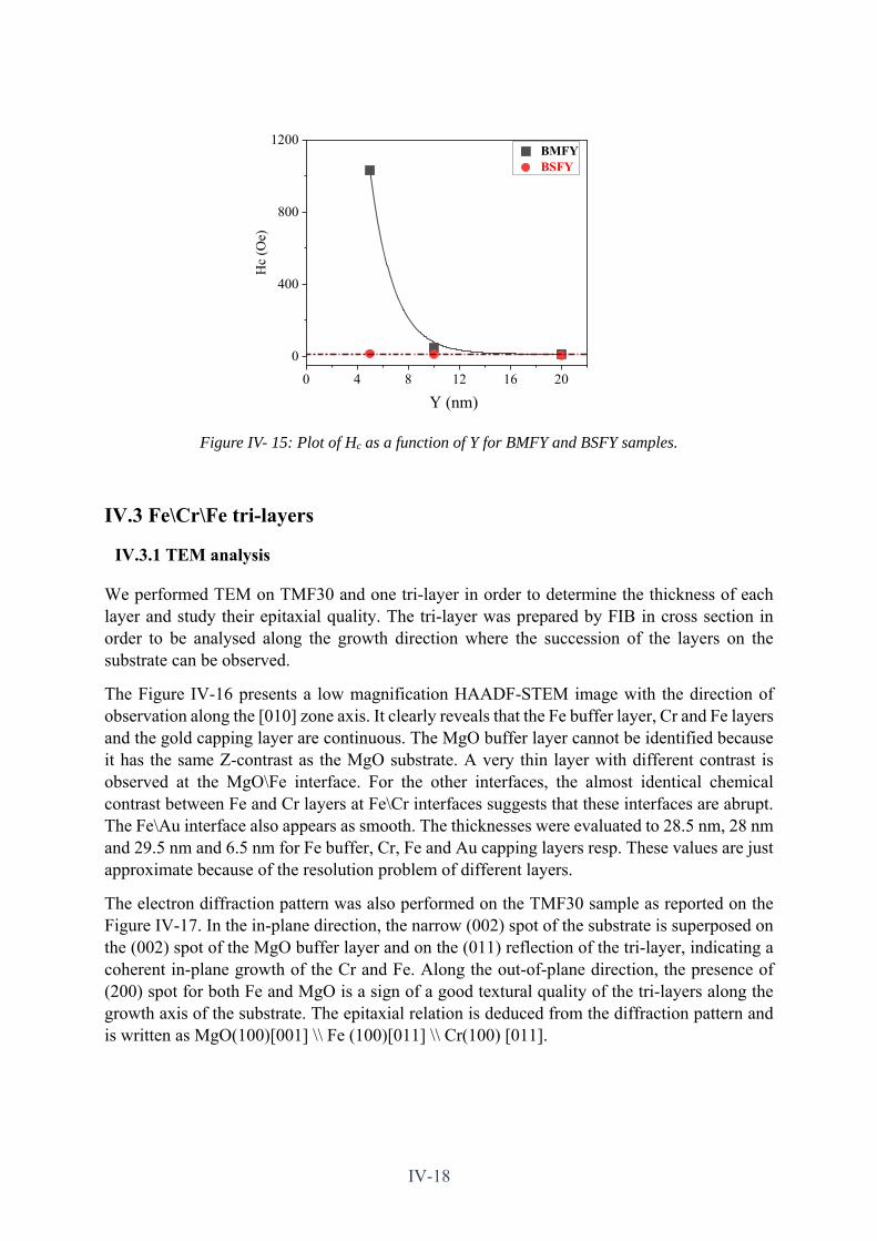
IV-18
Figure IV- 15: Plot of Hc as a function of Y for BMFY and BSFY samples.
IV.3 Fe\Cr\Fe tri-layers
IV.3.1 TEM analysis
We performed TEM on TMF30 and one tri-layer in order to determine the thickness of each layer and study their epitaxial quality. The tri-layer was prepared by FIB in cross section in order to be analysed along the growth direction where the succession of the layers on the substrate can be observed.
The Figure IV-16 presents a low magnification HAADF-STEM image with the direction of observation along the [010] zone axis. It clearly reveals that the Fe buffer layer, Cr and Fe layers and the gold capping layer are continuous. The MgO buffer layer cannot be identified because it has the same Z-contrast as the MgO substrate. A very thin layer with different contrast is observed at the MgO\Fe interface. For the other interfaces, the almost identical chemical contrast between Fe and Cr layers at Fe\Cr interfaces suggests that these interfaces are abrupt. The Fe\Au interface also appears as smooth. The thicknesses were evaluated to 28.5 nm, 28 nm and 29.5 nm and 6.5 nm for Fe buffer, Cr, Fe and Au capping layers resp. These values are just approximate because of the resolution problem of different layers.
The electron diffraction pattern was also performed on the TMF30 sample as reported on the Figure IV-17. In the in-plane direction, the narrow (002) spot of the substrate is superposed on the (002) spot of the MgO buffer layer and on the (011) reflection of the tri-layer, indicating a coherent in-plane growth of the Cr and Fe. Along the out-of-plane direction, the presence of (200) spot for both Fe and MgO is a sign of a good textural quality of the tri-layers along the growth axis of the substrate. The epitaxial relation is deduced from the diffraction pattern and is written as MgO(100)[001] \\ Fe (100)[011] \\ Cr(100) [011].
0 4 8 12 16 20
0
400
800
1200 BMFY BSFY
Hc
(Oe)
Y (nm)

IV-19
Figure IV- 16: HAADF showing the superposition of MgO buffer, Fe, Cr, Fe, and Au layers on MgO.
Figure IV- 17: Diffraction pattern of TMF30 sample.
IV.3.2 XRR characterization
The Figures IV-18 to 21 show the reflectivity spectra for the Fe\Cr\Fe tri-layers deposited on MgO and STO, TMFY and TSFY with Y = 2, 5, 10, 15, 20, 25, 30 nm, the thickness of each layer. All the x-ray reflectivity curves reveal a drop of intensity after the critical angle 2c as expected. We observe for TMF2, TMF5 and TSF2 samples, a fast vanishing of the Kiessig oscillations’ amplitude as a sign of a strong roughness of the substrate. When the thickness of the tri-layers increases, the x-ray reflectivity patterns show well-defined Kiessig oscillations.
On the XRR, there is no contrast between Cr and Fe because they almost have the same density and the deposited thicknesses of Cr and Fe are identical. Thus, it was more accurate to perform

IV-20
the fitting using only one (Fe,Cr) layer (a) to determine the total thickness of the tri-layer instead of using in the fitting program two Fe layers “sandwiched” by a Cr layer (b). In the cases (a), the refinement gives access to 2 parameters for the 3d-metal: the total thickness (d) and the roughness () of the interface with Au. In the cases (b), 6 parameters have to be considered: the thickness of each layer, the roughness of the substrate and of each interface, but there is a strong dependence between them. The density of the layers () are kept equal to those of the tables (the average for the 3d-metal layer). The plot of the thickness of the tri-layer obtained by reflectivity versus the nominal thickness is shown on the Figure IV-22. The thickness from reflectometry is systematically slightly smaller than the nominal value.
Figure IV- 18: XRR plots on TMFY and TSFY samples with Y=2 and 5 nm.
Experiment Fit
2 4 6 8 10 12 141E-8
1E-7
1E-6
1E-5
1E-4
0,001
0,01
0,1
1
10
100
Experiment Fit
2 4 6 8 10 12 141E-8
1E-7
1E-6
1E-5
1E-4
0,001
0,01
0,1
1
10
100Mat d(nm) ( ) (nm)
Au 5.05 19.3[--] 1.01Fe 4.44 7.8 [--] 0.24
MgO 0.0[--] 3.58[--] 0.95
TMF2
Log
((I
nten
sity
) (a
.u.)
)
2 (°)
Mat d(nm) ( ) (nm)
Au 5.5(3) 19.3[--] 1.26Fe 6.13(3) 7.8 [--] 0.84
MgO 16.47 3.58[--] 0.48(8)STO 0.0[--] 5.12[--] 0.76(6)
TSF2
Log
((I
nten
sity
) (a
.u.)
)
2(°)
Experiment Fit B
2 4 6 8 10 12 141E-8
1E-7
1E-6
1E-5
1E-4
0,001
0,01
0,1
1
10
100
Experiment Fit
2 4 6 8 10 12 141E-8
1E-7
1E-6
1E-5
1E-4
0,001
0,01
0,1
1
10
100
Mat d(nm) ( ) (nm)
Au 5.87 19.3[--] 0.91Fe 14.2 7.8 [--] 1.34
MgO 0.0[--] 3.58[--] 0.9
TMF5
Log
((I
nten
sity
) (a
.u.)
)
2 (°)
Mat d(nm) ( ) (nm)
Au 5.38 19.3[--] 0.09Fe 14.8 7.8 [--] 0.34
MgO 19.4(2) 3.58[--] 0.05STO 0.0[--] 5.12[--] 0.3
TSF5
Log
((I
nten
sity
) (a
.u.)
)
2(°)

IV-21
Figure IV- 19: XRR plots on TMFY and TSFY samples with Y=10 and 15 nm.
Experiment Fit
2 4 6 8 10 12 141E-8
1E-7
1E-6
1E-5
1E-4
0,001
0,01
0,1
1
10
100
Experiment Fit
2 4 6 8 10 12 141E-8
1E-7
1E-6
1E-5
1E-4
0,001
0,01
0,1
1
10
100Mat d(nm) ( ) (nm)
Au 10 19.3[--] 0.45Fe 29.19 7.8 [--] 0.49
MgO 0.0[--] 3.58[--] 0.81
TMF10L
og (
(Int
ensi
ty)
(a.u
.))
2 (°)
Mat d(nm) ( ) (nm)
Au 10.3 19.3[--] 0.17Fe 28.66 7.8 [--] 0.38
MgO 20.6(4) 3.58[--] 0.18STO 0.0[--] 5.12[--] 0.27
TSF10
Log
((I
nten
sity
) (a
.u.)
)
2(°)
Experiment Fit
2 4 6 8 10 12 141E-8
1E-7
1E-6
1E-5
1E-4
0,001
0,01
0,1
1
10
100
Experiment Fit
2 4 6 8 10 12 141E-8
1E-7
1E-6
1E-5
1E-4
0,001
0,01
0,1
1
10
100
1 2 3 4 51E-6
1E-4
0,01
1TMF15
Log
((I
nten
sity
) (a
.u.)
)
2 (°)
1 2 3 4 51E-6
1E-4
0,01
1TSF15
Log
((I
nten
sity
) (a
.u.)
)
2(°)
TMF15 TSF15 Materials d (nm) (
𝒈
𝒄𝒎𝟑) (nm) d (nm) ( 𝒈
𝒄𝒎𝟑) (nm)
Au 5.73 19.3[--] 0.34 5.77(3) 19.3[--] 0.18
Fe 46.42 7.8 [--] 0.48 41.62 7.8 [--] 0.21(3)
MgO 21.39(4) 3.58[--] 0.18(6)
Substrate 0.0[--] 3.58[--] 0.38(2) 0.0[--] 5.12[--] 0.25(3)

IV-22
Figure IV- 20: XRR plots on TMF20 and TSF20 samples.
For most samples (except TMF5), two sets of oscillations are observed: a large period/ large amplitude one and small period/ small amplitude one (most pronounced on TSFY samples). The large period/ large amplitude oscillations come from the gold layer which has a higher density and a smaller thickness than (Cr,Fe) layers. The oscillations with the small period and amplitude oscillations belong to (Fe,Cr) layers. We also observe that (Cr,Fe) layers are smoother when grown on STO than on MgO. For a thickness above 20 nm, the reflectivity patterns become very similar for all samples, except the fact that in some cases, the slope of the XRR curve is higher due to a higher roughness of the substrate.
Experiment Fit
2 4 6 8 10 12 141E-8
1E-7
1E-6
1E-5
1E-4
0,001
0,01
0,1
1
10
100
Experiment Fit
2 4 6 8 10 12 141E-8
1E-7
1E-6
1E-5
1E-4
0,001
0,01
0,1
1
10
100
1 2 3 4 5
1E-4
0,01
1TMF20L
og (
(Int
ensi
ty)
(a.u
.))
2 (°)
1 2 3 4 5
1E-4
0,01
1TSF20
Log
((I
nten
sity
) (a
.u.)
)
2(°)
TMF20 TSF20 Materials d (nm) (
𝒈
𝒄𝒎𝟑) (nm) d (nm) ( 𝒈
𝒄𝒎𝟑) (nm)
Au 4.76 19.3[--] 0.18 4.82 19.3[--] 0.16
Fe 56.2 7.8 [--] 0.21 55.4 7.8 [--] 0.2
MgO 19.94 3.58[--] 0.19
Substrate 0.0[--] 3.58[--] 0.186 0.0[--] 5.12[--]

IV-23
Figure IV- 21: XRR plots on TMF30 and TSF30.
TMF25 TSF25 Materials d (nm) (
𝒈
𝒄𝒎𝟑) (nm) d (nm) ( 𝒈
𝒄𝒎𝟑) (nm)
Au 9.97 19.3[--] 0.10 10.01 19.3[--] 0.19
Fe 74.7 7.8 [--] 0.19 74.94 7.8 [--] 0.25
MgO 19.02 3.58[--] 0.32
Substrate 0.0[--] 3.58[--] 0.31 0.0[--] 5.12[--] 0.3
TMF30 TSF30 Materials d (nm) (
𝒈
𝒄𝒎𝟑) (nm) d (nm) ( 𝒈
𝒄𝒎𝟑) (nm)
Au 5.01(6) 19.3[--] 0.09(2) 4.76 19.3[--] 0.21
Fe 81.33(3) 7.8 [--] 0.19(5) 83.61 7.8 [--] 0.24
MgO 19.97 3.58[--] 0.30
Substrate 0.0[--] 3.58[--] 0.21(2) 0.0[--] 5.12[--] 0.21
Experiment Fit
2 4 6 8 10 12 14 16 181E-8
1E-7
1E-6
1E-5
1E-4
0,001
0,01
0,1
1
10
100
Experiment Fit
2 4 6 8 10 12 14 16 181E-8
1E-6
1E-4
0,01
1
100
2 3
0,001
0,1TMF30
Log
((I
nten
sity
) (a
.u.)
)
2 (°)
2 3
0,001
0,1TSF30
Log
((I
nten
sity
) (a
.u.)
)
2(°)

IV-24
Figure IV- 22: Thickness “d” from reflectometry as a function of nominal thickness.
IV.3.3 Structural properties
IV.3.3.1 Texture Figures IV-23 and IV-24 show the high-angle scans for all the Fe\Cr\Fe tri-layers with different thickness deposited on MgO and on STO. The scans show that Fe\Cr are textured along the growth direction of MgO and of STO. A better texture is obtained when the thickness of the tri-layers increases. A reduction of the tri-layers thickness (for Y= 2 and 5 nm) lead to a less intense and broad (200) peak because the number of diffracting atoms is small. H00) and (K00) for the single crystalline gold capping layer and MgO buffer layer (only on STO) are also observed. Moreover, the presence of Laue oscillations around the (200) peak of Au indicates an abrupt Au\Fe interface. As can be seen from Figure IV-24, the Laue oscillations are more numerous and better defined when the thickness of the tri-layers increases. Their occurrence is a sign of the excellent quality and smoothness of each Fe and Cr layer. The Laue oscillations around the (200) peak of Au are narrower for the TMF25 and TSF25 compared with other fringes because a 10 nm of the Au layer was used instead of 5 nm. As the thickness of the tri-layers increases, the Laue oscillations are well pronounced around the (200) peak, meaning that the surface of the Fe\Cr trilayer is also extremely smooth for thicker layers. One should note that the Laue oscillations and the Kiessig fringes give different information. The Kiessig fringes are only sensitive to the difference in the density between elements but are not sensitive to the atomic structure of the sample; they can also be observed in liquids [11] and in polycrystalline materials [12], whereas Laue oscillations are related to the crystal structure. For all the tri-layers, the intensities of the (200) peaks for TSFY samples are identical within the error bar to the intensities of the TMFY samples thanks to the presence of the MgO buffer layer. The Figure IV-25 is a zoom of the scans around the (200) peaks of Fe and Cr and the insert graphs are in logarithm scale for better visibility of the small satellites. Many peaks and satellites are observed due to the interference effect between Cr and Fe layers as well as the concentration and the lattice parameters modulations of Fe and Cr. A better resolution is observed for the XRD patterns on STO.
0 20 40 60 80 1000
20
40
60
80
100TMFYTSFY
d ref
lect
omet
ry (
nm)
Y (nm)
d= 0.95Y d = 0.94Y
3

IV-25
20 40 60 80 100 120-1
0
1
2
3
4
5
6
7
8
9
10
11
12
2(°)
Fe (200)Cr (200)
Au
(40
0)
Au
(20
0)
30nm
25nm
20nm
15nm
10nm
5nm
2nm
MgO
(200
)
MgO
(400
)
Log
(I(a
.u.)
)
Figure IV- 23: scans of the tri-layers on the MgO(100).
20 40 60 80 100 120
1
2
3
4
5
6
7
8
9
10
11
Log
(I(a
.u.)
)
2(°)
2nm
5nm
10nm
15nm
20nm
25nm
30nm
STO
(100
)
Au
(40
0)
MgO
(200
)
MgO
(40
0)
Fe (200)Cr (200)
Au
(20
0)
ST
O(2
00)
ST
O(3
00)
ST
O(4
00)
Figure IV- 24: scans of the tri-layers on the STO(100).

IV-26
Figure IV- 25: scans around the Bragg peak of the tri-layers on MgO and on STO. The insert graphs are in logarithm scale for a better visibility of the satellites.
For a more quantitative interpretation of XRD profiles, we have performed some simulations based on the superlattice construction and the calculation of the diffracted amplitude using eq. II-13. We described the trilayer as n1 planes of Fe with d1 inter-planes distance, n2 planes of Cr with d2 distance and n3 planes of Fe with d1 distance. We assumed that the number of planes in each layer is integer. We considered that all the Fe\Cr interfaces are abrupt: the concentration of Cr varies from 0 to 1 discontinuously (taking into account some smoother variation has no significant effect as long as the thickness of the layers are large compared to the interface extend, considering the experimental error bars). This assumption was justified by the characterizations of the multilayers using atomic tomographic probe and EELS profiles (see Chapter V) and the fact that the Laue fringes around the Au (200) peak show that the layers are very flat, at least locally. The number of atoms per surface unit of the planes are taken as equal as we have shown that the fe/Cr/Fe epitaxy is coherent (same a// for Fe and Cr). The most important parameter is the lattice parameter contrast between Fe ad Cr layers. The Z contrast alone does not give rise to any satellites (see Appendix 2.2). The signal has been convoluted by
62 64 66 680
170
340
0
700
1400
0
1400
2800
0
3800
7600
0
3500
7000
0
24000
0
16000
32000
2(°)
TMF2
Inte
nsit
y (c
ps)
Inte
nsit
y (c
ps)
Inte
nsity
(cp
s)
TMF5
TMF10
TMF15
TMF20
TMF25
TMF30Cr Fe
62 64 66 680
170
340
0
700
1400
0
1400
2800
0
3800
7600
0
3200
6400
0
6500
13000
0
16000
32000
2(°)
TSF2
TSF5
Cr Fe
TSF10
TSF15
TSF20
TSF25
TSF30

IV-27
a gaussian of width to take into account the experimental resolution and some thickness distribution. The parameters of the adjustment were thus: n1, n2, n3, d1, d2, and . We gave the possibility to have n1 < n3 because the first Fe layer is not always totally coherent contrary to the other two (some mis-oriented grains, the presence of defects in the first Fe layer as dislocations or of a thin oxide formation at Fe\MgO interface). The results are presented on Figure IV-26
Figure IV- 26: Lattice parameter (top) and individual thicknesses (bottom) deduced from the least square fits of patterns around the (200) (Fe,Cr) Bragg peak in TMFY and TSFY samples. The
dot-dashed lines show the bulk values (top) and the black lines (bottom) show the individual thickness expected from XRR results.
We obtained simulated diffraction scans that are superimposed on the experiment. Figure IV-27 shows the example of TMF20. The red line corresponds to the diffraction without convolution and the orange one after convolution. This is also the case for all the tri-layers on MgO and on STO (Figure IV-28). The fit is only qualitatively improved by the asymmetry of the Fe layers (this was not successful in the thinnest and thickest samples). Note that the important parameter is the total coherent Fe thickness dFe1+dFe3 in the asymmetric case is very close to 2dFe in the symmetric case. There is some anomaly in TMF10 (too large aFe; we do not understand why) and TXF25 (too small thicknesses compared to reflectometry thickness that was too large on Figure IV-22). The lattice parameter results will be discussed in the IV.3.3.4 paragraph on stress analysis.

IV-28
Figure IV- 27: Measured and simulated patterns performed around the (200) Bragg peak for TMF20 samples.
Figure IV- 28: Measured and simulated patterns performed around the (200) Bragg peak for TMFY and TSFY samples. The angle deduced from aFe and aCr are shown as vertical bars.

IV-29
IV.3.3.2 Crystalline quality
The Figure IV-29 shows the rocking curves at the Fe\Cr\Fe (200) Bragg peak of the TXFY tri-layers. Thanks to the simulations, Cr and Fe peaks can be identified separately. As the thickness of the tri-layer increases, the Cr and the Fe peaks gradually become sharp and more intense thanks to the improvement of the preferentially well-aligned grains of Fe and of Cr on the substrates. For the same thickness of the tri-layers, the intensity of Fe layers is twice that of Cr layer in the tri-layer.
The values of the FWHM as reported on the Figure IV-30 vary from 1° for thinner sample to 0.21° for single Fe and Cr peak. This indicates a very good crystalline quality for both Cr and Fe layers when the thickness increases. Higher values of FWHM are obtained in thinner tri-layers (for Y=2 nm and Y=5 nm samples) may attest a higher fluctuation of Fe and Cr crystallites orientation at the beginning of the growth.
Figure IV- 29: 𝜔 scans for the tri-layers on MgO and on STO.
30 31 32 33 34 35
0
15000
30000
45000
30 31 32 33 34 35
0
15000
30000
45000
25 30 35 400
1000
2000
(°)I (c
ps)
TMF2 TMF5 TMF10 TMF15 TMF20 TMF25 TMF30
Fe Fe
25 30 35 400
1000
2000
(°)
TSF5 TSF10 TSF15 TSF25 TSF30
30 31 32 33 34 35
0
5000
10000
30 31 32 33 34 35
0
5000
10000
15000
20000
25000
(°)
TSF15 TSF20 TSF25
I (c
ps)
TMF15 TMF25 TMF30
(°)
Cr
Cr

IV-30
Figure IV- 30: FWHM for Fe (full square) and in Cr (empty square) as a function of the thickness of the tri-layer. The empty triangles stand for the FWHM on a single (200) peak of Fe\Cr\Fe peaks in
small thickness samples.
IV.3.3.3 Epitaxy: Pole figures and TEM analyses
Pole Figure measurements on the {110} (Fe,Cr) reflection (2= 44.5°) were performed on all the tri-layers (Figure IV-31 and IV-32). The pole figures have the characteristics of an epitaxial growth: a single (110) reflection of Fe and Cr close to the angles (relative to the {020} peaks of the substrate) and is attributed to an epitaxial relationship M(100)[011] // XO(100)[010] for M= Fe or Cr and XO=MgO or STO.
This is consistent with the electron diffraction patterns of Figure IV-17 in the TMF30 sample. However, the broad (110) spot with low intensity observed on the sample with small thickness (Y=2, 5 nm) indicates that this mosaïcity is much larger than for other samples. A shift of the (110) spot from the expected position is observed on some pole Figures; it is due to the positioning of the sample. A strong and circular spot at the origin of the pole figures corresponds to the gold capping layer reflection.
0 5 10 15 20 25 300,0
0,2
0,4
0,6
0,8
1,0TMFY TSFY
FW
HM
(°)
Thickness "Y" of the layers (nm)
FeCr
FeCr
FeCr Cr
Fe
Fe
FeFe
CrCr
Cr

IV-31
Figure IV- 31: Pole figures for the (110) Fe/Cr reflection for TMFY samples. The sample is positioned so that the Fe or Cr reflection is at the and location.
0 20 40 60 800
20
40
60
80
QP
y
TMF2
QPx0 20 40 60 80
TMF5
QPx
0 20 40 60 80
-50,00109,4268,8428,1587,5746,9906,31066122513841544170318632022218123412500
Imax
TMF10
QPx
0 20 40 60 800
20
40
60
80TMF15
QP
y
QPx
0 20 40 60 80
TMF20
QPx0 20 40 60 80
0,000562,5112516882250281333753938450050635625618867507313787584389000
ImaxTMF25
QPx
0 20 40 60 800
20
40
60
80
-50,00
1035
2120
3205
4290
5375
6460
7545
8630
9715
1,080E+04
Imax
QP
y
TMF30
QPx

IV-32
Figure IV- 32: Pole figures for the (110) Fe/Cr reflection for TSFY samples. The maximum intensity for TMFY and for TSFY sample is plotted as a function of the thickness “Y”.
IV.3.3.4 Stress analysis
In order to have comprehensive information on the residual stress evolution in Fe and Cr layers, x-ray stress analyses were made. Besides of the (200) peak, it was possible to measure the 2values from the (222), (130), (310), (220) and (211) reflections planes despite the low intensity of some peaks for small-thickness samples. For all these peaks, the uncertainty is smaller than 10-3 Å. The Figure IV-33 is an example of (200), (220) and (130) maps in the
0 20 40 60 800
20
40
60
80TSF2
QPy
QPx0 20 40 60 80
TSF5
QPx
0 20 40 60 80-50,00140,6331,3521,9712,5903,110941284147516661856204722382428261928093000
ImaxTSF10
QPx
0 20 40 60 800
20
40
60
80TSF15
QP
y
QPx
0 20 40 60 80
TSF20
QPx
0 20 40 60 800
20
40
60
80
0,000
1080
2160
3240
4320
5400
6480
7560
8640
9720
1,080E+04Imax
TSF30
QPx
QP
y
0 20 40 60 80
-100,0468,8103816062175274433133881445050195588615667257294786384319000
Imax
QPx
TSF25
0 15 300,0
0,6
1,2
I (x
104 cp
s)
TMFY TSFY
Y (nm)

IV-33
reciprocal space for the TSF30 sample measured at different angles (or angles). The lattice parameter ahkl = dhkl×sqrt(h²+k²+l²) is plotted versus sin²() for all observable reflections on the Figure IV-34. The horizontal dot lines represent the bulk value for Fe and Cr.
For the small thickness samples (Y=2 and 5 nm), only one slope is obtained with almost the same value of a⟘ and a// for TMF2 and TMF5 samples. We obtain a linear variation of ahkl versus sin²() with positive slopes, indicating tensile in-plane stress.
Figure IV- 33: Maps of TSF30 (with and without Fe and Cr peaks separation).
Figure IV- 34: The sin² plots for Fe and Cr in TMFY and TSFY
Along the growth direction, Fe lattice parameter is smaller than the bulk value whereas Cr lattice parameter is almost equal to the bulk value. On both substrates, the in-plane lattice parameter a// decreases when the thickness increases showing the stress relaxation in the layers (Figure IV-34), but the decrease is larger on STO (Figure IV-35). At large thickness of the tri-layer, in-plane lattice parameters are constant and equal for Cr and Fe showing the coherent growth of Cr on Fe1 and Fe3 on Cr.
For a better understanding of strains’ evolution of Fe layers in the tri-layers, we plotted the in-plane strains for Fe and for MgO buffer layer in TSFY samples. In the MgO buffer layer, negative and almost constant values of the in-plane strain (about -0.61%; Figure IV-36b) are
0,0 0,5 1,0
2,84
2,88
2,92
TMF2 TMF5 TMF10 TMF15 TMF20 TMF25 TMF30
sin²()aa
Fe bulk
Cr bulk200 310 211 220
200310 211
220222
130
a
(A
)
0,0 0,5 1,0
2,84
2,88
2,92
TSF2 TSF5 TSF10 TSF15 TSF20 TSF25 TSF30
Cr bulk
Fe bulk
a sin²() a
-3 -2 -1 0 1 2 3
64
65
66
(°
)
alpha
0,000
6300
1,260E+04
1,890E+04
2,520E+04
3,150E+04
3,780E+04
4,410E+04
5,040E+04
5,670E+04
6,300E+04Imax
200TSF30
42 44 46 4897
98
99
100
40,00341,3642,5943,81245154618482149245027513053335436553956425845594860
Imax
220TSF30
(°
)
chi70 71 72 73
114,5
115,0
115,5
116,0
116,5
0,000
4083
8167
1,225E+04
1,633E+04
2,042E+04
2,450E+04
2,858E+04
3,267E+04
3,675E+04
4,083E+04
4,492E+04
4,900E+04
ImaxTSF30
130
(°
)
chi

IV-34
observed due to i) the misfit of MgO on STO (the number of epitaxy dislocations created during the growth and the annealing is not large enough to relax the misfit) and ii) the contraction of the MgO on STO substrate during the cooling of the MgO buffer layer deposited at 600°C due to the larger expansion coefficient of STO.
Figure IV- 35: Evolution of the in-plane lattice parameter and the out-of-plane lattice parameter for Fe as a function of the thickness.
For TMFY samples, the in-plane strains is about 0.786 0.04% in TMF2 and has a constant value of 0.41%at larger tri-layer thickness. Along the growth direction, the strain in Fe layers is -1.048 0.171% in TMF2 and -0.51% for the other tri-layers. For the TSFY samples, the Figure IV-36a reveals an exponential-like decrease of the in-plane strains when the thickness increases. For large Y, tensile strains are identical in the tri-layers on STO and on MgO, but below 10 nm it is much higher on STO.
We estimated the thermal strains due to the STO substrate shrinkage during the cooling down to room temperature after the growth of MgO buffer layer at 600°C. We obtained an in-plane contraction of about 0.574% for the growth on STO and 0.742% on MgO substrate. This induces a thermal in plane dilatation of 0.17% of the MgO buffer on the STO substrate. Assuming a Poisson’s coefficient of 0.180(5), as //=-(1-)/(2 x =-2.28 x, we get =-0.17%/2.28=-0.075%. This value has the opposite sign of the measured out-of-plane strain measure on MgO (0.15-0.25%; Figure IV-36). Thus, the strain of MgO mainly originates from the misfit with the substrate (-7.3%) that is not completely relaxed by the formation of epitaxy dislocations. It is classical that the residual strain is around 1%. The thermal strain has even the effect to reduce it. We would thus expect smaller strains on STO than on MgO, as the lattice parameter of MgO in plane is indeed smaller than in bulk MgO. The positive in-plane strain of Fe, larger on STO than on MgO, has another origin.
0 5 10 15 20 25 30
2,80
2,82
2,84
2,86
2,88
2,90
2,92TMFY a a(Fe)
TSFY a a(Fe)
a
a
(a)

IV-35
Figure IV- 36: Plot of in-plane and out-of-plane strains in Fe layers in TMFY and TSFY (a) and MgO buffer layer in TSFY (b) as a function of the thickness Y. The values in MgO are deduced from the 𝜃
2𝜃 scans on TSFY samples () and calculated with a Poisson’s coefficient of 0.180(5) (//). The red (black) dashed line shows the estimated in-plane (out-of-plane) thermal strain expected in MgO.
Considering the cooling after the annealing of Fe at 500°C, the thermal strain is between - 0.11% to - 0.17% for Fe. When comparing strains at 25°C (red bullet and purple star on Figure IV-36) to those at 500°C (blue triangle and pink square), we note that the effect of thermal strains is almost negligible.
However, for small sample thickness on STO, we observe a strong in-plane dilatation of the Fe lattice parameter. The EELS chemical analysis of the Fe\Cr multilayer deposited on STO (Figure IV-37) shows that some Sr atoms are present in the MgO buffer layer and near the MgO\Fe interface. No titanium atoms were detected. The diffusion of Sr through the MgO buffer layer in Fe could be at the origin of a dilatation of the Fe lattice near to the MgO buffer layer. This is consistent with Zhang et al results which show that despite the fact that the Sr has a larger ionic radius than Mg [13], the diffusion coefficient of Sr in MgO is higher than the one of Ti in MgO.
Using the result of R. FREER [14], we extrapolated the diffusion coefficient of Sr in MgO at 2.33x10⁻²⁷ m²/s along the dislocations and between 4x10-25 m²/s and 1x10-29 m²/s in bulk for the growth at 600°C. At 500°C, these values are respectively 2x10-29 m²/s along the dislocations and between 5x10-27 m²/s and 7x10-32 m²/s in bulk MgO oxide materials.
A typical value of the diffusion coefficient of Sr in metals at 500°C is 10-21 m2/s [16]. The width of the Sr distribution is after a 2h annealing is (2Dt)1/2=(2 10-21x7200)1/2=4 nm [15].
The size factor as proposed by Hepbrun [17] induces a strain of 0.15% (as observed in TSF5) for a concentration of 120 ppm of Sr, which is very small and cannot be quantified by TEM. The average strain will decrease with an allotropic-type function when the pure layer increases. This function is similar to the measured variation. Thus the dilatation of Fe (Figure IV-36) can be due to the diffusion of Sr at MgO\Fe interface. Besides, it has been shown by other authors that the presence of Sr does not change the magnetization of Fe [18]. To summarize, we can say that a small content of Sr is present at MgO\Fe interface for all the samples on STO. Its effect is more pronounced near to the MgO\Fe interface, inducing for the smallest thickness samples a strong stress (Figure IV-38). With the increase of the thickness, both the bi-axial
0 5 10 15 20 25 30-3
-2
-1
0
1
2
3
0.41%
TSFY (Fe) (Fe) thermal
TMFY (Fe) (Fe) thermal
Y (nm)
(a)

IV-36
stress and the in-plane stress reduce in TSFY and TMFY samples thanks to an improvement of the layer microstructure which induces a better stress relaxation in Fe and Cr layer. For a thickness higher than Y=5 nm on MgO and Y=15 nm on STO, we observed that the bi-axial stress remains constant when the thickness increases. This indicates that the residual stress is not sufficient to create more dislocations for a complete relaxation of Fe.
Figure IV- 37: EELS map on Fe\Cr multilayers deposited on STO substrate.
Figure IV- 38: Evolution of residual stress in TXFY as a function of Y.
These results clearly show that the residual stress level in the films is strongly correlated to their microstructure and the mechanism of stress relaxation in Fe layers. This relaxation behavior has not been clearly investigated to date. For a deeply investigation of the relaxation process, one should complete this analysis with the study of the strain relaxation’s mechanism by the dislocation at MgO\Fe interface and in the layer. This is discussed in Chapter V.
0 5 10 15 20 25 300
1
2
3
4
5
6 TSFY (Fe)
TMFY (Fe)
GP
a
Y (nm)
1.3
(b)

IV-37
IV.3.4 Was the MgO buffer layer necessary to epitaxy the tri-layers?
In this manuscript we have highlighted the study of the MgO buffer layer’s effect on the structure of the sample on MgO and on STO. In this regards, we prepared Fe\Cr\Fe tri-layers on STO and MgO substrates with and without the MgO buffer layer. The thickness of each layer is 10 nm. The sample without the MgO buffer layer is named TSF10_no MgO for the tri-layer on STO and TMF10_no MgO for the tri-layer on MgO. scans were realized on the tri-layers as reported on the Figure IV-39. For the growth on MgO with and without the buffer layer, a good texture of the tri-layers with a growth direction along [100] of MgO is observed.
Figure IV- 39: 𝜃 2𝜃 scans for TXF10 samples with and without the MgO buffer layer.
The intensity of the (200) Bragg peak is slightly higher for the TMF10 sample than for the sample without a buffer layer indicating that the presence of MgO buffer layer reduce the substrate roughness. For the growth on STO with no MgO buffer layer, we obtained a very small (200) Bragg peak of the tri-layer; meaning a poorer ordering along the [100] of STO. The presence of the (111) peak of Au implies that Au layer is polycrystalline. When the MgO buffer is used, the (200) Fe\Cr\Fe peak becomes extremely strong compared. This indicates a notable improvement of the textural quality of the tri-layer on the MgO buffer layer on STO substrate compared with the “same” sample without a buffer layer of MgO.

IV-38
We also studied the crystalline quality of the samples by performing rocking curves scans. The Figure IV-40 shows that for samples on MgO substrates, the (200) peak becomes narrower with a two times smaller value of the FWHM when the MgO buffer layer is used.
25 30 35 40
0
500
1000
1500
2000
2500
3000
25 30 35 40
0
500
1000
1500
2000
2500
3000TMF10_no MgO_FWHM = 0.4797± 0.001°TMF10 _FWHM = 0.2851 ± 0.0005°
I (c
ps)
2 (°)I(
cps)
2 (°)
TSF10_no MgO_FWHM = 2.141± 0.037°TSF10 _ FWHM = 0.373± 0.006°
Figure IV- 40: 𝝎 scans for TXF10 samples with and without the MgO buffer layer on MgO (left image) and STO (right image).
This attests a better crystal quality for the sample with MgO buffer layer thanks to a smoother and more homogenous MgO\Fe interface. A notable improvement of the crystalline quality is obtained for the samples on STO where the presence of the MgO buffer layer gives rise to an extremely intense (24 times higher than for the TSF10_no MgO sample) and narrow peak
(4 times smaller than for the TMF10_no MgO sample).
IV.3.5 Magnetic properties
All the hysteresis loops for the TMFY and TSFY samples were measured with the external field along the sample edge i.e. the [010] direction of the substrate and the [011] direction of Fe. The Figure IV-41 shows that in all samples, the magnetization was mainly in the film plane. The values of the coercive field are similar to the expected values in Fe bulk. In the thin tri-layers, a small contribution is observed perpendicularly and a large coercive field is obtained for the samples on MgO, indicating the presence of magnetically decoupled grains, which can be explained by the roughness of the interfaces that is in these samples of the same order of magnitude as the thickness.

IV-39
Figure IV- 41: M-H hysteresis loops for TMFY and TSFY samples.
For a better understanding, SQUID measurements were done on TMF5 and on TSF5 samples with the field applied along the easy axis of Fe in the plane and out-of-the plane (see Figure IV-42). The AGFM curve is plotted on the Figure IV-42 to show that similar result within the error bar of 3% is obtained for the in-plane measurements using AGFM or the SQUID. In perpendicular we observe also some contribution of decoupled grains with a large coercive field. We think that for the growth on MgO, the large coercive field is due to the intrinsic roughness of both substrate and film, giving rise to a lower structural quality (to the Fe grain size distribution as observed by the scans and the rocking curves). This is called in the literature the Néel’s orange-peel effect: the surface roughness of the substrate gives rise to a random microscopic field (due to dipole–dipole interaction coupling) acting on the interface spins [19] as illustrated on the inset image (see Figure IV-42).
As the thickness increases, the saturation moment per surface unit increases linearly (Figure IV-43). The straight lines are the results of the linear fits of the experimental data. The slope is used to deduce the saturation magnetization of Fe. The obtained values are close to that in Fe bulk (Ms=1720 emu/cm3) for the tri-layers on MgO (Ms=1705 ± 27 emu/cm3), whereas they are slightly higher for the tri-layers deposited on STO (Ms=1813± 35 emu/cm3). This small difference can be due to the higher tensile stress in TSFY samples than in TMFY samples. This indicates that the nature and the sign of strain can affect the magnetic properties. It is suggested by Kock that the magneto-striction energy due to the lattice distortion (𝜀 10 ) in heteroepitaxial films is expressed as Fmel = B1x𝜀 where B1 is the magneto-elastic constant of Fe bulk B1 = - 3.44x10⁶ J/m3 and the in-plane strains. Using this expression, we obtained the value of 5.5x10⁴ J/m3 for TSF2 and 3.44x10⁴ J/m3 for TSF5. These values are in the same order of magnitude as the magneto-crystalline anisotropy Fmcr indicating that Fmel may compete with Fmcr and stabilize the magnetic anisotropies which are different from the bulk.
The intercept of the Mi axes with the vertical axis gives the contribution of interfaces. We have obtained values that are not larger than the error bar (Mi = -104 ± 273 emu/cm² for TMFY and Mi = -248 ± 260 emu/cm² for TSFY samples). The obtained Mi has a negative sign in both cases as expected by Freyss [20].

IV-40
Figure IV- 42: M-H hysteresis loops in parallel and perpendicular geometries for TMF5 and TSF5 samples.
Figure IV- 43: Plot of the magnetization per surface as a function of the thickness of Fe layer for TMFY and TSFY samples.

IV-41
Conclusion on TXFY trilayers
We have prepared Fe\Cr\Fe samples with different thickness Y= 2, 5, 10, 15, 20, 25, and 30 nm in order to study the structure of the tri-layer and deduce the mean moment of the iron and the modification of its value at the interfaces. TEM measurements have been performed for the local study of the structure of Fe\Cr\Fe tri-layers. The HAADF image on the TMF30 sample reveals a diffusion contrast between Fe and Cr layer indicating that Cr and Fe are not mixed and the electron diffraction patterns reveals an epitaxial growth of the tri-layers attesting the good structure of Fe\Cr\Fe tri-layers deposited by MBE. To have the global information on the structure of the samples, XRD have been done on Fe layers and Fe\Cr\Fe tri-layers. We found byscans that the samples are textured along the [100] direction of the substrates. A better resolution is observed for the scans of the samples on STO substrates (Figure IV-25). The pole figures maps reveal that the samples are epitaxied. These observations are in agreement with TEM results. scans, pole figures and rocking curves measurements also reveals that the small thickness tri-layers on STO have a better epitaxial quality than that on MgO. As expected, the (200) peaks become narrower and more intense when the thickness of the tri-layer increases, reflecting an improvement of the out-of-plane coherence length. The decrease of the FWHM and increase of the intensity of Cr\Fe\Cr(200) rocking curves while the growth temperature of Fe decreases attests an improvement of the crystallinity.
To further study the structure of the samples, we have analyzed the stress using the sin²() method. For the single Fe layers, we found that the in-plane residual stress is in tension on both substrates with a higher in-plane dilatation for the Fe layers deposited on STO than on MgO substrates. The decrease of the in-plane lattice parameters of Fe with the Fe thickness indicates a better relaxation. In the Fe\Cr\Fe tri-layers, only one slope (Figure IV-34) is observed for small thickness samples. For the thick tri-layers, a linear variation of ahkl versus sin²() for Cr and for Fe are obtained separately with equal in-plane lattice parameters attesting an in-plane coherent growth of Cr and Fe as observed by HRTEM (Figure IV-17). Higher in-plane strains of Fe in the tri-layer are also observed for the growth on STO compared to the growth on MgO. On MgO, except for the TMF2 sample, the in-plane residual strain is almost constant whereas on STO, its amplitude is higher for thin samples. We have attributed this strong in-plane dilatation of Fe in single layer and in the tri-layers on STO to the presence of Sr impurities in the MgO buffer layer that diffuses in the Fe layer.
Concerning the magnetic properties, we observe a difference of the in-plane anisotropy with a hysteresis curves having the expected shape when the thickness of the tri-layer increases. This is related to the epitaxial quality of the tri-layers. For the small thickness samples (TMF2 and TMF5), we obtained a large coercive field on MgO which can be due to the strong roughness of MgO inducing at the MgO\Fe interface a Néel’s orange-peel coupling.
From the plot of the saturation magnetization of Fe versus the thickness of the Fe layer, I deduced the mean magnetization of Fe called Ms and the global contribution of the moment from Fe\Cr interfaces Mi. The values of Ms are almost close to the bulk. These results confirm that the magnetic properties of the Fe layer are directly influenced by the structural properties and also the residual stress evolution in the tri-layers. Despite the growth of MgO buffer layer on both substrates, we see that the nature of the substrate still affects the structure and the magnetic properties of Fe single layers and Fe\Cr\Fe tri-layers. However, the values of Mi obtained for the tri-layer on MgO and STO are very small. The small magnetic contributions of

IV-42
the interfaces could originate from a) the formation of a dead layer at MgO\Fe interface as suggested in the papers [9] and [10]. b) the contribution of the Fe moment from Fe\Au interfaces, c) the magneto-striction that changes with thickness (constant at high thickness), d) the presence of Sr impurities which may affect the magnetic environment of Fe atoms. To get rid of a), b) and c) artefacts and have a better determination of the moment change at the Fe\Cr interfaces, Cr\Fe\Cr tri-layers have been prepared and investigated.
IV.4 Analysis of Cr buffer layers
Before to study Cr\Fe\Cr tri-layers, we have deposited 10 nm of Cr buffer layers under different conditions and studied their structural properties.
IV.4.1 Thickness determination
The Figure IV-44 shows the x-ray reflectivity profile for two samples of Cr layer deposited on STO with a MgO buffer layer. One of the Cr layer was deposited at 400°C because it has been shown in Chapter III that this temperature allows a good epitaxy of Cr on MgO. Another Cr layer was deposited at room temperature then annealed at 400°C for about 2 h. We observe more defined and more numerous fringes when Cr is deposited at high temperature. A fast vanishing of Kiessig oscillations when Cr is deposited at room temperature indicates that surfaces and/or interfaces are rough.
Figure IV- 44: XRR of buffer Cr layers on a STO\MgO substrate.
These results imply that high diffusion of Cr at the surface of the substrates is thus needed for the epitaxial growth of Cr. The inserted fitting results give a thickness of 12 nm and 13.66 nm for Cr@400°C and Cr@RT_annealed respectively. In the following work, the Cr growth time was adjusted so that we obtained the expected thickness. A much stronger roughness is obtained at each interface between elements when Cr is deposited at room temperature and annealed. The roughness of the MgO buffer layer for Cr@RT_annealed is at least six times higher than that of the MgO buffer for Cr@400°C, meaning that, during the post-growth annealing of Cr
4 8 12 16 201E-8
1E-7
1E-6
1E-5
1E-4
0,001
0,01
0,1
1
10
100
4 8 12 16 201E-8
1E-7
1E-6
1E-5
1E-4
0,001
0,01
0,1
1
10
100Mat d(nm) ( ) (nm)
Au 9.6 19.3[--] 0.15Cr 12 7.5[--] 0.55
MgO 19.24 3.58[--] 0.2STO 0.0[--] 5.12[--] 0.32
BSC400
Log
((I
nten
sity
) (a
.u.)
)
2 (°)
Experiment Fit
Mat d(nm) ( ) (nm)
Au 9.64 19.3[--] 0.88Cr 13.66 7.5[--] 0.45
MgO 19.05 3.58[--] 1.3STO 0.0[--] 5.12[--] 0.73
BSCRT
Log
((I
nten
sity
) (a
.u.)
)
2(°)
Experiment Fit

IV-43
deposited at room temperature, bulk diffusion is not able to improve the crystallinity and flatness of the layer (whereas during the growth of Cr@400°C, the surface diffusion of Cr, much more active, is at work).
IV.4.2 Structural properties
Texture in BSCY
The Figure IV-45 shows the diffraction patterns of Cr buffer layers deposited on STO. For the two samples, it reveals a texture of Cr along the growth direction of the STO substrate. The (200) Cr peak is more intense in the BSC400 sample than in the BSCRT sample, attesting a better texture of BSC400. Besides, the diffraction pattern contains the peaks of the single crystalline MgO buffer (in BSC400 and RSCRT) and some peaks of the Au capping layer (200 and 400 in BSC400; 111 and 222 in BSCRT). We observe a better relaxation of the MgO buffer layer in BSC400 (the out-of-plane lattice parameter is 4.2106 ±0.001 Å). For BSCRT sample, the out-of-plane lattice parameter is about 4.2204 ±0.0004 Å.
Figure IV- 45: 𝜽 𝟐𝜽 scans for Cr buffer layers on STO.
Table IV- 4: Position, width and corresponding perpendicular coherence length of the (200) Cr peak. d* is the thickness determined by XRR.
d*(nm) 2 FWHM D⟘(nm) BSC400 12 64.77±9E-4 0.909±2E-3 10.35± 5E-3
BSCRT 13.66 64.75±12E-4 1.024 ± 3E-3 7.813± 4E-3
10-2
100
102
104
106
20 40 60 80 100 12010-2
100
102
104
106
BSC400
ST
O(2
00)
ST
O(1
00)
ST
O(3
00)
MgO
(400
)
ST
O(4
00)
MgO
(200
)
Log
(I(c
ps))
2(°)
Au
(11
1)
Au
(22
2)
Au
(40
0)
Au
(20
0)
Log
(I(c
ps)) Cr (200)
BSCRT

IV-44
The presence of the (111) and (222) peaks of Au (at the Bragg positions = 38.18° and 81.72°) indicates a (111) texture of the capping layer for the BSCRT sample (texture expected for a non-epitaxial growth as (111) are the densest planes).
Crystalline quality in BSCY
The scans measured on the (200) reflection (Figure IV-46) reveal a higher intensity and a larger FWHM for the BSC400 sample than on BSCRT sample. The in-plane minimal coherence length (assuming a zero mosaïcity and a zero experimental enlargement), evaluated to 7.719± 0.012 nm for the BSC400 sample and 8.065± 0.041 nm for the BSCRT sample, are almost identical table IV-5). This result is close to that of BSF10 sample (7.80± 0.01 nm). This indicates a good in-plane coherence length if the buffer layer deposited on the MgO buffer layer is either Fe or Cr.
Figure IV- 46: 𝝎 scans on Cr buffer layers.
Table IV- 5: Fitting parameters of the 𝝎 scan (200) Cr peak. d* is the thickness determined by XRR.
d*(nm) FWHM D⫽ (nm)
BSC400 12 1.218± 0.001 7.719± 0.012
BSCRT 13.66 1.168 ± 0.003 8.065± 0.04
26 28 30 32 34 36 38
0
300
600
900
1200
I (c
ps)
(°)
BSCRT BSC400

IV-45
Epitaxy in BSCY
A further study of the epitaxy was done by measuring pole figures on the buffer BSCY layers (Figure IV-47). On the quarter pole figures, the signature of the coherent epitaxy of Cr on STO is observed: the (110) reflection of Cr is observed at the expected position. A better epitaxy is obtained for the BSC400 sample than on BSCRT sample. Besides, the Au (H00)-type diffraction peaks are observed on the BSC400 sample whereas for the BSCRT sample, only a texture contribution corresponding to the (200) reflections of Au (111) textured grains is visible on the amplified image (Figure IV-47).
Figure IV- 47: Pole figures of Cr buffer layers on STO substrate. Bottom: intensity amplified by 10.
Stress analysis in BSCY
Stress analysis for Cr layers on STO substrates are presented in the Figure IV-48. A similar tensile bi-axial stress is observed with almost the same value of the lattice parameters, the out-of-plane lattice parameter is 2.8754± 0.0013 Å (resp 2.8769 ± 8E-4 Å) and the same in-plane lattice parameter 2.9173±0.0034 Å (resp 2.9168±0.0021 Å) for BSC400 (resp. BSCRT). An in-plane strain of about 1% and 0.7% is found in BSC400 and BSCRT respectively. To these strains is associated a tensile residual stress evaluated to 2.26 ± 0.5 GPa for BSC400 and 2.16 ± 0.4 GPa for BSCRT. Thus, the residual stress generated during the epitaxy are almost the same when the Cr layer is deposited at high temperature and when Cr is deposited at room

IV-46
temperature and annealed at 400°C. This shows that 2 hours of annealing at 400°C is sufficient to relax the layer to the minimum residual strain. Along the growth direction, the Cr lattice parameter is smaller than in the bulk.
Figure IV- 48: sin² plots for BMC400 and BSCRT samples.
Considering =0.21, the usual value for Cr [9], we deduce the value of the free of stress lattice parameters and the swelling (see table IV-6). Slightly higher values are obtained for the BSCRT sample than for the BSC400 sample. Thus, for the growth of Cr\Fe\Cr tri-layers, we choose to grow the Cr buffer layer at high temperature since the BSC400 sample shows smaller roughness, better texture and epitaxy than BSCRT.
Table IV- 6: Parameters deduced from sin²() plots.
a0(Å) (GPa) Sa (%)
BSC400 2.8899(21) 2.26(5) 0.21(1) BSCRT 2.8907(12) 2.16(4) 0.23(5)
IV.5 Cr\Fe\Cr tri-layers
Cr\Fe\Cr tri-layers with various thicknesses: 5, 10 and 20 nm were prepared by MBE on STO and MgO substrates. The x-ray reflectivity and structural properties are investigated. The magnetic properties of Cr\Fe\Cr tri-layers are discussed.
0,0 0,5 1,02,82
2,84
2,86
2,88
2,90
2,92
200
211
220222
130
BSC400 BSCRT
bulk_Cr
a0
sin² ()
a
(A)
a
a//

IV-47
IV.5.1 XRR measurements
The Figures IV-49 and IV-50 show the raw specular XRR scans obtained on TSCY tri-layers. Specular XRR intensities were recorded over an angular range from 2θ = 0.2° (below the critical angle) up to an angle where all intensity oscillations arising from the tri-layers’ thickness were damped out. The red line shows the best fit model for the data set in black. The insert tables are the results of the fit. In the fitting process, the density of Cr was kept constant to 7.5 g/cm3 and the fitting were performed by replacing the tri-layer with only one Cr layer. Except the case of TMC5 sample (where the fit was not possible), the fitting results are in good agreement with the experiment. A substantial reduction in the amplitude oscillations for TMCY samples is observed compared to the TSCY samples. This attests a higher roughness in the tri-layers on MgO than in those on STO. The results in the inserted tables indicate that the thickness of the tri-layer is close to the nominal thickness of the layers with an error bar of about 3%.
Figure IV- 49: XRR plots on TMC5 and TSC5 samples.
Experiment
2 4 6 8 100,01
0,1
1
10
100
1000
10000
100000
1000000
1E7
1E8
Experiment Fit
2 4 6 8 101E-8
1E-7
1E-6
1E-5
1E-4
0,001
0,01
0,1
1
10
100
TMC5
Log
((I
nten
sity
) (a
.u.)
)
2 (°)
Mat d(nm) ( ) (nm)
Au 11.02 19.3[--] 0.57
Cr 14.59 7.5[--] 0.32
MgO 18.3 3.58[--] 0.31
STO 0.0[--] 5.12[--] 0.71
TSC5L
og (
(Int
ensi
ty)
(a.u
.))
2(°)
Experiment Fit
2 4 6 8 101E-8
1E-7
1E-6
1E-5
1E-4
0,001
0,01
0,1
1
10
100
Experiment Fit
2 4 6 8 101E-8
1E-7
1E-6
1E-5
1E-4
0,001
0,01
0,1
1
10
100
Mat d(nm) ( ) (nm)
Au 9.32 19.3[--] 0.46Cr 30.37 7.5[--] 0.57
MgO 0.0[--] 3.58[--] 0.14
TMC10
Log
((I
nten
sity
) (a
.u.)
)
2 (°)
Mat d(nm) ( ) (nm)
Au 9.31 19.3[--] 0.34
Cr 29.28 7.5[--] 0.73
MgO 19.28 3.58[--] 0.22
STO 0.0[--] 5.12[--] 0.2
TSC10
Log
((I
nten
sity
) (a
.u.)
)
2(°)

IV-48
TMC20 TSC20 Materials d (nm) ( 𝒈
𝒄𝒎𝟑) (nm) d (nm) ( 𝒈
𝒄𝒎𝟑) (nm)
Au 9.16 19.3[--] 0.25 9.14 19.3[--] 0.63
Cr 68.88 7.8 [--] 0.55 67.1 7.8 [--] 0.89
MgO 20.9 3.58[--] 0.15
Substrate 0.0[--] 3.58[--] 0.7 0.0[--] 5.12[--] 0.11
Figure IV- 50: XRR plots on TMCY and TSCY samples with Y=10 and 20 nm.
IV.5.2 Structural properties
Texture in TXCY
The Figure IV-50 shows the diffraction patterns of Cr\Fe\Cr tri- layers. It reveals that Fe and Cr are textured along the growth direction of the substrates. The improvement of the texture of TMCY and TSCY samples is observed when the thickness of the tri-layers increases. The positions of Au and MgO peaks attest that they are single crystalline except for TMC5 and TSC5.
Experiment Fit
2 4 6 8 101E-8
1E-7
1E-6
1E-5
1E-4
0,001
0,01
0,1
1
10
100
Experiment Fit
2 4 6 8 101E-8
1E-7
1E-6
1E-5
1E-4
0,001
0,01
0,1
1
10
100
1 2 3 41E-6
1E-4
0,01
1
1 2 3 41E-6
1E-4
0,01
1TMC20L
og (
(Int
ensi
ty)
(a.u
.))
2 (°)
TSC20
Log
((I
nten
sity
) (a
.u.)
)
2(°)

IV-49
Figure IV- 51:scans of the tri-layers on MgO(100).
Figure IV- 52:scans of the tri-layers on the MgO/STO(100).
The absence of Laue oscillations around the (200) peak of gold capping layer indicates that the Cr\Au interface is not as flat as at the Fe\Au interface for the Fe\Cr\Fe tri-layers. The measurements around the (200) peaks of Fe and Cr show many satellites surrounding the (200) peak particularly for TMC10 and TSC10. As discussed in the section IV.3.3, the presence of satellites around the main peak comes from the interferences of the amplitudes scattered by Cr and Fe layers. As the thickness increases, the distance between satellites decreases giving rise to two symmetric and intense peaks for the TMC20 and TSC20 samples. For these thickest samples, we note a shift of the Bragg position of the film to higher angles compared to the bulk positions attesting a contraction along the growth direction. Along this direction, the crystallites size is10±0.05 nm in TXC10 and 20.80±0.09 nm in TXC20 whereas in TMC5 the crystallites size of about 3 nm indicates a poorer texture. Due to the bad epitaxial quality of TMC5 (low signal over background), other measurements on TMC5 were not usable.
20 40 60 80 100 120
100
101
102
103
104
105
2-1
MgO
(20
0)A
u(20
0) Cr Fe
MgO
(40
0)
20nm
Au(
400)
10nm
5nm
Au(
111)
2 (°)
Log
(I(
a.u.
))
20 40 60 80 100 120
101
102
103
104
105
106
Log
(I(
a.u.
))
2 (°)
10nm
ST
O (
100)
ST
O (
200)
MgO (200) Au
(200
) Cr
ST
O (
300)
ST
O (
400)
MgO
(40
0)
Au
400
Fe
5nm
5
20nm
60 65 700,98
1,47
1,96
2,45
0,77
1,54
2,31
3,08
1,76
2,64
3,52
4,40
2 (°)
TSC5
TSC10
TSC20
Cr Fe
Log
(I(a
.u.)
)
60 65 700,00
0,96
1,92
2,88
3,840,96
1,92
2,88
3,84
(°)
TMC10
Cr Fe
Log
(I(a
.u.)
)
TMC20

IV-50
Pole figures in TXCY
We also performed pole figures to study the epitaxial quality of the samples in detail. All the pole figures were measured in the same conditions so that their intensities could be compared. On the quarter pole figures, a signature of a coherent epitaxy of Cr on STO is observed: the (110) reflection of Cr is observed at the expected position.
Figure IV- 53: Pole figures for TSCY and TMCY samples. The maximum intensity for TMCY and TSCY samples is plotted as a function of Y.
For the TSC5 sample, the (110) reflection of the tri-layer is broad and less intense because the epitaxy is partially lost. As the thickness increases, we observe a single (110) spot becoming narrower and more intense, indicating a better epitaxy.
Stress analysis in TXCY
In Cr\Fe\Cr tri-layers, the Figures IV-54 show that bi-axial stresses are tensile in all cases. A coherent in-plane growth of Fe on Cr is observed for the thickest tri-layers. For the TSC5 samples, the sin2()-plot shows a strong in-plane distortion (1.39 ± 0.25 %) of (Cr,Fe) lattice parameter during the epitaxy. This induces in the out-of-plane direction a compressive strain of about -1.85 ± 0.52%. The magnitude of the in-plane residual stress generated within the tri-layer is also high, about of 7.0 ± 1.8 GPa (tables IV-7). This may indicate a more difficult incorporation of misfit dislocations for the relaxation in Cr\Fe\Cr than in Fe\Cr\Fe tri-layers.
0 20 40 60 800
20
40
60
80
QP
y
QPx
TSC5
0 20 40 60 80
QPx
TSC10
0 20 40 60 800
20
40
60
80
QP
y
QPx
TMC10
0 20 40 60 80
QPx
-40,00
380,0
800,0
1220
1640
2060
2480
2900
3320
3740
4160
4580
5000
5420
5840
6260
6680
Imax
TMC20
0 20 40 60 80
QPx
-40,00
386,3
812,5
1239
1665
2091
2518
2944
3370
3796
4223
4649
5075
5501
5928
6354
6780
Imax
TSC20
0 150,0
0,4
0,8
I (x
104 cp
s)
TMCY TSCY
Y (nm)

IV-51
When the thickness of the Cr\Fe\Cr tri-layers increases, the in-plane strains and the residual stress reduce significantly as a result of the relaxation. The tri-layers deposited on MgO show a small value of the strains and stress compared to those grown on STO, attesting a better relaxation for the tri-layers on MgO.
Figure IV- 54: The sin² plots for TMCY and TSCY samples.
Table IV- 7: Parameters deduced from sin²() plots.
⫽ (%) ⟘ (%) (GPa)
TMC10 0.55±0.135 Fe 0.53±0.06 Cr
-0.734±0.245 Fe -0.705±0.155 Cr
2.7856±0.87 Fe 2.68±0.52 Cr
TMC20 0.603±0.09 Fe 0.61 Cr
-0.804±0.106 Fe -0.814 Cr
3.05±0.32 Fe 3.09 Cr
⫽ (%) ⟘ (%) (GPa)
TSC5 1.385±0.25 -1.846±0.516 7.01±1.8 Fe\Cr
TSC10 0.962±0.17 Fe 1.01±0.08 Cr
-1.283±0.352 Fe -1.34±0.26 Cr
4.87±1.23 Fe 5.09±0.87 Cr
TSC20 0.773±0.03 Fe 0.69±0.008 Cr
-1.031±0.125 Fe -0.92±0.212 Cr
3.91±0.37 Fe 3.5±0.72 Cr
0,0 0,5 1,02,82
2,84
2,86
2,88
2,90
2,92
200310
211220
200211
130222
TMC10 TMC20
a
(A
)
sin²() a
Fe bulk
Cr bulk
Cr\Fe\Cr
a
0.0 0.5 1.02.82
2.84
2.86
2.88
2.90
2.92
TSC5 TSC10 TSC20
sin²()
Fe bulk
Cr bulk
Cr\Fe\Cr
220
a a

IV-52
IV.5.3 Magnetic properties
The M-H loops of the TMCY and TSCY samples are shown on Figure IV-55. When the thickness increases the shape of the hysteresis loop becomes closer to the expected shape for a bcc Fe with the external field along the [110] direction. The insert Figure reveals that the coercive field is slightly higher than in Fe bulk for the TSCY samples. The coercive field decreases as the thickness increases, but is always higher than the bulk values. A high HC was also obtained on the small-thickness Fe\Cr\Fe tri-layers on MgO. SQUID analyses on TMC5 samples show that the coercive field is also high in the perpendicular geometry meaning an orange peel effect due to the substrate roughness is transferred through the Cr layer. The saturation magnetization is plotted as a function of the Fe thickness on the right panel of Figure IV-56. For comparison, the plots obtained for Fe\Cr\Fe tri-layers were included. Despite the fact that the statistic is worse, the slopes for the Cr\Fe\Cr samples and Fe\Cr\Fe samples are different, indicating different values of Fe moment. Besides, the slopes are identical for the Cr\Fe\Cr tri-layers on both MgO and STO, indicating that the average value of Fe magnetization is the same in both cases.
As reported in the table (IV-8), the means magnetization of Fe for Cr\Fe\Cr tri-layers is smaller than the bulk value which is 1720 emu/cm3. The contribution of the moment changes due to interfaces is also small.
Figure IV- 55: M-H hysteresis loops for TMFY and TSFY samples.

IV-53
Figure IV- 56: Left image: in-plane and perpendicular M-H hysteresis loops for TMC5 and TSC5 samples. Right image: Plot of the magnetization per surface unit as a function of the thickness of Fe
layer
Table IV- 8: Parameters deduced from the magnetization plots.
TMCY TSCY
Ms (emu/cm3) Mi (emu/cm²) Ms (emu/cm3) Mi (emu/cm²)
1385 ± 186 176 ± 246 1437 ± 132 57 ± 174
Conclusion on TXCY trilayers
The aim of the sections V-4 and V-5 was to estimate the contribution of the global moment from Fe\Cr interface from Cr\Fe\Cr tri-layers.
We have studied the structure of Cr single layers and Cr\Fe\Cr tri-layers with the thickness Y = 5, 10 and 20 nm. XRD diffractions analyses reveal an improvement of the structure: the texture, the epitaxy and the crystalline quality. We also found that the in-plane bi-axial stresses are in tension and decrease when the thickness increases thanks to a better epitaxy of the tri-layers. The change of the average moment at the Fe\Cr interfaces deduced from the hysteresis curves is as small as in the case of Fe\Cr\Fe tri-layers. The precision is probably not sufficient.
Since it is difficult to estimate efficiently the interface contribution in the tri-layers, we have prepared some Fe\Cr multilayers in order to have a larger relative contribution of the Fe\Cr interfaces.

IV-54
IV.6 Cr\(Fe\Cr)N multilayers
IV.6.1 Architecture of the multilayers
Fe\Cr multilayers were prepared in the same conditions as the tri-layers. The architecture of the multilayers is as follows: A 10 nm of Cr is used as a second buffer layer (considering that the 20 nm of MgO is the first buffer layer). This allows to avoid the presence of a magnetic/insulator interface which may induce a hybridization, an interdiffusion, some stacking faults and maybe impurities at the interface. We fixed the thickness of Cr of the Fe/Cr multilayer at 2 nm and varied the thickness of the individual layer of iron in order to always have the total thickness of Fe equal to 20 nm (see the appendix I). This thickness corresponds to 140 atomic planes of Fe. We call n the number of Fe/Cr interfaces.
If we consider one Fe atom in the multilayer, its effective moment depends on his environment and the average moment per Fe atom in the multilayer can be expressed as m = 2.25+ ∆𝜇 ∙ n/140. In this equation, 2.25 µB represents the moment per Fe atom in the volume (neglecting the strain effects); ∆𝜇 is the moment change at a Fe\Cr interface per atom of the interface. Some theoreticians have evaluated the effect of the vicinity of a Fe/Cr interface on the moment of Fe and Cr atoms in the case of perfect interfaces (see the Introduction Chapter).
For a precise determination of the total moment, SQUID magnetometer was used to measure the M-H loops in the multilayers. In the following, we named MXCY the multilayers XO\MgO\Cr_10\(Fe_Y\Cr_2)p\Au, where Y is the thickness of the Fe layer in nm and p the number of Fe\Cr bilayers (we have: p=n/2=20/Y). We used the couples: (Y,p)=(2,10), (2.5,8), (4,5), (5,4), (6.5,3), (10,2). The TXC20 tri-layers take place in this series with (Y,p)=(1,20).
IV.6.2 Magnetic properties and discussion
The Figure IV-56 shows the hysteresis cycles for the multilayers on MgO and on STO. To normalize the moment per Fe atom, we use the nominal thickness of the multilayers and the density of iron. A precise determination of the sample surface was done using an optical microscope.
Figure IV- 57: The m-H plots for the multilayers on MgO and STO. In braun dash-dot line the expected partial cycle for bulk Fe along [011] direction.

IV-55
We are expecting a linear evolution of the moment per Fe atom as a function of n, the number of Fe\Cr interfaces (Figure IV-58). This is the case up to 16 interfaces. Nevertheless, the slope is far more important than expected from the theoretical results. This can be due to the in-plane strain of about 1% in Cr@400°C or to the oxidation at Cr@400°C and Fe@RT. Some points are obviously false: there is a significant decrease of Fe moment for MMC5, and the values for MMC2 and MSC2 are much too high, probably due to an orange peel effect (finally no well-defined interfaces are present) or to the poor textural, epitaxial and crystalline quality of the multilayers as shown by scans, pole figures and rocking curve analysis (see the appendix I). The linear evolution of the moment in the MSCY multilayers (with a thickness larger than 2 nm) has a slope of -0.0163 µB per interface, which corresponds to a lack of 2.28 µB per interface (one atomic dead layer and/or some alloyed layer due to roughness). The intercept at n=0 shows a decrease of the Fe moment in the core of the layers: 2.17 µB (instead of 2.25 µB), i.e. a 3.6 ± 1.5 % decrease, that could be attributed to the effect of stress and oxygen defects.
Figure IV- 58: Plot of the moment per Fe atom (of MMCY: black circles and MSCY: red squares) as a function of n, the number of Fe\Cr interfaces. The brown and green lines are the predictions of [20] and [21] resp. The red line is the linear fit of the moment in MSCY for Y between 2.5 nm and 20 nm. Its equation is: m(µB)=(2.172 ± 0.033)-n*(0.0163 ± 0.0038). The points circles are obviously false.
Conclusion
In this chapter, we have prepared a series of Cr and Fe single layers, tri-layers and multilayers in order to study the structure and the magnetic properties of Fe. We have successfully established a correlation between structural and magnetic properties for all the samples. However, the experimental estimation of the global moment at Fe\Cr interfaces called mi, which is known to be very small (see referees [20], [21]) is still a challenging issue. Very small (almost negligible) values of mi are obtained on the two series of the tri-layers. For Fe\Cr\Fe tri-layers, we have suggested that the formation of a dead layer at MgO\Fe interface, the contribution of the Fe moment from Fe\Au interface, the presence of Sr impurities in Fe and/or the effect of

IV-56
magneto-striction (which is thickness-dependent) can reduce the value of mi. In order to have only clean Fe\Cr interfaces, we have prepared the Cr\Fe\Cr tri-layers but the precision is not sufficient to make a conclusion on the value of mi. Since it is difficult to have an accurate estimation of the global moment at Fe\Cr interfaces in the tri-layers, we have prepared Fe\Cr multilayers in order to have additive contributions of Fe\Cr interfaces. In this case, we have followed the variation of the moment per Fe atom as a function of the number of Fe\Cr interfaces. Our result is far from the expected tendency, showing an atomic dead layer at each interface and a small decrease of Fe moments in the core of the layers. As we will see in the next chapter, the oxygen is limited to the interfaces and in the Cr layers, so there are no oxygen atoms within the core of the layers. The oxygen impurities can thus be responsible of the dead layers at the interfaces and not of the decrease of the moment inside the layers.

IV-57
Bibliography
[1] D. Halley, O. Bengone, S. Boukari, and W. Weber, “Novel Oscillation Period of the Interlayer Exchange Coupling in $\mathrm{Fe}/\mathrm{Cr}/\mathrm{Fe}$ Due to MgO Capping,” Phys. Rev. Lett., vol. 102, no. 2, p. 027201, Jan. 2009, doi: 10.1103/PhysRevLett.102.027201.
[2] E. Bertin et al., “Random barrier double-well model for resistive switching in tunnel barriers,” Journal of Applied Physics, vol. 109, no. 8, p. 083712, Apr. 2011, doi: 10.1063/1.3561497.
[3] D. Halley et al., “Size-induced enhanced magnetoelectric effect and multiferroicity in chromium oxide nanoclusters,” Nature Communications, vol. 5, no. 1, Art. no. 1, Jan. 2014, doi: 10.1038/ncomms4167.
[4] G. Ehrlich and F. G. Hudda, “Atomic View of Surface Self‐Diffusion: Tungsten on Tungsten,” J. Chem. Phys., vol. 44, no. 3, pp. 1039–1049, Feb. 1966, doi: 10.1063/1.1726787.
[5] R. L. Schwoebel and E. J. Shipsey, “Step Motion on Crystal Surfaces,” Journal of Applied Physics, vol. 37, no. 10, pp. 3682–3686, Sep. 1966, doi: 10.1063/1.1707904.
[6] M. Saloaro, H. Deniz, H. Huhtinen, H. Palonen, S. Majumdar, and P. Paturi, “The predominance of substrate induced defects in magnetic properties of Sr2FeMoO6thin films,” J. Phys.: Condens. Matter, vol. 27, no. 38, p. 386001, Sep. 2015, doi: 10.1088/0953-8984/27/38/386001.
[7] V. I. Razumovskiy, A. V. Ruban, and P. A. Korzhavyi, “First-principles study of elastic properties of Cr- and Fe-rich Fe-Cr alloys,” Phys. Rev. B, vol. 84, no. 2, p. 024106, Jul. 2011, doi: 10.1103/PhysRevB.84.024106.
[8] K. Sangwal, P. Gorostiza, F. Sanz, and J. Borc, “Study of the Nature and Distribution of Elementary Steps on the (100) Cleavage Faces of MgO Single Crystals by Atomic Force Microscopy,” Crystal Research and Technology, vol. 35, no. 8, pp. 959–967, 2000, doi: 10.1002/1521-4079(200008)35:8<959::AID-CRAT959>3.0.CO;2-N.
[9] H. L. Meyerheim et al., “Geometrical and Compositional Structure at Metal-Oxide Interfaces: MgO on Fe(001),” Phys. Rev. Lett., vol. 87, no. 7, p. 076102, Jul. 2001, doi: 10.1103/PhysRevLett.87.076102.
[10] F. J. Palomares, C. Munuera, C. M. Boubeta, and A. Cebollada, “Spatial and chemical interface asymmetry in Fe/MgO/Fe(001) heterostructures,” Journal of Applied Physics, vol. 97, no. 3, p. 036104, Jan. 2005, doi: 10.1063/1.1847718.
[11] J. Als-Nielsen, D. Jacquemain, K. Kjaer, F. Leveiller, M. Lahav, and L. Leiserowitz, “Principles and applications of grazing incidence X-ray and neutron scattering from ordered molecular monolayers at the air-water interface,” Physics Reports, vol. 246, no. 5, pp. 251–313, Oct. 1994, doi: 10.1016/0370-1573(94)90046-9.
[12] L. G. Parratt, “Surface Studies of Solids by Total Reflection of X-Rays,” Phys. Rev., vol. 95, no. 2, pp. 359–369, Jul. 1954, doi: 10.1103/PhysRev.95.359.
[13] F. Zhang, A. M. Walker, K. Wright, and J. D. Gale, “Defects and dislocations in MgO: atomic scale models of impurity segregation and fast pipe diffusion,” J. Mater. Chem., vol. 20, no. 46, pp. 10445–10451, Nov. 2010, doi: 10.1039/C0JM01550D.
[14] R. Freer, “Self-diffusion and impurity diffusion in oxides,” J Mater Sci, vol. 15, no. 4, pp. 803–824, Apr. 1980, doi: 10.1007/BF00552089.
[15] W. E. Martinez, G. Gregori, and T. Mates, “Titanium diffusion in gold thin films,” Thin Solid Films, vol. 518, no. 10, pp. 2585–2591, Mar. 2010, doi: 10.1016/j.tsf.2009.07.187.
[16] C. D. Versteylen, N. H. van Dijk, and M. H. F. Sluiter, “First-principles analysis of solute diffusion in dilute bcc Fe-$\mathit{X}$ alloys,” Phys. Rev. B, vol. 96, no. 9, p. 094105, Sep. 2017, doi: 10.1103/PhysRevB.96.094105.

IV-58
[17] D. J. Hepburn, E. MacLeod, and G. J. Ackland, “Transition metal solute interactions with point defects in fcc iron from first principles,” Phys. Rev. B, vol. 92, no. 1, p. 014110, Jul. 2015, doi: 10.1103/PhysRevB.92.014110.
[18] E. A. Devi, R. Chinnappan, and C. S. Sundar, “First-principles study of interaction energies of atomic defects in bcc ferromagnetic iron,” Phys. Rev. B, vol. 98, no. 14, p. 144104, Oct. 2018, doi: 10.1103/PhysRevB.98.144104.
[19] L. Néel, “Sur un nouveau mode de couplage entre les aimantations de deux couches minces ferromagnétiques,” Comptes Rendus Hebdomadaires Des Seances De L Academie Des Sciences, vol. 255, no. 15, pp. 1676–1681, 1962.
[20] M. Freyss, “Proprietes magnetiques de systemes de basse dimensionnalite : determination de la structure electronique,” These de doctorat, Strasbourg 1, 1999.
[21] M. Yu. Lavrentiev, R. Soulairol, C.-C. Fu, D. Nguyen-Manh, and S. L. Dudarev, “Noncollinear magnetism at interfaces in iron-chromium alloys: The ground states and finite-temperature configurations,” Phys. Rev. B, vol. 84, no. 14, p. 144203, Oct. 2011, doi: 10.1103/PhysRevB.84.144203.

Chapter V:
Interdiffusion in epitaxial Fe\Cr multilayers

V - 2
Chapter V:Interdiffusion study in epitaxial Fe\Cr multilayers
V.1 Architecture of Fe\Cr multilayers .......................................................................................... 3
V.2 X‐ray studies on the sample before the annealing ................................................................. 3 V.2.1 XRR analysis .......................................................................................................................................... 3 V.2.2 XRD for structural studies ..................................................................................................................... 4 V.2.3 Simulation of XRD profiles with the Python code. ............................................................................... 8
V.3 Study of Fe\Cr multilayers after 4h at different temperatures ............................................... 9 V.3.1 Evolution of x‐ray diffraction pattern ................................................................................................... 9 V.3.2 Monte Carlo simulations of the annealed samples. ............................................................................. 9 V.3.3 TEM and APT analysis before and after annealing at 500°C for 4 hours ............................................ 11
V.3.3.1 TEM results ................................................................................................................................. 11 V.3.3.1 EELS analysis ............................................................................................................................... 12 V.3.3.3 APT results .................................................................................................................................. 13
V.4 Isothermal annealing at high temperatures ......................................................................... 16 V.4.1 Evolution of x‐ray diffraction patterns: Satellite intensities and peaks’ positions ............................. 16 V.4.2 Effect of relaxation on the variation of diffraction spectrum. ........................................................... 19
V.4.2.1 Correlation between A and 𝒂⟘ as a function of the time at T=450°C ....................................... 19 V.4.2.2 Strains evolution during the annealing ....................................................................................... 19
V.5 Isothermal annealings at low temperatures ........................................................................ 21
Discussion and conclusion ......................................................................................................... 21
Bibliography .............................................................................................................................. 25

V - 3
Chapter V:
Interdiffusion in epitaxial Fe\Cr multilayers
In this Chapter, XRD, APT, TEM and Monte Carlo simulations (MC) are used to study the interdiffusion mechanism in Fe\Cr multilayers.
V.1 Architecture of Fe\Cr multilayers
For the interdiffusion studies, we have prepared Fe\Cr multilayers on STO substrate with a buffer layer of Fe. Previous studies have shown that the best structure and abrupt interfaces are obtained when the layers are deposited on STO and when a buffer layer of Fe is used (see Chapter IV). The multilayer is constituted of 5 bi-layers of about 20 nm thick, corresponding to 140 planes of Fe and 140 planes of Cr. The growth of these multilayers was done in MBE using the same conditions as for the tri-layers Fe/Cr/Fe samples presented in Chapter IV. In the following, the multilayer is named MS10.
Figure V- 1: Architecture of MS10 sample. The thickness of Au capping layer is about 5 nm
V.2 X-ray studies on the sample before the annealing
V.2.1 XRR analysis
XRR analysis has been done on MS10 to determine the total thickness of the multilayer and the roughness of the Fe\Au interface and also to control the surface roughness of Au before and after the annealing. Kiessig oscillations are observed in the Figure V-2: large oscillations come

V - 4
from the gold layer and small oscillations correspond to the Kiessig fringes of Fe and Cr total thickness. Two peaks with higher amplitude at 2and (red array) correspond to the period of the Fe\Cr superlattice. Most of the superlattice peaks are hidden in Kiessig fringes of (Fe,Cr) and gold. The simulated intensity curve, in red on Figure V-2, gives a total thickness of the multilayer of 105(4) nm (instead of 110 nm nominal, there is a 4.8% reduction). For the capping layer of Au, we obtain 6.31 nm with a very small roughness as reported in the inserted table. The substrate and Cr layer surfaces present a small roughness.
Figure V- 2: XRR on MS10. The experimental data are in black and the fitting is in red.
V.2.2 XRD for structural studies
Prior to the annealing steps, the samples with 10x10 mm² initial size was divided into 9 samples of 3x3 mm² size on which XRD was performed in order to determine its structural properties. The graph shows thediffraction patterns (Figure V-3). We distinguish a well-defined and intense (200) Bragg central peak surrounded with many well-resolved satellites. This is due to the modulation of both the concentration and the lattice parameters in Fe and Cr of the multilayer. This result is consistent with the epitaxial growth. All the samples have more or less the same intensity, indicating that the growth of the multilayer is homogeneous. From the position of the (200) main peak, we deduce the mean lattice parameter of Fe\Cr along the growth direction to be (2.8657± 0.0002) Å. The positions of the satellites allow determining with a good precision the period of the multilayer (plotting the intensity in log evidences the high index satellites, see Figure V-4). The Bragg peak angle and the diffusion vector are related by the expression Q = 4 sin()/λ; we plot the variation of Q as a function of n, the satellites’ index relative to the main peak (n=0), and use the slope to deduce the period (slope = 2/) of the multilayer (see Figure V-5a). We find about of 191.6(6) Å which is just 4.2% smaller than the nominal period. This result is consistent with TEM observations.

V - 5
Figure V- 3:scan on the multilayer as prepared. The left insert is the illustration of how the sample with the dimension 10x10mm² was divided into 9 pieces.
Figure V- 4: scan in log scale on the N°6 multilayer as prepared, with numerous evidenced satellites.
The Figure V- 5b is the rocking curve measured on the main peak of the initial 10x10 mm² size and of two 3x3 mm² samples. The FWHM of 0.2623 ± 0.0005° for the biggest sample is almost identical to the value obtained on the small size sample as expected, corresponding to both a small mosaïcity and a high in plane coherent length, which is a sign of a good crystalline quality.

V - 6
Figure V- 5: (a) Diffusion vector Q as a function of the satellite order n. The inserted table gives the value of Q deduced from the angular position of each peak. The period of the multilayer is deduced from the slope. (b): scans for the 10x10 mm² sample and for the 3x3 mm² samples (N°5 and N°7).
On the poles figures, the presence of a single (110) reflection of (Fe,Cr) at and (Figure V-6)is a signature of the epitaxial quality of the multilayer, corresponding to the epitaxy relationship M(100)[011] // STO(100)[010] for M= Fe or Cr.
Figure V- 6: Pole figure on MS10 (N°5).
In order to determine of the lattice parameter and analyze stress evolution in MS10, the sin²() method was used (Figure V-7). The Figure V-8 shows ahkl versus the sin²() for some reflections of Fe and Cr on STO. As reported on the Figure V-7, the main peak and the satellites are observed on the (200), (220) and (211) maps whereas only one value of the lattice parameter is observed along the (222) and the (130) maps (due to the fact that these maps are done in

V - 7
symmetric geometry – at different – which highly convolutes the spectrum, whereas the other 3 can be measured in asymmetric geometry – – with no tilt).
Figure V- 7: Maps in the reciprocal lattice unit (RLU) showing the mean peak and the satellites for the 200, 220 and 211 reflections of MS10.
Figure V- 8: The sin² () plots of MS10 sample N°5. The index “c” is for the main peak of the multilayer and other indices stand for satellites. The dot lines represent the bulk lattice parameter for Fe (in wine), for Cr (in green), for the Fe\Cr multilayers (in black). The bulk lattice parameter of the
multilayer is aFe\Cr = 𝟏
𝟏𝟏 (𝟔𝒂𝑭𝒆 𝟓𝒂𝑪𝒓) = 2.8737 Å.
Identical values of the lattice parameter in the plane of the film attests a coherent in plane growth of Fe and Cr. If we consider only the reflections of the main peak, we obtain the mean values

V - 8
of the out-of-plane and in-plane lattice parameters: a⟘200c = a⟘Fe\Cr = 2.8628 ± 0.0002 Å and a⫽200c= a⫽200Fe = a⫽200Cr = 2.8896 ± 0.0005 Å respectively. Values of a⫽200c higher than the a⟘200c indicates a tensile bi-axial stress, generated in the multilayers during the epitaxy.
V.2.3 Simulation of XRD profiles with the Python code.
We have simulated the XRD spectrum of the multilayer by considering the nominal thickness and supposing a rectangular periodic shape of the multilayer. Since we couldn’t determine separately the lattice parameters of Cr and of Fe along the growth direction, we used the values obtained on the tri-layers TSF15 which are 2.84 Å for Fe and 2.885 Å for Cr to generate the profile (Figure V-8). The simulated pattern is shown in the Figure V-9: green triangles show the curve before convolution. The position of the satellite peaks is well reproduced, confirming that the interfaces are initially abrupt. Laue oscillations surrounding the main peak correspond to the total thickness.
We did a convolution of the simulated spectrum (black and blue graphs) in order to represent experimental convolution which depends on the mosaïcity, some structural inhomogeïnity and the instrumental width. The position and amplitude of the satellite peaks are well reproduced, confirming that the interfaces are initially abrupt.
Knowing the structure of the prepared multilayer, the next step is to determine the appropriate range of annealing temperature for the interdiffusion studies.
Figure V- 9: Simulation of the diffraction pattern of the MS10 sample. Black dots: experimental results; green triangles: raw simulated data; blue dots: convoluted simulated data; kaki line: gaussian
curve for convolution.

V - 9
V.3 Study of Fe\Cr multilayers after 4h at different temperatures
V.3.1 Evolution of x-ray diffraction pattern
In order to find the appropriate range of temperature for the interdiffusion studies, different samples have been annealed in vacuum at different temperatures and XRD measurements have been done on each sample to follow the variation in intensity of satellites as a function of the annealing temperature. For all the samples, the annealing time was 4 hours. The Figure V-10 shows the diffraction pattern (a) and the ratio of the satellites intensities over the main peak intensity as a function of T (in °C) (b). We observe that the intensity of satellites is almost constant for the sample annealed at the temperature lower than 400°C. At 400°C, there is a significant decrease of the satellites’ relative intensities.
Figure V- 10: (a) scans on the samples annealed at different temperatures. The intensity is normalized by the surface of each sample. (b) Plot of the ratios of the satellite intensities over the
main peak intensity as a function of T.
For the sample annealed at 500°C, we notice a vanishing of the second order satellites which may indicate the concentration variation at Fe\Cr interface or in the layers. A considerable shift of the main peak at a lower 2 angle is observed for the samples annealed at the temperature between 400°C and 500°C. This attests the compression of the mean lattice parameter along the growth direction. In order to determine the expected concentration variation at the Fe\Cr interface, Monte Carlo simulations were realized by our partners from Paris Saclay for samples annealed at 400°C and 500°C.
V.3.2 Monte Carlo simulations of the annealed samples.
The Figure V-10 shows the concentration profiles of Fe for different annealing times at T=400°C (blue line), 450°C ( green line) and 500°C (orange line).
The simulation conditions are:
- The box size was (256×128×128)/2 where 2 is the number of atomic sites in bcc.
- The vacancy jump frequency model is taken from [1].

V - 10
- The vacancy is assumed to be at equilibrium with respect to the concentration profile at any time.
- The periodicity of the profile is 128 × d (d is the interplanes distance) along the [100]-type directions of the bcc crystal.
Before the annealing, Fe layers are 64 planes of pure Fe and Cr layer 64 planes of pure Cr. When the samples are annealed, there is a variation of concentration depending on the temperature and the annealing time. The diffusion of Fe in Cr layers (resp. Cr in Fe layers) has a symmetric variation at the Fe\Cr and Cr\Fe interfaces.
Figure V- 11: Concentration profiles of Fe and Cr at 400°C, 450°C, and 500°C from Monte-Carlo simulations. Bottom right (from [1]): phase diagram of Fe-Cr (full black line), calculated –’
miscibility gap (red circles), evolution of the Curie temperature in the homogeneous solid solution (dashed line). Numbers give the concentrations of Fe or Cr inside the miscibility gap at the
equilibrium for T=400°C (blue line), 450°C (green line) and 500°C (orange line).
For short annealing times at 400°C, we observe that the concentration of Fe in the Cr layer are only extended on few Cr planes while the concentration of Cr in the Fe layer varies from 0% to 11% on almost 24 planes of Fe. This indicates a slow diffusion of Fe into Cr layers and a rapid diffusion of Cr into the Fe layers. For further annealing, the diffusion of Cr into the Fe layer continues until the equilibrium concentration of Cr is reached in the Fe layers. The increase of the thickness of the Fe layers is also observed.

V - 11
At higher annealing temperatures (450°C and 500°C), the diffusion process is faster and the thickness of Fe layer further increases. The equilibrium concentration of Cr in Fe layers is reached after 600 hours at 450°C and 30 hours at 500°C while the diffusion of Fe in Cr layer is still going.
In order to study the role of defects in the diffusion process, we have performed transmission electron microscopy (TEM) and atomic probe tomography (APT) measurements on one sample before and after annealing at 500°C during 4 hours.
V.3.3 TEM and APT analysis before and after annealing at 500°C for 4 hours
V.3.3.1 TEM results TEM and APT analysis have been done by Estelle Meslin and Maxime Vallet on the prepared multilayer in order to verify the multilayers’ architecture (by TEM) and also for chemical analysis (APT). The sample was prepared in cross section and as a needle by FIB. For the TEM observation, the beam direction is along [010] zone-axis of the STO substrate. Figures V-12 show the nanometer scale arrangement of the Fe and Cr layers with uniform thickness for the sample as prepared and after the annealing. For both samples, multilayers are full of line dislocations that propagate through all layers. They are called threading dislocations. They originate from the misfit dislocations that are located at STO\MgO interface but are not observed due to the resolution of the images.
Before the annealing, the thickness of both Fe and Cr layers is about 9.5 nm with an error bar of 0.3 nm. When the sample is annealed at 500°C for about 4h (Figure V-13), the thickness of Fe varies from 9.5 nm (before the annealing) to 10.3 nm (after the annealing) and from 9.5 nm (before the annealing) to 8.5 nm (after the annealing) for Cr layers.
Figure V- 12: BF-STEM image of MS10 before annealing.

V - 12
Figure V- 13: HAADF image of the MS10 sample annealed at 500°C during 4 hours.
V.3.3.1 EELS analysis EELS analyses have been done by Michael Walls using a Nion Operating at 100kV (Figures V-14 and V-15). The scan directions were parallel and perpendicular to the interface of the multilayer. We observe that before the annealing, the dislocation lines that are observed on the HAADF image do not affect the Fe and Cr concentrations. The EELS profile is symmetric. The finite slope at the interfaces (right bottom profile) is due to the spatial resolution of the TEM in the EELS mode.
Figure V- 14: EELS images and concentration profiles of MS10 before annealing.

V - 13
Figure V- 15: EELS images and concentration profiles of MS10 annealed at 500°C during 4 hours
When the sample is annealed, for the in-plane profile, the relative concentration of Fe decreases attesting a diffusion of Cr in Fe layers of about 4-5 %. In the Cr layers, there is a significant increase of the Fe concentration from 17 to 19 % (averaged on the whole Fe thickness) along threading dislocations. When Fe goes into Cr layer, Cr atoms are driven out and dispersed into the Fe layer. This attests that dislocations in Cr layers act as pipes, allowing Fe to be rapidly transported into the Cr layers. Along the growth direction (Figure V-15, right image), two important information can be extracted: a) the maximum concentration of Cr is about 10 % in Fe layers, meaning that the equilibrium concentration for both Cr and Fe is not yet reached. At 500 °C, the equilibrium concentrations of Fe in Cr-rich and in the Fe-rich region are respectively 17% and 86% (see the phase diagram of the Figure V-11). The obtained concentrations in Fe layers are close to the one obtained by the Monte Carlo simulations. b) Some modulation of Cr composition in the Fe-rich layers is also observed.
V.3.3.3 APT results In order to precisely quantify the layers’ composition, the relative content of impurities and their distribution, we performed some APT analysis on the samples. Figure V-16 shows that Fe and Cr layers are homogeneous in composition, suggesting that defects observed by TEM do not affect the chemical composition of layers. The atomic composition of each layer has been quantified on a 7x7x60 nm3 in the middle of the needle extracted from the layers to prevent any artefact on the APT results due to the difference of evaporation field between Fe and Cr.
The results show a purity higher than 99.7% for all the Fe and Cr layers. The oxygen distribution was also analyzed due to its high reactivity with Cr. Oxygen levels remain extremely weak through the sample thanks to the ultrahigh vacuum chamber of our MBE machine. The oxygen is mainly localized at interfaces with a maximum local atom composition of 2%. The global oxygen content in the layer is very small (0.05%).

V - 14
Figure V- 16: As prepared sample: (a) 3D reconstruction from APT of MS10 including several Fe-Cr periods. (b) Map of Fe-Cr (middle) and O (top) from a 7×7×60 nm3 box extracted close to the (100) pole and the relative atomic composition of Fe, Cr and O (x10) along the growth direction (bottom).
Figure V- 17: Sample annealed 4h at 500°C: (a) 3D reconstruction from APT of MS10 including several Fe-Cr periods. (b) Map of Fe-Cr (middle) and O (top) from a 7×7×60 nm3 box extracted close to the (100) pole and the relative atomic composition of Fe, Cr and O (x10) along the growth direction
(bottom).
After the annealing, the diffusion of Cr atoms in Fe layers is observed on the Figure V-17. The variation of the relative concentration of Fe in the Fe layers is different from one layer to another and may be due to the distribution of defects in the multilayer. The concentration of Cr in Fe is the highest for the layer Fe4 of Figure V-17b. We observe on the Figure V-17a the presence of

V - 15
Fe aggregates in some Cr layers, with elongated shape as if they were formed on a line of diffusion. Besides, the migration of Fe in Cr layers is along the threading dislocations in Cr (small yellow cycle on Figure V-17a), as observed by EELS.
For a better understanding of the heterogeneity of Cr layers, many 3D reconstruction volumes have been done to determine the distribution of Fe and O in Cr layer. Eleven defects have been analyzed by APT. The diffusion of Fe in Cr is generally localized along the [211] direction (Figures V-18-20). Some agglomerates of oxygen have similar location, either alone of near to some Fe pipe. In bcc materials, the [211] direction of a defect can be the trace of the (111) gliding plane along the [011] direction [2]. Thus, the Fe inclusions that diffuse along the [211] direction may preferentially accumulate along the (110) dislocation planes present in Cr layers. Nine other Fe inclusions and chromium oxide were analyzed by Maxime Vallet (not shown) and the relative composition of each element was determined. He showed that Fe and oxygen indeed diffuse in Cr layers along the threading dislocations and the migration direction of Fe in Cr layers is the [112], the [113] or the [111]. This will affect the diffusion mechanism.
Figure V- 18: Composition map showing on the left an Fe inclusion in the Cr layer and on the right the corresponding composition profile.
Figure V- 19: Composition map showing an oxygen pipe in a Cr layer (the points representing O atoms have a larger radius than those representing Cr atoms).

V - 16
Figure V- 20: Composition map of a thin slice on the left showing a Fe inclusion near to a Cr oxide and the corresponding concentration of each element on the right. The observation planes of defects is [100] along the growth direction and [011]along the interface.Tthe points representing O atoms have
a larger radius than those representing Cr atoms.
V.4 Isothermal annealing at high temperatures
To study the interdiffusion, we have annealed one sample at 400°C and another one at 450°C during different annealing times.
V.4.1 Evolution of x-ray diffraction patterns: Satellite intensities and peaks’ positions
The diffraction patterns of the sample annealed at 450°C (Figure V-21) show a non-regular decrease of satellites intensities with the annealing time. This indicates that shape of Fe\Cr interface profiles get modified. In the first stage of annealing, a fast and abrupt decay of satellites takes place. After the first step of annealing, the satellites’ intensities’ decay becomes slow. The fast decrease of the 2nd order satellites indicates that the smaller-wavelength modulations decay more rapidly. Figure V-21 also reveals an angular shift of the whole spectrum to a lower 2 value, indicating an increase of the average out-of-plane lattice parameter (table V-1).
For the sample annealed at 400°C, the decay of the satellites has also a jump after the first annealing. The shift of satellites’ positions is smaller (table V-2).
In order to find the analytic model that is the most appropriate for our system and will give access to some interdiffusion coefficients D, we plot on Figure V-23 for each satellite Si of intensity Ii, either log(Ai) (with Ai(t) = [Ii(t)/ I0(t)] / [Ii(0)/ I0(0)], the relative intensity of the satellite normalized to its value at t=0) as a function of the time t (case a), or log(Ai) as a function of log(t) (case b), or the ratio Ai as a function of the square root of the annealing time√𝑡 (case c), for the samples annealed at 450°C and 400°C.
In Figures V-23 (a) and (c), we observe a rapid decay of Ai (or ln(Ai)) for the first annealing and a noticeable slow decrease for the long time annealing. The log-log model (Figure V-22b) which shows a more linear evolution than the others (Figure V-22a and c), was fitted with a linear function to deduce the composition gradient-correlation constant Kc. For the Fickian diffusion model, Kc is equal to 0.5. For all the satellites, we obtain Kc values that were different from 0.5 and different from each other [3]. In all the cases, the three diffusion regimes (or

V - 17
Figure V- 21: scans on the samples annealing at 450°C during different times.
Figure V- 22: scans on the samples annealing at 400°C during different times.

V - 18
Figure V- 23: Plots of A(t) as a function √𝑡 (c), log (A) as a function of log (t) (b) and log (A) as a function of t (a) for MS10 annealed at 450°C (left images) and at 400°C (right images).
Table V-1: Lattice parameter deduced from the scans of MS10 annealed at 450 °C.
t (h) 0 4 8 20 28 44 68 116 164 260
𝑎 (Å) 2.862 2.861 2.862 2.863 2.866 2.866 2.867 2.868 2.869 2.869

V - 19
Table V-2: Lattice parameter deduced from the scans of MS10 annealed at 400 °C.
domains of linearity) R0, R1 and R2 are observable indicating that in our Fe\Cr system, it is not possible to determine a unique value of the interdiffusion coefficient.
Since the Figure V-22a shows an exponential decrease of the satellites intensities, we can determine the relaxation time i which corresponds to the inverse of the slope (slope = -1/i) for each regime. The variation of relaxation times i with the temperature follows the Arrhenius law (i=i0 exp(EA/kBT). From the plot of log(i) as a function of 1/T (R1 and R2 on Figure V-28), the activation energies are deduced and are resumed in the tables V-3. Details on the attribution of mechanism that controls each regime are discussed in the discussion section.
V.4.2 Effect of relaxation on the variation of diffraction spectrum.
V.4.2.1 Correlation between A and 𝒂⟘ as a function of the time at T=450°C To study if there is a correlation between the relaxation and the satellites’ evolution, we plotted in Figure V-24 both A and a⟘ as a function of the annealing time. When the annealing time increases, the decrease of the relative intensity of satellites is accompanied with an increase of the average out-of-plane lattice parameter of Fe\Cr. This attests that Cr and Fe lattices are relaxing. Figure V-24 also shows that the relaxation is not abrupt as the decay of satellites’ intensities during the first step of the annealing. This may indicate a rapid diffusion of atoms in a dilated Fe lattice to relax defects (vacancies, O interstitials…) that were trapped in Fe layer during the sample preparation.
To conclude this part, we observe that there is a correlation between A and 𝒂⟘, after the first step, meaning that the diffusion regimes that we are looking for must be accompanied by a relaxation, but not always along the same direction.
V.4.2.2 Strains evolution during the annealing
To obtain the strains, we measured the intensity maps for different peaks and made a sin²() plot for the sample annealed at 450°C for 4, 116, 164, 260 hours. In Figure V-24, only the lattice parameters deduced from the main peak are represented for a better visibility. We see that when the annealing time increases, the average in-plane lattice parameter decreases, inducing a dilation of the mean lattice parameter of Fe\Cr along the growth direction as also observed on the scans. These observations may be due to the diffusion of Cr atoms in Fe layers that gives rise to an alloy compound at the interface with a smaller value of the mean lattice parameter of the multilayer as predicted by Vegard’s rule [4]. This change of about 0.3% of the in plane lattice parameter a// may affect the diffusion along the normal. We observe that the free-of-stress lattice parameter decreases for a short annealing and its value is slightly higher
t (h) 0 4 28 76 168 384 540
𝑎 (Å) 2.865 2.866 2.866 2.866 2.866 2.867 2.867

V - 20
than the bulk value of the multilayer aFe\Cr = (6𝑎𝐹𝑒 5𝑎𝐶𝑟) = 2.8737 Å. For a long annealing
time, the free-of-stress lattice parameter increases and tends to a value that is slightly higher than the bulk.
Figure V- 24: Variation of the intensity ratios and of the out-of-plane lattice parameter as a function of the annealing time. Different diffusion regime R0 (regime 0), R1 (Regime 1) and R2 (regime 2) are
separated by dot lines.
Figure V- 25: (a) The sin²() plots of MS10 sample annealed at 450°C. The dot-dashed lines represent the bulk values of the lattice parameter for Fe (in wine), for Cr (in green), for the multilayer (in red).
(b) Lattice parameters’ variation as a function of the annealing time. To deduce the free of stress
lattice parameter, we used the average value ν expressed as ν = 𝟏
𝟏𝟏 (𝟔𝝂𝑭𝒆 𝟓𝝂𝑪𝒓) = 0.297 with 𝝂𝑭𝒆=
0.37 and 𝝂𝑪𝒓= 0.21. The different diffusion regimes R0, R1 and R2 are separated by dot lines.

V - 21
V.5 Isothermal annealings at low temperatures
To better analyze the regime R0 (jump on the curves at 400°C and 450°C), scans were performed on some samples annealed at lower temperatures (200, 275, 325°C); this temperature range enables to explore the first step of interdiffusion. This will allow determining the migration energy of the defects (vacancies, threading dislocations, O interstitials…) in the Fe-rich region. The annealing times were adjusted so that the satellites’ intensities decay after the first annealing is as small as possible. This is because the intensity decrease is extremely fast in the beginning of the annealing. The highest is the annealing temperature; the shortest is the annealing time. The patterns are given in the Figure V-26 and the Ln(Ai)=f(t) in the Figure V-27. We see that the decrease of satellites’ intensity is obviously more linear for the sample annealed at low temperature for a long annealing time. With the increase of temperature, the linear decay of satellites’ intensities is shorter.
Figure V- 26: scans on the samples annealed at different temperatures and times.
Discussion and conclusion
Epitaxial Fe\Cr multilayers have been prepared in order to study the interdiffusion mechanism. As reported in many studies on FeCr alloys [5], we found that the diffusion of Cr and Fe in the multilayers is asymmetric. scans show a significant decrease of satellites intensities when the sample is annealed at the temperature range between 400 and 500°C for 4 hours. This was confirmed by Monte Carlo simulations. The concentration profiles of Cr obtained by Monte Carlo simulations for the samples annealed at 400°C, 450°C
0 h
4 h
8 h
12 h
63 64 65 66 67
0
2000
4000
6000
8000
I(cp
s)
2(°)
T = 200°C
63 64 65 66 67
0
2000
4000
6000
8000 0 h 1 h 2 h 3 hI(
cps)
2(°)
T = 275°C
63 64 65 66 67
0
2000
4000
6000
8000 0 h
30'
1 h
I(cp
s)
T = 325°C
2(°)
63 64 65 66 67
0
2000
4000
6000
8000 0 h
15'
30'
T = 400°C
I(cp
s)
2(°)

V - 22
Figure V- 27: (a) Plot of intensity decay as a function of the annealing time for the samples annealed at low temperature (275°C: yellow filled symbols, dashed lines; 400°C: empty symbols, dotted lines;
325°C: symbols filled with red, full lines). For a better clarity, the plot for the sample annealed at 200°C is in inset.
and 500°C for different annealing times show a faster diffusion of Cr in Fe rich regions than Fe in Cr rich regions. This induces some interfaces mobility of Fe layers, to keep constant the number of Fe atoms during this asymmetric diffusion. This corresponds to a diffusion of Fe into the Fe layer towards the interface, then through the interface in order to make the interface move from the Fe layer to the Cr layer by replacing Cr atoms that have diffused into the Fe layer.
The TEM, EELS and APT have been done on the sample before and after annealing at 500°C for 4 hours. TEM results show an enlargement of Fe layer of about 1 nm to the detriment of Cr layers. This is consistent with the Fe interface mobility observed on concentration profiles obtained by Monte Carlo simulation. TEM images also reveal a huge amount of threading dislocations that propagate through all layers. These dislocation lines come from the MgO buffer layer; they are generated as a result of a significant misfit between the MgO buffer layer and the STO substrate. The partial planes that are excluded from the MgO to relax the lisfit, have some lateral limits that are these threading dislocations. The analysis of EELS maps reveals that before the annealing the dislocation line that are observed on the HAADF image do not affect the concentration of Fe and Cr layers: Cr layers are pure in Cr and Fe layers are pure in Fe. The EELS profile is not abrupt at Fe\Cr interfaces because of the convolution effect between Fe and Cr but the profile is symmetric. After the annealing, we found that some Fe atoms diffuse in Cr layers through the pipes created by the dislocations (this corresponds to pink color in Cr layer (see Figures V-18 and V-20)) inducing a depletion of Cr in Cr layers. Along the growth direction, the profiles are asymmetric attesting an asymmetric diffusion between Cr and Fe. This is in agreement with the Monte Carlo simulations.

V - 23
We have performed ATP analysis on the samples in order to precisely quantify the layers’ composition, the relative content of impurities and their distribution. As observed from the EELS profiles, ATP results confirm the fast diffusion of Cr in Fe layers for the sample as prepared and after the annealing. The ATP distribution map reveals three types of defects in Cr layers (Fe inclusions, Cr oxide and both Fe inclusions and Cr oxide) along the propagation direction that are in the dislocation slip planes expected for the bcc systems. Only Cr layer are oxidized because of the fact that the free enthalpies of formation of chromium oxides are smaller than that of iron oxides as predict by the Ellingham diagram for metals [6]. These thermodynamic considerations explain why defects are preferentially formed in Cr layer and not in Fe layers.
In order to determine the interdiffusion parameters, we have annealed one sample at 400°C and another one at 450°C.We found by scans a non-regular decrease of the satellites intensities with the annealing time indicating that the concentration profile at the Fe\Cr interfaces get modified. This was confirmed by TEM analysis which shows that after the annealing of MS10 at 500°C for about 4h, the thickness of Fe varies from 9.5 nm (before the annealing) to 10.3 nm (after the annealing) and from 9.5 nm (before the annealing) to 8.5 nm (after the annealing) for Cr layers. The Figures VI-23-a, b and c indicate that 3 diffusion regimes are observable but only the regime 1 and the regime 2 can be analyzed. In order to explore the regime 0, we have realized the scans on the samples annealed at low temperatures (200, 275, 325°C). At 200°C, we found the most linear decay of the satellites’ relative intensities which corresponds to the regime 0.
We have plotted (Figure V-28) the relaxation time as a function of the temperature of all the regimes. We also included the data for the regime 3 obtained by Monte Carlo simulations. The slopes of the graph give the corresponding activation energies. The regime 0 has a much smaller activation energy than the others, in agreement with the annihilation of already present point defects.
Based on the experimental activation energies, the TEM, EELS and APT analyses, we attribute these three experimental diffusion regimes to different physical mechanisms:
Regime 0: Points defects in sursaturation and additional (near and with opposite Burger's vectors) dislocations are eliminated.
Regime 1: Oxides are formed only in Cr layers because of the fact that the free enthalpies of formation of chromium oxides are smaller than that of iron oxides as predict by the Ellingham diagram for metals. This indicates that the diffusion coefficient depends extremely on the nature of the studied material.
Regime 2: Diffusion of Fe in the pipe dislocation that are in Cr layer until these pipes are saturated with Fe. This is more rapid than in the bulk.
Regime 3: Diffusion of Cr in Fe from the interfaces and from the surface of the pipes.
Regime 4: Diffusion of Fe in Cr layers without any dislocation support. This regime is very slow and requires a very long time of annealing to be observed experimentally.
Complementary measurements are necessary to observe the two last regimes, which is out of the scope of this thesis.

V - 24
Figure V- 28: Arrhenius plots of Log(𝝉) versus 1/T of the regime 0 (R0) (large full symbols), the regime 1 (R1) (small full symbols), the regime 2 (R2) (empty small symbols) and the regime 3 R3 (large empty symbols with +) from the simulation. The given relaxation times are those of S1 and S-1. An estimation
of the activation energies of the different process are given on the curves.

V - 25
Bibliography
[1] O. Senninger, E. Martínez, F. Soisson, M. Nastar, and Y. Bréchet, “Atomistic simulations of the decomposition kinetics in Fe–Cr alloys: Influence of magnetism,” Acta Materialia, vol. 73, pp. 97–106, Jul. 2014, doi: 10.1016/j.actamat.2014.03.019.
[2] F. R. N. Nabarro and M. S. Duesbery, Dislocations in Solids. Elsevier, 2002. [3] Z. Balogh et al., “Transition from anomalous kinetics toward Fickian diffusion for Si
dissolution into amorphous Ge,” Appl. Phys. Lett., vol. 92, no. 14, p. 143104, Apr. 2008, doi: 10.1063/1.2908220.
[4] “XXXV. An X-ray examination of Iron-Chromium alloys: The London, Edinburgh, and Dublin Philosophical Magazine and Journal of Science: Vol 13, No 84.” https://www.tandfonline.com/doi/abs/10.1080/14786443209461944?journalCode=tphm18 (accessed Aug. 15, 2020).
[5] G. Bonny, D. Terentyev, and L. Malerba, “On the α–α′ miscibility gap of Fe–Cr alloys,” Scripta Materialia, vol. 59, no. 11, pp. 1193–1196, Dec. 2008, doi: 10.1016/j.scriptamat.2008.08.008.
[6] B. Gleeson, “Thermodynamics and Theory of External and Internal Oxidation of Alloys,” in Shreir’s Corrosion, Elsevier, 2010, pp. 180–194.

V - 26

GENERAL CONCLUSION

C - 2
General conclusion
The main objectives of this thesis were (i) to elaborate some Fe\Cr tri-layers and multilayers with good structural and magnetic properties, (ii) to estimate, if possible, the moment change due to one Fe\Cr interface and (iii) to study the interdiffusion mechanisms in epitaxial Fe\Cr multilayers.
The structure (texture, epitaxy, crystalline quality and strains/stress analysis) was studied using the 4-axes Rigaku and the Jeol2100F transmission electron microscope whereas the SQUID and AGFM were used for the magnetic measurements (saturation magnetization, coercive and saturation fields in-plane and in perpendicular, in-plane anisotropy). Complementary information was obtained by collaborators who performed ATP and high resolution EELS measurements as well as Monte-Carlo simulations.
In the first part of our work, the structure and the magnetic behaviors of sputtered Cr\Fe\Cr tri-layers were investigated as a function of the Fe growth temperature and the nature of the substrate. For this purpose, Cr\Fe\ Cr tri-layers were prepared by sputtering on MgO and STO substrates. To optimize the epitaxy, the tested parameters were the growth temperature of Fe: T= 400°C, 300°C, 200°C and 40°C, and the nature of the substrate. The thickness was kept constant to 35 nm for Cr layers and 80 nm for the Fe layer.
The main results on sputtered Cr\Fe\Cr trilayers are the following:
♦ Texture, epitaxy and degree of crystal orientation are improved when the Fe growth temperature decreases. The best growth is obtained when Fe is deposited at 40°C. In M40 and S40 samples, the growth of Fe on Cr is coherent. The best substrate is MgO(100). The increase of Fe growth temperature leads to the formation of either a mixed (Fe,Cr) oxide or a non-negligible polycrystalline amount.
♦ Stresses are bi-axial, as expected, in all the samples. However, for all the samples, unusual compressive stresses are observed with the highest values in the Cr layers. We show that these stresses are not due to the thermal stress. They are caused by the diffusion of a small amount of oxygen impurities as interstitials in the Cr buffer layer during the waiting time after its epitaxy.
♦ Hysteresis curves of the Fe layer measured in both parallel and perpendicular configurations are dependent on the Fe growth temperature and also on the nature of the substrate. Only the M40 gives the M-H loop shape expected for Fe grown on a (100)-oriented MgO substrate. The decrease of Fe growth temperature gives rise to a higher in-plane magneto-crystalline anisotropy thanks to an improvement of the epitaxy and the presence of a smaller stress in the Fe layers. The smallest value of Ha is obtained when Fe is deposited at 400°C. The high coercive field obtained on these samples is attributed to the oxygen defects which trap the domain walls. Small Ha and high Hc are correlated with the lower epitaxial quality.
♦ In the perpendicular geometry, we have observed hysteresis curves with a very large coercive field when some the CrO2 ferromagnetic is formed in Cr buffer layer. A bias present in the hysteresis curve of S40 is attributed to the Cr2O3 anti-ferromagnetic oxide which is formed at

C - 3
Cr\Fe interface for S40 sample due to a long delay time between the growth of Cr@400°C and Fe@RT.
These results show that a very good epitaxy of the tri-layers by sputtering is possible when the Fe is deposited at room temperature on MgO(100) and STO(100) substrates with a Cr buffer layer. We established a correlation between structural and magnetic properties. We can say that one of the objectives of this work is achieved. However, the presence of metal oxides at Fe\Cr interfaces and the diffusion of a small amount of oxygen inside the layers make it very difficult to determine the variation of moments at the Fe\Cr interfaces.
In the second part of this work, MBE is used as a growth technique because of the low vacuum pressure of the system which is about 3 orders of magnitude lower than in our sputtering chamber and allows reducing significantly the pollution of the sample by eventual impurities from the growth chamber. Fe\Cr\Fe and Cr\Fe\Cr trilayers as well as Fe\Cr multilayers with different thickness were prepared for this purpose. A 20 nm-thick MgO layer was used as a buffer on the substrates. We show that the surface quality of STO substrate was excellent and obtained a notable improvement of the structural quality of Cr and Fe layers when the MgO buffer layer is used. On the MgO substrates, the MgO buffer layer reduces the surface roughness but does not change significantly the structure of Fe and Cr layers.
For the Fe\Cr\Fe tri-layers prepared by MBE, we found that:
♦ Texture, epitaxy, and mosaïcity are improved when the thickness of the tri-layers is increased. The best substrate is STO(100)\MgO.
♦ In-plane strains are bi-axial and in tension. With the increase of the thickness, both the bi-axial stress and the in-plane strains are reduced, on both substrates. When the tri-layer is thicker than 3x10 nm, the lattice parameters of Cr and Fe can be measured separately and a coherent growth of Cr on Fe is evidenced. For the small-thickness samples on STO, an in-plane dilatation of the Fe/Cr lattice parameter is observed and attributed to the diffusion of Sr through the MgO inside the Fe buffer layer during the annealing of the latter.
♦ The shape of hysteresis loops attests that Fe magnetic moments are mainly in the film plane with a coercive field similar to that expected in bulk Fe. In the thinnest tri-layers on MgO, a large coercive field is observed due to the Néel’s orange-peel effect.
♦ As the thickness increases, the saturation moment per surface unit increases linearly. The slope gives a Fe saturation magnetization close to that in bulk Fe (Ms=1720 emu/cm3) for the tri-layers on MgO (Ms=1705 ± 27 emu/cm3), whereas it is slightly higher for the tri-layers deposited on STO (Ms=1813± 35 emu/cm3). This small difference in Ms can be attributed to the tensile stress (higher in TSFY samples than in TMFY samples) inducing a higher magnetostriction contribution.
♦ The global contribution of Fe\Cr interfaces is found small due to the combination of different phenomena: (i) contributions of the MgO\Fe and Fe\Au interfaces (formation of a dead layer at the MgO\Fe interface?), (ii) thickness-dependent magnetostriction and (iii) presence of Sr impurities in the Fe buffer layer.

C - 4
♦ For a better determination of the moment change due to the Fe\Cr interfaces, getting rid of (i) and (iii), Cr\Fe\Cr tri-layers have been prepared. The structural and magnetic properties again improved with the increase of the thickness of the tri-layers, but the epitaxial quality was worse than in the Fe\Cr\Fe samples. The contribution of interfaces to the global moment was also small in the Cr\Fe\Cr tri-layers.
♦ We have then prepared some Fe\Cr multilayers in order to have a larger relative contribution of the interfaces. We fixed the thickness of Cr of the Fe/Cr multilayer at 2 nm (to keep a ferromagnetic coupling between the Fe layers) and varied the thickness of the individual Fe layers keeping the total thickness of Fe equal to 20 nm. A linear evolution of the total magnetization as a function of the number of interfaces is expected. It is the case up to 16 interfaces. Nevertheless, the slope is far more important than expected from the theoretical results. The formation of an alloy and/or of a dead layer can explain this observation.
Despite the difficulty to determine the interface contribution in Fe\Cr systems, we have clearly established a correlation between the structural and magnetic properties of the sample prepared by MBE. But there is still some way to optimize the deposition conditions or improve the measurement itself (using more sophisticated measurement techniques for example as Magnetic Circular Dischroïsm techniques) on much thinner layers.
For the interdiffusion study, we studied a multilayer constituted of 5 bi-layers (about 20 nm thick), grown in our MBE machine on STO(100)\MgO. XRD, APT, TEM and Monte Carlo simulations were used for this study. The sample were studied before annealing, after isochronal annealing at various temperatures and after isothermal annealing at several chosen temperatures.
As prepared:
♦ Structural characterizations by XRD show a well-defined (200) central Bragg peak of high intensity of Fe\Cr, with many well-resolved satellites. The small obtained mosaïcity is the sign of a good crystalline quality. The in-plane stress are bi-axial and in tension.
♦ TEM analysis shows the nanometer scale arrangement of the Fe and Cr layers in MS10. The thickness of both Fe and Cr layers is about 9.5 nm. The multilayer presents many misfit dislocations, formed at the STO\MgO interface and propagating through all layers. Fewer dislocations are formed at the MgO\Fe interface.
♦ APT profiles reveal that Cr and Fe layers are homogeneous in composition and that oxygen levels remain extremely weak (0.3% in average) through the sample. Oxygen atoms are mainly present in the Cr layers near the Cr\Fe interfaces.
• After a 4 h annealing at different temperatures:
♦ We determine the interesting temperature range for interdiffusion studies: [400°C, 500°C].
♦ In this temperature range, Monte Carlo simulations reveal an asymmetric diffusion of Cr and Fe (Cr diffuses rapidly into Fe whereas Fe diffuses very slowly into Cr) and an associated interface mobility.
♦ A sample annealed at 500°C was studied in details:

C - 5
TEM shows that the Fe layers’ thickness increase whereas the Cr layers’ thickness decrease, confirming the global diffusion of Cr into Fe more rapid than the diffusion of Fe into Cr.
APT analyses show that some defects like Fe inclusions and Cr oxides are present in Cr layers and that their distribution is anisotropic. The Fe inclusions appear along the [113], [112] or [111] directions and are preferentially accumulated along the (110) dislocation planes present in Cr layers due to thermodynamic considerations. Moreover, the oxygen atoms are regrouped as oxide grains inside the Cr layers, along the [113] direction and near to the interfaces.
EELS show the diffusion of Cr in Fe layers up to a concentration about 4-5%. In Cr layers, a significant increase of the Fe concentration up to 17 to 19% (averaged on the whole Fe thickness) is only observed along transversal dislocations attesting that dislocations act as pipes in the Cr layers, allowing Fe to be rapidly transported inside Cr layers.
• After isothermal annealing:
♦ XRD reveals a non-regular decay of satellites’ intensities with the annealing time indicating different regimes of diffusion. Three diffusion regimes are observed experimentally:
Regime 0: Points defects in supersaturation formed during growth and supplementary dislocations with opposite Burger’s vectors are eliminated.
Regime 1: Oxide clusters are formed in Cr layers because the diffusion of oxygen is very fast through interstitial sites.
Regime 2: Diffusion of Fe along the threading dislocations in Cr layers to relax the tensile strains in Cr until these pipes are saturated with Fe and homogenous in concentration with the Fe layer.
For these three kinetic processes, the activation energy is smaller than 2eV and the relaxation times very similar, contrary to the regimes observed using Monte-Carlo (for which the activation energy is around 3 eV):
Regime 3: ‘Bulk’ diffusion in Fe of Cr atoms coming through the interfaces and through the surfaces of the pipes until the Fe is saturated according to the phase diagram (maximum enlargement of Fe layers).
Regime 4: ‘Bulk’ diffusion of Fe in Cr layers far from dislocations. This regime is very slow and requires very long annealing times to be observed experimentally. The interfaces move back towards the final equilibrium positions corresponding to the equilibrium concentrations in both Fe-rich and Cr-rich layers.
Complementary measurements are necessary to observe the two last regimes experimentally. They are not within the framework of this thesis. Moreover, measurements in some different multilayers will be useful to confirm some points: role of dislocations (on multilayers on MgO substrate where the dislocations are few), observation of the Cahn-Hilliard process (in multilayers with an average concentration in the equilibrium solid solution range)…

C - 6
APPENDIX
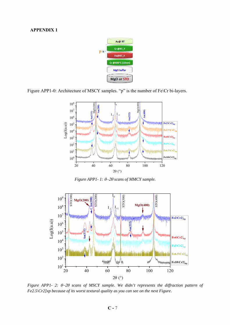
C - 7
APPENDIX 1
Figure APP1-0: Architecture of MSCY samples. “p” is the number of Fe\Cr bi-layers.
Figure APP1- 1: scans of MMCY sample.
Figure APP1- 2: scans of MSCY sample. We didn’t represents the diffraction pattern of Fe2.5\Cr2]xp because of its worst textural quality as you can see on the next Figure.
20 40 60 80 100 120
100
101
102
103
104
105
106
107
108
Log
(I(a
.u))
MgO
(200
)A
u(1
11)
Au
(222
)
I0
I-1I+1
MgO
(400
)
Au(
200)
Au
(400
)
2 (°)
Fe2\Cr2]xp
Fe2.5\Cr2]xp
Fe4\Cr2]xp
Fe5\Cr2]xp
Fe6.5\Cr2]xp
Fe10\Cr2]xp
Fe2\Cr2]xp
Fe4\Cr2]xp
Fe5\Cr2]xp
Fe6.5\Cr2]xp
Fe10\Cr2]xp
20 40 60 80 100 120101
102
103
104
105
106
107
108
109
Log
(I(a
.u))
Au(
111)
Au(
200)
I-1I+1
I0
Au
(222
)
2 (°)
ST
O(1
00)
MgO(200)
ST
O(2
00)
ST
O(3
00)
STO
(400
)
MgO(400)

C - 8
Figure APP1- 3: scans around the (200) peak of MMCY and on MSCY samples.
Figure APP1- 4: scans around the (200) peak of the multilayers. “” corresponds to the FWHM of each peak.
62 64 66 68
0
1800
3600
0
740
1480
0
1600
3200
0
2300
4600
0
70
140
0
5600
11200
I (c
ps)
(°)
[Fe10\Cr2]xp
Ii-1
Ii+1
Ii-1
Ii+1
Ii-1
I (c
ps) [Fe6.5\Cr2]xp
I (c
ps) [Fe5\Cr2]xp
I (c
ps) [Fe4\Cr2]xp
I (c
ps) [Fe2.5\Cr2]xp
I (c
ps) Fe2\Cr2]xp
STO \ MgO \ Cr_10 \ (Fe_Y\Cr_2)xp \ Au
62 64 66 68
0
2100
4200
0
1500
3000
0
1900
3800
0
640
1280
0
1400
2800
0
5700
11400I
(cps
)
(°)
[Fe10\Cr2]xp
Ii-1
Ii+1
Ii-1
Ii+1
Ii-1
I (c
ps) [Fe6.5\Cr2]xp
I (c
ps) [Fe5\Cr2]xp
I (c
ps) [Fe4\Cr2]xp
MgO \ MgO \ Cr_10 \ (Fe_Y\Cr_2)xp \ AuI
(cps
) [Fe2.5\Cr2]xp
I (c
ps) Fe2\Cr2]xp
30 31 32 33 34 35
0
2300
4600
0
2300
4600
0
2300
46000
1100
2200
0
1400
2800
0
6000
12000
I (c
ps)
(°)
[Fe10\Cr2]xp
= 0.30(1)°
=0.3067(6)°
I (c
ps) [Fe6.5\Cr2]xp
I (c
ps) [Fe5\Cr2]xp
= 0.871(2)°
=0.682(1)°
= 1.069(2)°
= 0.742(1)°
I (c
ps) [Fe4\Cr2]xp
I (c
ps) [Fe2.5\Cr2]xp
I (c
ps) Fe2\Cr2]xp
MgO \ MgO \ Cr_10 \ (Fe_Y\Cr_2)xp \ Au
30 31 32 33 34 350
1800
3600
0
730
1460
0
1500
3000
0
2500
5000
0
70
1400
5700
11400
I (c
ps)
(°)
= 0.3403(5)°
= 0.354(2)°
= 1.32(1)°
STO \ MgO \ Cr_10 \ (Fe_Y\Cr_2)xp \ Au
Fe2\Cr2]xp
[Fe2.5\Cr2]xp
[Fe4\Cr2]xp
[Fe5\Cr2]xp
[Fe6.5\Cr2]xp
[Fe10\Cr2]xp
I (c
ps)
= 0.742(1)°
I (c
ps)
= 0.796(1)°
= 0.789 (1)°
I (c
ps)
I (c
ps)
I (c
ps)

C - 9
Figure APP1- 5: Pole figures maps for MMCY and MSCY samples.
Figure APP1- 6: Stress analysis for MMCY and on MSCY samples.
0 20 40 60 800
20
40
60
80
0,000
625,0
1250
1875
2500
3125
3750
4375
5000
Imax
MgO\[Fe2 \ Cr2]x10
0 20 40 60 800
20
40
60
80
0,000
300,0
600,0
900,0
1200
1500
1800
2100
2400
2700
3000
3300
Imax
MgO\[Fe4\Cr2]x5
0 20 40 60 800
20
40
60
80
0,000
300,0
600,0
900,0
1200
1500
1800
2100
2400
2700
Imax
MgO\[Fe10 \ Cr2]x2
0 20 40 60 800
20
40
60
80
0,000
200,0
400,0
600,0
800,0
1000
1200
1400
Imax
STO\[Fe4 \ Cr2]x5
0 20 40 60 800
20
40
60
80
0,000
200,0
400,0
600,0
800,0
1000
1200
1400
1600
1800
2000
Imax
STO\[Fe10 \ Cr2]x2
0 20 40 60 800
20
40
60
80
0,000
400,0
800,0
1200
1600
2000
2400
2800
3200
3600
4000
Imax
STO\[Fe2 \ Cr2]x10
0,0 0,5 1,02,82
2,84
2,86
2,88
2,90
2,92
211220
222
130
[Fe10 \ Cr2]xp [Fe6.5 \ Cr2]xp
[Fe5 \ Cr2]xp [Fe4 \ Cr2]xp
[Fe2.5 \ Cr2]xp [Fe2 \ Cr2]xp
a
(A
)
a a//
Fe bulk
sin² ()
Cr bulk
(200)
MgO \ MgO \ Cr_10\ (Fe_Y\Cr_2)xp \ Au
0,0 0,5 1,02,82
2,84
2,86
2,88
2,90
2,92
200
211
220
222
130
[Fe10 \ Cr2]xp [Fe6.5 \ Cr2]xp
[Fe5 \ Cr2]xp [Fe4 \ Cr2]xp
[Fe2.5 \ Cr2]xp [Fe2 \ Cr2]xp
a a//
a
(A
)
Cr bulk
Fe bulk
STO \ MgO \ Cr_10\ (Fe_Y\Cr_2)xp \ Au
sin² ()
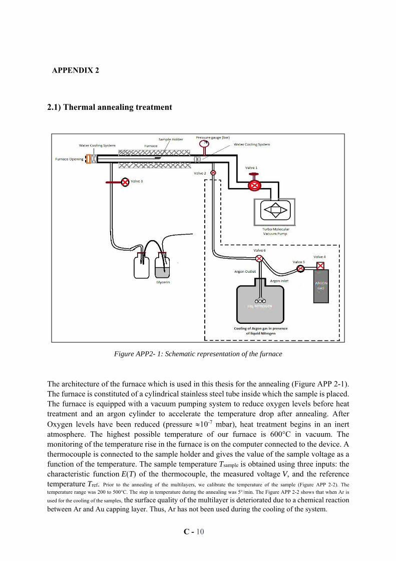
C - 10
APPENDIX 2
2.1) Thermal annealing treatment
Figure APP2- 1: Schematic representation of the furnace
The architecture of the furnace which is used in this thesis for the annealing (Figure APP 2-1). The furnace is constituted of a cylindrical stainless steel tube inside which the sample is placed. The furnace is equipped with a vacuum pumping system to reduce oxygen levels before heat treatment and an argon cylinder to accelerate the temperature drop after annealing. After Oxygen levels have been reduced (pressure 10-7 mbar), heat treatment begins in an inert atmosphere. The highest possible temperature of our furnace is 600°C in vacuum. The monitoring of the temperature rise in the furnace is on the computer connected to the device. A thermocouple is connected to the sample holder and gives the value of the sample voltage as a function of the temperature. The sample temperature Tsample is obtained using three inputs: the characteristic function E(T) of the thermocouple, the measured voltage V, and the reference temperature Tref. Prior to the annealing of the multilayers, we calibrate the temperature of the sample (Figure APP 2-2). The temperature range was 200 to 500°C. The step in temperature during the annealing was 5°/min. The Figure APP 2-2 shows that when Ar is
used for the cooling of the samples, the surface quality of the multilayer is deteriorated due to a chemical reaction between Ar and Au capping layer. Thus, Ar has not been used during the cooling of the system.

C - 11
Figure APP2- 2: (a) Example of the evolution of the sample annealing temperature with our furnace. (b) and (c) are the XRR analyses on the samples annealed at 450°C and 500°C with and without Ar
during the cooling.
2.2 Simulation of the XRD diffraction pattern
In order to study the effect of the variation of the lattice parameter of Fe and Cr on the position of the intensity of the main peak and satellites of the Fe\Cr multilayer, we simulated the diffraction spectra using Python code.
2.2.1) Effect of the modulation of the concentration and of the out-of-plane lattice parameter a⟘.
The Figure APP 2-3 is the diffraction patterns simulated with and without modulations of the concentration and/or a⟘. We see that only the main peak is observed when there is no modulation of a⟘ or when there is a variation of both the composition and the lattice parameter a⟘. The modulation of the concentration and a⟘ gives rise to one main peak surrounding by satellites. Besides, the intensity of the main peak increases and the position of the peaks are shifted compare to the case where there is no modulation. If there is only a modulation of the lattice parameter, satellites intensities are affected.
0 100 200 300 400 500 6000
100
200
300
400
500
Tsa
mpl
e (°C
)
Times (min)
No Ar With Ar With Ar during the cooling
T = 400°C(a)
0 1 2 3 4 5 6 70
1
2
3
4
5
6
Log
(I(
a.u.
))
2 (°)
With Ar No Ar
MSF10_T=450°C_4h(b)
0 1 2 3 4 5 6 70
1
2
3
4
5
6
Log
(I(
a.u.
))
2 (°)
With Ar No Ar
MSF10_T= 500°C_4h(c)

C - 12
Figure APP2- 3: scans with and without the modulation of the concentration and the out-of-plane lattice parameter.
2.2.2) Effect of the anomal correction on the XRD diffraction patterns.
The Figure APP 2-4 shows that the anomal correction affects slightly the intensities of satellites peaks. For the accuracy of the result, the anomal corrections on Cr and Fe have been considered during the simulation of the diffraction pattern.
Figure APP2- 4: scans showing the effect of the anomal correction.
62 64 66 68
0,0
0,2
0,4
0,6
0,8
1,0
Inte
nsit
y (a
.u.)
2 (°)
with conc. and a no conc. and a no conc. no a
MSF10
62 64 66 681E-4
0,001
0,01
0,1
1
Log
(I(
a.u.
))
no anom on Cr no anom on Fe no anom with anom
MSF10

C - 13
2.2.3) Effect of the lattice parameters difference on the XRD diffraction patterns.
The Figure APP 2-5 shows that the difference of the lattice parameter along the growth direction affects the intensities of the satellites in Fe\Cr multilayer.
Figure APP2- 5: scans showing the effect of the out-of-plane lattice parameter.
2.3) Monte Carlo simulations
The Figures APP 2-6 show the satellites evolution as a function of the time for the samples annealed at 400°C and 450°C. The data in red stand for Monte Carlo simulations and the blue data are obtained from experiment. The simulations follow the same trend that the experiment and different regimes of diffusion are also observed depending on the annealing time and temperature. At 400°C, the regime 1 is ended after 7000 hours whereas at 450°C, the regime 1 is observed up to 67 hours.
62 64 66 68
0,0
0,2
0,4
0,6
0,8
1,0
1,2L
og (
I(a.
u.))
2(°)
da 0 da 0.01 da 0.02 da 0.03 da 0.04 da 0.05
da : perp parameter differenceMSF10

C - 14
Figure APP2- 6: Experiment versus M.C. simulations for the samples annealed at 400°C and 450°C.

C - 15
2.4) XRR, AFM and MEB to check the surface morphology of Au capping layer during the annealing.
XRR on the MS10 annealed at 450°C
XRR was performed after each step of the annealing in order to control the surface roughness of the Au capping layer. When the multilayer is annealed for about 4h and 8h, large and well defined oscillations of Au capping layer are present. We observe also shift of the Kiessig oscillations to lower a dilatation of the lattice Fe lattice parameter due to the diffusion of Cr in Fe layers. For a long annealing, Au oscillations are not observed indicating a strong roughness of the Au layer. The 6th and 8th order superlattice peaks are visible. I have realized the rocking curves on the peak at 2on the XRR. The intensity of the peak from the w scan is almost identical to the one on the XRR at 2Thisconfirms that the intense peaks observed on the XRR patterns are indeed the superlattice peaks of the multilayer.
Figure APP2- 7: XRR image of the sample annealed at 450°C and at 400°C showing surperlattice peaks of the multilayers. scans measured on the 1rst order superlattice.
1 2 3 4 5 6100
101
102
103
104
105
R (l
og(I
(a.u
.))
(°)
450°C_116h 450°C_236h
1,2 1,3 1,4 1,5 1,6 1,70
25
50
75
100
125
150
I (cp
s)
450°C_236h
0,6 0,7 0,8 0,9 1,0
100
200
300
400
500
600
700
800
I (cp
s)
400°C_540h
1 2 3 4 5 610-1
100
101
102
103
104
105
R (l
og(I
(a.u
.))
(°)
400°C_540h

C - 16
AFM on the MS10 annealed at 450°C
AFM was used to determine the Au roughness. We see that the thickness roughness of Au capping layer increase from 1.6 to almost 5 nm when the sample is annealed for a long time. The annealing induces a strong coalescence and formation of isolated islands of Au layer.
Figure APP2- 8: Topography AFM images for the samples before and after annealing. The horizontal red line gives the height variation as a function of the vertical displacement.
SEM on the MS10 annealed at 450°C
Scanning Electron Microscopy image shows that the sample is not completely covered by the Au capping layer for long annealing time. Bright contrasts are for the Au capping layer and dark regions stand for the top Fe of the Fe\Au interface.
Figure APP2- 9: SEM image showing the morphology of Au capping layer when the sample is annealed at 400°C for about 540h

C - 17
scans on the MS10 annealed at 450°C
Rocking curves scan on the multilayer annealed at 450°C for different annealing times. We observe that the crystalline quality is highly improved for a long annealing time.
Figure APP2- 10: scans on the sample annealed at 450°C for different times. The bottom image shows is the plot of the FWHM deduced from the rocking curves versus the annealing time.
0 40 80 120 160 200 2400,40
0,45
0,50
0,55
0,60
0,65
FW
HM
(°)
t (h)
T= 450°C
30,5 31,0 31,5 32,0 32,5 33,0 33,5 34,0 34,5
0
1000
2000
3000
4000
5000
6000 avn rec 450°C_4h 450°C_8h 450°C_20h 450°C_28h 450°C_44h 450°C_68h 450°C_116h 450°C_164h 450°C_236h
I (cp
s)


Gladice Claire MAGNIFOUET TCHINDA
Etude des multicouches de Fe/Cr
épitaxiées : propriétés
structurales et magnétiques,
mécanisme d’interdiffusion
Résumé
Contexte et Objectif du projet de thèse Les alliages FeCr sont utilisés depuis longtemps comme matériaux de structure dans le cœur des réacteurs à
fission nucléaire. A une température de fonctionnement supérieure à 875K [1], les alliages Fe-Cr peuvent en effet
résister à des irradiations intenses présentes dans le cœur des centrales nucléaires. Depuis quelques décennies,
les systèmes Fe-Cr sont à nouveau étudiés pour les futures centrales nucléaires à fusion qui nécessiteront des
conditions d'irradiation et de température encore plus drastiques que les réacteurs à fission. Selon Zinkle et al,
le matériau de structure idéal pour les réacteurs nucléaires à fusion doit supporter 4 fois plus d'irradiation et une
température 3 fois plus élevée que les réacteurs nucléaires de génération 2 utilisés en France [2]. Pour ces raisons,
les matériaux de structure sont toujours étudiés et doivent être optimisés pour accélérer le développement de
réacteurs à fusion comme ITER (International Thermonuclear Experimental Reactor). Le matériau de structure
idéal doit présenter une densité élevée et uniforme de grains nanométriques qui servent simultanément
d'obstacles au mouvement de dislocations (pour une résistance mécanique élevée) et de centres de recombinaison
de défauts ponctuels (pour une guérison facile des dommages d’irradiation) [1], [2], [3], [4], [5].
Les alliages FeCr restent de bons candidats pour les réacteurs à fusion, car leurs propriétés d'auto-guérison des
défauts d'irradiation à haute température permettent [6]: (a) de conserver une bonne stabilité dimensionnelle (pas
de déformation et de gonflement) sous irradiation de neutrons, (b) de conserver des propriétés mécaniques
acceptables (résistance à la traction, ductilité, résistance au fluage) lors du vieillissement thermique et (c) de

préserver ces propriétés mécaniques dans des environnements corrosifs tels que les liquides de refroidissement
des réacteurs.
Une autre caractéristique des alliages Fe-Cr liée à ces propriétés mécaniques est le changement du signe de
l'ordre atomique à courte distance en fonction de la concentration de Cr dans l’alliage. En effet, le diagramme de
phase d’équilibre du système fer-chrome présente deux phases cubiques centrées (phases et ’) avec une lacune
de miscibilité (Figure 0-1). La présence d’une lacune de miscibilité signifie généralement que le paramètre
d'ordre à courte portée est positif (interaction répulsive entre les atomes de Fe et de Cr plus proches voisins) quel
que soit la concentration de l'alliage. Cependant, des mesures expérimentales de diffusion diffuse de neutrons
réalisées par Isabelle Mirebeau (Figure 0-2a) ont montré que dans la phase riche en Fe, ce paramètre d'ordre
est négatif pour les faibles concentrations de Cr (inférieures à 11 at.%), indiquant une tendance à l'ordre à courte
distance (interaction attractive entre les atomes de Fe et de Cr plus proches voisins). Pour comprendre ce
comportement singulier, des mesures magnétiques locales par diffusion diffuse de neutrons polarisés ont été
réalisées. Leurs résultats ont montré une variation relative considérable du moment du Cr pour les faibles
concentrations de Cr dans l’alliage alors que celle des atomes de Fe varie beaucoup moins pour la même gamme
de concentrations. Il est donc possible que l'évolution du paramètre d'ordre chimique à courte portée dans ces
alliages soit liée au comportement magnétique du Cr, ce qui justifie de l'étudier plus en profondeur dans le
système FeCr.
Figure 0-1 : Diagramme de phase du système Fe-Cr [8].
Figure 0-2 : Variation du paramètre d’ordre à courte distance [9] (à gauche) et des moment magnétiques μCr, µFe du Cr et du Fe [10] (à
droite) en fonction de la concentration “x” du Cr dans l’alliage Fe-Cr.
Mon travail de thèse s'est déroulé dans le cadre du projet franco-allemand MAGIKID (MAGnetism in Iron based
systems: Thermodynamic, KInetic and Defects). L'objectif de ce projet est de réunir des théoriciens (de Saclay,
Chatillon, Bochum et Düsseldorf) et des expérimentateurs (de l'IPCMS et de Münster) dans le but d'étudier les
effets du magnétisme et des défauts dans les systèmes Fe-M, avec M = Cr, Co et Mn. Dans ce projet, mon travail
a consisté à élaborer des échantillons modèles de multicouches Fe\Cr afin d'étudier la diffusion atomique et
l’influence des défauts étendus sur les propriétés magnétiques.

Historiquement, les multicouches Fe\Cr ont été étudiées pour leur magnétorésistance géante. Jusqu'à présent, la
plus grande attention a été portée aux multicouches polycristallines de Fe/Cr et au couplage magnétique des
couches de fer à travers les couches de chrome. Cependant, les questions posées dans le projet MAGIKID, à
savoir l'influence des interactions magnétiques (a) sur les propriétés thermodynamiques et cinétiques, (b) sur
l'évolution des défauts ponctuels et étendus dans les multicouches Fe\Cr, ainsi que, réciproquement, les effets de
la présence de défauts étendus sur les propriétés magnétiques locales, n'ont pas encore été traitées en détail.
Dans mon travail de thèse, des multicouches épitaxiées de Fe\Cr ont été préparées par pulvérisation cathodique
et par épitaxie par jet moléculaire (EJM). L’épitaxie par jet moléculaire permet d’élaborer des couches de hautes
qualités épiaxiales grâce à un vide de trois ordre de grandeur meilleur qu’en pulvérisation cathodique et grâce à
une vitesse de dépôt très lente. Cependant, en réduisant la vitesse atomique de dépôt, on arrive à avoir des
couches épitaxiées de qualité satisfaisante par pulvérisation cathodique.
Nous avons étudié les propriétés structurales et magnétiques afin de faire une corrélation entre ces propriétés.
L'objectif de ce travail était de déterminer la variation globale du moment magnétique aux interfaces Fe\Cr.
Quelques travaux ont déjà été réalisés par des théoriciens sur les multicouches Fe\Cr afin d’estimer la variation
de moment global aux interfaces Fe\Cr. Daniel Stoeffler et Michel Freyss [7] ont utilisé l'approximation de
liaison fortes pour comprendre l'influence des marches atomiques aux interfaces sur les propriétés magnétiques
du Fe induites par la nature antiferromagnétique du Cr. Ils ont également déterminé les valeurs des moments des
Cr et des Fe en fonction de leur position par rapport à une interface Fe\Cr parfaite (Figure 0-4).
Figure 0-4 : (a) Variation du moment magnétique dans la
multicouche Fe5/Cr10.5 où 5 et 10.5 représentent le nombre de
monocouches de Fe et de Cr. (b) Profil d’aimantation de 6
monocouches de Cr déposées sur le Fe(100).
À partir de la variation des moments de Fe et de Cr en fonction de la distance à l'interface, nous avons calculé la
variation globale de moment magnétique par atome d'interface (Figure 0-4). Elle est faible et négative (-
0.065 µB). Récemment, Chu-Chun Fu et al [8] ont calculé les moments sur les différents atomes près de l'interface
par DFT (Figure 0-7). En additionnant les contributions individuelles, nous obtenons une valeur positive du

changement de moment global à l'interface Fe\Cr d'environ 0.21µB par atome d'interface (Figure 0-8). Ces
résultats montrent que la variation du moment global aux interfaces Fe\Cr est relativement faible.
Figure 0-7 : Variation des moments magnétiques du Cr et du Fe au voisinage
d’une interface (100). Les calculs DFT ont été réalisés en considérant d’une part que
la structure magnétique du Cr est non-colinéaire (symboles verts) et d’autre part
antiferromagnétique (symboles noirs).
Figure 0-8 : Somme de ∆µCr et de ∆µFe en fonction de la position relative du Cr et du Fe à
l’interface Fe\Cr (déduit de la Figure 0-7).
Figure 0-9 : Variation du coefficient d’interdiffusion en fonction de la concentration du Cr dans l’alliage FeCr. Les lignes correspondent aux résultats expérimentaux obtenus par
radiotraceurs.
La deuxième partie de mon travail a consisté à étudier les mécanismes d'interdiffusion dans les multicouches
épitaxiées de Fe\Cr. Des travaux récents ont été menés sur les alliages FeCr par nos partenaires du CEA afin de
déterminer les paramètres influençant l'interdiffusion [9]. Ils ont déterminé par simulations Monte Carlo (MC)
des coefficients d'interdiffusion pour des températures comprises entre 850K et 1700K (Figure 0-9). Ils ont
également montré que le coefficient d'interdiffusion diminue considérablement avec la concentration de Cr dans
l'alliage, confirmant les résultats expérimentaux obtenus par radiotraceurs [10], [11] à très hautes températures.
Pour des températures inférieures à 900K, les mesures de diffusion par radiotraceurs ne sont pas possibles. Pour
répondre à ce problème, nous avons réalisé des multicouches Fe\Cr avec une excellente qualité épitaxiale pour
suivre l'interdiffusion et déduire les coefficients de diffusion pour les différents processus de diffusion observés
en combinant les résultats de diffraction des rayons X, les simulations Monte Carlo, la Microscopie Electronique
en Transmission (MET) et la tomographie par sonde atomique.

Les principaux objectifs de cette thèse étaient (i) d'élaborer des tri-couches et multicouches Fe\Cr avec de bonnes
propriétés structurales et magnétiques, (ii) d'estimer, si possible, le changement de moment dû à une interface
e\Cr, (iii) d’étudier les mécanismes d'interdiffusion dans les multicouches épitaxiales Fe\Cr. La texture, l'épitaxie
et la qualité cristalline ont été étudiées à l'aide d’un diffractomètre Rigaku 4 axes (mesures en mode , figures
de pôle et mesures en mode ) et du microscope électronique à transmission Jeol2100F. L'analyse des
déformations/contraintes a été réalisée par la méthode des sin²(). Cette méthode consiste à cartographier un
certain nombre de pics de la structure du matériau à différentes rotations et basculements de l’échantillon. A
partir des positions en 2 de tous les pics, on déduit les paramètres de maille hors-plan et dans le plan.
Connaissant le coefficient de Poisson du matériau, nous pouvons déduire le paramètre de réseau relaxé, le
gonflement et la contrainte bi-axiale de l’échantillon. Le SQUID et l'AGFM ont été utilisés pour les mesures
magnétiques. Les grandeurs recherchées ont été l’aimantation à saturation, les champs coercitifs et de saturation
dans le plan et en perpendiculaire, l’anisotropie dans le plan.
Résultats obtenus sur les tri-couches de Cr\Fe\Cr préparées
par pulvérisation cathodique
Pour les échantillons préparés par pulvérisation cathodique, nous avons joué sur la nature du substrat et la
température de dépôt du Fe pour optimiser la qualité épitaxiale des échantillons. Nous avons choisi les substrats
MgO et SrTiO3 (STO) d’orientation (100) du fait du faible désaccord entre les paramètres de maille des substrats
et du Cr tourné de 45°, ce qui favorise une épitaxie de bonne qualité. La couche de Cr a été déposée à chaud pour
permettre son épitaxie sur les substrats. La couche de Fe a été déposée à différentes températures (T = 40, 200,
300, 400°C) et la couche de protection de Cr à température ambiante. Nous avons utilisé les vitesses de dépôt de
2.1 Å/s et 1.1 Å/s pour le Cr et le Fe respectivement. Dans la suite, les échantillons sont nommés MT
(respectivement ST), où la première lettre M (respectivement S) correspond au substrat MgO (respectivement
STO) et T correspond à la température de croissance de la couche de Fe en degrés Celsius. L’épaisseur a été
maintenue constante à 35 nm pour la couche de Cr et 80 nm pour la couche de Fe. Des couches tampon seules
(MB et SB) ont été préparés et étudiées en comparaison.
Les principaux résultats sur les tri-couches de Cr\Fe\Cr pulvérisées sont les suivants :
♦ La texture, l'épitaxie et le degré d'orientation des cristaux sont améliorés lorsque la température de croissance
du Fe diminue. Des analyses MET ont été faites sur les échantillons SB et S200 ainsi que sur les échantillons
M300 et M40 et ont révélé que la couche tampon de Cr a une bonne qualité épitaxiale. Les mesures de diffraction

des rayons X réalisées sur les échantillons ST et MT ont montré que les échantillons sont texturés suivant la
direction [100] des substrats (mesures en mode . La meilleure texture a été obtenue pour les échantillons
S40 et M40 où on observe clairement des pics individuels (200) de Cr et de Fe. L'augmentation de la température
de croissance de Fe conduit à la formation d'un oxyde mixte (Fe,Cr) polycristallin en quantité non négligeable.
En mode nous avons observé la diminution de la largeur à mi-hauteur (FWHM) et l'augmentation de l'intensité
du pic de Bragg du Cr\Fe\Cr(200) lorsque la température de croissance du Fe ce qui atteste une amélioration de
la cristallinité. Les figures de pôle et les images de microscopie électronique à haute résolution montrent une
meilleure épitaxie et une croissance quasi cohérente dans le plan du Fe et du Cr lorsque la température de
croissance du Fe diminue. Le meilleur substrat est MgO(100).
♦ Les contraintes obtenues par la méthode sin²() sont bi-axiales comme prévu, et ce dans tous les échantillons.
Pour les échantillons M40 et S40, les paramètres dans le plan du Cr et du Fe sont égaux, ce qui signifie que la
croissance du Fe sur le Cr est cohérente confirmant ainsi les résultats de diffraction aux électrons. Cependant,
pour tous les échantillons, des contraintes de compression importantes sont générées et pourraient provenir de
facteurs externes tels que l’insertion d’impuretés d’oxygène et/ou d’atomes d’argon dans les couches. Afin de
suivre la distribution élémentaire aux interfaces et dans les couches, les spectres EELS ont été enregistrés et
analysés pour les échantillons M40 et M300 (Figure III-16).
Pour les interfaces Cr@400°C\Fe@T :
(a1) la concentration d'oxygène augmente à l'interface Cr@400°C\Fe pour l'échantillon M40 (Figure III-16 en
haut à gauche) et donne lieu à un profil gaussien de concentration en oxygène. Ceci atteste la présence des
couches d'oxyde de Cr et Fe. La présence d’un profil asymétrique à l’interface indique que la concentration en
oxygène est plus importante dans le Cr@400°C que dans le Fe@RT.
(a2) la teneur en oxygène est significativement plus élevée pour M40 que pour M300. Cette observation signifie
qu’un temps d’attente plus long entre la croissance des couches de Cr et de Fe est responsable de la quantité plus
élevée en oxygène à l'interface Cr@400°C\Fe@RT par rapport à celle de l’interface Cr@400°C\Fe@300°C
conduisant à la formation d'une couche d'oxyde de Cr et de Fe. Pour le M40, nous avons obtenu une couche
d'oxyde de 0.45 nm d’épaisseur avec une teneur élevée en oxygène et pour M300, la couche d'oxyde a une
épaisseur de 0.94 nm mais avec une concentration d'oxygène inférieure.
(a3) A l'interface Cr@400°C\Fe@T, nous avons obtenu un mélange du Cr et du Fe dont l’épaisseur est plus
importante pour M300 (4.4 nm) que pour M40 (2.9 nm) indiquant ainsi une possible diffusion du Fe dans le Cr
pendant le dépôt du fer et le refroidissement. L’épaisseur de près de 3 nm pour le dépôt de fer à température
ambiante montre qu’il y a aussi une diffusion du Fe dans le Cr par « atomic peening » [12], [13]. Cette méthode
de diffusion est un processus différent de celui du mécanisme d'interdiffusion qui est provoqué par le recuit de

l'échantillon. L’énergie supplémentaire des atomes y est apportée par les chocs avec les atomes déposés et
entraine aussi la présence de défauts dans les couches.
Figure III-16 : Variation de la concentration relative du Cr, du Fe et de O aux interfaces Cr\Fe (image au-dessus) et Fe\Cr (image en-dessous) des échantillons M40 et M300.
(b), (c) et (d) indiquent respectivement les couches de Cr@400°C, Fe@T et Cr@RT.
Pour les interfaces Fe@T\Cr@RT:
(b1) la concentration en oxygène est négligeable pour M40 contrairement à M300, ce qui est dû au long temps
d’attente entre la croissance des couches de Fe et de Cr.
(b2) nous observons une interface abrupte pour M40 lorsque les couches de Fe puis de Cr sont déposées à
température ambiante.
Dans les couches de Cr, la teneur d’oxygène varie de 7 à 11% dans la couche Cr@RT et de 3 à 6% dans celle
de Cr@400°C.
Nous avons aussi montré que les spectres EELS enregistrés de 200 eV à 800 eV ne montrent aucun seuil
d’ionisation de l’argon attendu à une énergie de 248 eV. Nous en avons conclu que l'argon, s'il est présent, a une
concentration bien plus faible que l’oxygène. La présence des contraintes en compression observées sur tous les
échantillons serait donc dû à la diffusion d'impuretés d'oxygène au niveau des sites interstitiels du réseau du
Cr@400°C après son épitaxie puisque la pression de base de la chambre de pulvérisation n'est pas très basse et
que le processus de refroidissement des films ne peut pas être accéléré. Les prédictions théoriques de D'Heurle
et Chason ont montré que l'oxygène a un effet considérable sur les contraintes produites dans les échantillons
déposés par pulvérisation cathodique [14]. En effet, pendant la croissance, les impuretés d'oxygène qui sont

adsorbées à la surface du film peuvent diffuser dans les sites interstitiels du réseau du film et conduire à une
contrainte de compression considérable à l'intérieur du film. Cette prédiction théorique est cohérente avec nos
résultats.
La forme des cycles d'hystérésis de la couche de Fe mesurés dans des configurations parallèles et
perpendiculaires dépend de la température de croissance du Fe et de la nature du substrat.
♦ Dans la configuration parallèle, seul M40 présente la forme M-H attendue pour du Fe déposé sur un substrat
MgO de surface (100). La diminution de la température de croissance du Fe entraîne une anisotropie magnéto-
cristalline dans le plan plus élevée grâce à une amélioration de l'épitaxie et à la présence d'une contrainte plus
faible dans les couches de Fe. La plus petite valeur du champ d’anisotropie Ha est obtenue lorsque le Fe est
déposé à 400°C. Sur ces échantillons, nous avons obtenu un champ coercitif Hc élevé que nous avons attribué
aux défauts d'oxygène qui piègent les parois de domaine. Une valeur de Ha petite et une valeur de Hc élevée sont
corrélées à une moins bonne qualité épitaxiale.
♦ Dans la géométrie perpendiculaire, les cycles d'hystérésis ont un champ coercitif très important lorsque l’oxyde
de chrome CrO2 ferromagnétique est formé dans la couche tampon de Cr. Shima et al ont obtenu des valeurs
similaires de Hc pour la croissance de CrO2 à 400°C sur les substrats LaAlO3 et Si [15]. La présence d’un « bias »
sur le cycle d'hystérésis de S40 est attribué à l'oxyde anti-ferromagnétique Cr2O3 qui se forme à l'interface Cr\Fe
pour l'échantillon S40 à cause d'un temps d’attente important entre la croissance de Cr@400°C et Fe@RT. Ces
résultats montrent qu'une très bonne épitaxie des tri-couches par pulvérisation cathodique est possible lorsque le
Fe est déposé à température ambiante sur des substrats MgO(100) et STO(100) avec une couche tampon de Cr.
Nous avons établi une corrélation entre les propriétés structurales et magnétiques. Cependant, la présence
d'oxydes métalliques aux interfaces Fe\Cr et la diffusion d'une faible quantité d'oxygène à l'intérieur des couches
rendent très difficile la détermination de la variation des moments aux interfaces Fe\Cr.
Résultats sur les tri-couches et multicouches préparées par
Epitaxie par Jet Moléculaire (EJM)
Nous avons montré qu'une très bonne épitaxie des tri-couches par pulvérisation cathodique est possible lorsque
la couche de Fe est déposée à température ambiante sur des substrats MgO(100) et STO(100) avec une couche
tampon de Cr déposée à 400°C. Cependant, en raison de l'inertie du porte-échantillon de pulvérisation et de la
qualité moyenne du vide dans la chambre de pulvérisation, la présence d'oxydes métalliques aux interfaces Fe\Cr

et la diffusion d'une faible teneur en oxygène à l'intérieur des couches rendent impossible la détermination de la
variation du moment global aux interfaces Fe\Cr. C'est pourquoi nous avons choisi de poursuivre la croissance
des tri-couches par EJM. L'un des avantages de cette technique est la faible pression du vide de base du système
qui est d'environ 3 ordres de grandeur inférieure à celle de notre chambre de pulvérisation, ce qui permet une
réduction significative de la pollution de l'échantillon par d'éventuelles impuretés de la chambre de croissance.
D'autres avantages sont la croissance plus lente et la possibilité de réaliser une caractérisation RHEED de la
surface cristalline des couches après chaque étape de dépôt. L'inconvénient de notre EJM est que la croissance
est beaucoup plus longue et spécialement laborieuse pour les multicouches. C'est pourquoi nos premières
tentatives de croissance des échantillons avaient utilisé la pulvérisation cathodique. Pour les échantillons élaborés
par EJM, nous avons choisi des substrats STO et MgO d’orientation (100) recouverts d’une couche tampon de
MgO de 20 nm d’épaisseur.
Rôle de la couche tampon de MgO
Nous avons mis en évidence l’effet de la couche tampon MgO en réalisant des tri-couches Fe\Cr\Fe sur les
substrats de MgO et de STO d’orientation (100) avec ou sans couche tampon de MgO. Sur MgO brut, le profil
DRX a montré un pic (200) intense de la tri-couche ce qui traduit une bonne épitaxie. Sur STO, une mauvaise
épitaxie est observée. En présence d’une couche tampon de MgO, la qualité épitaxiale des tri-couches est
légèrement améliorée sur le substrat MgO. Cependant, sur STO, nous observons une augmentation considérable
de l’amplitude du pic, ce qui signifie que la couche tampon de MgO est essentielle pour la reprise d’épitaxie des
tri-couches.
Tri-couches Fe\Cr\Fe
Pour les tri-couches Fe\Cr\Fe, les substrats ont été chauffés, puis recouverts de 20 nm de MgO qui permet de
réduire leur rugosité. La première couche de Fe a été déposée à température ambiante, puis recuite pour améliorer
ses propriétés structurales. Les clichés RHEED contiennent des tiges mieux définies après qu’avant le recuit.
Les couches de Fe et de Cr sont ensuite déposées à température ambiante afin d'éviter leur interdiffusion. On a
utilisé une couche de protection d’or dont l’épaisseur varie entre 5 et 10 nm. La vitesse de dépôt du Fe et du Cr
est de 0.2Å/s. Dans la suite, les tri-couches seront nommées TXFY, où X=M ou S correspond au substrat, F
signifie que la 1ere couche est du Fe et Y est l’épaisseur de chaque couche qui varie de 2 à 30 nm. Pour
comparaison, nous avons également préparé des échantillons de Fe@RT seules nommées BXFY.
Pour les tri-couches Fe\Cr\Fe préparées par EJM, les conclusions sont les suivantes :
♦ La texture, l'épitaxie et la mosaïcité sont améliorées lorsque l'épaisseur des tri-couches augmente. En effet,
nous avons fait une étude locale de la structure par MET pour une tri-couche de Fe\Cr\Fe préparée en section
transverse. L’image de microscopie en champ sombre nous a permis de voir un contraste entre les couches

(contraste de diffusion des électrons). Pour avoir l’information sur la qualité épitaxiale, nous avons fait des
clichés de diffraction et déduit la relation d’épitaxie dans le plan :
MgO(100)[010] // Fe(100)[011] // Cr(100)[011] // Fe(100)[011].
Cette relation indique que la direction dans le plan [011] du plan (100) de Cr (resp. Fe) est alignée avec la
direction [010] du plan de surface du substrat (100). Cette expression confirme la très bonne structure de nos
couches. L’étude globale de la structure des couches a été réalisée par diffraction des rayons X. On note qu’en
plus des pics des substrats, les réflexions (200) de la tri-couche sont aussi présentes, en accord avec les résultats
MET. Une dilatation de la courbe autour du pic (200) a révélé la présence de plusieurs pics due à des effets
d’interférences, de la modulation de paramètre de maille et de concentration du Fe et du Cr. Pour les tri-couches
de faible épaisseur, une meilleure résolution des profils sur STO a été observée, ce qui atteste que la croissance
sur STO est de meilleure qualité. Le meilleur substrat est le STO(100)\MgO.
♦ Les mesures en sin²() ont révélé que les déformations dans le plan sont bi-axiales et en tension pour tous les
échantillons. Avec l'augmentation de l'épaisseur, la contrainte bi-axiale et les déformations dans le plan sont
réduites sur les deux substrats. Lorsque la tri-couche est plus épaisse que 3x10 nm, les paramètres de réseau du
Cr et du Fe peuvent être mesurés séparément et une croissance cohérente du Cr sur du Fe est mise en évidence.
Pour les échantillons de faible épaisseur sur STO, une dilatation dans le plan du paramètre de réseau du Fe/Cr
est observée. Les analyses EELS sur une multicouche Fe\Cr déposée sur STO (Figure IV-37) nous ont permis
d’attribuer cette dilatation à la diffusion de strontium (Sr) dans la couche tampon de MgO, puis dans le Fe lors
du recuit de cette dernière. Ceci est cohérent avec les résultats de Zhang et al qui montrent que malgré le fait que
le Sr a un rayon ionique plus grand que le magnésium Mg [16], le coefficient de diffusion du Sr dans le MgO est
supérieur à celui du Ti dans le MgO.
Figure IV-37 : Cartographie EELS de la multicouche de [Fe10\Cr10]×5 déposée sur le STO(100). Les chiffres 10 et 5 correspondent respectivement à l’épaisseur de chaque couche en nm et au nombre de bi-couches Fe\Cr.

♦ Les cycles d'hystérésis des échantillons TMFY et TSFY ont été mesurés avec le champ externe le long du bord
de l'échantillon. La forme des cycles a permis de déduire que les moments magnétiques du Fe sont principalement
dans le plan du film avec un champ coercitif similaire à celui attendu dans le Fe massif. Dans les tri-couches les
plus minces sur le substrat MgO, on observe un champ coercitif important du fait de la rugosité importante du
MgO qui induit un effet « peau d’orange » (décrit par Louis Néel) aux interfaces MgO\Fe.
♦ Lorsque l'épaisseur augmente, le moment à saturation par unité de surface augmente linéairement. La pente
donne une aimantation à saturation du Fe proche de celle du Fe massif (Ms = 1720 emu/cm3) pour les tri-couches
sur MgO (Ms = 1705 ± 27 emu/cm3), alors qu'elle est légèrement plus élevée pour les tri-couches déposées sur
STO (Ms = 1813 ± 35 emu/cm3). Cette petite différence de Ms a été attribuée à la contrainte en tension (plus
élevée dans les échantillons TSFY que dans les échantillons TMFY) induisant une contribution de
magnétostriction plus élevée.
♦ Nous avons obtenu une contribution globale des interfaces Fe\Cr faible du fait de la combinaison de différents
phénomènes : (i) contributions des interfaces MgO\Fe et Fe\Au (formation d'une couche morte à l'interface
MgO\Fe?), (ii) magnétostriction dépendant de l'épaisseur et (iii) présence d'impuretés Sr dans la couche tampon
de Fe.
Pour tenter une meilleure détermination du changement de moment dû aux interfaces Fe\Cr, nous avons déposé
des tri-couches de Cr\Fe\Cr afin de s’affranchir de la contribution de (i) et de (iii).
Tri-couches Cr\Fe\Cr
Pour cette série de tri-couches, nous avons commencé la croissance avec une couche de Cr déposée à 400°C.
L'étude des échantillons déposés par pulvérisation cathodique a montré que cette température était optimale pour
le dépôt d'une couche tampon Cr. Après refroidissement à température ambiante, la bicouche Fe\Cr et la couche
de protection d’or ont été déposées. La vitesse de dépôt du Fe et du Cr est de 0.2 Å/s. Les clichés RHEED des
différentes couches ont montré que la qualité de la surface est bonne. Les tri-couches préparées sont TXCY, soit
XO\MgO_20 nm\Cr_Y\Fe_Y\ Cr_Y\Au_5 nm, avec Y = 10, 20, 40 nm.
Nous avons observé que les propriétés structurales et magnétiques se sont encore améliorées avec l'augmentation
de l'épaisseur des tri-couches, mais la qualité épitaxiale était moins bonne que dans les échantillons Fe\Cr\Fe. La
contribution des interfaces au moment global était également faible dans les tri-couches Cr\Fe\Cr.
Puisqu'il est difficile d'estimer efficacement la contribution d'interface dans les tri-couches, nous avons préparé
des multicouches Fe\Cr afin d'avoir une plus grande contribution relative des interfaces.

Multicouches Cr\(Fe\Cr)N
Les multicouches Fe\Cr ont été préparées dans les mêmes conditions que les tri-couches. Nous avons fixé
l'épaisseur de Cr de la multicouche Fe/Cr à 2 nm (pour maintenir un couplage ferromagnétique entre les couches
de Fe) et avons varié l'épaisseur des couches individuelles de Fe en gardant l'épaisseur totale de Fe égale à 20
nm. Une évolution linéaire de l'aimantation totale en fonction du nombre d'interfaces est attendue. C'est le cas
jusqu'à 16 interfaces. Néanmoins, nous avons obtenu une pente bien plus importante que prévu d'après les
résultats théoriques. La formation d'un alliage et/ou d'une couche morte peut expliquer cette observation.
Malgré la difficulté à déterminer la contribution de l'interface dans les systèmes Fe\Cr, nous avons clairement
établi une corrélation entre les propriétés structurales et magnétiques des échantillons préparés par EJM. Pour
améliorer la mesure elle-même, on pourrait utiliser des techniques de mesure plus adaptées comme les techniques
de Dischroïsme Circulaire Magnétique des électrons sur des couches fines. Nous avons fait des essais mais
n’avons pas obtenu de résultats concluants dans le cadre de cette thèse.
Résultats d'interdiffusion sur les multicouches de Fe\Cr
épitaxiées
Des multicouches épitaxiées de Fe\Cr ont été préparées afin d'étudier le mécanisme d'interdiffusion. Les
multicouches sont constituées de 5 bi-couches (environ 20 nm d'épaisseur), déposé par EJM sur le
STO(100)\MgO. Des mesures de diffraction des rayons X, des analyses au MET, de la tomographie par sonde
atomique et des simulations Monte Carlo ont été utilisées pour cette étude. Les échantillons ont été étudiés avant
recuit, après recuit isochrone à différentes températures et après recuits isothermes à plusieurs températures
choisies.
• Avant le recuit :
♦ Les caractérisations structurales par XRD montrent un pic (200) de Bragg central de Fe\Cr bien défini, de haute
intensité, entouré de nombreux satellites bien résolus. Cela est dû à la modulation de la concentration et à la
modulation des paramètres de réseau du Fe et du Cr dans la multicouche. Ce résultat est cohérent avec la
croissance épitaxiale. Les échantillons ont été coupés en 9 échantillons pour effectuer les différentes séries de
recuits. Tous les échantillons ont la même forme de courbe I() à la barre d’erreur près, ce qui indique que la
croissance de la multicouche est homogène. La faible mosaïcité obtenue est signe d'une bonne qualité cristalline
de la multicouche. Les contraintes dans le plan sont bi-axiales et en tension.

♦ Les images MET ont confitmé la succession à l'échelle nanométrique des couches de Fe et de Cr dans la
multicouche. L'épaisseur des couches de Fe et de Cr est d'environ 9.5 nm. La multicouche présente de
nombreuses dislocations, formées à l'interface STO\MgO et se propageant à travers les couches de Cr et de Fe.
La densité des dislocations est plus faible à l'interface MgO\Fe.
♦ Les profils en tomographie par sonde atomique ont révélé que les couches de Cr et de Fe sont de composition
homogène et la teneur en oxygène reste extrêmement faible (0.3% en moyenne) à travers l'échantillon. Les
atomes d'oxygène sont principalement localisés dans les couches de Cr près des interfaces Cr\Fe.
• Après un recuit de 4 h aux différentes températures T = 100, 200, 300, 400 et 500°C :
♦ Nous avons déterminé que la plage de température intéressante pour les études d'interdiffusion est [400°C,
500°C]. En effet, les balayages ont mis en évidence une diminution significative des intensités relatives
des satellites indiquant une variation de concentration à l'interface Fe\Cr ou dans les couches lorsque la
température de recuit est comprise entre [400 et 500°C].
♦ Dans cette plage de températures, les simulations de Monte Carlo révèlent une diffusion asymétrique de Cr et
de Fe (Cr diffuse rapidement dans Fe alors que Fe diffuse très lentement dans Cr) et une mobilité d'interface
associée.
♦ Pour un échantillon recuit à 500°C, nous avons observé que l'épaisseur des couches de Fe augmente alors que
l'épaisseur des couches de Cr diminue, confirmant une diffusion globale du Cr dans le Fe plus rapide que la
diffusion de Fe dans le Cr. Les analyses en sonde atomique tomographique ont montré que des défauts tels que
les inclusions de Fe et les oxydes de Cr sont présents dans les couches de Cr et que leur distribution est anisotrope.
Seules les couches de Cr sont oxydées du fait que les enthalpies libres de formation des oxydes de chrome sont
plus petites que celles des oxydes de fer comme le prévoient les diagrammes d'Ellingham pour les métaux [17].
Ces considérations thermodynamiques expliquent pourquoi les défauts se forment préférentiellement dans la
couche de Cr et non dans les couches de Fe.
• Après les recuits isothermes :
♦ La DRX a révélé une décroissance non régulière des intensités des satellites avec le temps de recuit indiquant
différents régimes de diffusion. Pour des recuits courts, nous avons observé une décroissance rapide et brutale
de l’intensité satellites qui devient beaucoup plus lente pour des recuits plus longs. Trois régimes de diffusion
sont observés expérimentalement :
Régime 0 : les défauts ponctuels en sursaturation formés lors de la croissance des couches et les dislocations
supplémentaires avec les vecteurs de Burger opposés sont éliminés. Pour ce régime cinétique, l'énergie
d'activation est inférieure à 1 eV, en accord avec les valeurs attendues pour la migration de défauts ponctuels
préformés.

Régime 1 : Des amas d'oxyde se forment dans les couches de Cr, via la diffusion de l'oxygène qui est très rapide
entre sites interstitiels.
Régime 2 : Diffusion du Fe le long des dislocations traversantes dans les couches de Cr pour relaxer les
déformations en tension dans la couche de Cr jusqu'à ce que ces « tuyaux » soient saturés en Fe et homogènes
en concentration avec la couche de Fe. Pour ces deux régimes cinétiques, l'énergie d'activation est supérieure à
4 eV et les temps de relaxation très similaires, contrairement aux régimes observés en Monte-Carlo (pour lesquels
l'énergie d'activation est d'environ 3 eV et les temps plus longs d’un ordre de grandeur).
Régime 3 : Diffusion en volume des atomes de Cr dans le Fe à partir des interfaces et des surfaces des tuyaux
jusqu'à saturation du Fe selon le diagramme de phase (agrandissement maximal des couches de Fe).
Régime 4 : Diffusion en volume des atomes de Fe dans le Cr loin des dislocations. Ce régime est très lent et
nécessiterait des temps de recuit très longs pour être observé expérimentalement ou pour être simulé par Monte
Carlo. Les interfaces reviennent vers les positions d'équilibre finales correspondant aux concentrations
d'équilibre dans les couches riches en Fe et en Cr.
Des mesures complémentaires sont nécessaires pour observer expérimentalement les deux derniers régimes.
Elles n'entrent pas dans le cadre de cette thèse. Par ailleurs, des mesures d’autres multicouches seront utiles pour
confirmer certains points : le rôle des dislocations (pour les multicouches équivalentes sur le substrat MgO où
les dislocations sont peu nombreuses), la validité du modèle de Cahn-Hilliard (dans des multicouches avec une
concentration moyenne dans la solution solide d’équilibre).
Figure V-28 : Variation de log() en fonction de 1/T du régime 0 (R0), régime 1 (R1), régime 2 (R2) et du régime 3 (R3). R3 est obtenu par simulation Monte Carlo. Pour une
meilleure visibilité, seuls les temps de relaxation des satellites d’ordre 1 sont représentés. Les énergies
activation des différentes cinétiques de diffusion sont déduites des pentes ( ligne rose, bleue, rouge et noire
pour R0, R1, R2 et R3 respectivement).
Figure V-18 : Cartographie des éléments de la multicouche montrant des inclusions de Fe (en violet)
dans la couche de Cr (en vert). Les oxygènes sont montrés en gros points jaunes.

Bibliographie
[1] S. J. Zinkle, “Advanced materials for fusion technology,” Fusion Engineering and Design, vol. 74, no. 1, pp. 31–40, Nov. 2005, doi: 10.1016/j.fusengdes.2005.08.008.
[2] R. Lindau et al., “Present development status of EUROFER and ODS-EUROFER for application in blanket concepts,” Fusion Engineering and Design, vol. 75–79, pp. 989–996, Nov. 2005, doi: 10.1016/j.fusengdes.2005.06.186.
[3] G. R. Odette, M. J. Alinger, and B. D. Wirth, “Recent Developments in Irradiation-Resistant Steels,” Annu. Rev. Mater. Res., vol. 38, no. 1, pp. 471–503, Aug. 2008, doi: 10.1146/annurev.matsci.38.060407.130315.
[4] S. Ukai and M. Fujiwara, “Perspective of ODS alloys application in nuclear environments,” Journal of Nuclear Materials, vol. 307–311, pp. 749–757, Dec. 2002, doi: 10.1016/S0022-3115(02)01043-7.
[5] R. L. Klueh, “Elevated temperature ferritic and martensitic steels and their application to future nuclear reactors,” International Materials Reviews, vol. 50, no. 5, pp. 287–310, Oct. 2005, doi: 10.1179/174328005X41140.
[6] P. Yvon and F. Carré, “Structural materials challenges for advanced reactor systems,” Journal of Nuclear Materials, vol. 385, no. 2, pp. 217–222, Mar. 2009, doi: 10.1016/j.jnucmat.2008.11.026.
[7] M. Freyss, “Proprietes magnetiques de systemes de basse dimensionnalite : determination de la structure electronique,” These de doctorat, Strasbourg 1, 1999.
[8] M. Yu. Lavrentiev, R. Soulairol, C.-C. Fu, D. Nguyen-Manh, and S. L. Dudarev, “Noncollinear magnetism at interfaces in iron-chromium alloys: The ground states and finite-temperature configurations,” Phys. Rev. B, vol. 84, no. 14, p. 144203, Oct. 2011, doi: 10.1103/PhysRevB.84.144203.
[9] O. Senninger, E. Martínez, F. Soisson, M. Nastar, and Y. Bréchet, “Atomistic simulations of the decomposition kinetics in Fe–Cr alloys: Influence of magnetism,” Acta Materialia, vol. 73, pp. 97–106, Jul. 2014, doi: 10.1016/j.actamat.2014.03.019.
[10] R. Braun and M. Feller-Kniepmeier, “Diffusion of chromium in α-iron,” phys. stat. sol. (a), vol. 90, no. 2, pp. 553–561, Aug. 1985, doi: 10.1002/pssa.2210900219.
[11] B. Jönsson, “Assessment of the Mobilities of Cr, Fe and Ni in bcc Cr-Fe-Ni Alloys.,” ISIJ International, vol. 35, no. 11, pp. 1415–1421, 1995, doi: 10.2355/isijinternational.35.1415.
[12] J. A. Thornton and D. W. Hoffman, “Internal stresses in titanium, nickel, molybdenum, and tantalum films deposited by cylindrical magnetron sputtering,” Journal of Vacuum Science and Technology, vol. 14, no. 1, pp. 164–168, Jan. 1977, doi: 10.1116/1.569113.
[13] J. A. Thornton and D. W. Hoffman, “Stress-related effects in thin films,” Thin Solid Films, vol. 171, no. 1, pp. 5–31, Apr. 1989, doi: 10.1016/0040-6090(89)90030-8.
[14] F. M. D’Heurle and J. M. E. Harper, “Note on the origin of intrinsic stresses in films deposited via evaporation and sputtering,” Thin Solid Films, vol. 171, no. 1, pp. 81–92, Apr. 1989, doi: 10.1016/0040-6090(89)90035-7.
[15] M. Shima, T. Tepper, and C. A. Ross, “Magnetic properties of chromium oxide and iron oxide films produced by pulsed laser deposition,” J. Appl. Phys., vol. 91, no. 10, p. 7920, 2002, doi: 10.1063/1.1451881.
[16] F. Zhang, A. M. Walker, K. Wright, and J. D. Gale, “Defects and dislocations in MgO: atomic scale models of impurity segregation and fast pipe diffusion,” J. Mater. Chem., vol. 20, no. 46, pp. 10445–10451, Nov. 2010, doi: 10.1039/C0JM01550D.
[17] B. Gleeson, “Thermodynamics and Theory of External and Internal Oxidation of Alloys,” in Shreir’s Corrosion, Elsevier, 2010, pp. 180–194.