
Structural and magnetic properties of Ru/Ni multilayers
35
Structural and magnetic properties of Ru/Ni multilayers 1 Structural and magnetic properties of Ru/Ni multilayers K Mergia 1 , A Tomou 2 , I Panagiotopoulos 2 ,F Ott 3 1 National Center for Scientific Research Demokritos, Institute of Nuclear Technology and Radiation Protection, Aghia Paraskevi, Athens, 15310, Greece 2 Dept. of Materials Science and Engineering, University of Ioannina, Ioannina 45110, Greece 3 Lab. Léon Brillouin CEA/CNRS, Centre d'Etudes de Saclay, France E-mail: [email protected] and [email protected] Abstract. Ru/Ni multilayers of different Ni thickness have been fabricated using magnetron sputtering. The structure of the multilayers has been determined by grazing incidence X-ray diffraction and X-ray reflectivity and their magnetic properties by magnetization and polarized neutron reflectivity measurements. The presence of Ru leads to the formation of a hexagonal Ni structure within interfacial layer ~1 nm above each Ru layer, while the rest of the Ni layer relaxes to the equilibrium fcc structure. The hcp Ni interfacial layer has a substantially increased cell volume is ferromagnetic with an atomic magnetic moment that increases with Ni layer thickness but remains lower than the value predicted from ab initio calculations. Keywords: hcp Ni, Ru/Ni multilayers, thin magnetic films, polarized neutron reflectivity PACS: 75.70.Cn Magnetic properties of interfaces (multilayers, superlattices, heterostructures), 68.65.Ac Multilayers, 61.05.cp X-ray diffraction, 61.05.fj Neutron reflectometry, 61.05.cm X-ray reflectometry (surfaces, interfaces, films) 1. Introduction Layered magnetic structures are now the basis for several technological applications from spin valves and magnetic random access memories to ultra high density recording hard disk media. In several applications as laminated recording media [1], flux concentrators [2], and various synthetic ferrimagnetic [3] and anti-ferromagnetic [4] structures, ruthenium is a usual choice as an interlayer material providing anti-ferromagnetic coupling between magnetic layers. Recently, it has been demonstrated that the incorporation of lattice mismatched or structurally incoherent layers between soft magnetic layers can lead to a significant reduction in saturation and coercive fields [5] due to suppression of stripe domains. Soft magnets as permalloys and iron-cobalt alloys crystallize in cubic structures and are thus structurally incompatible with hexagonal Ru. The existence of interfacial magnetically “dead” [6] or “weak” layers has been reported in NiFe/Ru multilayers [7] but their origin remains unclear. The interfacial moments of 3d elements as Ni depend sensitively on contributions, such as strain, chemical intermixing and surface structure and morphology [8]. It must be noted that growth on Ru layers can induce the hexagonal structure on layers that normally have a cubic structure as Fe [9]. Confidential: not for distribution. Submitted to IOP Publishing for peer review 24 September 2010 peer-00594971, version 1 - 23 May 2011 Author manuscript, published in "Journal of Physics D: Applied Physics 44, 7 (2011) 75001" DOI : 10.1088/0022-3727/44/7/075001
-
Upload
independent -
Category
Documents
-
view
5 -
download
0
Transcript of Structural and magnetic properties of Ru/Ni multilayers

Structural and magnetic properties of Ru/Ni multilayers
1
Structural and magnetic properties of Ru/Ni multilayers
K Mergia1, A Tomou2, I Panagiotopoulos2,F Ott3
1 National Center for Scientific Research Demokritos, Institute of Nuclear Technology and Radiation Protection, AghiaParaskevi, Athens, 15310, Greece2 Dept. of Materials Science and Engineering, University of Ioannina, Ioannina 45110, Greece3 Lab. Léon Brillouin CEA/CNRS, Centre d'Etudes de Saclay, France
E-mail: [email protected] and [email protected]
Abstract.Ru/Ni multilayers of different Ni thickness have been fabricated using magnetron sputtering.The structure of the multilayers has been determined by grazing incidence X-ray diffractionand X-ray reflectivity and their magnetic properties by magnetization and polarized neutronreflectivity measurements. The presence of Ru leads to the formation of a hexagonal Nistructure within interfacial layer ~1 nm above each Ru layer, while the rest of the Ni layerrelaxes to the equilibrium fcc structure. The hcp Ni interfacial layer has a substantiallyincreased cell volume is ferromagnetic with an atomic magnetic moment that increases with Nilayer thickness but remains lower than the value predicted from ab initio calculations.
Keywords: hcp Ni, Ru/Ni multilayers, thin magnetic films, polarized neutron reflectivityPACS: 75.70.Cn Magnetic properties of interfaces (multilayers, superlattices, heterostructures), 68.65.Ac Multilayers,61.05.cp X-ray diffraction, 61.05.fj Neutron reflectometry, 61.05.cm X-ray reflectometry (surfaces, interfaces, films)
1. IntroductionLayered magnetic structures are now the basis for several technological applications from spin valves
and magnetic random access memories to ultra high density recording hard disk media. In several
applications as laminated recording media [1], flux concentrators [2], and various synthetic
ferrimagnetic [3] and anti-ferromagnetic [4] structures, ruthenium is a usual choice as an interlayer
material providing anti-ferromagnetic coupling between magnetic layers. Recently, it has been
demonstrated that the incorporation of lattice mismatched or structurally incoherent layers between
soft magnetic layers can lead to a significant reduction in saturation and coercive fields [5] due to
suppression of stripe domains. Soft magnets as permalloys and iron-cobalt alloys crystallize in cubic
structures and are thus structurally incompatible with hexagonal Ru. The existence of interfacial
magnetically “dead” [6] or “weak” layers has been reported in NiFe/Ru multilayers [7] but their origin
remains unclear. The interfacial moments of 3d elements as Ni depend sensitively on contributions,
such as strain, chemical intermixing and surface structure and morphology [8]. It must be noted that
growth on Ru layers can induce the hexagonal structure on layers that normally have a cubic structure
as Fe [9].
Confidential: not for distribution. Submitted to IOP Publishing for peer review 24 September 2010pe
er-0
0594
971,
ver
sion
1 -
23 M
ay 2
011
Author manuscript, published in "Journal of Physics D: Applied Physics 44, 7 (2011) 75001" DOI : 10.1088/0022-3727/44/7/075001

2
In the following we report on the magnetic and structural properties of Ru/Ni multilayers. It is found
that the use of Ru interlayers leads to the formation of hexagonal Ni at the interfaces which disrupts
the coupling between the magnetic layers and thus can be used to reduce the saturation and coercive
fields.
2. Experimental
The Ru/Ni multilayered films have been deposited on Si wafers at room temperature using a MANTIS
magnetron sputtering system and employing Ni(3″ diameter) and Ru(2″) sources in confocal
geometry. The sources point at an angle of 45 degrees to the (horizontal) substrate plane, which is
rotated during the deposition. Prior to the deposition the chamber was evacuated to a base pressure of
7×10⁻⁵ Pa. The target to substrate distance is 15cm and the process gas (Ar) pressure during deposition
was 0.18 Pa. The Ni layers were deposited at a rate of 0.047 nm/sec by applying 50 W direct current
power and the Ru layers at a rate of 0.01 nm/sec by applying 120 W of radiofrequency power
(13.56 MHz). Multilayered samples of the nominal form Si/Ru(9 nm)/[Ru(1.5 nm)/Ni(t nm)]8 with tNi
from 0.8 to 4.5 nm were fabricated. In addition, Ni, Ru single layer samples and a Ru/Ni bilayer were
deposited under the same conditions.
The layer structure was assessed by X-ray reflectivity measurements (XRR) performed on a D8
Advance Bruker diffractometer using Cu-Kα radiation and parallel beam stemming from a Göbel
Mirror. The XRR measurements were analyzed using the Leptos software [10] which is based on
Parratt’s formalism. Structural depth sensitive information was obtained by the employment of grazing
incidence X-ray diffraction (GIXRD) measurements carried out on the D8 instrument. Different angles
of incidence were used either to get depth sensitive information or to distinguish between Bragg
reflections and multilayer structure satellites.
Magnetic measurements were carried out using a Lake Shore vibrating sample magnetometer (VSM).
The multilayer Ru/Ni magnetic structure was determined by Polarized Neutron Reflectivity (PNR)
measurements at PRISM instrument at Laboratoire Léon-Brillouin, CEA-Saclay. The PNR
measurements were performed at room temperature and with an in-plane external magnetic field of
0.275 T in order to magnetically saturate the samples and align the magnetic domains. The incident
neutron wavelength was 0.43 nm and the Q-range varied from 0.05 to 2.3 nm-1. The neutron spin-up
and spin-down reflectivities (R+, R-) were least squares fitted using the SimulReflec software [11].
peer
-005
9497
1, v
ersi
on 1
- 23
May
201
1

Structural and magnetic properties of Ru/Ni multilayers
3
3. Experimental results
3.1 X-ray diffraction measurements
In order to assess the crystal structure of the layers GIXRD measurements were carried out on all
Ru/Ni multilayers. The GIXRD patterns for all the Ru/Ni multilayers are presented in figure 1 together
with the spectrum from the 12 nm Ru single layer which was deposited under the same conditions.
The Ru hexagonal structure is clearly observed in the 12 nm single Ru layer. The sharp Bragg peaks
observed in the 50-52 degrees region stem from the single crystal Si substrate.
In the GIXRD patterns from Ru/Ni multilayers (figure 1), hexagonal Ru Bragg peaks arise from two
sources, the one attributed in the 9 nm Ru buffer layer (crosses in figure 1) and the other arising from
the Ru layers in the multilayer structure (stars in figure 1). This Bragg peak assignment is confirmed
by the GIXRD spectra of figure 2. These spectra have been received for decreasing values of the
incidence angleα . As the incidence angle decreases and approaches the angle for total reflection
(around 0.4 deg., see figure 5) the X-ray beam penetrates mostly the top layers and thus the XRD
spectrum arises from the top layers. Under these conditions, it is expected the Bragg reflections arising
from the Ru buffer layer to be relatively decreasing in comparison to the reflections of the Ru layers.
This is what is indeed observed in figure 2.
The remaining Bragg peaks are obviously arising from Ni and it is convenient for the discussion of the
methodology of their assignment to concentrate on the 4.5 nm Ni multilayer diffraction pattern in
figure 1. The two peaks at around 44.5 and 52 degrees can be attributed to cubic Ni with a lattice
constant of 0.354 nm, which is close to the cubic Ni bulk value. The Bragg peaks appearing in the 2θ
range 36 to 39 degrees can only be attributed to hexagonal Ni. In §3.2.2 from the analysis of the PNR
data it will be shown that the hexagonal Ni is formed at the Ru interface. The last unassigned peak is
that at around 45.5 degrees and its origin will be discussed in the next paragraph.
In order to tackle the ambiguities arising from peak overlap, several scans recorded at different
incidence angles,α , as well as conventional θθ 2− scans have been compared for each sample in
order to: (i) separate the contribution of the Ru buffer layer from those of the Ru/Ni multilayer
structure (discussed above), (ii) verify that the observed peaks are Bragg reflections as opposed to
satellites due to the multilayer periodicity and, (iii) acquire information for the crystallographic
texture. Examples of such scans are given in figures 2 and 3. Due to refraction effects the position of
the Bragg peaks depends on the incidence angle. As the incidence angle decreases the Bragg peaks are
shifted to higher angles [12]. However, the relative separation, θ∆(2 ) , of the Bragg peaks does not
depend on the incidence angle and this distinguishes the Bragg peaks from the satellite peaks of the
multilayer structure. An example of the independence of the θ∆(2 ) separation on the incidence angle
peer
-005
9497
1, v
ersi
on 1
- 23
May
201
1
4
is demonstrated in the inset of figure 3, where the separation θ∆(2 ) between the peak at around 41
deg. and the peak at around 44 deg. is displayed (□, (a)). The peaks assigned as Bragg peaks in figure
1 and discussed in the previous paragraph fulfill the requirement of constant θ∆ separation for
different angles of incidence. On the contrary, because the projection of the periodicity of the
compositional modulation of the multilayer along the scattering vector decreases, the angle separation
of a satellite peak with respect to a Bragg peak increases with increasing angle of incidence [13]. From
the data points (b) (●) in the inset of figure 3 we observe that the angle difference between the peak at
around 45.5 deg. and the Bragg peak at around 44 deg. increases with increasing angle of incidence.
Thus, the peak at around 45.5 deg. is not a Bragg peak but arises from the superlattice structure.
From the GIXRD patterns the hexagonal Ru and Ni layer lattice constants (a and c) were determined
(Table 1). For the calculation of the lattice constants profile matching was used to determine the exact
positions of overlapping nearby peaks and also the shift of the Bragg peaks due to refraction effects
has been taken into account. The lattice constants of the two hexagonal phases (Ru and Ni) as a
function of the nominal Ni layer thickness are presented in figure 4 with the corresponding bulk values
[14] shown as straight lines. The lattice constants of the single Ru layer (zero Ni thickness in figure 4)
are very close to the expected bulk values. The same holds for the cubic Ni structure (PDF: 65-2865).
Standard θ-2θ XRD scans show that Ni tends to grow with (111) texture, as typically occurs in
sputtered films of cubic metallic structures. The Ru layers have (002) texture for Ni thickness up to
1.5nm. This texture is lost for tNi above 3.0 nm and must be related to the mechanisms of relaxation of
interfacial misfit strains [15].
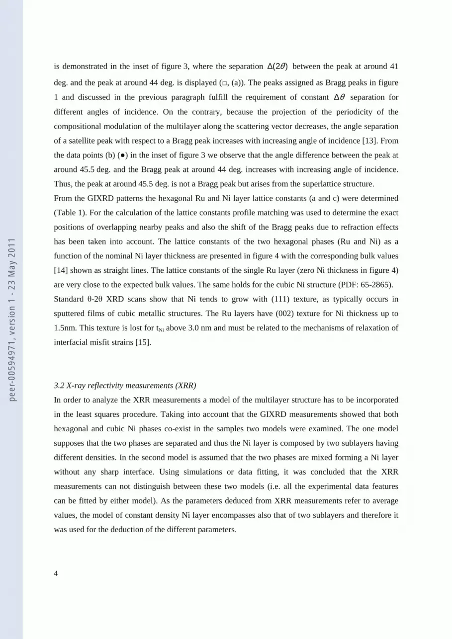
3.2 X-ray reflectivity measurements (XRR)
In order to analyze the XRR measurements a model of the multilayer structure has to be incorporated
in the least squares procedure. Taking into account that the GIXRD measurements showed that both
hexagonal and cubic Ni phases co-exist in the samples two models were examined. The one model
supposes that the two phases are separated and thus the Ni layer is composed by two sublayers having
different densities. In the second model is assumed that the two phases are mixed forming a Ni layer
without any sharp interface. Using simulations or data fitting, it was concluded that the XRR
measurements can not distinguish between these two models (i.e. all the experimental data features
can be fitted by either model). As the parameters deduced from XRR measurements refer to average
values, the model of constant density Ni layer encompasses also that of two sublayers and therefore it
was used for the deduction of the different parameters.
peer
-005
9497
1, v
ersi
on 1
- 23
May
201
1

Structural and magnetic properties of Ru/Ni multilayers
5
In figures 5 and 6 the XRR patterns for the [Ru(1.5 nm)/Ni(4.5 nm)]×8 and the
[Ru(1.5 nm)/Ni(1.0 nm)]×8 multilayer, respectively, are shown. The XRR measurements were
performed up to 2θ=8º and thus up to the 4th order Bragg peaks have been observed. The structural
parameters i.e. thickness, density and roughness of each layer, were determined by least squares fitting
of the calculated reflectivity values to the experimental data. The solid lines in figures 5 and 6 are the
least-squares fit to the XRR data. It can be observed that there is a very good agreement between the
experimental data and the fitted curve. Τhe structural data as determined by least square fit to the XRR
data are summarized in Table 1. The determined thickness values are close to the nominal ones. Also,
the mass densities obtained for the Ru and Ni layers are very close to the bulk ones.
3.3 Magnetometry
In figure 7 the hysteresis loops for a series of Si/Ru(9nm)/[Ru(1.5 nm)/Ni(t nm)]8 multilayers are
shown. A loss in magnetic moment as the Ni layers become thinner can be observed. The
measurements shown were performed with the applied field parallel to the substrate. In contrast to the
low saturation fields of the in-plane magnetization curves, when measured with the applied field
perpendicular to the film plane they have a linear part that saturates above 0.3 T. This shows the
presence of a typical easy-plane shape anisotropy. The films are polycrystalline and the substrate is
rotated during the deposition, so no anisotropy axis within the plane is expected.
Antiferromagnetic coupling between layers would manifest by an increase of the saturation field,
typical in synthetic antiferromagnets [16], not observed here. For a Ru thickness of 1.5 nm minimal
interlayer RKKY coupling is expected [17]. The structural incompatibility between the Ru and Ni
layers further reduces the possibility of exchange coupling between them. The only possible source of
interlayer coupling remains the dipolar interaction between the nickel layers as a result of the
correlated roughness at the interfaces [18]. However the magnetic data shown below imply that the
interlayer coupling is negligible as layering reduces both saturation and coercivity fields: In figure 8
the hysteresis loop of a [Ru(1.5 nm)/Ni(4.5 nm)]10 multilayer is compared to that of a Ni single layer
with the same total Ni thickness (45 nm). The comparison is done between two films with the same
total Ni thickness. There is a striking reduction in saturation (HS) and coercive fields (HC) by
interlayering with Ru: While the single layer Ni film has an HS of 600 Oe and HC of 160 Oe, these
drop to HS=67 Oe and HC=20 Oe in the multilayer. The shape of the loop of the single Ni layer is
characteristic of the existence of stripe domains [19]. It is known that in soft magnetic thin films above
a critical thickness an abrupt increase of coercivity and saturation field occurs (for instance in
permalloy 320 nm) which is related to the formation of stripe domains [20]. In single layer Ni films
sputtered under the same conditions with the Ru/Ni multilayers of our study this happens suddenly at
peer
-005
9497
1, v
ersi
on 1
- 23
May
201
1

6
40 nm. This low critical value must be attributed to the fact that the nickel tends to grow with the
(111), the easy magneto-crystalline anisotropy axis, perpendicular to the film plane. Of course with the
exception of very thin films (few monolayers) in which interface and elastic anisotropies prevail,
shape anisotropy dominates the magnetocrystalline one in Ni thin films, thus the magnetization is
expected to lie within the film plane. However, the conditions are favorable for the creation of stripe
domains [21] having a component of the magnetization out of the film plane. Therefore the
mechanism through which Ru interlayering makes the magnetic properties softer seems to be related
to the suppression of the formation of this domain structure due to decoupling. This has been proposed
as a practical way to retain the soft properties in applications that require thick ferromagnetic layers
[5]. The advantage is lost for thinner Ni layers below the critical thickness. For instance a Ni layer of
12 nm thickness has a HS=50 Oe and HC=25 Oe (figure 7).
3.4 Polarized Neutron Reflectometry
The PNR spectra were measured for the samples with Ni layer thickness of t=4.5, 3.0 and 1.5 nm. For
the fitting of the PNR data both a structural and a magnetic model have to be incorporated in the least
squares fitting. In order to reduce the number of parameters to be fitted by the least squares procedure
the structural parameters determined by XRR formed the basis for the structural models used for the
interpretation of the PNR spectra. GIXRD measurements have shown that cubic and hexagonal Ni
phases co-exist in all the samples. There are two possibilities, either the Ni two phases are mixed in
the Ni layer or the Ni layer is divided into two sublayers, one having cubic Ni and the other Ni
hexagonal structure. The second possibility was also considered for the modeling of the XRR data but
it was found that XRR can not distinguish between the two possibilities. However, existence of
separate cubic and hexagonal layers is physically reasonable and might result to different magnetic
structures. As PNR is a probe for the multilayer magnetic structure it could distinguish such a
formation. Thus, for the PNR measurements simulations of both of separate Ni layers (cubic and
hexagonal) or one type Ni layer have to be taken into account. As a result, the PNR data were least
square fitted considering two general models. In the first model (model A) it was assumed that the Ni
layer contains grains of both hexagonal and cubic structures and thus in the reflectivity simulations
can be presented as one layer with an average density and magnetization. In the second model (model
B) it was assumed that the hexagonal and cubic Ni form different layers. Since from the GIXRD
measurements it has been found that both cubic and hexagonal Ni structures are present in the samples
it can be assumed that the Ni hexagonal structure grows on the top of the hexagonal Ru. In all models
the magnetic moment, thickness and roughness of each Ni layer were parameters to be fitted. Also the
peer
-005
9497
1, v
ersi
on 1
- 23
May
201
1

Structural and magnetic properties of Ru/Ni multilayers
7
Ru layer magnetic moment was a fitted parameter thus magnetic and non magnetic Ru layer models
could be examined.
Figure 9 shows the PNR data from [Ru(1.5 nm)/Ni(4.5 nm)]×8 multilayer. The dashed line in figure 9
is the least square fitted curve for model A assuming that the Ru layers are non magnetic. It is
observed that model A fails to describe the region around the second Bragg peak. This is also observed
even if the Ru layer magnetic moment is a fitted parameter i.e. the least squares minimization
procedure results to a curve which does not describe the experimental data. This demonstrates that a
single Ni layer model is not consistent with the experimental PNR data.
In model B, initially, we let the magnetic moments of the three layers free to vary (i.e. as fitted
parameters m(Ru)≠0, m(Nihex)≠0 and m(Nicub)≠0) and for each PNR spectrum the three magnetic
moments are determined by a least squares fit. For each determined value its error is estimated. This
estimation is performed by simulating reflectivity curves for larger and smaller values than the least
squares one. The error limits are determined from an obvious discrepancy between the calculated and
the least squares curve. This procedure is in principle a sensitivity test which includes the statistical
errors and takes into account the situation in which the least squares minimum for a parameter is flat.
Using this procedure it has been found that the Ru magnetic moment and for the three measured
samples would be zero taking into account the errors. The last statement can be interpreted as there is
no observable difference between a reflectivity curve corresponding to non-magnetic Ru or to a Ru
with the small magnetic moment determined by the least squares fit (this applies to any set of Ni
moments). Thus, we may conclude that there is no measurable induced magnetic moment in Ru. As
the calculated reflectivity curve is not sensitive to small values of the Ru moment this was set equal to
zero and the magnetic moment of the two Ni layers was determined by the least squares fit (Table 2).
The fitted reflectivity curves for [Ru(1.5 nm)/Ni(4.7 nm)]×8 multilayer employing model B are the
solid lines in figure 9.
From Table 2 we observe that the Ni1 layer (on the top of Ru) has the smallest magnetic moment per
atom and thus we can infer that this layer corresponds to the hexagonal Ni. This is further corroborated
from the fact that the magnetic moment of the Ni2 layer (0.61 Bµ ) for the [Ru(1.5nm)/Ni(4.5nm)]x8
sample is similar to the bulk value of the cubic Ni (0.606 Bµ ). We also observe that the magnetic
moments for both cubic and hexagonal Ni layers increase as the thickness of the layer is increased.
Also the thickness of the hexagonal Ni layer on the top of the hexagonal Ru is around 1 nm and almost
independent of the nominal deposited Ni thickness. This thickness corresponds to about two deposited
Ni atomic layers and indicates the extent of Ru influence on the overlaid Ni.
peer
-005
9497
1, v
ersi
on 1
- 23
May
201
1

8
4. Discussion and ConclusionsThe actual thickness of Ni and Ru layers, their density and interfacial roughness as determined from
the XRR measurements are summarized in Table 1. It should be noted that these values represent the
averages of all eight bilayers of the multilayer structure. The density of Ni is almost constant for all
the multilayer samples, close to that of the bulk, except for the multilayer of Ni nominal thickness of
1.5 nm for which is around 13% lower than that of the bulk. For thin Ni layers (tNi <1.5 nm) the
density of the Ru layers is lower (5% than the bulk) a fact that may be related with the presence of the
Ni hexagonal layer on top of the Ru layer which results in a lower effective density of Ru and this
reduction is more pronounced for the thinner layers. For thicker Ni layers (tNi >1.5 nm) the Ru density
is that of the bulk corresponding to thinner Ru layers (≈1.7 nm). Therefore, we may conclude that the
thickness of the deposited Ni layer influences the structure of deposited Ru layers and that there is a
critical Ni layer thickness of 1.5 nm.
GIXRD measurements show that both cubic and hexagonal Ni phases are present in all the multilayer
samples. The lattice constant of the cubic Ni is very close to that of the bulk. PNR measurements show
that the hexagonal Ni lies on the top of the hexagonal Ru and its thickness is about 1 nm irrespectively
of the total thickness of the deposited Ni layer. It represents a critical thickness above which the
structure relaxes to the equilibrium bulk Ni structure. Some analogous examples can be found in Ni
nanoparticles. Bulk Ni as well as Ni nanoparticles naturally crystallize into face-centered-cubic (fcc)
with ferromagnetic properties. Preparation of an hexagonal close packed (hcp) Ni powder was
reported for the first time, via reduction of divalent Ni with a Potassium-Boron liquid alloy [22]. The
XRD pattern of the sample appears as the standard database card (no. 45–1027) with a=0.2653 nm and
c=0.4348 nm [14]. The hcp structure was found to be stable at temperatures up to 3800C above which
it transforms to fcc. Since this report hcp Ni or mixtures of fcc and hcp nanoparticles have been
fabricated by different routes [22,23,24,25,26,27,28]. The produced hcp Ni nanoparticles give a wide
range of lattice constants i.e. Ni(hcp)a varies from 0.250 to 0.265 nm and Ni(hcp)c from 0.397 to 0.435 nm
resulting in a c/a ratio variation from 1.59 to 1.64 [29] the ideal hcp being 1.633. The average (over all
the fabricated samples) lattice constant, ( )nm007.0257.0a)(
±=hcpNi
is within the lattice constants
found for the Ni (hcp) nanoparticles, whereas ( )nm01.045.0c)(
±=hcpNi
is higher. Therefore the
disturbed ~1 nm thick hcp Ni layer has on average similar)(
ahcpNi
lattice constant as the hcp
nanoparticles but its)(
chcpNi
lattice constant is substantially dilated resulting in the ratio c/a=1.75.
The large atomic volume expansion +18% is comparable to those of Fe observed in Fe/Ru
supperlattices ranging from +14% [9] to 25% [30] above the value of the ε-Fe and Cr in Cr/Ru
supperlattices [31].
peer
-005
9497
1, v
ersi
on 1
- 23
May
201
1

Structural and magnetic properties of Ru/Ni multilayers
9
Ab initio calculations [32] show that the total energy of the magnetic hcp Ni is about 0.02 eV/atom
(non-magnetic 0.05 eV/atom) higher than that of FM fcc Ni. Therefore the stabilization of the hcp Ni
phase can be attributed to impurity atoms introduced during the Ni nanoparticle fabrication or surface
effects. There is direct experimental evidence that the Ni hcp phase formation arises in systems with
high surface to volume ratio. Ni particles, prepared after chemical reduction of nickel salts by
activated sodium hydride in organic solvents, have an hcp structure in sizes smaller than 4 nm whereas
larger particles are fcc [33]. Hcp nickel islands grown on the (001) surface of MgO transform into the
normal fcc structure when the size of the islands exceeds a critical value of about 2.5 nm [34].
Furthermore proximity to hexagonal structures can stabilize hcp-Ni. For instance hcp-Ni film
produced by electrodeposition on a hcp Co single crystal reverted to fcc structure at room temperature
after being stripped from the substrate [35]. There is also an Ar-gas pressure window in magnetron
sputtering that favors the growth of stable single-phase hexagonal nanocrystalline Ni films [36]. It
may, thus, be concluded that the Ni deposited on the top of the Ru film takes the hcp structure as Ru-
Ni interface interaction makes hcp structure energetically more favorable than fcc. The critical
thickness of this pseudomorphic hcp-Ni growth is estimated to 1 nm as the hcp Ni layer thickness
determined by PNR is about 1 nm irrespectively of the deposited Ni layer total thickness. This result is
in concord with the observed hcp Fe structure in MBE deposited Fe/Ru [37] and the experimental
results on Fe/Ru multilayers prepared by high-vacuum electron-gun evaporation which show that even
a 0.6nm thick Ru layer can force to up 1.2nm thick Fe layer the hcp metastable structure [30]. In
Cr/Ru superlattices Cr layers thinner than 0.8 nm adopt a slightly distorted hcp structure, accompanied
by a large atomic volume expansion [31]. Therefore the hcp Ru constrains the as deposited Ni atoms
into the hcp structure. As the deposited Ni thickness increases above 1 nm, the Ru-Ni interface effect
is minimized and thus the bulk stable Ni fcc phase develops. The difference between hcp and fcc
structures can be thought of as a result of different stacking sequences of closed pack atomic layers
(ABAB vs ABCABC). Geometrically the transition hcp→fcc can be realized by a sliding on the (111)
fcc plane along the direction [112] fcc by a vector of 1/3 [112] fcc but the condition 2/fcchcp aa =
implied by this sliding mechanism is not obeyed by the lattice constants of hcp and fcc Ni. In fact
there is a lattice mismatch of 6% which probably gives rise to strain relaxation mechanisms within the
critical thickness of 1nm. The average coherence length [38] in the vertical direction (θ-2θ XRD
scans) varies from 9.6 to 12.8 nm for the thinnest and thickest multilayer, respectively. This shows that
the atomic layers sequence in the growth direction is correlated for about 2 (thickest multilayer) to 3.5
(thinner multilayer) bilayers which indicates some degree of columnar growth [39]. The in-plane
peer
-005
9497
1, v
ersi
on 1
- 23
May
201
1
10
diameter of the columns is around 10.6 nm as derived by applying the Scherrer formula to the GIXRD
peaks.
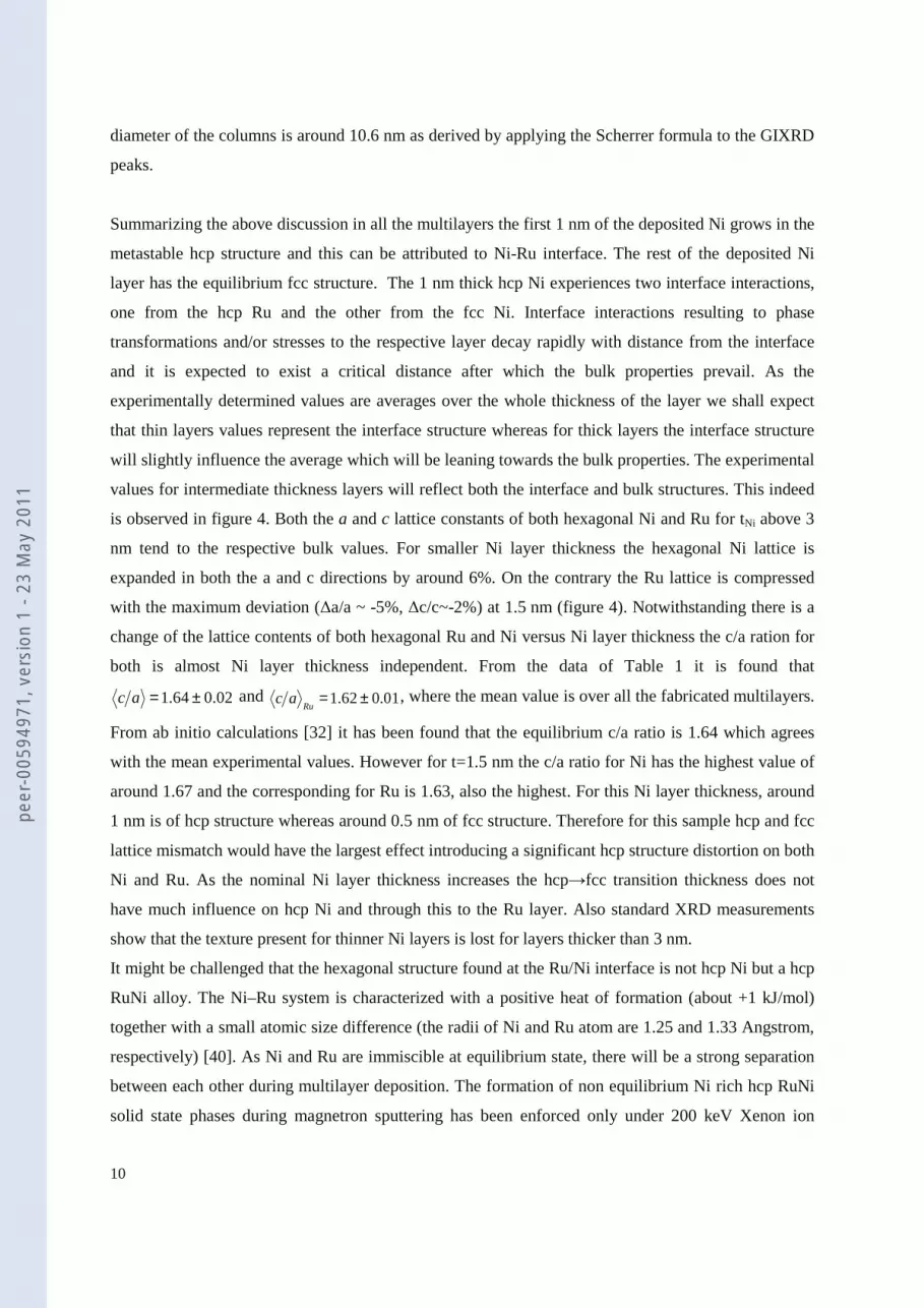
Summarizing the above discussion in all the multilayers the first 1 nm of the deposited Ni grows in the
metastable hcp structure and this can be attributed to Ni-Ru interface. The rest of the deposited Ni
layer has the equilibrium fcc structure. The 1 nm thick hcp Ni experiences two interface interactions,
one from the hcp Ru and the other from the fcc Ni. Interface interactions resulting to phase
transformations and/or stresses to the respective layer decay rapidly with distance from the interface
and it is expected to exist a critical distance after which the bulk properties prevail. As the
experimentally determined values are averages over the whole thickness of the layer we shall expect
that thin layers values represent the interface structure whereas for thick layers the interface structure
will slightly influence the average which will be leaning towards the bulk properties. The experimental
values for intermediate thickness layers will reflect both the interface and bulk structures. This indeed
is observed in figure 4. Both the a and c lattice constants of both hexagonal Ni and Ru for tNi above 3
nm tend to the respective bulk values. For smaller Ni layer thickness the hexagonal Ni lattice is
expanded in both the a and c directions by around 6%. On the contrary the Ru lattice is compressed
with the maximum deviation (∆a/a ~ -5%, ∆c/c~-2%) at 1.5 nm (figure 4). Notwithstanding there is a
change of the lattice contents of both hexagonal Ru and Ni versus Ni layer thickness the c/a ration for
both is almost Ni layer thickness independent. From the data of Table 1 it is found that
02.064.1 ±=ac and 01.062.1 ±=Ru
ac , where the mean value is over all the fabricated multilayers.
From ab initio calculations [32] it has been found that the equilibrium c/a ratio is 1.64 which agrees
with the mean experimental values. However for t=1.5 nm the c/a ratio for Ni has the highest value of
around 1.67 and the corresponding for Ru is 1.63, also the highest. For this Ni layer thickness, around
1 nm is of hcp structure whereas around 0.5 nm of fcc structure. Therefore for this sample hcp and fcc
lattice mismatch would have the largest effect introducing a significant hcp structure distortion on both
Ni and Ru. As the nominal Ni layer thickness increases the hcp→fcc transition thickness does not
have much influence on hcp Ni and through this to the Ru layer. Also standard XRD measurements
show that the texture present for thinner Ni layers is lost for layers thicker than 3 nm.
It might be challenged that the hexagonal structure found at the Ru/Ni interface is not hcp Ni but a hcp
RuNi alloy. The Ni–Ru system is characterized with a positive heat of formation (about +1 kJ/mol)
together with a small atomic size difference (the radii of Ni and Ru atom are 1.25 and 1.33 Angstrom,
respectively) [40]. As Ni and Ru are immiscible at equilibrium state, there will be a strong separation
between each other during multilayer deposition. The formation of non equilibrium Ni rich hcp RuNi
solid state phases during magnetron sputtering has been enforced only under 200 keV Xenon ion
peer
-005
9497
1, v
ersi
on 1
- 23
May
201
1

Structural and magnetic properties of Ru/Ni multilayers
11
mixing [40]. The lattice constants of the Ni75Ru25 formed by ion mixing compound (a=0.251 nm,
c=0.404 nm) or those determined by ab initio calculations (a=0.256 nm, c=0.417 nm) [41] are very
different than those determined here nmcnma 451.0,275.0 == . Formation of a Ni rich (>75 at %
Ni) hexagonal RuNi phase at the Ru/Ni interface cannot be excluded completely. Even in this case all
the aspects discussed and conclusions reached are valid and wherever Ni (hcp) is referred would need
to be replaced by Ni rich RuNi hcp phase.
The magnetic properties of the Ru/Ni multilayers have been determined by PNR and magnetization
measurements. The Ru from the PNR measurements is found within the experimental accuracy (±0.02
µB/atom) to be non magnetic. Also in Ni80Fe20/Ru multilayers was found by PNR that the maximal
polarization effect applied to the Ru layer is less than 0.03 µB [6].
The hcp Ni layer on the top of the Ru is ferromagnetic and the magnetic moment per atom increases
with Ni layer thickness and it is correlated with the increase of the magnetic moment of the fcc Ni
layer (Table 2). The hcp Ni magnetic moment even for the thickest layer (0.11 µB/atom) is much lower
than the value of 0.59 µB/atom obtained from ab initio calculations. However, there are divergent
reports on the magnetic properties of hcp nickel nanoparticles as being nonmagnetic [42],
antiferromagnetic [43] and ferromagnetic [44]. Ab initio calculations show that the energy difference
between magnetic and non-magnetic hcp Ni is around 0.05 eV/atom. Since the creation of the
metastable hcp instead of the equilibrium fcc phase involves energy difference of this order and as it
has been argued above this energy can be supplied by interfacial or impurity atoms effects, the variety
of the magnetic states observed in hcp Ni is not surprising. It has to be mentioned that the ab initio
calculations predict an hcp Ni magnetic or non-magnetic with atomic volume of around 11 Å3 whereas
the atomic volumes of our data (Table 1) are much higher. From Table (1) and (2) it is observed that
as the deposited Ni thickness increases the hcp Ni atomic volume decreases and also its magnetic
moment increases. Possibly at much thicker Ni layers, at which the interface effects would be
minimized, the equilibrium atomic volume and magnetic moment for hcp Ni might be attained.
Reduction of hcp Ni magnetic constant through the incorporation of Ru atoms [45, 46] seems unlikely
as it is difficult to explain the correlation of hcp Ni magnetic moment with Ni layer thickness.
Since the PNR measurements show that Ru is not magnetic and that the very thin hcp Ni layer has a
low magnetic moment, we may recognize that the bulk magnetization reflects the magnetic moment of
the fcc Ni. Therefore from the saturation magnetization values and the Ni actual thickness and density
derived from XRR, we can calculate the magnetic moment per atom in the Ni layer. These values are
presented in figure 10 together with the values determined from PNR. We observe that the agreement
between the macroscopically and microscopically determined values is very satisfactory taking also
peer
-005
9497
1, v
ersi
on 1
- 23
May
201
1

12
into account that the magnetic moments per atom derived from magnetization is underestimated as the
actual thickness of fcc Ni is smaller than the total Ni thickness measured by XRR. The variation of
fcc Ni magnetic moment versus film thickness presented in figure 10 is comparable to similar results
observed in other Ni multilayer systems [8]. From figure 10 we observe that for large Ni layer
thickness the magnetization tends to the bulk value of around 0.6 µB/atom.
Also the schema of the magnetization dependence on thickness indicates a magnetically dead layer of
around 0.6 nm present in all the samples. This dead layer is of course the hcp Ni which from PNR is
found to be around 1 nm for all measured samples and having a very low magnetic moment per atom
(Table 2).
In summary multilayers Si/Ru(9 nm)/[Ru(1.5 nm)/Ni(t nm)]8 with tNi from 0.8 to 4.5 nm have been
fabricated by magnetron sputtering. The structure of the deposited multilayers has been determined by
GIXRD and XRR and their magnetic structure by magnetometry and PNR measurements. About 1nm
of Ni on the top of Ru are of hexagonal structure irrespectively of the deposited Ni thickness. The rest
of the deposited Ni layer is of the equilibrium fcc structure. For thinner than 1.5 nm Ni layers the Ru
lattice is compressed whereas the hexagonal Ni lattice expanded. For thicker than 1.5 nm Ni layers the
lattice constants and densities of the layers approach the bulk values. The hcp Ni is ferromagnetic but
has a magnetic moment much lower than that expected from ab initio calculations. The magnetic
moment of fcc Ni increases with Ni layer thickness tending to the bulk value. The interfacial structural
incoherence offers a magnetic isolation that can be useful in preparing thick Ni films of low
coercivity.
References
[1] Margulies D.T, Supper N., Do H., Schabes M.E., Berger A., Moser A., Rice P.M., Arnett P., Madison M.,.Lengsfield B., Rosen H.,.Tang K, Polcyn A., Fullerton E.E., 2005 J. Appl. Phys. 97, 10N109[2] Trindade I.G., Oliveira J., Fermento Rui,. Bessa Sousa J, Cardoso S., Freitas P.P., Raghunathan A., and.Snyder J. E, 2009 IEEE Trans. Mag 45, 168[3]Janesky J., Rizzo N.D., Engel B.N., Tehrani S., 2004 Appl. Phys. Lett. 85, 2889[4] P.J. Bloemen et al., Phys. Rev. B 50, 13505 1994[5] Egelhoff W.F., Bonevich J., Pong P., Beauchamp C.R., Stafford G.R., Unguris J., and McMichael R.D.,2009 J. Appl. Phys. 105, 013921
[6] Hui-Chia Su, Jinn-Jer Peir, Chih-Hao Lee, Ming-Zhe Lin, Po-Tsang Wu, Huang J.C.A., Zin Tun, 2005Physica B 357 80–83[7] Ming-Zhe Lin, Hui-Chia Su, Chih-Hao Lee, J.C.A. Huang, 2007 Surf. Sci. 601 5707–5711[8] Vaz C.A.F., Bland J.A.C., Lauhoff G., 2008 Rep. Prog. Phys. 71 056501[9] De Santis M., De Andres A., Raoux D., Maurer M., Ravet M.F., Piecuch M., 1992 Phys. Rev. B. 46 15465[10] LEPTOS ver. 6.02 by Bruker-AXS GmbH 2002-2008[11] http://www-llb.cea.fr/prism/programs/simulreflec/simulreflec.html, version 1.9[12] Wroński S., Wierzbanowski K., Baczmański A, Lodini A., Braham Ch.and Seiler W., June 2009, PowderDiffraction Suppl. 24 S1
peer
-005
9497
1, v
ersi
on 1
- 23
May
201
1

Structural and magnetic properties of Ru/Ni multilayers
13
[13] Raghavendra Reddy V, Ajay Gupta, Anil Gome, Wolfram Leitenberger and Pietsch U; J. Phys.: Condens.Matter 21 2009 186002.[14] The database of the Joint Committee on Powder Diffraction Standards JCPDS of the International Centrefor Diffraction Data ICDD , includes the powder diffraction files PDF, no 45-1027 for hexagonal Ni and no 70-0274 for hexagonal Ru.[15] Milton Ohring in “Materials Science of Thin Films” (Second Edition) 2002 Elsevier Inc.ISBN: 978-0-12-524975-1, Chapter 8.[16] Burgler D.E., Grunberg P., Demokritov S.O.,. Johnson M.T, 2001 Handbook of Magnetic Materials,Vol.13, Chapter 1, Ed. K.H.J. Buschow, Elsevier Science[17] Bloemen P.J.H., Kesteren H.W.,. Swagten H.J.M,. de Jonge W.J.M, 1994 Phys. Rev. B 50 13505–13514[18] Tiusan C., Hehn M.; and Ounadjela K., 2002, Eur. Phys. J. B 26, 431.[19] Tutovan V., Velican N., 1973 Thin Solid Films, 15, 31-37.[20] Yutaka Sugita, Hideo Fujiwara, Takashi Sato, 1967, Appl. Phys. Lett. 10 229.[21] Holz A., Kronmuller H., 1969 Phys. Stat. Solid. 31, 787[22]Giovanni C., Giorgio C., Stefano E., Renzo G., Maurizio L., 1988 Mater. Lett. 7 47[23] Mia Y., Yuan D., Liu Y., Zhang J., Xiao Y.; 2005 Mater. Chem. Phys. 89, 359–361[24]Tzitzios V., Basina G., Gjoka M., Alexandrakis V., Georgakilas V., Niarchos D., Boukos N. and Petridis D.,2006 Nanotechnology 17 3750–3755[25] Rodriguez-Gonzalez V., Marceau E., Beaunier P., Che M., Train C., 2007 J. Solid State Chem. 180 22–30[26]Gong J., Wang L.L., Liu Y., Yang J.H., Zong Z.G., J. of Alloys and Compd 457 2008 6–9 [27] Mourdikoudis S., Simeonidis K., Vilalta-Clemente A., Tuna F., Tsiaoussis I., Angelakeris M.,. Dendrinou-Samara C, Kalogirou O.; 2009 J. Magn. Magn. Mat. 321 2723–2728[28] Yuanzhu Mi, Dingsheng Yuan, Yingliang Liu, Jingxian Zhang, Yong Xiao; 2005 Mater. Chem.Physics 89359–361[29] Xiaohua Luo, Yuanzhi Chen, Guang-Hui Yue, Dong-Liang Peng, Xuetao Luo, 2009 , J. Alloys Compd. 476864[30] Geng K.W., He T., Yang G.H., Pan F., 2004 J. Mag. Mag. Mater. 284 26–34[31] Albrecht M., Maret M. , Köhler J., Gilles B., Poinsot R., Hazemann J.L., Tonnerre J.M., Teodorescu C., andBucher E., 2000 Phys. Rev. Lett. 85 5344[32] He X., L. Kong T., and Liu B.X., 2005 J. Appl. Phys. 97 106107[33] Illy S., Tillement O., Machizaud F., Dubois J.M., Massicot F., Fort Y., Ghanbaja J., 1999 Philos. Mag. 791021[34] Tian W., Sun H.P., Pan X.Q., Yu J.H., Yeadon M., and Boothroy C.B.,. Feng Y.P, Lukaszew R.A.,Clarke R.; 2005 Appl. Phys. Lett. 86, 131915[35] Wright J.G., Goddard J., 1965 Philos. Mag. 11, 485[36] Poulopoulos P., Kapaklis V., Politis C., Schweiss P., Fuchs D., 2006, Journal of Nanoscience andNanotechnology, Vol.6, 3867–3870[37]Saint-Lager M.C., Raoux D., Brunel M., Piecuch M., Elkffim E. and Lauriat J.P, 1995, Phys. Rev. B 51 2446[38] Mary Beth Stearns, 1988 Phys. Rev. B 38 8109[39] Ming Xu, Guangming Luo, Chunling Chai, Zhenhong Mai, Wuyan Lai, Zhonghua Wu, Dewu Wang, 2000J Cryst Growth 212 291[40] Li X.Y., Li Z.F., Liu B.X., 2002 J. Alloys Compd. 334 167[41] He X., Kong L.T., Li J.H., Li X.Y., Liu B.X., 2006 Acta Mater 54 3375–3381[42] Chinnasamy C N, Jeyadevan B, Shinoda K, Tohji K, Narayanasamy A, Sato K and Hisano S, 2005 J. Appl.Phys. 97 10J309[43] Jeon Y T, Moon J Y, Lee G H, Park J and Chang Y, 2006 J. Phys. Chem. B 110, 1187[44] Han M, Liu Q, He J H, Song Y, Xu Z and Zhu J M, 2007 Adv. Mater. 19 1096[45]Parette G., Kajzar F, 1979, J. Phys. F: Metal Phys. 9, 1867[46]Madhav Rao L., Chakravarthy R., Jirak Z., and. Satya Murthy N.S; 1978 Phys. Rev. B 18, 6275–6282
peer
-005
9497
1, v
ersi
on 1
- 23
May
201
1
14
Tables
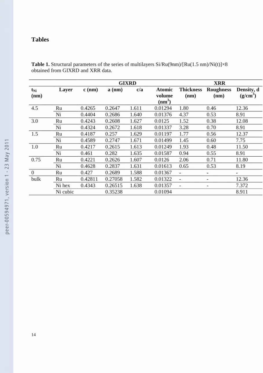
Table 1. Structural parameters of the series of multilayers Si/Ru(9nm)/[Ru(1.5 nm)/Ni(t)]×8obtained from GIXRD and XRR data.
GIXRD XRRtNi
(nm)Layer c (nm) a (nm) c/a Atomic
volume(nm3)
Thickness(nm)
Roughness(nm)
Density, d(g/cm3)
4.5 Ru 0.4265 0.2647 1.611 0.01294 1.80 0.46 12.36Ni 0.4404 0.2686 1.640 0.01376 4.37 0.53 8.91
3.0 Ru 0.4243 0.2608 1.627 0.0125 1.52 0.38 12.08Ni 0.4324 0.2672 1.618 0.01337 3.28 0.70 8.91
1.5 Ru 0.4187 0.257 1.629 0.01197 1.77 0.56 12.37Ni 0.4589 0.2747 1.671 0.01499 1.45 0.60 7.75
1.0 Ru 0.4217 0.2615 1.613 0.01249 1.93 0.48 11.50Ni 0.461 0.282 1.635 0.01587 0.94 0.55 8.91
0.75 Ru 0.4221 0.2626 1.607 0.0126 2.06 0.71 11.80Ni 0.4628 0.2837 1.631 0.01613 0.65 0.53 8.19
0 Ru 0.427 0.2689 1.588 0.01367 - - -bulk Ru 0.42811 0.27058 1.582 0.01322 - - 12.36
Ni hex 0.4343 0.26515 1.638 0.01357 - - 7.372Ni cubic 0.35238 0.01094 8.911
peer
-005
9497
1, v
ersi
on 1
- 23
May
201
1

Structural and magnetic properties of Ru/Ni multilayers
15
Table 2. Least square determined parameters from PNR data employing model B.
Layeredstructure
Thickness(nm)
Moment(µB)
Roughness(nm)
[Ru(1.5 nm)/Ni(4.5 nm)]×8Ru 1.55 0 0.82Ni1 0.96 0.11 ± 0.04 0.57Ni2 3.85 0.61 ± 0.02 0.79
[Ru(1.5 nm)/Ni(3.0 nm)]×8 Ru 1.52 0 0.99Ni1 1.22 0.08 ± 0.04 0.22Ni2 2.12 0.56 ± 0.02 0.50
[Ru(1.5 nm)/Ni(1.5 nm)]×8 Ru 1.89 0 1.03Ni1 0.78 0.04 ± 0.04 0.30Ni2 0.59 0.40 ± 0.02 0.45
peer
-005
9497
1, v
ersi
on 1
- 23
May
201
1

16
35 40 45 50 55 60 65
*
+
*
++
+
+
+
+
+
+
+
+
+
***
0
** Ru layer+ Ru buffer
o
I Ni hexagonalo Ni cubic
**
*
**
*
*
***
*
*
*
*
Ru(12 nm)
t=0.75 nm
t=1.0 nm
t=1.50 nm
t=3.00 nm
t=4.50 nm
Inte
nsity
(arb
.uni
ts)
2θ (deg)
sat0
+
Figure 1. Grazing incidence diffraction patterns for different Si/Ru(9 nm)/[Ru(1.5nm)/Ni(t nm)]8
multilayers. The bottom diffractogram is from a single Ru layer of 12 nm thickness, +: Ru bufferlayer. :٭ Ru layer in multilayer structure , o: Ni cubic : Ni hexagonal. The diffraction patterns of thedifferent samples are displaced along the y-axis (intensity) for clarity.
peer
-005
9497
1, v
ersi
on 1
- 23
May
201
1

Structural and magnetic properties of Ru/Ni multilayers
17
38 40 42 44 46 48 50
Inte
nsity
(arb
.uni
ts)
*
*
*+
+
*
*
*
*
*t=1.50 nm
+
+
+
+
+
40
10
α=0.470
2θ (deg)
+
*
Figure 2. Grazing incidence X-ray diffraction patterns from [Ru(1.5 nm)/Ni(1.5 nm)]×8multilayer for different values of incidence angle α . +: Ru buffer :٭ Ru layer in multilayerstructure. The different diffraction patterns are displaced along the y-axis (intensity) for clarity.
peer
-005
9497
1, v
ersi
on 1
- 23
May
201
1

18
38 40 42 44 46 48 50
0 5 10 15 20 25
1.2
1.4
1.62.8
3.0
3.2
∆θ(d
eg.)
α (deg.)
(a)
(b)
2θ (deg)
t=4.50 nm
α=θ
α=40
α=10
Inte
nsity
(arb
.uni
ts)
α=0.50
∆θ
Figure 3. Comparison of grazing incidence X-ray diffraction patterns of Ru(1.5 nm)/Ni(4.5 nm)]×8for different values of incidence angle α .The conventional θθ 2− scan is indicated as θα = . Inset(□, a): Separation between the Bragg peak at ~440 and the peak at ~410 as a function of the incidenceangle α ; (●, b): Separation between the Bragg peak at ~440 and the peak at ~45.50 as a function of theincidence angle α .
peer
-005
9497
1, v
ersi
on 1
- 23
May
201
1

Structural and magnetic properties of Ru/Ni multilayers
19
0 1 2 3 4 5 6
0.26
0.27
0.28
0.29
0 1 2 3 4 5 6
0.42
0.43
0.44
0.45
0.46
0.47
Ru bulk
Ru
latti
ceco
nsta
nts
(nm
)
Ni thickness (nm)
Ni
Ni bulk
α
Ni bulk
Ru bulkRu
Ni c
Figure 4. The lattice constants of hexagonal Ni (a-axis ●, c-axis ■), and Ru (a-axis ○, c-axis □) versusNi layer nominal thickness, in Ru/Ni multilayers. Solid lines are guide to the eye. At zero Ni thicknessthe values of the Ru single layer are presented with the symbols ♦ : a-axis and ◊: c-axis. The values ofthe bulk lattice constants, according to powder diffraction files (PDF) 45-1027 for hexagonal Ni andPDF: 70-0274 for Ru, are indicated by dotted and solid lines.
peer
-005
9497
1, v
ersi
on 1
- 23
May
201
1

20
0 1 2 3 4 5 6 7 810-6
10-5
10-4
10-3
10-2
10-1
100
Ref
lect
ivity
2θ (deg)
datafitted curve
Figure 5. X-ray reflectivity data from the sample [Ru(1.5 nm)/Ni(4.5 nm)]×8. Solid line: least squarefit to the data.
peer
-005
9497
1, v
ersi
on 1
- 23
May
201
1

Structural and magnetic properties of Ru/Ni multilayers
21
0 1 2 3 4 5 6 7 810-7
10-6
10-5
10-4
10-3
10-2
10-1
100
Ref
lect
ivity
2θ (deg)
datafitted curve
Figure 6. X-ray reflectivity data from the sample [Ru(1.5 nm)/Ni(1.0 nm)]×8. Solid line: leastsquare fit to the data.
peer
-005
9497
1, v
ersi
on 1
- 23
May
201
1

22
-600 -400 -200 0 200 400 600-1.5
-1.0
-0.5
0.0
0.5
1.0
1.5
t =0.8 nm
t =4.5 nm
t = 3 nm
t = 1.5 nm
Mag
netic
mom
entp
erar
ea(m
emu/
cm2 )
H (Oe)
Figure 7. Hysteresis loops of Si/Ru(9 nm)/[Ru(1.5nm)/Ni(t nm)]8 multilayers with t=4.5 nm(open circles), t=3 nm (solid circles), t=1.5 nm (open triangles), t=0.8 nm (solid triangles).Themeasurements were performed with the applied field in the film plane.
peer
-005
9497
1, v
ersi
on 1
- 23
May
201
1

Structural and magnetic properties of Ru/Ni multilayers
23
-1000 -800 -600 -400 -200 0 200 400 600 800 1000-2
-1
0
1
2
Ni (12nm)
Ni(45nm)[Ru(1.5 nm)/Ni(4.5 nm)]
10
Mag
netic
mom
entp
erar
ea(m
emu/
cm2 )
H (Oe)
Figure 8. Comparison of Hysteresis loops of a 45 nm Ni single layer (open circles), a 12 nm Ni singlelayer (solid triangles) and a [Ru(1.5 nm)/Ni(4.5 nm)]10 multilayer (solid circles). The measurementswere performed with the applied field in the film plane.
peer
-005
9497
1, v
ersi
on 1
- 23
May
201
1

24
0 1 2 3 4 5
10-6
10-5
10-4
10-3
10-2
10-1
100
R+
R-
R+, model BR-, model BR+, model AR-, model A
Ref
lect
ivity
θ (deg)
Figure 9. PNR data for the sample [Ru(1.5 nm)/Ni(4.5 nm)]×8. Experimental data: ○ for R+ (spin up)and ● for R- (spin down). Dashed line: model A. Solid line: model B.
peer
-005
9497
1, v
ersi
on 1
- 23
May
201
1

Structural and magnetic properties of Ru/Ni multilayers
25
0 1 2 3 4 5
0.0
0.2
0.4
0.6
VSMPNR
Ni thickness (nm)
Mag
netic
Mom
men
t(µ B
/ato
m)
Figure 10. Fcc Ni layer magnetic moment per atom versus actual Ni layer thickness, Nit , obtained byXRR●: data obtained from PNR measurements, �: data obtained from magnetization measurementsand reduced to a µB./atom using the Ni layer thickness and density obtained by XRR (Table 1).
Continuous line the equation NiB
(nm)(µ /atom) 0.6 1 exp
2.4
ty
= − −
peer
-005
9497
1, v
ersi
on 1
- 23
May
201
1

Figure 01 (Fig1.jpg)
peer
-005
9497
1, v
ersi
on 1
- 23
May
201
1
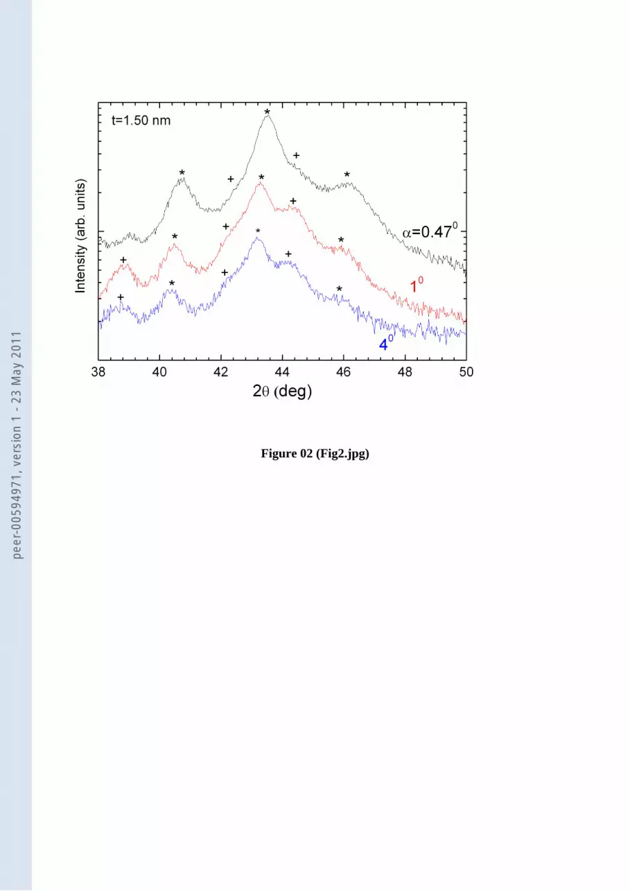
Figure 02 (Fig2.jpg)
peer
-005
9497
1, v
ersi
on 1
- 23
May
201
1

Figure 03 (Fig3.jpg)
peer
-005
9497
1, v
ersi
on 1
- 23
May
201
1

Figure 04 (Fig4.jpg)
peer
-005
9497
1, v
ersi
on 1
- 23
May
201
1

Figure 05 (Fig5.jpg)
peer
-005
9497
1, v
ersi
on 1
- 23
May
201
1

Figure 06 (Fig6.jpg)
peer
-005
9497
1, v
ersi
on 1
- 23
May
201
1
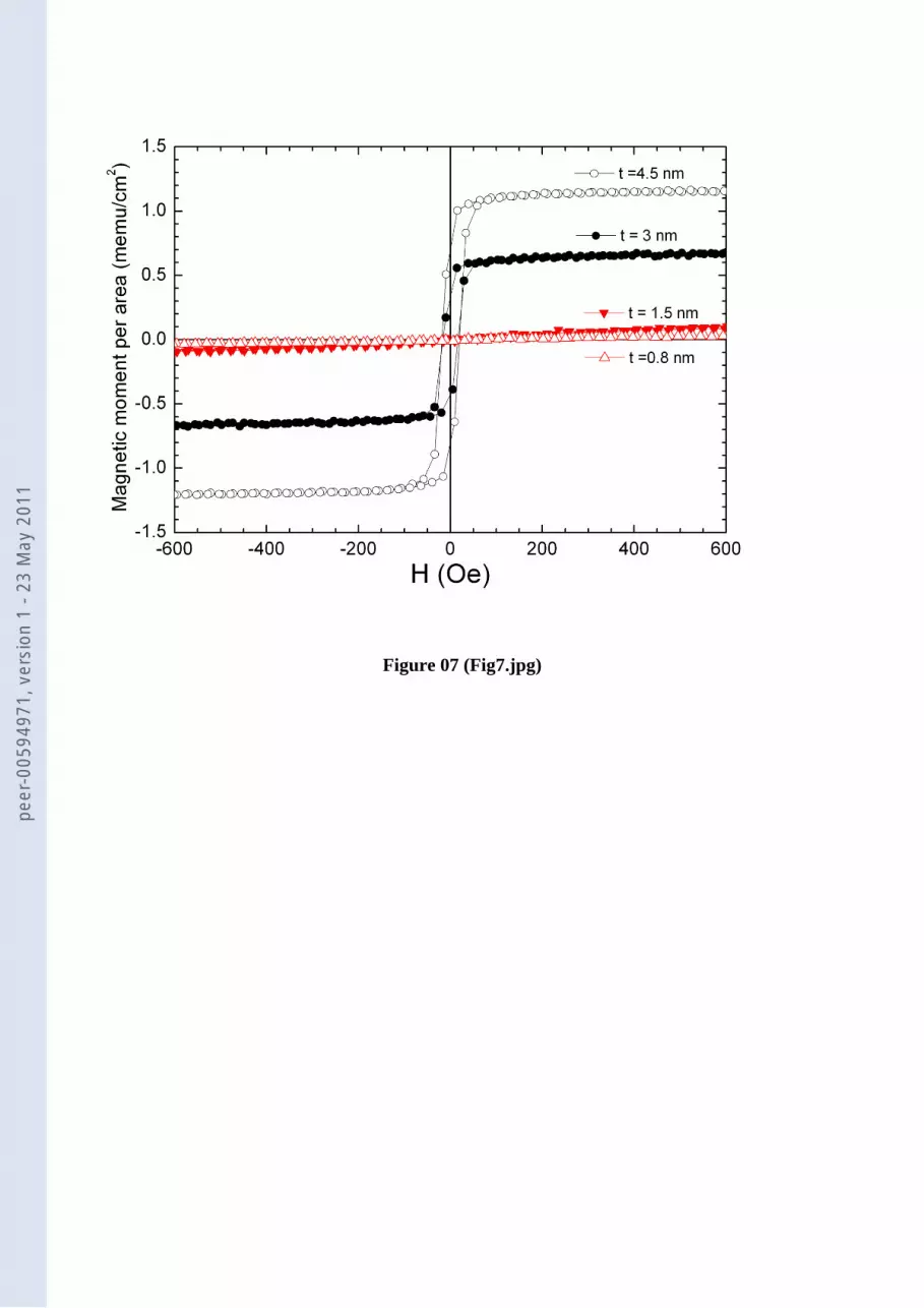
Figure 07 (Fig7.jpg)
peer
-005
9497
1, v
ersi
on 1
- 23
May
201
1

Figure 08 (Fig8.jpg)
peer
-005
9497
1, v
ersi
on 1
- 23
May
201
1

Figure 09 (Fig9.jpg)
peer
-005
9497
1, v
ersi
on 1
- 23
May
201
1
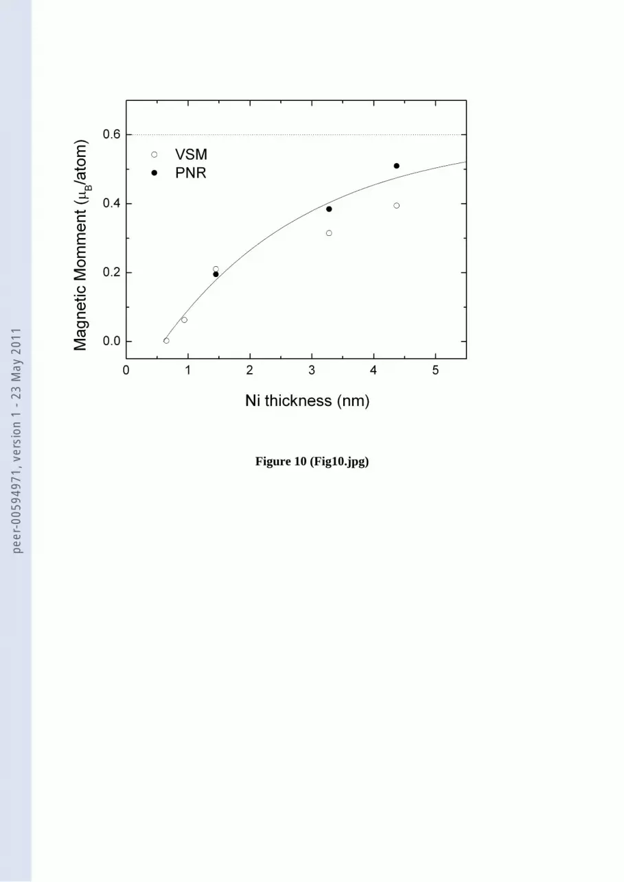
Figure 10 (Fig10.jpg)
peer
-005
9497
1, v
ersi
on 1
- 23
May
201
1