P8908 XXXYW - Diodes Incorporated
12
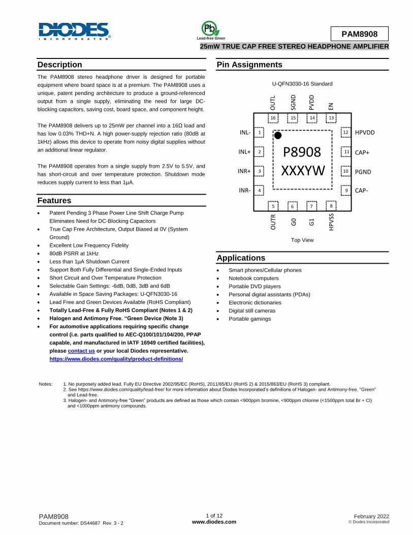
PAM8908 Document number: DS44687 Rev. 3 - 2 1 of 12 www.diodes.com February 2022 © Diodes Incorporated PAM8908 25mW TRUE CAP FREE STEREO HEADPHONE AMPLIFIER Description The PAM8908 stereo headphone driver is designed for portable equipment where board space is at a premium. The PAM8908 uses a unique, patent pending architecture to produce a ground-referenced output from a single supply, eliminating the need for large DC- blocking capacitors, saving cost, board space, and component height. The PAM8908 delivers up to 25mW per channel into a 16Ω load and has low 0.03% THD+N. A high power-supply rejection ratio (80dB at 1kHz) allows this device to operate from noisy digital supplies without an additional linear regulator. The PAM8908 operates from a single supply from 2.5V to 5.5V, and has short-circuit and over temperature protection. Shutdown mode reduces supply current to less than 1μA. Features Patent Pending 3 Phase Power Line Shift Charge Pump Eliminates Need for DC-Blocking Capacitors True Cap Free Architecture, Output Biased at 0V (System Ground) Excellent Low Frequency Fidelity 80dB PSRR at 1kHz Less than 1μA Shutdown Current Support Both Fully Differential and Single-Ended Inputs Short Circuit and Over Temperature Protection Selectable Gain Settings: -6dB, 0dB, 3dB and 6dB Available in Space Saving Packages: U-QFN3030-16 Lead Free and Green Devices Available (RoHS Compliant) Totally Lead-Free & Fully RoHS Compliant (Notes 1 & 2) Halogen and Antimony Free. “Green Device (Note 3) For automotive applications requiring specific change control (i.e. parts qualified to AEC-Q100/101/104/200, PPAP capable, and manufactured in IATF 16949 certified facilities), please contact us or your local Diodes representative. https://www.diodes.com/quality/product-definitions/ Pin Assignments U-QFN3030-16 Standard 8 7 6 5 12 9 10 11 13 14 15 16 INL+ INL- INR+ OUTR PGND HPVDD CAP+ CAP- P8908 XXXYW INR- 1 2 3 4 G0 G1 HPVSS OUTL SGND PVDD EN Top View Applications Smart phones/Cellular phones Notebook computers Portable DVD players Personal digital assistants (PDAs) Electronic dictionaries Digital still cameras Portable gamings Notes: 1. No purposely added lead. Fully EU Directive 2002/95/EC (RoHS), 2011/65/EU (RoHS 2) & 2015/863/EU (RoHS 3) compliant. 2. See https://www.diodes.com/quality/lead-free/ for more information about Diodes Incorporated’s definitions of Halogen- and Antimony-free, "Green" and Lead-free. 3. Halogen- and Antimony-free "Green” products are defined as those which contain <900ppm bromine, <900ppm chlorine (<1500ppm total Br + Cl) and <1000ppm antimony compounds.
-
Upload
khangminh22 -
Category
Documents
-
view
0 -
download
0
Transcript of P8908 XXXYW - Diodes Incorporated
PAM8908 Document number: DS44687 Rev. 3 - 2
1 of 12 www.diodes.com
February 2022 © Diodes Incorporated
PAM8908
25mW TRUE CAP FREE STEREO HEADPHONE AMPLIFIER
Description
The PAM8908 stereo headphone driver is designed for portable
equipment where board space is at a premium. The PAM8908 uses a
unique, patent pending architecture to produce a ground-referenced
output from a single supply, eliminating the need for large DC-
blocking capacitors, saving cost, board space, and component height.
The PAM8908 delivers up to 25mW per channel into a 16Ω load and
has low 0.03% THD+N. A high power-supply rejection ratio (80dB at
1kHz) allows this device to operate from noisy digital supplies without
an additional linear regulator.
The PAM8908 operates from a single supply from 2.5V to 5.5V, and
has short-circuit and over temperature protection. Shutdown mode
reduces supply current to less than 1µA.
Features
Patent Pending 3 Phase Power Line Shift Charge Pump
Eliminates Need for DC-Blocking Capacitors
True Cap Free Architecture, Output Biased at 0V (System
Ground)
Excellent Low Frequency Fidelity
80dB PSRR at 1kHz
Less than 1µA Shutdown Current
Support Both Fully Differential and Single-Ended Inputs
Short Circuit and Over Temperature Protection
Selectable Gain Settings: -6dB, 0dB, 3dB and 6dB
Available in Space Saving Packages: U-QFN3030-16
Lead Free and Green Devices Available (RoHS Compliant)
Totally Lead-Free & Fully RoHS Compliant (Notes 1 & 2)
Halogen and Antimony Free. “Green Device (Note 3)
For automotive applications requiring specific change
control (i.e. parts qualified to AEC-Q100/101/104/200, PPAP
capable, and manufactured in IATF 16949 certified facilities),
please contact us or your local Diodes representative.
https://www.diodes.com/quality/product-definitions/
Pin Assignments
U-QFN3030-16 Standard
8765
12
9
10
11
13141516
INL+
INL-
INR+
OUTR
PGND
HPVDD
CAP+
CAP-
P8908XXXYW
INR-
1
2
3
4
G0
G1
HPVSS
OUTL
SGND
PVDD
EN
Top View
Applications
Smart phones/Cellular phones
Notebook computers
Portable DVD players
Personal digital assistants (PDAs)
Electronic dictionaries
Digital still cameras
Portable gamings
Notes: 1. No purposely added lead. Fully EU Directive 2002/95/EC (RoHS), 2011/65/EU (RoHS 2) & 2015/863/EU (RoHS 3) compliant. 2. See https://www.diodes.com/quality/lead-free/ for more information about Diodes Incorporated’s definitions of Halogen- and Antimony-free, "Green"
and Lead-free. 3. Halogen- and Antimony-free "Green” products are defined as those which contain <900ppm bromine, <900ppm chlorine (<1500ppm total Br + Cl)
and <1000ppm antimony compounds.
PAM8908 Document number: DS44687 Rev. 3 - 2
2 of 12 www.diodes.com
February 2022 © Diodes Incorporated
PAM8908
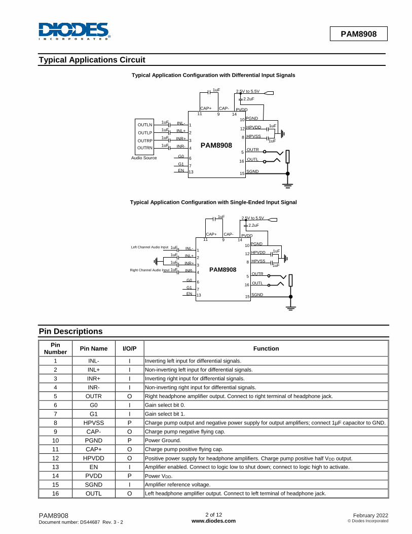
Typical Applications Circuit
Typical Application Configuration with Differential Input Signals
PGND
PAM8908
PVDD
1uFHPVDD
OUTR
OUTL
2.5V to 5.5V
2.2uF
14
12
5
16
10
1uFHPVSS8
SGND15
1uF INL- 11uF INL+ 2
1uF INR+ 31uF INR- 4
G0 6
G1 7EN 13
OUTLN
OUTLP
OUTRP
OUTRN
Audio Source
CAP+
11
1uF
9
CAP-
Typical Application Configuration with Single-Ended Input Signal
PGND
PAM8908
PVDD
1uFHPVDD
OUTR
OUTL
2.5V to 5.5V
2.2uF
14
12
5
16
10
1uFHPVSS8
CAP+
11
1uF
9
SGND15
CAP-
1uF INL- 11uF INL+ 2
1uF INR+ 31uF INR- 4
G0 6
G1 7EN 13
Left Channel Audio Input
Right Channel Audio Input
Pin Descriptions
Pin Number
Pin Name I/O/P Function
1 INL- I Inverting left input for differential signals.
2 INL+ I Non-inverting left input for differential signals.
3 INR+ I Inverting right input for differential signals.
4 INR- I Non-inverting right input for differential signals.
5 OUTR O Right headphone amplifier output. Connect to right terminal of headphone jack.
6 G0 I Gain select bit 0.
7 G1 I Gain select bit 1.
8 HPVSS P Charge pump output and negative power supply for output amplifiers; connect 1µF capacitor to GND.
9 CAP- O Charge pump negative flying cap.
10 PGND P Power Ground.
11 CAP+ O Charge pump positive flying cap.
12 HPVDD O Positive power supply for headphone amplifiers. Charge pump positive half VDD output.
13 EN I Amplifier enabled. Connect to logic low to shut down; connect to logic high to activate.
14 PVDD P Power VDD.
15 SGND I Amplifier reference voltage.
16 OUTL O Left headphone amplifier output. Connect to left terminal of headphone jack.
PAM8908 Document number: DS44687 Rev. 3 - 2
3 of 12 www.diodes.com
February 2022 © Diodes Incorporated
PAM8908
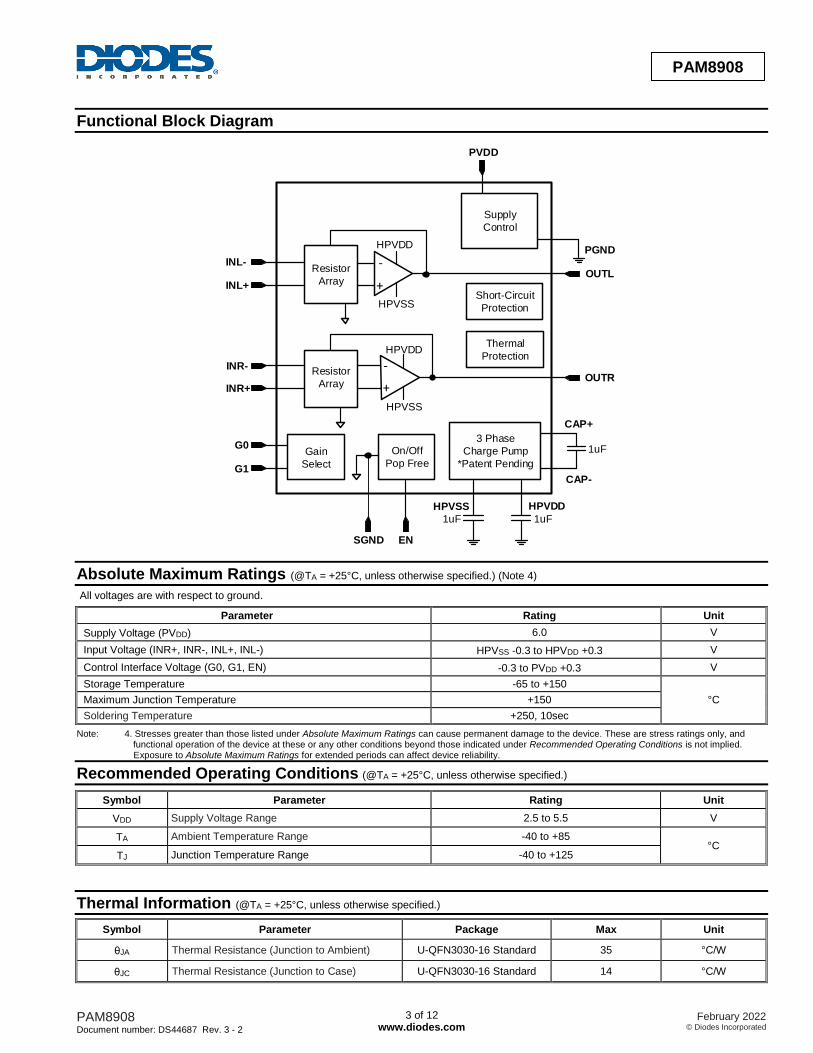
Functional Block Diagram
-
+
HPVDD
HPVSS
Resistor
Array
PVDD
Supply
Control
PGND
OUTL
Short-Circuit
Protection
Thermal
Protection
OUTR
CAP+
CAP-
1uF3 Phase
Charge Pump
*Patent Pending
On/Off
Pop Free
ENSGND
G1
G0
INR-
INR+
INL-
INL+
Resistor
Array
Gain
Select
HPVDD
1uF1uF
HPVSS
+
-
HPVSS
HPVDD
Absolute Maximum Ratings (@TA = +25°C, unless otherwise specified.) (Note 4)
All voltages are with respect to ground.
Parameter Rating Unit
Supply Voltage (PVDD) 6.0 V
Input Voltage (INR+, INR-, INL+, INL-) HPVSS -0.3 to HPVDD +0.3 V
Control Interface Voltage (G0, G1, EN) -0.3 to PVDD +0.3 V
Storage Temperature -65 to +150
°C Maximum Junction Temperature +150
Soldering Temperature +250, 10sec
Note: 4. Stresses greater than those listed under Absolute Maximum Ratings can cause permanent damage to the device. These are stress ratings only, and functional operation of the device at these or any other conditions beyond those indicated under Recommended Operating Conditions is not implied.
Exposure to Absolute Maximum Ratings for extended periods can affect device reliability.
Recommended Operating Conditions (@TA = +25°C, unless otherwise specified.)
Symbol Parameter Rating Unit
VDD Supply Voltage Range 2.5 to 5.5 V
TA Ambient Temperature Range -40 to +85 °C
TJ Junction Temperature Range -40 to +125
Thermal Information (@TA = +25°C, unless otherwise specified.)
Symbol Parameter Package Max Unit
θJA Thermal Resistance (Junction to Ambient) U-QFN3030-16 Standard 35 °C/W
θJC Thermal Resistance (Junction to Case) U-QFN3030-16 Standard 14 °C/W
PAM8908 Document number: DS44687 Rev. 3 - 2
4 of 12 www.diodes.com
February 2022 © Diodes Incorporated
PAM8908
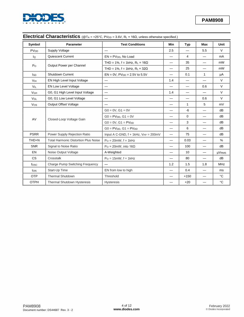
Electrical Characteristics (@TA = +25°C, PVDD = 3.6V, RL = 16Ω, unless otherwise specified.)
Symbol Parameter Test Conditions Min Typ Max Unit
PVDD Supply Voltage — 2.5 — 5.5 V
IQ Quiescent Current EN = PVDD, No Load — 4 — mA
PO Output Power per Channel THD = 1%, f = 1kHz, RL = 16Ω — 35 — mW
THD = 1%, f = 1kHz, RL = 32Ω — 25 — mW
ISD Shutdown Current EN = 0V, PVDD = 2.5V to 5.5V — 0.1 1 µA
VIH EN High Level Input Voltage — 1.4 — — V
VIL EN Low Level Voltage — — — 0.6 V
VGH G0, G1 High Level Input Voltage — 1.4 — — V
VGL G0, G1 Low Level Voltage — — — 0.6 V
VOS Output Offset Voltage — — 1 5 mV
AV Closed-Loop Voltage Gain
G0 = 0V, G1 = 0V — -6 — dB
G0 = PVDD, G1 = 0V — 0 — dB
G0 = 0V, G1 = PVDD — 3 — dB
G0 = PVDD, G1 = PVDD — 6 — dB
PSRR Power Supply Rejection Ratio Input A C-GND, f + 1kHz, VPP = 200mV — 75 — dB
THD+N Total Harmonic Distortion Plus Noise PO = 20mW, f = 1kHz — 0.03 — %
SNR Signal to Noise Ratio PO = 20mW, into 16Ω — 100 — dB
EN Noise Output Voltage A-Weighted — 10 — µVRMS
CS Crosstalk PO = 15mW, f = 1kHz — 80 — dB
fOSC Charge Pump Switching Frequency — 1.2 1.5 1.8 MHz
tON Start-Up Time EN from low to high — 0.4 — ms
OTP Thermal Shutdown Threshold — +150 — °C
OTPH Thermal Shutdown Hysteresis Hysteresis — +20 — °C
PAM8908 Document number: DS44687 Rev. 3 - 2
5 of 12 www.diodes.com
February 2022 © Diodes Incorporated
PAM8908
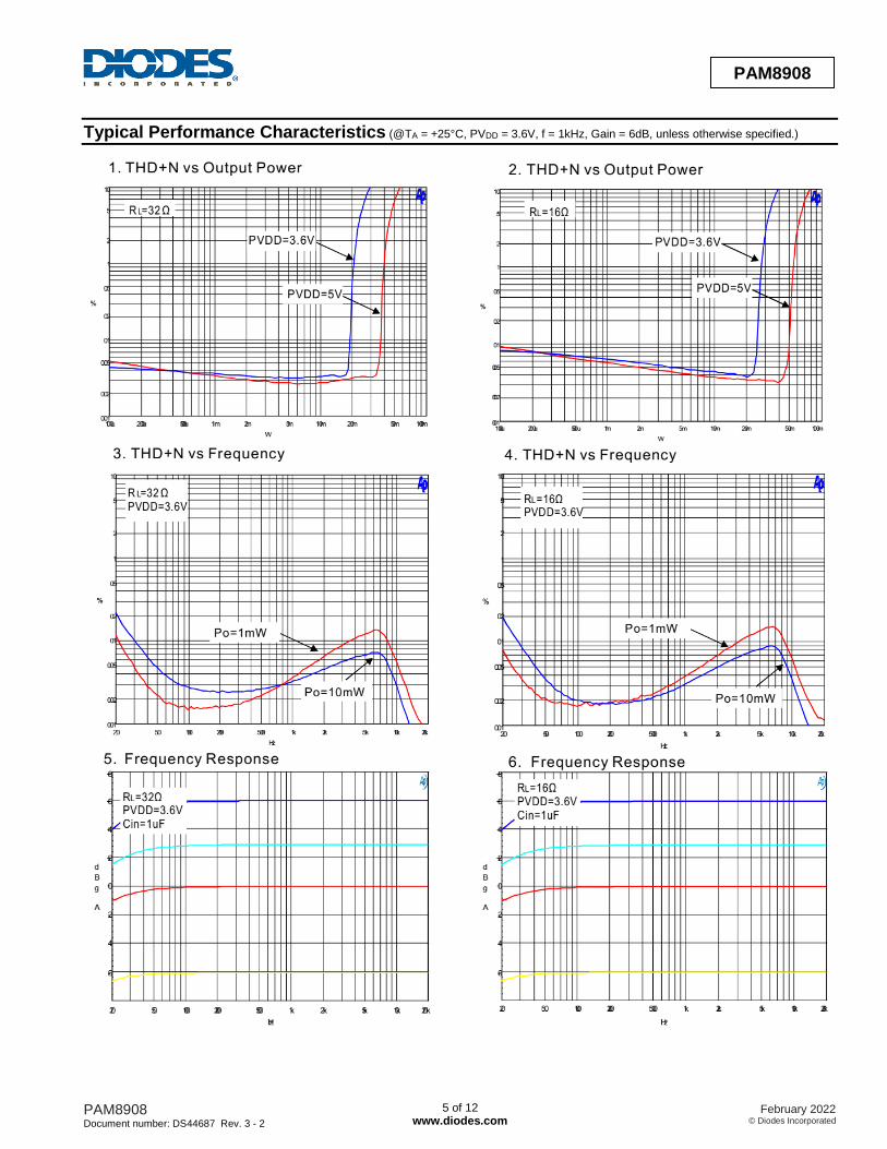
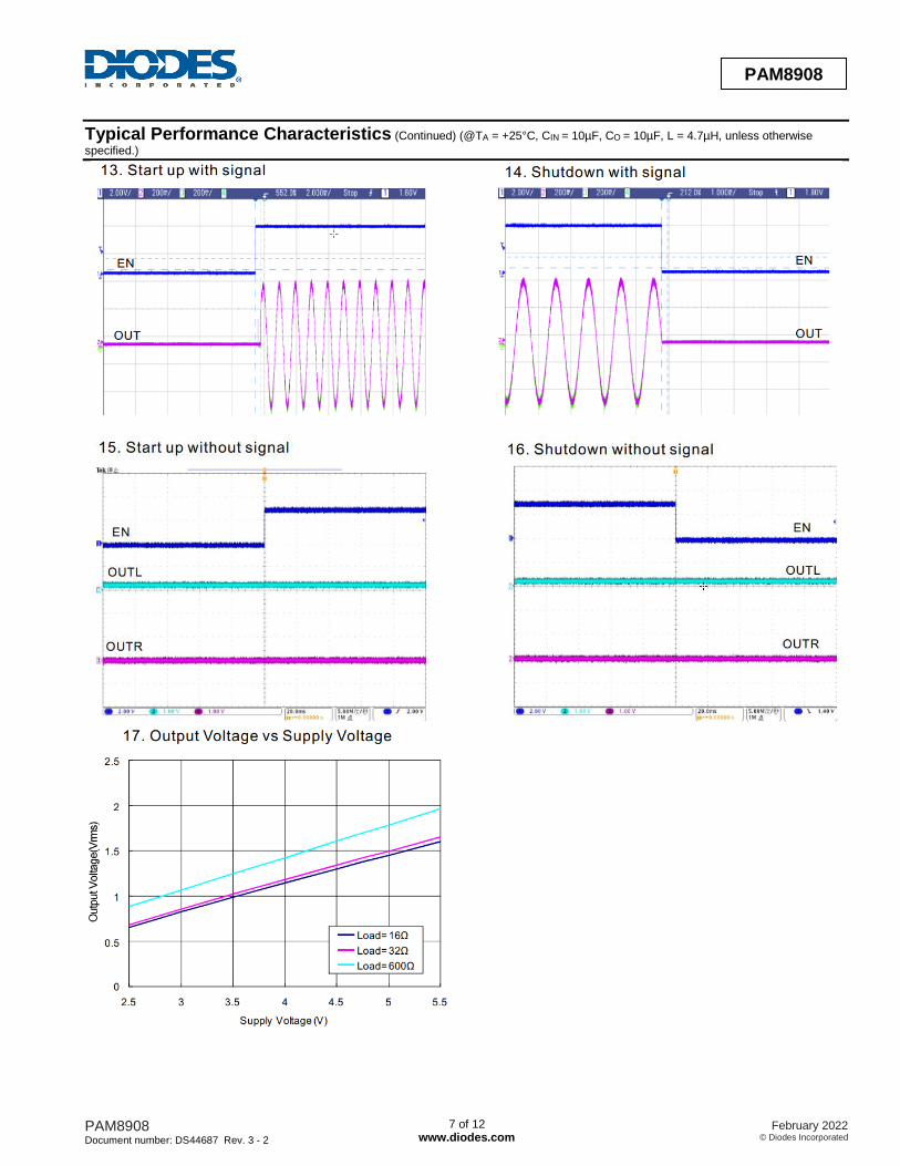
Typical Performance Characteristics (@TA = +25°C, PVDD = 3.6V, f = 1kHz, Gain = 6dB, unless otherwise specified.)
PAM8908 Document number: DS44687 Rev. 3 - 2
6 of 12 www.diodes.com
February 2022 © Diodes Incorporated
PAM8908
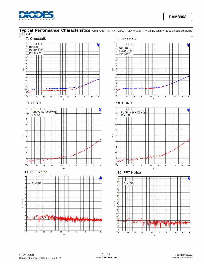
Typical Performance Characteristics (Continued) (@TA = +25°C, PVDD = 3.6V, f = 1kHz, Gain = 6dB, unless otherwise
specified.)
PAM8908 Document number: DS44687 Rev. 3 - 2
7 of 12 www.diodes.com
February 2022 © Diodes Incorporated
PAM8908
Typical Performance Characteristics (Continued) (@TA = +25°C, CIN = 10µF, CO = 10µF, L = 4.7µH, unless otherwise
specified.)
PAM8908 Document number: DS44687 Rev. 3 - 2
8 of 12 www.diodes.com
February 2022 © Diodes Incorporated
PAM8908
Application Information
The basic PAM8908 application circuit is shown on page 2.
Gain Control
The PAM8908 has four gain settings which are controlled with pins G0 and G1. The following table gives an overview of the gain function.
G0 Voltage G1 Voltage Amplifier Gain
≤ 0.6V ≤ 0.6V -6dB
≥ 1.4V ≤ 0.6V 0dB
≤ 0.6V ≥ 1.4V 3dB
≥ 1.4V ≥ 1.4V 6dB
Input Coupling Capacitors
Input coupling capacitors block any DC bias from the audio source and ensure maximum dynamic range. Input coupling capacitors also minimize
PAM8908 turn-on pop to an inaudible level. The input capacitors are in series with PAM8908 internal input resistors, creating a high-pass filter.
The following Equation calculates the high-pass filter corner frequency.
CR2
1f
ININTTC
The input impedance, RIN, is dependent on device gain. Larger input capacitors decrease the corner frequency. See the following table for input
impedance values.
G0 Voltage G1 Voltage RIN
≤ 0.6V ≤ 0.6V 26.4kΩ
≥ 1.4V ≤ 0.6V 19.8kΩ
≤ 0.6V ≥ 1.4V 16.5kΩ
≥ 1.4V ≥ 1.4V 13.2kΩ
For a given high-pass cutoff frequency, the minimum input coupling capacitor is found as:
Rf2
1C
INCTTIN
Example: Design for a 20Hz corner frequency with a PAM8908 gain of +6dB. The input impedance table gives RIN as 13.2kΩ. The CIN Equation
shows the input coupling capacitors must be at least 0.6µF to achieve a 20Hz high-pass corner frequency. Choose a 0.68µF standard value
capacitor for each PAM8908 input (X5R material or better is required for best performance).
Charge Pump Flying Capacitor, HPVDD Capacitor and HPVSS Capacitor
The PAM8908 uses a built-in charge pump to generate a positive and negative voltage supply for the headphone amplifiers. The charge pump
flying capacitor connects between CAP+ and CAP-. It transfers charge to generate the positive and negative supply voltage. The HPVDD
capacitor or HPVSS capacitor must be at least equal to or larger than value to the flying capacitor to allow maximum charge transfer. Use low
equivalent-series-resistance (ESR) ceramic capacitors (X5R material or better is required for best performance) to maximize charge pump
efficiency. Typical value is 1µF for the HPVDD, HPVSS and flying capacitors.
Power Supply Decoupling Capacitors
The PAM8908 TrueCapFree headphone amplifier requires adequate power supply decoupling to ensure that output noise and total harmonic
distortion (THD) remain low. Use good low equivalent-series-resistance (ESR) ceramic capacitors (X5R material or better is required for best
performance). Place a 2.2µF capacitor within 5mm of the PVDD pin. Reducing the distance between the decoupling capacitor and PVDD
minimizes parasitic inductance and resistance, improving PAM8908 supply rejection performance. Use 0402 or smaller size capacitors if possible.
PAM8908 Document number: DS44687 Rev. 3 - 2
9 of 12 www.diodes.com
February 2022 © Diodes Incorporated
PAM8908
Application Information (Continued)
Power Supply Sequencing
Use input coupling capacitors to ensure inaudible turn-on pop. Activate the PAM8908 after all audio sources have been activated and their output
voltages have settled. On power-down, deactivate the PAM8908 before deactivating the audio input source. The EN pin controls device shutdown:
Set to 0.6V or lower to deactivate the PAM8908; set to 1.4V or higher to activate.
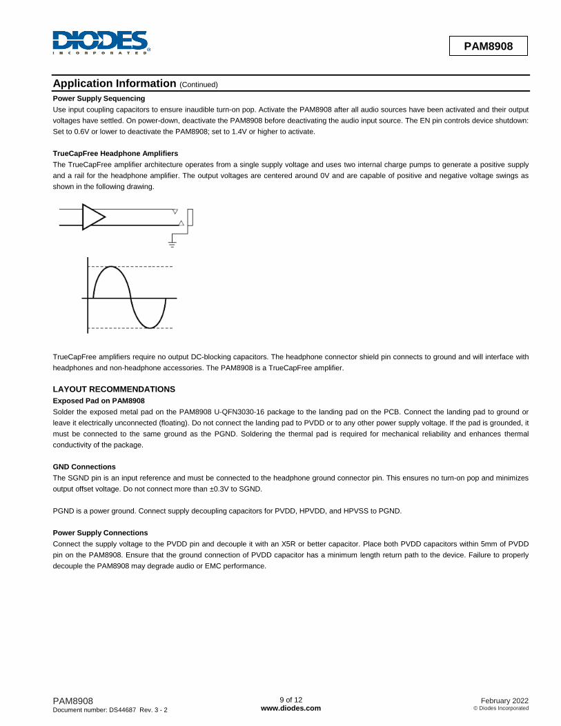
TrueCapFree Headphone Amplifiers
The TrueCapFree amplifier architecture operates from a single supply voltage and uses two internal charge pumps to generate a positive supply
and a rail for the headphone amplifier. The output voltages are centered around 0V and are capable of positive and negative voltage swings as
shown in the following drawing.
TrueCapFree amplifiers require no output DC-blocking capacitors. The headphone connector shield pin connects to ground and will interface with
headphones and non-headphone accessories. The PAM8908 is a TrueCapFree amplifier.
LAYOUT RECOMMENDATIONS
Exposed Pad on PAM8908
Solder the exposed metal pad on the PAM8908 U-QFN3030-16 package to the landing pad on the PCB. Connect the landing pad to ground or
leave it electrically unconnected (floating). Do not connect the landing pad to PVDD or to any other power supply voltage. If the pad is grounded, it
must be connected to the same ground as the PGND. Soldering the thermal pad is required for mechanical reliability and enhances thermal
conductivity of the package.
GND Connections
The SGND pin is an input reference and must be connected to the headphone ground connector pin. This ensures no turn-on pop and minimizes
output offset voltage. Do not connect more than ±0.3V to SGND.
PGND is a power ground. Connect supply decoupling capacitors for PVDD, HPVDD, and HPVSS to PGND.
Power Supply Connections
Connect the supply voltage to the PVDD pin and decouple it with an X5R or better capacitor. Place both PVDD capacitors within 5mm of PVDD
pin on the PAM8908. Ensure that the ground connection of PVDD capacitor has a minimum length return path to the device. Failure to properly
decouple the PAM8908 may degrade audio or EMC performance.
PAM8908 Document number: DS44687 Rev. 3 - 2
10 of 12 www.diodes.com
February 2022 © Diodes Incorporated
PAM8908
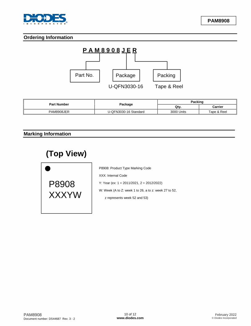
Ordering Information
P A M 8 9 0 8 J E R
Packing
Tape & Reel
Part No. Package
U-QFN3030-16
Part Number Package Packing
Qty. Carrier
PAM8908JER U-QFN3030-16 Standard 3000 Units Tape & Reel
Marking Information
(Top View)
W : Week
Y : Year
XXX : Internal Code
P/N : P8908
P8908
XXXYW ex: 1=2011/2021, 2=2012/2022
A~Z: 1-26 week, a~z: 27-52 week
z represents 52 and 53 week
P8908: Product Type Marking Code
XXX: Internal Code
Y: Year (ex: 1 = 2011/2021, 2 = 2012/2022)
W: Week (A to Z: week 1 to 26, a to z: week 27 to 52,
z represents week 52 and 53)
PAM8908 Document number: DS44687 Rev. 3 - 2
11 of 12 www.diodes.com
February 2022 © Diodes Incorporated
PAM8908
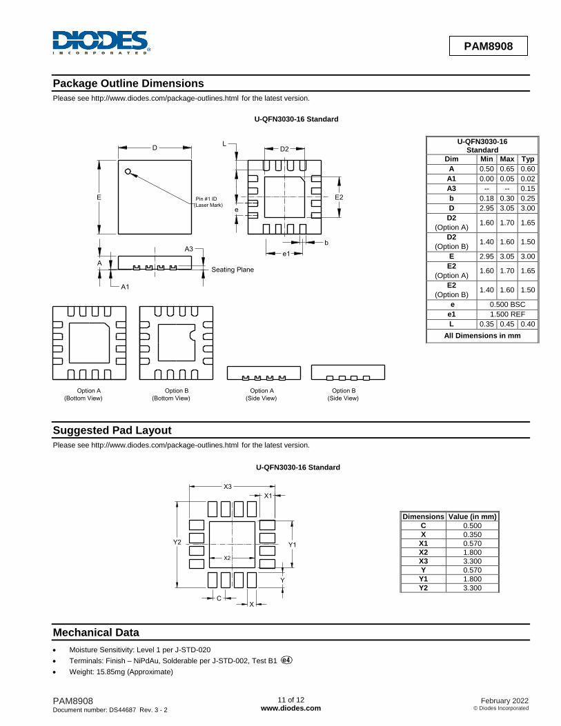
Package Outline Dimensions
Please see http://www.diodes.com/package-outlines.html for the latest version.
U-QFN3030-16 Standard
A1
D
E
D2
E2
b
A
A3
Pin #1 ID
(Laser Mark)
Seating Plane
Option A
(Bottom View)
Option B
(Bottom View)
Option A
(Side View)
Option B
(Side View)
L
e
e1
U-QFN3030-16 Standard
Dim Min Max Typ
A 0.50 0.65 0.60
A1 0.00 0.05 0.02
A3 -- -- 0.15
b 0.18 0.30 0.25
D 2.95 3.05 3.00
D2
(Option A) 1.60 1.70 1.65
D2
(Option B) 1.40 1.60 1.50
E 2.95 3.05 3.00
E2
(Option A) 1.60 1.70 1.65
E2
(Option B) 1.40 1.60 1.50
e 0.500 BSC
e1 1.500 REF
L 0.35 0.45 0.40
All Dimensions in mm
Suggested Pad Layout
Please see http://www.diodes.com/package-outlines.html for the latest version.
U-QFN3030-16 Standard
C
Y
X
X1
X2
Y1
X3
Y2
Dimensions Value (in mm)
C 0.500
X 0.350
X1 0.570
X2 1.800
X3 3.300
Y 0.570
Y1 1.800
Y2 3.300
Mechanical Data
Moisture Sensitivity: Level 1 per J-STD-020
Terminals: Finish – NiPdAu, Solderable per J-STD-002, Test B1
Weight: 15.85mg (Approximate)
PAM8908 Document number: DS44687 Rev. 3 - 2
12 of 12 www.diodes.com
February 2022 © Diodes Incorporated
PAM8908
IMPORTANT NOTICE 1. DIODES INCORPORATED AND ITS SUBSIDIARIES (“DIODES”) MAKE NO WARRANTY OF ANY KIND, EXPRESS OR IMPLIED, WITH REGARDS TO ANY INFORMATION CONTAINED IN THIS DOCUMENT, INCLUDING, BUT NOT LIMITED TO, THE IMPLIED WARRANTIES OF MERCHANTABILITY, FITNESS FOR A PARTICULAR PURPOSE OR NON-INFRINGEMENT OF THIRD PARTY INTELLECTUAL PROPERTY RIGHTS (AND THEIR EQUIVALENTS UNDER THE LAWS OF ANY JURISDICTION). 2. The Information contained herein is for informational purpose only and is provided only to illustrate the operation of Diodes products described herein and application examples. Diodes does not assume any liability arising out of the application or use of this document or any product described herein. This document is intended for skilled and technically trained engineering customers and users who design with Diodes products. Diodes products may be used to facilitate safety-related applications; however, in all instances customers and users are responsible for (a) selecting the appropriate Diodes products for their applications, (b) evaluating the suitability of the Diodes products for their intended applications, (c) ensuring their applications, which incorporate Diodes products, comply the applicable legal and regulatory requirements as well as safety and functional-safety related standards, and (d) ensuring they design with appropriate safeguards (including testing, validation, quality control techniques, redundancy, malfunction prevention, and appropriate treatment for aging degradation) to minimize the risks associated with their applications. 3. Diodes assumes no liability for any application-related information, support, assistance or feedback that may be provided by Diodes from time to time. Any customer or user of this document or products described herein will assume all risks and liabilities associated with such use, and will hold Diodes and all companies whose products are represented herein or on Diodes’ websites, harmless against al l damages and liabilities. 4. Products described herein may be covered by one or more United States, international or foreign patents and pending patent applications. Product names and markings noted herein may also be covered by one or more United States, international or foreign trademarks and trademark applications. Diodes does not convey any license under any of its intellectual property rights or the rights of any third parties (including third parties whose products and services may be described in this document or on Diodes’ website) under this document. 5. Diodes products are provided subject to Diodes’ Standard Terms and Conditions of Sale (https://www.diodes.com/about/company/terms-and-conditions/terms-and-conditions-of-sales/) or other applicable terms. This document does not alter or expand the applicable warranties provided by Diodes. Diodes does not warrant or accept any liability whatsoever in respect of any products purchased through unauthorized sales channel. 6. Diodes products and technology may not be used for or incorporated into any products or systems whose manufacture, use or sale is prohibited under any applicable laws and regulations. Should customers or users use Diodes products in contravention of any applicable laws or regulations, or for any unintended or unauthorized application, customers and users will (a) be solely responsible for any damages, losses or penalties arising in connection therewith or as a result thereof, and (b) indemnify and hold Diodes and its representatives and agents harmless against any and all claims, damages, expenses, and attorney fees arising out of, directly or indirectly, any claim relating to any noncompliance with the applicable laws and regulations, as well as any unintended or unauthorized application. 7. While efforts have been made to ensure the information contained in this document is accurate, complete and current, it may contain technical inaccuracies, omissions and typographical errors. Diodes does not warrant that information contained in this document is error-free and Diodes is under no obligation to update or otherwise correct this information. Notwithstanding the foregoing, Diodes reserves the right to make modifications, enhancements, improvements, corrections or other changes without further notice to this document and any product described herein. This document is written in English but may be translated into multiple languages for reference. Only the English version of this document is the final and determinative format released by Diodes. 8. Any unauthorized copying, modification, distribution, transmission, display or other use of this document (or any portion hereof) is prohibited. Diodes assumes no responsibility for any losses incurred by the customers or users or any third parties arising from any such unauthorized use. Copyright © 2022 Diodes Incorporated www.diodes.com