Microwave building blocks: Gunn flanges - World Radio History
Upload
khangminh22Category
view
0download
0
Received March 31, 2020, accepted April 22, 2020, date of publication April 29, 2020, date of current version May 18, 2020.
Digital Object Identifier 10.1109/ACCESS.2020.2991309
Reliable GaN-Based THz Gunn Diodes WithSide-Contact and Field-Plate TechnologiesAHID S. HAJO 1, (Member, IEEE), OKTAY YILMAZOGLU1, ARMIN DADGAR 2,FRANKO KÜPPERS1, (Senior Member, IEEE), AND THOMAS KUSSEROW11Department of Electrical Engineering and Information Technology, Institute for Microwave Engineering and Photonics (IMP), Technical University ofDarmstadt, 64283 Darmstadt, Germany2Faculty of Natural Sciences, Institute of Physics, Otto von Guericke University Magdeburg, 39106 Magdeburg, Germany
Corresponding authors: Ahid S. Hajo ([email protected]) and Oktay Yilmazoglu ([email protected])
This work was supported by the Pioneer Fund for Innovation under Grant 56300803.
ABSTRACT For the first time, Gallium Nitride(GaN)-based Gunn diodes with side-contact and field-plate technologies were fabricated and measured with reliable characteristics. A high negative differentialresistance (NDR) region was characterised for the GaN Gunn effect using side-contact technology. The I-Vmeasurement of the THz diode showed the ohmic and the Gunn effect region with high forward currentof 0.65A and high current drop of approximately 100mA for a small ring diode width wd of 1.5µm with600 nm effective diode height hd at a small threshold voltage of 8.5V. This THz diode worked stable dueto good passivation as protection from electro-migration and ionisation between the electrodes as well asa better heat sink to the GaN substrate and large side-contacts. The diodes can provide for this thickness afundamental frequency in the range of 0.3 - 0.4 THz with reliable characteristics.
INDEX TERMS Gallium nitride, gunn diodes, semiconductor structure, terahertz source, side-contact,field-plate.
I. INTRODUCTIONBased on the successful use of the Gunn effect in GalliumArsenide (GaAs) to generate high-frequency signals, severalmaterials were already tested for their suitability for thesame purpose [1]. The aim was to determine the possibilitiesand conditions for the so-called ‘‘electron transfer effect’’based on relevant material properties such as energy bandprofile, charge carrier velocity and mobility. At the sametime, attention was also drawn to the potential of so-callednitride materials for operation at much higher frequencies(up to 1 THz) and powers (up to 10mW). Reasons for thisinclude the achievable high saturation velocity for electrons(for GaN > 2 times higher than in GaAs), much higherelectric threshold field strength for the so-called ‘‘electrontransfer effect’’ (for GaN > 50 times higher than in GaAs)and the large energy band gap for higher breakdown voltage[1], [2]. The latter also enabled the development of short-wave optical diodes and semiconductor lasers, which areused in fields such as communications, lighting technology,
The associate editor coordinating the review of this manuscript andapproving it for publication was Anisul Haque.
multimedia, etc. While signal sources based on GaAs andindium phosphide (InP) components have cut-offfrequencies of 100GHz and 200GHz (for the fundamentalmode), respectively, the calculated maximum frequenciesfor GaN diodes are higher than 700GHz [1], [3]. So far,simulation for GaN-Gunn diodes [2], [3], as well as severalfabricationmethods and initial current-voltage characteristicswere performed [2], [4]. All of these results were based onGunn diodes on sapphire substrates. There are several effectsand problems that made the verification of the predicteddevice properties difficult. Typical problems are the occur-rence of the electro-migration effects as well as the high seriesresistances and self-heating [1], [5]. The small thermal con-ductivity of sapphire makes the implementation of heat sinksdifficult. This leads to high DC losses and reduced reliability.A new simulation scheme has been developed in [6]. Thesimulation results demonstrated the superiority of GaN as aGunn diode over those based on materials like GaAs and InP.An output power of 1400 kW/cm2 is achieved from the GaNGunn diode, as compared to 4.9 kW/cm2 from a GaAs diode.Another approach is described in [7] showing the modulationof the domain mode in the two-dimensional electron gas
84116
This work is licensed under a Creative Commons Attribution 4.0 License. For more information, see https://creativecommons.org/licenses/by/4.0/
VOLUME 8, 2020
A. S. Hajo et al.: Reliable GaN-Based THz Gunn Diodes With Side-Contact and Field-Plate Technologies
(2DEG) channel of GaN-based high electron mobility tran-sistor (HEMT)-like Gunn diodes by adjustment the electronconcentration of the 2DEG near the cathode side and displayan explicit numerical study on the GaN-based planar Gunndiode, and demonstrate that the electric field at the cathodeside plays an important role on the formation and modulationof the electron domain Gunn diode. In [8], [9], a detailedstudy about the GaN-based Gunn diode has been presentedusing an ensemble Monte-Carlo method. The drift velocity,electron density, and electric field distribution as a functionof time in the device are illustrated under direct current (DC)and alternating current (AC) bias condition. W. Z. Lee et al.showed in [9] that the Gunn diode with 550 nm transit lengthis capable to achieve a 500GHz signal of 2.61W with 2.27%efficiency under 22V DC and 5V RF condition. In [10],an efficient method to improve the crystal quality of GaNGunn diode with AlGaN hot electron injecting layer on SiCsubstrate was reported. Multi-channel Gunn diode, which isrealized by containing multiple AlGaN/GaN heterostructuresas GaN-based HEMT-like planar Gunn diode improves theoutput power and the characteristics at a higher frequency,was proposed in [11]. In comparison to the prior worksfrom other groups, the novelty of this work besides the GaNsubstrate is the side-contact and field-plate technologies forsmaller effective diode width and height with better fielddistribution. Moreover, we show the reliability measurementsof the NDR region for different diode width and height. So,in this work, we report on the fabrication and characterisationof GaN-based THz Gunn sources using new technology withstable side-contacts. Three benefits were obtained here: goodpassivation of the active mesa, good heat sink as well as stablediodes with smaller diode height and higher potential THzfrequencies.
II. PRINCIPLE OF THE GUNN DIODEA Gunn diode uses the electron transfer effect by applyinga corresponding threshold electric field to generate electrondomains which travel through the diode like waves. Thisresults in the generation and subsequent emission of elec-tromagnetic waves corresponding to the domain travellingtime. In addition to themainminimum (central valley, gamma(0)-valley) of the conduction band, there is a higher sec-ondary minimum (satellite valley) with lower electron mobil-ity. At room temperature and without an external electricfield, only the central valley is occupied by electrons. Thesemiconductor of a Gunn device must fulfil several condi-tions. On the one hand, the energy difference between thecentral valley and the satellite valley must be much largerthan the thermal energy of the electrons, so that the electronsdo not occupy the state of the secondary minima even withsmall field strengths. On the other hand, the energy differ-ence must be much smaller than the energy gap betweenthe valence band and the lowest conduction band, otherwisethe electrons in the central valley will gain enough energyto generate electron-hole pairs, in this case, an avalanchebreakdown occurs. These conditions are fulfiled e.g. for
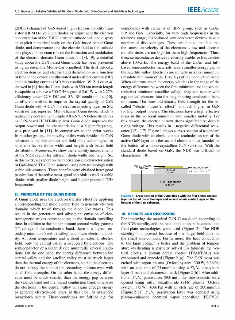
compounds with elements of III-V group, such as GaAs,InP and GaN. Especially, for very high frequencies in theterahertz range, GaAs-based semiconductor devices have anumber of disadvantages. These are due to the fact thatthe saturation velocity of the electrons is low and electrontransfer times are too high for these high frequencies. Thus,these semiconductor devices are hardly usable for frequenciesabove 100GHz. The energy band of the GaAs- and InP-based semiconductor materials have a smaller energy gap tothe satellite valley. Electrons are initially in a first minimum(absolute minimum of the 0-valley) of the conduction band.When electrons reach the energy which is in the range of theenergy difference between the first minimum and the second(relative) minimum (satellite-valley), they can scatter withe.g. optical phonons into the neighbouring conduction bandminimum. The threshold electric field strength for the so-called ‘‘electron transfer effect’’ is much higher in GaNfor high output powers. The electrons have a high effectivemass in the adjacent minimum with smaller mobility. Forthis reason, the electric current drops significantly, despiterising voltage. This results in a negative differential resis-tance [12]–[17]. Figure 1 shows a cross-section of a standardGunn diode with an ohmic contact (cathode) on top of theactive GaN layer and the second ohmic contact (anode) onthe bottom of a mono-crystalline GaN substrate. With thestandard diode based on GaN, the NDR was difficult tocharacterise [18].
FIGURE 1. Cross-section of the Gunn diode with the first ohmic contactlayer on top of the active layer and second ohmic contact layer on thebottom of the GaN substrate.
III. RESULTS AND DISCUSSIONFor improving the standard GaN Gunn diode according tothe NDR stability and the heat conduction, side-contact andfield-plate technologies were used (Figure 2). The NDRstability is improved because of the large field-plate onthe small side-contacts. Furthermore, the heat conductionto the large contact is better and the problem of temper-ature overheating is partially solved. To fabricate the ver-tical diodes, a bottom ohmic contact (Ti/Al/Ti/Au) wasevaporated and annealed [Figure 2 (a)]. The GaN mesa wasetched with argon plasma (Oxford system, 300W, 6.66 Pa)with an etch rate of 24 nm/min using a SixNy passivationlayer (1µm) and photoresist mask [Figure 2 (b)]. After addi-tional SixNy passivation (800 nm), the side-contacts wereopened using sulfur hexafluoride (SF6) plasma (Oxfordsystem, 175W, 16.66 Pa) with an etch rate of 200 nm/min[Figure 2 (c)]. SixNy passivation layer was deposed usingplasma-enhanced chemical vapor deposition (PECVD).
VOLUME 8, 2020 84117

A. S. Hajo et al.: Reliable GaN-Based THz Gunn Diodes With Side-Contact and Field-Plate Technologies
Finally, the field platewas evaporated (Ti/Au - 20 nm/120 nm)which contacted the diode form the side [Figure 2 (d)]. TheGaN active layer has a doping concentration as the diodein Figure 1.
FIGURE 2. Fabrication process of a Gunn diode with side contact.(a) First, the bottom contact was evaporated (Ti/Al/Ti/Au). (b) Afterwards,the mesa was etched using an argon-based dry etching process. Six Nypassivation layer and photoresist were used as an etch mask. (c) Anadditional Six Ny passivation was deposited and opened for theside-contact using SF6 dry etching. (d) The field plate was evaporatedwhich contacted the diode form the side.
Figure 3 shows the scanning electron microscope (SEM)image of the fabricated Gunn diode. The SEM image of a sin-gle diode before field-palate technology with mesa openingfor the side-contact can be seen on top of Figure 3. SixNypassivation and the photoresist were used as an etch mask.The whole area around the diode was passivated with SixNy.The photoresist was removed with acetone before the fabri-cation of the field-plate and side-contact. On the bottom ofFigure 3 is a SEM image of the fabricated Gunn diodes in anarray configuration with side-contact. The Gunn diode itselfis in the middle of the gold field-plate. The side-contact is aring surface.
FIGURE 3. Top: SEM image of a single diode before field-palatetechnology with mesa opening for the side-contact. Six Ny passivationand the photoresist were used as an etch mask. The whole area aroundthe diode was passivated with Six Ny . The photoresist was removed withacetone before the fabrication of the field-plate and side-contact. Bottom:SEM image of the fabricated Gunn diodes in an array configuration withside-contact. The Gunn diode itself is in the middle of the gold field-plate.
For the current-voltage (I-V) characteristics of the GaNGunn diodes, an in-house made system (Figure 4) was usedto measure the incident and the reflected voltage pulses fromthe Gunn diode and calculate the current–voltage (I-V) char-acteristics with a LabVIEW program. The wave impedanceZ0 was 50�. A DC power supply (TET – ARGOS; 1000 V)loaded the line charger capacitance [outer line (1)] with acharging resistance. The length of the line charger definedthe pulse width. A commercial pulse generator (HP 8114A)triggered the power switch based on aMESFET. Both ends ofthe line charger [inner line (2)] generated the incident waveat closed switch. One line end was used to measure directlythe incident wavewith an oscilloscope (Tektronix TDS 794D)and the second line end was connected to Gunn diode.
FIGURE 4. Schematic of the I-V measurement setup to characterise theGaN Gunn diodes. The setup contains multiple devices controlled by acomputer: A pulse generator (HP 8114A), an oscilloscope (Tektronix TDS794D) and a DC power supply (TET - ARGOS). The inset on the bottom sideshows a photograph of the zoomed sample - device under test (DUT) -under the microscope. The length of the line charger defines thepulse-width.
84118 VOLUME 8, 2020

A. S. Hajo et al.: Reliable GaN-Based THz Gunn Diodes With Side-Contact and Field-Plate Technologies
The reflected wave from the Gunn diode was measuredwith a delay over the line charger. The I-V characteristicswere calculated with:
0 =Vref .Vinc.
(1)
Rdiode = Z01+ 01− 0
(2)
Vdiode = Vinc. + Vref . (3)
Idiode =VdiodeRdiode
(4)
where Vref . is the reflected voltage from the diode, Vinc. is theincident voltage to the diode, 0 is the reflection coefficient,Rdiode is the diode resistance, Vdiode is the diode voltage, andIdiode is the diode current. The system can provide a pulse-width down to 20 ns depending on the length of the coaxialcable, an output voltage up to 1000V and an output currentup to 6A. A 30-dB attenuator is necessary to protect theoscilloscope from the high peak voltages, whereas the shortpulse is necessary to minimise the temperature effects andallows reliable measurements of the diode. A bias oscillationwas obtained in the reflected pulse above the threshold field150 kV/cm. It appears due to the diode capacitance and para-sitic inductance in themeasurement setup similar to [5] whichis evidence for the Gunn effect.
Figure 5 shows the measured linear and the NDR regionswith a high forward current of 0.65A, with a small effectivediode width wd of 1.5µm at a relatively small thresholdvoltage Vth of 8.5V. Furthermore, the doping and the thick-ness of the active layer results in high currents through theactive layer of the Gunn diode. The effective diode height
(hd =Vth
150 kV/cm) was calculated as 600 nm with potential
application for up to 330GHz (f =vsathd
, were the satura-
tion velocity vsat is 2 ·107cm/s). The current drop was up to100mA. This fast current modulation is about two ordershigher than for conventional GaAs photomixer [19]. Theoutput power is Pout ∝ 1I2. These measurements showhigh potential for high output power especially with muchbetter current modulation compared to the conventional GaAsphotomixer. The pulsed measurement of the device leads tolower device temperature at high diode currents during theoperation and stabilised the GaN Gunn diode. Figure 6 showsthe measured electrical pulse response. The curve shows thebias oscillation due to the Gunn effect which can be seenbetter in the zoomed inset in Figure 6. The pulse-width was70 ns. The left pulse corresponds to the input signal, whereasthe right one corresponds to the signal reflected from the GaNGunn diode.
This new approach (Figure 2) enables the fabrication ofdiodes having smaller width wd and height hd with morestable NDR characteristics. The current Imax is dependingon the effective width and the frequency on the heightof the diode. Instead of 2.5µm thick diodes (Figure 1) asmaller effective diode height of about 600 nmwas fabricated(Figure 2) applicable for higher THz frequencies up to330GHz. The highest electric field strength appears at the
FIGURE 5. Current-voltage curve of the Gunn diode based on GaN withside-contact. The Gunn effect and the ohmic regions are shown.
FIGURE 6. Measured electrical pulse response. (Left) shows the incidentbias pulse and reflected pulse from the Gunn diode as well as the biasoscillation due to the Gunn effect. (right) Zoomed region of the biasoscillation.
closest edge between wd (cathode) and the substrate (anode),on the other hand, that is also the path which the electrondomains are travelling through, resulting in an effectivecurrent flow through the channel (Figure 2). The side channelis effectively the thinnest diode region, where the Gunn effectoccurs at lower voltages compared to the other areas. Thethicker diode areas have only a parasitic current flow, whichis not relevant for the Gunn effect. In addition, by usingthis technology approach, the top contact passivation actsas a protection layer against electro-migration and ionisationbetween both electrodes. However, the diodes must be opti-mised in this regard.
To calculate the effective diode channel width wd of thering diode, equation (5) was used.
Imax = vsat · n · e · Aeff (5)
First, the maximum current Imax was taken from the mea-sured I-V curve in Figure 5, which corresponds to 0.65A.Then, the Aeff was calculated as 100µm2 by applying thedoping concentration n = 2 · 1017 cm−3 and the saturationvelocity vsat of about 2 ·107 cm/s. The last step was the cal-culation of the wd using Aeff and the mesa diameter ddiameterof 21µm. The effective wd is about 1.5µm. The effectivediode channel height hd with side-contact was calculatedusing equation (6) as 600 nm.
VNDR,th = EGunn · hd (6)
The theoretical threshold electric field of the GaN Gunndiode EGunn is 150 kV/cm and the NDR threshold voltageVNDR,th was taken from the measured I-V curve in Figure 5,which correspond to 8.5V. Additionally, the total diode
VOLUME 8, 2020 84119

A. S. Hajo et al.: Reliable GaN-Based THz Gunn Diodes With Side-Contact and Field-Plate Technologies
resistance (active layer and contact resistance) was calculatedfrom the linear fit of the ohmic region as 13.7�.Several diodes with different diode heights hd and different
widths wd were characterised regarding the voltage-currentcharacteristics (Figure 7). The measurements showed differ-ent I-V characteristics. The higher the diode height hd thehigher the applied threshold voltage and on the other sidethe wider the diode width wd the higher the current. As canalso be seen in Figure 7, the higher the current the smallerthe NDR region. For a lower hd,1 (green curve), the NDRregion is much bigger (current drop of about 100mA) thanfor a higher hd,3 (red curve) with a NDR with a current dropof 25mA. Therefore a moderate hd,2 (blue curve) was chosenfor moderate NDR region with a current drop of 50mAwith stable characteristics. Furthermore, for a lower hd,1,the device shows unstable characteristics at high voltage(Figure 7, green curve).
FIGURE 7. Current-voltage measurements of the Gunn diode withdifferent diode heights hd .
The technology of the vertical GaN Gunn diode with side-contact is more sensitive to misalignment and etching opti-misation. With the required argon-based dry etching process,rough edges on the mesa structure can be formed. As aresult, increased electrical field strengths occur there. Thisleads occasionally to electrical discharges between the mesafloor and the cathode. The resulting positive ions bombardthe cathode metallisation and cause material migration inthe direction of the surface of the active GaN Gunn dioderegion. These can then cause short circuits in the component.The solution is an optimum passivation layer around and onthe top of the diode. On the other hand, the fabrication of aside-contact with SF6 dry etching defines the width and theheight of the fabricated effective diodes. This needs bettertechnology than the fabrication of the standard vertical diode.This can be seen by comparing the cross-sections of bothvertical diodes (Figures 1 and 2). The fabrication of diodeswith the same characteristics is still challenging. The side-contacted GaN Gunn diode is better for the fabrication ofsmaller effective diode area and height for higher device
stability and higher oscillation frequency, respectively. Com-pared to the device designed for 40 GHz, which is reportedin [5], this diode is designed for 400 GHz. Additionally,better stability due to the effective passivation of the diodeof 800 nm was achieved. Moreover, due to its higher thermalconductivity (130W/mK), in contrast to sapphire (40W/mK),the GaN substrate is itself more suitable for heat dissipation.The large field-plate contact supports the effective heat dis-sipation. The side-contact and field-plate technologies wereused for smaller effective diode width and height with betterfield distribution. The critical mesa edge was passivatedand covered by the field-plate. Furthermore, the design ofa circle diode contributed to minimising the field peaks at theedges. Thus, the parasitic electrical field peaks at the edgeof the standard diode and the electro-migration effects wereminimised.
IV. CONCLUSIONNew GaN Gunn diodes with a good heat sink to the con-ductive GaN substrate and side-contact were fabricated. Withthe side-contact technology, stable voltage supply of smallerGaN Gunn diodes with smaller diode height resulting inhigher THz frequency performance was possible. The criticalmesa edge was passivated and covered by the field-plate.Furthermore, the design of a circle diode contributed to min-imising the field peaks at the edges. The parasitic electricalfield peaks at the edge of the standard diode and the electro-migration effects were minimised. Thus, the reliability ofthe THz diode was increased and stable negative differen-tial resistances were measured. A high negative differentialresistance region was shown with the new side-contact tech-nology. The measurement showed ohmic and Gunn effectregions with a high forward current of 0.65A, a high currentdrop of about 100mA, a small threshold voltage of 8.5V anda small effective diode channel height of about 600 nm. Thediodes can provide for this thickness a fundamental frequencyin the range of 0.3 - 0.4 THz and allow by using higherharmonics or special excitations even frequencies > 1 THzwith an integrated antenna. The initial diode resistance was13.7� and can be easily matched to an antenna. Thus,the diodes with side-contact and field-plate offer the possi-bility of directly generating terahertz radiation of relativelyhigh power (> 10mW) at selected target frequencies (up to400GHz), which can be set according to the application.
ACKNOWLEDGMENT(Ahid S. Hajo and Oktay Yilmazoglu contributed equally tothis work.)
REFERENCES[1] H. Eisele and G. I. Haddad, ‘‘Two-terminal millimeter-wave sources,’’
IEEE Trans. Microw. Theory Techn., vol. 46, no. 6, pp. 739–746,Jun. 1998.
[2] J. M. Barker, D. K. Ferry, D. D. Koleske, and R. J. Shul, ‘‘BulkGaN and AlGaN/GaN heterostructure drift velocity measurements andcomparison to theoretical models,’’ J. Appl. Phys., vol. 97, no. 6,pp. 063705-1–063705-5, Mar. 2005.
84120 VOLUME 8, 2020

A. S. Hajo et al.: Reliable GaN-Based THz Gunn Diodes With Side-Contact and Field-Plate Technologies
[3] E. Alekseev and D. Pavlidis, ‘‘GaN Gunn diodes for THz signal genera-tion,’’ in IEEE MTT-S Int. Microw. Symp. Dig., Boston, MA, USA, vol. 3,Jun. 2000, pp. 1905–1908.
[4] Z. C. Huang, R. Goldberg, J. C. Chen, Y. Zheng, D. B. Mott, and P. Shu,‘‘Direct observation of transferred-electron effect in GaN,’’ Appl. Phys.Lett., vol. 67, no. 19, pp. 2825–2826, Nov. 1995.
[5] O. Yilmazoglu, K. Mutamba, D. Pavlidis, and T. Karaduman, ‘‘First obser-vation of bias oscillations in GaN Gunn diodes on GaN substrate,’’ IEEETrans. Electron Devices, vol. 55, no. 6, pp. 1563–1567, Jun. 2008.
[6] R. K. Parida, N. C. Agrawala, G. N. Dash, and A. K. Panda, ‘‘Characteris-tics of a GaN-based Gunn diode for THz signal generation,’’ J. Semicond.,vol. 33, no. 8, Aug. 2012, Art. no. 084001.
[7] Y. Wang, L.-A. Yang, Z.-Z. Wang, and Y. Hao, ‘‘Modulation of the domainmode in GaN-based planar Gunn diode for terahertz applications,’’ Phys.Status Solidi C, vol. 13, nos. 5–6, pp. 382–385, May 2016.
[8] S. Wang, H. Liu, H. Zhang, and Q. Chen, ‘‘Research on the origin ofnegative effect in uniform doping GaN-based Gunn diode under THzfrequency,’’ Appl. Phys. A, Solids Surf., vol. 122, no. 6, Jun. 2016.
[9] W. Z. Lee, D. S. Ong, and K. Y. Choo, ‘‘Optimization of WurtziteGaN-based Gunn diode as terahertz source,’’ in Proc. IEEE Int. Conf.Semiconductor Electron. (ICSE), Kuala Lumpur, Malaysia, Aug. 2018,pp. 173–176.
[10] L. Li, L. Yang, J. Zhang, and Y. Hao, ‘‘Dislocation blocking by AlGaNhot electron injecting layer in the epitaxial growth of GaN terahertz Gunndiode,’’ J. Appl. Phys., vol. 114, no. 10, Sep. 2013, Art. no. 104508.
[11] Y.Wang, L.-A. Yang, Z.-Z.Wang, J.-P. Ao, and Y. Hao, ‘‘The enhancementof the output characteristics in the GaN based multiple-channel planarGunn diode,’’ Phys. Status Solidi A, vol. 213, no. 5, pp. 1252–1258,May 2016.
[12] K. Mutamba, O. Yilmazoglu, C. Sydlo, M. Mir, S. Hubbard, G. Zhao,I. Daumiller, and D. Pavlidis, ‘‘Technology aspects of GaN-based diodesfor high-field operation,’’ Superlattices Microstruct., vol. 40, nos. 4–6,pp. 363–368, Oct. 2006.
[13] B. E. Foutz, L. F. Eastman, U. V. Bhapkar, andM. S. Shur, ‘‘Comparison ofhigh field electron transport in GaN and GaAs,’’ Appl. Phys. Lett., vol. 70,no. 21, pp. 2849–2851, May 1997.
[14] V. Gružinskis, J. H. Zhao, P. Shiktorov, and E. Starikov, ‘‘Gunn effect andTHz frequency power generation in n+-n–n+ GaN structures,’’Mater. Sci.Forum, vols. 297–298, pp. 341–344, Dec. 1998.
[15] A. Ìñiguez-de-la-Torre, I. Ìñiguez-de-la-Torre, J. Mateos, T. González,P. Sangaré, M. Faucher, B. Grimbert, V. Brandli, G. Ducournau, andC. Gaquière, ‘‘Searching for THz Gunn oscillations in GaN planar nan-odiodes,’’ J. Appl. Phys., vol. 111, no. 11, Jun. 2012, Art. no. 113705.
[16] J. Voelcker, ‘‘The Gunn effect,’’ IEEE Spectr., vol. 26, no. 7, p. 24,Jul. 1989.
[17] A. S. Hajo, O. Yilmazoglu, B. Samodi, A. Dadgar, F. Kuppers, andT. Kussorow, ‘‘A new approach to achieve Gunn effect for GaN based THzsources with high power,’’ in Proc. 44th Int. Conf. Infr., Millim., THzWaves(IRMMW-THz), Paris, France, Sep. 2019, pp. 1–2.
[18] A. S. Hajo, O. Yilmazoglu, A. Dadgar, and F. Kuppers, ‘‘Reliabilityimprovement of high-power THz GaN Gunn sources for active imagingsystems,’’ inProc. 43rd Int. Conf. Infr., Millim., THzWaves (IRMMW-THz),Nagoya, JpnSep. 2018, pp. 1–2.
[19] S.-H. Yang and M. Jarrahi, ‘‘A high-power photomixer with plasmoniccontact electrodes,’’ in Proc. Conf. Lasers Electro-Opt. (CLEO), 2016,pp. 1–2.
AHID S. HAJO (Member, IEEE) receivedthe master’s degree in physics from the Insti-tute of Physics, Goethe University Frankfurt,in May 2014. He is currently pursuing the Ph.D.degree with the Institute of Microwave Engineer-ing and Photonics (IMP), Technical University ofDarmstadt. After the submission of the Masterthesis, he worked as an Early-Stage Researcher(ESR). His experience includes the areas of ter-ahertz and nanotechnology for the manufacture
of new semiconductor devices for THz sources and detectors. His currentresearch interests include the field of nanowire-based THz Schottky detec-tors, GaN-based THz Gunn sources as well as CNT-based THz devices forbiomedical applications. As a Ph.D. student, he contributed in two patentsand more than 15 publications.
OKTAY YILMAZOGLU received the Dr.Ing.and Habilitation degree from the Institute ofMicrowave Engineering, Technical Universityof Darmstadt, in 2004 and 2013, respectively.He worked on several projects where compoundsemiconductor materials and technologies wereused to develop sensors and electric devices onthe basis of GaAs, GaN, and ZnO as well ascarbon nanotubes and graphene for applicationsin mechanical engineering and at high-frequency.
He has 20 years of expertise in microelectronic devices and components.This includes the design, fabrication, and characterisation of 3-D mag-netic field sensors, pressure sensors, gas sensors, acceleration sensors,high-frequency diodes, and nanostructured field emission devices for highfrequency generation. His work includes the experimental use of 1-D or2-D materials, as well as the theoretical evaluation of related quantum sizeeffects. He is currently working in the field of THz photomixers as wellas CNT- and graphene-based field-emission devices for sensing, electronsource, and microwave applications. These resulted in several patents andnumerous publications in internationally highly regarded magazines.
ARMIN DADGAR received the Dr.Ing. in physicsfrom TU-Berlin, in 1999, and the Habilitationdegree in physics from Otto-von-Guericke-Universität Magdeburg, in 2005, respectively.Since January 2011, he has been a Professor withthe Faculty of Science, Institute of Physics, Otto-von-Guericke-Universität Magdeburg. He workedon several projects with compound semiconductormaterials like GaN as well as components as FETand HEMT. He is currently working in the field of
LED as well as MOCVD and MOVPE. These resulted in several patents andnumerous publications in internationally highly regarded magazines.
FRANKO KÜPPERS (Senior Member, IEEE)received the Ph.D. degree from the TechnicalUniversity of Kaiserslautern, Kaiserslautern,Germany. He is a Fellow of SPIE and a SeniorMember of the IEEE photonics and communi-cations section. He was with Siemens and theDeutsche Telekom’s Research and TechnologyCenter, where he directed the Optical NetworksResearch Group and the Photonic Systems Depart-ment, until 2002. He worked at Siemens and was
VOLUME 8, 2020 84121

A. S. Hajo et al.: Reliable GaN-Based THz Gunn Diodes With Side-Contact and Field-Plate Technologies
with Deutsche Telekom, where he directed the Optical Networks ResearchGroup and the Photonic Systems Department, Research and TechnologyCenter, Darmstadt, Germany, until 2002. In 2003, he joined the College ofOptical Sciences (COS), University of Arizona (UA), Tucson, AZ, USA,where he served as a tenured Associate Professor of optical sciences,built and ran the Photonic Telecommunication Systems Research Group.He served as the testbed lead for the national Science Foundation Engi-neering Research Center for Integrated Access Networks (ERC CIAN) withwhich he is still associated through his position as an Adjunct Professorat the UA COS. He has authored or coauthored more than 100 scientificarticles. In 2011, he joined the Institute for Microwave Engineering andPhotonics, Darmstadt University of Technology (TU Darmstadt), Germany,where he also held the Chair of Photonics and Optical Communications,where he served as the Institute Director. Since January 2019, he has beenwith the Skolkovo Institute of Science and Technology, Moscow, Russia,as a Professor and the Director of the Center for Photonics and QuantumMaterials.
THOMAS KUSSEROW received the Ph.D. degreefrom the University of Kassel, Germany, in 2010,on the topic of periodic InP/air-gap structures forMEMS and nano-optical devices. He was previ-ously working on holographic optical elementswith the Institute for Light and Building Technol-ogy (ILB), Cologne, from 1999 to 2001, and since2005, on in the Institute for Nanostructure Tech-nology and Analytics (INA), Kassel, on MEMSand photonic crystals. In 2014, he became an
Assistant Professor with INA, where he heading the Nanophotonics Group.Since 2018, he is also a temporary Head of the Photonics and OpticalCommunication Group, Institute for Microwave Engineering and Photonics(IMP), TU Darmstadt. His current research topics include optical proper-ties of nanostructures, emission from surface modes, and tailoring materialproperties.
84122 VOLUME 8, 2020
Copyright © 2022 FDOKUMEN