Nonlinear dynamics and chaos in coupled shape memory oscillators
Upload
khangminh22Category
view
3download
0
Univers
ity of
Cap
e Tow
n
('
(1)
SELF MIXING OSCILLATORS AT Q BAND
USIMG GUNN DIODE SOLID STATE SOURCES
Thesis for the Master of Science Degree
Faculty of Engineering
University of Cape Town
R.M.BRAUN
1982
' ' ~ . : .
i ,..-,. . . . f ~
.--,;
-..,,
(I)
BAND
ODE SOLID SOURCES
Master
2
, ~ . : of' ,,', ~ \ I
C:~~;~J:·. : J

The copyright of this thesis vests in the author. No quotation from it or information derived from it is to be published without full acknowledgement of the source. The thesis is to be used for private study or non-commercial research purposes only.
Published by the University of Cape Town (UCT) in terms of the non-exclusive license granted to UCT by the author.
Univers
ity of
Cap
e Tow
n

Univers
ity of
Cap
e Tow
n
(2)
ACKNOWLEDGEMENTS
The author wishes to thank the management of
Plessey South Africa for allowing him to do this
research in their laboratories and the Department
of Electrical Engineering at the University of Cape
Town for making this possible and Mr John Greene of
the Department for his supervision.
The author would also like to thank Jan Schreuder
and Bob Evans of Plessey and Dr Barry Downing of
RECCI for many useful! discussions and
encouragement. Also he would like to thank the
members of the CA2000 team for their forbearance
during the many months it took to prepare this
thesis.
Also the author would like to thank his family and
friends for their patience when he was unavailable
or just simply drowning under a sea of paper.
***000***
(2 )
ACKNOWLEDGEMENTS
The author to the
h PIes
re laborator
Town
the
The
and Bob Evans
RECCI
s
also
PIes
Also he
members the CA2
the
thes
Also the author would I
at the
to
and Dr
I
I
team
Mr
to
to thank
Jan
s
s
when was
or st s a sea
** **
Greene
and
the
and

(3 )
SUMMARY.
This Thesis is a report of research done into the
use of a GUNN Diode Millimetre Wave Source as both
the Reciever and the Transmitter of a system.
The Thesis is devided into three main sections. The
first of these sections (Chapter 2) Itsets the
scene lt so to speak. It presents certain
preliminary fundamentals that are essential for
placing the results obtained later into their
proper context. Areas discussed are NOISE FIGURE,
TRANSMISSION PATH LOSS and GUNN DIODE operation.
The second section ('Chapter 3 )
operation of the device as a mixer.
considers the
It I S operation
'asa Microwave Power Source is a well known concept
and it will not be discussed here. This section
covers such aspects as CONVERSION LOSS, NOISE
FIGURE and BIAS CIRCUIT STABILITY.
The third section considers those points arising
from the second section which seem to be of
interest. These include such aspects as Better
Correlation of results and theory and ways of
applying the device to modern Waveguide structures.
The Thesis ends with a Conclusion, Appendix and a
Bibliography.
***000***
1.1
1.2
.2.1
2.2
2.3
= 2.4
3.1
3.2
3.3
3.4
3.5
(4)
INDEX
Chapter 1 Introduction
Justification for the Investigation
Layout of the Thesis
Chapter 2. Preliminary Considerations.
Review of Noise Figure.
Noise Figure related to System Performance.
GUNN Theory.
GUNN Noise Generation.
Chapter 3. \
The Device as a Mixer.
Mixer Operation.
Effects of D.C. Bias Voltage
Effects of Rp and Rn on Conversion Loss.
Arrival at Noise Figure from
Gain and added Noise.
Effects of Matching Impedance at IF.
Page
7
8
11
15
25
38
44
58
65
69
80

(5 )
3.6 Bias Circuit Stability. 87
Chapter 4. Future developments and other aspects.
4.1 Computer Simulation of Conversion Loss
4.2 Other Modes of Operation. (Harmonic Mixing)
4.3 Effects of Dissimilar Powers.
4.4 Mounting -in Image Waveguide.
4.5 Alternative view of the mixer as a
Negative Resistance Amplifier
followed by a Non Linear Device.
Chapter 5. Conclusion.
Chapter 6. Appendix.
Chapter 7. Bibliography.
***000***
98
, 116
121
127
131
140
143
148

(6)
CHAPTER 1
INTRODUCTION

(7)
1.1 'Justification for the investigation
The need for cheap receivers at Millimeter Wave
frequencies has in recent years stimulated interest
in the SELF MIXING OSCILLATOR . concept. In
particular, CW applications such as DOPPLER RADAR
and Electronic Dis:t;:.ance Measurement need low noise
mixers because of their limited power output
capabilities. Separate Mixer Diodes £orMillimeter
Wave applications can be very expensive and the
Noise Figures obtainable still leave much to be
desired. In addition the application of separate
Mixer Diodes requires extra mounting structures and
extra design effort and hence extra expense. This
means that there remains a whole class of
applications where optimum range performance is not
at a premium and where price considerations
outweigh performance considerations. The use of a
GUNN Device as both the source of 'output power and
as the receiver of the system starts to look
attractive, especially if it is considered that
Noise Factors as good as l2dB could be obtainable.
The GUNN effect was discovered in the early sixties
(37). By the end of the sixties the GUNN effect
was already in widespread use as a microwave source
and HAKKI (38) had as early as 1966 suggested its
use as a mixer. It was only in 1970 that ALBRECHT
and BECHTLER (8) did any thorough investigations
into the self mixing properties of a GUNN source.
After this a group at the University of Lancaster
in England, (2,3,4 & 5) did some investigations into
the 8.M.O. concept with (5) suggesting threshold

(8)
powers as good as -93dBM. Subsequent work by
CHREPTA and JACOBS (6) suggested Noise Figures as
low as 15.5 dB and an even more recent paper from
Lancas'ter (39) still confirmed the threshold powers
of approximately -90dBM found by them.
No more recent work has been done to date, and it
was thus felt that a new wide ranging investigation
was r.equired. The Object of this thesis is to
explain the mechanism of mixing and to provide
practical information for the Microwave Engineer
attempting to use this technique.
1.2 Layout of the Thesis
Chapter 1 is the project overview, of which this
section is a part. It is hoped that this section
will enable the reader to select only those parts
of the thesis which are of interest to him. The
various different sections can be viewed
independantly.
In Chapter 2 it is hoped to present some
preliminary considerations. The subject of Noise
Figure will be discussed and what its implications
are to range performance will be shown. Some (
useful graphs and tables will be included with full
expla,nations as to their origin. Also in Chapter 2
is a summary of the GUNN effect and an explanation
of a GUNN Oscillator. Noise effects in GUNN
Oscillators will also be considered.

(9)
Chapter 3 will present a view as to how the device
operates as a mixer. The effects of the various
parameters will be discussed. The matching of the
device to the IF Amplifier will be discussed and
the gain and stability effects will be evaluated.
Chapter 4 will attempt to show where
simplifications in the theory as presented in
Chapter 3 cause results and theory to differ. A
computer numerical analysis will be used to obtain
a more acurate harmonic analysis of the mixing
waveform. The alternative approach of a Negative
Resistance Amplifier followed by a non linear
device will also be discussed. Other modes of
oscillation will be considered and such topics as
-harm0n-icmixingwillalso be discussed.
Chapter 4 will also consider future developements
such as Dielectric Waveguide mounting and
monolithic circuits mounted directly into Waveguide.
Chapter 5 is a conclusion. A bibliography will be
included at the end of the thesis.
Note: The
exponentiation
SxlO- 3-.
is symbol E
of 10. e.g.
***000***
used
SE-3
to
is
indicate
equal to

(10)
Chapter 2
PRELIMINARY CONSIDERATIONS.
(11)
2.1. Review of the definition of Noise Figure.
2.1.1
A system can be specified in terms of various
parameters. Among these parameters are Frequency
Response, Dynamic Range, Power output and Noise
Figure. The significance of Noise Figure is that it
specifies the mini~um possible signal power that is
usable through the system.
Symbols Used.
S. = Available input signal power l.
N. = Available input noise power l.
S = Available output signal power 0
N = Available output noise power o.
T = Temperature in Kelvin
k = Boltzmann's constant
= 1.38E-23
B = Bandwidth in Hertz
G = Gain of the system
F = Noise Figure
NF = Noise .Factor in dB
= 10L09lOF

(12)
The concepts of Noise Temperature are. not dealt
with here. A fuller description of the subject of
NOISE is available in references 22, 40 and 41.
2.1.2 Noise Figure.
A system can be represented as follows
~ ...
N. N l. 0
S. F G S
l. 0
" 10---._-
Fig.2.l
The Noise Figure F is then defined as follows.
This definition implies that the inputs and outputs
are correctly matched.
By manipulation of the expression it is possible to
show that -
N '0
F = G(kTB)

(13 )
This expression is very significant as will be shown
later. Its significance is that it gives rise to the
noise figure of the SMO directly.
2.1.3 Cascaded Systems
A cascaded system can be represented as shown below.
(F1 - l)kTB
Fl ...
F2 -y -kTB
G1 G2 ,... Out ...
Fig. 2.2
Output noise of the. first network = F1GlkTB
Output noise of an ideal network = GlkTB
Noise generated in the first network
= F1GlkTB-GlkTB
= (Fl-l)kTBGl
Thus the noise generated in the first network can be
represented as an input to the network.
Similarly for the second network.

(14)
Now using a new definition for Noise Figure as
fo110ws:-
Noise output of the system F = ~~~~~~~~~F-~~~-~~~-Noise output of the ideal system
Therefore:-
F1kTBG1G2 + (F2 -1)kTBG2 F = ------~~~~~--~----~ kTBG1G2
Or more fully
(Friis' Formula)
2.1.4 Direct Mixer Noise Figure.
A variation of the expression in section 2.1.2 can
be used to show that the Noise Figure of a reciever
using a mixer as the front end is given by:-
where Lc = Mixer conversion loss.
F2 = Noise Figure of -the I.F. Amp.
t = Mixer Noise Temperature.
***000***

(15)
2.2 Noise Figure related to System Performance.
The range performance of a system can be directly
related to its noise performance. If we return to
the expression for Noise Figure we will see that
the ratio SO/NO appears in the denominator. This
ratio, together with F can be used to calculate the
threshold power input of the receiver.
2.2.1 Threshold Input Power.
If we consider the basic block diagram of the
receiver we will see that it consists of a Front
End, IF Amplifier, Detector and Low Frequency
Amplifiers. Now considering Friis Formula as given
in 2.1.3 we note that the Noise Figures of the
latter stages become insignificant if the gains of
the preceding stages are high. In a receiver
system the gain of the IF Amplifier will be quite
high and hence the Noise Figure of the detectors
and following stages can be ignored.
To calculate the threshold power at the input we
must know the worst possible signal to noise ratio
that the detectors will be able to use. As a rule
of thumb and a good starting point we can assume
this ratio to be equal to 1. This implies that the
expression for Noise Figure simplifies as shown:-
S./N. 1. 1.
F = S IN o 0

(16)
But S /N = 1 o 0
F = S./N. 1. 1.
S. (thrsh) = F.N. 1. 1.
or more completely
2.2.2 Calculation of maximum path loss
Assuming that we now
and the
receive and transmit
we can calculate the
path loss is Lp.
or possible path loss:-
L P
know the
gains
antenna
possible
Or if the values are in dB.
But S. = F.N. 1. 1.
transmitter output
of the respective
(Gr and Gt ) then
path loss. Where

(17)
2.2.3 Calculation of Range from path loss
The attenuation of a Microwave signal is generally
made up of three components.
a) Attenuation due to free space.
Ls = 20Log(4PiR/l)
Where R is distance in meters
and 1 is wavelength in meters
b) Attenuation due to atmospheric absorbtion. (La).
This is 'usually due to the oxygen and water vapour
in the atmosphere, and it can be read from a table
such as that shown in Fig. 2.3. (Hughes wall chart.
1981)
c) Attenuation due to rainfall.
This attenuation starts to be ,of major importance
at millimeter wave frequencies. The particular
attenuations can again be read off from an
appropriate chart as in Fig 2.4 (Hughes wall chart.
1981)
The overall attenuation over any path can thus be
calculated as follows :-
)0 .I<!
40
?O
'0
o •.
004
00' '0
Fig 2.2
H)U
AVFqAGE ATMOSPt·tERtC AHSORPT lON or MILlIMEIERWAVES
(t-fORI~ONrA; PHOPAGATION)
HO
40
(18)
WAVEl.lNGfll ("1'111
50 60 70 80 90 t(Xl
~REOuENCY .GHIt
?;, . , , 0 URi
HO HO
o
l:)iJ
Attenuation due to Atmospheric absorbtion.
1i.kJ
50
20
'0
2 .
i
~ 05
§ ~ 02
~ 01
"'o~
0.02 .
001
0=
0002
0001 J
Fig 2.3
ATTENUATION DUE TO RAINFAll (FROM NRl
REPORT 8080. DEC 1971:,.
'0 JO
FREOUENCY lGHzI
100 mn, H.R
100
froplca t
Do ..... nDQuf
Ml.'<llum t~'--'i1\Y
Ram
1 25 L Ighl Rail'
025 Drizzle
JOO
Attenuation due to Rainfall.
(19)
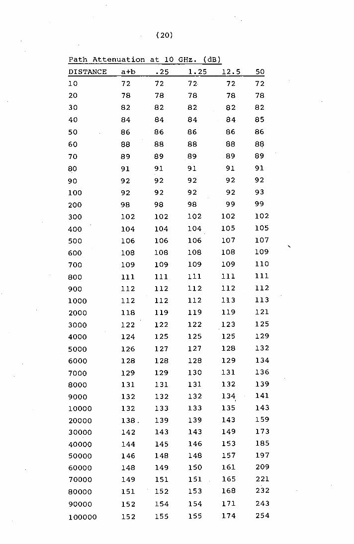
Where La and Lr are read off from the appropriate table and R is distance in meters.
A set
clearly
of tables' has
shows the
been
effects
compiled which more
of the various
attenuations. Three frequencies are chosen as
being three so called "windows u•
See overleaf.
(20)
Path Attenuation at 10 GHz. (dB)
DISTANCE a+b .25 1. 25 12.5 50
10 72 72 72 72 72
20 78 78 78 78 78
30 82 82 82 82 82
40 84 84 84 84 85
50 86 86 86 86 86
60 88 88 88 88 88
70 89 89 89 89 89
80 91 91 91 91 91
90 92 92 92 92 92
100 92 92 92 92 93
200 98 98 98 99 99
300 102 102 102 102 102
400 104 104 104 105 105
500 106 106 106 107 107 "-
600 108 108 108 108 109
700 109 109 109 109 110
800 III III III III III
900 112 112 112 112 112
1000 112 112 112 113 113
2000 118 119 119 119 121
3000 122 122 122 123 125
4000 124 125 125 125 129
5000 126 127 127 128 132
6000 128 128 128 129 134
7000 129 129 130 131 136
8000 131 131 131 132 139
9000 132 132 132 134 141
10000 132 133 133 135 143
20000 138. 139 139 143 159
30000 142 143 143 149 173
40000 144 145 146 153 185
50000 146 148 148 157 197
60000 148 149 150 161 209
70000 149 151 151 165 221
80000 151 152 153 168 232
90000 152 154 154 171 243
100000 152 155 155 174 254

(21)
Path Attenuation at 35 GHz. (dB)
DISTANCE a+b .25 1. 25 12.5 50
10 83 83 83 83 83
20 89 89 89 89 90
30 93 93 93 93 93
40 95 95 95 95 96
50 97 97 97 97 98
60 99 99 99 99 100
70 100 100 100 100 101
80 101 101 101 102 102
90 102 102 102 103 103
100 103 103 103 104 104
200 109 109 109 110 112
300 113 113 113 114 116
400 115 115 116 116 120
500 117 117 117 118 123
600 119 119 119 120 126
700 120 120 120 122 128
800 121 122 122 123 130
900 122 123 123 124 132
1000 123 124- 124 126 134
2000 129 130 130 134 152
3000 133 133 134 140 166
4000 135 136 137 144 180
5000 137 138 139 148 193
-6000 139 140 141 152 206
7000 140 142 143 156 218
8000 141 143 144 159 230
9000 142 144 145 162 243
10000 143 145 147 166 255
20000 149 153 156 194 372
30000 153 159 163 220 487
40000 155 163 169 245 601
50000 157 167 174 269 714
60000 159 170 179 293 827
70000 160 174 184 316 939
80000 161 177 189 340
90000 162 180 193 363
100000 163 182 197 386

(22)
Path Attenuation at 90 GHz. (dB)
DISTANCE a+b .25 1. 25 12.5 50
10 92 92 92 92 92
20 98 98 98 98 98
30 101 lOr 101 101 102
40 104 1.04 104 104 104
SO 106 106 106 106 107
60 107 107 107 108 108
7.0 108 108 109 109 110
8.0 lID 110 110 110 III
90 III III III III 113
100 112 112 112 112 114
200 118 118 118 119 122
300 121 121 121 123 127
400 124 124 124 127 132
500 126 126 126 129 136
600 127 128 128 132 140
700 128 129 129 134 143
800 130 130 131 136 147
900 131 131 132 137 150
1000 132 132 133 139 153
2000 138 139 140 152 180
3.000 141 143 145 163 ·205
4000 144 146 149 173 229
5.000 146 149 153 183 253
6000 147 151 155 191 275
7000 148 153 158 20.0 298
800.0 150 155 161 209 321
9000 151 157 163 217 343
10000 152 159 166 226 366
2.0000 158 172 186 306 586
30000 161 182 203 383 803
4000.0 164 192 220 460
50000 166 201 236 536
60000 167 209 251 611
70000 168 217 266
80000 170 226 282
90000 171 234 297
100000 172 242 312

2.2.4
(23)
Now the maximum Path Loss can be calculated as
follows:-
Lp(dB) = 10Log(Po/Ni ) - 10Log(F) +
10Log(Gr ) + 10Log(Gt )
The maximum useable range can now be read off the
appropriate table.
Example
Say N. = JeTB = IE-IS 1-
P = 50E-3 watts 0
F = 25.5dB
Gr = 27dB
Gt = 30dB
Therefore L (max) = l68dB P .
Using the charts gives the following ranges.
Distance a+b 0.25 1.25 12.5 50
10 GHz >lOOKm >lOOKm >lOOKm >lOOKm >lOOKm
35 GHz >lOOKm 50Km 40Km lOKm 3Km
90 GHz 70Km 20Km lOKm 4Km lKm
Conclusion
Concluding this section it can be pointed out that
NF subtracts directly from the maximum usable Path
Loss. This fact is independant of either the band
width of the receiver or the ratio of signal power
to noise power at the detector.

( 24)
Further it can be noted that the Noise Factor of
most Microwave Systems can be directly related to
the front end. e.g. The Mixer Diode. The IF
Amplifier works at low frequencies and hence can
have good Noise figures.
The price of the Microwave Mixer Diode relates
directly to the systems performance.
***000***

(25)
2.3 GUNN Theory:- The Transfered Electron Effect
2.3.1
2.3.2
It is hoped in this section to describe the
operation of the GUNN Diode and hence to explain
the dynamic characteristic of the GUNN Diodes
transfer function.
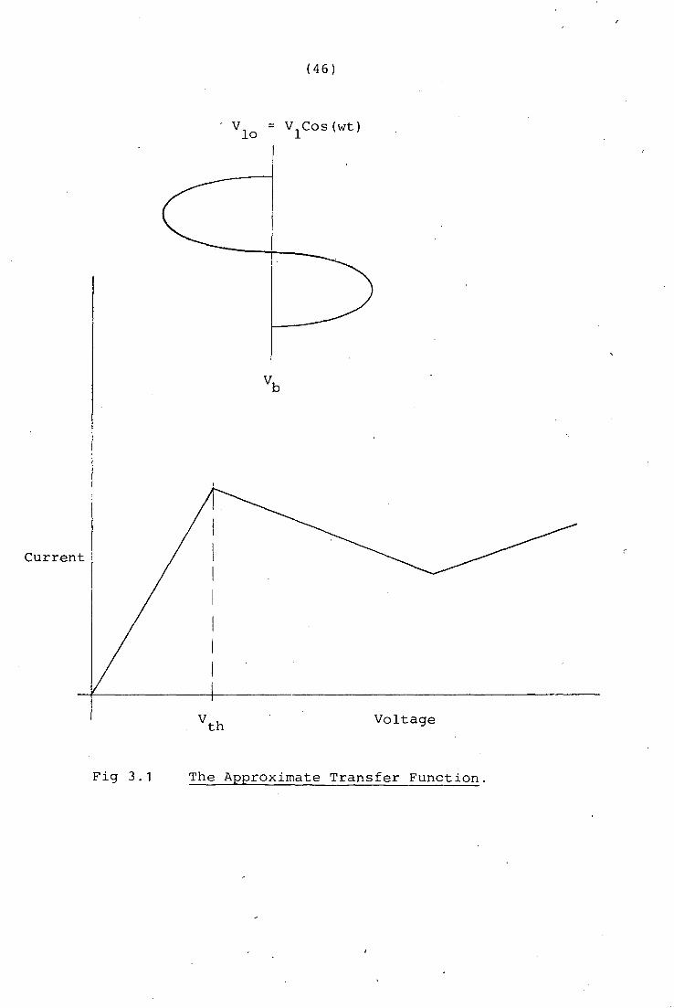
The Transfer Function
The current to voltage characteristic can be.
drawn for low frequencies as in Fig 2.4.
v The characteristic can generally be approximated
by two straight lines as the Bias Voltage added
to the Local Oscillator swing will generally
never take the voltage into the area of the
ultimate bulk resistence.
The Transfered Electron Effect
The shape of the characteristic is due to to what
is called the Transfered Electron Effect. This
can be summarised as follows.
...

(26)
2.3.2.1 The Two Valley Model Theory
Gallium Arsenide is one of· a class of
semi-conductors which has unusual properties of
the electrons in its conduction band.
i.e. The electrons are to be found in one of two
different valleys in the conduction band. The
unusual property is that the electrons in the
higher energy valley in fact have .lower mobility
than electrons in the lower energy valley.
The conductivity, given by s, of the n-type GaAs
is given as follows:-
Where e = electron charged
m1 = mobility in the lower valley
m = mobility in the upper valley u
n l = electron density in the lower valley
n = u electron density in the upper valley
If the applied electric field is increased some
electrons will scatter into the upper valley. If
some electrons are still present in the lower
valley a negative conductance region exists.
When all electrons are scattered into the upper
valley the conductance is once more posit.ive.

(27)
This is known .as the Two Valley Model Theory· and the
mathematical description is as follows.
Differentiating (1) with respect to E gives :-
ds/dE = e[ml(dnl/dE) + mu(dnu/dE)] + e[nl(dml/dE) + nu(dmu/dE)]- - -(2)
If the total number of electrons is given by n
+ nu and it is assumed that ml and mu
proportional to EP , where p is constant, then :-
= n 1
d n = dE = 0 -- - - - - - - - - - - - -(3)
(4)
Also dm/dE· is proportional to dEP/dE which is
equal to pEP-l and also to ·pEP/E, which is
again proportional to pm/E.- - - - - - - - - - - ( 5)
By substituting equations ( 3 ) and ( 5 ) into ( 1) we
get :-
ds/dE = e(ml - mu)dnl/dE
. + e(nlml + numu)p/E
- - - - (6)
Now Ohms Law J = s.E can be differentiated with.
respect to E as follows:-
dJ/dE = s + E.ds/dE
are

(28)
This may be rewritten as:-
1 dJ 5 dE = 1 + ds/dE
s/E - - - - - - - - - (7)
Now in a negative resistance region the ratio dJ/dE
must be negative. This would be true if:-
ds/dE > 1 - - - - - - - - - - - - - -(8) s/E
Now putting equations (1) and (6) into (8) gives:-
Notes:
l) The exponent p is a function of the lattice
scattering mechanism and should be negative and
large.
2) The term + fm) u must be
positive to satisfy the inequality. Thus ml is
greater
valley
than m. Electrons u and transfer to a
begin in. a low
high mass valley.
mass
The
maximum value of this term is unity, implying that
ml is much greater than mu'
(29)
3) The term dnl/dE must be negative. This
quantity represents the rate with which electrons transfer to the upper valley with· respect to the electric field, and will depend on differences
between electron densities, electron temperatures
and energy gaps between the two valleys.
In practice this means that the semi-conductor
should satisfy three criteria in order to exhibit
negative resistance.
a) The energy level. between the bottom of the lower
and the bottom of the upper valley must be much
larger than the thermal energy at normal ambient
t·emperatures. ie greater than O. 026eV.
b) The energy difference between the two valleys
must be smaller than the difference between the
conduction and valence bands.
c) The electron velocities must be much lower in
the upper valley than in the lower valley.
Some of the semi-conductors that satisfy these
requirements are Gallium Arsenide (GaAs), Indium
Phosphide (InP) and Cadmium Telluride (CdTe).
The Transfered Electron Effect can be shown
graphically as in Fig 2.5.
In practice the characteristic of GaAs is as in
Fig 2.6.

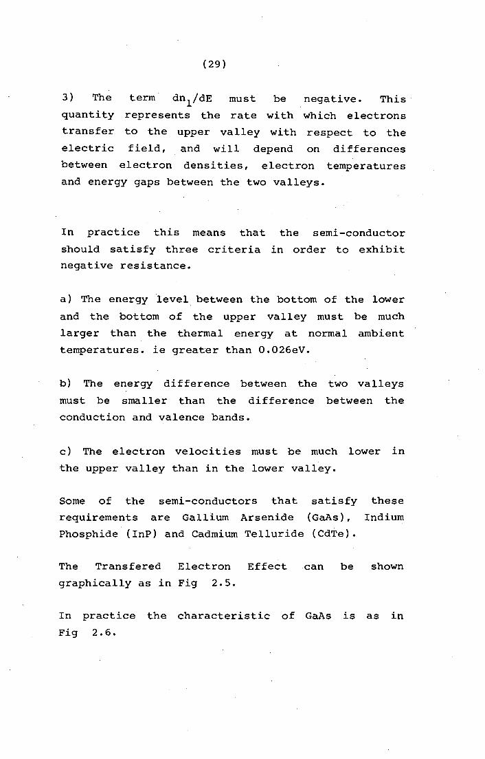
E t
0 I~ Q
E<E1
(30 )
Upper Valley
Lower Valley V ) Conduction
Delta E = • 36eV J Band
----1-----_________ _
Eg_ = 1. 43eV
_______ t ____ _ K
E +
v I
!~ , 00
0 I --~ .... K 0 K
El < E<Eu
E
0
Forbidden Band
Valence Band
\ ___ J 0
Eu<E
Fig 2.5. The Transfered Electron Effect
~owoo 000 00
K

J
3xl0 7
2xl0 7
Drift Velocity
I
/
( 31)
/ Original Bulk Resistence
J ~
V ~ ~
L r----r---
V
I (crn/s)
o o 1
Fig 2.6
2 3 4 5
Electric Field 6 7
{KV /ern)
Characteristic of GaAs.
Bulk Resistence
E
8 9 10 11

(32)
2.3.2.2 The High Field Domain Theory.
The previous section, 2.3.2.1 explained why the
bulk semi-conductor exhibits negative resistance.
It is possible to take this negative resistance as
an observed. phenomenon and to apply it to an RLC'
cir~uit and then to explain the resulting
oscillations by means of Circuit Theory. This
ucircuits" approach will not however help the
semi-conductor physisist to explain the
oscillations of current in the device on its own,
nor will it help him in the design of Solid State
Sources. The High Field Domain Theory attempts to
do this.
In the n-type GaAs the majority carriers· are
electrons. When the applied voltage is low the
Electric Field and conduction current density are
uniform throughout the device. The conduction
current density is given by:-
where:-
J = Conduction current density.
s = Conductivity.
Ex = Electric field in the x direction.
L = Length of the device.

(33)
v = Applied voltage.
p' = Charge density.
v = x Drift velocity in the x direction.
U = Unit vector in the x direction. x
The density of donors less the density of acceptors
is call.ed the "Doping". When the space is zero the
carrier density is equal to the doping. If the
applied voltage is above the threshold value of
about 3000 V /cm then a high field domain is formed
near the cathode that reduces the electric field in
the rest of the material and causes the current to
drop to about 2/3 of its maximum value. This can
be illustrated by the expression for applied
voltage:-
V is constant and hence the electric field is non
linear.
The high field domain then drifts with the carrier
stream across the electrodes and disappears at the
anode contact.
in general the high field domain has the following
properties:-
1) A domain will start to form whenever the
electric field in a region of the sample
increases above a certain threshold field.
(34)
The domain will drift through the sample with
the carrier drift.
2) On applying additional voltage the domain
will increase in size and absorb more voltage
than was added and current will decrease.
3)
4)
A domain will
the anode
not disappear before reaching
unless the voltage drops
appreciably below threshold.
The formation of a
prevented by
threshold.
reducing
new domain can be
the voltage below
5) A domain will modulate the current in the
device as it passes through regions of
different doping or different cross section.
6) The domain's length is generally inversely
proportional to doping.
The formation of an electron dipole layer in GaAs
can be shown as in Fig 2.7.

(35)
I _ L
l -I +
I +
Dn Dipole ~
r--
L 0
I 0 X
EI ."",,---
E2
L 'E
1 1 x
V
x
Fig 2.7 Formation of a Dipol.e Layer.

(36)
2.3.3 Modes of Operation
The four modes of operation are as follows:-
GUNN Oscillation Mode
.Stable Amplification Mode
LSA Oscillation Mode
First
Second
Third
Fourth Bias Circuit Oscillation Mode
The first, second and fourth modes are of
interest to us in this investigation. The first
will be described here, the second in Chapter 4
and the fourth in Chapter 3.
"2.3.3.1 GUNN Oscillation Modes
GUNN observed perturbations of current in the
bulk semi-conductor at a frequency given by:-
Where Vdom is the domain velocity
Leff is the effective length of the sample
These oscillations will generally
product noL lies in the range of
lOE14/cm2 •
a} Transition Time Domain Mode
occur if the
lOE12/cm2 to
This implies that the device is in a non
resonant circuit.
2.3.4
(3?)
Vd = vs = fL = + lOE? cm/s
b) Delayed Domain Mode
lOE? cm/s > fL > lOE6 cm/s
The field would . be oscillating more slowly than
the transit time of the device. ie. to > tt
c) Quenched Domain Mode
fL > 2 x lOE? cm/s
This means
domain is
anode.
that t , 0
quenched
Practical GUNN Sources
is less than t 2 •
before it reaches
The
the
In general the device will be operated in a
resonant cavity coupled to a waveguide. In many
cases it will be loosely coupled to a varactor to
provide tuning of the centre frequency of the
source. (Refer to 30).
***000***
(38)
2.4 Noise Generation in GUNN Oscillators.
2.4.1
In this section it is hoped to describe the
various forms of noise to be found close to the
centre frequency of a GUNN Oscillator. The Noise
at a frequency shifted from the carrier by the
I. F. frequency is important as i tappears as the
intrinsic noise input of the Self
Oscillator.
Thermal Noise Generation.
Mixing
This noise is generally referred to as the A.M.
noise of the device. It is only of significance
at high IF frequencies as it is usually several
orders of magnitude lower than the F.M. noise. It
is actually difficult to measure as its amplitude
is very low. It can be simply described as
follows.
The device has a certain resistance and when
operating has a certain noise temperature. This
generates the usual White Noise. This noise
power amplitude modulates the GUNN in a cavity of
a certain Q. The bandpass characteristic is now
imposed onto the White Noise generator giving
rise to the spectrum appearing as in Fig 2.8.
This diagram excludes the F .M. noise generation.
Josenhans in reference 17 measured a noise to
carrier ratio of -120dB at a point 100KHz from
the carrier. In our application of the Self
Mixing Oscillator we are generally interested in
frequencies above lOMHz from carrier and hence we
can expect N/C ratios of at least as large as
-160dB.

(39)
Carrier
M. Noise
+f
Fig 2.8. White Noise of the GUNN Source.

2.4.2
(40)
Upconverted Noise Generation.
This noise spectrum takes on a somewhat different
appearance to that of the A.M. spectrum. It is
upconverted noise and is generated by the process
of F.M. modulation of the GUNN source.
The frequency of the GUNN source has a dependance --,
on the supply voltage and the current flowing in
the device. The bulk semiconductor exhibits Shot
Noise, Flicker Noise and Thermal Noise in its
current flow and hence the center frequency is
mOdulated according to some function of these
. noise currents.
The mathematical treatment in general involves a
statistical analysis of the modulation current
and hence an application of this function to the
modulation· spectrum. This treatment is however
not very clear in its explaination of the actual
process of upconversion.
could be as follows.
A clearer description
Given that the current in the device is equal to
the quiescent current(Io ) added to the noise
current (In) •
If K and 10 are constant then :-
or more correctly:-

.( 41)
as In is itself a function Of t.
instantaneous signal output of the
oscillator can be written as follows:-
So = scos(wot + Mj9(t)dt) - - - - - - - (a)
The
GUNN
The conversion of such a time domain expression
into a frequency domain expression is very
difficult unless get) can be represented
sinusoidaly. In fact In can be shown to have a
spectral form with a maximum at I and tailing o off at the rate of 6dB per octave or at another
rate dependant on the ratio of l!fv • If this
spectrum where applied to expression (a) the
modulation process should result in a similar
spectral pattern around the centre frequency of
the GUNN diode.
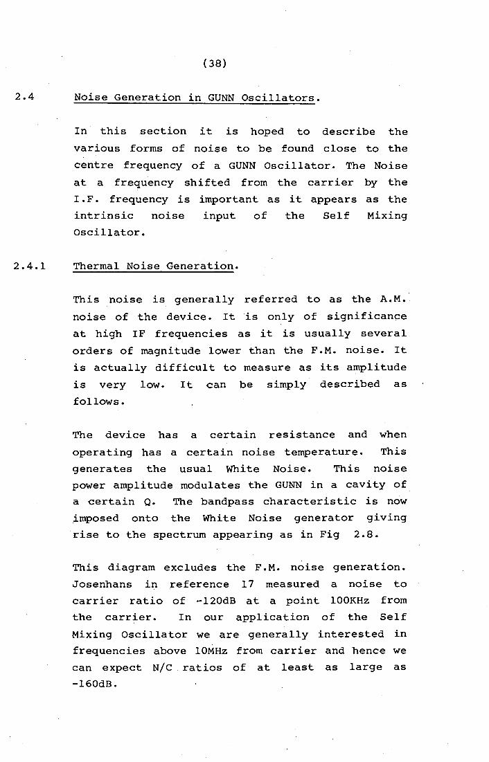
Matsuno in reference 25 shows that in fact the
ratio of F.M. noise to carrier power drops by as
much as 9dB per octave in the region close to
carrier. Matsuno measured the noise spectrum of
a cavity controlled GUNN oscillator with various
Qs and his results are repeated here as in Fig
2.9.
A fuller explanation of GUNN diode noise is
beyond this scope of this chapter. The reader is
referred to references 16, 17, 19, 22, 23, 25,
33, 35 and to Section 3.4 following in the next
chapter.
***000***
(42)
Carrier
9dB per Octave
6dB per Octave
A.M.Noise
-f +f
Fig 2.9. FM Noise of the GUNN Source.

II
(43 )
Chapter 3
THE DEVICE AS A MIXER.

(44)
3.1 Mixer Operation.
3.1.1
In this section an explanation will be given as
to how the device operates as a mixer. The
approach used is only one of a number of possible £
approaches that are possible. In the authors ~~--
opinion this particular approach most readily
lends itself to analysis. The . main al ternati ve
approach will also be discussed but in Chapter 4.
Symbols Used.
L c
r p
r n
Note.
= Conversion Loss.
= Power available to IF/Power input.
= Conversion Loss in dBs.
= lOLoglO(Lc )
= Positive resistance of the GUNN Diode.
ie. In the region before threshold.
= Negative resistance of the GUNN Diode.
ie. In the region after threshold.
r p are set by the inherent
properties
and
of GaAs semiconductor. See
references 20, 21 and 37.
P = Refl·ection Coefficient in the region p before threshold.
P = Reflection n Coefficient in the region
after threshold.
pet) = Time dependant Reflection Coefficient.

3.1.2
(45)
PO'Pl etc.
= Fourier Coefficients of P{t).
Vb = DC Bias Voltage on the device.
Vl = Amplitude of the Local Oscillator
signal.
V th = Thres,hold Voltage.
T = Conduction Time. This refers to the c
z o
Fourier Analysis.
= Charateristic Impedance of the
Waveguide.
The Transfer Characteristic.
The characteristic as given in section 2.3.1 can
be approximated by two straight lines. This
seems to be quite close to the actua'l si'tuation
exept that some hysteresis is apparent when the
local oscillator signal is applied. This will
not effect the amplitude of the Fourier
Coefficients, but will effect their phase. The
approximate transfer function together with the
local oscillator signal can be drawn as follows
as in Fig 3 .. 1.
(46 )
Current
Voltage
Fig 3.1 The Approximate Transfer Function.
3.1.3
(47)
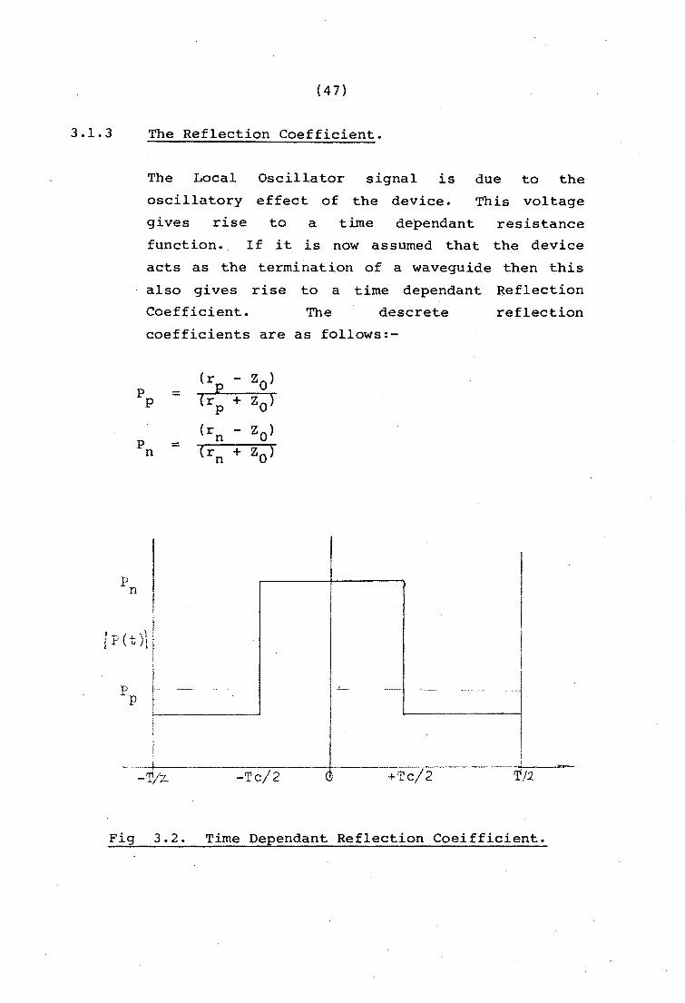
The Reflection Coefficient.
The Local Oscillator signal is due to the
oscillatory effect of the device. This voltage
gives rise to a time dependant resistance
function.. If it is now assumed that the device
acts as the termination of a waveguide then this
also gives rise to a time dependant Reflection
Coefficient. The descrete reflecticn
coefficients are as follows:-
(r - ZO) Pp = 2
ZO) (rp +
P
p n
= n
(r - ZO) n (r
n + ZO)
I P ( t )\ / ,
- .. --- -----~ _ .....
J
i I J i
2. -Tc / 2 ( +rc/2 T /1
Fig 3.2. Time Dependant Reflection Coeifficient.
(48)
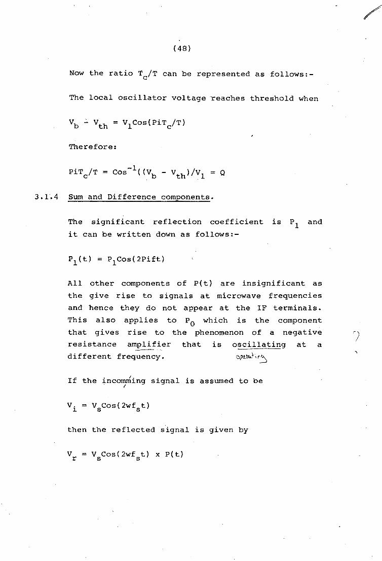
Now the ratio T IT can be represented as follows:c
The local oscillator voltage ~eaches threshold when
Therefore:
3.1.4 Sum and Difference components.
The significant reflection coefficient is PI and
it can be written down as follows:-
All other components of P(t) are insignificant as
the give rise to signals at microwave frequencies
and hence they do not appear at the IF terminals.
This also applies to Po which is the component
that gives rise to the phenomenon of a negative
resistance amplifier that is oscillating at a --different frequency.
If the inco~ing signal is assumed to be . I
then the reflected s'ignal is given by
= V Cos(2wf t) x pet} s s
/
"'
(49)
except that the difference signal will not
propagate in the waveguide and will be absorbed by
the IF terminals. This signal is given by:-
3.1. 5 Conversion Loss.
Conversion Loss is given by:-
Assuming correct matching of the incident and IF
signals then:-
This means that Lc can be given asfollows:-
L c . 2
= «Pn - P )/w x Sin(Q» p.
Thus the expression has two distinct components.
The component due to conductance of the terminating
device and the componerit due to the conduction
angle Q.
3.1.6 Arrival at Noise Figure.
The expression given in section/2.1.2 can be
rewritten to give a better form for this section.
F = S.N /(S N.) l. 0 0 l.
(50)
- - - - - (a)
F = «Pn - P )/w x Sin(Q»2 x (N /N.) P . 0 l.
Or this can again" be rewritten according to the
expression in section 2.1.4. Note that the above
expression is merely exp1isive and not analytical.
Now using the noise Temperature definition
F = L (F' f - 1 + t) C l.
Lct is
1) is
Formula.
the
the
above
second
expression
expression
(a) and
of Friis'
From the expression it can be seen that all terms
are a product of Lc. If the IF is ideal then
F if is equal to one, and the second term
dissapears and we return (a).
Also from section 2.1.3 we see that the equivalent
input noise signal can be represented by:-
N. = (F - l)kTB l.
/
(51)
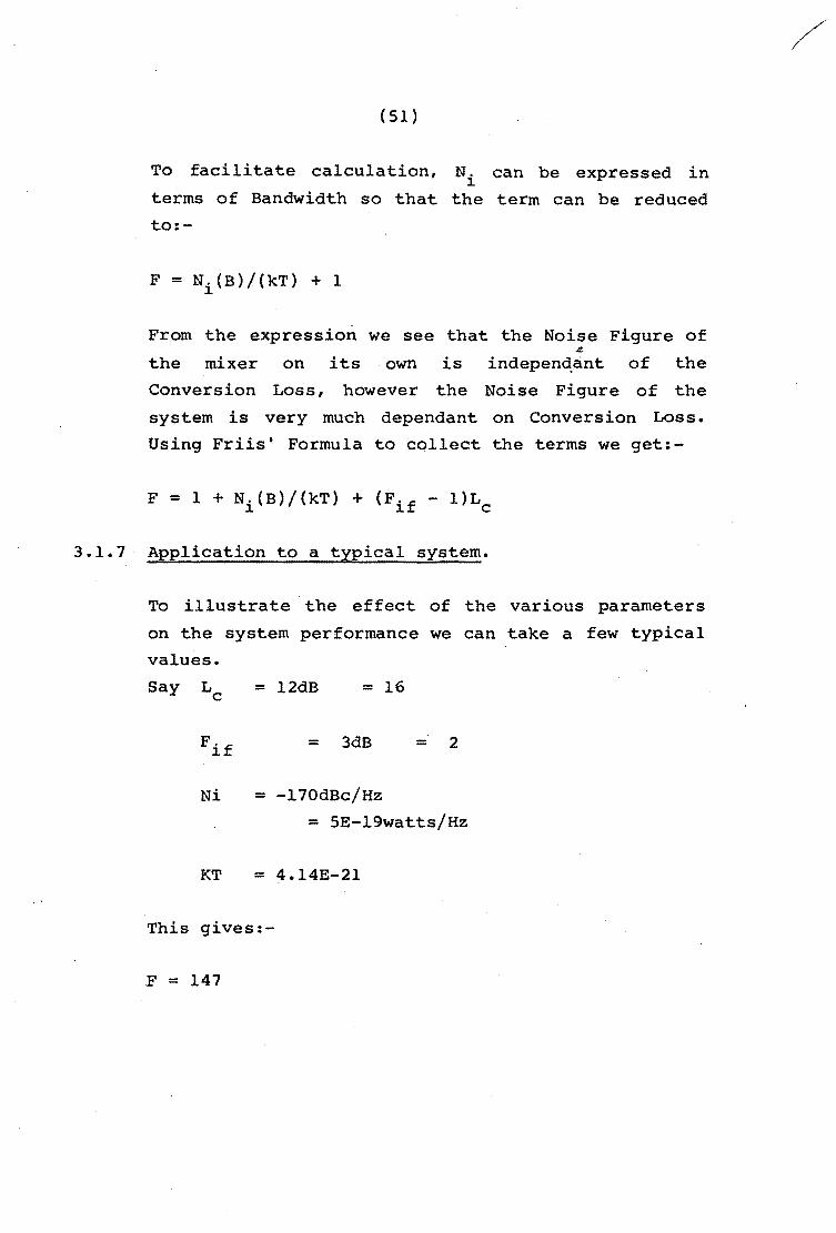
To facilitate calculation, Ni can be expressed in
terms of Bandwidth so that the term can be reduced
to:-
From the expression we see that the Noise Figure of JI.
the mixer on its own is indepenqant of the
Conversion Loss, however the Noise Figure of the
system is very much dependant on Conversion Loss.
Using Friis' Formula to collect the terms we get:-
3.1.7 Application to a typical system.
To illustrate the effect of the various parameters
on the system performance we can take a few typical
values.
= 12dB = 16
= 3dB = 2
Ni = -170dBc/Hz
= 5E-19watts/Hz
KT = 4.14E-21
This gives:-
F == 147

(52)
And
NF = 22dB
Note that the value given for N. is obtained from l.
the curves given in section 2.4.2.
3.1.8 Noise Figure measurement.
This section describes the methods used for
measuring the Noise Figures. The methods make use
of the expression for Noise Figure as follows:-
Where the first part of the expression is called
the Excess Noise Ratio and is given by the
manufacturer of the noise source, and the second
part of the expression Ne/NQ is the ratio
powers measured with the noise source active
and the inactive (No)' The
derived very easily as follows:-
Ne = KToBGc + (F - l)KToBGc
and
+ K(T - T )BG e 0 c
expression
This means that N /N can be reduced to:e 0
can
of
(N ) e be
(53 )
Solving for F gives:-
and hence taking the logs of both sides gives the
expression for NF.
If the reader requires further information the he
is referred to section 2.1 and to r~ferences 40 and
41.
A further note can be made concerning errors due to
mismatch of the noise source into the device under
test. This will effectively reduce the Excess
Noise Ratio. If for example the input Standing
Wave Ratio of the OUT is 1.2:1 then the mismatch
loss will be 0.83dB and hence the Excess Noise
Ratio will be reduced by this much. In practice
the sorts of Noise Figures that
are so high that this mismatch
we are measuring
loss will not be
significant. ego On a Noise Figure of 27dB a
mismatch loss of 0.83dB will be about 10% in the
actual ratios, and this will generally be of the
order of the measurement errors at these sorts of
power levels.
3.1.9 Procedure for Noise Figure measurement.
Measurements were done using both
technique and an Automatic technique.
a Manual
The Manual setup was as follows as in Fig 3.3.

( 54)
The Automatic setup was very similar to the manual
one, except that an Automatic Noise Figure Bridge
was used. The type is a Saunders No. 5440c. The
unit switches the noise source on and of at a set
rate and takes the appropriate power levels
automaticaly, then calculates the Noise Figure and
displays it on a digital display.
Swept frequency measurements were made by changing
the Local Oscillator frequencies as follows:-
Case L lOMHz to 110MHz
flo = 55MHz to l55MHz
fif = 45MHz
Low Pass Filter in position.
Case 2. lOOMHz to 200MHz
flo = 55MHz to l55MHz
fif = 45MHz
High Pass Filter in position.

Noise Source l---t
+28 volt.s
(55 )
Isolator
Device l--"""'Under 1 __ .....jTest.
Fig 3.3. . Manual Setup..:..
Power Met.er

Noise Source
(56)
Isolator
Unit
Fig 3.4.
. Device Under
-- ·Test
Arithmetic Unit
Digital Display
Automa 1. t 'c Setup.
--

(57)
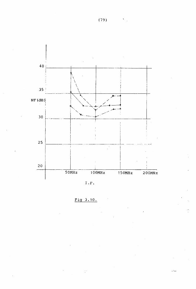
3.1.10 Results on 4 Sources.
NE
The graph in Fig 3.5. shows theoretical Noise
Figures of 4 different sources plotted over an IF
frequency of lOMHz to 200MHz. The actual measured
Noise Figures are then shown. ,
"" i
"" "' 1", 1/, eslse· iT I i POt eI ev' 'l /' ~ / P D ce
~ ~
\ I !
\ II-' .i' ~s~ !e~ \ L~U'l I J ! 1.....-I'--.
DC Til 2 I~ w. ~/ / K LY J I
\ / 1'-- • ........
" / "l.h i /
r'\.. V \[7 ,,, V I I . l
P\ I , I
(d 13) I I
I I i ; I
/' I I I I
II tE 3.1 He at Ii in k i 1 I gr I
\,1 ! . I_- I I t-.. ...... [ I
t-:J i _.- J
....... 0-- - ! I I i I
I I i I
! , I i ! I ,
I I ; I I i
, I I I
, , I , I I I I I j !
2·) i ,
! ! I I i
,1 ! ,
. I I r 1
i I !
! i
~ , I
I I i i
I ! I I I
jtl~ 1HZ I I !UM !tlZ 1 -t IUU r'lH 1: 5Uf'1H , ·UUf1fff : i , I
I i [ I ,
i i I
I j I I I
Fig 3.5. Noise Figures against Frequency.
***000***

(58)
3.2 Effects of D.C. Bias Voltage.
The bias voltage as related to the threshold
voltage affects certain parameters of the device.
The parameters it affects are Noise Generation,
Conversion Loss and Power Output. All these
parameters affect .the Noise Figure.
will show these effects.
This section
3.2.1 Effect on Noise Generation.
Matsuno in reference 25 shows that the Noise Power
Spectrum is much dependant on the RMS amplitude of
the fundamental oscillations. The RMS amplitude
gives the power output of the source and this is
much dependant on the D.C. bias voltage.
Matsuno shows that the Noise Power increase at any
particular frequency shift from the carrier is
largely proportional to the increase in the RMS
Amplitude of the oscillations. This in turn is
proportional to D.C. Bias and hence also to power
output. This leads to the conclusion that Noise to
Carrier Ratio remains substantialy constant with
bias voltage.
that
F.M.
current
Noise
On the other hand Matsuno show~
fluctuations and
increased sharply
hence upconverted
as the applied
electric field approaches the threshold field.
This means that the Noise to Carrier ratio is not
much dependant on the Bias Voltage unless the Bias
Voltage is brought close to the Threshold Voltage.
/'

(59 )
3.2.2 Affect on Conversion Loss.
The expression for . Conversion Loss as derived in
section 3.1.5 can be written as follows:-
L = «p - P )/w x Sin(Q»2 c . n p
Where Q can be written as:-
From the expression it seems that Sin2 (Q) is at
a maximum when Vb = Vth • In practice this
would appear to be correct as this would indicate a
Time Depend..<:;(nt Reflection Coefficient with a mark
to space ratio of 1: 1. In reality there are some
difficul ties in achieving this. On the one hand
the amplitude of V 1 is somewhat dependant on Vb
and decreases as Vb decreases. On the other hand
it is very difficult to operate a GUNN Source with
a low Bias Voltage as the bias circuit becomes
unstable.
The expression for Q can be re-written to aid
analysis as follow:-
The expression can be plotted on a set of axis to
show the effect of the various parameters. Say
Lc =. Sin2 (Q) then Lc can be plotted as
as in Fig 3.6.
/

1
L I
C
Vth
Lower V
1
Fig 3.6.
(60)
--~

-10
-15
-20
(61)
To illustrate the theory a number of sources have
been measured for Conversion Loss against Bias
Voltage, and the results plotted as follows:-
Plessey "DOT" Device
----... - ...... --.. ----.... - .. --..... ---- .. -.--~-.
+-~-----------~-... --.--.-.. -... -_ .. _--_ ... --------_ ...... --
-J-4. () 4.5 5.0 5.5 6.0 6.5
Vb (volts) -
Fig 3.7.

(62)
3.2.3 Effect of Bias Voltage on Power Output.
output and
the Local
hence it
Oscillator
Bias voltage effects power
~/effects the amplitude of .p\.
Voltage. This in turn sffects the Conversion Loss
which has an effect on the Noise Figure. The main
influence on Noise. Figure is however caused by the
change. in the amplitude of the noise. input due to
the Local Oscillator. If it is assumed that the l
Noise to Carrier ratio remains essen~ally constant
with bias voltage, then the amplitude of the added
noise will have the same characteristic with
respect to bias voltage as does the power output.
This in turn will affect the Noise Figure almost
~irectly as shown in section 3.1.6 equation ( c) •
The contribution to Noise Figure· due to added noise
is far more significant than that due to the Noise
Figure of the IF in combination with the Conversion
Loss.
The diagram in the previous section shows the
effect of bias voltage on Conversion Loss and hence
on Noise Figure. As another illustration of this
effect a number of sources with widely ranging
output powers are plotted for Noise Figure. All
are Q Band sources and all are operated at
recommended bias voltages. (Fig 3.8.)

(63)
, , ---l---1f..-.....--.4------+-+--~- I I
! i
: I _;i_'_~ __ 4_' __ I:'_~-!_--"_-'-+_-_-+-~'_---'-+-;-_'-'--,-!_-' +i -_.-: __ ""'-.-_-.,--'-__ 1
Ii! I Ii! i : i II,' i 'i, II I i i ! ! I '
I 'A n ! i I I i I ! I I I ! I·----t-~-V-t--'..._t-t-: -1,'----.----:--, --+, --+---+--+I-+I--+! -+----!r~-+-+l -"'--If---l-+I--+!/-+--~ ,-
! I i
i : _1 I
i ! i ,i
i
I !
, ! !
i ,
I : ! j
i
i I I
I ' .~!' ; iii I
,
II : ,I i i iii ;
Fig 3.8.

( 64)
3.2.4 Conclusion.
It seems that Noise Figure is much dependant on
Bias Voltage but not because of change in
Conversion Loss. It is· affected by the amplitude
of added noise at the I.F. frequency of interest.
***000***

(65)
3.3 Effect of Rp and Rn on Conversion Loss.
The intrinsic factor (p p)2 plays a very n p
important part in the Conversion Loss of the device.
R - Z P P 0 =
P R + Zo P
R - Z P n 0 = n R + Z n 0
To find the optimum values of Rand R for the p n best Conversion Loss, we could differentiate the
term w.r.t the variable of interest.
2 _ P - Loss Term.
_ Z ) 2 (R-o P + Z - 2 R +
o P
However it is prol?ably easier to
the expression by inspection as
varies with its variable.
First as regards Rp.
- Zo) 2 + Z o
simply observe
the gain term
This term is usually not very variable and in any
case it only provides the loss component of the
conversion loss, whereas Rn can also provide a
gain term. Generally Rp will always be of the
order of +2 to +4 ohms, and hence P will always , p range between -1
Zo can generally
hundreds of ohms
and +1 depending on Zoe However
be assumed to. be of the order of
positive, and hence will
always be close to ~l.

,
(66)
Secondly as regards Rn
This term can range quite widely in magnitude but
will always be of the order of -100 to -200 ohms.
This means that P will always be of the n
magnitude of say -1.5 to -2.6.
We can now re-inspect the gain expression in terms
of its three parts. The first term (p ) 2 n is
the gain term and will always be positive. The
third term is a loss term and will always be less
than one and will always be positive.
The second term may represent gain or loss but will
generally be negative and will subtract from the
sum of the other two terms.
Case 1.
p = -0.99 P
p = n -2.0 (Rn = -150 Zo = 450)
p2 = 1.020 (= OdB)
Ca.se 2.
p p = -0.99
p = n -1.57 (Rn = -100 Zo = 450)
p2 = 0.33 (= - 4.8dB)
(67)
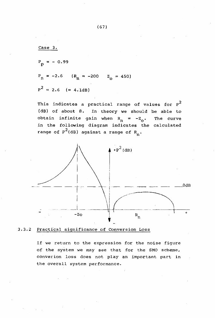
Case 3.
P = - 0.99 P
P = -2.6 (R = -200 Zo = 450) n n
p2 = 2.6 (= 4.ldB)
This indicates a practical range of values for p2
(dB) of about 8. In theory we should be able to
obtain infinite gain when R = -Z. The curve n 0
in the following diagram indicates the calculated
range of p2{dB) against a range of R • n
+p2(dB)
______ OdB --i«- 1-- ---~_l ___ ~-C-----~--r--
-Zo ~ Rn +
3.3.2 Practical significance of Conversion Loss
If we return to the expression for· the noise figure
of the system we may see that for the SMO scheme I
converion loss does not play an important part in
the overall system performance.
(68)
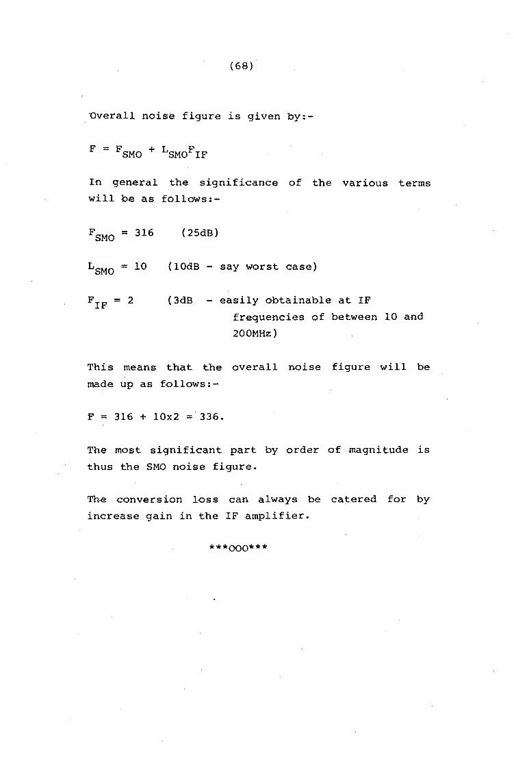
Overall noise figure is given by:-
In general the significance of the various terms
will be as follows:-
FSMO =
LSMO =
FIP =
316
10
2
(25dB)
(lOdB - say worst case)
(3dB - easily obtainable at IF
frequencies of between 10 and
200MHz)
This means that the overall noise figure will be
made up as foll·ows:-
F = 316 + 10x2 = 336.
The most significant part by order of magnitude is
thus the SMO noise figure.
The conversion loss can always be catered for by
increase gain in the IF amplifier.
***000***

(69)
3.4 Arrival at Noise Figure from Conversion Loss and
added Noise.
In this section we will try to show the form of the
noise skirts of a Gunn Source and how they give
rise to the Noise Figure.
3.4.1 Analysis of F.M. Noise of GUNN V.C.O.
Generally the instantaneas expression for an F.M.
modulated wave can be given as follows:-
Where E = Carrier Amplitude. c
Wc = Carrier Frequency.
w = Modulation Frequency m
B = Modulation Index
= fpeak/fm = wpeak/wm
Expanding the expression and setting Ec to 1
gives:-
e(t) = Cos(w t).Cos[BSin(w t)] -c m Sin(wct).Sin[BSin(wmt)]
Now for N.B.F.M. , that is with a modulation index
of much less than 1.5 we can approximate the
following:-

Cos[BSin(w t)] = 1 m
(70)
Sin[BSin(w t)] = BSin(w t» m m
The F.M. Wave now becomes:-
e(t) = cos(wctJ + (B/2)Cos(wc-wm)t +
(B/2)Cos(wc+wm)t
The expression is very similar to that for a Phase
Modulated wave, except that B is replaced by 0/2,
where 0 is Phase deviation.
A general way of specifying the noise level of an
oscillator is to use the concept of the single
Sideband to Carrier Ratio. This is defined as:-
SSB (dB) = 10L SSB Power N Carrier og Carrier Power = C
Given that the NBFM approximations hold then the
expression ca be written as:-
SSB (dB) 20L (B) Carrier = og 2
or:-
SSB (dB) = Carrier 20Log
Now given that
becomes:-fpk = 1.4 6. f rms the expression

(71)
SSB (~frms ) ~---:--(dB) = 20Log 1.4f Carrier m
Now in terms of phase deviation this is:-
SSB (dB) = 20Log (°2
\ Carrier )
The above .expressions apply to a single tone FM
modulation and its resultant sidebands. In general
the phase noise spectrum of a GUNN oscillator looks
something like Fig 3.9.
--------------~--------.~------------~----~--------------
f -f o m
Fig 3.9. Phase Noise Spectrum of typical GUNN.

(72)
The noise spectrum on each side of the carrier is
continuous, but it is possible to devide it into
strips of width B and then to generate a new
function as follows:-
If we first assume that the ammplitude of the noise
is constant over the width of the strip and the
that the strip is placed at fm removed from the
carrier then we may define a noise density function
as follows:-
D(f ) = Power Density(One Si~eband,Phase only) m Power(Total S1gnal)
The dimensions are Watts/Hz/Watts.
Using the single tone analogy we can see that:-
D( fm) = 20Log (~) dB/Hz
D(fm) = 20Lo9(~:~:) dB/Hz
If D(f) is measured and now plotted it will be m
plotted against a measuring bandwidth (BW). e.g. A
spectrum analyser will have an input filter set to
a certain bandwidth. To convert this spectrum to
D(f ) m in 1Hz of bandw id th we can use an
expression as follows:-
D(fm)l = SSB Noise Power(in BW) - lOLog(BW) dB/HZ Signal Power

(73)
We can now define the spectral function from the
density function as S(fm)BW' The Phase Noise
spectrum of the GUNN Oscillator will generally
appear to be as in Fig 3.10.
Hobson in reference 15 defines an expression for
the power spectral density of a GUNN Oscillator as
follows:-
b.BW
Where v is between 2 and 3. ie 2 indicates
6dB/Octaveand 3 indicates 9dB/Octave. The term b
is given as:-
b 0.94KT
X = A €"trE~
(!gf (:m3)
9dB
fa Q
(F kT)1 osc
2P s
OdB/octave
1-__ -:-1--____ """ ____ " ___ "'""_4",,,_:;:;: _____ "" """""------13J 72 ... f m a
Fig 3.10. Phase Noise spectrum of GUNN Osc.

( 74)
Hobson calculates the term appropriate to 1 ohm per
cm GaAs as follows:-
For a typical Q band device with a cavity 0 of say
lOO,b will calculate to:-
b = 185.5
Now for f m
greater than 1000Hz the term
more significant than (b/2)2, becomes much
the expression can be written as:-
b.BW
6.28fv m
We can thus derive an expression for the "a"
indicated in the previous diagram and repeated here
Slope in the Flicker Noise region is given by:-
(Given that BW = 1)
2
Slope( Flicker) = (fO) a 3 20 f m
We can solve for a as follows:-

a = 3.37E-7(O/f ) o
(75)
Now for an X band device we can calculate a value
for fa.
f occurs when:a
a
7 m
= F KT osc 2P f2
s m
This means that fa is given as:-
2aP s fa = =--...;..= F KT ose
For 0
P s
= 100
= 10E9Hz
= 50E-3Watts
F = 10 osc
This gives fa as
f = B.4KHz a
e.Manassawitch in his book on Frequency Synthesis9'rs
predicts an fa of 300KHz for an X band GUNN
source. On the one hand this would suggest a v of
about 2.5 or alternatively a cavity with a 0 much
higher than the 100 we used in our calculation.
/

(76)
If we now apply the expression to a Q band device
we <may obta,in a new value for b. We will use a
value of "a" proportionately smaller because of the
higher frequency.
a = 5.3E-15
f = l3.25KHz a
If we now assume that for frequencies above fa
the N/C ratio increases by 6dB per octave then we
may calculate the N/C ratio at any particular
frequency.
At about 12KHz Hobson suggests a N/C ratio of -60dB
in a bandwidth of 70Hz. This means that in 1Hz of
bandwidth the N/C ratio is -78dB.
Tabulating by octave we get:-
12Khz -78dB
24Khz -84dB
48Khz -90dB
96KHz -96dB
192KHz -102dB
384KHz -108dB
768KHz -114dB
1536KHz -120dB
3072KHz -126dB
6144KHz -132dB
l2288KHz -138dB
24576KHz -144dB
49l52KHz -lSOdB
98304KHZ -156dB
196608KHz -162dB
(77)
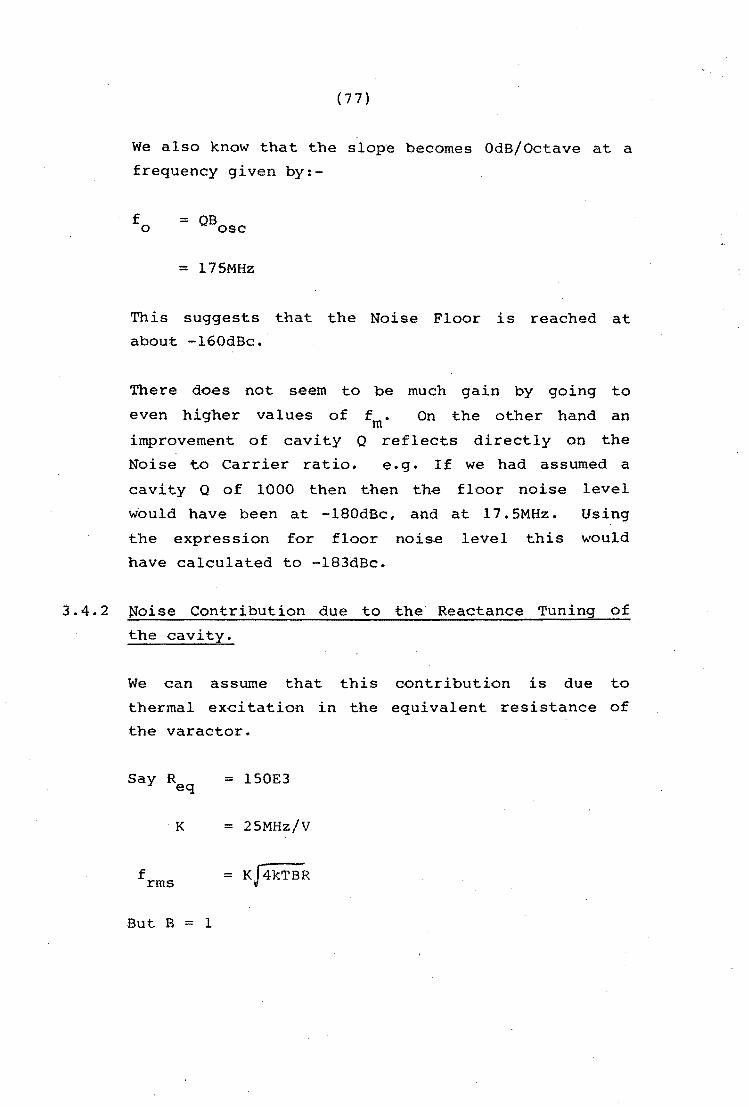
We also know that the slope becomes OdB/Octave at a
frequency given by:-
= 175MHz
This suggests that the Noise Floor is reached at
about -160dBc.·
There does not seem to be much gain by going to
even higher values of f m• On the other hand an
improvement of cavity Q reflects directly on the
Noise to Carrier ratio. e. g. If we had assumed a
cavity Q of 1000 then then the floor noise level
would have been at -180dBc, and at 17.SMHz. Using
the expression for floor noise level this would
have calculated to -183dBc.
3.4.2 tJoise Contribution due to the Reactance Tuning of
the cavity.
We can assume that this contribution is due to
thermal excitation in the equivalent resistance of
the varactor.
Say R eq = lSOE3
·K = 2SMHz/V
f = K[4kTBR rms
But B 1

(78)
i:::.frms = 1.22
N/C = 20Log(~f /(2f» rms m
At say f = 80MHz:m
N/C = -162dBc
This is quite close to the floor level found before
and hence it can be ignored.
3.4.3 Noise Figure from Added Noise.
Using the expression previously derived for Noise
Figure we can obtain a result by applying the floor
value for Added Noise.
F = 1 + N./KT J.
Say
= lOOmW~(-160dBc) W/Hz
= lE-17 W/Hz
KT = 4.l4E-2l W/Hz
This means that F calculates to:-
F = 2416
NF = 33.8dB
Fig 3.10 gives a set of typical devices as plotted.
(79)
40 i ________ ~---------~--~----~----------~ j
! 1 I
35 ;
NF (dB>! !
25
20
50MHz 100MHz 150MHz 200MHz
LF.
Fig 3. 10.
(80)
3.5 Effect of Matching Impedance at IF on Noise Figure
and System Performance
It is convenient to consider the effect of matching
impedance from two different aspects. The first
aspect being the way in which it affects the
intrinsic noise figure of the divice, and the
second aspect being the way it affects system noise
figure.
3.5.1 Effect on the device Parameters
The two device parameters considered are Noise
Figure and Conversion Loss.
Noise Figure appears to be substantially unaffected
by matching impedance. This matching impedance
seems to play very little part in the added noise
and hence very little part in the Noise Figure. On
the other hand it plays a very large part in the
Conversion Loss of the device.
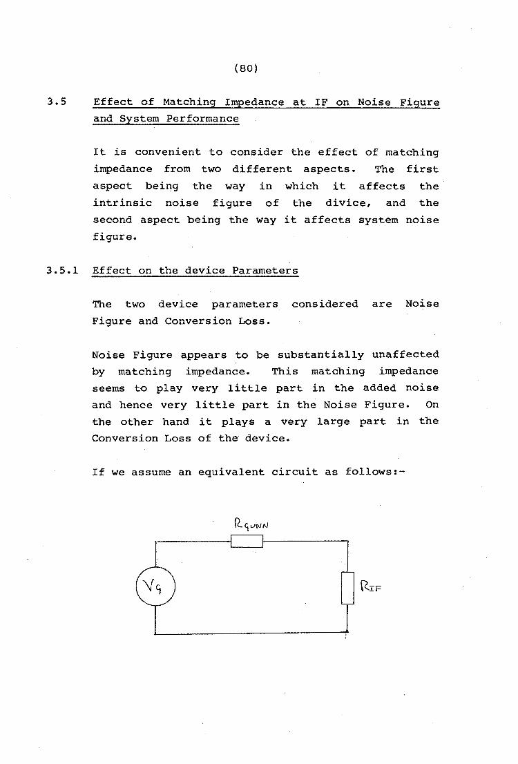
If we assume an equivalent circuit as fo11ows:-
(81 )
Where RGUNN is the output resistance to the IF of
the GUNN terminals and RIF is the loading
resistance of the IF.
P 1
Ptot =
= .2R + .. 2R ]. GUNN ]. IF
This expression is a maximum when RIF = RGUNN
The conversion loss of the device can now be
written as follows:-
L' c = Lc + lOLog R + RIF
GUNN
m!t;re Lc is the intrinsic loss of the device in

.' ,
(82)
This means that the conversion loss will in any
case alw'ays have a minimum of3dB. Unless the time
dependant reflection coefficient becomes such that
its gain is greater than 3dB.
3.5.2 Effect on System Performance
The overall system Noise Figure is given by:-
This means that the added conversion loss adds
directly to the Noise Figure, but is scaled by the
factor {FTF 1). If FIF tends to 1 t.hen this
factor dissapears.
The practical situation shows the significance of
the various terms.
If the designer were:;"r:equiring optimum range
performance from his system then he would choose an
IF amplifier with the best possible Noise Figure
and match it to the GUNN for optimum Noise Figure
rather than for optimum gain.
Taking two cases with NFGUNN = 25dB.
Case 1.
NF1P = 2.5dB
L"c = lldB

,
( 83)
Therefore
F = 316 + (1.778 - 1)12.59
F = 326 NF = 25.ldB
Case 2.
NFIF = 6.0dB
. L'c = 7dB
Therefore
F = 316 + (3.98 - 1)5.0
F = 330.9 NF = 25.2dB
This shows the very marginal effect that the
overall conversion loss L'c has on the system Noise
Figure. Suffice it to 'say that this should
generally be kept at atleast 10dB below the Noise
Figure of the GUNN.
In general there are so many other systematic
uncertainties that the matching impedance of the IF
plays only a marginal part in the system
performance.

(84)
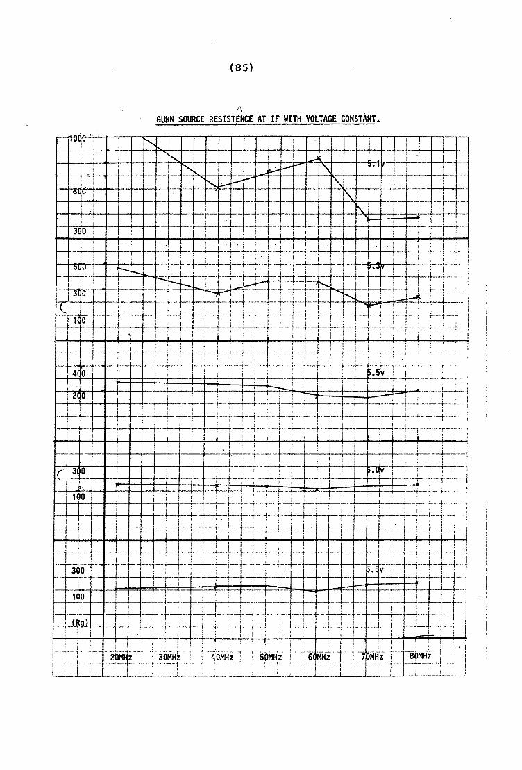
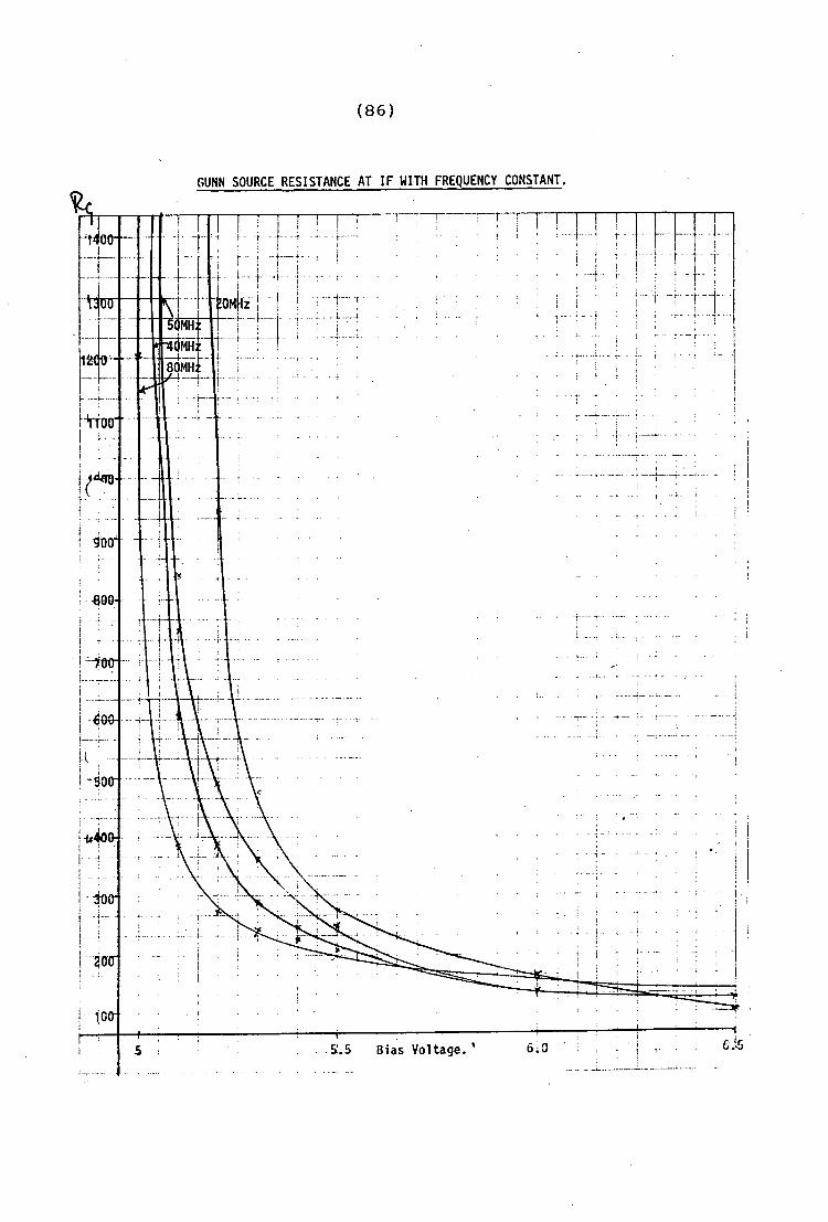
3.S.3 Measured Results
A ,<;UNN source was set up with an IF amplifier
turned to 73MHz with a bandpass of about 3MHz. The
GUNN device was then loaded with three different
resistors. SOohms, lOOohms and 500ohms. Change in
Noise Figure was unmeasureable and was about 27.SdB
with this particular device.
Note that the bias voltage was kept constant at the
nominal rated value. On the other hand if the bias
voltage were changed then wild variations are found
in impedance presented to the matching circuit and
oscillations are possible. This gives rise to what
seemed to be oscillations at the IF frequency which
cannot be distinguished from received IF power and
could thus lead to a quite erroneous Noise Figure
measurements.
For interest a set of curves is included showing
the change of GUNN impedance to the IF over a range
of bias voltages and fr,equencies. These results
were measured according to the technique given in
section 3.6.2.
***000***
(85)
A GUNN SOURCE RESISTENCE AT IF WITH VOLTAGE CONSTANT.
·It--J--~=3'j"'=O...,..· +-'-.f--+-'-.f--.f--~-+-+-.-.i---.j--+--.l..-.j- - L.I -TI- ---.'- --- -.- _._+--+--+---+--+--1- .-+_. >I I . I I ! I • ! i
I I I j I
4 0 !
i I I I : i i
, ! I I . ,
i
; : i_
I i _._-
i-f
-~
i i , I ,
, . ,
I ! , I ! I
-.~+-~~+-+-+-+-~~r-~t--~:-.t-'-4--.+-4-4-+-+-+-+-+-+-+-~_~._ti __ ~;.-·-i ~~~~+4-+~+-~-r4-+,~--+-_-.~1 ! !: ( 3 0 '; j ; i -+!.--1- ~.( v ! _, , __ 1 ... _ .... -'-+ .... '.J
"! , ' I I Iii ~--.... T! '
! 1 0 ' !" .. -f--'f- ;1 I '1--:--- .' , , ,I, i ' i I ~-+---!- -+ '1- .;..--..,.- I -+--~- i; ;_. -i-..
i· ! I, : i : i ,: '.'; . . ", -' , 1----"1--I'--l.............Jf----+---I--+-+-1---+---;--+---'---i---1-·T -- -1-.. ' --+ -~ i: : ! i'!: .: i • : i : I , : j , --+- r;, I j! ,'. -r--. -+1 -t- :--'+, i '~i I I I III I L Ii' , i ' i
I I I I 1 I I I i I tit 1 ! ,;, ! I • j ... +---!-_.t--- --. . I--+---:~! 1'''. -- '-1-~·-·..,--t . -+._-+---t- -I ' 1+ . " 'I ' , , I ,
d;-' ---I----.~---. j- - --i- t_ '1- -4- + 5-L -t-_ L ....,_-+--+--+-
3 0 "i I. i' . I • Sv; I ' . I ' - --1- --1-r-- 1 -to I I --f--- -- - -I -+-0----to
10 Iii 1-' I ,-t-~l I 1-------.l-------r--i-t-+-t--+-+"-+--i---·i-- '--- -.-- -_.
--~-j-- -T' +~- .. --1-. ...,- I--~- ~ - L j - -..... , -- r----,--t-+- -I!'--[i'=r--' ---; I I (Rg)!'! j' 1 'I I I I ',' ... ;-1' ,-- -·-...... ~~---I r 1'-' ---j---; , ,-;., : ,-- .... t - " ;- r-i..i.. j-; !
,·+ .. 1·; .... 2LM~Z 1!'36MH~' ',:,: .. --4i,tOMH.·Z: : 5bMH~ :6-MH~-i i-70M,¥-+.)-·i-86MHL 1 ' ,. +-I--t- ---~-~. :--1--t· 1 iii ._.f.-! j --- -+_.....l._.r- -!+ L-.L...J ' i :1 I I Iii ' I __ _
!
I~ r- - -. , ,
!-l
.aao
i : !-s
i ,
i I
I I I-
I
(86 )
GUNN SOURCE RESISTANCE AT IF WITH FREQUENCY CONSTANT.
-+--.~ M~ii--- j
.-- .
: --1---- -, .
+-t--t-F*="o+-+1+-, ~rtl '~" 80MH : i +--r- r-- --,
---4-- r--
--I
.s 5:.5
f-
Bias Voltage. ' 6;0
i-
+._-
, -- r -
, I . -t --:.-; .. --~-
! .. .;..,
l~ T -,,

(87)
3.6 Bias Circuit Stability.
The IF output of the source can be represented as a
Voltage Source (Thevenin) in series with a
resistance where the voltage is a Function of the
input. power. The equivalent circuit would be as
follows:-
R g
R. 3.
R
t V.=f(P ) R L
P 3. S
~
= Source Impedance of t.he GUNN.
= Parallel resistance of the inductor.
= Input resistance of the IF Amplifier.
3.6.1 Stability.
R. 3.
The int.erface is a Second Order resonant circiut.
If it is first assumed that the Q of the inductor
is ve:cy high then the total parallel resistance
becomes:-
R = t
R.R /(R. + R ) 3. g 3. g
The total parallel impedance can now be written as:-
t Vif
1

(88)
Z 1 S = C P (8 - 1 . )1 -(-2iJ) (s 1 jJ ~C -~itCl 2Rt C + J LC - --2Rt C
The real and imaginary portions of the complex
poles . can now be .extracted and plotted on an S
. plane diagram. Stability analysis is most easily
done by plotting the root loci of the poles. The
root locus is a circle as shown in Fig 3.11
The diagram shows four distinct regions,
can be analysed in these four •
. Region A = The overdamped case.
Region B = The underdamped case.
Region C = Sustained oscillation •. (Unstable)
Region D = Marginally stable. (Amplification)
and it
Regions C and D can easily be reached if the lossy
components in the system are more than counteracted
by the energy sources in the system.
Posi ti ve resistance can be regarded as an energy
sink while negative resistance can be regarded as
an energy source. More simply, Rg and Ri can
be regarded as a potentiometer and then v.f/V. l. . l.
is given as follows !-

(89)
A D
Fig 3.11

R -P g
=
Now if R g
----
--0
This is
R. 1
= -R. 1
I I I I I
= A v
then
(90)
A V
tends to
t Av
----
I I R =-R. R =0 g 1 g
the simple gain
infinity.
1
R g
curve, however
oscillations will occur under certain conditions
......p
because of the presence of the LC network. From
the locus diagram, oscillations will exist in
regionC.
follows:-
In terms of Rt the region is given as
If -1/2Rt C is greater than 0, and
(1/2Rt C)2 is less than or equal to l/LC then
the poles will lie in region C.
00

(91)
This means that Rt should must be bounded as
follows:-
Rt
Now
and
of R
( 0
R. is 1.
hence
. 9
constant, but R can become negative 9
the boundaries should be redrawn in terms
In order to meet the first condition,
Rt be negative, Rg must lie in the range:-
ie. that
o >R '>-R. . 9 1. - - - - - - - - - (a)
The second
set. The
R 9
= R .• 1.
left hand
stability
boundary is somewhat more difficult to
modulus of Rt tends to increase until
At this point the poles shift to the
side of the Pole/Zero diagram and
is reached. The breakpoint will thus
reached as follows:-
R. I Rg \ lJ1 1. = R. - I Rg \ 2 C 1.
or
I Rgi R.
1. =
J~ 2 R. +
1.
- - - - - - - - - - (b) 1

(92)
Now R ~ -R. to satisfy the first inequality g I 1.
(a) • This means that a state of oscillation will
exist while R ranges as follows:g
O)R '> -R. g 1. and
Now the second term of the inequality has a factor
greater than 1 in its denominator and hence it will
always be less than
amplification could
R .• 1.
thus
A state of controlled
concievably exist. The
range of Rg for controlled amplification ·would
thus be as follows:-
R. 1.
Rcan be plotted on a scale showing the various g regions where stability will occur.
+R 0 -R. 1
-R. 1
~.ji + 1 1
-R

(93)
3.6.2 Measurement of Rg.
P. 1.
Measur-~ment of R g cannot be done by dir-ect
measurement on a vector impedance bridge because of
the presence of energy sources other
bri-dqe supply. The alternative is to
than
place
the
the
component in a passive circuit and to measure it' s
effect on the circuit.
In ,the actual experement a high Q tuned cir-cuit
si.milar- to the circuit in the pr-evious
investi.gation was placed across the GUNN terminals
and the change in Q was measured. A pseudo white
noise source was applied at the Microwave Frequency
and the output spectrum was observed on a spectrum
analyser. The bandwidth and centre frequency could
then be readily observed. The block diagram was as
follows:-
,GUNN
Device
10MHz to 100MHz Spectrum Analyser

(94)
If it is assumed that R g
infinity to plus infinity
can range from
then there are
minus
three
possible results to be observed. (a) Reduction of
observed O. (b) Improvement of observed O. (c)A
state of oscillation. If the unloaded 0 of the
network is high then the network poles will be
close to the vertical axis and reduced will
indicate positive GUNN resistance. Increased 0
will indicate the range of controlled amplification
and oscillation will indicate the range of R to g give instability.
R is dependant on the I/V characteristic of the g
device and hence will be dependant on the bias
voltage applied.
If the equivalent circuit is now slightly redrawn
to represent the GUNN as a current generator with
equivalent parallel resistance then this' resistance
is given as follows:-
=
Where
OO'wL o - 0'
o = Unloaded 0 of the Coil.
0' = Loaded 0 of the Coil.
L = Inductance of the coil.
(95)
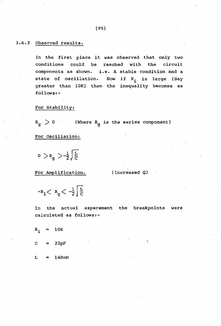
3.6.3 Observed results.
In the first place it was observed that only two
conditions could be reached with the circuit
components as shown.
state of oscillation.
i.e. A stable condition and a
Now if R. is l.
large (Say
greater than 10K)
follows:-
then the inequality becomes as
For Stability:
(Where Rg is the series component)
For Oscillation:
o >R >_lJL g 2 C
For Amplification.
-R.< R < -lTI: l. g 2JC
(Increased Q)
In the actual experement the breakpoints were
calculated as follows:-
R. = 10K l.
C = 22pF
L = 148nH
\

(96)
This gives valu'es as follows:-
(L/C)/2 = 4lohms
This means that a state of amplification could
occur. If the bias voltage were sleely reduced the
small signal
neg-ative. R g
resistance Rg
would reach
would
the
become
-4lohms
first. ie Rg >-41 and would also be > -Ri
more
point
and an
area of damped oscillation would appear. As soon
as Rg becomes less than -10K a state
stability would occur. In practice' a
of lossy
state of
amplification neVer occured and hence it could
assumed that the negative resistance region could
never reach -41 ohms. A change of the ratios of L
and C was made to the following values t.o observe i any change in the conditions.
L = 3'6nH
C = 86pF
The break points would hence be at lOohms and not
at 410hms. This did not assist the stability
situation and a stat.e of amplification' was st.ill
not reached.
(97)
3.5.4 Conclusion.
It seemed that selection of the (LIe) 12 breakpoint
did not affect the interface stability to any great
extent as reduction of the bias voltage did not
result in a region 'of stable gain.
This suggests that the Land C selection criteria
should only depend on the required 0 and centre
frequency and not on any gain conciderations for
the IF interface.
***000***

(98)
CHAPTER 4
IMPROVEMENT OF CORRELATION BETWEEN
THEORY AND EXPERIMENT "

(99)
4.1 Computer Simulation of Conversion Loss
I
In this section we will try to demonstrate a
-technique for using a computer simulation to
derive a more accurate figure for Conversion Loss.
Our original assumption as regards the transfer
charactaristic of the GUNN and the resultant Time
Dependent Reflection Coefficient was a straight
line function and a rectangular wave -for the Time
Dependent Reflection Coefficient. In practice
this is not the case and there results a small
error in the Conversion Loss.
I
Straight Line Transfer ~aracteristic against
actual Transfer Characteristic.
v ....

(100)
a 2.25 Applied Volts lOv +2
--f---fl----i
Resistance Transfer Function
Ohms
L ___ . _____________ ... __
Time Dependant Resistence Function +2
t--+--+--I--ff--lf--~f='r-=*=:::t==p.-.-I-. +-+--! I I ..
-100
-T/2 -Tc
J
I +-Tc +T/2

4.1.1
(101)
The computer simulation was done on' a Hewlet t Packard desk top computer, type HP85.
computer Simulation
The compu-ter .siniulation was done in two phases and requires two different programs.
The starting point was the two inpu,t variables.
These were fed into the first program which then outputs the Time Dependent Reflection Coefficient. It generates two intermediate stages i.e. The differential of the current/voltage Transfer Function which when inverted gives a Resistance Transfer Function.
Then the second intermediate stage is the generation of the Time D~ependant Resistance
Func-tion. This stage requires the insertion of the Bias Voltage and Local Oscillator Amplitude variables.
The Time Dependent Reflection Coefficient was then inserted into a program which did a Harmonic Analysis of the waveform assuming it to be periodic.
The process can be shown graphically as follows:

( 1 02 )
Start
Generate Resistence Function
Generate Time Dep. Res. Functiop
Generate Time Dep. Refl. Coeff.
00 Harmonic Analysis
Pause
Insert new Vb' V
lo Vth I
Flow Chart Representation of the Process.

4.1.2
(103)
The listings of the programs in Basic are given
in the appendices.
Results
These results wer:e obtained for a range of bias
voltages and local oscillator amplitudes. '!'he
results were then plotted for the two variables
seperately.
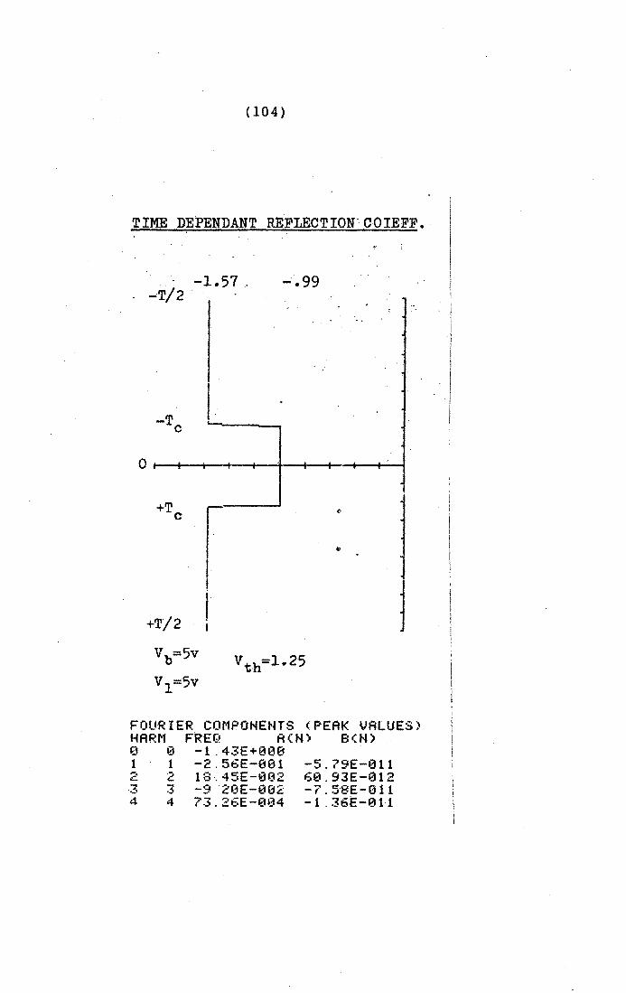
(104)
TIME DEPENDANT REFLECTION'COIEFF.
-1.57, -.99 -T/2
-T c
+T c
+T/2
I
r "
..
I I I
Vb=5v Vth=1.25 Vl=5v
FOURIER COMPONENTS (PEAK VALUES) HARM FREQ A(N) B<N) e e -1.43E+00e 1 1 -2.56E-001 2 2 18"45E-e02 3 3 -9 -Z0E-0e2 4 4 73.26E-004
-5.79E-011 60.93E-012 -7.58E-011 -1 .36E-011
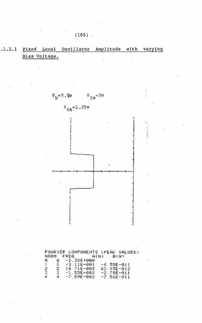
(105)
.1.2.1 Fixed Local Oscillator Amplitude with varying
Bias Voltage.
I , I I t I !
Vlo=3v
L __
, j
i 1 1
1 1
I I
FOURIER GOMPONEHTS (PEAK VALUES> HARM FREQ ACN) B(N) o 0 -1.38E+000 l t -3.11E-001 .-6.59E-011 2 2 16,71E-082 6~.~3E~012 3 ~ -1.55E-002 -2.78E-~11 4 4 -7.09E-002 -7.56E-011

(l06 )
V th=l. 25v
! 1 I 1 I i i I
I it' L __ ----.
~ +I-+-+-~~I~~~~~l I !
,r--_..J 1 I ~
I j I J j i I ]
~OURIER COMPONENTS (PEAK VALUES) HARM FREQ A(N) B(N) o 0 -l.42E+000 1 1 -2.63E-001 ,-, .::. 2
"7 '-' 4
1::: . 46E -~:::1IZ12 -8.44E-002 -,3 . ':!6E-~:::Hj.3
-6. 1 9E -(111 64.9.3E-(112 -6, 9i3E -I) 1 1 -2 56£-(; 11
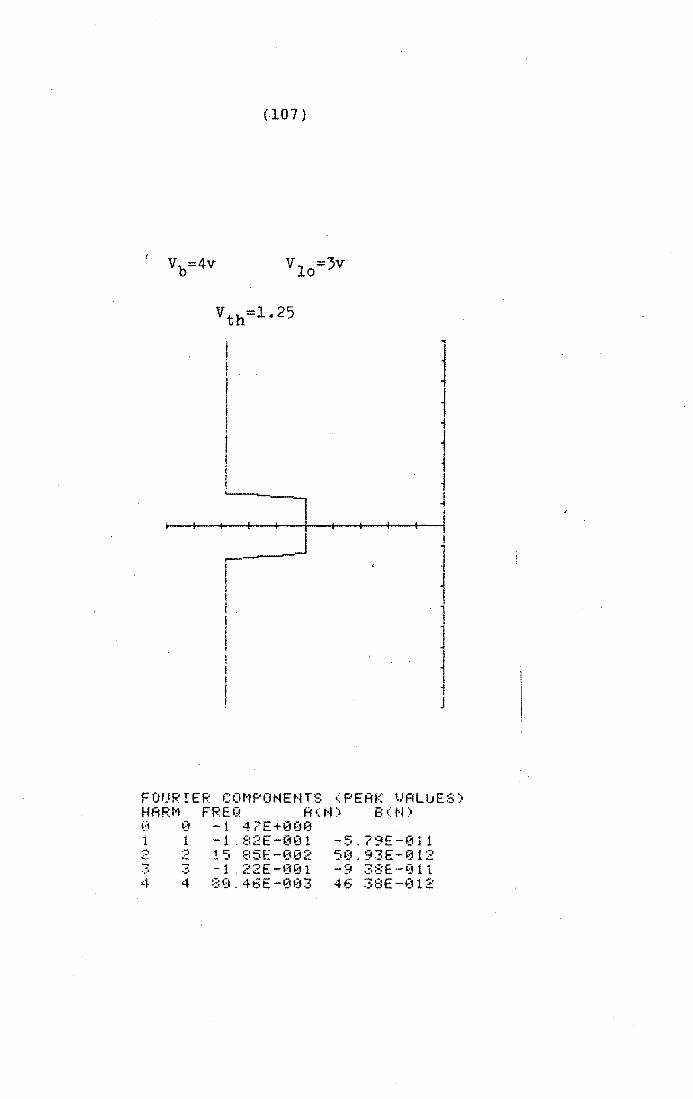
(107)
v lo=3v
__ J ~------
1 j 1 j i i
1 1 ]
1 J
FOIJR I EF.: COt'lf'ONEI'ITS .:: f'EfU( '.}ALIJES) HARM FREQ A(N) 8(N) o 0 -1 47E+000 1 1 -1.82£-001 -5.79E-011 2 2 15 85E-002 50.93£-012 3 3 -1.22£-001 -938E-011 4 4 88.46E-003 46 38£-012
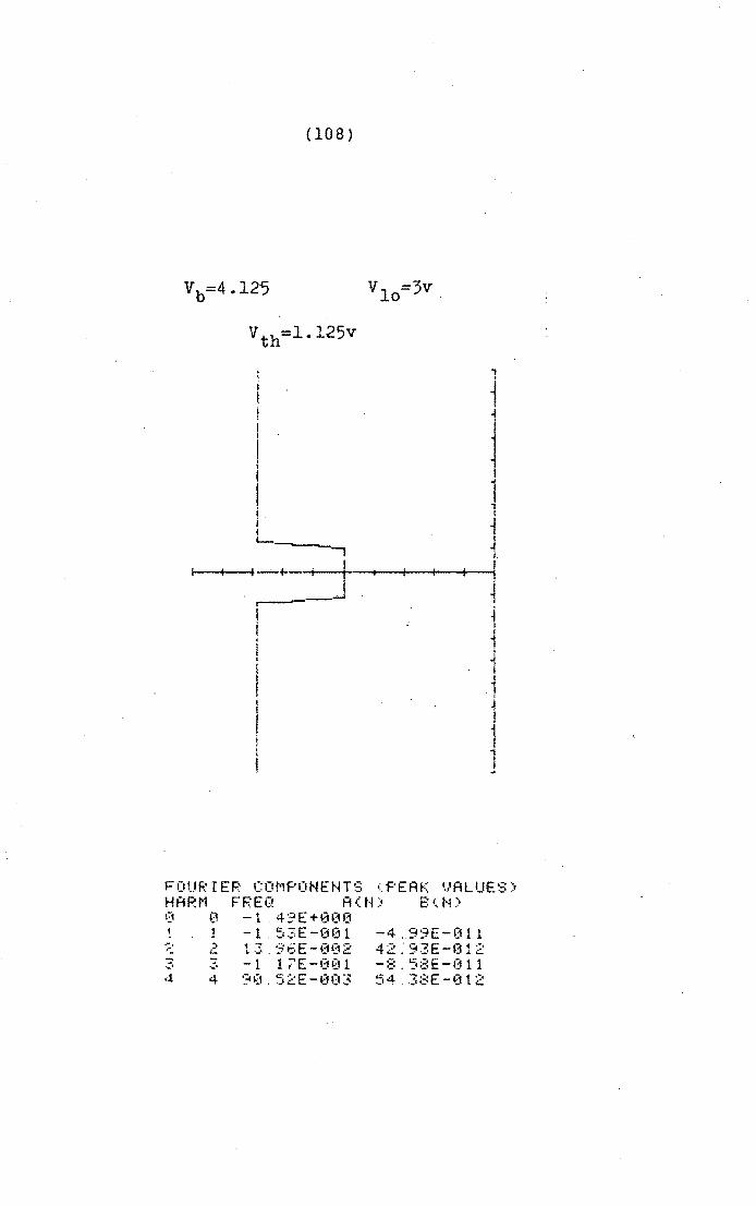
(l08 )
Vth=1.125v
1
I I
I I I '----,
f- j .' ]
Vlo=3v
~
1 1 j I.
j i
1 1
1 I ~
FOURIER CO~PONENTS (PEAK VALUES) HARM FREQ A(N) B(N) o 0 -\.49E+000 ! 1 -1.53E-00l -4 .. 99£-011 ~ 2 13.96E-002 42:93E-012 3 ~ -1 17E-091 -a.SSE-ell 4 4 90.52E-003 54.38E-012

(109)
v lo=3v
v th=1 .• 25v
I I • I f
! I I I · I
.---. i--I 1 ~ I
r I i
I i I j I
i I · i ·
, ·1 .i
I
~ ~ .1
j j I
-1
j 1 ~ I
1 1 ! .;
FOURIER COMPONENTS (PEAK VALUES) HARM FREQ A(N) B(N) L:~ 0 - I 5~;E+0(1fl 4
1 1 - 2 64E-~;1(1:2 -2 99£ -.3 1 1 .-, 2 .-. C" :.~ 7E -L~H33 - 7 L::17E -(1 1 2 c.. ~ ... ~ "_I • ". .:. -2 5:2E -L::U):2 -.~t ~:::E-(1 1 1 " "
;:\. 4 .-... O::'-t 25E-L3Lj3 7C ,_"_, 4L:::1E-(1 1 4

(110)
Oscillator 4.1.2.2 Fixed Bias Voltage with Local ------------------~~--------------~-----------amplitude changing
Vb=04v
Vth=1.25
! I °
I I I
I I I jL73
.. J I ~
i i i ~
J ~. I ~
, j i I 1 1 ~ I 1 J
FOU"~ r EF.~ COt1PONEtotTS <. PEAK i.,cALUES::O HARM FREQ ACN) 8(N) o ~ -1.S4E+000 1 1 -6 22E-~3f12 -4 39E-0 1 1 .:' OJ El~1 ..;.OE-~~H33 !:!9 29E-~3 i "7 <-. <- ~ 0_' .~ -; -5 T:::E -0(12 -5 ~3:=:E -(1 1 !. .:. '-' 4 4 53 24E-OO:3 22 .3::=E -~3 1 2

(111 )
Vb=4v V1o=2.75v
Vth=1.25v
1
1 l i j
I
FOURIER COMPONENTS (PEAK VALUES) HA~M FR£O ROn 80,0 ~ 0 -1.51E+O~O 1 1 -1.19E-081 -4.99E-Ol1 2 2 11.29E-002 30.93E-012 2 ~ -1.OlE-OOI -838E-Ol1 4 4 87 59E-003 52.38E-~12

(112)
Vb=4v V1o=3.0v
Vth=1125v
,.
~ .=] ! i
I
1
1 J i
~
1 i i ~ I
1 , J
FOURIER COMPONENTS (PEAK VALUES) HARM FREQ ACN) S(H) o 0 -1.4?E+000 t t -182E-001 -5.79E-011 2 2 15.85E-002 50.93E-0t2 3 3 -1.22E-081 -9.38E-011 4 4 30.46E-003 46.38E-012

(113)
Vb=4v V1o=3.5v
Vth=1.25v 1 1 l
I j ! I j I I L.-
'-1 j
I-- I j j
~ I
I 1 '1
I
1 I I I j I ! i i ! I
~
FOURIER COMPONENTS (PEAK VALUES) HARM FREQ R(N) B(N' o ij -1.43E+000 1 1 -2.48E-001 -5.79E-011 2 2 18.37£-002 60.93E-012 7 .... 4
3 -9.83E-002 -T.98E-0il 4 17.35E-003 -7 61E-012
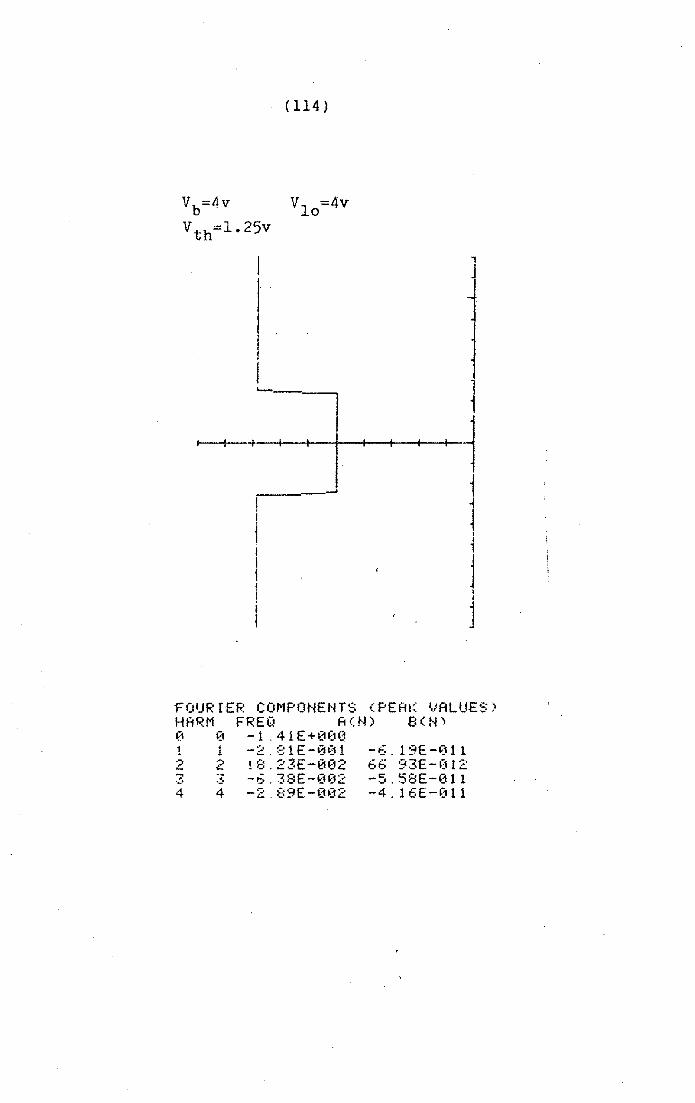
(114)
Vb=4v V1o=4v Vth=1.25v
1--~-4
I l-
I I ....... _,
I ,..--____ -,--t
1
'FOIJR IEF: COMPONENTS (PERI( I.}ALUES) HARM FREQ A(N) S(N) o 0 -i ,41E+00~ 1 1 -2,81£-~01 -6.19£-011 2 2
.:., 4
! 8. 23E-En32 -6.3:::E-@02 -2,89£-002
66 93E-(112 -5.5:3E-011 -4.16E-Ol1
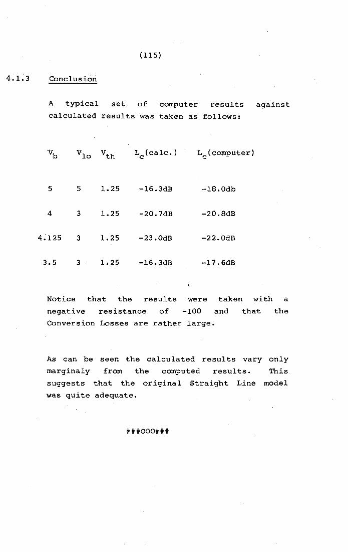
4.1. 3
(115)
Conclusion
A typical set of computer resul ts against
calculated results was taken as follows:
-v b
5
4
4~125
3.5
V 10
5
3
3
3 \
LC(computer)
1.25 -16.3dB -lS.Odb
1.25 -20.7dB -20.SdB
1.25 -23.0dB -22.0dB
1..25 -16.3dB -17.6dB
Notice that the results were taken with a
negative resistance of -100 and that the
Conversion Losses are rather large.
As can be seen the calculated results vary only
marginaly from the computed results. This
suggests that the original Straight Line model
was quite adequate.
###000###

(116)
4.2 Harmonic Mixing
4.2.1
In this section we consider the use of the
receiving device at harmonics of its fundamental
frequency. The author was unable to verify any
of the precepts given in this section as
equipment was not available for work at multiples
of 35 GHz. (This being the author I s frequency of
interest) .
Operation
The device would operate by mixing the received
signal with one of the harmonics of the Time
Dependent Reflection Coeffici.ent. The Time
Dependent Reflection Coefficient appears to have
predominent odd harmonics, however even harmonics
would exist. These harmonics would be
considerably lower in amplitude than the
fundamental and hence their noise skirts would
have an equivalent lower amplitude. This holds
out the promise that mixing with the harmonic
could lead to an improved Noise Figure than with
fundamental mixing.
The improved Noise Figure would lead to range
improvement' if the same transmit power could be
maintained. The other aspect to consider would
be the effect of atmospheric absorbtion at higher
frequencies.

(117 )
. All of this leads to an interesting speculation.
The fact is that the received frequency at a
harmonic of the fundamental is in fact mixing
wi th a harmonic of the Time Dependent Reflection
Coefficien·t and .not with an actual harmonic of
the fundamental. We may now assume that this
fundamental energy of the local oscillator is
spectraly distributed according to a Gausian
distribution around its fundamental as well as
being amplitude modulated according to the
thermal noise on the GUNN terminal. - each giving
rise to its particular noise skirt. (See section
3.4) •
If we assume that each term of the Time Dependent
Reflection Coefficient is given by Hn where
this can be represented as follows:
Now K is a statistical function in time and gives
rise to the A.M. noise skirt of the harmonic. w
is also a statistical function in time and gives
rise to the F.M. noise skirt of the harmonic.
In general Kn will be a factor rather less than
1 and hence the A.M. noise skirt will be
reduced. On the other hand, w is multiplied by n
and hence the F.M. noise skirt will be increased.
This means that the point at which the F.M. noise
skirt becomes less significant than the A.M.
noise skirt is further removed in frequency from
the "carrier" by both the mechanisms described in
the previous paragraph.
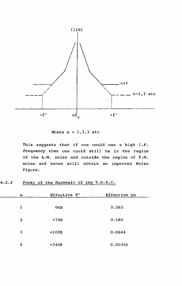
4.2.2
n
1
2
3
4
-----I' , I I I I
/ /
/
-f'
(118)
n c
Where n = 1,2,3 etc
...,, ____ n=1
'\. '\. '-___ n=2,3 etc
I
+f'
This suggests that if one could use a high I.F.
frequency then one could still be in the region
of the A.M. noise and outside -the r.egion of F.M.
noise and hence still obtain an improved Noise
Figure.
Power of the Harmonic of the T.O.R.C.
Effective F' Effective kn
OdB 0.263
+7dB 0.184
+10dB 0.0844
+24dB 0.00356

4.2.3
4.2.4
(119)
Possible practical implementation
Practical problems would lie in the area of the
electronic tuning range. If one required to use
the device as a transceiver then one would have
to select devices to have substantially different
centre frequencies to be able t.o cope with the
overly wide electronic tuning range required.
On the other hand if one required a Data link in
one direction only, then one could set up a
syst.em as follows.
Example of a possible system.
If it was required to use say Ka band (35Ghz) as
a carrier then one could use a GUNN diode at
35GHz as the transmitter but use a cheap GUNN at
about 12GHz as the receiver, but mix with its
third harmonic. The IF frequency could then be
guite freely chos,ento place it ouside the new
resultant F.M. noise skirt.
Conclusion
Harmonic mixing seems to hold various outstanding
advantages for communications links but only for
links that nead to· operate in one direction
only. A great deal of work would still need to
be done in ~rder to establish the feasibility of
such a system.

(120)
The other advantage of harmonic mixing could be that it allows operation at higher frequencies without having to provide apparatus at these higher frequen~ies. This could mean for example that the beamwidth of an antenna of a certain aperture could be reduced by a factor of three if th€t-hird harmonic were used instead of the fundamental.
***000***

(12l)
4.3 Effects of dis-similar powers in the two GUNN
Transceivers.
4.3.1
In this section we try to show that if the GUNN
transceivers have disfsimilar power outputs then
the resultant range performance will be
degraded. The powers referred to are the
intrinsic powers of the diodes and not the output
powers of the sources. By this we mean that
attenuation of the output power to match the
power output of the other device will only
degrade performance further.
Basic Range Performance.
o If we take the criterian discussed in Chapter 2
section 2 then we arrive at a figure for maximum
path loss and hence for max'imum range given as
follows.
Now in a Self Oscillating Mixer the Noise Figure
is substantially dependent on the receiving
transceiver's power output. See Section 3.4.3.
F = 1 + N./kT 1
Where N. = P x Noise to Carrier Ratio. 1 s
/

(122)
Say that Noise to Carrier ratio is constant and is given by M, then the overall < expression becomes as follows:-
But (N.)' = kT from the definition for Noise 1
Figul'e.
P = Transmit Power o
Ps = Source Power
= Maximum possible path loss.
Removing the logs gives:-
.' Po 1
Lp = kT x (1 + PsM/kT) x GrGt
L p increases as Po, Gr or Gt increase intuitively correct. If Ps or M should then Lp will decrease. The anomaly is the reverse path .the two powers are
which is increase
that for precisely
reversed in their positions in the equation.
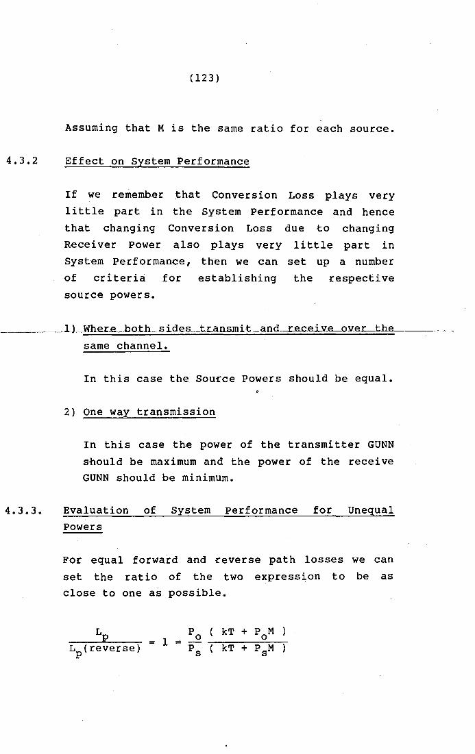
4.3.2
(123)
Assuming that M is the same ratio for each source.
Effect on System Performance
If we remember ~hat Conversion Loss plays very
little part in the System Performance and hence
that changing Conversion Loss due to changing
Receiver Power also plays v.ery little part in
System Performance, then we can set up a number
of cr iter ia for establishing the respective
source powers.
______ . __ lJ Wher_e... __ .ho~th ___ s ide s __ t_r..ansmi:t ___ and-----L_e.c_eLv.~oy_eL_the________ -
4.3.3.
same channel.
In this case the Sou~ce Powers should be equal.
2) One way transmission
In this case the power of the transmitter GUNN
should be maximum and the power of the receive GUNN should be minimum.
Evaluation of System Performance for Unequal
Powers
For equal forward and ~everse path losses we can
set the ratio of the two expression to be as close to one as possible.
L Po P = 1 =
Lp(reverse) Ps

If Po = Ps then on the other hand (say Po = 2Ps )
would be impaired other.
Say M = -160dB
(124)
this condition is true. If
the two powers are not equal then the range performance
in one direction but not the'
kT = 4.14E-21
Therefore PoM = Po lOE-16
We can thus ignore kT (This is a particular case
but can generally be applied)
= Lp(reVerse}
But for Po =
= 4
Thus performance of one or the other path is
degraded or enhanced by 4.
It is useful to consider this in terms of
decibells.
Lp ~~~----~ = 6dB Lp(reVerse)
In practical terms the effect would be as follows:

(125)
Say 35GHz channel and Lp was equal to l55dB.
This would indicate a range of 40km in free space
plus the oxygen attenuation. If L (reverse) p
were now 6dB less than this would approximate to
20km or half the range in the other direction.
This means that the overall System Performance
will be deg~adea to 20km.
It would be better to specify Source Powers in
terms of a tolerance of an absolute power, than
to specify these powers in terms of the pow·er of
the other source.
eg. Say Source Power was given as P s =
Pax!. 414 to P s = P a/I. 414. Then the worst
possible case would be when P s = PaX!. 414 and
Po = Pa/l.4l4. (,
Lp _ (1 1) 2 = L (reverse) - 1.414 x 1.414 4
P
This is still equal to 4 but loss in one
direction is' increased by 3dB while that in the
other direction is degraded by 3dB. This would
degrade range by about lOkm only.
Rewriting the expression to give:-
L (reverse) p
P 2 .(kT/P + M) o 0
= p-2 (kT/P + M) s s

(126)
If M = -180dB or g~eater, then we would find that
M becomes less significant than kT/Po or
kT/Ps • The expression then simplifies to:-
=
This is a much improved situation and would allow
more latitude in specifying Source Powers. This
would be more like the situation for a local
oscillator with a separate mixer. However in
practice this situation does not arise when using
the Self Mixing Oscilla~or.
***000***

4.4
4.4.1
( 127)
Mounting in Image Waveguide
The thrust of this research has been to show that
the GUNN diode can be used as the receiver and
the transmitter of a system.
consistent· with .this approach
device can be mounted in
structures to obtain full
technique.
Image Waveguide
It is thus fully
to show how the
cheap waveguide
benefit from the
In recent years
research into the
guiding structures.
there has been considerable
use of Dielectrics as wave
These were first studied in
Germany before World War 2 as the radiating
element in phased arrays for Radar applications.
In essence a waveguide is a st!:ucturethat guides
electromagnetic waves along a certain t::'oute by
means of these waves interacting with at least
two boundaries. The conventional rectangular
waveguide accomplishes this by setting conductive
bounda!:iesto an air dielectric space. The
Dielectric Waveguide does this by establishing
boundaries between air and some form of plastic
or mylar materials with a' permitivity quite
diff.erent to that of air.
The Image Waveguide is a sort of hybrid between
the .conductive waveguide and the Delectric
Waveguide in that it has both -dielectric
boundaries and conductive boundaries.
\

(128)
The structure of the waveguide is as follows:
rielectric
\ \ \ \ \ \ \ \ \ \ \ Ground Plane
l \ \ \ \ '\ \
The particular properties of the waveguide are
that it theoretically does not have a lower
cut-off frequency under which it becomes
evernescent.lt also does not confine the wave
to the Dielectric but the Dielectric guides the
wave.
In all other aspects the guide can be used as a
conventional transmission line ie. terminated
sections of a fraction of a wavelength exhibit
reactance
wavelength
and not
sections
pure resistance. Half
of the guide act as
resonators. Circulators and directional couplers
can also be constructed.
for further details.
See references (L(2.}43)

4.4.2
(129)
The GUNN Diode in Image Waveguide
A GUNN source can be constructed using an Image
Waveguide resonator. The heat is conducted away
by the groundplane and the groundplane also forms
the second contact for the diode. Chrepta and
Jacobs in their papers (6,7) showed that a
binocular radio at 90GHz could be constructed
using Image Guide.
follows:
Their construction was as
~ylon screw Choke r--~~---'
Boron Nitride ~~ Image Guide
·CJ ~rH>'" I.F.Amp.
GUNN Bias .
+Volts Bias
The results as published in their paper are
repeated here for~~~~~~~~~
1"1 DSB Noise Figure 18 (dB)
Loss 4
"
1 I fl.
!i0i e f igpr 1~
I ~ I I ._1_1- I I
26 Z<a Z.7 z.e 2~ 5.0
Bias Voltage

4.4.3
(130)
Note that they seemed to apply the theory
discussed in section 4.5 in analysing their
system performance.
Conclusion
There seems to be a bright future for the S.M.O.
scheme where cheapness is of special importance.
This is particularly the case where cheap
mounting structures such as Image Waveguides are
available.
***000***

5
(131)
Device as a Negative Resistance Amplifier
followed by a non linear transfer function.
In the initial stages of this research the author
took the view that the device consisted of an
amplifier/attenuator followed by a lion linear
device. This seemed to comply to some extent
wi th the view taken by the researchers at
Lancaster [2,3,5]. However the author was unable
to repeat the results given in the papers
referred to above.
There seemed to be considerable emphasis on the
noise presented to the IF by Shot Noise, Flicker
Noise and other Noise Sources in the GUNN current
itself. Dr F. Myers of the Plessey Research
Centre at Casswell in the United Kingdom
expressed the view that GUNN current fluctuations
would be the dominant Noise Source in the GUNN/IF
Interface. In the author I s opinion most of the
research done at Casswell and 'at Lancaster
concentrated on the use of the S.M.O as a Doppler
Rada;c f-or intruder alarms etc. This implies an
IF frequency equal to the Doppler frequency and
hence well within the F.M. Noise skirts of the
device. The author I s research has concentrated
on the use of the device as a receiver with a
fixed IF frequency greater than lOMHz.

4.5.1
Ni
Si
(132 )
The Noise Figures quoted in the papers from
Lancaster seemed to be very optimistic and would
be consistant with the Negative Resistance
Amplifier/Non Linear Device approach. The author
thus felt the theory to b~ deficient to some
extent and hence the alternative approach
presented earlier in this thesis was developed.
As has been shown this alternative approach seems
to be far more consistent with practical results
obtained.
The first approach of Negative Resistance
Amplifier etc. is presented in this section only
as an attempt at completeness. It does have some
merit as a technique for analysis and with some
thought it could be corrected to present more
accurate results.
System Layout
N 10
S asc
N.L.D. ...----I.F.
(133)
Where:-
Si = Signal Input
N. = kTB = Noise .feom Input Termination 1
NRA = Negative Resistance Amplifier
G = Gain of Negative Resistance Amplifier (can be less than one)
Nlo . = {F - 1] kTB = Local Os'cillatoe Noise at
frequency of interest.
Sosc = Signal f~om the Local Oscillator
N.L.D~ = Non Lineae Device {'.
Notes
It must be assumed that the noise introduced into the system can all be lumped into the Nlo term. It must also be assumed that the Negative Resistance Amplifier has a Noise Figure of 1-
The Non Linear Device can be assumed to have the same effect on the Noise, Input Signal and Local Oscillator Signal and can hence be regarded as an amplifying factor to the sum, difference and all other components.
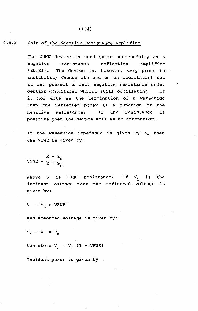
4.5.2
(134)
Gain of the Negative Resistance Amplifier
The GUNN device is used quite successfully as a
negative resistance reflection amplifier
(20,21) • The device is, however, very prone to
instability (hence its use as an oscillator) but
it may present a nett negative resistance under
certain -conditions whilst still oscillating. If
it now acts as the termination of a waveguide
then the reflected power is a function of the
negative resistance. If the resistance is
positive then the device acts as an attenuator.
If the waveguide impedance
the VSWR is given by:
R - Z o VSWR = R + Z
o
is given by Zthen o
Where R is GUNN resistance. If Vi is the
incident voltage then the reflected voltage is
given by:
V = V. x VSWR ~
and absorbed voltage is given by:
V. - V = V ~ a
therefore V = V. (1 - VSWR) a ~
Incident power is given by
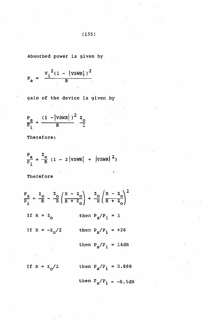
(135)
absorbed power is given by
p = a
Vi 2( 1 - 'VSWR I ) 2
R
gain of the device is given by
Therefore:
Pa Zo /VSWR\ 2) P." = ~ (1 - 2\VSWRj +
1
Therefore
Pa Zo _ Zo (R - Zo) Zo {R -P." = R Z + R R + R R +
1 0
If R = Zo then p /P. = a 1
If R = -Z /2 then Pa/Pi = 0
then Pa/Pi =
z~r Zo
1
+26
14dB

4.5.3
(136)
System Noise Performance
By definition the Noise Figur.e is· given by the
signal to noise ratio on the output to the signal
to noise ratio on the input of the system.
SIN ratio on the input is given by:
S. 1
N. 1
= S.
1
ktB
sIN ratio on the output is given by:
= GS.
1
GkTB + (Fosc -l)kTB
But Noise Figure of the system is defined as:
S.N F = .....!...-2 S N. o 1
Therfore:
Si(GkTB + (Fosc - l)kTB) F = (Si G + Sosc )kTB
Therefore:
F = Si(G + Fosc - 1)
SiG + Sosc
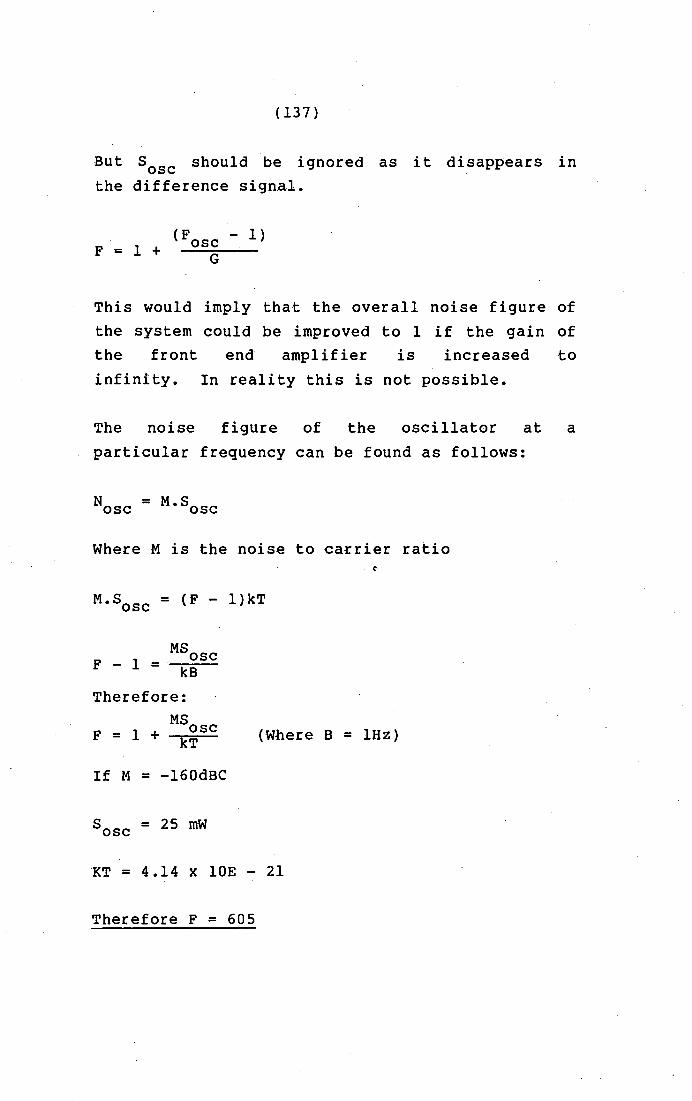
(137)
But Sosc should be ignored as it disappears in the difference signal.
(FOS C - 1) F = 1 + ---=G~--
This would imply that the overall noise figure of
the system could be improved to 1 if the gain of
the front end amplifier is increased to
infinity. In reality this is not possible.
The noise figure of the oscillator at a
particular frequency can be found as follows:
Where M is the noise to carrier ratio
M.SOSC = (F - l)kT
MSOS C F - 1 = kB
Therefore:
MSosc F = 1 + kT
If M = -160dBC
Sosc = 25 mW
(Where B = 1Hz)
KT = 4.14 x 10E - 21
Therefore F = 605

4
(138)
Say R = -100 and Zo = 450
Therefore G = 22
This suggests that system noise figure is:
"F = 27.7
Therefore NF = 14.4 dB
CONCLUSION
The author found that with carefully controlled
experiments, those sorts of noise figures could
not be realized. If, however, the noise
injection was moved to the input of the negative
resistance amplifier, then the G factor would
disappear f~om the expression.. The author was
then unable to obtain a realistic figure for
conversion loss.
The work done at Lancaster gives such noise
figures but ·the author was unable to establish
these. One further note is that the GUNN/IF
interface will generally be a tuned circuit of
some form and under negative resistance
conditions, the very small coherent oscillations

(139)
produced would be injection locked by the
received signal and would appear to enhance the input signal. However, they do not actually contain the input information and hence cannot be regarded as amplified input signal. On the other
hand they would. appear to be such to a power meter measuring output power and would thus tend to enhance the apparent signal to noise ratio on the output.
***000***

(140)
CHAPTER 5
C-oNCLUSION
"

5
(141)
Conclusion
The author has attempted to show the and practical aspects of using a millimeter wave source as both the
theoretical GUNN diode
transmitter and the receiver. of a sys-tem. His findings can be summarized as follows:
5.1 What theory holds good for mixer operation
The author found that a theory based on the use
of a Time Dependent Reflection Coefficient successfully demonstrates the conversion loss of
the device. In addition the view that the device noise figure is due to added noise prior to the mixing process seems to correspond to the results measured in practice. The aut·hor found that he was able to measure noise figures of as low as 22dB but that the lower noise figures predicted by the researchers at Lancaster (2, 3, 4, 5) seemed to be optimistic. Noise figure seemed to be affected by among other things, source power, cavity Q and IF frequency.
Other factors affecting noise figure but to a much lower extent are IF matching Impedance, Bias Voltage and actual values of Rn and Rp. Conversion loss also affected system noise figure but only to a very small extent. It can be noted here that very repeatable noise figures were obtained and these noise figures readily suggest the use of the device for commercial applications.

5.2.
(142)
As regards future applications
The device could readily be mqunted in cheap
waveguide structures such as Image Waveguide.
This could readily lead to cheap Dopplar Radar or
other forms of radar for such applications as
vehicle safety or burglar alarms.
Harmonic mixing also seems to hold out pr~mise of
commercial use with definite advantages in
certain areas such as the Electronic Distance
Measuring Instrument where substantially reduced
beamwidth could be obtained by changing the
microwave path from the fundamental to say the
third harmonic.
5.3 General conclusion
The S.M.O. concept appears to have very good
commercial possibilities if its drawbacks in
terms of
account.
range performance are taken in·to
In fact the S.M.O. is now in commercial
use by Plessey S.A. in their new Microwave
Distance Measuring Instrument.
***000***

(143)
CHAPTER 6
APPENDIX

(144)
6.1 Computer p.rogram for storing the transfer
function D.A.T.A. and generating' the Time
Dependant Reflection coifficient. U3 OEG 20 OIM T(201).RC361) 39 COM P(361) 40. T03)=2 5~ FOP. J~l TO 20e 6J31.",= (.J- t)/29 78 IF U(l 15 THEN T(J)=2 80 IF V>I.35 THE~ T(J)=-100 90 IF V=I.15 THEN T(J)=1.32
190 IF V=1.2 THEN T{J}=.66 110 IF V=I.25 THEN T(J)=0 120 IF U=I.J THEN T(J)=-33 130 IF V=I.3S THEN T<J)=~66 140 NEXT J 150 FOR J=0 TO 360 160 V=5+5*COS(J) 170 "1=IP(20*'I) 180 M=t'1/20
.. -~- 190--R ( J ) = T < M * 2e-)·-~-_._- .-.-------200 NEXT J 210 GCLEAR 220 SCALE 0.360.-150.10 230 XAXIS 0.20 @ YAXIS 180.5 240 PENIJP 250 MOVE 0,RCO) ~ 260 FOR J=l TO 360 270 DRAl~ J.ReJ) 280 NEXT J 290 FOR J=0 TO 360 300 P(J)=(R(J)-450)/(RCJ)+450) 310 NEXT J 329 GCLEAR 339 SCALE 0.360.-2.0 340 PEHUP 350 XAXIS 0.20 @ VAXIS 180 .. 2 360 PENlIP 370 t10VE a.p(O) 380 FOR J=1 TO 360 390 ORAH ... '.f'('J) 400 NEXT . ..1 410 PAUSE 420 CHAIN "HAR2" 430 END

6.2~
(145)
Computer program for doing the
ana1ysis.(Shortened version) Ie PROGRAM CALCULATES FOURIER 20 ! COEFFICIENTS OF A PERIODIC 30 ! WAVEFORM. WAVEFORM IS 40 ! AS A LIST OF EVENLY SPACED 50 ! POINTS. 60 DIM S(400).C(40~).Z(2,10) 70 COM P(361) B9 RAO . 90N=361
100 T=l 110 D=T/(N-l) 120 S=O 130 PRINT "" 140 PRINT "FOURIER COMPONENTS <P
EAK VALUES)" \50 PRINT "HARM FREQ A(N)
SCN) " 160 IMAGE D,2X.OO.2X.DO.OOE,2X.D
D.OOE 170 F=l/T 180 W=F*2*PI 190 GOSUB 450 200 PRINT USING 160 O.0.S 210 Fl=0 220 FOR 1=1 TO 4 230 T=0 240 Fl=Fl+F 250 W=2*PI*Fl 260 C(1)=P(1) 270 S(1)=0 280 C=0 290 5=0 300 FOR R=2 TO N 310 T=T+O 320 C(R)=PCR)*COSCW*T) 330 C=C+(C(R)+C(R-1»/2*O 340 SCR)=PCR)*SINCW*T) 350 S=S+CSCR)+S(R-l»/2*O 360 Z(l.I)=C @ 2(2.1)=8 370 NEXT R 380 C=C*2/T 390 S=S*2/T 400 H=(C A 2+S A 2)A.5 410 PRINT USING 160 I.Fl.C.S 420 NEXT I 430 C~AIN "GI Y
440 END 450 ! SUBROUTINE TO INTIGRATE FU
NTION. TRAPIZOIDRL INTIGRATI ON
460 S=0 470 FOR J=2 TO N 480 S=S+(P(J-l)+P(J»/2 490 NEXT J 500 S=S/(N-l) 510 RETURN
harmonic

6.3.
(146)
Computer program for doing the
analysis. (Full version)
10 PROGRAM CALCULATES FOURIER' 29 ! COEFFICIENTS OF A PERIODIC 30 ~ WAVEFORM. WAVEFORM IS 49 ! AS A lIST OF EVENLY SPACED 50 ! POINTS. 60 DIM R(·lea).S(lee).C(leO).Z(2
.113) 78 DISP "INPUT WAVEFORM DATA U
se DISP ItP-':1INT BY POINT AS FOll OWS"
90 OlSP ItHOW MANY POINTS" lee INPUT N 110 OISP "WHAT IS PERIOD OF WAVE
FORM" IHPUT T M=9 FOR .J=1 TO N
128 13121 140 145 1513 169 170 189 198 200 2113 220
DISP It ENTER POINT # ";J; I HPU T R (.J) A=R(.J) IF R(J)(e THEN A=-R(J) IF ft)M THEN N=A NEXT .J O=T/(N-l) S=9 PRINT .. "
2313 PRINT" N ·AGNITUOE"
240 ~OR J=1 TO H
T If1E(S) ,-.
M
258 PRINT USING 269 ~ J.S.ReJ) 2613 IMAGE OOO/SX, O.OOE. 5X,QDOO 2713 S=S+O 2813 NEXT J 298 CLEAR 308 DISP "DATA CORRECT? Y/N" 31121 H~PlIT F$ 32121 IF F$="Y" THEN 41e 330 DISP "WHAT ITEM" 348 INPUT J 350 OISP "NEW VALUE" 3613 INPUT R(.J) 370 A=R(J) 380 IF R(J)(e THEN A=-ReJ) 390 IF A)M THEN M=A 400 GOTO 210 418 PRINT Uti
.:120 GClEAR 430 PENUP 4413 SCALE 0.T,-M,M 450 XAXIS B,T/IO @ YAXIS 9,M'10 460 PENUP 47e MOVE 9,O 480 S=9 490 FOR J=l TO N see ORAl·J S., R (J) 5111 8=5+0 520 NE~n . .1 530 COpy 54~.3 GClEAR 5St.3 P-RINT '"'
harmonic

(147)
569 PRINT "FOURIER COMPONENTS (P EAK VALLlES)"
5713 PRINT "HARM FREQ A(N) B (N) C(N)"
5813 IMAGE DO.2X.O.DE.2X.D.OE.2X. D . DE .' 2X. D . DE
5913 F=1/T 6£113 l-l=F~:2*P I 610 GOSlIB 8413 6213 PRINT USING 5813 a,0.S 635 F1=e 6413 FOR 1=1 TO 1e 645 T=O 6513 F1=F1+F 660t·l=2*P I *F 1 6713 C(1)=R(1) 6813 S(1)=0 6913 C=0 7ee S=0 7113 FOR R=2 TO N 72e~o 7313 C(R)=R(R'*COS(W*T) 7413 C=C+(C(R)+C(R-l»/2:t.D 750 S(R)=R(R'*SIN(W*T) 760 S=S+(S(R)+S(R-l»/2*D~ 765 Z(1.1)=C @ 2(2.I)=S 770 NE:X:T R 780 C=C*2/T 7913 S=S:t.2/T 8ee H=(CA2+Sh2)A.S 81e PRINT USING sse; I,F1.C.S 8213 NEXT I 830 END 8413 ! SUBROUTINE TO INTIGRATE FU
NTION. TRAPIZOIDAL INTIGRATI ON
SS0 S=0 81,)0 FOR .J=2 TO N 8713 S=S+(R(J-l)+R(J»/2 880 NEXT .J 885 S=S/(N-1) 890 RETURN

(147)
569 PRINT "FOURIER COMPONENTS <P EAK VALUES)"
579 PRINT ~HARM FREQ A(N) B <tD CO~) ..
580 IMAGE OD,2X,O.DE.2X,O.DE,2X, D.DE~2X,O.OE
598 F=I/T . 6139 "t=F;:2*PI 6113 GOSUB 840 620 PRINT USING 588 0,8,$ 635 Fl=0 640 FOR 1=1 TO 10 645 T=0 650 Fl=Fl+F 6613 l·t=2*,P I *F 1 670 C(I)=R(I) 689 5(1)=9 699 C=0. 798 S=0 719 FOR R=2 TO N 72e~ 739 C(R)=R(R)*COS(WtT) 7413 C=C+(C(R)+C(R-l»/2*O 750 S(R)=R(R)tSIN(WtT) 769 S=S+(S(R)+S(R-l»/2tO 765 Z(I.I)=C @ 2(2,1)=S 770 NEXT R 7813 C=C*2/T 799 5=S*2/T Sge H=(C A2+S A 2)A.5 8113 PR IN T US 1 NG 58~3 j L F L C, S 829 NEXT I 83(~ END 8413 ! SUBROUTINE TO INTIGRATE FU
NTION. TRAPIZOIOAL INTIGRATI ON
859 S=0 860 FOR J=2 TO N 8713 S=S+(R<J-l)+R(J»/2 880 NEXT . ..1 885 S=S/(N-l) 890 RETURN

(148)
CHAPTER 7
BIBLIOGRAPHY

1)
2)
3)
4)
5)
6)
7)
(149)
REFERENCES
Tellurometer with Self Oscillating Mixer.
New
Plessey S.A. reference No. DEV/42/2556
R.A. Evan. s
Millimetre-Wave Receivers Using
Self-Oscillating Gunn-Diode Misers.
Microwave Journal. July 1971.
M.J. Lazarus, S. Noval and E.D. Bullimore.
A Sensitive Millimeter Wave Self-Oscillating Gun
Diode Mixer.
Proceedings of the IEEE. May 1971. Letters.
M.J. Lazarus, E.D. Bullimore and S. Novak.
Control of Injection Locking of a Millimeter Wave
Oscillator with AFC.
Proceedings of the IEEE. August 1976. Letters.
M.J. Lazarus, S. Novak and K.Y. Cheung.
Improved rom-Wave Gunn-Mixer Receivers.
Microwave Journal. March 1977.
M.J. Lazarus, K.Y.Cheung and S. Novak.
Millimeter-Wave Binocular Radio.
Microwave Journal. March 1980.
Yu-Wen Chang and Lloyd T. Yuan.
Millimeter-Wave Integrated Circuits.
Microwave Journal. November 1974.
M.M. Chrepta and Dr. H. Jacobs.

(150)
8) Noise Figure and conversion Loss of self excited Gunn-Diode Mixers.
ElectronLc Letters. 28th May 1970. Volume 6. No. 11.
P. Albrecht and M. Bechteler.
9) A millimeter-Wave Gunn M.ixer with -90 dBm·
Sensitivity, using a MOSFE'l'/Bipolar AFC Circuit.
proceedings of the IEEE. JUne 1972. Letters. M.J. Lazarus and S. Novak.
10) Self-Oscillating Mixer Cuts Atenna Test Costs.
Microwaves. April 1978. Michae.l R. I ngg s •
11) Theoretical Explanation for the Output Spectra of Unlocked Driven Oscillators.
proceedings of the IEEE. February 1966.
Letters. H.L. Stover.
12) A Study of Locking Phenomena in Oscillators. proceedings of the IEEE. October 1973. Reprinted from June 1946 Proceedings of IRE. Robert Adler.
13) Injection Locking of Microwave Solid-State
oscillators Proceedings of the IEEE. October 1973. Kaneyuki Kurikawa.
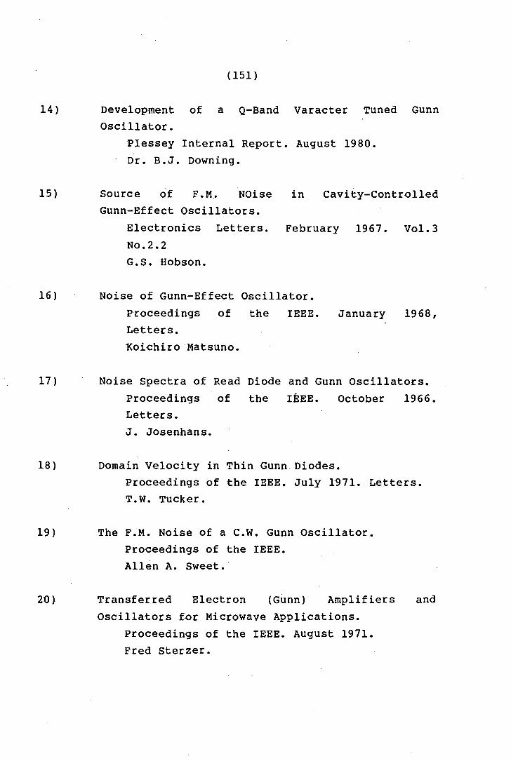
(151)
14) Development of a Q-Band Varacter Tuned Gunn
Oscillator.
15)
P1:essey Internal Report. August 1980.
Dr. B.J. Downing.
Source of F.M~ NOise
Gunn-Effect Oscillators.
in Cavity-Controlled
Electronics Letters. February 1967. Vol.3
No.2.2
G.S. Hobson.
16) Noise of Gunn-Effect Oscillator.
proceedings of the IEEE.
Letters.
Koichiro Matsuno.
January 1968,
17) Noise Spectra of Read Diode and Gunn Oscillators.
Proceedings of the IEEE. October 1966.
Letters.
J. Josenhans.
18) Domain Velocity in Thin Gunn Diodes.
proceedings of the IEEE. July 1971. Letters.
T.W. Tucker.
19) The F.M. Noise of a C.W. Gunn Oscillator.
2{) )
Proceedings of the IEEE.
Allen A. Sweet.·
Transferred Electron (Gunn) Amplifiers
Oscillators f~r Microwave Applications.
proceedings of the IEEE. August 1971.
Fred Sterzer.
and

(152)
21) Microwave properties and Applications of Negative
Conductance Transferred Electron Devices.
proceedings of the IEEE. August 1971. Perlman, upadhyayula and Siekanowicz.
22) Noise in Solid-State Devices and Lasers.
Proceedings of the IEEE. August 1970. Aldert van der Ziel.
23) A General Analysis of Noise in Gunn Oscillators.
proceedings of the IEEE. August 1972. Letters. Allen A. Sweet.
24) Small-Signal Admittance of a Gunn-Effect Device.
Electronics tetters. June 1966. Vol.2 No.6 G.S. Hobson.
25) F.M. Noise in a Gunn-Effect Oscillator.
26)
IEEE Trans. on Electron D~vices. December
1969.
Koichico Matsuno.
Efficient InP Gunn Requirements.
Microwaves. May 1980. Dr. Fred A. Myers.
Diodes Shrink Power
27) Microwave Gunn Oscillator Tuned over IGHz. Electronics Letters. June 1968. Vol.4. No.12.
B.K. Lee and M.S. Hodgart.
28)
(153)
Broadband from Gunn Oscillators
Hyperabrupts make a Difference.
MSN. May 1980.
E.G. Chalmers.
for
29) GaAs FETs Rival Guns in YIG-Tuned Oscillators.
Microwaves. July 1977.
Tom Ruttan.
30) Simplify High-power Gunn Oscillator Design.
Microwaves. 1975.
W. Wagner.
31) Solid State faces new questions •
. MSN. December 1979. 8
George Gibbons.
ECM.
32) Comparati ve Study of Bipolar" F.ET and Gunn X Band
Oscillators.
9th European Microwave Conference. 1980.
M. Fache and M. Quentel.
33) Q-Dependence .of Gunn Oscillator P.M. Noise.
IEEE Trans. on MTT February 1973.
H. Herbst and A. Ataman.
34) A High Stabilized Ka-Band Gunn Oscillator.
IEEE Trans. on MTT. February 1972.
S.Nagano and S. Ohnaka.
35) Low Noise Operation of CW GaAs Avalanche Diode
Oscillators.
Proceedings of the IEEE. July 1971. letters.
P.A. Levin, A.B. Dreeben, and A.R. Triano.
(154)
36) Wide-Band Mechanically Tunable and Dual In-Line
Radial Mode W-Band (75-ll0GHz) CW GaAs Gunn Diode Oscillators.
37)
Active Microwave Semiconductor Devices and Circuits Cornell University, Ithaca, N.Y. Aug-u-st 1979. John Ondria.
Microwave Oscillators of Current in Ill-V Semi-conductors.
Solid State Communications. Vol. 1. pp 88-97 1963 J.B. Gunn.
38) GaAs past-threshold microwave amplifier, mixer
and oscillator.
39)
Prac. IEEE. Letters 54. 299-300 Feb. 1966 • . '
B.W. Hakki.
Metallized
structures Systems.
Dielectric Horn
for Millimetre~Wave
and waveguide
Oscillator/Mixer
IEEE Tran's. MTT. Vol. MTT-29 No.2 pp.10-2-106 Feb. 1981. M.J. Lazarus, F~R. Pantaja, M.G. Somekh.
40) Noise Aldert van de Ziel.
41) Noise F.R. Conner. Published by Edward Arnold.
(155)
, 42) Dielectric Waveguide: A low cost option for I.C.s
Microwaves, March 1976
Robert M Knox
43) Dielectric IrnageLines.
loR.E. Transactions on MTT. July 1958
pp291-299.
S.P.Schesinger and D.D.King
"
J 4 DEC 1982

(156)
(.
Copyright © 2022 FDOKUMEN