Material survey for packaging semiconductor diode lasers
9
Material Survey for Packaging Semiconductor Diode Lasers David Schleuning * , Kenneth Scholz, Mike Griffin, Bo Guo, Calvin Luong, Rajiv Pathak, Christian Scholz, Jason Watson, Heiko Winhold, and Tom Hasenberg * Coherent Inc., 5100 Patrick Henry Drive, Santa Clara, CA 95054 ABSTRACT We present results from a survey of materials used for packaging semiconductor lasers, including Cu, CuW, BeO, diamond composite and other advanced materials. We present the results of residual bonding stress from various solders and consider the direct effects on wavelength and spectral width. We also provide data on the second order effects of threshold current and slow axis divergence. Additionally, we consider the heat spreading through different materials for a laser bar and present modeled and experimental data on the thermal performance. Finally, we consider the reliability under on-off life-testing and thermal cycling tests. Keywords: semiconductor laser diodes, packaging, material properties 1. INTRODUCTION The packaging of semiconductor diode lasers has moved increasingly from the traditional indium soldering on copper heat-sinks to the use of hard-solders on CTE matched materials [1-3]. While the use of AuSn has eliminated a number of packaging related failure modes—notably stability during on-off cycling operation—the use of standard CTE-matched materials have lower thermal conductivity and therefore give higher junction temperatures. For semiconductor lasers, increasing the junction temperature reduces the semiconductors expected lifetime parameterized by the activation energy. Additionally, the laser performance is also reduced by increasing the threshold current and decreasing the slope efficiency. In addition to the thermal effects, the residual bonding stress is also an important factor in the performance and reliability of a semiconductor laser. Adding strain to the quantum well of a typical semiconductor laser will change the band structure by shifting the band gap, altering the light and heavy hole splitting, and changing the effective mass. These effects within the semiconductor directly influence the lasing properties, including the wavelength, threshold current, and polarization. Additionally there is been an empirical trend of increased slow axis divergence with packaging on hard-solder which could be due to stress and/or thermal effects [7, 8]. The extreme heat flux of (~10 3 W/cm^2) from a semiconductor laser bar requires high conductivity from the heat-sink to adequately spread the heat. The total thermal resistance of the package will be dependent on the materials used, contact resistance at interfaces and geometry of the heat-sink. Therefore the industry has worked to develop a material that is CTE matched to GaAs (for hard solder die attach) and has high thermal conductivity (equal to or greater than copper). 2. MATERIAL PROPERTIES The figure below summarizes the CTE and thermal conductivity of many materials used in packaging semiconductor lasers bars. In this paper we limit the discussion to mounting a GaAs based semiconductor laser which has a CTE of ~ 5.7 PPM/ o C and a conductivity well below that of many metals, ceramics, and composite materials. Traditional packaging of a semiconductor bar has used a Cu heat-sink due to its high thermal conductivity; however the large CTE mismatch with GaAs requires the use of a compliant solder such as indium. CuW makes an attractive choice for a heat- sinking material, since the CTE allows for use of hard-solders such as AuSn. CuW is a composite material, where the CTE and conductivity can be tuned as a function of composition. The trend follows along a line based on a rule of mixtures of copper versus tungsten—a higher content of tungsten will have lower thermal conductivity; however, the CTE will be lower and better matched to GaAs. In contrast lower tungsten content will have higher conductivity but a larger CTE mismatch with GaAs leading to increased residual stress in the semiconductor laser High-Power Diode Laser Technology and Applications VII, edited by Mark S. Zediker, Proc. of SPIE Vol. 7198, 71981K · © 2009 SPIE · CCC code: 0277-786X/09/$18 · doi: 10.1117/12.809314 Proc. of SPIE Vol. 7198 71981K-1
-
Upload
independent -
Category
Documents
-
view
1 -
download
0
Transcript of Material survey for packaging semiconductor diode lasers
Material Survey for Packaging Semiconductor Diode Lasers David Schleuning*, Kenneth Scholz, Mike Griffin, Bo Guo, Calvin Luong, Rajiv Pathak, Christian
Scholz, Jason Watson, Heiko Winhold, and Tom Hasenberg
*Coherent Inc., 5100 Patrick Henry Drive, Santa Clara, CA 95054
ABSTRACT
We present results from a survey of materials used for packaging semiconductor lasers, including Cu, CuW, BeO, diamond composite and other advanced materials. We present the results of residual bonding stress from various solders and consider the direct effects on wavelength and spectral width. We also provide data on the second order effects of threshold current and slow axis divergence. Additionally, we consider the heat spreading through different materials for a laser bar and present modeled and experimental data on the thermal performance. Finally, we consider the reliability under on-off life-testing and thermal cycling tests.
Keywords: semiconductor laser diodes, packaging, material properties
1. INTRODUCTION The packaging of semiconductor diode lasers has moved increasingly from the traditional indium soldering on copper heat-sinks to the use of hard-solders on CTE matched materials [1-3]. While the use of AuSn has eliminated a number of packaging related failure modes—notably stability during on-off cycling operation—the use of standard CTE-matched materials have lower thermal conductivity and therefore give higher junction temperatures. For semiconductor lasers, increasing the junction temperature reduces the semiconductors expected lifetime parameterized by the activation energy. Additionally, the laser performance is also reduced by increasing the threshold current and decreasing the slope efficiency.
In addition to the thermal effects, the residual bonding stress is also an important factor in the performance and reliability of a semiconductor laser. Adding strain to the quantum well of a typical semiconductor laser will change the band structure by shifting the band gap, altering the light and heavy hole splitting, and changing the effective mass. These effects within the semiconductor directly influence the lasing properties, including the wavelength, threshold current, and polarization. Additionally there is been an empirical trend of increased slow axis divergence with packaging on hard-solder which could be due to stress and/or thermal effects [7, 8].
The extreme heat flux of (~103 W/cm^2) from a semiconductor laser bar requires high conductivity from the heat-sink to adequately spread the heat. The total thermal resistance of the package will be dependent on the materials used, contact resistance at interfaces and geometry of the heat-sink. Therefore the industry has worked to develop a material that is CTE matched to GaAs (for hard solder die attach) and has high thermal conductivity (equal to or greater than copper).
2. MATERIAL PROPERTIES
The figure below summarizes the CTE and thermal conductivity of many materials used in packaging semiconductor lasers bars. In this paper we limit the discussion to mounting a GaAs based semiconductor laser which has a CTE of ~ 5.7 PPM/oC and a conductivity well below that of many metals, ceramics, and composite materials. Traditional packaging of a semiconductor bar has used a Cu heat-sink due to its high thermal conductivity; however the large CTE mismatch with GaAs requires the use of a compliant solder such as indium. CuW makes an attractive choice for a heat-sinking material, since the CTE allows for use of hard-solders such as AuSn. CuW is a composite material, where the CTE and conductivity can be tuned as a function of composition. The trend follows along a line based on a rule of mixtures of copper versus tungsten—a higher content of tungsten will have lower thermal conductivity; however, the CTE will be lower and better matched to GaAs. In contrast lower tungsten content will have higher conductivity but a larger CTE mismatch with GaAs leading to increased residual stress in the semiconductor laser
High-Power Diode Laser Technology and Applications VII, edited by Mark S. Zediker,Proc. of SPIE Vol. 7198, 71981K · © 2009 SPIE · CCC code: 0277-786X/09/$18 · doi: 10.1117/12.809314
Proc. of SPIE Vol. 7198 71981K-1
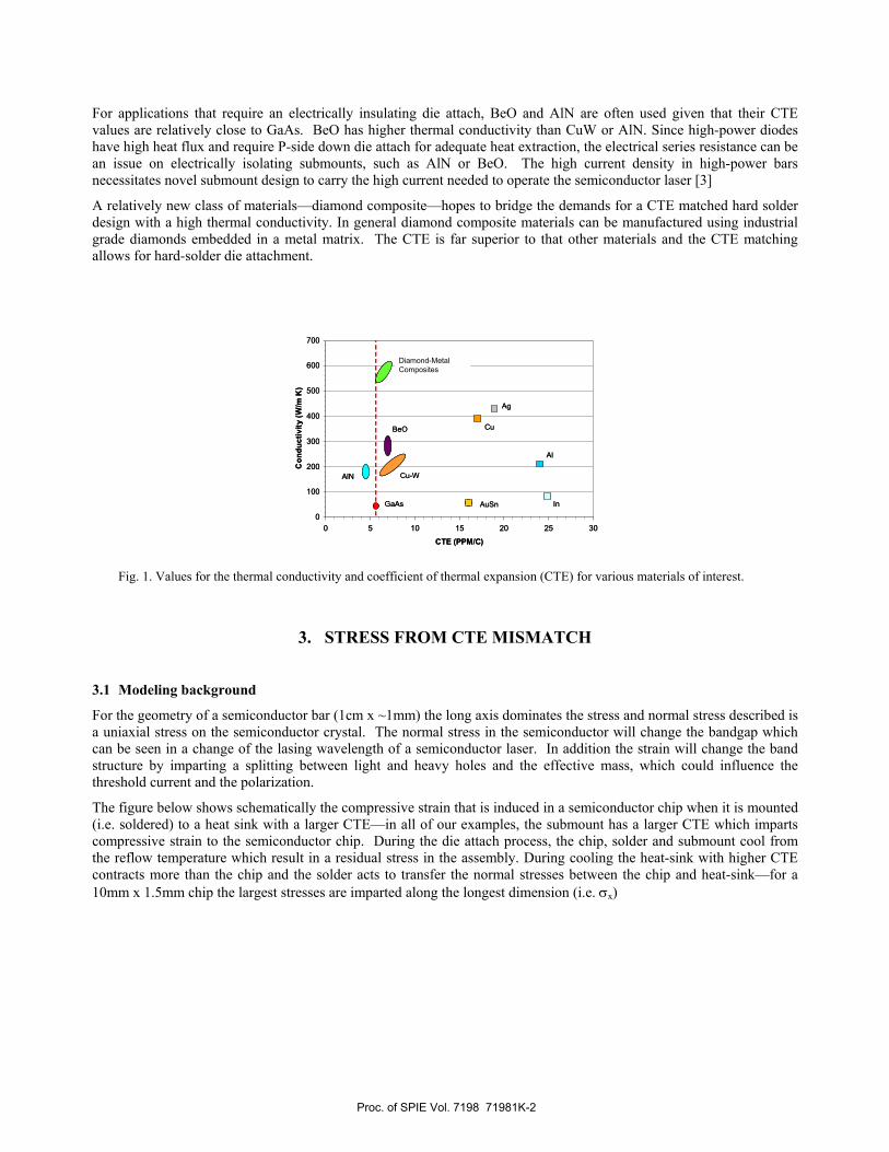
For applications that require an electrically insulating die attach, BeO and AlN are often used given that their CTE values are relatively close to GaAs. BeO has higher thermal conductivity than CuW or AlN. Since high-power diodes have high heat flux and require P-side down die attach for adequate heat extraction, the electrical series resistance can be an issue on electrically isolating submounts, such as AlN or BeO. The high current density in high-power bars necessitates novel submount design to carry the high current needed to operate the semiconductor laser [3]
A relatively new class of materials—diamond composite—hopes to bridge the demands for a CTE matched hard solder design with a high thermal conductivity. In general diamond composite materials can be manufactured using industrial grade diamonds embedded in a metal matrix. The CTE is far superior to that other materials and the CTE matching allows for hard-solder die attachment.
0
100
200
300
400
500
600
700
0 5 10 15 20 25 30
CTE (PPM/C)
Con
duct
ivity
(W/m
K)
Diamond-Metal Composites
Ag
Cu
Al
InAuSnGaAs
Cu-W
BeO
AlN
0
100
200
300
400
500
600
700
0 5 10 15 20 25 30
CTE (PPM/C)
Con
duct
ivity
(W/m
K)
Diamond-Metal Composites
Ag
Cu
Al
InAuSnGaAs
Cu-W
BeO
AlN
Fig. 1. Values for the thermal conductivity and coefficient of thermal expansion (CTE) for various materials of interest.
3. STRESS FROM CTE MISMATCH
3.1 Modeling background
For the geometry of a semiconductor bar (1cm x ~1mm) the long axis dominates the stress and normal stress described is a uniaxial stress on the semiconductor crystal. The normal stress in the semiconductor will change the bandgap which can be seen in a change of the lasing wavelength of a semiconductor laser. In addition the strain will change the band structure by imparting a splitting between light and heavy holes and the effective mass, which could influence the threshold current and the polarization.
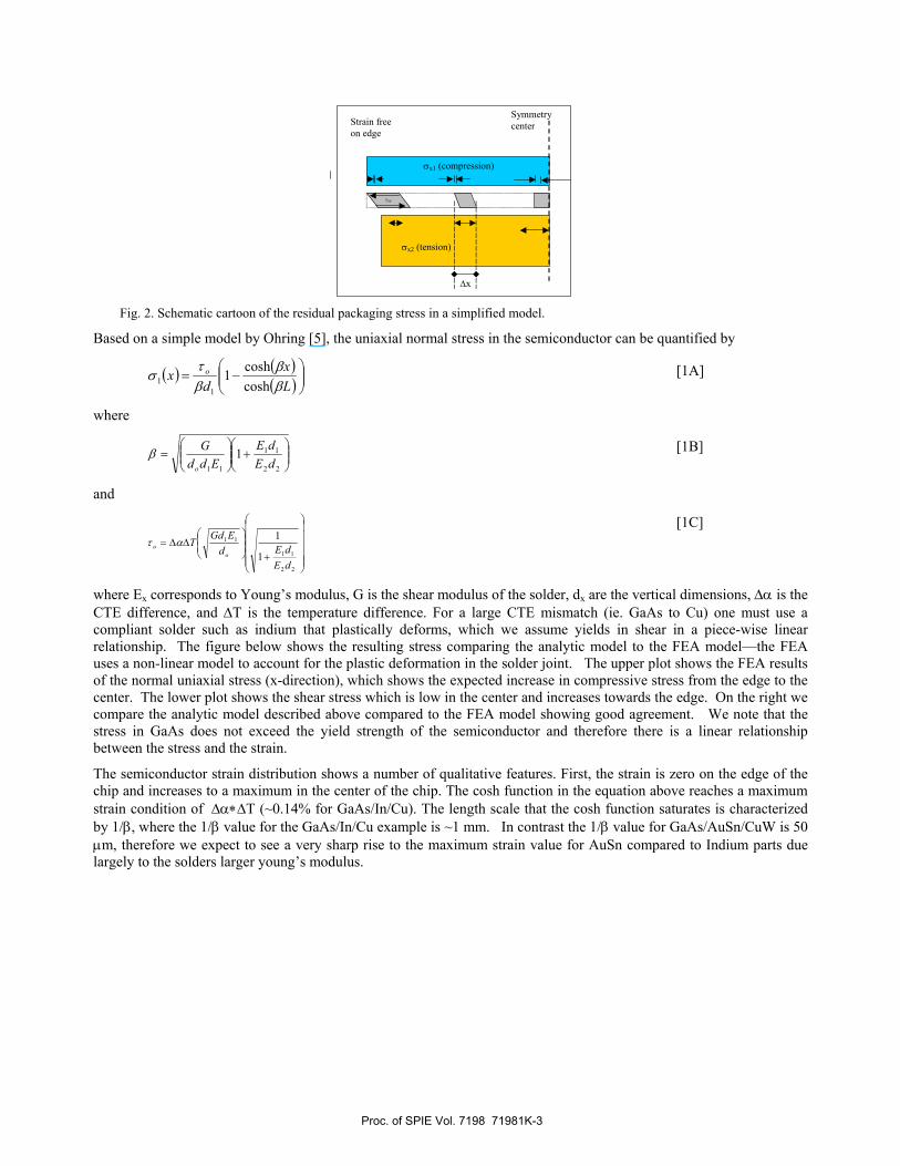
The figure below shows schematically the compressive strain that is induced in a semiconductor chip when it is mounted (i.e. soldered) to a heat sink with a larger CTE—in all of our examples, the submount has a larger CTE which imparts compressive strain to the semiconductor chip. During the die attach process, the chip, solder and submount cool from the reflow temperature which result in a residual stress in the assembly. During cooling the heat-sink with higher CTE contracts more than the chip and the solder acts to transfer the normal stresses between the chip and heat-sink—for a 10mm x 1.5mm chip the largest stresses are imparted along the longest dimension (i.e. σx)
Proc. of SPIE Vol. 7198 71981K-2
Txy
σx1 (compression)
σx2 (tension)
Δx
Symmetry center Strain free
on edge
Fig. 2. Schematic cartoon of the residual packaging stress in a simplified model.
Based on a simple model by Ohring [5], the uniaxial normal stress in the semiconductor can be quantified by
( ) ( )( )⎟⎟
⎠
⎞⎜⎜⎝
⎛−=
Lx
dx o
ββ
βτ
σcoshcosh1
11
[1A]
where
⎟⎟⎠
⎞⎜⎜⎝
⎛+⎟⎟
⎠
⎞⎜⎜⎝
⎛=
22
11
11
1dEdE
EddG
o
β [1B]
and
⎟⎟⎟⎟⎟
⎠
⎞
⎜⎜⎜⎜⎜
⎝
⎛
+⎟⎟⎠
⎞⎜⎜⎝
⎛ΔΔ=
22
11
11
1
1
dEdEd
EGdT
oo ατ
[1C]
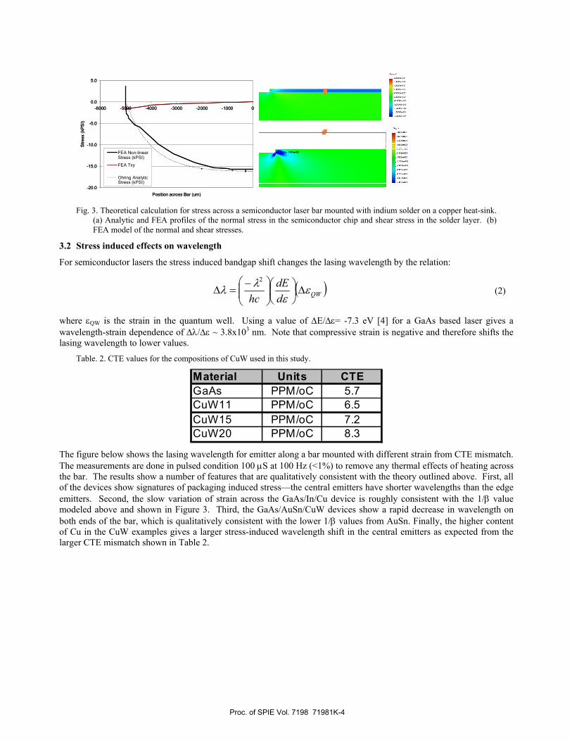
where Ex corresponds to Young’s modulus, G is the shear modulus of the solder, dx are the vertical dimensions, Δα is the CTE difference, and ΔT is the temperature difference. For a large CTE mismatch (ie. GaAs to Cu) one must use a compliant solder such as indium that plastically deforms, which we assume yields in shear in a piece-wise linear relationship. The figure below shows the resulting stress comparing the analytic model to the FEA model—the FEA uses a non-linear model to account for the plastic deformation in the solder joint. The upper plot shows the FEA results of the normal uniaxial stress (x-direction), which shows the expected increase in compressive stress from the edge to the center. The lower plot shows the shear stress which is low in the center and increases towards the edge. On the right we compare the analytic model described above compared to the FEA model showing good agreement. We note that the stress in GaAs does not exceed the yield strength of the semiconductor and therefore there is a linear relationship between the stress and the strain.
The semiconductor strain distribution shows a number of qualitative features. First, the strain is zero on the edge of the chip and increases to a maximum in the center of the chip. The cosh function in the equation above reaches a maximum strain condition of Δα∗ΔT (~0.14% for GaAs/In/Cu). The length scale that the cosh function saturates is characterized by 1/β, where the 1/β value for the GaAs/In/Cu example is ~1 mm. In contrast the 1/β value for GaAs/AuSn/CuW is 50 μm, therefore we expect to see a very sharp rise to the maximum strain value for AuSn compared to Indium parts due largely to the solders larger young’s modulus.
Proc. of SPIE Vol. 7198 71981K-3
-20.0
-15.0
-10.0
-5.0
0.0
5.0
-6000 -5000 -4000 -3000 -2000 -1000 0
Position across Bar (um)
Stre
ss (k
PSI)
FEA Non-linearStress (kPSI)
FEA Txy
Ohring AnalyticStress (kPSI)
-20.0
-15.0
-10.0
-5.0
0.0
5.0
-6000 -5000 -4000 -3000 -2000 -1000 0
Position across Bar (um)
Stre
ss (k
PSI)
FEA Non-linearStress (kPSI)
FEA Txy
Ohring AnalyticStress (kPSI)
Fig. 3. Theoretical calculation for stress across a semiconductor laser bar mounted with indium solder on a copper heat-sink.
(a) Analytic and FEA profiles of the normal stress in the semiconductor chip and shear stress in the solder layer. (b) FEA model of the normal and shear stresses.
3.2 Stress induced effects on wavelength
For semiconductor lasers the stress induced bandgap shift changes the lasing wavelength by the relation:
( )QWddE
hcε
ελλ Δ⎟
⎠⎞
⎜⎝⎛
⎟⎟⎠
⎞⎜⎜⎝
⎛ −=Δ
2
(2)
where εQW is the strain in the quantum well. Using a value of ΔE/Δε= -7.3 eV [4] for a GaAs based laser gives a wavelength-strain dependence of Δλ/Δε ~ 3.8x10³ nm. Note that compressive strain is negative and therefore shifts the lasing wavelength to lower values.
Table. 2. CTE values for the compositions of CuW used in this study.
Material Units CTEGaAs PPM/oC 5.7CuW11 PPM/oC 6.5CuW15 PPM/oC 7.2CuW20 PPM/oC 8.3
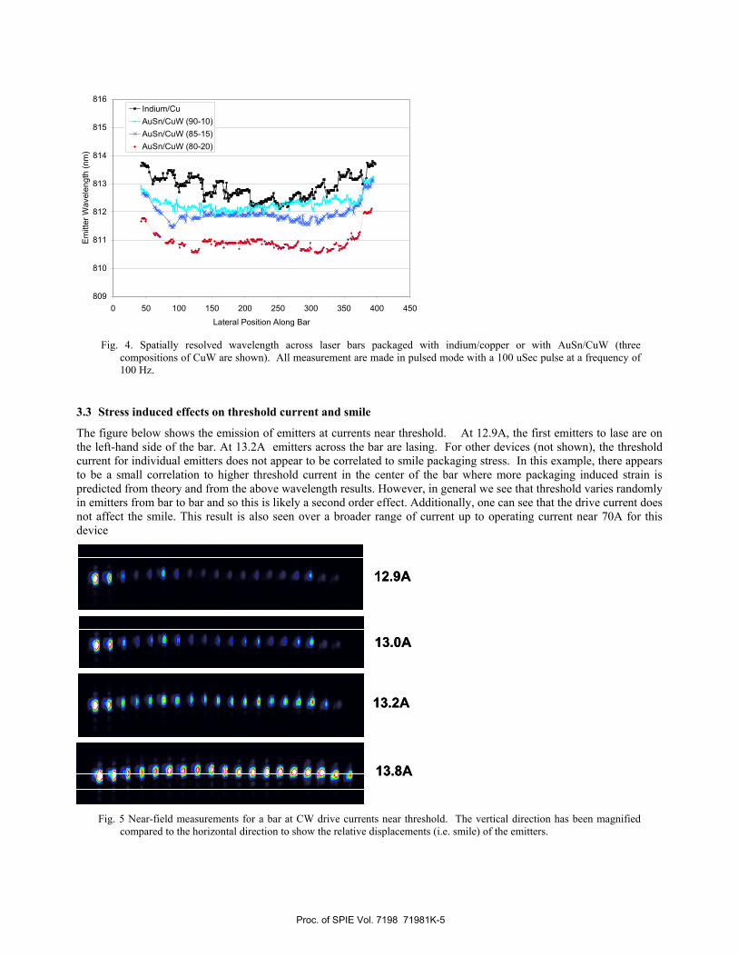
The figure below shows the lasing wavelength for emitter along a bar mounted with different strain from CTE mismatch. The measurements are done in pulsed condition 100 μS at 100 Hz (<1%) to remove any thermal effects of heating across the bar. The results show a number of features that are qualitatively consistent with the theory outlined above. First, all of the devices show signatures of packaging induced stress—the central emitters have shorter wavelengths than the edge emitters. Second, the slow variation of strain across the GaAs/In/Cu device is roughly consistent with the 1/β value modeled above and shown in Figure 3. Third, the GaAs/AuSn/CuW devices show a rapid decrease in wavelength on both ends of the bar, which is qualitatively consistent with the lower 1/β values from AuSn. Finally, the higher content of Cu in the CuW examples gives a larger stress-induced wavelength shift in the central emitters as expected from the larger CTE mismatch shown in Table 2.
Proc. of SPIE Vol. 7198 71981K-4
0 I * I I I I I 0
809
810
811
812
813
814
815
816
0 50 100 150 200 250 300 350 400 450Lateral Position Along Bar
Em
itter
Wav
elen
gth
(nm
)
Indium/CuAuSn/CuW (90-10)AuSn/CuW (85-15)AuSn/CuW (80-20)
Fig. 4. Spatially resolved wavelength across laser bars packaged with indium/copper or with AuSn/CuW (three
compositions of CuW are shown). All measurement are made in pulsed mode with a 100 uSec pulse at a frequency of 100 Hz.
3.3 Stress induced effects on threshold current and smile
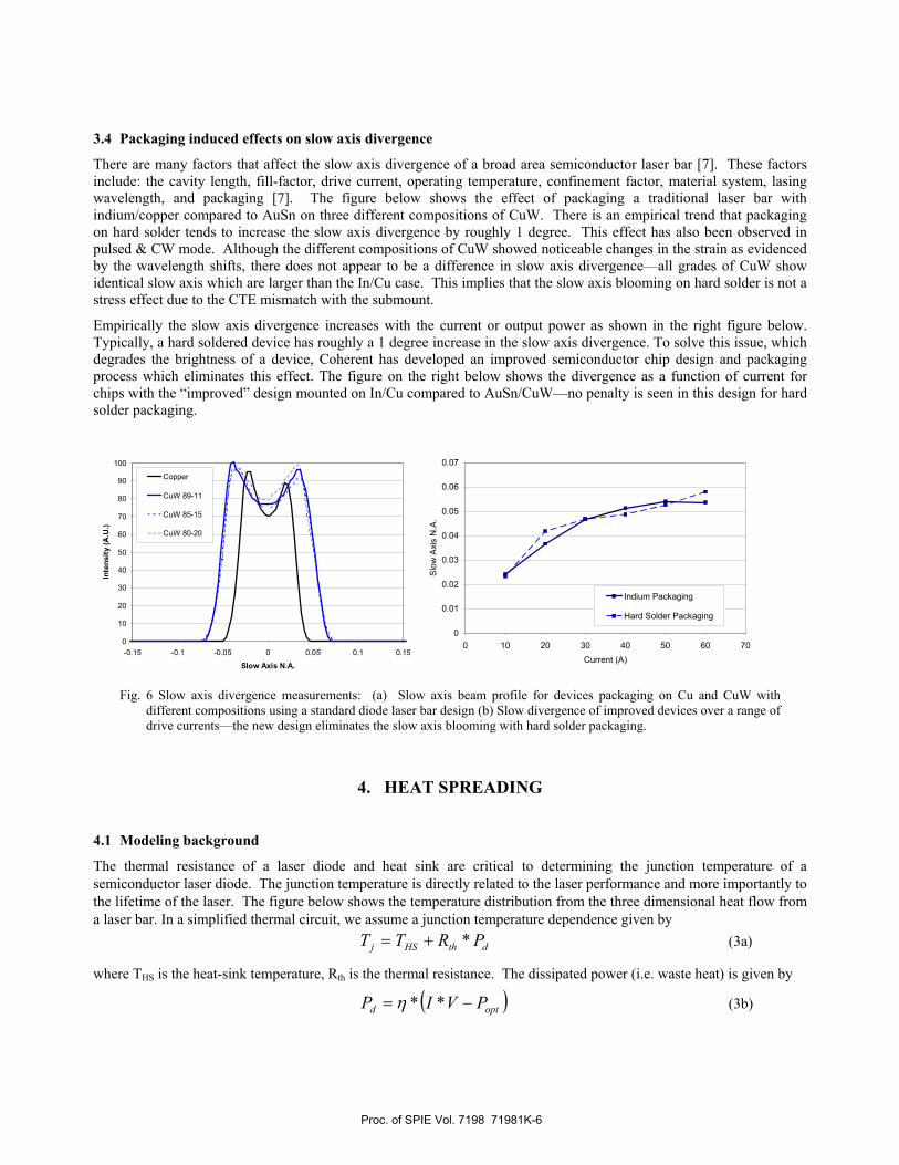
The figure below shows the emission of emitters at currents near threshold. At 12.9A, the first emitters to lase are on the left-hand side of the bar. At 13.2A emitters across the bar are lasing. For other devices (not shown), the threshold current for individual emitters does not appear to be correlated to smile packaging stress. In this example, there appears to be a small correlation to higher threshold current in the center of the bar where more packaging induced strain is predicted from theory and from the above wavelength results. However, in general we see that threshold varies randomly in emitters from bar to bar and so this is likely a second order effect. Additionally, one can see that the drive current does not affect the smile. This result is also seen over a broader range of current up to operating current near 70A for this device
12.9A
13.0A
13.2A
13.8A
12.9A
13.0A
13.2A
13.8A
Fig. 5 Near-field measurements for a bar at CW drive currents near threshold. The vertical direction has been magnified
compared to the horizontal direction to show the relative displacements (i.e. smile) of the emitters.
Proc. of SPIE Vol. 7198 71981K-5
3.4 Packaging induced effects on slow axis divergence
There are many factors that affect the slow axis divergence of a broad area semiconductor laser bar [7]. These factors include: the cavity length, fill-factor, drive current, operating temperature, confinement factor, material system, lasing wavelength, and packaging [7]. The figure below shows the effect of packaging a traditional laser bar with indium/copper compared to AuSn on three different compositions of CuW. There is an empirical trend that packaging on hard solder tends to increase the slow axis divergence by roughly 1 degree. This effect has also been observed in pulsed & CW mode. Although the different compositions of CuW showed noticeable changes in the strain as evidenced by the wavelength shifts, there does not appear to be a difference in slow axis divergence—all grades of CuW show identical slow axis which are larger than the In/Cu case. This implies that the slow axis blooming on hard solder is not a stress effect due to the CTE mismatch with the submount.
Empirically the slow axis divergence increases with the current or output power as shown in the right figure below. Typically, a hard soldered device has roughly a 1 degree increase in the slow axis divergence. To solve this issue, which degrades the brightness of a device, Coherent has developed an improved semiconductor chip design and packaging process which eliminates this effect. The figure on the right below shows the divergence as a function of current for chips with the “improved” design mounted on In/Cu compared to AuSn/CuW—no penalty is seen in this design for hard solder packaging.
0
10
20
30
40
50
60
70
80
90
100
-0.15 -0.1 -0.05 0 0.05 0.1 0.15
Slow Axis N.A.
Inte
nsity
(A.U
.)
Copper
CuW 89-11
CuW 85-15
CuW 80-20
Fig. 6 Slow axis divergence measurements: (a) Slow axis beam profile for devices packaging on Cu and CuW with
different compositions using a standard diode laser bar design (b) Slow divergence of improved devices over a range of drive currents—the new design eliminates the slow axis blooming with hard solder packaging.
4. HEAT SPREADING
4.1 Modeling background
The thermal resistance of a laser diode and heat sink are critical to determining the junction temperature of a semiconductor laser diode. The junction temperature is directly related to the laser performance and more importantly to the lifetime of the laser. The figure below shows the temperature distribution from the three dimensional heat flow from a laser bar. In a simplified thermal circuit, we assume a junction temperature dependence given by
dthHSj PRTT *+= (3a)
where THS is the heat-sink temperature, Rth is the thermal resistance. The dissipated power (i.e. waste heat) is given by
( )optd PVIP −= **η (3b)
0
0.01
0.02
0.03
0.04
0.05
0.06
0.07
0 10 20 30 40 50 60 70Current (A)
Slo
w A
xis
N.A
.
Indium Packaging
Hard Solder Packaging
Proc. of SPIE Vol. 7198 71981K-6
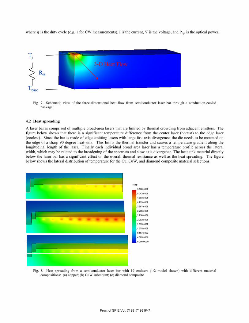
where η is the duty cycle (e.g. 1 for CW measurements), I is the current, V is the voltage, and Popt is the optical power.
Tj
Tbase
3-D Heat FlowRth
Tj
Tbase
3-D Heat FlowRth
Fig. 7—Schematic view of the three-dimensional heat-flow from semiconductor laser bar through a conduction-cooled
package.
4.2 Heat spreading
A laser bar is comprised of multiple broad-area lasers that are limited by thermal crowding from adjacent emitters. The figure below shows that there is a significant temperature difference from the center laser (hottest) to the edge laser (coolest). Since the bar is made of edge emitting lasers with large fast-axis divergence, the die needs to be mounted on the edge of a sharp 90 degree heat-sink. This limits the thermal transfer and causes a temperature gradient along the longitudinal length of the laser. Finally each individual broad area laser has a temperature profile across the lateral width, which may be related to the broadening of the spectrum and slow axis divergence. The heat sink material directly below the laser bar has a significant effect on the overall thermal resistance as well as the heat spreading. The figure below shows the lateral distribution of temperature for the Cu, CuW, and diamond composite material selections.
Fig. 8—Heat spreading from a semiconductor laser bar with 19 emitters (1/2 model shown) with different material
compositions: (a) copper; (b) CuW submount; (c) diamond composite.
Proc. of SPIE Vol. 7198 71981K-7

4.3 Thermal resistance
Accurate measurements of thermal resistance are important to the design of both the laser bar and laser packaging to optimally dissipate the waste heat. To measure thermal resistance, we rely on two approximations: (1) the linear dependence of wavelength with junction temperature and (2) the linear increase of junction temperature from an ideal heat-sink with dissipated thermal power. The figure below shows the thermal resistance as a function of the waste heat. From the equation above, the slope gives the thermal resistance. The dashed and dotted lines give the results for AuSn/CuW and In/Cu packaging respectively. As expected, there is a thermal penalty for mounted devices on a CTE match material appropriate for using AuSn. The solid line shows results for a diamond composite device mounted with AuSn. These results show similar or slightly better thermal results than In/Cu.
10
20
30
40
50
20 30 40 50 60Waste Heat (W)
Tem
p R
ise
(oC
)
243003 HCCP251642 PCCP245225 DC
Fig. 9—Thermal resistance measurements from conduction cooled heat sinks made with different packaging materials: (1)
In/Cu (PCCP); (2) AuSn/CuW (HCCP), and (3) AuSn/diamond composite (DC).
5. RELIABILITY For many industrial applications, a reliable semiconductor package needs to be robust under on-off current-cycling lifetime as well as thermal cycling tests. In the figure below we show results for an on-cycling life-test where no failures have been observed for > 10,000 hrs under hard pulse (1 second on-1second off) conditions at 85 Amps of drive current. We have also measured the smile under temperature cycling conditions. In the figure below we show that the smile stays below 1 micron for 40 thermal cycles from -40 to +60oC; these devices also show no degradation in power or wavelength throughout these tests. The stability of the smile is important for high brightness applications.
Proc. of SPIE Vol. 7198 71981K-8
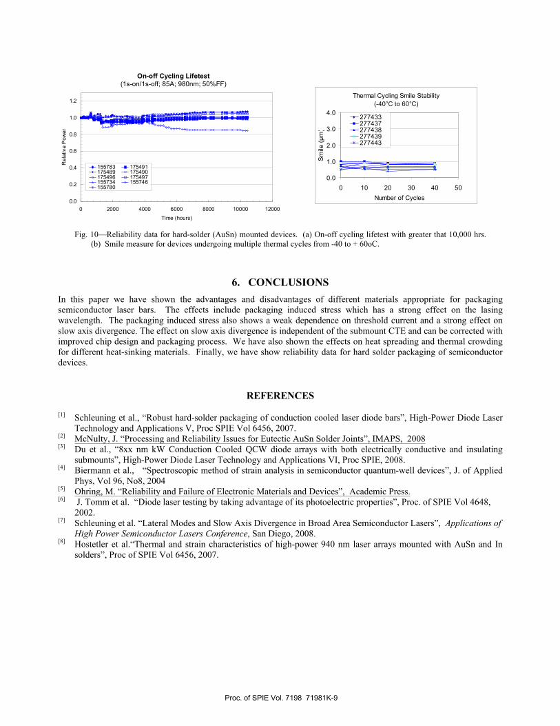
On-off Cycling Lifetest(1s-on/1s-off; 85A; 980nm; 50%FF)
0.0
0.2
0.4
0.6
0.8
1.0
1.2
0 2000 4000 6000 8000 10000 12000Time (hours)
Rel
ativ
e P
ower
155783 175491175489 175490175496 175497155734 155746155780
Fig. 10—Reliability data for hard-solder (AuSn) mounted devices. (a) On-off cycling lifetest with greater that 10,000 hrs.
(b) Smile measure for devices undergoing multiple thermal cycles from -40 to + 60oC.
6. CONCLUSIONS In this paper we have shown the advantages and disadvantages of different materials appropriate for packaging semiconductor laser bars. The effects include packaging induced stress which has a strong effect on the lasing wavelength. The packaging induced stress also shows a weak dependence on threshold current and a strong effect on slow axis divergence. The effect on slow axis divergence is independent of the submount CTE and can be corrected with improved chip design and packaging process. We have also shown the effects on heat spreading and thermal crowding for different heat-sinking materials. Finally, we have show reliability data for hard solder packaging of semiconductor devices.
REFERENCES
[1] Schleuning et al., “Robust hard-solder packaging of conduction cooled laser diode bars”, High-Power Diode Laser Technology and Applications V, Proc SPIE Vol 6456, 2007.
[2] McNulty, J. “Processing and Reliability Issues for Eutectic AuSn Solder Joints”, IMAPS, 2008 [3] Du et al., “8xx nm kW Conduction Cooled QCW diode arrays with both electrically conductive and insulating
submounts”, High-Power Diode Laser Technology and Applications VI, Proc SPIE, 2008. [4] Biermann et al., “Spectroscopic method of strain analysis in semiconductor quantum-well devices”, J. of Applied
Phys, Vol 96, No8, 2004 [5] Ohring, M. “Reliability and Failure of Electronic Materials and Devices”, Academic Press. [6] J. Tomm et al. “Diode laser testing by taking advantage of its photoelectric properties”, Proc. of SPIE Vol 4648,
2002. [7] Schleuning et al. “Lateral Modes and Slow Axis Divergence in Broad Area Semiconductor Lasers”, Applications of
High Power Semiconductor Lasers Conference, San Diego, 2008. [8] Hostetler et al.“Thermal and strain characteristics of high-power 940 nm laser arrays mounted with AuSn and In
solders”, Proc of SPIE Vol 6456, 2007.
Thermal Cycling Smile Stability(-40°C to 60°C)
0.0
1.0
2.0
3.0
4.0
0 10 20 30 40 50Number of Cycles
Sm
ile (µ
m)
277433277437277438277439277443
Proc. of SPIE Vol. 7198 71981K-9