The Power Diode
30
University Federico II Dept of Electronics and Telecommunications Paolo Spirito Power Semiconductor Devices 1 The Power Diode What makes a difference between the usual P/N semiconductor diode and the power diode? The response is basically: the need to withstand high voltages in the reverse bias condition; this need will pose some constraints on the device structure. All power devices that must operate at high reverse voltages present at least one P/N junction reverse biased, so the voltage requirements for the P/N junction of the power diode are equally shared by the other power devices, as we will see in the following. Let’s briefly recall, for a P/N junction, the basic relationship for the depletion region and field profile in reverse bias. the charge balance in the depleted regions W1 and W2 gives: q W1 Na = q W2 Nd, where Na is the concentration of acceptor atoms in P region, and Nd of the donor ones in N region. Then: University Federico II Dept of Electronics and Telecommunications Paolo Spirito Power Semiconductor Devices 2 Assuming constant doping profile in both P+ and N region (abrupt junction assumption), the field profile is linear, based on the Poisson equation: If Na >>Nd (P + N diode) W1 <<W2; then the total depletion width W D ! W2 Assuming P+ >>N, the field profile lies in the low- doped side of the junction, and the max E M value is dependent on the depletion layer width W D ! W2
-
Upload
independent -
Category
Documents
-
view
1 -
download
0
Transcript of The Power Diode

University Federico II Dept of Electronics and Telecommunications
Paolo Spirito Power Semiconductor Devices
1
The Power Diode
What makes a difference between the usual P/N semiconductor diode and the power diode? The response is basically: the need to withstand high voltages in the reverse bias condition; this need will pose some constraints on the device structure.
All power devices that must operate at high reverse voltages present at least one P/N junction reverse biased, so the voltage requirements for the P/N junction of the power diode are equally shared by the other power devices, as we will see in the following.
Let’s briefly recall, for a P/N junction, the basic relationship for the depletion region and field profile in reverse bias.
the charge balance in the depleted regions W1 and W2 gives: q W1 Na = q W2 Nd, where Na is the concentration of acceptor atoms in P region, and Nd of the donor ones in N region. Then:
University Federico II Dept of Electronics and Telecommunications
Paolo Spirito Power Semiconductor Devices
2
Assuming constant doping profile in both P+ and N region (abrupt junction assumption), the field profile is linear, based on the Poisson equation:
If Na >>Nd (P+N diode) W1 <<W2; then the total depletion width WD ! W2
Assuming P+ >>N, the field profile lies in the low-doped side of the junction, and the max EM value is dependent on the depletion layer width WD ! W2

University Federico II Dept of Electronics and Telecommunications
Paolo Spirito Power Semiconductor Devices
3
Recalling the expression of the built-in voltage VBI with no external bias:
assuming: NA = 1018 cm-3
ND = 1015 cm-3 we obtain: VBI = 0.8 V, WD = 0.1 µm
and recalling that: we obtain:
In reverse bias the junction voltage VJ is the sum of VBI + VR. The built in voltage (about 1V) is negligible with respect to the reverse bias voltages applied, so one can approximate: VJ ! VR.
VJ
both the max field EM and the depletion width WD increase with the reverse voltage Vr
University Federico II Dept of Electronics and Telecommunications
Paolo Spirito Power Semiconductor Devices
4
Breakdown voltage of a P/N junction
As it is well known, the IV characteristic of a PN junction has a current that depends exponentially from the applied voltage in an exponential vay in forward bias with a low voltage drop VON. In reverse bias it has a very low current, up to a max voltage VMAX limited by avalanche multiplication, where the current sharply increases in almost unlimited way.
The max reverse voltage VMAX of the junction is called the breakdown voltage VBR, and puts a limit in the max reverse voltage that the junction can withstand. We will now discuss the dependence of the breakdown voltage from the doping and width of the low doped region of the junction (remember that the field and voltage in reverse bias drops almost completely in the low doped region), to define the constraints posed on that region from the need of an high VMAX in the range of hundreds or thousand of volts.

University Federico II Dept of Electronics and Telecommunications
Paolo Spirito Power Semiconductor Devices
5
Avalanche multiplication
E
In the depleted region of the junction the mobile carriers travel under the drift effect the electric field E; their mobility is due to the collisions with Si atoms, but in the mean free path between each collision the carriers are accelerated by the field. If the field value is so high to give to the mobile charge an energy above the energy gap EG before the collision, the carrier that collides with an atom creates a secondary electron-hole pair generated by impact ionization.
Each secondary carrier can create again an electron-hole pair if that carrier can reach an energy higher than EG in his mean free path. The result is a number of secondary carriers created by impact ionization that tends to infinite even if the number of primary carriers is very low. This is the effect of avalanche multiplication.
University Federico II Dept of Electronics and Telecommunications
Paolo Spirito Power Semiconductor Devices
6
with N = 2 – 6 IO
The current due to impact multiplication is usually indicated as I = M IO , where IO is the current when impact ionization is not present, and M is the multiplication factor due to impact ionization. The factor M can vary from 1 infinite, depending from the percentage of carriers that, under the field E applied, reach an energy high enough to generate a secondary electron-hole pair by impact ionization. The factor M is a function of field E, and the breakdown voltage VBR is reached when M= f(E) becomes infinite.
An empirical relation for the multiplication factor M is the Miller expression:

University Federico II Dept of Electronics and Telecommunications
Paolo Spirito Power Semiconductor Devices
7
Let’s define more quantitatively the multiplication factor M from the basic transport equations
In the high field the primary carriers (both electrons and holes) moves with saturated velocity vs , and generate secondary carriers. The generation term in the continuity equation becomes : G = "pp vs + "nn vs where "p and "n are multiplication coefficients for holes and electrons, depending from field. The current components are: Jp = q p vs ; Jn = - q n vs
In the multiplication region:
Substituting eq. (3) in (1) one has: 1)
2)
3)
University Federico II Dept of Electronics and Telecommunications
Paolo Spirito Power Semiconductor Devices
8
An useful simplification comes from the assumption of equal ionization coefficients for holes and electrons: "P = "N = ", where " is a function of E and from E(x) depends on x
Integrating with boundary conditions: at x = 0 Jp = Jp0 at x=W Jp=MpJp0
summing JN0 to both members:
Then, by recalling that at x = 0 JP0 + JN0 = J0 , we have for the multiplied current J:

University Federico II Dept of Electronics and Telecommunications
Paolo Spirito Power Semiconductor Devices
9
This is a very fast dependence from field E, as it can be seen from the plot. The value of " can be significant only for fields in the range of 105 V/cm (for lower E values there is no appreciable multiplication effect)
From the previous equation we see that the breakdown condition M # is reached when:
(breakdown condition)
" is a a strong function of the electric field E; an approximate expression of "($) is: a(E)= 1.8 10-35 E 7
University Federico II Dept of Electronics and Telecommunications
Paolo Spirito Power Semiconductor Devices
10
For an approximate analysis we can assume
ECR = 2 105 V/cm
As it can be seen from the plot where the approximate value of "(E) given is used, the critical field ECR is slowly varying with the doping for dopings less than 1015 cm-3
The breakdown condition: can be transformed as a function of field by a variable transform dx dE
is a function of a critical field ECR that gives the first term equal to 1.

University Federico II Dept of Electronics and Telecommunications
Paolo Spirito Power Semiconductor Devices
11
Assuming as the critical field for avalanche breakdown: ECR = 200 kV/cm one can easily determine the breakdown voltage as a function of doping of the low doped region of the PN junction, assuming a linear field profile down to the abscissa WB (depleted width at breakdown):
At breakdown : VBR = ! ECR WB (6)
Recalling the relations:
From the Poisson relation (a) we obtain:
(4)
(5)
and substituting in (6):
we obtain the VBR dependence on doping as:
(7)
(8a)
University Federico II Dept of Electronics and Telecommunications
Paolo Spirito Power Semiconductor Devices
12
The PIN diode Up to now we considered only a P+/N junction, not a diode. To have a diode we need to contact both the P and N region with a metal to which are bonded the wires that connect the si chip to the external terminals. To have a good ohmic contact between the metal and the semiconductor, we need to have a high doping at the interface; otherwise we should have a schottky barrier and not an ohmic contact at the Si-metal interface. So we need to interpose an high doped N+ layer between the low doped N region and the metal (the P+ region has already high doping). This region can be the substrate of the chip for low N- thickness, or a diffused region for thick N- layers (above 150 µm).
For a given WN thickness of the low doped layer, and depending on the doping N-, we can have two cases, as indicated in the side plot:
a) the field at breakdown goes to zero in the low doped region (solid line): the depleted region is all inside the N- region (Non-Punch-Through case - NPT)
b) the field at breakdown reach the high doped N+ region before going to zero (dashed line): this means that the depletion region reach the high doped region N+ and then goes to zero (Punch-Through case - PT)

University Federico II Dept of Electronics and Telecommunications
Paolo Spirito Power Semiconductor Devices
13
Using the previous relation (8a) for the VBR dependence on doping of the N region, assuming a Non-Punch-Through case (NPT), we obtain:
with: %SI = 10-12 F/cm ECR = 200 KV/cm
VBR
doping
This plot shows a breakdown voltage of more than 1 KV for a N- region doped 1014 cm-3
However, the limitation posed by the thickness W of the N region is not taken into account in this plot; from eq. (d) to account for the NPT case, one need a thickness WB = 125 µm at breakdown, quite high as we will see in the following.
University Federico II Dept of Electronics and Telecommunications
Paolo Spirito Power Semiconductor Devices
14
If the thickness WD of the low doped ND region is less than value WB given by eq. (d) the field profile assumes a trapezoidal shape.
From the limit case of a doping ND* for which WD =WB, if the doping decreases furthermore, then the breakdown voltage merely doubles with respect to the one given by eq. (e) for the ND* , i.e.:
for ND " 0 VBR = ECR WD
For the more general case of a trapezoidal field profile, we have (PT case):
(8b)

University Federico II Dept of Electronics and Telecommunications
Paolo Spirito Power Semiconductor Devices
15
Breakdown Voltage for a Punch-Through diode
VBR
doping ND
NPT case
Using eq. (8b) for the general case case we obtain the breakdown voltage as a function of both the doping ND and the thickness WD of the low doped region. In this graphic the asymptote for very low doping corresponds to the rectangular field profile, and the PT line to the triangular field profile :
University Federico II Dept of Electronics and Telecommunications
Paolo Spirito Power Semiconductor Devices
16
Physical structure of a PIN diode
The cross-section of the physical structure of a PIN diode is depicted here. The N+ region (not in scale) is the chip substrate (some hundreds of microns, thicker than the active area). The low doped ND region of thickness WD is the epitaxial layer, in which the P+ region is made by implant and thermal diffusion through the field SI02 oxide. The oxide layer on top protects the lateral sides of the PN junction from an excessive current leakage in reverse bias, because the oxide is a good passivation layer (this is a basic benefit of the so-called planar technology).
# #
However as a result of this technique the PN junction will present a curvature both in the Y and Z directions (assuming the x axis as the vertical depth). This curvature will result in a strong limitation on the breakdown voltage, as we will see in the following.

University Federico II Dept of Electronics and Telecommunications
Paolo Spirito Power Semiconductor Devices
17
2D and 3D effects of junction curvature
cylindr. reg.
plane reg.
spher. reg.
The doping through the oxide window gives rise to a lateral diffusion under the oxide, and creates a 2D geometrical shape of the junction in the X and Y directions if one assumes an infinite length in the Z direction: in that case it is said that the junction has a cylindrical curvature in the y direction.
y
x
z
If the length of the window in the Z direction is not infinite, the corners of the window will create after diffusion a spherical junction curvature: it is said that the junction has a spherical curvature because it is bended both in the Y and Z directions.
University Federico II Dept of Electronics and Telecommunications
Paolo Spirito Power Semiconductor Devices
18
Field analysis for cylindrical junction
Assumptions: a) isotropic diffusion: rJ = xJ b) approximation: L>>rj rj xJ
WD
the cylindrical region in the dashed area can be analyzed by using radial coordinate in the plane E,r

University Federico II Dept of Electronics and Telecommunications
Paolo Spirito Power Semiconductor Devices
19
The field in the cylindrical region can be described again by the Poisson equation in radial coordinates:
Integrating the first term between the generic abscissa r and rD (where E = 0), we have a power law dependence for the field:
At the abscissa rJ the field has is max value EM|CIL :
(9)
University Federico II Dept of Electronics and Telecommunications
Paolo Spirito Power Semiconductor Devices
20
For low doping values ND the depletion layer is large and : rD>>rJ . It is possible in this case to approximate eq. (9) as:
For the plane junction the thickness WD can be written as: WD = rD – rJ , and the max field EM|P in the same approximation rD>>rJ can be written as:
(10)
From eq. (10) and (11) it comes out that the ratio of the max field EM|CIL in the cylindrical region and EM|P in the plane region is larger than 1:
(11)
(12)

University Federico II Dept of Electronics and Telecommunications
Paolo Spirito Power Semiconductor Devices
21
For the spherical region of the junction the field can be again described by the Poisson equation in radial coordinates:
In the case rD>>rJ
Field analysis for spherical junction
cylindr. reg.
plane reg.
spher. reg.
Integrating between r and rD we extract the field E(r), and we obtain the EM|SP as :
(13)
University Federico II Dept of Electronics and Telecommunications
Paolo Spirito Power Semiconductor Devices
22
From eq. (12) and (13) it comes out that EM|CIL and furthermore EM|SP are higher than EM|P of the plane junction, so the value ECR for the breakdown will be reached in the cylindrical ( or spherical ) region when the EM|P is still less than the ECR value. Assumed equipotential the anode and cathode planes, the VBR value for the cylindrical (or spherical) regions will be lower than the one VBR|P of the plane region, and the current will increase to infinite even if it is flowing only in the portion of the junction subjected to premature breakdown. By integrating the expressions of E(r) for the two cases analyzed one can obtain the following results for VBR|CIL or VBR|SP normalized to VBR|P, as a function of the junction curvature radius rJ normalized to the plane depletion layer at breakdown WB
Breakdown voltage for cylindrical or spherical junction
VBR/VBR|P
rJ/WB
cyl. sph.

University Federico II Dept of Electronics and Telecommunications
Paolo Spirito Power Semiconductor Devices
23
The decrease of VBR|SP respect to VBR|CYL can be eliminated by making the curvature radius r’J in the Y,Z plane (chip surface) much higher than the one rJ of the cylindrical region. This is possible because the r’J value is determined by the mask design of the window opening, and one can easily made r’J>>rJ. This latter is limited by the diffusion depth of the P+ region, that is usually less than 10 µm, and is usually much less than the depletion layer WB at breakdown.
The limitation for high r’J comes out from the area loss with respect to the one of a square window: the assumptions then are: L >>r’J >WB,; then r’J>>rJ.
As an example: xJ= rJ=10µm, WD= 50µm, r’J= 200 µm Percentage area loss < 2 10-2 if L = 1mm.
University Federico II Dept of Electronics and Telecommunications
Paolo Spirito Power Semiconductor Devices
24
Junction termination techniques To overcome the VBR decrease due to the lateral junction curvature the two most widely used
techniques (both for the power diode and the other high voltage devices) are: a) Floating field rings b) Field plates
The first one need to create some P+ diffused regions (rings) around the P+ anode region as indicated in the plot (here only one ring is sketched), left “floating” with respect to the anode bias (not metal contacted).
Assuming the potential in the y direction not altered by the presence of the ring, this latter will be actually biased by the potential value as far as the depletion region reach (and trespass) it.
x
y
Using the Poisson eq. for the plane case in the y direction (eq. 14), starting from the lateral boundary of the P+ anode, and integrating it with the boundary conditions: V= 0 for y=0; V= -VR for y= WD (depletion width at VR, assumed equal to WD|X ), we have:
(14) (15)

University Federico II Dept of Electronics and Telecommunications
Paolo Spirito Power Semiconductor Devices
25
When VR is increased, the depletion region WD extends in the y direction and reaches the floating ring at WS before breakdown if WS < WB. Then the voltage bias of the field ring at y = WS will be:
Two limiting cases are: a) for WS"0 VFR = VR Then the floating ring
has the same voltage of the main junction and the diode VBR is limited by the VBR|CIYL of the floating ring because its junction curvature is the same as for the main junction.
b) for WS"WB VFR = 0. Then the ring is not biased up to the breakdown voltage and this latter is the VBR|CYL of the main junction, i.e. the main junction is not protected by premature breakdown by the presence of the guard ring.
The best choice, as seen in the plot (for the case rJ/WB=0.4), is WS ! WB/3.
WS/WB
VBR/VBR|P
University Federico II Dept of Electronics and Telecommunications
Paolo Spirito Power Semiconductor Devices
26
cylindr.
guard ring
The increase of VBR using a floating ring is dependent on the curvature radius rJ of the junction (the depth and curvature of the ring is assumed equal to that of the main junction because the ring is made with the same diffusion process as the main junction).
To increase the VBR near the value of the plane case for the case of low rJ/WB ratios, we need to use multiple floating rings (about 4 or 5 rings are usually employed) to reduce the lateral field for each ring respect to the preceding one.

University Federico II Dept of Electronics and Telecommunications
Paolo Spirito Power Semiconductor Devices
27
b) Field plate
(a)
(b)
(c)
This technique uses a metal plate over the oxide and the charge induced on the Si surface to modify the lateral field distribution. If the metal plate over the oxide is positively biased (case a), the surface is in the accumulation state and NSURF>ND ; VBR<VBR|CYL If the metal plate is negatively biased (case b), NSURF<ND, and a depletion layer due to the plate bias develops under the plate thus reducing the lateral field. In case (b) the equipotential lines extend under the plate and the potential distribution is more similar to the plane case, so VBR > VBR|CYL. In the practical case (c) the metal plate over the oxide is connected to the metal of the anode junction, so the bias of the field plate is the same as the VR of the junction.
How to evaluate the equivalent voltage induced on the Si surface by the field plate?
University Federico II Dept of Electronics and Telecommunications
Paolo Spirito Power Semiconductor Devices
28
The critical parameter for evaluation the voltage bias at the Si surface is is the oxide thickness tOX of the field plate. We can evaluate the field across the oxide using the Gauss law:
Gauss law tells that the field in the oxide is 3 times the field in the Si material: that means that to evaluate the voltage drop across the thickness tOX we can consider an equivalent Si layer with a thickness 3tOX. (!V = ESItSI = EOXtOX). For negative bias of the field plate, the field at the end of the plate corresponds to the case of a diffused Si P+ layer with an equivalent thickness 3tOX,, and then with a curvature radius rJ = 3tOX and with a voltage bias VR - &V If we use a thin oxide, the voltage induced on the Si surface is near to the one of the main junction, but the field due to the curvature radius at the end of the field plate will be very strong, inducing a premature breakdown at the end of the field plate. If we use a thick oxide, the curvature will be quite small, but the voltage drop under the plate will be large and the voltage at the Si surface will be much less than the one of the main junction, creating a premature breakdown at the lateral junction side .

University Federico II Dept of Electronics and Telecommunications
Paolo Spirito Power Semiconductor Devices
29
a) For ECR SI = 20 V/µm EOX =60V/µm &VOX = 60 V VFP = 940 V con rJFP = 3µ << rJ = 10µ the breakdown develops at the end of the field plate'
b) For ECR SI = 20 V/µm EOX =60V/µm &VOX = 600 V VFP = 400 V con rJFP = 30µ > rJ = 10 µ the breakdown develops at the main junction lateral side'
a) xJ=10µ W(=100µ tOX = 1µ rJFP = 3µ'
b) xJ=10µ WB=100µ tOX = 10µ rJFP = 30µ'
Example: consider two possible cases:
Assuming a reverse bias VR = 1000 V, we obtain:
WB
tOX xj
University Federico II Dept of Electronics and Telecommunications
Paolo Spirito Power Semiconductor Devices
30
The ideal solution would be to make an oxide thickness that increases in the y direction going far from the main junction, as indicated in fig. (a). This however is not workable for the usual planar technology:
A more practical solution is to make an oxide thickness that is increasing in steps in moving far from the main junction, as indicated in the fig. (b).The above can be obtained by depositing over the thermal oxide the next oxide layers by CVD with different film thickness and windows openings
(a)
(b)

University Federico II Dept of Electronics and Telecommunications
Paolo Spirito Power Semiconductor Devices
31 catodo
# #
The main ratings for a power diode from its datasheet are:
• Max reverse voltage in OFF state VRMAX • Max current in ON state IMAX • Voltage drop in ON state at nominal current VON • Dynamic power losses in a) turn-on b) turn-off
These ratings are mainly defined by the following structure parameters:
• ND doping of the low doped region • WD thickness of the low doped region • lifetime ) of the low doped region
Ratings for the PIN power diode
From the analysis of the breakdown voltage of the PIN diode we know that in order to allow an high VRMAX the structure must have a low doping ND and a relatively thick WD (for example ND about 1014cm-3 and WD about 50 µm to have a VRMAX of 1000V). What are the effects of the presence of the ND layer of thickness WD on the static and dynamic performances of the diode?
University Federico II Dept of Electronics and Telecommunications
Paolo Spirito Power Semiconductor Devices
32
I-V characteristics of the PIN diode
P+ ND
WD J1 J2
N++
The presence of two N regions (the low doped ND of the epitaxial layer and the high doped N++ of the substrate), as well as the operation at high current levels, will induce some changes in the static I-V curves with respect to the usual ones of the signal P/N diode. In the structure we can see two junctions, J1 and J2; the presence of the ND/N++ junction J2 and the low level of doping in the ND region, have an important effect on the I-V characteristics (as well as for the dynamic behavior, as we will see).
The holes injected in that region from the P+ layer are usually called “minority carriers” because they are injected in a N doped region, where the majority carriers are electrons. However if the doping ND of this region is quite low, it can happens that the holes density injected from the (high doped) P+ region can have an higher value than the one of electrons that is equal to ND at ambient temperature (all donors are ionized and give a free electron).

University Federico II Dept of Electronics and Telecommunications
Paolo Spirito Power Semiconductor Devices
33
This plot reports the holes (minority carriers) distribution in the low doped ND layer, for a diffusion length L=(D))1/2
>WD. In the plot we can distinguish two different
modes of operation: a) low injection when the injected carriers
(holes) are lower than the doping ND (blue curve)
b) high injection when the injected carriers are higher than the doping ND ( red curve)
In the neutral ND region the electric charge balance gives:
ND +p (positive charge) = n (negative charge) (a)
We have low injection if: p<<ND then from (a) n ! ND
We have high injection if: p>ND then from (a) n ! p > ND
University Federico II Dept of Electronics and Telecommunications
Paolo Spirito Power Semiconductor Devices
34
In low injection regime n(x) = ND there is no voltage drop on J2 and V = V(J1). The J-V characteristic of the diode is the ideal one:
In high injection regime p(0) > ND let’s recall the expression of p(0):
As an example: for V= VJ1 = 0.6V, assuming ND = 1014 cm-3, ni2 = 2·1020 cm-3, we have from eq. (16): p(0) = 2·1015>>ND . Then we are in high injection because: p(0) = n(0) >> ND. If the diffusion length LP > WD also p(W) = n(W) > ND.
Due to an electron concentration n(WD) > ND, for the Boltzmann equation there will be a voltage drop VJ2 across the junction J2 to allow this electron increase; J2 will be directly biased and will inject electrons from the substrate N++ into the ND region.
The overall diode voltage will be the sum VPIN = VJ1 + VJ2 Let’s evaluate the I-V relationship in that case
(16)
(17)
University Federico II Dept of Electronics and Telecommunications
Paolo Spirito Power Semiconductor Devices
35
In the assumption LP>>WD we can approximate the holes distribution as flat over the thickness WD , and we have: p(WD) ! n(WD) > ND. From the Boltzmann eq. (17) applied to the abscissa WD, in the case n(WD) > ND, we have:
indicating that a voltage VJ2 develops across J2 in order to have n(WD) > ND
The current density J of the diode can be related to the carrier densities p(0) or n(W) as:
University Federico II Dept of Electronics and Telecommunications
Paolo Spirito Power Semiconductor Devices
36
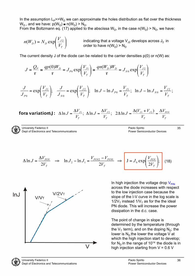
In high injection the voltage drop VPIN across the diode increases with respect to the low injection case because the slope of the I-V curve in the log scale is 1/2VT instead 1/VT as for the the ideal PN diode. This will increase the power dissipation in the d.c. case.
The point of change in slope is determined by the temperature (through the VT term), and on the doping ND: the lower is ND the lower the voltage V at which the high injection start to develop; for ND in the range of 1014 the diode is in high injection starting from V = 0.6 V
(18)
University Federico II Dept of Electronics and Telecommunications
Paolo Spirito Power Semiconductor Devices
37
N++ P+ ND
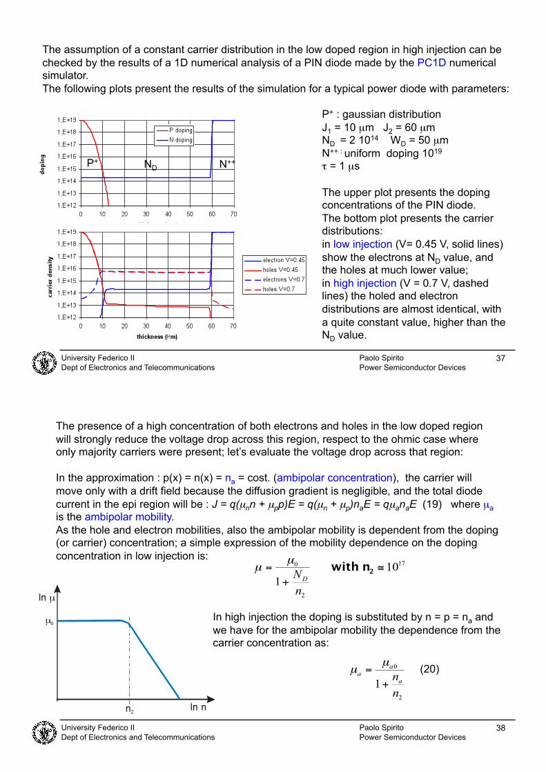
The assumption of a constant carrier distribution in the low doped region in high injection can be checked by the results of a 1D numerical analysis of a PIN diode made by the PC1D numerical simulator. The following plots present the results of the simulation for a typical power diode with parameters:
P+ : gaussian distribution J1 = 10 µm J2 = 60 µm ND = 2 1014 WD = 50 µm N++ : uniform doping 1019
) = 1 µs
The upper plot presents the doping concentrations of the PIN diode. The bottom plot presents the carrier distributions: in low injection (V= 0.45 V, solid lines) show the electrons at ND value, and the holes at much lower value; in high injection (V = 0.7 V, dashed lines) the holed and electron distributions are almost identical, with a quite constant value, higher than the ND value.
University Federico II Dept of Electronics and Telecommunications
Paolo Spirito Power Semiconductor Devices
38
The presence of a high concentration of both electrons and holes in the low doped region will strongly reduce the voltage drop across this region, respect to the ohmic case where only majority carriers were present; let’s evaluate the voltage drop across that region:
In the approximation : p(x) = n(x) = na = cost. (ambipolar concentration), the carrier will move only with a drift field because the diffusion gradient is negligible, and the total diode current in the epi region will be : J = q(µnn + µpp)E = q(µn + µp)naE = qµanaE (19) where µa is the ambipolar mobility. As the hole and electron mobilities, also the ambipolar mobility is dependent from the doping (or carrier) concentration; a simple expression of the mobility dependence on the doping concentration in low injection is:
In high injection the doping is substituted by n = p = na and we have for the ambipolar mobility the dependence from the carrier concentration as:
(20)

University Federico II Dept of Electronics and Telecommunications
Paolo Spirito Power Semiconductor Devices
39
From eq. (19): the voltage drop VD across the low doped region is:
in the limit na>> n2 (22), we have:
!
where : RM =WD
qAµa0n2
(24)
The resistance RM is much less than the “ohmic” resistance RD of the epi region:
because n2 is much higher than the doping ND.
(23)
reg. I
reg. II reg. III The decrease in resistance of the low doped
region is called “Conductivity modulation” and is due to the high injection regime (p=n>>ND). In the I-V curve we can identify 3 regions: the first 2 exponential, and the 3rd ohmic, in the high current range (the normal operating range for power diode)
(21)
University Federico II Dept of Electronics and Telecommunications
Paolo Spirito Power Semiconductor Devices
40
Trade-off between VON and VBR
Even if the RM value of the “conductivity modulated” epi region is much lower than the “ohmic” value, the voltage drop due to this resistance constitutes a significant increase of the total diode voltage VPIN = VJ1 + VJ2 + RMI . The doping and thickness of the low doped epi region are defined according to the breakdown voltage VBR needed, so we can express RM as a function of VBR. Recalling eq. (24) for RM, with reference to a triangular field profile up to breakdown (NPT case) , assuming: VBR = ECRWD/2= 105 WD, n2 = 1017, µa0 = 2000 we have:
indicating that RM increases linearly with the breakdown voltage VBR. (NPT)
As an example: for VBR= 1000V, assuming A=0.5cmx0.5cm " RM = 0.13 *; with a current of 10 A the voltage drop RMI = 1.3 V, that makes the overall diode voltage over 2 V with a d.c. power dissipation of more than 20 W.
For the case of almost constant field profile up to WD (in the limit of very low ND values) we have VBR = ECRWD, and the value of RM is half the value of the NPT case.
University Federico II Dept of Electronics and Telecommunications
Paolo Spirito Power Semiconductor Devices
41
Recombination lifetime
Up to now we did not consider the effect of carrier lifetime in the PIN diode analysis, due to the ideal approximation of a constant carrier profile P(x) = n(x) = const. The above assumption implies a carrier diffusion length L (and a recombination lifetime )) " $ . Let’s now consider the (very important) role of carrier lifetime both in the I-V static and in the dynamic behaviour. Carrier generation and recombination are processes that take place when the semiconductor is not in thermal equilibrium, (i.e. p%n = ni
2). When in a region the carriers are less than the equilibrium value (p%n < ni
2) there will be a net generation of carriers (typically in the depleted region of a reverse biased PN junction, the generation is responsible of the leakage current in reverse bias). When in a region the carriers are larger than the equilibrium value (p%n > ni
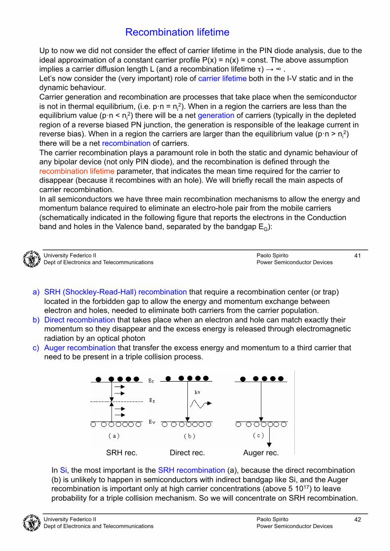
2) there will be a net recombination of carriers. The carrier recombination plays a paramount role in both the static and dynamic behaviour of any bipolar device (not only PIN diode), and the recombination is defined through the recombination lifetime parameter, that indicates the mean time required for the carrier to disappear (because it recombines with an hole). We will briefly recall the main aspects of carrier recombination. In all semiconductors we have three main recombination mechanisms to allow the energy and momentum balance required to eliminate an electro-hole pair from the mobile carriers (schematically indicated in the following figure that reports the electrons in the Conduction band and holes in the Valence band, separated by the bandgap EG):
University Federico II Dept of Electronics and Telecommunications
Paolo Spirito Power Semiconductor Devices
42
SRH rec. Direct rec. Auger rec.
a) SRH (Shockley-Read-Hall) recombination that require a recombination center (or trap) located in the forbidden gap to allow the energy and momentum exchange between electron and holes, needed to eliminate both carriers from the carrier population.
b) Direct recombination that takes place when an electron and hole can match exactly their momentum so they disappear and the excess energy is released through electromagnetic radiation by an optical photon
c) Auger recombination that transfer the excess energy and momentum to a third carrier that need to be present in a triple collision process.
In Si, the most important is the SRH recombination (a), because the direct recombination (b) is unlikely to happen in semiconductors with indirect bandgap like Si, and the Auger recombination is important only at high carrier concentrations (above 5 1017) to leave probability for a triple collision mechanism. So we will concentrate on SRH recombination.

University Federico II Dept of Electronics and Telecommunications
Paolo Spirito Power Semiconductor Devices
43
The SRH recombination requires a third component – recombination center or trap – located in the forbidden gap – step (a) -, that can temporarily capture an electron (minority carrier in a P region) coming from the conduction band - step (b) - and then let it recombinate with a hole coming from the valence band – step (c) ( the dual process is also possible if we consider the holes as minority carriers in N region).
The main parameters that determine the recombination process are: a) the energy level ET of the trap in the forbidden gap (referred to the midgap energy Ei) b) the capture cross sections +p and +n respectively for holes and electrons c) the density NT of the trap
Both parameters are dependent on the actual source of the center (an impurity atom or a defect in the crystal); with this mechanism the net recombination rate U for the excess carriers (electrons or holes) present in a region (pn ! ni
2) can be described by a very general relationship that can be specified for all operation regimes.
University Federico II Dept of Electronics and Telecommunications
Paolo Spirito Power Semiconductor Devices
44
The recombination rate U can be described by the following general equation:
(22)
where: are reference electron and holes lifetimes dependent on the thermal carrier velocity ,th, on cross section + and trap density NT
Defining in general way the lifetime as
and referring for reference to a N region, where an excess &p of carrier is injected, with p = p0 + &p, n = ND + &n, p0ND = ni
2, p0<< ND, substituting in (22), we have the following relationship for lifetime :
(23)

University Federico II Dept of Electronics and Telecommunications
Paolo Spirito Power Semiconductor Devices
45
The lifetime depends on the recombination center through )p0, )n0, ET, from doping through n0 (= ND), from injection level through &n, &p, and from temperature through ni , kT.
a) low injection limit
in that case &p , &n << ND , and eq. (23) becomes:
For the case of an energy level at midgap (ET = Ei) : "L = "p0
b) high injection limit
in that case &p = &n >> ND , and eq. (23) becomes:
University Federico II Dept of Electronics and Telecommunications
Paolo Spirito Power Semiconductor Devices
46
ET –Ei = 0 ET – Ei = 0.25 eV ET –Ei = - 0.25 eV
)n0/)po= 100'
)n0/)po= 10'
)n0/)po= 1'
)n0/)po= 100'
)n0/)po= 10'
)n0/)po= 1'
ET – Ei = 25 eV
The lifetime as a function of injection level I = p0/ND is plotted in the two graphs below for different ratios of )n0/)p0. The first one presents the lifetime dependence on the energy level of the trap, and the second one from temperature. For N doped Si, typically the energy level of the center lies in the upper bandgap, and )n0 is about 5 -10 times )p0, so the lifetime increases both with injection level and with temperature; however the actual behavior depends on the recombination center present in the crystal, and it may be changed with the processes used for lifetime control, as we will see.

University Federico II Dept of Electronics and Telecommunications
Paolo Spirito Power Semiconductor Devices
47
)h = 2 µs'
)h = 0.2 µs'
Lifetime dependence of the PIN diode behaviour
The carrier lifetime affects the I-V curve mainly in region III. If the lifetime is not very high, the carrier distribution in the high injection regime is no longer a constant one, but tends to reduce in the middle of the epi region. This behaviour can be noted in the carrier distribution plots of the following graph, obtained by PC1D for the same power diode as before. For a high level lifetime of 2 µs (dashed line curves) one can note that the carrier distribution are much more flat than for the case of the low lifetime value of 0.2 µs, (solid lines) where the carriers reduce at 1/3 of the initial value in the center of the low doped region. In the latter case the approximation (22) do not holds, and the voltage drop is described by eq. (21) instead of eq. (23), with an average value of na lower than in the former case (the RM value is higher in the latter case)
a) Static behaviour
University Federico II Dept of Electronics and Telecommunications
Paolo Spirito Power Semiconductor Devices
48
b) Dynamic behaviour
To allow a fast dynamic operation of the PIN diode, we need a fast change of the mobile carriers concentrations in the low doped region: this in turn will ask for a low lifetime to allow a quick redistribution of carries during the transient (in contrast with the d.c. case). The basic test circuit for both the turn-ON and turn-OFF transients is the one schematically reported:
VCC
Diode L
SW
The ideal switch SW of the circuit is actually done by a power device (like a MOS): during the first time TON when SW is closed, the inductance L charges with a linear current ramp i(t) = (L/VCC)t; the diode is reverse biased by the voltage VCC –VON(SW) .
During the time TOFF SW opens, and the current I(TON) will start to flow into the diode, inducing a TURN-ON transient into it, after which the current I will flow into it (assuming that the TOFF is sufficiently short to leave the current in L practically unaltered).
After the TOFF time the switch SW closes again during a second TON time; the voltage drop across the inductance change abruptly from –VON to VCC – VON(SW), and the diode becomes reverse biased: this will start the TURN-OFF transient, after which the diode becomes an open circuit and all the current flows into the switch SW.

University Federico II Dept of Electronics and Telecommunications
Paolo Spirito Power Semiconductor Devices
49
Turn-on transient When the diode is brought in turn-on by a current forced into it (red line in plot (a)), the diode voltage increases much above the VON voltage corresponding to the current I in steady state: this is because the holes injected in the low doped region (plot (b)) do not reach at the short times t1 ,t2 the high injection level (above ND) needed to bring the ND region in conductivity modulation (and to reduce its resistance RD). As a consequence, the voltage drop across the diode increases to VMAX (a value that can be of some tens of volts) and then it decreases to VON at times t4 needed to establish the steady state n,p carrier distribution. The VMAX increase is as higher as faster is the dI/dt slope of the forced current with respect to the carrier lifetime.
(a) current and voltage during turn-off (b) hole distribution in ND region
University Federico II Dept of Electronics and Telecommunications
Paolo Spirito Power Semiconductor Devices
50
Turn-off transient
P+ ND N+
x
p,n t5>t4>t3>t2>t1>t0 t*
t0 t1
t2 t3
t4 t5
(a) current and voltage during turn-off (b) carrier distributions in the ND region
In real turn-off cases, when the switch closes at t=t*, the current in SW will increase almost linearly between t* and t0, and then the diode current will linearly decrease. Due to the charge still present in the ND region when the diode current is crossing the zero value, the diode will remain in its conducting state (the diode voltage is dependent on the carrier distribution at the PN and NN+ junctions) when the current is negative. Only after time t1 the two junctions start to be depleted from carriers and two depleted regions develop, that increase their width toward the center of ND region, until all the stored charge is removed and the diode will sustain the full reverse voltage VR. During the time interval t0 – t5 there will be a substantial power dissipation due to the reverse current IRR and to the growing reverse voltage of the diode.

University Federico II Dept of Electronics and Telecommunications
Paolo Spirito Power Semiconductor Devices
51
The diode switching transient in turn-off is named “Reverse recovery”, indicating the time needed by the diode to establish a steady-state reverse behavior, i.e. an open circuit. With reference to a typical reverse recovery curve reported in figure, the main parameters for the reverse recovery transient are:
a) the on-state forward current IF b) the max current IRR in reverse conducting stage c) the slope dI/dt of the current d) the time tRR needed to recover the non conducting state after the current changes from
positive to negative (usually it is determined by the time difference between the zero current point and the time corresponding to 10% of IRR).
We will evaluate the effect of lifetime on the relevant parameters with some approximations, i.e. assuming the current plot during time tRR as of triangular shape.
University Federico II Dept of Electronics and Telecommunications
Paolo Spirito Power Semiconductor Devices
52
The total stored charge QRR in the low doped region to be removed during the reverse recovery is obtained by integrating the current during the tRR time. Assuming a triangular shape for the current curve we have from geometrical considerations:
The reverse charge QRR must be equal to the charge stored in forward conduction: this latter can be related to the lifetime ) through the charge control diode model: I = Q/) . Then:
(24) (25)
(26) and, by substituting (24), (25) in (26) we have the following expression for IRR:
or the following expression for tRR: (27)
(28)

University Federico II Dept of Electronics and Telecommunications
Paolo Spirito Power Semiconductor Devices
53
From eq. (27) and (28) we found that both the peak reverse current IRR and the reverse recovery time tRR increase with the square root of lifetime, so a low lifetime value is needed to have a fast switching during the turn-off. The peak reverse current also increases if the forward current IF increases, or the current slope dI/dt decreases (fast commutation). The diodes that have a fast turn-off transient (low IRR and low tRR) are called “fast recovery (FR)” diodes. For these diodes one need to reduce the (rather high) lifetime value of the low doped region to allow a fast carrier recombination.
The technologies used to introduce recombination centers in the epi region are called “lifetime control techniques”, and are usually needed for most bipolar devices if fast transient are required. In any case the need for a low lifetime is in contrast with the need of a conductivity modulation for the low doped region, so a trade-off between voltage drop and switching transient is a key point of all bipolar devices.
In particular for the PIN diodes with high reverse voltage rating, this is the main choice to be done: - if the diode has to be used in low frequency operation the d.c. power losses have to be considered most relevant and a low voltage drop should be chosen to reduce the d.c. power losses: then a high ) is needed - if the diode has to be used in high frequency operation, a fast switching should be chosen to reduce the dynamic power losses, and a low ) is required for a fast recovery diode.
University Federico II Dept of Electronics and Telecommunications
Paolo Spirito Power Semiconductor Devices
54
Lifetime control techniques The most used techniques for lifetime control are: a) the introduction of impurity atoms, usually heavy metal atoms, like gold (Au) or platinum
(Pt), by thermal diffusion in the epi layer prior the realization of the PIN diode b) the irradiation with high energy electrons (or more recently with light ions - hydrogen or
helium)
The energy levels of the recombination centers due to these techniques are indicated in figure: for Au and Pt the dominant one is near the midgap, while for electrons is in the upper bandgap

University Federico II Dept of Electronics and Telecommunications
Paolo Spirito Power Semiconductor Devices
55
The irradiation of electrons or light ions can be done after making the PIN diode, because the accelerated ions are cable to pass through the metal or oxide layer and do not require too much thermal treatment after irradiation (only an heating of about 300°C is enough to reduce the residual crystal damage due to irradiation. Instead the doping with heavy metal atoms require high temperature treatment (about 800 -900 °C) that can not be done after making the diode structure.
A further advantage of irradiation with H or He ions is the ability of reducing the lifetime only in a limited thickness of the layer, because the recombination centers (due to vacancy in the crystal) are mostly generated at the depth where the ion atoms are stopped, and then the position of the lifetime decrease can be modified by changing the energy of the irradiated ions.
The position of the lifetime minimum can give a better trade-off between voltage drop in the on-state and reverse recovery energy losses during switching; the best trade-off is obtained by a minimum lifetime position near the P+N junction.
University Federico II Dept of Electronics and Telecommunications
Paolo Spirito Power Semiconductor Devices
56
Schottky diode
An alternative device to the PIN diode for fast switching applications is the Schottky diode. A Schottky diode uses a metal-semiconductor junction (Schottky barrier) instead the P/N junction as in conventional PIN diodes. This Schottky barrier results in both very fast switching times and low forward threshold voltage V-SC . A normal PIN diode has a V-PIN of about 0.7 V , while a Schottky diode has a V-SC of approximately 0.3-0.45 V.
The electrical symbol of this device is:
The most important difference between PIN and Schottky diodes is the difference in recovery time. The reverse recovery times of Schottky diodes are extremely fast because these devices are majority carriers devices. They do not have minority carrier to be stored during the conduction in the low doped region. This in turn provides very little reverse current Ir overshoot when switching the Schottky diode from the forward conducting mode to the reverse blocking state. This feature make Schottky diodes a very attractive choice for low parasitic switching losses.

University Federico II Dept of Electronics and Telecommunications
Paolo Spirito Power Semiconductor Devices
57
The most evident limitations of Schottky diodes are the relatively low reverse voltage rating for silicon-metal Schottky diodes, 100 – 200 V, well below the PIN diode actual ratings, and a relatively high reverse current.
A schematic cross section of a Schottky diode is represented here:
The Schottky diode properties are primarily determined by the metal energy barrier height of material deposited on the silicon by the manufacturer. A metal with a low energy barrier height will minimize forward voltage, but will also be restricted in its high temperature operating capability and have very high reverse leakage currents. A high barrier metal height selection will minimize temperature and leakage current sensitivity but will increase the forward voltage Von.
University Federico II Dept of Electronics and Telecommunications
Paolo Spirito Power Semiconductor Devices
58
!
RONSCH =WD
qAµ0ND!
RONPIN =WD
qAµa0n2
The limitation in max reverse voltage comes mainly from the fact that in the Schottky diode we do not have the conductivity modulation effect in the low doped ND region, due to the conduction of only majority carriers. This increases greatly the RON value of the resistance of the low doped region.
For PIN diodes we have a Ron:
For Schottky diodes we have a Ron:
Then the trade-off between RON and VBR is much worse for the Schottky diodes, giving for the same VBR an RON resistance much larger than the one of the PIN diode, and increasing more than linearly with increasing VBR, as we will see. This poses an upper limit to the max voltage that can be obtained, if the voltage drop in the ON state must be kept in reasonable values (1-2 V)

University Federico II Dept of Electronics and Telecommunications
Paolo Spirito Power Semiconductor Devices
59
!
RONSCH =WD
qµnND
" 3# 10$7(VBR )2
Recalling that ND is related to VBR for NPT case as:
And substituting this ND value in the RONSCH expression, we have, for the RON = f(VBR) dependance: