All-Optical 2R Regeneration Using the Hysteresis in a Distributed Feedback Laser Diode
Upload
manchesterCategory
view
3download
0
Optics and Lasers in Engineering 34 (2000) 231}253
The advances and characteristics of high-powerdiode laser materials processing
Lin Li*Department of Mechanical Engineering, Laser Processing Research Centre, University of Manchester Institute
of Science and Technology (UMIST), Sackville Street, Manchester M60 1QD, UK
Abstract
This paper presents a review of the direct applications of high-power diode lasers formaterials processing including soldering, surface modi"cation (hardening, cladding, glazing andwetting modi"cations), welding, scribing, sheet metal bending, marking, engraving, paintstripping, powder sintering, synthesis, brazing and machining. The speci"c advantages anddisadvantages of diode laser materials processing are compared with CO
2, Nd:YAG and
excimer lasers. An e!ort is made to identify the fundamental di!erences in their beam/materialinteraction characteristics and materials behaviour. Also an appraisal of the future prospects ofthe high-power diode lasers for materials processing is given. ( 2001 Elsevier Science Ltd. Allrights reserved.
Keywords: HPDL; High-power diode laser; Materials; Processing; Welding; Hardening; Marking; Rapidprototyping; Machining; Soldering
1. Introduction
It has been almost a decade since the "rst direct diode laser application formaterials processing was reported in 1991 for soldering using a 15W medical diodelaser [1]. In the last 9 years, on average, the diode laser output power has doubledeach year to the present commercially available 4 kW continuous wave diode laserunits, which have a power level comparable to other high-power lasers for materialsprocessing. The advantages of high-power diode lasers in terms of compactness,energy e$ciency, lifetime and running costs have been increasingly recognised. Conse-quently, various applications of high-power diode lasers for materials processing have
*Tel.: #44-161-200-3816; fax: #44-161-200-3803.E-mail address: [email protected] (L. Li).
0143-8166/00/$ - see front matter ( 2001 Elsevier Science Ltd. All rights reserved.PII: S 0 1 4 3 - 8 1 6 6 ( 0 0 ) 0 0 0 6 6 - X

been reported. These include those which are currently being carried out using CO2
and Nd:YAG lasers, such as hardening and welding, and those which are new such astile grout sealing. Frequently, questions are asked on whether diode lasers couldreplace CO
2and Nd:YAG lasers in the future for materials processing due to the
associated cost bene"ts and whether there are any special features of diode lasermaterials processing. This paper intends to answer some of these questions byreviewing the advances and characteristics of direct high-power diode laser (HPDL)applications for materials processing in the last decade so that the inherent advant-ages and disadvantages of diode laser materials processing can be identi"ed. Speci"cemphasis is placed on the recognition of material behaviour di!erences betweenHPDL and other high-power lasers during processing. It is hoped that, from thisstudy, a broad picture can be obtained on what HPDLs can do and what they are notspecially given to do.
2. Characteristics of high-power diode lasers
The materials for the manufacture of diode lasers are based on semiconductors ofgroup III}V compounds. Population inversion, as a result of electron transitions fromthe valency band to the conduction band of doped semiconductors, is achieved byforward biasing the p}n junctions. Spontaneous emission and stimulated emissionoccur when electrons in the conduction band recombines with the holes in the valencyband. The optical cavity in a diode laser is formed by cleaving two opposite facets ofthe semiconductor wafer* forming a Fabry}Perot lasing cavity. The "rst diode laserwas demonstrated in 1962 in several laboratories [2}4]. Diode lasers with continuouswave (cw) output powers in excess of 0.5W (class IV) are referred to as high-powerdiode lasers or HPDLs.
HPDLs have many special optical properties that are di!erent from other types ofhigh-power lasers. These properties include wide spectrum band (2}20nm), largebeam divergence (up to 403 half-angle), non-symmetrical beam distribution (2.5}6times di!erence in beam divergence in the two orthogonal axes) and astigmatism [5].These properties are described brie#y in the following sections.
2.1. Wavelength
The wavelength at which a diode laser emits is dependent upon the band gapenergy, cavity length and refractive index of the semiconductor. It is therefore materialdependent, temperature dependent and driving current dependent. Table 1 lists thewavelengths of a selected range of diode lasers among which AlGaAs and InGaAs arethe materials mainly used for high-power diode lasers operating in the IR spectrum.Tuning of the diode laser wavelength can be achieved by temperature control (up to0.4 nm/3C) [5]. Also variation of laser power by varying input current can also lead towavelength changes. For example, for AlGaAs lasers, the wavelength typically cha-nges 0.025 nm/mA [5]. Thus, in practice, high-power diode lasers have broaderwavelength bands than CO
2and Nd:YAG lasers.
232 L. Li / Optics and Lasers in Engineering 34 (2000) 231}253
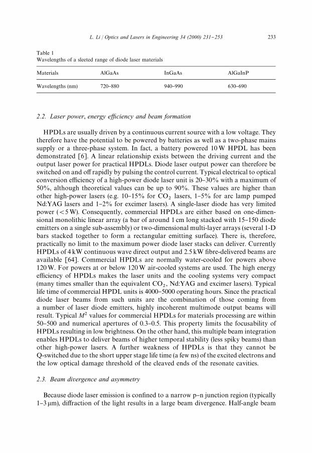
Table 1Wavelengths of a sleeted range of diode laser materials
Materials AlGaAs InGaAs AlGaInP
Wavelengths (nm) 720}880 940}990 630}690
2.2. Laser power, energy ezciency and beam formation
HPDLs are usually driven by a continuous current source with a low voltage. Theytherefore have the potential to be powered by batteries as well as a two-phase mainssupply or a three-phase system. In fact, a battery powered 10W HPDL has beendemonstrated [6]. A linear relationship exists between the driving current and theoutput laser power for practical HPDLs. Diode laser output power can therefore beswitched on and o! rapidly by pulsing the control current. Typical electrical to opticalconversion e$ciency of a high-power diode laser unit is 20}30% with a maximum of50%, although theoretical values can be up to 90%. These values are higher thanother high-power lasers (e.g. 10}15% for CO
2lasers, 1}5% for arc lamp pumped
Nd:YAG lasers and 1}2% for excimer lasers). A single-laser diode has very limitedpower ((5W). Consequently, commercial HPDLs are either based on one-dimen-sional monolithic linear array (a bar of around 1 cm long stacked with 15}150 diodeemitters on a single sub-assembly) or two-dimensional multi-layer arrays (several 1-Dbars stacked together to form a rectangular emitting surface). There is, therefore,practically no limit to the maximum power diode laser stacks can deliver. CurrentlyHPDLs of 4 kW continuous wave direct output and 2.5 kW "bre-delivered beams areavailable [64]. Commercial HPDLs are normally water-cooled for powers above120W. For powers at or below 120W air-cooled systems are used. The high energye$ciency of HPDLs makes the laser units and the cooling systems very compact(many times smaller than the equivalent CO
2, Nd:YAG and excimer lasers). Typical
life time of commercial HPDL units is 4000}5000 operating hours. Since the practicaldiode laser beams from such units are the combination of those coming froma number of laser diode emitters, highly incoherent multimode output beams willresult. Typical M2 values for commercial HPDLs for materials processing are within50}500 and numerical apertures of 0.3}0.5. This property limits the focusability ofHPDLs resulting in low brightness. On the other hand, this multiple beam integrationenables HPDLs to deliver beams of higher temporal stability (less spiky beams) thanother high-power lasers. A further weakness of HPDLs is that they cannot beQ-switched due to the short upper stage life time (a few ns) of the excited electrons andthe low optical damage threshold of the cleaved ends of the resonate cavities.
2.3. Beam divergence and asymmetry
Because diode laser emission is con"ned to a narrow p}n junction region (typically1}3lm), di!raction of the light results in a large beam divergence. Half-angle beam
L. Li / Optics and Lasers in Engineering 34 (2000) 231}253 233
divergence, h, is given by [7]
h+sin~1ja, (1)
where a is the width of active region and j is the laser wavelength. For j"0.8lm anda"2 lm, h+23.63. The half-angle beam divergence of diode emitters can be up to453 in the direction perpendicular to the facet [7]. Due to the non-circular cross-section of the active region, the output radiation of diode lasers quickly diverges in thedirection perpendicular to the plane of the p-n junction (fast axis), and slowly divergesin the parallel direction (slow axis). The slow axis diverges by a factor 2.5}6 times lessthan the fast axis [8]. This inherent asymmetry can be reasonably corrected withappropriate anamorphic beam condition optics (expanding the beam in one direction)such as high numerical aperture spherical lens combined with a cylindrical lenstelescope. Methods of producing symmetrical beams include the use of micro prisms[9], bundle of "bres combined with micro step-mirrors [10, 11] or cylindrical opticalsystems [8]. However, a low F number lens has to be used for focusing the highM2 HPDL beams in order to achieve a reasonable beam spot size. This results in shortworking distance for the HPDLs. Another feature of the HPDL beams is that they areastigmatic, i.e. beams in the two perpendicular directions do not come from one waistlocation. Weak cylindrical lenses are normally used to correct this problem. Commer-cial HPDLs not using a "bre beam delivery usually give rectangular beams due to fastand slow axis collimations. These beams, although having di!erent beam divergencein two orthogonal directions, may have an advantage for surface treatments sinceadditional beam integration is not required to produce a uniform rectangular beampro"le.
3. Applications of high-power diode lasers for materials processing
In order to understand the suitability of HPDLs for material processing applica-tions, a range of reported work on this subject is reviewed. Since the currentlyavailable HPDLs are limited to a maximum power density of 2.6]105Wcm~2, mostapplications of the HPDLs for materials processing are limited to surface treatments,conduction limited welding, soldering, scribing and marking, although cutting, drill-ing and keyhole welding have also been attempted. In the following, the character-istics of HPDL applications for materials processing are also described.
3.1. Soldering
Soldering was the earliest reported diode laser application for materials processing[1]. The main advantage of laser soldering over the conventional soldering such asre#ow or vapour-phase soldering is that the laser beam can be directed accuratelyonto a target area without heating the surrounding parts thus reducing the risk ofthermal damage. As a result, very small connectors (down to 200lm diameter) can be
234 L. Li / Optics and Lasers in Engineering 34 (2000) 231}253

laser soldered. Surface mount soldering using 10}25W air-cooled HPDL beamsdelivered through optical "bres has been achieved by many workers [12}17]. HPDLsof such a power level are the size of a lap top computer. The compactness andreliability of the diode lasers o!er a great advantage over other lasers such as theNd:YAG lasers. Also, due to the shorter wavelength, HPDL output is better ab-sorbed, to a certain extent, by the soldering materials, than that of CO
2and Nd:YAG
lasers. Commercial applications of HPDL soldering include the joining of telephoneconnectors using a 25W HPDL. An actual production machine has been developedand commissioned and is positively impacting the costs and production performance[15].
3.2. Transformation hardening
Initial studies into using relatively low-powered HPDLs ((550W) for hardeningwere reported by a number of workers [8,18}20]. These include transformationhardening 400 series stainless-steel tapes of 0.1mm thickness using a 15W "bre-delivered HPDL having a 1mm beam spot size [18], transformation hardening ofstainless-steel sheets of 0.15mm thickness using a 500W diode laser at 30m/mintraverse speed [19] and the hardening of controller shaft fabricated from 100Cr6 steelwith a power of 300W #at-top rectangular beam pro"le [8]. Good uniformity ofhardened depth was found using the #at-top beam [8]. Furthermore, saw blade tips(micro-edge), cutter drums and scalpels of CK60 steel were also hardened. During thetransformation hardening of 42CrMoS4 using a 200W HPDL having 0.8]5mm2
beam size, Loosen et al. found that diode laser system used was very sensitive tobackre#ection which caused damage to the diode laser [20].
More recently, industrial scale kilowatt HPDLs have become available. Theselasers have uniform rectangular distributed beams similar to the traditional integratedbeams utilising beam integrators. They are, therefore, ideal for surface treatment.Ehlers et al. reported the use of a 2.4 kW HPDL with a linear shaped beam pro"le forhardening medium carbon steel M1044 producing a constant hardened depth of 1mmand a width of 20mm [21]. Kugler et al. demonstrated the use of a 1.5 kW diode laser(one direction Gaussian and the other rectangular) for transformation hardening oftool steels. The work shows that higher hardness and wider track width can beachieved with the HPDL due to better beam absorption as a result of shorterwavelength than with a 2 kW Nd:YAG laser (Gaussian beam) [22]. Bonss et al.described the use of a 1.4 kW HPDL (940lm wavelength) and 6.6]6.1mm2 rectangu-lar spot for hardening carbon steel (AISI 1045) [19]. The work showed that theHPDL has approximately 70% absorption compared with 10}15% for the CO
2laser
and 65% for the Nd:YAG laser. In fact, in this particular case the CO2
laser hardeningprocess required the application of an absorption coating on the workpiece surface.Applications include the hardening of piston rings, razor blades, pliers and turbineblades. Klocke el al. discovered the importance of laser beam traverse direction fora rectangular HPDL beam. The process e$ciency (de"ned as hardened volume/laserpower) decreases to 60% when the long beam axis is along the feed direction [23].
L. Li / Optics and Lasers in Engineering 34 (2000) 231}253 235
3.3. Welding/brazing
Due to the low laser power density currently achievable for the HPDLs, mostreported work on HPDL welding is based on conduction-limited welding [22}26].Bonss et al. reported the use of a 500W HPDL to weld 0.5mm thick stainless steelswith a welding speed of 6000mm/min. No plasma or key hole formation was found[19]. In addition, 0.8mm thick aluminium (A1120) was butt-welded using a 2kWHPDL. Haag and Rudla! reported that butt welding of 0.8mm stainless-steel sheets(X5CrNi189) could be achieved using a 800W HPDL [8]. Smooth welds have beenachieved without pores or other defects. It was found that conduction welding wasparticularly good for aluminium where the process is inherently more unstable due tolow vaporisation and ionisation thresholds. The extraordinary surface smoothness ofthe weld bead was found to be attributed to the mode stability of the HPDL system.Klocke et al. showed that conduction butt welding of X5CrNi189 using a 600W diodelaser (wavelength 940 lm) results in defect-free (spatter, tears and pores) welds [23]. Itwas observed that there was no HAZ and there was a clear boundary between theweld zone and the parent material. Kugler et al. discovered that welding with fast axisin the traverse direction was more e$cient featuring faster speed and smaller heat-a!ected zone [22]. A comparison between a diode laser (1.5 kW) and a CO
2laser
(1 kW) for welding high carbon (0.95% wt% C) steel by Ng and Waston [24] showedthat the diode laser (2.1]104 Wcm~2) generated weld beads had central line cracksat higher speeds whilst CO
2laser (1.3]105Wcm~2) generated beads do not. For
diode laser welds a uniform hardness pro"le as a function of weld depth was observed.Similar volumes of weld were achieved for both lasers at speeds above 10mms~1.Moreover, greater beam absorption by the material was observed for the HPDL.Triantafyllidis et al. have shown that HPDLs can be used e!ectively for weldingthermocouple wires [25]. The weld quality produced with the "bre delivered HPDLbeam was found to be superior (beadless and porosity free) to the existing plasma arcwelded thermocouples. Tensile strength was increased by 4 times and temperaturemeasurement response time reduced by 35% compared to the plasma arc-weldedthermocouples. The weld was also found to be marginally better than those weldedwith an Nd:YAG laser for the 0.2mm diameter thermocouple wires as shown in Fig. 1.The process was found to be very sensitive to the shroud gas type and #ow rate due tothe cooling e!ect.
Due to the requirement of a laser power density of over 105W cm~2 forlaser keyhole welding of metallic materials, most of the reported results of usingdirect HPDLs for welding metallic materials are based on thermal conductionmechanism limited by the laser power density achievable. Notwithstanding this,keyhole welding of metallic materials has been achieved by Petring et al. (ILT,Germany) using a multi-kW HPDL at a power density of 2]105W cm~2 for welding2mm stainless steel at 0.5m/min [27]. Also Bliedtner et al. (IFW, Germany) reportedsuccessful keyhole welding stainless steels of up to 3.9mm thick at 1000m/minwelding rate with a 2.5 kW Jenoptik diode laser delivered with 1.5mm optical"bre giving a laser power density of 2.6]105 Wcm~2 on workpiece when thebeam was focused to a 1 mm diameter spot. A cross gas jet was used to prevent
236 L. Li / Optics and Lasers in Engineering 34 (2000) 231}253

Fig. 1. A comparison of thermocouple performance welded with HPDL, Nd:YAG laser and commercialArgon arc systems.
the weld plume from damaging the processing head which was 3.4 cm away from theworkpiece [64].
Hansch et al. reported work in which HPDLs were used for welding plastics andpolymer [28]. Although absorption of polymer at the near IR is similar to that at thefar IR (10}15%) spectrum, much greater beam transmission was found for the HPDL(5}75%). Various pigments were used to vary the beam absorptivity. The work showsthat green-coloured polymer has the highest absorption coe$cient (70%) followed byred, blue, natural and yellow. Absorption length can be reduced to 0.1mm. Onespecial feature of such an arrangement is that surface absorption can lead to deeppenetration due to high transmission or absorption length of the HPDLs. Applica-tions of such techniques include the welding of car belt holder and sun glasses, etc.Also work by Loosen et al. shows that HPDL welding of plastics can result in jointstrength of more than 50% higher than that achieved with ultrasonic welding [20].
Schuber et al. reported the use of a 1.4 kW HPDL for joining (brazing) aluminiumto steel substrates with a "ller wire (Al}Si12) to prevent cracking [29]. Moltenaluminium #ows over the surface of the steel sheet. There is no performance di!erencefrom an Nd:YAG laser.
3.4. Surface melting and wetting characteristics modixcation for improvedcoating/bonding
The interfacial phenomenon of wetting is often the primary factor governingwhether a coating will adhere and bond to a substrate in practical applications such asenamelling and thermal spray coating. Recent work at UMIST by Lawrence et al. has
L. Li / Optics and Lasers in Engineering 34 (2000) 231}253 237

Table 2Surface roughness, surface energy and wetting contact angles of mild steels before and after diode lasersurface melting
Lasers
Untreated CO2
Nd:YAG Excimer HPDL
Surface roughness (Ra), (lm) 1.46 2.58 1.25 2.12 1.12Surface energy (polar component9), mJm~2) 4.17 3.83 4.24 4.02 6.59Contact angle (Glycerol), (3) 44 51 43 46 32
shown that the wetting characteristics of a selected range of ceramic, metallic andcomposite materials can be modi"ed by high-power diode laser surface treatments[30}34]. The changes in surface morphology (e.g. roughness), surface composition(e.g. O
2content) and surface energy (principally the polar component) are identi"ed as
being the principal factors a!ecting the wetting characteristics. Microstructure cha-nges were found to be unimportant in in#uencing the changes in wetting character-istics [31]. Comparisons were made between the HPDL and other high-power lasers(CO
2, Nd:YAG and excimer) for surface treatment of composites and metals [30,31].
HPDL-treated (melted) surfaces were found to have a surface roughness values lessthan those treated (melted) with other lasers as shown in Table 2 for mild steels.Meanwhile, the polar component of the surface energy is higher for the HPDL treatedsurfaces and the contact angle for the control liquid used is lower for the HPDLtreated surfaces. This can be attributed to the better beam stability of the diode lasers.Applications of the technique include surface enamelling [34] and sealing of tilegrouts [33] as a new clean room technology.
3.5. Surface glazing (densixcation) for crack/porosity sealing
A 60W diode laser was used by the UMIST team to densify 60 and 85% Al2O
3-
based refractory materials [35]. The work aimed to improve the corrosion anderosion resistance of these materials at high temperatures. The work showed thatdiode laser processing produced a more homogeneous, denser phase than the un-treated materials. Compared with the CO
2laser treated samples, the HPDL produc-
ed more adherent and less cracked laser-treated zones. Columnar grain formationwas found in the CO
2vlaser-treated samples whilst "ne needle-like structures were
formed in the diode-laser-treated zones as shown in Fig. 2. This work showed that,there was a de"nite di!erence in the behaviour of material when treated with a diodelaser and a CO
2laser. Further work by Lawrence and Li using a HPDL for the
surface glazing of concrete revealed that the HPDL can produce better qualitysurfaces than those obtained with the CO
2laser since the latter is given to generating
larger heat-a!ected zone, spallation and cracks on the concrete samples under thesame operating conditions [36]. One of the reasons for this marked di!erence wasfound to be the signi"cant di!erence in the beam absorption length (470$22 lm for
238 L. Li / Optics and Lasers in Engineering 34 (2000) 231}253

Fig. 2. SEM photographs of typical laser treated 85% alumina-based refractory ceramics. (a) CO2
lasertreated. (b) HPDL treated.
the CO2
laser and 177$15 lm for the diode laser) as a result of di!erent laserwavelengths [37]. The applications of this technique include wear improvement [62],corrosion protection [35], decoration and sealing of surface contamination[36,38,39].
3.6. Marking, engraving and scribing
A 60W "bre delivered diode laser was used by Li et al. for marking and engravingmarble, granite, clay tiles, ceramic tiles, roof tiles, cement, bricks, glass, and wood[40,41]. High-contrast marks have been generated on these materials by heating,
L. Li / Optics and Lasers in Engineering 34 (2000) 231}253 239
melting or material removal mechanisms. The colour of materials was found to havean e!ect on the beam absorption. Light-coloured material re#ects more of the laserbeam. This has caused non-uniform line width for marbles with vains of a di!erentcolour although an absorption coating could reduce this e!ect [41]. Di!erent shroudgases were also found to have a signi"cant e!ect on the quality and colour of themarks generated, with O
2gas shroud giving less porous and darker coloured glazes
compared with those obtained using Ar gas.In another report by Ponnaluri and Molian, it was shown that a 15W (820 nm
wavelength) "bre beam delivery (400lm core diameter) diode laser could be used toscribe 25lm thick metallic glass 2605 (Fe80B12Si8) ribbons used in transformers [42].Laser scribing reduced the core losses in transformers by decreasing the eddy currentlosses through domain re"nement. When the material is scribed, the diode laser beammelts the ribbon locally and the melt rapidly resolidi"es back into the amorphousstate. This interaction induces domain re"nement in the material reducing the coreloss. Scribing amorphous materials is only suitable for low power lasers. Too highpower creates excessive localised stress. Re-crystallisation may occur. In this applica-tion, the diode laser has replaced the previously used Nd:YAG lasers due to lowercosts.
3.7. Machining
Slocombe and Li demonstrated the use of a 60W "bre delivered diode laser for thedirect machining of NiCr/polymer and Al/polymer composites [43,44]. This wasintended to produce solid metallic or ceramic functional parts by sintering the lasermachined composite parts. Highly re#ective materials such as aluminium and coppercan be laser machined easily using this technique. More than 20-fold reduction in laserpower requirement was identi"ed. In this process, a pre-mixed block of themetal/polymer composite was scanned with the diode laser. The polymer binder wasremoved selectively by the diode laser beam at very low temperatures (around 3003C)and ejected with a gas jet (Ar). The process is a reverse version of selectivelaser sintering to eliminate error transformation in layered manufacturing [45,46].When the laser was "red directly at the NiCr and Al metal blocks, there wasonly a small temperature rise and no melting occurred. When the laser beam was"red to the polymer block (transparent), the laser beam passed through withoutleaving any visible e!ects. The mechanism of the laser machining was identi"ed asbeing due to the absorption of the laser beam by the metal powders which thentransfer the thermal energy, by conduction, to the polymer binder which heats up toits decomposition point. The loose metal powders are then ejected by the gas jet. Thetechnique, not previously reported using other lasers, is therefore a new application.Thermoset polymer instead of thermoplastic polymer was preferred. This workdemonstrates that very low-power lasers (more than 20 times less power requirementcompare to that for machining a solid metallic block) can be used for producingmetallic parts.
Machining of marbles using a 60 W diode laser was reported by Li et al.[40, 41]. Marble is a metamorphic rock composed of recrystallized calcite or
240 L. Li / Optics and Lasers in Engineering 34 (2000) 231}253

Fig. 3. Comparison of removal depth vs. laser #uence for various lasers during the removal of whitechlorinated rubber.
dolomite. Therefore marble contains 95wt% of CaCO3. Laser heating of marble
resulted in decomposition of CaCO3
at temperatures between 825 and 9503C.
CaCO3"CaO#CO
2!42.52 kcal/mol. (2)
The breakdown results in white, unslaked lime (CaO) and carbon dioxide.HPDL-assisted machining was reported by Loosen et al. [20] involving a 1kW
diode laser pre-heating the material in front of the mechanical cutting tool formachining Si3N4 ceramics. Increased removal e$ciency was noted.
3.8. Paint stripping
Applications of HPDLs for the removal of white chlorinated rubber paint fromconcrete surfaces have been reported by Schmidt et al. [47,48]. The work was aimed atdeveloping a portable device for decontamination of buildings in the nuclear industry.The process mechanism was identi"ed to be principally a laser-controlled combustionas against laser chemical, laser acoustic and laser ablative processes encountered whenother lasers are used. O
2gas was used in the process to assist the combustion process.
Paint removal depth with O2
gas was found to be 4 times as high as the case whenN
2or Ar gas was used. When the diode laser beam was turned o! the combustion
process stopped as well. The combustion process enables the sustained beam absorp-tion which is normally less than 2% for this material. A linear relationship betweenlaser power and paint removal rate was obtained. The ash particle size was found toincrease with laser power density and decrease with increasing oxygen #ow suggestingboth combustion and laser vaporisation/ablation taking place [49]. A comparisonwas made with CO
2, Nd:YAG, excimer lasers and an arc lamp in Fig. 3. The
L. Li / Optics and Lasers in Engineering 34 (2000) 231}253 241

Table 3Comparison of diode laser and other optical sources for the removal of chlorinated rubber coatings fromconcrete substrates
Energy source Ablation threshold,FT
(J cm~2)E!ective absorptioncoe$cient, a (cm~1)
Thermal loading,c(J cm~3)
Arc lamp 37.4 64.7 2419RF CO
2laser 5.2 425 2200
CW CO2
laser 0.3 300 90HPDL 38 40 1500Excimer laser 0.04 30000 1200Nd:YAG laser 4.8 212 1000
absorption coe$cients, ablation thresholds and thermal loading of these lasers arecompared in Table 3. It can be seen that the diode laser does not have an advantage inthese aspects. However, the diode laser is portable and more energy e$cient in laserpower generation. These advantages may compensate the weakness in beam absorp-tion. In addition, the excimer laser ablation showed a redeposition problem and hadvery slow removal rate. CO
2laser-produced residues which were di$cult to remove
and the concrete substrates was very easily damaged (scabbled). The Nd:YAG laserproduced very rough surfaces with incomplete paint removal due to the domination ofphoto-ablation rather than combustion. The diode laser has excellent control over theremoval depth and residuals produced can be easily extracted away. The robustnessand portability of the diode laser gives an advantage for this type of application.
3.9. Sintering and synthesis for rapid prototyping
Li et al. reported the use of a 60W diode laser for the sintering of Cu/Zn powdersselectively as a method for rapid prototyping [50, 51]. A new layer-by-layer compact-ing technique was used to enable the reduction of layer thickness and the increase ofgreen part density. The use of a diode laser opens the opportunity for desk top rapidprototyping. Slocombe and Li reported the combination of selective diode lasersintering with self-propagation high-temperature synthesis (SHS) for the controlledsynthesis of TiC/Al
2O
3[52]. Powders of TiO
2, aluminium and carbon were mixed
stoichiometrically. After compacting (layer-by-layer) the diode laser was able toinitiate and control the solid-state combustion to produce TiC and Al
2O
3composites
in the following reaction:
3TiO2#4Al#3CP3TiC#2Al
2O
3#exothermic energy. (3)
The work showed that powder density was extremely important for the control ofSHS. Without compacting, SHS cannot be controlled properly resulting in overspread of the reaction beyond the laser-scanned tracks. With compacting the degree ofSHS can be limited to within the laser-scanned track. Furthermore, shroud gas wasfound to play an important role in the reaction process. The use of reactive gas such asO
2has led to the burning of C, therefore, there is insu$cient C to form TiC.
242 L. Li / Optics and Lasers in Engineering 34 (2000) 231}253

A comparison was made between the diode laser and a Q-switched Nd:YAG laseroperating at high frequencies (20 kHz) with a defocused beam of an identical beam sizeas the HPDL. No signi"cant di!erences in materials morphological characteristicswere found. This is a new application not previously reported with other lasers. Theuse of diode lasers may open up a potential for desk top processes.
3.10. Bending/sheet metal forming
LoH pez et al. used a 100W continuous wave (CW) diode laser of 810 nm wavelengthand a focused spot of 1mm]0.5mm to bend aluminium alloy sheets (AlMg3), carbody sheet steel St14 and stainless steel of 0.5}2mm [53]. The work shows that thee!ect of material thermal di!usivity is dependent on the material thickness. For thinmaterials (0.5mm), the bending angle of Alis higher than those of stainless steel andmild steel and vice versa for 2mm thick material. Graphite coating was used atthe surface of AlMg3 in order to improve the beam absorption. Recent work atUMIST conducted by Lawrence et al. [54] using a 2.5 kW rectangular diode laserbeam (6]6mm) on a 0.8mm thick mild steel (En3) found that a minimumthreshold of 138 Jmm~1 line energy density exists for bending the material belowwhich no bending can occur no matter how many scans are made. A linear relation-ship between the number of passes and bending angle for up to 55 passes was foundfor laser line energy density below 260 J mm~1. A comparison between the diode laserbending and CO
2/Nd:YAG laser bending is currently being carried out by the
UMIST team.
3.11. Cladding
Work by Nowotny et al. [55] shows that a 1.4 kW diode laser is equivalent toa 3.9 kW CO
2laser for the cladding of Stellite21 on a mild steel substrate. An increase
of beam absorption by a factor of 2.5 has been demonstrated for the HPDL.
3.12. Other applications
Attempts have been made to use HPDLs for cutting and drilling applications,despite the poor focusability of the HPDLs. These are mainly for thin "lms or sheetssuch as the work of ToK nsho! et al. [57] using a 25 W HPDL focused to a 1 mm beamspot. The materials studied include stainless steel (1mm thickness), mild steel (0.5mmthickness), aluminium (0.25mm thickness), copper (0.25mm thickness), plastics, ep-oxy, paper and wood. A detailed report on the e!ect of cutting and drilling is notgiven. The quality of the cut may not be as good as that produced with CO
2and
Nd:YAG lasers [26,58]. A common problem is the large kerf width and largeheat-a!ected zones. This is mainly due to the large beam spot sizes (normally above500lm diameter) of the currently available HPDLs. Li et al. showed that HPDLcutting of glass by controlled microcracking had resulted in much better cut than withthe conventional mechanical means [40]. An absorption coating is required forcutting clear glasses since they are transparent to the HPDL beams.
L. Li / Optics and Lasers in Engineering 34 (2000) 231}253 243

Table 4Asummary of HPDL applications for materials processing and their features
HPDL applications Features Ref.
Soldering f Better beam absorption than CO2
and Nd:YAG lasers.1, 12}17
f Compact
Transformation hardening f Better beam absorption than Nd:YAGlasers (8% higher) and CO
2lasers
(up to 500% higher).
8, 18}23
f More uniform
f E$ciency depends on beam scanningdirection with fast axis direction havinghigher e$ciency.
f Sensitive to back-re#ection
Welding/brazing f Dominated by conduction welding forpower density (105Wcm~2, featuringbetter quality weld and better surface"nish than other lasers
8,19}20, 22}29, 64
f Keyhole welding possible with powerdensity '2]105Wcm~2
f Welding in the direction of fast axis ismore e$cient.
Surface melting (sealing,wettability modi"cation)
f Better surface "nish (smoother) thanNd:YAG and CO
2laser melted
30}39
f Shorter absorption length than CO2
lasers on concrete
f Generating di!erent microstructuresfrom those by CO
2lasers
Marking/engraving/scribingf Colour of material a!ects beam
absorption.
40}42f Good power control
Machining f Desk-top process 20, 43}44
Paint stripping f Lower e$ciency than CO2
andYAG lasers
47}48
f Better paint ash structure andremoval
f Portable
Sintering f Desk top process 50}52
Forming f Flexible 53}54
Cladding f 2.5 times higher beam absorptionthan CO
2lasers
55
Cutting/drilling f Poor quality for metals 26, 57}58, 40
f Reasonably good for class
244 L. Li / Optics and Lasers in Engineering 34 (2000) 231}253

A summary of HPDL applications for the materials processing and their speci"cfeatures is given in Table 4.
4. Discussion
4.1. The advantages and disadvantages of HPDLs for materials processing
The applications of HPDLs have so far been largely focused on:(a) traditional laser processing requiring laser power densities below
2]105Wcm~2 such as surface treatments, marking and conduction-limited welding.(b) New applications taking the advantages of portability of the HPDL to enable
desk top processing (such as soldering, microwelding, machining and selective lasersintering) and laser processing of large parts such as building structures where the`workpiecea cannot be brought to the laser workstation.
The material behaviour for the HPDL processing has been found to be di!erentfrom the other high-power lasers in the following aspects:
f fewer cracks and less spallation for surface glazing/sealing.f More uniform melt/heating zones.f Smoother surface.f Better beam absorption for metallic materials.f More consistent and repeatable.
These advantages are the result of features unique to the HPDLs, such as: shorterwavelength (thus better beam absorption for most metallic materials, Fig. 4, andsmaller absorption length) and better temporal beam stability (due to beam integra-tion) compared to Nd:YAG and CO
2lasers. HPDL materials processing is, therefore,
expected to produce better quality and more consistent and repeatable results forapplications requiring beam spot sizes larger than 0.5mm diameter. HPDLs may beparticularly good for processing aluminium since the beam absorption has a peakvalue at the HPDL wavelengths (Fig. 4). One of the issues of concern in the practicalapplications of the lasers in materials processing for mass production is the repeatabil-ity. It is a well-known fact that the same laser processing parameters may notnecessarily produce the same results in laser materials processing. It has already beennoticed that HPDLs can produce more consistent materials-processing results thanNd:YAG lasers. This feature, together with the lower maintenance costs and longerservice life would make HPDLs suitable for mass production applications such as thesoldering of telephone connectors. Other advantages of the HPDLs are:
f lower running cost.f Higher energy e$ciency (up to 35% wall plug e$ciency) thus the cooling require-
ment is low and the size of laser and cooling unit is small.f Flexible beam shaping by controlling the intensity of individual beams [56].f Theoretically unlimited average power.f Portable.f Longer service life (typically 4000}5000 up to 10000h).
L. Li / Optics and Lasers in Engineering 34 (2000) 231}253 245

Fig. 4. Re#ectivity spectrum of various polished metal surfaces.
The capital costs of comparably powered lasers show that the cost of HPDLs isalready lower than those of Nd:YAG and excimer lasers and is expected to be lowerthan that of CO
2lasers in a few years time. This is largely due to the mass production
capability of the semiconductors fuelled by the increased market demand. Some otheradvantages such as fast switching and complex pulse shape control by direct elec-tronic waveform generation and wavelength tunability have not yet been fully utilisedfor HPDLs in materials processing.
Despite the many and various advantages of HPDLs over other high-power lasers,they are still limited in applications due to several disadvantages. These include:
f poor beam mode structure thus poor focusability, lower power density and smallerlens to workpiece stand-o! distance (low F number lens is required for focusing).
f Astigmatism and asymmetry of the beams resulting in di!erent beam divergence inthe two perpendicular directions causing the beam spot geometry variation dispro-portionally depending on the distance between workpiece and laser lens.
f The inability for Q-switching unless through pumping another solid-state laser.f Beam absorption is workpiece colour dependent.f Di!erent processing characteristics in the fast- and slow-axis directions with the
fast-axis direction more e$cient.
As seen in the previous sections, the HPDLs are well suited to soldering, hardening,melting, welding and various surface treatment applications. This can be expected byexamining Fig. 5, since HPDLs are now only available for a maximum power densityof 2.6]105 Wcm~2 and most of them are operated in the CW mode. The di$culty of
246 L. Li / Optics and Lasers in Engineering 34 (2000) 231}253

Fig. 5. E!ects and possible applications of lasers under various operating conditions (data from [59]).
focusing the HPDL beams to a smaller (e.g. less than 200 lm) spot size prevents theapplication of diode lasers for industrial cutting and drilling processes. Short workingdistance causes inconvenience for optics protection and avoiding collision withworkpiece, and di$culties for sample clamping, etc. The incapability for Q-switchingprevents the direct use of HPDLs for shock hardening, "ne marking of metals,ablation and micromaching applications.
4.2. Prediction of the roles of HPDLs in materials processing in the next 5}10 years
Based on the above analysis, it can be reasonably estimated that HPDLs willpossibly compete heavily with the high-power range of CO
2lasers for the surface
treatment and welding of metallic materials. This is primarily because of the HPDL'sbetter beam stability, better beam absorption by metals, smaller physical sizes andlower running costs. However, sealed-o! CO
2, fast axial #ow CO
2and slab CO
2lasers have the advantages of better beam quality and focusability than diode lasers.CO
2lasers also have the advantages of being very well absorbed by organic, glass and
ceramic materials and are relatively colour independent. Therefore, within the next5}10 years one would expect that CO
2laser systems of less than 4 kW power would
still dominate the cutting market and processing of organic (e.g. polymer, textile,paper, tissue material and food), glass and ceramic materials.
Diode lasers do not have signi"cant wavelength advantages over Nd:YAG lasers,although an improved beam absorption for metallic materials has been noticed. Inaddition, diode lasers cannot produce a Q-switched beam directly, although diodepumped solid-state lasers can. Therefore, Nd:YAG lasers, especially diode pumped
L. Li / Optics and Lasers in Engineering 34 (2000) 231}253 247

Nd:YAG lasers, which have much better beam quality and energy e$ciency than thearc lamp pumped Nd:YAG lasers (even higher than the CO
2lasers) will still play an
important role in materials processing such as drilling, marking and micromachiningdue to their capability of producing Q-switched and mode-locked pulses. Nd:YAGlasers with arc lamp pumping may "nd it di$cult to compete with diode-pumpedNd:YAG lasers in the future due to the lower e$ciency and inferior beam quality ofthe arc lamp pumped systems. As a result, diode lasers have already been to indirectlyreplace the conventional arc-lamp-pumped Nd:YAG lasers by simply being part ofNd:YAG laser itself. However, the cost of these lasers are over 100}500% higher thanthe equivalent direct diode lasers. Consequently, it is expected that the CW Nd:YAGlasers will give some grounds to the HPDLs.
Although diode lasers can be frequency doubled and quadrupled to produce visibleand UV beams. The e$ciency of such conversions will be adversely a!ected by thewider spectrum of the HPDLs. In addition, their incapability of producing high peakpower, ultra short pulse beams directly makes them di$cult to replace copper vapourlasers and excimer lasers for micromaching applications, although diode-pumpedsolid-state lasers are starting to compete with excimer and copper vapour lasers in thisarea.
Nevertheless, many of the above-mentioned disadvantages of the HPDLs, such aspoor beam coherence and asymmetry, can be overcome by the introduction ofdiode-pumped solid-state lasers like the "bre lasers and diode-pumped Nd:YAGlasers as well as the use of optical "bre beam delivery. Moreover, the portability ofHPDLs would enable the development of new areas of applications such as buildingmaterials processing and in-service repairs. A hand-held diode laser welding devicedelivering 1.2 kW HPDL beam through an optical "bre was demonstrated by Exnerand Drechsel [60]. Such a device would aid the new applications for in-service repairsand manual welding of large structures. Future development of diode lasers mayinclude the reduction of M2 to enable the use of longer focal length lens and toproduce smaller beam sizes, thus higher power density.
If one asks the question: under what circumstances should a diode laser be used formaterials processing, the answer would be if the work can be done by a diode laser aswell as other lasers, then the diode lasers should be used for economy, energye$ciency, reliability and processing repeatability.
The diode lasers will be seen in the next 5}10 years actively been used for hardening,cladding, alloying, soldering, glazing, welding, desk top processing, portable applica-tions and integration with conventional machine tools for machining. These applica-tions, however, only form a small part of overall laser materials processing marketwhich is still dominated by cutting and marking. Therefore, in the next 5}10 years, thedirect HPDLs in materials processing market share would be expected to increasefrom the present less than 0.2% ($17m compared to $1b total in 1999) to 3}5%.Current uses of HPDLs are mainly for R & D. More practical industrial applicationswill certainly boost the HPDL sales. The 1999 world materials processing lasermarket share is shown in Fig. 6 (data derived from Ref. [61]). It can be expected that inaddition to the direct HPDL increase in market shares, diode pumped Nd:YAG laserswill also increase their market share dramatically. Although the HPDL market for
248 L. Li / Optics and Lasers in Engineering 34 (2000) 231}253

Fig. 6. The market share distribution of lasers for materials processing applications. (a) 1999, (b) in5}10 years time (predicted) to indicate the trend only.
Fig. 7. The HPDL sales in the last 4 years for materials processing.
materials processing dropped in 1999 as shown in Fig. 7 (data obtained from Ref.[63]) largely due to the reduction in unit prices, the future looks good for the HPDLsdue to the increased awareness in the laser community, more practical applicationsand further drop in price of the HPDLs.
L. Li / Optics and Lasers in Engineering 34 (2000) 231}253 249

5. Conclusions
A review on high-power diode laser applications for materials processing has beencarried out. Many special features of HPDL interaction with materials have beenidenti"ed. These features include better surface "nish, less heat-a!ected zone, betterbeam absorption, better morphological characteristics, more consistent and repeat-able results, fewer cracks and less porosity generation. These are due to the multiplebeam integration and shorter wavelength of the HPDLs as compared to Nd:YAG andCO
2lasers. In addition, HPDLs have the advantages of being potentially low in cost,
high in energy e$ciency, more reliable, longer service life and portable. HPDLs areideal for surface treatments and welding applications. Other portable and desk topapplications suitable for the HPDLs include soldering, micro-welding, brazing, build-ing material marking/engraving, paint stripping, rapid prototyping and machining.The weaknesses of the high-power diode lasers include high beam divergence (thusdi$cult to focus to a small beam size), beam absorption dependent on workpiececolours and the di$culty to produce very high-peak-powered short-pulsed beamdirectly (Q-switching). These prevent them from competing directly with other high-power lasers for cutting, drilling, marking on metallic materials and micro-machining.However, diode-pumped solid-state lasers can overcome many of the above weak-nesses of the HPDLs. Therefore, HPDLs can also compete with other lasers for othermaterials processing applications through imbedding in other lasers.
Acknowledgements
The author would like thank Professor W.M. Steen and the Journal of Optics andLasers in Engineering for inviting him to write this paper. The author would also liketo thank his colleagues and students in the UMIST Laser Processing Research Centre(LPRC), Dr. J. Lawrence, Dr. L. Bradley, Mr. M.J.J. Schmidt, Mr. A. Slocombe, Mr.D. Triantafyllidis and Mr. K.L. Ng, for providing original data and photographsincluded in this paper.
References
[1] Polijanczuk AV, Whitehead DG. Semiconductor lasers for microsoldering. Proceedings of IEE:Advances in Interconnection Technology, vol. 82. San Diego, CA, Oct. 1991. p. 1}3.
[2] Hall RN, Fenner GE, Kingsley JD, Saltz TJ, Calson RN. Stimulated emission of radiation froma semiconductor (GaAs). Phys Rev Lett 1962;9:366}9.
[3] Nathan MI, Dumke WP, Burns G, Dill FH, Lasher G. Stimulated emission of radiation from GaAsp-n Junction, Appl Phys Lett 1962;1(3):62}4.
[4] Holonyak N, Bevacqua SF. Coherent (visible) light emission from Ga (As1-xPx) junctions. Appl PhysLett 1962;1(4):82}3.
[5] Melles Griot product catalogue. 1996.[6] Beneati D, Wu J, Fu R, Bull D. Portable battery operated 10 watt diode laser system. SPIE Proc
1995;2382:89}96.[7] Das P. Lasers and optical engineering. New York: Springer-Verlag, 1991.
250 L. Li / Optics and Lasers in Engineering 34 (2000) 231}253

[8] Haag M, Rudla! T. Assessment of di!erent high power diode lasers for materials processing. ProcSPIE: Lasers Mater Process 1997;3097:583}91.
[9] Sturm V, Tresch H-G, Loosen P. Cylindrical microlenses for collimating high-power diode lasers.SPIE Proc Lasers Mater Process 1997;3097:717}26.
[10] Yamaguchi S, Kobayyashi T, Saito Y, Chiba K. Collimation of emissions from a high-powermultistripe laser-diode bar with multiprism array coupling and focusing to a small spot. Opt Lett1995;20:898.
[11] Baumann M, Ehlers B, Quade M, Du K, Treusch H-G, Loosen P, Poprawe R. Compact "bre-coupledhigh-power diode-laser unit. SPIE Proc. Lasers Mater Process 1997;3097:712}6.
[12] Zediker M S. Direct diode laser competes with Nd: YAG and CO2. Indust Laser Rev 1993;
27(5):17.[13] Forrest G. Coupling high power laser diodes to applications. Laser Optron 1993;12(3):10.[14] Beckett PM, Fleming AR, Foster RJ, Gilbert JM, Whitehead DG. The application of semiconductor
diode lasers to the soldering of electronic components. Opt Quantum Electron 1995;27(12):1300}11.[15] Gilbert G. Laser soldering with high power laser diodes. Proceedings of the Institute of Physics
Quantum Group Meeting: Direct Applications of High Power Laser Diodes, vol. 1, No. 8. London,UK. 1995. p. 102}112.
[16] Fitzgerald ME. Diode laser optimises soldering e$ciency. Photon Spectra 1996;30(9):22}4.[17] Loosen P. Advanced concepts using diode lasers in materials processing. SPIE Proc 1997;3097:480}5.[18] Chen W, Roychoudhuri CS, Banas CM. Design approaches for laser diode material processing
systems using "bres and micro-optics. Opt Engng 1994;33(11):3662}9.[19] Bonss S, Brenner B, Beyer E, Bachmann F. Diode laser applications hardening and welding.
ICALEO'98 Proceedings, vol. 85G. Laser Institute of America, 1998. p. 121}130.[20] Loosen P, Treusch H-G, Haas CR, Gardenier U, Weck M, Sinnho! V, Kasperowski S, Vor Dem
Esche R. High power diode laser and the direct industrial applications. SPIE Proc 1995;2382:78}89.[21] Ehlers B, Herfurth HJ, Heinemann S. Surface hardening with high power diode lasers. ICALEO'98
Proceedings, vol. 85G. Laser Institute of America, 1998. p. 75}84.[22] Kugler P, Ho!mann P, Geiger M. Low cost laser system for material processing, ICALEO'98
Proceedings, vol. 85G. Laser Institute of America, 1998. p. 85}94.[23] Klocke F, Demmer A, Saboklicki. An investigation into the use of high power diode lasers for
hardening and thermal conduction welding of metals. SPIE Proc Lasers Mater Process1997;3097:592}9.
[24] Ng ES, Watson IA. Characterization of CO2
and diode laser welding of high carbon steels. J LaserAppl 1999;11(6):273}8.
[25] Triantafyllidis D, Schmidt MJJ, Li L. Diode laser welding of thermocouples. Proceedings ofICALEO'99, vol. 87B. Laser Institute of America, 1999. p. 38}47.
[26] Abe N, Kunugita Y, Miyake S. Processing characteristics of a high energy density diode laser system.ICALEO'98 Proceedings, vol. 85G. Laser Institute of America, 1998. p. 95}102.
[27] Diode lasers weld stainless steel. Opt. Laser Eur. January 2000;70:9.[28] Hansch D, Haaf D, Putz H, Treusch H-G, Gillner A, Poprawe R. Welding of plastics with diode laser,
ICALEO'98 Procedings, vol. 85G. Laser Institute of America, 1998. p. 131}140.[29] Schubert E, Zerner I, Sepold. New possibilities for joining by using high power diode lasers.
ICALOE'98 Proceedings,vol. 85G. Laser Institute of America, 1998. p. 111}120.[30] Lawrence J, Li L. Wettability characteristics of an Al
2O
3/SiO
2-based ceramic modi"ed with CO
2,
Nd: YAG, excimer and high-power diode lasers. J Phys D 1999;32:1075}82.[31] Lawrence J, Li L. Wettability characteristics of a modi"ed mild steel with CO
2, Nd: YAG, excimer
and high-power diode lasers. J Phys D 1999;32:1075}82.[32] Lawrence L, Li L, Spencer JT. High power diode laser modi"cation of the wettability characteristics
of an Al2O
3/SiO
2based oxide compound for improved enamelling. Mater Sci Engng
A 1999;266:167}74.[33] Lawrence J, Li L, Spencer J T. The e!ects of high power diode laser Radiation on the wettability,
adhesion and bonding characteristics of an alumina/silica-based oxide and vitreous enamel. Surf CoatTechnol. 1999;115:273}81.
L. Li / Optics and Lasers in Engineering 34 (2000) 231}253 251

[34] Lawrence J, Li L, Spencer JT. Diode laser modi"cation of ceramic material surface properties forimproved wettability and adhesion. Appl Surf Sci 1999;138-139:388}93.
[35] Bradley L, Li L, Stott FH. Characteristics of the microstructures of alumina-based refractorymaterials treated with CO
2and diode lasers. Appl Surf Sci 1999;138-139:233}9.
[36] Lawrence J, Li L. Surface glazing of concrete using a 2.5 kW diode laser and the e!ects of large beamgeometry. Opt Laser Technol. 2000;31(8):583}91.
[37] Lawrence J, Li L. Determination of absorption length of CO2
and high power diode laser radiationfor ordinary Portland cement and its in#uence on the depth of melting. Opt Laser Technol2000;32(3):1}4.
[38] Lawrence J, Li L, Spencer JT. A two-stage ceramic tile grout sealing process using a high power diodelaser* part I. grout development and materials characteristics. Opt Laser Technol 1998;30:205}14.
[39] Lawrence J, Li L, Spencer JT. A two-stage ceramic tile grout sealing process using a high power diodelaser * part II. mechanical, chemical and physical properties. Opt Laser Technol 1998;30:215}23.
[40] Li L, Lawrence J, Spencer JT. Materials processing with a high power diode laser. ICALEO'96Proceedings, vol. 81E. Laser Institute of America, 1996. p. 38}47.
[41] Li L, Lawrence J, Spencer JT. High power diode laser marking and engraving of building materials.SPIE Proc 1997;3097:600}11.
[42] Ponnaluri SV, Molian PA. Diode laser scribing of amorphous alloys for core loss reduction indistribution. ICALEO'98 Proceedings, vol. 85G. Laser Institute of America, 1998. p. 103}110.
[43] Slocombe A, Li L. Laser ablation machining of metal/polymer composite material. Appl Surf Sci2000;154-155:617}21.
[44] Slocombe A, Li L. Feasibility and e!ects of producing high temperature/strength superalloyed solidparts through diode laser machining of metal/polymer composite material, Proceedings ofICALEO'99, vol. 87F. Laser Institute of America, 1999. p. 138}149.
[45] Liu W, Li L, Kochhar AK. A method for assessing geometrical errors in layered manufacturing. part1: error interaction and transfer mechanisms. Int JAdv Manufr Technol 1998;14(9):637}43.
[46] Liu W, Li L, Kochhar AK. A method for assessing geometrical errors in layered manufacturing. part2: mathematical modelling and numerical evaluation. Int J Adv Manufr Technol 1998;14(9):644}50.
[47] Schmidt MJJ, Li L, Spencer JT. Characteristics of high power diode laser removal of multilayerchlorinated rubber coatings from concrete surfaces. Opt Laser Technol 1999;31:171}80.
[48] Schmidt MJJ, Li L, Spencer JT, Key PH. A comparative study of the e!ects of laser wavelength onlaser removal of chlorinated rubber. Appl Surf Sci 1999;138-139:418}23.
[49] Peligrad AA, Schmidt MJJ, Li L, Spencer JT. Ash characteristics in controlled diode laser pyrolysis ofchlorinated rubber. Opt Laser Technol 2000;32(1):49}57.
[50] Li L, Slocombe A, Ng KL. Selective laser sintering of compacted Cu/Sn powders. ICALEO'98Proceedings, vol. 85E. Laser Institute of America, 1998. p. 38}47.
[51] Li L, Ng KL and Slocombe A. Diode laser sintering of compacted metallic powders for desk top rapidprototyping, Proc. of 7th European Conference on Rapid Prototyping and Manufacturing, 7}9 July.Aachen, Germany: Publ. by University of Nottingham. 1998. p. 281}196.
[52] Slocombe A, Li L. Selective laser synthesis of TiC-Al2O3 composite through controlledsolid state combustion, Proceedings of ICALEO'99, vol. 87C. Laser Institute of America, 1999.p. 162}171.
[53] LoH pez DC, Dubsla! J, HoK #ing R, Aswendt P. Application of a high power diode laser for laserbending. Proc SPIE 1997;3097:692}7.
[54] Lawrence J, Schmidt MJJ and Li L. The forming of En3 mild steel plates with a 2.5 kW high powerdiode laser. Int J Mach Tools Manufr. 2001, in press.
[55] Nowotny S, Richter A, Beyer E. Laser cladding using high-power diode lasers. ICALEO'98 Proceed-ings, vol. 85G. Laser Institute of America, 1998. p. 68}74.
[56] Krause V. High power laser diodes as a beam source for materials processing, ECLAT'92 Proceed-ings. Gottingen, 1992.
[57] ToK nsho! HK, Berndt A, StruK rmer M, Golla D, Schumacher J. Diode laser material processing. J DePhys IV 1994;4:C4}59}63.
[58] Zediker M S. Direct diode laser competes with Nd:YAG and CO2. Ind Laser Rev 1993: 17.
252 L. Li / Optics and Lasers in Engineering 34 (2000) 231}253

[59] Li L and Dewhurst R. Chewing gum removal by lasers. UK Patent Application, GB9926638.9, 10Nov.1999, by Tidy Britain Group.
[60] Exner H, Drechsel J. Laser material processing with a hand-held laser head "bre coupled with a 1200W HPDL. Proceedings, of ICALEO'99, vol. 87B. Laser Institute of America, 1999. p. 28}37.
[61] Anderson S G. Review & forecast of laser maketes Part 1; non-diode lasers. Laser Focus World 2000.p. 92}112.
[62] Lawrence J and Li L. The wear characteristics of a high power diode laser generated glaze on theordinary Portland cement surface. Wear 2000;246 (1}2):91}7.
[63] Steel R V. Review and forecast of laser markets Part II: diode lasers. Laser Focus World 2000; 70}88.[64] Bliedtner J, MuK ller H, Wol! D, Heyse T, Michel G. Diode lasers weld deep. Eur Prod Engng 2000;
32}38.
L. Li / Optics and Lasers in Engineering 34 (2000) 231}253 253
Copyright © 2022 FDOKUMEN