
All-Optical 2R Regeneration Using the Hysteresis in a Distributed Feedback Laser Diode
7
IEEE JOURNAL OF SELECTED TOPICS IN QUANTUM ELECTRONICS, VOL. X, NO. X, 2010 1 All-Optical 2R Regeneration using the Hysteresis in a Distributed Feedback Laser Diode Koen Huybrechts, Student Member, IEEE, Takuo Tanemura, Member, IEEE, Koji Takeda, Student Member, IEEE, Yoshiaki Nakano, Member, IEEE, Roel Baets, Fellow, IEEE, and Geert Morthier, Senior Member, IEEE Abstract—A broadband optical 2R regenerator based on a sin- gle distributed feedback laser is demonstrated for NRZ signals at a bitrate of 10 Gb/s. A semi-analytical approach for the influence of hysteresis on the transfer function of a 2R regenerator is shown. Index Terms—2R regeneration, DFB laser, hysteresis. I. I NTRODUCTION T HE telecommunication industry has experienced a huge growth in the last years and the need for bandwidth is expected to increase further as new internet-based services are being implemented. Optical point-to-point wavelength- division-multiplexed (WDM) network links were able to fulfill the capacity requirements in the past and have been imple- mented world-wide. However, to meet the future demand, the logical next step in optical network evolution will be to implement the routing and switching in the optical domain. A major concern is however the accumulation of noise which severly limits the cascadability of optical network nodes. Different techniques for 2R regeneration have been proposed in the past such as devices based on interferometers [1] and self-phase modulation [2], [3]. Recently, we demonstrated that a distributed feedback (DFB) laser diode shows a hysteresis in the lasing power under the injection of a holding beam [4], [5]. The underlying effect for the bistability is the spatial hole burning induced nonlinear- ity. The bistability at the lasing wavelength has been success- fully applied to obtain flip-flop operation [4] and all-optical packet switching [6]. However, as illustrated in Figure 1, the bistability is not only present at the lasing wavelength, but also in the transmission characteristics of the injected light. In this article, we will demonstrate with numerical and experimental results that the transmission characteristic of the injected light can be used to improve the bit-error rate and is therefore applicable for 2R regeneration in optical systems. The injected light can have any wavelength outside the stopband of the DFB Manuscript received September 1, 2009; This work is financed by the Fund for Scientific Research (FWO), the IAP-project ”Photonics@be” and the Erasmus Mundus program. The work of K. Huybrechts is supported by the Institute for the Promotion of Innovation through Science and Technology in Flanders (IWT) under a specialization grant. K. Huybrechts, R. Baets and G. Morthier are with the Photonics Research Group, Department of Information Technology (INTEC), Ghent University - IMEC, Sint-Pietersnieuwstraat 41, B-9000 Ghent, Belgium (author e-mail: [email protected]) T. Tanemura, K. Takeda and Y. Nakano are with the Research Center for Advanced Science and Technology (RCAST), University of Tokyo, 4-6-1 Komaba, Meguro-ku, Tokyo, 153-8904, Japan grating resulting in broadband operation of the 2R regenerator. This is a major advantage over 2R regenerators based on four wave mixing [7] and injection-locking [8], [9]. To the authors’ knowledge, no research has been performed yet on the influence of hysteresis for 2R regeneration. In [10], [11], a theoretical approach is given for hysteresis- based detectors in networks to give a sub-optimal solution for the mismatch between the fixed bandwidth of electrical filters and the different bit-rates present in an optical network. The experimental results that will be presented in this article suggest that the hysteresis in the transmission characteristic plays an important role and we will give the basis for a theoretical analysis on 2R regeneration with a hysteresis in the next section. Intuitively, one can consider that instead of a fixed decision level for the zero’s and ones, the hysteresis causes the decision level to change dynamically and therefore reduces the bit error rate of a noisy signal. As outlined in [3], [12], distinctive transfer functions for the ones and zeros are necessary for improvement of the bit-error rate (BER) of a signal. We follow a more intuitive approach but the presence of a hysteresis suggests that this condition is fulfilled and that our regenerator is what is called a class II optical regenerator in [3]. II. THEORETICAL APPROACH In this section, we will investigate the influence of a hys- teresis in the transmission characteristic of a 2R regenerator. The concept is illustrated in Figure 2. We assume a step function (Figure 2a) with a hysteresis of width h. When a noisy signal is sent through the regenerator, a normal regenerator will distinguish between the ones and zeros using a static decision level. We will assume that the probability distribution function of noise on the one (pdf 1 ) and zero (pdf 0 ) levels is equal and the optimal position of the decision characteristic is at 1/2. We also assume that the electrical signal-to-noise ratio after the receiver is predominantly determined by the optical signal to noise ratio before the receiver. When we use a hysteresis in the transfer characteristic on the other hand, the decision level will change dynamically with the bit pattern. This will improve the bit-error rate because the transfer function will be different for the ones and zeros [12]. As can be seen in Figure 2(c), the decision level will be lower for a one and higher for a zero allowing a wider distribution of noise. There is a small adverse effect caused by the increased threshold to change from one state to the other, but we will demonstrate that for small values of the hysteresis and fast regenerators this has little or no influence.
Transcript of All-Optical 2R Regeneration Using the Hysteresis in a Distributed Feedback Laser Diode
IEEE JOURNAL OF SELECTED TOPICS IN QUANTUM ELECTRONICS, VOL. X, NO. X, 2010 1
All-Optical 2R Regeneration using the Hysteresis ina Distributed Feedback Laser Diode
Koen Huybrechts, Student Member, IEEE, Takuo Tanemura, Member, IEEE, Koji Takeda, Student Member, IEEE,Yoshiaki Nakano, Member, IEEE, Roel Baets, Fellow, IEEE, and Geert Morthier, Senior Member, IEEE
Abstract—A broadband optical 2R regenerator based on a sin-gle distributed feedback laser is demonstrated for NRZ signals ata bitrate of 10 Gb/s. A semi-analytical approach for the influenceof hysteresis on the transfer function of a 2R regenerator isshown.
Index Terms—2R regeneration, DFB laser, hysteresis.
I. INTRODUCTION
THE telecommunication industry has experienced a hugegrowth in the last years and the need for bandwidth is
expected to increase further as new internet-based servicesare being implemented. Optical point-to-point wavelength-division-multiplexed (WDM) network links were able to fulfillthe capacity requirements in the past and have been imple-mented world-wide. However, to meet the future demand,the logical next step in optical network evolution will be toimplement the routing and switching in the optical domain. Amajor concern is however the accumulation of noise whichseverly limits the cascadability of optical network nodes.Different techniques for 2R regeneration have been proposedin the past such as devices based on interferometers [1] andself-phase modulation [2], [3].
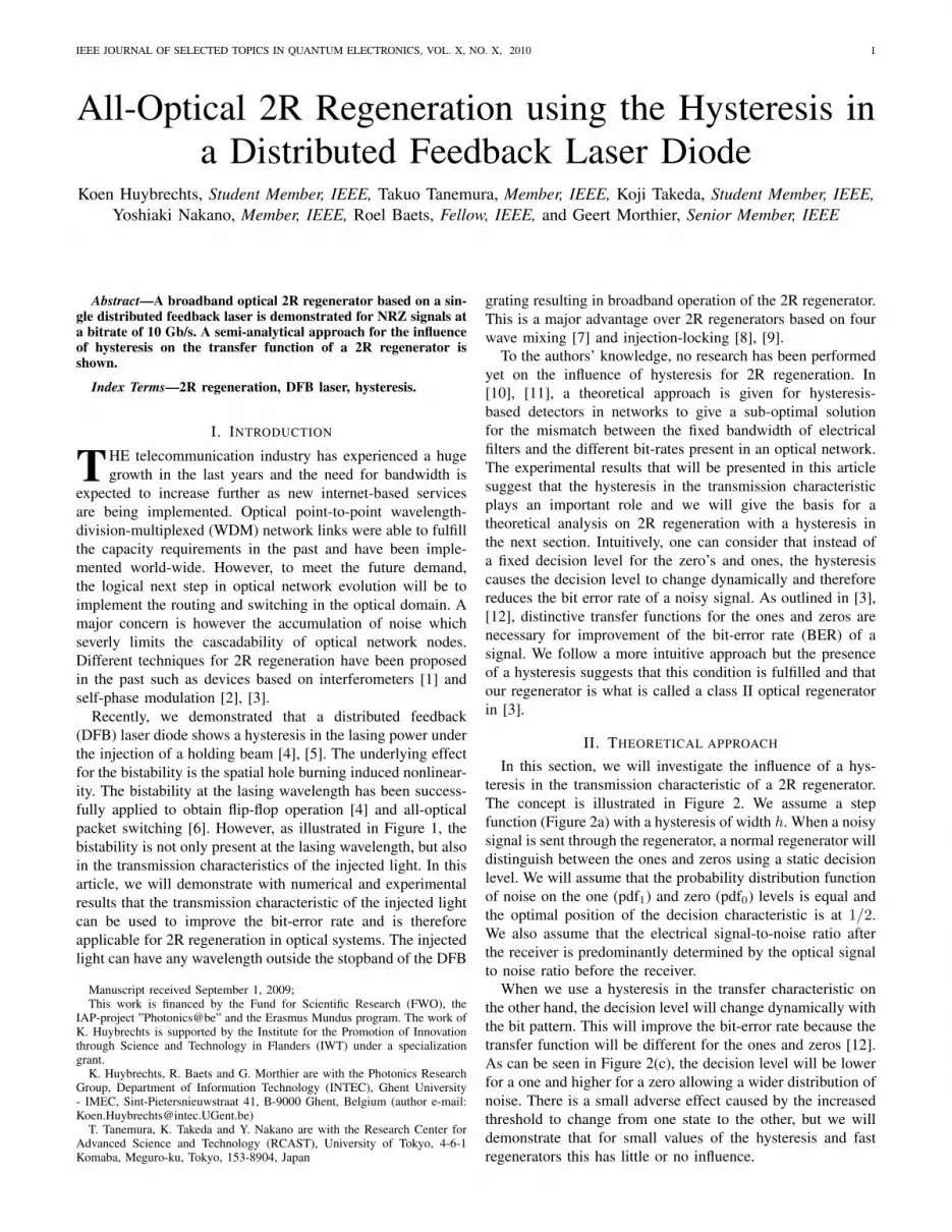
Recently, we demonstrated that a distributed feedback(DFB) laser diode shows a hysteresis in the lasing power underthe injection of a holding beam [4], [5]. The underlying effectfor the bistability is the spatial hole burning induced nonlinear-ity. The bistability at the lasing wavelength has been success-fully applied to obtain flip-flop operation [4] and all-opticalpacket switching [6]. However, as illustrated in Figure 1, thebistability is not only present at the lasing wavelength, but alsoin the transmission characteristics of the injected light. In thisarticle, we will demonstrate with numerical and experimentalresults that the transmission characteristic of the injected lightcan be used to improve the bit-error rate and is thereforeapplicable for 2R regeneration in optical systems. The injectedlight can have any wavelength outside the stopband of the DFB
Manuscript received September 1, 2009;This work is financed by the Fund for Scientific Research (FWO), the
IAP-project ”Photonics@be” and the Erasmus Mundus program. The work ofK. Huybrechts is supported by the Institute for the Promotion of Innovationthrough Science and Technology in Flanders (IWT) under a specializationgrant.
K. Huybrechts, R. Baets and G. Morthier are with the Photonics ResearchGroup, Department of Information Technology (INTEC), Ghent University- IMEC, Sint-Pietersnieuwstraat 41, B-9000 Ghent, Belgium (author e-mail:[email protected])
T. Tanemura, K. Takeda and Y. Nakano are with the Research Center forAdvanced Science and Technology (RCAST), University of Tokyo, 4-6-1Komaba, Meguro-ku, Tokyo, 153-8904, Japan
grating resulting in broadband operation of the 2R regenerator.This is a major advantage over 2R regenerators based on fourwave mixing [7] and injection-locking [8], [9].
To the authors’ knowledge, no research has been performedyet on the influence of hysteresis for 2R regeneration. In[10], [11], a theoretical approach is given for hysteresis-based detectors in networks to give a sub-optimal solutionfor the mismatch between the fixed bandwidth of electricalfilters and the different bit-rates present in an optical network.The experimental results that will be presented in this articlesuggest that the hysteresis in the transmission characteristicplays an important role and we will give the basis for atheoretical analysis on 2R regeneration with a hysteresis inthe next section. Intuitively, one can consider that instead ofa fixed decision level for the zero’s and ones, the hysteresiscauses the decision level to change dynamically and thereforereduces the bit error rate of a noisy signal. As outlined in [3],[12], distinctive transfer functions for the ones and zeros arenecessary for improvement of the bit-error rate (BER) of asignal. We follow a more intuitive approach but the presenceof a hysteresis suggests that this condition is fulfilled and thatour regenerator is what is called a class II optical regeneratorin [3].
II. THEORETICAL APPROACH
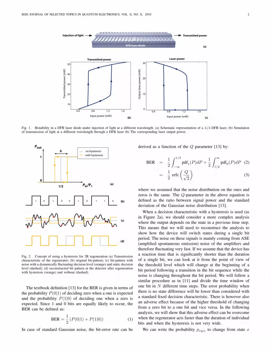
In this section, we will investigate the influence of a hys-teresis in the transmission characteristic of a 2R regenerator.The concept is illustrated in Figure 2. We assume a stepfunction (Figure 2a) with a hysteresis of width h. When a noisysignal is sent through the regenerator, a normal regenerator willdistinguish between the ones and zeros using a static decisionlevel. We will assume that the probability distribution functionof noise on the one (pdf1) and zero (pdf0) levels is equal andthe optimal position of the decision characteristic is at 1/2.We also assume that the electrical signal-to-noise ratio afterthe receiver is predominantly determined by the optical signalto noise ratio before the receiver.
When we use a hysteresis in the transfer characteristic onthe other hand, the decision level will change dynamically withthe bit pattern. This will improve the bit-error rate because thetransfer function will be different for the ones and zeros [12].As can be seen in Figure 2(c), the decision level will be lowerfor a one and higher for a zero allowing a wider distribution ofnoise. There is a small adverse effect caused by the increasedthreshold to change from one state to the other, but we willdemonstrate that for small values of the hysteresis and fastregenerators this has little or no influence.
IEEE JOURNAL OF SELECTED TOPICS IN QUANTUM ELECTRONICS, VOL. X, NO. X, 2010 2
0.4 0.8 1.2 1.6
10
20
30
40
50
Input power [mW]
Tran
smit
ted
po
wer
[mW
]
0.4 0.8 1.2 1.60
10
20
30
Input power [mW]
Ou
tpu
t la
ser p
ow
er [m
W]
Injection of light
DFB laser diode
Transmitted power
(a)
(b) (c)
Transmitted power Laser power
Fig. 1. Bistability in a DFB laser diode under injection of light at a different wavelength. (a) Schematic representation of a λ/4 DFB laser; (b) Simulationof transmission of light at a different wavelength through a DFB laser (b) The corresponding laser output power.
0
1
1 1 1 1 10 0 0 0 0
1/2 Pin/P1
Pouth
(a)
(b)
(c)
(d)
no hysteresis
with hysteresis
Fig. 2. Concept of using a hysteresis for 2R regeneration (a) Transmissioncharacteristic of the regenerator; (b) original bit-pattern; (c) bit-pattern withnoise with a dynamically fluctuating decision level (orange) and static decisionlevel (dashed); (d) reconstructed bit pattern at the detector after regenerationwith hysteresis (orange) and without (dashed).
The textbook definition [13] for the BER is given in terms ofthe probability P (0|1) of deciding zero when a one is expectedand the probability P (1|0) of deciding one when a zero isexpected. Since 1 and 0 bits are equally likely to occur, theBER can be defined as:
BER =12
(P (0|1) + P (1|0)) (1)
In case of standard Gaussian noise, the bit-error rate can be
derived as a function of the Q parameter [13] by:
BER =12
∫ 1/2
−∞pdf1(P )dP +
12
∫ ∞1/2
pdf0(P )dP (2)
=12
erfc(Q√2
)(3)
where we assumed that the noise distribution on the ones andzeros is the same. The Q-parameter in the above equation isdefined as the ratio between signal power and the standarddeviation of the Gaussian noise distribution [13].
When a decision characteristic with a hysteresis is used (asin Figure 2a), we should consider a more complex analysiswhere the output depends on the state in a previous time step.This means that we will need to reconstruct the analysis toshow how the device will switch states during a single bitperiod. The noise on these signals is mainly coming from ASE(amplified spontaneous emission) noise of the amplifiers andtherefore fluctuating very fast. If we assume that the device hasa reaction time that is significantly shorter than the durationof a single bit, we can look at it from the point of view ofthe threshold level which will change at the beginning of abit period following a transition in the bit sequence while thenoise is changing throughout the bit period. We will follow asimilar procedure as in [11] and divide the time window ofone bit in N different time steps. The error probability whenthere is no state difference will be lower than considered witha standard fixed decision characteristic. There is however alsoan adverse effect because of the higher threshold of changingfrom a zero bit to a one bit and vice versa. In the followinganalysis, we will show that this adverse effect can be overcomewhen the regenerator acts faster than the duration of individualbits and when the hysteresis is not very wide.
We can write the probability pxy|z to change from state x

IEEE JOURNAL OF SELECTED TOPICS IN QUANTUM ELECTRONICS, VOL. X, NO. X, 2010 3
to y while z is given, as follows:
p00|1 =(1+h)/2∫−∞
pdf1dP =12
erfc(
(1− h) Q√2
)p10|1 =
(1−h)/2∫−∞
pdf1dP =12
erfc(
(1 + h)Q√2
)p01|0 =
∞∫(1+h)/2
pdf0dP =12
erfc(
(1 + h)Q√2
)p11|0 =
∞∫(1−h)/2
pdf0dP =12
erfc(
(1− h) Q√2
)When using a hysteresis, the previous state is used to
determine the next state and a recursive expression for Pn(0|1)(being the probability on time step n to decide zero when aone is expected) can be written as:
Pn+1(0|1) = Pn(0|1) p00|1 + Pn(1|1) p10|1
P1(0|1) =12p00|1 +
12p10|1
and a similar equation for P (1|0). Because the noise dis-tribution on the ones is assumed similar to the noise dis-tribution on the zeros (p00|1 = p11|0 and p10|1 = p01|0)and P (1|1) = 1 − P (0|1) we can write down the followingrecursive expression for the BER:
BER(n+ 1) = BER(n) p00|1 + [1− BER(n)] p10|1 (4)
BER(1) =12p00|1 +
12p10|1 (5)
The second term of Equation 4 appears to be dominant forrealistic values of the hysteresis (h < 1) and the bit error rateasymptotically becomes equal to p10|1 after a sufficient amountof time steps. This asymptotical bit error rate is depicted inFigure 3 for different values of the hysteresis width. However,this figure does not take into account the adverse effect of thehigher threshold for switching between two different states.As discussed above, the bit error rate will improve during thetime window of a single bit. For high values of the hysteresiswidth, it will take more time steps to achieve an improvement.The evolution of the BER is depicted in Figure 4 for differenttime steps n and a hysteresis width h = 0.4. We can observean improvement in bit error rate after 3 time steps. This meansthat - according to this model - the reaction time of the deviceshould be 4 or 5 times faster than the bit duration when h =0.4. The number of time steps needed for an improvementin bit error rate increases with the hysteresis width, eg. for ahysteresis of h = 0.1 there is already an improvement in thesecond time step but it takes 15 time steps for a hysteresiswidth of h = 0.9.
We can conclude this section by stating that a hysteresis inthe transmission characteristic makes the decision thresholdto move dynamically with the signal. Therefore, a distinctivetransfer function for the ones and zeros allows to improvethe bit error rate. The theoretical model that is derived above,suggests however that the response time of the regeneratorshould be significantly faster with respect to the bitrate of theoriginal signal.
0 2 4 6 810-12
10-9
10-6
10-3
100
Q parameter
Erro
r pro
bab
ility
(BER
)
h=0
h=1.0
Fig. 3. Asymptotical behaviour of BER as a function of the Q parameterfor different values of the hysteresis width h (and n→∞).
n=1
n=2
n=3
10-12
10-9
10-6
10-3
100
Erro
r pro
bab
ility
(BER
)
0 2 4 6 8
Q parameter
n>3
Fig. 4. BER as a function of the Q parameter at different time steps nfor a hysteresis with width h = 0.4. The dashed line represents the situationwithout hysteresis.
III. EXPERIMENT
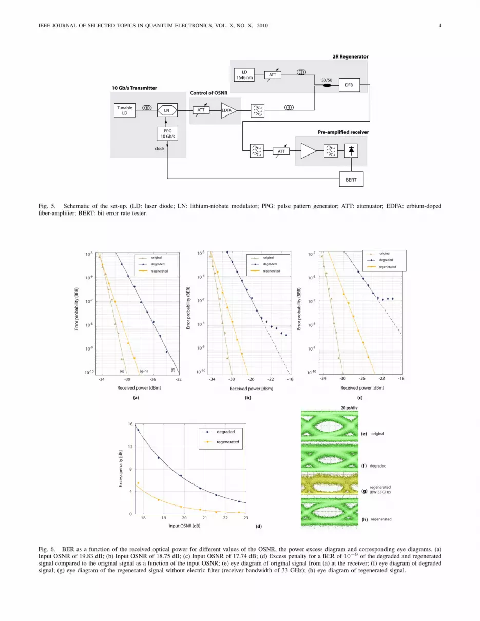
For the experiment, we use the set-up as depicted inFigure 5. A pulse pattern generator (PPG) generates a pseudo-random bit-sequence (PRBS) of 231 − 1 bits. The originalsignal is being attenuated and amplified to decrease the OSNR.The regenerator is a standard, non-optimized λ/4-shifted DFBlaser diode from Alcatel-Thales with AR-coated facets. It hasa κL value of 1.6, a bias current of 150 mA and its centralwavelength is 1553 nm. Lensed fibers are aligned at bothsides of the laser to couple the light. The degenerated signalhas an input power of 5-7 dBm (depending on the powerinjected in the EDFA) and is combined with a holding beam of5 dBm (both measured in fiber after the coupler). The holdingbeam is used to decrease the threshold for bistability and canbe adjusted by an attenuator. The width of the bistability isapproximately 1 dB wide (resulting in a value for h between0.1 and 0.2 in the analysis of section II). An optical band-
IEEE JOURNAL OF SELECTED TOPICS IN QUANTUM ELECTRONICS, VOL. X, NO. X, 2010 4
TunableLD
LN
PPG10 Gb/s
10 Gb/s Transmitter
clock
LD1546 nm
ATT
2R Regenerator
ATT
Pre-amplified receiver
50/50DFB
ATT EDFA
BERT
Control of OSNR
Fig. 5. Schematic of the set-up. (LD: laser diode; LN: lithium-niobate modulator; PPG: pulse pattern generator; ATT: attenuator; EDFA: erbium-dopedfiber-amplifier; BERT: bit error rate tester.
Input OSNR [dB]
Exce
ss p
enal
ty [d
B]
-34 -30 -26 -22
10-5
10-6
10-7
10-8
10-9
10-10
Received power [dBm]
Erro
r pro
bab
ility
(BER
)
regenerated
original
degraded
10-5
10-6
10-7
10-8
10-9
10-10
Erro
r pro
bab
ility
(BER
)
-34 -30 -26 -22 -18
Received power [dBm]
regenerated
original
degraded
10-5
10-6
10-7
10-8
10-9
10-10
Erro
r pro
bab
ility
(BER
)
-34 -30 -26 -22 -18
Received power [dBm]
regenerated
original
degraded
(a) (b) (c)
(d)
(e)
(f)
(g)
(h)
20 ps/div
original
degraded
regenerated�(BW 33 GHz)
regenerated
(e) (f )(g-h)
18 19 20 21 22 230
4
8
12
16
regenerated
degraded
Fig. 6. BER as a function of the received optical power for different values of the OSNR, the power excess diagram and corresponding eye diagrams. (a)Input OSNR of 19.83 dB; (b) Input OSNR of 18.75 dB; (c) Input OSNR of 17.74 dB; (d) Excess penalty for a BER of 10−9 of the degraded and regeneratedsignal compared to the original signal as a function of the input OSNR; (e) eye diagram of original signal from (a) at the receiver; (f) eye diagram of degradedsignal; (g) eye diagram of the regenerated signal without electric filter (receiver bandwidth of 33 GHz); (h) eye diagram of regenerated signal.

IEEE JOURNAL OF SELECTED TOPICS IN QUANTUM ELECTRONICS, VOL. X, NO. X, 2010 5
pass filter with a width of 1 nm removes the lasing light sothat only the signal at the original wavelength is sent to thepre-amplified receiver for a bit-error rate (BER) analysis. Avariable attenuator is used to change the received optical poweron the receiver in order to make BER-diagrams. F
In Figure 6a-c, the BER diagrams as a function of thereceived optical power are shown for different values of theEDFA input power (and thus for different OSNR’s). Fromthese diagrams, it is clear that the 2R regenerator is able toimprove the degraded signal significantly. Its noise suppressioncapabilities are demonstrated by Figure 6d where the excesspower penalty for the regenerated and degraded signal com-pared to the original signal are depicted as a function of theEDFA input power. The corresponding eye diagrams for theregeneration are depicted in Figure 6e-h. In Figure 6g, theregenerated signal is shown without an electrical filter that ismatched with the 10 GHz bandwidth at the receiver side buton a regular optical scope with a 33 GHz bandwidth. Thiseye diagram illustrates that the regenerator might work also athigher bitrates. We want to point out that our 2R regeneratorwith hysteresis even reduces the BER when the degradedsignal reaches the noise floor, determined by the OSNR;something which is beyond the capabilities of regeneratorswith a single decision level.
The extinction ratio improvement is depicted in Figure 7.However, in this diagram, we did not take the influence ofthe 5 dBm holding beam into account and an amplified signalwithout holding beam might result in a better extinction ratioimprovement. In Figure 8, the OSNR at the output of the2R regenerator is depicted as a function of the OSNR atthe input. The OSNR is measured by setting the resolutionof the spectrum analyzer to 0.1 nm and determining thedifference between the signal and noise. The reduction ofnoise is important with regard to the cascadability of theregenerators.
The 2R regenerator can work at any wavelength outside thestopband of the DFB grating as illustrated for three arbitrarywavelengths in Figure 9. The BER diagrams for different in-jected wavelengths are depicted and show broadband operationthat is only limited by the spectral width of the gain medium.The gain medium in our device are quantum wells leading to again bandwidth of approximately 20 nm. The small differencesbetween the graphs are mostly due to the spectral variation ingain of the EDFA.
When we separate the signal at the lasing wavelength(instead of the injected wavelength), we obtain the reversed,wavelength converted signal. The noise floor is much higherand error-free wavelength conversion was only obtained at asmaller bitrate of 3 Gb/s. This is because the carrier densitychanges much faster than the laser signal which also dependson the cavity decay time.
IV. CONCLUSION
A new concept for 2R regeneration is proposed using ahysteresis in the transmission characteristic. The concept isillustrated with experimental results showing bit error rate im-provement of a 10 GB/s NRZ signal using a single distributed
5 6 7 8 9 10 11
5
6
7
8
9
10
11
Input Extinction Ratio [dB]
Ou
tpu
t Ex
tin
ctio
n R
atio
[dB
]
Fig. 7. The extinction ratio improvement.
14 18 22 26
14
18
22
26
30
OSN
R o
utp
ut
at 0
.1 n
m [d
B]
OSNR input at 0.1 nm [dB]
Fig. 8. OSNR in 0.1 nm at the output of the all-optical 2R regenerator as afunction of the input OSNR.
feedback (DFB) laser diode. The simplicity of the conceptand the good performance make this regenerator suitable forapplication in optical access or metro networks. Since directmodulation of DFB lasers has been demonstrated at higherbitrates (up to 40 GHz), the presented technique might bealso employed at higher speeds by using optimalized designs.
ACKNOWLEDGMENT
The authors would like to thank Guang-Hua Duan fromAlcatel-Thales III/V-labs for providing the DFB laser diodes.
REFERENCES
[1] D. Wolfson, A. Kloch, T. Fjelde, C. Janz, B. Dagens, and M. Renaud,“40-Gb/s all-optical wavelength conversion, regeneration, and demulti-plexing in an soa-based all-active mach-zehnder interferometer,” IEEEPhotonics Technology Letters, vol. 12, no. 3, pp. 332–334, 2000.
[2] P. V. Mamyshev and T. E. T. E. Telefon Espana, “All-optical dataregeneration based on self-phase modulation effect,” in 24th EuropeanConference on Optical Communications. Madrid, Spain: TelefonicaEspana Sa, 1998, pp. 475–476.

IEEE JOURNAL OF SELECTED TOPICS IN QUANTUM ELECTRONICS, VOL. X, NO. X, 2010 6
-35 -30 -25 -2010 -10
10 -9
10 -8
10 -7
10 -6
Received power [dBm]
Erro
r pro
bab
ility
(BER
)
λsig = 1545 nm
Received power [dBm]Received power [dBm]Er
ror p
rob
abili
ty (B
ER)
Erro
r pro
bab
ility
(BER
)
-35 -30 -25 -20-35 -30 -25 -2010 -10
10 -9
10 -8
10 -7
10 -6
10 -10
10 -9
10 -8
10 -7
10 -6
10 -5
regenerated
original
degraded
regenerated
original
degraded
regenerated
original
degraded
λsig = 1550 nm λsig = 1555 nm
Fig. 9. Wavelength independence: BER as a function of the received optical power for different transmission wavelengths.
[3] M. Rochette, L. B. Fu, V. Ta’eed, D. J. Moss, and B. J. Eggleton,“2R optical regeneration: An all-optical solution for BER improvement,”IEEE Journal of Selected Topics in Quantum Electronics, vol. 12, no. 4,pp. 736–744, 2006.
[4] K. Huybrechts, G. Morthier, and R. Baets, “Fast all-optical flip-flopbased on a single distributed feedback laser diode,” Optics Express,vol. 16, no. 15, pp. 11 405–11 410, 2008.
[5] K. Huybrechts, W. D’Oosterlinck, G. Morthier, and R. Baets, “Proposalfor an all-optical flip-flop using a single distributed feedback laserdiode,” Photonics Technology Letters, vol. 20, no. 1-4, pp. 18–20, 2008.
[6] K. Huybrechts, T. Tanemura, Y. Nakano, R. Baets, and G. Morthier,“40-Gb/s all-optical packet switching with a distributed-feedback laseras all-optical flip-flop,” IEEE Photonics Technology Letters, vol. 21, no.9-12, pp. 703–705, 2009.
[7] H. Simos, A. Bogris, and D. Syvridis, “Investigation of a 2R all-opticalregenerator based on four-wave mixing in a semiconductor opticalamplifier,” Journal of Lightwave Technology, vol. 22, no. 2, pp. 595–604,2004.
[8] A. Kuramoto and S. Yamashita, “All-optical regeneration using a side-mode injection-locked semiconductor laser,” Selected Topics in QuantumElectronics, IEEE Journal of, vol. 9, no. 5, pp. 1283–1287, 2003.
[9] S. Yamashita and J. Suzuki, “All-optical 2R regeneration using atwo-mode injection-locked fabry-perot laser diode,” IEEE PhotonicsTechnology Letters, vol. 16, no. 4, pp. 1176–1178, 2004.
[10] C. E. Korman, R. Barry, and U. C. Kozat, “On binary detection withhysteresis,” Siam Journal on Applied Mathematics, vol. 62, no. 5, pp.1794–1809, 2002.
[11] C. E. Korman, “A discrete-time model for binary detection with rectan-gular hysteresis operators,” in 5th International Symposium on Hysteresisand Micromagnetic Modeling (HMM 2005). Budapest (Hungary):Elsevier Science Bv, 2005, pp. 17–20.
[12] M. Rochette, J. N. Kutz, J. L. Blows, D. Moss, J. T. Mok, and B. J.Eggleton, “Bit-error-ratio improvement with 2R optical regenerators,”IEEE Photonics Technology Letters, vol. 17, no. 4, pp. 908–910, 2005.
[13] G. Agrawal, Fiber-optic communication systems. John Wiley and sons,pp. 162-164.
Koen Huybrechts (S’06) received his master degree in Physics Engineeringfrom Ghent University in 2006. During his masters, he spent one year as anexchange student at KTH in Stockholm. Currently, he is working towards aPhD degree at the Photonics Research Group of Ghent University - IMEC. Hisresearch includes mainly all-optical flip-flops and all-optical signal processingdevices. He is vice-chairman of the IEEE Photonics Society Benelux StudentChapter.
Takuo Tanemura (S’02M’06) received the B.E., M.S., and Ph.D. degrees inelectronic engineering, all from the University of Tokyo, Japan, in 2001, 2003,and 2006, respectively. He joined the Department of Electronic Engineering,University of Tokyo in 2006 and moved to the Research Center for AdvancedScience and Technology, University of Tokyo in 2007, where he is currentlya Lecturer. His current research interest includes photonic integrated circuitsbased on III-V semiconductors, photonic switching networks, and all-opticalsignal processing devices. Dr. Tanemura is a member of IEEE Lasers andElectro-Optics Society (LEOS) and the Institute of Electronics, Information,and Communication Engineers (IEICE) of Japan. He is the recipient of the2005 IEEE LEOS Graduate Student Award and the 2006 Ericsson YoungScientist Award. He has authored and coauthored over 20 refereed journalpublications and over 50 international conference papers.
Koji Takeda (S’06) was born in Chiba, Japan, in 1982. He received theB.E. and M.E. degrees in electronic engineering, all from the University ofTokyo, Tokyo, Japan, in 2005 and in 2007, respectively. He has belongedto school of engineering, the University of Tokyo as a Ph.D candidate. Heis also with the Research Center for Advanced Science and Technology, theUniversity of Tokyo. He has received the Research Fellowship for YoungScientists from Japan Society for the Promotion of Science (JSPS) since 2007.In 2008, he spent two weeks at the University of Rochester, New York, underthe cooperative program of the JSPS. His research has mainly focused onsemiconductor photonic integrated circuits based on III-V materials, especiallyon all-optical flip-flops and switches. Mr. Takeda is a student member ofIEEE/LEOS and the Japan Society of Applied Physics (JSAP).
Yoshiaki Nakano (S’81M’87) received the B.E., M.S., and Ph.D. degrees inelectronic engineering from the University of Tokyo, Tokyo, Japan, in 1982,1984, and 1987, respectively. In 1984, he spent a year at the University ofCalifornia, Berkeley, as an exchange student.

IEEE JOURNAL OF SELECTED TOPICS IN QUANTUM ELECTRONICS, VOL. X, NO. X, 2010 7
In 1987, he joined the Department of Electronic Engineering, Universityof Tokyo, where he was an Associate Professor in 1992, a Professor in 2000,and the Department Head in 2001, and is currently the Vice Director and aProfessor in the Research Center for Advanced Science and Technology, andis also with the Department of Electronic Engineering, School of Engineering.In 1992, he was a visiting Associate Professor at the University of California,Santa Barbara. He was the Project Leader of the Japanese National Projecton Photonic Networking Technology organized by the Ministry of Economy,Trading, and Industry, and as the Project Leader of the Solution OrientedResearch for Science and Technology (SORST) Program on Non-reciprocalSemiconductor Digital Photonic Integrated Circuits and their Applications toPhotonic Networking sponsored by the Japan Science and Technology Corpo-ration. He authored and coauthored over 200 refereed journal publications andover 400 international conference papers, and holds 40 patents. He was theEditor-in-Chief of the Applied Physics Express (APEX) and Japanese Journalof Applied Physics (JJAP). His current research interests include physicsand fabrication technologies of semiconductor distributed feedback lasers,semiconductor optical modulators/switches, and monolithically integratedphotonic circuits.
Prof. Nakano was an elected member of the Board of Governors ofthe IEEE Laser Electro-Optical Society (LEOS, nowthe Photonics Society)and a member of the Board of Directors of the Japan Society of AppliedPhysics (JSAP). He is a member of the Board of Directors of the JapanInstitute of Electronics Packaging (JIEP), the Chairman of the OptoelectronicsTechnology Trend Research Committee of the Optoelectronics Industry andTechnology Development Association (OITDA), and the Chairman of the Op-tical Interconnect Standardization Committee of Japan Electronics Packagingand Circuits Association. He is also a Fellow of the Institute of Electronics,Information, and Communication Engineers (IEICE) and a member of theIEEE Electron Devices Society and the Optical Society of America. He is therecipient of the 1987 Shinohara Memorial Prize from the IEICE, the 1991Optics Paper Award from the JSAP, the 1997 Marubun Science Prize, the2007 Ichimura Prize, the 2007 IEICE Electronics Society Award, and the2007 Sakurai Medal from the OITDA. He was presented the Prime MinisterAward in Collaborative Research between Academia and Industry in 2007.
Roel Baets (M’88, SM’96) received the degree in electrical engineering fromGhent University, Belgium, in 1980. He received the M.Sc. degree in electricalengineering from Stanford University in 1981 and the Ph.D. degree fromGhent University in 1984. Since 1981 he has been with the Department ofInformation Technology (INTEC) of Ghent University. Since 1989 he is aprofessor in the engineering faculty of Ghent University. From 1990 till 1994he has also been a part-time professor at the Technical University of Delft,The Netherlands. Since 2004 he is also part-time professor at the TechnicalUniversity of Eindhoven.
Roel Baets has mainly worked in the field of photonic components. Withabout 250 journal publications and 500 conference papers as well as about15 patents he has made contributions to research on semiconductor laserdiodes, passive guided wave and grating devices and to the design andfabrication of photonic ICs, both in III-V semiconductors and in silicon. Heleads the Photonics Research Group at Ghent University-INTEC (associatedlab of IMEC), which focuses on new concepts for photonic components andcircuits for optical communication, optical interconnect and optical sensing.He has been involved in various European research projects and has beencoordinator of some of them. Currently he coordinates the European Networkof Excellence ePIXnet.
Roel Baets is a member of the Optical Society of America, IEEE-LEOS,SPIE and the Flemish Engineers Association. He has been member ofthe program committees of a.o. OFC, ECOC, IEEE Semiconductor LaserConference, ESSDERC, CLEO-Europe, LEOS Annual Meeting, PhotonicsEurope and ECIO. He has been chairman of the IEEE-LEOS-Benelux chapterfrom 1999 to 2001. From 2003 to 2005 he was an elected member of the Boardof Governors of IEEE-LEOS. He is a Fellow of the IEEE.
Geert Morthier (M’93, SM’01) received the degree in electrical engineeringand the Ph.D. degree from the University of Gent in 1987, 1991, respectively.In 2001 he was appointed parttime professor at Ghent University.
Since 1991 he is a member of the permanent staff of IMEC. His maininterests are in the modelling and characterisation of optoelectronic compo-nents. He has authored or co-authored around 100 papers in the field. He isalso one of the two authors of the Handbook of Distributed Feedback Laser(Artech House, 1997) and co-editor of the book How to model and measurephotonic components: experience from a European project (Springer-Verlag,1998). He has been the project manager of the ACTS project ACTUAL dealingwith the control of widely tunable laser diodes and of the FP5 IST projectNEWTON on new widely tunable lasers. He is currently the project managerof the FP7 ICT project HISTORIC on all optical logic and routing based onheterogeneous InP on silicon technology.