A compact double-gate MOSFET model comprising quantum-mechanical and nonstatic effects
4The Power MOSFET
Issa Batarseh, Ph.D.School of Electrical Engineering and
Computer Science, University ofCentral Florida, 4000 CentralFlorida Blvd., Orlando, Florida,USA
4.1 Introduction .......................................................................................... 414.2 Switching in Power Electronic Circuits ....................................................... 424.3 General Switching Characteristics .............................................................. 44
4.3.1 The Ideal Switch • 4.3.2 The Practical Switch
4.4 The Power MOSFET ............................................................................... 484.4.1 MOSFET Structure • 4.4.2 MOSFET Regions of Operation • 4.4.3 MOSFET SwitchingCharacteristics • 4.4.4 MOSFET PSPICE Model • 4.4.5 MOSFET Large-signal Model• 4.4.6 Current MOSFET Performance
4.5 Future Trends in Power Devices ................................................................ 68References ............................................................................................. 69
4.1 Introduction
In this chapter, an overview of power MOSFET (metal oxidesemiconductor field effect transistor) semiconductor switch-ing devices will be given. The detailed discussion of thephysical structure, fabrication, and physical behavior of thedevice and packaging is beyond the scope of this chapter.The emphasis here will be given on the terminal i–v switchingcharacteristics of the available device, turn-on, and turn-offswitching characteristics, PSPICE modeling and its current,voltage, and switching limits. Even though, most of today’savailable semiconductor power devices are made of siliconor germanium materials, other materials such as galliumarsenide, diamond, and silicon carbide are currently beingtested.One of the main contributions that led to the growth of the
power electronics field has been the unprecedented advance-ment in the semiconductor technology, especially with respectto switching speed and power handling capabilities. The areaof power electronics started by the introduction of the sili-con controlled rectifier (SCR) in 1958. Since then, the fieldhas grown in parallel with the growth of the power semi-conductor device technology. In fact, the history of powerelectronics is very much connected to the development ofswitching devices and it emerged as a separate discipline whenhigh power bipolar junction transistors (BJTs) and MOSFETsdevices where introduced in the 1960s and 1970s. Sincethen, the introduction of new devices has been accompaniedwith dramatic improvement in power rating and switching
performance. Because of their functional importance, drivecomplexity, fragility, cost, power electronic design engineermust be equipped with the thorough understanding of thedevice operation, limitation, drawbacks, and related reliabilityand efficiency issues.In the 1980s, the development of power semiconductor
devices took an important turn when new process technol-ogy was developed that allowed the integration of MOS andBJT technologies on the same chip. Thus far, two devicesusing this new technology have been introduced: integratedgate bipolar transistor (IGBT) and MOS controlled thyristor(MCT). Many of the IC processing methods and equipmenthave been adopted for the development of power devices.However, unlike microelectronic IC’s which process informa-tion, power devices IC’s process power, hence, their packagingand processing techniques are quite different. Power semi-conductor devices represent the “heart” of modern powerelectronics, with two major desirable characteristics of powersemiconductor devices that guided their development are: theswitching speed and power handling capabilities.The improvement of semiconductor processing technol-
ogy along with manufacturing and packaging techniques hasallowed power semiconductor development for high voltageand high current ratings and fast turn-on and turn-off char-acteristics. Today, switching devices are manufactured withamazing power handling capabilities and switching speedsas will be shown later. The availability of different deviceswith different switching speed, power handling capabilities,size, cost, . . . etc. make it possible to cover many power
Copyright © 2007, 2001, Elsevier Inc.
All rights reserved.
41
42 I. Batarseh
electronics applications. As a result, trade-offs are made whenit comes to selecting power devices.
4.2 Switching in Power ElectronicCircuits
As stated earlier, the heart of any power electronic circuitis the semiconductor-switching network. The question ariseshere is do we have to use switches to perform electrical powerconversion from the source to the load? The answer of courseis no, there are many circuits which can perform energy con-version without switches such as linear regulators and poweramplifiers. However, the need for using semiconductor devicesto perform conversion functions is very much related to theconverter efficiency. In power electronic circuits, the semicon-ductor devices are generally operated as switches, i.e. either inthe on-state or the off-state. This is unlike the case in poweramplifiers and linear regulators where semiconductor devicesoperate in the linear mode. As a result, very large amount ofenergy is lost within the power circuit before the processedenergy reaches the output. The need to use semiconductorswitching devices in power electronic circuits is their ability tocontrol and manipulate very large amounts of power from theinput to the output with a relatively very low power dissipa-tion in the switching device. Hence, resulting in a very highefficient power electronic system.Efficiency is considered as an important figure of merit and
has significant implications on the overall performance of thesystem. Low efficient power systems means large amounts ofpower being dissipated in a form of heat, resulting in one ormore of the following implications:
1. Cost of energy increases due to increased consumption.2. Additional design complications might be imposed,especially regarding the design of device heat sinks.
3. Additional components such as heat sinks increasecost, size, and weight of the system, resulting in lowpower density.
4. High power dissipation forces the switch to operateat low switching frequency, resulting in limited band-width, slow response, and most importantly, the sizeand weight of magnetic components (inductors andtransformers), and capacitors remain large. Therefore,it is always desired to operate switches at very highfrequencies. But, we will show later that as the switch-ing frequency increases, the average switching powerdissipation increases. Hence, a trade-off must be madebetween reduced size, weight, and cost of componentsvs reduced switching power dissipation, which meansinexpensive low switching frequency devices.
5. Reduced component and device reliability.
For more than forty years, it has been shown that in orderto achieve high efficiency, switching (mechanical or electrical)is the best possible way to accomplish this. However, unlikemechanical switches, electronic switches are far more superiorbecause of their speed and power handling capabilities as wellas reliability.We should note that the advantages of using switches don’t
come at no cost. Because of the nature of switch currents andvoltages (square waveforms), normally high order harmon-ics are generated in the system. To reduce these harmonics,additional input and output filters are normally added to thesystem. Moreover, depending on the device type and powerelectronic circuit topology used, driver circuit control andcircuit protection can significantly increase the complexity ofthe system and its cost.
EXAMPLE 4.1 The purpose of this example is to inves-tigate the efficiency of four different power circuitswhose functions are to take in power from 24 volts dcsource and deliver a 12 volts dc output to a 6� resis-tive load. In other words, the tasks of these circuits areto serve as dc transformer with a ratio of 2:1. The fourcircuits are shown in Fig. 4.1a–d representing voltagedivider circuit, zener-regulator, transistor linear regula-tor, and switching circuit, respectively. The objective isto calculate the efficiency of those four power electroniccircuits.
SOLUTION.
Voltage Divider DC Regulator The first circuit is thesimplest forming a voltage divider with R = RL = 6�and Vo = 12 volts. The efficiency defined as the ratioof the average load power, PL , to the average inputpower, Pin
η = PL
Pin%
= RL
RL + R% = 50%
In fact efficiency is simply Vo/Vin%. As the out-put voltage becomes smaller, the efficiency decreasesproportionally.
Zener DC Regulator Since the desired output is12V, we select a zener diode with zener breakdownVZ = 12V. Assume the zener diode has the i–v char-acteristic shown in Fig. 4.1e since RL = 6�, the loadcurrent, IL , is 2 A. Then we calculate R for IZ = 0.2 A(10% of the load current). This results in R = 5.27�.Since the input power is Pin = 2.2 A × 24V = 52.8Wand the output power is Pout = 24W. The efficiency of

4 The Power MOSFET 43
(a) (b)
(c) (d)
R
+
vo
vo vo
_
IL
ILIL
Control
+
_
+ vCE
IB
Vin
Vin
Vin
Vin
R
RLRL
RL RL
+
_
_
+
_
S
vo
(e)
(f)
i(A)
−12V
0.01
v(V)
switch
ON ONOFF
DT Tt
0
vo
DT T0
Vin
Vo,ave
t
FIGURE 4.1 (a) Voltage divider; (b) zener regulator; (c) transistor regulator; (d) switching circuit; (e) i–v zener diode characteristics; and(f) switching waveform for S and corresponding output waveform.

44 I. Batarseh
the circuit is given by,
η = 24W
52.8W%
= 45.5%
Transistor DC Regulator It is clear from Fig. 4.1c thatfor Vo = 12V, the collector emitter voltage must bearound 12V. Hence, the control circuit must providebase current, IB to put the transistor in the active modewith VCE ≈ 12V. Since the load current is 2 A, then col-lector current is approximately 2 A (assume small IB).The total power dissipated in the transistor can beapproximated by the following equation:
Pdiss = VCEIC + VBEIB
≈ VCEIC ≈ 12× 2 = 24watts
Therefore, the efficiency of the circuit is 50%.
Switching DC Regulator Let us consider the switch-ing circuit of Fig. 4.1d by assuming the switch is idealand periodically turned on and off is shown in Fig. 4.1f.The output voltage waveform is shown in Fig. 4.1f. Eventhough the output voltage is not constant or pure dc, itsaverage value is given by,
Vo,ave = 1
T
T0∫0
Vindt = VinD
where D is the duty ratio equals the ratio of the on-timeto the switching period. For Vo,ave = 12V, we setD = 0.5, i.e. the switch has a duty cycle of 0.5 or50%. In case, the average output power is 48W andthe average input power is also 48W, resulting in 100%efficiency! This is of course because we assumed theswitch is ideal. However, let us assume a BJT switchis used in the above circuit with VCE ,sat = 1V and IBis small, then the average power loss across the switchis approximately 2W, resulting in overall efficiency of96%. Of course the switching circuit given in this exam-ple is over simplified, since the switch requires additionaldriving circuitry that was not shown, which also dis-sipates some power. But still, the example illustratesthat high efficiency can be acquired by switching powerelectronic circuits when compared to the efficiency oflinear power electronic circuits. Also, the differencebetween the linear circuit in Figs. 4.1b and c and theswitched circuit of Fig. 4.1d is that the power deliv-ered to the load in the later case in pulsating betweenzero and 96watts. If the application calls for constant
power delivery with little output voltage ripple, thenan LC filter must be added to smooth out the outputvoltage.The final observation is regarding what is known
as load regulation and line regulation. The line reg-ulation is defined as the ratio between the change inoutput voltage, �Vo , with respect to the change in theinput voltage �Vin . This is a very important param-eter in power electronics since the dc input voltageis obtained from a rectified line voltage that normallychanges by ±20%. Therefore, any off-line power elec-tronics circuit must have a limited or specified rangeof line regulation. If we assume the input voltage inFigs. 4.1a,b is changed by 2V, i.e. �Vin = 2V, withRL unchanged, the corresponding change in the outputvoltage �Vo is 1 V and 0.55V, respectively. This isconsidered very poor line regulation. Figures 4.1c,dhave much better line and load regulations since theclosed-loop control compensate for the line and loadvariations.
4.3 General Switching Characteristics
4.3.1 The Ideal Switch
It is always desired to have the power switches perform as closeas possible to the ideal case. Device characteristically speaking,for a semiconductor device to operate as an ideal switch, itmust possess the following features:
1. No limit on the amount of current (known as forwardor reverse current) the device can carry when in theconduction state (on-state);
2. No limit on the amount of the device-voltage ((knownas forward or reverse blocking voltage) when the deviceis in the non-conduction state (off-state);
3. Zero on-state voltage drop when in the conductionstate;
4. Infinite off-state resistance, i.e. zero leakage currentwhen in the non-conduction state; and
5. No limit on the operating speed of the device whenchanges states, i.e. zero rise and fall times.
The switching waveforms for an ideal switch is shown inFig. 4.2, where isw and vsw are the current through and thevoltage across the switch, respectively.Both during the switching and conduction periods, the
power loss is zero, resulting in a 100% efficiency, and withno switching delays, an infinite operating frequency can beachieved. In short, an ideal switch has infinite speed, unlimitedpower handling capabilities, and 100% efficiency. It must benoted that it is not surprising to find semiconductor-switchingdevices that can almost, for all practical purposes, perform asideal switches for number of applications.

4 The Power MOSFET 45
+
vsw
_
isw
vsw
Voff
Von time
isw
Ioff
Ion
time
p (t )
time
FIGURE 4.2 Ideal switching current, voltage, and power waveforms.
4.3.2 The Practical Switch
The practical switch has the following switching and conduc-tion characteristics:
1. Limited power handling capabilities, i.e. limited con-duction current when the switch is in the on-state,and limited blocking voltage when the switch is in theoff-state.
2. Limited switching speed that is caused by the finiteturn-on and turn-off times. This limits the maximumoperating frequency of the device.
3. Finite on-state and off-state resistance’s i.e. there existsforward voltage drop when in the on-state, and reversecurrent flow (leakage) when in the off-state.
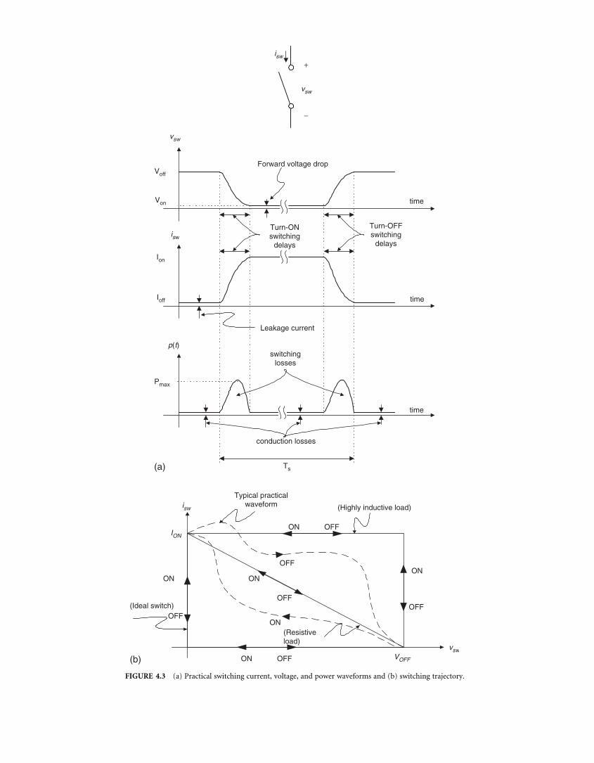
4. Because of characteristics 2 and 3 above, the practicalswitch experiences power losses in the on and the offstates (known as conduction loss), and during switch-ing transitions (known as switching loss). Typicalswitching waveforms of a practical switch are shownin Fig. 4.3a.
The average switching power and conduction power lossescan be evaluated from these waveforms. We should point outthe exact practical switching waveforms vary from one deviceto another device, but Fig. 4.3a is a reasonably good representa-tion. Moreover, other issues such as temperature dependence,
power gain, surge capacity, and over voltage capacity mustbe considered when addressing specific devices for specificapplications. A useful plot that illustrates how switching takesplace from on to off and vice versa is what is called switch-ing trajectory, which is simply a plot of isw vs vsw . Figure 4.3bshows several switching trajectories for the ideal and practicalcases under resistive loads.
EXAMPLE 4.2 Consider a linear approximation ofFig. 4.3a as shown in Fig. 4.4a: (a) Give a possiblecircuit implementation using a power switch whoseswitching waveforms are shown in Fig. 4.4a, (b) Derivethe expressions for the instantaneous switching andconduction power losses and sketch them, (c) Determinethe total average power dissipated in the circuit duringone switching frequency, and (d) The maximum power.
SOLUTION. (a) First let us assume that the turn-on time,ton , and turn-off time, toff , the conduction voltage VON ,and the leakage current, IOFF , are part of the switchingcharacteristics of the switching device and have nothingto do with circuit topology.When the switch is off, the blocking voltage across
the switch is VOFF that can be represented as a dc volt-age source of value VOFF reflected somehow across theswitch during the off-state. When the switch is on, thecurrent through the switch equals ION , hence, a dc cur-rent is needed in series with the switch when it is inthe on-state. This suggests that when the switch turnsoff again, the current in series with the switch mustbe diverted somewhere else (this process is known ascommutation). As a result, a second switch is needed tocarry the main current from the switch being investi-gated when it’s switched off. However, since isw and vsware linearly related as shown in Fig. 4.4b, a resistor willdo the trick and a second switch is not needed. Figure 4.4shows a one-switch implementation with S, the switchand R represents the switched-load.
(b) The instantaneous current and voltage waveformsduring the transition and conduction times are given asfollows
isw (t ) =
⎧⎪⎪⎪⎪⎨⎪⎪⎪⎪⎩
t
tON(ION − IOFF )+ IOFF
ION
− t−TstOFF
(ION − IOFF )+ IOFF
0 ≤ t ≤ tON
tON ≤ t ≤ Ts − tOFF
Ts − tOFF ≤ t ≤ Ts
vsw (t ) =
⎧⎪⎪⎪⎪⎪⎪⎪⎪⎪⎨⎪⎪⎪⎪⎪⎪⎪⎪⎪⎩
−VOFF − VON
tON0 ≤ t ≤ tON
× (t − tON )+ VON
VON tON ≤ t ≤ Ts − tOFF
VOFF − VON
tOFFTs − tOFF ≤ t ≤ Ts
× (t − (Ts − tOFF ))+ VON
+
vsw
_
isw
vsw
Voff
Von time
isw
Ioff
Ion
time
p(t)
time
Pmax
Ts
Forward voltage drop
Turn-ONswitching
delays
Turn-OFFswitching
delays
Leakage current
switchinglosses
conduction losses
(a)
vsw
isw
(Ideal switch)
(Resistiveload)
ON OFF
ON OFF
ON
OFF
ON
OFFON
OFF
Typical practicalwaveform (Highly inductive load)
VOFF
ION
ON
OFF
(b)
FIGURE 4.3 (a) Practical switching current, voltage, and power waveforms and (b) switching trajectory.

4 The Power MOSFET 47
Ts
(a)
+
vsw
_
isw
vswVof
f
Von
isw
Ioff
Ion
ton tofft=0
t
Load
(b)
+ vsw −
isw
Vof
fR Vof
f
S
(c)
IonVoff4
ton2
0 ton toff2
TsTs– toff
t
Psw(t)
tmax
FIGURE 4.4 Linear approximation of typical current and voltage switching waveforms.
It can be shown that if we assume ION IOFF
and VOFF VON , then the instantaneous power,p(t)= iswvsw can be given as follows,
p(t ) =
⎧⎪⎪⎪⎪⎪⎪⎪⎨⎪⎪⎪⎪⎪⎪⎪⎩
−VOFF IONt2ON
(t − tON ) t 0 ≤ t ≤ tON
VON ION tON ≤ t ≤ Ts − tOFF
−VOFF IONt2OFF
(t − (Ts − tOFF )) (t − Ts ) Ts − tOFF ≤ t ≤ Ts
Figure 4.4c shows a plot of the instantaneous powerwhere the maximum power during turn-on and off isVOFF ION /4.
(c) The total average dissipated power is given by
Pave = 1
Ts
Ts∫0
p(t )dt = 1
Ts
⎡⎣ tON∫0
−VOFF ION
t 2ON
(t −tON )t dt
+Ts−tOFF∫tON
VON IONdt
+Ts∫
Ts−tOFF
−VOFF ION
t 2OFF
(t −(Ts −tOFF ))(t −Ts)dt
⎤⎥⎦

48 I. Batarseh
The evaluation of the above integral gives
Pave = VOFF ION
Ts
(tON + tOFF
6
)
+ VON ION
Ts(Ts − tOFF − tON )
The first expression represents the total switchingloss, whereas the second expression represents the totalconduction loss over one switching cycle. We notice thatas the frequency increases, the average power increaseslinearly. Also the power dissipation increases with theincrease in the forward conduction current and thereverse blocking voltage.(d) The maximum power occurs at the time when thefirst derivative of p(t) during switching is set to zero, i.e.
dp(t )
dt
∣∣∣∣t=tmax
= 0
solve the above equation for tmax , we obtain values atturn on and off, respectively,
tmax = trise2
tmax = T − tfall2
Solving for the maximum power, we obtain
Pmax = Voff Ion
4
4.4 The Power MOSFET
Unlike the bipolar junction transistor (BJT), the MOSFETdevice belongs to the Unipolar Device family, since it usesonly the majority carriers in conduction. The developmentof the metal oxide semiconductor technology for micro-electronic circuits opened the way for developing the powermetal oxide semiconductor field effect transistor (MOSFET)device in 1975. Selecting the most appropriate device fora given application is not an easy task, requiring knowl-edge about the device characteristics, its unique features,innovation, and engineering design experience. Unlike lowpower (signal devices), power devices are more complicatedin structure, driver design, and understanding of their oper-ational i–v characteristics. This knowledge is very importantfor power electronics engineer to design circuits that willmake these devices close to ideal. The device symbol for ap- and n-channel enhancement and depletion types are shownin Fig. 4.5. Figure 4.6 shows the i–v characteristics for the
+
−
iD
Gate(G)
Source(S)
VDSVGD
+−
+−
Drain(D)
VGS
(a)
(G)
(S)
D
(b)
D
G
S
(c)
G
S
D
(d)
FIGURE 4.5 Device symbols: (a) n-channel enhancement-mode;(b) p-channel enhancement-mode; (c) n-channel depletion-mode; and(d) p-channel depletion-mode.
n-channel enhancement-type MOSFET. It is the fastest powerswitching device with switching frequency more than 1MHz,with voltage power ratings up to 1000V and current rating ashigh as 300A.MOSFET regions of operations will be studied shortly.
4.4.1 MOSFET Structure
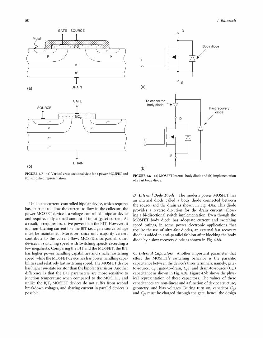
Unlike the lateral channel MOSFET devices used in many ICtechnology in which the gate, source, and drain terminalsare located in the same surface of the silicon wafer, powerMOSFET use vertical channel structure in order to increasethe device power rating [1]. In the vertical channel structure,the source and drain are in opposite side of the silicon waver.Figure 4.7a shows vertical cross-sectional view for a powerMOSFET. Figure 4.7b shows a more simplified representation.There are several discrete types of the vertical structure powerMOSFET available commercially today such as V-MOSFET,

4 The Power MOSFET 49
+
vDS
_+ vGS −
Drain (D)
Source (S)
(a)
(b)
Gate (G)
vDS > vGS– VThvDS < vGS– VTh
Saturation region (active region)Triode(linear region)
VGS increases
VGS = VTh+1
VGS < VTh
vDS
iD
FIGURE 4.6 (a) n-Channel enhancement-mode MOSFET and (b) its iD vs vDS characteristics.
U-MOSFET, D-MOSFET, and S-MOSFET [1, 2]. The P–Njunction between p-base (also referred to as body or bulkregion) and the n-drift region provide the forward voltageblocking capabilities. The source metal contact is connecteddirectly to the p-base region through a break in the n+ sourceregion in order to allow for a fixed potential to p-base regionduring the normal device operation. When the gate and sourceterminal are set the same potential (VGS = 0), no channel isestablished in the p-base region, i.e. the channel region remainunmodulated. The lower doping in the n-drift region is neededin order to achieve higher drain voltage blocking capabilities.For the drain–source current, ID , to flow, a conductive pathmust be established between the n+ and n− regions throughthe p-base diffusion region.
A. On-state Resistance When the MOSFET is in the on-state (triode region), the channel of the device behaves like a
constant resistance, RDS(on), that is linearly proportional to thechange between vDS and iD as given by the following relation:
RDS(ON ) = ∂vDS
∂iD
∣∣VGS=Constant
(4.1)
The total conduction (on-state) power loss for a givenMOSFET with forward current ID and on-resistance RDS(on) isgiven by,
Pon,diss = I 2DRDS(on) (4.2)
The value of RDS(on) can be significant and it varies betweentens of milliohms and a few ohms for low-voltage and high-voltage MOSFETS, respectively. The on-state resistance is animportant data sheet parameter, since it determines the for-ward voltage drop across the device and its total powerlosses.
50 I. Batarseh
n+
P
GATE SOURCE
DRAIN
SiO2
SiO2
P
Metal
n+n+
n−
pp
GATE
DRAIN
SOURCE
n+
n−
n+
n+
(a)
(b)
FIGURE 4.7 (a) Vertical cross-sectional view for a power MOSFET and(b) simplified representation.
Unlike the current-controlled bipolar device, which requiresbase current to allow the current to flow in the collector, thepower MOSFET device is a voltage-controlled unipolar deviceand requires only a small amount of input (gate) current. Asa result, it requires less drive power than the BJT. However, itis a non-latching current like the BJT i.e. a gate source voltagemust be maintained. Moreover, since only majority carrierscontribute to the current flow, MOSFETs surpass all otherdevices in switching speed with switching speeds exceeding afew megahertz. Comparing the BJT and the MOSFET, the BJThas higher power handling capabilities and smaller switchingspeed, while the MOSFET device has less power handling capa-bilities and relatively fast switching speed. TheMOSFET devicehas higher on-state resistor than the bipolar transistor. Anotherdifference is that the BJT parameters are more sensitive tojunction temperature when compared to the MOSFET, andunlike the BJT, MOSFET devices do not suffer from secondbreakdown voltages, and sharing current in parallel devices ispossible.
S
D
G
To cancel thebody diode
Fast recoverydiode
D
S
G
Body diode
(a)
(b)
FIGURE 4.8 (a) MOSFET Internal body diode and (b) implementationof a fast body diode.
B. Internal Body Diode The modern power MOSFET hasan internal diode called a body diode connected betweenthe source and the drain as shown in Fig. 4.8a. This diodeprovides a reverse direction for the drain current, allow-ing a bi-directional switch implementation. Even though theMOSFET body diode has adequate current and switchingspeed ratings, in some power electronic applications thatrequire the use of ultra-fast diodes, an external fast recoverydiode is added in anti-parallel fashion after blocking the bodydiode by a slow recovery diode as shown in Fig. 4.8b.
C. Internal Capacitors Another important parameter thateffect the MOSFET’s switching behavior is the parasiticcapacitance between the device’s three terminals, namely, gate-to-source, Cgs , gate-to-drain, Cgd , and drain-to-source (Cds)capacitance as shown in Fig. 4.9a. Figure 4.9b shows the phys-ical representation of these capacitors. The values of thesecapacitances are non-linear and a function of device structure,geometry, and bias voltages. During turn on, capacitor Cgd
and Cgs must be charged through the gate, hence, the design

4 The Power MOSFET 51
Cds
Cgd
Cgs
(a)
n+
n−
n+
n+
p
G
D
S S
CgdCds
Cgs
(b)
SiO2
FIGURE 4.9 (a) Equivalent MOSFET representation including junctioncapacitances and (b) representation of this physical location.
of the gate control circuit must take into consideration thevariation in this capacitance (Fig. 4.9b). The largest variationoccurs in the gate-to-drain capacitance as the drain-to-gatevoltage varies. The MOSFET parasitic capacitance are given interms of the device data sheet parameters Ciss , Coss , and Crss
as follows,
Cgd = Crss
Cgs = Ciss − Crss
Cds = Coss − Crss
where Crss = small-signal reverse transfer capacitance.Ciss = small-signal input capacitance with the drain
and source terminals are shorted.Coss = small-signal output capacitance with the
gate and source terminals are shorted.
The MOSFET capacitances Cgs , Cgd , and Cds are non-linearand function of the dc bias voltage. The variations in Coss andCiss are significant as the drain-to-source and gate-to-sourcevoltages cross zero, respectively. The objective of the drivecircuit is to charge and discharge the gate-to-source and gate-to-drain parasitic capacitance to turn on and off the device,respectively.
In power electronics, the aim is to use power-switchingdevices to operate at higher and higher frequencies. Hence,size and weight associated with the output transformer, induc-tors, and filter capacitors will decrease. As a result, MOSFETsare used extensively in power supply design that requires highswitching frequencies including switching and resonant modepower supplies and brushless dc motor drives. Because ofits large conduction losses, its power rating is limited to afew kilowatts. Because of its many advantages over the BJTdevices, modern MOSFET devices have received high marketacceptance.
4.4.2 MOSFET Regions of Operation
Most of the MOSFET devices used in power electronicsapplications are of the n-channel, enhancement-type like thatwhich is shown in Fig. 4.6a. For the MOSFET to carry draincurrent, a channel between the drain and the source must becreated. This occurs when the gate-to-source voltage exceedsthe device threshold voltage, VTh . For vGS > VTh , the devicecan be either in the triode region, which is also called “con-stant resistance” region, or in the saturation region, dependingon the value of vDS . For given vGS , with small vDS(vDS <
vGS −VTh), the device operates in the triode region(saturationregion in the BJT), and for larger vDS(vDS > vGS − VTh),the device enters the saturation region (active region in theBJT). For vGS <VTh , the device turns off, with drain currentalmost equals zero. Under both regions of operation, the gatecurrent is almost zero. This is why the MOSFET is knownas a voltage-driven device, and therefore, requires simple gatecontrol circuit.The characteristic curves in Fig. 4.6b show that there are
three distinct regions of operation labeled as triode region,saturation region, and cut-off-region. When used as a switch-ing device, only triode and cut-off regions are used, whereas,when it is used as an amplifier, the MOSFET must operate inthe saturation region, which corresponds to the active regionin the BJT.The device operates in the cut-off region (off-state) when
vGS <VTh , resulting in no induced channel. In order to oper-ate the MOSFET in either the triode or saturation region, achannel must first be induced. This can be accomplished byapplying gate-to-source voltage that exceeds VTh , i.e.
vGS > VTh
Once the channel is induced, the MOSFET can either operatein the triode region (when the channel is continuous with nopinch-off, resulting in the drain current proportioned to thechannel resistance) or in the saturation region (the channelpinches off, resulting in constant ID). The gate-to-drain biasvoltage (vGD) determines whether the induced channel enterpinch-off or not. This is subject to the following restriction.
52 I. Batarseh
For triode mode of operation, we have
vGD > VTh
vGD < VTh
And for the saturation region of operation,
Pinch-off occurs when vGD = VTh .
In terms of vDS , the above inequalities may be expressed asfollows:
1. For triode region of operation
vDS < vGS − VTh and vGS > VTh (4.3)
2. For saturation region of operation
vDS > vGS − VTh and vGS > VTh (4.4)
3. For cut-off region of operation
vGS < VTh (4.5)
It can be shown that drain current, iD , can be mathematicallyapproximated as follows:
iD = K [2(vGS − VTh)vDS − v2DS] Triode Region (4.6)
iD = K (vGS − VTh)2 Saturation Region (4.7)
where, K = 1
2μnCOX
(W
L
)μn = electron mobilityCOX = oxide capacitance per unit areaL = length of the channelW = width of the channel.
Typical values for the above parameters are given in thePSPICE model discussed later. At the boundary between thesaturation (active) and triode regions, we have,
vDS = vGS − VTh (4.8)
Resulting in the following equation for iD ,
iD = kv2DS (4.9)
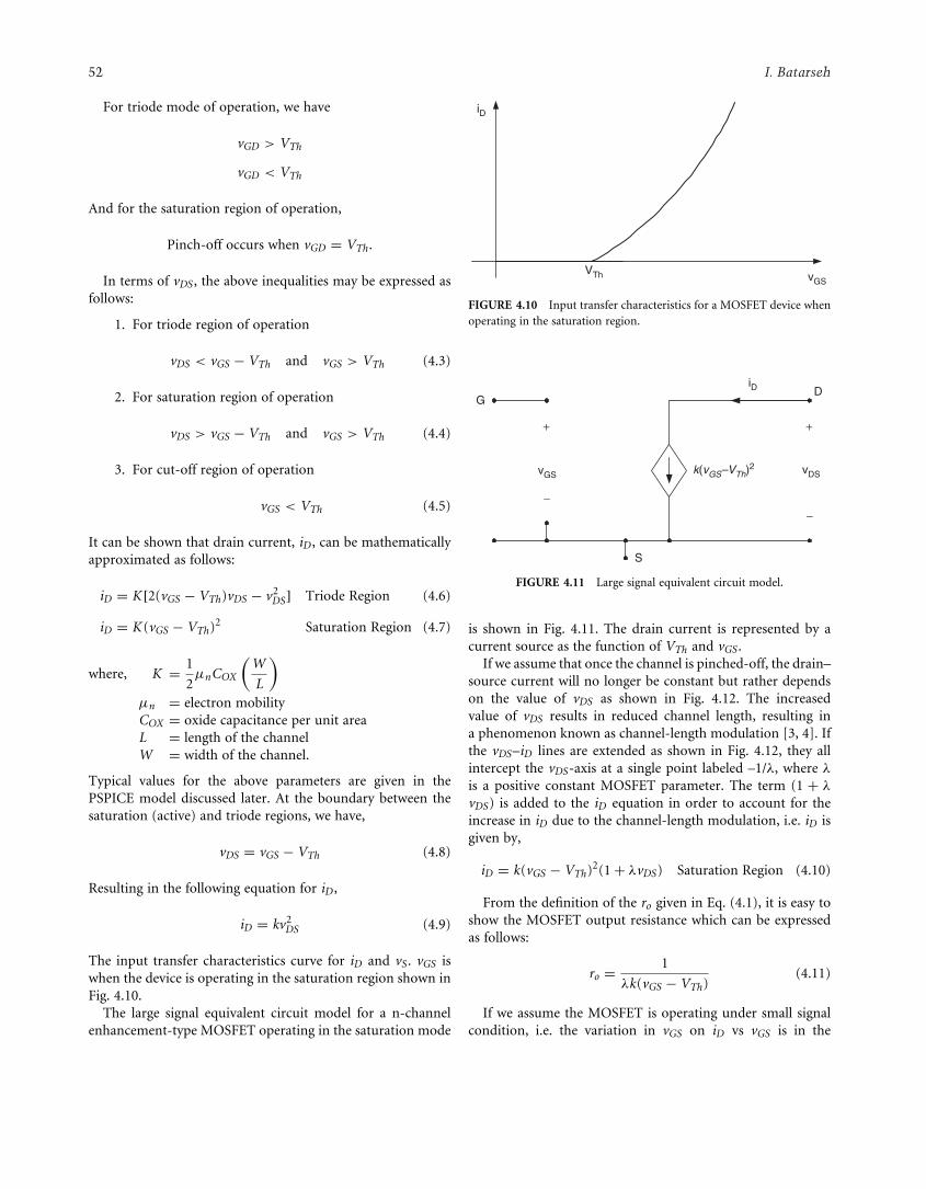
The input transfer characteristics curve for iD and vS . vGS iswhen the device is operating in the saturation region shown inFig. 4.10.The large signal equivalent circuit model for a n-channel
enhancement-type MOSFET operating in the saturation mode
VTh vGS
iD
FIGURE 4.10 Input transfer characteristics for a MOSFET device whenoperating in the saturation region.
iD D
vDS
G
vGS
−
+
−
+
k(vGS–VTh)2
S
FIGURE 4.11 Large signal equivalent circuit model.
is shown in Fig. 4.11. The drain current is represented by acurrent source as the function of VTh and vGS .If we assume that once the channel is pinched-off, the drain–
source current will no longer be constant but rather dependson the value of vDS as shown in Fig. 4.12. The increasedvalue of vDS results in reduced channel length, resulting ina phenomenon known as channel-length modulation [3, 4]. Ifthe vDS–iD lines are extended as shown in Fig. 4.12, they allintercept the vDS-axis at a single point labeled –1/λ, where λis a positive constant MOSFET parameter. The term (1 + λ
vDS) is added to the iD equation in order to account for theincrease in iD due to the channel-length modulation, i.e. iD isgiven by,
iD = k(vGS − VTh)2(1+ λvDS) Saturation Region (4.10)
From the definition of the ro given in Eq. (4.1), it is easy toshow the MOSFET output resistance which can be expressedas follows:
ro = 1
λk(vGS − VTh)(4.11)
If we assume the MOSFET is operating under small signalcondition, i.e. the variation in vGS on iD vs vGS is in the

4 The Power MOSFET 53
iD
vDS
Increasing
vGS
0− 1/ λ
rO
Slope =1
FIGURE 4.12 MOSFET characteristics curve including output resistance.
neighborhood of the dc operating point Q at iD and vGS asshown in Fig. 4.13. As a result, the iD current source can berepresented by the product of the slope gm and vGS as shownin Fig. 4.14.
4.4.3 MOSFET Switching Characteristics
Since the MOSFET is a majority carrier transport device, it isinherently capable of a high frequency operation [5–8]. Butstill the MOSFET has two limitations:
1. High input gate capacitances.2. Transient/delay due to carrier transport through thedrift region.
As stated earlier the input capacitance consists of two com-ponents: the gate-to-source and gate-to-drain capacitances.The input capacitances can be expressed in terms of the device
VTh VGS
ID
Slope = gm
iD
Q
VGS
FIGURE 4.13 Linearized iD vs vGS curve with operating dc point (Q).
rO
D
gmvgs
G
S
vGS
−
+
FIGURE 4.14 Small-signal equivalent circuit including MOSFET out-put resistance.
junction capacitances by applying Miller theorem to Fig. 4.15a.Using Miller theorem, the total input capacitance, Cin , seenbetween the gate-to-source is given by,
Cin = Cgs + (1+ gmRL)Cgd (4.12)
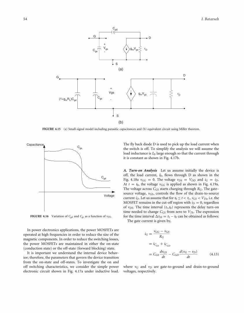
The frequency response of the MOSFET circuit is limited bythe charging and discharging times of Cin . Miller effect isinherent in any feedback transistor circuit with resistive loadthat exhibits a feedback capacitance from the input and output.The objective is to reduce the feedback gate-to-drain resis-tance. The output capacitance between the drain-to-source,Cds , does not affect the turn-on and turn-off MOSFET switch-ing characteristics. Figure 4.16 shows how Cgd and Cgs varyunder increased drain-source, vDs , voltage.
54 I. Batarseh
G
gmVgs
Cgd
D
VgsCgs
+
-rO
S
(1+gmRL)Cgd
rO
S
D
Cgs
G
gmVgsVgs+
-
(a)
(b)
FIGURE 4.15 (a) Small-signal model including parasitic capacitances and (b) equivalent circuit using Miller theorem.
Cgd
CgsCapacitance
Voltage
FIGURE 4.16 Variation of Cgd and Cgs as a function of vDS .
In power electronics applications, the power MOSFETs areoperated at high frequencies in order to reduce the size of themagnetic components. In order to reduce the switching losses,the power MOSFETs are maintained in either the on-state(conduction state) or the off-state (forward blocking) state.It is important we understand the internal device behav-
ior; therefore, the parameters that govern the device transitionfrom the on-state and off-states. To investigate the on andoff switching characteristics, we consider the simple powerelectronic circuit shown in Fig. 4.17a under inductive load.
The fly back diode D is used to pick up the load current whenthe switch is off. To simplify the analysis we will assume theload inductance is L0 large enough so that the current throughit is constant as shown in Fig. 4.17b.
A. Turn-on Analysis Let us assume initially the device isoff, the load current, I0, flows through D as shown in theFig. 4.18a vGG = 0. The voltage vDS = VDD and iG = iD .At t = t0, the voltage vGG is applied as shown in Fig. 4.19a.The voltage across CGS starts charging through RG . The gate–source voltage, vGS , controls the flow of the drain-to-sourcecurrent iD . Let us assume that for t0 ≤ t< t1, vGS <VTh , i.e. theMOSFET remains in the cut-off region with iD = 0, regardlessof vDS . The time interval (t1,t0) represents the delay turn-ontime needed to change CGS from zero to VTh . The expressionfor the time interval �t10 = t1− t0 can be obtained as follows:The gate current is given by,
iG = vGG − vGS
RG
= iCGS+ iCGD
= CGSdvGS
dt− CGD
d(vG − vD)
dt(4.13)
where vG and vD are gate-to-ground and drain-to-groundvoltages, respectively.

4 The Power MOSFET 55
RG
L0 D
CGS
CGD
iG
vGG
+VDD
+-
iD
vGG
RG
IOD
CGS
CGD
iG
+VDD
+-
iD
(a)
(b)
FIGURE 4.17 (a) Simplified equivalent circuit used to study turn-onand turn-off characteristics of the MOSFET and (b) simplified equivalentcircuit.
Since we have vG = vGS , vD = +VDD , then iG is given by
iG = CGSdvGS
dt+ CGD
dvGS
dt= (CGS + CGD)
dvGS
dt(4.14)
From Eqs. (4.13) and (4.14), we obtain,
VGG − vGS
RG= (CGS + CGD)
dvGS
dt(4.15)
Solving Eq. (4.15) for vGS(t) for t> t0 with vGS(t0)= 0,we obtain,
vGS(t ) = VGG(1− e(t−t0)/τ) (4.16)
IO
+-
D
G
SvGG=0
VDD
RG
iG
D
iCGS
iCGD
vDS
-
+
vGS
-
+
CGD
CGS
IO
+-
D
G
S
CGD
CGSvGG=VGG
VDD
RG
iG
D
iCGS
iCGD
vDS
-
+
vGS
-
+
(a)
(b)
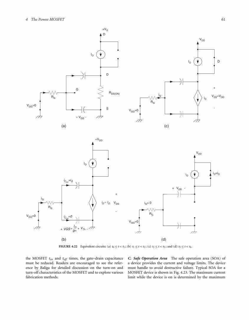
FIGURE 4.18 Equivalent modes: (a) MOSFET is in the off-state fort< t0, vGG = 0, vDS =VDD , iG = 0, iD = 0; (b) MOSFET in the off-statewith vGS <VTh for t1 > t > t0; (c) vGS > VTh , iD < I0 for t1< t< t2;(d) vGS > VTh , iD = I0 for t2 ≤ t< t3; and (e) VGS > VTh , iD = Io fort3 ≤ t < t4.
56 I. Batarseh
+-vGG
VDD
RG
IO
iDS = f(VDS,vGS) = gm(vDS – VTh)
iD
CGD
CGS
iG
D
+-VGG
+VDD
RG
IO
iD ≈ IO
CGS
CGD
D
iG G
iGD
iGS=0
CDS
(c)
(d)
+-
IO
D
G
S
rON
VGG
+VD
RG
iG=0
VDS = IorDS (ON)
iD
(e)
FIGURE 4.18 continued
where,
τ = RG(CGS + CGD)
The gate current, iG , is given by,
iG = vGG − vGS
RG
iG = VGG
RGe−(t−t0)/τ
(4.17)
As long as vGS <VTh , iD remains zero. At t= t1, vGS reachesVTh causing the MOSFET to start conducting. Waveforms foriG and vGS are shown in Fig. 4.19. The time interval (t1−t0) isgiven by,
�t10 = t1 − t0 = −τ ln(1− VTh
VGG
)
�t10 represents the first delay interval in the turn-on process.For t> t1 with vGS >VTh , the device starts conducting and
its drain current is given as a function of vGS and VTh . Infact iD starts flowing exponentially from zero as shown inFig. 4.19d. Assume the input transfer characteristics for theMOSFET is limited as shown in Fig. 4.20 with slope of gm thatis given by
gm = (∂iD/∂vGS)
ID= 2
√IDSSIDVTh
(4.18)
The drain current can be approximately given as fol-lows:
iD(t ) = gm(vGS − VTh) (4.19)
As long as iD(t)< I0, D remains on and vDS =VDD as shownin Fig. 4.18c.The equation for vGS(t) remains the same as in Eq. (4.16),
hence, Eq. (4.19) results in iD(t) given by,
iD(t ) = gm(VGG − VTh)− gmVGGe−(t−t1)/τ (4.20)
The gate current continues to decrease exponentially asshown in Fig. 4.19c. At t = t2, iD reaches its maximum valueof I0, turning D off. The time interval �t21 = (t2 − t1) isobtained from Eq. (4.20) by setting iD(t2)= I0.
�t21 = τlngmVGG
gm(VGG − VTh)− I0(4.21)
For t> t2, the diode turns off and iD ≈ I0 as shown inFig. 4.18d. Since the drain current is nearly a constant, then
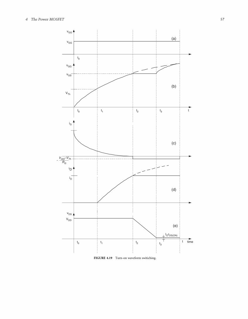
4 The Power MOSFET 57
vGG
vGG
t0
vGG
vGS
t0
VTh
t2t1
iG
RG
iD
vDS
VDD
t3
t
t
(a)
(b)
(c)
(d)
(e)
t0 t2t1 t3
iO
time
IOrDS(ON)
VGG–VTh–
FIGURE 4.19 Turn-on waveform switiching.

58 I. Batarseh
VThVGS vGS
ID
iD
Slope=gm
ideal
dc operatingpoint
Q
FIGURE 4.20 Input transfer characteristics.
the gate–source voltage is also constant according to the inputtransfer characteristic of the MOSFET, i.e.
iD = gm(vGS − VTh) ≈ I0 (4.22)
Hence,
vGS(t ) = I0gm
+ VTh (4.23)
At t = t2, iG(t) is given by,
iG(t2) = VGG − vGS(t2)
VTh= VGG − (I0/gm)− VTh
VTh(4.24)
Since the time constant τ is very small, it is safe to assumevGS(t2) reaches its maximum, i.e.
vGS(t2) ≈ VGG
and
iG(t2) ≈ 0
For t2 ≤ t< t3, the diode turns off the load current I0 (draincurrent iD), which starts discharging the drain-to-sourcecapacitance.Since vGS is constant, the entire gate current flows through
CGD , resulting in the following relation,
iG(t ) = iCGD
= CGDd(vG − vD)
dt
Since vG is constant and vs = 0, we have
iG(t ) = −CGDdvDS
dt
= −VGG − VTh
RG
Solving for vDS(t) for t> t2, with vDS(t2) =VDD , we obtain
vDS(t ) = −VGG − VTh
RGCGD(t − t2)+ VDD For t > t2 (4.25)
This is a linear discharge of CGD as shown in Fig. 4.19eThe time interval�t32 = (t3−t2) is determined by assuming
that at t = t3, the drain-to-source voltage reaches its minimumvalue determined by its on resistance, vDS(ON ) i.e. vDS(ON ) isgiven by,
vDS(ON ) ≈ I0rDS(ON )
= constant
For t> t3, the gate current continues to charge CGD and sincevDS is constant, vGS starts charging at the same rate as ininterval t0 ≤ t< t1, i.e.
vGS(t ) = VGG(1− e−(t−t3)/τ)
The gate voltage keeps increasing exponentially until t = t3when it reaches VGG , at which iG = 0 and the device fullyturns on as shown in Fig. 4.18e.The equivalent circuit model when the MOSFET is com-
pletely turned on is for t> t1. At this time, the capacitorsCGS and CGD are charged with VGG and (I0rds(ON )−VGG ),respectively.The time interval �t32 = (t3 − t2) is obtained by evaluating
vDS at t = t3 as follows
vDS(t3) = −VGG − VTh
RGCGD(t3 − t2)+ VDD (4.26)
= I0rDS(ON )
Hence, �t32 = (t3−t2) is given by,
�t32 = t3 − t2 = RGCGD
(VDD − IDrDS(ON )
)VGG − VTh
(4.27)
The total delay in turning on the MOSFET is given by
tON = �t10 +�t21 +�t32 (4.28)
Notice the MOSFET sustains high voltage and currentsimultaneously during intervals �t21 and �t32. This resultsin large power dissipation during turn on, that contributes tothe overall switching losses. The smaller the RG , the smaller�t21 and �t32 become.

4 The Power MOSFET 59
B. Turn-off Characteristics To study the turn-off charac-teristic of the MOSFET, we will consider Fig. 4.17b again byassuming the MOSFET is ON and in steady state at t> t0 withthe equivalent circuit of Fig. 4.18e. Therefore, at t= t0 we havethe following initial conditions.
vDS(t0) = IDrDS(ON )
vGS(t0) = VGG
iDS(t0) = I0
iG(t0) = 0
vCGS (t0) = VGG
vCGD (t0) = VGG − I0rDS(ON )
(4.29)
At t = t0, the gate voltage, vGG(t) is reduced to zero asshown in Fig. 4.21a. The equivalent circuit at t> t0 is shownin Fig. 4.22a.If we assume the drain-to-source voltage remains constant,
CGS and CGD are discharging through RG as governed by thefollowing relations
iG = −vGRG
= iCGS + iCGD
= CGSdvGS
dt+ CGD
dvGD
dt
Since vDS is assumed constant, then iG becomes,
iG = −vGS
RG
= (CGS + CGD)dvGS
dt(4.30)
Hence, evaluating for vGS for t≥ t0, we obtain
vGS(t ) = vGS(t0)e−(t−t0)/τ (4.31)
where,vGS(t0) = vGG
τ = (CGS + CGD)RG
As vGS continues to decrease exponentially, drawing currentfrom CGD will reach a constant value at which drain current isfixed, i.e. ID = I0. From the input transfer characteristics, thevalue of vGS when ID = I0 is given by,
vGS = I0gm
+ VTh (4.32)
The time interval �t10 = t1 − t0 can be obtained easily bysetting Eq. (4.31) to (4.32) at t = t1.
The gate current during the t2 ≤ t< t1 is given by
iG = −VGG
RG− e−(t−t0)/τ (4.33)
Since, for t2−t1, the gate-to-source voltage is constant andequals vGS(t1) = (I0/gm) + VTh as shown in Fig. 4.21b, thenthe entire gate current is being drawn from CGD , hence,
iG = CGDdvGD
dt= CGD
d(vGS − vDS)
dt= −CGD
dvDS
dt
= vGS(t1)
RG= 1
RG
(I0gm
+ VTh
)
Assuming iG constant at its initial value at t = t1, i.e.
iG = vGS(t1)
RG= 1
RG
(I0gm
+ VTh
)
Integrating both sides of the above equation from t1 to t withvDS(t1)= − vDS(ON ), we obtain,
vDS(t ) = vDS(ON ) + 1
RGCGD
(I0gm
+ VTh
)(t − t1) (4.34)
hence, vDS charges linearly until it reaches VDD .At t = t2, the drain-to-source voltage becomes equal to
VDD , forcing D to turn on as shown in Fig. 4.22c.The drain-to-source current is obtained from the transfer
characteristics and given by
iDS(t ) = gm(vGS − VTh)
where vGS(t) is obtained from the following equation
iG = −vGS
RG= (CGS + CGD)
dvGS
dt(4.35)
Integrate both sides from t2 to t with vGS(t2) = (I0/gm)+VTh ,we obtain the following expression for vGS(t),
vGS(t ) =(
I0gm
+ VTh
)e−(t−t2)/τ (4.36)
Hence the gate current and drain-to-source current aregiven by,
iG(t ) = −1RG
(I0gm
+ VTh
)e−(t−t2)/τ (4.37)
iDS(t ) = gmVTh(e−(t−t2)/τ − 1)+ I0e
−(t−t2)/τ (4.38)
The time interval between t2 ≤ t< t3 is obtained byevaluating vGS(t3)=VTh , at which the drain current becomes

60 I. Batarseh
vGG
t0
VTh
VGG
vGS
iG
0
VDD
t0
VDS(ON)
vDS
iD
t4t3t2t1
IO
(b)
(c)
(d)
(e)
(a)
t
t
t
t
t
FIGURE 4.21 Turn-off switching waveforms.
approximately zero and the MOSFET turn off hence,
vGS(t3) = VTh
=(
I0gm
+ VTh
)e−(t3−t2)/τ
Solving for �t32 = t3 − t2 we obtain,
�t32 = t3 − t2 = τ ln
(1+ I0
VThgm
)(4.39)
For t> t3, the gate voltage continues to decrease exponen-tially to zero, at which the gate current becomes zero and CGD
charges to −VDD . Between t3 and t4, ID discharges to zero asshown in the equivalent circuit Fig. 4.22d.The total turn-off time for the MOSFET is given by,
toff = �t10 +�t21 +�t32 +�t43
≈ �t21 +�t32 (4.40)
The time intervals that most effect the power dissipa-tion are �t21 and �t32. It is clear that in order to reduce
4 The Power MOSFET 61
VDD
RG
IO
iG
-
+
iD
D
VGG=0
VDS=VDD
(c)
VGG=0
VDD
RG
iO
VDD -+
iG= 0
iD=iO
(d)
VGG=0
+VD
D
RG
IO
RDS(ON)
G
S
D
+ VGS −
(a)
VGG=0
+VDD
RG
IO
iG
-+
iD ≈ IO VDS
-
+
iCGS=0
iCGD=iG
VThgm
IOVGS +=
(b)
FIGURE 4.22 Equivalent circuits: (a) t0 ≤ t< t1 ; (b) t1 ≤ t< t2 ; (c) t2 ≤ t< t3 ; and (d) t3 ≤ t< t4.
the MOSFET ton and toff times, the gate–drain capacitancemust be reduced. Readers are encouraged to see the refer-ence by Baliga for detailed discussion on the turn-on andturn-off characteristics of the MOSFET and to explore variousfabrication methods.
C. Safe Operation Area The safe operation area (SOA) ofa device provides the current and voltage limits. The devicemust handle to avoid destructive failure. Typical SOA for aMOSFET device is shown in Fig. 4.23. The maximum currentlimit while the device is on is determined by the maximum
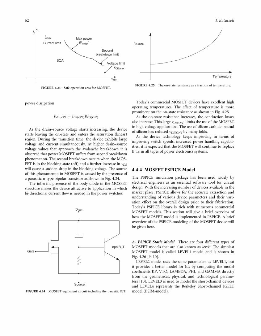
62 I. Batarseh
iD
vDS
SOA
Current limit
Icmax Max power(Pcmax)
Secondbreakdown limit
Voltage limitvCE,max
FIGURE 4.23 Safe operation area for MOSFET.
power dissipation
Pdiss,ON = IDS(ON )RDS(ON )
As the drain–source voltage starts increasing, the devicestarts leaving the on-state and enters the saturation (linear)region. During the transition time, the device exhibits largevoltage and current simultaneously. At higher drain–sourcevoltage values that approach the avalanche breakdown it isobserved that power MOSFET suffers from second breakdownphenomenon. The second breakdown occurs when the MOS-FET is in the blocking state (off) and a further increase in vDS
will cause a sudden drop in the blocking voltage. The sourceof this phenomenon in MOSFET is caused by the presence ofa parasitic n-type bipolar transistor as shown in Fig. 4.24.The inherent presence of the body diode in the MOSFET
structure makes the device attractive to application in whichbi-directional current flow is needed in the power switches.
Drain
Gate
Source
npn BJT
FIGURE 4.24 MOSFET equivalent circuit including the parasitic BJT.
rDS(ON)
Temperature
FIGURE 4.25 The on-state resistance as a fraction of temperature.
Today’s commercial MOSFET devices have excellent highoperating temperatures. The effect of temperature is moreprominent on the on-state resistance as shown in Fig. 4.25.As the on-state resistance increases, the conduction losses
also increase. This large vDS(ON ) limits the use of the MOSFETin high voltage applications. The use of silicon carbide insteadof silicon has reduced vDS(ON ) by many folds.As the device technology keeps improving in terms of
improving switch speeds, increased power handling capabil-ities, it is expected that the MOSFET will continue to replaceBJTs in all types of power electronics systems.
4.4.4 MOSFET PSPICE Model
The PSPICE simulation package has been used widely byelectrical engineers as an essential software tool for circuitdesign. With the increasing number of devices available in themarket place, PSPICE allows for the accurate extraction andunderstanding of various device parameters and their vari-ation effect on the overall design prior to their fabrication.Today’s PSPICE library is rich with numerous commercialMOSFET models. This section will give a brief overview ofhow the MOSFET model is implemented in PSPICE. A briefoverview of the PSPICE modeling of the MOSFET device willbe given here.
A. PSPICE Static Model There are four different types ofMOSFET models that are also known as levels. The simplestMOSFET model is called LEVEL1 model and is shown inFig. 4.26 [9, 10].LEVEL2 model uses the same parameters as LEVEL1, but
it provides a better model for Ids by computing the modelcoefficients KP, VTO, LAMBDA, PHI, and GAMMA directlyfrom the geometrical, physical, and technological parame-ters [10]. LEVEL3 is used to model the short-channel devicesand LEVEL4 represents the Berkeley Short-channel IGFETmodel (BSIM-model).

4 The Power MOSFET 63
-
Gate
Source
VDS
VGD
+
-
+
Drain
VGS
Bulk(substrate)iDS
VBD
VBS-
+
-
RG
iG
rD
RS
iBD
iBS
iB
IS
iD
+
FIGURE 4.26 PSPICE LEVEL1 MOSFET static model.
The triode region, vGS >VTh and vDS < vGS and vDS < vGS –VTh the drain current is given by,
iD = KP
2
W
L − 2Xjl
(vGS − VTh − vDS
2
)vDS(1+ λvDS)
(4.41)
In the saturation (linear) region, where vGS >VTh andvDS > vGS − VTh , the drain current is given by
ID = KP
2
W
L − 2Xjl(VGS − VTh)
2(1+ λVDS) (4.42)
where KP is the transconductance and Xjl is the lateraldiffusion.The threshold voltage, VTh , is given by,
VTh = VT0 + ∂ (√2φp − VBS −√2φp)
(4.43)
where,
VT0 = Zero-bias threshold voltage.δ = Body-effect parameter.φp = Surface inversion potential.
Typically, Xij � L and λ ≈ 0.The term (1+ λVDS) is included in the model as empiri-
cal connection to model the effect of the output conductancewhen the MOSFET is operating in triode region. λ is knownas the channel-length modulation parameter.
When the bulk and source terminals are connected together,i.e. VBS = 0, the device threshold voltage equals the zero-biasthreshold voltage, i.e.
VTh = VT0
VT0 is positive for the n-channel enhancement-mode devicesand negative for the n-channel depletion-mode devices.The parameters KP , VT0, δ, φ are electrical parameters that
can be either specified directly in the MODEL statement underthe Pspice keywords KP, VTO, GAMMA, and PHI, respec-tively, as shown in Table 4.1. They also can be calculated whenthe geometrical and physical parameters are known. The two-substrate currents that flow from the bulk to the source, IBS
and from the bulk to the drain, IBD are simply diode currents,which are given by,
IBS = ISS(e−(VBS /VT ) − 1
)(4.44)
IBD = IDS
(e−(VBD /VT ) − 1
)(4.45)
where ISS and IDS are the substrate source and substrate drainsaturation currents. These currents are considered equal andgiven as IS in the MODEL statement with a default value of10−14 A. Where the equation symbols and their correspondingPSPICE parameter names are shown in Table 4.1.In PSPICE, a MOSFET device is described by two
statements: the first statement start with the letter M and the

64 I. Batarseh
TABLE 4.1 PSPICE MOSFET parameters
Symbol Name Description Default Units
(a) Device dc and parasitic parameters
Level LEVEL Model type (1, 2, 3, or 4) 1 –VTO VTO Zero-bias threshold voltage 0 V
λ LAMDA Channel-length modulation 1,2∗
0 v−1γ GAMMA Body-effect (bulk) threshold parameter 0 v−1/2�ρ PHI Surface inversion potential 0.6 Vη ETA Static feedback3 0 –κ KAPPA Saturation field factor3 0.2 –μ0 UO Surface mobility 600 cm2/V·sIs IS Bulk saturation current 10−14 AJs JS Bulk saturation current/area 0 A/m2
JSSW JSSW Bulk saturation current/length 0 A/mN N Bulk emission coefficient n 1 –PB PB Bulk junction voltage 0.8 VPBSW PBSW Bulk sidewall diffusion voltage PB VRD RD Drain resistance 0 �
RS RS Source resistance 0 �
RG RG Gate resistance 0 �
RB RB Bulk resistance 0 �
Rds RDS Drain–source shunt resistance α �
Rsh RSH Drain and source diffusion sheet resistance 0 �/m2
(b) Device process and dimensional parameters
Nsub NSUB Substrate doping density None cm−3W W Channel width DEFW mL L Channel length DEFL mWD WD Lateral Diffusion width 0 mXjl LD Lateral Diffusion length 0 m
Kp KP Transconductance coefficient 20μ A/v2
tOX TOX Oxide thickness 10−7 mNSS NSS Surface-state density None cm−2NFS NFS Fast surface-state density 0 cm−2NA NSUB Substrate doping 0 cm−3TPG TPG Gate material 1 –
+1 Opposite of substrate – –−1 Same as substrate – –0 Aluminum – –
Xj XJ Metallurgical junction depth2,3 0 mμ0 UO Surface mobility 600 cm2/V·sUc UCRIT Mobility degradation critical field2 104 V/cmUe UEXP Mobility degradation exponent2 0 –Ut VMAX Maximum drift velocity of carriers2 0 m/sNeff NEFF Channel charge coefficient2 1 –
δ DELTA Width effect on threshold2,3 0 –θ THETA Mobility modulation3 0 –(c) Device capacitance parameters
CBD CBD Bulk-drain zero-bias capacitance 0 FCBS CBS Bulk-source zero-bias capacitance 0 FCj CJ Bulk zero-bias bottom capacitance 0 F/m2
Cjsw CJSW Bulk zero-bias perimeter capacitance/length 0 F/mMj MJ Bulk bottom grading coefficient 0.5 –Mjsw MJSW Bulk sidewall grading coefficient 0.33 –FC FC Bulk forward-bias capacitance coefficient 0.5 –CGSO CGSO Gate–source overlap capacitance/channel width 0 F/mCGDO CGDO Gate–drain overlap capacitance/channel width 0 F/mCGBO CGBO Gate-bulk overlap capacitance/channel length 0 F/mXQC XQC Fraction of channel charge that associates with drain1,2 0 –KF KF Flicker noise coefficient 0 –αF AF Flicker noise exponent 0 –
∗These numbers indicate that this parameter is available in this level number, otherwise it is available in all levels.
4 The Power MOSFET 65
second statement starts with .Model that defines the modelused in the first statement. The following syntax is used:
M<device_name><Drain_node_number>
<Gate_node_number>
<Source_node_number><Substrate_node number>
<Model_name>
* [<param_1>=<value_1><param_2>=<value_2> . . ..]
.MODEL <Model_name><type_name>
[(<param_1>=<value_1><param_2>=<value_2> . . ...]
where the starting letter “M” in M<device_name> statementindicates that the device is a MOSFET and <device_name>isa user specified label for the given device, the<Model_name>is one of the hundreds of device models specified in the PSPICElibrary,<Model_name> the same name specified in the devicename statement, <type_name> is either NMOS of PMOS,depending on whether the device is n-channel or p-channelMOS, respectively, that follows by optional list of parametertypes and their values. The length L and the width W andother parameters can be specified in the M<device_name>,in the .MODEL or .OPTION statements. User may select notto include any value, and PSPICE will use the specified defaultvalues in the model. For normal operation (physical construc-tion of the MOS devices), the source and bulk substrate nodesmust be connected together. In all the PSPICE library files, adefault parameter values for L, W, AS, AD, PS, PD, NRD, andNDS are included, hence, user should not specify such valuesin the device “M” statement or in the OPTION statement.The power MOSFET device PSPICE models include rela-
tively complete static and dynamic device characteristics givenin the manufacturing data sheet. In general, the followingeffects are specified in a given PSPICE model: dc transfercurves, on-resistance, switching delays, and gate drive charac-teristics and reverse-mode “body-diode” operation. The devicecharacteristics that are not included in the model are noise,latch-ups, maximum voltage, and power ratings. Please seeOrCAD Library Files.
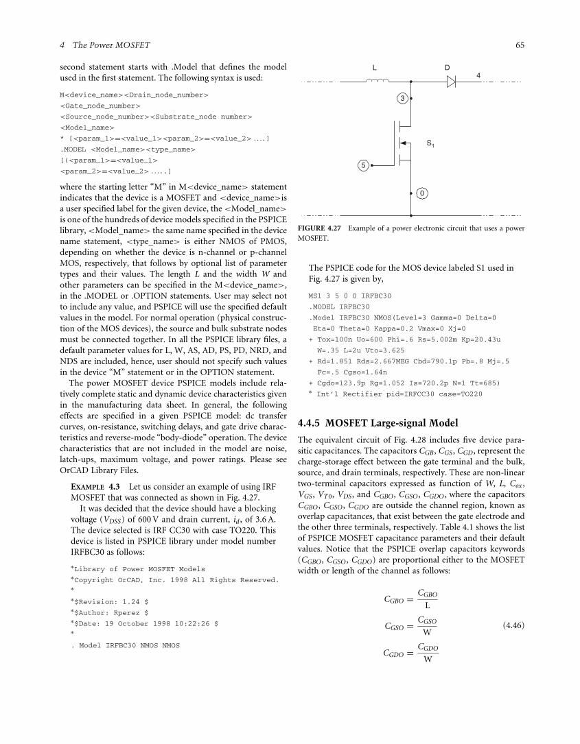
EXAMPLE 4.3 Let us consider an example of using IRFMOSFET that was connected as shown in Fig. 4.27.It was decided that the device should have a blocking
voltage (VDSS) of 600V and drain current, id , of 3.6 A.The device selected is IRF CC30 with case TO220. Thisdevice is listed in PSPICE library under model numberIRFBC30 as follows:
∗Library of Power MOSFET Models∗Copyright OrCAD, Inc. 1998 All Rights Reserved.∗∗$Revision: 1.24 $∗$Author: Rperez $∗$Date: 19 October 1998 10:22:26 $∗. Model IRFBC30 NMOS NMOS
S1
4DL
5
0
3
FIGURE 4.27 Example of a power electronic circuit that uses a powerMOSFET.
The PSPICE code for the MOS device labeled S1 used inFig. 4.27 is given by,
MS1 3 5 0 0 IRFBC30
.MODEL IRFBC30
.Model IRFBC30 NMOS(Level=3 Gamma=0 Delta=0
Eta=0 Theta=0 Kappa=0.2 Vmax=0 Xj=0
+ Tox=100n Uo=600 Phi=.6 Rs=5.002m Kp=20.43u
W=.35 L=2u Vto=3.625
+ Rd=1.851 Rds=2.667MEG Cbd=790.1p Pb=.8 Mj=.5
Fc=.5 Cgso=1.64n
+ Cgdo=123.9p Rg=1.052 Is=720.2p N=1 Tt=685)∗ Int’l Rectifier pid=IRFCC30 case=TO220
4.4.5 MOSFET Large-signal Model
The equivalent circuit of Fig. 4.28 includes five device para-sitic capacitances. The capacitors CGB , CGS , CGD , represent thecharge-storage effect between the gate terminal and the bulk,source, and drain terminals, respectively. These are non-lineartwo-terminal capacitors expressed as function of W, L, Cox ,VGS , VT0, VDS , and CGBO , CGSO , CGDO , where the capacitorsCGBO , CGSO , CGDO are outside the channel region, known asoverlap capacitances, that exist between the gate electrode andthe other three terminals, respectively. Table 4.1 shows the listof PSPICE MOSFET capacitance parameters and their defaultvalues. Notice that the PSPICE overlap capacitors keywords(CGBO , CGSO , CGDO) are proportional either to the MOSFETwidth or length of the channel as follows:
CGBO = CGBO
L
CGSO = CGSO
W
CGDO = CGDO
W
(4.46)

66 I. Batarseh
+
VDS
VGD +
-+
-
VGS
Bulk(Substrate)iDS
VBD
VBS- -
+
+
rSCBS
iB
iS
iBD
iBSCgs
Cgb
CBD
Drain
iD
rD
Cgd
Gate
iG
Source
FIGURE 4.28 Large-signal model for the n-channel MOSFET.
In the triode region, vGS > vDS−VTh , the terminal capacitorsare given by,
CGS = LWCOX
[1−(
vGS − vDS − VTh
2(vGS − VTh)− VDS
)2]+ CGSO
CGD = LWCOX
[1−(
vGS − VTh
2(vGS − VTh)− vDS
)2]+ CGDO
CGB = CGBOL (4.47)
In the saturation (linear) region, we have
CGS = 2
3LWCOX + CGSO
CGB = CGB0L (4.48)
CGD = CGD0
where COX is the per-unit-area oxide capacitance given by,
COX = KOXE0TOX
KOX = Oxide’s relative dielectric constant.E0 = Free space dielectric constant equals
8.854×10⁻¹² F/m.TOX = Oxide’s thickness layer given as TOX in Table 4.1.
Finally, the diffusion and junction region capacitancesbetween the bulk-to-channel (drain and source) are modeled
gmVgs'
+gmbVbs'
-+
d
VGS'
VBS' +
iD
iG
RD
RS
CBD
CBS
ib
iS
gBD
gBS
Cgd
Cgs
Cgb
d'
S'
go
-
FIGURE 4.29 Small-signal equivalent circuit model for MOSFET.
by CBD and CBS across the two diodes. Because for almost allpower MOSFETs, the bulk and source terminals are connectedtogether and at zero potential, diodes DBD and DBS don’thave forward bias, resulting in very small conductance val-ues, i.e. small diffusion capacitances. The small-signal modelfor MOSFET devices is given in Fig. 4.29.
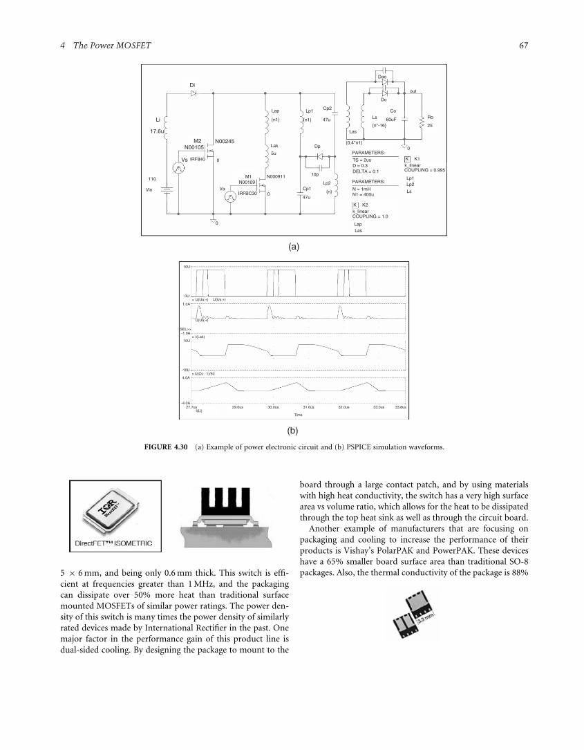
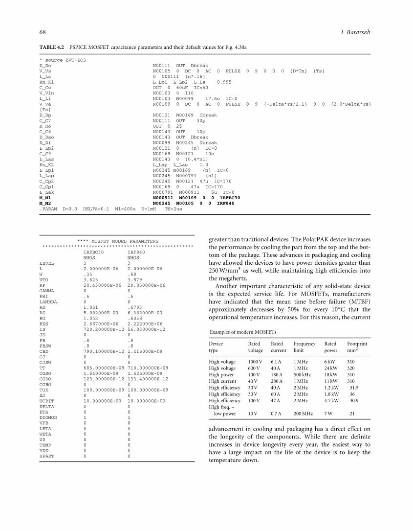
EXAMPLE 4.4 Figure 4.30a shows an example of a soft-switching power factor connection circuit that has twoMOSFETs. Its PSPICE simulation waveforms are shownin Fig. 4.30b.
Table 4.2 shows the PSPICE code for Fig. 4.30a.
4.4.6 Current MOSFET Performance
The current focus of MOSFET technology development ismuch more broad than power handling capacity and switchingspeed; the size, packaging, and cooling of modern MOSFETtechnology is a major focus. Of course, the development ofhigher power and efficiency is still paramount, but as modernelectronics have become increasingly smaller, the packagingand cooling of power circuits has become more important. Ithas been indicated by manufacturers that many of their mod-ern MOSFETs are not limited by their semiconductor, but bythe packaging. If the MOSFET cannot properly disperse heat,the device will become overheated, which will lead to failure.An example of modern MOSFET technology is the
DirectFET surface mounted MOSFET manufactured byInternational Rectifier. Part number IRF6662, for example,can handle 47 A at 100V, while consuming a board space of
4 The Power MOSFET 67
(a)
(b)
Di
Li
17.6u
M2N00105
N00245
Vs IRF840 0
110
Vin Va
0
10U
10U
-10U
4.0AU(Cs : 1)/50
I(Lak)
U(Ua;+)
U(Ua;+) U(Us;+)
-4.0A27.7us 29.0us
I(Li)30.0us 32.0us 33.0us 33.8us31.0us
Time
0U
1.0A
SEL>>-1.0A
M1N00109
N000911
IRFBC30 0
5u
Lak
{n1} {n1}
{n}
Lap Lp1 Cp2
47u
Dp
Las
LsCo
60uF{n*-16}
PARAMETERS:
PARAMETERS:
TS = 2usD = 0.3DELTA = 0.1
N = 1mHN1 = 400u
K K2
K K1
k_linearCOUPLING = 1.0
k_linearCOUPLING = 0.995
Lap
Ls
Lp2Lp1
Las
{0.4*n1}
Do
out
Dao
Ro
25
0
10p
Cp1
47u
Lp2
FIGURE 4.30 (a) Example of power electronic circuit and (b) PSPICE simulation waveforms.
5 × 6mm, and being only 0.6mm thick. This switch is effi-cient at frequencies greater than 1MHz, and the packagingcan dissipate over 50% more heat than traditional surfacemounted MOSFETs of similar power ratings. The power den-sity of this switch is many times the power density of similarlyrated devices made by International Rectifier in the past. Onemajor factor in the performance gain of this product line isdual-sided cooling. By designing the package to mount to the
board through a large contact patch, and by using materialswith high heat conductivity, the switch has a very high surfacearea vs volume ratio, which allows for the heat to be dissipatedthrough the top heat sink as well as through the circuit board.Another example of manufacturers that are focusing on
packaging and cooling to increase the performance of theirproducts is Vishay’s PolarPAK and PowerPAK. These deviceshave a 65% smaller board surface area than traditional SO-8packages. Also, the thermal conductivity of the package is 88%
68 I. Batarseh
TABLE 4.2 PSPICE MOSFET capacitance parameters and their default values for Fig. 4.30a
* source ZVT-ZCSD_Do N00111 OUT DbreakV_Vs N00105 0 DC 0 AC 0 PULSE 0 9 0 0 0 {D*Ts} {Ts}L_Ls 0 N00111 {n*.16}Kn_K1 L_Lp1 L_Lp2 L_Ls 0.995C_Co OUT 0 60uF IC=50V_Vin N00103 0 110L_Li N00103 N00099 17.6u IC=0V_Va N00109 0 DC 0 AC 0 PULSE 0 9 {-Delta*Ts/1.1} 0 0 {2.0*Delta*Ts}{Ts}D_Dp N00121 N00169 DbreakC_C7 N00111 OUT 30pR_Ro OUT 0 25C_C8 N00143 OUT 10pD_Dao N00143 OUT DbreakD_Di N00099 N00245 DbreakL_Lp2 N00121 0 {n} IC=0C_C9 N00169 N00121 10pL_Las N00143 0 {0.4*n1}Kn_K2 L_Lap L_Las 1.0L_Lp1 N00245 N00169 {n} IC=0L_Lap N00245 N000791 {n1}C_Cp2 N00245 N00121 47u IC=170C_Cp1 N00169 0 47u IC=170L_Lak N000791 N000911 5u IC=0M_M1 N000911 N00109 0 0 IRFBC30M_M2 N00245 N00105 0 0 IRF840.PARAM D=0.3 DELTA=0.1 N1=400u N=1mH TS=2us
**** MOSFET MODEL PARAMETERS****************************************************
IRFBC30 IRF840NMOS NMOS
LEVEL 3 3L 2.000000E-06 2.000000E-06W .35 .68VTO 3.625 3.879KP 20.430000E-06 20.850000E-06GAMMA 0 0PHI .6 .6LAMBDA 0 0RD 1.851 .6703RS 5.002000E-03 6.382000E-03RG 1.052 .6038RDS 2.667000E+06 2.222000E+06IS 720.200000E-12 56.030000E-12JS 0 0PB .8 .8PBSW .8 .8CBD 790.100000E-12 1.415000E-09CJ 0 0CJSW 0 0TT 685.000000E-09 710.000000E-09CGSO 1.640000E-09 1.625000E-09CGDO 123.900000E-12 133.400000E-12CGBO 0 0TOX 100.000000E-09 100.000000E-09XJ 0 0UCRIT 10.000000E+03 10.000000E+03DELTA 0 0ETA 0 0DIOMOD 1 1VFB 0 0LETA 0 0WETA 0 0U0 0 0TEMP 0 0VDD 0 0XPART 0 0
greater than traditional devices. The PolarPAK device increasesthe performance by cooling the part from the top and the bot-tom of the package. These advances in packaging and coolinghave allowed the devices to have power densities greater than250W/mm3 as well, while maintaining high efficiencies intothe megahertz.Another important characteristic of any solid-state device
is the expected service life. For MOSFETs, manufacturershave indicated that the mean time before failure (MTBF)approximately decreases by 50% for every 10◦C that theoperational temperature increases. For this reason, the current
Examples of modern MOSFETs
Device Rated Rated Frequency Rated Footprinttype voltage current limit power mm2
High voltage 1000V 6.1 A 1MHz 6 kW 310High voltage 600V 40A 1MHz 24 kW 320High power 100V 180A 500 kHz 18 kW 310High current 40V 280A 1MHz 11 kW 310High efficiency 30V 40A 2MHz 1.2 kW 31.5High efficiency 30V 60A 2MHz 1.8 kW 36High efficiency 100V 47A 2MHz 4.7 kW 30.9High freq. –low power 10V 0.7 A 200MHz 7W 21
advancement in cooling and packaging has a direct effect onthe longevity of the components. While there are definiteincreases in device longevity every year, the easiest way tohave a large impact on the life of the device is to keep thetemperature down.

4 The Power MOSFET 69
As development continues, MOSFETs will become smaller,more efficient, higher power density, and higher frequency ofoperation. As such, MOSFETs will continue to expand intoapplications that typically use other forms of power switches.
4.5 Future Trends in Power Devices
As stated earlier, depending on the applications, the powerrange processed in power electronic range is very wide, fromhundreds of milliwatts to hundreds of megawatts, therefore, itis very difficult to find a single switching device type to cover allpower electronic applications. Today’s available power deviceshave tremendous power and frequency rating range as wellas diversity. Their forward current ratings range from a fewamperes to a few kiloamperes, blocking voltage rating rangesfrom a few volts to a few of kilovolts, and switching frequencyranges from a few hundred of hertz to a few megahertz asillustrated in Table 4.3. This table illustrates the relative com-parison between available power semiconductor devices. Weonly give relative comparison because there is no straightfor-ward technique that gives ranking of these devices. As weaccumulate this table, devices are still being developed veryrapidly with higher current, voltage ratings, and switchingfrequency.
TABLE 4.3 Comparison of power semiconductor devices
Device type Yearmadeavailable
Ratedvoltage
Ratedcurrent
Ratedfrequency
Ratedpower
Forwardvoltage
Thyristor (SCR) 1957 6 kV 3.5 kA 500Hz 100’sMW 1.5–2.5 VTriac 1958 1 kV 100A 500Hz 100’s kW 1.5–2VGTO 1962 4.5 kV 3 kA 2 kHz 10’sMW 3–4VBJT(Darlington)
1960s 1.2 kV 800A 10 kHz 1MW 1.5–3V
MOSFET 1976 500V 50A 1MHz 100 kW 3–4VIGBT 1983 1.2 kV 400A 20 kHz 100’skW 3–4VSIT 1.2 kV 300A 100 kHz 10’s kW 10–20VSITH 1.5 kV 300A 10 kHz 10’s kW 2–4VMCT 1988 3 kV 2 kV 20–
100 kHz10’sMW 1–2V
It is expected that improvement in power handling capabil-ities and increasing frequency of operation of power deviceswill continue to drive the research and development insemiconductor technology. From power MOSFET to powerMOS-IGBT and to power MOS-controlled thyristors, powerrating has consistently increased by a factor of 5 from one typeto another. Major research activities will focus on obtainingnew device structure based on MOS-BJT technology integra-tion to rapidly increase power ratings. It is expected that thepower MOS-BJT technology will capture more than 90% ofthe total power transistor market.The continuing development of power semiconductor tech-
nology has resulted in power systems with driver circuit, logicand control, device protection, and switching devices beingdesigned and fabricated on a single-chip. Such power IC mod-ules are called “smart power” devices. For example, some oftoday’s power supplies are available as IC’s for use in low-power applications. No doubt the development of smart powerdevices will continue in the near future, addressing morepower electronic applications.
References
1. B. Jayant Baliga , Power Semiconductor Devices, 1996.2. L. Lorenz, M. Marz, and H. Amann, “Rugged Power MOSFET- Amilestone on the road to a simplified circuit engineering,” SIEMENSapplication notes on S-FET application, 1998.
3. M. Rashid, Microelectronics, Thomson-Engineering, 1998.4. Sedra and Smith,Microelectronic Circuits, 4th Edition, Oxford Series,1996.
5. Ned Mohan, Underland, and Robbins, Power Electronics: Converters,Applications and Design, 2nd Edition. John Wiley. 1995.
6. R. Cobbold, Theory and Applications of Field Effect Transistor, JohnWiley, 1970.
7. R.M. Warner and B.L. Grung,MOSFET: Theory and Design, Oxford,1999.
8. Power FET’s and Their Application, Prentice-Hall, 1982.9. J. G. Gottling, Hands on pspice, Houghton Mifflin Company, 1995.10. G. Massobrio and P. Antognetti, Semiconductor Device Modeling with
PSPICE, McGraw-Hill, 1993.
Copyright © 2022 FDOKUMEN