MOSFET pour la caractérisation des substrats SOI avancés
201
THÈSE Pour obtenir le grade de DOCTEUR DE L’UNIVERSITÉ DE GRENOBLE Spécialité : NANO ELECTRONIQUE ET NANO TECHNOLOGIES (NENT) Arrêté ministériel : 7 août 2006 Présentée par Amer EL HAJJ DIAB Thèse dirigée par Sorin CRISTOLOVEANU et codirigée par Irina IONICA préparée au sein du Laboratoire IMEP-LAHC dans l'École Doctorale EEATS Nouvelles méthodes pseudo- MOSFET pour la caractérisation des substrats SOI avancés (Novel pseudo-MOSFET methods for the characterization of advanced SOI substrates) Thèse soutenue publiquement le 10 Décembre 2012, devant le jury composé de : M. Olivier BONNAUD Professeur, Université de Rennes (Président, Rapporteur) Mme. Daniela MUNTEANU Directrice de Recherche CNRS, IM2NP Marseille (Rapporteur) M. Francisco GÁMIZ PÉREZ Professeur, Université de Granada (Membre) M. Daniel DELPRAT Manager advanced R&D, Soitec (Membre) M. Sorin CRISTOLOVEANU Directeur de Recherche CNRS, IMEP-LAHC (Directeur de thèse) Mme. Irina IONICA Maître de conférences, IMEP-LAHC/INPG (Co-encadrante de thèse)
-
Upload
khangminh22 -
Category
Documents
-
view
1 -
download
0
Transcript of MOSFET pour la caractérisation des substrats SOI avancés

THÈSE
Pour obtenir le grade de
DOCTEUR DE L’UNIVERSITÉ DE GRENOBLE
Spécialité : NANO ELECTRONIQUE ET NANO TECHNOLOGIES (NENT)
Arrêté ministériel : 7 août 2006
Présentée par
Amer EL HAJJ DIAB Thèse dirigée par Sorin CRISTOLOVEANU et codirigée par Irina IONICA préparée au sein du Laboratoire IMEP-LAHC dans l'École Doctorale EEATS
Nouvelles méthodes pseudo-MOSFET pour la caractérisation des substrats SOI avancés (Novel pseudo-MOSFET methods for the characterization of advanced SOI substrates) Thèse soutenue publiquement le 10 Décembre 2012, devant le jury composé de :
M. Olivier BONNAUD Professeur, Université de Rennes (Président, Rapporteur)
Mme. Daniela MUNTEANU Directrice de Recherche CNRS, IM2NP Marseille (Rapporteur)
M. Francisco GÁMIZ PÉREZ Professeur, Université de Granada (Membre)
M. Daniel DELPRAT Manager advanced R&D, Soitec (Membre)
M. Sorin CRISTOLOVEANU Directeur de Recherche CNRS, IMEP-LAHC (Directeur de thèse)
Mme. Irina IONICA Maître de conférences, IMEP-LAHC/INPG (Co-encadrante de thèse)

To my parents, brother, sister
and my secret love

1
TABLE OF CONTENTS
ACKNOWLEDGEMENTS _____________________________________________ 5
LIST OF ACRONYMS ________________________________________________ 7
LIST OF SYMBOLS _________________________________________________ 8
LIST OF CONSTANTS ______________________________________________ 10
GENERAL INTRODUCTION __________________________________________ 11
CHAPTER I: INTRODUCTION TO SOI MATERIALS AND DEVICES ______________ 13
INTRODUCTION _________________________________________________________ 14
1. SOI DEVICES ________________________________________________________ 15
1.1 SOI technology: an answer to scaling and diversity in Moore’s law _________________ 15
1.2 Advantages of the SOI technology _______________________________________ 16
1.3 SOI MOSFETs _____________________________________________________ 19
1.3.1 Partially depleted transistors: PD MOSFETs _____________________________ 20
1.3.2 Fully depleted transistors: FD MOSFETs ________________________________ 22
1.4 Innovative SOI transistors ____________________________________________ 23
1.4.1 Multi-gate transistors _____________________________________________ 23
1.4.1.1 Double-gate (DG) transistors ___________________________________ 24
1.4.1.2 Triple-gate transistors ________________________________________ 24
1.4.1.3 Four-gate (G4-FET) transistors __________________________________ 25
1.4.2 Gate-All-Around (GAA) transistors ____________________________________ 26
1.4.3 Tri-dimensional nanowires (3D NWs) __________________________________ 26
2. SOI MATERIALS ______________________________________________________ 27
2.1 State-of-the-art ____________________________________________________ 27
2.2 Fabrication methods ________________________________________________ 28
2.2.1 SIMOX technology _______________________________________________ 28
2.2.2 SOI by wafer bonding _____________________________________________ 30
2.2.2.1 BESOI ___________________________________________________ 32
2.2.2.2 ELTRAN _________________________________________________ 32
2.2.2.3 Unibond (Smart-CutTM process) _________________________________ 33
2.2.3 Silicon-On-Nothing (SON) _________________________________________ 36
2.2.4 Other SOI technologies ____________________________________________ 36
2.2.4.1 Silicon-On-Sapphire _________________________________________ 36
2.2.4.2 Insulation by Porous Oxidized Silicon ______________________________ 37
2.2.4.3 Zone Melting Recrystallization and Epitaxial Layer Overgrowth ____________ 37
2.3 Novel semiconductor on insulator structures ________________________________ 38
2.3.1 Strained SOI materials ____________________________________________ 38
2.3.2 Hybrid orientation technologies ______________________________________ 39
2.3.3 Germanium-On-Insulator __________________________________________ 40
2.3.4 Other semiconductor, BOX and substrate materials ________________________ 41
2.3.4.1 Conductive film materials ______________________________________ 41
2.3.4.2 BOX and substrate materials ____________________________________ 41
2.4 Defects of SOI material _______________________________________________ 42
CONCLUSION __________________________________________________________ 43
REFERENCES CHAPTER I ___________________________________________________ 44

2
CHAPTER II: ELECTRICAL CHARACTERIZATION OF SOI SUBSTRATES _________ 47
INTRODUCTION _________________________________________________________ 48
1. PSEUDO-MOSFET PRINCIPLE AND OPERATION __________________________________ 49
1.1 Overview ________________________________________________________ 49
1.2 Point-contact -MOSFET technique _____________________________________ 51
1.2.1 Sample preparation ______________________________________________ 52
1.2.2 Typical ID-VG in -MOSFET configuration ______________________________ 53
1.2.3 Substrate effect _________________________________________________ 55
1.2.4 Influence of probe pressure _________________________________________ 56
1.3 Extraction methods of the electrical parameters ______________________________ 57
1.3.1 Threshold voltage and flat-band voltage ________________________________ 59
1.3.2 Carrier mobility _________________________________________________ 60
1.3.3 Mobility reduction factor and series resistance ____________________________ 62
1.3.4 Subthreshold swing and interface traps density ___________________________ 62
1.4 Impact of the top interface in thin SOI films ________________________________ 63
1.5 Revisited -MOSFET models __________________________________________ 67
2. CHARACTERIZATION OF ULTRA AND EXTRA THIN SOI WAFERS _________________________ 69
2.1 Experimental conditions ______________________________________________ 69
2.1.1 Sample preparation ______________________________________________ 70
2.1.2 Measurement system _____________________________________________ 70
2.2 Results obtained on UT/ET SOI _________________________________________ 71
3. LOW-TEMPERATURE -MOSFET MEASUREMENTS _______________________________ 74
3.1 Interest of low-temperature measurements _________________________________ 74
3.2 Experimental set-up _________________________________________________ 74
3.3 Drain current variation with temperature __________________________________ 75
3.4 Extracted parameters ________________________________________________ 77
3.4.1 Carrier mobility _________________________________________________ 78
3.4.2 Subthreshold swing and threshold voltage _______________________________ 82
CONCLUSION __________________________________________________________ 86
REFERENCES CHAPTER II __________________________________________________ 87
CHAPTER III: NOVEL DEVELOPMENTS OF -MOSFET METHOD ______________ 89
INTRODUCTION _________________________________________________________ 90
1. LOW-FREQUENCY NOISE MEASUREMENTS ON BARE SOI WAFERS _______________________ 91
1.1 Why noise measurements? ____________________________________________ 91
1.2 Overview of the electronic noise _________________________________________ 91
1.2.1 Fundamentals of noise ____________________________________________ 92
1.2.2 Different sources of noise in MOS transistor _____________________________ 93
1.2.2.1 White noise _______________________________________________ 93
1.2.2.2 Excess noise _______________________________________________ 94
1.3 LFN on SOI wafers _________________________________________________ 99
1.3.1 LFN in -MOSFET: experimental set-up ________________________________ 99
1.3.2 Experimental results _____________________________________________ 101
1.3.2.1 1/f noise behavior ___________________________________________ 101
1.3.2.2 Noise model: CNF or HMF? ___________________________________ 102
1.3.2.3 Probe pressure impact on LFN _________________________________ 103
1.3.2.4 Dit extraction _____________________________________________ 104
1.3.2.5 Impact of the surface preparation on LFN __________________________ 105

3
1.3.2.6 Feasibility of LFN on extra-thin SOI structures ______________________ 107
1.4 Conclusion of section 1 ______________________________________________ 107
2. SPLIT C-V MEASUREMENT IN -MOSFET CONFIGURATION _________________________ 109
2.1 Split C-V technique and principle _______________________________________ 109
2.2 Interest of split C-V for SOI wafer characterization ____________________________ 110
2.3 Extension of -MOSFET for split C-V measurements __________________________ 111
2.3.1 Method and experiment ___________________________________________ 111
2.3.2 Experimental C-V curves ___________________________________________ 112
2.4 Impact of experimental conditions on C-V measurements _______________________ 113
2.4.1 Probe pressure impact on C-V curves __________________________________ 113
2.4.2 Frequency effects ________________________________________________ 114
2.5 Extraction of μeff by split C-V technique____________________________________ 118
2.5.1 Adapted methodology to extract μeff ___________________________________ 118
2.5.2 Applications of μeff extraction for advanced SOI structures ___________________ 120
2.6 Conclusion of section 2 ______________________________________________ 123
CONCLUSION _________________________________________________________ 124
REFERENCES CHAPTER III __________________________________________________125
CHAPTER IV: INNOVATIVE APPLICATIONS OF PSEUDO-MOSFET ____________ 127
INTRODUCTION ________________________________________________________ 128
1. CHARACTERIZATION OF HEAVILY DOPED SOI WAFERS _____________________________ 129
1.1 From undoped to doped SOI __________________________________________ 129
1.2 -MOSFET characterizations _________________________________________ 129
1.2.1 Y-function ____________________________________________________ 131
1.3 Revised model for parameter extraction in HD SOI ___________________________ 131
1.3.1 Volume conduction _____________________________________________ 132
1.3.2 Surface accumulation ____________________________________________ 133
1.3.3 Extracted parameters ____________________________________________ 134
1.3.3.1 Van der Pauw and Hall effect ___________________________________135
1.3.3.2 Comparison of -MOSFET, Van der Pauw and Hall effect results ___________ 137
1.4 Conclusion of section 1 ______________________________________________ 138
2. SOI-BASED SENSOR FOR GOLD NANOPARTICLES DETECTION _________________________ 140
2.1 SOI as a detection platform ___________________________________________ 140
2.2 Gold nanoparticles detection by -MOSFET ________________________________ 141
2.2.1 Fabrication steps of SOI sensors _____________________________________ 142
2.2.2 Sensor response ________________________________________________ 143
2.2.2.1 Reproducibility ____________________________________________ 144
2.2.2.2 Impact of particle size and density _______________________________ 145
2.2.2.3 Sensitivity improvement ______________________________________ 146
2.3 Conclusion of section 2 ______________________________________________ 148
3. -MOSFET CHARACTERIZATION OF 3D VERTICALLY STACKED SIGE AND SIGEC NANOWIRES ____ 149
3.1 Overview _______________________________________________________ 149
3.2 Fabrication process _________________________________________________ 151
3.3 Electrical transport properties of SiGe NWs ________________________________ 154
3.3.1 Basic characteristics _____________________________________________ 154
3.3.2 Carrier transport and impact of series resistance _________________________ 156
3.3.2.1 Hole carrier transport and mobility _______________________________ 157
3.3.2.2 Impact of series resistance ____________________________________ 159
3.3.3 Low-temperature measurements ____________________________________ 160

4
3.3.4 Multiple parallel NWs at 300 K _____________________________________ 162
3.4 Conclusion of section 3 ______________________________________________ 163
CONCLUSION _________________________________________________________ 164
REFERENCES CHAPTER IV _________________________________________________ 165
GENERAL CONCLUSION ___________________________________________ 168
LIST OF SCIENTIFIC PUBLICATIONS _________________________________ 172
ABSTRACT/RÉSUMÉ______________________________________________ 174
FRENCH THESIS SUMMARY ________________________________________ 175
INTRODUCTION GENERALE__________________________________________________ 176
PARTIE I: LE MATERIAU SOI FABRICATION ET CARACTERISATION _________________________ 177
A. Le procédé Unibond (Smart-CutTM) _____________________________________ 178
B. La technique pseudo-MOSFET _________________________________________ 179
C. Extraction des paramètres électriques ___________________________________ 180
D. Caractérisation des plaques SOI très minces _______________________________ 182
PARTIE II: NOUVELLES TECHNIQUES DE CARACTERISATION DES PLAQUES SOI ________________ 184
A. Mesures -MOSFET à basse température _________________________________ 184
B. Mesures de bruit à basse fréquence _____________________________________ 188
C. Mesures split C-V _________________________________________________ 192
CONCLUSION GENERALE __________________________________________________ 196
RÉFÉRENCES _________________________________________________________ 198

Acknowledgements
5
Acknowledgements
A major research project like this is never the work of a single person. The
contributions of many different people, in their different ways, have made this
possible. I would like to express my appreciation especially to the following.
First, I would like to particularly express my gratitude and my thanks to my
supervisors. Sorin Cristoloveanu and Irina Ionica, my dear thesis supervisors, who
had allowed me to develop positively towards independent thinking and led me to
adopt my subject, something essential in the world of research. Thank you for having
always supported me, encouraged me and corrected my papers/my presentations
several times… Sorin, my professor in the “three things”, I learned a lot from you not
only in SOI but also in project management, conference organization, scientific
human relations and many other things.
Irina, I will be always your “jeune padawan”, I am deeply grateful for your
help in the research, presentation, paper/thesis writing, moral and teaching levels
during these three years. You were always near me for any help I needed. I appreciate
a lot your personality, kindness, your humor and your ability to listen and understand
people, your way of thinking and dealing with things. Sorin and Irina, no words can
express my thanks for you both!
For Gérard Ghibaudo, my third non official supervisor, what I can say!
Thanks are not enough. It has always been very simple and motivating to work with
you, your kindness, your humanity and your loyalty make you one of the persons that
I respect most. Of course, I will not forget your great and deep knowledge in the
semiconductor area and thank you for sharing a part of it with me.
I would like to express my gratitude to the committee of this thesis: Prof.
Olivier Bonnaud, Prof. Francisco Gámiz Pérez, Dr. Daniela Munteanu and Manager
advanced R&D Daniel Delprat. I am honored by their participation to my Ph.D.
defense and their expert judgment of my work.
My collaboration with SoitecTM engineers and scientists was much
appreciated: Carlos Mazuré, Frédéric Allibert, Daniel Delprat and William Van Den
Daele (“I will always remember Bonjour Madame every morning”).

Acknowledgements
6
Next, I’d like to thank the French Ministry of National Education and the
doctoral school EEATS (University of Grenoble and Grenoble Institute of
Technology), for offering me a chance to conduct this Ph.D. thesis research and for
their financial support (Allocation de Recherche) during the three years. I would also
like to thank our collaborators, Akiko Ohata, Young-Ho Bae, Crisitina Fernández
“pseudo-MOSFET girl”, my friend Noel Rodriguez, Emeline Saracco and Jean-
François Damlencourt for providing me many insightful discussions as well as the
help in paper’s preparing and other technical problems. Additionally, I’d like to
acknowledge people at IMEP-LAHC laboratory for giving me help and support during
experiments: Jan Chroboczek, Xavier Mescot, Martine Gri. Thanks to Fanyu Liu,
Luca Pirro, Mehdi Daanoune and Sofiane Sirajeddine for the good work that we did
and we will continue to do together.
I would like also thank all my friends “Ph.D. students” at IMEP-LAHC
laboratory, my present and my ex office colleagues (A286), all the members of the
laboratory IMEP-LAHC council, IMEP technical and administration staff and my
foreign, French and Lebanese friends in Grenoble/France.
Special thanks to my professor Bilal Beydoun in the Lebanese University for
introducing me to the world of nanotechnology.
Finally, loving thanks to my parents Abla & Ahmad, brother Assem and sister
Katia. Without their support and motivation, my achievements would have been
incomplete. I love you all.

List of acronyms
7
List of acronyms
Acronym Nomination
MOS Metal oxide semiconductor MOSFET Metal oxide semiconductor field effect transistor
-MOSFET Pseudo-MOSFET BOX Buried oxide CMOS Complementary metal oxide semiconductor SOI Silicon-On-Insulator HD SOI Heavily-doped Silicon-On-Insulator VDP Van der Pauw NWs Nanowires GAA Gate-All-Around Low-T Low-temperature 1D, 2D and 3D One, two and tri-Dimensional NP Nanoparticles APTES Amino-Propyl-Tri-Ethoxy-Silane AFM Atomic force microscopy PD Partially depleted FD Fully depleted SIMOX Separation by IMplantation of OXygen BESOI Bond-and-Etch-back Silicon-On-Insulator ELTRAN Epitaxial Layer TRANsfer ITOX Internal Thermal OXidation MLD Modified Low Dose UT Ultra-thin ET Extra-thin h+ Hole e- Electron LFN Low-frequency noise RTS Random Telegraph Signal G-R Generation-recombination CNF Carrier number fluctuation HMF Hooge mobility fluctuation

List of symbols
8
List of symbols
Symbol Unit Description
ID A Drain current ID,corr A Corrected drain current from series resistance IS A Source current IG A Gate current Iacc A Accumulation current Ivol A Volume current VD V Drain voltage VS V Source voltage VG V Back-gate voltage VT V Threshold voltage VFB V Flat-band voltage S V.dec-1 Subthreshold swing Sn V.dec-1 Subthreshold swing for electrons Sp V.dec-1 Subthreshold swing for holes PSD, S(f) W.Hz-1 Power spectral density SId
A2.Hz-1 Drain current power spectral density
SVg V2.Hz-1 Gate voltage power spectral density
SVfb V2.Hz-1 Flat-band voltage power spectral density
SId/ID
2 Hz-1 Normalized power spectral density
Seff mm2 Effective surface Dit cm-2/eV Interface trap density Dit1 cm-2/eV Interface trap density at film-BOX (back) interface Dit2 cm-2/eV Interface traps density at top interface µ0 cm2/V.s Low-field mobility µeff cm2/V.s Effective mobility µn cm2/V.s Low-field electrons mobility µp cm2/V.s Low-field holes mobility µvol cm2/V.s Volume mobility µs cm2/V.s Accumulation mobility µH cm2/V.s Hall mobility μPh cm2/V.s Low-field mobility limited by phonon scattering μsr cm2/V.s Low-field mobility limited by surface roughness μC cm2/V.s Low-field mobility limited by phonon scattering RSD Ω Series resistance between source and drain R□ Ω Sheet resistance G Ω-1 Electrical conductance gm S Transconductance f Hz Frequency fg unitless Geometrical factor in pseudo-MOSFET T K Temperature

List of symbols
9
Symbol Unit Description
CSi, Cfilm F.cm-2 Surface silicon film capacitance Cit1 F.cm-2 Surface traps density capacitance at film-BOX interface Cit2 F.cm-2 Surface traps density capacitance at top interface Cox F.cm-2 Surface oxide capacitance/BOX capacitance per unit area Cdep F.cm-2 Dynamic depletion capacitance Cgc F.cm-2 Gate-to-channel capacitance Cgb F.cm-2 Gate-to-bulk capacitance Cmax F Maximum value of the gate-oxide capacitance Csub F.cm-2 Depleted substrate capacitance
cm.Ω Electrical resistivity
θ1 V-1 First order mobility attenuation factor θ2 V-1 Second order mobility attenuation factor
F V Fermi level potential
fb V Work function difference between Si film and substrate
Qox C The fixed charge in the buried oxide Qdep C Depletion charge Qinv C Inversion charge Qacc C Accumulation charge EG eV Band gap Eeff V/cm Effective transversal electric field Nt cm-3/eV Volume trap density Nit cm-2/eV Surface trap density in the oxide Ninv cm-2 The concentration of carriers in the inversion layer NA cm-3 Acceptor impurities concentration ND cm-3 Donor impurities concentration Nfilm cm-3 Doping level in the silicon film Nsub cm-3 Doping level in the substrate ni, ni(T) cm-3 Intrinsic carrier density tSi nm Silicon film thickness tBOX nm Buried oxide thickness WD nm Width of the depletion layer p g Pseudo-MOSFET probe pressure

List of constants
10
List of constants
Symbol Value/Unit Description
k 1.38 10-23 J/K Boltzmann constant
q 1.602 10-19 C Elementary charge
0 8.85 10-12 F/m Vacuum permittivity
Si 11.8 0 F/m Silicon permittivity
SiO2 3.9 0 F/m Silicon dioxide permittivity

General introduction
11
General introduction
Since the era of portable multimedia, Smartphones and other state-of-the-art
applications, the demand for smaller, smarter and deeper processors was accelerated,
pulling behind it all the microelectronics industry and intensifying the rhythm of the
technological research. In this challenging context of evolution of microelectronics,
the use of Silicon-On-Insulator (SOI) substrates instead of bulk silicon opens new
avenues for innovation, delivering performance, power and miniaturization. Indeed,
SOI technology can overcome some of the major issues of bulk silicon technology
(e.g. device isolation is less complex thanks to the presence of the buried oxide).
Moreover, SOI devices offer a much better electrostatic control of the channel thanks
to advanced architectures (e.g. multi-gate transistors).
In order to take full advantage of all SOI benefits, the SOI wafers must be of
an excellent electrical quality. In this highly competitive field, the aim of this thesis is
to contribute to the analysis and to the optimization of advanced SOI substrates by
the development of innovative methods of electrical characterization and new
physical models, starting from the classical, well-known pseudo-MOSFET (-
MOSFET) configuration.
This manuscript is composed of four chapters: one on the review of SOI
technology, the second about -MOSFET characterization technique and its
developments, the third on innovative electrical methods and the last on the use of -
MOSFET configuration for more exotic applications in nanoelectronics.
The first chapter will cover Semiconductor-On-Insulator (SOI) materials and
devices as well as their characteristics. In the first section, we will introduce SOI
technology and transistor structures fabricated on SOI substrate. We will concentrate
on partially depleted (PD) and fully depleted (FD) SOI MOSFETs by presenting their
principles and challenging issues. Finally, we will show some innovative SOI-based
technology architectures. In the second section, the state-of-the art of SOI material
technology and the fabrication methods are discussed. We also introduce novel
semiconductor on insulator structures emerged from SOI technologies. Finally, we
will present the defects of SOI materials.

General introduction
12
In the second chapter, we start from the classical well known -MOSFET
characterization method for SOI materials. Firstly, we describe the principles,
standard operation and classical parameters extraction for -MOSFET. In second
section we wanted to know whether it is possible to extend the -MOSFET to
advanced SOI substrates with ultra-thin film and/or BOX. Furthermore, the main
question of the third section is: can we also extend -MOSFET at low temperature?
In the third chapter, we investigate the possibility to expand the range of -
MOSFET from classical I-V measurements to other types of characterizations. The
first track followed concerns the low frequency noise measurements. Is it possible to
measure low-frequency noise in -MOSFET configuration? Furthermore, is it
reasonable to apply MOS-like models to these measurements and extract material
parameters? The second road taken drove us to C-V measurements in -MOSFET.
Would a split C-V technique be possible for SOI in -MOSFET? Is the effective
mobility extraction possible here, as it is in MOSFETs?
In the last chapter, we let our imagination run towards exotic uses of -
MOSFET. Would it be possible to apply -MOSFET to heavily doped SOI films and
could we obtain parameters such as the doping level? The SOI in -MOSFET is
sensitive to the environment, but could it be used as a reliable sensor? We will
present the answer to this question for gold nanoparticle detection. Finally the
paradigm of -MOSFET is based on the use of back gate. Can this configuration be
suitable for 3D vertically-stacked nanowires? Would the conduction through these
nanowires be controlled by a back-gate as it is in -MOSFET? Could one obtain
electrical parameters concerning the NWs from this kind of measurements?
The main answers to these questions will be developed chapter after chapter
and synthetized in the general conclusion. During this Ph.D., some doors were
opened albeit further investigations are needed; they will be presented as
perspectives.

Chapter I: Introduction to SOI materials and devices
13
Chapter I:
Introduction to SOI materials and devices

Chapter I: Introduction to SOI materials and devices
14
Introduction
This chapter introduces Semiconductor-On-Insulator (SOI) materials and
devices as well as their characteristics.
In the first section, the motivations and the advantages of SOI structure for
building transistors are shown. Then we discuss SOI devices by presenting
successively the partially depleted (PD) and fully depleted (FD) transistors; finally,
some innovative architectures based on SOI technology are described.
In the second section, we give an overview of the state of art of SOI technology
and fabrication methods, followed by an introduction to new SOI-like materials. The
defects of SOI material are also discussed.

Chapter I: Introduction to SOI materials and devices
15
1. SOI devices
1.1 SOI technology: an answer to scaling and diversity
in Moore’s law
The use of Silicon-On-Insulator (SOI) components is technically imperative in
diverse domains of the electronics. Here are some examples: very low consumption
circuits, in particular for laptops, telephones, tablets, game consoles, computers,
watches; very fast microprocessors intended for PCs and servers; Radio Frequency
circuits for wireless communication; average and high-voltage circuits for the lighting
or engines command control; high temperature circuits for the oil, automobile and
the aeronautics industries; hardened circuits for the space and the defense.
Silicon-On-Insulator is gaining momentum as bulk complementary metal
oxide semiconductor (CMOS) technology is confronted with scaling, power and
performance challenges. The miniaturization driven by Moore's Law requires
doubling the density of transistors per unit area every two years. This law has very
strong economic implications and makes the market very beneficial for the most
powerful microelectronic integrated circuit manufacturers. The topic is hot, being
situated at the crossing of two Moore avenues: continuing the scaling and diversity.
The milestones of the scaling are measurable in nanometers for the transistor
feature size and in billions for the number of transistors in a System-On-Chip (SOC).
SOI is certainly able to take us far beyond the current status. SOI circuits are denser,
smaller, and faster. This is why the device miniaturization is more efficient and
comfortable if transistors are fabricated “On Insulator”. In addition, an effort to gain
a stronger foothold in the coming fully depleted (FD) CMOS era: the world leader for
SOI manufacturing (Soitec) is already providing SOI wafers to both planar two-
Dimensional FD (FD-2D) and tri-Dimensional FD (FD-3D FinFET) customers for the
next technological nodes (Figure I-1).
The diversity side of the Moore’s law departs from the traditional forms of
scaling. This route is imposed by the need for enriched circuit functionality. SOI is
flexible for the co-integration of heterogeneous technologies and multi-functional
devices. Skilled circuit design can take advantage of multiple gates, independently

Chapter I: Introduction to SOI materials and devices
16
biased, to reduce the transistor count for a given logic function or to elaborate new
schemes of operation. Some innovative SOI devices will be illustrated later.
On the other hand, SOI circuits naturally offer low-power consumption
without fundamentally disrupting the current CMOS process and design
infrastructure [1]. A comparison of state-of-the-art bulk and SOI circuits provides
unquestionable evidence. The main advantages of SOI technology will be discussed in
the next sub-sections.
Figure I-1: SOI wafer roadmap from Soitec for next technological nodes [2].
The superior performances of SOI devices justify additional cost, which
moreover is decreasing under the influence of the increase of the volume of markets.
Finally, there is wide space for further improvements enabling a massive increase of
the SOI segment in the global market for integrated circuits.
1.2 Advantages of the SOI technology
The main originality of the SOI transistor compared with the silicon bulk
transistor comes from the presence of the buried oxide (BOX) under the Si film. By
isolating the thin silicon film from the substrate, we limit the parasitic effects
associated with it that may damage the good function of devices. Indeed, in a
MOSFET there is only the superficial layer of silicon, with a thickness of 0.006-0.1
µm (that is to say less than 0.01 % of the total thickness of the silicon wafer), which is
really useful for the transport of carriers [3]. The rest of the Si wafer (99.99 %) is

Chapter I: Introduction to SOI materials and devices
17
responsible for the undesirable parasitic effects, which can be avoided by calling a
solution such as SOI.
A schematic configuration cross section of a metal oxide semiconductor
(MOS) transistor built in SOI is shown in Figure I-2a. An interesting specificity of SOI
transistor is the possibility of applying simultaneously front-gate voltage (VG1) and
back-gate voltage (VG2) to the gates G1 (front-gate) and G2 (back-gate). According to
the bias applied to the gates G1 and G2, the body of the transistor can accommodate
two conduction channels: the front-channel at the film/gate oxide interface and the
back-channel at the film/BOX interface (Figure I-2b).
Figure I-2: SOI MOS transistor cross section (a) of schematic architecture [4], (b) of the transistor.
The SOI transistors, thanks to their structure, present advantages with
respect to bulk MOSFETs. Below we expose some of these advantages.
Immunity against radiations: historically, there have been three
reasons for developing and using SOI. In the 1970’s and 1980’s, radiation hardness of
integrated circuits was the main motivation for choosing these new substrates.
Transistors with thin SOI film are exceptionally tolerant to the transient effects of the
ionizing irradiations. The majority of charges generated in the Si substrate would be
stopped by the buried oxide, thus reducing the current surge in the active film.
Besides, compared with silicon bulk, SOI possesses superior immunity for the
induced degradation by hot carriers.
Device and structure isolation: SOI chips consist of millions of single-
transistor islands dielectrically isolated from each other and from the underlying
silicon substrate. The entire transistor body (the source, the drain, and the channel in

Chapter I: Introduction to SOI materials and devices
18
between) is isolated from the Si substrate and from every other transistor by means of
the buried oxide below, and by a combination of thermally grown and deposited
oxide above and on the sides of the transistor.
The lateral isolation makes inter-device separation in SOI free of complicated
schemes of trench or well formation. The overall technology and circuit design are, in
this respect, highly simplified and result in more compact Very-Large-Scale
Integration chips compared to Si bulk circuit concept and design. On the other hand,
the vertical isolation protects the thin active silicon layer (Si film) from most parasitic
effects induced by the Si bulk substrate: leakage currents, radiation-induced
photocurrents, latch-up effects between contiguous devices, etc.
Reduction of parasitic capacitances: the source and drain regions
spread out down to the buried oxide so that the junctions between source/drain and
the Si body do not present more than a lateral side and minimized surface [3]. It
results a strong reduction of the current leakage and the junction capacitances. This
offers the opportunity to fabricate CMOS circuits with lower power dissipation in
standby and operating modes, improved speed, and wider temperature range.
Reduction of short-channel effects (SCEs): the limited extension of
drain and source regions makes SOI MOS transistors less sensitive to the short-
channel effects, induced by the charge sharing between gate and junctions. Indeed,
the surfaces of the source/drain junctions depend only on the film thickness, the
depleted zones are less spread and the SCEs decrease. Furthermore, the possibility of
bias by the back-gate offers an additional way for controlling the short-channels
effects.
Low voltage and low power (LV/LP) circuits: it is especially in this
very competitive domain that SOI expresses its full potential. A low voltage applied to
the gate is desirable to switch the transistor from the off state to the on state, leading
to the need for a low subthreshold swing (S). Only the SOI offers almost ideal slope in
weak inversion (S ≈ 60 mV/decade at room temperature), and thus the possibility of
lowering the threshold voltage (VT) around 0.2 to 0.3 V. The low leakage currents
minimize the dissipated power in static mode, while the dynamic power is saved by
the decrease of parasitic capacitances and of power supply voltage.
A gain in performance of about 20-30 % as compared to bulk-silicon circuits
is systematically observed during operation with similar voltage power, whereas

Chapter I: Introduction to SOI materials and devices
19
operation at similar low power dissipation yields higher the gain by more than two
times. In other words, SOI circuits of n generation and bulk-Si circuits from the next
generation (n + 1) perform comparably [5]. This argument is strong enough for major
companies to include SOI technology in their strategy. IBM, Sony, AMD, Sharp,
STMicroelectronics, etc., are currently fabricating commercial SOI-enhanced PC
processors and mobile communication devices.
The main disadvantage which the SOI had to undergo is the fact that the
enumeration of this impressive list of advantages was not enough for perturbing the
fast and continuous progress of the silicon technology. Moreover, the presence of the
BOX asks to take into account other phenomena (e.g., floating body, self-heating,
BOX and Si-SiO2 interface quality) which can affect the operating of SOI devices.
In the following sub-sections of this chapter we will describe the traditional
technologies (PD and FD) of SOI MOSFETs and give examples of innovative SOI
device architectures. The aim of these examples is to show how the SOI can improve
performance.
1.3 SOI MOSFETs
The two technologies, which we denote now FD for fully depleted and PD for
partially depleted are specific for “film On Insulator” structures, such as SOI or GeOI.
PD technology is closer to the Si bulk technology in terms of electrical behavior, but
does not have as many advantages as the FD technology in terms of reduced short-
channel effects.
For a MOS transistor, there are different operating regimes (weak and strong
inversion, depletion and accumulation). When we bias the gate in inversion mode,
the majority carriers are pushed away from the oxide/semiconductor interface to
create a depletion zone and then an inversion layer. Once the inversion regime
appears, the depletion zone freezes and possesses a maximal width (WDmax). It is
expressed by the following relationship [6]:
√
√
(
( )
) (I-1)

Chapter I: Introduction to SOI materials and devices
20
where Si is the silicon permittivity, q is the elementary charge, k is the Boltzmann
constant, T is the temperature, F is the Fermi level potential, ni(T) is the intrinsic
carrier density and NA,D is the impurities concentration for acceptors (NA) or donors
(ND).
In the case of SOI MOSFET, there are two MOS stacks, the first one
corresponding to metal gate/gate oxide/Si film and the second to Si film/BOX/Si
substrate. In that case, it is possible according to WDmax and to the film thickness (tSi)
to distinguish the two modes (PD and FD) for SOI transistors:
- The PD mode, or partially depleted, corresponds to a film thickness tSi
superior two times to the maximal depletion width WDmax. In that case,
there is a part of the film which will be ‘neutral’ (no space charge region
can cover this part). Thus, the condition of PD mode can be written as tSi
> 2WDmax.
- The FD mode, or fully depleted, is obtained in case of tSi < 2WDmax. The
depletion zones overlap and the potential of both interfaces interacts by
coupling.
The FD and PD modes depend only on the intrinsic carrier density, on the
impurities concentration and on the temperature. Therefore, they are really specific
to the semiconductor material used. To give an example, WDmax for a Si film with a
doping concentration level (NA = 1017 cm-3), at room temperature (T = 300 K), is
almost equal to 100 nm. The future generations of SOI transistors for the advanced
nodes must be made on FD SOI to keep all the advantages of short-channel effects
control ([7], [8]).
Notice that the previous analysis corresponds to long channels. In short
channel transistors, the depletions of the source/drain are added to the depletion of
the gate modifying the actual doping and leading to two-dimensional (2D) effects [9].
1.3.1 Partially depleted transistors: PD MOSFETs
As previously mentioned, in this case the depletion zones do not overlap and
the electric potentials of the two interfaces (gate oxide/Si film and Si film/BOX)
remain independent. This situation is very similar for the electrical operating to the
architecture of bulk silicon transistors. The Si film must be inevitably doped to reduce

Chapter I: Introduction to SOI materials and devices
21
the depletion width so to decrease the short-channel effects. Nevertheless, in PD films
there are additional effects named “floating-body effects”. In Si-bulk architecture, if
majority carriers are created during the operating of the transistor, they can be
evacuated by the substrate because it is directly connected to ground. On the other
hand, in the case of a PD SOI transistor, the film potential is not fixed; it is then
floating. The film potential is determined by the capacitances related to source and
drain, by the front and back gate and also by the current which circulates in the
channel. In most of the cases, the parasitic effects appear because of created majority
carriers excess which cannot be evacuated from the Si film. Below are the most
frequently encountered “floating-body effects”:
- The kink effect occurs in strong longitudinal field due to high drain
voltage (VD). Majority carriers are then produced by impact ionization
and increase the body potential. The potential increase has the impact of
decreasing the threshold voltage (VT) and increasing the drain current
(ID) [10].
- The parasitic bipolar transistor effect appears at strong VD when a
strong majority carrier density is accumulated, the body potential
becomes high enough so that the PN (body-Source) junction turns on.
The NPN (Source/film/Drain) bipolar transistor is activated. The drain
current increases, it is the second kink effect.
- The transient effects (variations of body potential, threshold voltage,
and current) occur during the switching of transistors [11]. When the
gate is switched on, majority carriers are expelled from the depletion
region (instantly formed by capacitive coupling) and collected in the
neutral body, giving rise to a drain current ‘overshoot’. The drain current
decreases gradually with time during electron-hole recombination. A
reciprocal ‘undershoot’ occurs when the gate is switched from strong to
weak inversion: the drain current increases with time as the majority
carriers are generated and allow the depletion depth to shrink. The
amplitude of current overshoot or undershoot is proportional to the
difference between the final and initial body charges, and the transient
duration depends on the generation-recombination rate in the film
volume, at interfaces and on the edges.

Chapter I: Introduction to SOI materials and devices
22
- The Gate-Induced Floating Body Effect (GIFBE) effect [12] occurs
for very thin gate oxides and at strong gate voltage; the leakage currents
by tunnel effect can be important, leading to body charping, a variation
of the film potential (even for low drain current) and an increase of the
drain current.
In order to face all these floating-body effects and to ameliorate the transistor
performances, FD technology presented in the next sub-section was found suitable to
replace the PD technology.
1.3.2 Fully depleted transistors: FD MOSFETs
Unlike PD technology, full depletion appears when the depletion regions
cover the whole transistor body (i.e.; the film thickness). The depletion charge is
constant and cannot extend further when the gate bias increases. There is no neutral
zone.
In SOI MOSFETs, two inversion channels can be activated, one at the front
Si-gate oxide interface and the other at the back Si-BOX interface. A better coupling
is then obtained between the gate bias and the inversion charge, leading in particular
to an increase of the drain current. Besides, the front and back surface potentials
become inter-related [3]. The interface coupling means that the electrical
characteristics of one channel vary with the bias applied to the opposite gate. In
practice, the front gate measurements may include contributions from the BOX and
from the BOX/bulk Si interface, and highly depend on the back gate bias.
This FD technology presents numerous advantages:
- The possibility to non-dope the conduction channel enables increasing
the mobility compared with a PD SOI transistor.
- Short-channel effects are largely reduced if tSi is very small ([7], [8]).
- Lower threshold voltage compared to Si bulk technologies allows low
power consumption applications.
- The subthreshold slope (S) is reduced due to the replacement of the
dynamic depletion capacitance (Cdep) by a fixed Si film capacitance (CSi =
Si/tSi).

Chapter I: Introduction to SOI materials and devices
23
Nevertheless FD SOI transistors have several issues especially in the case of
ultra-thin films:
- Very sensitive threshold voltages to the ultra-thin Si film uniformity
(especially for tSi < 10 nm).
- Defect coupling in FD MOSFETs means that carriers flowing at one
interface are influenced by the presence of defects at the opposite
interface.
- A mobility variation with the film thickness [13].
- Self-heating conveyed by the low thermal conductivity of the BOX.
- Drain-induced virtual substrate biasing (DIVSB) effect is due to the
lateral penetration of the electric field into the BOX and underlying
substrate. The fringing field causes an increase in the potential at the
film-BOX interface; by consequence the front-channel threshold voltage
and subthreshold slope are lowered [14].
To ameliorate the electrical behavior (lower VT, steeper S, higher mobility,
etc.) of SOI transistors, several innovative structures based on this technology were
proposed.
1.4 Innovative SOI transistors
The SOI structure and the advanced development of the film layer transfer
technology allow the conception of transistors with innovative architectures and with
improved performances. In this sub-section, we show various SOI-based
architectures.
1.4.1 Multi-gate transistors
Transistors with multi-gate are innovative architectures but with more
complicated technological steps compared to SOI single-gate transistors (Figure I-
3a). Their basic structure is the same as that of FD SOI: an extremely thin silicon film
and a relatively thick buried oxide on a silicon substrate are always part of the
structure.

Chapter I: Introduction to SOI materials and devices
24
The number, shape and the location of the gates improve the gate control over
the channel and isolate it from parasitic effects which can appear in single-gate
architectures. Components with multi-gates will lead microelectronics industry into
the near future. These components present several advantages when the gate length
becomes shorter than 25 nm.
1.4.1.1 Double-gate (DG) transistors
The conception of double-gate transistors appeared as a solution for the
penetration of the electric field in the BOX for ultra-thin SOI transistors. The
addition of the second gate under the silicon blocks the penetration of the electric
field and offers a better control of the channel (Figure I-3b). The presence of the
back-gate increases the channel surface conduction and favors the volume inversion,
thus, the drain current is increased compared with the single-gate SOI transistor
(Figure I-3a). The substhreshold slope and the short-channel effects are also
improved [15].
Figure I-3: (a) Conventional thin film SOI MOSFET, (b) SOI MOSFET with top and bottom gate (DG
MOSFET).
1.4.1.2 Triple-gate transistors
In triple-gate (Figure I-4a) or FinFET (Figure I-4b) transistors, the gate
recovers the three faces of the Si ‘fin’, forming then three channels. The upper
channel could be deactivated by using a thicker oxide, forming a semi-vertical
double-gate transistor. The current is horizontal, but controlled by two vertical gates,
which can be possibly biased independently. Because of the FinFET configuration,
the coupling effects are tri-dimensional (3D): ‘lateral’ coupling between the opposite

Chapter I: Introduction to SOI materials and devices
25
gates, the ‘vertical’ coupling between channels and the substrate voltage and the
‘longitudinal’ coupling between the drain and the channel. Nevertheless, the
performances are excellent thanks to the strengthening of the gate role. In general,
FinFET transistors are made on bulk Si, but their structure and operation, in fully
depleted regime, are similar to their cousins on SOI (Figure I-4b).
Figure I-4: (a) triple-gate SOI MOSFET, (b) SOI FinFET structure [16].
1.4.1.3 Four-gate (G4-FET) transistors
The four-gate (G4-FET) transistor (Figure I-5) has four independently biased
gates [17]. The source and the drain are doped N+ and the body is N type, as in a
transistor in accumulation mode. We form on sides two P+ junctions which play the
role of lateral gates. These gates allow modulating the effective width of the transistor
while the usual MOS gates, situated in front and back face, govern the accumulation
or the depletion of the carriers. G4-FET combines MOSFET and JFET (junction field-
effect transistor) operating types where every gate can cut the current. The published
results [17] show that G4-FET turns out to be a useful and new transistor, with a high
flexibility in the modulation of the subthreshold slope, threshold voltage and noise.
Figure I-5: Configuration of the n-channel G4-FET [17].

Chapter I: Introduction to SOI materials and devices
26
1.4.2 Gate-All-Around (GAA) transistors
The Gate-All-Around (GAA) transistor (Figure I-6) possesses a unique gate which
surrounds the body, rectangular or circular. The electrostatic control being ideal, this
transistor, called also ‘nanowire MOSFET’, turns out to be the most scalable. A recent
variant is the transistor without junction (‘junctionless’ FET) where the source, the
drain and the body have all a very high doping [18]. It is in fact a resistance the center
part of which is surrounded by a gate able to cut the current by full depletion. This
implies a technological compromise between strong doping (>> 1019 cm-3) and low
diameter (< 5 nm).
Figure I-6: Gate-All-Around (GAA) MOSFET [16].
1.4.3 Tri-dimensional nanowires (3D NWs)
Another alternative to increase the on-current at the end of roadmap is the
fabrication of multi-gate and multi-channel superposed structures working in parallel
(Figure I-7). Components are made by iterations using the Silicon-On-Nothing (SON)
technology, which can give rise to very good performances [19].
Figure I-7: Schematic representation of multi-gate and multi-channel MOSFET.

Chapter I: Introduction to SOI materials and devices
27
2. SOI materials
The zoology of architectures of SOI devices previously shown represents
different answers to efficient scaling. Obviously, the condition for efficient scaling is
the use of high quality SOI wafers. In this section we will show different SOI
materials and the technologies of fabrication. We will resume the best technological
choices in order to obtain high quality SOI materials.
2.1 State-of-the-art
The Semiconductor-On-Insulator is a new generation of materials for an
alternative technology to traditional “bulk” substrates used in the microelectronics
industry. The SOI substrates are composed of a buried oxide (BOX) inserted between
the active silicon layer (Si film) on which electronic components are made, and the
silicon substrate which serves for mechanical support (Figure I-8) [3].
Figure I-8: Schematic representation of SOI structure.
SOI technology has been developed in the 1960-1970s. The first SOI substrate
was the Silicon-On-Sapphire (SOS) which used the sapphire (Al2O3) as an insulator
[20]. This technology has been used for long time in niche applications such as
spacecraft and military electronics, because it improves the resistance of the
integrated circuits against ionizing radiation. The use of SOS was limited due to their
high cost and material issues.
Thanks to the advance in the technology and especially the patent of the
Smart-CutTM process [21], the SOI material was able to prove itself and to enter the

Chapter I: Introduction to SOI materials and devices
28
world of microelectronics industry. Below we discuss the different fabrication
methods of SOI wafers.
2.2 Fabrication methods
The main problem to fabricate an SOI wafer comes up when a crystalline
silicon layer must be deposited on top of an insulator, usually an oxide sitting on top
of a silicon wafer. Ideally both the silicon layer and the oxide layer should be defect-
free, stress-free and uniform in thickness, and should display excellent interface
properties.
There are numerous methods for manufacturing SOI wafers ([3], [5]). In this
section, we briefly describe the most relevant techniques that have been developed
and we focus on the technological approaches that gained commercial significance. It
is possible to separate them into two main groups: the formation of buried oxide layer
by implantation through the substrate (SIMOX: Separation by IMplantation of
OXygen) and wafer bonding (BESOI: Bond-and-Etch-back SOI, ELTRAN: Epitaxial
Layer TRANsfer and Smart CutTM).
2.2.1 SIMOX technology
In 1966 the first publications reported the attempt to form silicon dioxide
(SiO2) by oxygen (O) implantation into silicon [22]. However, it was not until the late
1970’s that the SIMOX process was actually developed and demonstrated for the
fabrication of MOS devices with SOI structure [23].
The principle of SIMOX material formation is quite simple, and consists of
the synthesis of a buried layer of SiO2 by oxygen ions implantation beneath the
surface of a silicon wafer. The silicon oxide is made by internal oxidation during the
deep implantation of oxygen ions at high doses (in the order of 2 × 10¹⁸ ions.cm-2), at
high energies (200 KeV) and at temperatures close to 600°C [5]. After implantation,
very high temperature annealing (~ 1300°C) is required (Figure I-9) to restore film
cristallinity.

Chapter I: Introduction to SOI materials and devices
29
Figure I-9: The principle of SIMOX: a heavy-dose oxygen implantation into silicon followed by a
very high temperature annealing step produces a buried layer of silicon dioxide, below a thin single-
crystal Si film [24].
Figure I-10 shows the annealing impact by changing the time and by
increasing the temperature (from 11150°C to 1250°C and then to 1405°C). The aim of
this annealing is to induce the reaction between oxygen ions and silicon in order to
form SiO2, to eliminate the high density of precipitates and residual defects and
finally to obtain atomically sharp and planar interfaces between the near-surface
regions of Si and the buried oxide (Figure I-10). A single-crystal but highly defective
silicon overlayer (Si film) above the oxide is obtained.
Figure I-10: Evolution of SIMOX microstructure with annealing temperature and time [25].
The first wafers obtained by SIMOX technology with high implanted dose
presented numerous crystalline defects in the active Si layer as well as numerous
roads of BOX leakage, harmful defects for the good electric properties of the SOI.

Chapter I: Introduction to SOI materials and devices
30
Several advances consisted in modifying the implanters to improve the
crystalline quality of SIMOX substrate. Due to these advances and to the fact that the
wafer cost is a strong function of the implant dose, the SIMOX “low dose” was
achieved. The implant parameters, mainly the energy (120 KeV), dose (1-4 × 10¹⁷
ions.cm-2) and temperature (600°C), were used to improve and also to engineer the
SIMOX structure and interface properties [5]. The lower oxygen dose needed implies
a considerable gain in processing time and wafer cost. In addition, it enabled the
drastic limitation of the dislocation density (reduced to 106 cm-2) in the Si layer (with
thickness between 170 and 215 nm) [26]. A continuous planar buried oxide (between
80 and 200 nm thickness) was obtained. Low dose implantation has the benefit of
reduced implantation damage and as a direct consequence fewer defects are present
in the final annealed wafers [27].
In addition, it is possible to obtain thinner films and buried oxides [28] by
variation of the oxygen implanted dose, energy and the annealing temperature. One
concern with the thinner BOX is a higher probability of Si pipes that electrically short
the Si film to the substrate. Another SIMOX process called ITOX (Internal Thermal
OXidation) is effective in reducing the density of dislocations and Si pipes in the BOX
[29]. By oxidizing an SOI wafer at 1350°C, a small fraction of the oxygen spreads
through the Si film and re-acts at the film/BOX interface (instead of oxidizing the Si
film). This internal oxidation ameliorates the quality of the SiO2 with electrical
properties comparable to those obtained from a thermal oxide.
SIMOX technology presents several disadvantages such as cost and
processing time, crystalline defects, BOX quality and thickness scaling limitation of
BOX and Si film, etc.
2.2.2 SOI by wafer bonding
Wafer bonding (WB) is another mature SOI technology. It was first proposed
in the 1980’s at Bell laboratories and IBM ([30], [31]). Wafer bonding method
consists in putting in contact two substrates having an excellent surface state [32]. It
is then possible to bond Si-Si, SiO2-Si and SiO2-SiO2. In the case of the SOI (Figure I-
11aA), we have one substrate with oxidized surface (which will represent later the
insulator) and another substrate (with or without surface oxidation). Both substrates
are cleaned in an RCA solution [33] followed by a water rinse in order to eliminate

Chapter I: Introduction to SOI materials and devices
31
any possible contamination: particles, organic, or metallic (Figure I-11aB). The
surface cleaning makes the non-oxidized substrate “hydrophilic” and water (H2O)
molecules are able to fix on the surface during the rinsing. After putting in contact
both substrates (Figure I-11aC), OH molecules related to the hanging connections of
Si form a very thin film of water (~ 2 nm) by making hydrogen connections (Figure I-
11b). A high-temperature stabilization annealing (for example, 1100°C for the
standard Unibond), allows then to break the connections of Si-OH for the benefit of
Si-O-Si connections (Si-O-H + H-O-Si Si-O-Si + H-O-H). After further heating of
the samples a complete closure of the interface (Figure I-11b) occurs by coupling the
remaining interface hydroxyl species and diffusion of the hydrogen into the Si (Figure
I-11aD).
Figure I-11: Principle of the (a) hydrophilic bonding, (b) formation of interface bonding.
Generally, the bonding interface is placed below the BOX, far from the silicon
film (where the components will be made).
The essential advantage of wafer bonding is to supply almost unlimited
combinations of film and BOX thicknesses, which are attractive for the
manufacturing of sensors and power circuits. On the other hand, its limitation is the
practical difficulty to produce ultrathin films (< 100 nm), with uniform thickness, low
stress, and excellent crystallinity. By using this principle of bonding, three techniques

Chapter I: Introduction to SOI materials and devices
32
were developed (described in the following sub-sections) as variants for the thinning
down of the Si film.
2.2.2.1 BESOI
The Bond-and-Etch-back SOI (BESOI) technique relies on the hydrophilic
bonding described previously. The specificity of this technique is the thinning down
of the upper wafer, by mechanical polishing followed by mechanico-chemical
polishing and/or by sacrificial oxidations (Figure I-12). Etch-stop layers can be
introduced before bonding as for example a selective doping (junction P+/P- or P/N)
or a different structure (SiGe, etc.) [32]. However, we to note that this technique
presents disadvantages, in particular mechanical constraints and poor uniformity of
the film thickness [3]. Thus, it is mainly used for the applications which require thick
Si film (several micrometers thickness). Further, this method is relatively expensive
because of the use of two wafers for the manufacturing of one SOI wafer.
Figure I-12: Schematic representation of BESOI process. Bonding and annealing (A) of wafer A and
wafer B are carried out, then the upper wafer A is thinned and polished (B) [5].
2.2.2.2 ELTRAN
The Epitaxial Layer TRANsfer (ELTRAN) technique is another approach that
combines the formation of a porous layer and wafer bonding to produce a material
with good film thickness uniformity. This technique was developed by Canon in 1990
for the industrial production of SOI wafers [34].

Chapter I: Introduction to SOI materials and devices
33
A donor Si substrate ‘Wafer A’ undergoes an electrolytic attack making the Si
surface porous (Figure I-13). Two successive epitaxial steps, first of porous silicon
followed by single-crystal silicon allow forming a layer of non-porous silicon with
high crystalline quality. The porous silicon wafer with the epitaxial layer film is then
oxidized and bonded to another wafer ‘Handle Wafer’. The fracture is made by means
of a high-power water jet along the planar porous layers which are mechanically more
fragile, leading to a more uniform cleavage. After wafers splitting, the residual porous
Si on the SOI wafer is etched away, and the newly exposed SOI wafer surface is
smoothed by a second application of hydrogen annealing at about 1100°C.
The wafer ‘A’ that donated the epitaxial film can be reclaimed, polished if
necessary, and then reutilized. The crystal quality of the SOI material obtained by
wafer bonding and etch-back is, in principle, as good as that of the starting silicon
wafer. The control of film thickness is challenging.
Figure I-13: Schematic representation of ELTRAN process for SOI wafer manufacturing [34].
2.2.2.3 Unibond (Smart-CutTM process)
In the 1990s, a revolutionary process of wafer separation, named Smart-
CutTM, was invented by Michel Bruel from CEA-Leti (France-Grenoble) [35] and
constitutes the technological exclusivity of the company Soitec (France-Bernin). The
key step of the Smart-CutTM process is the implantation of hydrogen for splitting the
wafers (Figure I-14).

Chapter I: Introduction to SOI materials and devices
34
First the ‘donor wafer’ A undergoes a thermal oxidation to form an oxide
which will serve as a BOX. Its thickness is easily adjustable by the control of
oxidation. Then, a dose of hydrogen between 3 × 10¹⁶ and 1 × 1017 cm-2 is implanted
through this oxide. The hydrogen engenders micro-cavities (zone in dashed lines on
Figure I-14). These are going to allow defining a plan of the fracture. The ‘donor
wafer’ and ‘Handle wafer’ B are then cleaned to eliminate particles and
contaminations on surface. This stage also allows returning both surfaces
hydrophilic. The two wafers are aligned and putted in contact so that the bonding is
made on the entire surface. During the bonding of wafers A and B (Figure I-14) and of
the annealing that follows, the pressure of hydrogen molecules (H2) in micro-cavities
increases. H2 propagates then in micro-cavities and provokes a horizontal fracture
which leads to a natural separation of wafers. This separation takes place, not at the
bonding interface, but in the region defined by the localization of hydrogen micro-
cavities.
Figure I-14: Schematic illustration of the fabrication steps for a standard Unibond SOI wafer with
Smart-CutTM process described by Soitec [36].
After this step, the surface roughness is of the order of some nanometers. It is
important to underline that one of the advantages of this technique is to be able to
reuse wafer A: the process is called “refresh”.
To improve the crystalline quality of the transferred layer, some fracture
processes use at present the co-implantation of hydrogen-helium. The implanted
dose varies between 2.5 x 10¹⁶ and 5 x 1016 cm-2. Helium implanted after the hydrogen

Chapter I: Introduction to SOI materials and devices
35
fills the voids and provides most of the pressure that causes separation of a Si film
from the bulk substrate. In addition, the helium improves the quality of the fracture.
A better quality of the film and a reduction in the production cost are obtained.
The extraordinary potential of the Smart-CutTM approach is evidenced by
several essential key benefits [5]:
i. The thinning step can be achieved without any limitations.
ii. The donor wafer (A) undergoes only the removal of a thin Si surface
layer and can be recycled several times. The quality of this mother wafer
must be excellent, while that of the wafer B, used primarily for
mechanical support, is not critical. Therefore, the Smart-CutTM is
almost mono-wafer, with a low cost for the wafer B. This translates into
competitive production costs.
iii. Conventional implantation and annealing equipments are used, even
for the manufacturing of 12 inch wafers, which is not the case of SIMOX
where only maximum 8 inch wafers can be obtained.
iv. The silicon film and the BOX thicknesses are adjustable (via the
implantation energy of hydrogen and oxidation time) in a wide range
(tSi = 0.01 to 1.5 microns and tBOX = 0.01 to 5 microns) in order to adapt
to most architectures of integrated components: ultra-thin CMOS,
power transistors or sensors with thick films.
v. The crystal quality, defect density and characteristics of the Si film are
excellent, while the buried oxide keeps the usual properties of the
thermal oxide. The fact that the bonding interface is below the BOX
improves the Si film quality.
The Smart-Cut™ wafer manufacturing technology gives Soitec the flexibility
to tailor SOI substrates to meet most demanding design specifications and to cover
the full range of applications for microelectronics markets (Figure I-15). Note that the
Smart-CutTM is universal in the sense of adaptability to a variety of materials. These
new products (showed in the next section) allow Soitec to answer the expectation of
the microelectronics market subjected to the technological nodes defined by the ITRS
(International Technology Roadmap for Semiconductors) and to invest new market
shares still dominated by the Si bulk technology.

Chapter I: Introduction to SOI materials and devices
36
Figure I-15: Soitec’s Unibond SOI wafers with wide flexibility in top Si and buried oxide thicknesses
to meet the industry's most rigorous requirements [37].
2.2.3 Silicon-On-Nothing (SON)
The Silicon-On-Nothing (SON) technology was invented in 2000 to realize
localized SOI regions favoring the cohabitation of SOI and bulk Si circuits [38]. On a
isolated bulk wafer, is epitaxied in predefined regions, a stack of sacrificial SiGe and
Si layers. The selective etching of the SiGe leaves a vacuum (‘Nothing’) under the Si
film. This space is filled by a dielectric to form “integrated” SOI in silicon. The thin
layer of Si can also be used for the fabrication of Gate-All-Around transistors. The
SON process allows the buried dielectric (which may be an oxide but also an air gap)
to be fabricated locally in dedicated parts of the chip, which may present advantages
in terms of cost and facility of System-On-Chip integration.
The innovative SON process enables fabrication of SOI-like structures on bulk
substrates with well-controlled and extremely thin buried oxide (10 to 30 nm) and
silicon films (5 to 20 nm). The very thin layers in the SON transistor allow good
control of the short-channel effects (SCEs) and excellent electrical performances [38].
2.2.4 Other SOI technologies
2.2.4.1 Silicon-On-Sapphire
The Silicon-On-Sapphire (SOS) is the godfather of the SOI family. The
epitaxial growth of a silicon film on a bulk sapphire (Al2O3) substrate gives rise to

Chapter I: Introduction to SOI materials and devices
37
small Si islands that finally coalesce. The interface transition region contains
numerous crystallographic defects, mainly stacking faults, due to the lattice mismatch
and aluminum contamination from the sapphire substrate. The electrical properties
are affected by the lateral stress, difference in thermal expansion, in depth
inhomogeneity of SOS films, and interface traps [20].
However, the quasi-infinite thickness of the insulator makes SOS look very
attractive for RF applications. SOS has recently been improved for larger wafers (150-
200 mm diameter) with thinner films (0.1 μm) and better crystal quality, by a SPER
step. Solid Phase Epitaxial Regrowth (SPER) consists in implanting silicon ions to
amorphize the film and erases the memory of the damaged lattice and interface. An
annealing allows the epitaxial re-growth of the film, starting from “seeding” surface
towards the Si/Al2O3 interface. Another solution is to remove most of the SOS film by
sacrificial oxidation and to adjust the thickness by a second epitaxial growth [39]. The
increase of the carrier mobility and life time reflects the efficiency of the process. The
SOS can be also fabricated by Smart-CutTM process.
2.2.4.2 Insulation by Porous Oxidized Silicon
The Porous Oxidized Silicon (FIPOS) technique is established on the high
selectivity of the porous silicon oxidation by comparison to the bulk silicon [3].
Indeed, the porous silicon presents a very strong surface/volume ratio (103 cm2/cm3),
which makes it particularly oxidable. The key step is the conversion of selected p-type
regions of the silicon wafer into porous silicon, by controlling their thickness and
porosity via anodic reaction. FIPOS has been proposed for combining photo and
electro-luminescent porous silicon devices with fast SOI-CMOS circuits on a single
chip.
2.2.4.3 Zone Melting Recrystallization and Epitaxial Layer Overgrowth
Zone Melting Recrystallization (ZMR) material is formed by depositing a
poly-silicon layer on an oxidized wafer. ZMR is achieved with high-energy sources
(lamps, laser, electron beam, or graphite strip heater) scanned across the wafer [5].
The ZMR process can be seeded or un-seeded, but is basically limited by the small
lateral extension of single-crystal regions, free from grain sub-boundaries and
associated defects. In the Epitaxial Lateral Overgrowth (ELO) method, the single-

Chapter I: Introduction to SOI materials and devices
38
crystal silicon film is grown on a seeded oxide. Since the epitaxial growth proceeds in
both vertical and lateral directions (with a ratio of 1 to 10-100), the ELO process
requires a post epitaxy thinning of the silicon film.
The ELO and ZMR process are fundamentally limited by the reduced size of
the silicon single-crystal regions, exempt from joints of grains, dislocations and other
defects. However, these two techniques allow the fabrication of tri-Dimensional (3D)
integrated circuits. Indeed, after the integration of the first layer of the active circuits
on SOI, the growth steps can be repeated several times.
2.3 Novel semiconductor on insulator structures
With the aim of improving the performances of electronic components made
on SOI substrate and to meet the requirements of new generations of transistors, the
introduction of new materials is attractive. In general, Smart-CutTM allows to
introduce in the kingdom of the silicon other semiconductors and insulators with
their range of specific properties. For that reason, SOI acronym has evolved,
corresponding at the moment to Semiconductor On Insulator. All these advantages
and potentialities make the Unibond/Smart-CutTM couple to fully dominate the
market of SOI wafers.
Three axes of development are possible: vary the material in the active zone,
change the buried dielectric or even replace the substrate serving as support.
2.3.1 Strained SOI materials
Recent studies have successfully demonstrated that carrier transport
properties can be enhanced by applying an adapted strain to the conduction channel.
This has led to an increasing interest in strained SOI substrates, used to improve the
drive current and transconductance in SOI MOSFETs ([40], [41]).
It was demonstrated, by using pseudo-MOSFET (-MOSFET)
measurements, that the electrons and holes mobilities show higher values for
strained SOI compared to standard SOI wafers [42].
The techniques used to create strain in SOI substrates can be classified within
two families, depending on whether the final SOI substrate contains a Silicon-
Germanium (SiGe) layer:
Chapter I: Introduction to SOI materials and devices
39
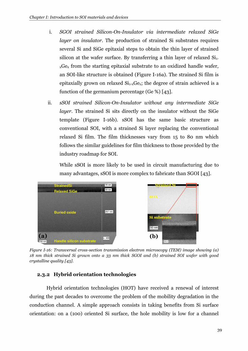
i. SGOI strained Silicon-On-Insulator via intermediate relaxed SiGe
layer on insulator. The production of strained Si substrates requires
several Si and SiGe epitaxial steps to obtain the thin layer of strained
silicon at the wafer surface. By transferring a thin layer of relaxed Si1-
xGex from the starting epitaxial substrate to an oxidized handle wafer,
an SOI-like structure is obtained (Figure I-16a). The strained Si film is
epitaxially grown on relaxed Si1-xGex; the degree of strain achieved is a
function of the germanium percentage (Ge %) [43].
ii. sSOI strained Silicon-On-Insulator without any intermediate SiGe
layer. The strained Si sits directly on the insulator without the SiGe
template (Figure I-16b). sSOI has the same basic structure as
conventional SOI, with a strained Si layer replacing the conventional
relaxed Si film. The film thicknesses vary from 15 to 80 nm which
follows the similar guidelines for film thickness to those provided by the
industry roadmap for SOI.
While sSOI is more likely to be used in circuit manufacturing due to
many advantages, sSOI is more complex to fabricate than SGOI [43].
Figure I-16: Transversal cross-section transmission electron microscopy (TEM) image showing (a)
18 nm thick strained Si grown onto a 33 nm thick SGOI and (b) strained SOI wafer with good
crystalline quality [43].
2.3.2 Hybrid orientation technologies
Hybrid orientation technologies (HOT) have received a renewal of interest
during the past decades to overcome the problem of the mobility degradation in the
conduction channel. A simple approach consists in taking benefits from Si surface
orientation: on a (100) oriented Si surface, the hole mobility is low for a channel

Chapter I: Introduction to SOI materials and devices
40
along the (110) direction, whereas it is maximal for a (110) surface orientation. On the
contrary, the electron mobility is maximal on a (100) oriented surface, and
significantly decreases on a (110) oriented surface [44]. It is thus desirable to enclose
hybrid (110) and (100) Si oriented areas on a same ‘‘hybrid’’ layer to maximize both
carriers mobility.
The co-integration of silicon layers with strong mobility of electrons (100) and
of holes (110) begins with a bi-layer stacking (110)/(100). The lower layer (100) is
locally amorphized by Si implantation and the Solid Phase Epitaxial Regrowth
recrystallization process converts it to (110) orientation. After elimination of the
superior layer (110) we obtain neighboring regions (110 and 100) on same SOI wafer
[45].
2.3.3 Germanium-On-Insulator
It was demonstrated these last 10 years that it is possible to realize functional
and successful Ge pMOSFETs (MOS transistors with p-type channel) with two to
three times superior mobility values in comparison with an equivalent pMOSFET
with silicon channel [46]. On the other hand, Ge nMOSFETs (MOS transistors with
n-type channel) suffer from poor electrons mobility values which make them
unusable at the moment.
Germanium was abandoned since his first use on transistor in 1974 by J.
Barden, W. Brattain and W. Schockley. The main cause was the insufficient chemical
stability of the oxide (GeO2). The germanium made its comeback in the world of the
microelectronics thanks to the introduction of new metal gate dielectric (with high
permittivity), the improvement of deposition techniques and its high hole mobility,
superior to that in silicon.
GeOI substrates are fabricated by using Ge condensation technique [47],
which exploits the selective oxidation of a SiGe layer grown on SOI. During oxidation,
only Si atoms are consumed whereas the diffusion of Ge atoms is blocked by the BOX
barrier. This process results in a thinner Ge-enriched film; the initial SOI layer can be
totally converted into thin GeOI film. The layer thickness can be completed via a Ge
epitaxial step.

Chapter I: Introduction to SOI materials and devices
41
An attractive solution is the co-integration of n-channel SOI and p-channel
GeOI transistors within the same chip. Local Ge condensation in selected islands
enables the fabrication of SOI-GeOI hybrid substrates and related devices. On the
other hand, Ge possesses an excellent lattice agreement with Gallium Arsenide
(GaAs). It could be so used as a buffer material for the growth of GaAs, in particular
for nMOSFET applications with high mobility or in photonic or photovoltaic fields.
GeOI can also be fabricated by Smart-CutTM.
2.3.4 Other semiconductor, BOX and substrate materials
2.3.4.1 Conductive film materials
Current research is directed towards the achievement of mixed structures
with novel properties by replacing the film material with composed semiconductor
and wide band gap films: GaAs, GaN (Gallium Nitride) or SiC (Silicon Carbide).
The wafer bonding and the layers transfer by Smart-CutTM technology opened
new perspectives of structures with III-V materials, intended for optoelectronic
applications. The first GaAs layer transfer on silicon substrate was published by
Jalaguier et al [48] and the optimization of the implantation conditions allowed
improving the quality of the transferred GaAs layer. SiCOI (Silicon Carbide-On-
Insulator) substrates were also obtained [49]. The engineered substrates are
attractive for the development of high-temperature, high-power, high-frequency and
GaN-based optoelectronic devices.
2.3.4.2 BOX and substrate materials
In a device fabricated on SOI substrate, the heating is widely higher than on
bulk substrate due to the presence of the buried oxide. SiO2 is characterized by a low
thermal conductivity (≈ 1.4 W.m-1. K-1), hundred times less than for silicon. SiO2 plays
the role of thermal barrier preventing the evacuation of the thermal power from the
Si layer towards the substrate. This effect is called “self-heating” and can be an
obstacle in the integration of advanced SOI circuits.
To improve the thermal dissipation in devices, it is possible to replace the
SiO2 by more thermal conductive dielectrics. Four dielectrics, which are already well
studied and used in the microelectronics industry, are considered as potential

Chapter I: Introduction to SOI materials and devices
42
candidates: sapphire (Al2O3), Silicon Carbide (SiC), Aluminum Nitride (AlN) and
Diamond [50]. Silicon-On-Diamond (SOD) wafers were recently demonstrated, and
SOD MOSFETs exhibit excellent characteristics [51]. Also, a buried Oxide-Nitride-
Oxide (ONO) stack is useful as a reservoir of non-volatile charges, enabling a new
paradigm of a “unified” SOI memory.
The Smart-CutTM technology allows also the use of High Resistivity SOI
substrate (HR SOI for Radio Frequency (RF) circuits) [52] and silicon film on
transparent substrates (Silicon-On-Quartz (SOQ) for optoelectronics and high-
frequency telecom applications). SOQ offers a single crystal silicon layer on a fused
silica substrate, a development that is extendable to Silicon-On-Glass (SOG).
2.4 Defects of SOI material
Despite the concern to limit the number of defects introduced by the
manufacturing process of SOI wafers, some defects remain and can be harmful for
the good operating of devices: mobility decrease, degradation of oxide break down
voltage, increase of the junction current leakage, modifications of threshold voltages,
etc. Various defects can be observed in SOI structures (see Figure I-17). Some defects
are of conventional nature, the same as encountered in bulk Si and in epitaxial Si
films, e.g., dislocations and stacking faults. In SOI, the majority of dislocations are
threading through the thickness of the film, terminating at the BOX and the surface.
Other defects are unique to the method of SOI wafers fabrication. The evaluation of
SOI structures requires different characterization techniques. These techniques must
be able to overcome difficulties that are intrinsic to SOI structures: very thin Si films
and BOX, BOX isolation, multiple Si/SiO2 interfaces, and defects unique to SOI, in-
depth inhomogeneities, stress effects, etc. The traditional techniques detailed in [5]
and other novel characterization methods are discussed in chapters II and III.
Figure I-17: Typical defects in SOI wafers [5].

Chapter I: Introduction to SOI materials and devices
43
Conclusion
In this chapter, the main characteristics of the SOI technologies were
presented at both device level and substrate level. The performances and the
weaknesses of SOI devices were addressed with a brief outline of innovative
transistor architectures made possible by the SOI structure.
We exposed the SOI technology history, the main fabrication methods of SOI
substrates, as well as the innovative technologies which allow the improvement of
device performances. The issues and the new challenges of SOI substrates were also
explained.
Nowadays, as the SOI substrates are more and more used for device/circuit
manufacturing, high quality wafers are required. It is difficult to monitor and
optimize the electric properties of ultra-thin SOI materials with nanometer size
thicknesses using traditional characterization techniques. New methods to evaluate
advanced SOI wafers will be proposed in details in the following chapters.
Chapter I: Introduction to SOI materials and devices
44
References chapter I
[1] R. Pottier, J. Tong, C. Hawkins, R. Kundu and J. L. Pelloie, "ARM 1176 implementation in SOI 45nm technology and silicon measurement," in SOI Conference, 2009 IEEE International, pp. 1-4, 2009.
[2] Semiconductor Manufacturing & Design Community: http://semimd.com/blog/tag/fd-soi/
[3] S. Cristoloveanu and S. S. Li, Electrical Characterization of Silicon-On-Insulator Materials
and Devices, Kluwer, Boston, 1995.
[4] Advanced Substrate News: http://www.advancedsubstratenews.com/2011/05/fd-soi-a-quick-backgrounder/
[5] G. K. Celler and Sorin Cristoloveanu, "Frontiers of silicon-on-insulator," Journal of Applied Physics, vol. 93, pp. 4955-4978, 2003.
[6] S. M. Sze, Physics of Semiconductor Devices (Second Edition), Wiley press, New York, 1981.
[7] T. Tsuchiya, Y. Sato and M. Tomizawa, "Three mechanisms determining short-channel effects in fully-depleted SOI MOSFETs," Electron Devices, IEEE Transactions on, vol. 45, pp. 1116-1121, 1998.
[8] V. P. Trivedi and J. G. Fossum, "Scaling fully depleted SOI CMOS," Electron Devices, IEEE Transactions on, vol. 50, pp. 2095-2103, 2003.
[9] D. J. Frank, Y. Taur and H. S. P. Wong, "Generalized scale length for two-dimensional effects in MOSFETs," Electron Device Letters, IEEE, vol. 19, pp. 385-387, 1998.
[10] K. Kato, T. Wada and K. Taniguchi, "Analysis of kink characteristics in Silicon-on-insulator MOSFET's using two-carrier modeling," Electron Devices, IEEE Transactions on, vol. 32, pp. 458-462, 1985.
[11] Daniela Munteanu, "Modélisation et caractérisation des transistors SOI: du pseudo-mosfet au mosfet submicronique ultra-mince", Grenoble, France, 1999.
[12] J. Pretet, T. Matsumoto, T. Poiroux, S. Cristoloveanu, R. Gwoziecki, C. E. Raynaud, A. Roveda and H. Brut, "New Mechanism of Body Charging in Partially Depleted SOI-MOSFETs with Ultra-thin Gate Oxides," in Solid-State Device Research Conference, 2002. Proceeding of the 32nd European, pp. 515-518, 2002.
[13] K. Uchida, H. Watanabe, A. Kinoshita, J. Koga, T. Numata and S. Takagi, "Experimental study on carrier transport mechanism in ultrathin-body SOI nand p-MOSFETs with SOI thickness less than 5 nm," in Electron Devices Meeting, 2002. IEDM '02. International, pp. 47-50, 2002.
[14] T. Ernst, R. Ritzenthaler, O. Faynot and S. Cristoloveanu, "A Model of Fringing Fields in Short-Channel Planar and Triple-Gate SOI MOSFETs," Electron Devices, IEEE Transactions on, vol. 54, pp. 1366-1375, 2007.
[15] F. Balestra, S. Cristoloveanu, M. Benachir, J. Brini and T. Elewa, "Double-gate silicon-on-insulator transistor with volume inversion: A new device with greatly enhanced performance," Electron Device Letters, IEEE, vol. 8, pp. 410-412, 1987.
[16] V. Jaju, "Silicon-On-Insulator Technology," in Advances in MOSFETs EE 530, pp. 1-12, 2004.
[17] B. Dufrene, K. Akarvardar, S. Cristoloveanu, B. J. Blalock, R. Gentil, E. Kolawa and M. M. Mojarradi, "Investigation of the four-gate action in G4-FETs," Electron Devices, IEEE Transactions on, vol. 51, pp. 1931-1935, 2004.
[18] Jean-Pierre Colinge, Chi-Woo Lee, Aryan Afzalian, Nima Dehdashti Akhavan, Ran Yan, Isabelle Ferain, Pedram Razavi, Brendan O'neill, Alan Blake, Mary White, Anne-Marie Kelleher, Brendan Mccarthy and Richard Murphy, "Nanowire transistors without junctions," Nat Nano, vol. 5, pp. 225-229, 2010.
[19] T. Ernst, L. Duraffourg, C. Dupre, E. Bernard, P. Andreucci, S. Becu, E. Ollier, A. Hubert, C. Halte, J. Buckley, O. Thomas, G. Delapierre, S. Deleonibus, B. De Salvo, P. Robert and O.

Chapter I: Introduction to SOI materials and devices
45
Faynot, "Novel Si-based nanowire devices: Will they serve ultimate MOSFETs scaling or ultimate hybrid integration?," in Electron Devices Meeting, 2008. IEDM 2008. IEEE International, pp. 1-4, 2008.
[20] Sorin Cristoloveanu, "Silicon films on sapphire," Reports on Progress in Physics, vol. 50, pp. 327-371, 1987.
[21] Michel Bruel, "Process for the production of thin semiconductor materials films," U.S. Patent n°5,374,564, 1994.
[22] M. Watanabe and A. Tooi, "Formation of the SIO films by oxygen-ion bombardment," Japanese Journal of Applied Physics, vol. 5, pp. 737-745, 1966.
[23] Katsutoshi Izumi, "Historical overview of SIMOX," Vacuum, vol. 42, pp. 333-340, 1991.
[24] P. L. F. Hemment, K. J. Reeson, J. A. Kilner, R. J. Chater, C. Marsh, G. R. Booker, J. R. Davis and G. K. Celler, "Novel dielectric/silicon planar structures formed by ion beam synthesis," Nuclear Instruments and Methods in Physics Research Section B: Beam Interactions with Materials and Atoms, vol. 21, pp. 129-133, 1987.
[25] D. Marsh, G. R. Booker, K. J. Reeson, P. L. F. Hemment, R. J. Chater, J. A. Kilner, J. A. Alderman and G. K. Celler, "The influence of high temperature anneals on the microstructure of SOI structures formed by high-dose oxygen implantation into silicon," in Proceedings of the European MRS Conference, Materials Research Society, Pittsburgh, p. 137, 1986.
[26] S. Nakashima and K. Izumi, "Analysis of buried oxide layer formation and mechanism of threading dislocation generation in the substoichiometric oxygen dose region," Journal of Materials Research, vol. 8, pp. 523-534 1993.
[27] B. Aspar, C. Guilhalmenc, C. Pudda, A. Garcia, A. M. Papon, A. J. Auberton-Hervé and J. M. Lamure, "Buried oxide layer formed by low dose SIMOX processes," Microelectronic Engineering, vol. 28, pp. 411-414, 1995.
[28] M. J. Anc, R. P. Dolan, J. Jiao and T. Nakai, "Thin-layer SIMOX for future applications," in Proceedings of IEEE International SOI Conference, pp. 106-107, 1999.
[29] A. Matsumura, I. Hamaguchi, K. Kawamura, T. Sasaki, S. Takayama and Y. Nagatake, "Technological innovation in low-dose SIMOX wafers fabricated by an internal thermal oxidation (ITOX) process," Microelectronic Engineering, vol. 66, pp. 400-414, 2003.
[30] R. C. Frye, J. E. Griffith and Y. H. Wong, "Dielectrically isolated semiconductor devices," U.S. Patent n°4,501,060, 1985.
[31] J. B. Lasky, "Wafer bonding for silicon-on-insulator technologies," Applied Physics Letters, vol. 48, pp. 78-80, 1986.
[32] Kiyoshi Mitani and Ulrich Gösele, "Wafer bonding technology for silicon-on-lnsulator applications: A review," Journal of Electronic Materials, vol. 21, pp. 669-676, 1992.
[33] Werner Kern, "The Evolution of Silicon Wafer Cleaning Technology," Journal of the Electrochemical Society, vol. 137, pp. 1887-1892, 1990.
[34] Takao Yonehara, Kiyofumi Sakaguchi and Nobuhiko Sato, "Epitaxial layer transfer by bond and etch back of porous Si," Applied Physics Letters, vol. 64, pp. 2108-2110, 1994.
[35] M. Bruel, "Silicon on insulator material technology," Electronics Letters, vol. 31, pp. 1201-1202, 1995.
[36] Soitec (Smart Cut): http://www.soitec.com/pdf/Soitec_SmartCut_EN.pdf
[37] Soitec: http://www.soitec.com/en/products-and-services/microelectronics/
[38] M. Jurczak, T. Skotnicki, M. Paoli, B. Tormen, J. Martins, J. L. Regolini, D. Dutartre, P. Ribot, D. Lenoble, R. Pantel and S. Monfray, "Silicon-on-Nothing (SON)-an innovative process for advanced CMOS," Electron Devices, IEEE Transactions on, vol. 47, pp. 2179-2187, 2000.
[39] Y. Moriyasu, T. Morishita, M. Matsui and A. Yasujima, "Preparation of high quality silicon on sapphire," In: Hemment PLF et al. Silicon-on-insulator technology and devices. Electrochemical Society Proceedings, vol. 99, pp. 137-142, 1999.

Chapter I: Introduction to SOI materials and devices
46
[40] K. Rim, J. L. Hoyt and J. F. Gibbons, "Fabrication and analysis of deep submicron strained-Si n-MOSFET's," Electron Devices, IEEE Transactions on, vol. 47, pp. 1406-1415, 2000.
[41] Xiang Qi, Goo Jung-Suk, J. Pan, Yu Bin, S. Ahmed, Zhang John and Lin Ming-Ren, "Strained silicon NMOS with nickel-silicide metal gate," in VLSI Technology, 2003. Digest of Technical Papers. 2003 Symposium on, pp. 101-102, 2003.
[42] C. Dupre, T. Ernst, J. M. Hartmann, F. Andrieu, J. P. Barnes, P. Rivallin, O. Faynot, S. Deleonibus, P. F. Fazzini, A. Claverie, S. Cristoloveanu, G. Ghibaudo and F. Cristiano, "Carrier mobility degradation due to high dose implantation in ultrathin unstrained and strained silicon-on-insulator films," Journal of Applied Physics, vol. 102, pp. 104505-104508, 2007.
[43] Bruno Ghyselen, "Strain engineering in SOI-type materials for future technologies," Materials Science and Engineering: B, vol. 124–125, pp. 16-23, 2005.
[44] Yang Min, V. W. C. Chan, K. K. Chan, L. Shi, D. M. Fried, J. H. Stathis, A. I. Chou, E. Gusev, J. A. Ott, L. E. Burns, M. V. Fischetti and Ieong Meikei, "Hybrid-orientation technology (HOT): opportunities and challenges," Electron Devices, IEEE Transactions on, vol. 53, pp. 965-978, 2006.
[45] T. Signamarcheix, F. Andrieu, B. Biasse, M. Cassé, A. M. Papon, E. Nolot, B. Ghyselen, O. Faynot and L. Clavelier, "Fully depleted silicon on insulator MOSFETs on (1 1 0) surface for hybrid orientation technologies," Solid-State Electronics, vol. 59, pp. 8-12, 2011.
[46] P. Zimmerman, G. Nicholas, B. De Jaeger, B. Kaczer, A. Stesmans, L. A. Ragnarsson, D. P. Brunco, F. E. Leys, M. Caymax, G. Winderickx, K. Opsomer, M. Meuris and M. M. Heyns, "High performance Ge pMOS devices using a Si-compatible process flow," in Electron Devices Meeting, 2006. IEDM '06. International, pp. 1-4, 2006.
[47] T. Tezuka, S. Nakaharai, Y. Moriyama, N. Sugiyama and Takagi Shin-Ichi, "Selectively-formed high mobility SiGe-on-Insulator pMOSFETs with Ge-rich strained surface channels using local condensation technique," in VLSI Technology, 2004. Digest of Technical Papers. 2004 Symposium on, pp. 198-199, 2004.
[48] E. Jalaguier, B. Aspar, S. Pocas, J. F. Michaud, M. Zussy, A. M. Papon and M. Bruel, "Transfer of 3 in GaAs film on silicon substrate by proton implantation process," Electronics Letters, vol. 34, pp. 408-409, 1998.
[49] L. Di Cioccio, Y. Le Tiec, F. Letertre, C. Jaussaud and M. Bruel, "Silicon carbide on insulator formation using the Smart Cut process," Electronics Letters, vol. 32, pp. 1144-1145, 1996.
[50] N. Bresson, S. Cristoloveanu, C. Mazuré, F. Letertre and H. Iwai, "Integration of buried insulators with high thermal conductivity in SOI MOSFETs: Thermal properties and short channel effects," Solid-State Electronics, vol. 49, pp. 1522-1528, 2005.
[51] J. P. Mazellier, J. Widiez, F. Andrieu, M. Lions, S. Saada, M. Hasegawa, K. Tsugawa, L. Brevard, J. Dechamp, M. Rabarot, V. Delaye, S. Cristoloveanu, L. Clavelier, S. Deleonibus, P. Bergonzo and O. Faynot, "First demonstration of heat dissipation improvement in CMOS technology using Silicon-On-Diamond (SOD) substrates," in SOI Conference, 2009 IEEE International, pp. 1-2, 2009.
[52] D. Lederer, C. Desrumeaux, F. Brunier and J. P. Raskin, "High resistivity SOI substrates: how high should we go?," in SOI Conference, 2003. IEEE International, pp. 50-51, 2003.

Chapter II: Electrical characterization of SOI substrates
47
Chapter II:
Electrical characterization of SOI substrates

Chapter II: Electrical characterization of SOI substrates
48
Introduction
We saw in chapter I that the Smart-CutTM technology presents several
advantages and is dominant at present in the manufacturing industry of SOI
substrate. The characterization of SOI wafers for the quality control accompanies the
manufacturing process and allows optimization of the products. The aim of this
chapter is to present the electrical study of SOI structures by pseudo-MOSFET (-
MOSFET) technique.
The first part proposes an overview of the -MOSFET method through the
preparation of samples, its principle of operation and the extraction of the electrical
parameters for different SOI structures.
The second part presents the -MOSFET results of electrical characterization
of advanced SOI substrates with thin films down to 12 nm and thin BOX down to 10
nm.
The third part is dedicated to the study of the electrical properties of SOI
wafers at low-temperature with -MOSFET concept. Our aim is to reveal the
electrical behavior and parameters variation with temperature.

Chapter II: Electrical characterization of SOI substrates
49
1. Pseudo-MOSFET principle and operation
1.1 Overview
As shown in chapter I, the evolution of SOI materials and their more and
more frequent employment in integrated circuit fabrication make an effective and
fast quality control necessary. The SOI electrical characterization aims revealing the
wafer parameters that will have a direct impact on the components realized on that
substrate. The characterization of SOI materials and devices requires techniques able
to adapt to difficulties induced by very thin film layers, presence of thin BOX, strong
coupling between interfaces (Si/BOX, BOX/substrate and Si/air) and typical defects
(stress effects, in-depth in-homogeneities, dislocations, precipitates, etc.). Some
conventional methods show their limits for thin films and BOX, whereas novel
techniques were implemented and will be discussed in chapter III.
The electrical characterization of SOI wafers involves mainly measuring the
conductivity of the silicon top layer. Moreover, the natural MOS-like structure of SOI
allows using the bulk substrate as a gate to control the conductivity in the top silicon
film. Based on current flowing into the film versus gate voltage, one can extract
numerous electrical parameters of the film. This is basically the philosophy of a
pseudo-MOS transistor, called the -MOSFET.
The -MOSFET technique has been developed to characterize the quality of
the silicon layer and the BOX in as-fabricated SOI wafers before any device
processing ([1], [2], [3]). It is largely used for evaluation of material parameters such
as mobility of carriers and interface quality. Contrary to the characterization
performed for a conventional MOS transistor, it is here the lower interface of the
silicon film (in touch with the BOX) that is estimated. While the information
extracted from a MOSFET concerns normally the gate oxide, in -MOSFET the data
is related to the buried oxide.
The important advantage of -MOSFET is to allow the extraction of the
electrical characteristics intrinsic to the SOI material, avoiding the subsequent
modifications which arise during a complete CMOS process manufacturing in clean
room.

Chapter II: Electrical characterization of SOI substrates
50
There are two ways to measure the current flowing into the film: four-probe
configuration and two-probe configuration.
The four-point (4-point) probe is used to measure the semiconductor
resistivity when the volume of the material is not accessible and only the surface may
be probed (Figure II-1a). It was originally proposed in 1916 to measure the earth’s
resistivity and then adopted for semiconductor wafer resistivity (ρ) measurements in
1954 [4]. Most commonly it measures the sheet resistance (R□) of thin conducting
layers and wafers.
As shown in Figure II-1a, the 4 probes are generally collinear, i.e., arranged
in-line, with equal probe spacing (1 mm). The outer probes (1 and 4) are carrying the
current whereas the voltage is sensed between the inner probes (2 and 3). The current
is probed via drain and source contacts. While the probe 1 is grounded, a current
source is connected to probe 4 (I41) and the differential potential, V32, is recorded
with high impedance voltmeters ([2], [5]). The sheet resistance (R□) and the average
resistivity (ρ) are given by:
(II-1)
The advantage of the 4-point probe -MOSFET method, compared to two-
point probes -MOSFET, lies in the way the current and voltage are measured. Due
to the high input impedance voltmeter, very low current is drawn so, the contact
resistances of probes 2 and 3 usually play a negligible role in the measurements.
Thus, the 4-point probe characteristics are not influenced by parasitic effects (contact
resistances) [2]. Unfortunately, extracting MOS parameters from the configuration is
tedious because one needs to readjust the I14 = ID current in order to keep V32
constant (V0) during measurements.
A simpler two-probe configuration was proposed. Two contacts on the top
silicon film (body of the transistor) serve as source and drain, while the bulk silicon
substrate can be biased as a gate. The buried oxide (BOX) is used as a gate dielectric.
Direct ID-VG curves are thus obtained.
In FD SOI layers, the substrate is biased as a gate and inversion or
accumulation layers are induced at the Si/BOX interface.

Chapter II: Electrical characterization of SOI substrates
51
Two main versions of the pseudo-MOSFET technique exist; they differ in the
way the source and drain contacts are formed. The first one, the point-contact -
MOSFET (see Figure II-1b), which uses two metal tips (pressure probe technique),
has been developed by Cristoloveanu et al in 1992 at IMEP [1]. The second one, the
Hg-FET (see Figure II-1c), uses mercury probes and has been developed by Hovel in
1997 at IBM [6]. The Hg-FET is based on S/D contacts formed by two concentric
circles of mercury creating ohmic contacts and allowing to obtain a perfectly defined
geometry for SOI characterization [6]. Note that some groups are working with
deposited metal contacts (see Figure II-1d) on the top Si film [7]. The modeling of this
configuration is more complicated since the source/drain contacts to film are
Schottky diodes.
Let us also cite here a more exotic method called SHG (Second-Harmonic-
Generation). This method frees itself from probes or from physical contact. It is based
on the reflections of a laser beam at various interfaces of the SOI film and gives
information on the carrier charge density by the analysis of the second harmonic of
the signals [8].
The simplest and most efficient of all these techniques is the point-contact -
MOSFET (Figure II-1b) with pressure probes to form source and drain contacts as
detailed below.
Figure II-1: (a) Principle of the 4-point probe measurement [5]. -MOSFET configuration with: (b)
metallic pressure probes [9], (c) mercury probes [9] and (d) deposited metal contacts [7].
1.2 Point-contact -MOSFET technique
The point-contact -MOSFET equipment is a standard JANDEL universal
probe station for electrical testing.

Chapter II: Electrical characterization of SOI substrates
52
It consists of a chuck which must be a brass conductive table that can be
biased as a gate. It is composed of 4 tungsten carbide probes with a tunable pressure
and with ~ 40 µm tip radius. The distance between two successive probes is 1 mm.
Needles load is controllable (between 0 and 100 g) by adjustable individual tension
gauges. The chuck and the 4 needles (Figure II-2a) are covered by a dark box
enabling the test in dark conditions. The external electrical connection with -
MOSFET equipment is done using 6 independent electrical outputs: 5 BNC (female)
corresponding to the 4 probes and the chuck, and one simple output for dark box
ground (typically banana plug).
Note that different electrical measurements could be made using -MOSFET:
the 2-point probes measurements (standard ID-VG, gm-VG, IG-VG and ID-VD) and the
four-point (4-point) probes measurement discussed previously.
The -MOSFET technique conquered the world of SOI substrates
characterization by its simplicity and its speed of implementation. As specified in the
previous sub-section, the point-contact -MOSFET can be presented as an upside-
down MOS configuration. The contacts (source and drain) are insured by two probes
(Figure II-3a). The substrate acts as a gate where we can apply a back-gate voltage
(VG) through the metallic holder (chuck).
1.2.1 Sample preparation
The capability to characterize full SOI wafers was demonstrated [2], but is
very sensitive to the edge effects and to the defects that may be present in the BOX
(leakage). Therefore, using a wafer with isolated silicon islands is preferable in order
to reduce leakage current on the edges (Figure II-2b) and also for wafer mapping.
The size of these islands must be sufficient to be able to place the needles
without any difficulty, without being too large in order to reduce the probability of a
BOX defect. However, the defects that cause leakage through the buried oxide
became rare; thanks to the improvement of the SOI materials fabrication, the islands
surface can go to a few cm2. It is important that the etching of the film around the Si
islands reaches the BOX to isolate well each island. Indeed, if a thin layer of
semiconductor material remained, the current could spread from one island to
another. We must also take into account possible variations of the film thickness.
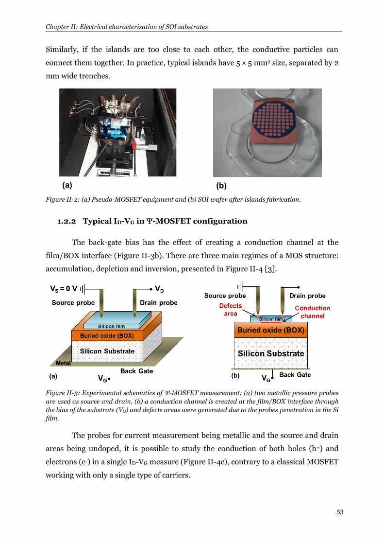
Chapter II: Electrical characterization of SOI substrates
53
Similarly, if the islands are too close to each other, the conductive particles can
connect them together. In practice, typical islands have 5 × 5 mm2 size, separated by 2
mm wide trenches.
Figure II-2: (a) Pseudo-MOSFET equipment and (b) SOI wafer after islands fabrication.
1.2.2 Typical ID-VG in -MOSFET configuration
The back-gate bias has the effect of creating a conduction channel at the
film/BOX interface (Figure II-3b). There are three main regimes of a MOS structure:
accumulation, depletion and inversion, presented in Figure II-4 [3].
Figure II-3: Experimental schematics of -MOSFET measurement: (a) two metallic pressure probes
are used as source and drain, (b) a conduction channel is created at the film/BOX interface through
the bias of the substrate (VG) and defects areas were generated due to the probes penetration in the Si
film.
The probes for current measurement being metallic and the source and drain
areas being undoped, it is possible to study the conduction of both holes (h+) and
electrons (e-) in a single ID-VG measure (Figure II-4c), contrary to a classical MOSFET
working with only a single type of carriers.

Chapter II: Electrical characterization of SOI substrates
54
If we apply a positive gate voltage (VG from 0 to + 10 V in Figure II-4a), there
is generation of a hole accumulation layer at the BOX/substrate interface (zone 1) and
the electrons are rejected towards the gate which leads to a positive gate current (IG)
in Figure II-6. At the Si film level, the holes are evacuated (zone 2) and an inversion
layer forms resulting in a drain current (ID) visible on the ID-VG curves in logarithmic
scale (Figure II-4c).
If we apply a negative gate voltage (VG from 0 to - 10 V in Figure II-4b), there
is a depletion area before the creation of an inversion zone at the BOX/substrate
interface (zone 1). The holes are collected by the gate which leads to a negative gate
current (Figure II-6). In the Si film, a hole conduction channel is formed (zone 2) and
a positive drain current flows (Figure II-4c). The current is zero when the film is
totally depleted (-1 V < VG < +1 V).
In Figure II-4c, we show standard 2-point probes measurement: drain
current (ID) and transconductance (gm = ∂ID/∂VG) versus VG curves. Note that ID-VG
and gm-VG characteristics are very pure, similar to those of a conventional MOS
transistor. The two conduction mechanisms just explained (accumulation and
inversion) depend on the voltage range applied on the Si substrate.
Figure II-4: Carriers movement induced by a voltage sweep of a -MOSFET structure for (a) VG
from 0 to + 10 V and (b) VG from 0 to - 10 V. (c) Illustration of ambipolarity conduction ID-VG
(logarithmic scale) and transconductance gm-VG on p-type (NA ≈ 1015 cm-3) SOI film with tSi = 88 nm
and tBOX = 145 nm.
Note that the ID-VG curves in Figure II-4c were obtained in linear regime (low
VD value). Figure II-5 shows linear drain current versus drain voltage curves for
various back-gate voltages. The curves exhibit a clear ohmic conduction for negative
VG (see Figure II-5a) and for positive VG (see Figure II-5b). Moreover, the drain
current is modulated by the voltage applied on the substrate, which confirms the

Chapter II: Electrical characterization of SOI substrates
55
MOSFET-like characterization. Without substrate biasing (VG = 0 V), the current is
zero because the Si film is fully depleted.
Figure II-5: ID versus VG curves for various back-gate voltages: negative in (a) and positive in (b).
SOI film with tSi = 88 nm and tBOX = 145 nm (p = 70 g).
In the following sub-sections, we will discuss the impact of two main aspects
which should be taken into account during the measurements: the substrate effect
and the probe pressure contact influence.
1.2.3 Substrate effect
To better understand the -MOSFET operation mechanisms, the effects due
to the substrate below the BOX can be studied [3]. Indeed, the substrate acts as a
gate, and contrary to conventional MOSFETs, the gate here is not metallic or heavily
doped; it is thick (total thickness of the substrate exceeds 500 µm) and lightly doped
(p-type, NA ≈ 1015 cm-3).
This leads to the appearance of large depletion areas (about 1 µm depth)
under the BOX with possible formation of an inversion layer for negative VG. An
accumulation layer forms for positive VG. The access to the substrate current is easy;
a study of the gate current (IG) as a function of VG (Figure II-6), collected at the back-
gate contact of the SOI wafer is enough. Note that the values of the gate current must
be less than 100 nA during each ID-VG measurement in order to avoid polluting the
drain current measurement by leakage through the BOX. The gate voltage is limited
by oxide breakdown. The two picks of the gate current for VG > 0 and VG < 0
respectively correspond to the threshold (VT) and flat-band voltage (VFB) at the BOX-
substrate interface.

Chapter II: Electrical characterization of SOI substrates
56
Figure II-6: Gate current versus gate voltage in SOI wafer with tSi = 88 nm and tBOX = 145 nm.
1.2.4 Influence of probe pressure
As the source and drain contacts are metallic, while the undoped silicon film
is semiconductor, for low drain voltages one would expect to have Schottky barriers
dominating the source and drain access. This is definitely the case for deposited
metal contacts (i.e. Ti/Al) [7].
As shown by linear symmetrical ID-VD curves in Figure II-5, the situation is
different for pressure probes -MOSFET: the pressure applied on the probes allows
recovering the ohmic contact for source and drain as it was previously demonstrated
in [10]. Figure II-7 shows drain current and transconductance characteristics
obtained for a 200 nm film thickness and a 400 nm BOX thickness [10]. The
measurements performed with higher pressures are clearly evidencing an increase in
the current level and in the transconductance peak. This effect is due to the variation
of the series resistances with the probe pressure.
In addition, it was proven in [10] that the pressure applied on the probes
results in a localized damage of the Si layer, with formation of craters (Figure II-7b
and Figure II-7c). Figure II-7b and Figure II-7c show atomic force microscopy
topographies of two craters obtained with the same probe, for different pressures.
The shape of the craters is the same, but their sizes are increasing with pressure. The
diameter and the height of these craters were both increasing with pressure. The
height obtained was quasi-linear dependent on the pressure, with a slope of 1-2 nm/g
[10]. This confirms also the earlier estimation of 10 nm probe penetration for 10 g
pressure [3]. Increasing pressure induces deeper penetration of probes into the film
and higher crystal local damage, which allows decreasing the Schottky barrier and

Chapter II: Electrical characterization of SOI substrates
57
obtaining an ohmic probe-to-film contact. Since the probe inter-distance (1 mm) is
much larger than the probe size (~ 40 µm diameter), the generated local defects,
which may arise over a few micrometers near the contacts, can be neglected and do
not affect the interface properties and the parameters extraction.
Figure II-7: (a) Drain current (linear scale) and transconductance (inset) versus back-gate voltage
for various pressures applied on the -MOSFET probes [10]. There is no visible variation of VT and
VFB. Atomic Force Microscope topographies of two craters obtained with the same probe at two
different pressures: (b) p = 70 g and (c) p = 50 g [11]. The shape of each crater is not regular and it
represents the “fingerprint” of the probe, the size of which is pressure-related.
A good control of series resistances is essential to obtain realistic material
parameters and the optimal control is obtained by the pressure applied on the probes.
For thick films, the degradation induced by the probes is made far from the
conduction zone. On the other hand, the applied probe pressure becomes very critical
for the measurements of thin and extra-thin films where the needles can penetrate
into the BOX and result in a current leakage. In these cases, it is necessary to
decrease the probe pressure but to keep it at a value sufficient to ensure ohmic
contacts between probes and thin Si film.
1.3 Extraction methods of the electrical parameters
As in the case of an ordinary MOSFET, two operation modes exist for the -
MOSFET: linear (or ohmic) regime and saturated regime. For all our measurements
and parameters extraction we place ourselves at low VD (ohmic region). Note that ID-
VG curves previously showed in Figure II-4c were obtained in this regime. The
transistor behaves like a quasi-two-dimensional conductance controlled by the back-
gate. If we consider the case of fully depleted films, where the volume current is
negligible, we can detail the expressions of the current in inversion and accumulation.
In such configuration, the theoretical relationships of the MOS transistor can be
-20 -10 0 10 20-0.2
-0.1
0.0
0.1
0.2
0.3
0.4
0.5
80g
70g
60g
50g
40g
VG (V)
gm (
µS
)

Chapter II: Electrical characterization of SOI substrates
58
directly applied [12]. The drain current (ID) in ohmic regime for a MOSFET is given
by the relation:
( )
[ ( ) ( ) ]( ) (II-2)
where:
- fg is the geometrical factor taking into account the size of the devices
(similar to the ratio W/L in classical MOSFETs; fg = W/L = 0.75 in the case
of -MOSFET [1], [2], [13]).
- Cox represents the buried oxide capacitance per unit area.
- μ0 is the low-field mobility (μn accounts for electrons and μp for holes).
- VT is the threshold voltage for electrons channel and VFB is the threshold
voltage for holes channel (or the flat-band voltage).
- θ1 is the first-order mobility attenuation factor related to the series
resistances (RSD) and to the interaction between the carriers and the
phonons of the crystal lattice.
- θ2 is the second-order mobility attenuation factor which takes into account
the surface roughness of the Si/SiO2 interface and becomes important for
transistors with thin gate oxide at high vertical field.
In the case of the -MOSFET where the BOX is thick enough, the second
mobility attenuation factor (θ2) is negligible because it only occurs at very high gate
voltage (very strong inversion). Therefore, we re-write the simplified expressions for
the drain current (ID) and transconductance (gm):
( )
[ ( )]( ) (II-3)
[ ( )] (II-4)
θ1 coefficient measures the reduction of the “pure” mobility µ0 with vertical
field and is a function of series resistance (RSD); and of carrier confinement at the
interface (θ1,0):
(II-5)

Chapter II: Electrical characterization of SOI substrates
59
Important material parameters appear in these equations (e.g. mobilities,
VFB, VT, RSD etc.). Their extraction methods will be described in the next sections.
1.3.1 Threshold voltage and flat-band voltage
There are various methods to extract the threshold voltage [14]:
- The gate voltage corresponding to a drain current equal to 10-7 A/μm
(difficult to use in our case as W is unknown in -MOSFET).
- The maximum of the transconductance gm (inaccurate approximation)
[15].
- The Y-function [16].
- The maximum of ∂gm/∂VG (∂2(ID)/∂(VG2)) [17].
For accuracy reason, the last two methods will be used. We prefer to proceed
with the Y-function method developed by Ghibaudo [16]. The main advantage of this
method comes from its independence from θ1 factor enabling to avoid the impact of
RSD which is critical in our measurements. If we consider the drain current given by
equation (II-3), the Y-function is linear for |VG| ≥ |VT,FB| and is given by:
( )
√ √ ( ) (II-6)
Due to the ambipolarity of the -MOSFET measurements, the Y-function can
be plotted at the same time in accumulation and in inversion, in order to extract the
thresholds voltages of the corresponding channels. The extraction of the VT and VFB
voltages requires extrapolating the tangent of the linear part of the Y-VG curve in
inversion or accumulation. The intersection of the tangent with the VG axis gives the
searched values (Figure II-8a).
VT,FB can be extracted by the voltages corresponding to the peaks of
∂2(ID)/∂(VG2) or to the inflexion points of the gm(VG) curve [17]. This last method is
illustrated by Figure II-8b. By comparing the two methods, Y-function and peak of
∂2ID/∂V2G, we notice that the extracted values are extremely close. But we prefer to
use in our extraction the Y-function technique because the double derivative is more
tedious and results in noise.

Chapter II: Electrical characterization of SOI substrates
60
Figure II-8: Extraction of VT and VFB: (a) by Y-function method [16], (b) by the maximum of the
second derivative of the drain current [17]. The film thickness is 88 nm while the BOX thickness is 145
nm.
1.3.2 Carrier mobility
Again, the mobility of holes and electrons is extracted from a single
measurement. Two notions of mobility are to be differentiated: the low-field mobility
(µ0) and the effective mobility (µeff). The first one corresponds to a maximum value of
mobility that carriers could reach if there was no mobility degradation factor. The
effective mobility is variable, depending on the effective electric field (i.e. on VG), and
reflects the real mobility of carriers in the channel at a certain gate bias.
To determine the low-field mobility, we use the slope of the linear part of the
“Y-function” (Figure II-9). The value of this slope is given by:
√ √ (II-7)
The values of low-field mobility for electrons (µn) and for holes (µp) can be
then extracted by:
(II-8)
Note that another method of mobility extraction is based on the
transconductance (gm). Indeed, according to the equation (II-4) the transconductance
reaches a maximum (gmmax) for VG ≈ VT. We can then determine the mobility µ0 by:
(II-9)

Chapter II: Electrical characterization of SOI substrates
61
Nevertheless the use of the transconductance tends to underestimate the
value of the low-field mobility as the peak of gm does not exactly correspond to VG =
VT. The peak actually appears at a voltage slightly superior to VT. Equation (II-4) is
valid in strong inversion and neglects the proximity of weak inversion. That is why µ0
will be extracted by the Y-function in our measurements, the gmmax method being only
used for comparisons.
The effective mobility is defined in the simplified case of -MOSFET as:
( ) (II-10)
It is also possible to draw the effective mobility curves as a function of gate
voltage for electrons and holes, without making use of the mobility reduction factor
(θ1) thanks to:
√
[ ( )] (II-11)
The notation µFE means “field-effect mobility”. It characterizes the
dependence of the transconductance on the effective electric field. This mobility
overestimates the impact of the vertical field on the current. A new method to
evaluate the effective mobility by capacitance measurements will be proposed in
section 2 of chapter III.
Figure II-9: Extraction of βn and βp factors by Y-function method [16] in the case of a SOI substrate
with 88 nm film and 145 nm BOX thicknesses.

Chapter II: Electrical characterization of SOI substrates
62
1.3.3 Mobility reduction factor and series resistance
The mobility degradation factor for electrons and holes, θ1, is obtained by
combining equations (II-3) and (II-4), for gate voltage much higher than VT,FB:
( )
( ) (II-12)
The series resistance for electrons and holes can be simply deduced from θ1,
using equation (II-5):
(II-13)
Note that the coefficient θ1,0 in equation (II-5) is proportional to Cox and can
be neglected in the standard case of thick buried oxides.
1.3.4 Subthreshold swing and interface traps density
If we focus on the semi-log scale ID-VG curves another parameter can be
extracted: the subthreshold swing (S). The density of interface states is calculated
from S. For this purpose we need to use the current in weak inversion regime. In
practice, to extract the subthreshold swing is given by the inverse of the slope of the
logarithmic drain current with respect to the gate voltage, i.e.:
( ( )
)
(II-14)
The subthreshold swing depends on the interface trap density (Dit) and the Si film
capacitance(CSi) [12]:
(
) (II-15)
As we can see in Figure II-10, it is more conveninient to measure the slope of
the linear log(ID-VG) curve. The subthreshold swing S is the reciprocal of the slope.
The subthreshold swings Sn for electrons and Sp for holes may be different because
they are directly affected by the effective density of interface traps which can be
different in accumulation and inversion.

Chapter II: Electrical characterization of SOI substrates
63
Figure II-10: Extraction of the subthreshold swing Sn and Sp of a -MOSFET for electron and hole
channels.
Once the subthreshold swing was determined, the trap density at Si-BOX
interface can be calculated, for both conduction modes, by:
( ) [
(
)] (II-16)
Obviously, Dit(n,p) are only average values of the defect density in the band
gap. They correspond more to “mid-gap” defects situated at the middle of the band
gap. Furthermore, this extracted value has sense only if the opposite interface (in
general the free wafer surface) is rather far from the BOX. We will discuss this aspect
in sub-section 1.4 and in section 3 of chapter III will propose a new method for the
evaluation of Dit by noise measurements in -MOSFET configuration.
1.4 Impact of the top interface in thin SOI films
As seen in chapter I, thin SOI films have considerable technological interest in
the race for device scaling. The film thickness has been drastically reduced in order to
achieve very small gate lengths. Consequently, the characterization of ultra-thin (UT)
films has become a cornerstone for manufacturers of SOI substrates. The
characterization of thick SOI films is reliable and the parameters extraction can be
easily extracted.
The extraction of electrical parameters on thin films remains rather
challenging, for two main reasons:
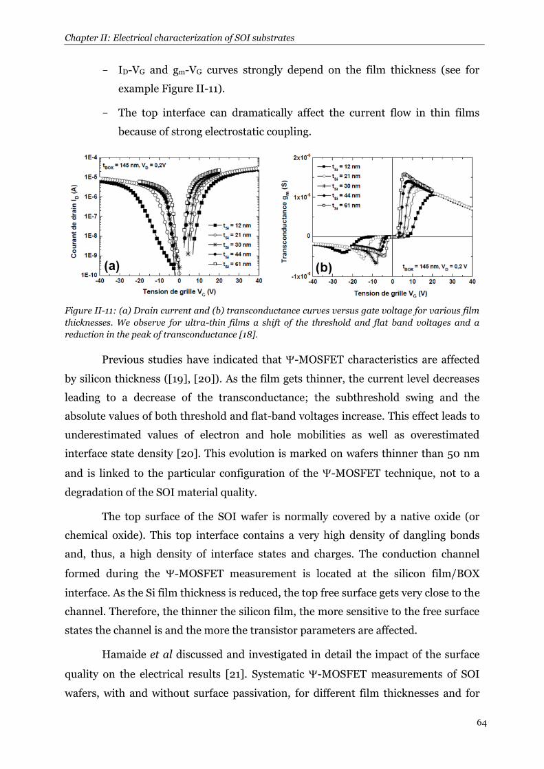
Chapter II: Electrical characterization of SOI substrates
64
- ID-VG and gm-VG curves strongly depend on the film thickness (see for
example Figure II-11).
- The top interface can dramatically affect the current flow in thin films
because of strong electrostatic coupling.
Figure II-11: (a) Drain current and (b) transconductance curves versus gate voltage for various film
thicknesses. We observe for ultra-thin films a shift of the threshold and flat band voltages and a
reduction in the peak of transconductance [18].
Previous studies have indicated that -MOSFET characteristics are affected
by silicon thickness ([19], [20]). As the film gets thinner, the current level decreases
leading to a decrease of the transconductance; the subthreshold swing and the
absolute values of both threshold and flat-band voltages increase. This effect leads to
underestimated values of electron and hole mobilities as well as overestimated
interface state density [20]. This evolution is marked on wafers thinner than 50 nm
and is linked to the particular configuration of the -MOSFET technique, not to a
degradation of the SOI material quality.
The top surface of the SOI wafer is normally covered by a native oxide (or
chemical oxide). This top interface contains a very high density of dangling bonds
and, thus, a high density of interface states and charges. The conduction channel
formed during the -MOSFET measurement is located at the silicon film/BOX
interface. As the Si film thickness is reduced, the top free surface gets very close to the
channel. Therefore, the thinner the silicon film, the more sensitive to the free surface
states the channel is and the more the transistor parameters are affected.
Hamaide et al discussed and investigated in detail the impact of the surface
quality on the electrical results [21]. Systematic -MOSFET measurements of SOI
wafers, with and without surface passivation, for different film thicknesses and for

Chapter II: Electrical characterization of SOI substrates
65
the same BOX thickness of 145 nm, were performed. One group of wafers were
considered as a reference (Figure II-12a), the other group underwent a dry oxidation
at 900°C in order to passivate the surface with a 10 nm thermal oxide (Figure II-12b).
The surface oxide was removed for some wafers in 5 % HF to collect the “post-HF”
data.
Figure II-12: SOI structure for (a) non-passivated sample where Dit1 and Dit2 represent the state
densities at the back and top interface respectively, and for (b) passivated sample with 10 nm surface
oxide.
The evolution of carrier mobility (low-field mobility) versus film thickness for
samples with and without surface oxide is reproduced in Figure II-13. It is clear that
the electron mobility values (Figure II-13a) are increased by about 25 % after surface
passivation for the whole range of film thickness. Post-HF mobility values drop back
to preoxidation level (reference samples).
This result demonstrates that the increase of mobility with surface oxide is
not due to thermal curing during oxidation. Hamaide et al mentioned that the
mobility values right after the HF treatment and before the native oxide formation
are the same as with the oxide, due to the HF passivating effect where the impurities
at the top Si film are cleaned [21]. As the films became thinner, part of the electron
mobility degradation is only “apparent”, being induced by the electrostatic coupling
effect between the top surface states and the conduction channel which gains
importance.
A more significant improvement of mobility values for holes than for
electrons with surface passivation was observed (Figure II-13b). This stronger
influence of surface quality is explained by the fact that in an accumulation channel,
the conduction of majority carriers extends further in the volume of the film than do

Chapter II: Electrical characterization of SOI substrates
66
the minority carriers of the inversion layer. The majority carriers are more influenced
by the top surface and thus benefit more from the Dit2 (top interface) reduction.
The results in Figure II-13 show that the thickness film dependence is much
reduced for electron mobility and nearly suppressed for hole mobility.
Figure II-13: Comparison of (a) electron mobility and (b) hole mobility measured on samples without
surface oxide (reference), with surface oxide, and long after oxide removal (post-HF) [21].
After surface passivation the results in Figure II-14a show a decrease of both
the absolute values of VT and VFB and of their thickness dependence. As for the
inversion and accumulation threshold voltages, the interface state density at the top
surface is expected to have a strong influence on the subthreshold swing. In
particular, the knowledge of the top surface state density Dit2 is necessary to extract a
realistic density Dit1 at the Si/BOX interface. As anticipated, the swing is strongly
surface-quality dependent (Figure II-14b), especially at small film thicknesses (< 20
nm). Once again, passivating the top surface significantly reduces both S and its
dependence on film thickness.
Figure II-14: Comparison of (a) threshold and flat-band voltages and (b) subthreshold swing
variations with film thickness obtained on samples without surface oxide (reference, open symbols)
and with surface oxide (solid symbols) [21].
These results in Figure II-13 and in Figure II-14 clearly reveal the role of the
top interface states which is reinforced by the interface coupling effect ([2], [22]). In
addition, the results showed in Figure II-14 are in good agreement with the

Chapter II: Electrical characterization of SOI substrates
67
mathematical model presented by Hovel where the coupling effect between the two
interfaces of the Si film is taken into account [23].
1.5 Revisited -MOSFET models
In the case of -MOSFET on partially depleted (PD) Si films, where the back
interface maximum depletion width (WDmax) does not reach the top interface, it is
possible to use the conventional -MOSFET equations below [2]:
(
)
(II-17)
(
) (II-18)
where Nfilm and Nsub are the doping levels in the silicon film and substrate (in
Unibond SOI wafers Nfilm ≈ Nsub). Qox is the fixed charge in the buried oxide and Dit1 is
the trap density at the film-BOX interface. These equations show no dependence of
VFB with the silicon film thickness (tSi), and suggest a decrease of VT for thinner films.
In the frequent case of fully depleted (FD) Si films, the potential of the back interface
(Si/BOX) can be influenced by the top interface state (charges present at Si/air
interface). The experimental data (reproduced in Figure II-14a) suggests that a
corrected model is needed to account for the coupling between the top and bottom
interfaces of UT films (< 100 nm).
Recently, Rodriguez et al [24] have revisited the associated -MOSFET
models to fit the case of ultra-thin film SOI. In this new model, the analytical
expressions are determined from the 1-D numerical solution of Poisson equation
(adapted for the case of a low doped semiconductor) by taking into account the
charges resulting from the bands bending at film/BOX interface. In the case of non-
passivated SOI films, a new boundary condition appears at the film interface/surface
level. The top-surface field is no longer negligible, being defined by the Gauss law and
implying a new definition of the threshold voltage [24]:
(
( )) (II-19)
where fb is the work function difference between Si film and substrate (here fb ≈ 0)
and the surface trap density capacitances associated to the top and back interfaces are

Chapter II: Electrical characterization of SOI substrates
68
calculated by: Cit1,2 = qDit1,2. In addition, the model could be extended to calculate the
subthreshold swing S:
(
( )) (II-20)
In our work we will focus on these two equations (II-19) & (II-20). Other
equations for passivated SOI films and an empirical model for VT in -MOSFET
configuration for very thin films can be found in Rodriguez et al [24].

Chapter II: Electrical characterization of SOI substrates
69
2. Characterization of ultra and extra thin SOI wafers
In the previous section, we showed that the -MOSFET technique has
constantly been used for studying the electrical properties of as-fabricated fully
depleted SOI wafers. While the film and the BOX of SOI structures are getting
thinner we are facing problems with the characterization and the extraction methods.
Nowadays, two recent challenges drive the research for advanced SOI wafers:
(i) Application of -MOSFET to ultra-thin and extra-thin SOI structures;
(ii) Extension to other types of electrical measurements.
In the section 3 of this chapter and in chapter III, we will address the second
challenge by proving the possibility of low-temperature, low-frequency noise and
split C-V measurements with -MOSFET configuration.
In this sub-section, we will prove that the -MOSFET is still a very successful
characterization technique for bare SOI even when the film and BOX thickness are
dramatically reduced [25]. We demonstrate for the first time the ability to
characterize advanced SOI structures with ultra-thin films (down to 12 nm) and
extra-thin BOX (down to 10 nm) using the -MOSFET. In addition, the impact of
surface passivation on some samples is also showed and discussed.
The UT/ET SOI wafers are produced by Soitec with Smart-CutTM process but
with different technologies compared to thick SOI samples. Notice that these
characterizations are recent and no paper was published by other groups on this
subject. Due to the confidential and the continuing progress of UT/ET SOI wafers, we
will show only the ID-VG and gm-VG characteristics without mentioning the technology
details or the extracted values of mobility and Dit.
2.1 Experimental conditions
In our work, square mesas with 7 cm × 7 cm size of bonded Unibond/Smart-
Cut™ SOI wafers were used with low-doped (NA ≈ 1015 cm-3) p-type silicon layers.
Different couples of Si layers and BOX were characterized: between 12 and 200 nm
for film thickness and between 10 and 400 nm for BOX thickness. Some of the wafers

Chapter II: Electrical characterization of SOI substrates
70
underwent a clean dry oxidation at 900°C in order to passivate the surface with a 4-
10 nm surface oxide (SiO2).
2.1.1 Sample preparation
As mentioned previously, the -MOSFET technique requires very few
technological steps to be implemented. The wafer is etched in silicon islands isolated
from the edges where a leakage current between the gate and the electrodes may
occur, which would degrade the measured electrical characteristics.
We engraved several islands per sample in the clean room by dry etching. The
wafer is covered with a photosensitive resist using a spin coater with a speed
previously set in order to obtain uniform spread on the wafer surface. The sample is
then irradiated with UV light passing through a mask which degrades the structure of
the exposed resist. A development step allows removing exposed resist. The wafer
undergoes a Reactive Ion Etching (RIE), which frees silicon islands with a slight over-
etching. The remaining resist is removed by an organic solution called “Remover”.
Samples are cleaned and dried and ready to be characterized.
2.1.2 Measurement system
The measuring system consists of a JANDEL probing station (normally used
for 4-point probes measurements) and a semiconductor parameter analyzer Agilent
HP-4156B (or HP-4155A). This station has undergone some changes, by linking the
chuck to a triaxial connector in order to bias the back-gate substrate. The advantage
of this station is that the pressure applied on the probes (spaced out by 1 mm) is
manually adjustable and from 0 to 100 g. The measurements are performed in the
darkness. All measurements were performed at low drain voltage (VD) so as to ensure
linear mode operation. In addition, two important parameters in the configuration of
the semiconductor parameter analyzer should be well defined especially for advanced
electrical measurements of extra-thin film and ultra-thin BOX: the hold time
(standby time before each measurement) and the delay time (standby time between
two successive gate biases).
In our work, the measurements were done by applying a single sweep gate
voltage (forward) from zero to positive value then from zero to a negative value. Some

Chapter II: Electrical characterization of SOI substrates
71
measurements can be done also by using dual sweep, forward and backward (from
positive value to zero and then from negative value to zero) to reveal hysteresis
effects.
2.2 Results obtained on UT/ET SOI
By adjusting the configuration settings such as the probe pressure, hold and
delay time and the gate bias we succeeded to characterize these very thin structures.
First, we measured the drain current (in Figure II-15a) and the transconductance (in
Figure II-15b) curves versus gate voltage for passivated and non-passivated SOI with
88 nm thick Si film and 25 nm BOX thickness.
Figure II-15: (a) Drain current and (b) transconductance versus gate voltage for 88 nm Si film
(passivated and non-passivated) and 25 nm BOX.
The probability to damage the BOX by the probes and to have current leakage
is high. In our measurements we monitored the gate current which in general is
below 100 nA for all the range of VG. This means that no BOX damage (and
consequently no current leakage) is visible. The feasibility to characterize an SOI
structure with 25 nm BOX is clearly demonstrated in Figure II-15.
As we discussed above, in ultrathin films (< 100 nm) the coupling of the
buried channel with the free surface defects is very strong [21]. We studied the impact
of this coupling by measuring both passivated (with 4 nm oxide layer on the film
surface) and non-passivated samples in Figure II-15. The drain current curve for
passivated samples (Figure II-15a) exhibits lower threshold/flat-band voltages (VT,FB)
and lower subthreshold swings (Sn,p) than non-passivated ones. This is a direct
consequence of a reduction in the density of surface states by passivation ([21], [24]).
The gm-VG curve (Figure II-15b) for passivated sample shows a large increase of the

Chapter II: Electrical characterization of SOI substrates
72
apparent mobility compared to non-passivated sample (if we extract the mobility by
gm peak method, a higher gm peak implies a higher mobility).
After we proved the -MOSFET characteristics for 25 nm BOX with 88 nm
film, we characterized for the first time extra-thin (12 nm) layer of silicon with same
BOX thickness (25 nm). Here, the probability to damage the buried oxide by the
probes and to have current leakage is even higher. Successful ID-VG curves are
showed in Figure II-16a and gm-VG curves in Figure II-16b. No leakage current is
visible and clean curves were obtained.
Figure II-16: (a) Drain current and (b) transconductance versus gate voltage for 12 nm Si film
(passivated and non-passivated) and 25 nm BOX.
The passivation issue was also studied on 12 nm thin films (Figure II-16),
where the channel-surface coupling is stronger. A similar behavior is observed
compared to Figure II-15, albeit the benefit of surface passivation is accentuated. The
curve shape differs for electrons and holes in 12 nm Si film. This is due to the high
impact of series resistance (RSD) which is 10 times higher for holes compared to
electrons [10] and more evident in thinner films. It is worth reminding that the
apparent degradation of the subthreshold swing for thinner films is connected to the
stronger surface-channel coupling and does not imply a degradation of the film-BOX
interface.
The results in Figure II-15 and in Figure II-16 of surface passivation for thin
BOX (25 nm) confirm those obtained for thick BOX (145 nm) [21]. Their merit is to
have been obtained on such thin film/BOX couple.
We further studied two SOI wafers with extra-thin (10 nm) BOX and thick
(180 nm) or ultra-thin (20 nm) Si film. The ID-VG (Figure II-17a) and gm-VG (Figure
II-17b) curves confirm the adaptability of -MOSFET technique to extra-thin BOX

Chapter II: Electrical characterization of SOI substrates
73
(no leakage current or BOX damage are visible). The comparison of these two wafers
(Figure II-17) confirms the role of the Si film thickness on the electrical parameters:
higher VT,FB and lower μn,p for thinner film (20 nm).
Figure II-17: (a) Drain current and (b) transconductance versus gate voltage.
It is worth mentioning that in ultrathin films and thin BOX SOI wafers, the
channel-to-surface and channel-to-substrate coupling are important effects. The
equations used before for the extraction of the electrical parameters did not account
for the substrate underneath the BOX. Rodriguez et al proposed new three-interface
(free surface, channel/BOX and BOX/substrate) models for the threshold voltage and
the subthreshold swing extractions, which are more appropriate for addressing the
case of SOI wafers with ultrathin film and BOX [26].
In conclusion, we demonstrated for the first time the capability of exploring
very thin as-grown SOI films, down to 12 nm and BOX layers down to 10 nm, using
the -MOSFET. More systematic investigations would be interesting in order to
evaluate the electrical behavior of these advanced and recent structures. Other
innovative measurements were also made on some of these wafers (see chapter III).

Chapter II: Electrical characterization of SOI substrates
74
3. Low-temperature -MOSFET measurements
We demonstrated the extension of the -MOSFET technique to the low-
temperature (low-T) range in order to investigate the transport properties of as-
fabricated SOI wafers [27]. The temperature is a most valuable experimental
parameter able to provide additional information on the mechanism governing the
carrier mobility, threshold voltage and swing. We will first see the interest of such
measurements and how to setup the experimental conditions. Then, the evolution of
the drain current characteristics with temperature (T) will be presented in order to
prove the feasibility of our new extension of -MOSFET. From these experimental
results, we show and explain the temperature dependence of the extracted electrical
parameters (hole and electron mobility, subthreshold slope and threshold voltage).
Finally, the impact of the coupling between channel and free surface on the extracted
parameters in ultra-thin SOI films will be discussed.
3.1 Interest of low-temperature measurements
The semiconductors, generally, are extremely sensitive to the temperature.
Crucial parameters are dependent on T, such as the carrier mobility, the band gap
(EG), the effective density of states in the valence band NV or in the conduction band
NC, and consequently the intrinsic carrier density of the semiconductor (ni), etc.
The low-temperature measurements give detailed information on the
transport parameters (dominant scattering mechanisms, interfaces quality), which is
not available from room temperature experiments. Identifying the main scattering
mechanism in bare SOI wafers reveals the quality of the film and the Si-SiO2 interface
which is very important for the SOI manufacturing process.
3.2 Experimental set-up
The aim of our measurements is to expand the -MOSFET technique at low-
temperature to characterize SOI wafers. Using a 200 mm wafer cryogenic probe
station (Suss Microtec), we performed measurements in a temperature range from
liquid nitrogen (T = 77 K) to ambient (T = 300 K) with a temperature control better
than ± 0.1 K. Two metallic probes have been used to form source and drain contacts

Chapter II: Electrical characterization of SOI substrates
75
on the SOI wafer surface and a voltage (VG) was applied to the metallic plate holder
(chuck) to ensure back-gate biasing of the Si substrate, as in normal -MOSFET
configuration.
The distance between source and drain was maintained fixed (~ 1 mm). Drain
current versus drain voltage ID-VD curves and drain current versus gate voltage ID-VG
curves were recorded using a HP-4156 semiconductor parameter analyzer connected
to the cryogenic station. The main difference comes from the probes used. In
standard -MOSFET set-up at room temperature, the JANDEL station with
pressure-adjustable probes is used. The contacts between pressure probes and Si
film are converted from Schottky contacts into ohmic contacts by increasing the
pressure as it was shown in sub-section 1.2.4 [10]. In the cryogenic station, the
electrical set-up is similar but the pressure on the probes is not controllable which
may cause contact problems in our measurements.
The FD-SOI wafers under test had 145 nm thick BOX and 88 or 40 nm thick
silicon films. Silicon islands of 5 × 5 mm2 size were etched on the wafer in order to
avoid edge effects. No surface treatment was performed. Therefore, Si film was
covered by native oxide which contains a high density of defects and forms a rather
poor top interface. We will discuss the impact of the top interface on the extracted
parameters in the following.
3.3 Drain current variation with temperature
A preliminary experiment was conducted to verify the possibility to obtain
ohmic contacts in the cryo-station. ID-VD curves were measured with positive and
negative VG (Figure II-18a) at different temperatures for 40 nm Si film. The linear
shape of the curves confirms that the contacts between probes and Si film have ohmic
behavior even though there is no adjustable pressure control on the probes. This
result was obtained by proper adjustment of the probe penetration in the Si film
during the measurements. Ohmic behavior is obtained for both electrons (VG > 0) and
holes (VG < 0). The ID-VG curves for 40 nm thick Si film at several temperatures are
presented in Figure II-18b, where electron and hole channels are gradually activated,
confirming that the -MOSFET is still operating at low temperature. In the positive
VG region, drain current decreases with the temperature rise, being dominated by the
mobility evolution with temperature. For negative VG region, which corresponds to
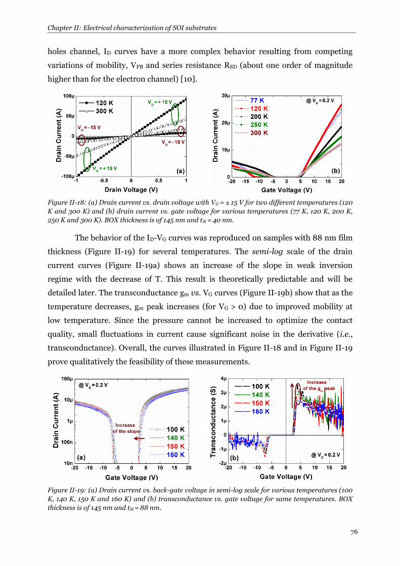
Chapter II: Electrical characterization of SOI substrates
76
holes channel, ID curves have a more complex behavior resulting from competing
variations of mobility, VFB and series resistance RSD (about one order of magnitude
higher than for the electron channel) [10].
Figure II-18: (a) Drain current vs. drain voltage with VG = ± 15 V for two different temperatures (120
K and 300 K) and (b) drain current vs. gate voltage for various temperatures (77 K, 120 K, 200 K,
250 K and 300 K). BOX thickness is of 145 nm and tSi = 40 nm.
The behavior of the ID-VG curves was reproduced on samples with 88 nm film
thickness (Figure II-19) for several temperatures. The semi-log scale of the drain
current curves (Figure II-19a) shows an increase of the slope in weak inversion
regime with the decrease of T. This result is theoretically predictable and will be
detailed later. The transconductance gm vs. VG curves (Figure II-19b) show that as the
temperature decreases, gm peak increases (for VG > 0) due to improved mobility at
low temperature. Since the pressure cannot be increased to optimize the contact
quality, small fluctuations in current cause significant noise in the derivative (i.e.,
transconductance). Overall, the curves illustrated in Figure II-18 and in Figure II-19
prove qualitatively the feasibility of these measurements.
Figure II-19: (a) Drain current vs. back-gate voltage in semi-log scale for various temperatures (100
K, 140 K, 150 K and 160 K) and (b) transconductance vs. gate voltage for same temperatures. BOX
thickness is of 145 nm and tSi = 88 nm.

Chapter II: Electrical characterization of SOI substrates
77
3.4 Extracted parameters
The -MOSFET measurements are promising because the evolution of the
curves with the temperature is qualitatively correct. In order to fully validate the -
MOSFET capability at low-T, we need to extract the transistor parameters and
compare their temperature dependence with theoretical expectations. For
quantitative analysis, we use classical MOS models for low drain voltage and strong
inversion or accumulation regime described in sub-section 1.3.
In order to avoid the impact of RSD, which is critical in our measurements
because the pressure on the probes is not tunable when using the cryogenic
equipment, the parameters (μ0, VT and S) extraction is performed with the Y-function
method previously detailed see sub-section 1.3.1.
In absence of control of pressure on the probes, reproducibility could be an
issue so we need to test it. We placed the probes again and re-tested same dies at one
day interval. The superposition of the curves is quite good (Figure II-20). These
experiments allowed calculating the variability between the parameter extracted
values: 20 % error was obtained for μp and μn values, 10 % for VT and 18 % for S.
These values are slightly higher than the ones obtained with the JANDEL system (5 −
10 %). Error bars in our next curves indicate these percentages.
Figure II-20: Drain current versus gate voltage for two curves where the empty squares curve
represents the same characterization of die 1 at one day interval compared to full squares curve. 88
nm Si film and 145 nm BOX.

Chapter II: Electrical characterization of SOI substrates
78
3.4.1 Carrier mobility
The carrier mobility reflects the capability of carriers to move in the inversion
layer under the influence of an electric field. A technology giving a good mobility
allows obtaining a high level of current which is crucial for MOS transistors.
The mobility depends on numerous parameters: electric field, orientation of
the crystal, substrate doping level, defects, temperature etc. The electron (or the hole)
does not move freely in the crystal lattice but undergoes interactions (“scattering”)
with its surroundings. The type and number of collisions the carriers experience
define the mobility magnitude and its dependence on temperature.
The carrier mobility in a semiconductor is defined by the following equation:
⟨ ⟩
(II-21)
where m* is the effective mass and τ is the average relaxation time of the carriers
between two collisions. In an inversion layer, the frequency of interactions depends
on electric field and temperature. When the interactions are independent from each
other, the average relaxation time can be written, using Matthiessen’s law [12]:
⟨ ⟩ ∑
(II-22)
where n is the number of scattering mechanisms. The resulting inverse of the
mobility can be written as:
∑
(II-23)
Therefore, the scattering mechanism with the lowest relaxation time
dominates the mobility.
We review the main effects that alter the mobility and in particular, the
various collision mechanisms in the inversion layer. Then we will extract the mobility
values with the aim of identifying the dominant scattering mechanism which brings
important information on the quality of the film and Si-SiO2 interface.
In an inversion layer, there are several types of interactions. We focus on
three main mechanisms:

Chapter II: Electrical characterization of SOI substrates
79
(i) Interaction carrier/phonon,
(ii) Coulomb interaction between carriers and charged defects
(iii) Interaction carrier/surface roughness.
Each scattering mechanisms has a specific signature on the mobility versus T
variation ([28], [29]) as illustrated below.
Phonon scattering:
This interaction resulting from vibrations of the crystal lattice is, in bulk Si
and SOI, dominant in moderate electric field (0.1-1 MV/cm) at room temperature.
There are two types of mechanisms following the energy of the carriers: the
interactions with phonons intra-valley and inter-valley. The models are complex
because they differentiate the interactions with optical and acoustic phonons which
also depend on the occupied energy valleys [30]. A review of these mechanisms as
well as their implication on the mobility of electrons in bulk Si can be found in [31].
The analytical expressions of the mobility limited by acoustic phonons in the
inversion layer are as follows:
1) At low temperatures T < 100 K, the sub-bands are not involved in the
transport because the inversion layer electrons are in the lowest sub-band.
Therefore, the interactions with intra-valley phonons are dominant and can
be modeled by [29]:
⁄ (II-24)
where Ninv is the concentration of carriers in the inversion layer.
2) At higher temperature (100 < T < 370 K), where the carriers can undergo
inter-valley and inter-sub-band phonon scattering, the mobility is
expressed by [29]:
⁄ (II-25)
where τ = 3 − 6 and n = 1 − 2 are constants depending on the crystallographic
orientation of the surface.
Note that our measurements being conducted at low VD, optical phonon
scattering can be discarded.

Chapter II: Electrical characterization of SOI substrates
80
Coulomb scattering:
These interactions occur between carriers and charged centers: ionized
dopants, interface traps Dit or oxide charges. They are called Coulomb scattering and
are mainly responsible for the degradation of the mobility in low inversion regime.
When Ninv increases the electrical potential created by the charged defects is
gradually screened by the increasing number of the mobile charges in the channel
[32]. The carrier mobility limited by charged defects (Coulomb scattering) is:
(II-26)
where Nit is the interface charge density at the Si-SiO2 interface and n = 1 − 2 is a
constant. Since μC increases with temperature, this interaction is more visible below
100 K.
Surface roughness:
The surface-roughness scattering mobility is rather independent of
temperature. Surface asperities at the Si-SiO2 constitute a major cause of scattering at
high electron concentrations. This mechanism, relevant only at high electric field (in
very strong inversion/accumulation regime where carriers are more confined near
the interface), is not likely to affect the low-field mobility. The resultant mobility can
be modeled according to Jeon et al [29] by:
(II-27)
where Eeff is the effective transversal electric field.
The relative contribution of these three scattering mechanisms depends on
the temperature and on the concentration of the carriers in the channel. At room
temperature and in weak inversion, the mobility is controlled by the collisions on
phonons and marginally by Coulomb scattering, while in strong inversion the surface
roughness is dominating. At low temperature, only the latter two mechanisms are
significant, the collisions on phonons being “masked” by the temperature decrease.
Figure II-21 summarizes this discussion in a simplistic way.

Chapter II: Electrical characterization of SOI substrates
81
Figure II-21: Schematic of the channel mobility dependence on the inversion layer carrier density for
various temperatures. The regions where a specific scattering mechanism is dominant are indicated
in the boxes [29].
We have extracted the parameters (mobility, threshold voltage and
subthreshold swing) with the Y-function method. The results in Figure II-22a and in
Figure II-22b show the T-dependence of the low-field electron and hole mobility,
respectively, in wafers with 88 and 40 nm film thickness. As theoretically predicted,
carrier mobility increases as the temperature is lowered down to 100 K and then it
decreases for T < 100 K.
In order to reveal the contribution of the scattering effects on low-field
mobility, we fit the experimental curves in Figure II-22a and in Figure II-22b with the
theoretical μ0 (T) curves deduced from the Matthiessen’s rule for electrons and holes:
( )
( )
( ) (II-28)
with:
( ) (
)
( ) (
)
(II-29)
where μ0@300 and μ0@77 represent the extracted values of low-field mobility at 300 K
and 77 K. For Coulomb mobility, we added 20 % for electrons ( = 1.2) and 50 % for
holes (α = 1.5) to μ0 values extracted at 77 K, in order to account for residual phonon
scattering and to improve the fit. No other adjustable parameter was used for curves
fitting.

Chapter II: Electrical characterization of SOI substrates
82
Figure II-22: Measured and theoretical low-field mobility for electrons (a) and holes (b) vs.
temperature T for 88 nm and 40 nm Si film thickness. Experimental error bars are about 20 %
(calculated from reproducibility measurements).
The theoretical curves deduced from equations ((II-28) & (II-29)) and the
experimental curves in Figure II-22a merge together especially for high T. The slight
difference, which subsists at very low temperature, stands within the limit of error
bars for multiple tested samples. Similar behavior is obtained for the holes mobility
(Figure II-22b). The actual fitting seems less precise due to less stable ID-VG curves
and higher series resistance RSD for VG < 0.
In order to further confirm more our results for T > 100 K, we note that the
mobility curves vary with T-n where the value of n extracted from μ(T) curves in log-
log scale is between 1 and 2 for both 88 and 40 nm film thicknesses. That is in
agreement with equation (II-25), meaning that phonon scattering mechanism
dominates at high T. Let us remind that Coulomb scattering arises from interface
traps (Dit) at Si-SiO2 interface or at the top surface because the film doping is very
low. Therefore, the decrease of the mobility with increasing temperature shows that
phonon scattering (and not Coulomb scattering) is responsible for mobility reduction
in SOI wafer. This indirectly reflects the good quality of Si film and Si-SiO2 interface.
3.4.2 Subthreshold swing and threshold voltage
The threshold voltage and subthreshold slope variations with temperature
provide valuable informations about the density of defects at the top (film/native
oxide) interface and film/BOX interface. We studied these variations and we
concentrated on the electrons side, in order to avoid the higher RSD impact that was
visible on the holes side (see Figure II-18b).

Chapter II: Electrical characterization of SOI substrates
83
The evolution of subthreshold swing (S) with T is presented in Figure II-23
and compared with the theoretical values calculated using equation below:
(
( )) (II-30)
where CSi is the Si film capacitance and Cit1,2 = qDit1,2 with Dit1,2 the interface trap
density at the top and film/BOX interfaces. The fitting values were Dit1 = 6 × 1011 cm-
2eV-1 (good Si film/BOX interface) and Dit2 = 2 × 1013 cm-2eV-1 (typical value for a poor
interface between Si film and native oxide), in agreement with the values used in [21]
and [24]. The subthreshold swing is linearly dependent on temperature. The behavior
of the measured curves is similar to the theoretical ones: S increases with T (Figure
II-23). For confirmation, we have linearly interpolated the log-log curves and
obtained variations of S ~ T1 in 88 nm and S ~ T
0.6 in 40 nm Si film. This means that
the predicted dependency with temperature is well followed for 88 nm and is less
accurate for 40 nm film.
Figure II-23: Theoretical and measured subthreshold slope curves (S) as a function of temperature T
for 88 nm and 40 nm thick Si film. Experimental error bars are about 18 %.
The discrepancy is explained by electrostatic coupling effect. As documented
earlier in sub-section 1.4, thinner films are more sensitive to the impact of top-surface
defects due to a stronger coupling between the channel and the surface. If the Si film
capacitance CSi is small (i.e. thick film: CSi << Cit2), the influence of top surface defects
is negligible in equation (II-30). On the contrary, in thinner films, CSi and Cit2, are
comparable so that Dit2 becomes relevant. The sublinear dependence of swing on
temperature is due to the increase in interface state density as the temperature is
reduced and the Fermi level approaches the band edge where Dit2 is higher [33].

Chapter II: Electrical characterization of SOI substrates
84
Figure II-24 shows the threshold voltage (VT) variation with temperature. The
theoretical curves were calculated using:
( ) (
( )) (II-31)
with:
( ) [ ( ( )
)] ( ) √ ( ) ( ) ( ( )
)
{
( ) (
)
( ) (
) ⁄
( ) (
) ⁄
(II-32)
where EG0 is the energy gap at T = 0 K (EG0 = 1.17 eV), NC0 and NV0 are the effective
density of states in the conduction band (NC0 = 1.133 × 1019 cm-3) or in the valence
band (NV0 = 2.728 × 1019 cm-3) at T = 0 K. and β are two constants ( = 4.73 × 10⁻⁴
eV/K3 and β = 636 K) [12]. The same values of Dit1,2 were used for computing both VT
(T) (in Figure II-24) and S (T) (in Figure II-23) curves.
Figure II-24: Theoretical and measured threshold voltage curves (VT) as a function of temperature T
for 88 nm and 40 nm thick Si film. Experimental error bars are about 10 %.
The experimental VT (T) variation stands close to the theoretical prediction
for T > 150 K. The difference in behavior for the 40 nm and the 88 nm films, coming
from the surface coupling, is well reproduced, which allows concluding that the -
MOSFET measurements at low T are valid for reliable extractions of VT and S.

Chapter II: Electrical characterization of SOI substrates
85
We proved the extension of -MOSFET method to low temperature for SOI
wafers. As theoretically expected, the drain current, transconductance peak and
carrier mobility increase with decreasing temperature, whereas the subthreshold
slope becomes more abrupt. The measured temperature dependence of holes and
electrons mobility fits with the theoretical curves indicating a good Si-BOX interface
quality.

Chapter II: Electrical characterization of SOI substrates
86
Conclusion
In this chapter II, we presented the -MOSFET technique, the
characterization results of ultra and extra thin SOI wafers and the first extension to
low-temperature measurements.
In section 1, the -MOSFET configuration was explained by a detailed
methodology for the characterization of SOI wafers. The results shown are from
measurements carried out on standard SOI substrates with 88 nm Si film and 145 nm
BOX. The preparation of the samples and the set-up of the equipment were
presented. Then, the extraction method of the electrical parameters was explained.
Finally, the influence of the top interface and a revisited -MOSFET model for
parameters extraction from the state of the art literature were discussed.
In section 2, we demonstrated for the first time the capability of exploring
ultra and extra thin SOI wafers using the -MOSFET with pressure probes. The
impact of the passivation of the top interface on the electrical behavior of SOI wafer
was showed.
In section 3, we extended the characterization of SOI wafers to low-
temperature measurements using -MOSFET principle. The feasibility of the
measurements using cryogenic station was verified by achieving ohmic contacts. The
drain current variation with temperature was examined by extracting the key
parameters. The measured temperature dependence of holes and electrons mobility
fits with the theoretical curves. For T > 100 K, phonon scattering mechanism
dominates and indicates a good quality of Si-BOX interface. The impact of the top
interface defects on the swing and the threshold voltage is more prominent in thinner
films and at lower temperature.

Chapter II: Electrical characterization of SOI substrates
87
References chapter II
[1] S. Cristoloveanu and S. Williams, "Point-contact pseudo-MOSFET for in-situ characterization of as-grown silicon-on-insulator wafers," Electron Device Letters, IEEE, vol. 13, pp. 102-104, 1992.
[2] S. Cristoloveanu and S. S. Li, Electrical Characterization of Silicon-On-Insulator Materials
and Devices, Kluwer, Boston, 1995.
[3] S. Cristoloveanu, D. Munteanu and M. S. T. Liu, "A review of the pseudo-MOS transistor in SOI wafers: operation, parameter extraction, and applications," Electron Devices, IEEE Transactions on, vol. 47, pp. 1018-1027, 2000.
[4] Dieter K. Schroder, Semiconductor material and device characterization (Third Edition), Wiley-Interscience, USA, 2006.
[5] A. M. Ionescu, D. Munteanu, A. Chovet, A. Rusu and D. Steriu, "The intrinsic pseudo-MOSFET technique," in Semiconductor Conference, 1997. CAS '97 Proceedings., 1997 International, pp. 217-220 vol.211, 1997.
[6] H. J. Hovel, "The HgFET: a new characterization tool for SOI silicon film properties," in SOI Conference, 1997. Proceedings., 1997 IEEE International, pp. 180-181, 1997.
[7] Vadim Kushner, Jinman Yang, Joon Choi, Trevor Thornton and Dieter Schroder, "SOI Low Frequency Noise and Interface Trap Density Measurements with the Pseudo MOSFET," ECS Transactions, vol. 2, pp. pp. 491-502, 2006.
[8] B. Jun, Y. V. White, R. D. Schrimpf, D. M. Fleetwood, F. Brunier, N. Bresson, S. Cristoloveanu and N. H. Tolk, "Characterization of multiple Si/SiO2 interfaces in silicon-on-insulator materials via second-harmonic generation," Applied Physics Letters, vol. 85, pp. 3095-3097, 2004.
[9] S. Cristoloveanu, T. V. C. Rao, Nguyen Quang Tuan, J. Antoszewski, H. Hovel, P. Gentil and L. Faraone, "The Corbino Pseudo-MOSFET on SOI: Measurements, Model, and Applications," Electron Devices, IEEE Transactions on, vol. 56, pp. 474-482, 2009.
[10] I. Ionica, I. Savin, W. Van Den Daele, T. Nguyen, X. Mescot and S. Cristoloveanu, "Characterization of silicon-on-insulator films with pseudo-metal-oxide-semiconductor field-effect transistor: Correlation between contact pressure, crater morphology, and series resistance," Applied Physics Letters, vol. 94, pp. 012111-012113, 2009.
[11] I. Ionica, A. El Hajj Diab, Y. H. Bae, X. Mescot, A. Ohata, F. Allibert and S. Cristoloveanu, "Advances in the pseudo-MOSFET characterization method," in Semiconductor Conference (CAS), 2010 International, pp. 45-51, 2010.
[12] S. M. Sze, Physics of Semiconductor Devices (Second Edition), Wiley press, New York, 1981.
[13] K. Komiya, N. Bresson, Sato Shingo, S. Cristoloveanu and Y. Omura, "Detailed investigation of geometrical factor for pseudo-MOS transistor technique," Electron Devices, IEEE Transactions on, vol. 52, pp. 406-412, 2005.
[14] Kazuo Terada, Katsuhiko Nishiyama and Kei-Ichi Hatanaka, "Comparison of MOSFET-threshold-voltage extraction methods," Solid-State Electronics, vol. 45, pp. 35-40, 2001.
[15] Hao Chu, B. Cabon-Till, S. Cristoloveanu and G. Ghibaudo, "Experimental determination of short-channel MOSFET parameters," Solid-State Electronics, vol. 28, pp. 1025-1030, 1985.
[16] G. Ghibaudo, "New method for the extraction of MOSFET parameters," Electronics Letters, vol. 24, pp. 543-545, 1988.
[17] Hon-Sum Wong, Marvin H. White, Thomas J. Krutsick and Richard V. Booth, "Modeling of transconductance degradation and extraction of threshold voltage in thin oxide MOSFET's," Solid-State Electronics, vol. 30, pp. 953-968, 1987.
[18] Q. Nguyen, "Caractérisation et modélisation électrique de substrats SOI innovants", Ph.D. dissertation, INPG, Grenoble, 2009.

Chapter II: Electrical characterization of SOI substrates
88
[19] N. Bresson and S. Cristoloveanu, "Innovating SOI films: impact of thickness and temperature," Microelectronic Engineering, vol. 72, pp. 357-361, 2004.
[20] F. Allibert, N. Bresson, K. Bellatreche, C. Maunand-Tussot and S. Cristoloveanu, "Electrical characterization of ultra-thin SOI films: comparison of the pseudo-MOSFET and Hg-FET techniques," in SOI Conference, 2005. Proceedings. 2005 IEEE International, pp. 59-60, 2005.
[21] G. Hamaide, F. Allibert, H. Hovel and S. Cristoloveanu, "Impact of free-surface passivation on silicon on insulator buried interface properties by pseudotransistor characterization," Journal of Applied Physics, vol. 101, pp. 114513-114516, 2007.
[22] Lim Hyung-Kyu and J. G. Fossum, "Threshold voltage of thin-film Silicon-on-insulator (SOI) MOSFET's," Electron Devices, IEEE Transactions on, vol. 30, pp. 1244-1251, 1983.
[23] H.J. Hovel, "Si film characterization in SOI substrates by the HgFET technique," Solid State Electronics, vol. 47, pp. 1311-1333, 2003.
[24] N. Rodriguez, S. Cristoloveanu and F. Gamiz, "Revisited Pseudo-MOSFET Models for the Characterization of Ultrathin SOI Wafers," Electron Devices, IEEE Transactions on, vol. 56, pp. 1507-1515, 2009.
[25] A. Diab, I. Ionica, S. Cristoloveanua, F. Allibert, Y. H. Bae, J. A. Chroboczek and G. Ghibaudo, "Static and low-frequency noise characterization of ultrathin SOI with very thin BOX in pseudo-MOSFET configuration," in Semiconductor Device Research Symposium (ISDRS), 2011 International, pp. 1-2, 2011.
[26] Noel Rodriguez, Sorin Cristoloveanu, Mariazel Maqueda, Francisco Gámiz and Frederic Allibert, "Three-interface pseudo-MOSFET models for the characterization of SOI wafers with ultrathin film and BOX," Microelectronic Engineering, vol. 88, pp. 1236-1239, 2011.
[27] A. Diab, L. Pirro, I. Ionica, X. Mescot, G. Ghibaudo and S. Cristoloveanu, "Low-temperature pseudo-metal-oxide-semiconductor field-effect transistor measurements on bare silicon-on-insulator wafers," Applied Physics Letters, vol. 101, pp. 092110-092114, 2012.
[28] C. T. Sah, T. H. Ning and L. L. Tschopp, "The scattering of electrons by surface oxide charges and by lattice vibrations at the silicon-silicon dioxide interface," Surface Science, vol. 32, pp. 561-575, 1972.
[29] D. S. Jeon and D. E. Burk, "MOSFET electron inversion layer mobilities-a physically based semi-empirical model for a wide temperature range," Electron Devices, IEEE Transactions on, vol. 36, pp. 1456-1463, 1989.
[30] Mark Lundstrom, Fundamentals of carrier transport, second edition, Cambridge University Press, UK, 2002.
[31] Shin-Ichi Takagi, Judy L. Hoyt, Jeffrey J. Welser and James F. Gibbons, "Comparative study of phonon-limited mobility of two-dimensional electrons in strained and unstrained Si metal--oxide--semiconductor field-effect transistors," Journal of Applied Physics, vol. 80, pp. 1567-1577, 1996.
[32] Frank Stern and W. E. Howard, "Properties of Semiconductor Surface Inversion Layers in the Electric Quantum Limit," Physical Review, vol. 163, pp. 816-835, 1967.
[33] T. Elewa, F. Balestra, S. Cristoloveanu, I. M. Hafez, J. P. Colinge, A. J. Auberton-Herve and J. R. Davis, "Performance and physical mechanisms in SIMOX MOS transistors operated at very low temperature," Electron Devices, IEEE Transactions on, vol. 37, pp. 1007-1019, 1990.

Chapter III: Novel developments of -MOSFET method
89
Chapter III:
Novel developments of -MOSFET method
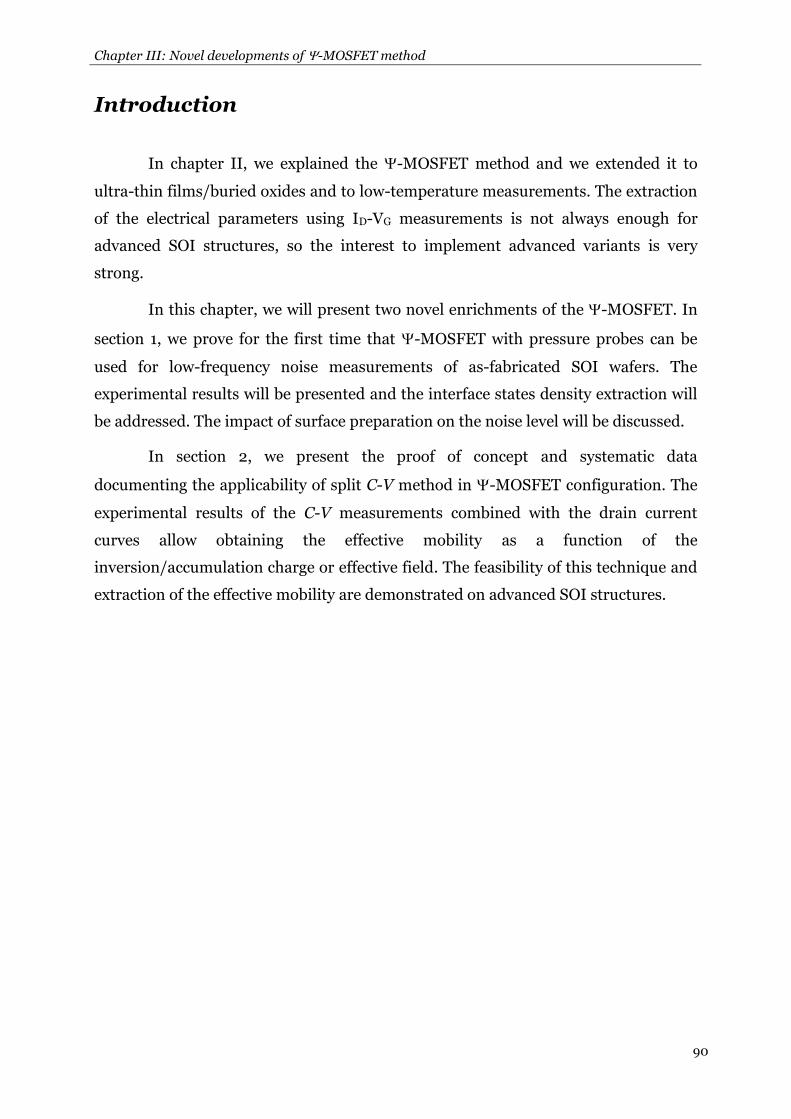
Chapter III: Novel developments of -MOSFET method
90
Introduction
In chapter II, we explained the -MOSFET method and we extended it to
ultra-thin films/buried oxides and to low-temperature measurements. The extraction
of the electrical parameters using ID-VG measurements is not always enough for
advanced SOI structures, so the interest to implement advanced variants is very
strong.
In this chapter, we will present two novel enrichments of the -MOSFET. In
section 1, we prove for the first time that -MOSFET with pressure probes can be
used for low-frequency noise measurements of as-fabricated SOI wafers. The
experimental results will be presented and the interface states density extraction will
be addressed. The impact of surface preparation on the noise level will be discussed.
In section 2, we present the proof of concept and systematic data
documenting the applicability of split C-V method in -MOSFET configuration. The
experimental results of the C-V measurements combined with the drain current
curves allow obtaining the effective mobility as a function of the
inversion/accumulation charge or effective field. The feasibility of this technique and
extraction of the effective mobility are demonstrated on advanced SOI structures.

Chapter III: Novel developments of -MOSFET method
91
1. Low-frequency noise measurements on bare SOI
wafers
1.1 Why noise measurements?
In the world of electronic devices, the noise indicates random fluctuations of
current or voltage around an average value. If these fluctuations are not engendered
by external disturbances then we talk about the “background noise” of devices. This
means that the fluctuations in current are generated by sources of noise internal to
the device. Noise has a huge impact on the electronics and analog circuits ([1], [2]) in
particular in the nano-scale area.
By consequence, it is necessary to know the low-frequency noise (LFN) and its
origin to be able to reduce it. Besides, with the transistor size shrinking, LFN impact
increases dramatically which makes the study of the noise mandatory. The noise is
sensitive to the technology, architecture, gate stacking, deposit and oxidation
processes, channel type (N or P), materials, etc.
Moreover, the noise constitutes a powerful characterization tool. LFN
measurements reveal the fluctuations of carrier mobility and concentration in the
MOSFET channel as well as the oxide quality in terms of trap density. The physical
models used to describe the fluctuation in current allow characterizing a certain
technology in terms of low-frequency noise.
LFN technique has been widely applied to FD-SOI transistors [3], offering an
insight into the trap density at the front and back interfaces, which is nowadays an
important issue in ultra-thin FD devices. In our work, we studied for the first time the
LFN on bare SOI wafers before any CMOS process in order to determine the
dominant noise source and to qualify the Si/BOX and Si/air interfaces [4].
1.2 Overview of the electronic noise
Before moving to LFN measurements in SOI wafers, let us remind the basic
theory of the electronic noise, the different sources of noises and their analysis
methods.

Chapter III: Novel developments of -MOSFET method
92
1.2.1 Fundamentals of noise
The electrical noise in electronic devices originates from the random behavior
of free carriers as a function of time. Consequently, the usual parameters (e.g. current
flowing in the device) which depend on carriers present fluctuations around their
average values. The noise can have internal or external sources. For example, the
“cross talk” between the adjacent circuits, the electrostatic or electromagnetic
coupling between the DC or AC power supply lines, the vibrations and the light are
external sources of noise. The disturbances resulting from these sources can be
eliminated by filtering. On the other hand, the internal sources of noise are related to
particular physical mechanisms. The internal noise cannot be eliminated, but it can
be reduced by the improvement of manufacturing steps and architectures. We
consider here only the internal sources of noise in devices.
The various sources of noise govern the electrical conductance (G)
fluctuations of devices and are thus accessible by the study of the current or the
voltage. A nominal static electronic signal (voltage or current) is not microscopically
stable but rather fluctuates around a fixed value. This fixed value is the mean value
measured by a voltmeter or ampermeter and the small fluctuation for the same time
period is the variance. In noise studies, it is the fluctuation or the variance of the
parameters that is measured. These microscopic fluctuations cause the electronic
noise.
The noise is always supposed to be a stationary random signal, i.e. it is
independent with time. It is also supposed to be an ergodic signal, in other words any
average of a group is equal to the temporal average. The temporal analysis of the
fluctuations does not allow separating the various sources of noise because the
amplitude of the current or the voltage fluctuations have generally a Gaussian
distribution around the average value of the signal.
Noise analysis is commonly done using the Fourier transform which allows
passing from the time domain into the frequency domain. In turn, the frequency
analysis enables to identify the source of noise and to determine the physical
characteristics relative to the noise signal. This analysis is possible through the
measurement of the power spectral density (PSD or S(f)) of the fluctuations, defined
as the frequency distribution of the power of the noise signal. S(f) is just the Fourier
transform of its autocorrelation function R(τ) given by:

Chapter III: Novel developments of -MOSFET method
93
( ) ∫ ( )
(III-1)
PSD represents the signal power or energy per Hz, hence it indicates the
signal power distribution with respect to frequency. The signal power equals to the
dissipated energy on a 1 Ω resistive load, thus its unit is W/Hz. In real applications,
the power is often denoted by the square of the real signal value either in voltage or in
current, corresponding to the two forms of PSD: SI and SV. If the PSD is measured
from a signal of drain current, the accordingly PSD is SId with the unit of A2/Hz. If the
PSD is measured from a signal of gate voltage, the accordingly PSD is SVg with the
unit of V2/Hz. It should be noted that PSD is a function in frequency domain not in
time domain.
In the next sub-section we describe the main types of electrical noise present
in a MOS transistor and the associated models.
1.2.2 Different sources of noise in MOS transistor
As already said, we focus on the internal noise sources only. Any
semiconductor-based device possesses a background noise. There are two different
families of noise sources:
The fundamental noise called white noise: intrinsic to
semiconductor material and frequency independent (the sources are
thermal and shot noise).
The excess noise: this type of noise varies with the frequency and
appears especially in the low frequency range (1/f noise, Lorentzien noise:
Generation-Recombination and Random Telegraph Signal).
In the following, we present in a synthetic way these various sources of noise.
1.2.2.1 White noise
The thermal noise, or Nyquist noise, results from the random thermal
movement of the charge carriers in a material. It is independent of applied voltage
and frequency, thus thermal noise is a white noise (i.e., its PSD is constant over a
large range of frequency, typically from few Hz to MHz). If the load is a resistance

Chapter III: Novel developments of -MOSFET method
94
with value of R and the noise is the current or the voltage drop measured on R, the
thermal noise PSD reads:
(III-2)
Shot noise: this type of noise originates from the fact that the current
flowing across a junction is not smooth and, as a result, the electrons pass through
the junction independently and at random times. Such a non-uniform or quasi-
discrete flow leads to broadband white noise, which becomes worse when increasing
the current density. The associated PSD is:
(III-3)
1.2.2.2 Excess noise
Generation-recombination (G-R) noise: in semiconductors, this noise
results from the random trapping-release of carriers which causes fluctuations in the
number of free carriers [5]. This trapping can provoke fluctuations in the mobility, in
the height of the band gap, in the thickness of the space charge region, etc. The G-R
takes place essentially in depleted regions, and is generally caused by traps located in
the band gap of the semiconductor. The noise associated with a single trap presents a
Lorentzian spectrum [6]:
( )
( ) (III-4)
where τ is the time constant characteristic (capture or emission) of the trap and ∆N is
the average fluctuation of carrier number. For low frequencies, f << 1/(2τ), the noise
spectrum presents a flat part, whereas for f >> 1/(2τ) the noise spectrum decreases
according to 1/f
2.
A special case of G-R noise is the Random Telegraph noise Signal (RTS). It is
generally related to the individual trapping of a single carrier at the Si/SiO2 interface
in MOS transistors. The traps can then capture or release carriers from or towards
the channel. The RTS noise is characterized by random rectangular signals in the
temporal domain. In the frequency domain, the S(f) spectrum is constituted by one or
several Lorentzians (i.e., a plateau followed by a slope of -2 in log-log scale), each of

Chapter III: Novel developments of -MOSFET method
95
them being characteristic of an individual active trap under the bias conditions of the
structure.
Three parameters allow the description of the temporal signal: average time
of capture τc and of emission τe (for acceptor-type) trap and the amplitude averages of
the signal ∆I. The PSD for each trap is then written [7] as:
( )
( )
(III-5)
where fc is the cutoff frequency and equals to 1/2τ.
Flicker or 1/f noise: 1/f noise (Figure III-1) generally dominates the overall
noise spectrum for the drain current at low frequencies; it is often called flicker noise
since it was observed from a flat current. The name 1/f results from the fact that its
spectrum varies with frequency as 1/fα, where the exponent α is very close to unity (α
= 1 ± 0.2). This type of noise is associated with conductivity fluctuations in the
channel [8]. The conductance fluctuations of 1/f type were observed, such as in all
semiconductors, in electronic devices and almost in all conductive materials.
Figure III-1: Example of 1/f spectrum in the frequency domain. Sample: bare SOI.
The definition of the electric conductance of a material is given by [9]:
(III-6)
where µ, n, S and L are respectively the mobility, the density of free carriers, the
surface and the length of the material under consideration.
Up to now, there is no universal explanation for the origin of 1/f noise. Two
theories have been developed for 1/f noise in microelectronic devices. According to

Chapter III: Novel developments of -MOSFET method
96
equation (III-6), G fluctuation can either be due to the carrier number fluctuation Δn
(model proposed by McWhorter [10]) or to the mobility fluctuation Δμ (model
proposed by Hooge [11]). These two sources can be simultaneously present, even if
one will be dominant [8]. Let us give some details about the two models.
Carrier number fluctuation (CNF) model:
McWhorter proposed that the drain current fluctuation is due to the
fluctuation of the mobile charge number in the channel near the
semiconductor/oxide interface [10]. ∆n results from the dynamic charge
capture/release by the slow traps distributed in the oxide. It is possible to
characterize every trap by a time constant dependent on its energy and on its position
in the oxide.
The capture of the free carriers in the traps located in the oxide causes a
change of the oxide charge (Qox). This modification of the trapped charge in the oxide
(δQox) is associated with a change of VFB [12]. Furthermore, the fluctuation in the
inversion charge (δQinv) and the oxide charge (δQox) (or the flat-band fluctuations
δVFB) are related by the equation of the gate charge conservation [12].
The fluctuation in the inversion charge, i.e. of the number of free carriers
(∆n), entails that of the drain current. In addition, a variation of Qox due to the
trapping/de-trapping of a free carrier may also lead to a variation in the effective
mobility (δµeff), resulting again in drain current fluctuation. According to Ghibaudo et
al, both possible fluctuations can be combined as [8]:
|
|
(III-7)
where is the Coulomb diffusion coefficient (≈ 104 Vs/C) [13]. The ± sign of the
mobility is chosen either negative for acceptor-like traps or positive for donor-like
traps. δVFB is the fluctuation of the flat-band voltage: δVFB = - δQox/Cox. Therefore, the
normalized PSD is written as ([8], [12]):
( )
(
)
(III-8)
where SVg and SVfb
are respectively the gate voltage and flat-band voltage power
spectral densities. Here SVfb = SQox/(Cox)2 and SQox is the spectral density of the

Chapter III: Novel developments of -MOSFET method
97
fluctuation of the oxide charge. From the second part of equation (III-8), it is clear
that if ≈ 0, i.e., mobility is not sensitive to the trapped charges, thus SVg ≈ SVfb. By
consequence, only the (gm/ID)2SVfb
subsists in equation (III-8) and the normalized
power spectral density (SId/ID
2) essentially varies as (gm/ID)
2. Note that the formulas
in equation (III-8) are valid at low and high ID.
In general, SQox depends on the physical mechanism of charge trapping by the
slow traps in the oxide. In the case of a tunneling process, the trapping probability
decreases exponentially with the depth of traps in the oxide, so SVfb is [14]:
(III-9)
where f is the frequency, γ is the characteristic exponent which is close to the unity, λ
is the tunnel attenuation distance (≈ 0.1 nm for a Si/SiO2 interface) and Nt is the
volume density of slow traps (or border traps) in the oxide near the Fermi level.
In the case of trapping process, the trapping probability decreases exponentially
with the cross section activation energy Ea, and SVfb reads [15]:
(III-10)
where ΔEa is the amplitude of the activation energy dispersion, Nit is the surface trap
density in the oxide.
Note that in the case of thermally activated mechanism, SVfb depends more
strongly on temperature for trapping process (~ T2) than for tunneling process (~ T).
Hooge mobility fluctuation (HMF) model:
Hooge attributes the conductance fluctuations to fluctuations in mobility. He
stated that the 1/f noise of the drain current is a volume phenomenon due to carrier
mobility fluctuations resulting from the phonon scattering [11].
In this case, the flicker noise amplitude is inversely proportional to the total
carrier number in the device. The normalized PSD of ID in linear regime (i.e. in the
presence of an uniform channel) is [8]:

Chapter III: Novel developments of -MOSFET method
98
( )
( )
(III-11)
where αH is the Hooge parameter, an empirical constant of ~ 10-5 for classical silicon
MOSFETs and Qinv is the inversion charge. If the transistor operates in strong
inversion and linear regime, Qinv = Cox(VG-VT,FB). Using equation (II-3) of the drain
current, equation (III-11) can be written as:
( )
(III-12)
Therefore, Hooge model is identified from equation (III-12) by a dependence
SId/ID
2 1/ID.
Once the observed LF noise shows 1/f type spectrum, the diagnostic of LFN
sources can be conducted. Because there are two competing theories to explain the LF
noise in transistors, it is necessary to distinguish which one is dominant, CNF model
or HMF model. First, the normalized SId/ID
2 for a fixed frequency is plotted with
respect to ID in log-log scale (see Figure III-2). Then, the variation of SId/ID
2 versus ID
is compared with the shape of the (gm/ID)2 versus ID curve (taken from experimental
results) by adjusting a constant factor [16]. If the two curves can be superposed, one
can conclude that the CNF model dominates and that the adjusting factor yields the
trap density according to equation (III-9).
On the other hand, if SId/ID
2 varies inversely with the drain current from weak
inversion to strong inversion, it indicates that the Hooge mobility fluctuations are
responsible for the observed 1/f noise.
Figure III-2: Schematic representation of the variation of PSD normalized by the square of drain
current versus drain current for CNF or HMF 1/f noise models.

Chapter III: Novel developments of -MOSFET method
99
1.3 LFN on SOI wafers
The -MOSFET technique has been successfully used to characterize SOI
wafers and to extract Dit from static ID-VG curves using the equation of subthreshold
swing:
(
) (III-13)
If we characterize thick SOI films (i.e. low CSi), the term between brackets (CSi
+ qDit) in equation (III-13) allows extracting Dit, if qDit is comparable (or higher) with
CSi. However, in ultra-thin films (i.e. CSi >> qDit), the qDit term is negligible and by
consequence the resolution is lost. 1/f noise could be useful for Dit extraction in ultra-
thin SOI wafers, as it shows, a better sensitivity in qualifying Si-SiO2 or Si/air
interfaces.
Schroder’s group already performed LFN measurements on SOI wafers but
with evaporated metal contacts ([17], [18]). First, they used permanent-contact -
MOSFETs with a ground–signal–ground (GSG) geometry and they were able to
measure the PSD and to extract the interface trap densities [17]. In [18], they have
adopted a circular geometry of concentric rings to study the LFN and to extract Dit
which has the advantage, compared to GSG contacts, of perfectly defined the
transistor geometry (W/L). But the main inconvenient of this technique comes from
the use of Schottky contacts to the Si film.
We performed noise measurements at wafer level using the standard -
MOSFET configuration ([4], [19]). The interest of our work comes from the use of
pressure probes to directly carry out LFN measurements on as-fabricated SOI wafers,
which requires no contact processing and ensures ohmic contacts. Therefore, the
density of traps can be determined directly at the film-BOX interface, before
transistors fabrication or any device processing.
1.3.1 LFN in -MOSFET: experimental set-up
Before showing results of LFN in -MOSFET, let us present the equipment
used: a system 3PNMS (Programmable Point Probe Noise Measuring System) from
Synergy Concepts (Meylan-France). Figure III-3 shows the manual or automatic

Chapter III: Novel developments of -MOSFET method
100
bench of measurement [20]. This system allows to obtain the static (DC) and
dynamic (AC) data (i.e., noise) simultaneously. The heart of the system consists of a
Programmable Biasing Amplifier (PBA) which has two tri-axial inputs (Input1 and
Input2) to bias the gate and the drain and an output for a current-voltage converter to
measure the drain current noise.
In MOSFETs LF noise measurements, we need two inputs for source and
drain: the Input1 is divided in two outputs with a tri-axial separator. These two
outputs are connected to the -MOSFET station to form source and drain, while
Input2 is directly related to the chuck in order to bias the gate. A voltage power
supply is used to ensure static polarization of the system where the maximum gate
voltage that can be applied is 5 V. In some specific cases a battery is connected in
series with this supply in order to apply higher gate voltage and to make manual
measurement for VG > 5 V.
The outputs (VACout) and (VDCout) are connected to a spectrum analyzer which
is in fact a National Instrument PC card managed via the PC by the software called
NOISYS. After connecting the gate, source and drain of the -MOSFET to the inputs,
the software NOISYS takes care of adjusting automatically the biasing of the drain
and the gate, as well as the gain of the current-voltage converter. Finally, the -
MOSFET station is isolated from the outside in a dark box in order to eliminate the
external noise and to obtain better isolation of the system.
From the control windows of the software, we can set the experimental
parameters: the voltage range of the gate, the number of measurements, the drain
bias and the parameters for the noise measurement: maximum frequency, average
(number of chronograms in a train) and number of points.
Figure III-3: Schematic representation of the 3PNMS system [20].

Chapter III: Novel developments of -MOSFET method
101
An important advantage of this equipment is the wide range of current for
which we can measure the noise: from 10-9 to 10-2 A, that is seven decades of current.
The possibility of detecting low current values allows subthreshold noise
measurement in MOSFETs. In addition, as shown in Figure III-3, a programmable
amplifier can be obtained for variable gain by adjusting the feedback resistance Rf.
The Input1 current of DUT (Device Under Test) is measured; here, it is the drain
current of a tested transistor configuration (FET mode is used for -MOSFET). After
fast Fourier transform, the PSD of the measured signal (SId here) is obtained.
In our study, the PSD is mainly the sum of two noise sources: the excess noise
of the drain current and the total noise of the measurement system (including the
thermal noise). This total noise of the system is removed by the corrections made
before each PSD measurement. In addition, the average values of this noise are
substracted from SId curves. Furthermore, in -MOSFET configuration we can
neglect the shot noise because no junctions are formed during the penetration of the
pressure probes into the silicon film (ohmic contacts).
Note that ID-VG curves can also be measured using this noise system but we
prefer for more accuracy to carry out static measurements using a HP-4156 before
each noise measurement. Several SOI samples were characterized and the results are
presented in the following sub-sections.
1.3.2 Experimental results
1.3.2.1 1/f noise behavior
The first step in these measurements is to verify that our new LFN technique
using -MOSFET with pressure probes leads to exploitable results. Figure III-4a
shows the power spectral density, SId, plotted versus frequency for a SOI wafer with
88 nm thick Si film and 145 nm BOX for various back-gate voltages. The 1/f (flicker
noise) behavior is clearly visible. To verify if this behavior is valid for ultra-thin SOI
films, we traced SId versus frequency for various VG in SOI with 12 nm Si film and 145
nm BOX thicknesses (Figure III-4b). Same type of noise (flicker noise) is found. All
the measurements are carried out at low drain voltage ensuring linear mode
operation.

Chapter III: Novel developments of -MOSFET method
102
Figure III-4: PSD versus frequency in -MOSFET: (a) 88 nm thick Si film and (b) 12 nm ultra-thin Si
film with 145 nm BOX. 1/f noise is clearly evidenced in both SOI films.
The results in Figure III-4 prove the possibility to extend the -MOSFET
capabilities to LFN measurements. 1/f noise type is obtained in either relatively thick
or ultra-thin SOI layers. In very thin films (12 nm) the impact of the top free surface
on the noise of the remote buried channel (at film-BOX interface) is more significant
than in thicker films (88 nm). This is why the noise level is higher in Figure III-4b.
Note that the curves in Figure III-4b are obtained by manual measurements using a
battery in series with the power supply in order to achieve 40 V as gate bias.
1.3.2.2 Noise model: CNF or HMF?
Let us remind that 1/f noise is associated with conductivity fluctuations in the
channel and that two phenomena could be responsible for these fluctuations: the
carrier number fluctuations (CNF) or the Hooge mobility fluctuations (HMF). In
order to determine which of the two models better accounts for the LFN data, it is
required to plot a normalized PSD as a function of the drain current in log-log scale
as explained in sub-section 1.2.2.2. In the mobility fluctuations model one expects to
obtain a linear decrease of log (SId/ID
2) with log (ID). In the CNF, the normalized PSD
follows the (gm/ID)2 dependence: a flat part in weak inversion and a (ID)
-2 dependence
for the strong inversion regime.
Figure III-5 shows that the normalized PSD follows (gm/ID)2 dependence
corroborating the CNF model. In Figure III-5a, the normalized PSD as a function of
ID shows a plateau in weak inversion and a linear decrease in strong inversion, as it is
proportional to a constant (gm/ID)2. For further confirmation of our results, we show

Chapter III: Novel developments of -MOSFET method
103
in Figure III-5b the normalized PSD multiplied by frequency plotted versus ID at
different extrapolated frequencies (fext) equal to 10, 20 and 30 Hz.
Figure III-5: (a) Normalized PSD and cst (gm/ID)2 versus ID (with cst ≈ 10-9 and p = 50 g). (b)
Normalized PSD noise multiplied by frequency versus ID (p = 70 g) for various frequencies. 88 nm Si
film and 145 nm BOX thicknesses.
The curves are superposed. The frequency-independent curve confirms
correctness of the CNF model of 1/f noise in thick films. Therefore, the extraction of
the Dit should be possible; we will discuss the method and the values obtained in sub-
section 1.3.2.4.
1.3.2.3 Probe pressure impact on LFN
Before discussing the quantitative results, an important issue is related to the
impact of the probe pressure. As already mentioned in chapter II, the transport
properties of the -MOSFET may depend on the probe pressure. It is well known,
that the probe pressure controls the series resistance (RSD decrease at higher
pressures [21]).
Figure III-6 shows the normalized PSD versus drain current on the 88 nm
thick film for different pressures applied on the probes. The noise level is almost
pressure-independent, even though the series resistance of the device varies. This
result proves that the series resistance does not act as an additional noise source or,
at least, does not play the dominant role as a noise source in this configuration.

Chapter III: Novel developments of -MOSFET method
104
Figure III-6: Normalized power spectral density noise versus drain current in -MOSFET with 88
nm film thickness for various probe pressures (50 g, 60 g and 70 g).
1.3.2.4 Dit extraction
Our results demonstrate the feasibility of LFN measurements and also that
the key mechanism responsible for this noise in 88 nm thick films is the carrier
trapping by shallow traps located in the BOX. These results allow us to obtain the Dit
value using the equations below:
( )
(
)
(III-14)
We briefly explain the extraction method before we show the obtained values.
The variation of the normalized PSD obtained in strong inversion follows (ID)-2
, this
means that there is no mobility correlation with CNF model. Therefore, ≈ 0 and
equation (III-14) becomes:
( )
(III-15)
First, we extrapolate the SVfb value by fitting the two curves SId
/ID2 and
(gm/ID)2. Note that the (gm/ID)
2 curve is obtained from static measurements and SId
represents the values of the PSD for all the VG range chosen at the same frequency (f).
Then, we replace this value and the values of q, γ, k, T, Cox and f in the second part of
equation (III-15). We still have to determine two terms (W and L) in order to extract
Nt. In -MOSFET, L can be interpreted as the space distance between source and
drain probes (= 1 mm) but the value of W (width of the inversion or accumulation

Chapter III: Novel developments of -MOSFET method
105
layer in the Si film) is unknown. There is no gate to define the inversion or
accumulation area compared to MOSFET transistors.
We tried to solve this problem by using the geometrical factor (fg = W/L ≈
0.75). L is equal to 1 mm therefore W is equal to fg multiplied by L (i.e., W = 0.75
mm). Finally, we extract the Si-SiO2 interface traps density value from the relation Dit
= λ Nt where λ is equal to 0.1 nm. However, the Dit values (≈ 1013-14 cm-2.eV-1)
obtained from the LFN data are 2-3 orders of magnitude higher than those extracted
from the static measurements (Dit ≈ 1010-11 cm-2.eV-1). Two arguments can be offered
to explain these high Dit values.
First, may be underestimated by W L value. The channel charge controlled
by the substrate bias occupies a larger surface, beyond the area defined by the
contacts.
The second explanation lies on the idea that the extra-noise might be
generated at the free wafer surface (Si/air interface). Since the film is fully depleted,
there is a direct electrostatic coupling between the surface and the buried channel. In
general and as shown in chapter II, the quality of the free surface influences the
transport and thus the LFN of the channel. In the following we will see the impact of
this top interface on LFN results in SOI wafers.
1.3.2.5 Impact of the surface preparation on LFN
We investigated the influence of the top free-surface quality on LFN by
comparing passivated and non-passivated samples. Let us remind that the non-
passivated wafers are covered by native oxide forming a very poor interface with the
Si film whereas the passivation step (thermal oxidation) is known to decrease the
density of interface states at the free surface.
In static ID-VG -MOSFET measurements, the surface passivation leads to
improvement of mobility, subthreshold swing and threshold voltage, as documented
in chapter II. In LFN, the variation of the surface states density is expected to affect
the measurements, because these states act as trapping centers also inducing carrier
number fluctuations in the device channel via electrostatic interface coupling. The
noise level should be lower in passivated samples.

Chapter III: Novel developments of -MOSFET method
106
That issue was studied on thin Si films where the channel-surface coupling is
strong. We plotted in Figure III-7a the PSD versus frequency before and after
passivation for 12 nm ultra-thin film and 145 nm BOX, measured at the same drain
current (ID = 10-6 A) for the same probe pressure. The passivation does not alter the
1/f noise behavior. However, contrary to our expectations, a higher level of noise is
measured in the passivated sample with 12 nm thick film.
The question is whether the film thickness may cause this difference in noise
level between passivated and non-passivated samples.
In order to explore further this question, we examined in Figure III-7b the
PSD versus frequency plots for 88 nm film and 145 nm BOX before and after
passivation, measured at the same drain current (ID = 3 10-6 A). A higher noise level
is again observed on passivated wafers. The variation of film thickness for passivated
samples does not account for the difference between the levels of noise in samples
with and without surface treatments.
The surprising difference in noise level may be explained by change in series
resistance. RSD value in passivated samples (e.g., RSD ≈ 26 KΩ in 12 nm Si film) is one
order of magnitude higher than in non-passivated samples (e.g., RSD ≈ 2.8 KΩ in 12
nm Si film). The series resistance values are extracted from ID-VG curves using
equation (II-13). In passivated samples, the pressure probes must penetrate first the
oxide passivation layer (between 4 and 10 nm thickness) and then the Si film which
induces additional access resistance compared to non-passivated samples. Systematic
measurements on additional SOI wafers are needed to fully confirm this scenario.
Figure III-7: Power spectral density versus frequency at VD = 0.2 V in: (a) 12 nm thick film for
passivated and non-passivated surface at the same ID = 10-6 A and probe pressure and (b) in 88 nm
thick film for passivated and non-passivated surface at ID = 3 10-6 A. Box thickness is 145 nm.

Chapter III: Novel developments of -MOSFET method
107
1.3.2.6 Feasibility of LFN on extra-thin SOI structures
In chapter II, we confirmed the adaptability of -MOSFET technique to
extra-thin SOI structures (e.g., 20 nm film and 10 nm BOX) for ID-VG measurements.
Let us also prove here the feasibility of LFN characterization on these films. The low-
frequency noise is of 1/f type (Figure III-8a) for various VG, which confirms the same
behavior as in the thicker SOI structures shown previously.
We traced in Figure III-8b the normalized PSD versus frequency for the SOI
wafer with 20 nm film and 10 nm BOX thickness. The clean noise signature (‘plateau’
in weak inversion and rapid decrease in strong inversion) indicates that CNF model is
responsible for the LFN in such SOI structures.
Figure III-8: Power spectral density versus frequency for various gate voltages, (b) normalized
power spectral density versus drain current. 20 nm film and 10 nm BOX thicknesses.
While the results in Figure III-8 open the road for noise-based
characterization of SOI wafers, the Dit extraction still demands an accurate evaluation
of the (W L) term and of the contribution of the free surface traps.
1.4 Conclusion of section 1
The results above proved for the first time the feasibility of LFN
measurements at wafer level using the -MOSFET configuration with pressure
probes. 1/f noise behavior in relatively thick and ultra-thin SOI layers is obtained.
CNF model accounts best for the 1/f noise. A technique to extract the interface traps
density from noise measurements is possible. Unfortunately, the estimation of the
actual geometrical factor W L is a real challenge for Dit extraction.

Chapter III: Novel developments of -MOSFET method
108
No probe pressure dependence of the noise is observed at least in non-
passivated samples. The influence of wafer surface preparation and the sources of
noise need further clarification. The quantitative separation of the impact of free
surface traps and BOX traps on noise level is a challenging issue. Comparing samples
with and without HF treatment could bring additional information for the better
understanding of the top surface influence on LFN.
Finally, we demonstrated the capability of exploring very thin as-grown SOI
films, down to 20 nm, and BOX layers down to 10 nm, using the -MOSFET by
combining current, transconductance and noise measurements.

Chapter III: Novel developments of -MOSFET method
109
2. Split C-V measurement in -MOSFET configuration
2.1 Split C-V technique and principle
The most common method used to measure the effective mobility (μeff) is the
split C-V technique. The effective mobility is a key parameter that characterizes the
electrical transport in MOSFETs. Split C-V method is based on two capacitive
measurements and a current-voltage measurement in order to obtain the variation of
the effective mobility with the effective electric field (Eeff). This technique was first
developed for the characterization of the interface trap density and the substrate
doping concentration in silicon MOSFETs [22]. Afterwards it was applied to the
effective mobility analysis [23]. Nowadays, it is commonly used to compare the
impact of the technological parameters on the effective mobility [24].
In a split C-V method, the capacitance between the gate and source-drain
(denoted as Cgc) and the capacitance between the gate and the substrate (denoted as
Cgb) are measured, as shown in Figure III-9.
At high frequency, we carry out a measurement of the gate-to-channel
capacitance that reflects the variation of the inversion charge with the gate voltage.
Figure III-9a illustrates how to measure the Cgc: the gate is connected to the high
potential, the source and the drain are together connected to the low potential and
the substrate is grounded. In this configuration, the capacitive response of the
inversion channel of carriers is measured. In strong inversion the capacitance tends
to saturate to the effective value of the oxide capacitance (Coxeff) [25].
The second step is the measurement of the gate-to-bulk capacitance. This
time, the source and the drain are grounded and it is the bulk which is connected to
low potential, the gate being always at high potential (see Figure III-9b). In this
configuration, the capacitive response is no longer given by the inversion channel but
it is related to the charge variation in the depleted area (which is gate controlled).
The inversion and the depletion charges are obtained by the integration of the
Cgc and Cgb capacitance curves:
( ) ∫ ( )
( ) ∫ ( )
(III-16)

Chapter III: Novel developments of -MOSFET method
110
where Vacc is the gate voltage taken in accumulation.
Let us note that for FD-SOI transistors, the depletion charge (Qdep) can be
neglected compared to Qinv, which simplifies the procedure of the μeff extraction.
Finally, the effective mobility is calculated by using the measured values of
the drain current in ohmic regime:
(III-17)
In the following sub-sections we will extend the split C-V technique for -
MOSFET in thick and thin SOI wafers [26].
Figure III-9: Schematic representation of (a) gate-to-channel capacitance and (b) gate-to-substrate
capacitance measured in bulk Si-MOSFET.
2.2 Interest of split C-V for SOI wafer characterization
Split C-V measurements are usually carried out on fully processed SOI
MOSFETs [27]. The interest of our work on split C-V measurements comes from the
use of -MOSFET with pressure probes, which requires no contact preparation. For
this reason, the rapid extraction of the mobility in SOI wafers before any CMOS
processing is a key methodology to monitor and optimize the quality of the starting
substrates.
Traditionally, the Y-function [28] has been a preferred technique for such
task. However, the information that can be obtained on carrier mobility is limited
(low-field mobility), and the plot of mobility versus inversion/accumulation charge or
effective field is only approximated and reconstructed. A more direct approach is

Chapter III: Novel developments of -MOSFET method
111
based on the determination of the inversion or accumulation charge from capacitance
measurements combined with static ID-VG curves. Another important aspect of split
C-V is that it is valid from weak to strong inversion.
2.3 Extension of -MOSFET for split C-V measurements
In this sub-section, we will present the method used to characterize SOI
wafers with split C-V using -MOSFET and the results obtained.
2.3.1 Method and experiment
In MOSFETs, the split C-V technique is based on the measurements of the Cgc
and Cgb capacitances as a function of the gate voltage. However, in -MOSFET
structure, the Si substrate acts as gate and no top metal gate is available, therefore
only the Cgc can be measured.
Two types of -MOSFET measurements were performed: static ID-VG curves
and split C-V curves. In our measurements, both Cgc-VG and ID-VG characterizations
were conducted using the JANDEL station with pressure-controlled probes.
In the -MOSFET configuration for C-V measurements, the source and drain
probes were connected to low potential, whereas the back gate was biased to VG and
connected to high potential of the LCR meter (Figure III-10). The schematic of the
measurement system and the equivalent circuit are shown in Figure III-10. A Cp-G
model is used for eliminating the dispersive effect of the resistance (R = 1/G) in the
capacitance curves.
The LCR meter was properly calibrated with two corrections before the
measurements, the open procedure and short procedure, in order to eliminate the
parasitic capacitance and to guarantee the best accuracy for the absolute capacitance
measurement. The mean value of the parasitic capacitance resulting from the two
successive corrections is automatically subtracted from the measured capacitance
value. The split C-V measurements were performed using a standard Agilent E 4980A
LCR meter for a frequency range from 20 Hz to 5 kHz. Before each split C-V
measurement, ID-VG characteristics were recorded with a HP-4156. The current
measurements were performed at low drain voltage to ensure ohmic behavior.

Chapter III: Novel developments of -MOSFET method
112
Figure III-10: Schematic configuration for the split C-V technique with the equivalent circuit
representation (Cp-G model).
2.3.2 Experimental C-V curves
The proof of concept was checked on different geometries of SOI structures.
We show here only two structures: the first with 200 nm film/400 nm BOX (Figure
III-11a & Figure III-11b), the second with 20 nm film/145 nm BOX (Figure III-11c &
Figure III-11d). As already known, both electrons (VG > 0) and holes (VG < 0) channels
are activated, as illustrated in Figure III-11a and Figure III-11c by the ID-VG curves.
Sweeping the gate voltage, a small AC sinusoidal signal is superposed to the
DC bias in order to detect the charge variation with respect to the small AC signal;
hence the capacitance of Cgc can be calculated for each bias. The Cgc-VG curves for
different frequencies are reproduced in Figure III-11b & in Figure III-11d. When the
film is depleted (VG ≈ 0 V), the capacitance is zero. Then, the capacitance increases
reflecting the gradual build-up of the inversion or accumulation channel. When the
capacitance of the inversion/accumulation charge well exceeds the oxide capacitance,
a maximum value of the capacitance, corresponding to the BOX capacitance (CBOX), is
obtained at both positive and negative voltages.
The shape of C-V curves for the two wafers confirms this observation.
Therefore, our new technique experimental is successfully validated for thick and for
thin SOI structures.
In the following parts we will focus on frequency and probe pressure impact
on Cgc curves.

Chapter III: Novel developments of -MOSFET method
113
Figure III-11: (a) ID vs. VG and (b) Cgc vs. VG for SOI wafer with 200 nm Si film and 400 nm BOX. (c)
ID vs. VG and (d) Cgc vs. VG for SOI wafer with 20 nm thin Si film and 145 nm BOX.
2.4 Impact of experimental conditions on C-V measurements
2.4.1 Probe pressure impact on C-V curves
From split C-V curves a maximum value of the capacitance is obtained at
either positive or negative voltages in -MOSFETs. We studied the impact of the
pressure of the probes on split C-V measurements. Figure III-12 shows Cgc-VG curves,
where Cmax increases for higher probe pressure. This effect is related to the contact
improvement (decrease of the drain/source series resistance) as the probe pressure is
increased [21]. For lower pressures, the S/D resistance is higher and, therefore, it is
more difficult for carriers to be injected and spread. Consequently, the effective
surface of the capacitance is reduced. At high pressure values (over 70 g), the
capacitance value becomes saturated. The optimum pressure depends on the film and
BOX thicknesses and has to be calibrated prior to mobility measurements.

Chapter III: Novel developments of -MOSFET method
114
Figure III-12: Cgc vs. VG curves for different probe pressures on SOI wafer with 88 nm Si film and 145
nm BOX.
2.4.2 Frequency effects
Figure III-13a shows the dependence of the capacitance curves on the
frequency from 100 Hz to 5 kHz for SOI wafer with 88 nm thick silicon film and 145
nm thick BOX. As already observed in Figure III-11, the C-V curve behavior is not
similar for electrons and holes. For frequencies below 500 Hz, the maximum
capacitance remains saturated and symmetrical for electron and hole channels (see
Figure III-13b). Above 500 Hz, the capacitance saturation value decreases due to the
limited frequency response of the carriers to the AC signal. For higher frequency, the
maximum capacitance value is lowered and the curves become asymmetrical. This
reduction of the capacitance can be attributed to several reasons:
Figure III-13: (a) Cgc-VG curves for various frequencies. (b) Cmax values for various frequencies. 88
nm Si film and 145 nm BOX.
Time diffusion of carriers. Since the gate is the substrate, one may
imagine that the inversion/accumulation layers cover the whole sample surface. This

Chapter III: Novel developments of -MOSFET method
115
is not the case and a Seff value must be considered. At higher frequency, the diffusion
of the carriers injected from the needles is limited. Carriers located far from the
contacts are not able to follow the AC signal. Therefore the effective area covered by
the carriers will be lower, leading to a reduction of the total capacitance [29]. As the
diffusion coefficient of holes in silicon is about three times lower than that for
electrons, the effective area is smaller in accumulation than in inversion and may
cause the C-V asymmetry at higher frequencies.
Surface carrier spreading. Another explanation of the area dependence
with the AC frequency was proposed by Fernandez et al [30] for thick BOX SOI
wafers. The model relates the dependence of Seff with frequency by a simple model
which suggests that the surface carrier spreading is the actual origin of the
capacitance reduction. They proposed a simple geometrical method to evaluate the
two needle capacitance from single-needle measurements. The area covered by the
collected carriers in single-needle configuration is supposed to have a circular shape
(Figure III-14a). By consequence, the effective surface in two-needle configuration
can be derived as the combination of the areas covered by the carriers injected from
each probe (Figure III-14b). Their results show a good agreement between the model
and the experimental curves for hole and electron channels (Figure III-15).
Figure III-14: Schematic representation of the area covered by the carriers in (a) single-needle and
(b) two-needle configurations [30].
Figure III-15: Comparison between the effective surfaces obtained from experimental and model in
two-needle configuration: (a) hole channel and (b) electron channel. 88 nm Si film and 145 nm BOX
[30].

Chapter III: Novel developments of -MOSFET method
116
Back-gate depletion. The gate of the -MOSFET is far from being an ideal
MOS-like gate. The doping in the substrate of our samples is relatively low (NA ≈ 1015
cm-3) and the total thickness of the substrate exceeds 500 μm. When the gate bias is
negative, the wafer substrate tends to be first depleted and then inverted with
electrons at the substrate-BOX interface. Due to the p-type character of the
substrates, electrons (minority carriers in the substrate) are more difficult to generate
than holes which are available in the substrate. At higher frequencies, the substrate
electrons are less prone to follow the AC signal [31]. By contrast, for positive gate bias
(inversion channel in the -MOSFET film but accumulated substrate-BOX interface),
many holes are present in the substrate, so eliminating the substrate effect. The
different behavior of carriers transport for positive and negative gate voltage can
explain the substrate depletion effect and its impact on C-V curves.
In order to examine the substrate effect, we characterized SOI with thick
silicon film (180 nm) and ultra-thin BOX (10 nm). Figure III-16a shows the ID-VG
curve and Figure III-16b illustrates the Cgc-VG curves for various frequencies.The
maximum capacitance values for electrons and holes are different, so the depletion
underneath the BOX may be invoked. According to this scenario, the decrease of the
measured capacitance for negative VG values is the result of the series combination
between Cox and the capacitance associated to the substrate depletion layer (only
present for negative VG values). Note that this behavior was also obtained for very
thick BOX (400 nm) with thick Si film (200 nm) in Figure III-11b. The substrate
depletion effect is expected to be more pronounced in thin BOX wafers. The
difference between the curves in Figure III-16b and Figure III-11b tends to confirm
this hypothesis. A similar effect has been addressed by Schroder et al [29] who used
metallic contacts deposited on the wafer surface.
Figure III-16: (a) ID vs. VG and (b) Cgc vs. VG for SOI wafer with 180 nm thick Si film and ultra-thin 10
nm BOX.

Chapter III: Novel developments of -MOSFET method
117
In this case, the maximum capacitance value can be corrected by including
the depleted substrate capacitance Csub:
(III-18)
However, the split C-V method is frequently and successfully utilized in FD-
SOI MOSFETs without corrections for the substrate effects, including the Csub(VG)
dependence. Based on this argument and as long we use thick BOX (145 nm for
example), we can also neglect the substrate depletion for split C-V in -MOSFET.
From our point of view, the primary reason for frequency effects is the
modification of the effective surface. The time constant of the RC circuit formed by
the channel resistance and capacitance depends on carrier mobility, film thickness
and BOX thickness. The channel resistance is obviously higher for holes and thinner
films, leading to a smaller effective surface, in particular at low frequency. The
frequency-dependent effective area corresponding to Figure III-13b, Seff is equal to
Cmax (F) divided by Cox (F/cm2), is shown in Figure III-17 and given by:
(III-19)
Note that this area is, even at the lower frequencies, smaller than the physical
area of the Si island etched on the SOI wafers (25 mm2). On the other hand it is much
larger than the surface involved in -MOSFET operation (W/L ≈ 0.75, hence W L ≈
0.75 mm2).
Figure III-17: Frequency dependence of the effective surface, Seff, values obtained by neglecting the
substrate effects. Same sample as in Figure III-13b with 88 nm Si film and 145 nm BOX.
In order to explain the maximum capacitance variation with the frequency for
the split C-V measurements we propose an analytical model. The physics behind our

Chapter III: Novel developments of -MOSFET method
118
model is based on the fact that the creation of the inversion (or accumulation) layer is
not instantaneous. Indeed the carriers need to be supplied by the pressure probes.
This induces a time constant that can be neglected for low frequency measurements
but that can disturb the higher frequency measurements. The equation setting for our
model is done using a RC low-pass filter. The model is under study and here we will
only show the preliminary results. The fitting between the model and the
experimental curves in (Figure III-18) confirm our expectation for both electron and
hole sides.
Note that the effective mobility curves will not be affected by these
considerations as long as the measurement is performed at frequency low enough.
Although the frequency dependence of C-V characteristics is theoretically interesting,
it does not challenge the practical implementation of the split C-V method in -
MOSFET in order to extract the effective mobility.
Figure III-18: Experimental and calculated C-V curves for (a) holes and (b) electrons in 88 nm film
thickness and 145 nm BOX thickness.
2.5 Extraction of μeff by split C-V technique
In order to obtain more quantitative results, we will discuss, in this sub-
section, the methodology to extract effective mobility from the experimental curves
and the results obtained.
2.5.1 Adapted methodology to extract μeff
Traditionally, two methods are used to evaluate μeff versus VG, defined as:
( ) (III-20)

Chapter III: Novel developments of -MOSFET method
119
Y function method. This technique is indirect, based on the conventional
ID-VG measurements [28]. As mentioned earlier that VT,FB and the low-field mobilities
μn,p are extracted from the Y-function.
The inversion charge Qinv(VG) and the accumulation charge Qacc(VG) are
calculated using VT and VFB:
( ) ( ) ( ) ( ) (III-21)
where Cox is the BOX capacitance per unit area (Cox = εox/tBOX).
Equation (III-21) is a good approximation in strong inversion and
accumulation. It serves to reconstruct the effective mobility μeff(Qinv,acc) curves.
However, the relations (III-21) fail in weak and moderate inversion.
Split C-V method. This direct technique serves to evaluate μeff(Qinv,acc)
curves from split C-V measurements. For split C-V, Qinv(VG) and Qacc(VG) are
obtained by integrating the measured capacitance over the positive and negative VG
range, respectively:
( )
∫ ( )
( )
∫ ( )
(III-22)
where V0 is equal to (VT + VFB)/2, in our case V0 ≈ 0V. Normalization by the effective
surface (Seff) is necessary in order to obtain the inversion or accumulation charge
density per unit area.
The effective surface represents the maximum area where the electrons (or
holes) participating to the strong inversion (or accumulation) are sensed during the
measurements. In this area, the carriers are able to follow the AC gate bias signal. The
maximum capacitance value Cmax represents the gate-oxide capacitance [23]. In
regular MOSFETs, where the size of the gate and body is defined by lithography, Cmax
serves to determine the equivalent oxide thickness.
In bare SOI wafers, the situation is different. The BOX thickness is accurately
known from ellipsometry but the -MOSFET capacitor dimensions are ill defined
and Seff must be calculated. As showed in equation (III-19), the effective area is found
by dividing Cmax (F) by Cox (F/cm2), where Cmax is the maximum capacitance extracted
from split C-V data at positive VG for electrons and at negative VG for holes.

Chapter III: Novel developments of -MOSFET method
120
Two main differences can be concluded from these two methods. First, the μeff
evaluated from static measurements is reconstructed by calculating the Qinv,acc(VG).
For split C-V technique μeff is still obtained from equation (III-20) but the charge
Qinv,acc(VG) is directly measured by integrating the capacitance (Cgc) over the selected
VG range. The second key difference between these two methods is that split C-V is
valid from weak to strong inversion.
We used these two methods to calculate the electrons and holes mobility μeff,
as shown in Figure III-19. The effective mobility versus VG in SOI samples with 88
nm film and 145 nm BOX is illustrated in Figure III-19a for electrons and in Figure
III-19b for holes. The mobility curves from static and split C-V match together and
superpose in strong inversion for electrons and in strong accumulation for holes.
These experimental results confirm the feasibility and efficiency of the split C-V
technique using -MOSFETs and also show that our adapted model for the
extraction of Seff and μeff is successfully verified.
Figure III-19: μeff as a function of VG calculated from static ID-VG and split C-V curves for electrons
(a) and for holes (b). 88 nm Si film and 145 nm BOX.
2.5.2 Applications of μeff extraction for advanced SOI structures
The previous sub-section proved that our split C-V technique of mobility
extraction is valid for 145 nm BOX thickness. Very thin BOX (25 nm) is currently
needed for short-channel effects reduction in advanced SOI CMOS.
In Figure III-20, the Cgc-VG curves in 88 and 12 nm Si film with 25 nm BOX,
measured for various frequencies, show same behavior as the one obtained previously
for 145 nm BOX.

Chapter III: Novel developments of -MOSFET method
121
Figure III-20: Cgc vs. VG for SOI wafer with: (a) 88 nm thick Si film and thin 25 nm BOX and (b) 12
nm thin Si film and thin 25 nm BOX.
Figure III-21a and Figure III-21b show the corresponding mobility curves for
88 nm Si film thickness. The effective mobility extracted from the two methods (split
C-V and Y-function) match together for both electrons and holes. Figure III-21c
shows the electron effective mobility for ultra-thin 12 nm Si film where the two
methods again give the same results. Note that the hole mobility for 12 nm film was
not studied due to the high impact of RSD which is visible in the C-V curves for
negative VG.
Figure III-21: μeff as a function of VG calculated from static ID-VG and split C-V curves for electrons
(a) and for holes (b) in 88 nm Si film and 25 nm BOX and for electrons (c) in 12 nm Si film and 25 nm
BOX.
Further investigations were done to validate the method. We compared the
mobility, determined by split C-V in passivated and non-passivated SOI wafers for
electrons channel. Figure III-22a shows the effective mobility plotted versus back
gate voltage for 145 nm thick BOX samples with passivated (empty squares) and non-
passivated (solid squares) surfaces, measured for same experimental condition.

Chapter III: Novel developments of -MOSFET method
122
The split C-V method clearly confirms that passivated sample offers better
mobility compared to the non-passivated one, in agreement with [32] and [33]. The
beneficial effect of surface passivation on electron mobility is also observed for thin
BOX (25 nm) with 88 nm Si film in Figure III-22b.
Figure III-22: μeff from split C-V for passivated and non-passivated wafers for electrons: (a) in 88
nm Si film and 145 nm BOX and (b) in 88 nm Si film and 25 nm BOX.
The passivation reduces the surface charge and the related vertical field. Its
effect is therefore expected to be more pronounced in thinner films (~ 10 nm). To
confirm this hypothesis, we compared passivated and non-passivated SOI samples
with ultra-thin 12 nm Si film and 25 nm BOX in Figure III-23.
The effective mobility is visibly higher (up to 30 %) in passivated sample than
in the non-passivated one. These results confirm the previously reported ones ([32],
[33]), but their merit is to be obtained for the first time on such thin film/BOX couple
(25 nm BOX) with our new split C-V technique.
Figure III-23: μeff as a function of VG calculated from split C-V curves for passivated and non-
passivated 12 nm Si film with 25 nm BOX.

Chapter III: Novel developments of -MOSFET method
123
2.6 Conclusion of section 2
We demonstrated the feasibility of split C-V measurements on as-fabricated
SOI wafers using -MOSFET configuration. An adapted methodology to determine
the effective mobility of electrons and holes by split C-V technique was proposed and
validated through comparison with the effective mobility extracted from static
measurements. The method has been applied to different SOI materials (thin and
thick film/BOX, passivated and non-passivated surface). The electron mobility can
exceed 500 cm2V-1s-1 in thin SOI films with passivated surface. The frequency and
substrate depletion effects as well as the role of probe pressure have been
documented.

Chapter III: Novel developments of -MOSFET method
124
Conclusion
In this chapter III, we presented two novel applications of the -MOSFET.
First, the -MOSFET configuration has been extended to the low-frequency noise
characterization of as-fabricated SOI wafers. Second, we introduced a new efficient
characterization technique for bare SOI, based on split C-V measurement using -
MOSFET.
In section 1, low-frequency noise measurements were carried out, for the first
time, on SOI substrates in the -MOSFET set-up with pressure probes. The low-
frequency noise is shown to be of 1/f type and is clearly associated with the carrier
number fluctuation in the channel, due to the trapping/de-trapping of carriers. For
static measurements the pressure plays a key-role in order to obtain small series
resistance; the noise does not seem to depend on the pressure for the thicker films
(88 nm). Dit values can be extracted using this new method, but higher values
compared to extraction made from static curves were obtained. Passivated samples
show an unexpectedly high level of noise compared to non-passivated samples for
both 12 and 88 nm film thickness. The impact of series resistance and free surface
preparation on the channel properties is suspected to be significant.
In section 2, we showed that the -MOSFET can also be used for split C-V
measurements in bare SOI wafers. Several variants of SOI wafers have successfully
been tested. The probe pressure needs to be high enough for accurate capacitance
curves while avoiding probe penetration through the ultra-thin Si film and BOX. A
variation of the maximum capacitance in the high frequency regime was observed
and explained. An adapted model for -MOSFET was proposed for extracting the
effective mobility from the split C-V curves. The mobility curves were systematically
compared with those obtained from static measurements using the Y-function
method. Excellent agreement was obtained validating our approach. Samples with
passivated surface show higher mobility values than non-passivated ones. The impact
of film/BOX thickness and interface quality on the effective carrier mobility can be
accurately investigated using this new -MOSFET capability to assimilate the split C-
V technique.

Chapter III: Novel developments of -MOSFET method
125
References chapter III
[1] Y. Nemirovsky, I. Brouk and C. G. Jakobson, "1/f noise in CMOS transistors for analog applications," Electron Devices, IEEE Transactions on, vol. 48, pp. 921-927, 2001.
[2] R. Brederlow, W. Weber, D. Schmitt-Landsiedel and R. Thewes, "Fluctuations of the low frequency noise of MOS transistors and their modeling in analog and RF-circuits," in Electron Devices Meeting, 1999. IEDM '99. Technical Digest. International, pp. 159-162, 1999.
[3] E. Simoen, A. Mercha, C. Claeys and N. Lukyanchikova, "Low-frequency noise in silicon-on-insulator devices and technologies," Solid-State Electronics, vol. 51, pp. 16-37, 2007.
[4] A. Diab, I. Ionica, S. Cristoloveanu, F. Allibert, Y. H. Bae, J. A. Chroboczek and G. Ghibaudo, "Low-frequency noise in SOI pseudo-MOSFET with pressure probes," Microelectronic Engineering, vol. 88, pp. 1283-1285, 2011.
[5] L. K. J. Vandamme, Li Xiaosong and D. Rigaud, "1/f noise in MOS devices, mobility or number fluctuations?," Electron Devices, IEEE Transactions on, vol. 41, pp. 1936-1945, 1994.
[6] F. N. Hooge, "1/f noise sources," Electron Devices, IEEE Transactions on, vol. 41, pp. 1926-1935, 1994.
[7] M. J. Kirton and M. J. Uren, "Noise in solid-state microstructures: A new perspective on individual defects, interface states and low-frequency (1/ƒ) noise," Advances In Physics, vol. 38, pp. 367-468, 1989.
[8] G. Ghibaudo, O. Roux, Ch Nguyen-Duc, F. Balestra and J. Brini, "Improved Analysis of Low Frequency Noise in Field-Effect MOS Transistors," physica status solidi (a), vol. 124, pp. 571-581, 1991.
[9] Dieter K. Schroder, Semiconductor material and device characterization (Third Edition), Wiley-Interscience, USA, 2006.
[10] A. L. Mcwhorter and R. H. Kingston, Semiconductor Surface Physics,. University of Pennsylvania, USA, pp. 207-228, 1957.
[11] F. N. Hooge, T. G. M. Kleinpenning and L. K. J. Vandamme, "Experimental studies on 1/f noise," Rep. Prog. Phys., vol. 44, pp. 479-532, 1981.
[12] Gerard Ghibaudo, "On the theory of carrier number fluctuations in MOS devices," Solid-State Electronics, vol. 32, pp. 563-565, 1989.
[13] S. C. Sun and J. D. Plummer, "Electron Mobility in Inversion and Accumulation Layers on Thermally Oxidized Silicon Surfaces," Solid-State Circuits, IEEE Journal of, vol. 15, pp. 562-573, 1980.
[14] S. Christensson, I. Lundström and C. Svensson, "Low frequency noise in MOS transistors," Solid-State Electronics, vol. 11, pp. 797-812, 1968.
[15] Charles Surya and Thomas Y. Hsiang, "A thermal activation model for 1/ƒy noise in Si-MOSFETs," Solid-State Electronics, vol. 31, pp. 959-964, 1988.
[16] G. Ghibaudo, "Critical MOSFETs operation for low voltage/low power IC's: Ideal characteristics, parameter extraction, electrical noise and RTS fluctuations," Microelectronic Engineering, vol. 39, pp. 31-57, 1997.
[17] Vadim Kushner, Jinman Yang, Joon Choi, Trevor Thornton and Dieter Schroder, "SOI Low Frequency Noise and Interface Trap Density Measurements with the Pseudo MOSFET," ECS Transactions, vol. 2, pp. pp. 491-502, 2006.
[18] V.A. Kushner, K. Park, D.K. Schroder and T.J. Thornton, "Low-Frequency-Noise Spectroscopy of SIMOX and Bonded SOI Wafers," Electron Devices, IEEE Transactions on, vol. 54, pp. 3378-3382, 2007.
[19] A. Diab, I. Ionica, S. Cristoloveanua, F. Allibert, Y. H. Bae, J. A. Chroboczek and G. Ghibaudo, "Static and low-frequency noise characterization of ultrathin SOI with very thin BOX in

Chapter III: Novel developments of -MOSFET method
126
pseudo-MOSFET configuration," in Semiconductor Device Research Symposium (ISDRS), 2011 International, pp. 1-2, 2011.
[20] J. A. Chroboczek, "Automatic, wafer-level, low frequency noise measurements for the interface slow trap density evaluation," in Microelectronic Test Structures, 2003. International Conference on, pp. 95-98, 2003.
[21] I. Ionica, I. Savin, W. Van Den Daele, T. Nguyen, X. Mescot and S. Cristoloveanu, "Characterization of silicon-on-insulator films with pseudo-metal-oxide-semiconductor field-effect transistor: Correlation between contact pressure, crater morphology, and series resistance," Applied Physics Letters, vol. 94, pp. 012111-012113, 2009.
[22] Koomen Jan, "Investigation of the MOST channel conductance in weak inversion," Solid-State Electronics, vol. 16, pp. 801-810, 1973.
[23] C. G. Sodini, T. W. Ekstedt and J. L. Moll, "Charge accumulation and mobility in thin dielectric MOS transistors," Solid-State Electronics, vol. 25, pp. 833-841, 1982.
[24] S. Takagi and M. Takayanagi, "Experimental evidence of inversion-layer mobility lowering in ultrathin gate oxide metal-oxide-semiconductor field-effect-transistors with direct tunneling current," Japanese Journal of Applied Physics, vol. 41, pp. 2348-2352, 2002.
[25] F. Lime, R. Clerc, G. Ghibaudo, G. Pananakakis and G. Guégan, "Impact of gate tunneling leakage on the operation of NMOS transistors with ultra-thin gate oxides," Microelectronic Engineering, vol. 59, pp. 119-125, 2001.
[26] A. Diab, C. Fernández, A. Ohata, N. Rodriguez, I. Ionica, Y. H. Bae, F. Allibert, F. Gámiz, G. Ghibaudo and S. Cristoloveanu, "A New Characterization Technique for SOI Wafers: Split C(V) in Pseudo-MOSFET Configuration," in Proceeding of the EUROSOI conference, pp. 103-104, 2012.
[27] J. Wang, N. Kistler, J. Woo and C. R. Viswanathan, "Mobility-field behavior of fully depleted SOI MOSFET's," Electron Device Letters, IEEE, vol. 15, pp. 117-119, 1994.
[28] G. Ghibaudo, "New method for the extraction of MOSFET parameters," Electronics Letters, vol. 24, pp. 543-545, 1988.
[29] P. Nayak, M. Seacrist and D. K. Schroder, "Unusual C–V Characteristics of High-Resistivity SOI Wafers," Electron Device Letters, IEEE, vol. 32, pp. 1659-1661, 2011.
[30] C. Fernández, A. Diab, N. Rodriguez, A. Ohata, F. Allibert, I. Ionica, F. Gámiz and S. Cristoloveanu, "Impact of Effective Capacitance Area on the Characterization of SOI Wafers by Split-C(V) in Pseudo-MOSFET Configuration," in 2012 International Semiconductor Conference Dresden-Grenoble (IEEE-ISCDG), pp. 1-2, 2012.
[31] B. Rong, L. K. Nanver, J. N. Burghartz, A. B. M. Jansman, A. G. R. Evans and B. S. Rejaei, "C-V characterization of MOS capacitors on high resistivity silicon substrate," in European Solid-State Device Research, 2003. ESSDERC '03. 33rd Conference on, pp. 489-492, 2003.
[32] G. Hamaide, F. Allibert, H. Hovel and S. Cristoloveanu, "Impact of free-surface passivation on silicon on insulator buried interface properties by pseudotransistor characterization," Journal of Applied Physics, vol. 101, pp. 114513-114516, 2007.
[33] N. Rodriguez, S. Cristoloveanu and F. Gamiz, "Revisited Pseudo-MOSFET Models for the Characterization of Ultrathin SOI Wafers," Electron Devices, IEEE Transactions on, vol. 56, pp. 1507-1515, 2009.

Chapter IV: Innovative applications of pseudo-MOSFET
127
Chapter IV:
Innovative applications of pseudo-MOSFET

Chapter IV: Innovative applications of pseudo-MOSFET
128
Introduction
In chapters II and III we described the standard operation and application of
the -MOSFET as well as several advanced variants. In this chapter IV, we will
present innovative applications of the -MOSFET.
In section 1, we investigate the -MOSFET extension for the characterization
of heavily doped (HD) SOI wafers (up to 1020 cm-3). Experimental results and an
appropriate model for parameter extraction will be showed. In addition to -
MOSFET measurements, Hall effect and four-point probe experiments are presented
for validation.
In section 2, we present the proof of concept of a new simple SOI sensor for
gold nanoparticle detection. The shifts observed in the electrical measurements are
explained by the nanoparticle charging and modeled with the pseudo-MOSFET
theory. Our experimental results open a wide panel of bio/chemical sensing and
memory applications directly achievable on the SOI substrates.
In section 3, we study the electrical transport properties of 3D vertically-
stacked Silicon-Germanium (SiGe) and Silicon-Germanium-Carbon (SiGeC)
nanowires fabricated on SOI wafers. We demonstrate that the suspended gateless
nanowires behave as MOS transistors controlled by the back gate, similar to the -
MOSFET principle. This technique proves efficient for the preliminary
characterization of as-grown nanowires before the processing of MOS gate and
source/drain terminals. Measurements carried out at low temperature yield more
detailed information on the conduction mechanisms.

Chapter IV: Innovative applications of pseudo-MOSFET
129
1. Characterization of heavily doped SOI wafers
1.1 From undoped to doped SOI
Standard SOI wafers have a low p-type doping of silicon film (NA ≈ 1015 cm-3),
suitable to fabricate the body of SOI devices [1]. However, heavily-doped film (HD)
SOI wafers can be useful for several aspects: source/drain engineering [2],
junctionless transistor [3], multiple threshold voltage tuning [4], etc. So far, most of
the characterizations were performed on undoped or relatively low doped SOI wafers
[5], [6] and there is no report to date on the application of -MOSFET in heavily-
doped (1019-1020 cm-3) SOI wafers.
The aim of -MOSFET measurements of heavily-doped SOI wafers is to
determine the degree of doping activation, carrier mobility and implantation-induced
defects.
Wafers under test were fabricated in SEMATECH [7]. They feature 40 nm
thick Si film and 145 nm BOX with various doping types and with target doping
concentration of 1019 cm-3. All wafers were implanted with a dose of 8 × 1013 cm-2 and
annealed at 1070℃. Three different dopants were used: arsenic (As), phosphorus (P)
and boron (B). Besides, undoped SOI wafers were also fabricated as a reference.
Silicon -MOSFET islands with square size of 5 × 5 mm2 were etched. All
measurements were performed at room temperature.
Another set of wafers had thinner film (10 nm) and even higher doping (~
1020 cm-3).
1.2 -MOSFET characterizations
For low VD values, the characterization of wafers with undoped Si film results
in typical curves for ID-VG (Figure IV-1a) and gm-VG (Figure IV-2a). The -MOSFET
characteristics for 40 nm HD SOI wafers, illustrated in Figure IV-1b (for ID-VG) and
in Figure IV-2b (for gm-VG), are totally different from those in undoped SOI wafer.
The pressure applied on the probes (p) was equal to 60 g in both cases and is not a
factor. Heavily doped SOI wafers do not exhibit an off-current region. However, they

Chapter IV: Innovative applications of pseudo-MOSFET
130
still show a small field-effect modulation of the drain current by the back-gate
voltage, which is also reflected by the changes in gm-VG curves (Figure IV-2b).
Figure IV-1: Drain current versus gate voltage in (a) undoped (inset: log scale of ID-VG) and (b)
doped SOI. tSi = 40 nm, tBOX = 145 nm, VD = 0.2 V.
Figure IV-2: Transconductance versus gate voltage in (a) undoped and (b) doped SOI. Same samples
as in Figure IV-1.
The drain current and transconductance curves in HD SOI have distinct
variations between 0 to + 40 V and 0 to - 40 V, revealing two types of conduction
mechanisms. The super-linear curves in Figure IV-1b indicate that an accumulation
channel is activated (0 to + 40 V for As-implanted and P-implanted samples and 0 to
- 40 V for B-implanted sample). For opposite gate biasing, the films tend to be
depleted. However, the heavily doped films cannot be fully depleted: there is no zero-
current region at VG ≈ 0 V as in undoped SOI (Figure IV-1a @ VG = 0 V).
We calculated the maximum depletion width (WDmax) and obtained a value
close to 12 nm for 1019 doping concentration [8]. In other words, only 12 nm from the
total 40 nm silicon film thicknesses can be depleted, which means that these films
can never be fully depleted.

Chapter IV: Innovative applications of pseudo-MOSFET
131
The expansion of the depletion region is reflected by a linear decrease in
volume current (Ivol). A neutral region with ‘volume’ conduction (as opposed to an
‘interface’ channel) subsists for the entire VG range. The current is exclusively due to
majority carriers. No inversion channel is created from minority carries because the
threshold voltage (e.g. for boron VT ≈ 80 V) is too high and cannot be experimentally
reached.
1.2.1 Y-function
In Figure IV-3a, the linear shape of Y-function versus VG [9] for the undoped
SOI wafers allows us to extract the main parameters: VFB and µp for holes; VT and µn
for electrons. The conventional Y-function fails in HD SOI wafers (Figure IV-3b). No
straight line of Y versus VG can be plotted, which makes the parameter extraction
impossible. This problem was predictable, being attributed to the strong volume
current, about 10 μA at VG = 0 V for HD SOI (for undoped SOI wafers Ivol ≈ 1 pA at VG
= 0 V), which tends to mask the accumulation channel [10]. A revised model for
parameters extraction based on earlier work [6] was detailed in [7]. The main
equations and results are exposed in the following section.
Figure IV-3: Y-function versus VG @ VD = 0.2 V for (a) undoped SOI and (b) high-doped 40 nm SOI
wafers using the total drain current. The Y-function is meaningless in (b).
1.3 Revised model for parameter extraction in HD SOI
We consider boron-implanted SOI wafer in Figure IV-4 as an example but a
similar derivation is straight-forward for donor-type doping (arsenic and
phosphorus). When VG is negative enough for p-type SOI, an accumulation channel is
formed at the Si-SiO2 interface (Figure IV-4a). For positive VG a depletion layer is

Chapter IV: Innovative applications of pseudo-MOSFET
132
formed at the Si-SiO2 interface (Figure IV-4b). The two conduction regimes involved
in ID-VG characteristics of heavily doped substrates (Figure IV-1b) are variable
volume contribution assisted by:
i. the interface accumulation in Figure IV-4a;
ii. the extension of the depletion region in Figure IV-4b.
We now propose analytical expressions for each region, which can be used to
extract the corresponding material parameters [7].
Figure IV-4: -MOSFET cross-section in boron-implanted SOI wafers for (a) VG < 0 and (b) VG > 0.
1.3.1 Volume conduction
The drain current varies as a linear function of VG, arising from the non-
negligible conduction (ID = Ivol) in the undepleted volume of the silicon film (see
Figure IV-4b) and from the modulation of the space charge region with WD ([6], [7]):
( ) ( ) (IV-1)
where µvol is the volume mobility, WD is the depth of the depletion layer, and:
(IV-2)
V0 represents a fictive voltage which would lead to full depletion of the film
and it is measured by extrapolating to zero current the linear region of ID-VG curves of
Figure IV-1b. Note that V0 is very large (> 150 V) because the full depletion cannot be
actually achieved due to the very high doping. Two parameters can be extracted from
this model in the volume conduction region. From equation (IV-2), V0 yields the

Chapter IV: Innovative applications of pseudo-MOSFET
133
effective doping concentration NA,D, whereas the slope of equation (IV-1) allows
extracting the volume mobility (µp,vol for holes and µn,vol for electrons). Figure IV-5a
shows the application of our model on the measured currents for the variable
depletion region. The model fits the measured curves.
1.3.2 Surface accumulation
In this regime (Figure IV-4a), there is no depletion layer so the drain current
contains the volume current and the accumulation current (ID = Ivol + Iacc). Ivol
represents the maximum volume current flowing through the entire undepleted Si
film (ID = Ivol at VG = VFB):
(IV-3)
In order to access the interface current only, we subtract the maximum
volume current from the total measured current (Iacc = ID - Ivol). The transconductance
accounts exclusively for the accumulation channel. Thus, a new Y-function can be
defined:
√ √ ( ) (IV-4)
The low-field mobility µs is the majority carrier mobility at the Si-SiO2
interface, different from the volume mobility µvol calculated from equation (IV-1). A
linear variation of the new Y-function (Yacc) versus VG curve is obtained, as shown in
Figure IV-5b. By consequence, the intercept of Yacc with VG yields VFB and µs is
extracted from the slope of the new Y-function (µp,s for holes and µn,s for electrons).
Figure IV-5: (a) Experimental (symbols) and modeled (solid lines from equation (IV-1)) drain
currents in volume conduction regime of -MOSFET. (b) Revised Y-function vs. VG for surface
accumulation current. Symbols: experimental data. Solid lines: linear approximation by equation
(IV-4). (VD = 0.2 V).

Chapter IV: Innovative applications of pseudo-MOSFET
134
1.3.3 Extracted parameters
The extracted parameters from -MOSFET measurements (VF,B, µp,s, µn,s,
NA,D, µp,vol and µn,vol) based on equations (IV-1) & (IV-4) are summarized in Table IV-
1. The doping levels are close to the target values (1019 cm-3). This implies that despite
the very high implant doses, the impurities are essentially confined within the Si film
and exhibit a reasonable electrical activation (> 50 %).
Table IV-1: Extracted activated doping concentration, volume mobility, flat-band voltage and
low-field surface mobility from -MOSFET measurements for 40 nm film thickness.
Dopants NA,D
(1019 cm-3) µvol
(cm²/V.s) VFB (V)
µs (cm²/V.s)
Undoped _ _ - 6.1 (VFB) 94 (h+)
6.9 (VT) 457 (e-)
Arsenic 0.53 86 0.68 104 (e-)
Phosphorus 0.52 73 0.57 79 (e-)
Boron 0.47 50 - 0.77 53 (h+)
The mobility values in Table IV-1 are much lower than those extracted for
undoped wafer (µp = 94 cm2/V.s and µn = 457 cm2/V.s), which documents the strong
reduction of the mobility (5 times for electrons and 2 times for holes) with 1019 cm-3
doping concentration level. The mobility in the accumulation channel (µs) is
systematically larger than in the volume (µvol). This can be possibly explained by the
accumulation channel screening the effect of Coulomb scattering on interface
mobility [11].
The flat-band voltages are small, close to the theoretical values of the work-
function difference (≈ 0.24 V) between the HD film (1019 cm-3) and the undoped
substrate (1015 cm-3). This result indicates a negligible concentration of interface and
oxide defects, demonstrating that the implantation process did not degrade the
interface quality [12].
Two independent characterizations techniques were used to validate the -
MOSFET measurements, Hall effect and four-point probe techniques. Below, we will
briefly remind Van der Pauw and Hall effect concepts (see Figure IV-6) which are
detailed elsewhere ([7], [13]) and apply them to HD SOI wafers utilized in this work.

Chapter IV: Innovative applications of pseudo-MOSFET
135
A comparison of the results between -MOSFET with Hall effect and four-point
probe follows in the next section.
1.3.3.1 Van der Pauw and Hall effect
Before Hall effect measurements, contact resistance experiments are
performed in order to verify whether all the contacts are ohmic. Van der Pauw
experiments at B = 0 T yield the average resistivity VDP [13]:
( )
(IV-5)
where R12,34 and R23,41 are pseudoresistances, defined as R12,34 = V34/I12 and R23,41 =
V41/I23, respectively. V34 corresponds to the voltage applied between probe 3 and
probe 4 when the current I12 is injected through probes 1 and 2 (See Figure IV-6).
Similar definitions apply to V41 and I23. Tsi is the Si film thickness and f is a
configuration coefficient given by [13]. For additional accuracy, the Van der Pauw
measurements are repeated by injecting the current from probe 3 to probe 4 and
from probe 4 to probe 1. The final resistivity is the average value.
1
23
4
Si film
BOX
Substrate
or
≈
≈
≈
B direction
VG
Figure IV-6: Schematic configuration of Van der Pauw and Hall effect measurements. The direction
of the magnetic field (B) can be reversed. 4 metallic probes were placed in the corners of the die and a
back-gate bias can be applied to the substrate.
The Hall effect was discovered in 1879. We consider a schematic
representation for a p-type semiconductor in Figure IV-7. Hall found that a current
flowing along a conductor, where a magnetic field (B) is perpendicularly applied,
induces a deviation of the carriers by the Lorentz force (F). The Lorentz force tends to
deviate the holes from their originally horizontal path downwards to the bottom.
Since no current is allowed in the transversal direction, a Hall electric field (EH)

Chapter IV: Innovative applications of pseudo-MOSFET
136
develops to oppose the Lorentz force. Hence, a potential drop (VH) can be measured
between the upside and the bottom side of this semiconductor.
Figure IV-7: Schematic illustration of Hall effect measurements in a p-type semiconductor.
Hall Effect measurement is a very important tool to determine the carrier
mobility and the free carrier density independently. The trapped carriers cannot
contribute to the Hall voltage as the Lorentz force, relying on the carrier velocity (v),
becomes zero for them. Hall effect technique is largely used in the characterization of
semiconductors materials because it gives the carrier density (which can be smaller
than the doping concentration NA,D) and the Hall mobility (µH). The Hall effect works
similarly in Van der Pauw configuration.
In our study, a magnetic field (B = 0.5 T) vertical to the dies is applied. The
current (Ix) is then injected through diagonally opposite probes (for example, 1 and 3,
Figure IV-6) and the corresponding voltage between the two other probes (2 and 4) is
measured. The measurement is repeated by (i) injecting the current from the other
probe and (ii) reversing the magnetic field (+ B, - B). The same procedure is applied
with changing the diagonal opposite probes (for example, 2 and 4) in order to verify
the consistency of the measurements.
Finally, the average values represent the Hall voltage VH. Hall factor RH and
NA,D (by adjusting p = NA and n = ND) can be calculated from VH using the equation
below [13]:
(IV-6)
where rH = μH/μvol is the Hall scattering factor which depends on the scattering
mechanisms and accounts for collision with acoustic phonons (≈ 1.18) and for
collisions with ionized impurities (≈ 1.93) [13].

Chapter IV: Innovative applications of pseudo-MOSFET
137
Finally Hall mobility (µH) is computed:
(IV-7)
Where the resistivity was measured by Van der Pauw method at B = 0.
Hall effect measurements on Si with substrate biasing were done 10 years ago
[10] and again in 2006 on undoped thin SOI wafers [14].
1.3.3.2 Comparison of -MOSFET, Van der Pauw and Hall effect results
The resistivities extracted from -MOSFET using = 1/qNA,Dµvol where NA,D
and µvol are known (Table IV-1), Van der Pauw method and four-point probe (showed
in chapter II) are compared in Table IV-2 below. The results show good agreement
between the values extracted from the three techniques.
Table IV-2: Resistivities in 40 nm HD SOI measured with different methods.
Dopants -MOSFET VDP Four-point probe
(cm.Ω)
(cm.Ω)
(cm.Ω)
Arsenic 0.014 0.01 0.013
Phosphorus 0.016 0.012 0.016
Boron 0.027 0.018 0.025
In thin 40 nm HD SOI, the four-point technique gives the value of µvol ( =
1/qNA,Dµvol) only if the activated doping concentration is known. Up to date, the
volume mobility µvol in thick films can be obtained from tables available in the
literatures which give the resistivity versus doping level [8]. However, such tables
have not been computed for ultrathin highly doped Si films.
Table IV-3: Extracted volume and Hall mobility and activated doping concentration for 40 nm
thick SOI film from -MOSFET and Hall effect measurements.
Dopants -MOSFET Hall effect @ VG = 0 V
NA,D (1019 cm-3)
µvol (cm²/V.s)
NA,D (1019 cm-3)
µH (cm²/V.s)
Arsenic 0.53 86 0.58 108 (e)
Phosphorus 0.52 73 0.46 107 (e)
Boron 0.47 50 0.62 55 (h)

Chapter IV: Innovative applications of pseudo-MOSFET
138
The comparison between the extracted parameters (mobility and doping
concentration) from -MOSFET and Hall effect experiments is illustrated in Table
IV-3. Note that Hall mobility (µH) was extracted for VG = 0 V where the maximum
volume conduction (ID = Ivol) is obtained. The overall agreement between Hall effect
and -MOSFET results is excellent for NA,D. This indicates that the -MOSFET
delivers reliable results for HD SOI wafers.
However, the comparison of -MOSFET and Hall effect offers additional
information on the scattering mechanisms. The Hall mobility is consistently larger
than the volume drift mobility calculated in depletion (from equation (IV-1)) and
larger than the surface mobility calculated in accumulation (from equation (IV-4)).
The difference between Hall and drift mobilities results from the combination of
Coulomb and phonon scattering. Despite the very high doping of our samples, rH ≈
1.1-1.3 shows the prevailing role of phonon scattering compared to Coulomb
scattering which indirectly indicates a good quality of Si-SiO2 interface after
implantation.
1.4 Conclusion of section 1
We showed for the first time that the -MOSFET configuration can be
adapted for heavily doped SOI wafers. The field-effect induced by back-gate biasing is
small, due to very high doping level (up to 1019 cm-3), but still exploitable for detailed
characterization. The volume conductance is modulated by the increase of the
depletion region and dominates the total current. An accumulation channel is formed
and gives insight on the carrier mobility at the film/BOX interface.
-MOSFET is the only method able to provide independently the carrier
concentration and mobility without the need of a magnetic field (B). We also showed
that parameters extraction from -MOSFET measurements is possible using an
updated model which takes the volume current into account. The results for doping
concentration and mobility extraction show convincing agreement between -
MOSFET and Hall effect.
It follows that the -MOSFET can be substituted to the more tedious, time-
consuming Hall effect measurements. This conclusion has been validated by

Chapter IV: Innovative applications of pseudo-MOSFET
139
comparing -MOSFET, Hall and four-point probe experiments for resistivity
measurements.
The above experiments procedure has been reported on thinner films (10 nm)
with high doping (~ 1020 cm-3). The results and conclusions are similar.

Chapter IV: Innovative applications of pseudo-MOSFET
140
2. SOI-based sensor for gold nanoparticles detection
2.1 SOI as a detection platform
In the last few years, several detection techniques using SOI wafers were
proposed. One of these techniques is based on the conductance variation due to the
presence on the SOI surface of chemical or biological species that are aimed to be
detected.
In this context, the detection capability of silicon nanowires (Si-NWs),
fabricated from SOI substrates, has already been demonstrated. Several groups
showed the possibility to detect pH, proteins [15], DNA [16], etc. deposited on the
nanowire surface. The operating principle of the devices is based on the
functionalization of the surface in order to catch the molecules to be detected. If the
presence of these molecules is accompanied by a change of the charging state of the
surface, a shift in the conductance of the functionalized wire appears. One of the
nanowire issues is the fabrication technology that can be complex.
The use of thin SOI films for detection could be an answer to the complicated
fabrication techniques of nanowires. Charges deposited on the top of thin film SOI,
the film-to-air interface in particular, are sensed by carriers flowing at the film-BOX
interface. Therefore, thinner films are more subject to the influence of surface
charges due to stronger electrostatic coupling. We believe that SOI substrates with
ultra-thin silicon film are successful candidates for chemical and biological detection
purposes.
As detailed in chapter II, in pseudo-MOSFETs with thin films (< 88 nm), the
threshold/flat-band voltages (VT,FB) depend on the surface condition and by
extension, on any charge intentionally deposited on the free surface. Our results
together with those in ([17], [18]), showed that a surface passivation of SOI films,
which changes the charge density at the free surface, has a strong impact on the
electrical response. A revised model [18] was presented which takes into account the
shift of the threshold voltage and subthreshold swing (S) of the -MOSFET, induced
by the surface state.
Recent research showed that as-fabricated SOI wafers can be utilized as
radiation detectors to monitor the buildup of positive charges in the buried oxide

Chapter IV: Innovative applications of pseudo-MOSFET
141
(BOX) [19]. The proton irradiation induces positively charged oxide traps and defect
interface traps (Figure IV-8a). Another application was explored by grafting a
monolayer of molecules (Figure IV-8b) with electron-donating abilities on SOI
surface [20]. The results show a shift of the threshold voltage that allows opening a
channel in the silicon film. The drain current can be modulated according to the
electron-donating ability.
Both studies presented above suggest that -MOSFET can be easily used for
detection functions, which is indeed an exotic application. Moreover, Ionica et al
showed that -MOSFET configuration can be easily used for bio and chemical
detection purposes (i.e., for bio-sensing applications as ‘conjugate-holders’) [21].
Figure IV-8: (a) Drain current versus gate voltage characteristics of -MOSFET for increased total
dose radiation after subsequent annealing [19]. (b) Schematic side-view representation of the device
used for the molecule detection [20].
Additionally to detection aspects, other authors proposed another application
of functionalized SOI substrates for fabrication of hybrid memories. They showed the
possibility to obtain hybrid memory devices by grafting porphyrins on SOI [22].
Based on these observations, we will explore in the following section an SOI
based sensor with controlled deposition of gold nanoparticles (NP) on the top silicon
film.
2.2 Gold nanoparticles detection by -MOSFET
We propose the direct use of ultra-thin SOI films for electrical detection of
gold nanoparticles [23]. The choice of SOI substrates comes from the technology-
light solution, which makes the sensor very simple to implement and from the

Chapter IV: Innovative applications of pseudo-MOSFET
142
surface-to-channel coupling in thin films. Furthermore, this detection technique with
gold nanoparticles is motivated by the wide applications of the nanoparticles (NP) in
biochemical sensing and nano-medicine (e.g. cancer diagnosis, DNA detection [24]).
Indeed, different molecules can be easily attached to gold NP. The nanoparticles also
have interest in memory devices as it is possible to store charges inside them [25].
The fabrication steps and the electrical response are discussed below.
2.2.1 Fabrication steps of SOI sensors
Dies for the -MOSFET were isolated from full SOI wafers. As usually, the
pseudo-MOSFET fabrication needs a single lithography step, in order to define SOI
islands of 5 mm × 5 mm area. Afterwards, a two-step procedure for particle
attachment has been used:
i. First, the SOI surface with native oxide was treated with Amino-Propyl-
Tri-Ethoxy-Silane (APTES) diluted with ethanol solution for better
electrostatic bounding to silicon film. Wafers were baked on a hotplate
at 120°C for 30 minutes after the APTES treatment in order to complete
the covalent binding between APTES and the surface [26]. An amine
terminated surface has been obtained.
ii. Secondly, colloidal gold particles, stabilized with citric acid, were
dispersed on the surface [27]. After a deposition time between 5 and 15
minutes, the samples were rinsed with de-ionized water and dried with
nitrogen.
Samples with 5 nm and 50 nm diameter gold nanoparticles on SOI wafers
have been fabricated and tested. Figure IV-9 shows atomic force microscopy (AFM)
images of the distribution of gold nanoparticles (50 nm diameter) on the SOI surface.
In order to test the reproducibility of the technological process, two samples have
been processed with the same technological parameters (APTES concentration and
time, gold deposition time). Two AFM images corresponding to these samples are
presented. Similar densities of particles were obtained: 3.7 × 108 cm-2 and 4.1 × 10⁸
cm-2. The density was calculated by counting the number of gold nanoparticles and
dividing by the total area. The variability of the nanoparticle density is of about 5 % -
10 %.
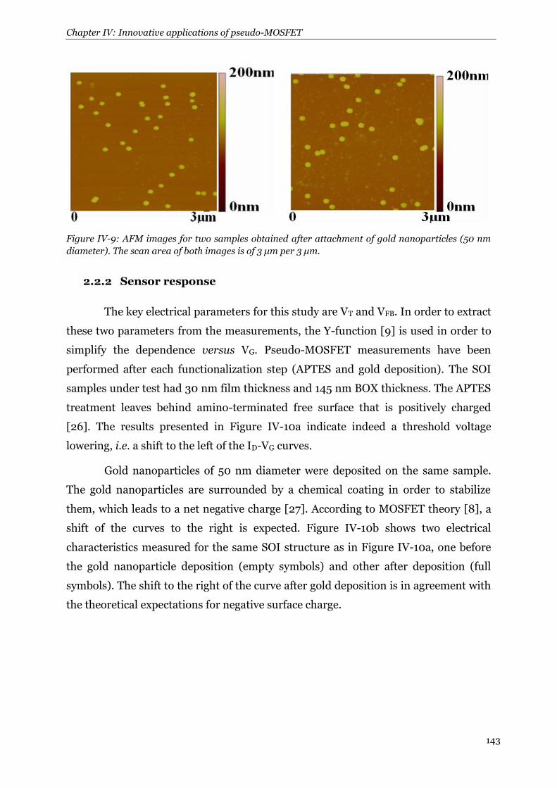
Chapter IV: Innovative applications of pseudo-MOSFET
143
Figure IV-9: AFM images for two samples obtained after attachment of gold nanoparticles (50 nm
diameter). The scan area of both images is of 3 μm per 3 μm.
2.2.2 Sensor response
The key electrical parameters for this study are VT and VFB. In order to extract
these two parameters from the measurements, the Y-function [9] is used in order to
simplify the dependence versus VG. Pseudo-MOSFET measurements have been
performed after each functionalization step (APTES and gold deposition). The SOI
samples under test had 30 nm film thickness and 145 nm BOX thickness. The APTES
treatment leaves behind amino-terminated free surface that is positively charged
[26]. The results presented in Figure IV-10a indicate indeed a threshold voltage
lowering, i.e. a shift to the left of the ID-VG curves.
Gold nanoparticles of 50 nm diameter were deposited on the same sample.
The gold nanoparticles are surrounded by a chemical coating in order to stabilize
them, which leads to a net negative charge [27]. According to MOSFET theory [8], a
shift of the curves to the right is expected. Figure IV-10b shows two electrical
characteristics measured for the same SOI structure as in Figure IV-10a, one before
the gold nanoparticle deposition (empty symbols) and other after deposition (full
symbols). The shift to the right of the curve after gold deposition is in agreement with
the theoretical expectations for negative surface charge.

Chapter IV: Innovative applications of pseudo-MOSFET
144
Figure IV-10: (a) ID-VG curves obtained before any chemical treatment (full symbols) and after
APTES treatment (empty symbols). (b) ID-VG curves after APTES treatment (empty symbols) and
after gold particles deposition (full symbols). VG is scanned forwards and backwards from 0 to - 40 V
and from 0 to + 40 V. Film thickness of 30 nm and 145 nm BOX.
It is worth pointing out that a hysteresis appeared in the curves after the
nanoparticle deposition (see Figure IV-10b). The hysteresis effect comes from the fact
that gold nanoparticles act as charge holders where the electrons can be trapped and
de-trapped depending on the gate voltage sweep. This phenomenon opens a road
towards nano-memory applications for these hybrid devices. These results were
validated with other geometries of SOI (20 nm film thickness) and of gold
nanoparticles (5 nm and 100 nm diameter). After the qualitative proof of concept of
our device, the following sub-sections are dedicated to more quantitative analysis of
the sensor (reproducibility, sensitivity and particle size/density improvements).
2.2.2.1 Reproducibility
In order to validate that the VT shifts obtained above result from the chemical
treatments applied and that the data is reproducible, we fabricated and tested two
samples (A & B) of 30 nm film thickness with the same density of particles (~ 4 × 10⁸
cm-2 with 50 nm diameter). Table IV-4 and Table IV-5 show the extracted parameters
before any process (naked SOI) and after completing gold deposition.
Table IV-4: Comparison of VFB for two quasi identical samples A & B. Gold nanoparticles with 50
nm diameter and 4 108 density.
Naked SOI SOI + gold VFB
Sample A - 4.2 V - 7.2 V 3 V
Sample B - 4 V - 7.7 V 3.7 V

Chapter IV: Innovative applications of pseudo-MOSFET
145
Table IV-5: Comparison of VT for two quasi identical samples A & B. Gold nanoparticles with 50
nm diameter and 4 108 density.
Naked SOI SOI + gold VT
Sample A 7.5 V 6.4 V 1.1 V
Sample B 8 V 6.4 V 1.6 V
The flat-band voltage shows a variation of ~ 18 % from sample A to sample B
after completing gold deposition. For the threshold voltage shift, the absolute values
are within 5 % but the relative shift VT varies by 30 %. As the measurement is based
on pressure probes and is done on large-area samples (5 mm × 5 mm), typical
variations in -MOSFETs extracted parameters, from one sample to another, are of
maximum 5 %. We also saw previously that the process itself can produce variations
of particles densities of about 5 %. It is concluded that VT/VFB values and their shifts
due to the presence of particles present a reasonable reproducibility. Note that the
sensitivity (shift magnitude: VFB) on the holes side (negative back gate voltages) is
higher than on the electrons side (VT) and the variability is lower. This result was
repeatedly confirmed on all other 30 nm film thickness samples we fabricated.
2.2.2.2 Impact of particle size and density
As previously stated, the charge for gold nanoparticles is actually given by the
chemical coating that allows them to remain independent and not to agglomerate.
Therefore, one expects to have a higher quantity of charges associated to a higher
diameter [28]. In a very rough approximation, the shifts of the curves after adding
gold nanoparticles are given by:
(IV-8)
with Cox being the buried oxide capacitance and QT the total charge associated to all
the particles on the surface. The charge associated to one single gold nanoparticle,
Q/particle, can be estimated by using the density of particles measured with AFM
(densityAFM):
(IV-9)

Chapter IV: Innovative applications of pseudo-MOSFET
146
Table IV-6 shows the extracted charge/particle for two samples with 20 nm
film thickness, one with 5 nm particle diameter and the other with 50 nm particle
diameter. The charge per particle is higher for the higher diameter which is consistent
with the fact that the charged coating has larger surface.
Table IV-6: Particle size impact on electrical response.
Particle diameter (nm)
Particle density (cm-2)
Shift (V) (V)
Q/particle (C)
5 4.7 × 10⁹ 5.1 0.3 × 10¹⁶
50 5.5 × 10⁸ 3.5 1.5 × 10¹⁶
The sensitivity of our simple detector with respect to particles density was
demonstrated. The proportionality of the response was tested on SOI with 20 nm film
and 145 nm BOX thicknesses. All samples had 5 nm diameter particles. Figure IV-11
shows the shifts of the curves, for negative and for positive gate voltages, with respect
to the density of particles. A clear proportionality between the VT and VFB shifts and
the density of particles is evidenced.
Figure IV-11: Shifts of VT and VFB versus density of gold nano-particles (5 nm diameter) on the
surface of SOI wafer.
2.2.2.3 Sensitivity improvement
The sensitivity of the detection is expected to depend on the thickness of the
SOI film, because coupling between the free surface and the channel located at the
film-BOX interface is stronger for thinner films [18]. This means that the shifts of the
curves should be larger with thinner films. In order to test this effect, we fabricated
two samples with 50 nm diameter gold nanoparticles and with two different film
thicknesses (20 nm and 30 nm) for the same BOX thickness (145 nm).

Chapter IV: Innovative applications of pseudo-MOSFET
147
Figure IV-12a and Figure IV-12b show drain current curves for positive VG.
For negative VG, ID-VG curves were traced in Figure IV-12c and in Figure IV-12d. The
filled symbols represent the curves just before adding gold particles and empty
symbols represent the curves after gold particle deposition. The shifts after gold
deposition are clearly higher for the 20 nm film than for the 30 nm film, and this
conclusion applies to both electron and hole conductions. The larger shift of the
curves for thinner films implies an improvement of the sensitivity.
Figure IV-12: ID-VG curves for 30 nm film thickness (a and c) and 20 nm film thickness (b and d). On
each curve, the full symbols represent the curves before adding the particles and the empty symbols
after adding gold particles (50 nm diameter). The back-gate voltage has been scanned for positive (a
and b) and negative values (c and d).
Table IV-7 shows the extracted shift values for VT and VFB. The shift in VFB is
about 94 % higher and the shift in VT is about 444 % higher for the thinner film (20
nm). This result should be multiplied by the density of the particles (40 % higher for
the thinner film), the electrical response being proportional to the density of
particles, as it was shown in the previous sub-section. However, the parameter
variation is too large to be explained just by the higher particle density. Therefore,
with thinner SOI films, larger curve shifts are obtained, hence higher sensitivity can
be achieved with thinner silicon films.
Table IV-7: Shifts of the -MOSFET curves after gold nanoparticle deposition with two film
thicknesses (145 nm BOX).
Film thickness (nm)
Particle density (cm-2)
VT shift (V)
VFB shift (V)
20 5.5 × 10⁸ 4 3.5
30 4 × 10⁸ 0.9 1.8

Chapter IV: Innovative applications of pseudo-MOSFET
148
2.3 Conclusion of section 2
We presented the proof of concept of a new, SOI sensor, the simplest that can
be imagined based on the coupling between the channel at the film-BOX interface
and the charge placed intentionally on the top free surface. The interest of SOI
substrates comes from the technology-light solution, easy to implement. The shifts
observed in the measured ID-VG characteristics are explained with the pseudo-
MOSFET theory.
The selectivity of the detection was addressed by a proper surface
functionalization (APTES) which enhances the adhesion of gold nanoparticles on the
surface. The reproducibility of the technological process as well as of the electrical
response has been proven. The shifts in the drain current curves are proportional to
the density of the charge on the surface, i.e. to the density of the gold nanoparticles. A
gain in the sensitivity was found for thinner films SOI where the surface-to-channel
coupling is more intense.
The -MOSFET configuration can be easily used for detection purposes, as
long as the phenomena to be sensed are accompanied by a change in the charge
distribution on the SOI structure. Our experimental results open a wide panel of bio
and chemical sensing applications based on SOI wafers. Moreover, the road to
memory applications is suggested by the appearance of a hysteresis effect.

Chapter IV: Innovative applications of pseudo-MOSFET
149
3. -MOSFET characterization of 3D vertically
stacked SiGe and SiGeC nanowires
3.1 Overview
Nowadays challenges in CMOS device performance can be approached by
alternatives to silicon planar integration which is reaching fundamental limits in
terms of miniaturization, power and performance ([1], [29]). The short-channel
effects (SCEs), shallow junctions and gate current leakage are some examples of
possible disturbances affecting the good operation of microelectronic devices. To
better illustrate the implications of miniaturization on the transistor operation, we
will focus on short-channel effects [30].
In a long channel transistor, the profile of the surface potential is practically
flat along the entire gate length. Reducing the size of transistors, the lateral
component of the electrical field (due to VD for example) is no longer negligible. The
potential distribution changes from one dimensional (1D) distribution (governed by
the vertical gate-induced field Ey) to a two-dimensional (2D) distribution (Ex and Ey).
Scaling down the length implies that electrostatic control of the channel by the gate is
disturbed by space charge areas dominated by junctions (source/substrate and
drain/substrate). In short-channel MOS transistors, these areas became closer to
each-other, until they are partially overlapped. The depletion charge in the channel is
then largely controlled by the junctions and not by the gate. This effect is even more
important when the drain voltage increases. The mechanism is called Drain-Induced
Barrier Lowering (DIBL) [31] and it results in a decrease of threshold voltage.
Furthermore, the effective mobility (µeff) depends on the bias applied between
drain and source and on the gate. Shrinking the devices, the impact of the
longitudinal field component on the mobility increases leading to velocity saturation.
The channel resistance decreases in shorter channels and we can no longer neglect
the effect of series resistance of the source and drain.
Faced with so many challenges, it is necessary to find innovative solutions
adapted to each of these issues in order to perpetuate the miniaturization of devices
while ensuring the amelioration of their performance. In order to do so, recent trends
in microelectronics are to explore nanowire gate-all-around (GAA) structures and

Chapter IV: Innovative applications of pseudo-MOSFET
150
alternative channel materials with superior properties. For example, the best possible
electrostatic control and immunity against short-channel effects can be achieved by
using GAA nanowire-based transistors [32]. Nevertheless, the small diameters of
nanowire devices drastically limit the drive current. To overcome this issue,
nanowires can be integrated in parallel tri-dimensional (3D) networks [33].
Furthermore, the transport properties can be improved by changing the
channel materials. For instance, replacing silicon with Germanium (Ge) or SiGe
allows obtaining higher mobility for holes [34]. Germanium nanowires for multi-
channel technology appear as promising candidates for transistor performance
enhancement. One of the critical issues in Ge nanostructures is again the low level of
drain current that can be supported. Bundling more NWs per device and vertically
stacking them (see Figure IV-13) improves the on-state current [35]. Figure IV-13a
shows a schematic view of vertically stacked SiGe NWs and Figure IV-13b and Figure
IV-13c show SEM images of three-stacked and four-stacked NWs respectively. Figure
IV-13d illustrates four-stacked levels of SiGe NWs with 5 rows.
Figure IV-13: (a) Schematic representation of SiGe NW stacks. Tilted view SEM images after release
of stacked NW for (b) 2X laterally arrayed three-stacked NWs, (c) 2X laterally arrayed four-stacked
NWs and (d) 5X laterally arrayed four-stacked NWs [35].
The electrical study of NWs before CMOS process offers relevant information
and feed-back on optimization solution before starting the long technological
sequence [36]. One of our research partners (CEA-Leti, France) fabricated 3D

Chapter IV: Innovative applications of pseudo-MOSFET
151
vertically stacked Ge-enriched SiGe or SiGeC NWs by a top-down technique. The
fabrication process is described in section 3.2. We proposed a characterization
technique of nanowires before gate processing in order to qualify the quality of these
structures (in section 3.3).
3.2 Fabrication process
The Ge enrichment method has been proposed in 2001 for the fabrication of
strained SiGe and Ge short-channel MOSFETs [37]. It is based on the dry oxidation,
at high temperature, of a SiGe layer with a low initial concentration of Ge. The
fabrication process has been proposed in CEA-Leti using the germanium
condensation technique in silicon on insulator layers ([38], [39]). The fabrication
method is based on the epitaxial growth of Si/SiGe super lattice, selective etching of
Si compared to SiGe and on the Ge enrichment technique (Figure IV-14).
Figure IV-14: Fabrication process of suspended 3D SiGe nanowires. (a) Epitaxy of Si and SiGe
layers. (b) Photolithography and anisotropic etching to define the geometry (width and length) of the
wires. (c) Selective isotropic etching of intermediate Si layers. (d) Ge condensation under dry
oxydation.
Figure IV-14 shows the fabrication process of two suspended Ge nanowires
starting from an SOI wafer:
a. The epitaxy step (Figure IV-14a) is performed at 650◦C by Reduced
Pressure Chemical Vapor Deposition (RPCVD) on SOI wafer. A super-
lattice of Si layers alternating with SiGe layers is obtained. A 5 nm thick

Chapter IV: Innovative applications of pseudo-MOSFET
152
silicon dioxide layer followed by a 100 nm thick silicon nitride (SiN)
layer are then deposited on the surface and used as a hard mask.
b. Mesa structures are isolated by photolithography and anisotropic
etching (Figure IV-14b).
c. Selective isotropic etching of Si layers versus SiGe layers allows SiGe
beams releasing (Figure IV-14c).
d. The SiGe beams are then enriched by Ge condensation under 900◦C in
dry oxygen (Figure IV-14d) in order to increase the Ge content and
achieve almost pure Ge, in the middle of the structures by consuming
the Si during the oxidation process.
The above processing sequence was used here to fabricate two-level stacked
SiGe (Figure IV-15a) and three-levels stacked SiGeC (Figure IV-15b) wires. Fabricated
nanowire channels are suspended and surrounded by silicon dioxide.
Figure IV-15: Schematic view of two suspended germanium-enriched nanowires fabricated from
SiGe layers. (b) Three suspended germanium-enriched nanowires fabricated from SiGeC layers.
Each suspended nanowire is surrounded by silicon dioxide.
From the fabrication point of view, the interest in adding carbon (C) in the
super-lattice structure is to reduce the mismatch between the lattice parameters of
SiGeC and Si. In this case, the selective etching used to free the nanowires is more
stable and avoids the bowing of the structures.
Figure IV-16 shows a scanning electron microscope (SEM) image of the cross-
section of Ge-enriched NWs obtained from SiGeC and surrounded by SiO2. In order
to be able to view this image by SEM, polycrystalline silicon was used to fill-in the
suspended structures before cutting them. Nanowires of crystalline quality have been
obtained (dark dots in Figure IV-16a). Figure IV-16b shows a SEM image of the top

Chapter IV: Innovative applications of pseudo-MOSFET
153
view of multiple parallel nanowires after the selective etching of Si versus SiGeC. The
material sandwich seen from above is composed of silicon dioxide surrounding the
SiGeC NWs. Only the upper wire is visible. At the top of the source and drain mesas, a
silicon nitride layer is visible.
Figure IV-16: (a) SEM image of cross-section nanowires after germanium condensation. Ge-enriched
wires (dark dots) are surrounded by silicon dioxide. (b) Top view SEM picture of multiple parallel
nanowires [39].
Before moving to electrical characterization let us give one important detail
about the geometry of the structures. When referring to the geometry of the structure,
we define two kinds of widths. The ‘designed’ width corresponds to the designed
pattern on the mask used for the lithography and anisotropic etching (Figure IV-14b).
During the condensation process, the Si is oxidized selectively with respect to Ge, so a
germanium enriched channel surrounded by silicon oxide is obtained, as seen in
Figure IV-16a. The effective width (weff) of the Ge enriched channel is smaller than
the designed width (wdes) as shown in Figure IV-17. A relevant consequence is
observed when starting from the same material but with two different designed
widths. After the same oxidation time (meaning the same silicon consumption), it is
possible to obtain wires with different germanium concentrations. The designed
geometry of the wires under test is 100 or 500 nm long and 50 or 100 nm wide.
Figure IV-17: Schematic representation of the nanowire width before and after condensation
process.

Chapter IV: Innovative applications of pseudo-MOSFET
154
The use of both selective etching of Si versus Ge and condensation technique
allows the 3D integration of SiGe and Ge 3D nanowires. This new architecture will
increase the current per unit area by multiplying the number of stacked conduction
channels.
3.3 Electrical transport properties of SiGe NWs
Once the NWs have been liberated and isolated, it is important to probe their
electrical properties before completing the time-consuming CMOS process (gate
stack, source/drain implants, back end). Knowing the properties of as-grown
nanowires enables the optimization of the material content, device configuration and
fabrication steps.
3.3.1 Basic characteristics
The characterization task is challenging because undoped NWs are fully
depleted, preventing current flow. The only subsisting solution for inducing a mobile
charge is to bias the substrate and therefore to use it as a back-gate. The capacitive
coupling between the substrate and the nanowires is done via the buried oxide of 145
nm thickness. This is exactly the principle of the pseudo-MOSFET, which is adapted
here to investigate the electrical transport properties of NWs. The electrical set-up is
shown in Figure IV-18a for SiGe NWs and in Figure IV-18b for SiGeC NWs. Two
metallic probes placed on the top surface of the NW stack are used as source and
drain.
Figure IV-18: Electrical set-up of (a) two suspended and (b) three suspended nanowires.

Chapter IV: Innovative applications of pseudo-MOSFET
155
The first step before we go into detailed characterization is to test the ohmic
behavior of connected NWs. Figure IV-19 shows linear drain current versus drain
voltage curves for various back-gate voltages. The nanowires exhibit clear ohmic
conduction. Moreover, the drain current is modulated by the voltage applied on the
substrate, which opens the way to MOSFET-like characterization. Without substrate
biasing (VG = 0 V), the current is zero which proves that the NWs are fully depleted.
Figure IV-19: Drain current versus drain voltage for various back-gate voltages: negative in (a) and
positive in (b). The designed geometry of the wire under test is 100 nm long and 100 nm wide.
The peculiarity of the two graphics (Figure IV-19a & Figure IV-19b) is the
possibility to activate a drain current with both positive and negative back-gate
voltages. As the chemical content of the nanowires is mainly germanium, in which the
mobility of holes is much higher than the mobility of electrons [34], one would expect
to primarily observe a channel of holes. This means that only a negative back-gate
voltage should give rise to a drain current, which is not the case.
In order to document this puzzling ambipolar conduction, we show in Figure
IV-20 drain current versus back-gate voltage (ID-VG) curves obtained for two
structures of 100 nm length, one with a designed width of 100 nm (Figure IV-20a)
and the other of 50 nm (Figure IV-20b). The curve obtained for a width of 100 nm
confirms the results in Figure IV-19: transport shows both electron and hole
channels. Surprisingly, when the same characteristic is traced for a narrower
nanowire (wdes = 50 nm), only a channel of holes is created (Figure IV-20b).
Moreover, the study of a 100 nm wide and 500 nm long structure also shows a loss of
the electron channel (inset of Figure IV-20b). So, electrons and holes channels are

Chapter IV: Innovative applications of pseudo-MOSFET
156
created in the structure with W/L of 1 while only the hole side is visible for W/L of
1/2 and 1/5.
Figure IV-20: Drain current versus back-gate voltage for a SiGeC-based NW of 100 nm length with
wdes = 100 nm (a) and wdes = 50 nm (b). Inset: ID versus gate voltage VG for a nanowire with wdes =
100 nm and L = 500 nm.
We therefore conclude that the aspect-ratio (W/L) plays an important role
controlling the appearance of the electron channel. Two possible phenomena, both
geometry-dependent, need to be taken into consideration, as they might be
responsible for the onset of the electron channel:
i. during the condensation process, a parasitic wire of silicon subsists
under the short and wide SiGeC wires and enables the conduction of
electrons and holes;
ii. bowing and sticking of the nanowires can occur during the selective
etching process.
We also considered the possibility of enhanced enrichment (higher Ge
concentration) in the narrow NW (wdes = 50 nm), which can suppress electron
conduction. However, the two NW with wdes = 100 nm exhibit contrasting behavior
according to their length.
3.3.2 Carrier transport and impact of series resistance
The impacts of device geometry and germanium concentration on the current
flowing through the NWs will be discussed. We will also show that a correction of the
measured drain current is necessary in order to mitigate the strong influence of series
resistance (RSD).

Chapter IV: Innovative applications of pseudo-MOSFET
157
3.3.2.1 Hole carrier transport and mobility
For parameter extraction, the geometrical factor (fg) is normally equal to W/L
where W and L represent the width and length of the transistor. In order to take into
account the real value of the drain current in our parameter extractions, we
considered that fg is equal to number of nanowires that are vertically stacked
multiplied by weff/L (here 3 × (weff/L)). The extractions of μ0, VT are done using the Y-
function method [9]. Other parameters such as subthreshold swing S and series
resistance RSD can also be extracted as documented in chapter II.
Table IV-8 shows the geometry, the Ge concentration (Ge %) and the
extracted low-field mobility of holes (μp). Superior hole mobility values were obtained
in the nanowire with a higher Ge (100 %) concentration, i.e. narrow width (wdes = 50
nm). This result is in agreement with previous data obtained for SiGe thin films on
insulator [34]. It suggests that hole transport is primarily dominated by the material
nature (Ge) rather than by the interface traps, the density of which can increase in
nanowires with smaller diameter [40]. In principle, the interface between Ge
enriched NW and the surrounding silicon oxide has high quality because SiO2 was
grown during the Ge condensation, with a dry oxidation process and high
temperature. Therefore, the density of states at the interface is presumably low and
does not affect the channel conduction.
Table IV-8: Geometry and electrical properties of SiGeC vertically stacked 3-level nanowires in a
single row.
Per NW 3-level NWs @ VG = - 10 V
L (nm)
wdes (nm)
weff (nm)
Ge
() µp
(cm²/V.s) ID
(nA) 100 50 9 100 80 390 100 100 60 40 14 450 500 100 60 40 34 230
The values of the weff and the Ge concentration were taken from [41] after
investigation by SEM and EDX studies, respectively. The relatively low values of
extracted mobility are explained by the difficulty to determine the precise effective
width and also by the fact that the series resistance in these samples is very high (due
to undoped source and drain). Using the experimental θ1 values, we can estimate the
series resistance to about 60 kΩ for wdes = 100 nm and L = 100 nm.

Chapter IV: Innovative applications of pseudo-MOSFET
158
Another way to validate our experimental results is suggested by the drain
current formula. The drain current should be proportional to the aspect-ratio
multiplied by the mobility. We know that the mobility is Ge-concentration
dependent, so the drain current should be roughly proportional to Ge concentration
multiplied by 3 × (weff/L). Figure IV-21 shows that this proportionality is qualitatively
verified. We used here experimental values of drain current measured for - 10 V on
the back-gate (strong accumulation).
Figure IV-21: ID measured at VG = - 10 V as a function of (3 × weff/L) multiplied by Ge-concentration.
All extracted parameters suffer from an unknown information: where is the
dominant current flowing through? Normally, we have parallel conduction through
multiple stacked nanowires with different gate dielectric thicknesses. As a
consequence, a variable oxide capacitance should be seen by each NW: the stacked
parallel channels should exhibit different threshold voltages. However, multiple
threshold voltages could not be evidenced from the experimental curves: when
plotting the second derivative of current with respect to gate voltage (Figure IV-22),
we obtained one peak, not multiple peaks (which would be the signature of multiple
VT). We explain this result by the thickness of the buried oxide which is much larger
than the inter-wire separation. In our experimental conditions, the threshold voltage
measurement cannot confirm whether the drain current flows mainly through the
lowest nanowire or through several stacked nanowires, which are simultaneously
unblocked by the field effect.

Chapter IV: Innovative applications of pseudo-MOSFET
159
Figure IV-22: Second derivative of drain current with respect to gate voltage versus gate voltage for
a nanowire with wdes = 100 nm and L = 100 nm. The peak positions indicate the threshold voltage and
the flat-band voltage. These values confirm the ones obtained by the Y-function method.
3.3.2.2 Impact of series resistance
The series resistance is significant in this nanowire configuration because the
source/drain stacks are not doped. Furthermore, the undoped nature of source/drain
suggests that a field effect might also be present in source and drain stacks. This
phenomenon was explored by conducting -MOSFET experiments on the source
stack only (Figure IV-23a). Figure IV-23b confirms that the current through the
source stack is depending on the gate voltage. The contribution of the gate-dependent
series resistance has not been taken into account in the extracted values of mobility
presented above. The series resistance effect is complicated due to the contributions
of the vertical current flow in the source/drain terminals (through the Si/SiGe super-
lattice) and horizontal flow (along the SiGe layers contacting the NWs).
The average value of the nanowire series resistance is found to be higher for
SiGe (≈ 2 × 10⁶ Ω) than for SiGeC (≈ 4 × 10⁴ Ω): series resistance in SiGe exceeds by
about two orders of magnitude that in SiGeC NWs. The RSD values were extracted
using equation (II-13) illustrated in chapter II.
To clarify the effect of series resistance, we corrected the drain current by the
voltage drop on RSD = RS + RD for SiGe NWs using the equation below detailed in [42]:
( )
(IV-10)

Chapter IV: Innovative applications of pseudo-MOSFET
160
Figure IV-23: (a) Schematic view of the pseudo-MOSFET measurement on the contact stack: probes
are placed on the same contact pad. (b) Drain current versus back-gate voltage in double sweep
mode (forward and backward) for the SiGeC-Si super-lattice.
Figure IV-24a shows a comparison between ID before and after correction for
SiGe NWs. The corrected current is much higher than the measured one for both
positive and negative back-gate voltage. This confirms our expectations about the
strong RSD consequence on SiGe NWs. The mobility extracted after correction is
almost six times larger. For SiGeC NWs no variation was obtained between corrected
and non-corrected drain current (Figure IV-24b); this result points out low value of
RSD.
Figure IV-24: Drain current versus back-gate voltage (a) for a SiGe-based NW and (b) for a SiGeC-
based NW before and after correction of series resistance. VD = 0.2 V, L = 100 nm and wdes = 100 nm.
3.3.3 Low-temperature measurements
We present SiGeC NWs properties measured at low-temperature (low-T). The
aim of this characterization is to investigate the variation of electrical parameters
with temperature.

Chapter IV: Innovative applications of pseudo-MOSFET
161
Before decreasing the temperature, vacuum is created at 300 K in the
chamber where the NWs are (pressure inside the chamber is then around 10−6 mbar).
It is worth noting that the simple fact of pumping the chamber might induce changes
in the electrical response of SiGeC nanowires, because the nanowires are not
encapsulated and therefore may suffer from surface contamination.
Figure IV-25a shows the drain current as a function of back-gate voltage for
wdes = 100 nm and L = 100 nm in air and vacuum conditions in the cryogenic station.
The drain current level decreases in vacuum compared to air condition for both
negative and positive VG. In Figure IV-25, the lateral shifts of the ID-VG curves are
related to the change in threshold voltage and flat-band voltage. Higher VT and VFB
were obtained for vacuum condition, probably due to the contribution of the surface
contamination when the experiments are conducted in air.
Liquid nitrogen was injected into the chamber in order to reach low
temperature (77 K). We compared the electrical characteristics at different
conditions: air, 300 K (in vacuum) and 77 K (in vacuum). Figure IV-25b shows the
variation of the drain current curves for these three different conditions of
measurement. As usually with crystalline semiconductors, the drain current level at
low temperature is higher than at room temperature (in vacuum conditions).
Figure IV-25: Drain current versus back-gate voltage for a SiGeC-based NW of 100 nm length with
wdes = 100 nm. (a) air and vacuum condition: the shifts of VT and VFB are clearly visible. (b) ID-VG
curves at room temperature (in air and vacuum) and at 77 K (vacuum). VD = 0.2 V.
For more quantitative analysis, we show in Table IV-9 the extracted low-field
mobility for holes and electrons (μp, μn), and the subthreshold swing (S) for two
different temperatures (77 and 300 K). The electron and hole mobility increases by a
factor of two with the decrease of temperature from 300 K to 77 K. The mobility
enhancement is dominated by the reduction in phonon scattering rate as the

Chapter IV: Innovative applications of pseudo-MOSFET
162
temperature decreases [43]. Another scattering mechanism is suspected because pure
phonon interactions would lead to µ ~ T-1
. The swing decreases almost four times
between 300 K and 77 K which is consistent with S ∼ kT. This result indicates that the
density of interface traps does not increase significantly at low temperature.
Table IV-9: Variation of electrical parameters for a SiGeC-based NW of 100 nm length with wdes =
100 nm for different temperatures.
T (K)
µn
(cm²/V.s) µp
(cm²/V.s) S
(V/dec)
300 12 5 1.1
77 24 10 0.3
3.3.4 Multiple parallel NWs at 300 K
Another aspect studied here concerns the transport through multiple parallel
channels. The comparison of structures composed of a single row or 50 parallel rows
in 3D vertically stacked NWs is intriguing. Figure IV-26 shows the current measured
in vacuum at room temperature through a single row and through multi-row
structures (50 in parallel). Two different geometries were under test (wdes = 50 nm, L
= 100 nm in Figure IV-26a and wdes = 100 nm, L = 500 nm in Figure IV-26b). The
drain current values hardly correspond to the aspect ratio or to the number of
nanowires. This implies that the current in the multi-parallel structures is defined
either by the contact (source/drain) resistance or by the most conductive nanowires
of the stack.
Figure IV-26: Drain current versus negative back-gate voltage for SiGeC based NWs of 100 nm
length with wdes = 50 nm (a) and 500 nm length with wdes = 100 nm (b).

Chapter IV: Innovative applications of pseudo-MOSFET
163
3.4 Conclusion of section 3
We have studied 3D vertically-stacked SiGe and SiGeC nanowires fabricated
at CEA-Leti with a new method based on the Ge condensation technique on silicon-
on-insulator wafers. We have demonstrated that the 3D vertically stacked suspended
gateless nanowires behave as MOS transistors controlled by the back gate. An original
characterization method, inspired by the pseudo-MOSFET, has been implemented.
This technique proves efficient for the preliminary characterization of as-grown
nanowires before the processing of MOS gate and source/drain terminals.
Transport measurements show that the hole mobility is improved by
increasing the Ge concentration. Typical issue of these structures is the high series
resistance. Our data demonstrates that the contact resistance is field-effect sensitive.
The undoped nature of the contacts explains this problem, which can easily be solved
by implanting the contacts of the NWs stacks when fabricating a complete device.
At low temperature, the carrier mobility and subthreshold slope are clearly
improved. The benefit of integrating multiple parallel nanowires for increasing on-
current is obvious even though the current gain was not as high as expected for GAA
architecture. Source and drain doping should improve the electrical properties of
NWs.
The comparison of NWs with different widths, lengths and parallel
combinations is informative but opens questions that will probably be answered after
full CMOS completion of GAA NWs.

Chapter IV: Innovative applications of pseudo-MOSFET
164
Conclusion
This chapter IV was dedicated to innovative applications of the -MOSFET.
First, the -MOSFET configuration has been extended for the characterization of
heavily doped SOI wafers. Second, we introduced a new SOI sensor for gold
nanoparticles detection. Finally, we studied the electrical transport properties of 3D
vertically-stacked SiGe and SiGeC NWs fabricated on SOI wafers.
The -MOSFET configuration was used for the first time to characterize
heavily doped SOI wafers with doping concentration of 1019-1020 cm-3. Unusual -
MOSFET characteristics were obtained and a revised model was proposed to extract
independently the carrier conduction, volume mobility and surface mobility. Two
characterizations techniques (Hall effect and four-point probes) were also used for
comparison. The results show good agreement between these three different
techniques and prove that -MOSFET delivers reliable results.
We proposed and verified that the -MOSFET stands as a simple sensor of
gold nanoparticles deposited on the top Si film. The shifts of VT and VFB obtained
after adding charged gold nanoparticles on the top surface are large enough for
detection. The shifts in the ID-VG curves are proportional to the amount of surface
charge, i.e. to the density of the gold nanoparticles. The sensitivity was found to be
higher for thinner Si films due to the stronger coupling between the channel at the
film-BOX interface and the surface charge.
3D vertically-stacked SiGe and SiGeC nanowires were tentatively
characterized by -MOSFET, which delivers useful I-V characteristics. The 3D
vertically stacked suspended gateless nanowires behave as MOS transistors
controlled by the back gate. The contacts were ohmic albeit their resistance shows
strong gate bias dependence. Hole mobility is improved by increasing the Ge
concentration. The carrier mobility and the subthreshold slope are improved at low
temperature. Finally, integrating multiple parallel nanowires raise the on-current
without confirming that all NWs are active.

Chapter IV: Innovative applications of pseudo-MOSFET
165
References chapter IV
[1] Sorin Cristoloveanu, "A Review of the Electrical Properties of SIMOX Substrates and Their Impact on Device Performance," Journal of the Electrochemical Society, vol. 138, pp. 3131-3139, 1991.
[2] Dae-Hyun Moon, Jae-Joon Song and Ohyun Kim, "Effect of Source/Drain Doping Gradient on Threshold Voltage Variation in Double-Gate Fin Field Effect Transistors as Determined by Discrete Random Doping," Japanese Journal of Applied Physics, vol. 49, pp. 104301-104305, 2010.
[3] Jean-Pierre Colinge, Chi-Woo Lee, Aryan Afzalian, Nima Dehdashti Akhavan, Ran Yan, Isabelle Ferain, Pedram Razavi, Brendan O'neill, Alan Blake, Mary White, Anne-Marie Kelleher, Brendan Mccarthy and Richard Murphy, "Nanowire transistors without junctions," Nat Nano, vol. 5, pp. 225-229, 2010.
[4] J. Hartwich, L. Dreeskornfeld, F. Hofmann, J. Kretz, E. Landgraf, R. J. Luyken, M. Specht, M. Stadele, T. Schulz, W. Rosner and L. Risch, "Off current adjustment in ultra-thin SOI MOSFETs," in Solid-State Device Research conference, 2004. ESSDERC 2004. Proceeding of the 34th European, pp. 305-308, 2004.
[5] S. Cristoloveanu and S. Williams, "Point-contact pseudo-MOSFET for in-situ characterization of as-grown silicon-on-insulator wafers," Electron Device Letters, IEEE, vol. 13, pp. 102-104, 1992.
[6] T. Ouisse, P. Morfouli, O. Faynot, H. Seghir, J. Margail and S. Cristoloveanu, "A Detailed Investigation of the Pseudo-Mos Transistor for in Situ Characterization of Soi Wafers," in SOI Conference, 1992. IEEE International, pp. 30-31, 1992.
[7] F. Y. Liu, A. Diab, I. Ionica, K. Akarvardar, C. Hobbs, T. Ouisse, X. Mescot and S. Cristoloveanu, "Characterization of Heavily Doped SOI wafers under Pseudo-MOSFETs Configuration," Solid-State Electronics, vol. Submitted, 2012.
[8] S. M. Sze, Physics of Semiconductor Devices (Second Edition), Wiley press, New York, 1981.
[9] G. Ghibaudo, "New method for the extraction of MOSFET parameters," Electronics Letters, vol. 24, pp. 543-545, 1988.
[10] S. Cristoloveanu, D. Munteanu and M. S. T. Liu, "A review of the pseudo-MOS transistor in SOI wafers: operation, parameter extraction, and applications," Electron Devices, IEEE Transactions on, vol. 47, pp. 1018-1027, 2000.
[11] Naotoshi Kadotani, Teruyuki Ohashi, Tsunaki Takahashi, Shunri Oda and Ken Uchida, "Experimental Study on Electron Mobility in Accumulation-Mode Silicon-on-Insulator Metal–Oxide–Semiconductor Field-Effect Transistors," Japanese Journal of Applied Physics, vol. 50, pp. 094101-094105, 2011.
[12] T. Ouisse, S. Cristoloveanu and G. Borel, "Electron trapping in irradiated SIMOX buried oxides," Electron Device Letters, IEEE, vol. 12, pp. 312-314, 1991.
[13] S. Cristoloveanu and S. S. Li, Electrical Characterization of Silicon-On-Insulator Materials
and Devices, Kluwer, Boston, 1995.
[14] Q. T. Nguyen, J. Antoszewski, L. Faraone, N. Bresson, P. Gentil and S. Cristoloveanu, "Correlation of Pseudo-MOS transistor and Hall effect measurements in thin SOI wafers," in Optoelectronic and Microelectronic Materials and Devices, 2006 Conference on, pp. 39-40, 2006.
[15] Cui Yi, Wei Qingqiao, Park Hongkun and C. M. Lieber, "Nanowire nanosensors for highly sensitive and selective detection of biological and chemical species," Science, vol. 293, pp. 1289-1292, 2001.
[16] J. Hahm and C. M. Lieber, "Direct ultrasensitive electrical detection of DNA and DNA sequence variations using nanowire nanosensors," Nano Letters. Jan., vol. 4, pp. 51-54, 2004.

Chapter IV: Innovative applications of pseudo-MOSFET
166
[17] G. Hamaide, F. Allibert, H. Hovel and S. Cristoloveanu, "Impact of free-surface passivation on silicon on insulator buried interface properties by pseudotransistor characterization," Journal of Applied Physics, vol. 101, pp. 114513-114516, 2007.
[18] N. Rodriguez, S. Cristoloveanu and F. Gamiz, "Revisited Pseudo-MOSFET Models for the Characterization of Ultrathin SOI Wafers," Electron Devices, IEEE Transactions on, vol. 56, pp. 1507-1515, 2009.
[19] Sung-Hoon Jung, Jae-Min Kim, Lak-Myung Jung, Yong-Hyun Lee, S. Cristoloveanu and Young Ho Bae, "Pseudo-Mosfet Analysis of Proton Irradiated and Annealed SOI Wafer," ECS Transactions, vol. 19, pp. 329-334, 2009.
[20] Tao He, Jianli He, Meng Lu, Bo Chen, Harry Pang, William F. Reus, Whitney M. Nolte, David P. Nackashi, Paul D. Franzon and James M. Tour, "Controlled Modulation of Conductance in Silicon Devices by Molecular Monolayers," Journal of the American Chemical Society, vol. 128, pp. 14537-14541, 2006.
[21] I. Ionica, J. Champliaud, Y.H. Bae and S. Cristoloveanu, "SOI Pseudo-MOSFET: platform for high sensitivity charge detection," in Advanced Workshop on Frontiers in Electronics (WOFE), Porto Rico, p. 18, 2009.
[22] Duclairoir Florence, Dubois Lionel, Calborean Adrian, Fateeva Alexandra, Fleury Benoit, Kalaiselvan Anbarasan, Marchon Jean-Claude, Maldivi Pascale, Billon Martial, Bidan Gerard, De Salvo Barbara, Delapierre Guillaume, Buckley Julien, Huang Kai, Barattin Régis, P. R. O. Tiziana and Levy Laurent P, "Bistable molecules development and Si surface grafting: two chemical tools used for the fabrication of hybrid molecule/Si CMOS component," International journal of nanotechnology, vol. 7, pp. 719-737, 2010.
[23] I. Ionica, A. El Hajj Diab and S. Cristoloveanu, "Gold nanoparticles detection using intrinsic SOI-based sensor," in Nanotechnology (IEEE-NANO), 2011 11th IEEE Conference on, pp. 38-43, 2011.
[24] Elodie Boisselier and Didier Astruc, "Gold nanoparticles in nanomedicine: preparations, imaging, diagnostics, therapies and toxicity," Chemical Society Reviews, vol. 38, pp. 1759-1782, 2009.
[25] Jang-Sik Lee, "Recent progress in gold nanoparticle-based non-volatile memory devices," Gold Bulletin, vol. 43, pp. 189-199, 2010.
[26] Elaine T. Vandenberg, Lars Bertilsson, Bo Liedberg, Kajsa Uvdal, Ragnar Erlandsson, Hans Elwing and Ingemar Lundström, "Structure of 3-aminopropyl triethoxy silane on silicon oxide," Journal of Colloid and Interface Science, vol. 147, pp. 103-118, 1991.
[27] Jiwen Zheng, Zihua Zhu, Haifeng Chen and Zhongfan Liu, "Nanopatterned Assembling of Colloidal Gold Nanoparticles on Silicon," Langmuir, vol. 16, pp. 4409-4412, 2000.
[28] Wissanu Patungwasa and José H. Hodak, "pH tunable morphology of the gold nanoparticles produced by citrate reduction," Materials Chemistry and Physics, vol. 108, pp. 45-54, 2008.
[29] T. Skotnicki, J. A. Hutchby, King Tsu-Jae, H. S. P. Wong and F. Boeuf, "The end of CMOS scaling: toward the introduction of new materials and structural changes to improve MOSFET performance," Circuits and Devices Magazine, IEEE, vol. 21, pp. 16-26, 2005.
[30] T. N. Nguyen and J. D. Plummer, "Physical mechanisms responsible for short channel effects in MOS devices," in Electron Devices Meeting, 1981 International, pp. 596-599, 1981.
[31] T. Grotjohn and B. Hoefflinger, "A parametric short-channel MOS transistor model for subthreshold and strong inversion current," Solid-State Circuits, IEEE Journal of, vol. 19, pp. 100-112, 1984.
[32] N. Singh, A. Agarwal, L. K. Bera, T. Y. Liow, R. Yang, S. C. Rustagi, C. H. Tung, R. Kumar, G. Q. Lo, N. Balasubramanian and D. L. Kwong, "High-performance fully depleted silicon nanowire (diameter ≤ 5 nm) gate-all-around CMOS devices," Electron Device Letters, IEEE, vol. 27, pp. 383-386, 2006.
[33] C. Dupre, T. Ernst, V. Maffim-Alvaro, V. Delaye, J. M. Hartmann, S. Borel, C. Vizoz, O. Faynot, G. Ghibaudo and S. Deleonibus, "3D nanowire gate-all-around transistors: Specific integration and electrical features," Solid-State Electronics, vol. 52, pp. 519-525, 2008.

Chapter IV: Innovative applications of pseudo-MOSFET
167
[34] Q. T. Nguyen, J. F. Damlencourt, B. Vincent, L. Clavelier, Y. Morand, P. Gentil and S. Cristoloveanu, "High quality Germanium-On-Insulator wafers with excellent hole mobility," Solid-State Electronics, vol. 51, pp. 1172-1179, 2007.
[35] W. W. Fang, N. Singh, L. K. Bera, H. S. Nguyen, S. C. Rustagi, G. Q. Lo, N. Balasubramanian and D. L. Kwong, "Vertically Stacked SiGe Nanowire Array Channel CMOS Transistors," Electron Device Letters, IEEE, vol. 28, pp. 211-213, 2007.
[36] A. Diab, E. Saracco, I. Ionica, C. Bonafos, J. F. Damlencourt, J. H. Lee and S. Cristoloveanu, "Electrical Transport at Room and Low Temperature in 3D Vertically Stacked SiGe and SiGeC Nanowires," Journal of the Electrochemical Society, vol. 159, pp. H467-H472, 2012.
[37] T. Tezuka, N. Sugiyama, T. Mizuno and S. Takagi, "Novel fully-depleted SiGe-on-insulator pMOSFETs with high-mobility SiGe surface channels," in Electron Devices Meeting, 2001. IEDM Technical Digest. International, pp. 33.36.31-33.36.33, 2001.
[38] Jean-François Damlencourt, "Method for manufacturing a device having a structure with one or a plurality of SI and GE-based micro or nanowires, using germanium condensation," U.S. Patent n°FR2905197, 2008.
[39] Emeline D. Saracco, Jean-Francois Damlencourt, Dominique Lafond, Sophie Bernasconi, Veronique Benevent, Pierette Rivallin, Yves Morand, Jean-Michel Hartmann, Pauline Gautier, Christian Vizioz, Thomas Ernst, Caroline Bonafos and Pier Fransesco Fazzini, "Fabrication of Suspended Ge-rich Nanowires by Ge Enrichment Technique for Multi-channel Devices," ECS Transactions, vol. 19, pp. 207-212, 2009.
[40] K. Tachi, M. Casse, D. Jang, C. Dupre, A. Hubert, N. Vulliet, V. Maffini-Alvaro, C. Vizioz, C. Carabasse, V. Delaye, J. M. Hartmann, G. Ghibaudo, H. Iwai, S. Cristoloveanu, O. Faynot and T. Ernst, "Relationship between mobility and high-k interface properties in advanced Si and SiGe nanowires," in Electron Devices Meeting (IEDM), 2009 IEEE International, pp. 1-4, 2009.
[41] Emeline Saracco, "FABRICATION ET COINTEGRATION DE TRANSISTORS N-MOS A BASE DE NANOFILS DE SILICIUM ET DE TRANSISTORS P-MOS A BASE DE NANOFILS DE GERMANIUM", Ph.D. dissertation, Grenoble-INP, France, 2011.
[42] Krunoslav Romanjek, "CARACTÉRISATION ET MODÉLISATION DES TRANSISTORS CMOS DES TECHNOLOGIES 50nm ET EN DEÇÀ", Ph.D. dissertation, Grenoble-INP, France, 2004.
[43] Shinji Kawaji, "The Two-Dimensional Lattice Scattering Mobility in a Semiconductor Inversion Layer," Journal of the Physical Society of Japan (J. Phys. Soc. Jpn.), vol. 27, pp. 906-908, 1969.

General conclusion
168
General conclusion
During these three years of Ph.D., I focused on the study of SOI and pseudo-
MOSFET, in a very broad definition. The SOI used was not only the Silicon-On-
Insulator standard material, but also ultra-thin film (down to 12 nm), ultra-thin BOX
(down to 10 nm), highly doped films (up to 1020 cm-3), SiGe nanowires stacked in 3D
architectures or silicon films decorated with gold nanoparticles.
In a general definition, the -MOSFET is a configuration in which the
electrical regime of the top film is electrostatically controlled by a back-gate, that is
capacitively coupled through a buried oxide. The physical parameters measured in -
MOSFET will not only be limited to current, but they can go to capacitance or low
frequency noise spectra.
With this extended definitions, we studied the electrical characterization of
SOI in -MOSFET configuration. A sum of technical conclusions will be presented.
Our study allowed also discovering new roads to explore which will be presented in
the perspectives section.
Main conclusions
1. We demonstrated for the first time the capability of exploring ultra and extra thin
SOI wafers down to 12 nm silicon film and 10 nm BOX using the -MOSFET with
pressure probes. The impact of the top surface silicon film state and its
passivation on the ID-VG and gm-VG curves for advanced SOI structures were
showed and clarified.
2. We extended the characterization of SOI wafers to low-temperature
measurements using -MOSFET concept. The feasibility of the measurements
using cryogenic station was verified and ohmic contacts were ensured. The
measured temperature dependence of holes and electrons mobility fits with the
theoretical curves. For T > 100 K, phonon scattering mechanism dominates and
indicates a good quality of Si-BOX interface in SOI wafers. The impact of the top
interface defects on the swing and the threshold voltage is more prominent in
thinner films and at lower temperature.

General conclusion
169
3. We initiated low-frequency noise characterization of as-fabricated SOI wafers
using the -MOSFET. The LFN is shown to be of 1/f type and is clearly associated
with the carrier number fluctuation in the channel, due to the
trapping/detrapping of carriers. The interface trap values can be extracted using
this novel method. The noise does not seem to depend on the probe pressure for
the thicker films (88 nm). The impact of the free surface preparation on the
channel properties is significant. The LFN technique using -MOSFET can be
used to characterize thin SOI films, down to 20 nm, and BOX layers down to 10
nm.
4. We implemented a novel characterization technique for bare SOI, based on split
C-V measurement using -MOSFET. Different SOI structures have successfully
been tested from thick to thin film/BOX couples. The effective mobility of
electrons and holes can be obtained by this split C-V technique using an
appropriate model. The adapted methodology to determine μeff was showed and
validated through comparison with μeff extracted from ID-VG measurements.
Excellent agreement was obtained between effective mobility curves from Y-
function method and from our new method, validating our approach. The impact
of surface passivation on the effective mobility was confirmed by our technique
and the values show that electron mobility can exceed 500 cm2V-1s-1 in thin SOI
films with passivated surface. The variation of the maximum capacitance in the
high frequency regime was observed and explained by a RC analytical model.
5. We characterized for the first time heavily doped SOI wafers with doping
concentration of 1019-1020 cm-3 by -MOSFET method and validated the results
by Hall effect and 4-point probe. Unusual -MOSFET characteristics (ID-VG and
gm-VG curves) were obtained. We showed that -MOSFET is the only method able
to provide independently the carrier concentration and mobility without the need
of a magnetic field. We demonstrated that parameters extraction is possible using
a revised model which takes the volume current into account. As the -MOSFET
yields independently the carrier mobility (in volume and at the interface) and
carrier concentration, it can successfully replace more complex Hall effect
measurements.
6. We proposed and verified an innovative -MOSFET based sensor of gold
nanoparticles deposited on the top Si film. The shifts of VT and VFB after adding

General conclusion
170
gold nanoparticles on the top surface, observed in the measured ID-VG
characteristics, are explained with the -MOSFET theory. The shifts are related to
the change of the surface potential (density of the charge) on the surface, i.e. to
the density of the gold nanoparticles. The sensitivity proved to be higher for
thinner SOI films. The reproducibility of the technological process as well as of the
electrical response has been proven.
7. We have demonstrated that the 3D vertically-stacked SiGe and SiGeC suspended
gateless nanowires behave as MOS transistors controlled by the back gate. An
original characterization method before the processing of the gate stack and
source/drain contacts, inspired by the -MOSFET, has been implemented which
delivers useful I-V characteristics. Ohmic contacts were obtained albeit their
resistance shows strong gate bias dependence. Hole mobility is improved by
increasing the Ge concentration. At low-temperature measurements, the carrier
mobility and the subthreshold slope are improved. Integrating multiple parallel
nanowires raises the on-current.
Future perspectives
Our work opened the road to new questions about further improvements and
developments in these research fields.
1. A still opened question remains about the ultra-thin film/BOX structure. What is
the thinnest film/BOX for which the -MOSFET can still give reliable results?
2. In the noise sections, we saw the critical importance of the geometrical factor in
order to correctly determine the density of states. Due to time constraints, a
simple calculation method for the effective geometry has not been developed. A
more sophisticated model should be explained where numerical simulations
would presumably bring interesting information.
3. The impact of the surface preparation on the noise measurements was not clear
for some of our experiments (e.g. before/after HF treatment). A complementary
study would be necessary to clarify the impact of each interface to the global
noise.
4. The influence of experimental parameters (e.g. probe spacing and sample size) on
split C-V measurements has to be clarified. We started numerical simulations (i)
to verify that substrate effects are indeed negligible and (ii) to determine the

General conclusion
171
impact of film thickness, BOX thickness and substrate/BOX interface quality on
the effective surface and frequency. My younger colleagues will complete this
work. I thank them in advance.

List of scientific publications
172
List of scientific publications
Journal publications:
1. A. Diab, C. Fernández, A. Ohata, N. Rodriguez, I. Ionica, Y. Bae, W. Van Den Daele, F. Allibert, F.
Gámiz, G. Ghibaudo, C. Mazure and S. Cristoloveanu, “A New Characterization Technique for SOI
Wafers: Split C(V) in Pseudo-MOSFET Configuration”, to be published in Solid-State Electronics.
2. F. Y. Liu, A. Diab, I. Ionica, K. Akarvardar, C. Hobbs, T. Ouisse, X. Mescot and S. Cristoloveanu,
“Characterization of Heavily Doped SOI Wafers under Pseudo-MOSFETs Configuration”, to be
published in Solid-State Electronics.
3. A. Diab, L. Pirro, I. Ionica, X. Mescot, G. Ghibaudo and S. Cristoloveanu, “Low-temperature
pseudo-metal-oxide-semiconductor field-effect transistor measurements on bare silicon-on-
insulator wafers”, Applied Physics Letters, vol. 101, p. 092110, 2012.
4. A. Diab, E. Saracco, I. Ionica, C. Bonafos, J. F. Damlencourt, J. H. Lee and S. Cristoloveanu,
“Electrical Transport at Room and Low Temperature in 3D Vertically Stacked SiGe and SiGeC
Nanowires”, Journal of the Electrochemical Society, vol. 159, p. H467, 2012.
5. A. Diab, I. Ionica, S. Cristoloveanu, F. Allibert, Y. H. Bae, J. A. Chroboczek and G. Ghibaudo,
“Low-frequency noise in SOI pseudo-MOSFET with pressure probes”, Microelectronic
Engineering, vol. 88, p. 1283, 2011.
International conference papers:
1. A. Diab, C. Fernández, L. Pirro, N. Rodriguez, I. Ionica, A. Ohata, Y. H. Bae, W. Van Den Daele, F.
Allibert, F. Gámiz, G. Ghibaudo, D. Delprat, C. Mazuré and S. Cristoloveanu, “Effective Mobility in
Extra-Thin Film and Ultra-Thin BOX SOI Wafers”, Proc. of the EUROSOI conference, Paris,
France, pp. 1-2, 2013. (Oral presentation)
2. M. Daanoune, S. Sirajeddine, A. Diab, A. Kaminski-Cachopo, I. Ionica, and S. Cristoloveanu,
“Pseudo-MOSFET under illumination: a novel method for extraction of carrier lifetime”, Proc. of
the EUROSOI conference, Paris, pp. 1-2, France, 2013. (Poster presentation)
3. S. Cristoloveanu, I. Ionica, A. Diab and F. Liu, “The Pseudo-MOSFET: Principles and Recent
Trends”, Proc. of the ECS 222th International Symposium on Advanced Substrates and
Characterization, Honolulu PRiME 2012, Hawaii, USA, pp. 249–258, 2012. (Invited paper)
4. C. Fernández, A. Diab, N. Rodriguez, A. Ohata, F. Allibert, I. Ionica, F. Gámiz and S.
Cristoloveanu, “Impact of Effective Capacitance Area on the Characterization of SOI Wafers by
Split-C(V) in Pseudo-MOSFET Configuration”, 2012 International Semiconductor Conference
Dresden-Grenoble (IEEE-ISCDG), Grenoble, pp. 123-126, France, 2012. (Oral presentation)
5. A. Diab, C. Fernández, A. Ohata, N. Rodriguez, I. Ionica, Y. H. Bae, F. Allibert, F. Gámiz, G.
Ghibaudo and S. Cristoloveanu, “A New Characterization Technique for SOI Wafers: Split C(V) in
Pseudo-MOSFET Configuration”, Proc. of the EUROSOI conference, Montpellier, France, pp. 103-
104, 2012. (Oral presentation)
6. F. Y. Liu, A. Diab, I. Ionica, K. Akarvardar, C. Hobbs and S. Cristoloveanu, “Transport Properties
in Heavily Doped SOI Wafers”, Proc. of the EUROSOI conference, Montpellier, France, pp. 57-58,
2012. (Poster presentation)
7. A. Diab, I. Ionica, S. Cristoloveanu, F. Allibert, Y. H. Bae, J. A. Chroboczek and G. Ghibaudo,
“Static and Low-Frequency Noise Characterization of Ultrathin SOI with Very Thin BOX in

List of scientific publications
173
Pseudo-MOSFET Configuration”, Semiconductor Device Research Symposium (IEEE), Maryland,
USA, pp. 1-2, 2011. (Oral presentation)
8. I. Ionica, A. Diab and S. Cristoloveanu, “Gold nanoparticles detection using an intrinsic SOI-
based sensor”, Nanotechnology (IEEE-NANO), Portland, USA, pp. 38-43, 2011. (Oral
presentation)
9. A. Diab, E. Saracco, I. Ionica, C. Bonafos, J. F. Damlencourt and S. Cristoloveanu, “Transport
Properties of 3D Vertically Stacked SiGe and SiGeC Nanowires”, Proc. of the ECS 219th
International Symposium on Silicon-on-Insulator Technology and Devices, Montreal, Canada,
pp. 157-162, 2011. (Oral presentation)
10. A. Diab, I. Ionica, S. Cristoloveanu, F. Allibert, Young Ho Bae, J. A. Chroboczek and G. Ghibaudo,
“Low-Frequency Noise in SOI Pseudo-MOSFET with Pressure Probes”, 17th Conference on
“Insulating Films on semiconductors” (INFOS 2011), Grenoble, France, pp. 1-2, 2011. (Poster
presentation)
11. A. Diab, I. Ionica, S. Cristoloveanu, F. Allibert, N. Rodriguez, F. Gamiz, M. Bawedin, Y. H. Bae, J.
Chroboczek and G. Ghibaudo, “Low-Frequency Noise in Ultrathin SOI Pseudo-MOSFET: Where is
the Noise Coming From?”, Proc. of the EUROSOI conference, Granada, Spain, pp. 23-24, 2011.
(Oral presentation)
12. I. Ionica, A. Diab, Y. H. Bae, X. Mescot, A. Ohata, F. Allibert and S. Cristoloveanu, “Advances in
the Pseudo-MOSFET Characterization Method”, IEEE Semiconductor Conference (CAS), Sinaia,
Romania, pp. 45-51, 2010. (Invited paper)
Published book chapter:
1. S. Cristoloveanu, M. Bawedin, K. I. Na, W. Den Daele, K. H. Park, L. Pham-Nguyen, J. Wan, K.
Tachi, S. J. Chang, I. Ionica, A. Diab, Y. H. Bae, J. A. Chroboczek, A. Ohata, C. Fenouillet-
Beranger, T. Ernst, E. Augendre, C. Royer, A. Zaslavsky and H. Iwai,“A Selection of SOI Puzzles
and Tentative Answers”, in Semiconductor-On-Insulator Materials for Nanoelectronics
Applications, Springer Berlin Heidelberg, pp. 425-441, 2011. (Invited chapter)
National conference papers:
1. A. Diab, I. Ionica and S. Cristoloveanu, “Bruit basse fréquence sur Silicium sur Isolant dans la
configuration Pseudo-MOSFET”, Proc. of the JNRDM, Paris, France, pp. 1-4, 2011. (Oral
presentation)

Abstract/Résumé
174
Abstract/Résumé
Title: Novel pseudo-MOSFET methods for the characterization of
advanced SOI substrates
Abstract: Silicon-On-Insulator (SOI) device architectures represent attractive alternatives to
bulk ones thanks to the improvement of transistors and circuits performances. In this context, the SOI starting material should be of prime quality.
In this thesis, we develop novel electrical characterization tools and models for
advanced SOI substrates. The classical pseudo-MOSFET (-MOSFET) characterization for
SOI was revisited and extended to low temperatures. Enriched variants of -MOSFET, proposed and demonstrated on numerous geometries, concern split C-V and low-frequency noise measurements. Based on split C-V, an extraction method for the effective mobility was validated. A model explaining the capacitance variations with the frequency shows good
agreement with the experimental results. The -MOSFET was also extended to highly doped SOI films and a model for parameter extraction was derived. Furthermore, we proved the
possibility to characterize SiGe nanowire 3D stacks using the -MOSFET concept. Finally
thin film -MOSFET proved to be an interesting, technology-light detector for gold nanoparticles.
Keywords: Silicon-On-Insulator, -MOSFET (Pseudo-MOSFET), Smart-CutTM, Split C-V, Low-frequency noise, Low-temperature, Heavily doped SOI, SiGe NWs, Gold nanoparticles.
Titre: Nouvelles méthodes pseudo-MOSFET pour la caractérisation des
substrats SOI avancés
Résumé: Les architectures des dispositifs Silicium-Sur-Isolant (SOI) représentent des
alternatives attractives par rapport à celles en Si massif grâce à l’amélioration des performances des transistors et des circuits. Dans ce contexte, les plaquettes SOI doivent être d’excellente qualité.
Dans cette thèse nous développons des nouveaux outils de caractérisation électrique et des modèles pour des substrats SOI avancés. La caractérisation classique pseudo-MOSFET
(-MOSFET) pour le SOI a été revisitée et étendue pour des mesures à basses températures.
Les variantes enrichies de -MOSFET, proposées et validées sur des nombreuses géométries, concernent des mesures split C-V et des mesures bruit basse fréquence. A partir des courbes split C-V, une méthode d'extraction de la mobilité effective a été validée. Un modèle expliquant les variations de la capacité avec la fréquence s’accorde bien avec les résultats
expérimentaux. Le -MOSFET a été aussi étendu pour les films SOI fortement dopés et un modèle pour l'extraction des paramètres a été élaboré. En outre, nous avons prouvé la possibilité de caractériser des nanofils de SiGe empilés dans des architectures 3D, en utilisant
le concept -MOSFET. Finalement, le SOI ultra-mince dans la configuration -MOSFET s'est avéré intéressant pour la détection des nanoparticules d'or.
Mots-clefs: Silicium-Sur-Isolant, -MOSFET (Pseudo-MOSFET), Split C-V, Bruit basse fréquence, Basse température, SOI fortement dopé, Nanofils SiGe, Nanoparticules d’or.

French thesis summary
175
French thesis summary
Nouvelles méthodes pseudo-MOSFET pour la
caractérisation des substrats SOI avancés
Amer EL HAJJ DIAB

French thesis summary
176
Introduction générale
Depuis l'ère du multimédia portable, des Smartphones et d’autres
applications, la demande des processeurs plus petits, plus intelligents et moins
voraces en énergie a été accélérée, tirant derrière toute l'industrie de la
microélectronique et intensifiant le rythme de la recherche technologique. Dans ce
contexte de l’évolution de la microélectronique, l'utilisation des substrats Silicium-
Sur-Isolant (SOI) en remplacement des substrats de silicium massif ouvre des
nouvelles voies pour l'innovation, offrant des meilleures performances, de la
puissance et de la miniaturisation.
En effet, la technologie SOI peut surmonter certains des problèmes majeurs
de la technologie du silicium massif (par exemple l'isolation des dispositifs est moins
complexe grâce à la présence de l'oxyde enterré). En outre, les dispositifs SOI offrent
un meilleur contrôle électrostatique du canal grâce à des architectures avancées (par
exemple des transistors à multi-grilles).
Afin de profiter de tous les avantages du SOI, ces plaques SOI doivent être
d'une excellente qualité électrique. Dans ce domaine fortement concurrentiel,
l'objectif de cette thèse est de contribuer à l'analyse et à l'optimisation des substrats
SOI avancés par le développement des méthodes innovantes de caractérisation
électrique et de nouveaux modèles physiques, à partir de la configuration classique la
plus connue du pseudo-MOSFET (-MOSFET).
Ce résumé est composé de deux grandes parties qui donnent une vue générale
de mon travail du thèse. La première partie, portant sur la technologie de la
fabrication du SOI (Smart-CutTM) et la technique de caractérisation -MOSFET,
montre le contexte de notre travail avec l’extension de cette technique pour la
caractérisation des structures SOI avancées. La seconde partie présente les méthodes
innovantes que nous avons proposés pour la caractérisation électrique des plaques
SOI (mesures basse température, mesures bruit basse fréquence et mesures split C-
V). Des modèles ont été conçus, adaptés et appliqués à chaque technique de mesure.

French thesis summary
177
Partie I: Le matériau SOI fabrication et caractérisation
Le SOI est une nouvelle génération des matériaux pour une technologie
alternative aux substrats traditionnels “silicium massif” utilisés dans l'industrie de la
microélectronique. Les substrats SOI sont composés d'un oxyde enterré (BOX) inséré
entre la couche active de silicium (film de silicium) et un substrat de silicium qui sert
de support mécanique (Figure 1) [1].
Figure 1: Représentation schématique de la structure SOI.
Grâce à l'avancement dans la technologie et particulièrement le brevet du
procédé Smart-CutTM [2], le matériau SOI a pu entrer dans le monde industriel de la
microélectronique. L'évolution du SOI et son emploi de plus en plus fréquent dans la
fabrication des circuits intégrés s’accompagne d’un besoin de contrôle de qualité
efficace et rapide. La caractérisation électrique du SOI vise à révéler les paramètres
des plaques qui auront un impact direct sur les composants réalisés par la suite sur ce
substrat.
La caractérisation des matériaux et des dispositifs SOI nécessite des
techniques capables de s'adapter aux difficultés induites par les couches du film de
silicium très mince, la présence d’oxyde enterré mince, le couplage fort entre les
interfaces (Si/BOX, BOX/substrat et Si/air) et les défauts typiques (les effets du
stress, les homogénéités dans les profondeurs, les dislocations, les précipités, etc.).
Certaines méthodes classiques montrent leurs limites pour les films et BOX minces,
alors que de nouvelles techniques ont été mises en œuvre et seront discutées dans la
section II.
Dans cette partie, nous montrons le procédé principal de fabrication des
plaques SOI: le Smart CutTM (section A), la technique de caractérisation classique -
MOSFET (section B) avec la fonction Y pour l’extraction des paramètres électriques

French thesis summary
178
(section C) et finalement les résultats obtenues pour des substrats SOI avancés
(section D).
A. Le procédé Unibond (Smart-CutTM)
La technologie Smart-CutTM a été mise au point dans les années 1990 au CEA-
Léti par Michel Bruel [3] et constitue maintenant l'exclusivité technologique de
l’entreprise Soitec (France-Bernin). Ce procédé repose sur l’implantation d’hydrogène
(H) dans un substrat dont on souhaite reporter une couche sur un substrat isolant
(Figure 2). On peut le diviser en cinq étapes majeures (voir Figure 2).
Le matériau SOI Unibond est fabriqué par collage de plaques, mais tout en
évitant les aléas du processus d’amincissement mécano-chimique. Pour cela, on
implante, dans la plaquette oxydée A, de l’hydrogène qui engendre la formation de
microcavités (zone en pointillés de la Figure 2). Lors du collage des plaques A et B et
du recuit qui suit, les microcavités coalescent, provoquant ainsi une fracture
horizontale qui permet la séparation naturelle des plaques. Cette séparation a lieu,
non pas à l’interface de collage, mais à une profondeur définie par la localisation des
microcavités produites lors de l’implantation d’hydrogène. Une étape finale de
polissage a pour but de gommer la rugosité de surface de la nouvelle plaque SOI [4].
Figure 2: Représentation schématique des étapes de fabrication d'une plaque Unibond SOI avec le
procédé Smart CutTM décrit par Soitec [5].

French thesis summary
179
Ce procédé propose donc des avantages très importants, pour la réalisation
des plaques SOI [6]:
- Un procédé viable qui offre peu de pertes de matériau. Le procédé
Smart-CutTM est quasiment monoplaquette (le substrat donneur est
utilisé pour créer plusieurs films);
- Un large panel d’épaisseurs du film de silicium et du BOX sont
ajustables dans une gamme étendue (tSi = 0.01 à 1.5 microns et tBOX =
0.01 à 5 microns) en jouant sur la dose et l’énergie d’implantation
d’hydrogène (H+);
- Une excellente qualité cristalline et une grande uniformité;
- Une très bonne qualité d’interface Si/BOX (obtenu par oxydation);
B. La technique pseudo-MOSFET
La technique -MOSFET a été mise au point au début des années 1990 par
Cristoloveanu et al dans le laboratoire IMEP [7] et a depuis conquis le monde de la
caractérisation des substrats SOI par sa simplicité et sa rapidité de mise en œuvre. Le
-MOSFET se présente comme une structure MOSFET simple, inversée. Les contacts
(source et drain) sont assurés par deux pointes métalliques (Figure 3a), le plus
souvent en carbure de tungstène (WC). On applique sur la face arrière du substrat,
une tension VG par l’intermédiaire d’un support métallique appelé “chuck”. La
polarisation en face arrière a pour effet de créer un canal de conduction à l’interface
film/BOX (Figure 3a). Le canal de conduction permet notamment d’extraire un grand
nombre des paramètres électriques du SOI comme la mobilité des porteurs, les
défauts à l’interface, etc.
La particularité du -MOSFET est que les pointes sont métalliques et donc il
est possible d’étudier le comportement des deux types de porteurs (trous h+ et
électrons e-) en une seule mesure standard du courant de drain (ID) et de la
transconductance (gm = ∂ID/∂VG) en fonction de VG (Figure 3b). Les films reportés
sont généralement non dopés (type p, NA ≈ 1015 cm-3); le contact entre les pointes et le
film est donc supposé Schottky. La pression appliquée sur les pointes est réglable de
0 à 100 grammes et elle permet de transformer le contact Schottky en contact
ohmique. Suivant la pression appliquée, un nombre plus ou moins important de

French thesis summary
180
défauts sont créés autour des pointes, générant ainsi des pièges (Figure 3a). Ces
derniers facilitent le passage des porteurs en abaissant la barrière énergétique entre
le métal et le film semiconducteur faiblement dopé. Il est donc possible d’obtenir un
comportement ohmique pour les contacts S/D avec le film de silicium [8].
Figure 3: (a) Schéma expérimental d’une mesure -MOSFET avec deux pointes métalliques qui sont
utilisées comme Source et Drain. Un canal de conduction est créé à l’interface film/BOX par
l’intermédiaire de la polarisation du substrat VG et les zones de défauts sont générées par la
pénétration des pointes dans le film de silicium. (b) Illustration de la conduction ambipolaire (canal
d’électrons et canal de trous): ID-VG (échelle logarithmique) et gm-VG sur un film SOI type p avec tSi =
88 nm et tBOX = 145 nm.
Comme mentionné précédemment, la technique -MOSFET nécessite très
peu d’étapes technologiques pour être mise en place. En effet, les seules étapes utiles
sont la gravure des tranchées de largeur de 2 mm du film semiconducteur pour
séparer des “plots” de SOI de 5 5 mm2. Cette isolation est souhaitable pour éviter
toute fuite dans le film et des problèmes aux bords de plaque, qui dégraderaient les
caractéristiques électriques mesurées. L’appareillage de mesure est constitué d’une
station sous pointes JANDEL et d’un analyseur de paramètres Agilent HP-4156B (ou
HP-4155A).
C. Extraction des paramètres électriques
Comme dans le cas d’un MOSFET ordinaire, il existe pour le -MOSFET deux
types de régimes de conduction: ohmique et saturé. Pour toutes les extractions de
paramètres, nous serons dans le régime linéaire (ou ohmique), soit à tension de drain
VD faible. Dans une telle configuration, les formules théoriques du MOS peuvent être
appliquées.

French thesis summary
181
Nous retrouvons donc les expressions pour le courant de drain (ID) et la
transconductance (gm):
( )
[ ( )]( ) (1)
[ ( )] (2)
avec:
- fg le facteur géométrique (similaire au ratio fg = W/L dans un MOSFET
classique; fg = 0,75 dans un -MOSFET [9], [10]);
- Cox, la capacité surfacique du BOX
- μ0, la mobilité à faible champ (μn pour les électrons et μp pour les
trous)
- VT,FB, les tensions de seuil pour les canaux des électrons (VT) et des
trous (VFB)
- 1, le facteur de réduction de mobilité relié aux résistances séries (RSD)
Il existe diverses méthodes pour faire les extractions en utilisant les équations
(1) et (2), mais pour une raison de précision seulement la méthode de la fonction Y
développée par Ghibaudo [11] sera utilisée dans notre étude (Figure 4a). L'avantage
principal de cette méthode vient de son indépendance du facteur de réduction 1
permettant d’éviter l'impact de la RSD qui est critique dans nos mesures. Si l’on
considère que le courant de drain est donné par l’équation (1), dans ce cas la fonction
Y, linéaire pour |VG| ≥ |VT,FB|, est donnée par [11]:
( )
√ √ ( ) (3)
Du fait de l’ambipolarité des mesures -MOSFET, la fonction Y peut être
tracée à la fois en accumulation et en inversion. L’intersection de la partie linéaire de
Y avec l’axe des abscisses (VG) donne les valeurs VT et VFB (Figure 4a). Afin de
déterminer la mobilité à faible champ pour les électrons et les trous, on utilise la
pente d’une partie linéaire de la fonction Y (Figure 4a).

French thesis summary
182
Un autre paramètre à extraire est la pente sous le seuil (S) de la courbe du
courant de drain (Figure 4b), en calculant l’inverse de la dérivée du logarithme du
courant par rapport à la tension de grille:
( ( )
)
(4)
Il est possible d’extraire la pente sous seuil S pour chacun des modes de
conduction du -MOSFET, l’accumulation Sp et l’inversion Sn. Les pentes Sn et Sp
peuvent être différentes pour l’accumulation ou l’inversion car elles sont directement
impactées par les défauts d’interface qui peuvent agir différemment selon le type de
porteurs.
Figure 4: (a) Extraction de VT,FB et μn,p par la fonction Y dans le cas d’un substrat SOI. (b) Extraction
des pentes sous seuil Sn et Sp pour les deux canaux de conduction d’un -MOSFET. tSi = 88 nm et tBOX
= 145 nm.
D. Caractérisation des plaques SOI très minces
Dans notre travail, différents couples des couches du film de Si et de BOX ont
été caractérisés: entre 12 et 200 nm pour l'épaisseur du film et entre 10 et 400 nm
pour l’épaisseur du BOX. Certaines des plaques ont subi une oxydation thermique et
sèche à 900°C afin de passiver la surface du film de Si avec 4-10 nm d’oxyde (SiO2).
Dans ce paragraphe, nous allons prouver que le -MOSFET est encore une
technique de caractérisation très réussie pour les plaques SOI nues même lorsque les
épaisseurs du film et du BOX sont considérablement réduites [12]. En outre, l'impact
de la passivation de surface sur quelques échantillons est également montré et
discuté.

French thesis summary
183
En ajustant les paramètres de configuration de mesure tels que la pression
des pointes, les temps d’attente entre les points de mesure et la polarisation de la
grille, nous avons réussi à caractériser avec succès ces structures très minces. Tout
d'abord, nous avons mesuré le courant de drain (Figure 5a) et la transconductance
(Figure 5b) en fonction de la tension du grille pour des plaques SOI passivées et non
passivées avec 12 nm d’épaisseur de film et 25 nm d’épaisseur de BOX. Le premier
résultat remarquable est qu’aucun endommagement du BOX par les pointes (et par
conséquent aucun courant de fuite) n’est visible.
Dans les films très minces (< 100 nm), le couplage entre le canal et les défauts
présents sur la surface libre du film de Si est très grand [13]. Nous avons étudié
l'impact de ce couplage en mesurant deux échantillons, passivé (avec 4 nm de couche
d'oxyde sur la surface du film) et non passivé dans la Figure 5.
La courbe du courant de drain pour les échantillons passivés (Figure 5a)
présente une diminution de la tension de seuil/bande plate (VT,FB) et une diminution
des pentes sous le seuil (Sn,p) comparées au film non-passivé. Ceci est une
conséquence directe de la réduction de la densité d'états de surface par l’effet de
passivation ([13], [14]). La courbe gm-VG (Figure 5b) pour l'échantillon passivé
montre une forte augmentation de la mobilité apparente par rapport à l’échantillon
non-passivé (si on extrait la mobilité par la méthode du pic de gm [15], un pic plus
élevé de gm implique une plus grande mobilité).
Les résultats de la Figure 5 sur la passivation de surface pour un oxyde
enterré mince (25 nm) confirment ceux obtenus pour un oxyde épais (145 nm) [13].
Leur mérite est d'avoir été obtenus sur un tel couple film/BOX mince.
Figure 5: (a) Le courant de drain et (b) la transconductance en fonction de la tension de grille pour
un film de Si d’épaisseur 12 nm (passivé et non passivé) et 25 nm d’épaisseur de BOX.

French thesis summary
184
Partie II: Nouvelles techniques de caractérisation des
plaques SOI
Dans cette partie, qui constitue le cœur de cette thèse, nous allons étendre
tout d'abord la méthode -MOSFET pour réaliser des mesures à basse température,
puis nous présenterons deux développements inédits du -MOSFET: le bruit à basse
fréquence et le split C-V.
A. Mesures -MOSFET à basse température
Les mesures à basse température donnent des informations détaillées sur les
paramètres de transport (mécanismes dominants de collisions, qualité des
interfaces), qui ne sont pas disponibles à partir des mesures à température ambiante.
Identifier le mécanisme de collision principal révèle la qualité du film et de l'interface
Si-SiO2 qui est très importante pour le procédé de fabrication du SOI. Ici, nous avons
démontré l'extension de la technique -MOSFET à basse température afin d'étudier
les propriétés du transport des plaques SOI [16].
En utilisant la station cryogénique sous pointe 200 mm (Suss Microtec), nous
avons effectué des mesures dans une gamme de température de l'azote liquide (T = 77
K) à la température ambiante (T = 300 K) avec un contrôle de la température meilleur
que ± 0,1 K. Deux pointes métalliques ont été utilisées pour former les contacts de
source et de drain sur la surface de la plaque SOI. Une tension (VG) est appliquée au
support métallique “chuck” pour assurer une polarisation face arrière du substrat de
silicium, comme dans une configuration -MOSFET normale. La distance entre la
source et le drain a été maintenue fixe (~ 1 mm).
La principale différence entre les mesures à température ambiante et à basse
température provient des pointes utilisées. Dans une configuration standard -
MOSFET à température ambiante, avec la station JANDEL, les pointes sont à
pression réglable (les contacts obtenus sont ohmique). Dans la station cryogénique, la
pression sur les pointes n'est pas contrôlable, ce qui peut causer des problèmes de
contact dans les mesures.
Afin de vérifier la possibilité d'obtenir des contacts ohmiques dans la station
cryogénique, des courbes ID-VD à différentes températures ont été mesurées pour des

French thesis summary
185
tensions VG positives et négatives (Figure 6a) sur un film de Si d’épaisseur 40 nm et
un BOX d’épaisseur 145 nm. L’allure linéaire des courbes confirme pour les deux
types de porteurs (électrons et trous) que les contacts pointes-film de Si sont
ohmiques, bien qu'il n'y ait pas de contrôle de pression sur les pointes.
Les courbes ID-VG à plusieurs températures pour le film de Si de 40 nm
d’épaisseur sont présentées dans la Figure 6b, où les canaux des électrons et des trous
sont progressivement activés, ce qui confirme que le -MOSFET fonctionne toujours
à basse température. Dans la région de VG positive, le courant de drain diminue avec
l'augmentation de la température, étant dominé par l'évolution de la mobilité avec la
température. Pour la région VG négative, ce qui correspond au canal des trous, les
courbes ID ont un comportement plus complexe résultant des variations concurrentes
de la mobilité, VFB et la résistance série RSD (environ un ordre de grandeur plus élevé
que pour le canal d’électrons) [8].
Figure 6: (a) Courant de drain vs. tension de drain avec VG = ± 15 V pour deux différentes
températures (120 K et 300 K) et (b) courant de drain vs. tension de grille pour différentes
températures (77 K, 120 K, 200 K, 250 K et 300 K). L’épaisseur de BOX est de 145 nm et tSi = 40 nm.
Le comportement des courbes ID-VG a été reproduit sur des échantillons avec
88 nm d'épaisseur du film de Si (Figure 7) pour plusieurs températures. L'échelle
semi-logarithmique des courbes du courant de drain (Figure 7a) montre une
augmentation de la pente en régime de faible inversion en diminuant la température.
Ce résultat est théoriquement prévisible. Les courbes de la transconductance gm vs.
VG (Figure 7b) montrent qu’en diminuant la température, le pic du gm augmente
(pour VG > 0) grâce à l’amélioration de la mobilité à basse température. Les courbes
illustrées dans la Figure 6 et dans la Figure 7 valident qualitativement la faisabilité de
nos mesures.

French thesis summary
186
Figure 7: (a) Courant de drain vs. tension de grille dans l’échelle semi-logarithmique pour différentes
températures (100 K, 140 K, 150 K et 160 K) et (b) transconductance vs. tension de grille pour les
mêmes températures. Épaisseur de BOX est de 145 nm et tSi = 88 nm.
Afin d'éviter l'impact de la RSD, ce qui est essentiel dans nos mesures,
l'extraction des paramètres électriques a été réalisée avec la méthode de la fonction Y
précédemment décrite. En outre, nous avons calculé la variabilité entre les valeurs
des paramètres extraites et nous avons obtenu moins de 20 % d'erreur pour les
valeurs de μp et μn (barres d'erreur dans la Figure 8).
Dans ce résumé, nous allons montrer et discuter seulement la mobilité des
porteurs. Le travail complémentaire mené sur la tension de seuil et la pente sous le
seuil est décrit dans le manuscrit complet [16].
Ici, nous allons extraire les valeurs de mobilité dans le but d'identifier le
mécanisme de collision dominant qui apporte des informations importantes sur la
qualité du film et de l’interface Si-SiO2. Il existe plusieurs types d'interactions, dont
les trois mécanismes principaux sont:
(i) Collisions avec les Phonons: μPh T-n
, où n varie entre 1 et 2.
(ii) Collisions Coulombiennes: μC Tn, où n varie entre 1 et 2.
(iii) Rugosité de surface avec μSr Eeff-2
.
Le total de l'inverse de la mobilité suit la loi de Matthiessen [17]:
∑
(5)
où n est le nombre de mécanismes des collisions.

French thesis summary
187
Les résultats de la Figure 8a et la Figure 8b montrent la dépendance de la
mobilité à faible champ avec la température pour les électrons et les trous,
respectivement. Comme théoriquement prévu, la mobilité des porteurs augmente en
diminuant la température jusqu’au 100 K puis elle diminue pour T < 100 K.
Pour mettre en évidence la contribution des effets de collisions sur la mobilité
à faible champ, nous avons superposé les courbes expérimentales (en trait continu) et
les courbes théoriques (en pointillés) de la mobilité μ0(T) déduites de la loi du
Matthiessen pour les électrons et les trous:
( )
( )
( ) (6)
avec:
( ) (
)
( ) (
)
(7)
où μ0@300 et μ0@77 représentent les valeurs mesurées de la mobilité à faible champ aux
températures 300 K et 77 K, respectivement. Pour la mobilité Coulombienne, nous
avons ajouté 20 % pour les électrons ( = 1,2) et 50 % pour les trous ( = 1,5) aux
valeurs de μ0 extraites à 77 K, afin de prendre en compte des résidus des collisions
avec les phonons et pour améliorer le fit. Aucun autre paramètre d’ajustement n’a été
utilisé pour les superpositions des courbes.
Figure 8: Mobilité à faible champ expérimentale (trait continu) et modèle (pointillés) des électrons
(a) et des trous (b) en fonction de la température pour 88 nm et 40 nm d'épaisseur de film de Si.
Les courbes modélisées déduites des équations (6) et (7) et les courbes
expérimentales de la Figure 8a se superposent, en particulier pour des températures
élevés. La petite différence qui subsiste à très basse température, se trouve dans les
limites des barres d'erreur pour plusieurs échantillons testés. Un comportement

French thesis summary
188
similaire est obtenu pour la mobilité des trous (Figure 8b). Afin de confirmer encore
plus nos résultats, on note que les courbes des mobilités varient comme T-n
pour T >
100 K (où n est la valeur extraite des courbes de μ(T) en échelle log-log et varie entre
1 et 2 pour les deux films de Si d’épaisseurs 88 et 40 nm). Cela implique que le
mécanisme de collision avec les phonons domine à haute T.
Rappelons que les collisions coulombiennes résultent des pièges (Dit) à
l’interface Si-BOX ou à la surface supérieure du film. Par conséquent, la diminution
de la mobilité avec l’augmentation de la température montre que les collisions des
phonons (et non les collisions coulombienne) sont responsables de la réduction de la
mobilité dans les plaques SOI. Cela reflète indirectement la bonne qualité du film de
Si et de l’interface Si-SiO2.
B. Mesures de bruit à basse fréquence
Dans le monde des dispositifs électroniques, le bruit indique des fluctuations
aléatoires de courant ou de tension autour d'une valeur moyenne. Le bruit basse
fréquence (LFN) constitue un outil de caractérisation puissant. Les mesures LFN
révèlent les fluctuations de la concentration et de la mobilité des porteurs dans le
canal d’un MOSFET, de même que la qualité de l'oxyde en termes de densité des
pièges.
Dans notre travail, nous avons étudié pour la première fois le bruit LFN sur
des plaques SOI nues avant tout procès CMOS afin de déterminer la source de bruit
dominante et de qualifier les interfaces Si/BOX et Si/air [18]. Avant de passer aux
mesures LFN sur les plaques SOI, rappelons brièvement la théorie de base du bruit
électronique, les différentes sources de bruits et leurs méthodes d'analyse.
Différentes types de bruit existent mais nous nous concentrerons ici sur le
bruit 1/f (Figure 9a) qui domine généralement le spectre du bruit global pour le
courant de drain dans le domaine des basses fréquences. Ce type de bruit est associé à
des fluctuations de la conductivité dans le canal [19].
La définition de la conductance électrique d'un matériau est donnée par [20]:
(8)

French thesis summary
189
où μ, n, S et L sont respectivement la mobilité, la densité de porteurs libres, la surface
et la longueur du matériau considéré.
Selon l'équation (8), la fluctuation de G peut être due soit à la fluctuation de
nombres des porteurs n (modèle proposé par McWhorter [21]) soit à la fluctuation
de la mobilité Δμ (modèle proposé par Hooge [22]). Donnons quelques détails sur les
deux modèles.
Modèle de fluctuation du nombre des porteurs (CNF):
McWhorter a proposé que la fluctuation du courant de drain est due à la
fluctuation du nombre des charges mobiles dans le canal, près de l'interface
semiconducteur/oxyde [21]. n résulte de la capture/libération de charge dynamique
par les pièges lents distribués dans l'oxyde. Dans ce cas, la densité spectrale
normalisée (SId/ID
2) peut être écrite comme ([19], [11] et [23]):
( )
(9)
où SVfb est la densité spectrale de puissance de la tension de bandes plates, f est la
fréquence, γ est l'exposant caractéristique proche de l'unité, λ est la constante
caractéristique de l’effet de tunnel (≈ 0,1 nm pour une interface Si/SiO2) et Nt est la
densité volumique des pièges lents dans l'oxyde au voisinage du niveau de Fermi.
Modèle de fluctuation de la mobilité Hooge (HMF):
Hooge attribue les fluctuations de la conductance aux fluctuations de la
mobilité. Dans son modèle, le bruit 1/f du courant de drain est un phénomène de
volume dû aux fluctuations de la mobilité des porteurs résultant des collisions avec
les phonons [22]. Dans ce cas, SId/ID
2 en régime linéaire et forte inversion est [19]:
( )
(10)
Dès que le bruit basse fréquence (LF) montre un spectre du type 1/f, il est
nécessaire de distinguer le modèle qui domine, le bruit CNF ou HMF. Tout d'abord,
nous traçons SId/ID
2 pour une fréquence fixe en fonction de ID en échelle
logarithmique (voir la Figure 9b). D’après les équations (9) et (10) les allures des
courbes obtenues sont différentes, ce qui permet de distinguer les modèles.

French thesis summary
190
Figure 9: (a) Densité spectrale de puissance (SId) du spectre 1/f dans le domaine fréquentiel pour un
substrat SOI. (b) Représentation schématique de la variation de la densité spectrale normalisée par
le courant de drain au carré en fonction du courant de drain pour les modèles CNF ou HMF du bruit
1/f.
Nous avons effectué des mesures de bruit au niveau des plaques en utilisant la
configuration standard -MOSFET ([18], [12]). Par conséquent, la densité de pièges
peut être déterminée directement à l'interface film-BOX, avant la fabrication des
transistors.
La Figure 10a montre la densité spectrale de puissance, SId, tracée en fonction
de la fréquence pour une plaque SOI avec 88 nm de film de Si et 145 nm de BOX pour
différentes tensions appliqués sur la grille-arrière. Le comportement en 1/f (flicker
noise) est clairement visible. Pour vérifier si ce comportement est valable pour les
films SOI très minces, nous avons tracé SId également en fonction de la fréquence
pour différentes VG pour un SOI avec 12 nm d’épaisseur de film et 145 nm de BOX
(Figure 10b). Même type de bruit (flicker noise) est trouvé.
Dans les films très minces (12 nm) l'impact de la surface supérieure sur le
bruit du canal enterré (à l’interface film-BOX) est plus important que celui dans des
films plus épais (88 nm). C'est pourquoi le niveau de bruit est supérieur dans la
Figure 10b.

French thesis summary
191
Figure 10: Bruit basse fréquence en fonction de la fréquence dans un -MOSFET: (a) 88 nm
d'épaisseur de film de Si et (b) 12 nm d’épaisseur de film de Si avec 145 nm de BOX. Le bruit 1/f est
clairement visible dans les deux films SOI.
Afin de déterminer lequel des deux modèles CNF ou HMF compte mieux pour
les données du bruit basse fréquence, il est nécessaire de tracer SId/ID
2 en fonction du
courant de drain en échelle logarithmique comme expliqué précédemment. La Figure
11 montre que SId/ID
2 suit la dépendance en (gm/ID)
2 confirmant le modèle CNF. Dans
la Figure 11, la courbe de SId/ID
2 en fonction de ID montre un plateau en faible
inversion et une décroissante linéaire en forte inversion, étant proportionnel à
(gm/ID)2. La faisabilité de ces mesures de bruit basse fréquence sur les structures SOI
très minces a donc été démontrée dans cette thèse.
Figure 11: Bruit basse fréquence normalisé et k (gm/ID)2 en fonction du courant de drain (avec k ≈
10-9 et p = 50 g). 88 nm d’épaisseur du film de Si et 145 nm de BOX.
Par conséquent, l'extraction du Dit est envisageable. Cependant, les valeurs Dit
(≈ 1013-14 cm-2.eV-1) obtenues à partir des mesures de bruit basse fréquence sont 2 à 3
ordres de grandeur plus élevées que celles obtenues à partir des mesures statiques ID-

French thesis summary
192
VG (Dit ≈ 1011 cm-2.eV-1). Deux arguments peuvent être donnés pour expliquer ces
valeurs élevées des Dit:
- La difficulté d’estimer la surface effective qui engendre le bruit.
- Le bruit en excès peut être généré à la surface libre de la plaque SOI
(Si/interface air).
En plus de la mise en place de cette méthode de mesure, nous avons
également montré que le bruit n’est pas affecté par la pression des pointes. Nous
avons également étudié l’effet de la passivation de la surface des plaques sur les
résultats du bruit. Même s’il y a quelques points à approfondir dans cette étude, elle a
le mérite de montrer la faisabilité expérimentale des mesures de bruit basse
fréquence sur des plaques SOI vierges en configuration -MOSFET.
C. Mesures split C-V
La méthode la plus couramment utilisée pour mesurer la mobilité effective
(μeff) est la technique split C-V. Les mesures split C-V sont généralement effectuées
sur des transistors SOI MOSFET entièrement procécés [24]. L'intérêt de notre travail
sur les mesures split C-V vient de l'utilisation de la technique -MOSFET avec des
pointes en pression, qui ne nécessite aucune préparation des contacts. Pour cette
raison, l'extraction rapide de la mobilité dans les plaques SOI avant tout procès
CMOS est de grand intérêt pour contrôler et optimiser la qualité des substrats de
départ.
Traditionnellement, la fonction Y [11] a été la technique préférée. Toutefois,
les informations qui peuvent être obtenues sur la mobilité des porteurs sont limitées
(mobilité à faible champ); le graphe de la mobilité en fonction de
l'inversion/l’accumulation des charges ou du champ effectif n’est pas mesuré mais
reconstruit. Une approche plus directe est basée sur la détermination de la charge
d'inversion ou d'accumulation à partir des mesures de capacité combinées avec des
courbes statiques ID-VG. Un autre aspect important de la split C-V est que la mobilité
est valable de faible à forte inversion, contrairement à celles extraite en mode statique
qui est correcte juste en forte inversion.
Dans les MOSFETs, la technique de split C-V est basée sur les mesures des
capacités Cgc (capacité grille-canal) et Cgb (capacité grille-substrat) en fonction de la

French thesis summary
193
tension de grille. Toutefois, dans la structure -MOSFET, le substrat de Si agit en
tant qu’une grille (il n’y a pas de grille métallique supérieure), donc seulement la Cgc
peut être mesurée. Deux types de mesures -MOSFET ont été effectuées: courbes
statique ID-VG et courbes split C-V. Pour les mesures de C-V dans la configuration -
MOSFET, les pointes de source et de drain sont reliées à un potentiel bas, tandis que
la grille arrière a été polarisée par VG et reliée au potentiel haut du LCR-mètre (Figure
12). Le schéma du système de mesure et le circuit équivalent sont présentés dans la
Figure 12 ci-dessous.
Figure 12: Configuration schématique de la technique split C-V avec la représentation du circuit
équivalent (modèle Cp-G).
Le concept a été vérifié pour différentes géométries de structures SOI. Nous
montrons ici une seule structure de 20 nm de film de Si et 145 nm de BOX (Figure
13). Comme habituellement pour le -MOSFET, les deux canaux des électrons (VG >
0) et des trous (VG < 0) sont activés (Figure 13a). Les courbes Cgc-VG pour différentes
fréquences sont reproduites dans la Figure 13b. Lorsque le film est déserté (VG ≈ 0 V),
la capacité est égale à zéro. Ensuite, la capacité augmente en raison de l'accumulation
progressive de la couche d'inversion ou d'accumulation. Une fois l’inversion (ou
l’accumulation) atteinte la capacité sature à une valeur fixée par CBOX.
La forme des courbes C-V dans la Figure 13b confirme cette observation. Par
conséquent, notre nouvelle technique est expérimentalement validée avec succès
pour les structures SOI. La dépendance en fréquence de ces courbes a été également
abordée dans le manuscrit.

French thesis summary
194
Figure 13: (a) ID vs. VG and (b) Cgc vs. VG pour un substrat SOI avec 20 nm d’épaisseur du film de Si et
145 nm de BOX.
Nous montrons ici la méthodologie pour extraire la mobilité effective à partir
des courbes expérimentales et les résultats obtenus. Traditionnellement, deux
méthodes sont utilisées pour évaluer μeff en fonction de VG:
( ) (11)
Méthode de la fonction Y. Cette technique est indirecte, elle se base sur
des mesures conventionnelles ID-VG [11]. La charge d'inversion Qinv(VG) et la charge
d'accumulation Qacc(VG) sont calculées en utilisant VT et VFB extraits par la fonction Y:
( ) ( ) ( ) ( ) (12)
où Cox est la capacité du BOX par unité de surface (Cox = εox/tBOX).
Méthode split C-V. Cette technique directe sert à évaluer les courbes de la
μeff (Qinv, acc) à partir des mesures split C-V. Pour le split C-V, Qinv(VG) et Qacc(VG) sont
obtenues par intégration de la capacité mesurée sur toute la gamme de VG positive et
négative, respectivement:
( )
∫ ( )
( )
∫ ( )
(13)
où V0 dans notre cas est ≈ 0 V. La normalisation par la surface effective (Seff) est
nécessaire pour obtenir la densité des charges d’inversion ou d’accumulation par
unité de surface. La surface effective est obtenue en divisant Cmax (F) par Cox (F/cm2),
où Cmax est la capacité maximale extraite des mesures split C-V à VG positif pour les
électrons et à VG négatif pour les trous.

French thesis summary
195
Nous avons utilisé ces deux méthodes pour calculer la mobilité effective des
électrons et des trous, comme le montre la Figure 14. La mobilité effective en fonction
de VG pour l’échantillon SOI avec 88 nm d’épaisseur de film et 145 nm de BOX est
illustrée dans la Figure 14a pour les électrons et dans la Figure 14b pour les trous. Les
courbes de mobilité obtenues en statique et par split C-V se superposent en forte
inversion pour les électrons et en forte accumulation pour les trous.
Figure 14: μeff en fonction du VG calculée à partir des mesures statique ID-VG et des courbes split C-V
pour les électrons (a) et pour les trous (b). 88 nm du film de Si et 145 nm de BOX.
Après avoir démontré la faisabilité de la mesure et validé la technique
d’extraction de la mobilité sur plusieurs géométries d’échantillons, nous nous
sommes intéressés à des études plus subtiles, comme le développement et la
validation d’un modèle physique pour expliquer la variation de la valeur maximale de
la capacité avec la fréquence ou l’étude de la passivation des surfaces des
échantillons.

French thesis summary
196
Conclusion générale
Au cours de ces trois années de doctorat, je me suis concentré sur l'étude de
matériaux SOI et du pseudo-MOSFET dans une définition large. Le SOI utilisé n’est
pas seulement le matériau standard Silicium-Sur-Isolant. Nous avons aussi étudié
des films très minces (moins de 12 nm d’épaisseur), des BOX très minces (jusqu'à 10
nm d’épaisseur), des films fortement dopés (jusqu'à 1020 cm-3), des nanofils SiGe
empilés dans des architectures 3D ou des films de silicium décorés avec des
nanoparticules d’or.
Les paramètres physiques mesurés dans un -MOSFET ne sont pas
seulement limités au courant, mais ils peuvent s’étendre à la capacité ou à des
spectres de bruit de basse fréquence. Avec ces extensions, nous avons enrichi la
caractérisation électrique des plaques SOI dans la configuration -MOSFET. Des
conclusions regroupant la totalité de notre travail sont présentées ici:
La possibilité d'explorer des plaques SOI très minces jusqu'à 12 nm
d’épaisseur du film de silicium et 10 nm de BOX en utilisant le -MOSFET
avec les pointes de pression réglable a été prouvée.
La caractérisation des substrats SOI par -MOSFET a été mise en place pour
les mesures à basse température et les modèles adaptés ont permis
d’expliquer la variation des paramètres avec la température.
Nous avons initié la caractérisation du bruit basse fréquence pour les plaques
SOI nues en utilisant le -MOSFET.
Nous avons implémenté une nouvelle technique de caractérisation des
substrats SOI nu, basée sur des mesures split C-V à l’aide du -MOSFET.
Nous avons caractérisé pour la première fois des films SOI fortement dopés
de 1019-20 cm-3 par la méthode -MOSFET et nous avons validé ces résultats
par des mesures d’effet Hall et 4-pointes.
Nous avons proposé et vérifié un capteur innovant basé sur le -MOSFET
pour la détection des nanoparticules d'or déposées sur la surface supérieure
du film de Si.

French thesis summary
197
Une méthode de caractérisation originale pour les nanofils 3D SiGe/SiGeC
suspendus et verticalement empilés avant la fabrication de la grille et des
contacts source/drain, inspiré du principe -MOSFET, a été mise en œuvre.

French thesis summary
198
Références
[1] S. Cristoloveanu and S. S. Li, Electrical Characterization of Silicon-On-Insulator Materials
and Devices, Kluwer, Boston, 1995.
[2] Michel Bruel, "Process for the production of thin semiconductor materials films," U.S. Patent n°5,374,564, 1994.
[3] M. Bruel, "Silicon on insulator material technology," Electronics Letters, vol. 31, pp. 1201-1202, 1995.
[4] Balestra Francis and Cristoloveanu Sorin, "Technologie silicium sur isolant (SOI)," Techniques de l'ingénieur Technologies des dispositifs actifs, vol. base documentaire : TIB286DUO, 2002.
[5] Soitec (Smart Cut): http://www.soitec.com/pdf/Soitec_SmartCut_FR.pdf
[6] G. K. Celler and Sorin Cristoloveanu, "Frontiers of silicon-on-insulator," Journal of Applied Physics, vol. 93, pp. 4955-4978, 2003.
[7] S. Cristoloveanu and S. Williams, "Point-contact pseudo-MOSFET for in-situ characterization of as-grown silicon-on-insulator wafers," Electron Device Letters, IEEE, vol. 13, pp. 102-104, 1992.
[8] I. Ionica, I. Savin, W. Van Den Daele, T. Nguyen, X. Mescot and S. Cristoloveanu, "Characterization of silicon-on-insulator films with pseudo-metal-oxide-semiconductor field-effect transistor: Correlation between contact pressure, crater morphology, and series resistance," Applied Physics Letters, vol. 94, pp. 012111-012113, 2009.
[9] D. Munteanu, S. Cristoloveanu and E. Guichard, "Numerical simulation of the pseudo-MOSFET characterization technique," Solid-State Electronics, vol. 43, pp. 547-554, 1999.
[10] K. Komiya, N. Bresson, Sato Shingo, S. Cristoloveanu and Y. Omura, "Detailed investigation of geometrical factor for pseudo-MOS transistor technique," Electron Devices, IEEE Transactions on, vol. 52, pp. 406-412, 2005.
[11] G. Ghibaudo, "New method for the extraction of MOSFET parameters," Electronics Letters, vol. 24, pp. 543-545, 1988.
[12] A. Diab, I. Ionica, S. Cristoloveanua, F. Allibert, Y. H. Bae, J. A. Chroboczek and G. Ghibaudo, "Static and low-frequency noise characterization of ultrathin SOI with very thin BOX in pseudo-MOSFET configuration," in Semiconductor Device Research Symposium (ISDRS), 2011 International, pp. 1-2, 2011.
[13] G. Hamaide, F. Allibert, H. Hovel and S. Cristoloveanu, "Impact of free-surface passivation on silicon on insulator buried interface properties by pseudotransistor characterization," Journal of Applied Physics, vol. 101, pp. 114513-114516, 2007.
[14] N. Rodriguez, S. Cristoloveanu and F. Gamiz, "Revisited Pseudo-MOSFET Models for the Characterization of Ultrathin SOI Wafers," Electron Devices, IEEE Transactions on, vol. 56, pp. 1507-1515, 2009.
[15] Hao Chu, B. Cabon-Till, S. Cristoloveanu and G. Ghibaudo, "Experimental determination of short-channel MOSFET parameters," Solid-State Electronics, vol. 28, pp. 1025-1030, 1985.
[16] A. Diab, L. Pirro, I. Ionica, X. Mescot, G. Ghibaudo and S. Cristoloveanu, "Low-temperature pseudo-metal-oxide-semiconductor field-effect transistor measurements on bare silicon-on-insulator wafers," Applied Physics Letters, vol. 101, pp. 092110-092114, 2012.
[17] S. M. Sze, Physics of Semiconductor Devices (Second Edition), Wiley press, New York, 1981.
[18] A. Diab, I. Ionica, S. Cristoloveanu, F. Allibert, Y. H. Bae, J. A. Chroboczek and G. Ghibaudo, "Low-frequency noise in SOI pseudo-MOSFET with pressure probes," Microelectronic Engineering, vol. 88, pp. 1283-1285, 2011.
[19] G. Ghibaudo, O. Roux, Ch Nguyen-Duc, F. Balestra and J. Brini, "Improved Analysis of Low Frequency Noise in Field-Effect MOS Transistors," physica status solidi (a), vol. 124, pp. 571-581, 1991.

French thesis summary
199
[20] Dieter K. Schroder, Semiconductor material and device characterization (Third Edition), Wiley-Interscience, USA, 2006.
[21] A. L. Mcwhorter and R. H. Kingston, Semiconductor Surface Physics,. University of Pennsylvania, USA, pp. 207-228, 1957.
[22] F. N. Hooge, T. G. M. Kleinpenning and L. K. J. Vandamme, "Experimental studies on 1/f noise," Rep. Prog. Phys., vol. 44, pp. 479-532, 1981.
[23] S. Christensson, I. Lundström and C. Svensson, "Low frequency noise in MOS transistors," Solid-State Electronics, vol. 11, pp. 797-812, 1968.
[24] J. Wang, N. Kistler, J. Woo and C. R. Viswanathan, "Mobility-field behavior of fully depleted SOI MOSFET's," Electron Device Letters, IEEE, vol. 15, pp. 117-119, 1994.