TMC6140 MOSFET Gate Driver / 3-phase / Bottom Shunt ...
29
Dedicated 3-phase gate driver for 3-Phase BLDC INTEGRATED CIRCUITS TMC6140 Datasheet IC Version V1.0 | Document Revision V1.00 • 2021-June-11 TMC6140 is a fully integrated universal 3-phase MOSFET gate driver for PMSM servo or BLDC motors. External MOSFETs for up to 100 A motor current are supported. Three bottom shunt ampliers al- low easy current sensing and enhanced commutation of the motor. A switching regulator (3.3 V, 0.5 A, internal Schottky diode for up to 100 mA) generates enough power for the IOs and an exter- nal microcontroller. Further on, it can serve as step-up converter to stabilize statically the gate voltages of the MOSFETs. A DIAG output for further diagnostics and two different power down modes are available. Features • 3-phase motors up to 100 A coil current (external MOSFETs) • Voltage Range 5. . . 30 V DC • Gate Drive 0.5 A or 1.0 A • 3V3 Switching Regulator (0.5 A) with internal Schottky diode (up to 100 mA) • Charge pump pin to utilize buck converter for step-up converter • 3 Bottom Shunt Ampliers • Analog programmable short detect • 2 Low Power Modes with 0.25 mA standby current consumption • Diagnostics output via UART-TxD Applications • Industrial Drives • Power Tools • Robotics • Textile Machines • Factory Automation • Laboratory Automation • Pumps • Fans • Battery Operated Devices Simplied Block Diagram ©2021 TRINAMIC Motion Control GmbH & Co. KG, Hamburg, Germany Terms of delivery and rights to technical change reserved. Download newest version at: www.trinamic.com Read entire documentation.
-
Upload
khangminh22 -
Category
Documents
-
view
3 -
download
0
Transcript of TMC6140 MOSFET Gate Driver / 3-phase / Bottom Shunt ...

Dedicated 3-phase gate driver for 3-Phase BLDC INTEGRATED CIRCUITS
TMC6140 DatasheetIC Version V1.0 | Document Revision V1.00 • 2021-June-11TMC6140 is a fully integrateduniversal 3-phaseMOSFET gate driver for PMSMservo or BLDCmotors.External MOSFETs for up to 100 A motor current are supported. Three bottom shunt amplifiers al-low easy current sensing and enhanced commutation of the motor. A switching regulator (3.3V,0.5A, internal Schottky diode for up to 100mA) generates enough power for the IOs and an exter-nal microcontroller. Further on, it can serve as step-up converter to stabilize statically the gatevoltages of the MOSFETs. A DIAG output for further diagnostics and two different power downmodes are available. Features
• 3-phase motors up to 100Acoil current (external MOSFETs)• Voltage Range 5. . .30 V DC• Gate Drive 0.5 A or 1.0 A• 3V3 Switching Regulator (0.5 A)withinternal Schottky diode (up to 100mA)• Charge pump pin to utilize buckconverter for step-up converter• 3 Bottom Shunt Amplifiers• Analog programmable short detect• 2 Low Power Modes with 0.25mAstandby current consumption• Diagnostics output via UART-TxDApplications
• Industrial Drives• Power Tools• Robotics
• Textile Machines• Factory Automation• Laboratory Automation
• Pumps• Fans• Battery Operated Devices
Simplified Block Diagram
©2021 TRINAMIC Motion Control GmbH & Co. KG, Hamburg, GermanyTerms of delivery and rights to technical change reserved.Download newest version at: www.trinamic.com
Read entire documentation.

TMC6140 Datasheet • IC Version V1.0 | Document Revision V1.00 • 2021-June-11 2 / 29
Contents1 Order Codes 3
2 Principle of Operation 4
3 Pinout 7
4 TMC6140 Pin Table 8
5 Functional Description 105.1 MOSFETs and Slope Control . . . . . . . . . . . . . . . . . . . . . . . . . . . . . . . . . . . . . . . 105.2 Tuning the MOSFET Bridge . . . . . . . . . . . . . . . . . . . . . . . . . . . . . . . . . . . . . . . 115.3 Low Power Modes . . . . . . . . . . . . . . . . . . . . . . . . . . . . . . . . . . . . . . . . . . . . 145.4 Diagnostics . . . . . . . . . . . . . . . . . . . . . . . . . . . . . . . . . . . . . . . . . . . . . . . . . 155.5 3V3 Switching Regulator . . . . . . . . . . . . . . . . . . . . . . . . . . . . . . . . . . . . . . . . . 175.6 Shunt Resistor Amplifiers . . . . . . . . . . . . . . . . . . . . . . . . . . . . . . . . . . . . . . . . 186 Electrical Characteristics 196.1 Absolute Maximum Ratings . . . . . . . . . . . . . . . . . . . . . . . . . . . . . . . . . . . . . . . 196.2 Operational Range . . . . . . . . . . . . . . . . . . . . . . . . . . . . . . . . . . . . . . . . . . . . 206.3 DC and Timing characteristics . . . . . . . . . . . . . . . . . . . . . . . . . . . . . . . . . . . . . . 207 Package Mechanical Data 25
8 Figures Index 27
9 Tables Index 28
10 Revision History 2910.1 IC Revision . . . . . . . . . . . . . . . . . . . . . . . . . . . . . . . . . . . . . . . . . . . . . . . . . 2910.2 Document Revision . . . . . . . . . . . . . . . . . . . . . . . . . . . . . . . . . . . . . . . . . . . . 29
©2021 TRINAMIC Motion Control GmbH & Co. KG, Hamburg, GermanyTerms of delivery and rights to technical change reserved.Download newest version at www.trinamic.com

TMC6140 Datasheet • IC Version V1.0 | Document Revision V1.00 • 2021-June-11 3 / 29
1 Order Codes
Order Code PN Description Size [mm] x [mm]TMC6140-LA 00-0203 Full functionality, 3 Shunt Amplifier,QFN , 36 pins, 0.5 mm pitch, Tray 5 x 6TMC6140-LA-T 00-0203T Full functionality, 3 Shunt Amplifier,QFN , 36 pins, 0.5 mm pitch, Tape 5 x 6TMC6140-EVAL 40-0208 Evaluation board for TMC6140 80 x 85LANDUNGSBRUECKE 40-0167 Baseboard for TMC6140-EVAL andfurther boards. 55 x 85ESELSBRUECKE 40-0098 Connector board for plug-in evalua-tion board system. 38 x 61
Table 1: Order codes
©2021 TRINAMIC Motion Control GmbH & Co. KG, Hamburg, GermanyTerms of delivery and rights to technical change reserved.Download newest version at www.trinamic.com

TMC6140 Datasheet • IC Version V1.0 | Document Revision V1.00 • 2021-June-11 4 / 29
2 Principle of OperationTMC6140 is a MOSFET gate driver for three phase PMSM and BLDCmotors. Ideally suited for applicationsin the range of 5 V to 24V, it supports motor power ratings from 1Watt to 1 kW.Single Supply OperationTMC6140 is designed towork with a single external power supply rail. All required supply voltages are gen-erated internally based on themotor supply. TMC6140 generates a fixed 3.3 V rail voltage with a switchingregulator (buck converter). Allocating up to 0.5A, TMC6140 is capable to supply internal and external logicsupply (e.g. microcontroller). An internal Schottky diode is also available. This diode is operational up to100mA load. In case more current has to be served, an external diode has to be mounted in parallel.Basic application setupFor a supply of VS up to 30V, the following sample circuit depicts the required external components. Thisstandard application circuit uses a minimum set of additional components. Six MOSFETs are selected forthe desired current, voltage and package type. Three sense resistors arematched to themaximummotorcoil current, and to the desired internal current amplifier output swing and amplification setting. Use lowESR capacitors for filtering the power supply. A minimum capacity of 100µF per ampere of coil currentnear to the power bridge is recommended for keeping power supply ripple low. The capacitors need tocope with the current ripple caused by chopper operation. Current ripple in the supply capacitors alsodepends on the power supply internal resistance and cable length.
DIE
PA
D
CE
HSW
W
CW
LS
LSLSU
LSV
+VM
RG
RG
RG
5V Linear
60mA
VDD5
3V3
Switching
Regulator
500mA
680 kHz
LOWGAIN
CB
47R
SI2
RS
SI3
RS
nSI
SW
BLDC
Motor
ENABLE
0.5 A / 1.0 A selection
10V
Linear
60mA
V10
UH
VH
WH
UL
VL
WL
Shunt Amplifiers
SO1
SO2
SO3
Shunt
Amplifier
Outputs
SH_SET
BBM
+
Short
Protection
DIAG
TMC6140
DRV_STRONG
V10
V10
V10
VCC_IO
LSLSW
RG
V10
47R
SI1
RS
47R
HS
HSV
V
CV
RG
CB
V10
HS
HSU
URG
V10
HS
CB
CU
Diagnostics
- UVVS flag
- OT(PW) flags
- Short Protect
clr
STDBY
µC
100n
VCC_IO47u
33uH
VS
4.7 µF
VCP
470
n
opt.
max.
100 mA
x20 / x50 selection
Use
low inductivity
SMD resistors
Bootstrap capacitor CB:
MOSFET with
QC < 40 nC: 470 nF, 16 V
Else: minimum 1 µF
Optional slope control resistor RG:
1) May be left out with compact, low inductivity routing of power stage.
2) Recommended RG = 1..2.2 Ohm for larger MOSFET.
3) MOSFET with QC < 20 nC: Adapt to yield slope of ~50 ns.
Slope must be lower than diode recovery time.
V10 capacitor:
16V
C= 5...10 times higher than CB
External sense resistor RS:
Adapt to maximum peak current and LOWGAIN selection:
LOWGAIN=0: RS = 3.0V / 100 / IPEAK
=1: RS = 3.0V / 40 / IPEAK
Buck Converter:
15 µH ≤ L ≤ 68 uH
22 µF ≤ C ≤ 47 uF
Keep inductivity of
thick interconnetions
as small as possible
to avoid undershoot
of U/V/W < -5V
Optional: Attach an external
Schottky diode to SW in case the
load current on VCC_IO is higher
than 100 mA
Figure 1: Standard application
Due to the required charge of the bootstrap capacitors by switching low sides, full 100% high side activityis not possible.
©2021 TRINAMIC Motion Control GmbH & Co. KG, Hamburg, GermanyTerms of delivery and rights to technical change reserved.Download newest version at www.trinamic.com

TMC6140 Datasheet • IC Version V1.0 | Document Revision V1.00 • 2021-June-11 5 / 29
Step-up converterFor low voltage application (VS≤15V) the switching regulator output can be used to stabilize the powersupply VCP to maintain 10V output signals on HSx and LSx. Therefore, two additional Schottky diodesand a capacitor have to be provided. The voltage at VCP, which is the supply for the V10 regulator, will bealmost doubled with this external circuit. Please be aware to not use this circuitry in case VS exceed thislimit of 15V to meet the maximum voltage limit for VCP.
Step-Up converter circuitry: Please adapt all additional elements to
maximum voltage of 2*VS
TMC6140
CE
+VM
5V Linear
60mA
VDD5
3V3
Switching
Regulator
500mA
680 kHz
SW
10V
Linear
60mA
V10
V10
100n
VCC_IO*47u
33uH
VS
1 µ
VCP
47
0n
opt.
max.
100 mA
100n
10
0n
opt.**
Figure 2: Optional step-up converter for VCP, * minimal load at VCC_IO is required, ** optional resistor to limitswitching regulator load peak current (e.g. 10 Ohm)
VCC_IO can be used as 3.3 V supply for external circuitry. To ensure the steady load of the capacitor aminimum load current at VCC_IO is required in case the step circuit as shown in Figure 2 is utilized. Thefollowing equations fit theoretically for a sufficient load at VCC_IO:ICP [mA] = QG[nC] · fPWM [kHz] ·NoMOSFET /1000
ILOAD[mA] =ICP [mA]
(1− VV CCIO[V ]VV Smin
[V ] )
QG is the gate charge of the MOSFET, fPWM the PWM frequency andNoMOSFET the number of MOSFETsthat are switched during one PWM period.The charge pump current is then modified by the ratio of the VCC_IO supply voltage VV CCIO that is equalto 3.3 V and the minimum VS supply voltage VV Smin, which must be higher than or equal to 5V, to providethe required load current ILOAD.To be on the safe side, is it better to increase the theoretical value by 20 . . .50%, e.g. to compensate a lowquality inductor.In case the external circuitry do not reach the required load current, an additonal loadmust be connectedat VCC_IO, e.g. by using a resitor and/or a LED. This load can be switched off during standby because it isonly required during regular operation.
©2021 TRINAMIC Motion Control GmbH & Co. KG, Hamburg, GermanyTerms of delivery and rights to technical change reserved.Download newest version at www.trinamic.com

TMC6140 Datasheet • IC Version V1.0 | Document Revision V1.00 • 2021-June-11 6 / 29
Diagnostics and protection featuresDiagnostic information is transmitted via an UART-TxD byte that can also been taken as INTR output.Internal break-before-make operation to protect against concurrent switching of high and low side isprovided for the ease-of-use in combination with microcontrollers for PWM generation.Bottom Shunt Resistor AmplifiersBottom shunt amplifiers for all three motor phases are available and configurable for different sensitivity.
©2021 TRINAMIC Motion Control GmbH & Co. KG, Hamburg, GermanyTerms of delivery and rights to technical change reserved.Download newest version at www.trinamic.com

TMC6140 Datasheet • IC Version V1.0 | Document Revision V1.00 • 2021-June-11 7 / 29
3 Pinout
TMC6140-LA
QFN 5x6
5
6
3
4
7
8
1
2
9
10
14 15 16 17 1812 1311
24
23
26
25
22
21
28
27
20
19
33 32 31 30 2935 3436
PAD = GNDD, GDNP
LSV
LSU
HSV
V
U
HSU
LSW
CV
CU
SW
nSI
SO2
SI1
SO3
SO1
VCC_IO
SI3
SI2
DIAG
SH_SET
UL VH VL WH WLVDD5 UHVS
V10 CPHSW CWW DR
V_
ST
RO
NG
EN
AB
LE
LO
WG
AIN
Figure 3: TMC6140-LA pinning QFN, 36 pins, 5 mm x 6 mm, Top view
©2021 TRINAMIC Motion Control GmbH & Co. KG, Hamburg, GermanyTerms of delivery and rights to technical change reserved.Download newest version at www.trinamic.com
TMC6140 Datasheet • IC Version V1.0 | Document Revision V1.00 • 2021-June-11 8 / 29
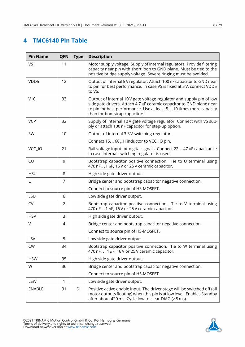
4 TMC6140 Pin Table
Pin Name QFN Type Description
VS 11 Motor supply voltage. Supply of internal regulators. Provide filteringcapacity near pin with short loop to GND plane. Must be tied to thepositive bridge supply voltage. Severe ringing must be avoided.VDD5 12 Output of internal 5 V regulator. Attach 100nF capacitor toGNDnearto pin for best performance. In case VS is fixed at 5V, connect VDD5to VS.V10 33 Output of internal 10V gate voltage regulator and supply pin of lowside gate drivers. Attach 4.7µF ceramic capacitor to GND plane nearto pin for best performance. Use at least 5. . .10 times more capacitythan for bootstrap capacitors.VCP 32 Supply of internal 10V gate voltage regulator. Connect with VS sup-ply or attach 100nF capacitor for step-up option.SW 10 Output of internal 3.3 V switching regulator.
Connect 15. . .68µH inductor to VCC_IO pin.VCC_IO 21 Rail voltage input for digital signals. Connect 22. . .47µF capacitancein case internal switching regulator is used.CU 9 Bootstrap capacitor positive connection. Tie to U terminal using470nF. . .1µF, 16V or 25V ceramic capacitor.HSU 8 High side gate driver output.U 7 Bridge center and bootstrap capacitor negative connection.
Connect to source pin of HS-MOSFET.LSU 6 Low side gate driver output.CV 2 Bootstrap capacitor positive connection. Tie to V terminal using470nF. . .1µF, 16V or 25V ceramic capacitor.HSV 3 High side gate driver output.V 4 Bridge center and bootstrap capacitor negative connection.
Connect to source pin of HS-MOSFET.LSV 5 Low side gate driver output.CW 34 Bootstrap capacitor positive connection. Tie to W terminal using470nF . . . 1µF, 16V or 25V ceramic capacitor.HSW 35 High side gate driver output.W 36 Bridge center and bootstrap capacitor negative connection.
Connect to source pin of HS-MOSFET.LSW 1 Low side gate driver output.ENABLE 31 DI Positive active enable input. The driver stage will be switched off (allmotor outputs floating) when this pin is at low level. Enables Standbyafter about 420ms. Cycle low to clear DIAG (> 5ms).
©2021 TRINAMIC Motion Control GmbH & Co. KG, Hamburg, GermanyTerms of delivery and rights to technical change reserved.Download newest version at www.trinamic.com

TMC6140 Datasheet • IC Version V1.0 | Document Revision V1.00 • 2021-June-11 9 / 29
Pin Name QFN Type Description
DIAG 20 DO Diagnosis output. High in case no error is detected. Can be used asUART-TxD or simple INTR. Short-to-x events are cleared by cyclingENABLE.SH_SET 19 AI Analog input voltage to define short protection threshold.
Set to 0 results in switched off high side gate driver outputs.DRV_STRONG 29 DI Digital driver strength input selection pin.
DRV_STRONG=0: 0.5 A, = 1: 1.0 A.UL 14 DI Low side control input for U.UH 13 DI High side control input for U.VL 16 DI Low side control input for V.VH 15 DI High side control input for V.WL 18 DI Low side control input for W.WH 17 DI High side control input for W.LOWGAIN 30 DI Digital driver gain selection pin for shunt amplifiers.
LOWGAIN=0: gain =50, = 1: gain = 20.SI1 26 AI 1st analog shunt amplifier input.
Do not exceed input limits of 3V / (2 · gain).SI2 27 AI 2nd analog shunt amplifier input.
Do not exceed input limits of 3V / (2 · gain).SI3 28 AI 3rd analog shunt amplifier input.
Do not exceed input limits of 3V / (2 · gain).nSI 24 AI Shared negative shunt amplifier input.
Connect to GND terminal of shunt resistor.SO1 22 AO 1st analog shunt amplifier output, bias =V(V CC_IO) / 2:
V (SO1) = VV CC_IO / 2 + gain · (V (SI1)− V (nSI)).SO2 23 AO 2nd analog shunt amplifier output, bias =V(V CC_IO) / 2:
V (SO2) = VV CC_IO / 2 + gain · (V (SI2)− V (nSI)).SO3 25 AO 3rd analog shunt amplifier output, bias =V(V CC_IO) / 2:
V (SO3) = VV CC_IO / 2 + gain · (V (SI3)− V (nSI)).Exposed die – Connect the exposed die pad to a GND plane. Provide as many aspossible vias for heat transfer to GND plane. Serves as GND pin forthe low side gate drivers and for digital logic. Ensure low loop induc-tivity to bridge GND.
Table 2: Functional Pin Description
©2021 TRINAMIC Motion Control GmbH & Co. KG, Hamburg, GermanyTerms of delivery and rights to technical change reserved.Download newest version at www.trinamic.com

TMC6140 Datasheet • IC Version V1.0 | Document Revision V1.00 • 2021-June-11 10 / 29
5 Functional DescriptionTMC6140 is a fully integrated universal 3-phase MOSFET gate driver. External MOSFETs for up to 100Amotor current are supported. Configuration possibilites and tuning options for the MOSFET bridge arepresented in this chapter. The diagnostics output and standby capabilites of TMC6140 are described inthe following. Finally, the buck converter and bottom shunt settings are presented.5.1 MOSFETs and Slope ControlThe selection of powerMOSFETs depends on a number of factors, like package size, on-resistance, voltagerating and supplier. It is not true, that larger, lower RDSonMOSFETswill always be better, as a larger devicealso has higher capacitances and may add more ringing in trace inductance and power dissipation in thegate drive circuitry. Adapt the MOSFETs to the required motor voltage (adding 5. . .10 V of reserve to thepeak supply voltage) and to the desired maximum current, in a way that resistive power dissipation stillis low for the selected MOSFET package. Choose modern MOSFETs with fast and soft recovery bulk diodeand low reverse recovery charge. A small, SMD MOSFET package allows compacter routing and reducesparasitic inductance effects. TMC6140 drives the MOSFET gates with 10V, so normal, 10 V specified typesare sufficient. Logic level FETs (4.5 V specified RDSon) will also work but may be more critical with regardto bridge cross-conduction due to lower VGS_th.The gate-drive current and MOSFET gate resistors RG (optional) should basically be adapted to the MOS-FET gate-drain charge (Miller charge) in order to yield reasonable slope times. The following figure showsthe influence of the Miller charge on the switching event.
Figure 4: Miller charge determines switching slope
The following table shall serve as a thumb rule for programming theMOSFET driver current (DRV_STRONGsetting) and the selection of gate resistors:Typ. Miller Charge [nC] DRV_STRONG Value of RG [Ohm]
<10 0 ≤10 (recomended)10. . .20 0 or 1 ≤ 5 (optional)20. . .80 1 ≤ 2.5 (optional)
Table 3: Functional Pin Description
©2021 TRINAMIC Motion Control GmbH & Co. KG, Hamburg, GermanyTerms of delivery and rights to technical change reserved.Download newest version at www.trinamic.com

TMC6140 Datasheet • IC Version V1.0 | Document Revision V1.00 • 2021-June-11 11 / 29
Note Use the lowest gate driver strength setting DRV_STRONG=0 giving favorableswitching slopes, before increasing the value of the gate series resistors. A slopetime of nominal 40ns to 80ns is absolutely sufficient and will normally be cov-ered by a Break-Before-Make (BBM) time up to 160ns. This BBM has to be gen-erated by the microcontroller adapting the PWM signal accordingly. TMC6140provides a small BBM of almost 1ns, just to ensure that only one MOSFET ofa phase is switched on. In case slower slopes have to be used, e.g. with largeMOSFETs, ensure that the BBM time sufficiently covers the switching event, inorder to avoid bridge cross conduction. The shortest BBM time, safely coveringthe switching event, gives best results. Add roughly 30% of reserve, to coverproduction stray of MOSFETs and driver.
5.2 Tuning the MOSFET BridgeA clean switching event is favorable to ensure low power dissipation and good EMC behavior. Unsuitablelayout or components endanger stable operation of the circuit. Therefore, it is important to understandthe effect of parasitic trace inductivity and MOSFET reverse recovery.Stray inductance in power routingwill cause ringingwhenever the oppositeMOSFET is in diode conductionprior to switching on a low-side or high-sideMOSFET. Diode conduction occurs during break-before-maketime whenever the load current is inverse to the following bridge polarity. The MOSFET bulk diode has acertain, type specific reverse recovery time and charge. This time typically is in the range of a few 10ns.During reverse recovery time, the bulk diode will cause high current flow across the bridge. This currentis taken from the power supply filter capacitors (see thick lines in the next figure). Once the diode opens,parasitic inductance tries to keep the current flowing.
DIE
PAD
LSLSV
HSV
VHS
CV
CB
+VM
RG: Reduce slope and protect the driver against ringing
in the interconnections between MOSFET and driver
4.7µF
RG
RG
Coil out
RG‘
Decide use and value of the additional components based on measurements of the actual circuit using
the final layout!
1n, 100V
470pF to a few nF output
capacitors close to bridge
and / or output reduce
ringing and improve EMC
Additional 1A type Schottky Diodes (selected for full VM range) in
combination with RG’ (0.47 to 1 Ohm) eliminate undershooting of BM.
RS
LOW-
ESR
Place filtering capacitors near to the bridge to avoid
severe overshooting and ringing.
Use sufficient capacitance with regard to motor current.
VS
220nF1R
Optional RC filter
against VS ringing
Figure 5: Bridge protection options for power routing indcutivity
©2021 TRINAMIC Motion Control GmbH & Co. KG, Hamburg, GermanyTerms of delivery and rights to technical change reserved.Download newest version at www.trinamic.com

TMC6140 Datasheet • IC Version V1.0 | Document Revision V1.00 • 2021-June-11 12 / 29
A high, fast slope results and leads to ringing in all parasitic inductivities (see next figures). This may leadto bridge voltage undershooting the GND level as well as fast pulses on VS and all MOSFET connections.It must be ensured, that the driver IC does not see spikes on its BM pins to GND going below -5V. SevereVS ripple might overload the charge-pump circuitry. Measure the voltage directly at the driver pins todriver GND. The amount of undershooting depends on energy stored in parasitic inductivities from lowside drain to low side source and via the sense resistor RS to GND. The following figure depicts a scopeshot of a switching high side MOSFET whose switching quality is good and signals are clean.
Figure 6: Ringing of output (green) and gate voltages (yellow, blue) with DRV_STRONG=0
When using relatively small MOSFETs, a soft slope control requires a high gate series resistance. Thisendangers safe MOSFET switch off. Add additional diodes to ensure safe MOSFET off conditions withslow switch-on slopes (see next figure).
DIE
PAD
LSLSV
HSV
VHS
CV
CB
+VM
4.7µF
RG
RG
Coil out
Additional 1A type Schottky Diodes (20V type sufficient) in
combination with high resistance gate resistors >10Ohm
RS
LOW-
ESR
VS
220nF
Figure 7: Diodes for safe off condition with high gate series resistance
©2021 TRINAMIC Motion Control GmbH & Co. KG, Hamburg, GermanyTerms of delivery and rights to technical change reserved.Download newest version at www.trinamic.com

TMC6140 Datasheet • IC Version V1.0 | Document Revision V1.00 • 2021-June-11 13 / 29
Ensure Reliable Operation• Use SMD MOSFETs and short interconnections• Provide sufficient power filtering capacity close to the bridge and close to VS pin• Tune MOSFET switching slopes (measure switch-on event at MOSFET gate) to be slower than theMOSFET bulk diode reverse recovery time. This will reduce cross conduction.• Add optional gate resistors close to MOSFET gate and output capacitors to ensure clean switchingand reliable operation by minimizing ringing.• Some MOSFETs eliminate reverse recovery charge by integrating a fast diode from source to drain.
Bridge Layout Considerations• Tune the bridge layout for minimum loop inductivity. A compact layout is best.• Keep MOSFET gate connections short and straight and avoid loop inductivity between bridge feed-back (U,V,W) and corresponding HS driver pin. Loop inductance is minimized with parallel traces,or adjacent traces on adjacent layers. A wider trace reduces inductivity (do not use minimum tracewidth).• Place the TMC6140 near the low side MOSFETs GND connections, with its GND connections directlyconnected to the same GND plane.• Optimize switching behavior by using lowest acceptable gate current setting.• Check influence of optional components.• Measure the performance of the bridge by probing BM pins directly at the bridge or at the TMC6140using a short GND tip on the scope probe rather than a GND cable, if available.
©2021 TRINAMIC Motion Control GmbH & Co. KG, Hamburg, GermanyTerms of delivery and rights to technical change reserved.Download newest version at www.trinamic.com

TMC6140 Datasheet • IC Version V1.0 | Document Revision V1.00 • 2021-June-11 14 / 29
5.3 Low Power ModesTMC6140 provides two standby modes that lower significantly the overall power consumption. SwitchingENABLE input signal to 0 will switch off the drive stage immediately. Furhermore, any generated shortcircuit event (see next section) will be cleared. After around typically 425ms from the event when ENABLEswitches from high to low, the internal standby mode is enabled. Dependent on the digital high andlow sides input control pins (UL, UH, VL, VH, WL, WH) the 3V3 switching regulator is also turned off orremains powered. The next figure depicts this exemplarily. In this example only the low side of phase Uis considered (with impact on LSU output). All other input control pins (UH, VL, VH, WL, WH) are definedto be equal to 0. Thus all gate driver outputs except LSU are switched off. Supposed that during ULequals 1 (LSU is active) a short to ground is detected, the LSU gate output is immediately turned off andDIAG switches to low to indicate the error (further details on DIAG will be explained in the next section).Switching ENABLE from high to low will clear this event, but as long as ENABLE is low, the driver stage isturned off. After around typically 425ms, the internal standby will be activated if ENABLE remains at lowlevel. In case any of the digital input pins (UL, UH, VL, VH,WL,WH) is set to high at this point in time (standbyis activated), the 3V3 regulator will not be switched off (Low Power Mode1: buck_en=1). In this example,the short-to-ground cause remain and after enabling the power stage (ENABLE=1) and switching on thelow side again, the next S2G event will be triggered. To save more power, it is possible to also turn off the3V3 switching regulator. To obtain this Low Power Mode0, all of the digital input pins (UL, UH, VL, VH, WL,WH) have to be low when standby is activated. This is depicted at the right side of the figure where UL islow when standby is activated.Note Beware, Low Power Mode 0 will result in a shut down of the logic in case the 3V3switching regualtor is the supply of the microcontroller.
Drv stage
ENABLE
UH
VH
WH
UL
VL
WL
SH_SET
BBM
+
Short
Protection
DIAG
TMC6140
Diagnostics
- UVVS flag
- OT(PW) flags
- Short Protect
clr
STDBY
LSU
buck_en (internal)
Low Power Mode: 1 0
UL (in)
DIAG (out)
ENABLE (in)
290...580 ms
S2G (internal)
clear (internal)
LSU (out)
stdby (internal)
Short-to-ground
290...580 ms
Figure 8: Illustration of the activation of the two available Low Power Modes
©2021 TRINAMIC Motion Control GmbH & Co. KG, Hamburg, GermanyTerms of delivery and rights to technical change reserved.Download newest version at www.trinamic.com

TMC6140 Datasheet • IC Version V1.0 | Document Revision V1.00 • 2021-June-11 15 / 29
5.4 DiagnosticsAs briefly described in the section before, TMC6140 provides error diagnostics capabilites and a digitalDIAG output to indicate recognized error states. In case any error state is identified, a single wire UARTdatagram of 64 bits is sent out repeatedly. This UART datagram consists of a sync byte (with start andstop bit), a data byte (with start and stop bit) and 44 stop bits. After the start bit (low level) of the syncbyte six bits with high level will be sent. The seventh bit is a zero, followed by the stop bit (high level). Thedata byte again starts with a start bit (low level), then eight data bits are transmitted followed by 45 stopbits. Then, UART transmission starts again. In the following the UART datagram is depicted.
Failure detection
uart_clock (internal)
x Start 0 1 2 3 4 5 6 7 Stop Start 0 1 2 3 4 5 6 7 Stop Stop Stop Start 0
44 Stop bits8 sync bits 8 data bits
DIAG (output) OTUV1 SCOTUV1 S2VS S2G SHU SHV SHW
...
Figure 9: Schematic of the DIAG output in case an error state is identified.
The internal UART clock frequency is typically 9.6 kHz. This allows all kind of microcontrollers to synchro-nize with the bit stream. By detecting the two first high-to-low switches of DIAG, shifting the determinedtime between both switches by 3 will reveal the time for one bit. After detecting the third switch fromhigh-to-low the second START bit and the eigth data bits will follow. In case it is only required to knowerror states of TMC6140 and not the error condition specifically, a low level signal of DIAG can be takenas error message.Error flagsIn summary, TMC6140 transmits ten error condition bitswithin eight data bits. The data bits 0. . .2 transmitfour status flags. That means, switching ENABLE to low for a short time (> 5ms) will not reset these errorflags because these failure states are permanently checked and have to be dissolved externally. It is alsonoted, that detecting these error flags will not generate an automatic switch-off of the driver stage.Following status flags are available:
• OT: Overtemperature warningThe chip temperature has reached 150 °C. The driver should be switched off immediately becausethe temperature is out of operational range.• OTPW: Overtemperature prewarningThe chip temperature has reached 120 °C. Further operation could harm the chip.• UVVS: VS voltage is below 6.8 VThis may result in gate driver outputs (at LSx, HSx) which are too low for a proper operation of theconnected MOSFETs.• SC: Load at the 3V3 switching regulator consumes too much current. The output is automaticallyswitched off in every buck converter clock cycle in case overcurrent is detected.
The first three error flags are coded in the first two data bits OTUV1 and OTUV0 with defined hierarchy(OT is prior to UVVS, UVVS is prior to OTPW):• OTUV[1:0] = 11 indicates OT=1, UVVS= x, OTPW=1• OTUV[1:0] = 10 indicates OT=0, UVVS=1, OTPW=x• OTUV[1:0] = 01 indicates OT=0, UVVS=0, OTPW=1• OTUV[1:0] = 00 indicates OT=0, UVVS=0, OTPW=0
©2021 TRINAMIC Motion Control GmbH & Co. KG, Hamburg, GermanyTerms of delivery and rights to technical change reserved.Download newest version at www.trinamic.com

TMC6140 Datasheet • IC Version V1.0 | Document Revision V1.00 • 2021-June-11 16 / 29
Error eventsThe data bits 3. . .4 transmit two status events that will result in switched off driver stage outputs:
• S2G: Short-to-ground on one or more phases:All three driver stage high side outputs (HSU, HSV, HSW) will be switched off.• S2VS: Short-to-VS (supply) on one or more phases:All six driver stage outputs (HSU, HSV, HSW, LSU, LSV, LSW) will be switched off.
The remaining status events (data bits 5. . .7) serve as information source on which phase the short-to-xevent has been identified. The sequence is:• Bit5: Short-to-x has been detected at phase U.• Bit6: Short-to-x has been detected at phase V.• Bit7: Short-to-x has been detected at phase W.
These Short-to-x events have to be cleared by ENABLE=0 for at least 5ms to release the particular driverstage outputs.Short-to-x ConfigurationBy applying an analog signal to SH_SET the Short-to-VS resp. Short-to-GND detector level is defined. Short-to-VS checks for the voltage drop between low side MOSFET and bottom shunt resistor, whereas Short-to-GND checks for the voltage drop on high side MOSFET. If these voltage drops exceed SH_SET/2 [V] anerror will occur.Additonally, SH_SET is dedicated for a second feature. In case SH_SET is set to 0V (< 0.4 V), the high sideoutputs are masked, only the low side outputs can be driven during this state. This state suits well forthe beginning of the operation as it can be used to load the bootstrap capacitors without switching offthe high side PWM signals. In case SH_SET is lower than 0.4 V, the internal tolerable voltage drop for theShort-to-VS detetion is set to 1.0 V. Values at SH_SET between 0.4 V and 0.9 V are prohibited.
pro-
hibited
ENABLE
SH_SETDiagnostics
- UVVS flag
- OT(PW) flags
- Short Protect
clr
3.3 (VCC_IO)
0.9
0.4
V(SH_SET) [V]
VCC_IO / 2
0.45
V(Short_Protect) [V]
internal
t
t
1.00
TMC6140
DIAG
BBM
+
Short
Protection
HSx
xL
xH
LSx
xL (input)
xH (input)
LSx (output)
HSx (output)
Figure 10: Impact of SH_SET configuration.SH_SET < 0.4 V: High side gate signals are low, internal S2VS limit = 1.0 Vabove 0.9 V: internal S2x limit = SH_SET/2 [V]0.4 V < SH_SET < 0.9 V is prohibited.
©2021 TRINAMIC Motion Control GmbH & Co. KG, Hamburg, GermanyTerms of delivery and rights to technical change reserved.Download newest version at www.trinamic.com

TMC6140 Datasheet • IC Version V1.0 | Document Revision V1.00 • 2021-June-11 17 / 29
5.5 3V3 Switching RegulatorTMC6140 integrates a buck switching regulator designed for up to 500mA of output current and a 3.3 Voutput voltage. Its main purpose is to supply the TMC6140 and a connected microcontroller.This regulator comes with an integrated 100mA 30V Schottky diode which minimizes part count. If morecurrent is required, use an external Schottky diode in parallel.The integrated linear 5V regulator starts up the switch regulator with a start delay of 1ms at maximum.The following figure shows the basic internal circuit and required external circuitry.
VS
SW
VCC_IO
680 KHZ
PMOS
Driver
SAW
oscillator
IMAX
SetS
R
Q1.2 ΩMOSFET
Dutycycle limit
SC_FLAG
CFB
RFB
Soft Start
Circuit
Sum
Amplifier &
Compa-
rator
+
+
-
Ref
UV5V
0.1 A Schottky
CSW
LSW
CSWE
3.3 V
CE
+VM
47
0n
TMC6140
Optional:Ext. Schottky
Figure 11: Internal schematic of and external components for the 3V3 switching regulator
Component SelectionTMC6140 switching regulator provides stable regulation in a wide range of input and output voltages aswell as for a wide range of external L/C components. This allows for using standardized capacitance andinductivity values, unless an optimization is desired, e.g. for space critical applications, where the size ofexternal components has to be minimized.The following table depcits exemplary values when using the chopper frequency of 680 kHz. The capacitorcan either be a ceramic type, or an electrolytic low-ESR capacitor in parallel to a 1µF or larger ceramiccapacitor. Generally increasing the inductivity reduces current ripple, and thus allows for a higher outputcurrent without triggering the overcurrent detector.
Input Voltage [V] LSW [µH] Value of CSW [µF]
5 15 2212 33 4724 68 4730 68 47
Table 4: 3V3 switching regulator component examples
©2021 TRINAMIC Motion Control GmbH & Co. KG, Hamburg, GermanyTerms of delivery and rights to technical change reserved.Download newest version at www.trinamic.com

TMC6140 Datasheet • IC Version V1.0 | Document Revision V1.00 • 2021-June-11 18 / 29
5.6 Shunt Resistor AmplifiersTMC6140 provides for each motor phase a bottom shunt amplifier with a bias of VV CC_IO/2 [V].LOWGAIN adapts the internal gain factor to 20 (LOWGAIN=1) or 50 (LOWGAIN=0).Thus, the maximum input limit at SIx analog input must not exceed 3V / (2 · gain).The resulting analog voltage at SOx yields to VSOx = VV CC_IO/2 + gain · (VSIx − VnSI) with x is U,V, or W.All three amplifiers share the same negative input pin nSI.
DIE
PA
D
LOWGAIN
SI2
RS
SI3
RS
nSI
3 Shunt Amplifiers
SO1
SO2
SO3
LSLSW
RG
SI1
RS
47R
x20 / x50 selection
x10
x2x5
VCC_IO
V(VCC_IO)/2
TMC6140
Figure 12: Shunt Amplifier setup for phase W
©2021 TRINAMIC Motion Control GmbH & Co. KG, Hamburg, GermanyTerms of delivery and rights to technical change reserved.Download newest version at www.trinamic.com

TMC6140 Datasheet • IC Version V1.0 | Document Revision V1.00 • 2021-June-11 19 / 29
6 Electrical Characteristics
6.1 Absolute Maximum RatingsThe maximum ratings may not be exceeded under any circumstances. Operating the circuit at ornear more than one maximum rating at a time for an extended period must be avoided by applicationdesign.Parameter Symbol Min Max Unit
Supply voltage operating with inductive load VV S -0.5 33 VSupply and bridge voltage short time peak VV SMAX 33 VSupply voltage for V10 regulator VV CP VV S − 0.5 33 VPeak voltages on U/V/W pins (due to stray inductivity) VX -5 VV S + 6 VPeak voltage on Cxx bootstrap pins VCx 45 VPeak voltage on Cxx bootstrap pins relative to BM VCx VV x + 16 VSupply voltage VDD5 VV DD5 -0.5 5.5 VIO supply voltage VV CC_IO -0.5 3.6 VLogic and analog input voltage VI -0.5 VV CC_IO + 0.5 VMaximum current to/from digital pins (short time peak) IIO +/- 500 mA5V regulator output current IV DD5 60 mA5V regulator continious power dissipation PV DD5 0.5 W10V regulator output current IV 10 60 mA10V regulator continious power dissipation PV 10 0.5 WJunction temperature TJ -50 150 °CStorage temperature TSTG -55 150 °CESD protection (HBM / CDM) VESD 1500 /500 V
Table 5: Absolute Maximum Ratings
©2021 TRINAMIC Motion Control GmbH & Co. KG, Hamburg, GermanyTerms of delivery and rights to technical change reserved.Download newest version at www.trinamic.com

TMC6140 Datasheet • IC Version V1.0 | Document Revision V1.00 • 2021-June-11 20 / 29
6.2 Operational Range
Parameter Symbol Min Max Unit
Junction temperature TJ -40 125 °CSupply voltage for motor and bridge VV S 5 30 VSupply voltage for V10 regulator VV CP VV S 30 VIO supply voltage VV CC_IO 3.0 3.6 VSupply voltage VDD5 (internally generated) VV DD5 4.5 5.5 V10V regulator output (internally generated) VV 10 9.5 10.5 V
Table 6: Operational Range
6.3 DC and Timing characteristics
Parameter Symbol Condition Min Typ Max Unit
Total supply current, no Low Powermode, no active driver IV S VV S = 24V 4 6 mATotal supply current, Low Powermode 1 , no active driver IV S VV S = 24V 1 1.25 mATotal supply current, Low Powermode 0 , no active driver IV S VV S = 24V 0.2 0.25 mAInternal current consumption fromVDD5 IV S VV S = 24V 4 mA
Table 7: Power Supply Current DC characteristics
©2021 TRINAMIC Motion Control GmbH & Co. KG, Hamburg, GermanyTerms of delivery and rights to technical change reserved.Download newest version at www.trinamic.com

TMC6140 Datasheet • IC Version V1.0 | Document Revision V1.00 • 2021-June-11 21 / 29
Parameter Symbol Condition Min Typ Max Unit
RDSON low side RONL Gate off, 1.8 2.0 OhmDRV_STRONG=1
RDSON high side RONH Gate off, 1.2 2.0 OhmDRV_STRONG=1
Gate Drive current low side, ILON0 DRV_STRONG=0 450 mAMOSFET turning on at 3 V VGS ILON1 DRV_STRONG=1 850 mAGate Drive current high side, IHON0 DRV_STRONG=0 450 mAMOSFET turning on at 3 V VGS IHON1 DRV_STRONG=1 850 mAGate Drive current low side, ILOFF0 DRV_STRONG=0 650 mAMOSFET turning off at 3V VGS ILOFF1 DRV_STRONG=1 1250 mAGate Drive current high side, IHOFF0 DRV_STRONG=0 700 mAMOSFET turning off at 3V VGS IHOFF1 DRV_STRONG=1 1250 mA
Table 8: Motor Driver Timing and DC characteristics
Parameter Symbol Condition Min Typ Max Unit
Low side on reaction delay time tDLY LON0 DRV_STRONG=0 120 nstDLY LON1 DRV_STRONG=1 90 ns
Low side off reaction delay time tDLY LOFF0 DRV_STRONG=0 90 nstDLY LOFF1 DRV_STRONG=1 90 ns
High side on reaction delay time tDLY LON0 DRV_STRONG=0 150 nstDLY LON1 DRV_STRONG=1 90 ns
High side off reaction delay time tDLY LOFF0 DRV_STRONG=0 120 nstDLY LOFF1 DRV_STRONG=1 90 ns
Matching difference delay timeHigh side off to low side on tDLYM 15 nsLow side off to high side onSwitch off time of LSx/HSx output af-ter disabling ENABLE tDIS 400 ns
Table 9: Reaction delay times from input signal change to start gate driver output change
©2021 TRINAMIC Motion Control GmbH & Co. KG, Hamburg, GermanyTerms of delivery and rights to technical change reserved.Download newest version at www.trinamic.com

TMC6140 Datasheet • IC Version V1.0 | Document Revision V1.00 • 2021-June-11 22 / 29
Parameter Symbol Condition Min Typ Max Unit
Short-to-VS voltage limit VV S2V S SH_SET=2.5 V 1.0 1.25 1.5 Vduring brake mode VV S2V SB
SH_SET=0 V 0.75 1.0 1.25 VShort-to-GND voltage limit tV S2G SH_SET=2.5 V 1.0 1.25 1.5 VShort-to-VS delay tTS2V S SH_SET=0 1.3 1.8 2.5 µsShort-to-GND delay tTS2G SH_SET=0 1.8 2.2 2.7 µsUndervoltage VS threshold for VUV V S VV S falling 6.7 6.9 VDIAG error output (UVVS flag)VV DD5 threshold for internal reset VUV 5 VV DD5 rising 3.7 4.0 VVV CC_IO threshold for internal reset VV CC_IO VV CC_IO rising 1.9 2.5 VOvertemperature prewarning TOTPW Temp rising 105 120 135 °COvertemperature warning TOT Temp rising 135 150 165 °C
Table 10: Detection DC characteristics
Parameter Symbol Condition Min Typ Max Unit
UART-Frequency of DIAG output fUART Any error 6.5 9.6 14.5 kHzDeviation of DIAG output frequency fDEV UT TJ = +/-300 Hzover temperature full rangeStart delay of LowPowerMode 0/1 af-ter falling edge of ENABLE tSTDBY 290 470 590 msDelay to clear Short-to-x event tCLR 5 ms(ENABLE=0)
Table 11: DIAG and Low Power Mode Timing
©2021 TRINAMIC Motion Control GmbH & Co. KG, Hamburg, GermanyTerms of delivery and rights to technical change reserved.Download newest version at www.trinamic.com

TMC6140 Datasheet • IC Version V1.0 | Document Revision V1.00 • 2021-June-11 23 / 29
Parameter Symbol Condition Min Typ Max Unit
Input offset VINOFF TJ =25 °C 0.15 0.2 0.25 mVDeviation of input offset over VDEV ST TJ = +/-0.1 +/-0.2 mVtemperature full rangeInput resistor VINRES TJ =25 °C 48 60 72 kOhmOutput resistor VINRES TJ =25 °C 240 300 360 OhmLow Gain (LOWGAIN=1) GLOW TJ =25 °C 19.0 19.8 20.0Deviation of low gain over VDEVGL TJ = +/-0.1 +/-0.2temperature full rangeHigh Gain (LOWGAIN=0) GHIGH TJ =25 °C 49 49.5Deviation of high gain over VDEVGH TJ = +/-0.5 +/-1.0temperature full range
Table 12: Shunt Resistor Amplifier DC characteristics
©2021 TRINAMIC Motion Control GmbH & Co. KG, Hamburg, GermanyTerms of delivery and rights to technical change reserved.Download newest version at www.trinamic.com

TMC6140 Datasheet • IC Version V1.0 | Document Revision V1.00 • 2021-June-11 24 / 29
Parameter Symbol Condition Min Typ Max Unit
5V regulator output voltage VV DD5 TJ =25 °C 4.75 5.0 5.25 VDeviation of 5V regulator output over VDEV 5T TJ = +/-5 +/-50 mVtemperature full rangeDeviation of 5V regulator output over VDEV 5S VV S = +/-20 mVsupply voltage full range10V regulator output voltage VV 10 TJ = 25 °C 9.5 10.0 10.5 VDeviation of 10V regulator output VDEV 10T VV S = +/-10 +/-50 mVover temperature full rangeDeviation of 10V regulator output VDEV 10S VV S = +/-20 mVover supply voltage 10 V . . .33 V3V3 regulator output V3V 3 TJ =25 °C 3.1 3.3 3.5 VDeviation of 3V3 regulator output VDEV 3T TJ = +/-5 +/-20 mVover temperature full rangeDeviation of 3V3 regulator output VDEV 3S VV S = +/-50 mVover supply voltage full rangeRDSON power switch RON3V 3 TJ =25 °C 1.2 1.6 OhmOvercurrent protection activationthreshold IOV B Output current 800 1200 1600 mAOscillator frequency fBUCK 520 650 820 kHz3V3 regulator duty cycle limit cycleLimit 83 %Schottky diode forward voltage VSDF I = 350 mA 0.6 0.8 VInternal Schottky diode maximumcurrent ISDI 0.1 0.12 AStart delay of buck converter after ris-ing edge of ENABLE tSTART 1 ms
Table 13: Regulator DC and Timing characteristics
©2021 TRINAMIC Motion Control GmbH & Co. KG, Hamburg, GermanyTerms of delivery and rights to technical change reserved.Download newest version at www.trinamic.com

TMC6140 Datasheet • IC Version V1.0 | Document Revision V1.00 • 2021-June-11 25 / 29
7 Package Mechanical DataPackage: QFN36, 0.5mm pitch, size 5.0mm x 6.0mm. Attention: Drawings not to scale.
Figure 13: QFN36 Package Dimensions
©2021 TRINAMIC Motion Control GmbH & Co. KG, Hamburg, GermanyTerms of delivery and rights to technical change reserved.Download newest version at www.trinamic.com

TMC6140 Datasheet • IC Version V1.0 | Document Revision V1.00 • 2021-June-11 26 / 29
Description Dimension [mm] Min Typ Max
Total Thickness A 0.80 0.85 0.90Stand Off A1 0.00 0.035 0.05Mold Thickness A2 — 0.65 —L/F Thickness A3 0.203 REFLead Width b 0.20 0.25 0.30Body Width D 5 BSCBody Length E 6 BSCLead Pitch e 0.5 BSCEP Size J 3.5 3.6 3.7EP Size K 4.0 4.1 4.2Lead Length L 0.35 0.40 0.45Package Edge Tolerance aaa 0.1Mold Flatness bbb 0.1Coplanarity ccc 0.08Lead Offset ddd 0.1Exposed Pad Offset eee 0.1
Table 14: QFN36 Package Dimensionsin mm
©2021 TRINAMIC Motion Control GmbH & Co. KG, Hamburg, GermanyTerms of delivery and rights to technical change reserved.Download newest version at www.trinamic.com

TMC6140 Datasheet • IC Version V1.0 | Document Revision V1.00 • 2021-June-11 27 / 29
8 Figures Index1 Standard application . . . . . . . . . . 42 Optional step-up converter for VCP, *minimal load at VCC_IO is required, **optional resistor to limit switching reg-ulator load peak current (e.g. 10 Ohm) 53 TMC6140-LA pinning QFN36 . . . . . 74 Miller charge schematic . . . . . . . . 105 Bridge protection options . . . . . . . 11
6 Ringing DRV_STRONG=0 . . . . . . . . 127 Safe off condition . . . . . . . . . . . . 128 Low Power Modes . . . . . . . . . . . 149 DIAG Output . . . . . . . . . . . . . . . 1510 SH_SET configuration . . . . . . . . . . 1611 3V3 Switching Regulator . . . . . . . . 1712 Shunt Amplifier setup for phase W . . 1813 QFN36 Package Dimensions . . . . . . 25
©2021 TRINAMIC Motion Control GmbH & Co. KG, Hamburg, GermanyTerms of delivery and rights to technical change reserved.Download newest version at www.trinamic.com

TMC6140 Datasheet • IC Version V1.0 | Document Revision V1.00 • 2021-June-11 28 / 29
9 Tables Index1 Order codes . . . . . . . . . . . . . . . 32 Functional Pin Description . . . . . . . 93 Functional Pin Description . . . . . . . 104 3V3 Switching Regulator Components 175 Absolute Maximum Ratings . . . . . . 196 Operational Range . . . . . . . . . . . 207 Power Supply Current DC characteris-tics . . . . . . . . . . . . . . . . . . . . . 208 Motor Driver Timing and DC charac-teristics . . . . . . . . . . . . . . . . . . 21
9 Reaction delay times from input sig-nal change to start gate driver outputchange . . . . . . . . . . . . . . . . . . 2110 Detection DC characteristics . . . . . 2211 DIAG and Low Power Mode Timing . 2212 Shunt Resistor Amplifier DC charac-teristics . . . . . . . . . . . . . . . . . . 2313 Regulator DC and Timing characteristics 2414 QFN36 Package Dimensionsin mm . . 2615 IC Revision . . . . . . . . . . . . . . . . 2916 Document Revision . . . . . . . . . . . 29
©2021 TRINAMIC Motion Control GmbH & Co. KG, Hamburg, GermanyTerms of delivery and rights to technical change reserved.Download newest version at www.trinamic.com

TMC6140 Datasheet • IC Version V1.0 | Document Revision V1.00 • 2021-June-11 29 / 29
10 Revision History
10.1 IC Revision
Version Date Author DescriptionV1.0 2021-MAY-17 HS TMC6140-LA release
Table 15: IC Revision
10.2 Document Revision
Version Date Author DescriptionV1.0 2021-JUN-10 HS Initial version
Table 16: Document Revision
©2021 TRINAMIC Motion Control GmbH & Co. KG, Hamburg, GermanyTerms of delivery and rights to technical change reserved.Download newest version at www.trinamic.com