Two-dimensional analytical sub-threshold model of multi-layered gate dielectric recessed channel...
14
Superlattices and Microstructures 45 (2009) 91–104 Contents lists available at ScienceDirect Superlattices and Microstructures journal homepage: www.elsevier.com/locate/superlattices Two-dimensional analytical subthreshold model of graded channel DG FD SOI n-MOSFET with gate misalignment effect Rupendra Kumar Sharma, Mridula Gupta 1 , R.S. Gupta *,2 Semiconductor Devices Research Laboratory, Department of Electronic Science, University of Delhi South Campus, New Delhi 110021, India article info Article history: Received 16 June 2008 Received in revised form 25 November 2008 Accepted 2 December 2008 Available online 28 January 2009 Keywords: Analytical modeling Subthreshold analysis Non-uniform doping CMT approach Silicon on insulator (SOI) ATLAS 3-D device simulator abstract A two-dimensional (2-D) analytical subthreshold model is devel- oped for a graded channel double gate (DG) fully depleted SOI n- MOSFET incorporating a gate misalignment effect. The conformal mapping transformation (CMT) approach has been used to pro- vide an accurate prediction of the surface potential, electric field, threshold voltage and subthreshold behavior of the device, consid- ering the gate misalignment effect to be on both source and drain side. The model is applied to both uniformly doped (UD) and graded channel (GC) DG MOSFETs. The results of an analytical model agree well with 3-D simulated data obtained by ATLAS-3D device simu- lation software. © 2008 Elsevier Ltd. All rights reserved. 1. Introduction DG-SOI is a promising CMOS device to be scaled beyond the 100-nm regime [1], as it exhibits an almost ideal sub-threshold swing (S ≈ 60 mV/dec), lower output conductance and higher drive current for analog applications [2]. One major issue of DG-MOSFETs is the alignment between the top and bottom gates. There are some self-aligned DG-MOSFETs proposed in the literature [3,4], however, complicated fabrication techniques are usually required. It would then be critical to understand how the misalignment between the gates would affect the properties of DG-MOSFETs, especially the SCE‘s, subthreshold slope and device performance. * Corresponding author. Tel.: +91 011 24115580; fax: +91 011 24110606. E-mail addresses: [email protected] (R.K. Sharma), [email protected] (R.S. Gupta). 1 Member IEEE. 2 Senior member IEEE. 0749-6036/$ – see front matter © 2008 Elsevier Ltd. All rights reserved. doi:10.1016/j.spmi.2008.12.005
-
Upload
independent -
Category
Documents
-
view
1 -
download
0
Transcript of Two-dimensional analytical sub-threshold model of multi-layered gate dielectric recessed channel...

Superlattices and Microstructures 45 (2009) 91–104
Contents lists available at ScienceDirect
Superlattices and Microstructures
journal homepage: www.elsevier.com/locate/superlattices
Two-dimensional analytical subthreshold model of gradedchannel DG FD SOI n-MOSFET with gate misalignmenteffectRupendra Kumar Sharma, Mridula Gupta 1, R.S. Gupta ∗,2Semiconductor Devices Research Laboratory, Department of Electronic Science, University of Delhi South Campus,New Delhi 110021, India
a r t i c l e i n f o
Article history:Received 16 June 2008Received in revised form25 November 2008Accepted 2 December 2008Available online 28 January 2009
Keywords:Analytical modelingSubthreshold analysisNon-uniform dopingCMT approachSilicon on insulator (SOI)ATLAS 3-D device simulator
a b s t r a c t
A two-dimensional (2-D) analytical subthreshold model is devel-oped for a graded channel double gate (DG) fully depleted SOI n-MOSFET incorporating a gate misalignment effect. The conformalmapping transformation (CMT) approach has been used to pro-vide an accurate prediction of the surface potential, electric field,threshold voltage and subthreshold behavior of the device, consid-ering the gate misalignment effect to be on both source and drainside. Themodel is applied to both uniformly doped (UD) and gradedchannel (GC) DGMOSFETs. The results of an analytical model agreewell with 3-D simulated data obtained by ATLAS-3D device simu-lation software.
© 2008 Elsevier Ltd. All rights reserved.
1. Introduction
DG-SOI is a promising CMOS device to be scaled beyond the 100-nm regime [1], as it exhibitsan almost ideal sub-threshold swing (S ≈ 60 mV/dec), lower output conductance and higher drivecurrent for analog applications [2]. One major issue of DG-MOSFETs is the alignment between the topand bottom gates. There are some self-aligned DG-MOSFETs proposed in the literature [3,4], however,complicated fabrication techniques are usually required. It would then be critical to understand howthemisalignment between the gates would affect the properties of DG-MOSFETs, especially the SCE‘s,subthreshold slope and device performance.
∗ Corresponding author. Tel.: +91 011 24115580; fax: +91 011 24110606.E-mail addresses: [email protected] (R.K. Sharma), [email protected] (R.S. Gupta).
1 Member IEEE.2 Senior member IEEE.
0749-6036/$ – see front matter© 2008 Elsevier Ltd. All rights reserved.doi:10.1016/j.spmi.2008.12.005
92 R.K. Sharma et al. / Superlattices and Microstructures 45 (2009) 91–104
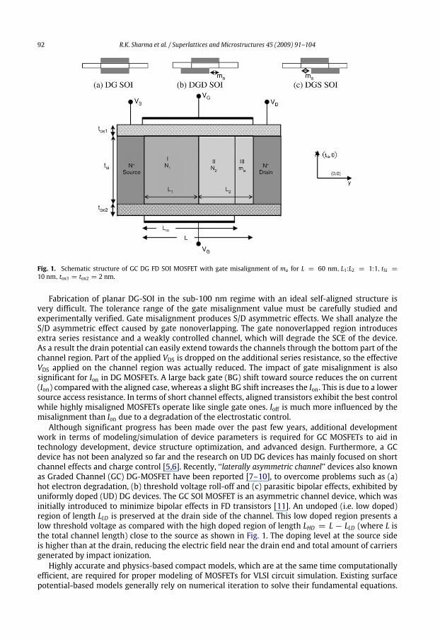
Fig. 1. Schematic structure of GC DG FD SOI MOSFET with gate misalignment of ma for L = 60 nm, L1:L2 = 1:1, tSi =10 nm, tox1 = tox2 = 2 nm.
Fabrication of planar DG-SOI in the sub-100 nm regime with an ideal self-aligned structure isvery difficult. The tolerance range of the gate misalignment value must be carefully studied andexperimentally verified. Gate misalignment produces S/D asymmetric effects. We shall analyze theS/D asymmetric effect caused by gate nonoverlapping. The gate nonoverlapped region introducesextra series resistance and a weakly controlled channel, which will degrade the SCE of the device.As a result the drain potential can easily extend towards the channels through the bottom part of thechannel region. Part of the applied VDS is dropped on the additional series resistance, so the effectiveVDS applied on the channel region was actually reduced. The impact of gate misalignment is alsosignificant for Ion in DG MOSFETs. A large back gate (BG) shift toward source reduces the on current(Ion) compared with the aligned case, whereas a slight BG shift increases the Ion. This is due to a lowersource access resistance. In terms of short channel effects, aligned transistors exhibit the best controlwhile highly misaligned MOSFETs operate like single gate ones. Ioff is much more influenced by themisalignment than Ion due to a degradation of the electrostatic control.Although significant progress has been made over the past few years, additional development
work in terms of modeling/simulation of device parameters is required for GC MOSFETs to aid intechnology development, device structure optimization, and advanced design. Furthermore, a GCdevice has not been analyzed so far and the research on UD DG devices has mainly focused on shortchannel effects and charge control [5,6]. Recently, ‘‘laterally asymmetric channel’’ devices also knownas Graded Channel (GC) DG-MOSFET have been reported [7–10], to overcome problems such as (a)hot electron degradation, (b) threshold voltage roll-off and (c) parasitic bipolar effects, exhibited byuniformly doped (UD) DG devices. The GC SOI MOSFET is an asymmetric channel device, which wasinitially introduced to minimize bipolar effects in FD transistors [11]. An undoped (i.e. low doped)region of length LLD is preserved at the drain side of the channel. This low doped region presents alow threshold voltage as compared with the high doped region of length LHD = L − LLD (where L isthe total channel length) close to the source as shown in Fig. 1. The doping level at the source sideis higher than at the drain, reducing the electric field near the drain end and total amount of carriersgenerated by impact ionization.Highly accurate and physics-based compact models, which are at the same time computationally
efficient, are required for proper modeling of MOSFETs for VLSI circuit simulation. Existing surfacepotential-based models generally rely on numerical iteration to solve their fundamental equations.
R.K. Sharma et al. / Superlattices and Microstructures 45 (2009) 91–104 93
Still, explicit analytical models are highly desirable because they offer better computational efficiencythan their numerical alternatives without loss of physical insight. We have presented a twodimensional closed form analytical model of a graded channel (GC) DG-SOI MOSFET, consideringthe misalignment of the bottom gate on both source (DGS) and drain (DGD) sides. The model uses aconformal mapping transformation approach to include the fringing field effect arising at the bottomgate electrode in the ungated region, which can provide an accurate prediction of the subthresholdbehavior of the device. The results so obtainedhave been verifiedwith theATLAS 3-Ddevice simulator.
1.1. Model formulation
A graded channel (GC) DG-SOI n-MOSFET with gate misalignment (ma) is shown in Fig. 1. Inthis structure n+ top and bottom poly-silicon gates (Npoly = 1.65 × 1025 m−3), top gate oxide as(tox1 = 2 nm), bottom gate oxide as (tox2 = 2 nm), silicon film thickness as (tSi = 10 nm), p-typechannel impurity concentration in the high and low doped regions as N1 and N2, with the lengths asL1 and L2 respectively. The 2-D Potential distribution can be obtained by solving 2-D Poisson equation.
∇2ψ(x, y) =
qNiεSi
(1)
i = 1 and 2 for the highly doped and lightly doped regions respectively. In order to simplify theanalysis, the polysilicon depletion effect [12–14] and the quantum effect [15–17] are not considered.The thin film is divided into three regions:Case I: Gate overlap highly doped regionCase II: Gate overlap lightly doped regionCase III: Non-gate overlap lightly doped regionCase I: Gate overlap highly doped region.The potential profile in the vertical direction ψ(x, y) can be approximated by a 2-D parabolic
approximation.
ψi(x, y) = C0i(y)+ C1i(y)x+ C2i(y)x2. (2)
Solving 2-D Poisson’s equation with these boundary conditions
−∂ψi(x, y)∂x
∣∣∣∣x=0=Cox2εSi
[VG + φf 2 − ψbi(y)
], −
∂ψi(x, y)∂x
∣∣∣∣x=tSi
=Cox1εSi
[ψSi(y)− VG − φf 1
].
ψi(x, y) can be written as
ψi(x, y) = ψbi (y)−εox
εSitox2
[VG + φf 2 − ψbi(y)
]+
1tox2
[(tox2 + εox
εSitSi + tox1
)(VG − ψbi(y))+
(tox1 + εox
εSitSi)φf 2
]+ φf 1
t2Si(1+ 2εSitox1
εoxtSi
) . (3)
Using Eqs. (2)–(3), a relationship between front and back surface potentials has been obtained as
ψSi(y) = ψbi(y)−εoxtSiεSitox2
[VG + φf 2 − ψbi(y)
]+ P21(y)t2Si. (4)
Assuming silicon film to be very thin (tSi ≈ 10 nm), we can write
∂2ψi(y)∂y2
∼=1κSi
∂2ψbi(y)∂y2
(5)
Where κSi is the parameter that accounts for the correlation between the derivative of the lateralelectric field at any depth in the thin film and the derivative of the lateral electric field at the back
94 R.K. Sharma et al. / Superlattices and Microstructures 45 (2009) 91–104
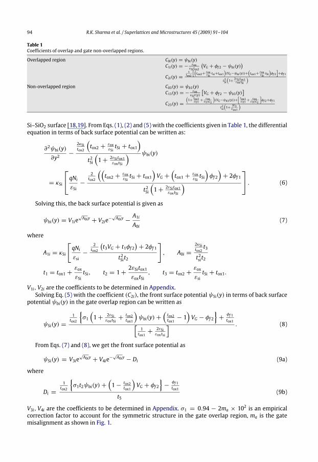
Table 1Coefficients of overlap and gate non-overlapped regions.
Overlapped region C0i(y) = ψbi(y)C1i(y) = − εox
εSi tox2
(VG + φf 2 − ψbi(y)
)C2i(y) =
1tox2
[(tox2+
εoxεSitsi+tox1
)(VG−ψbi(y))+
(tox1+
εoxεSitSi)φf 2
]+φf 1
t2Si(1+ 2εSi tox1εox tSi
)Non-overlapped region C03(y) = ψb3(y)
C13(y) = − εoxεSi t(y)
[VG + φf 2 − ψb3(y)
]C23(y) =
(1+ tox1t(y) +
εoxt(y)CS
)(VG−ψb3(y))+
[tox1t(y) +
εoxt(y)CS
]φf 2+φf 1
t2si(1+ 2CS
Cox1
)
Si–SiO2 surface [18,19]. From Eqs. (1), (2) and (5) with the coefficients given in Table 1, the differentialequation in terms of back surface potential can be written as:
∂2ψbi(y)∂y2
−
2κSitox2
(tox2 + εox
εSitSi + tox1
)t2Si(1+ 2εSitox1
εoxtSi
) ψbi(y)
= κSi
qNiεSi−
2tox2
((tox2 + εox
εSitSi + tox1
)VG +
(tox1 + εox
εSitSi)φf 2
)+ 2φf 1
t2Si(1+ 2εSitox1
εoxtSi
) . (6)
Solving this, the back surface potential is given as
ψbi(y) = V1ie√A0iy + V2ie−
√A0iy −
A1iA0i
(7)
where
A1i = κSi
[qNiεsi−
2tox2
(t3VG + t1φf 2
)+ 2φf 1
t2Sit2
], A0i =
2κSitox2t3
t2sit2
t1 = tox1 +εox
εSitSi, t2 = 1+
2εSitox1εoxtSi
, t3 = tox2 +εox
εsitSi + tox1.
V1i, V2i are the coefficients to be determined in Appendix.Solving Eq. (5) with the coefficient (C2i), the front surface potentialψSi(y) in terms of back surface
potential ψbi(y) in the gate overlap region can be written as
ψSi(y) =1tox2
{σ1
(1+ 2εSi
εoxtSi+tox2tox1
)ψbi(y)+
(tox2tox1− 1
)VG − φf 2
}+
φf 1tox1[
1tox1+
2εSiεoxtsi
] . (8)
From Eqs. (7) and (8), we get the front surface potential as
ψSi(y) = V3ie√A0iy + V4ie−
√A0iy − Di (9a)
where
Di =1tox2
{σ1t2ψbi(y)+
(1− tox2
tox1
)VG + φf 2
}−
φf 1tox1
t5(9b)
V3i, V4i are the coefficients to be determined in Appendix. σ1 = 0.94 − 2ma × 102 is an empiricalcorrection factor to account for the symmetric structure in the gate overlap region, ma is the gatemisalignment as shown in Fig. 1.
R.K. Sharma et al. / Superlattices and Microstructures 45 (2009) 91–104 95
Case III: Non-gate overlap lightly doped regionThe electrostatic potential in the non-gate overlap region could be written as in the gate overlap
region:
ψ3(x, y) = C03(y)+ C13(y)x+ C23(y)x2. (10)
Using Eq. (10) with the boundary conditions
−∂ψ3(x, y)∂x
∣∣∣∣x=0=
εox
εSit(y)
[VG + φf 2 − ψb3(y)
], −
∂ψ3(x, y)∂x
∣∣∣∣x=ti
=Cox1εSi
[ψs3(y)− VG − φf 1
]ψS3(y) = ψb3(y)−
εox
εSit(y)
[VG + φf 2 − ψb3(y)
]ti + C23(y)t2i (11)
where, the coefficients used in the above equation are given in Table 1, t(y) is the distance from theright edge of the bottom gate to the back surface channel. Using a similar approximation approach asfor the gate overlap region (I), we can write:
∂2ψ3(y)∂y2
∼=1κS2
∂2ψb3(y)∂y2
. (12)
From (1) and (10), back surface potential for the lightly doped non gate overlap region is given as
∂2ψb3(y)∂y2
= κS2
[∂2ψ3(y)∂y2
]= κS2
[qN2εSi− 2C23(y)
]. (13)
To simplify the analysis, a conformal mapping transformation approach has been used [20]. Usingthis approach, we can transform the original xEX + yEY space in terms of EX and EY axes to the uEU + v EVspace in terms of EU and EV axes based on the following transfer function:
(y− Lm)EY + nxEX = k sinh(uEU + v EV )Lm = Lc −ma
n =ma
tox2 sinh[cosh−1
(tox2+tg2tox2
)] , k =ma
sinh[cosh−1
(tox2+tg2tox2
)]From the above formula, xEX + yEY coordinates are transformed into uEU + v EV coordinates. As a result,the arc-shaped electric field contour in the ungated region has become straight line shaped.The back surface potential is obtained as
ψb3 (y) = j1eγk (y−Lm) + j2e−
γk (y−Lm) +
B1B0
(14)
where
k =ma
sinh[cosh−1
(tox2+tg2tox2
)] , γ =√−B0,
B0 = 2κS2k2α0, B1 = κS2k
2[qN2εSi− 2β0
]j1 and j2 are the coefficients to be determined in Appendix.The front surface potential ψs3(y) and back surface potential ψb3(y) are correlated as
ψs3(y) =1t(y)
{σ2
(1+ 2εSit(y)
εoxtSi
)ψb3(y)+
(t(y)tox1− 1
)VG − φf 2
}+
φf 1tox1[
1tox1+
2εSiεoxtSi
] . (15)
96 R.K. Sharma et al. / Superlattices and Microstructures 45 (2009) 91–104
Substituting, Eq. (14) in (15), we find
ψs3 (y) = j3eγk (y−Lm) + j4e−
γk (y−Lm) + D3 (16a)
where
D3 =1t(y)
{σ2t6
B1B0+ t4VG − φf 2
}+
φf 1tox1
t5(16b)
t4 = 1−t(y)tox1
, t5 =1tox1+2εSiεoxtSi
, t6 = 1+2εSit(y)εoxtSi
(16c)
σ2 = 0.51 + 4ma × 102 is an empirical factor to account for the non-symmetric structure in thenon-gate overlap region. j3 and j4 are the coefficients to be determined in Appendix.
1.2. Subthreshold analysis
Knowing the potential solution, the current density (both drift and diffusion) [21,22] can bewrittenas
J = −qµn(x, y)dφn(y)dy
. (17)
Integrating Eq. (17), we get
Ids(y) = −µWdφn(y)dy
Qi(y). (18)
Where, Qi(y) =∫ tSi0 n(x, y)dx =
∫ tSi0 nie
[q(ψS (x,y)−φn(y))]/kTdx is the inversion charge per unit gate areaand ψS(x, y) is the total surface potential.The integration of Eq. (18) from 0 to L yields:
Ids(y) =µW
∫ Vds0 e−qφn(y)/kTdφn(y)∫ L
0dy∫ tSi
0 nieq(ψS (x,y)−2φf )/kT
. (19)
Hence, the subthreshold current expression for GC DG-FD SOI n-MOSFET can be expressed as
Ids(y) =µW
∫ Vds0 e−qφn(y)/kTdφn(y)∫ Lm/2
0dy∫ tsi
0 nieq(ψS (x,y)−2φf )/kT
+∫ LmLm/2
dy∫ tSi0 nie
q(ψS (x,y)−2φf )/kT+∫ LLm
dy∫ tsi0 nie
q(ψS (x,y)−2φf )/kT
(20)
which is a unified solution and can be used to calculate the subthreshold current for UD & GC channelDG SOI for different gate misalignments.
2. Results and discussion
In all figures the symbols represent the simulated data and the lines represent the analyticalresults. The simulated results were obtained using ATLAS 3-D device simulator incorporating theconcentration dependent mobility model and electric field dependent carrier mobility model withvelocity saturation. The various UD and GC DG devices analyzed in our work are given in Table 2,which shows the effect of gate misalignment on various device parameters such as threshold voltage,DIBL and subthreshold slope for both DGD and DGS configurations. The threshold voltage was definedas the gate voltage at 10−7 A/µm drain current in order to estimate Ioff current; DIBL has beencalculated as differences of threshold voltage at VDS = 50 mV & 1.0 V; Subthreshold Slope is definedas the change in gate voltage VGS required to reduce the subthreshold current IDS by one decade andextracted at VDS = 50 mV. Fig. 2 shows the variation of subthreshold slope with gate misalignment
R.K. Sharma et al. / Superlattices and Microstructures 45 (2009) 91–104 97
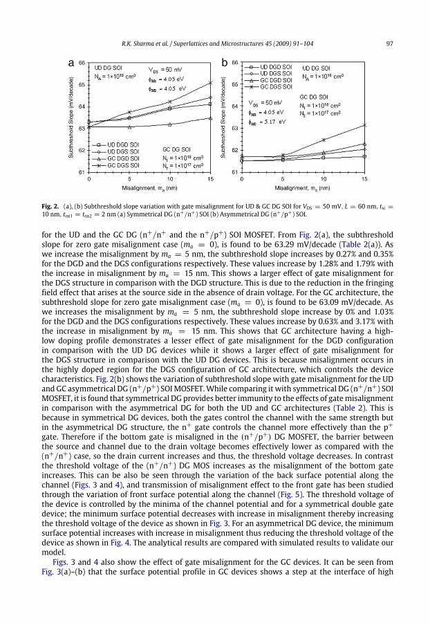
Fig. 2. (a), (b) Subthreshold slope variation with gate misalignment for UD & GC DG SOI for VDS = 50 mV, L = 60 nm, tsi =10 nm, tox1 = tox2 = 2 nm (a) Symmetrical DG (n+/n+) SOI (b) Asymmetrical DG (n+/p+) SOI.
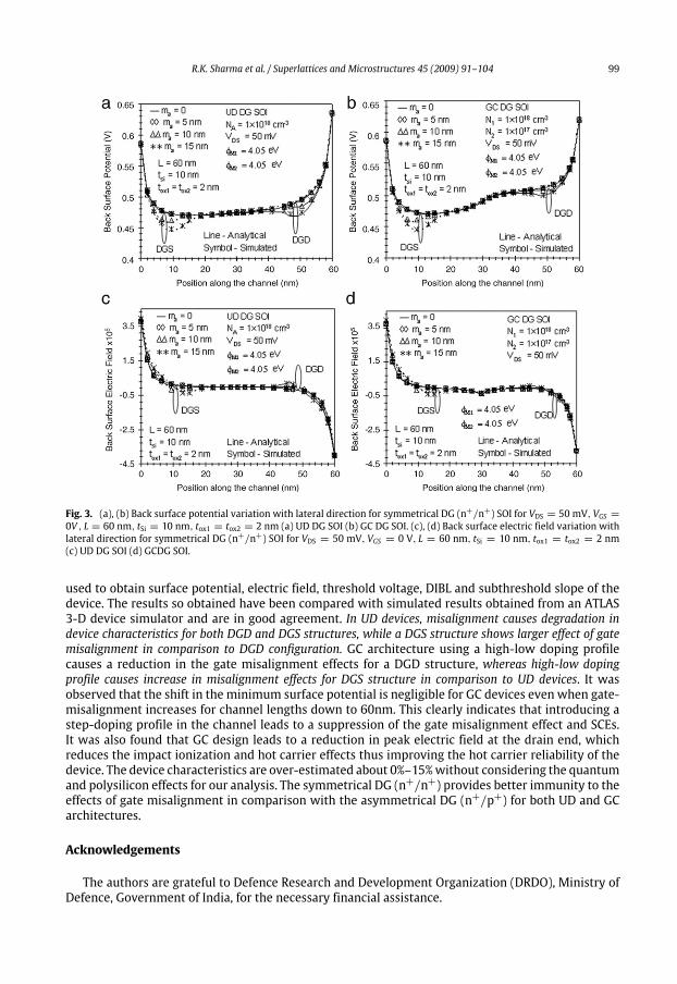
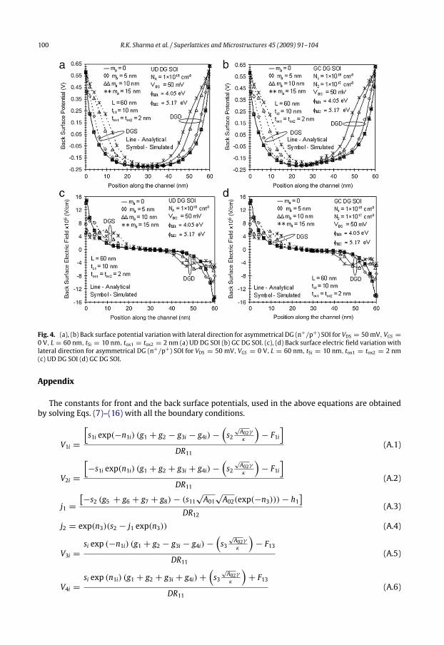
for the UD and the GC DG (n+/n+ and the n+/p+) SOI MOSFET. From Fig. 2(a), the subthresholdslope for zero gate misalignment case (ma = 0), is found to be 63.29 mV/decade (Table 2(a)). Aswe increase the misalignment by ma = 5 nm, the subthreshold slope increases by 0.27% and 0.35%for the DGD and the DGS configurations respectively. These values increase by 1.28% and 1.79% withthe increase in misalignment by ma = 15 nm. This shows a larger effect of gate misalignment forthe DGS structure in comparison with the DGD structure. This is due to the reduction in the fringingfield effect that arises at the source side in the absence of drain voltage. For the GC architecture, thesubthreshold slope for zero gate misalignment case (ma = 0), is found to be 63.09 mV/decade. Aswe increases the misalignment by ma = 5 nm, the subthreshold slope increase by 0% and 1.03%for the DGD and the DGS configurations respectively. These values increase by 0.63% and 3.17% withthe increase in misalignment by ma = 15 nm. This shows that GC architecture having a high-low doping profile demonstrates a lesser effect of gate misalignment for the DGD configurationin comparison with the UD DG devices while it shows a larger effect of gate misalignment forthe DGS structure in comparison with the UD DG devices. This is because misalignment occurs inthe highly doped region for the DGS configuration of GC architecture, which controls the devicecharacteristics. Fig. 2(b) shows the variation of subthreshold slope with gate misalignment for the UDand GC asymmetrical DG (n+/p+) SOIMOSFET.While comparing it with symmetrical DG (n+/n+) SOIMOSFET, it is found that symmetrical DG provides better immunity to the effects of gatemisalignmentin comparison with the asymmetrical DG for both the UD and GC architectures (Table 2). This isbecause in symmetrical DG devices, both the gates control the channel with the same strength butin the asymmetrical DG structure, the n+ gate controls the channel more effectively than the p+gate. Therefore if the bottom gate is misaligned in the (n+/p+) DG MOSFET, the barrier betweenthe source and channel due to the drain voltage becomes effectively lower as compared with the(n+/n+) case, so the drain current increases and thus, the threshold voltage decreases. In contrastthe threshold voltage of the (n+/n+) DG MOS increases as the misalignment of the bottom gateincreases. This can be also be seen through the variation of the back surface potential along thechannel (Figs. 3 and 4), and transmission of misalignment effect to the front gate has been studiedthrough the variation of front surface potential along the channel (Fig. 5). The threshold voltage ofthe device is controlled by the minima of the channel potential and for a symmetrical double gatedevice; the minimum surface potential decreases with increase in misalignment thereby increasingthe threshold voltage of the device as shown in Fig. 3. For an asymmetrical DG device, the minimumsurface potential increases with increase in misalignment thus reducing the threshold voltage of thedevice as shown in Fig. 4. The analytical results are compared with simulated results to validate ourmodel.Figs. 3 and 4 also show the effect of gate misalignment for the GC devices. It can be seen from
Fig. 3(a)–(b) that the surface potential profile in GC devices shows a step at the interface of high
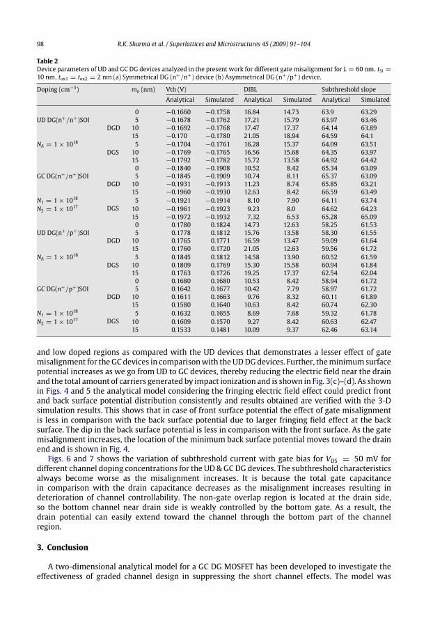
98 R.K. Sharma et al. / Superlattices and Microstructures 45 (2009) 91–104
Table 2Device parameters of UD and GC DG devices analyzed in the present work for different gate misalignment for L = 60 nm, tSi =10 nm, tox1 = tox2 = 2 nm (a) Symmetrical DG (n+/n+) device (b) Asymmetrical DG (n+/p+) device.
Doping (cm−3) ma (nm) Vth (V) DIBL Subthreshold slopeAnalytical Simulated Analytical Simulated Analytical Simulated
0 −0.1660 −0.1758 16.84 14.73 63.9 63.29UD DG(n+/n+)SOI
DGD5 −0.1678 −0.1762 17.21 15.79 63.97 63.4610 −0.1692 −0.1768 17.47 17.37 64.14 63.8915 −0.170 −0.1780 21.05 18.94 64.59 64.1
NA = 1× 10¹⁸
DGS5 −0.1704 −0.1761 16.28 15.37 64.09 63.5110 −0.1769 −0.1765 16.56 15.68 64.35 63.9715 −0.1792 −0.1782 15.72 13.58 64.92 64.420 −0.1840 −0.1908 10.52 8.42 65.34 63.09
GC DG(n+/n+)SOIDGD
5 −0.1845 −0.1909 10.74 8.11 65.37 63.0910 −0.1931 −0.1913 11.23 8.74 65.85 63.2115 −0.1960 −0.1930 12.63 8.42 66.59 63.49
N1 = 1× 10¹⁸
DGS5 −0.1921 −0.1914 8.10 7.90 64.11 63.74
N2 = 1× 10¹⁷ 10 −0.1961 −0.1923 9.23 8.0 64.62 64.2315 −0.1972 −0.1932 7.32 6.53 65.28 65.090 0.1780 0.1824 14.73 12.63 58.25 61.53
UD DG(n+/p+)SOIDGD
5 0.1778 0.1812 15.76 13.58 58.30 61.5510 0.1765 0.1771 16.59 13.47 59.09 61.6415 0.1760 0.1720 21.05 12.63 59.56 61.72
NA = 1× 10¹⁸
DGS5 0.1845 0.1812 14.58 13.90 60.52 61.5910 0.1809 0.1769 15.30 15.58 60.94 61.8415 0.1763 0.1726 19.25 17.37 62.54 62.040 0.1680 0.1680 10.53 8.42 58.94 61.72
GC DG(n+/p+)SOIDGD
5 0.1642 0.1677 10.42 7.79 58.97 61.7210 0.1611 0.1663 9.76 8.32 60.11 61.8915 0.1580 0.1640 10.63 8.42 60.74 62.30
N1 = 1× 10¹⁸
DGS5 0.1632 0.1655 8.69 7.68 59.32 61.78
N2 = 1× 10¹⁷ 10 0.1609 0.1570 9.27 8.42 60.63 62.4715 0.1533 0.1481 10.09 9.37 62.46 63.14
and low doped regions as compared with the UD devices that demonstrates a lesser effect of gatemisalignment for theGCdevices in comparisonwith theUDDGdevices. Further, theminimumsurfacepotential increases as we go from UD to GC devices, thereby reducing the electric field near the drainand the total amount of carriers generated by impact ionization and is shown in Fig. 3(c)–(d). As shownin Figs. 4 and 5 the analytical model considering the fringing electric field effect could predict frontand back surface potential distribution consistently and results obtained are verified with the 3-Dsimulation results. This shows that in case of front surface potential the effect of gate misalignmentis less in comparison with the back surface potential due to larger fringing field effect at the backsurface. The dip in the back surface potential is less in comparison with the front surface. As the gatemisalignment increases, the location of the minimum back surface potential moves toward the drainend and is shown in Fig. 4.Figs. 6 and 7 shows the variation of subthreshold current with gate bias for VDS = 50 mV for
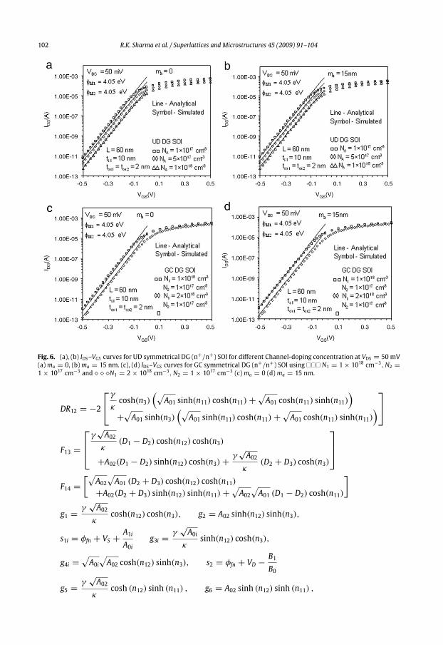
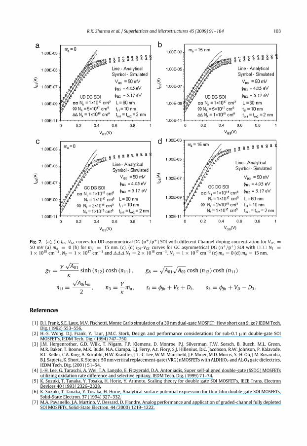
different channel doping concentrations for the UD & GC DG devices. The subthreshold characteristicsalways become worse as the misalignment increases. It is because the total gate capacitancein comparison with the drain capacitance decreases as the misalignment increases resulting indeterioration of channel controllability. The non-gate overlap region is located at the drain side,so the bottom channel near drain side is weakly controlled by the bottom gate. As a result, thedrain potential can easily extend toward the channel through the bottom part of the channelregion.
3. Conclusion
A two-dimensional analytical model for a GC DG MOSFET has been developed to investigate theeffectiveness of graded channel design in suppressing the short channel effects. The model was
R.K. Sharma et al. / Superlattices and Microstructures 45 (2009) 91–104 99
Fig. 3. (a), (b) Back surface potential variation with lateral direction for symmetrical DG (n+/n+) SOI for VDS = 50 mV, VGS =0V , L = 60 nm, tSi = 10 nm, tox1 = tox2 = 2 nm (a) UD DG SOI (b) GC DG SOI. (c), (d) Back surface electric field variation withlateral direction for symmetrical DG (n+/n+) SOI for VDS = 50 mV, VGS = 0 V, L = 60 nm, tSi = 10 nm, tox1 = tox2 = 2 nm(c) UD DG SOI (d) GCDG SOI.
used to obtain surface potential, electric field, threshold voltage, DIBL and subthreshold slope of thedevice. The results so obtained have been compared with simulated results obtained from an ATLAS3-D device simulator and are in good agreement. In UD devices, misalignment causes degradation indevice characteristics for both DGD and DGS structures, while a DGS structure shows larger effect of gatemisalignment in comparison to DGD configuration. GC architecture using a high-low doping profilecauses a reduction in the gate misalignment effects for a DGD structure, whereas high-low dopingprofile causes increase in misalignment effects for DGS structure in comparison to UD devices. It wasobserved that the shift in the minimum surface potential is negligible for GC devices even when gate-misalignment increases for channel lengths down to 60nm. This clearly indicates that introducing astep-doping profile in the channel leads to a suppression of the gate misalignment effect and SCEs.It was also found that GC design leads to a reduction in peak electric field at the drain end, whichreduces the impact ionization and hot carrier effects thus improving the hot carrier reliability of thedevice. The device characteristics are over-estimated about 0%–15%without considering the quantumand polysilicon effects for our analysis. The symmetrical DG (n+/n+) provides better immunity to theeffects of gate misalignment in comparison with the asymmetrical DG (n+/p+) for both UD and GCarchitectures.
Acknowledgements
The authors are grateful to Defence Research and Development Organization (DRDO), Ministry ofDefence, Government of India, for the necessary financial assistance.
100 R.K. Sharma et al. / Superlattices and Microstructures 45 (2009) 91–104
Fig. 4. (a), (b) Back surface potential variation with lateral direction for asymmetrical DG (n+/p+) SOI for VDS = 50mV, VGS =0 V, L = 60 nm, tSi = 10 nm, tox1 = tox2 = 2 nm (a) UD DG SOI (b) GC DG SOI. (c), (d) Back surface electric field variation withlateral direction for asymmetrical DG (n+/p+) SOI for VDS = 50 mV, VGS = 0 V, L = 60 nm, tSi = 10 nm, tox1 = tox2 = 2 nm(c) UD DG SOI (d) GC DG SOI.
Appendix
The constants for front and the back surface potentials, used in the above equations are obtainedby solving Eqs. (7)–(16) with all the boundary conditions.
V1i =
[s1i exp(−n1i) (g1 + g2 − g3i − g4i)−
(s2√A02γκ
)− F1i
]DR11
(A.1)
V2i =
[−s1i exp(n1i) (g1 + g2 + g3i + g4i)−
(s2√A02γκ
)− F1i
]DR11
(A.2)
j1 =
[−s2 (g5 + g6 + g7 + g8)− (s11
√A01√A02(exp(−n3)))− h1
]DR12
(A.3)
j2 = exp(n3)(s2 − j1 exp(n3)) (A.4)
V3i =si exp (−n1i) (g1 + g2 − g3i − g4i)−
(s3√A02γκ
)− F13
DR11(A.5)
V4i =si exp (n1i) (g1 + g2 + g3i + g4i)+
(s3√A02γκ
)+ F13
DR11(A.6)
R.K. Sharma et al. / Superlattices and Microstructures 45 (2009) 91–104 101
Fig. 5. (a), (b) Front surface potential variationwith lateral direction for asymmetrical DG (n+/p+) SOI for VDS = 50mV, VGS =0 V, L = 60 nm, tSi = 10 nm, tox1 = tox2 = 2 nm (a) UD DG SOI (b) GC DG SOI (c), (d) Front surface electric field variation withlateral direction for asymmetrical DG (n+/p+) SOI for VDS = 50 mV, VGS = 0 V, L = 60 nm, tSi = 10 nm, tox1 = tox2 = 2 nm(c) UD DG SOI (d) GC DG SOI.
j3 =
[−s2 (g5 + g6 + g7 + g8)− (s11
√A02√A01(exp(−n3)))− (exp(−n3)) F14
]DR12
(A.7)
j4 =
[s2 (−g5 + g6 − g7 + g8)− (s11
√A02√A01(exp(n3)))+ (exp(n3)) F14
]DR12
(A.8)
where
F1i =
γ√A02κ
(A1iA0i−A12A02
)cosh(n12) cosh(n3)
+A02
(A1iA0i−A12A02
)sinh(n12) sinh(n3)+
γ√A02κ
(A12A02+B1B0
)cosh(n3)
h1 = exp(−n3)
×
√A02√A01
(B1B0+A12A02
)cosh(n12) cosh(n11)
+A02
(B1B0+A12A02
)sinh(n12) sinh(n11)
√A02√A01
(A11A01−A12A02
)cosh(n11)
DR11 = −2
γκ cosh(n3) (√A02 sinh(n11) cosh(n12)+√A01 cosh(n11) sinh(n12))+
√A02 sinh(n3)
(√A02 sinh(n11) sinh(n12)+
√A01 cosh(n11) cosh(n12)
)
102 R.K. Sharma et al. / Superlattices and Microstructures 45 (2009) 91–104
Fig. 6. (a), (b) IDS–VGS curves for UD symmetrical DG (n+/n+) SOI for different Channel-doping concentration at VDS = 50 mV(a)ma = 0, (b)ma = 15 nm. (c), (d) IDS–VGS curves for GC symmetrical DG (n+/n+) SOI using ��� N1 = 1× 1018 cm−3,N2 =1× 1017 cm−3 and � � �N1 = 2× 1018 cm−3,N2 = 1× 1017 cm−3 (c)ma = 0 (d)ma = 15 nm.
DR12 = −2
γκ cosh(n3) (√A01 sinh(n11) cosh(n11)+√A01 cosh(n11) sinh(n11))+
√A01 sinh(n3)
(√A01 sinh(n11) cosh(n11)+
√A01 cosh(n11) sinh(n11)
)
F13 =
γ√A02κ
(D1 − D2) cosh(n12) cosh(n3)
+A02(D1 − D2) sinh(n12) cosh(n3)+γ√A02κ
(D2 + D3) cosh(n3)
F14 =
[√A02√A01 (D2 + D3) cosh(n12) cosh(n11)
+A02(D2 + D3) sinh(n12) sinh(n11)+√A02√A01 (D1 − D2) cosh(n11)
]g1 =
γ√A02κ
cosh(n12) cosh(n3), g2 = A02 sinh(n12) sinh(n3),
s1i = φfn + VS +A1iA0i
g3i =γ√A0iκ
sinh(n12) cosh(n3),
g4i =√A0i√A02 cosh(n12) sinh(n3), s2 = φfn + VD −
B1B0
g5 =γ√A02κ
cosh (n12) sinh (n11) , g6 = A02 sinh (n12) sinh (n11) ,
R.K. Sharma et al. / Superlattices and Microstructures 45 (2009) 91–104 103
Fig. 7. (a), (b) IDS-VGS curves for UD asymmetrical DG (n+/p+) SOI with different Channel-doping concentration for VDS =50 mV (a) ma = 0 (b) for ma = 15 nm. (c), (d) IDS-VGS curves for GC asymmetrical DG (n+/p+) SOI with ��� N1 =1× 1018 cm−3,N2 = 1× 1017 cm−3 and∆∆∆ N1 = 2× 1018 cm−3,N2 = 1× 1017 cm−3 (c)ma = 0 (d)ma = 15 nm.
g7 =γ√A01κ
sinh (n12) cosh (n11) , g8 =√A01√A02 cosh (n12) cosh (n11)
n1i =√A0iLm2
, n3 =γ
κma, si = φfn + VS + Di, s3 = φfn + VD − D3.
References
[1] D.J. Frank, S.E. Laux, M.V. Fischetti, Monte Carlo simulation of a 30 nmdual-gateMOSFET: How short can Si go? IEDM Tech.Dig. (1992) 553–556.
[2] H.-S. Wong, D.J. Frank, Y. Taur, J.M.C. Stork, Design and performance considerations for sub-0.1 µm double-gate SOIMOSFET’s, IEDM Tech. Dig. (1994) 747–750.
[3] J.M. Hergenrother, G.D. Wilk, T. Nigam, F.P. Klemens, D. Monroe, P.J. Silverman, T.W. Sorsch, B. Busch, M.L. Green,M.R. Baker, T. Boone, M.K. Bude, N.A. Ciampa, E.J. Ferry, A.t. Fiory, S.J. Hillenius, D.C. Jacobson, R.W. Johnson, P. Kalavade,R.C. Keller, C.A. King, A. Kornblit, H.W. Krautter, J.T.-C. Lee,W.M.Mansfield, J.F. Miner, M.D. Morris, S.-H. Oh, J.M. Rosamilia,B.J. Sapjeta, K. Short, K. Steiner, 50nmvertical replacement-gate (VRG) nMOSFETswithALDHfO2 andAl2O3 gate dielectrics,IEDM Tech. Dig. (2001) 51–54.
[4] J.-H. Lee, G. Taraschi, A. Wei, T.A. Langdo, E. Fitzgerald, D.A. Antoniadis, Super self-aligned double-gate (SSDG) MOSFETsutilizing oxidation rate difference and selective epitaxy, IEDM Tech. Dig. (1999) 71–74.
[5] K. Suzuki, T. Tanaka, Y. Tosaka, H. Horie, Y. Arimoto, Scaling theory for double gate SOI MOSFET’s, IEEE Trans. ElectronDevices 40 (1993) 2326–2328.
[6] K. Suzuki, T. Tanaka, Y. Tosaka, H. Horie, Analytical surface potential expression for thin-film double gate SOI MOSFETs,Solid-State Electron. 37 (1994) 327–332.
[7] M.A. Pavanello, J.A. Martino, V. Dessard, D. Flandre, Analog performance and application of graded-channel fully depletedSOI MOSFETs, Solid-State Electron. 44 (2000) 1219–1222.
104 R.K. Sharma et al. / Superlattices and Microstructures 45 (2009) 91–104
[8] M.A. Pavanello, J.A. Martino, D. Flandre, Graded-channel fully depleted silicon-on-insulator n-MOSFET for reducing theparasitic bipolar effects, Solid-State Electron. 44 (2000) 917–922.
[9] M.A. Pavanello, J.A. Martino, J.P. Raskin, D. Flandre, High performance analog operation of double gate transistors with theguarded-channel architecture at low temperatures, Solid-State Electron. 49 (2005) 1569–1575.
[10] J.S. Martin, A. Bournel, P. Dollfus, Comparison of multiple-gate MOSFET architectures usingMonte Carlo simulation, Solid-State Electron. 50 (2006) 94–101.
[11] A. Kranti, T.M. Chung, D. Flandre, J.P. Raskin, Laterally asymmetric channel engineering in fully depleted double gate SOIMOSFETs for high performance analog applications, Solid-State Electron. 48 (2004) 947–959.
[12] T. Ushiki, M.C. Yu, Y. Hirano, H. Shimada, M.Moria, T. Ohmi, Reliable tantalum-gate fully depleted-SOIMOSFET technologyfeaturing low temperature processing, IEEE Trans. Electron Devices 44 (1997) 1387–1393.
[13] B.Maiti, P.J. Tobin, C. Hobbs, R.I. Hedge, F. Hunag, D.L.O.Meara, D. Jovanovic, M.Mendicino, J. Chen, D. Connelly, O. Adetutu,J. Mogab, J.B. La, PVD tin metal gate MOSFETs on bulk silicon and fully depleted silicon-on-insulator (FDSOI) substrates fordeep sub-quarter micron CMOS technology, IEDM Tech. Dig. (1998) 781–784.
[14] N. Rodriguez, F. Gámiz, J.B. Roldán,Modeling of inversion layer centroid andpolysilicon depletion effects onultrathin-gate-oxide MOSFET behavior: The influence of crystallographic orientation, IEEE Trans. Electron Devices 54 (2007) 723–732.
[15] K. Uchida, J. Koga, R. Ohba, T. Numata, S. Takagi, Experimental evidences of quantum-mechanical effects on low-fieldmobility, gate channel capacitance, and threshold voltage of ultrathin body SOIMOSFETs, IEDMTech. Dig. (2001) 633–636.
[16] C.H. Choi, Z. Yu, R.W. Dutton, Two-dimensional polysilicon quantum-mechanical effects in double-gate SOI, IEDM Tech.Dig. (2002) 723–726.
[17] H.K. Jung, S. Dimitrijev, Analysis of subthreshold carrier transport for ultimate DGMOSFET, IEEE Trans. Electron Devices53 (2006) 685–691.
[18] S. Chen, J.B. Kuo, Deep sub micrometer DG FD SOI PMOS devices: A concise short channel effect threshold voltage modelusing a quasi-2-D approach, IEEE Trans. Electron Devices 43 (1996) 1387–1393.
[19] K.W. Su, J.B. Kuo, A nonlocal impact ionization/lattice temperature model for VLSI DG ultra-thin SOI nMOS devices, IEEETrans. Electron Devices 44 (1997) 324–330.
[20] E.C. Sun, J.B. Kuo, A compact threshold voltagemodel for gate misalignment effect of DG FD SOI nMOS devices consideringfringing electric field effects, IEEE Trans. Electron Devices 51 (2004) 587–596.
[21] X. Liang, Y. Taur, A 2-D analytical solution for SCEs in DG MOSFETs, IEEE Trans. Electron Devices 51 (2004) 1385–1391.[22] P. Francis, A. Terao, D. Flandre, F. Van de Wiele, Modeling of ultrathin double-gate nMOS/SOI transistors, IEEE Trans.
Electron Devices 41 (1994) 715–719.