Linvill's model as applied to P-N junction photo-diodes
77
Scholars' Mine Scholars' Mine Masters Theses Student Theses and Dissertations 1965 Linvill's model as applied to P-N junction photo-diodes Linvill's model as applied to P-N junction photo-diodes Rudy Michael Chittenden Follow this and additional works at: https://scholarsmine.mst.edu/masters_theses Part of the Electrical and Computer Engineering Commons Department: Department: Recommended Citation Recommended Citation Chittenden, Rudy Michael, "Linvill's model as applied to P-N junction photo-diodes" (1965). Masters Theses. 5353. https://scholarsmine.mst.edu/masters_theses/5353 This thesis is brought to you by Scholars' Mine, a service of the Missouri S&T Library and Learning Resources. This work is protected by U. S. Copyright Law. Unauthorized use including reproduction for redistribution requires the permission of the copyright holder. For more information, please contact [email protected].
-
Upload
khangminh22 -
Category
Documents
-
view
1 -
download
0
Transcript of Linvill's model as applied to P-N junction photo-diodes
Scholars' Mine Scholars' Mine
Masters Theses Student Theses and Dissertations
1965
Linvill's model as applied to P-N junction photo-diodes Linvill's model as applied to P-N junction photo-diodes
Rudy Michael Chittenden
Follow this and additional works at: https://scholarsmine.mst.edu/masters_theses
Part of the Electrical and Computer Engineering Commons
Department: Department:
Recommended Citation Recommended Citation Chittenden, Rudy Michael, "Linvill's model as applied to P-N junction photo-diodes" (1965). Masters Theses. 5353. https://scholarsmine.mst.edu/masters_theses/5353
This thesis is brought to you by Scholars' Mine, a service of the Missouri S&T Library and Learning Resources. This work is protected by U. S. Copyright Law. Unauthorized use including reproduction for redistribution requires the permission of the copyright holder. For more information, please contact [email protected].
I i c \
'f 7 ' ..,!
'"' -. LINVILL' S MODEL AS APPLIED TO P-N JUNCTION PHOTO-DIODES
BY
RUDY MICHAEL CHITTENDEN J /Cf Y.,.(
A
THESIS
submitted to the faculty of the
UNIVERSITY OF MISSOURI AT ROLLA
1136~~0
in partial fulfillment of the requirements for the
Degree of
MASTER OF SCIENCE IN ELECTRICAL ENGINEERING
Rolla, Missouri
1965
Approved by
-~~--{'~~ /$~~-"-";::;......h:;.....;;;..v __ (Advisor )--~-,df,l-J-..=;-- _:::.£_. +--7]4'-U?d!!;_~--· __
u
ii
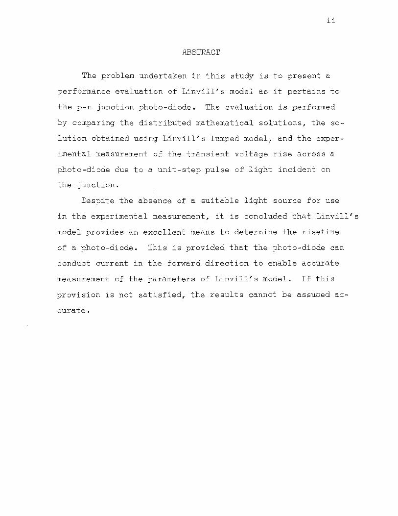
ABSTRACT
The problem undertaken in this study is to present a
performance evaluation of Linvill's model as it pertains to
the p-n junction photo-diode. The evaluation is performed
by comparing the distributed mathematical solutions, the so
lution obtained using Linvill's lumped model, and the exper
imental measurement of the transient voltage rise across a
photo-diode due to a unit-step pulse of light incident on
the junction.
Despite the absence of a suitable light source for use
in the experimental measurement, it is concluded that Linvill's
model provides an excellent means to determine the risetime
of a photo-diode. This is provided that the photo-diode can
conduct current in the forward direction to enable accurate
measurement of the parameters of Linvill's model. If this
provision is not satisfied, the results cannot be asswded ac
curate.

ACKNOWLEDGEMENTS
The author would like to express his gratitude to
Dr. R. A. Anderson and Mr. Robert C. Pickett of the Phy
sics Department for their suggestions and assistance
throughout the experimental portion of this work.
Thanks to Dr. R. C. Harden and Dr. R. E. Nolte for
their help and guidance.
Thanks to the Electrical Engineering Department for
the extensive use of its laboratories and equipment.
iii

iv
TABLE OF CONTENTS
LIST OF Page
FIGURES .......................................... I • • • vi
CHAPTER I. INTRODUCTION. . . . . . . . . . . . . . . . . • . . . . . . . . . . . . . 1
A. Statement of the problem.. . • . . . . . . . . . . . . . . . l
B. Significance of the study ......•....•...• , . 2
C. Reasons for the investigation .......•.....• 2
CHAPTER II. REVIEW OF THE LITERATURE ...•............... 3
CHAPTER III. REVIEW OF SEMICONDUCTOR THEORY ......•...... 4
A. Introduction and explanation ............•.• 4
B. General .................................... 4
C. Current carriers and their mode of flow .... 10
D. The approximation of space-charge neutralityl3
E. The basics of photo-diode operation ........ 14
CHAPTER IV. LINVILL' S MODEL. • . . . . . . . . • . . . . . • . . . . • . . . • . . 17
A. Introduction ................................ 17
B. Derivation of Linvill's model .............. 18
C. Solution for the transient voltage rise .•.• 23
CHAPTER V. DISTRIBUTED SOLUTION FOR THE TRANSIENT VOLTAGE ...•.....• I •••••••••••••••••••• II I • • • 2 5
A. Introduction. . . . . . .. . . . . . . . . . . . . . . . . . . . . . . . . 25
B. General ................................. - ..... 25
C. Solution of the partial differential equa t i on . . . . . . . . . . . . . . . . . . . . . . . . . . . . .. . . . . . . 2 7
D. Solution for the transient voltage ..•...•.• 37
CHAPTER VI . EXPERIMENTAL TECHNIQUES AND RESULTS. • . . . • . • 43
A. Light source . ..................... ·· . . . . . . . . 43
B. Determination of the parameters for Linvill's model .....................•.....• 48

v
C. Determination of the absorption coefficient.58
CHAPTER VII. CONCLUSIONS .••.••••••••••••••.•••.••••••.••. 65
BIBLIOGRAPHY .•• . . . . . . . . . . . . . . . . . . . . . . . . . . . . . . . . . . . . . ••••• 67
\TJ[~Ji •••••••••••••••••••.••••••••••••••••••••••••••••••••• 69
vi
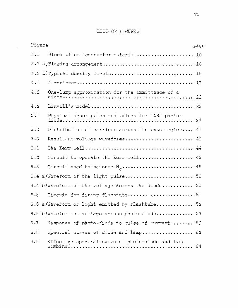
LIST· OF FIGURES
Figure page
3.1 Block of semiconductor material .••••••.•••.••.••.•. 10
3.2 a)Biasing arrangement •••...•••••••••••••••••.•••••••• 16
3.2 b)Typical density levels •••••••••••••••••••.•••..•••• 16
4.1 A resistor ••••••••••.••••••••••••••••••.••••••••••. 17
4.2 One-lump approximation for the immittance of a diode . • . . . • • . . . • . . . . . • • . . . . . . . . . . . . . .. .. . . . . . . . . . • . . . 2 2
4.3 Linvill's model .................................... 23
5.1 Physical description and values for 1N85 photo-diode ............................................... 27
5.2 Distribution of carriers across the base region •••• 41
5.3 Resultant voltage waveforms ••••••.•••••••••.••••••• 42
6 .1 The Kerr cell. . . . . . . . . . . . . . . . . . . . . . . . . . . . . . . . . . . . . . 44
6.2 Circuit to operate the Kerr cell ••••••••••••••••••. 45
6.3 Circuit used to measure H .•••••.•••••..••••.•••••. c 49
6.4 a)Waveform of the light pulse ••••••••••.••••••••••••. 50
6.4 b)Waveform of the voltage across the diode ••••••••••• 50
6.5 Circuit for firin;; flashtube .••••••.••••••••••••••. 51
6.6 a)Waveform of light emitted by flashtube •.••••••••••. 53
6.6 b)Waveform of voltage across photo-diode •••.••••••••• 53
6.7 Response of photo-diode to pulse of current .••••••• 57
6.8 Spectral curves of diode and lamp ••••.••••••••••••• 63
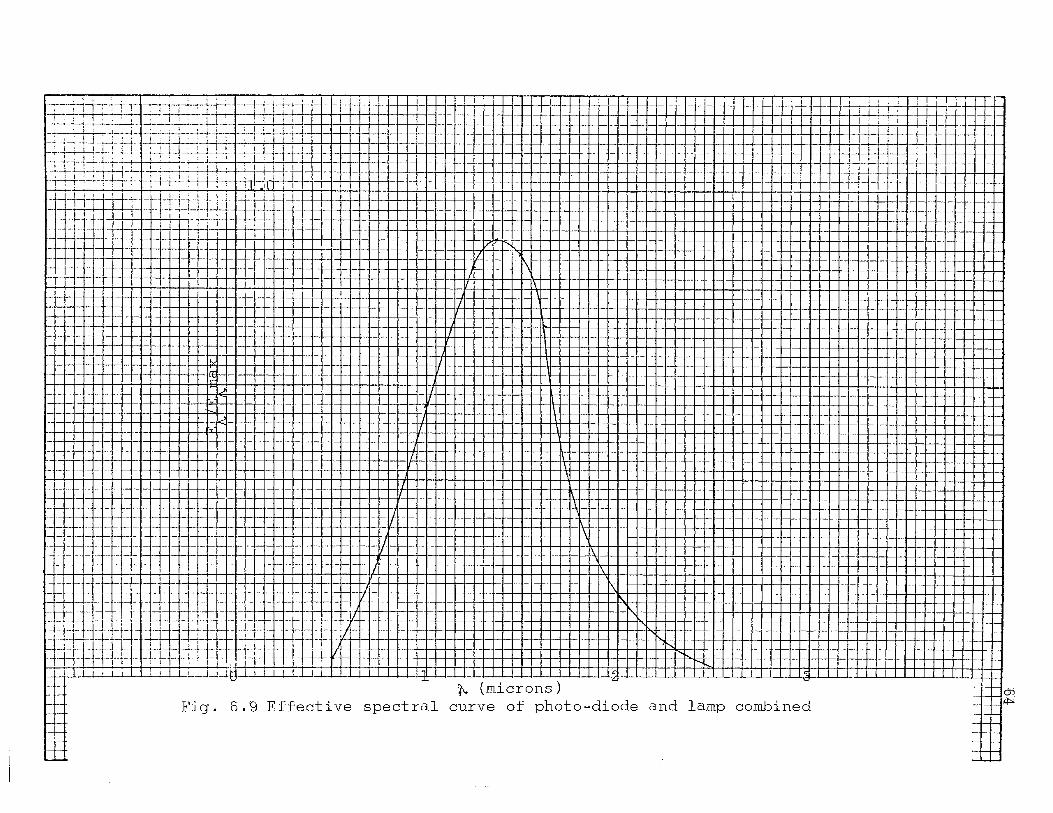
6.9 Effective spectral curve of photo-diode and lamp combined. • . • • . . . . • • • . .. . . . • . . . • • . . . • . • . . . . . . .. . . • • • • . 64

vii
LIST OF TABLES
Table No~ Page No.
I. VARIATION OF STORANCE WITH WIDTH OF LIGHT BEAM •••• 56
CHAPTER I
INTRODUCTION
A. Statement of the Problem.
The purpose of this study is to evaluate the accuracy
of the use of Linvill's model for the p-n junction photo-
diode in expressing the transient voltage waveform across
the photo-diode due to a unit-step pulse of light incident
on the junction. The evaluation is made through a compari
son of results obtained from a distributed solution, from a
solution using Linvill's model, and from an experimental mea-
surement (the experimental measurement is later deleted due
to the absence of a suitable source of modulated light).
The development of Linvill's model is presented and
the assumptions made are pointed out and discussed in the
final stage of this study.
In order to obtain an analytical expression for the re-
sultant transient voltage, the carrier concentration is found
both as a function of distance and time. From this distribu-
tion, the expression for the voltage is found.
The major difficulty in makin~ the experimental measure
ments is producing a unit-step of light. Theoretically, of
course, this is impossible, but no error is introduced as
long as the risetime of the light pulse is short compared to
the effective risetime of the photo-diode. In this study,
this restriction called for a light pulse with a risetime of
approximately one-tenth of a micro-second. Methods of obtainin~
2
such a pulse of light are discussed (risetime for this study
designates the time required for the transient to reach 99
per cent of its steady-state value).
B. Significance of the Study.
The application of models for circuit analysis and de-
sign cannot be exaggerated. The use of any one particular
model is dependent, amon:;r other considerations, upon the
relative ease and accuracy with which it can be applied.
The parameters of Linvill's model are easily measured(2)
and its use is fairly simple, therefore, it is of importance
that an evaluation of the accuracy of this model be made and
the value of its use be known.
C. Reasons for the Investigation.
An interest in the theory and application of models for
solid state devices led the author to explore this area for
a possible thesis topic.
The book by Linvill, studied in a course taken by the
author, presented the development and application of models
for transistors and diodes. Although Linvill had little to
say about photo-sensitive devices, it was believed that his
model would apply in this area.
Numbers in parenthesis refer to references listed in the bibliography.
3
CHAPTER II
REVIEW OF THE LITERATURE
The model discussed here was first presented in a grad
uate subject that has formed the basis for the book by Linvill
and 8ibbons(l). Later, the presentation in the aforementioned
text was worked into a more compact form by Linvill(2).
Papers prepared by Chang(3), Gossick(4), Bhar(5), Holmes
and Feucht(6), and Ritter(7), were helpful in explainin~ the
theory of the p-n junction and the distribution of carrier con
centration.
Methods for solving the partial differen·:ial equations by
Laplace transforms are given by Churchill(9) and by Carslaw
and Jaegar ( 10) •
Other background material was obtained from Shockley(8),
Hunter(ll), and Lange(l2).
Methods of modulating light at extreme frequencies are
discussed by Jones(l3) and Draper{l4), and the theory concern
ing the determination of the absorption coefficien~ is dis
cussed in a book by Bauman{l5).
Material on the operation and characteristics of the
nitrobenzene-filled Kerr cell was obtained from Gronemeyer
and Spanberger(l6).
4
CHAPTER III
REVIEW OF SEMICONDUCTOR THEORY
A. Introduction and Explanation.
The purpose of this chapter is to review the theory of
semiconductors in general, and the mechanics of the opera
tion of photo-diodes in particular.
This chapter supplies the base on which the entire study
is built, in that the characteristics of semiconductors per
tinent to this study are summarized and their contributions
are assessed. The most important feature of the basis for
this study is the discussion of carriers of current in semi
conductors and their modes of flow, i.e., drift and diffus
ion. The above-mentioned discussion and the discussion on
the specifics of photo-diode operations constitute the bulk
of the theoretical concepts supporting this thesis.
B.. General.
Materials which are intermediate in conductivity between
insulators and the metallic conductors are classified as
semiconductors. The most familiar of semiconductors in tran
sistor and diode applications are germanium and silicon, though
compounds formed from elements of Group III and Group V of the
periodic table show great promise for use in semiconductor de
vices. The discussion given here will concentrate on german
ium and silicon, since the diode to be tested is of one of
these, and also, knowledge of these two types of semiconduc
tors is more complete than knowledge of other semiconductors.
5
Germanium and silicon exhibit a crystalline structure
in which each atom is equally spaced from four neighboring
atoms. Each atom, having four valence electrons of its own,
shares an electron with each of the four neighboring atoms
to complete its valence structure. The net charge of each
atom is zero, the negative charge of orbital electrons just
balancing the positive charge of the nucleus.
The electrons moving about the nucleus are found with
only certain permitted energies, the magnitude of which varies
with the separation of the electron from the nucleus. The
allowed energy states fall into ranges or bands separated by
a forbidden band. The region of energy states which falls
below the forbidden band is called the valence band and the
region of energy states above the forbidden band is called
the conduction band.
The amount of energy required to move an electron from
the valence band to the conduction band, which corresponds
to separating an electron from its nucleus, is dependent on
the width of the forbidden band. This amount of energy is
0.7ev in germanium and l.lev in silicon.
At room temperature a small fraction of the electrons
have a sufficient amount of energy to pass from the valence
band into the conduction band and are free to move about.
These freed electrons are referred to as "conduction electrons,
or more simply as just "electrons," since we are not interested
in valence electrons in the flow of electricity. The sites
6
from which these electrons have escaped exhibit a net pos-
itive charge and are called "holes." Holes and electrons
constitute the two carriers of electricity in semiconductors.
The thermal generation of electron-hole pairs as de-
scribed above operates continuously. However, due to recom-
bination of electrons and holes the population of electrons
and holes fluctuates randomly about some average value and
does not increase indefinitely.
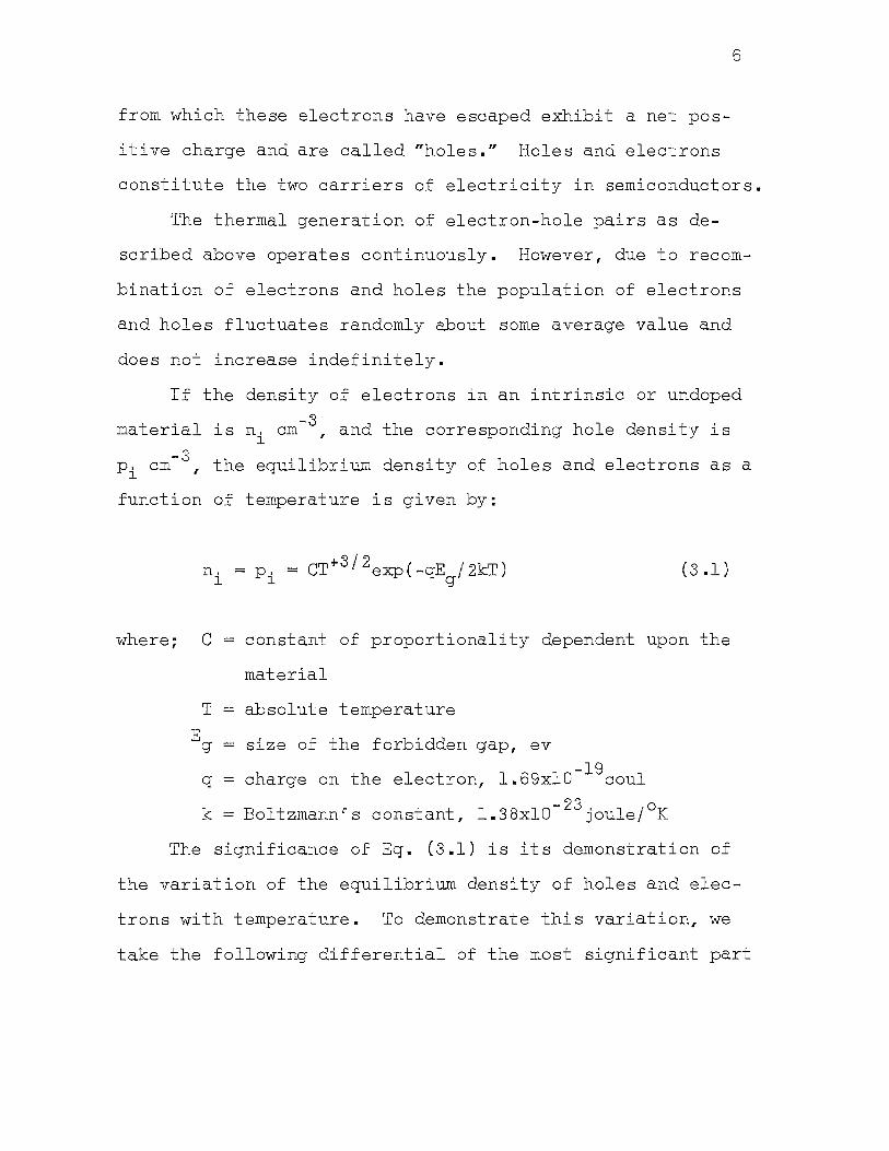
If the density of electrons in an intrinsic or undoped -S material is n. em , and the corresponding hole density is
l
-S pi em , the equilibrium density of holes and electrons as a
function of temperature is given by:
n. = P· l l
= CT+S/ 2exp(-qE /2kT) g
(S .1)
where; C = constant of proportionality dependent upon the
material
T = absolute temperature E g = size of the forbidden gap, ev
-19 q = charge on the electron, 1.69xl0 coul -23 0 k = Boltzmanncs constant, 1.38xl0 joule/ K
The significance of Eq. (3.1) is its demonstration of
the variation of the equilibrium density of holes and elec-
trans with temperature. To demonstrate this variation, we
take the following differential of the most significant part
7
of Eq. (3.1), the exponential factor and obtain:
( 3 • 2)
The fractional change in density is found as follows;
d[exp(-qE /2kTTI qE 1 ---,......---._.g....,...,..,.._...... - --=_g_ dT exp(-qEg/2kT) - ZET T ( 3. 3)
Eq. (3.3) tells us that for germanium an increase of one
degree centigrade above room temperature will increase the
density of holes and electrons by approximately 5 per cent
and for silicon the increase will be about 7 per cent per
degree rise in temperature. This increase in carrier den-
sity with temperature accounts for the characteristic decrease
in resistivity of semiconductors with rising temperature.
The density of hole-electron pairs in germanium at room
temperature is approximately 2.5 x 1013 cm-3 or about one
billionth of the atom density which is about 4.5 x 1022 cm-3 •
In silicon, the density of hole-electron pairs at room tem-10 -3 perature is about 6.8 x 10 em , compared to the atom den-
sity which is 5.0 x 1022 cm-3 • These values are seen to cor-
relate with the relative sizes of the forbidden gaps of ger
manium and silicon, the larger hole-electron pair density
corresponding to the smaller forbidden gap and vice versa.
Up to this point we have been discu:s:sing densities of
intrinsic or undoped materials. We are now prepared to dis
cuss the more interesting and more important (to this study)
8
properties of impure or doped semiconductors.
At some time during or after the growth of a crystalr
a small fraction of impurities from the third or fifth column
of the periodic table may be added to the crystal of germanium
or silicon. Impurities frorJ. the fifth are called donor impur
ities, because they have one extra valence electron (or a to-
tal of five electrons) which is free to condact electricity.
Impurities from the third colu..rnn are called acceptor impuri-
ties due to.their lack of a valence electron which caus~s them
to accept valence electrons of neighboring atoms. Since it
is found that practically all of the impurities are ionized,
donor impurities contribute electrons to the material, noi.Y
called n-type material and acceptor impurities accept electrons
or correspondingly contribute holes to the raaterial, now called
p-type ma·t:erial.
The reason why the addition of impurities to a material
makes it either p-type or n-type is that the addition of im-
( 13 19 -3) purities in typical densities ,from 10 to 10 em does
not significantly alter the rate at which hole-electron pairs
are generated thermally. So, for exdmple, in a donor-doped
material, the electron density is increased by the addition of
more electrons, while the hole density is decreased due to the
increased rate of recombination. The result is that the re-
combination process dominates until the equilibrium density of
holes is down to value such that:
pn 2 ·- n, l
2 3 = C T exp(-qEg/kT) ( 3 .4)
9
It is usually assumed that the density of electrons in
n-type material and the density of holes in p-type material
equal approximately their corresponding doping densities.
Thus, in n-type material the equilibrium density of electrons,
designated nn, is given by:
(3.5)
where Nd is the density of donor atoms.
The equilibrium density of holes in n-type material,
designated p , from Eqs. {3.4) and (3.5) is: n
(3. 6)
Similar relations for the equilibrium densities in a
p-type material are:
( 3. 7)
and
(3.8)
where p is the equilibrium density of holes in the p-type p
material, np is the equilibrium density of electrons in the
p-type material, and N is the density of acceptor atoms= a
10
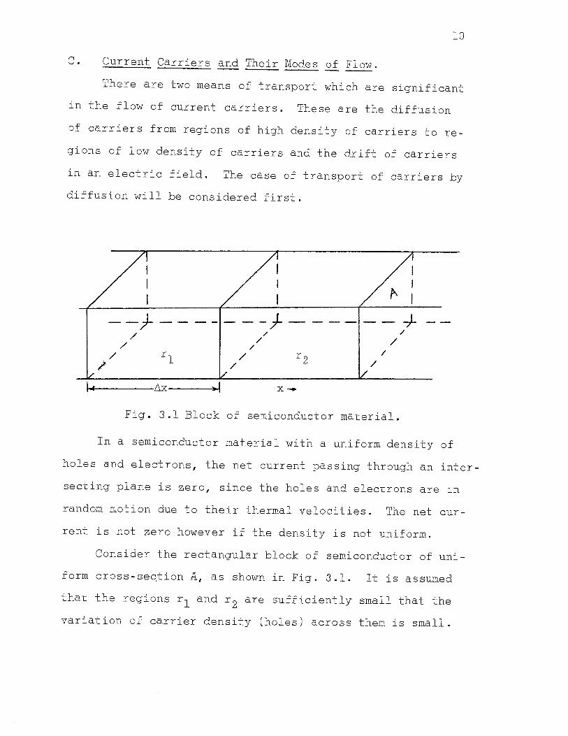
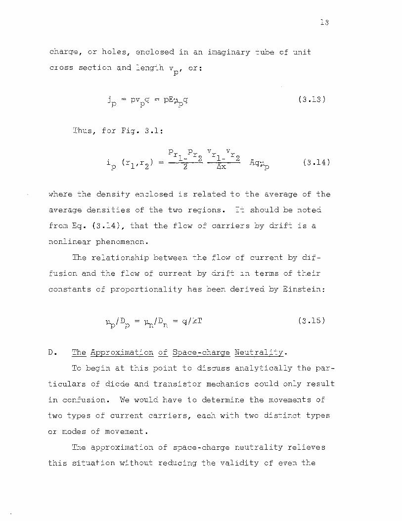
C. Current Carriers and Their Modes of Flow.
There are two means of transport which are significant
in the flow of current carriers. These are the diffusion
of carriers from regions of high density of carriers to re-
gions of low density of carriers and the drift of carriers
in an electric field. The case of transport of carriers by
diffusion will be considered first.
/
--f /
/ /
~------6x-----~~~l
/ /
-}--/
/ /
x-
I
" : --+
/
/
/ /
Fig. 3.1 Block of semiconductor material.
In a semiconductor material with a uniform density of
holes and electrons, the net current passing through an inter-
secting plane is zero 1 since the holes and electrons are in
random motion due to their thermal velocities. The net cur-
rent is not zero however if the density is not uniform.
Consider the rectangular block of semiconductor of uni-
form cross-section A, as shown in Fig. 3.1. It is assumed
that the regions r 1 and r 2 are sufficiently small that the
variation of carrier density (holes) across them is small.
11
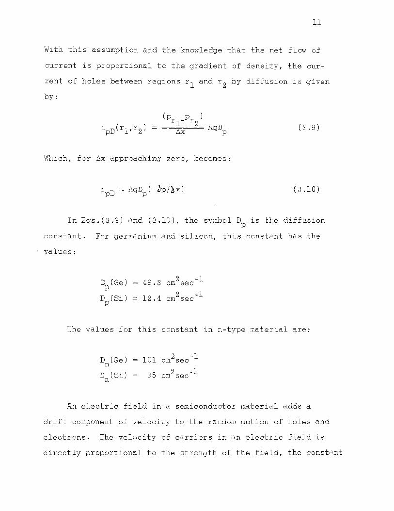
With this assumption and the knowledge that the net flow of
current is proportional to the gradient of density, the cur
rent of holes between regions r 1 and r 2 by diffusion is given
by:
( 3 • 9)
Which, for 6x approaching zero, becomes:
(3.10)
In Eqs.(3.9) and (3.10), the symbol D is the diffusion p
constant. For germanium and silicon, this constant has the
values:
D (Ge) = 49.3 p
DP(Si) = 12.4
2 -1 em sec
2 -1 em sec
The values for this constant in n-type material are:
D (Ge) = 101 n
2 -1 em sec
D (Si) = 2 -1 35 em sec n
An electric field in a semiconductor material adds a
drift component of velocity to the random motion of holes and
electrons. The velocity of carriers in an electric field is
directly proportional to the strength of the field, the constant
12
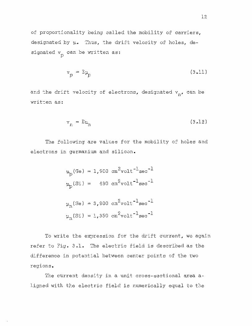
of proportionality being called the mobility of carriers,
designated by ~· Thus, the drift velocity of holes, de-
signated v can be written as: p
v = Ell p p
and the drift velocity of electrons, designated
written as:
v = Eu n n
v n'
( 3 .ll)
can be
(3.12)
The following are values for the mobility of holes and
electrons in germanium and silicon.
up ( Ge) 1,900 2 -1 -1 = em volt sec
~(Si) 480 2 -1 -1 ·- em volt sec
lln(Ge) 3,900 2 -1 -1 = em volt sec
1ln(Si) 1,350 2 -1 -1 = em volt sec
To write the expression for the drift current, we again
refer to Fig. 3.1. The electric field is described as the
difference in potential between center points of the two
regions.
The current density in a unit cross-sectional area a-
ligned with the electric field is numerically equal to the
13
charge, or holes, enclosed in an imaginary tube of unit
cross section and length v , or: p
Thus, for Fig. 3.1:
(3.13)
(3.14)
where the density enclosed is related to the average of the
average densities of the two regions. It should be noted
from Eq. (3.14), that the flow of carriers by drift is a
nonlinear phenomenon.
The relationship between the flow of current by dif-
fusion and the flow of current by drift in terms of their
constants of proportionality has been derived by Einstein:
(3.15)
D. The Approximation of Space-charge Neutrality.
To begin at this point to discuss analytically the par
ticulars of diode and transistor mechanics could only result
in confusion. We would have to determine the movements of
two types of current carriers, each with two distinct types
or modes of movement.
The approximation of space-charge neutrality relieves
this situation without reducing the validity of even the
14
most rigorous examination. The analysis is reduced to
consideration of only the movements of the minority car
riers by assuming that any movement of minority carriers
is immediately accompanied by the flow of majority carri
ers. The actual lapse of time involved has been estimated
by Linvill (2) to be in the order of micromicroseconds for
a typically doped segment of n-type germanium.
Thus, if the distribution of holes in an n-type ma
terial has been determined as p(x,t), the distribution of
electrons can be found from:
n(x,t) p(x,t) + Nd (3.16)
E. Basics of Photo-Diode Operation.
The semiconductor photo-diode is a device used to con
vert radiant energy into electrical energy. Its primary
use to date, however, is not as a source of energy, but as
a control or measuring device, such as the photographic
light meter. It is feasible, however, that the search for
means to tap the sun as a source of energy may find new and
more profitable uses for this device.
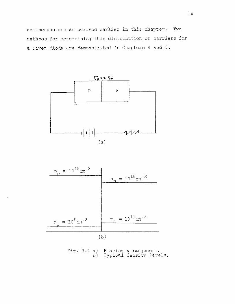
The biasing arrangement for the photo-diode is shown
in Fig. 3.2. The voltage applied to the diode is there
verse direction so as to prohibit the flow of majority car
riers. The current flowing with no light incident on the
junction is therefore due entirely to minority carriers.
Since, as is the case in most photo-diodes, the p-region
15
is more hi<;rhly doped than the n-region, the minority con
centration in the p-region is substantially less than the
minority concentration in n-region, and the reverse current
is solely determined by pn, the equilibrium density of
holes in the n-region. Typical values for the concentra
tions in each region are given in Fig. 3.2(b).
When the liqht is m:s.de to shine on the junction, hole
electron pairs are generated according to the quantum nature
of li,;rht, the nwnber of pairs produced being proportional to
the intensity of the light. In both regions of the semi
conductor, the percent increase of majority carriers rela
tive to the percent increase in minority carriers is quite
small, and the net current resulting from the illumination
is in the reverse direction. The illumination current then
is composed mainly of minority carriers.
In this study, the photo-diode is to be pulsed with a
unit step of li·;rht, and i:he transient rise in voltage across
the entire diode will be analysed. Any voltage drop across
the p-type emitter region will be neqlected due to the high
conductivity of this region. The determination of the dis
tribution of the minority carriers in the n-type region will
provide all the information necessary to predict the wave
form of the desired transient.
The holes in the n-region will distribute across the
region according to the laws of the flow of carriers in
semiconductors as derived earlier in this chapter. Two
methods for determining this distribution of carriers for
a given diode are demonstrated in Chapters 4 and 5.
~ \"\
p
!l..
11 l'l
p = 1019 em -.3 'n
n = 'o
Fig . .3 .2 a) b)
N
(a)
n,..
(b)
Biasing arrangement. Typical density levels.
16
17
CHAPTER IV
LINVILL'S MODEL
A. Jnt~od~ction.
A model of a physical device is a mathematical entity
with precise laws governing the relationship of its varia
bles. The use of models is quite common, and often the
process or deYice is confused with the model, especially if
the model is a very good approximation of the process. For
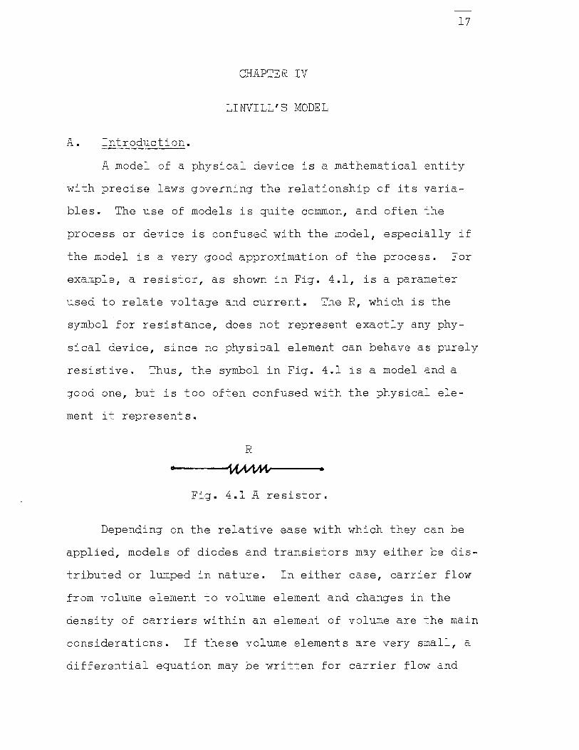
example, a resistor, as shown in Fig. 4.1, is a parameter
used to relate voltage and current. The R, which is the
symbol for resistance, does not represent exactly any phy
sical device, since no physical element can behave as purely
resistive. Thus, the symbol in Fig. 4.1 is a model and a
good one, but is too often confused with the physical ele
ment it represents.
R
··------~~-------..
Fig. 4.1 A resistor.
Depending on the relative ease with which they can be
applied, models of diodes and transistors may either be dis
tributed or lumped in nature. In either case, carrier flow
from volume element to volume element and changes in the
density of carriers within an element of volume are the main
considerations. If these volume elements are very small, a
differential equation may be written for carrier flow and
18
integration may be performed over the entire volume to de
termine the populations. If these equations, together
with the appropriate initial and boundary conditions, can
be solved, very accurate results may be obtained for the
distributions of the current carriers. A model employing
this rigorous type of solution would be referred to as a
distributed model.
It is often found that the intricate boundary condi-
tions associated with the analysis of semiconductor behavior
make the use of the distributed model impractical and some
times, impossible. It is for this reason that a great num-
ber of equivalent circuits and lumped models have been de-
rived for use in semiconductor analysis. The lumped models
are simplifications of the distributed models, employing
finite volume elements instead of very small volume ele-
ments. The differential equations become difference equa-
tions, and the solution is much more straightforward.
B. Derivation of Linvill's Model.
The model derived by Linvill(l) was a lumped model. The
initial ass~~ptions made in deriving the model are as follows
(for ann-type semiconductor):
a) Space-charge neutrality is assamed.
b) Minority carriers flow ;)nly by di.f fusion in one-dimensional flow according to the equation:
J, = -qD 1E. P pt>x
(4.1)
19
c) The minority-carrier densities obey the linear continuity equation:
p--p ~P = __ n _ l , ~ ~P q grad Jp (4.2)
d) The minority-carrier densities in the vicinity of the junction obey Shockley's injection relation:
( 4. 3)
Substituting Eq.(4.l) into Eq.(4.2):
(4.4)
Linvill in deriving his model used the solution for
Eq.(4.4). The solution will not be repeated here since it
is straight forward and the solution of a similar equation
more appropriate to this study is presented in Chapter 5.
The boundary conditions used by Linvill were p(~,t) = Pn
and Eq . ( 4 , 3 ) •
The solutions found by Linvill for the minority carrier
distribution and the current at the junction are as follows(l):
- x ( l +s 1' ) l I 2 p(x,t) -pn = p 0 (0)expLx + p1 (0)exn-----1~P __ __
p p
po(O) pl(O) i = I +I (l +
P P 0 Pn p 0 n sl ) l/ 2 exr::(st)
p
exp~t) ( 4 . 5 )
( 4 • 6)
20
where; p 0 = steady-state density
pl = time-dependent density
The expression for the hole current in Eq.(4.6) was
found by substituting Eq.(4.5) into Eq.(4.l).
At this point, Linvill introduced the concept of
"current-density immittances." The solutions found in
Eqs.(4.5) and (4.6) are actually solutions for a distribu-
ted model. The parameters of Linvill's lumped model are
found by requiring that its current-density immittance
should be a reasonable approximation to that of the dis
tributed model. The current-density immittance is defined
as the ratio of the complex current component and the com-
plex density component. Thus, from Eqs.(4.5) and (4.6),
the current-density driving-point immittance for holes is:
l/2 Pn (l + sTP) exp(st) Ip
-----...,...,...-----.,...--....-.---- = ____£ ( l + s 't ) l I 2 p1 (o) exp(st) Pn P
( 4. 7)
It would be possible, using procedures developed for
the approximation problem of network synthesis, to develop
a lumped network that would closely approximate the driving
point immittance of Eq.(4.7). For a diode in the reverse-bias
condition, however, the model must be limited to only one
lump due to the effect of the capacitance of the junction
which is neglected in Eq.(4.7).
21
The capacitance of the junction is a function of the
applied voltage. There exists in the vicinity of the june-
tiona region called the transition region in which the
densities are changing toward their equilibrium values.
When a negative voltage is applied across the junction, a
charge of holes must move from the edqe of the transition
region in the p-region and a corresponding charge of elec-
trons must move from the ed;re of the transition re]·ion in
the n-region. This movement of charge corresponds to a
change of the capacitance required to store the charge.
This capacitance appears in parallel with the immittance
defined by Eq.(4.7). Its effects are negligible when the
junction is forward-biased, since due to its small size
(lOO~~f) the currents through it are small compared to other
currents elsewhere(l). This is no longer true when the
junction is reverse-biased.
A one-lump structure which has an inunittance approxi
mating the function given in Eq.(4.7) can be found by making
a binomial expansion of the square root as follows:
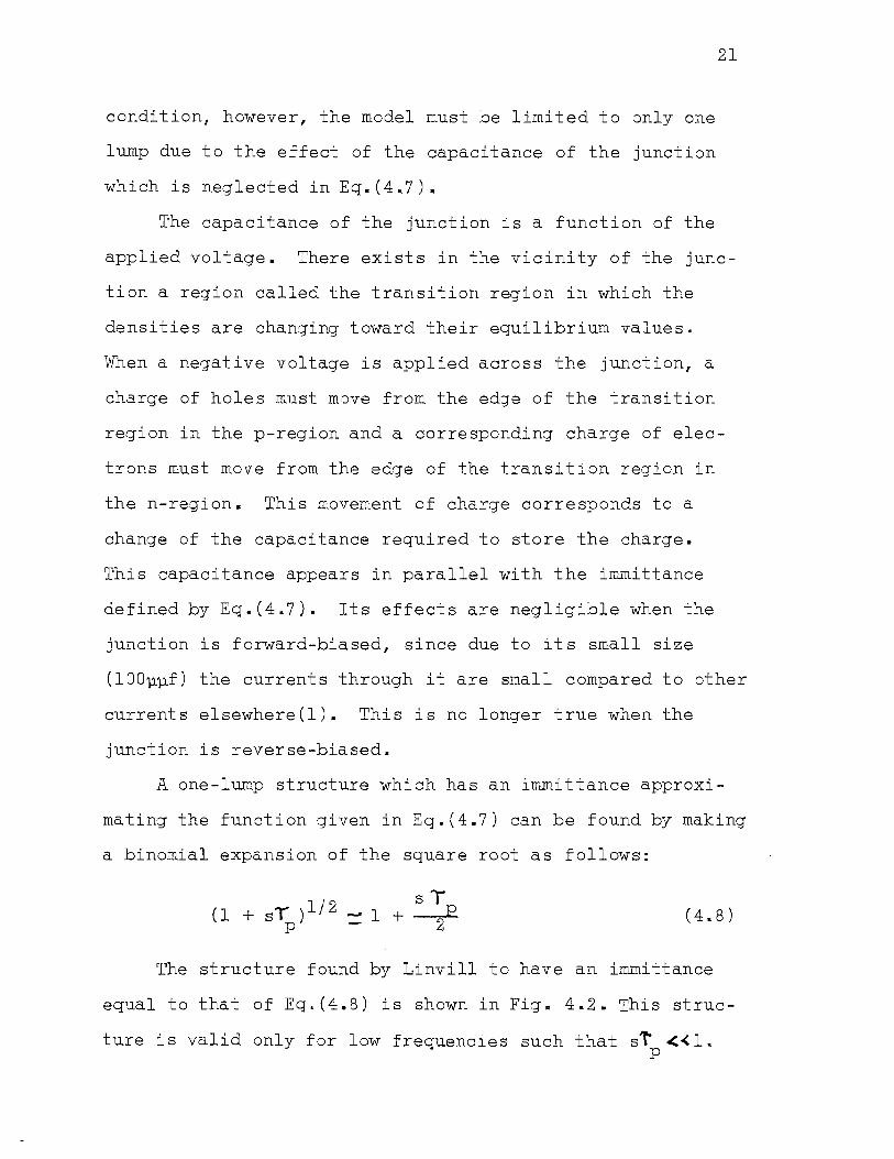
I s T (l + sl )1 2 - l + P
p - 2 (4 .. 8)
The structure found by Linvill to have an immittance
equal to that of Eq.(4.8) is shown in Fig. 4.2. This struc
ture is valid only for low frequencies such that st' << l. p

22
The symbols S and H are called storance and com-P c binance, respectively. Their relation to current and mi-
nority-carrier density are:
i = s dp/dt Ps p (4.9)
i PH
= H cp (4.10)
where sp has the dimensions, CO'J.lomb-cm3 and He has the
d ' ' 3 lmenslons amp-em •
Fig. 4.2 One-luin.p approxirn.ation for the iwnittance of a diode.
The complete model as derived by Linvill is shown in
Fig. 4.3. The symbol Cj represents the capacitance of the
junction. It is ass~~ed ~hat the density of minority car-
riers in the vicinity of the junction obeys the requirements
of Eq.(4.3) and that recombination in the transition re·gion
is negligible, or the hole current en-i::ering the junction is
equal to the hole current leaving the junction.
23
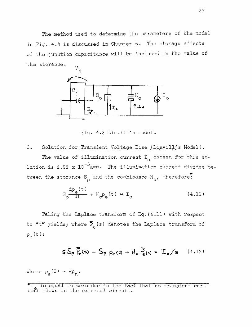
The method used to determine the parameters of the model
in Fig. 4.3 is discussed in Chap·ter 6. The storaqe effects
of the junction capacitance will be included in the value of
the storance. v. J
~
c. J s p
t:r~
_H c
Fig. 4.3 Linvill's model.
I 0
C. Solution for Transient Voltage Rise (Linvill's Model).
The value of illumination current I chosen for this soo -5 lution is 3.93 x 10 amp. The illumination current divides be-
"' tween the storance S and the combinance H , therefore; p c
dp (t) e
8p at +HP(t)=I c- e o (4.11)
Taking the Laplace transform of Eq.(4.ll) with respect
to "t" yields; where P (s) denotes the Laplace transform of e
(4-12)
where p ( 0) = -p • e n
*I is equal to zero due to the fact that no transient curre~t flows in the external circuit.
Solving for P (s) we obtain: e
p ( s) e
24
(4.13)
To return to the time domain we take the inverse Laplace
of Pe(s) to find:
p (t) e (4.14)
The expression for the voltage across the junction is
found by substituting Eq.(4.14) into Eq.(4.3) and solving for
(4.15)
where; p = p + p . e n
The variation of V. with respect to time for the values J
of SP and H0 as determined in Chapter 6 is shown in Fig.5.3.
25
CHAPTER V
DISTRIBUTED SOLUTION FOR THE TRANSIENT VOLTAGE
A. Introduction.
In order to determine the validity and accuracy of
Linvill's model in predicting the transient voltage rise
across a photo-diode, a more rigorous analysis will be
presented in this chapter.
The solution of the differential equation for dis-
tributed models can be obtained, if certain limitations
are placed upon the range of magnitude of the signals
applied to the photo-diode. These limitations will be
discussed as they appear in the analysis.
B. General.
The voltage across the photo-diode is composed of
two distinct types. They are the voltage across the june-
tion proper, Vj, and the voltage drop across the bulk
material, Vb. If the distribution of minority carriers in
the region under consideration is known as a function of
time and distance, the voltages vj and vb may be found.
The equations governing the behavior of injected mi-
nority carriers into ann-region are (7):
~p/dt = - (p-p j1p - q-ldiv J n P
(5.1)
(5.2)
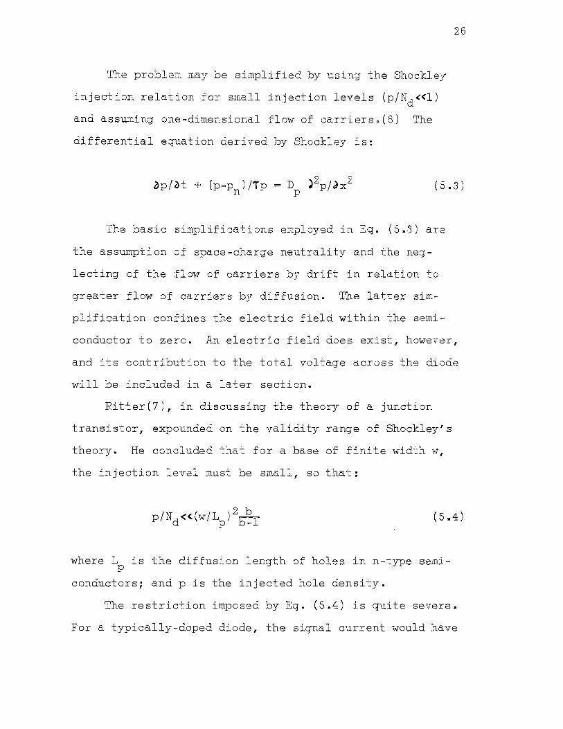
The problem may be simplified by usin;r the Shockley
injection relation for small injection levels (p/Nd«l)
and assuming one-dimensional flow of carriers.(8) The
differential equation derived by Shockley is:
26
( 5. 3)
The basic simplifications employed in Eq. (5 •. 3) are
the assumption of space-charge neutrality and the neg
lectin:;r of the flow of carriers by drift in r·elation to
greater flow of carriers by diffusion. The latter sim-
plification confines the electric field within the semi-
conductor to zero. An electric field does exist, however,
and its contribution to the total voltage across the diode
will be included in a later section.
Ritter(7) 1 in discussing the theory of a junction
transistor, expounded on the validity range of Shockley's
theory. He concluded that for a base of finite width w,
the injection level must be small, so that:
(5.4)
where Lp is the diffusion length of holes in n-type semi
conductors; and p is the injected hole density.
The restriction imposed by Eq. (5.4) is quite severe.
For a typically-doped diode, the signal current would have

to be limited to a very few microamperes. Ritter went on
to demonstrate, however, that if the recombination of car
riers in the base region could 'De ne,;rlected, the following
equation could be used for any arbitrary injection level.
27
( 5. 5)
It shall be assUt--ned in this study that the length of
the n-region is short compared to the diffusion length of
holes, and recombination in this ret;rion will be neglected.
Eq.(5.5), then, is the desired starting point for the der-
ivation of the distribution of holes in the base region.
C. Solution of the Partial Differential Equation~
The first step in the solution is the determination
of the correct initial and boundary conditions (the dimen-
sions and references for the following discussion are de-
fined in Fig. 5.1).
p N
I x=O
I x=W
Fig. 5.1
1N85 photo-diode
W = .222 em -4 2 A= 33.8 x 10 em
ND= .890 x lo15cm-3
p = 7.02 x 1o11cm-3 n
Physical description and values for 1N85 photo-diode.
28
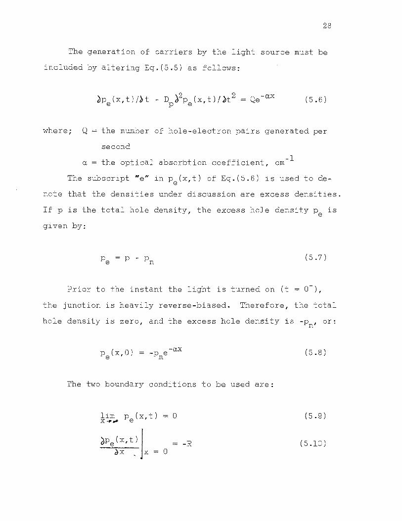
The generation of carriers by the light source must be
included by altering Eq.(5.5) as follows:
~p (x,t)/bt - D ~2p (x,t)/jt 2 = Qe-ax e p e (5.6)
where; Q = the number of hole-electron pairs generated per
second
a = the optical absorbtion coefficient, -1 em
The subscript "e" in p (x,t) of Eq.(5.6) is used to dee
note that the densities under discussion are excess densities.
If p is the total hole density, the excess hole density pe is
given by:
p - p n (5.7)
Prior to the instant the light is turned on (t = 0-),
the junction is heavily reverse-biased. Therefore, the total
hole density is zero, and the excess hole density is -pn, or:
p (x,O) e
-a.x = -p e n
The two boundary conditions to be used are:
lim pe(x,t) = 0 x-...-
~p9 (x,t} j = -R ~X , X = 0
(5.8)
( 5 . 9)
(5.10)
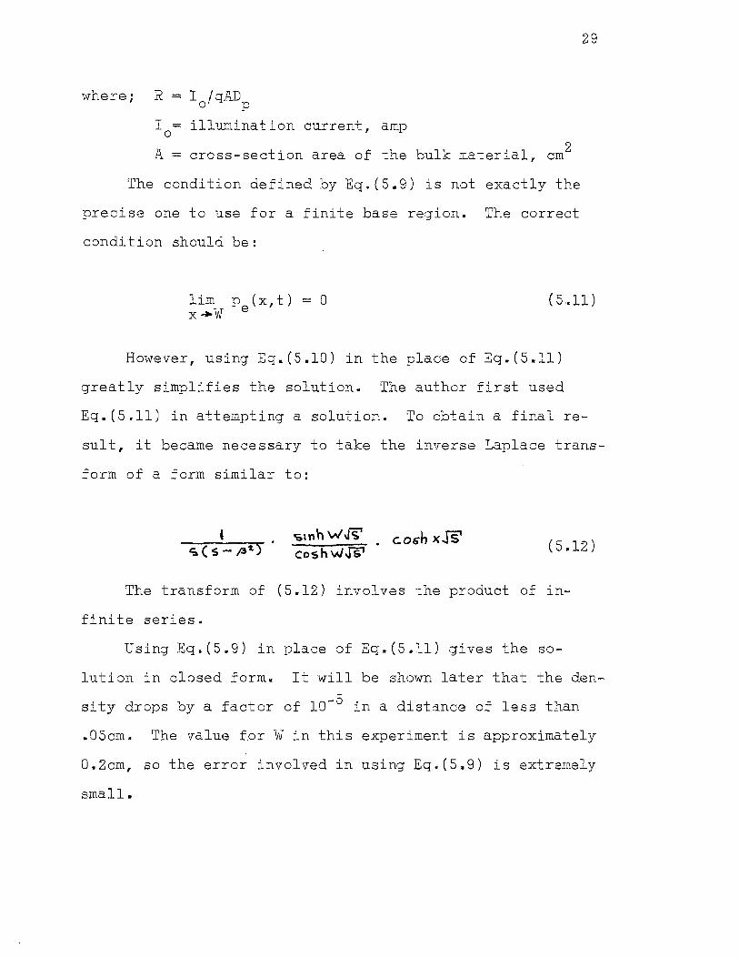
where; R = I /qAD 0 p
I = illumination current, amp 0
2 A = cross-section area of the bulk material, em
The condition defined by Eq.(5.9) is not exactly the
precise one to use for a finite base region. The correct
condition should be:
29
lim pe(x,t) = 0 x+W
(5.11)
However, using Eq.(S.lO) in the place of Eq.(5.ll)
greatly simplifies the solution. The author first used
Eq. (5 .11) in attempting ,:J. solution. To obtain a final re-
sult, it became necessary to take the inverse Laplace trans-
form of a form similar to:
"&tnh w~ . C.06"h xJS' coshvJJSI (5.12)
The transform of (5.12) involves the product of in ....
finite series.
Using Eq.(5.9) in place of Eq.(S.ll) gives the so-
lution in closed form. It will be shown later that the den
sity drops by a factor of l0-5 in a distance of less than
.05cm. The v·alue f.or W in this experiment is approximately
0 .. .2cm, so the error involved in using Eq.(5.9) is extremely
small ..
30
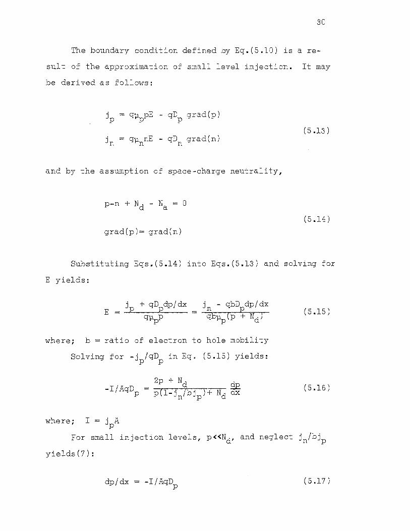
The boundary condition defined by Eq.(5.10) is are-
sult of the approximation of small level injection. It may
be derived as follows:
qD grad(p) :p
J. = q~~ nE - qD grad(n) n ~'"'"n n
and by the assumption of space~charge neutrality,
grad(p)= grad(n)
( 5 .. 13)
(5.14)
Substituting Eqs .. (5.14) into Eqs.(5.13) and solving for
E yields:
E = jp + qDpdp/ dx q'flpp
= jn - qbDPdp/dx qbllp(P + Nd)
where; b = ratio of electron to hole mobility
Solving for -jp/qDP in Eq. (5.15) yields:
where;
2p + Nd d -I/AqDP = p(l-j /bj )+ Nd 3i
n P
I = j A p
(5.15)
(5.16)
For small injection levels, p<<Nd, and neglect jn/bjp
yields (7):
dp/dx = -I/AqDP (5.17)
31
Evaluating Eq.(5.17) at the junction (x=O) gives
Eq.(5.10). The relation between I and I will be discussa ed in Chai.'Jter 6.
The required initial and boundary conditions are smn-
marized below:
a) p (x,O) - - Pn e
b) lim p (x,t) = 0 (5.18) X+..- e
c) )Pe(x,t) = - R ~t x=O
The solution ~ay now continue by taking the Laplace
transform of Eq.(5.6) with respect to "t.•
(5.19)
Now,
--
If e-stp (x,t) is such a function that the in~erchange e
of the order of integration with respect to "t• and the sec-
ond order differentiation with respect to "x" is valid, the
Laplace transform of the bracketed term of Eq.(5.19) is:
(5.20)
32
Substituting Eqs.(5.20) and (5.8) into Eq.(5.19) and
rearranging terms:
(5.21)
A solution for Eq.(5.21) is:
(5 .. 22)
The constants A and B in Eq. ( 5. 22) may be determined
from application of the transform of the boundary conditions
defined in Eqs.(5.18).
\,n'\ Pe.Cx • ._) -= 0 ')(~--
Substituting Eq.(5.22) into Eqs.(5.23) yields:
or,
B = o
_.fi. s
A
-~SA>~ A
CKJOP Q gS/ & (S -clo;, [i" ( s- -<'Op)
(5.23)
(5.24)
33
Substituting the values for A and B into Eq.(5.22):
R .f5P e-~~ _ «JD; Q e-~JS' _ 0( Pft~ e ft',JS' s1'z. sv. cs-.:•op) .fi' (s-l( ... o,)
_41()( + p .. e. (5.25)
S-o<.'Op
The inverse Laplace transform of Eq.(5.25) will give the
desired expression for p (x,t). The inverse transform of the e
first term and the last two terms may be obtained directly
from available tables(9). The second and third terms require
the use of the convolution integral.
t; s .f, (T) t'" ( i:.-1"') d T 0 (5.26)
We shall consider the second term of Eq.(5.25) first.
Let,
F; ( S) : 53/'1..
and
Ft (s) =
then,
z. Jt;iT' exp (- ~Dpt)
and,
34
Therefore,
tt\',(s) F,(~ =
+ (5.27)
The above expression cannot be simplified any further
without making some gross approximations, so it will be used
as is, to calculate p (x,t). This will prove to be the most e
accurate approach, since a nu.1nerical solution will be used
to analyse the final results.
Proceeding as above with the third term of Eq.(5.25),
we let:
F; (S) e-A-,JS'
= .J'S' and
F-z. ($) :. « fn Jop' (S- «.l.Op)
Then,
i-'[Ec~~ = '/J-rr£ exp (- ')(Xo,t) and
[-'[F~ls)] ::. tJ( P" 4 o~ e.ot."" o,t Therefore,
r [f, '") F,cs~ = "'pft~ e"'Prl~<><"Jn,.~ ... JO,."~"~-'td T ()
2 2 The above expression may be simplified by letting z =a Dp
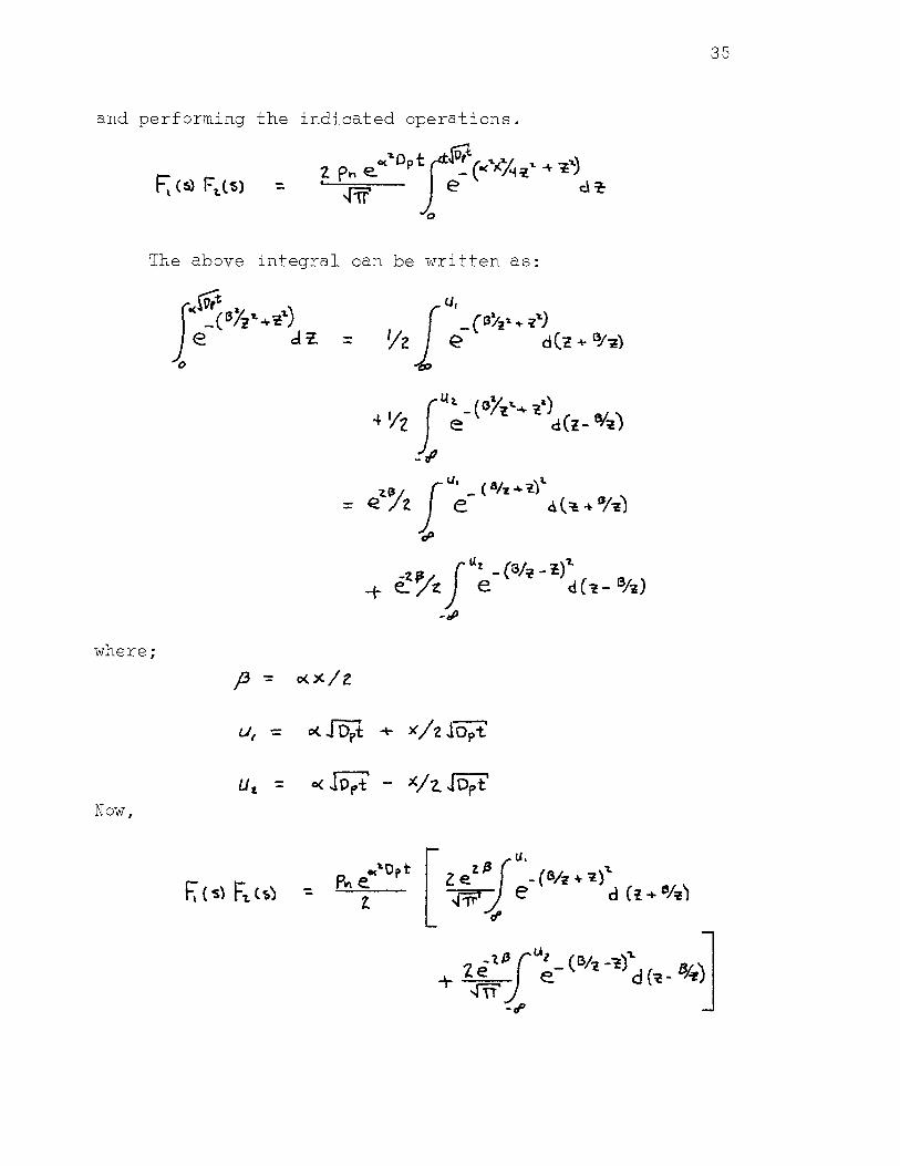
35
and performing the indicated operations.
The above integral can be written as:
where;
Now,
36
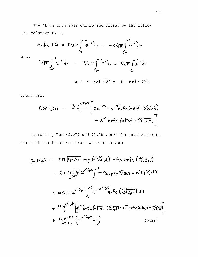
The above integrals can be identified by the follow-
ing relationships:
and,
= 2/.Jn' J~-~d .. + %/,ffl I ;-·d~ -tP 0
- 1 + e rf ( A) = l - e r-t c. ( ~)
Therefore,
F; (S) ~ (5)
Combining Eqs.(5.27) and (5.28), and the inverse trans-
forms of the first and last two terms gives:
pe (x,t) = Z RJq>t/1T 1 e.xp (-)(~opt.) -Rx erfc. (~Jopt')
2 oc. Q .fi5P e"''opl"':.'hexp (- xAo,"r- o<'"Dr 1-) d'T .r-tf"' 0
(5.29)
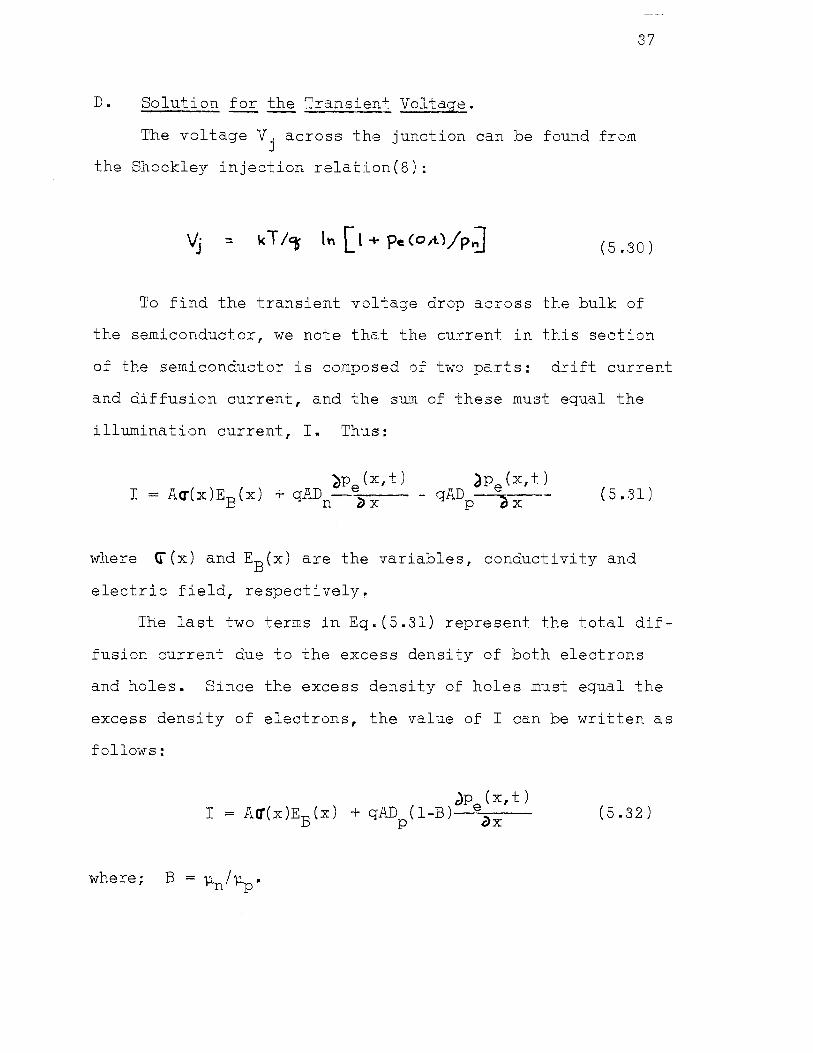
D. Solution for the Transient Volta(;;r_e.
The voltage V, across the junction can be found from J
the Shockley injection relat:Lon(S):
37
(5.30)
To find the transient voltage drop across the bulk of
the semiconductor, we note that the current in this section
of the semiconductor is composed of two parts: drift current
and diffusion current, and the SQ~ of these must equal the
illumination current, I. Thus:
~P (x,t) ~pe(x,t) I = Ac:r(x)EB(x) + qAD eo - qAD ~--n x p ox (5.31)
where <r(x) and EB(x) are the variables, conductivity and
electric field, respectively.
The last two terms in Eq.(5.3l) represent the total dif-
fusion current due to the excess density of both electrons
and holes. Since the excess density of holes must equal the
excess density of electrons, the value of I can be written as
follows:
Jp {x, t) I = AQ"(x)EB(x) + qADP(l-B) e~0-x-- (5.32)

38
Solving for EB(x) in Eq.(5.32) we obtain:
(5.33)
For reasons which will become evident later, let:
(5.34)
where,
(5.35)
and qD (1-B) dP
ED(x) - P e(x,t) - (j'(x) C>x
(5.36)
The voltage VR, corresponding to ER(x) in Eq.{3.35), is
due to the IR drop through the bulk material, and ED(x) in
Eq.(5.36) corresponds to the space-charge voltage VD, due to
the inequality of electron and hole mobilities. VR must be
obtained by digital integration, but VD can be obtained by
direct integration of Eq.(5.36).
The conductivity ~(x) in the previous equations is re-
lated to the carrier densities as follows:
(5.37)
where, by use of the assumption of space-charge neutrality,
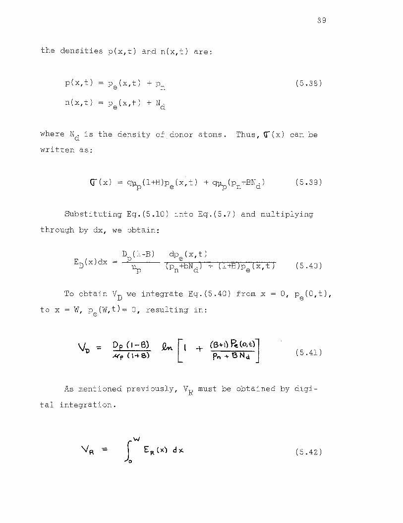
the densities p(x,t) and n(x,t) are:
p(x,t) = pe(x,t) + pn
n(x,t) = pe(x,t) + Nd
39
(5.38)
where Nd is the density of donor atoms. Thus, u(x) can be
written as:
(5.39)
Substituting Eq.(5.10) into Eq.(5.7) and multiplying
through by dx, we obtain:
D (1-B)
up
dp ( x, t) e
To obtain VD we integrate Eq.(5.40) from x
to x = W, p (W,t)= 0, resulting in: e
V-o = Dp (1-B) -"fp ( l-4- B)
+ (6+1) Pe. (o,t)J Pn + B Nc1
(5.40)
(5.41)
As mentioned previously, VR must be obtained by digi
tal integration.
(5.42)
The total voltage across the diode is the sum of the
three voltages Vj' VR, and VD.
E. Results.
40
The numerical values for pe(x,t), Vj, VR, and VD were
obtained by programming the appropriate equations on a 1620
IBM digital computer. The variation of p (x,t) over dise
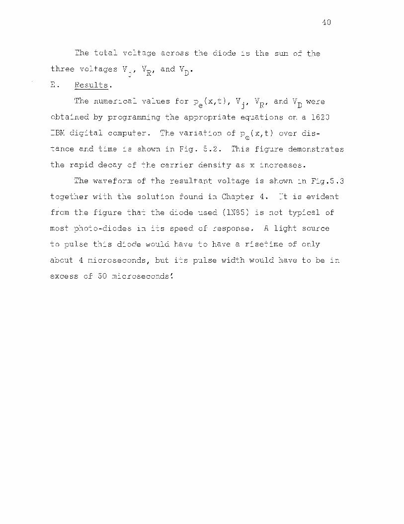
tance and time is shown in Fig. 5.2. This figure demonstrates
the rapid decay of the carrier density as x increases.
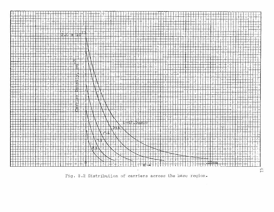
The waveform of the resultant voltage is shown in Fig.5.3
together with the solution found in Chapter 4. It is evident
from the figure that the diode used (lN85) is not typical of
most photo-diodes in its speed of response. A light source
to pulse this diode would have to have a risetime of only
about 4 microseconds, but its pulse width would have to be in
excess of 50 microseconds~
I I I I I I I I I I I I I I I I I I I I I I I I I I I I I I 1-++H I I I I I I I I I I ntn ltntrntlttfttH+·",I I I I I I I I I I I I I I I I I I I I I I I I I I I I I I I I I I I I I I I I I I I I I I I I I I I I I I I-I+I+H-1-+tffr-
I
+null
11 I I I I I ~I~ II I Ill II I I I I I I II II II I I If IIIII I II I II II Ill I I I II H Ill II I If I lllllll=t--
l-
1 1 1 1 1 I I I I I I I I I I I I I I I I I I I I I I I I I I\ I I ~ I I ~ I 1· P r N I I I 11-J I I I I I I I I I I I I I I I I I I I I I I I I I I I I I I I I I I I I I I H-+-t+++-++i-H--·-
11111111 RlJ#RJmJ 1111111 re M- ' ~ " . ~ ! I j:f:H: - ttf:F_:_+r-•-t
I I I I I I I I I 1-t-H-1 I I I I I I I I I I I I I I I : I -,..... I . L I - I '·- =i-++-=d __ j--j=_1_-. "' . ' ,_ "'Fi4- . . ! ' ,__ .p-lJ ' .. · [-- -....;,. I 1-N I , . - j 1 1 -f--H- ttl. ~-L: .
< 0 0 0
O
0
O ' _l f-1 ' o ~ , + 1--r _ I I I I I I I I I I I I I I I I ' I I ' I ' , I I I ' I I , i I I--f - -·r·-r--·.·
I I I I I 1 -'- , ·· ' . I
1
I I I I I I I I I I I I I LLLL LJ.- riPt:rJ'T_l]u __ ltrrJ=l l U J • J:c::ml ' -f -+-~-H- -~ ~~: :l
Fig. 5.2 Distribution of carriers across the base region.
f-1" I--'
42
0 !'J) --
i r
s
I t
I
"' rl=-1 _rh ·H
_f>.
I _
b
~
fl O
J (\)
11 L
l I
I • ~ ~
0 G
-i (!)
I :> m
I
~
I
I (!) b
;) lu
r·-r
+> ,-...
rl
0 C
J 0
(I.) (!)
:> C
)
~
+'
..._... ~
I I
: --l
((I 1
.) rl
::s U)
(j) p::;
t<"\ •
lf\
. tJ
·r-1 J:.x_,
4S
CHAPTER VI
EXPERIMENTAL TECHNIQUES AND RESULTS
A. Light Source.
The requirements placed upon the risetime and pulse
width of the pulse of light to be shone on the junction of
the photo-diode are quite severe. It is necessary that the
risetime of the light pulse be short in comparison to the
effective risetime of the photo-diode, and the pulse width
should be large in comparison to the time required for the
photo-diode to reach its steady state. An examination of
the literature available concerning the transient response
of photo-diodes and diodes in general indicated that the
risetime of the light pulse must be on the order of 100
nanoseconds and the pulse width must be at least 10 micro
seconds(S,4,5,6).
Jones(lS) has written a general discussion on the meth
ods of modulating light. The method most suitable for the
requirements described above involves the use of the Kerr
cell. The Kerr cell operates as a light shutter, turning on
or off the light as is desired.
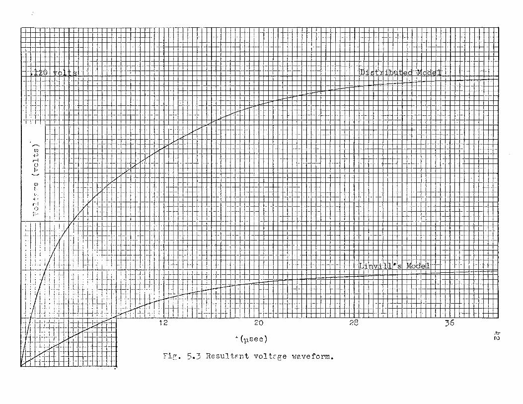
The Kerr cell, as illustrated in Fig. 6.1, is essen
tially two parallel plates in a container filled with liquid
nitrobenzene across which is connected a high direct-current
voltage. The light from the source on the left is focused
through polarizing plates on the center of the cell halfway
between the plates. With no voltage on the Kerr cell, the
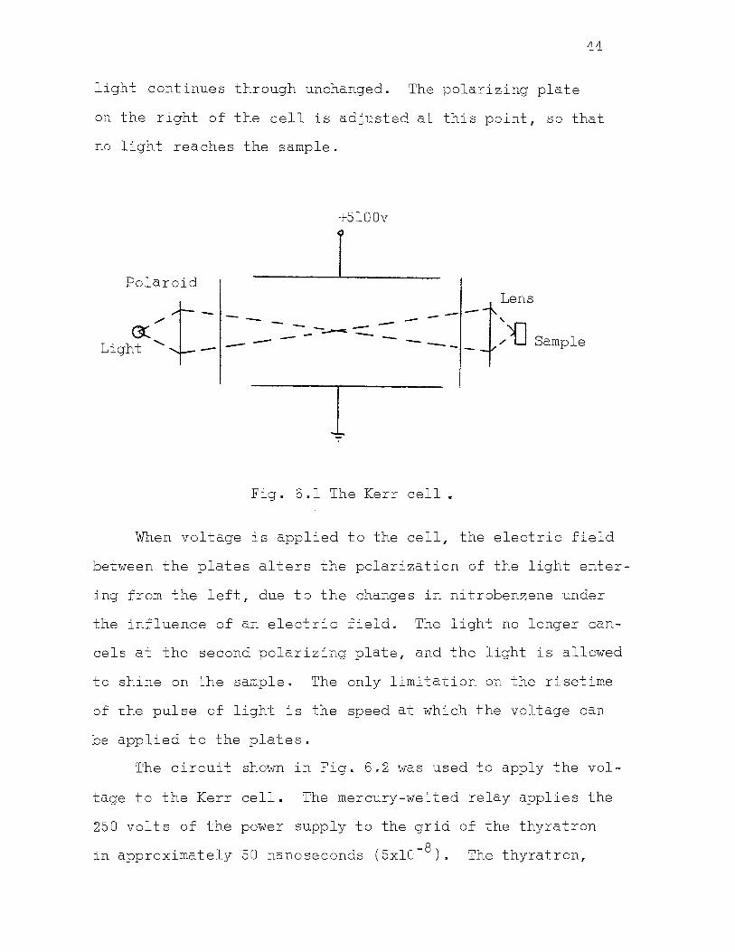
44
light continues through unchanged. The polarizing plate
on the right of the cell is adjusted at this point, so that
no light reaches the sample.
+5l00v
I Polaroid
--:,.......c. --- ----- ----Lens
: =-~ ~+:~ Sample
I Fig. 6 .l The Kerr cell ..
When voltage is applied to the cell, the electric field
between the plates alters the polarization of the light enter-
ing from the left, due to the changes in nitrobenzene under
the influence of an electric field. The light no longer can
cels at the second polarizing plate, and the light is allowed
to shine on the sample. The only limitation on the risetime
of the pulse of light is the speed at which the voltage can
be applied to the plates.
The circuit shown in Fig. 6.2 was used to apply the vol-
tage to the Kerr cell. The mercury-wetted relay applies the
250 volts of the power supply to the grid of the thyratron
in approximately 50 nanoseconds (Sxl0- 8 ). The thyratron,
45
activated by the pulse from the relay, fires and places the
5,100 volts across the Kerr cell. The speed at which this
is accomplished is determined primarily by the risetime of
the pulse on the grid of the thyratron, which in this in-
stance will be in the neighborhood of 50 nanoseconds. This
time will also correspond closely to the risetime of the
pulse of light.
+250v
Relay
+5100v
Kerr Cell
Fig. 6.2 Circuit to operate the Kerr cell.
The pulse width of the light can be regulated by ad-
justing the parameters in the circuit controlling the decay
of the voltage on the Kerr cell. The cell itself acts as a
capacitor of from 100 to 200 micromicrofarads. The cell
discharges through the resistor R2 . By adjusting R2, the
decay time can be made long enough so that the magnitude of
the light pulse stays close to its maximum magnitude for a
time long enough to allow the photo-diode to reach its steady-
state condition.
46
The capacitor C in fig. 6.2 is where the charge is
stored when the thyratron is off. The value of C toge
ther with R1 and R2 determine the repetition rate of the
light pulses. Ample time must be allotted for the voltage
to build on the capacitor C, before the tube is fired the
next time.
A major disadvantage of the circuit shown in Fig. 6.2
is the noise level. When the thyratrons fire, surges of
up to 35 amperes flow through the circuit, producing high
frequency noise. Since the signals involved in the photo
diode are small, the output must be well shielded, and the
intensity of the light source used must be as high as pos
sible.
The author, in attempting to use the circuit of Fig.6.2
to operate a Kerr cell with a distance between the plates
of 3 mm., was unable to obtain enough light intensity to ex
cite the photo-diode. The insertion of the polarizing plates
and the Kerr cell between the light source reduces the inten
sity of the light at the sample by a factor of approximately
one hundred. The highest intensity light sources used were
a mercury vapor lamp, an arc lamp and a 500 watt tungsten
lamp with reflector. The Kerr cell, however, was observed
to be operating, though no measurements could be made to de
termine the characteristics of the light pulse.
The failure to obtain results in the above instance does
not in any way depreciate the value of the Kerr cell as a
modulator .of light. It is believed by this author that had
47
a Kerr cell with a greater aperture been available, the re
sults would have been much more favorable. Kerr cells are
made with much larger aperturGs than the one used in this
experiment. The voltage required to fire the cell increases,
however, as the distance between the plates is increased.
Voltages on an order of 40 kilovolts (40,000 volts) are com
monly used for plate separations of about 1 cm(l3).
A larger Kerr cell would be more suitable as a means to
provide a fast-rising pulse of light due to the fact that
more light could be collected by the cell and the light in
tensity would be diminished less by the cell. To operate
the cell correctly, the light being focused on the center of
the cell must not be allowed to strike either of the plates
as it enters. This would cause internal reflections in the
cell disrupting the plane of polarization and light would
pass through when the cell was off. For a small cell, this
restriction limits the size of the light beam entering the
cell and therefore limits the size of the lens to be used to
focus the beam and the amount of light the lens can capture.
For a larger cell, the beam can be larger and more intense,
permitting more intensity to reach the sample.
The amount of moise present will be increased due to
the higher voltage needed to operate the larger cell. If
necessary this noise can be reduced by shielding the thyra
tron from the output equipment and by inserting a limiting
resistor in series with the thyratron of such a value that
will not seriously affect the desired risetime. The fastest
48
risetime attainable will be limited by the speed of response
of the liquid surrounding the cell which for the most common
liquid, nitrobenzene, is approximately one nanosecond(l6).
The size of the limiting resistor for a nitrobenzene-filled
cell will be determined then by how long the desired risetime
is compared to one nanosecond.
Another light source tested for possible use was an
Amglo M6-LZ, xenon-filled flashtube. It was found that al
though the intensity of the tube was easily high enough, the
fastest risetime attainable with low-inductance capacitors,
resistors, and leads was greater than 5 microseconds. This
tube was used later to measure the parameters of Linvill's
model.
An article by Draper(l4) suggested another possible
light source, using the sweep trace of an oscilloscope to
produce millimicrosecond pulses through a well-defined slit.
It was found in this instance that the combination of low
intensity and the photo-diode's relative insensitiveness to
green light (common to most oscilloscopes) makes the method
impractical.
The absence of a suitable light source to pulse the
photo-diode prevented any experimental confirmation of the
results of Chapters 4 and 5.
B. Determination of the Parameters for Linvill's Model.
Only two measurements are required to measure the para
meters of Linvill's model. One is the reverse saturation
49
current, and the other is the charge removed from the diode
following a pulse of light on the junction(2).
V-o ~
I s
..__--------11•1' t---------' VB
Fig. 6.3 Circuit used to measure H • c
The arrangement in Fig. 6.3 is used to measure there-
verse saturation current. With the junction reverse biased,
the excess density from Eq.(5.30) is -Pn· In the steady
state condition, current Is is given by:
( 6 .1)
The charge stored in the diode will be measured by com
paring the waveform of the voltage across the photo-diode in
Fig. 6.3, and the waveform of the light pulse.
The time "t " in Fig. 6.4, is the time at which the 0
light is effectively turned off. The area under the curve
following the time "t " in Fig. 6.4(a) represents the volume 0
of charge stored in the diode, QD (the phrase "volume of charge"
means the quantity or amount of charge present).
50
If the current flowing in the diode (determined by
VDMAX/RL) is 1 0 , then the charge of holes on the hole stor
age, Q , is: s
I Qs = (l + Io)pnSp
s
where; I is an incremental current. 0
I
I r
I
I
r \ I I
I I
\
( 6 . 2)
(a) t(11sec)
(!)
-f-1 rl 0 :>
I
I
I
I
t
I
I
,..-1_ I ', I ' ' I '
' '
(b)
Fig. 6.4 a) Waveform of the light pulse.
b) Waveform of the voltage across the diode,.
51
It is evident that:
( 6 . 3 )
Substituting Eq.(6.3) into Eq.(6.2) and solving for SP
yields:
s p = Q D ( 6. 4)
The light source used to pulse the photo-diode was the
flashtube discussed in the previous section. The circuit
used to flash the tube is shown in Fig. 6.5. The transformer
+2500v
_..._ -r- I
I--
Flash tube
.. . .
.
Relay
~6v
Fig. 6.5 Circuit for firing flashtube.
52
in the circuit is an ignition coil of the type used in auto
mobiles. Its purpose is to provide a high-voltage pulse to
"tickle" or excite the tube causing it to flash. The wave
form applied to the coil of the relay was obtained from the
load resistor of a cathode-follower, whose grid was driven
by a multivibrator oscillating at approximately l cps. The
slow repetition rate allowed time for the power supply to
recover to its initial state after the tube had fired. It
was necessary to fire the tube periodically to facilitate
synchronization of the oscilloscope with the signals to be
recorded.
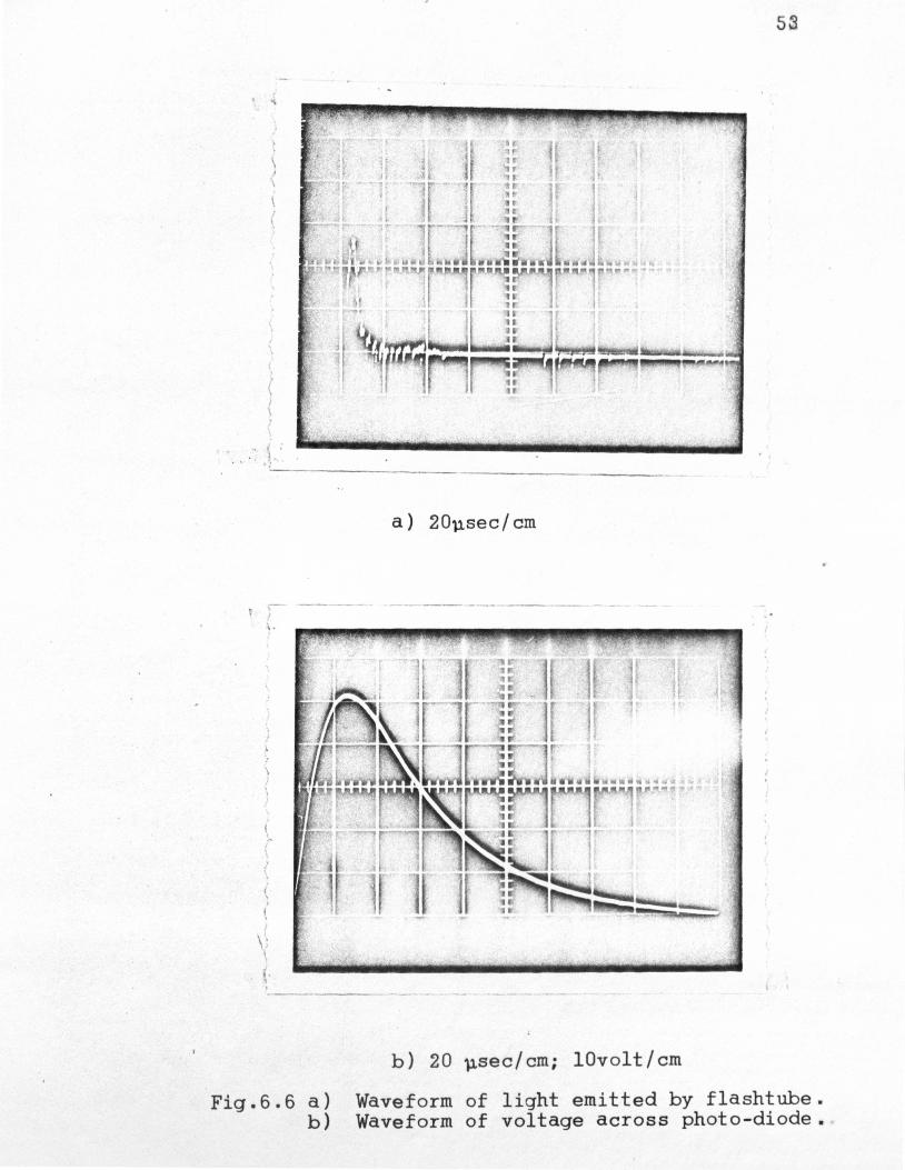
The photographs on the following page were taken on a
Type 516 Tektronix oscilloscope of the waveforms of the
light pulse and the voltage across the photo-diode. The
light pulse was made to fall simultaneously on the photo
diode and the entrance slit of a monochrometer. The mono
chrometer was used to focus the light on a photomultiplier
and also to reduce the intensity of the light to prevent
driving the photomultiplier into saturation.
The output of the photomultiplier, which corresponds
to the shape of the light pulse, was amplified through a
Model 400 AB, Hewlett-Packard, vacuum-tube voltmeter with
a gain of approximately 400 on the lowest scale and an upper
3 db frequency of 3 megacycles. All external connections
and leads in the photomultiplier curcuit were made with coax
ial cables to prevent amplification of stray signals. The
cables were terminated in the characteristic impedance to re
duce the capacitance of the circuit and insure an accurate
. \
/ \
53
··~· --------------- -----------------
\~ .. ' '
Fig.6.6 a) b)
a) 20p.sec/cm
b) 20 ~sec/em; lOvolt/cm
Waveform of light emitted by flashtube. Waveform of voltage across photo-diode.
54
description of the light pulse.
Before proceeding to the actual determination of the
value of the storance, some comments are necessary on the ac
curacy of the experimental technique outlined above.
The assumptions made in performing a measurement of the
type just discussed are that the light was incident only on
the junction and did not strike any part of the bulk material,
and that the carriers produced by the light were distributed
evenly across the cross-sectional area of the junction. Nat
urally, any deviation of these approximations from perfection
that occur during the experiment would result in incorrect
values for the parameters of Linvill's model. The model de
rived by Linvill represents physically an area only as large
as the transition region. This means that for typical photo
diodes the width of the light beam striking the junction -4 should be less than 10 em wide, a very difficult task at best.
The error involved in assuming the injected carriers are
evenly distributed across the cross-sectional area of the june-
tion is generally smaller, especially if the material under
test is thin and also has a low absorption coefficient. This
would insure that in the small distance between the two sur-
faces of the material, the density of injected carriers would
not vary appreciably. Using the value obtained for the ab-
sorption coefficient in Section C of this chapter, and the
thickness of the material tested ( .038cm), it was determined
from Eq.(6.6) that the density decreased by only 20 per cent
across the thickness of the material. The actual average
55
error due to the exponential shape of the distribution would
be less than 10 per cent. It will be illustrated shortly
that this amount of error is negligible compared to the amount
of error present in the other approximation.
To determine the amount of error involved in assuming the
light to be incident only on the junction, several measure
ments of the storance were made for varying widths of the in-
cident beam of light. The results of these measurements,
listed in Table I, showed that as the width of the beam was
decreased the magnitude of the storance also decreased. The
width of the beam was varied by placing an adjustable metal
slit against the diode. The smallest width attainable was
only . 0013 in., which was not small enough to allow any "level
ing-off" of the magnitude of the storance. This last value
for the storance would have to be the value used for Linvill's
model if no other method were available to determine a more
accurate value, and in the absence of another method, no check
could be performed experimentally to determine the accuracy of
the value used. A rough estimate can be obtained, however, for
the appropriate value of the storance from the following equa-
tion derived by Linvill(2):
q.lj.W = -2- ( 6 • 5 )
where; A = cross-section area of the junction
W length of the p-type material
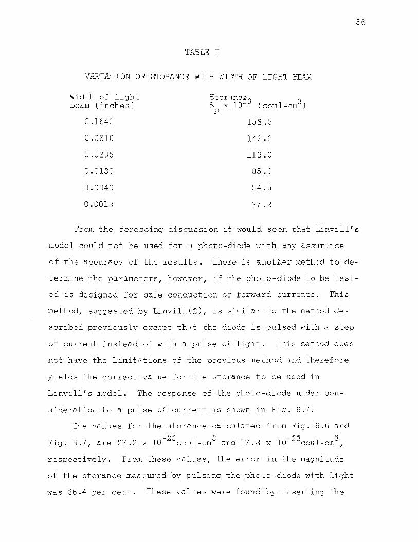
TABLE I
VARIATION OF STORANCE WITH WIDTH OF LIGHT BE[M
Width of light beam (inches)
0.1640
0.0810
0.0285
0.0130
0.0040
0.0013
Storanc23 3 S x 10 (coul-cm ) p
153.5
142.2
119.0
85.0
54.5
27.2
56
From the foregoing discussion it would seem that Linvill's
model could not be used for a photo-diode with any assurance
of the accuracy of the results. There is another method to de
termine the parameters, however, if the photo-diode to be test-
ed is designed for safe conduction of forward currents. This
method, suggested by Linvill(2), is similar to the method de-
scribed previously except that the diode is pulsed with a step
of current instead of with a pulse of light. This method does
not have the limitations of the previous method and therefore
yields the correct value for the storance to be used in
Linvill's model. The response of the photo-diode under con-
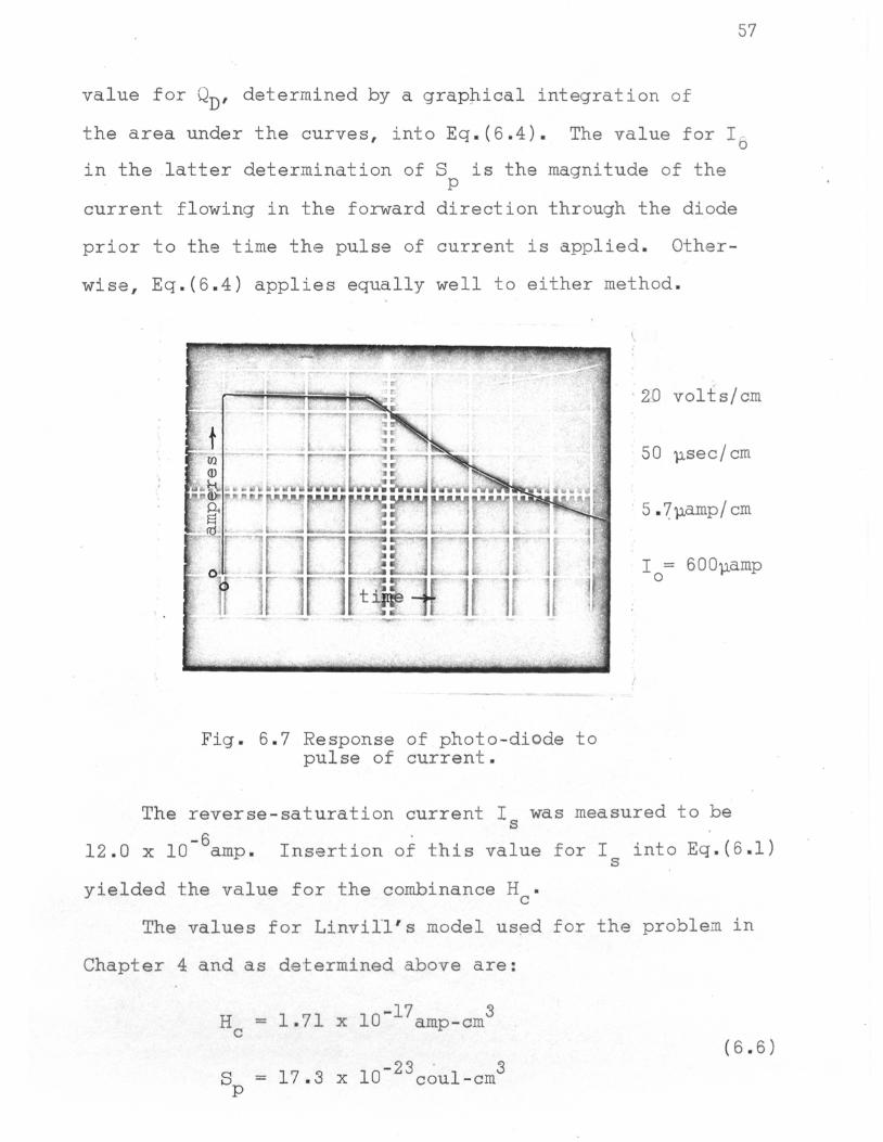
sideration to a pulse of current is shown in Fig. 6.7.
The values for the storance calculated from Fig. 6.6 and
-23 3 -23 3 Fig. 6.7, are 27.2 x 10 coul-cm and 17.3 x 10 coul-cm,
respectively. From these values, the error in the magnitude
of the storance measured by pulsing the photo-diode with light
was 36.4 per cent. These values were found by inserting the
C. Determination of the Absorption Coefficient.
If the illumination of the junction of a photo-diode
produces a current I , corresponding to the generation of 0
6p hole-electron pairs per second, the current leaving the
diode is given by Lambert's Law(l4):
I =I e-ax 0
where; I = the current in the external circuit
a = absorption coefficient
x = length of the n-region
( 6. 7)
Thus, to deter~ine the absorption coefficient for a
given light source, it becomes necessary to determine the
absolute intensity of light falling on the junction from
which can be found the number of hole-electron pairs being
produced per second.
The light used for this measurement was a 375 watt
tungsten lamp operating at a temperature of 2348°K. To
determine its intensity at a given distance, an area of one
square inch of water in a well-insulated container was ex-
posed to the light. The change in temperature of the water
was recorded for certain lengths of time. The relation used
to calculate the amount of energy transferred to the water
is as follows:
SwW~T 2 Q = watt/in
(1-Rw)~t ( 6. 8)
58
where; Sw =heat capacity of water, 4.18 joules/g°C
W =amount of water, grams
~T = temperature change, °C
~t = time elapsed, min
Rw = reflection coefficient of the water
Three runs were performed and the average of the three
values obtained was determined as:
Q = 8.43 watts/in2 ave
The reflection coefficient of the water was measured
with an optical pyrometer by a comparison of the total light
incident on the water to light reflected by the water. The
value obtained for Rw was 0.650.
Knowing energy density of the light source at a certain
distance, the number of carriers generated per second ~P can
59
be computed from the quantum nature of light, the total en-·
ergy being equal to the average energy per photon (one photon
produces one hole-electron pair) times the total number of
photons. The equation is:
~p(~~)= Pn(l-RD)AjQave (6.9)
wherei PD = spectral efficiency of the photo-diode= 0.457
RD = reflection coefficient of the photo-diode = .555
A. = area of the ~unction exposed J to light, in
~ = range of wavelengths in the lamp's spectrum
60
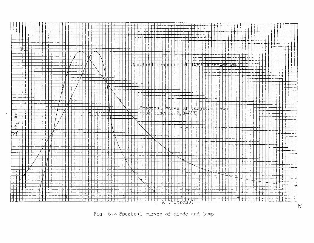
A comment is necessary here on the wavelength depen
dency of the absorption coefficient. The coefficient deter
mined by the method described above is a total absorption
coefficient for "white" light. The variation of the coeffi
cient and the energy per photon with the wavelength of light
was accounted for by a spectrum analysis of the light and
the photodiode ..
The spectral distribution of the light source was ob
tained by assuming black body radiation and plotting the re
lative energy density versus wavelength. The plot was ob
tained from Planck's radiation equation(l5):
(6.10)
The product of the above distribution with the spectral
sensitivity of the photo-diode was obtained to determine pD,
the spectral efficiency of the photo-diode. The numerical
value for pD was found from the ratio of the total area under
the curve of the product of the two curves to the total area
under the curve of Eq.(6.10). The value of Pn represents the
percentage of the total light energy incident on the photo
diode which is actually detected. (The curves and areas dis
cussed above are shown in Figs. 6.8 and 6.9). It should be
mentioned at this point that the value of a is only accurate
for a lamp operating at the same temperature as the one used
in the experiment.
The current produced by the illumination is equal to
q~p. The value for ~P determined from Eq.(6.9) was: ~P =
.302 x 1016 sec-1 , giving an illumination current of I 0 =
.510 x 10-3 amp. The current flowing in the circuit of the
61
photo-diode placed the proper distance from the light source
was measured as: I = .130 x 10-3 amp. Substituting these
values into Eq.(6.7) yields:
a= 15.55 in-l = 6.13 -1 em
The experimental determination of the absorption coef-
ficient represents one of the main sources of error present
in the distributed solution. It is necessary therefore to
determine the relative magnitude of this error and its effect
on the final solution.
The error in this experiment is centered in the follow-
ing measurements:
a) the square inch of water exposed to the light source
b) the measurements of the reflectivity of the surfaces involved
c) the measurement of the temperature change of the water
d) the measurement of the filament temperature
The error from the measurements of the temperature changes
of the water due to loss of heat was made negligible by ade-
quate insulation of the water from the surrounding air. By
making the time of exposure of the water to the light long
enough (15 minutes) so that large changes in temperature (4
to 5 degrees) occurred, the changes in temperature were easily
measured within 2 per cent of their actual values.
The measurements of the reflectivity and the filament
temperature were accomplished with a Model 8B Pyro manu
factured by the Pyrometer Instrument Company, Inc., which
stated the accuracy of its instrument as one-half of one
per cent.
62
The dimensions of the square hole through which the
light was incident on the water were found to vary by no
greater than one thirty-second of an inch or approximately
3 per cent of the designated value. The maximum error in
volved in ass~~ing the area to be one square inch therefore
is approximately 6 per cent.
The total error involved in determininJ the absorption
coefficient is approximately 9.5 per cent, including three
separate measurements with the pyrometer.
I
I
·+-~
I
J.
lj
I I
I
I : I
J. I
:
I
I
·-'
I
63
I
I I
' I I
I I
I -I.
I I
I I
I
co
+
-r
! ..:.
'"Ci (!) ~
-r-1
~ 0 0 ~ rd rl
'"Ci ~
rd (!)
'"Ci 0 -r-1 '"Ci I 0 +
' -
0 m
...C: .....
~
0.. v
0 I
!--i4-l
:t· 0
0 -r-1 ~
(!)
i> !--i
A
::l 0
rl
rd !--i +
' 0 (!)
0.. {()
(!)
i> -r-1 +
' 0 (!)
4-l 4-l ril
Ol
I ':
~b <.0
-+---~-~~~4-~~~~~~~~~~+44-~+4~~++~~r+~~-rr-H
--~~~~~~-~~~~~-+4-~~~~~~44~~~~+4~~44~++4-rr+4~r+~~
... L~---+
'
4-~~~~~~4-~~~~~~~~~~~+4~~~~++4-rr++,_~
... -1--
-
-+--W
--I
I . ---
+i-
~-·t,t±::=tt:i~:tij~ttij=ttij=tti~=ttij=ttij'=iti~j'=itt"t~-=i=tt~j=~+_-+4-H-I •
·-.. 1
--
--;
I
~ ;
I ,
!
·'Effi
-+-Tff -+-
-I
I
f --r-
-~
__ --.: -_ -~~~~---~~--f-rl-l-++--1-1---1-1--l-1--+-+-H-H+I-I-H-H-++-++-+++++++++++-++-++++++ -
--
... -+1
--i-f-.. j_j.....j._..J--I.....j._..J--I..-!--l-l---l--l-l---l--~..J..--il-++-ll-++-1++4-+-+-+-+-~-l--H-....;....,H--H-t--H-H
I I
I I
I ,-11-...
·-.. , ..... ---~ -+..ji-+-+-l--l-l--f-+~~i-l-t-+-.J.-+.++++-+-I--l-l-!-i-l-t-+-++++++-H-H-+-1,..-j-i--l-t-+-H
-I-~~ ~tff ~~-l--l--l--l-+--l-l-l----J-..+-.i.-+-+-1---+--t-4-I--+-IH-l-~l-+-l-1-H-t-+-+-+--++++++-+-+-+-+-H
I I
'
b"' -r-1 ~
Tl I

65
CHAPTER VII
CONCUJSIONS
The resul tan·!:: wa vefonas for the transient voltage across
the diode found from the two solutions presented in this
study are shown in Fig. 5.3. The times required for the vol-
tage to reach its steady-state value for each solution com-
pared very well. The time required for the distributed solu
tion to reach its steady-state value was approximately 40
microseconds, while the corresponding time for the solution
using Linvill's model calculated as four tiae constants or
4S /H was 39.5 ~icroseconds. This is well within the exp c
perimental error involved in determ:Lning the absorption co-
efficient for the distributed solution.
The difference in magnitude of the steady-state voltages
found by the two solutions suggests one drawback to the use
of Linvill's model. Since Linvill's model is concerned with
the material very close to the junction, relatively large
concentrations of carriers and their contributio:ls to the
total voltage across the diode are neglected. In the case
of this study, for example, Fig. 5.2 demonstrates that at a
-5 distance of approximately 10 em, where Linvill 1 s model ends,
the concentration of carriers had not yet begun to decrease
appreciably. Neglecting these carriers causes the steady-
state voltage as predicted by Limrill' s model to be much
lower than it actually is.
66
The absence of a suitable light source prevented an ex
perimental measurement which could be used as a second so-
lution to compare with the solution obtained with Linvill's
model and also as a check solution to evaluate the actual I
error made in the determination of the absorption coefficient.
The value of Linvill's model as a means to determine the rise-
time of a photo-diode can easily be seen, however, despite
the absence of the experimental measurement.
There are several possibilities of studies which could
be made to supplement and extend the material presented in
this study. One possibility could be the development of a
method to determine a value for the storance of Linvill's
model independent of the junction capacitance. This, as dis-
cussed in Chapter 4, would enable the design of a more accu-
rate model. Another possibility could be a study to develop
a suitable and practical method to produce a pulse of light
with the particular characteristics required for the testing
of photo-diodes as described in this study.
67
BIBLIOGRAPHY
l. Linvill, J, G. and Gibbons, J, F., Transistors and Active Circuits, McGraw-Hill Book Company, Inc. 1 New York, N.Y., 1961.
2. Linvill, J. G., Models of Transistors and Diodes/McGrawHill Book Company, Inc., New York, N.Y.,l963.
3. Chang, Y. F.,Switch-on Transients in p-n Junctions, ]. of App. Phy., vol.34, No.7, pp.2056-2060; July, 1963.
4. Gossick, B. R., On the Transient Behavior of Semiconductor Rectifiers, J, of App. Phy., vol.27, No.8, pp.905-9ll; August, 1956.
5. Bhar, J. N., Microwaves Techniques in the Study of Semiconductors, Proc. IEEE, vol.5l, pp.l623-l63l; November, 1963.
6. Holmes, D. A. and Feucht, D. L., Excess Carrier Concentration in a Bulk Semiconductor Illuminated by a Pulse of Light, Proc. IEEE 1 vol.52, p.630; May, 1964.
7. Ritter, E. S., Extension of the Theory of the Junction Transistor, Physical Review, vol.94,pp.ll6lll7l; June, 1954.
8. Shockley, W.,The Theory of p-n Junctions in Semiconductors and p-n Junction Transistors, Bell Systems Tech. Jr., vol.28, pp.435-389; 1949.
9. Churchill, R.V., Operational Mathematics, McGraw-Hill Book qompany, Inc., New York, N.Y.; 1958.
10. Carslaw, H. S., and Jaegar, J. C., Conduction of Heat in Solids, Oxford University Press, New York, N.Y.; 1959.
ll . Lange, B . , Photoelements and Their Application, Reinhold Publishing Corp., New York, N.Y.; 1938
12. Hunter, L. P., Handbook of Semiconductor Electronics, McGraw-Hill Book Company, Inc., New York, N.Y.; 1956.
13. Jones, 0. C., Methods of Modulating Light at Extreme Frequencies, J. of Scientific Instrwnents, vol. 41, pp.653-66l; November, 1964.
68
14. Draper, J. E.,Millimicrosecond Photomultiplier Tests with Oscilloscope Light Pulses, Review of Scientific Instruments, vol.29,pp.l79-l80; February, 1958.
15. BaQman, R. P., Absorption Spectroscopy, John Wiley and Sons, Inc., New York, N.Y.; 1962.
16. Cronemeyer, D. C. and Spanberger, L. R., Infrared Transmittance and Kerr Effect of Nitrobenzene, J. of Optical Soc. of America, vol. 51, pp. 1061-1066; October, 1961.
b9
VITA
Rudy Michael Chittenden was born on September 25,1941,
in Sikeston, Missouri. He graduated from the Sikeston High
School at Sikeston, Missouri in 1959.
In that same year, he was accepted as a cadet in the
United States Military Academy at West Point, New York. He
transferred from the Academy in 1962 to the University of
Missouri at Rolla, where he received the degree of Bachelor
of Science in Engineering in January,l964.
The author entered the graduate school of the Univer
sity of Missouri at Rolla in February, 1964. Since that
time he has concurrently held a graduate-assistantship and
pursued graduate studies.
The author is a member of Eta Kappa Nu and Tau Beta Pi.