Status and Future of High-Power Light-Emitting Diodes for ...
16
160 JOURNAL OF DISPLAY TECHNOLOGY, VOL. 3, NO. 2, JUNE 2007 Status and Future of High-Power Light-Emitting Diodes for Solid-State Lighting Michael R. Krames, Member, IEEE, Oleg B. Shchekin, Regina Mueller-Mach, Gerd O. Mueller, Ling Zhou, Gerard Harbers, and M. George Craford, Fellow, IEEE (Invited Paper) Abstract—Status and future outlook of III-V compound semi- conductor visible-spectrum light-emitting diodes (LEDs) are presented. Light extraction techniques are reviewed and extrac- tion efficiencies are quantified in the 60% (AlGaInP) and 80% (InGaN) regimes for state-of-the-art devices. The phosphor-based white LED concept is reviewed and recent performance discussed, showing that high-power white LEDs now approach the 100-lm/W regime. Devices employing multiple phosphors for “warm” white color temperatures ( 3000–4000 K) and high color rendering ( ), which provide properties critical for many illumi- nation applications, are discussed. Recent developments in chip design, packaging, and high current performance lead to very high luminance devices ( Mcd/m white at 1 A forward current in 1 1 mm chip) that are suitable for application to automotive forward lighting. A prognosis for future LED performance levels is considered given further improvements in internal quantum efficiency, which to date lag achievements in light extraction efficiency for InGaN LEDs. Index Terms—Light-emitting diodes (LEDs), light sources, ni- trogen compounds, phosphors, phosphorus compounds, semicon- ductor devices. I. INTRODUCTION T HE light-emitting diode (LED), unlike conventional light sources, provides a direct transfer of electrical energy into light. The ramifications are significant and indeed the LED has been foreseen as an “ultimate lamp” for the future [1], [2]. In this paper, we review the present state-of-the-art of LEDs for visible-spectrum light emission and compare their performance to conventional light sources. In particular, we review various light extraction schemes which are important for achieving the highest possible light output efficiencies. An emphasis is placed on high power ( 1-W input) LEDs which are most likely to compete with conventional light sources on a system cost basis, rather than small-area low-power LEDs. Recent performance in external quantum efficiency for high power LEDs is reviewed, as well as luminous efficacy of white LEDs based on phos- phor down-conversion. The evolution of increasing LED surface brightness, or luminance, by improved packaging technology, power-handling capability, and chip design, is presented. These improvements in LED performance are discussed in the con- text of selected applications such as illumination and automo- Manuscript received July 26, 2006; revised October 11, 2006. The authors are with Philips Lumileds Lighting Company, San Jose, CA 95131 USA (e-mail: [email protected]). Color versions of one or more of the figures are available online at http:// ieeexplore.ieee.org. Digital Object Identifier 10.1109/JDT.2007.895339 Fig. 1. Energy bandgap versus lattice constant for wurtzite III-nitride and zinc- blende III-phosphide semiconductor alloy systems employing Al, In, and Ga [3], [4]. Solid lines indicate direct-bandgap alloys, dotted lines indicate indirect- bandgap alloys, and dashed lines are estimates (due to relative uncertainty in bowing parameters for high InN-fraction alloys). The Al Ga In P system is lattice-matched to GaAs and emission is tuneable from red ( 650 nm) to yellow ( 580 nm). The InGaN system is grown pseudomorphic to GaN, and strain and alloy miscibility issues have, to date, limited the useful emission wavelength range from UV-A ( 365 nm) to deep green ( 550 nm). tive forward lighting. Finally, key challenges remaining in LEDs for solid-state lighting are elucidated and discussed, and future performance levels estimated. II. MATERIALS FOR SOLID-STATE LIGHTING The workhorse materials for solid-state lighting are III-V compound semiconductor systems based on phosphorus, and nitrogen, respectively. The electronic energy bandgap versus lattice constant relationships are shown in Fig. 1. As indicated in the figure, the III-phosphide material system, Al Ga In P, is lattice-matched to GaAs for . The wide commercial availability of high quality GaAs bulk substrates allows for relatively straightforward epitaxial growth of optoelectronic device layers in this material system, with high quality devices demonstrated by both metal-organic chemical vapor deposition (MOCVD) as well as molecular-beam epi- taxy (MBE) methods. The former method has been particu- larly productive with respect to AlGaInP LEDs, with strong progress in performance over the last 15 years [5]–[10]. The en- ergy bandgap is tuneable on the GaAs lattice constant by varying the AlInP molar fraction . Direct bandgap emission is avail- able from (InGaP), at 1.9 eV ( 650 nm, deep red) to , at 2.2 eV ( 560 nm, yellow-green), beyond which 1551-319X/$25.00 © 2007 IEEE www.DownloadPaper.ir www.DownloadPaper.ir
-
Upload
khangminh22 -
Category
Documents
-
view
1 -
download
0
Transcript of Status and Future of High-Power Light-Emitting Diodes for ...
160 JOURNAL OF DISPLAY TECHNOLOGY, VOL. 3, NO. 2, JUNE 2007
Status and Future of High-Power Light-EmittingDiodes for Solid-State Lighting
Michael R. Krames, Member, IEEE, Oleg B. Shchekin, Regina Mueller-Mach, Gerd O. Mueller, Ling Zhou,Gerard Harbers, and M. George Craford, Fellow, IEEE
(Invited Paper)
Abstract—Status and future outlook of III-V compound semi-conductor visible-spectrum light-emitting diodes (LEDs) arepresented. Light extraction techniques are reviewed and extrac-tion efficiencies are quantified in the 60%+ (AlGaInP) and 80%(InGaN) regimes for state-of-the-art devices. The phosphor-basedwhite LED concept is reviewed and recent performance discussed,showing that high-power white LEDs now approach the 100-lm/Wregime. Devices employing multiple phosphors for “warm” whitecolor temperatures ( 3000–4000 K) and high color rendering(CRI 80), which provide properties critical for many illumi-nation applications, are discussed. Recent developments in chipdesign, packaging, and high current performance lead to very highluminance devices ( 50 Mcd/m2 white at 1 A forward currentin 1 1 mm2 chip) that are suitable for application to automotiveforward lighting. A prognosis for future LED performance levelsis considered given further improvements in internal quantumefficiency, which to date lag achievements in light extractionefficiency for InGaN LEDs.
Index Terms—Light-emitting diodes (LEDs), light sources, ni-trogen compounds, phosphors, phosphorus compounds, semicon-ductor devices.
I. INTRODUCTION
THE light-emitting diode (LED), unlike conventional lightsources, provides a direct transfer of electrical energy into
light. The ramifications are significant and indeed the LED hasbeen foreseen as an “ultimate lamp” for the future [1], [2]. Inthis paper, we review the present state-of-the-art of LEDs forvisible-spectrum light emission and compare their performanceto conventional light sources. In particular, we review variouslight extraction schemes which are important for achieving thehighest possible light output efficiencies. An emphasis is placedon high power ( 1-W input) LEDs which are most likely tocompete with conventional light sources on a system cost basis,rather than small-area low-power LEDs. Recent performance inexternal quantum efficiency for high power LEDs is reviewed,as well as luminous efficacy of white LEDs based on phos-phor down-conversion. The evolution of increasing LED surfacebrightness, or luminance, by improved packaging technology,power-handling capability, and chip design, is presented. Theseimprovements in LED performance are discussed in the con-text of selected applications such as illumination and automo-
Manuscript received July 26, 2006; revised October 11, 2006.The authors are with Philips Lumileds Lighting Company, San Jose, CA
95131 USA (e-mail: [email protected]).Color versions of one or more of the figures are available online at http://
ieeexplore.ieee.org.
Digital Object Identifier 10.1109/JDT.2007.895339
Fig. 1. Energy bandgap versus lattice constant for wurtzite III-nitride and zinc-blende III-phosphide semiconductor alloy systems employing Al, In, and Ga [3],[4]. Solid lines indicate direct-bandgap alloys, dotted lines indicate indirect-bandgap alloys, and dashed lines are estimates (due to relative uncertainty inbowing parameters for high InN-fraction alloys). The (Al Ga ) In Psystem is lattice-matched to GaAs and emission is tuneable from red (�650nm) to yellow (�580 nm). The InGaN system is grown pseudomorphic to GaN,and strain and alloy miscibility issues have, to date, limited the useful emissionwavelength range from UV-A (�365 nm) to deep green (�550 nm).
tive forward lighting. Finally, key challenges remaining in LEDsfor solid-state lighting are elucidated and discussed, and futureperformance levels estimated.
II. MATERIALS FOR SOLID-STATE LIGHTING
The workhorse materials for solid-state lighting are III-Vcompound semiconductor systems based on phosphorus, andnitrogen, respectively. The electronic energy bandgap versuslattice constant relationships are shown in Fig. 1.
As indicated in the figure, the III-phosphide material system,Al Ga In P, is lattice-matched to GaAs for .
The wide commercial availability of high quality GaAs bulksubstrates allows for relatively straightforward epitaxial growthof optoelectronic device layers in this material system, with highquality devices demonstrated by both metal-organic chemicalvapor deposition (MOCVD) as well as molecular-beam epi-taxy (MBE) methods. The former method has been particu-larly productive with respect to AlGaInP LEDs, with strongprogress in performance over the last 15 years [5]–[10]. The en-ergy bandgap is tuneable on the GaAs lattice constant by varyingthe AlInP molar fraction . Direct bandgap emission is avail-able from (InGaP), at 1.9 eV ( 650 nm, deep red) to
, at 2.2 eV ( 560 nm, yellow-green), beyond which
1551-319X/$25.00 © 2007 IEEE
Authorized licensed use limited to: IEEE Xplore. Downloaded on May 10,2010 at 19:10:58 UTC from IEEE Xplore. Restrictions apply.
www.DownloadPaper.irwww.DownloadPaper.ir
KRAMES et al.: STATUS AND FUTURE OF HIGH-POWER LEDs FOR SOLID-STATE LIGHTING 161
the indirect X valley minima provide the lowest bandgap ener-gies. In addition to the proximity of indirect bandgap minimato carriers in the emission layer, carrier confinement to thatlayer becomes a challenge since the available bandgap offsetis spoiled by the relatively low electron confinement potentialprovided by AlInP [11]. These two effects have consequencesfor the performance of AlInGaP LEDs, limiting practical emis-sion wavelengths to 580 nm or longer, and causing increasedthermal sensitivity to device performance as emission wave-length is reduced shorter than deep red [12].
Fig. 1 also depicts the energy bandaps for the wurtziteIII-nitrogen material system. The alloy of interest for visible-spectrum LEDs is In Ga N, wherein increase of the InNmole fraction decreases the emission bandgap from(GaN), at 3.4 eV ( 365 nm, UV-A) to, in principle, , at
0.7 eV ( 1800 nm, infrared), maintaining a direct-bandgapacross the entire alloy composition range. Key breakthroughs[13], [14] in the 1980s ushered in the modern era of GaN-basedoptoelectronic device development and led to the realization ofhigh brightness blue and green LEDs [15], [16] and laser diodes[17] in the subsequent decade. Many years later, there are stillseveral factors which limit the range of useful InGaN alloycompositions. Due to the lack of native bulk substrates, InGaNalloys used in today’s LEDs are lattice-matched to c-plane GaNtypically grown on the basal plane of either sapphire (sublattice
), or silicon carbide ( ), bulk substrates.The lattice mismatch between the underlying GaN and sapphire(or SiC) provides for very high dislocation densities which,although having been reduced by improved epitaxial growthtechniques from 1E10 to 1E8 cm over the last decade,are known to act as nonradiative recombination centers [18]and are linked to degradation in laser diode structures [19].Pseudomorphic growth of InGaN on GaN results in compres-sive strain in the InGaN emission layer which increases asInN mole fraction increases. Furthermore, the wurtzite crystalstructure provides for spontaneous and piezoelectric polariza-tion within the InGaN layer that causes large built-in electricfields along the -axis [20], [21], complicating device operationand characterization of basic optical processes. While epitaxialgrowth on other planes ( -, -, or even in between) can beexploited to achieve a zero-field situation, the materials qualityrendered by these approaches is to date inferior to the case ofc-plane growth, and the (documented) performance of non--plane LEDs reflects this [22]–[24]. Regardless of crystal ori-
entation, miscibility issues make it difficult to form high qualityInGaN films when high InN incorporation is attempted and,at excessive compositions, lead to alloy non-homogeneity andeventually breakdown of the crystallographic structure [25].
Even so, reasonably high internal quantum efficiencies areobtained with InGaN-GaN structures, especially for relativelylow InN mole fractions. High performing LEDs are availablefrom 365 (UV-A) to 550 (deep green) nm, and laser diodewavelengths have expanded from their initial 405 nm regimeto between 350 [26] and 470 nm.1
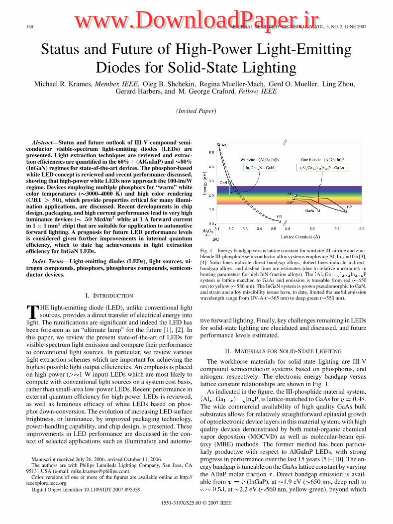
State-of-the-art performance of high-power LEDs versusemission wavelength, shown in Fig. 2, reflect the characteristicsof the III-V material systems as discussed above. Details behindthe data points in Fig. 2 are described in the following sections.
1[Online.] Available: http://www.nichia.com
Fig. 2. State-of-art external quantum efficiencies for high-power visible-spec-trum LEDs (T = 25 C): (1) InGaN TFFC LEDs, 350 mA (this paper); (2)InGaN VTF LED, 1000 mA [42]; (3) InGaN CC LEDs employing patternedsubstrates [35]; and (4) Production performance, AlGaInP TIP LEDs [9], PhilipsLumileds Lighting Co., 350 mA. V (�) is the luminous eye response curve fromCIE. Dashed lines are guides to the eye.
III. CHIP DESIGN AND LIGHT EXTRACTION
A. Basic Principles
Light extraction from LED chips has continued to remain achallenge since their inception several decades ago [27]. Thebasic problem is that photons are generated in III-V crystals withrelatively high optical refractive indices— for AlGaInPand for InGaN. From an imaging optics point of view,brightness conservation alone would demand a reductionin optical power transfer to air. Any non-imaging (e.g., texturingfor light redirection) approach may attempt to overcome thislimitation but must deal with optical loss mechanisms withinthe LED chip, which include impurity or free-carrier absorp-tion, low-bandgap layers, metal contacts, and even reabsorptionin the active layer(s) itself. Another important consideration isthe radiation pattern of light from the active layer, which is oftenneglected in discussions of LED light extraction. For cubic crys-tals like AlGaInP, light generation is equally probable along allthree axis orientations, so random dipole light generation dom-inates and the radiation pattern within the active layer can beconsidered isotropic. For wurtzite InGaN-GaN, this is not thecase; the dipole transition parallel to the -axis is not observed[28]. Thus, the emission pattern is “egg-shaped” with prefer-ential emission along the -axis [see Fig. 5(a)]. This serves toassist in light extraction for -plane InGaN-based LEDs. All ofthese considerations must be taken into account if one is to talkquantitatively about from a first principles approach.
External quantum efficiency may be written
(1)
where is the internal quantum efficiency (ratio of gener-ated photons to electrons injected into the LED contacts), and
is the light extraction efficiency. As written in (1), in-cludes both radiative and injection efficiency terms lumped to-gether. Of course, (1) shows that a measure of gives a lowerbound to . This can be useful in estimating for LEDswherein can be considered close to 100%. We will attempt
Authorized licensed use limited to: IEEE Xplore. Downloaded on May 10,2010 at 19:10:58 UTC from IEEE Xplore. Restrictions apply.
www.DownloadPaper.irwww.DownloadPaper.ir
162 JOURNAL OF DISPLAY TECHNOLOGY, VOL. 3, NO. 2, JUNE 2007
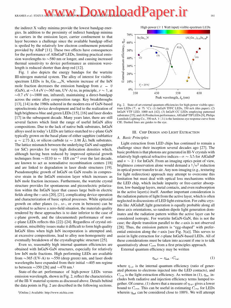
Fig. 3. Common chip designs for AlGaInP LEDs. (a) Thin epilayers on GaAs absorbing substrate (AS). (b) Thick window layer on AS. (c) Thick AS design butincluding distributed Bragg reflector (DBR) above substrate. (d) Thick window layer on transparent substrate (TS). (e) Shaped TS (truncated-inverted-pyramid,TIP, LED shown). (f) Thick window layer on reflective substrate (RS). Consideration of escape cones (shown) allow estimations of extraction efficiencies.
to quantify for state-of-art AlGaInP and InGaN LEDs inSection III-B and III-C, below.
B. III-Phosphide LEDs
Common to all high-efficiency AlGaInP LED design ap-
proaches is the requirement to reduce or (preferably) eliminate
the negative effect of the absorbing GaAs epitaxial growth sub-
strate on light extraction. Several approaches are shown in Fig. 3.
1) Thin AS: The case of thin ( chip width) epilayers on
the GaAs absorbing substrate (AS) provides the lowest light
extraction. The “escape cone” (a useful concept popularized
with the development of AlGaInP LEDs during the 1990s) pro-
vided according to Snell’s Law is governed by a critical angle
of , and being the refractive indices
of the ambient medium and the LED semiconductor, respec-
tively. Photons impinging the semiconductor/ambient interface
at angles beyond are totally internally reflected back into the
chip. In the case of a AS chip, this reflected light is absorbed.
Therefore, light extraction is limited to one escape cone out the
top surface. For isotropic emission from the active layer, and
taking Fresnel reflection into account, one may approximate
(see, for
example, [11, p.184]). Since most LED chips are encapsulated
with epoxy or silicone to improve light extraction, ,
and we may calculate . This is an upper limit, since
unless special measures are taken for current spreading, a large
fraction of light is generated underneath (and thus occluded by)
the Ohmic contact on top of the chip.
2) Thick AS: In this design, a thick, conductive, and trans-
parent window layer is provided atop the device epitaxial
layers. One choice is AlGaAs, provided the AlAs fraction is
high enough for transparency. Since the window layer does not
participate in the minority carrier processes, even metamorphic
epitaxy is allowed as long as defects do not migrate down
into the active region. GaP has in fact become a common
window layer [7]. The window layer serves the dual purpose of
spreading current from the top electrode to the full chip active
area, and also provides for light extraction from “side” escape
cones. In the case of hydride vapor phase epitaxy (HVPE),
very fast growth rates allow window layers exceeding 50 m
in thickness. For typical small-area chip widths of 250 m,
such a window layer thickness provides access to effectively
two (4 1/2) additional escape cones, as implied in the figure.
Thus, we may calculate .
3) Thick AS DBR: In this design, a thick window layer is
accompanied by an epitaxial distributed Bragg reflector (DBR)
stack provided between the active layer and absorbing substrate
[29]. For most AlGaInP LEDs, the active region is too thick to
allow design of resonant structures, so the most one can hope for
is the recovery of the “bottom” escape cone, which would give
. In practice, limited angular/spectral bandwidth of
DBR designs provided by AlGaAs–AlGaAs or AlInGaP–AlInP,
and absorption within the active region, reduce the achievable
extraction efficiency to below this upper limit.
4) Thick TS: In this design, the GaAs substrate is replaced
with a transparent substrate (TS). For example, the GaAs
may be removed by selective wet chemical etching, and the
remaining epitaxial layers bonded to a GaP “host” substrate
at elevated pressure and temperature. Under the correct condi-
tions, an Ohmic interface can be provided between the AlGaInP
epitaxial layers and the GaP host substrate [8]. Now all four
side cones are available and, depending on the reflectivity of
the bottom-side metallization, the bottom cone as well. So,
20%–24% are estimated.
Unlike the previous cases, light within a TS chip which does
not extract upon “first or second pass” at the semiconductor/air
interface, still has a chance for escape upon further passes pro-
vided there is low residual optical loss, and the chip geometry
Authorized licensed use limited to: IEEE Xplore. Downloaded on May 10,2010 at 19:10:58 UTC from IEEE Xplore. Restrictions apply.
www.DownloadPaper.irwww.DownloadPaper.ir
KRAMES et al.: STATUS AND FUTURE OF HIGH-POWER LEDs FOR SOLID-STATE LIGHTING 163
is ergodic or there are optical scattering mechanisms provided
to re-orient the light. Indeed, peak external quantum efficiencies
as high as 40% are measured (data not shown) in TS LEDs im-
proved by reduction of internal optical loss mechanisms.
5) Shaped TS: In the case of a TS device, the option of
shaping the transparent material around the active layer pro-
vided a lever arm for increasing light extraction. One example
is the case of a hemispherical dome surrounding a smaller ac-
tive layer area. A suitable design can ensure that most generated
light will satisfy criteria for escape, but cost and other prac-
tical considerations have limited the impact of such designs.
Another shape is the compound parabolic concentrator (CPC)
which can be used to collimate all generated light to within
an escape cone. Again, practicality prevents implementation of
the full structure. However, a related design is the truncated-in-
verted-pyramid (TIP) structure which has demonstrated peak
external quantum efficiencies of 60% [9]. This chip struc-
ture is currently utilized in commercially available high-power
LEDs,2 and is behind the AlGaInP data points in Fig. 2. Junc-
tion area, , is mm . The TIP LED design is
shown in Fig. 3(e), where extraction of rays outside the escape
cones for rectangular parallelepiped geometries are possible, as
illustrated.
6) Thick RS: This idea is an alternative to the TS approach, in
which semiconductor-semiconductor wafer bonding is replaced
with metallized wafer bonding in order to provide a “reflec-
tive substrate” (RS). The metal-bonded substrate is typically
chosen for thermal expansion coefficient matching and to mini-
mize thermal resistance. GaAs, Ge, and Si are common choices.
In order to approach extraction efficiencies as high as for a TS
LED, means for light extraction must be incorporated into the
lifted-off epitaxial film. One approach is to texture the top sur-
face of the LED for light randomization so that “multiple pass”
light may eventually escape the device. In addition, high reflec-
tivity on the LED side of the metallized wafer bond is important.
Light extraction from such devices may be modeled by consid-
ering a “photon gas” within the semiconductor chip, with para-
sitic optical loss dominating the light extraction efficiency [30].
The RS structure has also been combined with shaping, by
providing very small partitions of active regions which are sur-
rounded by “micro-reflectors” [10]. This combination of micro-
shaping and top surface texturing provides reasonably high ex-
traction efficiency, as evidenced by peak external quantum effi-
ciencies reaching 50% [31]. This performance is still below that
of the TIP LEDs. However, one advantage of the RS approach is
that light emission is predominantly from the top surface, which
simplifies package design and reduces optical source size, or
étendue.
Evolution of for AlGaInP LEDs, based on the preceding
discussion, is shown in Fig. 7. The final limit for in these
devices has likely not been reached, but improvement well be-
yond the current state-of-art will be a challenge due to the very
high refractive index and certain inherent optical losses. The rel-
atively thick active regions required for sufficient minority car-
rier electron confinement cause built-in optical loss [32], and
complicate the design of advanced structures such as resonant-
2[Online.] Available: http://www.philipslumileds.com
cavity and photonic-crystal LEDs. Furthermore, internal effi-
ciencies well below 100% at operating temperatures limit the
positive impact of photon recycling.
C. III–Nitride LEDs
Device design for III–nitride LEDs depends critically on the
substrate technology. In the case of SiC, which is both trans-
parent and conductive, the Thick TS and Shaped TS approaches
described above are viable, with the latter exhibiting as
high as 47% for small-area low-current, 455-nm LEDs [33].
For the case of sapphire, the electrically insulating substrate
requires new designs, with the main approaches summarized
in Fig. 4.
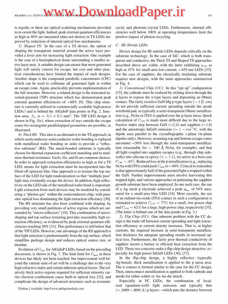
1) Conventional Chip (CC): In this “epi up” configuration
[15], the cathode must be realized by etching down through the
p layers to expose the n-type layers and depositing an Ohmic
contact. The fairly resistive GaN:Mg p-type layers 1 cm
do not provide sufficient current spreading outside the anode
wirebond pad, so typically a semi-transparent Ohmic metalliza-
tion (e.g., NiAu or ITO) is applied over the p-layer mesa. Quick
calculation of is made more difficult due to the large re-
fractive index step between GaN ( 2.4) and sapphire ( 1.8)
and the anisotropic InGaN emission , with the
dipole axes parallel to the crystallographic -plane (in-plane
dipoles only). However, assuming top and bottom escape cones
encounter 50% loss through the semi-transparent metalliza-
tion (reasonable for 100 NiAu, for example), and that
all light coupled into sapphire escapes (e.g., through chip side-
walls) into silicone or epoxy , we arrive at a best-case
. Reduced loss at the p metallization (e.g., replacing
NiAu with ITO) could push to 40%. Critical to remember
is that approximately half of the generated light is trapped within
the GaN. Further improvements must involve harvesting this
trapped light, and various approaches in patterning the sapphire
growth substrate have been employed. In one such case, the use
of a Ag mesh p electrode achieved a peak of 54% mea-
sured for a small-area blue LED [34]. More recently, the use
of an indium-tin-oxide (ITO) contact in such a configuration is
estimated to achieve 77 for a small, low-power chip
and 62 for a large, high-power chip, respectively [35].
(The latter is behind one of the data points in Fig. 2.)
2) Flip Chip (FC): One inherent problem with the CC de-
sign is the trade-off between current spreading and light extrac-
tion efficiency as current density increases. That is, at higher
currents, the required increase in semi-transparent metalliza-
tion thickness for adequate spreading results in increased op-
tical loss. Furthermore, the fairly poor thermal conductivity of
sapphire inserts a barrier to efficient heat extraction from the
LED. These two concerns make a flip-chip design attractive, es-
pecially for high-power InGaN LEDs [36], [37].
In the flip-chip design, a highly reflective (typically
Ag-based), thick metallization is applied to the p mesa area.
The n contact is formed similar to the case for the CC design.
Then, interconnect metallization is applied to both cathode and
anode for either solder or Au-Au die attach.
Especially in FC LEDs, the combination of local-
ized (quantum-well) light emission and typically thin
p layers—which puts the distance between
Authorized licensed use limited to: IEEE Xplore. Downloaded on May 10,2010 at 19:10:58 UTC from IEEE Xplore. Restrictions apply.
www.DownloadPaper.irwww.DownloadPaper.ir
164 JOURNAL OF DISPLAY TECHNOLOGY, VOL. 3, NO. 2, JUNE 2007
Fig. 4. Common chip designs for sapphire-based InGaN-GaN LEDs:. (a) “Epi-up” conventional chip (CC) with semi-transparent top p contact. (b) Flip-chip (FC)with reflective p contact. (c) Vertical-injection thin-film (VTF) bonded to reflective metal on host substrate. (d) Thin-film flip-chip (TFFC). Both thin-film designsprovide access to the GaN surface for incorporation of light extraction features such as texturing or micro-optics.
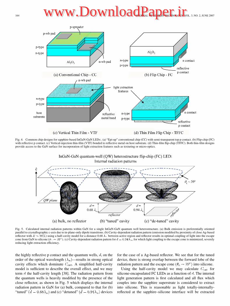
Fig. 5. Calculated internal radiation patterns within GaN for a single InGaN-GaN quantum well heterostructure. (a) Bulk emission is preferentially orientedparallel to crystallographic c-axis due to in-plane-only dipole transitions. (b) Cavity-dependent radiation pattern (emission modified by proximity of close Ag-basedreflector with R � 90%) using a half-cavity model for a distance 0.68 � between active region and reflector results in optimal coupling of light into the escapecone from GaN to silicone (� � 39 ). (c) Cavity-dependent radiation pattern for d = 0:94� , for which light coupling to the escape cone is minimized, severelyreducing light extraction efficiency.
the highly reflective p contact and the quantum wells, , on the
order of the optical wavelength —results in strong optical
cavity effects which dominate . A simplified half-cavity
model is sufficient to describe the overall effect, and we may
term the half-cavity length [38]. The radiation pattern from
the quantum wells is heavily modified by the presence of the
close reflector, as shown in Fig. 5 which displays the internal
radiation pattern in GaN for (a) bulk, compared to that for (b)
“tuned” and (c) “detuned” devices
for the case of a Ag-based reflector. We see that for the tuned
device, there is strong overlap between the forward lobe of the
radiation pattern and the escape cone into silicone.
Using the half-cavity model we may calculate for
silicone-encapsulated FC LEDs as a function of . The internal
light generation pattern is first calculated and all flux which
couples into the sapphire superstrate is considered to extract
into silicone. This is reasonable as light totally-internally-
reflected at the sapphire–silicone interface will be extracted
Authorized licensed use limited to: IEEE Xplore. Downloaded on May 10,2010 at 19:10:58 UTC from IEEE Xplore. Restrictions apply.
www.DownloadPaper.irwww.DownloadPaper.ir
KRAMES et al.: STATUS AND FUTURE OF HIGH-POWER LEDs FOR SOLID-STATE LIGHTING 165
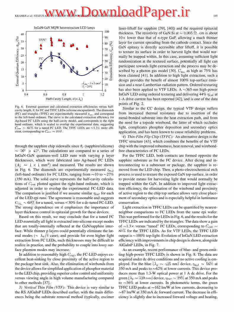
Fig. 6. External quantum and calculated extraction efficiencies versus half-cavity length, d, for FC and TFFC LEDs (silicone encapsulated). The diamonds(FC) and triangles (TFFC) are experimentally measured � and correspondto the left-hand ordinate. The curve is the calculated extraction efficiency forAg-based FC LEDs using the half-cavity model, and corresponds to the righthand ordinate, which is scaled to overlap the experimental data, suggestingC � 60% for a tuned FC LED. The TFFC LEDs are �1.3� more effi-cient, corresponding to C � 80%.
through the sapphire chip sidewalls since (sapphire/silicone)
. The calculations are compared to a series of
InGaN-GaN quantum-well LED runs with varying p layer
thicknesses, which were fabricated into Ag-based FC LEDs
mm and measured. The results are shown
in Fig. 6. The diamonds are experimentally measured
(left-hand ordinate) for FC LEDs, ranging from 10 to 27%
(350 mA). The solid curve represents the half-cavity calcula-
tions of plotted against the right-hand ordinate, which is
adjusted in order to overlap the experimental FC-LED data.
The comparison is justified if we assume similar for each
of the LED epi runs. The agreement is reasonable and suggests
for a tuned, versus 30% for a de-tuned FC-LED.
The strong dependence on emphasizes the importance of
layer thickness control in epitaxial growth for these devices.
Based on this result, we may conclude that for a tuned FC
LED essentially all light is extracted into silicone except modes
that are totally-internally reflected at the GaN/sapphire inter-
face. While thinner p layers could potentially eliminate the lat-
eral modes ( case), and provide for even higher light
extraction from FC LEDs, such thicknesses may be difficult to
realize in practice, and the probability to couple into lossy sur-
face plasmon modes may increase.
In addition to reasonably high , the FC-LED enjoys ex-
cellent heat-sinking by close proximity of the active region to
the package heat sink. Also, the elimination of wirebonds from
the device allows for simplified application of phosphor material
to the LED chip, providing superior color control and uniformity
versus viewing angle in high volume manufacturing compared
to other methods [37].
3) Vertical Thin Film (VTF): This device is very similar to
the RS AlGaInP LEDs described earlier, with the main differ-
ences being the substrate removal method (typically, excimer
laser-liftoff for sapphire [39], [40]) and the required epitaxial
thickness. The resistivity of GaN:Si at cm is about
10 lower than that of n-type GaP, allowing a much thinner
layer for current spreading from the cathode contact. Since the
GaN epitaxy is directly accessible after liftoff, it is possible
to texture its surface in order to harvest light that would nor-
mally be trapped within. In this case, assuming sufficient light
randomization at the textured surface, potentially all light can
participate towards light extraction and the process may be de-
scribed by a photon gas model [30]. as high as 75% has
been claimed [41]. In addition to high light extraction, such a
design provides the benefit of almost 100% top-surface emis-
sion and a near-Lambertian radiation pattern. Ordered texturing
has also been applied to VTF LEDs. A 365-nm high-power
InGaN LED using ordered texturing and delivering 44% at
1-A drive current has been reported [42], and is one of the data
points of Fig. 2.
Similar to the CC design, the typical VTF design suffers
from increased thermal resistance due to insertion of the
metal-bonded substrate into the heat extraction path, and from
the need for a topside wirebond, the latter of which occludes
light, complicates phosphor deposition and secondary optics
application, and has been known to cause reliability problems.
4) Thin-Film Flip Chip (TFFC): An alternative design is the
TFFC structure [43], which combines the benefits of the VTF
chip with the improved robustness, heat removal, and wirebond-
free characteristics of FC LEDs.
For the TFFC LED, both contacts are formed opposite the
sapphire substrate as for the FC device. After dicing and in-
terconnecting to a submount or package, the sapphire is re-
moved from the LED chip. Then, a photo-electrochemical etch
process is used to texture the exposed GaN top-surface, in order
to provide means for harvesting light that would normally be
trapped within the GaN. In addition to improved light extrac-
tion efficiency, the elimination of the wirebond and proximity
of active region to the chip top surface allows very close place-
ment of secondary optics and is especially helpful in luminance
conservation.
Light extraction in TFFC LEDs can be quantified by nearest-
neighbor comparisons to FC LEDs from the same epi wafer.
This was performed for the LEDs in Fig. 6, and the results for the
TFFC LEDs are indicated by the triangles. The data show a gain
of 1.3 versus “tuned” FC LEDs, corresponding to
for the TFFC LEDs. As for VTF LEDs, the TFFC LED
output is 100% top-light. Evolution of InGaN LED extraction
efficiency with improvements in chip design is shown, alongside
AlGaInP LEDs, in Fig. 7.
As an example, recent performance of blue- and green-emit-
ting high-power TFFC LEDs is shown in Fig. 8. The data are
acquired under dc drive conditions and no active cooling is em-
ployed. For the blue nm device, at
350 mA and peaks to 62% at lower currents. This device pro-
duces more than 1.3-W optical power at 1 A dc drive. For the
green device, at 350 mA and peaks
to 36% at lower currents. In photometric terms, the green
TFFC LED peaks at 162 lm/W at low currents, decreasing to
87 lm/W at 350 mA dc forward current. The decrease in effi-
ciency is slightly due to increased forward voltage and heating,
Authorized licensed use limited to: IEEE Xplore. Downloaded on May 10,2010 at 19:10:58 UTC from IEEE Xplore. Restrictions apply.
www.DownloadPaper.irwww.DownloadPaper.ir
166 JOURNAL OF DISPLAY TECHNOLOGY, VOL. 3, NO. 2, JUNE 2007
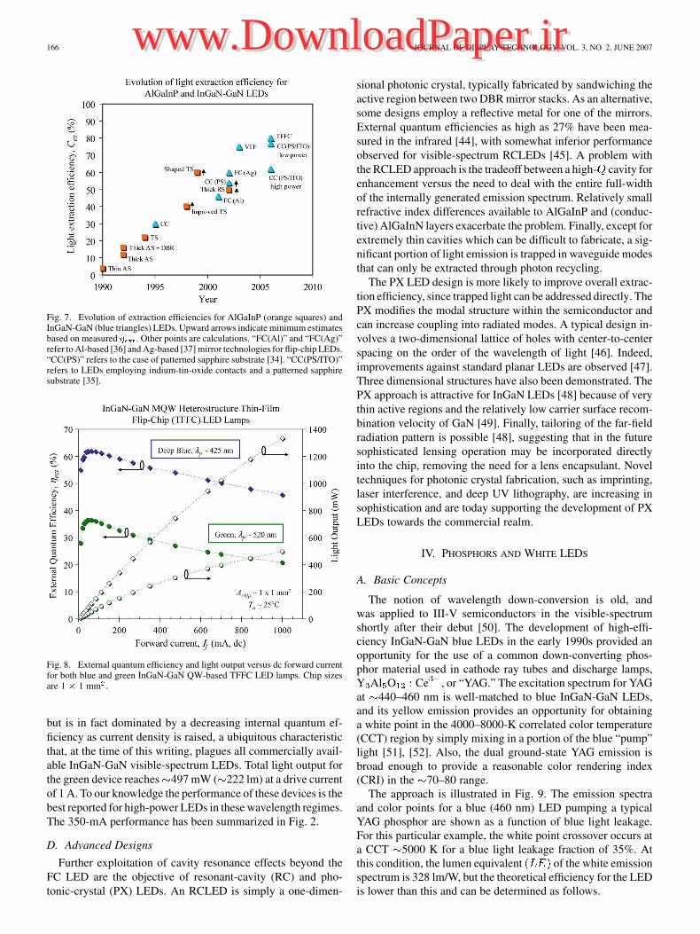
Fig. 7. Evolution of extraction efficiencies for AlGaInP (orange squares) andInGaN-GaN (blue triangles) LEDs. Upward arrows indicate minimum estimatesbased on measured � . Other points are calculations. “FC(Al)” and “FC(Ag)”refer to Al-based [36] and Ag-based [37] mirror technologies for flip-chip LEDs.“CC(PS)” refers to the case of patterned sapphire substrate [34]. “CC(PS/ITO)”refers to LEDs employing indium-tin-oxide contacts and a patterned sapphiresubstrate [35].
Fig. 8. External quantum efficiency and light output versus dc forward currentfor both blue and green InGaN-GaN QW-based TFFC LED lamps. Chip sizesare 1 � 1 mm .
but is in fact dominated by a decreasing internal quantum ef-
ficiency as current density is raised, a ubiquitous characteristic
that, at the time of this writing, plagues all commercially avail-
able InGaN-GaN visible-spectrum LEDs. Total light output for
the green device reaches 497 mW ( 222 lm) at a drive current
of 1 A. To our knowledge the performance of these devices is the
best reported for high-power LEDs in these wavelength regimes.
The 350-mA performance has been summarized in Fig. 2.
D. Advanced Designs
Further exploitation of cavity resonance effects beyond the
FC LED are the objective of resonant-cavity (RC) and pho-
tonic-crystal (PX) LEDs. An RCLED is simply a one-dimen-
sional photonic crystal, typically fabricated by sandwiching the
active region between two DBR mirror stacks. As an alternative,
some designs employ a reflective metal for one of the mirrors.
External quantum efficiencies as high as 27% have been mea-
sured in the infrared [44], with somewhat inferior performance
observed for visible-spectrum RCLEDs [45]. A problem with
the RCLED approach is the tradeoff between a high- cavity for
enhancement versus the need to deal with the entire full-width
of the internally generated emission spectrum. Relatively small
refractive index differences available to AlGaInP and (conduc-
tive) AlGaInN layers exacerbate the problem. Finally, except for
extremely thin cavities which can be difficult to fabricate, a sig-
nificant portion of light emission is trapped in waveguide modes
that can only be extracted through photon recycling.
The PX LED design is more likely to improve overall extrac-
tion efficiency, since trapped light can be addressed directly. The
PX modifies the modal structure within the semiconductor and
can increase coupling into radiated modes. A typical design in-
volves a two-dimensional lattice of holes with center-to-center
spacing on the order of the wavelength of light [46]. Indeed,
improvements against standard planar LEDs are observed [47].
Three dimensional structures have also been demonstrated. The
PX approach is attractive for InGaN LEDs [48] because of very
thin active regions and the relatively low carrier surface recom-
bination velocity of GaN [49]. Finally, tailoring of the far-field
radiation pattern is possible [48], suggesting that in the future
sophisticated lensing operation may be incorporated directly
into the chip, removing the need for a lens encapsulant. Novel
techniques for photonic crystal fabrication, such as imprinting,
laser interference, and deep UV lithography, are increasing in
sophistication and are today supporting the development of PX
LEDs towards the commercial realm.
IV. PHOSPHORS AND WHITE LEDS
A. Basic Concepts
The notion of wavelength down-conversion is old, andwas applied to III-V semiconductors in the visible-spectrumshortly after their debut [50]. The development of high-effi-ciency InGaN-GaN blue LEDs in the early 1990s provided anopportunity for the use of a common down-converting phos-phor material used in cathode ray tubes and discharge lamps,Y Al O Ce , or “YAG.” The excitation spectrum for YAGat 440–460 nm is well-matched to blue InGaN-GaN LEDs,and its yellow emission provides an opportunity for obtaininga white point in the 4000–8000-K correlated color temperature(CCT) region by simply mixing in a portion of the blue “pump”light [51], [52]. Also, the dual ground-state YAG emission isbroad enough to provide a reasonable color rendering index(CRI) in the 70–80 range.
The approach is illustrated in Fig. 9. The emission spectraand color points for a blue (460 nm) LED pumping a typicalYAG phosphor are shown as a function of blue light leakage.For this particular example, the white point crossover occurs ata CCT 5000 K for a blue light leakage fraction of 35%. Atthis condition, the lumen equivalent of the white emissionspectrum is 328 lm/W, but the theoretical efficiency for the LEDis lower than this and can be determined as follows.
Authorized licensed use limited to: IEEE Xplore. Downloaded on May 10,2010 at 19:10:58 UTC from IEEE Xplore. Restrictions apply.
www.DownloadPaper.irwww.DownloadPaper.ir
KRAMES et al.: STATUS AND FUTURE OF HIGH-POWER LEDs FOR SOLID-STATE LIGHTING 167
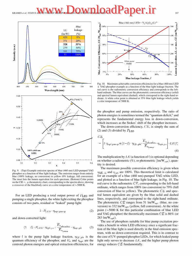
Fig. 9. (Top) Example emission spectra of blue (460 nm) LED-pumped YAGphosphor as a function of blue light leakage. The emission ranges from entirelyblue (100% leakage, no conversion) to yellow (0% leakage, full conversion).The inset lists the lumen equivalent for each spectrum. (Bottom) Color pointson the CIE x; y chromaticity chart, corresponding to the spectra above, showinga crossover of the blackbody curve at a color temperature of �5000 K.
For an LED producing a total output power of andpumping a single phosphor, the white light exiting the phosphorconsists of two parts, residual or “leaked” pump light:
(2)
and down-converted light:
(3)
where is the pump light leakage fraction, is thequantum efficiency of the phosphor, and and are thecentroid photon energies and optical extraction efficiencies, for
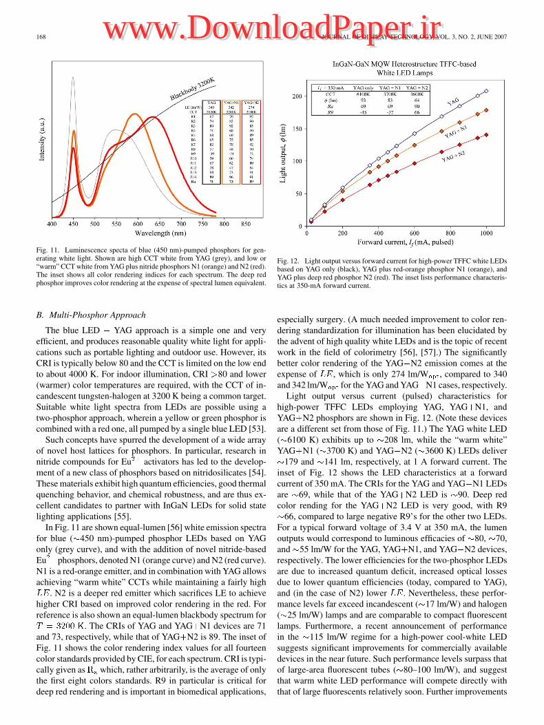
Fig. 10. Maximum achievable conversion efficiencies for a blue (460 nm) LED+ YAG phosphor example as a function of the blue light leakage fraction. Thered curve is the radiometric conversion efficiency and corresponds to the left-hand ordinate. The blue curves are the photometric conversion efficiency (solid)and spectral lumen equivalent (dashed), which correspond to the right-hand or-dinate. A white color point is obtained at 35% blue light leakage which yieldsa color temperature of 5000 K.
the phosphor and pump emission, respectively. The ratio ofphoton energies is sometimes termed the “quantum deficit,” andrepresents the fundamental energy loss in down-conversion,which increases as the Stokes’ shift of the phosphor increases.
The down-conversion efficiency, , is simply the sum of(2) and (3) divided by
(4)
The multiplication by (a function of ) is optional dependingon whether a radiometric (%), or photometric lm/W , quan-tity is desired.
The maximum possible conversion efficiency is given whenand are 100%. This theoretical limit is calculated
for an example of a blue (460 nm)-pumped YAG white LED,and plotted as a function of blue light leakage, in Fig. 10. Thered curve is the radiometric , corresponding to the left-handordinate, which ranges from 100% (no conversion) to 79% (fullconversion of blue to yellow). The photometric and spec-tral lumen equivalent are given by the blue solid and dashedlines, respectively, and correspond to the right-hand ordinate.The photometric ranges from 51 lm/W (blue, no con-version) to 332 lm/W (yellow, full conversion). At the whitepoint ( 5000 K for this particular combination of blue LEDand YAG phosphor) the theoretically maximum is 86% (or283 lm/W ).
The use of phosphors suitable for blue pump excitation pro-vides a benefit in white LED efficiency since a significant frac-tion of the blue light is used directly in the final emission spec-trum, with no down-conversion required. This is in contrast tothe case of UV-pumped phosphor LEDs, for which leaked pumplight only serves to decrease , and the higher pump photonenergy reduces fundamentally.
Authorized licensed use limited to: IEEE Xplore. Downloaded on May 10,2010 at 19:10:58 UTC from IEEE Xplore. Restrictions apply.
www.DownloadPaper.irwww.DownloadPaper.ir
168 JOURNAL OF DISPLAY TECHNOLOGY, VOL. 3, NO. 2, JUNE 2007
Fig. 11. Luminescence specta of blue (450 nm)-pumped phosphors for gen-erating white light. Shown are high CCT white from YAG (grey), and low or“warm” CCT white from YAG plus nitride phosphors N1 (orange) and N2 (red).The inset shows all color rendering indices for each spectrum. The deep redphosphor improves color rendering at the expense of spectral lumen equivalent.
B. Multi-Phosphor Approach
The blue LED YAG approach is a simple one and very
efficient, and produces reasonable quality white light for appli-
cations such as portable lighting and outdoor use. However, its
CRI is typically below 80 and the CCT is limited on the low end
to about 4000 K. For indoor illumination, CRI 80 and lower
(warmer) color temperatures are required, with the CCT of in-
candescent tungsten-halogen at 3200 K being a common target.
Suitable white light spectra from LEDs are possible using a
two-phosphor approach, wherein a yellow or green phosphor is
combined with a red one, all pumped by a single blue LED [53].
Such concepts have spurred the development of a wide array
of novel host lattices for phosphors. In particular, research in
nitride compounds for Eu activators has led to the develop-
ment of a new class of phosphors based on nitridosilicates [54].
These materials exhibit high quantum efficiencies, good thermal
quenching behavior, and chemical robustness, and are thus ex-
cellent candidates to partner with InGaN LEDs for solid state
lighting applications [55].
In Fig. 11 are shown equal-lumen [56] white emission spectra
for blue ( 450 nm)-pumped phosphor LEDs based on YAG
only (grey curve), and with the addition of novel nitride-based
Eu phosphors, denoted N1 (orange curve) and N2 (red curve).
N1 is a red-orange emitter, and in combination with YAG allows
achieving “warm white” CCTs while maintaining a fairly high
. N2 is a deeper red emitter which sacrifices LE to achieve
higher CRI based on improved color rendering in the red. For
reference is also shown an equal-lumen blackbody spectrum for
. The CRIs of YAG and YAG N1 devices are 71
and 73, respectively, while that of YAG N2 is 89. The inset of
Fig. 11 shows the color rendering index values for all fourteen
color standards provided by CIE, for each spectrum. CRI is typi-
cally given as which, rather arbitrarily, is the average of only
the first eight colors standards. R9 in particular is critical for
deep red rendering and is important in biomedical applications,
Fig. 12. Light output versus forward current for high-power TFFC white LEDsbased on YAG only (black), YAG plus red-orange phosphor N1 (orange), andYAG plus deep red phosphor N2 (red). The inset lists performance characteris-tics at 350-mA forward current.
especially surgery. (A much needed improvement to color ren-
dering standardization for illumination has been elucidated by
the advent of high quality white LEDs and is the topic of recent
work in the field of colorimetry [56], [57].) The significantly
better color rendering of the YAG N2 emission comes at the
expense of , which is only 274 lm/W , compared to 340
and 342 lm/W for the YAG and YAG N1 cases, respectively.
Light output versus current (pulsed) characteristics for
high-power TFFC LEDs employing YAG, YAG N1, and
YAG N2 phosphors are shown in Fig. 12. (Note these devices
are a different set from those of Fig. 11.) The YAG white LED
( 6100 K) exhibits up to 208 lm, while the “warm white”
YAG N1 ( 3700 K) and YAG N2 ( 3600 K) LEDs deliver
179 and 141 lm, respectively, at 1 A forward current. The
inset of Fig. 12 shows the LED characteristics at a forward
current of 350 mA. The CRIs for the YAG and YAG N1 LEDs
are 69, while that of the YAG N2 LED is 90. Deep red
color rending for the YAG N2 LED is very good, with R9
66, compared to large negative R9’s for the other two LEDs.
For a typical forward voltage of 3.4 V at 350 mA, the lumen
outputs would correspond to luminous efficacies of 80, 70,
and 55 lm/W for the YAG, YAG N1, and YAG N2 devices,
respectively. The lower efficiencies for the two-phosphor LEDs
are due to increased quantum deficit, increased optical losses
due to lower quantum efficiencies (today, compared to YAG),
and (in the case of N2) lower . Nevertheless, these perfor-
mance levels far exceed incandescent ( 17 lm/W) and halogen
( 25 lm/W) lamps and are comparable to compact fluorescent
lamps. Furthermore, a recent announcement of performance
in the 115 lm/W regime for a high-power cool-white LED
suggests significant improvements for commercially available
devices in the near future. Such performance levels surpass that
of large-area fluorescent tubes ( 80–100 lm/W), and suggest
that warm white LED performance will compete directly with
that of large fluorescents relatively soon. Further improvements
Authorized licensed use limited to: IEEE Xplore. Downloaded on May 10,2010 at 19:10:58 UTC from IEEE Xplore. Restrictions apply.
www.DownloadPaper.irwww.DownloadPaper.ir
KRAMES et al.: STATUS AND FUTURE OF HIGH-POWER LEDs FOR SOLID-STATE LIGHTING 169
Fig. 13. Lumen maintenance curves for high power white LUXEON LEDsat 450 (blue), 700 (magenta), and 885 (green) mA drive in a 35 C ambient.Resulting board temperatures are 65 C, 85 C, and 95 C, respectively. (Datafrom the Lighting Research Center, Rensselaer Polytechnic Institute [60].).
in the quantum efficiencies of red phosphors will accelerate
this. In addition, as described later in Section VII, LED per-
formance can be expected to significantly surpass even these
levels in the future as internal quantum efficiency is increased.
V. RELIABILITY AND PACKAGING
Penetration of the general lighting market by LEDs iscontingent upon reductions in cost (per lm) compared to con-ventional sources. The implied high lumen density mandatespower chips and packages that can handle high power densities
W/cm . Total cost of ownership of a light source in-cludes maintenance (“re-lamping”) and a significant advantageof LEDs is their inherent robustness and promise of long-lifeoperation [58]. However, reliability of the LED “lamp” is notguaranteed, especially at the high power densities necessary forhigh lumen output per package (i.e., minimum $ per lm). Tothis end, specially designed power LED packages have beendeveloped in recent years. The first one [59]—LUXEON—wasintroduced in 1998 and has become a benchmark standard inthe solid state lighting industry. Recent reliability data fromthe Lighting Research Center at the Rensselaer PolytechnicInstitute, which benchmarks commercial LED performance,are shown in Fig. 13 [60]. The three curves correspond towhite LUXEON III LEDs with drive current levels of 450,700 (rated), and 885 mA which produce board temperatures of65 C, 85 C, and 95 C, respectively, under 35 C ambientconditions. At 3500 hrs, the lumen depreciation is 5%, 10%,and 15%, respectively. Typical end-of-life for incandescent andfluorescent lamps are 2000 and 10 000–16 000 h, respec-tively. Note that most reliability issues with high power LEDstend to be package, and not chip, related. In particular, organiccomponents (glues, encapsulants, etc.) have a difficult timeunder the combination of high heat C and extremephoto fluence W/cm . This is especially true in the caseof high photon energy blue light, and poses an even greaterchallenge for UV LEDs.
Recent improvements in high power packaging for LEDsare highlighted in the LUXEON K2 package released in 2006,which is shown schematically (right) in Fig. 14 alongside itspredecessor (left). The improvements in base material andattach technologies provide a package that can allow 150 C(white) or higher (185 C, non-white) junction temperatureoperation with forward currents up to 1.5 A dc, which is 50%
higher than its predecessor. This increase in useful flux froma single device serves as a benchmark for the further push ofsolid-state lighting into the mainstream.
VI. SELECTED APPLICATIONS
A. Automotive Forward Lighting
Many lighting applications are based on imaging optics andfor these applications source brightness is a critical parametersince it determines the size (cost) of the optical system necessaryto direct the light for the required application. Source brightnesscan be described in terms either radiometric,
radiance (5)
or photometric,
luminance (6)
where is the source output flux in Watts, is the same inlumens, and is the source étendue, defined by
(7)
where is the refractive index for the source distribution,is the source area, and is polar angle with respect to theoptical axis. For planar surface emitters, (7) reduces to
. For a uniform, Lambertian source distribution,flux and luminance (or radiance) is constant regardlessof viewing angle. In this case the luminance of an emittingsurface is simply
Lambertian (8)
To estimate the luminance of an arbitrary LED design, wemay use (8) to sum over all emitting surfaces of an LED, whichindividually are assumed to provide Lambertian light output.Recasting the flux in terms related to LED performance, we have
LED (9)
where is the average emitted photon energy [in electronvolts (eV)], is the forward current density, is the areaof the active region, the summation in the denominator repre-sents the total surface area of the LED, and the other terms areas described previously. Equation (9) shows that luminance isincreased when and are increased, and when the totalsurface area of the LED is minimized to match the active re-gion area. Also, it is clearly detrimental to embed the chip ina high-index encapsulant, which magnifies the source size andincreases étendue, decreasing luminance.
Equation (9) was used to calculate luminance for LEDs ofvarious III-V materials systems and chip designs over the lastfew decades and the results are plotted in Fig. 15 along withthe effective luminances of conventional light sources: tubefluorescents, automotive halogen, automotive Xe high-intensitydischarge (HID), and ultra-high-performance (UHP) dischargelamp used in projection applications. The LED data pointsare color-coded corresponding to emission wavelength: red,
Authorized licensed use limited to: IEEE Xplore. Downloaded on May 10,2010 at 19:10:58 UTC from IEEE Xplore. Restrictions apply.
www.DownloadPaper.irwww.DownloadPaper.ir
170 JOURNAL OF DISPLAY TECHNOLOGY, VOL. 3, NO. 2, JUNE 2007
Fig. 14. High power LED “lamp” packages used in solid-state lighting applications. (a) LUXEON circa 1998. (b) LUXEON K2 circa 2006.
Fig. 15. Luminance evolution of LEDs compared to conventional light sources.LED data points are color coded corresponding to emission wavelength. Rangesrequired for various applications are shown to the right of the chart. Dashed linesare guides to the eye for luminance evolution of early red, and more recent powerLEDs, respectively. TFFC LED performance is indicated by the triangular datapoint. Luminance of the (120 W) UHP lamp is 300 Mcd/m , corresponding tounfiltered, collected flux of 4500 lm within 15 mm � sr, an étendue typical formicro-display projection [61].
green, blue, or white. Early LED progress (red dashed line)was largely given by improvements to due to improvedmaterial systems and better chip designs for light extraction.The more recent, rapid improvement for power LEDs (blackdashed line) comprises increased performance in , but isaugmented by increases in (allowed by more sophisticatedLED packaging technology) and improved LED chip designfor high luminance. For example, the point at 50 Mcd/m forwhite is given by an all-top-emitting TFFC blue LED coatedwith YAG phosphor, but not lens encapsulated. We note thatat this performance level, LEDs are suitable for automotiveforward lighting and projection display applications, withthose required luminance ranges shown at right of the chart inFig. 15. Moreover, continued progress at this rate would see
LEDs reach 300 Mcd/m , matching the effective luminanceof an unfiltered UHP lamp, by 2010.
The availability of very high brightness white LEDs willallow the replacement of conventional automotive “headlamps.”A side-by-side comparison of flux and brightness characteristicsfor a white TFFC LED versus that of conventional “low-beam”automotive halogen and Xe HID lamps is shown in Fig. 16.The useful flux is provided by the average luminance of thesource, measured by a radiant imaging system. The particularTFFC LED measured gives 50 Mcd/m at 1 A drive, comparedto 20–30 and 60–80 Mcd/m for halogen and HID lamps, re-spectively. The 1 1 mm TFFC LED provides 120 lm at aninput power of 3.6 W. Early prototyping of automotive forwardlighting systems suggest light utilization to reach 60%–80%,compared to 25%–40% for the conventional lamps. This sug-gests that halogen (55 W) and HID (35 W) lamps could bereplaced by as few as 3–7 ( 12–28 W), and 6–11 ( 24–44 W),LEDs, respectively. The use of LEDs in forward lighting notonly allows a more compact auto headlamp design but offersother benefits such as integrated high-/low-beam functionality.The precisely defined emitting area creates the potential forsharper far-field radiation patterns, which improve visibilitywhile reducing glare for on-coming traffic. Finally, selectiveuse of down-converting phosphors offers flexible tailoring ofthe spectral content of the LED headlamp beam.
B. Illumination
No doubt the most popular application in discussion of LEDsis that of general illumination. One of the most appealing op-portunities is a reduction in worldwide energy consumption byreplacing incandescent lamps (now) and fluorescent tubes (fu-ture) with LED-based luminaires. Commercially available highpower white LEDs, which at the time of this writing operate inthe 70-lm/W regime, require less than 1/4th the energy of in-candescent lamps. Furthermore, the small source size and welldefined position of LEDs improves the light utilization (as dis-cussed above) in a practical luminaire, putting light only where
Authorized licensed use limited to: IEEE Xplore. Downloaded on May 10,2010 at 19:10:58 UTC from IEEE Xplore. Restrictions apply.
www.DownloadPaper.irwww.DownloadPaper.ir
KRAMES et al.: STATUS AND FUTURE OF HIGH-POWER LEDs FOR SOLID-STATE LIGHTING 171
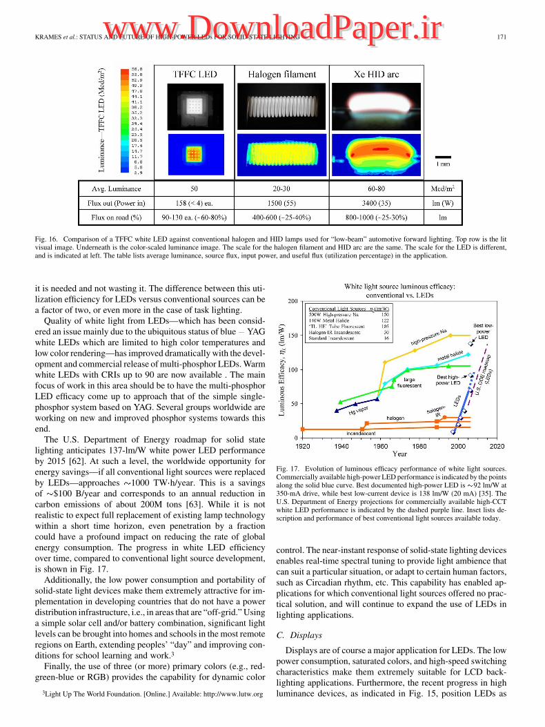
Fig. 16. Comparison of a TFFC white LED against conventional halogen and HID lamps used for “low-beam” automotive forward lighting. Top row is the litvisual image. Underneath is the color-scaled luminance image. The scale for the halogen filament and HID arc are the same. The scale for the LED is different,and is indicated at left. The table lists average luminance, source flux, input power, and useful flux (utilization percentage) in the application.
it is needed and not wasting it. The difference between this uti-lization efficiency for LEDs versus conventional sources can bea factor of two, or even more in the case of task lighting.
Quality of white light from LEDs—which has been consid-ered an issue mainly due to the ubiquitous status of blue YAGwhite LEDs which are limited to high color temperatures andlow color rendering—has improved dramatically with the devel-opment and commercial release of multi-phosphor LEDs. Warmwhite LEDs with CRIs up to 90 are now available . The mainfocus of work in this area should be to have the multi-phosphorLED efficacy come up to approach that of the simple single-phosphor system based on YAG. Several groups worldwide areworking on new and improved phosphor systems towards thisend.
The U.S. Department of Energy roadmap for solid statelighting anticipates 137-lm/W white power LED performanceby 2015 [62]. At such a level, the worldwide opportunity forenergy savings—if all conventional light sources were replacedby LEDs—approaches 1000 TW h/year. This is a savingsof $100 B/year and corresponds to an annual reduction incarbon emissions of about 200M tons [63]. While it is notrealistic to expect full replacement of existing lamp technologywithin a short time horizon, even penetration by a fractioncould have a profound impact on reducing the rate of globalenergy consumption. The progress in white LED efficiencyover time, compared to conventional light source development,is shown in Fig. 17.
Additionally, the low power consumption and portability ofsolid-state light devices make them extremely attractive for im-plementation in developing countries that do not have a powerdistribution infrastructure, i.e., in areas that are “off-grid.” Usinga simple solar cell and/or battery combination, significant lightlevels can be brought into homes and schools in the most remoteregions on Earth, extending peoples’ “day” and improving con-ditions for school learning and work.3
Finally, the use of three (or more) primary colors (e.g., red-green-blue or RGB) provides the capability for dynamic color
3Light Up The World Foundation. [Online.] Available: http://www.lutw.org
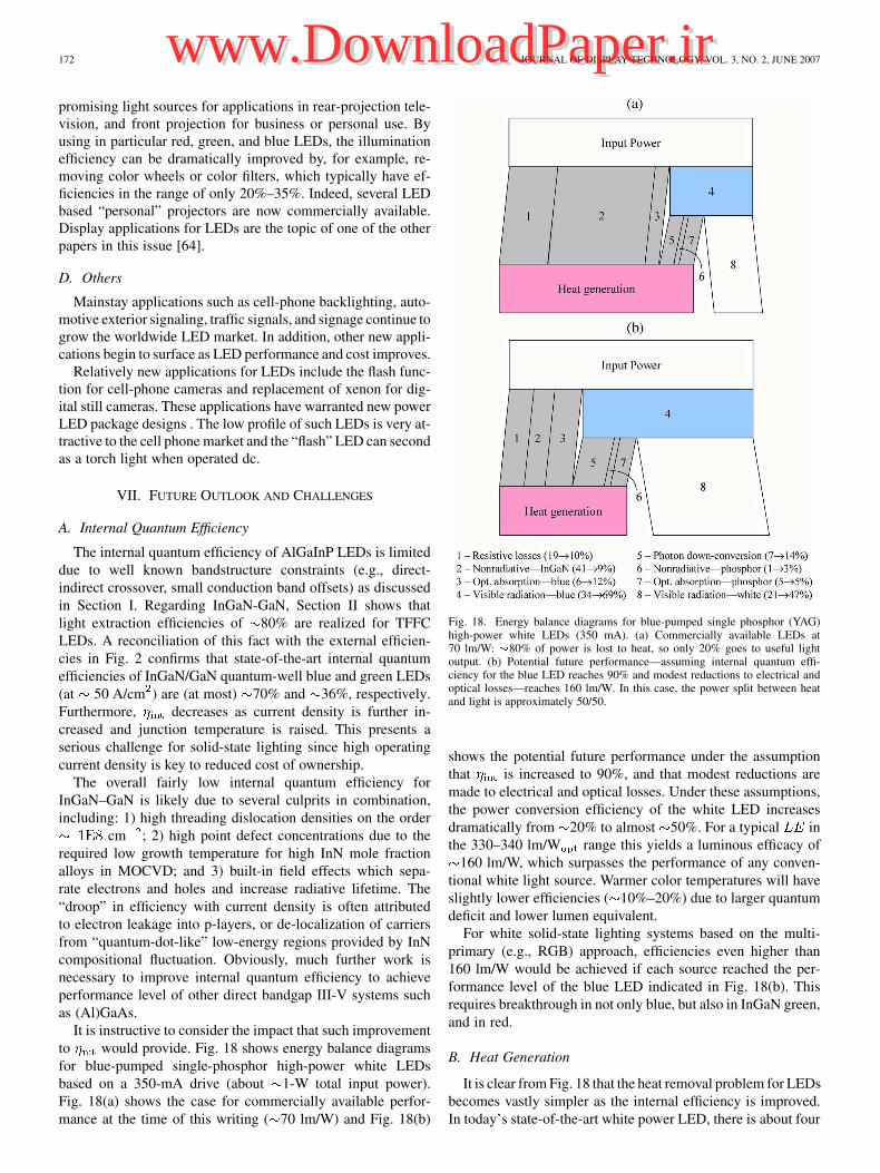
Fig. 17. Evolution of luminous efficacy performance of white light sources.Commercially available high-power LED performance is indicated by the pointsalong the solid blue curve. Best documented high-power LED is �92 lm/W at350-mA drive, while best low-current device is 138 lm/W (20 mA) [35]. TheU.S. Department of Energy projections for commercially available high-CCTwhite LED performance is indicated by the dashed purple line. Inset lists de-scription and performance of best conventional light sources available today.
control. The near-instant response of solid-state lighting devicesenables real-time spectral tuning to provide light ambience thatcan suit a particular situation, or adapt to certain human factors,such as Circadian rhythm, etc. This capability has enabled ap-plications for which conventional light sources offered no prac-tical solution, and will continue to expand the use of LEDs inlighting applications.
C. Displays
Displays are of course a major application for LEDs. The lowpower consumption, saturated colors, and high-speed switchingcharacteristics make them extremely suitable for LCD back-lighting applications. Furthermore, the recent progress in highluminance devices, as indicated in Fig. 15, position LEDs as
Authorized licensed use limited to: IEEE Xplore. Downloaded on May 10,2010 at 19:10:58 UTC from IEEE Xplore. Restrictions apply.
www.DownloadPaper.irwww.DownloadPaper.ir
172 JOURNAL OF DISPLAY TECHNOLOGY, VOL. 3, NO. 2, JUNE 2007
promising light sources for applications in rear-projection tele-vision, and front projection for business or personal use. Byusing in particular red, green, and blue LEDs, the illuminationefficiency can be dramatically improved by, for example, re-moving color wheels or color filters, which typically have ef-ficiencies in the range of only 20%–35%. Indeed, several LEDbased “personal” projectors are now commercially available.Display applications for LEDs are the topic of one of the otherpapers in this issue [64].
D. Others
Mainstay applications such as cell-phone backlighting, auto-motive exterior signaling, traffic signals, and signage continue togrow the worldwide LED market. In addition, other new appli-cations begin to surface as LED performance and cost improves.
Relatively new applications for LEDs include the flash func-tion for cell-phone cameras and replacement of xenon for dig-ital still cameras. These applications have warranted new powerLED package designs . The low profile of such LEDs is very at-tractive to the cell phone market and the “flash” LED can secondas a torch light when operated dc.
VII. FUTURE OUTLOOK AND CHALLENGES
A. Internal Quantum Efficiency
The internal quantum efficiency of AlGaInP LEDs is limited
due to well known bandstructure constraints (e.g., direct-
indirect crossover, small conduction band offsets) as discussed
in Section I. Regarding InGaN-GaN, Section II shows that
light extraction efficiencies of 80% are realized for TFFC
LEDs. A reconciliation of this fact with the external efficien-
cies in Fig. 2 confirms that state-of-the-art internal quantum
efficiencies of InGaN/GaN quantum-well blue and green LEDs
(at 50 A/cm ) are (at most) 70% and 36%, respectively.
Furthermore, decreases as current density is further in-
creased and junction temperature is raised. This presents a
serious challenge for solid-state lighting since high operating
current density is key to reduced cost of ownership.
The overall fairly low internal quantum efficiency for
InGaN–GaN is likely due to several culprits in combination,
including: 1) high threading dislocation densities on the order
cm ; 2) high point defect concentrations due to the
required low growth temperature for high InN mole fraction
alloys in MOCVD; and 3) built-in field effects which sepa-
rate electrons and holes and increase radiative lifetime. The
“droop” in efficiency with current density is often attributed
to electron leakage into p-layers, or de-localization of carriers
from “quantum-dot-like” low-energy regions provided by InN
compositional fluctuation. Obviously, much further work is
necessary to improve internal quantum efficiency to achieve
performance level of other direct bandgap III-V systems such
as (Al)GaAs.
It is instructive to consider the impact that such improvement
to would provide. Fig. 18 shows energy balance diagrams
for blue-pumped single-phosphor high-power white LEDs
based on a 350-mA drive (about 1-W total input power).
Fig. 18(a) shows the case for commercially available perfor-
mance at the time of this writing ( 70 lm/W) and Fig. 18(b)
Fig. 18. Energy balance diagrams for blue-pumped single phosphor (YAG)high-power white LEDs (350 mA). (a) Commercially available LEDs at70 lm/W: �80% of power is lost to heat, so only 20% goes to useful lightoutput. (b) Potential future performance—assuming internal quantum effi-ciency for the blue LED reaches 90% and modest reductions to electrical andoptical losses—reaches 160 lm/W. In this case, the power split between heatand light is approximately 50/50.
shows the potential future performance under the assumption
that is increased to 90%, and that modest reductions are
made to electrical and optical losses. Under these assumptions,
the power conversion efficiency of the white LED increases
dramatically from 20% to almost 50%. For a typical in
the 330–340 lm/W range this yields a luminous efficacy of
160 lm/W, which surpasses the performance of any conven-
tional white light source. Warmer color temperatures will have
slightly lower efficiencies ( 10%–20%) due to larger quantum
deficit and lower lumen equivalent.
For white solid-state lighting systems based on the multi-
primary (e.g., RGB) approach, efficiencies even higher than
160 lm/W would be achieved if each source reached the per-
formance level of the blue LED indicated in Fig. 18(b). This
requires breakthrough in not only blue, but also in InGaN green,
and in red.
B. Heat Generation
It is clear from Fig. 18 that the heat removal problem for LEDs
becomes vastly simpler as the internal efficiency is improved.
In today’s state-of-the-art white power LED, there is about four
Authorized licensed use limited to: IEEE Xplore. Downloaded on May 10,2010 at 19:10:58 UTC from IEEE Xplore. Restrictions apply.
www.DownloadPaper.irwww.DownloadPaper.ir
KRAMES et al.: STATUS AND FUTURE OF HIGH-POWER LEDs FOR SOLID-STATE LIGHTING 173
times more heat generated than light, whereas for the future case
the amount of heat generation reduces to be about the same as the
light generation. For the former, a single 1000-lm emitter would
have to dissipate roughly 12 W of heat in one package. In the
small form factors desired for solid-state lighting, it is difficult
to imagine dissipating this much heat without resorting to active
cooling, which would serve to increase complexity and cost of
the solid-state lighting system. In the future case, only 3 W of
heat would need to be removed, which in fact is already well
within the scope of today’s high power LED packages.
Even so, for applications using the multi-primary (e.g., RGB)
approach, provision must be made for colors at wavelengths
550 nm, presumably the domain of AlGaInP LEDs. At junc-
tion temperatures above 100 C, the efficiency of these LEDs
suffers significantly in comparison to InGaN-based LEDs.
Breakthroughs in AlGaInP LED temperature dependence,
which appears to be fundamentally related to bandstructure,
are not readily anticipated. A nitride-based solution for red
currently does not exist and, rather curiously, has not been the
subject of strong interest in the scientific community until very
recently. As InGaN-GaN efficiency, especially in the green,
continues to improve, the “red problem” will present a greater
and greater challenge (opportunity).
C. Cost Considerations
As for heat generation, cost considerations closely track ef-ficiency. As efficiency and drive current increase, the total lu-mens per emitter increases, reducing the initial cost of light inaddition to providing energy savings. Today’s standard house-hold incandescent bulbs generate 1000 lm (60 W) and initialcost is $1 for the end user. The operating cost, assuming $0.1per kW h, over the useful life of the bulb ( 2000 h) is $12,which far outweighs the initial cost of the light source. The op-erating cost of today’s best high-power LEDs is $3 over thesame time period. However, at the current level of 100 lmper LED, the initial cost of a 1000 lm solid-state light source
10 3 30 presents a significantbarrier to the customer. To compete adequately against initialcost, a single 1000-lm LED is warranted. If internal quantumefficiency for InGaN-GaN can reach its potential (i.e., for phos-phor-based down-conversion: 160 lm/W for cool white,and 130–150 lm/W for warm white), a single power LEDat 6–8 W input drive should achieve this. In addition, a pricescenario of $1 for this single 1000–l m light source is not un-reasonable in the foreseeable future. This is in contrast to thecase for small, low-current LEDs, which are heavily package-and assembly-cost loaded at such high lumen output levels. At1000 lm per $1, LEDs become attractive even on initial costs,and significant penetration of the general lighting market is in-evitable since maintenance and energy savings significantly re-duce the total cost of ownership versus incandescent or fluores-cent (esp. compact) solutions.
VIII. CONCLUSION
The status of LEDs for solid-state lighting applications has
been presented. The AlGaInP (red to yellow) and InGaN-GaN
(blue to green) material systems dominate the field and so-
phisticated device structures based on these material systems
result in light extraction efficiencies of 60% and 80%, for
AlGaInP and InGaN-GaN, respectively. At the time of this
writing, commercially available high-power white LEDs based
on phosphor down-conversion provide luminous efficacies of
70 lm/W. Recent laboratory results suggest devices in the
100-lm/W regime will be available soon, surpassing both
incandescents and compact fluorescent lamps, and competing
directly with large fluorescent performance. Moreover, recent
improvements in LED luminance place them brighter than
halogen filaments, making LEDs attractive for use in automo-
tive headlamps for the first time. The challenge for solid-state
lighting now is clearly in internal quantum efficiency, which for
the InGaN-GaN and AlGaInP (at operating temperatures) is far
below what has been achieved in other III-V systems such as
(Al)GaAs. Breakthroughs in internal quantum efficiency would
result in high-power phosphor-white LEDs with efficiencies
reaching 160 lm/W or more, a performance level surpassing
anything known to date for a practical white light source.
ACKNOWLEDGMENT
The authors would like to acknowledge several colleagueswhose efforts made this paper possible. Many thanks to S. Bier-huizen, H. Choy, W. Daschner, J. Epler, N. Gardner, W. Goetz,P. Grillot, M. Holcomb, A. Kim, J. Kmetec, T. Margalith,P. Martin, M. Misra, G. Mueller, A. Munkholm, Y.-C. Shen,D. Steigerwald, F. Steranka, R. Steward, D. Sun, T. Trot-tier, S. Watanabe, S. West, J. Wierer, and L. Zhou of PhilipsLumileds Lighting Company, San Jose, CA; M. Haverlag,H. Nikol, M. van Rijswick, and J. Schug of Philips Lighting,Eindhoven, the Netherlands; P. Schmidt and D. Wiechert ofPhilips Research, Aachen, Germany.
REFERENCES
[1] N. Holonyak, Jr., “Is the light emitting diode (LED) an ultimate lamp?,”Am. J. Phys., vol. 68, pp. 864–866, 2000.
[2] M. G. Craford, N. Holonyak, Jr., and F. A. Kish, Jr., “In pursuit of theultimate lamp,” Scientific Amer., pp. 83–88, Feb. 2001.
[3] I. Vurgaftman and J. R. Meyer, “Band parameters for III-V com-pound semiconductors and their alloys,” J. Appl. Phys., vol. 89, pp.5815–5875, 2001.
[4] K. M. Yu et al., “On the crystalline structure, stoichiometry and bandgap of InN thin films,” Appl. Phys. Lett., vol. 86, p. 071910, 2005.
[5] C. P. Kuo et al., “High performance AlGaInP visible light-emittingdiodes,” Appl. Phys. Lett., vol. 57, pp. 2937–2939, 1990.
[6] H. Sugawara, M. Ishikawa, and G. Hatakoshi, “High-efficiency In-GaAlP/GaAs visible light-emitting diodes,” Appl. Phys. Lett., vol. 58,pp. 1010–1012, 1991.
[7] K. H. Huang et al., “Twofold efficiency improvement in high perfor-mance AlGaInP light-emitting diodes in the 555–620 nm spectral re-gion using a thick GaP window layer,” Appl. Phys. Lett., vol. 61, pp.1045–1047, 1992.
[8] F. A. Kish et al., “Very high-efficiency semiconductor wafer-bondedtransparent-substrate (Al Ga ) In P=GaP light-emittingdiodes,” Appl. Phys. Lett., vol. 64, pp. 2839–2841, 1994.
[9] M. R. Krames et al., “High-power truncated-inverted-pyramid(Al Ga ) In P=GaP light-emitting diodes exhibiting >50%external quantum efficiency,” Appl. Phys. Lett., vol. 75, pp. 2365–2367,1999.
[10] K. Streubel, N. Linder, R. Wirth, and A. Jaeger, “High brightness Al-GaInP light-emitting diodes,” IEEE J. Sel. Topics Quantum Electron.,vol. 8, no. 2, pp. 321–332, Mar. 2002.
[11] F. A. Kish and R. M. Fletcher, “AlGaInP light-emitting diodes,” inSemiconductors and Semimetals, G. Stringfellow and M. G. Craford,Eds. San Diego, CA: Academic, 1997, vol. 48, pp. 149–226.
[12] D. P. Bour, D. W. Treat, R. L. Thornton, R. S. Geels, and D. F. Welch,“Drift leakage current in AlGaInP quantum-well lasers,” IEEE J.
Quantum Electron., vol. 29, no. 5, pp. 1337–1343, May 1993.
Authorized licensed use limited to: IEEE Xplore. Downloaded on May 10,2010 at 19:10:58 UTC from IEEE Xplore. Restrictions apply.
www.DownloadPaper.irwww.DownloadPaper.ir
174 JOURNAL OF DISPLAY TECHNOLOGY, VOL. 3, NO. 2, JUNE 2007
[13] H. Amano, N. Sawaki, I. Akasaki, and Y. Toyoda, “Metalorganic vaporphase epitaxial growth of a high quality GaN film using an AlN bufferlayer,” Appl. Phys. Lett., vol. 48, pp. 353–355, 1986.
[14] H. Amano, M. Kito, K. Hiramatsu, and I. Akasaki, “P-type conductionin Mg-doped GaN treated with low-energy electron beam irradiation(LEEBI),” Jpn. J. Appl. Phys., vol. 28, pp. L2112–L2114, 1989.
[15] S. Nakamura, M. Senoh, and T. Mukai, “High-power InGaN/GaNdouble-heterostructure violet light emitting diodes,” Appl. Phys. Lett.,vol. 62, pp. 2390–2392, 1993.
[16] S. Nakamura, M. Senoh, N. Iwasa, and S.-I. Nagahama, “High-powerInGaN single-quantum-well-structure blue and violet light-emittingdiodes,” Appl. Phys. Lett., vol. 67, pp. 1868–1870, 1995.
[17] S. Nakamura, M. Senoh, S. Nagahama, N. Iwasa, T. Yamada, T. Mat-sushita, H. Kiyoku, and Y. Sugimoto, “InGaN-based multi-quantum-well-structure laser diodes,” Jpn. J. Appl. Phys., vol. 35, pp. L74–L76,1996.
[18] S. J. Rosner, E. C. Carr, M. J. Ludowise, G. Girolami, and H. I. Erikson,“Correlation of cathodoluminescence inhomogeneity with microstruc-tural defects in epitaxial GaN grown by metalorganic chemical-vapordeposition,” Appl. Phys. Lett., vol. 70, pp. 420–422, 1997.
[19] S. Nakamura, “The roles of structural imperfections in InGaN-basedblue light-emitting diodes and laser diodes,” Science, vol. 14, pp.956–961, 1998.
[20] F. Bernardini, V. Fiorentini, and D. Vanderbilt, “Spontaneous polar-ization and piezoelectric constants of III-V nitrides,” Phys. Rev. B, vol.56, pp. R10024–R10027, 1997.
[21] T. Takeuchi et al., “Determination of piezoelectric fields in strainedGaInN quantum wells using the quantum-confined Stark effect,” Appl.
Phys. Lett., vol. 73, pp. 1691–1693, 1998.[22] N. F. Gardner, J. C. Kim, J. J. Wierer, Y.-C. Shen, and M. R. Krames,
“Polarization anisotropy in the electroluminescence of m-planeInGaN-GaN multiple-quantum-well light-emitting diodes,” Appl.
Phys. Lett., vol. 86, p. 111101, 2005.[23] R. Sharma et al., “Demonstration of a semipolar (10-1-3) InGaN/GaN
green light emitting diode,” Appl. Phys. Lett., vol. 87, p. 231110, 2005.[24] M. Funato et al., “Blue, green, and amber InGaN/GaN light-emitting
diodes on semipolar {11–22} GaN bulk substrates,” Jpn. J. Appl. Phys.,vol. 45, pp. L650–L662, 2006.
[25] N. A. El-Masry, E. L. Piner, S. X. Liu, and S. M. Bedair, “Phase sep-aration in InGaN grown by metalorganic chemical vapor deposition,”Appl. Phys. Lett., vol. 72, pp. 40–42, 1998.
[26] K. Iida et al., “350.9 nm UV laser diode grown on low-dislocation-density AlGaN,” Jpn. J. Appl. Phys., vol. 43, pp. L499–L500, 2004.
[27] W. B. Joyce, R. Z. Bachrach, R. W. Dixon, and D. A. Sealer, “Geomet-rical properties of random particles and the extraction of photons fromelectroluminescent diodes,” J. Appl. Phys., vol. 45, pp. 2229–2253,1974.
[28] G. O. Mueller, Philips Lumileds Lighting Co., San Jose, CA, data, un-published.
[29] H. Sugawara, K. Itaya, H. Nozaki, and G. Hatakoshi, “High-brightnessInGaAlP green light-emitting diodes,” Appl. Phys. Lett., vol. 61, pp.1775–1777, 1992.
[30] I. Schnitzer and E. Yablonovitch, “30% external quantum efficiencyfrom surface textured, thin-film light-emitting diodes,” Appl. Phys.
Lett., vol. 63, pp. 2174–2176, 1993.[31] K. Streubel, Osram Opto Semiconductors, Regensburg, Germany, Jul.
2006, private communication.[32] N. F. Gardner, H. C. Chui, E. I. Chen, M. R. Krames, J.-W. Huang, F.
A. Kish, S. A. Stockman, C. P. Kocot, T. S. Tan, and N. Moll, “1.4� ef-ficiency improvement in transparent-substrate (Al Ga ) In Plight-emitting diodes with thin (� 2000�A) active regions,” Appl. Phys.
Lett., vol. 74, pp. 2230–2232, 1999.[33] J. Edmond et al., “High efficiency GaN-based LEDs and lasers on SiC,”
J. Crystal Growth, vol. 272, pp. 242–250, 2004.[34] M. Yamada et al., “InGaN-based near-ultraviolet and blue-light-emit-
ting diodes with high external quantum efficiency using a patternedsapphire substrate and a mesh electrode,” Jpn. J. Appl. Phys., vol. 41,pp. L1431–L1433, 2002.
[35] Y. Narukawa et al., “Ultra-high efficiency white light-emitting diodes,”Jpn. J. Appl. Phys., vol. 45, pp. L1084–L1086, 2006.
[36] J. J. Wierer et al., “High-power AlGaInN flip-chip light-emittingdiodes,” Appl. Phys. Lett., vol. 78, pp. 3379–3381, 2001.
[37] D. A. Steigerwald et al., “Illumination with solid state lighting tech-nology,” IEEE J. Sel. Topics Quant. Electron., vol. 8, pp. 310–320, 2002.
[38] Y.-C. Shen et al., “Optical cavity effects in InGaN/GaN quantum-well-heterostructure flip-chip light-emitting diodes,” Appl. Phys. Lett., vol.82, pp. 2221–2223, 2003.
[39] M. K. Kelly, O. Ambacher, R. Dimitrov, R. Handschuh, and M. Stutz-mann, “Optical process for liftoff of group III-nitride films,” Phys. Stat.
Sol. (A), vol. 159, pp. R3–R4, 1997.[40] W. S. Wong, T. Sands, and N. W. Cheung, “Damage-free separation
of GaN thin films from sapphire substrates,” Appl. Phys. Lett., vol. 72,pp. 599–601, 1998.
[41] V. Haerle et al., “High brightness LEDs for general lighting applica-tions using the new ThinGaN technology,” Phys. Stat. Sol. (A), vol. 201,pp. 2736–2739, 2004.
[42] D. Morita et al., “Watt-class high-output-power 365 nm ultravioletlight-emitting diodes,” Jpn. J. Appl. Phys., vol. 43, pp. 5945–5950,2004.
[43] O. B. Shchekin et al., “High performance thin-film flip-chipInGaN-GaN light-emitting diodes,” Appl. Phys. Lett., vol. 89, p.071109, 2006.
[44] J. J. Wierer, D. A. Kellogg, and N. Holonyak, Jr., “Tunnel contact junc-tion native-oxide aperture and mirror vertical-cavity surface-emittinglasers and resonant-cavity light-emitting diodes,” Appl. Phys. Lett., vol.74, pp. 926–928, 1999.
[45] R. Joray, R. P. Stanley, and M. Ilegems, “High efficiency planarMCLEDs,” Phys. Stat. Sol. (B), vol. 242, pp. 2315–2325, 2005.
[46] S. Fan, P. R. Villeneuve, J. D. Joannopoulos, and E. F. Schubert, “Highextraction efficiency of spontaneous emission from slabs of photoniccrystals,” Phy. Rev. Lett., vol. 78, pp. 3294–3297, 1997.
[47] M. Rattier et al., “Toward ultrahigh-efficiency aluminum oxide mi-crocavity light-emitting diodes: Guided mode extraction by photoniccrystals,” IEEE J. Select. Top. Quant. Electron., vol. 8, pp. 238–247,2002.
[48] J. J. Wierer et al., “InGaN/GaN quantum-well-heterostructure light-emitting diodes employing photonic crystal structures,” Appl. Phys.
Lett., vol. 84, pp. 3885–3887, 2004.[49] M. Boroditsky et al., “Surface recombination measurements on III-V
candidate materials for nanostructure light-emitting diodes,” J. Appl.
Phys., vol. 87, pp. 3497–3504, 2000.[50] G. E. Stillman, M. D. Sirkis, J. A. Rossi, M. R. Johnson, and N.
Holonyak, Jr., “Volume excitation of an ultrathin single-code CdSelaser,” Appl. Phys. Lett., vol. 9, pp. 268–269, 1966.
[51] P. Schlotter, R. Schmidt, and J. Schneider, “Luminescence conversionof blue light emitting diodes,” Appl. Phys. A, vol. 64, pp. 417–418,1997.
[52] S. Nakamura and G. Fasol, The Blue Laser Diode. Berlin, Germany:Springer, 1997, pp. 216–219.
[53] R. Mueller-Mach, G. O. Mueller, M. R. Krames, and T. Trottier, “High-power phosphor-converted light-emitting diodes based on III-nitrides,”IEEE J. Select. Top. Quant. Electron., vol. 8, pp. 339–345, 2002.
[54] H. A. Höppe, H. Lutz, P. Morys, W. Schick, and A. Seilmeier,“Luminescence in Eu -doped Ba Si N : Fluorescence, thermolu-minescence, and upconversion,” J. Phys. Chem. Solids, vol. 61, pp.2001–2006, 2000.
[55] R. Mueller-Mach et al., “Highly efficient all-nitride phosphor-con-verted white light emitting diode,” Phys. Stat. Sol. (A), vol. 202, pp.1727–1732, 2005.
[56] G. O. Mueller, R. Mueller-Mach, and M. R. Krames, “Proposal for anew metric on the illumination quality of light,” in LRO Symp. on Light
and Color, 2005.[57] W. Davis and Y. Ohno, “Toward an improved color rendering metric,”
in Proc. SPIE, 2005, vol. 5941, pp. 283–290.[58] P. N. Grillot, M. R. Krames, H. Zhao, and S.-H. Teoh, “Sixty thousand
hour light output reliability of AlGaInP light emitting diodes,” IEEE
Trans. Dev. Mater. Rel., submitted for publication.[59] G. E. Höfler, C. Carter-Coman, M. R. Krames, N. F. Gardner, F. A.
Kish, T. S. Tan, B. Loh, J. Posselt, D. Collins, and G. Sasser, “High-flux, high-efficiency transparent-substrate AlGaInP/GaP light-emittingdiodes,” Electron. Lett., vol. 34, pp. 1781–1782, 1998.
[60] N. Narendran, Rensselaer Polytechnic Institute, Troy, NY, Troy, NY,Jul. 2006, private communication.
[61] G. Derra, “UHP lamp systems for projection applications,” J. Phys. D:
Appl. Phys., vol. 38, pp. 1995–3110, 2005.[62] “Solid-State Lighting Research and Development Portfolio,” 2006, p.
48, prepared for U.S. Dep. of Energy.[63] R. Haitz, F. Kish, J. Tsao, and J. Nelson, “The case for a national re-
search program on semiconductor lighting,” presented at the Optoelec-tronics Industry Development Association, Washington, D.C., 1999,unpublished.
[64] G. Harbers, S. Bierhuizen, and M. R. Krames, “Performance ofhigh power light-emitting diodes in display applications,” J. Display
Technol., no. 2, Jun. 2007.
Authorized licensed use limited to: IEEE Xplore. Downloaded on May 10,2010 at 19:10:58 UTC from IEEE Xplore. Restrictions apply.
www.DownloadPaper.irwww.DownloadPaper.ir

KRAMES et al.: STATUS AND FUTURE OF HIGH-POWER LEDs FOR SOLID-STATE LIGHTING 175
Michael R. Krames (M’86) was born in Irving, TX, on March 17, 1967. He re-ceived the B.S. degree in electrical engineering from the University of Texas atAustin, in 1989, and the M.S. and Ph.D. degrees in electrical engineering fromthe University of Illinois at Urbana-Champaign, in 1992 and 1995, respectively.His Ph.D. dissertation work was completed in the Solid State Devices Labora-tory, where he developed native-oxide based optoelectronic devices, includinglaser diodes and waveguides, in the InGaAsP–InP and AlGaAs–GaAs materialsystems.
After graduation, he joined Hewlett-Packard Optoelectronics Division as aresearch engineer developing high-power visible-spectrum LEDs based on theAlGaInP material system. He then transitioned to research on light-emitting de-vices based on the III-nitride material system, and is currently manager of Ad-vanced Laboratories for Philips Lumileds Lighting Company, San Jose, CA.There his research focuses upon advanced III-nitride and III-phosphide epitaxyand chip technology, luminescent materials for down-conversion, and novel dis-play concepts for solid-state lighting applications.
Oleg B. Shchekin was born in Odessa, Ukraine, on May 12, 1975. He receivedthe B.S. degree in physics, and the M.S. and Ph.D. in electrical engineering fromthe University of Texas at Austin, TX, in 1997, 1999, and 2003 respectively. HisPh.D. work focused on crystal growth and physics of long-wavelength GaAs-based quantum-dot lasers.
After his doctorate, he served in the position of senior process engineer atOrganicID, Inc., focusing on performance, physics and manufacturing of inte-grated circuits based on thin-film organic semiconductor transistors. In 2005,he joined Advanced Laboratories at Philips Lumileds Lighting Company, SanJose, CA, as a staff scientist. His work is focused on novel designs and physicsof light emitting diodes. He has authored and coauthored 34 scientific journalpublication and more than 40 conference presentation.
Dr. Shchekin’s work has been recognized by the 2002 Electronic MaterialsConference (EMC) Best Student Paper and the 2003 University of Texas BenStreetman Prize for his contributions to the development of long-wavelengthquantum-dot lasers.
Regina Mueller-Mach received the diploma in physics and the Dr.rer.nat. de-gree, in 1971, from Humboldt University, Berlin, Germany. She worked in re-search institutes of Academy of Sciences in Berlin on phosphors and opto-electronics and earned her habilitation (Dr.sc.nat.) in 1985 from Academy ofSciences. She was awarded the Gustaf-Hertz-Price for her electroluminescencework in 1986.
After this academic career she was hired into Hewlett Packard Laboratories,Palo Alto, CA, in 1994 as an expert in thin-film electroluminescence. There, andlater on, in Agilent Laboratories (1998) she concentrated her efforts on mate-rials science and especially on phosphors. She was spearheading the concept ofphosphor converted LEDs while at Agilent Laboratories, and joined Lumileds in2000. She currently manages the Luminescence Laboratory of Advanced Labo-ratories at Philips Lumileds Lighting in San Jose, CA, and runs the R&D workon phosphor-converted LEDs.
Gerd O. Mueller received the diploma in physics and the Dr.rer.nat. degree,in 1961, from Humboldt University, Berlin, Germany. He worked in semicon-ductor research at Academy of Sciences in Berlin, received his habilitation(Dr.sc.nat) from Humboldt University in 1972 and was appointed Professor ofSolid State Physics at Academy of Sciences.
After the academic career in Germany, which was mainly dedicated to solidstate physics, and some time of world-wide consulting, he joined HewlettPackard Laboratories, Palo Alto, CA, in 1994, Agilent Laboratories in 1998,and worked on aspects of electroluminescence and cathodoluminescencefor various applications. He joined Lumileds in 2000 and works now in theAdvanced Laboratories of Philips Lumileds Lighting on optical and semicon-ductor problems in connection with solid-state lighting.
Dr. Mueller is a member of the Editorial Board of physica status solidi.
Ling Zhou was born in Beijing, China, and received the Ph.D. degree in elec-tronic materials from the University of Illinois at Urbana-Champaign in 2002,where he investigated MBE growth of cubic GaN and device processing forIII-nitride-based HEMT and HBTs.
Following graduation, he joined Lumileds Lighting, LLC, San Jose, CA,working on deep ultraviolet light-emitting diodes, for which he received an“Outstanding Performer” award from the Defense Advanced Research ProjectsAgency, U.S. Department of Defense, in 2003. He is now a Senior Scientist inthe Advanced Laboratories at Philips Lumileds Lighting Company.
Gerard Harbers was born in the Netherlands. He received the M.S. degreein applied physics from the Twente University of Technology, Enschede, TheNetherlands, in 1985.
After military services, he joined Philips Research Laboratories, Eindhoven,the Netherlands, in 1986, as research scientist, where he developed various op-tical test and measuring techniques in the field of interferometric and Schlierentest systems. In 1996, he joined Philips Lighting Central Development LightingLaboratories as group manager of the optics group, where he worked on illumi-nation systems, including various LED projects. He joined Lumileds LightingLighting Company, Best the Netherlands, in 1999, and later moved to LumiledsLighting Lighting Company, San Jose, CA, in 2001. Within Philips Lumileds,he has been working on various display illumination projects, initially focusedon backlighting, but later also on projection.
M. George Craford (F’00) received the Ph.D. degree in physics from the Uni-versity of Illinois in 1967.
He began his professional career as a research physicist at Monsanto Chem-ical Company. He advanced to the level of Technical Director of the ElectronicsDivision, before joining the Hewlett Packard Company in 1979. He is currentlythe Chief Technology Officer of Philips LumiLeds Lighting Company. His re-search has been mainly focused on the development of visible LEDs using avariety of compound semiconductor materials. He developed nitrogen-dopedGaAsP technology in the early 1970’s, which became one of the dominant com-mercial LED technologies. At Hewlett Packard, his group pioneered the devel-opment of AlInGaP LED’s, and has developed AlGaAs and InGaN products.
Dr. Craford is a member of the National Academy of Engineering. He hasreceived technical achievement awards from a variety of organizations and re-ceived the 2002 National Medal of Technology from the President of the UnitedStates.
Authorized licensed use limited to: IEEE Xplore. Downloaded on May 10,2010 at 19:10:58 UTC from IEEE Xplore. Restrictions apply.
www.DownloadPaper.irwww.DownloadPaper.ir


![IJCBS RESEARCH PAPER VOL. 1 [ISSUE 3] JUNE, 2014 ISSN:-2349–2724 Light Emitting Diodes (LEDs) Reduce Vertimec, Resistance in Tetranychus urticae (Koch](https://static.fdokumen.com/doc/165x107/631ba468a906b217b9069031/ijcbs-research-paper-vol-1-issue-3-june-2014-issn-23492724-light-emitting.jpg)


![Highly Air‐Stable Thieno [3, 2‐b] thiophene‐Thiophene‐Thiazolo [5, 4‐d] thiazole‐Based Polymers for Light‐Emitting Diodes](https://static.fdokumen.com/doc/165x107/63314f6cc1adb6fc8c0f4a46/highly-airstable-thieno-3-2b-thiophenethiophenethiazolo-5-4d.jpg)

