On the electrostatic potential profile in biased molecular wires
Upload
independentCategory
view
5download
0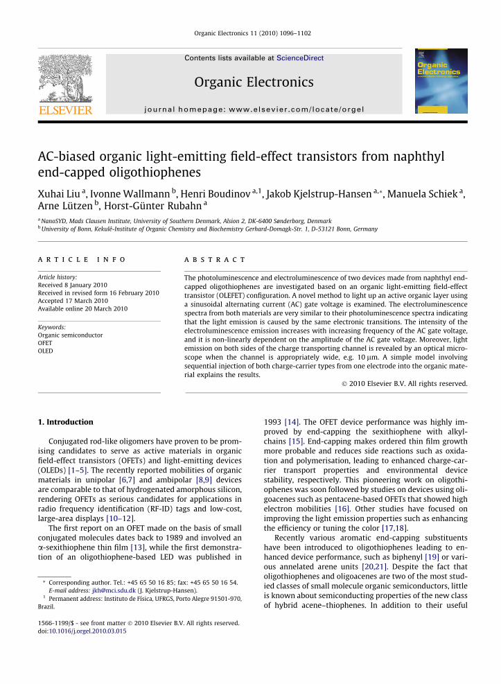
Organic Electronics 11 (2010) 1096–1102
Contents lists available at ScienceDirect
Organic Electronics
journal homepage: www.elsevier .com/locate /orgel
AC-biased organic light-emitting field-effect transistors from naphthylend-capped oligothiophenes
Xuhai Liu a, Ivonne Wallmann b, Henri Boudinov a,1, Jakob Kjelstrup-Hansen a,*, Manuela Schiek a,Arne Lützen b, Horst-Günter Rubahn a
a NanoSYD, Mads Clausen Institute, University of Southern Denmark, Alsion 2, DK-6400 Sønderborg, Denmarkb University of Bonn, Kekulé-Institute of Organic Chemistry and Biochemistry Gerhard-Domagk-Str. 1, D-53121 Bonn, Germany
a r t i c l e i n f o a b s t r a c t
Article history:Received 8 January 2010Received in revised form 16 February 2010Accepted 17 March 2010Available online 20 March 2010
Keywords:Organic semiconductorOFETOLED
1566-1199/$ - see front matter � 2010 Elsevier B.Vdoi:10.1016/j.orgel.2010.03.015
* Corresponding author. Tel.: +45 65 50 16 85; faE-mail address: [email protected] (J. Kjelstrup-Han
1 Permanent address: Instituto de Física, UFRGS, PoBrazil.
The photoluminescence and electroluminescence of two devices made from naphthyl end-capped oligothiophenes are investigated based on an organic light-emitting field-effecttransistor (OLEFET) configuration. A novel method to light up an active organic layer usinga sinusoidal alternating current (AC) gate voltage is examined. The electroluminescencespectra from both materials are very similar to their photoluminescence spectra indicatingthat the light emission is caused by the same electronic transitions. The intensity of theelectroluminescence emission increases with increasing frequency of the AC gate voltage,and it is non-linearly dependent on the amplitude of the AC gate voltage. Moreover, lightemission on both sides of the charge transporting channel is revealed by an optical micro-scope when the channel is appropriately wide, e.g. 10 lm. A simple model involvingsequential injection of both charge-carrier types from one electrode into the organic mate-rial explains the results.
� 2010 Elsevier B.V. All rights reserved.
1. Introduction
Conjugated rod-like oligomers have proven to be prom-ising candidates to serve as active materials in organicfield-effect transistors (OFETs) and light-emitting devices(OLEDs) [1–5]. The recently reported mobilities of organicmaterials in unipolar [6,7] and ambipolar [8,9] devicesare comparable to that of hydrogenated amorphous silicon,rendering OFETs as serious candidates for applications inradio frequency identification (RF-ID) tags and low-cost,large-area displays [10–12].
The first report on an OFET made on the basis of smallconjugated molecules dates back to 1989 and involved ana-sexithiophene thin film [13], while the first demonstra-tion of an oligothiophene-based LED was published in
. All rights reserved.
x: +45 65 50 16 54.sen).
rto Alegre 91501-970,
1993 [14]. The OFET device performance was highly im-proved by end-capping the sexithiophene with alkyl-chains [15]. End-capping makes ordered thin film growthmore probable and reduces side reactions such as oxida-tion and polymerisation, leading to enhanced charge-car-rier transport properties and environmental devicestability, respectively. This pioneering work on oligothi-ophenes was soon followed by studies on devices using oli-goacenes such as pentacene-based OFETs that showed highelectron mobilities [16]. Other studies have focused onimproving the light emission properties such as enhancingthe efficiency or tuning the color [17,18].
Recently various aromatic end-capping substituentshave been introduced to oligothiophenes leading to en-hanced device performance, such as biphenyl [19] or vari-ous annelated arene units [20,21]. Despite the fact thatoligothiophenes and oligoacenes are two of the most stud-ied classes of small molecule organic semiconductors, littleis known about semiconducting properties of the new classof hybrid acene–thiophenes. In addition to their useful

Scheme 1. Synthesis of naphthyl end-capped thiophenes NaT and NaT2.
X. Liu et al. / Organic Electronics 11 (2010) 1096–1102 1097
semiconducting properties, oligothiophene-based mole-cules can also self-assemble into crystalline nanoaggre-gates under special growth conditions [22], which couldfurther increase their application potential in future, nano-scale optoelectronic devices.
In addition to OFETs and OLEDs, the organic light-emit-ting field-effect transistor (OLEFET) is an excellent plat-form to investigate charge transport and light-emittingmechanisms of organic materials. Moreover, the combina-tion of current modulation and light emission in OLEFETsmake them interesting for display applications since thenumber of components could be reduced compared tothe traditional design with an LED and a driver transistor.However, unipolar devices with bottom contact configura-tion operated by direct current (DC) voltages at the gatecontact suffer from weak light emission, which in additionis restricted to the vicinity of the contact with the highestenergy barrier for charge-carrier injection [3,23]. Thesedrawbacks are mainly due to (a) the necessity to injectholes and electrons simultaneously and (b) to the differentmobilities of those species. They can be overcome by a no-vel operating method, in which an alternating electric fieldis used to sequentially inject holes and electrons [24]. Here,we report on the electroluminescence properties of twonovel naphthyl end-capped (bi)thiophenes (NaT andNaT2) examined in an AC-biased OLEFET geometry. We ob-serve electroluminescence from both compounds evenwhen only one of the source–drain electrodes is biased rel-ative to the gate electrode; the other electrode floating. Theobservation of light emission in this configuration, whichbasically corresponds to a metal–insulator–semiconductordiode, shows that a single injecting electrode is sufficientto produce clear electroluminescence that can be modu-lated by the applied gate voltage amplitude and/orfrequency.
2. Experimental
2.1. Materials synthesis
Scheme 1 depicts the synthesis of the two naphthyl-end-capped (bi)thiophenes, 5,5-bis(naphthyl)-2,20-bithi-ophene (NaT2) and 2,5-bis(naphthyl)-thiophene (NaT).Actually, the synthesis of NaT2 has been achieved beforeusing a Stille cross-coupling approach [21], while NaT hasonly been part of some recent patents [25]. Recently, wewere able to employ Suzuki cross-coupling protocols forthe synthesis of oligophenylenes and oligothiophenephen-ylenes similar to NaT and NaT2 thereby avoiding toxicorganotin compounds [26]. Thus, we decided to make useof this strategy here, too.
Solvents were dried, distilled and stored under argonaccording to standard procedures. 2-Bromonaphthylbo-ronic acid, 2,5-dibromothiophene, and 5,50-dibromo-2,20-bithiophene were purchased from commercial sourcesand used as received. Reactions were performed under anargon atmosphere in oven-dried glassware using standardSchlenk techniques. Thin-layer chromatography was per-formed on aluminum TLC plates (silica gel 60 F254) fromMerck and the products were visualized under UV-light
(254 or 366 nm). Products were purified by sublimationunder ultra-high-vacuum.
Mass spectra were recorded on a Finnigan MAT-95XL.UV/Vis spectra were measured on a Jena Analytic Specord200 spectrometer in a 1 cm quartz cuvette. Fluorescencespectra were taken on an Aminco Bowman AB2 spectrom-eter in a 1 cm quartz cuvette. Elemental analyses were car-ried out with a Heraeus Vario EL.
2.1.1. NaTA two-neck flask equipped with a condenser was
charged with 2,5-dibromothiophene (1.5 g, 6.20 mmol),2-naphtylboronic acid (2.24 g, 13.02 mmol), K2CO3
(2.57 g, 18.6 mmol) and [Pd(PPh3]4 (358 mg, 0.31 mmol,5 mol%). A mixture of toluene, MeOH and water (60/30/3 mL) was added and the reaction mixture was refluxedfor 50 h. After the mixture was allowed to cool down toroom temperature the precipitate was collected andwashed with toluene, CH2Cl2, and H2O (2 � 80 mL each).The crude product was sublimed in ultra-high-vacuum(5.4 � 10�7 mbar, 296 �C (sand bath temperature)) to give1.75 g (84%) of the desired product.
UV–vis (CH2Cl2): kmax = 282, 352 nm; fluorescence(CH2Cl2): kmax = 399, 420 nm; MS (EI): m/z (%): 336.1(100) [M]�+, 168.0 (15) [M]2+; HRMS (EI, m/z): [M]�+ calcdfor C24H16S, 336.0969; found: 336.0977. Anal. calcd forC24H16S�1/5H2O: C, 84.77; H, 4.86; S, 9.43; found: C,84.74; H, 4.65; S, 9.51.
1098 X. Liu et al. / Organic Electronics 11 (2010) 1096–1102
2.1.2. NaT2
A two-neck flask equipped with a condenser was chargedwith 5,50-dibromothiophene (794 mg, 2.46 mmol), 2-naph-tylboronic acid (888 mg, 5.05 mmol), CsF (1.12 g,
Fig. 1. Schematic diagram of the electrical circuit together with a bottomcontact/bottom gate OLEFET configuration.
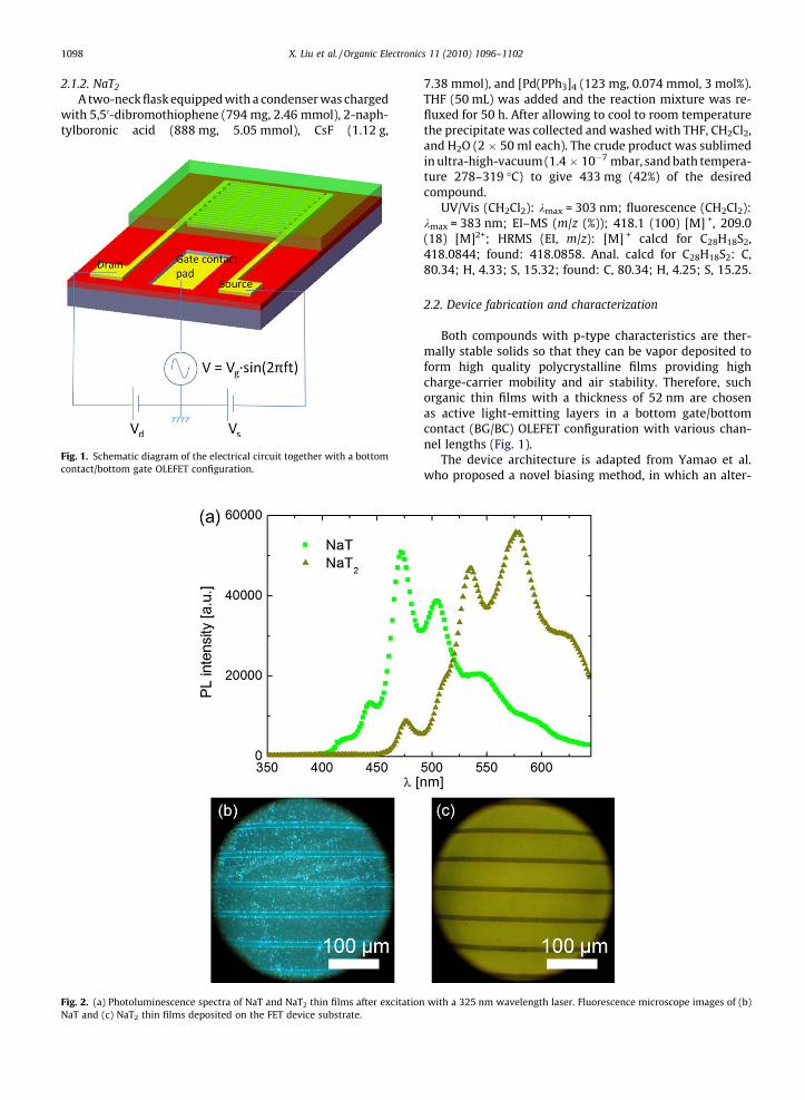
Fig. 2. (a) Photoluminescence spectra of NaT and NaT2 thin films after excitationNaT and (c) NaT2 thin films deposited on the FET device substrate.
7.38 mmol), and [Pd(PPh3]4 (123 mg, 0.074 mmol, 3 mol%).THF (50 mL) was added and the reaction mixture was re-fluxed for 50 h. After allowing to cool to room temperaturethe precipitate was collected and washed with THF, CH2Cl2,and H2O (2 � 50 ml each). The crude product was sublimedin ultra-high-vacuum (1.4 � 10�7 mbar, sand bath tempera-ture 278–319 �C) to give 433 mg (42%) of the desiredcompound.
UV/Vis (CH2Cl2): kmax = 303 nm; fluorescence (CH2Cl2):kmax = 383 nm; EI–MS (m/z (%)); 418.1 (100) [M]�+, 209.0(18) [M]2+; HRMS (EI, m/z): [M]�+ calcd for C28H18S2,418.0844; found: 418.0858. Anal. calcd for C28H18S2: C,80.34; H, 4.33; S, 15.32; found: C, 80.34; H, 4.25; S, 15.25.
2.2. Device fabrication and characterization
Both compounds with p-type characteristics are ther-mally stable solids so that they can be vapor deposited toform high quality polycrystalline films providing highcharge-carrier mobility and air stability. Therefore, suchorganic thin films with a thickness of 52 nm are chosenas active light-emitting layers in a bottom gate/bottomcontact (BG/BC) OLEFET configuration with various chan-nel lengths (Fig. 1).
The device architecture is adapted from Yamao et al.who proposed a novel biasing method, in which an alter-
with a 325 nm wavelength laser. Fluorescence microscope images of (b)

Fig. 3. Optical microscope image of electroluminescence from a 52 nmthin film of NaT (a) and a 52 nm thin film of NaT2 (b) operated by asinusoidal AC gate voltage.
X. Liu et al. / Organic Electronics 11 (2010) 1096–1102 1099
nating current (AC) voltage is applied to the gate terminalof a BG/BC OLEFET with a phenylene–thiophene oligomeras the active organic layer [24]. Their study demonstratedthat the AC gate voltage allows injection of holes and elec-trons from source and drain electrodes, respectively, lead-ing to intense light emission within the channel region.Moreover, a noble metal (Au) can be used to inject bothholes and electrons and gold is therefore also used in ourstudy.
Highly n-doped silicon (q = 0.025 O cm) served as backgate electrode, on which 300 nm SiO2 (C = 11.5 nF cm�2)was thermally grown. An interdigitated array of titanium/gold (2 nm/30 nm) source and drain electrodes was fabri-cated on SiO2 by optical lithography, metal evaporation(electron beam heating), and lift-off. The channel widthW is summed up to 2.66 cm, and the channel length L var-ies from 2.5, 5 to 10 lm. The substrate fabrication wascompleted by etching out a rectangular area (defined byphotolithography) in the SiO2 film using buffered hydroflu-oric acid and then depositing titanium/gold (10 nm/50 nm)as the contact pad to the back gate, which is depicted inFig. 1. The substrates were cleaned by one minute ultra-sonic agitation in acetone followed by five minutes DI-water rinse. Organic thin films with a thickness of 52 nmwere then deposited onto the substrates at room tempera-ture and under vacuum conditions (2 � 10�6 mbar) at arate of 0.1–0.4 Å s�1.
The photoluminescence spectra of both materials werecollected by exciting the materials with a He–Cd laser(wavelength of 325 nm) and recording the spectra withan ARC SpectraPro-150 spectrometer in ambient air. A Ni-kon eclipse ME 600 epifluorescence microscope with amercury UV lamp was used to obtain fluorescence imagesof the deposited organic materials. The electrolumines-cence experiments have been carried out under vacuumconditions (�8 � 10�5 mbar). Source and drain were sym-metrically biased relative to ground using two Delta Elek-tronika ES075-2 DC power supplies, while the gateelectrode was biased by a Grundig FG100 function genera-tor amplified by a Falco Systems WMA-300 voltage ampli-fier. A schematic diagram of the electrical circuit alongwith an OFET structure is illustrated in Fig. 1. Light emis-sion was detected either with a Navitar microscope and aLumenera Infinity1 camera or an ARC SpectraPro-150spectrometer.
Fig. 4. Electroluminescence spectra of a 52 nm NaT thin film operatedunder drain and source voltages of Vd = �Vs = 0 V and an AC gate voltagewith varying frequencies and amplitudes. The photoluminescence spec-trum (scaled by a factor of 100) is also shown for comparison.
3. Results and discussion
3.1. Photoluminescence
Fig. 2(a) shows the photoluminescence characteristicsof 52 nm thin films obtained upon vapor deposition ofNaT and NaT2, respectively. The spectra indicate green–blue light emission from NaT and yellow light emissionfrom NaT2. This is consistent with the fluorescence imagesshown in Fig. 2(b) and (c), respectively. Since naphthylend-capped (oligo)thiophenes are semiconducting materi-als, the peaks of the spectra can be attributed to the tran-sition from the vibrational ground state of the electronicexcited state to vibrational states of the electronic ground
state. The wider HOMO–LUMO gap of NaT compared withNaT2 suggested by the spectra in Fig. 2(a) is in agreementwith the HOMO–LUMO gap decreasing trend with theincreasing number of thiophene rings in naphthyl end-capped oligothiophenes reported by Tian et al. [21].
1100 X. Liu et al. / Organic Electronics 11 (2010) 1096–1102
3.2. Electroluminescence
Both the green–blue electroluminescence from NaTand the yellow electroluminescence from NaT2 can be ob-served in an optical microscope. Fig. 3(a) shows a NaT de-vice with 2.5 lm channel length emitting green–bluelight generated by drain and source voltages ofVd = �Vs = 10 V and an AC gate voltage with a frequencyof f = 200 kHz and an amplitude of Vg = 87.5 V. Electrolu-minescence of a NaT2 device with 10 lm channel lengthis presented in Fig. 3(b) (Vd = �Vs = 15 V, f = 200 kHz,and Vg = 62.5 V). The inset of Fig. 3(b) demonstrates that
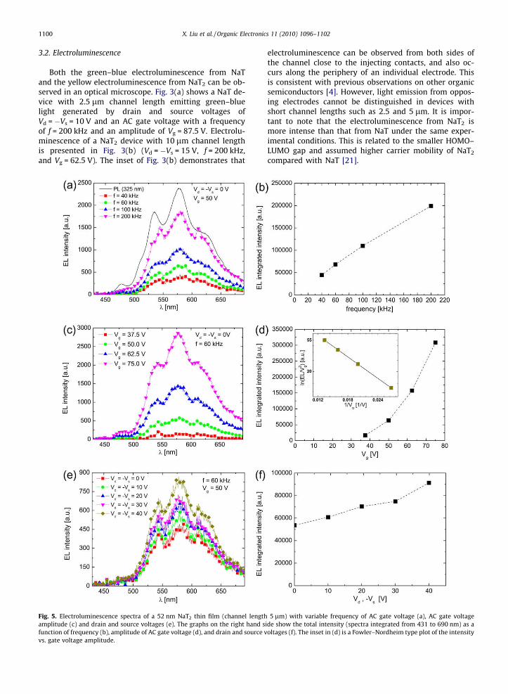
Fig. 5. Electroluminescence spectra of a 52 nm NaT2 thin film (channel lengthamplitude (c) and drain and source voltages (e). The graphs on the right hand sfunction of frequency (b), amplitude of AC gate voltage (d), and drain and source vvs. gate voltage amplitude.
electroluminescence can be observed from both sides ofthe channel close to the injecting contacts, and also oc-curs along the periphery of an individual electrode. Thisis consistent with previous observations on other organicsemiconductors [4]. However, light emission from oppos-ing electrodes cannot be distinguished in devices withshort channel lengths such as 2.5 and 5 lm. It is impor-tant to note that the electroluminescence from NaT2 ismore intense than that from NaT under the same exper-imental conditions. This is related to the smaller HOMO–LUMO gap and assumed higher carrier mobility of NaT2
compared with NaT [21].
5 lm) with variable frequency of AC gate voltage (a), AC gate voltageide show the total intensity (spectra integrated from 431 to 690 nm) as aoltages (f). The inset in (d) is a Fowler–Nordheim type plot of the intensity
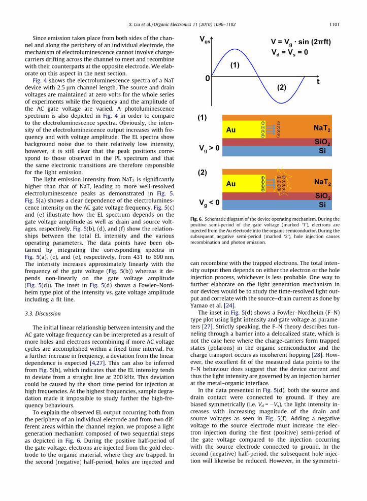
Fig. 6. Schematic diagram of the device operating mechanism. During thepositive semi-period of the gate voltage (marked ‘1’), electrons areinjected from the Au electrode into the organic semiconductor. During thesubsequent negative semi-period (marked ‘2’), hole injection causesrecombination and photon emission.
X. Liu et al. / Organic Electronics 11 (2010) 1096–1102 1101
Since emission takes place from both sides of the chan-nel and along the periphery of an individual electrode, themechanism of electroluminescence cannot involve charge-carriers drifting across the channel to meet and recombinewith their counterparts at the opposite electrode. We elab-orate on this aspect in the next section.
Fig. 4 shows the electroluminescence spectra of a NaTdevice with 2.5 lm channel length. The source and drainvoltages are maintained at zero volts for the whole seriesof experiments while the frequency and the amplitude ofthe AC gate voltage are varied. A photoluminescencespectrum is also depicted in Fig. 4 in order to compareto the electroluminescence spectra. Obviously, the inten-sity of the electroluminescence output increases with fre-quency and with voltage amplitude. The EL spectra showbackground noise due to their relatively low intensity,however, it is still clear that the peak positions corre-spond to those observed in the PL spectrum and thatthe same electronic transitions are therefore responsiblefor the light emission.
The light emission intensity from NaT2 is significantlyhigher than that of NaT, leading to more well-resolvedelectroluminescence peaks as demonstrated in Fig. 5.Fig. 5(a) shows a clear dependence of the electrolumines-cence intensity on the AC gate voltage frequency. Fig. 5(c)and (e) illustrate how the EL spectrum depends on thegate voltage amplitude as well as drain and source volt-ages, respectively. Fig. 5(b), (d), and (f) show the relation-ships between the total EL intensity and the variousoperating parameters. The data points have been ob-tained by integrating the corresponding spectra inFig. 5(a), (c), and (e), respectively, from 431 to 690 nm.The intensity increases approximately linearly with thefrequency of the gate voltage (Fig. 5(b)) whereas it de-pends non-linearly on the gate voltage amplitude(Fig. 5(d)). The inset in Fig. 5(d) shows a Fowler–Nord-heim type plot of the intensity vs. gate voltage amplitudeincluding a fit line.
3.3. Discussion
The initial linear relationship between intensity and theAC gate voltage frequency can be interpreted as a result ofmore holes and electrons recombining if more AC voltagecycles are accomplished within a fixed time interval. Fora further increase in frequency, a deviation from the lineardependence is expected [4,27]. This can also be inferredfrom Fig. 5(b), which indicates that the EL intensity tendsto deviate from a straight line at 200 kHz. This deviationcould be caused by the short time period for injection athigh frequencies. At the highest frequencies, sample degra-dation made it impossible to study further the high-fre-quency behaviours.
To explain the observed EL output occurring both fromthe periphery of an individual electrode and from two dif-ferent areas within the channel region, we propose a lightgeneration mechanism composed of two sequential stepsas depicted in Fig. 6. During the positive half-period ofthe gate voltage, electrons are injected from the gold elec-trode to the organic material, where they are trapped. Inthe second (negative) half-period, holes are injected and
can recombine with the trapped electrons. The total inten-sity output then depends on either the electron or the holeinjection process, whichever is less probable. One way tofurther elaborate on the light generation mechanism inour devices would be to study the time-resolved light out-put and correlate with the source–drain current as done byYamao et al. [24].
The inset in Fig. 5(d) shows a Fowler–Nordheim (F–N)type plot using light intensity and gate voltage as parame-ters [27]. Strictly speaking, the F–N theory describes tun-neling through a barrier into a delocalized state, which isnot the case here where the charge-carriers form trappedstates (polarons) in the organic semiconductor and thecharge transport occurs as incoherent hopping [28]. How-ever, the excellent fit of the measured data points to theF–N behaviour does suggest that the device current andthus the light intensity are governed by an injection barrierat the metal–organic interface.
In the data presented in Fig. 5(d), both the source anddrain contact were connected to ground. If they arebiased symmetrically (i.e. Vd = �Vs), the light intensity in-creases with increasing magnitude of the drain andsource voltages as seen in Fig. 5(f). Adding a negativevoltage to the source electrode must increase the elec-tron injection during the first (positive) semi-period ofthe gate voltage compared to the injection occurringwith the source electrode connected to ground. In thesecond (negative) half-period, the subsequent hole injec-tion will likewise be reduced. However, in the symmetri-
1102 X. Liu et al. / Organic Electronics 11 (2010) 1096–1102
cally biased configuration, the hole injection occurringfrom the drain contact should increase and the electroninjection should decrease. Assuming that the limitingfactor on the light emission is electron injection, oneshould therefore anticipate that the light emission occur-ring at the source (drain) electrode would increase (de-crease). Since the data in Fig. 5(f) represent the averageover a large area, it therefore suggests that the increaseoccurring at the source electrodes more than outweighsthe intensity decrease at the drain electrodes. However,the detailed mechanism of this effect is still not clearlyunderstood. Yamao et al. also observed an increasinglight intensity with increasing magnitude of the drainand source voltages [24], however their model deals withrecombination of holes and electrons injected from oppo-site electrodes as opposed to ours that only includes oneinjecting electrode, so a direct comparison is not feasible.
4. Conclusions and outlook
Two naphthyl end-capped (oligo)thiophenes areimplemented in an easy-fabricated OLEFET structure uti-lizing an AC gate voltage to obtain intensified electrolu-minescence. The intensity of the electroluminescenceemission is linearly proportional to the frequency of theAC gate voltage amplitude and is non-linearly dependenton the amplitude of the AC voltage. We propose that thisnon-linearity is caused by the carrier injection process,which, although occurring into localized states in an or-ganic semiconductor nevertheless obeys a simple Fow-ler–Nordheim relationship. Further experiments areaimed at studying this effect in more detail and at inte-grating nanostructured organic material [22] on the de-vice substrate to realize nanoscale OLEFETs [4]. Inaddition, it must be expected that tuning of the injectionbarrier can lead to more efficient light emission. Thiscould for example be realized by modifying the gold elec-trodes via, e. g., adsorption of an organic layer prior todeposition of the organic semiconductor [29].
Acknowledgements
I. Wallmann and A. Lützen are grateful to the DeutscheForschungsgemeinschaft for financial support. The VELUXFoundation and the BHJ-Foundation are acknowledgedfor financial support. Finally, we thank Henrik H. Henrich-sen for assisting with the sample preparation.
References
[1] C.D. Dimitrakopoulos, P.R.L. Malenfant, Adv. Mater. 14 (2002) 99–117.
[2] A.L. Briseno, S.C.B. Mannsfeld, S.A. Jenekhe, Z. Bao, Y. Xia, Mater.Today 11 (2008) 38–47.
[3] A. Hepp, H. Heil, W. Weise, M. Ahles, R. Schmechel, H. von Seggern,Phys. Rev. Lett. 91 (2003) 157406.
[4] J. Kjelstrup-Hansen, X. Liu, H.H. Henrichsen, K. Thilsing-Hansen, H.G.Rubahn, Phys. Status Solidi (c), in press.
[5] H. Yanagi, T. Morikawa, S. Hotta, Appl. Phys. Lett. 81 (2002) 1512–1514.
[6] D.H. Kim, D.Y. Lee, H.S. Lee, W.H. Lee, Y.H. Kim, J.I. Han, K. Cho, Adv.Mater. 19 (2007) 678–682.
[7] J.H. Oh, H.W. Lee, S. Mannsfeld, R.M. Stoltenberg, E. Jung, Y.W. Jin,J.M. Kim, J.-B. Yoo, Z. Bao, Proc. Natl. Acad. Sci. USA 106 (2009) 6065–6070.
[8] C. Rost, S. Karg, W. Riess, M.A. Loi, M. Murgia, M. Muccini, Appl. Phys.Lett. 85 (2004) 1613.
[9] J. Zaumseil, C.L. Donley, J.S. Kim, R.H. Friend, H. Sirringhaus, Adv.Mater. 18 (2006) 2708–2712.
[10] R. Rotzoll, S. Mohapatra, V. Olariu, R. Wenz, M. Grigas, K. Dimmler,Appl. Phys. Lett. 88 (2006) 123502.
[11] S.R. Forrest, Nature 428 (2004) 911–918.[12] M. Muccini, Nat. Mater. 5 (2006) 605–613.[13] G. Horowitz, D. Fichou, X. Peng, Z. Xu, F. Garnier, Solid State
Commun. 72 (1989) 381–384.[14] F. Geiger, M. Stoldt, H. Schweizer, P. Bäuerle, E. Umbach, Adv. Mater.
5 (1993) 922–925.[15] G. Horowitz, Adv. Mater. 10 (1998) 365–377.[16] Y.-Y. Lin, D.J. Gundlach, S.F. Nelson, T.N. Jackson, IEEE Trans. Electron.
Dev. 44 (1997) 1325–1331.[17] K. Wong, C. Wang, C.H. Chou, Y.O. Su, G. Lee, S. Peng, Org. Lett. 25
(2002) 4439–4442.[18] T. Noda, H. Ogawa, N. Noma, Y. Shirota, J. Mater. Chem. 9 (1999)
2177–2181.[19] H. Yanagi, Y. Araki, T. Ohara, S. Hotta, M. Ichikawa, Y. Taniguchi, Adv.
Funct. Mater. 13 (2003) 767–773.[20] J.A. Merlo, C.R. Newman, C.P. Gerlach, T.W. Kelley, D.V. Muyres, S.E.
Fritz, M.F. Toney, C.D. Frisbie, J. Am. Chem. Soc. 127 (2005) 3997–4009.
[21] H. Tian, J. Shi, B. He, N. Hu, S. Dong, D. Yan, J. Zhang, Y. Geng, F. Wang,Adv. Funct. Mater. 17 (2007) 1940–1951.
[22] M. Schiek, F. Balzer, K. Al-Shamery, A. Lützen, H.-G. Rubahn, J. Phys.Chem. C 113 (2009) 9601–9608.
[23] T. Sakanoue, M. Yahiro, C. Adachi, J.H. Burroughes, Y. Oku, N. Shimoji,T. Takahashi, A. Toshimitsu, Appl. Phys. Lett. 92 (2008) 053505.
[24] T. Yamao, Y. Shimizu, K. Terasaki, S. Hotta, Adv. Mater. 20 (2008)4109–4112.
[25] R. Soumya, M. Charette, S.P. Finkelstein, PCT Int. Appl. (2009) WO2009088975 A2 20090716.;Y. Geng, H. Tian, J. Shi, Faming Zhuanli Shenqing GongkaiShuomingshu (2006) CN 1807428 A 20060726.;O. Hotta, T. Tamaoki, Jpn. Kokai Tokkyo Koho (2000) JP 2000-26451A 20000125.
[26] M. Schiek, K. Al-Shamery, A. Lützen, Synthesis (2007) 613–621;I. Wallmann, M. Schiek, R. Koch, A. Lützen, Synthesis (2008) 2446–2450;I. Wallmann, G. Schnakenburg, A. Lützen, Synthesis (2009) 79–84.
[27] R.J. Walters, G.I. Bourianoff, H.A. Atwater, Nat. Mater. 4 (2005) 143–146.
[28] J. Shinar, R. Shinar, J. Phys. D: Appl. Phys. 41 (2008) 133001.[29] B.H. Hamadani, D.A. Corley, J.W. Ciszek, J.M. Tour, D. Natelson, Nano
Lett. 6 (2006) 1303–1306.
Copyright © 2022 FDOKUMEN